1
R
Connectorless Debugging Port Landing Pads (J6)
Connectorless Debugging Port Landing Pads (J6)
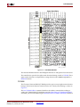
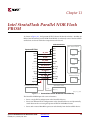
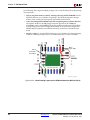
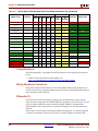
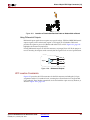
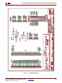
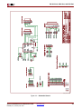
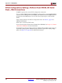
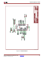
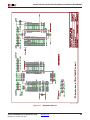
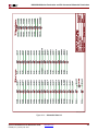
Landing pads for a connectorless debugging port are provided as header J6, shown in
Figure 15-1, page 115. There is no physical connector on the board. Instead a connectorless
probe, such as those available from Agilent, provides an interface to a logic analyzer. This
debugging port is intended primarily for the Xilinx ChipScope Pro software with the
Agilent’s FPGA Dynamic Probe. It can, however, be used with either the Agilent or
Tektronix probes, without the ChipScope software, using FPGA Editor’s probe command.
Refer to “Related Resources,” page 126 for more information on the ChipScope Pro tool,
probes, and connectors.
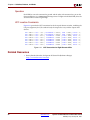
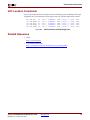
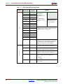
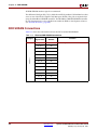
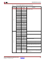
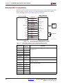
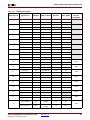
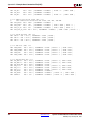
Table 15-3 provides the connector pinout. Only 18 FPGA pins attach to the connector; the
remaining connector pads are unconnected. All 18 FPGA pins are shared with the FX2
connector (J3) and the 6-pin accessory port connectors (J1, J2, and J4). See Table 15-1,
page 117 for more information on how these pins are shared.
Table 15-3:
Connectorless Debugging Port Landing Pads (J6)
Connectorless
Landing Pads
Signal Name
FPGA Pin
FPGA Pin
Signal Name
FX2_IO1
B4
A1
B1
GND
GND
FX2_IO2
A4
A2
B2
D5
FX2_IO3
GND
GND
A3
B3
C5
FX2_IO4
FX2_IO5
A6
A4
B4
GND
GND
FX2_IO6
B6
A5
B5
E7
FX2_IO7
GND
GND
A6
B6
F7
FX2_IO8
FX2_IO9
D7
A7
B7
GND
GND
FX2_IO10
C7
A8
B8
F8
FX2_IO11
GND
GND
A9
B9
E8
FX2_IO12
FX2_IO13
F9
A10
B10
GND
GND
FX2_IO14
E9
A11
B11
D11
FX2_IO15
GND
GND
A12
B12
C11
FX2_IO16
FX2_IO17
F11
A13
B13
GND
GND
FX2_IO18
E11
A14
B14
A15
B15
A16
B16
A17
B17
A18
B18
A19
B19
A20
B20
A21
B21
A22
B22
A23
B23
A24
B24
A25
B25
A26
B26
A27
B27
Spartan-3E FPGA Starter Kit Board User Guide
UG230 (v1.2) January 20, 2011
www.xilinx.com
125


































![2008 [DAMN SMALL NAS]](http://vs1.manualzilla.com/store/data/005757702_2-ad0d2f1082977ee9ed587e807bbc0127-150x150.png)