1
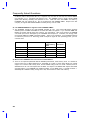
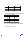
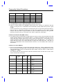
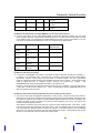
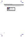
AP5T/AX5T Special Test Notice
Please refer to following FAQ (Frequently Asked Question) for the special test notice and interesting
features of INTEL TX chipset.
1. TX memory performance.
2. TX DMA/33 performance.
3. SDRAM that can be used.
4. 75/83.3MHz external clock.
5. ACPI new features. (Modem ring-on, OnNow, Suspend to HDD)
6. P55C MMX
7. FCC DoC
Note: FAQ may be updated without notice. If
you cannot find the information that you need in
this appendix, visit our WWW home page,
(address: http://www.aopen.com.tw) and check
the FAQ area and other new information.
Q: What is MMX?
A: MMX is the new single-line multiple-instruction technology of the new Intel Pentium PP/MT (P55C)
CPU. A new Pentium Pro CPU (Klamath) with MMX technology is also expected to be released soon.
The MMX instructions are specifically useful for multimedia applications (such as 3D video, 3D
sound, video conference). The performance can be improved if applications use these instructions. All
AOpen MBs have at least dual power onboard to support PP/MT. It is not necessary to have special
chipset for MMX CPU.
Q: What is PBSRAM (Pipelined Burst SRAM)?
A: For Pentium CPU, the Burst means reading four QWord (Quad-word, 4x16 = 64 bits) continuously
with only the first address decoded by SRAM. The PBSRAM will automatically send the remaining
three QWord to CPU according to predefined sequence. The normal address decoding time for
SRAM is 2 to 3 clocks. This makes the CPU data read timing of four QWord to be at least 3-2-2-2
and a total of 9 clocks if traditional asynchronous SRAM is used. However, with PBSRAM, there is
no need to decode address for rest three Qword. Therefore, data read timing can be 3-1-1-1, that is
equivalent to 6 clocks and is faster than asynchronous SRAM.
Q: What is EDO (Extended Data Output) memory?
A: The EDO DRAM technology of EDO is actually very similar to FPM (Fast Page Mode). Unlike
traditional FPM that tri-states the memory output data to start the pre-charge activity, EDO DRAM
holds the memory data valid until the next memory access cycle, that is similar to pipeline effect and
reduces one clock state.
Q: What is SDRAM (Synchronous DRAM)?
A: The SDRAM is a new generation DRAM technology that allows DRAM to use the same clock as the
CPU host bus (EDO and FPM are asynchronous and do not have clock signal). The idea is the same
B-1
Frequently Asked Questions
as "Burst" (refer to the previous Q & A). It requires only one clock for the 2nd, 3rd, and 4th QWord
(for example, 5-1-1-1 compares with EDO 5-2-2-2). The SDRAM comes in 64-bit 168-pin DIMM
(Dual-in-line Memory Module) and operates at 3.3V. Note that some old DIMMs are made by
FPM/EDO and only operate at 5V. Do not confuse them with SDRAM DIMM. AOpen is the first
company to support dual-SDRAM DIMMs onboard (AP5V), from Q1 1996.
Q: Can SDRAM DIMM work together with FPM/EDO SIMM?
A: The FPM/EDO operate at 5V while SDRAM operates at 3.3V. The current MB design provides
different power to DIMM and SIMM but connects the data bus together. If you combine SIMM and
DIMM, the system will still work fine; however, only temporarily. After a few months, the SDRAM
3.3V data input will be damaged by 5V FPM/EDO data output line. Therefore, we strongly NOT
recommend DIMM and SIMM combined together. There is one exception, if your SDRAM supports
5V tolerance (such as TI or Samsung), which accepts 5V signal at 3.3V operating power, you can
combine them.
Manufacturer
Model
Suggested
CAS Latency
Time
5V
Tolerance
Samsung
NEC
Micron
TI
TI
KM416S1120AT-G12
D4516161G5-A12-7JF
MT4LC1M16E5TG-6
TMS626162DGE -15
TMS626162DGE M-67
2
2
2
2
3
Yes
No
No
Yes
Yes
Q: What kind of SDRAM have been tested on AP5T/AX5T?
A: There is an important parameter affects SDRAM performance, CAS Latency Time. It is similar as
CAS Access Time of EDO DRAM and is calculated as number of clock state. INTEL TX chipset
support 2 or 3 clocks CAS Latency Time, and the default timing is set to 2 clocks. However, there is
SDRAM which can not meet requirement of INTEL TX chipset. The SDRAM that AOpen had tested
are listed below. If your SDRAM has unstable problem, go into BIOS setup → Chipset Features →
SDRAM(CAS Lat/RAS-to-CAS), change 2/2 to 3/3, which means 3 clocks CAS Latency.
B-2
Frequently Asked Question
Manufacturer
Model
Suggested
CAS Latency
Time
5V
Tolerance
Samsung
NEC
Micron
TI
TI
KM416S1120AT-G12
D4516161G5-A12-7JF
MT4LC1M16E5TG-6
TMS626162DGE -15
TMS626162DGE M-67
2
2
2
2
3
Yes
No
No
Yes
Yes
Q: Which Pentium chipset has the best performance?
A: The performance difference of chipset depends on what kind of DRAM they use and the DRAM timing
they support. (They all use PBSRAM, so that the difference is very little at 2nd level cache.)
The following table lists the read timing of current available chipsets. The four digital represents the
clocks needed for 1st-2nd-3rd-4th QWord. Notice that the Intel HX + EDO or SIS 5571+ EDO are
almost the same as VX + SDRAM and the TX + SDRAM has the best performance among Pentium
chipsets. Please note AP57 does not support SDRAM..
P5 Chipset
Model
PBSRAM
FPM
EDO
SDRAM
Intel 430FX
Intel 430VX
AP5C/P
AP5VM/
AP5V
AP53/
AP5K/
AX53
AP5T/
AX5T
AP57
AP58/
AX58
3-1-1-1
3-1-1-1
7-3-3-3
6-3-3-3
7-2-2-2
6-2-2-2
NA
6-1-1-1
3-1-1-1
6-3-3-3
5-2-2-2
NA
3-1-1-1
6-3-3-3
5-2-2-2
5-1-1-1
3-1-1-1
3-1-1-1
5-3-3-3
5-3-3-3
4/5-2-2-2
4/5-2-2-2
(6/7-1-1-1)
6/7-1-1-1
Intel 430HX
Intel 430TX
SIS 5571
SIS 5582
Q: What is the memory performance improvement of TX chipset?
A: Following is the compare table of TX+SDRAM, VX+SDRAM, TX+EDO, HX+EDO and VX+EDO.
CPU
: Pentium PP/MT (P55C) 200MHz
DRAM
:16MB EDO or SDRAM
HDD : Quantum Fireball 1280AT
VGA : AOpen PV60 S3 Trio64V+ 800x600x256 Small font
OS
: Windows 95 OSR2
B-3
Frequently Asked Questions
Chipset
Model
DRAM
Timing
Winstone9
6
Intel 430VX
Intel 430HX
Intel 430TX
Intel 430VX
Intel 430TX
AP5VM
AP53/AP5K
AP5T/AX5T
AP5VM/AP5V
AP5T/AX5T
EDO
EDO
EDO
SDRAM
SDRAM
6-2-2-2
5-2-2-2
5-2-2-2
6-1-1-1
5-1-1-1
86.1
86.8
87.3
86.6
87.7
Q: Can AP5T/AX5T support 75M and 83.3MHz external CPU clock?
A: INTEL TX chipset support only 60/66MHz external (bus) clock. However, we tested the lab pilot
sample, it looks good to run 75/83.3MHz under Winstone96, perhaps INTEL BGA process is good
enough.
For the convenience of over-clocking user, we add jumper (JP5) on new version AP5T-2 and AX5T-1.
User set clock to 75/83.3MHz is taking his own risk, and is probably to have system unstable
behavior. Note that AX5T-1 supports 75MHz but without 83.3MHz, because the clock generator
reserves more pins for I2C bus. The AP5T-2 and AX5T-2 support both 75/83.3MHz
Q: What is Bus Master IDE (DMA mode)?
A: The traditional PIO (Programmable I/O) IDE requires the CPU to involve in all the activities of the IDE
access including waiting for the mechanical events. To reduce the workload of the CPU, the bus
master IDE device transfers data from/to memory without interrupting CPU, and releases CPU to
operate concurrently while data is transferring between memory and IDE device. You need the bus
master IDE driver and the bus master IDE HDD to support bus master IDE mode. Note that it is
different with master/slave mode of the IDE device connection. For more details, refer to section 2.3
"Connectors".
Q: What is the Ultra DMA/33?
A: This is the new specification to improve IDE HDD data transfer rate. Unlike traditional PIO mode,
which only uses the rising edge of IDE command signal to transfer data, the DMA/33 uses both rising
edge and falling edge. Hence, the data transfer rate is double of the PIO mode 4 or DMA mode 2.
(16.6MB/s x2 = 33MB/s).
The following table lists the transfer rate of IDE PIO and DMA modes. The IDE bus is 16-bit, which
means every transfer is two bytes.
Mode
Clock
count
Cycle
time
Data Transfer rate
PIO mode 0
Clock per
33MHz
PCI
30ns
20
600ns
PIO mode 1
30ns
13
383ns
PIO mode 2
30ns
8
240ns
PIO mode 3
30ns
6
180ns
PIO mode 4
30ns
4
120ns
DMA mode 0
30ns
16
480ns
(1/600ns) x 2byte =
3.3MB/s
(1/383ns) x 2byte =
5.2MB/s
(1/240ns) x 2byte =
8.3MB/s
(1/180ns) x 2byte =
11.1MB/s
(1/120ns) x 2byte =
16.6MB/s
(1/480ns) x 2byte =
4.16MB/s
B-4
Frequently Asked Question
DMA mode 1
30ns
5
150ns
DMA mode 2
30ns
4
120ns
DMA/33
30ns
4
120ns
(1/150ns) x 2byte =
13.3MB/s
(1/120ns) x 2byte =
16.6MB/s
(1/120ns) x 2byte x2 =
33MB/s
Q: What is the performance of Ultra DMA/33? Do we need special driver?
A: Currently (Jan 1997), the only Ultra DMA/33 HDD we can test is Quantum 1620AT. It is only a lab
pilot run sample and has not been tuned to best performance. The final sample will probably be ready
in the middle of Feb. You need driver to activate DMA/33, there are now driver from INTEL or you can
use driver in the Windows 95 Memphis, which can recognize South Bridge PIIX4.
Model
OS/Driver
Mode
Quantum
1620AT
Quantum
1620AT
Quantum
1620AT
Windows 95
OSR2
Windows 95
OSR2
Windows 95
OSR2 + INTEL
driver
Windows 95
Memphis
Windows 95
Memphis
PIO mode 4
Winbench96
Diskwinmark
1330
DMA mode 2
1300
DMA/33
1280
PIO mode 4
1280
DMA/33
1330
Quantum
1620AT
Quantum
1620AT
Q: What is PnP (Plug and Play)?
A: In the past, the IRQ/DMA and memory or I/O space of add-on cards are normally set manually, i.e.,
by jumper or by proprietary utility. The user has to check the user's guide for the correct setting.
Sometimes, resource conflict occurs and this leads to unstable system.. The PnP specification
suggests a standard register interface for both BIOS and OS (such as Win95). These registers are
used by BIOS and OS to configure system resource and prevent any conflicts.
The
IRQ/DMA/Memory will be automatically allocated by PnP BIOS or OS.
Currently, almost all the PCI cards and most ISA cards are PnP compliant. If you are still using a
Legacy ISA card that cannot support PnP, set the corresponding resource (IRQ/DMA/memory) to
ISA in the BIOS "PCI/PnP Setup".
Q: What is ACPI (Advanced Configuration & Power Interface) and OnNow?
A: The ACPI is new power management specification of 1997 (PC97). It intends to save more power by
taking full control of power management to operating system and not through BIOS. Because of this,
the chipset or super I/O chip needs to provide standard register interface to OS (such as Win97) and
provides the ability for OS to shutdown and resume power of different part of chip. The idea is a bit
similar to the PnP register interface.
ACPI defines momentary soft power switch to control the power state transition. Most likely, it uses
the ATX form factor with momentary soft power switch. The most attractive part of ACPI for desktop
user is probably the "OnNow" feature, an idea from notebook. This feature allows you to immediately
resume to your original work without the long time waiting from bootup, entering Win95 and running
Winword. The AX5T with Intel TX chipset can support ACPI.
B-5
Frequently Asked Questions
Q: What is ATX Soft Power On/Off and Momentary Switch?
A: The Soft Power On of the ATX specification means to provide a standby current for special circuit to
wait for wakeup event when main power is off. For example, Infrared wakeup, modem wakeup, or
voice wakeup. Currently, the most simple usage is to provide standby current for power switch circuit
so that power switch can turn on/off the main power through soft power control pin. The ATX power
specification does not mention anything about the power switch type. You can use toggle or
momentary switch, note that ACPI specification requires momentary switch for power state control.
All the AOpen ATX MBs support momentary switch and AX5T/AX58/AX6L support modem wakeup
(Modem Ring-On).
Soft Power Off means to turn off system through software, Windows 95 Shutdown function can be
used to verify if your mainboard supports soft power off. AOpen AX5T/AX58/AX6F/AX6L support soft
power off.
Q: What is the Modem Ring-On?
A: With the help of ACPI OnNow and ATX soft power On/Off, it is possible to have system totally power
off (The traditional suspend mode of power management function does not really turn off the system
power supply), and wakeup to automatically answer a phone call such as answering machine or to
send/receive fax. You may identify the true power off by checking fan of your power supply. AOpen
AX5T/AX58 implement special circuit for Modem Ring-On through external modem or internal
modem card such as AOpen F34I.
Q: How to use "True" Modem Ring-On?
A: The Modem Ring-On discussed here is to wakeup from true power off (identified by fan of power
supply is off), the traditional green PC suspend mode is not discussed here.
AOpen AX5T/AX58 ATX mainboards and F34I Modem card implement special circuit to detect ring
signal from telephone line and then, turn on system power. It is recommended to use Internal Modem
Card (AOpen F34I), since Internal Modem Card consumes no power when system power is off.
For Internal Modem Card (AOpen F34I):
1. Go into BIOS setup , Power Management
Wake Up by Ring, select Enable.
2. Setup your application, put into Windows 95 StartUp or use Suspend to Hard Disk function.
3. Turn system power off by soft power switch.
4. Connect 4-pin Modem Ring-On cable from F34I RING connector (it is CN2 on the evaluation sample)
to AX5T/AX58 connector WKUP.
5. Connect telephone line to F34I. You are now ready to use Modem Ring-On.
For External Box Modem:
1. Go into BIOS setup , Power Management
Wake Up by Ring, select Enable.
2. Setup your application, put into Windows 95 StartUp or use Suspend to Hard Disk function.
3. Turn system power off by soft power switch.
4. Connect RS232 cable of external box Modem to COM1 or COM2.
5. Connect telephone line to external box Modem. Turn on Modem power (you must keep Modem power
always on). You are now ready to use Modem Ring-On.
Q: What is the Suspend to Hard Disk?
A: This is the same as Notebook. You can resume your original work directly from hard disk without go
through the Win95 booting process and run your application again. Suspend to Hard Disk saves your
current work (system status, memory image) into hard disk. If your memory is 16MB, normally, you
need to reserve at least 16MB HDD space to save your memory image. ACPI OnNow is possible to
B-6
Frequently Asked Question
do the same function, since the ACPI specification is not fully ready. AOpen AX5T/AX58 support
Suspend to Hard Disk through BIOS. Note that you have to use AOpen VGA PT60 (S3 Virge), AOpen
Modem card F34I (Rockwell), AOpen Sound card S320 (Creative) for Suspend to Hard Disk to work
properly.
Q: What is the AGP (Accelerated Graphic Port)?
A: AGP is a PCI-like bus interface targeted for high-performance 3D graphic. AGP supports only
memory read/write operation and single-master single-slave one-to-one only. The AGP uses both
rising and falling edge of the 66MHz clock and produces 66MHz x 4byte x 2 = 528MB/s data transfer
rate. The AOpen AX6L MB are designed to support AGP via the new Intel Klamath LX chipset.
Q: Why the AOpen mainboards (MB) do not have cache module expansion slot?
A: Faster CPU speed requires more difficult and complex MB timing design. Every trace and
components delay must be taken into consideration. The expansion cache slot design will cause 2 or
3ns delay in PBSRAM timing, and the extended trace length to the cache module through the golden
finger will further delay the timing by 1 or 2ns. This may result in unreliable system once the cache
module and slot becomes worn. All AOpen MBs support 512KB PBSRAM onboard. For better
performance (around 3% higher than 256KB), we strongly recommend you to use 512KB onboard.
Otherwise, reliable 256KB is better than unreliable 512KB with cache module. AOpen is the first
company to promote this concept since the fourth quarter of 1995.
Q: What is USB (Universal Serial Bus)?
A: USB is a new 4-pin serial peripheral bus that is capable of cascading low/medium speed peripherals
(less than 10Mbit/s) such as keyboard, mouse, joystick, scanner, printer and modem/ISDN. With
USB, the traditional complex cables from back panel of your PC can be eliminated.
You need the USB driver to support USB device(s). AOpen MBs are all USB ready, you may get
latest BIOS from AOpen web site (http://www.aopen.com.tw). Our latest BIOS includes the keyboard
driver (called Legacy mode), that simulates USB keyboard to act as AT or PS/2 keyboard and makes
it possible to use USB keyboard if you don't have driver in your OS. For other USB devices, you may
get the drivers from your device vendor or from OS (such as Win95). Be sure to turn off "USB
Legacy Support" in BIOS "Chipset Setup" if you have another driver in your OS.
Q: What is P1394?
A: P1394 (IEEE 1394) is another standard of high-speed serial peripheral bus. Unlike low or medium
speed USB, P1394 supports 50 to 1000Mbit/s and can be used for video camera, disk and LAN.
Since P1394 is still under development, , there is no P1394 device currently available in the PC
market. Also, there is no chipset that can support P1394. Probably in the near future, a card will be
developed to support P1394 device.
Q: What is SMBus (System Management Bus, also called I2C bus)?
A: SMBus is a two-wire bus developed for component communication (especially for semiconductor IC).
It is most useful for notebook to detect component status and replace hardware configuration pin
(pull-high or pull-low). For example, disabling clock of DIMM that does not exist, or detecting battery
low condition. The data transfer rate of SMBus is only 100Kbit/s, it allows one host to communicate
with CPU and many masters and slaves to send/receive message. The SMBus may be used for
jumpless mainboard, the components which support SMbus are not ready yet, we will keep eyes on it.
Q: What is FCC DoC (Declaration of Conformity)?
A: The DoC is new certification standard of FCC regulations. This new standard allows DIY component
(such as mainboard) to apply DoC label separately without a shielding of housing. The rule to test
mainboard for DoC is to remove housing and test it with regulation 47 CFR 15.31. The DoC test of
B-7
Frequently Asked Questions
mainboard is more difficult than traditional FCC test. If the mainboard passes DoC test, that means it
has very low EMI radiation and you can use any kind of housing (even paper housing). Following is
an example of DoC label. Currently, AOpen AX65/AP57/AP5T had passed DoC test.
AP5T
Test To Comply
With FCC Standards
FOR HOME OR OFFICE USE
B-8