1
Data Sheet
VT8237R
South Bridge
Revision 2.06
December 15, 2004
VIA TECHNOLOGIES, INC.
Copyright Notice:
Copyright © 2002 - 2004 VIA Technologies Incorporated. Printed in the United States. ALL RIGHTS RESERVED.
No part of this document may be reproduced, transmitted, transcribed, stored in a retrieval system, or translated into
any language, in any form or by any means, electronic, mechanical, magnetic, optical, chemical, manual or otherwise
without the prior written permission of VIA Technologies Incorporated.
VT8233, VT8233A, VT8235, VT8235PCI and VT8237R may only be used to identify products of VIA Technologies.
VIA C3™ is a registered trademark of VIA Technologies.
AMD-K7™ and Athlon TM are registered trademarks of Advanced Micro Devices.
Celeron™ ,Pentium™, Pentium-II™, Pentium-III™, Pentium-4™, MMX™, and Intel™ ,are registered trademarks of Intel
Corporation.
PS/2™ is a registered trademark of International Business Machines Corporation.
Windows XP™, Windows 2000™, Windows ME™, Windows 98™, Windows 95™, and Plug and Play™ are registered
trademarks of Microsoft Corporation.
PCI™ is a registered trademark of the PCI Special Interest Group.
VESA™ is a trademark of the Video Electronics Standards Association.
All trademarks are the properties of their respective owners.
Disclaimer Notice:
No license is granted, implied or otherwise, under any patent or patent rights of VIA Technologies. VIA Technologies
makes no warranties, implied or otherwise, in regard to this document and to the products described in this document.
The information provided by this document is believed to be accurate and reliable as of the publication date of this
document. However, VIA Technologies assumes no responsibility for any errors in this document. Furthermore, VIA
Technologies assumes no responsibility for the use or misuse of the information in this document and for any patent
infringements that may arise from the use of this document. The information and product specifications within this
document are subject to change at any time, without notice and without obligation to notify any person of such change.
Offices:
USA Office:
940 Mission Court
Fremont, CA 94539
USA
Tel: (510) 683-3300
Fax: (510) 683-3301 or (510) 687-4654
Web: http://www.viatech.com
Taipei Office:
1st Floor, No. 531
Chung-Cheng Road, Hsin-Tien
Taipei, Taiwan ROC
Tel: (886-2) 2218-5452
Fax: (886-2) 2218-5453
Web: http://www.via.com.tw
VT8237R Data Sheet
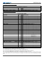
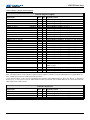
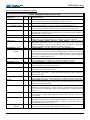
REVISION HISTORY
Document Release
1.07
Date
10/9/03
1.08
1.09
1.1
10/9/03
10/16/03
10/23/03
1.11
1.20
11/5/03
2/11/04
1.21
1.22
2/16/04
2/25/04
1.23
3/11/04
1.24
3/31/04
1.25
4/26/04
1.26
1.27
1.28
5/10/04
5/11/04
6/16/04
1.29
7/7/04
1.3
9/6/04
1.31
9/22/04
2.0
2.01
9/22/04
10/13/04
2.02
2.03
2.04
2.05
2.06
10/27/04
11/3/04
11/23/04
12/1/04
12/15/04
Revision
Modified Figure 2 & Figure 3 block diagram for SATA devices
Fixed signal description for MIIVCC and EEDI
Fixed power voltage for signals VCCAO, VCCAS, VCCATS, VCC, VSUS25,
VSUSUSB, MIIVCC25, RAMVCC, VCCUPLL, PLLVCC
Modified the power supply current of SATA oscillator on page169
Modified note for Dev.16 Fun.5 Offset 2F-2C on page 86
Added Figure 8. Mechanical Spec for place of origin in China.
Modified cover page style & header
Updated Device 15 Function 0 Rx45[6] and Device 17 Function 0 Rx5C[0]
Updated GPI17/CPUMISS signal description. Added Strap Pin Table.
Updated D17 F0 Rx4F[3], Rx54, RxE0 and E1, I/O offset 50 and 52
Changed Ultra V-Link pin names VAD to VD in Figure 4, Table 1, Table 2 and pin
descriptions
Removed Figure 8. Modified Figure 7 Mechanical Spec. by adding China as Country
of Assembly and adding CD to chip version
Modified Pins G22 (VIIN) and F23 (VIOUT) to NC.
Updated inter-operable VIA North Bridges in product features
Updated Figure 4, Table 1, Table 2 and Figure 6
Modified VCC, VCCUPLL and PLLVCC voltage
Added Pin Numbers to Strap Pins Table
Added headings to pin description tables
Updated D18F0 Rx6, 7, 8, 9, 0C, 0D, 23-20, 43-40, 6E and 6F
Updated Absolute Maximum Ratings, DC Characteristics and Power Requirements
Updated V-Link product features. Fixed AC’97 Audio Controller product features to
be AC97 2.2 compliant
Fixed total number of VCC33 pins on page 8 and 9.
Updated Figure 4, Table 1 and Table 2. Updated Absolute Maximum Ratings
Fixed pin# errors for DNSTB, USB6+, USB6- and PDDACK#
Added PERR# pin description to PCI Interface Pin Description Table
Modified Power Management I/O Space Registers I/O offset 1-0 bit 8
Modified I/O attribute of Pin LFRM#, LREQ0# and LREQ1# in Table 1&2 and pin
description table
Updated D18F0 I/O Register Rx7B
Updated D17F5 I./O Base 0 Rx41[4]
Modified PDA[2-0], SDA[2-0] pin descriptions
Fixed D17F0 Rx81[7]
Updated D15F0 Rx52[2], D17F0 Rx40. Added D15F0 Rx5E, Rx5F. Updated
SDIOR# signal description
Added Lead-Free package diagram
Updated D15F0 Rx43, Rx51[4:3], added Rx4E and removed Rx5F
Updated Table 9. APIC Fixed IRQ Routing
Updated D17F0 Rx80[5] and added RxC, E & F to D16F0-3.
Removed Rx33-30 from D15F0
Changed product name to VT8237R
Updated Taipei office address in legal page
Added D16F4 Rx5A-5E and updated D17F0 RxEC
Updated D17F5&6 Rx48-4B
Updated D17F0 Rx95[6]
Updated GPI17, GPI18 signal description and lead-free package diagram
Updated KBKC, KBDT signal descriptions
Fixed FERR# signal description
Revision 2.06 December 15, 2004
-i-
Initials
DA
DA
DA
DA
DA
DA
DA
DA
DA
DA
DA
DA
DA
DA
DA
DA
DA
DA
DA
DA
DA
DA
DA
DA
Revision History
VT8237R Data Sheet
TABLE OF CONTENTS
REVISION HISTORY .......................................................................................................................................................................I
TABLE OF CONTENTS.................................................................................................................................................................. II
LIST OF FIGURES .......................................................................................................................................................................... V
LIST OF TABLES ...........................................................................................................................................................................VI
PRODUCT FEATURES.................................................................................................................................................................... 1
OVERVIEW....................................................................................................................................................................................... 4
PINOUTS............................................................................................................................................................................................ 7
PIN DESCRIPTIONS...................................................................................................................................................................... 10
V-Link Pin Descriptions....................................................................................................................................................... 10
CPU, APIC and CPU Control Pin Descriptions ................................................................................................................ 11
PCI Bus Pin Descriptions..................................................................................................................................................... 12
MII, Serial EEPROM and Low Pin Count Pin Descriptions............................................................................................ 13
USB, SMB Pin Descriptions................................................................................................................................................. 14
Enhanced IDE Interface Pin Descriptions.......................................................................................................................... 15
Serial ATA Pin Descriptions................................................................................................................................................ 16
AC’97 Audio and Modem Pin Descriptions ....................................................................................................................... 17
Serial IRQ and PC / PCI DMA Pin Descriptions............................................................................................................... 17
Internal Keyboard Controller and Speaker Pin Descriptions .......................................................................................... 18
Programming Chip Selects Pin Descriptions ..................................................................................................................... 19
General Purpose Inputs Pin Descriptions........................................................................................................................... 19
General Purpose Outputs Pin Descriptions........................................................................................................................ 20
Power Management and Event Pin Descriptions............................................................................................................... 21
Clocks, Resets, Power Status, Power and Ground Pin Descriptions................................................................................ 22
Strap Pin Descriptions.......................................................................................................................................................... 23
REGISTERS..................................................................................................................................................................................... 24
REGISTER OVERVIEW ................................................................................................................................................................. 24
REGISTER DESCRIPTIONS ........................................................................................................................................................... 43
Legacy I/O Ports ................................................................................................................................................................... 43
Keyboard Controller I/O Registers........................................................................................................................................................ 44
DMA Controller I/O Registers .............................................................................................................................................................. 46
Interrupt Controller I/O Registers.......................................................................................................................................................... 47
Timer / Counter Registers...................................................................................................................................................................... 47
CMOS / RTC I/O Registers................................................................................................................................................................... 48
Keyboard / Mouse Wakeup Index / Data Registers........................................................................................................... 49
Keyboard / Mouse Wakeup Registers................................................................................................................................. 49
Memory Mapped I/O APIC Registers ................................................................................................................................ 50
Indexed I/O APIC Registers ................................................................................................................................................ 50
Configuration Space I/O ...................................................................................................................................................... 52
Device 15 Function 0 Registers – Serial ATAController................................................................................................... 53
PCI Configuration Space Header........................................................................................................................................................... 53
SATA-Controller-Specific Configuration Registers.............................................................................................................................. 55
SATA Transport Control Registers ....................................................................................................................................................... 58
SATA Link Control Registers ............................................................................................................................................................... 58
SATA PHY Control Registers............................................................................................................................................................... 59
Transport Status Registers ..................................................................................................................................................................... 59
PHY Status Registers ............................................................................................................................................................................ 60
Channel Control Registers..................................................................................................................................................................... 60
Power Management Control Registers .................................................................................................................................................. 60
Miscellaneous Control Registers ........................................................................................................................................................... 60
Revision 2.06 December 15, 2004
-ii-
Table Of Contents
VT8237R Data Sheet
SATA I/O Registers .............................................................................................................................................................................. 61
Device 15 Function 1 Registers - Enhanced IDE Controller............................................................................................. 62
PCI Configuration Space Header........................................................................................................................................................... 62
IDE-Controller-Specific Configuration Registers ................................................................................................................................. 64
IDE Power Management Registers........................................................................................................................................................ 68
IDE Back Door Registers ...................................................................................................................................................................... 68
IDE I/O Registers .................................................................................................................................................................................. 68
Device 16 Function 0 Registers - USB 1.1 UHCI Ports 0-1 ............................................................................................... 69
PCI Configuration Space Header........................................................................................................................................................... 69
USB 1.1-Specific Configuration Registers ............................................................................................................................................ 70
USB 1.1 Ports 0-1 I/O Registers............................................................................................................................................................ 72
Device 16 Function 1 Registers - USB 1.1 UHCI Ports 2-3 ............................................................................................... 73
PCI Configuration Space Header........................................................................................................................................................... 73
USB 1.1-Specific Configuration Registers ............................................................................................................................................ 74
USB 1.1 Ports 2-3 I/O Registers............................................................................................................................................................ 76
Device 16 Function 2 Registers - USB 1.1 UHCI Ports 4-5 ............................................................................................... 77
PCI Configuration Space Header........................................................................................................................................................... 77
USB 1.1-Specific Configuration Registers ............................................................................................................................................ 78
USB 1.1 Ports 4-5 I/O Registers............................................................................................................................................................ 80
Device 16 Function 3 Registers - USB 1.1 UHCI Ports 6-7 ............................................................................................... 81
PCI Configuration Space Header........................................................................................................................................................... 81
USB 1.1-Specific Configuration Registers ............................................................................................................................................ 82
USB 1.1 Ports 6-7 I/O Registers............................................................................................................................................................ 84
Device 16 Function 4 Registers - USB 2.0 EHCI................................................................................................................ 85
PCI Configuration Space Header........................................................................................................................................................... 85
USB 2.0-Specific Configuration Registers ............................................................................................................................................ 86
EHCI USB 2.0 I/O Registers................................................................................................................................................................. 87
Device 16 Function 5 Registers - USB Direct Device Communications ........................................................................... 88
PCI Configuration Space Header........................................................................................................................................................... 88
USB-Device-Communications-Specific Registers ................................................................................................................................ 89
USB Device Controller Interface (UDCI) Memory Mapped I/O Registers........................................................................................... 92
Device 17 Function 0 Registers – Bus Control and Power Management......................................................................... 98
PCI Configuration Space Header........................................................................................................................................................... 98
ISA Bus Control .................................................................................................................................................................................... 99
LPC Firmware Memory Control ......................................................................................................................................................... 100
Miscellaneous Control......................................................................................................................................................................... 101
Function Control.................................................................................................................................................................................. 102
Serial IRQ, LPC, and PC/PCI DMA Control ...................................................................................................................................... 103
Plug and Play Control - PCI ................................................................................................................................................................ 103
GPIO and Miscellaneous Control........................................................................................................................................................ 104
Programmable Chip Select Control ..................................................................................................................................................... 106
Output Control..................................................................................................................................................................................... 107
High Precision Event Timers (HPET) ................................................................................................................................................. 107
ISA Decoding Control......................................................................................................................................................................... 108
Power Management-Specific Configuration Registers........................................................................................................................ 110
System Management Bus-Specific Configuration Registers ............................................................................................................... 117
SMB GPIO Slave Command Codes .................................................................................................................................................... 117
General Purpose I/O Control Registers ............................................................................................................................................... 118
Watchdog Timer Registers .................................................................................................................................................................. 119
Power Management I/O-Space Registers ............................................................................................................................................ 120
System Management Bus I/O-Space Registers.................................................................................................................................... 129
Device 17 Function 5 Registers - AC97 Audio Controller............................................................................................... 132
PCI Configuration Space Header......................................................................................................................................................... 132
Audio-Specific PCI Configuration Registers....................................................................................................................................... 133
I/O Base 0 Regs – Audio Scatter / Gather DMA ................................................................................................................................. 135
Device 17 Function 6 Registers - AC97 Modem Controller ............................................................................................ 144
PCI Configuration Space Header......................................................................................................................................................... 144
Modem-Specific PCI Configuration Registers .................................................................................................................................... 145
I/O Base 0 Regs – Modem Scatter / Gather DMA............................................................................................................................... 147
Device 18 Function 0 Registers - LAN .............................................................................................................................. 150
PCI Configuration Space Header......................................................................................................................................................... 150
LAN-Specific PCI Configuration Registers ........................................................................................................................................ 150
LAN I/O Registers............................................................................................................................................................................... 152
Revision 2.06 December 15, 2004
-iii-
Table Of Contents
VT8237R Data Sheet
FUNCTIONAL DESCRIPTIONS ................................................................................................................................................ 164
POWER MANAGEMENT .............................................................................................................................................................. 164
Power Management Subsystem Overview .......................................................................................................................................... 164
Processor Bus States............................................................................................................................................................................ 165
System Suspend States and Power Plane Control................................................................................................................................ 165
General Purpose I/O Ports ................................................................................................................................................................... 166
Power Management Events ................................................................................................................................................................. 166
System and Processor Resume Events................................................................................................................................................. 167
Legacy Power Management Timers .................................................................................................................................................... 168
System Primary and Secondary Events ............................................................................................................................................... 168
Peripheral Events................................................................................................................................................................................. 168
ELECTRICAL SPECIFICATIONS ............................................................................................................................................ 169
ABSOLUTE MAXIMUM RATINGS ............................................................................................................................................... 169
DC CHARACTERISTICS.............................................................................................................................................................. 169
REGISTER BITS POWERED BY VBAT ....................................................................................................................................... 170
REGISTER BITS POWERED BY VSUS25 .................................................................................................................................... 170
POWER REQUIREMENTS ............................................................................................................................................................ 171
PACKAGE MECHANICAL SPECIFICATIONS...................................................................................................................... 172
Revision 2.06 December 15, 2004
-iv-
Table Of Contents
VT8237R Data Sheet
LIST OF FIGURES
FIGURE 1.
FIGURE 2.
FIGURE 3.
FIGURE 4.
FIGURE 5.
FIGURE 6.
FIGURE 7.
FIGURE 8.
PC SYSTEM CONFIGURATION USING THE VT8237R...................................................................................... 4
BLOCK DIAGRAM WITH 2 SERIAL–ATA DEVICES......................................................................................... 5
BLOCK DIAGRAM WITH 4 SERIAL–ATA DEVICES......................................................................................... 6
BALL DIAGRAM (TOP VIEW)................................................................................................................................. 7
POWER MANAGEMENT SUBSYSTEM BLOCK DIAGRAM......................................................................... 164
SYSTEM BLOCK DIAGRAM USING THE PT800 NORTH BRIDGE ............................................................ 167
MECHANICAL SPECIFICATIONS – 539 PIN BALL GRID ARRAY PACKAGE ........................................ 172
LEAD-FREE MECHANICAL SPECIFICATIONS – 539 PIN BALL GRID ARRAY PACKAGE ................ 173
Revision 2.06 December 15, 2004
-v-
Table Of Contents
VT8237R Data Sheet
LIST OF TABLES
TABLE 1. PIN LIST (NUMERICAL ORDER) ............................................................................................................................. 8
TABLE 2. PIN LIST (ALPHABETICAL ORDER) ...................................................................................................................... 9
TABLE 3. MEMORY MAPPED REGISTERS ........................................................................................................................... 24
TABLE 4. FUNCTION SUMMARY............................................................................................................................................. 24
TABLE 5. SYSTEM I/O MAP....................................................................................................................................................... 24
TABLE 6. REGISTERS ................................................................................................................................................................. 25
TABLE 7. KEYBOARD CONTROLLER COMMAND CODES .............................................................................................. 45
TABLE 8. CMOS REGISTER SUMMARY ................................................................................................................................ 48
TABLE 9. APIC FIXED IRQ ROUTING .................................................................................................................................. 101
TABLE 10. PNP IRQ ROUTING TABLE ................................................................................................................................. 103
Revision 2.06 December 15, 2004
-vi-
Table Of Contents
VT8237R Data Sheet
VT8237R
“ULTRA V-LINK” SERIAL ATA SOUTH BRIDGE
16-BIT V-LINK FOR HIGH BANDWIDTH NORTH BRIDGE DATA TRANSFER,
DUAL CHANNEL SERIAL ATA / RAID CONTROLLER,
ULTRADMA-133/100/66/33 MASTER MODE EIDE CONTROLLER,
INTEGRATED FAST ETHERNET AND EIGHT PORT USB 2.0,
DIRECT SOUND AC97 AUDIO, KEYBOARD / MOUSE CONTROLLER,
RTC, LPC, SMBUS, SERIAL IRQ, PLUG AND PLAY, ACPI,
AND PC2001 COMPLIANT ENHANCED POWER MANAGEMENT
PRODUCT FEATURES
•
Inter-operable with a wide variety of existing VIA North Bridges
− Combines with PT890 / K8T890 for high performance Pentium 4 / Athlon 64 (Operton) based server / workstation /
desktop designs
− Combines with PT880 / KT600 / KT880 / K8T800 for performance Pentium 4 / Athlon / Athlon 64 (Operton) based
desktop designs
− Combines with PM880 / PM800 / KM400A for value Pentium 4 / Athon based desktop designs
− Combines with PN880 / PN800 / KN400A for complete Pentium 4 / Athlon based mobile designs
− Combines with CN400 for complete featured, power efficient VIA C3 based desktop / mobile embedded designs
•
High Bandwidth 1GB/sec 16-bit“Ultra V-Link” Client Controller
− Supports 16-bit, 66 MHz, 4x and 8x transfer modes, Ultra V-Link interface with 1 GB/sec total bandwidth
− Full duplex, with separate 8-bit Up and Down data path and command / strobe, in 8x mode
− Half duplex, with 16-bit data path, in 4x mode
− Request / Data split-transaction
− Transaction assurance for V-Link Host-to-Client access eliminates V-Link Host-Client Retry cycles
− Intelligent V-Link transaction protocol to minimize data wait-state and throttle transfer latency to avoid data
overflow
− Highly efficient V-Link arbitration with minimum overhead
•
Integrated Peripheral Controllers
− Dual channel Serial ATA / RAID controller
− Dual channel UltraDMA-133 / 100 / 66 / 33 master mode EIDE controller
− Integrated Fast Ethernet Controller with 1 / 10 / 100 Mbit capability
− Integrated USB 2.0 Controller with four root hubs and eight function ports
− AC-link interface for AC-97 audio codec and modem codec
− HSP modem support
− Integrated DirectSound compatible digital audio controller
− LPC interface for Low Pin Count interface to Super-I/O or ROM
•
Integrated Legacy Functions
− Integrated Keyboard Controller with PS2 mouse support
− Integrated DS12885-style Real Time Clock with extended 256 byte CMOS RAM and Day/Month Alarm for ACPI
− Integrated DMA, timer, and interrupt controller
− Serial IRQ for docking and non-docking applications
− Fast reset and Gate A20 operation
Revision 2.06 December 15, 2004
-1-
Product Features
VT8237R Data Sheet
•
UltraDMA-133 / 100 / 66 / 33 Master Mode EIDE (Parallel ATA) Controller
− Dual channel master mode hard disk controller supporting four Enhanced IDE devices
− Transfer rate up to 133MB/sec to cover PIO mode 4, multi-word DMA mode 2 drives, and UltraDMA-133 interface
− Increased reliability using UltraDMA-133/100/66 transfer protocols
− Thirty-two levels (doublewords) of prefetch and write buffers
− Dual DMA engine for concurrent dual channel operation
− Bus master programming interface for SFF-8038i rev.1.0 and Windows-95 compliant
− Full scatter gather capability
− Support ATAPI compliant devices including DVD devices
− Support PCI native and ATA compatibility modes
− Complete software driver support
•
Dual Channel Serial ATA / RAID Controller
− Complies with Serial ATA Specification Revision 1.0
− Dual Channel master mode PCI
− On-chip two-channel Serial ATA (S-ATA) PHY for support of up to two S-ATA devices directly
− Supports optional external S-ATA PHY on P-ATA secondary port for support of two additional S-ATA devices
− Primary P-ATA port can support two P-ATA devices (master and slave) along with two S-ATA devices on the PATA secondary port (with external S-ATA PHY) plus two more S-ATA devices on the direct S-ATA interface
− S-ATA devices can be configured in multiple RAID configurations – supports RAID Level 0, RAID Level 1, RAID
Level 0+1 and JBOD
− S-ATA drive transfer rate is capable of up to 150 MB/s per channel (serial speed of 1.5 Gbit/s)
− External Crystal input for Serial ATA port operation
•
Fast Ethernet Controller
− High performance PCI master interface with scatter / gather and bursting capability
− Standard MII interface to external PHYceiver
− 1 / 10 / 100 MHz full and half duplex operation
− Independent 2K byte FIFOs for receive and transmit
− Flexible dynamically loadable EEPROM algorithm
− Physical, Broadcast, and Multicast address filtering using hashing function
− Magic packet and wake-on-address filtering
− Software controllable power down
•
Universal Serial Bus Controller
− USB v2.0 and Enhanced Host Controller Interface (EHCI) v1.0 compatible
− USB v1.1 and Universal Host Controller Interface (UHCI) v1.1 compatible
− Four root hubs and eight functional ports
− Integrated physical layer transceivers with optional over-current detection status on USB inputs
− Port 0 support of direct communication via built-in device controller
− Eighteen level (doublewords) data FIFO with full scatter and gather capability
− Legacy keyboard and PS/2 mouse support
•
Direct Sound Ready AC97 Digital Audio Controller
− AC-Link access to 4 CODECs (AC97 + AMC97 + MC97)
− Multichannel Audio
− Bus Master Scatter / Gather DMA
− Dedicated read and write channels supporting simultaneous stereo playback and record
− Dedicated read and write channels supporting simultaneous modem receive and transmit
− 1 stereo DirectSound channel with source / volume control / mixer
− 1 shared FM / SPDIF PCM read channel
− 1 dedicated channel supporting multi-channel audio
− 32-byte line-bufers for each SGD channel
− Programmable 8bit / 16bit mono / stereo PCM data format support
− AC97 2.2 compliant
Revision 2.06 December 15, 2004
-2-
Product Features
VT8237R Data Sheet
•
System Management Bus Interface
− Host interface for processor communications
− Slave interface for external SMBus masters
•
Concurrent PCI Bus Controller
− 33 MHz operation
− Supports up to six PCI masters
− Peer concurrency
− Concurrent multiple PCI master transactions; i.e., allow PCI masters from both PCI buses active at the same time
− Zero wait state PCI master and slave burst transfer rate
− PCI to system memory data streaming up to 132Mbyte/sec (north bridge data transfer via high speed V-Link)
− PCI master snoop ahead and snoop filtering
− Eight DW of CPU to PCI posted write buffers
− Byte merging in the write buffers to reduce the number of PCI cycles and to create further PCI bursting possibilities
− Enhanced PCI command optimization (MRL, MRM, MWI, etc.)
− Four lines of post write buffers from PCI masters to DRAM
− Sixteen levels (double-words) of prefetch buffers from DRAM for access by PCI masters
− Delay transaction from PCI master accessing DRAM
− Transaction timer for fair arbitration between PCI masters (granularity of two PCI clocks)
− Symmetric arbitration between Host/PCI bus for optimized system performance
− Complete steerable PCI interrupts
− PCI-2.2 compliant, 32 bit 3.3V PCI interface with 5V tolerant inputs
•
Sophisticated PC2001-Compatible Mobile Power Management
− Supports both ACPI (Advanced Configuration and Power Interface) and legacy (APM) power management
− ACPI v2.0 and APM v1.2 Compliant
− CPU clock throttling and clock stop control for complete ACPI C0 to C3 state support
− PCI bus clock run, Power Management Enable (PME) control, and PCI/CPU clock generator stop control
− Supports multiple system suspend types: power-on suspends with flexible CPU/PCI bus reset options,
−
−
−
−
−
−
−
−
−
−
−
−
suspend to DRAM, and suspend to disk (soft-off), all with hardware automatic wake-up
Multiple suspend power plane controls and suspend status indicators
One idle timer, one peripheral timer and one general purpose timer, plus 24/32-bit ACPI compliant timer
Normal, doze, sleep, suspend and conserve modes
Global and local device power control
System event monitoring with two event classes
Primary and secondary interrupt differentiation for individual channels
Dedicated input pins for power and sleep buttons, external modem ring indicator, and notebook lid open/close for
system wake-up
32 general purpose input ports and 32 output ports
Multiple internal and external SMI sources for flexible power management models
Enhanced integrated real time clock (RTC) with date alarm, month alarm, and century field
Thermal alarm on external temperature sensing circuit
I/O pad leakage control
•
Plug and Play Controller
− PCI interrupts steerable to any interrupt channel
− Steerable interrupts for integrated peripheral controllers: USB, floppy, serial, parallel, and audio
− Microsoft Windows XPTM, Windows NTTM, Windows 2000TM, Windows 98TM and plug and play BIOS compliant
•
Built-in NAND-tree pin scan test capability
•
0.22um, 2.5V, low power CMOS process
•
Single chip 27 x 27 mm, 1.0 mm ball pitch, 539 pin BGA
Revision 2.06 December 15, 2004
-3-
Product Features
VT8237R Data Sheet
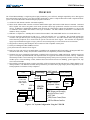
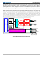
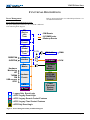
OVERVIEW
The VT8237R South Bridge is a high integration, high performance, power-efficient, and high compatibility device that supports
Intel and non-Intel based processor to V-Link bus bridge functionality to make a complete Microsoft PC2001-compliant PCI/LPC
system. The VT8237R includes standard intelligent peripheral controllers:
a) Serial ATA dual channel controller with RAID capability.
b) Master mode enhanced IDE controller with dual channel DMA engine and interlaced dual channel commands. Dedicated
FIFO coupled with scatter and gather master mode operation allows high performance transfers between PCI and IDE
devices. In addition to standard PIO and DMA mode operation, the VT8237R also supports the UltraDMA-133, 100, 66, and
33 standards to allow reliable data transfer at rates up to 133 MB/sec. The IDE controller is SFF-8038i v1.0 and Microsoft
Windows-family compliant.
c) IEEE 802.3 compliant 10 / 100 Mbps PCI bus master Ethernet MAC with standard MII interface to external PHYceiver.
d) Universal Serial Bus controller that is USB v2.0 / 1.1 and Universal HCI v2.0 / 1.1 compliant. The VT8237R includes four
root hubs with eight function ports with integrated physical layer transceivers. The USB controller allows hot plug and play
and isochronous peripherals to be inserted into the system with universal driver support. The controller also implements
legacy keyboard and mouse support so legacy software can run transparently in a non-USB-aware OS environment.
e) Integrated bus-mastering dual full-duplex direct-sound AC97-link-compatible sound system.
f) Full System Management Bus (SMBus) interface.
g) Keyboard controller with PS2 mouse support.
h) Real Time Clock with 256 byte extended CMOS. In addition to the standard ISA RTC functionality, the integrated RTC also
includes the date alarm, century field, and other enhancements for compatibility with the ACPI standard.
i) Notebook-class power management functionality compliant with ACPI and legacy APM requirements. Multiple sleep states
(power-on suspend, suspend-to-DRAM, and suspend-to-Disk) are supported with hardware automatic wake-up. Additional
functionality includes event monitoring, CPU clock throttling and stop (Intel processor protocol), PCI bus clock stop control,
modular power, clock and leakage control, hardware-based and software-based event handling, general purpose I/O, chip
select and external SMI.
j) Plug and Play controller that allows complete steerability of all PCI interrupts and internal interrupts / DMA channels to any
interrupt channel. One additional steerable interrupt channel is provided to allow plug and play and reconfigurability of onboard peripherals for Windows family compliance.
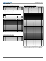
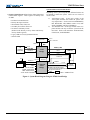
HA
HD
CPU
Sideband Signals:
Init / A20M#
INTR / NMI
SMI / StopClk
FERR / IGNNE
Sleep
APIC
Boot ROM
MA/Command
MD
System Memory
DIMM Module ID
V-Link
Interface
LPC
Onboard
LPC I/O
North Bridge
SMB
USB 2.0 Ports 0-7
Keyboard / Mouse
VT8237R
Expansion
Cards
PCI
539 BGA
IDE Primary and Secondary
Serial ATA Ports 1 and 2
AC97 Link
GPIO, Power Control, Reset
MII Fast Ethernet Interface
RTC
Crystal
Figure 1. PC System Configuration Using the VT8237R
Revision 2.06 December 15, 2004
-4-
Overview
VT8237R Data Sheet
The VT8237R also enhances the functionality of standard integrated peripherals. The integrated interrupt controller supports both
edge and level triggered interrupts channel by channel. The integrated DMA controller supports type F DMA in addition to
standard ISA DMA modes. Compliant with the PCI-2.2 specification, the VT8237R supports delayed transactions and remote
power management so that slower internal ISA peripherals do not block the traffic of the PCI bus. Special circuitry is built in to
allow concurrent operation without causing deadlock even in a PCI-to-PCI bridge environment. The chip also includes eight
levels (doublewords) of line buffers from the PCI bus to internal ISA bus devices to further enhance overall system performance.
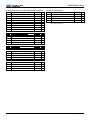
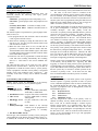
The high performance Serial ATA RAID Controller in the VT8237R supports RAID Level 0, RAID Level 1, RAID Level 0+1 and
JBOD. The internal PCI interface of the Serial ATA controller complies with PCI Specification Revision 2.2. The chip also
complies with revision 1.0 of the scatter / gather host DMA mechanism of “Programming Interface for Bus Master IDE
Controller”. The VT8237R complies with Serial ATA Specification Revision 1.0 and includes two internal Serial-ATA direct
interfaces (i.e., a two-channel S-ATA PHY is provided on-chip) plus two Parallel-ATA channels (primary and secondary). An
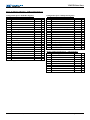
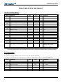
external S-ATA PHY is also supported which is multiplexed on the P-ATA secondary interface. By that mechanism, an external
Serial-ATA PHY can be implemented on the secondary Parallel-ATA interface for support of up to four S-ATA devices total (see
figures below) along with two Parallel-ATA devices (master and slave) on the Parallel-ATA primary channel.
Transport 1
Link 1
PHY1
Link 2
PHY2
SATA 1
SRAM
Mux
Host
Interface
Transport 2
SRAM
SATA Controller
SATA 2
PATA Primary Channel
Parallel ATA EIDE Controller
PATA Secondary Channel
Master
Slave
Figure 2. Block Diagram with 2 Serial–ATA devices
Revision 2.06 December 15, 2004
-5-
Overview
VT8237R Data Sheet
Link 1
PHY1
Link 2
PHY2
SATA Devices 1
Transport 1
SRAM
2
Mux
Host
Interface
Link 3
Transport 2
Link 4
SRAM
Serial-ATA
LITE
Interface
SATA
Lite
PHY
3
4
SATA Controller
PATA Primary Channel
Parallel ATA EIDE Controller
Master
Slave
Figure 3. Block Diagram with 4 Serial–ATA devices
Revision 2.06 December 15, 2004
-6-
Overview
VT8237R Data Sheet
PINOUTS
Key
1
Figure 4. Ball Diagram (Top View)
2
3
4
5
6
7
8
9
10
11
12
13
14
15
16
17
18
19
20
21
22
23
24
25
26
INTG#
GPIO14
INTH#
GPIO15
INT
A#
INT
B#
REQ
0#
INT
C#
GNT
0#
REQ
1#
MD
CK
MD
IO
MRX
D2
MRX
D1
MTX
D3
MTX
D2
MTX
D0
MTX
D1
M
CRS
M
COL
EE
DI
EE
DO
USB
GND
USB
GND
USB
P7+
USB
P7–
USB
GND
USB
GND
USB
P5+
USB
P5–
USB
GND
USB
GND
USB
P3+
USB
P3–
USB
GND
USB
GND
USB
P1+
USB
P1–
USB
GND
USB
GND
USB
VCC
USB
VCC
VCC
UPLL
VCC
UPLL
USB
OC5#
USB
OC4#
USB
OC7#
USB
REXT
USB
OC6#
USB
OC2#
INT
D#
REQ
2#
GNT
2#
MRX
D3
MRX
D0
MRX
CLK
MTX
CLK
MTX
ENA
EE
CK
USB
GND
USB
GND
USB
GND
USB
GND
USB
GND
USB
GND
USB
GND
USB
GND
USB
GND
USB
VCC
GND
UPLL
VSUS
USB
USB
OC3#
USB
OC0#
A
GND
GND
B
GND
GND
C
CBE
1#
SERR# PERR#
D
AD11
AD13
INTE#
AD14 GPIO12
REQ
3#
GNT
1#
PHY
RST#
MRX
DV
MII
VCC
MRX
ERR
EE
CS#
MII
VCC25
USB
GND
USB
P6+
USB
GND
USB
P4+
USB
GND
USB
P2–
USB
GND
USB
P0–
USB
GND
USB
VCC
GND
UPLL
USB
OC1#
E
AD8
CBE
0#
INTF#
AD10 GPIO13
GNT
3#
LAN
GND
LAN
VCC
GND
MII
VCC
MII
VCC
MII
VCC
MII
VCC25
USB
GND
USB
P6–
USB
GND
USB
P4–
USB
GND
USB
P2+
USB
GND
USB
P0+
USB
GND
USB
VCC
USB
CLK
VD
08
VD
13
VD
12
F
AD4
AD7
AD15
PAR
F5
GND
GND
F8
9
10
11
12
13
14
15
16
17
18
19
20
F21
USB
VCC
NC
V
PAR
GND
VD
04
G
AD5
AD0
AD9
AD12
G5
G6
G7
LAN
Pins
USB
Pins
VLink
G21
NC
VD
09
VBE
0#
VD
05
VD
01
H
T
RDY#
DEV
SEL#
AD3
AD6
H5
VCC
33
VCC
33
VCC
33
VCC
33
USB
GND
USB
GND
USB
GND
USB
GND
USB
GND
USB
GND
Pins
H21
VL
VREF
GND
DN
STB#
VD
0
DN
STB
J
FRM#
I
RDY#
AD2
AD1
GND
J6
VCC
33
VCC
25
VCC
25
VCC
25
VCC
25
USB
VCC
USB
VCC
USB
VCC
USB
VCC
USB
VCC
USB
VCC
J20
GND
VL
COMP
VD
03
UP
STB#
GND
UP
STB
K
AD19
AD18
AD16
STOP#
GND
K6
PCI
VCC
33
VCC
25
K10
11
12
13
14
15
16
K17
GND
GND
K
VCC
VK
VD
06
UP
CMD
VD
07
DN
CMD
VD
02
L
AD23
AD21
AD17
CBE
2#
L5
Pins
VCC
33
VCC
25
L
GND
GND
GND
GND
GND
GND
L
VCC
25
VCC
VK
L
VCC
VK
V
CLK
VCC
VK
VD
14
VD
11
VD
10
M
AD25
AD24
CBE
3#
AD20
M5
VCC
33
VCC
25
M
GND
GND
GND
GND
GND
GND
M
VCC
25
VCC
VK
M
VCC
VK
VCC
VK
VCC
VK
VCC
VK
VCC
VK
VD
15
N
AD29
AD28
AD27
AD22
N5
VCC
33
VCC
25
N
GND
GND
GND
GND
GND
GND
N
VCC
25
VCC
VK
N
VCC
VK
VCC
VK
VCC
VK
VCC
VK
VCC
VK
VCC
VK
P
AD30
AD26
GND
P6
GND
GND
GND
GND
GND
P
VCC
VK
R
GND
GND
GND
GND
GND
GND
R
VCC
VK
VCC
33
DP
SLP#
R6
VCC
25
VCC
25
P
GND
VCC
25
VCC
25
GND
GNT
4#
VCC
33
VCC
33
P
R
REQ
4#
PCI GNT5# REQ5#
RST# GPO7
GPI7
R
GND
GHI#
VCC
VK
PCI
CLK
VCC
VCC
VCC
VK
VK
VK
STP APICD0 INIT#
CLK# GPIO10
T
AC
BTCK
AC
RST#
VSUS
25
T5
AC97
VCC
33
VCC
25
T10
GND
GND
GND
GND
GND
GND
T
VCC
25
VCC
33
T
GND
PLL
VCC
APICD1
GPIO11
U
AC
AC
SDI2 SDOUT
AC
SDI0
VSUS
25
U5
VCC
33
VCC
25
U10
11
12
13
14
15
16
U17
VCC
25
VCC
33
U
U21
PLL APICCK FERR#
GND
GPI9
V
AC
SDI1
MS
DT
AC
SDI3
KB
CK
BAT
LOW#
GND
V6
KB
/MS
GND
W6
PM
VCC
25
VCC
33
VCC
25
VCC
33
VCC
25
VCC
33
VCC
25
VCC
ATS
VCC
25
VCC
ATS
VCC
25
VCC
ATS
VCC
25
VCC
ATS
VCC
25
VCC
ATS
VCC
25
VCC
33
VCC
25
VCC
33
VCC
33
VCC
33
W
VCC
33
VCC
33
PD
CS1#
PME#
VCC
33
VCC
33
V
W
KB
DT
MS
CK
Y
CPU
MISS
RING#
SUS
ST#
AOLGI
THRM#
Y5
PM
LPC
Pwr
9
10
SATA
Pins
Y
AA
EXT
SMI#
SUSA#
GPO2
GPO
0
VSUS
33
AA5
6
7
8
GND
GND
11
12
13
14
15
16
17
18
19
SMB
SMB
DT1
SUS
CLK
VSUS
33
VSUS
33
VSUS
33
PCK
RUN#
OSC
VDSLP
GPIO29
GND
AO
VCC
AS
GND
AS
STX
1+
GND
ATS
STX
2+
GND
AS
VCC
AO
GND
AC
LID#
GPI
1
SMB
CK2
SMB
CK1
PWR
GD
GPIOD
CPU VIDSEL VGATE
PCGNTB STP# GPIO28 GPIO8
VCC
AO
VCC
AS
GND
AS
STX
1–
GND
ATS
STX
2–
GND
AS
VCC
AO
AD
SMB
DT2
PWR
BTN#
SUSB#
IN
GPI
0
GPO
1
RTC
X1
PWR
OK#
SUS
C#
RTC
X2
V
BAT
AB ALRT#
AE TRUD#
AF
AD31
AC
SYNC
IGN
NE#
UPEN# UPWR
GPO9 GPI9
INTR
NMI
SMI#
A20M#
PD
DAK#
PD
A2
PD
A1
SLP#
GND
PD
CS3#
PD
A0
GND
PD
IOR#
VCC
33
PD
RDY
PD
DRQ
PD
D1
PD
IOW#
PD
D14
AA20
GND
PD
D0
PD
D15
PD
D13
PD
D3
PD
D2
GND
SD
D1
SD
COMP
GND
PD
D12
PD
D11
GND
PD
D4
GND
SD
VREF
SD
D0
SD
D2
SDA1
strap
PD
D6
PD
D9
PD
D10
PD
D5
SIDE PIDE
L
AD3
L
AD0
SER
IRQ
AGBZ#
GPI6
SR
EXT
GND
ATS
GND
ATS
GND
ATS
GND
ATS
GND
ATS
SD
DRQ
SD
D5
SDD6
SD
D10
SD
D13
SD
D14
SD
DAK#
IRQ
14
PD
D7
PD
D8
GPIOA
L
PCREQA REQ0#
L
AD2
L
REQ1#
TEST
S
XO
VCC
A33
GND
ATS
SRX
1+
GND
ATS
SRX
2+
GND
ATS
GND
SD
D3
GND
SD
D8
SD
D11
GND
SD
IOW#
SDA2
strap
GND
IRQ
15
GPIOC
PCGNTA
L
AD1
SPKR
strap
TPO
S
XI
GND
A33
GND
ATS
SRX
1–
GND
ATS
SRX
2–
GND
ATS
SD
RDY
SD
D4
SD
D7
SD
D9
SD
D12
SD
D15
SD
IOR#
SDA0
strap
SD SDCS3#
CS1#
strap
RSM
GPIOB
RST# PCREQB
Revision 2.06 December 15, 2004
PCI
STP#
L
FRM#
-7-
Pin Diagram
VT8237R Data Sheet
Table 1. Pin List (Numerical Order)
Pin #
Pin Name
Pin #
Pin Name
Pin #
Pin Name
Pin #
Pin Name
Pin #
E03 IO AD10
A03 IO INTG# / GPIO14
W23 O PDA0 / strap
AD07 IO
M19 P VCCVK
A04 I INTA#
E04 IO INTF# / GPIO13
W24 O PDA2 / strap
AD08 IO
M21 P VCCVK
A05 I REQ0#
E05 O GNT3#
W26 O PDIOR#
AD09 I
M22 P VCCVK
A06 O GNT0#
Y01 I CPUMISS / GPI17
AD10 I
E06 P LANGND
M23 P VCCVK
A07 O MDCK
Y02 I RING# / GPI3
AD11 AI
E07 P LANVCC
M24 P VCCVK
A08 I MRXD2
Y03 O SUSST1# / GPO3
E09 P MIIVCC
M25 P VCCVK
AD12 P
Y04 I AOLGPI / THRM# / GPI18 AD13 P
A09 O MTXD3
M26 IO VD15
E10 P MIIVCC
N01 IO AD29
A10 O MTXD0
Y22 I PDRDY
E11 P MIIVCC
AD14 P
N02 IO AD28
A11 I MCRS
E12 P MIIVCC25
Y23 I PDDRQ
AD15 P
N03 IO AD27
A12 O EEDI / strap
Y24 IO PDD01
E14 IO USBP6–
AD16 P
N04 IO AD22
A14 IO USBP7+
E16 IO USBP4–
Y25 O PDIOW#
AD17 I
A16 IO USBP5+
E18 IO USBP2+
Y26 IO PDD14
AD18 IO
N19 P VCCVK
AA01 IO EXTSMI# / GPI2
A18 IO USBP3+
E20 IO USBP0+
AD19 IO
N21 P VCCVK
A20 IO USBP1+
E23 I USBCLK
AA02 O SUSA# / GPO2
AD20 IO
N22 P VCCVK
E24 IO VD08
AA03 OD GPO0
AD21 IO
A23 P VCCUPLL
N23 P VCCVK
AD22 IO
A24 I USBOC5#
E25 IO VD13
AA04 P VSUS33
N24 P VCCVK
A25 I USBOC7#
E26 IO VD12
AA22 IO PDD00
AD23 O
N25 P VCCVK
F01 IO AD04
A26 I USBOC6#
AA23 IO PDD15
AD24 I
N26 P VCCVK
F02 IO AD07
P01 IO AD30
B03 IO INTH# / GPIO15
AA24 IO PDD13
AD25 IO
F03 IO AD15
P02 IO AD31
B04 I INTB#
AA25 IO PDD03
AD26 IO
B05 I INTC#
F04 IO PAR
P03 I REQ4#
AA26 IO PDD02
AE01 I
P04 IO AD26
B06 I REQ1#
F23 O NC
AB01 I SMBALRT#
AE02 I
B07 IO MDIO
F24 IO VPAR
AB02 IO SMBDT1
AE03 OD
P19 P VCCVK
P21 OD DPSLP# / GPIO23 AB03 O SUSCLK / GPO4
B08 I MRXD1
F26 IO VD04
AE04 I
G01 IO AD05
AE05 OD
B09 O MTXD2
AB04 P VSUS33
P22 P VCCVK
G02 IO AD00
AE06 I
B10 O MTXD1
AB05 P VSUS33
P23 P VCCVK
G03 IO AD09
AE07 IO
B11 I MCOL
AB06 P VSUS33
P24 P VCCVK
B12 I EEDO
G04 IO AD12
AB07 IO PCKRUN#
AE08 I
P25 P VCCVK
B14 IO USBP7–
G22 I NC
AB08
I
OSC
AE09 I
P26 P VCCVK
B16 IO USBP5–
G23 IO VD09
R01 O PCIRST#
AB09 OD VRDPSLP/GPIO29
AE10 I
B18 IO USBP3–
G24 IO VBE#
R02 O GNT5# / GPO7
AB10 P GNDAO
AE11 P
B20 IO USBP1–
G25 IO VD05
R03 I REQ5# / GPI7
AB11 P VCCAS
AE12 P
G26 IO VD01
R04 O GNT4#
AE13 I
B23 P VCCUPLL
AB12 P GNDAS
R22 OD GHI# / GPIO22
B24 I USBOC4#
H01 IO TRDY#
AB13 O STX1+
AE14 P
H02 IO DEVSEL#
AE15 I
B25 I USBREXT
R23 I PCICLK
AB14 P GNDA120
H03 IO AD03
B26 I USBOC2#
R24 OD STPCLK#
AB15 O STX2+
AE16 P
C01 IO CBE1#
H04 IO AD06
R25 O APICD0 / GPIO10 AB16 P GNDAS
AE18 IO
C02 I SERR#
R26 OD INIT#
AE20 IO
H22 P VLVREF
AB17 P VCCAS
H24 I DNSTB#
T01 I ACBITCLK
C03 IO PERR#
AB20 IO SDD01
AE21 IO
T02 O ACSYNC / strap
AE23 O
C04 I INTD#
H25 IO VD00
AB21 I SDCOMP
H26 I DNSTB
T03 O ACRST#
C05 I REQ2#
AB23 IO PDD12
AE24 O
J01
IO
FRAME#
C06 O GNT2#
AB24 IO PDD11
AE26 I
T04 P VSUS25
C07 I MRXD3
J02 IO IRDY#
AB26 IO PDD04
AF01 O
T22 P PLLVCC
J03 IO AD02
T23 O APICD1 / GPIO11 AC01 I LID# / GPI4
C08 I MRXD0
AF02 O
J04 IO AD01
C09 I MRXCLK
T24 OD IGNNE#
AC02 I GPI1
AF03 O
C10 I MTXCLK
T25 OD INTR
AC03 IO SMBCK2 / GPIO27
J22 I VLCOMP
AF04 P
C11 O MTXENA
J23 IO VD03
T26 OD NMI
AC04 IO SMBCK1
AF05 OD
C12 O EECK
U01 I ACSDI2
J24 O UPSTB#
AC05 I PWRGD
AF06 O
U02 O ACSDOUT / strap AC06 OD GPIOD / PCGNTB / strap
J26 O UPSTB
AF07 IO
C23 P GNDUPLL
K01 IO AD19
U03 I ACSDIN0
AC07 O CPUSTP# / GPO5
AF08 O
C24 P VSUSUSB
K02 IO AD18
C25 I USBOC3#
AC08 OD VIDSEL / GIO28
AF09 O
U04 P VSUS25
K03 IO AD16
C26 I USBOC0#
AC09 I VGATE / GPIO8
AF10 I
U22 P PLLGND
D01 IO AD11
U23 I APICCLK / GPI19 AC10 P VCCAO
K04 IO STOP#
AF11 P
U24
I
FERR#
D02 IO AD13
AC11 P VCCAS
AF12 P
K21 P VCCVK
D03 IO AD14
K22 IO VD06
U25 OD SMI#
AF13 I
AC12 P GNDAS
U26 OD A20M#
D04 IO INTE# / GPIO12
K23 O UPCMD
AC13 O STX1–
AF14 P
D05 I REQ3#
K24 IO VD07
V01 IO KBDT
AF15 I
AC14 P GNDATS
K25 I DNCMD
V02 I ACSDIN1
D06 O GNT1#
AC15 O STX2–
AF16 P
V03 I ACSDI3
D07 O PHYRST#
K26 IO VD02
AF17 I
AC16 P GNDAS
L01 IO AD23
V04 I BATLOW# / GPI5 AC17 P VCCAS
D08 I MRXDV
AF18 IO
L02 IO AD21
V22 O PDCS1# / strap
AF19 IO
D09 P MIIVCC
AC19 P SDVREF
L03 IO AD17
D10 I MRXERR
V23 O PDCS3# / strap
AC20 IO SDD00
AF20 IO
D11 O EECS#
L04 IO CBE2#
AF21 IO
V24 O PDDACK# / strap AC21 IO SDD02
D12 P MIIVCC25
AC22 O SDA1
AF22 IO
V25 O PDA1 / strap
L19 P VCCVK
V26 OD SLP#
AC23 IO PDD06
AF23 O
D14 IO USBP6+
L21 P VCCVK
D16 IO USBP4+
L22 I VCLK
W01 IO MSCK
AC24 IO PDD09
AF24 O
W02 IO MSDT
AC25 IO PDD10
AF25 O
D18 IO USBP2–
L23 P VCCVK
D20 IO USBP0–
L24 IO VD14
W03 IO KBCK
AC26 IO PDD05
AF26 O
L25 IO VD11
W04 I PME#
AD01 IO SMBDT2 / GPIO26
D23 P GNDUPLL
D24 I USBOC1#
L26 IO VD10
AD02 I PWRBTN#
W12 P VCCATS
M01 IO AD25
D25 O UDPEN# / GPO9
AD03 O SUSB#
W13 P VCCATS
M02 IO AD24
D26 I UDPWR / GPI9
AD04 I RSMRST#
W14 P VCCATS
E01 IO AD08
M03 IO CBE3#
AD05 OD GPIOB / PCREQB / strap
W15 P VCCATS
E02 IO CBE0#
M04 IO AD20
AD06 O PCISTP# / GPO6 / strap
W16 P VCCATS
VCC33 pins (28 pins): H9-12, J8, K8, L8, M8, N8, P8, R8,19, T8,19, U8,19, V8,19, 21 W8-11,17-19, 21, Y21
VCC25 pinS (29 pins): J9-12, K9, L9,18, M9,18, N9,18, P9,18, R9,18, T9,18, U9,18, V9-18
GND pins
(71 pins): A1-2, B1-2, E8, F6-7,25, H23, J5,21,25, K5,18-19, L11-16, M11-16, N11-16, P5,11-16, R5,11-16,21, T11-16,21, V5, W5,22,25,
AA9-10,21, AB18-19,22,25, AC18, AE17,19,22,25
USBVCC pins (12 pins): A22, B22, C22, D22, E22, F22, J13-18
USBGND pins (35 pins): A13,15,17,19,21, B13,15,17,19,21, C13-21, D13,15,17,19,21, E13,15,17,19,21, H13-18
Revision 2.06 December 15, 2004
-8-
Pin Name
LAD3
LAD0
SERIRQ
AGPBZ# / GPI6
SREXT
GNDATS
GNDATS
GNDATS
GNDATS
GNDATS
SDDRQ
SDD05
SDD06
SDD10
SDD13
SDD14
SDDACK#
IRQ14
PDD07
PDD08
INTRUD# / GPI16
GPI0
GPO1
RTCX1
GPIOA / PCREQA / strap
LREQ0#
LAD2
LREQ1#
TEST
SXO
VCCA33
GNDATS
SRX1+
GNDATS
SRX2+
GNDATS
SDD03
SDD08
SDD11
SDIOW#
SDA2
IRQ15
PWROK#
SUSC#
RTCX2
VBAT
GPIOC / PCGNTA / strap
LFRM#
LAD1
SPKR / strap
TPO
SXI
GNDA33
GNDATS
SRX1–
GNDATS
SRX2–
GNDATS
SDRDY
SDD04
SDD07
SDD09
SDD12
SDD15
SDIOR#
SDA0
SDCS1#
SDCS3#
Pin Lists
VT8237R Data Sheet
Table 2. Pin List (Alphabetical Order)
Pin #
Pin Name
Pin #
Pin Name
Pin
Pin Name
Pin #
Pin Name
Pin #
U26 OD A20M#
A10 O MTXD0
AF21 IO SDD12
K26
AD12 P GNDATS
T01 I ACBITCLK
B10 O MTXD1
AD21 IO SDD13
J23
AD13 P GNDATS
T03 O ACRST#
B09 O MTXD2
AD22 IO SDD14
F26
AD14 P GNDATS
U03 I ACSDIN0
A09 O MTXD3
AF22 IO SDD15
G25
AD15 P GNDATS
V02 I ACSDIN1
C11 O MTXENA
AD23 O SDDACK#
K22
AD16 P GNDATS
U01 I ACSDI2 /IO20/PCS0#
K24
T26 OD NMI
AD17 I SDDRQ
AE12 P GNDATS
V03 I ACSDI3 /IO21/PCS1# /SLPB# AE14 P GNDATS
AB08 I OSC
AF23 O SDIOR#
E24
U02 O ACSDOUT / strap
F04 IO PAR
AE23 O SDIOW#
G23
AE16 P GNDATS
T02 O ACSYNC / strap
AB07 IO PCKRUN#
AF17 I SDRDY
L26
AF12 P GNDATS
G02 IO AD00
L25
R23 I PCICLK
AC19 P SDVREF
AF14 P GNDATS
J04 IO AD01
E26
R01 O PCIRST#
AD09 I SERIRQ
AF16 P GNDATS
J03 IO AD02
E25
AD06 O PCISTP#/O6/strap C02 I SERR#
C23 P GNDUPLL
H03 IO AD03
V26 OD SLP#
L24
W23 O PDA0 / strap
D23 P GNDUPLL
F01 IO AD04
AB01 I SMBALRT#
M26
A06 O GNT0#
V25 O PDA1 / strap
G01 IO AD05
AC04 IO SMBCK1
D06 O GNT1#
W24 O PDA2 / strap
AF04
H04 IO AD06
AC03 IO SMBCK2 / GPIO27
G24
C06 O GNT2#
V22 O PDCS1# / strap
F02 IO AD07
AB02 IO SMBDT1
E05 O GNT3#
V23 O PDCS3# / strap
AE11
E01 IO AD08
R04 O GNT4#
AA22 IO PDD00
AD01 IO SMBDT2 / GPIO26 AC10
G03 IO AD09
R02 O GNT5# / GPO7
Y24 IO PDD01
U25 OD SMI#
W12
E03 IO AD10
AE02 I GPI0
AA26 IO PDD02
AF08 O SPKR / strap
W13
D01 IO AD11
AC02 I GPI1
AA25 IO PDD03
AD11 AI SREXT
W14
G04 IO AD12
AF13 I SRX1–
AE05 OD GPIOA / PCREQA / strap AB26 IO PDD04
W15
D02 IO AD13
AE13 I SRX1+
AD05 OD GPIOB / PCREQB / strap AC26 IO PDD05
W16
D03 IO AD14
AF15 I SRX2–
AF05 OD GPIOC / PCGNTA / strap AC23 IO PDD06
AB11
F03 IO AD15
AE15 I SRX2+
AC06 OD GPIOD / PCGNTB / strap AD25 IO PDD07
AB17
K03 IO AD16
AA03 OD GPO0
AD26 IO PDD08
AC13 O STX1–
AC17
L03 IO AD17
AE03 OD GPO1
AC24 IO PDD09
AB13 O STX1+
AC11
K02 IO AD18
T24 OD IGNNE#
AC25 IO PDD10
AC15 O STX2–
A23
K01 IO AD19
R26 OD INIT#
AB24 IO PDD11
AB15 O STX2+
B23
M04 IO AD20
A04 I INTA#
AB23 IO PDD12
K04 IO STOP#
K21
L02 IO AD21
B04 I INTB#
AA24 IO PDD13
R24 OD STPCLK#
L19
N04 IO AD22
B05 I INTC#
Y26 IO PDD14
AA02 O SUSA# / GPO2
L21
L01 IO AD23
C04 I INTD#
AA23 IO PDD15
AD03 O SUSB#
L23
M02 IO AD24
D04 IO INTE# / GPIO12
V24 O PDDACK# / strap AF02 O SUSC#
M19
M01 IO AD25
AB03 O SUSCLK / GPO4
E04 IO INTF# / GPIO13
Y23 I PDDRQ
M21
P04 IO AD26
A03 IO INTG# / GPIO14
W26 O PDIOR#
Y03 O SUSST1# / GPO3
M22
N03 IO AD27
B03 IO INTH# / GPIO15
Y25 O PDIOW#
AF10 I SXI
M23
N02 IO AD28
T25 OD INTR
Y22 I PDRDY
AE10 I SXO
M24
N01 IO AD29
AE01 I INTRUD# / GPI16
C03 IO PERR#
AE09 I TEST
M25
P01 IO AD30
J02 IO IRDY#
D07 O PHYRST#
AF09 O TPO
N19
P02 IO AD31
H01 IO TRDY#
AD24 I IRQ14
U22 P PLLGND
N21
AD10 I AGPBZ# / GPI6
AE26 I IRQ15
D25 O UDPEN# / GPO9
T22 P PLLVCC
N22
Y04 I AOLGPI / THRM# / GPI18
W04 I PME#
D26 I UDPWR / GPI9
W03 IO KBCK
N23
U23 I APICCLK / GPI19
V01 IO KBDT
AD02 I PWRBTN#
K23 O UPCMD
N24
R25 O APICD0 / GPIO10
AD08 IO LAD0
AC05 I PWRGD
J26 O UPSTB
N25
T23 O APICD1 / GPIO11
AF07 IO LAD1
AF01 O PWROK#
J24 O UPSTB#
N26
V04 I BATLOW# / GPI5
E23 I USBCLK
AE07 IO LAD2
A05 I REQ0#
P19
E02 IO CBE0#
C26 I USBOC0#
AD07 IO LAD3
B06 I REQ1#
P22
C01 IO CBE1#
D24 I USBOC1#
C05 I REQ2#
P23
E06 P LANGND
L04 IO CBE2#
B26 I USBOC2#
D05 I REQ3#
P24
E07 P LANVCC
M03 IO CBE3#
C25 I USBOC3#
AF06 O LFRM#
P03 I REQ4#
P25
Y01 I CPUMISS / GPI17
AC01 I LID# / GPI4
R03 I REQ5# / GPI7
B24 I USBOC4#
P26
AC07 O CPUSTP# / GPO5
Y02 I RING# / GPI3
A24 I USBOC5#
L22
AE06 I LREQ0#
H02 IO DEVSEL#
AD04 I RSMRST#
A26 I USBOC6#
AC09
AE08 I LREQ1#
K25 I DNCMD
B11 I MCOL
AE04 I RTCX1
A25 I USBOC7#
AC08
H26 I DNSTB
A11 I MCRS
AF03 O RTCX2
D20 IO USBP0–
J22
H24 I DNSTB#
AF24 O SDA0
E20 IO USBP0+
A07 O MDCK
H22
P21 OD DPSLP# / GPIO23
F24
B07 IO MDIO
AC22 O SDA1
B20 IO USBP1–
C12 O EECK
AE24 O SDA2
A20 IO USBP1+
AB09
D09 P MIIVCC
D11 O EECS#
D18 IO USBP2–
T04
E09 P MIIVCC
AB21 I SDCOMP
A12 O EEDI / strap
AF25 O SDCS1#
E18 IO USBP2+
E10 P MIIVCC
U04
B12 I EEDO
AF26 O SDCS3#
B18 IO USBP3–
AA04
E11 P MIIVCC
AA01 IO EXTSMI# / GPI2
D12 P MIIVCC25
AC20 IO SDD00
A18 IO USBP3+
AB04
U24 I FERR#
E12 P MIIVCC25
AB20 IO SDD01
E16 IO USBP4–
AB05
J01 IO FRAME#
AC21 IO SDD02
D16 IO USBP4+
C09 I MRXCLK
AB06
R22 OD GHI# / GPIO22
C08 I MRXD0
AE18 IO SDD03
B16 IO USBP5–
C24
B08 I MRXD1
AF18 IO SDD04
A16 IO USBP5+
AF11 P GNDA33
A08 I MRXD2
AD18 IO SDD05
E14 IO USBP6–
AB10 P GNDAO
C07 I MRXD3
AD19 IO SDD06
D14 IO USBP6+
AB12 P GNDAS
D08
I
MRXDV
AF19
IO
SDD07
B14
IO USBP7–
AB16 P GNDAS
D10 I MRXERR
AE20 IO SDD08
A14 IO USBP7+
AC12 P GNDAS
AF20 IO SDD09
B25 I USBREXT
W01 IO MSCK
AC16 P GNDAS
W02 IO MSDT
AD20 IO SDD10
H25 IO VD00
AB14 P GNDATS
C10 I MTXCLK
AE21 IO SDD11
G26 IO VD01
AC14 P GNDATS
VCC33 pins (28 pins): H9-12, J8, K8, L8, M8, N8, P8, R8,19, T8,19, U8,19, V8,19, 21, W8-11,17-19, 21, Y21
VCC25 pins (29 pins): J9-12, K9, L9,18, M9,18, N9,18, P9,18, R9,18, T9,18, U9,18, V9-18
GND pins
(71 pins): A1-2, B1-2, E8, F6-7,25, H23, J5,21,25, K5,18-19, L11-16, M11-16, N11-16, P5,11-16, R5,11-16,21, T11-16,21, V5, W5,22,25,
AA9-10,21, AB18-19,22,25, AC18, AE17,19,22,25
USBVCC pins (12 pins): A22, B22, C22, D22, E22, F22, J13-18
USBGND pins (35 pins): A13,15,17,19,21, B13,15,17,19,21, C13-21, D13,15,17,19,21, E13,15,17,19,21, H13-18
NC pins
(2 pins): G22, F23
Revision 2.06 December 15, 2004
-9-
Pin Name
IO
IO
IO
IO
IO
IO
IO
IO
IO
IO
IO
IO
IO
IO
P
IO
P
P
P
P
P
P
P
P
P
P
P
P
P
P
P
P
P
P
P
P
P
P
P
P
P
P
P
P
P
P
P
P
P
P
P
P
I
I
OD
I
P
IO
OD
P
P
P
P
P
P
P
VD02
VD03
VD04
VD05
VD06
VD07
VD08
VD09
VD10
VD11
VD12
VD13
VD14
VD15
VBAT
VBE#
VCCA33
VCCAO
VCCATS
VCCATS
VCCATS
VCCATS
VCCATS
VCCAS
VCCAS
VCCAS
VCCAS
VCCUPLL
VCCUPLL
VCCVK
VCCVK
VCCVK
VCCVK
VCCVK
VCCVK
VCCVK
VCCVK
VCCVK
VCCVK
VCCVK
VCCVK
VCCVK
VCCVK
VCCVK
VCCVK
VCCVK
VCCVK
VCCVK
VCCVK
VCCVK
VCCVK
VCCVK
VCLK
VGATE / GPIO8
VIDSEL / GIO28
VLCOMP
VLVREF
VPAR
VRDPSLP/GPIO2
VSUS25
VSUS25
VSUS33
VSUS33
VSUS33
VSUS33
VSUSUSB
Pin Lists
VT8237R Data Sheet
PIN DESCRIPTIONS
V-Link Pin Descriptions
V-Link Interface
Signal Name
Pin #
I/O
Signal Description
VD[15:0]
(see
pin
list)
IO
VPAR
F24
IO
VBE#
VCLK
UPCMD
DNCMD
UPSTB
UPSTB#
DNSTB
DNSTB#
G24
L22
K23
K25
J26
J24
H26
H24
IO
I
O
I
O
O
I
I
Data Bus. All bits 15-0 are implemented for use with VIA north bridge chips which
support this capability (if not, only bits 7-0 are used). VD[7:0] are also used to send strap
information to the chipset north bridge (see strap table below for details). The specific
interpretation of these straps is north bridge chip design dependent.
Parity. If the VPAR function is implemented in a compatible manner on the north bridge,
this pin should be connected to the north bridge VPAR pin (KT400 / KM400 / KN400,
PT400, PT600). If VPAR is not implemented in the north bridge chip or is incompatible
with the VT8237R (4x V-Link north bridges) connect this pin to an 8.2K pullup to 2.5V
(Pro266, Pro266T, KT266, KT266A, KT333, P4X266, PN266, KN266, KM266, P4M266,
P4N266). See app note AN222 for details.
Byte Enable. Connect to same named pin on north bridge.
V-Link Clock. 66 MHz. Supplied by clock generator.
Command from Client-to-Host. Connect to same named pin on north bridge.
Command from Host-to-Client. Connect to same named pin on north bridge.
Strobe from Client-to-Host. Connect to same named pin on north bridge.
Complement Strobe from Client-to-Host. Connect to same named pin on north bridge.
Strobe from Host-to-Client. Connect to same named pin on north bridge.
Complement Strobe from Host-to-Client. Connect to same named pin on north bridge.
Revision 2.06 December 15, 2004
-10-
Pin Descriptions
VT8237R Data Sheet
CPU, APIC and CPU Control Pin Descriptions
CPU Interface
Signal Name
Pin # I/O Signal Description
OD A20 Mask. Connect to A20 mask input of the CPU to control address bit-20 generation.
Logical combination of the A20GATE input (from internal or external keyboard controller)
and Port 92 bit-1 (Fast_A20).
U24
I Numerical Coprocessor Error. This signal is tied to the coprocessor error signal on the
FERR#
CPU. Internally generates interrupt 13 if active. Input voltage swing is programmable to
1.5V or 2.5V by Device 17 Function 0 Rx67[2].
T24 OD Ignore Numeric Error. This pin is connected to the CPU “ignore error” pin.
IGNNE#
R26 OD Initialization. The VT8237R asserts INIT# if it detects a shut-down special cycle on the
INIT#
PCI bus or if a soft reset is initiated by the register
T25 OD CPU Interrupt. INTR is driven by the VT8237R to signal the CPU that an interrupt
INTR
request is pending and needs service.
T26 OD Non-Maskable Interrupt. NMI is used to force a non-maskable interrupt to the CPU. The
NMI
VT8237R generates an NMI when PCI bus SERR# is asserted.
V26 OD Sleep. Used to put the CPU to sleep.
SLP#
U25 OD System Management Interrupt. SMI# is asserted by the VT8237R to the CPU in
SMI#
response to different Power-Management events.
R24 OD Stop Clock. STPCLK# is asserted by the VT8237R to the CPU to throttle the processor
STPCLK#
clock.
Note: Connect each of the above signals to 150 Ω pullup resistors to VCC_CMOS (see Design Guide).
A20M#
U26
CPU Speed Control Interface
Signal Name
Pin # I/O Signal Description
VGATE / GPI8
/ GPO8
AC9
I
VIDSEL / GPI28
/ GPO28
AC8
OD
VRDSLP / GPI29
/ GPO29
AB9
OD
GHI#
R22
OD
P21
OD
Y1
I
AD10
I
/ GPI22
/ GPO22
DPSLP# / GPI23
/ GPO23
CPUMISS / GPI17
AGPBZ# / GPI6
Voltage Gate. Signal from the CPU voltage regulator. High indicates the voltage regulator
output is stable. This pin performs the VGATE function if Device 17 Function 0 RxE5[4]
= 1 and E4[3] = 0.
Voltage Regulator ID Select. Connected to the CPU voltage regulator. Low selects the
voltage ID from the CPU; high selects a different fixed voltage ID (the lower voltage used
for CPU deep sleep mode). This pin performs the VIDSEL function if Device 17 Function
0 RxE5[3] = 0.
Voltage Regulator Deep Sleep. Connected to the CPU voltage regulator. High selects
the proper voltage for deep sleep mode. This pin performs the VRDPSLP function if
Device 17 Function 0 RxE5[3] = 0.
CPU Speed Select. Connected to the CPU voltage regulator, used to select high speed (L)
or low speed (H). This pin performs the GHI# function if Device 17 Func 0 RxE5[3] = 0.
CPU Deep Sleep. This pin performs the DPSLP# function if Device 17 Function 0
RxE5[3] = 0.
CPU Missing. Used to detect the physical presence of the CPU chip in its socket. High
indicates no CPU present. Connect to the CPUMISS pin of the CPU socket. The state of
this pin may be read in the SMBus 2 registers. This pin may be used as CPUMISS and
GPI17 at the same time.
AGP Busy. Low indicates that an AGP master cycle is in progress (CPU speed transitions
will be postponed if this input is asserted low). Connected to the AGP Bus AGPBZ# pin.
Advanced Programmable Interrupt Controller (APIC) Interface
Signal Name
Pin #
APICD1 / GPIO11
APICD0 / GPIO10
APICCLK / GPI19
T23
R25
U23
Revision 2.06 December 15, 2004
I/O Signal Description
O
O
I
Internal APIC Data 1. Device 17 Function 0 Rx58[6] = 1 & APIC Rx3[0] = 0
Internal APIC Data 0. Device 17 Function 0 Rx58[6] = 1 & APIC Rx3[0] = 0
Internal APIC Clock. Device 17 Function 0 Rx58[6] = 1 & APIC Rx3[0] = 0
-11-
Pin Descriptions
VT8237R Data Sheet
PCI Bus Pin Descriptions
PCI Bus Interface
Signal Name
AD[31:0]
CBE[3:0]#
DEVSEL#
FRAME#
IRDY#
TRDY#
STOP#
SERR#
PERR#
PAR
INTA#
INTB#
INTC#
INTD#
INTE# / GPI12,
/ GPO12,
INTF# / GPI13,
/ GPO13,
INTG# / GPI14,
/ GPO14,
INTH# / GPI15,
/ GPO15
REQ5# / GPI7,
REQ4#,
REQ3#,
REQ2#,
REQ1#,
REQ0#
GNT5# / GPO7,
GNT4#,
GNT3#,
GNT2#,
GNT1#,
GNT0#
PCIRST#
PCICLK
PCKRUN#
Pin #
I/O Signal Description
(see pin IO Address / Data Bus. Multiplexed address and data. The address is driven with FRAME#
list)
assertion and data is driven or received in following cycles.
M3, L4, IO Command / Byte Enable. The command is driven with FRAME# assertion. Byte
C1, E2
enables corresponding to supplied or requested data are driven on following clocks.
H2
IO Device Select. The VT8237 asserts this signal to claim PCI transactions through positive
or subtractive decoding. As an input, DEVSEL# indicates the response to a VT8237initiated transaction and is also sampled when decoding whether to subtractively decode
the cycle.
J1
IO Frame. Assertion indicates the address phase of a PCI transfer. Negation indicates that
one more data transfer is desired by the cycle initiator.
J2
IO Initiator Ready. Asserted when the initiator is ready for data transfer.
H1
IO Target Ready. Asserted when the target is ready for data transfer.
K4
IO Stop. Asserted by the target to request the master to stop the current transaction.
C2
I System Error. SERR# can be pulsed active by any PCI device that detects a system error
condition. Upon sampling SERR# active, the VT8237 can be programmed to generate an
NMI to the CPU.
C3
- Parity Error. PERR#, sustained tri-state, is only for the reporting of data parity errors
during all PCI transactions except for a Special Cycle.
F4
IO Parity. A single parity bit is provided over AD[31:0] and C/BE[3:0]#.
I PCI Interrupt Request. The INTA# through INTD# pins are typically connected to the
A4
PCI bus INTA#-INTD# pins per the table below. INTE-H# are enabled by setting Device
B4
17 Function 0 Rx5B[1] = 1 and RxE4[4] = 0. BIOS settings must match the physical
B5
connection method.
C4
INTA#
INTB#
INTC#
INTD#
D4
PCI Slot 1
INTA#
INTB#
INTC#
INTD#
PCI Slot 2
INTB#
INTC#
INTD#
INTE#
E4
PCI Slot 3
INTC#
INTD#
INTE#
INTF#
PCI Slot 4
INTD#
INTE#
INTF#
INTG#
A3
PCI Slot 5
INTE#
INTF#
INTG#
INTH#
PCI Slot 6
INTF#
INTG#
INTH#
INTA#
B3
R3
I PCI Request. These signals connect to the VT8237 from each PCI slot (or each PCI
P3
master) to request the PCI bus. To use pin R3 as REQ5#, Function 0 RxE4 must be set to
D5
1 otherwise this pin will function as General Purpose Input 7.
C5
B6
A5
R2
O PCI Grant. These signals are driven by the VT8237 to grant PCI access to a specific PCI
R4
master. To use pin R2 as GNT5#, Function 0 RxE4 must be set to 1 otherwise this pin
E5
will function as General Purpose Output 7.
C6
D6
A6
R1
O PCI Reset. This signal is used to reset devices attached to the PCI bus.
R23
I PCI Clock. This signal provides timing for all transactions on the PCI Bus.
AB7
IO PCI Bus Clock Run. This signal indicates whether the PCI clock is or will be stopped
(high) or running (low). The VT8237 drives this signal low when the PCI clock is running
(default on reset) and releases it when it stops the PCI clock. External devices may assert
this signal low to request that the PCI clock be restarted or prevent it from stopping.
Connect this pin to ground using a 100 Ω resistor if the function is not used. Refer to the
“PCI Mobile Design Guide” and VIA PT400 or K8M400 Design Guides for more details.
Revision 2.06 December 15, 2004
-12-
Pin Descriptions
VT8237R Data Sheet
MII, Serial EEPROM and Low Pin Count Pin Descriptions
LAN Controller - Media Independent Interface (MII)
Signal Name
Pin #
I/O
MCOL
MCRS
B11
A11
I
I
MDCK
A7
O
MDIO
B7
IO
C9
C7, A8, B8, C8
I
I
MRXDV
MRXERR
D8
D10
I
I
MTXCLK
C10
I
MTXD[3-0]
A9, B9, B10, A10
O
MTXENA
C11
O
PHYRST#
MIIVCC
D7
D9, E9 - 11
O
Power
MIIVCC25
LANVCC
LANGND
D12, E12
E7
E6
Power
Power
Power
MRXCLK
MRXD[3-0]
PU Signal Description
PD MII Collision Detect. From the external PHY.
PD MII Carrier Sense. Asserted by the external PHY when the media is
active.
PD MII Management Data Clock. Sent to the external PHY as a timing
reference for MDIO
PD MII Management Data I/O. Read from the MDI bit or written to the
MDO bit.
PD MII Receive Clock. 2.5 or 25 MHz clock recovered by the PHY.
PD MII Receive Data. Parallel receive data lines driven by the external
PHY synchronous with MRXCLK.
PD MII Receive Data Valid.
PD MII Receive Error. Asserted by the PHY when it detects a data
decoding error.
PD MII Transmit Clock. Always active 2.5 or 25 MHz clock supplied by
the PHY.
PD MII Transmit Data. Parallel transmit data lines synchronized to
MTXCLK.
PD MII Transmit Enable. Signals that transmit is active from the MII
port to the PHY.
External PHY Reset.
LAN MII Power. 3.3V ±5% Suspend Power for LAN Media
Independent Interface (interface to external PHY).
MII Suspend Power. 2.5V ±5%.
Power For LAN. 2.5V ±5%.
Ground For LAN.
Serial EEPROM Interface
Signal Name
Pin #
I/O
PU Signal Description
D11
O
- Serial EEPROM Chip Select.
EECS#
C12
O
- Serial EEPROM Clock.
EECK
B12
I
- Serial EEPROM Data Output. Connect to EEPROM Data Out pin.
EEDO
EEDI / strap
A12
O
- Serial EEPROM Data Input. Connect to EEPROM Data In pin.
The serial EEPROM Interface signals are disabled if the EEDI pin is strapped high.
Low Pin Count (LPC) Interface
Signal Name
Pin #
I/O
PU Signal Description
AD7, AE7, AF7, AD8
IO
PU LPC Address / Data.
LAD[3-0]
AF6
O
- LPC Frame.
LFRM#
AE6
I
- LPC DMA / Bus Master Request 0.
LREQ0#
AE8
I
- LPC DMA / Bus Master Request 1.
LREQ1#
Note: Connect the LPC interface LPCRST# (LPC Reset) signal to PCIRST#
Revision 2.06 December 15, 2004
-13-
Pin Descriptions
VT8237R Data Sheet
USB, SMB Pin Descriptions
Universal Serial Bus 2.0 Interface
Signal Name
USBP0+
USBP0–
USBP1+
USBP1–
USBP2+
USBP2–
USBP3+
USBP3–
USBP4+
USBP4–
USBP5+
USBP5–
USBP6+
USBP6–
USBP7+
USBP7–
USBCLK
USBOC0#
USBOC1#
USBOC2#
USBOC3#
USBOC4#
USBOC5#
USBOC6#
USBOC7#
UDPWR
/ GPI9
UDPWREN# / GPO9
USBVCC
USBGND
VSUSUSB
VCCUPLL
GNDUPLL
Pin #
I/O
E20
D20
A20
B20
E18
D18
A18
B18
D16
E16
A16
B16
D14
E14
A14
B14
E23
C26
D24
B26
C25
B24
A24
A26
A25
D26
D25
(see pin list)
(see pin list)
C24
A23, B23
C23, D23
IO
IO
IO
IO
IO
IO
IO
IO
IO
IO
IO
IO
IO
IO
IO
IO
I
I
I
I
I
I
I
I
I
I
O
Power
Power
Power
Power
Power
Signal Description
USB 2.0 Port 0 Data +
USB 2.0 Port 0 Data –
USB 2.0 Port 1 Data +
USB 2.0 Port 1 Data –
USB 2.0 Port 2 Data +
USB 2.0 Port 2 Data –
USB 2.0 Port 3 Data +
USB 2.0 Port 3 Data –
USB 2.0 Port 4 Data +
USB 2.0 Port 4 Data –
USB 2.0 Port 5 Data +
USB 2.0 Port 5 Data –
USB 2.0 Port 6 Data +
USB 2.0 Port 6 Data –
USB 2.0 Port 7 Data +
USB 2.0 Port 7 Data –
USB 2.0 Clock. 48 MHz clock input for the USB interface
USB 2.0 Port 0 Over Current Detect. Port 0 is disabled if low.
USB 2.0 Port 1 Over Current Detect. Port 1 is disabled if low.
USB 2.0 Port 2 Over Current Detect. Port 2 is disabled if low.
USB 2.0 Port 3 Over Current Detect. Port 3 is disabled if low.
USB 2.0 Port 4 Over Current Detect. Port 4 is disabled if low.
USB 2.0 Port 5 Over Current Detect. Port 5 is disabled if low.
USB 2.0 Port 6 Over Current Detect. Port 6 is disabled if low.
USB 2.0 Port 7 Over Current Detect. Port 7 is disabled if low.
USB 2.0 Power.
(Device 17 Function 0 RxE4[5] = 0)
USB 2.0 Power Enable.
(Device 17 Function 0 RxE4[5] = 0)
USB 2.0 Port Differential Output Interface Logic Voltage. 3.3V
USB 2.0 Port Differential Output Interface Logic Ground.
USB 2.0 Suspend Power. 2.5V ±5%.
USB 2.0 PLL Analog Voltage. 2.5V ±5%.
USB 2.0 PLL Analog Ground.
System Management Bus (SMB) Interface (I2C Bus)
Signal Name
Pin #
I/O
Signal Description
SMBCK1
SMBCK2 / GPI27 / GPO27
SMBDT1
SMBDT2 / GPI26 / GPO26
SMBALRT#
AC4
AC3
AB2
AD1
AB1
IO
IO
IO
IO
I
SMB / I2C Channel 1 Clock.
SMB / I2C Channel 2 Clock. Rx95[2] = 0
SMB / I2C Channel 1 Data.
SMB / I2C Channel 2 Data. Rx95[2] = 0
SMB Alert. Enabled by System Management Bus I/O space Rx8[3] = 1.
When the chip is enabled to allow it, assertion generates an IRQ or SMI
interrupt or a power management resume event. Connect to a 10K ohm
pullup to VSUS33 if not used.
Revision 2.06 December 15, 2004
-14-
Pin Descriptions
VT8237R Data Sheet
Enhanced IDE Interface Pin Descriptions
UltraDMA-133 / 100 / 66 / 33 Enhanced IDE Interface
Signal Name
Pin #
I/O Signal Description
PDRDY /
PDDMARDY /
PDSTROBE
Y22
I
SDRDY /
SDDMARDY /
SDSTROBE
AF17
I
PDIOR# /
PHDMARDY /
PHSTROBE
W26
O
SDIOR# /
SHDMARDY /
SHSTROBE
AF23
O
PDIOW# / PSTOP
Y25
O
SDIOW# / SSTOP
AE23
O
PDDRQ
SDDRQ
PDDACK# / strap
SDDACK#
IRQ14
IRQ15
Y23
AD17
V24
AD23
AD24
AE26
I
I
O
O
I
I
Revision 2.06 December 15, 2004
EIDE Mode:
Primary I/O Channel Ready. Device ready indicator
UltraDMA Mode: Primary Device DMA Ready. Output flow control. The device may
assert DDMARDY to pause output transfers
Primary Device Strobe. Input data strobe (both edges). The device
may stop DSTROBE to pause input data transfers
EIDE Mode:
Secondary I/O Channel Ready. Device ready indicator
UltraDMA Mode: Secondary Device DMA Ready. Output flow control. The device
may assert DDMARDY to pause output transfers
Secondary Device Strobe. Input data strobe (both edges). The device
may stop DSTROBE to pause input data transfers
EIDE Mode:
Primary Device I/O Read. Device read strobe
UltraDMA Mode: Primary Host DMA Ready. Primary channel input flow control. The
host may assert HDMARDY to pause input transfers
Primary Host Strobe. Output data strobe (both edges). The host may
stop HSTROBE to pause output data transfers
EIDE Mode:
Secondary Device I/O Read. Device read strobe
UltraDMA Mode: Secondary Host DMA Ready. Input flow control. The host may
assert HDMARDY to pause input transfers
Second Host Strobe. Output strobe (both edges). The host may stop
HSTROBE to pause output data transfers
EIDE Mode:
Primary Device I/O Write. Device write strobe
UltraDMA Mode: Primary Stop. Stop transfer: Asserted by the host prior to initiation of
an UltraDMA burst; negated by the host before data is transferred in
an UltraDMA burst. Assertion of STOP by the host during or after data
transfer in UltraDMA mode signals the termination of the burst.
EIDE Mode:
Secondary Device I/O Write. Device write strobe
UltraDMA Mode: Secondary Stop. Stop transfer: Asserted by the host prior to initiation
of an UltraDMA burst; negated by the host before data is transferred in
an UltraDMA burst. Assertion of STOP by the host during or after data
transfer in UltraDMA mode signals the termination of the burst.
Primary Device DMA Request. Primary channel DMA request
Secondary Device DMA Request. Secondary channel DMA request
Primary Device DMA Acknowledge. Primary channel DMA acknowledge
Secondary Device DMA Acknowledge. Secondary channel DMA acknowledge
Primary Channel Interrupt Request.
Secondary Channel Interrupt Request.
-15-
Pin Descriptions
VT8237R Data Sheet
UltraDMA-133 / 100 / 66 / 33 Enhanced IDE Interface (continued)
Signal Name
Pin #
PDCS1# / strap
V22
O
PDCS3# / strap
V23
O
SDCS1#
AF25
O
SDCS3#
AF26
O
W24, V25, W23
O
AE24, AC22,
AF24
(see pin list)
(see pin list)
O
PDA[2-0] / strap
SDA[2-0]
PDD[15-0]
SDD[15-0]
I/O Signal Description
IO
IO
Primary Master Chip Select. This signal corresponds to CS1FX# on the
primary IDE connector.
Primary Slave Chip Select. This signal corresponds to CS3FX# on the
primary IDE connector.
Secondary Master Chip Select. This signal corresponds to CS17X# on the
secondary IDE connector.
Secondary Slave Chip Select. This signal corresponds to CS37X# on the
secondary IDE connector.
Primary Disk Address. PDA[2:0] are used to indicate which byte in either the
ATA command block or control block is being accessed. Strap information is
communicated to the north bridge via VD[6:4].
Secondary Disk Address. SDA[2:0] are used to indicate which byte in either
the ATA command block or control block is being accessed.
Primary Disk Data.
Secondary Disk Data.
Serial ATA Pin Descriptions
Serial ATA Interface
Signal Name
Pin #
I/O Signal Description
SRX1+
SRX1–
SRX2+
SRX2–
STX1+
STX1–
STX2+
STX2–
SXI
SXO
SREXT
SATALED# /
VIDSEL / GPIO28
VCCAO
GNDAO
VCCAS
AE13
AF13
AE15
AF15
AB13
AC13
AB15
AC15
AF10
AE10
AD11
AC8
I
I
I
I
I
I
I
I
I
O
AI
OD
AC10
AB10
AB11, AB17,
AC11, AC17
AB12, AB16,
AC12, AC16
W12-16
AB14, AC14,
AD12-16,
AE12, AE14, AE16,
AF12, AF14, AF16
AE11
AF11
P
P
P
SATA Oscillator Power. 2.5V ±5%.
SATA Oscillator Ground.
SATA Power. 2.5V ±5%.
P
SATA Ground.
P
P
SATA Power. 2.5V ±5%.
SATA Ground.
P
P
SATA Power. 3.3V ±5%.
SATA Ground
GNDAS
VCCATS
GNDATS
VCCA33
GNDA33
Revision 2.06 December 15, 2004
SATA Port 1 Receive +
SATA Port 1 Receive –
SATA Port 2 Receive +
SATA Port 2 Receive –
SATA Port 1 Transmit +
SATA Port 1 Transmit –
SATA Port 2 Transmit +
SATA Port 2 Transmit –
SATA Crystal In.
SATA Crystal Out.
SATA External Resistor.
SATA LED. Device 17 Function 0 RxE5[0] = 1.
-16-
Pin Descriptions
VT8237R Data Sheet
AC’97 Audio and Modem Pin Descriptions
AC97 Audio / Modem Interface
Signal Name
Pin # I/O Signal Description
T3
O AC97 Reset.
ACRST#
T1
I AC97 Bit Clock.
ACBTCK
ACSYNC / strap
T2
O AC97 Sync.
ACSDOUT / strap
U2
O AC97 Serial Data Out.
ACSDIN0
(VSUS33)† U3
I AC97 Serial Data In 0.
ACSDIN1
(VSUS33)† V2
I AC97 Serial Data In 1.
ACSDIN2 / GPIO20 / PCS0#
U1
I AC97 Serial Data In 2. RxE4[6]=0,E5[1]=0, PMIO Rx4C[20]=1
ACSDIN3 / GPIO21 / PCS1# / SLPBTN#
V3
I AC97 Serial Data In 3. RxE4[6]=0,E5[2]=0, PMIO Rx4C[21]=1
†The supply voltage for ACSDIN0-1 is VSUS33 so these inputs can support wake-up on modem ring.
Serial IRQ and PC / PCI DMA Pin Descriptions
Serial IRQ
Signal Name
Pin #
I/O
SERIRQ
AD9
I
Signal Description
Serial IRQ. This pin has an internal pull-up resistor.
PC / PCI DMA
Signal Name
Pin # I/O Signal Description
PCREQA / GPI24 / GPO24 (GPIOA)
PCREQB / GPI25 / GPO25 (GPIOB)
PCGNTA / GPI30 / GPO30 (GPIOC)
PCGNTB / GPI31 / GPO31 (GPIOD)
AE5
AD5
AF5
AC6
Revision 2.06 December 15, 2004
I
I
O
O
PC / PCI Request A. Device 17 Function 0 Rx53[7] = 1
PC / PCI Request B. Device 17 Function 0 Rx58[7] = 1
PC / PCI Grant A. Device 17 Function 0 Rx53[7] = 1
PC / PCI Grant B. Device 17 Function 0 Rx58[7] = 1
-17-
Pin Descriptions
VT8237R Data Sheet
Internal Keyboard Controller and Speaker Pin Descriptions
Internal Keyboard Controller
Signal Name
Pin #
I/O
PU
W1
IO
PU
Signal Description
Mouse Clock. From internal mouse controller. Dev17 Fun0
Rx51[2]=1.
W2
IO
PU Mouse Data. From internal mouse controller.
MSDT
Dev17 Fun 0 Rx51[2]=1.
KBCK / KA20G
W3
IO
PU MultiFunction Pin (Internal keyboard controller enabled by Dev17
Fun 0 Rx51[0])
Rx51[0]=1 Keyboard Clock. From internal keyboard controller
Rx51[0]=0 Gate A20. Input from external keyboard controller.
KBDT / KBRC
V1
IO
PU MultiFunction Pin (Internal keyboard controller enabled by Dev 17
Fun 0 Rx51[0])
Rx51[0]=1 Keyboard Data. From internal keyboard controller.
Rx51[0]=0 Keyboard Reset. From external keyboard controller
(KBC) for CPURST# generation
Note: KBCK, KBDT, MSCK, and MSDT are powered by the VSUS33 suspend voltage plane.
MSCK
Speaker
Signal Name
Pin #
I/O
SPKR / strap
AF8
O
Revision 2.06 December 15, 2004
PU
Signal Description
Speaker. Strap low to enable (high to disable) CPU frequency
strapping.
-18-
Pin Descriptions
VT8237R Data Sheet
Programming Chip Selects Pin Descriptions
Programmable Chip Selects
Signal Name
Pin #
PCS0# / GPIO20 / ACSDIN2
PCS1# / GPIO21 / ACSDIN3 / SLPBTN#
U1
V3
I/O Signal Description
O
O
Programmable Chip Select 0. RxE4[6]=1, E5[1]=1
Programmable Chip Select 1. RxE4[6]=1, E5[2]=1
General Purpose Inputs Pin Descriptions
General Purpose Inputs
Signal Name
Pin #
General Purpose Input 0. Status on PMIO Rx20[0]
General Purpose Input 1. Status on PMIO Rx20[1]
General Purpose Input 2. Status on PMIO Rx20[4]
General Purpose Input 3. Status on PMIO Rx20[8]
General Purpose Input 4. Status on PMIO Rx20[11]
General Purpose Input 5. Status on PMIO Rx20[12]
General Purpose Input 6.
General Purpose Input 7. RxE4[2] = 0
General Purpose Input 8. RxE4[3] = 0, E5[4]=0
General Purpose Input 9. RxE4[5] = 1
General Purpose Input 10. Rx58[6] = 0 or APIC Rx3[0]=1
General Purpose Input 11. Rx58[6] = 0 or APIC Rx3[0]=1
General Purpose Input 12. RxE4[4] = 0, 5B[1]=0
General Purpose Input 13. RxE4[4] = 0, 5B[1]=0
General Purpose Input 14. RxE4[4] = 0, 5B[1]=0
General Purpose Input 15. RxE4[4] = 0, 5B[1]=0
(VBAT)
General Purpose Input 16. Status on PMIO Rx20[6]
(VSUS33)
General Purpose Input 17.
(VSUS33)
General Purpose Input 18. Rx8C[3] = 0
General Purpose Input 19. Rx58[6] = 0 or APIC Rx3[0]=1
General Purpose Input 20. RxE4[6]=1, E5[1]=0,
PMIO 4C[20] = 1
GPI21 / GPO21 / ACSDIN3 / PCS1# / SLPBTN#
V3
I General Purpose Input 21. RxE4[6]=1, E5[2]=0
PMIO 4C[21] = 1
GPI22 / GPO22 / GHI#
R22
I General Purpose Input 22. RxE5[3] = 1, PMIO 4C[22] = 1
GPI23 / GPO23 / DPSLP#
P21
I General Purpose Input 23. RxE5[3] = 1, PMIO 4C[23] = 1
GPI24 / GPO24 (GPIOA) / PCREQA / strap
AE5
I General Purpose Input 24. RxE6[0] = 0, 53[7] = 0
GPI25 / GPO25 (GPIOB) / PCREQB / strap
AD5
I General Purpose Input 25. RxE6[1] = 0, 58[7] = 0
GPI26 / GPO26 / SMBDT2
(VSUS33)
AD1
I General Purpose Input 26. Rx95[2] = 1, 95[3] = 0
GPI27 / GPO27 / SMBCK2
(VSUS33)
AC3
I General Purpose Input 27. Rx95[2] = 1, 95[3] = 0
GPI28 / GPO28 / VIDSEL / SATALED#
AC8
I General Purpose Input 28. RxE5[0] = 0,E5[3] = 1, PMIO
4C[28] = 1
GPI29 / GPO29 / VRDSLP
AB9
I General Purpose Input 29. RxE5[3] = 1, PMIO 4C[29] = 1
GPI30 / GPO30 (GPIOC) / PCGNTA / strap
AF5
I General Purpose Input 30. RxE6[6] = 0, 53[7] = 0
GPI31 / GPO31 (GPIOD) / PCGNTB / strap
AC6
I General Purpose Input 31. RxE6[7] = 0, 58[7] = 0
Note: Register bits referenced above are Device 17 Function 0 unless indicated otherwise.
Note: Default pin function is underlined in the signal name column above.
Note: Input pin status for the above GPI pins 31-0 is available on PMIO Rx48[31-0]
Note: See also Power Management I/O register Rx50 for input pin change status for GPI16-18 and 24-27
Note: See also Power Management I/O register Rx52 for SCI/SMI select for GPI16-18 and 24-27
Note: See also Power Management I/O register Rx4C. General purpose input pins 20-31 are shared with OD (open drain) general
purpose output functions, so to use one of these pins as an input pin, a one must be written to the corresponding bit of PMIO
Rx4C.
GPI0
GPI1
GPI2 / EXTSMI#
GPI3 / RING#
GPI4 / LID#
GPI5 / BATLOW#
GPI6 / AGPBZ#
GPI7 / REQ5#
GPI8 / GPO8 / VGATE
GPI9 / UDPWR
GPI10 / GPO10 / APICD0
GPI11 / GPO11 / APICD1
GPI12 / GPO12 / INTE#
GPI13 / GPO13 / INTF#
GPI14 / GPO14 / INTG#
GPI15 / GPO15 / INTH#
GPI16 / INTRUDER#
GPI17 / CPUMISS
GPI18 / THRM# / AOLGPI
GPI19 / APICCLK
GPI20 / GPO20 / ACSDIN2 / PCS0#
Revision 2.06 December 15, 2004
(VBAT)
(VSUS33)
(VSUS33)
(VSUS33)
(VSUS33)
(VSUS33)
AE2
AC2
AA1
Y2
AC1
V4
AD10
R3
AC9
D26
R25
T23
D4
E4
A3
B3
AE1
Y1
Y4
U23
U1
I/O Signal Description
I
I
I
I
I
I
I
I
I
I
I
I
I
I
I
I
I
I
I
I
I
-19-
Pin Descriptions
VT8237R Data Sheet
General Purpose Outputs Pin Descriptions
General Purpose Outputs
Signal Name
Pin #
I/O Signal Description
GPO0
(VSUS33)
GPO1
(VSUS33)
GPO2 / SUSA#
(VSUS33)
GPO3 / SUSST1#
(VSUS33)
GPO4 / SUSCLK
(VSUS33)
GPO5 / CPUSTP#
GPO6 / PCISTP#
GPO7 / GNT5#
GPO8 / GPI8 / VGATE
GPO9 / UDPWREN
GPO10 / GPI10 / APICD0
GPO11 / GPI11 / APICD1
GPO12 / GPI12 / INTE#
GPO13 / GPI13 / INTF#
GPO14 / GPI14 / INTG#
GPO15 / GPI15 / INTH#
GPO20 / GPI20 / ACSDIN2 / PCS0#
GPO21 / GPI21 / ACSDIN3 / PCS1# /SLPBTN#
GPO22 / GPI22 / GHI#
GPO23 / GPI23 / DPSLP#
GPO24 / GPI24 (GPIOA) / PCREQA / strap
GPO25 / GPI25 (GPIOB) / PCREQB / strap
GPO26 / GPI26 / SMBDT2
(VSUS33†)
GPO27 / GPI27 / SMBCK2
(VSUS33†)
GPO28 / GPI28 / VIDSEL / SATALED#
AA3
AE3
AA2
Y3
AB3
AC7
AD6
R2
AC9
D25
R25
T23
D4
E4
A3
B3
U1
V3
R22
P21
AE5
AD5
AD1
AC3
AC8
O
O
O
O
O
O
O
O
O
O
O
O
O
O
O
O
OD
OD
OD
OD
OD
OD
OD
OD
OD
General Purpose Output 0.
General Purpose Output 1.
General Purpose Output 2. Rx94[2] = 1
General Purpose Output 3. Rx94[4] = 1
General Purpose Output 4. Rx95[1] = 1
General Purpose Output 5. RxE4[0] = 1
General Purpose Output 6. RxE4[1] = 1
General Purpose Output 7. RxE4[2] = 0
General Purpose Output 8. RxE4[3] = 1, E5[4]=0
General Purpose Output 9. RxE4[5] = 1
General Purpose Output 10. Rx58[6]=0 or APIC Rx3[0]=1
General Purpose Output 11. Rx58[6]=0 or APIC Rx3[0]=1
General Purpose Output 12. RxE4[4]=1, 5B[1]=0
General Purpose Output 13. RxE4[4]=1, 5B[1]=0
General Purpose Output 14. RxE4[4]=1, 5B[1]=0
General Purpose Output 15. RxE4[4]=1, 5B[1]=0
General Purpose Output 20. RxE4[6]=1, E5[1]=0
General Purpose Output 21. RxE4[6]=1, E5[2]=0
General Purpose Output 22. RxE5[3]=1, PMIO 4C[22]=1
General Purpose Output 23. RxE5[3]=1, PMIO 4C[23]=1
General Purpose Output 24. RxE6[0] = 1, 53[7] = 0
General Purpose Output 25. RxE6[1] = 1, 58[7] = 0
General Purpose Output 26. Rx95[2] = 1, 95[3] = 1
General Purpose Output 27. Rx95[2] = 1, 95[3] = 1
General Purpose Output 28. RxE5[0] = 0, E5[3] = 1,
PMIO 4C[28]=1
GPO29 / GPI29 / VRDSLP
AB9 OD General Purpose Output 29. RxE5[3] = 1, PMIO 4C[29]=1
GPO30 / GPI30 (GPIOC) / PCGNTA / strap
AF5
OD General Purpose Output 30. RxE6[6] = 1, 53[7] = 0
GPO31 / GPI31 (GPIOD) / PCGNTB / strap
AC6 OD General Purpose Output 31. RxE6[7] = 1, 58[7] = 0
Note: Register bits referenced above are Device 17 Function 0 unless indicated otherwise.
Note: The output state for each of the above general purpose outputs is selectable via Power Management I/O registers Rx4C-48
Note: Default pin functions are underlined in the table above.
† The suspend voltage is only used for maintaining the operation of the SMB function on these pins (Device 17 Function 0
Rx95[3] = 0). If VCC power is lost, the GPIO function of these pins and the state of PMIO Rx4C[27:26} (which determines the
GPO output level) will be lost also.
General Purpose I/O
Signal Name
Pin #
I/O Signal Description
GPIOA / GPI24 / GPO24
AE5
IO General Purpose I/O A / 24. RxE6[0] = 1
GPIOB / GPI25 / GPO25
AD5
IO General Purpose I/O B / 25. RxE6[1] = 1
GPIOC / GPI30 / GPO30
AF5
IO General Purpose I/O C / 30. RxE6[6] = 1
GPIOD / GPI31 / GPO31
AC6
IO General Purpose I/O D / 31. RxE6[7] = 1
The output type of the above pins may be selected as either OD or TTL (see Device 17 Function 0 RxE7)
Revision 2.06 December 15, 2004
-20-
Pin Descriptions
VT8237R Data Sheet
Power Management and Event Pin Descriptions
Power Management and Event Detection
Signal Name
Pin # I/O Signal Description
PWRBTN#
AD2
SLPBTN# / GPIO21
/ ACSDIN3 / PCS1#
RSMRST#
EXTSMI# / GPI2
PME#
SMBALRT#
LID# / GPI4
INTRUDER# / GPI16
THRM# / GPI18
/ AOLGPI
RING# / GPI3
BATLOW# / GPI5
CPUSTP# / GPO5
PCISTP# / GPO6 / strap
SUSA# / GPO2
SUSB#
SUSC#
SUSST1# / GPO3
SUSCLK
CPUMISS / GPI17
AOLGPI / GPI18
/ THRM#
Power Button. Used by the Power Management subsystem to monitor an external
system on/off button or switch. Internal logic powered by VSUS33.
V3
I Sleep Button. Used by the Power Management subsystem to monitor an external sleep
button or switch. RxE4[6] = 1, 80[6] = 1, E5[2] = 0 and PMIO Rx4C[21] = 1
AD4
I Resume Reset. Resets the internal logic connected to the VSUS33 power plane and
also resets portions of the internal RTC logic. Internal logic powered by VBAT.
AA1 IOD External System Management Interrupt. When enabled to allow it, a falling edge on
this input causes an SMI# to be generated to the CPU to enter SMI mode. (10K PU to
VSUS33 if not used) (3.3V only)
W4
I Power Management Event. (10K PU to VSUS33 if not used)
AB1
I SMB Alert. When programmed to allow it (SMB I/O Rx8[3]=1), assertion generates
an IRQ, SMI, or power management event. (10K PU to VSUS33 if not used)
AC1
I Notebook Computer Display Lid Open / Closed Monitor. Used by the Power
Management subsystem to monitor the opening and closing of the display lid of
notebook computers. Can be used to detect either low-to-high or high-to-low
transitions to generate an SMI#. (10K PU to VSUS33 if not used)
AE1
I Intrusion Indicator. The value of this bit may be read at PMIO Rx20[6]
Y4
I Thermal Alarm Monitor. Rx8C[3] = 1. Rising or falling edges (selectable by PMIO
Rx2C[6]) may be detected to set status at PMIO Rx20[10]. Setting of this status bit
may then be used to generate an SCI or SMI. THRM# may also be used to enable duty
cycle control of stop-clock (STPCLK#) to automatically limit maximum temperature
(see Device 17 Function 0 Rx8C[7-3]).
Y2
I Ring Indicator. May be connected to external modem circuitry to allow the system to
be re-activated by a received phone call. (10K PU to VSUS33 if not used)
V4
I Battery Low Indicator. (10K PU to VSUS33 if not used) (3.3V only)
AC7 O CPU Clock Stop (RxE4[0] = 0). Signals the system clock generator to disable the
CPU clock outputs. Not connected if not used.
AD6 O PCI Clock Stop (RxE4[1] = 0). Signals the system clock generator to disable the PCI
clock outputs. Not connected if not used.
AA2 O Suspend Plane A Control (Rx94[2]=0). Asserted during power management POS,
STR, and STD suspend states. Used to control the primary power plane. (10K PU to
VSUS33 if not used)
AD3 O Suspend Plane B Control. Asserted during power management STR and STD suspend
states. Used to control the secondary power plane. (10K PU to VSUS33 if not used)
AF2 O Suspend Plane C Control. Asserted during power management STD suspend state.
Used to control the tertiary power plane. Also connected to ATX power-on circuitry.
(10K PU to VSUS33 if not used)
Y3
O Suspend Status 1 (Rx94[4] = 0). Typically connected to the North Bridge to provide
information on host clock status. Asserted when the system may stop the host clock,
such as Stop Clock or during POS, STR, or STD suspend states. Connect 10K PU to
VSUS33.
AB3 O Suspend Clock. 32.768 KHz output clock for use by the North Bridge for DRAM
refresh purposes. Stopped during Suspend-to-Disk and Soft-Off modes. Connect 10K
PU to VSUS33.
Y1
I CPU Missing. Used to detect the physical presence of the CPU chip in its socket.
High indicates no CPU present. Connect to the CPUMISS pin of the CPU socket. The
state of this pin may be read in the SMBus 2 registers. This pin may be used as
CPUMISS and GPI17 at the same time.
Y4
I Alert On LAN. The state of this pin may be read in the SMBus 2 registers. This pin
may be used as AOLGPI, GPI18 and THRM# all at the same time.
Revision 2.06 December 15, 2004
I
-21-
Pin Descriptions
VT8237R Data Sheet
Clocks, Resets, Power Status, Power and Ground Pin Descriptions
Resets, Clocks, and Power Status
Signal Name
Pin #
I/O Signal Description
PWRGD
AC5
I
PWROK#
PCIRST#
AF1
R1
O
O
OSC
RTCX1
AB8
AE4
I
I
RTCX2
TEST
TPO
AF3
AE9
AF9
O
I
O
Power Good. Connected to the Power Good signal on the Power Supply. Internal logic
powered by VBAT.
Power OK. Internal logic powered by VSUS33.
PCI Reset. Active low reset signal for the PCI bus. The VT8237R will assert this pin
during power-up or from the control register.
Oscillator. 14.31818 MHz clock signal used by the internal Timer.
RTC Crystal Input: 32.768 KHz crystal or oscillator input. This input is used for the
internal RTC and power-well power management logic and is powered by VBAT.
RTC Crystal Output: 32.768 KHz crystal output. Internal logic powered by VBAT.
Test.
Test Pin Output. Output pin for test mode.
Power and Ground
Signal Name
Pin #
I/O Signal Description
I/O Power. 3.3V ±5%
Core Power. 2.5V ±5%. This supply is turned on only when the mechanical switch on
the power supply is turned on and the PWRON signal is conditioned high.
(see pin list)
P Ground. Connect to primary motherboard ground plane.
GND
AA4, AB4-6
P Suspend Power. 3.3V ±5%. Always available unless the mechanical switch of the
VSUS33
power supply is turned off. If the “soft-off” state is not implemented, then this pin can be
connected to VCC33. Signals powered by or referenced to this plane are: PWRGD,
RSMRST#, PWRBTN#, SMBCK1/2, SMBDT1/2, GPO0, SUSA# / GPO1, SUSB# /
GPO2, SUSC#, SUSST1# / GPO3, SUSCLK / GPO4, GPI1, GPI2 / EXTSMI#, GPI3 /
RING#, GPI4 / LID, GPI5 / BATLOW#, GPI6 / PME#, SMBALRT#
T4, U4
P Suspend Power. 2.5V ±5%.
VSUS25
C24
P USB Suspend Power. 2.5V ±5%.
VSUSUSB
AF4
P RTC Battery. Battery input for internal RTC (RTCX1, RTCX2)
VBAT
H22
P V-Link Voltage Reference. 0.9V ±5% for 4x transfers and 0.625V ±5% for 8x transfers.
VLVREF
J22
AI V-Link Compensation.
VLCOMP
(see pin list)
P V-Link Compensation Circuit Voltage. 2.5V ±5%
VCCVK
D9, E9-11
P Refer to “LAN Controller – Media Independent Interface (MII)” on page 13 for
MIIVCC
details.
D12. E12
P LAN MII Suspend Power. 2.5V ±5%.
MIIVCC25
E7
P LAN Power. 2.5V ±5%. Power for LAN. Connect to VCC through a ferrite bead.
LANVCC
E6
P LAN Ground. Connect to GND through a ferrite bead.
LANGND
(see pin list)
P USB 2.0 Differential Output Power. 3.3V ±5%. Power for USB differential outputs
USBVCC
(USBP0+, P0–, P1+, P1–, P2+, P2–, P3+, P3–, P4+, P4–, P5+, P5–). Connect to VSUS33
through a ferrite bead.
(see pin list)
P USB 2.0 Differential Output Ground. Connect to GND through a ferrite bead.
USBGND
A23, B23
P USB 2.0 PLL Analog Voltage. 2.5V ±5%. Connect to VCC through a ferrite bead.
VCCUPLL
C23, D23
P USB 2.0 PLL Analog Ground. Connect to GND through a ferrite bead.
GNDUPLL
T22
P PLL Analog Power. 2.5V ±5%. Connect to VCC through a ferrite bead.
PLLVCC
U22
P PLL Analog Ground. Connect to GND through a ferrite bead.
PLLGND
AC19
P Parallel ATA Secondary Data Channel Voltage Reference. 0.9V†
SDVREF
AB21
AI Parallel ATA Secondary Data Channel Disk Compensation. 360Ω 1% to ground
SDCOMP
†Created by a resistive voltage divider of 1KΩ 1% to 3.3V and 383Ω 1% to ground (see Design Guide)
VCC33
VCC
(see pin list)
(see pin list)
Revision 2.06 December 15, 2004
P
P
-22-
Pin Descriptions
VT8237R Data Sheet
Strap Pin Descriptions
Strap Pins
(External pullup / pulldown straps are required to select “H” / “L”)
Strap Pins for VT8237R Configuration
Signal
SPKR
Pin#
AF8
ACSDOUT
U2
EEDI
A12
Function
CPU
Frequency
Strapping
Auto Reboot
Eliminate
External LAN
EEPROM
ACSYNC
T2
LPC FWH
Command
PDCS1#
V22
SATA Master
/ Slave Mode
PDDACK#
V24
PCISTP# /
GPO6
AD6
External
SATA PHY
Reserved
PDCS3#
V23
NB
Configuration
PDA2
W24
NB
Configuration
PDA1
V25
NB
Configuration
GPIOD /
PCGNTB
AC6
NB
Configuration
GPIOB /
PCREQB
AD5
NB
Configuration
PDA0,
GPIOA /
PCREQA,
GPIOC /
PCGNTA
W23
AE5
AF5
NB
Configuration
Description
L: Enable CPU Frequency Strapping
H: Disable CPU Frequency Strapping
Default setting: Disable
L: Enable Auto Reboot
H: Disable Auto Reboot
Default setting: Disable
L: Disable.
Use external EEPROM
H: Enable.
Do not use external
EEPROM
Default setting: Disable
L: Enable LPC FWH Command
H: Disable LPC FWH Command
Default setting: Disable
L: SATA Master Slave Mode
H: SATA Master Master Mode
Strapping low when using external PHY
L: Enable External SATA PHY
H: Disable External SATA PHY
Reserved for future use. Must be strapped
high
Status Bit
-
Strap Pins for North Bridge (“NB”) Configuration
PDCS3# signal state is reflected on signal pin
VD7 during power up for North Bridge
configuration.
PDA2 signal state is reflected on signal pin
VD6 during power up for North Bridge
configuration.
PDA1 signal state is reflected on signal pin
VD5 during power up for North Bridge
configuration.
GPIOD/PCGNTB signal state is reflected on
signal pin VD3 during power up for North
Bridge configuration.
GPIOB/PCREQB signal state is reflected on
signal pin VD2 during power up for North
Bridge configuration.
PDA0,
GPIOA/PCREQA
and
GPIOC/PCGNTA signal states are reflected
on signal pins VD4, VD1 and VD0 during
power up for North Bridge configuration.
Note
-
D15F0
Rx49[5]
D15F0
Rx49[6]
-
-
Check the North Bridge DS
for details
-
Check the North Bridge DS
for details -
-
Check the North Bridge DS
for details -
-
Check the North Bridge DS
for details -
-
Check the North Bridge DS
for details -
-
Check the North Bridge DS
for details -
Summary of Internal Pull-Up / Pull-Down Resistor Implementation
Internal Pullups are present on pins KBCK, KBDT, MSCK, MSDT, SERIRQ, LAD[3:0]
Internal Pulldowns are present on all LAN pins
Revision 2.06 December 15, 2004
-23-
Pin Descriptions
VT8237R Data Sheet
REGISTERS
Register Overview
Table 5. System I/O Map
The following tables summarize the configuration and I/O
registers of the VT8237R. These tables also document the
power-on default value (“Default”) and access type (“Acc”)
for each register. Access type definitions used are RW
(Read/Write), RO (Read/Only), “—” for reserved / used
(essentially the same as RO), and RWC (or just WC) (Read /
Write 1’s to Clear individual bits). Registers indicated as RW
may have some read/only bits that always read back a fixed
value (usually 0 if unused); registers designated as RWC or
WC may have some read-only or read write bits (see
individual register descriptions for details).
Detailed register descriptions are provided in the following
section of this document. All offset and default values are
shown in hexadecimal unless otherwise indicated
Table 3. Memory Mapped Registers
FEC00000
FEC00010
FEC00020
FEC00040
APIC Index
APIC Data
APIC IRQ Pin Assertion
APIC EOI
(8-bit)
(32-bit)
(8-bit)
(8-bit)
Port
00-1F
20-3F
40-5F
60-6F
(60h)
(61h)
(64h)
70-77
78-7F
80
81-8F
90-91
92
93-9F
A0-BF
C0-DF
E0-FF
Function
Actual Port Decoding
Master DMA Controller
0000 0000 000x nnnn
Master Interrupt Controller 0000 0000 001x xxxn
Timer / Counter
0000 0000 010x xxnn
Keyboard Controller
0000 0000 0110 xnxn
KBC Data
0000 0000 0110 x0x0
Misc Functions & Spkr Ctrl 0000 0000 0110 xxx1
KBC Command / Status
0000 0000 0110 x1x0
RTC/CMOS/NMI-Disable 0000 0000 0111 0nnn
-available for system use- 0000 0000 0111 1xxx
-reserved- (debug port)
0000 0000 1000 0000
DMA Page Registers
0000 0000 1000 nnnn
-available for system use- 0000 0000 1001 000x
System Control
0000 0000 1001 0010
-available for system use- 0000 0000 1001 nnnn
Slave Interrupt Controller 0000 0000 101x xxxn
Slave DMA Controller
0000 0000 110n nnnx
-available for system use- 0000 0000 111x xxxx
100-CF7
-available for system use*
CF8-CFB PCI Configuration Address 0000 1100 1111 10xx
CFC-CFF PCI Configuration Data
0000 1100 1111 11xx
D00-FFFF -available for system use-
“APIC” = “Advanced Programmable Interrupt Controller”
Table 4. Function Summary
Bus Device Func Device ID Function
0 15 (0Fh) 0
3149h Serial ATA (SATA) Controller
0 15 (0Fh) 1
0571h Parallel ATA (IDE) Controller
0
0
0
0
16 (10h)
16 (10h)
16 (10h)
16 (10h)
0
1
2
3
3038h
3038h
3038h
3038h
USB 1.1 UHCI Ports 0-1
USB 1.1 UHCI Ports 2-3
USB 1.1 UHCI Ports 4-5
USB 1.1 UHCI Ports 6-7
0 16 (10h)
0 16 (10h)
4
5
3104h USB 2.0 EHCI Ports 0-7
D104h USB 2.0 Communications
0 17 (11h)
0
3074h Bus Control & Power Mgmt
0 17 (11h)
0 17 (11h)
5
6
3059h AC97 Audio Codec Controller
3068h MC97 Modem Codec Ctrlr
0 18 (12h)
0
3065h VIA LAN Controller
Revision 2.06 December 15, 2004
-24-
Register Overview
VT8237R Data Sheet
Table 6. Registers
Legacy I/O Registers
Legacy I/O Registers (continued)
Master DMA Controller Registers
Channel 0 Base & Current Address
Channel 0 Base & Current Count
Channel 1 Base & Current Address
Channel 1 Base & Current Count
Channel 2 Base & Current Address
Channel 2 Base & Current Count
Channel 3 Base & Current Address
Channel 3 Base & Current Count
Status / Command
Write Request
Write Single Mask
Write Mode
Clear Byte Pointer FF
Master Clear
Clear Mask
Read / Write Mask
Default Acc
RW
RW
RW
RW
RW
RW
RW
RW
RW
WO
WO
WO
WO
WO
WO
RW
Port Master Interrupt Controller Regs
20 Master Interrupt Control
21 Master Interrupt Mask
20 Master Interrupt Control Shadow
21 Master Interrupt Mask Shadow
* RW if shadow registers are disabled
Default Acc
—
*
—
*
—
RW
—
RW
Port
00
01
02
03
04
05
06
07
08
09
0A
0B
0C
0D
0E
0F
Port
40
41
42
43
Timer/Counter Registers
Timer / Counter 0 Count
Timer / Counter 1 Count
Timer / Counter 2 Count
Timer / Counter Control
Default Acc
RW
RW
RW
WO
Port
60
61
64
Keyboard Controller Registers
Keyboard Controller Data
Misc Functions & Speaker Control
Keyboard Ctrlr Command / Status
Default Acc
RW
RW
RW
Port CMOS / RTC / NMI Registers
Default Acc
70 CMOS Memory Address & NMI Disa
WO
71 CMOS Memory Data (128 bytes)
RW
74 CMOS Memory Address
RW
75 CMOS Memory Data (256 bytes)
RW
NMI Disable is port 70h (CMOS Memory Address) bit-7.
RTC control occurs via specific CMOS data locations (0-Dh).
Ports 74-75 may be used to access CMOS if the internal RTC
is disabled.
Revision 2.06 December 15, 2004
-25-
Port
87
83
81
82
8F
8B
89
8A
DMA Page Registers
DMA Page – DMA Channel 0
DMA Page – DMA Channel 1
DMA Page – DMA Channel 2
DMA Page – DMA Channel 3
DMA Page – DMA Channel 4
DMA Page – DMA Channel 5
DMA Page – DMA Channel 6
DMA Page – DMA Channel 7
Default Acc
RW
RW
RW
RW
RW
RW
RW
RW
Port System Control Registers
92 System Control
Default Acc
RW
Port Slave Interrupt Controller Regs
Default Acc
A0 Slave Interrupt Control
—
*
A1 Slave Interrupt Mask
—
*
A0 Slave Interrupt Control Shadow
—
RW
A1 Slave Interrupt Mask Shadow
—
RW
* RW accessible if shadow registers are disabled
Port
C0
C2
C4
C6
C8
CA
CC
CE
D0
D2
D4
D6
D8
DA
DC
DE
Slave DMA Controller Registers
Channel 0 Base & Current Address
Channel 0 Base & Current Count
Channel 1 Base & Current Address
Channel 1 Base & Current Count
Channel 2 Base & Current Address
Channel 2 Base & Current Count
Channel 3 Base & Current Address
Channel 3 Base & Current Count
Status / Command
Write Request
Write Single Mask
Write Mode
Clear Byte Pointer FF
Master Clear
Clear Mask
Read / Write Mask
Default Acc
RW
RW
RW
RW
RW
RW
RW
RW
RW
WO
WO
WO
WO
WO
WO
RW
Register Overview
VT8237R Data Sheet
Keyboard / Mouse Wakeup Registers (I/O Space)
Memory Mapped Registers – IOAPIC
Default Acc
Port KB / Mouse Wakeup Registers
002E Keyboard / Mouse Wakeup Index †
00
RW
002F Keyboard / Mouse Wakeup Data †
00
RW
† Keyboard / Mouse Wakeup registers (index values E0-EF
defined below) are accessible if Function 0 PCI
Configuration register Rx51[1] = 1.
Address
FEC00000
FEC00001-0F
FEC00010-13
FEC00014-1F
FEC00020
FEC00021-3F
FEC00040
FEC00041-FF
Keyboard / Mouse Wakeup Registers (Indexed via Port
2E/2F)
Offset Reserved
00-DF -reserved-
Default
—
Acc
RO
Offset
E0
E1
E2
E3
E4
E5
E6
E7
E8
E9
EA
EB
EC-EF
Default
08
F0
00
00
00
00
00
00
00
09
00
00
—
Acc
RW
RW
RW
RW
RW
RW
RW
RW
RW
RW
RW
RW
RO
KB / Mouse Wakeup (Rx51[1]=1)
Keyboard / Mouse Wakeup Enable
Keyboard Wakeup Scan Code Set 0
Keyboard Wakeup Scan Code Set 1
Keyboard Wakeup Scan Code Set 2
Keyboard Wakeup Scan Code Set 3
Keyboard Wakeup Scan Code Set 4
Keyboard Wakeup Scan Code Set 5
Keyboard Wakeup Scan Code Set 6
Keyboard Wakeup Scan Code Set 7
Mouse Wakeup Scan Code Set 1
Mouse Wakeup Scan Code Set 2
Mouse Wakeup Scan Code Mask
-reserved-
Game Port Registers (I/O Space)
Offset
0
1
1
2-F
Game Port (200-20F typical)
-reservedGame Port Status
Start One-Shot
-reserved-
Revision 2.06 December 15, 2004
Default Acc
00
—
RO
WO
00
—
-26-
APIC Index / Data
APIC Register Index
-reservedAPIC Register Data
-reservedAPIC IRQ Pin Assertion
-reservedAPIC EOI
-reserved-
Default
00
00
0000 0000
00
xx
00
xx
00
Acc
RW
—
RW
—
WO
—
WO
—
Offset APIC Registers
Default
Acc
0
APIC ID
0000 0000
RW
1
APIC Version
0017 8003
RO
2
APIC Arbitration
0000 0000
RO
3
Boot Configuration
0000 0000
RW
4-F -reserved0000 0000
—
11-10 I/O Redirection– AIRQ0 xxx1xxxx xxxxxxxx RW
13-12 I/O Redirection– AIRQ1 xxx1xxxx xxxxxxxx RW
15-14 I/O Redirection– AIRQ2 xxx1xxxx xxxxxxxx RW
17-16 I/O Redirection– AIRQ3 xxx1xxxx xxxxxxxx RW
19-18 I/O Redirection– AIRQ4 xxx1xxxx xxxxxxxx RW
1B-1A I/O Redirection– AIRQ5 xxx1xxxx xxxxxxxx RW
1D-1C I/O Redirection– AIRQ6 xxx1xxxx xxxxxxxx RW
1F-1E I/O Redirection– AIRQ7 xxx1xxxx xxxxxxxx RW
21-20 I/O Redirection– AIRQ8 xxx1xxxx xxxxxxxx RW
23-20 I/O Redirection– AIRQ9 xxx1xxxx xxxxxxxx RW
25-24 I/O Redirection– AIRQ10 xxx1xxxx xxxxxxxx RW
27-26 I/O Redirection– AIRQ11 xxx1xxxx xxxxxxxx RW
29-28 I/O Redirection– AIRQ12 xxx1xxxx xxxxxxxx RW
2B-2A I/O Redirection– AIRQ13 xxx1xxxx xxxxxxxx RW
2D-2C I/O Redirection– AIRQ14 xxx1xxxx xxxxxxxx RW
2F-2E I/O Redirection– AIRQ15 xxx1xxxx xxxxxxxx RW
31-30 I/O Redirection– AIRQ16 xxx1xxxx xxxxxxxx RW
33-32 I/O Redirection– AIRQ17 xxx1xxxx xxxxxxxx RW
35-34 I/O Redirection– AIRQ18 xxx1xxxx xxxxxxxx RW
37-36 I/O Redirection– AIRQ19 xxx1xxxx xxxxxxxx RW
39-38 I/O Redirection– AIRQ20 xxx1xxxx xxxxxxxx RW
3B-3A I/O Redirection– AIRQ21 xxx1xxxx xxxxxxxx RW
3D-3C I/O Redirection– AIRQ22 xxx1xxxx xxxxxxxx RW
3F-3E I/O Redirection– AIRQ23 xxx1xxxx xxxxxxxx RW
40-4F -reserved0000 0000
—
Note: The “I/O Redirection” registers are 64-bit registers, so
each uses two consecutive index locations, with the lower 32
bits at the even index and the upper 32 bits at the odd index.
Register Overview
VT8237R Data Sheet
Device 15 Function 0 Registers – SATA Controller
Configuration Space SATA Header Registers
Default
Offset Configuration Space Header
1-0 Vendor ID
1106
3-2 Device ID
3149
5-4 Command
0000
7-6 Status
0290
8 Revision ID
80
9 Programming Interface
8F
A Sub Class Code (RAID Controller)
04
B Base Class Code (Mass Storage)
01
C Cache Line Size
00
D Latency Timer
20
E Header Type (MultiFunction Device)
80
F -reserved00
13-10 Base Address – Pri Data / Command 000001F1
17-14 Base Address – Pri Control / Status
000003F5
1B-18 Base Address – Sec Data / Command 00000171
1F-1C Base Address – Sec Control / Status 00000375
23-20 Base Address – Bus Master Control 0000CC01
27-24 Base Address – SATA Control/Status 00008C00
28-2B -reserved- (unassigned)
00
2D-2C Sub Vendor ID
1106
2F-2E Sub Device ID
3149
30-33 Base Address – Expansion ROM
0000 0000
34 PCI Power Mgmt Capability Pointer
C0
35-3B -reserved- (unassigned)
00
3C Interrupt Line
0D
3D Interrupt Pin
01
3E Minimum Grant
00
3F Maximum Latency
00
Revision 2.06 December 15, 2004
Acc
RO
RO
RO
RW
RO
RW
RO
RO
RO
RW
RO
—
RW
RW
RW
RW
RW
RW
—
RO
RO
RW
RO
—
RO
RO
RO
RO
-27-
Configuration Space SATA-Specific Registers
Default
Offset SATA Configuration Registerss
40 SATA Channel Enable
03
41 SATA Interrupt Gating
03
42 Native Mode Enable
F1
43 FIFO Threshold Control
00
44 Miscellaneous Control I
0E
45 Miscellaneous Control II
AF
46 Miscellaneous Control III
00
47 -reserved00
48 PHY Wakeup Request Control
00
49 PATA / SATA Shared Function Ctrl
82
4A SATA External PHY Pad Control I
10
4B SATA External PHY Pad Control II
0B
4E PHY Port Error Status Control
00
4F -reserved00
Acc
RW
RW
RW
RW
RW
RW
RW
—
RW
RW
RW
RW
RW
—
Offset
50
51
52
53
SATA Transport Control Registers
Software Ctrl Power Mode Request
Hardware Ctrl Power Mode
Transport Miscellaneous Control
Reserved (Do Not Program)
Default
00
00
00
00
Acc
RW
RW
RW
RW
Offset
54
55
56
57
SATA Link Control Registers
-reservedReserved (Do Not Program)
Internal PHY SATA LINK Control
External PHY SATA LITE Control
Default
00
00
00
00
Acc
—
RW
RW
RW
Offset
58-59
5A
5B
5C
5D
5E
60-77
SATA PHY Control Registers
Reserved (Do Not Program)
Internal SATA PHY Control
External SATA PHY Control
Internal SATA PHY Control
SATA PHY Direct Access Mode Ctrl
SATA Internal PHY Pad Control
-reserved-
Default
—
10
00
05
00
00
00
Acc
RW
RW
RW
RW
RW
RW
—
Register Overview
VT8237R Data Sheet
Configuration Space SATA-Specific Registers (continued)
Offset Transport Status Registers
Default Acc
78 Primary Channel Transport Status I
01
RO
79 Primary Channel Transport Status II
00
RO
7A Sec Channel Transport Status I
01
RO
7B Sec Channel Transport Status II
00
RO
Offset
7C
7D
7E-7F
PHY Status Registers
Internal PHY Status
External PHY Status
-reserved-
Offset
80
81
82-87
8B-88
8F-8C
Channel Control Registers
Pri Channel Device Mode Status
Sec Channel Device Mode Status
-reservedPrimary Channel SG Base Address
Secondary Channel SG Base Addr
Default
00
00
00
Acc
RO
RO
—
Default
00
00
00
0000 0000
0000 0000
Acc
RO
RO
—
RO
RO
Offset Test Registers
90-9F Reserved (Do Not Program)
Default
00
Acc
RW
Offset
A0-C1
C3-C2
C5-C4
C6-CF
Legacy Power Management Regs
-reservedPCI Power Mgmt Capabilities
PCI Power Mgmt Control / Status
-reserved-
Default
00
0002
0000
00
Acc
—
RO
RW
—
Offset
D0
D1
D2-FF
Miscellaneous Control Registers
-reservedPATA Control
-reserved-
Default
00
00
00
Acc
—
RW
—
Revision 2.06 December 15, 2004
-28-
I/O Space SATA Registers
Offset Status Control Registers
Default Acc
3-0 SATA Status
0000 0000 RO
7-4 SATA Error
0000 0000 WC
B-8 SATA Control
0000 0310 RW
9-FF -reserved00
—
Note: The base address for access of these registers is
specified in Rx27-24.
Register Overview
VT8237R Data Sheet
Device 15 Function 1 Registers – PATA (IDE) Controller
Configuration Space IDE Header Registers
Offset Configuration Space Header
1-0 Vendor ID
3-2 Device ID
5-4 Command
7-6 Status
8 Revision ID
9 Programming Interface
A Sub Class Code (IDE Controller)
B Base Class Code (Mass Storage)
C-F -reserved13-10 Base Address – Pri Data / Command
17-14 Base Address – Pri Control / Status
1B-18 Base Address – Sec Data / Command
1F-1C Base Address – Sec Control / Status
23-20 Base Address – Bus Master Control
24-2B -reserved- (unassigned)
2D-2C Sub Vendor ID
2F-2E Sub Device ID
30-33 -reserved- (expan ROM base addr)
34 Capability Pointer
35-3B -reserved- (unassigned)
3C Interrupt Line
3D Interrupt Pin
3E Minimum Grant
3F Maximum Latency
Default
1106
0571
0080
0290
nn
85
01
01
00
000001F1
000003F5
00000171
00000375
0000CC01
00
0000
0000
00
C0
00
0E
01
00
00
Acc
RO
RO
RO
RW
RO
RW
RO
RO
—
RW
RW
RW
RW
RW
—
RO
RO
—
RO
—
RO
RO
RO
RO
Configuration Space IDE-Specific Registers
Offset Configuration Space IDE Registers Default
40 IDE Chip Enable
00
41 IDE Configuration I
00
42 IDE Configuration II
00
43 IDE FIFO Configuration
0A
44 IDE Miscellaneous Control 1
08
45 IDE Miscellaneous Control 2
10
46 IDE Miscellaneous Control 3
C0
A8A8A8A8
4B-48 IDE Drive Timing Control
4C IDE Address Setup Time
FF
4D -reserved- (do not program)
00
4E Sec Non-170 Port Access Timing
B6
4F Pri Non-1F0 Port Access Timing
B6
Acc
RW
RW
RW
RW
RW
RW
RW
RW
RW
RW
RW
RW
Revision 2.06 December 15, 2004
-29-
Configuration Space IDE-Specific Registers (continued)
Offset Configuration Space IDE Registers Default Acc
53-50 UltraDMA Extended Timing Control 07070707 RW
54 UltraDMA FIFO Control
RW
04
55 IDE Clock Gating
00
RW
56-5F -reserved00
—
61-60 IDE Primary Sector Size
RW
0200
62-67 -reserved00
—
69-68 IDE Secondary Sector Size
RW
0200
69-6F -reserved00
—
70 IDE Primary Status
00
RW
71 IDE Primary Interrupt Control
RW
01
72-77 -reserved00
—
78 IDE Secondary Status
00
RW
79 IDE Secondary Interrupt Control
RW
01
7A-7F -reserved00
—
83-80 IDE Primary S/G Descriptor Address 0000 0000 RW
84-87 -reserved00
—
8B-88 IDE Secondary S/G Descriptor Addr 0000 0000 RW
8C-BF -reserved00
—
C3-C0 Power Management Capabilities
0002 0001 RO
C7-C4 Power State
0000 0000 RW
C8-CF -reserved00
—
Offset IDE Back Door Registers
D0 Back Door – Revision ID
D1 -reservedD3-D2 Back Door – Device ID
D5-D4 Back Door – Sub Vender ID
D7-D6 Back Door – Sub Device ID
D8-FF -reserved-
Default
06
00
0571
0000
0000
00
Acc
RW
—
RW
RW
RW
—
I/O Registers – IDE Controller (SFF 8038 v1.0 Compliant
Offset IDE I/O Registers
Default Acc
0 Primary Channel Command
00
RW
1 -reserved00
—
2 Primary Channel Status
00
WC
3 -reserved00
—
4-7 Primary Channel PRD Table Addr
00
RW
8 Secondary Channel Command
00
RW
9 -reserved00
—
A Secondary Channel Status
00
WC
B -reserved00
—
C-F Secondary Channel PRD Table Addr
00
RW
Register Overview
VT8237R Data Sheet
Device 16 Function 0 Registers – USB 1.1 UHCI Ports 0-1
Configuration Space USB-Specific Registers
Configuration Space USB Header Registers
Offset
1-0
3-2
5-4
7-6
8
9
A
B
C
D
E
F
23-20
24-2B
2D-2C
2F-2E
30-33
34
35-3B
3C
3D
3E-3F
Configuration Space Header
Default Acc
Vendor ID
RO
1106
Device ID
RO
3038
Command
0000
RW
Status
0210
WC
Revision ID
RO
nn
Programming Interface
00
RO
Sub Class Code
RO
03
Base Class Code
RO
0C
Cache Line Size
00
RW
Latency Timer
16
RW
Header Type
RO
80
BIST
00
RO
USB I/O Registers Base Port Address 00000301 RW
-reserved00
—
Sub Vendor ID
RO†
1106
Sub Device ID
RO†
3038
-reserved00
—
Power Management Capabilities
RO
80
-reserved00
—
Interrupt Line
00
RW
Interrupt Pin
RO
01
-reserved00
—
† RW if Rx42[4] = 1.
Revision 2.06 December 15, 2004
-30-
Offset
40
41
42
43
44-47
48
49
4A
4B-5F
60
61-7F
83-80
84
85-BF
C1-C0
C2-FF
USB Control
USB Miscellaneous Control 1
USB Miscellaneous Control 2
USB Miscellaneous Control 3
USB Miscellaneous Control 4
-reserved- (test, do not program)
USB Miscellaneous Control 5
USB Miscellaneous Control 6
USB Miscellaneous Control 7
-reservedUSB Serial Bus Release Number
-reservedPM Capability
PM Capability Status
-reservedUSB Legacy Support
-reserved-
Default
40
10
03
00
00
00
00
A0
00
10
00
FFC20001
00
00
2000
00
Acc
RW
RW
RW
RW
—
RW
RW
RW
—
RO
—
RO
RW
—
RW
—
Memory Mapped I/O Registers – USB Controller
Offset
1-0
3-2
5-4
7-6
B-8
C
11-10
13-12
14-1F
USB I/O Registers
USB Command
USB Status
USB Interrupt Enable
Frame Number
Frame List Base Address
Start Of Frame Modify
Port 0 Status / Control
Port 1 Status / Control
-reserved-
Default
0000
0000
0000
0000
00000000
40
0080
0080
00
Acc
RW
WC
RW
RW
RW
RW
WC
WC
—
Register Overview
VT8237R Data Sheet
Device 16 Function 1 Registers – USB 1.1 UHCI Ports 2-3
Configuration Space USB-Specific Registers
Configuration Space USB Header Registers
Offset
1-0
3-2
5-4
7-6
8
9
A
B
C
D
E
F
23-20
24-2B
2D-2C
2F-2E
30-33
34
35-3B
3C
3D
3E-3F
Configuration Space Header
Default Acc
Vendor ID
RO
1106
Device ID
RO
3038
Command
0000
RW
Status
0210
WC
Revision ID
RO
nn
Programming Interface
00
RO
Sub Class Code
RO
03
Base Class Code
RO
0C
Cache Line Size
00
RW
Latency Timer
16
RW
Header Type
RO
80
BIST
00
RO
USB I/O Registers Base Port Address 00000301 RW
-reserved00
—
Sub Vendor ID
RO†
1106
Sub Device ID
RO†
3038
-reserved00
—
Power Management Capabilities
RO
80
-reserved00
—
Interrupt Line
00
RW
Interrupt Pin
RO
02
-reserved00
—
† RW if Rx42[4] = 1.
Revision 2.06 December 15, 2004
-31-
Offset
40
41
42
43
44-47
48
49
4A
4B-5F
60
61-7F
83-80
84
85-BF
C1-C0
C2-FF
USB Control
USB Miscellaneous Control 1
USB Miscellaneous Control 2
USB Miscellaneous Control 3
USB Miscellaneous Control 4
-reserved- (test, do not program)
USB Miscellaneous Control 5
USB Miscellaneous Control 6
USB Miscellaneous Control 7
-reservedUSB Serial Bus Release Number
-reservedPM Capability
PM Capability Status
-reservedUSB Legacy Support
-reserved-
Default
40
10
03
00
00
00
00
A0
00
10
00
FFC20001
00
00
2000
00
Acc
RW
RW
RW
RW
—
RW
RW
RW
—
RO
—
RO
RW
—
RW
—
Memory Mapped I/O Registers – USB Controller
Offset
1-0
3-2
5-4
7-6
B-8
C
11-10
13-12
14-1F
USB I/O Registers
USB Command
USB Status
USB Interrupt Enable
Frame Number
Frame List Base Address
Start Of Frame Modify
Port 2 Status / Control
Port 3 Status / Control
-reserved-
Default
0000
0000
0000
0000
00000000
40
0080
0080
00
Acc
RW
WC
RW
RW
RW
RW
WC
WC
—
Register Overview
VT8237R Data Sheet
Device 16 Function 2 Registers – USB 1.1 UHCI Ports 4-5
Configuration Space USB-Specific Registers
Configuration Space USB Header Registers
Offset
1-0
3-2
5-4
7-6
8
9
A
B
C
D
E
F
23-20
24-2B
2D-2C
2F-2E
30-33
34
35-3B
3C
3D
3E-3F
Configuration Space Header
Default Acc
Vendor ID
RO
1106
Device ID
RO
3038
Command
0000
RW
Status
0210
WC
Revision ID
RO
nn
Programming Interface
00
RO
Sub Class Code
RO
03
Base Class Code
RO
0C
Cache Line Size
00
RW
Latency Timer
16
RW
Header Type
RO
80
BIST
00
RO
USB I/O Registers Base Port Address 00000301 RW
-reserved00
—
Sub Vendor ID
RO†
1106
Sub Device ID
RO†
3038
-reserved00
—
Power Management Capabilities
RO
80
-reserved00
—
Interrupt Line
00
RW
Interrupt Pin
RO
03
-reserved00
—
† RW if Rx42[4] = 1.
Revision 2.06 December 15, 2004
-32-
Offset
40
41
42
43
44-47
48
49
4A
4B-5F
60
61-7F
83-80
84
85-BF
C1-C0
C2-FF
USB Control
USB Miscellaneous Control 1
USB Miscellaneous Control 2
USB Miscellaneous Control 3
USB Miscellaneous Control 4
-reserved- (test, do not program)
USB Miscellaneous Control 5
USB Miscellaneous Control 6
USB Miscellaneous Control 7
-reservedUSB Serial Bus Release Number
-reservedPM Capability
PM Capability Status
-reservedUSB Legacy Support
-reserved-
Default
40
10
03
00
00
00
00
A0
00
10
00
FFC20001
00
00
2000
00
Acc
RW
RW
RW
RW
—
RW
RW
RW
—
RO
—
RO
RW
—
RW
—
Memory Mapped I/O Registers – USB Controller
Offset
1-0
3-2
5-4
7-6
B-8
C
11-10
13-12
14-1F
USB I/O Registers
USB Command
USB Status
USB Interrupt Enable
Frame Number
Frame List Base Address
Start Of Frame Modify
Port 4 Status / Control
Port 5 Status / Control
-reserved-
Default
0000
0000
0000
0000
00000000
40
0080
0080
00
Acc
RW
WC
RW
RW
RW
RW
WC
WC
—
Register Overview
VT8237R Data Sheet
Device 16 Function 3 Registers – USB 1.1 UHCI Ports 6-7
Configuration Space USB-Specific Registers
Configuration Space USB Header Registers
Offset
1-0
3-2
5-4
7-6
8
9
A
B
C
D
E
F
23-20
24-2B
2D-2C
2F-2E
30-33
34
35-3B
3C
3D
3E-3F
Configuration Space Header
Default Acc
Vendor ID
RO
1106
Device ID
RO
3038
Command
0000
RW
Status
0210
WC
Revision ID
RO
nn
Programming Interface
00
RO
Sub Class Code
RO
03
Base Class Code
RO
0C
Cache Line Size
00
RW
Latency Timer
16
RW
Header Type
RO
80
BIST
00
RO
USB I/O Registers Base Port Address 00000301 RW
-reserved00
—
Sub Vendor ID
RO†
1106
Sub Device ID
RO†
3038
-reserved00
—
Power Management Capabilities
RO
80
-reserved00
—
Interrupt Line
00
RW
Interrupt Pin
RO
03
-reserved00
—
† RW if Rx42[4] = 1.
Revision 2.06 December 15, 2004
-33-
Offset
40
41
42
43
44-47
48
49
4A
4B-5F
60
61-7F
83-80
84
85-BF
C1-C0
C2-FF
USB Control
USB Miscellaneous Control 1
USB Miscellaneous Control 2
USB Miscellaneous Control 3
USB Miscellaneous Control 4
-reserved- (test, do not program)
USB Miscellaneous Control 5
USB Miscellaneous Control 6
USB Miscellaneous Control 7
-reservedUSB Serial Bus Release Number
-reservedPM Capability
PM Capability Status
-reservedUSB Legacy Support
-reserved-
Default
40
10
03
00
00
00
00
A0
00
10
00
FFC20001
00
00
2000
00
Acc
RW
RW
RW
RW
—
RW
RW
RW
—
RO
—
RO
RW
—
RW
—
Memory Mapped I/O Registers – USB Controller
Offset
1-0
3-2
5-4
7-6
B-8
C
11-10
13-12
14-1F
USB I/O Registers
USB Command
USB Status
USB Interrupt Enable
Frame Number
Frame List Base Address
Start Of Frame Modify
Port 6 Status / Control
Port 7 Status / Control
-reserved-
Default
0000
0000
0000
0000
00000000
40
0080
0080
00
Acc
RW
WC
RW
RW
RW
RW
WC
WC
—
Register Overview
VT8237R Data Sheet
Device 16 Function 4 Registers – USB 2.0 EHCI Ports 0-7
Configuration Space USB Header Registers
Offset
1-0
3-2
5-4
7-6
8
9
A
B
C
D
E-F
13-10
14-2B
2D-2C
2F-2E
30-33
34
35-3B
3C
3D
3E-3F
Configuration Space Header
Vendor ID
Device ID
Command
Status
Revision ID
Programming Interface
Sub Class Code
Base Class Code
Cache Line Size
Latency Timer
-reservedEHCI Mem Mapped I/O Base Addr
-reservedSub Vendor ID
Sub Device ID
-reservedPower Management Capabilities
-reservedInterrupt Line
Interrupt Pin
-reserved-
Memory Mapped I/O Registers – USB EHCI
Default
1106
3104
0000
0210
nn
20
03
0C
00
16
00
0000 0000
00
1106
3104
00
80
00
00
04
00
Acc
RO
RO
RW
WC
RO
RO
RO
RO
RW
RW
—
RW
—
RO†
RO†
—
RO
—
RW
RO
—
† RW if Rx42[4] = 1.
Configuration Space USB-Specific Registers
Offset
40
41-47
48
49
4A-4B
4C-4F
50-57
58-59
5A-5B
5C
5D-5E
5F
60
61
63-62
64-67
6B-68
6F-6C
70-7F
83-80
84
85-FF
USB Control
Default Acc
USB Miscellaneous Control 1
00
RW
-reserved- (Do Not Program)
00
—
USB Miscellaneous Control 5
RW
A0
USB Miscellaneous Control 6
RW
20
-reserved- (Do Not Program)
00
—
-reserved00
—
-reserved- (test, do not program)
00
—
-reserved- (Do Not Program)
00
—
High-Speed Port Pad Termination
RW
8888
Resistor Fine Tune
PHY Control
RW
53
High-Speed Port Pad Termination
RW
8888
Resistor Fine Tune
-reserved00
—
USB Serial Bus Release Number
20
RO
Frame Length Adjust
RW
20
Port Wake Capability
RW
0001
-reserved00
—
Legacy Support Extended Capability 0000 0001 RW
Legacy Support Control / Status
0000 0000 RW
-reserved00
—
PM Capability
FFC20001 RO
PM Capability Status
00
RW
-reserved00
—
Revision 2.06 December 15, 2004
-34-
Offset
00
01
03-02
07-04
0B-08
0C-0F
EHCI Capabilities
Capability Register Length
-reservedInterface Version Number
Structure Parameters
Capability Parameters
-reserved-
Default
00
00
0100
0000 3206
0000 6872
00
Acc
RW
—
RO†
RO†
RO†
—
Default
0000 0000
0000 0000
0000 0000
0000 0000
0000 0000
0000 0000
0000 0000
00
0000 0000
0000 0000
0000 0000
0000 0000
0000 0000
0000 0000
0000 0000
0000 0000
0000 0000
00
Acc
RW
RW
RW
RW
RW
RW
RW
—
RW
RW
RW
RW
RW
RW
RW
RW
RW
—
† RW if Rx42[4] = 1.
Offset
13-10
17-14
1B-18
1F-1C
23-20
27-24
2B-28
2C-4F
53-50
57-54
5B-58
5F-5C
63-60
67-64
6B-68
6F-6C
73-70
74-FF
Host Controller Operation
USB Command
USB Status
USB Interrupt Enable
USB Frame Index
4G Segment Selector
Frame List Base Address
Next Asynchronous List Address
-reservedConfigured Flag Register
Port 0 Status / Control
Port 1 Status / Control
Port 2 Status / Control
Port 3 Status / Control
Port 4 Status / Control
Port 5 Status / Control
Port 6 Status / Control
Port 7 Status / Control
-reserved-
Register Overview
VT8237R Data Sheet
Device 16 Func 5 Registers – USB Device Communications
Configuration Space USB Device Comm Header Registers
Offset
1-0
3-2
5-4
7-6
8
9
A
B
C
D
E-F
13-10
14-2B
2D-2C
2F-2E
30-33
34
35-3B
3C
3D
3E-3F
Configuration Space Header
Vendor ID
Device ID
Command
Status
Revision ID
Programming Interface
Sub Class Code
Base Class Code
Cache Line Size
Latency Timer
-reservedUDCI Mem Mapped I/O Base Addr
-reservedSub Vendor ID
Sub Device ID
-reservedPower Management Capabilities
-reservedInterrupt Line
Interrupt Pin
-reserved-
Default
1106
D104
0000
0210
nn
00
80
02
00
16
00
0000 0000
00
1106
D104
00
80
00
00
04
00
Config Space USB-Device-Comm-Specific Regs (cont)
Acc
RO
RO
RW
WC
RO
RO
RO
RO
RW
RW
—
RW
—
RO†
RO†
—
RO
—
RW
RO
—
† RW if Rx41[2] = 1.
Configuration Space USB-Device-Comm-Specific Regs
Offset
40
41
42
43
44
45
46-47
48
49
Offset
4A
4B
4C-4F
50
51
52-57
Offset
58
59
5A
5B
5C
5D-6F
USB Device Communications Ctrl
Miscellaneous Control 1
Miscellaneous Control 2
Miscellaneous Control 3
-reservedPHY Signal Monitoring 1
PHY Signal Monitoring 2
-reservedMiscellaneous Control 5
Miscellaneous Control 6
USB Device Comm MAC Control
MAC Receiver Enable Delay
MAC Turnaround Time Delay
-reservedReserved for Test (Do Not Program)
USB 2.0 MAC Timeout Parameter
-reservedUSB Device Comm PHY Control
PHY Control 1
PHY Control 2
Hi Speed Port Pad Fine Tune
-reservedPHY Control 3
-reserved-
Revision 2.06 December 15, 2004
Default
00
00
00
00
00
00
00
A0
60
Default
00
09
00
00
5A
00
Default
00
08
08
00
53
00
Acc
RW
RW
RW
—
RW
RW
—
RW
RW
Acc
RW
RW
—
RW
RW
—
Acc
RW
RW
RW
—
RW
—
-35-
Offset
71-70
72
73
77-74
78-7F
Offset
83-80
84
85-EF
Offset
F0-F4
F5
F6
F7-FB
FC
FD-FF
USB Device Comm SRAM Control
SRAM Direct Access Address
-reservedSRAM Direct Access Control
SRAM Direct Access Data
-reservedUSB Device Comm PM Control
Power Management
Rx41[1]=0:
Capabilities
Rx41[1]=1:
PM Capabilities Status
-reservedUSB Device Comm Reserved Regs
-reservedReserved (Do Not Program)
Reserved (Do Not Program)
-reservedReserved (Do Not Program)
-reserved-
Default
0000
00
00
0000 0000
00
Default
480A0001
C9C20001
00b or 11b
00
Default
00
—
—
00
—
00
Acc
RW
—
RW
RW
—
Acc
RO
RO
—
Acc
—
RW
RO
—
RW
—
Mem Mapped I/O Regs – USB Dev Ctrlr Interface (UDCI)
Offset
0
1
3-2
7-4
B-8
F-C
Offset
11-10
13-12
15-14
17-16
18
19
1A-1F
Offset
23-20
37-24
38-3F
43-40
5B-44
5C-5F
63-60
7B-64
7C-7F
83-80
8B-84
8C-FF
USB Comm Capability & Shadow
Capability Register Length
Interface Version
Structure Parameters 1
Structure Parameters 2
Structure Parameters 3
EHCI Port 0 Shadow
USB Device Controller Operation
USB Device Command
USB Device Status
USB Device Interrupt Enable
Device Port Control Status
Device Mode Listen Timeout Param
Host Mode Waiting Timeout Param
-reservedDevice Endpoint Ctrlr Operation
Endpoint 0 Status & Control
Endpoint 0 Transfer Descriptor
-reservedEndpoint 1 Status & Control
Endpoint 1 Transfer Descriptor
-reservedEndpoint 2 Status & Control
Endpoint 2 Transfer Descriptor
-reservedEndpoint 3 Status & Control
Endpoint 3 Transfer Descriptor
-reserved-
Default
10
10
0121
0200 0040
0008 0200
—
Default
0010
0010
0000
1000
10
10
00
Default
0040 0000
—
00
1200 8000
—
00
2200 8000
—
00
3008 4000
—
00
Acc
RO
RO
RO
RO
RO
RO
Acc
RW
WC
RW
WC
RW
RW
—
Acc
RW
RW
—
RW
RW
—
RW
RW
—
RW
RW
—
Register Overview
VT8237R Data Sheet
Device 17 Function 0 Registers – Bus Control & Power
Management
Configuration Space Bus Control & PM Header Registers
Offset
1-0
3-2
5-4
7-6
8
9
A
B
C
D
E
F
10-27
28-2B
2D-2C
2F-2E
30-33
34-3B
3C
3D
3E
3F
Configuration Space Header
Vendor ID
Device ID
Command
Status
Revision ID
Programming Interface
Sub Class Code
Base Class Code
-reserved- (cache line size)
-reserved- (latency timer)
Header Type
Built In Self Test (BIST)
-reserved- (base address registers)
-reserved- (unassigned)
Sub Vendor ID
Sub Device ID
-reserved- (expan. ROM base addr)
-reserved- (unassigned)
-reserved- (interrupt line)
-reserved- (interrupt pin)
-reserved- (min gnt)
-reserved- (max lat)
Default
1106
3227
0087
0200
nn
00
01
06
00
00
80
00
00
00
00
00
00
00
00
00
00
00
Acc
RO
RO
RW
WC
RO
RO
RO
RO
—
—
RO
RO
—
—
RO
RO
—
—
—
—
—
—
Configuration Space PCI-to-ISA Bridge-Specific Registers
Offset
40
41
42
43
44
45
46
47
48
49
4A
4B
ISA Bus Control
ISA Bus Control
BIOS ROM Decode Control
Line Buffer Control
Delay Transaction Control
INTE / INTF Routing
INTG / INTH Routing
INT Control
-reservedRead Pass Write Control
CCA Control
LPC Firmware Memory Control 1
LPC Firmware Memory Control 2
Default
00
00
00
00
00
00
00
00
00
00
00
00
Acc
RW
RW
RW
RW
RW
RW
RW
—
RW
RW
RW
RW
Offset
4C
4D
4E
4F
Miscellaneous Control
IDE Interrupt Routing
Miscellaneous Control
Internal RTC Test Mode
PCI Bus & CPU Interface Control
Default
00
00
00
00
Acc
RW
RW
RW
RW
Revision 2.06 December 15, 2004
-36-
Offset Function Control
50 Function Control 1
51 Function Control 2
Default
00
0C
Acc
RW
RW
Offset Serial IRQ, LPC & PC/PCI Control Default
52 Serial IRQ & LPC Control
00
53 PC/PCI DMA Control
00
Acc
RW
RW
Offset
54
55
56
57
Plug and Play Control
PCI Interrupt Polarity
PnP Routing for PCI INTA
PnP Routing for PCI INTB-C
PnP Routing for PCI INTD
Default
00
00
00
00
Acc
RW
RW
RW
RW
Offset
58
59
5A
5B
GPIO and Miscellaneous Control
Miscellaneous Control 0
Miscellaneous Control 1
DMA Bandwidth Control
Miscellaneous Control 2
Default
40
00
00
00
Acc
RW
RW
RW
RW
Offset
5D-5C
5F-5E
61-60
63-62
64
65
66
67
68
6B-69
Programmable Chip Select Control
PCS0# I/O Port Address
PCS1# I/O Port Address
PCS2# I/O Port Address
PCS3# I/O Port Address
PCS[1-0]# I/O Port Address Mask
PCS[3-2]# I/O Port Address Mask
Programmable Chip Select Control
Output Control
HPET Control
HPET Memory Base Address
Default
0000
0000
0000
0000
00
00
00
04
00
000000
Acc
RW
RW
RW
RW
RW
RW
RW
RW
RW
RW
Offset
6C
6D
6E
6F
71-70
73-72
70-73
74
75-78
79-7B
7C
7D-7F
Miscellaneous
ISA Positive Decoding Control 1
ISA Positive Decoding Control 2
ISA Positive Decoding Control 3
ISA Positive Decoding Control 4
Sub Vendor ID Backdoor
Sub Device ID Backdoor
-reservedPCI I/O Cycle Control
-reservedReserved for Test (Do Not Program)
I/O Pad Control
-reserved-
Default
00
00
00
00
00
00
00
00
00
00
00
00
Acc
RW
RW
RW
RW
RW
RW
—
RW
—
RW
RW
—
Register Overview
VT8237R Data Sheet
Configuration Space Power Management Registers
Offset
80
81
82
83
85-84
87-86
8B-88
8C
8D
8E-8F
93-90
94
95
96
97
98
99
9A
9B-A0
A1
A2
A3
A4-BF
C3-C0
C7-C4
C8-CF
Power Management
General Configuration 0
General Configuration 1
ACPI Interrupt Select
-reservedPrimary Interrupt Channel
Secondary Interrupt Channel
Power Mgmt I/O Base (256 Bytes)
Host Bus Power Mgmt Control
Throttle / Clock Stop Control
-reservedGP Timer Control
Power Well Control
Miscellaneous Control
Power On / Reset Control
-reservedGP2 / GP3 Timer Control
GP2 Timer
GP3 Timer
-reservedWrite value for Offset 9 (Prog Intfc)
Write value for Offset A (Sub Class)
Write value for Offset B (Base Class)
-reservedPower Management Capability
Power Management Capability CSR
-reserved-
Revision 2.06 December 15, 2004
Default
00
04
00
00
0000
0000
0000 0001
00
00
00
0000 0000
00
40
00
00
00
00
00
00
00
00
00
00
0002 0001
0000 0000
00
Configuration Space SMBus Registers
Acc
RW
RW
RW
—
RW
RW
RW
RW
RW
—
RW
RW
RW
RW
—
RW
RW
RW
—
WO
WO
WO
—
RO
RW
—
-37-
Offset
D1-D0
D2
D3
D4
D5
D6
D7-DF
System Management Bus
Default
SMBus I/O Base (16 Bytes)
0001
SMBus Host Configuration
00
SMBus Host Slave Command
00
SMBus Slave Address Shadow Port 1
00
SMBus Slave Address Shadow Port 2
00
SMBus Revision ID
nn
-reserved00
Acc
RW
RW
RW
RW
RW
RO
—
Configuration Space General Purpose I/O Registers
Offset
E0
E1
E2-E3
E4
E5
E6
E7
General Purpose I/O
GPI Inversion Control
GPI SCI / SMI Select
-reservedGPO Pin Select
GPIO I/O Select 1
GPIO I/O Select 2
-reserved-
Default
00
00
00
00
00
00
00
Acc
RW
RW
—
RW
RW
RW
RW
Configuration Space Watchdog Timer Registers
Offset
EB-E8
EC
ED-FF
Watchdog Timer
Watchdog Timer Memory Base
Watchdog Timer Control
-reserved-
Default
0000 0000
00
00
Acc
RW
RW
—
Register Overview
VT8237R Data Sheet
I/O Space Power Management Registers
I/O Space System Management Bus Registers
Offset
1-0
3-2
5-4
6-7
B-8
C-F
Basic Control / Status Registers
Power Management Status
Power Management Enable
Power Management Control
-reservedPower Management Timer
-reserved-
Default
0000
0000
0000
00
0000 0000
00
Acc
WC
RW
RW
—
RW
—
Offset
13-10
14
15
16-1F
Processor Registers
Processor and PCI Bus Control
Processor LVL2
Processor LVL3
-reserved-
Default
0000 0000
00
00
00
Acc
RW
RO
RO
—
Offset
21-20
23-22
25-24
26-27
General Purpose Registers
General Purpose Status
General Purpose SCI Enable
General Purpose SMI Enable
-reserved-
Default
0000
0000
0000
00
Acc
WC
RW
RW
—
Offset
29-28
2B-2A
2D-2C
2E
2F
33-30
37-34
3B-38
3C-3F
Generic Registers
Global Status
Global Enable
Global Control
-reservedSMI Command
Primary Activity Detect Status
Primary Activity Detect Enable
GP Timer Reload Enable
-reserved-
Default
0000
0000
0010
00
00
0000 0000
0000 0000
0000 0000
00
Acc
WC
RW
RW
—
RW
WC
RW
RW
—
Offset
40
41
42
43-44
45
46-47
4B-48
4F-4C
50
51
52
53-57
59-58
5A
5B
5C
5D-FF
General Purpose I/O Registers
Extended I/O Trap Status
-reservedExtended I/O Trap Enable
-reservedSMI / IRQ / Resume Status
-reservedGPI Port Input Value
GPO Port Output Value
GPI Pin Change Status
-reservedGPI Pin Change SCI/SMI Select
-reservedI/O Trap PCI I/O Address
I/O Trap PCI Command / Byte Ena
-reservedCPU Performance Control
-reserved-
Revision 2.06 December 15, 2004
Offset
0
1
2
3
4
5
6
7
8
9
A-B
C-D
E
F
System Management Bus
SMBus Host Status
SMBus Slave Status
SMBus Host Control
SMBus Host Command
SMBus Host Address
SMBus Host Data 0
SMBus Host Data 1
SMBus Block Data
SMBus Slave Control
SMBus Shadow Command
SMBus Slave Event
SMBus Slave Data
-reservedSMBus GPIO Slave Address
Default
00
00
00
00
00
00
00
00
00
00
0000
0000
00
00
Acc
WC
RW
RW
RW
RW
RW
RW
RW
RW
RO
RW
RO
—
RW
System Management Bus Command Codes
Code
00
01
02
03
System Management Bus
SMBus GPIO Slave Input Data
SMBus GPIO Slave Output Data
SMBus GPIO Slave Polarity Inversion
SMBus GPIO Slave I/O Configuration
Default
—
00
F0
FF
Acc
RO
RW
RW
RW
Default
00
00
00
00
00
00
input
Acc
WC
—
RW
—
RO
—
RO
FFFFCFFF RW
00
RW
00
—
00
RW
00
—
0000
RO
00
RO
00
—
00
RW
00
—
-38-
Register Overview
VT8237R Data Sheet
Device 17 Function 5 & 6 Registers – AC/MC97 Codecs
Function 5 Configuration Space AC97 Header Registers
Offset
1-0
3-2
5-4
7-6
8
9
A
B
C-F
13-10
17-14
1B-18
1F-1C
23-20
27-24
28-29
2F-2C
33-30
34
35-3B
3C
3D
3E
3F
Configuration Space Header
Vendor ID
Device ID
Command
Status
Revision ID
Programming Interface
Sub Class Code
Base Class Code
-reservedBase Address 0 - SGD Control/Status
Base Address 1 (reserved)
Base Address 2 (reserved)
Base Address 3 (reserved)
Base Address 4 (reserved)
Base Address 5 (reserved)
-reservedSubsystem ID / SubVendor ID
Expansion ROM (reserved)
Capture Pointer
-reservedInterrupt Line
Interrupt Pin
Minimum Grant
Maximum Latency
Default
1106
3059
0000
0210
50
00
01
04
00
0000 0001
0000 0000
0000 0000
0000 0000
0000 0000
0000 0000
00
0000 0000
0000 0000
C0
00
00
03
00
00
Function 6 Configuration Space MC97 Header Registers
Acc
RO
RO
RW
RO
RO
RO
RO
RO
—
RW
—
—
—
—
—
—
RW
—
RW
—
RW
RO
RO
RO
Configuration Space Audio Codec-Specific Registers
Offset
40
41
42
43
44
45-47
4B-48
4C-BF
C3-C0
C7-C4
C8-FF
Audio Codec Link Control
AC-Link Interface Status
AC-Link Interface Control
Function Enable
-reservedMC97 Interface Control
-reservedTest Mode (reserved)
-reservedPower Management Capability
Power State
-reserved-
Revision 2.06 December 15, 2004
Default
00
00
00
00
00
00
00
00
0602 0001
0000 0000
00
Offset
1-0
3-2
5-4
7-6
8
9
A
B
C-F
13-10
17-14
1B-18
1F-1C
23-20
27-24
28-29
2F-2C
33-30
34
35-3B
3C
3D
3E
3F
Configuration Space Header
Vendor ID
Device ID
Command
Status
Revision ID
Programming Interface
Sub Class Code
Base Class Code
-reservedBase Address 0 - SGD Control/Status
Base Address 1 (reserved)
Base Address 2 (reserved)
Base Address 3 (reserved)
Base Address 4 (reserved)
Base Address 5 (reserved)
-reservedSubsystem ID / SubVendor ID
Expansion ROM (reserved)
Capture Pointer
-reservedInterrupt Line
Interrupt Pin
Minimum Grant
Maximum Latency
Default
1106
3068
0000
0200
70
00
80
07
00
0000 0001
0000 0000
0000 0000
0000 0000
0000 0000
0000 0000
00
0000 0000
0000 0000
D0
00
00
03
00
00
Acc
RO
RO
RW
RO
RO
RO
RO
RO
—
RW
—
—
—
—
—
—
RW
—
RW
—
RW
RO
RO
RO
Configuration Space Modem Codec-Specific Registers
Acc
RO
RW
RW
—
RO
—
—
—
RO
RW
—
-39-
Offset Modem Codec Link Control
40 AC-Link Interface Status
41 AC-Link Interface Control
42 Function Enable
43 -reserved44 MC97 Interface Control
45-47 -reserved4B-48 Test Mode (reserved)
4C-CF -reservedD3-D0 Power Management Capability
D7-D4 Power State
D8-FF -reserved-
Default
00
00
00
00
00
00
00
00
0602 0001
0000 0000
00
Acc
RO
RW
RO
—
RW
—
—
—
RO
RW
—
Register Overview
VT8237R Data Sheet
Function 5 I/O Base 0 Registers – AC97 Audio S/G DMA
7B-78
7F-7C
AC97 SGD I/O Registers
SGD Channel x Status
SGD Channel x Control
SGD Channel x Left Volume
SGD Channel x Right Volume
SGD Channel x Table Pointer Base
SGD Channel x Current Address
Stop Index / Data Type / Sample Rate
SGD Channel x Current Count
SGD 3D Channel Status
SGD 3D Channel Control
SGD 3D Channel Format
SGD 3D Channel Scratch
SGD 3D Channel Table Pointer Base
SGD 3D Channel Current Address
SGD 3D Channel Slot Select
SGD 3D Channel Current Count
-reservedSGD Write Channel 0 Status
SGD Write Channel 0 Control
SGD Write Channel 0 Format
SGD Write Channel 0 Select
SGD Write Channel 0 Table Ptr Base
SGD Write Channel 0 Current Addr
SGD Write Channel 0 Stop Index
SGD Write Channel 0 Current Count
SGD Write Channel 1 Status
SGD Write Channel 1 Control
SGD Write Channel 1 Format
SGD Write Channel 1 Select
SGD Write Channel 1 Table Ptr Base
SGD Write Channel 1 Current Addr
SGD Write Channel 1 Stop Index
SGD Write Channel 1 Current Count
Offset
83-80
87-84
88
89
8A
8B
8C
8D-8F
90-9F
A0-FF
AC97 / Audio Codec I/O Registers
AC97 Controller Command / Status
SGD Global IRQ Shadow
DX0 FIFO Count
DX1 FIFO Count
DX2 FIFO Count
DX3 FIFO Count
3D FIFO Count
-reservedShadow PCI Config Registers 40-4F
-reserved-
Offset
x0
x1
x2
x3
x7-x4
xB-x8
xF-xC
40
41
42
43
47-44
4B-48
4F-4C
50-5F
60
61
62
63
67-64
6B-68
6F-6C
70
71
72
73
77-74
Revision 2.06 December 15, 2004
Default
00
00
3F
3F
0000 0000
Function 6 I/O Base 0 Registers – MC97 Modem S/G DMA
Offset
0-7
8-F
10-17
18-1F
20-27
28-2F
30-37
38-3F
40
41
42
43
47-44
5B-58
5F-5C
60-7F
MC97 SGD I/O Registers
-reserved-reserved-reserved-reserved-reserved-reserved-reserved-reservedSGD Read Channel Status
SGD Read Channel Control
SGD Read Channel Type
-reservedSGD Read Chan Table Pointer Base
SGD Read Channel Current Address
-reserved- (Test)
SGD Read Channel Current Count
SGD Write Channel Status
SGD Write Channel Control
SGD Write Channel Type
-reservedSGD Write Channel Table Ptr Base
SGD Write Channel Current Address
Reserved (Test)
SGD Write Channel Current Count
-reserved-
FF00 0000
0000 0000
Acc
WC
RW
RW
RW
WR
RD
RW
RO
WC
RW
RW
RW
WR
RD
RW
RO
—
WC
RW
RW
RW
WR
RD
RW
RO
WC
RW
RW
RW
WR
RD
RW
RO
Default
0000 0000
0000 0000
00
00
00
00
00
00
n/a
00
Acc
RW
RO
RO
RO
RO
RO
RO
—
RO
—
Offset
83-80
87-84
88
89
8A
8B
8C
8D-8F
90-9F
A0-FF
AC97 / Modem Codec I/O Registers Default Acc
AC97 Controller Command / Status 0000 0000 RW
SGD Global IRQ Shadow
0000 0000 RO
DX0 FIFO Count
00
RO
DX1 FIFO Count
00
RO
DX2 FIFO Count
00
RO
DX3 FIFO Count
00
RO
3D FIFO Count
00
RO
-reserved00
—
Shadow PCI Config Registers 40-4F
n/a
RO
-reserved00
—
FF0F FFFF
0000 0000
00
00
00
00
0000 0000
FF00 0000
0000 0000
00
00
00
00
00
0000 0000
FF00 0000
0000 0000
00
00
00
00
0000 0000
-40-
4B-48
4F-4C
50
51
52
53
57-54
Default
00
00
00
00
00
00
00
00
00
00
00
00
0000 0000
0000 0000
0000 0000
00
00
00
00
0000 0000
0000 0000
0000 0000
00
Acc
—
—
—
—
—
—
—
—
WC
RW
RW
—
WR
RD
RO
RO
WC
RW
RW
—
WR
RD
RO
RO
—
Register Overview
VT8237R Data Sheet
Device 18 Function 0 Registers - LAN
Configuration Space LAN Header Registers
Default
Offset Configuration Space Header
1-0 Vendor ID
1106
3-2 Device ID
3065
5-4 Command
0000
7-6 Status
0470
8 Revision ID
40
9 Programming Interface
00
A Sub Class Code
00
B Base Class Code
00
C Cache Line Size
00
D Latency Timer
00
E Header Type
00
F BIST
00
13-10 I/O Base Address
0000 0000
17-14 Memory Base Address
0000 0000
18-27 -reserved00
2B-28 Card Bus CIS Pointer
0000 0000
2C-2F -reserved00
33-30 Expansion ROM Base Address
0000 0000
34 Capabilities Offset
40
35-3C -reserved00
3D Interrupt Pin
01
3E-3F -reserved00
Revision 2.06 December 15, 2004
Acc
RO
RO
RO
WC
RO
RO
RO
RO
RW
RW
RO
RO
RW
RW
—
RW
—
RW
RO
—
RO
—
-41-
Configuration Space LAN Device Specific Registers
Default
Offset Power Management
40 Capability ID
01
41 Next Item Pointer
00
43-42 Power Management Configuration
0002
47-44 Power Management Control / Status 0000 0000
48-FF -reserved00
Acc
RO
RO
RO
WC
—
Register Overview
VT8237R Data Sheet
I/O Space LAN Registers
Offset Power Management
5-0 Ethernet Address
6 Receive Control
7 Transmit Control
8 Command 0
9 Command 1
A-B -reservedC Interrupt Status 0
D Interrupt Status 1
E Interrupt Mask 0
F Interrupt Mask 1
17-10 Multicast Address
1B-18 Receive Address
1F-1C Transmit Address
23-20 Receive Status
27-24 Receive Data Buffer Control
2B-28 Receive Data Buffer Start Address
2F-2C Receive Data Buffer Branch Address
30-3F -reserved43-40 Transmit Status
47-44 Transmit Data Buffer Control
4B-48 Transmit Data Buffer Start Address
4F-4C Transmit Data Buffer Branch Addr
50-6B -reserved6C PHY Address
6D MII Status
6E Buffer Control 0
6F Buffer Control 1
70 MII Management Port Command
71 MII Management Port Address
73-72 MII Management Port Data
74 EEPROM Command / Status
75-77 -reserved78 EEPROM Control
Revision 2.06 December 15, 2004
Default
00
08
00
00
00
00
00
00
00
0000 0400
0000 0000
00
0000 0000
0000 0000
00
01
13
00
00
00
81
0000
00
00
00
Acc
RW
RW
RW
RW
RW
—
RW
RW
RW
RW
RW
RW
RW
RW
RO
RO
RO
—
RW
RO
RO
RO
—
RW
RW
RW
RW
RW
RW
RW
RW
—
RW
-42-
I/O Space LAN Registers (continued)
Offset Power Management
79 Configuration 1
7A Configuration 2
7B Configuration 3
7C-7F -reserved80 Miscellaneous 1
81 Miscellaneous 2
82 -reserved83 Sticky Hardware Control
84 MII Interrupt Status
85 -reserved86 MII Interrupt Mask
87-8B -reserved8D-8C Flash Address
8E -reserved8F Flash Write Data Output
90 Flash Read / Write Command
91 Flash Write Data Input
92 -reserved93 Flash Checksum
95-94 Suspend Mode MII Address
96 Suspend Mode PHY Address
97 -reserved99-98 Pause Timer
9A Pause Status
9B -reserved9D-9C Soft Timer 0
9F-9E Soft Timer 1
A0/A4 Wake On LAN Control Set / Clear
A1/A5 Power Configuration Set / Clear
A2/A6 -reserved- (do not program)
A3/A7 Wake On LAN Config Set / Clear
A8-AF -reservedB3-B0 Pattern CRC 0
B7-B4 Pattern CRC 1
BB-B8 Pattern CRC 2
BF-BC Pattern CRC 3
CF-C0 Byte Mask 0
DF-D0 Byte Mask 1
EF-E0 Byte Mask 2
FF-F0 Byte Mask 3
Default
00
00
00
00
00
00
00
00
00
00
00
00
0000
00
00
00
00
00
00
0000
00
00
0000
00
00
0000
0000
00 / 00
00 / 00
00 / 00
00 / 00
00
0000 0000
0000 0000
0000 0000
0000 0000
0000 0000
0000 0000
0000 0000
0000 0000
Acc
RW
RW
RW
—
RW
RW
—
RW
WC
—
RW
—
RW
—
RW
RW
RO
—
RW
RW
RW
—
RW
RW
—
RW
RW
RW
RW
—
RW
—
RW
RW
RW
RW
RW
RW
RW
RW
Register Overview
VT8237R Data Sheet
Register Descriptions
Port 61 - Misc Functions & Speaker Control................. RW
7
SERR# Status .......................................................RO
0 SERR# has not been asserted ................ default
1 SERR# was asserted by a PCI agent
Note: This bit is set when the PCI bus SERR# signal
is asserted. Once set, this bit may be cleared
by setting bit-2 of this register. Bit-2 should
be cleared to enable recording of the next
SERR# (i.e., bit-2 must be set to 0 to enable
this bit to be set).
6
IOCHK# Status ....................................................RO
0 IOCHK# has not been asserted.............. default
1 IOCHK # was asserted by an ISA agent
Note: This bit is set when the ISA bus IOCHCK#
signal is asserted. Once set, this bit may be
cleared by setting bit-3 of this register. Bit-3
should be cleared to enable recording of the
next IOCHCK# (i.e., bit-3 must be set to 0 to
enable this bit to be set). IOCHCK# generates
NMI to the CPU if NMI is enabled.
5
Timer/Counter 2 Output .....................................RO
This bit reflects the output of Timer/Counter 2
without any synchronization.
4
Refresh Detected...................................................RO
This bit toggles on every rising edge of the ISA bus
REFRESH# signal.
3
IOCHK# Enable
0 Enable (see bit-6 above) ........................ default
1 Disable (force IOCHCK# inactive and clear
any “IOCHCK# Active” condition in bit-6)
2
SERR# Enable
0 Enable (see bit-7 above) ........................ default
1 Disable (force SERR# inactive and clear any
“SERR# Active” condition in bit-7)
1
Speaker Enable
0 Disable................................................... default
1 Enable Timer/Ctr 2 output to drive SPKR pin
0
Timer/Counter 2 Enable
0 Disable................................................... default
1 Enable Timer/Counter 2
Legacy I/O Ports
This group of registers includes the DMA Controllers,
Interrupt Controllers, and Timer/Counters as well as a number
of miscellaneous ports originally implemented using discrete
logic on original PC/AT motherboards. All of the registers
listed are integrated on-chip. These registers are implemented
in a precise manner for backwards compatibility with previous
generations of PC hardware. These registers are listed for
information purposes only. Detailed descriptions of the
actions and programming of these registers are included in
numerous industry publications (duplication of that
information here is beyond the scope of this document). All
of these registers reside in I/O space.
Port 92h - System Control................................................ RW
7-2 Reserved
........................................always reads 0
1
A20 Address Line Enable
0 A20 disabled / forced 0 (real mode) ...... default
1 A20 address line enabled
0
High Speed Reset
0 Normal
1 Briefly pulse system reset to switch from
protected mode to real mode
Revision 2.06 December 15, 2004
-43-
Legacy I/O Registers
VT8237R Data Sheet
Port 60 - Keyboard Controller Input Buffer.................. WO
Only write to port 60h if port 64h bit-1 = 0 (1=full).
Keyboard Controller I/O Registers
The keyboard controller handles the keyboard and mouse
interfaces. Two ports are used: port 60 and port 64. Reads
from port 64 return a status byte. Writes to port 64h are
command codes (see command code list following the register
descriptions). Input and output data is transferred via port 60.
Port 60 - Keyboard Controller Output Buffer................ RO
Only read from port 60h if port 64h bit-0 = 1 (0=empty).
Port 64 - Keyboard / Mouse Status .................................. RO
7
Parity Error
0 No parity error (odd parity received)..... default
1 Even parity occurred on last byte received
from keyboard / mouse
6
General Receive / Transmit Timeout
0 No error ................................................. default
1 Error
5
Mouse Output Buffer Full
0 Mouse output buffer empty ................... default
1 Mouse output buffer holds mouse data
4
Keylock Status
0 Locked
1 Free
3
Command / Data
0 Last write was data write....................... default
1 Last write was command write
2
System Flag
0 Power-On Default.................................. default
1 Self Test Successful
1
Input Buffer Full
0 Input Buffer Empty ............................... default
1 Input Buffer Full
0
Keyboard Output Buffer Full
0 Keyboard Output Buffer Empty ............ default
1 Keyboard Output Buffer Full
A “Control” register is also available. It is accessable by
writing commands 20h / 60h to the command port (port 64h);
The control byte is written by first sending 60h to the
command port, then sending the control byte value.
The
control register may be read by sending a command of 20h to
port 64h, waiting for “Output Buffer Full” status = 1, then
reading the control byte value from port 60h.
Traditional (non-integrated) keyboard controllers have an
“Input Port” and an “Output Port” that control pins dedicated
to specific functions. In the integrated version, connections
are hard wired as listed below. Outputs are “open-collector”
so to allow input on one of these pins, the output value for that
pin would be set high (non-driving) and the desired input
value read on the input port. These ports are defined as
follows:
Bit
0
1
Bit
0
1
2
3
6
7
Bit
0
1
Input Port
Keyboard Data In
Mouse Data In
Output Port
System Reset (1 = Execute Reset)
Gaste A20 (1 = A20 Enabled)
Mouse Data Out
Mouse Clock Out
Keyboard Clock Out
Keyboard Data Out
Test Port
Keyboard Clock In
Mouse Clock In
KBC Control Register..........(R/W via Commands 20h/60h)
7
Reserved
........................................always reads 0
6
PC Compatibility
0 Disable scan conversion
1 Convert scan codes to PC format; convert 2byte break sequences to 1-byte PC-compatible
break codes ............................................ default
5
Mouse Interface
0 Enable.................................................... default
1 Disable
4
Keyboard Interface
0 Enable.................................................... default
1 Disable
3
Reserved
........................................always reads 0
2
System Flag ................................................ default=0
This bit may be read back as status register bit-2
1
Mouse Interrupts
0 Disable................................................... default
1 Enable - Generate interrupt on IRQ12 when
mouse data comes into output buffer
0
Keyboard Interrupts
0 Disable................................................... default
1 Enable - Generate interrupt on IRQ1 when
output buffer has been written.
Hardwired Internal Connections
Keyboard Data Out (Open Collector) <=> Keyboard Data In
Keyboard Clock Out (Open Collector) <=> Keyboard Clk In
Mouse Data Out (Open Collector) <=> Mouse Data In
Mouse Clock Out (Open Collector) <=> Mouse Clock In
Keyboard OBF Interrupt => IRQ1
Mouse OBF Interrupt => IRQ12
Input / Output / Test Port Command Codes
C0h transfers input port data to the output buffer.
D0h copies output port values to the output buffer.
E0h transfers test input port data to the output buffer.
The above definitions are provided for reference only as actual
keyboard and mouse control is no longer performed bit-by bit
using the above ports but controlled directly by keyboard /
mouse controller internal logic. Data is sent and received
using the command codes listed on the following page.
Revision 2.06 December 15, 2004
-44-
Legacy I/O Registers
VT8237R Data Sheet
Port 64 - Keyboard / Mouse Command ..........................WO
This port is used to send commands to the keyboard / mouse
controller. The command codes recognized by the VT8237R
are listed in the table below.
Table 7. Keyboard Controller Command Codes
Code
20h
21-3Fh
60h
61-7Fh
A1h
A4h
A7h
A8h
A9h
AAh
ABh
ADh
AEh
AFh
C0h
C1h
C8h
C9h
CAh
D0h
D1h
D2h
D3h
D4h
E0h
Exh
Fxh
Keyboard Command Code Description
Read Control Byte (next byte is Control Byte)
Read SRAM Data (next byte is Data Byte)
Write Control Byte (next byte is Control Byte)
Write SRAM Data (next byte is Data Byte)
Output Keyboard Controller Version #
Test if Password is installed
(always returns F1h to indicate not installed)
Disable Mouse Interface
Enable Mouse Interface
Mouse Interface Test (puts test results in port 60h)
(value: 0=OK, 1=clk stuck low, 2=clk stuck high,
3=data stuck lo, 4=data stuck hi, FF=general error)
KBC self test (returns 55h if OK, FCh if not)
Keyboard Interface Test (see A9h Mouse Test)
Disable Keyboard Interface
Enable Keyboard Interface
Return Version #
Read Input Port (read input data to output buffer)
Poll Input Port (read Mouse Data In
continuously to status bit 5
Unblock Mouse Output (use before D1 to change
active mode)
Reblock Mouse Output (protection mechanism
for D1)
Read Mode (output KBC mode info to port 60
output buffer: bit-0=0 if ISA, 1 if PS/2)
Read Output Port (copy output port values
to port 60)
Write Output Port (data byte following is written to
keyboard output port as if it came from keyboard)
Write Keyboard Output Buffer & clear status bit-5
(write following byte to keyboard)
Write Mouse Output Buffer & set status bit-5 (write
following byte to mouse; put value in mouse input
buffer so it appears to have come from the mouse)
Write Mouse (write following byte to mouse)
Read Keyboard Clock In and Mouse Clock In
(return in bits 0-1 respectively of response byte)
Set Mouse Clock Out per command bit 3
Set Mouse Data Out per command bit 2
Set Gate A20 per command bit 1
Pulse Mouse Clock Out low for 6usec per cmd bit 3
Pulse Mouse Data Out low for 6usec per cmd bit 2
Pulse Gate A20 low for 6usec per command bit 1
Pulse System Reset low for 6usec per cmd bit 0
All other codes not listed are undefined.
Revision 2.06 December 15, 2004
-45-
Legacy I/O Registers
VT8237R Data Sheet
DMA Controller I/O Registers
Ports 80-8F - DMA Page Registers
There are eight DMA Page Registers, one for each DMA
channel. These registers provide bits 16-23 of the 24-bit
address for each DMA channel (bits 0-15 are stored in
registers in the Master and Slave DMA Controllers). They are
located at the following I/O Port addresses:
Ports 00-0F - Master DMA Controller
Channels 0-3 of the Master DMA Controller control System
DMA Channels 0-3. There are 16 Master DMA Controller
registers:
I/O Address Bits 15-0
0000 0000 000x 0000
0000 0000 000x 0001
0000 0000 000x 0010
0000 0000 000x 0011
0000 0000 000x 0100
0000 0000 000x 0101
0000 0000 000x 0110
0000 0000 000x 0111
0000 0000 000x 1000
0000 0000 000x 1001
0000 0000 000x 1010
0000 0000 000x 1011
0000 0000 000x 1100
0000 0000 000x 1101
0000 0000 000x 1110
0000 0000 000x 1111
Register Name
Ch 0 Base / Current Address
Ch 0 Base / Current Count
Ch 1 Base / Current Address
Ch 1 Base / Current Count
Ch 2 Base / Current Address
Ch 2 Base / Current Count
Ch 3 Base / Current Address
Ch 3 Base / Current Count
Status / Command
Write Request
Write Single Mask
Write Mode
Clear Byte Pointer F/F
Master Clear
Clear Mask
R/W All Mask Bits
RW
RW
RW
RW
RW
RW
RW
RW
RW
WO
WO
WO
WO
WO
WO
RW
Register Name
Ch 4 Base / Current Address
Ch 4 Base / Current Count
Ch 5 Base / Current Address
Ch 5 Base / Current Count
Ch 6 Base / Current Address
Ch 6 Base / Current Count
Ch 7 Base / Current Address
Ch 7 Base / Current Count
Status / Command
Write Request
Write Single Mask
Write Mode
Clear Byte Pointer F/F
Master Clear
Clear Mask
Read/Write All Mask Bits
Register Name
Channel 0 DMA Page (M-0) .........RW
Channel 1 DMA Page (M-1) .........RW
Channel 2 DMA Page (M-2) .........RW
Channel 3 DMA Page (M-3) .........RW
0000 0000 1000 1111
0000 0000 1000 1011
0000 0000 1000 1001
0000 0000 1000 1010
Channel 4 DMA Page (S-0)...........RW
Channel 5 DMA Page (S-1)...........RW
Channel 6 DMA Page (S-2)...........RW
Channel 7 DMA Page (S-3) ..........RW
DMA Controller Shadow Registers
The DMA Controller shadow registers are enabled by setting
function 0 Rx77 bit 0. If the shadow registers are enabled,
they are read back at the indicated I/O port instead of the
standard DMA controller registers (writes are unchanged).
Ports C0-DF - Slave DMA Controller
Channels 0-3 of the Slave DMA Controller control System
DMA Channels 4-7. There are 16 Slave DMA Controller
registers:
I/O Address Bits 15-0
0000 0000 1100 000x
0000 0000 1100 001x
0000 0000 1100 010x
0000 0000 1100 011x
0000 0000 1100 100x
0000 0000 1100 101x
0000 0000 1100 110x
0000 0000 1100 111x
0000 0000 1101 000x
0000 0000 1101 001x
0000 0000 1101 010x
0000 0000 1101 011x
0000 0000 1101 100x
0000 0000 1101 101x
0000 0000 1101 110x
0000 0000 1101 111x
I/O Address Bits 15-0
0000 0000 1000 0111
0000 0000 1000 0011
0000 0000 1000 0001
0000 0000 1000 0010
Port 0 –Channel 0 Base Address ...................................... RO
Port 1 –Channel 0 Byte Count.......................................... RO
Port 2 –Channel 1 Base Address ...................................... RO
Port 3 –Channel 1 Byte Count.......................................... RO
Port 4 –Channel 2 Base Address ...................................... RO
Port 5 –Channel 2 Byte Count.......................................... RO
Port 6 –Channel 3 Base Address ...................................... RO
Port 7 –Channel 3 Byte Count.......................................... RO
RW
RW
RW
RW
RW
RW
RW
RW
RW
WO
WO
WO
WO
WO
WO
WO
Port 8 –1st Read Channel 0-3 Command Register .......... RO
Port 8 –2nd Read Channel 0-3 Request Register ............. RO
Port 8 –3rd Read Channel 0 Mode Register ..................... RO
Port 8 –4th Read Channel 1 Mode Register ..................... RO
Port 8 –5th Read Channel 2 Mode Register ..................... RO
Port 8 –6th Read Channel 3 Mode Register ..................... RO
Port F –Channel 0-3 Read All Mask ................................ RO
Port C4 –Channel 5 Base Address ................................... RO
Port C6 –Channel 5 Byte Count....................................... RO
Port C8 –Channel 6 Base Address ................................... RO
Port CA –Channel 6 Byte Count ...................................... RO
Port CC –Channel 7 Base Address .................................. RO
Port CE –Channel 7 Byte Count ...................................... RO
Note that not all bits of the address are decoded.
Port D0 –1st Read Channel 4-7 Command Register ....... RO
Port D0 –2nd Read Channel 4-7 Request Register .......... RO
Port D0 –3rd Read Channel 4 Mode Register .................. RO
Port D0 –4th Read Channel 5 Mode Register .................. RO
Port D0 –5th Read Channel 6 Mode Register .................. RO
Port D0 –6th Read Channel 7 Mode Register .................. RO
The Master and Slave DMA Controllers are compatible with
the Intel 8237 DMA Controller chip. Detailed description of
8237 DMA controller operation can be obtained from the Intel
Peripheral Components Data Book and numerous other
industry publications.
Port DE –Channel 4-7 Read All Mask............................. RO
Revision 2.06 December 15, 2004
-46-
Legacy I/O Registers
VT8237R Data Sheet
Interrupt Controller Shadow Registers
Interrupt Controller I/O Registers
The following shadow registers are enabled by setting
function 0 Rx47[4]. If the shadow registers are enabled, they
are read back at the indicated I/O port instead of the standard
interrupt controller registers (writes are unchanged).
Ports 20-21 - Master Interrupt Controller
The Master Interrupt Controller controls system interrupt
channels 0-7. Two registers control the Master Interrupt
Controller. They are:
I/O Address Bits 15-0
0000 0000 001x xxx0
0000 0000 001x xxx1
Register Name
Master Interrupt Control
Master Interrupt Mask
Port 20 - Master Interrupt Control Shadow ................... RO
Port A0 - Slave Interrupt Control Shadow ..................... RO
7
Reserved
........................................always reads 0
6
OCW3 bit 2 (POLL)
5
OCW3 bit 0 (RIS)
4
OCW3 bit 5 (SMM)
3
OCW2 bit 7 (R)
2
ICW4 bit 4 (SFNM)
1
ICW4 bit 1 (AEOI)
0
ICW1 bit 3 (LTIM)
RW
RW
Note that not all bits of the address are decoded.
The Master Interrupt Controller is compatible with the Intel
8259 Interrupt Controller chip. Detailed descriptions of 8259
Interrupt Controller operation can be obtained from the Intel
Peripheral Components Data Book and numerous other
industry publications.
Port 21 - Master Interrupt Mask Shadow....................... RO
Port A1 - Slave Interrupt Mask Shadow ........................ RO
7-5 Reserved
........................................always reads 0
4-0 T7-T3 of Interrupt Vector Address
Ports A0-A1 - Slave Interrupt Controller
The Slave Interrupt Controller controls system interrupt
channels 8-15. The slave system interrupt controller also
occupies two register locations:
I/O Address Bits 15-0
0000 0000 101x xxx0
0000 0000 101x xxx1
Register Name
Slave Interrupt Control
Slave Interrupt Mask
Timer / Counter Registers
RW
RW
Ports 40-43 - Timer / Counter I/O Registers
There are 4 Timer / Counter registers:
I/O Address Bits 15-0
0000 0000 010x xx00
0000 0000 010x xx01
0000 0000 010x xx10
0000 0000 010x xx11
Note that not all address bits are decoded.
The Slave Interrupt Controller is compatible with the Intel
8259 Interrupt Controller chip. Detailed descriptions of 8259
Interrupt Controller operation can be obtained from the Intel
Peripheral Components Data Book and numerous other
industry publications.
Register Name
Timer / Counter 0 Count
Timer / Counter 1 Count
Timer / Counter 2 Count
Timer / Counter Cmd Mode
RW
RW
RW
WO
Note that not all bits of the address are decoded.
The Timer / Counters are compatible with the Intel 8254
Timer / Counter chip. Detailed descriptions of 8254 Timer /
Counter operation can be obtained from the Intel Peripheral
Components Data Book and numerous other industry
publications.
Timer / Counter Shadow Registers
The following shadow registers are enabled for readback by
setting function 0 Rx47[4]. If the shadow registers are
enabled, they are read back at the indicated I/O port instead of
the standard timer / counter registers (writes are unchanged).
Port 40 – Counter 0 Base Count Value (LSB 1st MSB 2nd)RO
Port 41 – Counter 1 Base Count Value (LSB 1st MSB 2nd)RO
Port 42 – Counter 2 Base Count Value (LSB 1st MSB 2nd)RO
Revision 2.06 December 15, 2004
-47-
Legacy I/O Registers
VT8237R Data Sheet
Offset
00
01
02
03
04
CMOS / RTC I/O Registers
Port 70 - CMOS Address..................................................RW
7
NMI Disable ........................................................ RW
0 Enable NMI Generation. NMI is asserted on
encountering SERR# on the PCI bus.
1 Disable NMI Generation ........................default
6-0 CMOS Address (lower 128 bytes) ...................... RW
05
Port 71 - CMOS Data........................................................RW
7-0 CMOS Data (128 bytes)
Note:
06
07
08
09
Ports 70-71 may be accessed if Device 17 Function 0
Rx51 bit-3 is set to one to select the internal RTC. If
Rx51 bit-3 is set to zero, accesses to ports 70-71 will
be directed to an external RTC.
Port 74 - CMOS Address..................................................RW
7-0 CMOS Address (256 bytes) ................................ RW
Port 75 - CMOS Data........................................................RW
7-0 CMOS Data (256 bytes)
Note:
Ports 74-75 may be accessed only if Rx4E bit-3 (Port
74/75 Access Enable) is set to one to enable port
74/75 access.
Note:
Ports 70-71 are compatible with PC industrystandards and may be used to access the lower 128
bytes of the 256-byte on-chip CMOS RAM. Ports 7475 may be used to access the full on-chip extended
256-byte space in cases where the on-chip RTC is
disabled.
Note:
The system Real Time Clock (RTC) is part of the
“CMOS” block. The RTC control registers are
located at specific offsets in the CMOS data area (00Dh and 7D-7Fh). Detailed descriptions of CMOS /
RTC operation and programming can be obtained
from the VIA VT82887 Data Book or numerous
other industry publications.
For reference, the
definition of the RTC register locations and bits are
summarized in the following table:
Description
Binary Range BCD Range
Seconds
00-3Bh
00-59h
Seconds Alarm
00-3Bh
00-59h
Minutes
00-3Bh
00-59h
Minutes Alarm
00-3Bh
00-59h
Hours
am 12hr: 01-1Ch
01-12h
pm 12hr: 81-8Ch
81-92h
24hr: 00-17h
00-23h
Hours Alarm am 12hr: 01-1Ch
01-12h
pm 12hr: 81-8Ch
81-92h
24hr: 00-17h
00-23h
Day of the Week Sun=1: 01-07h
01-07h
Day of the Month
01-1Fh
01-31h
Month
01-0Ch
01-12h
Year
00-63h
00-99h
0A
Register A
7
UIP Update In Progress
6-4 DV2-0 Divide (010=ena osc & keep time)
3-0 RS3-0 Rate Select for Periodic Interrupt
0B
Register B
7
SET
6
PIE
5
AIE
4
UIE
3 SQWE
2
DM
1
24/12
0
DSE
Inhibit Update Transfers
Periodic Interrupt Enable
Alarm Interrupt Enable
Update Ended Interrupt Enable
No function (read/write bit)
Data Mode (0=BCD, 1=binary)
Hours Byte Format (0=12, 1=24)
Daylight Savings Enable
0C
Register C
7
IRQF
6
PF
5
AF
4
UF
3-0
0
Interrupt Request Flag
Periodic Interrupt Flag
Alarm Interrupt Flag
Update Ended Flag
Unused (always read 0)
0D
Register D
7
VRT
6-0
0
Reads 1 if VBAT voltage is OK
Unused (always read 0)
0E-7C Software-Defined Storage Registers (111 Bytes)
Offset
7D
7E
7F
Extended Functions
Date Alarm
Month Alarm
Century Field
Binary Range BCD Range
01-1Fh
01-31h
01-0Ch
01-12h
13-14h
19-20h
80-FF Software-Defined Storage Registers (128 Bytes)
Table 8. CMOS Register Summary
Revision 2.06 December 15, 2004
-48-
Legacy I/O Registers
VT8237R Data Sheet
Keyboard / Mouse Wakeup Index / Data Registers
Index E1 – Keyboard Wakeup Scan Code Set 0 (F0h).. RW
7-0 Keyboard Wakeup First Scan Code .........def = F0h
Index E2 – Keyboard Wakeup Scan Code Set 1 (00h) .. RW
7-0 Keyboard Wakeup Second Scan Code .....def = 00h
Index E3 – Keyboard Wakeup Scan Code Set 2 (00h) .. RW
7-0 Keyboard Wakeup Third Scan Code .......def = 00h
Index E4 – Keyboard Wakeup Scan Code Set 3 (00h) .. RW
7-0 Keyboard Wakeup Fourth Scan Code .....def = 00h
Index E5 – Keyboard Wakeup Scan Code Set 4 (00h) .. RW
7-0 Keyboard Wakeup Fifth Scan Code.........def = 00h
Index E6 – Keyboard Wakeup Scan Code Set 5 (00h) .. RW
7-0 Keyboard Wakeup Sixth Scan Code ........def = 00h
Index E7 – Keyboard Wakeup Scan Code Set 6 (00h) .. RW
7-0 Keyboard Wakeup Seventh Scan Code....def = 00h
Index E8 – Keyboard Wakeup Scan Code Set 7 (00h) .. RW
7-0 Keyboard Wakeup Eighth Scan Code......def = 00h
The Keyboard / Mouse Wakeup registers are accessed by
performing I/O operations to / from an index / data pair of
registers in system I/O space at port addresses 2Eh and 2Fh.
The registers accessed using this mechanism are used to
initialize Keyboard / Mouse Wakeup functions at index values
in the range of E0-EF.
Keyboard / Mouse Wakeup initialization is accomplished in
three steps:
1) Enter initialization mode (set Function 0 Rx51[1] = 1)
2) Initialize the chip
a) Write index to port 2Eh
b) Read / write data from / to port 2Fh
c) Repeat a and b for all desired registers
3) Exit initialization mode (set Function 0 Rx51[1] = 0)
Port 2Eh – Keyboard Wakeup Index ..............................RW
7-0 Index Value
Function 0 PCI configuration space register Rx51[1] must be
set to 1 to enable access to the configuration registers.
Index E9 –Mouse Wakeup Scan Code Set 1 (09h) ......... RW
7-0 Mouse Wakeup Scan Code Set 1...............def = 09h
Index EA –Mouse Wakeup Scan Code Set 2(00h) ......... RW
7-0 Mouse Wakeup Scan Code Set 2...............def = 00h
Port 2Fh – Keyboard Wakeup Data................................RW
7-0 Data Value
Index EB –Mouse Wakeup Scan Code Mask (00h) ....... RW
7-0 Mouse Wakeup Scan Code Mask..............def = 00h
Keyboard / Mouse Wakeup Registers
These registers are accessed via the port 2E / 2F index / data
register pair with Function 0 Rx51[1] = 1 using the indicated
index values below
Index E0 – Keyboard / Mouse Wakeup Enable (08h)....RW
7-5 Reserved ........................................ always reads 0
4
Reserved (Do Not Program).................... default = 0
3
Win98 Keyboard Power Key Wake-up
0 Disable
1 Enable ...................................................default
2
Password Wake-up
0 Disable ...................................................default
1 Enable
1
PS/2 Mouse Wake-up
0 Disable ...................................................default
1 Enable
0
Keyboard Wake-up
0 Disable ...................................................default
1 Enable
Revision 2.06 December 15, 2004
-49-
KBC Configuration Registers
VT8237R Data Sheet
Memory Mapped I/O APIC Registers
Indexed I/O APIC Registers
Memory Address FEC00000 – APIC Index....................RW
7-0 APIC Index .......................................... default = 00h
8-bit pointer to APIC registers.
Offset 0 – APIC Identification (0000 0000h) .................. RW
31-28 Reserved
........................................always reads 0
27-24 APIC Identification.................................. default = 0
Software must program this value before using the
APIC.
23-0 Reserved
........................................always reads 0
Memory Address FEC00013-10 – APIC Data ................RW
31-0 APIC Data ............................. default = 0000 0000h
Data for the APIC register pointed to by the APIC
index
Memory Address FEC00020 – APIC IRQ Pin AssertionWO
7-5 Reserved ........................................ always reads 0
4-0 APIC IRQ Number........................default undefined
IRQ # for this interrupt. Valid values are 0-23 only.
Memory Address FEC00040 – APIC EOI ......................WO
7-0 Redirection Entry Clear................default undefined
When a write is issued to this register, the APIC will
check this field and compare it with the vector field
for each entry in the I/O redirection table. When a
match is found, the “Remote_IRR” bit for that I/O
Redirection Entry will be cleared.
Offset 1 – APIC Version (00178003) ................................ RO
31-24 Reserved
....................................always reads 00h
23-16 Maximum Redirection ...................always reads 17h
Equal to the number of APIC interrupt pins minus
one. For this APIC, this value is 17h (23 decimal).
15 PCI IRQ
Always reads 1 to indicate that the IRQ assertion
register is implemented and that PCI devices are
allowed to write to it to cause interrupts.
14-8 Reserved
........................................always reads 0
7-0 APIC Version..................................always reads 03h
The implementation version for this APIC is 03h.
Offset 2 – APIC Arbitration (0000 0000h) ...................... RO
31-28 Reserved
....................................always reads 00h
27-24 APIC Arbitration ID......................always reads 00h
23-0 Reserved
....................................always reads 00h
Offset 3 – Boot Configuration (0000 0000h)................... RW
31-1 Reserved
....................................always reads 00h
0
Interrupt Delivery Mechanism
0 APIC Serial Bus .................................... default
1 Front Side Bus Message
Revision 2.06 December 15, 2004
-50-
Memory Mapped I/O APIC Registers
VT8237R Data Sheet
Format for Each I/O Redirection Table Entry:
Offset 3F-10 – I/O Redirection Table
This table contains 24 registers, with one dedicated table entry
for each of the 24 APIC interrupt signals. Each 64-bit register
consists of two 32-bit values at consecutive index locations,
with the low 32 bits at the even index and the upper 32 bits at
the odd index. The default value for all registers is xxx1 xxxx
xxxx xxxxh.
Physical Mode (bit-11=0)
63-60 Reserved
........................................always reads 0
59-56 APIC ID
................................ default = undefined
Logical Mode (bit-11=1)
63-56 Destination ................................ default = undefined
Offset 11-10 – I/O Redirection – APIC IRQ0 .................RW
Offset 13-12 – I/O Redirection – APIC IRQ1 .................RW
Offset 15-14 – I/O Redirection – APIC IRQ2 .................RW
Offset 17-16 – I/O Redirection – APIC IRQ3 .................RW
Offset 19-18 – I/O Redirection – APIC IRQ4 .................RW
Offset 1B-1A – I/O Redirection – APIC IRQ5................RW
Offset 1D-1C – I/O Redirection – APIC IRQ6 ...............RW
Offset 1F-1E – I/O Redirection – APIC IRQ7 ................RW
Offset 21-20 – I/O Redirection – APIC IRQ8 .................RW
Offset 23-22 – I/O Redirection – APIC IRQ9 .................RW
Offset 25-24 – I/O Redirection – APIC IRQ10 ...............RW
Offset 27-26 – I/O Redirection – APIC IRQ11 ...............RW
Offset 29-28 – I/O Redirection – APIC IRQ12 ...............RW
Offset 2B-2A – I/O Redirection – APIC IRQ13..............RW
Offset 2D-2C – I/O Redirection – APIC IRQ14 .............RW
Offset 2F-2E – I/O Redirection – APIC IRQ15 ..............RW
Offset 31-30 – I/O Redirection – APIC IRQ16 ...............RW
Offset 33-32 – I/O Redirection – APIC IRQ17 ...............RW
Offset 35-34 – I/O Redirection – APIC IRQ18 ...............RW
Offset 37-36 – I/O Redirection – APIC IRQ19 ...............RW
Offset 39-38 – I/O Redirection – APIC IRQ20 ...............RW
Offset 3B-3A – I/O Redirection – APIC IRQ21..............RW
Offset 3D-3C – I/O Redirection – APIC IRQ22 .............RW
Offset 3F-3E – I/O Redirection – APIC IRQ23 ..............RW
55-17 Reserved
16
15
14
13
12
11
........................................always reads 0
Interrupt Masked
0 Not masked............................................ default
1 Masked
Trigger Mode
0 Edge Sensitive ....................................... default
1 Level Sensitive
Remote IRR (Level Sensitive Interrupts Only) RO
0 EOI message with a matching interrupt vector
received from a local APIC
1 Level sensitive interrupt sent by IOAPIC
accepted by local APIC(s)
Interrupt Input Pin Polarity
0 Active High ........................................... default
1 Active Low
Delivery Status..................................................... RO
Contains the current status of the delivery of this
interrupt.
0 Idle (no activity)
1 Send Pending (the interrupt has been injected
but its delivery is temporarily delayed either
because the APIC bus is busy or because the
receiving APIC unit cannot currently accept
the interrupt)
Destination Mode
Determines the interpretation of bits 56-63.
0 Physical Mode ....................................... default
1 Logical Mode
10-8 Delivery Mode
Specifies how the APICs listed in the destination
field should act upon reception of this signal
000 Fixed .................................................... default
001 Lowest Priority
010 SMI
011 -reserved100 NMI
101 INIT
110 -reserved111 External INT
7-0
Revision 2.06 December 15, 2004
-51-
Interrupt Vector
Contains the interrupt vector for this interrupt.
Vector values range from 10h to FEh.
Memory Mapped I/O APIC Registers
VT8237R Data Sheet
Configuration Space I/O
Configuration space accesses for all functions use PCI
configuration mechanism 1 (see PCI specification revision 2.2
for more details). The ports respond only to double-word
accesses. Byte or word accesses will be passed on unchanged.
There are 8 “functions” implemented in the VT8237R (see
Table 5 on page 24). The following sections describe the
registers and register bits of these functions.
Port CFB-CF8 - Configuration Address .........................RW
31 Configuration Space Enable
0 Disabled .................................................default
1 Convert configuration data port writes to
configuration cycles on the PCI bus
30-24 Reserved ........................................ always reads 0
23-16 PCI Bus Number
Used to choose a specific PCI bus in the system
15-11 Device Number
Used to choose a specific device in the system
10-8 Function Number
Used to choose a specific function if the selected
device supports multiple functions
7-2 Register Number
Used to select a specific doubleword in the device’s
configuration space
1-0 Fixed
........................................ always reads 0
Port CFF-CFC - Configuration Data ..............................RW
Revision 2.06 December 15, 2004
-52-
PCI Configuration Space I/O Registers
VT8237R Data Sheet
Offset 9 - Programming Interface (8Fh)......................... RW
7
Master Capability................... fixed at 1 (Supported)
6-4 Reserved
........................................always reads 0
3
Programmable Indicator - Secondary...... fixed at 1
Supports both modes (may be set to either mode by
writing Rx42[6])
2
Channel Operating Mode - Secondary
0 Compatibility Mode
1 Native Mode ......................................... default
1
Programmable Indicator - Primary ......... fixed at 1
Supports both modes (may be set to either mode by
writing Rx42[7])
0
Channel Operating Mode - Primary
0 Compatibility Mode
1 Native Mode ......................................... default
Device 15 Function 0 Registers – Serial ATAController
This Serial ATA controller interface is fully compatible with
the SATA v.1.0 specification. There are two sets of software
accessible registers -- PCI configuration registers and I/O
registers. The PCI configuration registers are located in the
device 15 function 0 PCI configuration space of the VT8237R.
The base address of the I/O registers is specified in PCI
Configuration register offset 27-24.
PCI Configuration Space Header
Offset 1-0 - Vendor ID (1106h=VIA)................................RO
Offset 3-2 - Device ID (3149h=SATA Controller) ...........RO
Compatibility Mode (fixed IRQs and I/O addresses):
Command Block
Control Block
Channel
Registers
Registers
IRQ
Pri
1F0-1F7
3F6
14
Sec
170-177
376
15
Offset 5-4 – Command (0000h) ........................................RW
15-10 Reserved ............................................. always reads 0
9
Fast Back-to-Back Cycles.............................. def = 0
8
Reserved ............................................. always reads 0
7
Address Stepping ........................................... def = 0
6
Parity Error Response................................... def = 0
5
Reserved ............................................. always reads 0
4
Memory-Write-and-Invalidate ..................fixed at 0
3
Respond to Special Cycles..........................fixed at 0
2
Bus Master...................................................... def = 0
1
Memory Space Access ................................... def = 0
0
I/O Space Access ............................................ def = 0
When the “I/O Space” bit is disabled, the device will
not respond to I/O addresses.
Native PCI Mode (registers are programmable in I/O space)
Command Block
Control Block
Channel
Registers
Registers
Pri
BA @offset 10h BA @offset 14h
Sec
BA @offset 18h BA @offset 1Ch
Command register blocks are 8 bytes of I/O space
Control registers are 4 bytes of I/O space (only byte 2 is used)
Offset 7-6 – Status (0290h)) ...............................................RO
15 Detected Parity Error.................................fixed at 0
14 Signalled System Error ..............................fixed at 0
13 Received Master Abort............................ default = 0
12 Received Target Abort ............................ default = 0
11 Signalled Target Abort...............................fixed at 0
10-9 DEVSEL# Timing.......... always reads 01 (medium)
8
Data Parity Detected...................................fixed at 0
7
Fast Back to Back Caability.......................fixed at 1
6-5 Reserved ........................................ always reads 0
4
Power Management Capability List..........fixed at 1
3-0 Reserved ........................................ always reads 0
Offset A - Sub Class Code (04h=RAID Controller)........ RO
Offset B - Base Class Code (01h=Mass Storage Ctrlr) ... RO
Offset D – Latency Timer (20h)....................................... RW
Offset E – Header Type (80h)........................................... RO
7
Multiple Function Device................. always reads 1
6-0 Reserved
........................................always reads 0
Offset 8 - Revision ID (80) .................................................RO
7-0 Revision Code for SATA Controller Logic Block
Revision 2.06 December 15, 2004
-53-
Device 15 Function 0 Serial ATA Controller Registers
VT8237R Data Sheet
Offset 2D-2C – Sub Vendor ID (1106h)........................... RO
Offset 13-10 - Pri Data / Command Base Address .........RW
Specifies an 8 byte I/O address space.
Offset 2F-2E – Sub Device ID (3149h) ............................. RO
31-16 Reserved ..........................................always read 0
15-3 Port Address....................................... default=01F0h
2-0 Fixed at 001b ..................................................... fixed
Offset 34 – Power Mgmt Capabilities Pointer (C0h)...... RO
Offset 17-14 - Pri Control / Status Base Address ...........RW
Specifies a 4 byte I/O address space of which only the third
byte is active (i.e., 3F6h for the default base address of 3F4h).
Offset 3C - Interrupt Line (0Dh)...................................... RO
7-4 Reserved
......................................... always read 0
3-0 IDE Interrupt Routing (for native mode)
0000 Disable
0001 IRQ1
0010 IRQ2
… …
1101 IRQ13 .................................................... default
1110 IRQ14
1111 IRQ15
APIC (See Device 17 Function 0 Rx58[6])
x000 IRQ16
x001 IRQ17
x010 IRQ18
… …
x111 IRQ23
31-16 Reserved ..........................................always read 0
15-2 Port Address....................................... default=03F4h
1-0 Fixed at 01b ....................................................... fixed
Offset 1B-18 - Sec Data / Command Base Address ........RW
Specifies an 8 byte I/O address space.
31-16 Reserved ..........................................always read 0
15-3 Port Address ...................................... default=0170h
2-0 Fixed at 001b ..................................................... fixed
Offset 1F-1C - Sec Control / Status Base Address..........RW
Specifies a 4 byte I/O address space of which only the third
byte is active (i.e., 376h for the default base address of 374h).
31-16 Reserved ..........................................always read 0
15-2 Port Address ...................................... default=0374h
1-0 Fixed at 01b ....................................................... fixed
Offset 3D - Interrupt Pin (01h)......................................... RO
7-0 Interrupt Routing Mode
00h Legacy mode interrupt routing
01h Native mode interrupt routing .............. default
Offset 23-20 - Bus Master Control Regs Base Address..RW
Specifies a 16 byte I/O address space compliant with the
SATA rev 1.0 specification.
31-16 Reserved ..........................................always read 0
15-4 Port Address ....................................... default=CC0h
3-0 Fixed at 0001b ................................................... fixed
Offset 3E - Minimum Grant (00h) ................................... RO
See Rx42[7-6] for Native / Compatibility mode select for the
above registers
Offset 3F - Maximum Latency (00h)................................ RO
Offset 27-24 - SATA Ctrl/Status Regs Base Address .....RW
Specifies a 256 byte I/O address space.
31-16 Reserved ..........................................always read 0
15-8 Port Address ..........................................default=8Ch
7-6 SATA Port Select
00 SATA 1 (Primary Master)
01 SATA 2 (Primary Slave)
10 SATA 3 (Secondary Master)
11 SATA 4 (Secondary Slave)
5-0 Fixed at 000001b ............................................... fixed
Revision 2.06 December 15, 2004
-54-
Device 15 Function 0 Serial ATA Controller Registers
VT8237R Data Sheet
SATA-Controller-Specific Configuration Registers
Offset 42 –Native Mode Enable (F1h)............................. RW
7
Primary Channel I/O Native Mode
0 Disable
1 Enable................................................... default
6
Secondary Channel I/O Native Mode
0 Disable
1 Enable................................................... default
5
Primary Channel Interrupt Native Mode Enable
0 Disable
1 Enable................................................... default
4
Secondary Channel Interrupt Native Mode
0 Disable
1 Enable................................................... default
3-2 Reserved..............................................always reads 0
1-0 DEVSEL Timing ....................................... def = 01b
Offset 40 – SATA Channel Enable (03h) ........................RW
7-4 Chip ID
.......................................RO, default = 0
3-2 Reserved ............................................. always reads 0
1
SATA Primary Channel Enable
0 Disable
1 Enable ...................................................default
0
SATA Secondary Channel Enable
0 Disable
1 Enable ...................................................default
Offset 41 – SATA Interrupt Gating (03h).......................RW
7-4 Reserved ............................................. always reads 0
3
PERR Check
0 Disable ...................................................default
1 Enable
2
SERR Check
0 Disable ...................................................default
1 Enable
1
Primary Channel Interrupt Gating
0 Disable
1 Enable ...................................................default
0
Secondary Channel Interrupt Gating .......... def = 1
0 Disable
1 Enable ...................................................default
Revision 2.06 December 15, 2004
Offset 43 – FIFO Threshold Control (40h)..................... RW
7
Reserved..............................................always reads 0
6-4 Primary Channel Threshold Control .......def = 100
3
Reserved..............................................always reads 0
2-0 Secondary Channel Threshold Control
000 Zero Threshold ...................................... default
001 1/8
010 1/4
011 3/8
100 1/2
101 5/8
110 3/4
111 7/8
-55-
Device 15 Function 0 Serial ATA Controller Registers
VT8237R Data Sheet
Offset 46 – Miscellaneous Control III (00h) ................... RW
7-3 Reserved..............................................always reads 0
5
IRQ Asserted When Device Is Hot-Plugged
0 Disable................................................... default
1 Enable
4
Reserved (Do Not Program) .................... default = 0
3
Reserved..............................................always reads 0
2
PLL Reset
0 Disable................................................... default
1 Enable
Occurs when external PCI clock is stopped.
1
Improve PIO Performance
0 On .......................................................... default
1 Off
0
Mask PCI Bus Input Floating Signal (Vector
Mode and Test Only)
0 Disable................................................... default
1 Enable
Offset 44 – Miscellaneous Control I (0Eh) ......................RW
7
Reserved ............................................. always reads 0
6
Master Read Cycle IRDY# Wait States ....... def = 0
5
Master Write Cycle IRDY# Wait States ...... def = 0
4
Reserved ............................................. always reads 0
3
Bus Master IDE Status Register Read Retry
0 Disable
1 Enable ...................................................default
2
Change Drive to Clear all FIFO Internal States
0 Disable
1 Enable ...................................................default
1
Split 2 Channel Request
0 Disable
1 Enable ...................................................default
0
Reserved ............................................. always reads 0
Offset 45 – Miscellaneous Control II (AF) ......................RW
7
Sub Class (Rx0A) Write Protect
0 Rx0A Write Enable
1 Rx0A Write Disable..............................default
6
Clock Gating
0 Enable ....................................................default
1 Disable
5
Latency Timer
0 Disable
1 Enable ...................................................default
Set to 1 only when GNT is deasserted, to improve
performance.
4
Interrupt Line (Rx3C) Write Protect
0 Rx3C Write Enable ................................default
1 Rx3C Write Disable
3
Memory Read Multiple Command
0 Disable
1 Enable ...................................................default
2
Memory Write and Invalidate Command
0 Disable
1 Enable ...................................................default
1
Pri Channel Read DMA Flush Data After Intrpt
0 Disable
1 Enable ...................................................default
0
Sec Channel Read DMA Flush Data After Intrpt
0 Disable
1 Enable ...................................................default
Revision 2.06 December 15, 2004
Offset 48 – PHY Wakeup Request Control (00h) .......... RW
7-4 Reserved..............................................always reads 0
3
External PHY Port 2 Wakeup Request........def = 0
2
External PHY Port 1 Wakeup Request........def = 0
1
Internal PHY Port 2 Wakeup Request.........def = 0
0
Internal PHY Port 1 Wakeup Request.........def = 0
The internal request is triggerred by the rising edge of each bit
written.
-56-
Device 15 Function 0 Serial ATA Controller Registers
VT8237R Data Sheet
Offset 4A – SATA External PHY Pad Ctrl I (10h)........ RW
7
VCOMP Internal Latch Control........... RO, def = 0
6-5 VCOMP Output Status (valid only when Bit[4] is
0)
....................................................... RO, def = 0
4
Adjust VCOMP Manually
0 Disable
1 Enable................................................... default
3
SATA Strobe Pad VCOMP Control 1..........def = 0
2
SATA Strobe Pad VCOMP Control 0..........def = 0
1
SATA Data Pad VCOMP Control 1 .............def = 0
0
SATA Data Pad VCOMP Control 0 .............def = 0
Offset 49 – PATA / SATA Sharing Function Ctrl (82h) RW
7
PATA Function
0 Disable (Rx0E[7] will be 0)
1 Enable ...................................................default
6
PATA / SATA Sharing Bus Usage
0 Use PATA
1 Use external PHY ..................................default
5
SATA Ports Master / Slave Configuration
0 Master / Master Configuration
1 Master / Slave Configuration
The default value is set per strap pin PDCS1#.
4-2 Reserved ............................................. always reads 0
1
PATA / SATA Pad Drive Control
0 PATA 2/3 drive strength
1 PATA Full drive strength......................default
0
PATA Slew Rate Control
0 Disable ...................................................default
1 Enable
Offset 4B – SATA External PHY Pad Ctrl II (0Bh) ...... RW
7-4 Reserved..............................................always reads 0
3
SATA Strobe Pad VREF Source Selection
0 Select STBI
1 Select VREF ......................................... default
2-0 SATA Strobe Pad Delay Modulation Bits (shared
with PATA)........................................default = 011b
Offset 4E – PHY Port Error Status Control (00h) ........ RW
7
Enable External PHY Secondary Port Error
Status (2) Output to EEDI Pin ......................def = 0
6
Enable External PHY Secondary Port Error
Status (1) Output to EEDI Pin ......................def = 0
5
Enable External PHY Primary Port Error Status
(2) Output to EEDI Pin..................................def = 0
4
Enable External PHY Primary Port Error Status
(1) Output to EEDI Pin..................................def = 0
3
Enable Internal PHY Secondary Port Error
Status (2) Output to EEDI Pin ......................def = 0
2
Enable Internal PHY Secondary Port Error
Status (1) Output to EEDI Pin ......................def = 0
1
Enable Internal PHY Primary Port Error Status
(2) Output to EEDI Pin..................................def = 0
0
Enable Internal PHY Primary Port Error Status
(1) Output to EEDI Pin..................................def = 0
Revision 2.06 December 15, 2004
-57-
Device 15 Function 0 Serial ATA Controller Registers
VT8237R Data Sheet
SATA Transport Control Registers
SATA Link Control Registers
Offset 50 – Software Ctrl Power Mode Request (00h)...RW
7
External PHY Port2 SLUMBER Request ... def = 0
6
External PHY Port2 PARTIAL Request ..... def = 0
5
External PHY Port1 SLUMBER Request ... def = 0
4
External PHY Port1 PARTIAL Request ..... def = 0
3
Internal PHY Port2 SLUMBER Request .... def = 0
2
Internal PHY Port2 PARTIAL Request...... def = 0
1
Internal PHY Port1 SLUMBER Request .... def = 0
0
Internal PHY Port1 PARTIAL Request...... def = 0
The internal request is triggered by rising edge of each bit.
Offset 56 – Internal PHY SATA Link Control (00h)..... RW
7
Reserved..............................................always reads 0
6
Receive Scrambler
0 Enable.................................................... default
1 Disable
5
Transmit Scrambler
0 Enable.................................................... default
1 Disable
4
Align Primitive Transmission
0 Enable.................................................... default
1 Disable
3
Continue Primitive Transmission
0 Enable.................................................... default
1 Disable
2
Continue Primitive after Align
0 Disable................................................... default
1 Enable
1
Double OOB Burst Number (6 to 12)
0 Disable................................................... default
1 Enable
0
SATA Link Dynamic Clock Gating
0 Enable.................................................... default
1 Disable
Offset 51 – Hardware Ctrl Power Mode (00h) ...............RW
7
Change Drive & Let Idle Device Enter Power
Mode
0 Disable ...................................................default
1 Enable
6
Change Drive Power Mode Selection for Idle
Device
0 Partial .....................................................default
1 Slumber
5
Reserved ............................................. always reads 0
4
Enter to Partial Process (Item1) Disabled
0 Disable ...................................................default
1 Enable
3
Enter to Slumber Process (Item2) Disabled
0 Disable ...................................................default
1 Enable
2-0 Power Clock Select
000 T = 1t......................................................default
001 T = 2t
…
1. Power Mode Control Process: Partial will be
requested if transport idle for at least 2T.
2. Slumber will be requested if transport layer idle
for at least 10 T. t = 0.425s
Offset 57 – External PHY SATA LITE Control (00h) .. RW
7
Reserved..............................................always reads 0
6
Receive Scrambler
0 Enable.................................................... default
1 Disable
5
Transmit Scrambler
0 Enable.................................................... default
1 Disable
4
Align Primitive Transmission
0 Enable.................................................... default
1 Disable
3
Continue Primitive Transmission
0 Enable.................................................... default
1 Disable
2
Continue Primitive after Align
0 Disable................................................... default
1 Enable
1
Double OOB Burst Number (6 to 12)
0 Disable................................................... default
1 Enable
0
SATA Lite Dynamic Clock Gating
0 Enable.................................................... default
1 Disable
Offset 52 – Transport Miscellaneous Control (00h).......RW
7
Reserved ............................................always reads 0
6
Transport Issue Early Request to Link to improve
Performance ............................................. default = 0
5
Reserved ............................................always reads 0
4
Signal Data FIS Transmission ................ default = 0
Allow over 8k bytes.
3
BIST FIS................................................... default = 0
Controller can accept BIST FIS when behaves as a
device (Rx53[1:0] are set). This bit is set only for
controller to control BIST FIS self-test.
2
SATA Flow Control Water Flag
0 Based on FIFO threshold value (Rx43)..default
1 32DW
1
COMRESET (test mode only) ................ default = 0
For reset both master / slave device.
0
Reset Shadow (test mode only) ............... default = 0
Revision 2.06 December 15, 2004
-58-
Device 15 Function 0 Serial ATA Controller Registers
VT8237R Data Sheet
SATA PHY Control Registers
Transport Status Registers
Offset 5A – Internal SATA PHY Control (10h) .............RW
7
Reserved ......................................................... def = 0
6
Bypass Oscillator ........................................... def = 0
5
OSC Latch up Test Control .......................... def = 0
4
OOB Signal Select
0 AFE
1 Digital ...................................................default
3
Reserved ......................................................... def = 0
2
TxReady Timer Speed up (simulation only) def = 0
1
Bailout Mode Test Enable............................. def = 0
0
Force PHY Ready (simulation only) ............ def = 0
Offset 78 – Primary Channel Transport Stats (01h) ...... RO
7-5 Reserved..............................................always reads 0
4
Primary Channel DMA Read Device Cycle Active
...............................................................def = 0
3
Primary Channel DMA Write Device Cycle Active
...............................................................def = 0
2
Primary Channel SG Operation Active .......def = 0
1
Primary Channel Interrupt Status ...............def = 0
0
Primary Channel FIFO Empty Status .........def = 1
Offset 79 – Primary Channel Transport Status (00h) .... RO
7-5 Reserved..............................................always reads 0
4
Primary Channel Slave Drive Select ............def = 0
3
Transmit PIO Data Cycle Active ..................def = 0
2
Transmit PIO Data Cycle Receive ................def = 0
1
Transmit DMA Data Cycle Active................def = 0
0
Transmit DMA Data Cycle Receive..............def = 0
Offset 5B – External SATA PHY Control (00h).............RW
7-3 Reserved ............................................. always reads 0
2
TxReady Timer Speed up (simulation only) def = 0
1
Bailout Mode Test Enable............................. def = 0
0
Force PHY Ready (simulation only) ............ def = 0
Offset 5C – Internal SATA PHY Control (05h) .............RW
7-6 Reserved ................................................... default = 0
5
CDR Bandwidth Select Bit1.................... default = 0
4
CDR Bandwidth Select Bit0.................... default = 0
3
OOB2 Current Control Bit 1 .................. default = 0
2
OOB2 Current Control Bit 0 ................. default = 1
1
OOB1 Current Control Bit 1 .................. default = 0
0
OOB1 Current Control Bit 0 ................. default = 1
Offset 7A – Secondary Channel Transport Stats I (01h) RO
7-5 Reserved..............................................always reads 0
4
Secondary Channel DMA Read Device Cycle
Active...............................................................def = 0
3
Secondary Channel DMA Write Device Cycle
Active...............................................................def = 0
2
Secondary Channel SG Operation Active....def = 0
1
Secondary Channel Interrupt Status............def = 0
0
Secondary Channel FIFO Empty Status......def = 1
Offset 5D – SATA PHY Direct Access Mode Ctrl (00h) RW
7
Enable SATA PLL Testing Mode........... default = 0
6-5 Reserved ............................................always reads 0
4
Enable Test Pin Data Output.................. default = 0
3
Select External PHY Signals................... default = 0
2
Select Secondary Port Signals................. default = 0
1
Select 10B Receive Signals ...................... default = 0
0
Select 8B Transmit Signals...................... default = 0
Offset 7B – Secondary Channel Transport Status II...... RO
7-5 Reserved............................................ always reads 0
4
Primary Channel Slave Drive Select ............def = 0
3
Transmit PIO Data Cycle Active ..................def = 0
2
Transmit PIO Data Cycle Receive ................def = 0
1
Transmit DMA Data Cycle Active................def = 0
0
Transmit DMA Data Cycle Receive..............def = 0
Offset 5E – SATA Internal PHY Pad Control (00h) ......RW
7
VCOMP Internal Latch Ctrl Status....... default = 0
6-4 VCOMP Output Status ........................... default = 0
Valid only when Bit 3 = 0
3
Adjust VCOMP Manually ...................... default = 0
2-0 VCOMP Control
Revision 2.06 December 15, 2004
-59-
Device 15 Function 0 Serial ATA Controller Registers
VT8237R Data Sheet
PHY Status Registers
Power Management Control Registers
Offset 7C – Internal PHY Status ......................................RO
7-6 Reserved ................................................... default = 0
5
Port2 Auto Check Error Report............. default = 0
4
Port2 Squelch Detector Output
3-2 Reserved ................................................... default = 0
1
Port1 Auto Check Error Report............. default = 0
0
Port1 Squelch Detector Output
Offset C3-C2 – PCI Power Mgmt Capabilities (02h) ..... RO
2-0 Version ...............................................default = 010b
The default value indicates this function complies
with Revision 1.1 of PCI Power Management
Interface Spec.
Offset C5-C4 – PCI Power Mgmt Ctrl / Status..... RW / RO
15-2 Reserved............................................ always reads 0
1-0 Power State
00 D0 .......................................................... default
01 -reserved10 -reserved11 D3 hot
Offset 7D – External PHY Status (00h)............................RO
7
External PHY Port2 Receive COMINIT ..... def = 0
6
External PHY Port2 Receive COMWAKE . def = 0
5
External PHY Port1 Receive COMINIT ..... def = 0
4
External PHY Port1 Receive COMWAKE . def = 0
3
Internal PHY Port2 Receive COMINIT ...... def = 0
2
Internal PHY Port2 Receive COMWAKE .. def = 0
1
Internal PHY Port1 Receive COMINIT ...... def = 0
0
Internal PHY Port1 Receive COMWAKE .. def = 0
Miscellaneous Control Registers
Offset D1 – PATA Control (00h)...................................... RO
7-4 Reserved............................................ always reads 0
3
PATA Enable Method
0 PATA will be enabled with Rx49[7]=1 and
SATA function enabled......................... default
1 PATA will be enabled with Rx49[7]=1
2-0 Reserved............................................ always reads 0
Channel Control Registers
Offset 80 – Primary Channel Device Mode Status ..........RO
7-0 Primary Channel Parsing FIS Number when in
Device mode.............................................. default = 0
Offset 81 – Secondary Channel Device Mode Status ......RO
7-0 Secondary Channel Parsing FIS Number when in
Device mode.............................................. default = 0
Offset 8B-88 – Primary Channel SG Base Address ........RO
Offset 8F-8C – Secondary Channel SG Base Address ....RO
Revision 2.06 December 15, 2004
-60-
Device 15 Function 0 Serial ATA Controller Registers
VT8237R Data Sheet
SATA I/O Registers
The base address for access of these registers is specified in
Rx27-24.
Offset B-8 – SATA Control (00000310h) ......................... RO
31-12 Reserved..............................................always reads 0
11-18 IPM
Represents the enabled interface power management
states that can be invoked via SATA interface power
management capabilities.
0000 No interface power mgmt state restrictions
0001 Transitions to the PARTIAL power mgmt state
disabled
0010 Transitions to the SLUMBER power mgmt
state disabled
0011 Transitions to both the PARTIAL and
SLUMBER power mgmt states disabled..... def
All other values are reserved.
7-4 SPD
Represents the maximum communication speed that
the interface is allowed.
0000 No speed negotiation restrictions
0001 Limit speed negotiation to a rate not greater
than Generation 1 communication rate........def
All other values are reserved.
3-0 DET
Controls the host adapter device detection and
interface initialization.
0000 No device detection or initialization action
requested...................................................... def
0001 Perform interface communication initialization
sequence to establish communication
0100 Disable the SATA interface and put PHY in
offline mode
All other values are reserved.
I/O Offset 3-0 – SATA Status............................................RO
31-12 Fixed at 0 ...........................................always reads 0
11-8 IPM
Indicates the current interface power management.
0000 Device not present or communication not
established
0001 Interface in active state
0010 Interface in PARTIAL power mgmt state
0110 Interface in SLUMBER power mgmt state
7-4 SPD
Indicates the negotiated interface communication
speed established.
0000 No negotiated speed (device not present or
communication not established)
0001 Generation 1 communication rate negotiated
3-0 DET
Indicates the interface device detection and PHY
state.
0000 No device detected and PHY communication
not established
0001 Device presence detected but PHY
communication not established
0011 Device presence detected and PHY
communication established
0100 PHY in offline mode as a result of interface
disabled or running in a BIST loopback mode
Offset 7-4 – SATA Error (00000000h).......................... RWC
31-26 Reserved ............................................. always reads 0
25 Unrecognized FIS Type ........................... default = 0
24 Transport State Transition Error .......... default = 0
23 Link Sequence Error ............................... default = 0
22 Handshake Error ..................................... default = 0
21 CRC Error................................................ default = 0
20 Disparity Error ........................................ default = 0
19 10B to 8B Decode Error .......................... default = 0
18 Comm Wake Detected ............................. default = 0
17 PHY Internal Error ................................. default = 0
16 PHY Ready Change................................. default = 0
15-12 Reserved ............................................always reads 0
11 Internal Error .......................................... default = 0
10 Protocol Error.......................................... default = 0
9
Non-recovered Persistent Communication or Data
Integrity Error ......................................... default = 0
8
Non-recovered Transient Data Integrity Error
.............................................................. default = 0
7-2 Reserved ............................................always reads 0
1
Recovered Communications Error ........ default = 0
0
Recovered Data Integrity Error ............. default = 0
Revision 2.06 December 15, 2004
-61-
Device 15 Function 0 Serial ATA Controller Registers
VT8237R Data Sheet
Device 15 Function 1 Registers - Enhanced IDE Controller
This Enhanced IDE (Parallel ATA) controller interface is fully
compatible with the SFF 8038i v.1.0 specification. There are
two sets of software accessible registers -- PCI configuration
registers and Bus Master IDE I/O registers. The PCI
configuration registers are located in the device 15 function 1
PCI configuration space of the VT8237R. The Bus Master
IDE I/O registers are defined in the SFF8038i v1.0
specification.
PCI Configuration Space Header
Offset 1-0 - Vendor ID (1106h=VIA)................................RO
Offset 3-2 - Device ID (0571h=IDE Controller)...............RO
Offset 5-4 – Command (0000h) ........................................RW
15-3 Reserved ........................................ always reads 0
2
Bus Master ............................. default = 0 (disabled)
S/G operation can be issued only when the “Bus
Master” bit is enabled.
1
Reserved ........................................ always reads 0
0
I/O Space ............................. default = 0 (disabled)
When the “I/O Space” bit is disabled, the device will
not respond to any I/O addresses for both compatible
and native mode.
Offset 7-6 – Status (0290h) ................................................RO
15 Detected Parity Error.................................fixed at 0
14 Signalled System Error ..............................fixed at 0
13 Received Master Abort............................ default = 0
12 Received Target Abort ............................ default = 0
11 Signalled Target Abort...............................fixed at 0
10-9 DEVSEL# Timing.......... always reads 01 (medium)
8
Data Parity Detected...................................fixed at 0
7
Fast Back to Back .......................................fixed at 1
6-5 Reserved ........................................ always reads 0
4
Capability List.............................................fixed at 1
3-0 Reserved ........................................ always reads 0
Offset 8 - Revision ID (06) .................................................RO
7-0 Revision Code for IDE Controller Logic Block
Offset 9 - Programming Interface ................................... RW
7
Master IDE Capability .......... fixed at 1 (Supported)
6-4 Reserved
........................................always reads 0
3
Programmable Indicator - Secondary...... fixed at 1
Supports both modes (may be set to either mode by
writing Rx42[6])
2
Channel Operating Mode - Secondary
0 Compatibility Mode .............................. default
1 Native Mode
1
Programmable Indicator - Primary ......... fixed at 1
Supports both modes (may be set to either mode by
writing Rx42[7])
0
Channel Operating Mode - Primary
0 Compatibility Mode .............................. default
1 Native Mode
Compatibility Mode (fixed IRQs and I/O addresses):
In this mode, fixed IRQs are used and IDE controller registers
are hard wired to fixed I/O addresses as defined below.
Channel
Pri
Sec
Command Block
Registers
1F0-1F7
170-177
Control Block
Registers
3F6
376
IRQ
14
15
Native PCI Mode (registers are programmable in I/O space)
In this mode, IRQs for the primary and secondary IDE
channels are programmable via configuration register Rx3C
and the registers of the IDE channels are relocatable in I/O
space (using base addresses provided in the IDE Controller
PCI configuration space). Specific base address registers are
used to map the different register blocks as defined below:
Channel
Pri
Sec
Command Block
Registers
BA @offset 10h
BA @offset 18h
Control Block
Registers
BA @offset 14h
BA @offset 1Ch
Command register blocks are 8 bytes of I/O space
Control registers are 4 bytes of I/O space (only byte 2 is used)
Offset A - Sub Class Code (01h=IDE Controller)........... RO
Offset B - Base Class Code (01h=Mass Storage Ctrlr) ... RO
Revision 2.06 December 15, 2004
-62- Device 15 Function 1 Parallel ATA (IDE) Controller Registers
VT8237R Data Sheet
Offset 13-10 - Pri Data / Command Base Address .........RW
Specifies an 8 byte I/O address space.
Offset 2D-2C – Sub Vendor ID (0000h)........................... RO
The readback value may be changed by writing to RxD5-D4.
31-16 Reserved ..........................................always read 0
15-3 Port Address....................................... default=01F0h
2-0 Fixed at 001b ..................................................... fixed
Offset 2F-2E – Sub Device ID (0000h) ............................. RO
The readback value may be changed by writing to RxD7-D6.
Offset 17-14 - Pri Control / Status Base Address ...........RW
Specifies a 4 byte I/O address space of which only the third
byte is active (i.e., 3F6h for the default base address of 3F4h).
Offset 34 - Capability Pointer (C0h) ................................ RO
31-16 Reserved ..........................................always read 0
15-2 Port Address....................................... default=03F4h
1-0 Fixed at 01b ....................................................... fixed
Offset 1B-18 - Sec Data / Command Base Address ........RW
Specifies an 8 byte I/O address space.
31-16 Reserved ..........................................always read 0
15-3 Port Address ...................................... default=0170h
2-0 Fixed at 001b ..................................................... fixed
Offset 1F-1C - Sec Control / Status Base Address..........RW
Specifies a 4 byte I/O address space of which only the third
byte is active (i.e., 376h for the default base address of 374h).
31-16 Reserved ..........................................always read 0
15-2 Port Address ...................................... default=0374h
1-0 Fixed at 01b ....................................................... fixed
Offset 23-20 - Bus Master Control Regs Base Address..RW
Specifies a 16 byte I/O address space compliant with the SFF8038i rev 1.0 specification.
31-16 Reserved ..........................................always read 0
15-4 Port Address ....................................... default=CC0h
3-0 Fixed at 0001b ................................................... fixed
See Rx42[7-6] for Native / Compatibility mode select for the
above registers
Offset 3C - Interrupt Line (0Eh) ...................................... RO
7-4 Reserved
......................................... always read 0
3-0 IDE Interrupt Routing (native mode only)
0000 Disable
0001 IRQ1
0010 IRQ2
… …
1101 IRQ13
1110 IRQ14 .................................................... default
1111 IRQ15
APIC (See Device 17 Function 0 Rx58[6])
x000 IRQ16
x001 IRQ17
x010 IRQ18
… …
x111 IRQ23
Offset 3D - Interrupt Pin (01h)......................................... RO
7-0 Interrupt Routing Mode .............. always reads 01h
Offset 3E - Minimum Grant (00h) ................................... RO
Offset 3F - Maximum Latency (00h)................................ RO
Revision 2.06 December 15, 2004
-63- Device 15 Function 1 Parallel ATA (IDE) Controller Registers
VT8237R Data Sheet
IDE-Controller-Specific Configuration Registers
Offset 40 - Chip Enable (00h)...........................................RW
7-2 Reserved ........................................ always reads 0
1
Primary Channel
0 Disable ...................................................default
1 Enable
0
Secondary Channel
0 Disable ...................................................default
1 Enable
Offset 41 - IDE Configuration I (00h) .............................RW
7
Primary IDE Read Prefetch Buffer
0 Disable ...................................................default
1 Enable
6
Primary IDE Post Write Buffer
0 Disable ...................................................default
1 Enable
5
Secondary IDE Read Prefetch Buffer
0 Disable ...................................................default
1 Enable
4
Secondary IDE Post Write Buffer
0 Disable ...................................................default
1 Enable
3-0 Reserved ........................................ always reads 0
Offset 43 - FIFO Configuration (0Ah) ............................ RW
7-4 Reserved
........................................always reads 0
3-2 Primary Channel FIFO Threshold
Determines the threshold required before the primary
channel FIFO is flushed.
00 FIFO flushed when 1/4 full
01 FIFO flushed when 1/2 full
10 FIFO flushed when 3/4 full .................. default
11 FIFO flushed when completely full (32 DWs)
1-0 Secondary Channel FIFO Threshold
Determines the threshold required before the
secondary channel FIFO is flushed.
00 FIFO flushed when 1/4 full
01 FIFO flushed when 1/2 full
10 FIFO flushed when 3/4 full .................. default
11 FIFO flushed when completely full (32 DWs)
Offset 42 - IDE Configuration II (00h)............................RW
7
PIO Operating Mode - Primary Channel
Selects the mode used in the primary channel for the
I/O Base Address (not IRQ routing or sharing)
0 Compatibility Mode (fixed addressing) .default
1 Native PCI Mode (flexible addressing)
6
PIO Operating Mode - Secondary Channel
Selects the mode used in the secondary channel for
the I/O Base Address (not IRQ routing or sharing)
0 Compatibility Mode (fixed addressing) .default
1 Native PCI Mode (flexible addressing)
5-0 Reserved ........................................ always reads 0
Revision 2.06 December 15, 2004
-64- Device 15 Function 1 Parallel ATA (IDE) Controller Registers
VT8237R Data Sheet
Offset 44 - Miscellaneous Control 1 (08h) .......................RW
7-5 Reserved ........................................ always reads 0
4
PIO Read Pre-Fetch Byte Counter
Determines whether the amount of data prefetched
under PIO read is limited.
0 Disable (no limit) ...................................default
1 Enable. The maximum number of bytes that
can be prefetched is determined by Rx6160[11:0] for the primary channel and Rx6968[11:0] for the secondary channel.
3
Bus Master IDE Status Register Read Retry
Determines whether a read to the bus master IDE
status register is retried when DMA operation is not
complete.
0 Disable. Reads will return status even if DMA
operation is not complete.
1 Enable. Reads of the status register are
automatically retried while DMA operation is
not complete..........................................default
2
Packet Command Prefetching
Determines whether prefetching is enabled for packet
commands. Packet commands are commands for
ATAPI, which is used for operating devices such as
CD-ROM drives.
0 Disable ...................................................default
1 Enable
1
Reserved ........................................ always reads 0
0
UltraDMA Host Must Wait for First Transfer
Before Termination
0 Enable. The UltraDMA host must wait until at
least the first transfer is completed before it
can terminate a transaction.....................default
1 Disable
Revision 2.06 December 15, 2004
Offset 45 - Miscellaneous Control 2 (20h) ...................... RW
7
Reserved
........................................always reads 0
6
Interrupt Steering Swap
Controls whether primary and secondary channel
interrupts are swapped.
0 Primary channel interrupt is steered to IRQ14,
Secondary channel is steered to IRQ15 . default
1 Primary channel interrupt is steered to IRQ15,
Secondary channel interrupt steered to IRQ14
5
Reserved
...................................... always reads 1
4
Rx3C Write Protect
0 Disable (writes to Rx3C are allowed).... default
1 Enable (writes to Rx3C are ignored). Under
Native Mode (Rx9[2]=1 or Rx9[0]=1) Rx3C
should not be write protected as it is used to
route IRQ lines.
3
“Memory-Read-Multiple” Command
0 Disable................................................... default
1 Enable
2
“Memory-Write-and-Invalidate” Command
0 Disable................................................... default
1 Enable
1-0 Reserved
........................................always reads 0
Offset 46 - Miscellaneous Control 3 (C0h) ..................... RW
7
Primary Channel Read DMA FIFO Flush
0 Disable
1 Enable. The primary channel DMA FIFO is
flushed when an interrupt request is generated
................................................... default
6
Secondary Channel Read DMA FIFO Flush
0 Disable
1 Enable. The secondary channel DMA FIFO is
flushed when an interrupt request is generated
................................................... default
5-0 Reserved
........................................always reads 0
-65- Device 15 Function 1 Parallel ATA (IDE) Controller Registers
VT8237R Data Sheet
Offset 4B-48 - Drive Timing Control (A8A8A8A8h)......RW
The following fields define the Active Pulse Width and
Recovery Time for the IDE DIOR# and DIOW# signals when
accessing the data ports (1F0 and 170):
One Completed Cycle
DIOR# / DIOW#
Active Time
31-28
27-24
23-20
19-16
15-12
11-8
7-4
3-0
Recovery Time
Primary Drive 0 Active Pulse Width...... def=1010b
Primary Drive 0 Recovery Time............. def=1000b
Primary Drive 1 Active Pulse Width...... def=1010b
Primary Drive 1 Recovery Time............. def=1000b
Secondary Drive 0 Active Pulse Width .. def=1010b
Secondary Drive 0 Recovery Time ......... def=1000b
Secondary Drive 1 Active Pulse Width .. def=1010b
Secondary Drive 1 Recovery Time ......... def=1000b
The actual value for each field is the encoded value in the field
plus one and indicates the number of PCI clocks. For
example, if the value in the field is 1010b (10 decimal), the
active pulse width or recovery time is 11 PCI clocks.
Offset 4C - Address Setup Time (FFh)............................RW
The following fields define the Address Setup Time. The
Address Setup Time is measured from the point when address
signals are stable to the point when DIOR# and DIOW# are
asserted. The IDE specification requires the setup time to not
exceed 1T. However, the VT8233 provides flexibility for
devices that may not be able to meet the 1T requirement.
7-6
5-4
3-2
1-0
Primary Drive 0 Address Setup Time
Primary Drive 1 Address Setup Time
Secondary Drive 0 Address Setup Time
Secondary Drive 1 Address Setup Time
For each field above:
00 1T
01 2T
10 3T
11 4T
....................................................default
Offset 4E – Sec Non-170 Port Access Timing (B6h).......RW
7-4 DIOR# / DIOW# Active Pulse Width.......def = 0Bh
3-0 DIOR# / DIOW# Recovery Time.............. def = 06h
Offset 4F – Pri Non-1F0 Port Access Timing (B6h) .......RW
7-4 DIOR# / DIOW# Active Pulse Width.......def = 0Bh
3-0 DIOR# / DIOW# Recovery Time.............. def = 06h
The above fields define the primary and secondary channel
DIOR# and DIOW# active pulse widths and recovery times
when accessing non-data ports. The times are defined in terms
of PCI clocks and the actual value is equal to the value
encoded in the field plus one.
Offset 53-50 - UltraDMA Extended Timing Control..... RW
31 Pri Drive 0 UltraDMA-Mode Enable Method
0 Enable by using “Set Feature” command .... def
1 Enable by setting bit-30 of this register
30 Pri Drive 0 UltraDMA-Mode Enable
0 Disable................................................... default
1 Enable UltraDMA-Mode Operation
29 Pri Drive 0 Transfer Mode
0 DMA or PIO Mode ............................... default
1 UltraDMA Mode
28 Pri Drive 0 Cable Type Reporting
0 40-pin cable is being used ..................... default
1 80-pin cable is being used
27-24 Pri Drive 0 Cycle Time (T = 7.5 ns for 133 MHz)
0000
2T
0001
3T
0010
4T
0011
5T
0100
6T
0101
7T
0110
8T
0111
9T
............................. default
1000
10T
1001
11T
1010
12T
1011
13T
1100
14T
1101
15T
1110
16T
1111
17T
23
22
21
20
Pri Drive 1 UltraDMA-Mode Enable Method
Pri Drive 1 UltraDMA-Mode Enable
Pri Drive 1 Transfer Mode
Pri Drive 1 Cable Type Reporting
0 40-pin cable is being used ..................... default
1 80-pin cable is being used
19-16 Pri Drive 1 Cycle Time ...................default = 0111b
15
14
13
12
Sec Drive 0 UltraDMA-Mode Enable Method
Sec Drive 0 UltraDMA-Mode Enable
Sec Drive 0 Transfer Mode
Sec Drive 0 Cable Type Reporting
0 40-pin cable is being used ..................... default
1 80-pin cable is being used
11-8 Sec Drive 0 Cycle Time ..................default = 0111b
7
6
5
4
3-0
Sec Drive 1 UltraDMA-Mode Enable Method
Sec Drive 1 UltraDMA-Mode Enable
Sec Drive 1 Transfer Mode
Sec Drive 1 Cable Type Reporting
0 40-pin cable is being used ..................... default
1 80-pin cable is being used
Sec Drive 1 Cycle Time ..................default = 0111b
Each byte defines UltraDMA operation for the indicated drive.
The bit definitions are the same within each byte.
Revision 2.06 December 15, 2004
-66- Device 15 Function 1 Parallel ATA (IDE) Controller Registers
VT8237R Data Sheet
Offset 54 – UltraDMA FIFO Control (04h) ....................RW
7
Reserved ........................................ always reads 0
6
Lower ISA Request Priority When Write Device
Packet Command is Issued
The IDE secondary channel shares a bus internally
with the ISA interface. When this bit is enabled, the
IDE secondary channel is given higher priority over
ISA, which results in better performance.
0 Disable ...................................................default
1 Enable
5
Clear Native Mode Interrupt on Falling Edge of
Gated Interrupt
0 Disable ...................................................default
1 Enable. The interrupt will be automatically
cleared on the falling edge of the gated
interrupt.
4
Improve
PIO
Prefetch
and
Post-Write
Performance
0 Enable.
PIO prefetch and post write
performance is increased by being given
higher throughput...................................default
1 Disable
3
Memory Prefetch Size
This bit determines how many lines are prefetched
from memory for IDE transactions.
0 Prefetch 1 line ........................................default
1 Prefetch 2 lines (16 DoubleWords). This
setting improves ATA100 throughput.
2
Change Drive Clears All FIFO & Internal States
0 Disable
1 Command switch from one drive to another
drive in the same channel terminates all
previous outstanding transactions involving
the previous drive..................................default
1
Reserved ........................................ always reads 0
0
Complete DMA Cycle with Transfer Size Less
Than FIFO Size
0 Enable. DMA transfer size is less than the
FIFO size................................................default
1 Disable
Revision 2.06 December 15, 2004
Offset 55 – IDE Clock Gating (00h) ................................ RW
7-2 Reserved
........................................always reads 0
1
Dynamic 100 / 133 MHz Clock Gating
0 Enable.................................................... default
1 Disable
0
Dynamic 66 MHz Clock Gating
0 Enable.................................................... default
1 Disable
Offset 61-60 - Primary Sector Size (0200h) .................... RW
15-12 Reserved
........................................always reads 0
11-0 Number of Bytes Per Sector ...def=200h (512 bytes)
This field determines the maximum number of bytes
that can be prefetched when Rx44[4] = 1.
Offset 69-68 - Secondary Sector Size (0200h)................. RW
15-12 Reserved
........................................always reads 0
11-0 Number of Bytes Per Sector ...def=200h (512 bytes)
This field determines the maximum number of bytes
that can be prefetched when Rx44[4] = 1.
-67- Device 15 Function 1 Parallel ATA (IDE) Controller Registers
VT8237R Data Sheet
Offset 70 – Primary IDE Status ........................................RO
7
Interrupt Status ...................................................RO
1 Primary channel interrupt request pending
6
Prefetch Buffer Status .........................................RO
1 PIO Prefetch transaction in progress
5
Post Write Buffer Status .....................................RO
1 PIO Post Write transaction in progress
4
DMA Read Prefetch Status.................................RO
1 DMA Read Prefetch transaction in progress
3
DMA Write Pipeline Status ................................RO
1 DMA Write transaction in progress
2
S/G Operation Complete .....................................RO
1 Scatter / Gather operation complete
1
FIFO Empty Status..............................................RO
1 Primary Channel FIFO empty
0
Response to External DMA Request ..................RO
1 External pri channel DMA request pending
Offset 71 – Primary Interrupt Control (01h)..................RW
7-1 Reserved ........................................ always reads 0
0
Interrupt Gating
0 Disable
1 Enable (IRQ output gated until FIFO empty)
....................................................default
IDE Power Management Registers
Offset C3-C0 – Power Management Capabilities ........... RO
31-0 PCI PM Block 1.................always reads 0002 0001h
This field reports support details for Power
Management Capabilities according to the PCI Power
Management specification.
Offset C7-C4 – Power State .............................................. RO
31-2 Reserved
........................................always reads 0
1-0 Power State
00 D0
.................................................... default
01 -reserved10 -reserved11 D3 Hot
IDE Back Door Registers
Offset D0 – Back Door – Revision ID (06h).................... RW
Offset D3-D2 – Back Door – Device ID (0571h)............. RW
Offset D5-D4 – Back Door – Sub-Vendor ID (0000h) ... RW
Offset 78 – Secondary IDE Status.....................................RO
7
Interrupt Status ...................................................RO
1 Secondary channel interrupt request pending
6
Prefetch Buffer Status .........................................RO
1 PIO Prefetch transaction in progress
5
Post Write Buffer Status .....................................RO
1 PIO Post Write transaction in progress
4
DMA Read Prefetch Status.................................RO
1 DMA Read Prefetch transaction in progress
3
DMA Write Pipeline Status ................................RO
1 DMA Write transaction in progress
2
S/G Operation Complete .....................................RO
1 Scatter / Gather operation complete
1
FIFO Empty Status..............................................RO
1 Secondary Channel FIFO empty
0
Response to External DMA Request ..................RO
1 External sec channel DMA request pending
Offset 79 - Secondary Interrupt Control (01h)...............RW
7-1 Reserved ........................................ always reads 0
0
Interrupt Gating
0 Disable
1 Enable (IRQ output gated until FIFO empty)
....................................................default
Offset D7-D6 – Back Door – Sub-Device ID (0000h) ..... RW
IDE I/O Registers
These registers are compliant with the SFF 8038I v1.0
standard. Refer to the SFF 8038I v1.0 specification for further
details.
I/O Offset 0 - Primary Channel Command
I/O Offset 2 - Primary Channel Status
I/O Offset 4-7 - Primary Channel PRD Table Address
I/O Offset 8 - Secondary Channel Command
I/O Offset A - Secondary Channel Status
I/O Offset C-F - Secondary Channel PRD Table Address
Offset 83-80 – Primary S/G Descriptor Address .............RO
Offset 8B-88 – Secondary S/G Descriptor Address .........RO
These registers are used for debugging purposes only.
Revision 2.06 December 15, 2004
-68- Device 15 Function 1 Parallel ATA (IDE) Controller Registers
VT8237R Data Sheet
Offset 8 - Revision ID (nnh) .............................................. RO
7-0 Silicon Revision Code (0 indicates first silicon)
Device 16 Function 0 Registers - USB 1.1 UHCI Ports 0-1
This Universal Serial Bus host controller interface is fully
compatible with UHCI specification v1.1. There are two sets
of software accessible registers: PCI configuration registers
and USB I/O registers. The PCI configuration registers are
located in the Device 16 Function 0 PCI configuration space
of the VT8237R. The USB I/O registers are defined in UHCI
specification v1.1. The registers in this function control USB
ports 0-1 (see function 1 for ports 2-3, function 2 for ports 4-5,
and function 3 for ports 6-7).
Offset 9 - Programming Interface (00h) .......................... RO
Offset A - Sub Class Code (03h=USB Controller) .......... RO
Offset B - Base Class Code (0Ch=Serial Bus Controller)RO
Offset C – Cache Line Size (00h)..................................... RW
Offset D - Latency Timer (16h) ....................................... RW
Offset E – Header Type (80h)........................................... RO
Offset F – BIST (Fixed at 00h) ......................................... RO
PCI Configuration Space Header
Offset 1-0 - Vendor ID (1106h) .........................................RO
15-0 Vendor ID ................. (1106h = VIA Technologies)
Offset 3-2 - Device ID (3038h) ...........................................RO
15-0 Device ID .....(3038h = VT8237R USB Controller)
Offset 23-20 - USB I/O Register Base Address............... RW
31-16 Reserved
........................................always reads 0
15-5 USB I/O Register Base Address. Port Address for
the base of the 32-byte USB I/O Register block,
corresponding to AD[15:5]
4-0 00001b
Offset 5-4 - Command (0000h).........................................RW
15-8 Reserved ........................................ always reads 0
7
Reserved (address stepping) ........................fixed at 0
6
Reserved (parity error response) ..................fixed at 0
5
Reserved (VGA palette snoop) ....................fixed at 0
4
Memory Write and Invalidate . default=0 (disabled)
3
Reserved (special cycle monitoring)............fixed at 0
2
Bus Master ............................... default=0 (disabled)
1
Memory Space........................... default=0 (disabled)
0
I/O Space ............................... default=0 (disabled)
Offset 2D-2C - Sub Vendor ID (1106h).......................... RO†
Offset 2F-2E - Sub Device ID (3038h)............................ RO†
† RW if Rx42[4] = 1.
Offset 7-6 - Status (0210h) ............................................. RWC
15 Reserved (detected parity error).......... always reads 0
14 Signalled System Error ............................. default=0
13 Received Master Abort.............................. default=0
12 Received Target Abort .............................. default=0
11 Signalled Target Abort.............................. default=0
10-9 DEVSEL# Timing
00 Fast
01 Medium......................................default (fixed)
10 Slow
11 Reserved
8-0 Reserved ...............................fixed 10h (PCI PMI)
Offset 34 - Power Management Capabilities (80h) ........ RW
Offset 3C - Interrupt Line (00h)...................................... RW
7-4 Reserved
........................................always reads 0
3-0 USB Interrupt Routing
0000 Disabled................................................. default
0001 IRQ1
0010 Reserved
0011 IRQ3
0100 IRQ4
0101 IRQ5
0110 IRQ6
0111 IRQ7
1000 IRQ8
1001 IRQ9
1010 IRQ10
1011 IRQ11
1100 IRQ12
1101 IRQ13
1110 IRQ14
1111 Disabled
Offset 3D - Interrupt Pin (01h)......................................... RO
7-0 Interrupt Pin..........................default = 01h (INTA#)
Revision 2.06 December 15, 2004
-69-
Device 16 Function 0 USB 1.1 UHCI Registers for Ports 0-1
VT8237R Data Sheet
USB 1.1-Specific Configuration Registers
Offset 41 - Miscellaneous Control 2 (10h) ...................... RW
7
USB 1.1 Improvement for EOP
This bit controls whether USB Specification 1.1 or
1.0 is followed when a stuffing error occurs before an
EOP (End-Of-Packet). A stuffing error results when
the receiver sees seven consecutive ones in a packet.
Under USB specification 1.1, when this occurs in the
interval just before an EOP, the receiver will accept
the packet. Under USB specification 1.0, the packet
is ignored.
0 USB Spec 1.1 Compliant (packet accepted) def
1 USB Spec 1.0 Compliant (packet ignored)
6-3 Reserved (Do Not Program) .................... default = 0
2
Trap Option
Under the UHCI spec, port 60 / 64 is trapped only
when its corresponding enable bits are set. When this
bit is set, trap can be set without checking the enable
bits.
0 Set trap 60/64 status bits only when trap 60/64
enable bits are set .................................. default
1 Set trap 60/64 status bits without checking
enable bits
1
A20Gate Pass Through Option
This bit controls whether the A20Gate pass-through
sequence (as defined in UHCI) is followed. The
A20Gate sequence consists of 4 commands. When
this bit is 0, the 4-command sequence is followed.
When this bit is 1, the last command (write FFh to
port 64) is skipped.
0 A20GATE Pass-through command sequence
as defined in UHCI................................ default
1 Last command skipped
0
Reserved (Do Not Program) .................... default = 0
Offset 40 - Miscellaneous Control 1 (40h) .......................RW
7
Reserved ........................................ always reads 0
6
Babble Option
This bit controls whether the port is disabled when
EOF (End-Of-Frame) babble occurs. Babble is
unexpected bus activity that persists into the EOF
interval. When this bit is 0, the port with the EOF
babble is disabled. When it is 1, it is not disabled
0 Automatically disable babbled port when EOF
babble occurs
1 Don’t disable babbled port ....................default
5
PCI Parity Check
0 Disable ...................................................default
1 Enable
4
Frame Interval Select
0 1 msec frame time ..................................default
1 0.1 msec frame time
3
USB Data Length Option
0 Support TD length up to 1280................default
1 Support TD length up to 1023
(TD = Transfer Descriptor)
2
Improve FIFO Latency
0 Improve latency if packet size < 64 bytes ....def
1 Disable improvement
1
DMA Option
0 Enhanced performance (8 DW burst access
with better FIFO latency).......................default
1 Normal performance (16 DW burst access
with normal FIFO latency)
0
Reserved ........................................ always reads 0
Revision 2.06 December 15, 2004
-70-
Device 16 Function 0 USB 1.1 UHCI Registers for Ports 0-1
VT8237R Data Sheet
Offset 49 - Miscellaneous Control 6 (03h) ...................... RW
7-6 Reserved
........................................always reads 0
5-4 Reserved (Do Not Program) .................... default = 0
3-2 Reserved
........................................always reads 0
1
EHCI Supports PME Assertion in D3 Cold State
0 Not Supported
1 Supported ............................................. default
0
UHCI Supports PME Assertion in D3 Cold State
0 Not Supported
1 Supported ............................................. default
Offset 42 - Miscellaneous Control 3 (03h) .......................RW
7
Reserved (Do Not Program).................... default = 0
6-5 Reserved ........................................ always reads 0
4
SubVendor ID / SubDevice ID Backdoor
0 Rx2C-2F RO ..........................................default
1 Rx2C-2F RW
3-2 Reserved (Do Not Program).................... default = 0
1-0 Reserved ...................................always reads 11b
Offset 43 - Miscellaneous Control 4 (00h) .......................RW
7-5 Reserved ........................................ always reads 0
4
Reserved (Do Not Program).................... default = 0
3
Continue Transmission of Erroneous Data on
FIFO Underrun
0 Enable ....................................................default
1 Disable
2
Issue CRC Error Instead of Stuffing Error on
FIFO Underrun
0 Enable ....................................................default
1 Disable
1-0 Reserved ........................................ always reads 0
Offset 4A - Miscellaneous Control 7 (A0h)..................... RW
7-3 USB 1.1 Bus Timeout Parameter ........ default = 14h
2
Reserved (Do Not Program) .................... default = 0
1
Reserved
........................................always reads 0
0
Use External 60 MHz Clock
0 Disable................................................... default
1 Enable
Offset 60 - Serial Bus Release Number ............................ RO
7-0 Release Number..............................always reads 10h
Offset 48 - Miscellaneous Control 5.................................RW
7-5 Reserved ........................................ always reads 0
4-3 Reserved (Do Not Program).................... default = 0
2
Issue Bad CRC5 in SOF After FIFO Underrun
0 Enable ....................................................default
1 Disable
1
Lengthen PreSOF Time
The preSOF time point determines whether there is
enough timein the remaining frame period to perform
a 64-byte transaction. It prevents a packet that may
not fit in the remaining frame period from being
initiated. This bit controls whether the preSOF time
point is moved back so that the preSOF time is
lengthened.
0 Disable ...................................................default
1 Enable (PreSOF time lengthened)
0
Issue Nonzero Bad CRC Code on FIFO Underrun
A FIFO underrun occurs when there is no data in the
FIFO to supply data transmission. When this occurs,
the south bridge invalidates the data by sending an
incorrect CRC code to the device. This bit controls
the type of incorrect CRC sent.
0 Non zero CRC (recommended)..............default
1 All zero CRC
This option isn’t really needed any more as non-zero
CRC always works.
Revision 2.06 December 15, 2004
Offset 83-80 – PM Capability ........................................... RO
31-0 PM Capability ..................always reads FFC2 0001h
Offset 84 – PM Capability Status.................................... RW
7-0 PM Capability Status
00 D0
.................................................... default
01 -reserved10 -reserved11 D3 Hot
Offset C1-C0 - Legacy Support ........................................ RO
15-0 UHCI v1.1 Compliant ................always reads 2000h
-71-
Device 16 Function 0 USB 1.1 UHCI Registers for Ports 0-1
VT8237R Data Sheet
USB 1.1 Ports 0-1 I/O Registers
These registers are compliant with the UHCI v1.1 standard.
Refer to the UHCI v1.1 specification for further details.
I/O Offset 1-0 - USB Command
I/O Offset 3-2 - USB Status
I/O Offset 5-4 - USB Interrupt Enable
I/O Offset 7-6 - Frame Number
I/O Offset B-8 - Frame List Base Address
I/O Offset 0C - Start Of Frame Modify
I/O Offset 11-10 - Port 0 Status / Control
I/O Offset 13-12 - Port 1 Status / Control
Revision 2.06 December 15, 2004
-72-
Device 16 Function 0 USB 1.1 UHCI Registers for Ports 0-1
VT8237R Data Sheet
Offset 8 - Revision ID (nnh) .............................................. RO
7-0 Silicon Revision Code (0 indicates first silicon)
Device 16 Function 1 Registers - USB 1.1 UHCI Ports 2-3
This Universal Serial Bus host controller interface is fully
compatible with UHCI specification v1.1. There are two sets
of software accessible registers: PCI configuration registers
and USB I/O registers. The PCI configuration registers are
located in the Device 16 Function 1 PCI configuration space
of the VT8237R. The USB I/O registers are defined in UHCI
specification v1.1. The registers in this function control USB
ports 2-3 (see function 0 for ports 0-1, function 2 for ports 4-5,
and function 3 for ports 6-7).
Offset 9 - Programming Interface (00h) .......................... RO
Offset A - Sub Class Code (03h=USB Controller) .......... RO
Offset B - Base Class Code (0Ch=Serial Bus Controller)RO
Offset C - Cache Line Size (00h) ..................................... RW
Offset D - Latency Timer (16h) ....................................... RW
Offset E – Header Type (80h)........................................... RO
Offset F – BIST (Fixed at 00h) ......................................... RO
PCI Configuration Space Header
Offset 1-0 - Vendor ID (1106h) .........................................RO
15-0 Vendor ID ................. (1106h = VIA Technologies)
Offset 3-2 - Device ID (3038h) ...........................................RO
15-0 Device ID .....(3038h = VT8237R USB Controller)
Offset 23-20 - USB I/O Register Base Address............... RW
31-16 Reserved
........................................always reads 0
15-5 USB I/O Register Base Address. Port Address for
the base of the 32-byte USB I/O Register block,
corresponding to AD[15:5]
4-0 00001b
Offset 5-4 - Command (0000h).........................................RW
15-8 Reserved ........................................ always reads 0
7
Reserved (address stepping) ........................fixed at 0
6
Reserved (parity error response) ..................fixed at 0
5
Reserved (VGA palette snoop) ....................fixed at 0
4
Memory Write and Invalidate . default=0 (disabled)
3
Reserved (special cycle monitoring)............fixed at 0
2
Bus Master ............................... default=0 (disabled)
1
Memory Space........................... default=0 (disabled)
0
I/O Space ............................... default=0 (disabled)
Offset 2D-2C - Sub Vendor ID (1106h).......................... RO†
Offset 2F-2E - Sub Device ID (3038h)............................ RO†
† RW if Rx42[4] = 1.
Offset 7-6 - Status (0210h) ............................................. RWC
15 Reserved (detected parity error).......... always reads 0
14 Signalled System Error ............................. default=0
13 Received Master Abort.............................. default=0
12 Received Target Abort .............................. default=0
11 Signalled Target Abort.............................. default=0
10-9 DEVSEL# Timing
00 Fast
01 Medium......................................default (fixed)
10 Slow
11 Reserved
8-0 Reserved ...............................fixed 10h (PCI PMI)
Offset 34 - Power Management Capabilities (80h) ........ RW
Offset 3C - Interrupt Line (00h)...................................... RW
7-4 Reserved
........................................always reads 0
3-0 USB Interrupt Routing
0000 Disabled................................................. default
0001 IRQ1
0010 Reserved
0011 IRQ3
0100 IRQ4
0101 IRQ5
0110 IRQ6
0111 IRQ7
1000 IRQ8
1001 IRQ9
1010 IRQ10
1011 IRQ11
1100 IRQ12
1101 IRQ13
1110 IRQ14
1111 Disabled
Offset 3D - Interrupt Pin (02h)......................................... RO
7-0 Interrupt Pin..........................default = 01h (INTA#)
Revision 2.06 December 15, 2004
-73-
Device 16 Function 1 USB 1.1 UHCI Registers for Ports 2-3
VT8237R Data Sheet
USB 1.1-Specific Configuration Registers
Offset 41 - Miscellaneous Control 2 (10h) ...................... RW
7
USB 1.1 Improvement for EOP
This bit controls whether USB Specification 1.1 or
1.0 is followed when a stuffing error occurs before an
EOP (End-Of-Packet). A stuffing error results when
the receiver sees seven consecutive ones in a packet.
Under USB specification 1.1, when this occurs in the
interval just before an EOP, the receiver will accept
the packet. Under USB specification 1.0, the packet
is ignored.
0 USB Spec 1.1 Compliant (packet accepted) def
1 USB Spec 1.0 Compliant (packet ignored)
6-3 Reserved (Do Not Program) .................... default = 0
2
Trap Option
Under the UHCI spec, port 60 / 64 is trapped only
when its corresponding enable bits are set. When this
bit is set, trap can be set without checking the enable
bits.
0 Set trap 60/64 status bits only when trap 60/64
enable bits are set .................................. default
1 Set trap 60/64 status bits without checking
enable bits
1
A20Gate Pass Through Option
This bit controls whether the A20Gate pass-through
sequence (as defined in UHCI) is followed. The
A20Gate sequence consists of 4 commands. When
this bit is 0, the 4-command sequence is followed.
When this bit is 1, the last command (write FFh to
port 64) is skipped.
0 A20GATE Pass-through command sequence
as defined in UHCI................................ default
1 Last command skipped
0
Reserved (Do Not Program) .................... default = 0
Offset 40 - Miscellaneous Control 1 (40h) .......................RW
7
Reserved ........................................ always reads 0
6
Babble Option
This bit controls whether the port is disabled when
EOF (End-Of-Frame) babble occurs. Babble is
unexpected bus activity that persists into the EOF
interval. When this bit is 0, the port with the EOF
babble is disabled. When it is 1, it is not disabled
0 Automatically disable babbled port when EOF
babble occurs
1 Don’t disable babbled port ....................default
5
PCI Parity Check
0 Disable ...................................................default
1 Enable
4
Frame Interval Select
0 1 msec frame time ..................................default
1 0.1 msec frame time
3
USB Data Length Option
0 Support TD length up to 1280................default
1 Support TD length up to 1023
(TD = Transfer Descriptor)
2
Improve FIFO Latency
0 Improve latency if packet size < 64 bytes ....def
1 Disable improvement
1
DMA Option
0 Enhanced performance (8 DW burst access
with better FIFO latency).......................default
1 Normal performance (16 DW burst access
with normal FIFO latency)
0
Reserved ........................................ always reads 0
Revision 2.06 December 15, 2004
-74-
Device 16 Function 1 USB 1.1 UHCI Registers for Ports 2-3
VT8237R Data Sheet
Offset 49 - Miscellaneous Control 6 (03h) ...................... RW
7-6 Reserved
........................................always reads 0
5-4 Reserved (Do Not Program) .................... default = 0
3-2 Reserved
........................................always reads 0
1
EHCI Supports PME Assertion in D3 Cold State
0 Not Supported
1 Supported ............................................. default
0
UHCI Supports PME Assertion in D3 Cold State
0 Not Supported
1 Supported ............................................. default
Offset 42 - Miscellaneous Control 3 (03h) .......................RW
7
Reserved (Do Not Program).................... default = 0
6-5 Reserved ........................................ always reads 0
4
SubVendor ID / SubDevice ID Backdoor
0 Rx2C-2F RO ..........................................default
1 Rx2C-2F RW
3-2 Reserved (Do Not Program).................... default = 0
1-0 Reserved ...................................always reads 11b
Offset 43 - Miscellaneous Control 4 (00h) .......................RW
7-5 Reserved ........................................ always reads 0
4
Reserved (Do Not Program).................... default = 0
3
Continue Transmission of Erroneous Data on
FIFO Underrun
0 Enable ....................................................default
1 Disable
2
Issue CRC Error Instead of Stuffing Error on
FIFO Underrun
0 Enable ....................................................default
1 Disable
1-0 Reserved ........................................ always reads 0
Offset 4A - Miscellaneous Control 7 (A0h)..................... RW
7-3 USB 1.1 Bus Timeout Parameter ........ default = 14h
2
Reserved (Do Not Program) .................... default = 0
1
Reserved
........................................always reads 0
0
Use External 60 MHz Clock
0 Disable................................................... default
1 Enable
Offset 60 - Serial Bus Release Number ............................ RO
7-0 Release Number..............................always reads 10h
Offset 48 - Miscellaneous Control 5.................................RW
7-5 Reserved ........................................ always reads 0
4-3 Reserved (Do Not Program).................... default = 0
2
Issue Bad CRC5 in SOF After FIFO Underrun
0 Enable ....................................................default
1 Disable
1
Lengthen PreSOF Time
The preSOF time point determines whether there is
enough timein the remaining frame period to perform
a 64-byte transaction. It prevents a packet that may
not fit in the remaining frame period from being
initiated. This bit controls whether the preSOF time
point is moved back so that the preSOF time is
lengthened.
0 Disable ...................................................default
1 Enable (PreSOF time lengthened)
0
Issue Nonzero Bad CRC Code on FIFO Underrun
A FIFO underrun occurs when there is no data in the
FIFO to supply data transmission. When this occurs,
the south bridge invalidates the data by sending an
incorrect CRC code to the device. This bit controls
the type of incorrect CRC sent.
0 Non zero CRC (recommended)..............default
1 All zero CRC
This option isn’t really needed any more as non-zero
CRC always works.
Revision 2.06 December 15, 2004
Offset 83-80 – PM Capability ........................................... RO
31-0 PM Capability ..................always reads FFC2 0001h
Offset 84 – PM Capability Status.................................... RW
7-0 PM Capability Status
00 D0
.................................................... default
01 -reserved10 -reserved11 D3 Hot
Offset C1-C0 - Legacy Support ........................................ RO
15-0 UHCI v1.1 Compliant ................always reads 2000h
-75-
Device 16 Function 1 USB 1.1 UHCI Registers for Ports 2-3
VT8237R Data Sheet
USB 1.1 Ports 2-3 I/O Registers
These registers are compliant with the UHCI v1.1 standard.
Refer to the UHCI v1.1 specification for further details.
I/O Offset 1-0 - USB Command
I/O Offset 3-2 - USB Status
I/O Offset 5-4 - USB Interrupt Enable
I/O Offset 7-6 - Frame Number
I/O Offset B-8 - Frame List Base Address
I/O Offset 0C - Start Of Frame Modify
I/O Offset 11-10 - Port 2 Status / Control
I/O Offset 13-12 - Port 3 Status / Control
Revision 2.06 December 15, 2004
-76-
Device 16 Function 1 USB 1.1 UHCI Registers for Ports 2-3
VT8237R Data Sheet
Offset 8 - Revision ID (nnh) .............................................. RO
7-0 Silicon Revision Code (0 indicates first silicon)
Device 16 Function 2 Registers - USB 1.1 UHCI Ports 4-5
This Universal Serial Bus host controller interface is fully
compatible with UHCI specification v1.1. There are two sets
of software accessible registers: PCI configuration registers
and USB I/O registers. The PCI configuration registers are
located in the Device 16 Function 0 PCI configuration space
of the VT8237R. The USB I/O registers are defined in UHCI
specification v1.1. The registers in this function control USB
ports 4-5 (see function 0 for ports 0-1, function 1 for ports 2-3,
and function 3 for ports 6-7).
Offset 9 - Programming Interface (00h) .......................... RO
Offset A - Sub Class Code (03h=USB Controller) .......... RO
Offset B - Base Class Code (0Ch=Serial Bus Controller)RO
Offset C - Cache Line Size (00h) ..................................... RW
Offset D - Latency Timer (16h) ....................................... RW
Offset E - Header Type (80h)............................................ RO
Offset F - BIST (Fixed at 00h) .......................................... RO
PCI Configuration Space Header
Offset 1-0 - Vendor ID (1106h) .........................................RO
15-0 Vendor ID ................. (1106h = VIA Technologies)
Offset 3-2 - Device ID (3038h) ...........................................RO
15-0 Device ID .....(3038h = VT8237R USB Controller)
Offset 23-20 - USB I/O Register Base Address............... RW
31-16 Reserved
........................................always reads 0
15-5 USB I/O Register Base Address. Port Address for
the base of the 32-byte USB I/O Register block,
corresponding to AD[15:5]
4-0 00001b
Offset 5-4 - Command (0000h).........................................RW
15-8 Reserved ........................................ always reads 0
7
Reserved (address stepping) ........................fixed at 0
6
Reserved (parity error response) ..................fixed at 0
5
Reserved (VGA palette snoop) ....................fixed at 0
4
Memory Write and Invalidate . default=0 (disabled)
3
Reserved (special cycle monitoring)............fixed at 0
2
Bus Master ............................... default=0 (disabled)
1
Memory Space........................... default=0 (disabled)
0
I/O Space ............................... default=0 (disabled)
Offset 2D-2C - Sub Vendor ID (1106h).......................... RO†
Offset 2F-2E - Sub Device ID (3038h)............................ RO†
† RW if Rx42[4] = 1.
Offset 7-6 - Status (0210h) ............................................. RWC
15 Reserved (detected parity error).......... always reads 0
14 Signalled System Error ............................. default=0
13 Received Master Abort.............................. default=0
12 Received Target Abort .............................. default=0
11 Signalled Target Abort.............................. default=0
10-9 DEVSEL# Timing
00 Fast
01 Medium......................................default (fixed)
10 Slow
11 Reserved
8-0 Reserved ...............................fixed 10h (PCI PMI)
Offset 34 - Power Management Capabilities (80h) ........ RW
Offset 3C - Interrupt Line (00h)...................................... RW
7-4 Reserved
........................................always reads 0
3-0 USB Interrupt Routing
0000 Disabled................................................. default
0001 IRQ1
0010 Reserved
0011 IRQ3
0100 IRQ4
0101 IRQ5
0110 IRQ6
0111 IRQ7
1000 IRQ8
1001 IRQ9
1010 IRQ10
1011 IRQ11
1100 IRQ12
1101 IRQ13
1110 IRQ14
1111 Disabled
Offset 3D - Interrupt Pin (03h)......................................... RO
7-0 Interrupt Pin.......................... default = 02h (INTB#)
Revision 2.06 December 15, 2004
-77-
Device 16 Function 2 USB 1.1 UHCI Registers for Ports 4-5
VT8237R Data Sheet
USB 1.1-Specific Configuration Registers
Offset 41 - Miscellaneous Control 2 (10h) ...................... RW
7
USB 1.1 Improvement for EOP
This bit controls whether USB Specification 1.1 or
1.0 is followed when a stuffing error occurs before an
EOP (End-Of-Packet). A stuffing error results when
the receiver sees seven consecutive ones in a packet.
Under USB specification 1.1, when this occurs in the
interval just before an EOP, the receiver will accept
the packet. Under USB specification 1.0, the packet
is ignored.
0 USB Spec 1.1 Compliant (packet accepted) def
1 USB Spec 1.0 Compliant (packet ignored)
6-3 Reserved (Do Not Program) .................... default = 0
2
Trap Option
Under the UHCI spec, port 60 / 64 is trapped only
when its corresponding enable bits are set. When this
bit is set, trap can be set without checking the enable
bits.
0 Set trap 60/64 status bits only when trap 60/64
enable bits are set .................................. default
1 Set trap 60/64 status bits without checking
enable bits
1
A20Gate Pass Through Option
This bit controls whether the A20Gate pass-through
sequence (as defined in UHCI) is followed. The
A20Gate sequence consists of 4 commands. When
this bit is 0, the 4-command sequence is followed.
When this bit is 1, the last command (write FFh to
port 64) is skipped.
0 A20GATE Pass-through command sequence
as defined in UHCI................................ default
1 Last command skipped
0
Reserved (Do Not Program) .................... default = 0
Offset 40 - Miscellaneous Control 1 (40h) .......................RW
7
Reserved ........................................ always reads 0
6
Babble Option
This bit controls whether the port is disabled when
EOF (End-Of-Frame) babble occurs. Babble is
unexpected bus activity that persists into the EOF
interval. When this bit is 0, the port with the EOF
babble is disabled. When it is 1, it is not disabled
0 Automatically disable babbled port when EOF
babble occurs
1 Don’t disable babbled port ....................default
5
PCI Parity Check
0 Disable ...................................................default
1 Enable
4
Frame Interval Select
0 1 msec frame time ..................................default
1 0.1 msec frame time
3
USB Data Length Option
0 Support TD length up to 1280................default
1 Support TD length up to 1023
(TD = Transfer Descriptor)
2
Improve FIFO Latency
0 Improve latency if packet size < 64 bytes ....def
1 Disable improvement
1
DMA Option
0 Enhanced performance (8 DW burst access
with better FIFO latency).......................default
1 Normal performance (16 DW burst access
with normal FIFO latency)
0
Reserved ........................................ always reads 0
Revision 2.06 December 15, 2004
-78-
Device 16 Function 2 USB 1.1 UHCI Registers for Ports 4-5
VT8237R Data Sheet
Offset 49 - Miscellaneous Control 6 (03h) ...................... RW
7-6 Reserved
........................................always reads 0
5-4 Reserved (Do Not Program) .................... default = 0
3-2 Reserved
........................................always reads 0
1
EHCI Supports PME Assertion in D3 Cold State
0 Not Supported
1 Supported ............................................. default
0
UHCI Supports PME Assertion in D3 Cold State
0 Not Supported
1 Supported ............................................. default
Offset 42 - Miscellaneous Control 3 (03h) .......................RW
7
Reserved (Do Not Program).................... default = 0
6-5 Reserved ........................................ always reads 0
4
SubVendor ID / SubDevice ID Backdoor
0 Rx2C-2F RO ..........................................default
1 Rx2C-2F RW
3-2 Reserved (Do Not Program).................... default = 0
1-0 Reserved ...................................always reads 11b
Offset 43 - Miscellaneous Control 4 (00h) .......................RW
7-5 Reserved ........................................ always reads 0
4
Reserved (Do Not Program).................... default = 0
3
Continue Transmission of Erroneous Data on
FIFO Underrun
0 Enable ....................................................default
1 Disable
2
Issue CRC Error Instead of Stuffing Error on
FIFO Underrun
0 Enable ....................................................default
1 Disable
1-0 Reserved ........................................ always reads 0
Offset 4A - Miscellaneous Control 7 (A0h)..................... RW
7-3 USB 1.1 Bus Timeout Parameter ........ default = 14h
2
Reserved (Do Not Program) .................... default = 0
1
Reserved
........................................always reads 0
0
Use External 60 MHz Clock
0 Disable................................................... default
1 Enable
Offset 60 - Serial Bus Release Number ............................ RO
7-0 Release Number..............................always reads 10h
Offset 48 - Miscellaneous Control 5.................................RW
7-5 Reserved ........................................ always reads 0
4-3 Reserved (Do Not Program).................... default = 0
2
Issue Bad CRC5 in SOF After FIFO Underrun
0 Enable ....................................................default
1 Disable
1
Lengthen PreSOF Time
The preSOF time point determines whether there is
enough timein the remaining frame period to perform
a 64-byte transaction. It prevents a packet that may
not fit in the remaining frame period from being
initiated. This bit controls whether the preSOF time
point is moved back so that the preSOF time is
lengthened.
0 Disable ...................................................default
1 Enable (PreSOF time lengthened)
0
Issue Nonzero Bad CRC Code on FIFO Underrun
A FIFO underrun occurs when there is no data in the
FIFO to supply data transmission. When this occurs,
the south bridge invalidates the data by sending an
incorrect CRC code to the device. This bit controls
the type of incorrect CRC sent.
0 Non zero CRC (recommended)..............default
1 All zero CRC
This option isn’t really needed any more as non-zero
CRC always works.
Revision 2.06 December 15, 2004
Offset 83-80 – PM Capability ........................................... RO
31-0 PM Capability ..................always reads FFC2 0001h
Offset 84 – PM Capability Status.................................... RW
7-0 PM Capability Status
00 D0
.................................................... default
01 -reserved10 -reserved11 D3 Hot
Offset C1-C0 - Legacy Support ........................................ RO
15-0 UHCI v1.1 Compliant ................always reads 2000h
-79-
Device 16 Function 2 USB 1.1 UHCI Registers for Ports 4-5
VT8237R Data Sheet
USB 1.1 Ports 4-5 I/O Registers
These registers are compliant with the UHCI v1.1 standard.
Refer to the UHCI v1.1 specification for further details.
I/O Offset 1-0 - USB Command
I/O Offset 3-2 - USB Status
I/O Offset 5-4 - USB Interrupt Enable
I/O Offset 7-6 - Frame Number
I/O Offset B-8 - Frame List Base Address
I/O Offset 0C - Start Of Frame Modify
I/O Offset 11-10 - Port 4 Status / Control
I/O Offset 13-12 - Port 5 Status / Control
Revision 2.06 December 15, 2004
-80-
Device 16 Function 2 USB 1.1 UHCI Registers for Ports 4-5
VT8237R Data Sheet
Offset 8 - Revision ID (nnh) .............................................. RO
7-0 Silicon Revision Code (0 indicates first silicon)
Device 16 Function 3 Registers - USB 1.1 UHCI Ports 6-7
This Universal Serial Bus host controller interface is fully
compatible with UHCI specification v1.1. There are two sets
of software accessible registers: PCI configuration registers
and USB I/O registers. The PCI configuration registers are
located in the Device 16 Function 0 PCI configuration space
of the VT8237R. The USB I/O registers are defined in UHCI
specification v1.1. The registers in this function control USB
ports 6-7 (see function 0 for ports 0-1, function 1 for ports 2-3,
and function 2 for ports 4-5).
Offset 9 - Programming Interface (00h) .......................... RO
Offset A - Sub Class Code (03h=USB Controller) .......... RO
Offset B - Base Class Code (0Ch=Serial Bus Controller)RO
Offset C - Cache Line Size (00)........................................ RW
Offset D - Latency Timer (16h) ....................................... RW
Offset E - Header Type (80h)............................................ RO
Offset F - BIST (Fixed at 00h) .......................................... RO
PCI Configuration Space Header
Offset 1-0 - Vendor ID (1106h) .........................................RO
15-0 Vendor ID ................. (1106h = VIA Technologies)
Offset 3-2 - Device ID (3038h) ...........................................RO
15-0 Device ID .....(3038h = VT8237R USB Controller)
Offset 23-20 - USB I/O Register Base Address............... RW
31-16 Reserved
........................................always reads 0
15-5 USB I/O Register Base Address. Port Address for
the base of the 32-byte USB I/O Register block,
corresponding to AD[15:5]
4-0 00001b
Offset 5-4 - Command (0000h).........................................RW
15-8 Reserved ........................................ always reads 0
7
Reserved (address stepping) ........................fixed at 0
6
Reserved (parity error response) ..................fixed at 0
5
Reserved (VGA palette snoop) ....................fixed at 0
4
Memory Write and Invalidate . default=0 (disabled)
3
Reserved (special cycle monitoring)............fixed at 0
2
Bus Master ............................... default=0 (disabled)
1
Memory Space........................... default=0 (disabled)
0
I/O Space ............................... default=0 (disabled)
Offset 2D-2C - Sub Vendor ID (1106h).......................... RO†
Offset 2F-2E - Sub Device ID (3038h)............................ RO†
† RW if Rx42[4] = 1.
Offset 7-6 - Status (0210h) ............................................. RWC
15 Reserved (detected parity error).......... always reads 0
14 Signalled System Error ............................. default=0
13 Received Master Abort.............................. default=0
12 Received Target Abort .............................. default=0
11 Signalled Target Abort.............................. default=0
10-9 DEVSEL# Timing
00 Fast
01 Medium......................................default (fixed)
10 Slow
11 Reserved
8-0 Reserved ...............................fixed 10h (PCI PMI)
Offset 34 - Power Management Capabilities (80h) ........ RW
Offset 3C - Interrupt Line (00h)...................................... RW
7-4 Reserved
........................................always reads 0
3-0 USB Interrupt Routing
0000 Disabled................................................. default
0001 IRQ1
0010 Reserved
0011 IRQ3
0100 IRQ4
0101 IRQ5
0110 IRQ6
0111 IRQ7
1000 IRQ8
1001 IRQ9
1010 IRQ10
1011 IRQ11
1100 IRQ12
1101 IRQ13
1110 IRQ14
1111 Disabled
Offset 3D - Interrupt Pin (03h)......................................... RO
7-0 Interrupt Pin.......................... default = 02h (INTB#)
Revision 2.06 December 15, 2004
-81-
Device 16 Function 3 USB 1.1 UHCI Registers for Ports 6-7
VT8237R Data Sheet
USB 1.1-Specific Configuration Registers
Offset 41 - Miscellaneous Control 2 (10h) ...................... RW
7
USB 1.1 Improvement for EOP
This bit controls whether USB Specification 1.1 or
1.0 is followed when a stuffing error occurs before an
EOP (End-Of-Packet). A stuffing error results when
the receiver sees seven consecutive ones in a packet.
Under USB specification 1.1, when this occurs in the
interval just before an EOP, the receiver will accept
the packet. Under USB specification 1.0, the packet
is ignored.
0 USB Spec 1.1 Compliant (packet accepted) def
1 USB Spec 1.0 Compliant (packet ignored)
6-3 Reserved (Do Not Program) .................... default = 0
2
Trap Option
Under the UHCI spec, port 60 / 64 is trapped only
when its corresponding enable bits are set. When this
bit is set, trap can be set without checking the enable
bits.
0 Set trap 60/64 status bits only when trap 60/64
enable bits are set .................................. default
1 Set trap 60/64 status bits without checking
enable bits
1
A20Gate Pass Through Option
This bit controls whether the A20Gate pass-through
sequence (as defined in UHCI) is followed. The
A20Gate sequence consists of 4 commands. When
this bit is 0, the 4-command sequence is followed.
When this bit is 1, the last command (write FFh to
port 64) is skipped.
0 A20GATE Pass-through command sequence
as defined in UHCI................................ default
1 Last command skipped
0
Reserved (Do Not Program) .................... default = 0
Offset 40 - Miscellaneous Control 1 (40h) .......................RW
7
Reserved ........................................ always reads 0
6
Babble Option
This bit controls whether the port is disabled when
EOF (End-Of-Frame) babble occurs. Babble is
unexpected bus activity that persists into the EOF
interval. When this bit is 0, the port with the EOF
babble is disabled. When it is 1, it is not disabled
0 Automatically disable babbled port when EOF
babble occurs
1 Don’t disable babbled port ....................default
5
PCI Parity Check
0 Disable ...................................................default
1 Enable
4
Frame Interval Select
0 1 msec frame time ..................................default
1 0.1 msec frame time
3
USB Data Length Option
0 Support TD length up to 1280................default
1 Support TD length up to 1023
(TD = Transfer Descriptor)
2
Improve FIFO Latency
0 Improve latency if packet size < 64 bytes ....def
1 Disable improvement
1
DMA Option
0 Enhanced performance (8 DW burst access
with better FIFO latency).......................default
1 Normal performance (16 DW burst access
with normal FIFO latency)
0
Reserved ........................................ always reads 0
Revision 2.06 December 15, 2004
-82-
Device 16 Function 3 USB 1.1 UHCI Registers for Ports 6-7
VT8237R Data Sheet
Offset 49 - Miscellaneous Control 6 (03h) ...................... RW
7-6 Reserved
........................................always reads 0
5-4 Reserved (Do Not Program) .................... default = 0
3-2 Reserved
........................................always reads 0
1
EHCI Supports PME Assertion in D3 Cold State
0 Not Supported
1 Supported ............................................. default
0
UHCI Supports PME Assertion in D3 Cold State
0 Not Supported
1 Supported ............................................. default
Offset 42 - Miscellaneous Control 3 (03h) .......................RW
7
Reserved (Do Not Program).................... default = 0
6-5 Reserved ........................................ always reads 0
4
SubVendor ID / SubDevice ID Backdoor
0 Rx2C-2F RO ..........................................default
1 Rx2C-2F RW
3-2 Reserved (Do Not Program).................... default = 0
1-0 Reserved ...................................always reads 11b
Offset 43 - Miscellaneous Control 4 (00h) .......................RW
7-5 Reserved ........................................ always reads 0
4
Reserved (Do Not Program).................... default = 0
3
Continue Transmission of Erroneous Data on
FIFO Underrun
0 Enable ....................................................default
1 Disable
2
Issue CRC Error Instead of Stuffing Error on
FIFO Underrun
0 Enable ....................................................default
1 Disable
1-0 Reserved ........................................ always reads 0
Offset 4A - Miscellaneous Control 7 (A0h)..................... RW
7-3 USB 1.1 Bus Timeout Parameter ........ default = 14h
2
Reserved (Do Not Program) .................... default = 0
1
Reserved
........................................always reads 0
0
Use External 60 MHz Clock
0 Disable................................................... default
1 Enable
Offset 60 - Serial Bus Release Number ............................ RO
7-0 Release Number..............................always reads 10h
Offset 48 - Miscellaneous Control 5.................................RW
7-5 Reserved ........................................ always reads 0
4-3 Reserved (Do Not Program).................... default = 0
2
Issue Bad CRC5 in SOF After FIFO Underrun
0 Enable ....................................................default
1 Disable
1
Lengthen PreSOF Time
The preSOF time point determines whether there is
enough timein the remaining frame period to perform
a 64-byte transaction. It prevents a packet that may
not fit in the remaining frame period from being
initiated. This bit controls whether the preSOF time
point is moved back so that the preSOF time is
lengthened.
0 Disable ...................................................default
1 Enable (PreSOF time lengthened)
0
Issue Nonzero Bad CRC Code on FIFO Underrun
A FIFO underrun occurs when there is no data in the
FIFO to supply data transmission. When this occurs,
the south bridge invalidates the data by sending an
incorrect CRC code to the device. This bit controls
the type of incorrect CRC sent.
0 Non zero CRC (recommended)..............default
1 All zero CRC
This option isn’t really needed any more as non-zero
CRC always works.
Revision 2.06 December 15, 2004
Offset 83-80 – PM Capability ........................................... RO
31-0 PM Capability ..................always reads FFC2 0001h
Offset 84 – PM Capability Status.................................... RW
7-0 PM Capability Status
00 D0
.................................................... default
01 -reserved10 -reserved11 D3 Hot
Offset C1-C0 - Legacy Support ........................................ RO
15-0 UHCI v1.1 Compliant ................always reads 2000h
-83-
Device 16 Function 3 USB 1.1 UHCI Registers for Ports 6-7
VT8237R Data Sheet
USB 1.1 Ports 6-7 I/O Registers
These registers are compliant with the UHCI v1.1 standard.
Refer to the UHCI v1.1 specification for further details.
I/O Offset 1-0 - USB Command
I/O Offset 3-2 - USB Status
I/O Offset 5-4 - USB Interrupt Enable
I/O Offset 7-6 - Frame Number
I/O Offset B-8 - Frame List Base Address
I/O Offset 0C - Start Of Frame Modify
I/O Offset 11-10 - Port 6 Status / Control
I/O Offset 13-12 - Port 7 Status / Control
Revision 2.06 December 15, 2004
-84-
Device 16 Function 3 USB 1.1 UHCI Registers for Ports 6-7
VT8237R Data Sheet
Device 16 Function 4 Registers - USB 2.0 EHCI
Offset 9 - Programming Interface (20h) .......................... RO
Offset A - Sub Class Code (03h=USB Controller) .......... RO
Offset B - Base Class Code (0Ch=Serial Bus Controller)RO
This Enhanced Serial Bus host controller interface is fully
compatible with EHCI specification v1.0. There are two sets
of software accessible registers: PCI configuration registers
and USB I/O registers. The PCI configuration registers are
located in the Device 16 Function 4 PCI configuration space
of the VT8237R. The USB I/O registers are defined in EHCI
specification v1.0. The registers in this function control USB
2.0 functions (see functions 0-3 for USB 1.1 UHCI control).
Offset C – Cache Line Size (10h)..................................... RW
Offset D - Latency Timer (16h) ....................................... RW
PCI Configuration Space Header
Offset 13-10 – EHCI Memory Mapped I/O Base Addr. RW
31-8 EHCI Memory Mapped I/O Registers Base
Address. Memory Address for the base of the USB
2.0 EHCI I/O Register block, corresponding to
AD[31:8]
7-3 Reserved
........................................always reads 0
2-1 Memory Mapping.....reads 00b for 32-bit addressing
0
Reserved
........................................always reads 0
Offset 1-0 - Vendor ID (1106h) .........................................RO
15-0 Vendor ID ................. (1106h = VIA Technologies)
Offset 3-2 - Device ID (3104h) ...........................................RO
15-0 Device ID (3104h = VT8237R USB 2.0 EHCI
Controller)
Offset 5-4 - Command (0000h).........................................RW
15-8 Reserved ........................................ always reads 0
7
Address Stepping ...................... default=0 (disabled)
6
Reserved (parity error response) ..................fixed at 0
5
Reserved (VGA palette snoop) ....................fixed at 0
4
Memory Write and Invalidate . default=0 (disabled)
3
Reserved (special cycle monitoring)............fixed at 0
2
Bus Master ............................... default=0 (disabled)
1
Memory Space........................... default=0 (disabled)
0
I/O Space ............................... default=0 (disabled)
Offset 2D-2C - Sub Vendor ID (1106h).......................... RO†
Offset 2F-2E - Sub Device ID (3104h)............................ RO†
† RW if Rx42[4] = 1.
Offset 34 - Power Management Capabilities (80h) ........ RW
Offset 7-6 - Status (0210h) ............................................. RWC
15 Reserved (detected parity error).......... always reads 0
14 Signaled System Error............................... default=0
13 Received Master Abort.............................. default=0
12 Received Target Abort .............................. default=0
11 Signaled Target Abort ............................... default=0
10-9 DEVSEL# Timing
00 Fast
01 Medium......................................default (fixed)
10 Slow
11 Reserved
8-0 Reserved ...............................fixed 10h (PCI PMI)
Offset 3C - Interrupt Line (00h)...................................... RW
7-4 Reserved
........................................always reads 0
3-0 USB Interrupt Routing
0000 Disabled................................................. default
0001 IRQ1
0010 Reserved
0011 IRQ3
0100 IRQ4
0101 IRQ5
0110 IRQ6
0111 IRQ7
1000 IRQ8
1001 IRQ9
1010 IRQ10
1011 IRQ11
1100 IRQ12
1101 IRQ13
1110 IRQ14
1111 Disabled
Offset 8 - Revision ID (nnh)...............................................RO
7-0 Silicon Revision Code
Offset 3D - Interrupt Pin (04h)......................................... RO
7-0 Interrupt Pin.......................... default = 03h (INTC#)
Revision 2.06 December 15, 2004
-85-
Device 16 Function 4 USB 2.0 EHCI Registers
VT8237R Data Sheet
USB 2.0-Specific Configuration Registers
Offset 5C - PHY Control (53h)........................................ RW
7
DPLL Zero Phase Start Select
0 ZPS takes 8-bit times to start................ default
1 ZPS takes 4-bit times to start
6-4 Delay DPLL Input Data Control .... default = 101b†
3-2 DPLL Track Speed Select.................... default = 00b
1-0 DPLL Lock Speed Select ..................... default = 11b
†Rx5C[6:4] recommended value = 000b
Offset 40 - Miscellaneous Control 1 (40h) .......................RW
7
Reserved ........................................ always reads 0
6
Babble Option
This bit controls whether the port is disabled when
EOF (End-Of-Frame) babble occurs. Babble is
unexpected bus activity that persists into the EOF
interval. When this bit is 0, the port with the EOF
babble is disabled. When it is 1, it is not disabled
0 Automatically disable babbled port when EOF
babble occurs
1 Don’t disable babbled port ....................default
5
PCI Parity Check
0 Disable ...................................................default
1 Enable
4
Reserved (Do Not Program).................... default = 0
3-2 Reserved ........................................ always reads 0
1
DMA Options
0 16 DW burst access................................default
1 8 DW burst access
0
Reserved ........................................ always reads 0
Offset 5D - High Speed Port Pad Termination Resistor
Fine Tune 3 (88h).............................................................. RW
7-4 CTRL_F[3:0] .......................................... default = 8h
3-0 CTRL_E[3:0].......................................... default = 8h
Offset 5E - High Speed Port Pad Termination Resistor
Fine Tune 4 (88h).............................................................. RW
7-4 CTRL_H[3:0] ......................................... default = 8h
3-0 CTRL_G[3:0] ........................................default = 8h
Offset 48 - Miscellaneous Control 5 (A0h) ......................RW
7-6 Reserved (Do Not Program).................... default = 0
5
CCA Burst Access
0 Burst enable
1 Burst disable..........................................default
4-1 Reserved ........................................ always reads 0
0
Reserved (Do Not Program).................... default = 0
Offset 60 - Serial Bus Release Number (20h) .................. RO
7-0 Release Number......... always reads 20h for USB 2.0
Offset 61 - Frame Length Adjust (20h)............................ RO
Offset 63-62 – Port Wake Capability (0001h) ................. RO
Offset 49 - Miscellaneous Control 6 (20h) .......................RW
7-6 Reserved (Do Not Program).................... default = 0
5
Clock Auto Stop
0 Disable, no stop
1 Enable, auto stop...................................default
4
Auto Power Down Receiver Squelch Detector
0 Auto Power Down..................................default
1 Always Powered Up
3-0 Reserved ........................................ always reads 0
Offset 6B-68 - Legacy Support Extended Capability ..... RO
31-0 Capabilities .......................always reads 0000 0001h
Offset 6F-6C - Legacy Support Control / Status............ RW
31-0 Control / Status..................always reads 0000 0000h
Offset 83-80 – PM Capability ........................................... RO
31-0 PM Capability ..................always reads FFC2 0001h
Offset 5A - High Speed Port Pad Termination Resistor
Fine Tune 1 (88h) ..............................................................RW
7-4 CTRL_D[3:0] ......................................... default = 8h
3-0 CTRL_C[3:0] ......................................... default = 8h
Offset 84 – PM Capability Status.................................... RW
7-0 PM Capability Status
00 D0
.................................................... default
01 -reserved10 -reserved11 D3 Hot
Offset 5B - High Speed Port Pad Termination Resistor
Fine Tune 2 (88h) ..............................................................RW
7-4 CTRL_B[3:0] ......................................... default = 8h
3-0 CTRL_A[3:0] ......................................... default = 8h
Revision 2.06 December 15, 2004
-86-
Device 16 Function 4 USB 2.0 EHCI Registers
VT8237R Data Sheet
EHCI USB 2.0 I/O Registers
These registers are compliant with the EHCI v1.0 standard.
Refer to the EHCI v1.0 specification for further details.
EHCI Capabilities
I/O Offset 0 - Capability Register Length (10h)
I/O Offset 3-2 - Interface Version Number (0100h) ......RO†
I/O Offset 7-4 – Structure Parameters (0000 3206h) ...RO†
I/O Offset B-8 – Capability Parameters (0000 6872h) .RO†
† RW if Rx42[4] = 1.
Host Controller Operations
I/O Offset 13-10 - USB Command
I/O Offset 17-14 - USB Status
I/O Offset 1B-18 - USB Interrupt Enable
I/O Offset 1F-1C - USB Frame Index
I/O Offset 23-20 - 4G Segment Selector
I/O Offset 27-24 - Frame List Base Address
I/O Offset 2B-28 - Next Asynchronous List Address
I/O Offset 53-50 - Configured Flags
I/O Offset 57-54 - Port 0 Status / Control
I/O Offset 5B-58 - Port 1 Status / Control
I/O Offset 5F-5C - Port 2 Status / Control
I/O Offset 63-60 - Port 3 Status / Control
I/O Offset 67-64 - Port 4 Status / Control
I/O Offset 6B-88 - Port 5 Status / Control
I/O Offset 6F-6C - Port 6 Status / Control
I/O Offset 73-70 - Port 7 Status / Control
Revision 2.06 December 15, 2004
-87-
Device 16 Function 4 USB 2.0 EHCI Registers
VT8237R Data Sheet
Device 16 Function 5 Registers - USB Direct Device
Communications
The registers in this function control USB direct device
communications. There are two sets of software accessible
registers: PCI Configuration registers and Memory Mapped
I/O registers. The PCI configuration registers are located in
the Device 16 Function 5 PCI configuration space of the
VT8237R. The Memory Mapped I/O registers are accesible in
the system memory space at an address defined in the UDCI
(USB Device Controller Interface) Base Address register at
PCI Configuration offset 13-10
PCI Configuration Space Header
Offset 1-0 - Vendor ID (1106h) .........................................RO
15-0 Vendor ID ................. (1106h = VIA Technologies)
Offset 3-2 - Device ID (D104h) ..........................................RO
15-0 Device ID .. (D104h = VT8237R USB UDCI Ctrlr)
Offset 5-4 - Command (0000h).........................................RW
15-8 Reserved ........................................ always reads 0
7
Address Stepping ...................... default=0 (disabled)
6
Reserved (parity error response) ..................fixed at 0
5
Reserved (VGA palette snoop) ....................fixed at 0
4
Memory Write and Invalidate . default=0 (disabled)
3
Reserved (special cycle monitoring)............fixed at 0
2
Bus Master ............................... default=0 (disabled)
1
Memory Space........................... default=0 (disabled)
0
I/O Space ............................... default=0 (disabled)
Offset 7-6 - Status (0210h) ............................................. RWC
15 Reserved (detected parity error).......... always reads 0
14 Signaled System Error............................... default=0
13 Received Master Abort.............................. default=0
12 Received Target Abort .............................. default=0
11 Signaled Target Abort ............................... default=0
10-9 DEVSEL# Timing
00 Fast
01 Medium......................................default (fixed)
10 Slow
11 Reserved
8-0 Reserved ........................ fixed at 10h (PCI PMI)
Offset 8 - Revision ID (nnh)...............................................RO
7-0 Silicon Revision Code
Offset 9 - Programming Interface (00h) .......................... RO
Offset A - Sub Class Code (80h) ....................................... RO
Offset B - Base Class Code (02h)...................................... RO
Offset C – Cache Line Size (00h)..................................... RW
Offset D - Latency Timer (16h) ....................................... RW
Offset 13-10 – UDCI Memory Mapped I/O Base Addr. RW
31-8 UDCI Memory Mapped I/O Registers Base
Address. Memory Address for the base of the USB
UDCI I/O Register block, corresponding to AD[31:8]
7-3 Reserved
........................................always reads 0
2-1 Memory Mapping.....reads 00b for 32-bit addressing
0
Reserved
........................................always reads 0
Offset 2D-2C - Sub Vendor ID (1106h).......................... RO†
Offset 2F-2E - Sub Device ID (D104h)........................... RO†
† RW if Rx42[4] = 1.
Offset 34 - Power Management Capabilities (80h) ........ RW
Offset 3C - Interrupt Line (00h)...................................... RW
7-4 Reserved
........................................always reads 0
3-0 USB Interrupt Routing
0000 Disabled................................................. default
0001 IRQ1
0010 Reserved
0011 IRQ3
0100 IRQ4
0101 IRQ5
0110 IRQ6
0111 IRQ7
1000 IRQ8
1001 IRQ9
1010 IRQ10
1011 IRQ11
1100 IRQ12
1101 IRQ13
1110 IRQ14
1111 Disabled
Offset 3D - Interrupt Pin (04h)......................................... RO
7-0 Interrupt Pin..........................default = 04h (INTD#)
Revision 2.06 December 15, 2004
-88- Device 16 Function 5 USB Direct Device Communications Registers
VT8237R Data Sheet
USB-Device-Communications-Specific Registers
USB Device Communications Control
Offset 40 - Miscellaneous Control 1 (00h) .......................RW
7-2 Reserved ........................................ always reads 0
1
DMA Options
0 16 DW burst access................................default
1 8 DW burst access
0
Reserved ........................................ always reads 0
Offset 41 - Miscellaneous Control 2 (00h) .......................RW
7-1 Reserved ........................................ always reads 0
0
IRQ Generation Test
0 Normal operation ...................................default
1 Generate USB IRQ
Offset 42 - Miscellaneous Control 3 (00h) .......................RW
7-5 Reserved ........................................ always reads 0
4
Subsystem ID / Subvendor ID Backdoor
0 Disable (Rx2F-2C are RO) ....................default
1 Enable (Rx2F-2C are RW)
3-0 Reserved ........................................ always reads 0
Offset 44 - PHY Signal Monitoring 1 (00h).....................RW
7-1 Reserved ........................................ always reads 0
0
PHY Signal Monitoring
0 Disable ...................................................default
1 Enable
Offset 48 - Miscellaneous Control 5 (A0h) ..................... RW
7
USB 2.0 EOP Pattern (FEh) Error Check
0 Enable
1 Disable ................................................. default
6
Reserved
........................................always reads 0
5
CCA Burst Access
0 Enable
1 Disable ................................................. default
4-0 Reserved
........................................always reads 0
Offset 49 - Miscellaneous Control 6 (60h) ...................... RW
7
Reserved
........................................always reads 0
6
Full Speed Clock Auto Stop
0 Disable (no stop)
1 Enable (auto stop)................................. default
5
High Speed Clock Auto Stop
0 Disable (no stop)
1 Enable (auto stop)................................. default
4
Auto Power Down Receiver Squelch Detector
0 Enable (auto power down).................... default
1 Disable (always powered up)
3-0 Reserved
........................................always reads 0
Offset 45 - PHY Signal Monitoring 2 (00h).....................RW
7-4 Reserved ........................................ always reads 0
3
PHY Signal Status - Receive Data
2
PHY Signal Status - Squelch
1
PHY Signal Status - Disconnect
0
PHY Signal Status – Term On
Revision 2.06 December 15, 2004
-89- Device 16 Function 5 USB Direct Device Communications Registers
VT8237R Data Sheet
USB Device Communications MAC Control
USB Device Communications PHY Control
Offset 4A – MAC Receiver Enable Delay (00h)..............RW
7-0 MAC Receiver Enable Delay Parameter . def = 00h
Offset 58 – PHY Control 1 (00h) ..................................... RW
7
Test UTM Elastic Buffer Error Control
0 Disable................................................... default
1 Enable
6
Reserved
........................................always reads 0
5
Internal Receive Block During Transmission
0 Disable................................................... default
1 Enable
4
UTM Test Mode Clock Select
0 Use APLL Clock ................................... default
1 Use External Input
3
Internal Loopback Mode
0 Disable................................................... default
1 Enable
2-0 Reserved
........................................always reads 0
Offset 4B – MAC Turnaround Time Delay (09h) ..........RW
7-5 Reserved ........................................ always reads 0
4
Automatic Hardware Reset of Device Address
When USB Bus Reset is Received
0 Enable (auto reset).................................default
1 Disable (no reset)
3-0 USB 2.0 MAC Transmit Turnaround Time
Parameter ........................................... default = 9h
Offset 51 – USB 2.0 MAC Timeout Parameter (5Ah)....RW
This register contains the USB 2.0 receive timeout parameter
in units of bytes. The host controller of a device expecting a
response to a transmission must not timeout the transaction if
the inter-packet delay is between 736 and 816 bit times. The
worst-case round trip delay is 721 bit times.
7-0
USB 2.0 Receive Timeout Parameter ...... def = 5Ah
Offset 59 – PHY Control 2 (08h) ..................................... RW
7
PHY Auto Power Down
0 Enable (if the port is suspended, the port will
auto power down) .................................. default
1 Disable
6
Reserved
........................................always reads 0
5
UTM Autocheck
0 Disable................................................... default
1 Enable
4
Reserved
........................................always reads 0
3
Digital PLL Fast Lock
0 Disable
1 Enable................................................... default
2
Digital PLL Loop Back
0 Disable................................................... default
1 Enable
1-0 Reserved
........................................always reads 0
Offset 5A – High Speed Port Pad Fine Tune (08h)........ RW
7-4 Reserved
........................................always reads 0
3-0 High Speed Port Pad Termination Resistor Fine
Tune
...........................................default = 8h
Offset 5C – PHY Control 3 (53h) .................................... RW
7
Fast Start (DPLL Zero Phase Start Select)
0 ZPS takes 8 bit-times to start................. default
1 ZPS takes 4 bit-times to start
6-4 DPLL Input Data Delay............................ def=101b
3-2 DPLL Track Speed Select........................... def=00b
1-0 DPLL Lock Speed Select ............................ def=11b
Revision 2.06 December 15, 2004
-90- Device 16 Function 5 USB Direct Device Communications Registers
VT8237R Data Sheet
USB Device Communications SRAM Control
USB Device Communications Power Management Control
Offset 71-70 – SRAM Direct Access Address (0000h)....RW
15-9 Reserved ........................................ always reads 0
8-0 SRAM Direct Access Address..................... def=00h
The valid address range for SRAM 0 is 0 to 011h.
The valid address range for SRAM 1 is 0 to 100h
The valid address range for SRAM 2 is 0 to 100h
Offset 83-80 – PM Capability ........................................... RO
31-0 PM Capability ......... Rx41[1]=0: reads 480A 0001h
............ Rx41[1]=1: reads C9C2 0001h
Offset 73 – SRAM Direct Access Control (00h)..............RW
7-6 Reserved ........................................ always reads 0
5-4 SRAM Select
There are three SRAMs in the device controller:
00 SRAM 0 - Control Endpoint (18x32).....default
01 SRAM 1 - Bulk Endpoint (129x32)
10 SRAM 2 - Bulk Endpoint (129x32)
11 -reserved3-2 Reserved ........................................ always reads 0
1
SRAM Operation Start ................write 1 to trigger
0
SRAM Read / Write Control
0 Read .....................................................default
1 Write
Offset 84 – PM Capability Status.................................... RW
7-0 PM Capability Status
00 D0
.................................................... default
01 -reserved10 -reserved11 D3 Hot
Offset 77-74 – SRAM Direct Access Data (00000000h) .RW
This 32-bit register stores data read from the SRAM or data to
write to the SRAM.
Revision 2.06 December 15, 2004
-91- Device 16 Function 5 USB Direct Device Communications Registers
VT8237R Data Sheet
USB Device Controller Interface (UDCI) Memory Mapped
I/O Registers
USB Communications Capability
USB Shadow Registers
Offset 0 – Capability Register Length (10h) ....................RO
7-0 Capability Register Length ..........always reads 10h
Offset F-C – EHCI Port 0 Shadow................................... RO
This register shadows the EHCI Port 0 Status register.
Offset 1 – Interface Version (10h).....................................RO
7-0 Interface Version Number ...........always reads 10h
Offset 3-2 – Structure Parameters 1 (0121h) ...................RO
15-12 Number of Isochronous Endpoints Implemented
...................................... always reads 0h
11-8 Number of Interrupt In Endpoints Implemented
.....................................always reads 1h
7-4 Number of Bulk Endpoints Implemented
.....................................always reads 2h
This field shows the actual hardware that is capable
of independently managing streams.
3-0 Number of Control Endpoints Implemented
.....................................always reads 1h
Offset 7-4 – Structure Parameters 2 (0200 0040h) ..........RO
31-16 Endpoint 1 Max FIFO Size ......always reads 0200h
15-0 Endpoint 0 Max FIFO Size ......always reads 0040h
Offset B-8 – Structure Parameters 3 (0008 0200h)..........RO
31-16 Endpoint 3 Max FIFO Size ......always reads 0008h
15-0 Endpoint 2 Max FIFO Size ......always reads 0200h
Revision 2.06 December 15, 2004
-92- Device 16 Function 5 USB Direct Device Communications Registers
VT8237R Data Sheet
USB Device Controller Operation
Offset 11-10 – USB Device Command (0010h) ...............RW
15 Device Address Change ........................... default = 0
This bit is cleared by hardware when the next SETUP
command is received. When this bit is 1, hardware
will decode both the old address and the newly
changed address. When changing the device address,
this bit must also be set for status phase decoding.
14-8 Device Address ..................................... default = 00h
This field specifies the device address. This field is
reset to its default value if a USB bus reset is
received. This field should be programmed by
software after the address setup procedure is
complete.
7-5 Reserved ........................................ always reads 0
4
Device Controller High Speed Support
0 Disable (full speed only) ........................default
1 Enable (high speed supported)
3
Device Force Resume
0 Disable ...................................................default
1 Enable
This bit forces the suspended device port to issue a
resume signal to wakeup the host. Hardware clears
this bit automatically after it is set by software.
Suspend status must be checked before setting this
bit.
2
Automatic Device Mode
0 Manual mode .........................................default
1 Automatic Mode (the device controller
automatically controls the dedicated port for
device operation)
1
Controller Reset
0 Disable ...................................................default
1 Enable (writing a 1 to this bit resets the device
controller; this bit is set to 0 by hardware
when the reset process is complete)
0
Run / Stop
0 Stop .....................................................default
1 Run (setting this bit enables device controller
operations, including host / device negotiation
and endpoint DMA)
Revision 2.06 December 15, 2004
Offset 13-12 – USB Device Status (0010h) ...................... WC
15-8 Reserved
........................................always reads 0
7
Device Port Resume Detected..........write 1 to clear
This bit indicates whether the controller has detected
bus host resume.
0 No resume detected ............................... default
1 Host resume detected
6
Device Port Bus Suspend Detected .write 1 to clear
This bit indicates whether the controller has detected
bus suspend. If the bus suspend is detected, pullup
resistor status will also be set.
0 No suspend detected .............................. default
1 Bus suspend detected
5
Device Reset ......................................................... RO
This bit is set by the controller if the USB bus reset is
complete.
0 Not emulated ......................................... default
1 Emulated
4
Controller Halted ................................................ RO
This bit is zero whenever the Run / Stop bit is one.
This bit is set if the controller is stopped.
0 Running
1 Halted ................................................... default
3
Controller System Error..................write 1 to clear
The controller sets this bit to one when a serious error
occurs during a system access. If this bit is set, the
controller also clears the “Run/Stop” bit and sets the
“Halted” bit.
0 No error ................................................. default
1 System error
2
Bus Activities Interrupt ...................write 1 to clear
The controller sets this bit when any USB bus
activities interrupt is generated.
Bus activities
include bus reset, bus suspend and bus resume.
0 No bus activities interrupt ..................... default
1 Bus activities interrupt generated
1
Reserved
........................................always reads 0
0
Transaction Complete Interrupt.....write 1 to clear
The controller sets this bit when a transaction is
completed. Software must clear the interrupts from
all endpoints first before clearing this bit.
0 No interrupt ........................................... default
1 Interrupt generated
-93- Device 16 Function 5 USB Direct Device Communications Registers
VT8237R Data Sheet
Offset 15-14 – USB Device Interrupt Enable (0000h) ....RW
15-4 Reserved ........................................ always reads 0
3
Controller System Error Interrupt Enable
0 Disable ...................................................default
1 Enable (the controller will generate an
interrupt if a system error occurs)
2
Bus Activities Interrupt Enable
0 Disable ...................................................default
1 Enable (the controller will generate an
interrupt if any bus activity occurs - bus
activities include bus reset, bus suspend and
bus resume)
1
Reserved ........................................ always reads 0
0
Transaction Complete Interrupt Enable
0 Disable ...................................................default
1 Enable (the controller will generate an
interrupt on completion of a transaction)
Offset 17-16 – USB Device Port Control Status (1000h) WC
15-13 Reserved for Test (Do Not Program).... default = 0h
12 Device Port Power Control................................ RW
This bit enables power on the device port connector.
0 Disable Port Power
1 Enable Port Power ................................ default
11 Reserved
........................................always reads 0
10 USB Host Controller Is Using This Device PortRO
Indicates if UHCI or EHCI is using the device port.
9
USB Bus Line Status (D+) .................................. RO
8
USB Bus Line Status (D–)................................... RO
Bits 8-9 show the current state of the USB signals.
7
Pullup Resistor Status......................................... RO
Indicates whether the pullup resistor is connected. If
connected, the host is not USB 2.0 capable.
0 Not connected........................................ default
1 Connected
6
Termination Resistor Status............................... RO
Indicates whether the termination resistor is
connected. If connected, the host is USB 2.0 capable.
0 Not connected........................................ default
1 Connected
5
Reserved
........................................always reads 0
4
Port Owner ........................................................ RW
This bit selects the owner of the dedicated port. This
bit is set by the device controller in automatic mode.
0 Host owned............................................ default
1 Device owned
3
Pullup Resistor ................................................... RW
This bit enables the 1.5K ohm pullup resistor of the
D+ line. This bit is used only in manual mode.
0 Disable................................................... default
1 Enable
2
Termination Resistor ......................................... RW
This bit enables the 45 ohm termination resistor.
This bit is used only in manual mode.
0 Disable................................................... default
1 Enable
1
Connection Change ....................... Write 1 to Clear
0 No change.............................................. default
1 Status changed (set if the bit-0 state changes)
0
Remote Host Connected...................................... RO
0 Not connected........................................ default
1 Connected (set if the remote host is connected
to the device port)
Offset 18 – Device Mode Listen Timeout (10h).............. RW
7-0 Device Mode Listen Timeout Parameter... def=10h
Offset 19 – Host Mode Waiting Timeout (10h) .............. RW
7-0 Host Mode Waiting Timeout Parameter... def=10h
Revision 2.06 December 15, 2004
-94- Device 16 Function 5 USB Direct Device Communications Registers
VT8237R Data Sheet
USB Device Endpoint Controller Operation
Offset 23-20 – Endpoint 0 Status/Control (0040 0000h) WC
This endpoint is a “Control” endpoint with a default maximum
packet size of 64 bytes. See right-hand column for Status /
Control bit descriptions for all 4 endpoints.
Offset 37-24 – Endpoint 0 Transfer Descriptor ..............RW
See following pages for “Control Endpoint” transfer descriptor
definition.
Offset 43-40 – Endpoint 1 Status/Control (1200 8000h) RW
This endpoint is a “Bulk In” endpoint with a default maximum
packet size of 512 bytes. See right-hand column for Status /
Control bit descriptions for all 4 endpoints.
Offset 5B-44 – Endpoint 1 Transfer Descriptor .............RW
See following pages for “Bulk In” transfer descriptor
definition.
Offset 63-60 – Endpoint 2 Status/Control (2200 8000h) RW
This endpoint is a “Bulk Out” endpoint with a default
maximum packet size of 512 bytes. See right-hand column for
Status / Control bit descriptions for all 4 endpoints.
Offset 7B-64 – Endpoint 2 Transfer Descriptor .............RW
See following pages for “Bulk Out” transfer descriptor
definition.
Offset 83-80 – Endpoint 3 Status/Control (3008 4000h) RW
This endpoint is an “Interrupt In” endpoint with a default
maximum packet size of 8 bytes. See right-hand column for
Status / Control bit descriptions for all 4 endpoints.
Offset 8B-84 – Endpoint 3 Transfer Descriptor .............RW
See following pages for “Interrupt In” transfer descriptor
definition.
Revision 2.06 December 15, 2004
Endpoints 0-3 Status / Control Bit Definitions
31-28 Endpoint ID Number ............................. default = 0h
Only the 2 lsbs are writable since only four endpoints
are implemented in this design.
27 Reserved
........................................always reads 0
26-16 Endpoint Max Packet Size. default = max FIFO size
This field specifies the maximum packet size of this
endpoint. The value programmed must not exceed
that defined in the capability registers.
................................. default = 64 bytes for endpoint 0
.......................... default = 512 bytes for endpoints 1-2
................................... default = 8 bytes for endpoint 3
15-14 Endpoint Type ..................................................... RO
00 Control endpoint.......... default for endpoint 0
01 Interrupt endpoint ....... default for endpoint 3
10 Bulk I/O endpoint .. default for endpoints 1-2
11 Isochronous endpoint.... (unused in this design)
13 Reserved
........................................always reads 0
12 Endpoint DMA Engine Active Status................ RO
Set by the endpoint controller if it starts the DMA
engine (including USB & OCI bus traffic), cleared on
DMA process complete. When this bit is 1, software
must not modify the related data buffer. .... default = 0
11 Endpoint Stalled
If this bit is set, the DMA engine will halt
immediately and return a STALL handshake to USB
bus queries. The endpoint controller will also set this
bit if the DMA engine encounters a serious error.
0 Endpoint not stalled............................... default
1 Endpoint stalled
10 Endpoint Transfer Complete ....... Write 1 to Clear
The controller sets this bit when it completes a
transfer if the schedule has its IOC bit set. If
interrupts are enabled, the controller will also
generate an interrupt................................... default = 0
9-3 Reserved
........................................always reads 0
2
Endpoint Light Reset
This bit is cleared by hardware on reset complete.
Software should wait until this bit goes back to 0
before initiating any further operations)
0 No reset ................................................. default
1 Endpoint light reset
1
Endpoint DMA Engine
Software may disable the DMA engine by clearing
this bit to remove the schedule. Software must check
to make sure the DMA active status is zero before
removing or modifying the schedule.
0 Disable................................................... default
1 Enable (activate the DMA engine)
0
Endpoint Run / Stop
Hardware clears this bit if a serious error is detected.
0 Stop (the controller will not respond to any
USB host packets) ................................. default
1 Run (when set, the endpoint controller starts
executing the specified descriptor)
-95- Device 16 Function 5 USB Direct Device Communications Registers
VT8237R Data Sheet
Endpoint Transfer Descriptor – “Control” Endpoint
Endpoint Transfer Descriptor – “Interrupt In” Endpoint
Offset 27-24 – Transfer Control.......................................RW
31 Data Toggle (initial data toggle of this transfer)
0 Data 0
1 Data 1
30-29 Reserved ........................................ always reads 0
28-16 Total Bytes to Transfer................... Max = 4K Bytes
15 Interrupt On Complete (IOC)
0 Disable
1 Enable (an interrupt will be issued when data
phase transfer or setup command transfer is
complete or a short packet is received)
14-13 Reserved ........................................ always reads 0
12 Buffer Pointer Page
Index into data phase descriptor buffer pointer list.
11 Transfer Direction
0 Out (from the viewpoint of the host)
1 In (from the viewpoint of the host)
10-4 Reserved ........................................ always reads 0
3
Transfer Status – Active
1 = DMA engine is active.
2
Transfer Status – Short Packet Detected
1 = If IOC is set, an interrupt is also generated.
1
Transfer Status – Babble Detected
1 does not generate an interrupt.
0
Transfer Status – Transaction Error
1 does not generate an interrupt.
Offset 87-84 – Transfer Control ...................................... RW
31 Data Toggle (initial data toggle of this transfer)
0 Data 0
1 Data 1
30-20 Reserved
........................................always reads 0
19-16 Total Bytes to Transfer ......................Max = 8 Bytes
15 Interrupt On Complete (IOC)
0 Disable
1 Enable (an interrupt will be issued when this
transaction is complete or a short packet is
received)
14-4 Reserved
........................................always reads 0
3
Transfer Status – Active
2-1 Reserved
........................................always reads 0
0
Transfer Status – Transaction Error
Includes timeout or PID error. 1 does not generate an
interrupt.
Offset 2C-28 – Transfer Buffer Pointer Page 0 ..............RW
31-12 Buffer Pointer (Page 0)
11-0 Current Offset
The buffer pointers for pages 0-1 point to the physical
memory address that stores all the data to transfer.
Offset 90 – Data Byte 0..................................................... RW
Offset 91 – Data Byte 1..................................................... RW
Offset 92 – Data Byte 2..................................................... RW
Offset 93 – Data Byte 3..................................................... RW
Offset 94 – Data Byte 4..................................................... RW
Offset 95 – Data Byte 5..................................................... RW
Offset 96 – Data Byte 6..................................................... RW
Offset 97 – Data Byte 7..................................................... RW
Offset 2F-2D – Transfer Buffer Pointer Page 1..............RW
31-12 Buffer Pointer (Page 1)
11-1 Reserved ........................................ always reads 0
0
Valid 8-Byte Setup Command Received
0 Setup command sequence not received..default
1 Setup command sequence received (data is
contained in the following two double words)
Offset 30 – Command Byte 0............................................RW
Offset 31 – Command Byte 1............................................RW
Offset 32 – Command Byte 2............................................RW
Offset 33 – Command Byte 3............................................RW
Offset 34 – Command Byte 4............................................RW
Offset 35 – Command Byte 5............................................RW
Offset 36 – Command Byte 6............................................RW
Offset 37 – Command Byte 7............................................RW
Revision 2.06 December 15, 2004
-96- Device 16 Function 5 USB Direct Device Communications Registers
VT8237R Data Sheet
Endpoint Transfer Descriptor – “Bulk In” Endpoint
Endpoint Transfer Descriptor – “Bulk Out” Endpoint
Offset 47-44 – Transfer Control.......................................RW
31 Data Toggle (initial data toggle of this transfer)
0 Data 0
1 Data 1
30-16 Total Bytes to Transfer................. Max = 16K Bytes
15 Interrupt On Complete (IOC)
0 Disable
1 Enable (an interrupt will be issued when
transfer is complete or a short packet is
received)
14-12 Buffer Pointer Page
Index into the descriptor buffer pointer list. Valid
values are in the range of 0-4.
11 Transfer Direction
0 Out (from the viewpoint of the host)
1 In (from the viewpoint of the host)
10-4 Reserved ........................................ always reads 0
3
Transfer Status – Active
2
Transfer Status – Short Packet Detected
1 = If IOC is set, an interrupt is also generated.
1
Transfer Status – Babble Detected
1 does not generate an interrupt.
0
Transfer Status – Transaction Error
1 does not generate an interrupt.
Offset 67-64 – Transfer Control ...................................... RW
31 Data Toggle (initial data toggle of this transfer)
0 Data 0
1 Data 1
30-16 Total Bytes to Transfer .................Max = 16K Bytes
15 Interrupt On Complete (IOC)
0 Disable
1 Enable (an interrupt will be issued when
transfer is complete or a short packet is
received)
14-12 Buffer Pointer Page
Index into the descriptor buffer pointer list. Valid
values are in the range of 0-4.
11 Transfer Direction
0 Out (from the viewpoint of the host)
1 In (from the viewpoint of the host)
10-4 Reserved
........................................always reads 0
3
Transfer Status – Active
2
Transfer Status – Short Packet Detected
1 = If IOC is set, an interrupt is also generated.
1
Transfer Status – Babble Detected
1 does not generate an interrupt.
0
Transfer Status – Transaction Error
1 does not generate an interrupt.
Offset 4B-48 – Transfer Buffer Pointer Page 0 ..............RW
31-12 Buffer Pointer (Page 0)
11-0 Current Offset
Offset 6B-68 – Transfer Buffer Pointer Page 0.............. RW
31-12 Buffer Pointer (Page 0)
11-0 Current Offset
Offset 4F-4C – Transfer Buffer Pointer Page 1..............RW
31-12 Buffer Pointer (Page 1)
11-0 Reserved ........................................ always reads 0
Offset 6F-6C – Transfer Buffer Pointer Page 1 ............. RW
31-12 Buffer Pointer (Page 1)
11-0 Reserved
........................................always reads 0
Offset 53-50 – Transfer Buffer Pointer Page 2 ...............RW
31-12 Buffer Pointer (Page 2)
11-0 Reserved ........................................ always reads 0
Offset 73-70 – Transfer Buffer Pointer Page 2............... RW
31-12 Buffer Pointer (Page 2)
11-0 Reserved
........................................always reads 0
Offset 57-54 – Transfer Buffer Pointer Page 3 ...............RW
31-12 Buffer Pointer (Page 3)
11-0 Reserved ........................................ always reads 0
Offset 77-74 – Transfer Buffer Pointer Page 3............... RW
31-12 Buffer Pointer (Page 3)
11-0 Reserved
........................................always reads 0
Offset 5B-58 – Transfer Buffer Pointer Page 4 ..............RW
31-12 Buffer Pointer (Page 4)
11-0 Reserved ........................................ always reads 0
Offset 7B-78 – Transfer Buffer Pointer Page 4.............. RW
31-12 Buffer Pointer (Page 4)
11-0 Reserved
........................................always reads 0
The buffer pointers for pages 0-4 point to the physical
memory address that stores all the data to transfer.
The buffer pointers for pages 0-4 point to the physical
memory address that stores all the data to transfer.
Revision 2.06 December 15, 2004
-97- Device 16 Function 5 USB Direct Device Communications Registers
VT8237R Data Sheet
Device 17 Function 0 Registers – Bus Control and Power
Management
All registers are located in the device 17 function 0
configuration space of the VT8237R. These registers are
accessed through PCI configuration mechanism #1 via I/O
address 0CF8h / 0CFCh.
PCI Configuration Space Header
Offset 8 - Revision ID (nnh) .............................................. RO
7-0 Revision ID
Offset 1-0 - Vendor ID (1106h) .........................................RO
Offset 3-2 - Device ID (3227h) ...........................................RO
Offset 9 - Program Interface (00h)................................... RO
Offset 5-4 - Command.......................................................RW
15-8 Reserved ........................................ always reads 0
7
Address / Data Stepping
0 Disable
1 Enable ...................................................default
6-4 Reserved ........................................ always reads 0
3
Special Cycle Enable ....................... RW, default = 0
2
Bus Master ........................................ always reads 1
1
Memory Space.................................... RO, reads as 1
0
I/O Space ........................................ RO, reads as 1
Offset A - Sub Class Code (01h) ....................................... RO
Offset B - Class Code (06h)............................................... RO
Offset E - Header Type (80h)............................................ RO
7-0 Header Type Code......... 80h (Multifunction Device)
Offset F - BIST (00h)......................................................... RO
Offset 7-6 - Status........................................................... RWC
15 Detected Parity Error.................... write one to clear
14 Signalled System Error ..................... always reads 0
13 Signalled Master Abort ................. write one to clear
12 Received Target Abort .................. write one to clear
11 Signalled Target Abort.................. write one to clear
10-9 DEVSEL# Timing.................... fixed at 01 (medium)
8
Data Parity Detected
Reads 1 if PERR# is asserted (driven or observed) or
a bus master data parity error occurred.
7
Fast Back-to-Back Capable............... always reads 0
6-0 Reserved ........................................ always reads 0
Revision 2.06 December 15, 2004
Offset 2F-2C - Subsystem ID ............................................ RO
Use offset 70-73 to change the value returned.
-98-
Device 17 Function 0 Bus Control Registers
VT8237R Data Sheet
ISA Bus Control
Offset 42 – Line Buffer Control (00h)............................. RW
7
ISA Master DMA Line Buffer
Controls whether the DMA line buffer is used.
0 Disable................................................... default
1 Enable. Master DMA waits until the line
buffer is full (8 DWords) before transmitting
data (bit-6 must also be enabled to insure that
there are no coherency issues).
6
Gate Interrupt Until Line Buffer Flush Complete
This bit should be enabled if bit-7 is enabled.
0 Disable................................................... default
1 Enable. IRQs are gated until the line buffer is
flushed to insure that there are no coherency
issues.
5
Flush Line Buffer for Interrupt
This bit controls whether the line bufer is flushed
when an interrupt request is generated. This bit
should be enabled if bit-7 is enabled.
0 Disable................................................... default
1 Enable
4
Uninterruptable Burst Read
0 Disable................................................... default
1 Enable. The PCI bus is not granted to DMA
until burst read transactions from the north
bridge are completed.
3
Gate IRQ Until Line Bufer Flush Completed
0 Disable................................................... default
1 Enable
2-0 Reserved
........................................always reads 0
Offset 40 - ISA Bus Control (00h)....................................RW
7
ISA Command Delay
0 Normal ...................................................default
1 Extra
6
I/O Recovery Time
The number of clocks between 2 I/O commands
0 Disable ...................................................default
1 Enable (Rx4C[7:6] determines the # of clocks)
5
ROM Wait States
0 1 Wait State............................................default
1 0 Wait State
4
ROM Write
0 Disable (ROM writes are ignored).........default
1 Enable (ROM can be written)
3
Double DMA Clock
0 DMA clock runs at 4 MHz.....................default
1 DMA clock runs at 8 MHz
2
4D0 / 4D1 Port Configuration
Controls whether ports 4D0 / 4D1 can be configured.
Ports 4D0 / 4D1 determine whether IRQ requests are
edge or level triggerred (4D0[7-0] for IRQ7-0,
4D1[7-0] for IRQ15-8) (0 = level, 1 = edge).
0 Disable ...................................................default
1 Enable
1
DMA / Interrupt / Timer Shadow Register Read
0 Disable ...................................................default
1 Enable (shadow register values can be read)
0
Double ISA Bus Clock
0 Bus clock runs at PCLK / 4 (8 MHz) .....default
1 Bus clock runs at PCLK / 2 (16 MHz)
Offset 43 – Delay Transaction Control (00h) ................. RW
7-4 Reserved (Do Not Program) .................... default = 0
3
Delayed Transactions (PCI Spec Rev 2.1)
This bit controls whether delayed transactions
(delayed read / write and posted write) are enabled.
0 Disable................................................... default
1 Enable
2
Only Posted Write
This bit controls whether posted write is enabled, as
opposed to bit-3 which controls whether delayed read
/ write as well as posted write are enabled.
0 Disable................................................... default
1 Enable
1
Write Delay Transaction Timeout Timer
When enabled, if a delayed transaction (write cycle
only) is not retried after 212 PCI clocks, the
transaction is terminated.
0 Disable................................................... default
1 Enable
0
Read Delay Transaction Timeout Timer
When enabled, if a delayed transaction (read cycle
only) is not retried after 212 PCI clocks, the
transaction is terminated.
0 Disable................................................... default
1 Enable
Offset 41 – BIOS ROM Decode Control (00h)................RW
Setting these bits to 1 enables the indicated address range to be
included in the LPC BIOS ROM address decode:
7
6
5
4
3
2
1
0
000E0000h-000EFFFFh.............. default=0 (disable)
FFF00000h-FFF7FFFFh ............ default=0 (disable)
FFE80000h-FFEFFFFFh ........... default=0 (disable)
FFE00000h-FFE7FFFFh............ default=0 (disable)
FFD80000h-FFDFFFFFh .......... default=0 (disable)
FFD00000h-FFD7FFFFh .......... default=0 (disable)
FFC80000h-FFCFFFFFh .......... default=0 (disable)
FFC00000h-FFC7FFFFh ........... default=0 (disable)
Note: The LPC BIOS ROM is always accessed when ISA
addresses FFF80000-FFFFFFFF and 000F0000-000FFFFF are
decoded.
Revision 2.06 December 15, 2004
-99-
Device 17 Function 0 Bus Control Registers
VT8237R Data Sheet
Offset 44 – PCI PNP Interrupt Routing INTE/F............RW
7-4 PCI INTF# Routing (see PnP IRQ routing Table 11)
3-0 PCI INTE# Routing (see PnP IRQ routing Table 11)
Offset 45 – PCI PNP Interrupt Routing INTG/H ..........RW
7-4 PCI INTH# Routing (see PnP IRQ routing Table 11)
3-0 PCI INTG# Routing (see PnP IRQ routing Table 11)
Offset 46 – PCI INTE-F Interrupt Control ....................RW
7-5 Reserved ........................................ always reads 0
4
PCI INT Sharing Control
0 INTE shared with INTA ........................default
INTF shared with INTB
INTG shared with INTC
INTH shared with INTD
1 INTE-INTH routing per Rx44-45
3
2
1
0
Note:
The following bits all default to “level” triggered (0)
PCI INTH# Invert (edge) / Non-invert (level) .(1/0)
PCI INTG# Invert (edge) / Non-invert (level) .(1/0)
PCI INTF# Invert (edge) / Non-invert (level) ..(1/0)
PCI INTE# Invert (edge) / Non-invert (level)..(1/0)
For routing control of PCI INTA-INTD, see Device
17 Function 0 Rx54-57 and Table 11.
Offset 48 – Read Pass Write Control...............................RW
7
APIC FSB Fixed at Low DW
0 Disable (Address Bit-2 not masked) ......default
1 Enable (force A2 from APIC FSB to low)
Address bit A2 controls whether data is in the lower
(0) or upper (1) doubleword of a quadword sent to
the CPU. When this bit is enabled, A2 is masked
which means it is always 0 to select the lower
doubleword.
6-4 Reserved ........................................ always reads 0
3
AC97 / LPC Read Pass Write
0 Disable (a read cannot be performed before a
preceeding write has been completed) ...default
1 Enable (internal AC97 and LPC devices are
allowed to perform a read before a preceeding
write)
2
IDE Read Pass Write
0 Disable (a read cannot be performed before a
preceeding write has been completed) ...default
1 Enable (the internal IDE controller is allowed
to perform a read before a preceeding write)
1
USB Read Pass Write
0 Disable (a read cannot be performed before a
preceeding write has been completed) ...default
1 Enable (the internal USB controllers are
allowed to perform a read before a preceeding
write)
0
NIC Read Pass Write
0 Disable (a read cannot be performed before a
preceeding write has been completed) ...default
1 Enable (the internal LAN controller is allowed
to perform a read before a preceeding write)
Revision 2.06 December 15, 2004
-100-
Offset 49 – CCA Control.................................................. RW
7
Reserved
........................................always reads 0
6
South Bridge Internal Master Devices Priority
Higher Than External PCI Master
0 Disable................................................... default
1 Enable
The “CCA” is an internal arbiter that controls the
priority of external PCI masters vs. internal master
devices. Normally priority is the same for internal
and external PCI master devices, but when this bit is
enabled, internal master devices are given higher
priority than external PCI masters (3/4 : 1/4).
5
CCA Clean to Mask Off IRQ
Controls whether interrupt requests are gated until
data is written to memory.
0 Disable................................................... default
1 Enable
4-3 Reserved (Do Not Program) .................... default = 0
2
WSC Mask Off INTR
Controls whether INTR is masked until write snoop
is complete.
0 Disable................................................... default
1 Enable
1-0 Reserved (Do Not Program) .................... default = 0
LPC Firmware Memory Control
Offset 4A – LPC Firmware Memory Control 1 ............. RW
7-1 LPC Firmware Memory Base Address A[23:17]
0
LPC Firmware Memory Programmable IDSEL
0 Disable................................................... default
1 Enable
Offset 4B – LPC Firmware Memory Control 2 ............. RW
7
Reserved
........................................always reads 0
6-4 LPC Firmware Memory Base Address Mask
bit-6 = 1 to mask A19 decoding
bit-5 = 1 to mask A18 decoding
bit-4 = 1 to mask A17 decoding
3-0 LPC Firmware Memory IDSEL Value
Device 17 Function 0 Bus Control Registers
VT8237R Data Sheet
Miscellaneous Control
Offset 4C - IDE Interrupt Routing (04h) ........................RW
7-6 I/O Recovery Time Select
When Rx40[6] is enabled, this field determines the
I/O recovery time.
00 1 Bus Clock............................................default
01 2 Bus Clock
10 4 Bus Clock
11 8 Bus Clock
5-4 Reserved (do not program) ..................... default = 0
3-2 IDE Secondary Channel IRQ Routing
00 IRQ14
01 IRQ15.....................................................default
10 IRQ10
11 IRQ11
1-0 IDE Primary Channel IRQ Routing
00 IRQ14.....................................................default
01 IRQ15
10 IRQ10
11 IRQ11
Note:
When the internal APIC is enabled, internal IRQ
routing to the APIC is fixed as follows:
INTA# => IRQ16
INTB# => IRQ17
INTC# => IRQ18
INTD# => IRQ19
IDE (Native Mode)/SATA IRQ & INTE => IRQ20
USB IRQ (all 5 functions) and INTF => IRQ21
AC’97 / MC’97 IRQ and INTG => IRQ22
LAN IRQ and INTH => IRQ23
Offset 4E - Internal RTC Test Mode .............................. RW
7
RTC High Bank Rx38-3F R/W Protect
0 Disable (allow R/W).............................. default
1 Enable (Protect)
6
RTC Low Bank Rx38-3F R/W Protect
0 Disable (allow R/W).............................. default
1 Enable (Protect)
5
Reserved
........................................always reads 0
4
Last Port 70/74 Written Status
0 Last write was to port 70 ....................... default
1 Last write was to port 74
3
Extra RTC Port 74/75
The RTC is normally accessed though ports 70/74.
This bit controls whether two extra ports (74 / 75)
can be used to access the RTC.
0 Disable................................................... default
1 Enable
2-0 Reserved (Do Not Program) .................... default = 0
Offset 4F – PCI Bus and CPU Interface Control........... RW
7-4 Reserved
........................................always reads 0
3
CPU Reset Source
This bit determines whether CPU Reset (generated
through port 92 or the keyboard) uses INIT or
CPURST.
0 Do not use CPURST as CPU Reset....... default
1 Use INIT as CPU Reset
2
Reserved (Do Not Program) .................... default = 0
1
Reserved
........................................always reads 0
0
Software PCI Reset ......write 1 to generate PCI reset
Table 9. APIC Fixed IRQ Routing
Offset 4D – Miscelleneous Control (00h).........................RW
7-6 LPC Firmware Burst Length Select
00 Disable burst read...................................default
01 Support 4-byte burst read
10 -reserved11 Support 4-byte burst read / write & 16-byte
burst read
5-3 Reserved ........................................ always reads 0
2
Serial IRQs Always Shared in APIC Mode
0 Disable ...................................................default
1 Enable
1
Reserved ........................................ always reads 0
0
LPC TPM Function
0 Disable ...................................................default
1 Enable
Revision 2.06 December 15, 2004
-101-
Device 17 Function 0 Bus Control Registers
VT8237R Data Sheet
Function Control
Offset 50 – Function Control 1 (00h)...............................RW
7
Device 17 Function 6 MC97
0 Enable ....................................................default
1 Disable
6
Device 17 Function 5 AC97
0 Enable ....................................................default
1 Disable
5
Device 16 Function 1 USB 1.1 UHCI Ports 2-3
0 Enable ....................................................default
1 Disable
4
Device 16 Function 0 USB 1.1 UHCI Ports 0-1
0 Enable ....................................................default
1 Disable
3
Device 15 Function 0 Serial ATA
0 Enable ....................................................default
1 Disable
2
Device 16 Function 2 USB 1.1 UHCI Ports 4-5
0 Enable ....................................................default
1 Disable
1
Device 16 Function 4 USB 2.0 EHCI
0 Enable ....................................................default
1 Disable
0
Device 16 Function 3 USB 1.1 UHCI Ports 6-7
0 Enable ....................................................default
1 Disable
Revision 2.06 December 15, 2004
-102-
Offset 51 – Function Control 2 (0Ch) ............................. RW
7
USB Device Mode
0 Enable.................................................... default
1 Disable
6
Reserved
........................................always reads 0
5
Internal LAN Controller Clock Gating
When bit-4 of this register is disabled, the LAN
function is disabled but the LAN controller clock is
not gated automatically. This bit controls whether
the clock is actually gated.
0 Disable................................................... default
1 Enable
4
Internal LAN Controller
0 Disable................................................... default
1 Enable
3
Internal RTC
0 Disable
1 Enable................................................... default
2
Internal PS2 Mouse
0 Disable
1 Enable................................................... default
1
Internal KBC Configuration
0 Disable ports 2E / 2F offsets E0-EF ...... default
1 Enable ports 2E / 2F offsets E0-EF
0
Internal Keyboard Controller
0 Disable................................................... default
1 Enable
Device 17 Function 0 Bus Control Registers
VT8237R Data Sheet
Serial IRQ, LPC, and PC/PCI DMA Control
Plug and Play Control - PCI
Offset 52 – Serial IRQ & LPC Control (00h) .................RW
7
Reserved ........................................ always reads 0
6
LPC Short Wait Abort
0 Disable ...................................................default
1 Enable. During a short wait, the cycle is
aborted after 8Ts.
5
LPC Frame Wait State Time
0 Frame Wait State is 1T...........................default
1 Frame Wait State is 2T
4
LPC Stop to Start Frame Wait State
0 Enable. One idle state is inserted between
Stop and Start.........................................default
1 Disable. Stop is followed immediately by
Start.
3
Serial IRQ
0 Disable ...................................................default
1 Enable (IRQ asserted via SerialIRQ pin AD9)
2
Serial IRQ Quiet Mode
0 Continuous Mode...................................default
1 Quiet Mode
1-0 Serial IRQ Start-Frame Width
00 4 PCI Clocks ..........................................default
01 6 PCI Clocks
10 8 PCI Clocks
11 10 PCI Clocks
Offset 54 - PCI Interrupt Polarity................................... RW
7-4 Reserved
........................................always reads 0
The following bits all default to “Non-inverted”
triggered (0)
3
PCI INTA# Invert / Non-invert........................ (1/0)
2
PCI INTB# Invert / Non-invert ....................... (1/0)
1
PCI INTC# Invert / Non-invert ....................... (1/0)
0
PCI INTD# Invert / Non-invert........................ (1/0)
Offset 53 – PC/PCI DMA Control ...................................RW
7
PCI DMA Pair A
0 Disable (AE5=GPIO24, AF5=GPIO30) default
1 Enable (AE5=PCREQA, AF5=PCGNTA)
6
PCI DMA Channel 7
0 Disable ...................................................default
1 Enable
5
PCI DMA Channel 6
0 Disable ...................................................default
1 Enable
4
PCI DMA Channel 5
0 Disable ...................................................default
1 Enable
3
PCI DMA Channel 3
0 Disable ...................................................default
1 Enable
2
PCI DMA Channel 2
0 Disable ...................................................default
1 Enable
1
PCI DMA Channel 1
0 Disable ...................................................default
1 Enable
0
PCI DMA Channel 0
0 Disable ...................................................default
1 Enable
Revision 2.06 December 15, 2004
-103-
Note:
PCI INTA-D# normally connect to PCI interrupt pins
INTA-D# (see pin definitions for more information).
Offset 55 – PCI PNP Interrupt Routing 1 ...................... RW
7-4 PCI INTA# Routing (see PnP IRQ routing table)
3-0 Reserved
........................................always reads 0
Offset 56 – PCI PNP Interrupt Routing 2 ...................... RW
7-4 PCI INTC# Routing (see PnP IRQ routing table)
3-0 PCI INTB# Routing (see PnP IRQ routing table)
Offset 57 – PCI PNP Interrupt Routing 3 ...................... RW
7-4 PCI INTD# Routing (see PnP IRQ routing table)
3-0 Reserved
........................................always reads 0
Table 10. PnP IRQ Routing Table
0000
0001
0010
0011
0100
0101
0110
0111
1000
1001
1010
1011
1100
1101
1110
1111
Disabled................................................. default
IRQ1
Reserved
IRQ3
IRQ4
IRQ5
IRQ6
IRQ7
Reserved
IRQ9
IRQ10
IRQ11
IRQ12
Reserved
IRQ14
IRQ15
Device 17 Function 0 Bus Control Registers
VT8237R Data Sheet
GPIO and Miscellaneous Control
Offset 58 – Miscellaneous Control 0 (40h) ......................RW
7
PCI DMA Pair B
0 Disable (AD5=GPIO25, AC6=GPIO31)default
1 Enable (AD5=PCREQB, AC6=PCGNTB)
6
Internal APIC
0 Disable
(R25=GPIO10,T23=GPIO11,U23=GPI19)
1 Enable ...................................................default
(R25=APICD0,T23=APICD1,U23=APICCK)
5
South Bridge Interrupt Cycles Run at 33 MHz
0 Disable ...................................................default
1 Enable
4
Address Decode
0 Subtractive .............................................default
1 Positive
3
RTC High Bank Access
0 Disable access to upper 128 bytes..........default
1 Enable access to upper 128 bytes
2
RTC Rx32 Write Protect
0 Disable (not protected)...........................default
1 Enable (write protected)
1
RTC Rx0D Write Protect
0 Disable (not protected)...........................default
1 Enable (write protected)
0
RTC Rx32 Map to Century Byte
Controls whether RTC Rx32 is mapped to the
century byte.
0 Disable ...................................................default
1 Enable
Revision 2.06 December 15, 2004
-104-
Offset 59 – Miscellaneous Control 1 (00h)...................... RW
7
ROM Memory Cycles Go To LPC
0 Disable (all memory cycles go to LPC). default
1 Enable (only ROM memory cycles go to LPC)
6
Internal ISA Cycles Arbitrate with Secondary
IDE
0 Disable (Internal ISA cycles do not arbitrate
with secondary IDE).............................. default
1 Enable (all internal ISA cycles arbitrate with
secondary IDE)
5
LPC RTC
0 Disable................................................... default
1 Enable
4
LPC Keyboard
0 Disable (ISA Keyboard) ........................ default
1 Enable (LPC Keyboard)
3
Port 62h / 66h (MCCS#) to LPC
0 Disable................................................... default
1 Enable
2
Port 62h / 66h (MCCS#) Decoding
0 Disable................................................... default
1 Enable
1
A20M# Active
0 Disable (A20M# signal not asserted) .... default
1 Enable (A20M# signal asserted)
0
NMI on PCI Parity Error
0 Disable................................................... default
1 Enable (to generate NMI, Port 61[3] and Port
70[7] must also be set)
Device 17 Function 0 Bus Control Registers
VT8237R Data Sheet
Offset 5A – DMA Bandwidth Control (00h) ...................RW
7
DMA Channel 7 Bandwidth
0 Normal ...................................................default
1 Improved
6
DMA Channel 6 Bandwidth
0 Normal ...................................................default
1 Improved
5
DMA Channel 5 Bandwidth
0 Normal ...................................................default
1 Improved
4
DMA Single Transfer Mode Bandwidth
0 Normal ...................................................default
1 Improved
3
DMA Channel 3 Bandwidth
0 Normal ...................................................default
1 Improved
2
DMA Channel 2 Bandwidth
0 Normal ...................................................default
1 Improved
1
DMA Channel 1 Bandwidth
0 Normal ...................................................default
1 Improved
0
DMA Channel 0 Bandwidth
0 Normal ...................................................default
1 Improved
Offset 5B – Miscellaneous Control 2 (01h) ..................... RW
7-6 Reserved
........................................always reads 0
5
PCI/DMA Memory Cycles Output to PCI Bus
0 Disable................................................... default
1 Enable
4
LPC PCS2
0 Disable................................................... default
1 Enable
3
Bypass APIC De-Assert Message
0 Disable................................................... default
1 Enable
2
APIC HyperTransport Mode
0 Disable................................................... default
1 Enable
1
INTE#, INTF#, INTG#, INTH# (pins GPIO12-15)
0 Disable (GPIO)...................................... default
1 Enable (INT)
0
Dynamic Clock Stop
0 Disable
1 Enable................................................... default
The above bits determine if DMA bandwidth is improved for
the specified channel. If enabled, bandwidth improvement is
accomplished by reducing the transaction latency between the
DMA Controller and the LPC Bus Controller.
Revision 2.06 December 15, 2004
-105-
Device 17 Function 0 Bus Control Registers
VT8237R Data Sheet
Programmable Chip Select Control
Offset 5D-5C – PCS 0 I/O Port Address (0000h)............RW
15-0 PCS 0 I/O Port Address........................... default = 0
Offset 5F-5E – PCS 1 I/O Port Address (0000h) ............RW
15-0 PCS 1 I/O Port Address........................... default = 0
Offset 61-60 – PCS 2 I/O Port Address (0000h) .............RW
15-0 PCS 2 I/O Port Address........................... default = 0
Offset 63-62 – PCS 3 I/O Port Address (0000h) .............RW
15-0 PCS 3 I/O Port Address........................... default = 0
Offset 65-64 – PCS I/O Port Address Mask (0000h) ......RW
15-12 PCS 3 I/O Port Address Mask 3-0
0000 Decode range is 1 byte ...........................default
0001 Decode range is 2 bytes
0011 Decode range is 4 bytes
0111 Decode range is 8 bytes
1111 Decode range is 16 bytes
11-8 PCS 2 I/O Port Address Mask 3-0
0000 Decode range is 1 byte ...........................default
0001 Decode range is 2 bytes
0011 Decode range is 4 bytes
0111 Decode range is 8 bytes
1111 Decode range is 16 bytes
7-4 PCS 1 I/O Port Address Mask 3-0
0000 Decode range is 1 byte ...........................default
0001 Decode range is 2 bytes
0011 Decode range is 4 bytes
0111 Decode range is 8 bytes
1111 Decode range is 16 bytes
3-0 PCS 0 I/O Port Address Mask 3-0
0000 Decode range is 1 byte ...........................default
0001 Decode range is 2 bytes
0011 Decode range is 4 bytes
0111 Decode range is 8 bytes
1111 Decode range is 16 bytes
Revision 2.06 December 15, 2004
-106-
Offset 66 – PCS Control (00h) ......................................... RW
7
PCS 3 Internal I/O
0 Disable (External).................................. default
1 Enable (Internal)
6
PCS 2 Internal I/O
0 Disable (External).................................. default
1 Enable (Internal)
5
PCS 1 Internal I/O
0 Disable (External).................................. default
1 Enable (Internal)
4
PCS 0 Internal I/O
0 Disable (External).................................. default
1 Enable (Internal)
The above 4 bits determine whether Programmable Chip
Selects 0-3 are treated as internal I/O
3
2
1
0
PCS 3
0 Disable................................................... default
1 Enable
PCS 2
0 Disable................................................... default
1 Enable
PCS 1
0 Disable................................................... default
1 Enable
PCS 0
0 Disable................................................... default
1 Enable
Device 17 Function 0 Bus Control Registers
VT8237R Data Sheet
Output Control
High Precision Event Timers (HPET)
Offset 67 – Output Control (04h).....................................RW
7-3 Reserved ........................................ always reads 0
2
FERR Voltage
0 2.5V
1 1.5V ....................................................default
1-0 Reserved ........................................ always reads 0
Offset 68 – HPET Control (00h)...................................... RW
7
High Precision Event Timers
0 Disable................................................... default
1 Enable
6-0 Reserved
........................................always reads 0
Revision 2.06 December 15, 2004
-107-
Offset 6B-69 – HPET Memory Base Address (000000h)RW
23-22 Reserved
........................................always reads 0
21-0 HPET Memory Base Address [31:10]
Device 17 Function 0 Bus Control Registers
VT8237R Data Sheet
ISA Decoding Control
Offset 6C – ISA Positive Decoding Control 1 .................RW
7
On-Board I/O (Ports 00-FFh) Positive Decoding
0 Disable ...................................................default
1 Enable
6
Microsoft-Sound System I/O Port Positive
Decoding
0 Disable ...................................................default
1 Enable (bits 5-4 determine the decode range)
5-4 Microsoft Sound System I/O Decode Range
00 0530h-0537h ..........................................default
01 0604h-060Bh
10 0E80-0E87h
11 0F40h-0F47h
3
Internal APIC Positive Decoding
0 Disable ...................................................default
1 Enable
2
BIOS ROM Positive Decoding
0 Disable ...................................................default
1 Enable
1
Internal PCS1# Positive Decoding
0 Disable ...................................................default
1 Enable
0
Internal PCS0# Positive Decoding
0 Disable ...................................................default
1 Enable
Offset 6E – ISA Positive Decoding Control 3 ................. RW
7
COM Port B Positive Decoding
0 Disable................................................... default
1 Enable
6-4 COM-Port B Decode Range
000 3F8h-3FFh (COM1)............................ default
001 2F8h-2FFh (COM2)
010 220h-227h
011 228h-22Fh
100 238h-23Fh
101 2E8h-2EFh (COM4)
110 338h-33Fh
111 3E8h-3EFh (COM3)
3
COM Port A Positive Decoding
0 Disable................................................... default
1 Enable
2-0 COM-Port A Decode Range
000 3F8h-3FFh (COM1)............................ default
001 2F8h-2FFh (COM2)
010 220h-227h
011 228h-22Fh
100 238h-23Fh
101 2E8h-2EFh (COM4)
110 338h-33Fh
111 3E8h-3EFh (COM3)
Offset 6D – ISA Positive Decoding Control 2 .................RW
7
FDC Positive Decoding
0 Disable ...................................................default
1 Enable
6
LPT Positive Decoding
0 Disable ...................................................default
1 Enable
5-4 LPT Decode Range
00 3BCh-3BFh, 7BCh-7BEh ......................default
01 378h-37Fh, 778h-77Ah
10 278h-27Fh, 678h-67Ah
11 -reserved3
Game Port Positive Decoding
0 Disable ...................................................default
1 Enable
2
MIDI Positive Decoding
0 Disable ...................................................default
1 Enable
1-0 MIDI Decode Range
00 300-303h ................................................default
01 310-313h
10 320-323h
11 330-333h
Offset 6F – ISA Positive Decoding Control 4 ................. RW
7
Reserved
........................................always reads 0
6
LPC TPM Positive Decoding
0 Disable................................................... default
1 Enable
5
PCS2# and PCS3# Positive Decoding
0 Disable................................................... default
1 Enable
4
I/O Port 0CF9h Positive Decoding
0 Disable................................................... default
1 Enable
3
FDC Decoding Range
0 Primary .................................................. default
1 Secondary
2
Sound Blaster Positive Decoding
0 Disable................................................... default
1 Enable
1-0 Sound Blaster Decode Range
00 220-233h................................................ default
01 240-253h
10 260-273h
11 280-293h
Revision 2.06 December 15, 2004
-108-
Device 17 Function 0 Bus Control Registers
VT8237R Data Sheet
PCI I/O Cycle Control
I/O Pad Control
Offset 74 – PCI I/O Cycle Control (00h) .........................RW
7-6 Reserved ........................................ always reads 0
5
Forward LPC Cycles to External PCI Bus
0 Disable ...................................................default
1 Enable
4
Forward LAN Cycles to External PCI Bus
0 Disable ...................................................default
1 Enable
3
Forward USB 2.0 Cycles to External PCI Bus
0 Disable ...................................................default
1 Enable
2
Forward USB 1.1 Cycles to External PCI Bus
0 Disable ...................................................default
1 Enable
1
Forward SATA Cycles to External PCI Bus
0 Disable ...................................................default
1 Enable
0
Forward PATA Cycles to External PCI Bus
0 Disable ...................................................default
1 Enable
Offset 7C – I/O Pad Control (00h) .................................. RW
7-6 Reserved
........................................always reads 0
5-4 IDE (PATA) Interface Output Drive Strength
00 Lowest ................................................... default
… …
11 Highest
3-0 Reserved
........................................always reads 0
Revision 2.06 December 15, 2004
-109-
Device 17 Function 0 Bus Control Registers
VT8237R Data Sheet
Power Management-Specific Configuration Registers
Offset 80 – General Configuration 0 (00h)......................RW
7
Reserved ........................................ always reads 0
6
Sleep Button
0 Disable ...................................................default
1 Sleep Button is on GPI21 / ACSDIN3 pin (V3)
5
Debounce LID and PWRBTN# Inputs for 16ms
This bit controls whether the debounce circuit for the
LID# and PWRBTN# inputs is enabled to reduce
possible noise.
0 Disable ...................................................default
1 Enable
4
Reserved (Do Not Program).................... default = 0
3
Microsoft Sound Monitor in Audio Access
This bit controls whether an I/O access to the sound
port sets I/O Rx33-30[10] (Audio Access Status) = 1.
0 Disable ...................................................default
1 Enable
2
Game Port Monitor in Audio Access
This bit controls whether an I/O access to the game
port sets I/O Rx33-30[10] (Audio Access Status) = 1.
0 Disable ...................................................default
1 Enable
1
Sound Blaster Monitor in Audio Access
This bit controls whether an I/O access to the sound
blaster port sets I/O Rx33-30[10] (Audio Access
Status) = 1.
0 Disable ...................................................default
1 Enable
0
MIDI Monitor in Audio Access
This bit controls whether an I/O access to the MIDI
port sets I/O Rx33-30[10] (Audio Access Status) = 1.
0 Disable ...................................................default
1 Enable
Revision 2.06 December 15, 2004
-110-
Offset 81 - General Configuration 1 (04h)...................... RW
7
I/O Enable for ACPI I/O Base
0 Disable access to ACPI I/O block ......... default
1 Allow access to Power Management I/O
Register Block (see offset 8B-88 to set the
base address for this register block). The
definitions of the registers in the Power
Management I/O Register Block are included
later in this document, following the Power
Management Subsystem overview.
6-4 Reserved
........................................always reads 0
3
ACPI Timer Count Select
0 24-bit Timer........................................... default
1 32-bit Timer
2
RTC Enable Signal Gated with PSON (SUSC#) in
Soft-Off Mode
This bit controls whether RTC control signals are
gated during system suspend state. This is to prevent
CMOS and Power-Well register data from being
corrupted during system on/off when the control
signals (PWRGD) may not be stable.
0 Disable
1 Enable................................................... default
1
Clock Throttling Clock Select (STPCLK#)
This bit controls the timer tick base for the throttle
timer.
0 30 usec (480 usec cycle time when using a 4bit timer) ................................................ default
1 1 msec (16 msec cycle time when using a 4-bit
timer)
The timer tick base can be further lowered to 7.5 usec
(120 usec cycle time when using a 4-bit timer) by
setting Rx8D[4] = 1. When Rx8D[4] = 1, the setting
of this bit is ignored.
0
Reserved (Do Not Program) .................... default = 0
Device 17 Function 0 Power Management Registers
VT8237R Data Sheet
Offset 82 - ACPI Interrupt Select ....................................RW
7
ATX / AT Power Indicator .................................RO
0 ATX
1 AT
6
PSON (SUSC#) Gating ........................................RO
During system on/off, this status bit reports whether
PSON gating state has been completed, 0 meaning
that gating is active now and 1 meaning that gating is
complete. Software should not access any CMOS or
Power-Well registers until this bit becomes 1 if
Rx81[2] = 1 (see register description on previous
page).
0 PSON Gating Active
1 PSON Gating Complete
5
Reserved ........................................ always reads 0
4
SUSC# AC-Power-On Default Value .................RO
This bit is written at RTC Index 0D bit-7. If this bit
is 0, the system is configured to “default on” when
power is connected.
3-0 SCI Interrupt Assignment
This field determines the routing of the ACPI IRQ.
0000 Disabled .................................................default
0001 IRQ1
0010 Reserved
0011 IRQ3
0100 IRQ4
0101 IRQ5
0110 IRQ6
0111 IRQ7
1000 IRQ8
1001 IRQ9
1010 IRQ10
1011 IRQ11
1100 IRQ12
1101 IRQ13
1110 IRQ14
1111 IRQ15
Revision 2.06 December 15, 2004
-111-
Device 17 Function 0 Power Management Registers
VT8237R Data Sheet
Offset 85-84 - Primary Interrupt Channel (0000h) ........RW
If a device IRQ is enabled as a Primary IRQ, that device’s
IRQ can be used to generate wake events. The bits in this
register are used in conjunction with:
■ PMIO Rx28[7] – Primary Resume Status
■ PMIO Rx2A[7] – Primary Resume Enable
If a device on one of the IRQ’s is set to enable the Primary
Interrupt, once the device generates an IRQ, the PMIO
Rx28[7] status bit will become 1 to report the occurrence of
the Primary IRQ. If PMIO Rx2A[7] is set to 1 to enable
Resume-on-Primary-IRQ, the IRQ then becomes a wake
event.
15
14
13
12
11
10
9
8
7
6
5
4
3
2
1
0
1/0 = Ena/Disa IRQ15 as Primary Intrpt Channel
1/0 = Ena/Disa IRQ14 as Primary Intrpt Channel
1/0 = Ena/Disa IRQ13 as Primary Intrpt Channel
1/0 = Ena/Disa IRQ12 as Primary Intrpt Channel
1/0 = Ena/Disa IRQ11 as Primary Intrpt Channel
1/0 = Ena/Disa IRQ10 as Primary Intrpt Channel
1/0 = Ena/Disa IRQ9 as Primary Intrpt Channel
1/0 = Ena/Disa IRQ8 as Primary Intrpt Channel
1/0 = Ena/Disa IRQ7 as Primary Intrpt Channel
1/0 = Ena/Disa IRQ6 as Primary Intrpt Channel
1/0 = Ena/Disa IRQ5 as Primary Intrpt Channel
1/0 = Ena/Disa IRQ4 as Primary Intrpt Channel
1/0 = Ena/Disa IRQ3 as Primary Intrpt Channel
Reserved ........................................ always reads 0
1/0 = Ena/Disa IRQ1 as Primary Intrpt Channel
1/0 = Ena/Disa IRQ0 as Primary Intrpt Channel
Revision 2.06 December 15, 2004
-112-
Offset 87-86 - Secondary Interrupt Channel (0000h).... RW
For legacy PMU, the bits in this register are used in
conjunction with:
■ PMIO Rx28[1] – Secondary Event Timer Timeout Status
■ PMIO Rx2A[7] – SMI on Secondary Event Timer Timeout
Secondary IRQ’s are different from Primary IRQ’s in that
systems that resume due to a Secondary IRQ can return
directly to suspend state after the secondary event timer times
out. For this to work, PMIO Rx2A[1] needs to be set to one to
enable SMI-on-Secondary-Event-Timer-Timeout (when PMIO
Rx28[1] = 1). The timer’s count value can be set via Rx9390[27-26].
15
14
13
12
11
10
9
8
7
6
5
4
3
2
1
0
1/0 = Ena/Disa IRQ15 as Secondary Intr Channel
1/0 = Ena/Disa IRQ14 as Secondary Intr Channel
1/0 = Ena/Disa IRQ13 as Secondary Intr Channel
1/0 = Ena/Disa IRQ12 as Secondary Intr Channel
1/0 = Ena/Disa IRQ11 as Secondary Intr Channel
1/0 = Ena/Disa IRQ10 as Secondary Intr Channel
1/0 = Ena/Disa IRQ9 as Secondary Intr Channel
1/0 = Ena/Disa IRQ8 as Secondary Intr Channel
1/0 = Ena/Disa IRQ7 as Secondary Intr Channel
1/0 = Ena/Disa IRQ6 as Secondary Intr Channel
1/0 = Ena/Disa IRQ5 as Secondary Intr Channel
1/0 = Ena/Disa IRQ4 as Secondary Intr Channel
1/0 = Ena/Disa IRQ3 as Secondary Intr Channel
Reserved
........................................always reads 0
1/0 = Ena/Disa IRQ1 as Secondary Intr Channel
1/0 = Ena/Disa IRQ0 as Secondary Intr Channel
Device 17 Function 0 Power Management Registers
VT8237R Data Sheet
Offset 8B-88 – Power Management I/O Base .................RW
31-16 Reserved ........................................ always reads 0
15-7 Power Management I/O Register Base Address
Port Address for the base of the 128-byte Power
Management I/O Register block, corresponding to
AD[15:7]. See “Power Management I/O Space
Registers” in this document for definitions of the
registers in the Power Management I/O Register
Block
6-0 0000001b
Offset 8C – Host Bus Power Management Control........RW
7-4 Thermal Duty Cycle
This field determines the duty cycle of STPCLK#
when the THRM# pin is asserted. The STPCLK#
duty cycle when THRM# is NOT asserted is
controlled by PMIO Rx10[3:0]. The duty cycle
indicates the percentage of performance (the lower
the percentage, the lower the performance and the
higher the power savings). If the Throttling Timer
Width (Function 0 Rx8D[6-5]) is set to 3-bit width,
bit-0 of this field should be set to 0 (and the
performance increment will be 12.5%). If the
Throttling Timer Width is set to 2-bit width, bits 1-0
of this field should be set to 0 (and the performance
increment will be 25%).
0000
0001
0010
0011
0100
0101
0110
0111
1000
1001
1010
1011
1100
1101
1110
1111
3
2
1-0
Throttling Timer Width
4-Bit
3-Bit
2-Bit
-reserved- -reserved- -reserved6.25%
-reserved- -reserved12.50%
12.50%
-reserved18.75%
-reserved- -reserved25.00%
25.00%
25.00%
31.25%
-reserved- -reserved37.50%
37.50%
-reserved43.75%
-reserved- -reserved50.00%
50.00%
50.00%
56.25%
-reserved- -reserved62.50%
62.50%
-reserved68.75%
-reserved- -reserved75.00%
75.00%
75.00%
81.25%
-reserved- -reserved87.50%
87.50%
-reserved93.75%
-reserved- -reserved-
Offset 8D – Throttle / Clock Stop Control...................... RW
7
Throttle Timer Reset......................................def = 0
6-5 Throttle Timer
This field determines the number of bits used for the
throttle timer, which in conjunction with the throttle
timer tick determines the cycle time of STPCLK#.
For example, if a 2-bit timer and a 7.5 usec timer tick
are selected, the STPCLK# cycle time would be 30
usec (2**2 x 7.5). If a 4-bit timer and a 7.5 usec
timer tick is selected, the cycle time would be 120
usec (2**4 x 7.5).
0x 4-Bit .................................................... default
10 3-Bit
11 2-Bit
(see also Rx8C[7-4] and PMIO Rx10[3-0])
4
Fast Clock (7.5us) as Throttle Timer Tick
This bit controls whether the throttle timer tick uses
7.5 usec as its time base (120 usec cycle time when
using a 4-bit timer).
0 Timer Tick is selected by Rx81[1] ........ default
1 Timer Tick is 7.5 usec (Rx81[1] is ignored)
3
SMI Level Output (Low)
0 Disable................................................... default
1 Enable (during an SMI event, SMI# is held
low until SMI event status is cleared)
2
Internal Clock Stop for PCI Idle
This bit controls whether the internal PCI clock is
stopped when PCKRUN# is high.
0 PCI clock is not stopped ........................ default
1 PCI clock is stopped
1
Internal Clock Stop During C3
This bit controls whether the internal PCI clock is
stopped during C3 state.
0 PCI clock is not stopped ........................ default
1 PCI clock is stopped
0
Internal Clock Stop During Suspend
This bit controls whether the internal PCI clock is
stopped during Suspend state.
0 PCI clock is not stopped ........................ default
1 PCI clock is stopped
THRM Enable
0 Disable ...................................................default
1 Enable
Processor Break Event
0 Disable ...................................................default
1 Enable
Reserved ........................................ always reads 0
Revision 2.06 December 15, 2004
-113-
Device 17 Function 0 Power Management Registers
VT8237R Data Sheet
Offset 93-90 - GP Timer Control (0000 0000h) ..............RW
31-30 Conserve Mode Timer Count Value
00 1/16 second ............................................default
01 1/8 second
10 1 second
11 1 minute
29 Conserve Mode Status
This bit reads 1 when in Conserve Mode
28 Conserve Mode
This bit controls whether conserve mode (throttling)
is enabled. When this bit is set, the system can enter
conserve mode when primary activity is not detected
within a given time period (determined by bits 31-30
of this register). Primary activity is defined in PMIO
Rx33-30.
0 Disable ...................................................default
1 Enable
27-26 Secondary Event Timer Count Value
00 2 milliseconds ........................................default
01 64 milliseconds
10 ½ second
11 by EOI + 0.25 milliseconds
25 Secondary Event Occurred Status
This bit reads 1 to indicate that a secondary event has
occurred (to resume the system from suspend) and
the secondary event timer is counting down.
24 Secondary Event Timer Enable
0 Disable ...................................................default
1 Enable
7
6
5-4
3
23-16 GP1 Timer Count Value (base defined by bits 5-4)
Write to load count value; Read to get current count
15-8 GP0 Timer Count Value (base defined by bits 1-0)
Write to load count value; Read to get current count
2
1-0
Revision 2.06 December 15, 2004
-114-
GP1 Timer Start
On setting this bit to 1, the GP1 timer loads the value
defined by bits 23-16 of this register and starts
counting down. The GP1 timer is reloaded at the
occurrence of certain peripheral events enabled in the
GP Timer Reload Enable Register (Power
Management I/O Space Offset 38h). If no such event
occurs and the GP1 timer counts down to zero, then
the GP1 Timer Timeout Status bit is set to one (bit-3
of the Global Status register at Power Management
Register I/O Space Offset 28h). Additionally, if the
GP1 Timer Timeout Enable bit is set (bit-3 of the
Global Enable register at Power Management
Register I/O Space Offset 2Ah), then an SMI is
generated.
GP1 Timer Automatic Reload
0 GP1 Timer stops at 0 ............................ default
1 Reload GP1 timer automatically after counting
down to 0
GP1 Timer Base
00 Disable................................................... default
01 1/16 second
10 1 second
11 1 minute
GP0 Timer Start
On setting this bit to 1, the GP0 timer loads the value
defined by bits 15-8 of this register and starts
counting down. The GP0 timer is reloaded at the
occurrence of certain peripheral events enabled in the
GP Timer Reload Enable Register (Power
Management I/O Space Offset 38h). If no such event
occurs and the GP0 timer counts down to zero, then
the GP0 Timer Timeout Status bit is set to one (bit-2
of the Global Status register at Power Management
Register I/O Space Offset 28h). Additionally, if the
GP0 Timer Timeout Enable bit is set (bit-2 of the
Global Enable register at Power Management
Register I/O Space Offset 2Ah), then an SMI is
generated.
GP0 Timer Automatic Reload
0 GP0 Timer stops at 0 ............................ default
1 Reload GP0 timer automatically after counting
down to 0
GP0 Timer Base
00 Disable................................................... default
01 1/16 second
10 1 second
11 1 minute
Device 17 Function 0 Power Management Registers
VT8237R Data Sheet
Offset 94 – Power Well Control .......................................WO
7
SMBus Clock Select
0 SMBus Clock from 14.31818 MHz Divider
1 SMBus Clock from RTC 32.768 KHz ... defult
6
Check Power Button Enable for STR/STD Wakeup by PWRBTN#
0 Disable ...................................................default
1 Enable
5
Internal PLL Reset During Suspend
0 Enable ...................................................default
1 Disable
4
SUSST1# / GPO3 Select (Pin Y3)
0 SUSST1# ...............................................default
1 GPO3
3
Reserved ........................................ always reads 0
2
GPO2 / SUSA# Select (Pin AD3)
0 SUSA# ...................................................default
1 GPO2
1-0 GPO0 Output Select (Pin AA3)
This field controls the GPO0 output signal for Pulse
Width Modulation.
00 GPO0 Fixed Output Level (defined by PMIO
Rx4C[0]) ................................................default
01 GPO0 output is 1 Hz “SLOWCLK”
10 GPO0 output is 4 Hz “SLOWCLK”
11 GPO0 output is 16 Hz “SLOWCLK”
Offset 95 – Miscellaneous Power Well Control.............. RW
7
CPUSTP# to SUSST# Delay Select
This bit controls the delay between the deassertion of
CPUSTP# and the deassertion of SUSST# during a
resume.
0 1 msec minimum ................................... default
1 125 usec minimum
6
SUSST# Deasserted Before PWRGD for STD
0 Disable
1 Enable (SUST# is deasserted before PWRGD
when resuming from STD).................... default
5
Keyboard / Mouse Port Swap
This bit determines whether the keyboard and mouse
ports can be swapped.
0 Disable................................................... default
1 Enable
4
Reserved
........................................always reads 0
3
SMB2 / GPO Select
0 SMBDT2 / SMBCK2 ............................ default
1 GPO26 / GPO27
2
AOL 2 SMB Slave
This bit controls whether external SMB masters can
access internal SMB registers (for Alert-On-LAN).
0 Enable.................................................... default
1 Disable
1
SUSCLK / GPO4 Select
0 SUSCLK................................................ default
1 GPO4
0
USB Wakeup for STR / STD / SoftOff
This bit controls whether USB Wakeup is enabled
when PMIO Rx21-20[14] (USB Wakeup Status) = 1.
This allows wakeup from STR, STD, Soft Off, and
POS.
0 Disable................................................... default
1 Enable
Offset 96 – Power On / Reset Control............................. RW
7-4 Reserved
........................................always reads 0
3-0 CPU Frequency Strapping Value Output to NMI,
INTR, IGNNE#, and A20M# during RESET#
The value written to this field is strapped through
NMI, INTR, IGNNE#, and A20M# during RESET#
to determine the multiplier for setting the CPU’s
internal frequency. If the CPU hangs due to
inappropriate settings written here, the GP3 timer
(second timeout) can be used to initiate a system
reboot (PMIO Rx42[2] = 1). Refer to the BIOS
Porting Guide for additional details.
Revision 2.06 December 15, 2004
-115-
Device 17 Function 0 Power Management Registers
VT8237R Data Sheet
Offset 98 – GP2 / GP3 Timer Control .............................RW
7
GP3 Timer Start
On setting this bit to 1, the GP3 timer loads the value
defined by Rx9A and starts counting down. The GP3
timer is reloaded at the occurrence of certain events
enabled in the GP Timer Reload Enable Register
(Power Management I/O Space Offset 38h). If no
such event occurs and the GP3 timer counts down to
zero, then the GP3 Timer Timeout Status bit is set to
one (bit-13 of the Global Status register at Power
Management Register I/O Space Offset 28h).
Additionally, if the GP3 Timer Timeout Enable bit is
set (bit-13 of the Global Enable register at Power
Management Register I/O Space Offset 2Ah), then an
SMI is generated.
6
GP3 Timer Automatic Reload
0 GP3 Timer stops at 0 .............................default
1 Reload GP3 timer automatically after counting
down to 0
5-4 GP3 Timer Tick Select
00 Disable ...................................................default
01 1/16 second
10 1 second
11 1 minute
3
2
1-0
Offset 99 – GP2 Timer ..................................................... RW
7
Write: GP2 Timer Load Value .............. default = 0
Read: GP2 Timer Current Count
Offset 9A – GP3 Timer..................................................... RW
7
Write: GP3 Timer Load Value .............. default = 0
Read: GP3 Timer Current Count
Offset C3-C0 – Power Management Capability.............. RO
31-16 Power Management Capability.always reads 0002h
15-8 Next Pointer ....................................always reads 00h
7-0 Capability ID ..................................always reads 01h
Offset C7-C4 – Power Mgmt Capability CSR................ RW
31-24 Power Management Data ..............always reads 00h
23-16 PM CSR P2P Support Extensions always reads 00h
15-0 PM Control / Status (D0/D3 Only).. default = 0000h
GP2 Timer Start
On setting this bit to 1, the GP2 timer loads the value
defined by Rx99 and starts counting down. The GP2
timer is reloaded at the occurrence of certain events
enabled in the GP Timer Reload Enable Register
(Power Management I/O Space Offset 38h). If no
such event occurs and the GP2 timer counts down to
zero, then the GP2 Timer Timeout Status bit is set to
one (bit-12 of the Global Status register at Power
Management Register I/O Space Offset 28h).
Additionally, if the GP2 Timer Timeout Enable bit is
set (bit-12 of the Global Enable register at Power
Management Register I/O Space Offset 2Ah), then an
SMI is generated.
GP2 Timer Automatic Reload
0 GP2 Timer stops at 0 .............................default
1 Reload GP2 timer automatically after counting
down to 0
GP2 Timer Tick Select
00 Disable ...................................................default
01 1/16 second
10 1 second
11 1 minute
Revision 2.06 December 15, 2004
-116-
Device 17 Function 0 Power Management Registers
VT8237R Data Sheet
System Management Bus-Specific Configuration Registers
SMB GPIO Slave Command Codes
Offset D1-D0 – SMBus I/O Base ......................................RW
15-4 I/O Base (16-byte I/O space) ............... default = 00h
3-0 Fixed
................................ always reads 0001b
SMBus Command Code 0 – GPIO Slave Input Port...... RO
7-0 Input Data ...................................... default per pins
Reflects the incoming logic levels of the pins,
regardless of whether the pin is defined as an input or
an output. Writes to this register have no effect.
Offset D2 – SMBus Host Configuration..........................RW
7-4 Reserved ........................................ always reads 0
3
SMBus Interrupt Type
0 SMI .....................................................default
1 SCI
2
Reserved ........................................ always reads 0
1
SMBus Interrupt Enable
0 Disable SCI / SMI ..................................default
1 Enable SCI / SMI
0
SMBus Host Controller Enable
0 Disable SMB controller functions..........default
1 Enable SMB controller functions
Offset D3 – SMBus Host Slave Command ......................RW
7-0 SMBus Host Slave Command Code ......... default=0
Offset D4 – SMBus Slave Address for Port 1 .................RW
7-1 SMBus Slave Address for Port 1 .............. default=0
0
Read / Write for Shadow Port 1
Offset D5 – SMBus Slave Address for Port 2 .................RW
7-1 SMBus Slave Address for Port 2 .............. default=0
0
Read / Write for Shadow Port 2
SMBus Command Code 1 – GPIO Slave Output Port.. RW
7-0 Output Data .............................................. default = 0
Controls the levels of the GPIO output pins defined
as outputs. Bit values in this register have no effect
on pins defined as inputs. Reads from this register
reflect the saved value last written, not the actual pin
value.
SMBus Cmd Code 2 – GPIO Slave Polarity Inversion . RW
7-0 Polarity Inversion.................................default = 0Fh
This register enables polarity inversion of pins
defined as inputs by Command Code 3.
0 Corresponding pin’s polarity unchanged
1 Corresponding pin’s polarity inverted
SMBus Cmd Code 3 – GPIO Slave I/O Configuration . RW
7-0 Input / Output Configuration............default = 0FFh
This register configures the directions of the I/O pins.
0 Corresponding pin is an output
1 Corresponding pin is an input............... default
Offset D6 – SMBus Revision ID........................................RO
7-0 SMBus Revision Code
Revision 2.06 December 15, 2004
-117-
Device 17 Function 0 Power Management Registers
VT8237R Data Sheet
General Purpose I/O Control Registers
Offset E0 – GPI Inversion Control ..................................RW
7-4 GPI[27-24] Input Inversion
0 Non-inverted ..........................................default
1 Inverted
3-0 GPI[19-16] Input Inversion
0 Non-inverted ..........................................default
1 Inverted
Offset E1 – GPI SCI / SMI Select ....................................RW
7-4 GPI[27-24] SCI / SMI Select
When GPI[27-24, 19-16] are set to enable SCI / SMI
generation (PMIO Rx52), this field determines
whether an SCI or SMI is generated.
0 SCI .....................................................default
1 SMI
3-0 GPI[19-16] SCI / SMI Select
0 SCI .....................................................default
1 SMI
Offset E4 – GPO Pin Select ..............................................RW
7
Reserved ........................................ always reads 0
6
ACSDIN2,3 / GPIO20,21 Select (Pins U1, V3)
This bit is ignored if any of RxE5 bits 1, 2, 4, or 5 = 1
0 U1 = ACSDIN2, V3 = ACSDIN3..........default
1 U1 = GPIO20, V3 = GPIO21
5
UDPWRxx / GPIO9 Select (Pins D25, D26)
0 D25 = UDPWREN#, D26 = UDPWR ..default
1 D25 = GPO9, D26 = GPI9
4
GPIO[15:12] Direction (Pins B3, A3, E4, D4)
0 Input (pins are GPI[15:12] / INT[H:E]) .default
1 Output (pins are GPO[15:12])
(see also Rx5B[1] for GPO/Int select)
3
GPIO8 Pin Direction (Pin AC9)
0 Input (AC9=GPI8 / VGATE).................default
(see RxE5[4] for GPI8 / VGATE select)
1 Output (AC9=GPO8)
2
GNT5# / GPO7 Select (Pin R2)
REQ5# / GPI7 Select (Pin R3)
0 R2 = GPO7, R3 = GPI7 .........................default
1 R2 = GNT5#, R3 = REQ5#
1
PCISTP# / GPO6 Select (Pin AF6)
0 AF6 = PCISTP# .....................................default
1 AF6 = GPO6
0
CPUSTP# / GPO5 Select (Pin AC7)
0 AC7 = CPUSTP# ...................................default
1 AC7 = GPO5
Revision 2.06 December 15, 2004
-118-
Offset E5 – GPIO I/O Select 1 ......................................... RW
7
Voltage Regulator Change Timer Select
0 100 usec................................................. default
1 200 usec
6
AGPBZ# Source of Bus Master Status
0 Disable................................................... default
1 Enable
5
External APIC Wakeup from INTH#
0 Disable................................................... default
1 Enable
4
VGATE on GPIO8 (Pin AC9)
0 AC9 = GPIO8........................................ default
1 AC9 = VGATE (bit 1 & RxE4[6] are ignored)
3
CPU Frequency Change .......................... default = 0
AC8
R22
AB9
P21
0 Enable VIDSEL GHI# VRDSLP DPSLP#
1 Disable GPIO28 GPIO22 GPIO29 GPIO23
2
PCS1# on ACSDIN3 (Pin V3)
0 V3 = ACSDIN3 / GPIO21 / SLPBTN#. default
1 V3 = PCS1# (RxE4[6] ignored)
1
PCS0# on ACSDIN2 (Pin U1)
0 U1 = ACSDIN2 / GPIO20..................... default
1 U1 = PCS0# (RxE4[6] ignored)
0
SATALED# Function on GPIO28 (Pin AC8)
0 Disable................................................... default
1 Enable
Offset E6 – GPIO I/O Select 2 ......................................... RW
7
GPI31 / GPO31 (GPIOD) Select (Pin AC6)
0 AC6 = GPI31......................................... default
1 AC6 = GPO31 / GPIOD
6
GPI30 / GPO30 (GPIOC) Select (Pin AF5)
0 AF5 = GPI30 ......................................... default
1 AF5 = GPO30 / GPIOC
5-2 Reserved
........................................always reads 0
1
GPI25 / GPO25 (GPIOB) Select (Pin AD5)
0 AD5 = GPI25......................................... default
1 AD5 = GPO25 / GPIOB
0
GPI24 / GPO24 (GPIOA) Select (Pin AE5)
0 AE5 = GPI24 ......................................... default
1 AE5 = GPO24 / GPIOA
Device 17 Function 0 Power Management Registers
VT8237R Data Sheet
Watchdog Timer Registers
Offset EB-E8 – Watchdog Timer Memory Base ............RW
31-8 Watchdog Timer Memory Base [31:8]
7-0 Reserved ........................................ always reads 0
Offset EC – Watchdog Timer Control (00h)...................RW
7-3 Reserved ........................................ always reads 0
2
C3 VID / FID Latency Reduce to 5us
1
Watchdog Timer
0 Disable ...................................................default
1 Enable (after being set to 1, this bit can only
be set to 0 by PCI reset)
0
Watchdog Timer Memory
0 Disable ...................................................default
1 Enable
Revision 2.06 December 15, 2004
-119-
Device 17 Function 0 Power Management Registers
VT8237R Data Sheet
Power Management I/O-Space Registers
Basic Power Management Control and Status
I/O Offset 1-0 - Power Management Status ................. RWC
The bits in this register are set only by hardware and can be
reset by software by writing a one to the desired bit position.
15
Wakeup Status ......................................... default = 0
This bit is set when the system is in the suspend state
and an enabled resume event occurs. Upon setting
this bit, the system automatically transitions from the
suspend state to the normal working state (from C3 to
C0 for the processor).
14-12 Reserved ........................................ always reads 0
11 Abnormal Power-Off Status ................... default = 0
10 RTC Alarm Status ................................... default = 0
This bit is set when the RTC generates an alarm (on
assertion of the RTC IRQ signal).
9
8
7-6
5
4
3-1
0
Sleep Button Status.................................. default = 0
This bit is set when the sleep button is pressed
(SLPBTN# signal asserted low).
Power Button Status ................................ default = 0
This bit is set when the PWRBTN# signal is asserted
low. If the PWRBTN# signal is held low for more
than four seconds and this bit is cleared, the system
will transition into the soft off state.
Reserved ........................................ always reads 0
Global Status ............................................ default = 0
This bit is set by hardware when the BIOS Release
bit is set (typically by an SMI routine to release
control of the SCI / SMI lock). When this bit is
cleared by software (by writing a one to this bit
position) the BIOS Release bit is also cleared at the
same time by hardware.
Bus Master Status .................................... default = 0
This bit is set when a system bus master requests the
system bus. All PCI master, ISA master and ISA
DMA devices are included.
Reserved ........................................ always reads 0
ACPI Timer Carry Status....................... default = 0
The bit is set when the 23rd (31st) bit of the 24 (32)
bit ACPI power management timer changes.
Revision 2.06 December 15, 2004
-120-
I/O Offset 3-2 - Power Management Enable .................. RW
The bits in this register correspond to the bits in the Power
Management Status Register at offset 1-0.
15
Reserved
........................................always reads 0
14-12 Reserved
........................................always reads 0
11 Reserved
........................................always reads 0
10 RTC Alarm Enable .................................. default = 0
This bit may be set to trigger either an SCI or an SMI
(depending on the setting of the SCI Enable bit) to be
generated when the RTC Status bit is set.
9
Sleep Button Enable................................. default = 0
This bit may be set to trigger either an SCI or SMI
when the Sleep Button Status bit is set.
8
Power Button Enable ............................... default = 0
This bit may be set to trigger either an SCI or an SMI
(depending on the setting of the SCI Enable bit) to be
generated when the Power Button Status bit is set.
7-6
5
4
3-1
0
Reserved
........................................always reads 0
Global Enable ........................................... default = 0
This bit may be set to trigger either an SCI or an SMI
(depending on the setting of the SCI Enable bit) to be
generated when the Global Status bit is set.
Reserved
........................................always reads 0
Reserved
........................................always reads 0
ACPI Timer Enable ................................. default = 0
This bit may be set to trigger either an SCI or an SMI
(depending on the setting of the SCI Enable bit) to be
generated when the Timer Status bit is set.
I/O Space Power Management Registers
VT8237R Data Sheet
I/O Offset 5-4 - Power Management Control .................RW
15 Soft Resume
This bit is used to allow a system using an AT power
supply to operate as if an ATX power supply were
being used. Refer to the BIOS Porting Guide for
implementation details.
0 Disable ...................................................default
1 Enable
14 Reserved ........................................ always reads 0
13 Sleep Enable ................................. Write 1 to activate
This is a write-only bit; reads from this bit always
return zero. Writing a one to this bit causes the
system to sequence into the sleep (suspend) state
defined by the Sleep Type field.
12-10 Sleep Type
000 Normal On
001 Suspend to RAM (STR)
010 Suspend to Disk (STD) (also called Soft Off).
The VCC power plane is turned off while the
VSUS33 and VBAT planes remain on.
011 Reserved
100 Power On Suspend without Reset
101 Power On Suspend with CPU/PCI Reset
11x Reserved
In any sleep state, there is minimal interface between
powered and non-powered planes so that the effort
for hardware design may be well managed.
9
Reserved ........................................ always reads 0
8
STD Command Generates System Reset Only
0 Disable ...................................................default
1 Enable (STD command generates a system
reset and not STD)
7-3 Reserved ........................................ always reads 0
2
Global Release................................. WO, default = 0
This bit is set by ACPI software to indicate the
release of the SCI / SMI lock. Upon setting of this
bit, the hardware automatically sets the BIOS Status
bit. The bit is cleared by hardware when the BIOS
Status bit is cleared by software. Note that the setting
of this bit will cause an SMI to be generated if the
BIOS Enable bit is set (bit-5 of the Global Enable
register at offset 2Ah).
1
Bus Master Reload
This bit controls whether bus master requests (PMIO
Rx00[4] = 1) transition the processor from C3 to C0
state.
0 Bus master requests are ignored by power
management logic ..................................default
1 Bus master requests transition the processor
from the C3 state to the C0 state
Revision 2.06 December 15, 2004
-121-
0
SCI / SMI Select
This bit controls whether SCI or SMI is generated for
power management events triggered by the Power
Button, Sleep Button, and RTC (when PMIO Rx1-0
bits 8, 9, or 10 equal one).
0 Generate SMI ........................................ default
1 Generate SCI
Note that certain power management events can be
programmed individually to generate an SCI or SMI
independent of the setting of this bit (refer to the
General Purpose SCI Enable and General Purpose
SMI Enable registers at offsets 22 and 24). Also,
Timer Status & Global Status always generate SCI
and BIOS Status always generates SMI.
I/O Offset 0B-08 - Power Management Timer............... RW
31-24 Extended Timer Value
This field reads back 0 if the 24-bit timer option is
selected (Rx81 bit-3).
23-0 Timer Value
This read-only field returns the running count of the
power management timer. This is a 24/32-bit counter
that runs off a 3.579545 MHz clock, and counts while
in the S0 (working) system state. The timer is reset
to an initial value of zero during a reset, and then
continues counting until the 14.31818 MHz input to
the chip is stopped. If the clock is restarted without a
reset, then the counter will continue counting from
where it stopped.
I/O Space Power Management Registers
VT8237R Data Sheet
Processor Power Management Registers
I/O Offset 13-10 - Processor & PCI Bus Control ...........RW
31-12 Reserved ........................................ always reads 0
11 Disable PCISTP# When PCKRUN# is Deasserted
0 Enable ....................................................default
1 Disable
10 PCI Bus Clock Run Without Stop
0 PCKRUN# is always asserted................default
1 PCKRUN# will be de-activated after the PCI
bus is idle for 26 clocks
9
Host Clock Stop
This bit controls whether CPUSTP# is asserted in C3
and S1 states. Normally CPUSTP# is not asserted in
C3 and S1 states, only STPCLK# is asserted.
0 CPUSTP# will not be asserted in C3 and S1
states (only STPCLK# is asserted).........default
1 CPUSTP# will be asserted in C3 and S1 states
8
Assert SLP# for Processor Level 3 Read
This bit controls whether SLP# is asserted in C3
state.
0 SLP# is not asserted in C3 state .............default
1 SLP# is asserted in C3 state
Used with Intel CPUs only.
7
Lower CPU Voltage During C3 / S1
This bit controls whether the CPU voltage is lowered
when in C3/S1 state. The voltage is lowered using
the VRDSLP signal to the voltage regulator. PMIO
RxE5[3] must be 0 to enable the voltage change
function. Bits 8 and 9 of this register must also be set
to 1.
0 Disable (normal voltage during C3/S1) .......def
1 Enable (lower voltage during C3/S1)
6-5 Reserved ........................................ always reads 0
4
Throttling Enable
Setting this bit starts clock throttling (modulating the
STPCLK# signal) regardless of the CPU state. The
throttling duty cycle is determined by bits 3-0 of this
register.
3-0
Throttling Duty Cycle
This field determines the duty cycle of the STPCLK#
signal when the system is in throttling mode
("Throttling Enable" bit of this register set to one).
The duty cycle indicates the percentage of
performance (the lower the percentage, the lower the
performance and the higher the power savings). If
the Throttling Timer Width (Function 0 Rx8D[6-5])
is set to 3-bit width, bit-0 of this field should be set to
0 (and the performance increment will be 12.5%). If
the Throttling Timer Width is set to 2-bit width, bits
1-0 of this field should be set to 0 (and the
performance increment will be 25%).
0000
0001
0010
0011
0100
0101
0110
0111
1000
1001
1010
1011
1100
1101
1110
1111
Throttling Timer Width
4-Bit
3-Bit
2-Bit
-reserved- -reserved- -reserved6.25%
-reserved- -reserved12.50%
12.50%
-reserved18.75%
-reserved- -reserved25.00%
25.00%
25.00%
31.25%
-reserved- -reserved37.50%
37.50%
-reserved43.75%
-reserved- -reserved50.00%
50.00%
50.00%
56.25%
-reserved- -reserved62.50%
62.50%
-reserved68.75%
-reserved- -reserved75.00%
75.00%
75.00%
81.25%
-reserved- -reserved87.50%
87.50%
-reserved93.75%
-reserved- -reserved-
I/O Offset 14 - Processor Level 2...................................... RO
7-0 Level 2
........................................always reads 0
Reads from this register put the processor into the
Stop Grant state (the VT8237R asserts STPCLK# to
suspend the processor). Wake up from Stop Grant
state is by interrupt (INTR, SMI, and SCI).
Reads from this register return all zeros; writes to this register
have no effect.
I/O Offset 15 - Processor Level 3...................................... RO
7-0 Level 3
........................................always reads 0
Reads from this register put the processor in the C3
clock state with the STPCLK# signal asserted. If
Rx10[9] = 1 then the CPU clock is also stopped by
asserting CPUSTP#. Wakeup from the C3 state is by
interrupt (INTR, SMI, and SCI).
Reads from this register return all zeros; writes to this register
have no effect.
Revision 2.06 December 15, 2004
-122-
I/O Space Power Management Registers
VT8237R Data Sheet
General Purpose Power Management Registers
I/O Offset 21-20 - General Purpose Status................... RWC
15 North Bridge SERR# Status
14 USB Wake-Up Status
For STR / STD / Soff
13 AC97 Wake-Up Status
Can be set only in suspend mode
12 Battery Low Status
Set when the BATLOW# input is asserted low.
11 Notebook Lid Status
Set when the LID input detects the edge selected by
Rx2C bit-7 (0=rising, 1=falling).
10 Thermal Detect Status
Set when the THRM# input detects the edge selected
by Rx2C bit-6 (0=rising, 1=falling).
9
Internal Mouse Controller PME Status
8
Ring Status
Set when the RING# input is asserted low.
7
GP3 Timer Timeout Status
6
INTRUDER# Status
Set when the INTRUDER# pin is asserted low.
5
PME# Status
Set when the PME# pin is asserted low.
4
EXTSMI# Status
Set when the EXTSMI# pin is asserted low.
3
Internal LAN PME Status
Set when the internal LAN PME signal is asserted.
2
Internal Keyboard Controller PME Status
Set when the internal KBC PME signal is asserted.
1
GPI1 Status
Set when the GPI1 pin is asserted low.
0
GPI0 Status
Set when the GPI0 pin is asserted low.
Note that the above bits correspond one for one with the bits
of the General Purpose SCI Enable and General Purpose SMI
Enable registers at offsets 22 and 24: an SCI or SMI is
generated if the corresponding bit of the General Purpose SCI
or SMI Enable registers, respectively, is set to one.
The above bits are set by hardware only and can only be
cleared by writing a one to the desired bit.
Revision 2.06 December 15, 2004
-123-
I/O Offset 23-22 - General Purpose SCI Enable ............ RW
15 Enable SCI on setting of Rx21-20[15].............def=0
14 Enable SCI on setting of Rx21-20[14].............def=0
13 Enable SCI on setting of Rx21-20[13].............def=0
12 Enable SCI on setting of Rx21-20[12].............def=0
11 Enable SCI on setting of Rx21-20[11].............def=0
10 Enable SCI on setting of Rx21-20[10].............def=0
9
Enable SCI on setting of Rx21-20[9]...............def=0
8
Enable SCI on setting of Rx21-20[8]...............def=0
7
Enable SCI on setting of Rx21-20[7]...............def=0
6
Enable SCI on setting of Rx21-20[6]...............def=0
5
Enable SCI on setting of Rx21-20[5]...............def=0
4
Enable SCI on setting of Rx21-20[4]...............def=0
3
Enable SCI on setting of Rx21-20[3]...............def=0
2
Enable SCI on setting of Rx21-20[2]...............def=0
1
Enable SCI on setting of Rx21-20[1]...............def=0
0
Enable SCI on setting of Rx21-20[0]...............def=0
These bits allow generation of an SCI using a separate set of
conditions from those used for generating an SMI.
I/O Offset 25-24 - General Purpose SMI Enable ........... RW
15 Enable SMI on setting of Rx21-20[15]............def=0
14 Enable SMI on setting of Rx21-20[14]............def=0
13 Enable SMI on setting of Rx21-20[13]............def=0
12 Enable SMI on setting of Rx21-20[12]............def=0
11 Enable SMI on setting of Rx21-20[11]............def=0
10 Enable SMI on setting of Rx21-20[10]............def=0
9
Enable SMI on setting of Rx21-20[9]..............def=0
8
Enable SMI on setting of Rx21-20[8]..............def=0
7
Reserved
........................................always reads 0
6
Enable SMI on setting of Rx21-20[6]..............def=0
5
Enable SMI on setting of Rx21-20[5]..............def=0
4
Enable SMI on setting of Rx21-20[4]..............def=0
3
Enable SMI on setting of Rx21-20[3]..............def=0
2
Enable SMI on setting of Rx21-20[2]..............def=0
1
Enable SMI on setting of Rx21-20[1]..............def=0
0
Enable SMI on setting of Rx21-20[0]..............def=0
These bits allow generation of an SMI using a separate set of
conditions from those used for generating an SCI.
I/O Space Power Management Registers
VT8237R Data Sheet
Generic Power Management Registers
I/O Offset 29-28 - Global Status.................................... RWC
15 PCS1 Access Status.................................. default = 0
14 PCS0 Access Status.................................. default = 0
13 GP3 Timer Timeout Status ..................... default = 0
12 GP2 Timer Timeout Status ..................... default = 0
11 SERIRQ SMI Status................................ default = 0
10 Rx5[5] Write SMI Status......................... default = 0
This bit reports whether Rx5[5] is written. If
Rx2B[3] is set to enable SMI, an SMI in generated
when this bit = 1.
9
Reserved ........................................ always reads 0
8
PCKRUN# Resume Status ...................... default = 0
This bit is set when PCI bus peripherals wake up the
system by asserting PCKRUN#
7
Primary IRQ/INIT/NMI/SMI Resume Statusdef=0
This bit is set at the occurrence of primary IRQs as
defined in Rx85-84 of PCI configuration space
6
Software SMI Status................................ default = 0
This bit is set when the SMI Command port (Rx2F)
is written.
5
BIOS Status .............................................. default = 0
This bit is set when the Global Release bit is set to
one (typically by the ACPI software to release
control of the SCI/SMI lock). When this bit is reset
(by writing a one to this bit position) the Global
Release bit is reset at the same time by hardware.
4
Legacy USB Status................................... default = 0
This bit is set when a legacy USB event occurs. This
is normally used for USB keyboards.
3
GP1 Timer Time Out Status ................... default = 0
This bit is set when the GP1 timer times out.
2
GP0 Timer Time Out Status ................... default = 0
This bit is set when the GP0 timer times out.
1
Secondary Event Timer Time Out Status...... def=0
This bit is set when the secondary event timer times
out.
0
Primary Activity Status........................... default = 0
This bit is set at the occurrence of any enabled
primary system activity (see the Primary Activity
Detect Status register at offset 30h and the Primary
Activity Detect Enable register at offset 34h). After
checking this bit, software can check the status bits in
the Primary Activity Detect Status register at offset
30h to identify the specific source of the primary
event. Note that setting this bit can be enabled to
reload the GP0 timer (see bit-0 of the GP Timer
Reload Enable register at offset 38).
I/O Offset 2B-2A - Global Enable ................................... RW
15 PCS1 SMI Enable..................................... default = 0
14 PCS0 SMI Enable..................................... default = 0
13 GP3 Timer Timeout SMI Enable............ default = 0
12 GP2 Timer Timeout SMI Enable............ default = 0
11 SERIRQ SMI Enable ............................... default = 0
10 SMI on Sleep Enable Write ..................... default = 0
9
8
7
6
5
4
3
2
1
0
Reserved
........................................always reads 0
PCKRUN# Resume Enable ..................... default = 0
This bit may be set to trigger an SMI to be generated
when the PCKRUN# Resume Status bit is set.
Primary IRQ/INIT/NMI/SMI Resume Enable In
Post State .............................................. default = 0
This bit may be set to trigger an SMI to be generated
when the Primary IRQ / INIT / NMI / SMI Resume
Status bit is set.
SMI on Software SMI .............................. default = 0
This bit may be set to trigger an SMI to be generated
when the Software SMI Status bit is set.
SMI on BIOS Status................................. default = 0
This bit may be set to trigger an SMI to be generated
when the BIOS Status bit is set.
SMI on Legacy USB ................................. default = 0
This bit may be set to trigger an SMI to be generated
when the Legacy USB Status bit is set.
SMI on GP1 Timer Time Out ................. default = 0
This bit may be set to trigger an SMI to be generated
when the GP1 Timer Timeout Status bit is set.
SMI on GP0 Timer Time Out ................. default = 0
This bit may be set to trigger an SMI to be generated
when the GP0 Timer Timeout Status bit is set.
SMI on Secondary Event Timer Time Out ....def=0
This bit may be set to trigger an SMI to be generated
when the Secondary Event Timer Timeout Status bit
is set.
SMI on Primary Activity ......................... default = 0
This bit may be set to trigger an SMI to be generated
when the Primary Activity Status bit is set.
Note that SMI can be generated based on the setting of any of
the above bits (see the Rx2A Global Enable register bit
descriptions in the right hand column of this page).
The bits in this register are set by hardware only and can only
be cleared by writing a one to the desired bit position.
The bits in this register are for SMI’s only while the bits in
Rx21-20 are for SMI’s and SCI’s
Revision 2.06 December 15, 2004
-124-
I/O Space Power Management Registers
VT8237R Data Sheet
I/O Offset 2D-2C - Global Control ..................................RW
15-12 Reserved ........................................ always reads 0
11 IDE Secondary Bus Power-Off
0 Disable ...................................................default
1 Enable
10 IDE Primary Bus Power-Off
0 Disable ...................................................default
1 Enable
9
Reserved ........................................ always reads 0
8
SMI Active
0 SMI Inactive...........................................default
1 SMI Active. If the SMI Lock bit is set, this bit
needs to be written with a 1 to clear it before
the next SMI can be generated.
7
LID Triggering Polarity
0 Rising Edge............................................default
1 Falling Edge
6
THRM# Triggering Polarity
0 Rising Edge............................................default
1 Falling Edge
5
Battery Low Resume Disable
0 Enable resume ........................................default
1 Disable resume from suspend when
BATLOW# is asserted
4-3 Reserved ........................................ always reads 0
2
Power Button Triggering Select
0 SCI/SMI generated by PWRBTN# rising edge
.....................................................default
1 SCI/SMI generated by PWRBTN# falling
edge
Set to zero to avoid the situation where the Power
Button Status bit is set to wake up the system then
reset again by PBOR Status to switch the system into
the soft-off state.
1
BIOS Release
This bit is set by legacy software to indicate release
of the SCI/SMI lock. Upon setting of this bit,
hardware automatically sets the Global Status bit.
This bit is cleared by hardware when the Global
Status bit cleared by software.
Note that if the Global Enable bit is set (Power
Management Enable register Rx2[5]), then setting
this bit causes an SCI to be generated (because
setting this bit causes the Global Status bit to be set).
0
SMI Enable
0 Disable all SMI generation ....................default
1 Enable SMI generation
Revision 2.06 December 15, 2004
-125-
I/O Offset 2F - SMI Command........................................ RW
7-0 SMI Command
Writing to this port sets the Software SMI Status bit.
Note that if the Software SMI Enable bit is set (see
Global Enable register Rx2A[6]), then an SMI is
generated.
I/O Space Power Management Registers
VT8237R Data Sheet
I/O Offset 33-30 - Primary Activity Detect Status....... RWC
These bits correspond to the Primary Activity Detect Enable
bits in Rx37-34. If the corresponding bit is set in that register,
setting of a bit below will cause the Primary Activity Status
(PACT_STS) bit to be set (Global Status register Rx28[0]).
All bits in this register default to 0, are set by hardware only,
and may only be cleared by writing 1s to the desired bit.
I/O Offset 37-34 - Primary Activity Detect Enable........ RW
These bits correspond to the Primary Activity Detect Status
bits in Rx33-30. Setting of any of these bits also sets the
Primary Activity Status (PACT_STS) bit (Rx28[0]) which
causes the GP0 timer to be reloaded (if the Primary Activity
GP0 Enable bit is set) or generates an SMI (if Primary
Activity Enable is set).
31-11 Reserved ..........................................always read 0
10 Audio Access Status.............................. (AUD_STS)
Set if Audio is accessed.
31-11 Reserved
......................................... always read 0
10 SMI on Audio Status.............................. (AUD_EN)
0 Don't set PACT_STS if AUD_STS is set.... def
1 Set PACT_STS if AUD_STS is set
9
SMI on Keyboard Controller Status .... (KBC_EN)
0 Don't set PACT_STS if KBC_STS is set .... def
1 Set PACT_STS if KBC_STS is set
8
SMI on VGA Status ............................... (VGA_EN)
0 Don't set PACT_STS if VGA_STS is set.... def
1 Set PACT_STS if VGA_STS is set
7
SMI on Parallel Port Status.................... (LPT_EN)
0 Don't set PACT_STS if LPT_STS is set ..... def
1 Set PACT_STS if LPT_STS is set
6
SMI on Serial Port B Status ...............(COMB_EN)
0 Don't set PACT_STS if COMB_STS is set. def
1 Set PACT_STS if COMB_STS is set
5
SMI on Serial Port A Status .............. (COMA_EN)
0 Don't set PACT_STS if COMA_STS is set. def
1 Set PACT_STS if COMA_STS is set
4
SMI on Floppy Status .............................(FDC_EN)
0 Don't set PACT_STS if FDC_STS is set..... def
1 Set PACT_STS if FDC_STS is set
3
SMI on Secondary IDE Status ..............(SIDE_EN)
0 Don't set PACT_STS if SIDE_STS is set.... def
1 Set PACT_STS if SIDE_STS is set
2
SMI on PrimaryIDE Status...................(PIDE_EN)
0 Don't set PACT_STS if PIDE_STS is set.... def
1 Set PACT_STS if PIDE_STS is set
1
SMI on Primary IRQ Status ................ (PIRQ_EN)
0 Don't set PACT_STS if PIRQ_STS is set ... def
1 Set PACT_STS if PIRQ_STS is set
9
Keyboard Controller Access Status .... (KBC_STS)
Set if the KBC is accessed via I/O port 60h.
8
VGA Access Status ............................... (VGA_STS)
Set if the VGA port is accessed via I/O ports 3B03DFh or memory space A0000-BFFFFh.
Parallel Port Access Status.................... (LPT_STS)
Set if the parallel port is accessed via I/O ports 27827Fh or 378-37Fh (LPT2 or LPT1).
Serial Port B Access Status ...............(COMB_STS)
Set if the serial port is accessed via I/O ports 2F82FFh or 2E8-2Efh (COM2 and COM4 respectively).
Serial Port A Access Status .............. (COMA_STS)
Set if the serial port is accessed via I/O ports 3F83FFh or 3E8-3EFh (COM1 and COM3, respectively).
Floppy Access Status .............................(FDC_STS)
Set if the floppy controller is accessed via I/O ports
3F0-3F5h or 3F7h.
Secondary IDE Access Status ..............(SIDE_STS)
Set if the IDE controller is accessed via I/O ports
170-177h or 376h.
Primary IDE Access Status................. (PIDE_STS)
Set if the IDE controller is accessed via I/O ports
1F0-1F7h or 3F6h.
Primary Interrupt Activity Status...... (PIRQ_STS)
Set on the occurrence of a primary interrupt (enabled
via the "Primary Interrupt Channel" register at
Device 17 Function 0 PCI configuration register
offset 84h).
PCI Master Access Status .................... (DRQ_STS)
Set on the occurrence of PCI master activity.
7
6
5
4
3
2
1
0
0
SMI on PCI Master Status .................... (DRQ_EN)
0 Don't set PACT_STS if DRQ_STS is set .... def
1 Set PACT_STS if DRQ_STS is set
Note: Setting of Primary Activity Status (PACT_STS) may be
done to enable a "Primary Activity Event": an SMI will be
generated if the Primary Activity Enable bit is set (Global
Enable register Rx2A[0]) and/or the GP0 timer will be
reloaded if the "GP0 Timer Reload on Primary Activity" bit is
set (GP Timer Reload Enable register Rx38[0]).
Note: Bits 2-9 above also correspond to bits of GP Timer
Reload Enable register Rx38: If bits are set in that register,
setting a corresponding bit in this register will cause the GP1
timer to be reloaded.
Revision 2.06 December 15, 2004
-126-
I/O Space Power Management Registers
VT8237R Data Sheet
I/O Offset 3B-38 - GP Timer Reload Enable ..................RW
All bits in this register default to 0 on power up.
31-8 Reserved ........................................ always reads 0
7
GP1 Timer Reload on KBC Access
0 Normal GP1 Timer Operation................default
1 Setting of KBC_STS causes the GP1 timer to
reload.
6
GP1 Timer Reload on Serial Port Access
0 Normal GP1 Timer Operation ...............default
1 Setting of COMA_STS or COMB_STS causes
the GP1 timer to reload.
5
Reserved
4
GP1 Timer Reload on VGA Access
0 Normal GP1 Timer Operation ...............default
1 Setting of VGA_STS causes the GP1 timer to
reload.
GP1 Timer Reload on IDE/Floppy Access
0 Normal GP1 Timer Operation ...............default
1 Setting of FDC_STS, SIDE_STS, or
PIDE_STS causes the GP1 timer to reload.
3
2
1
0
........................................ always reads 0
GP3 Timer Reload on GPIO Range 1 Access
0 Normal GP3 Timer Operation ...............default
1 Setting of GR1_STS causes the GP3 timer to
reload.
GP2 Timer Reload on GPIO Range 0 Access
0 Normal GP2 Timer Operation ...............default
1 Setting of GR0_STS causes the GP2 timer to
reload.
GP0 Timer Reload on Primary Activity
0 Normal GP0 Timer Operation ...............default
1 Setting of PACT_STS causes the GP0 timer to
reload. Primary activities are enabled via the
Primary Activity Detect Enable register (offset
37-34) with status recorded in the Primary
Activity Detect Status register (offset 33-30).
Revision 2.06 December 15, 2004
-127-
I/O Offset 40 – Extended I/O Trap Status................... RWC
7-5 Reserved
........................................always reads 0
4
BIOS Write Access Status
3
GP3 Timer Second Timeout With No Cycles
0 Disable................................................... default
1 Enable (GP3 timer timed out twice with no
cycles in between)
2
GP3 Timer Second Timeout Status
1
GPIO Range 3 Access Status
0
GPIO Range 2 Access Status
I/O Offset 42 – Extended I/O Trap Enable .................... RW
7-5 Reserved
........................................always reads 0
4
SMI on BIOS Write Access
This bit controls whether SMI is generated when
BIOS Write Access Status Rx40[4] = 1.
0 Disable................................................... default
1 Enable (can be reset only by OCI_Reset)
3
Reserved
........................................always reads 0
2
GP3 Timer Second Timeout Reboot
This bit controls whether the system is rebooted
when the GP3 timer times out twice (Rx40[2] = 1).
0 Disable................................................... default
1 Enable
1
SMI on GPIO Range 3 Access
This bit controls whether SMI is generated when
GPIO range 3 is accessed (Rx40[1] = 1)
0 Disable................................................... default
1 Enable
0
SMI on GPIO Range 2 Access
This bit controls whether SMI is generated when
GPIO range 2 is accessed (Rx40[0] = 1)
0 Disable................................................... default
1 Enable
I/O Space Power Management Registers
VT8237R Data Sheet
General Purpose I/O Registers
I/O Trap Registers
I/O Offset 45 – SMI / IRQ / Resume Status .....................RO
7-5 Reserved ........................................ always reads 0
4
Latest PCSn Status
0 Latest PCSn was an I/O Read
1 Latest PCSn was an I/O Write
3
Serial SMI Status
This bit is used to report a Serial-IRQ-generated SMI.
2
Reserved ........................................ always reads 0
1
SMBus IRQ Status
This bit is used to report an SMBus SMI.
0
SMBus Resume Status
This bit is used to report an SMBus Resume Event.
I/O Offset 57-54 – I/O Trap PCI Data ............................. RO
31-0 PCI Data During I/O Trap SMI
I/O Offset 4B-48 - GPI Port Input Value (GPIVAL) ......RO
31-0 GPI[31-0] Input Value..............................Read Only
I/O Offset 4F-4C - GPO Port Output Value (GPOVAL)RW
Reads from this register return the last value written (held on
chip). Some GPIO pins can be used as both input and output
(GPIO pins 8-15 and 20-31). The output type of these pins is
OD (open drain) so to use one of these pins as an input pin, a
one must be written to the corresponding bit of this register.
See also Function 0 RxE4[4-3] for I/O control of GPIO pins 815.
31-0 GPO[31-0] Output Value .............def = FFFFFFFFh
I/O Offset 59-58 – I/O Trap PCI I/O Address................. RO
15-0 PCI Address During I/O Trap SMI
I/O Offset 5A – I/O Trap PCI Command / Byte Enable RO
7-4 PCI Command Type During I/O Trap SMI
3-0 PCI Byte Enable During I/O Trap SMI
I/O Offset 5C – CPU Performance Control.................... RW
7-1 Reserved
........................................always reads 0
0
Lower CPU Frequency During C3 / S1
This bit controls the CPU frequency in C3/S1 state.
The frequency is lowered using the GHI# signal
(Device 17 Function 0 RxE5[3] must be 0 to enable
the frequency change function).
0 Enable (lower voltage / frequency during
C3/S1).......................................................... def
1 Disable (normal voltage / frequency during
C3/S1)
I/O Offset 50 – GPI Pin Trigger Control ........................RW
7-4 GPI[27-24] Status
0
Falling Triggered ............................ default = 0
1
Rising Triggered
3-0 GPI[19-16] Status
0
Falling Triggered ............................ default = 0
1
Rising Triggered
I/O Offset 52 – GPI Pin Change SCI/SMI Enable .........RW
7-4 GPI[27-24] SCI / SMI Enable
Dev17 Fun0 RxE1[7:4] determines whether a SCI or
SMI would be generated
0 Disable
1 Enable
3-0 GPI[19-16] SCI / SMI Enable
Dev17 Fun0 RxE1[3:0] determines whether a SCI or
SMI would be generated
0 Disable
1 Enable
Revision 2.06 December 15, 2004
-128-
I/O Space Power Management Registers
VT8237R Data Sheet
System Management Bus I/O-Space Registers
The base address for these registers is defined in RxD1-D0 of
the Device 17 Function 0 PCI configuration registers. The
System Management Bus I/O space is enabled for access by
the system if Device 17 Function 0 RxD2[0] = 1.
I/O Offset 00 – SMBus Host Status............................... RWC
7
Reserved ........................................ always reads 0
6
SMB Semaphore .............................................. RWC
This bit is used as a semaphore among various
independent software threads that may need to use
the Host SMBus logic and has no effect on hardware.
After reset, this bit reads 0. Writing 1 to this bit
causes the next read to return 0, then all reads after
that return 1. Writing 0 to this bit has no effect.
Software can therefore write 1 to request control and
if readback is 0 then it will own usage of the host
controller.
5
Reserved ........................................ always reads 0
4
Failed Bus Transaction.................................... RWC
0 SMBus interrupt not caused by failed bus
transaction ..............................................default
1 SMBus interrupt caused by failed bus
transaction. This bit may be set when the
KILL bit (I/O Rx02[1]) is set and can be
cleared by writing a 1 to this bit position.
3
Bus Collision..................................................... RWC
0 SMBus interrupt not caused by transaction
collision..................................................default
1 SMBus interrupt caused by transaction
collision. This bit is only set by hardware and
can be cleared by writing a 1 to this bit
position.
2
Device Error ..................................................... RWC
0 SMBus interrupt not caused by generation of
an SMBus transaction error....................default
1 SMBus interrupt caused by generation of an
SMBus transaction error (illegal command
field, unclaimed host-initiated cycle, or host
device timeout). This bit is only set by
hardware and can be cleared by writing a 1 to
this bit position.
1
SMBus Interrupt.............................................. RWC
0 SMBus interrupt not caused by host command
completion..............................................default
1 SMBus interrupt caused by host command
completion. This bit is only set by hardware
and can be cleared by writing a 1 to this bit
position.
0
Host Busy ..........................................................RO
0 SMBus controller host interface is not
processing a command ...........................default
1 SMBus host controller is busy processing a
command. None of the other SMBus registers
should be accessed if this bit is set.
Revision 2.06 December 15, 2004
-129-
I/O Offset 01h – SMBus Slave Status........................... RWC
7-6 Reserved
........................................always reads 0
5
Alert Status ..................................................... RWC
0 SMBus interrupt not caused by SMBALERT#
signal .................................................... default
1 SMBus interrupt caused by SMBALERT#
signal. This bit will be set only if the Alert
Enable bit is set in the SMBus Slave Control
Register at I/O Offset R08[3]. This bit is only
set by hardware and can be cleared by writing
a 1 to this bit position.
4
Shadow 2 Status............................................... RWC
0 SMBus interrupt not caused by address match
to SMBus Shadow Address Port 2 ........ default
1 SMBus interrupt or resume event caused by
slave cycle address match to SMBus Shadow
Address Port 2. This bit is only set by
hardware and can be cleared by writing a 1 to
this bit position.
3
Shadow 1 Status............................................... RWC
0 SMBus interrupt not caused by address match
to SMBus Shadow Address Port 1 ........ default
1 SMBus interrupt or resume event caused by
slave cycle address match to SMBus Shadow
Address Port 1. This bit is only set by
hardware and can be cleared by writing a 1 to
this bit position.
2
Slave Status ..................................................... RWC
0 SMBus interrupt not caused by slave event
match .................................................... default
1 SMBus interrupt or resume event caused by
slave cycle event match of the SMBus Slave
Command Register at PCI Function 4
Configuration Offset D3h (command match)
and the SMBus Slave Event Register at
SMBus Base + Offset 0Ah (data event match).
This bit is only set by hardware and can be
cleared by writing a 1 to this bit position.
1
Reserved
........................................always reads 0
0
Slave Busy ......................................................... RO
0 SMBus controller slave interface is not
processing data ...................................... default
1 SMBus controller slave interface is busy
receiving data. None of the other SMBus
registers should be accessed if this bit is set.
I/O Space System Management Bus Registers
VT8237R Data Sheet
I/O Offset 02h – SMBus Host Control.............................RW
7
Reserved ........................................ always reads 0
6
Start
........................................ always reads 0
0 Writing 0 has no effect...........................default
1 Start Execution of Command
Writing a 1 to this bit causes the SMBus
controller host interface to initiate execution of
the command programmed in the SMBus
Command Protocol field (bits 4-2).
All
necessary registers should be programmed
prior to writing a 1 to this bit. The Host Busy
bit (SMBus Host Status Register bit-0) can be
used to identify when the SMBus controller
has completed command execution.
5-2 SMBus Command Protocol
Selects the type of command the SMBus host
controller will execute.
Reads or Writes are
determined by Rx04[0].
0000 Quick default
0001 Byte
0010 Byte Data
0011 Word Data
0100 Process Call
0101 Block
0110 I2C with 10-bit Address
0111 -reserved10xx -reserved1100 I2C Process Call
1101 I2C Block
1110 I2C with 7-bit Address
1111 Universal
1
Kill Transaction in Progress
0 Normal host controller operation ...........default
1 Stop host transaction currently in progress.
Setting this bit also sets the FAILED status bit
(Host Status bit-4) and asserts the interrupt
selected by the SMB Interrupt Select bit
(Function 4 SMBus Host Configuration
Register RxD2[3]).
0
Interrupt Enable
0 Disable interrupt generation...................default
1 Enable generation of interrupts on completion
of the current host transaction.
Revision 2.06 December 15, 2004
-130-
I/O Offset 03h – SMBus Host Command ....................... RW
7-0 SMBUS Host Command .......................... default = 0
This field contains the data transmitted in the
command field of the SMBus host transaction.
I/O Offset 04h – SMBus Host Address ........................... RW
The contents of this register are transmitted in the address
field of the SMBus host transaction.
7-1 SMBUS Address ....................................... default = 0
This field contains the 7-bit address of the targeted
slave device.
0
SMBUS Read or Write
0 Execute a WRITE command ................. default
1 Execute a READ command
I/O Offset 05h – SMBus Host Data 0 .............................. RW
The contents of this register are transmitted in the Data 0 field
of SMBus host transaction writes. On reads, Data 0 bytes are
stored here.
7-0 SMBUS Data 0.......................................... default = 0
For Block Write commands, this field is programmed
with the block transfer count (a value between 1 and
32). Counts of 0 or greater than 32 are undefined.
For Block Read commands, the count received from
the SMBus device is stored here.
I/O Offset 06h – SMBus Host Data 1 .............................. RW
The contents of this register are transmitted in the Data 1 field
of SMBus host transaction writes. On reads, Data 1 bytes are
stored here.
7-0 SMBUS Data 1.......................................... default = 0
I/O Offset 07h – SMBus Block Data ............................... RW
Reads and writes to this register are used to access the 32-byte
block data storage array. An internal index pointer is used to
address the array. It is reset to 0 by reads of the SMBus Host
Control register (I/O Offset 2) and incremented automatically
by each access to this register. The transfer of block data into
(read) or out of (write) this storage array during an SMBus
transaction always starts at index address 0.
7-0 SMBUS Block Data .................................. default = 0
I/O Space System Management Bus Registers
VT8237R Data Sheet
I/O Offset 08h – SMBus Slave Control............................RW
7-5 Reserved ........................................ always reads 0
4
SMBus GPIO Slave Enable
0 Disable ...................................................default
1 Enable generation of a resume event upon an
external SMBus master generating a
transaction with an address that matches the
GPIO Slave Address register (I/O offset 0Fh).
3
SMBus Alert Enable
0 Disable ...................................................default
1 Enable generation of an interrupt or resume
event on the assertion of the SMBALERT#
signal
2
SMBus Shadow Port 2 Enable
0 Disable ...................................................default
1 Enable generation of an interrupt or resume
event on external SMBus master generation of
a transaction with an address that matches the
SMBus Slave Shadow Port 2 register (PCI
function 4 configuration register RxD5).
1
SMBus Shadow Port 1 Enable
0 Disable ...................................................default
1 Enable generation of an interrupt or resume
event on external SMBus master generation of
a transaction with an address that matches the
SMBus Slave Shadow Port 1 register (PCI
function 4 configuration register RxD4).
0
SMBus Slave Enable
0 Disable ...................................................default
1 Enable generation of an interrupt or resume
event on external SMBus master generation of
a transaction with an address that matches the
SMBus host controller slave port of 10h, a
command field which matches the SMBus
Slave Command register (PCI function 4
configuration register RxD3), and a match of
one of the corresponding enabled events in the
SMBus Slave Event Register (I/O Offset 0Ah).
I/O Offset 0B-0Ah – SMBus Slave Event ....................... RW
This register is used to enable generation of interrupt or
resume events for accesses to the host controller’s slave port.
15-0 SMBus Slave Event .................................. default = 0
This field contains data bits used to compare against
incoming data to the SMBus Slave Data Register (I/O
Offset 0Ch). When a bit in this register is set and the
corresponding bit the Slave Data register is also set,
an interrupt or resume event will be generated if the
command value matches the value in the SMBus
Slave Command register and the access was to
SMBus host address 10h.
I/O Offset 0D-0Ch – SMBus Slave Data .......................... RO
This register is used to store data values for external SMBus
master accesses to the shadow ports or the SMBus host
controller’s slave port.
15-0 SMBus Slave Data .................................... default = 0
This field contains the data value which was
transmitted during an external SMBus master access
whose address field matched one of the slave shadow
port addresses or the SMBus host controller slave
port address of 10h.
I/O Offset 0Fh – SMBus GPIO Slave Address (30h) ..... RW
7-1 SMBus GPIO Slave Address ................... default = 0
This field specifies the address to match against
incoming SMBus addresses for a GPIO slave.
0
Reserved
........................................always reads 0
I/O Offset 09h – SMBus Shadow Command....................RO
This register is used to store command values for external
SMBus master accesses to the host slave and slave shadow
ports.
7-0 Shadow Command................................... default = 0
This field contains the command value which was
received during an external SMBus master access
whose address field matched the host slave address
(10h) or one of the slave shadow port addresses.
Revision 2.06 December 15, 2004
-131-
I/O Space System Management Bus Registers
VT8237R Data Sheet
Device 17 Function 5 Registers - AC97 Audio Controller
The audio controller interface is hardware compatible with
AC97.
The PCI configuration registers for the audio
controller are located in the function 5 PCI configuration
space. The I/O registers are located in the system I/O space.
PCI Configuration Space Header
Offset 1-0 - Vendor ID .......................................................RO
15-0 Vendor ID ................. (1106h = VIA Technologies)
Offset 3-2 - Device ID.........................................................RO
15-0 Device ID .. (3059h = VT8237R Audio Controller)
Offset 5-4 - Command.......................................................RW
15-10 Reserved ........................................ always reads 0
9
Reserved (fast back-to-back) .......................fixed at 0
8
SERR# Enable.............................................fixed at 0
7
Reserved (address stepping) ........................fixed at 0
6
Reserved (parity error response) ..................fixed at 0
5
Reserved (VGA palette snoop) ....................fixed at 0
4
Reserved (memory write and invalidate) .....fixed at 0
3
Reserved (special cycle monitoring)............fixed at 0
2
Bus Master .................................................fixed at 0
1
Memory Space.............................................fixed at 0
0
I/O Space ............................... default=0 (disabled)
Offset 7-6 - Status...............................................................RO
15 Detected Parity Error.................................fixed at 0
14 Signalled System Error ..............................fixed at 0
13 Received Master Abort...............................fixed at 0
12 Received Target Abort ...............................fixed at 0
11 Signalled Target Abort...............................fixed at 0
10-9 DEVSEL# Timing
00 Fast
01 Medium.................................................... fixed
10 Slow
11 Reserved
8
Data Parity Error .......................................fixed at 0
7
Fast Back-to-Back Capable........................fixed at 0
6-5 Reserved ........................................ always reads 0
4
PM 1.1
.................................................fixed at 1
3-0 Reserved ........................................ always reads 0
Offset 8 - Revision ID (nnh)...............................................RO
7-0 Silicon Revision Code .......................... default = nnh
Offset 9 - Programming Interface (00h) ...........................RO
Offset A - Sub Class Code (01h=Audio Device) ...............RO
Offset B - Base Class Code (04h=Multimedia Device)......RO
Revision 2.06 December 15, 2004
-132-
Offset 13-10 - Base Address 0 – SGD Control / Status .. RW
31-16 Reserved
........................................always reads 0
15-8 Base Address......................................... default = 00h
7-0 00000001b (256 bytes)
Device 0 Offset 2D-2C – Subsystem Vendor ID (0000h)*RO
15-0 Subsystem Vendor ID .............................. default = 0
*This register is RW if function 5 Rx42[5] = 1
Device 0 Offset 2F-2E – Subsystem ID (0000h)............. *RO
15-0 Subsystem ID ............................................ default = 0
*This register is RW if function 5 Rx42[5] = 1
Offset 34 – Capture Pointer (C0h) ................................... RO
Offset 3C - Interrupt Line ............................................... RW
7-4 Reserved
........................................always reads 0
3-0 Audio Interrupt Routing
0000 Disabled................................................. default
0001 IRQ1
0010 Reserved
0011 IRQ3
0100 IRQ4
0101 IRQ5
0110 IRQ6
0111 IRQ7
1000 IRQ8
1001 IRQ9
1010 IRQ10
1011 IRQ11
1100 IRQ12
1101 IRQ13
1110 IRQ14
1111 Disabled
APIC (See Device 17 Function 0 Rx58[6])
x000 IRQ16
x001 IRQ17
x010 IRQ18
… …
x111 IRQ23
Offset 3D - Interrupt Pin (03h)......................................... RO
Offset 3E - Minimum Grant (00h).................................... RO
Offset 3F - Maximum Latency (00h)................................ RO
Device 17 Function 5 Audio Controller Registers
VT8237R Data Sheet
Audio-Specific PCI Configuration Registers
Offset 40 – AC Link Interface Status ...............................RO
7-6 Reserved ........................................ always reads 0
5
Codec CID=11b Ready Status ............................RO
0 Codec Not Ready
1 Codec Ready (audio ctrlr can access codec)
4
Codec CID=10b Ready Status ............................RO
0 Codec Not Ready
1 Codec Ready (audio ctrlr can access codec)
3
Reserved ........................................ always reads 0
2
Codec CID=01b Ready Status ............................RO
0 Codec Not Ready
1 Codec Ready (audio ctrlr can access codec)
1
AC97 Low-Power Status .....................................RO
0 AC97 Codecs not in low-power mode
1 AC97 Codecs in low-power mode
This bit reports 1 when Rx26[12] of the codecs
is 1. It is used to determine whether the bitclock should be gated.
0
Codec CID=00b Ready Status ............................RO
0 Codec Not Ready
1 Codec Ready (audio ctrlr can access codec)
Revision 2.06 December 15, 2004
-133-
Offset 41 – AC Link Interface Control ........................... RW
7
AC-Link Interface
0 Disable................................................... default
1 Enable
6
AC-Link Reset
0Assert AC-Link Reset (used for cold reset) ......... def
1De-assert AC-Link Reset
5
AC-Link Sync
0 Release SYNC....................................... default
1 Force SYNC High (used for warm reset)
4
AC-Link Serial Data Out
0 Release SDO.......................................... default
1 Force SDO High
3
Variable-Sample-Rate On-Demand Mode
0 Disable (AC Link sends data every frame).. def
1 Enable (AC Link sends data only when there is
a request from the codec)
2
3D Audio Channel Slots 3/4
0 Disable................................................... default
1 Enable
Note that slots 7/8 and 6/9 do not have to be selected
as they are not muxed with DXS as are slots 3/4)
1
Free Running Clock
0 Dynamic Stop Clock.............................. default
1 Free Running Clock
0
Reserved
........................................always reads 0
Device 17 Function 5 Audio Controller Registers
VT8237R Data Sheet
Offset 42 – Function Enable .............................................RW
7-6 Reserved ........................................ always reads 0
5
Function 5 Config Reg Rx2C Writable .............RW
0 Device 17 Function 5 Rx2C-2F RO.......default
1 Device 17 Function 5 Rx2C-2F RW
4-0 Reserved ........................................ always reads 0
Offset 44 – MC97 Interface Control.................................RO
Mapped RO to function 5 (RW in func 6) for status reporting.
7
6
5
4
3
2
1-0
Offset C3-C0 – Power Mgmt Capability ......................... RO
31-0 Power Mgmt Capability....always reads 0602 0001h
Offset C7-C4 – Power State ............................................. RW
31-2 Reserved
........................................always reads 0
1-0 Power State
00 D0
.................................................... default
01 D1
10 D2
11 D3
AC-Link Interface for Slot-5 (Modem)..............RO
0 Disable ...................................................default
1 Enable
Secondary Codec Support...................................RO
0 Disable ...................................................default
1 Enable
Function 6 Config Reg Rx9-B Writable.............RO
0 Device 17 Function 6 Rx9-B RO ...........default
1 Device 17 Function 6 Rx9-B RW
Function 6 Config Reg 2Ch Writable.................RO
0 Device 17 Function 6 Rx2C-2F RO.......default
1 Device 17 Function 6 Rx2C-2F RW
Sync
..........................................................RO
This bit reports whether there is activity in function 6
(modem). When function 5 (audio) enters low-power
state and wants to gate bit-clock, software needs to
check this bit to see whether bit-clock can actually be
gated, as function 6 shares the same bit-clock.
0 Function 6 activity in progress that requires
bit-clock
1 Function 6 does not need bit-clock so bit-clock
can be gated
AC97 Supports Modem Power States D1/D2 ....RO
0 Can’t support D1/D2 power states .........default
1 Can support D1/D2 power states
Reserved ........................................ always reads 0
Revision 2.06 December 15, 2004
-134-
Device 17 Function 5 Audio Controller Registers
VT8237R Data Sheet
I/O Base 0 Regs – Audio Scatter / Gather DMA
DXS Channel 0-3 SGD Registers (x = 0-3)
I/O Offset x0 – DXS Channel x SGD Status ................ RWC
7
SGD Active ..........................................................RO
0 SGD has completed or been terminated.default
1 SGD Active
6-5 Reserved ........................................ always reads 0
4
Current SGD Index Equals Stop Index .............RO
0 SGD index not equal to stop index ........default
1 SGD index being processed equals the stop
index. This bit differs from bit-2 of this
register in that this bit becomes 1 as soon as
the SGD reaches the index equal to the stop
index. Bit-2 becomes 1 after the SGD finishes
processing the index equal to the stop index.
So this bit will always turn on before bit-2.
3
SGD Trigger Queued...........................................RO
This bit reports whether the trigger used to restart the
SGD operation is queued (I/O Offset x1[1] = 1 while
the SGD engine is running).
0 SGD trigger not queued .........................default
1 SGD trigger queued (when SGD reaches EOL,
it will restart).
2
SGD Stop Interrupt Status.............................. RWC
1 SGD finished the index equal to the stop index
set in xB-x8[31-24].
1
SGD EOL (End Of Link) ................................ RWC
1 Block is the last of the link. May be used by
software as a signal to generate an interrupt
request if I/O Offset x1[1] = 1.
0
SGD Flag ...................................................... RWC
1 Block complete. May be used by software as a
signal to generate an interrupt request if I/O
Offset x1[0] = 1.
Revision 2.06 December 15, 2004
-135-
I/O Offset x1 – DXS Channel x SGD Control ................ RW
7
SGD Start ............................WO (always reads 0)
0 No effect
1 Start SGD operation
6
SGD Terminate.......................WO (always reads 0)
0 No effect
1 Terminate SGD operation
5
SGD Auto-Start
0 Stop at EOL ........................................... default
1 Auto Restart at EOL
4
Reserved
........................................always reads 0
3
SGD Pause
0 Release pause and resume the transfer
1 Pause SGD read operation (SGD pointer stays
at the current address). SGD will finish
transferring the current block before pausing.
2
Interrupt on Stop Index = Current Index and End
of Block
Controls whether an interrupt is generated when the
current index equals the stop index (x0[2] = 1).
0 Disable................................................... default
1 Enable
1
Interrupt on EOL @ End of Block
Controls whether an interrupt is generated on EOL
(x0[1] = 1).
0 Disable................................................... default
1 Enable
0
Interrupt on FLAG @ End-of-Block
Controls whether an interrupt is generated on FLAG
(x0[0] = 1).
0 Disable................................................... default
1 Enable
Device 17 Function 5 Audio Controller Registers
VT8237R Data Sheet
I/O Offset x2 – DXS Left Channel x Volume (3Fh)........RW
I/O Offset x3 – DXS Right Channel x Volume (3Fh) .....RW
7-6 Reserved (Do Not Program)............always write 0’s
5-0 Volume Control
000000 0 db
…
…
000111 -10.5 db
…
…
011111 -46.5 db
…
…
111111 Muted (instead of -94.5 db) ...............default
I/O Offset xF-xC – DXS Chan x SGD Current Count ... RO
31-24 Current SGD Index
This field reports the index the SGD engine is
currently processing.
23-0 Current SGD Count
This field reports the count remaining in the current
entry being processed. For example, if 10 bytes of a
30-byte count have been transferred, this field would
read 20 to indicate 20 bytes remaining.
Audio SGD Table Format
63
62
61-56
55-32
31-0
EOL FLAG -reserved- Base
Base
Count
Address
[23:0]
[31:0]
I/O Offset x7-x4 – DXS Chan x SGD Table Ptr Base.....RW
31-0 SGD Table Pointer Base Address (even addr) ....W
Current Pointer Address........................................R
I/O Offset xB-x8 – StopIndex / DataType / SampleRateRW
31-24 SGD Stop Index Setting....................... default = FFh
23-22 Reserved ........................................ always reads 0
21-20 PCM Format
Selects the format used by the controller to process
the incoming sample.
00 8-bit Mono .............................................default
01 8-bit Stereo
10 16-bit Mono
11 16-bit Stereo
19-0 Sample Rate.........................default = FFFFFh (48K)
This field allows the sample rate converter to know
the sample rate of an incoming sample so the
converter can properly convert the sample into the
required 48 KHz sample output. Program as (220 /
48.000) * Sample Rate
Revision 2.06 December 15, 2004
-136-
EOL
End Of Link. 1 indicates this block is the last of the
link. If the channel “Interrupt on EOL” bit is set,
then an interrupt is generated at the end of the
transfer.
FLAG Block Flag. If set, transfer pauses at the end of this
block. If the channel “Interrupt on FLAG” bit is set,
then an interrupt is generated at the end of this block.
Device 17 Function 5 Audio Controller Registers
VT8237R Data Sheet
Multichannel SGD Registers
I/O Offset 40 – Multichannel SGD Status .................... RWC
7
SGD Active ..........................................................RO
0 SGD has completed or been terminated.default
1 SGD Active
6-5 Reserved ........................................ always reads 0
4
Current SGD Index Equals Stop Index .............RO
0 SGD index not equal to stop index ........default
1 SGD index being processed equals the stop
index. This bit differs from bit-2 of this
register in that this bit becomes 1 as soon as
the SGD reaches the index equal to the stop
index. Bit-2 becomes 1 after the SGD finishes
processing the index equal to the stop index.
So this bit will always turn on before bit-2.
3
SGD Trigger Queued...........................................RO
This bit reports whether the trigger used to restart the
SGD operation is queued (I/O Offset 41[1] = 1 while
the SGD engine is running).
0 SGD trigger not queued .........................default
1 SGD trigger queued (when SGD reaches EOL,
it will restart).
2
SGD Stop Interrupt Status.............................. RWC
1 SGD finished the index equal to the stop index
set in 4B-48[31-24].
1
SGD EOL (End Of Link) ................................ RWC
1 Block is the last of the link. May be used by
software as a signal to generate an interrupt
request if I/O Offset 41[1] = 1.
0
SGD Flag ...................................................... RWC
1 Block complete. May be used by software as a
signal to generate an interrupt request if I/O
Offset 41[0] = 1.
Revision 2.06 December 15, 2004
-137-
I/O Offset 41 – Multichannel SGD Control.................... RW
7
SGD Start ............................WO (always reads 0)
0 No effect
1 Start SGD operation
6
SGD Terminate.......................WO (always reads 0)
0 No effect
1 Terminate SGD operation
5
SGD Auto-Start
0 Stop at EOL ........................................... default
1 Auto Restart at EOL
4
Center / LFE Playback Order
0 Keep Center & LFE playback order
(3,4,6,9,7,8) ........................................... default
1 Swap Center & LFE playback order
(3,4,9,6,7,8)
3
SGD Pause
0 Release pause and resume the transfer
1 Pause SGD read operation (SGD pointer stays
at the current address). SGD will finish
transferring the current block before pausing.
2
Interrupt on Stop Index = Current Index and End
of Block
Controls whether an interrupt is generated when the
current index equals the stop index (40[2] = 1).
0 Disable................................................... default
1 Enable
1
Interrupt on EOL @ End of Block
Controls whether an interrupt is generated on EOL
(40[1] = 1).
0 Disable................................................... default
1 Enable
0
Interrupt on FLAG @ End-of-Block
Controls whether an interrupt is generated on FLAG
(40[0] = 1).
0 Disable................................................... default
1 Enable
Device 17 Function 5 Audio Controller Registers
VT8237R Data Sheet
I/O Offset 42 – Multichannel SGD Format.....................RW
7
PCM Format
Selects the PCM format used by the controller to
process the incoming sample.
0 8-bit .....................................................default
1 16-bit
6-4 Number of Channels Supported
001 One Channel...........................................default
010 Two Channels
100 Four Channels
110 Six Channels
All the other values are invalid
3-0 Reserved ........................................ always reads 0
I/O Offset 4B-48 – Multichannel SGD Slot Select ......... RW
31-24 SGD Stop Index Setting .......................default = FFh
23-0 Reserved
........................................always reads 0
I/O Offset 4F-4C – Multichannel SGD Current Count.. RO
31-24 Current SGD Index
This field reports the index the SGD engine is
currently processing.
23-0 Current SGD Count
This field reports the count remaining in the current
entry being processed. For example, if 10 bytes of a
30-byte count have been transferred, this field would
read 20 to indicate 20 bytes remaining.
I/O Offset 43 – Multichannel Scratch Register...............RW
7-0 No Hardware Function........................ default = 00h
I/O Offset 47-44 – Multichannel SGD Table Ptr Base ...RW
31-0 SGD Table Pointer Base Address (even addr) ....W
Current Pointer Address........................................R
Revision 2.06 December 15, 2004
-138-
Device 17 Function 5 Audio Controller Registers
VT8237R Data Sheet
Write Channel 0 SGD Registers
I/O Offset 60 – Write Channel 0 SGD Status .............. RWC
7
SGD Active ..........................................................RO
0 SGD has completed or been terminated.default
1 SGD Active
6
SGD Paused ..........................................................RO
0 SGD not paused .....................................default
1 SGD Paused
5
Reserved ........................................ always reads 0
4
Current SGD Index Equals Stop Index .............RO
0 SGD index not equal to stop index ........default
1 SGD index being processed equals the stop
index. This bit differs from bit-2 of this
register in that this bit becomes 1 as soon as
the SGD reaches the index equal to the stop
index. Bit-2 becomes 1 after the SGD finishes
processing the index equal to the stop index.
So this bit will always turn on before bit-2.
3
SGD Trigger Queued...........................................RO
This bit reports whether the trigger used to restart the
SGD operation is queued (I/O Offset 61[1] = 1 while
the SGD engine is running).
0 SGD trigger not queued .........................default
1 SGD trigger queued (when SGD reaches EOL,
it will restart).
2
SGD Stop Interrupt Status.............................. RWC
1 SGD finished the index equal to the stop index
set in 6B-68[31-24].
1
SGD EOL (End Of Link) ................................ RWC
1 Block is the last of the link. May be used by
software as a signal to generate an interrupt
request if I/O Offset 61[1] = 1.
0
SGD Flag ...................................................... RWC
1 Block complete. May be used by software as a
signal to generate an interrupt request if I/O
Offset 61[0] = 1.
Revision 2.06 December 15, 2004
-139-
I/O Offset 61 – Write Channel 0 SGD Control .............. RW
7
SGD Start ............................WO (always reads 0)
0 No effect
1 Start SGD operation
6
SGD Terminate.......................WO (always reads 0)
0 No effect
1 Terminate SGD operation
5
SGD Auto-Start
0 Stop at EOL ........................................... default
1 Auto Restart at EOL
4
Reserved
........................................always reads 0
3
SGD Pause
0 Release pause and resume the transfer
1 Pause SGD read operation (SGD pointer stays
at the current address). SGD will finish
transferring the current block before pausing.
2
Interrupt on Stop Index = Current Index and End
of Block
Controls whether an interrupt is generated when the
current index equals the stop index (60[2] = 1).
0 Disable................................................... default
1 Enable
1
Interrupt on EOL @ End of Block
Controls whether an interrupt is generated on EOL
(60[1] = 1).
0 Disable................................................... default
1 Enable
0
Interrupt on FLAG @ End-of-Block
Controls whether an interrupt is generated on FLAG
(60[0] = 1).
0 Disable................................................... default
1 Enable
Device 17 Function 5 Audio Controller Registers
VT8237R Data Sheet
I/O Offset 62 – Write Channel 0 SGD Format ...............RW
7
Reserved (Do Not Program).............. always write 0
6
Recording FIFO
0 Disable ...................................................default
1 Enable
5-0 Reserved ........................................ always reads 0
I/O Offset 63 – Write Channel 0 Input Select.................RW
7-3 Reserved ........................................ always reads 0
2
Input Source Select
0 Line In (Slot 3, 4)...................................default
1 Mic In (Slot 6)
1-0 Recording Source Select
00 Primary Codex .......................................default
01 Secondary Codec 01
10 Secondary Codec 10
11 Secondary Codec 11
I/O Offset 67-64 – Wr Channel 0 SGD Table Ptr Base..RW
31-0 SGD Table Pointer Base Address (even addr) ....W
Current Pointer Address........................................R
Revision 2.06 December 15, 2004
-140-
I/O Offset 6B-68 – Write Channel 0 SGD Stop Index ... RW
31-24 SGD Stop Index Setting .......................default = FFh
23-22 Reserved
........................................always reads 0
21-20 PCM Format
Selects the PCM format used by the controller to
process the incoming sample.
00 8-bit Mono............................................. default
01 8-bit Stereo
10 16-bit Mono
11 16-bit Stereo
19-16 Reserved
........................................................ RW
15-0 Reserved
........................................always reads 0
I/O Offset 6F-6C – Wr Channel 0 SGD Current Count. RO
31-24 Current SGD Index
This field reports the index the SGD engine is
currently processing.
23-0 Current SGD Count
This field reports the count remaining in the current
entry being processed. For example, if 10 bytes of a
30-byte count have been transferred, this field would
read 20 to indicate 20 bytes remaining.
Device 17 Function 5 Audio Controller Registers
VT8237R Data Sheet
Write Channel 1 SGD Registers
I/O Offset 70 – Write Channel 1 SGD Status .............. RWC
7
SGD Active ..........................................................RO
0 SGD has completed or been terminated.default
1 SGD Active
6
SGD Paused ..........................................................RO
0 SGD not paused .....................................default
1 SGD Paused
5
Reserved ........................................ always reads 0
4
Current SGD Index Equals Stop Index .............RO
0 SGD index not equal to stop index ........default
1 SGD index being processed equals the stop
index. This bit differs from bit-2 of this
register in that this bit becomes 1 as soon as
the SGD reaches the index equal to the stop
index. Bit-2 becomes 1 after the SGD finishes
processing the index equal to the stop index.
So this bit will always turn on before bit-2.
3
SGD Trigger Queued...........................................RO
This bit reports whether the trigger used to restart the
SGD operation is queued (I/O Offset 71[1] = 1 while
the SGD engine is running).
0 SGD trigger not queued .........................default
1 SGD trigger queued (when SGD reaches EOL,
it will restart).
2
SGD Stop Interrupt Status.............................. RWC
1 SGD finished the index equal to the stop index
set in 7B-78[31-24].
1
SGD EOL (End Of Link) ................................ RWC
1 Block is the last of the link. May be used by
software as a signal to generate an interrupt
request if I/O Offset 71[1] = 1.
0
SGD Flag ...................................................... RWC
1 Block complete. May be used by software as a
signal to generate an interrupt request if I/O
Offset 71[0] = 1.
Revision 2.06 December 15, 2004
-141-
I/O Offset 71 – Write Channel 1 SGD Control .............. RW
7
SGD Start ............................WO (always reads 0)
0 No effect
1 Start SGD operation
6
SGD Terminate.......................WO (always reads 0)
0 No effect
1 Terminate SGD operation
5
SGD Auto-Start
0 Stop at EOL ........................................... default
1 Auto Restart at EOL
4
Reserved
........................................always reads 0
3
SGD Pause
0 Release pause and resume the transfer
1 Pause SGD read operation (SGD pointer stays
at the current address). SGD will finish
transferring the current block before pausing.
2
Interrupt on Stop Index = Current Index and End
of Block
Controls whether an interrupt is generated when the
current index equals the stop index (70[2] = 1).
0 Disable................................................... default
1 Enable
1
Interrupt on EOL @ End of Block
Controls whether an interrupt is generated on EOL
(70[1] = 1).
0 Disable................................................... default
1 Enable
0
Interrupt on FLAG @ End-of-Block
Controls whether an interrupt is generated on FLAG
(70[0] = 1).
0 Disable................................................... default
1 Enable
Device 17 Function 5 Audio Controller Registers
VT8237R Data Sheet
I/O Offset 72 – Write Channel 1 SGD Format ...............RW
7
Reserved (Do Not Program).............. always write 0
6
Recording FIFO
0 Disable ...................................................default
1 Enable
5-0 Reserved ........................................ always reads 0
I/O Offset 73 – Write Channel 1 Input Select.................RW
7-3 Reserved ........................................ always reads 0
2
Input Source Select
0 Line In (Slot 3, 4)...................................default
1 Mic In (Slot 6)
1-0 Recording Source Select
00 Primary Codex .......................................default
01 Secondary Codec 01
10 Secondary Codec 10
11 Secondary Codec 11
I/O Offset 77-74 – Wr Channel 1 SGD Table Ptr Base..RW
31-0 SGD Table Pointer Base Address (even addr) ....W
Current Pointer Address........................................R
Revision 2.06 December 15, 2004
-142-
I/O Offset 7B-78 – Write Channel 1 SGD Stop Index ... RW
31-24 SGD Stop Index Setting .......................default = FFh
23-22 Reserved
........................................always reads 0
21-20 PCM Format
Selects the PCM format used by the controller to
process the incoming sample.
00 8-bit Mono............................................. default
01 8-bit Stereo
10 16-bit Mono
11 16-bit Stereo
19-16 Reserved
........................................................ RW
15-0 Reserved
........................................always reads 0
I/O Offset 7F-7C – Wr Channel 1 SGD Current Count. RO
31-24 Current SGD Index
This field reports the index the SGD engine is
currently processing.
23-0 Current SGD Count
This field reports the count remaining in the current
entry being processed. For example, if 10 bytes of a
30-byte count have been transferred, this field would
read 20 to indicate 20 bytes remaining.
Device 17 Function 5 Audio Controller Registers
VT8237R Data Sheet
Codec Command / Status SGD Registers
These registers are used to send commands to the codecs
I/O Offset 83-80 – AC97 Controller Cmd (W) / Status (R)
This register may be accessed from either function 5 or 6
31-30 Codec ID .........................................................RW
00 Select Codec CID = 00
01 Select Codec CID = 01
10 Select Codec CID = 10
11 Select Codec CID = 11
29 Codec 11 Data / Status / Index Valid.................WC
0 Not Valid
1 Valid (OK to Read bits 0-23)
28 Codec 10 Data / Status / Index Valid.................WC
0 Not Valid
1 Valid (OK to Read bits 0-23)
27 Codec 01 Data / Status / Index Valid.................WC
0 Not Valid
1 Valid (OK to Read bits 0-23)
26 Reserved ........................................ always reads 0
25 Codec 00 Data / Status / Index Valid.................WC
0 Not Valid
1 Valid (OK to Read bits 0-23)
24 AC97 Controller Busy ......................................... RO
0 Codec is ready for a register access command
1 AC97 Controller is sending a command to the
codec (commands are not accepted)
23 Codec Register Read / Write Mode...................RW
0 Select Codec register write mode
1 Select Codec register read mode
22-16 Codec Register Index [7:1].................................RW
Index of the AC97 codec register to access (in the
attached codec). Data must be written before or at
the same time as Index because writing to the index
triggers the AC97 controller to access the addressed
codec register over the AC-link interface.
15-0 Codec Register Data ...........................................RW
Note: “WC” in the above bit descriptions indicates “write one
to clear”.
I/O Offset 87-84 – Audio SGD Status Shadow ................ RO
31 Audio Record 1 SGD Active Shadow ...... (Rx70[7])
30 Audio Record 1 SGD Stop Shadow.......... (Rx70[2])
29 Audio Record 1 SGD EOL Shadow......... (Rx70[1])
28 Audio Record 1 SGD Flag Shadow.......... (Rx70[0])
27 Audio Record 0 SGD Active Shadow ...... (Rx60[7])
26 Audio Record 0 SGD Stop Shadow.......... (Rx60[2])
25 Audio Record 0 SGD EOL Shadow......... (Rx60[1])
24 Audio Record 0 SGD Flag Shadow.......... (Rx60[0])
23-20
19
18
17
16
Reserved
........................................always reads 0
MultiChannel SGD Active Shadow ......... (Rx60[7])
MultiChannel SGD Stop Shadow ............ (Rx60[2])
MultiChannel SGD EOL Shadow............ (Rx60[1])
MultiChannel SGD Flag Shadow............. (Rx60[0])
15
14
13
12
11
10
9
8
DX Channel 3 SGD Active Shadow ......... (Rx30[7])
DX Channel 3 SGD Stop Shadow ............ (Rx30[2])
DX Channel 3 SGD EOL Shadow............ (Rx30[1])
DX Channel 3 SGD Flag Shadow ............ (Rx30[0])
DX Channel 2 SGD Active Shadow ......... (Rx20[7])
DX Channel 2 SGD Stop Shadow ............ (Rx20[2])
DX Channel 2 SGD EOL Shadow............ (Rx20[1])
DX Channel 2 SGD Flag Shadow ............ (Rx20[0])
7
6
5
4
3
2
1
0
DX Channel 1 SGD Active Shadow ......... (Rx10[7])
DX Channel 1 SGD Stop Shadow ............ (Rx10[2])
DX Channel 1 SGD EOL Shadow............ (Rx10[1])
DX Channel 1 SGD Flag Shadow ............ (Rx10[0])
DX Channel 0 SGD Active Shadow ......... (Rx00[7])
DX Channel 0 SGD Stop Shadow ............ (Rx00[2])
DX Channel 0 SGD EOL Shadow............ (Rx00[1])
DX Channel 0 SGD Flag Shadow ............ (Rx00[0])
The following registers 88-8C may be accessed from either
function 5 or 6:
I/O Offset 88 – DX0 FIFO Count ..................................... RO
7-0 Total Valid Data Bytes in DX0 Engine
I/O Offset 89 – DX1 FIFO Count ..................................... RO
7-0 Total Valid Data Bytes in DX1 Engine
I/O Offset 8A – DX2 FIFO Count .................................... RO
7-0 Total Valid Data Bytes in DX2 Engine
I/O Offset 8B – DX3 FIFO Count .................................... RO
7-0 Total Valid Data Bytes in DX3 Engine
I/O Offset 8C – 3D Audio FIFO Count............................ RO
7-0 Total Valid Data Bytes in 3D Audio Engine
Offset 90-9F – Mapped from Function 5/6 Rx40-4F ...... RO
Revision 2.06 December 15, 2004
-143-
Device 17 Function 5 Audio Controller Registers
VT8237R Data Sheet
Device 17 Function 6 Registers - AC97 Modem Controller
The modem controller interface is hardware compatible with
AC97. The PCI configuration registers for the modem
controller are located in the function 6 PCI configuration
space. The I/O registers are located in the system I/O space.
PCI Configuration Space Header
Offset 1-0 - Vendor ID (1106h) .........................................RO
15-0 Vendor ID ................. (1106h = VIA Technologies)
Offset 3-2 - Device ID (3068h) ...........................................RO
15-0 Device ID (3068h = VT8237R Modem Controller)
Offset 5-4 – Command (0000h) ........................................RW
15-10 Reserved ........................................ always reads 0
9
Reserved (fast back-to-back) .......................fixed at 0
8
SERR# Enable.............................................fixed at 0
7
Reserved (address stepping) ........................fixed at 0
6
Reserved (parity error response) ..................fixed at 0
5
Reserved (VGA palette snoop) ....................fixed at 0
4
Reserved (memory write and invalidate) .....fixed at 0
3
Reserved (special cycle monitoring)............fixed at 0
2
Bus Master .................................................fixed at 0
1
Memory Space.............................................fixed at 0
0
I/O Space ............................... default=0 (disabled)
Offset 7-6 - Status (0200h) .................................................RO
15 Detected Parity Error........................ always reads 0
14 Signalled System Error ..............................fixed at 0
13 Received Master Abort...............................fixed at 0
12 Received Target Abort ...............................fixed at 0
11 Signalled Target Abort...............................fixed at 0
10-9 DEVSEL# Timing
00 Fast
01 Medium.................................................... fixed
10 Slow
11 Reserved
8
Data Parity Error .......................................fixed at 0
7
Fast Back-to-Back Capable........................fixed at 0
6-0 Reserved ........................................ always reads 0
Offset 8 - Revision ID (nnh)...............................................RO
7-0 Silicon Revision Code .......................... default = nnh
Offset 9 - Programming Interface (00h).........................*RO
Offset A - Sub Class Code (80h)......................................*RO
Offset B - Base Class Code (07h) ....................................*RO
*Registers 9-B are RW if function 6 Rx44[5] = 1
Offset 13-10 - Base Address 0 – SGD Control / Status .. RW
31-16 Reserved
........................................always reads 0
15-8 Base Address......................................... default = 00h
7-0 00000001b (256 bytes)
Device 0 Offset 2D-2C – Subsystem Vendor ID (0000h)*RO
15-0 Subsystem Vendor ID .............................. default = 0
*This register is RW if function 6 Rx44[4] = 1
Device 0 Offset 2F-2E – Subsystem ID (0000h)............. *RO
15-0 Subsystem ID ............................................ default = 0
*This register is RW if function 6 Rx44[4] = 1
Offset 3C - Interrupt Line (00h)...................................... RW
7-4 Reserved
........................................always reads 0
3-0 Modem Interrupt Routing
0000 Disabled................................................. default
0001 IRQ1
0010 Reserved
0011 IRQ3
0100 IRQ4
0101 IRQ5
0110 IRQ6
0111 IRQ7
1000 IRQ8
1001 IRQ9
1010 IRQ10
1011 IRQ11
1100 IRQ12
1101 IRQ13
1110 IRQ14
1111 Disabled
APIC (See Device 17 Function 0 Rx58[6])
x000 IRQ16
x001 IRQ17
x010 IRQ18
… …
x111 IRQ23
Offset 3D - Interrupt Pin (03h)......................................... RO
Offset 3E - Minimum Grant (00h) ................................... RO
Offset 3F - Maximum Latency (00h)................................ RO
Revision 2.06 December 15, 2004
-144-
Device 17 Function 6 Modem Controller Registers
VT8237R Data Sheet
Modem-Specific PCI Configuration Registers
Offset 40 – AC Link Interface Status ...............................RO
7-6 Reserved ........................................ always reads 0
5
Codec CID=11b Ready Status ............................RO
0 Codec Not Ready
1 Codec Ready (modem ctrlr can access codec)
4
Codec CID=10b Ready Status ............................RO
0 Codec Not Ready
1 Codec Ready (modem ctrlr can access codec)
3
Reserved ........................................ always reads 0
2
Codec CID=01b Ready Status ............................RO
0 Codec Not Ready
1 Codec Ready (modem ctrlr can access codec)
1
AC97 Low-Power Status .....................................RO
0 AC97 Codecs not in low-power mode
1 AC97 Codecs in low-power mode
This bit reports 1 when Rx26[4] of the codecs
is 1. It is used to determine whether the bitclock should be gated.
0
Codec CID=00b Ready Status ............................RO
0 Codec Not Ready
1 Codec Ready (modem ctrlr can access codec)
Revision 2.06 December 15, 2004
-145-
Offset 41 – AC Link Interface Control ........................... RW
7
AC-Link Interface
0 Disable................................................... default
1 Enable
6
AC-Link Reset
0Assert AC-Link Reset (used for cold reset) ......... def
1De-assert AC-Link Reset
5
AC-Link Sync
0 Release SYNC....................................... default
1 Force SYNC High (used for warm reset)
4
AC-Link Serial Data Out
0 Release SDO.......................................... default
1 Force SDO High
3
Variable-Sample-Rate On-Demand Mode ........ RO
This bit is controlled through function 5 but may be
read from function 6.
0 Disable (AC Link sends data every frame).. def
1 Enable (AC Link sends data only when there is
a request from the codec)
2
3D Audio Channel Slots 3/4................................ RO
This bit is controlled through function 5 but may be
read from function 6.
0 Disable................................................... default
1 Enable
Note that slots 7/8 and 6/9 do not have to be selected
as they are not muxed with DXS as are slots 3/4)
1
Free Running Clock
0 Dynamic Stop Clock.............................. default
1 Free Running Clock
0
Reserved
........................................always reads 0
Device 17 Function 6 Modem Controller Registers
VT8237R Data Sheet
Offset 42 – Function Enable ..............................................RO
This register is controlled through function 5 but may be read
from function 6.
7-6
5
4-0
Reserved ........................................ always reads 0
Function 5 Config Reg Rx2C Writable ..............RO
0 Device 17 Function 5 Rx2C-2F RO.......default
1 Device 17 Function 5 Rx2C-2F RW
Reserved ........................................ always reads 0
Offset D3-D0 – Power Mgmt Capability ......................... RO
31-0 Power Mgmt Capability....always reads 0602 0001h
Offset D7-D4 – Power State ............................................. RW
31-2 Reserved
........................................always reads 0
1-0 Power State
00 D0
.................................................... default
01 D1
10 D2
11 D3
Offset 44 – MC97 Interface Control................................RW
7
AC-Link Interface for Slot-5 (Modem)
0 Disable ...................................................default
1 Enable
6
Secondary Codec Support
0 Disable ...................................................default
1 Enable
5
Function 6 Config Reg Rx9-B Writable
0 Device 17 Function 6 Rx9-B RO ...........default
1 Device 17 Function 6 Rx9-B RW
4
Function 6 Config Reg 2C-2Fh Writable
0 Device 17 Function 6 Rx2C-2F RO.......default
1 Device 17 Function 6 Rx2C-2F RW
3
Sync
This bit reports whether there is activity in function 6
(modem). When function 5 (audio) enters low-power
state and wants to gate bit-clock, software needs to
check this bit to see whether bit-clock can actually be
gated, as function 6 shares the same bit-clock.
0 Function 6 activity in progress that requires
bit-clock
1 Function 6 does not need bit-clock so bit-clock
can be gated
2
AC97 Supports Modem Power States D1/D2 ....RO
0 Can’t support D1/D2 power states .........default
1 Can support D1/D2 power states
1-0 Reserved ........................................ always reads 0
Revision 2.06 December 15, 2004
-146-
Device 17 Function 6 Modem Controller Registers
VT8237R Data Sheet
I/O Base 0 Regs – Modem Scatter / Gather DMA
Modem SGD Read Channel Registers
I/O Offset 40 – Modem SGD Read Channel Status..... RWC
7
SGD Active ..........................................................RO
0 SGD has completed or been terminated.default
1 SGD Active
6
SGD Paused ..........................................................RO
0 SGD not paused .....................................default
1 SGD Paused
5-4 Reserved ........................................ always reads 0
3
SGD Trigger Queued...........................................RO
This bit reports whether the trigger used to restart the
SGD operation is queued (I/O Offset 41[1] = 1 while
the SGD engine is running).
0 SGD trigger not queued .........................default
1 SGD trigger queued (when SGD reaches EOL,
it will restart).
2
SGD Stop Interrupt Status.............................. RWC
1 SGD finished the index equal to the stop index
set in 4B-48[31-24].
1
SGD EOL (End Of Link) ................................ RWC
1 Block is the last of the link. May be used by
software as a signal to generate an interrupt
request if I/O Offset 41[1] = 1.
0
SGD Flag ...................................................... RWC
1 Block complete. May be used by software as a
signal to generate an interrupt request if I/O
Offset 41[0] = 1.
I/O Offset 41 – Modem SGD Read Channel Control.....RW
7
SGD Start ............................ WO (always reads 0)
0 No effect
1 Start SGD read channel operation
6
SGD Terminate ...................... WO (always reads 0)
0 No effect
1 Terminate SGD read channel operation
5-4 Test (Do Not Program) ...................... always write 0
3
SGD Pause .........................................................RW
0 Release SGD read channel pause and resume
the transfer from the paused line
1 Pause SGD read channel operation (SGD read
channel pointer stays at the current address)
2-1 Reserved ........................................ always reads 0
0
Modem SGD Read Reset
0 Normal Operation ..................................default
1 Reset Modem SGD read channel operation
Revision 2.06 December 15, 2004
-147-
I/O Offset 42 – Modem SGD Read Channel Type......... RW
7
Auto-Start SGD at EOL
0 Stop at EOL ........................................... default
1 Auto restart at EOL
6-4 Reserved
........................................always reads 0
3-2 Interrupt Select
This bit determines the timing of interrupt generation
when bit-1 or bit-0 of this register are equal to 1.
00 Interrupt at PCI Read of Last Line ........ default
01 Interrupt at Last Sample Sent
10 Interrupt at Less Than One Line to Send
11 -reserved1
Interrupt on EOL @ End of Block
0 Disable................................................... default
1 Enable
0
Interrupt on FLAG @ End-of-Blk
0 Disable................................................... default
1 Enable
I/O Offset 47-44 – Modem SGD R Ch Table Ptr Base .. RW
31-0 SGD Table Pointer Base Address (even addr).... W
Current Pointer Address ....................................... R
I/O Offset 4F-4C – Modem SGD R Ch Current Count.. RO
31-24 Current Modem SGD Read Channel Index
This field reports the index the SGD engine is
currently processing.
23-0 Current Modem SGD Read Channel Count
This field reports the count remaining in the current
entry being processed. For example, if 10 bytes of a
30-byte count have been transferred, this field would
read 20 to indicate 20 bytes remaining.
Modem SGD Table Format
62
61
63
EOL FLAG STOP
60-56
55-32
-reserved- Base
Count
[23:0]
31-0
Base
Address
[31:0]
Device 17 Function 6 Modem Controller Registers
VT8237R Data Sheet
Modem SGD Write Channel Registers
I/O Offset 50 – Modem SGD Write Channel Status .......RO
7
SGD Active ..........................................................RO
0 SGD has completed or been terminated.default
1 SGD Active
6
SGD Paused ..........................................................RO
0 SGD not paused .....................................default
1 SGD Paused
5-4 Reserved ........................................ always reads 0
3
SGD Trigger Queued...........................................RO
This bit reports whether the trigger used to restart the
SGD operation is queued (I/O Offset 51[1] = 1 while
the SGD engine is running).
0 SGD trigger not queued .........................default
1 SGD trigger queued (when SGD reaches EOL,
it will restart).
2
Reserved ........................................ always reads 0
1
SGD EOL (End Of Link) ................................ RWC
1 Block is the last of the link. May be used by
software as a signal to generate an interrupt
request if I/O Offset 51[1] = 1.
0
SGD Flag ...................................................... RWC
1 Block complete. May be used by software as a
signal to generate an interrupt request if I/O
Offset 51[0] = 1.
I/O Offset 51 – Modem SGD Write Channel Control....RW
7
SGD Start ............................ WO (always reads 0)
0 No effect
1 Start SGD write channel operation
6
SGD Terminate ...................... WO (always reads 0)
0 No effect
1 Terminate SGD write channel operation
5-4 Test (Do Not Program) ...................... always write 0
3
SGD Pause
0 Release SGD write channel pause and resume
the transfer from the paused line
1 Pause SGD write channel operation (SGD
write channel pointer stays at current address)
2
Reserved ........................................ always reads 0
1
Reset Modem SGD Write Operation
0
Reserved ........................................ always reads 0
Revision 2.06 December 15, 2004
-148-
I/O Offset 52 – Modem SGD Write Channel Type........ RW
7
Auto-Start SGD at EOL
0 Stop at EOL ........................................... default
1 Auto restart at EOL
6-2 Reserved
........................................always reads 0
1
Interrupt on EOL @ End of Block
0 Disable................................................... default
1 Enable
0
Interrupt on FLAG @ End-of-Blk
0 Disable................................................... default
1 Enable
I/O Offset 57-54 – Modem SGD W Ch Table Ptr Base . RW
31-0 SGD Table Pointer Base Address (even addr).... W
Current Pointer Address ....................................... R
I/O Offset 5F-5C – Modem SGD W Ch Current Count. RO
31-24 Current Modem SGD Write Channel Index
This field reports the index the SGD engine is
currently processing.
23-0 Current Modem SGD Write Channel Count
This field reports the count remaining in the current
entry being processed. For example, if 10 bytes of a
30-byte count have been transferred, this field would
read 20 to indicate 20 bytes remaining.
EOL
End Of Link. 1 indicates this block is the last of the
link. If the channel “Interrupt on EOL” bit is set,
then an interrupt is generated at the end of the
transfer.
FLAG Block Flag. If set, transfer pauses at the end of this
block. If the channel “Interrupt on FLAG” bit is set,
then an interrupt is generated at the end of this block.
STOP Block Stop. If set, transfer pauses at the end of this
block. To resume the transfer, write 1 to Rx?0[2].
Device 17 Function 6 Modem Controller Registers
VT8237R Data Sheet
Codec Command / Status SGD Registers
These registers are used to send commands to the codecs
Offset 83-80 – AC97 Controller Command (W) / Status (R)
This register may be accessed from either function 5 or 6
31-30 Codec ID ......................................................... RW
00 Select Codec CID = 00
01 Select Codec CID = 01
10 Select Codec CID = 10
11 Select Codec CID = 11
29 Codec 11 Data / Status / Index Valid.................. RO
0 Not Valid
1 Valid (OK to Read bits 0-23)
28 Codec 10 Data / Status / Index Valid.................. RO
0 Not Valid
1 Valid (OK to Read bits 0-23)
27 Codec 01 Data / Status / Index Valid.................. RO
0 Not Valid
1 Valid (OK to Read bits 0-23)
26 Reserved ........................................ always reads 0
25 Codec 00 Data / Status / Index Valid.................. RO
0 Not Valid
1 Valid (OK to Read bits 0-23)
24 AC97 Controller Busy ......................................... RO
0 Codec is ready for a register access command
1 AC97 Controller is sending a command to the
codec (commands are not accepted)
23 Codec Register Read / Write Mode................... RW
0 Select Codec register write mode
1 Select Codec register read mode
22-16 Codec Register Index [7:1]................................. RW
Index of the AC97 codec register to access (in the
attached codec). Data must be written before or at
the same time as Index because writing to the index
triggers the AC97 controller to access the addressed
codec register over the AC-link interface.
15-0 Codec Register Data ........................................... RW
Offset 87-84 – Modem SGD Status Shadow .................... RO
31-30 Reserved
........................................always reads 0
29 Modem Write SGD Active Shadow ......... (Rx50[7])
28 Modem Read SGD Active Shadow .......... (Rx40[7])
27-26 Reserved
........................................always reads 0
25 Modem Write SGD Stop Shadow ............ (Rx50[2])
24 Modem Read SGD Stop Shadow ............. (Rx40[2])
23-22
21
20
19-18
17
16
Reserved
........................................always reads 0
Modem Write SGD EOL Shadow............ (Rx50[1])
Modem Read SGD EOL Shadow............. (Rx40[1])
Reserved
........................................always reads 0
Modem Write SGD Flag Shadow............. (Rx50[0])
Modem Read SGD Flag Shadow.............. (Rx40[0])
15-0 Reserved
........................................always reads 0
Offset 8B-88 – Codec GPI Interrupt Status / GPIO ... RWC
This register may be accessed from either function 5 or 6
31-16 GPI Interrupt Status........................................ RWC
R GPI[15-0] Interrupt Status
W 1 to clear
15-0 Codec GPIO.........................................................RW
R Reflect status of Codec GPI[15-0]
W Triggers AC-Link slot-12 output to codec
Offset 8F-8C – Codec GPI Interrupt Enable ................. RW
This register may be accessed from either function 5 or 6
31-16 Interrupt on GPI[15-0] Change of Status .........RW
0 Disable
1 Enable
15-0 Reserved
........................................always reads 0
Offset 90-9F – Mapped from Function 5/6 Rx40-4F ...... RO
Revision 2.06 December 15, 2004
-149-
Device 17 Function 6 Modem Controller Registers
VT8237R Data Sheet
Device 18 Function 0 Registers - LAN
All registers are located in the Device 18 Function 0 PCI
configuration space of the VT8237R. These registers are
accessed through PCI configuration mechanism #1 via I/O
address CF8 / CFC.
PCI Configuration Space Header
Offset 1-0 - Vendor ID = 1106h.........................................RO
Offset 3-2 - Device ID = 3065h ..........................................RO
Offset 5-4 - Command.......................................................RW
15-3 Reserved ........................................ always reads 0
2
Bus Master ........................................ always reads 0
1
Memory Space.................................... always reads 0
0
I/O Space ...................................... RW, default = 0
Offset 34 – Capabilities Offset (40h) ................................ RO
7-0 Capabilities Offset
Offset into the LAN function PCI space pointing to
the location of the first item in the function’s
capability list.
Offset C – Cache Line Size ...............................................RW
This register must be implemented by master devices that can
generate the memory-write-and-invalidate command.
Offset 3C - Interrupt Line ............................................... RW
7-4 Reserved
........................................always reads 0
3-0 LAN Interrupt Routing
0000 Disabled................................................. default
0001 IRQ1
0010 Reserved
0011 IRQ3
0100 IRQ4
0101 IRQ5
0110 IRQ6
0111 IRQ7
1000 IRQ8
1001 IRQ9
1010 IRQ10
1011 IRQ11
1100 IRQ12
1101 IRQ13
1110 IRQ14
1111 Disabled
APIC (See Device 17 Function 0 Rx58[6])
x000 IRQ16
x001 IRQ17
x010 IRQ18
… …
x111 IRQ23
Offset D – Latency Timer .................................................RW
This register must be implemented as writable by any master
that can burst more than two data phases.
Offset 3D - Interrupt Pin (01h)......................................... RO
7-0 Interrupt Routing Mode
00h Legacy mode interrupt routing
01h Native mode interrupt routing .............. default
Offset E - Header Type (00h) ............................................RO
Offset F - BIST (00h) .........................................................RO
LAN-Specific PCI Configuration Registers
Offset 7-6 – Status (0400h) ................................................RO
15 Detected Parity Error........................ always reads 0
14 Signalled System Error ..................... always reads 0
13 Received Master Abort...................... always reads 0
12 Received Target Abort ...................... always reads 0
11 Signalled Target Abort...................... always reads 0
10-9 DEVSEL# Timing......................... fixed at 10 (slow)
8
Data Parity Detected.......................... always reads 0
7
Fast Back-to-Back Capable............... always reads 0
6
UDF Support ...................................... always reads 1
5
66 MHz Capable ................................ always reads 1
4
Capabilities (e.g. PCI Pwr Mgmt) .... always reads 1
3-0 Reserved ........................................ always reads 0
Offset 8 - Revision ID (40h) ...............................................RO
Offset 9 - Program Interface .............................................RO
Offset A - Sub Class Code .................................................RO
Offset B - Class Code .........................................................RO
Offset 13-10 – I/O Base Address (0000 0000h)................RW
Offset 17-14 – Memory Base Address (0000 0000h).......RW
Offset 2B-28 – Card Bus CIS Pointer (0000 0000h) .......RW
Offset 33-30 – Expansion ROM Base (0000 0000h)........RW
Revision 2.06 December 15, 2004
-150-
Offset 40 – Capability ID (01h) ........................................ RO
7-0 Capability ID ..................................always reads 01h
Identifies the linked list item as being PCI power
management registers
Offset 41 – Next Item Pointer (00h) ................................. RO
7-0 Next Item Pointer ...........................always reads 00h
Offset into the LAN function PCI space pointing to
the location of the next item in the function’s
capability list.
Device 18 Function 0 LAN Registers
VT8237R Data Sheet
Offset 43-42 – Power Mgmt Configuration (0002h)........RO
15-11 Power State In Which LAN Can Assert PME#.......
.............................................. default = 0
1xxxx PME# can be asserted from D3C
x1xxx PME# can be asserted from D3H
xx1xx PME# can be asserted from D2
xxx1x PME# can be asserted from D1
xxxx1 PME# can be asserted from D0
10 D2 PM State
0 Not Supported ........................................default
1 Supported
9
D1 PM State
0 Not Supported ........................................default
1 Supported
8-6 PCI 3.3V Auxiliary Current Requirements.............
........................................ always reads 0
5
Device-Specific Initialization ............ always reads 0
4
Reserved ........................................ always reads 0
3
PME# Operation Uses PCI Clock
0 No PCI clock req’d for PME# generation....def
1 PME# generated using PCI clock
2-0 Power Management Interface Revision . reads 010b
Readback of 010b indicates compliance with revision
1.1 of the power mangement interface specification
Revision 2.06 December 15, 2004
-151-
Offset 47-44 – Power Management Control / Status .. RWC
31-0 Control / Status........................ default = 0000 0000h
(see Power Management Specification 1.0)
Device 18 Function 0 LAN Registers
VT8237R Data Sheet
LAN I/O Registers
Offset 05-00 – Ethernet Address ......................................RW
Unless the EEPROM is disabled, the Ethernet Address is
loaded to this register from the EEPROM every time the
system starts up.
Offset 06 – Receive Control (00h) ....................................RW
7-5 Reserved ...................................... Do not program
4
Physical Address Packets Accepted
0 Packets with a physical destination address are
not accepted ...........................................default
1 All packets with a physical destination address
are accepted............................................default
3
Broadcast Packets Accepted
0 Broadcast packets are rejected ...............default
1 Broadcast packets are accepted
2
Multicast Packets Accepted
0 Multicast packets are rejected ................default
1 Multicast packets are accepted
1
Small Packets Accepted
0 Packets smaller than 64 bytes are rejected ...def
1 Packets smaller than 64 bytes are accepted
0
Error Packets Accepted
0 Packets with receive errors are rejected .......def
1 Packets with receive errors are accepted
Revision 2.06 December 15, 2004
-152-
Offset 07 – Transmit Control (08h)................................. RW
7-3 Reserved
......................................Do not program
2-1 Transmit Loopback Mode
00 Normal................................................... default
01 Internal loopback (signal is looped back to the
host from the MAC)
10 MII loopback (signal is looped back to the host
from the PHY)
11 -reserved- (do not program)
0
Reserved
........................................always reads 0
Device 18 Function 0 LAN Registers
VT8237R Data Sheet
Offset 08 – Command 0 (00h) ..........................................RW
7
Reserved ........................................ always reads 0
6
Receive Poll Demand ............................... default = 0
If this bit is set to 1, the Receive Descriptor (RD) will
be polled once (this bit will be cleared by hardware
after the polling is complete)
5
Transmit Poll Demand ............................ default = 0
If this bit is set to 1, the Transmit Descriptor (TD)
will be polled once (this bit will be cleared by
hardware after the polling is complete)
4
Transmit Process
0 Transmit engine disabled .......................default
1 Transmit engine enabled (transmit may occur)
3
Receive Process
0 Receive disabled ....................................default
1 Receive enabled
2
Stop NIC
0 NIC enabled ...........................................default
1 NIC disabled (transmit/receive cannot occur)
1
Start NIC
0 No command entered .............................default
1 Start the NIC
0
Reserved ..................................... Do not program
Revision 2.06 December 15, 2004
-153-
Offset 09 – Command 1 (00h).......................................... RW
7
Software Reset
0 No reset ................................................. default
1 Reset the MAC
6
Receive Poll Demand 1............................. default = 0
This bit functions the same as Rx8[6]. The function
can be enabled by setting either bit (for backward
compatibility).
5
Transmit Poll Demand 1.......................... default = 0
This bit functions the same as Rx8[5]. The function
can be enabled by setting either bit (for backward
compatibility).
4
Reserved
........................................always reads 0
3
TD / RD Auto Polling
0 Enable (polling interval is determined by
Rx6F[2:0] ) ............................................ default
1 Disable
2
Full Duplex
0 Set MAC to half duplex mode............... default
1 Set MAC to full duplex mode
1-0 Reserved
......................................Do not program
Device 18 Function 0 LAN Registers
VT8237R Data Sheet
Offset 0C – Interrupt Status 0 (00h)................................RW
7
CRC or Miss Packet Tally Counter Overflow
Set if either counter overflows (both counters are 16
bits)
6
PCI Bus Error
Set if PCI bus error occurred.
5
Receive Buffer Link Error
Set when there is not enough buffer space for a
packet requiring multiple buffers.
4
Reserved ...................................... Do not program
3
Transmit Error (Packet Transmit Aborted)
Set due to excessive collisions (more than 16),
transmit underflow, or transmit data linking error
2
Receive Error
Set due to CRC error, frame alignment error, FIFO
overflow, or received data linking error
1
Packet Transmitted Successfully
0
Packet Received Successfully
Offset 0D – Interrupt Status 1 (00h)................................RW
7
General Purpose Interrupt
This bit is set when there is a general purpose
interrupt event (Rx84). This bit is set when any bit in
Rx84 equals one and when its corresponding mask
bit in Rx86 also equals one.
6
Port State Change (PHY)
5
Transmit Abort Due to Excessive Collisions
Set when there is a transmit error that is due to
excessive collisions. Alternatively, Rx0C[3] is set
for all transmit errors.
4
Receive Buffer Full
Set when there is no more buffer space available in
system memory.
3
Receive Packet Race
Set when there is not enough room in the FIFO to
receive an additional packet.
2
Receive FIFO Overflow
1-0 Reserved ...................................... Do not program
Revision 2.06 December 15, 2004
-154-
Offset 0E – Interrupt Mask 0 (00h)................................. RW
Bits correspond to the bits in Interrupt Status Register 0. An
interrupt is generated when corresponding bits in both
registers equal 1.
Offset 0F – Interrupt Mask 1 (00h)................................. RW
Bits correspond to the bits in Interrupt Status Register 1. An
interrupt is generated when corresponding bits in both
registers equal 1.
Offset 17-10 – Multicast Address .................................... RW
The value in this register determines which Multicast
addresses are received.
Offset 1B-18 – RX Address .............................................. RW
This register reports the receive transcriptor address that is
being accessed.
Offset 1F-1C – TX Address.............................................. RW
This register reports the transmit transcriptor address that is
being accessed.
Device 18 Function 0 LAN Registers
VT8237R Data Sheet
Offset 23-20 – Receive Status (0000 0400h).....................RW
31 Descriptor Owner
0 Descriptor Owned By Host (NIC cannot
access descriptor)
1 Descriptor Owned by NIC (NIC can access
descriptor)
This bit has no default so must be set by the driver at
initialization.
30-27 Reserved ........................................ always reads 0
26-16 Received Packet Length ........................ RO, def = 0
15 Received Packet Successfully ................ RO, def = 0
14 Reserved ........................................ always reads 0
13 NIC Accepted Multicast Packet............ RO, def = 0
12 NIC Accepted Broadcast Packet........... RO, def = 0
11 NIC Accepted Physical Address PacketRO, def = 0
10 Chain Buffer....................................... always reads 1
Set if packet too large to occupy a single receive
descriptor.
9-8 Buffer Descriptor Start / End .............................RO
For packets too large to fit into a single receive
descriptor and thus occupy multiple RD’s, this field
reports whether this RD is the start, middle or end.
00 Chain Buffer Middle Descriptor ............default
01 Chain Buffer End Descriptor
10 Chain Buffer Start Descriptor
11 Single Buffer Descriptor (packet accupies only
one descriptor)
7
Reserved ...................................... Do not program
6
System Error .................................... RO, default = 0
5
Runt Packet (< 64 bytes).................. RO, default = 0
4
Long Packet (> 2500 bytes) ............. RO, default = 0
3
FIFO Overflow Error...................... RO, default = 0
2
Frame Alignment Error .................. RO, default = 0
1
CRC Error ...................................... RO, default = 0
0
Receiver Error ................................. RO, default = 0
Revision 2.06 December 15, 2004
-155-
Offset 27-24 – Rx Data Buffer Control (0000 0000h) .... RO
31-11 Reserved
........................................always reads 0
10-0 Rx Data Buffer Size.................................. default = 0
The receive data buffer size for this descriptor. The
total byte count of the entire frame will be stored in
the last descriptor.
Offset 2B-28 – Rx Data Buffer Start Address ................. RO
31-0 Rx Data Buffer Start Address
Offset 2F-2C – Rx Data Buffer Branch Address ............ RO
31-0 Rx Data Buffer Branch Address
Note: Rx20-2F reflect values from the RD being accessed.
Device 18 Function 0 LAN Registers
VT8237R Data Sheet
Offset 43-40 – Transmit Status (0000 0000h)..................RW
31 Descriptor Owner
0 Descriptor Owned By Host (NIC cannot
access descriptor)
1 Descriptor Owned by NIC (NIC can access
descriptor)
This bit has no default so must be set by the driver at
initialization.
30-16 Reserved ........................................ always reads 0
15 Transmit Error ................................ RO, default = 0
0 Transmit Successful ...............................default
1 Excessive Collisions During Transmit Attempt
14 Reserved ........................................ always reads 0
13 System Error .................................... RO, default = 0
12 Invalid TD Format or Structure or TD Overflow
...................................... RO, default = 0
11 Reserved ...................................... Do not program
10 Carrier Sense Lost During Transmit ... RO, def = 0
9
Out of Window Collision....................... RO, def = 0
(collision outside initial 64 bytes)
8
Transmit Abort (Excessive Collisions). RO, def = 0
7
CD Heartbeat Issued (10BaseT Only)... RO, def = 0
6-5 Reserved ........................................ always reads 0
4
Collision Detected During Transmit .... RO, def = 0
3-0 Collision Retry Count............................ RO, def = 0
Offset 47-44 – Tx Data Buffer Control (0000 0000h)...... RO
31-24 Reserved
........................................always reads 0
23 Send-Complete Interrupt
0 Interrupt not generated .......................... default
1 Interrupt generated after send complete
22 End of Transmit Packet
For packets too large to fit into a single transmit
descriptor and thus occupy multiple TD’s, this bit
reports whether this TD is the End TD.
0 This TD is not the End TD .................... default
1 This TD is the End TD
21 Start of Transmit Packet
For packets too large to fit into a single transmit
descriptor and thus occupy multiple TD’s, this bit
reports whether this TD is the Start TD.
0 This TD is not the Start TD ................... default
1 This TD is the Start TD
20-17 Reserved
........................................always reads 0
16 Disable CRC Generation ......................... default = 0
15 Chain Buffer ............................................. default = 0
14-11 Reserved
........................................always reads 0
10-0 Tx Data Buffer Size .................................. default = 0
The transmit data buffer size for this descriptor. The
total byte count of the entire frame will be stored in
the last descriptor.
Offset 4B-48 – Tx Data Buffer Start Address ................. RO
31-0 Tx Data Buffer Start Address
Offset 4F-4C – Tx Data Buffer Branch Address............. RO
31-4 Tx Data Buffer Branch Address
3-1 Reserved
........................................always reads 0
0
Tx Interrupt Enable
0 Issue interrupt for this packet ................ default
1 No interrupt generated
Revision 2.06 December 15, 2004
-156-
Device 18 Function 0 LAN Registers
VT8237R Data Sheet
Offset 6C – PHY Address (01h) .......................................RW
7-6 MII Management Polling Timer Interval (Polling
PHY)
00 1024 MDC Clock Cycles .......................default
01 512 MDC Clock Cycles
10 128 MDC Clock Cycles
11 64 MDC Clock Cycles
MDC is an internal clock with a 960 ns cycle time.
5
Accelerate MDC Speed
0 Normal ...................................................default
1 4x Accelerated
4-0 Extended PHY Device Address.......... default = 01h
Stored from EEPROM during power-up or EEPROM
auto-reload but can be programmed by software
Offset 6D – MII Status (13h) ............................................RW
7
PHY Reset
0 PHY reset not asserted ...........................default
1 PHY reset asserted
6-5 Reserved ........................................ always reads 0
4
PHY Option
0 PHY address updated from EEPROM
1 Use default PHY address of 0001h .......default
3
PHY Device Received Error
0 No MII error...........................................default
1 MII Error
2
Reserved ........................................ always reads 0
1
Link Failure
0 Link successful
1 Link unsuccessful (no connection)........default
0
PHY Speed
0 100 Mb
1 10 Mb ....................................................default
Revision 2.06 December 15, 2004
-157-
Offset 6E – Buffer Control 0 (00h).................................. RW
7-3 Reserved
......................................Do not program
2-0 DMA Length
000 32 bytes
8 DW................................ default
001 64 bytes
16 DW
010 128 bytes
32 DW
011 256 bytes
64 DW
100 512 bytes
128 DW
101 1024 bytes 256 DW
11x Store & Forward
Offset 6F – Buffer Control 1 (00h) .................................. RW
7-3 Reserved
......................................Do not program
2-0 Polling Interval Timer
This field determines the polling interval when TX /
RX Auto-Polling is enabled (LAN I/O Rx09[3]=0).
000 213 V-Link Clocks.................................. default
001 215 V-Link Clocks
001 214 V-Link Clocks
001 212 V-Link Clocks
001 211 V-Link Clocks
001 210 V-Link Clocks
001 29 V-Link Clocks
001 28 V-Link Clocks
Device 18 Function 0 LAN Registers
VT8237R Data Sheet
Offset 70 – MII Management Port Command (00h)......RW
7
MII (PHY) Auto Polling
0 Disable ...................................................default
1 Enable (polling interval determined by
Rx6C[7:6] )
6
PHY Read
Every time this bit is set to one, the Phy is read once.
The address read is determined by Rx71[4:0] and the
data is stored in Rx73-72.
0 Disable ...................................................default
1 Enable
5
PHY Write
Every time this bit is set to one, the PHY is written
once.
The address written is determined by
Rx71[4:0] and the value in Rx73-72 will be written to
the PHY.
0 Disable ...................................................default
1 Enable
4
PHY Direct Programming Mode
0 Disable (bits 3-0 are ignored, see bits 6-5)...def
1 Enable (bits 6-5 are ignored, see bits 2-0)
3
MDIO Output Enable Indicator
2
Phy Direct Programming Write Data Out
During direct programming (write), the value in this
bit is written to the Phy every time bit-0 of this
register (the “clock”) toggles.
1
Phy Direct Programming Read Data In ............RO
During direct programming (read), every time the
“clock” (bit-0) toggles, the value from the Phy is
stored in this bit.
0
Phy Direct Programming Clock
This bit acts as the clock during direct reads from and
direct writes to the Phy.
Offset 71 – MII Management Port Address (81h)..........RW
7
Polling Status
0 Polling mechanism is busy (polling can’t be
initiated)
1 Polling mechanism is idle (polling can be
initiated) ................................................default
6
Polling Type
0 Poll One Cycle .......................................default
1 Auto polling – close the pause function at bit-5
5
Polling Complete
0 Polling not complete ..............................default
1 Polling complete (auto polling data ready)
4-0 MII Management Port Address Bits 4-0..def = 01h
This field contains the address of the PHY register to
be read or written.
Offset 74 – EEPROM Command / Status (00h)............. RW
7
EEPROM Program Complete............... RO, def = 0
Set when EEPROM loading is complete.
6
EEPROM Embedded Program Enable........def = 0
When this bit is set, configuration data (in Rx6E, 6F,
74, 78, 79, 7A, and 7B) will start to be programmed
into the EEPROM.
5
Dynamically Reload EEPROM Content ......def = 0
When this bit toggles, the Ethernet ID (Rx5-0) is
reloaded from EEPROM.
4
EEPROM Direct Program Mode
0 Disable................................................... default
1 Enable (see bits 3-0)
3
EEPROM Direct Programming Chip Select
This bit must be set to allow proramming of the
EEPROM using bits 2-0
2
EEPROM Direct Programming Clock
This bit acts as the clock for direct programming of
the EEPROM.
1
EEPROM Direct Programming Write Data
During direct programming (write), the value in this
bit is presented to the EEPROM Data In pin and
written to the EEPROM every time bit-2 of this
register (the “clock”) toggles.
0
EEPROM Direct Programming Read Data...... RO
During direct programming (read), every time bit-2
of this register (the “clock”) toggles, the value on the
EEPROM Data Out pin is stored in this bit.
Offset 78 – EEPROM Control (00h) ............................... RW
7
EEPROM Embedded & Direct Programming
0 Disable (EEPROM cannot be programmed) def
1 Enable (allow EEPROM to be programmed)
6
Extension Clock
0 Disable................................................... default
1 Enable (the clock to the EEPROM is sent prior
to the start of data to allow more time for the
EEPROM to return to the ready state)
5-0 Reserved
........................................always reads 0
Offset 73-72 – MII Management Port Data Data ...........RW
After a Phy read, the data read from the PHY is stored in this
register. For writes to the Phy, the data to be written is placed
in this register.
Revision 2.06 December 15, 2004
-158-
Device 18 Function 0 LAN Registers
VT8237R Data Sheet
Offset 79 – Configuration 1 (00h) ....................................RW
7
Transmit Frame Queueing
0 Enable (frames from the PCI bus can be
queued in the transmit FIFO – a maximum of
2 packets may be queued) ......................default
1 Disable
6
Data Parity Generation and Checking
This bit controls whether PCI parity is enabled.
0 Enable ....................................................default
1 Disable
5
Memory-Read-Line Supported
This bit controls whether PCI Memory-Read-Line is
supported.
0 Enable ....................................................default
1 Disable
4
Transmit FIFO DMA Interleaved to Receiving
FIFO DMA After 32 DW Transaction
This bit controls whether during a transmit, priority
can be given to a receive transaction.
0 Disable ...................................................default
1 Enable (during a transmit, if a receive request
is seen, the transmit is paused after 32 DW’s
and priority is given to the receive)
3
Receive FIFO DMA Interleaved to Transmitting
FIFO DMA After 32 DW Transaction
This bit controls whether during a receive, priority
can be given to a transmit transaction.
0 Disable ...................................................default
1 Enable (during a receive, if a transmit request
is seen, the receive is paused after 32 DW’s
and priority is given to the transmit)
2
Memory Read Wait States (for ISA only)
0 None .....................................................default
1 Insert one wait state 2222
1
Memory Write Wait States s (for ISA only)
0 None .....................................................default
1 Insert one wait state 2222
0
Latency Timer
This bit controls whether PCI Delayed Transactions
are enabled.
0 Disable ...................................................default
1 Enable
Revision 2.06 December 15, 2004
-159-
Offset 7A – Configuration 2 (00h)................................... RW
7
Reserved
........................................always reads 0
6
Unused BootROM Address MA
This bit controls whether unused BootROM memory
address bits are tied high.
0 Not tied high.......................................... default
1 Tied high
5
Delayed Transactions for BootROM Memory
Read
This bit controls whether PCI delayed transactions
are enabled.
0 Disable................................................... default
1 Enable
4-0 Reserved
........................................always reads 0
Offset 7B – Configuration 3 (00h) ................................... RW
7
Memory Mapped I/O Access
0 Disable................................................... default
1 Enable
6-4 Reserved (Do Not Program) .................... default = 0
3
Backoff Algorithm
0 Fixed .................................................... default
1 Random
2-1 Reserved (Do Not Program) .................... default = 0
0
Backoff Algorithm Optional
0 Disable................................................... default
1 Enable
Device 18 Function 0 LAN Registers
VT8237R Data Sheet
Offset 80 – Miscellaneous 1 (00h) ....................................RW
7-4 Reserved ........................................ always reads 0
3
Full Duplex Flow Control
0 Disable ...................................................default
1 Enable
2
Half Duplex Flow Control
0 Disable ...................................................default
1 Enable
1
Soft Timer 0 Status / Start
0 Timer Counting......................................default
(write 0 after time out to start timer counting)
1 Timer Timed Out
0
Soft Timer 0 Enable
0 Disable ...................................................default
1 Enable timer to count
Offset 81 – Miscellaneous 2 (00h) ....................................RW
7
Reserved ........................................ always reads 0
6
Force Software Reset
Setting this bit resets the MAC. This bit functions
differently from Rx09[7] in that when Rx09[7] is set,
the MAC will reset only after all state machines are
in idle mode (all on-going transactions have been
completed). When this bit is set, the MAC will be
reset regardless of the status of the state machines.
This bit is used when Rx09[7] cannot force a reset
due to issues with the state machines.
0 Normal ...................................................default
1 Force Reset
5
Reserved (Do Not Program).................... default = 0
4-1 Reserved ........................................ always reads 0
0
Soft Timer 1 Enable
0 Disable ...................................................default
1 Enable timer to count
Revision 2.06 December 15, 2004
-160-
Offset 83 – Sticky Hardware Control (00h).................... RW
7
Legacy WOL Status (for software reference) ... RO
This bit reports whether legacy WOL is supported.
0 Disable................................................... default
1 Enable
6-4 Reserved
........................................always reads 0
3
Legacy WOL Status ............................................ RO
This bit is set when there is a legacy WOL event.
0 No legacy WOL event occurred ............ default
1 Legacy WOL event occurred
2
Legacy WOL Enable
This bit controls whether legacy WOL is a wake
event.
0 Disable (if a wake event is detected (bit-3 = 1),
PME# will not be asserted).................... default
1 Enable (if a wake event is detected (bit-3 = 1),
PME# will be asserted)
1-0 Sticky DS Shadow
This field reports the current power management
state of the device.
00 D0 State ................................................. default
01 D1 State
10 D2 State
11 D3 State
Device 18 Function 0 LAN Registers
VT8237R Data Sheet
Offset 84 – MII Interrupt Status (00h)......................... RWC
The bits in this register correspond to bits in the MII Interrupt
Mask register (Rx86). An interrupt is generated when
corresponding bits in both registers equal one.
7
6
5
4
3
2
1
0
Power Event Report in Test Mode (RO)...... def = 0
User Defined Host Driven Interrupt ............ def = 0
Reserved ........................................ always reads 0
Suspend Mode MII Polling Status Change.. def = 0
Transmit Data Write Buffer Queue Race.... def = 0
(will be set by transmit shutdown)
Reserved ........................................ always reads 0
Soft Timer 1 Timeout .................................... def = 0
Soft Timer 0 Timeout .................................... def = 0
All bits above: write 0 to clear the interrupt
Offset 86 – MII Interrupt Mask (00h).............................RW
The bits in this register correspond to bits in the MII Interrupt
Status register (Rx84). An interrupt is generated when
corresponding bits in both registers equal one.
7
6
5
4
3
2
1
0
Interrupt on MII Interrupt Status (Rx84) Bit-7
Interrupt on MII Interrupt Status (Rx84) Bit-6
Reserved ........................................ always reads 0
Interrupt on MII Interrupt Status (Rx84) Bit-4
Interrupt on MII Interrupt Status (Rx84) Bit-3
Reserved ........................................ always reads 0
Interrupt on MII Interrupt Status (Rx84) Bit-1
Interrupt on MII Interrupt Status (Rx84) Bit-0
All bits above:
0 Disable ...................................................default
1 Enable
Revision 2.06 December 15, 2004
-161-
Offset 8D-8C – Flash Address ......................................... RW
This register stores the address that is read from or written to
when reading or configuring the BootROM.
15-0 Flash Address [15:0] ................................ default = 0
Offset 8F – Flash Write Data Out ................................... RW
This register stores the data that is written to the BootROM.
7-0
Flash Write Data Out............................... default = 0
Offset 90 – Flash Read / Write Command...................... RW
7-2 Reserved
........................................always reads 0
1
Boot ROM Embedded Write Command......def = 0
Setting this bit initiates a write transaction (data in
Rx8F will be written to the address specified in
Rx8D-8C).
0
Boot ROM Embedded Read Command.......def = 0
Setting this bit initiates a read transaction (data in the
address specified in Rx8D-8C will be read and stored
in Rx91).
Offset 91 – Flash Write Data In ....................................... RO
This register stores the data that is read from the BootROM.
7-0
Flash Write Data In ................................. default = 0
Offset 93 – Flash Checksum (00h)................................... RW
This register stores the checksum from the BootROM after
programming.
7-0
EEPROM Checksum ............................... default = 0
Device 18 Function 0 LAN Registers
VT8237R Data Sheet
Offset 95-94 – Suspend Mode MII Address (0000h) ......RW
15-0 MII Address During Suspend................. default = 0
Functionally, this field is the same as Rx71[4:0].
However, during suspend state this field is used
because Rx71[4:0] cannot be accessed.
Offset 96 – Suspend Mode PHY Address (00h) ..............RW
7-0 PHY Address During Suspend ............... default = 0
This field stores the address of the PHY to access
during suspend state. This field selects the PHY
while Rx95-94 selects the specific register within the
PHY.
Offset 99-98 – Pause Timer (0000h) ................................ RW
7-0 Pause Timer Value .........................................def = 0
This field is used for full duplex flow control. When
the Receive FIFO is nearly full, The transmitter can
send a pause frame to the transmitting side (generally
a switch) to request a pause. The length of pause
time is determined by this field.
Offset 9A – Pause Status (00h) ........................................ RW
7-1 Reserved
........................................always reads 0
0
Pause Status
0 Not paused............................................. default
1 Paused
Offset 9D-9C – Soft Timer 0 (0000h) .............................. RW
7-0 Soft Timer 0 Count Value........................ default = 0
This field reports the count value of soft timer 0.
Offset 9F-9E – Soft Timer 1 (0000h) ............................... RW
7-0 Soft Timer 1 Count Value........................ default = 0
This field reports the count value of soft timer 1.
Revision 2.06 December 15, 2004
-162-
Device 18 Function 0 LAN Registers
VT8237R Data Sheet
Offset A0 – Wake On LAN Control Set (00h) ...............RW
Offset A4 – Wake On LAN Control Clear (00h) ............RW
7
Link Off Detected (determines whether the system
wakes up from link off detection)
6
Link On Detected (determines whether the system
wakes up from link on detection)
5
Magic Packet Filter (determines whether the system
wakes up when a Magic Packet is detected)
4
Unicast Filter (determines whether the system wakes
up when a Unicast Packet is detected)
3
CRC3 Pattern Match Filtering (determines whether
the system wakes up when packet matching CRC3
pattern is detected)
2
CRC2 Pattern Match Filtering (determines whether
the system wakes up when packet matching CRC2
pattern is detected)
1
CRC1 Pattern Match Filtering (determines whether
the system wakes up when packet matching CRC1
pattern is detected)
0
CRC0 Pattern Match Filtering (determines whether
the system wakes up when packet matching CRC0
pattern is detected)
All bits above:
0 Disable ...................................................default
1 Enable
Offset A1 – Power Configuration Set (00h) ....................RW
Offset A5 – Power Configuration Clear (00h) ................RW
7-6 Reserved ........................................ always reads 0
5
WOL Type
0 Driven by Level .....................................default
1 Driven By Pulse
4
Legacy WOL
0 Disable ...................................................default
1 Enable
3-2 Reserved ........................................ always reads 0
1-0 Reserved (Do Not Program).................... default = 0
Offset A3 – Wake On LAN Configuration Set (00h) ..... RW
Offset A7 – Wake On LAN Configuration Clear (00h). RW
7
Force Power Management Enable over PME
Enable Bit (Legacy Use Only)
6
Full Duplex During Suspend
5
Accept Multicast During Suspend
This bit controls whether multicast packets are
accepted during suspend state. Whether a multicast
packet will actually wake up the system depends on
whether the packet is a type of packet set to wake up
the system, as determined by RxA0[5:0].
4
Accept Broadcast During Suspend
This bit controls whether broadcast packets are
accepted during suspend state. Whether a broadcast
packet will actually wake up the system depends on
whether the packet is a type of packet set to wake up
the system, as determined by RxA0[5:0].
3
MDC Acceleration
2
Extend Clock During Suspend
When enabled, the clock to the PHY is sent prior to
the start of data to allow more time for the PHY to
return to ready state.
1-0 Reserved
........................................always reads 0
All bits above:
0 Disable................................................... default
1 Enable
Offset B3-B0 – Pattern CRC0.......................................... RW
127-0 CRC0 Pattern ........................................... default = 0
Offset B7-B4 – Pattern CRC1.......................................... RW
127-0 CRC1 Pattern ........................................... default = 0
Offset BB-B8 – Pattern CRC2......................................... RW
127-0 CRC2 Pattern ........................................... default = 0
Offset BF-BC – Pattern CRC3 ........................................ RW
127-0 CRC3 Pattern ........................................... default = 0
Offset CF-C0 – Byte Mask 0............................................ RW
Offset DF-D0 – Byte Mask 1............................................ RW
Offset EF-E0 – Byte Mask 2 ............................................ RW
Offset FF-F0 – Byte Mask 3............................................. RW
Revision 2.06 December 15, 2004
-163-
Device 18 Function 0 LAN Registers
VT8237R Data Sheet
FUNCTIONAL DESCRIPTIONS
Refer to ACPI Specification v2.0 and APM specification v1.2
for additional information.
Power Management
Power Management Subsystem Overview
The power management function of the VT8237R is indicated
in the following block diagram:
GP1
(Device
Idle)
Timer
- SMI Events
- SCI/SMI Events
- Wake-up Events
Primary
Events
GP0
(Global
Standby)
Timer
PWRBTN#
SLPBTN#
Hardware
Monitoring
LID
THRM#
RI#
USB resume
GPIO
User
Interface
SCI_EN
SMI Arbiter
SMI#
SCI Arbiter
SCI#
0
Dec
1
Bus
Master
Sleep/Wake
State
Machine
Hardware
Events
CPU
STPCLK#
and ClkGen
Control
RTC
PM Timer
Power
Plane and
System
Control
- Legacy Only Event Logic
- ACPI / Legacy Event Logic
- ACPI / Legacy Generic Control Features
- ACPI / Legacy Fixed Control Features
- ACPI Only Event Logic
Figure 5. Power Management Subsystem Block Diagram
Revision 2.06 December 15, 2004
-164-
Functional Descriptions
VT8237R Data Sheet
System Suspend States and Power Plane Control
Processor Bus States
The VT8237R supports the complete set of C0 to C3
processor states as specified in the Advanced Configuration
and Power Interface (ACPI) specification (and defined in
ACPI I/O space Registers 10-15):
C0:
C1:
C2:
C3:
Normal Operation
CPU Halt (controlled by software).
Stop Clock. Entered when the Processor Level 2
register (PMIO Rx14) is read. The STPCLK# signal
is asserted to put the processor in the Stop Grant
State. The CPUSTP# signal is not asserted so that
host clocks remain running. To exit this state, the
chip negates STPCLK#.
Suspend. Entered when the Processor Level 3
register (PMIO Rx15) is read. In addition to
STPCLK# assertion as in the C2 state, the SUSST1#
(suspend status 1) signal is asserted to tell the north
bridge to switch to “Suspend DRAM Refresh” mode
based on the 32KHz suspend clock (SUSCLK)
provided by the VT8237R. If the Host Stop bit is
enabled, then CPUSTP# is also asserted to stop clock
generation and put the CPU into Stop Clock State.
To exit this state, the chip negates CPUSTP# and
allows time for the processor PLL to lock. Then the
SUSST1# and STPCLK# signals are negated to
resume to normal operation.
There are three power planes inside the VT8237R. The first
power plane (VSUS33) is always on unless turned off by the
mechanical switch. The second power plane (VCC) is
controlled by chip output SUSC# (also called “PSON”). The
third plane (VCCRTC) is powered by the combination of the
VSUS33 and the external battery (VBAT) for the integrated
real time clock. Most of the circuitry inside the VT8237R is
powered by VCC. The amount of logic powered by VSUS33
is very small; its main function is to control the supply of
VCC and other power planes. VCCRTC is always on unless
both the mechanical switch and VBAT are removed.
The VT8237R supports multiple system suspend states by
configuring the SLP_TYP field of ACPI I/O space register
Rx4-5:
a)
During normal operation, two mechanisms are provided to
modulate CPU execution and control power consumption by
throttling the duty cycle of STPCLK#:
a.
b.
Setting the Throttle Enable bit to 1, the duty
cycle defined in Throttle Duty Cycle (PMIO
Rx10) is used.
THRM# pin assertion enables automatic clock
throttling with duty cycle pre-configured in
THRM# Duty Cycle (PCI configuration Rx4C).
b)
c)
d)
Revision 2.06 December 15, 2004
-165-
POS (Power On Suspend): Most devices in the
system remain powered. The host bus is put into an
equivalent of the C3 state. In particular, the CPU is
put into the Stop Grant State or Stop Clock State
depending on the setting of the Host Stop bit.
SUSST1# is asserted to tell the north bridge to switch
to “Suspend DRAM Refresh” mode based on the
32KHz SUSCLK provided by the VT8237R. As to
the PCI bus, setting the PCLK Run bit to 0 enables
the CLKRUN protocol defined in the PCI Mobile
Design Guide. That is, the PCKRUN# pin will be
de-activated after the PCI bus is idle for 26 clocks.
Any PCI bus masters including the north bridge may
resume PCI clock operation by pulling the
PCKRUN# pin low. During the PCKRUN# deactivation period, the PCISTP# pin may be activated
to disable the output of the PCI clock generator if the
PCI_STP bit is enabled. When the system resumes
from POS, the VT8237R can optionally resume
without resetting the system, can reset the processor
only, or can reset the entire system. When no reset is
performed, the chip only needs to wait for the clock
synthesizer and processor PLL to lock before the
system is resumed, which typically takes 20ms.
STR (Suspend to RAM): Power is removed from
most of the system except the system DRAM. Power
is supplied to the suspend refresh logic in the north
bridge (e.g., VSUS25 or equivalent) and the suspend
logic of the VT8237R (VSUS33).
STD (Suspend to Disk, also called Soft-off): Power
is removed from most of the system except the
suspend logic of VT8237R (VSUS33).
Mechanical Off: This is not a suspend state. All
power in the system is removed except the RTC
battery.
Functional Descriptions
VT8237R Data Sheet
Power Management Events
The suspend state is entered by setting the Sleep Enable bit to
1. Three power plane control signals (SUSA#, SUSB# and
SUSC#) are provided to turn off more system power planes as
the system moves to deeper power-down states, i.e., from
normal operation to POS (only SUSA# asserted), to STR (both
SUSA# and SUSB# asserted), and to STD (all three SUS#
signals asserted). In particular, the assertion of SUSC# can be
used to turn off the VCC supply to the VT8237R.
One additional suspend status indicator (SUSST1#) is
provided to inform the north bridge and the rest of the system
of the processor and system suspend states. SUSST1# is
asserted when the system enters the suspend state or the
processor enters the C3 state. SUSST1# is connected to the
north bridge to switch between normal and suspend-DRAMrefresh modes.
General Purpose I/O Ports
As ACPI compliant hardware, the VT8237R includes
PWRBTN#, SLPBTN#, and RI# pins to implement power
button, sleep button, and ring indicator functionality,
respectively. Furthermore, the VT8237R offers many generalpurpose I/O ports with the following capabilities:
I2C / SMB Support
Thermal Detect
Notebook Lid Open / Close Detect
Battery Low Detect
Twelve General Purpose Input Ports (multiplexed with
other functions).
• Nineteen General Purpose Output Ports (1 dedicated
and 18 multiplexed with other functions)
• Four General Purpose Input / Output Ports
(multiplexed with other functions)
In addition, the VT8237R provides an external dedicated SMI
pin (EXTSMI#). The external SMI input can be programmed
to trigger an SCI or SMI at both the rising and falling edges of
the corresponding input signal. Software can check the status
of the input pin and take appropriate actions.
•
•
•
•
•
Revision 2.06 December 15, 2004
-166-
Three types of power management events are supported:
1) ACPI-required Fixed Events defined in the PM1a Status
and PM1a Enable registers. These events can trigger
either SCI or SMI depending on the SCI Enable bit:
•
•
•
•
•
PWRBTN# Triggering
RTC Alarm
Sleep Button
ACPI Power Management Timer Carry (always SCI)
BIOS Release (always SCI)
2) ACPI-aware General Purpose Function Events defined
in the GP Status and GP SCI Enable, and GP SMI Enable
registers. These events can trigger either SCI or SMI
depending on the setting of individual SMI and SCI
enable bits:
•
•
•
•
•
•
External SMI triggering
USB Resume
Ring Indicator (RI#)
Battery Low Detect (BATLOW#)
Notebook Lid Open/Close Detect (LID)
Thermal Detect (THRM#)
Functional Descriptions
VT8237R Data Sheet
System and Processor Resume Events
3) Generic Global Events defined in the Global Status and
Global Enable registers. These registers are mainly used
for SMI:
•
•
•
•
•
PCI Bus Clock Run Resume
Primary Interrupt Occurance
GP0 and GP1 Timer Time Out
Secondary Event Timer Time Out
Occurrence of Primary Events
(defined in the Primary Activity Status and Primary
Activity Enable registers)
• Legacy USB accesses (keyboard and mouse)
- Software SMI
Host CPU
GCLK
b)
VSUS-based events. Event logic resides in the
VSUS plane and thus can resume the system from
any suspend state. Such events include PWRBTN#,
RI#, BATLOW#, LID, SMBus resume event, RTC
alarm, EXTSMI#, and GP1 (EXTSMI1#).
VCC-Based Events. Event logic resides in the VCC
plane and thus can only resume the system from the
POS state. Such events include the ACPI PM timer,
USB resume, and EXTSMIn#.
HCLK
SMI# / STPCLK#
Memory Bus
AGP Bus
North
Bridge
GCKRUN#
V-Link
Interface
PCLK
a)
CPU
Bus
SMIACT#
3D
Graphics
Controller
Depending on the system suspend state, different features can
be enabled to resume the system. There are two classes of
resume events:
CKE#
HCLK
GCLK
Module ID
SUSCLK,
SUSST1#
PCKRUN#
PCI Bus
LPC
8 Ports USB 2
RAID / Serial ATA
IDE / Parallel ATA
AC97 Audio / Modem
SMBus
VT8237R
South
Bridge
DDR
SDRAM
MCLK
PCLK
CPUSTP#
PCISTP#
Clock
Generator
GPIO and ACPI Events
Power Plane & Peripheral Control
Keyboard / Mouse
MII
PHY
10 / 100BaseT Lan
Figure 6. System Block Diagram Using the PT800 North Bridge
Revision 2.06 December 15, 2004
-167-
Functional Descriptions
VT8237R Data Sheet
Legacy Power Management Timers
In addition to the ACPI power management timer, the
VT8237R includes the following four legacy power
management timers:
GP0 Timer: general purpose timer with primary event
GP1 Timer: general purpose timer with peripheral event
reload
Secondary Event Timer: to monitor secondary events
Conserve Mode Timer: Hardware-controlled return to
standby
The normal sequence of operations for a general purpose timer
(GP0 or GP1) is to
1) First program the time base and timer value of the initial
count (register GP Timer Count).
2) Then activate counting by setting the GP0 Start or GP1
Start bit to one: the timer will start with the initial count
and count down towards 0.
3) When the timer counts down to zero, an SMI will be
generated if enabled (GP0 Timeout Enable and GP1
Timeout Enable in the Global Enable register) with status
recorded (GP0 Tomeout Status and GP1 Timeout Status
in the Global Status register).
4) Each timer can also be programmed to reload the initial
count and restart counting automatically after counting
down to 0. This feature is not used in standard VIA
BIOS.
The GP0 and GP1 timers can be used just as the general
purpose timers described above. However, they can also be
programmed to reload the initial count by system primary
events or peripheral events thus used as primary event (global
standby) timer and peripheral timer, respectively. The
secondary event timer is solely used to monitor secondary
events.
System Primary and Secondary Events
Primary system events are distinguished in the Primary
Activity Status and Primary Activity Enable registers:
Bit Event
7 Keyboard Access
6 Serial Port Access
Trigger
I/O port 60h
I/O ports 3F8h-3FFh, 2F8h-2FFh,
3E8h-3EFh, or 2E8h-2EFh
5 Parallel Port Access I/O ports 378h-37Fh or 278h-27Fh
4 Video Access
I/O ports 3B0h-3DFh or memory
A/B segments
3 IDE/Floppy Access I/O ports 1F0h-1F7h, 170h-177h,
or 3F5h
2 Reserved
1 Primary Interrupts Each channel of the interrupt
controller can be programmed to
be a primary or secondary
interrupt
0 ISA Master/DMA Activity
Each category can be enabled as a primary event by setting the
corresponding bit of the Primary Activity Enable register to 1.
If enabled, the occurrence of the primary event reloads the
Revision 2.06 December 15, 2004
-168-
GP0 timer if the Primary Activity GP0 Enable bit is also set to
1. The cause of the timer reload is recorded in the
corresponding bit of Primary Activity Status register while the
timer is reloaded. If no enabled primary event occurs during
the count down, the GP0 timer will time out (count down to 0)
and the system can be programmed (setting the GP0 Timeout
Enable bit in the Global Enable register to one) to trigger an
SMI to switch the system to a power down mode.
The VT8237R distinguishes two kinds of interrupt requests as
far as power management is concerned: the primary and
secondary interrupts.
Like other primary events, the
occurrence of a primary interrupt demands that the system be
restored to full processing capability. Secondary interrupts,
however, are typically used for housekeeping tasks in the
background unnoticeable to the user. The VT8237R allows
each channel of interrupt request to be declared as either
primary, secondary, or ignorable in the Primary IRQ Channel
and Secondary IRQ Channel registers. Secondary interrupts
are the only system secondary events defined in the VT8237R.
Like primary events, primary interrupts can be made to reload
the GP0 timer by setting the PIRQ Enable bit to 1. Secondary
interrupts do not reload the GP0 timer. Therefore the GP0
timer will time out and the SMI routine can put the system
into power down mode if no events other than secondary
interrupts are happening periodically in the background.
Primary events can be programmed to trigger an SMI (setting
of the Primary Activity Enable bit). Typically, this SMI
triggering is turned off during normal system operation to
avoid degrading system performance. Triggering is turned on
by the SMI routine before entering the power down mode so
that the system may be returned to normal operation at the
occurrence of primary events. At the same time, the GP0
timer is reloaded and the count down process is restarted.
Peripheral Events
Primary and secondary events define system events in general
and the response is typically expressed in terms of system
events. Individual peripheral events can also be monitored by
the VT8237R through the GP1 timer. The following four
categories of peripheral events are distinguished (via the GP
Reload Enable register):
Bit-7 Keyboard Access
Bit-6 Serial Port Access
Bit-4 Video Access
Bit-3 IDE/Floppy Access
The four categories are subsets of the primary events as
defined in Primary Activity Enable and the occurrence of
these events can be checked through a common register
Primary Activity Status. As a peripheral timer, GP1 can be
used to monitor one (or more than one) of the above four
device types by programming the corresponding bit to one and
the other bits to zero. Time out of the GP1 timer indicates no
activity of the corresponding device type and appropriate
action can be taken as a result.
Functional Descriptions
VT8237R Data Sheet
ELECTRICAL SPECIFICATIONS
Absolute Maximum Ratings
Symbol Parameter
Min
Max
Unit Comment
–55
125
ºC
0
85
ºC
TS
Storage Temperature
TC
Case Operating Temperature
VCC
Core Voltage
–0.5
2.625
Volts
2.5V
VSUS25
Suspend Voltage – 2.5V
–0.5
VCC + 0.3
Volts
2.5V
VSUSUSB
Suspend Voltage – USB
–0.5
VCC + 0.3
Volts
2.5V
VSUSMII
Suspend Voltage – LAN
–0.5
VCC + 0.3
Volts
2.5V
VCCVK
V-Link Voltage
–0.5
VCC + 0.3
Volts
2.5V
VCCPLL
PLL Voltage
–0.5
VCC + 0.3
Volts
2.5V
VCCUPLL
USB PLL Voltage
–0.5
VCC + 0.3
Volts
2.5V
VCCLAN
LAN Power Voltage
–0.5
VCC + 0.3
Volts
2.5V
VCC33
I/O Voltage
–0.5
3.6
Volts
3.3V
VSUS33
Suspend Voltage – 3.3V
–0.5
VCC33 + 0.3
Volts
3.3V
VCCUSB
USB Voltage
–0.5
VCC33 + 0.3
Volts
3.3V
VCCMII
LAN Voltage
–0.5
VCC33 + 0.3
Volts
3.3V
VCC33 + 0.3
VBAT
Battery Voltage
VCC33 – 0.9
Volts
3.3V
VVLVREF
Reference Voltage – V-Link
–0.5
VCCVK * 0.38 Volts
0.9V
VSDVREF
Reference Voltage – Secondary IDE
–0.5
Volts
Input voltage (3.3V only inputs)
–0.5
VCC33 + 0.3
Volts
FERR#, USBCLK, PWRBTN#,
EXTSMI#, BATLOW#,
SMBCK1-2, SMBDT1-2
Note: Stress above the conditions listed may cause permanent damage to the device.
Functional operation of this device should be restricted to the conditions described under operating conditions.
DC Characteristics
TC = 0 - 85°C
VCC = VSUS25 = VSUSUSB = VSUSMII = VCCVK = VCCPLL = VCCUPLL = VCCLAN = 2.5V ±5%,
VCC33 = VSUS33 = VCCUSB = VCCMII = 3.3V ±5%, VBAT = 3.3V +0.3 / –0.9V, VSDVREF = VVLVREF = 0.9V ±5%, GND = 0V
Symbol Parameter
Min
Max
Unit
VIL
Input low voltage
–0.5
0.8
V
VIH
Input high voltage
2.0
VCC33 + 0.3
V
Condition
VOL
Output low voltage
–
0.45
V
IOL = 4.0mA
VOH
Output high voltage
2.4
–
V
IOH = –1.0mA
IIL
Input leakage current
–
±10
uA
0 < VIN < VCC33
IOZ
Tristate leakage current
–
±20
uA
0.45 < VOUT < VCC33
Revision 2.06 December 15, 2004
-169-
Electrical Specifications
VT8237R Data Sheet
Register Bits Powered by VBAT
Register
Description
RTC Rx0D[7]
VBAT Voltage OK
F0 Rx96[3:0]
CPU Frequency Strapping Value
PMIO Rx20[0]
GPI0 Status
PMIO Rx20[6]
INTRUDER# Status
PMIO Rx22[2]
Enable SCI on KBC PME Asserted
Register Bits Powered by VSUS25
Register
Description
F0 Rx81[2]
RTC Enable Gated During Soft Off
F0 Rx94[7:0]
Power Well Control Register
F0 Rx95[3:0]
Misc Power Well Control Register
PMIO Rx00[15,11,10,8]
Wake, Abnormal PowerOff, RTC Alarm, and
Power Button Status bits
PMIO Rx02[10,8]
RTC Alarm and Power Button Enables
PMIO Rx04[12:10]
Sleep Type
PMIO Rx20[13,11,9:8,5:2]
AC97 Wakeup, LID, USB Resume, Ring, PME#,
EXTSMI#, LAN PME, and KBC PME Status bits
PMIO Rx22[13,11,8,6:3,1:0]
SCI on corresponding bits of PMIO Rx20
PMIO Rx24[13,11,8,6:3,1:0]
SMI on corresponding bits of PMIO Rx20
PMIO Rx2C[7,5,2]
LID polarity, Battery Low Resume Disable, Power
Button triggering select
PMIO Rx4C[4:0]
GPO 4:0 Output Value
Revision 2.06 December 15, 2004
-170-
Electrical Specifications
VT8237R Data Sheet
Power Requirements
TC = 0 - 85°C
VCC = VSUS25 = VSUSUSB = VSUSMII = VCCVK = VCCPLL = VCCUPLL = VCCLAN = 2.5V ±5%,
VCC33 = VSUS33 = VCCUSB = VCCMII = 3.3V ±5%, VBAT = 3.3V +0.3 / –0.9V, VSDVREF = VVLVREF = 0.9V ±5%, GND = 0V
Symbol Parameter
ICC33
ICC
Power Supply Current – I/O (3.3V)
Power Supply Current – Core (2.5V)
ICCVK
Power Supply Current – V-Link (2.5V)
ISUS33
Power Supply Current – Suspend (3.3V)
ISUS25
Power Supply Current – Suspend (2.5V)
ISUSUSB
Power Supply Current – Suspend (2.5V) USB
ISUSMII
Power Supply Current – Suspend (2.5V) LAN
ICCUSB
Power Supply Current – USB I/O (3.3V)
ICCUPLL
Power Supply Current – USB PLL (2.5V)
ICCMII
Power Supply Current – LAN MII (3.3V)
ICCLAN
Power Supply Current – LAN Power (2.5V)
ICCA33
Power Supply Current – SATA (3.3V)
ICCAS+ATS
Power Supply Current – SATA (2.5V)
ICCAO
IVLVREF
ISDVREF
IBAT
PD
Typ
Max
Unit
50
–
–
425
140
50
<1
534
<1
62
160
mA
uA
uA
mA
uA
mA
uA
Normal operation
STR / STD
Soft Off
Normal operation
STR / STD / SoftOff
Normal operation
STR / STD / SoftOff
110
1920
4.5
254
–
mA
uA
mA
uA
mA
uA
mA
uA
Normal operation
STR / STD / SoftOff
Normal operation
STR / STD / SoftOff
Normal operation
STR / STD / SoftOff
Normal operation
STR / STD / SoftOff
9
–
63
–
mA
uA
mA
uA
Normal operation
STR / STD / SoftOff
Normal operation
STR / STD / SoftOff
mA
uA
mA
uA
Normal operation
STR / STD / SoftOff
Normal operation
STR / STD / SoftOff
–
mA
uA
mA
uA
Normal operation
STR / STD / SoftOff
Normal operation
STR / STD / SoftOff
–
–
–
–
uA
uA
uA
uA
Normal operation
Normal operation
Normal operation
Normal operation
W
W
Normal operation
STR / STD / SoftOff
34
120
13
–
4.1
–
4
–
–
–
–
Power Supply Current – SATA Oscillator (2.5V)
Power Supply Current – V-Link Reference (0.9V)
Power Supply Current – IDE Reference (0.9)
Power Supply Current – RTC Battery (3.3V)
1.1
–
Power Dissipation
5
2.5
Condition
Note: If there is a possibility that both SATA ports and all eight USB 2.0 ports will have devices attached and transferring data
simultaneously, a heat spreader is recommended on the chip (see Design Guide for additional information).
Revision 2.06 December 15, 2004
-171-
Electrical Specifications
VT8237R Data Sheet
PACKAGE MECHANICAL SPECIFICATIONS
24.00 REF
Ø 1.00(3X) REF
4.00*45º (4X)
= Date Code Year
= Date Code Week
= Chip Version (CD)
= Lot Code
Part Number
24.00 REF
Y
W
V
L
26
25
24
23
22
21
20
19
18
17
16
15
14
13
12
11
10
9
8
7
6
5
4
3
2
1
VT8237R
Country of Assembly
(TAIWAN or CHINA)
YYWWVV CCCCC
M
C
○
LLLLLLLLLL
○
A B C D E F G H J K L M N P R T U V W Y AA
PIN #1
CORNER
AB
AC AE
AD AF
Ø 0.10 S C
Ø 0.25 S C A S B S
Ø 0.60 ±0.10 (539x)
26 25 24 23 22 21 20 19 18 17 16 15 14 13 12 11 10 9 8 7 6 5 4 3 2 1
1.00
27x27x2.23 mm
25.00
27.00 ±0.20
A
B
C
D
E
F
G
H
J
K
L
M
N
P
R
T
U
V
W
Y
AA
AB
AC
AD
AE
AF
1.00
B
25.00
A
27.00 ±0.20
JEDEC Spec MS-034
0.20(4X)
30º TYP
1.17 REF
539-Pin BGA
0.15 C
0.56 REF
C
SEATING PLANE
2.23 ±0.13
0.50 ±0.10
Figure 7. Mechanical Specifications – 539 Pin Ball Grid Array Package
Revision 2.06 December 15, 2004
-172-
Package Mechanical Specifications
VT8237R Data Sheet
24.00 REF
Ø 1.00(3X) REF
4.00*45º (4X)
Y
W
V
L
26
25
24
23
22
21
20
19
18
17
16
15
14
13
12
11
10
9
8
7
6
5
4
3
2
1
= Date Code Year
= Date Code Week
= Chip Version (CD)
= Lot Code
24.00 REF
Part Number
VT8237R
YYWWVV CCCCC
M
G ○
C ○
LLLLLLLLLL ○
Country of Assembly
(TAIWAN or CHINA)
Indicates “Lead-Free” Package
A B C D E F G H J K L M N P R T U V W Y AA
PIN #1
CORNER
AB
AC AE
AD AF
Ø 0.10 S C
Ø 0.25 S C A S B S
Ø 0.60 ±0.10 (539x)
26 25 24 23 22 21 20 19 18 17 16 15 14 13 12 11 10 9 8 7 6 5 4 3 2 1
1.00
27x27x2.23 mm
25.00
27.00 ±0.20
A
B
C
D
E
F
G
H
J
K
L
M
N
P
R
T
U
V
W
Y
AA
AB
AC
AD
AE
AF
1.00
B
25.00
A
27.00 ±0.20
JEDEC Spec MS-034
0.20(4X)
30º TYP
1.17 REF
539-Pin BGA
0.15 C
0.56 REF
C
SEATING PLANE
2.23 ±0.13
0.50 ±0.10
Figure 8. Lead-Free Mechanical Specifications – 539 Pin Ball Grid Array Package
Revision 2.06 December 15, 2004
-173-
Package Mechanical Specifications