1
VT8237R Data Sheet
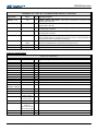
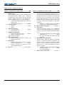
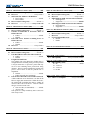
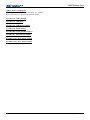
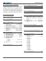
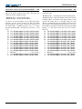
Device 16 Function 5 Registers - USB Direct Device
Communications
The registers in this function control USB direct device
communications. There are two sets of software accessible
registers: PCI Configuration registers and Memory Mapped
I/O registers. The PCI configuration registers are located in
the Device 16 Function 5 PCI configuration space of the
VT8237R. The Memory Mapped I/O registers are accesible in
the system memory space at an address defined in the UDCI
(USB Device Controller Interface) Base Address register at
PCI Configuration offset 13-10
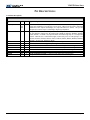
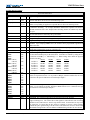
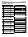
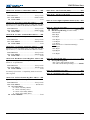
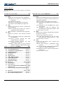
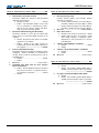
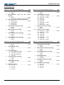
PCI Configuration Space Header
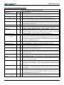
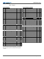
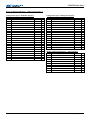
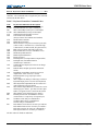
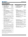
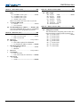
Offset 1-0 - Vendor ID (1106h) .........................................RO
15-0 Vendor ID ................. (1106h = VIA Technologies)
Offset 3-2 - Device ID (D104h) ..........................................RO
15-0 Device ID .. (D104h = VT8237R USB UDCI Ctrlr)
Offset 5-4 - Command (0000h).........................................RW
15-8 Reserved ........................................ always reads 0
7
Address Stepping ...................... default=0 (disabled)
6
Reserved (parity error response) ..................fixed at 0
5
Reserved (VGA palette snoop) ....................fixed at 0
4
Memory Write and Invalidate . default=0 (disabled)
3
Reserved (special cycle monitoring)............fixed at 0
2
Bus Master ............................... default=0 (disabled)
1
Memory Space........................... default=0 (disabled)
0
I/O Space ............................... default=0 (disabled)
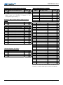
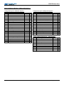
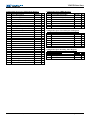
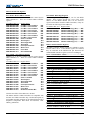
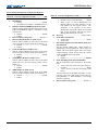
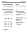
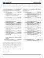
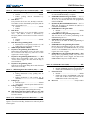
Offset 7-6 - Status (0210h) ............................................. RWC
15 Reserved (detected parity error).......... always reads 0
14 Signaled System Error............................... default=0
13 Received Master Abort.............................. default=0
12 Received Target Abort .............................. default=0
11 Signaled Target Abort ............................... default=0
10-9 DEVSEL# Timing
00 Fast
01 Medium......................................default (fixed)
10 Slow
11 Reserved
8-0 Reserved ........................ fixed at 10h (PCI PMI)
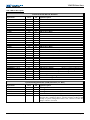
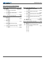
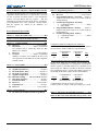
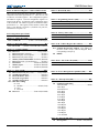
Offset 8 - Revision ID (nnh)...............................................RO
7-0 Silicon Revision Code
Offset 9 - Programming Interface (00h) .......................... RO
Offset A - Sub Class Code (80h) ....................................... RO
Offset B - Base Class Code (02h)...................................... RO
Offset C – Cache Line Size (00h)..................................... RW
Offset D - Latency Timer (16h) ....................................... RW
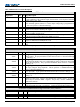
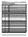
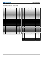
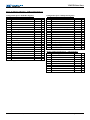
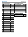
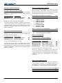
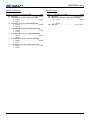
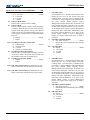
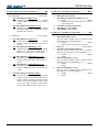
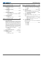
Offset 13-10 – UDCI Memory Mapped I/O Base Addr. RW
31-8 UDCI Memory Mapped I/O Registers Base
Address. Memory Address for the base of the USB
UDCI I/O Register block, corresponding to AD[31:8]
7-3 Reserved
........................................always reads 0
2-1 Memory Mapping.....reads 00b for 32-bit addressing
0
Reserved
........................................always reads 0
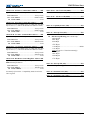
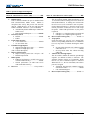
Offset 2D-2C - Sub Vendor ID (1106h).......................... RO†
Offset 2F-2E - Sub Device ID (D104h)........................... RO†
† RW if Rx42[4] = 1.
Offset 34 - Power Management Capabilities (80h) ........ RW
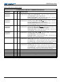
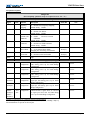
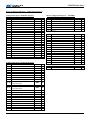
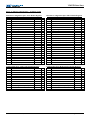
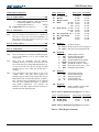
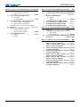
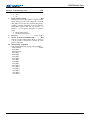
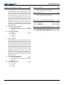
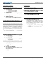
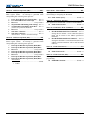
Offset 3C - Interrupt Line (00h)...................................... RW
7-4 Reserved
........................................always reads 0
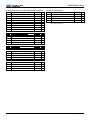
3-0 USB Interrupt Routing
0000 Disabled................................................. default
0001 IRQ1
0010 Reserved
0011 IRQ3
0100 IRQ4
0101 IRQ5
0110 IRQ6
0111 IRQ7
1000 IRQ8
1001 IRQ9
1010 IRQ10
1011 IRQ11
1100 IRQ12
1101 IRQ13
1110 IRQ14
1111 Disabled
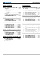
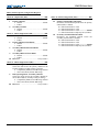
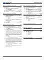
Offset 3D - Interrupt Pin (04h)......................................... RO
7-0 Interrupt Pin..........................default = 04h (INTD#)
Revision 2.06 December 15, 2004
-88- Device 16 Function 5 USB Direct Device Communications Registers