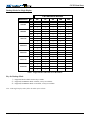
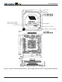
1
Data Sheet CN333 North Bridge with Integrated UniChrome Pro 3D / 2D Graphics Controller Revision 1.0 January 5, 2005 VIA TECHNOLOGIES, INC. Copyright Notice: Copyright © 2004-2005, VIA Technologies Incorporated. All Rights Reserved. No part of this document may be reproduced, transmitted, transcribed, stored in a retrieval system, or translated into any language, in any form or by any means, electronic, mechanical, magnetic, optical, chemical, manual or otherwise without the prior written permission of VIA Technologies Incorporated. The material in this document is for information only and is subject to change without notice. VIA Technologies Incorporated reserves the right to make changes in the product design without reservation and without notice to its users. Copyright © 2004-2005, S3 Graphics Incorporated. All rights reserved. If you have received this document from S3 Graphics Incorporated in electronic form, you are permitted to make the following copies for business use related to products of S3 Graphics Incorporated: one copy onto your computer for the purpose of on-line viewing, and one printed copy. With respect to all documents, whether received in hard copy or electronic form, other use, copying or storage, in whole or in part, by any means electronic, mechanical, photocopying or otherwise, is not permitted without the prior written consent of S3 Graphics Incorporated. The material in this document is for information only and is subject to change without notice. S3 Graphics Incorporated reserves the right to make changes in the product design without reservation and without notice to its users. Trademark Notices: VT8237R and CN333 may only be used to identify products of VIA Technologies. C3™ and PowerSaver™ are registered trademarks of VIA Technologies. Windows XP™, Windows 2000™, Windows ME™, Windows 98™ and Plug and Play™ are registered trademarks of Microsoft Corporation. PCI™ is a registered trademark of the PCI Special Interest Group. VESA™ is a trademark of the Video Electronics Standards Association. All trademarks are the properties of their respective owners. Disclaimer Notice: No license is granted, implied or otherwise, under any patent or patent rights of VIA Technologies or S3 Graphics. VIA Technologies and S3 Graphics make no warranties, implied or otherwise, in regard to this document and to the products described in this document. The information provided by this document is believed to be accurate and reliable as of the publication date of this document. However, VIA Technologies and S3 Graphics assume no responsibility for any errors in this document. Furthermore, VIA Technologies and S3 Graphics assume no responsibility for the use or misuse of the information in this document and for any patent infringements that may arise from the use of this document. The information and product specifications within this document are subject to change at any time, without notice and without obligation to notify any person of such change. Offices: VIA Technologies Incorporated Taiwan Office: st 1 Floor, No. 531 Chung-Cheng Road, Hsin-Tien Taipei, Taiwan ROC Tel: (886-2) 2218-5452 Fax: (886-2) 2218-5453 Home page: http://www.via.com.tw VIA Technologies Incorporated USA Office: 940 Mission Court Fremont, CA 94539 USA Tel: (510) 683-3300 Fax: (510) 683-3301 or (510) 687-4654 Home Page: http://www.viatech.com S3 Graphics Incorporated USA Office: 1045 Mission Court Fremont, CA 94539 USA Tel: (510) 687-4900 Fax: (510) 687-4901 Home Page: http://www.s3graphics.com CN333 Data Sheet REVISION HISTORY Document Release 1.0 Date 1/5/05 Revision 1.0, January 5, 2005 Revision Initial external release Initials SV -i- Revision History CN333 Data Sheet TABLE OF CONTENTS REVISION HISTORY .......................................................................................................................................................................I TABLE OF CONTENTS.................................................................................................................................................................. II LIST OF FIGURES .........................................................................................................................................................................IV LIST OF TABLES ...........................................................................................................................................................................IV PRODUCT FEATURES.................................................................................................................................................................... 1 CN333 SYSTEM OVERVIEW......................................................................................................................................................... 5 VIA C3 PROCESSOR INTERFACE .................................................................................................................................................. 5 MEMORY CONTROLLER ................................................................................................................................................................ 5 ULTRA V-LINK .............................................................................................................................................................................. 6 SYSTEM POWER MANAGEMENT ................................................................................................................................................... 6 3D GRAPHICS ENGINE ................................................................................................................................................................... 6 128-BIT 2D GRAPHICS ENGINE ..................................................................................................................................................... 6 MPEG VIDEO PLAYBACK ............................................................................................................................................................. 6 LCD AND DVI MONITOR SUPPORT .............................................................................................................................................. 7 DESKTOP MODES FOR SINGLE DISPLAY ....................................................................................................................................... 8 PINOUTS............................................................................................................................................................................................ 9 PIN DIAGRAMS ............................................................................................................................................................................... 9 PIN LISTS ..................................................................................................................................................................................... 10 PIN DESCRIPTIONS....................................................................................................................................................................... 13 CPU Interface Pin Descriptions .......................................................................................................................................... 13 DDR SDRAM Memory Controller Pin Descriptions......................................................................................................... 14 Ultra V-Link Pin Descriptions............................................................................................................................................. 15 CRT and Serial Bus Pin Descriptions ................................................................................................................................. 16 Flat Panel Display Port (FPDP) Pin Descriptions.............................................................................................................. 17 Digital Video Port 1 (GDVP1) Pin Descriptions ................................................................................................................ 18 Clock, Reset, Power Control, GPIO, Interrupt and Test Pin Descriptions ..................................................................... 19 Compensation and Reference Voltage Pin Descriptions ................................................................................................... 20 Power Pin Descriptions ........................................................................................................................................................ 21 Strap Pin Descriptions.......................................................................................................................................................... 22 REGISTERS..................................................................................................................................................................................... 23 REGISTER OVERVIEW ................................................................................................................................................................. 23 MISCELLANEOUS I/O................................................................................................................................................................... 30 CONFIGURATION SPACE I/O ....................................................................................................................................................... 30 DEVICE 0 FUNCTION 0 REGISTERS – AGP................................................................................................................................. 31 Device 0 Function 0 Header Registers ................................................................................................................................ 31 AGP GART / Graphics Aperture........................................................................................................................................................... 34 DEVICE 0 FUNCTION 1 REGISTERS – ERROR REPORTING ......................................................................................................... 35 Device 0 Function 1 Header Registers ................................................................................................................................ 35 Device 0 Function 1 Device-Specific Registers ................................................................................................................... 36 V-Link Error Reporting......................................................................................................................................................................... 36 AGP Error Reporting............................................................................................................................................................................. 36 Revision 1.0, January 5, 2005 -ii- Table of Contents CN333 Data Sheet DEVICE 0 FUNCTION 2 REGISTERS – HOST CPU....................................................................................................................... 37 Device 0 Function 2 Header Registers ................................................................................................................................ 37 Device 0 Function 2 Device-Specific Registers ................................................................................................................... 38 Host CPU Control ................................................................................................................................................................................. 38 Host CPU AGTL+ I/O Control ............................................................................................................................................................. 42 DEVICE 0 FUNCTION 3 REGISTERS – DRAM ............................................................................................................................. 43 Device 0 Function 3 Header Registers ................................................................................................................................ 43 Device 0 Function 3 Device-Specific Registers ................................................................................................................... 44 DRAM Control...................................................................................................................................................................................... 44 ROM Shadow Control........................................................................................................................................................................... 52 DRAM Above 4G Control .................................................................................................................................................................... 53 UMA Control ........................................................................................................................................................................................ 54 Graphics Control ................................................................................................................................................................................... 55 AGP Controller Interface Control ......................................................................................................................................................... 55 DRAM Drive Control............................................................................................................................................................................ 56 DEVICE 0 FUNCTION 4 REGISTERS – POWER MANAGEMENT ................................................................................................... 57 Device 0 Function 4 Header Registers ................................................................................................................................ 57 Device 0 Function 4 Device-Specific Registers ................................................................................................................... 58 Power Management Control.................................................................................................................................................................. 58 BIOS Scratch......................................................................................................................................................................................... 58 DEVICE 0 FUNCTION 7 REGISTERS – V-LINK ............................................................................................................................ 59 Device 0 Function 7 Header Registers ................................................................................................................................ 59 Device 0 Function 7 Device-Specific Registers ................................................................................................................... 60 V-Link Control ...................................................................................................................................................................................... 60 PCI Bus Control .................................................................................................................................................................................... 63 Graphics Aperture Control .................................................................................................................................................................... 65 V-Link CKG Control............................................................................................................................................................................. 65 V-Link Compensation / Drive Control .................................................................................................................................................. 66 DRAM Above 4G Support .................................................................................................................................................................... 66 DEVICE 1 REGISTERS – PCI-TO-PCI BRIDGE............................................................................................................................ 67 Device 1 Header Registers.................................................................................................................................................... 67 Device 1 Device-Specific Registers ...................................................................................................................................... 69 AGP Bus Control................................................................................................................................................................................... 69 ELECTRICAL SPECIFICATIONS .............................................................................................................................................. 71 ABSOLUTE MAXIMUM RATINGS ................................................................................................................................................. 71 DC CHARACTERISTICS ............................................................................................................................................................... 71 MECHANICAL SPECIFICATIONS............................................................................................................................................. 72 Revision 1.0, January 5, 2005 -iii- Table of Contents CN333 Data Sheet LIST OF FIGURES FIGURE 1. FIGURE 2. FIGURE 3. FIGURE 4. FIGURE 5. SYSTEM BLOCK DIAGRAM.................................................................................................................................... 5 INTEGRATED UNICHROME PRO GRAPHICS CONTROLLER INTERNAL BLOCK DIAGRAM ............ 7 BALL DIAGRAM (TOP VIEW) – FLAT PANEL / DIGITAL VIDEO OUTPUT................................................ 9 GRAPHICS APERTURE ADDRESS TRANSLATION......................................................................................... 34 MECHANICAL SPECIFICATIONS – 681-PIN HSBGA BALL GRID ARRAY PACKAGE WITH HEAT SPREADER................................................................................................................................................................. 72 FIGURE 6. LEAD-FREE MECHANICAL SPECIFICATIONS – 681-PIN HSBGA BALL GRID ARRAY PACKAGE WITH HEAT SPREADER ........................................................................................................................................ 73 LIST OF TABLES TABLE 1. TABLE 2. TABLE 3. TABLE 4. SUPPORTED CRT AND PANEL SCREEN RESOLUTIONS.................................................................................. 8 PIN LIST (LISTED BY PIN NUMBER) .................................................................................................................... 10 PIN LIST (LISTED BY PIN NAME) ......................................................................................................................... 11 POWER, GROUND AND VOLTAGE REFERENCE PIN LIST............................................................................ 12 Revision 1.0, January 5, 2005 -iv- Lists of Figures and Tables CN333 Data Sheet CN333 NORTH BRIDGE 133 / 100 MHz VIA C3 Front Side Bus Integrated UniChrome Pro 3D / 2D Graphics and Video Controllers Advanced DDR333 SDRAM Controller 1 GB / Sec Ultra V-Link Interface PRODUCT FEATURES • Defines Highly Integrated Solutions for Full Featured, Power Efficient PC Designs – – – – • High Performance CPU Interface – – – • Supports 133 / 100 MHz FSB VIA C3 processors Eight outstanding transactions (eight-level In-Order Queue (IOQ)) Built-in Phase Lock Loop circuitry for optimal skew control within and between clocking regions Advanced High-Performance 64-Bit DDR SDRAM Controller – – – – – – – – – – – – – – – • High Performance UMA North Bridge: Integrated VIA C3 North Bridge with 133 / 100 MHz FSB support and UniChrome Pro 3D / 2D Graphics and Video Controllers in a single chip Advanced memory controller supporting DDR 333 / 266 / 200 SDRAM Combines with VIA VT8235M-CE / VT8237R South Bridge for integrated 10/100 LAN, Audio, ATA133 IDE, LPC, USB 2.0 and Serial ATA (VT8237R) “Lead-Free” 31 x 31mm HSBGA (Ball Grid Array with Heat Spreader) package with 681 balls and 1mm ball pitch Supports DDR333 / 266 memory types with 2.5V SSTL-2 DRAM interface Supports mixed 64 / 128 / 256 / 512 / 1024Mb DDR SDRAMs in x8 and x16 configurations Supports CL 2 / 2.5 for DDR266 / 333 Supports 2 unbuffered double-sided DIMMs and up to 4 GBytes of physical memory Programmable timing / drive for memory address, data and control signals DRAM interface pseudo-synchronous with host CPU for optimal memory performance Concurrent CPU, internal graphics controller and V-Link access for minimum memory access latency Rank interleave and up to 16-bank page interleave (i.e., 16 pages open simultaneously) based on LRU to effectively reduce memory access latency Seamless DRAM command scheduling for maximum DRAM bus utilization – (e.g., precharge other banks while accessing the current bank) CPU Read-Around-Write capability for non-stalled operation Speculative DRAM read before snoop result to reduce PCI master memory read latency Supports Burst Read and Write operations with burst length of 4 or 8 Eight cache lines (64 quadwords) of integrated CPU-to-DRAM write buffers and eight separate cache lines of CPUto-DRAM read prefetch buffers Optional dynamic Clock Enable (CKE) control for DRAM power reduction during normal system state (S0) Supports self-refresh and CAS-before-RAS DRAM refresh with staggered RAS timing High Bandwidth 1 GB / Sec 16-Bit “Ultra V-Link” Host Controller – – – – – – Supports 66 MHz, 4x and 8x transfer modes, Ultra V-Link Host interface with 1 GB / Sec total bandwidth Full duplex transfers with separate command / strobe for 4x and 8x modes Request / Data split transaction Transaction assurance for V-Link Host-to-Client access eliminates V-Link Host-Client Retry cycles Intelligent V-Link transaction protocol to minimize data wait-states, throttle transfer latency and avoid data overflow Highly efficient V-Link arbitration with minimum overhead Revision 1.0, January 5, 2005 -1- Product Features CN333 Data Sheet • Advanced System Power Management Support – – – – – – • ACPI 2.0 and PCI Bus Power Management 1.1 compliant Supports Suspend-to-DRAM (STR) and DRAM self-refresh Supports dynamic Clock Enable (CKE) control for DRAM power reduction during normal system state (S0) Supports SMI, SMM and STPCLK mechanisms Supports VIA PowerSaver™ Technology Low-leakage I/O pads Integrated Graphics with 2D / 3D / Video Controllers – – – – – – Optimized Unified Memory Architecture (UMA) Supports 16 / 32 / 64 MB Frame Buffer sizes 200 MHz Graphics Engine Clock Two independent 128-bit data paths between North Bridge and graphics core to improve video performance, one for frame buffer access and one for texture / command access PCI v2.2 Host Bus compliant AGP v3.0 compliant 2D Acceleration – – – – – – – – – – – 128-bit 2D graphics engine Hardware 2D rotation Supports ROP3, 256 operations Supports 8bpp, 15/16bpp and 32bpp color depth modes BitBLT (Bit BLock Transfer) functions including alpha BLTs True-color hardware cursor (64x64x32bpp) with 256-level blending effect Color expansion, source Color Key and destination Color Key Bresenham line drawing / style line function Transparency mode Window clipping Text function 3D Acceleration 3D Graphics Processor – 128-bit 3D graphics engine – Dual pixel rendering pipes and dual texture units – Floating-point setup engine – Internal full 32-bit ARGB format for high rendering quality – 8K Texture Cache Capability – Supports ROP2 – Supports various texture formats including 16/32bpp ARGB, 8bpp Palletized (ARGB), YUV 422/420 and compressed texture (DXTC) – Texture sizes up to 2048x2048 with Microsoft DirectX texture compression – High quality texture filter for Nearest, Linear, Bi-linear, Tri-linear and Anisotropic modes – Flat and Gouraud shading – Vertex Fog and Fog Table – Z-Bias, LOD-Bias, Polygon offset, Edge Anti-aliasing and Alpha Blending – Bump mapping and cubic mapping – Hardware back-face culling – Specular lighting Performance – Two textures per pass – Triangle rate up to 4.5 million triangles per second – Pixel rate up to 200 million pixels per second for 2 textures each – Texel bilinear fill rate up to 400 million texels per second – High quality dithering Revision 1.0, January 5, 2005 -2- Product Features CN333 Data Sheet Video Acceleration High Quality Video Processor – RGB555, RGB565, RGB8888 and YUV422 video playback formats – High quality 5-tap horizontal and 5-tap vertical scaler (up or down) for both horizontal and vertical scaling (linear interpolation for horizontal and vertical p-scaling and filtering for horizontal and vertical down-scaling) – Independent graphics and video gamma tables – 2 sets of Color and Chroma Key support – Color enhancement for contrast, hue, saturation and brightness – Display rotation in clockwise and counter-clockwise directions – Bob, Weave, Median-filter and Adaptive de-interlacing modes – 3:2 / 2:2 pull-down detection – De-blocking mode support – Combining of many special effects such as filter, scaling up or down, sub-picture blending, de-interlacing and deblocking to one pass process – Tear-free double / triple buffer flipping – Input video vertical blanking or line interrupt – Video gamma correction Video Overlay Engine – Simultaneous graphics video playback overlay – Supports video window overlays – Supports 16 operations for Color and Chroma Key – Hardware sub-picture blending MPEG Video Playback – MPEG-2 hardware VLD (Various Length Decode), iDCT, and motion compensation for full speed DVD and MPEG-2 playback at full D1 resolution – High quality DVD and streaming video playback – Video auto-flipping – Hardware DVD sub-picture blending DuoView+™ Dual Image Capability – – – – WinXP, WinME and Win98 multi-monitor, extended desktop support Two independent display engines, each of which can display completely different information at different resolutions, pixel depths and refresh rates (supports different images on different displays simultaneously) CRT, FPD and DVI monitor refresh rates are independently programmable for optimum image quality Improved display flexibility with simultaneous FPD / CRT, FPD, FPD / DVI and other combined operations Full Software Support – – – – – Microsoft DirectX 7.0, 8.0 and 9.0 compatible Microsoft DirectX Texture Compression (DXTC / S3TC) Supports OpenGL Drivers for major operating systems and APIs: Windows 9x / ME, Windows 2000, Windows XP, Direct3D, DirectDraw, DirectShow and OpenGL ICD for Windows 9x / ME and XP Windows NT 4.0 Standard VGA driver Revision 1.0, January 5, 2005 -3- Product Features CN333 Data Sheet • Extensive Display Support for External Video Output – – – CRT display interface 12-bit Digital Video Port with support for external DVI transmitter 24-bit / Dual 12-Bit FPD interface to external LVDS transmitter CRT Display – – CRT display interface with 24-bit true-color RAMDAC up to 300 MHz pixel rate with gamma correction capability Supports CRT resolutions up to 1920 x 1440 12-Bit DVI Transmitter Interface – – – 1.5V low-swing interface supports external DVI transmitter for a driving a DVI monitor Double-data-rate data transfer with clock rates up to 165 MHz Built-in digital phase adjuster to fine-tune signal timing between clock and data bus 24-Bit Flat Panel Display (FPD) Interface – – Supports 18/24-bit FPD interface with external LVDS transmitter chip using single or double-data rate data transfer Supports panel resolutions up to 1600x1200 Dual 12-Bit Flat Panel Display (FPD) Interface – – – • Alternate operating mode of FPD interface with external LVDS transmitters Single or separate sets of clock and sync signals Supports panel resolutions up to 1600x1200 Advanced Graphics Power Management Support – – – – – Built-in reference voltage generator and monitor sense circuits Automatic panel power sequencing and VESA DPMS (Display Power Management Signaling) CRT power-down External I/O signal controls enabling of graphics accelerator into standby / suspend-off state Dynamic clock gating for inactive functions to achieve maximum power saving I2C Serial Bus and DDC / E-DDC Monitor Communications for Plug-and-Play configuration Revision 1.0, January 5, 2005 -4- Product Features CN333 Data Sheet CN333 SYSTEM OVERVIEW The CN333 is a high performance, cost-effective and energy efficient UMA North Bridge with integrated UniChrome Pro graphics / video controller used for the implementation of mobile and desktop personal computer systems with 133 / 100 MHz CPU host bus (“Front Side Bus”) based on VIA C3 processors. VIA C3 CPU System Management Bus 133 / 100 MHz Front Side Bus 64-Bit RGB, HV, DDC DDR North Bridge with UniChrome Pro Graphics Controller UDMA / ATA 133 / 100 / 66 / 33 MII 66 MHz 8x / 4x V-Link PCI Slots 10/100 Ethernet VT6103 DDR333 / 266 DIMMs CN333 CRT Network Interface PHY 33MHz, 32-bit PCI VT8237R V-Link South Bridge Pri Sec FPDP Flat Panel Display Port 24-Bit / Dual 12-Bit Flat Panel Display Interface EPROM VT1631 LVDS Transmitter 6X USB 2.0 GDVP1 Digital Video Port 1 12-Bit DVI Interface TFT Flat Panel LPC AC-Link VT1616 AC'97 Audio Codec VT1632A DVI Transmitter MC-97 Modem Codec Integrated AC'97 Audio DVI Monitor VT1211 LPC Super I/O Serial / IR Parallel Floppy Disk Keyboard Mouse Figure 1. System Block Diagram The complete chipset consists of the CN333 North Bridge and the VT8237R V-Link South Bridge. The CN333 integrates VIA’s most advanced system controller with a high-performance UniChrome Pro 3D / 2D graphics / video controller plus flat panel and DVI monitor. The CN333 provides superior performance between the CPU, DRAM, V-Link and integrated graphics controller with pipelined, burst and concurrent operation. The VT8237R is a highly integrated peripheral controller which includes V-Linkto-PCI / V-Link-to-LPC controllers, Ultra DMA IDE controller, USB2.0 host controller, 10/100Mb networking MAC, AC97 and system power management controllers. VIA C3 Processor Interface The CN333 supports 133 / 100 MHz FSB VIA C3 processors and implements an eight-deep In-Order-Queue. VIA PowerSaver technology is supported for VIA Antaur processors to reduce system power consumption while sustaining high processing power. Memory Controller The CN333 SDRAM controller supports up to two double-sided DDR333 / 266 DIMMs for 4 GB maximum physical memory. The DDR DRAM interface allows zero-wait-state data transfer bursting between the DRAM and the memory controller’s data buffers. The different banks of DRAM can be composed of an arbitrary mixture of 64 / 128 / 256 / 512 / 1024Mb DRAMs in x8 or x16 configurations. The DRAM controller can run either synchronous or pseudo-synchronous with the host CPU bus. Revision 1.0, January 5, 2005 -5- Overview CN333 Data Sheet Ultra V-Link The CN333 North Bridge interfaces to the South Bridge through a high speed (up to 1 GB / Sec) 8x, 66 MHz Data Transfer interconnect bus called “Ultra V-Link”. Deep pre-fetch and post-write buffers are included to allow for concurrent CPU and VLink operation. The combined CN333 North Bridge and VT8237R South Bridge system supports enhanced PCI bus commands such as “Memory-Read-Line”, “Memory-Read-Multiple” and “Memory-Write-Invalid” commands to minimize snoop overhead. In addition, advanced features are supported such as CPU write-back forward to PCI master and CPU write-back merged with PCI post write buffers to minimize PCI master read latency and DRAM utilization. Delay transaction and read caching mechanisms are also implemented for further improvement of overall system performance. System Power Management For sophisticated power management, the CN333 supports dynamic CKE control to minimize DDR SDRAM power consumption during normal system state (S0). A separate suspend-well plane is implemented for the memory control logic for the Suspend-toDRAM state. VIA PowerSaver™ Technology is supported to minimize CPU power consumption while sustaining processing power. The CN333 graphics accelerator implements automatic clock gating for each graphics engine to achieve power saving, moving to standby or suspend states to further reduce power consumption when idle. Automatic panel power sequencing and VESA DPMS (Display Power Management Signaling) CRT power-down are supported. Coupled with the VT8237R South Bridge chip, a complete power conscious PC main board can be implemented with no external glue logic. 3D Graphics Engine Featuring an integrated 128-bit 3D graphics engine, the CN333 North Bridge utilizes a highly pipelined architecture that provides high performance along with superior image quality. Several new features enhance the 3D architecture, including two pixel rendering pipes, single-pass multitexturing, bump and cubic mapping, texture compression, edge anti-aliasing, vertex fog and fog table, hardware back-face culling, specular lighting, anisotropic filtering and an 8-bit stencil buffer. The chip also offers the industry’s only simultaneous usage of single-pass multitexturing and single-cycle trilinear filtering – enabling stunning image quality without performance loss. Image quality is further enhanced with true 32-bit color rendering throughout the 3D pipeline to produce more vivid and realistic images. The advanced triangle setup engine provides industry leading 3D performance for a realistic user experience in games and other interactive 3D applications. The 3D engine is optimized for AGP texturing from system memory. 128-bit 2D Graphics Engine The CN333 North Bridge's advanced 128-bit 2D graphics engine delivers high-speed 2D acceleration for productivity applications. The enhanced 2D architecture with direct access frame buffer capability optimizes UMA performance and provides acceleration of all color depths. MPEG Video Playback The CN333 North Bridge provides the ideal architecture for high quality MPEG-2 based video applications. For MPEG playback, the integrated video accelerator offloads the CPU by performing planar-to-packed format conversion and motion video compensation tasks, while the enhanced scaling algorithm delivers incredible full-screen video playback. Revision 1.0, January 5, 2005 -6- Overview CN333 Data Sheet North Bridge Host Bus 66 MHz PCI Host Bus Interface VGAGFXController MPEGEngine Display Engine IGA 1 Panel Vertex Cache Setup Engine Texture Engine Rendering Pipelines VideoProcessor Texture Cache 3D Engine AGP-like Interface IGA 2 HWSprite HWCursor GFXStream Mux 128-bit2DEngine Digital Video Port CommandEngine 24-Bit FPD plus 12-Bit DVP Digital Video Port 1 DAC CRT VideoEngine 0/1 (Scaler/ YUV-to-RGB) Vide o Stream MemoryInterface Unit North Bridge Memory Controller Figure 2. Integrated UniChrome Pro Graphics Controller Internal Block Diagram LCD and DVI Monitor Support The CN333 provides two “Digital Video Port” interfaces: FPDP and GDVP1. The Flat Panel Display Port (FPDP) implements a 24-bit / dual 12-bit interface which is designed to drive a Flat Panel Display via an external LVDS transmitter chip (such as the VIA VT1631 or NSC DS90C387R). The CN333 can be connected to the external LVDS transmitter chip in either 24-bit or dual12-bit modes. A wide variety of LCD panels are supported including VGA, SVGA, XGA, SXGA+ and up to UXGA-resolution TFT color panels, in either SDR (1 pixel / clock) or DDR (2 pixels / clock) modes. UXGA and higher resolutions require dualedge data transfer (DDR) mode which is supported by the VIA VT1631 LVDS transmitter chip. Digital Video Port 1 (GDVP1) is used to drive a DVI monitor via an external DVI transmitter chip (such as the VIA VT1632A). The flexible display configurations of the CN333 allow support of a flat panel (LVDS interface) or flat panel monitor (DVI interface) and CRT display at the same time. Internally the CN333 North Bridge provides two separate display engines, so if two display devices are connected, each can display completely different information at different resolutions, pixel depths and refresh rates. If more than two display devices are connected, the additional displays must have the same resolution, pixel depth and refresh rate as one of the first two. The maximum display resolutions supported for one display device are listed in the table below. If more than one display is implemented (i.e., if both display engines are functioning at the same time), then available memory bandwidth may limit the display resolutions supported on one or both displays. This will be dependent on many factors including primarily clock rates and memory speeds (contact VIA for additional information). Revision 1.0, January 5, 2005 -7- Overview CN333 Data Sheet Desktop Modes for Single Display CRT Maximum Refresh Resolution 640x480 800x600 1024x768 1280x1024 1400x1050 1600x1200 1920x1440 BPP 60 75 85 100 120 8 √ √ √ √ √ 16 32 √ √ √ √ √ √ √ √ √ √ 8 16 32 √ √ √ √ √ √ √ √ √ √ √ √ √ √ √ 8 √ √ √ √ 16 32 √ √ √ √ √ √ √ √ 8 16 32 √ √ √ √ √ √ √ √ √ 8 √ 16 32 √ √ 8 16 32 √ √ √ √ √ √1 √ √ √2 8 √ √ 16 √ √ 32 √ √ Table 1. Supported CRT and Panel Screen Resolutions Key for Desktop Mode √ = Supported: Mode available and Overlay available √1 = Supported, but DDR266: Mode available, overlay not available. √2 = Supported, but DDR266: Mode not available, overlay not available. Note: LCD Single Display modes follow the 60Hz refresh column. Revision 1.0, January 5, 2005 -8- Overview CN333 Data Sheet PINOUTS Key 1 4 5 6 7 8 11 12 13 14 15 16 17 20 21 22 23 24 25 26 27 28 29 HD 28# HD 29# HD 25# HD 26# HD 16# HD 13# GND HD 5# HD 15# GND HA 23# HA 19# GND HA 11# BNR# NC GND DE FER# HREQ 0# GND D RDY# ADS# GND HD 34# GND HD 31# GND HD 24# HD 19# GND HD 10# HD 17# HD 4# NC HA 30# HA 31# HA 15# GND HA 4# NC B PRI# HREQ 2# HIT M# D BSY# RS2# NC HD 38# HD 22# NC HD 32# NC NC HD 20# HD 11# HD 12# NC HD 8# HD 6# HA 29# HA 27# HA 22# HA 10# HA 13# HA 3# HA 9# HA 8# HREQ 1# HREQ 4# NC RS1# RS0# BREQ 0# NC GND HD 33# HD 21# HD 30# HD 14# HD 18# GND HD 9# HD 0# GND HA 20# CPU RST# GND HA 12# HA 5# HA 6# NC HA 7# GND HREQ 3# HT RDY# GND NC NC HD 23# GND HD 2# NC HD 1# HA 26# HA 24# HA 21# HA 28# HA 16# E H LOCK# HIT# HD 35# HD 7# HD 3# HR COMP HA 18# HA 17# HA 25# GND HA VREF0 A B Figure 3. Ball Diagram (Top View) – Flat Panel / Digital Video Output Pin Diagrams 3 2 C HD 43# D HD 37# GND HD 27# E NC HD 39# HD 36# F HD 42# NC HD 45# HD 44# HD 47# G HD 51# GND HD 49# HD 41# GND H HD 63# HD 57# HD 55# HD 59# HD 48# J HD 46# NC NC HD 52# NC K HD 53# GND HD 54# HD 58# GND L HD 62# HD 56# HD 61# NC HD 40# HD 50# VCCA15 GNDA VCCA15 GNDA PLL3 PLL3 PLL1 PLL1 DISP CLKI P AB AG W Y GND HA VREF1 GND F G GNDA VCCA3 MCK MCK 9 10 11 12 13 14 15 16 17 18 19 20 21 22 H23 HD VREF3 J VCC 15 VCC 15 VCC 15 VCC 15 VCC 15 VCC 15 VCC 15 VCC 15 VCC 15 VCC 15 VCC 15 VCC 15 VCC 15 VCC 15 J HD VREF2 K VCC 15 VTT VTT VTT VTT VTT VTT VTT VTT VCC25 VCC25 VCC25 VCC25 MEM MEM MEM MEM VCC 15 K L VCC 15 VTT GND GND GND GND GND GND GND GND GND GND VCC25 MEM VCC 15 L M VCC 15 VTT GND GND GND GND GND GND GND GND GND GND VCC25 MEM VCC 15 M MD 5 GND MD 1 GND MD 6 MD 2 DQS 0# DQM 0 CKE 3 CKE 1 MD 3 MD 7 GND MD 9 MD 12 GND MD 8 CKE 0 CKE 2 DQM 1 DQS 1# MD 13 MA 12 MA 11 MD 15 MD 14 GND MD 20 MD 11 GND MD 10 MA 9 MA 7 MD 21 MD 17 MD 16 MA 5 MA 8 DQM 2 DQS 2# GND GND GND GND GND GND VCC25 MEM VCC 15 N DISP VCCA15 GNDA CLKO PLL2 PLL2 G CLK XIN P VCC 15 VTT GND GND GND GND GND GND GND GND GND GND VCC25 MEM VCC 15 P VCCA33 GNDA DAC1 DAC1 R VCC 15 VCC33 GFX GND GND GND GND GND GND GND GND GND GND VCC25 MEM VCC 15 R GNDA DAC2 T VCC 15 VCC33 GFX GND GND GND GND GND GND GND GND GND GND VCC25 MEM VCC 15 T U VCC 15 VCC33 GFX GND GND GND GND GND GND GND GND GND GND VCC25 MEM VCC 15 U GND MD 19 MD 22 GND MD 18 V VCC 15 VCC15 AGP GND GND GND GND GND GND GND GND GND GND VCC25 MEM VCC 15 V MA 4 MA 6 MD 28 MD 24 MD 23 W VCC 15 VCC15 AGP GND GND GND GND GND GND GND GND GND GND VCC25 MEM VCC 15 W MEM VREF3 MA 2 MA 3 MD 29 DQS 3# MD 25 Y VCC 15 VCC15 AGP GND VCC MEM25 VCC 15 Y MA 0 GND MD 30 MD 26 GND DQM 3 VCC15 VCC15 VCC15 VCC15 VCC15 VCC15 VCC25 VCC25 VCC25 VCC25 VCC25 VCC25 AGP AGP AGP AGP VL VL MEM MEM MEM MEM MEM MEM VCC 15 AA MA 1 MD 33 MD 32 MD 31 MD 27 BA 0 BA 1 MA 10 MD 37 MD 36 GND MD 34 DQM 4 GND DQS 4# AD MD 35 MD 39 MD 38 AGP MEM BUSY# VREF5 AE MD 40 MD 44 AR NC NC NC NC NC NC NC GND GND GND GND GND GND GND GND GND AA NC NC NC NC AA AB NC NC NC NC AB VCC 15 VCC 15 VCC 15 VCC 15 VCC 15 VCC 15 VCC 15 VCC 15 VCC 15 VCC 15 VCC 15 VCC 15 VCC 15 GND AB NC NC GND 6 AC8 9 10 11 12 13 14 15 16 17 18 19 20 21 22 AC23 ENA VEE AGP VREF1 ENA BLT NC FP CLK FP D13 FP HS FP1 VS FP D10 FP D20 GND NC FP DE GND FP1 CLK# FP1 DET GND FP D7 FP D9 V PAR VD 4 DN STB+ DN STB– VD 3 VD 7 GND VSUS 15 GND NC NC FP D17 FP1 DE FP D23 FP D22 FP D11 FP1 CLK NC GND VD 1 V BE# GND DN CMD UP CMD VD 14 PWR OK CS 3# GDVP1 GDVP1 GDVP1 GDVP1 GDVP1 AH GDVP1 D3 CLK# D6 D7 D10 D11 FP D18 SBPL CLK SBPL DAT FP D1 FP D2 FP D6 NC VD 8 VD 5 VD 0 UP STB+ VD 2 VD 6 VD 11 RE SET# MD 59 AJ GDVP1 CLK SBDDC SBDDC DAT CLK AGP AGP FP AE COMPP COMPN CLK# GND MD 4 GND VCC 15 AF GDVP1 DE MEM VREF0 GND NC NC MD 0 GND NC NC MEM VREF1 GND GND SP CLK2 AD 25 M CLKO VTT INTA# GND 24 M CLKI VCC 15 R SET NC GND DFT IN# N SP DAT2 AC GND TEST IN# H8 30 T CLK V SYNC NC NC HA 14# 7 HD 60# VCCA33 GNDA DAC2 DAC3 H SYNC HD HCOMP GTL VREF1 VREF VREF 19 H CLK– U V NC 18 H CLK+ R T 10 HD VREF0 GND GNDA VCCA33 VCCA33 GNDA GNDA M VCCA33 HCK1 HCK1 GCK HCK2 HCK2 GCK N 9 ENA VDD GDVP1 GDVP1 VS D0 GDVP1 GDVP1 GDVP1 AG GDVP1 HS D2 D1 D5 7 AD AGP VL VL VREF0 COMPP VREF MEM VREF2 24 MEM VREF4 S WE# GND MD 45 MD 41 GND DQS 5# MD 61 CS 2# S CAS# S RAS# MD 46 DQM 5 MD 42 MA 13 MD 57 CS 1# CS 0# MD 54 MD 48 MD 43 MD 47 GDVP1 D9 FP DET GND FP D14 FP VS GND FP D21 FP D3 GND FP D5 VD 12 VD 9 UP STB– GND SUS ST# MD 63 GND DQS 7# MD 60 GND MD 50 MD 52 GND MD 49 GDVP1 GDVP1 AK GDVP1 D8 DET D4 FP D12 FP D15 FP D16 FP D19 NC FP D00 FP1 HS FP D4 FP D8 VD 13 GND GND VD 10 VD 15 MD 58 MD 62 DQM 7 MD 56 MD 51 MD 55 DQS 6# DQM 6 MD 53 GND Revision 1.0, January 5, 2005 -9- Pin Diagrams CN333 Data Sheet Pin Lists Table 2. Pin List (Listed by Pin Number) Pin # A03 A04 A05 A06 A07 A08 A12 A13 A15 A16 A20 A21 A22 A24 A25 A27 A28 B02 B04 B06 B07 B11 B12 B13 B14 B15 B16 B17 B21 B22 B23 B24 B25 B26 B27 B28 C01 C02 C03 C04 C05 C06 C07 C08 C09 C10 C11 C12 C13 C14 C15 C16 C17 C18 C19 C20 C21 C22 C23 C24 C25 C26 C27 C28 D01 IO IO IO IO IO IO IO IO IO IO IO IO – IO IO IO IO IO IO IO IO IO IO IO – IO IO IO IO – IO IO I IO IO – IO IO IO – IO – – IO IO IO – IO IO IO IO IO IO IO IO IO IO IO IO – IO IO O – IO Pin Name Pin # HD28# D03 HD29# D06 HD25# D07 HD26# D08 HD16# D09 HD13# D10 HD05# D12 HD15# D13 HA23# D15 HA19# D16 HA11# D18 BNR# D19 NC D20 DEFER# D21 HREQ0# D22 DRDY# D24 ADS# D25 HD34# D27 HD31# E01 HD24# E02 HD19# E03 HD10# E06 HD17# E07 HD04# E09 NC E11 HA30# E12 HA31# E13 HA15# E14 HA04# E15 NC E16 BPRI# E17 HREQ2# E18 HITM# E19 DBSY# E22 RS2# E24 NC E25 HD43# F01 HD38# F02 HD22# F03 NC F04 HD32# F05 NC F07 NC F08 HD20# F09 HD11# F13 HD12# F14 NC F15 HD08# F16 HD06# F27 HA29# F28 HA27# F29 HA22# F30 HA10# G01 HA13# G03 HA03# G04 HA09# G30 HA08# H01 HREQ1# H02 HREQ4# H03 NC H04 RS1# H05 RS0# H06 BREQ0# H27 NC H28 HD37# H30 IO IO IO IO IO IO IO IO IO O IO IO IO – IO IO IO – – IO IO – IO IO – – IO IO IO IO IO IO – IO I IO IO – IO IO IO IO IO IO AI IO IO IO I I I O IO IO IO IO IO IO IO IO IO IO IO IO IO Revision 1.0, January 5, 2005 Pin Name HD27# HD33# HD21# HD30# HD14# HD18# HD09# HD00# HA20# CPURST# HA12# HA05# HA06# NC HA07# HREQ3# HTRDY# NC NC HD39# HD36# NC HD23# HD02# NC NC HD01# HA26# HA24# HA21# HA28# HA16# NC HA14# HLOCK# HIT# HD42# NC HD45# HD44# HD47# HD35# HD07# HD03# HRCOMP HA18# HA17# HA25# TESTIN# DFTIN# MCLKI MCLKO HD51# HD49# HD41# MD00 HD63# HD57# HD55# HD59# HD48# HD40# MD04 MD05 MD01 Pin # Pin Name J01 IO HD46# J02 – NC J03 – NC J04 IO HD52# J05 – NC J27 IO MD06 J28 IO MD02 J29 IO DQS0# J30 O DQM0 K01 IO HD53# K03 IO HD54# K04 IO HD58# K06 IO HD50# K27 O CKE3 K28 O CKE1 K29 IO MD03 K30 IO MD07 L01 IO HD62# L02 IO HD56# L03 IO HD61# L04 – NC L06 IO HD60# L27 IO MD09 L28 IO MD12 L30 IO MD08 M26 O CKE0 M27 O CKE2 M28 O DQM1 M29 IO DQS1# M30 IO MD13 N05 I HCLK+ N06 I HCLK– N07 I TCLK N27 O MA12 N28 O MA11 N29 IO MD15 N30 IO MD14 P02 I DISPCLKI P03 O DISPCLKO P06 I GCLK P07 I XIN P27 IO MD20 P28 IO MD11 P30 IO MD10 R26 O MA09 R27 O MA07 R28 IO MD21 R29 IO MD17 R30 IO MD16 T01 AO AB T02 AO AG T03 AO AR T27 O MA05 T28 O MA08 T29 O DQM2 T30 IO DQS2# U06 – NC U07 – NC U27 IO MD19 U28 IO MD22 U30 IO MD18 V01 O HSYNC V02 O VSYNC V03 IO SPDAT2 V04 AI RSET Pin # V05 V06 V26 V27 V28 V29 V30 W02 W03 W04 W05 W26 W27 W28 W29 W30 Y02 Y03 Y04 Y05 Y25 Y27 Y28 Y30 AA02 AA03 AA04 AA05 AA26 AA27 AA28 AA29 AA30 AB02 AB03 AB04 AB05 AB26 AB27 AB28 AB29 AB30 AC01 AC03 AC04 AC27 AC28 AC30 AD01 AD02 AD03 AD04 AD05 AD27 AD28 AD29 AE01 AE02 AE03 AE04 AE05 AE06 AE07 AE08 AE09 -10- O – O O IO IO IO IO – – – O O IO IO IO – – – – O IO IO O – – – – O IO IO IO IO – – – – O O O IO IO – – – IO O IO – – IO IO O IO IO IO AI AI O O O – O O O Pin Name INTA# NC MA04 MA06 MD28 MD24 MD23 SPCLK2 NC NC NC MA02 MA03 MD29 DQS3# MD25 NC NC NC NC MA00 MD30 MD26 DQM3 NC NC NC NC MA01 MD33 MD32 MD31 MD27 NC NC NC NC BA0 BA1 MA10 MD37 MD36 NC NC NC MD34 DQM4 DQS4# NC NC SBDDCDAT SBDDCCLK ENAVEE MD35 MD39 MD38 AGPPCMP AGPNCMP FPCLK# ENAVDD ENABLT NC FPCLK FPD13 FPHS Pin # AE10 AE11 AE12 AE14 AE21 AE27 AE28 AF01 AF03 AF04 AF06 AF07 AF09 AF10 AF12 AF13 AF14 AF15 AF16 AF17 AF18 AF19 AF25 AF27 AF28 AF30 AG01 AG02 AG03 AG04 AG05 AG06 AG07 AG08 AG09 AG10 AG11 AG12 AG13 AG15 AG16 AG18 AG19 AG20 AG21 AG23 AG24 AG25 AG26 AG27 AG28 AG29 AG30 AH01 AH02 AH03 AH04 AH05 AH06 AH07 AH08 AH09 AH10 AH11 AH12 O O O AI O IO IO O O O – O O I O O IO IO O O IO IO O IO IO IO O O O O – – O O O O O O – IO IO O I IO I O IO O O O IO O IO O O O O O O O IO IO O O O Pin Name FP1VS FPD10 FPD20 VLCOMPP AGPBUSY# MD40 MD44 GDVP1DE GDVP1VS GDVP1D00 NC FPDE FP1CLK# FP1DET FPD07 FPD09 VPAR VD04 DNSTB+ DNSTB– VD03 VD07 SWE# MD45 MD41 DQS5# GDVP1HS GDVP1D02 GDVP1D01 GDVP1D05 NC NC FPD17/ FP1DE FPD23/ FPD22/ FPD11 FP1CLK NC VD01 VBE# DNCMD UPCMD VD14 PWROK CS3# MD61 CS2# SCAS# SRAS# MD46 DQM5 MD42 GDVP1D03 GDVP1CLK# GDVP1D06 GDVP1D07 GDVP1D10 GDVP1D11 FPD18 SBPLCLK SBPLDAT FPD01 FPD02 FPD06 Pin # AH13 AH14 AH15 AH16 AH17 AH18 AH19 AH20 AH21 AH22 AH23 AH24 AH25 AH26 AH27 AH28 AH29 AH30 AJ01 AJ03 AJ04 AJ06 AJ07 AJ09 AJ10 AJ12 AJ13 AJ14 AJ17 AJ21 AJ22 AJ24 AJ25 AJ27 AJ28 AJ30 AK01 AK02 AK03 AK04 AK05 AK06 AK07 AK08 AK09 AK10 AK11 AK12 AK13 AK20 AK21 AK22 AK23 AK24 AK25 AK26 AK27 AK28 AK29 AK30 – IO IO IO I IO IO IO I IO O IO O O IO IO IO IO O O I O O O O O IO IO I I IO IO IO IO IO IO O I O O O O O – O O O O IO IO IO IO IO O IO IO IO IO O IO Pin Name NC VD08 VD05 VD00 UPSTB+ VD02 VD06 VD11 RESET# MD59 MA13 MD57 CS1# CS0# MD54 MD48 MD43 MD47 GDVP1CLK GDVP1D09 FPDET FPD14 FPVS FPD21 FPD03 FPD05 VD12 VD09 UPSTB– SUSST# MD63 DQS7# MD60 MD50 MD52 MD49 GDVP1D08 GDVP1DET GDVP1D04 FPD12 FPD15 FPD16 FPD19 NC FPD00 FP1HS FPD04 FPD08 VD13 VD10 VD15 MD58 MD62 DQM7 MD56 MD51 MD55 DQS6# DQM6 MD53 Pin Lists CN333 Data Sheet Table 3. Pin List (Listed by Pin Name) Pin # Pin Name T01 AO AB A28 IO ADS# T02 AO AG AE21 O AGPBUSY# AE02 AI AGPCOMPN AE01 AI AGPCOMPP T03 AO AR AB26 O BA0 AB27 O BA1 A21 IO BNR# B23 IO BPRI# C27 O BREQ0# M26 O CKE0 K28 O CKE1 M27 O CKE2 K27 O CKE3 D16 O CPURST# AH26 O CS0# AH25 O CS1# AG25 O CS2# AG23 O CS3# B26 IO DBSY# A24 IO DEFER# F28 I DFTIN# P02 I DISPCLKI P03 O DISPCLKO AG18 O DNCMD AF16 O DNSTB+ AF17 O DNSTB– J30 O DQM0 M28 O DQM1 T29 O DQM2 Y30 O DQM3 AC28 O DQM4 AG29 O DQM5 AK29 O DQM6 AK24 O DQM7 J29 IO DQS0# M29 IO DQS1# T30 IO DQS2# W29 IO DQS3# AC30 IO DQS4# AF30 IO DQS5# AK28 IO DQS6# AJ24 IO DQS7# A27 IO DRDY# AE05 O ENABLT AE04 O ENAVDD AD05 O ENAVEE AG12 O FP1CLK AF09 O FP1CLK# AG08 O FP1DE AF10 I FP1DET AK10 O FP1HS AE10 O FP1VS AE07 O FPCLK AE03 O FPCLK# AK09 O FPD00 AH10 O FPD01 AH11 O FPD02 AJ10 O FPD03 AK11 O FPD04 AJ12 O FPD05 AH12 O FPD06 AF12 O FPD07 Pin # AK12 AF13 AE11 AG11 AK04 AE08 AJ06 AK05 AK06 AG07 AH07 AK07 AE12 AJ09 AG10 AG09 AF07 AJ04 AE09 AJ07 P06 AJ01 AH02 AF04 AG03 AG02 AH01 AK03 AG04 AH03 AH04 AK01 AJ03 AH05 AH06 AF01 AK02 AG01 AF03 C19 B21 D19 D20 D22 C21 C20 C17 A20 D18 C18 E22 B17 E18 F15 F14 A16 D15 E16 C16 A15 E15 F16 E14 C15 E17 Revision 1.0, January 5, 2005 O O O O O O O O O O O O O O O O O I O O I O O O O O O O O O O O O O O O I O O IO IO IO IO IO IO IO IO IO IO IO IO IO IO IO IO IO IO IO IO IO IO IO IO IO IO Pin Name FPD08 FPD09 FPD10 FPD11 FPD12 FPD13 FPD14 FPD15 FPD16 FPD17 FPD18 FPD19 FPD20 FPD21 FPD22 FPD23 FPDE FPDET FPHS FPVS GCLK GDVP1CLK GDVP1CLK# GDVP1D00 GDVP1D01 GDVP1D02 GDVP1D03 GDVP1D04 GDVP1D05 GDVP1D06 GDVP1D07 GDVP1D08 GDVP1D09 GDVP1D10 GDVP1D11 GDVP1DE GDVP1DET GDVP1HS GDVP1VS HA03# HA04# HA05# HA06# HA07# HA08# HA09# HA10# HA11# HA12# HA13# HA14# HA15# HA16# HA17# HA18# HA19# HA20# HA21# HA22# HA23# HA24# HA25# HA26# HA27# HA28# Pin # C14 B15 B16 N05 N06 D13 E13 E09 F09 B13 A12 C13 F08 C12 D12 B11 C09 C10 A08 D09 A13 A07 B12 D10 B07 C08 D07 C03 E07 B06 A05 A06 D03 A03 A04 D08 B04 C05 D06 B02 F07 E03 D01 C02 E02 H06 G04 F01 C01 F04 F03 J01 F05 H05 G03 K06 G01 J04 K01 K03 H03 L02 H02 K04 H04 IO IO IO I I IO IO IO IO IO IO IO IO IO IO IO IO IO IO IO IO IO IO IO IO IO IO IO IO IO IO IO IO IO IO IO IO IO IO IO IO IO IO IO IO IO IO IO IO IO IO IO IO IO IO IO IO IO IO IO IO IO IO IO IO Pin Name HA29# HA30# HA31# HCLK+ HCLK– HD00# HD01# HD02# HD03# HD04# HD05# HD06# HD07# HD08# HD09# HD10# HD11# HD12# HD13# HD14# HD15# HD16# HD17# HD18# HD19# HD20# HD21# HD22# HD23# HD24# HD25# HD26# HD27# HD28# HD29# HD30# HD31# HD32# HD33# HD34# HD35# HD36# HD37# HD38# HD39# HD40# HD41# HD42# HD43# HD44# HD45# HD46# HD47# HD48# HD49# HD50# HD51# HD52# HD53# HD54# HD55# HD56# HD57# HD58# HD59# -11- Pin # L06 L03 L01 H01 E25 B25 E24 F13 A25 C22 B24 D24 C23 V01 D25 V05 Y25 AA26 W26 W27 V26 T27 V27 R27 T28 R26 AB28 N28 N27 AH23 F29 F30 G30 H30 J28 K29 H27 H28 J27 K30 L30 L27 P30 P28 L28 M30 N30 N29 R30 R29 U30 U27 P27 R28 U28 V30 V29 W30 Y28 AA30 V28 W28 Y27 AA29 AA28 IO IO IO IO IO I I AI IO IO IO IO IO O IO O O O O O O O O O O O O O O O I O IO IO IO IO IO IO IO IO IO IO IO IO IO IO IO IO IO IO IO IO IO IO IO IO IO IO IO IO IO IO IO IO IO Pin Name HD60# HD61# HD62# HD63# HIT# HITM# HLOCK# HRCOMP HREQ0# HREQ1# HREQ2# HREQ3# HREQ4# HSYNC HTRDY# INTA# MA00 MA01 MA02 MA03 MA04 MA05 MA06 MA07 MA08 MA09 MA10 MA11 MA12 MA13 MCLKI MCLKO MD00 MD01 MD02 MD03 MD04 MD05 MD06 MD07 MD08 MD09 MD10 MD11 MD12 MD13 MD14 MD15 MD16 MD17 MD18 MD19 MD20 MD21 MD22 MD23 MD24 MD25 MD26 MD27 MD28 MD29 MD30 MD31 MD32 Pin # AA27 AC27 AD27 AB30 AB29 AD29 AD28 AE27 AF28 AG30 AH29 AE28 AF27 AG28 AH30 AH28 AJ30 AJ27 AK26 AJ28 AK30 AH27 AK27 AK25 AH24 AK22 AH22 AJ25 AG24 AK23 AJ22 A22 B14 B22 B28 C04 C06 C07 C11 C24 C28 D21 D27 E01 E06 E11 E12 E19 F02 J02 J03 J05 L04 U06 U07 V06 W03 W04 W05 Y02 Y03 Y04 Y05 AA02 AA03 IO IO IO IO IO IO IO IO IO IO IO IO IO IO IO IO IO IO IO IO IO IO IO IO IO IO IO IO IO IO IO – – – – – – – – – – – – – – – – – – – – – – – – – – – – – – – – – – Pin Name MD33 MD34 MD35 MD36 MD37 MD38 MD39 MD40 MD41 MD42 MD43 MD44 MD45 MD46 MD47 MD48 MD49 MD50 MD51 MD52 MD53 MD54 MD55 MD56 MD57 MD58 MD59 MD60 MD61 MD62 MD63 NC NC NC NC NC NC NC NC NC NC NC NC NC NC NC NC NC NC NC NC NC NC NC NC NC NC NC NC NC NC NC NC NC NC Pin # AA04 AA05 AB04 AB05 AC01 AC03 AC04 AD01 AD02 AE06 AF06 AG05 AG06 AG13 AH13 AK08 AG21 AH21 C26 C25 B27 V04 AD03 AD04 AH08 AH09 AG26 AB02 W02 AB03 V03 AG27 AJ21 AF25 N07 F27 AG19 AH17 AJ17 AG16 AH16 AG15 AH18 AF18 AF15 AH15 AH19 AF19 AH14 AJ14 AK20 AH20 AJ13 AK13 AG20 AK21 AE14 AF14 V02 P07 – – – – – – – – – – – – – – – – I I IO IO IO AI IO IO IO IO O – IO – IO O I O I I I I I IO IO IO IO IO IO IO IO IO IO IO IO IO IO IO IO IO AI IO O I Pin Name NC NC NC NC NC NC NC NC NC NC NC NC NC NC NC NC PWROK RESET# RS0# RS1# RS2# RSET SBDDCDAT SBDDCCLK SBPLCLK SBPLDAT SCAS# NC SPCLK2 NC SPDAT2 SRAS# SUSST# SWE# TCLK TESTIN# UPCMD UPSTB+ UPSTB– VBE# VD00 VD01 VD02 VD03 VD04 VD05 VD06 VD07 VD08 VD09 VD10 VD11 VD12 VD13 VD14 VD15 VLCOMPP VPAR VSYNC XIN Pin Lists CN333 Data Sheet Table 4. Power, Ground and Voltage Reference Pin List Outer Ring Pins (Intermixed with Signal Pins) AGPVREF[0:1] (2 pins): AE13, AD6 GTLVREF (1 pin): G15 HAVREF[0:1] (2 pins): F18,20 HDVREF[0:3] (4 pins): G10,13, K7, J7 HCOMPVREF (1 pin): G14 MEMVREF[0:5] (6 pins): H26, L25, R25, W25, AC25, AE22 VLVREF (1 pin): AE15 VCCA33HCK1 GNDAHCK1 (1 pin): (1 pin): M1 M2 VCCA33HCK2 GNDAHCK2 (1 pin): (1 pin): M4 M5 VCCA33GCK GNDAGCK (1 pin): (1 pin): M3 M6 VCCA33MCK GNDAMCK (1 pin): (1 pin): G28 G27 VCCA15PLL1 GNDAPLL1 (1 pin): (1 pin): N3 N4 VCCA15PLL2 GNDAPLL2 (1 pin): (1 pin): P4 P5 VCCA15PLL3 GNDAPLL3 (1 pin): (1 pin): N1 N2 VCCA33DAC[1:2] (2 pins): GNDADAC[1:3] (3 pins): R4, U4 R5, T4, U5 VSUS15 AF21 (1 pin): GND (63 pins): A11,14,17,23,26,29, B3,5,8,20, D2,5,11,14,17,23,26,29, E8,20,30, F17, G2,5,8,16,29, H29, J26, K2,5, L26,29, P26,29, U26,29, Y26,29, AC2,5,26, 29, AF2,5,8,11,20,23,26,29, AG14,17, AJ2,5,8,11,20,23,26,29, AK14,17 Center Pins VCC15 (51 pins): J9-22, K9,22, L9,22, M9,22, N9,22, P9,22, R9,22, T9,22, U9,22, V9,22, W9,22, Y9,22, AA9,22, AB9-21 VCC25MEM (20 pins): K18-21, L21, M21, N21, P21, R21, T21, U21, V21, W21, Y21, AA16-21 VCC15AGP (7 pins): V10, W10, Y10, AA10-13 VCC15VL (2 pins): AA14-15 VCC33GFX (3 pins): R10, T10, U10 VTT (12 pins): GND (101 pins): K10-17, L10, M10, N10, P10 L11-20, M11-20, N11-20, P11-20, R11-20, T11-20, U11-20, V11-20, W11-20, Y11-20 Revision 1.0, January 5, 2005 -12- Pin Lists CN333 Data Sheet Pin Descriptions CPU Interface Pin Descriptions CPU Interface Signal Name Pin # I/O Signal Description HA[31:3]# (see pin list) IO HD[63:0]# ADS# BNR# (see pin list) A28 A21 IO IO IO BPRI# B23 IO DBSY# B26 IO DEFER# A24 IO DRDY# HIT# A27 E25 IO IO HITM# B25 I HLOCK# E24 I HREQ[4:0]# C23, D24, B24, IO C22, A25 HTRDY# D25 IO RS[2:0]# B27, C25, C26 IO CPURST# D16 O BREQ0# C27 O Host Address Bus. HA[31:3] connect to the address bus of the host CPU. During CPU cycles HA[31:3] are inputs. These signals are driven by the North Bridge during cache snooping operations. Host CPU Data. These signals are connected to the CPU data bus. Address Strobe. The CPU asserts ADS# in T1 of the CPU bus cycle. Block Next Request. Used to block the current request bus owner from issuing new requests. This signal is used to dynamically control the processor bus pipeline depth. Priority Agent Bus Request. The owner of this signal will always be the next bus owner. This signal has priority over symmetric bus requests and causes the current symmetric owner to stop issuing new transactions unless the HLOCK# signal is asserted. The North Bridge drives this signal to gain control of the processor bus. Data Bus Busy. Used by the data bus owner to hold the data bus for transfers requiring more than one cycle. Defer. A dynamic deferring policy is used to optimize system performance. The DEFER# signal is also used to indicate a processor retry response. Data Ready. Asserted for each cycle that data is transferred. Hit. Indicates that a caching agent holds an unmodified version of the requested line. Also driven in conjunction with HITM# by the target to extend the snoop window. Hit Modified. Asserted by the CPU to indicate that the address presented with the last assertion of EADS# is modified in the L1 cache and needs to be written back. Host Lock. All CPU cycles sampled with the assertion of HLOCK# and ADS# until the negation of HLOCK# must be atomic. Request Command. Asserted during both clocks of the request phase. In the first clock, the signals define the transaction type to a level of detail that is sufficient to begin a snoop request. In the second clock, the signals carry additional information to define the complete transaction type. Host Target Ready. Indicates that the target of the processor transaction is able to enter the data transfer phase. Response Signals. Indicates the type of response per the table below: RS[2:0]# Response type 000 Idle State 001 Retry Response 010 Defer Response 011 Reserved 100 Hard Failure 101 Normal Without Data 110 Implicit Writeback 111 Normal With Data CPU Reset. Reset output to CPU. External pullup and filter capacitor to ground should be provided per CPU manufacturer’s recommendations. Bus Request 0. Connect to CPU bus request 0. Note: Clocking of the CPU interface is performed with HCLK+ and HCLK–. Note: Internal pullup resistors are provided on all GTL interface pins. If the CPU does not have internal pullups, the North Bridge internal pullups may be enabled to allow the interface to meet GTL bus interface specifications (see strap descriptions). Note: I/O pads for the above pins are powered by VTT. Input voltage levels are referenced to HAVREF, HDVREF and GTLREF. Revision 1.0, January 5, 2005 -13- Pin Descriptions CN333 Data Sheet The pinouts were defined assuming the ATX PCB layout model shown below (and general pin layout shown) as a guide for PCB component placement. Other PCB layouts (AT, LPX and NLX) were also considered and can typically follow the same general component placement. Power Supply VIA C3 CPU PCI Slots 1 … 36 CPU VT8237R V-Link South Bridge GFX CN 333 AGP VL SDRAM A … DDR SDRAM Modules AT IDE Connectors DDR SDRAM Memory Controller Pin Descriptions DDR DRAM Interface Signal Name Pin # I/O MA[13:0] (see pin lists) O BA[1:0] AB27, AB26 O SRAS#, SCAS#, SWE# AG27, AG26, AF25 O MD[63:0] (see pin lists) IO DQM[7:0] AK24, AK29, AG29, AC28, Y30, T29, M28, J30 AJ24, AK28, AF30, AC30, W29, T30, M29, J29 AG23, AG25, AH25, AH26 K27, M27, K28, M26 O DQS[7:0]# CS[3:0]# CKE[3:0] Note: Signal Description Memory Address. Output drive strength may be set by Device 0 Function 3 RxE8. Bank Address. Output drive strength may be set by Device 0 Function 3 RxE8. Row Address, Column Address and Write Enable Command Indicators. Output drive strength may be set by Device 0 Function 3 Rx E8. Memory Data. These signals are connected to the DRAM data bus. Output drive strength may be set by Device 0 Function 3 RxE2. Data Mask. Data mask of each byte lane. Output drive strength may be set by Device 0 Function 3 RxE2. IO DDR Data Strobe. Data strobe of each byte lane. Output drive strength may be set by Device 0 Function 3 RxE0. O Chip Select. Chip select of each bank. Output drive strength may be set by Device 0 Function 3 RxE4. Clock Enables. Clock enables for each DRAM bank for powering down the SDRAM or clock control for reducing power usage and for reducing heat / temperature in high-speed memory systems. O I/O pads for all pins on this page are powered by VCC25MEM. MD / DQS input voltage levels are referenced to MEMVREF. Revision 1.0, January 5, 2005 -14- Pin Descriptions CN333 Data Sheet Ultra V-Link Pin Descriptions Ultra V-Link Interface Signal Name Pin # I/O Signal Description VD15 VD14 VD13 VD12 VD11 VD10 VD9 VD8 VD7 VD6 VD5 VD4 VD3 VD2 VD1 VD0 VPAR VBE# UPCMD AK21 AG20 AK13 AJ13 AH20 AK20 AJ14 AH14 AF19 AH19 AH15 AF15 AF18 AH18 AG15 AH16 AF14 AG16 AG19 IO IO IO IO IO IO IO IO IO IO IO IO IO IO IO IO IO IO I V-Link Data Bus. During system initialization, VD[7:0] are used to transmit strap information from the South Bridge (the straps are not on the VD pins but are on the indicated pins of the South Bridge chip). Check the strap pin table for details. UPSTB+ UPSTB– DNCMD AH17 AJ17 AG18 I I O DNSTB+ DNSTB– AF16 AF17 O O Note: V-Link Parity. V-Link Byte Enable. V-Link Command from Client (South Bridge) to Host (North Bridge). V-Link Strobe from Client to Host. V-Link Complement Strobe from Client to Host. V-Link Command from Host (North Bridge) to Client (South Bridge). V-Link Strobe from Host to Client. V-Link Complement Strobe from Host to Client. I/O pads for the pins in the above table are powered by VCC15VL. Input voltage levels are referenced to VLVREF. Revision 1.0, January 5, 2005 -15- Pin Descriptions CN333 Data Sheet CRT and Serial Bus Pin Descriptions CRT Interface Signal Name AR AG AB HSYNC VSYNC RSET Pin # T3 T2 T1 V1 V2 V4 I/O AO AO AO O O AI Signal Description Analog Red. Analog red output to the CRT monitor. Analog Green. Analog green output to the CRT monitor. Analog Blue. Analog blue output to the CRT monitor. Horizontal Sync. Output to CRT. Vertical Sync. Output to CRT. Reference Resistor. Tie to GNDDAC through an external 82Ω 1% resistor to control the RAMDAC full-scale current value. I/O pads for the pins in the above table are powered by VCC33GFX (i.e., 3.3V I/O). SMB / I2C Interface Signal Name SBPLCLK SBPLDAT SBDDCCLK SBDDCDAT SPCLK2 SPCLK1 / CAPD12 Pin # AH8 AH9 AD4 AD3 W2, AB2 SPDAT2, SPDAT1 / CAPD13 V3, AB3 I/O IO IO IO IO IO Signal Description I2C Serial Bus Clock for Panel I2C Serial Bus Data for Panel I2C Serial Bus Clock for CRT DDC I2C Serial Bus Data for CRT DDC Serial Port (SMB/I2C) Clock and Data. The SPCLKn pins are the clocks for serial data transfer. The SPDATn pins are the data signals used for serial data transfer. SPxxx1 is typically used for DVI monitor communications and SPxxx2 is typically used for DDC for CRT monitor communications. These pins are programmed via “Sequencer” graphics registers (port 3C5) in the “Extended” VGA register space (see the UniChrome-II Graphics Registers document for additional details). The SPxxx1 registers are programmed via 3C5.31 (“IIC Serial Port Control 1”) and the SPxxx2 registers are programmed via 3C5.26 (“IIC Serial Port Control 0”). In both registers, the clock out state is programmed via bit-5 and the data out state via bit-4, clock in status may be read in bit-3 and data in status in bit-2 and the port may be enabled via bit-0. I/O pads for SPCLK[2:1] / SPDAT[2:1] above are powered by VCC33GFX (i.e., 3.3V I/O). All other pins in the above table are powered by VCC15AGP (i.e., 1.5V I/O). Revision 1.0, January 5, 2005 -16- Pin Descriptions CN333 Data Sheet Flat Panel Display Port (FPDP) Pin Descriptions The FPDP can be configured as either an LVDS transmitter interface port (see the LVDS Transmitter Interface) 24-Bit / Dual 12-Bit Flat Panel Display Interface Signal Name FPD23 / FPD0D11 FPD22 / FPD0D10 FPD21 / FPD0D09 FPD20 / FPD0D08 FPD19 / FPD0D07 FPD18 / FPD0D06 FPD17 / FPD0D05 FPD16 / FPD0D04 FPD15 / FPD0D03 FPD14 / FPD0D02 FPD13 / FPD0D01 FPD12 / FPD0D00 FPD11 / FPD1D11 FPD10 / FPD1D10 FPD09 / FPD1D09 FPD08 / FPD1D08 FPD07 / FPD1D07 FPD06 / FPD1D06 FPD05 / FPD1D05 FPD04 / FPD1D04 FPD03 / FPD1D03 FPD02 / FPD1D02 FPD01 / FPD1D01 FPD00 / FPD1D00 FPHS FPVS FPDE FPDET FPCLK FPCLK# Pin # AG9 AG10 AJ9 AE12 AK7 AH7 AG7 AK6 AK5 AJ6 AE8 AK4, AG11 AE11 AF13 AK12 AF12 AH12 AJ12 AK11 AJ10 AH11 AH10 AK9 AE9 AJ7 AF7 AJ4 AE7 AE3 I/O O FP1HS FP1VS FP1DE FP1DET FP1CLK FP1CLK# AK10 AE10 AG8 AF10 AG12 AF9 O O O I O O Signal Description Flat Panel Data. For 24-bit or dual 12-bit flat panel display modes. Two FPD interface modes, 24-bit and dual 12-bit, are supported. Strap High (3C5.12[4]=1): 24-bit Strap Low (3C5.12[4]=0): Dual 12-bit In “24-bit” mode, only one set of control pins is required. However, in dual 12-bit mode, the CN333 provides two sets of control signals that are required for certain LVDS transmitter chips. In 24-bit mode, two operating modes are supported: 3C5.12[4]=1 & 3x5.88[2]=0 & 3x5.88[4]=0 Double data rate: each rising and falling clock edge transmits a complete 24-bit pixel. 3C5.12[4]=1 & 3x5.88[2]=0 & 3x5.88[4]=1 Single data rate: each clock rising edge transmits a complete 24-bit pixel. In dual 12-bit mode, 3C5.12[4]=0 & 3x5.88[2] = 1 Double data rate: Each rising and falling clock edge transmits half (12 bits) of two 24-bit pixels. O O O I O O Flat Panel Horizontal Sync. 24-bit mode or port 0 in dual 12-bit mode. Flat Panel Vertical Sync. 24-bit mode or port 0 in dual 12-bit mode. Flat Panel Data Enable. 24-bit mode or port 0 in dual 12-bit mode. Flat Panel Detect. 24-bit mode or port 0 in dual 12-bit mode. Flat Panel Clock. 24-bit mode or port 0 in dual 12-bit mode. Flat Panel Clock Complement. 24-bit mode or port 0 in dual 12-bit mode. For double-data-rate data transfers. Flat Panel Horizontal Sync. For port 1 in dual 12-bit mode. Flat Panel Vertical Sync. For port 1 in dual 12-bit mode. Flat Panel Data Enable. For port 1 in dual 12-bit mode. Flat Panel Detect. For port 1 in dual 12-bit mode. Flat Panel Clock. For port 1 in dual 12-bit mode. Flat Panel Clock Complement. For port 1 in dual 12-bit mode. For double-data-rate data transfers. Flat Panel Power Control Signal Name ENAVDD ENAVEE ENABLT Note: Pin # AE4 AD5 AE5 I/O IO IO IO Signal Description Enable Panel VDD Power. Enable Panel VEE Power. Enable Panel Back Light. I/O pads for all pins on this page are powered by VCC15AGP (i.e., 1.5V I/O). Revision 1.0, January 5, 2005 -17- Pin Descriptions CN333 Data Sheet Digital Video Port 1 (GDVP1) Pin Descriptions GDVP1 can be configured as either a DVI transmitter interface port (see the DVI Transmitter Interface pin lists below for details). Digital Video Port 1 (GDVP1) – DVI Interface Signal Name GDVP1D11 GDVP1D10 GDVP1D9 GDVP1D8 GDVP1D7 GDVP1D6 GDVP1D5 GDVP1D4 GDVP1D3 GDVP1D2 GDVP1D1 GDVP1D0 GDVP1HS GDVP1VS GDVP1DE GDVP1DET Pin # AH6 AH5 AJ3 AK1 AH4 AH3 AG4 AK3 AH1 AG2 AG3 AF4 AG1 AF3 AF1 AK2 I/O O GDVP1CLK GDVP1CLK# AJ1 AH2 O O O O O I Signal Description Data. Horizontal Sync. Vertical Sync. Data Enable. Display Detect. If VGA register 3C5.3E[0] = 1, 3C5.1A[4] will read 1 if a display is connected. Tie to GND if not used. Clock. Clock Complement. I/O pads for the pins on this page are powered by VCC15AGP (1.5V I/O). Revision 1.0, January 5, 2005 -18- Pin Descriptions CN333 Data Sheet Clock, Reset, Power Control, GPIO, Interrupt and Test Pin Descriptions Clocks, Resets, Power Control, General Purpose I/O, Interrupts and Test Signal Name HCLK+ Pin # N5 I/O I HCLK– MCLKO N6 F30 I O MCLKI DISPCLKI F29 P2 I I DISPCLKO P3 O GCLK XIN P6 P7 I I RESET# AH21 I PWROK SUSST# AG21 AJ21 I I AGPBUSY# / NMI AE21 O GPOUT / CAPD14 GPO0 / CAPD15 U7 AA2 O O INTA# V5 O TCLK N7 I TESTIN# F27 I DFTIN# F28 I BISTIN / CAPAFLD U6 I Revision 1.0, January 5, 2005 Signal Description Host Clock. This pin receives the host CPU clock (100 / 133 / 200 MHz). This clock is used by all CN333 logic that is in the host CPU domain. Host Clock Complement. Memory (SDRAM) Clock. Output from internal clock generator to the external clock buffer for memory interface. Memory (SDRAM) Clock Feedback. Input from MCLKO. Dot Clock (Pixel Clock) In. Used for external EMI reduction circuit if used. Connect to GND if external EMI reduction circuit not implemented. Dot Clock (Pixel Clock) Out. Used for external EMI reduction circuit if used. NC if external EMI reduction circuit not implemented. AGP Clock. Clock for AGP logic. Reference Frequency Input. External 14.31818 MHz clock source. All internal graphics controller clocks are synthesized on chip using this frequency as a reference. Reset. Input from the South Bridge chip. When asserted, this signal resets the CN333 and sets all register bits to the default value. The rising edge of this signal is used to sample all power-up strap options Power OK. Connect to South Bridge and Power Good circuitry. Suspend Status. For implementation of the Suspend-to-DRAM feature. Connect to an external pull-up to disable. AGP Interface Busy. Connect to a South Bridge GPIO pin for monitoring the status of the internal AGP bus. See Design Guide for details. Pin function selectable with Device 0 Function 0 RxBE[7] (default = NMI). General Purpose Output. This pin reflects the state of SRD[0]. General Output Port. When SR1A[4] is cleared, this pin reflects the state of CR5C[0]. Interrupt. PCI interrupt output (handled by the interrupt controller in the South Bridge) Test Clock. This pin is used for testing and must be connected to GND through a 1K-4.7K ohm resistor for all board designs. Test In. This pin is used for testing and must be connected to VTT through a 1K-4.7K ohm resistor for all board designs. DFT In. This pin is used for testing and must be connected to VTT through a 1K-4.7K ohm resistor for all board designs. BIST In. This pin is used for testing and must be tied to GND with a 1K-4.7K ohm resistor on all board designs. -19- Power Plane VTT VTT VCC25MEM VCC25MEM VCC33GFX VCC33GFX VCC15AGP VCC33GFX VSUS15 VSUS15 VSUS15 VCC25MEM VCC33GFX VCC33GFX VCC33GFX VCC33GFX VCC25MEM VCC25MEM VCC33GFX Pin Descriptions CN333 Data Sheet Compensation and Reference Voltage Pin Descriptions Compensation Signal Name HRCOMP Pin # F13 I/O AI VLCOMPP AGPCOMPN AE14 AE2 AI AI AGPCOMPP AE1 AI Signal Description Power Plane Host CPU Compensation. Connect a 20.5 Ω 1% resistor to ground. VTT Used for Host CPU interface I/O buffer calibration. V-Link Compensation. Connect a 360 Ω 1% resistor to ground. VCC15VL AGP N Compensation. Connect a 60.4 Ω 1% resistor to VCC15AGP VCC15AGP. AGP P Compensation. Connect a 60.4 Ω 1% resistor to ground. VCC15AGP Reference Voltages Signal Name GTLVREF Pin # G15 I/O P P HAVREF[0:1] G10, G13, K7, J7 F18, F20 P HCOMPVREF G14 P P VLVREF H26, L25, R25, W25, AC25, AE22 AE15 P AGPVREF[0:1] AE13, AD6 P HDVREF[0:1] MEMVREF[0:5] Revision 1.0, January 5, 2005 Signal Description Power Plane Host CPU Interface AGTL+ Voltage Reference. 2/3 VTT ±2% VTT typically derived using a resistive voltage divider. See Design Guide. Host CPU Data Voltage Reference. 2/3 VTT ±2% typically derived VTT using a resistive voltage divider. See Design Guide. Host CPU Address Voltage Reference. 2/3 VTT ±2% typically VTT derived using a resistive voltage divider. See Design Guide. Host CPU Compensation Voltage Reference. 1/3 VTT ±2% VTT typically derived using a resistive voltage divider. See Design Guide. Memory Voltage Reference. 0.5 VCC25MEM ±2% typically derived VCC25MEM using a resistive voltage divider. See Design Guide. V-Link Voltage Reference. 0.625V ±2% derived using a resistive VCC15VL voltage divider. See Design Guide. AGP Voltage Reference. ½ VCC15AGP (0.75V) for AGP 2.0 (4x VCC15AGP transfer mode) and 0.23 VCC15AGP (0.35V) for AGP 3.0 (8x transfer mode). See the Design Guide for additional information and circuit implementation details.. -20- Pin Descriptions CN333 Data Sheet Power Pin Descriptions Analog Power / Ground Signal Name VCCA33HCK1 Pin # M1 I/O P GNDAHCK1 M2 P VCCA33HCK2 M4 P GNDAHCK2 M5 P VCCA33MCK GNDAMCK G28 G27 P P VCCA33GCK GNDAGCK M3 M6 P P VCCA15PLL1 GNDAPLL1 N3 N4 P P VCCA15PLL2 GNDAPLL2 P4 P5 P P VCCA15PLL3 GNDAPLL3 N1 N2 P P R4, U4 VCCA33DAC[1:2] R5, T4, U5 GNDADAC[1:3] P P Signal Description Power for Host CPU Clock PLL 1 (3.3V ±5%). 400 MHz for CPU / DRAM frequencies of multiples of 100, 133 and 200 MHz. Ground for Host CPU Clock PLL 1. Connect to main ground plane through a ferrite bead. Power for Host CPU Clock PLL 2 (3.3V ±5%). 500 MHz for CPU / DRAM frequencies of multiples of 166 MHz. Ground for Host CPU Clock PLL 2. Connect to main ground plane through a ferrite bead. Power for Memory Clock PLL (3.3V ±5%) Ground for Memory Clock PLL. Connect to main ground plane through a ferrite bead. Power for AGP Clock PLL (3.3V ±5%) Ground for AGP Clock PLL. Connect to main ground plane through a ferrite bead. Power for Graphics Controller PLL1 (1.5V ±5%). Ground for Graphics Controller PLL1. Connect to main ground plane through a ferrite bead. Power for Graphics Controller PLL2 (1.5V ±5%). Ground for Graphics Controller PLL2. Connect to main ground plane through a ferrite bead. Power for Graphics Controller PLL3 (1.5V ±5%). Ground for Graphics Controller PLL3. Connect to main ground plane through a ferrite bead. Power for DAC. (3.3V ±5%) Ground for DAC. Connect to main ground plane through a ferrite bead. Digital Power / Ground Signal Name VTT VCC25MEM VCC15VL VCC15AGP VCC33GFX VCC15 VSUS15 GND Pin # (see pin lists) I/O Signal Description P Power for CPU I/O Interface Logic (12 Pins). Voltage is CPU dependent. See Design Guide for details. (see pin lists) P Power for Memory I/O Interface Logic (20 Pins). 2.5V ±5%. AA14, AA15 P Power for V-Link I/O Interface Logic (2 Pins). 1.5V ±5% (see pin lists) P Power for AGP Bus I/O Interface Logic (7 Pins). 1.5V ±5% R10, T10, U10 P Power for Graphics I/O Logic (3 Pins). 3.3V ±5% (see pin lists) P Power for Internal Logic (51 Pins). 1.5V ±5% AF21 P Suspend Power (1 Pin). 1.5V ±5% (see pin lists) P Digital Ground (164 Pins). Connect to main ground plane. Revision 1.0, January 5, 2005 -21- Pin Descriptions CN333 Data Sheet Strap Pin Descriptions Strap Pins (External pullup / pulldown straps are required to select “H” / “L”) Actual Signal Strap Pin VD7 VT8235M-CD: SDCS3# VT8235M-CE: SDCS3# VT8237R: PDCS3# VD6 VT8235M-CD: SDA2 VT8235M-CE: SDA2 VT8237R: PDA2 VD5 VT8235M-CD: SDA1 VT8235M-CE: SDA1 VT8237R: PDA1 VD3 VT8235M-CD: SA19 VT8235M-CE: Strap_VD3 VT8237R: GPIOD VD2 VT8235M-CD: SA18 VT8235M-CE: Strap_VD2 VT8237R: GPIOB VD4, VD1, VD0 VT8235M-CD: SDA0, SA17, SA16 VT8235M-CE: SDA0, Strap_VD1, Strap_VD0 VT8237R: PDA0, GPIOA, GPIOC Revision 1.0, January 5, 2005 Function Number of processors installed Description Status Bit L: Single processor F2Rx50[6] H: Dual processor VD7 is sampled during system initialization; the actual strapping pin is located on the South Bridge chip. Auto-Configure L: Disable Auto-Configure F2Rx76[2] H: Enable Auto-Configure VD6 is sampled during system initialization; the actual strapping pin is located on the South Bridge chip. -reserved- Must be strapped high. VD5 is sampled during system initialization; the actual strapping pin is located on the South Bridge chip. AGTL+ Pullups L: Enable internal AGTL+ Pullups F2Rx52[5] H: Disable internal AGTL+ Pullups VD3 is sampled during system initialization; the actual strapping pin is located on the South Bridge chip. IOQ Depth L: 8-Level deep F2Rx50[7] H: 1-Level deep VD2 is sampled during system initialization; the actual strapping pin is located on the South Bridge chip. FSB Frequency LLL: 100MHz LLH: 133MHz F2Rx54[7:5] LHL: -reservedLHH: -reservedHLL: -reservedHLH: -reservedHHL: -reservedHHH: Auto VD4, VD1 and VD0 are sampled during system initialization; the actual strapping pins are located on the South Bridge chip. -22- - Pin Descriptions CN333 Data Sheet REGISTERS Register Overview The following tables summarize the configuration and I/O registers of the CN333 North Bridge. These tables also document the power-on default value (“Default”) and access type (“Acc”) for each register. Access type definitions used are RW (Read/Write), RO (Read/Only), “—” for reserved / used (essentially the same as RO), RWC (or just WC) (Read / Write 1’s to Clear individual bits) and W1 (Write Once then Read / Only after that). Registers indicated as RW may have some read/only bits that always read back a fixed value (usually 0 if unused); registers designated as RWC or WC may have some read-only or read write bits (see individual register descriptions following these tables for details). All offset and default values are shown in hexadecimal unless otherwise indicated. The graphics registers are described in a separate document. Table 5. Registers I/O Ports Port # 22 CFB-8 CFF-C I/O Port PCI / AGP Arbiter Disable Configuration Address Configuration Data Revision 1.0, January 5, 2005 Default 00 0000 0000 0000 0000 Acc RW RW RW -23- Register Summary Tables CN333 Data Sheet Device 0 Function 0 Registers – AGP Header Registers Offset Configuration Space Header 1-0 Vendor ID 3-2 Device ID 5-4 Command 7-6 Status 8 Revision ID 9 Program Interface A Sub Class Code B Base Class Code C -reserved- (Cache Line Size) D Latency Timer E Header Type F -reserved- (Built In Self Test) 13-10 Graphics Aperture Base 14-2B -reserved2D-2C Subsystem Vendor ID 2F-2E Subsystem ID 30-33 -reserved37-34 Capability Pointer 38-3F -reserved- Device 0 Function 1 Registers – Error Reporting Default 1106 0259 0006 0210 0n 00 00 06 00 00 00 or 80 00 0000 0008 00 0000 0000 00 0000 0080 00 Acc RO RO RW WC RO RO RO RO — RW RO — RW — W1 W1 — RO — Device-Specific Registers Offset AGP Drive Control 40-4D -reserved4F Multiple Function Control Default 00 00 Acc — RW Offset 50 51 52 53 54 55 56 57 Default 01 00 02 00 00 00 00 00 Acc RO RO RO RO RW RO RO RO Offset Reserved 58-7F -reserved- (K8) Default 00 Acc — Device-Specific Registers Offset AGP Control 80-CF -reserved- Default 00 Acc — Offset D0-DF E0-EF F0-FF Default 00 00 00 Acc — — — AGP Power Management Control Power Management Capability Power Management Next Pointer Power Management Capabilities I Power Management Capabilities II Power Management Control/Status Power Management Status PCI-to-PCI Bridge Support Extension Power Management Data Reserved -reserved-reserved-reserved- Revision 1.0, January 5, 2005 -24- Header Registers Offset Configuration Space Header 1-0 Vendor ID 3-2 Device ID for Error Reporting 5-4 Command 7-6 Status 8 Revision ID 9 Program Interface A Sub Class Code B Base Class Code C -reserved- (Cache Line Size) D -reserved- (Latency Timer) E -reserved- (Header Type) F -reserved- (Built In Self Test) 10-2B -reserved2D-2C Subsystem Vendor ID 2F-2E Subsystem ID 30-33 -reserved37-34 Capability Pointer 38-3F -reserved- Default 1106 1259 0006 0200 0n 00 00 06 00 00 00 00 00 00 00 00 0000 0000 00 Acc RO RO RW WC RO RO RO RO — — — — — W1 W1 — RO — Device-Specific Registers Offset 40-4F 50 51-57 58 59-5F V-Link Error Control -reservedNB Vlink Bus Error Status -reservedNB Vlink Bus Err Reporting Enable -reserved- Default Acc 00 — 00 WC 00 — 00 RW 00 — Offset Host CPU Error Control 60-7F -reserved- Default 00 Acc — Offset DRAM Error Control 80-CF -reserved- Default 00 Acc — Offset D0-DF E0 E1 E2-E7 E8 E9-FF Default Acc 00 — 00 WC 00 RO 00 — 00 RW 00 — AGP Error Control -reservedAGP Error Status 1 AGP Error Status 2 -reservedAGP Error Reporting Enable -reserved- Register Summary Tables CN333 Data Sheet Device 0 Function 2 Registers – Host CPU Header Registers Offset 1-0 3-2 5-4 7-6 8 9 A B C D E F 10-2B 2D-2C 2F-2E 30-33 37-34 38-3F Configuration Space Header Vendor ID Device ID for Host CPU Bus Command Status Revision ID Program Interface Sub Class Code Base Class Code -reserved- (Cache Line Size) -reserved- (Latency Timer) -reserved- (Header Type) -reserved- (Built In Self Test) -reservedSubsystem Vendor ID Subsystem ID -reservedCapability Pointer -reserved- Revision 1.0, January 5, 2005 Device-Specific Registers Default 1106 2259 0006 0200 0n 00 00 06 00 00 00 00 00 00 00 00 0000 0000 00 Acc RO RO RW WC RO RO RO RO — — — — — W1 W1 — RO — -25- Offset 40-4F 50 51 52 53 54 55 56 57 58 59 5A 5B 5C 5D 5E 5F 60 61 62 63 64 65 66 67 68 69 6A 6B 6C 6D 6E 6F Host CPU Protocol Control -reservedCPU Interface Request Phase Control CPU Interface Basic Control CPU Interface Advanced Control CPU Interface Arbitration Control CPU Frequency CPU Miscellaneous Control Reorder Latency -reservedDelivery / Trigger Control IPI Control Destination ID Interrupt Vector CPU Miscellaneous Control Write Policy Bandwidth Timer Miscellaneous Control DRDY L Timing 1 DRDY L Timing 2 DRDY L Timing 3 DRDY Q Timing 1 DRDY Q Timing 2 DRDY Q Timing 3 Burst DRDY Timing 1 Burst DRDY Timing 2 Lowest Priority CPU ID #0 Lowest Priority CPU ID #1 Lowest Priority CPU ID #2 Lowest Priority CPU ID #3 Lowest Priority CPU ID #4 Lowest Priority CPU ID #5 Lowest Priority CPU ID #6 Lowest Priority CPU ID #7 Default 00 00 00 00 00 00 00 00 01 00 00 00 00 00 00 00 00 00 00 00 00 00 00 00 00 00 00 00 00 00 00 00 00 Acc — RW RW RW RW RW RW RW — RW RW RW RW RW RW RW RW RW RW RW RW RW RW RW RW RW RW RW RW RW RW RW RW Offset 70 71 72 73 74 75 76 77 78-FF Host CPU AGTL+ I/O Control Host Address (2x) Pullup Drive Host Address (2x) Pulldown Drive Host Data (1x) Pullup Drive Host Data (1x) Pulldown Drive AGTL+ Output Delay / Stagger Ctrl AGTL+ I/O Control AGTL+ Compensation Status AGTL+ AutoCompensation Offset -reserved- Default 00 00 00 00 00 00 00 00 00 Acc RW RW RW RW RW RW RW RW — Register Summary Tables CN333 Data Sheet Device 0 Function 3 Registers – DRAM Header Registers Offset Configuration Space Header 1-0 Vendor ID 3-2 Device ID for DRAM Control 5-4 Command 7-6 Status 8 Revision ID 9 Program Interface A Sub Class Code B Base Class Code C -reserved- (Cache Line Size) D -reserved- (Latency Timer) E -reserved- (Header Type) F -reserved- (Built In Self Test) 10-2B -reserved2D-2C Subsystem Vendor ID 2F-2E Subsystem ID 30-33 -reserved37-34 Capability Pointer 38-3F -reservedDevice-Specific Registers Offset DRAM Control 40-47 DRAM Row Ending Address: 40 Bank 0 Ending (HA[32:25]) 41 Bank 1 Ending (HA[32:25]) 42 Bank 2 Ending (HA[32:25]) 43 Bank 3 Ending (HA[32:25]) 44 Bank 4 Ending (HA[32:25]) 45 Bank 5 Ending (HA[32:25]) 46 Bank 6 Ending (HA[32:25]) 47 Bank 7 Ending (HA[32:25]) 48 DRAM DIMM #0 Control 49 DRAM DIMM #1 Control 4A DRAM DIMM #2 Control 4B DRAM DIMM #3 Control 4C-4F -reserved51-50 MA Map Type 52 DRAM Rank End Address Bit-33 53 DRAM Rank Begin Address Bit-33 54 DRAM Controller Internal Options 55 DRAM Timing for All Banks I 56 DRAM Timing for All Banks II 57 DRAM Timing for All Banks III 58-5F -reserved60 DRAM Control 61-64 -reserved65 DRAM Arbitration Timer 66 DRAM Arbitration Control 67 Reserved (Do Not Program) 68 DRAM DDR Control Revision 1.0, January 5, 2005 Default 1106 3259 0006 0200 0n 00 00 06 00 00 00 00 00 00 00 00 0000 0000 00 Acc RO RO RW WC RO RO RO RO — — — — — W1 W1 — RO — Default Acc 01 01 01 01 01 01 01 01 00 00 00 00 00 2222 00 00 00 00 65 01 00 00 00 00 00 00 00 RW RW RW RW RW RW RW RW RW RW RW RW — RW RW RW RW RW RW RW — RW — RW RW RW RW -26- Device-Specific Registers (continued) Default Offset Reserved 69 DRAM Page Policy Control 00 6A DRAM Refresh Counter 00 6B DRAM Arbitration Control 10 6C DRAM Clock Control 00 6D -reserved00 6E DRAM Control 00 6F -reserved00 70 DRAM DDR Control 1 00 71 DRAM DDR Control 2 00 72 DRAM DDR Control 3 00 73 DRAM DDR Control 4 00 74 DRAM DQS Input Delay 00 75 -reserved00 76 DRAM Early Clock Select 00 77 -reserved00 78 DRAM Timing Control 13 79 DRAM DQS Output Control 01 7A DRAM DQS Capture Control Chan A 44 7B DRAM DQS Capture Control Chan B 04 7C DIMM0 DQS Input Delay Offset 00 7D DIMM1 DQS Input Delay Offset 00 7E DIMM2 DQS Input Delay Offset 00 7F DIMM3 DQS Input Delay Offset 00 Acc RW RW RW RW — RW — RW RW RW RW RW — RW — RW RW RW RW RW RW RW RW Offset 80 81 82 83 ROM Shadow C-ROM Shadow Control D-ROM Shadow Control F-ROM Shadow/MemHole/SMI Ctrl E-ROM Shadow Control Default 00 00 00 00 Acc RW RW RW RW Offset 84 85 86 87-9F DRAM Above 4G Control Low Top Address Low Low Top Address High SMM / APIC Decoding -reserved- Default 00 FF 01 00 Acc RW RW RW — Offset A0 A1 A2 A3 A4 A5-AF UMA Control CPU Direct Access FB Base CPU Direct Access FB Size VGA Timer Graphics Timer Graphics Miscellaneous Control -reserved- Default 00 00 00 00 00 00 Acc RW RW RW RW RW — Register Summary Tables CN333 Data Sheet Device 0 Function 4 Registers – Power Management Function 3 DRAM Device-Specific Registers (continued) Default Acc Offset Graphics Control B0 Graphics Control 1 00 RW B1 Graphics Control 2 00 RW B2 Graphics Control 3 00 RW B3 Graphics Control 4 00 RW B4 Graphics Control 5 00 RW B5-BF -reserved00 — Offset AGP Controller Interface Control C0 AGP Controller Interface Control C1-DF -reserved- Default 00 00 Acc RW — Offset E0 E1 E2 E3 E4 E5 E6 E7 E8 E9 EA EB EC ED EE EF F0-FF Default 00 00 00 00 00 00 00 00 00 00 00 00 00 00 00 00 00 Acc RW RW RW RW RW — RW — RW — RW — RW RW RW RW — DRAM Drive Control DRAM DQSA Drive DRAM DQSB Drive DRAM MDA / DQMA Drive DRAM MDB / DQMB Drive DRAM CS / CKE Drive -reservedDRAM S-Port Drive Control -reservedDRAM MAA / ScmdA Drive -reservedDRAM MAB / ScmdB Drive -reservedChannel A Duty Cycle Control Channel B Duty Cycle Control DDR CKG Duty Cycle Control 1 DDR CKG Duty Cycle Control 2 -reserved- Revision 1.0, January 5, 2005 -27- Header Registers Offset Configuration Space Header 1-0 Vendor ID 3-2 Device ID for Power Manager 5-4 Command 7-6 Status 8 Revision ID 9 Program Interface A Sub Class Code B Base Class Code C -reserved- (Cache Line Size) D -reserved- (Latency Timer) E -reserved- (Header Type) F -reserved- (Built In Self Test) 10-3F -reserved- Default Acc RO 1106 RO 4259 0006 RW 0200 WC RO 0n 00 RO 00 RO RO 06 00 — 00 — 00 — 00 — 00 — Device-Specific Registers Offset Reserved 40-4F -reserved50-5F -reserved60-6F -reserved70-7F -reserved80-8F -reserved90-9F -reserved- Default 00 00 00 00 00 00 Acc — — — — — — Offset A0 A1 A2 A3 A4-AF Default 00 00 00 00 00 Acc RW RW RW RW — Offset Reserved B0-BF -reservedC0-CF -reserved- Default 00 00 Acc — — Offset BIOS Scratch D0-EF BIOS Scratch Registers Default 00 Acc RW Offset Test F0-FF Reserved (Do Not Program) Default 00 Acc RW Power Management Control Power Management Mode DRAM Power Management Dynamic Clock Stop MA / SCMD Pad Toggle Reduction -reserved- Register Summary Tables CN333 Data Sheet Device 0 Function 7 Registers – V-Link / PCI Header Registers Offset Configuration Space Header 1-0 Vendor ID 3-2 Device ID for V-Link Control 5-4 Command 7-6 Status 8 Revision ID 9 Program Interface A Sub Class Code B Base Class Code C -reserved- (Cache Line Size) D -reserved- (Latency Timer) E -reserved- (Header Type) F -reserved- (Built In Self Test) 10-2B -reserved2D-2C Subsystem Vendor ID 2F-2E Subsystem ID 30-33 -reserved37-34 Capability Pointer 38-3F -reservedDevice-Specific Registers Offset V-Link Control 40 V-Link Revision ID 41 V-Link NB Capability 42 V-Link NB Downlink Command 43 V-Link NB Uplink Max Req Depth 44 V-Link NB Uplink Buffer Size 45 V-Link NB Bus Timer 46 V-Link NB Misc Control 47 V-Link Control 48 V-Link NB/SB Configuration 49 V-Link SB Capability 4A V-Link SB Downlink Status 4B V-Link SB Uplink Max Req Depth 4C V-Link SB Uplink Buffer Size 4D V-Link SB Bus Timer 4E CCA Master High Priority 4F V-Link SB Miscellaneous Control Offset Bank 7 End (same as F3Rx47) 50-56 -reserved57 Bank 7 Ending Address (Sent to SB) 58-5F -reservedOffset ROM Shadow (same as F3Rx80-82) 60 -reserved61 C-ROM Shadow Control 62 D-ROM Shadow Control 63 F-ROM Shadow/MemHole/SMI Ctrl 64 E-ROM Shadow Control 65-6F -reserved- Revision 1.0, January 5, 2005 Default 1106 7259 0006 0200 0n 00 00 06 00 00 00 00 00 00 00 00 0000 0000 00 Acc RO RO RW WC RO RO RO RO — — — — — W1 W1 — RO — Default Acc 40 RO 39 RO RW 88 RW 80 RW 82 RW 44 00 RW 00 RW RW 18 19 WC 88 RO RW 80 RW 82 RW 44 00 RW 00 RW Default Acc 00 — 01 RO 00 — Default Acc 00 — 00 RW 00 RW 00 RW 00 RW 00 — -28- Device-Specific Registers (continued) Offset PCI Bus Control 70 PCI Buffer Control 71 CPU to PCI Flow Control 72 -reserved73 PCI Master Control 74 -reserved75 PCI Arbitration 1 76 PCI Arbitration 2 77-7F -reserved- Default Acc 00 RW 48 WC 00 — 00 RW 00 — 00 RW 00 RW 00 — Offset 80-83 85-84 86-87 88 89-8F Default 00 0000 00 00 00 Acc — RW — RW — Offset Reserved 90-9F -reservedA0-AF -reserved- Default 00 00 Acc — — Offset B0 B1 B2 B4 B5 B6 B7 B8 B9 V-Link Compenation / Drive Ctrl V-Link CKG Control 1 V-Link CKG Control 2 -reservedV-Link NB Compensation Control V-Link NB Strobe Drive Control V-Link NB Data Drive Control V-Link NB Receive Strobe Delay V-Link SB Compensation Control V-Link SB Strobe Drive Control BA-BF -reserved- Default 00 00 00 00 00 00 00 00 00 00 Acc RW RW — RW RW RW RW RW RW — Offset Reserved C0-CF -reservedD0-DF -reserved- Default 00 00 Acc — — Default 00 00 FF 01 00 Acc — RW RW RW — Default 00 Acc — Offset E0-E3 E4 E5 E6 E7-EF GART -reservedGraphics Aperture Size -reservedGART Base Address -reserved- DRAM > 4G (same as F3Rx84-86) -reservedLow Top Address Low Low Top Address High SMM / APIC Decoding -reserved- Offset Reserved F0-FF -reserved- Register Summary Tables CN333 Data Sheet Device 1 Registers - PCI-to-PCI Bridge Header Registers Offset 1-0 3-2 5-4 7-6 8 9 A B C D E F 13-10 14-17 18 19 1A 1B 1C 1D 1F-1E 21-20 23-22 25-24 27-26 28-33 34 35-3F Configuration Space Header Vendor ID Device ID Command Status Revision ID Program Interface Sub Class Code Base Class Code -reserved- (Cache Line Size) -reserved- (Latency Timer) Header Type -reserved- (Built In Self Test) Graphics Aperture Base -reservedPrimary Bus Number Secondary Bus Number Subordinate Bus Number -reservedI/O Base I/O Limit Secondary Status Memory Base Memory Limit (Inclusive) Prefetchable Memory Base Prefetchable Memory Limit -reservedCapability Pointer -reserved- Revision 1.0, January 5, 2005 Device-Specific Registers Default 1106 B198 0007 0230 nn 00 04 06 00 00 01 00 0000 0008 00 00 00 00 00 F0 00 0000 FFF0 0000 FFF0 0000 00 70 00 Acc RO RO RW WC RO RO RO RO — — RO — RW — RW RW RW — RW RW RO RW RW RW RW — RO — -29- Offset 40 41 42 43 44 45 47-46 48-6F AGP Bus Control CPU-to-AGP Flow Control 1 CPU-to-AGP Flow Control 2 AGP Master Control AGP Master Latency Timer Reserved (Do Not Program) Fast Write Control PCI-to-PCI Bridge Device ID -reserved- Default 00 08 00 22 20 72 0000 00 Acc RW RW RW RW RW RW RW — Offset 70 71 72 73 74 75 76 77 78-FF Power Management Capability ID Next Pointer Power Management Capabilities 1 Power Management Capabilities 2 Power Management Control / Status Power Management Status PCI-PCI Bridge Support Extensions Power Management Data -reserved- Default 01 00 02 00 00 00 00 00 00 Acc RO RO RO RO RW RO RO RO — Register Summary Tables CN333 Data Sheet Miscellaneous I/O Configuration Space I/O One I/O port is defined: Port 22. All North Bridge registers (listed above) are addressed via the following configuration mechanism: Port 22 – PCI / AGP Arbiter Disable ..............................RW 7-2 Reserved ........................................ always reads 0 1 AGP Arbiter Disable 0 Respond to GREQ# signal .....................default 1 Do not respond to GREQ# signal 0 PCI Arbiter Disable 0 Respond to all REQ# signals..................default 1 Do not respond to any REQ# signals, including PREQ# Mechanism #1 These ports respond only to double-word accesses. Byte or word accesses will be passed on unchanged. Port CFB-CF8 - Configuration Address......................... RW 31 Configuration Space Enable 0 Disabled................................................. default 1 Convert configuration data port writes to configuration cycles on the PCI bus 30-24 Reserved ........................................always reads 0 23-16 PCI Bus Number Used to choose a specific PCI bus in the system 15-11 Device Number Used to choose a specific device in the system (devices 0 and 1 are defined) 10-8 Function Number Used to choose a specific function if the selected device supports multiple functions (functions 0-4 and 7 are defined for device 0 but the function number is unused / ignored for Device 1). 7-2 Register Number (also called the "Offset") Used to select a specific DWORD in the configuration space 1-0 Fixed ........................................always reads 0 This port can be enabled for read/write access by setting bit-7 of Device 0 Configuration Register 78. Port CFF-CFC - Configuration Data.............................. RW Refer to PCI Bus Specification Version 2.2 for further details on operation of the above configuration registers. Revision 1.0, January 5, 2005 -30- Miscellaneous I/O and Configuration Space I/O CN333 Data Sheet Device 0 Function 0 Registers – AGP Offset 7-6 – Status (0210h)............................................ RWC 15 Detected Parity Error 0 No parity error detected......................... default 1 Error detected in either address or data phase. This bit is set even if error response is disabled (command register bit-6). ..... write one to clear 14 Signaled System Error (SERR# Asserted) ........................................always reads 0 13 Signaled Master Abort 0 No abort received .................................. default 1 Transaction aborted by the master ................... ................................... write one to clear 12 Received Target Abort 0 No abort received .................................. default 1 Transaction aborted by the target ..................... ................................... write one to clear 11 Signaled Target Abort .......................always reads 0 0 Target Abort never signaled 10-9 DEVSEL# Timing 00 Fast 01 Medium ...................................always reads 01 10 Slow 11 Reserved 8 Data Parity Error Detected 0 No data parity error detected ................. default 1 Error detected in data phase. Set only if error response enabled via command bit-6 = 1 and the North Bridge was initiator of the operation in which the error occurred... write one to clear 7 Fast Back-to-Back Capable ...............always reads 0 6 User Definable Features.....................always reads 0 5 66MHz Capable..................................always reads 0 4 Supports New Capability list.............always reads 1 3-0 Reserved ........................................always reads 0 Device 0 Function 0 Header Registers All registers are located in PCI configuration space. They should be programmed using PCI configuration mechanism 1 through CF8 / CFC with bus number, function number and device number equal to zero and function number equal to 0. (CN333 does not support external AGP port) Offset 1-0 - Vendor ID (1106h) .........................................RO 15-0 ID Code (reads 1106h to identify VIA Technologies) Offset 3-2 - Device ID (0259h) ...........................................RO 15-0 ID Code (reads 0259h to identify the CN333 NB) Offset 5-4 –Command (0006h) .........................................RW 15-10 Reserved ........................................ always reads 0 9 Fast Back-to-Back Cycle Enable ........................ RO 0 Fast back-to-back transactions only allowed to the same agent........................................default 1 Fast back-to-back transactions allowed to different agents 8 SERR# Enable...................................................... RO 0 SERR# driver disabled...........................default 1 SERR# driver enabled 7 Address / Data Stepping ...................................... RO 0 Device never does stepping....................default 1 Device always does stepping 6 Parity Error Response........................................RW 0 Ignore parity errors & continue..............default 1 Take normal action on detected parity errors 5 VGA Palette Snoop .............................................. RO 0 Treat palette accesses normally..............default 1 Don’t respond to palette accesses on PCI bus 4 Memory Write and Invalidate Command ......... RO 0 Bus masters must use Mem Write..........default 1 Bus masters may generate Mem Write & Inval 3 Special Cycle Monitoring .................................... RO 0 Does not monitor special cycles.............default 1 Monitors special cycles 2 PCI Bus Master.................................................... RO 0 Never behaves as a bus master 1 Can behave as a bus master....................default 1 Memory Space...................................................... RO 0 Does not respond to memory space 1 Responds to memory space....................default 0 I/O Space .......................................................... RO 0 Does not respond to I/O space ..............default 1 Responds to I/O space Revision 1.0, January 5, 2005 Offset 8 - Revision ID (0nh) .............................................. RO 7-0 Chip Revision Code........................always reads 0nh Offset 9 - Programming Interface (00h) .......................... RO 7-0 Interface Identifier .........................always reads 00h Offset A - Sub Class Code (00h) ....................................... RO 7-0 Sub Class Code .......reads 00 to indicate Host Bridge Offset B - Base Class Code (06h)...................................... RO 7-0 Base Class Code.. reads 06 to indicate Bridge Device Offset D - Latency Timer (00h) ....................................... RW Specifies the latency timer value in PCI bus clocks. 7-3 Guaranteed Time Slice for CPU ............... default=0 2-0 Reserved (fixed granularity of 8 clks) .. always read 0 Bits 2-1 are writeable but read 0 for PCI specification compatibility. The programmed value may be read back in Rx75[6-4] (PCI Arbitration 1). -31- Device 0 Function 0 Register Descriptions - AGP CN333 Data Sheet Device 0 Function 0 Header Registers (continued) Offset E - Header Type (00h) ............................................RO 7-0 Header Type Code ..................Rx4F[0]=0: reads 00h: single function ...................Rx4F[0]=1: reads 80h, multi function Offset 13-10 - Graphics Aperture Base (AGP 3.0) (00000008h) ...................................................................... RW This register is interpreted per the following definition if Rx4D[2]=1 (AGP 3.0 header at Rx80h). Offset F - Built In Self Test (BIST) (00h) .........................RO 7 BIST Supported .......reads 0: no supported functions 6-0 Reserved ........................................ always reads 0 31-22 Programmable Base Address Bits...................def=0 These bits behave as if hardwired to 0 if the corresponding AGP 3.0 Graphics Aperture Size register bit (Device 0 Function 0 Offset 94h) is 0. 31 11 RW RW RW RW RW RW RW RW RW RW 0 Offset 13-10 - Graphics Aperture Base (AGP 2.0) (00000008h) .......................................................................RW This register is interpreted per the following definition if Rx4D[2]=0 (AGP 2.0 header at Rx80h). 31-28 Upper Programmable Base Address Bits ...... def=0 27-20 Lower Programmable Base Address Bits ...... def=0 These bits behave as if hardwired to 0 if the corresponding AGP 2.0 Graphics Aperture Size register bit (Device 0 Function 0 Offset B4h) is 0. 27 26 25 24 23 22 21 20 7 6 5 4 3 2 1 0 RW RW RW RW RW RW RW RW RW RW RW RW RW RW RW 0 RW RW RW RW RW RW 0 0 RW RW RW RW RW 0 0 0 RW RW RW RW 0 0 0 0 RW RW RW 0 0 0 0 0 RW RW 0 0 0 0 0 0 RW 0 0 0 0 0 0 0 0 0 0 0 0 0 0 0 30 10 RW RW RW RW RW RW RW RW RW 0 0 29 9 RW RW RW RW RW RW RW RW 0 0 0 28 8 RW RW RW RW RW RW RW 0 0 0 0 7 0 0 0 0 0 0 0 0 0 0 0 6 0 0 0 0 0 0 0 0 0 0 0 27 5 RW RW RW RW RW RW 0 0 0 0 0 26 4 RW RW RW RW RW 0 0 0 0 0 0 25 3 RW RW RW RW 0 0 0 0 0 0 0 24 2 RW RW RW 0 0 0 0 0 0 0 0 23 1 RW RW 0 0 0 0 0 0 0 0 0 22 (Base) 0 (Size) RW 4M 0 8M 0 16M 0 32M 0 64M 0 128M 0 256M 0 512M 0 1G 0 2G-max 0 4G 21-4 Reserved ........................................always reads 0 3 Prefetchable ...................................... always reads 1 Indicates that the locations in the address range defined by this register are prefetchable. 2-1 Type ........................................always reads 0 Indicates the address range in the 32-bit address space. 0 Memory Space ....................................always reads 0 Indicates the address range in the memory address space. (Base) (Size) 1M 2M 4M 8M 16M 32M 64M 128M 256M Offset 2D-2C – Subsystem Vendor ID (0000h) ........... R/W1 15-0 Subsystem Vendor ID .............................. default = 0 This register may be written once and is then read only. 19-4 Reserved ........................................ always reads 0 3 Prefetchable.......................................always reads 1 Indicates that the locations in the address range defined by this register are prefetchable. 2-1 Type ........................................ always reads 0 Indicates the address range in the 32-bit address space. 0 Memory Space.................................... always reads 0 Indicates the address range in the memory address space. Offset 2F-2E – Subsystem ID (0000h).......................... R/W1 15-0 Subsystem ID ............................................ default = 0 This register may be written once and is then read only. Offset 37-34 - Capability Pointer (CAPPTR).................. RO Contains an offset from the start of configuration space. 31-0 AGP Capability List Ptr ...always reads 0000 0080h Revision 1.0, January 5, 2005 -32- Device 0 Function 0 Register Descriptions - AGP CN333 Data Sheet AGP Miscellaneous Control AGP Power Management Control Offset 4F – Multiple Function Control (00h)..................RW 7-1 Reserved ........................................ always reads 0 0 Bridge Configuration Supports Multiple Functions 0 Not supported, other functions 1, 2, 3, 4 and 7 cannot be seen and will return FFFFFFFFh when accessed........................................default 1 Supported (this bit is reflected on Rx0E[7]) Offset 50 – Power Management Capability ID ............... RO 7-0 Capability ID ..................................always reads 01h Offset 51 – Power Management Next Pointer ................. RO 7-0 Next Pointer ......... always reads 00h (“Null” Pointer) Offset 52 – Power Mgmt Capabilities I............................ RO 7-0 Power Management Capabilities ..always reads 02h Offset 53 – Power Mgmt Capabilities II .......................... RO 7-0 Power Management Capabilities ..always reads 00h Offset 54 – Power Mgmt Control / Status ...................... RW 7-2 Reserved ........................................always reads 0 1-0 Power State 00 D0 .................................................... default 01 -reserved10 -reserved11 D3 Hot Offset 55 – Power Management Status............................ RO 7-0 Power Management Status............always reads 00h Offset 56 – PCI-to-PCI Bridge Support Extensions ....... RO 7-0 P2P Bridge Support Extensions ....always reads 00h Offset 57 – Power Management Data .............................. RO 7-0 Power Management Data ..............always reads 00h Revision 1.0, January 5, 2005 -33- Device 0 Function 0 Register Descriptions - AGP CN333 Data Sheet AGP GART / Graphics Aperture Since address translation using the above scheme requires an access to system memory, an on-chip cache (called a “Translation Lookaside Buffer” or TLB) is utilized to enhance performance. The TLB in the CN333 contains 16 entries. Address “misses” in the TLB require an access of system memory to retrieve translation data. Entries in the TLB are replaced using an LRU (Least Recently Used) algorithm. The function of the Graphics Address Relocation Table (GART) is to translate virtual 32-bit addresses issued by an AGP device into 4K-page based physical addresses for system memory access. In this translation, the upper 20 bits (A31A12) are remapped, while the lower 12 address bits (A11-A0) are used unchanged. A one-level fully associative lookup scheme is used to implement the address translation. In this scheme, the upper 20 bits of the virtual address are used to point to an entry in a page table located in system memory. Each page table entry contains the upper 20 bits of a physical address (a “physical page” address). For simplicity, each page table entry is 4 bytes. The total size of the page table depends on the GART range (called the “aperture size”) which is programmable in the CN333. Addresses are translated only for accesses within the “Graphics Aperture” (GA). The Graphics Aperture can be any power of two in size from 1MB to 256MB (i.e., 1MB, 2MB, 4MB, 8MB, etc) for AGP 2.0 and 4MB to 2GB for AGP 3.0. The base of the Graphics Aperture can be anywhere in the system virtual address space on an address boundary determined by the aperture size (e.g., if the aperture size is 4MB, the base must be on a 4MB address boundary). The Graphics Aperture Base is defined in Device 0 Function 0 Rx10. The Graphics Aperture Size and TLB Table Base are defined in Rx94 and Rx98 along with various control bits. This scheme is shown in the figure below. 31 12 11 Virtual Page Address 0 Page Offset index TLB Base Page Table 31 12 11 Physical Page Address 0 Page Offset Figure 4. Graphics Aperture Address Translation Revision 1.0, January 5, 2005 -34- Device 0 Function 0 Register Descriptions - AGP CN333 Data Sheet Device 0 Function 1 Registers – Error Reporting Device 0 Function 1 Header Registers Offset 7-6 – Status (0200h)............................................ RWC 15 Detected Parity Error 0 No parity error detected......................... default 1 Error detected in either address or data phase. This bit is set even if error response is disabled (command register bit-6). ......... write 1 to clear 14 Signaled Sys Err (SERR# Asserted) .always reads 0 13 Signaled Master Abort 0 No abort received .................................. default 1 Transaction aborted by master . write 1 to clear 12 Received Target Abort 0 No abort received .................................. default 1 Transaction aborted by target ... write 1 to clear 11 Signaled Target Abort .......................always reads 0 0 Target Abort never signaled 10-9 DEVSEL# Timing 00 Fast 01 Medium ...................................always reads 01 10 Slow 11 Reserved 8 Data Parity Error Detected 0 No data parity error detected ................. default 1 Error detected in data phase. Set only if error response enabled via command bit-6 = 1 and the North Bridge was initiator of the operation in which the error occurred... write one to clear 7 Fast Back-to-Back Capable ...............always reads 0 6 User Definable Features.....................always reads 0 5 66MHz Capable..................................always reads 0 4 Supports New Capability list.............always reads 0 3-0 Reserved ........................................always reads 0 All registers are located in PCI configuration space. They should be programmed using PCI configuration mechanism 1 through CF8 / CFC with bus number and device number equal to zero and function number equal to 1. Offset 1-0 - Vendor ID (1106h) .........................................RO 15-0 ID Code (reads 1106h to identify VIA Technologies) Offset 3-2 - Device ID for Error Reporting (1259h)........RO 15-0 ID Code (reads 1259h to identify CN333 NB virtual device function 1) Offset 5-4 –Command (0006h) .........................................RW 15-10 Reserved ........................................ always reads 0 9 Fast Back-to-Back Cycle Enable ........................ RO 0 Fast back-to-back transactions only allowed to the same agent........................................default 1 Fast back-to-back transactions allowed to different agents 8 SERR# Enable...................................................... RO 0 SERR# driver disabled...........................default 1 SERR# driver enabled 7 Address / Data Stepping ...................................... RO 0 Device never does stepping....................default 1 Device always does stepping 6 Parity Error Response........................................RW 0 Ignore parity errors & continue..............default 1 Take normal action on detected parity errors 5 VGA Palette Snoop .............................................. RO 0 Treat palette accesses normally..............default 1 Don’t respond to palette accesses on PCI bus 4 Memory Write and Invalidate Command ......... RO 0 Bus masters must use Mem Write..........default 1 Bus masters may generate Mem Write & Inval 3 Special Cycle Monitoring .................................... RO 0 Does not monitor special cycles.............default 1 Monitors special cycles 2 PCI Bus Master.................................................... RO 0 Never behaves as a bus master 1 Can behave as a bus master....................default 1 Memory Space...................................................... RO 0 Does not respond to memory space 1 Responds to memory space....................default 0 I/O Space .......................................................... RO 0 Does not respond to I/O space ..............default 1 Responds to I/O space Offset 8 - Revision ID (0nh) .............................................. RO 8-0 Chip Revision Code........................always reads 0nh Offset 9 - Programming Interface (00h) .......................... RO 7-0 Interface Identifier .........................always reads 00h Offset A - Sub Class Code (00h) ....................................... RO 7-0 Sub Class Code .......reads 00 to indicate Host Bridge Offset B - Base Class Code (06h)...................................... RO 7-0 Base Class Code.. reads 06 to indicate Bridge Device Offset 2D-2C – Subsystem Vendor ID (0000h) ...... W1 / RO 15-0 Subsystem Vendor ID .............................. default = 0 This register may be written once and is then read only. Offset 2F-2E – Subsystem ID (0000h)..................... W1 / RO 15-0 Subsystem ID ............................................ default = 0 This register may be written once and is then read only. Offset 37-34 - Capability Pointer (CAPPTR).................. RO Contains an offset from the start of configuration space. 31-0 AGP Capability List Ptr ...always reads 0000 0000h Revision 1.0, January 5, 2005 -35- Device 0 Function 1 Register Descriptions – Error Reporting CN333 Data Sheet Device 0 Function 1 Device-Specific Registers These registers are normally programmed once at system initialization time. V-Link Error Reporting AGP Error Reporting Offset 50 – V-Link Error Status ......................................WC 7-1 Reserved ........................................ always reads 0 0 V-Link Parity Error Detected by NB................WC 0 No V-Link Parity Error Detected ...........default 1 V-Link Parity Error Detected (write 1 to clear) Offset E0 – AGP / PCI2 Error Status 1 (00h) ............. RWC 7 AGP Cycle Data Parity Error ........................... WC 0 Parity Error did not occur ...................... default 1 Parity error occurred................. write 1 to clear 6 PCI #2 GSERR Error ........................................ WC 0 Parity Error did not occur ...................... default 1 Parity error occurred................. write 1 to clear 5-0 Reserved ........................................always reads 0 Offset 58 – V-Link Error Reporting Enable...................RW 7 Parity Error or SERR# Reported via NMI 0 Disable ...................................................default 1 Enable 6 Parity Error or SERR# Reported to SB via Vlink 0 Disable ...................................................default 1 Enable 5-1 Reserved ........................................ always reads 0 0 V-Link Parity Check Report 0 Disable ...................................................default 1 Enable Offset E1 – AGP / PCI2 Error Status 2 (00h) ................. RO 7-2 Reserved ........................................always reads 0 1-0 Isoch Error Code from Func 0 Rx8C[1:0] ........ RO Offset E8 – AGP / PCI2 Error Reporting Enable (00h) RW 7-5 Reserved ........................................always reads 0 4 Report Data Parity Errors on AGP Cycles 0 Disable................................................... default 1 Enable 3-2 Reserved ........................................always reads 0 1 Report Data Parity Errors on PCI2 Cycles 0 Disable................................................... default 1 Enable 0 Report Address Parity Errors on PCI2 Cycles 0 Disable................................................... default 1 Enable Revision 1.0, January 5, 2005 -36- Device 0 Function 1 Register Descriptions – Error Reporting CN333 Data Sheet Device 0 Function 2 Registers – Host CPU Device 0 Function 2 Header Registers Offset 7-6 – Status (0200h)............................................ RWC 15 Detected Parity Error 0 No parity error detected......................... default 1 Error detected in either address or data phase. This bit is set even if error response is disabled (command register bit-6). ..... write one to clear 14 Signaled Sys Err (SERR# Asserted) .always reads 0 13 Signaled Master Abort 0 No abort received .................................. default 1 Transaction aborted by master . write 1 to clear 12 Received Target Abort 0 No abort received .................................. default 1 Transaction aborted by target ... write 1 to clear 11 Signaled Target Abort .......................always reads 0 0 Target Abort never signaled 10-9 DEVSEL# Timing 00 Fast 01 Medium ...................................always reads 01 10 Slow 11 Reserved 8 Data Parity Error Detected 0 No data parity error detected ................. default 1 Error detected in data phase. Set only if error response enabled via command bit-6 = 1 and the North Bridge was initiator of the operation in which the error occurred... write one to clear 7 Fast Back-to-Back Capable ...............always reads 0 6 User Definable Features.....................always reads 0 5 66MHz Capable..................................always reads 0 4 Supports New Capability list.............always reads 0 3-0 Reserved ........................................always reads 0 All registers are located in PCI configuration space. They should be programmed using PCI configuration mechanism 1 through CF8 / CFC with bus number and device number equal to zero and function number equal to 2. Offset 1-0 - Vendor ID (1106h) .........................................RO 15-0 ID Code (reads 1106h to identify VIA Technologies) Offset 3-2 - Device ID (2259h) ...........................................RO 15-0 ID Code (reads 2259h to identify CN333 NB virtual device function 2) Offset 5-4 –Command (0006h) .........................................RW 15-10 Reserved ........................................ always reads 0 9 Fast Back-to-Back Cycle Enable ........................ RO 0 Fast back-to-back transactions only allowed to the same agent........................................default 1 Fast back-to-back transactions allowed to different agents 8 SERR# Enable...................................................... RO 0 SERR# driver disabled...........................default 1 SERR# driver enabled 7 Address / Data Stepping ...................................... RO 0 Device never does stepping....................default 1 Device always does stepping 6 Parity Error Response........................................RW 0 Ignore parity errors & continue..............default 1 Take normal action on detected parity errors 5 VGA Palette Snoop .............................................. RO 0 Treat palette accesses normally..............default 1 Don’t respond to palette accesses on PCI bus 4 Memory Write and Invalidate Command ......... RO 0 Bus masters must use Mem Write..........default 1 Bus masters may generate Mem Write & Inval 3 Special Cycle Monitoring .................................... RO 0 Does not monitor special cycles.............default 1 Monitors special cycles 2 PCI Bus Master.................................................... RO 0 Never behaves as a bus master 1 Can behave as a bus master....................default 1 Memory Space...................................................... RO 0 Does not respond to memory space 1 Responds to memory space....................default 0 I/O Space .......................................................... RO 0 Does not respond to I/O space ..............default 1 Responds to I/O space Offset 8 - Revision ID (0nh) .............................................. RO 9-0 Chip Revision Code........................always reads 0nh Offset 9 - Programming Interface (00h) .......................... RO 7-0 Interface Identifier .........................always reads 00h Offset A - Sub Class Code (00h) ....................................... RO 7-0 Sub Class Code .......reads 00 to indicate Host Bridge Offset B - Base Class Code (06h)...................................... RO 7-0 Base Class Code.. reads 06 to indicate Bridge Device Offset 2D-2C – Subsystem Vendor ID (0000h) ...... W1 / RO 15-0 Subsystem Vendor ID .............................. default = 0 This register may be written once and is then read only. Offset 2F-2E – Subsystem ID (0000h)..................... W1 / RO 15-0 Subsystem ID ............................................ default = 0 This register may be written once and is then read only. Offset 37-34 - Capability Pointer (CAPPTR).................. RO Contains an offset from the start of configuration space. 31-0 AGP Capability List Ptr ...always reads 0000 0000h Revision 1.0, January 5, 2005 -37- Device 0 Function 2 Register Descriptions – Host CPU CN333 Data Sheet Device 0 Function 2 Device-Specific Registers These registers are normally programmed once at system initialization time. Host CPU Control Offset 52 – CPU Interface Advanced Ctrl (00h) ............ RW 7 CPU RW DRAM 0WS for Back-to-Back Pipeline Access 0 Disable................................................... default 1 Enable 6 HREQ High Priority 0 Disable................................................... default 1 Enable 5 AGTL+ Pullups Default set from the inverse of the VD3 strap. 0 Disable (strap pulled high) 1 Enable (strap pulled low) 4 Reserved ........................................always reads 0 3 Write Retire Policy After 2 Writes 0 Disable................................................... default 1 Enable 2 2-Level Defer Queue with Lock 0 Normal Operation.................................. default 1 Enhanced Operation (this bit should always be set to 1) 1 Consecutive Speculative Read 0 Disable................................................... default 1 Enable 0 Speculative Read 0 Disable................................................... default 1 Enable Offset 50 – Request Phase Control (00h) ........................RW 7 CPU Hardwired IOQ (In Order Queue) Size Default set from the inverse of the VD2 strap. This register can be written 0 to restrict the chip to one level of IOQ. 0 1-Level (strap pulled high) 1 8-Level (strap pulled low) 6 Dual CPU Support Default set from the VD7 strap (VT8237R South Bridge PDCS3# pin) or ROMSIP. 0 Single (SB strap pulled low) 1 Dual (SB strap pulled high) 5 Fast DRAM Access 0 Disable ...................................................default 1 Enable 4-0 Dynamic Defer Snoop Stall Count (granularity = 2T, normally set to 01000b) Offset 51 – CPU Interface Basic Control (00h) ..............RW 7 CPU Read DRAM Fast Ready 0 Wait until all 8 QWs are received before DRDY is returned ..................................default 1 See Rx60-67 for DRDY timing 6 Read Around Write 0 Disable ...................................................default 1 Enable 5 DRQ Control 0 Non pipelined similar to Pro266 ............default 1 Pipelined 4 CPU to PCI Read Defer 0 Disable ...................................................default 1 Enable 3 Two Defer / Retry Entries 0 Disable ...................................................default 1 Enable 2 Two Defer / Retry Entries Shared 0 Each entry is dedicated to 1 CPU...........default 1 Each entry is shared by 2 CPUs 1 PCI Master Pipelined Access 0 Disable ...................................................default 1 Enable 0 Reserved ........................................ always reads 0 Revision 1.0, January 5, 2005 Offset 53 – CPU Arbitration Control (00h).................... RW 7-4 Host Timer .............................................. default = 0 3-0 BPRI Timer (units of 4 HCLKs) .............. default = 0 -38- Device 0 Function 2 Register Descriptions – Host CPU CN333 Data Sheet Offset 56 – Reorder Latency (00h) .................................. RW 7-4 Medium Threshold for Write Policy to Improve Memory Read / Write Performance A setting of 2-4 is recommended ............. default = 0h 3-0 Maximum Reorder Latency 0000 Disable (same as Rx55[0]=0) ................ default 0001 Reorder latency 1 (Rx55[0] must be 1) 0010 Reorder latency 2 (Rx55[0] must be 1) … … 1100 Reorder latency 12 (Rx55[0] must be 1) 1101 -reserved1110 -reserved1111 -reserved- Offset 54 – CPU Frequency (00h) ....................................RW 7-5 CPU FSB Frequency........ Set from VD4,1,0 Straps 000 100 MHz (all three straps pulled low) 001 133 MHz 010 -reserved011 -reserved100 -reserved101 -reserved110 -reserved111 Auto 4 SDRAM Burst Length of 8 0 Disable ...................................................default 1 Enable (must be set for 128-bit operation) 3 Fast Host Master Read Ready 0 Disable (normal) ....................................default 1 Enable (1T early) 2 PCI Master 8QW Operation 0 Disable ...................................................default 1 Enable 1 Sync 1T Conversion 0 Transparent ............................................default 1 Sync 0 VPX Mode 0 Disable (AGP Mode) .............................default 1 Enable (VPX Mode) Offset 58 – Delivery / Trigger Control (00h) .................. RW 7 Redirection Hint in Register-Triggered APIC 0 .................................................... default 1 6 Trigger Register 0 .................................................... default 1 5 Trigger Mode 0 .................................................... default 1 4 Delivery Status 0 .................................................... default 1 3 Destination Mode 0 .................................................... default 1 2-0 Delivery Mode 000 .................................................... default 001 010 011 100 101 110 111 Offset 55 – CPU Miscellaneous Control (00h) ................RW 7-6 Snoop Queue 00 12-level ..................................................default 01 13-level 1x 16-level 5 Reserved ........................................ always reads 0 4 Fast Command with 8QW Prefetch 0 Disable ...................................................default 1 Enable 3 Reserved ........................................ always reads 0 2 Medium Threshold for Write Policy 0 Disable ...................................................default 1 Enable 1 DRDY Early / Late Timing Select 0 2T Early .................................................default 1 2T Late 0 Reserved ........................................ always reads 0 Revision 1.0, January 5, 2005 -39- Device 0 Function 2 Register Descriptions – Host CPU CN333 Data Sheet Offset 5F – CPU Miscellaneous Control (00h) ............... RW 7 Same Bank But Different Sub-Bank Considered Off-Page 0 Disable................................................... default 1 Enable (reduces post-write burst length and may increase performance) 6 Back-to-Back Fast Read, Burst CPU-to-AGP Read and Burst CPU-to-Memory Read 0 Disable................................................... default 1 Enable 5 Machine Error Output 0 Disable................................................... default 1 Enable 4 Bus Initialization Output 0 Disable................................................... default 1 Enable 3 Pipeline APIC / Master Transactions 0 Disable................................................... default 1 Enable 2 Host CPU Bandwidth Limited 0 Disable................................................... default 1 Enable 1 DRAM Bandwidth Limited 0 Disable................................................... default 1 Enable 0 Improve CPU Access DRAM Read After Write 0 Disable................................................... default 1 Enable Offset 59 – IPI Control (00h)............................................RW 7-1 Reserved ........................................ always reads 0 0 Lowest Priority IPI Support 0 Disable ...................................................default 1 Enable Offset 5A – Destination ID (00h)......................................RW 7-0 Destination ID in A[19:12] .................. default = 00h Offset 5B – Interrupt Vector (00h) ..................................RW 7-0 Interrupt Vector in D[7:0] .................. default = 00h Offset 5C – CPU Miscellaneous Control (00h) ...............RW 7 Reserved ........................................ always reads 0 6 Copy / Compare Performance Improvement 0 Disable ...................................................default 1 Enable 5 CPU Bus Ownership 0 Disable ...................................................default 1 Enable 4 Patch D11 in APIC Logic Mode 0 Disable ...................................................default 1 Enable 3 Redirection Hint Information Obtained From 0 Address Field .........................................default 1 Data Field 2 Destination Mode Information Obtained From 0 Address Field .........................................default 1 Data Field 1 APIC Cluster Mode Support 0 Disable ...................................................default 1 Enable 0 Reserved ........................................ always reads 0 Offset 5D – Write Policy (00h) .........................................RW 7-4 Write Request Limit .............................. default = 0h 3-0 Write Request Base................................ default = 0h Offset 5E – Bandwidth Timer (00h) ................................RW 7-4 Host CPU Bandwidth Timer................. default = 0h 3-0 DRAM Bandwidth Timer ..................... default = 0h Revision 1.0, January 5, 2005 -40- Device 0 Function 2 Register Descriptions – Host CPU CN333 Data Sheet Offset 66 – Burst DRDY Timing Control 1 (00h) .......... RW 7 Burst DRDY Wait State #8 6 Burst DRDY Wait State #7 5 Burst DRDY Wait State #6 4 Burst DRDY Wait State #5 3 Burst DRDY Wait State #4 2 Burst DRDY Wait State #3 1 Burst DRDY Wait State #2 0 Burst DRDY Wait State #1 0 0 ws DRDY Burst.................................. default 1 1 ws DRDY Burst Offset 60 – DRDY L Timing Control 1 (00h)..................RW 7-6 Phase 4 L Wait States .......................... default = 00b 5-4 Phase 3 L Wait States .......................... default = 00b 3-2 Phase 2 L Wait States .......................... default = 00b 1-0 Phase 1 L Wait States .......................... default = 00b Offset 61 – DRDY L Timing Control 2 (00h)..................RW 7-6 Phase 8 L Wait States .......................... default = 00b 5-4 Phase 7 L Wait States .......................... default = 00b 3-2 Phase 6 L Wait States .......................... default = 00b 1-0 Phase 5 L Wait States .......................... default = 00b Offset 62 – DRDY L Timing Control 3 (00h)..................RW 7-4 Reserved ........................................ always reads 0 3-2 Phase 10 L Wait States ........................ default = 00b 1-0 Phase 9 L Wait States .......................... default = 00b Offset 67 – Burst DRDY Timing Control 2 (00h) .......... RW 7-6 Reserved ........................................always reads 0 5-4 Burst DRDY Wait State #10-9 0 Disable................................................... default 1 Enable 3-0 Reserved ........................................always reads 0 Offset 63 – DRDY Q Timing Control 1 (00h) .................RW 7-6 Phase 4 Q Wait States.......................... default = 00b 5-4 Phase 3 Q Wait States.......................... default = 00b 3-2 Phase 2 Q Wait States.......................... default = 00b 1-0 Phase 1 Q Wait States.......................... default = 00b Offset 68 – Lowest Priority CPU ID #0 (00h).................. RO Offset 69 – Lowest Priority CPU ID #1 (00h).................. RO Offset 6A – Lowest Priority CPU ID #2 (00h)................. RO Offset 6B – Lowest Priority CPU ID #3 (00h) ................. RO Offset 64 – DRDY Q Timing Control 2 (00h) .................RW 7-6 Phase 8 Q Wait States.......................... default = 00b 5-4 Phase 7 Q Wait States.......................... default = 00b 3-2 Phase 6 Q Wait States.......................... default = 00b 1-0 Phase 5 Q Wait States.......................... default = 00b Offset 6C – Lowest Priority CPU ID #4 (00h)................. RO Offset 6D – Lowest Priority CPU ID #5 (00h)................. RO Offset 6E – Lowest Priority CPU ID #6 (00h) ................. RO Offset 6F – Lowest Priority CPU ID #7 (00h) ................. RO Offset 65 – DRDY Q Timing Control 3 (00h) .................RW 7-4 Reserved ........................................ always reads 0 3-2 Phase 10 Q Wait States........................ default = 00b 1-0 Phase 9 Q Wait States.......................... default = 00b Revision 1.0, January 5, 2005 -41- Device 0 Function 2 Register Descriptions – Host CPU CN333 Data Sheet Host CPU AGTL+ I/O Control Offset 75 – AGTL+ I/O Control (00h) ............................ RW 7 AGTL+ 1x Input Increase Delay to Filter Noise 0 Disable................................................... default 1 Enable 6 AGTL+ 2x Input Increase Delay to Filter Noise 0 Disable................................................... default 1 Enable 5 AGTL+ Slew Rate Control 0 Disable................................................... default 1 Enable 4 Increase Delay for First HD Strobe 0 Disable................................................... default 1 Enable 3 Input Pullup 0 Disable................................................... default 1 Enable 2 AGTL+ Strobe Internal Termination Pullups 0 Disable................................................... default 1 Enable 1 AGTL+ Data Internal Termination Pullups 0 Disable................................................... default 1 Enable 0 AGTL+ Dynamic Compensation 0 Disable................................................... default 1 Enable Offset 70 – Host Address (2x) Pullup Drive ....................RW 7 Reserved ........................................ always reads 0 6-4 Reserved (Do Not Program).................... default = 0 3 Reserved ........................................ always reads 0 2-0 Address Pullup Drive (HA,HREQ#) ...... default = 0 Offset 71 – Host Address (2x) Pulldown Drive ...............RW 7 Reserved ........................................ always reads 0 6-4 Reserved (Do Not Program).................... default = 0 3 Reserved ........................................ always reads 0 2-0 Address Pulldown Drive (HA,HREQ#) . default = 0 Offset 72 – Host Data (1x) Pullup Drive..........................RW 7 Reserved ........................................ always reads 0 6-4 Reserved (Do Not Program).................... default = 0 3 Reserved ........................................ always reads 0 2-0 Data Pullup Drive (HD)........................... default = 0 Offset 73 – Host Data (1x) Pulldown Drive.....................RW 7 Reserved ........................................ always reads 0 6-4 Reserved (Do Not Program).................... default = 0 3 Reserved ........................................ always reads 0 2-0 Data Pulldown Drive (HD)...................... default = 0 Note: Refer to BIOS Porting Guide for recommended settings for these bits for typical system configurations. Offset 76 – AGTL+ Comp Status (00h) .......................... RW 7 Select AutoCompensation Drive 0 Disable................................................... default 1 Enable (RxD8-DB set automatically on-chip based on auto compensation results) 6-4 AGTL+ Compensation Result................. default = x 3 AGTL+ POS Function 0 Inputs always powered .......................... default 1 Inputs powered down when not in input mode 2 Auto Configure ........................ Set from VD6 Strap 0 Disable (strap pulled low) 1 Enable (strap pulled high). AGTL+ Drive settings and other chip configuration settings are stored in ROM, transferred from the South Bridge (via the V-Link bus) and loaded into the North Bridge automatically after system reset. Refer to the BIOS Porting Guide for layout of the AutoConfigure settings in ROM and for recommended bit settings. 1-0 Reserved (Do Not Program) .................... default = 0 Offset 74 – Output Delay / Stagger Control....................RW 7-6 Reserved ........................................ always reads 0 5 HD[63:48, 31:16] Output Stagger 0 No delay.................................................default 1 1 nsec delay 4 HA[31:17] Output Stagger 0 No delay.................................................default 1 1 nsec delay 3-0 Reserved ........................................ always reads 0 Offset 77 – AGTL+ Auto Comp Offset (00h) ................. RW 7-4 AGTL+ Drive Offset to Comp Result for 2x Pad .............................................. default = 0 3-0 AGTL+ Drive Offset to Comp Result for 1x Pad .............................................. default = 0 Revision 1.0, January 5, 2005 -42- Device 0 Function 2 Register Descriptions – Host CPU CN333 Data Sheet Device 0 Function 3 Registers – DRAM Device 0 Function 3 Header Registers Offset 7-6 – Status (0200h)............................................ RWC 15 Detected Parity Error 0 No parity error detected......................... default 1 Error detected in either address or data phase. This bit is set even if error response is disabled (command register bit-6). ..... write one to clear 14 Signaled Sys Err (SERR# Asserted) .always reads 0 13 Signaled Master Abort 0 No abort received .................................. default 1 Transaction aborted by master . write 1 to clear 12 Received Target Abort 0 No abort received .................................. default 1 Transaction aborted by target ... write 1 to clear 11 Signaled Target Abort .......................always reads 0 0 Target Abort never signaled 10-9 DEVSEL# Timing 00 Fast 01 Medium ...................................always reads 01 10 Slow 11 Reserved 8 Data Parity Error Detected 0 No data parity error detected ................. default 1 Error detected in data phase. Set only if error response enabled via command bit-6 = 1 and the North Bridge was initiator of the operation in which the error occurred... write one to clear 7 Fast Back-to-Back Capable ...............always reads 0 6 User Definable Features.....................always reads 0 5 66MHz Capable..................................always reads 0 4 Supports New Capability list.............always reads 0 3-0 Reserved ........................................always reads 0 All registers are located in PCI configuration space. They should be programmed using PCI configuration mechanism 1 through CF8 / CFC with bus number and device number equal to zero and function number equal to 3. Offset 1-0 - Vendor ID (1106h) .........................................RO 15-0 ID Code (reads 1106h to identify VIA Technologies) Offset 3-2 - Device ID (3259h) ...........................................RO 15-0 ID Code (reads 3259h to identify CN333 NB virtual device function 3) Offset 5-4 –Command (0006h) .........................................RW 15-10 Reserved ........................................ always reads 0 9 Fast Back-to-Back Cycle Enable ........................ RO 0 Fast back-to-back transactions only allowed to the same agent........................................default 1 Fast back-to-back transactions allowed to different agents 8 SERR# Enable...................................................... RO 0 SERR# driver disabled...........................default 1 SERR# driver enabled 7 Address / Data Stepping ...................................... RO 0 Device never does stepping....................default 1 Device always does stepping 6 Parity Error Response........................................RW 0 Ignore parity errors & continue..............default 1 Take normal action on detected parity errors 5 VGA Palette Snoop .............................................. RO 0 Treat palette accesses normally..............default 1 Don’t respond to palette accesses on PCI bus 4 Memory Write and Invalidate Command ......... RO 0 Bus masters must use Mem Write..........default 1 Bus masters may generate Mem Write & Inval 3 Special Cycle Monitoring .................................... RO 0 Does not monitor special cycles.............default 1 Monitors special cycles 2 PCI Bus Master.................................................... RO 0 Never behaves as a bus master 1 Can behave as a bus master....................default 1 Memory Space...................................................... RO 0 Does not respond to memory space 1 Responds to memory space....................default 0 I/O Space .......................................................... RO 0 Does not respond to I/O space ..............default 1 Responds to I/O space Offset 8 - Revision ID (0nh) .............................................. RO 10-0 Chip Revision Code........................always reads 0nh Offset 9 - Programming Interface (00h) .......................... RO 7-0 Interface Identifier .........................always reads 00h Offset A - Sub Class Code (00h) ....................................... RO 7-0 Sub Class Code .......reads 00 to indicate Host Bridge Offset B - Base Class Code (06h)...................................... RO 7-0 Base Class Code.. reads 06 to indicate Bridge Device Offset 2D-2C – Subsystem Vendor ID (0000h) ...... W1 / RO 15-0 Subsystem Vendor ID .............................. default = 0 This register may be written once and is then read only. Offset 2F-2E – Subsystem ID (0000h)..................... W1 / RO 15-0 Subsystem ID ............................................ default = 0 This register may be written once and is then read only. Offset 37-34 - Capability Pointer (CAPPTR).................. RO Contains an offset from the start of configuration space. 31-0 AGP Capability List Ptr ...always reads 0000 0000h Revision 1.0, January 5, 2005 -43- Device 0 Function 3 Register Descriptions - DRAM CN333 Data Sheet Device 0 Function 3 Device-Specific Registers These registers are normally programmed once at system initialization time. DRAM Control These registers are normally set at system initialization time and not accessed after that during normal system operation. Some of these registers, however, may need to be programmed using specific sequences during power-up initialization to properly detect the type and size of installed memory (refer to the VIA Technologies CN333 BIOS porting guide for details). Offset 48 - DRAM DIMM #0 Control (00h) ................... RW 7 Rank 1 Enable .......................................... default = 0 6 Rank 0 Enable .......................................... default = 0 5 Rank 1 Is Above 4GB............................... default = 0 4 Rank 0 Is Above 4GB............................... default = 0 3-0 MA Setting (see Table below)................... default = 0 Table 6. System Memory Map Offset 49 - DRAM DIMM #1 Control (00h) ................... RW 7 Rank 3 Enable .......................................... default = 0 6 Rank 2 Enable .......................................... default = 0 5 Rank 3 Is Above 4GB............................... default = 0 4 Rank 2 Is Above 4GB............................... default = 0 3-0 MA Setting (see Table below)................. default = 0 Space Start DOS 0 VGA 640K BIOS 768K BIOS 784K BIOS 800K BIOS 816K BIOS 832K BIOS 848K BIOS 864K BIOS 880K BIOS 896K BIOS 960K Sys 1MB Bus D Top Init 4G-64K Size 640K 128K 16K 16K 16K 16K 16K 16K 16K 16K 64K 64K — Address Range 00000000-0009FFFF 000A0000-000BFFFF 000C0000-000C3FFF 000C4000-000C7FFF 000C8000-000CBFFF 000CC000-000CFFFF 000D0000-000D3FFF 000D4000-000D7FFF 000D8000-000DBFFF 000DC000-000DFFFF 000E0000-000EFFFF 000F0000-000FFFFF 00100000-DRAM Top DRAM Top-FFFEFFFF 64K FFFEFFFF-FFFFFFFF Comment Cacheable Used for SMM Shadow Ctrl 1 Shadow Ctrl 1 Shadow Ctrl 1 Shadow Ctrl 1 Shadow Ctrl 2 Shadow Ctrl 2 Shadow Ctrl 2 Shadow Ctrl 2 Shadow Ctrl 3 Shadow Ctrl 3 Can have hole Offset 4A - DRAM DIMM #2 Control (00h) .................. RW 7 Rank 5 Enable .......................................... default = 0 6 Rank 4 Enable .......................................... default = 0 5 Rank 5 Is Above 4GB............................... default = 0 4 Rank 4 Is Above 4GB............................... default = 0 3-0 MA Setting (see Table below)................. default = 0 Offset 4B - DRAM DIMM #3 Control (00h) .................. RW 7 Rank 7 Enable .......................................... default = 0 6 Rank 6 Enable .......................................... default = 0 5 Rank 7 Is Above 4GB............................... default = 0 4 Rank 6 Is Above 4GB............................... default = 0 3-0 MA Setting (see Table below).................. default = 0 000Fxxxx alias Table 7. DIMM MA Setting Offset 40-47 – DRAM Row Ending Address: Offset 40 – Bank 0 Ending (HA[32:25]) (01h) ...........RW Offset 41 – Bank 1 Ending (HA[32:25]) (01h) ...........RW Offset 42 – Bank 2 Ending (HA[32:25]) (01h) ...........RW Offset 43 – Bank 3 Ending (HA[32:25]) (01h) ...........RW Offset 44 – Bank 4 Ending (HA[32:25]) (01h) ...........RW Offset 45 – Bank 5 Ending (HA[32:25]) (01h) ...........RW Offset 46 – Bank 6 Ending (HA[32:25]) (01h) ...........RW Offset 47 – Bank 7 Ending (HA[32:25]) (01h) ...........RW Note : Refer to the BIOS Porting Guide or BIOS Porting Update Note for detailed programming information. Revision 1.0, January 5, 2005 -44- Columns 12 Rows 13 Rows 14 Rows 8 0000 32 MB/Rank – – 9 0001 64 MB/Rank 0100 128 MB/Rank – 10 0010 128 MB/Rank 0101 256 MB/Rank 1000 512 MB/Rank 11 0011 256 MB/Rank 0110 512 MB/Rank 1001 1 GB/Rank 12 – 0111 1 GB/Rank 1010 2 GB/Rank Device 0 Function 3 Register Descriptions - DRAM CN333 Data Sheet Offset 55 - DRAM Rank Decode Address Config (00h) RW 7-2 Reserved ........................................always reads 0 1-0 DRAM Rank Decode Address Configuration 00 .................................................... default 01 10 11 Offset 51-50 - DRAM MA Map Type (2222h) ................RW 15-13 Bank 5/4 MA Map Type (see Table below) 12 Bank 5/4 1T Command Rate 0 2T Command .........................................default 1 1T Command 11-9 Bank 7/6 MA Map Type (see Table below) 8 Bank 7/6 1T Command Rate 0 2T Command .........................................default 1 1T Command 7-5 Bank 1/0 MA Map Type (see Table below) 4 Bank 1/0 1T Command Rate 0 2T Command .........................................default 1 1T Command 3-1 Bank 3/2 MA Map Type (see Table below) 0 Bank 3/2 1T Command Rate 0 2T Command .........................................default 1 1T Command Offset 56 - DRAM Timing for All Banks I (65h) ........... RW 7-6 Active Command to Precharge Command Period 00 TRAS = 6T 01 TRAS = 7T ............................................. default 10 TRAS = 8T 11 TRAS = 9T 5-4 CAS Latency 00 1.5T 01 2T 10 2.5T ................................................... default 11 3T 3-2 ACTIVE to CMD 00 TRCD = 2T 01 TRCD = 3T ............................................. default 10 TRCD = 4T 11 TRCD = 5T 1-0 Precharge Command to Active Command Period 00 TRP = 2T 01 TRP = 3T ............................................... default 10 TRP = 4T 11 TRP = 5T Table 8. MA Map Type Encoding 000 001 010 011 100 101 110 111 – 64/128Mb 64/128Mb 64/128Mb 1Gb 256/512Mb 256/512Mb 256/512Mb -reserved 8 / 9-bit Column Address.........default 9 / 10-bit Column Address 10 / 11-bit Column Address 10 / 11 / 12-bit Column Address 8-bit Column Address 9-bit Column Address 10 / 11 / 12-bit Column Address Offset 57 - DRAM Timing for All Banks II (01h).......... RW 7-6 Reserved ........................................always reads 0 5 Active (0) -> Active (1) 0 TRRD = 2T .............................................. default 1 TRRD = 3T 4 Write Recovery Time 0 2T .................................................... default 1 3T 3 TWTR 0 TWTR = 1T.............................................. default 1 TWTR = 2T 2 Increase TRFC For 1 Gbit DRAMs 0 Disable................................................... default 1 Enable 1-0 TRFC (Refresh-to-Active or Refresh-to-Refresh) Bit-2=0 Bit-2=1 00 12T 21T 01 13T 22T.................................. default 10 14T 23T 11 15T 24T Offset 52 - DRAM Rank End Address Bit-33 (00h) .......RW 7-1 Reserved ........................................ always reads 0 0 Rank End Address Bit-33........................ default = 0 Offset 53 - DRAM Rank Begin Address Bit-33 (00h) ....RW 7-1 Reserved ........................................ always reads 0 0 Rank Begin Address Bit-33..................... default = 0 Offset 54 - DRAM Controller Internal Options (00h) ...RW 7-5 Reserved ........................................ always reads 0 4 Read-Modify-Write Option 0 Disable ...................................................default 1 Enable 3 Apply Same-Channel Constraints on Different Channels 0 Disable ...................................................default 1 Enable 2 Two SCMD Buses Are Exclusive & Cannot Operate Simultaneously 0 Disable ...................................................default 1 Enable 1-0 Reserved ........................................ always reads 0 Revision 1.0, January 5, 2005 -45- Device 0 Function 3 Register Descriptions - DRAM CN333 Data Sheet Offset 68 – DRAM DDR Control (00h)........................... RW 7 DRAM Access Timing 0 2T .................................................... default 1 3T 6 Non-Burst Write-to-Write Can Be Closer in NonDQM Mode 0 Disable................................................... default 1 Enable 5 Zero Delay DRAM Channel Switching for Read Cycles 0 Disable................................................... default 1 Enable 4 Zero Delay DRAM Channel Switching for Write Cycles 0 Disable................................................... default 1 Enable 3-0 DRAM Operating Frequency Offset 60 – DRAM Control (00h).....................................RW 7 0WS Back-to-Back Write to Different DDR Bank 0 Disable ...................................................default 1 Enable 6 Fast Read to Read Turnaround 0 Disable ...................................................default 1 Enable (DQS postamble overlap with preamble) 5 Fast Read to Write Turnaround 0 Disable ...................................................default 1 Enable 4 Fast Write to Read Turnaround 0 Disable ...................................................default 1 Enable 3 DQSA Input Capture Extended Range Control 0 .....................................................default 1 2 DQSB Input Capture Extended Range Control 0 .....................................................default 1 1-0 DQS[7:4] Input Capture Extended Range Control for Channels A and B 00 .....................................................default 01 10 11 CPU / DRAM 0000 133 / 133 (DDR-266) ......................... default 0001 100 / 133 (DDR-266) 133 / 166 (DDR-333) 0101 100 / 166 (DDR-333) 1001 -reserved0010 -reserved1010 -reservedAll other combinations are reserved. Offset 65 - DRAM Arbitration Timer (00h) ...................RW 7-4 AGP Timer (units of 4 DRAM clocks) .... default = 0 3-0 CPU Timer (units of 4 DRAM clocks)..... default = 0 Offset 66 - DRAM Arbitration Control (00h).................RW 7 DRAM Controller Queue Greater Than 2 0 Disable ...................................................default 1 Enable 6 DRAM Controller Queue Not Equal To 4 0 Disable ...................................................default 1 Enable 5-4 Arbitration Parking Policy 00 Park at last bus owner ............................default 01 Park at CPU 10 Park at AGP 11 -reserved3-0 AGP / CPU Priority (units of 4 DRAM clocks) Revision 1.0, January 5, 2005 -46- Device 0 Function 3 Register Descriptions - DRAM CN333 Data Sheet Offset 6B - DRAM Arbitration Control (10h)................ RW 7 DQS Input DLL Adjust 0 Disable................................................... default 1 Enable 6 DQS Output DLL Adjust 0 Disable................................................... default 1 Enable 5 Burst Refresh 0 Disable................................................... default 1 Enable 4 Reserved (Do Not Program) ................... default = 1 3 HA14 / HA22 Swap 0 Normal................................................... default 1 Swap to improve performance 2-0 SDRAM Operation Mode Select 000 Normal SDRAM Mode ......................... default 001 NOP Command Enable 010 All-Banks-Precharge Command Enable (CPU-to-DRAM cycles are converted to All-Banks-Precharge commands). 011 MSR to Low DIMM 100 CBR Cycle Enable (if this code is selected, CAS-before-RAS refresh is used; if it is not selected, RAS-Only refresh is used) 101 MSR to High DIMM 11x Reserved Offset 69 – DRAM Page Policy Control (00h) ................RW 7-6 Bank Interleave 00 No Interleave..........................................default 01 2-way 10 4-way 11 Reserved For 16Mb DRAMs bank interleave is always 2-way 5 Reserved ........................................ always reads 0 4 Auto-Precharge for TLB Read or CPU WriteBack 0 Disable ...................................................default 1 Enable 3 DRAM 8K Page Enable 0 Disable ...................................................default 1 Enable 2 DRAM 4K Page Enable 0 Disable ...................................................default 1 Enable 1 Page Kept Active When Crossing Banks 0 Disable ...................................................default 1 Enable 0 Multiple Page Mode 0 Disable ...................................................default 1 Enable Offset 6A - Refresh Counter (00h)...................................RW 7-0 Refresh Counter (in units of 16 DRAM clocks) 00 DRAM Refresh Disabled .......................default 01 32 DRAM clocks 02 48 DRAM clocks 03 64 DRAM clocks 04 80 DRAM clocks 05 96 DRAM clocks … … The programmed value is the desired number of 16DRAM clock units minus one. Revision 1.0, January 5, 2005 -47- Device 0 Function 3 Register Descriptions - DRAM CN333 Data Sheet Offset 6E – DRAM Control (00h) ................................... RW 7 Reserved ........................................always reads 0 6 DRAM Scrubber 0 Disable................................................... default 1 Enable 5 DRAM Scrubber Redirect 0 Disable................................................... default 1 Enable 4-3 Reserved ........................................always reads 0 2 For Double-Sided DIMMs, Interleave Using Address Bit-15 0 Disable................................................... default 1 Enable 1 Select Address Bit 19 Instead of 14 as Sub-Bank Address 0 Disable................................................... default 1 Enable 0 Select Address Bit 18 Instead of 13 as Sub-Bank Address 0 Disable................................................... default 1 Enable Offset 6C – DRAM Clock Control (00h) .........................RW 7-5 Reserved ........................................ always reads 0 4 DQM Removal (Always Perform 4-Burst R/W) 0 Disable ...................................................default 1 Enable 3 Reserved (Do Not Program).................... default = 0 2 DDR x4 Device Enable 0 Disable ...................................................default 1 Enable 1-0 Reserved (Do Not Program).................... default = 0 Note: Refer to the CN333 BIOS Porting Guide for SDRAM configuration algorithms and recommended settings for these bits for typical memory system configurations. Revision 1.0, January 5, 2005 -48- Device 0 Function 3 Register Descriptions - DRAM CN333 Data Sheet Offset 78 – DRAM Timing Control (13h)....................... RW 7-6 Reserved (Do Not Program) .................... default = 0 5-4 Write MD / DQS / CAS Timing Range Control 00 01 ................................................... default 10 11 3-0 Reserved (Do Not Program) ................... default = 3 Offset 70 – DRAM DDR Control 1 (00h) ........................RW 7-0 Channel A DQS Output Delay 00h .....................................................default FFh Offset 71 – DRAM DDR Control 2 (00h) ........................RW 7-0 Channel A MD Output Delay 00h .....................................................default FFh Offset 79 – DRAM DQS Output Control (01h).............. RW 7-4 Reserved ........................................always reads 0 3 DQS / MD Output Enable Gated with DQS Input Enable 0 Disable................................................... default 1 Enable 2 DQS Output Long Postamble 0 Disable................................................... default 1 Enable 1 DQS Output Long Preamble 2 0 Disable................................................... default 1 Enable 0 DQS Output Long Preamble 0 Disable 1 Enable................................................... default Offset 72 – DRAM DDR Control 3 (00h) ........................RW 7-0 Channel B DQS Output Delay 00h .....................................................default FFh Offset 73 – DRAM DDR Control 4 (00h) ........................RW 7-0 Channel B MD Output Delay 00h .....................................................default FFh Offset 74 – DRAM DQS Input Delay (00h).....................RW 7 DQS Input Delay Setting 0 Auto .....................................................default 1 Manual 6 Reserved ........................................ always reads 0 5-0 DQS Input Delay (if bit-7 = 0, reads DLL calibration result) 00h .....................................................default FFh Offset 76 – DRAM Early Clock Select (00h)...................RW 7 Early Clock Select - Scmd/MA Bit-2 (see bits 3-2) 6 Early Clock Select - CS, CKE Bit-2 (see bits 1-0) 5-4 Reserved (Do Not Program).................... default = 0 3-2 Early Clock Select - Scmd/MA Bits 1-0 (see bit-7) 000 .....................................................default 001 010 011 100 101 110 111 1-0 Early Clock Select - CS, CKE Bits 1-0 (see bit-6) 000 .....................................................default 001 010 011 100 101 110 111 Revision 1.0, January 5, 2005 -49- Device 0 Function 3 Register Descriptions - DRAM CN333 Data Sheet Offset 7C – DIMM #0 DQS Input Delay Offset (00h) ... RW Values are programmed as two's-complement 7-5 Rank 1 DQS Input 2nd-Order Delay Offset 000 .................................................... default … 111 4-0 Rank 0 DQS Input Delay Offset 00000 .................................................... default … 11111 Offset 7A – DRAM DQS Capture Ctrl Chan A (44h)....RW 7-6 MD Input Internal Timing Control 00 01 ....................................................default 10 11 5 Process DQS Input as in QBM Mode 0 Disable ...................................................default 1 Enable 4-0 DQS Input Capture Range - Channel A 00000 00001 00010 00011 00100 .....................................................default 00101 … 11111 Offset 7D – DIMM #1 DQS Input Delay Offset (00h) ... RW Values are programmed as two's-complement 7-5 Rank 3 DQS Input 2nd-Order Delay Offset 000 .................................................... default … 111 4-0 Rank 2 DQS Input Delay Offset 00000 .................................................... default … 11111 Offset 7B – DRAM DQS Capture Ctrl Chan B (04h) ....RW 7-5 Reserved (Do Not Program).................... default = 0 4-0 DQS Input Capture Range - Channel B 00000 00001 00010 00011 00100 .....................................................default 00101 … 11111 Offset 7E – DIMM #2 DQS Input Delay Offset (00h).... RW Values are programmed as two's-complement 7-5 Rank 5 DQS Input 2nd-Order Delay Offset 000 .................................................... default … 111 4-0 Rank 4 DQS Input Delay Offset 00000 .................................................... default … 11111 Offset 7F – DIMM #3 DQS Input Delay Offset (00h).... RW Values are programmed as two's-complement 7-5 Rank 7 DQS Input 2nd-Order Delay Offset 000 .................................................... default … 111 4-0 Rank 6 DQS Input Delay Offset 00000 .................................................... default … 11111 Revision 1.0, January 5, 2005 -50- Device 0 Function 3 Register Descriptions - DRAM CN333 Data Sheet Table 9. 1x Bandwidth (64-Bit DDR) Memory Address Mapping Table MA: 64/128Mb 2K page 001 4K page 010 8K page 011 256/512Mb 2K page 101 4K page 110 8K page 111 1Gb 8K page 100 Revision 1.0, January 5, 2005 15 14 13 12 11 10 9 8 7 6 5 4 3 2 1 0 28 31 28 31 28 31 14 28 14 28 14 28 24 27 25 27 26 27 14 14 14 14 14 14 13 13 13 13 13 13 12 PC 12 PC 25 PC 11 26 24 26 24 12 23 25 23 11 23 11 x32 (14,8) 22 21 20 19 18 17 16 15 x16 (14,8) 10 9 8 7 6 5 4 3 x8 (14,9) 22 21 20 19 18 17 16 15 x16 (14,9) 10 9 8 7 6 5 4 3 x4 (14,10) 22 21 20 19 18 17 16 15 x8 (14,10) 10 9 8 7 6 5 4 3 x4 (14,11) 28 31 28 31 28 31 25 29 26 29 27 29 24 28 25 28 26 28 14 14 14 14 14 14 13 13 13 13 13 13 12 PC 12 PC 25 PC 11 27 24 27 24 12 23 26 23 11 23 11 22 21 20 19 18 17 16 15 x32 (15,8) 10 9 8 7 6 5 4 3 22 21 20 19 18 17 16 15 x32 (15,9) 10 9 8 7 6 5 4 3 x16 (15,9) 22 21 20 19 18 17 16 15 x16 (15,10) 10 9 8 7 6 5 4 3 x8 (15,10) x8 (15,11) x4 (15,11) x4 (15,12) 28 27 26 14 13 25 24 23 22 21 20 19 18 17 16 15 x16 (16,10) 31 30 29 14 13 PC 12 11 10 9 8 7 6 5 4 3 x8 (16,11) x4 (16,12) -51- Device 0 Function 3 Register Descriptions - DRAM CN333 Data Sheet ROM Shadow Control Offset 82 – F-ROM Shadow /Memory Hole / SMI Control (00h) ................................................................................... RW 7-6 Reserved ........................................always reads 0 5-4 F0000h-FFFFFh 00 Read/write disable ................................. default 01 Write enable 10 Read enable 11 Read/write enable 3-2 Memory Hole 00 None .................................................... default 01 512K-640K 10 15M-16M (1M) 11 14M-16M (2M) 1 Disable A,BK SMRAM Direct Access 0 Enable A,BK DRAM Access Offset 80 – C-ROM Shadow Control (00h) RW 7-6 CC000h-CFFFFh 00 Read/write disable..................................default 01 Write enable 10 Read enable 11 Read/write enable 5-4 C8000h-CBFFFh 00 Read/write disable..................................default 01 Write enable 10 Read enable 11 Read/write enable 3-2 C4000h-C7FFFh 00 Read/write disable..................................default 01 Write enable 10 Read enable 11 Read/write enable 1-0 C0000h-C3FFFh 00 Read/write disable..................................default 01 Write enable 10 Read enable 11 Read/write enable SMI Mapping Control: Bits 1-0 00 01 10 11 Offset 81 – D-ROM Shadow Control (00h).....................RW 7-6 DC000h-DFFFFh 00 Read/write disable..................................default 01 Write enable 10 Read enable 11 Read/write enable 5-4 D8000h-DBFFFh 00 Read/write disable..................................default 01 Write enable 10 Read enable 11 Read/write enable 3-2 D4000h-D7FFFh 00 Read/write disable..................................default 01 Write enable 10 Read enable 11 Read/write enable 1-0 D0000h-D3FFFh 00 Read/write disable..................................default 01 Write enable 10 Read enable 11 Read/write enable Revision 1.0, January 5, 2005 SMM Code Data DRAM DRAM DRAM DRAM DRAM PCI DRAM DRAM Non-SMM Code Data PCI PCI DRAM DRAM PCI PCI DRAM DRAM Offset 83 – E-ROM Shadow Control (00h) .................... RW 7-6 EC000h-EFFFFh 00 Read/write disable ................................. default 01 Write enable 10 Read enable 11 Read/write enable 5-4 E8000h-EBFFFh 00 Read/write disable ................................. default 01 Write enable 10 Read enable 11 Read/write enable 3-2 E4000h-E7FFFh 00 Read/write disable ................................. default 01 Write enable 10 Read enable 11 Read/write enable 1-0 E0000h-E3FFFh 00 Read/write disable ................................. default 01 Write enable 10 Read enable 11 Read/write enable -52- Device 0 Function 3 Register Descriptions - DRAM CN333 Data Sheet DRAM Above 4G Control Offset 86 – SMM / APIC Decoding (01h) ....................... RW 7-6 Reserved ........................................always reads 0 5 APIC Lowest Interrupt Arbitration 0 Disable................................................... default 1 Enable 4 I/O APIC Decoding 0 FECxxxxx accesses go to PCI ............... default 1 FEC00000 to FEC7FFFF accesses go to PCI FEC80000 to FECFFFFF accesses go to AGP 3 MSI (Processor Message) Support 0 Disable (master access to FEExxxxx will go to PCI) .................................................... default 1 Enable (master access to FEExxxxx will be passed to host side to do snoop) 2 Top SMM 0 Disable................................................... default 1 Enable 1 Reserved ........................................always reads 0 0 Compatible SMM 0 Disable 1 Enable................................................... default Offset 84 – Low Top Address Low (00h).........................RW 7-4 Low Top Address Low ............................ default = 0 3-0 DRAM Granularity 0 16M Total DRAM less than 4G .........default 1 32M Total DRAM less than 8G 2 64M Total DRAM less than 16G 3 128M Total DRAM less than 32G 4 256M Total DRAM less than 64G 5-7 -reservedOffset 85 – Low Top Address High (FFh).......................RW 7-0 Low Top Address High........................ default = FFh Revision 1.0, January 5, 2005 -53- Device 0 Function 3 Register Descriptions - DRAM CN333 Data Sheet UMA Control Offset A4 – Graphics Miscellaneous Control (00h) ....... RW 7-4 Reserved ........................................always reads 0 3 AGP DIO (Pad) Clock 0 Disable................................................... default 1 Enable 2 Graphics Data Delay to Sync with Clock 0 No sync.................................................. default 1 Sync with clock 1-0 Graphics DISPCLK Delay Control 00 .................................................... default 01 10 11 Offset A0 – CPU Direct Access FB Base Address (00h).RW 7-1 CPU Direct Access FB Address [27:21] ....... def = 0 0 CPU Direct Access FB 0 Disable ...................................................default 1 Enable Offset A1 – CPU Direct Access FB Size (00h).................RW 7 VGA 0 Disable ...................................................default 1 Enable 6-4 CPU Direct Access FB Size 000 None .....................................................default 001 2MB† 010 4MB† 011 8MB† 100 16MB 101 32 MB 110 64 MB 111 -reserved†Microsoft WHQL DCT certification requires the frame buffer size to be a minimum of 16MB. Smaller frame buffer sizes are supported for nonWindows applications to reserve more available memory for the system. 3-0 CPU Direct Access FB Address [31:28] ....... def = 0 Offset A2 – VGA Timer 1 (00h) .......................................RW 7-4 VGA High Priority Timer............................. def = 0 3-0 VGA Timer .................................................... def = 0 (programmed in units of 16 dot clocks) Offset A3 – VGA Timer 2 (00h) .......................................RW 7-4 Timer to Promote Graphics Priority............ def = 0 (programmed in units of 16 dot clocks) 3-2 Reserved ........................................ always reads 0 1-0 Reserved (Do Not Program).................... default = 0 Revision 1.0, January 5, 2005 -54- Device 0 Function 3 Register Descriptions - DRAM CN333 Data Sheet Graphics Control AGP Controller Interface Control Offset B0 – Graphics Control 1 (00h)..............................RW 7-4 Reserved ........................................ always reads 0 3 Frame Buffer Rank Searching 0 Automatic...............................................default 1 Select bank per bits 2-0 2-0 Frame Buffer Rank Location Offset C0 – AGP Controller Interface Control (00h) .... RW 7-3 Reserved ........................................always reads 0 2 Graphics AGP Read Data Delay 0 No delay ................................................ default 1 Delay 1 clock 1 AGP Controller Interface Pipe Mode (Graphics) 0 Pipe .................................................... default 1 Pipe bypass 0 AGP Controller Interface Pipe Mode (North Bridge) 0 Pipe .................................................... default 1 Pipe bypass Offset B1 – Graphics Control 2 (00h)..............................RW 7-4 Current High Channel Granted (Normal Priority) and Request Pending Low Request Just Arrived ... .................................................... def = 0 3-0 Current Low Channel Granted and Request Pending High Request Just Arrived............. def = 0 Offset B2 – Graphics Control 3 (00h)..............................RW 7-4 Lot Counter for High Channel to Extend Arbitration Slot to High Requests ................ def = 0 3-0 Lot Counter for Low Channel to Extend Arbitration Slot to Low Requests................. def = 0 Offset B3 – Graphics Control 4 (00h)..............................RW 7 Reserved ........................................ always reads 0 6-4 Graphics Write Queue Threshold ................ def = 0 3-0 Graphics VM FIFO Threshold ..................... def = 0 Offset B4 – Graphics Control 5 (00h)..............................RW 7-4 Reserved ........................................ always reads 0 3 Graphics Read / Write Order Control 0 R/W may be out of order........................default 1 Keep original low channel R/W order as received from graphics controller 2 Optimize Graphics Arbitration with DRAM Hit / Miss Consideration 0 Disable ...................................................default 1 Enable 1 Qualify Length from Graphics Controller to Differentiate 2QW / 4QW Requests 0 Disable ...................................................default 1 Enable 0 Alternate Arbitration to Low / High Channel Read When Both Hit 0 Disable ...................................................default 1 Enable Revision 1.0, January 5, 2005 -55- Device 0 Function 3 Register Descriptions - DRAM CN333 Data Sheet DRAM Drive Control Offset E6 – Drive Group S-Port Control (00h) .............. RW 7 DQ S-Port Control ................................... default = 0 6 CS S-Port Control .................................... default = 0 5 MAA S-Port Control................................ default = 0 4 MAB S-Port Control ................................ default = 0 3 DQS S-Port Control ................................. default = 0 2-1 Reserved ........................................always reads 0 0 DQ / DQS / DQM Terminator 0 Disable................................................... default 1 Enable Offset E0 – DRAM DQSA Drive......................................RW 7-4 High Drive 0000 Lowest....................................................default … … 1111 Highest 3-0 Low Drive 0000 Lowest....................................................default … … 1111 Highest Offset E1 – DRAM DQSB Drive......................................RW 7-4 High Drive 0000 Lowest....................................................default … … 1111 Highest 3-0 Low Drive 0000 Lowest....................................................default … … 1111 Highest Offset E8 – MAA Drive (MAA, ScmdA) ........................ RW 7-4 High Drive 0000 Lowest ................................................... default … … 1111 Highest 3-0 Low Drive 0000 Lowest ................................................... default … … 1111 Highest Offset E2 – DRAM MDA, DQMA Drive.........................RW 7-4 High Drive 0000 Lowest....................................................default … … 1111 Highest 3-0 Low Drive 0000 Lowest....................................................default … … 1111 Highest Offset EA – MAB Drive (MAB, ScmdB) ........................ RW 7-4 High Drive 0000 Lowest ................................................... default … … 1111 Highest 3-0 Low Drive 0000 Lowest ................................................... default … … 1111 Highest Offset E3 – DRAM MDB, DQMB Drive .........................RW 7-4 High Drive 0000 Lowest....................................................default … … 1111 Highest 3-0 Low Drive 0000 Lowest....................................................default … … 1111 Highest Offset EC – Channel A Duty Cycle Control................... RW 7-6 DQS Duty Cycle Control – Falling ......... default = 0 5-4 DQS Duty Cycle Control - Rising ........... default = 0 3-2 DQ Duty Cycle Control – Falling............ default = 0 1-0 DQ Duty Cycle Control - Rising ............. default = 0 Offset ED – Channel B Duty Cycle Control ................... RW 7-6 DQS Duty Cycle Control – Falling ......... default = 0 5-4 DQS Duty Cycle Control - Rising ........... default = 0 3-2 DQ Duty Cycle Control – Falling............ default = 0 1-0 DQ Duty Cycle Control - Rising ............. default = 0 Offset E4 – DRAM CS / CKE Drive................................RW 7-4 High Drive 0000 Lowest....................................................default … … 1111 Highest 3-0 Low Drive 0000 Lowest....................................................default … … 1111 Highest Revision 1.0, January 5, 2005 Offset EE – DDR CKG Duty Cycle Control 1................ RW 7-2 Reserved ........................................always reads 0 1-0 DDR CKG Duty Cycle Control............... default = 0 Offset EF – DDR CKG Duty Cycle Control 2................ RW 7-2 Reserved ........................................always reads 0 1-0 DDR CKG Duty Cycle Control............... default = 0 -56- Device 0 Function 3 Register Descriptions - DRAM CN333 Data Sheet Device 0 Function 4 Registers – Power Management Device 0 Function 4 Header Registers All registers are located in PCI configuration space. They should be programmed using PCI configuration mechanism 1 through CF8 / CFC with bus number and device number equal to zero and function number equal to 4. Offset 1-0 - Vendor ID (1106h) .........................................RO 15-0 ID Code (reads 1106h to identify VIA Technologies) Offset 3-2 - Device ID for Power Manager (4259h).........RO 15-0 ID Code (reads 4259h to identify CN333 NB virtual device function 4) Offset 5-4 –Command (0006h) .........................................RW 15-10 Reserved ........................................ always reads 0 9 Fast Back-to-Back Cycle Enable ........................ RO 0 Fast back-to-back transactions only allowed to the same agent........................................default 1 Fast back-to-back transactions allowed to different agents 8 SERR# Enable...................................................... RO 0 SERR# driver disabled...........................default 1 SERR# driver enabled 7 Address / Data Stepping ...................................... RO 0 Device never does stepping....................default 1 Device always does stepping 6 Parity Error Response........................................RW 0 Ignore parity errors & continue..............default 1 Take normal action on detected parity errors 5 VGA Palette Snoop .............................................. RO 0 Treat palette accesses normally..............default 1 Don’t respond to palette accesses on PCI bus 4 Memory Write and Invalidate Command ......... RO 0 Bus masters must use Mem Write..........default 1 Bus masters may generate Mem Write & Inval 3 Special Cycle Monitoring .................................... RO 0 Does not monitor special cycles.............default 1 Monitors special cycles 2 PCI Bus Master.................................................... RO 0 Never behaves as a bus master 1 Can behave as a bus master....................default 1 Memory Space...................................................... RO 0 Does not respond to memory space 1 Responds to memory space....................default 0 I/O Space .......................................................... RO 0 Does not respond to I/O space ..............default 1 Responds to I/O space Revision 1.0, January 5, 2005 -57- Offset 7-6 – Status (0200h)............................................ RWC 15 Detected Parity Error 0 No parity error detected......................... default 1 Error detected in either address or data phase. This bit is set even if error response is disabled (command register bit-6). ..... write one to clear 14 Signaled System Error (SERR# Asserted) ........................................always reads 0 13 Signaled Master Abort 0 No abort received .................................. default 1 Transaction aborted by the master ................... ................................... write one to clear 12 Received Target Abort 0 No abort received .................................. default 1 Transaction aborted by the target ..................... ................................... write one to clear 11 Signaled Target Abort .......................always reads 0 0 Target Abort never signaled 10-9 DEVSEL# Timing 00 Fast 01 Medium ...................................always reads 01 10 Slow 11 Reserved 8 Data Parity Error Detected 0 No data parity error detected ................. default 1 Error detected in data phase. Set only if error response enabled via command bit-6 = 1 and the North Bridge was initiator of the operation in which the error occurred... write one to clear 7 Fast Back-to-Back Capable ...............always reads 0 6 User Definable Features.....................always reads 0 5 66MHz Capable..................................always reads 0 4 Supports New Capability list.............always reads 0 3-0 Reserved ........................................always reads 0 Offset 8 - Revision ID (0nh) .............................................. RO 11-0 Chip Revision Code........................always reads 0nh Offset 9 - Programming Interface (00h) .......................... RO 7-0 Interface Identifier .........................always reads 00h Offset A - Sub Class Code (00h) ....................................... RO 7-0 Sub Class Code .......reads 00 to indicate Host Bridge Offset B - Base Class Code (06h)...................................... RO 7-0 Base Class Code.. reads 06 to indicate Bridge Device Device 0 Function 4 Register Descriptions – Power Management CN333 Data Sheet Device 0 Function 4 Device-Specific Registers These registers are normally programmed once at system initialization time. Power Management Control Offset A0 – Power Management Mode (00h)..................RW 7 Dynamic Power Management 0 Disable ...................................................default 1 Enable 6 Halt / Shutdown Power Management 0 Disable ...................................................default 1 Enable 5 Stop Clock Power Management 0 Disable ...................................................default 1 Enable 4 Suspend Status Power Management 0 Disable ...................................................default 1 Enable 3-0 Reserved ........................................ always reads 0 Offset A1 – DRAM Power Management (00h) ...............RW 7 Reserved ........................................ always reads 0 6 Dynamic CKE when DRAM Idle 0 Disable ...................................................default 1 Enable 5 Dynamic DRAM I/O Pad Power Down (Float) 0 Disable ...................................................default 1 Enable 4-0 Reserved ........................................ always reads 0 Offset A2 – Dynamic Clock Stop Control (00h)............. RW 7 Host Interface Power Management 0 Disable................................................... default 1 Enable 6 DRAM Interface Power Management 0 Disable................................................... default 1 Enable 5 V-Link Interface Power Management 0 Disable................................................... default 1 Enable 4 AGP Interface Power Management 0 Disable................................................... default 1 Enable 3 PCI #2 Interface Power Management 0 Disable................................................... default 1 Enable 2 Graphics Interface Power Management 0 Disable................................................... default 1 Enable 1 Reserved ........................................always reads 0 0 Host Fast Power Management (DADS Fast Timing) 0 Disable................................................... default 1 Enable Offset A3 – DRAM Pad Toggle Reduction (00h) ........... RW 7 MA / SCMD Pin Toggle Reduction 0 Disable................................................... default 1 Enable (MA and S command pins won’t toggle if not accessed) 6-0 Reserved ........................................always reads 0 BIOS Scratch Offset D0-EF – BIOS Scratch Registers ......................... RW 7-0 No hardware function .............................. default = 0 Revision 1.0, January 5, 2005 -58- Device 0 Function 4 Register Descriptions – Power Management CN333 Data Sheet Device 0 Function 7 Registers – V-Link Device 0 Function 7 Header Registers Offset 7-6 – Status (0200h)............................................ RWC 15 Detected Parity Error 0 No parity error detected......................... default 1 Error detected in either address or data phase. This bit is set even if error response is disabled (command register bit-6). ..... write one to clear 14 Signaled Sys Err (SERR# Asserted) .always reads 0 13 Signaled Master Abort 0 No abort received .................................. default 1 Transaction aborted by master . write 1 to clear 12 Received Target Abort 0 No abort received .................................. default 1 Transaction aborted by target ... write 1 to clear 11 Signaled Target Abort .......................always reads 0 0 Target Abort never signaled 10-9 DEVSEL# Timing 00 Fast 01 Medium ...................................always reads 01 10 Slow 11 Reserved 8 Data Parity Error Detected 0 No data parity error detected ................. default 1 Error detected in data phase. Set only if error response enabled via command bit-6 = 1 and the North Bridge was initiator of the operation in which the error occurred... write one to clear 7 Fast Back-to-Back Capable ...............always reads 0 6 User Definable Features.....................always reads 0 5 66MHz Capable..................................always reads 0 4 Supports New Capability list.............always reads 0 3-0 Reserved ........................................always reads 0 All registers are located in PCI configuration space. They should be programmed using PCI configuration mechanism 1 through CF8 / CFC with bus number and device number equal to zero and function number equal to 7. Offset 1-0 - Vendor ID (1106h) .........................................RO 15-0 ID Code (reads 1106h to identify VIA Technologies) Offset 3-2 - Device ID for V-Link Control (7259h) .........RO 15-0 ID Code (reads 7259h to identify the CN333 North Bridge virtual device function 7) Offset 5-4 –Command (0006h) .........................................RW 15-10 Reserved ........................................ always reads 0 9 Fast Back-to-Back Cycle Enable ........................ RO 0 Fast back-to-back transactions only allowed to the same agent........................................default 1 Fast back-to-back transactions allowed to different agents 8 SERR# Enable...................................................... RO 0 SERR# driver disabled...........................default 1 SERR# driver enabled 7 Address / Data Stepping ...................................... RO 0 Device never does stepping....................default 1 Device always does stepping 6 Parity Error Response........................................RW 0 Ignore parity errors & continue..............default 1 Take normal action on detected parity errors 5 VGA Palette Snoop .............................................. RO 0 Treat palette accesses normally..............default 1 Don’t respond to palette accesses on PCI bus 4 Memory Write and Invalidate Command ......... RO 0 Bus masters must use Mem Write..........default 1 Bus masters may generate Mem Write & Inval 3 Special Cycle Monitoring .................................... RO 0 Does not monitor special cycles.............default 1 Monitors special cycles 2 PCI Bus Master.................................................... RO 0 Never behaves as a bus master 1 Can behave as a bus master....................default 1 Memory Space...................................................... RO 0 Does not respond to memory space 1 Responds to memory space....................default 0 I/O Space .......................................................... RO 0 Does not respond to I/O space ..............default 1 Responds to I/O space Offset 8 - Revision ID (0nh) .............................................. RO 12-0 Chip Revision Code........................always reads 0nh Offset 9 - Programming Interface (00h) .......................... RO 7-0 Interface Identifier .........................always reads 00h Offset A - Sub Class Code (00h) ....................................... RO 7-0 Sub Class Code .......reads 00 to indicate Host Bridge Offset B - Base Class Code (06h)...................................... RO 7-0 Base Class Code.. reads 06 to indicate Bridge Device Offset 2D-2C – Subsystem Vendor ID (0000h) ...... W1 / RO 15-0 Subsystem Vendor ID .............................. default = 0 This register may be written once and is then read only. Offset 2F-2E – Subsystem ID (0000h)..................... W1 / RO 15-0 Subsystem ID ............................................ default = 0 This register may be written once and is then read only. Offset 37-34 - Capability Pointer (CAPPTR).................. RO Contains an offset from the start of configuration space. 31-0 AGP Capability List Ptr ...always reads 0000 0000h Revision 1.0, January 5, 2005 -59- Device 0 Function 7 Register Descriptions – V-Link CN333 Data Sheet Device 0 Function 7 Device-Specific Registers These registers are normally programmed once at system initialization time. V-Link Control Offset 45 –NB V-Link Bus Timer (44h).......................... RW 7-4 Timer for Normal Priority Requests from SB 0000 Immediate 0001 1*4 VCLKs 0010 2*4 VCLKs 0011 3*4 VCLKs 0100 4*4 VCLKs............................................ default 0101 5*4 VCLKs 0110 6*4 VCLKs 0111 7*4 VCLKs 1000 8*4 VCLKs 1001 16*4 VCLKs 1010 32*4 VCLKs 1011 64*4 VCLKs 11xx Own the bus for as long as there is a request 3-0 Timer for High Priority Requests from SB 0000 Immediate 0001 1*2 VCLKs 0010 2*2 VCLKs 0011 3*2 VCLKs 0100 4*2 VCLKs............................................ default 0101 5*2 VCLKs 0110 6*2 VCLKs 0111 7*2 VCLKs 1000 8*2 VCLKs 1001 16*2 VCLKs 1010 32*2 VCLKs 1011 64*2 VCLKs 11xx Own the bus for as long as there is a request Offset 40 – V-Link Specification ID (40h)........................RO 7-0 Specification Revision...................... always reads 40 Offset 41 – NB V-Link Capability (39h)...........................RO 7-6 Reserved ........................................ always reads 0 5 16-bit Bus Width Supported by NB ...................RO 0 Not Supported 1 Supported ..............................................default 4 8-Bit Bus Width Supported by NB .....................RO 0 Not Supported 1 Supported ..............................................default 3 4x Rate Supported by NB....................................RO 0 Not Supported 1 Supported ..............................................default 2 2x Rate Supported by NB....................................RO 0 Not Supported ........................................default 1 Supported 1 Reserved ........................................ always reads 0 0 8x Rate Supported by NB....................................RO 0 Not Supported 1 Supported ..............................................default Offset 42 – NB Downlink Command (88h) .....................RW 7-4 DnCmd Max Request Depth (0=1 DnCmd).. def = 8 3-0 DnCmd Write Buffer Size (doublewords)..... def = 8 Offset 43 – NB Uplink Max Req Depth (80h) ..................RO 7-4 UpCmd Max Request Depth (0=1 UpCmd).. def = 8 Indicates the maximum allowable number of outstanding UPCMD requests 3-0 Reserved ........................................ always reads 0 Offset 44 – NB Uplink Buffer Size (82h) ..........................RO 7-4 UpCmd P2C Write Buffer Size (max lines).. def = 8 3-0 UpCmd P2P Write Buffer Size (max lines) .. def = 2 Revision 1.0, January 5, 2005 -60- Device 0 Function 7 Register Descriptions – V-Link CN333 Data Sheet Offset 48 – NB/SB V-Link Configuration (18h)............. RW 7 V-Link Parity Check 0 Disable................................................... default 1 Enable 6 Reserved ........................................always reads 0 5 16-bit Bus Width Supported 0 Not Supported........................................ default 1 Supported 4 8-Bit Bus Width Supported 0 Not Supported 1 Supported ............................................. default 3 4x Rate Supported 0 Not Supported 1 Supported ............................................. default 2 Reserved ........................................always reads 0 1 V-Link Split Bus 0 Disable................................................... default 1 Enable 0 8x Rate Supported 0 Not Supported........................................ default 1 Supported Offset 46 – NB V-Link Misc Control (00h) .....................RW 7 Downstream High Priority 0 Disable High Priority Down Commands .....def 1 Enable High Priority Down Commands 6 Downlink Priority 0 Treat Downlink Cycles as Normal Priority.def 1 Treat Downlink Cycles as High Priority 5-4 Combine Multiple STPGNT Cycles Into One VLink Command 00 Compatible, 1 command per V-Link cmd....def 01 2 commands per V-Link command 10 3 commands per V-Link command 11 4 commands per V-Link command 3-2 V-Link Master Access Ordering Rules 00 High priority read, pass normal read (not pass write) .....................................................default 01 Read (high/normal) pass write (HR>LR>W) 1x Read / write in order (ignore bit-1) 1 Read Around Write (ignored if bit-3 = 1) 0 Reads always pass writes .......................default 1 8RAW 0 Reserved ........................................ always reads 0 Transfers VPer Link 66MHz Bus Rx48 Rx48 Rx48 Mode Cycle Bits Usage Bit-4 Bit-5 Bit-1 0 4x 8 Bidirectional 0 0 0 1 8x 4+4 Split 1 0 1 2 8x 8 Bidirectional 1 0 0 3 4x 16 Bidirectional 0 1 0 4 8x 8+8 Split 1 1 1 Offset 47 – V-Link Control (00h).....................................RW 7-6 Reserved ........................................ always reads 0 5 C2P Read L1 Ready Return Timing 0 V-Link bus decodes C2P Read Ack cmd .....def 1 Wait till previous P2C write cycles all flushed 4 Reserved ........................................ always reads 0 3 Down Strobe Dynamic Stop 0 Disable ...................................................default 1 Enable 2 Auto-Disconnect 0 Disable ...................................................default 1 Enable 1 V-Link Disconnect Cycle for STPGNT Cycle 0 Disable ...................................................default 1 Enable 0 V-Link Disconnect Cycle for HALT Cycle 0 Disable ...................................................default 1 Enable Revision 1.0, January 5, 2005 Offset 49 – SB V-Link Capability (19h).......................... WC 7-6 Reserved ........................................always reads 0 5 16-bit Bus Width Supported by SB.................... RO 0 Not Supported........................................ default 1 Supported 4 8-Bit Bus Width Supported by SB ..................... RO 0 Not Supported 1 Supported ............................................. default 3 4x Rate Supported by SB.................................... RO 0 Not Supported 1 Supported ............................................. default 2 2x Rate Supported by SB.................................... RO 0 Not Supported........................................ default 1 Supported 1 Reserved ........................................always reads 0 0 8x Rate Supported by SB.................................... RO 0 Not Supported 1 Supported ............................................. default -61- Device 0 Function 7 Register Descriptions – V-Link CN333 Data Sheet Offset 4E – CCA Master Priority (00h).......................... RW 7 1394 High Priority 0 Low priority........................................... default 1 High priority 6 LAN / NIC High Priority 0 Low priority........................................... default 1 High priority 5 Reserved ........................................always reads 0 4 USB High Priority 0 Low priority........................................... default 1 High priority 3 Reserved ........................................always reads 0 2 IDE High Priority 0 Low priority........................................... default 1 High priority 1 AC97-ISA High Priority 0 Low priority........................................... default 1 High priority 0 PCI High Priority 0 Low priority........................................... default 1 High priority Offset 4A – SB Downlink Status (88h) .............................RO 7-4 DnCmd Max Request Depth (0=1 DnCmd).. def = 8 3-0 DnCmd Write Buffer Size (doublewords)..... def = 8 Offset 4B – SB Uplink Command (80h) ..........................RW 7-4 UpCmd Max Request Depth (0=1 UpCmd).. def = 8 Indicates the maximum allowable number of outstanding UPCMD requests 3-0 Reserved ........................................ always reads 0 Offset 4C – SB Uplink Command (82h) ..........................RW 7-4 UpCmd P2C Write Buffer Size (max lines).. def = 8 3-0 UpCmd P2P Write Buffer Size (max lines) .. def = 2 Offset 4D – SB V-Link Bus Timer (44h) .........................RW 7-4 Timer for Normal Priority Requests from NB 0000 Immediate 0001 1*4 VCLKs 0010 2*4 VCLKs 0011 3*4 VCLKs 0100 4*4 VCLKs ............................................default 0101 5*4 VCLKs 0110 6*4 VCLKs 0111 7*4 VCLKs 1000 8*4 VCLKs 1001 16*4 VCLKs 1010 32*4 VCLKs 1011 64*4 VCLKs 11xx Own the bus for as long as there is a request 3-0 Timer for High Priority Requests from NB 0000 Immediate 0001 1*2 VCLKs 0010 2*2 VCLKs 0011 3*2 VCLKs 0100 4*2 VCLKs ............................................default 0101 5*2 VCLKs 0110 6*2 VCLKs 0111 7*2 VCLKs 1000 8*2 VCLKs 1001 16*2 VCLKs 1010 32*2 VCLKs 1011 64*2 VCLKs 11xx Own the bus for as long as there is a request Offset 4F – SB V-Link Misc Control (00h)..................... RW 7 Upstream Command High Priority 0 Disable high priority up commands....... default 1 Enable high priority up commands 6-4 Reserved ........................................always reads 0 3 Up Strobe Dynamic Stop 0 Disable................................................... default 1 Enable 2-1 Reserved ........................................always reads 0 0 Down Cycle Wait for Up Cycle Write Flush (Except Down Cycle Post Write) 0 Disable................................................... default 1 Enable Offset 57 – Bank 7 Ending (01h) ...................................... RO DRAM Bank 7 Ending Address High (HA[31:24]) sent to the South Bridge. (See also Function 3 Rx47). Offset 61 – C-ROM Shadow (00h) .................................. RW (same as Function 3 Rx80) Offset 62 – D-ROM Shadow (00h) .................................. RW (same as Function 3 Rx81) Offset 63 – F-ROM Shadow / Mem Hole / SMI (00h) ... RW (same as Function 3 Rx82) Offset 64 – E-ROM Shadow (00h)................................... RW (same as Function 3 Rx83) Revision 1.0, January 5, 2005 -62- Device 0 Function 7 Register Descriptions – V-Link CN333 Data Sheet PCI Bus Control These registers are normally programmed once at system initialization time. Offset 73 - PCI Master Control (00h) ............................. RW 7 Reserved ........................................always reads 0 6 PCI Master 1-Wait-State Write 0 Zero wait state TRDY# response........... default 1 One wait state TRDY# response 5 PCI Master 1-Wait-State Read 0 Zero wait state TRDY# response........... default 1 One wait state TRDY# response 4 WSC# 0 Disable................................................... default 1 Enable 3-1 Reserved ........................................always reads 0 0 PCI Master Broken Timer Enable 0 Disable................................................... default 1 Enable. Force into arbitration when there is no FRAME# 16 PCICLK’s after the grant. Offset 70 - PCI Buffer Control (00h)...............................RW 7 CPU to PCI Post-Write 0 Disable ...................................................default 1 Enable 6 Reserved ........................................ always reads 0 5-4 PCI Master to DRAM Prefetch 00 Always prefetch .....................................default x1 Never prefetch 10 Prefetch only for Enhance command 3 Reserved ........................................ always reads 0 2 PCI Master Read Buffering 0 Disable ...................................................default 1 Enable 1 Delay Transaction 0 Disable ...................................................default 1 Enable 0 Reserved ........................................ always reads 0 Offset 71 - CPU to PCI Flow Control (48h) ................. RWC 7 Retry Status ...................................................... RWC 0 No retry occurred ...................................default 1 Retry occurred 6 Retry Timeout Action 0 Retry forever (record status only) 1 Flush buffer or return FFFFFFFFh for reads .....................................................default 5-4 Retry Count and Retry Backoff 00 Retry 2 times, backoff CPU ...................default 01 Retry 16 times 10 Retry 4 times 11 Retry 64 times 3 PCI Burst 0 Disable 1 Enable ...................................................default 2 Reserved ........................................ always reads 0 1 Compatible Type#1 Configuration Cycles 0 Disable (fixed AD31).............................default 1 Enable 0 IDSEL Control 0 AD11, AD12 ..........................................default 1 AD30, AD31 Revision 1.0, January 5, 2005 -63- Device 0 Function 7 Register Descriptions – V-Link CN333 Data Sheet Offset 76 - PCI Arbitration 2 (00h) ................................. RW 7 I/O Port 22 Access 0 CPU access to I/O address 22h is passed on to the PCI bus ............................................ default 1 CPU access to I/O address 22h is processed internally 6 Reserved ........................................always reads 0 5-4 Master Priority Rotation Control 00 Disable................................................... default 01 Grant to CPU after every PCI master grant 10 Grant to CPU after every 2 PCI master grants 11 Grant to CPU after every 3 PCI master grants Setting 01: the CPU will always be granted access after the current bus master completes, no matter how many PCI masters are requesting. Setting 10: if other PCI masters are requesting during the current PCI master grant, the highest priority master will get the bus after the current master completes, but the CPU will be guaranteed to get the bus after that master completes. Setting 11: if other PCI masters are requesting, the highest priority will get the bus next, then the next highest priority will get the bus, then the CPU will get the bus. In other words, with the above settings, even if multiple PCI masters are continuously requesting the bus, the CPU is guaranteed to get access after every master grant (01), after every other master grant (10) or after every third master grant (11). 3-2 Select REQn# to REQ4# mapping 00 REQ4#................................................... default 01 REQ0# 10 REQ1# 11 REQ2# 1 Reserved ........................................always reads 0 0 REQ4# is High Priority Master 0 Disable................................................... default 1 Enable Offset 75 - PCI Arbitration 1 (00h)..................................RW 7 Arbitration Mode 0 REQ-based (arbitrate at end of REQ#) ..default 1 Frame-based (arbitrate at FRAME# assertion) 6-4 CPU Latency 3 Reserved ........................................ always reads 0 2-0 PCI Master Bus Time-Out (force into arbitration after a period of time) 000 Disable ...................................................default 001 1x16 PCICLKs 010 2x16 PCICLKs 011 3x16 PCICLKs 100 4x16 PCICLKs ... ... 111 7x16 PCICLKs Revision 1.0, January 5, 2005 -64- Device 0 Function 7 Register Descriptions – V-Link CN333 Data Sheet Graphics Aperture Control V-Link CKG Control Offset 85-84 – Graphics Aperture Size (0000h)..............RW 15-12 Reserved ........................................ always reads 0 11-0 Graphics Aperture Size [31:20] .......... default = 00h 111100111111 4MB 111100111110 8MB 111100111100 16MB 111100111000 32MB 111100110000 64MB 111100100000 128MB 111100000000 256MB 111000000000 512MB 110000000000 1GB 100000000000 2GB <= Max supported 000000000000 4GB <= Do not program In AGP 2.0 mode, only 4MB - 256MB are supported Offset B0 – V-Link CKG Control 1 (00h) ...................... RW 7 Rise Time Duty Cyclc Control - V-Link #1 R-Port 6 Rise Time Duty Cyclc Control - V-Link #0 R-Port 5 Fall Time Duty Cyclc Control - V-Link #1 R-Port 4 Fall Time Duty Cyclc Control - V-Link #0 R-Port 3 2 1 0 Offset B1 – V-Link CKG Control 2 (00h) ...................... RW 7-4 Reserved ........................................always reads 0 3 Rise Time Duty Cyclc Control - V-Link #1 D-Port 2 Rise Time Duty Cyclc Control - V-Link #0 D-Port 1 Fall Time Duty Cyclc Control - V-Link #1 D-Port 0 Fall Time Duty Cyclc Control - V-Link #0 D-Port Offset 88 – GART Base (00h)...........................................RW 7-2 Reserved ........................................ always reads 0 1 GART Window Access 0 Disable ...................................................default 1 Enable 0 Reserved ........................................ always reads 0 Revision 1.0, January 5, 2005 Rise Time Duty Cyclc Control - V-Link #1 S-Port Rise Time Duty Cyclc Control - V-Link #0 S-Port Fall Time Duty Cyclc Control - V-Link #1 S-Port Fall Time Duty Cyclc Control - V-Link #0 S-Port -65- Device 0 Function 7 Register Descriptions – V-Link CN333 Data Sheet V-Link Compensation / Drive Control VT8237R South Bridge: Offset B4 – V-Link NB Compensation Control (00h) ....RW 7-5 V-Link Autocomp Output Value – High Drive . RO 4 Reserved ........................................ always reads 0 3-1 V-Link Autocomp Output Value – Low Drive.. RO 0 Compensation Select 0 Auto Comp (use values in bits 7-5, 3-1) default 1 Manual Comp (use values in RxB5, B6) Offset B8 – V-Link SB Compensation Control (00h) .... RW 7-5 V-Link Autocomp Output Value – High Drive .RO 4-1 Reserved ........................................always reads 0 0 Compensation Select 0 Auto Comp (use values in bits 7-5) ....... default 1 Manual Comp (use values in RxB9) Offset B5 – V-Link NB Strobe Drive Control (00h).......RW 7-5 V-Link Strobe Pullup Manual Setting (High) 4 Reserved ........................................ always reads 0 3-1 V-Link Strobe Pulldown Manual Setting (Low) 0 Reserved ........................................ always reads 0 Offset B9 – V-Link SB Strobe Drive Control (00h)....... RW 7-5 V-Link Strobe Pullup Manual Setting (High) 4 Reserved ........................................always reads 0 3-1 V-Link Strobe Pulldown Manual Setting (Low) 0 Reserved ........................................always reads 0 Offset B6 – V-Link NB Data Drive Control (00h) ..........RW 7-5 V-Link Data Pullup Manual Setting (High) 4 Reserved ........................................ always reads 0 3-1 V-Link Data Pulldown Manual Setting (Low) 0 Reserved ........................................ always reads 0 VT8233 South Bridge (VT8233, VT8233A): Offset B8 – V-Link SB Compensation Control (00h) .... RW 7-6 V-Link Autocomp Output Value ......always reads 0 5 Pullup Compensation Selection 0 Auto Comp (use values in bits 7-6) ....... default 1 Manual Comp (use values in bits 3-2) 4 Pulldown Compensation Selection 0 Auto Comp (use values in bits 7-6) ....... default 1 Manual Comp (use values in bits 1-0) 3-2 Pullup Compensation Manual Setting..........def = 0 1-0 Pulldown Compensation Manual Setting.....def = 0 Offset B7 – V-Link NB Receive Strobe Delay (00h).......RW 7-2 Reserved ........................................ always reads 0 1-0 NB V-Link Strobe Delay for Receiving 00 150 psec early ........................................default 01 No delay 10 150 psec late 11 300 psec late Offset B9 – V-Link SB Drive Control (00h) ................... RW 7-6 SB V-Link Strobe Pullup Manual Setting 5-4 SB V-Link Strobe Pulldown Manual Setting 3-1 Reserved ........................................always reads 0 0 SB V-Link Slew Rate Control 0 Disable................................................... default 1 Enable DRAM Above 4G Support Offset E4 – Low Top Address Low (00h) ....................... RW (same as Function 3 Rx84) Offset E5 – Low Top Address High (FFh)...................... RW (same as Function 3 Rx85) Offset E6 – SMM / APIC Decoding (01h)....................... RW (same as Function 3 Rx86) Revision 1.0, January 5, 2005 -66- Device 0 Function 7 Register Descriptions – V-Link CN333 Data Sheet Device 1 Registers – PCI-to-PCI Bridge Device 1 Header Registers Device 1 Offset 7-6 - Status (Primary Bus) (0230h) .... RWC 15 Detected Parity Error ........................always reads 0 14 Signaled System Error (SERR#).......always reads 0 13 Signaled Master Abort 0 No abort received .................................. default 1 Transaction aborted by the master with Master-Abort (except Special Cycles).............. ....................................... write 1 to clear 12 Received Target Abort 0 No abort received .................................. default 1 Transaction aborted by the target with TargetAbort ....................................... write 1 to clear 11 Signaled Target Abort .......................always reads 0 10-9 DEVSEL# Timing 00 Fast 01 Medium ...................................always reads 01 10 Slow 11 Reserved 8 Data Parity Error Detected ...............always reads 0 7 Fast Back-to-Back Capable ...............always reads 0 6 User Definable Features.....................always reads 0 5 66MHz Capable..................................always reads 1 4 Supports New Capability list.............always reads 1 3-0 Reserved ........................................always reads 0 All registers are located in PCI configuration space. They should be programmed using PCI configuration mechanism 1 through CF8 / CFC with bus number of 0 and function number equal to 0 and device number equal to one. Device 1 Offset 1-0 - Vendor ID (1106h) ..........................RO 15-0 ID Code (reads 1106h to identify VIA Technologies) Device 1 Offset 3-2 - Device ID (B198h) ...........................RO 15-0 ID Code (reads B198h to identify the North Bridge PCI-to-PCI Bridge device) Device 1 Offset 5-4 – Command (0007h) .........................RW 15-10 Reserved ........................................ always reads 0 9 Fast Back-to-Back Cycle Enable ........................ RO 0 Fast back-to-back transactions only allowed to the same agent........................................default 1 Fast back-to-back transactions allowed to different agents 8 SERR# Enable...................................................... RO 0 SERR# driver disabled...........................default 1 SERR# driver enabled 7 Address / Data Stepping ...................................... RO 0 Device never does stepping....................default 1 Device always does stepping 6 Parity Error Response........................................RW 0 Ignore parity errors & continue..............default 1 Take normal action on detected parity errors 5 Reserved ........................................ always reads 0 4 Memory Write and Invalidate Command ......... RO 0 Bus masters must use Mem Write..........default 1 Bus masters may generate Mem Write & Inval 3 Special Cycle Monitoring .................................... RO 0 Does not monitor special cycles.............default 1 Monitors special cycles 2 Bus Master .........................................................RW 0 Never behaves as a bus master 1 Enable to operate as a bus master on the primary interface on behalf of a master on the secondary interface ...............................default 1 Memory Space.....................................................RW 0 Does not respond to memory space 1 Enable memory space access ................default 0 I/O Space .........................................................RW 0 Does not respond to I/O space 1 Enable I/O space access ........................default Revision 1.0, January 5, 2005 Device 1 Offset 8 - Revision ID (00h) ............................... RO 7-0 Chip Revision Code (00=First Silicon) Device 1 Offset 9 - Programming Interface (00h)........... RO This register is defined in different ways for each Base/SubClass Code value and is undefined for this type of device. 7-0 Interface Identifier ...........................always reads 00 Device 1 Offset A - Sub Class Code (04h)........................ RO 7-0 Sub Class Code .reads 04 to indicate PCI-PCI Bridge Device 1 Offset B - Base Class Code (06h)....................... RO 7-0 Base Class Code.. reads 06 to indicate Bridge Device Device 1 Offset E - Header Type (01h) ............................ RO 7-0 Header Type Code............ reads 01: PCI-PCI Bridge -67- Device 1 Register Descriptions - PCI-to-PCI Bridge CN333 Data Sheet Device 1 Offset 13-10 – Graphics Aperture Base (0000 0008h).................................................................................RW This register is interpreted per the following definition if RxFD[1]=1 (AGP 2.0 registers enabled). Device 1 Offset 1F-1E - Secondary Status ....................... RO 15-0 Secondary Status Rx44[4] = 0: these bits read back 0000h Rx44[4] = 1: these bits read back same as Rx7-6 31-22 Programmable Base Address Bits .................. def=0 These bits behave as if hardwired to 0 if the corresponding AGP 3.0 Graphics Aperture Size register bit (Device 0 Function 0 Offset 94h) is 0. 31 11 RW RW RW RW RW RW RW RW RW RW 0 30 10 RW RW RW RW RW RW RW RW RW 0 0 21-4 3 2-1 0 29 9 RW RW RW RW RW RW RW RW 0 0 0 28 8 RW RW RW RW RW RW RW 0 0 0 0 7 0 0 0 0 0 0 0 0 0 0 0 6 0 0 0 0 0 0 0 0 0 0 0 27 5 RW RW RW RW RW RW 0 0 0 0 0 26 4 RW RW RW RW RW 0 0 0 0 0 0 25 3 RW RW RW RW 0 0 0 0 0 0 0 24 2 RW RW RW 0 0 0 0 0 0 0 0 23 1 RW RW 0 0 0 0 0 0 0 0 0 Device 1 Offset 21-20 - Memory Base (FFF0h) .............. RW 15-4 Memory Base AD[31:20] .................. default = FFFh 3-0 Reserved ........................................always reads 0 22 (Base) 0 (Size) RW 4M 0 8M 0 16M 0 32M 0 64M 0 128M 0 256M 0 512M 0 1G 0 2G-max 0 4G Device 1 Offset 23-22 - Memory Limit (Inclusive) (0000h) RW 15-4 Memory Limit AD[31:20]........................ default = 0 3-0 Reserved ........................................always reads 0 Device 1 Offset 25-24 - Prefetchable Mem Base (FFF0h) RW 15-4 Prefetchable Memory Base AD[31:20]default = FFFh 3-0 Reserved ........................................always reads 0 Device 1 Offset 27-26 - Prefetchable Memory Limit (0000h) .............................................................................. RW 15-4 Prefetchable Memory Limit AD[31:20].. default = 0 3-0 Reserved ........................................always reads 0 Reserved ........................................ always reads 0 Prefetchable.......................................always reads 1 Type ........................................ always reads 0 Memory Space.................................... always reads 0 Device 1 Offset 34 - Capability Pointer (70h).................. RO Contains an offset from the start of configuration space. Device 1 Offset 18 - Primary Bus Number (00h) ............RW 7-0 Primary Bus Number .............................. default = 0 This register is read write, but internally the chip always uses bus 0 as the primary. 7-0 AGP Capability List Pointer .........always reads 70h Device 1 Offset 19 - Secondary Bus Number (00h) ........RW 7-0 Secondary Bus Number........................... default = 0 Note: AGP must use these bits to convert Type 1 to Type 0. Device 1 Offset 1A - Subordinate Bus Number (00h) ....RW 7-0 Primary Bus Number .............................. default = 0 Note: AGP must use these bits to decide if Type 1 to Type 1 command passing is allowed. Device 1 Offset 1C - I/O Base (F0h).................................RW 7-4 I/O Base AD[15:12].......................... default = 1111b 3-0 I/O Addressing Capability ...................... default = 0 Device 1 Offset 1D - I/O Limit (00h)................................RW 7-4 I/O Limit AD[15:12] ................................ default = 0 3-0 I/O Addressing Capability ...................... default = 0 Revision 1.0, January 5, 2005 -68- Device 1 Register Descriptions - PCI-to-PCI Bridge CN333 Data Sheet Device 1 Device-Specific Registers AGP Bus Control Device 1 Offset 41 - CPU-to-AGP Flow Control 2 (08h) RW 7 Retry Status 0 No retry occurred................................... default 1 Retry Occurred ........................write 1 to clear 6 Retry Timeout Action 0 No action taken except to record status ....... def 1 Flush buffer for write or return all 1s for read 5-4 Retry Count 00 Retry 2, backoff CPU ............................ default 01 Retry 4, backoff CPU 10 Retry 16, backoff CPU 11 Retry 64, backoff CPU 3 CPU-to-AGP Bursting Timeout 0 Disable 1 Enable................................................... default 2 Reserved ........................................always reads 0 1 CPU-to-PCI/AGP Cycles Invalidate PCI/AGP Buffered Read Data 0 Disable................................................... default 1 Enable 0 Reserved ........................................always reads 0 Device 1 Offset 40 - CPU-to-AGP Flow Control 1 (00h) RW 7 CPU-AGP Post Write 0 Disable ...................................................default 1 Enable 6 CPU-AGP One Wait State Burst Write 0 Disable ...................................................default 1 Enable 5-4 Read Prefetch Control 00 Always prefetch .....................................default x1 Never prefetch 10 Prefetch only for Enhance command 3 Reserved ........................................ always reads 0 2 MDA Present on AGP 0 Forward MDA accesses to AGP ............default 1 Forward MDA accesses to PCI Note: Forward despite IO / Memory Base / Limit Note: MDA (Monochrome Display Adapter) addresses are memory addresses B0000h-B7FFFh and I/O addresses 3B4-3B5h, 3B8-3BAh and 3BFh (10-bit decode). 3BC-3BE are reserved for printers. Note: If Rx3E bit-3 is 0, this bit is a don't care (MDA accesses are forwarded to the PCI bus). 1 AGP Master Read Caching 0 Disable ...................................................default 1 Enable 0 AGP Delay Transaction 0 Disable ...................................................default 1 Enable Device 1 Offset 42 - AGP Master Control (00h) ............ RW 7 Reserved (Must Be Programmed to 1) .........def = 0 When this bit is set, the North Bridge will automatically resolve the problem of AGP master cycles being blocked by PCI Master Cycles. 6 AGP Master One Wait State Write 0 Disable................................................... default 1 Enable 5 AGP Master One Wait State Read 0 Disable................................................... default 1 Enable 4 Break Consecutive PCI Master Accesses 0 Disable................................................... default 1 Enable 3 Reserved ........................................always reads 0 2 Claim I/O R/W and Memory Read Cycles 0 Disable................................................... default 1 Enable 1 Claim Local APIC FEEx xxxx Cycles 0 Disable................................................... default 1 Enable 0 Snoop Write Enable 2T Rate, Support Host Side Snoop Cycles at 2T Rate 0 Disable................................................... default 1 Enable Table 10. VGA/MDA Memory/IO Redirection 3E[3] 40[2] VGA MDA VGA MDA is is Pres. Pres. on on 0 PCI PCI 1 0 AGP AGP 1 1 AGP PCI Revision 1.0, January 5, 2005 Axxxx, B8xxx Access PCI AGP AGP B0000 -B7FFF Access PCI AGP PCI 3Cx, 3Dx I/O PCI AGP AGP 3Bx I/O PCI AGP PCI -69- Device 1 Register Descriptions - PCI-to-PCI Bridge CN333 Data Sheet Power Management Device 1 Offset 43 - AGP Master Latency Timer (22h) RW 7-4 Host to AGP Time slot 0 Disable (no timer) 1 16 GCLKs 2 32 GCLKs ..............................................default … … F 128 GCLKs 3-0 AGP Master Time Slot 0 Disable (no timer) 1 16 GCLKs 2 32 GCLKs ..............................................default … … F 128 GCLKs Device 1 Offset 70 – Capability ID (01h) ......................... RO 7-0 Capability ID ..................................always reads 01h Device 1 Offset 71 – Next Pointer (00h) ........................... RO 7-0 Next Pointer: Null ..........................always reads 00h Device 1 Offset 72 – Power Mgmt Capabilities 1 (02h) .. RO 7-0 Power Mgmt Capabilities ..............always reads 02h Device 1 Offset 73 – Power Mgmt Capabilities 2 (00h) .. RO 7-0 Power Mgmt Capabilities ..............always reads 00h Device 1 Offset 74 – Power Mgmt Ctrl/Status (00h)...... RW 7-2 Reserved ........................................always reads 0 1-0 Power State 00 D0 .................................................... default 01 -reserved10 -reserved11 D3 Hot Device 1 Offset 47-46 – PCI-to-PCI Bridge Device ID...RW 15-0 PCI-to-PCI Bridge Device ID ........... default = 0000 Device 1 Offset 75 – Power Mgmt Status (00h)............... RO 7-0 Power Mgmt Status .................................. default = 00 Device 1 Offset 76 – P2P Br. Support Extensions (00h) . RO 7-0 P2P Bridge Support Extensions ............... default = 00 Device 1 Offset 77 – Power Management Data (00h) ..... RO 7-0 Power Management Data ......................... default = 00 Revision 1.0, January 5, 2005 -70- Device 1 Register Descriptions - PCI-to-PCI Bridge CN333 Data Sheet ELECTRICAL SPECIFICATIONS Absolute Maximum Ratings Table 11. Absolute Maximum Ratings Symbol TC Parameter Case operating temperature Min Max Unit 0 85 oC Notes 1 1 TS Storage temperature –55 125 oC VIN Input voltage –0.5 VRAIL + 10% Volts 1, 2 Output voltage –0.5 VRAIL + 10% Volts 1, 2 VOUT Note 1. Stress above the conditions listed may cause permanent damage to the device. Functional operation of this device should be restricted to the conditions described under operating conditions. Note 2. VRAIL is defined as the VCC level of the respective rail. The CPU interface voltage is CPU dependent. AGP is 1.5V (4x transfer mode) or 0.8V (8x transfer mode). V-Link is 1.5V. Memory is 2.5V. Graphics / Display is 3.3V. DC Characteristics TC = 0-85oC, VRAIL = VCC ±5%, VCORE = 1.5V ±5%, GND=0V Table 12. DC Characteristics Symbol Parameter Min Max Unit Condition VIL Input Low Voltage –0.50 0.8 V VIH Input High Voltage 2.0 VCC + 0.5 V VOL Output Low Voltage – 0.55 V IOL = 4.0mA VOH Output High Voltage 2.4 – V IOH = –1.0mA IIL Input Leakage Current – ±10 uA 0 < VIN < VCC IOZ Tristate Leakage Current – ±20 uA 0.55 < VOUT < VCC Revision 1.0, January 5, 2005 -71- Electrical Specifications CN333 Data Sheet MECHANICAL SPECIFICATIONS 29.00 REF. 2.00*45º (4X) 30 29 28 27 26 25 24 23 22 21 20 19 18 17 16 15 14 13 12 11 10 9 8 7 6 5 4 3 2 1 HEAT SLUG Ø 22.5 ~ 23.5 Ø 0.30 M C A S B S Ø 0.50 M C D S E S CN333 YYWWVV TAIWAN C ○ M LLLLLLLLLL ○ AB AD AF AH AK AA AC AE AG AJ Ø 0.10 M C Ø 0.25 M C A M B M Ø 0.50~0.70 (681X) JEDEC Spec MS-034 30 29 28 27 26 25 24 23 22 21 20 19 18 17 16 15 14 13 12 11 10 9 8 7 6 5 4 3 2 1 1.00 A B C D E F G H J K L M N P R T U V W Y AA AB AC AD AE AF AG AH AJ AK 29.00 31.00 ±0.20 Chip Name Country of Assembly A B C D E F G H J K L M N P R T U VW Y PIN #1 CORNER 29.00 REF. Date Code, Chip Version and Country of Assembly Lot Code / 1.00 (3X) REF. B 1.00 29.00 A // 0.35 C // 0.25 C 1.17 REF. HSBGA-681 Ball Grid Array with Heat Spreader 30º TYP 31 x 31 x 2.23 mm with 1.00 mm Ball Pitch 0.68 REF. C SEATING PLANE 0.40~0.60 0.20 C 31.00 ±0.20 0.20 (4X) 2.35±0.13 Figure 5. Mechanical Specifications – 681-Pin HSBGA Ball Grid Array Package with Heat Spreader Revision 1.0, January 5, 2005 -72- Mechanical Specifications CN333 Data Sheet 29.00 REF. 2.00*45º (4X) 30 29 28 27 26 25 24 23 22 21 20 19 18 17 16 15 14 13 12 11 10 9 8 7 6 5 4 3 2 1 HEAT SLUG Ø 22.5 ~ 23.5 Ø 0.30 M C A S B S Ø 0.50 M C D S E S CN333 Country of Assembly Indicates Lead-Free Package AB AD AF AH AK AA AC AE AG AJ Ø 0.10 M C Ø 0.25 M C A M B M Ø 0.50~0.70 (681X) JEDEC Spec MS-034 30 29 28 27 26 25 24 23 22 21 20 19 18 17 16 15 14 13 12 11 10 9 8 7 6 5 4 3 2 1 1.00 A B C D E F G H J K L M N P R T U V W Y AA AB AC AD AE AF AG AH AJ AK 29.00 31.00 ±0.20 Chip Name YYWWVV TAIWAN G ○ C ○ M LLLLLLLLLL ○ A B C D E F G H J K L M N P R T U VW Y PIN #1 CORNER 29.00 REF. Date Code, Chip Version and Country of Assembly Lot Code / 1.00 (3X) REF. B 1.00 29.00 A // 0.35 C // 0.25 C 1.17 REF. 0.20 (4X) HSBGA-681 Ball Grid Array with Heat Spreader 30º TYP 31 x 31 x 2.23 mm with 1.00 mm Ball Pitch 0.68 REF. C SEATING PLANE 0.40~0.60 0.20 C 31.00 ±0.20 2.35±0.13 Figure 6. Lead-Free Mechanical Specifications – 681-Pin HSBGA Ball Grid Array Package with Heat Spreader Revision 1.0, January 5, 2005 -73- Mechanical Specifications