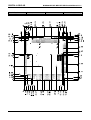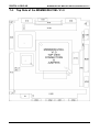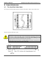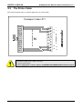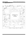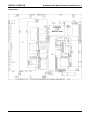
1
DETAILED TECHNICAL USER MANUAL FOR: PC/104 plus MSM800SEV/SEL MSM800BEV MSM800XEV/XEL Nordstrasse 11/F CH - 4542 Luterbach Tel.: ++41 (0)32 681 58 00 Fax: ++41 (0)32 681 58 01 Email: [email protected] Homepage: http://www.digitallogic.com DIGITAL-LOGIC AG MSM800SEV/SEL/BEV/XEV/XEL Detailed Manual V1.7 For internal use only: File: Path: MSM800SEV-SEL_Detailed_V1.7.doc R:\HANDBUCH\MSM\cpu_boards\MSM800\MSM800SEV-SEL_Detailed_V1.7.doc COPYRIGHT 2008 BY DIGITAL-LOGIC AG This publication is protected by copyright and all rights are reserved. No part of this document may be reproduced, transmitted, transcribed or stored in a retrieval system, in any form or by any means, electronic, mechanical, optical, manual, or otherwise, without the prior written permission of DIGITAL-LOGIC AG. The software described herein, together with this document, are furnished under a license agreement and may be used or copied only in accordance with the terms of that agreement. About this Manual and How to Use It This manual is written for the original equipment manufacturer (OEM) who plans to build computer systems based on the single board MICROSPACE-PC. It is for integrators and programmers of systems based on the MICROSPACE-Computer family. This manual provides instructions for installing and configuring the board, and describes the system and setup requirements. This document contains information on hardware requirements, interconnections, and details of how to program the system. Please check the Product CD for further information and manuals. REVISION HISTORY: Document Version V0.1 V0.2/V0.3 V0.4 V1.0 V1.0A V1.0B V1.1 V1.1A V1.1B V1.2 V1.2A V1.3 V1.4 V1.5 V1.6 V1.6A V1.6B V1.6C V1.6D V1.6E V1.6F V1.7 Date/Initials: Modification: Remarks, News, Attention: 02.2006 KUF Initial Version 03.2006 DAR Preliminary Version 1 / Preliminary Version 2 06.2006 DAR Preliminary Version 3 07.2006 DAR Final Release 07.2006 DAR LCD connector / Flat Panel description 08.2006 DAR Minor corrections, BIOS update 10.2006 DAR System I/O Map / Index structure, Board Version 2.1 11.2006 DAR BIOS V1.12, misc drawings 12.2006 DAR Front Picture, BIOS V1.13 02.2007 DAR BIOS V1.14, other board versions added (not complete) 03.2007 DAR Power Mgt / BIOS Setup pictures Serial Port Remote Control 04.2007 KUF General Doc Revision/Preface additions 05.2007 WAS/DAR Revision History format change / Filename & Path moved Previous product versions chapter added KUF “Ext. battery connect & onboard battery removed” warning added 06.2007 DAR/WAS Jumper7 Section 7.1 added w/Note for BIOS boot up Section 4.7.3 07.2007 WAS VGA monitor signals updated / XEV&XEL thermoscans added 08.2007 DAR MSM800XEV/XEL BIOS History added 12.2007 SEP/WAS ACPI S3 (Suspend to RAM) not available; available PCI slots (3 vs 4); Jumpers clarified; 1.12 & 1.13 added / Chapter 10 02.2008 DAR Chapter 10 / Heat sink options updated per Solution Guide 2008 / BIOS V1.24 added 03.2008 DAR Mechanical Drawings 09.2008 DAR Chapter 2.6 10.2008 DAR ?? 08.2009 MEG/WAS Jumpers J6 & J7 "Remarks" / LANCON info / Power conn. pin diagram Attention! 1. All information in this manual, and the product, are subject to change without prior notice. 2. Read this manual prior to installation of the product. 3. Read the security information carefully prior to installation of the product. 2 DIGITAL-LOGIC AG MSM800SEV/SEL/BEV/XEV/XEL Detailed Manual V1.7 Table of Contents 1. PREFACE........................................................................................................................5 1.1. Trademarks ..................................................................................................................................... 5 1.2. Disclaimer ....................................................................................................................................... 5 1.3. Environmental Protection Statement ........................................................................................... 5 1.4. Who should use this Product ....................................................................................................... 5 1.5. Recycling Information.................................................................................................................... 6 1.6. Technical Support .......................................................................................................................... 6 1.7. Limited Two Year Warranty ........................................................................................................... 6 1.8. Explanation of Symbols................................................................................................................. 7 1.9. Applicable Documents and Standards ........................................................................................ 8 1.10. For Your Safety............................................................................................................................... 9 1.11. RoHS Commitment......................................................................................................................... 9 1.11.1. RoHS Compatible Product Design ........................................................................................ 10 1.11.2. RoHS Compliant Production Process ................................................................................... 10 1.11.3. WEEE Application.................................................................................................................. 10 1.12. Swiss Quality ................................................................................................................................ 11 1.13. The Swiss Association for Quality and Management Systems............................................... 11 2. OVERVIEW ....................................................................................................................12 2.1. Standard Features........................................................................................................................ 12 2.2. Unique Features MSM800SEV/SEL ............................................................................................ 12 2.3. Unique Features MSM800BEV/BEL ............................................................................................ 12 2.4. Unique Features MSM800XEV/XEL ............................................................................................ 12 2.5. Block Diagrams ............................................................................................................................ 13 2.5.1. MSM800SEV ......................................................................................................................... 13 2.5.2. MSM800BEV ......................................................................................................................... 14 2.5.3. MSM800XEV ......................................................................................................................... 15 2.6. MSM800 SEV/SEL, BEV/BEL, XEV/XEL Specifications ............................................................ 16 2.7. Examples of Ordering Codes ...................................................................................................... 19 2.8. Dimensions and Diagrams .......................................................................................................... 20 2.8.1. MSM800SEV/SEL/BEV/XEV/XEL ......................................................................................... 20 2.8.2. MSM800LVDSCON ............................................................................................................... 32 2.8.3. MSM800DVICON .................................................................................................................. 33 2.8.4. MSM800CON ........................................................................................................................ 34 2.9. MSM800SEV/SEL Incompatibilities to a Standard PC/AT ........................................................ 35 2.9.1. PC104 BUS / ISA BUS .......................................................................................................... 35 2.9.2. ISA-Incompatibility with ISA-PCCARD-Controller ................................................................. 36 2.9.3. ISA-Incompatibility with 16bit I/O Transfer with FPGA-Decoder ........................................... 36 2.9.4. ISA-Incompatibility with 16bit Memory Transfer with FPGA-Decoder................................... 36 2.10. Related Application Notes........................................................................................................... 36 2.11. Thermoscan .................................................................................................................................. 37 2.12. High Frequency Radiation (to meet EN55022) .......................................................................... 39 2.12.1. For Peripheral Cables:........................................................................................................... 39 2.12.2. For Stack-Through Applications: ........................................................................................... 39 2.12.3. Power Supply:........................................................................................................................ 39 2.13. Battery Lifetime ............................................................................................................................ 40 2.13.1. External Battery Assembly: ................................................................................................... 40 3. BUS SIGNALS ...............................................................................................................41 3.1. PC104 Bus..................................................................................................................................... 41 3.2. PC104+ Bus................................................................................................................................... 43 3.3. Expansion Bus ............................................................................................................................. 45 3.4. Addressing PCI Devices .............................................................................................................. 45 3.4.1. MSM800SEV/SEL V2.1......................................................................................................... 45 3.4.2. MSM800BEV/XEV/XEL V1.x................................................................................................. 45 4. 5. BIOS HISTORY .............................................................................................................46 DETAILED SYSTEM DESCRIPTION ...................................................................................47 5.1. 5.2. 5.3. Power Requirements.................................................................................................................... 47 Boot Time...................................................................................................................................... 47 CPU, Boards and RAMs............................................................................................................... 48 3 DIGITAL-LOGIC AG MSM800SEV/SEL/BEV/XEV/XEL Detailed Manual V1.7 5.3.1. CPUs of this MICROSPACE Product .................................................................................... 48 5.3.2. Numeric Coprocessor ............................................................................................................ 48 5.3.3. DDRAM Memory on MSM800SEV/SEL/BEV/BEL................................................................ 48 5.3.4. DDRAM Memory on MSM800XEV/XEL ................................................................................ 48 5.4. Interfaces ...................................................................................................................................... 48 5.4.1. AT Compatible Keyboard & PS/2 Mouse X31....................................................................... 48 5.4.2. Line Printer Port LPT1 ........................................................................................................... 49 5.4.3. Serial Ports COM1-COM2 ..................................................................................................... 49 5.4.4. Floppy Disk Interface............................................................................................................. 49 5.4.5. Speaker Interface .................................................................................................................. 50 5.5. Controllers .................................................................................................................................... 51 5.5.1. Interrupt Controllers ............................................................................................................... 51 5.6. Timers and Counters ................................................................................................................... 51 5.6.1. Programmable Timers ........................................................................................................... 51 5.6.2. RTC (Real Time Clock) ......................................................................................................... 52 5.6.3. Watchdog............................................................................................................................... 52 5.7. BIOS............................................................................................................................................... 53 5.7.1. Core BIOS download ............................................................................................................. 53 5.7.2. ROM-BIOS Sockets............................................................................................................... 54 5.7.3. BIOS CMOS Setup ................................................................................................................ 54 5.8. CMOS RAM Map ........................................................................................................................... 54 5.9. EEPROM saved CMOS Setup...................................................................................................... 60 5.9.1. EEPROM Memory for Setup ................................................................................................. 61 5.10. Memory & I/O Map ........................................................................................................................ 61 5.10.1. System Memory Map............................................................................................................. 61 5.10.2. System I/O Map ..................................................................................................................... 62 6. VGA/LCD ...................................................................................................................66 6.1. 6.2. 6.3. 6.4. 7. VGA/LCD Controller of the Geode LX800 .................................................................................. 66 Graphic Modes ............................................................................................................................. 66 DVICON Resolution...................................................................................................................... 66 Flat Panel Functional Description .............................................................................................. 67 DESCRIPTION OF THE CONNECTORS ................................................................................68 7.1. 7.2. 7.3. 7.4. 8. Top Side of the MSM800SEV/SEL V2.1/V2.2.............................................................................. 69 Bottom Side of the MSM800SEV V2.1/V2.2................................................................................ 70 Top Side of the MSM800BEV V1.1 .............................................................................................. 71 Top Side of the MSM800XEV/XEL V1.0 ...................................................................................... 72 JUMPER LOCATIONS ON THE BOARD ..............................................................................83 8.1. 8.2. 9. The Jumpers on the MSM800SEV/SEL ...................................................................................... 83 The Jumpers on the MSM800BEV/XEV/XEL .............................................................................. 83 CABLE INTERFACES ......................................................................................................88 9.1. 9.2. 9.3. 9.4. 9.5. 10. 11. 11.1. 11.2. 11.3. The Hard Disk Cable 44pin .......................................................................................................... 88 The COM 1/2 Serial Cable ............................................................................................................ 89 The Printer Cable.......................................................................................................................... 90 The Micro-Floppy Cable............................................................................................................... 91 The LAN Cable (RJ45).................................................................................................................. 92 THERMAL SPECIFICATIONS .........................................................................................93 ASSEMBLY VIEWS .....................................................................................................95 MSM800SEV/SEL V2.1/V2.2 ......................................................................................................... 95 MSM800BEV V1.1 ......................................................................................................................... 97 MSM800XEV/XEL V1.0 ................................................................................................................. 99 12. PREVIOUS PRODUCT VERSIONS ................................................................................101 12.1. Board Dimensions – Versions 1.0 / 1.1 / 1.2 ............................................................................ 101 12.2. Assembly Views ......................................................................................................................... 102 12.2.1. MSM800SEV/SEL V1.1....................................................................................................... 102 12.2.2. MSM800 V1.2 ...................................................................................................................... 106 12.3. Connectors and Jumpers of Previous Product Versions ...................................................... 110 12.3.1. Description of the Connectors for V1.0 /V1.1 /V1.2............................................................. 110 13. INDEX .....................................................................................................................119 4 DIGITAL-LOGIC AG MSM800SEV/SEL/BEV/XEV/XEL Detailed Manual V1.7 1. PREFACE The information contained in this manual has been carefully checked and is believed to be accurate; it is subject to change without notice. Product advances mean that some specifications may have changed. DIGITAL-LOGIC AG assumes no responsibility for any inaccuracies, or the consequences thereof, that may appear in this manual. Furthermore, DIGITAL-LOGIC AG does not accept any liability arising from the use or application of any circuit or product described herein. 1.1. Trademarks DIGITAL-LOGIC, DIGITAL-LOGIC-Logo, MICROSPACE, and smartModule are registered trademarks owned worldwide by DIGITAL-LOGIC AG, Luterbach (Switzerland). In addition, this document may include names, company logos, and registered trademarks which are, therefore, proprietary to their respective owners. 1.2. Disclaimer DIGITAL-LOGIC AG makes no representations or warranties with respect to the contents of this manual, and specifically disclaims any implied warranty of merchantability or fitness, for any particular purpose. DIGITALLOGIC AG shall, under no circumstances, be liable for incidental or consequential damages or related expenses resulting from the use of this product, even if it has been notified of the possibility of such damage. 1.3. Environmental Protection Statement This product has been manufactured to satisfy environmental protection requirements wherever possible. Many of the components used (structural parts, printed circuit boards, connectors, batteries, etc.) are capable of being recycled. Final disposal of this product after its service life must be accomplished in accordance with applicable country, state, or local laws or regulations. 1.4. Who should use this Product Electrical engineers with know-how in PC-technology. Because of the complexity and the variability of PC-technology, we cannot guarantee that the product will work in any particular situation or set-up. Our technical support will try to help you find a solution. Pay attention to electrostatic discharges; use a CMOS protected workplace. Power supply must be OFF when working on the board or connecting any cables or devices. 5 DIGITAL-LOGIC AG 1.5. MSM800SEV/SEL/BEV/XEV/XEL Detailed Manual V1.7 Recycling Information All components within this product fulfill the requirements of the RoHS (Restriction of Hazardous Substances Directive). The product is soldered with a lead free process. 1.6. Technical Support 1. Contact your local DIGITAL-LOGIC Technical Support, in your country. 2. Use the Internet Support Request form at http://support.digitallogic.ch/ embedded products New Support Request Support requests are only accepted with detailed information about the product (i.e., BIOS-, Boardversion)! 1.7. Limited Two Year Warranty DIGITAL-LOGIC AG guarantees the hardware and software products it manufactures and produces to be free from defects in materials and workmanship for two years following the date of shipment from DIGITALLOGIC AG, Switzerland. This warranty is limited to the original purchaser of the product and is not transferable. During the two year warranty period, DIGITAL-LOGIC AG will repair or replace, at its discretion, any defective product or part at no additional charge, provided that the product is returned, shipping prepaid, to DIGITAL-LOGIC AG. All replaced parts and products become property of DIGITAL-LOGIC AG. Before returning any product for repair, direct customers of DIGITAL-LOGIC AG, Switzerland are required to register a RMA (Return Material Authorization) number in the Support Center at http://support.digitallogic.ch/ All other customers must contact their local distributors for returning defective materials. This limited warranty does not extend to any product which has been damaged as a result of accident, misuse, abuse (such as use of incorrect input voltages, wrong cabling, wrong polarity, improper or insufficient ventilation, failure to follow the operating instructions that are provided by DIGITAL-LOGIC AG or other contingencies beyond the control of DIGITAL-LOGIC AG), wrong connection, wrong information or as a result of service or modification by anyone other than DIGITAL-LOGIC AG. Nor if the user has insufficient knowledge of these technologies or has not consulted the product manuals or the technical support of DIGITAL-LOGIC AG and therefore the product has been damaged. Empty batteries (external and onboard), as well as all other battery failures, are not covered by this manufacturer’s limited warranty. Except, as directly set forth above, no other warranties are expressed or implied, including, but not limited to, any implied warranty of merchantability and fitness for a particular purpose, and DIGITAL-LOGIC AG expressly disclaims all warranties not stated herein. Under no circumstances will DIGITAL-LOGIC AG be liable to the purchaser or any user for any damage, including any incidental or consequential damage, expenses, lost profits, lost savings, or other damages arising out of the use or inability to use the product. 6 DIGITAL-LOGIC AG 1.8. MSM800SEV/SEL/BEV/XEV/XEL Detailed Manual V1.7 Explanation of Symbols CE Conformity This symbol indicates that the product described in this manual is in compliance with all applied CE standards. Caution, Electric Shock! This symbol and title warn of hazards due to electrical shocks (> 60V) when touching products or parts of them. Failure to observe the precautions indicated and/or prescribed by the law may endanger your life/health and/or result in damage to your equipment. Caution, Electric Shock! This symbol and title warn of hazards due to electrical shocks (> 32V) when touching products or parts of them. Failure to observe the precautions indicated and/or prescribed by the law may endanger your life/health and/or result in damage to your equipment Warning, ESD Sensitive Device! This symbol and title inform that electronic boards and their components are sensitive to Electro Static Discharge (ESD). In order to ensure product integrity at all times, care must always be taken while handling and examining this product. Attention! This symbol and title emphasize points which, if not fully understood and taken into consideration by the reader, may endanger your health and/or result in damage to your equipment. Note... This symbol and title emphasize aspects the user should read through carefully for his, or her, own advantage. Warning, Heat Sensitive Device! This symbol indicates a heat sensitive component. Safety Instructions This symbol shows safety instructions for the operator to follow. This symbol warns of general hazards from mechanical, electrical, and/or chemical failure. This may endanger your life/health and/or result in damage to your equipment. 7 DIGITAL-LOGIC AG 1.9. MSM800SEV/SEL/BEV/XEV/XEL Detailed Manual V1.7 Applicable Documents and Standards The following publications are used in conjunction with this manual. When any of the referenced specifications are superseded by an approved revision, that revision shall apply. All documents may be obtained from their respective organizations. Advanced Configuration and Power Interface Specification Revision 2.0c, August 25, 2003 Copyright © 1996-2003 Compaq Computer Corporation, Intel Corporation, Microsoft Corporation, Phoenix Technologies Ltd., Toshiba Corporation. All rights reserved. http://www.acpi.info/ ANSI/TIA/EIA-644-A-2001: Electrical Characteristics of Low Voltage Differential Signaling (LVDS) Interface Circuits, January 1, 2001. http://www.ansi.org/ ANSI INCITS 361-2002: AT Attachment with Packet Interface - 6 (ATA/ATAPI-6), November 1, 2002. http://www.ansi.org/ ANSI INCITS 376-2003: American National Standard for Information Technology – Serial Attached SCSI (SAS), October 30, 2003. http://www.ansi.org/ Audio Codec ’97 Revision 2.3 Revision 1.0, April 2002 Copyright © 2002 Intel Corporation. All rights reserved. http://www.intel.com/labs/media/audio/ Display Data Channel Command Interface (DDC/CI) Standard (formerly DDC2Bi) Version 1, August 14, 1998 Copyright © 1998 Video Electronics Standards Association. All rights reserved. http://www.vesa.org/summary/sumddcci.htm ExpressCard Standard Release 1.0, December 2003 Copyright © 2003 PCMCIA. All rights reserved. http://www.expresscard.org/ IEEE 802.3-2002, IEEE Standard for Information technology, Telecommunications and information exchange between systems–Local and metropolitan area networks–Specific requirements – Part 3: Carrier Sense Multiple Access with Collision Detection (CSMA/CD) Access Method and Physical Layer Specifications. http://www.ieee.org IEEE 802.3ae (Amendment to IEEE 802.3-2002), Part 3: Carrier Sense Multiple Access with Collision Detection (CSMA/CD) Access Method and Physical Layer Specifications, Amendment: Media Access Control (MAC) Parameters, Physical Layers, and Management Parameters for 10 GB/s Operation. http://www.ieee.org Intel Low Pin Count (LPC) Interface Specification Revision 1.1, August 2002 Copyright © 2002 Intel Corporation. All rights reserved. http://developer.intel.com/design/chipsets/industry/lpc.htm PCI Express Base Specification Revision 1.1, March 28, 2005, Copyright © 2002-2005 PCI Special Interest Group. All rights reserved. http://www.pcisig.com/ PCI Express Card Electromechanical Specification Revision 1.1, March 28, 2005, Copyright © 20022005 PCI Special Interest Group. All rights reserved. http://www.pcisig.com/ PCI Local Bus Specification Revision 2.3, March 29, 2002 Copyright © 1992, 1993, 1995, 1998, 2002 PCI Special Interest Group. All rights reserved. http://www.pcisig.com/ PCI-104 Specification, Version V1.0, November 2003. All rights reserved. http://www.pc104.org PICMG® Policies and Procedures for Specification Development, Revision 2.0, September 14, 2004, PCI Industrial Computer Manufacturers Group (PICMG®), 401 Edgewater Place, Suite 500, Wakefield, MA 01880, USA, Tel: 781.224.1100, Fax: 781.224.1239. http://www.picmg.org/ Serial ATA: High Speed Serialized AT Attachment Revision 1.0a January 7, 2003 Copyright © 20002003, APT Technologies, Inc, Dell Computer Corporation, Intel Corporation, Maxtor Corporation, Seagate Technology LLC. All rights reserved. http://www.sata-io.org/ 8 DIGITAL-LOGIC AG MSM800SEV/SEL/BEV/XEV/XEL Detailed Manual V1.7 Smart Battery Data Specification Revision 1.1, December 11, 1998. www.sbs-forum.org System Management Bus (SMBus) Specification Version 2.0, August 3, 2000 Copyright © 1994, 1995, 1998, 2000 Duracell, Inc., Energizer Power Systems, Inc., Fujitsu, Ltd., Intel Corporation, Linear Technology Inc., Maxim Integrated Products, Mitsubishi Electric Semiconductor Company, PowerSmart, Inc., Toshiba Battery Co. Ltd., Unitrode Corporation, USAR Systems, Inc. All rights reserved. http://www.smbus.org/ Universal Serial Bus Specification Revision 2.0, April 27, 2000 Copyright © 2000 Compaq Computer Corporation, Hewlett-Packard Company, Intel Corporation, Lucent Technologies Inc., Microsoft Corporation, NEC Corporation, Koninklijke Philips Electronics N.V. All rights reserved. http://www.usb.org/ 1.10. For Your Safety Your new DIGITAL-LOGIC product was developed and tested carefully to provide all features necessary to ensure its compliance with electrical safety requirements. It was also designed for a long, fault-free life. However, this life expectancy can be drastically reduced by improper treatment during unpacking and installation. Therefore, in the interest of your own safety and for the correct operation of your new DIGITAL-LOGIC product, please comply with the following guidelines. Attention! All work on this device must only be carried out by sufficiently skilled personnel. Caution, Electric Shock! Before installing your new DIGITAL-LOGIC product, always ensure that your mains power is switched off. This applies also to the installation of piggybacks or peripherals. Serious electrical shock hazards can exist during all installation, repair and maintenance operations with this product. Therefore, always unplug the power cable and any other cables which provide external voltage before performing work. Warning, ESD Sensitive Device! Electronic boards and their components are sensitive to static electricity. In order to ensure product integrity at all times, be careful during all handling and examinations of this product. 1.11. RoHS Commitment DIGITAL-LOGIC AG is committed to develop and produce environmentally friendly products according to the Restriction of Hazardous Substances (RoHS) Directive (2002/95/EC) and the Waste Electrical and Electronic Equipment (WEEE) Directive (2002/96/EC) established by the European Union. The RoHS directive was adopted in February 2003 by the European Union and came into effect on July 1, 2006. It is not a law but a directive, which restricts the use of six hazardous materials in the manufacturing of various types of electronic and electrical equipment. It is closely linked with the Waste Electrical and Electronic Equipment Directive (WEEE) 2002/96/EC, which has set targets for collection, recycling and recovery of electrical goods and is part of a legislative initiative to solve the problem of huge amounts of toxic e-waste. Each European Union member state is adopting its own enforcement and implementation policies using the directive as a guide. Therefore, there could be as many different versions of the law as there are states in the EU. Additionally, non-EU countries like China, Japan, or states in the U.S. such as California may have their own regulations for green products, which are similar, but not identical, to the RoHS directive. 9 DIGITAL-LOGIC AG MSM800SEV/SEL/BEV/XEV/XEL Detailed Manual V1.7 RoHS is often referred to as the "lead-free" directive but it restricts the use of the following substances: Lead Mercury Cadmium Chromium VI PBB and PBDE The maximum allowable concentration of any of the above mentioned substances is 0.1% (except for Cadmium, which is limited to 0.01%) by weight of homogeneous material. This means that the limits do not apply to the weight of the finished product, or even to a component but to any single substance that could (theoretically) be separated mechanically. 1.11.1. RoHS Compatible Product Design All DIGITAL-LOGIC standard products comply with RoHS legislation. Since July 1, 2006, there has been a strict adherence to the use of RoHS compliant electronic and mechanical components during the design-in phase of all DIGITAL-LOGIC standard products. 1.11.2. RoHS Compliant Production Process DIGITAL-LOGIC selects external suppliers that are capable of producing RoHS compliant devices. These capabilities are verified by: 1. A confirmation from the supplier indicating that their production processes and resulting devices are RoHS compliant. 2. If there is any doubt of the RoHS compliancy, the concentration of the previously mentioned substances in a produced device will be measured. These measurements are carried out by an accredited laboratory. 1.11.3. WEEE Application The WEEE directive is closely related to the RoHS directive and applies to the following devices: Large and small household appliances IT equipment Telecommunications equipment (although infrastructure equipment is exempt in some countries) Consumer equipment Lighting equipment – including light bulbs Electronic and electrical tools Toys, leisure and sports equipment Automatic dispensers It does not apply to fixed industrial plants and tools. The compliance is the responsibility of the company that brings the product to market, as defined in the directive. Components and sub-assemblies are not subject to product compliance. In other words, since DIGITAL-LOGIC does not deliver ready-made products to end users the WEEE directive is not applicable for DIGITAL-LOGIC. Users are nevertheless encouraged to properly recycle all electronic products that have reached the end of their life cycle. 10 DIGITAL-LOGIC AG MSM800SEV/SEL/BEV/XEV/XEL Detailed Manual V1.7 1.12. Swiss Quality 100% Made in Switzerland DIGITAL-LOGIC is a member of "Swiss-Label" This product was not manufactured by employees earning piecework wages This product was manufactured in humane work conditions All employees who worked on this product are paid customary Swiss market wages and are insured ISO 9000:2001 (quality management system) 1.13. The Swiss Association for Quality and Management Systems The Swiss Association for Quality and Management Systems (SQS) provides certification and assessment services for all types of industries and services. SQS certificates are accepted worldwide thanks to accreditation by the Swiss Accreditation Service (SAS), active membership in the International Certification Network, IQNet, and co-operation contracts/agreements with accredited partners. www.sqs.ch The SQS Certificate ISO 9001:2000 has been issued to DIGITAL-LOGIC AG, the entire company, in the field of development, manufacturing and sales of embedded computer boards, embedded computer modules and computer systems. The certification is valid for three years at which time an audit is performed for recertification. 11 DIGITAL-LOGIC AG MSM800SEV/SEL/BEV/XEV/XEL Detailed Manual V1.7 2. OVERVIEW 2.1. Standard Features The MICROSPACE PC/104 is a miniaturized modular device incorporating the major elements of a PC/AT compatible computer. It includes standard PC/AT compatible elements, such as: 2.2. Powerful Geode LX-800 500MHz BIOS ROM Timers, DMA Real-time clock with CMOS-RAM and battery buffer (external/onboard) LPT1 parallel port COM1-, COM2-RS2332 serial port Speaker interface AT-keyboard interface or PS/2-keyboard interface Floppy disk interface AT-IDE hard disk interface VGA/LCD video interface PC/104 ISA Bus PC104+ PCI Bus (option) PS/2 mouse interface 4 Channel USB 2.0 Optional: Onboard CF socket Type II Single 5V supply EEPROM for setup and configuration UL approved parts Watchdog Unique Features MSM800SEV/SEL The MSM800SEV/SEL includes all standard PC/AT functions plus unique enhancements, such as: LAN Ethernet, INTEL 82551ER (or on request [optional] 82551QM) LPC to ISA Bridge SODIMM DDR-Memory holder (128-1024MByte) 2.3. Unique Features MSM800BEV/BEL The MSM800BEV includes all standard PC/AT functions plus unique enhancements, such as: LAN Ethernet, INTEL 82551ER (or on request [optional] 82551QM) PCI to ISA Bridge for full ISA support. Needs one PCI load/resource. SODIMM DDR-Memory holder (128-1024MByte) 2.4. Unique Features MSM800XEV/XEL The MSM800XEV includes all standard PC/AT functions plus unique enhancements, such as: LAN Ethernet, INTEL 82551ER (or on request [optional] 82551QM) PCI to ISA Bridge for full ISA support. Needs one PCI load/resource. Soldered 256MByte onboard DDR-RAM 12 DIGITAL-LOGIC AG 2.5. 2.5.1. MSM800SEV/SEL/BEV/XEV/XEL Detailed Manual V1.7 Block Diagrams MSM800SEV 13 DIGITAL-LOGIC AG 2.5.2. MSM800SEV/SEL/BEV/XEV/XEL Detailed Manual V1.7 MSM800BEV 14 DIGITAL-LOGIC AG 2.5.3. MSM800SEV/SEL/BEV/XEV/XEL Detailed Manual V1.7 MSM800XEV 15 DIGITAL-LOGIC AG 2.6. MSM800SEV/SEL/BEV/XEV/XEL Detailed Manual V1.7 MSM800 SEV/SEL, BEV/BEL, XEV/XEL Specifications CPU CPU CPU Core Supply Mode Compatibility Word Size Secondary Cache Physical Addressing Virtual Addressing Clock Rates Socket Standard Geode LX800 1.8V very low powered Real/Protected 8086 – P5 32bits – 32 lines 16GBytes 500MHz Soldered BGA Chipset Northbridge Southbridge LAN Audio Firewire IEEE1394 Video AMD LX800 AMD 5536 10/100MBit Intel 82C551ER AC97 – V2.3 Not onboard 16MByte Video-DDRAM Power Management Available since V2.0 The LX800 supports ACPI and APM Version 1.2. The following ACPI Sleep States are supported: - S1 - S4 - S5-G2 - S5-G3 (Sleep with CPU content) (Hibernation - LED* is blinking) with transition to S5 (Power Off - LED* is blinking. The device can be switched on by the Main Button (or if available with WOL) (Power Off - Mechanically) * = if available DMA 8237A comp. Interrupts 8259 comp. 4 channel 8bits 3 channel 16bits 8 + 7 levels PC compatible Timers 8254 comp. 3 programmable counter/timers Memory MSM800SEV/SEL/BEV MSM800SEV/SEL SODIMM200pin DDR PC2700 333MHz 128-1024Mbyte Soldered onboard 256Mbyte DDR-RAM Video Controller BUS Enhanced BIOS Memory CRT-Monitor Flat panel Controller modes Video input Drivers MSM800SEV 32bit high speed 33MHz PCI Bus VGA/LCD BIOS 2-254MByte shared RAM VGA, SVGA up to 1920x1440 TFT 3.3V 18/24bit up to 1600x1200 CRT only; flat panel only; or simultaneous CRT and flat panel no WIN2000, XP 16 DIGITAL-LOGIC AG Mass Storage FD: HD: Standard AT Interfaces Serial Parallel Keyboard Mouse Speaker RTC Backup current Non-chargeable Battery MSM800SEV/BEV/XEV MSM800SEL/BEL/XEL BUS PC/104plus MSM800SEV/SEL/BEV/XEV/XEL Detailed Manual V1.7 Floppy disk interface, for max. 1 floppy with 26pin connector E-IDE interface, AT-type, for max. 2 hard disks, 44pin connector, for 1.3, 1.8 and 2.5" hard disks with 44 pins IDE Name FIFO IRQs Addr. Standard Option COM1 yes IRQ4 3F8 RS232C COM2 yes IRQ3 2F8 RS232C (Baud rates: 50-115 KBaud programmable) LPT1 printer interface mode: SPP(output), EPP (bidir.) (Centronics) AT or PS/2 –keyboard PS/2 0.1 W output drive Integrated into the chipset, RTC with CMOS-RAM 256Byte <5 µA 3.6V Lithium 400mAh internally or externally connected External 3.6V Lithium battery needed Clock IEEE-996 standard ISA bus, buffered MSM800SEV/SEL: 8bit and limited 16bit support MSM800BEV/BEL/XEV/XEL: full 16bit ISA support 8MHz defined by the Geode USB USB Transfer rate Channels 2.0 400MBps, 12.5MBps/1.5MBps 4 Peripheral Extension ISA PCI With PC/104 BUS MSM800SEV/SEL: MSM800BEV/BEL/XEV/XEL: With PC/104plus BUS MSM800SEV/SEL: MSM800BEV/BEL/XEV/XEL: Power Supply Working Power Rise Time Power consumption with ISA 16bit DMA limitation no ISA limitation 3 slots – max. 3 master devices 2 slots – max. 2 master devices 5 Volts ± 5% Unspecified MSM800SEV V2.1 with HD, MS/KB (PS/2), CRT Monitor Windows XP Desktop: type 7.5-10W Standby power consumption MSM800SEV/SEL/BEV: Windows Standby: 2.5W (without MS/KB wake-up function) Windows Standby: 4.5W (with PS/2 wake-up function) Physical Characteristics Dimensions Weight PCB Thickness PCB Layer Length: 91mm Depth: 96mm Height: 25mm 170gr 1.6mm / 0.0625 inches nominal Multilayer 17 DIGITAL-LOGIC AG Operating Environment Relative humidity Vibration Shock Temperature MSM800SEV/SEL/BEV/XEV/XEL Detailed Manual V1.7 5-90% non-condensing 5 to 2000Hz, 0.1G 1G MSM800SEV/SEL Operating standard version: Without heat sink: With small heat sink 807041: Operating extended version: Not possible MSM800BEV Operating standard version: Without heat sink: With small heat sink 807041: Operating extended version: With large heat sink 807042 + E48: With thermojunction + E48: MSM800XEV/XEL Operating standard version: Without heat sink: With small heat sink 807041: Operating extended version: With large heat sink 807042 + E47: With thermojunction + E48: EMI / EMC (IEC1131-2 refer MIL 461/462) ESD Electro Static Discharge REF Radiated Electromagnetic Field EFT Electric Fast Transient (Burst) SIR Surge Immunity Requirements High-frequency Radiation Compatibility MSM800SEV/BEV/XEV/SEL/BEL/XEL 0°C to +60°C -25°C to +70°C 0°C to +60°C -25°C to +70°C -40°C to +85°C -40°C to +85°C 0°C to +60°C -25°C to +70°C -40°C to +70°C -40°C to +85°C IEC 801-2, EN55101-2, VDE 0843/0847 Part 2 Metallic protection needed Separate ground layer included 15 kV single peak IEC 801-3, VDE 0843 Part 3, IEC770 6.2.9. (not tested) IEC 801-4, EN50082-1, VDE 0843 Part 4 250V - 4kV, 50 ohms, Ts=5ns Grade 2: 1kV Supply, 500 I/O, 5kHz IEC 801-5, IEEE587, VDE 0843 Part 5 Supply: 2kV, 6 pulse/minute I/O: 500V, 2 pulse/minute FD, CRT: none EN55022 Mechanically compatible to our MSMx86 Boards and to all other PC/104 boards All information is subject to change without notice. 18 DIGITAL-LOGIC AG 2.7. MSM800SEV/SEL/BEV/XEV/XEL Detailed Manual V1.7 Examples of Ordering Codes Part / Option MSM800SEL MSM800SEV MSM800BEV MSM800XEL Part Nr. 802105 802100 802110 802125 MSM800XEV 802120 Option -L+ Option -P+ Option -CF MSM800-CKCON MSFLOPPY MSFDCK MSM800-LANCON MSM800-DVICON MSM800-LVDSCON MSM800DK 807006 807005 807007 803035 891001 802600 803046 803042 803044 802118 Description Low cost version without: RTC-battery Standard version with: LPC-Bridge Standard version with: full ISA-16bit support and PCI-ISA-Bridge Low cost soldered RAM version without: RTC-battery or PCI-ISA-Bridge Standard soldered RAM version with: full ISA-16bit support and PCI-ISA-Bridge PC/104-Plus with long connector PC/104-Plus with short connector CompactFlash socket (without Option -L) MSM800 PC/104-cable kit 3.5” Micro-floppy drive (26pin) Micro-floppy cable (26pin) LAN cable with PCB connector DVI-D interface LVDS interface Development kit These are only examples; for current ordering codes, please see the current price list. 19 DIGITAL-LOGIC AG 2.8. 2.8.1. MSM800SEV/SEL/BEV/XEV/XEL Detailed Manual V1.7 Dimensions and Diagrams MSM800SEV/SEL/BEV/XEV/XEL Board / Version MSM800SEV/BEV V2.1 Unit: mm (millimeter) Tolerance: + / - 0.1mm Board Dimensions 20 Date / Author 19.03.2008 / BRR DIGITAL-LOGIC AG Board / Version MSM800XEV MSM800SEV/SEL/BEV/XEV/XEL Detailed Manual V1.7 Unit: mm (millimeter) Tolerance: + / - 0.1mm 21 Date / Author 19.03.2008 / BRR DIGITAL-LOGIC AG MSM800SEV/SEL/BEV/XEV/XEL Detailed Manual V1.7 Top of board with heat sink (Option 807041) and battery (SEV/BEV only) Board profile with heat sink (Option 807041) and battery (SEV/BEV only) 22 DIGITAL-LOGIC AG MSM800SEV/SEL/BEV/XEV/XEL Detailed Manual V1.7 Top of board with heat sink (Option 807041) and battery, 3D perspective (SEV/BEV/XEV only) Bottom of board, 3D perspective, including the CompactFlash Option 23 DIGITAL-LOGIC AG MSM800SEV/SEL/BEV/XEV/XEL Detailed Manual V1.7 MSM800SEV/BEV, 3D perspective Top of Board, with heat sink (Option 807041) Bottom of board 24 DIGITAL-LOGIC AG MSM800SEV/SEL/BEV/XEV/XEL Detailed Manual V1.7 MSM800SEL, 3D perspective Top of board, with heat sink (Option 807041) Bottom of board 25 DIGITAL-LOGIC AG MSM800SEV/SEL/BEV/XEV/XEL Detailed Manual V1.7 MSM800XEL, 3D perspective Top of board Bottom of board 26 DIGITAL-LOGIC AG MSM800SEV/SEL/BEV/XEV/XEL Detailed Manual V1.7 MSM800XEV, 3D perspective Top of board, with heat sink (Option 807041) Bottom of board 27 DIGITAL-LOGIC AG MSM800SEV/SEL/BEV/XEV/XEL Detailed Manual V1.7 MSM800BEV/XEV Top of board, with heat sink (Option 807042) 28 DIGITAL-LOGIC AG MSM800SEV/SEL/BEV/XEV/XEL Detailed Manual V1.7 29 DIGITAL-LOGIC AG MSM800SEV/SEL/BEV/XEV/XEL Detailed Manual V1.7 MSM800BEV/XEV Top of board, with heat sink (Option 807043) 30 DIGITAL-LOGIC AG MSM800SEV/SEL/BEV/XEV/XEL Detailed Manual V1.7 31 DIGITAL-LOGIC AG 2.8.2. MSM800SEV/SEL/BEV/XEV/XEL Detailed Manual V1.7 MSM800LVDSCON Board / Version Unit: MSM800-LVDSCON V0.1 mm (millimeter) Tolerance: + / - 0.1mm 32 Date / Author 25.10.2006 / BRR DIGITAL-LOGIC AG 2.8.3. MSM800SEV/SEL/BEV/XEV/XEL Detailed Manual V1.7 MSM800DVICON Board / Version MSM800-DVICON V0.1 Unit: mm (millimeter) Tolerance: + / - 0.1mm 33 Date / Author 25.10.2006 / BRR DIGITAL-LOGIC AG 2.8.4. MSM800SEV/SEL/BEV/XEV/XEL Detailed Manual V1.7 MSM800CON Board / Version MSM800-CON V1.0 Unit: mm (millimeter) Tolerance: + / - 0.1mm 34 Date / Author 25.10.2006 / BRR DIGITAL-LOGIC AG 2.9. 2.9.1. MSM800SEV/SEL/BEV/XEV/XEL Detailed Manual V1.7 MSM800SEV/SEL Incompatibilities to a Standard PC/AT PC104 BUS / ISA BUS An onboard LPC to ISA-bridge makes it possible to expand the functionality of the board with additional PC/104 cards. Unfortunately, because of the transformation from LPC to ISA it is not possible to realize a 16bit access. This does not mean that these cards cannot be used, but that the 16bit access is divided into two. Therefore the access to these cards is a little bit slower. The LPC support the following bus cycles: Cycle Type Memory Read Memory Write I/O Read I/O Write DMA Read DMA Write Bus Master Memory Read Sizes Supported 1Byte 1Byte 1Byte 1Byte 1, 2, 4Byte 1, 2, 4Byte 1, 2, 4Byte Bus Master Memory Write 1, 2, 4Byte Bus Master I/O Read Bus Master I/O Write Firmware Memory Read Firmware Memory Write 1, 2, 4Byte 1, 2, 4Byte 1, 2, 4, 128Byte 1, 2, 4Byte Comments Optional for both LPC hosts and peripherals Optional for both LPC hosts and peripherals. Optional for peripherals. Optional for peripherals. Optional for peripherals. Optional for peripherals. Optional for both LPC hosts and peripherals, but strongly recommended for hosts. Optional for both LPC hosts and peripherals, but strongly recommended for hosts. Optional for both LPC hosts and peripherals. Optional for both LPC hosts and peripherals. Optional for both LPC hosts and peripherals. Optional for both LPC hosts and peripherals. This means, all Non-BusMaster I/O and MEM Cycles are only 8bit wide and never 16bit wide. 16bit data transfer is available in the BusMaster modus only. Attention! With the BEV/BEL/XEV/XEL versions, this limitation is solved by using a PCI-ISA bridge. The disadvantage is that now 2 PCI devices are onboard and there are only 2 external PCI slots available. 35 DIGITAL-LOGIC AG 2.9.2. MSM800SEV/SEL/BEV/XEV/XEL Detailed Manual V1.7 ISA-Incompatibility with ISA-PCCARD-Controller Experience shows that ATA-Drives controlled in an ISA-PCMCIA Controller do not work. Solution: Use a PCCARD-Controller on the PCI-Bus 2.9.3. ISA-Incompatibility with 16bit I/O Transfer with FPGA-Decoder Our experience shows that 16bit I/O-transfers decoded with a FPGA do not always work correctly. Each case must be tested. Expect problems on odd addresses. Solution: Use two 8bit transfers instead of one 16bit transfer. For time critical transfers we recommend using the PCI-Bus. 2.9.4. ISA-Incompatibility with 16bit Memory Transfer with FPGADecoder Experience shows that 16bit Memory-transfers decoded with a FPGA do not always work correctly. Each case must be tested. Expect problems on odd addresses. Solution: Use two 8bit transfers instead of one 16bit transfer. For time critical transfers we recommend using the PCI-Bus. 2.10. Related Application Notes Application Notes are available at http://www.digitallogic.com support, or on any DIGITAL-LOGIC Application CD. # Description 36 DIGITAL-LOGIC AG MSM800SEV/SEL/BEV/XEV/XEL Detailed Manual V1.7 2.11. Thermoscan MSM800SEV V1.2 with small heat sink (OS: MSDOS promt) t [min] 45 fCPU [MHz] P01 [°C] 500 61.9 P02 [°C] 52.1 R11 [°C] 56.2 R12 [°C] 62.6 MSM800SEV V2.1 with small heat sink (OS: MSDOS promt) t [min] 90 fCPU [MHz] P01 [°C] 500 53.1 R11 [°C] 60.5 R12 [°C] 51.1 37 DIGITAL-LOGIC AG MSM800SEV/SEL/BEV/XEV/XEL Detailed Manual V1.7 MSM800XEV V1.0 with small heat sink t [min] 60 fCPU [MHz] R11 [°C] 500 47.1 R12 [°C] 53.8 MSM800XEL V1.0 t [min] 60 fCPU [MHz] P01 [°C] 500 54.2 R11 [°C] 53.7 R12 [°C] 49.9 38 DIGITAL-LOGIC AG MSM800SEV/SEL/BEV/XEV/XEL Detailed Manual V1.7 2.12. High Frequency Radiation (to meet EN55022) Since the PC/104 CPU modules are very highly integrated embedded computers, peripheral lines are not protected against radiation from the high frequency spectrum. To meet a typical EN55022 requirement, all peripherals that go outside of the computer case must be externally filtered. Typical signals that must be filtered: Keyboard: Mouse: COM1/2/3/4: LPT: CRT: KBCLK, KBDATA and VCC MSCLK, MSDATA and VCC All serial signals must be filtered All parallel signals must be filtered Red, blue, green, hsynch and vsynch must be filtered Typical signals that must not be filtered, since they are used internally: IDE: Floppy: LCD: Connected to the hard disk Connected to the floppy Connected to the internal LCD 2.12.1. For Peripheral Cables: Use a filtered version for all DSUB connectors. Select the filter specifications carefully. Place the filtered DSUB connector directly on the front side and be sure that the shielding makes good contact with the case. 9pin DSUB connector from AMPHENOL: FCC17E09P 820pF 25pin DSUB connector from AMPHENOL: FCC17B25P 820pF 2.12.2. For Stack-Through Applications: On each peripheral signal line that goes outside the computer case, place a serial inductivity followed by a grounded capacitor of 100pF to 1000pF. In this case, no filtered connectors are needed. Place the filter directly under or behind the onboard connector. Serial Inductivity: TDK HF50ACB321611-T Ground Capacitor: Ceramic Capacitor with 1000pF 2.12.3. Power Supply: Use a current-compensated dual inductor on the 5V supply. SIEMENS B82721-K2362-N1 with 3.6A, 0.4mH 39 100MHz, 500mA, 1206 Case DIGITAL-LOGIC AG MSM800SEV/SEL/BEV/XEV/XEL Detailed Manual V1.7 2.13. Battery Lifetime Note... The RTC back-up battery is assembled onboard only for the MSM800SEV/BEV/XEV systems. Battery specifications Lowest temp. -40°C Nominal temp. +20°C Manufacturer pba Type ER10280 Capacity versus temp. 10uA 430mAh 400mAh Voltage versus temp. 10uA 3.6V 3.6V Nominal values 3.6V / 400mAh @ 0.5mA / -55°C...~+85°C Information is taken from the datasheet. Temperature °C Product Battery current +25°C Battery lifetime +25°C 300mAh Ca. 3.6V VCC (+5) switched ON µA Battery voltage V 3.6 Highest temp. +85°C VCC (+5V) switched off µA <1 <4 > 5 years > 5 year 2.13.1. External Battery Assembly: Note... The MSM800SEL/BEL/XEL versions require this. The external battery must be a lithium 3.6Volt with a capacity from 400-800mAh. If the customer wants to connect an external battery (check for the appropriate connector in chapter 7), some precautions must be taken: Do not use a rechargeable battery – the battery is prohibited from charging. The RTC device defines a voltage level of 3-3.6V, so use an external battery within this range (inclusive of the diode which is already assembled onboard). Attention! For systems that already have an onboard battery (MSM800SEV/BEV/XEV): if an external battery is to be connected, then the onboard battery must be removed first. 40 DIGITAL-LOGIC AG MSM800SEV/SEL/BEV/XEV/XEL Detailed Manual V1.7 3. BUS SIGNALS 3.1. PC104 Bus Note... Not all of the signals are available on this board (please see Chapter 7 for a description of the connectors). AEN, output Address Enable: used to degate the microprocessor and other devices from the I/O channel to allow DMA transfers to take place. low = CPU Cycle, high = DMA Cycle BALE, output Address Latch Enable: provided by the bus controller and used on the system board to latch valid addresses and memory decodes from the microprocessor. This signal is used so that devices on the bus can latch LA17-23. The SA0-19 address lines latch internally according to this signal. BALE is forced high during DMA cycles. /DACK[0, 5-7], output DMA Acknowledge: 0 to 3 and 5 to 7 are used to acknowledge DMA requests (DRQO through DRQ7). They are active low. This signal indicates that the DMA operation can begin. DRQ[0, 5-7], input DMA Requests: 0 through 3 and 5 through 7 are asynchronous channel requests used by peripheral devices and the I/O channel microprocessors to gain DMA service (or control of the system). A request is generated by bringing a DRQ line to an active level. A DRQ line must be held high until the corresponding DMA Request Acknowledge (DACK/) line goes active. DRQO through DRQ3 will perform 8bit DMA transfers; DRQ5-7 are used for 16 accesses. /IOCHCK, input IOCHCK/: provides the system board with parity (error) information about memory or devices on the I/O channel. low = parity error, high = normal operation IOCHRDY, input I/O Channel Ready: pulled low (not ready) by a memory or I/O device to lengthen I/O or memory cycles. Any slow device using this line should drive it low immediately upon detecting its valid address and a Read or Write command. Machine cycles are extended by an integral number of one clock cycle (67 nanoseconds). This signal should be held in the range of 125-15600nS. low = wait, high = normal operation /IOCS16, input I/O 16 Bit Chip Select: signals the system board that the present data transfer is a 16bit, 1 wait-state, I/0 cycle. It is derived from an address decode. /IOCS16 is active low and should be driven with an open collector (300 ohm pull-up) or tri-state driver capable of sinking 20mA. The signal is driven based only on SA15-SAO (not /IOR or /IOW) when AEN is not asserted. In the 8bit I/O transfer, the default transfers a 4 wait-state cycle. /IOR, input/output I/O Read instructs an I/O device to drive its data onto the data bus. It may be driven by the system microprocessor or DMA controller, or by a microprocessor or DMA controller resident on the I/O channel. This signal is active low. /IOW, input/output I/O Write: instructs an I/O device to read the data on the data bus. It may be driven by any microprocessor or DMA controller in the system. This signal is active low. 41 DIGITAL-LOGIC AG MSM800SEV/SEL/BEV/XEV/XEL Detailed Manual V1.7 IRQ [10, 12, 14, 15], input These signals are used to tell the microprocessor that an I/O device needs attention. An interrupt request is generated when an IRQ line is raised from low to high. The line must be held high until the microprocessor acknowledges the interrupt request. /Master, input This signal is used with a DRQ line to gain control of the system. A processor or DMA controller on the I/0 channel may issue a DRQ to a DMA channel in cascade mode and receive a /DACK. /MEMCS16, input MEMCS16 Chip Select: signals the system board if the present data transfer is a 1 wait-state, 16bit, memory cycle. It must be derived from the decode of LA17 through LA23. /MEMCS16 should be driven with an open collector (300 ohm pull-up) or tri-state driver capable of sinking 20mA. /MEMR, input/output These signals instruct the memory devices to drive data onto the data bus. /MEMR is active on all memory read cycles. /MEMR may be driven by any microprocessor or DMA controller in the system. When a microprocessor on the I/0 channel wishes to drive /MEMR, it must have the address lines valid on the bus for one system clock period before driving /MEMR active. These signals are active low. /MEMW, input/output These signals instruct the memory devices to store the data present on the data bus. /MEMW is active in all memory read cycles. /MEMW may be driven by any microprocessor or DMA controller in the system. When a microprocessor on the I/O channel wishes to drive /MEMW, it must have the address lines valid on the bus for one system clock period before driving /MEMW active. Both signals are active low. OSC, output Oscillator (OSC): a high-speed clock with a 70 nanosecond period (14.31818 MHz). This signal is not synchronous with the system clock. It has a 50% duty cycle. OSC starts 100µs after reset is inactive. RESETDRV, output Reset Drive: used to reset or initiate system logic at power-up time or during a low line-voltage outage. This signal is active high. When the signal is active all adapters should turn off or tri-state all drivers connected to the I/O channel. This signal is driven by the permanent Master. /REFRESH, input/output These signals are used to indicate a refresh cycle and can be driven by a microprocessor on the I/0 channel. These signals are active low. SA0-SA19, LA17 - LA23 input/output Address bits 0 through 19 are used to address memory and I/0 devices within the system. These 20 address lines, allow access of up to 1MBytes of memory. SAO through SA19 are gated on the system bus when BALE is high and are latched on the falling edge of BALE. LA17 to LA23 are not latched and addresses the full 16MByte range. These signals are generated by the microprocessors or DMA controllers. They may also be driven by other microprocessor or DMA controllers that reside on the I/0 channel. The SA17-SA23 are always LA17-LA23 address timings for use with the MSCS16 signal. This is advanced AT96 design. The timing is selectable with jumpers LAxx or SAxx. /SBHE, input/output Bus High Enable (system): indicates a transfer of data on the upper byte of the data bus, XD8 through XD15. Sixteen-bit devices use /SBHE to condition data-bus buffers tied to XD8 through XD15. SD[0-15], input/output These signals provide bus bits 0 through 15 for the microprocessor, memory, and I/0 devices. D0 is the least significant bit and D15 is the most significant bit. All 8bit devices on the I/O channel should use D0 through D7 for communications to the microprocessor. The 16bit devices will use D0 through D15. To support 8bit devices, the data on D8 through D15 will be gated to D0 through D7 during 8bit transfers to these devices; 16bit microprocessor transfers to 8bit devices will be converted to two 8bit transfers. 42 DIGITAL-LOGIC AG MSM800SEV/SEL/BEV/XEV/XEL Detailed Manual V1.7 /SMEMR, input/output These signals instruct the memory devices to drive data onto the data bus for the first MByte. /SMEMR is active on all memory read cycles. /SMEMR may be driven by any microprocessor or DMA controller in the system. When a microprocessor on the I/0 channel wishes to drive /SMEMR, it must have the address lines valid on the bus for one system clock period before driving /SMEMR active. The signal is active low. /SMEMW, input/output These signals instruct the memory devices to store the data present on the data bus for the first MByte. /SMEMW is active in all memory read cycles. /SMEMW may be driven by any microprocessor or DMA controller in the system. When a microprocessor on the I/O channel wishes to drive /SMEMW, it must have the address lines valid on the bus for one system clock period before driving /SMEMW active. Both signals are active low. SYSCLK, output This is an 8MHz system clock. It is a synchronous microprocessor cycle clock with a cycle time of 167 nanoseconds. The clock has a 66% duty cycle. This signal should only be used for synchronization. TC, output Terminal Count: provides a pulse when the terminal count for any DMA channel is reached. The TC completes a DMA-Transfer. This signal is expected by the onboard floppy disk controller. Do not use this signal, because it is internally connected to the floppy controller. /0WS, input The Zero Wait State (/0WS) signal tells the microprocessor that it can complete the present bus cycle without inserting any additional wait cycles. In order to run a memory cycle to a 16bit device without wait cycles, /0WS is derived from an address decode gated with a Read or Write command. In order to run a memory cycle to an 8bit device with a minimum of one-wait states, /OWS should be driven active one system clock after the Read or Write command is active, gated with the address decode for the device. Memory Read and Write commands to an 8bit device are active on the falling edge of the system clock. /0WS is active low and should be driven with an open collector or tri-state driver capable of sinking 20mA. 12V, +/- 5% This signal is used only for the flat panel supply. GROUND = 0V This is used for the entire system. VCC, +5V +/- 0.25V This signal is used for logic and hard/floppy disk supply. For further information about PC/104 and PC/104plus, please refer to the PC/104 Specification Manual which is available on the internet: http://www.digitallogic.com (manuals). 3.2. PC104+ Bus AD[31:00] Address and Data are multiplexed. A bus transaction consists of an address cycle followed by one or more data cycles. C/BE[3:0]* Bus Command/Byte Enables are multiplexed. During the address cycle, the command is defined. During the Data cycle, they define the byte enables. PAR Parity is even on AD[31:00] and C/BE[3:0]* and is required. 43 DIGITAL-LOGIC AG MSM800SEV/SEL/BEV/XEV/XEL Detailed Manual V1.7 FRAME* Frame is driven by the current master to indicate the start of a transaction and will remain active until the final data cycle. TRDY* Target Ready indicates the selected device’s ability to complete the current data cycle of the traansaction. Both IRDY* and TRDY* must be asserted to terminate a data cycle. IRDY* Initiator Ready indicates the master’s ability to complete the current data cycle of the transaction. STOP* Stop indicates the current selected device is requesting the master to stop the current transaction. DEVSEL* Device Select is driven by the target device when its address is decoded. IDSEL Initialization Device Select is used as a chip-select during configuration. LOCK* Lock indicates an operation that may require multiple transactions to complete. PERR* Parity Error is for reporting data parity errors. SERR* System Error is for reporting address parity errors. REQ* Request indicates to the arbitrator that this device desires use of the bus. GNT* Grant indicates to the requesting device that access has been granted. CLK Clock provides timing for all transactions opn the PCI bus. RST* Reset is used to bring PCI-specific registers to a known state. INTA* Interrupt A is used to request Interrupts. INTB* Interrupt B is used to request Interrupts only for multi-function devices. INTC* Interrupt C is used to request Interrupts only for multi-function devices. INTD* Interrupt D is used to request Interrupts only for multi-function devices. 44 DIGITAL-LOGIC AG 3.3. MSM800SEV/SEL/BEV/XEV/XEL Detailed Manual V1.7 Expansion Bus The bus currents are as follows: Output Signals D0-D16 A0-A23 MR, MW, IOR, IOW, RES, ALE, AEN, C14 DACKx, DRQx, INTx, PSx, OPW IOH 8 mA 8 mA 8 mA 8 mA IOL 8 mA 8 mA 8 mA 8 mA Output Signals Logic Family ABT-Logic ViH (min.) = 2.15 V Voltage ABT-Logic Vil (max.) = 0.85 V Input Signals: 3.4. 3.4.1. Addressing PCI Devices MSM800SEV/SEL V2.1 (3 PCI slots available) DEVICE SLOT 1 SLOT 2 SLOT 3 IDSEL AD20 AD21 AD22 PIRQ A/B/C/D B/C/D/A C/D/A/B LAN AD29 A 3.4.2. #REG #GNT Remarks 3 3 For additional cards (peripheral boards) 4 4 For additional cards (peripheral boards) 5 5 For additional cards (peripheral boards) 0 0 Onboard devices MSM800BEV/XEV/XEL V1.x (4 PCI slots available) DEVICE SLOT 1 SLOT 2 SLOT 3 SLOT 4 IDSEL AD20 AD21 AD22 AD23 PIRQ A/B/C/D B/C/D/A C/D/A/B D/A/B/C LAN PCI-ISA-Bridge AD29 AD24 A #REG #GNT Remarks 3 3 For additional cards (peripheral boards) 4 4 For additional cards (peripheral boards) 5 5 For additional cards (peripheral boards) 6 6 For additional cards (peripheral boards) 7 8 7 8 45 Onboard devices DIGITAL-LOGIC AG MSM800SEV/SEL/BEV/XEV/XEL Detailed Manual V1.7 4. BIOS HISTORY This BIOS history is for the MSM800XEV/XEL. This BIOS history is not for the following products: MSM800SEV/SEL, MSM800BEV, MPCV800, MSEP800, SM800 Version 1.22 1.24 Date 09.2007 02.2008 Status Initial Release Modifications E47 support Memory problem solved (XEV/XEL incorporated to the standard LX800 BIOS V1.24) Note… This product has a unique BIOS version. For a description of the other features of the BIOS, please refer to the driver/software/BIOS manual “GEODE_LX800-LX900” on the Product CD. 46 DIGITAL-LOGIC AG MSM800SEV/SEL/BEV/XEV/XEL Detailed Manual V1.7 5. DETAILED SYSTEM DESCRIPTION This system has a system configuration based on the ISA architecture. Check the I/O and the Memory maps in this chapter. 5.1. Power Requirements The power is connected through the PC/104 power connector; or the separate power connector on the board. The supply uses only +5Volts and a ground connection. Attention! Be sure the power plug is wired correctly before supplying power to the board! A built-in diode protects the board against reverse polarity. Tolerance of the 5V supply: 5Volt ±5%; the power-fail signal starts at ±10% of the 5V norm and generates a reset status for the MICROSPACE PC. Test environment for the power consumption measurement: Peripherals: Hard disk Hitachi Mod-HTS424020M9AT00 20GB Monitor Eizo Flexscan F340i.W PS/2-KB Logitech Mod-iTouch Keyboard PS/2-MS Logitech Mod-M-CAA43 Floppy TEAC Mod-FD-05HF Software: MS-DOS V6.22 WinXP Current consumption @ 5Volt supply at -40°C/+25°C/+85°C: 1GB +25°C [mA] 1600 Win2000: Desktop 1GB 1600 5.2. Memory -30°C [mA] Mode MSM800SEV-500MHz DOS: C:\ DLAG-Nr. +85°C [mA] Boot Time System Boot-Times: Definitions/Boot-Medium MSM800SEV-500MHz From Hard disk-Hitachi Mod-DK233AA-60: Boot from Hard disk to “Starting MS-DOS”-Prompt Boot from Hard disk to XP desktop Booting without a storage device (only BIOS) 47 Quick Boot time [s] Normal Boot time [s] - 17 45 10 DIGITAL-LOGIC AG 5.3. 5.3.1. CPU, Boards and RAMs CPUs of this MICROSPACE Product Processor GEODE LX800 5.3.2. MSM800SEV/SEL/BEV/XEV/XEL Detailed Manual V1.7 Type National Clock 500MHz Numeric Coprocessor The numeric coprocessor is always integrated into the Pentium CPUs. 5.3.3. Speed Size Bits Capacity Bank 5.3.4. Speed Size Bits Capacity Bank 5.4. 5.4.1. Pin Pin 1 Pin 2 Pin 3 Pin 4 Pin 5 Pin 6 Pin 7 Pin 8 Pin 9 Pin 10 DDRAM Memory on MSM800SEV/SEL/BEV/BEL 333 DDR-SODIMM DDRDIMM 200pin 64bit 256-1024 MByte DDR-SODIMM 1 DDRAM Memory on MSM800XEV/XEL 333 DDR-Chips (BGA) 64bit 256MByte 1 Interfaces AT Compatible Keyboard & PS/2 Mouse X31 Signal Speaker out GND External reset input VCC Keyboard Data Keyboard Clock GND NC Mouse Clock (PS/2) Mouse Data (PS/2) 48 DIGITAL-LOGIC AG 5.4.2. MSM800SEV/SEL/BEV/XEV/XEL Detailed Manual V1.7 Line Printer Port LPT1 A standard bi-directional LPT port is integrated into the MICROSPACE PC. Further information about these signals is available in numerous publications, including the IBM technical reference manuals for the PC and AT computers and from other reference documents. The current is: 5.4.3. IOH = 12mA IOL = 24mA Serial Ports COM1-COM2 The serial channels are fully compatible with 16C550 UARTS. COM1 is the primary serial port and is supported by the board's ROM-BIOS as the PC-DOS 'COM1' device. The secondary serial port is COM2; it is supported as the 'COM2' device. Standard: COM 1/2: National PC87317VUL: 2 x 16C550 compatible serial interfaces Serial Port Connectors COM1, COM2: Pin 1 2 3 4 5 6 7 8 9 Signal Name CD DSR RXD RTS TXD CTS DTR RI GND Function Data Carrier Detect Data Set Ready Receive Data Request To Send Transmit Data Clear to Send Data Terminal Ready Ring Indicator Signal Ground in/out in in in out out in out in DB25 Pin 8 6 3 4 2 5 20 22 7 DB9 Pin 1 6 2 7 3 8 4 9 5 The serial port signals are compatible with the RS232C specifications. 5.4.4. Floppy Disk Interface The onboard floppy disk controller and ROM-BIOS support one or two floppy disk drives in any of the standard PC-DOS and MS-DOS formats shown in the table. Supported Floppy Formats: Capacity 1.2MB 720K 1.44M Drive size 5-1/4" 3-1/2" 3-1/2" Tracks 80 80 80 Data rate 500KHz 250KHz 500KHz DOS version 3.0 - 6.22 3.2 - 6.22 3.3 - 6.22 Floppy Interface Configuration The desired configuration of floppy drives (number and type) must be properly initialized in the board's CMOS - configuration memory. This is generally done by using DEL or F2 at boot up time. Floppy Interface Connector The table shows the pin-out and signal definitions of the board's floppy disk interface connector. It is identical in pin-out to the floppy connector of a standard AT. Note that, as in a standard PC or AT, both floppy drives are jumpered to the same drive select: as the 'second' drive. The drives are uniquely selected as a result of a swapping of a group of seven wires (conductors 10-16) that must be in the cable between the two drives. The seven-wire swap goes between the computer board and drive 'A'; the wires to drive 'B' are unswapped (or swapped a second time). The 26pin high density (1mm pitch FCC) connector has only one drive and motor select. The onboard jumper defines the drive A: or B:. Default is always A:. 49 DIGITAL-LOGIC AG MSM800SEV/SEL/BEV/XEV/XEL Detailed Manual V1.7 Floppy Disk Interface Technology Only CMOS drives are supported. This means the termination resistors are 1 KOhm and 5 1/4“-drives are not recommended (TTL interface). The 26pin connector: FFC/FPC 0.3mm thick 1.0mm (0.039") pitch (MOLEX 52030 Series) Floppy Disk Interface Connector: FD26: Pin 1 2 3 4 5 6 10 12 14 16 17 18 19 20 21 22 23 24 25 26 5.4.5. Signal Name VCC IDX VCC DS2 VCC DCHG M02 DIRC STEP WD GND WE GND TRKO GND WP GND RDD GND HS Function +5Volt Index Pulse +5Volt Drive Select 2 +5Volt Disk Change Motor On 2 Direction Select Step Write Data Signal grounds Write Enable Signal grounds Track 0 Signal grounds Write Protect Signal grounds Read Data Signal grounds Head Select in/out in out in out out out out out in in in out Speaker Interface One of the board's CPU devices provides the logic for a PC compatible speaker port. The speaker logic signal is buffered by a transistor amplifier, and provides approximately 0.1Watt of audio power to an external 8 ohm speaker. Connect the speaker between VCC and speaker output to have no quiescent current. 50 DIGITAL-LOGIC AG 5.5. MSM800SEV/SEL/BEV/XEV/XEL Detailed Manual V1.7 Controllers 5.5.1. Interrupt Controllers An 8259A compatible interrupt controller, within the chipset, provides seven prioritized interrupt levels. Of these, several are normally associated with the board's onboard device interfaces and controllers, and several are available on the AT expansion bus. Interrupt IRQ0 IRQ1 IRQ2 IRQ3 IRQ4 IRQ5 IRQ6 IRQ7 IRQ8 IRQ9 IRQ10 IRQ11 IRQ12 IRQ13 IRQ14 IRQ15 5.6. 5.6.1. Sources ROM-BIOS clock tick function, from timer 0 Keyboard controller output buffer full Used for cascade 2. 8259 COM2 serial port COM1 serial port LPT2 parallel printer (if present) Floppy controller LPT1 parallel printer Battery backed clock Free for user Free for user Free for user PS/2 mouse Math. coprocessor Hard disk IDE Free for user Onboard use yes yes yes yes yes no * yes yes yes no * no * no * yes yes yes no * * May depend on the LAN configuration Timers and Counters Programmable Timers An 8253 compatible timer/counter device is also included in the board's ASIC device. This device is utilized in precisely the same manner as in a standard AT implementation. Each channel of the 8253 is driven by a 1.190MHz clock, derived from a 14.318MHz oscillator, which can be internally divided in order to provide a variety of frequencies. Timer 2 can also be used as a general purpose timer if the speaker function is not required. Timer Assignment: Timer 0 1 2 Function ROM-BIOS clock tick (18.2Hz) DRAM refresh request timing (15µs) Speaker tone generation time base 51 DIGITAL-LOGIC AG 5.6.2. MSM800SEV/SEL/BEV/XEV/XEL Detailed Manual V1.7 RTC (Real Time Clock) An AT compatible date/time clock is located within the chipset. The device also contains a CMOS static RAM, compatible with that in standard ATs. System configuration data is normally stored in the clock chip's CMOS RAM in a manner consistent with the convention used in other AT compatible computers. Connect an external Lithium battery to X33 pin6 (or use the mounted battery). Be sure to use the correct polarity! The battery-backed clock can be set by using the DIGITAL-LOGIC AG SETUP at boot-time. Note… On all MSM800SEL/BEL/XEL boards – the battery must be connected externally! There is no battery assembled onboard. Attention! For systems that already have an onboard battery (MSM800SEV/BEV/XEV): if an external battery is to be connected, then the onboard battery must be removed first. 5.6.3. Watchdog The watchdog timer detects a system crash and performs a hardware reset. After power up, the watchdog is always disabled as the BIOS does not send strobes to the watchdog. In case the user wants to take advantage of the watchdog, the application must produce a strobe at least every 800 ms. If no strobe occurs within the 800 ms, the watchdog resets the system. For more information, please refer to the driver/software/BIOS manual “GEODE_LX800-LX900” on the Product CD. The watchdog feature is integrated in the INT15 function. There are some programming examples available: Product CD-Rom or customer download area: \tools\SM855\int15dl\… 52 DIGITAL-LOGIC AG 5.7. MSM800SEV/SEL/BEV/XEV/XEL Detailed Manual V1.7 BIOS 5.7.1. Core BIOS download 5.7.1.1. Before downloading a BIOS Please read through this section carefully and prepare for the download. Make a bootable diskette which includes the following files: Flashrom.com core BIOS xxxxxxxx.yyy Important... Do not use boot disks created in a Windows operating system. If you do not have an MSDOS 6.22 disk available, you can download a boot disk from www.bootdisk.com. NOTE: Select the SHADOW option in the BIOS, for a BIOS and VGA (if this option is available). Disable the EMM386 or other memory managers in the CONFIG.SYS of your boot disk. Make sure that the Flashrom.com program and the BIOS to download are on the same path and directory! Boot the DOS without config.sys and autoexec.bat press F5 while starting the DOS boot. Check, where the Flashrom.com is located, that the available disk space is larger than 64kB (for safe storage). Make sure the floppy disk is not write-protected. 5.7.1.2. Start the download 1. Start the system with the bootable diskette. If you do not have a bootable diskette or floppy drive, you can start in DOS mode by pressing the F5 key to disable autoexec.bat and config.sys. 2. Run Flashrom.com. (In some cases you have to try the following: FLASHROM /D /sFFFC0000 biosname.xxx) 3. Power off the system. After powering on the system, press F1 to enter setup and set the default values; then “save and leave” the setup. 4. Switch off the system after the download is finished. 5.7.1.3. If the download does not work: Check, if the EMM386 is not loaded. Check if there is a peripheral card in the system, which would occupy the same memory range. If one is present, disconnect it. If the download stopped or did not finish, make a warm boot* and repeat the steps or download another file. (* As the video is shadowed, everything is visible and a cold boot would clear the screen so nothing would be visible afterwards.) Attention! NEVER UPDATE A BIOS WITH A USB MEMORY STICK!! THE SYSTEM WILL CRASH DURING THE DOWNLOAD! Only use a USB or a standard floppy Also, if you have two IDE devices attached to the board (e.g. HDD and CD-ROM), disconnect the CD-ROM before downloading the BIOS. 53 DIGITAL-LOGIC AG 5.7.2. MSM800SEV/SEL/BEV/XEV/XEL Detailed Manual V1.7 ROM-BIOS Sockets An EPROM socket with 8bit wide data access normally contains the board’s AT compatible ROM-BIOS. The socket takes a 29F020 EPROM (or equivalent) device. The board's wait-state control logic automatically inserts four memory wait states in all CPU accesses to this socket. The ROM-BIOS sockets occupy the memory area from C0000H through FFFFFh; however, the board's ASIC logic reserves the entire area from C0000h through FFFFFh for onboard devices, so that this area is already usable for ROM-DOS and BIOS expansion modules. Consult the appropriate address map for the MICROSPACE PC-Product ROM-BIOS sockets. 5.7.2.1. Standard BIOS ROM Device: FWH Map: E0000 - FFFFFh C0000 - C7FFFh CC000 - CFFFFh 5.7.3. Core BIOS 128k VGA BIOS 32k FREE BIOS CMOS Setup If wrong setups are memorized in the CMOS-RAM, the default values will be loaded after resetting the RTC/CMOS-RAM by de-soldering the battery. If the battery is down, it is always possible to start the system with the default values from the BIOS. Note... For the MSM800BEV/XEV/XEL: Should the product have an inaccurate BIOS setup and won’t boot up, proceed as follows. (The installed BIOS must be V1.20 or newer.) 1. 2. 3. 4. 5. 6. 5.8. Set J7 Turn the power on Press F1 to enter the BIOS setup Select “L” to load the BIOS default settings Remove J7 Select “X” to save and exit the BIOS setup CMOS RAM Map Systems based on the industry-standard specification include a battery backed Real Time Clock chip. This clock contains at least 64Bytes of non-volatile RAM. The system BIOS uses this area to store information including system configuration and initialization parameters, system diagnostics, and the time and date. This information remains intact even when the system is powered down. The BIOS supports 128Bytes of CMOS RAM. This information is accessible through I/O ports 70h and 71h. CMOS RAM can be divided into several segments: Locations 00h - 0Fh contain the real time clock (RTC) and status information Locations 10h - 2Fh contain system configuration data Locations 30h - 3Fh contain system BIOS-specific configuration data as well as chipset-specific information Locations 40h - 7Fh contain chipset-specific information as well as power management configuration parameters 54 DIGITAL-LOGIC AG MSM800SEV/SEL/BEV/XEV/XEL Detailed Manual V1.7 The following table provides a summary of how these areas may be further divided. Beginning Ending Checksum Description 00h 10h 2Eh 30h 34h 40h 5Ch 5Eh 6Fh 7Eh 0Fh 2Dh 2Fh 33h 3Fh 5Bh 5Dh 6Eh 7Dh 7Fh No Yes No No No Yes No No Yes No RTC and Checksum System Configuration Checksum Value of 10h - 2Dh Standard CMOS Standard CMOS - SystemSoft Reserved Extended CMOS - Chipset Specific Checksum Value of 40h - 5Bh Extended CMOS - Chipset Specific Extended CMOS - Power Management Checksum Value of 6Fh - 7Dh CMOS Map Location 00h Description Time of day (seconds) specified in BCD 01h Alarm (seconds) specified in BCD 02h Time of day (minutes) specified in BCD 03h Alarm (minutes) specified in BCD 04h Time of day (hours) specified in BCD 05h Alarm (hours) specified in BCD 06h Day of week specified in BCD 07h Day of month specified in BCD 08h Month specified in BCD 09h Year specified in BCD 0Ah Status Register A Bit 7 = Update in progress Bits 6-4 = Time based frequency divider Bits 3-0 = Rate selection bits that define the periodic interrupt rate and output frequency. 0Bh Status Register B Bit 7 = Run/Halt 0 Run 1 Halt Bit 6 = Periodic Timer 0 Disable 1 Enable Bit 5 = Alarm Interrupt 0 Disable 1 Enable Bit 4 = Update Ended Interrupt 0 Disable 1 Enable Bit 3 = Square Wave Interrupt 0 Disable 1 Enable Bit 2 = Calendar Format 0 BCD 1 Binary Bit 1 = Time Format 0 12-Hour 1 24-Hour Bit 0 = Daylight Savings Time 0 Disable 1 Enable Continued... 55 DIGITAL-LOGIC AG MSM800SEV/SEL/BEV/XEV/XEL Detailed Manual V1.7 CMOS Map continued... Location Description 0Ch Status Register C Bit 7 = Interrupt Flag Bit 6 = Periodic Interrupt Flag Bit 5 = Alarm Interrupt Flag Bit 4 = Update Interrupt Flag Bits 3-0 = Reserved 0Dh Status Register D Bit 7 = Real Time Clock 0 Lost Power 1 Power 0Eh CMOS Location for Bad CMOS and Checksum Flags Bit 7 = Flag for CMOS Lost Power 0 1 Bit 6 = = Power OK Lost Power = Flag for CMOS checksum bad 0 1 = = Checksum is valid Checksum is bad 0Fh Shutdown Code 10h Diskette Drives Bits 7-4 = Diskette Drive A 0000 0001 0010 0011 0100 0101 = = = = = = Not installed Drive A = 360 kB Drive A = 1.2MB Drive A = 720 kB Drive A = 1.44MB Drive A = 2.88MB Bits 3-0 = Diskette Drive B 0000 0001 0010 0011 0100 0101 = = = = = = Not installed Drive B = 360 kB Drive B = 1.2MB Drive B = 720 kB Drive B = 1.44MB Drive B = 2.88MB 11h Reserved 12h Fixed (Hard) Drives Bits 7-4 = Hard Drive 0, AT Type 0000 0001-1110 1111 = = = Not installed Types 1-14 Extended drive types 16-44. See location 19h. Bits 3-0 = Hard Drive 1, AT Type 0000 0001-1110 1111 = = = Not installed Types 1-14 Extended drive types 16-44. See location 2Ah. 13h Reserved Continued... 56 DIGITAL-LOGIC AG MSM800SEV/SEL/BEV/XEV/XEL Detailed Manual V1.7 CMOS Map continued... Location Description 14h Equipment Bits 7-6 = Number of Diskette Drives 00 = 01 = 10, 11 = One diskette drive Two diskette drives Reserved Bits 5-4 = Primary Display Type 00 01 10 11 = = = = Adapter with option ROM CGA in 40 column mode CGA in 80 column mode Monochrome Bits 3-2 = Reserved Bit 1 = Math Coprocessor Presence 0 1 Bit 0 = = Not installed Installed = Bootable Diskette Drive 0 1 = = Not installed Installed 15h Base Memory Size (in kB) - Low Byte 16h Base Memory Size (in kB) - High Byte 17h Extended Memory Size (in kB) - Low Byte 18h Extended Memory Size (in kB) - High Byte 19h Extended Drive Type - Hard Drive 0 1Ah Extended Drive Type - Hard Drive 1 1Bh Custom and Fixed (Hard) Drive Flags Bits 7-6 = Reserved Bit 5 = Internal Floppy Disk Controller 0 1 Bit 4 = = Disabled Enabled = = Disabled Enabled = Hard Drive 1 Custom Flag 0 1 Bit 0 Disabled Enabled = Hard Drive 0 IDE Flag 0 1 Bit 1 = = = Hard Drive 0 Custom Flag 0 1 Bit 2 Disabled Enabled = Internal IDE Controller 0 1 Bit 3 = = = = Disabled Enabled = Hard Drive 1 IDE Flag 0 1 = = Disabled Enabled 1Ch Reserved 1Dh EMS Memory Size Low Byte 1Eh EMS Memory Size High Byte 1Fh - 24h Custom Drive Table 0 These 6 Bytes (48 bits) contain the following data: Cylinders 10bits range 0-1023 Landing Zone 10bits range 0-1023 Write Precompensation 10bits range 0-1023 Heads 08bits range 0-15 Sectors/Track 08bits range 0-254 Continued... 57 DIGITAL-LOGIC AG MSM800SEV/SEL/BEV/XEV/XEL Detailed Manual V1.7 CMOS Map continued... Location Description 1Fh Byte 0 Bits 7-0 = Lower 8 bits of Cylinders 20h Byte 1 Bits 7-2 = Lower 6 bits of Landing Zone Bits 1-0 = Upper 2 bits of Cylinders 21h Byte 2 Bits 7-4 = Lower 4 bits of Write Precompensation Bits 3-0 = Upper 4 bits of Landing Zone 22h Byte 3 Bits 7-6 = Reserved Bits 5-0 = Upper 6 bits of Write Precompensation 23h Byte 4 Bits 7-0 = Number of Heads 24h Byte 5 Bits 7-0 = Sectors Per Track 25h - 2Ah Custom Drive Table 1 These 6 Bytes (48 bits) contain the following data: Cylinders 10bits range 0-1023 Landing Zone 10bits range 0-1023 Write Precompensation 10bits range 0-1023 Heads 08bits range 0-15 Sectors/Track 08bits range 0-254 25h Byte 0 Bits 7-0 = Lower 8 bits of Cylinders 26h Byte 1 Bits 7-2 = Lower 6 bits of Landing Zone Bits 1-0 = Upper 2 bits of Cylinders 27h Byte 2 Bits 7-4 = Lower 4 bits of Write Precompensation Bits 3-0 = Upper 4 bits of Landing Zone 28h Byte 3 Bits 7-6 = Reserved Bits 5-0 = Upper 6 bits of Write Precompensation 29h Byte 4 Bits 7-0 = Number of Heads 2Ah Byte 5 Bits 7-0 = Sectors Per Track 2Bh Boot Password Bit 7 = Enable/Disable Password 0 1 = = Disable Password Enable Password Bits 6-0 = Calculated Password 2Ch SCU Password Bit 7 = Enable/Disable Password 0 1 = = Disable Password Enable Password Bits 6-0 = Calculated Password Continued... 58 DIGITAL-LOGIC AG MSM800SEV/SEL/BEV/XEV/XEL Detailed Manual V1.7 CMOS Map continued... Location Description 2Dh Reserved 2Eh High Byte of Checksum - Locations 10h to 2Dh 2Fh Low Byte of Checksum - Locations 10h to 2Dh 30h Extended RAM (kB) detected by POST - Low Byte 31h Extended RAM (kB) detected by POST - High Byte 32h BCD Value for Century 33h Base Memory Installed Bit 7 = Flag for Memory Size 0 1 = = 640kB 512kB Bits 6-0 = Reserved 34h Minor CPU Revision Differentiates CPUs within a CPU type (i.e., 486SX vs 486 DX, vs 486 DX/2). This is crucial for correctly determining CPU input clock frequency. During a power-on reset, Reg DL holds minor CPU revision. 35h Major CPU Revision Differentiates between different CPUs (i.e., 386, 486, Pentium). This is crucial for correctly determining CPU input clock frequency. During a power-on reset, Reg DH holds major CPU revision. 36h Hotkey Usage Bits 7-6 = Reserved Bit 5 = Semaphore for Completed POST Bit 4 = Semaphore for 0 Volt POST (not currently used) Bit 3 = Semaphore for already in SCU menu Bit 2 = Semaphore for already in PM menu Bit 1 = Semaphore for SCU menu call pending Bit 0 = Semaphore for PM menu call pending 40h-7Fh Definitions for these locations vary depending on the chipset. 59 DIGITAL-LOGIC AG 5.9. MSM800SEV/SEL/BEV/XEV/XEL Detailed Manual V1.7 EEPROM saved CMOS Setup The EEPROM has different functions, as listed below: Backup of the CMOS-Setup values. Storing system information (i.e., version, production date, customization of the board, CPU type). Storing user/application values. The EEPROM will be updated automatically after exiting the BIOS setup menu. The system will operate also without any CMOS battery. While booting, the CMOS is automatically updated with the EEPROM values. Press the Esc-key while powering on the system before the video shows the BIOS message and the CMOS will not be updated. This would be helpful, if wrong parameters are stored in the EEPROM and the setup of the BIOS does not start. If the system hangs or a problem appears, the following steps must be performed: 1. Reset the CMOS-Setup (disconnect the battery for at least 10 minutes). 2. Press Esc until the system starts up. 3. Enter the BIOS Setup: a. load DEFAULT values b. enter the settings for the environment c. exit the setup 4. Restart the system. The user may access the EEPROM through the INT15 special functions. Refer to that chapter in the GEODE LX800-LX900 manual on the Product CD. The system information is read-only and uses the SFI functions. Refer to the GEODE LX800-LX900 manual. 60 DIGITAL-LOGIC AG 5.9.1. MSM800SEV/SEL/BEV/XEV/XEL Detailed Manual V1.7 EEPROM Memory for Setup The EEPROM is used for setup and configuration data, stored as an alternative to the CMOS-RTC. Optionally, the EEPROM setup driver may update the CMOS RTC, if the battery is running down and the checksum error would appear and stop the system. The capacity of the EEPROM is 2 kByte. Organization of the 2048Byte EEPROMs: Address MAP: Function: 0000h CMOS-Setup valid (01=valid) 0001h Reserved 0003h Flag for DLAG-Message (FF=no message) 0010h-007Fh Copy of CMOS-Setup data 0080h-00FFh Reserved for AUX-CMOS-Setup 0100h-010Fh Serial-Number 0110h-0113h Production date (year/day/month) 0114h-0117h 1. Service date (year/day/month) 0118h-011Bh 2. Service date (year/day/month) 011Ch-011Fh 3. Service date (year/day/month) 0120h-0122h Boot errors (Auto incremented if any boot error occurs) 0123h-0125h Setup Entries (Auto incremented on every Setup entry) 0126h-0128h Low Battery (Auto incremented every time the battery is low, EEPROM -> CMOS) 0129h-012Bh Startup (Auto incremented on every power-on start) 0130h Reserved 0131h Reserved 0132h/0133h BIOS Version (V1.4 => [0132h]:= 4, [0133h]:=1) 0134h/0135h BOARD Version (V1.5 => [0124h]:=5, [0125h]:=1) 0136h BOARD TYPE (‘M’=PC/104, ‘E’=Euro, ‘W’=MSWS, ‘S’=Slot, ‘C’=Custom, ‘X’= smartCore or smartModule) 0137h CPU TYPE: (01h=ELAN300/310, 02h=ELAN400, 05h=P5, 08h=P3, 09h=ELAN520, 10h=P-M). 0200h-03FFh Reserved 0200h-027Fh Reserved 0400h-07FFh Free for Customer use 5.10. Memory & I/O Map 5.10.1. System Memory Map The X86 CPU, used as a central processing unit on the MICROSPACE, has a memory address space which is defined by 32 address bits. Therefore, it can address 1 GByte of memory. The memory address MAP is as follows: CPU GEODE Address: 000000 - 09FFFFh 0A0000 - 0BFFFFh 0C0000 - 0C7FFFh 0C8000 - 0CFFFFh 0D0000 - 0DFFFFh 0E0000 - 0EBFFFh 0EC000 - 0EFFFFh 0F0000 - 0FFFFFh 100000 - 1FFFFFFh Size: 640kBytes 128kBytes 32kBytes 32kBytes 64kBytes 32kBytes 16kBytes 64kBytes 31MBytes Function / Comments: Onboard DRAM for DOS applications CGA, EGA, LCD Video RAM 128kB VGA BIOS Free for user Free for user Bios BIOS extensions Core BIOS DRAM for extended onboard memory 61 DIGITAL-LOGIC AG MSM800SEV/SEL/BEV/XEV/XEL Detailed Manual V1.7 5.10.2. System I/O Map The following table details the legacy I/O range for 000h through 4FFh. Each I/O location has a read/write (R/W) capability. Note the following abbreviations: --- Unknown or cannot be determined. Yes Read and write the register at the indicated location. No shadow required. WO Write only. Value written can not be read back. Reads do not contain any useful information. RO Read only. Writes have no effect. Shw The value written to the register can not be read back via the same I/O location. Read back is accomplished via a “Shadow” register located in MSR space. Shw@ Reads of the location return a constant or meaningless value. Shw$ Reads of the location return a status or some other meaningful information. Rec Writes to the location are “recorded” and written to the LPC. Reads to the location return the recorded value. The LPC is not read. I/O Map I/O Addr. Function Size R/W Comment 000h Slave DMA Address - Channel 0 8bit Yes 16bit values in two transfers. 001h Slave DMA Counter - Channel 0 8bit Yes 16bit values in two transfers. 002h Slave DMA Address - Channel 1 8bit Yes 16bit values in two transfers. 003h Slave DMA Counter - Channel 1 8bit Yes 16bit values in two transfers. 004h Slave DMA Address - Channel 2 8bit Yes 16bit values in two transfers. 005h Slave DMA Counter - Channel 2 8bit Yes 16bit values in two transfers. 006h Slave DMA Address - Channel 3 8bit Yes 16bit values in two transfers. 007h Slave DMA Counter - Channel 3 8bit Yes 16bit values in two transfers. 008h Slave DMA Command/Status - Channels [3:0] 8bit 009h Slave DMA Request - Channels [3:0] 8bit 00Ah Slave DMA Mask - Channels [3:0] 8bit Shw@ Reads return value B2h. 00Bh Slave DMA Mode - Channels [3:0] 8bit Shw@ Reads return value B2h. 00Ch Slave DMA Clear Pointer - Channels [3:0] 8bit WO Reads return value B2h. 00Dh Slave DMA Reset - Channels [3:0] 8bit WO Reads return value B2h. Shw$ WO Reads return value B2h. 00Eh Slave DMA Reset Mask - Channels [3:0] 8bit Shw@ Reads return value B2h. 00Fh Slave DMA General Mask - Channels [3:0] 8bit Shw@ Reads return value B2h. 010h-01Fh No Specific Usage --- --- 020h PIC Master - Command/Status 8bit Shw$ 021h PIC Master - Command/Status 8bit Shw$ --- --- 022h-03Fh No Specific Usage 040h PIT – System Timer 8bit Shw$ 041h PIT – Refresh Timer 8bit Shw$ 042h PIT – Speaker Timer 8bit Shw$ 043h PIT – Control 8bit Shw$ --- --- 044h-05Fh No Specific Usage Continued… 62 DIGITAL-LOGIC AG MSM800SEV/SEL/BEV/XEV/XEL Detailed Manual V1.7 I/O Map Continued… I/O Addr. Function Size R/W Comment If KEL Memory Offset 100h[0] = 1(EmulationEnabled bit). 060h Keyboard/Mouse - Data Port 8bit Yes 061h Port B Control 8bit Yes --- --- 062h-063h No Specific Usage 064h Keyboard/Mouse - Command/ Status 8bit 065h-06Fh No Specific Usage --- If MSR 5140001Fh[0] = 1 (SNOOP bit) and KEL Memory Offset 100h[0] = 0 (EmulationEnabled bit). If KEL Memory Offset 100h[0] = 1 (Emulation-Enabled bit). . Yes If MSR 5140001Fh[0] = 1 (SNOOP bit) and KEL Memory Offset 100h[0] = 0 (Emulation-Enabled bit) --- 070h-071h RTC RAM Address/Data Port 8bit Yes Options per MSR 51400014h[0]. (Note 1) 072h-073h High RTC RAM Address/Data Port 8bit Yes Options per MSR 51400014h[1]. 074-077h No Specific Usage --- 078h-07Fh No Specific Usage 080h Post Code Display 081h DMA Channel 2 Low Page 082h DMA Channel 3 Low Page 083h DMA Channel 1 Low Page --- ----- 8bit Rec Write LPC and DMA. Read only DMA. 8bit Rec 084h-086h No Specific Usage 8bit 087h DMA Channel 0 Low Page 8bit 088h No Specific Usage 8bit Rec Write LPC and DMA. Read only DMA. Upper addr bits [23:16]. Write LPC and DMA. Rec Read only DMA. Rec Write LPC and DMA. Read only DMA. 8bit Rec 8bit Rec Write LPC and DMA. Read only 8bit Rec Upper addr bits [23:16]. See comment at 080h. 089h DMA Channel 6 Low Page 08Ah DMA Channel 7 Low Page 08B DMA Channel 5 Low Page 08Ch-08Dh No Specific Usage 08Eh DMA 08Fh DMA C4 Low Page 090h-091h No Specific Usage 092h Port A 093h-09Fh No Specific Usage --- --- 8bit Yes --- --- 0A0h PIC Slave - Command/Status 8bit Shw$ 0A1h PIC Slave - Command/Status 8bit Shw$ 8bit --- 0A2h-0BFh No Specific Usage Upper addr bits [23:16]. Write LPC and DMA. Read only DMA. Upper addr bits [23:16]. Write LPC and DMA. Read only DMA. If kel_porta_en is enabled, then access Port A; else access LPC. 0C0h Master DMA Address - Channel 4 8bit 0C1h No Specific Usage 8bit 0C2h Master DMA Counter - Channel 4 8bit 0C3h No Specific Usage 8bit 0C4h Master DMA Address - Channel 5 8bit Yes 16bit values in two transfers. 0C6h Master DMA Counter - Channel 5 8bit Yes 16bit values in two transfers. 0C7h No Specific Usage 8bit 0C8h Master DMA Address - Channel 6 8bit Yes 16bit values in two transfers. 0CAh Master DMA Counter - Channel 6 8bit Yes 16bit values in two transfers. 0CBh No Specific Usage 8bit Continued… 63 Yes 16bit values in two transfers. --Yes 16bit values in two transfers. --- --- --- DIGITAL-LOGIC AG MSM800SEV/SEL/BEV/XEV/XEL Detailed Manual V1.7 I/O Map Continued… I/O Addr. Function Size R/W Comment 0CCh Master DMA Address - Channel 7 8bit Yes 16bit values in two transfers. 0CDh No Specific Usage 8bit 0CEh Master DMA Counter - Channel 7 8bit 0CFh No Specific Usage 8bit --- 0D0h Master DMA Command/Status – Channels [7:4] 8bit Shw$ 0D1h No Specific Usage 8bit --- 0D2h Master DMA Request - Channels [7:4] 8bit WO 0D3h No Specific Usage 8bit --- 0D4h Master DMA Mask - Channels [7:4] 8bit Yes 0D5h No Specific Usage 8bit --- 0D6h Master DMA Mode - Channels [7:4] 8bit Shw@ 0D7h No Specific Usage 8bit --- 0D8h Master DMA Clear Pointer - Channels [7:4] 8bit WO 0D9h No Specific Usage 8bit --- 0DAh Master DMA Reset - Channels [7:4] 8bit WO 0DBh No Specific Usage 8bit --- 0DCh Master DMA Reset Mask - Channels [7:4] 8bit WO 0DDh No Specific Usage 8bit --- 0DEh Master DMA General Mask - Channels [7:4] 8bit Shw@ 0DFh No Specific Usage 8bit --- --- --- 0E0h-2E7h No Specific Usage --Yes 16bit values in two transfers. 2E8h-2EFh UART/IR - COM4 8bit --- 2F0h-2F7h No Specific Usage --- --- 2F8h-2FFh UART/IR - COM2 8bit 300h- 36Fh No Specific Usage --- --- MSR bit enables/disables into I/O 2EFh space. (UART1 MSR 51400014h[18:16], UART2 MSR 51400014h[22:20]). Defaults to LPC. MSR bit enables/disables into I/O 2FFh space. (UART1 MSR 51400014h[18:16], UART2 MSR 51400014h[22:20]). Defaults to LPC. --- 370h Floppy Status R A 8bit RO Second Floppy. 371h 372h Floppy Status R B 8bit RO Second Floppy. Floppy Digital Out 8bit Shw@ Second Floppy. 373h No Specific Usage 8bit --- 374h Floppy Cntrl Status 8bit RO Second Floppy. 375h Floppy Data 8bit Yes Second Floppy. 376h No Specific Usage 8bit 377h Floppy Conf Reg 8bit 378h-3E7h No Specific Usage --- --Shw$ Second Floppy. --MSR bit enables/disables into I/O 3EFh space. (UART1 MSR 51400014h[18:16], UART2 MSR 51400014h[22:20]). Defaults to LPC. 3E8h-3EFh UART/IR - COM3 8bit --- 3F0h 8bit RO First Floppy. Floppy Status R A Continued… 64 DIGITAL-LOGIC AG MSM800SEV/SEL/BEV/XEV/XEL Detailed Manual V1.7 I/O Map Continued… I/O Addr. Function Size R/W Comment 3F1h Floppy Status R B 8bit RO First Floppy. 3F2h Floppy Digital Out 8bit Shw@ First Floppy. 3F3h No Specific Usage 8bit 3F4h Floppy Cntrl Status 8bit RO First Floppy. 3F5h Floppy Data 8bit Yes First Floppy. 3F6h No Specific Usage 8bit 3F7h Floppy Conf Reg 8bit 3F8h-3FFh UART/IR - COM1 8bit 480h No Specific Usage 8bit 481h DMA Channel 2 High Page 8bit 482h DMA Channel 3 High Page 483h DMA Channel 1 High Page 484h-486h No Specific Usage 8bit 487h DMA Channel 0 High Page 8bit 489h DMA Channel 6 High Page 8bit 48Ah DMA Channel 7 High Page 48Bh DMA Channel 5 High Page 48Ch-48Eh No Specific Usage 8bit 48Fh 8bit DMA Channel 4 High Page 490h-4CFh No Specific Usage --- --- --Shw$ First Floppy. --- MSR bit enables/disables into I/O 3FFh space. (UART1 MSR 51400014h[18:16], UART2 MSR 51400014h[22:20]). Defaults to LPC. WO Write LPC and DMA. Read only DMA. Upper addr bits [31:24]. Write LPC and DMA. Rec Read only DMA. WO Write LPC and DMA. Read only DMA. Upper addr bits [31:24]. Write LPC and DMA. Rec Read only DMA. Upper addr bits [31:24]. Write LPC and DMA. Rec Read only DMA. WO Write LPC and DMA. Read only DMA. Upper addr bits [31:24]. Write LPC and DMA. Rec Read only DMA. --- 4D0h PIC Level/Edge 8bit Yes IRQ0-IRQ 7. 4D1h PIC Level/Edge 8bit Yes IRQ8-IRQ15. 4D2h-4FFh No Specific Usage --- --- Note 1: The Diverse Device Snoops writes to this port and maintains the MSB as NMI enabled. When low, NMI is enabled. When high, NMI is disabled. This bit defaults high. Reads of this port return bits [6:0] from the on-chip or off-chip target, while Bit 7 is returned from the “maintained” value. 65 DIGITAL-LOGIC AG MSM800SEV/SEL/BEV/XEV/XEL Detailed Manual V1.7 6. VGA/LCD 6.1. VGA/LCD Controller of the Geode LX800 Highly integrated flat panel and CRT GUI Accelerator & Multimedia Engine, Palette/DAC, Clock Synthesizer, and integrated frame buffer HiQColorTM Technology implemented with TMED (Temporal Modulated Energy Distribution) Hardware Windows Acceleration Hardware Multimedia Support High-Performance flat panel display resolution and color depth at 3.3V 18/24bit direct interface to color TFT panels (X1) Advanced Power Management minimizes power usage in: Normal operation Standby (Sleep) modes Panel-Off Power-Saving Mode VESA standards supported Fully compatible with IBM® VGA Driver support for Windows XP, Windows 2000 Note... On the MSM800SEV/SEL, if the LCD ouput is used then the VGA/CRT output will not work. 6.2. Graphic Modes Bios settings: 254MB video memory (shared) Resolution 800x600 1024x768 1152x864 1280x1024 1600x1200 1920x1440 6.3. Col. Dept. 16bit / 32bit 16bit / 32bit 16bit / 32bit 16bit / 32bit 16bit / 32bit 16bit / 32bit Frequency 60Hz – 100Hz 60Hz – 100Hz 60Hz – 100Hz 60Hz – 100Hz 60Hz – 100Hz 60Hz – 85Hz DVICON Resolution The maximum resoluton of the DVICON is 1600x1200. 66 DIGITAL-LOGIC AG 6.4. MSM800SEV/SEL/BEV/XEV/XEL Detailed Manual V1.7 Flat Panel Functional Description The FP connects to the RGB port of the video mixer. LCD Interface: The FP interfaces directly to industry standard 18 or 24bit active matrix thin-film-transistor (TFT). The digital RGB or video data that is supplied by the video logic is converted into a suitable format to drive a wide variety range of panels with variable bits. The LCD interface includes dithering logic to increase the apparent number of colors displayed for use on panels with less than 6bits per color. The LCD interface also supports automatic power sequence off panel power supplies. Mode Selection: The FP can be configured for operation with most standard TFT panels in the bios setup: Supports TFT panels with 18 or 24bit interface with 320x240, 640x480, 800x600, 1024x768, 1280x1024, and 1600x1200 pixel resolutions. Either one or two pixels per clock is supported for all resolutions. For TFT panel support, the output from the dither block is directly fed onto the panel data pins (DRGBx). The data that is being sent onto the panel data pins is in sync with the TFT timing signals such as HSYNC, VSYNC, and LDE. One pixel (or two pixels in 2 pix/clk mode) is shifted on every positive edge of the clock as long as DISP_ENA is active. Enter the BIOS with F1 Select C (Motherboard Device Configuration) Select F (Video and Flat Panel Configuration Output Display = Flat Panel Flat Panel Configuration • TYPE = TFT o Resolution = 320x240, 640x480, 800x600, 1024x768, 1280x1024, or 1600x1200 pixel 67 DIGITAL-LOGIC AG MSM800SEV/SEL/BEV/XEV/XEL Detailed Manual V1.7 7. DESCRIPTION OF THE CONNECTORS The following pages describe the connector pin-out for the MSM800SEV/SEL V2.1/V2.2, MSMBEV V1.1, and MSMXEV/XEL V1.0. Flat cable 44pin IDE is: All others are: NC: Connector X1 X10 X15 X29 X30 X300 X31 X33 X38 X39 X44 X50 X51 X52 X53 X60 X70 X71 X100 X101 X110 X230 IDT Terminal for Dual Row (2.00mm grid) and 1.00mm flat cable IDT Terminal for Dual Row 0.1" (2.54mm grid) and 1.27mm flat cable not connected Structure Power VGA LCD Sound Audio I/O LPT1 SODIMM Keyboard, mouse, utility LAN / Battery COM1 COM2 IrDA USB 1 USB 2 USB 3 USB 4 IDE Floppy CompactFlash Holder PC104 PC104+ POD Port JTAG-Port Pin 2x4 2x5 2x22 2x15 2x13 144 2x5 2x5 2x5 2x5 4 4 4 4 4 2x22 26 Remarks 2.54mm 2.54mm 2mm 2.00mm 2.54mm 0.8mm 2.54mm 2.00mm 2.54mm 2.54mm 2.54mm 2.54mm 2.54mm 2.54mm 2.54mm 2mm FCC micro 104 120 2x7 4 2.54mm 2mm 2mm 2.54mm 68 DIGITAL-LOGIC AG 7.1. MSM800SEV/SEL/BEV/XEV/XEL Detailed Manual V1.7 Top Side of the MSM800SEV/SEL V2.1/V2.2 69 DIGITAL-LOGIC AG 7.2. MSM800SEV/SEL/BEV/XEV/XEL Detailed Manual V1.7 Bottom Side of the MSM800SEV V2.1/V2.2 70 DIGITAL-LOGIC AG 7.3. MSM800SEV/SEL/BEV/XEV/XEL Detailed Manual V1.7 Top Side of the MSM800BEV V1.1 71 DIGITAL-LOGIC AG 7.4. MSM800SEV/SEL/BEV/XEV/XEL Detailed Manual V1.7 Top Side of the MSM800XEV/XEL V1.0 72 DIGITAL-LOGIC AG X1 Pin 1 3 5 MSM800SEV/SEL/BEV/XEV/XEL Detailed Manual V1.7 Power Supply Signal GND NC NC Pin 2 4 6 Signal VCCSUS +5Volt Input Supply (+12V input) Main_SW (Push button to switch on the board if J2 is open) 7 GND 8 VCCSUS +5Volt Input Supply VCCSUS = 5Volt Main Supply Input Pin placement: X10 2 4 6 8 1 3 5 7 VGA Monitor (CRT-signals) J2 Header 10 Pin -M 2 4 6 8 9 1 3 5 7 10 15 pins HiDensity DSUB Pin Signal 1 Red 2 Green 3 Blue 13 H-Synch 14 V-Synch 5 + 11 Bridged 5, 6, 7, 8 Ground Signal VGA red VGA green VGA blue Horizontal Synch Vertical Synch Ground NC NC Serial_Data Serial_Clock 12 15 DDC-SDA DDC-SCL The VGA-CRT signals from J2 must be wired to a standard VGA HiDensity DSub connector (female): The LCD signals must be wired panel specific. Solder-side view of the female 15pin HiDSub 1 2 3 4 5 Red Green Blue 6 7 8 GND 9 10 GND 11 12 13 14 15 HSyn VSyn 73 DIGITAL-LOGIC AG X15 MSM800SEV/SEL/BEV/XEV/XEL Detailed Manual V1.7 LCD TFT Interface (flat panel signals) Pin 1 2 3 4 5 6 7 8 9 10 11 12 13 14 15 16 17 18 19 20 21 22 23 24 25 26 27 28 29 30 31 32 33 34 35 36 37 38 39 40 41 42 43 44 Signal FPM (out) CRT-Vert.Synch Backlight Supply output (5/12V)* CRT-Horiz.Synch VCC 3.3V Ground NC Shift Clock VDD Supply output (3/5V)* FP0 FP1 FP2 FP3 FP4 FP5 FP6 FP7 FP8 FP9 FP10 FP11 FP12 FP13 FP14 FP15 Ground FP16 FP17 FP18 FP19 FP20 FP21 FP22 FP23 NC Reserved PICR Reserved VPIC Reserved PIC_DAT Reserved PIC_CLK Reserved PIC_OSC1 Ground NC +5Volt Supply (out) +12Volt Supply (out) Pin 3 9 Signal Name BKL VDD Supply 5V 3.3V TFT 18bit TFT 24bit LDE LDE VSYNC VSYNC HSYNC CKL ENLVDD HSYNC Green 0 Green 1 Green 2 Green 3 Green 4 Green 5 CKL ENLVDD Blue 0 Blue 1 Blue 2 Blue 3 Blue 4 Blue 5 Blue 6 Blue 7 Green 0 Green 1 Green 2 Green 3 Green 4 Green 5 Green 6 Green 7 Red 0 Red 1 Red 2 Red 3 Red 4 Red 5 Red 0 Red 1 Red 2 Red 3 Red 4 Red 5 Red 6 Red 7 Blue 0 Blue 1 Blue 2 Blue 3 Blue 4 Blue 5 * Since board version V2.1, the signals BKL (pin3) and VDD (pin9) can be used directly, without an external circuit Supply jumper Max. Current 12V** R165 / R166 1.5A 5V R163 / R164 1.5A ** The 12V will not generate on the board; you have to supply the 12V from an external PSU through the connector X1, pin4. Please refer to the jumper list in Chapter 8 to install the supply jumpers correctly. 74 DIGITAL-LOGIC AG X29 Pin 1 3 5 7 9 11 13 15 17 19 21 23 25 27 29 MSM800SEV/SEL/BEV/XEV/XEL Detailed Manual V1.7 Sound/Audio Port Signal Input_CD_L Input_CD_R GND Input_Line_L Input_Line_R Input_MIC 1 Input_MIC 2 Output Front / Line Left Output Front / Line Right Output Surround Left Output Surround Right Output_Center Output_Subwoofer SPDIF Digital Output Jack Sense 2 Input Pin 2 4 6 8 10 12 14 16 18 20 22 24 26 28 30 Signal GND Input_AUX_L Input_AUX_R GND GND GND Input Mono GND GND GND GND GND GND Jack Sense 0 Input Jack Sense 3 Input The audio/sound feature is only available on the MSM800SEV board, NOT on the MSM800SEL. X30 Printer Port (Centronics) The printer connector provides an interface for 8bit Centronics printers. Header onboard Pin 1 Pin 3 Pin 5 Pin 7 Pin 9 Pin 11 Pin 13 Pin 15 Pin 17 Pin 19 Pin 21 Pin 23 Pin 25 Pin 2 Pin 4 Pin 6 Pin 8 Pins 10, 12, 14, 16, 18, 26 Pins 20, 22, 24 D-SUB connector Pin 1 Pin 2 Pin 3 Pin 4 Pin 5 Pin 6 Pin 7 Pin 8 Pin 9 Pin 10 Pin 11 Pin 12 Pin 13 Pin 14 Pin 15 Pin 16 Pin 17 Pin 18-22 Pin 23-25 Signal Strobe Data 0 Data 1 Data 2 Data 3 Data 4 Data 5 Data 6 Data 7 Acknowledge Busy paper end select autofeed error init printer shift in (SI) left open GND 75 DIGITAL-LOGIC AG X31 MSM800SEV/SEL/BEV/XEV/XEL Detailed Manual V1.7 Keyboard PS/2/-Mouse Utility Connector The speaker must be connected to VCC, to have a low, inactive current in the speaker. Pin 1 3 5 7 9 Signal Pin Signal Speaker Out 2 Ground (for Speaker) Reset In* (active low) 4 VCC Keyboard Data 6 Keyboard Clock Ground 8 External Battery PS/2 Mouse Clock 10 PS/2 Mouse Data * Reset-In signal has an internal Pullup of 1k to 5Volt VCC. The Utility connector must be wired to a standard AT-female connector: Front side AT-Keyboard (female) Solder-side AT-Keyboard (female) Data (2) Ground (4) Data (2) VCC (5) VCC (5) Clock (1) Ground (4) Clock (1) PS/2 Front side (female) Connector and adapter Shield DATA GND VCC (+5V) CLK VCC (+5V) DATA GND CLK Mini-DIN PS/2 (6 PC) Shield 1 3 4 5 Mini-DIN PS/2 (6 PC) 4 1 3 5 DIN 41524 (5 PC) Shield 2 4 5 1 Remarks KEYBOARD MOUSE 76 DIGITAL-LOGIC AG MSM800SEV/SEL/BEV/XEV/XEL Detailed Manual V1.7 X33 10/100 BASE-T Interface Connector Pin * 1 2 3 4 5 6 7 8 9 10 Signal TXTX+ RXRX+ Activity LED BAT input 3.0-3.6V GND VCC 3.3V Speed LED Link LED X38 Serial Port COM1 Header onboard Pin 1 Pin 2 Pin 3 Pin 4 Pin 5 Pin 6 Pin 7 Pin 8 Pin 9 Pin 10 X39 Remarks The LAN transformer is onboard starting with board version: SEV/SEL V2.1 XEV/XEL V0.1 BEV V1.0 Ext. Lithium battery (see also chapter 2.13.1) D-SUB connector Pin 1 Pin 6 Pin 2 Pin 7 Pin 3 Pin 8 Pin 4 Pin 9 Pin 5 Signal DCD DSR RxD RTS TxD CTS DTR RI GND NC Serial Port COM2 Header onboard Pin 1 Pin 2 Pin 3 Pin 4 Pin 5 Pin 6 Pin 7 Pin 8 Pin 9 Pin 10 D-SUB connector Pin 1 Pin 6 Pin 2 Pin 7 Pin 3 Pin 8 Pin 4 Pin 9 Pin 5 Signal DCD DSR RxD RTS TxD CTS DTR RI GND NC 77 DIGITAL-LOGIC AG X44 Pin 1 2 3 4 MSM800SEV/SEL/BEV/XEV/XEL Detailed Manual V1.7 IrDA Connector Signal VCC IRTX IRRX GND BIOS settings: You must enable the UART A of the GeodeLX in the BIOS setup: F1Mother board device configurationI/O configuration: UART port A = enabled UART mode = SIR/CIR Attention! Never set the UART A mode to “Serial-16550 compatible” or “Extended” when an IrDA diode is connected to the X44 or the diode will be destroyed! X50 Pin 1 2 3 4 X51 Pin 1 2 3 4 X52 Pin 1 2 3 4 X53 Pin 1 2 3 4 USB 1 Connector Signal VCC USB-P0USB-P0+ GND USB 2 Connector Signal VCC USB-P0USB-P0+ GND USB 3 Connector Signal VCC USB-P0USB-P0+ GND USB 4 Connector Signal VCC USB-P0USB-P0+ GND Pin 1 Pin 2 Pin 3 Pin 4 VCC USB-P0USB-P0+ GND 78 DIGITAL-LOGIC AG X60 Pin 1 3 5 7 9 11 13 15 17 19 21 23 25 27 29 31 33 35 37 39 41 43 X70 FD26 Pin 1 Pin 2 Pin 3 Pin 4 Pin 5 Pin 6 Pin 7 Pin 8 Pin 9 Pin 10 Pin 11 Pin 12 Pin 13 Pin 14 Pin 15 Pin 16 Pin 17 Pin 18 Pin 19 Pin 20 Pin 21 Pin 22 Pin 23 Pin 24 Pin 25 Pin 26 MSM800SEV/SEL/BEV/XEV/XEL Detailed Manual V1.7 IDE Interface Signal Reset (active low) D7 D6 D5 D4 D3 D2 D1 D0 GND DREQ IOW (active low) IOR (active low) IORDY DACK IRQ14 ADR1 ADR0 CS0 (active low) LED (active low) asp VCC Logic GND Pin 2 4 6 8 10 12 14 16 18 20 22 24 26 28 30 32 34 36 38 40 42 44 Signal GND D8 D9 D10 D11 D12 D13 D14 D15 (keypin) NC GND GND GND SPSYNC GND NC PDIAG ADR2 CS1 (active low) GND VCC Motor NC Floppy Disk Interface Connector Signal Name VCC IDX VCC DS2 VCC DCHG NC NC NC M02 NC DIRC NC STEP GND WD GND WE GND TRKO GND WP GND RDD GND HS Function +5Volt Index Pulse +5Volt Drive Select 2 +5Volt Disk Change in/out in out in Motor On 2 out Direction Select out Step out Write Data Signal grounds Write Enable Signal grounds Track 0 Signal grounds Write Protect Signal grounds Read Data Signal grounds Head Select out out in in in out 79 DIGITAL-LOGIC AG MSM800SEV/SEL/BEV/XEV/XEL Detailed Manual V1.7 X100 PC/104 BUS interface Pin 0 1 2 3 4 5 6 7 8 9 10 11 12 13 14 15 16 17 18 19 20 21 22 23 24 25 26 27 28 29 30 31 32 A: B: IOCHCK SD7 SD6 SD5 SD4 SD3 SD2 SD1 SD0 IOCHRDY AEN SA19 SA18 SA17 SA16 SA15 SA14 SA13 SA12 SA11 SA10 SA9 SA8 SA7 SA6 SA5 SA4 SA3 SA2 SA1 SA0 Ground Ground RESET +5Volt IRQ9 NC DRQ2 (-12Volt) 0WS +12Volt Ground NC SMEMW SMEMR SIOW SIOR DACK3 DRQ3 DACK1 DRQ1 REF SYSCLK IRQ7 IRQ6 IRQ5 IRQ4 IRQ3 DACK2 TC ALE +5Volt OSC Ground Ground C: Ground SBHE LA23 LA22 LA21 LA20 LA19 LA18 LA17 MEMR MEMW SD8 SD9 SD10 SD11 SD12 SD13 SD14 SD15 Ground D: Ground MEMCS16 IOCS16 IRQ10 IRQ11 IRQ12 IRQ15 IRQ14 DACK0 DRQ0 DACK5 DRQ5 DACK6 DRQ6 DACK7 DRQ7 +5Volt MASTER Ground Ground 80 DIGITAL-LOGIC AG MSM800SEV/SEL/BEV/XEV/XEL Detailed Manual V1.7 X101 PC/104+ BUS Interface Pin 1 2 3 4 5 6 7 8 9 10 11 12 13 14 15 16 17 18 19 20 21 22 23 24 25 26 27 28 29 30 A GND/5.0V KEY2 VI/O AD05 C/BE0* GND AD11 AD14 +3.3V SERR* GND STOP* +3.3V FRAME* GND AD18 AD21 +3.3V IDSEL0 AD24 GND AD29 +5V REQ0* GND GNT1* +5V CLK2 GND +12V NC B Reserved AD02 GND AD07 AD09 VI/O AD13 C/BE1* GND NC +3.3V TRDY* GND AD16 +3.3V AD20 AD23 GND C/BE3* AD26 +5V AD30 GND REQ2* VI/O CLK0 +5V INTD* INTA* Reserved C +5 AD01 AD04 GND AD08 AD10 GND AD15 NC +3.3V NC GND IRDY* +3.3V AD17 GND AD22 IDSEL1 VI/O AD25 AD28 GND REQ1* +5V GNT2* GND CLK3 +5V INTB* Reserved D AD00 +5V AD03 AD06 GND NC AD12 +3.3V PAR NC GND DEVSEL* +3.3V C/BE2* GND AD19 +3.3V IDSEL2 IDSEL3 GND AD27 AD31 VI/O GNT0* GND CLK1 GND RST* INTC* NC Notes: 1. The shaded area denotes power or ground signals. 2. The KEY pins are to guarantee proper module installation. Pin-A1 will be removed and the female side plugged for 5.0V I/O signals and Pin-D30 will be modified in the same manner for 3.3V I/O. It is recommended that both KEY pins (A1 and D30) be electrically connected to GND for shielding. DLAG boards have them as NC (not connected). Onboard used signals (not for external use): IRQ3, IRQ4 IRQ5 IRQ7 IRQ6 IRQ14 IRQ12 IRQ13 TC DACK2 and DRQ2 COM1 /2 Sound LPT1 FD HD PS/2 Mouse Coprocessor FD FD 81 DIGITAL-LOGIC AG MSM800SEV/SEL/BEV/XEV/XEL Detailed Manual V1.7 X110 LPC-Port Only for factory and POD-Diagnostic use. Pin 1 3 5 7 9 11 13 Signal VCC 3.3V LFrame# PCI_RST# FWH_TBL# VCC 5V LPC_Clock Ground Pin 2 4 6 8 10 12 14 Signal LAD0 LAD1 LAD2 LAD3 PCI_RST# FWH_Control NC Pin 2 4 Signal TMS TDO X230 JTAG-Port Pin 1 3 Signal TCK TDI 82 DIGITAL-LOGIC AG MSM800SEV/SEL/BEV/XEV/XEL Detailed Manual V1.7 8. JUMPER LOCATIONS ON THE BOARD The following figure shows the location of all jumper blocks on the MSB800/L board. The numbers shown in this figure are silk screened on the board so that the pins can easily be located. This chapter refers to the individual pins for these jumpers. The default jumper settings are indicated with asterisks. Be careful: some jumpers are soldering bridges; you will need a miniature soldering station with a vacuum pump. 8.1. The Jumpers on the MSM800SEV/SEL Settings written in bold are defaults! Jumper J1 J2 R163 R164 R165 R166 Structure Compact Flash select Power On Switch 1-2 / open 2-3 / closed Remarks Slave Master Top always on Connect push Top button to X1 pin 6 3.3V LCD VDD 5V Top 3.3V LCD VDD 5V Top 1) 12V LCD BKL (Backlight) 5V Bottom 1) 12V LCD BKL (Backlight) 5V Bottom 1) The 12V will not be generated on the board, you must supply the 12V from an external PSU through connector X1 pin4. Attention! Never install R163 and R164 together! Never install R165 and R166 together! The board will be destroyed! 8.2. The Jumpers on the MSM800BEV/XEV/XEL Settings written in bold are defaults! Jumper J1 J2 Structure Compact Flash select Power On Switch 1-2 / open 2-3 / closed Slave Master always on Connect push button to X1 pin 6 J5 3.3V LCD VDD 5V b) J6 5V LCD BKL (Backlight) 12V a) J7 Normal function Reset CMOS/EEPROM reset a) Refer to Section 5.7.3 for important information! b) The 12V will not be generated on the board, you must supply the 12V from connector X1 pin4. 83 Remarks Top Top Top Top Top an external PSU through DIGITAL-LOGIC AG MSM800SEV/SEL/BEV/XEV/XEL Detailed Manual V1.7 MSM800SEV/SEL V2.1/V2.2 – Top View 84 DIGITAL-LOGIC AG MSM800SEV/SEL/BEV/XEV/XEL Detailed Manual V1.7 MSM800SEV/SEL V2.1/2.2 – Bottom View 85 DIGITAL-LOGIC AG MSM800SEV/SEL/BEV/XEV/XEL Detailed Manual V1.7 MSM800BEV V1.1 – Top View 86 DIGITAL-LOGIC AG MSM800SEV/SEL/BEV/XEV/XEL Detailed Manual V1.7 MSM800XEV/XEL V1.0 – Top View 87 DIGITAL-LOGIC AG MSM800SEV/SEL/BEV/XEV/XEL Detailed Manual V1.7 9. CABLE INTERFACES 9.1. The Hard Disk Cable 44pin IDT Terminal for Dual Row (2.00mm grid) and 1.00mm flat cable; 44pins = 40pins signal and 4pins power. 1 2 39 1 2 40 39 43 44 40 43 44 Maximum length for the IDE cable is 30cm. Attention! Check the pin 1 marker of the cable and the connector before you power-on. Refer to the technical manual of the installed drives because a wrong cable will immediately destroy the drive and/or the MICROSPACE MSM800SEV board. In this case the warranty is void! Without the technical manual you may not connect this type of drive. The 44pin IDE connector on the drives is normally composed of the 44 pins, 2 open pins and 4 test pins, 50 pins in total. Leave the 4 test pins unconnected. c d a b 1 3 Testpin 43 44pin IDE Interface with integrated power lines open pin 88 DIGITAL-LOGIC AG 9.2. MSM800SEV/SEL/BEV/XEV/XEL Detailed Manual V1.7 The COM 1/2 Serial Cable DT terminal for dual row 0.1" (2.54 mm grid) and 1.27 mm flat cable. Line of pin 1 1 2 6 1 2 7 3 8 9 4 COM1 9pin D-Sub male 5 COM1/2 9 10 Attention! Do not short circuit these signal lines. Never connect any pins on the same plug or to any other plug on the MICROSPACE MSM800SEV. The +/- 10Volts will destroy the MICROSPACE core logic immediately. In this case the warranty is void! Do not overload the output; the maximum output current converters: 10mA 89 DIGITAL-LOGIC AG 9.3. MSM800SEV/SEL/BEV/XEV/XEL Detailed Manual V1.7 The Printer Cable IDT terminal for dual row 0.1" (2.54mm grid) and 1.27 mm flat cable Parallelport Cable LPT1 14 15 24 25 1 2 12 13 Attention! Maximum length of this cable is 6 meters. Prevent short-circuits. Never apply power to these signals, the MICROSPACE MSM800SEV will be destroyed. 90 DIGITAL-LOGIC AG 9.4. MSM800SEV/SEL/BEV/XEV/XEL Detailed Manual V1.7 The Micro-Floppy Cable 91 DIGITAL-LOGIC AG 9.5. MSM800SEV/SEL/BEV/XEV/XEL Detailed Manual V1.7 The LAN Cable (RJ45) Attention! Early board versions use the MSM855-LANCON. Later versions must use the MSM800-LANCON, because the LAN transformer (pulse) is integrated on the MSM800 product. See below for the version numbers. Use the MSM800-LANCON starting with the: SEV/SEL Version 2.1 XEV/SEL Version 0.1 BEV Version 1.0 For earlier versions use the MSM855-LANCON RJ45 connector 10BaseT (IEEE 802.3i), 100BaseTX (IEEE 802.3u): MDI-Pin EIA/TIA 568A colors (wire/line) Pin Twisted Pair TX+ White /green 1 3 TX- Green 2 3 RX+ White/orange 3 2 GND .. 4 1 GND .. 5 1 6 2 GND .. 7 4 GND .. 8 4 RX- Orange Cabling: Do not exceed 100m (328 feet); minimum quality of CAT5, preferably S/FTP or STP CAT6. Be careful to have a well balanced shield/ground concept. 92 DIGITAL-LOGIC AG MSM800SEV/SEL/BEV/XEV/XEL Detailed Manual V1.7 10.THERMAL SPECIFICATIONS The temperature is specified by 90°C for the BGA case. The table shows the allowable ambient temperature at various airflows and with different heat sink configurations. Product MSM800… CPU Frequency [MHz] Air Temperature (ambient) T case: No Airflow 0m/sec T case: Airflow 3m/sec T case: Airflow 6m/sec Photo of heat sink Heat sink type Part Nr. CPU: LX800 / T (case) = 90°C / Power consumption: 5W Thermojunction SEV SEL 500 - - - - BEV 500 85°C - - - XEV XEL 500 85°C - - - SEV SEL 500 - - - - BEV 500 85°C 110°C 100°C 95°C XEV XEL 500 70°C 100°C 90°C 80°C All MSM800s 500 70°C 100°C 90°C 80°C All MSM800s 500 60°C 90°C 807043 (see Notes below) Large 807042 Small 807041 No heat sink Notes… 1. This thermojunction has been specifically designed by DLAG in almost 2 separate parts to provide distinct heat dissipation for the CPU and the other onboard chips. 2. The holes in the thermojunction are for ø2mm screws. The holes in the casing/housing that will be attached to the thermojunction should be ø2.5 or 3mm. 93 DIGITAL-LOGIC AG Option MSM800SEV/SEL/BEV/XEV/XEL Detailed Manual V1.7 Assembly example on an MSM800BEV Heat sink Heat sink, small (35x37.5x6mm) 807041 -25°C to 70°C 807042 Heat sink, large (79x79.5x8.5mm) MSM800BEV: -40°C to +85°C only with screening E48 MSM800XEV/XEL: -40°C to +70°C only with screening E47 not possible with MSM800SEV/SEL 807043 MSM800BEV: -40°C to +85°C only with screening E48 Thermojunction (64x50x13mm) MSM800XEV/XEL: -40°C to +70°C only with screening E48 not possible with MSM800SEV/SEL 94 DIGITAL-LOGIC AG MSM800SEV/SEL/BEV/XEV/XEL Detailed Manual V1.7 11.ASSEMBLY VIEWS 11.1. MSM800SEV/SEL V2.1/V2.2 95 DIGITAL-LOGIC AG MSM800SEV/SEL/BEV/XEV/XEL Detailed Manual V1.7 96 DIGITAL-LOGIC AG MSM800SEV/SEL/BEV/XEV/XEL Detailed Manual V1.7 11.2. MSM800BEV V1.1 97 DIGITAL-LOGIC AG MSM800SEV/SEL/BEV/XEV/XEL Detailed Manual V1.7 98 DIGITAL-LOGIC AG MSM800SEV/SEL/BEV/XEV/XEL Detailed Manual V1.7 11.3. MSM800XEV/XEL V1.0 99 DIGITAL-LOGIC AG MSM800SEV/SEL/BEV/XEV/XEL Detailed Manual V1.7 100 DIGITAL-LOGIC AG MSM800SEV/SEL/BEV/XEV/XEL Detailed Manual V1.7 12.PREVIOUS PRODUCT VERSIONS 12.1. Board Dimensions – Versions 1.0 / 1.1 / 1.2 101 DIGITAL-LOGIC AG MSM800SEV/SEL/BEV/XEV/XEL Detailed Manual V1.7 12.2. Assembly Views 12.2.1. MSM800SEV/SEL V1.1 Top View 102 DIGITAL-LOGIC AG MSM800SEV/SEL/BEV/XEV/XEL Detailed Manual V1.7 Bottom View 103 DIGITAL-LOGIC AG MSM800SEV/SEL/BEV/XEV/XEL Detailed Manual V1.7 Top View – Connectors and Jumpers 104 DIGITAL-LOGIC AG MSM800SEV/SEL/BEV/XEV/XEL Detailed Manual V1.7 Bottom View – Connectors and Jumpers 105 DIGITAL-LOGIC AG MSM800SEV/SEL/BEV/XEV/XEL Detailed Manual V1.7 12.2.2. MSM800 V1.2 Top View 106 DIGITAL-LOGIC AG MSM800SEV/SEL/BEV/XEV/XEL Detailed Manual V1.7 Bottom View 107 DIGITAL-LOGIC AG MSM800SEV/SEL/BEV/XEV/XEL Detailed Manual V1.7 Top View – Connectors and Jumpers 108 DIGITAL-LOGIC AG MSM800SEV/SEL/BEV/XEV/XEL Detailed Manual V1.7 Bottom View – Connectors and Jumpers 109 DIGITAL-LOGIC AG MSM800SEV/SEL/BEV/XEV/XEL Detailed Manual V1.7 12.3. Connectors and Jumpers of Previous Product Versions 12.3.1. Description of the Connectors for V1.0 /V1.1 /V1.2 Flat cable 44pin IDE is: All others are: NC: Connector J1 J2 J3 J4 J5 J7 J9 J10 J11 J12 J13 J14 J15 J16 J17 J19 U1 X1 X2 IDT Terminal for Dual Row (2.00mm grid) and 1.00mm flat cable IDT Terminal for Dual Row 0.1" (2.54mm grid) and 1.27mm flat cable not connected Structure PC104+ VGA IDE JTAG-Port USB 1 USB 2 COM1 COM2 Keyboard, mouse, utility IrDA LPT1 Floppy PC104 Sound Audio I/O LAN / Battery Power, PM SODIMM LCD Compact Flash Holder Pin 120 2x5 2x22 4 4 4 2x5 2x5 2x5 4 2x13 26 104 2x15 2x5 2x4 144 2x22 Remarks 2mm 2.54mm 2mm 2.54mm 2.54mm 2.54mm 2.54mm 2.54mm 2.54mm 2.54mm 2.54mm FCC micro 2.54mm 2.00mm 2.00mm 2.54mm 0.8mm 2mm 110 DIGITAL-LOGIC AG J2 MSM800SEV/SEL/BEV/XEV/XEL Detailed Manual V1.7 VGA Monitor (CRT-signals) J2 Header 10 Pin -M 2 4 6 8 9 1 3 5 7 10 15 pins HiDensity DSUB Pin Signal 1 Red 2 Green 3 Blue 13 H-Synch 14 V-Synch 5 + 11 Bridged 5, 6, 7, 8 Ground Signal VGA red VGA green VGA blue Horizontal Synch Vertical Synch Ground NC NC Serial_Data Serial_Clock The VGA-CRT signals from J2 must be wired to a standard VGA HiDensity DSub connector (female): The LCD signals must be wired panel specific. Solder-side view of the female 15pin HiDSub 1 2 3 4 5 Red Green Blue 6 7 8 GND 9 10 GND 11 12 13 14 15 HSyn VSyn J3 Pin 1 3 5 7 9 11 13 15 17 19 21 23 25 27 29 31 33 35 37 39 41 43 IDE Interface Signal Reset (active low) D7 D6 D5 D4 D3 D2 D1 D0 GND DREQ IOW (active low) IOR (active low) IORDY DACK IRQ14 ADR1 ADR0 CS0 (active low) LED (active low) VCC Logic GND Pin 2 4 6 8 10 12 14 16 18 20 22 24 26 28 30 32 34 36 38 40 42 44 Signal GND D8 D9 D10 D11 D12 D13 D14 D15 (keypin) NC GND GND GND ALE / Master-Slave GND NC NC ADR2 CS1 (active low) GND VCC Motor NC 111 DIGITAL-LOGIC AG J4 Pin 1 3 J5 Pin 1 2 3 4 J8 Pin 1 3 5 7 9 11 13 J9 JTAG-Port Signal TCK TDI Pin 2 4 USB 1 Connector Signal VCC USB-P0USB-P0+ GND Signal TMS TDO J7 Pin 1 2 3 4 USB 2 Connector Signal VCC USB-P0USB-P0+ GND LPC-Port Only for factory and POD-Diagnostic use. Signal Pin Signal VCC 3.3V 2 LAD0 LFrame# 4 LAD1 PCI_RST# 6 LAD2 FWH_TBL# 8 LAD3 VCC 5V 10 PCI_RST# LPC_Clock 12 NC Ground 14 FWH_Control Serial Port COM1 Header onboard Pin 1 Pin 2 Pin 3 Pin 4 Pin 5 Pin 6 Pin 7 Pin 8 Pin 9 Pin 10 J10 MSM800SEV/SEL/BEV/XEV/XEL Detailed Manual V1.7 D-SUB connector Pin 1 Pin 6 Pin 2 Pin 7 Pin 3 Pin 8 Pin 4 Pin 9 Pin 5 Signal DCD DSR RxD RTS TxD CTS DTR RI GND open Serial Port COM2 Header onboard Pin 1 Pin 2 Pin 3 Pin 4 Pin 5 Pin 6 Pin 7 Pin 8 Pin 9 Pin10 D-SUB connector Pin 1 Pin 6 Pin 2 Pin 7 Pin 3 Pin 8 Pin 4 Pin 9 Pin 5 Signal DCD DSR RxD RTS TxD CTS DTR RI GND open 112 Pin 1 Pin 2 Pin 3 Pin 4 VCC USB-P0USB-P0+ GND DIGITAL-LOGIC AG J11 MSM800SEV/SEL/BEV/XEV/XEL Detailed Manual V1.7 Keyboard PS/2/-Mouse Utility Connector The speaker must be connected to VCC, to have a low inactive current in the speaker ! Pin 1 3 5 7 9 Signal Pin Signal Speaker Out 2 Ground (for Speaker) Reset In (activ low) 4 VCC Keyboard Data 6 Keyboard Clock Ground 8 Ext. Lithium battery PS/2 Mouse Clock 10 PS/2 Mouse Data Reset-In-Signal has an internal Pullup of 1k to 5Volt VCC. The Utility connector must be wired to a standard AT-female connector: Front side AT-Keyboard (female) Solder-side AT-Keyboard (female) Data (2) Ground (4) Data (2) VCC (5) VCC (5) Ground (4) (3 Clock (1) Clock (1) PS/2 Front side (female) Connector and adapter Shield DATA GND VCC (+5V) CLK VCC (+5V) DATA GND CLK Mini-DIN PS/2 (6 PC) Shield 1 3 4 5 Mini-DIN PS/2 (6 PC) 4 1 3 5 DIN 41524 (5 PC) Shield 2 4 5 1 Remarks KEYBOARD MOUSE 113 DIGITAL-LOGIC AG J12 Pin 1 2 3 4 MSM800SEV/SEL/BEV/XEV/XEL Detailed Manual V1.7 IrDA Connector Signal VCC IRTX IRRX GND BIOS settings: You must enable the UART A of the GeodeLX in the BIOS setup: F1Mother board device configurationI/O configuration: UART port A = enabled UART mode = SIR/CIR Attention! Never set the UART A mode to “Serial-16550 compatible” or “Extended” when an IrDA diode is connected to the X44 or the diode will be destroyed! J13 Printer Port (Centronics) The printer connector provides an interface for 8bit Centronics printers. Header onboard Pin 1 Pin 3 Pin 5 Pin 7 Pin 9 Pin 11 Pin 13 Pin 15 Pin 17 Pin 19 Pin 21 Pin 23 Pin 25 Pin 2 Pin 4 Pin 6 Pin 8 Pins 10, 12, 14, 16, 18 Pins 20, 22, 24 D-SUB connector Pin 1 Pin 2 Pin 3 Pin 4 Pin 5 Pin 6 Pin 7 Pin 8 Pin 9 Pin 10 Pin 11 Pin 12 Pin 13 Pin 14 Pin 15 Pin 16 Pin 17 Pins 18-22 Pins 23-25 Signal Strobe Data 0 Data 1 Data 2 Data 3 Data 4 Data 5 Data 6 Data 7 Acknowledge Busy paper end select autofeed error init printer shift in (SI) left open GND 114 DIGITAL-LOGIC AG J14 Floppy Disk interface connector FD26 Pin 1 Pin 2 Pin 3 Pin 4 Pin 5 Pin 6 Pin 10 Pin 12 Pin 14 Pin 16 Pin 17 Pin 18 Pin 19 Pin 20 Pin 21 Pin 22 Pin 23 Pin 24 Pin 25 Pin 26 J15 Pin 0 1 2 3 4 5 6 7 8 9 10 11 12 13 14 15 16 17 18 19 20 21 22 23 24 25 26 27 28 29 30 31 32 MSM800SEV/SEL/BEV/XEV/XEL Detailed Manual V1.7 Signal Name VCC IDX VCC DS2 VCC DCHG M02 DIRC STEP WD GND WE GND TRKO GND WP GND RDD GND HS Function +5 volts Index Pulse +5 volts Drive Select 2 +5 volts Disk Change Motor On 2 Direction Select Step Write Data Signal grounds Write Enable Signal grounds Track 0 Signal grounds Write Protect Signal grounds Read Data Signal grounds Head Select in/out in out in out out out out out in in in out PC/104 BUS interface A: IOCHCK SD7 SD6 SD5 SD4 SD3 SD2 SD1 SD0 IOCHRDY AEN SA19 SA18 SA17 SA16 SA15 SA14 SA13 SA12 SA11 SA10 SA9 SA8 SA7 SA6 SA5 SA4 SA3 SA2 SA1 SA0 Ground B: Ground RESET +5V IRQ9 NC DRQ2 (-12V) 0WS +12V Ground NC SMEMW SMEMR SIOW SIOR DACK3 DRQ3 DACK1 DRQ1 REF SYSCLK IRQ7 IRQ6 IRQ5 IRQ4 IRQ3 DACK2 TC ALE +5 Volt OSC Ground Ground C: D: Ground SBHE LA23 LA22 LA21 LA20 LA19 LA18 LA17 MEMR MEMW SD8 SD9 SD10 SD11 SD12 SD13 SD14 SD15 Ground Ground MEMCS16 IOCS16 IRQ10 IRQ11 IRQ12 IRQ15 IRQ14 DACK0 DRQ0 DACK5 DRQ5 DACK6 DRQ6 DACK7 DRQ7 +5 Volt MASTER Ground Ground 115 DIGITAL-LOGIC AG J16 Pin 1 3 5 7 9 11 13 15 17 19 21 23 25 27 29 J17 Pin * 1 2 3 4 5 6 7 8 9 10 MSM800SEV/SEL/BEV/XEV/XEL Detailed Manual V1.7 Sound/Audio Port Signal Input_CD_L Input_CD_R GND Input_Line_L Input_Line_R Input_MIC 1 Input_MIC 2 Output Front / Line Left Output Front / Line Right Output Surround Left Output Surround Right Output_Center Output_Subwoofer SPDIF Digital Output Jack Sense 1 Input Pin 2 4 6 8 10 12 14 16 18 20 22 24 26 28 30 Signal GND Input_AUX_L Input_AUX_R GND GND GND Input Mono GND GND GND GND GND GND Jack Sense 0 Input Jack Sense 2 Input 10/100 BASE-T interface Connector Signal TXTX+ RXRX+ Activity LED BAT input 3.0-3.6V GND VCC 3.3V Speed LED Link LED At J17, for earlier board versions, the LAN-Interface board including the LAN-transformer and the Lithium RTC-Battery (for backup), must be connected. Starting with SEV/SEL V2.1, XEV/XEL V0.1 and BEV V1.0, the LAN transformer and battery are integrated on the MSM800 product. 116 DIGITAL-LOGIC AG J18 Pin 1 2 3 4 5 6 7 8 9 10 11 12 13 14 15 16 17 18 19 20 21 22 23 24 25 26 27 28 29 30 MSM800SEV/SEL/BEV/XEV/XEL Detailed Manual V1.7 PC/104+ BUS Interface A GND/5.0V KEY2 VI/O AD05 C/BE0* GND AD11 AD14 +3.3V SERR* GND STOP* +3.3V FRAME* GND AD18 AD21 +3.3V IDSEL0 AD24 GND AD29 +5V REQ0* GND GNT1* +5V CLK2 GND +12V -12V B Reserved AD02 GND AD07 AD09 VI/O AD13 C/BE1* GND PERR* +3.3V TRDY* GND AD16 +3.3V AD20 AD23 GND C/BE3* AD26 +5V AD30 GND REQ2* VI/O CLK0 +5V INTD* INTA* Reserved C +5 AD01 AD04 GND AD08 AD10 GND AD15 SB0* +3.3V LOCK* GND IRDY* +3.3V AD17 GND AD22 IDSEL1 VI/O AD25 AD28 GND REQ1* +5V GNT2* GND CLK3 +5V INTB* Reserved D AD00 +5V AD03 AD06 GND M66EN AD12 +3.3V PAR SDONE GND DEVSEL* +3.3V C/BE2* GND AD19 +3.3V IDSEL2 IDSEL3 GND AD27 AD31 VI/O GNT0* GND CLK1 GND RST* INTC* GND/3.3V KEY2 Notes: 1. The shaded area denotes power or ground signals. 2. The KEY pins are to guarantee proper module installation. Pin-A1 will be removed and the female side plugged for 5.0V I/O signals and Pin-D30 will be modified in the same manner for 3.3V I/O. It is recommended that both KEY pins (A1 and D30) be electrically connected to GND for shielding. DLAG boards have them as NC (not connected). Onboard used signals (not for external use): IRQ3, IRQ4 IRQ5 IRQ7 IRQ6 IRQ14 IRQ12 IRQ13 TC DACK2 and DRQ2 COM1 /2 Sound LPT1 FD HD PS/2 Mouse Coprocessor FD FD 117 DIGITAL-LOGIC AG J19 Pin 1 3 5 7 MSM800SEV/SEL/BEV/XEV/XEL Detailed Manual V1.7 Power supply Signal GND NC NC GND Pin 2 4 6 8 Signal VCCSUS +5Volt Input Supply (+12V input) PWR_BTN# VCCSUS +5Volt Input Supply VCCSUS = 5Volt Main Supply Input Pin placement: X1 2 4 6 8 1 3 5 7 LCD TFT Interface (Flat Panel sSignals) Pin Signal TFT 18 Bit TFT 24 Bit 1 2 3 4 5 6 7 8 9 10 11 12 13 14 15 16 17 18 19 20 21 22 23 24 25 26 27 28 29 30 31 32 33 34 35 36 37 38 39 40 41 42 43 44 FPM (out) CRT-Vert.Synch Enable BKL (TTL out) CRT: Horiz. Synch VCC 3.3V Ground NC Shift Clock Enable VDD (TTL out) FP0 FP1 FP2 FP3 FP4 FP5 FP6 FP7 FP8 FP9 FP10 FP11 FP12 FP13 FP14 FP15 Ground FP16 FP17 FP18 FP19 FP20 FP21 FP22 FP23 NC NC NC NC NC NC Ground NC +5Volt Output +12V Output LDE VSYNC LDE VSYNC HSYNC HSYNC CKL ENLVDD Green 0 Green 1 Green 2 Green 3 Green 4 Green 5 CKL ENLVDD Blue 0 Blue 1 Blue 2 Blue 3 Blue 4 Blue 5 Blue 6 Blue 7 Green 0 Green 1 Green 2 Green 3 Green 4 Green 5 Green 6 Green 7 Red 0 Red 1 Red 2 Red 3 Red 4 Red 5 Red 0 Red 1 Red 2 Red 3 Red 4 Red 5 Red 6 Red 7 Blue 0 Blue 1 Blue 2 Blue 3 Blue 4 Blue 5 118 DIGITAL-LOGIC AG MSM800SEV/SEL/BEV/XEV/XEL Detailed Manual V1.7 13.INDEX Floppy disk ......................................................... 17 Floppy Disk Interface ................................... 49, 79 Floppy Disk Interface Connector ....................... 50 1 10/100 BASE-T interface ....................................77 G A Graphic Modes................................................... 66 Addressing PCI Devices .....................................45 Assembly Views..................................................95 H Hard Disk Cable................................................. 88 High Frequency Radiation ................................. 39 B Battery Lifetime...................................................40 BIOS ...................................................................53 BIOS CMOS .......................................................54 BIOS History .......................................................46 Block Diagram, MSM800BEV.............................14 Block Diagram, MSM800SEV.............................13 Block Diagram, MSM800XEV.............................15 Boot Time ...........................................................47 Bus Currents .......................................................45 Bus Signals .........................................................41 I IDE Interface ................................................ 17, 79 Incompatibilities ................................................. 35 Input Signals ...................................................... 45 Interfaces ..................................................... 17, 48 Interrupt Controllers ........................................... 51 IrDA .................................................................... 78 ISA-Incompatibility ............................................. 36 ISO 9001:2000................................................... 11 C J Cable Interfaces..................................................88 CMOS .................................................................54 CMOS RAM Map ................................................54 COM 1/2 Serial Cable.........................................89 Connectors .........................................................68 Connectors, Previous Product Versions...........110 Controllers ..........................................................51 Core BIOS download ..........................................53 JTAG-Port .......................................................... 82 Jumper Locations............................................... 83 K Keyboard...................................................... 48, 76 L D Dimensions and Diagrams..................................20 Disclaimer .............................................................5 DRAM .................................................................48 LAN Cable.......................................................... 92 LCD TFT Interface ............................................. 74 LPC .................................................................... 35 LPC-Port ............................................................ 82 LPT1................................................................... 49 E EEPROM Memory for Setup...............................61 EEPROM saved CMOS Setup ...........................60 EMI / EMC ..........................................................18 Environmental Protection Statement ....................5 Expansion Bus ....................................................45 External Battery Assembly..................................40 F Features, MSM800BEV/BEL ..............................12 Features, MSM800SEV/SEL ..............................12 Features, MSM800XEV/XEL ..............................12 Features, Standard .............................................12 Flat Panel............................................................67 119 M Manual, How to Use It.......................................... 2 Memory Address MAP ....................................... 61 Micro-Floppy Cable............................................ 91 Mouse .......................................................... 48, 76 MSM800BEV 1.1 ............................................... 97 MSM800CON..................................................... 34 MSM800DVICON............................................... 33 MSM800LVDSCON ........................................... 32 MSM800SEV 2.1/2.2 ......................................... 95 MSM800XEV/XEL V1.0 ..................................... 99 DIGITAL-LOGIC AG MSM800SEV/SEL/BEV/XEV/XEL Detailed Manual V1.7 P PC/104 BUS interface.................................80, 115 PC/104+ BUS Interface ......................................81 PC104 Bus..........................................................41 PC104/ISA BUS..................................................35 PC104+ Bus........................................................43 Power..................................................................47 Power Requirements ..........................................47 Power Supply......................................................73 Previous Product Versions .......................101, 110 Printer .................................................................49 Printer Cable .......................................................90 Printer Port..........................................................75 PS/2 ....................................................................76 R Recycling Information ...........................................6 Related Application Notes ..................................36 RJ45....................................................................92 RoHS Commitment...............................................9 ROM-BIOS..........................................................54 RTC.....................................................................52 S Standards............................................................. 8 Swiss Association for Quality and Management Systems ......................................................... 11 Swiss Quality ..................................................... 11 Symbols ............................................................... 7 System Description ............................................ 47 System I/O Map ................................................. 62 System Memory Map ......................................... 61 T Technical Support ................................................ 6 Thermal Specifications....................................... 93 Thermoscan ....................................................... 37 Timers and Counters ......................................... 51 Timers, Programmable ...................................... 51 Trademarks.......................................................... 5 U USB.................................................................... 78 Utility Connector................................................. 76 V VGA Monitor ...................................................... 73 VGA/LCD ........................................................... 66 Safety Precautions................................................9 Serial Ports ...................................................49, 77 Sound/Audio Port................................................75 Speaker Interface ...............................................50 Specifications......................................................16 SQS ....................................................................11 120 W Warranty .............................................................. 6 Watchdog........................................................... 52