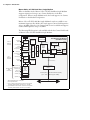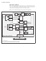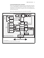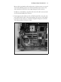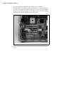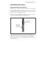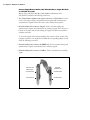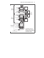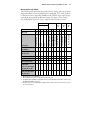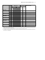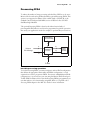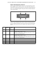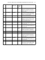
1
Matrox Solios
Installation and Hardware Reference
Manual no. Y10898-101-0500
November 15, 2013
Matrox® is a registered trademark of Matrox Electronic Systems Ltd.
Microsoft® and Windows®, are registered trademarks of Microsoft Corporation.
Intel® is a registered trademark of Intel Corporation.
Altera®, Stratix®, and Quartus® are registered trademarks of Altera Corporation.
In addition, Altera Byteblaster™ is a trademark of Altera Corporation.
Camera Link® is a registered trademark of the Automated Imaging Association
(AIA).
PCI-X® and PCI Express® are registered trademarks of PCI-SIG. In addition, PCIe is
a trademark of PCI-SIG.
GigE Vision™ is a trademark of the Automated Imaging Association.
All other nationally and internationally recognized trademarks and tradenames
are hereby acknowledged.
© Copyright Matrox Electronic Systems Ltd., 2004 - 2013. All rights reserved.
Limitation of Liabilities: In no event will Matrox or its suppliers be liable for any
indirect, special, incidental, economic, cover or consequential damages arising
out of the use of or inability to use the product, user documentation or related
technical support, including without limitation, damages or costs relating to the
loss of profits, business, goodwill, even if advised of the possibility of such
damages. In no event will Matrox and its suppliers’ liability exceed the amount
paid by you, for the product.
Because some jurisdictions do not allow the exclusion or limitation of liability for
consequential or incidental damages, the above limitation may not apply to
you.
Disclaimer: Matrox Electronic Systems Ltd. reserves the right to make changes in
specifications at any time and without notice. The information provided by this
document is believed to be accurate and reliable. However, neither Matrox
Electronic Systems Ltd. nor its suppliers assume any responsibility for its use; or for
any infringements of patents or other rights of third parties resulting from its use.
No license is granted under any patents or patent right of Matrox Electronic
Systems Ltd.
PRINTED IN CANADA
Contents
Chapter 1: Introduction. . . . . . . . . . . . . . . . . . . . . . . . . . . . . . . . . . 7
Matrox Solios boards . . . . . . . . . . . . . . . . . . . . . . . . . . . . . . . . . . . . . . . . . . . . . . . . . . 8
Acquisition with Matrox Solios eCL/XCL . . . . . . . . . . . . . . . . . . . . . . . . . . . . 8
Acquisition with Matrox Solios eA/XA . . . . . . . . . . . . . . . . . . . . . . . . . . . . . 13
Processing capabilities . . . . . . . . . . . . . . . . . . . . . . . . . . . . . . . . . . . . . . . . . . 16
On-board memory . . . . . . . . . . . . . . . . . . . . . . . . . . . . . . . . . . . . . . . . . . . . 16
Additional functionality . . . . . . . . . . . . . . . . . . . . . . . . . . . . . . . . . . . . . . . . 16
Data transfer . . . . . . . . . . . . . . . . . . . . . . . . . . . . . . . . . . . . . . . . . . . . . . . . . 18
Documentation conventions . . . . . . . . . . . . . . . . . . . . . . . . . . . . . . . . . . . . . 18
Software . . . . . . . . . . . . . . . . . . . . . . . . . . . . . . . . . . . . . . . . . . . . . . . . . . . . . . . . . . 19
Essentials to get started . . . . . . . . . . . . . . . . . . . . . . . . . . . . . . . . . . . . . . . . . . . . . . . 20
Inspecting the Matrox Solios package . . . . . . . . . . . . . . . . . . . . . . . . . . . . . . . . . . . . 21
With all Matrox Solios packages . . . . . . . . . . . . . . . . . . . . . . . . . . . . . . . . . . 21
With Matrox Solios eCL/XCL and Matrox Solios eA/XA . . . . . . . . . . . . . . . 21
Available separately . . . . . . . . . . . . . . . . . . . . . . . . . . . . . . . . . . . . . . . . . . . . 21
Handling components. . . . . . . . . . . . . . . . . . . . . . . . . . . . . . . . . . . . . . . . . . 22
Installation . . . . . . . . . . . . . . . . . . . . . . . . . . . . . . . . . . . . . . . . . . . . . . . . . . . . . . . . 22
Chapter 2: Hardware installation . . . . . . . . . . . . . . . . . . . . . . . . . 25
Installing your Matrox Solios board . . . . . . . . . . . . . . . . . . . . . . . . . . . . . . . . . . . . . . 26
Installing an adapter board/bracket . . . . . . . . . . . . . . . . . . . . . . . . . . . . . . . . . . . . . . 30
Connecting video sources . . . . . . . . . . . . . . . . . . . . . . . . . . . . . . . . . . . . . . . . . . . . . 33
Connecting to Matrox Solios eCL/XCL-B . . . . . . . . . . . . . . . . . . . . . . . . . . 33
Connecting to Matrox Solios eCL/XCL dual-Base/single-Medium or eCL/XCL-F
boards . . . . . . . . . . . . . . . . . . . . . . . . . . . . . . . . . . . . . . . . . . . . . . . . . . . . . . 34
Connecting to Matrox Solios eA/XA . . . . . . . . . . . . . . . . . . . . . . . . . . . . . . . 35
Chapter 3: Using multiple Matrox Solios boards . . . . . . . . . . . . 39
Multiple board installation . . . . . . . . . . . . . . . . . . . . . . . . . . . . . . . . . . . . . . . . . . . . 40
Simultaneous image capture from different boards . . . . . . . . . . . . . . . . . . . . . . . . . . 40
Chapter 4: Matrox Solios hardware reference . . . . . . . . . . . . . . 43
Matrox Solios hardware reference . . . . . . . . . . . . . . . . . . . . . . . . . . . . . . . . . . . . . . . 44
Acquisition path . . . . . . . . . . . . . . . . . . . . . . . . . . . . . . . . . . . . . . . . . . . . . . . 45
Digitizer configuration format . . . . . . . . . . . . . . . . . . . . . . . . . . . . . . . . . . . . 45
Matrox Solios eCL/XCL acquisition section . . . . . . . . . . . . . . . . . . . . . . . . . . . . . . . 46
Performance . . . . . . . . . . . . . . . . . . . . . . . . . . . . . . . . . . . . . . . . . . . . . . . . . . 47
Acquisition . . . . . . . . . . . . . . . . . . . . . . . . . . . . . . . . . . . . . . . . . . . . . . . . . . . 47
Supported video sources . . . . . . . . . . . . . . . . . . . . . . . . . . . . . . . . . . . . . . . . . 52
ChannelLink receivers. . . . . . . . . . . . . . . . . . . . . . . . . . . . . . . . . . . . . . . . . . . 53
Demultiplexers . . . . . . . . . . . . . . . . . . . . . . . . . . . . . . . . . . . . . . . . . . . . . . . . 54
Lookup tables . . . . . . . . . . . . . . . . . . . . . . . . . . . . . . . . . . . . . . . . . . . . . . . . . 54
Communication . . . . . . . . . . . . . . . . . . . . . . . . . . . . . . . . . . . . . . . . . . . . . . . 55
UARTs . . . . . . . . . . . . . . . . . . . . . . . . . . . . . . . . . . . . . . . . . . . . . . . . . . . . . . 56
PSGs. . . . . . . . . . . . . . . . . . . . . . . . . . . . . . . . . . . . . . . . . . . . . . . . . . . . . . . . 56
Synchronization, timing, and control signals. . . . . . . . . . . . . . . . . . . . . . . . . . 56
Matrox Solios eA/XA acquisition section . . . . . . . . . . . . . . . . . . . . . . . . . . . . . . . . . . 70
Performance . . . . . . . . . . . . . . . . . . . . . . . . . . . . . . . . . . . . . . . . . . . . . . . . . . 72
Analog input. . . . . . . . . . . . . . . . . . . . . . . . . . . . . . . . . . . . . . . . . . . . . . . . . . 72
UARTs . . . . . . . . . . . . . . . . . . . . . . . . . . . . . . . . . . . . . . . . . . . . . . . . . . . . . . 76
General synchronization . . . . . . . . . . . . . . . . . . . . . . . . . . . . . . . . . . . . . . . . . 76
Synchronization, timing, and control signals. . . . . . . . . . . . . . . . . . . . . . . . . . 78
Processing FPGA . . . . . . . . . . . . . . . . . . . . . . . . . . . . . . . . . . . . . . . . . . . . . . . . . . . . 85
Possible processing operations . . . . . . . . . . . . . . . . . . . . . . . . . . . . . . . . . . . . 85
Processing FPGA. . . . . . . . . . . . . . . . . . . . . . . . . . . . . . . . . . . . . . . . . . . . . . 86
High-speed serial interface . . . . . . . . . . . . . . . . . . . . . . . . . . . . . . . . . . . . . . 86
PCI-X interface . . . . . . . . . . . . . . . . . . . . . . . . . . . . . . . . . . . . . . . . . . . . . . . 86
Dedicated Processing FPGA memory . . . . . . . . . . . . . . . . . . . . . . . . . . . . . . 87
Debugging . . . . . . . . . . . . . . . . . . . . . . . . . . . . . . . . . . . . . . . . . . . . . . . . . . 87
Video to PCI-X bridge . . . . . . . . . . . . . . . . . . . . . . . . . . . . . . . . . . . . . . . . . . . . . . . 88
Memory . . . . . . . . . . . . . . . . . . . . . . . . . . . . . . . . . . . . . . . . . . . . . . . . . . . . . . . . . . 89
PCIe/PCI/PCI-X interface . . . . . . . . . . . . . . . . . . . . . . . . . . . . . . . . . . . . . . . . . . . . . 90
Appendix A: Glossary . . . . . . . . . . . . . . . . . . . . . . . . . . . . . . . . . . 91
Glossary . . . . . . . . . . . . . . . . . . . . . . . . . . . . . . . . . . . . . . . . . . . . . . . . . . . . . . . . . . 92
Appendix B: Technical information . . . . . . . . . . . . . . . . . . . . . . . 97
Board summary . . . . . . . . . . . . . . . . . . . . . . . . . . . . . . . . . . . . . . . . . . . . . . . . . . . . . 98
Global information . . . . . . . . . . . . . . . . . . . . . . . . . . . . . . . . . . . . . . . . . . . . 98
Technical features of Matrox Solios eCL/XCL . . . . . . . . . . . . . . . . . . . . . . . . 99
Technical features of Matrox Solios eA/XA . . . . . . . . . . . . . . . . . . . . . . . . . 104
Optional features for Matrox Solios boards . . . . . . . . . . . . . . . . . . . . . . . . . 106
Electrical specifications . . . . . . . . . . . . . . . . . . . . . . . . . . . . . . . . . . . . . . . . . . . . . . 107
Dimensions and environmental specifications . . . . . . . . . . . . . . . . . . . . . . . . . . . . . 114
Connectors on Matrox Solios eCL/XCL-B . . . . . . . . . . . . . . . . . . . . . . . . . . . . . . . 115
Camera Link video input connector . . . . . . . . . . . . . . . . . . . . . . . . . . . . . . 116
External auxiliary I/O connector 0 . . . . . . . . . . . . . . . . . . . . . . . . . . . . . . . 117
Connectors on Matrox Solios eCL/XCL dual-Base/single-Medium and eCL/XCL-F boards 120
Camera Link video input connectors . . . . . . . . . . . . . . . . . . . . . . . . . . . . . . 121
External auxiliary I/O connector 0 . . . . . . . . . . . . . . . . . . . . . . . . . . . . . . . . 124
External auxiliary I/O connector 1 . . . . . . . . . . . . . . . . . . . . . . . . . . . . . . . . 127
Internal auxiliary I/O connector . . . . . . . . . . . . . . . . . . . . . . . . . . . . . . . . . . 128
JTAG connector . . . . . . . . . . . . . . . . . . . . . . . . . . . . . . . . . . . . . . . . . . . . . . 131
Connectors on Matrox Solios eA/XA . . . . . . . . . . . . . . . . . . . . . . . . . . . . . . . . . . . . 132
Analog video input connectors . . . . . . . . . . . . . . . . . . . . . . . . . . . . . . . . . . . 133
External auxiliary I/O connector 0 . . . . . . . . . . . . . . . . . . . . . . . . . . . . . . . . 136
External auxiliary I/O connector 1 . . . . . . . . . . . . . . . . . . . . . . . . . . . . . . . . 140
Internal auxiliary I/O connector . . . . . . . . . . . . . . . . . . . . . . . . . . . . . . . . . . 141
JTAG connector . . . . . . . . . . . . . . . . . . . . . . . . . . . . . . . . . . . . . . . . . . . . . . 144
Appendix C: Major revisions of Matrox Solios boards . . . . . . . 145
Major revisions of Matrox Solios . . . . . . . . . . . . . . . . . . . . . . . . . . . . . . . . . . . . . . . 146
Appendix D: Acknowledgments . . . . . . . . . . . . . . . . . . . . . . . . . 151
UART copyright information . . . . . . . . . . . . . . . . . . . . . . . . . . . . . . . . . . . . . . . . . 152
Index
Regulatory Compliance
FCC Compliance Statement
Industry Canada Compliance Statement
EU Notice (European Union)
Directive on Waste Electrical and Electronic Equipment (WEEE)
Limited Warranty
Chapter
1
Chapter 1:
Introduction
This chapter briefly describes the features of the Matrox
Solios boards, as well as the software that can be used with
the boards.
8 Chapter 1: Introduction
Matrox Solios boards
The Matrox Solios family consists of five members: two PCI-X compliant,
single-slot frame grabbers, and three PCIe compliant, single-slot frame grabbers.
If purchased with the optional Processing FPGA, members also have custom image
processing capabilities.
The PCI-X compliant boards are Matrox Solios XCL and Matrox Solios XA. The
PCIe compliant boards are Matrox Solios eCL and Matrox Solios eA. The PCIe
compliant boards provide the exact same features as the related PCI-X boards,
except for the way the boards connect to the Host bus.
Acquisition with Matrox Solios eCL/XCL
Matrox Solios eCL/XCL boards are high-performance Camera Link frame
grabbers and are available in three versions: PCIe/PCI-X single-Base, PCIe/PCI-X
dual-Base/single-Medium, and PCIe/PCI-X single-Full. These are referred to as
Matrox Solios eCL/XCL-B, eCL/XCL dual-Base/single-Medium, and
eCL/XCL-F, respectively.
Note
The PCIe/PCI-X dual-Base/single-Medium board can be configured to operate
in single-Medium or dual-Base mode; for this reason, this board is referred to as
Matrox Solios eCL/XCL dual-Base/single-Medium. To change the mode of
Matrox Solios eCL/XCL, from its factory-default setting of single-Medium to
dual-Base, use MILConfig (Solios tab) and follow all on-screen instructions. Once
changed, you must restart your computer (perform a cold-boot) for changes to
take effect.
Matrox Solios boards
9
Matrox Solios eCL/XCL-B
Matrox Solios eCL/XCL-B supports acquisition from one Camera Link device in
the Base configuration; the device can be a power-over Camera Link (PoCL) video
source. Matrox Solios eCL/XCL-B supports Camera Link frequencies of up to
85 MHz.
Unlike the other Matrox Solios eCL/XCL boards, Matrox Solios eCL/XCL-B does
not support the Processing FPGA option.
Acquisition
memory
(32/64/128 MB)
Matrox Solios
eCL/XCL-B
32 DDR
(up to 800 MB/s)
ChannelLink
Receiver
Cam Ctrl (4)
LVDS
drivers
SerTFG
SerTC
LVDS driver
& receiver
Demultiplexer
MDR-26
connector
24
Data (24)
& Syncs (4)*
Clock
PSG
32
LUTs
Video to
PCI-X
bridge
Color
space
converter
eCL
32-bit
(up to 264 MB/s)
XCL
64-bit
(up to 528 MB/s)
UART
LVDS
drivers
and
receivers
Aux In (2)
Aux In (1)
DBHD-15
connector
Aux I/Os (3)
TTL buffers
OptoAux (2)
Optocoupler
PCI-X to PCI-X Bridge
x1 PCIe (eCL)
up to 250 MB/s
5V/3.3V PCI/PCI-X (XCL)
64-bit (up to 1 GB/s)
* 28 bits serialized across 4 LVDS pairs.
Host PCI / PCI-X/PCIe bus
10 Chapter 1: Introduction
Matrox Solios eCL/XCL dual-Base/single-Medium
When in dual-Base mode, Matrox Solios eCL/XCL dual-Base/single-Medium
supports acquisition from up to two Camera Link devices in the Base
configuration. When in single-Medium mode, the board supports one Camera
Link device in the Medium configuration.
Matrox Solios eCL/XCL dual-Base/single-Medium boards are available in two
maximum frequencies. By default, the boards support Camera Link frequencies
of up to 66 MHz. However, a fast Camera Link version is available and supports
Camera Link frequencies of up to 85 MHz.
The Processing FPGA option is only available with the fast Camera Link boards
of Matrox Solios eCL/XCL dual-Base/single-Medium.
SerTFG
SerTC
Cam Ctrl (4)
Clock
Data (24)
& Syncs (4)*
First
MDR-26
connector
LVDS driver
& receiver
LVDS
drivers
ChannelLink
Receiver #2 24
24
Data (24)
& Syncs (4)*
Clock
ChannelLink
Receiver #1
Cam Ctrl (4)
LVDS
drivers
SerTFG
SerTC
PSG #1
LVDS driver
& receiver
Demultiplexer Demultiplexer
Second
MDR-26
connector
Matrox Solios eCL/XCL
dual-Base/single-Medium
(dual-Base mode)
Acquisition
memory
(64/128/256 MB)
UART
32
64 DDR
(up to 1.6 GB/s)***
LUTs
DDR SDRAM
(64/128/256 MB)
Video to
PCI-X
bridge
64
(up to 1.3 GB/s)
16
Color
space
converter
32
LUTs
(up to
924 MB/s)
16
Processing
FPGA
(up to
924 MB/s)
32
QDRII
(up to 0.67GB/s) SRAM
32
(4/8 MB)
(up to 0.67GB/s)
64
(up to 800 MB/s)****
PSG #0
UART
DBHD-44 and
DB-9
connectors**
HSYNC Out (2)
VSYNC Out (2)
Clock Out (2)
Aux In (4)
Aux Out (4)
LVDS
drivers
and
receivers
Aux I/Os (6)
TTL buffers
OptoAux (4)
Optocoupler
* 28 bits serialized across 4 LVDS pairs.
** On a separate bracket.
*** Up to 1.6 GB/s for fast Camera Link board or with optional
Processing FPGA installed, otherwise up to 1.32 GB/s.
**** Up to 800 MB/s for fast Camera Link board or with optional
Processing FPGA installed, otherwise up to 660 MB/s.
Optional
PCI-X to PCI-X (XCL)
or PCI-X to PCIe (eCL)
Bridge
x4 PCIe (eCL)
(Up to 1 GB/s)
5V/3.3V PCI/PCI-X (XCL)
64-bit (up to 1 GB/s)
Host PCI/PCI-X/PCIe bus
Matrox Solios boards
Matrox Solios eCL/XCL
dual-Base/single-Medium
(single-Medium mode)
Acquisition
memory
(64/128/256 MB)
64 DDR
(up to 1.6 GB/s)***
First
MDR-26
connector
Clock
Data (24)
& Syncs (4)*
ChannelLink
Receiver #2 24
24
Data (24)
& Syncs (4)*
Clock
ChannelLink
Receiver #1
Cam Ctrl (4)
LVDS
drivers
SerTFG
SerTC
LVDS driver
& receiver
Demultiplexer
Second
MDR-26
connector
64
(up to 1.3 GB/s)
16
LUTs
Color
space
converter
(up to
924 MB/s)
16
32
Processing
FPGA
(up to
924 MB/s)
QDRII
SRAM
(4/8 MB)
32
(up to 0.67 GB/s)
(up to 0.67 GB/s)
64
(up to 800 MB/s)****
PSG
UART
DBHD-44 and
DB-9
connectors**
HSYNC Out (1)
VSYNC Out (1)
Clock Out (1)
Aux In (4)
Aux Out (2)
LVDS
drivers
and
receivers
Aux I/Os (4)
TTL buffers
OptoAux (4)
Optocoupler
PCI-X to PCI-X (XCL)
or PCI-X to PCIe (eCL)
Bridge
x4 PCIe (eCL)
(Up to 1 GB/s)
5V/3.3V PCI/PCI-X (XCL)
64-bit (up to 1 GB/s)
* 28 bits serialized across 4 LVDS pairs.
** On a separate bracket.
*** Up to 1.6 GB/s for fast Camera Link board or with optional
Processing FPGA installed, otherwise up to 1.32 GB/s.
**** Up to 800 MB/s for fast Camera Link board or with
optional Processing FPGA installed, otherwise up to 660 MB/s.
Optional
DDR SDRAM
(64/128/256 MB)
Video to
PCI-X
bridge
48
11
Host PCI/PCI-X/PCIe bus
12 Chapter 1: Introduction
Matrox Solios eCL/XCL-F
Matrox Solios eCL/XCL-F supports acquisition from one Camera Link device in
the Base, Medium, or Full configuration (with up to 10 taps). Matrox Solios
eCL/XCL-F supports Camera Link frequencies of up to 85 MHz; additionally,
Matrox Solios eCL/XCL-F supports the Processing FPGA option.
Matrox Solios eCL/XCL-F
Acquisition
memory
(64/128/256 MB)
Clock
Data (28) *
Clock
Data (28) *
Data (24)
& Syncs (4) *
Clock
First
MDR-26
connector
ChannelLink
Receiver #2
SerTFG
SerTC
28
24
Video to
PCI-X
bridge
64
64
(up to 1.3 GB/s)
LUTs
32
16
Color
space
(up to
924 MB/s)
16
Processing
FPGA
(up to
924 MB/s)
ChannelLink
Receiver #1
QDRII
(up to 0.67 GB/s) SRAM
32
(4/8MB)
(up to 0.67 GB/s)
LVDS
drivers
Cam Ctrl (4)
LVDS driver
& receiver
64
PSG
(up to 880 MB/s)
UART
DBHD-44 and
DB-9
connectors**
HSYNC Out (1)
VSYNC Out (1)
Clock Out (1)
Aux In (4)
LVDS
drivers
and
receivers
PCI-X to PCIe Bridge
Aux Out (2)
Aux I/Os (4)
TTL buffers
OptoAux (4)
Optocoupler
* 28 bits serialized across 4 LVDS pairs.
** On a separate bracket.
Optional
DDR SDRAM
(64/128/256 MB)
28
Demultiplexer
Second
MDR-26
connector
64 DDR
(up to 1.76 GB/s)
ChannelLink
Receiver #3
x4 PCIe (eCL)
(Up to 1 GB/s)
5V/3.3V PCI/PCI-X (XCL)
64-bit (up to 1 GB/s)
Host PCI / PCI-X / PCIe bus
Matrox Solios boards
13
Acquisition with Matrox Solios eA/XA
Matrox Solios eA/XA boards are high-performance, high-frequency, and
high-fidelity analog frame grabbers. They are available in three factory-configured
versions: Matrox Solios eA/XA Single, Matrox Solios eA/XA Dual, and Matrox
Solios eA/XA Quad.
Matrox Solios eA/XA Single
Matrox Solios eA/XA Single can acquire from one analog video source. This
acquisition path has an input selector that can switch between receiving input
from one of two video sources. Matrox Solios eA/XA Single does not support the
optional Processing FPGA.
VID_IN
A
B
8
Aux In
DBHD-44 Aux Out
and
DB-9
connectors*
Aux In
2
LVDS/TTL
drivers and
receivers
Input
Selector
DC
restoration
Optocouplers
low
10
16
pass 10-bit
LUTs
filter A/D
Hsync/Csync
(LVDS/TTL)
Vsync (LVDS/TTL)
1
Attenuator,
offset,
and
gain
Clock (LVDS/TTL)
Aux In (Trigger (TTL))
Aux Out (Exposure (TTL))
Rx
PSG
RS-232
transceivers
Tx
UART
Independent
acquisition path
Video to
PCI-X bridge
DVI
connectors
(0 and 1)
Independent
acquisition
path 0
16
Color
space
converter
Acquisition
64 DDR
memory
(up to 1.32 GB/s) (64/128/256 MB)
64
(up to 660 MB/s)
Matrox Solios eA/XA Single
* On a separate bracket.
PCI-X to PCIe (eA)
or PCI-X to PCI-X (XA)
Bridge
x1 PCIe (eA)
(up to 250 MB/s)
64-bit PCI or PCI-X (XA)
(up to 1 GB/s)
Host PCI / PCI-X / PCIe bus
14 Chapter 1: Introduction
Matrox Solios eA/XA Dual
Matrox Solios eA/XA Dual can acquire from up to two independent analog video
sources. For added flexibility, each acquisition path has an input selector that can
switch between receiving input from one of two video sources.
Matrox Solios eA/XA Dual supports the optional Processing FPGA.
VID_IN
A
B
8
Aux In
4
DBHD-44 Aux Out
and
DB-9
connectors*
DC
restoration
Optocouplers
RS-232
transceivers
Tx
DVI
connectors
(0 and 1)
low
10
16
pass 10-bit
LUTs
filter A/D
PSG
Clock (LVDS/TTL)
Aux In (Trigger (TTL))
Aux Out (Exposure (TTL))
Rx
Independent
acquisition
path 0
Attenuator,
offset,
and
gain
Hsync/Csync
(LVDS/TTL)
Vsync (LVDS/TTL)
2
Aux In
LVDS/TTL
drivers and
receivers
Input
Selector
16
Video to
PCI-X bridge
64 DDR
UART
Independent
acquisition path
Acquisition
memory
(64/128/256 MB)
(up to 1.6 GB/s)**
16
Independent
acquisition
path 1
16
Color
space
converter
(up to 924 MB/s)
16
Processing
FPGA
32
QDRII
(up to 0.67 GB/s) SRAM
32
(4/8 MB)
(up to 0.67 GB/s)
(up to 924 MB/s)
64
(up to 1.3 GB/s)
64
(up to
800 MB/s)***
DDR SDRAM
(64/128/256 MB)
Optional
Matrox Solios eA/XA Dual
PCI-X to PCIe (eA)
or PCI-X to PCI-X (XA)
Bridge
x1 (eA Single) or x4 PCIe (eA)
(up to 1 GB/s)
64-bit PCI or PCI-X (XA)
(up to 1 GB/s)
Host PCI / PCI-X / PCIe bus
* On a separate bracket.
** Up to 1.6 GB/s with optional Processing FPGA installed, otherwise up to 1.32 GB/s.
*** Up to 800 MB/s with optional Processing FPGA installed, otherwise up to 660 MB/s.
Matrox Solios boards
15
Acquisition with Matrox Solios eA/XA Quad
Matrox Solios eA/XA Quad can acquire from up to four independent analog video
sources. For added flexibility, each acquisition path has an input selector that can
switch between receiving input from one of two video sources. This means, for
example, that you can connect two 4-tap video sources to the eA/XA Quad board
and switch between them.
Matrox Solios eA/XA Quad supports the optional Processing FPGA.
VID_IN
A
B
Aux In
DBHD-44 Aux Out
and
DB-9
connectors*
Aux In
8
8
LVDS/TTL
drivers and
receivers
Input
Selector
DC
restoration
Optocouplers
PSG
Clock (LVDS/TTL)
Aux In (Trigger (TTL))
Aux Out (Exposure (TTL))
Rx
Independent
acquisition
path 0
DVI
connectors
(0 and 1)
Independent
acquisition
path 1
Independent
acquisition
path 2
low
10
16
pass 10-bit
LUTs
A/D
filter
Hsync/Csync
(LVDS/TTL)
Vsync (LVDS/TTL)
4
Attenuator,
offset,
and
gain
RS-232
transceivers
Tx
16
16
16
16
Video to
PCI-X bridge
64 DDR
UART
Independent
acquisition path
Acquisition
memory
(64/128/256 MB)
(up to 1.6 GB/s)**
32
16
Color
space
converter
(up to 924 MB/s)
16
Processing (up to 0.67 GB/s)
32
FPGA
QDRII
SRAM
(4/8 MB)
(up to 0.67 GB/s)
(up to 924 MB/s)
Independent
acquisition
path 3
64
(up to 1.3 GB/s)
64
(up to
800 MB/s)***
DDR SDRAM
(64/128/256 MB)
Optional
Matrox Solios eA/XA Quad
PCI-X to PCIe (eA)
or PCI-X to PCI-X (XA)
Bridge
x4 PCIe (eA)
(up to 1 GB/s)
64-bit PCI or PCI-X (XA)
(up to 1 GB/s)
Host PCI / PCI-X / PCIe bus
* On a separate bracket.
** Up to 1.6 GB/s with optional Processing FPGA installed, otherwise up to 1.32 GB/s.
*** Up to 800 MB/s with optional Processing FPGA installed, otherwise up to 660 MB/s.
16 Chapter 1: Introduction
Processing capabilities
To reduce the number of image processing tasks performed by the CPU of the
host computer (Host), most Matrox Solios boards (except for those mentioned
earlier) can be purchased with the optional Processing FPGA. Using this FPGA,
Matrox Solios can process and format image data.
Processing FPGA
The Processing FPGA is a highly customizable processing core, based on the Altera
Stratix family of pin-compatible FPGA devices. The Processing FPGA can be
programmed to perform functions that satisfy your application’s needs. The
Processing FPGA includes a high-speed serial interface, a PCI-X interface, and
can include up to two memory controllers for access to DDR SDRAM and QDRII
SRAM memory.
On-board memory
As a standard feature, Matrox Solios supports up to 256 Mbytes of linearly
addressable DDR SDRAM* to store acquisition data. This memory is referred to
as acquisition memory. Up to 256 Mbytes of additional DDR SDRAM and up
to 8 Mbytes of QDRII SRAM is included if the Processing FPGA is installed.
This memory is referred to as dedicated Processing FPGA memory. This memory
holds preprocessing data and is accessed by the Processing FPGA.
Additional functionality
In addition to the core video capture and optional processing capabilities, Matrox
Solios incorporates a variety of features to simplify overall system integration.
These features include:
• LVDS or RS-232 compatible serial interfaces (number depends on the type of
Matrox Solios) for Matrox Solios eCL/XCL and Matrox Solios eA/XA,
respectively. Each interface is mapped as a COM port so that it can be accessed
through the Win32 API. The serial interface can both receive and transmit signals,
in full-duplex mode.
• Color space converter. The converter, part of the Video-to-PCI-X bridge, allows
captured data to be converted to YUV or YCbCr formats.
*. Except Matrox Solios eCL/XCL-B which supports up to 128 Mbytes of linearly
addressable DDR SDRAM.
Matrox Solios boards
17
• Auxiliary, multi-purpose signals. These are non-video signals that can support one
or more functionalities depending on the auxiliary signal (for example, trigger
input or timer output). The number of signals each board supports is given in the
table below.
Board
Auxiliary signals available
Matrox Solios eCL/XCL-B
8*
Matrox Solios eCL/XCL dual-Base
18
Matrox Solios eCL/XCL single-Medium + eCL/XCL-F
14
Matrox Solios eA/XA Single
13
Matrox Solios eA/XA Dual
18
Matrox Solios eA/XA Quad
28
*. This is the number of auxiliary signals available when using the DBHD-15 auxiliary I/O connector; if replaced
with the optional DB-9 connector from the SOLCLBACCxxPAK accessory kit, less auxiliary signals are available (see the pinout of the auxiliary I/O connector in Appendix B: Technical information).
• Matrox Solios eA/XA also has a bi-color LED per timing and control section to
monitor PLL operation and sychronization signal input. Matrox Solios
eA/XA Quad has a total of four LEDs, Matrox Solios eA/XA Dual has two LEDs,
while Matrox Solios eA/XA Single has one LED.
• All Matrox Solios eCL/XCL boards* support an integrated rotary decoder.
*. For the standard Camera Link speed Matrox Solios XCL dual-Base/single-Medium
boards (66 MHz), starting from version 100.
18 Chapter 1: Introduction
Data transfer
Under optimum conditions, Matrox Solios can exchange data with the Host at a
peak transfer rate of up to 1 Gbyte/sec. For Matrox Solios XCL and XA, these
conditions include using the board in a 133 MHz PCI-X slot. For Matrox Solios
eCL and eA, these conditions include using the board in a x4 or x8 PCIe slot with
at least 4 active lanes; the eCL-B and eA Single boards can use a x1 PCIe slot. If
Matrox Solios XCL and XA are used with a conventional 3.3 or 5V PCI slot, the
maximum transfer rate is reduced (132 Mbytes/sec for a 32-bit PCI slot, 266
Mbytes/sec for a 66 MHz 32-bit PCI slot, and 532 Mbytes/sec for a 66 MHz
64-bit PCI slot).
Although the Matrox Solios boards do not have an integrated display section,
images can be transferred either to any available Matrox display board or a
third-party display board in the computer.
Important
Note that transfer of image data to a display board might require intervention
from the Host CPU, depending on your computer’s architecture.
Documentation conventions
This manual refers to all Matrox Solios boards as Matrox Solios. Matrox Solios
eCL/XCL refers to the single-Base, dual-Base/single-Medium, and single-Full
versions of Matrox Solios XCL and Matrox Solios eCL. In addition, Matrox Solios
eA/XA refers to the Quad, Dual, and Single versions of Matrox Solios XA and
Matrox Solios eA. When necessary, this manual distinguishes between the boards
using their full names. Also note that, when the term Host is used in this manual,
it refers to the host computer.
❖ Note that unless otherwise stated, the information in this manual reflects the most
recent versions of the boards available at the time that this manual was written
(refer to Appendix C: Major revisions of Matrox Solios boards).
Software
19
Software
To operate Matrox Solios, you can use one or more Matrox Imaging software
products that supports the board. These are the Matrox Imaging Library (MIL)
and its derivatives (MIL-Lite, Matrox Inspector, and Matrox Intellicam). All
Matrox software is supported under Windows; consult your software manual for
supported Windows environments.
MIL
MIL is a high-level programming library with an extensive set of optimized
functions for image capture, processing, analysis, transfer, compression, display,
and archiving. Image processing operations include point-to-point, statistical,
spatial filtering, morphological, geometric transformation, and FFT operations.
Analysis operations support calibration, are performed with sub-pixel accuracy,
and include pattern recognition (normalized grayscale correlation and Geometric
Model Finder), blob analysis, edge extraction and analysis, measurement,
metrology, character recognition (template-based and feature-based), and code
recognition (1D, 2D and composite code types).
MIL applications are easily ported to new Matrox hardware platforms and can be
designed to take advantage of multi-processing and multi-threading
environments.
MIL-Lite
MIL-Lite is a subset of MIL. It includes all the MIL functions for image
acquisition, transfer, display control, and archiving. It also allows you to perform*
processing operations that are typically useful to pre-process grabbed images.
Matrox Inspector
Matrox Inspector is an interactive Windows application for image capture,
processing, analysis, and archiving. Matrox Inspector is included* with MIL. MIL
application developers can use Matrox Inspector as a prototyping tool to quickly
build proof-of-concept demonstrations. End users can use Matrox Inspector to
perform and automate image enhancement and measurement tasks.
Matrox Intellicam
Matrox Intellicam is an interactive Windows program that allows for fast video
source interfacing and provides interactive access to all the acquisition features of
your Matrox board. Matrox Intellicam also has the ability to create custom digitizer
configuration format (DCF) files, which MIL and its derivatives use to interface
to specific non-standard video sources. Matrox Intellicam is included with all
Matrox Imaging software products.
*. As of MIL 9.0.
20 Chapter 1: Introduction
Essentials to get started
To begin using Matrox Solios, you must have a computer with the following:
• An available conventional PCIe, PCI, or PCI-X slot.
❖
Note that only Matrox Solios eCL and eA support a PCIe slot, and it should
be a x4 or x8 PCIe slot. For Matrox Solios eCL-B or eA Single, it can also be a
x1 slot.
• Processor with an Intel 32-bit architecture (IA32) or equivalent.
• A relatively up-to-date PCIe/PCI/PCI-X chipset. The list of platforms that are
known to be compatible with Matrox Solios are available on the Matrox website,
under the board’s PC compatibility list.
Consult your software package for other computer requirements (for example,
operating system and memory requirements).
Inspecting the Matrox Solios package
21
Inspecting the Matrox Solios package
You should check the contents of your Matrox Solios package when you first
open it. If something is missing or damaged, contact your Matrox representative.
Standard items
With all Matrox Solios packages
You should receive the following item:
• The Matrox Solios eCL, XCL, eA, or XA board, depending on which was
purchased.
With Matrox Solios eCL/XCL and Matrox Solios eA/XA
You should also receive the following items:
• An adapter board, and a flat ribbon cable to interface the frame grabber with the
adapter board. Note that the Matrox Solios eCL/XCL-B package does not
support/include an adapter board or a flat ribbon cable.
• A supplementary 50-pin auxiliary I/O mating connector. The mating connector
is included in case you need to build a cable that can access the signals of the
internal auxiliary I/O connector from within the chassis. Note that the Matrox
Solios eCL/XCL-B package does not include an internal auxiliary connector.
Available separately
You might have also ordered one or more of the following:
• MIL, which includes Matrox Inspector*, or MIL-Lite. Matrox Intellicam is
included with each of the aforementioned software packages.
• DVI-TO-8BNC/O, an 8-foot (2.4 m) input cable with a DVI connector on one
end and both 8 BNCs and open-ended wires on the other end. This cable is meant
to connect to Matrox Solios eA/XA. The open-ended wires allow you to connect
to the synchronization and control signals of the module.
Important
To connect the output of a display board (with a DVI output connector) to the
analog video input connectors, you can use a standard cable (DVI-I to DVI-I or
DVI-A to DVI-A cable) if the display board encodes the synchronization signals
*. As of MIL 9.0.
22 Chapter 1: Introduction
on the video data (sync on green). Otherwise, you must use the Matrox
DVI-TO-8BNC/O cable or a custom cable that re-routes the synchronization
signals to the appropriate pins.
❖ If needed, you can purchase a Camera Link or PoCL Camera Link cable from the
video source manufacturer, 3M Interconnect Solutions for Factory Automation,
Intercon 1, or other third parties.
• SOLCLBACCxxPAK accessory kit, which allows you to replace the DBHD-15
auxiliary I/O connector on Matrox Solios eCL/XCL-B with a DB-9 connector.
In this case, the DB-9 connector has the same pinout as auxiliary I/O connector 1
(DB-9) on the adapter board of other Matrox Solios eCL/XCL boards. Note
however, when using the optional DB-9 connector, some DBHD-15 signals are
not available.
Handling components
The electronic circuits in your computer and the circuits on Matrox Solios are
sensitive to static electricity and surges. Improper handling can seriously damage
the circuits. Be sure to drain static electricity from your body by touching a metal
fixture (or ground) before you touch any electronic component. In addition, do
not let your clothing come in contact with the circuit boards or components.
Warning
Before you add or remove devices from your computer, always turn off the power
to your computer and all peripherals.
Installation
The installation procedure consists of the following steps:
1. Complete the hardware installation as described in Chapter 2: Hardware
installation.
2. Complete the software installation procedure described in the documentation
accompanying your software package.
More information
For information on using multiple Matrox Solios boards, refer to Chapter 3: Using
multiple Matrox Solios boards.
Installation
23
For in-depth hardware information, refer to Chapter 4: Matrox Solios hardware
reference; whereas for a summary of this information, as well as environmental and
electrical specifications, and connector pinout descriptions, see Appendix B:
Technical information.
This manual occasionally makes reference to a MIL-Lite function. However,
anything that can be accomplished with MIL-Lite can also be accomplished with
MIL or Matrox Inspector.*
Need help?
If you experience problems during installation or while using this product, refer
to the support page on the Matrox Imaging web site:
www.matrox.com/imaging/support. This page provides answers to frequently asked
questions, as well as offers registered customers additional ways of obtaining
support.
If your question is not addressed and you are currently registered with the MIL
maintenance program, you can contact technical support. To do so, you should
first complete and submit the online Technical Support Request Form, accessible
from the above-mentioned page. Once the information is submitted, a Matrox
support agent will contact you shortly thereafter by email or phone, depending
on the problem.
*. Most operations can be accomplished with Matrox Inspector.
24 Chapter 1: Introduction
Chapter
2
Chapter 2:
Hardware
installation
This chapter explains how to install your Matrox Solios
board in your computer.
26 Chapter 2: Hardware installation
Installing your Matrox Solios board
Before you install your Matrox Solios board, some precautionary measures must
be taken. Turn off the power to your computer and its peripherals, and drain static
electricity from your body (by touching a metal part of the computer chassis).
Proceed with the following steps to install your board. Note that your board should
be installed before you install your software.
1. Remove the cover from your computer; refer to your computer’s documentation
for instructions.
2. Check that you have an empty PCIe slot in which to install your Matrox Solios
eCL or eA; the slot must have at least 4 active lanes, except for eCL-B and eA
Single which need one active lane. Matrox Solios XCL or XA must be installed in
an empty PCI-X slot. These boards can also be installed in a conventional 32- or
64-bit PCI slot, but this will reduce the transfer rate between the board and the
Host.
x16 PCIe
32-bit PCI slot
x8 PCIe
x1 PCIe
64-bit PCI-X slot
Installing your Matrox Solios board
Important
27
Some computers have a large, black-ridged heat sink that prevents long boards
from using some of the PCI board slots. Matrox Solios must not touch the heat
sink. Therefore, choose a slot where the board completely avoids it. If you cannot
find a suitable slot, contact your computer dealer.
If you also need to install the adapter board/bracket of your Matrox Solios board,
you need an additional slot. This slot need not be adjacent to the Matrox Solios
board. Note that the adapter boards/brackets do not plug into a slot’s
PCI/PCI-X/PCIe connector; they attach only to the back of the computer’s
chassis. Since Matrox Solios eA/XA’s adapter board is longer, it has a support tab
that can be removed; if a PCI/PCI-X slot is selected, the tab will fit into the slot’s
connector, ensuring that the board does not move. For a PCIe slot, the tab will
have to be removed because it physically doesn’t fit.
External
auxiliary I/O
connector 0
Internal
auxiliary I/O
connector
External
auxiliary I/O
connector 1
External
auxiliary I/O
connector 0
External
auxiliary I/O
connector 1
Adapter board for
Matrox Solios eCL/XCL
Internal
auxiliary I/O
connector
Tab
Adapter board for
Matrox Solios eA/XA
3. If there is a metal plate at the back of the selected slots, remove it. Keep the screw
from the top of the plates to anchor your boards once they are installed.
28 Chapter 2: Hardware installation
4. Position your Matrox Solios board in the selected slot, and then press the board
firmly but carefully into the connector of the slot.
When installing Matrox Solios XCL or XA in a conventional 32-bit slot, only the
32-bit portion of the edge connector is connected in the slot. The other portion
will remain out.
Important
When installing a Matrox Solios eCL or eA board in a x16 PCIe slot, special care
must be taken to avoid damaging the board. Some x16 PCIe slots have a connector
with a retainer. Matrox Solios boards must not come into contact with the latch
of this retainer.
x16 PCIe solder-side latch
x16 PCIe component-side latch
The PCIe specification does not define appropriate keep-out regions for the latch
to provide any tolerance to tilting or rotation when inserting or removing add-in
boards in these connectors. Therefore, do not to tilt the Matrox Solios board
backwards or rotate it when installing it; otherwise the board can touch the latch
and get damaged. Note that the same is true when removing the board.
Alternatively, you can remove the latch from the retainer.
Correct
Incorrect
Installing your Matrox Solios board
29
5. Anchor the board using the screw that you removed in step 3.
6. If required, install the adapter board/bracket of your Matrox Solios board, as
described in the section Installing an adapter board/bracket, later in this chapter.
7. Attach your video sources, as described in the section Connecting video sources,
later in this chapter.
8. Turn on your computer.
❖ When you boot your computer, Windows’ Plug-and-Play system will detect a new
Multimedia Video Device and you will be asked to assign it a driver. At this point,
you should click on Cancel because the driver will be installed during the
installation of Matrox Solios software.
30 Chapter 2: Hardware installation
Installing an adapter board/bracket
To install the adapter board/bracket of Matrox Solios eCL/XCL or eA/XA, proceed
with the following steps.
1. Make sure that your Matrox Solios eCL/XCL or eA/XA board is fastened to the
computer chassis.
2. If you are installing the adapter board of Matrox Solios eA/XA and the slot that
you have selected for the board is not a PCI/PCI-X slot, break off the board’s tab
if it interferes with other components in the computer. The tab was added so that
if used in a PCI/PCI-X slot, the board would have extra support and be more
sturdy.
External
auxiliary I/O
connector 0
External
auxiliary I/O
connector 1
Internal
auxiliary I/O
connector
Tab
Adapter board for
Matrox Solios eA/XA
To break off the tab, use a set of pliers; there is a groove along the tab so that you
can break it off without an excessive amount of force.
3. Connect the adapter board/bracket’s flat ribbon cable to the internal auxiliary I/O
connector of the Matrox Solios board. To do so, position the cable so that the red
wire is on the same side as the bracket of the Matrox Solios board. With the
Installing an adapter board/bracket
31
Matrox Solios board and the cable in this position, only the connector on one end
of the cable will latch properly onto the internal auxiliary I/O connector. The
other end will not and excessive force might damage the cable connector.
In addition, you should hear a snap when the hooks of the cable’s connector latch
onto the internal auxiliary I/O connector.
4. For the adapter boards of Matrox Solios eCL/XCL and eA/XA, connect the other
end of the flat ribbon cable to the internal auxiliary I/O connector of the adapter
board. Position the connectors so that their triangular etchings face each other.
The etchings indicate the location of pin 1.
32 Chapter 2: Hardware installation
5. If you are installing the adapter board of Matrox Solios eA/XA in a
PCI/PCI-X/PCIe slot, align the board’s tab with the slot’s connector, and then
press the board firmly but carefully into the slot’s connector. For other types of
slots or when installing the adapter board of Matrox Solios eCL/XCL, slide the
bracket into the opening at the back of the selected slot.
6. Anchor the bracket to the chassis using the screw that you removed in the previous
section.
Connecting video sources
33
Connecting video sources
Connecting to Matrox Solios eCL/XCL-B
The Matrox Solios eCL/XCL-B board has the following connectors on its bracket:
• One Camera Link-compliant video input connector. Used to receive video input,
timing, and synchronization signals and transmit/receive communication signals
between the video source and the frame grabber.
• External I/O connector 0 (DBHD-15 or DB-9). Used to transmit timing and
synchronization signals, and transmit/receive auxiliary signals.
Auxiliary I/O
Connector #0
Camera Link
Video Input
Connector #0
Use a standard Camera Link cable or a standard PoCL Camera Link cable to
interface with Camera Link Video input connector 0. You can purchase such a
cable from your video source manufacturer, 3M Interconnect Solutions for
Factory Automation, Intercon 1, or other third parties. Note that this cable is not
available from Matrox.
34 Chapter 2: Hardware installation
Connecting to Matrox Solios eCL/XCL dual-Base/single-Medium
or eCL/XCL-F boards
Matrox Solios eCL/XCL dual-Base/single-Medium and Matrox Solios
eCL/XCL-F boards have the following connectors:
• Two Camera Link-compliant video input connectors (on the bracket). Used to
receive video input, timing, and synchronization signals and transmit/receive
communication signals between the video source and the frame grabber.
• Internal auxiliary I/O connector (50-pin). Used to transmit timing and
synchronization signals, and transmit/receive auxiliary signals. The connector is
located on the edge of the board, making the signals accessible from inside the
computer enclosure.
To access the signals of the internal auxiliary I/O connector from outside of the
computer enclosure, you might have installed the corresponding adapter board.
It has the following connectors:
• External auxiliary I/O connector 0 (DBHD-44). Used to transmit timing and
synchronization signals, and transmit/receive auxiliary signals.
• External auxiliary I/O connector 1 (DB-9). Used to transmit/receive auxiliary
signals.
Camera Link
Video Input
External
Auxiliary I/O
Connector #0
Connector #0
Connector #1
Connector #1
Connecting video sources
35
One video source can be connected to each Camera Link connector (dual-Base
mode) or a single video source can be connected to both connectors
(single-Medium and single-Full modes). Use standard Camera Link cables. You
can purchase such a cable from your video source manufacturer, 3M Interconnect
Solutions for Factory Automation, Intercon 1, or other third parties. Note that
this cable is not available from Matrox. If using both Camera Link connectors in
single-Medium mode, the cables must be of the same type and length.
Warning
Connecting a single-Medium video source to a board operating in dual-Base mode
could seriously damage your video source. Note that Matrox Solios eCL/XCL
single-Medium/dual-Base boards are all factory configured to operate in
single-Medium mode.
Connecting to Matrox Solios eA/XA
The Matrox Solios eA/XA boards have the following connectors:
• Two DVI analog video input connectors (on the bracket). Used to receive video
input signals and transmit/receive timing, synchronization, and communication
signals between the video source and the frame grabber. For Matrox Solios eA/XA
Quad, you can connect up to 4 video sources to each connector. Connector 0
provides source A for acquisition paths 0 through 3, and connector 1 provides
source B for acquisition paths 0 through 3. For Matrox Solios eA/XA Dual, you
can connect upto to two video sources to each connector. For Matrox Solios eA/XA
Single, you can connect a single video source to each connector. Connector 0
provides source A for acquisition path 0, and connector 1 provides source B for
acquisition path 0.
• Internal auxiliary I/O connector (50-pin). Used to transmit control signals and
supply power to the adapter board, and to transmit/receive the timing and
auxiliary signals. The connector is located on the edge of the board, making the
signals accessible from inside the computer enclosure.
To access the signals of the internal auxiliary I/O connector from outside of the
computer enclosure, you might have installed the corresponding adapter board.
It has the following connectors:
• External auxiliary I/O connector 0 (DBHD-44). Used to transmit/receive
synchronization and auxiliary signals. Note that all the signals can be in either
LVDS or TTL format.
36 Chapter 2: Hardware installation
• External auxiliary I/O connector 1 (DB-9). Used to receive opto-isolated trigger
input signals.
Analog
Video Input
Connector #1
Connector #0
External
Auxiliary I/O
Connector #0
Connector #1
You can use the Matrox DVI-TO-8BNC/O input cable to connect to your video
sources. The cable has a DVI connector on one end and both 8 BNCs and
open-ended wires on the other end; the open-ended wires allow you to connect
to some timing, synchronization, and control signals of the frame grabber. Two
of these cables are required to connect to more than 4 video sources if using Matrox
Solios eA/XA Quad, more than 2 video sources if using Matrox Solios eA/XA
Dual, or more than one video source if using Matrox Solios eA/XA Single.
Connecting video sources
37
Connect the cable’s DVI connector to one of the DVI connectors on Matrox Solios
eA/XA. Then, connect the BNC connectors as follows.
BNC label* ,†
Signal on DVI connector 0
Signal on DVI connector 1
Expected input, with respect to the DVI
connector.
VID IN 0
P0_VID_IN_A
P0_VID_IN_B
Video input A or B for path 0 (monochrome or
red input).
VID IN 1
P1_VID_IN_A
P1_VID_IN_B
Video input A or B for path 1 (monochrome or
green input).
TRIG 0/2
P0_TTL_AUX(TRIG)_IN
P2_TTL_AUX(TRIG)_IN
TTL trigger input for PSG 0 or 2.
EXP 0/2
P0_TTL_AUX(EXP)_OUT
P2_TTL_AUX(EXP)_OUT
TTL timer output for PSG 0 or 2.
VID IN 2
P2_VID_IN_A
P2_VID_IN_B
Video input A or B for path 2 (monochrome or
blue input).
VID IN 3
P3_VID_IN_A
P3_VID_IN_B
Video input A or B for path 3 (monochrome
input).
TRIG 1/3
P1_TTL_AUX(TRIG)_IN
P3_TTL_AUX(TRIG)_IN
TTL trigger input for PSG 1 or 3.
EXP 1/3
P1_TTL_AUX(EXP)_OUT
P3_TTL_AUX(EXP)_OUT
TTL timer output for PSG 1 or 3.
*. Note that only VID IN 0, TRIG 0, and EXP 0 can be used with Matrox Solios eA/XA Single since there is only one acquisition path (P0).
†. Note that only VID IN 0 and 1, TRIG 0 and 1, and EXP 0 and 1 can be used with Matrox Solios eX/XA Dual since there are only two acquisition
paths (P0 and P1).
Important
To connect the output of a display board (with a DVI output connector) to the
analog video input connectors, you can use a standard cable (DVI-I to DVI-I or
DVI-A to DVI-A cable) if the display board encodes the synchronization signals
on the video data (sync on green). Otherwise, you must use the Matrox
DVI-TO-8BNC/O cable or a custom cable that re-routes the synchronization
signals to the appropriate pins.
38 Chapter 2: Hardware installation
Chapter
3
Chapter 3:
Using multiple
Matrox Solios
boards
This chapter explains how to use multiple Matrox Solios
boards.
40 Chapter 3: Using multiple Matrox Solios boards
Multiple board installation
You can install and use multiple Matrox Solios boards in one computer.
To use multiple Matrox Solios boards, install each additional Matrox Solios board
as you installed the first board (refer to Chapter 2: Hardware installation).
Theoretically, you can have as many as 16 Matrox Solios boards installed in your
computer; this number is limited by the number of empty slots in your computer
and by the available bandwidth of your PCIe/PCI/PCI-X interface (segment), as
discussed in the next section.
Using MIL-Lite, you have to allocate a MIL system for each board and allocate
the resources of each MIL system. For more information, see MsysAlloc() in the
MIL Reference.
Simultaneous image capture from different
boards
You can simultaneously capture images from video sources attached to different
Matrox Solios boards; however, the number of video sources from which you can
simultaneously capture images is determined by the available bandwidth of your
PCIe/PCI/PCI-X interface (segment). If there is not enough bandwidth, your
boards will drop frames.
Matrox Solios XCL and XA are susceptible to dropping frames because the
PCI/PCI-X bus bandwidth can be shared if you are using multiple boards.
Matrox Solios eCL and eA might have a problem with dropped frames if there are
not at least 4 active lanes on the PCIe connector to the Host (for example, if the
board is connected to a x4 PCIe connector that has only one active lane).
Customers have to verify with the motherboard manufacturer to find out whether
the particular motherboard works efficiently with a x4 PCIe board, such Matrox
Solios eCL.
Simultaneous image capture from different boards
41
The use of a high performance PCIe/PCI/PCI-X core-logic chipset is necessary
to sustain PCIe/PCI/PCI-X transfers to Host memory. If a high performance
chipset and a 133 MHz 64-bit PCI-X slot is used with Matrox Solios XCL and
XA, you should not have a problem with dropped frames. The list of platforms
that are known to be compatible with Matrox Solios are available on the Matrox
web site, under the board’s compatibility list.
To measure the available bandwidth of the PCIe/PCI/PCI-X segment used by
your Matrox Solios board, you can use the SoliosBench tool integrated in the
MILConfig utility. As a reference point, capturing from a 1K x 1K, 8-bit,
60 frames/sec video source will require a minimum bandwidth of 63 Mbytes/sec,
plus an additional bandwidth margin of approximately 20%, for a bandwidth of
75 Mbytes/sec.
42 Chapter 3: Using multiple Matrox Solios boards
Chapter
4
Chapter 4:
Matrox Solios
hardware reference
This chapter explains the architecture, features, and modes
of the Matrox Solios eCL/XCL and Matrox Solios eA/XA
hardware.
44 Chapter 4: Matrox Solios hardware reference
Matrox Solios hardware reference
This chapter provides information on the Matrox Solios eCL/XCL and Matrox
Solios eA/XA hardware. It covers the architecture, features, and modes of their
acquisition section. In addition, it covers the Matrox Solios hardware related to
the processing and transfer of data.
Acquisition
memory
(32/64/128/256 MB)**
64
64***
Acquisition
section
Video to
PCI-X Bridge
Color
space
converter
Optional*
DDR SDRAM
(64/128/256 MB)
32
16
Processing
FPGA
16
32
QDRII
SRAM
(4/8 MB)
64****
* Option not available for Matrox Solios
eCL/XCL-B and eA/XA Single.
** Matrox Solios eCL/XCL-B: 32/64/128 MB;
others: 64/128/256 MB.
*** Matrox Solios eCL/XCL-B: 32-bit.
**** Matrox Solios eCL-B: 32-bit.
PCI-X to PCI-X (XCL/XA)
or PCI-X to PCIe
(eCL/eA) Bridge
x1 or x4 PCIe
(eCL/eA)
5V/3.3V PCI/PCI-X
64-bit
(XCL/XA)
Host PCI/PCI-X/PCIe bus
A summary of the features of Matrox Solios, as well as pin assignments for the
various connectors, can be found in Appendix B: Technical information.
Matrox Solios hardware reference
45
Acquisition path
This manual uses the term acquisition path to refer to a path that has the
components to, for example, digitize or capture a video input signal. The term
independent acquisition path is used to refer to an acquisition path that can, if
required, acquire data from an input source independently from another such path
on the same frame grabber. Each independent acquisition path has its own
programmable synchronization generator (PSG) to manage all video timing,
synchronization, triggering, timer, and user input and output signals for the path.
MIL-Lite uses the concept of a MIL digitizer to represent the acquisition path(s)
with which to grab from one input source of the specified type. When several MIL
digitizers are allocated, their device number along with their DCF identify if they
represent the same path(s) (but perhaps for a different input format) or
independent path(s) for simultaneous acquisition. MIL-Lite uses the concept of
a data input channel to identify which input source to use when several of its type
are connected to the same acquisition path(s) (for example, grab from channel 0
(video source A) or channel 1 (video source B) of digitizer 0).
Digitizer configuration format
To program the acquisition section, allocate a MIL digitizer using MdigAlloc()
with an appropriate DCF (supplied or created) and digitizer device number; to
select the required input channel, use MdigControl() with M_CHANNEL*. If
you find a DCF file that is suitable for your video source, but you need to adjust
some of the more common settings, you can do so directly, without adjusting the
file, using the appropriate MIL-Lite function. For more specialized adjustments,
use the Matrox Intellicam program to adjust the DCF file. Using Matrox
Intellicam, you can set the active video region, the sampling clock, and all the
other parameters related to the timing of the video signal (that is, standard and
non-standard video, interlaced or non-interlaced) in your DCF file.
*. As of MIL 10.
46 Chapter 4: Matrox Solios hardware reference
Matrox Solios eCL/XCL acquisition section
Matrox Solios eCL/XCL can capture video from digital video sources compliant
with the Camera Link specification. Matrox Solios eCL/XCL supports
monochrome and component RGB acquisition. Besides standard Camera Link
video sources, it also supports additional types of video sources, including
time-multiplexed video sources. Grabbed data can be converted into YUV and
YCbCr formats in the color space converter of the Video to PCI-X bridge.
Matrox Solios eCL/XCL is available in three different versions: a PCIe/PCI-X
single-Base version (eCL/XCL-B), a PCIe/PCI-X dual-Base/single-Medium
version, and a PCIe/PCI-X single-Full version (eCL/XCL-F). In addition, Matrox
Solios eCL/XCL dual-Base/single-Medium boards are available in two maximum
frequencies: standard Camera Link speed and fast Camera Link speed.
Matrox Solios eCL/XCL has one acquisition path, except when Matrox Solios
eCL/XCL dual-Base/single-Medium is in dual-Base mode; in this case, it has two
independent acquisition paths.
By default, each acquisition path on Matrox Solios eCL/XCL
dual-Base/single-Medium boards can grab up to 66 Mega-samples/sec; on fast
Camera Link boards, each acquisition path can grab up to 85 Mega-samples/sec.
The acquisition path on Matrox Solios eCL/XCL-B and Matrox Solios
eCL/XCL-F boards can grab up to 85 Mega-samples/sec. Each acquisition path
has its own programmable synchronization generator (PSG), formatters, and
LUTs, and can have a different acquisition rate. Matrox Solios eCL/XCL supports
a comprehensive set of general purpose I/O and serial ports to control cameras
and other video sources.
Matrox Solios eCL/XCL acquisition section
47
Performance
The video timing parameters supported by the board are as follows:
Maximum
Number of pixels / line (including sync and blanking)
64 K
Number of lines / frame (including sync and blanking)
64 K
Pixel clock
eCL/XCL-B
85 Mhz
eCL/XCL dual-Base/single-Medium without fast Camera Link option
66 Mhz
eCL/XCL dual-Base/single-Medium with fast Camera Link option
85 Mhz
eCL/XCL-F
85 Mhz
Bandwidth
eCL/XCL-B
255 Mbytes/sec
eCL/XCL dual-Base/single-Medium without fast Camera Link option
396 Mbytes/sec
eCL/XCL dual-Base/single-Medium with fast Camera Link option
510 Mbytes/sec
eCL/XCL-F
680 Mbytes/sec
The maximum pixel clock frequency is dependent on the length of the cable used.
Refer to the Technical features of Matrox Solios eCL/XCL section.
Acquisition
A Base-type acquisition path supports a maximum of 24 bits of video data when
acquiring from Camera Link-compliant video sources or up to 32 bits when
acquiring from non-standard time-multiplexed video sources. Similarly, a
Medium-type acquisition path can grab up to 48 bits of video data when acquiring
from Camera Link-compliant sources or up to 64 bits when acquiring from nonstandard time-multiplexed sources. Finally, a Full-type acquisition path supports
up to 64 bits of video data when acquiring from Camera Link-compliant video
sources and up to 80 bits when acquiring from non-standard video sources.
48 Chapter 4: Matrox Solios hardware reference
The video sources can be frame, field, or line-scan video sources. Note that the
acquisition paths in dual-Base mode are completely independent, and therefore
the video sources do not need to be identical when running in dual-Base mode.
ChannelLink
Receiver
Cam Ctrl (4)
LVDS
drivers
SerTFG
SerTC
LVDS driver
& receiver
Demultiplexer
MDR-26
connector
24
Data (24)
& Syncs (4)*
Clock
32
LUTs
Video
to
PCI-X
bridge
PSG
UART
Aux In (2)
Aux Out (1)
LVDS
drivers
and
receivers
Aux I/Os (3)
TTL buffers
OptoAux (2)
Optocoupler
DBHD-15
connector
* 28 bits serialized across 4 LVDS pairs.
Acquisition section of
Matrox Solios XCL-B
Matrox Solios eCL/XCL acquisition section
49
UART
SerTFG
SerTC
Clock
ChannelLink
Receiver #2 24
24
Data (24)
& Syncs (4)*
Clock
ChannelLink
Receiver #1
Cam Ctrl (4)
LVDS
drivers
SerTFG
SerTC
PSG #1
LVDS
drivers
Cam Ctrl (4)
Data (24)
& Syncs (4)*
First
MDR-26
connector
LVDS driver
& receiver
LVDS driver
& receiver
Demultiplexer Demultiplexer
Second
MDR-26
connector
32
LUTs
Video
to
PCI-X
Bridge
32
LUTs
PSG #0
UART
HSYNC Out (2)
VSYNC Out (2)
Clock Out (2)
DBHD-44 and
DB-9
connectors**
Aux In (4)
Aux Out (4)
LVDS
drivers
and
receivers
Aux I/Os (6)
TTL buffers
OptoAux (4)
Optocoupler
* 28 bits serialized across 4 LVDS pairs.
** On a separate bracket.
Acquisition section of
Matrox Solios eCL/XCL
dual-Base/single-Medium
(dual-Base mode)
50 Chapter 4: Matrox Solios hardware reference
First
MDR-26
connector
Clock
Data (24)
& Syncs (4)*
ChannelLink
Receiver #2
24
Data (24)
& Syncs (4)*
Clock
ChannelLink
Receiver #1
Cam Ctrl (4)
LVDS
drivers
SerTFG
SerTC
24
LVDS driver
& receiver
Demultiplexer
Second
MDR-26
connector
48
LUTs
Video
to
PCI-X
bridge
PSG
UART
DBHD-44 and
DB-9
connectors**
HSYNC Out (1)
VSYNC Out (1)
Clock Out (1)
Aux In (4)
Aux Out (2)
LVDS
drivers
and
receivers
Aux I/Os (4)
TTL buffers
OptoAux (4)
Optocoupler
* 28 bits serialized across 4 LVDS pairs.
Acquisition section of
Matrox Solios eCL/XCL
dual-Base/single-Medium
(single-Medium mode)
Matrox Solios eCL/XCL acquisition section
Clock
Data (28)*
First
MDR-26
connector
Clock
Data (28)*
ChannelLink
Receiver #2
Data (24)
& Syncs (4)*
Clock
ChannelLink
Receiver #1
Cam Ctrl (4)
LVDS
drivers
SerTFG
SerTC
28
28
24
LVDS driver
& receiver
Demultiplexer
Second
MDR-26
connector
ChannelLink
Receiver #3
51
64
LUTs
Video
to
PCI-X
bridge
PSG
UART
DBHD-44 and
DB-9
connectors**
HSYNC Out (1)
VSYNC Out (1)
Clock Out (1)
Aux In (4)
Aux Out (2)
LVDS
drivers
and
receivers
Aux I/Os (4)
TTL buffers
OptoAux (4)
Optocoupler
* 28 bits serialized across 4 LVDS pairs.
** On a separate bracket.
Acquisition section of
Matrox Solios
eCL/XCL-F
52 Chapter 4: Matrox Solios hardware reference
Supported video sources
Each acquisition path supports the following video sources:
Video sources supported per acquisition path
Camera Link Standard
• One tap x 8/10/12/14/16-bit.
• Two tap x 8/10/12-bit.
• One 3 x 8-bit (RGB).
Not Camera Link Standard
• Two tap 14/16-bit with time-multiplexing.
• Four tap x 10/12-bit with time-multiplexing.
• Four tap 8-bit with time-multiplexing.
In addition to the above video sources, the following video sources are supported
when running in single-Medium mode:
Video sources supported
Camera Link Standard
• Four tap x 8/10/12-bit.
• One 3 x 10/12-bit (RGB).
Not Camera Link Standard
• 8 tap x 8-bit with time-multiplexing (using only 2 receivers).
• Two tap x 14/16-bit.
• One 3 x 14/16-bit (RGB).
• Two 3 x 8-bit (RGB) (genlocked).
In addition to the above video sources, the following video sources are supported
when running in single-Full mode:
Video sources supported
Camera Link Standard
• Eight tap x 8-bit.
Not Camera Link Standard
• 10 tap x 8-bit.
❖ Note that Matrox Solios eCL/XCL boards can simultaneously write to a limited
number of non-sequential memory regions; this further restricts the tap
configurations supported. Matrox Solios eCL/XCL-B can write to two
non-sequential memory regions. Matrox Solios eCL/XCL
dual-Base/single-Medium can write to two per acquisition path when in dual-Base
mode and four when in single-Medium mode. Matrox Solios eCL/XCL-F can
Matrox Solios eCL/XCL acquisition section
53
write to four. This means that using Matrox Solios eCL/XCL-F, for example, you
could only grab from an 8-tap x 8-bit video source if four of the taps carry pixels
that are sequential to the other four taps. To establish the number of
non-sequential memory regions to which your video source must write, refer to
the documentation accompanying your video source.
Supported tap configuration for
Matrox Solios eV-CLB and eV-CLBL
in single-Medium configuration
Supported tap configuration for
Matrox Solios eV-CLF and eV-CLFL
T1 T2T1 T2
T3 T4T3 T4
T1 T1
T5 T6T5 T6
T7 T8T7 T8
T5 T5
T3 T3
T2 T2
T4 T4
T7 T7
T6 T6
T8 T8
Tn: tap n, where n indicates the tap.
Matrox Solios eCL/XCL-B also supports power-over Camera Link (PoCL) video
sources. The PoCL protection on-board fuse can sustain a current of 0.4 A at up
to 45°C.
ChannelLink receivers
Matrox Solios eCL/XCL-B uses one ChannelLink receiver for video input(s).
Matrox Solios eCL/XCL dual-Base/single-Medium uses two ChannelLink
receivers that can be used synchronously (single-Medium mode) or
asynchronously (dual-Base mode). Finally, Matrox eCL/XCL-F uses three
ChannelLink receivers synchronously.
Each ChannelLink receiver on Matrox Solios eCL/XCL can receive up to 24 bits
of video data and 4 bits of synchronization and field data from the video source,
as serialized data over four LVDS pairs. A clock is received from the video source
over a fifth LVDS pair.
54 Chapter 4: Matrox Solios hardware reference
Demultiplexers
Each acquisition path of the board features a demultiplexer. It can deserialize input
from time-multiplexed video sources on a clock basis; time-multiplexed video
sources can output twice the amount of data as is possible when using other video
sources with the same amount of cabling. When enabled, the demultiplexer
assumes that two video streams share the same data path and that the streams are
interleaved based on the clock cycle. The demultiplexer assumes that on one clock
cycle, the data is from one stream and that on the next clock cycle, the data is from
the second stream. The demultiplexer combines the data from the two streams
every second clock cycle and sends them to the LUTs. The demultiplexer can only
deserialize video inputs that when combined, total a maximum depth of 48 bits
per acquisition path.
Lookup tables
Matrox Solios eCL/XCL has on-board lookup tables (LUTs) that can be used to
precondition input data at acquisition time, before it is stored in an image buffer.
The various versions of Matrox Solios eCL/XCL support different lookup table
configurations.
The LUTs are programmed using the MIL-Lite function MdigControl() with
M_LUT_ID*.
Single-Base board
Matrox Solios eCL/XCL-B has programmable LUTs. The LUTs can be operated
in the following configurations†:
• 8 palettes of one, two, or three 256-entry 8-bit LUTs.
• 4 palettes of one or two 1024-entry 8- or 16-bit LUTs.
• 1 palette of one or two 4096-entry 8- or 16-bit LUTs.
*. As of MIL 10.
†. For example, two 1024-entry 8-bit LUTs can map 2-tap 10-bit data to 8-bit values. In
addition one 1024-entry 8-bit LUT can map 1-tap 10-bit data to 8-bit values.
Matrox Solios eCL/XCL acquisition section
55
Dual-Base/single-Medium and single-Full boards
Matrox Solios eCL/XCL dual-Base/single-Medium and Matrox Solios
eCL/XCL-F boards each have programmable LUTs.
In dual-Base mode, the LUTs can be operated in the following configurations per
acquisition path*:
• 8 palettes of one, two, three, or four 256-entry 8-bit LUTs.
• 4 palettes of one or two 1024-entry 8- or 16-bit LUTs.
• 1 palette of one or two 4096-entry 8- or 16-bit LUTs.
In single-Medium and single-Full modes, the LUTs can be operated in the
following configurations:
• 8 palettes of one, two, three, four, or eight 256-entry 8-bit LUTs.
• 4 palettes of one, two, three, or four 1024-entry 8- or 16-bit LUTs.
• 1 palette of one, two, three, or four 4096-entry 8- or 16-bit LUTs.
Instead of being mapped through a LUT, 14- and 16-bit data by-pass the LUTs.
Communication
For each acquisition path, two LVDS pairs are used to transmit and receive
asynchronous serial communication between the video source and the board.
These signals are handled by the Universal Asynchronous Receiver/Transmitters
(UARTs).
For each acquisition path, four camera control output signals are also available.
These are general-purpose signals that are sent to the video source.
*. For example, two 1024-entry 8-bit LUTs can map 2-tap 10-bit data to 8-bit values. In
addition one 1024-entry 8-bit LUT can map 1-tap 10-bit data to 8-bit values.
56 Chapter 4: Matrox Solios hardware reference
UARTs
Matrox Solios eCL/XCL-B and Matrox Solios eCL/XCL-F each offer a single
LVDS-compatible Matrox serial interface. Matrox Solios eCL/XCL
dual-Base/single-Medium offers two LVDS-compatible serial interfaces; however,
when operating in single-Medium mode, only one LVDS compatible serial
interface can be used. Each interface is mapped as a COM port so that it can be
accessed through the Win32 API. Each interface is comprised of both a transmit
port and a receive port, permitting the interface to work in full-duplex mode. The
interfaces are located on the Camera Link connectors.
Each interface is controlled by a Universal Asynchronous Receiver-Transmitter
(UART)*. Each UART features independently programmable baud rates,
supporting all standard baud rates from 300 baud up to 230400† baud.
PSGs
Matrox Solios eCL/XCL-B and Matrox Solios eCL/XCL-F both feature one
programmable synchronization generator (PSG). Matrox Solios eCL/XCL
dual-Base/single-Medium features two PSGs; however, when operating in
single-Medium mode, only one PSG can be used. The PSGs are responsible for
managing all video timing, synchronization, triggering, timer, and user input and
output signals. Each PSG allows for independent acquisition from one video
source.
Synchronization, timing, and control signals
The following tables summarize the synchronization, timing, and control signals
supported by Matrox Solios eCL/XCL. Most of these signals are available by
defining a camera control or auxiliary (multi-purpose) signal as the required
synchronization, timing, or control signal in the DCF.
*. The UART implementation was derived from a design by Daniel Wallner. Please see
Appendix D: Acknowledgments for copyright information.
†. Maximum starting from version 100; earlier versions had a maximum baud rate of
115200 baud. In addition, the maximum baud rate is highly dependent on the
amount of computer resources available.
Matrox Solios eCL/XCL acquisition section
57
Matrox Solios eCL/XCL-B
The following tables summarize the synchronization, timing, and control signals
supported by Matrox Solios eCL/XCL-B. For example, P0_TTL_AUX_IO_0 can
be defined as a timer output (M_TIMER3 on M_DEV0), trigger input (trigger
controller 0 on acq path 0), field polarity input, user input, or user output
(M_USER_BIT2) signal. CL connect. stands for Camera Link connector.
TTL aux. I/O*
LVDS cam. ctrl
7
10
11
12
P0_OPTO_AUX_IN1
P0_LVDS_AUX_IN0
P0_LVDS_AUX_IN1‡
P0_LVDS_AUX_OUT0‡
3
1/4
2
0
T0
T1
T2
1
0
0
1/2 1/2 1/2 1/2
out*
P0_OPTO_AUX_IN0
4
in *
6
P0_TTL_AUX_IO_2‡
3
LVDS
aux.
2
P0_TTL_AUX_IO_1‡
Timer
2
LVDS
aux.
9
P0_TTL_AUX_IO_0
Functionality
1
CC4
m
CC3
M_CC_IOm†
8
CC2
n
CC1
M_AUX_IOn†
Acquisition Path
CL connect.
OPTO
aux.
in*
1
(M_TIMERn†)
Trigger controller affected
T0
T1
T0
T1
by input signal
Field polarity input
Timer-clock input
0
0
1
Bit of quadrature input
1
User output (bit of
Camera Link
static-user-output register
0
**
0
0
1
0/1 0/1 0/1 0/1
M_USER_BIT_CC_IOn†)
User output (bit of main
static-user-output register
0
2
3
4
0
M_USER_BITn†)
*. On auxiliary I/O connector (DBHD-15).
†. MIL constant, where n and m correspond to the number in the row.
‡. Not available when the DBHD-15 auxiliary I/O connector is replaced with the optional DB-9 connector from
the SOLCLBACCxxPAK accessory kit.
**. Note that a rotary encoder with quadrature output transmits a two-bit code. The table entries 0 and 1, therefore, denote bit position.
Frame valid input
1
VSYNC output
1
Line valid input
1
HSYNC output
1
Data valid input
1
Clock input
1
Clock output
1
LVDS cam. ctrl
CC4
CC3
CC2
CL connect.
CC1
Type of signal
Max # signals*
58 Chapter 4: Matrox Solios hardware reference
Received
with data
LVDS dedicated signals†
CL
connect.
0
0
0
0
0
0
0
0
0
0
0
Xclk (CL connect.)
0
0
0
0
*. The maximum # for each signal type cannot always be attained. The actual maximum depends on whether
the required auxiliary signals are available or have been defined as another type.
†. In this column, each signal is a dedicated signal (that is, it cannot be redefined as another type of signal).
Matrox Solios eCL/XCL acquisition section
59
The following table lists the auxiliary input signals (or auxiliary I/O signals set to
input) that can be rerouted onto output signals and the output signals onto which
they can be rerouted.
TTL aux. I/O
LVDS cam. ctrl
LVDS
aux. out
•
•
•
•
•
•
•
•
7
•
•
•
•
P0_LVDS_AUX_IN0†
10
•
•
•
•
P0_LVDS_AUX_IN1
11
P0_TTL_AUX_IO_0†
8
P0_TTL_AUX_IO_1
9
P0_TTL_AUX_IO_2
2
P0_OPTO_AUX_IN0†
6
P0_OPTO_AUX_IN1†
12
P0_LVDS_AUX_OUT0
4
2
P0_TTL_AUX_IO_2
3
9
P0_TTL_AUX_IO_1
2
8
P0_TTL_AUX_IO_0†
Auxiliary input signal (or auxiliary
I/O signal set to input)
1
CC4
m
CC3
M_CC_IOm*
CC2
n
CC1
M_AUX_IOn*
M_AUX_IOn*
CL connect.
*. MIL constant, where n and m correspond to the number in the row.
†. This hardware signal is also available on auxiliary I/O connector DB-9.
Matrox Solios eCL/XCL dual-Base/single-Medium and eCL/XCL-F
The following tables summarize the synchronization, timing, and control signals
supported by Matrox Solios eCL/XCL dual-Base/single-Medium and Matrox
Solios eCL/XCL-F. For example, P0_TTL_AUX_IO_0 can be defined for
acquisition path 0 as timer output signal 3, trigger input signal 0, field polarity
input signal 0, user input signal 2, or user output signal 2. Note, signals defined
for acquisition path 1 do not apply to the single-Medium and single-Full
configurations. CL connect. stands for Camera Link connector.
60 Chapter 4: Matrox Solios hardware reference
TTL aux. I/O*
LVDS cam. ctrl
CC1
CC2
CC3
CC4
CC1
CC2
CC3
0
0
1
1
0/1 0/1
3 1/4
1/2 1/2 1/2 1/2
1
T0 T1
0/1 0/1
0
0
0/1 0/1
0
0
1
1
1
2
2
0
T0/ T1/
T2 T3
0
0
0
1
User output (bit of
Camera Link
static-user-output
register
M_USER_BIT_CC_IOx†)
0 0/1 0/1 0/1 0/1
User output
(bit of main
static-user-output
register
0
1
1
0
1
0
0
0
0
1
input**
2
T0/ T1/
T2 T3
0
Bit of quadrature
1
T2 T3 T0 T1 T2 T3 T0 T1 T2 T3
T0 T1 T2 T3
1
Timer-clock input
0
2
3
1
0
P1_LVDS_AUX_OUT1
1
P1_LVDS_AUX_OUT0
1
12 13 12 13
P0_LVDS_AUX_OUT1
1
5
P0_LVDS_AUX_OUT0
0
4
LVDS_AUX_IN1
0
10 11
LVDS_AUX_IN0
0
1
P0_LVDS_AUX_IN1
0
Field polarity input
LVDS aux. out*
P0_LVDS_AUX_IN0‡
z
0
OPTO_AUX_IN1
4
7
OPTO_AUX_IN0
3
6
P0_OPTO_AUX_IN1‡
2
3
P0_OPTO_AUX_IN0‡
1
2
TTL_AUX_IO_1
4
0
0
TTL_AUX_IO_0
3
Trigger controller
affected by input
signal
1
P1_TTL_AUX_IO_1
2
1
9
P1_TTL_AUX_IO_0
1
0 1/2 1/2 1/2 1/2
8
P0_TTL_AUX_IO_1
y
for M_DEVz†
(M_TIMERx† )
9
P0_TTL_AUX_IO_0‡
M_CC_IOy
Timer
8
CC4
x
Functionality
LVDS aux. in *
CL connect. 1
M_AUX_IOx or
Acquisition path
CL connect. 0
OPTO aux. in*
0
0
1
0
1
0/1 0/1 0/1 0/1
2
3
2
3
4
5
4
5
0
1
M_USER_BITx† )
*. On external auxiliary I/O connector 0 (DBHD-44).
†. MIL constant, where x, y, and z correspond to the numbers in the row. M_DEVz is the required device number of the digitizer (MdigAlloc()) that
you must use to access this signal.
‡. On external auxiliary I/O connector 1 (DB-9).
**. Note that a rotary encoder (starting with Matrox Solios XCL Version 100) with quadrature output transmits a two-bit code. The table entries,
therefore, denote bit position.
Matrox Solios eCL/XCL acquisition section
1
1
1
0
1
1
1
0
1
1
1
0
1
1
1
0
1
1
1
HSYNC output
Data valid input
Clock input
Clock output
LVDS dedicated signals† ‡
CL connect. 1
1
0
CL connect. 0
1
Line valid input
CC4
1
CC3
0
VSYNC output
CC2
1
Received with data
CL connect. 1
CC1
1
CC4
1
CC3
0
CC2
Max # signals*
Frame valid input
CL connect. 0
CC1
Type of signal
Acquisition path
LVDS cam. ctrl
61
0
0
0
0
0
0
P0_LVDS_VSYNC_OUT
0
0
0
0
P1_LVDS_VSYNC_OUT
0
0
0
0
0
0
P0_LVDS_HSYNC_OUT
0
0
0
0
P1_LVDS_HSYNC_OUT
0
0
Xclk (CL connect. 0)
Xclk (CL connect. 1)
0
0
0
0
P0_LVDS_CLK_OUT
0
0
0
0
P1_LVDS_CLK_OUT
*. The maximum # for each signal type cannot always be attained. The actual maximum depends on whether the required auxiliary signals are
available or have been defined as another type.
†. In this column, each signal is a dedicated signal (that is, it cannot be redefined as another type of signal).
‡. Clock input is received on the Camera Link connectors, whereas the other signals in this column are received on/transmitted from external auxiliary I/O connector 0 (DBHD-44).
62 Chapter 4: Matrox Solios hardware reference
The following table lists the auxiliary input signals (or auxiliary I/O signals set to
input) that can be re-routed onto output signals and the output signals onto which
they can be re-routed.
TTL aux. I/O*
LVDS cam. ctrl
1
1
1
•
•
•
M_AUX_IOx†
0/1 •
2
P1_TTL_AUX_IO_0
8
1
P1_TTL_AUX_IO_1
9
1
TTL_AUX_IO_1
3
0/1
P0_OPTO_AUX_IN0‡
6
0
P0_OPTO_AUX_IN1‡
7
0
OPTO_AUX_IN0*
0
0/1
OPTO_AUX_IN1*
1
0/1 •
P0_LVDS_AUX_IN0‡
10
0
P0_LVDS_AUX_IN1*
11
0
LVDS_AUX_IN0*
4
0/1
LVDS_AUX_IN1*
5
0/1 •
•
•
•
•
•
•
•
•
•
•
0
0
1
1
•
•
•
•
•
•
•
•
•
•
•
•
•
•
•
•
•
•
•
•
•
•
•
•
12 13 12 13
•
•
•
0/1
P1_LVDS_AUX_OUT1
0
TTL_AUX_IO_0
1
P1_LVDS_AUX_OUT0
0
0
1
P0_LVDS_AUX_OUT1
0
9
0/1
P0_LVDS_AUX_OUT0
0
P0_TTL_AUX_IO_1
0
TTL_AUX_IO_1
z
•
0
P1_TTL_AUX_IO_1
4
•
1
P1_TTL_AUX_IO_0
3
•
3
TTL_AUX_IO_0
2
•
9
CC4
1
0
8
CC3
4
8
2
CC2
3
P0_TTL_AUX_IO_0‡
9
CC1
2
CC4
1
CC3
y
for M_DEVz†
CC2
M_CC_IOy
CC1
x
Acquisition Path
M_AUX_IOx or
Auxiliary input signal (or auxiliary I/O
signal set to input)
8
P0_TTL_AUX_IO_1
CL connect. 1
P0_TTL_AUX_IO_0‡
CL connect. 0
LVDS aux. out*
•
*. On external auxiliary I/O connector 0 (DBHD-44).
†. MIL constant, where x, y, and z correspond to the numbers in the row. M_DEVz is the required device number of the digitizer (MdigAlloc()) that
you must use to access this signal.
‡. On external auxiliary I/O connector 1 (DB-9).
Matrox Solios eCL/XCL acquisition section
63
Auxiliary signals and camera control signals
Matrox Solios eCL/XCL supports multi-purpose auxiliary input and output
signals. Auxiliary signals are non-video signals that can be controlled and support
one or more functionalities depending on the auxiliary signal (for example, as
trigger input or timer output signals). As mentioned previously, for each
independent acquisition path, the board also supports four camera control output
signals, which are configurable signals that can support one or several functions,
one of which is user-defined. The table in the previous subsection identifies the
functions to which an auxiliary signal/camera control signal can be defined. You
specify their function in the DCF file.
Matrox Solios eCL/XCL-B has auxiliary/camera control signals in the following
formats:
Auxiliary signals
# total*
LVDS camera control output signals.
4
TTL auxiliary input or output signals.
3
Opto-isolated auxiliary input signals.
2
LVDS auxiliary input signals.
2
LVDS auxiliary output signals.
1
*. This is the number of auxiliary signals available when using the DBHD-15 auxiliary I/O connector; if replaced
with the optional DB-9 connector from the SOLCLBACCxxPAK accessory kit, less auxiliary signals are available (see the pinout of the auxiliary I/O connector in Appendix B: Technical information).
64 Chapter 4: Matrox Solios hardware reference
Matrox Solios eCL/XCL dual-Base/single-Medium in dual-Base mode has
auxiliary/camera control signals in the following formats:
Auxiliary signals
# per path
# total
LVDS camera control output signals.
4
8
TTL auxiliary input or output signals.
2 (+2 depending on type of signal)
6
Opto-isolated auxiliary input signals.
depends on type (2 reserved for P0, 2 not specified)
4
LVDS auxiliary input signals.
depends on type (2 reserved for P0, 2 not specified)
4
LVDS auxiliary output signals.
2
4
Matrox Solios eCL/XCL dual-Base/single-Medium in single-Medium mode and
Matrox Solios eCL/XCL-F have auxiliary/camera control signals in the following
formats:
Auxiliary signals
# total
LVDS camera control output signals.
4
TTL auxiliary input or output signals.
4
Opto-isolated auxiliary input signals.
4
LVDS auxiliary input signals.
4
LVDS auxiliary output signals.
2
Note that the opto-isolated signals pass through an opto-coupler, a device that
protects the board from outside surges and different ground levels, and allows the
frame grabber to be totally isolated.
You can set up the auxiliary signals in the DCF. Alternatively, for most commonly
used functionalities, you can configure the auxiliary signals using the MIL-Lite
function MdigControl() (for example, with M_IO...*, M_GRAB_TRIGGER...,
or M_TIMER...*).
*. As of MIL 10.
Matrox Solios eCL/XCL acquisition section
65
Timers
Each PSG has four timers*. These timers can each generate a timer output signal
with up to two pulses; timer output signals can be used to control the exposure
time and other external events related to the video source (such as a strobe). The
timer output signals can be output using camera control signals or auxiliary output
signals (or auxiliary I/O signals in output mode).
Each PSG has two 24-bit timers (Timer 0 and 1) and two 16-bit timers (Timer 2
and 3). The 24-bit timers can count up to 16777215 clock ticks before resetting;
the 16-bit timers can count up to 65535 clock ticks before resetting.
The timers can use one of the following as a clock source:
• A clock based on an external pixel clock signal.
• A clock that is internally generated. Each timer can use its PSG’s clock generator,
which can generate a single clock with a programmable frequency of 0.8 to
100 MHz. Timers can only use the clock generator of their own PSG.
• A clock from an external source. In this case, you must define the appropriate
auxiliary input signal as a timer-clock input; the timer-clock input signal must
meet the specification of the auxiliary signal. The same timer-clock input can be
used to clock different timers of the same PSG.
• A clock based on another timer output of the same PSG. Timer 0 can use a clock
based on Timer 1, and Timer 1, 2, and 3 can use a clock based on Timer 0.
• A clock based on the HSYNC or VSYNC signal generated by the PSG.
To output a timer signal, use the MIL-Lite function MdigControl() with
M_IO_SOURCE + M_AUX_IOn† (or + M_CC_IOn†) set to M_TIMERm†.
Set up the timers using MdigControl() with M_TIMER_...†.
*. For the standard Camera Link speed Matrox Solios XCL dual-Base/single-Medium
boards (66 MHz), four timers have been available starting from version 100. Prior to
version 100, only two timers were available.
†. As of MIL 10.
66 Chapter 4: Matrox Solios hardware reference
Trigger
The board accepts trigger input signals which allow, for example, image acquisition
to be synchronized with external events. Each PSG has 4 trigger controllers.
Multiple auxiliary signals can trigger a trigger controller; however, you can
program only one per trigger controller as a trigger input signal
PSG 0
Trigger
Controller
2
MUX
Trigger
Controller
1
Trigger
Controller
3
P0_LVDS_AUX_IN1
(M_AUX_IO11)
TTL_AUX_IO_1
(M_AUX_IO3)
LVDS_AUX_IN1
(M_AUX_IO5)
OPTO_AUX_IN0
(M_AUX_IO0)
Trigger
Controller
2
Trigger
Controller
1
Trigger
Controller
3
LVDS_AUX_IN0
(M_AUX_IO4)
P1_TTL_AUX_IO_1
(M_AUX_IO9)
MUX
P0_TTL_AUX_IO_1
(M_AUX_IO9)
OPTO_AUX_IN1
(M_AUX_IO1)
MUX
LVDS_AUX_IN0
(M_AUX_IO4)
P0_OPTO_AUX_IN1
(M_AUX_IO7)
MUX
OPTO_AUX_IN0
(M_AUX_IO0)
TTL_AUX_IO_0
(M_AUX_IO2)
MUX
TTL_AUX_IO_0
(M_AUX_IO2)
Trigger
Controller
0
MUX
P0_LVDS_AUX_IN0
(M_AUX_IO10)
Trigger
Controller
0
MUX
P0_OPTO_AUX_IN0
(M_AUX_IO6)
PSG 1
P1_TTL_AUX_IO_0
(M_AUX_IO8)
MUX
P0_TTL_AUX_IO_0
(M_AUX_IO8)
TTL_AUX_IO_1
(M_AUX_IO3)
OPTO_AUX_IN1
(M_AUX_IO1)
LVDS_AUX_IN1
(M_AUX_IO5)
When received in TTL format directly, the signal must have a maximum
amplitude of 5 V. A signal over 2 V is considered high, while anything less than
0.8 V is considered low; the transition of 0.8 V to 2 V is considered to be the rising
edge.
If using the trigger to start acquisition, the trigger signal’s pulse width must be
greater than two pixels; if using the trigger to start the timer, the trigger signal’s
pulse width must be greater than two clock periods of the timer. To determine the
timer period, take the inverse of the pixel or timer’s clock frequency, respectively.
For example, if the pixel frequency is 12.27 MHz, the minimum pulse width is 2
x 1/12.27 MHz (approximately 163 nsec).
Matrox Solios eCL/XCL acquisition section
67
The opto-isolated trigger signals pass through an opto-coupler. The voltage
difference across the positive and negative components of the signal must be
between 4.06 V and 9.165 V for logic high, and between -5.0 V and 0.8 V for
logic low.
Synchronization
For each PSG, the board can supply one horizontal (HSYNC) and one vertical
(VSYNC) synchronization signal to the video source. Through the Camera Link
connectors, the board also receives synchronization data (frame valid, line valid,
and data valid) along with the video data; refer to the Camera Link specification
for a description of the synchronization data.
Note that the Camera Link standard does not regulate how to transmit an
interlaced video signal; however, you can define an auxiliary signal as a field
polarity input signal and transmit the field polarity on this signal.
Clock
For each PSG, the board can supply a clock signal to the video sources. Through
each of the video input Camera Link connectors, the board can also receive a clock
signal.
Rotary decoder
The PSGs of all Matrox Solios eCL/XCL boards* feature a rotary decoder
(quadrature decoder). A rotary decoder is used to decode quadrature input
received from a rotary encoder with quadrature output. A rotary encoder is a device
that provides information about the position and direction of a rotating shaft (for
example, that of a conveyor belt). The encoder outputs a two-bit code (also known
as Gray code) on two pairs of LVDS wires for each change in position of the
rotating shaft; for a given direction of the rotating shaft, the rotary encoder outputs
the code in a precise sequence (either 00 - 01 - 11 - 10 or 00 - 10 - 11 - 01,
depending on how the rotary encoder is attached to the rotating shaft). If the
rotating shaft changes direction, the rotary encoder transmits the Gray code in the
reverse sequence (00 - 10 - 11 - 01 or 00 - 01- 11 - 10, respectively).
Upon decoding a Gray code, the rotary decoder increments or decrements its
32-bit internal counter, depending on the direction of movement. You can
configure which Gray code sequence represents forward movement and
*. For the standard Camera Link speed Matrox Solios XCL dual-Base/single-Medium
boards (66 MHz), starting from version 100.
68 Chapter 4: Matrox Solios hardware reference
increments the counter; the reverse Gray code sequence will then represent the
backward direction and decrement the counter. You can specify the direction of
movement occurring when the Gray code sequence is 00 - 01 - 11 - 10, using
MdigControl() with M_ROTARY_ENCODER_DIRECTION.
The rotary decoder supports a maximum encoder frequency equal to the pixel
clock frequency of the video source. The PSGs of all Matrox Solios eCL/XCL*
boards support 5 V tolerant rotary encoders, except for the PSGs of the
standard-speed Matrox Solios XCL dual-Base/single-Medium board (66 MHz),
which supports 3.3 V tolerant rotary encoders.
Note that an external source must be used to power the rotary encoder (for
example, your computer’s 5 V power source).
For each PSG, you can configure the rotary decoder’s settings, using the MIL-Lite
function MdigControl() with M_ROTARY_ENCODER..., or by modifying the
DCF file with Matrox Intellicam.
User signals
Auxiliary signals can also be used to transmit or receive application-specific user
output and/or input.
If you want to start or stop an external event based on some calculation or analysis,
you can manually set the state of any auxiliary output signal (or I/O signal set to
output) to high or low. To do so, you set the state (on/off ) of a bit in a user settable
register (static-user-output register). When the bit is on, its associated auxiliary
output signal will be high; when it is off, the auxiliary output signal will be low.
This bit is referred to as a user-bit.
Your application can also act upon and interpret the state of an auxiliary input
signal (or I/O signal set to input). The state of an auxiliary input signal is not
associated with a user-bit; you poll the state of the signal directly. The state of an
auxiliary input signal can also generate an interrupt.
*. For Matrox Solios eCL/XCL-F SOL6MFCF* and SOL6MFCFE*, starting from versions 205 and 206, respectively. For Matrox Solios eCL dual-Base/single-Medium
SOL6MCLE*, SOL6MFCE*, and SOL6MFCE30546*, starting from versions 200,
101, and 100, respectively. For Matrox Solios XCL dual-Base/single-Medium
SOL6MFC* and SOL6MFC30546*, starting from versions 103 and 100, respectively.
Matrox Solios eCL/XCL acquisition section
69
You can specify the on/off state of a required output signal and have the PSG
generate and route it to an auxiliary output signal (or auxiliary I/O signals in
output mode) configured as a user signal; your application can set the on/off state
of the signal based on some analysis.
To route the state of a user-bit to an auxiliary output signal, use the MIL-Lite
function MdigControl() with M_IO_SOURCE and M_USER_BITn; to set the
state of a user-bit, use MdigControl() with M_USER_BIT_STATE. To poll the
state of an auxiliary input signal, use MdigInquire() with M_IO_STATUS*,
whereas to have the signal cause an interrupt, use MdigControl() with
M_IO_INTERRUPT_STATE and then use MdigHookFunction() with
M_IO_CHANGE to hook a function to this event (that is, to set up an event
handler).
70 Chapter 4: Matrox Solios hardware reference
Matrox Solios eA/XA acquisition section
Matrox Solios eA/XA is available in three versions: Matrox Solios eA/XA Quad,
Matrox Solios eA/XA Dual, and Matrox Solios eA/XA Single. eA/XA Quad has
four completely independent acquisition paths, allowing simultaneous acquisition
from four independent video sources. eA/XA Dual has two independent
acquisition paths; eA/XA Single, on the other hand, has one acquisition path. The
video sources can be standard or non-standard video sources. Grabbed data can
be converted into YUV and YCbCr formats in the color space converter of the
Video to PCI-X bridge.
Each acquisition path has two selectable inputs (A or B), and performs AC
coupling on each one. In addition, each acquisition path digitizes at a 10-bit pixel
resolution; the most-significant 8 bits or all 10 bits can be stored. Each acquisition
path has its own filters, programmable gain, and LUTs.
Matrox Solios eA/XA supports video sources with up to 4 taps, depending on the
version, and can grab at a maximum rate of 65 Mega-samples/sec per acquisition
path. In addition, Matrox Solios eA/XA has a comprehensive set of general purpose
I/O signals and serial ports to control video sources and other devices.
Matrox Solios eA/XA acquisition section
The following image is the acquisition section of Matrox Solios eA/XA.
VID_IN
A
B
Aux In
DBHD-44
and
DB-9
Aux Out
8
8
connectors*
Aux In
4
Hsync/Csync
(LVDS/TTL)
LVDS/TTL
drivers and
receivers
✝✝
✝✝✝
Input
Selector
DC
restoration
low
pass
filter
16
10-bit 10
LUTs
A/D
✕✕
Vsync (LVDS/TTL)
PSG
Clock (LVDS/TTL)
Trigger (TTL)
Exposure (TTL)
Optocouplers
Rx
Tx
DVI
connectors
(0 and 1)
Attenuator,
offset,
and
gain
Independent
acquisition
✝
path 0
16
Independent
acquisition
path 1✕
16
Independent
acquisition
path 2
16
Independent
acquisition
path 3
16
RS-232
transceivers
UART
Video
to
PCI-X
Bridge
Acquisition section of Matrox Solios eA/XA
✝
Only acquisition path 0 is available on Matrox Solios eA/XA Single.
✕
Only acquistion paths 0 and 1 are available on Matrox Solios eA/XA Dual.
✝✝
Only two auxiliary outputs are used on Matrox Solios eA/XA Single.
Four auxiliary outputs are used on Matrox Solios eA/XA Dual.
✝✝✝
Only one opto-coupled auxiliary input is available on Matrox Solios eA/XA Single.
Two opto-coupled auxiliary inputs are available on Matrox Solios eA/XA Dual.
✕✕
The board can accept an HSYNC or CSYNC input signal, but it can only output an HSYNC signal.
* On a separate bracket.
Independent
acquisition path
71
72 Chapter 4: Matrox Solios hardware reference
Performance
The video timing parameters supported by the board are as follows:
Maximum
Number of pixels / line (including sync and blanking)
64 K
Number of lines / frame (including sync and blanking)
64 K
Pixel clock for single sampling rate operation
65 MHz
Bandwidth
eA/XA Single
130 Mbytes/sec
eA/XA Dual
260 Mbytes/sec
eA/XA Quad
520 Mbytes/sec
Analog bandwidth (-3 db cutoff frequency)
100 MHz
Analog input
Matrox Solios eA/XA includes the electronic circuitry needed to select, amplify,
filter, and drive the video signal prior to sending it to the analog-to-digital (A/D)
converters.
Matrox Solios eA/XA Quad has four wide-band analog acquisition paths, Matrox
Solios eA/XA Dual has two, whereas Matrox Solios eA/XA Single has one. The
following table describes the video source combinations from which simultaneous,
independent acquisition is supported and the acquisition paths to which they must
be connected:
Configuration
Acquisition path†
Asynchronous video sources supported *
0
1
1
1 4-tap video source
2
1 3-tap video source (RGB) and 1 1-tap video source
3
2 2-tap video sources
2-tap
4
1 2-tap video source and
2 1-tap video sources
2-tap
5
1 2-tap video source and
2 1-tap video sources
1-tap
1-tap
6
4 1-tap video sources
1-tap
1-tap
2
3
4-tap
3-tap
1-tap
2-tap
1-tap
1-tap
2-tap
1-tap
1-tap
*. Note that taps expected to come from the same video source can also come from different video sources as long as they are synchronized (genlocked). In this case, the grabbed data is stored in separate color bands of the same buffer; the buffer can be in planar format.
†. Note that Matrox Solios eA/XA Single only has acquisition path 0 and can therefore suppor t only 1 tap. Matrox Solios eA/XA Dual only has acquisition paths 0 and 1, and can only support two taps.
Matrox Solios eA/XA acquisition section
73
Input voltage level and protection
The various amplification stages on Matrox Solios eA/XA are able to provide a
maximum peak signal of 2.4 V without saturation. Any positive video signal level
greater than this threshold will be distorted, so it is not recommended to feed a
signal above 3 V with termination (6 V unterminated).
Clamping diodes protect video inputs from overvoltage. The diodes clamp (clip)
the inputs if they go under -5 V or above +5 V. When there is overvoltage, the
maximum current flowing must be no more than 0.5A, otherwise damage can
occur to the board.
Selectable inputs
Each acquisition path can acquire data from one of two possible input sources (A
or B); each is 75-Ohm terminated and is capacitor coupled (AC coupling).
AC coupling transmits the varying (AC) characteristics of the signal while blocking
the static (DC) characteristics. This produces a signal that has an average DC level
of 0 Volts regardless of average picture level or DC offset of the incoming signal.
In effect, this ensures that the average surface area of the signal above 0 Volts is
the same as the average surface area below 0 Volts.
AC coupling is implemented using a series capacitor. The capacitor is a first order
high-pass filter with a 4 Hz -3dB cutoff frequency. The high-pass frequency cutoff
is 4 Hz to allow all frequency components of a frame with a 3 kHz line rate to
pass with less than 0.3% attenuation.
DC restoration
After the signal undergoes AC coupling, the signal is DC restored in order to
retrieve the DC level of the original video signal.
To perform DC restoration, the board samples the signal during each scanned line
in the specified region, and vertically shifts the signal so that this region is at 0.
Note that DC restoration requires a reference region in the video signal, usually
the back porch of the signal.
74 Chapter 4: Matrox Solios hardware reference
Adjusting the reference levels
For each acquisition path, you can adjust the signal’s black and white reference
levels so that the full dynamic range of each 10-bit A/D is used. Matrox Solios
eA/XA uses the offset-gain topology to adjust the black and white reference levels
of the signal. The topology uses a variable offset controller followed by a variable
gain controller; the signal can be routed through a 2:1 attenuator before being
restored and offset.
Filtered/
clamped
video signal
2:1 attenuator
DC
Restore
Offset
control
Gain
control
Video signal
to A/D converter
The variable offset controller vertically shifts the entire signal so that you can set
the lowest part of the video signal to 0 V, which is at the bottom of the A/D
conversion range. The offset adjustment range is -1 V to +1 V, in 4096 steps
(12-bit resolution).
The variable gain controller can then amplify the signal so that you can set the
highest part of the video signal to 1 V, which is at the top of the A/D conversion
range. The gain adjustment range is between 0 and 4, in 4096 step increment
(12-bit resolution).
Before passing to the DC restore and offset blocks, the signal can be routed through
an attenuator. The attenuator is a 2:1 voltage divider. The attenuator is present
because the variable gain controller cannot accept a positive or negative signal with
an amplitude above 1.2 V without distortion. The attenuator allows you to pass
a signal up to 2.4 V in amplitude (active video) without distortion. If the active
input video (excluding the sync pulse) is greater than 1.2 V in amplitude, the
attenuator should be enabled.
The maximum gain factors and the recommended video signal amplitude are as
follows:
2:1 attenuator
Maximum gain
Max recommended video signal
amplitude (terminated)
Min recommended video
signal amplitude
Off (bypassed)
4
1.2 V
0.25 V
On (active)
2
2.4 V
0.5 V
Matrox Solios eA/XA acquisition section
75
There are three ways to program the reference levels and the attenuator. You can
specify the actual black and white voltage levels of your input signal and have the
software calculate appropriate values for each element in the offset-gain topology.
You can have the software emulate an A/D with programmable black and white
references and specify the levels as a percentage of their possible values.
Alternatively, you can specify the required values for the offset and the gain
controls. If the signal amplitude is specified as greater than 1.1 V, the attenuator
will be enabled automatically. In all cases, you use the MIL-Lite function
MdigControl() with M_BLACK_REF and M_WHITE_REF.
Low-pass filter
The low-pass filtering stage is used to limit high frequency noise and aliasing effects
at the input of the A/D converter. Each acquisition path has two filters. The filters
used on Matrox Solios are 4th order Butterworth filters. The first has a -3 dB
cutoff frequency of 33 MHz. The second filter has a -3 dB cutoff frequency of
7.5 MHz, useful for RS-170 and CCIR video sources. All filters provide
80 dB/decade or 24 dB/octave of attenuation for frequencies above the cutoff
value. Enable the low-pass filters using the MIL-Lite function MdigControl() with
M_INPUT_FILTER.
10-bit A/D converters
Matrox Solios eA/XA uses high-quality, high-speed, 10-bit analog-to-digital
(A/Ds) converters to sample the video signal. Therefore, Matrox Solios eA/XA
provides excellent digitization quality, even at the highest sampling frequency. The
A/D converters can accept inputs from 5 MHz to 65 MHz, allowing full use of
their sampling speed.
Lookup tables
Matrox Solios eA/XA has programmable lookup tables (LUTs). For Matrox Solios
eA/XA Quad, the LUTs can be operated as one, two, three, or four 1024-entry
8- or 16-bit LUTs. For Matrox Solios eA/XA Dual, the LUTs can be operated as
one or two 1024-entry 8- or 16-bit LUTs. For Matrox Solios eA/XA Single, the
LUTs can be operated as a 1024-entry 8- or 16-bit LUT*.
The LUTs are programmed using the MIL-Lite function MdigControl() with
M_LUT_ID†.
*. For example, two 1024-entry 8-bit LUTs can map 2-tap 10-bit data to 8-bit values.
†. As of MIL 10.
76 Chapter 4: Matrox Solios hardware reference
UARTs
Matrox Solios eA/XA Quad offers four RS-232 compatible serial interfaces,
Matrox Solios eA/XA Dual offers two, whereas Matrox Solios eA/XA Single offers
one. Each interface is mapped as a COM port so that it can be accessed through
the Win32 API. Each interface is comprised of both a transmit port and a receive
port, permitting the interface to work in full-duplex (bidirectional) mode. The
interfaces are on the DVI connectors.
Each interface is controlled by a Universal Asynchronous Receiver-Transmitter
(UART)*. Each UART features independently programmable baud rates; each
supports all standard baud rates from 300 baud up to 115200† baud.
General synchronization
Matrox Solios eA/XA can operate in either slave or master mode.
Slave mode
In slave mode, the video source provides the synchronization information to
Matrox Solios eA/XA. It can accept any one of the following:
• Synchronization signals encoded on one of the analog video signals provided to
the board.
• Horizontal and/or vertical or composite synchronization signals supplied
separately by the video source, in either TTL or LVDS format.
Master mode
In master mode, Matrox Solios eA/XA generates the horizontal and/or vertical
synchronization signals, and/or a pixel clock, and supplies them to the video
source, allowing the video source to synchronize to the board.
*. The UART implementation was derived from a design by Daniel Wallner. Please see
Appendix D: Acknowledgments for copyright information.
†. Note that the maximum baud rate is highly dependant on the amount of computer
resources available.
Matrox Solios eA/XA acquisition section
77
PSGs
Matrox Solios eA/XA Quad features four programmable synchronization
generators (PSGs), Matrox Solios eA/XA Dual features two, whereas Matrox Solios
eA/XA Single features one. The PSGs are responsible for managing all input and
output video timing, synchronization, trigger, timer, and user signals. The PSGs
on Matrox Solios eA/XA allow the board to adapt to many video standards. Each
PSG allows for independent acquisition from a video source. Therefore, Matrox
Solios eA/XA allows acquisition from up to four independent video sources,
depending on the board.
The phase-locked loop
The high-performance, low-jitter phase-locked loop (PLL) uses frequency
synthesis techniques to generate the clock signal in slave mode.
As a reference, the PLL uses the composite or horizontal video synchronization
signal supplied by the video source (line-locked mode).
Since the signal from the video source is used as a reference, the PLL can produce
a clock signal that is a multiple of it. If the video source supplies a clock signal
within the input range of the A/D converters, the PLL is bypassed to avoid adding
jitter to the supplied clock.
Specification
Operating frequency range
12 to 80 MHz
Jitter
4.6 nsec p-p absolute with RS-170 synchronization source
78 Chapter 4: Matrox Solios hardware reference
Synchronization, timing, and control signals
The following tables summarize the synchronization, timing, and control signals
supported by Matrox Solios eA/XA. Most of these signals are available by defining
an auxiliary (multi-purpose) signal as the required synchronization, timing, or
control signal. For example, P0_TTL_AUX(TRIG)_IN can be defined for
acquisition path 0 as a trigger input (trigger controller 0), field polarity input, and
user input signal.
Only the auxiliary signals of the first acquisition path used by a video source are
available (for example, if grabbing RGB and monochrome, only the auxiliary
signals for path 0 and path 3 are available).
Note that only signals defined for acquisition path 0 (those beginning with P0)
and the common LVDS/TTL auxiliary signals apply to the Matrox Solios eA/XA
Single board. Only signals defined for acquisition paths 0 and 1 and the common
LVDS/TTL signals apply to the Matrox Solios eA/XA Dual board.
You can set TTL/LVDS signals in pairs to either TTL or LVDS format when
accessed from the external auxiliary I/O connector 0 (DBHD-44) of the cable
adapter board. For example, setting LVDS/TTL_AUX_IN2 to TTL also sets
LVDS/TTL_AUX_IN3 to TTL, and setting P0_LVDS/TTL_AUX_OUT0 to
LVDS also sets P0_LVDS/TTL_AUX_OUT1 to LVDS.
0
1
2
3
1
1
1
1
1
1
2
2
3
3
P3_LVDS/TTL_AUX_OUT1
P3_OPTO_AUX(TRIG)_IN
Timer
(M_TIMERn**)
0
P3_LVDS/TTL_AUX_OUT0
Functionality
0
P2_LVDS/TTL_AUX_OUT1
3
P2_LVDS/TTL_AUX_OUT0
2
P1_LVDS/TTL_AUX_OUT1
1
P1_LVDS/TTL_AUX_OUT0
0
10 11 10 11 10 11 10 11
P0_LVDS/TTL_AUX_OUT1
3
9
P0_LVDS/TTL_AUX_OUT0
2
8
LVDS/TTL_AUX_IN7
1
7
LVDS/TTL_AUX_IN6
0
6
LVDS/TTL_AUX_IN5
3
5
LVDS/TTL_AUX_IN4
2
4
LVDS/TTL_AUX_IN3
1
3
LVDS/TTL_AUX_IN2
m 0
2
TTL/LVDS aux. output ‡
0/1/ 0/1/ 0/1/ 0/1/ 0/1/ 0/1/ 0/1/ 0/1/
2/3 2/3 2/3 2/3 2/3 2/3 2/3 2/3
LVDS/TTL_AUX_IN1
for M_DEVm**
P2_OPTO_AUX(TRIG)_IN
0
P1_OPTO_AUX(TRIG)_IN
0
P0_OPTO_AUX(TRIG)_IN
0
P3_TTL_AUX(EXP)_OUT
0
P2_TTL_AUX(EXP)_OUT
12 12 12 12
P1_TTL_AUX(EXP)_OUT
1
P0_TTL_AUX(EXP)_OUT
1
P3_TTL_AUX(TRIG)_IN
1
TTL/LVDS aux. input‡
LVDS/TTL_AUX_IN0
input†
P2_TTL_AUX(TRIG)_IN
1
Opto aux.
output*
P1_TTL_AUX(TRIG)_IN
n
TTL aux.
input*
Acquisition path
P0_TTL_AUX(TRIG)_IN
M_AUX_IOn
TTL aux.
1
2
1
2
1
2
1
2
Matrox Solios eA/XA acquisition section
0 T0
1
T1
T0
2
3
Field polarity
input
0
1
2
3
Data valid
input
3
0
1
0
1
0
1
0
1
0
0
0
0
0
0
0
0
1
0
0
3
0
0
0
1
0
2
0
3
3
3
T1 T2 T3 T2 T3 T2 T3 T2 T3
0
0
User output
0
(bit of
static-user-output 1
register
M_USER_BITn**) 2
2
T2 T3 T2 T3 T2 T3 T2 T3
2
Timer-clock
input
2
T2 T3 T2 T3 T2 T3 T2 T3
T1
T0
1
T2 T3 T2 T3 T2 T3 T2 T3
T1
T0
1
P3_LVDS/TTL_AUX_OUT1
P3_OPTO_AUX(TRIG)_IN
Trigger controller
affected
by input signal
0
P3_LVDS/TTL_AUX_OUT0
Functionality
0
P2_LVDS/TTL_AUX_OUT1
3
P2_LVDS/TTL_AUX_OUT0
2
P1_LVDS/TTL_AUX_OUT1
1
P1_LVDS/TTL_AUX_OUT0
0
10 11 10 11 10 11 10 11
P0_LVDS/TTL_AUX_OUT1
3
9
P0_LVDS/TTL_AUX_OUT0
2
8
LVDS/TTL_AUX_IN7
1
7
LVDS/TTL_AUX_IN6
0
6
LVDS/TTL_AUX_IN5
3
5
LVDS/TTL_AUX_IN4
2
4
LVDS/TTL_AUX_IN3
1
3
LVDS/TTL_AUX_IN2
m 0
2
TTL/LVDS aux. output ‡
0/1/ 0/1/ 0/1/ 0/1/ 0/1/ 0/1/ 0/1/ 0/1/
2/3 2/3 2/3 2/3 2/3 2/3 2/3 2/3
LVDS/TTL_AUX_IN1
for M_DEVm**
P2_OPTO_AUX(TRIG)_IN
0
P1_OPTO_AUX(TRIG)_IN
0
P0_OPTO_AUX(TRIG)_IN
0
P3_TTL_AUX(EXP)_OUT
0
P2_TTL_AUX(EXP)_OUT
12 12 12 12
P1_TTL_AUX(EXP)_OUT
1
P0_TTL_AUX(EXP)_OUT
1
P3_TTL_AUX(TRIG)_IN
1
TTL/LVDS aux. input‡
LVDS/TTL_AUX_IN0
input†
P2_TTL_AUX(TRIG)_IN
1
Opto aux.
output*
P1_TTL_AUX(TRIG)_IN
n
TTL aux.
input*
Acquisition path
P0_TTL_AUX(TRIG)_IN
M_AUX_IOn
TTL aux.
79
0
2
2
2
2
*. On analog video input connectors (DVI).
†. On external auxiliary I/O connector 1 (DB-9).
‡. On external auxiliary I/O connector 0 (DBHD-44).
**. MIL constant, where n and m correspond to the numbers in the row. M_DEVm is the required device number of the digitizer (MdigAlloc()) that
you must use to access this signal.
80 Chapter 4: Matrox Solios hardware reference
3
1 in + 1 out
P3_LVDS_TTL_VSYNC_IO
CSYNC or
0
1 in + 1 out
P0_LVDS/TTL_CHSYNC_IO
HSYNC**
1
1 in + 1 out
P1_LVDS/TTL_CHSYNC_IO
2
1 in + 1 out
P2_LVDS/TTL_CHSYNC_IO
Clock
3
1 in + 1 out
P3_LVDS/TTL_CHSYNC_IO
0
1 in/out
P0_LVDS/TTL_CLK_IO
1
1 in/out
P1_LVDS/TTL_CLK_IO
2
1 in/out
P2_LVDS/TTL_CLK_IO
3
1 in/out
P3_LVDS/TTL_CLK_IO
P3_LVDS/TTL_AUX_OUT1
P3_LVDS/TTL_AUX_OUT0
P2_LVDS/TTL_AUX_OUT1
P2_LVDS/TTL_AUX_OUT0
P2_LVDS_TTL_VSYNC_IO
P1_LVDS/TTL_AUX_OUT1
1 in + 1 out
P1_LVDS/TTL_AUX_OUT0
2
in
P0_LVDS/TTL_AUX_OUT1
P1_LVDS_TTL_VSYNC_IO
LVDS/TTL_AUX_IN7
1 in + 1 out
LVDS/TTL_AUX_IN6
1
LVDS/TTL_AUX_IN5
P0_LVDS_TTL_VSYNC_IO
LVDS/TTL_AUX_IN4
1 in +1 out
LVDS/TTL_AUX_IN3
0
LVDS/TTL_AUX_IN2
Max # signals*
VSYNC
LVDS/TTL_AUX_IN1
Type of signal
Acquisition Path
LVDS/TTL_AUX_IN0
input/output signals
TTL/LVDS aux. output‡
†
P0_LVDS/TTL_AUX_OUT0
TTL/LVDS aux. input‡
TTL/LVDS dedicated
out
in
out
in
out
in
in
out
out
in
out
in
out
in
out
*. The maximum # for each signal type cannot always be attained. The actual maximum depends on whether the required auxiliary signals are
available or have been defined as another type.
†. In this column, each signal is a dedicated signal (that is, it cannot be redefined as another type of signal). These signals can be accessed from
the DVI connectors; the clock signal can also be accessed from the internal auxiliary I/O connector.
‡. On external auxiliary I/O connector 0 (DBHD-44).
**. The board can accept an HSYNC or CSYNC input signal, but it can only output an HSYNC signal.
Matrox Solios eA/XA acquisition section
81
Auxiliary signals
Matrox Solios eA/XA supports multi-purpose auxiliary input and output signals.
Auxiliary signals are non-video signals that can be controlled and support one or
more functionalities depending on the auxiliary signal (for example, as trigger
input or timer output signals). The table in the previous subsection identifies the
functions to which an auxiliary signal can be defined. You specify their function
in the DCF file.
The board supports auxiliary signals in different formats:
Auxiliary signals
# per path
Matrox Solios
eA/XA Quad #total
Matrox Solios
eA/XA Dual # total
Matrox Solios
eA/XA Single #total
Auxiliary input signals that can be defined as either
TTL or LVDS.
depends on
type of signal
8
8
8
Opto-isolated auxiliary input signals.
1
4
2
1
TTL auxiliary input signals.
1
4
2
1
Auxiliary output signals that can be defined as either
TTL or LVDS.
2
8
4
2
TTL auxiliary output signals.
1
4
2
1
Note that the opto-isolated signals pass through an opto-coupler, a device that
protects the board from outside surges and different ground levels, and permits
total electrical isolation from the frame grabber.
You can set up the auxiliary signals in the DCF. Alternatively, for most commonly
used functionalities, you can configure the auxiliary signals using the MIL-Lite
function MdigControl() (for example, with M_IO...*, M_GRAB_TRIGGER...,
or M_TIMER...*).
Synchronization
Each PSG can accept and/or provide one horizontal (HSYNC) and one vertical
(VSYNC) synchronization signal (slave or master mode). Instead of accepting a
horizontal synchronization signal, each PSG can alternatively accept a composite
(CSYNC) synchronization signal. Note also that, if the synchronization signals
are encoded on the video signal, the horizontal and vertical synchronization signals
are present as a composite synchronization pulse along with the video signal.
*. As of MIL 10.
82 Chapter 4: Matrox Solios hardware reference
With interlaced video sources, you can typically establish which field is being input
by noting the phase shift between the horizontal and the vertical synchronization
signals. Alternatively, you can define an auxiliary signal as a field polarity input
signal and transmit the field polarity on this signal.
To establish which pixels are active in a line (because the horizontal
synchronization signal does not identify the blanking portion of the signal), the
board can generate a data valid signal based on information specified in the DCF.
Alternatively, you can define an auxiliary input signal as a data valid signal.
Clock
Each PSG can accept or provide one pixel clock signal (slave or master mode).
Important
When accessed from the analog video input connectors (DVI), the pixel clock,
composite/horizontal synchronization, and vertical synchronization signals of
each PSG form a group of signals. The signals of each group shares the same
direction (input or output) and same signal format (TTL or LVDS). When
accessed from the internal or external auxiliary I/O connectors (HD-44), the
format and direction of the synchronization signals are independent; the board
can both transmit and receive synchronization signals at the same time.
Timers
Each PSG has two timers. These timers can each generate a timer output signal
with up to two pulses; timer output signals allow you to control the exposure time
and other external events related to the video source (such as a strobe). The timer
signals can be output using auxiliary output signals.
The timers are 24-bit timers, allowing each to count up to 16777215 clock ticks
before resetting.
The timers can use one of the following as a clock source:
• A clock that is internally generated. Each timer can use its PSG’s clock generator,
which can generate a single clock with a programmable frequency of 0.8 to
100 MHz. Timers can only use the clock generator of their own PSG.
• A clock from an external source. In this case, you must define the appropriate
auxiliary input signal as a timer-clock input; the timer-clock input signal must
meet the specification of the auxiliary signal. The same timer-clock input can be
used to clock both timers of a PSG.
Matrox Solios eA/XA acquisition section
83
• A clock based on another timer output of the same PSG.
• A clock based on an external pixel clock signal.
• A clock based on the HSYNC or VSYNC signal generated by the PSG.
To set up a timer, use the MIL-Lite function MdigControl() with M_TIMER...
Set the clock source of a timer using MdigControl() with
M_TIMER_CLOCK_SOURCE. To transmit the output of a timer, use
MdigControl() with M_IO_SOURCE* + M_AUX_IOn set to M_TIMERm.
Trigger signals
The board accepts trigger input signals, which allow acquisition to be
synchronized with external events. Each PSG accepts two external trigger input
signals: one TTL or LVTTL trigger input and another trigger input that passes
through an opto-coupler, a device that protects the board from outside surges. For
each PSG, you can also program two path-independent auxiliary signals as trigger
input signals; these can be received in LVDS, TTL, or LVTTL.
When received in TTL format directly, the signal must have a maximum
amplitude of 5 V; when received in LVTTL format directly, the signal must have
a maximum amplitude of 3.3 V. A signal over 2 V is considered high, while
anything less than 0.8 V is considered low; the transition of 0.8 V to 2 V is
considered to be the rising edge.
If using the trigger to start acquisition, the trigger signal’s pulse width must be
greater than two pixels; if using the trigger to start the timer output, the trigger
signal’s pulse width must be greater than two clock periods of the timer. To
determine the timer period, take the inverse of the pixel or timer’s clock frequency,
respectively. For example, if the pixel frequency is 12.27 MHz, the minimum pulse
width is 2 x 1/12.27 MHz (approximately 163 nsec).
A trigger signal connected to external I/O connector 1 of the adapter board, passes
through an opto-coupler. The voltage difference across the positive and negative
components of the signal must be between 3.15 V and 6.45 V for logic high, and
between -5.0 V and 0.8 V for logic low.
*. As of MIL 10.
84 Chapter 4: Matrox Solios hardware reference
User signals
Auxiliary signals can be used for application-specific user input and output. Any
auxiliary output signal (or I/O signal set to output) can be configured as a user
output signal to start or stop an external event. In this case, the state (on/off ) of
a bit in a user settable register (static-user-output register) is routed onto its
associated auxiliary output signal. This bit is referred to as a user-bit. Your
application can also act upon and interpret the state of an auxiliary input signal
(or I/O signal set to input). The state of an auxiliary input signal is not associated
with a user-bit; you poll the state of the signal directly. The state of an auxiliary
input signal can also generate an interrupt.
You can specify the on/off state of a required output signal and have the PSG
generate and route it to an auxiliary output signal (or auxiliary I/O signals in
output mode) configured as a user signal; your application can set the on/off state
of the signal based on some analysis.
To route the state of a user-bit to an auxiliary output signal, use the MIL-Lite
function MdigControl() with M_IO_SOURCE and M_USER_BITn; to set the
state of a user-bit, use MdigControl() with M_USER_BIT_STATE. To poll the
state of an auxiliary input signal, use MdigInquire() with M_IO_STATUS*,
whereas to have the signal cause an interrupt, use MdigControl() with
M_IO_INTERRUPT_STATE and then use MdigHookFunction() with
M_IO_CHANGE to hook a function to this event (that is, to set up an event
handler).
Processing FPGA
85
Processing FPGA
To reduce the number of image processing tasks the Host CPU has to do, most
Matrox Solios boards can be purchased with the optional Processing FPGA. This
option is not supported on Matrox Solios eA/XA Single, eCL/XCL-B, or the
standard Camera Link speed (66 MHz) version of Matrox Solios eCL/XCL
dual-Base/single-Medium.
The optional Processing FPGA is based on the Altera Stratix family of
pin-compatible FPGA devices, and it can be programmed to perform operations
that satisfy your application’s needs (for example, to perform a Bayer conversion).
Optional
DDR SDRAM
(64/128/256 MB)
64
16
Video to
PCI-X Bridge
32
Processing
FPGA
32
QDRII
SRAM
(4/8 MB)
16
64
To Host
Possible processing operations
To use the Processing FPGA, you must configure it with an FPGA configuration
that defines the appropriate functionality. An FPGA configuration is a code
segment that is used to program an FPGA. You can use standard Matrox FPGA
configurations or you can create your own using the Matrox FPGA Developer’s
Toolkit (FDK) for Matrox Solios. Once the Processing FPGA is programmed, you
can then make use of its functionality using MIL. Refer to Using MIL with a
Processing FPGA chapter in the MIL User Guide for more information.
86 Chapter 4: Matrox Solios hardware reference
Processing FPGA
Depending on your application requirements, you can purchase the board with a
Processing FPGA implemented using one of the following two supported FPGA
chips.
Altera Stratix I package
C5 speed grade
780 pin count
LEs
EP1S30
EP1S40
32,470
41,250
DSP blocks
12
14
DSP block 9-bit elements
96
112
PLLS
10
12
M512 RAM blocks
295
384
M4K RAM blocks
171
183
MRAM blocks
4
4
Total RAM bits
3,317,184
3,423,744
High-speed serial interface
The Processing FPGA includes a 32-channel (16 channels per direction),
high-speed serial interface to communicate with the acquisition section of the
Matrox Solios boards. Each channel has a data rate of 462 Mbits/sec, for a total
of 924 Mbytes/sec per direction.
PCI-X interface
The 64-bit PCI-X interface allows the Processing FPGA to communicate with the
Host. It is 64-bits wide and runs at 100 MHz, providing a throughput of up to
800 Mbytes/sec. The implementation of the PCI-X interface will vary depending
on the requirements of the application.
Processing FPGA
87
Dedicated Processing FPGA memory
When you purchase a Matrox Solios with a Processing FPGA, the board also comes
with the following memory, which can only be accessed through the Processing
FPGA:
• 64/128/256 Mbytes of DDR SDRAM at 1.33 Gbytes/sec (2 x 64 bits x
83.3 MHz).
• 4/8 Mbytes of QDRII SRAM at 666 Mbytes/sec input, and 666 Mbytes/sec
output (2 x 32 bits x 83.3 MHz, in each direction).
Although the board comes with dedicated Processing FPGA memory, the
Processing FPGA can also access acquisition memory through its high-speed serial
interface.
Debugging
To interface with the Processing FPGA for debugging and probing internal signals,
Matrox Solios boards purchased with the Processing FPGA feature a 10-pin male
JTAG connector. For further details on the JTAG connector, see the section JTAG
connector in Appendix B: Technical information.
88 Chapter 4: Matrox Solios hardware reference
Video to PCI-X bridge
The video to PCI-X bridge is capable of high-speed transfers to acquisition
memory, to the optional Processing FPGA, and through the PCI-X to
PCI-X/PCIe bridge, to Host memory, off-board display memory, or other devices
across the Host bus. Upon transmitting the video data, the video to PCI-X bridge
can also format the data as follows:
• Image resizing. Captured image data can be cropped (ROI capture) or
subsampled. This can be useful to implement custom software-based motion
detection because at a reduced scale, image comparison is faster.
For all versions of Matrox Solios, the video to PCI-X bridge can arbitrarily
subsample image data to 1/16th of a field or frame.
• Vertical flipping. Captured image data can be flipped vertically.
• Color space conversion. For all versions of Matrox Solios, the color space
converter in the video to PCI-X bridge can convert grabbed image data to YUV
and YCbCr formats. The color space converter can also perform color kill, which
converts the data to grayscale and then converts it to the appropriate destination
format. The equations for the conversion are described in the following table.
Color space conversion
Equations
RGB-to-YUV
• Y = 0.299 R + 0.587 G + 0.114 B
• U = -0.169 R - 0.331 G +0.500 B + 128
• V = 0.500 R - 0.419 G - 0.081 B +128
RGB-to-YCbCr
• Y = 0.257 R + 0.504 G + 0.098 B +16
• Cb = -0.148 R - 0.291 G + 0.439 B +128
• Cr =0.439 R -0.368 G - 0.071 B +128
Memory
89
Memory
As a standard feature, all Matrox Solios boards except Matrox Solios eCL/XCL-B
and Matrox Solios eCL/XCL-F support up to 256 Mbytes of linearly addressable,
DDR SDRAM used as acquisition memory. This memory has a bandwidth of up
to 1.6 Gbytes/sec when the optional Processing FPGA is installed, and up to
1.32 Gbytes/sec without the optional Processing FPGA installed.
As a standard feature, Matrox Solios eCL/XCL-B and eCL/XCL-F also support
acquisition memory. However, Matrox Solios eCL/XCL-B supports up to
128 Mbytes of linearly addressable DDR SDRAM, with a bandwidth of up to
800 Mbytes/sec. Matrox Solios eCL/XCL-F supports up to 256 Mbytes of
110 MHz SDRAM with a bandwidth of 1.76 Gbytes.
Optional memory
If the optional Processing FPGA is installed on the board, Matrox Solios supports
up to 256 Mbytes of additional DDR SDRAM and either four or eight Mbytes
of QDRII SRAM. The Processing FPGA has an 83.3 MHz 64-bit DDR controller
and an 83.3 MHz 32-bit QDRII controller, for data transfer rates of
1.33 Gbytes/sec and 1.33 Gbytes/sec (666 Mbyte/sec input and 666 Mbyte/sec
output), respectively.
By default, some acquisition memory is mapped onto the PCI bus so that you can
use a Host pointer to access this memory, or you can access it directly from another
PCI/PCI-X bus master; this memory is referred to as shared memory. To allocate
a buffer in shared memory, use the MIL-Lite function MbufAlloc...() with
M_SHARED. To increase or decrease the amount of shared memory, use the
MilConfig utility. If your application accesses multiple boards that have their
memory mapped onto the PCI bus, ensure that the total amount of memory
mapped onto the PCI bus does not exceed the maximum address space available
to your application.
90 Chapter 4: Matrox Solios hardware reference
PCIe/PCI/PCI-X interface
Matrox Solios uses PCI-X technology to communicate on-board. PCI-X is a
high-performance backwards-compatible enhancement to the conventional PCI
bus specification. To communicate with the Host, Matrox Solios XCL and XA
can transfer data using either the Host’s PCI or PCI-X bus, depending on the slot
used by the board. Matrox Solios eCL and eA can transfer data using the Host’s
PCIe bus.
On Matrox Solios XCL and XA, a standard PCI-X to PCI-X bridge handles the
PCI/PCI-X connection. On Matrox Solios eCL and eA, a PCI-X to PCIe bridge
handles the PCIe connection.
Using the Host PCIe/PCI/PCI-X bus, Matrox Solios can copy data between its
acquisition memory, the Host, and any other memory mapped onto the
PCIe/PCI/PCI-X bus. The PCIe/PCI/PCI-X bus connects all Matrox Solios
components to the Host, and to peripherals such as a display board.
Under optimum conditions, Matrox Solios can exchange data with the Host at a
peak transfer rate of up to 1 Gbyte/sec. For Matrox Solios eCL and eA, these
conditions include using the board in a x4 or x8 PCIe slot with at least 4 active
lanes. For Matrox Solios eCL-B and eA Single, these conditions include using the
board in a x1 PCIe slot. For Matrox Solios XCL and XA, these conditions include
using the board in a 133 MHz PCI-X slot. If Matrox Solios XCL and XA are used
with a conventional 3.3 or 5V PCI slot, the maximum transfer rate is reduced
(132 Mbytes/sec for a 32-bit PCI slot, 266 Mbytes/sec for a 66 MHz 32-bit PCI
slot, and 532 Mbytes/sec for a 66 MHz 64-bit PCI slot).
Using the PCIe/PCI/PCI-X bus, Matrox Solios can also access Host physically
contiguous, non-paged memory. An advantage of this memory is that a bus
mastering device (such as Matrox Solios) can access this memory without the help
of the Host CPU.
Appendix A:
Appendix A:
Glossary
This appendix defines some of the specialized terms used
in the Matrox Solios documentation.
92 Appendix A: Glossary
Glossary
• Bandwidth
A term describing the capacity to transfer data. Greater bandwidth is needed to
sustain a higher transfer rate. Greater bandwidth can be achieved, for example, by
using a wider bus.
• Blanking period
The portion of a video signal after the end of a line or frame, and before the
beginning of a new line or frame. During this period, the video signal is "blank"
so that a scan line can be brought back to the beginning of the new line or frame.
The portion of a video signal after the end of a line and before the beginning of
a new line is known as the horizontal blanking period. The portion of a video signal
after the end of a frame and before the beginning of a new frame is known as the
vertical blanking period.
• Contiguous memory
A block of memory occupying a single, unbroken series of addresses.
• DCF
Digitizer Configuration Format. A file format that defines the input data format
and, for example, how to accept or generate video timing signals, such as horizontal
sync, vertical sync, and pixel clock.
Such files have a .dcf extension.
• DDR SDRAM
Double Data Rate Synchronous Dynamic Random Access Memory. A type of memory
used for image capture and processing. SDRAM allows the Matrox Solios to access
data at very high speed, which is important for I/O-bound functions.
• Digitizer Configuration Format
See DCF.
Glossary
93
• Double buffering
Alternating the destination of an operation between two buffers. Double buffering
allows you to, for example, process one buffer while grabbing into the other buffer.
• Dynamic range
The range of values present in a buffer. An unsigned 8-bit buffer, for example, has
an allowable range of 0 to 255; its dynamic range can be any range within these
values.
• Exposure time
Refers to the period during which the image sensor of a video source is exposed
to light. As the length of this period increases, so does the image brightness.
• Field
One of the two halves that together make up the image grabbed from an interlaced
video source. One half consists of the image’s odd lines (known as the odd field);
the other half consists of the image’s even lines (known as the even field).
• FPGA
Field-programmable gate array. An array of digital electronic components that can
be programmed to perform a specific function. An FPGA can contain logic gates,
lookup tables, flip-flops and programmable interconnect wiring. This
combination of customizability and functionality allows for the same FPGA
design to be used in a variety of projects.
• Frame
A single image grabbed from a video source.
• Gain level
The factor by which an analog input signal is scaled. The gain affects the brightness
and contrast of the resulting image.
94 Appendix A: Glossary
• Grab
To acquire an image from a video source.
• Horizontal blanking period
The portion of a video signal after the end of a line and before the beginning of
a new line. During this period, the video signal is "blank".
See also vertical blanking period.
• Horizontal synchronization signal
The part of a video signal that indicates the end of a line and the start of a new one.
See also vertical synchronization signal.
• Interlaced scanning
Describes a transfer of data in which the odd-numbered lines of the source are
written to the destination buffer first, and then the even-numbered lines (or
vice-versa).
See also progressive scanning.
• Latency
The time from when an operation is started to when the final result is produced.
• LUT mapping
Lookup table mapping. A point-to-point operation that uses a table to define a
replacement value for each possible pixel value in an image.
• LVDS
Low-voltage differential signalling. LVDS offers a general-purpose, high bandwidth
interface standard for serial and parallel data interfaces that require increased
bandwidth at high speed, with low noise and power consumption.
Glossary
95
• Progressive scanning
Describes a transfer of data in which the lines of the source are written sequentially
into the destination buffer.
See also interlaced scanning.
• QDRII SRAM
Quad Data Rate II Static Random Access Memory. A type of memory used for
processing. QDRII SRAM allows the Processing FPGA to access data faster than
with DDR SDRAM.
• Real-time processing
The processing of an image as quickly as the next image is grabbed.
Also known as live processing.
• Reference levels
The zero and full-scale levels of an analog-to-digital converter. Voltages below a
black reference level are converted to a zero pixel value; voltages above a white
reference level are converted to the maximum pixel value. Together with the analog
gain factor, the reference levels affect the brightness and contrast of the resulting
image.
• Rotary encoder
A device used to convert the angular position of a shaft or axle to an analog or
digital code.
• Saturate
To replace overflows (or underflows) in an operation with the highest (or lowest)
possible value that can be held in the destination buffer of the operation.
96 Appendix A: Glossary
• Timer output
The signal generated by one of the programmable timers of the frame grabber
module. The timer output can be used to control external hardware. For example,
it can be fed to the video source to control its exposure time or used to fire a strobe
light.
• UART
Universal Asynchronous Receiver/Transmitter. A component that handles
asynchronous communication through a serial interface (for example, RS-232 or
LVDS).
• Vertical blanking period
The portion of a video signal after the end of a frame and before the beginning of
a new frame. During this period, the video signal is "blank".
See also horizontal blanking period.
• Vertical synchronization signal
The part of a video signal that indicates the end of a frame and the start of a new
one.
See also horizontal synchronization signal.
Appendix B:
Appendix B:
Technical
information
This appendix contains information that might be useful
when installing your Matrox Solios board.
98 Appendix B: Technical information
Board summary
Global information
• Operating system: See your software manual for supported versions of Microsoft
Windows.
• Computer requirements:
- For Matrox Solios eCL and eA, a x4 or x8 PCIe slot; Matrox Solios eCL-B and
eA Single can also be used in x1 PCIe slot. For Matrox Solios XCL and XA, an
available conventional PCI slot or PCI-X slot.
- Processor with an Intel 32-bit architecture (IA32) or equivalent.
- A relatively up-to-date PCIe/PCI/PCI-X chipset. The list of platforms that are
known to be compatible with Matrox Solios are available on the Matrox website,
under the board’s PC compatibility list.
Important
- A proper power supply. Refer to the Electrical specifications section.
Matrox does not guarantee compatibility with all computers that have the above
specifications. Please consult with your local Matrox Imaging representative, local
Matrox Imaging sales office, the Matrox web site, or the Matrox Imaging
Customer Support Group at headquarters before using a specific computer.
Board summary
99
Technical features of Matrox Solios eCL/XCL
Features common to all Matrox Solios eCL/XCL boards
• PCIe or PCI/PCI-X short board. Matrox Solios XCL has a universal (3.3 V - 5 V)
64-bit board edge connector; Matrox Solios eCL has a x4 PCIe connector, except
for Matrox Solios eCL-B, which has a x1 PCIe connector.
• Maximum clock frequency of up to 66 MHz or 85 MHz, depending on the
configuration. Clock frequency is also dependent on the length of the cable used.
Maximum cable length (m)
Maximum clock frequency (MHz)
20
20
10
40
8
66
5
85
• Supports frame and line-scan video sources. The min/max length for an image
and min/max width for a line are as follows:
Resolution
Min/max pixels per line
8-bit monochrome
17/65535
16-bit monochrome
17/32767
24-bit color
17/21845
48-bit color
17/10922
• Captured data can be converted into YUV or YCbCr format.
• Supports a 64-bit 66/100/133 MHz 3.3 V PCI-X (or a 32/64-bit 33/66 MHz
3.3 V or 5 V conventional PCI) Host interface for Matrox Solios XCL, a x4 PCIe
Host interface for Matrox Solios eCL, and a x1 PCIe interface for Matrox Solios
eCL-B.
100 Appendix B: Technical information
• Supports an external rotary encoder with quadrature output.* All Matrox Solios
eCL/XCL† boards support 5 V tolerant rotary encoders, except for the
standard-speed Matrox Solios XCL dual-Base/single-Medium board (66 MHz),
which supports 3.3 V tolerant rotary encoders.
Features specific to Matrox Solios eCL/XCL-B
• Supports a single video source in the Camera Link Base configuration. It can be
a power-over Camera Link (PoCL) video source. The PoCL protection on-board
fuse can sustain a current of 0.4 A at up to 45°C.
• The programmable LUTs can be operated in the following configurations‡:
- 8 palettes of one, two, or three 256-entry 8-bit LUTs.
- 4 palettes of one or two 1024-entry 8- or 16-bit LUTs.
- 1 palette of one or two 4096-entry 8- or 16-bit LUTs.
• 32/64/128 Mbytes of 100 MHz DDR SDRAM used as acquisition memory.
800 Mbytes/sec of memory bandwidth.
• Separate LVDS pixel clock, HSYNC, and VSYNC outputs.
• Three TTL auxiliary I/O signals (trigger input, field polarity input, user input,
user output, or timer output). See the Matrox Solios hardware reference chapter for
supported configurations.
• One LVDS auxiliary output signal (timer output or user output). See the Matrox
Solios hardware reference chapter for supported configurations.
*. For the standard Camera Link speed Matrox Solios XCL dual-Base/single-Medium
boards (66 MHz), starting from version 100.
†. For Matrox Solios eCL/XCL-F SOL6MFCF* and SOL6MFCFE*, starting from versions 205 and 206, respectively. For Matrox Solios eCL dual-Base/single-Medium
SOL6MCLE*, SOL6MFCE*, and SOL6MFCE30546*, starting from versions 200,
101, and 100, respectively. For Matrox Solios XCL dual-Base/single-Medium
SOL6MFC* and SOL6MFC30546*, starting from versions 103 and 100, respectively.
‡. For example, two 1024-entry 8-bit LUTs can map 2-tap 10-bit data to 8-bit values. In
addition one 1024-entry 8-bit LUT can map 1-tap 10-bit data to 8-bit values.
Board summary
101
• Two LVDS auxiliary input signals (trigger input, field polarity input, timer-clock
input, quadrature input, or user input). See the Matrox Solios hardware reference
chapter for supported configurations.
• Two opto-isolated auxiliary input signals (trigger input, field polarity input, or
user input). See the Matrox Solios hardware reference chapter for supported
configurations.
• One LVDS serial port.
Features specific to Matrox Solios eCL/XCL dual-Base/single-Medium in
dual-Base mode
• Supports two independent video sources in the Camera Link Base configuration.
• Available in two maximum Camera Link frequencies. Standard Camera Link
boards have a maximum frequency of 66 MHz; while fast Camera Link boards
support a maximum frequency of 85 MHz.
• In dual-Base mode, the programmable LUTs can be operated in the following
configurations per acquisition path*:
- 8 palettes of one, two, three, or four 256-entry 8-bit LUTs.
- 4 palettes of one or two 1024-entry 8- or 16-bit LUTs.
- 1 palette of one or two 4096-entry 8- or 16-bit LUTs.
• Instead of being mapped through a LUT, 14- and 16-bit data by-pass the LUTs.
• 64/128/256 Mbytes of 83 MHz DDR SDRAM used as acquisition memory.
1.32 Gbytes/sec of memory bandwidth. Note that when the optional Processing
FPGA is installed or when the fast Camera Link board is used, these numbers
increase to 100 MHz and 1.6 Gbytes/sec, respectively.
• Two separate LVDS pixel clock outputs, HSYNC outputs, and VSYNC outputs.
*. For example, two 1024-entry 8-bit LUTs can map 2-tap 10-bit data to 8-bit values. In
addition one 1024-entry 8-bit LUT can map 1-tap 10-bit data to 8-bit values.
102 Appendix B: Technical information
• Four LVDS auxiliary output signals (timer output or user output). See the Matrox
Solios hardware reference chapter for supported configurations.
• Six TTL auxiliary I/O signals (trigger input, field polarity input, user input, user
output, or timer output). See the Matrox Solios hardware reference chapter for
supported configurations.
• Four LVDS auxiliary input signals (trigger input, field polarity input, timer-clock
input, quadrature input, or user input). See the Matrox Solios hardware reference
chapter for supported configurations.
• Four opto-isolated auxiliary input signals (trigger input, field polarity input, or
user input). See the Matrox Solios hardware reference chapter for supported
configurations.
• Two LVDS serial ports.
Features specific to Matrox Solios eCL/XCL dual-Base/single-Medium in
single-Medium mode and Matrox Solios eCL/XCL-F
• Matrox Solios eCL/XCL dual-Base in single-Medium mode supports a single
video source in the Camera Link Medium configuration, while Matrox Solios
eCL-F supports a single video source in the Camera Link Full configuration.
• Matrox Solios eCL/XCL dual-Base/single-Medium is available in two maximum
Camera Link frequencies: standard Camera Link boards have a maximum
frequency of 66 MHz, while fast Camera Link boards support a maximum
frequency of 85 MHz. Matrox Solios eCL/XCL-F has a maximum frequency of
85 MHz.
• In single-Medium and single-Full modes, the programmable LUTs can be
operated in the following configurations*:
- 8 palettes of one, two, three, four, or eight 256-entry 8-bit LUTs.
- 4 palettes of one, two, three, or four 1024-entry 8- or 16-bit LUTs.
- 1 palette of one, two, three, or four 4096 entry 8- or 16-bit LUTs.
*. For example, two 1024-entry 8-bit LUTs can map 2-tap 10-bit data to 8-bit values. In
addition one 1024-entry 8-bit LUT can map 1-tap 10-bit data to 8-bit values.
Board summary
103
• Instead of being mapped through a LUT, 14- and 16-bit data by-pass the LUTs.
• For Matrox Solios eCL/XCL dual-Base/single-Medium in single-Medium mode,
64/128/256 Mbytes of 83 MHz DDR SDRAM used as acquisition memory, with
1.32 Gbytes/sec of memory bandwidth is available. Note that when the optional
Processing FPGA is installed or when the fast Camera Link board is used, these
numbers increase to 100 MHz and 1.6 Gbytes/sec, respectively. For Matrox Solios
eCL/XCL-F, 64/128/256 Mbytes of 110 MHz DDR SDRAM is available with
1.76 Gbytes of memory bandwidth.
• Six TTL auxiliary I/O signals (trigger input, field polarity input, user input, user
output, or timer output). See the Matrox Solios hardware reference chapter for
supported configurations.
• Four LVDS auxiliary input signals (trigger input, field polarity input, timer-clock
input, quadrature input, or user input). See the Matrox Solios hardware reference
chapter for supported configurations.
• Four LVDS auxiliary output signals (timer output or user output). See the Matrox
Solios hardware reference chapter for supported configurations.
• Separate LVDS pixel clock outputs, HSYNC outputs, and VSYNC outputs.
• Four opto-isolated auxiliary input signals (trigger input, field polarity input, or
user input). See the Matrox Solios hardware reference chapter for supported
configurations.
• One LVDS serial port.
104 Appendix B: Technical information
Technical features of Matrox Solios eA/XA
• PCIe or PCI/PCI-X long board. Matrox Solios XA has a universal (3.3 V - 5 V)
64-bit PCI/PCI-X board edge connector. Matrox Solios eA Quad and Dual have
a x4 PCIe connector, while Matrox Solios eA Single has a x1 PCIe connector.
• Three factory configured versions:
- Single acquisition path (Single).
- Two independent acquisition paths (Dual).
- Four independent acquisition paths (Quad).
• With Matrox Solios eA/XA Dual, acquisition paths can be combined to acquire
from one dual-tap monochrome video source.
• With Matrox Solios eA/XA Quad, acquisition paths can be combined to acquire
from:
- Component RGB video source.
- Two dual-tap monochrome video sources.
• Captured data can be converted into YUV or YCbCr formats.
• Supports frame and line-scan video sources.
Board summary
105
• One to four independent acquisition paths, depending on the board. Each
acquisition path has the following:
- Input from one of two software selectable sources. The sources are AC coupled.
- Two low-pass filters with cut-offs at 33 MHz and a 7.5 MHz, respectively.
- Variable gain amplifier and adjustable offset to set the black and white reference
levels.
- 10-bit A/D with a 65 MHz sampling rate.
- An LVDS/TTL pixel clock input/output.
- An LVDS/TTL CSYNC input or HSYNC input/output.
- An LVDS/TTL VSYNC input/output.
- A TTL auxiliary input signal (trigger input, field polarity input, or user input).
See the Matrox Solios hardware reference chapter for supported configurations.
- A TTL auxiliary output signal (timer output or user output). See the Matrox
Solios hardware reference chapter for supported configurations.
- Two TTL/LVDS auxiliary output signals (timer output, synchronization
output, or user output). See the Matrox Solios hardware reference chapter for
supported configurations.
- An opto-isolated auxiliary input signal (trigger input or user input). See the
Matrox Solios hardware reference chapter for supported configurations.
- RS-232 serial port.
- Bi-color status LED.
• One, two, or four 1024 entry 8- or 16-bit programmable LUTs, depending on
the board.
106 Appendix B: Technical information
• 64/128/256 Mbytes of 83 MHz DDR SDRAM used as acquisition memory.
1.32 Gbytes/sec of memory bandwidth. Note that when the optional Processing
FPGA is installed, these numbers increase to 100 MHz and 1.6 Gbytes/sec
respectively.
• Eight TTL/LVDS auxiliary input signals (trigger input, field polarity input, data
valid input, timer-clock input, synchronization input, or user input). See the
Matrox Solios hardware reference chapter for supported configurations.
• Supports a 64-bit 66/100/133 MHz 3.3 V PCI-X (or a 32/64-bit 33/66 MHz
3.3 V or 5 V conventional PCI) Host interface for Matrox Solios XA, a x4 or
greater PCIe Host interface for Matrox Solios eA, and a x1 or greater Host interface
for Matrox Solios eA Single.
Optional features for Matrox Solios boards
• Processing FPGA*. The Processing FPGA can be either the Altera Stratix I EP1S30
or the Altera Stratix I EP1S40. These have 32,470 and 41,250 logic elements,
respectively. The Processing FPGA can come with either 4 or 8 Mbytes of QDRII
SRAM. It can also come with 64, 128, or 256 Mbytes of DDR SDRAM.
*. The Processing FPGA option is not available for Matrox Solios eCL/XCL-B,
eA/XA Single, nor the 66 MHz version of the Matrox Solios eCL/XCL dual-Base/single-Medium.
Electrical specifications
107
Electrical specifications
Matrox Solios eCL/XCL-B (starting from version 000)
Operating voltage and
current (eCL-B)
Typical: 3.3 V, 1 A: 3.3 W
Max. PoCL 12.0 V, 0.333 A: 4.0 W* (Current directly drawn from the slot. Power is not dissipated by the board; it is
only used by the camera).
Total dissipated by the board: 3.3 W
Total dissipated by the board and PoCL video sources = 3.3 W + 4.0 W = 7.3 W
Operating voltage and
current (XCL-B)
Typical: 3.3 V, 0 A: 0 W
Typical: 5.0 V, 0.67 A: 3.35 W
Max. PoCL 12.0 V, 0.333 A: 4.0 W* (Current directly drawn from the slot. Power is not dissipated by the board; it is
only used by the camera).
Total dissipated by the board: 3.35 W
Total dissipated by the board and PoCL video sources = 3.35 W + 4.0 W = 7.35 W
I/O Specifications
Input signals in
LVDS format
100 Ohm differential termination.
Input current: -10 μA (min) to +10 μA (max).
Input voltage:
• common-mode: 0.1 V (min) to 2.3 V (max).
• differential threshold: low of -100 mV (min); high of 100 mV (max).
The following specification applies to the 5 V tolerant LVDS receiver for the rotary encoder†:
100 Ohm differential termination.
Input current: -75 μA (min) to +40 μA (max).
Input voltage:
• common-mode: -4 V (min) to 5 V (max).
• differential threshold: low of 100 mV (min); high of 3 V (max).
Output signals in
LVDS format
No termination.
Output current (loaded 100 Ohm): 20 mA (typ).
Output voltage (loaded 100 Ohm):
• differential: 250 mV (min) to 450 mV (max).
• common-mode: 1.125 V (min) to 1.375 V (max).
• low: 1.02 V (typ), 0.9 V (min); high: 1.33 V (typ), 1.6 V (max).
Input signals in
TTL format
No termination.
Pulled up to 3.3 V with 4.716 k ohm.
Clamped to -0.7 V and to 5.7 V.
Input current: 1 μA (max).
Input voltage threshold: low of 0.8 V (max); high of 2.0 V (min).
108 Appendix B: Technical information
Matrox Solios eCL/XCL-B (starting from version 000)
Output signals in
TTL format
27 Ohm series termination.
High-level output current: -32 mA (max).
Low-level output current: +64 mA (max).
Output voltage: low of 0.55 V (max); high of 3.0 V (min) at -3 mA, 2.0 V (min) at -32 mA.
Opto-coupled input
signals
511 Ohm series termination.
Input current:
• low: 250 μA (max).
• high: 5 mA (min) (6.3 mA recommended) to 15 mA (max) (10 mA recommended).
Input voltage (with 511 Ohm series resistor only): low of 0.8 V (max); high of 4.06 V (min) (4.72 V recommended).
*. The PoCL protection on-board fuse can sustain a current of 0.4 A at up to 45°C.
†. This specification is supported by the following hardware signals: P0_LVDS_AUX_IN0, P0_LVDS_AUX_IN1, LVDS_AUX_IN0, and
LVDS_AUX_IN1.
Matrox Solios eCL/XCL dual-Base/single-Medium (starting from version 100)
Operating voltage and
current (eCL)
Typical: 3.3 V, 2.67 A: 8.82 W
Typical: 12.0 V, 0.21 A: 2.48 W
Total dissipated by the board = 8.82 W + 2.48 W = 11.3 W (typical)
Operating voltage and
Typical: 3.3 V, 0.0 A: 0.0 W
current (XCL)*
Typical: 5.0 V, 2.1 A: 10.5 W
Typical: 12.0 V, 0.00 A: 0.0 W
Total dissipated by the board = 0.0 W + 10.5 W + 0.0 W = 10.5 W (typical)
I/O Specifications
Input signals in
LVDS format
100 Ohm differential termination.
Input current: -10 μA (min) to +10 μA (max).
Input voltage:
• common-mode: 0.1 V (min) to 2.3 V (max).
• differential threshold: low of -100 mV (min); high of 100 mV (max).
The following specification applies to the 5 V tolerant LVDS receiver for the rotary encoder†:
100 Ohm differential termination.
Input current: -75 μA (min) to +40 μA (max).
Input voltage:
• common-mode: -4 V (min) to 5 V (max).
• differential threshold: low of 100 mV (min); high of 3 V (max).
Electrical specifications
109
Matrox Solios eCL/XCL dual-Base/single-Medium (starting from version 100)
Output signals in
LVDS format
No termination.
Output current (loaded 100 Ohm): 20 mA (typ).
Output voltage (loaded 100 Ohm):
• differential: 250 mV (min) to 450 mV (max).
• common-mode: 1.125 V (min) to 1.375 V (max).
• low: 1.02 V (typ), 0.9 V (min); high: 1.33 V (typ), 1.6 V (max).
Input signals in
TTL format
No termination.
Pulled up to 3.3 V with 4.716 k ohm.
Clamped to -0.7 V and to 5.7 V.
Input current: 1 μA (max).
Input voltage threshold: low of 0.8 V (max); high of 2.0 V (min).
Output signals in
TTL format
27 Ohm series termination.
High-level output current: -32 mA (max).
Low-level output current: +64 mA (max).
Output voltage: low of 0.55 V (max); high of 3.0 V (min) at -3 mA, 2.0 V (min) at -32 mA.
Opto-coupled input
signals
511 Ohm series termination.
Input current:
• low: 250 μA (max).
• high: 5 mA (min) (6.3 mA recommended) to 15 mA (max) (10 mA recommended).
Input voltage (with 511 Ohm series resistor only): low of 0.8 V (max); high of 4.06 V (min) (4.72 V recommended).
*. Operating voltages and currents apply starting from version 100 of Matrox Solios XCL.
†. This specification is supported by the following hardware signals: P0_LVDS_AUX_IN0, P0_LVDS_AUX_IN1, LVDS_AUX_IN0, and
LVDS_AUX_IN1.
Matrox Solios eCL/XCL-F (starting from version 200)
Operating voltage and
current (eCL-F)
Typical: 3.3 V, 2.67 A: 8.82 W
Typical: 12.0 V, 0.21 A: 2.48 W
Total dissipated by the board = 8.82 W + 2.48 W = 11.3 W (typical)
Operating voltage and
current (XCL-F)
Typical: 3.3 V, 0.0 A: 0.0 W
Typical: 5.0 V, 2.1 A: 10.5 W
Typical: 12.0 V, 0.00 A: 0.0 W
Total dissipated by the board = 0.0 W + 10.5 W + 0.0 W = 10.5 W (typical)
I/O Specifications
110 Appendix B: Technical information
Matrox Solios eCL/XCL-F (starting from version 200)
Input signals in
LVDS format
100 Ohm differential termination.
Input current: -10 μA (min) to +10 μA (max).
Input voltage:
• common-mode: 0.1 V (min) to 2.3 V (max).
• differential threshold: low of -100 mV (min); high of 100 mV (max).
The following specification applies to the 5 V tolerant LVDS receiver for the rotary encoder*:
100 Ohm differential termination.
Input current: -75 μA (min) to +40 μA (max).
Input voltage:
• common-mode: -4 V (min) to 5 V (max).
• differential threshold: low of 100 mV (min); high of 3 V (max).
Output signals in
LVDS format
No termination.
Output current (loaded 100 Ohm): 20 mA (typ).
Output voltage (loaded 100 Ohm):
• differential: 250 mV (min) to 450 mV (max).
• common-mode: 1.125 V (min) to 1.375 V (max).
• low: 1.02 V (typ), 0.9 V (min); high: 1.33 V (typ), 1.6 V (max).
Input signals in
TTL format
No termination.
Pulled up to 3.3 V with 4.716 k ohm.
Clamped to -0.7 V and to 5.7 V.
Input current: 1 μA (max).
Input voltage threshold: low of 0.8 V (max); high of 2.0 V (min).
Output signals in
TTL format
27 Ohm series termination.
High-level output current: -32 mA (max).
Low-level output current: +64 mA (max).
Output voltage: low of 0.55 V (max); high of 3.0 V (min) at -3 mA, 2.0 V (min) at -32 mA.
Opto-coupled input
signals
511 Ohm series termination.
Input current:
• low: 250 μA (max).
• high: 5 mA (min) (6.3 mA recommended) to 15 mA (max) (10 mA recommended).
Input voltage (with 511 Ohm series resistor only): low of 0.8 V (max); high of 4.06 V (min) (4.72 V recommended).
*. This specification is supported by the following hardware signals: P0_LVDS_AUX_IN0, P0_LVDS_AUX_IN1, LVDS_AUX_IN0, and
LVDS_AUX_IN1.
Electrical specifications
111
Matrox Solios eA (starting from version 100)/Matrox Solios XA (starting from version 200)
Operating
voltage and
current (XA)*
Operating
voltage and
current (eA)
Analog data
signal
specification
Matrox Solios XA Single
Matrox Solios XA Dual
Matrox Solios XA Quad
Typical: 5.0 V, 1.46 A = 7.3 W
Typical: 5.0 V, 1.552 A = 7.76 W
Typical: 5.0 V, 1.64 A = 8.21 W
Typical: 12 V, 0.081 A = 0.975 W
Typical: 12 V, 0.203 A = 2.44 W
Typical: 12 V, 0.325 A = 3.90 W
Total (typical) = 7.3 W + 0.975 W =
8.275 W
Total (typical) = 7.76 W + 2.44 W =
10.20 W
Total (typical) = 8.21 W + 3.90 W =
12.11 W
Matrox Solios eA Single
Matrox Solios eA Dual
Matrox Solios eA Quad
Typical: 3.3 V, 1.58 A = 5.21 W
Typical: 3.3 V, 2.05 A = 6.76 W
Typical: 3.3 V, 2.52 A = 8.31 W
Typical: 12V, 0.27 A = 3.19 W
Typical: 12 V, 0.354 A = 4.25 W
Typical: 12V, 0.44 A = 5.30 W
Total (typical) = 5.21 W + 3.19 W =
8.40 W
Total (typical) = 6.76 W + 4.25 W =
11.01 W
Total (typical) = 8.31 W + 5.30 W =
13.61 W
75 Ohm termination.
Peak signal without saturation: 2.4 V.
Clamped to -5 V and to 5 V (max source current +0.5 A).
Amplitude:
• 0.25 V (min) to 1.2 V (max) (terminated) if using a maximum gain factor of 4.
• 0.5 V (min) to 2.4 V (max) (terminated) if using a maximum gain factor of 2.
I/O
Specifications
Input signals
in LVDS
format
110 Ohm differential termination.
On the analog video input (DVI) connectors:
• Input current: -10 μA (min) to +10 μA (max).
• Input voltage:
- common-mode voltage: 0.1 V (min) to 2.3 V (max).
- differential threshold: low of -100 mV (min); high of 100 mV (max).
On external auxiliary I/O connector 0:
• Differential input current: -1.8 mA (min) to +1.8 mA (max).
• Input voltage:
- common-mode: -0.5 V (min) to 5 V (max).
- differential threshold: low of -200 mV (min); high of 200 mV (max).
112 Appendix B: Technical information
Matrox Solios eA (starting from version 100)/Matrox Solios XA (starting from version 200)
Output
signals in
LVDS format
On the analog video input (DVI) connectors:
• No termination.
• Output current (loaded 100 Ohm): 3.1 mA (typ).
• Output voltage (loaded 100 Ohm):
- differential: 250 mV (min) to 450 mV (max).
- common-mode: 1.125 V (min) to 1.375 V (max).
-
low of 1.02 V (typ), 0.9 V (min); high of 1.33 V (typ), 1.6 V (max).
On external auxiliary I/O connector 0:
• Output current (loaded 100 Ohm): 26 mA total (typ).
• Output voltage (loaded 100 Ohm):
- differential: 250 mV (min), 450 mV (max).
- common-mode: 1.125 V (min), 1.375 V (max).
Input signals On the analog video input (DVI) connectors, for all TTL input signals, except for TTL auxiliary signals that can be configured for
in TTL format trigger input:
• No termination.
• Clamped to 4 V (max source current +100 mA).
• Input current: 5 μA (max).
• Input voltage threshold: low of 0.8 V (max); high of 2.0 V (min).
On the analog video input (DVI) connectors, only for TTL auxiliary signals that can be configured for trigger input:
• No series termination.
• Pulled up to 5 V with 4.7 k Ohm.
• Clamped to -0.7 V and to 5.7 V.
• Input current: 1 μA (max).
• Input voltage threshold: low of 0.8 V (max); high of 2.0 V (min).
On external auxiliary I/O connector 0:
• No termination.
• Clamped to -0.7 V and to 4.0 V.
• Input current: 1 μA (max).
• Input voltage threshold: low of 0.8 V (max); high of 2.0 V (min).
Electrical specifications
113
Matrox Solios eA (starting from version 100)/Matrox Solios XA (starting from version 200)
Output
signals in
TTL format
On the analog video input (DVI) connectors, for all TTL output signals, except for TTL auxiliary signals that can be configured
for timer output:
• 22 Ohm series impedance.
• High-level output current: -24 mA (max).
• Low-level output current: +24 mA (max).
• Output voltage: low of 0.55 V (max); high of 2.0 V (min).
On the analog video input (DVI) connectors, only for TTL auxiliary signals that can be configured for timer output:
• 27 Ohm series impedance.
• High-level output current: -32 mA (max).
• Low-level output current: +64 mA (max).
On external auxiliary I/O connector 0:
• 50 Ohm series impedance.
• High-level output current: -32 mA (max).
• Low-level output current: +64 mA (max).
• Output voltage: low of 0.55 V (max); high of 3.0 V (min).
Opto-coupled 330 Ohm series termination.
input signals Input current:
• low: 250 μA (max).
• high: 5 mA (min) (6.3 mA recommended) to 15 mA (max) (10 mA recommended).
Input voltage (with 330 Ohm series resistor only): low of 0.8 V (max); high of 3.15 V (min).
*. Operating voltages and currents apply star ting from version 100 of Matrox Solios XA.
114 Appendix B: Technical information
Dimensions and environmental
specifications
• Dimensions:
Board
Dimensions
Matrox Solios eCL/XCL
eCL-B
16.76 L x 6.89 H x 0.16 W cm (6.6" x 2.714" x 0.062") from
bottom edge of goldfinger to top edge of board.
XCL-B
16.76 L x 6.44 H x 0.16 W cm (6.6" x 2.536" x 0.062") from
bottom edge of goldfinger to top edge of board.
eCL/XCL dual-Base/single-Medium
and eCL/XCL-F
19.05 L x 10.67 H x 0.16 W cm (7.5" x 4.2" x 0.062") from
bottom edge of goldfinger to top edge of board.
Matrox Solios eA/XA
23.43 L x 10.67 H x 0.16 W cm (9.225" x 4.2" x 0.062") from
bottom edge of goldfinger to top edge of board.
• Ventilation:
Board
Ventilation
Matrox Solios eCL/XCL
100 LFM between boards.
Matrox Solios eA/XA
100 LFM between boards.
• Minimum/maximum ambient operating temperature: 0°C to55°C
(32°F to 131°F).
• Minimum/maximum storage temperature: -40°C to 75°C (-40°F to 167°F).
• Operating humidity: 0 to 95% relative humidity (non-condensing).
• Storage humidity: 0 to 95% relative humidity (non-condensing).
Connectors on Matrox Solios eCL/XCL-B
115
Connectors on Matrox Solios eCL/XCL-B
On the Matrox Solios eCL/XCL-B board, there are several interface connectors.
On its bracket, there is one Camera Link video input connector and one auxiliary
connector (DBHD-15 or DB-9). On the top edge of the board, there is an internal
auxiliary I/O connector.
The following illustrates Matrox Solios eCL/XCL-B:
Auxiliary I/O
Connector #0
Camera Link
Video Input
Connector #0
❖ Note that the Matrox Solios eCL/XCL-B signal names have a ranking that reflects
the number of signals of that type, format, and direction for a path. For example,
two TTL and two LVDS auxiliary input signals for path 0 would be named
P0_TTL_AUX_IN0, P0_TTL_AUX_IN1, P0_LVDS_AUX_IN0, and
P0_LVDS_AUX_IN1. Notice that the ranking of the LVDS signals also starts at 0.
116 Appendix B: Technical information
Camera Link video input connector
The Camera Link video input connector is a 26-pin high-density mini D ribbon
(MDR) connector. It is used to receive video input, timing, and synchronization
signals and transmit/receive communication signals between the video source and
the frame grabber. The pinout of this connector follows the Camera Link standard.
Pin
Hardware
signal name
MIL constant
for auxiliary
13
1
26
14
Description
signal*
1
Inner shield
3+,16-
CC3
Ground, or for PoCL cables, +12 V.
M_CC_IO3
Camera control output 3 for acquisition path 0, which suppor ts: timer output
(M_TIMER1/M_TIMER2 on M_DEV0), user output
(M_USER_BIT_CC_IO0/M_USER_BIT_CC_IO1 on M_DEV0), VSYNC, HSYNC, clock output, or
rerouting of specific auxiliary input signals†.
5+,18-
CC1
M_CC_IO1
Camera control output 1 for acquisition path 0, which suppor ts: timer output
(M_TIMER1/M_TIMER2 on M_DEV0), user output
(M_USER_BIT_CC_IO0/M_USER_BIT_CC_IO1 on M_DEV0), VSYNC, HSYNC, clock output, or
rerouting of specific auxiliary input signals†.
6+,19-
SerTFG
Serial port to frame grabber (UART).
8+,21-
X3
Video input data X3.
9+,22-
Xclk
Clock input X.
10+,23-
X2
Video input data X2.
11+,24-
X1
Video input data X1.
12+,25-
X0
Video input data X0.
13
Inner shield
Ground.
14
Inner shield
Ground.
15+,2-
CC4
M_CC_IO4
Camera control output 4 for acquisition path 0, which suppor ts: timer output
(M_TIMER1/M_TIMER2 on M_DEV0), user output
(M_USER_BIT_CC_IO0/M_USER_BIT_CC_IO1 on M_DEV0), VSYNC, HSYNC, clock output, or
rerouting of specific auxiliary input signals†.
Connectors on Matrox Solios eCL/XCL-B
Pin
Hardware
signal name
MIL constant
for auxiliary
117
Description
signal*
17+,4-
CC2
M_CC_IO2
Camera control output 2 for acquisition path 0, which suppor ts: timer output
(M_TIMER1/M_TIMER2 on M_DEV0), user output
(M_USER_BIT_CC_IO0/M_USER_BIT_CC_IO1 on M_DEV0), VSYNC, HSYNC, clock output, or
rerouting of specific auxiliary input signals†.
20+,7-
SerTC
Serial port to video source (UART).
26
Inner shield
Ground, or for PoCL cables, +12 V.
*. These MIL constants represent the signals as of MIL 10. The signals that were previously represented by M_CCn became represented by
M_CC_IOn (where the value of n remained the same between the constants). For a complete list of changes between previous MIL versions and
MIL 10, see MILSoliosCameraLinkIOConversionTable within MIL Release Notes.
†. See the table in the Camera control and auxiliary signals section of Chapter 4: Matrox Radient eCL hardware reference for more information on
which auxiliary input signals (or auxiliary I/O signals set to input) can be rerouted onto the camera control output signals. Also note that
M_DEV0 should be replaced by the M_DEV constant used when allocating the digitizer (MdigAlloc()) for the video source.
To interface with the above connector, use a standard Camera Link cable. You can
purchase such a cable from your video source manufacturer, 3M Interconnect
Solutions for Factory Automation, Intercon 1, or other third parties. Note that
this cable is not available from Matrox.
External auxiliary I/O connector 0
External auxiliary I/O connector 0 is a high-density D-subminiature 15-pin
(DBHD-15*) male or standard D-subminiature 9-pin (DB-9†) female connector‡,
located on the Matrox Solios eCL/XCL-B bracket. It is used to transmit timing
and synchronization signals, and transmit/receive auxiliary signals.
❖ The DBHD-15 auxiliary I/O connector on Matrox Solios eCL/XCL-B is not
compatible with VGA devices. Connecting the DBHD-15 connector on Matrox
Solios eCL/XCL-B to a VGA monitor or any other VGA device might damage
both the VGA device and the Matrox Solios board.
*. Sometimes referred to as DB-15, but more accurately known as DE-15.
†. More accurately known as DE-9.
‡. If you purchase the SOLCLBACCxxPAK accessory kit, you can replace the DBHD-15 auxiliary I/O connector with the optional DB-9 connector. In this case, the DB-9 connector has the
same pinout as auxiliary I/O connector 1 (DB-9) on the adapter board of other Matrox Solios
eCL/XCL boards. Note however, when using the optional DB-9 connector, some DBHD-15
signals are not available.
118 Appendix B: Technical information
The pinout for the auxiliary I/O connector is as follows.
Pinout
for
DBHD-15
Pinout
for
DB-9
Hardware signal name
1
1
P0_TTL_AUX_IO_0
2
-
3
1
5
11
6
15
10
MIL constant for
5
9
1
6
Digitizer
device
number for
auxiliary
signal
Description
M_AUX_IO8
M_DEV0
TTL auxiliary signal (input/output) for acquisition path
0, which supports: timer output (M_TIMER3 on
M_DEV0), trigger input (trigger controller 0 on acq path
0), user input, user output (M_USER_BIT2), or field
polarity input.
P0_TTL_AUX_IO_1
M_AUX_IO9
M_DEV0
TTL auxiliary signal (input/output) for acquisition path
0, which supports: timer output
(M_TIMER1/M_TIMER4 on M_DEV0), trigger input
(trigger controller 1 on acq path 0), user input, or user
output (M_USER_BIT3).
-
P0_TTL_AUX_IO_2
M_AUX_IO2
M_DEV0
TTL auxiliary signal (input/output) for acquisition path
0, which supports: timer output (M_TIMER2 on
M_DEV0), trigger input (trigger controller 2 on acq path
0), user input, or user output (M_USER_BIT4).
4+,5-
8+,3-
P0_LVDS_AUX_IN0
M_AUX_IO10
M_DEV0
LVDS auxiliary signal (input) for acquisition path 0,
which supports: trigger input (trigger controller 0 on
acq path 0), user input, field polarity input, or
quadrature input bit 0.
6+,8-
-
P0_LVDS_AUX_IN1
M_AUX_IO11
M_DEV0
LVDS auxiliary signal (input) for acquisition path 0,
which supports: trigger input (trigger controller 1 on
acq path 0), user input, timer clock input, or quadrature
input bit 1.
7
6
GND
N/A
N/A
Ground.
10
-
GND
N/A
N/A
Ground.
12+,11-
4+,5-
P0_OPTO_AUX_IN1
M_AUX_IO7
M_DEV0
Opto-isolated auxiliary signal (input) for acquisition
path 0, which supports: trigger input (trigger controller
1 on acq path 0) or user input.
auxiliary signal*
Connectors on Matrox Solios eCL/XCL-B
Pinout
for
DBHD-15
Pinout
for
DB-9
Hardware signal name
13+,14-
-
P0_LVDS_AUX_OUT0
15+,9-
7+,2-
-
9
MIL constant for
119
Digitizer
device
number for
auxiliary
signal
Description
M_AUX_IO12
M_DEV0
LVDS auxiliary signal (output) for acquisition path 0,
which supports: timer output (M_TIMER1 on M_DEV0)
or user output (M_USER_BIT0).
P0_OPTO_AUX_IN0
M_AUX_IO6
M_DEV0
Opto-isolated auxiliary signal (input) for acquisition
path 0, which supports: trigger input (trigger controller
0 on acq path 0), user input, or field polarity input.
NC
N/A
N/A
Not connected.
auxiliary signal*
*. These MIL constants represent the signals as of MIL 10. The signals that were previously represented by M_HARDWARE_PORTn became represented by M_AUX_IOn (where the value of n remained the same between the constants). For a complete list of changes between previous MIL
versions and MIL 10, see MILSoliosCameraLinkIOConversionTable within MIL Release Notes.
To build your own cable, you can purchase the following parts:
Mating information for DBHD-15
Mating information for DB-9
Manufacturer:
NorComp, Inc.
NorComp, Inc.
Connector:
180-015-203L001
172-E09-102-031
Backshell:
970-015-010-011
970-009-010-011
These parts can be purchased from third parties such as Digi-Key Corporation
(www.digikey.com).
120 Appendix B: Technical information
Connectors on Matrox Solios eCL/XCL
dual-Base/single-Medium and eCL/XCL-F
boards
On the Matrox Solios eCL/XCL dual-Base/single-Medium and eCL/XCL-F
boards, there are several interface connectors. On its bracket, there are two Camera
Link video input connectors. On the top edge of the board, there is an internal
auxiliary I/O connector and, if the board has the optional Processing FPGA, a
JTAG connector.
On the bracket of the cable adapter board, there are two external auxiliary I/O
connectors (DBHD-44 and DB-9); these allow you to access the signals of the
internal auxiliary I/O connector from outside the computer enclosure.
The following illustrates Matrox Solios XCL and an adapter board:
Camera Link
Video Input
External
Auxiliary I/O
Connector #0
Connector #0
Connector #1
Connector #1
❖ Note that the Matrox Solios eCL/XCL signal names have a ranking that reflects
the number of signals of that type, format, and direction for a path. For example,
two TTL and two LVDS auxiliary input signals for path 0 would be named
P0_TTL_AUX_IN0, P0_TTL_AUX_IN1, P0_LVDS_AUX_IN0, and
P0_LVDS_AUX_IN1. Notice that the ranking of the LVDS signals also starts at 0.
Connectors on Matrox Solios eCL/XCL dual-Base/single-Medium and eCL/XCL-F boards
121
Camera Link video input connectors
The two Camera Link video input connectors are 26-pin high-density mini D
ribbon (MDR) connectors. They are used to receive video input, timing, and
synchronization signals and transmit/receive communication signals between the
video source and the frame grabber. The pinout of these connectors follow the
Camera Link standard.
13
1
26
14
The two Camera Link video input connectors have the same pinout when the
board is configured in dual-Base mode; this pinout is listed in the following table.
Note that, in this mode, each connector supports video input from one video
source.
Pin
Hardware
signal name
MIL constant
for auxiliary
Description
signal*
1
Inner shield
3+,16-
CC3
Ground (inner shield), or +12 V to camera in PoCL mode.
M_CC_IO3
Camera control output 3 for acquisition path 0, which supports: timer output
(M_TIMER1/M_TIMER2 on M_DEV0), user output
(M_USER_BIT_CC_IO0/M_USER_BIT_CC_IO1 on M_DEV0), VSYNC, HSYNC, clock output,
or rerouting of specific auxiliary input signals†
5+,18-
CC1
M_CC_IO1
Camera control output 1 for acquisition path 0, which supports: timer output
(M_TIMER1/M_TIMER2 on M_DEV0), user output
(M_USER_BIT_CC_IO0/M_USER_BIT_CC_IO1 on M_DEV0), VSYNC, HSYNC, clock output,
or rerouting of specific auxiliary input signals† .
6+,19-
SerTFG
Serial port to frame grabber (UART).
8+,21-
X3
Video input data X3.
9+,22-
Xclk
Clock input X.
10+,23-
X2
Video input data X2.
11+,24-
X1
Video input data X1.
122 Appendix B: Technical information
Pin
Hardware
signal name
MIL constant
for auxiliary
Description
signal*
12+,25-
X0
Video input data X0.
13
Inner shield
Ground.
14
Inner shield
Ground.
15+,2-
CC4
M_CC_IO4
Camera control output 4 for acquisition path 0, which supports: timer output
(M_TIMER1/M_TIMER2 on M_DEV0), user output
(M_USER_BIT_CC_IO0/M_USER_BIT_CC_IO1 on M_DEV0), VSYNC, HSYNC, clock output,
or rerouting of specific auxiliary input signals† .
17+,4-
CC2
M_CC_IO2
Camera control output 2 for acquisition path 0, which supports: timer output
(M_TIMER1/M_TIMER2 on M_DEV0), user output
(M_USER_BIT_CC_IO0/M_USER_BIT_CC_IO1 on M_DEV0), VSYNC, HSYNC, clock output,
or rerouting of specific auxiliary input signals† .
20+,7-
SerTC
Serial port to video source (UART).
26
Inner shield
Ground, or for PoCL cables, +12 V.
*. These MIL constants represent the signals as of MIL 10. The signals that were previously represented by M_CCn became represented by
M_CC_IOn (where the value of n remained the same between the constants). For a complete list of changes between previous MIL versions and
MIL 10, see MILSoliosCameraLinkIOConversionTable within MIL Release Notes.
†. See the table in the Camera control and auxiliary signals section of Chapter 4: Matrox Radient eCL hardware reference for more information on
which auxiliary input signals (or auxiliary I/O signals set to input) can be rerouted onto the camera control output signals.
Connectors on Matrox Solios eCL/XCL dual-Base/single-Medium and eCL/XCL-F boards
123
When the board is configured in single-Medium or single-Full mode, the first
connector has the pinout described above, while the second connector has the
following pinout.
Pin
Hardware signal name
Description
1
Inner shield
Ground (inner shield), or +12V to camera in PoCL mode.
2+,15-
Z3
Video input data Z3.*
3+,16-
Zclk+
Clock input Z.*
4+,17-
Z2
Video input data Z2.*
5+,18-
Z1
Video input data Z1.*
6+,19-
Z0
Video input data Z0.*
7
terminated
Unused.*
8+,21-
Y3
Video input data Y3.
9+,22-
Yclk
Clock input Y.
10+,23-
Y2
Video input data Y2.
11+,24-
Y1
Video input data Y1.
12+,25-
Y0
Video input data Y0.
13
Inner shield
Ground.
14
Inner shield
Ground.
20
100 Ω
Unused.*
26
Inner shield
Ground (inner shield), or +12V to camera in PoCL mode.
*. When the board is configured in single-Medium mode, these pins are reserved.
To interface with the above connectors, use a standard Camera Link cable. You
can purchase such a cable from your video source manufacturer, 3M Interconnect
Solutions for Factory Automation, Intercon 1, or other third parties. Note that
this cable is not available from Matrox.
❖ If using both Camera Link connectors to connect to the same video source
(single-Medium mode or single-Full mode), the cables you choose must be of the
same type and length. Otherwise, the cables can have different propagation delays.
124 Appendix B: Technical information
External auxiliary I/O connector 0
External auxiliary I/O connector 0 is a high-density D-subminiature 44-pin
(DBHD-44*) female connector, located on the bracket of the cable adapter board.
It is used to transmit timing and synchronization signals, and transmit/receive
auxiliary signals. It interfaces with the 50-pin internal auxiliary I/O connector on
the board, making the I/O signals accessible outside the computer enclosure.
The pinout for this connector is as follows.
1
15
16
30
44
Pin
Hardware signal name
MIL constant for
31
Digitizer
device number
for auxiliary
signal
Description
auxiliary signal*
1
P1_TTL_AUX_IO_1
M_AUX_IO9
M_DEV1
TTL auxiliary signal (input/output) for acquisition path 1,
which suppor ts: timer output (M_TIMER1 on M_DEV1),
trigger input (trigger controller 1 on acq path 1), user input,
or user output (M_USER_BIT3).
2+,17-
P1_LVDS_AUX_OUT1
M_AUX_IO13
M_DEV1
LVDS auxiliary signal (output) for acquisition path 1, which
supports: timer output (M_TIMER2 on M_DEV1) or user
output (M_USER_BIT1).
6+,5-
P1_LVDS_HSYNC_OUT
N/A
N/A
HSYNC output for acq. path 1.
7+,22-
P1_LVDS_CLK_OUT
N/A
N/A
Clock output for acq. path 1.
9
NC
N/A
N/A
Not connected.
10
NC
N/A
N/A
Not connected.
11+,27-
P0_LVDS_CLK_OUT
N/A
N/A
Clock output for acq. path 0.
*. Sometimes referred to as DB-44, but more accurately known as DE-44.
Connectors on Matrox Solios eCL/XCL dual-Base/single-Medium and eCL/XCL-F boards
Pin
Hardware signal name
MIL constant for
auxiliary signal*
Digitizer
device number
for auxiliary
signal
Description
125
12+,28-
LVDS_AUX_IN1
M_AUX_IO5
M_DEV0/
M_DEV1
LVDS auxiliary signal (input), shared between both
acquisition paths for trigger input (trigger controller 3 on
acq path 0; 3 or 1 on acq path 1) or user input, and
dedicated to acquisition path 1 for timer clock input or
quadrature input bit 1.
13
P0_TTL_AUX_IO_1
M_AUX_IO9
M_DEV0
TTL auxiliary signal (input/output) for acquisition path 0,
which suppor ts: timer output (M_TIMER1/M_TIMER4 on
M_DEV0), trigger input (trigger controller 1 on acq path 0),
user input, or user output (M_USER_BIT3).
14
GND
N/A
N/A
Ground.
15
TTL_AUX_IO_1
M_AUX_IO3
M_DEV0/
M_DEV1
TTL auxiliary signal (input/output), shared between both
acquisition paths for trigger input (trigger controller 3 on
acq path 0; 3 on acq path 1), user input, or user output
(M_USER_BIT5), and dedicated to acquisition path 1 for
timer output (M_TIMER2 on M_DEV1).
16
GND
N/A
N/A
Ground.
19+,3-
P0_LVDS_AUX_OUT1
M_AUX_IO13
M_DEV0
LVDS auxiliary signal (output) for acquisition path 0, which
supports: timer output (M_TIMER2 on M_DEV0) or user
output (M_USER_BIT1).
20+,4-
P0_LVDS_AUX_OUT0
M_AUX_IO12
M_DEV0
LVDS auxiliary signal (output) for acquisition path 0, which
supports: timer output (M_TIMER1 on M_DEV0) or user
output (M_USER_BIT0).
24+,8-
OPTO_AUX_IN0
M_AUX_IO0
M_DEV0/
M_DEV1
Opto-isolated auxiliary signal (input), shared between both
acquisition paths for trigger input (trigger controller 2 on
acq path 0; 2 or 0 on acq path 1) or user input, and
dedicated to acquisition path 1 for field polarity input.
29
GND
N/A
N/A
Ground.
30
GND
N/A
N/A
Ground.
32+,31-
LVDS_AUX_IN0
M_AUX_IO4
M_DEV0/
M_DEV1
LVDS auxiliary signal (input), shared between both
acquisition paths for trigger input (trigger controller 2 on
acq path 0; 2 or 0 on acq path 1) or user input, and
dedicated to acquisition path 1 for field polarity input or
quadrature input bit 0.
33+,18-
P1_LVDS_AUX_OUT0
M_AUX_IO12
M_DEV1
LVDS auxiliary signal (output) for acquisition path 1, which
supports: timer output (M_TIMER1 on M_DEV1) or user
output (M_USER_BIT0).
34
GND
N/A
N/A
Ground.
35
P1_TTL_AUX_IO_0
M_AUX_IO8
M_DEV1
TTL auxiliary signal (input/output) for acquisition path 1,
which suppor ts: timer output (M_TIMER3 on M_DEV1),
trigger input (trigger controller 0 on acq path 1), user input,
user output (M_USER_BIT2), or field polarity input.
126 Appendix B: Technical information
Pin
Hardware signal name
MIL constant for
Digitizer
device number
for auxiliary
signal
Description
auxiliary signal*
36+,21-
P1_LVDS_VSYNC_OUT
N/A
N/A
VSYNC output for acq. path 1.
37+,23-
P0_LVDS_AUX_IN1
M_AUX_IO11
M_DEV0
LVDS auxiliary signal (input) for acquisition path 0, which
supports: trigger input (trigger controller 1 on acq path 0),
user input, timer clock input, or quadrature input bit 1.
38+,39-
OPTO_AUX_IN1
M_AUX_IO1
M_DEV0/
M_DEV1
Opto-isolated auxiliary signal (input), shared between both
acquisition paths for trigger input (trigger controller 3 on
acq path 0; 3 or 1 on acq path 1) or user input.
40+,25-
P0_LVDS_VSYNC_OUT
N/A
N/A
VSYNC output for acq. path 0.
41+,26-
P0_LVDS_HSYNC_OUT
N/A
N/A
HSYNC output for acq. path 0.
42
GND
N/A
N/A
Ground.
43
TTL_AUX_IO_0
M_AUX_IO2
M_DEV0/
M_DEV1
TTL auxiliary signal (input/output), shared between both
acquisition paths for trigger input (trigger controller 2 on
acq path 0; 2 on acq path 1), user input, or user output
(M_USER_BIT4), and dedicated to acquisition path 0 for
timer output (M_TIMER2 on M_DEV0).
44
NC
N/A
N/A
Not connected.
*. These MIL constants represent the signals as of MIL 10. The signals that were previously represented by M_HARDWARE_PORTn became represented by M_AUX_IOn (where the value of n remained the same between the constants). For a complete list of changes between previous MIL
versions and MIL 10, see MILSoliosCameraLinkIOConversionTable within MIL Release Notes.
To build your own cable, you can purchase the following parts:
Manufacturer:
NorComp, Inc.
Connector:
180-044-102-001
Backshell:
970-025-010-011
These parts can be purchased from third parties such as Digi-Key Corporation
(www.digikey.com).
Connectors on Matrox Solios eCL/XCL dual-Base/single-Medium and eCL/XCL-F boards
127
External auxiliary I/O connector 1
External auxiliary I/O connector 1 is a standard D-subminiature (DB-9*) female
connector, located on the bracket of the cable adapter board. It is used to
transmit/receive auxiliary signals. It interfaces with the 50-pin internal auxiliary
I/O connector on the board, making the I/O signals accessible outside the
computer enclosure.
The pinout for this connector is as follows.
5
9
Pin
Hardware signal
name
MIL
constant for
auxiliary
signal*
Digitizer
device
number for
auxiliary
signal
Description
1
6
1
P0_TTL_AUX_IO_0
M_AUX_IO8
M_DEV0
TTL auxiliary signal (input/output) for acquisition path 0, which supports:
timer output (M_TIMER3 on M_DEV0), trigger input (trigger controller 0 on
acq path 0), user input, user output (M_USER_BIT2), or field polarity input.
4+,5-
P0_OPTO_AUX_IN1
M_AUX_IO7
M_DEV0
Opto-isolated auxiliary signal (input) for acquisition path 0, which supports:
trigger input (trigger controller 1 on acq path 0) or user input.
6
GND
N/A
N/A
Ground.
7+,2-
P0_OPTO_AUX_IN0
M_AUX_IO6
M_DEV0
Opto-isolated auxiliary signal (input) for acquisition path 0, which supports:
trigger input (trigger controller 0 on acq path 0), user input, or field polarity
input.
8+,3-
P0_LVDS_AUX_IN0
M_AUX_IO1
0
M_DEV0
LVDS auxiliary signal (input) for acquisition path 0, which supports: trigger
input (trigger controller 0 on acq path 0), user input, field polarity input, or
quadrature input bit 0.
9
NC
N/A
N/A
Not connected.
*. These MIL constants represent the signals as of MIL 10. The signals that were previously represented by M_HARDWARE_PORTn became represented by M_AUX_IOn (where the value of n remained the same between the constants). For a complete list of changes between previous MIL
versions and MIL 10, see MILSoliosCameraLinkIOConversionTable within MIL Release Notes.
*. More accurately known as DE-9.
128 Appendix B: Technical information
To build your own cable, you can purchase the following parts:
Mating information
Manufacturer:
NorComp, Inc.
Connector:
180-015-203L001
Backshell:
970-015-010-011
These parts can be purchased from third parties such as Digi-Key Corporation
(www.digikey.com).
Internal auxiliary I/O connector
The internal auxiliary I/O connector is a 50-pin low-profile IDC connector. It is
used to transmit timing and synchronization signals, and transmit/receive
auxiliary signals. The connector is located on the edge of the board, making the
signals accessible from inside the computer enclosure.
The pinout for this connector is as follows. Refer to the description of the external
auxiliary I/O connectors to establish if an auxiliary signal is specific to an
independent acquisition path and the type of signals that can be routed onto it.
Pin A25
Pin B25
Pin
Hardware signal name
MIL constant for
auxiliary signal *
Digitizer
device
number for
auxiliary
signal
Pin A1
Board side
Pin B1
Description
A1, B1
P0_LVDS_HSYNC_OUT
HSYNC output for acq. path 0.
A2
GND
Ground.
A3, B2
P1_LVDS_HSYNC_OUT
HSYNC output for acq. path 1.
A4, B4
P0_LVDS_VSYNC_OUT
VSYNC output for acq. path 0.
A5, B5
P1_LVDS_VSYNC_OUT
VSYNC output for acq. path 1.
Connectors on Matrox Solios eCL/XCL dual-Base/single-Medium and eCL/XCL-F boards
Pin
Hardware signal name
MIL constant for
auxiliary signal *
Digitizer
device
number for
auxiliary
signal
Description
129
A6
P0_TTL_AUX_IO_0
M_AUX_IO8
M_DEV0
TTL auxiliary signal (input/output) for acquisition path 0, which
supports: timer output (M_TIMER3 on M_DEV0), trigger input
(trigger controller 0 on acq path 0), user input, user output
(M_USER_BIT2), or field polarity input.
A7
P0_TTL_AUX_IO_1
M_AUX_IO9
M_DEV0
TTL auxiliary signal (input/output) for acquisition path 0, which
supports: timer output (M_TIMER1/M_TIMER4 on M_DEV0),
trigger input (trigger controller 1 on acq path 0), user input, or
user output (M_USER_BIT3).
A8
P1_TTL_AUX_IO_0
M_AUX_IO8
M_DEV1
TTL auxiliary signal (input/output) for acquisition path 1, which
supports: timer output (M_TIMER3 on M_DEV1), trigger input
(trigger controller 0 on acq path 1), user input, user output
(M_USER_BIT2), or field polarity input.
A9
GND
A10, B9
P0_LVDS_AUX_IN0
M_AUX_IO10
M_DEV0
LVDS auxiliary signal (input) for acquisition path 0, which supports: trigger input (trigger controller 0 on acq path 0), user
input, field polarity input, or quadrature input bit 0.
A11, B10
P0_LVDS_AUX_IN1
M_AUX_IO11
M_DEV0
LVDS auxiliary signal (input) for acquisition path 0, which supports: trigger input (trigger controller 1 on acq path 0), user
input, timer clock input, or quadrature input bit 1.
A12, B11
LVDS_AUX_IN0
M_AUX_IO4
M_DEV0/
M_DEV1
LVDS auxiliary signal (input), shared between both acquisition
paths for trigger input (trigger controller 2 on acq path 0; 2 or 0
on acq path 1) or user input, and dedicated to acquisition path 1
for field polarity input or quadrature input bit 0.
A13, B13
LVDS_AUX_IN1
M_AUX_IO5
M_DEV0/
M_DEV1
LVDS auxiliary signal (input), shared between both acquisition
paths for trigger input (trigger controller 3 on acq path 0; 3 or 1
on acq path 1) or user input, and dedicated to acquisition path 1
for timer clock input or quadrature input bit 1.
A14, B14
P0_LVDS_AUX_OUT0
M_AUX_IO12
M_DEV0
LVDS auxiliary signal (output) for acquisition path 0, which supports: timer output (M_TIMER1 on M_DEV0) or user output
(M_USER_BIT0).
A15, B15
P0_LVDS_AUX_OUT1
M_AUX_IO13
M_DEV0
LVDS auxiliary signal (output) for acquisition path 0, which supports: timer output (M_TIMER2 on M_DEV0) or user output
(M_USER_BIT1).
A16, B16
P1_LVDS_AUX_OUT0
M_AUX_IO12
M_DEV1
LVDS auxiliary signal (output) for acquisition path 1, which supports: timer output (M_TIMER1 on M_DEV1) or user output
(M_USER_BIT0).
A17, B17
P1_LVDS_AUX_OUT1
M_AUX_IO13
M_DEV1
LVDS auxiliary signal (output) for acquisition path 1, which supports: timer output (M_TIMER2 on M_DEV1) or user output
(M_USER_BIT1).
Ground.
130 Appendix B: Technical information
Pin
Hardware signal name
MIL constant for
auxiliary signal *
A18
TTL_AUX_IO_1
A19, B19
P0_LVDS_CLK_OUT
M_AUX_IO3
Digitizer
device
number for
auxiliary
signal
Description
M_DEV0/
M_DEV1
TTL auxiliary signal (input/output), shared between both acquisition paths for trigger input (trigger controller 3 on acq path 0; 3
on acq path 1), user input, or user output (M_USER_BIT5), and
dedicated to acquisition path 1 for timer output (M_TIMER2 on
M_DEV1).
Clock output for acq. path 0.
A20
GND
Ground.
A21, B20
P1_LVDS_CLK_OUT
Clock output for acq. path 1.
B3
GND
Ground.
B6
TTL_AUX_IO_0
M_AUX_IO2
M_DEV0/
M_DEV1
TTL auxiliary signal (input/output), shared between both acquisition paths for trigger input (trigger controller 2 on acq path 0; 2
on acq path 1), user input, user output (M_USER_BIT4), and
dedicated to acquisition path 0 for timer output (M_TIMER2 on
M_DEV0).
M_AUX_IO9
M_DEV1
TTL auxiliary signal (input/output) for acquisition path 1, which
supports: timer output (M_TIMER1 on M_DEV1), trigger input
(trigger controller 1 on acq path 1), user input, or user output
(M_USER_BIT3).
B7
GND
B8
P1_TTL_AUX_IO_1
Ground.
B12
GND
Ground.
B18
GND
Ground.
B21
GND
Ground.
B22, A22
P0_OPTO_AUX_IN0
M_AUX_IO6
M_DEV0
Opto-isolated auxiliary signal (input) for acquisition path 0,
which supports: trigger input (trigger controller 0 on acq path
0), user input, or field polarity input.
B23, A23
P0_OPTO_AUX_IN1
M_AUX_IO7
M_DEV0
Opto-isolated auxiliary signal (input) for acquisition path 0,
which suppor ts: trigger input (trigger controller 1 on acq path 0)
or user input.
B24, A24
OPTO_AUX_IN0
M_AUX_IO0
M_DEV0/
M_DEV1
Opto-isolated auxiliary signal (input), shared between both
acquisition paths for trigger input (trigger controller 2 on acq
path 0; 2 or 0 on acq path 1) or user input, and dedicated to
acquisition path 1 for field polarity input.
B25, A25
OPTO_AUX_IN1
M_AUX_IO1
M_DEV0/
M_DEV1
Opto-isolated auxiliary signal (input), shared between both
acquisition paths for trigger input (trigger controller 3 on acq
path 0; 3 or 1 on acq path 1) or user input.
*. These MIL constants represent the signals as of MIL 10. The signals that were previously represented by M_HARDWARE_PORTn became represented by M_AUX_IOn (where the value of n remained the same between the constants). For a complete list of changes between previous MIL
versions and MIL 10, see MILSoliosCameraLinkIOConversionTable within MIL Release Notes.
Connectors on Matrox Solios eCL/XCL dual-Base/single-Medium and eCL/XCL-F boards
131
JTAG connector
If Matrox Solios eCL/XCL has the optional Processing FPGA, the board features
a 10-pin male JTAG connector for debugging and probing internal signals of the
FPGA. The pin assignment, as used in JTAG mode, is as follows:
2
10
1
9
Pin
Hardware signal name
Description
1
TCK
Clock signal.
2
GND
Signal ground.
3
TDO
Data from device.
4
VCC(TRGT)
Target power supply.
5
TMS
JTAG state machine control.
6
No connect
No connect.
7
No connect
No connect.
8
No connect
No connect.
9
TDI
Data to device.
10
GND
Signal ground.
You can connect to the JTAG connector with a standard Altera ByteBlaster II cable
that can be purchased from the Altera Corporation. To begin debugging, you must
first enable the connector by installing a jumper on the adjacent 2-pin connector
(J2).
For further information on debugging with the JTAG connector, refer to the
Quartus II documentation from the Altera Corporation. For other debugging
information, refer to the Matrox Solios FPGA Developer’s Toolkit (FDK) manual.
132 Appendix B: Technical information
Connectors on Matrox Solios eA/XA
On the Matrox Solios eA/XA board, there are several interface connectors. On its
bracket, there are two analog video input connectors (DVI type). On the top edge
of the board, there is an internal auxiliary I/O connector and an optional JTAG
connector.
On the bracket of the cable adapter board, there are two external auxiliary I/O
connectors (DBHD-44 and DB-9); these allow you to access the signals of the
internal auxiliary I/O connector from outside the computer enclosure.
The following illustrates Matrox Solios XA and an adapter board:
Analog
Video Input
Connector #1
Connector #0
External
Auxiliary I/O
Connector #0
Connector #1
❖ Note that the Matrox Solios eA/XA signal names have a ranking that reflects the
number of signals of that type, format, and direction for a path. For example, two
TTL and two LVDS auxiliary input signals for path 0 would be named
P0_TTL_AUX_IN0, P0_TTL_AUX_IN1, P0_LVDS_AUX_IN0, and
P0_LVDS_AUX_IN1. Notice that the ranking of the LVDS signals also starts at 0.
Connectors on Matrox Solios eA/XA
133
Analog video input connectors
The two analog video input connectors are DVI dual-video-input female
connectors. They are used to receive video input signals and transmit/receive
timing, synchronization, and communication signals between the video source
and the frame grabber.
9
Important
1
8 C1 C2
17
24 C3 C4
C5,C6,M1,M2
To connect the output of a display board (with a DVI output connector) to the
analog video input connectors, you can use a standard cable (DVI-I to DVI-I or
DVI-A to DVI-A cable) if the display board encodes the synchronization signals
on the video data (sync on green). Otherwise, you must use the Matrox
DVI-TO-8BNC/O cable or a custom cable that re-routes the synchronization
signals to the appropriate pins.
Note that synchronization and clock signals can be either LVDS or TTL; when
TTL, they are expected on the pin denoted as positive.
The pinout for DVI connector 0 is as follows:
MIL constant for
Digitizer
device
number for
auxiliary
signal
Pin
Hardware signal name *
2+,1-
P1_LVDS/TTL_VSYNC_IO
VSYNC input/output for acq. path 1.
3
GND
Ground.
5+, 4-
P0_LVDS/TTL_VSYNC_IO
VSYNC input/output for acq. path 0.
6
P1_TTL_AUX(EXP)_OUT
7
P1_RS232_RxD
auxiliary signal †
M_AUX_IO12
M_DEV1
Description
TTL auxiliary signal (output) for acquisition path 1, which
supports: timer output (M_TIMER1 on M_DEV1) or user
output (M_USER_BIT2).
RS-232 serial input to acq. path 1 of frame grabber
(UART).
134 Appendix B: Technical information
MIL constant for
Digitizer
device
number for
auxiliary
signal
Pin
Hardware signal name *
8
P1_RS232_TxD
RS-232 serial output from acq. path 1 (UART) to video
source.
10+, 9-
P1_LVDS/TTL_CHSYNC_IO
CSYNC input or HSYNC input/output for acq. path 1.
11
GND
Ground.
13+, 12-
P0_LVDS/TTL_CHSYNC_IO
CSYNC input or HSYNC input/output for acq. path 0.
14
P0_TTL_AUX(TRIG)_IN
15
GND
Ground.
16
P0_RS232_TxD
RS-232 serial output from acq. path 0 (UART) to video
source.
auxiliary signal †
M_AUX_IO1
M_DEV0
Description
TTL auxiliary signal (input) for acquisition path 0, which
supports: trigger input (trigger controller 0 on acq path 0),
field polarity input, or user input.
18+,17-
P1_LVDS/TTL_CLK_IO
Clock input/output for acq. path 1.
19
GND
Ground.
21+, 20-
P0_LVDS/TTL_CLK_IO
Clock input/output for acq. path 0.
22
P1_TTL_AUX(TRIG)_IN
M_AUX_IO1
M_DEV1
TTL auxiliary signal (input) for acquisition path 1, which
supports: trigger input (trigger controller 0 on acq path 1),
field polarity input, or user input.
23
P0_TTL_AUX(EXP)_OUT
M_AUX_IO12
M_DEV0
TTL auxiliary signal (output) for acquisition path 0, which
supports: timer output (M_TIMER1 on M_DEV0) or user
output (M_USER_BIT2).
24
P0_RS232_RxD
RS-232 serial input to acq. path 0 of frame grabber
(UART).
C1
P0_VID_IN_A
Video input A for acq. path 0 (AC/DC).
C2
P1_VID_IN_A
Video input A for acq. path 1 (AC/DC).
C3
P2_VID_IN_A
Video input A for acq. path 2 (AC/DC).
C4
P3_VID_IN_A
Video input A for acq. path 3 (AC/DC).
C5
GND
Ground.
C6
GND
Ground.
M1
GND
Ground.
M2
GND
Ground.
*. Note that only signals defined for acquisition path 0 (those that begin with P0) and the grounds (GND) apply to the Matrox Solios eA/XA Single
board. Only signals defined for acquisition paths 0 and 1 (P0 and P1) and the grounds (GND) apply to the Matrox Solios eA/XA Dual.
†. These MIL constants represent the signals as of MIL 10. The signals that were previously represented by M_HARDWARE_PORTn became represented by M_AUX_IOn (where the value of n remained the same between the constants). For a complete list of changes between previous MIL
versions and MIL 10, see MilSoliosAnalogIOConversionTable within MIL Release Notes.
Connectors on Matrox Solios eA/XA
135
The pinout for DVI connector 1 is as follows:
MIL constant for
Digitizer device
number for auxiliary
signal
Pin
Hardware signal name*
2+, 1-
P3_LVDS/TTL_VSYNC_IO
VSYNC input/output for acq. path 3.
3
GND
Ground.
5+, 4-
P2_LVDS/TTL_VSYNC_IO
6
P3_TTL_AUX(EXP)_OUT
7
P3_RS232_RxD
RS-232 serial input to acq. path 3 of
frame grabber (UART).
8
P3_RS232_TxD
RS-232 serial output from acq. path 3
(UART) to video source.
10+, 9-
P3_LVDS/TTL_CHSYNC_IO
CSYNC input or HSYNC input/output for
acq. path 3.
11
GND
Ground.
13+, 12-
P2_LVDS/TTL_CHSYNC_IO
CSYNC input or HSYNC input/output for
acq. path 2.
14
P2_TTL_AUX(TRIG)_IN
15
GND
Ground.
16
P2_RS232_TxD
RS-232 serial output from acq. path 2
(UART) to video source.
18+, 17-
P3_LVDS/TTL_CLK_IO
Clock input/output for acq. path 3.
19
GND
Ground.
auxiliary signal †
Description
VSYNC input/output for acq. path 2.
M_AUX_IO12
M_AUX_IO1
M_DEV3
M_DEV2
TTL auxiliary signal (output) for
acquisition path 3, which supports:
timer output (M_TIMER1 on M_DEV3)
or user output (M_USER_BIT2).
TTL auxiliary signal (input) for
acquisition path 2, which supports:
trigger input (trigger controller 0 on acq
path 2), field polarity input, or user
input.
21+, 20-
P2_LVDS/TTL_CLK_IO
22
P3_TTL_AUX(TRIG)_IN
M_AUX_IO1
M_DEV3
TTL auxiliary signal (input) for
acquisition path 3, which supports:
trigger input (trigger controller 0 on acq
path 3), field polarity input, or user
input.
Clock input/output for acq. path 2.
23
P2_TTL_AUX(EXP)_OUT
M_AUX_IO12
M_DEV2
TTL auxiliary signal (output) for
acquisition path 2, which supports:
timer output (M_TIMER1 on M_DEV2)
or user output (M_USER_BIT2).
136 Appendix B: Technical information
MIL constant for
Digitizer device
number for auxiliary
signal
Pin
Hardware signal name*
24
P2_RS232_RxD
RS-232 serial input to acq. path 2 of
frame grabber (UART).
C1
P0_VID_IN_B
Video input B for acq. path 0 (AC/DC).
C2
P1_VID_IN_B
Video input B for acq. path 1 (AC/DC).
C3
P2_VID_IN_B
Video input B for acq. path 2 (AC/DC).
C4
P3_VID_IN_B
Video input B for acq. path 3 (AC/DC).
C5
GND
Ground.
C6
GND
Ground.
M1
GND
Ground.
M2
GND
Ground.
auxiliary signal †
Description
*. Note that only signals defined for acquisition path 0 (those that begin with P0) and the grounds (GND) apply to the Matrox Solios eA/XA Single
board. Only signals defined for acquisition paths 0 and 1 (P0 and P1) and the grounds (GND) apply to the Matrox Solios eA/XA Dual.
†. These MIL constants represent the signals as of MIL 10. The signals that were previously represented by M_HARDWARE_PORTn became represented by M_AUX_IOn (where the value of n remained the same between the constants). For a complete list of changes between previous MIL
versions and MIL 10, see MilSoliosAnalogIOConversionTable within MIL Release Notes.
To build your own cable, parts can be purchased from:
Manufacturer:
JAE Electronics
Connector:
DV2P029M11
External auxiliary I/O connector 0
External auxiliary I/O connector 0 is a high-density D-subminiature 44-pin
(DBHD-44*) female connector, located on the bracket of the LVDS cable adapter
board. This connector interfaces with the 50-pin internal auxiliary I/O connector
on the board. This connector is used to transmit/receive auxiliary signals; these
signals can be used to route synchronization, trigger, timer, or user signals.
The pins for auxiliary signals carry unidirectional signals, unlike those for
synchronization signals on the DVI connector. This means that using this
connector, the board can both transmit and receive synchronization signals at the
same time.
*. Sometimes referred to as DB-44.
Connectors on Matrox Solios eA/XA
137
In addition, all the signals can be either LVDS or TTL; when TTL, they are
expected on the pin denoted as positive.
The pinout for this connector is as follows. The description of each auxiliary signal
states whether the signal is specific to an acquisition path and the type of signals
that can be routed onto it.
1
15
16
30
44
Pin
Hardware signal name*
MIL constant for
1+,16-
LVDS/TTL_AUX_IN7
2+,17-
31
Digitizer device
number for
auxiliary signal
Description
M_AUX_IO9
M_DEV0/
M_DEV1/
M_DEV2/
M_DEV3
LVDS or TTL auxiliary signal (input), shared between all
acquisition paths for trigger input (trigger controller 3 on
acq path 0; 3 on acq path 1; 3 on acq path 2; 3 on acq
path 3) or user input, and dedicated to acquisition path 3
for field polarity, data valid, CSYNC, or HSYNC input.
P3_LVDS/TTL_AUX_OUT1
M_AUX_IO11
M_DEV3
LVDS or TTL auxiliary signal (output) for acquisition path
3, which supports: user output (M_USER_BIT1), timer
output (M_TIMER2 on M_DEV3), or VSYNC output.
3
GND
N/A
N/A
Ground.
6+,5-
LVDS/TTL_AUX_IN5
M_AUX_IO7
M_DEV0/
M_DEV1/
M_DEV2/
M_DEV3
LVDS or TTL auxiliary signal (input), shared between all
acquisition paths for trigger input (trigger controller 3 on
acq path 0; 3 on acq path 1; 3 on acq path 2; 3 on acq
path 3) or user input, and dedicated to acquisition path 2
for field polarity, data valid, CSYNC, or HSYNC input.
7+,22-
LVDS/TTL_AUX_IN4
M_AUX_IO6
M_DEV0/
M_DEV1/
M_DEV2/
M_DEV3
LVDS or TTL auxiliary signal (input), shared between all
acquisition paths for trigger input (trigger controller 2 on
acq path 0; 2 on acq path 1; 2 on acq path 2; 2 on acq
path 3) or user input, and dedicated to acquisition path 2
for field polarity, data valid, CSYNC, or HSYNC input.
auxiliary signal†
138 Appendix B: Technical information
Pin
Hardware signal name*
MIL constant for
Digitizer device
number for
auxiliary signal
Description
8+,24-
LVDS/TTL_AUX_IN2
M_AUX_IO4
M_DEV0/
M_DEV1/
M_DEV2/
M_DEV3
LVDS or TTL auxiliary signal (input), shared between all
acquisition paths for trigger input (trigger controller 2 on
acq path 0; 2 on acq path 1; 2 on acq path 2; 2 on acq
path 3) or user input, and dedicated to acquisition path 1
for field polarity, data valid, CSYNC, or HSYNC input.
9
GND
N/A
N/A
Ground.
10
GND
N/A
N/A
Ground.
11+,27-
P1_LVDS/TTL_AUX_OUT1
M_AUX_IO11
M_DEV1
LVDS or TTL auxiliary signal (output) for acquisition path
1, which supports: user output (M_USER_BIT1), timer
output (M_TIMER2 on M_DEV1), or VSYNC output.
12+,28-
LVDS/TTL_AUX_IN1
M_AUX_IO3
M_DEV0/
M_DEV1/
M_DEV2/
M_DEV3
LVDS or TTL auxiliary signal (input), shared between all
acquisition paths for trigger input (trigger controller 3 on
acq path 0; 3 on acq path 1; 3 on acq path 2; 3 on acq
path 3) or user input, and dedicated to acquisition path 0
for timer clock or VSYNC input.
13
GND
N/A
N/A
Ground.
14
GND
N/A
N/A
Ground.
15+,30-
P0_LVDS/TTL_AUX_OUT0
M_AUX_IO10
M_DEV0
LVDS or TTL auxiliary signal (output) for acquisition path
0, which supports: user output (M_USER_BIT0), timer
output (M_TIMER1 on M_DEV0), or HSYNC output.
19
GND
N/A
N/A
Ground.
20+,4-
P2_LVDS/TTL_AUX_OUT1
M_AUX_IO11
M_DEV2
LVDS or TTL auxiliary signal (output) for acquisition path
2, which supports: user output (M_USER_BIT1), timer
output (M_TIMER2 on M_DEV2), or VSYNC output.
21
GND
N/A
N/A
Ground.
23
GND
N/A
N/A
Ground.
26
GND
N/A
N/A
Ground.
32+,31-
LVDS/TTL_AUX_IN6
M_AUX_IO8
M_DEV0/
M_DEV1/
M_DEV2/
M_DEV3
LVDS or TTL auxiliary signal (input), shared between all
acquisition paths for trigger input (trigger controller 2 on
acq path 0; 2 on acq path 1; 2 on acq path 2; 2 on acq
path 3) or user input, and dedicated to acquisition path 3
for field polarity, data valid, CSYNC, or HSYNC input.
33+,18-
P3_LVDS/TTL_AUX_OUT0
M_AUX_IO10
M_DEV3
LVDS or TTL auxiliary signal (output) for acquisition path
3, which supports: user output (M_USER_BIT0), timer
output (M_TIMER1 on M_DEV3), or HSYNC output.
35+,34-
LVDS/TTL_AUX_IN0
M_AUX_IO2
M_DEV0/
M_DEV1/
M_DEV2/
M_DEV3
LVDS or TTL auxiliary signal (input), shared between all
acquisition paths for trigger input (trigger controller 2 on
acq path 0; 2 on acq path 1; 2 on acq path 2; 2 on acq
path 3) or user input, and dedicated to acquisition path 0
for field polarity, data valid, CSYNC, or HSYNC input.
auxiliary signal†
Connectors on Matrox Solios eA/XA
139
Pin
Hardware signal name*
MIL constant for
auxiliary signal†
Digitizer device
number for
auxiliary signal
Description
36
GND
N/A
N/A
Ground.
37
GND
N/A
N/A
Ground.
39+,38-
LVDS/TTL_AUX_IN3
M_AUX_IO5
M_DEV0/
M_DEV1/
M_DEV2/
M_DEV3
LVDS or TTL auxiliary signal (input), shared between all
acquisition paths for trigger input (trigger controller 3 on
acq path 0; 3 on acq path 1; 3 on acq path 2; 3 on acq
path 3) or user input, and dedicated to acquisition path 1
for field polarity, data valid, CSYNC, or HSYNC input.
40+,25-
P2_LVDS/TTL_AUX_OUT0
M_AUX_IO10
M_DEV2
LVDS or TTL auxiliary signal (output) for acquisition path
2, which supports: user output (M_USER_BIT0), timer
output (M_TIMER1 on M_DEV2), or HSYNC output.
41
GND
N/A
N/A
Ground.
43+,42-
P1_LVDS/TTL_AUX_OUT0
M_AUX_IO10
M_DEV1
LVDS or TTL auxiliary signal (output) for acquisition path
1, which supports: user output (M_USER_BIT0), timer
output (M_TIMER1 on M_DEV1), or HSYNC output.
44+,29-
P0_LVDS/TTL_AUX_OUT1
M_AUX_IO11
M_DEV0
LVDS or TTL auxiliary signal (output) for acquisition path
0, which supports: user output (M_USER_BIT1), timer
output (M_TIMER2 on M_DEV0), or VSYNC output.
*. Note that only signals defined for acquisition path 0 (those that begin with P0), the common auxiliary input signals (LVDS/TTL_AUX_), and the
grounds (GND) apply to the Matrox Solios eA/XA Single board. Only signals defined for acquisition paths 0 and 1 (P0 or P1), the common auxiliary input signals (LLVDS/TTL_AUX_), and the grounds (GND) apply to the Matrox Solios eA/XA Dual board.
†. These MIL constants represent the signals as of MIL 10. The signals that were previously represented by M_HARDWARE_PORTn became represented by M_AUX_IOn (where the value of n remained the same between the constants). For a complete list of changes between previous MIL
versions and MIL 10, see MilSoliosAnalogIOConversionTable within MIL Release Notes.
To build your own cable, you can purchase the following parts:
Manufacturer:
NorComp, Inc.
Connector:
180-044-102-001
Backshell:
970-025-010-011
These parts can be purchased from third parties such as Digi-Key Corporation
(www.digikey.com).
140 Appendix B: Technical information
External auxiliary I/O connector 1
External auxiliary I/O connector 1 is a standard D-subminiature 9-pin (DB-9*)
female connector, located on the bracket of the LVDS cable adapter board. It is
used to receive opto-isolated auxiliary input signals. It interfaces with the 50-pin
internal auxiliary I/O connector on the board, making the auxiliary signals
accessible outside the computer enclosure.
The pinout for this connector is as follows.The description of each auxiliary signal
states whether the signal is specific to an acquisition path and the type of signals
that can be routed onto it.
5
9
Pin
Hardware signal name*
MIL
constant
for
auxiliary
signal†
Digitizer
device
number for
auxiliary
signal
1
6
Description
1+,6-
P2_OPTO_AUX(TRIG)_IN
M_AUX_IO0
M_DEV2
Opto-isolated auxiliary signal (input) for acquisition path 2, which
supports: trigger input (trigger controller 1 on acq path 2) or user input.
4+,5-
P1_OPTO_AUX(TRIG)_IN
M_AUX_IO0
M_DEV1
Opto-isolated auxiliary signal (input) for acquisition path 1, which
supports: trigger input (trigger controller 1 on acq path 1) or user input.
7+,2-
P0_OPTO_AUX(TRIG)_IN
M_AUX_IO0
M_DEV0
Opto-isolated auxiliary signal (input) for acquisition path 0, which
supports: trigger input (trigger controller 1 on acq path 0) or user input.
8+,3-
P3_OPTO_AUX(TRIG)_IN
M_AUX_IO0
M_DEV3
Opto-isolated auxiliary signal (input) for acquisition path 3, which
supports: trigger input (trigger controller 1 on acq path 3) or user input.
9
NC
N/A
N/A
Not connected.
*. Note that only signals defined for acquisition path 0 (those that begin with P0) apply to the Matrox Solios eA/XA Single board. Only signals
defined for acquisition paths 0 and 1 (P0 or P1) apply to the Matrox Solios eA/XA Dual board.
†. These MIL constants represent the signals as of MIL 10. The signals that were previously represented by M_HARDWARE_PORTn became represented by M_AUX_IOn (where the value of n remained the same between the constants). For a complete list of changes between previous MIL
versions and MIL 10, see MilSoliosAnalogIOConversionTable within MIL Release Notes.
*. More accurately known as DE-9.
Connectors on Matrox Solios eA/XA
141
To build your own cable, you can purchase the following parts:
Manufacturer:
NorComp, Inc.
Connector:
172-E09-102-031
Backshell:
970-009-010-011
These parts can be purchased from third parties such as Digi-Key Corporation
(www.digikey.com).
Internal auxiliary I/O connector
The internal auxiliary I/O connector is a 50-pin low-profile IDC connector. It is
used to transmit control signals and supply power to the adapter board, and to
transmit/receive the timing and auxiliary signals. The auxiliary signals can be used
to route synchronization, trigger, timer, or user signals.
The connector is located on the edge of the board, making the signals accessible
from inside the computer enclosure. You can use the connectors on the adapter
board to access most of these signals from outside the computer enclosure; only
the most commonly used signals are accessible so that an easily sourced connector
of a reasonable size can be used. Note that the clock signals are not accessible from
the adapter board.
The pins for auxiliary signals carry unidirectional signals, unlike those for
synchronization signals on the DVI connector. This means that using this
connector, the board can both transmit and receive synchronization signals at the
same time.
All the signals are LVTTL signals unless otherwise specified. Note that the clock
and synchronization output signals are the LVTTL version of those output on the
DVI connectors. In addition, you cannot simultaneously receive a clock or
synchronization input signal on this connector and receive the same signal from
the DVI connectors.
The pinout for this connector is as follows. Refer to the description of the external
auxiliary I/O connectors to establish if an auxiliary signal is specific to an
acquisition path and the type of signals that can be routed onto it.
142 Appendix B: Technical information
Pin A25
Pin B25
Pin A1
Board side
Pin B1
Pin
Hardware signal name*
Description
Pin
Hardware signal name*
Description
A1
5V
5 V power.
B1
5V
5 V power.
A2
GND
Ground.
B2
P0_LVTTL_CLK_OUT
Clock output for acq. path 0.
A3
GND
Ground.
B3
P0_LVTTL_CLK_IN
Clock input for acq. path 0.
A4
GND
Ground.
B4
P1_LVTTL_CLK_OUT
Clock output for acq. path 1.
A5
GND
Ground.
B5
P1_LVTTL_CLK_IN
Clock input for acq. path 1.
A6
GND
Ground.
B6
P2_LVTTL_CLK_OUT
Clock output for acq. path 2.
A7
GND
Ground.
B7
P2_LVTTL_CLK_IN
Clock input for acq. path 2.
A8
GND
Ground.
B8
P3_LVTTL_CLK_OUT
Clock output for acq. path 3.
A9
GND
Ground.
B9
P3_LVTTL_CLK_IN
Clock input for acq. path 3.
A10
P0_LVTTL_AUX(TRIG)_IN
Auxiliary input for acq. path 0
(main purpose: trigger 1) from
external auxiliary I/O connector 1.
B10
P1_LVTTL_AUX(TRIG)_IN
Auxiliary input for acq. path 1
(main purpose: trigger 1) from
external auxiliary I/O connector 1.
A11
P2_LVTTL_AUX(TRIG)_IN
Auxiliary input for acq. path 2
(main purpose: trigger 1) from
external auxiliary I/O connector 1.
B11
P3_LVTTL_AUX(TRIG)_IN
Auxiliary input for acq. path 3
(main purpose: trigger 1) from
external auxiliary I/O connector 1.
A12
P0_LVTTL_AUX_OUT0
Auxiliary output 0 for acq. path 0.
B12
P0_LVTTL_AUX_OUT1
Auxiliary output 1 for acq. path 0.
A13
P1_LVTTL_AUX_OUT0
Auxiliary output 0 for acq. path 1.
B13
P1_LVTTL_AUX_OUT1
Auxiliary output 1 for acq. path 1.
A14
P2_LVTTL_AUX_OUT0
Auxiliary output 0 for acq. path 2.
B14
P2_LVTTL_AUX_OUT1
Auxiliary output 1 for acq. path 2.
A15
P3_LVTTL_AUX_OUT0
Auxiliary output 0 for acq. path 3.
B15
P3_LVTTL_AUX_OUT1
Auxiliary output 1 for acq. path 3.
A16
P0_CTRL_AUX_OUT
LVDS/TTL selector for acq.
path 0.
B16
P1_CTRL_AUX_OUT
LVDS/TTL selector for acq.
path 1.
A17
P2_CTRL_AUX_OUT
LVDS/TTL selector for acq.
path 2.
B17
P3_CTRL_AUX_OUT
LVDS/TTL selector for acq.
path 3.
A18
3.3 V
3.3 V power.
B18
3.3 V
3.3 V power.
A19
GND
Ground.
B19
GND
Ground.
Connectors on Matrox Solios eA/XA
143
Pin
Hardware signal name*
Description
Pin
Hardware signal name*
Description
A20
LVTTL_AUX_IN0
Auxiliary input 0 for an
unspecified acq. path.
B20
LVTTL_AUX_IN1
Auxiliary input 1 for an
unspecified acq. path.
A21
LVTTL_AUX_IN2
Auxiliary input 2 for an
unspecified acq. path.
B21
LVTTL_AUX_IN3
Auxiliary input 3 for an
unspecified acq. path.
A22
LVTTL_AUX_IN4
Auxiliary input 4 for an
unspecified acq. path.
B22
LVTTL_AUX_IN5
Auxiliary input 5 for an
unspecified acq. path.
A23
LVTTL_AUX_IN6
Auxiliary input 6 for an
unspecified acq. path.
B23
LVTTL_AUX_IN7
Auxiliary input 7 for an
unspecified acq. path.
A24
CTRL_AUX_IN0-1
LVDS/TTL selector. for auxiliary
input 0 and 1.
B24
CTRL_AUX_IN2-3
LVDS/TTL selector for auxiliary
input 2 and 3.
A25
CTRL_AUX_IN4-5
LVDS/TTL selector for auxiliary
input 4 and 5.
B25
CTRL_AUX_IN6-7
LVDS/TTL selector for auxiliary
input 6 and 7.
*. Note that only signals defined for acquisition path 0 (those that begin with P0), the common auxiliary input signals (LVTTL_AUX_), and the
grounds (GND) and power supply pins apply to the Matrox Solios eA/XA Single board. Only signals defined for acquisition paths 0 and 1 (P0 or
P1), the common auxiliary input signals (LLVDS/TTL_AUX_), and the grounds (GND) and power supply pins apply to the Matrox Solios eA/XA
Dual board.
144 Appendix B: Technical information
JTAG connector
If Matrox Solios eA/XA has the optional Processing FPGA, the board features a
10-pin male JTAG connector for debugging and probing internal signals of the
FPGA. The pin assignment, as used in JTAG mode, is as follows:
2
10
1
9
Pin
Signal
Description
1
TCK
Clock signal.
2
GND
Signal ground.
3
TDO
Data from device.
4
VCC(TRGT)
Target power supply.
5
TMS
JTAG state machine control.
6
No connect
No connect.
7
No connect
No connect.
8
No connect
No connect.
9
TDI
Data to device.
10
GND
Signal ground.
You can connect to the JTAG connector with a standard Altera ByteBlaster II cable
that can be purchased from the Altera Corporation. To begin debugging, you must
first enable the connector by installing a jumper on the adjacent 2-pin
connector (J4 for Matrox Solios eA, J5 for Matrox Solios XA).
For further information on debugging with the JTAG connector, refer to the
Quartus II documentation from the Altera Corporation. For other debugging
information, refer to the Matrox FPGA Developer’s Toolkit for Matrox Solios
manual.
Appendix C:
Appendix C:
Major revisions of
Matrox Solios
boards
This appendix lists the major revisions of the Matrox Solios
boards that are RoHS-compliant.
146 Appendix C: Major revisions of Matrox Solios boards
Major revisions of Matrox Solios
RoHS-compliant versions of Matrox Solios eA/XA
Part number
SOL6M1A*
SOL6M1AS*
SOL6M2A*
SOL6M2AE*
SOL6M4A*
Version
Description
200
First shipping version.
201
Moved to secondary source for A/D. This was done to ensure availability.
202
Improved product packaging.
203
Added pull-up resistors to the interface of the CPLD. This was a preventive
action.
204
Moved to primary source for A/D. This was done to ensure availability.
000
First shipping version.
001
Modified the power-up sequence of the PCIe bridge. This was a corrective
action. For more information, refer to product bulletin MIPB-77.
002
Moved to secondary source for A/D. This was done to ensure availability.
003
Improved product packaging.
004
Replaced a pull-up resistor so that stronger PCIe interrupt signals could be
transmitted. This was a preventive action.
005
Changed the default acquisition firmware.*
006
Upgraded the PCI-X to PCIe bridge to a new version. This was done to
ensure availability.
200
First shipping version.
201.01
Moved to secondary source for A/D. This was done to ensure availability.
100
First shipping version.
101
Upgraded the PCI-X to PCIe bridge to a new version. This was done to
ensure availability.
200
First shipping version.
201
Moved to secondary source for A/D. This was done to ensure availability.
202
Improved product packaging.
203
Added pull-up resistors to the interface of the CPLD. This was a preventive
action.
204
Moved to primary source for A/D. This was done to ensure availability.
Major revisions of Matrox Solios
147
RoHS-compliant versions of Matrox Solios eA/XA
Part number
Version
Description
SOL6M4AE*
100
First shipping version.
101
Upgraded the PCI-X to PCIe bridge to a new version. This was a corrective
action. For more information, refer to product bulletin MIPB-67.
102
Modified the power-up sequence of the PCIe bridge. This was a corrective
action. For more information, refer to product bulletin MIPB-77.
103
Moved to secondary source for A/D. This was done to ensure availability.
104
Improved product packaging.
105
Replaced a pull-up resistor so that stronger PCIe interrupt signals could be
transmitted. This was a preventive action.
106
Changed the default acquisition firmware.*
107
Upgraded the PCI-X to PCIe bridge to a new version. This was done to
ensure availability.
200
First shipping version.
201
Added termination resistors to the interface of the Processing FPGA. This
was a corrective action.
202
Moved to secondary source for A/D. This was done to ensure availability.
203
Improved product packaging.
204
Added a JTAG connector that can be used to validate an FPGA
configuration loaded in the Processing FPGA. This was done to enhance
the feature set.
SOL6M4A30546*
SOL6M4AE30546*
205
Moved to primary source for A/D. This was done to ensure availability.
100
First shipping version.
101
Replaced a pull-up resistor so that stronger PCIe interrupt signals could be
transmitted. This was a preventive action.
102
Removed termination resistors from the QDRII SRAM interface. This was a
corrective action.
103
Upgraded the PCI-X to PCIe bridge to a new version. This was done to
ensure availability.
*. Note that MIL automatically detects the version of the firmware and updates it if necessary.
148 Appendix C: Major revisions of Matrox Solios boards
RoHS-compliant versions of Matrox Solios eCL/XCL
Part number
Version
Description
SOL6MCL*
100
First shipping version.
101
Set a default clock speed to improve testability.
102
Changed product packaging.
103
Changed a TTL buffer of a TTL auxiliary output signal to one with a higher
voltage tolerance. This was a preventive action.
100
First shipping version.
101
Upgraded the PCI-X to PCIe bridge to a new version. This was a corrective
action. For more information, refer to product bulletin MIPB-67.
104
Modified the power-up sequence of the PCIe bridge. This was a corrective
action. For more information, refer to product bulletin MIPB-77.
SOL6MCLE*
SOL6MFC*
105
Changed product packaging.
106
Added pull-up resistors to the interface of the CPLD. This was a corrective
action. For more information, refer to product bulletin MIPB-95.
107
Replaced a pull-up resistor so that stronger PCIe interrupt signals could be
transmitted. This was a preventive action.
108
Upgraded the PCI-X to PCIe bridge to a new version. This was done to
ensure availability.
100
First shipping version.
101
Changed product packaging.
102
Changed a TTL buffer of a TTL auxiliary output signal to one with a higher
voltage tolerance. This was a preventive action.
103
Replaced the LVDS receiver to suppor t 5 V LVDS auxiliary input signals
(required to support most rotary encoders). This was done to enhance the
feature set. For more information, refer to product bulletin MIPB-56.
Major revisions of Matrox Solios
149
RoHS-compliant versions of Matrox Solios eCL/XCL
Part number
Version
Description
SOL6MFCE*
100
First shipping version.
101
Replaced the LVDS receiver to suppor t 5 V LVDS auxiliary input signals
(required to support most rotary encoders). This was done to enhance the
feature set. For more information, refer to product bulletin MIPB-56.
104
Modified the power-up sequence of the PCIe bridge. This was a corrective
action. For more information, refer to product bulletin MIPB-77.
SOL6MFC30546*
SOL6MFCE30546*
105
Changed product packaging.
106
Added pull-up resistors to the interface of the CPLD. This was a corrective
action. For more information, refer to product bulletin MIPB-95.
107
Replaced a pull-up resistor so that stronger PCIe interrupt signals could be
transmitted. This was a preventive action.
108
Upgraded the PCI-X to PCIe bridge to a new version. This was done to
ensure availability.
201
New PCB revision. No change to fit, form, or functionality.
100
First shipping version.
101
Added termination resistors to the interface of the Processing FPGA. This
was a corrective action.
102
Added a JTAG connector that can be used to validate an FPGA
configuration loaded in the Processing FPGA. This was done to enhance
the feature set.
103
Improved product packaging.
104
Changed a TTL buffer of a TTL auxiliary output signal to one with a higher
voltage tolerance. This was a preventive action.
100
First shipping version.
101
Added termination resistors to the interface of the Processing FPGA. This
was a corrective action.
102
Improved product packaging.
103
Added a JTAG connector that can be used to validate an FPGA
configuration loaded in the Processing FPGA. This was done to enhance
the feature set.
104
Replaced a pull-up resistor so that stronger PCIe interrupt signals could be
transmitted. This was a preventive action.
105
Upgraded the PCI-X to PCIe bridge to a new version. This was done to
ensure availability.
SOL6MCLB*
005
First active-product version.
SOL6MCLBE*
007
First active-product version.
150 Appendix C: Major revisions of Matrox Solios boards
Appendix D:
Appendix D:
Acknowledgments
This appendix lists the copyright information regarding
third-party material used to implement components on the
Matrox Solios board.
152 Appendix D: Acknowledgments
UART copyright information
The following is the copyright notice for the UART design used on the Matrox
Solios boards.
Copyright © 2002 Daniel Wallner ([email protected])
All rights reserved.
Redistribution and use in source and synthesized forms, with or without
modification, are permitted provided that the following conditions are met:
Redistributions of source code must retain the above copyright notice, this list of
conditions, and the following disclaimer.
Redistributions in synthesized form must reproduce the above copyright notice,
this list of conditions and the following disclaimer in the documentation and/or
other materials provided with the distribution.
Neither the name of the author nor the names of other contributors may be used
to endorse or promote products derived from this software without specific prior
written permission.
THIS SOFTWARE IS PROVIDED BY THE COPYRIGHT HOLDERS AND
CONTRIBUTORS "AS IS" AND ANY EXPRESS OR IMPLIED
WARRANTIES, INCLUDING, BUT NOT LIMITED TO, THE IMPLIED
WARRANTIES OF MERCHANTABILITY AND FITNESS FOR A
PARTICULAR PURPOSE ARE DISCLAIMED. IN NO EVENT SHALL THE
AUTHOR OR CONTRIBUTORS BE LIABLE FOR ANY DIRECT,
INDIRECT, INCIDENTAL, SPECIAL, EXEMPLARY, OR
CONSEQUENTIAL DAMAGES (INCLUDING, BUT NOT LIMITED TO,
PROCUREMENT OF SUBSTITUTE GOODS OR SERVICES; LOSS OF
USE, DATA, OR PROFITS; OR BUSINESS INTERRUPTION) HOWEVER
CAUSED AND ON ANY THEORY OF LIABILITY, WHETHER IN
CONTRACT, STRICT LIABILITY, OR TORT (INCLUDING
NEGLIGENCE OR OTHERWISE) ARISING IN ANY WAY OUT OF THE
USE OF THIS SOFTWARE, EVEN IF ADVISED OF THE POSSIBILITY OF
SUCH DAMAGE.
Index
A
A/D converters, Matrox Solios eA/XA 75
AC coupling, Matrox Solios eA/XA 73
acquisition features
Matrox Solios eA/XA 13, 70
Matrox Solios eCL/XCL 8, 46
acquisition path, defined 45
acquisition paths
Matrox Solios eA/XA 72
Matrox Solios eCL/XCL 10, 46
adapter board
Matrox Solios eA/XA 21, 27, 29–30
Matrox Solios eCL/XCL 21, 27, 29–30
adapter bracket 27, 29–30
analog input 72
analog video input connectors 133
analog-to-digital converters
see A/D converters, Matrox Solios eA/XA
attenuator, Matrox Solios eA/XA 74
auxiliary I/O mating connector 21
auxiliary signals 17
Matrox Solios eA/XA 81
Matrox Solios eCL/XCL 63
B
bandwidth
defined 92
blanking period
defined 92
computer requirements 20
connecting video sources
Matrox Solios eA/XA 35
Matrox Solios eCL/XCL 33
connectors
analog video input 133
Camera Link video input 116, 121
external auxiliary I/O connector 0 117, 124, 136
external auxiliary I/O connector 1 127, 140
internal auxiliary I/O 128, 141
control signals
camera control output 63
D
data transfer 18, 90
DCF
defined 92
see digitizer configuration format
digitizer configuration format 45
digitizer, MIL 45
display 18
documentation conventions 18
double buffering
defined 93
DVI-TO-8BNC/O 21
dynamic range
defined 93
E
electrical specifications 107
external auxiliary I/O connector 0 117, 124, 136
external auxiliary I/O connector 1 127, 140
F
C
Camera Link operating frequency
Matrox Solios eCL/XCL dual-Base/single-Medium 10
Matrox Solios eCL/XCL-B 9
Matrox Solios eCL/XCL-F 12
Camera Link video input connectors 116, 121
Camera Link, supported configurations 10, 46
channel switching, Matrox Solios eA/XA 73
ChannelLink receivers 53
color space conversion 88
COM port 16, 76
composite synchronization signals 76
field
defined 93
frame
defined 93
G
gain controller, Matrox Solios eA/XA 74
global information 98
Gray code 67
H
hardware reference 44
horizontal blanking period
defined 94
horizontal synchronization
defined 94
horizontal synchronization signals 76–77
Host 18
I
independent acquisition path 45
installation
hardware 26
multiple boards 40
overview 22
interlaced scanning
defined 94
internal auxiliary I/O connectors 128, 141
J
JTAG connector 131, 144
L
LED 17
line-locked mode 77
low-pass filters, Matrox Solios eA/XA 75
LUTs 54
defined 94
Matrox Solios eA/XA 75
Matrox Solios eCL/XCL 55
Matrox Solios eCL/XCL-B 54, 100
Matrox Solios eCL/XCL-F 55
LVDS
defined 94
M
Major revisions of Matrox Solios 146
master mode 76
Matrox eCL/XCL
lookup tables 55
Matrox Intellicam 45
Matrox Solios eA/XA 13, 16, 35, 71, 104, 111, 132
A/D converters 75
acquisition features 13, 70
acquisition paths 72
acquisition rate 72
attenuator 74
auxiliary signals 81
clamping diodes 73
connectors 132
dimensions 114
gain controller 74
input voltage level 73
line-locked mode 77
low-pass filters 75
LUTs 75
master mode 76
offset controller 74
phase-locked loop 77
pixel clock 77, 82
PLL 77
PSG 77
reference levels 74
selectable inputs 73
slave mode 76
synchronization 76, 81
synchronization and control signals 78
timer output 82
triggers 83
versions 13, 70, 104, 111
video sources supported 72
video timing information 72
Matrox Solios eA/XA Dual 13–14, 35, 70, 104, 111
Matrox Solios eA/XA Quad 13, 15, 35, 70, 104, 111
Matrox Solios eA/XA Single 13, 35, 70, 85, 104, 111
Matrox Solios eCL/XCL 8, 16, 33, 99, 131
acquisition features 8, 46
acquisition paths 10, 46
acquisition rate 47
auxiliary signals 63
camera control output signals 63
ChannelLink receivers 53
communication 55
connectors 115, 120
demultiplexer 54
dimensions 114
LUTs 55
pixel clock 67
synchronization 67
synchronization and control signals 56
timer output 65
video sources supported 52
video timing information 47
Matrox Solios eCL/XCL dual-Base/single-Medium 10,
108, 120
connectors 120
Matrox Solios eCL/XCL-B 9, 85, 107, 115
connectors 115
LUTs 54, 100
Matrox Solios eCL/XCL-F 109, 120
connectors 120
LUTs 55
memory
acquisition 16
acquisition memory
optional 89
MIL 19, 21, 69, 84
MIL-Lite 19, 21, 68–69, 84
monochrome 46, 52, 72
multiple boards 40
O
offset controller, Matrox Solios eA/XA 74
optional features 106
P
PCI slot 20, 26
PCIe slot 20, 26
PCI-X slot 20, 26
pixel clock
Matrox Solios eA/XA 77, 82
Matrox Solios eCL/XCL 67
PLL, Matrox Solios eA/XA 77
Processing FPGA 16, 85
Programmable Synchronization Generators 56
see Matrox Solios eA/XA,PSG
R
reference levels
defined 95
Matrox Solios eA/XA 74
requirements
computer 20
RGB 46, 52, 72
rotary decoder 67
RS-232 compatible serial interfaces 16, 76
S
sampling rates, Matrox Solios eA/XA 72
SDRAM 16, 89
defined 92
signal coupling, Matrox Solios eA/XA 73
signal termination, Matrox Solios eA/XA 73
slave mode 76
slot 20
software supported 19
SOLCLBACCxxPAK accessory kit 17, 22, 63, 117
specifications
electrical 107
technical 98
SRAM 16
synchronization 76–77
Matrox Solios eA/XA 81
synchronization and control signals
Matrox Solios eA/XA 78
Matrox Solios eCL/XCL 56
T
technical features
Matrox Solios eA/XA 104
Matrox Solios eCL/XCL 99
Matrox Solios eCL/XCL-B 99
Matrox Solios eCL/XCL-F 99
technical specifications 98
timer output
defined 96
Matrox Solios eA/XA 82
Matrox Solios eCL/XCL 65
transfer to/from the Host
buffer data 18, 90
triggers
Matrox Solios eA/XA 83
U
UART 16, 56, 76
defined 96
V
vertical blanking period 96
vertical synchronization
defined 96
vertical synchronization signals 76
video input connector 133
video sources supported
Matrox Solios eCL/XCL 10, 46
Matrox Solios eCL/XCL-B 46
Matrox Solios eCL/XCL-F 46
monochrome 46, 52, 72
RGB 46, 52, 72
Regulatory Compliance
FCC Compliance Statement
Warning
Changes or modifications to these units not expressly approved by the party responsible for the compliance could
void the user's authority to operate this equipment.
The use of shielded cables for connections of these devices to other peripherals is required to meet the regulatory
requirements.
Note
These devices comply with Part 15 of FCC Rules. Operation is subject to the following two conditions:
1. These devices may not cause harmful interference, and
2. These devices must accept any interference received, including interference that may cause undesired
operation.
This equipment has been tested and found to comply with the limits for Class A digital devices, pursuant to Part
15 of the FCC Rules. These limits are designed to provide reasonable protection against harmful interference
when the equipment is operated in a commercial environment. This equipment generates, uses, and can radiate
radio frequency energy and, if not installed and used in accordance with the instruction manual, may cause
harmful interference to radio communications. Operation of these devices in a residential area is likely to cause
harmful interference in which case the user will be required to correct the interference at his/her own expense.
Industry Canada Compliance Statement
These digital apparatuses do not exceed the Class A limits for radio noise emission from digital apparatuses set
out in the Radio Interference Regulations of Industry Canada.
Ces appareils numériques n’émettent pas de bruits radioélectriques dépassant les limites applicables aux appareils
numériques de Classe A prescrites dans le Règlement sur le brouillage radioélectrique édicté par Industrie Canada.
EU Notice (European Union)
WARNING: These are class A products. In a domestic environment these products may cause radio interference
in which case the user may be required to take adequate measures.
AVERTISSEMENT: Ces appareils sont des produits informatiques de Classe A. Lorsque ces appareils sont
utilisent dans un environnement résidentiel, ces produits peuvent entraîner des interférences radioélectriques.
Dans ce cas, l'usager peut être prié de prendre des mesures correctives appropriées.
This device complies with EC Directive 89/336/EEC for Class A digital devices. They have been tested and
found to comply with EN55022/CISPR22 and EN55024/CISPR24 when installed in a typical class A compliant
host system. It is assumed that these devices will also achieve compliance in any Class A compliant system.
Ces unités sont conformes à la Directive communautaire 89/336/EEC pour les unités numériques de Classe A.
Les tests effectués one prouvé qu’elles sont conformes aux normes EN55022/CISPR22 et EN55024/CISPR24
lorsqu’elles sont installées dans un système hôte typique de la Classe A. On suppose qu’ils présenteront la même
compatibilité dans tout système compatible de la Classe A.
Directive on Waste Electrical and Electronic Equipment
(WEEE)
Europe
(English) European user’s information – Directive on Waste Electrical
and Electronic Equipment (WEEE)
Please refer to the Matrox Web site (www.matrox.com/environment/weee) for recycling
information.
(Français) Informations aux utilisateurs Européens – Règlementation
des déchets d’équipements électriques et électroniques (DEEE)
Se référer au site Web de Matrox (www.matrox.com/environment/weee) pour l’information concernant le
recyclage.
(Deutsch) Information für europäische Anwender – Europäische Regelungen zu Elektro- und
Elektronikaltgeräten (WEEE)
Bitte wenden Sie sich an dem Matrox-Website (www.matrox.com/environment/weee) für Recycling
Informationen.
(Italiano) Informazioni per gli utenti europei – Direttiva sui rifiuti di apparecchiature elettriche
ed elettroniche (RAEE)
Si prega di riferirsi al sito Web Matrox (www.matrox.com/environment/weee) per le informazioni di riciclaggio.
Limited Warranty
Refer to the warranty statement that came with your product.