1
LogiCORE IP Block Memory Generator v6.1
•
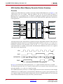
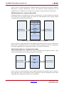
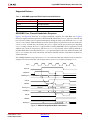
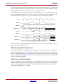
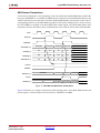
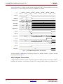
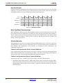
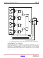
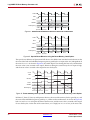
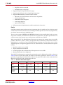
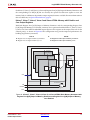
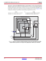
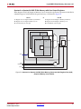
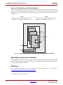
No Change Mode: In NO_CHANGE mode, the output latches remain unchanged during a Write
operation. As shown in Figure 28, the data output is still the previous Read data and is unaffected
by a Write operation on the same port.
X-Ref Target - Figure 28
CLKA
WEA
DINA[15:0]
ADDRA
1111
2222
bb
cc
aa
DOUTA[15:0]
0000
dd
MEM(aa)
MEM(dd)
ENA
DISABLED
WRITE
MEM(bb)=
1111
READ
WRITE
MEM(cc)=
2222
READ
Figure 28: No Change Mode Example
Data Width Aspect Ratios
The Block Memory Generator supports data width aspect ratios. This allows the port A data width to
be different than the port B data width, as described in Port Aspect Ratios in the following section. In
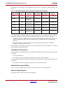
Kintex-7, Virtex-7, Virtex-6, Virtex-5 and Virtex-4 FPGA-based memories, all four data buses (DINA,
DOUTA, DINB, and DOUTB) can have different widths, as described in Kintex-7, Virtex-7, Virtex-6,
Virtex-5 and Virtex-4 Read-to-Write Aspect Ratios, page 28.
The limitations of the data width aspect ratio feature (some of which are imposed by other optional
features) are described in Aspect Ratio Limitations, page 29. The CORE Generator GUI ensures only
valid aspect ratios are selected.
Port Aspect Ratios
The Block Memory Generator supports port aspect ratios of 1:32, 1:16, 1:8, 1:4, 1:2, 1:1, 2:1, 4:1, 8:1, 16:1,
and 32:1. The port A data width can be up to 32 times larger than the port B data width, or vice versa.
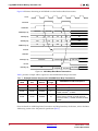
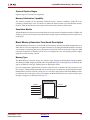
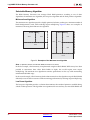
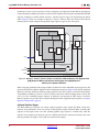
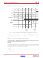
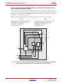
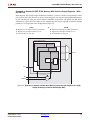
The smaller data words are arranged in little-endian format, as illustrated in Figure 29.
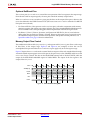
Port Aspect Ratio Example
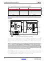
Consider a True Dual-port RAM of 32x2048, which is the A port width and depth. From the perspective
of an 8-bit B port, the depth would be 8192. The ADDRA bus is 11 bits, while the ADDRB bus is 13 bits.
The data is stored little-endian, as shown in Figure 29. Note that An is the data word at address n, with
respect to the A port. Bn is the data word at address n with respect to the B port. A0 is comprised of B3,
B2, B1, and B0.
X-Ref Target - Figure 29
31
A0 =
A1 =
0
7 .. 0
7 .. 0
7 .. 0
7 .. 0
B3
B2
B1
B0
7 .. 0
7 .. 0
7 .. 0
7 .. 0
B7
B6
B5
B4
.
.
.
Figure 29: Port Aspect Ratio Example Memory Map
DS512 March 1, 2011
Product Specification
www.xilinx.com
27