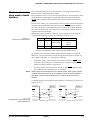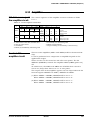
1
MF654-05
CMOS 4-BIT SINGLE CHIP MICROCOMPUTER
S1C62740
Technical Manual
S1C62740 Technical Hardware/S1C62740 Technical Software
NOTICE
No part of this material may be reproduced or duplicated in any form or by any means without the written permission of Seiko
Epson. Seiko Epson reserves the right to make changes to this material without notice. Seiko Epson does not assume any
liability of any kind arising out of any inaccuracies contained in this material or due to its application or use in any product or
circuit and, further, there is no representation that this material is applicable to products requiring high level reliability, such
as medical products. Moreover, no license to any intellectual property rights is granted by implication or otherwise, and there
is no representation or warranty that anything made in accordance with this material will be free from any patent or copyright
infringement of a third party. This material or portions thereof may contain technology or the subject relating to strategic
products under the control of the Foreign Exchange and Foreign Trade Law of Japan and may require an export license from
the Ministry of International Trade and Industry or other approval from another government agency.
© SEIKO EPSON CORPORATION 2001 All rights reserved.
PREFACE
This part explains the function of the S1C62740, the circuit configurations, and
details the controlling method.
II. S1C62740 Technical Software
This part explains the programming method of the S1C62740.
Software
I. S1C62740 Technical Hardware
Hardware
This manual is individualy described about the hardware and the software of the
S1C62740.
white
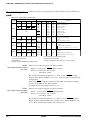
The information of the product number change
Starting April 1, 2001, the product number will be changed as listed below. To order from April 1,
2001 please use the new product number. For further information, please contact Epson sales
representative.
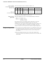
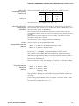
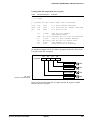
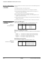
Configuration of product number
Devices
S1
C
60N01
F
0A01
00
Packing specification
Specification
Package (D: die form; F: QFP)
Model number
Model name (C: microcomputer, digital products)
Product classification (S1: semiconductor)
Development tools
C
60R08
S5U1
D1
1
00
Packing specification
Version (1: Version 1 ∗2)
Tool type (D1: Development Tool ∗1)
Corresponding model number (60R08: for S1C60R08)
Tool classification (C: microcomputer use)
Product classification
(S5U1: development tool for semiconductor products)
∗1: For details about tool types, see the tables below. (In some manuals, tool types are represented by one digit.)
∗2: Actual versions are not written in the manuals.
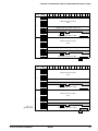
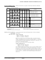
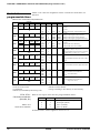
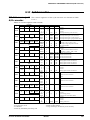
Comparison table between new and previous number
S1C60 Family processors
Previous No.
E0C6001
E0C6002
E0C6003
E0C6004
E0C6005
E0C6006
E0C6007
E0C6008
E0C6009
E0C6011
E0C6013
E0C6014
E0C60R08
New No.
S1C60N01
S1C60N02
S1C60N03
S1C60N04
S1C60N05
S1C60N06
S1C60N07
S1C60N08
S1C60N09
S1C60N11
S1C60N13
S1C60140
S1C60R08
S1C62 Family processors
Previous No.
E0C621A
E0C6215
E0C621C
E0C6S27
E0C6S37
E0C623A
E0C623E
E0C6S32
E0C6233
E0C6235
E0C623B
E0C6244
E0C624A
E0C6S46
New No.
S1C621A0
S1C62150
S1C621C0
S1C6S2N7
S1C6S3N7
S1C6N3A0
S1C6N3E0
S1C6S3N2
S1C62N33
S1C62N35
S1C6N3B0
S1C62440
S1C624A0
S1C6S460
Previous No.
E0C6247
E0C6248
E0C6S48
E0C624C
E0C6251
E0C6256
E0C6292
E0C6262
E0C6266
E0C6274
E0C6281
E0C6282
E0C62M2
E0C62T3
New No.
S1C62470
S1C62480
S1C6S480
S1C624C0
S1C62N51
S1C62560
S1C62920
S1C62N62
S1C62660
S1C62740
S1C62N81
S1C62N82
S1C62M20
S1C62T30
Comparison table between new and previous number of development tools
Development tools for the S1C60/62 Family
Previous No.
ASM62
DEV6001
DEV6002
DEV6003
DEV6004
DEV6005
DEV6006
DEV6007
DEV6008
DEV6009
DEV6011
DEV60R08
DEV621A
DEV621C
DEV623B
DEV6244
DEV624A
DEV624C
DEV6248
DEV6247
New No.
S5U1C62000A
S5U1C60N01D
S5U1C60N02D
S5U1C60N03D
S5U1C60N04D
S5U1C60N05D
S5U1C60N06D
S5U1C60N07D
S5U1C60N08D
S5U1C60N09D
S5U1C60N11D
S5U1C60R08D
S5U1C621A0D
S5U1C621C0D
S5U1C623B0D
S5U1C62440D
S5U1C624A0D
S5U1C624C0D
S5U1C62480D
S5U1C62470D
Previous No.
DEV6262
DEV6266
DEV6274
DEV6292
DEV62M2
DEV6233
DEV6235
DEV6251
DEV6256
DEV6281
DEV6282
DEV6S27
DEV6S32
DEV6S37
EVA6008
EVA6011
EVA621AR
EVA621C
EVA6237
EVA623A
New No.
S5U1C62620D
S5U1C62660D
S5U1C62740D
S5U1C62920D
S5U1C62M20D
S5U1C62N33D
S5U1C62N35D
S5U1C62N51D
S5U1C62560D
S5U1C62N81D
S5U1C62N82D
S5U1C6S2N7D
S5U1C6S3N2D
S5U1C6S3N7D
S5U1C60N08E
S5U1C60N11E
S5U1C621A0E2
S5U1C621C0E
S5U1C62N37E
S5U1C623A0E
Previous No.
EVA623B
EVA623E
EVA6247
EVA6248
EVA6251R
EVA6256
EVA6262
EVA6266
EVA6274
EVA6281
EVA6282
EVA62M1
EVA62T3
EVA6S27
EVA6S32R
ICE62R
KIT6003
KIT6004
KIT6007
New No.
S5U1C623B0E
S5U1C623E0E
S5U1C62470E
S5U1C62480E
S5U1C62N51E1
S5U1C62N56E
S5U1C62620E
S5U1C62660E
S5U1C62740E
S5U1C62N81E
S5U1C62N82E
S5U1C62M10E
S5U1C62T30E
S5U1C6S2N7E
S5U1C6S3N2E2
S5U1C62000H
S5U1C60N03K
S5U1C60N04K
S5U1C60N07K
Hardware
I.
S1C62740
Technical Hardware
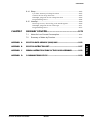
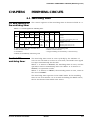
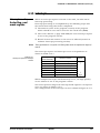
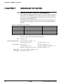
CONTENTS
CONTENTS
CHAPTER 2
OVERVIEW ....................................................................... I-1
1.1
Features .................................................................................... I-2
1.2
Block Diagram ........................................................................... I-3
1.3
Pin Layout Diagram ................................................................... I-4
1.4
Pin Description .......................................................................... I-6
Hardware
CHAPTER 1
POWER SUPPLY AND INITIAL RESET ................................ I-7
2.1
Power Supply ............................................................................ I-7
Voltage <VD1> for oscillation circuit and internal circuit ....... I-8
Voltage <VC1, VC2 and VC3> for LCD driving ......................... I-8
Reference voltage <VR1 and VR2> for A/D converter .............. I-8
Reference voltage <GND> for analog circuit .......................... I-9
2.2
Initial Reset ............................................................................... I-9
Reset terminal (RESET) ....................................................... I-10
Simultaneous low input to terminals K00–K03 .................... I-10
Watchdog timer ................................................................... I-11
Internal register at initial resetting ...................................... I-11
2.3
CHAPTER 3
CHAPTER 4
Test Terminals (TEST and CO) ............................................... I-11
CPU, ROM, RAM ............................................................ I-12
3.1
CPU .......................................................................................... I-12
3.2
ROM ......................................................................................... I-12
3.3
RAM ......................................................................................... I-13
PERIPHERAL CIRCUITS AND OPERATION ...................... I-14
4.1
Memory Map ............................................................................ I-14
4.2
Resetting Watchdog Timer ....................................................... I-20
Configuration of watchdog timer .......................................... I-20
Control of watchdog timer ................................................... I-21
Programming note ............................................................... I-21
4.3
Oscillation Circuit ..................................................................... I-22
Configuration of oscillation circuit ....................................... I-22
OSC1 oscillation circuit ....................................................... I-22
OSC3 oscillation circuit ....................................................... I-23
Control of oscillation circuit ................................................ I-24
Clock frequency and instruction execution time .................. I-25
Programming notes ............................................................. I-25
S1C62740 TECHNICAL HARDWARE
EPSON
I-i
CONTENTS
4.4
Input Ports (K00–K03, K10) ..................................................... I-26
Configuration of input ports ................................................ I-26
Interrupt function ............................................................... I-27
Mask option ........................................................................ I-29
Control of input ports .......................................................... I-30
Programming notes ............................................................. I-32
4.5
Output Ports (R00–R03) .......................................................... I-33
Configuration of output ports .............................................. I-33
Mask option ........................................................................ I-33
Special output ..................................................................... I-33
Control of output ports ........................................................ I-36
Programming note ............................................................... I-38
4.6
I/O Ports (P00–P03, P10–P13, P20–P23) ............................... I-39
Configuration of I/O ports ................................................... I-39
I/O control registers and input/output mode ...................... I-40
Pull up during input mode .................................................. I-40
Mask option ........................................................................ I-40
Control of I/O ports ............................................................ I-41
Programming note ............................................................... I-43
4.7
LCD Driver (COM0–COM3, SEG0–SEG31) ............................ I-44
Configuration of LCD driver ................................................. I-44
LCD display ON/OFF control and duty switching ................ I-47
Mask option (segment allocation) ......................................... I-48
Control of LCD driver .......................................................... I-49
Programming notes ............................................................. I-50
4.8
Clock Timer .............................................................................. I-51
Configuration of clock timer ................................................ I-51
Data reading and hold function ........................................... I-51
Interrupt function ............................................................... I-52
Control of clock timer .......................................................... I-53
Programming notes ............................................................. I-55
4.9
Stopwatch Timer ...................................................................... I-56
Configuration of stopwatch timer ........................................ I-56
Count-up pattern ................................................................ I-57
Interrupt function ............................................................... I-58
Control of stopwatch timer .................................................. I-59
Programming notes ............................................................. I-61
4.10 Programmable Timer ............................................................... I-62
Configuration of programmable timer .................................. I-62
Input clock and pre-divider ................................................. I-62
Operation of programmable timer ........................................ I-63
Interrupt function ............................................................... I-65
Control of programmable timer ............................................ I-66
Programming notes ............................................................. I-69
4.11 Serial Interface (SIN, SOUT, SCLK, SRDY) ............................ I-70
Configuration of serial interface ........................................... I-70
Master mode and slave mode of serial interface ................... I-71
I-ii
EPSON
S1C62740 TECHNICAL HARDWARE
CONTENTS
Data input/output and interrupt function ........................... I-72
Mask option ........................................................................ I-74
Control of serial interface .................................................... I-75
Programming notes ............................................................. I-79
Configuration of A/D converter ........................................... I-80
Measured input terminal and measurement items ............... I-81
Reference voltage generation circuit .................................... I-84
Middle electric potential (GND) generation circuit ................ I-86
Operation of the dual slope type A/D converter ................... I-87
A/D conversion and interrupt ............................................. I-92
Control of the A/D converter ............................................... I-96
Programming notes ............................................................ I-100
4.13 General-purpose Operation Amplifier (AMP) .......................... I-101
Configuration of AMP circuit .............................................. I-101
Operation of AMP circuit .................................................... I-101
Control of AMP circuit ........................................................ I-102
Programming notes ............................................................ I-102
4.14 SVD (Supply Voltage Detection) Circuit .................................. I-103
Configuration of SVD circuit ............................................... I-103
SVD operation .................................................................... I-103
Control of SVD circuit ........................................................ I-104
Programming notes ............................................................ I-105
4.15 Interrupt and HALT/SLEEP ..................................................... I-106
Interrupt factor .................................................................. I-108
Interrupt mask ................................................................... I-109
Interrupt vector .................................................................. I-110
Control of interrupt ............................................................ I-111
Programming notes ............................................................ I-113
CHAPTER 5
SUMMARY OF NOTES .................................................... I-114
5.1
Notes for Low Current Consumption ....................................... I-114
5.2
Summary of Notes by Function ............................................... I-115
CHAPTER 6
DIAGRAM OF BASIC EXTERNAL CONNECTIONS ........ I-119
CHAPTER 7
ELECTRICAL CHARACTERISTICS ................................... I-121
7.1
Absolute Maximum Rating ...................................................... I-121
7.2
Recommended Operating Conditions ..................................... I-121
7.3
DC Characteristics .................................................................. I-122
7.4
Analog Characteristics and Consumed Current ...................... I-123
7.5
Oscillation Characteristics ....................................................... I-129
S1C62740 TECHNICAL HARDWARE
EPSON
I-iii
Hardware
4.12 A/D Converter .......................................................................... I-80
CONTENTS
CHAPTER 8
CHAPTER 9
I-iv
PACKAGE ..................................................................... I-130
8.1
Plastic Package ....................................................................... I-130
8.2
Ceramic Package for Test Samples ........................................ I-132
PAD LAYOUT ................................................................. I-133
9.1
Diagram of Pad Layout ........................................................... I-133
9.2
Pad Coordinates ..................................................................... I-134
EPSON
S1C62740 TECHNICAL HARDWARE
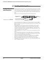
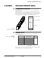
CHAPTER 1: OVERVIEW
CHAPTER 1
OVERVIEW
The S1C62740 is a single-chip microcomputer made up of the 4-bit
core CPU S1C6200A, ROM (4,096 words, 12 bits to a word), RAM
(512 words, 4 bits to a word) LCD driver, dual slope type A/D
converter, general purpose operational amplifier, serial interface,
watchdog timer, programmable timer and time base counter.
Because of its low-voltage operation and low power consumption,
this series is ideal for a wide range of applications, and is especially
suitable for battery-driven systems.
S1C62740 TECHNICAL HARDWARE
EPSON
I-1
CHAPTER 1: OVERVIEW
1.1 Features
OSC1 oscillation circuit ....
OSC3 oscillation circuit ....
Instruction set ....
Instruction execution time ....
(differ depending on instruction)
ROM capacity ....
RAM capacity ....
Input port ....
Output port ....
I/O port ....
Serial interface ....
A/D converter ....
Crystal oscillation circuit: 32,768 Hz (Typ.)
CR or ceramic oscillation circuit (*1): 1 MHz (Typ.)
109 types
During operation at 32 kHz: 153 µsec, 214 µsec, 366 µsec
During operation at 1 MHz: 5 µsec, 7 µsec, 12 µsec
4,096 words × 12 bits
512 words × 4 bits
5 bits (pull up resistors may be supplemented *1)
4 bits (buzzer and clock outputs are possible *2)
12 bits (4 bits may be selected for serial input/output port *2)
1 port (8 bits serial, synchronous clock type)
Dual slope type (operating temperature range: 0°C to 50°C)
Resolution/Conversion time: 4 types, programmable (*3)
6,400 counts / 500 msec 3,200 counts / 250 msec
1,600 counts / 125 msec 800 counts / 62.5 msec
A/D conversion precision: ±0.2% (6,400 couns, voltage measuremant mode)
Measurement item: Voltage/Difference voltage/Resistance, programmable
Analog input: 5 terminals
Reference voltage generation circuit built-in
Middle electric potential (GND) generation circuit built-in
LCD driver .... 32 segments × 4 / 3 / 2 / 1 commons (*2)
Regulated voltage circuit and booster voltage circuit built-in
(compatible with 3–4.5 V LCD, VR adjustable)
Time base counter .... 2 systems (clock timer and stopwatch)
Watchdog timer .... Built-in
Programmable timer .... Built-in, with 1 input × 8 bits event counter function
AMP (general-purpose operational amplifier)
.... MOS input operational amplifier × 2
SVD (supply voltage detection) circuit .... 2.3 / 2.4 / 2.5 / 2.6 V, programmable (±100 mV)
External interrupt .... Input port interrupt:
2 systems
Internal interrupt .... Timer interrupt:
3 systems
Serial interface interrupt: 1 system
A/D interrupt:
1 system
Supply voltage .... During A/D operation:
2.4–5.5 V
During A/D stop:
2.2–5.5 V
Current consumption (Typ.) .... During SLEEP:
0.7 µA (3 V, stop oscillation)
During HALT:
2.0 µA (3 V, 32 kHz)
During operation:
6.0 µA (3 V, 32 kHz)
200 µA(3 V, 1 MHz)
During A/D operation:
306 µA(3 V, 32 kHz)
506 µA(3 V, 32 kHz, AMP circuit is ON status)
Package .... QFP5-100pin / QFP15-100pin (plastic) or chip
*1 May be selected with mask option.
*2 May be selected with software.
*3 It is necessary to modify external parts.
I-2
EPSON
S1C62740 TECHNICAL HARDWARE
CHAPTER 1: OVERVIEW
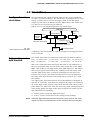
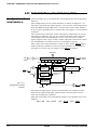
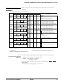
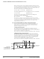
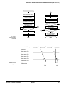
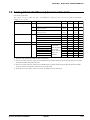
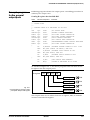
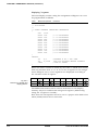
1.2 Block Diagram
S1C62740 BLOCK DIAGRAM
OSC1
OSC2
OSC3
OSC4
CORE CPU S1C6200A
ROM
4,096 x 12
OSC
and
SLEEP
SYSTEM
RESET
CONTROL
RAM
512 x 4
COM0–
COM3
SEG0–
SEG31
V DD
V CA
V C1
V C2
V C3
CA
CB
CC
V D1
V SS
AIP0, 1
AIM0, 1
AOUT0, 1
V DDA
V RA
V R1
V R2
CH
CL
GND
V SSA
Fig. 1.2.1
Block diagram
AI0
AI1
AI2
AI3
AI4
AIF
BF
RI
CI
CAZ
CO
S1C62740 TECHNICAL HARDWARE
RESET
TEST
INTERRUPT
CONTROL
LCD
DRIVER
32 x 4
TIMER
STOP
WATCH
LOGIC
POWER
CONTROL
and SVD
PROG.
TIMER or
EVENT
COUNTER
OP-AMP
ANALOG
POWER
CONTROL
INPUT
PORT
K00–K03
K10
OUTPUT
PORT
R00–R03
FOUT &
BUZZER
I/O
PORT
A/D
CONVERTER
P00–P03
P10–P13
P20–P23
SERIAL
I/O PORT
EPSON
I-3
CHAPTER 1: OVERVIEW
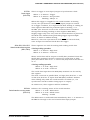
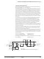
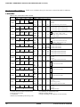
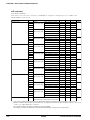
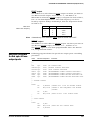
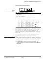
1.3 Pin Layout Diagram
QFP5-100pin
80
51
81
50
Index
100
31
1
30
Pin No. Pin Name Pin No. Pin Name Pin No. Pin Name Pin No. Pin Name
Fig. 1.3.1
Pin layout diagram (QFP5-100pin)
I-4
1
2
3
4
5
6
7
8
9
10
11
12
13
14
15
16
K02
K01
K00
N.C.
N.C.
VSS
OSC1
OSC2
OSC3
OSC4
VDD
R03
R02
R01
R00
P00
26
27
28
29
30
31
32
33
34
35
36
37
38
39
40
41
P22
P23
RESET
TEST
CC
CB
CA
VC3
VC2
VC1
VCA
COM3
COM2
COM1
COM0
SEG0
51
52
53
54
55
56
57
58
59
60
61
62
63
64
65
66
SEG10
SEG11
SEG12
SEG13
SEG14
SEG15
SEG16
SEG17
SEG18
SEG19
SEG20
SEG21
SEG22
SEG23
SEG24
SEG25
76
77
78
79
80
81
82
83
84
85
86
87
88
89
90
91
AI3
AI2
VSSA
AI1
AI0
CI
CAZ
BF
RI
CH
CL
GND
VDDA
AOUT0
AIP0
AIM0
17
18
19
20
21
P01
P02
P03
P10
P11
42
43
44
45
46
SEG1
SEG2
SEG3
SEG4
SEG5
67
68
69
70
71
SEG26
SEG27
SEG28
SEG29
SEG30
92
93
94
95
96
AIP1
AIM1
AOUT1
VR1
VR2
22
23
24
P12
P13
P20
47
48
49
SEG6
SEG7
SEG8
72
73
74
SEG31
CO
AIF
97
98
99
VRA
VD1
K10
25
P21
50
SEG9
75
AI4
100
K03
N.C. = No Connection
EPSON
S1C62740 TECHNICAL HARDWARE
CHAPTER 1: OVERVIEW
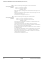
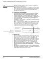
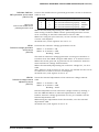
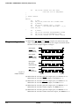
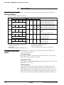
QFP15-100pin
75
51
76
50
Index
100
26
1
25
Pin No. Pin Name Pin No. Pin Name Pin No. Pin Name Pin No. Pin Name
Fig. 1.3.2
Pin layout diagram (QFP15-100pin)
S1C62740 TECHNICAL HARDWARE
1
2
3
4
5
6
7
8
9
10
11
12
13
14
15
16
K00
N.C.
N.C.
VSS
OSC1
OSC2
OSC3
OSC4
VDD
R03
R02
R01
R00
P00
P01
P02
26
27
28
29
30
31
32
33
34
35
36
37
38
39
40
41
RESET
TEST
CC
CB
CA
VC3
VC2
VC1
VCA
COM3
COM2
COM1
COM0
SEG0
SEG1
SEG2
51
52
53
54
55
56
57
58
59
60
61
62
63
64
65
66
SEG12
SEG13
SEG14
SEG15
SEG16
SEG17
SEG18
SEG19
SEG20
SEG21
SEG22
SEG23
SEG24
SEG25
SEG26
SEG27
76
77
78
79
80
81
82
83
84
85
86
87
88
89
90
91
VSSA
AI1
AI0
CI
CAZ
BF
RI
CH
CL
GND
VDDA
AOUT0
AIP0
AIM0
AIP1
AIM1
17
18
19
20
21
P03
P10
P11
P12
P13
42
43
44
45
46
SEG3
SEG4
SEG5
SEG6
SEG7
67
68
69
70
71
SEG28
SEG29
SEG30
SEG31
CO
92
93
94
95
96
AOUT1
VR1
VR2
VRA
VD1
22
23
24
P20
P21
P22
47
48
49
SEG8
SEG9
SEG10
72
73
74
AIF
AI4
AI3
97
98
99
K10
K03
K02
25
P23
50
SEG11
75
AI2
100
K01
N.C. = No Connection
EPSON
I-5
CHAPTER 1: OVERVIEW
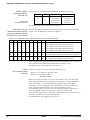
1.4 Pin Description
Pin name
VDD
VSS
VDDA
VSSA
GND
VD1
VC1
VC2
VC3
VCA
CA–CC
OSC1
OSC2
OSC3
OSC4
K00–10
P00–13
P20–23
R00–03
COM0–3
SEG0–31
AI0–4
AIF
CAZ
CI
RI
BF
CO
CH
CL
VR1
VR2
VRA
AIP0
AIM0
AOUT0
AIP1
AIM1
AOUT1
RESET
TEST
I-6
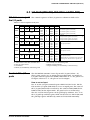
Table 1.4.1 Pin description
Pin No.
In/Out
QFP5-100pin
QFP15-100pin
11
6
88
78
87
98
35
34
33
36
32–30
7
8
9
10
3–1, 100, 99
16–23
24–27
15–12
40–37
41–72
80, 79, 77–75
74
82
81
84
83
73
85
86
95
96
97
90
91
89
92
93
94
28
29
9
4
86
76
85
96
33
32
31
34
30–28
5
6
7
8
1, 100–97
14–21
22–25
13–10
38–35
39–70
78, 77, 75–73
72
80
79
82
81
71
83
84
93
94
95
88
89
87
90
91
92
26
27
(I)
(I)
(I)
(I)
(I/O)
–
–
–
–
–
–
I
O
I
O
I
I/O
I/O
O
O
O
I
–
–
–
–
–
–
–
–
(I)
(I)
–
I
I
O
I
I
O
I
I
Function
Power (+)
Power (-)
Analog system power (+)
Analog system power (-)
Analog system ground
Internal logic system regulated voltage output
LCD system regulated voltage output
LCD system booster voltage output (VC1 × 2)
LCD system booster voltage output (VC1 × 3)
LCD system voltage adjustment pin
LCD system voltage booster condenser connecting pin
Crystal oscillator input
Crystal oscillator output
Ceramic or CR oscillator input (selected by mask option)
Ceramic or CR oscillator output (selected by mask option)
Input port
I/O port
I/O port or serial interface I/O pin (selected by software)
Output port (buzzer and clock outputs are selected by software)
LCD common output (1/4, 1/3, 1/2, 1/1 duty, programmable)
LCD segment output (DC output is selected by mask option)
Analog input
Analog input filter condenser connecting pin
Auto zero adjustment condenser connecting pin
Integral condenser connecting pin
Integral resistance connecting pin
Buffer amplifier output
Testing output pin
Reference voltage control condenser connecting pin
Reference voltage control condenser connecting pin
Reference voltage for resistance measurement
Reference voltage for voltage measurement
Reference voltage adjustment pin
AMP 0 non inverted input
AMP 0 inverted input
AMP 0 output
AMP 1 non inverted input
AMP 1 inverted input
AMP 1 output
System reset input pin
Testing input pin
EPSON
S1C62740 TECHNICAL HARDWARE
CHAPTER 2: POWER SUPPLY AND INITIAL RESET
CHAPTER 2
POWER SUPPLY AND INITIAL RESET
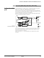
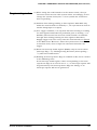
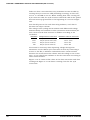
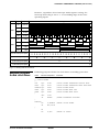
2.1 Power Supply
With a single external power supply (3 V *1) supplied to VDD/VDDA
through VSS/VSSA, the S1C62740 generates the necessary internal
voltage with the regulated voltage circuit (<VD1> for oscillators,
<VC1> for LCDs), the voltage booster circuit (<VC2, VC3> for LCDs)
and the voltage dividing circuit (<GND> ≈ VDDA/2, reference voltage
for analog circuit).
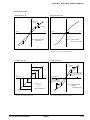
Figure 2.1.1 shows the configuration of power supply.
*1 Supply voltage: During A/D operation
During A/D stop
…2.4 to 5.5 V
…2.2 to 5.5 V
Note: • External loads cannot be driven by the regulated voltage and voltage
booster circuit's output voltage.
• See Chapter 7, "ELECTRICAL CHARACTERISTICS" for voltage values.
V DD
V DDA
V D1
VD1
Oscillation system
regulated voltage circuit
Internal
circuit
Oscillation
circuit
OSC1–4
V CA
V C1
V C2
V C3
CA
CB
CC
External
power
supply
GND
V R1
V R2
V RA
CH
CL
LCD system
regulated voltage circuit
V C1
V C1
LCD system
voltage booster circuit
V C2
V C3
COM0–3
LCD
driver
Analog system
voltage dividing circuit
SEG0–31
GND
GND
Analog system
reference voltage
generation circuit
VR
-VR
A/D
converter
AI0–4
V SSA
V SS
• An external voltage can be impressed
to the GND terminal.
• Open VRA terminal when VR1 is
impressed from the outside.
• Remove resistors between VR1–VRA
and between GND–VRA when VR1 is
Fig. 2.1.1
impressed from outside.
Configuration of power supply
S1C62740 TECHNICAL HARDWARE
EPSON
V DD /V DDA
V D1
GND
V C1
V R2
V SS /V SSA
V R1
I-7
CHAPTER 2: POWER SUPPLY AND INITIAL RESET
Voltage <VD1> for
oscillation circuit
and internal circuit
VD1 is the voltage of the oscillation circuit and the internal logic
circuit, and is generated by the oscillation system regulated voltage
circuit for stabilizing the oscillation.
Making VSS the standard (logic level 0), the oscillation system
regulated voltage circuit generates VD1 from the supply voltage that
is input from the VDD–VSS terminals.
Voltage <VC1, VC2
and VC3> for LCD
driving
VC1, VC2 and VC3 are the voltages for LCD drive, and are generated
by the LCD system regulated voltage circuit and the voltage booster
circuit to stabilize the display quality.
VC1 is generated by the LCD system regulated voltage circuit with
VSS as the standard from the supply voltage input from the VDD–
VSS terminals.
VC2 and VC3 are respectively double and triple obtained from the
voltage booster circuit.
The VC1 voltage can be adjusted to match the LCD panel characteristics by applying feedback to the VCA terminal using resistances
RA1 and RA2 as shown in Figure 2.1.2.
The voltage VC (≈VC1–VSS) of VC1 at this time is shown by the
following expression:
VC ≈ 1 × (RA1 + RA2) / RA1
Example:
VC
RA1
About 1 V
About 1.5 V
∞
2M
RA2
0Ω
1 MΩ
VC1
RA2
(1 M Ω)
VC1
VCA
–
RA1
(2 M Ω)
Reference voltage
<VR1 and VR2> for
A/D converter
I-8
VCA
–
+
VSS
Fig. 2.1.2
VC Adjustment circuit
See Chapter 7, "ELECTRICAL CHARACTERISTICS" for voltage values.
VSS
VC = 1.5 V
+
VSS
VC = 1 V
VR1 and VR2 are the reference voltage of the A/D converter. VR1 is
generated by the regulated voltage circuit and VR2 by resistance
splitting of VR1. VR1 and VR2 may also be adjusted from outside.
Use of the external adjustment or the internal adjustment can be
selected by the mask option. In addition, it is possible to impress
VR1 externally.
VR1 is used to generate VR2 and the reference voltage during
resistance measurement using an A/D converter and VR2 becomes
the reference voltage at the time of voltage measurement by the A/
D converter.
EPSON
S1C62740 TECHNICAL HARDWARE
CHAPTER 2: POWER SUPPLY AND INITIAL RESET
The GND (ground) explained here following becomes the standard
for both VR1 and VR2 and becomes the electric potential of the VSS
side.
Refer to the section "A/D Converter" for details such as circuit
configuration.
Note: Since the built-in reference voltage generation circuit is under development, the reference voltage should be impressed from outside.
Reference voltage
<GND> for analog
circuit
Since GND becomes the standard for the analog input voltage that
performs the A/D conversion, inside the circuit it is obtained by
voltage dividing the power voltage impressed between the VDDA–
VSSA terminals to about 1/2 by means of a resistance.
In addition, the GND (ground) level can also be impressed externally.
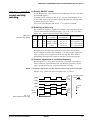
2.2 Initial Reset
To initialize the S1C62740 circuits, initial reset must be executed.
There are three ways of doing this.
(1) External initial reset by the RESET terminal
(2) External initial reset by simultaneous low input to terminals K00–K03
(3) Initial reset by watchdog timer
Be sure to use reset functions (1) when making the power and be
sure to initialize securely. In normal operation, the circuit may be
initialized by any of the above three types.
Figure 2.2.1 shows the configuration of the initial reset circuit.
OSC1
OSC2
OSC1
oscillation
circuit
Clock timer
Watchdog timer
VDD
SLEEP
(In SLEEP mode: HIGH)
K00
K01
Mask option
Time
authorize
circuit
K02
Initial
reset
Noise
reject
circuit
K03
VDD
RESET
Fig. 2.2.1
Configuration of the
initial reset circuit
S1C62740 TECHNICAL HARDWARE
EPSON
I-9
CHAPTER 2: POWER SUPPLY AND INITIAL RESET
Reset terminal
(RESET)
Initial reset can be executed externally by setting the reset terminal
to the low level.
Maintain a low level of 0.1 msec to securely perform the initial reset.
When the reset terminal goes high, the CPU begins to operate.
However, when turning the power on, the reset terminal should be
set at a low level as in the timing shown in Figure 2.2.2.
2.2 V
VDD
2.0 msec or more
RESET
Fig. 2.2.2
Initial reset at power on
0.4•VDD
0.1•VDD or less (low level)
Power on
The reset terminal should be set to 0.1·VDD or less (low level) until
the supply voltage becomes 2.2 V or more.
After that, a level of 0.4·VDD or less should be maintained more
than 2.0 msec.
Simultaneous low
input to terminals
K00–K03
Table 2.2.1
Combinations of input ports
Another way of executing initial reset externally is to input a low
signal simultaneously to the input ports (K00–K03) selected with
the mask option.
Since this initial reset signal passes through the noise reject
circuit, simultaneous low input of 0.4 msec or less is considered as
noise. Maintain the specified input port terminals at a low level of
1.5 msec (when the oscillation frequency fOSC1 = 32 kHz) to securely perform the initial reset.
Table 2.2.1 shows the combinations of input ports (K00–K03) that
can be selected with the mask option.
A
B
C
D
Not use
K00*K01
K00*K01*K02
K00*K01*K02*K03
When, for instance, mask option D (K00*K01*K02*K03) is selected,
initial reset is executed when the signals input to the four ports
K00–K03 are all low at the same time. The initial reset is done,
even when a key entry including a combination of selected input
ports is made.
Further, the time authorize circuit can be selected with the mask
option. The time authorize circuit performs initial reset, when the
input time of the simultaneous low input is authorized and found
to be the same or more than the defined time (1 to 2 sec). Since
clock timer output is used for time authorization, when the clock
timer is reset during time authorization, the authorization time is
also reduced. (The shortest is 0.5 msec due to the noise reject
circuit.)
In the SLEEP status, the noise reject circuit and the time authorize
circuit are bypassed since the OSC1 oscillation circuit is off.
I-10
EPSON
S1C62740 TECHNICAL HARDWARE
CHAPTER 2: POWER SUPPLY AND INITIAL RESET
If you use this function, make sure that the specified ports do not
go low at the same time during ordinary operation.
Furthermore, do not perform an initial reset when turning the
power on by this function.
Watchdog timer
If the CPU runs away for some reason, the watchdog timer will
detect this situation and output an initial reset signal. See Section
4.2, "Resetting Watchdog Timer" for details.
Furthermore, do not perform an initial reset when turning the
power on by this function.
Internal register at
initial resetting
Initial reset initializes the CPU as shown in the table below.
Table 2.2.2
Initial values
CPU Core
Symbol Number of bits Setting value
Name
Program counter step
Program counter page
New page pointer
Stack pointer
Index register IX
Index register IY
Rejister pointer
General-purpose register A
General-purpose register B
Interrupt flag
Decimal flag
Zero flag
Carry flag
PCS
PCP
NPP
SP
IX
IY
RP
A
B
I
D
Z
C
8
4
4
8
10
10
4
4
4
1
1
1
1
00H
1H
1H
Undefined
Undefined
Undefined
Undefined
Undefined
Undefined
0
0
Undefined
Undefined
Peripheral circuits
Name
Number of bits
4
4
RAM
Display memory
Other peripheral circuit
–
Setting value
Undefined
Undefined *2
*1
*1 See Section 4.1, "Memory Map".
*2 Bits corresponding to COM0 is set to 1.
2.3 Test Terminals (TEST and CO)
This is the terminal that is used at the time of the factory inspection of the IC. During normal operation, connect the TEST to VDD
and make the CO an N.C. (no connection).
S1C62740 TECHNICAL HARDWARE
EPSON
I-11
CHAPTER 3: CPU, ROM, RAM
CHAPTER 3
CPU, ROM, RAM
3.1 CPU
The S1C62740 employs the 4-bit core CPU S1C6200A for the CPU,
so that register configuration, instructions and so forth are virtually identical to those in other family processors using the
S1C6200A.
Refer to "S1C6200/6200A Core CPU Manual" for details about the
S1C6200A.
Note the following points with regard to the S1C62740:
(1) Because the ROM capacity is 4,096 words, bank bits are unnecessary and PCB and NBP are not used.
(2) RAM is set up to three pages, so only the two low-order bits are
valid for the page portion (XP, YP) of the index register that
specifies addresses. (The two high-order bits are ignored.)
3.2 ROM
The built-in ROM, a mask ROM for loading the program, has a
capacity of 4,096 steps, 12 bits each. The program area is 16 pages
(0–15), each of 256 steps (00H–FFH). After initial reset, the program beginning address is page 1, step 00H. The interrupt vector is
allocated to page 1, steps 02H–0FH.
0 page
1 page
2 page
3 page
4 page
5 page
6 page
7 page
8 page
9 page
10 page
11 page
12 page
13 page
14 page
15 page
Program start address
02H step
Interrupt vector address
0FH step
10H step
Program area
FFH step
12 bits
Fig. 3.2.1
ROM configuration
I-12
00H step
01H step
EPSON
S1C62740 TECHNICAL HARDWARE
CHAPTER 3: CPU, ROM, RAM
3.3 RAM
The RAM, a data memory storing a variety of data, has a capacity
of 512 words, each of four bits. When programming, keep the
following points in mind.
(1) Part of the data memory can be used as stack area when
subroutine calls and saving registers, so be careful not to
overlap the data area and stack area.
(2) Subroutine calls and interrupts take up three words of the
stack area.
(3) The data memory 000H–00FH is for the register pointers (RP),
and is the addressable memory register area.
S1C62740 TECHNICAL HARDWARE
EPSON
I-13
CHAPTER 4: PERIPHERAL CIRCUITS AND OPERATION (Memory Map)
CHAPTER 4
PERIPHERAL CIRCUITS AND
OPERATION
Peripheral circuits (timer, I/O, and so on) of the S1C62740 are
memory mapped, and interfaced with the CPU. Thus, all the
peripheral circuits can be controlled by using the memory operation command to access the I/O memory in the memory map.
The following sections describe how the peripheral circuits operation.
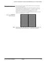
4.1 Memory Map
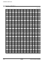
Data memory of the S1C62740 has an address space of 600 words,
of which 32 words are allocated to display memory and 56 words to
I/O memory.
Figure 4.1.1 present the overall memory maps of the S1C62740,
and Tables 4.1.1(a)–(d) the peripheral circuits' (I/O space) memory
maps.
In the S1C62740 the same I/O memory has been laid out for each
page C0H–FFH and the same display memory for 80H–9FH. As a
result, the I/O memory and display memory can be accessed
without changing over the data memory page. The same result is
obtained for I/O memory and display memory changes and for
readable/writable address references, no matter on what page it is
done.
Note: Memory is not mounted in unused area within the memory map and in
memory area not indicated in this chapter. For this reason, normal operation cannot be assured for programs that have been prepared with access
to these area.
I-14
EPSON
S1C62740 TECHNICAL HARDWARE
CHAPTER 4: PERIPHERAL CIRCUITS AND OPERATION (Memory Map)
Address
Low
F
0
1
2
3
4
5
6
7
8
9
A
B C D E
Page
High
M0 M1 M2 M3 M4 M5 M6 M7 M8 M9 MA MB MC MD ME MF
0
1
2
3
RAM (128 words x 4 bits)
4
R/W
5
6
7
0
8
Display memory (32 words x 4 bits) W
9
A
Unused area
B
C
D
E
I/O memory (56 words x 4 bits)
F
0
1
2
3
RAM (128 words x 4 bits)
4
R/W
5
6
7
1
8
Display memory (32 words x 4 bits) W
9
A
Unused area
B
C
D
E
I/O memory (56 words x 4 bits)
F
Unused area
Fig. 4.1.1
Memory map
Address
Low
Page
High
0
1
2
3
4
5
6
7
2
8
9
A
B
C
D
E
F
0
1
2
3
4
5
6
7
3
8
9
A
B
C
D
E
F
0
1
2
3
4
5
6
7
8
9
A
B
C
D
E
F
RAM (128 words x 4 bits)
R/W
Display memory (32 words x 4 bits) W
Unused area
I/O memory (56 words x 4 bits)
RAM (128 words x 4 bits)
R/W
Display memory (32 words x 4 bits) W
Unused area
I/O memory (56 words x 4 bits)
Unused area
S1C62740 TECHNICAL HARDWARE
EPSON
I-15
CHAPTER 4: PERIPHERAL CIRCUITS AND OPERATION (Memory Map)
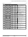
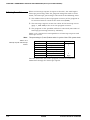
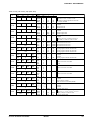
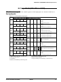
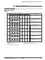
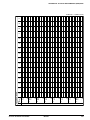
Table 4.1.1(a) I/O memory map (C0H–CCH)
Register
D2
D1
Address
D3
*7
0
0
D0
0
IPT
0
ISIO
0
IK1
0
IK0
0
IAD
ISW1
ISW0
C0H
R
0
0
C1H
R
0
0
C2H
R
0
0
C3H
R
0
0
C4H
R
0
0
C5H
R
IT1
IT8
IT32
EISIO
EIPT
IT2
C6H
R
0
EIAD
C8H
R
R/W
0
0
EIK1
EIK0
C9H
R
SIK03
R/W
SIK02
SIK00
SIK01
CAH
R/W
0
0
EISW1
EISW0
CBH
R/W
R
EIT1
EIT2
EIT8
CCH
R/W
EIT32
Name
0 *5
0 *5
0 *5
IPT *4
0 *5
0 *5
0 *5
ISIO *4
0 *5
0 *5
0 *5
IK1 *4
0 *5
0 *5
0 *5
IK0 *4
0 *5
0 *5
0 *5
IAD *4
0 *5
0 *5
ISW1 *4
ISW0 *4
IT1 *4
IT2 *4
IT8 *4
IT32 *4
0 *5
EIAD
EISIO
EIPT
0 *5
0 *5
EIK1
EIK0
SIK03
SIK02
SIK01
SIK00
0 *5
0 *5
EISW1
EISW0
EIT1
EIT2
EIT8
EIT32
Init *1
– *2
– *2
– *2
0
– *2
– *2
– *2
0
– *2
– *2
– *2
0
– *2
– *2
– *2
0
– *2
– *2
– *2
0
– *2
– *2
0
0
0
0
0
0
– *2
0
0
0
– *2
– *2
0
0
0
0
0
0
– *2
– *2
0
0
0
0
0
0
1
0
Yes
No
Yes
No
Yes
No
Yes
No
Yes
No
Yes
Yes
Yes
Yes
Yes
Yes
No
No
No
No
No
No
Enable
Enable
Enable
Mask
Mask
Mask
Enable
Enable
Enable
Enable
Enable
Enable
Mask
Mask
Disable
Disable
Disable
Disable
Enable
Enable
Enable
Enable
Enable
Enable
Mask
Mask
Mask
Mask
Mask
Mask
Comment
Unused
Unused
Unused
Interrupt factor flag (programmable timer)
Unused
Unused
Unused
Interrupt factor flag (serial interface)
Unused
Unused
Unused
Interrupt factor flag (K10)
Unused
Unused
Unused
Interrupt factor flag (K00–K03)
Unused
Unused
Unused
Interrupt factor flag (A/D converter)
Unused
Unused
Interrupt factor flag (stopwatch 1 Hz)
Interrupt factor flag (stopwatch 10 Hz)
Interrupt factor flag (clock timer 1 Hz)
Interrupt factor flag (clock timer 2 Hz)
Interrupt factor flag (clock timer 8 Hz)
Interrupt factor flag (clock timer 32 Hz)
Unused
Interrupt mask register (A/D converter)
Interrupt mask register (serial interface)
Interrupt mask register (programmable timer)
Unused
Unused
Interrupt mask register (K10)
Interrupt mask register (K00–K03)
Interrupt selection register (K03)
Interrupt selection register (K02)
Interrupt selection register (K01)
Interrupt selection register (K00)
Unused
Unused
Interrupt mask register (stopwatch 1 Hz)
Interrupt mask register (stopwatch 10 Hz)
Interrupt mask register (clock timer 1 Hz)
Interrupt mask register (clock timer 2 Hz)
Interrupt mask register (clock timer 8 Hz)
Interrupt mask register (clock timer 32 Hz)
Remarks
*1 Initial value at the time of initial reset
*2 Not set in the circuit
*3 Undefined
*4 Reset (0) immediately after being read
I-16
*5 Constantly "0" when being read
*6 Refer to main manual
*7 Page switching in I/O memory is not necessary
EPSON
S1C62740 TECHNICAL HARDWARE
CHAPTER 4: PERIPHERAL CIRCUITS AND OPERATION (Memory Map)
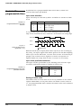
Table 4.1.1(b) I/O memory map (D0H–DFH)
Address
*7
D0H
D1H
D2H
D3H
D4H
D6H
D7H
D8H
D9H
DAH
DBH
DCH
DDH
DEH
DFH
D3
Register
D2
D1
Name
K03
K00
K03
K02
K01
K02
K01
R
K00
0 *5
K10
0
0
0
0 *5
0 *5
R
K10
DFK03
DFK00
DFK03
DFK02
DFK01
DFK02
DFK01
R/W
DFK00
0 *5
DFK10
0
0
0
0 *5
0 *5
R/W
R
DFK10
R03
R00
R03
R02
R01
BZ
R02
FOUT
BZ
BZ
PTOVF
BZ
R01
PTOVF
R/W
R00
FOUT
0 *5
0
IOC2
IOC1
IOC0
IOC2
IOC1
R
R/W
IOC0
0 *5
PUP0
0
PUP2
PUP1
PUP2
PUP1
R
R/W
PUP0
P03
P00
P03
P02
P01
P02
P01
R/W
P00
P13
P10
P13
P12
P11
P12
P11
R/W
P10
P23
P20
P23
P22
P21
P22
P21
R/W
P20
PFS
SDP
SCS0
PFS
SCS1
SDP
SCS1
R/W
SCS0
0 *5
0
0
SCRUN SCTRG
0 *5
SCRUN
R
W
SCTRG *5
SD3
SD0
SD3
SD2
SD1
SD2
SD1
R/W
SD0
SD7
SD4
SD7
SD6
SD5
SD6
SD5
R/W
SD4
0 *5
0
0
CLKCHG OSCC
0 *5
CLKCHG
R
R/W
OSCC
S1C62740 TECHNICAL HARDWARE
D0
Init *1
– *2
– *2
– *2
– *2
– *2
– *2
– *2
– *2
1
1
1
1
– *2
– *2
– *2
1
0
0
1
1
–
0
0
0
–
0
0
0
–
–
–
–
–
–
–
–
–
–
–
–
0
0
0
0
–
–
0
–
–
–
–
–
–
–
–
–
–
–
0
0
1
High
High
High
High
High
0
Low
Low
Low
Low
Low
High
On
High
On
High
Off
High
Off
Low
Off
Low
Off
Low
On
Low
On
Output
Output
Output
Input
Input
Input
*2
*2
*2
*2
*2
*2
*2
*2
*2
*2
*2
*2
On
Off
On
Off
On
Off
High
Low
High
Low
High
Low
High
Low
High
Low
High
Low
High
Low
High
Low
High
Low
High
Low
High
Low
High
Low
Serial I/F I/O port
LSB first MSB first
*2
*2
*2
Input port (K00–K03)
Unused
Unused
Unused
Input port (K10)
Input comparison register (K00–K03)
*2
*2
Comment
Run
Trigger
Stop
–
Unused
Unused
Unused
Input comparison register (K10)
Output port (R03)
Buzzer inverted output
Output port (R02)
Buzzer output
Output port (R01)
PTOVF output
Output port (R00)
FOUT output
Unused
I/O control register 2 (P20–P23)
I/O control register 1 (P10–P13)
I/O control register 0 (P00–P03)
Unused
Pull up control register 2 (P20–P23)
Pull up control register 1 (P10–P13)
Pull up control register 0 (P00–P03)
*6
*6
I/O port (P00–P03)
I/O port (P10–P13)
I/O port (P20–P23)
When P20–P23 is selected as SIO port, P20–
P23 registers will function as register only.
P2 port function selection
Serial data input/output permutation
Serial interface clock mode selection
0: slave, 1: PTOVF, 2: CLK/2, 3: CLK
Unused
Unused
Serial interface status
Serial interface clock trigger
*6
*2
*2
Serial interface data (low-order 4 bits)
*2
LSB
MSB
*2
*2
*2
Serial interface data (high-order 4 bits)
*2
*2
*2
*2
OSC3
On
EPSON
OSC1
Off
Unused
Unused
CPU system clock switch
OSC3 oscillation On/Off
I-17
CHAPTER 4: PERIPHERAL CIRCUITS AND OPERATION (Memory Map)
Table 4.1.1(c) I/O memory map (E0H–EFH)
Register
D2
D1
Address
*7
D3
BZR03
BZR02
D0
0
BZFQ
R
R/W
FOFQ1
FOFQ0
E0H
R/W
FOR00
0
R/W
R
0
0
E1H
R/W
0
TMRST
E2H
R
TM3
W
TM2
TM1
TM0
TM5
TM4
WD1
WD0
E3H
R
TM7
TM6
E4H
R
WDRST
0
E5H
W
R
0
0
SWRUN SWRST
E6H
R/W
W
SWL1
SWL0
R
SWL3
SWL2
E7H
R
SWH3
SWH2
SWH1
SWH0
E8H
R
PTR01
0
PTRUN
PTRST
R/W
R
R/W
W
PTD1
PTD0
PTC1
PTC0
PT1
PT0
E9H
EAH
R/W
PT2
PT3
EBH
R
PT7
PT6
PT5
PT4
ECH
R
RD3
RD2
RD1
RD0
EDH
R/W
RD7
RD6
RD5
RD4
EEH
R/W
LDTY1
LDTY0
0
LCDON
R
R/W
EFH
R/W
I-18
Name
BZR03
BZR02
0 *5
BZFQ
FOR00
0 *5
FOFQ1
FOFQ0
0 *5
0 *5
0 *5
TMRST *5
TM3
TM2
TM1
TM0
TM7
TM6
TM5
TM4
WDRST*5
0 *5
WD1
WD0
0 *5
0 *5
SWRUN
SWRST *5
SWL3
SWL2
SWL1
SWL0
SWH3
SWH2
SWH1
SWH0
PTR01
0 *5
PTRUN
PTRST *5
PTD1
PTD0
PTC1
PTC0
PT3
PT2
PT1
PT0
PT7
PT6
PT5
PT4
RD3
RD2
RD1
RD0
RD7
RD6
RD5
RD4
LDTY1
LDTY0
0 *5
LCDON
Init *1
0
0
– *2
0
0
– *2
0
0
– *2
– *2
– *2
– *2
– *3
– *3
– *3
– *3
– *3
– *3
– *3
– *3
Reset
– *2
0
0
– *2
– *2
0
Reset
0
0
0
0
0
0
0
0
0
–
0
–
0
0
0
0
–
–
–
–
–
–
–
–
–
–
–
–
–
–
–
–
0
0
–
0
1
Buzzer
Buzzer
0
DC
DC
2kHz
FOUT
4kHz
DC
Reset
–
Reset
–
Run
Reset
Stop
–
Comment
R03 port output selection
R02 port output selection
Unused
Buzzer frequency selection
R00 port output selection
Unused
FOUT frequency selection
0: 512 Hz, 1: 4096 Hz, 2: fOSC1, 3: fOSC3
Unused
Unused
Unused
Clock timer and watchdog timer reset
Clock timer data (16 Hz)
Clock timer data (32 Hz)
Clock timer data (64 Hz)
Clock timer data (128 Hz)
Clock timer data (1 Hz)
Clock timer data (2 Hz)
Clock timer data (4 Hz)
Clock timer data (8 Hz)
Watchdog timer reset
Unused
Watchdog timer data (1/4 Hz)
Watchdog timer data (1/2 Hz)
Unused
Unused
Stopwatch timer Run/Stop
Stopwatch timer reset
MSB
Stopwatch timer data 1/100 sec (BCD)
LSB
MSB
Stopwatch timer data 1/10 sec (BCD)
LSB
PTOVF
DC
Run
Reset
Stop
–
*2
*2
R01 port output selection
Unused
Programmable timer Run/Stop
Programmable timer reset (reload)
Programmable timer pre-divider selection
0: 1/256, 1: 1/32, 2: 1/4, 3: 1/1
Programmable timer clock source selection
0: K10 (NR), 1: K10, 2: fOSC1, 3: fOSC3
*3
*3
Programmable timer data (low-order 4 bits)
*3
LSB
MSB
*3
*3
*3
Programmable timer data (high-order 4 bits)
*3
*3
*3
Programmable timer reload data
(low-order 4 bits)
*3
*3
LSB
MSB
*3
*3
Programmable timer reload data
(high-order 4 bits)
*3
*3
*3
*2
On
EPSON
Off
LCD drive duty selection
0: 1/4, 1: 1/3, 2: 1/2, 3: 1/1
Unused
LCD display control (LCD display all off)
S1C62740 TECHNICAL HARDWARE
CHAPTER 4: PERIPHERAL CIRCUITS AND OPERATION (Memory Map)
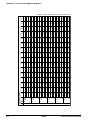
Table 4.1.1(d) I/O memory map (F0H–FFH)
Address
*7
F0H
F1H
F2H
F3H
F4H
F5H
F6H
F7H
F8H
F9H
FAH
FBH
FFH
D3
Register
D2
D1
Name
GNDON1
GNDON1 GNDON0 VRAON
VRON
GNDON0
VRAON
R/W
VRON
0 *5
0
0
AMPON1 AMPON0
0 *5
AMPON1
R
R/W
AMPON0
0 *5
0
0
AMPDT1 AMPDT0
0 *5
AMPDT1
R
AMPDT0
0 *5
0
0
ADRS1 ADRS0
0 *5
ADRS1
R/W
R
ADRS0
AIS3
AIS0
AIS3
AIS2
AIS1
AIS2
AIS1
R/W
AIS0
AI3
AI0
AI3
AI2
AI1
AI2
AI1
R/W
AI0
ADON
ADON
0
AI4
0
0 *5
0 *5
R/W
R/W
R
AI4
AD3
AD0
AD3
AD2
AD1
AD2
AD1
R
AD0
AD7
AD4
AD7
AD6
AD5
AD6
AD5
R
AD4
AD11
AD8
AD11
AD10
AD9
AD10
AD9
R
AD8
0 *5
AD12
0
0
ADP
0 *5
ADP
R
AD12
0 *5
0
IDR
0
0
0 *5
0 *5
R
IDR
SVDS1
SVDS1
SVDS0 SVDDT SVDON
SVDS0
SCDDT
R/W
R
R/W
SCDON
S1C62740 TECHNICAL HARDWARE
D0
Init *1
0
0
0
0
– *2
– *2
0
0
– *2
– *2
0
0
– *2
– *2
0
0
0
0
0
0
0
0
0
0
0
– *2
– *2
0
0
0
0
0
0
0
0
0
0
0
0
0
–
–
0
0
–
–
–
0
0
0
0
0
1
Comment
0
On
On
Off
Off
On
On
On
On
High
High
Low
Low
Resistor
Resistor
Differ. V
Differ. V
On
On
On
On
On
V(to GND)
V(to GND)
V(to GND)
V(to GND)
Off
Off
Off
Off
Off
On
Off
GND circuit On/Off and mode selection
0: Off, 1: On1, 2: On2, 3: On3
VR output voltage adjustment On/Off
VR circuit On/Off
Unused
Unused
AMP1 On/Off
AMP0 On/Off
Unused
Unused
AMP1 output data
AMP0 output data
Unused
Unused
A/D converter resolution selection
0: 6400, 1: 3200, 2: 1600, 3: 800
AI4/AI3 mode selection
AI4/AI2 mode selection
AI3/AI2 mode selection
AI1/AI0 mode selection
Analog input terminal AI3 On/Off
Analog input terminal AI2 On/Off
Analog input terminal AI1 On/Off
Analog input terminal AI0 On/Off
A/D converter clear and On/Off
Unused
Unused
Analog input terminal AI4 On/Off
*6
A/D converter count data
LSB
A/D converter count data
A/D converter count data
*2
*2
(+)
(-)
Invalid
Valid
Low
On
Normal
Off
*2
*2
*2
EPSON
Unused
Unused
Input voltage polarity
A/D converter count data (MSB)
Unused
Unused
Unused
Reading data status
SVD criteria voltage setting
0: 2.6 V, 1: 2.5 V, 2: 2.4 V, 3: 2.3 V
Supply voltage evaluation data
SVD circuit On/Off
I-19
CHAPTER 4: PERIPHERAL CIRCUITS AND OPERATION (Resetting Watchdog Timer)
4.2 Resetting Watchdog Timer
Configuration of
watchdog timer
The S1C62740 incorporates a watchdog timer as the source oscillator for OSC1 (clock timer 1 Hz signal). The watchdog timer must be
reset cyclically by the software. If reset is not executed in at least
3–4 seconds, the initial reset signal is output automatically for the
CPU.
Figure 4.2.1 is the block diagram of the watchdog timer.
OSC1 demultiplier
(256 Hz)
Fig. 4.2.1
Watchdog timer block diagram
Clock timer
TM0–TM7
1 Hz
Watchdog timer
WD0–WD1
Initial
reset signal
Clock timer reset signal
Watchdog timer reset signal
The watchdog timer, configured of a two-bit binary counter (WD0,
WD1), generates the initial reset signal internally by overflow of the
WD1 (1/4 Hz).
Watchdog timer reset processing in the program's main routine
enables detection of program overrun, such as when the main
routine's watchdog timer processing is bypassed. Ordinarily this
routine is incorporated where periodic processing takes place, just
as for the timer interrupt routine.
The watchdog timer can also be reset by the resetting of the clock
timer.
The watchdog timer operates in the HALT mode. If the watchdog
timer is not reset within 3 or 4 seconds including the HALT status,
the IC reactivates from initial reset status.
The time during which oscillation is stopped due to the SLEEP
function is not included in the watchdog timer reset cycle.
When the SLEEP status has been cancelled and it has begun
oscillation, it successively restarts the count from the status at the
time oscillation stopped.
I-20
EPSON
S1C62740 TECHNICAL HARDWARE
CHAPTER 4: PERIPHERAL CIRCUITS AND OPERATION (Resetting Watchdog Timer)
Table 4.2.1 lists the watchdog timer's control bits and their addresses.
Control of watchdog
timer
Table 4.2.1 Control bits of watchdog timer
Address
*7
D3
0
Register
D2
D1
0
0
E2H
R
WDRST
0
WD1
E5H
W
R
D0
Name
0 *5
TMRST
0 *5
0 *5
W
TMRST *5
WDRST*5
WD0
0 *5
WD1
WD0
*1 Initial value at the time of initial reset
*2 Not set in the circuit
*3 Undefined
*4 Reset (0) immediately after being read
Init *1
– *2
– *2
– *2
– *2
Reset
– *2
0
0
1
Reset
Reset
0
–
–
Comment
Unused
Unused
Unused
Clock timer and watchdog timer reset
Watchdog timer reset
Unused
Watchdog timer data (1/4 Hz)
Watchdog timer data (1/2 Hz)
*5 Constantly "0" when being read
*6 Refer to main manual
*7 Page switching in I/O memory is not necessary
WD0, WD1: The 1/2 Hz and 1/4 Hz data of the watchdog timer can be read
Watchdog timer data out. These bits are read only, and writing operations are invalid.
(E5H•D0, D1) At initial reset, the watchdog timer data is initialized to "00B".
WDRST: This is the bit for resetting the watchdog timer.
Watchdog timer reset
When "1" is written: Watchdog timer is reset
(E5H•D3)
When "0" is written: No operation
Reading: Always "0"
When "1" is written to WDRST, the watchdog timer is reset, and the
operation restarts immediately after this. When "0" is written to
WDRST, no operation results.
This bit is dedicated for writing, and is always "0" for reading.
TMRST: This is the bit for resetting the clock timer and the watchdog timer.
Clock timer reset
When "1" is written: Clock timer and watchdog timer are reset
(E2H•D0)
When "0" is written: No operation
Reading: Always "0"
When "1" is written to TMRST, the clock timer and the watchdog
timer are reset, and the operation restarts immediately after this.
When "0" is written to TMRST, no operation results.
This bit is dedicated for writing, and is always "0" for reading.
Programming note
S1C62740 TECHNICAL HARDWARE
The watchdog timer must be reset within 3-second cycles. Because
of this, the watchdog timer data (WD0, WD1) cannot be used for
clocking of 3 seconds or more.
EPSON
I-21
CHAPTER 4: PERIPHERAL CIRCUITS AND OPERATION (Oscillation Circuit)
4.3 Oscillation Circuit
Configuration of
oscillation circuit
The S1C62740 has two oscillation circuits (OSC1 and OSC3).
OSC1 is a crystal oscillation circuit that supplies the operating
clock the CPU and peripheral circuits. OSC3 is either a CR or
ceramic oscillation circuit. When processing with the S1C62740
requires high-speed operation, the CPU operating clock can be
switched from OSC1 to OSC3.
Figure 4.3.1 is the block diagram of this oscillation system.
SLEEP (during SLEEP: HIGH)
OSC1
oscillation
circuit
To peripheral circuit
Clock
switch
OSC3
oscillation
circuit
To CPU
(and serial interface)
CPU clock selection signal
Fig. 4.3.1
Oscillation system
Oscillation circuit control signal
Selection of either OSC1 or OSC3 for the CPU's operating clock can
be made through the software.
OSC1 oscillation
circuit
The S1C62740 has a built-in crystal oscillation circuit (OSC1
oscillation circuit). As an external element, the OSC1 oscillation
circuit generates the operating clock for the CPU and peripheral
circuitry by connecting the crystal oscillator (Typ. 32.768 kHz) and
trimmer capacitor (5–25 pF).
Figure 4.3.2 is the block diagram of the OSC1 oscillation circuit.
SLEEP
CGX
OSC2
Fig. 4.3.2
OSC1 oscillation circuit
RDX
To CPU and
peripheral circuit
RFX
X'tal
OSC1
C DX
V SS
V SS
As Figure 4.3.2 indicates, the crystal oscillation circuit can be
configured simply by connecting the crystal oscillator (X'tal) between terminals OSC1 and OSC2 to the trimmer capacitor (CGX)
between terminals OSC1 and VSS.
The OSC1 oscillation circuit is off in the SLEEP status.
I-22
EPSON
S1C62740 TECHNICAL HARDWARE
CHAPTER 4: PERIPHERAL CIRCUITS AND OPERATION (Oscillation Circuit)
OSC3 oscillation
circuit
The S1C62740 has twin clock specification. The mask option
enables selection of either the CR or ceramic oscillation circuit
(OSC3 oscillation circuit) as the CPU's sub-clock. Because the
oscillation circuit itself is built-in, it provides the resistance as an
external element when CR oscillation is selected, but when ceramic
oscillation is selected both the ceramic oscillator and two capacitors (gate and drain capacitance) are required.
Figure 4.3.3 is the block diagram of the OSC3 oscillation circuit.
C CR
RCR
OSC3
To CPU
(and serial interface)
Oscillation circuit
control signal
OSC4
(a) CR oscillation circuit
C GC
Fig. 4.3.3
OSC3 oscillation circuit
To CPU
(and serial interface)
RFC
Ceramic
CDC
OSC3
OSC4
RDC
Oscillation circuit
control signal
VSS
(b) Ceramic oscillation circuit
As indicated in Figure 4.3.3, the CR oscillation circuit can be
configured simply by connecting the resistor (RCR) between terminals OSC3 and OSC4 when CR oscillation is selected. When 39 kΩ
is used for RCR, the oscillation frequency is about 900 kHz. When
ceramic oscillation is selected, the ceramic oscillation circuit can
be configured by connecting the ceramic oscillator (Typ. 1 MHz)
between terminals OSC3 and OSC4 to the two capacitors (CGC and
CDC) located between terminals OSC3 and OSC4 and VSS. For both
CGC and CDC, connect capacitors that are about 100 pF. To lower
current consumption of the OSC3 oscillation circuit, oscillation can
be stopped through the software.
S1C62740 TECHNICAL HARDWARE
EPSON
I-23
CHAPTER 4: PERIPHERAL CIRCUITS AND OPERATION (Oscillation Circuit)
Control of oscillation
circuit
Table 4.3.1 lists the control bits and their addresses for the oscillation circuit.
Table 4.3.1 Control bits of oscillation circuit
Register
D2
D1
Address
*7
D3
0
0
D0
CLKCHG
OSCC
DFH
R
R/W
Name
0 *5
0 *5
CLKCHG
OSCC
*1 Initial value at the time of initial reset
*2 Not set in the circuit
*3 Undefined
*4 Reset (0) immediately after being read
Init *1
– *2
– *2
0
0
1
OSC3
On
0
OSC1
Off
Comment
Unused
Unused
CPU system clock switch
OSC3 oscillation On/Off
*5 Constantly "0" when being read
*6 Refer to main manual
*7 Page switching in I/O memory is not necessary
OSCC: Controls oscillation ON/OFF for the OSC3 oscillation circuit.
OSC3 oscillation control
When "1" is written: The OSC3 oscillation ON
(DFH•D0)
When "0" is written: The OSC3 oscillation OFF
Reading: Valid
When it is necessary to operate the CPU at high speed, set OSCC to
"1". At other times, set it to "0" to lessen the current consumption.
When "Not Use" is selected for the mask option of the OSC3 oscillation circuit, keep OSCC set to "0".
At initial reset, OSCC is set to "0".
CLKCHG: The CPU's operation clock is selected with this register.
The CPU's clock switch
When "1" is written: OSC3 clock is selected
(DFH•D1)
When "0" is written: OSC1 clock is selected
Reading: Valid
When the CPU clock is to be OSC3, set CLKCHG to "1"; for OSC1,
set CLKCHG to "0".
When "Not Use" is selected for the mask option of the OSC3 oscillation circuit, keep CLKCHG set to "0".
At initial reset, CLKCHG is set to "0".
I-24
EPSON
S1C62740 TECHNICAL HARDWARE
CHAPTER 4: PERIPHERAL CIRCUITS AND OPERATION (Oscillation Circuit)
Clock frequency
and instruction
execution time
Table 4.3.2
Clock frequency and instruction
execution time
Programming notes
Table 4.3.2 shows the instruction execution time according to each
frequency of the system clock.
Clock frequency
Instruction execution time (µsec)
5-clock instruction 7-clock instruction 12-clock instruction
OSC1: 32.768 kHz
OSC3: 1 MHz
152.6
5.0
213.6
7.0
366.2
12.0
(1) It takes at least 5 msec from the time the OSC3 oscillation
circuit goes ON until the oscillation stabilizes. Consequently,
when switching the CPU operation clock from OSC1 to OSC3,
do this after a minimum of 5 msec have elapsed since the OSC3
oscillation went ON.
Further, the oscillation stabilization time varies depending on
the external oscillator characteristics and conditions of use, so
allow ample margin when setting the wait time.
(2) When switching the clock form OSC3 to OSC1, use a separate
instruction for switching the OSC3 oscillation OFF. An error in
the CPU operation can result if this processing is performed at
the same time by the one instruction.
(3) When shifting to the SLEEP status, the CPU clock must be set
to OSC1 and the OSC3 oscillation circuit must be OFF.
S1C62740 TECHNICAL HARDWARE
EPSON
I-25
CHAPTER 4: PERIPHERAL CIRCUITS AND OPERATION (Input Ports)
4.4 Input Ports (K00–K03, K10)
Configuration of
input ports
The S1C62740 has five bits general-purpose input ports. Each of
the input port terminals (K00–K03, K10) provides internal pull up
resistor. Pull up resistor can be selected for each bit with the mask
option.
Figure 4.4.1 shows the configuration of input port.
Interrupt
request
Mask
option
Kxx
Data bus
VDD
Address
Fig. 4.4.1
Configuration of input port
VSS
Selection of "With pull up resistor" with the mask option suits
input from the push switch, key matrix, and so forth. When "Gate
direct" is selected, the port can be used for slide switch input and
interfacing with other LSIs.
Further, the input port terminal K10 is used as the input terminal
for the programmable timer/event counter and the interrupt port
for the SLEEP mode cancellation. (See Section 4.10, "Programmable Timer", and Section 4.15, "Interrupt and HALT/SLEEP" for
details.)
I-26
EPSON
S1C62740 TECHNICAL HARDWARE
CHAPTER 4: PERIPHERAL CIRCUITS AND OPERATION (Input Ports)
All five bits of the input ports (K00–K03, K10) provide the interrupt
function. The conditions for issuing an interrupt can be set by the
software. Further, whether to mask the interrupt function can be
selected individually for all five bits by the software.
Interrupt function
(1) K00–K03 interrupt
Figure 4.4.2 shows the configuration of K00–K03 interrupt circuit.
K00
Address
Address
Data bus
Input comparison
register (DFK00)
Interrupt factor
flag (IK0)
Interrupt
request
Address
Input selection
register (SIK00)
Interrupt mask
register (EIK0)
Address
Address
K01
K02
K03
Fig. 4.4.2
Input interrupt circuit
configuration (K00–K03)
The interrupt selection register (SIK) and input comparison register
(DFK) are individually set for the input ports K00–K03 and can
specify the terminal for generating interrupt and interrupt timing.
The interrupt selection register (SIK00–SIK03) select what input of
K00–K03 to use for the interrupt. Writing "1" into an interrupt
selection register incorporates that input port into the interrupt
generation conditions. The changing the input port where the
interrupt selection register has been set to "0" does not affect the
generation of the interrupt.
The input interrupt timing can select that the interrupt be generated at the rising edge of the input or that it be generated at the
falling edge according to the set value of the input comparison
register (DFK00–DFK03).
By setting these two conditions, the interrupt for K00–K03 is
generated when an input port in which an interrupt has been
enabled by the input selection register and the content of the input
comparison register have been changed from matching to no
matching.
When the interrupt is generated, the interrupt factor flag (IK0) is
set to "1".
The interrupt mask register (EIK0) enables the interrupt mask to
be selected for K00–K03. However, the interrupt factor flag is set to
"1" when the interrupt condition is established regardless of the
interrupt mask register setting.
Figure 4.4.3 shows an example of an interrupt for K00–K03.
S1C62740 TECHNICAL HARDWARE
EPSON
I-27
CHAPTER 4: PERIPHERAL CIRCUITS AND OPERATION (Input Ports)
Interrupt selection register
SIK03 SIK02 SIK01 SIK00
1
1
1
0
Input comparison register
DFK03 DFK02 DFK01 DFK00
1
0
1
0
With the above setting, the interrupt of K00–K03 is generated under the
following condition:
(1) K03
1
(2) K03
1
(3) K03
0
(4) K03
0
Input port
K02 K01
0
1
↓
K02 K01
0
1
↓
K02 K01
0
1
↓
K02 K01
1
1
Fig. 4.4.3
Example of interrupt of K00–K03
K00
0
(Initial value)
K00
1
K00
1
K00
1
→ Interrupt generation
Because K00 interrupt is set to disable,
interrupt will be generated when no
matching occurs between the contents of
the 3 bits K01–K03 and the 3 bits input
comparison register DFK01–DFK03.
K00 interrupt is disabled by the interrupt selection register (SIK00),
so that an interrupt does not occur at (2). At (3), K03 changes to
"0"; the data of the terminal that is interrupt enabled no longer
matches the data of the input comparison register, so that interrupt occurs. As already explained, the condition for the interrupt to
occur is the change in the port data and contents of the input
comparison register from matching to no matching. Hence, in (4),
when the no matching status changes to another no matching
status, an interrupt does not occur. Further, terminals that have
been masked for interrupt do not affect the conditions for interrupt
generation.
I-28
EPSON
S1C62740 TECHNICAL HARDWARE
CHAPTER 4: PERIPHERAL CIRCUITS AND OPERATION (Input Ports)
(2) K10 interrupt
Figure 4.4.4 shows the configuration of K10 interrupt circuit.
K10
Address
Data bus
Address
Input comparison
register (DFK10)
Interrupt factor
flag (IK1)
SLEEP
cancellation
Interrupt
request
Address
Interrupt mask
register (EIK1)
Address
Fig. 4.4.4
Input interrupt circuit configuration
(K10)
The input port K10 can generate interrupts for systems other then
K00–K03. The input comparison register (DFK10) is also set to the
K10 port and can specify the timing for generating an interrupt.
The interrupt generated timing is also the same as for K00–K03
and when the content of the K10 input and the input comparison
register changes from matching to no matching an interrupt is
generated.
When the interrupt is generated, the interrupt factor flag (IK1) is
set to "1".
The interrupt mask register (EIK1) enables the interrupt mask to
be selected for K10. However, the interrupt factor flag is set to "1"
when the interrupt condition is established regardless of the
interrupt mask register setting.
The K10 input interrupt is also used for cancellation of the SLEEP
mode.
Mask option
S1C62740 TECHNICAL HARDWARE
Internal pull up resistor can be selected for each of the five bits of
the input ports (K00–K03, K10) with the input port mask option.
When you have selected "Gate direct", take care that the floating
status does not occur for the input. Select "With pull up resistor"
for input ports that are not being used.
EPSON
I-29
CHAPTER 4: PERIPHERAL CIRCUITS AND OPERATION (Input Ports)
Table 4.4.1 lists the input ports control bits and their addresses.
Control of input ports
Table 4.4.1 Input port control bits
Register
D2
D1
Address
*7
D3
0
0
D0
IK1
0
C2H
R
0
0
IK0
0
C3H
R
0
0
EIK0
EIK1
C9H
R
SIK03
R/W
SIK02
SIK01
SIK00
CAH
R/W
K03
K02
K01
K00
D0H
R
0
0
K10
0
D1H
R
DFK03
DFK02
DFK01
DFK00
D2H
R/W
0
0
0
DFK10
D3H
R
R/W
Name
0 *5
0 *5
0 *5
IK1 *4
0 *5
0 *5
0 *5
IK0 *4
0 *5
0 *5
EIK1
EIK0
SIK03
SIK02
SIK01
SIK00
K03
K02
K01
K00
0 *5
0 *5
0 *5
K10
DFK03
DFK02
DFK01
DFK00
0 *5
0 *5
0 *5
DFK10
*1 Initial value at the time of initial reset
*2 Not set in the circuit
*3 Undefined
*4 Reset (0) immediately after being read
Init *1
– *2
– *2
– *2
0
– *2
– *2
– *2
0
– *2
– *2
0
0
0
0
0
0
– *2
– *2
– *2
– *2
– *2
– *2
– *2
– *2
1
1
1
1
– *2
– *2
– *2
1
1
Yes
No
Yes
No
Enable
Enable
Enable
Enable
Enable
Enable
High
High
High
High
Mask
Mask
Disable
Disable
Disable
Disable
Low
Low
Low
Low
High
Comment
0
Low
Unused
Unused
Unused
Interrupt factor flag (K10)
Unused
Unused
Unused
Interrupt factor flag (K00–K03)
Unused
Unused
Interrupt mask register (K10)
Interrupt mask register (K00–K03)
Interrupt selection register (K03)
Interrupt selection register (K02)
Interrupt selection register (K01)
Interrupt selection register (K00)
Input port (K00–K03)
Unused
Unused
Unused
Input port (K10)
Input comparison register (K00–K03)
Unused
Unused
Unused
Input comparison register (K10)
*5 Constantly "0" when being read
*6 Refer to main manual
*7 Page switching in I/O memory is not necessary
K00–K03, K10: Input data of the input
Input port data registers.
(D0H, D1H•D0)
When "1" is read:
When "0" is read:
Writing:
port terminals can be read with these
High level
Low level
Invalid
The reading is "1" when the terminal voltage of the five bits of the
input ports (K00–K03, K10) goes high (VDD), and "0" when the
voltage goes low (VSS).
These bits are dedicated for reading, so writing cannot be done.
I-30
EPSON
S1C62740 TECHNICAL HARDWARE
CHAPTER 4: PERIPHERAL CIRCUITS AND OPERATION (Input Ports)
DFK00–DFK03, DFK10: Interrupt conditions for terminals K00–K03 and K10 can be set
Input comparison registers with these registers.
(D2H, D3H•D0)
When "1" is written: Falling edge
When "0" is written: Rising edge
Reading: Valid
The interrupt conditions can be set for the rising or falling edge of
input for each of the five bits (K00–K03 and K10), through the
input comparison registers (DFK00–DFK03 and DFK10).
For DFK00–DFK03, a comparison is done only with the ports that
are enabled by the interrupt among K00–K03 by means of the SIK
register.
At initial reset, these registers are set to "0".
SIK00–SIK03: Selects the port to be used for the K00–K03 input interrupt.
Interrupt selection register
When "1" is written: Enable
(CAH)
When "0" is written: Disable
Reading: Valid
Enables the interrupt for the input ports (K00–K03) for which "1"
has been written into the interrupt selection register (SIK00–
SIK03). The input port set for "0" does not affect the interrupt
generation condition.
At initial reset, these registers are set to "0".
EIK0, EIK1: Masking the interrupt of the input port can be selected with these
Interrupt mask registers registers.
(C9H•D0, D1)
When "1" is written: Enable
When "0" is written: Mask
Reading: Valid
With these registers, masking of the input port can be selected for
each of the two systems (K00–K03, K10).
Writing to the interrupt mask registers can be done only in the DI
status (interrupt flag = "0").
At initial reset, these registers are all set to "0".
IK0, IK1: These flags indicate the occurrence of input interrupt.
Interrupt factor flags
When "1" is read: Interrupt has occurred
(C3H•D0, C2H•D0)
When "0" is read: Interrupt has not occurred
Writing: Invalid
The interrupt factor flags IK0 and IK1 are associated with K00–K03
and K10, respectively. From the status of these flags, the software
can decide whether an input interrupt has occurred. However,
these flags are set to "1" when the interrupt conditions are established even if the interrupts have been masked.
S1C62740 TECHNICAL HARDWARE
EPSON
I-31
CHAPTER 4: PERIPHERAL CIRCUITS AND OPERATION (Input Ports)
These flags are reset when the software reads them.
Reading of interrupt factor flags is available at EI, but be careful in
the following cases.
If the interrupt mask register value corresponding to the interrupt
factor flags to be read is set to "1", an interrupt request will be
generated by the interrupt factor flags set timing, or an interrupt
request will not be generated.
At initial reset, these flags are set to "0".
Programming notes
(1) When input ports are changed from low to high by pull up
resistor, the rise of the waveform is delayed on account of the
time constant of the pull up resistor and input gate
capacitance. Hence, when fetching input ports, set an
appropriate wait time.
Particular care needs to be taken of the key scan during key
matrix configuration.
Make this waiting time the amount of time or more calculated
by the following expression.
10 × C × R
C: terminal capacitance 5 pF + parasitic capacitance ? pF
R: pull up resistance 300 kΩ
(2) Write the interrupt mask register (EIK) only in the DI status
(interrupt flag = "0"). Writing during EI status (interrupt flag =
"1") will cause malfunction.
(3) Reading of interrupt factor flags is available at EI, but be careful
in the following cases.
If the interrupt mask register value corresponding to the interrupt factor flags to be read is set to "1", an interrupt request will
be generated by the interrupt factor flags set timing, or an
interrupt request will not be generated. Be very careful when
interrupt factor flags are in the same address.
I-32
EPSON
S1C62740 TECHNICAL HARDWARE
CHAPTER 4: PERIPHERAL CIRCUITS AND OPERATION (Output Ports)
4.5 Output Ports (R00–R03)
Configuration of
output ports
The S1C62740 has four bits general output ports.
Output specifications of the output ports can be selected individually with the mask option. Two kinds of output specifications are
available: complementary output and Nch open drain output.
Further, each of the output port to be used as special output ports
by the software setting.
Figure 4.5.1 shows the configuration of the output port.
VDD
Data bus
Nch open drain
Complementary
Register
R
Address
VSS
Fig. 4.5.1
Configuration of output port
Mask option
Mask option
Output specifications of the output ports can be selected with the
mask option.
Output specifications for the output ports (R00–R03) enable
selection of either complementary output or Nch open drain output
for each of the four bits.
However, even when Nch open drain output is selected, voltage
exceeding source voltage must not be applied to the output port.
Special output
In addition to the regular DC output, special output can be selected as shown in Table 4.5.1 with the software. Figure 4.5.2
shows the structure of the output ports R00–R03.
Table 4.5.1
Special output
S1C62740 TECHNICAL HARDWARE
Terminal
Special output
Output selection register
R00
R01
R02
R03
FOUT
PTOVF
BZ
BZ
FOR00
PTR01
BZR02
BZR03
EPSON
I-33
CHAPTER 4: PERIPHERAL CIRCUITS AND OPERATION (Output Ports)
BZ
Register
BZR03
R03
(BZ)
Register
R03
Data bus
Register
BZR02
R02
(BZ)
Register
R02
PTOVF
Register
PTR01
R01
(PTOVF)
Register
R01
FOUT
Register
FOR00
R00
(FOUT)
Register
R00
Fig. 4.5.2
Structure of the
output ports R00–R03
• BZ and BZ BZ and BZ are the buzzer signal output for driving the piezo(R02 and R03) electric buzzer.
By setting the register BZR02 to "1", R02 is set to BZ (buzzer
signal) output port and by setting the register BZR03 to "1", R03 is
set to BZ (buzzer inverted signal) output port. When BZR02 and
BZR03 are set to "0", R02 and R03 become the regular DC output
ports.
When the buzzer output and the buzzer inverted output are selected, ON/OFF of the buzzer outputs can be controlled by the R02
and R03 registers, respectively.
The buzzer frequency may be selected as 2 kHz or 4 kHz by setting
of the BZFQ register.
Note: The BZ and BZ output signals could generate hazards during ON/OFF
switching.
Figure 4.5.3 shows the output waveform of BZ and BZ.
R02 register
0
1
0
0
1
0
BZ output
R03 register
Fig. 4.5.3
Output waveform of BZ and BZ
I-34
BZ output
EPSON
S1C62740 TECHNICAL HARDWARE
CHAPTER 4: PERIPHERAL CIRCUITS AND OPERATION (Output Ports)
• FOUT By setting the register FOR00 to "1", R00 is set to FOUT (clock)
(R00) output port. When FOR00 is set to "0", R00 become the regular DC
output port.
When the FOUT output is selected, ON/OFF of the signal output
can be controlled by the R00 register.
The frequency of clock output signal may be selected from among 4
types as Table 4.5.2 by setting of the FOFQ0 and FOFQ1 registers.
Table 4.5.2
FOUT clock frequency
FOFQ1
FOFQ0
Clock frequency (Hz)
1
1
0
0
1
0
1
0
fOSC3
fOSC1
4,096
512
Note: A hazard may occur when the FOUT signal is turned ON or OFF.
Figure 4.5.4 shows the output waveform of FOUT.
R00 register
Fig. 4.5.4
Output waveform of FOUT
1
0
1
FOUT output
• PTOVF By setting the register PTR01 to "1", R01 is set to PTOVF (output
(R01) pulse of the programmable timer) output port. When PTR01 is set
to "0", R01 become the regular DC output port.
When the PTOVF output is selected, ON/OFF of the signal output
can be controlled by the R01 register. However, control of the
programmable timer is necessary.
Refer to Section 4.10, "Programmable Timer" for details of the
programmable timer.
Note: A hazard may occur when the PTOVF signal is turned ON or OFF.
Figure 4.5.5 shows the output waveform of PTOVF.
R01 register
Fig. 4.5.5
Output waveform of PTOVF
S1C62740 TECHNICAL HARDWARE
1
0
1
PTOVF output
EPSON
I-35
CHAPTER 4: PERIPHERAL CIRCUITS AND OPERATION (Output Ports)
Table 4.5.3 lists the output ports' control bits and their addresses.
Control of output
ports
Table 4.5.3 Control bits of output ports
D3
Register
D2
D1
D0
R03
R02
R01
R00
BZ
BZ
PTOVF
FOUT
Address
*7
D4H
R/W
BZR03
BZR02
0
BZFQ
R
R/W
FOFQ1
FOFQ0
E0H
R/W
FOR00
0
R/W
R
PTR01
0
PTRUN
PTRST
R/W
R
R/W
W
E1H
R/W
E9H
Name
R03
BZ
R02
BZ
R01
PTOVF
R00
FOUT
BZR03
BZR02
0 *5
BZFQ
FOR00
0 *5
FOFQ1
FOFQ0
PTR01
0 *5
PTRUN
PTRST *5
*1 Initial value at the time of initial reset
*2 Not set in the circuit
*3 Undefined
*4 Reset (0) immediately after being read
Init *1
0
0
1
1
1
High
On
High
On
High
Off
High
Off
Buzzer
Buzzer
0
0
– *2
2kHz
0
FOUT
0
– *2
0
0
PTOVF
0
– *2
Run
0
Reset
–
0
Low
Off
Low
Off
Low
On
Low
On
DC
DC
4kHz
DC
DC
Stop
–
Comment
Output port (R03)
Buzzer inverted output
Output port (R02)
Buzzer output
Output port (R01)
PTOVF output
Output port (R00)
FOUT output
R03 port output selection
R02 port output selection
Unused
Buzzer frequency selection
R00 port output selection
Unused
FOUT frequency selection
0: 512 Hz, 1: 4096 Hz, 2: fOSC1, 3: fOSC3
R01 port output selection
Unused
Programmable timer Run/Stop
Programmable timer reset (reload)
*5 Constantly "0" when being read
*6 Refer to main manual
*7 Page switching in I/O memory is not necessary
FOR00: Selects the output type
R00 output selection register
When "1" is written:
(E1H•D3)
When "0" is written:
Reading:
for the R00 terminal.
FOUT signal output
DC output
Valid
By setting the register FOR00 to "1", R00 is set to FOUT (clock)
output port. When FOR00 is set to "0", R00 become the regular DC
output port.
When the FOUT output is selected, ON/OFF of the signal output
can be controlled by the R00 register.
At initial reset, this register is set to "0".
PTR01: Selects the output type
R01 output selection register
When "1" is written:
(E9H•D3)
When "0" is written:
Reading:
for the R01 terminal.
PTOVF signal output
DC output
Valid
By setting the register PTR01 to "1", R01 is set to PTOVF (output
pulse of the programmable timer) output port. When PTR01 is set
to "0", R01 become the regular DC output port.
I-36
EPSON
S1C62740 TECHNICAL HARDWARE
CHAPTER 4: PERIPHERAL CIRCUITS AND OPERATION (Output Ports)
When the PTOVF output is selected, ON/OFF of the signal output
can be controlled by the R01 register.
At initial reset, this register is set to "0".
BZR02, BZR03: Selects the output type
R02, R03 output selection
When "1" is written:
register
When "0" is written:
(E0H•D2, D3)
Reading:
for the R02 and R03 terminals.
Buzzer signal output
DC output
Valid
By setting the register BZR02 to "1", R02 is set to BZ (buzzer
signal) output port and by setting the register BZR03 to "1", R03 is
set to BZ (buzzer inverted signal) output port. When BZR02 and
BZR03 are set to "0", R02 and R03 become the regular DC output
ports.
When the buzzer output and the buzzer inverted output are selected, ON/OFF of the buzzer outputs can be controlled by the R02
and R03 registers, respectively.
At initial reset, these register are set to "0".
R00–R03 (when DC output): Sets the output data for the output ports.
Output port data
When "1" is written: High output
(D4H)
When "0" is written: Low output
Reading: Valid
The output port terminals output the data written in the corresponding registers (R00–R03) without changing it. When "1" is
written in the register, the output port terminal goes high (VDD),
and when "0" is written, the output port terminal goes low (VSS).
At initial reset, R00 and R01 are set to "1"; R02 and R03 are set to
"0".
R02, R03 (when BZ and BZ These bits control the output of the buzzer signals (BZ, BZ).
output is selected):
When "1" is written: Buzzer signal is output
Special output port data
When "0" is written: Low level (DC) is output
(D4H•D2, D3)
Reading: Valid
BZ (buzzer signal) output is controlled by writing data to R10, and
BZ (buzzer inverted signal) output is controlled by writing data to
R13. At initial reset, R02 and R03 are set to "0".
BZFQ: Selects the frequency of the buzzer signal.
Buzzer frequency selection
When "1" is written: 2 kHz
register
When "0" is written: 4 kHz
(E0H•D0)
Reading: Valid
When "1" is written to register BZFQ, the frequency of the buzzer
signal is set in 2 kHz, and in 4 kHz when "0" is written.
At initial reset, this register is set to "0".
S1C62740 TECHNICAL HARDWARE
EPSON
I-37
CHAPTER 4: PERIPHERAL CIRCUITS AND OPERATION (Output Ports)
R00 Controls the FOUT (clock) output.
(when FOUT is selected):
When "1" is written: High level (DC) output
Special output port data
When "0" is written: Clock output
(D4H•D0)
Reading: Valid
FOUT output can be controlled by writing data to R00.
At initial reset, this register is set to "1".
FOFQ0, FOFQ1: Selects the FOUT frequency.
FOUT frequency selection
FOFQ1
FOFQ0
register
1
1
(E1H•D0, D1)
1
0
0
1
Table 4.5.4
0
0
FOUT clock frequency
Clock frequency (Hz)
fOSC3
fOSC1
4,096
512
At initial reset, these registers are set to "0".
R01 Controls the PTOVF (clock) output.
(when PTOVF is selected):
When "1" is written: High level (DC) output
Special output port data
When "0" is written: Clock output
(D4H•D0)
Reading: Valid
PTOVF output can be controlled by writing data to R01.
Refer to Section 4.10, "Programmable Timer" for details of PTOVF.
At initial reset, this register is set to "1".
Programming note
I-38
When BZ, BZ, FOUT and PTOVF are selected, a hazard may be
observed in the output waveform when the data of the output
register changes.
EPSON
S1C62740 TECHNICAL HARDWARE
CHAPTER 4: PERIPHERAL CIRCUITS AND OPERATION (I/O Ports)
4.6 I/O Ports (P00–P03, P10–P13, P20–P23)
Configuration of I/O
ports
The S1C62740 has 12 bits (4 bits × 3) general-purpose I/O ports.
Figure 4.6.1 shows the configuration of the I/O port.
The four bits of each of the I/O ports P00–P03, P10–P13 and P20–
P23 can be set to either input mode or output mode. Modes can be
set by writing data to the I/O control register.
Moreover, pull up resistor which is turned ON during input mode
can be controlled through the software.
VDD
Data bus
Address
Fig. 4.6.1
Configuration of I/O port
Pull up control
register (PUP)
Address
Address
Data
register
Address
I/O control
register (IOC)
P
VSS
The I/O ports P20–P23 are common used with the input/output
ports of the serial interface, and function of these ports can be
selected through the software.
Refer to Section 4.11, "Serial Interface" for details of the serial
interface.
S1C62740 TECHNICAL HARDWARE
EPSON
I-39
CHAPTER 4: PERIPHERAL CIRCUITS AND OPERATION (I/O Ports)
I/O control registers
and input/output
mode
Input or output mode can be set for the four bits of I/O ports P00–
P03, P10–P13 and P20–P23 by writing data into the corresponding
I/O control register IOC0, IOC1 and IOC2.
To set the input mode, "0" is written to the I/O control register.
When an I/O port is set to input mode, it becomes high impedance
status and works as an input port.
However, when the pull up explained in the following section has
been set by software, the input line is pulled up only during this
input mode.
The output mode is set when "1" is written to the I/O control
register. When an I/O port set to output mode works as an output
port, it outputs a high level (VDD) when the port output data is "1",
and a low level (VSS) when the port output data is "0".
If perform the read out in each mode; when output mode, the
register value is read out, and when input mode, the port value is
read out.
At initial reset, the I/O control registers are set to "0", and the I/O
port enters the input mode.
When P20–P23 are used as the input/output ports of the serial
interface, the I/O control of the IOC2 register becomes invalid and
IOC2 can be used as a 1 bit general-purpose register.
Pull up during input
mode
A pull up resistor that operates during the input mode is built into
the I/O ports of the S1C62740. Software can set the use or nonuse of this pull up. The pull up resistor becomes effective by
writing "1" into the pull up control registers PUP0, PUP1 and PUP2
that correspond to each 4 bits of P00–P03, P10–P13 and P20–P23,
and the input line is pulled up during the input mode. When "0"
has been written, no pull up is done.
At initial reset, the pull up control registers are set to "0".
Mask option
Output specifications during the output mode (IOC = "1") can be
selected with the mask option.
Output specifications for the I/O ports (P00–P03, P10–P13, P20–
P23) enable selection of either complementary output or Nch open
drain output for each of the 12 bits.
However, even when Nch open drain output is selected, voltage
exceeding source voltage must not be applied to the output port.
I-40
EPSON
S1C62740 TECHNICAL HARDWARE
CHAPTER 4: PERIPHERAL CIRCUITS AND OPERATION (I/O Ports)
Control of I/O ports
Table 4.6.1 lists the I/O ports' control bits and their addresses.
Table 4.6.1 Control bits of I/O ports
Address
*7
D3
0
Register
D2
D1
IOC2
IOC1
D0
IOC0
D6H
R
0
R/W
PUP2
PUP1
PUP0
D7H
R
P03
R/W
P02
P01
P00
D8H
R/W
P13
P12
P11
P10
D9H
R/W
P23
P22
P21
DAH
R/W
P20
Name
0 *5
IOC2
IOC1
IOC0
0 *5
PUP2
PUP1
PUP0
P03
P02
P01
P00
P13
P12
P11
P10
P23
P22
P21
P20
*1 Initial value at the time of initial reset
*2 Not set in the circuit
*3 Undefined
*4 Reset (0) immediately after being read
Init *1
1
– *2
Output
0
Output
0
Output
0
– *2
On
0
On
0
On
0
High
– *2
High
– *2
High
– *2
High
– *2
High
– *2
High
– *2
High
– *2
High
– *2
High
– *2
High
– *2
High
– *2
High
– *2
0
Input
Input
Input
Off
Off
Off
Low
Low
Low
Low
Low
Low
Low
Low
Low
Low
Low
Low
Comment
Unused
I/O control register 2 (P20–P23)
I/O control register 1 (P10–P13)
I/O control register 0 (P00–P03)
Unused
Pull up control register 2 (P20–P23)
Pull up control register 1 (P10–P13)
Pull up control register 0 (P00–P03)
*6
*6
I/O port (P00–P03)
I/O port (P10–P13)
I/O port (P20–P23)
When P20–P23 is selected as SIO port, P20–
P23 registers will function as register only
*5 Constantly "0" when being read
*6 Refer to main manual
*7 Page switching in I/O memory is not necessary
P00–P03, P10–P13, P20–P23: I/O port data can be read and output data can be set through
I/O port data these ports.
(D8H, D9H, DAH)
• When writing data
When "1" is written: High level
When "0" is written: Low level
When an I/O port is set to the output mode, the written data is
output unchanged from the I/O port terminal. When "1" is written
as the port data, the port terminal goes high (VDD), and when "0" is
written, the level goes low (VSS).
Port data can be written also in the input mode.
• When reading data out
When "1" is read: High level
When "0" is read: Low level
The terminal voltage level of the I/O port is read out. When the I/O
port is in the input mode the voltage level being input to the port
terminal can be read out; in the output mode the register value can
be read. When the terminal voltage is high (VDD) the port data that
can be read is "1", and when the terminal voltage is low (VSS) the
data is "0".
S1C62740 TECHNICAL HARDWARE
EPSON
I-41
CHAPTER 4: PERIPHERAL CIRCUITS AND OPERATION (I/O Ports)
When PUP register is set to "1", the built-in pull up resistor goes
ON during input mode, so that the I/O port terminal is pulled up.
Internal pull up resistors are only ON during input mode, but the
gate floating has not occur even during output mode.
When the serial input/output function is selected for P20–P23
ports, registers P20–P23 can be used as a four bits general register
having both read and write function, and data of this register
exerts no affect on input/output signal.
Note: When in the input mode, I/O ports are changed from low to high by pull up
resistor, the rise of the waveform is delayed on account of the time
constant of the pull up resistor and input gate capacitance. Hence, when
fetching input ports, set an appropriate wait time.
Particular care needs to be taken of the key scan during key matrix
configuration.
Make this waiting time the amount of time or more calculated by the
following expression.
10 x C x R
C: terminal capacitance 5 pF + parasitic capacitance ? pF
R: pull up resistance 300 kΩ
IOC0, IOC1, IOC2: The input and output modes of the I/O ports can be set with these
I/O control register registers.
(D6H•D0–D2)
When "1" is written: Output mode
When "0" is written: Input mode
Reading: Valid
The input and output modes of the I/O ports are set in units of
four bits. IOC0, IOC1 and IOC2 set the mode for P00–P03, P10–P13
and P20–P23, respectively.
Writing "1" to the I/O control register makes the corresponding I/O
port enter the output mode, and writing "0" induces the input
mode.
At initial reset, these registers are set to "0", so the I/O ports are in
the input mode.
When the serial input/output function is selected for P20–P23
ports, register IOC2 can be used as a one bits general register
having both read and write function, and data of this register
exerts no affect on input/output control.
I-42
EPSON
S1C62740 TECHNICAL HARDWARE
CHAPTER 4: PERIPHERAL CIRCUITS AND OPERATION (I/O Ports)
PUP0, PUP1, PUP2: The pull up during the
Pull up control register
When "1" is written:
(D7H•D0–D2)
When "0" is written:
Reading:
input mode can be set with these registers.
Pull up ON
Pull up OFF
Valid
The built-in pull up resistor which is turned ON during input mode
is set to enable in units of four bits. PUP0, PUP1 and PUP2 set the
pull up for P00–P03, P10–P13 and P20–P23, respectively.
By writing "1" to the pull up control register, the corresponding I/O
ports are pulled up (during input mode), while writing "0" turns the
pull up function OFF.
At initial reset, these registers are set to "0", so the pull up function
is set to OFF.
When P20–P23 have been set to input/output ports of the serial
interface, the terminal controlled by PUP2 differs from the case of
the I/O ports. (See Section 4.11, "Serial Interface".)
Programming note
S1C62740 TECHNICAL HARDWARE
When in the input mode, I/O ports are changed from low to high
by pull up resistor, the rise of the waveform is delayed on account
of the time constant of the pull up resistor and input gate capacitance. Hence, when fetching input ports, set an appropriate wait
time.
Particular care needs to be taken of the key scan during key matrix
configuration.
Make this waiting time the amount of time or more calculated by
the following expression.
10 x C x R
C: terminal capacitance 5 pF + parasitic capacitance ? pF
R: pull up registance 300 kΩ
EPSON
I-43
CHAPTER 4: PERIPHERAL CIRCUITS AND OPERATION (LCD Driver)
4.7 LCD Driver (COM0–COM3, SEG0–SEG31)
Configuration of LCD
driver
The S1C62740 has four common terminals (COM0–COM3) and 32
segment terminals (SEG0–SEG31), so that it can drive an LCD with
a maximum of 128 (32 × 4) segments.
The power for driving the LCD is generated by the CPU internal
circuit so that there is no need to apply power especially from
outside.
The driving method is 1/4 duty dynamic drive depending on the
four types of potential, VSS, VC1, VC2 and VC3. In addition to the 1/
4 duty, 1/3, 1/2 and 1/1 drive duty can be selected through the
software. The frame frequency is 32 Hz for 1/4, 1/2 and 1/1 duty,
and 42.7 Hz for 1/3 duty (fOSC1 = 32,768 Hz).
LCD display ON/OFF may be controlled by the software.
Figures 4.7.1–4.7.3 show the drive waveform for 1/4 duty, 1/3
duty and 1/2 duty.
Note: "fOSC1" indicates the oscillation frequency of the OSC1 oscillation circuit.
I-44
EPSON
S1C62740 TECHNICAL HARDWARE
CHAPTER 4: PERIPHERAL CIRCUITS AND OPERATION (LCD Driver)
VC3
VC2
VC1
VSS
COM0
COM1
COM2
LCD lighting status
COM0
COM1
COM2
COM3
SEG0–31
COM3
VC3
VC2
VC1
VSS
Not lit
Lit
SEG0
–SEG31
Fig. 4.7.1
Drive waveform
for 1/4 duty
S1C62740 TECHNICAL HARDWARE
Frame frequency
EPSON
I-45
CHAPTER 4: PERIPHERAL CIRCUITS AND OPERATION (LCD Driver)
VC3
VC2
VC1
VSS
COM0
COM1
LCD lighting status
COM0
COM1
COM2
SEG0–31
COM2
Not lit
Lit
COM3
VC3
VC2
VC1
VSS
SEG0
–SEG31
Fig. 4.7.2
Drive waveform
for 1/3 duty
Frame frequency
VC3
VC2
VC1
VSS
COM0
COM1
LCD lighting status
COM0
COM1
SEG0–31
COM2
COM3
VC3
VC2
VC1
VSS
Not lit
Lit
SEG0
–SEG31
Fig. 4.7.3
Drive waveform
for 1/2 duty
I-46
Frame frequency
EPSON
S1C62740 TECHNICAL HARDWARE
CHAPTER 4: PERIPHERAL CIRCUITS AND OPERATION (LCD Driver)
LCD display ON/OFF
control and duty
switching
(1) Display ON/OFF control
In the S1C62740, ON/OFF of the LCD display can be controlled
by LCDON register.
At initial reset, LCDON is set to "0", and the LCD display is set
to the OFF status. In this time, the COM terminal and the SEG
terminal goes to VC1 level.
To set the LCD display ON, write "1" to register LCDON.
(2) Switching of drive duty
By settings of registers LDTY0 and LDTY1, the LCD drive duty
can be selected from among 4 types, 1/4, 1/3, 1/2, 1/1 duty.
Table 4.7.1 shows the LCD drive duty setting.
Table 4.7.1
LCD drive duty setting
LDTY1 LDTY0 Duty
0
0
1
1
0
1
0
1
1/4
1/3
1/2
1/1
Terminals used Maximum number
in common
of segments
COM0–COM3
COM0–COM2
COM0, COM1
COM0
Frame frequency
*
128 (32 × 4)
fOSC1/1,024 (32 Hz)
96 (32 × 3)
fOSC1/768 (42.7 Hz)
64 (32 × 2)
fOSC1/1,024 (32 Hz)
32 (32 × 1)
fOSC1/1,024 (32 Hz)
* In case of fOSC1 = 32,768 Hz
Basically you should select the drive duty with the smallest
drive segment number (for example, 1/3 duty for 80 segments
and 1/2 duty for 40 segments) from among the drive duties
permitting driving of the segment number of the LCD panel.
(3) Cadence adjustment of oscillation frequency
By using the 1/1 duty drive waveform, it enables easy adjustment (cadence adjustment) of the oscillation frequency of the
OSC1 oscillation circuit (crystal oscillation circuit).
Note: For cadence adjustment, set the segment data so that all the LCDs light.
Figure 4.7.4 shows the drive waveform for 1/1 duty.
VC3
VC2
VC1
VSS
COM0
COM1
LCD lighting status
COM0
SEG0–31
COM2
COM3
VC3
VC2
VC1
VSS
SEG0
–SEG31
Fig. 4.7.4
Drive waveform for 1/1 duty
S1C62740 TECHNICAL HARDWARE
Not lit
Lit
Frame frequency
EPSON
I-47
CHAPTER 4: PERIPHERAL CIRCUITS AND OPERATION (LCD Driver)
(1) Segment allocation
Mask option
(segment allocation)
The LCD driver has a segment decoder built-in, and the data bit
of the optional address in the display memory area (80H–9FH)
can be allocated to the optional segment. This makes design
easy by increasing the degree of freedom with which the liquid
crystal panel can be designed.
The allocated segment displays when the bit for the display
memory is set to "1", and goes out when bit is set to "0".
Figure 4.7.5 shows an example of the relationship between the
LCD segments (on the panel) and the display memory for the
case of 1/3 duty.
Address
9AH
Data
D3
D2
D1
D0
d
c
b
a
9BH
p
g
f
e
9CH
d'
c'
b'
a'
9DH
p'
g'
f'
e'
SEG10
SEG11
SEG12
Display memory allocation
Common 0
Common 1
Common 2
9A, D0
9B, D1
9B, D0
(a)
9A, D1
(b)
9D, D1
(f')
(f)
9B, D2
(g)
9A, D2
(c)
(e)
9A, D3
(d)
9B, D3
(p)
Pin address allocation
a
a'
b
f
e
b'
f'
g'
g
c
c'
e'
d
p
d'
p'
SEG10 SEG11 SEG12
Common 0
Common 1
Fig. 4.7.5
Segment allocation
I-48
Common 2
EPSON
S1C62740 TECHNICAL HARDWARE
CHAPTER 4: PERIPHERAL CIRCUITS AND OPERATION (LCD Driver)
(2) Output specification
➀ The segment terminals (SEG0–SEG31) are selected with the
mask option in pairs for either segment signal output or DC
output (VDD and VSS binary output).
When DC output is selected, the data corresponding to
COM0 of each segment terminal is output.
➁ When DC output is selected, either complementary output or
Nch open drain output can be selected for each terminal
with the mask option.
Note: The terminal pairs are the combination of SEG2 × n and SEG2 × n + 1
(where n is an integer from 0 to 15).
Table 4.7.2 shows the LCD driver's control bits and their addresses. Figure 4.7.6 shows the display memory map.
Control of LCD driver
Table 4.7.2 LCD driver control bits
Register
D2
D1
Address
*7
D3
LDTY1
LDTY0
D0
0
LCDON
R
R/W
EFH
R/W
Init *1
0
0
– *2
0
Name
LDTY1
LDTY0
0 *5
LCDON
*1 Initial value at the time of initial reset
*2 Not set in the circuit
*3 Undefined
*4 Reset (0) immediately after being read
Address
Low
Page
High
0–3
0
1
8
2
3
1
Comment
0
On
LCD drive duty selection
0: 1/4, 1: 1/3, 2: 1/2, 3: 1/1
Unused
LCD display control (LCD display all off)
Off
*5 Constantly "0" when being read
*6 Refer to main manual
*7 Page switching in I/O memory is not necessary
4
5
6
7
8
9
A
B
C
D
E
F
Display memory (32 words x 4 bits) W
9
Fig. 4.7.6 Display memory map
LCDON: Controls the LCD display
Display control
When "1" is written: Display ON
(EFH•D0)
When "0" is written: Display OFF
Reading: Valid
By writing "1" to LCDON, the LCD display goes ON, and goes OFF
when "0" is written. The LCD display OFF setting does not affect
the contents of the display memory.
At initial reset, this register is set to "0".
S1C62740 TECHNICAL HARDWARE
EPSON
I-49
CHAPTER 4: PERIPHERAL CIRCUITS AND OPERATION (LCD Driver)
LDTY1, LDTY0: Sets the LCD drive duty as shown in Table 4.7.3
LCD drive duty selection
(EFH•D3, D2) LDTY1 LDTY0 Duty Terminals used Maximum number
in common
Table 4.7.3
LCD drive duty setting
0
0
1
1
0
1
0
1
1/4
1/3
1/2
1/1
COM0–COM3
COM0–COM2
COM0, COM1
COM0
of segments
Frame frequency
*
128 (32 × 4)
fOSC1/1,024 (32 Hz)
96 (32 × 3)
fOSC1/768 (42.7 Hz)
64 (32 × 2)
fOSC1/1,024 (32 Hz)
32 (32 × 1)
fOSC1/1,024 (32 Hz)
* In case of fOSC1 = 32,768 Hz
At initial reset, these registers are set to "0".
Display memory The LCD segments are
(80H–9FH)
When "1" is written:
When "0" is written:
Reading:
lit or turned off depending on this data.
Lit
Not lit
Invalid
By writing data into the display memory allocated to the LCD
segment (on the panel), the segment can be lit or put out.
At initial reset, the contents of the display memory for COM0 is set
to "1", and COM1–COM3 are undefined. Accordingly, when DC
output is selected, the output level at initial reset goes high (VDD).
Programming notes
(1) The contents of the display memory are undefined until the area
is initialized (through, for instance, memory clear processing by
the CPU). Initialize the display memory by executing initial
processing.
(2) Since the display memory area is write-only, display data
cannot be rewritten by arithmetic operations (such as AND, OR,
ADD, SUB).
I-50
EPSON
S1C62740 TECHNICAL HARDWARE
CHAPTER 4: PERIPHERAL CIRCUITS AND OPERATION (Clock Timer)
4.8 Clock Timer
The S1C62740 has a built-in clock timer as the source oscillator
for OSC1 (crystal oscillator). The clock timer is configured of a 8-bit
binary counter that serves as the input clock, a 256 Hz signal
output by the OSC1 oscillation circuit. Timer data (128–16 Hz and
8–1 Hz) can be read out by the software.
Figure 4.8.1 is the block diagram for the clock timer.
Configuration of
clock timer
Data bus
Watchdog
timer
Initial
1/2–1/4 Hz
reset
Clock timer
OSC1
oscillation
circuit
256 Hz
128–16 Hz
Clock timer reset signal
8–1 Hz
Watchdog timer
reset signal
32 Hz, 8 Hz, 2 Hz, 1 Hz
Interrupt
control
Fig. 4.8.1
Block diagram for the clock timer
Interrupt request
Ordinarily, this clock timer is used for all types of timing functions
such as clocks.
Data reading and
hold function
The 8 bits timer data are allocated to the address E3H and E4H.
E3H
E4H
D0: TM0 (128 Hz)
D0: TM4 (8 Hz)
D1: TM1 (64 Hz)
D1: TM5 (4 Hz)
D2: TM2 (32 Hz)
D2: TM6 (2 Hz)
D3: TM3 (16 Hz)
D3: TM7 (1 Hz)
Since the clock timer data has been allocated to two addresses, a
carry is generated from the low-order data within the count (TM0–
TM3: 128–16 Hz) to the high-order data (TM4–TM7: 8–1 Hz). When
this carry is generated between the reading of the low-order data
and the high-order data, a content combining the two does not
become the correct value (the low-order data is read as FFH and
the high-order data becomes the value that is counted up 1 from
that point).
The high-order data hold function in the S1C62740 is designed to
operate to avoid this. This function temporarily stops the counting
up of the high-order data (by carry from the low-order data) at the
point where the low-order data has been read and consequently the
time during which the high-order data is held is the shorter of the
two indicated here following.
1. Period until it reads the high-order data.
2. 0.48–1.5 msec (varies due to the timing of the reading)
Note: When the high-order data has previously been read, since the low-order
data is not held, you should be sure to first read from the low-order data.
S1C62740 TECHNICAL HARDWARE
EPSON
I-51
CHAPTER 4: PERIPHERAL CIRCUITS AND OPERATION (Clock Timer)
Interrupt function
The clock timer can cause interrupts at the falling edge of 32 Hz, 8
Hz, 2 Hz and 1 Hz signals. Software can set whether to mask any of
these frequencies.
Figure 4.8.2 is the timing chart of the clock timer.
Clock timer timing chart
Address Register Frequency
D0
128 Hz
D1
64 Hz
D2
32 Hz
D3
16 Hz
D0
8 Hz
D1
4 Hz
D2
2 Hz
D3
1 Hz
E3H
E4H
32 Hz interrupt request
8 Hz interrupt request
2 Hz interrupt request
1 Hz interrupt request
Fig. 4.8.2 Timing chart of clock timer
As shown in Figure 4.8.2, interrupt is generated at the falling edge
of the frequencies (32 Hz, 8 Hz, 2 Hz, 1 Hz). At this time, the
corresponding interrupt factor flag (IT32, IT8, IT2, IT1) is set to "1".
Selection of whether to mask the separate interrupts can be made
with the interrupt mask registers (EIT32, EIT8, EIT2, EIT1). However, regardless of the interrupt mask register setting, the interrupt
factor flag is set to "1" at the falling edge of the corresponding
signal.
Note: • Reading of interrupt factor flags is available at EI, but be careful in the
following cases.
If the interrupt mask register value corresponding to the interrupt factor
flags to be read is set to "1", an interrupt request will be generated by
the interrupt factor flags set timing, or an interrupt request will not be
generated. Be very careful when interrupt factor flags are in the same
address.
• Write the interrupt mask register only in the DI status (interrupt flag =
"0"). Writing during EI status (interrupt flag = "1") will cause malfunction.
I-52
EPSON
S1C62740 TECHNICAL HARDWARE
CHAPTER 4: PERIPHERAL CIRCUITS AND OPERATION (Clock Timer)
Table 4.8.1 shows the clock timer control bits and their addresses.
Control of clock
timer
Table 4.8.1 Control bits of clock timer
D3
Register
D2
D1
IT1
IT2
Address
*7
IT8
C6H
R
EIT1
EIT2
EIT8
CCH
R/W
0
0
0
E2H
R
TM3
TM2
TM1
E3H
R
TM7
TM6
TM5
E4H
R
D0
Name
IT1 *4
IT32
IT2 *4
IT8 *4
IT32 *4
EIT1
EIT32
EIT2
EIT8
EIT32
0 *5
TMRST
0 *5
0 *5
W
TMRST *5
TM3
TM0
TM2
TM1
TM0
TM7
TM4
TM6
TM5
TM4
*1 Initial value at the time of initial reset
*2 Not set in the circuit
*3 Undefined
*4 Reset (0) immediately after being read
Init *1
0
0
0
0
0
0
0
0
– *2
– *2
– *2
– *2
– *3
– *3
– *3
– *3
– *3
– *3
– *3
– *3
1
Yes
Yes
Yes
Yes
Enable
Enable
Enable
Enable
0
No
No
No
No
Mask
Mask
Mask
Mask
Reset
–
Comment
Interrupt factor flag (clock timer 1 Hz)
Interrupt factor flag (clock timer 2 Hz)
Interrupt factor flag (clock timer 8 Hz)
Interrupt factor flag (clock timer 32 Hz)
Interrupt mask register (clock timer 1 Hz)
Interrupt mask register (clock timer 2 Hz)
Interrupt mask register (clock timer 8 Hz)
Interrupt mask register (clock timer 32 Hz)
Unused
Unused
Unused
Clock timer and watchdog timer reset
Clock timer data (16 Hz)
Clock timer data (32 Hz)
Clock timer data (64 Hz)
Clock timer data (128 Hz)
Clock timer data (1 Hz)
Clock timer data (2 Hz)
Clock timer data (4 Hz)
Clock timer data (8 Hz)
*5 Constantly "0" when being read
*6 Refer to main manual
*7 Page switching in I/O memory is not necessary
TM0–TM7: The 128 Hz–1 Hz timer data of the clock timer can be read out with
Timer data these registers. These eight bits are read only, and writing opera(E3H, E4H) tions are invalid.
At initial reset, the timer data is initialized to "00H".
EIT32, EIT8, EIT2, EIT1: These registers are used to select whether to mask the clock timer
Interrupt mask register interrupt.
(CCH)
When "1" is written: Enabled
When "0" is written: Masked
Reading: Valid
The interrupt mask registers (EIT32, EIT8, EIT2, EIT1) are used to
select whether to mask the interrupt to the separate frequencies
(32 Hz, 8 Hz, 2 Hz, 1 Hz).
Writing to the interrupt mask registers can be done only in the DI
status (interrupt flag = "0").
At initial reset, these registers are all set to "0".
S1C62740 TECHNICAL HARDWARE
EPSON
I-53
CHAPTER 4: PERIPHERAL CIRCUITS AND OPERATION (Clock Timer)
IT32, IT8, IT2, IT1: These flags indicate the status of the clock timer interrupt.
Interrupt factor flag
When "1" is read: Interrupt has occurred
(C6H)
When "0" is read: Interrupt has not occurred
Writing: Invalid
The interrupt factor flags (IT32, IT8, IT2, IT1) correspond to the
clock timer interrupts of the respective frequencies (32 Hz, 8 Hz, 2
Hz, 1 Hz). The software can judge from these flags whether there is
a clock timer interrupt. However, even if the interrupt is masked,
the flags are set to "1" at the falling edge of the signal.
These flags can be reset through being read out by the software.
Reading of interrupt factor flags is available at EI, but be careful in
the following cases.
If the interrupt mask register value corresponding to the interrupt
factor flags to be read is set to "1", an interrupt request will be
generated by the interrupt factor flags set timing, or an interrupt
request will not be generated. Be very careful when interrupt factor
flags are in the same address.
At initial reset, these flags are set to "0".
TMRST: This bit resets the clock timer.
Clock timer reset
When "1" is written: Clock timer reset
(E2H•D0)
When "0" is written: No operation
Reading: Always "0"
The clock timer is reset by writing "1" to TMRST. The clock timer
starts immediately after this. No operation results when "0" is
written to TMRST.
TMRST also resets the watchdog timer.
This bit is write-only, and so is always "0" at reading.
I-54
EPSON
S1C62740 TECHNICAL HARDWARE
CHAPTER 4: PERIPHERAL CIRCUITS AND OPERATION (Clock Timer)
Programming notes
(1) Be sure to data reading in the order of low-order data (TM0–
TM3) then high-order data (TM4–TM7).
(2) When the clock timer has been reset, the interrupt factor flag
(IT) may sometimes be set to "1". Consequently, perform flag
reading (reset the flag) as necessary at reset.
(3) When the clock timer has been reset, the watchdog timer is also
reset.
(4) Write the interrupt mask register (EIT) only in the DI status
(interrupt flag = "0"). Writing during EI status (interrupt flag =
"1") will cause malfunction.
(5) Reading of interrupt factor flags is available at EI, but be careful
in the following cases.
If the interrupt mask register value corresponding to the interrupt factor flags to be read is set to "1", an interrupt request will
be generated by the interrupt factor flags set timing, or an
interrupt request will not be generated. Be very careful when
interrupt factor flags are in the same address.
S1C62740 TECHNICAL HARDWARE
EPSON
I-55
CHAPTER 4: PERIPHERAL CIRCUITS AND OPERATION (Stopwatch Timer)
4.9 Stopwatch Timer
Configuration of
stopwatch timer
The S1C62740 has a 1/100 sec and 1/10 sec stopwatch timer. The
stopwatch timer is configured of a two-stage, four-bit BCD counter
serving as the input clock of an approximately 100 Hz signal (signal
obtained by approximately demultiplying the 256 Hz signal output
by the oscillation circuit). Data can be read out four bits at a time
by the software.
Figure 4.9.1 is the block diagram of the stopwatch timer.
Data bus
OSC1
256 Hz
10 Hz
SWL counter
SWH counter
oscillation
circuit
Stopwatch reset signal
Fig. 4.9.1
Block diagram of stopwatch timer
Stopwatch RUN/STOP signal
10 Hz, 1 Hz
Interrupt
control
Interrupt
request
The stopwatch timer can be used as a separate timer from the
clock timer. In particular, digital watch stopwatch functions can be
realized easily with software.
During data reading, a hold function the same as the clock timer
operates.
Refer to Section 4.8, "Clock Timer" for details of the hold function.
I-56
EPSON
S1C62740 TECHNICAL HARDWARE
CHAPTER 4: PERIPHERAL CIRCUITS AND OPERATION (Stopwatch Timer)
Count-up pattern
The stopwatch timer is configured of four-bit BCD counters SWL
and SWH.
The counter SWL, at the stage preceding the stopwatch timer, has
an approximated 100 Hz signal for the input clock. It counts up
every 1/100 sec, and generates an approximated 10 Hz signal. The
counter SWH has an approximated 10 Hz signal generated by the
counter SWL for the input clock. It count-up every 1/10 sec, and
generated 1 Hz signal.
Figure 4.9.2 shows the count-up pattern of the stopwatch timer.
SWH count up pattern
SWH count value
0
1
26
256
Count time (sec)
2
3
4
5
6
7
8
9
0
26 25 25 26
26 25 25 26 26
256 256 256 256 256 256 256 256 256
1 Hz signal
generation
26 x 6 + 25 x 4 = 1 sec
256
256
SWL count up pattern 1
SWL count value
0
1
3
256
Count time (sec)
2
3
4
5
6
7
8
9
0
2
3
2
3
2
3
2
3
2
256 256 256 256 256 256 256 256 256
25
256 sec
Approximate
10 Hz signal
generation
SWL count up pattern 2
SWL count value
Count time (sec)
0
1
2
3
4
5
6
7
8
9
0
Approximate
3
3
3
2
3
2
3
2
3
2
256 256 256 256 256 256 256 256 256 256 10 Hz signal
26 sec
256
Fig. 4.9.2
Count-up pattern of the
stopwatch timer
generation
SWL generates an approximated 10 Hz signal from the basic 256
Hz signal. The count-up intervals are 2/256 sec and 3/256 sec, so
that finally two patterns are generated: 25/256 sec and 26/256 sec
intervals. Consequently, these patterns do not amount to an
accurate 1/100 sec.
SWH counts the approximated 10 Hz signals generated by the 25/
256 sec and 26/256 sec intervals in the ratio of 4:6, to generate a 1
Hz signal. The count-up intervals are 25/256 sec and 26/256 sec,
which do not amount to an accurate 1/10 sec.
S1C62740 TECHNICAL HARDWARE
EPSON
I-57
CHAPTER 4: PERIPHERAL CIRCUITS AND OPERATION (Stopwatch Timer)
Interrupt function
The 10 Hz (approximate 10 Hz) and 1 Hz interrupts can be generated through the overflow of stopwatch timers SWL and SWH
respectively. Also, software can set whether to separately mask the
frequencies described earlier.
Figure 4.9.3 is the timing chart for the stopwatch timer.
Address
Stopwatch timer (SWL) timing chart
Register
D0
E7H
(1/100 sec BCD)
D1
D2
D3
10 Hz interrupt request
Address
Stopwatch timer (SWH) timing chart
Register
D0
E8H
(1/10 sec BCD)
Fig. 4.9.3
Timing chart for the
stopwatch timer
D1
D2
D3
1 Hz interrupt request
As shown in Figure 4.9.3, the interrupts are generated by the
overflow of their respective counters ("9" changing to "0"). Also, at
this time the corresponding interrupt factor flags (ISW0, ISW1) are
set to "1".
The respective interrupts can be masked separately through the
interrupt mask registers (EISW0, EISW1). However, regardless of
the setting of the interrupt mask registers, the interrupt factor flags
are set to "1" by the overflow of their corresponding counters.
Note: • Reading of interrupt factor flags is available at EI, but be careful in the
following cases.
If the interrupt mask register value corresponding to the interrupt factor
flags to be read is set to "1", an interrupt request will be generated by
the interrupt factor flags set timing, or an interrupt request will not be
generated. Be very careful when interrupt factor flags are in the same
address.
• Write the interrupt mask register only in the DI status (interrupt flag =
"0"). Writing during EI status (interrupt flag = "1") will cause malfunction.
I-58
EPSON
S1C62740 TECHNICAL HARDWARE
CHAPTER 4: PERIPHERAL CIRCUITS AND OPERATION (Stopwatch Timer)
Control of stopwatch
timer
Table 4.9.1 list the stopwatch timer control bits and their addresses.
Table 4.9.1 Control bits of stopwatch timer
Address
*7
C5H
CBH
E6H
E7H
E8H
D3
Register
D2
D1
D0
Name
0 *5
0
0
ISW1
ISW0
0 *5
ISW1 *4
R
ISW0 *4
0 *5
0
EISW0
0
EISW1
0 *5
EISW1
R
R/W
EISW0
0 *5
0
0
SWRUN SWRST
0 *5
SWRUN
R/W
W
R
SWRST*5
SWL3
SWL0
SWL3
SWL2
SWL1
SWL2
SWL1
R
SWL0
SWH3
SWH0
SWH3
SWH2
SWH1
SWH2
SWH1
R
SWH0
*1 Initial value at the time of initial reset
*2 Not set in the circuit
*3 Undefined
*4 Reset (0) immediately after being read
Init *1
1
– *2
– *2
Yes
0
Yes
0
– *2
– *2
Enable
0
Enable
0
– *2
– *2
0
Run
Reset
Reset
0
0
0
0
0
0
0
0
Comment
0
No
No
Mask
Mask
Stop
–
Unused
Unused
Interrupt factor flag (stopwatch 1 Hz)
Interrupt factor flag (stopwatch 10 Hz)
Unused
Unused
Interrupt mask register (stopwatch 1 Hz)
Interrupt mask register (stopwatch 10 Hz)
Unused
Unused
Stopwatch timer Run/Stop
Stopwatch timer reset
MSB
Stopwatch timer data 1/100 sec (BCD)
LSB
MSB
Stopwatch timer data 1/10 sec (BCD)
LSB
*5 Constantly "0" when being read
*6 Refer to main manual
*7 Page switching in I/O memory is not necessary
SWL0–SWL3: Data (BCD) of the 1/100 sec column of the stopwatch timer can be
Stopwatch timer 1/100 sec read out. These four bits are read-only, and cannot be used for
(E7H) writing operations.
At initial reset, the timer data is set to "0H".
SWH0–SWH3: Data (BCD) of the 1/10 sec column of the stopwatch timer can be
Stopwatch timer 1/10 sec read out. These four bits are read-only, and cannot be used for
(E8H) writing operations.
At initial reset, the timer data is set to "0H".
Note: Be sure to data reading in the order of low-order data (SWL0–SWL3) then
high-order data (SWH0–SWH3).
S1C62740 TECHNICAL HARDWARE
EPSON
I-59
CHAPTER 4: PERIPHERAL CIRCUITS AND OPERATION (Stopwatch Timer)
EISW0, EISW1: These registers are used to select whether to mask the stopwatch
Interrupt mask register timer interrupt.
(CBH•D0, D1)
When "1" is written: Enabled
When "0" is written: Masked
Reading: Valid
The interrupt mask registers (EISW0, EISW1) are used to separately select whether to mask the 10 Hz and 1 Hz interrupts.
Writing to the interrupt mask registers can be done only in the DI
status (interrupt flag = "0").
At initial reset, these registers are both set to "0".
ISW0, ISW1: These flags indicate the status of the stopwatch timer interrupt.
Interrupt factor flag
When "1" is read: Interrupt has occurred
(C5H•D0, D1)
When "0" is read: Interrupt has not occurred
Writing: Invalid
The interrupt factor flags (ISW0, ISW1) correspond to the 10 Hz
and 1 Hz interrupts respectively. With these flags, the software can
judge whether a stopwatch timer interrupt has occurred. However,
regardless of the interrupt mask register setting, these flags are set
to "1" by the counter overflow.
These flags are reset when read out by the software.
Reading of interrupt factor flags is available at EI, but be careful in
the following cases.
If the interrupt mask register value corresponding to the interrupt
factor flags to be read is set to "1", an interrupt request will be
generated by the interrupt factor flags set timing, or an interrupt
request will not be generated. Be very careful when interrupt factor
flags are in the same address.
At initial reset, these flags are set to "0".
SWRST: This bit resets the stopwatch timer.
Stopwatch timer reset
When "1" is written: Stopwatch timer reset
(E6H•D0)
When "0" is written: No operation
Reading: Always "0"
The stopwatch timer is reset when "1" is written to SWRST. When
the stopwatch timer is reset in the RUN status, operation restarts
immediately. Also, in the STOP status the reset data is maintained.
This bit is write-only, and is always "0" at reading.
I-60
EPSON
S1C62740 TECHNICAL HARDWARE
CHAPTER 4: PERIPHERAL CIRCUITS AND OPERATION (Stopwatch Timer)
SWRUN: This bit controls RUN/STOP of the stopwatch timer.
Stopwatch timer RUN/STOP
When "1" is written: RUN
(E6H•D1)
When "0" is written: STOP
Reading: Valid
The stopwatch timer enters the RUN status when "1" is written to
SWRUN, and the STOP status when "0" is written.
In the STOP status, the timer data is maintained until the next
RUN status or resets timer. Also, when the STOP status changes to
the RUN status, the data that was maintained can be used for
resuming the count.
At initial reset, this register is set to "0".
Programming notes
(1) Be sure to data reading in the order of low-order data (SWL0–
SWL3) then high-order data (SWH0–SWH3).
(2) When the stopwatch timer has been reset, the interrupt factor
flag (ISW) may sometimes be set to "1". Consequently, perform
flag reading (reset the flag) as necessary at reset.
(3) Write the interrupt mask register (EISW) only in the DI status
(interrupt flag = "0"). Writing during EI status (interrupt flag =
"1") will cause malfunction.
(4) Reading of interrupt factor flags is available at EI, but be careful
in the following cases.
If the interrupt mask register value corresponding to the interrupt factor flags to be read is set to "1", an interrupt request will
be generated by the interrupt factor flags set timing, or an
interrupt request will not be generated. Be very careful when
interrupt factor flags are in the same address.
S1C62740 TECHNICAL HARDWARE
EPSON
I-61
CHAPTER 4: PERIPHERAL CIRCUITS AND OPERATION (Programmable Timer)
4.10 Programmable Timer
S1C62740 has a programmable timer which is configured with an
8 bits pre-settable down counter.
Aside from the count by the built-in clock (fOSC1/fOSC3), this
programmable timer also possesses an event counter function that
performs counting by making the signal input from the input port
K10 the clock.
The initial value of count data can be set by software to the reload
register; at the point where the down-counter value is "0", the
programmable timer reloads the initial value and continues to
down-count.
In addition, the clock created by the underflow of the down counter
can be output to the serial interface and to the output port R01.
Figure 4.10.1 shows the configuration of the programmable timer.
OSC1
oscillation
circuit
OSC3
oscillation
circuit
1/256, 1/32,
1/4, 1/1
Selector
Reload register
Data bus
Configuration of
programmable timer
Predivider
8-bit down counter
K10
Noise
rejecter
Fig. 4.10.1
Configuration of
the programmable
timer
Interrupt
control
Interrupt
request
Programmable timer RUN/STOP signal
PTOVF generation circuit
Programmable timer reset signal
To R01 and
serial interface
Input clock and pre- (1) Clock source selection
The counter clock source can be selected among four types
divider
shown in Table 4.10.1 by registers PTC0 and PTC1.
Table 4.10.1
Clock source selection
PTC1
PTC0
Clock source
0
0
1
1
0
1
0
1
K10 input (with noise rejector)
K10 input (direct)
fOSC1 (32 kHz)
fOSC3 (1 MHz)
The K10 input is an external input when used as an event
counter and when K10 input (with noise rejecter) has been
selected it passes through the noise reject circuit of the 256 Hz
sampling.
I-62
EPSON
S1C62740 TECHNICAL HARDWARE
CHAPTER 4: PERIPHERAL CIRCUITS AND OPERATION (Programmable Timer)
In case such as when counting by a key input, this causes it to
eliminate noise of 2 msec or less such as chattering and to
accept signals of 6 msec or more. (Acceptance of signals within
the range from 2 msec to 6 msec is uncertain.) The K10 input
(direct) is bypassed by this noise reject circuit. When it inputs a
clock of 6 msec or less, you should select direct.
fOSC1 and fOSC3 are the respective output clocks of the OSC1
and OSC3 oscillation circuit.
When using fOSC3, you must turn ON the OSC3 oscillation
circuit in advance. If the OSC3 oscillation circuit is ON, counting can be done by fOSC3, even when the CPU clock is fOSC1.
(2) Clock dividing ratio selection
For the programmable timer, the predivider that contains the
down counter is set up after the selector for the above mentioned clock source. The input clock dividing ratio can be
selected from four types. As shown in Table 4.10.2, this selection can be done by registers PTD0 and PTD1.
Table 4.10.2
Clock dividing ratio selection
PTD1
PTD0
Dividing ratio
0
0
1
1
0
1
0
1
1/256
1/32
1/4
1/1
(1) Down-count
Operation of
The 8-bit down counter counts down the divided input clock
programmable timer
explained in the foregoing clause as the clock.
In case of K10 input, the down count timing becomes the falling
edge of the clock and in fOSC1 and fOSC3 it becomes the rising
edge.
K10 input
fOSC1
Fig. 4.10.2
Timing of down-counts
(predivider = 1/1)
fOSC3
Down count
Run/Stop of the programmable timer can be controlled by
register PTRUN.
When initiating programmable timer count, perform programming by the following steps:
1. Set the initial data to RD0–RD7.
2. Reset the programmable timer by writing "1" to PTRST.
3. Start the down-count by writing "1" to PTRUN.
S1C62740 TECHNICAL HARDWARE
EPSON
I-63
CHAPTER 4: PERIPHERAL CIRCUITS AND OPERATION (Programmable Timer)
(2) Data reload
The reload register (8 bits) for the initial value setting of the
down counter is built into the programmable timer. The data set
into the reload register is loaded into the down counter in the
following instances and the count down is done from that value.
1. When the programmable timer has been reset by software
2. When the count down advances and the down counter
becomes 00H
(3) Data reading
The low-order 4 bits of the down counter data is allocated to the
address EBH and the high-order 4 bits are allocated to ECH and
they can respectively be read.
At the time of this reading as well, the high-order data hold
function operates the same as the clock timer. Refer to Section
4.8, "Clock Timer" for details of the hold function.
(4) PTOVF signal
The programmable timer generates a PTOVF signal by inverting
the level each time the down counter becomes 00H.
Down counter = 00H
Fig. 4.10.3
PTOVF signal
PTOVF
The cycles (frequency) for this signal can be set according to the
input clock, the dividing ratio and initial value that has been set
for the reload register. The frequency of the output clock is
indicated by the following expression.
fout = fin × dv / (RD × 2)
fout:
fin:
dv:
RD:
PTOVF frequency
Input clock frequency
Dividing ratio (1/256, 1/32, 1/4, 1/1)
Reload data (1 to 256 (0))
This PTOVF signal is input into the serial interface and can be
used as the transfer clock. In addition, it can also be output
externally through the output port R01.
I-64
EPSON
S1C62740 TECHNICAL HARDWARE
CHAPTER 4: PERIPHERAL CIRCUITS AND OPERATION (Programmable Timer)
Interrupt function
The programmable timer generates interrupt after the down-count
from the initial setting is completed and the content of the downcounter indicates 00H.
After interrupt generation, the programmable timer reloads the
initial count value into the down-counter and resumes counting.
Figure 4.10.4 shows the timing chart of the programmable timer.
PTRST
PTRUN
Count clock
Timer data D3
high-order D2
address D1
(ECH) D0
Timer data
low-order
address
(EBH)
D3
D2
D1
D0
PTOVF
Interrupt request
Interrupt request
Interrupt request
Note: • When "A6H" is set into the reload register.
• The count clock is output from the predivider.
Fig. 4.10.4 Timing chart of the programmable timer
When the down-counter values PT0–PT7 have become 00H the
interrupt factor flag IPT is set to "1" and an interrupt is generated.
The interrupt can be masked through the interrupt mask register
EIPT. However, regardless of the setting of the interrupt mask
register, the interrupt factor flag is set to "1" when the downcounter equals 00H.
S1C62740 TECHNICAL HARDWARE
EPSON
I-65
CHAPTER 4: PERIPHERAL CIRCUITS AND OPERATION (Programmable Timer)
Table 4.10.3 list the stopwatch timer control bits and their addresses.
Control of
programmable timer
Table 4.10.3 Control bits of stopwatch timer
Address
*7
D3
0
Register
D2
D1
0
0
D0
IPT
C0H
R
0
EIAD
EISIO
EIPT
C8H
R
R/W
PTR01
0
PTRUN
PTRST
R/W
R
R/W
W
PTD1
PTD0
PTC1
PTC0
PT1
PT0
E9H
EAH
R/W
PT3
PT2
EBH
R
PT7
PT6
PT5
PT4
ECH
R
RD3
RD2
RD1
RD0
EDH
R/W
RD7
RD6
RD5
EEH
R/W
RD4
Name
0 *5
0 *5
0 *5
IPT *4
0 *5
EIAD
EISIO
EIPT
PTR01
0 *5
PTRUN
PTRST *5
PTD1
PTD0
PTC1
PTC0
PT3
PT2
PT1
PT0
PT7
PT6
PT5
PT4
RD3
RD2
RD1
RD0
RD7
RD6
RD5
RD4
*1 Initial value at the time of initial reset
*2 Not set in the circuit
*3 Undefined
*4 Reset (0) immediately after being read
Init *1
– *2
– *2
– *2
0
– *2
0
0
0
0
– *2
0
– *2
0
0
0
0
– *3
– *3
– *3
– *3
– *3
– *3
– *3
– *3
– *3
– *3
– *3
– *3
– *3
– *3
– *3
– *3
1
Comment
0
Yes
No
Enable
Enable
Enable
PTOVF
Mask
Mask
Mask
DC
Run
Reset
Stop
–
Unused
Unused
Unused
Interrupt factor flag (programmable timer)
Unused
Interrupt mask register (A/D converter)
Interrupt mask register (serial interface)
Interrupt mask register (programmable timer)
R01 port output selection
Unused
Programmable timer Run/Stop
Programmable timer reset (reload)
Programmable timer pre-divider selection
0: 1/256, 1: 1/32, 2: 1/4, 3: 1/1
Programmable timer clock source selection
0: K10 (NR), 1: K10, 2: fOSC1, 3: fOSC3
Programmable timer data (low-order 4 bits)
LSB
MSB
Programmable timer data (high-order 4 bits)
Programmable timer reload data
(low-order 4 bits)
LSB
MSB
Programmable timer reload data
(high-order 4 bits)
*5 Constantly "0" when being read
*6 Refer to main manual
*7 Page switching in I/O memory is not necessary
PTC0, PTC1: Selects the input clock for the programmable timer.
Clock source selection
PTC1
PTC0
Clock source
(EAH•D0, D1)
0
0
K10 input (with noise rejector)
0
1
K10 input (direct)
Table 4.10.4
1
0
fOSC1 (32 kHz)
Clock source selection
1
1
fOSC3 (1 MHz)
At initial reset, these registers are set to "0".
I-66
EPSON
S1C62740 TECHNICAL HARDWARE
CHAPTER 4: PERIPHERAL CIRCUITS AND OPERATION (Programmable Timer)
PTD0, PTD1: Selects the dividing ratio in the predivider for the input clock.
Dividing ratio selection
PTD1
PTD0
Dividing ratio
(EAH•D2, D3)
0
0
1/256
0
1
1/32
Table 4.10.5
1
0
1/4
Clock dividing ratio selection
1
1
1/1
At initial reset, these registers are set to "0".
RD0–RD3, RD4–RD7: These are reload registers for setting the initial value of the timer.
Reload register Sets the low-order 4 bits of the 8 bits timer data to RD0–RD3, and
(EDH•EEH) the high-order 4 bits to RD4–RD7.
The set timer data is loaded to the down-counter when the programmable timer is reset or when the content of the down-counter
is "00H".
When data of reload registers is set at "00H", the down-counter
becomes a 256-value counter.
At initial reset, these registers will be undefined.
PTRST: This bit resets the programmable timer.
Programmable timer reset
When "1" is written: Programmable timer reset
(E9H•D0)
When "0" is written: No operation
Reading: Always "0"
By writing "1" on PTRST, the programmable timer is reset.
The contents set in RD0–RD7 are loaded into the down-counter.
When the programmable timer is reset in the RUN mode, it will restart counting immediately after loading and at STOP mode, the
load data is maintained.
Because this bit is only for writing, it is always "0" during reading.
PTRUN: This register controls RUN/STOP of the programmable timer.
Programmable timer
When "1" is written: RUN
RUN/STOP
When "0" is written: STOP
(E9H•D1)
Reading: Valid
By writing "1" on PTRUN, the programmable timer performs counting operation. Writing "0" will make the programmable timer stop
counting.
Even if the programmable timer is stopped, the timer data at that
point is kept.
At initial reset, PTRUN is set to "0".
S1C62740 TECHNICAL HARDWARE
EPSON
I-67
CHAPTER 4: PERIPHERAL CIRCUITS AND OPERATION (Programmable Timer)
PT0–PT3, PT4–PT7: Will read the data from the down-counter of the programmable
Programmable timer data timer.
(EBH, ECH) Will read the low-order 4 bits of the 8 bits counter data PT0–PT3,
and the high-order 4 bits PT4–PT7.
Because these 8 bits are only for reading, writing operation is
rendered invalid.
At initial reset, timer data will be undefined.
PTR01: Selects the output type
R01 output selection register
When "1" is written:
(E9H•D3)
When "0" is written:
Reading:
for the R01 terminal.
PTOVF signal output
DC output
Valid
By setting the register PTR01 to "1", R01 is set to PTOVF (output
pulse of the programmable timer) output port. When PTR01 is set
to "0", R01 become the regular DC output port.
When the PTOVF output is selected, ON/OFF of the signal output
can be controlled by the R01 register. (See Section 4.5, "Output
Ports".)
At initial reset, this register is set to "0".
EIPT: This register is used to
Interrupt mask register timer interrupt.
(C8H•D0)
When "1" is written:
When "0" is written:
Reading:
select whether to mask the programmable
Enabled
Masked
Valid
With this register, masking of the programmable timer can be
selected.
Writing to the interrupt mask registers can be done only in the DI
status (interrupt flag = "0").
At initial reset, this register is set to "0".
I-68
EPSON
S1C62740 TECHNICAL HARDWARE
CHAPTER 4: PERIPHERAL CIRCUITS AND OPERATION (Programmable Timer)
IPT: This is the interrupt factor flag of the programmable timer.
Interrupt factor flag
When "1" is read: Interrupt has occurred
(C0H•D0)
When "0" is read: Interrupt has not occurred
Writing: Invalid
From the status of this flag, the software can decide whether the
programmable timer interrupt. Note, however, that even if the
interrupt is masked, this flag will be set to "1" by the counter value
will become "00H".
This flag is reset when read out by the software.
Reading of interrupt factor flags is available at EI, but be careful in
the following cases.
If the interrupt mask register value corresponding to the interrupt
factor flags to be read is set to "1", an interrupt request will be
generated by the interrupt factor flags set timing, or an interrupt
request will not be generated.
At initial reset, this flag is set to "0".
Programming notes
(1) Be sure to data reading in the order of low-order data (PT0–PT3)
then high-order data (PT4–PT7).
(2) When data of reload registers is set at "00H", the down-counter
becomes a 256-value counter.
(3) Write the interrupt mask register (EIPT) only in the DI status
(interrupt flag = "0"). Writing during EI status (interrupt flag =
"1") will cause malfunction.
(4) Reading of interrupt factor flags is available at EI, but be careful
in the following cases.
If the interrupt mask register value corresponding to the interrupt factor flags to be read is set to "1", an interrupt request will
be generated by the interrupt factor flags set timing, or an
interrupt request will not be generated.
S1C62740 TECHNICAL HARDWARE
EPSON
I-69
CHAPTER 4: PERIPHERAL CIRCUITS AND OPERATION (Serial Interface)
4.11 Serial Interface (SIN, SOUT, SCLK, SRDY)
Configuration of
serial interface
The S1C62740 has a synchronous clock type 8 bits serial interface
built-in.
The configuration of the serial interface is shown in Figure 4.11.1.
The CPU, via the 8 bits shift register, can read the serial input data
from the SIN terminal. Moreover, via the same 8 bits shift register,
it can convert parallel data to serial data and output it to the SOUT
terminal.
The synchronous clock for serial data input/output may be set by
selecting by software any one of 3 types of master mode (internal
clock mode: when the S1C62740 is to be the master for serial
input/output) and a type of slave mode (external clock mode: when
the S1C62740 is to be the slave for serial input/output).
Also, when the serial interface is used at slave mode, SRDY signal
which indicates whether or not the serial interface is available to
transmit or receive can be output to the SRDY terminal.
SD0–SD7
SIN
(P20)
Shift register (8 bits)
Output
latch
SOUT
(P21)
SCS0 SCS1
SCLK
(P22)
Serial clock
selector
Serial clock
counter
Serial clock
generator
System clock
PTOVF
Serial interface
interrupt control circuit
ISIO
EISIO
Serial interface
activating circuit
Fig. 4.11.1
Configuration of serial
interface
SRDY
(P23)
SCTRG
The input/output ports of the serial interface are common used
with the I/O ports P20–P23, and function of these ports can be
selected through the software.
P20–P23 terminals and serial input/output correspondence are as
follows:
P20 = SIN P21 = SOUT P22 = SCLK P23 = SRDY
I-70
EPSON
S1C62740 TECHNICAL HARDWARE
CHAPTER 4: PERIPHERAL CIRCUITS AND OPERATION (Serial Interface)
Master mode and
slave mode of serial
interface
The serial interface of the S1C62740 has two types of operation
mode: master mode and slave mode.
In the master mode, it uses an internal clock as synchronous clock
of the built-in shift register, generates this internal clock at the
SCLK (P22) terminal and controls the external (slave side) serial
device.
In the slave mode, the synchronous clock output from the external
(master side) serial device is input from the SCLK (P22) terminal
and uses it as the synchronous clock to the built-in shift register.
The master mode and slave mode are selected by writing data to
registers SCS1 and SCS0.
When the master mode is selected, a synchronous clock may be
selected from among 3 types as shown in Table 4.11.1.
Table 4.11.1
Synchronous clock selection
SCS1
SCS0
Mode
Synchronous clock
1
1
CLK
1
0
Master mode
CLK/2
0
1
PTOVF
0
0
Slave mode
External clock
CLK : CPU system clock
PTOVF: Programmable timer output clock (See Section 4.10.)
At initial reset, the slave mode (external clock mode) is selected.
Moreover, the synchronous clock, along with the input/output of
the 8 bits serial data, is controlled as follows:
•
At master mode, after output of 8 clocks from the SCLK (P22)
terminal, clock output is automatically suspended and SCLK
(P22) terminal is fixed at high level.
•
At slave mode, after input of 8 clocks to the SCLK (P22) terminal, subsequent clock inputs are masked.
Note: When using the serial interface in the master mode, CPU system clock is
used as the synchronous clock. Accordingly, when the serial interface is
operating, system clock switching (fOSC1 ↔ fosc3) should not be performed.
A sample basic serial input/output portion connection is shown in
Figure 4.11.2.
Fig. 4.11.2
Sample basic connection of serial
input/output section
S1C62740 TECHNICAL HARDWARE
S1C62740
External
Serial device
S1C62740
External
Serial device
SCLK
CLK
SCLK
CLK
SOUT
SOUT
SOUT
SOUT
SIN
SIN
SIN
SIN
Input terminal
READY
R33(SRDY)
Input terminal
(a) Master mode
EPSON
(b) Slave mode
I-71
CHAPTER 4: PERIPHERAL CIRCUITS AND OPERATION (Serial Interface)
Data input/output
and interrupt
function
The serial interface of S1C62740 can input/output data via the
internal 8 bits shift register. The shift register operates by synchronizing with either the synchronous clock output from SCLK (P22)
terminal (master mode), or the synchronous clock input to SCLK
(P22) terminal (slave mode).
The serial interface generates interrupt on completion of the 8 bits
serial data input/output. Detection of serial data input/output is
done by the counting of the synchronous clock SCLK; the clock
completes input/output operation when 8 counts (equivalent to 8
cycles) have been made and then generates interrupt.
The serial data input/output procedure data is explained below:
(1) Serial data output procedure and interrupt
The S1C62740 serial interface is capable of outputting parallel
data as serial data, in units of 8 bits.
By setting the parallel data to 4 bits registers SD0–SD3 (DDH)
and SD4–SD7 (DEH) individually and writing "1" to SCTRG bit
(DCH•D0), it synchronizes with the synchronous clock and
serial data is output at the SOUT (P21) terminal. The synchronous clock used here is as follows: in the master mode, internal
clock which is output to the SCLK (P22) terminal while in the
slave mode, external clock which is input from the SCLK (P22)
terminal. The serial output of the SOUT (P21) terminal changes
with the falling edge of the clock that is input or output from
the SCLK (P22) terminal.
When the output of the 8 bits data from SD0 to SD7 is completed, the interrupt factor flag ISIO (C1H•D0) is set to "1" and
interrupt is generated. Moreover, the interrupt can be masked
by the interrupt mask register EISIO (C8H•D1). Note, however,
that regardless of the setting of the interrupt mask register, the
interrupt factor flag is set to "1" after output of the 8 bits data.
(2) Serial data input procedure and interrupt
The S1C62740 serial interface is capable of inputting serial data
as parallel data, in units of 8 bits.
The serial data is input from the SIN (P20) terminal, synchronizes with the synchronous clock, and is sequentially read in
the 8 bits shift register. As in the above item (1), the synchronous clock used here is as follows: in the master mode, internal
clock which is output to the SCLK (P22) terminal while in the
slave mode, external clock which is input from the SCLK (P22)
terminal.
The serial data to the built-in shift register is read with the
rising edge of the SCLK signal. Moreover, the shift register is
sequentially shifted as the data is fetched.
I-72
EPSON
S1C62740 TECHNICAL HARDWARE
CHAPTER 4: PERIPHERAL CIRCUITS AND OPERATION (Serial Interface)
When the input of the 8 bits data from SD0 to SD7 is completed, the interrupt factor flag ISIO is set to "1" and interrupt is
generated. Moreover, the interrupt can be masked by the
interrupt mask register EISIO. Note, however, that regardless of
the setting of the interrupt mask register, the interrupt factor
flag is set to "1" after input of the 8 bits data.
The data input in the shift register can be read from data
registers SD0–SD7 by software.
(3) Serial data input/output permutation
S1C62740 allows the input/output permutation of serial data
to be selected by register SDP (DBH•D2) as to either LSB first or
MSB first. The block diagram showing input/output permutation in case of LSB first and MSB first is provided in Figure
4.11.3.
SIN
Address [DEH]
Address [DDH]
SD7 SD6 SD5 SD4
SD3 SD2 SD1 SD0
Output
latch
SOUT
Output
latch
SOUT
(In case of LSB first)
Fig. 4.11.3
Serial data input/output
permutation
SIN
Address [DDH]
Address [DEH]
SD0 SD1 SD2 SD3
SD4 SD5 SD6 SD7
(In case of MSB first)
(4) SRDY signal
When the S1C62740 serial interface is used in the slave mode
(external clock mode), SRDY is used to indicate whether the
internal serial interface is available to transmit or receive data
for the master side (external) serial device. SRDY signal is
output from SRDY (P23) terminal.
SRDY signal becomes "0" (low) when the S1C62740 serial
interface becomes available to transmit or receive data; normally, it is at "1" (high).
SRDY signal changes from "1" to "0" immediately after "1" is
written to SCTRG and returns from "0" to "1" when "0" is input
to SCLK (P22) terminal (i.e., when the serial input/output
begins transmitting or receiving data). Moreover, when data is
read from or written to SD4–SD7, the SRDY signal returns to
"1".
S1C62740 TECHNICAL HARDWARE
EPSON
I-73
CHAPTER 4: PERIPHERAL CIRCUITS AND OPERATION (Serial Interface)
(5) Timing chart
The S1C62740 serial interface timing chart is shown in Figure
4.11.4.
SCTRG
SCLK
SIN
8-bit shift register
SOUT
ISIO
SRDY (slave mode)
(high)
SRDY (master mode)
Fig. 4.11.4
Serial interface timing chart
Mask option
SCRUN
Since the input/output terminal of the serial interface is dual used
with the I/O ports (P20–P23), the mask option that selects the
output specification for the I/O port is also applied to the serial
interface.
The output specification of the terminals SOUT, SCLK (during the
master mode) and SRDY that is used as output in the input/
output port of the serial interface is respectively selected by the
mask options of P21, P22 and P23.
Either complementary output or N channel (Nch) open drain as
output specification may be selected. However, even if Nch open
drain has been selected, application on the terminal of voltage
exceeding power source voltage is not permitted.
I-74
EPSON
S1C62740 TECHNICAL HARDWARE
CHAPTER 4: PERIPHERAL CIRCUITS AND OPERATION (Serial Interface)
Table 4.11.2 list the serial interface control bits and their addresses.
Control of serial
interface
Table 4.11.2 Control bits of serial interface
Address
*7
D3
0
Register
D2
D1
0
0
C1H
R
0
EIAD
EISIO
C8H
R
0
R/W
PUP2
PUP1
D7H
R
PFS
R/W
SDP
SCS1
DBH
R/W
0
0
SCRUN
DCH
R
SD3
SD2
SD1
DDH
R/W
SD7
SD6
SD5
DEH
R/W
D0
Name
0 *5
ISIO
0 *5
0 *5
ISIO *4
0 *5
EIPT
EIAD
EISIO
EIPT
0 *5
PUP0
PUP2
PUP1
PUP0
PFS
SCS0
SDP
SCS1
SCS0
0 *5
SCTRG
0 *5
SCRUN
W
SCTRG *5
SD3
SD0
SD2
SD1
SD0
SD7
SD4
SD6
SD5
SD4
*1 Initial value at the time of initial reset
*2 Not set in the circuit
*3 Undefined
*4 Reset (0) immediately after being read
Init *1
– *2
– *2
– *2
0
1
0
Comment
Unused
Unused
Unused
Interrupt factor flag (serial interface)
Yes
No
*2
Unused
Interrupt mask register (A/D converter)
Enable
Mask
0
Interrupt mask register (serial interface)
Enable
Mask
0
Interrupt mask register (programmable timer)
Enable
Mask
0
Unused
– *2
*6
Pull up control register 2 (P20–P23)
On
Off
0
Pull up control register 1 (P10–P13)
On
Off
0
Pull up control register 0 (P00–P03)
On
Off
0
Serial I/F I/O port P2 port function selection
0
LSB first MSB first Serial data input/output permutation
0
*6
Serial interface clock mode selection
0
0: slave, 1: PTOVF, 2: CLK/2, 3: CLK
0
Unused
– *2
Unused
– *2
Serial interface status
Run
Stop
0
Serial interface clock trigger
–
– *2 Trigger
– *2
– *2
Serial interface data (low-order 4 bits)
– *2
LSB
– *2
MSB
– *2
– *2
Serial interface data (high-order 4 bits)
– *2
– *2
*5 Constantly "0" when being read
*6 Refer to main manual
*7 Page switching in I/O memory is not necessary
PFS: Sets P20–P23 to the input/output port for the serial interface.
P2 port function selection
When "1" is written: Serial interface
(DBH•D3)
When "0" is written: I/O port
Reading: Valid
P20, P21, P22 and P23 will function as SIN, SOUT, SCLK, SRDY,
respectively.
At initial reset, this register is set to "0".
S1C62740 TECHNICAL HARDWARE
EPSON
I-75
CHAPTER 4: PERIPHERAL CIRCUITS AND OPERATION (Serial Interface)
PUP2: Sets the pull up of SIN
Pull up control register mode).
(D7H•D2)
When "1" is written:
When "0" is written:
Reading:
terminal and SCLK terminal (in the slave
Pull up ON
Pull up OFF
Valid
Sets the pull up resistor built into the SIN (P20) and SCLK (P22)
ports to ON or OFF. SCLK pull up is effective during the slave
mode.
At initial reset, this register is set to "0" and pull up goes OFF.
SCS0, SCS1: Selects the synchronous clock for the serial interface (SCLK).
Synchronous clock selection
SCS1
SCS0
Mode
Synchronous clock
(DBH•D0, D1)
1
1
CLK
1
0
Master mode
CLK/2
0
1
PTOVF
Table 4.11.3
Synchronous clock selection
0
0
Slave mode
External clock
CLK : CPU system clock
PTOVF: Programmable timer output clock (See Section 4.10.)
Synchronous clock (SCLK) is selected from among the above 4
types: 3 types of internal clock and external clock.
When using the serial interface in the master mode, CPU system
clock is used as the synchronous clock. Accordingly, when the
serial interface is operating, system clock switching (fOSC1 ↔ fOSC3)
should not be performed.
Also, when PTOVF is used, it is necessary to generate a clock on
the programmable timer side prior to sending and receiving.
At initial reset, external clock is selected.
SDP: Selects the serial data input/output permutation.
Data input/output permutation
When "1" is written: LSB first
selection
When "0" is written: MSB first
(DBH•D2)
Reading: Valid
Select whether the data input/output permutation will be MSB
first or LSB first.
At initial reset, this register is set to "0".
I-76
EPSON
S1C62740 TECHNICAL HARDWARE
CHAPTER 4: PERIPHERAL CIRCUITS AND OPERATION (Serial Interface)
SCTRG: This is a trigger to start input/output of synchronous clock.
Clock trigger
When "1" is written: Trigger
(DCH•D0)
When "0" is written: No operation
Reading: Always "0"
When this trigger is supplied to the serial interface activating
circuit, the synchronous clock (SCLK) input/output is started.
As a trigger condition, it is required that data writing or reading on
data registers SD0–SD7 be performed prior to writing "1" to
SCTRG. (The internal circuit of the serial interface is initiated
through data writing/reading on data registers SD0–SD7.)
Supply trigger only once every time the serial interface is placed in
the RUN state. Refrain from performing trigger input multiple
times, as leads to malfunctioning.
Moreover, when the synchronous clock SCLK is external clock,
start to input the external clock after the trigger.
SD0–SD3, SD4–SD7: These registers are used for writing and reading serial data.
Serial interface data register
• During writing operation
(DDH, DEH)
When "1" is written: High level
When "0" is written: Low level
Writes serial data will be output to SOUT (P21) terminal. From the
SOUT (P21) terminal, the data converted to serial data as high
(VDD) level bit for bits set at "1" and as low (VSS) level bit for bits set
at "0".
• During reading operation
When "1" is read: High level
When "0" is read: Low level
The serial data input from the SIN (P20) terminal can be read by
this register.
The data converted to parallel data, as high (VDD) level bit "1" and
as low (VSS) level bit "0" input from SIN (P20) terminal. Perform
data reading only while the serial interface is halted (i.e., the
synchronous clock is neither being input or output).
At initial reset, these registers will be undefined.
SCRUN: Indicates the running status of the serial interface.
Serial interface running status
When "1" is read: RUN status
(DCH•D1)
When "0" is read: STOP status
Writing : Invalid
The RUN status is indicated from immediately after "1" is written to
SCTRG bit through to the end of serial data input/output.
S1C62740 TECHNICAL HARDWARE
EPSON
I-77
CHAPTER 4: PERIPHERAL CIRCUITS AND OPERATION (Serial Interface)
EISIO: This is the interrupt mask register of the serial interface.
Interrupt mask register
When "1" is written: Enabled
(C8H•D1)
When "0" is written: Masked
Reading: Valid
With this register, masking of the serial interface interrupt can be
selected.
Writing to the interrupt mask registers can be done only in the DI
status (interrupt flag = "0").
At initial reset, this register is set to "0".
ISIO: This is the interrupt factor flag of the serial interface.
Interrupt mask register
When "1" is read: Interrupt has occurred
(C0H•D0)
When "0" is read: Interrupt has not occurred
Writing: Invalid
From the status of this flag, the software can decide whether the
serial interface interrupt.
The interrupt factor flag is reset when it has been read out.
Note, however, that even if the interrupt is masked, this flag will be
set to "1" after the 8 bits data input/output.
Reading of interrupt factor flags is available at EI, but be careful in
the following cases.
If the interrupt mask register value corresponding to the interrupt
factor flags to be read is set to "1", an interrupt request will be
generated by the interrupt factor flags set timing, or an interrupt
request will not be generated.
At initial reset, this flag is set to "0".
I-78
EPSON
S1C62740 TECHNICAL HARDWARE
CHAPTER 4: PERIPHERAL CIRCUITS AND OPERATION (Serial Interface)
Programming notes
(1) When using the serial interface in the master mode, the synchronous clock uses the CPU system clock. Accordingly, do not
change the system clock (fOSC1 ↔ fOSC3) while the serial interface is operating.
(2) Perform data writing/reading to data registers SD0–SD7 only
while the serial interface is halted (i.e., the synchronous clock is
neither being input or output).
(3) As a trigger condition, it is required that data writing or reading
on data registers SD0–SD7 be performed prior to writing "1" to
SCTRG. (The internal circuit of the serial interface is initiated
through data writing/reading on data registers SD0–SD7.)
Supply trigger only once every time the serial interface is placed
in the RUN state. Moreover, when the synchronous clock SCLK
is external clock, start to input the external clock after the
trigger.
(4) Write the interrupt mask register (EISIO) only in the DI status
(interrupt flag = "0"). Writing during EI status (interrupt flag =
"1") will cause malfunction.
(5) Reading of interrupt factor flags is available at EI, but be careful
in the following cases.
If the interrupt mask register value corresponding to the interrupt factor flags to be read is set to "1", an interrupt request will
be generated by the interrupt factor flags set timing, or an
interrupt request will not be generated.
S1C62740 TECHNICAL HARDWARE
EPSON
I-79
CHAPTER 4: PERIPHERAL CIRCUITS AND OPERATION (A/D Converter)
4.12 A/D Converter
Configuration of A/D
converter
The S1C62740 has a built-in dual slope type A/D converter. This
A/D converter has 5 analog input terminals and voltage, differential voltage between two terminals and resistance can be measured
by specifying combinations with those terminal functions using
software. The resolution and conversion time of the four types
indicated below can be set by programs. However, the integral
resistance is installed outside, so it is necessary to modify it accordingly.
Resolution (count)
6,552
3,276
1,638
820
Conversion time (msec)
500.0
250.0
125.0
62.5
See Chapter 7, "ELECTRICAL CHARACTERISTICS", for the conversion precision.
Figure 4.12.1 shows the configuration of the A/D converter.
CAZ
CI
VDD/VDDA
GND
Middle electric potential
(GND) generation circuit
GND
+
INT
–
GND
VR1
VR2
VRA
CH
CL
+
CMP
–
CO
RI
Reference voltage
generation circuit
VR
VR1, VR2
generation
circuit
-VR
VR, -VR
generation
circuit
Selector
+
BUF
–
BF
AIF
Dual slope counter
AI0
AI1
AI2
Analog input
control circuit
VIN
A/D converter
control circuit
AI3
AI4
OSC1 clock
32,768 Hz
VSS/VSSA
Fig. 4.12.1
Configuration of A/D converter
I-80
EPSON
S1C62740 TECHNICAL HARDWARE
CHAPTER 4: PERIPHERAL CIRCUITS AND OPERATION (A/D Converter)
Measured input
terminal and
measurement items
Five analog input terminals AI0–AI4 have been set in the A/D
converter.
VIN
VR
-VR
AIF
+
BUF
–
S11 S12 S13
S10
BF
S14
GND
S2
AI0
AI1
S4
AI2
Fig. 4.12.2
Analog input terminal
configuration
To non inverted input
of integral AMP
S3
VR, -VR
generation
circuit
S5
AI3
S6
AI4
VR2
GND
VR1
It offers the following three type of measurements.
• Voltage measurement
(measurement of the voltage between the analog input terminal and the GND
terminal)
• Differential voltage measurement
(measurement of the voltage between two analog input terminals)
• Resistance measurement
(A/D conversion for thermistor and the like)
The analog input terminal to be used and the measurement items
are specified by software.
(1) Voltage measurement
• Measurement terminal: AI0–AI4
• Input voltage:
Max. ±320 mV (GND reference)
In this mode, one of the analog input terminal AI0–AI4 is specified
by software and the voltage between the corresponding terminal
and the GND terminal is measured.
AIx
S1x
VIN
VR
-VR
+
BUF
–
VR = -VR2
GND
GND
VR, -VR
generation
circuit
Fig. 4.12.3
Voltage measurement
S1C62740 TECHNICAL HARDWARE
BF
VR2
GND
EPSON
I-81
CHAPTER 4: PERIPHERAL CIRCUITS AND OPERATION (A/D Converter)
Since the input voltage of each terminal is limited to a maximum of
±320 mV, when measuring voltage that is likely to exceed this
range, you should input a voltage that has been voltage divided to
less than ±320 mV.
R1
AIx
VAI
Fig. 4.12.4
Attenuator circuit when it exceeds
±320 mV
VIN
R2
VIN =
GND
GND
R2
VAI
R1 + R2
(2) Differential voltage measurement
• Measurement terminal:
AI0–AI1 and AI2–AI3
• Input voltage:
Max. ±420 mV (GND reference)
• Voltage between terminals: Max. ±320 mV
In this mode, the A/D converter measures the voltage input between the terminals AI0 and AI1 or between the terminals AI2 and
AI3. The AI0 or AI2 voltage levels are respectively input as the
reference voltage of the integral AMP. As a result, the difference
between the voltage level based on AI0 or AI2 and the voltage level
of AI1 or AI3 is measured. The voltage between the terminals AI0
and AI1 and between the terminals AI2 and AI3 are limited to a
maximum of ±320 mV. However, even when the voltage between
terminals is less than ±320 mV, the voltage level based on the GND
is limited to less than ±420 mV with any terminal.
AI1(AI3)
S11(S13)
VIN
VR
-VR
+
BUF
–
VR = -VR2
BF
GND
S2(S3)
To non inverted input
of integral AMP
AI0(AI2)
VR, -VR
generation
circuit
Fig. 4.12.5
Differential voltage measurement
VR2
GND
(3) Resistance measurement
• Measurement terminal:
• Reference resistance:
AI2–AI4 and AI3–AI4
1/2 of maximum resistance value of the
measured resistance (1 kΩ to 1 MΩ)
• Measured resistance:
Thermistor, variable resistance, etc.
(maximum resistance value : minimum
resistance value = 4 : 1)
• Resistance for stabilization: It is unnecessary when the reference
resistance is 10 kΩ or less. (10 kΩ to 30 kΩ)
I-82
EPSON
S1C62740 TECHNICAL HARDWARE
CHAPTER 4: PERIPHERAL CIRCUITS AND OPERATION (A/D Converter)
In this mode, the A/D converter measures the resistance value by
connecting elements as the follows:
1. Connects measured resistance such as a thermistor or other
elements between AI2 and GND terminals or between AI3 and
GND terminals
2. Connects a reference resistance where resistance value does not
change due to such factors as the temperature between AI4 and
AI2 terminals or between AI4 and AI3 terminals
3. Connects a resistance for stabilizing the AI4 output voltage
between AI4 and GND terminals.
However, it is unnecessary to connect the resistance for
stabilization when the reference resistance is 10 kΩ or less.
S12(S13)
AI2(AI3)
VIN
VR
-VR
VR = -VRref
Thermistor
etc.
Rref
+
BUF
–
BF
GND
S4(S5)
Resistance for
stabilization
Fig. 4.12.6
Resistance measurement
VRref
GND
VR, -VR
generation
circuit
S6
AI4
VR1
Table 4.12.1 shows the analog input terminals to be used and
measurement items and it specifies them by combinations of
registers AI0–AI4 and registers AIS0–AIS3.
Table 4.12.1 Specification of the analog input terminal and measurement items
AIS3 AIS2 AIS1 AIS0 AI4 AI3 AI2 AI1 AI0
Measurement items
0
0
0
0
0
0
0
0
1
0
0
0
0
0
0
0
1
0
0
0
0
0
0
0
1
0
0
0
0
0
0
0
1
0
0
0
0
0
0
0
1
0
0
1
1
0
0
0
1
0
0
1
0
1
0
0
1
0
0
0
1
1
0
0
1
0
0
0
1
0
0
0
1
0
0
0
0
1
0
0
0
AI0 voltage measurement (GND reference)
AI1 voltage measurement (GND reference)
AI2 voltage measurement (GND reference)
AI3 voltage measurement (GND reference)
AI4 voltage measurement (GND reference)
AI1 differential voltage measurement (AI0 reference)
AI3 differential voltage measurement (AI2 reference)
AI2 resistance measurement (AI4 reference)
AI3 resistance measurement (AI4 reference)
Note: You should not use settings other than those in Table 4.12.1.
When measuring load (+ voltage) on the VDD side using a GND
reference for voltage measurement and differential voltage measurement, you must set the load drive capacity of the middle electric
potential generation circuit matched to that load.
S1C62740 TECHNICAL HARDWARE
EPSON
I-83
CHAPTER 4: PERIPHERAL CIRCUITS AND OPERATION (A/D Converter)
The A/D converter of the S1C62740 has a built-in reference voltage
generation circuit and it generates a reference voltage VR1 for
resistance measurement and a reference voltage VR2 for voltage
measurement. VR1 and VR2 may also be adjusted from outside. Use
of the external adjustment or the internal adjustment can be
selected by the mask option.
In addition, VR1 can be impressed from outside.
Reference voltage
generation circuit
+
VR1
–
VRA
VR2
Fig. 4.12.7
Reference voltage generation
circuit configuration
(internal adjustment mode)
0.1 µF
GND
GND
(1) Reference voltage VR1
The reference voltage VR1 is generated by the internal voltage
regulation circuit and is used as the reference voltage for resistance
measurement and for the creation of reference voltage for voltage
measurement. The output voltage of VR1 and the temperature
characteristics are as follows.
• Output voltage:
-475.0 mV (GND reference, Typ.)
• Temperature characteristics: 150 ppm/°C (Typ.)
When the built-in VR1 is used, it is necessary to generate a reference voltage by writing "1" into the register VRON before doing A/D
conversion. When not using the built-in VR1, you should turn the
reference voltage generation circuit OFF by setting the VRON to "0"
to reduce current consumption.
When the internal adjustment mode has been selected by the mask
option, write "1" into the registers VRON and VRAON to turn the
internal adjustment ON.
(2) Reference voltage VR2
The VR2 is the reference voltage for voltage measurement and is
created by voltage dividing VR1 by means of a resistance. The VR2
output voltage and error are as follows.
• Output voltage:
• Error:
-163.8 mV (GND reference, Typ.)
±1.0% (during internal adjustment mode)
(3) External adjustment for VR1 and VR2
When the external adjustment mode has been selected by the mask
option, VR1 and VR2 can be adjusted from outside using external
resistors. When adjusting externally, connect the resistance for
adjustment as shown in Figure 4.12.8. Turn the internal adjustment OFF by setting the register VRAON to "0". You should set the
VR1 and VR2 so that the result of measurement error of the A/D
converter becomes a minimum value.
I-84
EPSON
S1C62740 TECHNICAL HARDWARE
CHAPTER 4: PERIPHERAL CIRCUITS AND OPERATION (A/D Converter)
(≈ -475.0 mV)
+
VR1
–
19 kΩ
20 kΩ
VRA
15 kΩ
~1.5 MΩ
(≈ -163.8 mV)
Fig. 4.12.8
External adjustment
for VR1 andVR2
0.1 µF
GND
VR2
VRON = "1"
VRAON = "0"
10 kΩ
GND
(4) External impression on VR1
When a high precision voltage from a built-in reference voltage is
necessary, you can impress an external voltage onto the VR1
terminal. In this case, select the external adjustment mode by the
mask option.
You should set the voltage to be impressed on the VR1 terminal so
that the result of measurement error of the A/D converter becomes
a minimum value.
The voltage on the VSS side (negative) serves as the GND reference.
When impressed from the outside, it is necessary to set the register
VRON to "0" and to turn the built-in reference voltage generation
circuit OFF. After an initial reset, the VRON is set to "0".
(≈ -475.0 mV)
19 kΩ
(≈ -163.8 mV)
Fig. 4.12.9
External impression of VR1
0.1 µF
VR1
VRA
VR2
10 kΩ
VRON = "0"
VRAON = "0"
GND
(5) VR and -VR generation circuit
This circuit generates a reference voltage that is output to the A/D
converter for the reverse integration period (described hereafter).
At the time of voltage measurement and differential voltage measurement, VR2 is output by this circuit as the reference voltage. At
the time of resistance measurement it outputs VR1 the voltage
obtained by the external attached resistance.
Since an analog input voltage and a reverse polarity reference
voltage is necessary for A/D conversion, it accordingly creates the
reference voltages of both polarities, VR and -VR.
S1C62740 TECHNICAL HARDWARE
EPSON
I-85
CHAPTER 4: PERIPHERAL CIRCUITS AND OPERATION (A/D Converter)
Middle electric
potential (GND)
generation circuit
As shown in Figure 4.12.10, it outputs an middle electric potential
(GND) through the operational amplifier buffer that divides the
source voltage impressed between VDDA–VSSA into 1/2 by means of
a resistance. This GND becomes the reference potential of the A/D
converter.
VDD/VDDA
+
+
GND
3.3 µF
–
+
Fig. 4.12.10
Middle electric potential (GND)
generation circuit configuration
3.3 µF
VSS/VSSA
The load drive by GND generated on the inside, presumes a load
connection between GND and VSS.
When connecting a load between VDD and GND, it is necessary to
change over the driving capacity through the software. This
changeover is done as shown in Table 4.12.2 by registers GNDON1
and GNDON0. When a large driving capacity has been set using
this function, the current consumption of the operational amplifier
also increases to beyond the current consumption of the load, so
you should be careful of this.
When the load becomes large, you should externally impress the
middle electric potential as shown in Figure 4.12.11. In this case
set the built-in middle electric potential generation circuit to OFF
using the GNDON1 and GNDON0 registers.
VDD/VDDA
+
3.3 µF
+
Fig. 4.12.11
External impression of middle
electric potential
Table 4.12.2
Control of the middle electric
potential generation circuit
GND
3.3 µF
VSS/VSSA
GNDON1
GNDON0
Middle electric potential generation circuit
0
0
1
1
0
1
0
1
OFF (external impression)
ON (VDD side load driving capacity – small)
ON (VDD side load driving capacity – medium)
ON (VDD side load driving capacity – large)
Refer to Chapter 7, "ELECTRICAL CHARACTERISTICS", for the
specific values of the load driving capacities.
I-86
EPSON
S1C62740 TECHNICAL HARDWARE
CHAPTER 4: PERIPHERAL CIRCUITS AND OPERATION (A/D Converter)
Operation of the
dual slope type A/D
converter
Figure 4.12.12 shows the circuit diagram of the dual slope type A/
D converter built into S1C62740.
BF
VIN
VR
-VR
RI
CI
CO
S1
+
BUF
–
S2
+
INT
–
GND
Fig. 4.12.12
Circuit diagram of A/D converter
CAZ
+
CMP
–
GND
To A/D converter
control circuit
S3
This A/D converter performs A/D conversion according to the
following three sequences.
• Auto zero adjustment period
• Input integration period
• Reference voltage reverse integration period
The respective periods become as shown in Table 4.12.3 when
software (setting of register ADRS1 and ADRS0) is used to set the
resolution and conversion time.
Table 4.12.3
Conversion time
ADRS1 ADRS0
0
0
1
1
0
1
0
1
Resolution
6,552 counts
3,276 counts
1,638 counts
820 counts
Auto zero
Input
Reverse
adjustment integration integration
Total
time
200 msec 100 msec 200 msec 500 msec
100 msec 50 msec 100 msec 250 msec
50 msec 25 msec 50 msec 125 msec
25 msec 12.5 msec 25 msec 62.5 msec
Here below is provided an explanation of the operations in the
respective period. Refer to Figure 4.12.13 for the output waveforms
of each operational amplifier.
S1C62740 TECHNICAL HARDWARE
EPSON
I-87
CHAPTER 4: PERIPHERAL CIRCUITS AND OPERATION (A/D Converter)
• Positive input voltage
Buffer AMP
output voltage
GND
Integral AMP
output
GND
Auto zero
adjustment
Input
integration
Auto zero
adjustment
*2
*1
Comparator
output
Reverse
integration
*3
GND
*1: This voltage is proportional to input
*2: Time is proportional to input voltage
*3: The gradient is fixed
• Negative input voltage
Buffer AMP
output voltage
Integral AMP
output
Fig. 4.12.13
Output waveform at the
time A/D conversion
Comparator
output
Auto zero
adjustment
Input
integration
Reverse
integration
Auto zero
adjustment
GND
GND
GND
(1) Auto zero adjustment period
Auto zero adjustment is the sequence initially effected in order to
compensate for error in the A/D conversion results, due to the
offset voltage of the buffer AMP (BUF), the integral AMP (INT) and
comparator (CMP).
The switch S1 in Figure 4.12.12 is connected on the GND at the
beginning of this period and switches S2 and S3 go ON.
Then switch S2 goes OFF, and voltage is charged into CAZ to
correct the offset.
The auto zero adjustment period becomes the time counted for only
the number of resolution counts that have specified the 32 kHz
clock.
(2) Input integration period
When the auto zero adjustment period terminates, start the integration of the input voltage by connecting switch S1 to the VIN side
and turning switches S2 and S3 OFF. The input voltage of the
integral AMP changes according to the time constant of the integral
resistance RI and the condenser CI, and the waveform that indicated in Figure 4.12.13 is output by the integral AMP.
I-88
EPSON
S1C62740 TECHNICAL HARDWARE
CHAPTER 4: PERIPHERAL CIRCUITS AND OPERATION (A/D Converter)
The slope of this integral output waveform changes in proportion to
the input voltage. The portion charged into the CAZ due to the
previous auto zero adjustment is added to the input voltage of the
integral AMP and negates the offset voltage. The input integration
period becomes the time that has been counted for only 1/2 the
number resolution counts that have specified the 32 kHz clock.
The integral AMP output voltage Vint at the point where this time
has elapsed is indicated by the following expression.
Vint = -VIN * (N * T / CI * RI)
VIN:
N:
T:
CI:
RI:
(Expression 4.12.1)
Input voltage
1/2 of the resolution (count number) specified by the software
Resolution
N
6,552
3,276
3,276
1,638
1,638
819
820
410
OSC1 clock cycle 1/32,768 (sec)
Integrating capacity
Integrating resistance
(3) Reference voltage reverse integration period
When the input integration period is completed, the reference
voltage causes it to shift to the reverse integration period. The
switch S1 is connected to the VR or -VR side and switches S2 and
S3 go OFF.
The side of opposite polarity to the input voltage that effected the
integration in step (2) is selected for the polarity of the reference
voltage VR.
• When the input voltage VIN is positive: Switch S1 connects to the -VR side
• When the input voltage VIN is negative: Switch S1 connects to the VR side
For this purpose, the polarity of the input voltage is checked by a
comparator for the input integration period, and which of the
polarities to be used is selected in advance.
At the same time as it begins the reverse integration by the reference voltage, the dual slope counter begins the count-up by the 32
kHz clock. The content of this counter is reset to the input integration period and hence counts up from "0".
Reverse integration continues until the comparator detects that the
output of the integral AMP has become "0" and at that point the
dual slope counter stops, then shifts to the next A/D conversion
sequence (auto zero adjustment period).
S1C62740 TECHNICAL HARDWARE
EPSON
I-89
CHAPTER 4: PERIPHERAL CIRCUITS AND OPERATION (A/D Converter)
Since the slope of the reverse integral waveform is fixed, the counter value according to the integral result of the input voltage in step
(2) is obtained from the dual slope counter. The counter value n at
this time is indicated by the following expression.
0 = Vint - (-VR * n * T / CI * RI)
(Expression 4.12.2)
According to Expression 4.12.1 and Expression 4.12.2, it becomes
n = VIN * N / VR
(Expression 4.12.3)
The value of the input voltage is determined by reading and
processing this value using software.
VIN = n * VR / N
(Expression 4.12.4)
The reference voltage reverse integration period shown in Table
4.12.3 is the time for counting the full scale and, actually, the A/D
conversions is completed at the point where the output of the
integral AMP has become "0".
(4) Circuit related differences due to measurement items
The A/D conversion sequence does not differ depending on the
items selected. It responds to the respective selected items by
partially changing over the circuit.
• Voltage measurement mode
For voltage measurement, the GND level is added to the noninverted input of the integral AMP and the specified analog input is
A/D converted as opposite the GND level.
VR2 is used for the reference voltage VR. (Calculate as VR = 163.8 mV.)
• Differential voltage measurement mode
For differential voltage measurement, the input level of AI0 (for
AI1–AI0 measurement) or the input level of AI2 (for AI3–AI2 measurement) is added to the non-inverted input of the integral AMP
and the specified analog input of AI1 or AI3 is respectively A/D
converted as the opposite AI0 or opposite AI2 level.
VR2 is used for the reference voltage VR. (Calculate as VR = 163.8 mV.)
BF
AI1(AI3)
Fig. 4.12.14
Circuit diagram at the
time of differential
voltage measurement
I-90
VIN
VR
-VR
VR = -VR2
RI
CAZ
CI
CO
S1
+
BUF
–
GND
S2
+
INT
–
+
CMP
–
To A/D converter
control circuit
S3
AI0(AI2)
EPSON
S1C62740 TECHNICAL HARDWARE
CHAPTER 4: PERIPHERAL CIRCUITS AND OPERATION (A/D Converter)
• Resistance measurement mode
At the time of resistance measurement, the non-inverted input of
the integral AMP is set to the GND level.
As shown in Figure 4.12.15, a voltage drop of the reference resistance is obtained as the reference voltage at the time of resistance
measurement by impressing a VR1 voltage from the AI4 terminal
onto the reference resistance connected between the AI4–AI3 (or
AI2) terminals. You can obtain an A/D conversion value according
to the resistance value by A/D conversion of the voltage generated
by the measured resistance connected between AI3 (or AI2) and
GND, using the reference voltage generated by the reference resistance, VR.
For this reason, even when the resistance value of the measured
resistance has been changed to the maximum/minimum, you
should adjust the resistance, such that the voltage that is input
into the A/D converter does not exceed ±320 mV (GND reference).
When using an internally generated VR1, a resistance should be
used such that the resistance variation range is within a
maximum:minimum of 4:1 and this condition is met by setting the
reference resistance at 1/2 of the resistance variation range of the
measured resistance.
However, you should configure the circuit such that the reference
resistance becomes 1 kΩ to 1 MΩ. Also be careful of these conditions when externally impressing VR1.
When the measured resistance has been made R and the reference
resistance has been made Rref, the voltage VIN input into the A/D
converter and the reference voltage VR are expressed by the following expressions.
VIN = VR1 * R / (R + Rref)
VR = VR1 * Rref / (R + Rref)
(Expression 4.12.5)
(Expression 4.12.6)
According to the Expressions 4.12.4, 4.12.5 and 4.12.6, it becomes
R = n * Rref / N
(Expression 4.12.7)
BF
AI2(AI3)
VIN
VR
-VR
VR = -VRref
Thermistor
etc.
R
Rref
GND
AI4
VR1
S1C62740 TECHNICAL HARDWARE
VR, -VR
generation
circuit
CAZ
CI
CO
S1
+
BUF
–
S2
+
INT
–
GND
GND
VRref
RI
+
CMP
–
To A/D converter
control circuit
S3
Fig. 4.12.15
Circuit diagram at the time of resistance measurement
EPSON
I-91
CHAPTER 4: PERIPHERAL CIRCUITS AND OPERATION (A/D Converter)
A/D conversion and
interrupt
Here we will explain about the control and interrupt of the A/D
conversion and reading of data.
Before beginning A/D conversion, it is necessary to set the analog
input terminal and measurement items explained previously and
set the reference voltage generation circuit and middle electric
potential generation circuit.
(1) Turning A/D converter ON/OFF
The power supply to the circuit of the A/D converter is normally
kept OFF, in order to reduce current consumption. The A/D
converter starts when "1" is written into the register ADON and
continues to operate until a "0" has been written. It terminates A/D
conversion when a "0" has been written into the ADON and the
circuit also goes OFF.
The ADON can be read and is "1" while the circuit is operating and
is "0" when it is stopped.
When "1" is written into the ADON, it resets the dual slope counter
to "0" and executes the A/D conversion sequence from auto zero
adjustment. Writing "1" into ADON is also effective during A/D
conversion and it terminates the sequence during the current
execution and starts a new A/D conversion sequence.
1
1
0
ADON write signal
ADON register
Fig. 4.12.16
Control of A/D conversion by the
ADON register
A/D converter circuit
ON
Integral AMP output
Reset
(2) A/D interrupt
When it terminates the integration of the analog input and starts
the reverse integration according to the reference voltage, the dual
slope counter is counted up from "0". At the point where the
integral AMP output due to the reverse integration has crossed "0",
the count stops and the data of the dual slope counter is latched.
When the reverse integration period has terminates, the A/D
interrupt factor flag IAD is set to "1" and an interrupt occurs.
The A/D interrupt can also be masked by writing a "0" into the
interrupt mask register EIAD. When EIAD is set to "1", an interrupt
occurs.
The interrupt factor flag IAD is set to "1" when the reverse integration period has terminates, regardless of the setting of the interrupt
mask register and is reset to "0" by reading.
I-92
EPSON
S1C62740 TECHNICAL HARDWARE
CHAPTER 4: PERIPHERAL CIRCUITS AND OPERATION (A/D Converter)
(3) Wait time for A/D conversion
To perform a stable A/D conversion, the following wait times are
necessary.
• In the case of voltage measurement mode and differential voltage
measurement mode
Take 300 msec or more wait time from the beginning of the reference voltage VR1 generation or impressing from outside to the end
of an input integration period. (Satisfy the regulation time by
delaying the timing of the A/D converter ON.)
• Resistance measurement mode
Take a time that is calculated by the following expression or more
from turning the A/D converter ON to the end of the input integration period. (The A/D converted data until the calculated time has
passed is invalid.)
10 × 0.1 µF (capacitance for VR, -VR generation circuit) × R (Rref + 130 kΩ)
(4) Reading of the A/D conversion result
The dual slope counter is a 13-bit binary counter and is counted
up from "0" to the reverse integration period. The result that has
been counted is latched upon completion of the reverse integration
period and the data from that latch can be read. This data AD0–
AD12 is allocated to the address F7H–FAH. The register ADP that
indicates the polarity of the analog input voltage is allocated to
FAH, in addition to the AD12 (MSB of the data).
When the analog input is positive (+) the ADP becomes "1" and
when it is negative (-) it becomes "0".
The latched data is effective until the next A/D conversion is
completed and it is necessary to read up to that point. Basically
you should process the read processing by the A/D interrupt.
Moreover, you should read the data in order of F7H → F8H → F9H
→ FAH from the lower side. This is due to the following reason.
When the following A/D conversion terminates during data reading, the latched data is just rewritten. For this reason, the IDR bit
is set into the address FBH, so that it can decide whether the data
read is effective or invalid, by reading the IDR bit following the
reading of data. When the reading of the data in the above sequence has been completed prior to the termination of the next A/
D conversion, the IDR becomes "0", indicating that the data is
effective. When the following A/D conversion has been terminated
and the latch rewritten before the reading terminates, the IDR
becomes "1", indicating that the data is invalid.
The circuit that sets this IDR decides whether the data has been
read and the reading terminated by the above mentioned data read
address. Consequently, you should read the data in the above
mentioned sequence and then decide whether the data is effective
or invalid by reading the IDR.
S1C62740 TECHNICAL HARDWARE
EPSON
I-93
CHAPTER 4: PERIPHERAL CIRCUITS AND OPERATION (A/D Converter)
Take care that conversion data may sometime become invalid by
turning the A/D converter OFF (including resetting). In this case,
as it is "0" the IDR is not set. When reading data after turning the
A/D converter OFF, the A/D converter should be OFF in the period
from an interrupt generation to the beginning of a reverse integration.
You should process the read data using software, such that is
becomes the object volume.
The voltage value (voltage measurement and differential voltage
measurement) and resistance value (resistance measurement) for
each count of read data becomes as follows according to the
resolution.
Resolution
Voltage value for each count
Resistance value for each count
6,552
3,276
1,638
820
50 µV (163.8 mV/3,276)
100 µV (163.8 mV/1,638)
200 µV (163.8 mV/819)
400 µV (163.8 mV/410)
Rref / 3,276
Rref / 1,638
Rref / 819
Rref / 410
Correction is necessary when inputting voltage through the
attenuator circuit. When A/D conversion is done by connecting a
sensor or the like, it will have individual sensor characteristics
between the sensor detection volume and the voltage or the resistance, so you should use software to do the conversion according to
those characteristics.
Figure 4.12.17 shows a flow chart of the data conversion and data
reading and Figure 4.12.18 shows a timing chart for the A/D
conversion.
I-94
EPSON
S1C62740 TECHNICAL HARDWARE
CHAPTER 4: PERIPHERAL CIRCUITS AND OPERATION (A/D Converter)
A/D conversion
1
Measurement mode
and input terminal setting
Read <F9H>
Reference voltage
generation circuit setting
Read <FAH>
Middle electric potential
generation circuit setting
Read IDR <FBH>
IDR = "0"
Start A/D conversion
(Set ADON to "1")
Yes
2
No
No
Data processing
A/D interrupt
Yes
2
No
Read <F7H>
Complete
Yes
Read <F8H>
Stop A/D conversion
(Set ADON to "0")
1
END
Fig. 4.12.17
A/D conversion
flow chart
Integral AMP output
Interrupt
Data read <F7>
Data read <F8>
Data read <F9>
Data read <FA>
Fig. 4.12.18
A/D conversion
timing chart
IDR read <FB>
IDR register
OK
S1C62740 TECHNICAL HARDWARE
EPSON
NG
I-95
CHAPTER 4: PERIPHERAL CIRCUITS AND OPERATION (A/D Converter)
Control of the A/D
converter
Table 4.12.4 shows the A/D converter control bit and its address.
Table 4.12.4 Control bits of A/D converter
Address
*7
C4H
C8H
F0H
F3H
F4H
F5H
F6H
F7H
F8H
F9H
FAH
FBH
D3
Register
D2
D1
D0
Name
0 *5
IAD
0
0
0
0 *5
0 *5
R
IAD *4
0 *5
EIPT
0
EIAD
EISIO
EIAD
EISIO
R
R/W
EIPT
GNDON1
GNDON1 GNDON0 VRAON VRON
GNDON0
VRAON
R/W
VRON
0 *5
0
0
ADRS1 ADRS0
0 *5
ADRS1
R/W
R
ADRS0
AIS3
AIS0
AIS3
AIS2
AIS1
AIS2
AIS1
R/W
AIS0
AI3
AI0
AI3
AI2
AI1
AI2
AI1
R/W
AI0
ADON
ADON
0
AI4
0
0 *5
0 *5
R
R/W
R/W
AI4
AD3
AD0
AD3
AD2
AD1
AD2
AD1
R
AD0
AD7
AD4
AD7
AD6
AD5
AD6
AD5
R
AD4
AD11
AD8
AD11
AD10
AD9
AD10
AD9
R
AD8
0 *5
AD12
0
0
ADP
0 *5
ADP
R
AD12
0 *5
0
IDR
0
0
0 *5
0 *5
R
IDR
*1 Initial value at the time of initial reset
*2 Not set in the circuit
*3 Undefined
*4 Reset (0) immediately after being read
I-96
Init *1
– *2
– *2
– *2
0
1
Yes
No
Enable
Enable
Enable
Mask
Mask
Mask
On
On
Off
Off
Resistor
Resistor
Differ. V
Differ. V
On
On
On
On
On
V(to GND)
V(to GND)
V(to GND)
V(to GND)
Off
Off
Off
Off
Off
On
Off
*2
0
0
0
0
0
0
0
–
–
0
0
0
0
0
0
0
0
0
0
0
–
–
0
0
0
0
0
0
0
0
0
0
0
0
0
–
–
0
0
–
–
–
0
Comment
0
*2
*2
*2
*2
Unused
Unused
Unused
Interrupt factor flag (A/D converter)
Unused
Interrupt mask register (A/D converter)
Interrupt mask register (serial interface)
Interrupt mask register (programmable timer)
GND circuit On/Off and mode selection
*6
0: Off, 1: On1, 2: On2, 3: On3
VR output voltage adjustment On/Off
VR circuit On/Off
Unused
Unused
A/D converter resolution selection
0: 6400, 1: 3200, 2: 1600, 3: 800
AI4/AI3 mode selection
AI4/AI2 mode selection
AI3/AI2 mode selection
AI1/AI0 mode selection
Analog input terminal AI3 On/Off
Analog input terminal AI2 On/Off
Analog input terminal AI1 On/Off
Analog input terminal AI0 On/Off
A/D converter clear and On/Off
Unused
Unused
Analog input terminal AI4 On/Off
A/D converter count data
LSB
A/D converter count data
A/D converter count data
*2
*2
(+)
(-)
Invalid
Valid
*2
*2
*2
Unused
Unused
Input voltage polarity
A/D converter count data (MSB)
Unused
Unused
Unused
Reading data status
*5 Constantly "0" when being read
*6 Refer to main manual
*7 Page switching in I/O memory is not necessary
EPSON
S1C62740 TECHNICAL HARDWARE
CHAPTER 4: PERIPHERAL CIRCUITS AND OPERATION (A/D Converter)
GNDON0, GNDON1: Control the middle electric potential generation circuit as shown in
GND generation circuit control Table 4.12.5.
(F0H•D3, D2)
Table 4.12.5
Control of the middle electric
potential generation circuit
GNDON1
GNDON0
Middle electric potential generation circuit
0
0
1
1
0
1
0
1
OFF (external impression)
ON (VDD side load driving capacity – small)
ON (VDD side load driving capacity – medium)
ON (VDD side load driving capacity – large)
When the externally impressing the GND level, set it to OFF and
when using a built-in middle electric potential generation circuit
set it according to the load connected to the VDD side.
When not using an A/D converter, set the circuit to OFF to reduce
current consumption.
At initial reset, these registers are set to "0".
VRON: Controls the reference voltage generation circuit.
Reference voltage generation
When "1" is written: ON
circuit control
When "0" is written: OFF
(F0H•D0)
Reading: Valid
The built-in reference voltage generation circuit goes ON when "1"
is written into the VRON and goes OFF when "0" is written into it.
When the circuit goes ON, it generate VR1 for resistance measurement and VR2 for voltage measurement.
When the externally impressing the reference voltage VR1, set it to
OFF.
Also, when an A/D converter is not used, you should set the circuit
to OFF so as to reduce current consumption.
At initial reset, this register is set to "0".
VRAON: Turns the internal adjustment of the reference voltage ON and
Reference voltage internal OFF.
adjustment control
When "1" is written: ON
(F0H•D1)
When "0" is written: OFF
Reading: Valid
Internal adjustment of the reference voltage is done by writing "1"
into the VRAON. When no external adjustment is done using a
built-in reference voltage generation circuit, you should turn the
internal adjustment ON.
When doing the adjustment from the outside, turn the internal
adjustment OFF.
At initial reset, this register is set to "0".
S1C62740 TECHNICAL HARDWARE
EPSON
I-97
CHAPTER 4: PERIPHERAL CIRCUITS AND OPERATION (A/D Converter)
ADRS0, ADRS1: Selects the A/D conversion resolution (number of counts).
Resolution selection
ADRS1
ADRS0
Resolution
Conversion time
(F3H•D0, D1)
0
0
6,552 counts
500 msec
0
1
3,276 counts
250 msec
1
0
1,638
counts
125 msec
Table 4.12.6
Resolution selection
1
1
820 counts
62.5 msec
At initial reset, these registers are set to "0".
AIS0–AIS3, AI0–AI4: Selects the measurement item and terminal that does the analog
Measurement items selection, input, by a combination of these registers.
Analog input terminal selection
(F4H•D0–D3), (F5H, F6H•D0)
Table 4.12.7 Specification of the analog input terminal and measurement items
AIS3 AIS2 AIS1 AIS0 AI4 AI3 AI2 AI1 AI0
Measurement items
0
0
0
0
0
0
0
0
1
0
0
0
0
0
0
0
1
0
0
0
0
0
0
0
1
0
0
0
0
0
0
0
1
0
0
0
0
0
0
0
1
0
0
1
1
0
0
0
1
0
0
1
0
1
0
0
1
0
0
0
1
1
0
0
1
0
0
0
1
0
0
0
1
0
0
0
0
1
0
0
0
AI0 voltage measurement (GND reference)
AI1 voltage measurement (GND reference)
AI2 voltage measurement (GND reference)
AI3 voltage measurement (GND reference)
AI4 voltage measurement (GND reference)
AI1 differential voltage measurement (AI0 reference)
AI3 differential voltage measurement (AI2 reference)
AI2 resistance measurement (AI4 reference)
AI3 resistance measurement (AI4 reference)
One combination can be selected from within Table 4.12.7. Do not
set a value other than those indicated in Table 4.12.7.
At initial reset, these registers are set to "0".
ADON: Turns the A/D converter ON/OFF and resets it.
A/D converter control
When "1" is written: ON and reset
(F6H•D3)
When "0" is written: OFF
Reading: Valid
When the A/D converter is in the stop status, the A/D converter
goes ON and starts A/D conversion by writing "1" into the ADON.
When it writes "1" into the ADON during the A/D conversion
operation, it then stops the A/D conversion cycle and shifts to a
new A/D conversion (from auto zero adjustment) cycle.
It terminates the A/D conversion at the point where it writes "0"
into the ADON and turns the A/D converter circuit OFF.
You should set the A/D converter to OFF when it is not necessary,
in order to reduce current consumption.
At initial reset, this register is set to "0".
I-98
EPSON
S1C62740 TECHNICAL HARDWARE
CHAPTER 4: PERIPHERAL CIRCUITS AND OPERATION (A/D Converter)
AD0–AD12: The A/D conversion result counted by the dual slope counter is
A/D conversion data binary data.
(F7H, F8H, F9H, FAH•D0) This data is effective from the time when the reverse integration
period has terminated (when an interrupt has been generated)
until the next reverse integration period has been terminated and
during this time it reads in the order of the address
F7H→F8H→F9H→FAH.
At initial reset, these data is set to "0".
ADP: Indicates the polarity of the analog input voltage.
Input voltage polarity
When "1" is read: Positive (+)
(FAH•D1)
When "0" is read: Negative (-)
Writing: Invalid
When the A/D converted analog input voltage is positive (+), the
ADP becomes "1" and when it is negative (-), it becomes "0".
At initial reset, the ADP is set to "0".
IDR: Indicates whether the data that has been read is effective or
Read data status invalid.
(FBH•D0)
When "1" is read: Data invalid
When "0" is read: Data effective
Writing: Invalid
It can decide whether the data that has been read is effective or
invalid by reading the IDR after data has been read.
When the reading of the data has completed before the next A/D
conversion terminates, the IDR is set to "1" to indicate data invalid,
so that the data will be rewritten. An IDR that has been set to "1" is
reset to "0" by reading.
At initial reset, the IDR is set to "0".
EIAD: Select whether to mask interrupt with the A/D converter.
Interrupt mask register
When "1" is written: Enable
(C8H•D2)
When "0" is written: Mask
Reading: Valid
The A/D interrupt is permitted when "1" is written in the EIAD.
When "0" is written, interrupt is masked.
At initial reset, this register is set to "0".
S1C62740 TECHNICAL HARDWARE
EPSON
I-99
CHAPTER 4: PERIPHERAL CIRCUITS AND OPERATION (A/D Converter)
IAD: This flag indicates interrupt caused by the A/D converter.
Interrupt factor flag
When "1" is read: Interrupt has occurred
(C4H•D0)
When "0" is read: Interrupt has not occurred
Writing: Invalid
From the status of this flag, the software can decide whether an A/
D interrupt has occurred.
This flag is reset when the software has read it.
Reading of interrupt factor flag is available at EI, but be careful in
the following cases.
If the interrupt mask register value corresponding to the interrupt
factor flag to be read is set to "1", an interrupt request will be
generated by the interrupt factor flag set timing, or an interrupt
request will not be generated.
At initial reset, this flag is set to "0".
Programming notes
(1) To reduce current consumption, set the reference voltage
generation circuit, the middle electric potential generation
circuit and the A/D converter to OFF when it is not necessary.
(2) Do not fail to select the correct combinations for the analog
input terminal and measurement items. (Refer to Table 4.12.1)
(3) To perform a stable A/D conversion, secure the decided wait
time.
(4) Be sure to check whether the data is effective or invalid by
reading the A/D conversion data in the order F7H → F8H →
F9H → FAH and immediately thereafter reading the IDR (FBH).
(5) When reading data after turning the A/D converter OFF, the A/
D converter should be OFF in the period from an interrupt
generation to the beginning of a reverse integration.
(6) When the A/D converter is reset or turned OFF, the interrupt
factor flag (IAD) may sometimes be set to "1". Consequently,
read the flag (reset the flag) as necessary at reset or at the
turning OFF.
(7) Write the interrupt mask register (EIAD) only in the DI status
(interrupt flag = "0"). Writing during EI status (interrupt flag =
"1") will cause malfunction.
(8) Reading of interrupt factor flag is available at EI, but be careful
in the following cases.
If the interrupt mask register value corresponding to the interrupt factor flag to be read is set to "1", an interrupt request will
be generated by the interrupt factor flag set timing, or an
interrupt request will not be generated.
I-100
EPSON
S1C62740 TECHNICAL HARDWARE
CHAPTER 4: PERIPHERAL CIRCUITS AND OPERATION (General-purpose Operation Amplifier)
4.13 General-purpose Operation Amplifier (AMP)
Configuration of
AMP circuit
The S1C62740 has an MOS input general-purpose operation
amplifier built into two channels (AMP0 and AMP1). The respective
AMP, which has two differential input terminals (inverted input
terminal AIM, noninverted input terminal AIP) and output terminal
(AOUT), can be used for general purposes.
When using this circuit as a general-purpose operational amplifier,
make sure that the output voltage does not exceed VDDA. In
addition, use within the permitted range of the operating
conditions on page I-128.
Figure 4.13.1 shows the configuration of the AMP circuit.
AOUT0(1)
VDDA
AIP0(1)
+
AIM0(1)
Input
control
VSSA
AMPON0(1)
Fig. 4.13.1
Configuration of AMP circuit
Operation of AMP
circuit
Data bus
AMPDT0(1)
Power
control
Address
(1) AMP circuit ON/OFF control
The AMP circuit AMP0 and AMP1 ON/OFF are controlled by
register AMPON0 and AMPON1, respectively. Writing "1" to the
register turns ON the AMP circuit, and writing "0" turns OFF
the circuit. Because the power current consumption of the IC
becomes big when the AMP circuit is turned ON, set the AMP
circuit to OFF unless otherwise necessary.
A waiting time of at least 3 msec is required for the AMP circuit
to become stable after its power is turned ON.
(2) AMP output
The outputs of AMP0 and AMP1 are output to outside through
AOUT0 and AOUT1 terminals, respectively. When the AMP
circuit is used in such a way that the comparator output takes
binary form ("0" or "1"), the output data can be read through
register AMPDT0 (AMP0 output data) or AMPDT1 (AMP1 output
data).
When the AMP circuit is OFF (when AMPON0 or AMPON1 is set
to "0"), AOUT0/AOUT1 shift into a high-impedance status and
the read data AMPDT0/AMPDT1 goes "0".
S1C62740 TECHNICAL HARDWARE
EPSON
I-101
CHAPTER 4: PERIPHERAL CIRCUITS AND OPERATION (General-purpose Operation Amplifier)
Table 4.13.1 lists the analog comparator control bits and their
addresses.
Control of AMP
circuit
Table 4.13.1 Control bits of AMP circuit
Register
D2
D1
Address
*7
D3
0
0
F1H
R
0
F2H
0
D0
Name
0 *5
AMPON1 AMPON0
0 *5
AMPON1
R/W
AMPON0
0 *5
AMPDT1 AMPDT0
0 *5
AMPDT1
R
AMPDT0
*1 Initial value at the time of initial reset
*2 Not set in the circuit
*3 Undefined
*4 Reset (0) immediately after being read
Init *1
– *2
– *2
0
0
– *2
– *2
0
0
1
Comment
0
On
On
On
On
High
High
Low
Low
Unused
Unused
AMP1 On/Off
AMP0 On/Off
Unused
Unused
AMP1 output data
AMP0 output data
*5 Constantly "0" when being read
*6 Refer to main manual
*7 Page switching in I/O memory is not necessary
AMPON0, AMPON1: Switches the AMP circuit ON and OFF.
AMP circuit ON/OFF
When "1" is written: The AMP circuit goes ON
(F1H•D0, D1)
When "0" is written: The AMP circuit goes OFF
Reading: Valid
The AMP0 (AMP1) circuit goes ON when "1" is written to AMPON0
(AMPON1), and OFF when "0" is written.
At initial reset, these registers are set to "0".
AMPDT0, AMPDT1: Reads out the output from the AMP circuit.
AMP data
When "1" is read: High
(F2H•D0, D1)
When "0" is read: Low
Writing: Invalid
AMPDT0 (AMPDT1) is "1" when the output level of AMP0 (AMP1)
circuit is high, and "0" when the output level is low.
At initial reset, AMPDT0 and AMPDT1 are set to "0".
Programming notes
(1) To reduce current consumption, set the AMP circuit to OFF
when it is not necessary.
(2) After setting AMP circuit turns ON, wait at least 3 msec for the
operation of the AMP circuit to stabilize before using the output
of the AMP circuit.
I-102
EPSON
S1C62740 TECHNICAL HARDWARE
CHAPTER 4: PERIPHERAL CIRCUITS AND OPERATION (SVD Circuit)
4.14 SVD (Supply Voltage Detection) Circuit
Configuration of SVD
circuit
The S1C62740 has a built-in SVD (supply voltage detection) circuit,
so that the software can find when the source voltage lowers.
Turning the SVD circuit ON/OFF and the SVD criteria voltage
setting can be controlled through the software.
Figure 4.14.1 shows the configuration of the SVD circuit.
VDDA
SVDDT
SVDON
VSSA Criteria voltage
setting circuit
Fig. 4.14.1
Configuration of the SVD circuit
SVD operation
Table 4.14.1
Criteria voltage setting
SVDS1
Data bus
Detection output
SVD circuit
SVDS0
The SVD circuit compares the criteria voltage set by the software
and the supply voltage (VDDA–VSSA) and sets its results into the
SVDDT latch. By reading the data of this SVDDT latch, it can be
determined by means of software whether the supply voltage is
normal or has dropped.
The criteria voltage can be set for the four types shown in Table
4.14.1 by SVDS0 and SCDS1.
SVD1
SVD0
Criteria voltage
0
0
1
1
0
1
0
1
2.6 V
2.5 V
2.4 V
2.3 V
Set it to match the specifications, such as batteries, to be used.
When the A/D converter is used, a supply voltage of 2.4 V or more
is necessary for its operation. In this case, you should set the
criteria voltage to 2.5 V or 2.6 V.
When SVDON is set to "1", source voltage detection by the SVD
circuit is executed. As soon as SVDON is reset to "0", the result is
loaded to in the SVDDT register and SVD circuit goes OFF.
S1C62740 TECHNICAL HARDWARE
EPSON
I-103
CHAPTER 4: PERIPHERAL CIRCUITS AND OPERATION (SVD Circuit)
To obtain a stable SVD detection result, the SVD circuit must be
on for at least l00 µsec. So, to obtain the SVD detection result,
follow the programming sequence below.
➀
➁
➂
➃
Set SVDON to "1"
Maintain for 100 µsec minimum
Set SVDON to "0"
Read SVDDT
However, when fOSC1 is selected for CPU system clock, the instruction cycles are long enough, so there is no need to worry about
maintaining 100 µsec for SVDON = "1" in the software.
When SVD is on, the IC draws a large current, so keep SVD off
unless it is.
Table 4.14.2 shows the control bits and their addresses for the
SVD circuit.
Control of SVD
circuit
Table 4.14.2 Control bits for SVD circuit
Register
D2
D1
Address
*7
D3
SVDS1
SVDS0
D0
SVDDT
SVDON
R
R/W
FFH
R/W
Name
SVDS1
SVDS0
SCDDT
SCDON
*1 Initial value at the time of initial reset
*2 Not set in the circuit
*3 Undefined
*4 Reset (0) immediately after being read
Init *1
0
0
0
0
1
Low
On
Comment
0
Normal
Off
SVD criteria voltage setting
0: 2.6 V, 1: 2.5 V, 2: 2.4 V, 3: 2.3 V
Supply voltage evaluation data
SVD circuit On/Off
*5 Constantly "0" when being read
*6 Refer to main manual
*7 Page switching in I/O memory is not necessary
SVDS0, SVDS1: Criteria voltage for SVD is set as shown in Table 4.14.3.
SVD criteria voltage setting
SVD1
SVD0
Criteria voltage
(FFH•D2, D3)
0
0
2.6 V
0
1
2.5 V
1
0
2.4 V
Table 4.14.3
1
1
2.3 V
Criteria voltage setting
At initial reset, these registers are set to "0".
SVDON: Turns the SVD circuit ON and OFF.
SVD ON/OFF
When "1" is written: SVD circuit ON
(FFH•D0)
When "0" is written: SVD circuit OFF
Reading: Valid
When SVDON is set to "1", source voltage detection by the SVD
circuit is executed. As soon as SVDON is reset to "0", the result is
loaded to in the SVDDT register. To obtain a stable SVD detection
result, the SVD circuit must be on for at least l00 µsec.
At initial reset, this register is set to "0".
I-104
EPSON
S1C62740 TECHNICAL HARDWARE
CHAPTER 4: PERIPHERAL CIRCUITS AND OPERATION (SVD Circuit)
SVDDT: This is the result of
SVD data
When "0" is read:
(FFH•D1)
When "1" is read:
Writing:
supply voltage detection.
Supply voltage (VDDA–VSSA) ≥ Criteria voltage
Supply voltage (VDDA–VSSA) < Criteria voltage
Invalid
The result of supply voltage detection at time of SVDON is set to "0"
can be read from this register.
At initial reset, SVDDT is set to "0".
Programming notes
(1) To obtain a stable SVD detection result, the SVD circuit must
be on for at least l00 µsec. So, to obtain the SVD detection
result, follow the programming sequence below.
➀
➁
➂
➃
Set SVDON to "1"
Maintain for 100 µsec minimum
Set SVDON to "0"
Read SVDDT
However, when fOSC1 is selected for CPU system clock, the
instruction cycles are long enough, so there is no need to worry
about maintaining 100 µsec for SVDON = "1" in the software.
(2) The SVD circuit should normally be turned OFF as the consumption current of the IC becomes large when it is ON.
S1C62740 TECHNICAL HARDWARE
EPSON
I-105
CHAPTER 4: PERIPHERAL CIRCUITS AND OPERATION (Interrupt and HALT/SLEEP)
4.15 Interrupt and HALT/SLEEP
<Interrupt types>
The S1C62740 provides the following interrupt settings, each of
which is maskable.
External interrupt:
• Input interrupt (2 system)
Internal interrupt:
•
•
•
•
•
Timer interrupt (4 system)
Stopwatch interrupt (2 system)
Programmable timer interrupt (1 system)
Serial interface interrupt (1 system)
A/D converter interrupt (1 system)
To authorize interrupt, the interrupt flag must be set to "1" (EI) and
the necessary related interrupt mask registers must be set to "1"
(enable).
When an interrupt occurs the interrupt flag is automatically reset
to "0" (DI), and interrupts after that are inhibited.
Figure 4.15.1 shows the configuration of the interrupt circuit.
<HALT and SLEEP>
The S1C62740 has HALT and SLEEP functions that considerably
reduce the current consumption when it is not necessary.
The CPU enters the HALT status when the HALT instruction is
executed.
In the HALT status, the operation of the CPU is stopped. However,
the oscillation circuit operates. Reactivating the CPU from the
HALT status is done by generating an interrupt request. When it
does not reactivate upon an interrupt request, the watchdog timer
will cause it to restart from the initial reset status.
When shifted into the SLEEP as the result of a SLEEP instruction,
the operation of the CPU is stopped, the same as for the HALT
status, and the oscillation circuit also stops.
Reactivation from the SLEEP status can only be done by generation
of K10 input interrupt request. Consequently, when it shifts to the
SLEEP status, you must invariably set the K10 interrupt to enable.
When the SLEEP status is canceled by a K10 input interrupt, wait
for oscillation to stabilize, then restart the CPU operation.
When shifting to the SLEEP status, the CPU clock must be set to
OSC1 and the OSC3 oscillation circuit must be off.
Refer to the "S1C6200/6200A Core CPU Manual" for transition to
the HALT/SLEEP status and timing of its cancellation.
I-106
EPSON
S1C62740 TECHNICAL HARDWARE
CHAPTER 4: PERIPHERAL CIRCUITS AND OPERATION (Interrupt and HALT/SLEEP)
IPT
EIPT
ISIO
EISIO
K10
IK1
DFK10
SLEEP
cancellation
EIK1
K00
DFK00
Interrupt
vector
generation
circuit
SIK00
K01
Program
counter
(low-order 4 bits)
DFK01
SIK01
IK0
K02
EIK0
DFK02
SIK02
K03
INT
(interrupt request)
DFK03
SIK03
Interrupt flag
IAD
EIAD
ISW1
EISW1
ISW0
Interrupt factor flag
EISW0
Interrupt mask register
IT1
EIT1
Input comparison register
IT2
Interrupt selection register
EIT2
IT8
EIT8
IT32
Fig. 4.15.1
Configuration of the interrupt circuit
EIT32
S1C62740 TECHNICAL HARDWARE
EPSON
I-107
CHAPTER 4: PERIPHERAL CIRCUITS AND OPERATION (Interrupt and HALT/SLEEP)
Table 4.15.1 shows the factors for generating interrupt requests.
Interrupt factor
The interrupt flags are set to "1" depending on the corresponding
interrupt factors.
The CPU operation is interrupted when any of the conditions below
set an interrupt factor flag to "1".
• The corresponding mask register is "1" (enabled)
• The interrupt flag is "1" (EI)
The interrupt factor flag is a read-only register, but can be reset to
"0" when the register data is read out.
At initial reset, the interrupt factor flags are reset to "0".
Table 4.15.1
Interrupt factors
Interrupt factor
Clock timer 1 Hz falling edge
Clock timer 2 Hz falling edge
Clock timer 8 Hz falling edge
Clock timer 32 Hz falling edge
Stopwatch timer 1 Hz falling edge
Stopwatch timer 10 Hz falling edge
A/D converter
reverse integration has completed
Input data (K00–K03)
rising or falling edge
Input data (K10)
rising or falling edge
Serial interface
data (8 bits) input/output has completed
Programmable timer
counter = 0
Interrupt factor flag
IT1
IT2
IT8
IT32
ISW1
ISW0
(C6H•D3)
(C6H•D2)
(C6H•D1)
(C6H•D0)
(C5H•D1)
(C5H•D0)
IAD
(C4H•D0)
IK0
(C3H•D0)
IK1
(C2H•D0)
ISIO
(C1H•D0)
IPT
(C0H•D0)
Note: Reading of interrupt factor flags is available at EI, but be careful in the
following cases.
If the interrupt mask register value corresponding to the interrupt factor
flags to be read is set to "1", an interrupt request will be generated by the
interrupt factor flags set timing, or an interrupt request will not be generated. Be very careful when interrupt factor flags are in the same address.
I-108
EPSON
S1C62740 TECHNICAL HARDWARE
CHAPTER 4: PERIPHERAL CIRCUITS AND OPERATION (Interrupt and HALT/SLEEP)
The interrupt factor flags can be masked by the corresponding
interrupt mask registers.
The interrupt mask registers are read/write registers. They are
enabled (interrupt authorized) when "1" is written to them, and
masked (interrupt inhibited) when "0" is written to them.
At initial reset, the interrupt mask register is set to "0".
Table 4.15.2 shows the correspondence between interrupt mask
registers and interrupt factor flags.
Interrupt mask
Table 4.15.2
Interrupt mask registers and
interrupt factor flags
Interrupt mask register
EIT1
EIT2
EIT8
EIT32
EISW1
EISW0
EIAD
EIK0
EIK1
EISIO
EIPT
(CCH•D3)
(CCH•D2)
(CCH•D1)
(CCH•D0)
(CBH•D1)
(CBH•D0)
(C8H•D2)
(C9H•D0)
(C9H•D1)
(C8H•D1)
(C8H•D0)
Interrupt factor flag
IT1
IT2
IT8
IT32
ISW1
ISW0
IAD
IK0
IK1
ISIO
IPT
(C6H•D3)
(C6H•D2)
(C6H•D1)
(C6H•D0)
(C5H•D1)
(C5H•D0)
(C4H•D0)
(C3H•D0)
(C2H•D0)
(C1H•D0)
(C0H•D0)
Note: Write the interrupt mask register only in the DI status (interrupt flag = "0").
Writing during EI status (interrupt flag = "1") will cause malfunction.
S1C62740 TECHNICAL HARDWARE
EPSON
I-109
CHAPTER 4: PERIPHERAL CIRCUITS AND OPERATION (Interrupt and HALT/SLEEP)
When an interrupt request is input to the CPU, the CPU begins
interrupt processing. After the program being executed is terminated, the interrupt processing is executed in the following order.
Interrupt vector
➀ The address data (value of program counter) of the program to
be executed next is saved in the stack area (RAM).
➁ The interrupt request causes the value of the interrupt vector
(page 1, 02H–0FH) to be set in the program counter.
➂ The program at the specified address is executed (execution of
interrupt processing routine by software).
Table 4.15.3 shows the correspondence of interrupt requests and
interrupt vectors.
Note: The processing in ➀ and ➁ above take 12 cycles of the CPU system clock.
Table 4.15.3
Interrupt request and interrupt
vectors
Interrupt vector
Interrupt request
Priority
102H
104H
106H
108H
10AH
10CH
10EH
Clock timer
Stopwatch timer
A/D converter
K00–K03 input
K10 input
Serial interface
Programmable timer
Low
↑
↓
High
The four low-order bits of the program counter are indirectly
addressed through the interrupt request.
I-110
EPSON
S1C62740 TECHNICAL HARDWARE
CHAPTER 4: PERIPHERAL CIRCUITS AND OPERATION (Interrupt and HALT/SLEEP)
Tables 4.15.4(a) and (b) show the interrupt control bits and their
addresses.
Control of interrupt
Table 4.15.4(a) Control bits of interrupt (1)
Register
D2
D1
Address
*7
D3
0
0
D0
0
IPT
0
ISIO
0
IK1
0
IK0
0
IAD
ISW1
ISW0
C0H
R
0
0
C1H
R
0
0
C2H
R
0
0
C3H
R
0
0
C4H
R
0
0
C5H
R
IT1
IT8
IT32
EISIO
EIPT
IT2
C6H
R
0
EIAD
C8H
R
R/W
0
0
EIK1
EIK0
C9H
R
SIK03
R/W
SIK02
SIK00
SIK01
CAH
R/W
0
0
EISW1
EISW0
CBH
R
R/W
Name
0 *5
0 *5
0 *5
IPT *4
0 *5
0 *5
0 *5
ISIO *4
0 *5
0 *5
0 *5
IK1 *4
0 *5
0 *5
0 *5
IK0 *4
0 *5
0 *5
0 *5
IAD *4
0 *5
0 *5
ISW1 *4
ISW0 *4
IT1 *4
IT2 *4
IT8 *4
IT32 *4
0 *5
EIAD
EISIO
EIPT
0 *5
0 *5
EIK1
EIK0
SIK03
SIK02
SIK01
SIK00
0 *5
0 *5
EISW1
EISW0
*1 Initial value at the time of initial reset
*2 Not set in the circuit
*3 Undefined
*4 Reset (0) immediately after being read
S1C62740 TECHNICAL HARDWARE
Init *1
– *2
– *2
– *2
0
– *2
– *2
– *2
0
– *2
– *2
– *2
0
– *2
– *2
– *2
0
– *2
– *2
– *2
0
– *2
– *2
0
0
0
0
0
0
1
0
Yes
No
Yes
No
Yes
No
Yes
No
Yes
No
Yes
Yes
Yes
Yes
Yes
Yes
No
No
No
No
No
No
Enable
Enable
Enable
Mask
Mask
Mask
Enable
Enable
Enable
Enable
Enable
Enable
Mask
Mask
Disable
Disable
Disable
Disable
Enable
Enable
Mask
Mask
*2
0
0
0
–
–
0
0
0
0
0
0
–
–
0
0
*2
*2
*2
*2
Comment
Unused
Unused
Unused
Interrupt factor flag (programmable timer)
Unused
Unused
Unused
Interrupt factor flag (serial interface)
Unused
Unused
Unused
Interrupt factor flag (K10)
Unused
Unused
Unused
Interrupt factor flag (K00–K03)
Unused
Unused
Unused
Interrupt factor flag (A/D converter)
Unused
Unused
Interrupt factor flag (stopwatch 1 Hz)
Interrupt factor flag (stopwatch 10 Hz)
Interrupt factor flag (clock timer 1 Hz)
Interrupt factor flag (clock timer 2 Hz)
Interrupt factor flag (clock timer 8 Hz)
Interrupt factor flag (clock timer 32 Hz)
Unused
Interrupt mask register (A/D converter)
Interrupt mask register (serial interface)
Interrupt mask register (programmable timer)
Unused
Unused
Interrupt mask register (K10)
Interrupt mask register (K00–K03)
Interrupt selection register (K03)
Interrupt selection register (K02)
Interrupt selection register (K01)
Interrupt selection register (K00)
Unused
Unused
Interrupt mask register (stopwatch 1 Hz)
Interrupt mask register (stopwatch 10 Hz)
*5 Constantly "0" when being read
*6 Refer to main manual
*7 Page switching in I/O memory is not necessary
EPSON
I-111
CHAPTER 4: PERIPHERAL CIRCUITS AND OPERATION (Interrupt and HALT/SLEEP)
Table 4.15.4(b) Control bits of interrupt (2)
D3
Register
D2
D1
EIT1
EIT2
Address
*7
D0
EIT8
EIT32
DFK01
DFK00
CCH
R/W
DFK03
DFK02
D2H
R/W
0
0
0
DFK10
D3H
R
R/W
Name
EIT1
EIT2
EIT8
EIT32
DFK03
DFK02
DFK01
DFK00
0 *5
0 *5
0 *5
DFK10
*1 Initial value at the time of initial reset
*2 Not set in the circuit
*3 Undefined
*4 Reset (0) immediately after being read
Init *1
0
0
0
0
1
1
1
1
– *2
– *2
– *2
1
1
Enable
Enable
Enable
Enable
0
Mask
Mask
Mask
Mask
Comment
Interrupt mask register (clock timer 1 Hz)
Interrupt mask register (clock timer 2 Hz)
Interrupt mask register (clock timer 8 Hz)
Interrupt mask register (clock timer 32 Hz)
Input comparison register (K00–K03)
Unused
Unused
Unused
Input comparison register (K10)
*5 Constantly "0" when being read
*6 Refer to main manual
*7 Page switching in I/O memory is not necessary
EIT32, EIT8, EIT2, EIT1: Interrupt mask registers (CCH)
IT32, IT8, IT2, IT1: Interrupt factor flags (C6H)
See Section 4.8, "Clock Timer".
EISW0, EISW1: Interrupt mask registers (CBH•D0, D1)
ISW0, ISW1: Interrupt factor flags (C5H•D0, D1)
See Section 4.9, "Stopwatch Timer".
EIAD: Interrupt mask register (C8H•D2)
IAD: Interrupt factor flag (C4H•D0)
See Section 4.12, "A/D Converter".
DFK00–DFK03:
SIK00–SIK03:
EIK0:
IK0:
Input comparison registers (D2H)
Interrupt selection registers (CAH)
Interrupt mask register (C9H•D0)
Interrupt factor flag (C3H•D0)
See Section 4.4, "Input Ports".
DFK10: Input comparison register (D3H•D0)
EIK1: Interrupt mask register (C9H•D0)
IK1: Interrupt factor flag (C3H•D0)
See Section 4.4, "Input Ports".
EISIO: Interrupt mask register (C8H•D1)
ISIO: Interrupt factor flag (C1H•D0)
See Section 4.11, "Serial Interface".
EIPT: Interrupt mask register (C8H•D0)
IPT: Interrupt factor flag (C0H•D0)
See Section 4.10, "Programmable Timer".
I-112
EPSON
S1C62740 TECHNICAL HARDWARE
CHAPTER 4: PERIPHERAL CIRCUITS AND OPERATION (Interrupt and HALT/SLEEP)
Programming notes
(1) When it shifts to the SLEEP status, you must invariably set the
K10 interrupt to enable.
(2) When shifting to the SLEEP status, the CPU clock must be set
to OSC1 and the OSC3 oscillation circuit must be off.
(3) The interrupt factor flags are set when the timing condition is
established, even if the interrupt mask registers are set to "0".
(4) Write the interrupt mask register only in the DI status (interrupt flag = "0"). Writing during EI status (interrupt flag = "1")
will cause malfunction.
(5) Reading of interrupt factor flags is available at EI, but be careful
in the following cases.
If the interrupt mask register value corresponding to the interrupt factor flags to be read is set to "1", an interrupt request will
be generated by the interrupt factor flags set timing, or an
interrupt request will not be generated. Be very careful when
interrupt factor flags are in the same address.
S1C62740 TECHNICAL HARDWARE
EPSON
I-113
CHAPTER 5: SUMMARY OF NOTES
CHAPTER 5
SUMMARY OF NOTES
5.1 Notes for Low Current Consumption
The S1C62740 contains control registers for each of the circuits so
that current consumption can be lowered. These control registers
lower the current consumption through programs that operate the
circuits at the minimum levels.
The following text explains the circuits that can control operation
and their control registers. Refer to these when putting programs
together.
Table 5.1.1 Circuits and control registers
Circuits (and items)
Control registers
CPU
CPU operating frequency
A/D converter
AMP circuit
SVD circuit
Order of consumed current
HALT, SLEEP instructions
CLKCHG, OSCC
ADON, GNDON0, GNDON1, VRON
AMPON0, AMPON1
SVDON
See electrical characteristics (Chapter 7)
See electrical characteristics (Chapter 7)
See electrical characteristics (Chapter 7)
See electrical characteristics (Chapter 7)
See electrical characteristics (Chapter 7)
Below are the circuit statuses at initial reset.
CPU: Operating status
CPU operating frequency: Low speed side (CLKCHG = "0"),
OSC3 oscillation circuit
A/D converter: A/D converter
GND generation circuit
Reference voltage generation circuit
OFF status (OSCC = "0")
OFF status (ADON = "0")
OFF status (GNDON0, GNDON1 = "0")
OFF status (VRON = "0")
AMP circuit: OFF status (AMPON0, AMPON1 = "0")
SVD circuit: OFF status (SVDON = "0")
Also, be careful about panel selection because the current consumption can differ by the order of several µA on account of the
LCD panel characteristics.
I-114
EPSON
S1C62740 TECHNICAL HARDWARE
CHAPTER 5: SUMMARY OF NOTES
5.2 Summary of Notes by Function
Here, the cautionary notes are summed up by function category.
Keep these notes well in mind when programming.
Memory Memory is not mounted in unused area within the memory map
and in memory area not indicated in this manual. For this reason,
normal operation cannot be assured for programs that have been
prepared with access to these area.
Watchdog timer The watchdog timer must be reset within 3-second cycles. Because
of this, the watchdog timer data (WD0, WD1) cannot be used for
clocking of 3 seconds or more.
Oscillation circuit (1) It takes at least 5 msec from the time the OSC3 oscillation
circuit goes ON until the oscillation stabilizes. Consequently,
when switching the CPU operation clock from OSC1 to OSC3,
do this after a minimum of 5 msec have elapsed since the OSC3
oscillation went ON.
Further, the oscillation stabilization time varies depending on
the external oscillator characteristics and conditions of use, so
allow ample margin when setting the wait time.
(2) When switching the clock form OSC3 to OSC1, use a separate
instruction for switching the OSC3 oscillation OFF. An error in
the CPU operation can result if this processing is performed at
the same time by the one instruction.
(3) When shifting to the SLEEP status, the CPU clock must be set
to OSC1 and the OSC3 oscillation circuit must be OFF.
Input ports When input ports are changed from low to high by pull up resistor,
the rise of the waveform is delayed on account of the time constant
of the pull up resistor and input gate capacitance. Hence, when
fetching input ports, set an appropriate wait time.
Particular care needs to be taken of the key scan during key matrix
configuration.
Make this waiting time the amount of time or more calculated by
the following expression.
10 × C × R
C: terminal capacitance 5 pF + parasitic capacitance ? pF
R: pull up resistance 300 kΩ
Output ports When BZ, BZ, FOUT and PTOVF are selected, a hazard may be
observed in the output waveform when the data of the output
register changes.
S1C62740 TECHNICAL HARDWARE
EPSON
I-115
CHAPTER 5: SUMMARY OF NOTES
I/O ports When in the input mode, I/O ports are changed from low to high
by pull up resistor, the rise of the waveform is delayed on account
of the time constant of the pull up resistor and input gate capacitance. Hence, when fetching input ports, set an appropriate wait
time. Particular care needs to be taken of the key scan during key
matrix configuration.
Make this waiting time the amount of time or more calculated by
the following expression.
10 × C × R
C: terminal capacitance 5 pF + parasitic capacitance ? pF
R: pull up resistance 300 kΩ
LCD driver (1) The contents of the display memory are undefined until the area
is initialized (through, for instance, memory clear processing by
the CPU). Initialize the display memory by executing initial
processing.
(2) Since the display memory area is write-only, display data
cannot be rewritten by arithmetic operations (such as AND, OR,
ADD, SUB).
Clock timer (1) Be sure to data reading in the order of low-order data (TM0–
TM3) then high-order data (TM4–TM7).
(2) When the clock timer has been reset, the interrupt factor flag
(IT) may sometimes be set to "1". Consequently, perform flag
reading (reset the flag) as necessary at reset.
(3) When the clock timer has been reset, the watchdog timer is also
reset.
Stopwatch timer (1) Be sure to data reading in the order of low-order data (SWL0–
SWL3) then high-order data (SWH0–SWH3).
(2) When the stopwatch timer has been reset, the interrupt factor
flag (ISW) may sometimes be set to "1". Consequently, perform
flag reading (reset the flag) as necessary at reset.
Programmable timer (1) Be sure to data reading in the order of low-order data (PT0–PT3)
then high-order data (PT4–PT7).
(2) When data of reload registers is set at "00H", the down-counter
becomes a 256-value counter.
Serial interface (1) When using the serial interface in the master mode, the synchronous clock uses the CPU system clock. Accordingly, do not
change the system clock (fOSC1 ↔ fOSC3) while the serial interface is operating.
I-116
EPSON
S1C62740 TECHNICAL HARDWARE
CHAPTER 5: SUMMARY OF NOTES
(2) Perform data writing/reading to data registers SD0–SD7 only
while the serial interface is halted (i.e., the synchronous clock is
neither being input or output).
(3) As a trigger condition, it is required that data writing or reading
on data registers SD0–SD7 be performed prior to writing "1" to
SCTRG. (The internal circuit of the serial interface is initiated
through data writing/reading on data registers SD0–SD7.)
Supply trigger only once every time the serial interface is placed
in the RUN state. Moreover, when the synchronous clock SCLK
is external clock, start to input the external clock after the
trigger.
A/D converter (1) To reduce current consumption, set the reference voltage
generation circuit, the middle electric potential generation
circuit and the A/D converter to OFF when it is not necessary.
(2) Do not fail to select the correct combinations for the analog
input terminal and measurement items. (Refer to Table 4.12.1)
(3) To perform a stable A/D conversion, secure the decided wait
time.
(4) Be sure to check whether the data is effective or invalid by
reading the A/D conversion data in the order F7H → F8H →
F9H → FAH and immediately thereafter reading the IDR (FBH).
(5) When reading data after turning the A/D converter OFF, the A/
D converter should be OFF in the period from an interrupt
generation to the beginning of a reverse integration.
(6) When the A/D converter is reset or turned OFF, the interrupt
factor flag (IAD) may sometimes be set to "1". Consequently,
read the flag (reset the flag) as necessary at reset or at the
turning OFF.
AMP circuit (1) To reduce current consumption, set the AMP circuit to OFF
when it is not necessary.
(2) After setting AMP circuit turns ON, wait at least 3 msec for the
operation of the AMP circuit to stabilize before using the output
of the AMP circuit.
SVD circuit (1) To obtain a stable SVD detection result, the SVD circuit must
be on for at least l00 µsec. So, to obtain the SVD detection
result, follow the programming sequence below.
➀
➁
➂
➃
S1C62740 TECHNICAL HARDWARE
Set SVDON to "1"
Maintain for 100 µsec minimum
Set SVDON to "0"
Read SVDDT
EPSON
I-117
CHAPTER 5: SUMMARY OF NOTES
However, when fOSC1 is selected for CPU system clock, the
instruction cycles are long enough, so there is no need to worry
about maintaining 100 µsec for SVDON = "1" in the software.
(2) The SVD circuit should normally be turned OFF as the consumption current of the IC becomes large when it is ON.
Interrupt and HALT/ (1) When it shifts to the SLEEP status, you must invariably set the
K10 interrupt to enable.
SLEEP
(2) When shifting to the SLEEP status, the CPU clock must be set
to OSC1 and the OSC3 oscillation circuit must be off.
(3) The interrupt factor flags are set when the timing condition is
established, even if the interrupt mask registers are set to "0".
(4) Write the interrupt mask register only in the DI status (interrupt flag = "0"). Writing during EI status (interrupt flag = "1")
will cause malfunction.
(5) Reading of interrupt factor flags is available at EI, but be careful
in the following cases.
If the interrupt mask register value corresponding to the interrupt factor flags to be read is set to "1", an interrupt request will
be generated by the interrupt factor flags set timing, or an
interrupt request will not be generated. Be very careful when
interrupt factor flags are in the same address.
I-118
EPSON
S1C62740 TECHNICAL HARDWARE
CHAPTER 6: DIAGRAM OF BASIC EXTERNAL CONNECTIONS
CHAPTER 6
DIAGRAM OF BASIC EXTERNAL
CONNECTIONS
• For temperature measurement by connecting thermistor
(VR1, VR2 and GND: internal voltage)
SEG0
|
SEG31
COM0
|
COM3
LCD panel
K00
|
K03
K10
P00
|
P03
P10
|
P13
P20 (SIN)
P21 (SOUT)
P22 (SCLK)
P23 (SRDY)
C1
C2
CC
CB
CA
VDD
VDDA
TEST
CP1
+3 V
VSS
VSSA
VCA
S1C62740
RA2
RA1
VC1
VC2
VC3
OSC1
OSC2
VD1
OSC3
AIP0
AIM0
AOUT0
AIP1
AIM1
AOUT1
X'tal
CR
C3
C4
C5
CGX
C6
CGC
*1
*2
C7
R02(BZ)
+
C8
CIF
TH
CI
CAZ
RI
C9
RREF
CO
CH
CL
RI
BF
CAZ
CI
AI0
AI1
AI2
AI3
AI4
AIF
VRA
VR1
VR2
GND
RCR
CDC
OSC4
RESET
R00 (FOUT)
R01 (PTOVF)
R03 (BZ)
+
CP2
S1C62740 TECHNICAL HARDWARE
EPSON
*1: Ceramic oscillation
*2: CR oscillation
I-119
CHAPTER 6: DIAGRAM OF BASIC EXTERNAL CONNECTIONS
X'tal
CGX
CR
CGC
CDC
RCR
RA1
RA2
TH
RREF
RI
Crystal oscillator
Trimmer capacitor
Ceramic oscillator
Gate capacitance
Drain capacitance
Resistance for CR oscillation
Resistance for LCD drive voltage adjustment
Resistance for LCD drive voltage adjustment
Thermistor
Reference resistance for resistance measurement
Integral resistance
CI
CAZ
CIF
C1–C9
CP1, CP2
Integral capacitor
Capacitor for auto zero adjustment
Analog input filter capacitor
32.768 kHz, CI (Max.) = 35 kΩ
5-25 pF
1 MHz
100 pF
100 pF
39 kΩ (fOSC3 ≈ 900 kHz)
1 MΩ (VC1 ≈ 1.5 V)
2 MΩ (VC1 ≈ 1.5 V)
10 kΩ (5 kΩ to 20 kΩ)
10 kΩ
680 kΩ (6400), 330 kΩ (3200), 180 kΩ (1600),
82 kΩ (800) ...(resolution)
0.1 µF
0.1 µF
0.01 µF
0.1 µF
3.3 µF
Note: The above table is simply an example, and is not guaranteed to work.
• When the piezoelectric buzzer is driven directly
S1C62740
R02
R03
(BZ)
(BZ)
R1
R1
R2
R2
Protection resistance 100 Ω
Protection resistance 100 Ω
Piezo
I-120
EPSON
S1C62740 TECHNICAL HARDWARE
CHAPTER 7: ELECTRICAL CHARACTERISTICS
CHAPTER 7
ELECTRICAL CHARACTERISTICS
7.1 Absolute Maximum Rating
Item
(VSS = 0 V)
Symbol
Rated value
-0.5 to 7.0
Unit
V
Power voltage
VDD
Input voltage (1)
Input voltage (2)
VI
-0.5 to VDD + 0.3
V
VIOSC
-0.5 to VD1 + 0.3
Permissible output current *1
ΣIVDD
10
V
mA
Operating temperature (1)
Topr1
Topr2
-20 to 70
0 to 50
°C
Operating temperature (2) *2
Strage temperature
Tstg
-65 to 150
Soldering temperature / Time
Allowable disspation *3
Tsol
260°C, 10sec (lead section)
°C
–
PD
250
mW
°C
*1 The permissible total output current is the sum total of the current (average current) that simultaneously flows from the
output pins (or is drawn in).
*2 The A/D converter and AMP circuit are ON status.
*3 For plastic package (QFP5-100pin, QFP15-100pin)
7.2 Recommended Operating Conditions
Item
Power voltage
Symbol
VSS = 0 V
VDD
VSS = 0 V
Oscillation frequency (1)
Oscillation frequency (2)
fOSC1
fOSC3
Condition
Min.
2.2
2.4
Typ.
3.0
3.0
Max.
5.5
5.5
Unit
V
V
–
50
32.768
1000
–
1300
kHz
kHz
When A/D converter or AMP is used
S1C62740 TECHNICAL HARDWARE
duty 50 ± 5 %
EPSON
I-121
CHAPTER 7: ELECTRICAL CHARACTERISTICS
7.3 DC Characteristics
If no special requirement
VDD = 3 V, VSS = 0 V, fOSC1 = 32.768 kHz, Ta = 25°C, VD1, VC1, VC2 and VC3 are internal voltage,
C1–C6 = 0.1 µF
Item
High level input voltage (1)
Symbol
VIH1
Condition
K00~03, K10
Min.
0.8·VDD
Typ.
Max.
Unit
VDD
V
V
V
P00~03, P10~13
P20~23, SIN, SCLK
High level input voltage (2)
Low level input voltage (1)
VIH2
RESET, TEST
0.9·VDD
VDD
VIL1
K00~03, K10
0
0.2·VDD
0
0
0.1·VDD
P00~03, P10~13
P20~23, SIN, SCLK
Low level input voltage (2)
High level input current
VIL2
IIH
RESET, TEST
VIH = 3.0 V
K00~03, K10
0.5
V
µA
-5
µA
0
µA
-0.9
mA
-1.8
mA
mA
P00~03, P10~13
P20~23, SIN, SCLK
RESET, TEST
Low level input current (1)
IIL1
VIL1 = VSS
With pull up resistor
K00~03, K10
-20
-10
P00~03, P10~13
P20~23, SIN, SCLK
RESET
Low level input current (2)
IIL2
VIL2 = VSS
K00~03, K10
Without pull up resistor P00~03, P10~13
High level output current (1)
IOH1
VOH1 = 0.9·VDD
-0.5
P20~23, SIN, SCLK
R00, R01, P00~03
P10~13, P20~23
SOUT, SCLK, SRDY
High level output current (2)
Low level output current (1)
IOH2
IOL1
VOH2 = 0.9·VDD
VOL1 = 0.1·VDD
R02, R03
R00, R01, P00~03
3.0
P10~13, P20~23
SOUT, SCLK, SRDY
Low level output current (2)
Common output current
Segment output current
(during LCD output)
Segment output current
(during DC output)
I-122
IOL2
IOH3
IOL3
IOH4
IOL4
IOH5
IOL5
VOL2 = 0.1·VDD
VOH3 = VC3 - 0.05 V
VOL3 = 0.05 V
VOH4 = VC3 - 0.05 V
VOL4 = 0.05 V
VOH5 = 0.9·VDD
VOL5 = 0.1·VDD
EPSON
R02, R03
6.0
COM0~3
mA
-3
µA
µA
-3
µA
µA
mA
mA
3
SEG0~31
3
-0.2
SEG0~31
0.2
S1C62740 TECHNICAL HARDWARE
CHAPTER 7: ELECTRICAL CHARACTERISTICS
7.4 Analog Characteristics and Consumed Current
If no special requirement
VDD = VDDA = 3 V, VSS = VSSA = 0 V, fOSC1 = 32.768 kHz, CG = 25 pF, Ta = 25°C, VD1, VC1, VC2 and VC3 are internal
voltage, C1–C6 = 0.1 µF
Item
LCD drive voltage
Symbol
Condition
VCA = VC1, IC1 = -5 µA
VC1
Min.
0.95
VC2
SVDS = "0"
SVDS = "1"
2·VC1
x 0.9
3·VC1
x 0.9
2.5
2.4
2.6
2.5
SVDS = "2"
SVDS = "3"
2.3
2.2
2.4
2.3
2.5
2.4
100
V
V
µS
0.7
2.0
6.0
200
2.0
7.0
15.0
500
µA
µA
µA
µA
306
506
16.0
915
1515
45.0
µA
µA
µA
Connect 1MΩ load resistor between VSS and VC2
(without panel load)
VC3
Connect 1MΩ load resistor between VSS and VC3
(without panel load)
SVD voltage
SVD circuit response time
Power current consumption
VSVD
Typ.
1.05
tSVD
IOP
During SLEEP
Current that
flows in external
During execution (32 kHz) *1
parts (loads)
During HALT (32 kHz)
During execution (1 MHz) *1
such as the LCD
panel is not
During execution (32 kHz) *3
included.
During execution (32 kHz) *2
During execution (32 kHz) *4
Max.
1.15
Unit
V
2·VC1
V
+ 0.1
3·VC1
+ 0.1
2.7
2.6
V
V
V
*1 The SVD, A/D converter and AMP circuits are OFF status.
*2 The A/D converter (reference voltage VR1 and middle electric potential GND are impressed from outside) is ON status.
The SVD and AMP circuits are OFF status.
*3 The A/D converter (reference voltage VR1 and middle electric potential GND are impressed from outside) and AMP
circuits (2 systems) are ON status. The SVD circuit is OFF status.
*4 The SVD circuit is ON status. The A/D converter and AMP circuits are OFF status.
S1C62740 TECHNICAL HARDWARE
EPSON
I-123
CHAPTER 7: ELECTRICAL CHARACTERISTICS
A/D converter
If no special requirement
VDD = VDDA = 3 V, VSS = VSSA = 0 V, fOSC1 = 32.768 kHz, CG = 25 pF, Ta = 0 to 50°C, VD1, VC1, VC2 and VC3 are
internal voltage, C1–C6 = 0.1 µF
Item
Absolute error
Symbol
Condition
Voltage
EV1
6400 counts, RI = 680 kΩ
measurement mode 3200 counts, RI = 330 kΩ
EV2
EV3
1600 counts, RI = 180 kΩ
EV4
ED1
ED2
ED3
Zero point error
Polarity error
Linearity error
Power current consumption
ED4
ER1
ER2
ER3
ER4
EZV1
EZV2
EZV3
EZV4
EZD1
EZD2
EZD3
EZD4
EPV1
EPV2
EPV3
EPV4
EPD1
EPD2
EPD3
EPD4
ELV1
ELV2
ELV3
ELV4
ELD1
ELD2
ELD3
ELD4
ELR1
ELR2
ELR3
ELR4
IAD
Min.
0
Typ.
±3
Max.
±13
0
±2
±7
0
±1
±4
800 counts, RI = 82 kΩ
Differential voltage 6400 counts, RI = 680 kΩ
measurement mode 3200 counts, RI = 330 kΩ
1600 counts, RI = 180 kΩ
0
0
±1
±4
±4
±16
0
±2
±8
0
±1
±5
800 counts, RI = 82 kΩ
6400 counts, RI = 680 kΩ
3200 counts, RI = 330 kΩ
1600 counts, RI = 180 kΩ
800 counts, RI = 82 kΩ
6400 counts, RI = 680 kΩ
3200 counts, RI = 330 kΩ
1600 counts, RI = 180 kΩ
800 counts, RI = 82 kΩ
6400 counts, RI = 680 kΩ
3200 counts, RI = 330 kΩ
1600 counts, RI = 180 kΩ
800 counts, RI = 82 kΩ
6400 counts, RI = 680 kΩ
3200 counts, RI = 330 kΩ
1600 counts, RI = 180 kΩ
800 counts, RI = 82 kΩ
6400 counts, RI = 680 kΩ
3200 counts, RI = 330 kΩ
1600 counts, RI = 180 kΩ
800 counts, RI = 82 kΩ
6400 counts, RI = 680 kΩ
3200 counts, RI = 330 kΩ
1600 counts, RI = 180 kΩ
800 counts, RI = 82 kΩ
6400 counts, RI = 680 kΩ
3200 counts, RI = 330 kΩ
1600 counts, RI = 180 kΩ
800 counts, RI = 82 kΩ
6400 counts, RI = 680 kΩ
3200 counts, RI = 330 kΩ
1600 counts, RI = 180 kΩ
800 counts, RI = 82 kΩ
0
±1
±5
0
±9
±20
0
0
0
0
0
0
0
0
0
0
0
0
0
0
0
0
0
0
0
0
0
0
0
0
±4
±2
±2
0
0
0
0
1
0
0
0
±4
±2
±1
±1
±4
±2
±1
±1
±1
±1
±1
±1
±2
±10
±5
±5
±4
±2
±2
±2
±5
±3
±3
±3
±11
±6
±4
±4
±13
±7
±5
±5
±8
±4
±3
±3
±10
0
0
0
0
0
0
0
±1
±1
±1
±2
±1
±1
±1
300
±5
±3
±3
±10
±5
±3
±3
900
Resistance
measurement mode
Voltage
measurement mode
Differential voltage
measurement mode
Voltage
measurement mode
Differential voltage
measurement mode
Voltage
measurement mode
Differential voltage
measurement mode
Resistance
measurement mode
Ta = 25°C
Current that flows in external parts is not included.
Unit
Count
Count
Count
Count
Count
Count
Count
Count
Count
Count
µA
* In case of the voltage measurement mode or differential voltage measurement mode, the reference voltage VR2 is
adjusted so that the measurement error (absolute error E) of the A/D converter becomes minimum when Ta = 25°C, VDD
= VDDA = 3 A, input voltage VIN = +320 mV.
Error and deviation by the reference voltage VR2 are not included.
See Chapter 6, "BASIC EXTERNAL CONNECTION DIAGRAM", for the circuit to be measured.
I-124
EPSON
S1C62740 TECHNICAL HARDWARE
CHAPTER 7: ELECTRICAL CHARACTERISTICS
[Refference curves]
Absolute error E
Zero point error EZ
Count
(+)
Count
(+)
Measured
value
E
Ideal value
(+)
Input
(–)
Input
(–)
E = measured value
- ideal value
E
(+)
EZ
EZ = value counted
when 0 mV is input
(–)
(–)
* There is no standard in the resistance measurement mode
because 0 mV input has been inhibited.
Porality error EP
Linearity error EL
Count
(+)
Count
(+)
Measured
value
c
b
EL
a
Input -C
(–)
-B
(+)
-A
A
B
C
a'
b'
c'
EP = a - a'
= b - b'
= c - c'
(Ep contains Ez)
(–)
(+)
Input -320mV
(–)
The straight line linked
two count values when
input was -320 mV and
0 mV.
+320mV
EL
EL = measured value
- value on
the straight line
(–)
* There is no standard in the resistance measurement mode
because it is - (minus) input only.
S1C62740 TECHNICAL HARDWARE
The straight line linked
two count values when
input was +320 mV and
0 mV.
EPSON
* In the resistance measurement mode, the straight line linked
two points at -6400 counts and 0 count.
I-125
CHAPTER 7: ELECTRICAL CHARACTERISTICS
Reference voltage generation circuit
If no special requirement
VDD = VDDA = 3 V, VSS = VSSA = 0 V, fOSC1 = 32.768 kHz, CG = 25 pF, Ta = 25°C, VD1, VC1, VC2 and VC3 are internal
voltage, C1–C6 = 0.1 µF
Item
Output voltage (1)
Output voltage (2)
Input voltage
Symbol
Condition
VR1O
GND reference, Internal adjustment mode
VRON = VRAON = "1"
VR2O
GND reference, Internal adjustment mode
VRON = VRAON = "1"
VR1I
GND reference, External adjustment mode
Min.
Typ.
Max.
-475
-1.0
(-163.8mV)
Unit
mV
1.0
-475
%
mV
VRON = VRAON = "0", (Input voltage when
the measurement error becomes minimum)
Input current
IVR1 External adjustment mode
A/D related are all OFF.
0
1.0
µA
ppm/°C
VRON = VRAON = "0"
Current that flows in external parts is not included.
Temperature characteristics
VR2/Ta
Internal adjustment mode
VRAON = "1"
-300
150
600
External adjustment mode
VRAON = "0"
-300
150
600
Internal adjustment mode
VRAON = "1"
-0.30
0
0.30
External adjustment mode
VRAON = "0"
Internal adjustment mode
VRON = VRAON = "1"
-0.15
0
0.15
10.0
30.0
2.0
5.0
Ta = 0 to 50°C
(25°C standard)
VRON = "1"
Supply voltage characteristics VR2/VDDA
VDDA = 2.4
to 5.5 V
VRON = "1"
Power current consumption
IAD1
IAD2
External adjustment mode
%FS
µA
VRON = "1", VRAON = "0"
* Error, deviation and power current consumption by external parts are not included.
I-126
EPSON
S1C62740 TECHNICAL HARDWARE
CHAPTER 7: ELECTRICAL CHARACTERISTICS
Middle electric potential (GND) generation circuit
If no special requirement
VDD = VDDA = 3 V, VSS = VSSA = 0 V, fOSC1 = 32.768 kHz, CG = 25 pF, Ta = 25°C, VD1, VC1, VC2 and VC3 are internal
voltage, C1–C6 = 0.1 µF
Item
Symbol
Condition
Output voltage
GNDO
GNDON = "01, 10, 11"
Input voltage
GNDI
GNDON = "00"
Input current
IGND GNDON = "00", A/D related are all OFF.
Min.
Typ.
Max.
Unit
VDDA/2
-0.05
VDDA/2
VDDA/2
VDDA/2
+0.05
VDDA/2
V
VDDA/2
-0.05
0
V
+0.05
1.0
µA
-100
µA
Current that flows in external parts is not included.
High level output current
IOH
GNDON = "01, 10, 11"
VOH = GND - 10 mV
Low level output current (1)
IOL1
Low level output current (2)
IOL2
GNDON = "01"
VOL1 = GND + 10 mV
GNDON = "10"
VOL2 = GND + 10 mV
GNDON = "11"
VOL3 = GND + 10 mV
GND/Ta Ta = 0 to 50°C (25°C standard)
Temperature characteristics
GNDON = "01, 10, 11"
Supply voltage characteristics GND/VDDA VDDA = 2.4 to 5.5 V
GNDON = "01, 10, 11"
IGND1 GNDON = "01"
Power current consumption
IGND2 GNDON = "10"
IGND3 GNDON = "11"
Low level output current (3)
IOL3
10.0
µA
20.0
µA
40.0
µA
-30
30
ppm/°C
0.5
10.0
mV/V
125
250
500
1000
µA
500
2000
* GNDON is mark of GNDON1 or GNDON0.
S1C62740 TECHNICAL HARDWARE
EPSON
I-127
CHAPTER 7: ELECTRICAL CHARACTERISTICS
General-purpose operational amplifier
If no special requirement
VDD = VDDA = 3 V, VSS = VSSA = 0 V, fOSC1 = 32.768 kHz, CG = 25 pF, Ta = 25°C, VD1, VC1, VC2 and VC3 are internal
voltage, C1–C6 = 0.1 µF
Item
High level output voltage
Low level output voltage
High level output current
Low level output current
Offset voltage
Input voltage range
Slew rate
Response time
Power current consumption
Symbol
Condition
Min.
VOHA AMPONx = "1", VAIM = GND
0.9·VDDA
VAIP = GND + 10 mV, IOHA = -10 µA
VOLA AMPONx = "1", VAIM = GND
VSSA
VAIP = GND - 10 mV, IOLA = 10 µA
IOHA
AMPONx = "1", VAIP = GND, AIP = AOUT
VOHA = GND - 0.1 V
AMPONx = "1", VAIP = GND, AIM = AOUT
IOLA
100
VOLA = GND + 0.1 V
VOF
AMPONx = "1", VAIP = GND, AIM = AOUT
-10
VIA
AMPONx = "1", VAIM = VIA
VSSA+0.7
VAIP = VIA ± 15 mV
Comparator operation
SR
Rising
AMPONx = "1"
20
Falling
Load = 10 pF
tAMP AMPONx = "1", VAIM = GND
VAIP = GND ± 15 mV
Comparator operation
IAMP1 AMPON0 = "1", AMPON1 = "0"
IAMP2 AMPON0 = "0", AMPON1 = "1"
Typ.
Max.
VDDA
Unit
V
0.1·VDDA
V
-20
µA
µA
10
mV
VDDA-0.7
V
200
-200
100
100
mV/µS
-20
3
300
300
msec
µA
* AMPONx indicates AMPON0 or AMPON1.
[Diagram for explanation of general-purpose operational amplifier]
IOHA, IOLA and VOF measurement circuits
VAIP (=GND)
+
VOA (=VOF)
–
[Diagram for explanation of reference voltage generation circuit]
• Temperature characteristic VR2/Ta
• Supply voltage characteristic VR2/VDDA
Max.
Max.
VR2 [mV]
VR2 [mV]
Typ.
Min.
Min.
0
25
Ta [˚C]
50
2.4
4.0
VDDA [V]
5.5
* Ta = 25°C as the standard
I-128
EPSON
S1C62740 TECHNICAL HARDWARE
CHAPTER 7: ELECTRICAL CHARACTERISTICS
7.5 Oscillation Characteristics
The oscillation characteristics change depending on the conditions (components used,
board pattern, etc.). Use the following characteristics as reference values.
OSC1 crystal oscillation circuit
If no special requirement
VDD = 3 V, VSS = 0 V, Crystal: Q13MC146, CG = 25 pF, CD = built-in, Ta = 25°C
Item
Oscillation start voltage
Symbol
Vsta
tsta ≤ 3 sec
Oscillation stop voltage
Vstp
tstp ≤ 10 sec
Built-in capacitance (drain)
Frequency/voltage deviation
Frequency/IC deviation
CD
f/V
Including incidental capacitance inside IC
VDD = 2.2 to 5.5 V
f/IC
f/CG
Frequency adjustment range
Harmonic oscillation start voltage Vhho
Permitted leak resistance
Rleak
Condition
Min.
2.2
Typ.
Max.
2.2
V
20
5
10
-10
CG = 5 to 25 pF
CG = 5 pF
Between OSC1 and VDD, VSS
35
Unit
V
45
pF
ppm
ppm
ppm
7.0
V
MΩ
Max.
30
Unit
%
V
msec
V
200
OSC3 CR oscillation circuit
If no special requirement
VDD = 3 V, VSS = 0 V, RCR = 39 kΩ, Ta = 25°C
Item
Oscillation frequency dispersion
Oscillation start voltage
Oscillation start time
Oscillation stop voltage
Symbol
Condition
fOSC3
VDD = 2.2 to 5.5 V
Vsta
tsta
Vstp
Min.
-30
2.2
Typ.
(900 kHz)
3
2.2
OSC3 ceramic oscillation circuit
If no special requirement
VDD = 3 V, VSS = 0 V, Ceramic oscillator: 1 MHz, CGC = CDC = 100 pF, Ta = 25°C
Item
Oscillation start voltage
Oscillation start time
Oscillation stop voltage
S1C62740 TECHNICAL HARDWARE
Symbol
Condition
Vsta
tsta VDD = 2.2 to 5.5 V
Vstp
EPSON
Min.
2.2
Typ.
Max.
3
2.2
Unit
V
msec
V
I-129
CHAPTER 8: PACKAGE
CHAPTER 8
PACKAGE
8.1 Plastic Package
QFP5-100pin
(Unit: mm)
25.6
± 0.4
20.0
± 0.1
80
51
± 0.1
± 0.4
19.6
50
14.0
81
Index
100
31
0.65
0.30
± 0.1
30
2.7 ± 0.1
0.15 ± 0.05
1
1.5
± 0.3
2.8
I-130
EPSON
S1C62740 TECHNICAL HARDWARE
CHAPTER 8: PACKAGE
QFP15-100pin
(Unit: mm)
16.0 ±0.4
14.0 ±0.1
75
51
16.0 ±0.4
50
14.0 ±0.1
76
Index
100
26
1
25
0.18 ±0.1
1.7max
0.125
0.5
0.5 ±0.2
1.0
S1C62740 TECHNICAL HARDWARE
EPSON
I-131
CHAPTER 8: PACKAGE
8.2 Ceramic Package for Test Samples
(Unit: mm)
26.8
20.0
51
50
100
31
14.0
81
30
0.4
0.76
0.30
0.95
0.65
0.8
1
20.9
80
Grass
Note: The ceramic package is fixed in this form regardless selecting of the
plastic package form.
I-132
EPSON
S1C62740 TECHNICAL HARDWARE
CHAPTER 9: PAD LAYOUT
CHAPTER 9
PAD LAYOUT
9.1 Diagram of Pad Layout
25
20
15
10
5
1
109
30
105
35
100
40
(0, 0)
X
95
5.5 mm
Y
45
90
50
85
60
65
70
75
80
55
5.35 mm
Chip thickness: 400 µm
Pad opening:
100 µm
S1C62740 TECHNICAL HARDWARE
EPSON
I-133
CHAPTER 9: PAD LAYOUT
9.2 Pad Coordinates
(Unit: µm)
Pad No.
I-134
X
Y
Pad No.
Pad name
X
X
Y
1
Pad name
N.C.
2,512
2,586
38
SEG22
-2,512
526
75
VRA
1,004
-2,586
2
N.C.
2,214
2,586
39
SEG23
-2,512
366
76
VD1
1,168
-2,586
3
RESET
2,051
2,586
40
SEG24
-2,512
139
77
K10
1,413
-2,586
4
TEST
1,889
2,586
41
SEG25
-2,512
-22
78
K03
1,576
-2,586
5
CC
1,693
2,586
42
SEG26
-2,512
-182
79
K02
1,739
-2,586
6
CB
1,533
2,586
43
SEG27
-2,512
-343
80
K01
1,902
-2,586
7
CA
1,372
2,586
44
SEG28
-2,512
-503
81
K00
2,065
-2,586
8
VC3
1,212
2,586
45
SEG29
-2,512
-663
82
N.C.
2,512
-2,586
9
VC2
1,051
2,586
46
SEG30
-2,512
-824
83
N.C.
2,512
-2,297
10
VC1
891
2,586
47
SEG31
-2,512
-984
84
N.C.
2,512
-2,134
11
VCA
731
2,586
48
CO
-2,512
-1,349
85
N.C.
2,512
-1,971
12
COM3
570
2,586
49
AIF
-2,512
-1,512
86
N.C.
2,512
-1,809
13
COM2
410
2,586
50
AI4
-2,512
-1,675
87
VSS
2,512
-1,589
14
COM1
249
2,586
51
AI3
-2,512
-1,837
88
OSC1
2,512
-1,273
15
COM0
89
2,586
52
AI2
-2,512
-2,000
89
OSC2
2,512
-1,110
16
SEG0
-235
2,586
53
VSSA
-2,512
-2,165
90
OSC3
2,512
-947
17
SEG1
-396
2,586
54
N.C.
-2,512
-2,327
91
OSC4
2,512
-785
18
SEG2
-556
2,586
55
N.C.
-2,512
-2,586
92
VDD
2,512
-623
19
SEG3
-717
2,586
56
N.C.
-2,187
-2,586
93
R03
2,512
-461
20
SEG4
-877
2,586
57
AI1
-2,025
-2,586
94
R02
2,512
-299
21
SEG5
-1,037
2,586
58
AI0
-1,862
-2,586
95
R01
2,512
-136
22
SEG6
-1,232
2,586
59
CI
-1,699
-2,586
96
R00
2,512
27
23
SEG7
-1,392
2,586
60
CAZ
-1,536
-2,586
97
P00
2,512
289
24
SEG8
-1,553
2,586
61
BF
-1,373
-2,586
98
P01
2,512
451
25
SEG9
-1,713
2,586
62
RI
-1,211
-2,586
99
P02
2,512
614
26
SEG10
-1,873
2,586
63
CH
-1,048
-2,586
100
P03
2,512
777
27
SEG11
-2,034
2,586
64
CL
-885
-2,586
101
P10
2,512
940
28
SEG12
-2,512
2,130
65
GND
-722
-2,586
102
P11
2,512
1,103
29
SEG13
-2,512
1,970
66
VDDA
-558
-2,586
103
P12
2,512
1,265
30
SEG14
-2,512
1,809
67
AOUT0
-397
-2,586
104
P13
2,512
1,428
31
SEG15
-2,512
1,649
68
AIP0
-234
-2,586
105
P20
2,512
1,591
32
SEG16
-2,512
1,489
69
AIM0
27
-2,586
106
P21
2,512
1,754
33
SEG17
-2,512
1,328
70
AIP1
190
-2,586
107
P22
2,512
1,917
34
SEG18
-2,512
1,168
71
AIM1
353
-2,586
108
P23
2,512
2,079
35
SEG19
-2,512
1,007
72
AOUT1
515
-2,586
109
N.C.
2,512
2,286
36
SEG20
-2,512
847
73
VR1
678
-2,586
37
SEG21
-2,512
687
74
VR2
841
-2,586
EPSON
Y
Pad No.
Pad name
S1C62740 TECHNICAL HARDWARE
Software
II.
S1C62740
Technical Software
CONTENTS
CONTENTS
CHAPTER 1
INTRODUCTION ............................................................... II-1
CHAPTER 2
BLOCK DIAGRAM ........................................................... II-2
CHAPTER 3
PROGRAM MEMORY (ROM) .......................................... II-3
CHAPTER 5
CHAPTER 6
Configuration of the ROM ........................................................ II-3
3.2
Interrupt Vector ........................................................................ II-3
DATA MEMORY ............................................................... II-4
4.1
Configuration of the Data Memory ........................................... II-4
4.2
Detail Map of the I/O Memory .................................................. II-6
INITIAL RESET .................................................................. II-10
5.1
Initialized Status ...................................................................... II-10
5.2
Example Program for the System Initialization ....................... II-11
5.3
Programing Note for the System Initialization ......................... II-12
PERIPHERAL CIRCUITS .................................................... II-13
6.1
Watchdog Timer ...................................................................... II-13
I/O data memory of the watchdog timer .............................
Control of the watchdog timer ............................................
Example program for the watchdog timer ...........................
Programing notes ...............................................................
6.2
OSC3 ...................................................................................... II-15
I/O data memory of the OSC3 ............................................
Control of the OSC3 ...........................................................
Example program for the OSC3 ..........................................
Programming notes ............................................................
6.3
II-17
II-18
II-20
II-21
Output Ports (R00–R03) ......................................................... II-22
I/O data memory of the output ports ..................................
Control of the general output ports .....................................
Example program for the general output ports ...................
Control of the special use output ports ...............................
Example program for the special use output ports ..............
Programming notes ............................................................
S1C62740 TECHNICAL SOFTWARE
II-15
II-15
II-15
II-16
Input Ports (K00–K03 and K10) .............................................. II-17
I/O data memory of the input ports ....................................
Control of the input ports ...................................................
Example program for the input ports ..................................
Programming notes ............................................................
6.4
II-13
II-13
II-14
II-14
EPSON
II-22
II-22
II-23
II-24
II-25
II-26
II-i
Software
CHAPTER 4
3.1
CONTENTS
6.5
I/O Ports (P00–P03, P10–P13 and P20–P23) ........................ II-27
I/O data memory of the I/O ports ......................................
Control of the I/O ports ......................................................
Example program for the I/O ports ....................................
Serial I/O port ...................................................................
Programming notes ............................................................
6.6
LCD Driver .............................................................................. II-32
I/O data memory of the LCD driver ....................................
Control of the LCD driver ...................................................
Example program for the LCD driver ..................................
Programming notes ............................................................
6.7
II-36
II-36
II-37
II-38
Stopwatch Timer ..................................................................... II-39
I/O data memory of the stopwatch timer ............................
Control of the stopwatch timer ...........................................
Example program for the stopwatch timer ..........................
Programming notes ............................................................
6.9
II-32
II-32
II-33
II-35
Clock Timer ............................................................................. II-36
I/O data memory of the clock timer ....................................
Control of the clock timer ...................................................
Example program for the clock timer ..................................
Programming notes ............................................................
6.8
II-27
II-27
II-28
II-31
II-31
II-39
II-39
II-40
II-42
Programmable Timer .............................................................. II-43
I/O data memory of the programmable timer ......................
Control of the programmable timer .....................................
Example program for the programmable timer ....................
Programming notes ............................................................
II-43
II-44
II-46
II-48
6.10 Serial Interface Circuit ............................................................. II-49
I/O data memory of the serial interface circuit ...................
Control of the serial interface circuit ...................................
Example program for the serial interface circuit .................
Programming notes ............................................................
II-49
II-49
II-51
II-54
6.11 Amplifier .................................................................................. II-55
I/O data memory of the amplifier circuit ............................
Control of the amplifier circuit ............................................
Example program for the amplifier circuit ..........................
Programming notes ............................................................
II-55
II-55
II-56
II-56
6.12 SVD (Supply Voltage Detection) Circuit .................................. II-57
I/O data memory of the SVD circuit ...................................
Control of the SVD circuit ..................................................
Example program for the SVD circuit .................................
Programming notes ............................................................
II-57
II-57
II-58
II-58
6.13 A/D Converter ......................................................................... II-59
I/O data memory of A/D converter .....................................
Feature of the A/D converter ..............................................
Control of the A/D converter ..............................................
Example program for the A/D converter .............................
Programming notes ............................................................
II-ii
EPSON
II-59
II-60
II-60
II-62
II-64
S1C62740 TECHNICAL SOFTWARE
CONTENTS
6.14 Sleep ....................................................................................... II-65
I/O data memory of sleep function .....................................
Control of the sleep function ..............................................
Example program for the sleep function .............................
Programming notes ............................................................
II-65
II-65
II-66
II-68
6.15 Interrupt ................................................................................... II-69
Interrupt vector, factor flag, and mask register ................... II-69
Example program for the interrupt ..................................... II-71
Programming notes ............................................................ II-75
SUMMARY OF NOTES ..................................................... II-76
7.1
Notes for Low Current Consumption ....................................... II-76
7.2
Summary of Notes by Function ............................................... II-77
APPENDIX A
S1C62740 DATA MEMORY (RAM) MAP .......................................... II-82
APPENDIX B
S1C62740 INSTRUCTION SET............................................................ II-87
APPENDIX C
PSEUDO-INSTRUCTION TABLE OF THE CROSS ASSEMBLER ............. II-92
APPENDIX D
COMMAND TABLE OF ICE ............................................................... II-93
S1C62740 TECHNICAL SOFTWARE
EPSON
II-iii
Software
CHAPTER 7
CHAPTER 1: INTRODUCTION
CHAPTER 1
INTRODUCTION
The S1C62740 is a microcomputer with a C-MOS 4-bit core CPU
S1C6200A as main component, and dual slope A/D converter
4,096 steps × 12 bits ROM, 512 words × 4 bits RAM, programmable
timer, clock timer, clock synchronous serial interface, etc. built-in.
Because of its low-voltage operation and low power consumption,
this series is ideal for a wide range of application, and is especially
suitable for battery-driven system.
S1C62740 TECHNICAL SOFTWARE
EPSON
II-1
CHAPTER 2: BLOCK DIAGRAM
CHAPTER 2
BLOCK DIAGRAM
The S1C62740 block diagram is shown in Figure 2.1.
S1C62740 BLOCK DIAGRAM
OSC1
OSC2
OSC3
OSC4
CORE CPU S1C6200A
ROM
4,096 x 12
OSC
and
SLEEP
SYSTEM
RESET
CONTROL
RAM
512 x 4
COM0–
COM3
SEG0–
SEG31
V DD
V CA
V C1
V C2
V C3
CA
CB
CC
V D1
V SS
AIP0, 1
AIM0, 1
AOUT0, 1
V DDA
V RA
V R1
V R2
CH
CL
GND
V SSA
Fig. 2.1
S1C62740 block
diagram
II-2
AI0
AI1
AI2
AI3
AI4
AIF
BF
RI
CI
CAZ
CO
RESET
TEST
INTERRUPT
CONTROL
LCD
DRIVER
32 x 4
TIMER
STOP
WATCH
LOGIC
POWER
CONTROL
and SVD
PROG.
TIMER or
EVENT
COUNTER
OP-AMP
ANALOG
POWER
CONTROL
INPUT
PORT
K00–K03
K10
OUTPUT
PORT
R00–R03
FOUT &
BUZZER
A/D
CONVERTER
I/O
PORT
P00–P03
P10–P13
P20–P23
SERIAL
I/O PORT
EPSON
S1C62740 TECHNICAL SOFTWARE
CHAPTER 3: PROGRAM MEMORY (ROM)
CHAPTER 3
PROGRAM MEMORY (ROM)
3.1 Configuration of the ROM
S1C62740 is built-in with 4,096 steps × 12 bits mask ROM for
program storage.
The program area is 16 (0–15) pages, each 256 (00H–FFH) steps.
After initial reset, the program beginning address is page 1, step
00H. The interrupt vector is allocated to page 1, steps 02H–0FH.
The configuration of the ROM is as shown in Figure 3.1.1.
0 page
1 page
2 page
3 page
4 page
5 page
6 page
7 page
8 page
9 page
10 page
11 page
12 page
13 page
14 page
15 page
00H step
01H step
02H step
Program start address
Interrupt vector address
0FH step
10H step
Program area
FFH step
12 bits
Fig. 3.1.1
Configuration of the ROM
3.2 Interrupt Vector
The interrupt vector and interrupt request correspondence is
shown in Table 3.2.1.
Table 3.2.1
Interrupt request and interrupt
vector
Interrupt vector
(PCP and PCS)
Interrupt request
Priority
102H
Clock timer interrupt
Low
104H
Stopwatch timer interrupt
↑
106H
A/D converter interrupt
108H
Input (K00–K03) interrupt
10AH
Input (K10) interrupt
10CH
Serial interface interrupt
↓
10EH
Programmable timer interrupt
High
* Sleep cancelled by: 1. Input (K10) interrupt
2. System reset
When multiple interrupts simultaneously occur, the high priority
vector address is set to the program counter.
S1C62740 TECHNICAL SOFTWARE
EPSON
II-3
CHAPTER 4: DATA MEMORY
CHAPTER 4
DATA MEMORY
4.1 Configuration of the Data Memory
The data memory consist of 512 words RAM, and I/O memory
which controls the peripheral circuit.
Figure 4.1.1 show the configuration of the data memory.
When you make your program, please take note of the following:
(1) Since the stack area is taken from the RAM area, take care that
destruction of stack data due to data writing does not occur.
Sub-routine calls or interrupts consume 3 words of the stack
area.
(2) RAM address 000H–00FH are memory register areas that are
addressed with register pointer RP.
Note: Memory is not mounted in unused area within the memory map and in
memory area not indicated in this chapter. For this reason, normal operation cannot be assured for programs that have been prepared with access
to these area.
II-4
EPSON
S1C62740 TECHNICAL SOFTWARE
CHAPTER 4: DATA MEMORY
Address
Low
F
0
1
2
3
4
5
6
7
8
9
A
B
C
D
E
Page
High
M0 M1 M2 M3 M4 M5 M6 M7 M8 M9 MA MB MC MD ME MF
0
1
2
3
RAM (128 words x 4 bits)
4
R/W
5
6
7
0
8
Display memory (32 words x 4 bits) W
9
A
Unused area
B
C
D
E
I/O memory (56 words x 4 bits)
F
0
1
2
3
RAM (128 words x 4 bits)
4
R/W
5
6
7
1
8
Display memory (32 words x 4 bits) W
9
A
Unused area
B
C
D
E
I/O memory (56 words x 4 bits)
F
Unused area
Fig. 4.1.1
Data memory map
Address
Low
Page
High
0
1
2
3
4
5
6
7
2
8
9
A
B
C
D
E
F
0
1
2
3
4
5
6
7
3
8
9
A
B
C
D
E
F
0
1
2
3
4
5
6
7
8
9
A
B
C
D
E
F
RAM (128 words x 4 bits)
R/W
Display memory (32 words x 4 bits) W
Unused area
I/O memory (56 words x 4 bits)
RAM (128 words x 4 bits)
R/W
Display memory (32 words x 4 bits) W
Unused area
I/O memory (56 words x 4 bits)
Unused area
S1C62740 TECHNICAL SOFTWARE
EPSON
II-5
CHAPTER 4: DATA MEMORY
4.2 Detail Map of the I/O Memory
Tables 4.2.1(a)–(d) show the detail map of the I/O memory.
Table 4.2.1(a) I/O memory map (C0H–CCH)
Register
D2
D1
Address
D3
*7
0
0
D0
0
IPT
0
ISIO
0
IK1
0
IK0
0
IAD
ISW1
ISW0
C0H
R
0
0
C1H
R
0
0
C2H
R
0
0
C3H
R
0
0
C4H
R
0
0
C5H
R
IT1
IT8
IT32
EISIO
EIPT
IT2
C6H
R
0
EIAD
C8H
R
R/W
0
0
EIK1
EIK0
C9H
R
SIK03
R/W
SIK02
SIK00
SIK01
CAH
R/W
0
0
EISW1
EISW0
CBH
R
EIT1
R/W
EIT2
EIT8
CCH
R/W
EIT32
Name
0 *5
0 *5
0 *5
IPT *4
0 *5
0 *5
0 *5
ISIO *4
0 *5
0 *5
0 *5
IK1 *4
0 *5
0 *5
0 *5
IK0 *4
0 *5
0 *5
0 *5
IAD *4
0 *5
0 *5
ISW1 *4
ISW0 *4
IT1 *4
IT2 *4
IT8 *4
IT32 *4
0 *5
EIAD
EISIO
EIPT
0 *5
0 *5
EIK1
EIK0
SIK03
SIK02
SIK01
SIK00
0 *5
0 *5
EISW1
EISW0
EIT1
EIT2
EIT8
EIT32
Init *1
– *2
– *2
– *2
0
– *2
– *2
– *2
0
– *2
– *2
– *2
0
– *2
– *2
– *2
0
– *2
– *2
– *2
0
– *2
– *2
0
0
0
0
0
0
– *2
0
0
0
– *2
– *2
0
0
0
0
0
0
– *2
– *2
0
0
0
0
0
0
1
0
Yes
No
Yes
No
Yes
No
Yes
No
Yes
No
Yes
Yes
Yes
Yes
Yes
Yes
No
No
No
No
No
No
Enable
Enable
Enable
Mask
Mask
Mask
Enable
Enable
Enable
Enable
Enable
Enable
Mask
Mask
Disable
Disable
Disable
Disable
Enable
Enable
Enable
Enable
Enable
Enable
Mask
Mask
Mask
Mask
Mask
Mask
Comment
Unused
Unused
Unused
Interrupt factor flag (programmable timer)
Unused
Unused
Unused
Interrupt factor flag (serial interface)
Unused
Unused
Unused
Interrupt factor flag (K10)
Unused
Unused
Unused
Interrupt factor flag (K00–K03)
Unused
Unused
Unused
Interrupt factor flag (A/D converter)
Unused
Unused
Interrupt factor flag (stopwatch 1 Hz)
Interrupt factor flag (stopwatch 10 Hz)
Interrupt factor flag (clock timer 1 Hz)
Interrupt factor flag (clock timer 2 Hz)
Interrupt factor flag (clock timer 8 Hz)
Interrupt factor flag (clock timer 32 Hz)
Unused
Interrupt mask register (A/D converter)
Interrupt mask register (serial interface)
Interrupt mask register (programmable timer)
Unused
Unused
Interrupt mask register (K10)
Interrupt mask register (K00–K03)
Interrupt selection register (K03)
Interrupt selection register (K02)
Interrupt selection register (K01)
Interrupt selection register (K00)
Unused
Unused
Interrupt mask register (stopwatch 1 Hz)
Interrupt mask register (stopwatch 10 Hz)
Interrupt mask register (clock timer 1 Hz)
Interrupt mask register (clock timer 2 Hz)
Interrupt mask register (clock timer 8 Hz)
Interrupt mask register (clock timer 32 Hz)
Remarks
*1 Initial value at the time of initial reset
*2 Not set in the circuit
*3 Undefined
*4 Reset (0) immediately after being read
II-6
*5 Constantly "0" when being read
*6 Refer to main manual
*7 Page switching in I/O memory is not necessary
EPSON
S1C62740 TECHNICAL SOFTWARE
CHAPTER 4: DATA MEMORY
Table 4.2.1(b) I/O memory map (D0H–DFH)
Address
*7
D0H
D1H
D2H
D3H
D4H
D6H
D7H
D8H
D9H
DAH
DBH
DCH
DDH
DEH
DFH
D3
Register
D2
D1
Name
K03
K00
K03
K02
K01
K02
K01
R
K00
0 *5
K10
0
0
0
0 *5
0 *5
R
K10
DFK03
DFK00
DFK03
DFK02
DFK01
DFK02
DFK01
R/W
DFK00
0 *5
DFK10
0
0
0
0 *5
0 *5
R/W
R
DFK10
R03
R00
R03
R02
R01
BZ
R02
FOUT
BZ
BZ
PTOVF
BZ
R01
PTOVF
R/W
R00
FOUT
0 *5
0
IOC2
IOC1
IOC0
IOC2
IOC1
R
R/W
IOC0
0 *5
PUP0
0
PUP2
PUP1
PUP2
PUP1
R
R/W
PUP0
P03
P00
P03
P02
P01
P02
P01
R/W
P00
P13
P10
P13
P12
P11
P12
P11
R/W
P10
P23
P20
P23
P22
P21
P22
P21
R/W
P20
PFS
SDP
SCS0
PFS
SCS1
SDP
SCS1
R/W
SCS0
0 *5
0
0
SCRUN SCTRG
0 *5
SCRUN
R
W
SCTRG *5
SD3
SD0
SD3
SD2
SD1
SD2
SD1
R/W
SD0
SD7
SD4
SD7
SD6
SD5
SD6
SD5
R/W
SD4
0 *5
0
0
CLKCHG OSCC
0 *5
CLKCHG
R
R/W
OSCC
S1C62740 TECHNICAL SOFTWARE
D0
Init *1
– *2
– *2
– *2
– *2
– *2
– *2
– *2
– *2
1
1
1
1
– *2
– *2
– *2
1
0
0
1
1
–
0
0
0
–
0
0
0
–
–
–
–
–
–
–
–
–
–
–
–
0
0
0
0
–
–
0
–
–
–
–
–
–
–
–
–
–
–
0
0
1
High
High
High
High
High
0
Low
Low
Low
Low
Low
High
On
High
On
High
Off
High
Off
Low
Off
Low
Off
Low
On
Low
On
Output
Output
Output
Input
Input
Input
*2
*2
*2
*2
*2
*2
*2
*2
*2
*2
*2
*2
On
Off
On
Off
On
Off
High
Low
High
Low
High
Low
High
Low
High
Low
High
Low
High
Low
High
Low
High
Low
High
Low
High
Low
High
Low
Serial I/F I/O port
LSB first MSB first
*2
*2
*2
Input port (K00–K03)
Unused
Unused
Unused
Input port (K10)
Input comparison register (K00–K03)
*2
*2
Comment
Run
Trigger
Stop
–
Unused
Unused
Unused
Input comparison register (K10)
Output port (R03)
Buzzer inverted output
Output port (R02)
Buzzer output
Output port (R01)
PTOVF output
Output port (R00)
FOUT output
Unused
I/O control register 2 (P20–P23)
I/O control register 1 (P10–P13)
I/O control register 0 (P00–P03)
Unused
Pull up control register 2 (P20–P23)
Pull up control register 1 (P10–P13)
Pull up control register 0 (P00–P03)
*6
*6
I/O port (P00–P03)
I/O port (P10–P13)
I/O port (P20–P23)
When P20–P23 is selected as SIO port, P20–
P23 registers will function as register only.
P2 port function selection
Serial data input/output permutation
Serial interface clock mode selection
0: slave, 1: PTOVF, 2: CLK/2, 3: CLK
Unused
Unused
Serial interface status
Serial interface clock trigger
*6
*2
*2
Serial interface data (low-order 4 bits)
*2
LSB
MSB
*2
*2
*2
Serial interface data (high-order 4 bits)
*2
*2
*2
*2
OSC3
On
EPSON
OSC1
Off
Unused
Unused
CPU system clock switch
OSC3 oscillation On/Off
II-7
CHAPTER 4: DATA MEMORY
Table 4.2.1(c) I/O memory map (E0H–EFH)
Register
D2
D1
Address
*7
D3
BZR03
BZR02
D0
0
BZFQ
R
R/W
FOFQ1
FOFQ0
E0H
R/W
FOR00
0
R/W
R
0
0
E1H
R/W
0
TMRST
E2H
R
TM3
W
TM2
TM1
TM0
TM5
TM4
WD1
WD0
E3H
R
TM7
TM6
E4H
R
WDRST
0
E5H
W
R
0
0
SWRUN SWRST
E6H
R/W
W
SWL1
SWL0
R
SWL3
SWL2
E7H
R
SWH3
SWH2
SWH1
SWH0
E8H
R
PTR01
0
PTRUN
PTRST
R/W
R
R/W
W
PTD1
PTD0
PTC1
PTC0
PT1
PT0
E9H
EAH
R/W
PT2
PT3
EBH
R
PT7
PT6
PT5
PT4
ECH
R
RD3
RD2
RD1
RD0
EDH
R/W
RD7
RD6
RD5
RD4
EEH
R/W
LDTY1
LDTY0
0
LCDON
R
R/W
EFH
R/W
II-8
Name
BZR03
BZR02
0 *5
BZFQ
FOR00
0 *5
FOFQ1
FOFQ0
0 *5
0 *5
0 *5
TMRST *5
TM3
TM2
TM1
TM0
TM7
TM6
TM5
TM4
WDRST*5
0 *5
WD1
WD0
0 *5
0 *5
SWRUN
SWRST *5
SWL3
SWL2
SWL1
SWL0
SWH3
SWH2
SWH1
SWH0
PTR01
0 *5
PTRUN
PTRST *5
PTD1
PTD0
PTC1
PTC0
PT3
PT2
PT1
PT0
PT7
PT6
PT5
PT4
RD3
RD2
RD1
RD0
RD7
RD6
RD5
RD4
LDTY1
LDTY0
0 *5
LCDON
Init *1
0
0
– *2
0
0
– *2
0
0
– *2
– *2
– *2
– *2
– *3
– *3
– *3
– *3
– *3
– *3
– *3
– *3
Reset
– *2
0
0
– *2
– *2
0
Reset
0
0
0
0
0
0
0
0
0
–
0
–
0
0
0
0
–
–
–
–
–
–
–
–
–
–
–
–
–
–
–
–
0
0
–
0
1
Buzzer
Buzzer
0
DC
DC
2kHz
FOUT
4kHz
DC
Reset
–
Reset
–
Run
Reset
Stop
–
Comment
R03 port output selection
R02 port output selection
Unused
Buzzer frequency selection
R00 port output selection
Unused
FOUT frequency selection
0: 512 Hz, 1: 4096 Hz, 2: fOSC1, 3: fOSC3
Unused
Unused
Unused
Clock timer and watchdog timer reset
Clock timer data (16 Hz)
Clock timer data (32 Hz)
Clock timer data (64 Hz)
Clock timer data (128 Hz)
Clock timer data (1 Hz)
Clock timer data (2 Hz)
Clock timer data (4 Hz)
Clock timer data (8 Hz)
Watchdog timer reset
Unused
Watchdog timer data (1/4 Hz)
Watchdog timer data (1/2 Hz)
Unused
Unused
Stopwatch timer Run/Stop
Stopwatch timer reset
MSB
Stopwatch timer data 1/100 sec (BCD)
LSB
MSB
Stopwatch timer data 1/10 sec (BCD)
LSB
PTOVF
DC
Run
Reset
Stop
–
*2
*2
R01 port output selection
Unused
Programmable timer Run/Stop
Programmable timer reset (reload)
Programmable timer pre-divider selection
0: 1/256, 1: 1/32, 2: 1/4, 3: 1/1
Programmable timer clock source selection
0: K10 (NR), 1: K10, 2: fOSC1, 3: fOSC3
*3
*3
Programmable timer data (low-order 4 bits)
*3
LSB
MSB
*3
*3
*3
Programmable timer data (high-order 4 bits)
*3
*3
*3
Programmable timer reload data
(low-order 4 bits)
*3
*3
LSB
MSB
*3
*3
Programmable timer reload data
(high-order 4 bits)
*3
*3
*3
*2
On
EPSON
Off
LCD drive duty selection
0: 1/4, 1: 1/3, 2: 1/2, 3: 1/1
Unused
LCD display control (LCD display all off)
S1C62740 TECHNICAL SOFTWARE
CHAPTER 4: DATA MEMORY
Table 4.2.1(d) I/O memory map (F0H–FFH)
Address
*7
F0H
F1H
F2H
F3H
F4H
F5H
F6H
F7H
F8H
F9H
FAH
FBH
FFH
D3
Register
D2
D1
Name
GNDON1
GNDON1 GNDON0 VRAON
VRON
GNDON0
VRAON
R/W
VRON
0 *5
0
0
AMPON1 AMPON0
0 *5
AMPON1
R
R/W
AMPON0
0 *5
0
0
AMPDT1 AMPDT0
0 *5
AMPDT1
R
AMPDT0
0 *5
0
0
ADRS1 ADRS0
0 *5
ADRS1
R/W
R
ADRS0
AIS3
AIS0
AIS3
AIS2
AIS1
AIS2
AIS1
R/W
AIS0
AI3
AI0
AI3
AI2
AI1
AI2
AI1
R/W
AI0
ADON
ADON
0
AI4
0
0 *5
0 *5
R/W
R
R/W
AI4
AD3
AD0
AD3
AD2
AD1
AD2
AD1
R
AD0
AD7
AD4
AD7
AD6
AD5
AD6
AD5
R
AD4
AD11
AD8
AD11
AD10
AD9
AD10
AD9
R
AD8
0 *5
AD12
0
0
ADP
0 *5
ADP
R
AD12
0 *5
0
IDR
0
0
0 *5
0 *5
R
IDR
SVDS1
SVDS1
SVDS0 SVDDT SVDON
SVDS0
SCDDT
R/W
R
R/W
SCDON
S1C62740 TECHNICAL SOFTWARE
D0
Init *1
0
0
0
0
– *2
– *2
0
0
– *2
– *2
0
0
– *2
– *2
0
0
0
0
0
0
0
0
0
0
0
– *2
– *2
0
0
0
0
0
0
0
0
0
0
0
0
0
–
–
0
0
–
–
–
0
0
0
0
0
1
Comment
0
On
On
Off
Off
On
On
On
On
High
High
Low
Low
Resistor
Resistor
Differ. V
Differ. V
On
On
On
On
On
V(to GND)
V(to GND)
V(to GND)
V(to GND)
Off
Off
Off
Off
Off
On
Off
GND circuit On/Off and mode selection
0: Off, 1: On1, 2: On2, 3: On3
VR output voltage adjustment On/Off
VR circuit On/Off
Unused
Unused
AMP1 On/Off
AMP0 On/Off
Unused
Unused
AMP1 output data
AMP0 output data
Unused
Unused
A/D converter resolution selection
0: 6400, 1: 3200, 2: 1600, 3: 800
AI4/AI3 mode selection
AI4/AI2 mode selection
AI3/AI2 mode selection
AI1/AI0 mode selection
Analog input terminal AI3 On/Off
Analog input terminal AI2 On/Off
Analog input terminal AI1 On/Off
Analog input terminal AI0 On/Off
A/D converter clear and On/Off
Unused
Unused
Analog input terminal AI4 On/Off
*6
A/D converter count data
LSB
A/D converter count data
A/D converter count data
*2
*2
(+)
(-)
Invalid
Valid
Low
On
Normal
Off
*2
*2
*2
EPSON
Unused
Unused
Input voltage polarity
A/D converter count data (MSB)
Unused
Unused
Unused
Reading data status
SVD criteria voltage setting
0: 2.6 V, 1: 2.5 V, 2: 2.4 V, 3: 2.3 V
Supply voltage evaluation data
SVD circuit On/Off
II-9
CHAPTER 5: INITIAL RESET
CHAPTER 5
INITIAL RESET
5.1 Initialized Status
The CPU core and peripheral circuits are initialized by initial
resetting as follows:
Table 5.1.1
Initialized status
CPU Core
Symbol Number of bits Setting value
Name
Program counter step
Program counter page
New page pointer
Stack pointer
Index register IX
Index register IY
PCS
PCP
NPP
SP
IX
IY
8
4
4
8
10
10
00H
1H
1H
Undefined
Undefined
Undefined
Rejister pointer
General-purpose register A
General-purpose register B
Interrupt flag
Decimal flag
Zero flag
RP
A
B
I
D
Z
4
4
4
1
1
1
Undefined
Undefined
Undefined
0
0
Undefined
Carry flag
C
1
Undefined
Peripheral circuits
Name
Number of bits
RAM
Display memory
Other peripheral circuit
4
4
–
Setting value
Undefined
Undefined *2
*1
*1 See Tables 4.2.1(a)–(d)
*2 Bits corresponding to COM0 is set to 1.
Note: Undefined values must be defined by the program.
II-10
EPSON
S1C62740 TECHNICAL SOFTWARE
CHAPTER 5: INITIAL RESET
5.2 Example Program for the System
Initialization
Following program shows the example of the procedure for system
initialization.
Label
Mnemonic/operand
Comment
;*
;* INITIAL RESET PROGRAM
;*
;
ORG
100H
;
JP
INIT
;
ORG
110H
;
INIT:
;* INITIALIZE CPU CORE AT THE BEGINNING
;
RST
F,0000B ;CLEAR IDZC FLAGS
;
LD
A,08H
;SET STACK POINTER TO 080H
LD
SPH,A
LD
A,00H
LD
SPL,A
;
;* CLEAR DATA MEMORY
;
CLR: LD
A,0
;CLEAR PAGE 0 AND 1
LD
XP,A
LD
A,1
LD
YP,A
LD
X,00H
LD
Y,00H
CLR1: LBPX MX,0H
;CLEAR RAMS
LDPY MY,0H
LDPY MY,0H
CP
XH,08H
;CONTINUE TILL 080H
JP
C,CLR1
;
LD
A,2
;CLEAR PAGE 2 AND 3
LD
XP,A
LD
A,3
LD
YP,A
LD
X,00H
LD
Y,00H
CLR2: LBPX MX,0H
;CLEAR RAMS
S1C62740 TECHNICAL SOFTWARE
EPSON
II-11
CHAPTER 5: INITIAL RESET
LDPY
LDPY
CP
JP
MY,0H
MY,0H
XH,08H
C,CLR2
;CONTINUE TILL 080H
;
;* INITIALIZE PERIPHERAL CIRCUITS
;
RSTCM: LD
X,0E2H
;RESET CLOCK TIMER
OR
MX,0001B
;
:
;
5.3 Programing Note for the System Initialization
In some of initial registers and initial data memory area, the initial
value is undefined after reset. Set them proper initial values by the
program, as necessary.
II-12
EPSON
S1C62740 TECHNICAL SOFTWARE
CHAPTER 6: PERIPHERAL CIRCUITS (Watchdog Timer)
CHAPTER 6
PERIPHERAL CIRCUITS
6.1 Watchdog Timer
I/O data memory of
the watchdog timer
The control registers of the watchdog timer is shown in Table 6.1.1.
Table 6.1.1 Control registers of watchdog timer
Address
*7
D3
0
Register
D2
D1
0
0
E2H
R
WDRST
0
WD1
E5H
W
R
D0
Name
0 *5
TMRST
0 *5
0 *5
W
TMRST *5
WDRST*5
WD0
0 *5
WD1
WD0
*1 Initial value at the time of initial reset
*2 Not set in the circuit
*3 Undefined
*4 Reset (0) immediately after being read
Control of the
watchdog timer
Init *1
– *2
– *2
– *2
– *2
Reset
– *2
0
0
1
Reset
Reset
0
–
–
Comment
Unused
Unused
Unused
Clock timer and watchdog timer reset
Watchdog timer reset
Unused
Watchdog timer data (1/4 Hz)
Watchdog timer data (1/2 Hz)
*5 Constantly "0" when being read
*6 Refer to main manual
*7 Page switching in I/O memory is not necessary
The watchdog timer must be reset cyclically by the software. If
reset is not executed in at least 3–4 seconds, the initial reset signal
is output automatically for the CPU.
When "1" is written to WDRST, the watchdog timer is reset, and the
operation restarts immediately after this. When "0" is written to
WDRST, no operation results.
When "1" is written to TMRST, the watchdog timer is reset, same as
the case of WDRST.
The watchdog timer operates in the HALT mode. If the watchdog
timer is not reset within 3 or 4 seconds including the HALT status,
the IC reactivates from initial reset status.
S1C62740 TECHNICAL SOFTWARE
EPSON
II-13
CHAPTER 6: PERIPHERAL CIRCUITS (Watchdog Timer)
Example program
for the watchdog
timer
Following program shows the reset procedure for watchdog timer.
Programing notes
(1) The watchdog timer must be reset within 3-second cycles.
Because of this, the watchdog timer data (WD0, WD1) cannot be
used for clocking of 3 seconds or more.
Label
Mnemonic/operand
Comment
;*
;* RESET WATCHDOG TIMER
;*
ZWDOG EQU
0E5H
;WATCHDOG ADDRESS
WDRST EQU
1000B
;WATCHDOG RESET BIT
;
LD
X,ZWDOG ;SET WATCHDOG ADDRESS
OR
MX,WDRST ;RESET WATCHDOG TIMER
;
(2) When clock timer resetting (TMRST←"1") is performed, the
watchdog timer is also reset.
II-14
EPSON
S1C62740 TECHNICAL SOFTWARE
CHAPTER 6: PERIPHERAL CIRCUITS (OSC3)
6.2 OSC3
S1C62740 has two built-in oscillation circuits (OSC1 and OSC3).
I/O data memory of
the OSC3
The control registers of the OSC3 are shown in Table 6.2.1.
Table 6.2.1 Control registers of OSC3
Register
D2
D1
Address
*7
D3
0
0
D0
CLKCHG
OSCC
DFH
R
R/W
Name
0 *5
0 *5
CLKCHG
OSCC
*1 Initial value at the time of initial reset
*2 Not set in the circuit
*3 Undefined
*4 Reset (0) immediately after being read
Control of the OSC3
Init *1
– *2
– *2
0
0
1
OSC3
On
0
OSC1
Off
Comment
Unused
Unused
CPU system clock switch
OSC3 oscillation On/Off
*5 Constantly "0" when being read
*6 Refer to main manual
*7 Page switching in I/O memory is not necessary
When processing of the S1C62740 requires high-speed operations,
the CPU's operating clock should be switched from OSC1 to OSC3.
When the S1C62740's CPU clock is to be OSC3, first set OSCC to
"1" (OSC3 oscillation goes on), and then, after about 5 msec, set
CLKCHG to "1" (switching from OSC1 to OSC3).
When switching the clock from OSC3 to OSC1, first set CLKCHG to
"0", and then set OSCC to "0". In this case, use a separate instruction for switching the clock and OSC3 OFF.
Example program
for the OSC3
Following program shows the oscillation clock controlling procedure.
Label
Mnemonic/operand
Comment
;*
;* OSC3 CLOCK CONTROL
;*
ZOSCC EQU
0DFH
;CPU CLOCK CONTROL
CLKCHG EQU
0010B
;CPU SYSTEM CLOCK SWITCH
OSCC EQU
0001B
;OSC3 OSCILLATION ON/OFF
;
OS3:
;* CHANGE CLOCK FREQUENCY FROM OSC1 TO OSC3
LD
X,ZOSCC ;SET OSC3 TO ON
OR
MX,OSCC
;
LD
A,0EH
;WAIT 5mS
OS3DLP:
ADD
A,0FH
JP
NZ,OS3DLP
;
S1C62740 TECHNICAL SOFTWARE
EPSON
II-15
CHAPTER 6: PERIPHERAL CIRCUITS (OSC3)
OR
RET
MX,CLKCHG ;CHANGE CLOCK TO OSC3
;
OS1:
;* CHANGE CLOCK FRWQUENCY FROM OSC3 TO OSC1
LD
X,ZOSCC
;CHANGE CLOCK TO OSC1
AND
MX,(NOT CLKCHG) AND 0FH
;CHANGE CLOCK TO OSC1
;
AND
MX,(NOT OSCC) AND 0FH
;SET OSC3 TO OFF
RET
;
Programming notes
(1) It takes at least 5 msec from the time the OSC3 oscillation
circuit goes ON until the oscillation stabilizes. Consequently,
when switching the CPU operation clock from OSC1 to OSC3,
do this after a minimum of 5 msec have elapsed since the OSC3
oscillation went ON.
Further, the oscillation stabilization time varies depending on
the external oscillator characteristics and conditions of use, so
allow ample margin when setting the wait time.
(2) When switching the clock from OSC3 to OSC1, use a separate
instruction for switching the OSC3 oscillation OFF. An error in
the CPU operation can result if this processing is performed at
the same time by the one instruction.
(3) To lessen current consumption, keep OSC3 oscillation OFF
except when the CPU must be run at high speed.
(4) When shifting to the SLEEP status, the CPU clock must be set
to OSC1 and the OSC3 oscillation circuit must be OFF.
II-16
EPSON
S1C62740 TECHNICAL SOFTWARE
CHAPTER 6: PERIPHERAL CIRCUITS (Input Ports)
6.3 Input Ports (K00–K03 and K10)
The control registers of the input ports are shown in Table 6.3.1.
I/O data memory of
the input ports
Table 6.3.1 Control registers of input ports
Register
D2
D1
Address
*7
D3
0
0
D0
0
IK1
0
IK0
EIK1
EIK0
C2H
R
0
0
C3H
R
0
0
C9H
R
SIK03
R/W
SIK02
SIK01
SIK00
CAH
R/W
K03
K02
K01
K00
D0H
R
0
0
K10
DFK01
DFK00
0
D1H
R
DFK03
DFK02
D2H
R/W
0
0
0
DFK10
D3H
R
R/W
Name
0 *5
0 *5
0 *5
IK1 *4
0 *5
0 *5
0 *5
IK0 *4
0 *5
0 *5
EIK1
EIK0
SIK03
SIK02
SIK01
SIK00
K03
K02
K01
K00
0 *5
0 *5
0 *5
K10
DFK03
DFK02
DFK01
DFK00
0 *5
0 *5
0 *5
DFK10
*1 Initial value at the time of initial reset
*2 Not set in the circuit
*3 Undefined
*4 Reset (0) immediately after being read
S1C62740 TECHNICAL SOFTWARE
Init *1
– *2
– *2
– *2
0
– *2
– *2
– *2
0
– *2
– *2
0
0
0
0
0
0
– *2
– *2
– *2
– *2
– *2
– *2
– *2
– *2
1
1
1
1
– *2
– *2
– *2
1
1
Yes
No
Yes
No
Enable
Enable
Enable
Enable
Enable
Enable
High
High
High
High
Mask
Mask
Disable
Disable
Disable
Disable
Low
Low
Low
Low
High
Comment
0
Low
Unused
Unused
Unused
Interrupt factor flag (K10)
Unused
Unused
Unused
Interrupt factor flag (K00–K03)
Unused
Unused
Interrupt mask register (K10)
Interrupt mask register (K00–K03)
Interrupt selection register (K03)
Interrupt selection register (K02)
Interrupt selection register (K01)
Interrupt selection register (K00)
Input port (K00–K03)
Unused
Unused
Unused
Input port (K10)
Input comparison register (K00–K03)
Unused
Unused
Unused
Input comparison register (K10)
*5 Constantly "0" when being read
*6 Refer to main manual
*7 Page switching in I/O memory is not necessary
EPSON
II-17
CHAPTER 6: PERIPHERAL CIRCUITS (Input Ports)
Control of the input
ports
Reading of input data
Input data of the input port terminal may be read out with registers K00–K03 and K10. The terminal voltage of 5 bits input ports
are each reading as "1" and "0" at high (VDD) level and low (VSS)
level, respectively.
Input interrupt (K00–K03)
The input interrupt timing of K00–K03 can be set to generate
interrupt at the rising edge or falling edge of the input by the
setting of input comparison registers DFK00–DFK03. When DFK
register is set to "1", the falling edge of the input becomes an
interrupt generating condition, the rising edge when set to "0".
Moreover, the interrupt mask can be set with the interrupt mask
register EIK0. And each K00–K03 inputs interrupt can be selected
by the interrupt selection registers SIK00–SIK03. So if you want
enable interrupt, for example K03, set EIK0 and SIK03 to "1".
However, if the interrupt of any one of K00–K03 is enabled, interrupt will be generated when the content change from matched to
no matched with the input comparison register.
When interrupt is generated, the interrupt factor flag IK0 is set to
"1".
Figure 6.3.1 shows an example of an interrupt for K00–K03.
Input interrupt (K10)
The input interrupt timing of K10 can be set to generate interrupt
at the rising edge or falling edge of the input by the setting of input
comparison registers DFK10. When DFK10 register is set to "1", the
falling edge of the input becomes an interrupt generating condition,
the rising edge when set to "0".
The interrupt mask can be selected with the interrupt mask register EIK1. When interrupt is generated, the interrupt factor flag IK1
is set to "1".
Figure 6.3.2 shows an example of an interrupt for K10.
II-18
EPSON
S1C62740 TECHNICAL SOFTWARE
CHAPTER 6: PERIPHERAL CIRCUITS (Input Ports)
Interrupt mask register
EIK0
1
Interrupt selection register
SIK03 SIK02 SIK01 SIK00
1
1
1
0
Input comparison register
DFK03 DFK02 DFK01 DFK00
1
0
1
0
With the above setting, the interrupt of K00–K03 is generated under the
following condition:
(1)
K03
1
(2)
K03
1
(3)
K03
0
(4)
K03
0
Input ports
K02 K01
0
1
↓
K02 K01
0
1
↓
K02 K01
0
1
↓
K02 K01
1
1
K00
0
(Initial value)
K00
1
K00
1
K00
1
Fig. 6.3.1
Example of an interrupt
for K00–K03
Interrupt mask register
EIK1
1
→ Interrupt generation
Because K00 is masked, interrupt will
be generated when no matching
occurs between the contents of the 3
bits K01–K03 and the 3 bits input
comparison registers DFK01–DFK03.
Input comparison register
DFK10
1
With the above setting, the interrupt of K10 is generated under the following
condition:
(1)
(2)
Input ports
K10
1
↓
K10
0
Fig. 6.3.2
Example of an interrupt for K10
S1C62740 TECHNICAL SOFTWARE
(Initial value)
→ Interrupt generation
Because K10 is not matched with DFK10.
EPSON
II-19
CHAPTER 6: PERIPHERAL CIRCUITS (Input Ports)
Example program
for the input ports
Following program shows the input ports controlling procedure.
Label
Mnemonic/operand
Comment
;*
;* INPUT PORT
;*
ZIK1 EQU
0C2H
;K10 INTERRUPT FACTOR FLAG
ZIK0 EQU
0C3H
;K0 INTERRUPT FACTOR FLAG
ZEIK EQU
0C9H
;K0, K10 INTERRUPT MASK REGISTER
EIK1 EQU
0010B
;K10
EIK0 EQU
0001B
;K0
ZSIK0 EQU
0CAH
;K0 INTERRUPT SELECTION REGISTER
ZK0
EQU
0D0H
;K0 INPUT PORT
ZK1
EQU
0D1H
;K10 INPUT PORT
ZDFK0 EQU
0D2H
;K0 DIFFERENTIAL REGISTER
ZDFK1 EQU
0D3H
;K10 DIFFERENTIAL REGISTER
;
ORG
108H
JP
K0INT
;K0 INTERRUPT ROUTINE
ORG
10AH
JP
K1INT
;K10 INTERRUPT ROUTINE
;
K0K10:
;* INPUT PORT K0 & K10 INITIAL ROUTINE
;
LD
X,ZK0
;INITIALIZE FOR
;DIFFERENTIAL REGISTERS
LD
Y,ZDFK0
LD
MY,MX
LD
X,ZK1
LD
Y,ZDFK1
LD
MY,MX
;
DI
LD
X,EIK
LD
MX,EIK1 OR EIK0
;ENABLE K0 AND K1 INPUT PORT
LD
X,ZSIK0 ;ENABLE K00, K01, K02, K03
LD
MX, 0FH
LD
X,ZIK1
;RESET INTERRUPT FLAG
LDPX A,MX
LD
A,MX
EI
RET
;
K0INT:
;* K0 INTERRUPT SERVICE ROUTINE
;
LD
X,ZIK0
LD
A,MX
;
:
II-20
EPSON
S1C62740 TECHNICAL SOFTWARE
CHAPTER 6: PERIPHERAL CIRCUITS (Input Ports)
;
:
LD
LD
LD
EI
RET
X,ZK0
Y,ZDFK0
MY,MX
;STORE DIFFERENTIAL REGISTER
;
K1INT:
;* K1 INTERRUPT SERVICE ROUTINE
;
LD
X,ZIK1
LD
A,MX
;
:
;
:
LD
X,ZK1
;STORE DIFFERENTIAL REGISTER
LD
Y,ZDFK1
LD
MY,MX
EI
RET
;
Programming notes
(1) When input ports are changed from low to high by pull up
resistor, the rise of the waveform is delayed on account of the
time constant of the pull up resistor and input gate capacitance. Hence, when fetching input ports, set an appropriate
wait time.
Particular care needs to be taken of the key scan during key
matrix configuration.
Make this waiting time the amount of time or more calculated
by the following expression.
10 × C × R
C: terminal capacitance 5 pF + parasitic capacitance ? pF
R: pull up resistance 300 kΩ
(2) Write the interrupt mask register (EIK) only in the DI status
(interrupt flag = "0"). Writing during EI status (interrupt flag =
"1") will cause malfunction.
(3) Reading of interrupt factor flags is available at EI, but be careful
in the following cases.
If the interrupt mask register value corresponding to the interrupt factor flags to be read is set to "1", an interrupt request will
be generated by the interrupt factor flags set timing, or an
interrupt request will not be generated. Be very careful when
interrupt factor flags are in the same address.
S1C62740 TECHNICAL SOFTWARE
EPSON
II-21
CHAPTER 6: PERIPHERAL CIRCUITS (Output Ports)
6.4 Output Ports (R00–R03)
The control registers of the output ports are shown in Table 6.4.1.
I/O data memory of
the output ports
Table 6.4.1 Control registers of output ports
D3
Register
D2
D1
D0
R03
R02
R01
R00
BZ
BZ
PTOVF
FOUT
Address
*7
D4H
R/W
BZR03
BZR02
0
BZFQ
R
R/W
FOFQ1
FOFQ0
E0H
R/W
FOR00
0
R/W
R
PTR01
0
PTRUN
PTRST
R/W
R
R/W
W
E1H
R/W
E9H
Name
R03
BZ
R02
BZ
R01
PTOVF
R00
FOUT
BZR03
BZR02
0 *5
BZFQ
FOR00
0 *5
FOFQ1
FOFQ0
PTR01
0 *5
PTRUN
PTRST *5
*1 Initial value at the time of initial reset
*2 Not set in the circuit
*3 Undefined
*4 Reset (0) immediately after being read
Control of the
general output ports
Init *1
0
0
1
1
1
High
On
High
On
High
Off
High
Off
Buzzer
Buzzer
0
0
– *2
2kHz
0
FOUT
0
– *2
0
0
PTOVF
0
– *2
Run
0
Reset
–
0
Low
Off
Low
Off
Low
On
Low
On
DC
DC
4kHz
DC
DC
Stop
–
Comment
Output port (R03)
Buzzer inverted output
Output port (R02)
Buzzer output
Output port (R01)
PTOVF output
Output port (R00)
FOUT output
R03 port output selection
R02 port output selection
Unused
Buzzer frequency selection
R00 port output selection
Unused
FOUT frequency selection
0: 512 Hz, 1: 4096 Hz, 2: fOSC1, 3: fOSC3
R01 port output selection
Unused
Programmable timer Run/Stop
Programmable timer reset (reload)
*5 Constantly "0" when being read
*6 Refer to main manual
*7 Page switching in I/O memory is not necessary
The S1C62740 has 4 bits (R00–R03) general output ports built-in.
Output port terminals will generate the data written into the
corresponding registers (R00–R03) as it is. The output port terminal goes high (VDD) when "1" is written to the register, and goes low
(VSS) when "0" is written. The output ports R03 and R02 are
initialized to low level (0), R01 and R00 are initialized to high level
(1) after an initial reset.
The output ports R00–R03 are all software programmable for
special use output ports as shown in the later of this section. So
please set the following registers to "0" when want to use R00–R03
as general output ports.
BZR03: E0H•D3, BZR02: E0H•D2, PTR01: E9H•D3, FOR00: E1H•D3
II-22
EPSON
S1C62740 TECHNICAL SOFTWARE
CHAPTER 6: PERIPHERAL CIRCUITS (Output Ports)
Example program
for the general
output ports
Following program shows the output ports controlling procedure in
ordinary DC output case.
Loading B register data into R00–R03
Label
Mnemonic/operand
Comment
;*
;* OUTPUT PORT
;*
;* LOADING DATA OF B REGISTER TO R00-R03
;
ZR0
EQU
0D4H
;R0 OUTPUT PORT
ZBZCTL EQU
0E0H
;BUZZER CONTROL REGISTER
BZR03 EQU
1000B
;R03 PORT OUTPUT SELECTION
BZR02 EQU
0100B
;R02 PORT OUTPUT SELECTION
ZFOCTL EQU
0E1H
;FOUT CONTROL REGISTER
FOR00 EQU
1000B
;R00 OUTPUT PORT SELECTION
ZPTC EQU
0E9H
;PROGRAMMABLE TIMER CONTROL REGISTER
PTR01 EQU
1000B
;R01 PORT OUTPUT SELECTION
;
LD
X,ZBZCTL ;DISABLE BUZZER OUTPUT TO R03 & R02
AND
MX,(NOT (BZR02 OR BZR03)) AND 0FH
LD
X,ZFOCTL ;DISABLE FOUT OUTPUT TO R00
AND
MX,(NOT FOR00) AND 0FH
LD
X,ZPTC
;DISABLE PTOVF OUTPUT TO R01
AND
MX,(NOT PTR01) AND 0FH
;
LD
X,ZR0
;SET OUTPUT PORT ADDRESS
LD
MX,B
;OUTPUT B REGISTER TO R0 PORT
;
As shown in Figure 6.4.1, the above program loads the data of the
B register into the output ports.
B register
D3
D2
Fig. 6.4.1
Correspondence between output
ports (R00–R03) and B register
D1
D0
Data register
R00
Data register
R01
Data register
R02
Data register
R03
The output data can be taken from the A register, MX, or immediate data instead of B register.
S1C62740 TECHNICAL SOFTWARE
EPSON
II-23
CHAPTER 6: PERIPHERAL CIRCUITS (Output Ports)
Control of the
special use output
ports
In addition to the regular DC output, special output can be selected by software for output ports (R00–R03), as shown in Table
6.4.2.
Pin name
When special output is selected
R00
R01
R02
R03
FOUT output
PTOVF output
BZ (buzzer) output
BZ (buzzer inverted) output
Table 6.4.2
Special output
Figure 6.4.2 shows the structure of output ports (R00–R03).
BZ
Register
BZR03
Data bus
Register
R03
R03
(BZ)
Register
BZR02
Register
R02
R02
(BZ)
PTOVF
Register
PTR01
Register
R01
R01
(PTOVF)
FOUT
Register
FOR00
Register
R00
Fig. 6.4.2
Structure of output ports
(R00–R03)
R00
(FOUT)
Buzzer output
BZR03 and BZR02 is to select R03 and R02 for BZ (buzzer inverted) output and BZ (buzzer) output, respectively. So when you
want to use R03 or R02 as buzzer inverted output or buzzer output, set BZR03 or BZR02 to "1" first.
When "1" is set on R02, buzzer signal is generated from R02
terminal. When "0" is set on R02, R02 terminal output goes low
(VSS). The R03 control way is the same with R02. But the R03 is
output the buzzer inverted signal to the terminal.
The buzzer frequency may be selected as 2 kHz or 4 kHz by software. When BZFQ (E0H•D0) is set to "0", the frequency of the
buzzer signal is set in 4 kHz, and in 2 kHz when "1" is set.
II-24
EPSON
S1C62740 TECHNICAL SOFTWARE
CHAPTER 6: PERIPHERAL CIRCUITS (Output Ports)
FOUT output
The FOR00 is to select R00 for FOUT output. So when you want to
use R00 as FOUT output, set FOR00 to "1", and R00 to "0".
When R00 is selected to FOUT output, it outputs the clock of fOSC3,
fOSC1 or the demultiplied fOSC1. The clock frequency can be selected by registers FOFQ1 and FOFQ0, from the frequencies listed
in Table 6.4.3.
Table 6.4.3
FOUT clock frequency
FOFQ1
FOFQ0
Clock frequency (Hz)
0
0
1
1
0
1
0
1
512
4,096
fOSC1
fOSC3
Note: A hazard may occur when the FOUT signal is turned ON or OFF.
PTOVF output
The PTR01 is to select R01 for PTOVF output. So when you want to
use R01 as PTOVF output, set PTR01 to "1", and R01 to "0".
The PTOVF signal is come from programmable timer. See Section
6.9, "Programmable Timer".
Example program
for the special use
output ports
S1C62740 TECHNICAL SOFTWARE
Following program shows the special use output ports controlling
procedure.
Label
Mnemonic/operand
Comment
;* SPECIAL USE OUTPUT PORT
;*
;
ZR0
EQU
0D4H ;R0 OUTPUT PORT
ZBZCTL EQU
0E0H ;BUZZER CONTROL REGISTER
ZFOCTL EQU
0E1H ;FOUT CONTROL REGISTER
ZPTC1 EQU
0E9H ;PROGRAMMABLE TIMER CONTROL REGISTER 1
ZPTC2 EQU
0EAH ;PROGRAMMABLE TIMER CONTROL REGISTER 2
ZRDL EQU
0EDH ;PROGRAMMABLE TIMER RELOAD REGISTER LOW
ZRDH EQU
0EEH ;PROGRAMMABLE TIMER RELOAD REGISTER HIGH
;
;* BUZZER OUTPUT
;
BZON:
LD
X,ZBZCTL ;SELECT R03 & R02 AS BUZZER OUTPUT
LD
MX,1101B ;SELECT 2 KHz FREQUENCY FOR BUZZER
;OUTPUT
LD
X,ZR0
LD
MX,1100B ;TURN ON R03 & R02 OUTPUT PORT
;
;
;* FOUT OUTPUT
;
FOUT:
LD
X,ZR0
AND
MX,1110B ;TURN OFF R00 OUTPUT PORT
LD
X,ZFOCTL
EPSON
II-25
CHAPTER 6: PERIPHERAL CIRCUITS (Output Ports)
LD
MX,1000B ;SELECT R00 FOR FOUT,
;AND SET 512 Hz FREQUENCY
;
;
;* PTOVF OUTPUT
;
PTOVF:
LD
X,ZR0
AND
MX,1101B
LD
X,ZPTC2
LD
MX,1110B
LD
X,ZRDL
LBPX MX,00H
;
LD
X,ZPTC1
OR
MX,0001B
OR
MX,0010B
OR
MX,1000B
;
Programming notes
;TURN OFF R01 OUTPUT PORT
;SELECT OSC1 = 32 KHz
;SET RELOAD REGISTER = (0,0)
;RESTORE PROGRAMMABLE TIMER
;RUN PROGRAMMABLE TIMER
;SELECT R01 AS PTOVF OUTPUT
(1) When BZ, BZ, FOUT and PTOVF output are selected by software, a hazard may be observed in the output waveform when
the data of the output register changes.
R00 register
1
0
1
1
0
1
0
1
0
0
1
0
FOUT output
(R00 terminal)
R01 register
PTOVF output
(R01 terminal)
R02 register
BZ output
(R02 terminal)
R03 register
Fig. 6.4.3
Output waveform
BZ output
(R03 terminal)
Hazard
Hazard
(2) When R00 is used for general output port, set FOR00 to "0".
When R00 is used for FOUT output, set FOR00 to "1".
(3) When R01 is used for general output port, set PTR01 to "0".
When R01 is used for PTOVF output, set PTR01 to "1".
(4) When R02 is used for general output port, set BZR02 to "0".
When R02 is used for buzzer output, set BZR02 to "1".
(5) When R03 is used for general output port, set BZR03 to "0".
When R03 is used for buzzer inverted output, set BZR03 to "1".
II-26
EPSON
S1C62740 TECHNICAL SOFTWARE
CHAPTER 6: PERIPHERAL CIRCUITS (I/O Ports)
6.5 I/O Ports (P00–P03, P10–P13 and P20–P23)
I/O data memory of
the I/O ports
The control registers of the I/O ports are shown in Table 6.5.1.
Table 6.5.1 Control registers of I/O ports
Address
*7
D3
0
Register
D2
D1
IOC2
IOC1
D0
IOC0
D6H
R
0
R/W
PUP2
PUP1
PUP0
D7H
R
P03
R/W
P02
P01
P00
D8H
R/W
P13
P12
P11
P10
D9H
R/W
P23
P22
P21
P20
DAH
R/W
*1 Initial value at the time of initial reset
*2 Not set in the circuit
*3 Undefined
*4 Reset (0) immediately after being read
Control of the I/O
ports
Name
0 *5
IOC2
IOC1
IOC0
0 *5
PUP2
PUP1
PUP0
P03
P02
P01
P00
P13
P12
P11
P10
P23
P22
P21
P20
Init *1
1
– *2
Output
0
Output
0
Output
0
– *2
On
0
On
0
On
0
High
– *2
High
– *2
High
– *2
High
– *2
High
– *2
High
– *2
High
– *2
High
– *2
High
– *2
High
– *2
High
– *2
High
– *2
0
Input
Input
Input
Off
Off
Off
Low
Low
Low
Low
Low
Low
Low
Low
Low
Low
Low
Low
Comment
Unused
I/O control register 2 (P20–P23)
I/O control register 1 (P10–P13)
I/O control register 0 (P00–P03)
Unused
Pull up control register 2 (P20–P23)
Pull up control register 1 (P10–P13)
Pull up control register 0 (P00–P03)
*6
*6
I/O port (P00–P03)
I/O port (P10–P13)
I/O port (P20–P23)
When P20–P23 is selected as SIO port, P20–
P23 registers will function as register only
*5 Constantly "0" when being read
*6 Refer to main manual
*7 Page switching in I/O memory is not necessary
The S1C62740 contains 3 sets of general I/O port (4 bits × 3).
These ports can be use as input port or output port, according to
I/O port control register IOC (D6H). When IOC is "0", the port is set
for input, when it is "1", the port is set for output.
How to set as input
Set "0" in the I/O port control register D6H, D0 (D1 for P1, D2 for
P2) and the I/O port (P00–P03) is set as an input port. The state of
the I/O port (P00–P03) is decided by the address D8H (D9H for P1,
DAH for P2). (In the input mode, the port level is read directly.)
The P0, P1 and P2 I/O ports can be pull up by software. Set "1" in
the I/O pull up control register D7H, D0 (D1 for P1, D2 for P2) and
the pull up register will directly connect to P00–P03 internally.
S1C62740 TECHNICAL SOFTWARE
EPSON
II-27
CHAPTER 6: PERIPHERAL CIRCUITS (I/O Ports)
How to set as output
Set "1" in the I/O port control register D6H, D0 (D1 for P1, D2 for
P2) and the I/O port (P00–P03) is set as an output port. The state
of the I/O port (P00–P03) is decided by the address D8H (D9H for
P1, DAH for P2). This data is held by the register, and can be set
regardless of the contents of the I/O control registers. (The data
can be set whether I/O ports are input ports or output ports is
read directly.)
If perform the read out I/O port in each mode; when output mode,
the register value is read out, and when input mode, the port value
(input voltage level) is read out.
The I/O control registers are cleared to "0" (input/output ports are
set as input ports), and the data registers are also cleared to "0"
after an initial reset.
Note: P2 port can be used as general I/O port or serial interface port. It is
selected by PFS (DBH•D3). When PFS is set to "0", then P2 port is an I/O
port. When PFS is set to "1", then P2 port is a serial interface port.
Example program
for the I/O ports
Following program shows the I/O ports controlling procedure.
Loading P00–P03 input data into A register
Label
Mnemonic/operand
Comment
;*
;* I/O PORT
;*
;* LOADING P00-P03 INPUT DATA INTO A REGISTER
;
ZIOC EQU
0D6H
;I/O PORT CONTROL REGISTER
ZPUP EQU
0D7H
;I/O PORT PULL-UP CONTROL REGISTER
ZP0
EQU
0D8H
;I/O PORT P00-P03
;
LD
Y,ZIOC
;SET I/O PORT CONTROL ADDRESS
AND
MY,1110B ;SET P00-P03 AS INPUT PORT
;SET PULL-UP CONTROL REGISTER ADDRESS
LD
Y,ZPUP
OR
MY,0001B ;PULL UP P00-P03 TO VDD
LD
Y,ZP0
;SET ADDRESS OF P00-P03
LD
A,MY
;LOAD DATA INTO A REGISTER
;
As shown in Figure 6.5.1, the above program loads the data of the
I/O ports into the A register.
A register
Fig. 6.5.1
Loading into the A register
II-28
EPSON
D3
D2
D1
D0
P03
P02
P01
P00
S1C62740 TECHNICAL SOFTWARE
CHAPTER 6: PERIPHERAL CIRCUITS (I/O Ports)
Loading P00–P03 output data into A register
Label
Mnemonic/operand
Comment
;*
;* I/O PORT
;*
;* LOADING P00-P03 OUTPUT DATA INTO A REGISTER
;
ZIOC EQU
0D6H
;I/O PORT CONTROL REGISTER
ZPUP EQU
0D7H
;I/O PORT PULL-UP CONTROL REGISTER
ZP0
EQU
0D8H
;I/O PORT P00-P03
;
LD
Y,ZPUP
;SET PULL-UP CONTROL
;REGISTER ADDRESS
AND
MY,1110B ;DISABLE P00-P03 PULL UP RESISTORS
LD
Y,ZIOC
;SET I/O PORT CONTROL ADDRESS
OR
MY,0001B ;SET P00-P03 AS OUTPUT PORT
LD
Y,ZP0
;SET ADDRESS OF P00-P03
LD
A,MY
;LOAD DATA INTO A REGISTER
;
As shown in Figure 6.5.2, the fabove program loads the data of the
I/O ports into the A register.
A register
D3
D2
D1
D0
P03
P02
P01
P00
Fig. 6.5.2
Control of I/O port (Input)
Data register
P00
Data register
P01
Data register
P02
Data register
P03
Data can be loaded from the I/O port into the B register or MX
instead of the A register.
S1C62740 TECHNICAL SOFTWARE
EPSON
II-29
CHAPTER 6: PERIPHERAL CIRCUITS (I/O Ports)
Loading contents of B register into P00–P03
Label
Mnemonic/operand
Comment
;*
;* I/O PORT
;*
;* LOADING CONTENTS OF B REGISTER INTO P00-P03
;
ZIOC EQU
0D6H
;I/O PORT CONTROL REGISTER
ZPUP EQU
0D7H
;I/O PORT PULL-UP CONTROL REGISTER
ZP0
EQU
0D8H
;I/O PORT P00-P03
;
LD
Y,ZPUP
;SET PULL-UP CONTROL REGISTER ADDRESS
AND
MY,1110B ;DISABLE P00-P03 PULL UP RESISTORS
LD
Y,ZIOC
;SET I/O PORT CONTROL ADDRESS
OR
MY,0001B ;SET P00-P03 AS OUTPUT PORT
LD
Y,ZP0
;SET ADDRESS OF P00-P03
LD
MY,B
;LOAD DATA INTO P00-P03
;
As shown in Figure 6.5.3, the above program loads the data of the
B register into the I/O ports.
B register
D3
D2
Fig. 6.5.3
Control of I/O port (Output)
D1
D0
Data register
P00
Data register
P01
Data register
P02
Data register
P03
The output data can be taken from the A register, MX, or immediate data instead of the B register.
II-30
EPSON
S1C62740 TECHNICAL SOFTWARE
CHAPTER 6: PERIPHERAL CIRCUITS (I/O Ports)
Serial I/O port
The I/O port P20–P23 may be set by software as serial I/O port for
the serial interface.
P20:
P21:
P22:
P23:
Serial
Serial
Serial
Serial
interface
interface
interface
interface
data input port (SIN)
data output port (SOUT)
clock port (SCLK)
inverted READY signal (SRDY)
The function of serial interface is explained in Section 6.10.
Programming notes
(1) When P20–P23 is used as general I/O ports, set PFS to "0".
(2) When P20–P23 is used as serial I/O ports, set PFS to "1".
(3) When in the input mode, I/O ports are changed from low to
high by pull up resistor, the rise of the waveform is delayed on
account of the time constant of the pull up resistor and input
gate capacitance. Hence, when fetching input ports, set an
appropriate wait time.
Particular care needs to be taken of the key scan during key
matrix configuration.
Make this waiting time the amount of time or more calculated
by the following expression.
10 × C × R
C: terminal capacitance 5 pF + parasitic capacitance ? pF
R: pull up registance 300 kΩ
S1C62740 TECHNICAL SOFTWARE
EPSON
II-31
CHAPTER 6: PERIPHERAL CIRCUITS (LCD Driver)
6.6 LCD Driver
The control registers of the LCD driver are shown in Table 6.6.1.
I/O data memory of
the LCD driver
Table 6.6.1 Control registers of LCD driver
Register
D2
D1
Address
*7
D3
LDTY1
LDTY0
D0
0
LCDON
R
R/W
EFH
R/W
Init *1
0
0
– *2
0
Name
LDTY1
LDTY0
0 *5
LCDON
*1 Initial value at the time of initial reset
*2 Not set in the circuit
*3 Undefined
*4 Reset (0) immediately after being read
Address
Low
Page
High
0–3
0
1
8
2
3
1
Comment
0
On
LCD drive duty selection
0: 1/4, 1: 1/3, 2: 1/2, 3: 1/1
Unused
LCD display control (LCD display all off)
Off
*5 Constantly "0" when being read
*6 Refer to main manual
*7 Page switching in I/O memory is not necessary
4
5
6
7
8
9
A
B
C
D
E
F
Display memory (32 words x 4 bits) W
9
Fig. 6.6.1 Display memory map
Control of the LCD
driver
The S1C62740 contains 128 bits of display memory in addresses
80H to 9FH of the data memory.
It's LCD common can be software programmable for 4 COM, 3
COM, 2 COM or 1 COM. So each display memory can be assigned
to any 128 bits (32 SEG × 4 COM), 96 bits (32 SEG × 3 COM), 64
bits (32 SEG × 2 COM), or 32 bits (32 SEG × 1 COM) of the 128 bits
for the LCD driver by using a segment mask option. The remaining
bits of display memory are not connected to the LCD driver, and
are not output even when data is written. An LCD segment is on
with "1" set in the display memory, and off with "0" set in the
display memory. The display memory cannot be read because it is
a write-only RAM.
•
Table 6.6.2
LCD drive duty selection
II-32
LCD drive duty selection is control by registers LDTY1 and
LDTY0 (EFH•D3, D2).
LDTY1
LDTY0
LCD drive duty
0
0
1
1
0
1
0
1
1/4 (dynamic)
1/3 (dynamic)
1/2 (dynamic)
1/1 (dynamic)
EPSON
S1C62740 TECHNICAL SOFTWARE
CHAPTER 6: PERIPHERAL CIRCUITS (LCD Driver)
•
LCD display ON/OFF is controlled by register LCDON
(EFH•D0).
Set LCDON to "1" to turn on LCD.
Set LCDON to "0" to turn off LCD.
Figure 6.6.2 is an example of the 7-segment LCD assignment.
a
f
b
g
Address
90H
e
Fig. 6.6.2
7-segment LCD assignment
91H
c
Register
D3
D2
D1
D0
d
c
g
b
f
a
e
d
In the assignment shown in Figure 6.6.2, the 7-segment display
pattern is controlled by writing data to display memory addresses
90H and 91H.
Example program
for the LCD driver
LCD common control and display ON/OFF
Label
Mnemonic/operand
Comment
;*
;* LCD DRIVER
;*
;* TURN ON LCD AND USE 4 COMMONS
;
ZLCDC EQU
0EFH
;LCD CONTROL REGISTER
;
LD
X,ZLCDC ;SET LCD CONTROL REGISTER ADDRESS
LD
MX,0001B ;SET DUTY AS 1/4 (4 COMMONS)
;SET LCD DISPLAY ON
;
S1C62740 TECHNICAL SOFTWARE
EPSON
II-33
CHAPTER 6: PERIPHERAL CIRCUITS (LCD Driver)
Displaying 7-segment
The LCD display routine using the assignment of Figure 6.6.2 can
be programmed as follows.
Label
Mnemonic/operand
Comment
;*
;* LCD DRIVER
;*
;* SEVEN SEGMENT CHARACTER GENERATOR
;
ORG
000H
RETD 3FH
;0 IS DISPLAYED
RETD 06H
;1 IS DISPLAYED
RETD 5BH
;2 IS DISPLAYED
RETD 4FH
;3 IS DISPLAYED
RETD 66H
;4 IS DISPLAYED
RETD 6DH
;5 IS DISPLAYED
RETD 7DH
;6 IS DISPLAYED
RETD 07H
;7 IS DISPLAYED
RETD 7FH
;8 IS DISPLAYED
RETD 6FH
;9 IS DISPLAYED
;
SEVENS:
LD
B,0
;PREPARE B AS 0 FOR JUMP
LD
X,090H
;SET LCD DISPLAY MEMORY ADDRESS
JPBA
;JUMP TO TABLE
;
When the above routine is called (by the CALL or CALZ instruction)
with any number from "0" to "9" set in the A register for the assignment of Figure 6.6.3, seven segments are displayed according to
the contents of the A register.
A resister
Fig. 6.6.3
Data set in A register and
display patterns
Display
A resister
Display
A resister
Display
A resister
Display
A resister
0
2
4
6
8
1
3
5
7
9
Display
The RETD instruction can be used to write data to the display
memory only if it is addressed using the X register. (Addressing
using the Y register is invalid.)
Note that the stack pointer must be set to a proper value before the
CALL (CALZ) instruction is executed.
II-34
EPSON
S1C62740 TECHNICAL SOFTWARE
CHAPTER 6: PERIPHERAL CIRCUITS (LCD Driver)
Bit-unit operation of the display memory
Data
Address
D3
Fig. 6.6.4
Example of segment assignment
D2
90H
Label
Mnemonic/operand
D1
D0
: SEG-A
: SEG-B
Comment
;*
;* LCD DRIVER
;*
;* BIT UNIT OPERATION
;
SEGBUF EQU
00H
;DISPLAY MEMORY BUFFER
;
LD
X,SEGBUF ;SET ADDRESS DISPLAY MEMORY BUFFER
LD
Y,90H
;SET ADDRESS DISPLAY MEMORY
LD
MX,3
;SET BUFFER DATA
LD
MY,MX
;SET SEGMENT A, B ON
(●
●, ▲)
AND
MX,1110B ;CHANGE BUFFER DATA
LD
MY,MX
;SET SEGMENT A OFF
(●, ▲ )
AND
MX,1101B ;CHANGE BUFFER DATA
LD
MY,MX
;SET SEGMENT B OFF
(●, ▲)
;
For manipulation of the display memory in bit-units for the assignment of Figure 6.6.4, a buffer must be provided in RAM to hold
data. Note that, since the display memory is write-only, data
cannot be changed directly using an ALU instruction (for example,
AND or OR).
After manipulating the data in the buffer, write it into the corresponding display memory using the transfer command.
Programming notes
(1) The contents of the display memory are undefined until the area
is initialized (through, for instance, memory clear processing by
the CPU). Initialize the display memory by executing initial
processing.
(2) Since the display memory area is write-only, display data
cannot be rewritten by arithmetic operations (such as AND, OR,
ADD, SUB).
S1C62740 TECHNICAL SOFTWARE
EPSON
II-35
CHAPTER 6: PERIPHERAL CIRCUITS (Clock Timer)
6.7 Clock Timer
The control registers of the clock timer are shown in Table 6.7.1.
I/O data memory of
the clock timer
Table 6.7.1 Control registers of clock timer
D3
Register
D2
D1
IT1
IT2
Address
*7
IT8
C6H
R
EIT1
EIT2
EIT8
CCH
R/W
0
0
0
E2H
R
TM3
TM2
TM1
E3H
R
TM7
TM6
TM5
E4H
R
Init *1
0
0
0
0
0
0
0
0
– *2
– *2
– *2
– *2
– *3
– *3
– *3
– *3
– *3
– *3
– *3
– *3
D0
Name
IT1 *4
IT32
IT2 *4
IT8 *4
IT32 *4
EIT1
EIT32
EIT2
EIT8
EIT32
0 *5
TMRST
0 *5
0 *5
W
TMRST *5
TM3
TM0
TM2
TM1
TM0
TM7
TM4
TM6
TM5
TM4
*1 Initial value at the time of initial reset
*2 Not set in the circuit
*3 Undefined
*4 Reset (0) immediately after being read
Control of the clock
timer
1
Yes
Yes
Yes
Yes
Enable
Enable
Enable
Enable
0
No
No
No
No
Mask
Mask
Mask
Mask
Reset
–
Comment
Interrupt factor flag (clock timer 1 Hz)
Interrupt factor flag (clock timer 2 Hz)
Interrupt factor flag (clock timer 8 Hz)
Interrupt factor flag (clock timer 32 Hz)
Interrupt mask register (clock timer 1 Hz)
Interrupt mask register (clock timer 2 Hz)
Interrupt mask register (clock timer 8 Hz)
Interrupt mask register (clock timer 32 Hz)
Unused
Unused
Unused
Clock timer and watchdog timer reset
Clock timer data (16 Hz)
Clock timer data (32 Hz)
Clock timer data (64 Hz)
Clock timer data (128 Hz)
Clock timer data (1 Hz)
Clock timer data (2 Hz)
Clock timer data (4 Hz)
Clock timer data (8 Hz)
*5 Constantly "0" when being read
*6 Refer to main manual
*7 Page switching in I/O memory is not necessary
S1C62740 has a clock timer with OSC1 (crystal oscillation) as
basic oscillation built-in.
Clock timer data
The 128–1 Hz timer data of the clock timer can be read out with
TM0–TM7 registers (E3H and E4H).
Clock timer reset
By writing "1" on TMRST (E2H•D0), the clock timer is reset and all
timer data are set to "0".
Timer interrupt
The clock timer interrupt is generated at the falling edge of the
frequencies (32 Hz, 8 Hz, 2 Hz and 1 Hz). At this time, the corresponding interrupt factor flag (IT32, IT8, IT2 and IT1) is set to "1".
Selection of whether to mask the separate interrupts can be made
with the interrupt mask registers (EIT32, EIT8, EIT2 and EIT1).
II-36
EPSON
S1C62740 TECHNICAL SOFTWARE
CHAPTER 6: PERIPHERAL CIRCUITS (Clock Timer)
However, regardless of the interrupt mask register setting, the
interrupt factor flag is set to "1" at the falling edge of the corresponding signal.
Clock timer timing chart
Address Register Frequency
D0
128 Hz
D1
64 Hz
D2
32 Hz
D3
16 Hz
D0
8 Hz
D1
4 Hz
D2
2 Hz
D3
1 Hz
E3H
E4H
32 Hz interrupt request
8 Hz interrupt request
2 Hz interrupt request
1 Hz interrupt request
Fig. 6.7.1 Timing chart of clock timer
Example program
for the clock timer
Following program shows the clock timer controlling procedure.
Label
Mnemonic/operand
;*
;* CLOCK TIMER
;*
ZIT
EQU
0C6H
ZEIT EQU
0CCH
ZTMRST EQU
0E2H
ZTML EQU
0E3H
ZTMH EQU
0E4H
;
ORG
102H
JP
TMINT
;
TMINIT:
LD
X,ZTMRST
OR
MX,0001B
;
DI
LD
X,ZIT
S1C62740 TECHNICAL SOFTWARE
EPSON
Comment
;CLOCK
;CLOCK
;CLOCK
;CLOCK
;CLOCK
TIMER
TIMER
TIMER
TIMER
TIMER
INTERRUPT FACTOR FLAG
INTERRUPT MASK REGISTER
RESET
DATA LOW
DATA HIGH
;TIMER INTERRUPT ROUTINE
;RESET CLOCK TIMER
;RESET IT FLAGS
II-37
CHAPTER 6: PERIPHERAL CIRCUITS (Clock Timer)
LD
A,MX
LD
LD
EI
RET
X,ZEIT
;SET TO TIMER MASK REGISTER
MX,0100B ;ENABLE TIMER 2 Hz INTERRUPT
;
;
;* CLOCK TIMER INTERRUPT
;
TMINT:
LD
X,ZIT
;LOAD TIMER INTERRUPT FLAG
;TO B REGISTER
LD
B,MX
FAN
B,0100B ;CHECK TIMER 2 Hz INTERRUPT FLAG
JP
Z,TMINT1 ;NO, THEN JMP
LD
X,ZTML
;SET TO TIMER DATA ADDRESS
LDPX A,MX
;READ TIMER LOW INTO A REGISTER
LD
B,MX
;READ TIMER HIGH INTO B REGISTER
;
:
;
DO THE PROCEDURE FOR 2 Hz INTERRUPT SERVICE
;
:
TMINT1:
EI
RET
;
Programming notes
(1) Be sure to data reading in the order of low-order data (TM0–
TM3) then high-order data (TM4–TM7).
(2) When the clock timer has been reset, the interrupt factor flag
(IT) may sometimes be set to "1". Consequently, perform flag
reading (reset the flag) as necessary at reset.
(3) When the clock timer has been reset, the watchdog timer is also
reset.
(4) Write the interrupt mask register (EIT) only in the DI status
(interrupt flag = "0"). Writing during EI status (interrupt flag =
"1") will cause malfunction.
(5) Reading of interrupt factor flags is available at EI, but be careful
in the following cases.
If the interrupt mask register value corresponding to the interrupt factor flags to be read is set to "1", an interrupt request will
be generated by the interrupt factor flags set timing, or an
interrupt request will not be generated. Be very careful when
interrupt factor flags are in the same address.
II-38
EPSON
S1C62740 TECHNICAL SOFTWARE
CHAPTER 6: PERIPHERAL CIRCUITS (Stopwatch Timer)
6.8 Stopwatch Timer
I/O data memory of
the stopwatch timer
The control registers of the stopwatch timer are shown in Table
6.8.1.
Table 6.8.1 Control registers of clock timer
Address
*7
C5H
CBH
E6H
E7H
E8H
D3
Register
D2
D1
D0
Name
0 *5
0
0
ISW1
ISW0
0 *5
ISW1 *4
R
ISW0 *4
0 *5
0
EISW0
0
EISW1
0 *5
EISW1
R
R/W
EISW0
0 *5
0
0
SWRUN SWRST
0 *5
SWRUN
R/W
W
R
SWRST*5
SWL3
SWL0
SWL3
SWL2
SWL1
SWL2
SWL1
R
SWL0
SWH3
SWH0
SWH3
SWH2
SWH1
SWH2
SWH1
R
SWH0
*1 Initial value at the time of initial reset
*2 Not set in the circuit
*3 Undefined
*4 Reset (0) immediately after being read
Control of the
stopwatch timer
Init *1
1
– *2
– *2
Yes
0
Yes
0
– *2
– *2
Enable
0
Enable
0
– *2
– *2
0
Run
Reset
Reset
0
0
0
0
0
0
0
0
Comment
0
No
No
Mask
Mask
Stop
–
Unused
Unused
Interrupt factor flag (stopwatch 1 Hz)
Interrupt factor flag (stopwatch 10 Hz)
Unused
Unused
Interrupt mask register (stopwatch 1 Hz)
Interrupt mask register (stopwatch 10 Hz)
Unused
Unused
Stopwatch timer Run/Stop
Stopwatch timer reset
MSB
Stopwatch timer data 1/100 sec (BCD)
LSB
MSB
Stopwatch timer data 1/10 sec (BCD)
LSB
*5 Constantly "0" when being read
*6 Refer to main manual
*7 Page switching in I/O memory is not necessary
The S1C62740 contains 1/100 sec and 1/10 sec stopwatch timers.
Starting, stopping, and resetting the timer can be controlled by
register.
Stopwatch timer data
This timer can be loaded in 4-bit units. It can be read out with
SWL (E7H) and SWH (E8H).
Stopwatch timer reset
By writing "1" on SWRST (E6H•D0), the stopwatch timer is reset
and stopwatch timer data (SWH, SWL) are set to "0".
Stopwatch timer RUN/STOP
By writing "1" on SWRUN (E6H•D1), the stopwatch timer is starting. By writing "0" on SWRUN, then it stop counting.
S1C62740 TECHNICAL SOFTWARE
EPSON
II-39
CHAPTER 6: PERIPHERAL CIRCUITS (Stopwatch Timer)
Stopwatch timer interrupt
The stopwatch timer interrupt is generated at the falling edge of the
frequencies (10 Hz and 1 Hz). At this time, the corresponding
interrupt factor flag (ISW0 and ISW1) is set to "1".
Selection of whether to mask the separate interrupts can be made
with the interrupt mask registers (EISW0 and EISW1). However,
regardless of the interrupt mask register setting, the interrupt
factor flag is set to "1" at the falling edge of the corresponding
signal.
Figure 6.8.1 shows the operation of the stopwatch timer.
Address
Register
Stopwatch timer (SWL) timing chart
D0
D1
E7H
(1/100 sec BCD)
D2
D3
10 Hz interrupt request
Address
Register
Stopwatch timer (SWH) timing chart
D0
D1
E8H
(1/10 sec BCD)
Fig. 6.8.1
Stopwatch timer operating timing
Example program
for the stopwatch
timer
II-40
D2
D3
1 Hz interrupt request
Following program shows the stopwatch timer controlling procedure.
Label
Mnemonic/operand
;*
;* STOPWATCH
;*
ZISW EQU
ZEISW EQU
ZSWCTL EQU
ZSWL EQU
ZSWH EQU
;
ORG
JP
;
Comment
TIMER
0C5H
0CBH
0E6H
0E7H
0E8H
;STOPWATCH
;STOPWATCH
;STOPWATCH
;STOPWATCH
;STOPWATCH
104H
SWINT
;STOPWATCH INTERRUPT ROUTINE
EPSON
INTERRUPT FACTOR FLAG
INTERRUPT MASK REGISTER
CONTROL REGISTER
TIMER DATA LOW
TIMER DATA HIGH
S1C62740 TECHNICAL SOFTWARE
CHAPTER 6: PERIPHERAL CIRCUITS (Stopwatch Timer)
SWINIT:
LD
OR
X,ZSWCTL ;SET STOPWATCH CONTROL
;REGISTER ADDRESS
MX,0001B ;WHEN RESET STOPWATCH
;THEN (SWL,SWH) WILL BECOME (0,0)
;
DI
LD
LD
X,ZISW
A,MX
LD
LD
X,ZEISW
MX,0001B ;ENABLE STOPWATCH 10 Hz INTERRUPT
LD
OR
X,ZSWCTL
MX,0010B ;START THE STOPWATCH TIMER
;RESET INTERRUPT FLAG
;
;
;
EI
RET
;
;* STOPWATCH TIMER INTERRUPT
;
SWINT:
LD
X,ZISW
;LOAD STOPWATCH INTERRUPT FLAG
;TO B REGISTER
LD
B,MX
;
FAN
B,0001B ;CHECK STOPWATCH 10 Hz
;INTERRUPT FLAG
JP
Z,SWINT1 ;NO, THEN JUMP
;
LD
X,ZSWL
;SET TO STOPWATCH TIMER DATA ADDRESS
LDPX A,MX
;READ STOPWATCH LOW INTO A REGISTER
LD
B,MX
;READ STOPWATCH HIGH INTO B REGISTER
;
:
;
DO THE PROCEDURE FOR 10 Hz INTERRUPT SERVICE
;
:
SWINT1:
EI
RET
;
;* STOPWATCH TIMER STOP ROUTINE
;
SWSTOP:
LD
X,ZSWCTL ;STOP STOPWATCH
AND
MX,1101B
RET
;
S1C62740 TECHNICAL SOFTWARE
EPSON
II-41
CHAPTER 6: PERIPHERAL CIRCUITS (Stopwatch Timer)
Programming notes
(1) Be sure to data reading in the order of low-order data (SWL0–
SWL3) then high-order data (SWH0–SWH3).
(2) When the stopwatch timer has been reset, the interrupt factor
flag (ISW) may sometimes be set to "1". Consequently, perform
flag reading (reset the flag) as necessary at reset.
(3) Write the interrupt mask register (EISW) only in the DI status
(interrupt flag = "0"). Writing during EI status (interrupt flag =
"1") will cause malfunction.
(4) Reading of interrupt factor flags is available at EI, but be careful
in the following cases.
If the interrupt mask register value corresponding to the interrupt factor flags to be read is set to "1", an interrupt request will
be generated by the interrupt factor flags set timing, or an
interrupt request will not be generated. Be very careful when
interrupt factor flags are in the same address.
II-42
EPSON
S1C62740 TECHNICAL SOFTWARE
CHAPTER 6: PERIPHERAL CIRCUITS (Programmable Timer)
6.9 Programmable Timer
The control registers of the programmable timer are shown in Table
6.9.1.
I/O data memory of
the programmable
timer
Table 6.9.1 Control registers of programmable timer
Address
*7
D3
0
Register
D2
D1
0
0
D0
IPT
C0H
R
0
EIAD
EISIO
EIPT
C8H
R
R/W
PTR01
0
PTRUN
PTRST
R/W
R
R/W
W
PTD1
PTD0
PTC1
PTC0
PT1
PT0
E9H
EAH
R/W
PT3
PT2
EBH
R
PT7
PT6
PT5
PT4
ECH
R
RD3
RD2
RD1
RD0
EDH
R/W
RD7
RD6
RD5
EEH
R/W
RD4
Name
0 *5
0 *5
0 *5
IPT *4
0 *5
EIAD
EISIO
EIPT
PTR01
0 *5
PTRUN
PTRST *5
PTD1
PTD0
PTC1
PTC0
PT3
PT2
PT1
PT0
PT7
PT6
PT5
PT4
RD3
RD2
RD1
RD0
RD7
RD6
RD5
RD4
*1 Initial value at the time of initial reset
*2 Not set in the circuit
*3 Undefined
*4 Reset (0) immediately after being read
S1C62740 TECHNICAL SOFTWARE
Init *1
– *2
– *2
– *2
0
– *2
0
0
0
0
– *2
0
– *2
0
0
0
0
– *3
– *3
– *3
– *3
– *3
– *3
– *3
– *3
– *3
– *3
– *3
– *3
– *3
– *3
– *3
– *3
1
Comment
0
Yes
No
Enable
Enable
Enable
PTOVF
Mask
Mask
Mask
DC
Run
Reset
Stop
–
Unused
Unused
Unused
Interrupt factor flag (programmable timer)
Unused
Interrupt mask register (A/D converter)
Interrupt mask register (serial interface)
Interrupt mask register (programmable timer)
R01 port output selection
Unused
Programmable timer Run/Stop
Programmable timer reset (reload)
Programmable timer pre-divider selection
0: 1/256, 1: 1/32, 2: 1/4, 3: 1/1
Programmable timer clock source selection
0: K10 (NR), 1: K10, 2: fOSC1, 3: fOSC3
Programmable timer data (low-order 4 bits)
LSB
MSB
Programmable timer data (high-order 4 bits)
Programmable timer reload data
(low-order 4 bits)
LSB
MSB
Programmable timer reload data
(high-order 4 bits)
*5 Constantly "0" when being read
*6 Refer to main manual
*7 Page switching in I/O memory is not necessary
EPSON
II-43
CHAPTER 6: PERIPHERAL CIRCUITS (Programmable Timer)
Control of the
programmable timer
S1C62740 has a programmable timer with OSC1, OSC3 and
external K10 input predivided.
Input clock selection
Input clock may be selected by PTC1 and PTC0 as shown in Table
6.9.2.
Table 6.9.2
Programmable timer input clock
selection
PTC1
PTC0
Input clock
0
0
1
1
0
1
0
1
K10 input with noise rejector (256 Hz)
K10 input direct
fOSC1 (32 kHz)
fOSC3 (1 MHz)
In case of K10 input, the down count timing becomes the falling
edge of the clock and in fOSC1 and fOSC3 it becomes the rising edge.
K10 input
fOSC1
Fig. 6.9.1
Timing of down-counts
(predivider = 1/1)
fOSC3
Down count
External clock of K10 input (with noise rejector) is for counting by
key entry, the input signal from which passes the 256 Hz sampling
noise reject circuit. With this, no more than 2 msec of chattering is
purged, and at least 6 msec signal is received. (Acceptance of
signals within the range from 2 msec to 6 msec is uncertain.)
Input clock predivided selection
The input clock is predivided by the dividing ratio selection registers PTD1 and PDT0 setting as shown in Table 6.9.3.
Table 6.9.3
Programmable timer input clock
predivided selection
PTC1
PTC0
Dividing ratio
0
0
1
1
0
1
0
1
1/256
1/32
1/4
1/1
Setting of initial value
The initial value of count data can be set by software to the reload
registers RD0–RD7; at the point where the down-counter value is
"0", the programmable timer reloads the initial value and continues
to down-count.
II-44
EPSON
S1C62740 TECHNICAL SOFTWARE
CHAPTER 6: PERIPHERAL CIRCUITS (Programmable Timer)
Programmable timer control
The PTRST bit resets the programmable timer.
By writing "1" on PTRST, the programmable timer is reset. The
contents set in reload registers RD0–RD7 are loaded into the downcounter.
The PTRUN bit controls RUN/STOP of the programmable timer.
By writing "1" on PTRUN, the programmable timer performs counting operation. Writing "0" will make the programmable timer stop
counting.
When the programmable timer is reset in the RUN status, it will restart counting immediately after loading and at STOP status, the
load data is maintained.
Programmable timer data
The data from the down-counter of the programmable timer can be
read out with PT0–PT3 (low-order 4 bits) and PT4–PT7 (high-order
4 bits).
Programmable timer interrupt
When the down-counter values PT0–PT7 have become 00H the
interrupt factor flag IPT is set to "1" and an interrupt is generated.
The interrupt can be masked through the interrupt mask register
EIPT. However, regardless of the setting of the interrupt mask
register, the interrupt factor flag is set to "1" when the downcounter equals 00H.
PTRST
PTRUN
Count clock
Timer data D3
high-order D2
address D1
(ECH) D0
Timer data
low-order
address
(EBH)
D3
D2
D1
D0
PTOVF
Interrupt request
Fig. 6.9.2
Timing chart for
programmable timer
Interrupt request
Interrupt request
Note: • When "A6H" is set into the reload register.
• The count clock is output from the predivider.
S1C62740 TECHNICAL SOFTWARE
EPSON
II-45
CHAPTER 6: PERIPHERAL CIRCUITS (Programmable Timer)
Overflow signal output
Overflow signal of programmable timer is generated to output port
R01 if RTR01 is set. This overflow output is toggled when programmable timer completes the down-counting (at the same time reload
occurs).
PTRST
PTRUN
Timer data
Fig. 6.9.3
Programmable timer
overflow output
(PTR01 = "1", R01 register = "0")
R01
Timer overflow (reload)
Note: When R01 output port is set for PTOVF, set R01 to "0".
Example program
for the
programmable timer
II-46
Following program shows the programmable timer controlling
procedure.
Label
Mnemonic/operand
Comment
;*
;* PROGRAMMABLE TIMER (PT)
;*
ZIPT
EQU 0C0H ;PROGRAMMABLE TIMER INTERRUPT FACTOR FLAG
ZEIAD EQU 0C8H ;A/D, SIO, PTM INTERRUPT MASK REGISTER
ZPTC1 EQU 0E9H ;PROGRAMMABLE TIMER CONTROL REGISTER 1
ZPTC2 EQU 0EAH ;PROGRAMMABLE TIMER CONTROL REGISTER 2
ZPTL EQU 0EBH ;PROGRAMMABLE TIMER DATA LOW NIBBLE
ZPTH EQU 0ECH ;PROGRAMMABLE TIMER DATA HIGH
ZRDL EQU 0EDH ;PROGRAMMABLE TIMER RELOAD LOW
ZRDH EQU 0EEH ;PROGRAMMABLE TIMER RELOAD HIGH
ZR0
EQU 0D4H ;R0 OUTPUT PORT
;
ORG 10EH
JP
PTINT ;PT INTERRUPT SERVICE ROUTINE
;
PTINIT:
;* ENABLE INTERRUPT FOR PT, RESET AND START IT.
;
DI
LD
X,ZIPT;RESET PT INTERRUPT FLAG
LD
A,MX
LD
X,ZEIAD
;ENABLE PT INTERRUPT
OR
MX,0001B
;
LD
X,ZRDL;SET RELOAD REGISTER AS 00H
LBPX MX,00H;(RDL,RDH) = (0,0)
;
LD
ZR0
EPSON
S1C62740 TECHNICAL SOFTWARE
CHAPTER 6: PERIPHERAL CIRCUITS (Programmable Timer)
AND
MX,1101B ;DISABLE R01 REGISTER OUTPUT
LD
LD
X,ZPTC2 ;SELECT PT INPUT FREQ. = 32 KHz/32
MX,0110B ;
= 1 KHz
LD
OR
X,ZPTC1 ;RESET PT AND
MX,1001B ;SET PTR01 AS PTOVF OUTPUT
;R01 WILL OUTPUT 1 KHz/(256*2) = 2 Hz
MX,0010B ;START PT
;
;
OR
;
EI
RET
;
;* PT INTERRUPT SERVICE ROUTINE
PTINT:
LD
X,ZIPT
;CHECK PT INTERRUPT FLAG
FAN
MX,0001B
JP
Z,PTINT1 ;NO, THEN JUMP
;
LD
X,ZPTL
;READ PROGRAMMABLE TIMER
;INTO A,B REGISTER
LDPX A,MX
LD
B,MX
;
:
;
DO THE PROCEDURE FOR PT SERVICE
;
:
PTINT1:
EI
RET
;
S1C62740 TECHNICAL SOFTWARE
EPSON
II-47
CHAPTER 6: PERIPHERAL CIRCUITS (Programmable Timer)
Programming notes
(1) When initiating programmable timer count, perform programming by the following steps:
1. Set the initial data to RD0–RD7.
2. Reset the programmable timer by writing "1" to PTRST.
3. Start the down-count by writing "1" to PTRUN.
(2) When the reload register (RD0–RD7) value is set at "00H", the
down-counter becomes a 256-value counter.
(3) Be sure to data reading in the order of low-order data (PT0–PT3)
then high-order data (PT4–PT7).
(4) Write the interrupt mask register (EIPT) only in the DI status
(interrupt flag = "0"). Writing during EI status (interrupt flag =
"1") will cause malfunction.
(5) Reading of interrupt factor flags is available at EI, but be careful
in the following cases.
If the interrupt mask register value corresponding to the interrupt factor flags to be read is set to "1", an interrupt request will
be generated by the interrupt factor flags set timing, or an
interrupt request will not be generated.
(6) If R01 terminal is program for PTOVF output, then R01 register
(D4H, D1) must be set as "0", and R01 terminal output the frequency = (PT Input predivided frequency)/[(PT reload register) * 2].
If R01 terminal is program for DC output, then PTR01 (E9H, D3)
must be set as "0".
II-48
EPSON
S1C62740 TECHNICAL SOFTWARE
CHAPTER 6: PERIPHERAL CIRCUITS (Serial Interface Circuit)
6.10 Serial Interface Circuit
The control registers of the serial interface circuit are shown in
Table 6.10.1.
I/O data memory of
the serial interface
circuit
Table 6.10.1 Control registers of serial interface circuit
Address
*7
D3
0
Register
D2
D1
0
0
C1H
R
0
EIAD
EISIO
C8H
R
0
R/W
PUP2
PUP1
D7H
R
PFS
R/W
SDP
SCS1
DBH
R/W
0
0
SCRUN
DCH
R
SD3
SD2
SD1
DDH
R/W
SD7
SD6
SD5
DEH
R/W
D0
Name
0 *5
ISIO
0 *5
0 *5
ISIO *4
0 *5
EIPT
EIAD
EISIO
EIPT
0 *5
PUP0
PUP2
PUP1
PUP0
PFS
SCS0
SDP
SCS1
SCS0
0 *5
SCTRG
0 *5
SCRUN
W
SCTRG *5
SD3
SD0
SD2
SD1
SD0
SD7
SD4
SD6
SD5
SD4
*1 Initial value at the time of initial reset
*2 Not set in the circuit
*3 Undefined
*4 Reset (0) immediately after being read
Control of the serial
interface circuit
Init *1
– *2
– *2
– *2
0
1
0
Comment
Unused
Unused
Unused
Interrupt factor flag (serial interface)
Yes
No
*2
Unused
Interrupt mask register (A/D converter)
Enable
Mask
0
Interrupt mask register (serial interface)
Enable
Mask
0
Interrupt mask register (programmable timer)
Enable
Mask
0
Unused
– *2
*6
Pull up control register 2 (P20–P23)
On
Off
0
Pull up control register 1 (P10–P13)
On
Off
0
Pull up control register 0 (P00–P03)
On
Off
0
Serial I/F I/O port P2 port function selection
0
LSB first MSB first Serial data input/output permutation
0
*6
Serial interface clock mode selection
0
0: slave, 1: PTOVF, 2: CLK/2, 3: CLK
0
Unused
– *2
Unused
– *2
Serial interface status
Run
Stop
0
Serial interface clock trigger
–
– *2 Trigger
– *2
– *2
Serial interface data (low-order 4 bits)
– *2
LSB
– *2
MSB
– *2
– *2
Serial interface data (high-order 4 bits)
– *2
– *2
*5 Constantly "0" when being read
*6 Refer to main manual
*7 Page switching in I/O memory is not necessary
The S1C62740 has a synchronous clock type 8 bits serial interface
built-in.
Set P2 port as serial I/O port by PFS (DBH•D3) setting.
PFS = "1": P2 port becomes serial I/O port.
PFS = "0": P2 port become general I/O port.
Serial data permutation
The serial data can be transmit for MSB or LSB first manner.
This setting can be done by register SDP (DBH•D2).
SDP = "1": LSB first
SDP = "0": MSB first
S1C62740 TECHNICAL SOFTWARE
EPSON
II-49
CHAPTER 6: PERIPHERAL CIRCUITS (Serial Interface Circuit)
Master/slave mode and synchronous clock (SCLK)
The serial interface of the S1C62740 has two types of operation
mode: master mode and slave mode.
In the master mode, it uses an internal clock as synchronous
clock. In the slave mode, the synchronous clock output from the
external (master side) serial device is input.
The master mode and slave mode are selected through registers
SCS0 and SCS1; when the master mode is selected, a synchronous
clock may be selected from among 3 types as shown in Table
6.10.2.
Table 6.10.2
Synchronous clock selection
SCS1
SCS0
1
1
0
0
Mode
Synchronous clock
1
CLK
0
Master mode
CLK/2
1
PTOVF
0
Slave mode
External clock
CLK: CPU system clock
PTOVF: Programmable timer overflow signal
At initial reset, the slave mode (external clock mode) is selected.
Moreover, the synchronous clock, along with the input/output of
the 8 bits serial data, is controlled as follows:
–
At master mode, after output of 8 clocks from the SCLK (P22)
terminal, clock output is automatically suspended and SCLK
(P22) terminal is fixed at high level.
–
At slave mode, after input of 8 clocks to the SCLK (P22) terminal, subsequent clock inputs are masked.
–
When using PTOVF signal selection, the synchronous clock is
equal to [PT input predivided frequency / (PT reload register × 2)].
Serial data output
By setting the parallel data to data registers SD0–SD3 and SD4–
SD7 individually and writing "1" to SCTRG (DCH•D0), it synchronizes with the synchronous clock and serial data is output at the
SOUT (P21) terminal.
When the output of the 8 bits data from SD0–SD7 is completed, the
interrupt factor flag ISIO is set to "1" and interrupt is generated.
Moreover, the interrupt can be masked by the interrupt mask
register EISIO. Note, however, that regardless of the setting of the
interrupt mask register, the interrupt factor flag is set to "1" after
output of the 8 bits data.
Serial data input
By writing "1" to SCTRG, the serial data is input from the SIN (P20)
terminal, synchronizes with the synchronous clock, and is
sequentially read in the 8 bits shift register.
II-50
EPSON
S1C62740 TECHNICAL SOFTWARE
CHAPTER 6: PERIPHERAL CIRCUITS (Serial Interface Circuit)
The input data will be fetched at the rising edge of SCLK.
When the input of the 8 bits data from SD0–SD7 is completed, the
interrupt factor flag ISIO is set to "1" and interrupt is generated.
Moreover, the interrupt can be masked by the interrupt mask
register EISIO. Note, however, that regardless of the setting of the
interrupt mask register, the interrupt factor flag is set to "1" after
input of the 8 bits data.
Also, the data input in the shift register can be read from data
registers SD0–SD7 by software.
SCTRG
SCLK
SIN
8-bit shift register
SOUT
ISIO
SRDY (slave mode)
(high)
SRDY (master mode)
Fig. 6.10.1
Serial interface timing chart
Example program
for the serial
interface circuit
S1C62740 TECHNICAL SOFTWARE
SCRUN
Following program shows the serial interface controlling procedure.
Label
Mnemonic/operand
Comment
;*
;* SERIAL INTERFACE (SIO)
;*
ZISIO EQU
0C1H ;SIO INTERRUPT FACTOR FLAG
ZEIAD EQU
0C8H ;A/D,SIO,PTM INTERRUPT MASK REGISTER
ZK0
EQU
0D0H ;K0 INPUT PORT
;(SLAVE MACHINE'S NSRDY IS CONNECT
; TO MASTER MACHINE'S K00 FOR CHECK
; SLAVE MACHINE READY OR NOT)
ZSIOC1 EQU
0DBH ;SIO CONTROL REGISTER 1
ZSIOC2 EQU
0DCH ;SIO CONTROL REGISTER 2
ZSDL EQU
0DDH ;SERIAL INTERFACE DATA LOW
ZSDH EQU
0DEH ;SERIAL INTERFACE DATA HIGH
ZPTC1 EQU
0E9H ;PROGRAMMABLE TIMER CONTROL REGISTER 1
ZPTC2 EQU
0EAH ;PROGRAMMABLE TIMER CONTROL REGISTER 2
ZRDL EQU
0EDH ;PROGRAMMABLE TIMER RELOAD LOW
ZRDH EQU
0EEH ;PROGRAMMABLE TIMER RELOAD HIGH
;
SENDL EQU
00H
;SENDING DATA BUFFER FOR SDL
SENDH EQU
01H
;SENDING DATA BUFFER FOR SDH
;
ORG
10CH
;
EPSON
II-51
CHAPTER 6: PERIPHERAL CIRCUITS (Serial Interface Circuit)
JP
SIOINT
;SIO INTERRUPT ROUTINE
;
;* OUTPUT DATA TO SERIAL INTERFACE
;* USE MASTER MODE WITH PROGRAMMABLE TIMER PTOVF
;* INPUT FOR SERIAL SYNCHRONOUS CLOCK
OUTSIO:
LD
X,ZSDL
;RESET SERIAL INTERFACE CIRCUIT
LDPX A,MX
LD
A,MX
;
LD
X,ZSIOC1
LD
MX,1101B ;SET P20-P23 AS SERIAL INTERFACE PORT
;SET LSB FIRST
;SET MASTER MODE AND USE PTOVF FOR
;SERIAL CLOCK
LD
X,ZRDL
;SET PT RELOAD REGISTER
;(RDH,RDL) = (0,0)
LBPX MX,00H
;
LD
X,ZPTC2 ;SET PT INPUT FREQ. = 32 KHz/1
LD
MX,1110B ;
= 32 KHz
;
LD
Z,ZPTC1 ;RESET PT THEN START IT
OR
MX,0001B ;RESET IT
OR
MX,0010B ;START IT
;SO, SERIAL INPUT CLOCK
; = 32 KHz / (256 * 2)
; = 64 Hz
;
DI
LD
X,ZISIO ;RESET SIO INTERRUPT FLAG
LD
A,MX
LD
X,ZEIAD ;ENABLE SIO INTERRUPT
OR
MX,0010B
EI
;
LD
X,ZSDL
;LOAD SEND DATA BUFFER TO
LD
Y,SENDL ;SERIAL DATA REGISTER
LDPY MX,MY
INC
X
LD
MX,MY
WAIT1:
;WAIT SLAVE MACHINE SEND NSRDY TO K00
LD
X,ZK0
FAN
MX,0001B
JP
NZ,WAIT1
;
LD
X,ZSIOC2 ;START SERIAL DATA TRANSFER
OR
MX,0001B
RET
;
II-52
EPSON
S1C62740 TECHNICAL SOFTWARE
CHAPTER 6: PERIPHERAL CIRCUITS (Serial Interface Circuit)
;* SERIAL INTERRUPT SERVICE ROUTINE
SIOINT:
LD
X,ZISIO ;CHECK SIO INTERRUPT FLAG
FAN
MX,0001B
JP
Z,SIOIN1
;
LD
X,ZSDL
;READ SERIAL DATA INTO A, B REGISTER
LDPX A,MX
LD
B,MX
;
:
;
DO THE INTERRUPT SERVICE ROUTINE
;
:
SIOIN1:
EI
RET
;
;* INPUT DATA FROM SERIAL INTERFACE
;* USE SLAVE MODE WITH POLLING METHOD
RDSIO:
LD
X,ZSDL
LDPX A,MX
;RESET SERIAL INTERFACE CIRCUIT
LD
A,MX
;
LD
X,ZSIOC1 ;SELECT SLAVE MODE
LD
MX,1000B ;SELECT MSB FIRST
;SET P20-P23 AS SERIAL I/O PORT
LD
X,ZEIAD ;DISABLE SIO INTERRUPT
AND
MX,1101B
;
LD
X,ZSIOC2 ;SET TRIGGER
OR
MX,0001B ;FOR SENDING NSRDY TO MASTER MACHINE
;
WAIT2:
FAN
MX,0010B ;CHECK MASTER SENDING COMPLETELY
JP
NZ,WAIT2 ;IF NOT, THEN WAIT
;
LD
X,ZSDL
;READ THE SERIAL DATA
LDPX A,MX
LDPX B,MX
RET
;
S1C62740 TECHNICAL SOFTWARE
EPSON
II-53
CHAPTER 6: PERIPHERAL CIRCUITS (Serial Interface Circuit)
Programming notes
(1) When using the serial interface in the master mode, the synchronous clock uses the CPU system clock. Accordingly, do not
change the system clock (fOSC1 ↔ fOSC3) while the serial interface is operating.
(2) Perform data writing/reading to data registers SD0–SD7 only
while the serial interface is halted (i.e., the synchronous clock is
neither being input or output).
(3) As a trigger condition, it is required that data writing or reading
on data registers SD0–SD7 be performed prior to writing "1" to
SCTRG. (The internal circuit of the serial interface is initiated
through data writing/reading on data registers SD0–SD7.)
Supply trigger only once every time the serial interface is placed
in the RUN state. Moreover, when the synchronous clock SCLK
is external clock, start to input the external clock after the
trigger.
(4) Be sure that writing to the interrupt mask register is done with
the interrupt in the DI status (interrupt flag = "0"). Writing to
the interrupt mask register while in the EI status (interrupt flag
= "1") may cause malfunction.
(5) Read the interrupt factor flag in the DI status (interrupt flag =
"0"). Reading of interrupt factor flag is available at EI, but be
careful in the following cases.
If the interrupt mask register value corresponding to the interrupt factor flags to be read is set to "1", an interrupt request will
be generated by the interrupt factor flags set timing, or an
interrupt request will not be generated.
(6) SCTRG can be read or write. After write "1" to SCTRG, it will
still high until serial data been shift in or out completely.
II-54
EPSON
S1C62740 TECHNICAL SOFTWARE
CHAPTER 6: PERIPHERAL CIRCUITS (Amplifier)
6.11 Amplifier
I/O data memory of
the amplifier circuit
The control registers of the amplifier circuit are shown in Table
6.11.1.
Table 6.11.1 Control registers of clock timer
Register
D2
D1
Address
*7
D3
0
0
F1H
R
0
F2H
0
D0
Name
0 *5
AMPON1 AMPON0
0 *5
AMPON1
R/W
AMPON0
0 *5
AMPDT1 AMPDT0
0 *5
AMPDT1
R
AMPDT0
*1 Initial value at the time of initial reset
*2 Not set in the circuit
*3 Undefined
*4 Reset (0) immediately after being read
Control of the
amplifier circuit
Init *1
– *2
– *2
0
0
– *2
– *2
0
0
1
0
On
On
On
On
High
High
Low
Low
Comment
Unused
Unused
AMP1 On/Off
AMP0 On/Off
Unused
Unused
AMP1 output data
AMP0 output data
*5 Constantly "0" when being read
*6 Refer to main manual
*7 Page switching in I/O memory is not necessary
There are two amplifiers (AMP1 and AMP0) build in the S1C62740
chip.
It can be performed as a comparator or amplifier depend on the
application usages.
These circuits can be turned on and off to save power. The bit
AMPON1 (AMPON0) controls the amplifier AMP1 (AMP0) power on/
off.
At initial reset, the AMP1 and AMP0 are off while these circuit is
not in use, keep these bits set to "0" to save power.
The output data of the amplifier appears on the chip's PAD and the
internal register AMPDT1 for AMP1, AMPDT0 for AMP0.
(1) When AMPP0 > AMPM0, AMPDT0 will be set to "1".
When AMPP0 < AMPM0, AMPDT0 will be set to "0".
(2) When AMPP1 > AMPM1, AMPDT1 will be set to "1".
When AMPP1 < AMPM1, AMPDT1 will be set to "0".
S1C62740 TECHNICAL SOFTWARE
EPSON
II-55
CHAPTER 6: PERIPHERAL CIRCUITS (Amplifier)
Example program
for the amplifier
circuit
Following program shows the amplifier controlling procedure.
Programming notes
(1) It takes about 3 msec for the AMP0 or AMP1 output becomes
stable when the circuit is turned on. Therefore, the program
must include a wait time of at least 3 msec before the output
data is loaded after the AMP1 or AMP0 circuit has been turned
on.
Label
Mnemonic/operand
Comment
;*
;* AMPLIFIER 0 & 1
;* (THIS EXAMPLE ONLY SHOW AMP 0 CONTROL,
;* THE WAY TO CONTROL AMP 1 IS THE SAME WITH AMP 0)
;
ZAMPON EQU
0F1H
;AMP 0 & 1 ON/OFF CONTROL REGISTER
ZAMPDT EQU
0F2H
;AMP 0 & 1 OUTPUT DATA
;
LD
X,ZAMPON
OR
MX,0001B ;SET AMP 0 ON
;
LD
A,0EH
LOOP:
ADD
A,0FH
JP
NZ,LOOP
LD
Y,ZAMPDT ;READ AMP 0 DATA INTO A REGISTER
LD
A,MY
AND
MX,1110B ;TURN OFF AMP 0
;
(2) The AMPDT1(0) is undefined when the AMPP1(0) or AMPM1(0)
is disconnected, and is "0" when AMPON1(0) is "0".
After an initial reset, this bit is set to "0".
(3) To reduce current consumption, set the AMP circuit to OFF
when it is not necessary.
II-56
EPSON
S1C62740 TECHNICAL SOFTWARE
CHAPTER 6: PERIPHERAL CIRCUITS (SVD Circuit)
6.12 SVD (Supply Voltage Detection) Circuit
The control registers of the SVD circuit are shown in Table 6.12.1.
I/O data memory of
the SVD circuit
Table 6.12.1 Control registers of SVD circuit
Register
D2
D1
Address
*7
D3
SVDS1
SVDS0
D0
SVDDT
SVDON
R
R/W
FFH
R/W
Init *1
0
0
0
0
Name
SVDS1
SVDS0
SCDDT
SCDON
*1 Initial value at the time of initial reset
*2 Not set in the circuit
*3 Undefined
*4 Reset (0) immediately after being read
Control of the SVD
circuit
1
Comment
0
Low
On
Normal
Off
SVD criteria voltage setting
0: 2.6 V, 1: 2.5 V, 2: 2.4 V, 3: 2.3 V
Supply voltage evaluation data
SVD circuit On/Off
*5 Constantly "0" when being read
*6 Refer to main manual
*7 Page switching in I/O memory is not necessary
The S1C62740 has a built-in SVD (supply voltage detection) circuit
which allows detection of power voltage drop through software.
Turning the SVD operation on and off can be controlled through
the software (SVDON: FFH•D0). Because the IC consumes a large
amount of current during SVD operation, it is recommended that
the SVD operation be kept OFF unless it is otherwise necessary.
Also, the SVD criteria voltage can be set by software. The criteria
voltage can be set by SVDS1 and SVDS0 (FFH•D3, D2) as follows:
Table 6.12.2
Criteria voltage selection
SVDS1
SVDS0
Criteria voltage
0
0
1
1
0
1
0
1
2.6 V
2.5 V
2.4 V
2.3 V
When SVDON is set to "1", SVD detection is executed. As soon as
SVDON is set to "0" the detection result is loaded to the SVDDT
register. To obtain a stable result, the SVD circuit must be set to
ON with at least 100 µsec. Hence, to obtain the SVD detection
result, follow the programming sequence below.
1.
2.
3.
4.
Set SVDON to "1" (ON)
Maintain at least 100 µsec minimum
Set SVDON to "0" (OFF)
Read out SVDDT
However, when a crystal oscillation clock (fOSC1) is selected for CPU
system clock, the instruction cycle are long enough, so that there
is no need for concern about maintaining 100 µsec for the SVDON
= "1" with the software.
S1C62740 TECHNICAL SOFTWARE
EPSON
II-57
CHAPTER 6: PERIPHERAL CIRCUITS (SVD Circuit)
Example program
for the SVD circuit
Following program shows the SVD controlling procedure.
Label
Mnemonic/operand
;*
;* SVD (FOR
;*
ZSVDC EQU
;
SCDCHK:
LD
LD
;
OR
AND
;
LD
RET
;
Programming notes
Comment
OSC1 OPERATION)
0FFH
;SVD CONTROL REGISTER
X,ZSVDC
MX,0000B ;SET CRITERIA VOLTAGE = 2.6 V
MX,0001B ;START CHECK SUPPLY VOLTAGE
MX,1110B ;TURN OFF SVD
A,MX
;READ SVD DATA INTO A REGISTER'S BIT 1
(1) The SVD circuit should normally be turned OFF (SVDON = "0")
as the consumption current of the IC becomes large when it is
ON (SVDON = "1").
(2) To obtain a stable result, the SVD circuit must be set to ON
with at least 100 µsec. Hence, to obtain the SVD detection
result, follow the programming sequence below.
1.
2.
3.
4.
Set SVDON to "1" (ON)
Maintain at least 100 µsec minimum
Set SVDON to "0" (OFF)
Read out SVDDT
However, when a crystal oscillation clock (fOSC1) is selected for
CPU system clock, the instruction cycle are long enough, so
that there is no need for concern about maintaining 100 µsec
for the SVDON = "1" with the software.
II-58
EPSON
S1C62740 TECHNICAL SOFTWARE
CHAPTER 6: PERIPHERAL CIRCUITS (A/D Converter)
6.13 A/D Converter
I/O data memory of
A/D converter
The control registers of the A/D converter are shown in Table
6.13.1.
Table 6.13.1 Control registers of A/D converter
Address
*7
C4H
C8H
F0H
F3H
F4H
F5H
F6H
F7H
F8H
F9H
FAH
FBH
D3
Register
D2
D1
D0
Name
0 *5
IAD
0
0
0
0 *5
0 *5
R
IAD *4
0 *5
EIPT
0
EIAD
EISIO
EIAD
EISIO
R
R/W
EIPT
GNDON1
GNDON1 GNDON0 VRAON VRON
GNDON0
VRAON
R/W
VRON
0 *5
0
0
ADRS1 ADRS0
0 *5
ADRS1
R/W
R
ADRS0
AIS3
AIS0
AIS3
AIS2
AIS1
AIS2
AIS1
R/W
AIS0
AI3
AI0
AI3
AI2
AI1
AI2
AI1
R/W
AI0
ADON
ADON
0
AI4
0
0 *5
0 *5
R/W
R
R/W
AI4
AD3
AD0
AD3
AD2
AD1
AD2
AD1
R
AD0
AD7
AD4
AD7
AD6
AD5
AD6
AD5
R
AD4
AD11
AD8
AD11
AD10
AD9
AD10
AD9
R
AD8
0 *5
AD12
0
0
ADP
0 *5
ADP
R
AD12
0 *5
0
IDR
0
0
0 *5
0 *5
R
IDR
*1 Initial value at the time of initial reset
*2 Not set in the circuit
*3 Undefined
*4 Reset (0) immediately after being read
S1C62740 TECHNICAL SOFTWARE
Init *1
– *2
– *2
– *2
0
1
Yes
No
Enable
Enable
Enable
Mask
Mask
Mask
On
On
Off
Off
Resistor
Resistor
Differ. V
Differ. V
On
On
On
On
On
V(to GND)
V(to GND)
V(to GND)
V(to GND)
Off
Off
Off
Off
Off
On
Off
*2
0
0
0
0
0
0
0
–
–
0
0
0
0
0
0
0
0
0
0
0
–
–
0
0
0
0
0
0
0
0
0
0
0
0
0
–
–
0
0
–
–
–
0
Comment
0
*2
*2
*2
*2
Unused
Unused
Unused
Interrupt factor flag (A/D converter)
Unused
Interrupt mask register (A/D converter)
Interrupt mask register (serial interface)
Interrupt mask register (programmable timer)
GND circuit On/Off and mode selection
*6
0: Off, 1: On1, 2: On2, 3: On3
VR output voltage adjustment On/Off
VR circuit On/Off
Unused
Unused
A/D converter resolution selection
0: 6400, 1: 3200, 2: 1600, 3: 800
AI4/AI3 mode selection
AI4/AI2 mode selection
AI3/AI2 mode selection
AI1/AI0 mode selection
Analog input terminal AI3 On/Off
Analog input terminal AI2 On/Off
Analog input terminal AI1 On/Off
Analog input terminal AI0 On/Off
A/D converter clear and On/Off
Unused
Unused
Analog input terminal AI4 On/Off
A/D converter count data
LSB
A/D converter count data
A/D converter count data
*2
*2
(+)
(-)
Invalid
Valid
*2
*2
*2
Unused
Unused
Input voltage polarity
A/D converter count data (MSB)
Unused
Unused
Unused
Reading data status
*5 Constantly "0" when being read
*6 Refer to main manual
*7 Page switching in I/O memory is not necessary
EPSON
II-59
CHAPTER 6: PERIPHERAL CIRCUITS (A/D Converter)
Feature of the A/D
converter
The S1C62740 has a built-in A/D converter with following characteristics:
(1) Using dual-slope conversion method
(2) Conversion time and resolution can change by software
(3) Can measurement different voltage between two inputs, or
between one input and GND
(4) Can measurement resistor between two inputs
(5) Can generate GND signal internally, also GND signal can be
support by external circuit
(6) A/D converter reference voltage can be generated internally, or
support by external
(7) Automatic detect the polarity and with 13 bits A/D converter
Control of the A/D
converter
Table 6.13.2
GND signal selection
Control the GND signal
GND signal is controlled by GND1 and GND0 (F0H•D3, D2).
GND1
GND0
Drivability
0
0
1
1
0
1
0
1
OFF (support by external)
ON (×1)
ON (×2)
ON (×4)
Reference voltage (VR) control
Reference voltage (VR) is controlled by VRAON and VRON (F0H•D1,
D0)
• VRON = "1":
VRON = "0":
VR reference voltage is generated internally
VR reference voltage is generated externally
• VRAON = "1": VR output voltage adjustment ON
VRAON = "0": VR output voltage adjustment OFF
Resolution/conversion time
It is controlled by ADRS1 and ADRS0 (F3H•D1, D0).
Table 6.13.3
Resolution/conversion time
selection
II-60
ADRS1
ADRS0
Resolution/conversion time
0
0
1
1
0
1
0
1
6,552 counts / 500 msec
3,276 counts / 250 msec
1,638 counts / 125 msec
820 counts / 62.5 msec
EPSON
S1C62740 TECHNICAL SOFTWARE
CHAPTER 6: PERIPHERAL CIRCUITS (A/D Converter)
Measurement mode selection
The A/D converter can measurement the following mode:
• Terminal voltage vs GND
• Difference voltage between terminal
• Resistance between terminal
How to set the measurement mode and measurement terminals are
shown as following:
Table 6.13.4 Measurement item selection
AIS3 AIS2 AIS1 AIS0 AI4 AI3 AI2
0
0
0
0
0
0
0
0
1
0
0
0
0
0
0
0
1
0
0
0
0
0
0
0
1
0
0
0
0
0
0
0
1
0
0
0
0
0
0
0
1
0
0
1
1
0
0
0
1
0
0
1
0
1
0
0
1
0
0
0
1
1
0
AI1
AI0
0
1
0
0
0
1
0
0
0
1
0
0
0
0
1
0
0
0
Measurement items
AI0 voltage measurement (GND reference)
AI1 voltage measurement (GND reference)
AI2 voltage measurement (GND reference)
AI3 voltage measurement (GND reference)
AI4 voltage measurement (GND reference)
AI1 differential voltage measurement (AI0 reference)
AI3 differential voltage measurement (AI2 reference)
AI2 resistance measurement (AI4 reference)
AI3 resistance measurement (AI4 reference)
Note: It is inhibit to set other condition that is not shown on the above table.
A/D conversion
When the above four stages is set properly, then can start the A/D
conversion by set ADON (F6H•D3) = "1". When set ADON to "1", it
means to reset A/D converter and start converting.
Figure 6.13.1 show the integration amplifier's output.
ADON = "1"
ADON = "1"
reset and start
(even though ADON
already set to "1")
Fig. 6.13.1
Integration amplifier output
Readout the A/D converter and check valid
There are 13 bits for the A/D converter counter data (AD12–AD0).
And with a sign bit ADP for input polarity.
It should be read the A/D converter counter data from the lowest
word to highest word, then check the valid bit IDR. If IDR = "1",
means the data is invalid.
S1C62740 TECHNICAL SOFTWARE
EPSON
II-61
CHAPTER 6: PERIPHERAL CIRCUITS (A/D Converter)
A/D converter interrupt
When the reverse integration period has terminates, the A/D
interrupt factor flag IAD is set to "1" and an interrupt occurs.
The A/D interrupt can also be masked by writing a "0" into the
interrupt mask register EIAD. When EIAD is set to "1", an interrupt
occurs.
The interrupt factor flag IAD is set to "1" when the reverse integration period has terminates, regardless of the setting of the interrupt
mask register and is reset to "0" by reading.
Example program
for the A/D
converter
Following program shows the A/D converter controlling procedure.
Label
;*
;* A/D
;*
ZIAD
ZEIAD
ZGNDON
ZADRS
ZAIS
ZAI
ZADON
ZAD0
ZAD1
ZAD2
ZAD3
ZIDR
;
DATA0
DATA1
DATA2
DATA3
VALID
;
Mnemonic/operand
Comment
CONVERTER
EQU
EQU
EQU
EQU
0C4H
0C8H
0F0H
0F3H
EQU
EQU
EQU
EQU
EQU
EQU
EQU
EQU
0F4H
0F5H
0F6H
0F7H
0F8H
0F9H
0FAH
0FBH
EQU
EQU
EQU
EQU
EQU
0H
1H
2H
3H
4H
ORG
JP
106H
ADINT
;
INITAD:
LD
;A/D CONVERTER INTERRUPT FACTOR FLAG
;A/D,SIO,PT INTERRUPT MASK REGISTER
;GNDON1,GNDON0,VRAON,VRON
;A/D CONVERTER RESOLVING POWER
;/CONVERSION SPEED SELECTION
;A/D MODE SELECTION
;A/D INPUT TERMINAL
;A/D CONVERTER CLEAR AND ON/OFF
;A/D CONVERTER COUNTER DATA 0 (LOWER)
;A/D CONVERTER COUNTER DATA 1
;A/D CONVERTER COUNTER DATA 2
;A/D CONVERTER COUNTER DATA 3 (HIGHER)
;A/D CONVERTER READOUT VALID
;STORE A/D CONVERTER DATA
;STORE THE VALID FLAG
;A/D INTERRUPT ROUTINE
LD
X,ZGNDON ;GND AND VR SIGNAL OFFER
;BY EXTERNAL CIRCUIT
MX,0000B
LD
LD
X,ZADRS
MX,0
;SET CONVERSION SPEED = 500 mS
LD
X,ZAIS
;SET FOR MEASUREMENT TERMINAL
;VOLTAGE VS GND
;
;
II-62
EPSON
S1C62740 TECHNICAL SOFTWARE
CHAPTER 6: PERIPHERAL CIRCUITS (A/D Converter)
LDPX
LBPX
MX,0
MX,01H
LD
X,ZADON
OR
MX,1000B
;
;RESET A/D CONVERTER,
;AND START A/D CONVERSION
;
DI
LD
LD
LD
OR
EI
:
:
X,ZIAD
;RESET INTERRUPT FLAG
A,MX
X,ZEIAD ;ENABLE A/D INTERRUPT
MX,0100B
;
;
;
;* A/D INTERRUPT SERVICE ROUTINE
ADINT:
LD
X,ZIAD
FAN
MX,0001B ;CHECK INTERRUPT FLAG = 1 ?
JP
Z,ADINT1 ;JUMP IF NOT
;
LD
X,ZAD0
;READ A/D CONVERTER COUNTER
;TO BUFFER
LD
Y,DATA0
LDPX MY,MX
INC
Y
LDPX MY,MX
INC
Y
LDPX MY,MX
INC
Y
LDPX MY,MX
INC
Y
LD
MY,MX
FAN
MY,0001B
JP
NZ,ADINT1
;
:
;
DO THE A/D SERVICE ROUTINE
;
:
ADINT1:
EI
RET
;
S1C62740 TECHNICAL SOFTWARE
EPSON
II-63
CHAPTER 6: PERIPHERAL CIRCUITS (A/D Converter)
Programming notes
(1) To reduce current consumption, set the reference voltage
generation circuit, the middle electric potential generation
circuit and the A/D converter to OFF when it is not necessary.
(2) Do not fail to select the correct combinations for the analog
input terminal and measurement items. (Refer to Table 6.13.4)
(3) To perform a stable A/D conversion, secure the decided wait
time.
(4) Be sure to check whether the data is effective or invalid by
reading the A/D conversion data in the order F7H → F8H →
F9H → FAH and immediately thereafter reading the IDR (FBH).
(5) When reading data after turning the A/D converter OFF, the A/
D converter should be OFF in the period from an interrupt
generation to the beginning of a reverse integration.
(6) When the A/D converter is reset or turned OFF, the interrupt
factor flag (IAD) may sometimes be set to "1". Consequently,
read the flag (reset the flag) as necessary at reset or at the
turning OFF.
(7) Write the interrupt mask register (EIAD) only in the DI status
(interrupt flag = "0"). Writing during EI status (interrupt flag =
"1") will cause malfunction.
(8) Reading of interrupt factor flag is available at EI, but be careful
in the following cases.
If the interrupt mask register value corresponding to the interrupt factor flag to be read is set to "1", an interrupt request will
be generated by the interrupt factor flag set timing, or an
interrupt request will not be generated.
II-64
EPSON
S1C62740 TECHNICAL SOFTWARE
CHAPTER 6: PERIPHERAL CIRCUITS (Sleep)
6.14 Sleep
The control registers of the sleep function are shown in Table
6.14.1.
I/O data memory of
sleep function
Table 6.14.1 Control registers of sleep function
Register
D2
D1
Address
*7
D3
0
0
D0
IK1
0
C2H
R
0
0
EIK0
EIK1
C9H
R
0
R/W
0
DFK10
0
D3H
R/W
R
0
0
CLKCHG
OSCC
DFH
R
R/W
Name
0 *5
0 *5
0 *5
IK1 *4
0 *5
0 *5
EIK1
EIK0
0 *5
0 *5
0 *5
DFK10
0 *5
0 *5
CLKCHG
OSCC
*1 Initial value at the time of initial reset
*2 Not set in the circuit
*3 Undefined
*4 Reset (0) immediately after being read
Control of the sleep
function
Init *1
1
– *2
– *2
– *2
Yes
0
– *2
– *2
Enable
0
Enable
0
– *2
– *2
– *2
1
– *2
– *2
OSC3
0
On
0
Comment
0
No
Mask
Mask
OSC1
Off
Unused
Unused
Unused
Interrupt factor flag (K10)
Unused
Unused
Interrupt mask register (K10)
Interrupt mask register (K00–K03)
Unused
Unused
Unused
Input comparison register (K10)
Unused
Unused
CPU system clock switch
OSC3 oscillation On/Off
*5 Constantly "0" when being read
*6 Refer to main manual
*7 Page switching in I/O memory is not necessary
The S1C62740 has a sleep function. When it executes "SLP"
instruction, then it sleeps. In the SLEEP mode, the core and all
peripheral circuit are not working except the K10 input port and
external system reset circuits. During the chip is sleeping, all
RAM's data and I/O registers remain the same values. Because all
output registers (like R00–R03, P00–P03, etc.) are keeping the
same values. So before the chip go to sleep first turn on or turn off
the necessary output pins.
When shifting to the SLEEP mode, the CPU clock must be set to
OSC1 and the OSC3 oscillation circuit must be off.
The K10 input port and external system reset circuit are use to
wakeup the S1C62740 chip while it is sleeping.
Use external system reset to wakeup
S1C62740 TECHNICAL SOFTWARE
•
Set the proper RAM's data and I/O register's data if necessary.
•
Executes "SLP" and the chip sleeps.
•
Low input to external system reset pin.
•
Hardware initial I/O registers as default values, and the program counter go to 100H.
•
Software initialize same procedures according the application
necessaries.
EPSON
II-65
CHAPTER 6: PERIPHERAL CIRCUITS (Sleep)
Use K10 input port to wakeup
Example program
for the sleep
function
•
Set the proper RAM's data and I/O register's data if necessary.
•
Set input comparison register (DFK10) to "1" or "0";
Set interrupt mask register EIK1 = "1";
Set interrupt flag (EI).
•
Executes "SLP" and the chip sleeps.
•
When K10 input port mismatch to DFK10, then the chip
wakeup, and go to K10 interrupt service routine.
•
After finishing the interrupt service routine then program
counter jump to the next of "SLP" instruction.
Following program shows the sleep function controlling procedure.
Label
Mnemonic/operand
;*
;* SLEEP
;*
ZIK1 EQU
ZEIK EQU
ZK1
EQU
ZDFK1 EQU
;
CHDATA EQU
Comment
0C2H
0C9H
0D1H
0D3H
;K10 INTERRUPT FACTOR FLAG
;K00-K03, K10 INTERRUPT MASK REGISTER
;K10 INPUT PORT
;K10 DIFFERENTIAL REGISTER
00H
;IF CPU IS SLEEPING, THEN
;IT STORE (5, A) IN RAMS 00H AND 01H
;
ORG
JP
100H
INIT
ORG
JP
10AH
K1INT
;
;K10 INTERRUPT ROUTINE
;
;* CPU IS GOING TO SLEEP
GOSLP:
;
:
; SET AMP 1 & 0 OFF, A/D CONVERTER OFF AND OTHERS
; FOR SAVING POWER IF NECESSARY
;
:
DI
LD
X,CHDATA ;SET CPU SLEEPING FLAG
LBPX MX,5AH
;
LD
X,ZK1
;SET DIFFERENTIAL REGISTER THE SAME
LD
Y,ZDFK1 ;AS K10 INPUT
LD
MY,MX
;
LD
X,ZIK1 ;RESET K10 INTERRUPT FLAG
LD
A,MX
II-66
EPSON
S1C62740 TECHNICAL SOFTWARE
CHAPTER 6: PERIPHERAL CIRCUITS (Sleep)
;
LD
OR
EI
X,ZEIK
;ENABLE K10 INTERRUPT
MX,0010B
;
SLP
;
(AFTER K10 INTERRUPT SERVICE FINISH, PROGRAM COUNTER
;
WILL COME HERE)
;
:
;
;* SYSTEM INITIALIZE ROUTINE
INIT:
;
:
;
DO SOME INITIALIZE PROCEDURE
;
:
CALL CHKSLP
;CALL CHECK SLEEP ROUTINE
JP
Z,INIT1 ;JUMP IF WAKEUP FROM SLEEP
;
:
;
DO NORMAL SYSTEM RESET ROUTINE
;
:
INIT1:
;
;
;
;
;* K10
K1INT:
:
DO WAKEUP SERVICE ROUTINE
:
INTERRUPT SERVICE ROUTINE
LD
X,ZK1
;READ INTERRUPT FLAG
LD
A,MX
CALL CHKSLP
;CALL CHECK SLEEP ROUTINE
JP
Z,K1INT1 ;JUMP IF WAKEUP FROM SLEEP
;
:
;
DO K10 NORMAL INTERRUPT SERVICE ROUTINE
;
:
JP
K1INT2
K1INT1:
;
:
;
DO WAKEUP SERVICE ROUTINE
;
:
K1INT2:
EI
RET
;
;* CHECK IF WAKEUP FROM SLEEP ROUTINE
;
CHKSLP:
LD
X,CHDATA ;COMPARE RAM 00H & 01H EQUAL (5, A)
CP
MX,0AH
JP
NZ,CHKSL1 ;IF EQUAL THEN
S1C62740 TECHNICAL SOFTWARE
EPSON
II-67
CHAPTER 6: PERIPHERAL CIRCUITS (Sleep)
INC
CP
LD
LBPX
CHKSL1:
RET
;
Programming notes
X
;THIS ROUTINE RETURN
;WITH ZERO FLAG = 1
MX,5H
;IF NOT EQUAL THEN
;THIS ROUTINE RETURN
;WITH ZERO FLAG = 0
X,CHDATA ;CLEAR THE SLEEPING FLAG
MX,0
(1) Because all I/O registers remain the same values, so please set
the proper values before execute "SLP" instruction.
(2) After the K10 input port or external system reset trigger to the
chip, the chip should wait, then wakeup.
(3) When the chip is sleeping, there is no noise rejector for K10
input port all low system reset.
(4) When shifting to the SLEEP status, the CPU clock must be set
to OSC1 and the OSC3 oscillation circuit must be off.
(5) Normally, the K10 interrupt is used to release the SLEEP mode.
Because of this, the following settings must be done before
shifting to the SLEEP mode.
• Set the K10 input interrupt condition using the DFK10
register.
• Enable the K10 input interrupt using the EIK1 register.
• Set the interrupt flag to EI (interrupt enable).
II-68
EPSON
S1C62740 TECHNICAL SOFTWARE
CHAPTER 6: PERIPHERAL CIRCUITS (Interrupt)
6.15 Interrupt
When an interrupt request is issued to the CPU, the CPU starts
interrupt processing.
Interrupt processing is accomplished by the following steps after
the instruction being executed is completed.
Interrupt vector,
factor flag, and
mask register
➀ The address (value of the program counter) of the program
which should be run next is saved in the stack area (RAM).
➁ The vector address (1 page 02H–0FH) for each interrupt request
is set to the program counter.
➂ Branch instruction written to the vector is effected (branch to
software interrupt processing routine).
Note: Time equivalent to 12 cycles of CPU system clock is required for steps ➀
and ➁.
The interrupt request and interrupt vector correspondence is
shown in Table 6.15.1.
Table 6.15.1
Interrupt request and interrupt
vectors
Interrupt vector
(PCP and PCS)
Interrupt request
Priority
102H
104H
106H
108H
10AH
10CH
10EH
Clock timer interrupt
Stopwatch timer interrupt
A/D converter interrupt
Input (K00–K03) interrupt
Input (K10) interrupt
Serial interface interrupt
Programmable timer interrupt
Low
↑
↓
High
When multiple interrupts simultaneously occur, the high priority
vector address is set to the program counter.
The interrupt factor flags and interrupt mask registers correspondence are shown in Table 6.15.2.
The configuration of the interrupt circuit is shown in Figure 6.15.1.
S1C62740 TECHNICAL SOFTWARE
EPSON
II-69
CHAPTER 6: PERIPHERAL CIRCUITS (Interrupt)
IPT
EIPT
ISIO
EISIO
K10
IK1
DFK10
SLEEP
cancellation
EIK1
K00
DFK00
Interrupt
vector
generation
circuit
SIK00
K01
Program
counter
(low-order 4 bits)
DFK01
SIK01
IK0
K02
EIK0
DFK02
SIK02
K03
INT
(interrupt request)
DFK03
SIK03
Interrupt flag
IAD
EIAD
ISW1
EISW1
ISW0
Interrupt factor flag
EISW0
Interrupt mask register
IT1
EIT1
Input comparison register
IT2
Interrupt selection register
EIT2
IT8
EIT8
IT32
EIT32
Fig. 6.15.1
Configuration of interrupt circuit
II-70
EPSON
S1C62740 TECHNICAL SOFTWARE
CHAPTER 6: PERIPHERAL CIRCUITS (Interrupt)
Table 6.15.2 Interrupt flags and interrupt mask registers
Interrupt factor
Interrupt factor flag
Falling edge of clock timer (1 Hz)
Falling edge of clock timer (2 Hz)
Falling edge of clock timer (8 Hz)
Falling edge of clock timer (32 Hz)
Falling edge of stopwatch timer (1 Hz)
Falling edge of stopwatch timer (10 Hz)
A/D converter converting finish
No matching between input ports (K00–K03)
and input comparison registers (DFK00–DFK03)
IT1
IT2
IT8
IT32
ISW1
ISW0
IAD
IK0
(C6H•D3)
(C6H•D2)
(C6H•D1)
(C6H•D0)
(C5H•D1)
(C5H•D0)
(C4H•D0)
(C3H•D0)
No matching between input port K10
and input comparison register DFK10
Data (8 bits) input/output of
serial interface has completed
Programmable timer down count to 00H
IK1
Example program
for the interrupt
(C2H•D0)
(CCH•D3)
(CCH•D2)
(CCH•D1)
(CCH•D0)
(CBH•D1)
(CBH•D0)
(C8H•D2)
(C9H•D0)
(CAH•D0)
(CAH•D1)
(CAH•D2)
(CAH•D3)
(C9H•D1)
ISIO
(C1H•D0)
EISIO
(C8H•D1)
IPT
(C0H•D0)
EIPT
(C8H•D0)
Following program shows the interrupt procedure.
Label
Mnemonic/operand
;*
;* INTERRUPT
;*
ZIPT EQU
ZISIO EQU
ZIK1 EQU
ZIK0 EQU
ZIAD EQU
ZISW EQU
ZIT
EQU
ZWDOG EQU
;
ORG
JP
;
ORG
JP
;
ORG
JP
;
ORG
JP
;
ORG
JP
S1C62740 TECHNICAL SOFTWARE
Interrupt mask register
EIT1
EIT2
EIT8
EIT32
EISW1
EISW0
EIAD
EIK0
SIK00
SIK01
SIK02
SIK03
EIK1
Comment
0C0H
0C1H
0C2H
0C3H
0C4H
0C5H
0C6H
0E5H
;PTM INTERRUPT FACTOR FLAG
;SIO INTERRUPT FACTOR FLAG
;K10 INTERRUPT FACTOR FLAG
;K00-K03 INTERRUPT FACTOR FLAG
; A/D CONVERTER INTERRUPT FACTOR FLAG
;STW INTERRUPT FACTOR FLAG
;TIMER INTERRUPT FACTOR FLAG
;WATCHDOG REGISTER
102H
TMINT
;TIMER (7th PRIORITY)
104H
SWINT
;STOPWATCH (6th PRIORITY)
106H
ADINT
;A/D (5th PRIORITY)
108H
K0INT
;K0 (4th PRIORITY)
10AH
K1INT
;K10 (3rd PRIORITY)
EPSON
II-71
CHAPTER 6: PERIPHERAL CIRCUITS (Interrupt)
;
ORG
JP
10CH
SIOINT
ORG
JP
10EH
PTINT
;SIO (2nd PRIORITY)
;
;PTM (1st PRIORITY)
;
;* APPLICATION MAIN ROUTINE
MAIN:
DI
;
:
;
(ENABLE TIMER. STOPWATCH, A/D CONVERTER, K0 INPUT,
;
K10 INPUT, SIO, PROGRAMMABLE TIMER INTERRUPT)
;
:
EI
MAIN1:
HALT
JP
MAIN1
;
;* CLOCK TIMER INTERRUPT
TMINT:
LD
X,ZIT
;LOAD TIMER INTERRUPT FLAG
;TO B REGISTER
LD
B,MX
CHKT32:
FAN
B,0001B ;CHECK TIMER 32 Hz INTERRUPT FLAG
JP
Z,CHKT8 ;NO, THEN JUMP
CALL SERT32
;TIMER 32 Hz SERVICE ROUTINE
CHKT8:
FAN
B,0010B ;CHECK TIMER 8 Hz INTERRUPT FLAG
JP
Z,CHKT2 ;NO, THEN JUMP
CALL SERT8
;TIMER 8 Hz SERVICE ROUTINE
CHKT2:
FAN
B,0100B ;CHECK TIMER 2 Hz INTERRUPT FLAG
JP
Z,CHKT1 ;NO, THEN JUMP
CALL SERT2
;TIMER 2 Hz SERVICE ROUTINE
CHKT1:
FAN
B,1000B ;CHECK TIMER 1 Hz INTERRUPT FLAG
JP
Z,INTEND ;NO, THEN JUMP
CALL SERT1
;TIMER 1 Hz SERVICE ROUTINE
;
LD
X,ZWDOG ;RESET WATCHDOG IN EVERY ONE
;1 Hz INTERRUPT
OR
MX,1000B
INTEND:
;END OF INTERRUPT
EI
RET
;
;* STOPWATCH TIMER INTERRUPT
SWINT:
LD
X,ZISW
;LOAD STOPWATCH INTERRUPT FLAG
;TO B REGISTER
LD
B,MX
II-72
EPSON
S1C62740 TECHNICAL SOFTWARE
CHAPTER 6: PERIPHERAL CIRCUITS (Interrupt)
CHKSW0:
FAN
B,0001B
;CHECK STOPWATCH 1/10 Hz
;INTERRUPT FLAG
Z,CHKSW1 ;NO, THEN JUMP
SERSW0
;STOPWATCH 1/10 Hz SERVICE ROUTINE
JP
CALL
CHKSW1:
FAN
B,0010B ;CHECK STOPWATCH 1 Hz INTERRUPT FLAG
JP
Z,INTEND ;NO, THEN JUMP
CALL SERSW1
;STOPWATCH 1 Hz SERVICE ROUTINE
JP
INTEND
;
;* A/D CONVERTER INTERRUPT
ADINT:
LD
X,ZIAD
;CHECK A/D INTERRUPT FLAG
FAN
MX,0001B
JP
Z,INTEND ;NO, THEN JUMP
CALL SERAD
;A/D SERVICE ROUTINE
JP
INTEND
;
;* K0 INTERRUPT SERVICE ROUTINE
K0INT:
LD
X,ZIK0
FAN
MX,0001B ;CHECK K0 INTERRUPT FLAG
JP
Z,INTEND ;NO, THEN JUMP
CALL SERK0
;K0 SERVICE ROUTINE
JP
INTEND
;
;* K1 INTERRUPT SERVICE ROUTINE
K1INT:
LD
X,ZIK1
FAN
MX,0001B ;CHECK K1 INTERRUPT FLAG
JP
Z,INTEND ;NO, THEN JUMP
CALL SERK1
;K1 SERVICE ROUTINE
JP
INTEND
;
;* SIO INTERRUPT SERVICE ROUTINE
SIOINT:
LD
X,ZISIO
FAN
MX,0001B ;CHECK SIO INTERRUPT FLAG
JP
Z,INTEND ;NO, THEN JUMP
CALL SERSIO
;SIO SERVICE ROUTINE
JP
INTEND
;
;* PROGRAMMABLE TIMER INTERRUPT SERVICE ROUTINE
PTINT:
LD
X,ZIPT
FAN
MX,0001B ;CHECK PT INTERRUPT FLAG
JP
Z,INTEND ;NO, THEN JUMP
CALL SERPT
;PT SERVICE ROUTINE
JP
INTEND
;
SERT32:
;
:
S1C62740 TECHNICAL SOFTWARE
EPSON
II-73
CHAPTER 6: PERIPHERAL CIRCUITS (Interrupt)
;
;
;
DO THE TIMER 32 Hz INTERRUPT
SERVICE ROUTINE HERE
:
RET
;
SERT8:
;
:
;
DO THE TIMER 8 Hz INTERRUPT
;
SERVICE ROUTINE HERE
;
:
RET
;
SERT2:
;
:
;
DO THE TIMER 2 Hz INTERRUPT
;
SERVICE ROUTINE HERE
;
:
RET
;
SERT1:
;
:
;
DO THE TIMER 1 Hz INTERRUPT
;
SERVICE ROUTINE HERE
;
:
RET
;
SERSW0:
;
:
;
DO THE STOPWATCH 1/10 Hz INTERRUPT
;
SERVICE ROUTINE HERE
;
:
RET
;
SERSW1:
;
:
;
DO THE STOPWATCH 1 Hz INTERRUPT
;
SERVICE ROUTINE HERE
;
:
RET
;
SERAD:
;
:
;
DO THE A/D CONVERTER INTERRUPT
;
SERVICE ROUTINE HERE
;
:
RET
;
SERK0:
;
:
;
DO THE INPUT K0 INTERRUPT
;
SERVICE ROUTINE HERE
;
:
RET
II-74
EPSON
S1C62740 TECHNICAL SOFTWARE
CHAPTER 6: PERIPHERAL CIRCUITS (Interrupt)
;
SERK1:
;
:
;
DO THE INPUT K1 INTERRUPT
;
SERVICE ROUTINE HERE
;
:
RET
;
SERSIO:
;
:
;
DO THE SIO INTERRUPT
;
SERVICE ROUTINE HERE
;
:
RET
;
SERPT:
;
:
;
DO THE PROGRAMMABLE TIMER INTERRUPT
;
SERVICE ROUTINE HERE
;
:
RET
;
Programming notes
(1) The interrupt factor flag is set when the interrupt conditions are
established, regardless of the setting of the interrupt mask
register.
(2) Read the interrupt factor flag in the DI status (interrupt flag =
"0"). Reading of interrupt factor flag is available at EI, but be
careful in the following cases.
If the interrupt mask register value corresponding to the interrupt factor flags to be read is set to "1", an interrupt request will
be generated by the interrupt factor flags set timing, or an
interrupt request will not be generated. Be very careful when
interrupt factor flags are in the same address.
(3) Be sure that writing to the interrupt mask register is done with
the interrupt in the DI status (interrupt flag = "0"). Writing to
the interrupt mask register while in the EI status (interrupt flag
= "1") may cause malfunction.
(4) When multiple interrupts simultaneously occur, the high
priority vector address is set to the program counter.
S1C62740 TECHNICAL SOFTWARE
EPSON
II-75
CHAPTER 7: SUMMARY OF NOTES
CHAPTER 7
SUMMARY OF NOTES
7.1 Notes for Low Current Consumption
The S1C62740 contains control registers for each of the circuits so
that current consumption can be lowered. These control registers
lower the current consumption through programs that operate the
circuits at the minimum levels.
The following text explains the circuits that can control operation
and their control registers. Refer to these when putting programs
together.
Table 7.1.1 Circuits and control registers
Circuits (and items)
Control registers
CPU
CPU operating frequency
A/D converter
AMP circuit
SVD circuit
Order of consumed current
HALT, SLEEP instructions
See electrical characteristics (*)
CLKCHG, OSCC
See electrical characteristics (*)
ADON, GNDON0, GNDON1, VRON See electrical characteristics (*)
AMPON0, AMPON1
See electrical characteristics (*)
SVDON
See electrical characteristics (*)
* "I. S1C62740 Technical Hardware", Chapter 7
Below are the circuit statuses at initial reset.
CPU: Operating status
CPU operating frequency: Low speed side (CLKCHG = "0"),
OSC3 oscillation circuit
A/D converter: A/D converter
GND generation circuit
Reference voltage generation circuit
OFF status (OSCC = "0")
OFF status (ADON = "0")
OFF status (GNDON0, GNDON1 = "0")
OFF status (VRON = "0")
AMP circuit: OFF status (AMPON0, AMPON1 = "0")
SVD circuit: OFF status (SVDON = "0")
II-76
EPSON
S1C62740 TECHNICAL SOFTWARE
CHAPTER 7: SUMMARY OF NOTES
7.2 Summary of Notes by Function
Here, the cautionary notes are summed up by function category.
Keep these notes well in mind when programming.
System initialization In some of initial registers and initial data memory area, the initial
value is undefined after reset. Set them proper initial values by the
program, as necessary.
Memory Memory is not mounted in unused area within the memory map
and in memory area not indicated in this manual. For this reason,
normal operation cannot be assured for programs that have been
prepared with access to these area.
SVD (Supply voltage (1) The SVD circuit should normally be turned OFF (SVDON = "0")
as the consumption current of the IC becomes large when it is
detection) circuit
ON (SVDON = "1").
(2) To obtain a stable result, the SVD circuit must be set to ON
with at least 100 µsec. Hence, to obtain the SVD detection
result, follow the programming sequence below.
1.
2.
3.
4.
Set SVDON to "1" (ON)
Maintain at least 100 µsec minimum
Set SVDON to "0" (OFF)
Read out SVDDT
However, when a crystal oscillation clock (fOSC1) is selected for
CPU system clock, the instruction cycle are long enough, so
that there is no need for concern about maintaining 100 µsec
for the SVDON = "1" with the software.
Watchdog timer (1) The watchdog timer must be reset within 3-second cycles.
Because of this, the watchdog timer data (WD0, WD1) cannot be
used for clocking of 3 seconds or more.
(2) When clock timer resetting (TMRST ← "1") is performed, the
watchdog timer is also reset.
Oscillation circuit (1) It takes at least 5 msec from the time the OSC3 oscillation
circuit goes ON until the oscillation stabilizes. Consequently,
when switching the CPU operation clock from OSC1 to OSC3,
do this after a minimum of 5 msec have elapsed since the OSC3
oscillation went ON.
Further, the oscillation stabilization time varies depending on
the external oscillator characteristics and conditions of use, so
allow ample margin when setting the wait time.
S1C62740 TECHNICAL SOFTWARE
EPSON
II-77
CHAPTER 7: SUMMARY OF NOTES
(2) When switching the clock from OSC3 to OSC1, use a separate
instruction for switching the OSC3 oscillation OFF. An error in
the CPU operation can result if this processing is performed at
the same time by the one instruction.
(3) To lessen current consumption, keep OSC3 oscillation OFF
except when the CPU must be run at high speed.
(4) When shifting to the SLEEP status, the CPU clock must be set
to OSC1 and the OSC3 oscillation circuit must be OFF.
Input ports When input ports are changed from low to high by pull up resistor,
the rise of the waveform is delayed on account of the time constant
of the pull up resistor and input gate capacitance. Hence, when
fetching input ports, set an appropriate wait time.
Particular care needs to be taken of the key scan during key matrix
configuration.
Make this waiting time the amount of time or more calculated by
the following expression.
10 × C × R
C: terminal capacitance 5 pF + parasitic capacitance ? pF
R: pull up resistance 300 kΩ
Output ports (1) When BZ, BZ, FOUT and PTOVF output are selected by software, a hazard may be observed in the output waveform when
the data of the output register changes.
(2) When R00 is used for general output port, set FOR00 to "0".
When R00 is used for FOUT output, set FOR00 to "1".
(3) When R01 is used for general output port, set PTR01 to "0".
When R01 is used for PTOVF output, set PTR01 to "1".
(4) When R02 is used for general output port, set BZR02 to "0".
When R02 is used for buzzer output, set BZR02 to "1".
(5) When R03 is used for general output port, set BZR03 to "0".
When R03 is used for buzzer inverted output, set BZR03 to "1".
I/O ports (1) When P20–P23 is used as general I/O ports, set PFS to "0".
(2) When P20–P23 is used as serial I/O ports, set PFS to "1".
(3) When in the input mode, I/O ports are changed from low to
high by pull up resistor, the rise of the waveform is delayed on
account of the time constant of the pull up resistor and input
gate capacitance. Hence, when fetching input ports, set an
appropriate wait time.
Particular care needs to be taken of the key scan during key
matrix configuration.
II-78
EPSON
S1C62740 TECHNICAL SOFTWARE
CHAPTER 7: SUMMARY OF NOTES
Make this waiting time the amount of time or more calculated
by the following expression.
10 × C × R
C: terminal capacitance 5 pF + parasitic capacitance ? pF
R: pull up registance 300 kΩ
LCD driver (1) The contents of the display memory are undefined until the area
is initialized (through, for instance, memory clear processing by
the CPU). Initialize the display memory by executing initial
processing.
(2) Since the display memory area is write-only, display data
cannot be rewritten by arithmetic operations (such as AND, OR,
ADD, SUB).
Clock timer (1) Be sure to data reading in the order of low-order data (TM0–
TM3) then high-order data (TM4–TM7).
(2) When the clock timer has been reset, the interrupt factor flag
(IT) may sometimes be set to "1". Consequently, perform flag
reading (reset the flag) as necessary at reset.
(3) When the clock timer has been reset, the watchdog timer is also
reset.
Stopwatch timer (1) Be sure to data reading in the order of low-order data (SWL0–
SWL3) then high-order data (SWH0–SWH3).
(2) When the stopwatch timer has been reset, the interrupt factor
flag (ISW) may sometimes be set to "1". Consequently, perform
flag reading (reset the flag) as necessary at reset.
Programmable timer (1) When initiating programmable timer count, perform programming by the following steps:
1. Set the initial data to RD0–RD7.
2. Reset the programmable timer by writing "1" to PTRST.
3. Start the down-count by writing "1" to PTRUN.
(2) When the reload register (RD0–RD7) value is set at "00H", the
down-counter becomes a 256-value counter.
(3) Be sure to data reading in the order of low-order data (PT0–PT3)
then high-order data (PT4–PT7).
(4) If R01 terminal is program for PTOVF output, then R01 register
(D4H, D1) must be set as "0", and R01 terminal output the frequency = (PT Input predivided frequency)/[(PT reload register) * 2].
If R01 terminal is program for DC output, then PTR01 (E9H, D3)
must be set as "0".
S1C62740 TECHNICAL SOFTWARE
EPSON
II-79
CHAPTER 7: SUMMARY OF NOTES
Serial interface (1) When using the serial interface in the master mode, the synchronous clock uses the CPU system clock. Accordingly, do not
change the system clock (fOSC1 ↔ fOSC3) while the serial interface is operating.
(2) Perform data writing/reading to data registers SD0–SD7 only
while the serial interface is halted (i.e., the synchronous clock is
neither being input or output).
(3) As a trigger condition, it is required that data writing or reading
on data registers SD0–SD7 be performed prior to writing "1" to
SCTRG. (The internal circuit of the serial interface is initiated
through data writing/reading on data registers SD0–SD7.)
Supply trigger only once every time the serial interface is placed
in the RUN state. Moreover, when the synchronous clock SCLK
is external clock, start to input the external clock after the
trigger.
(4) SCTRG can be read or write. After write "1" to SCTRG, it will
still high until serial data been shift in or out completely.
Amplifier (1) It takes about 3 msec for the AMP0 or AMP1 output becomes
stable when the circuit is turned on. Therefore, the program
must include a wait time of at least 3 msec before the output
data is loaded after the AMP1 or AMP0 circuit has been turned
on.
(2) The AMPDT1(0) is undefined when the AMPP1(0) or AMPM1(0) is
disconnected, and is "0" when AMPON1(0) is "0".
After an initial reset, this bit is set to "0".
(3) To reduce current consumption, set the AMP circuit to OFF
when it is not necessary.
A/D converter (1) To reduce current consumption, set the reference voltage
generation circuit, the middle electric potential generation
circuit and the A/D converter to OFF when it is not necessary.
(2) Do not fail to select the correct combinations for the analog
input terminal and measurement items. (Refer to Table 6.13.4)
(3) To perform a stable A/D conversion, secure the decided wait
time.
(4) Be sure to check whether the data is effective or invalid by
reading the A/D conversion data in the order F7H → F8H →
F9H → FAH and immediately thereafter reading the IDR (FBH).
II-80
EPSON
S1C62740 TECHNICAL SOFTWARE
CHAPTER 7: SUMMARY OF NOTES
(5) When reading data after turning the A/D converter OFF, the A/
D converter should be OFF in the period from an interrupt
generation to the beginning of a reverse integration.
(6) When the A/D converter is reset or turned OFF, the interrupt
factor flag (IAD) may sometimes be set to "1". Consequently,
read the flag (reset the flag) as necessary at reset or at the
turning OFF.
Sleep function (1) Because all I/O registers remain the same values, so please set
the proper values before execute "SLP" instruction.
(2) After the K10 input port or external system reset trigger to the
chip, the chip should wait, then wakeup.
(3) When the chip is sleeping, there is no noise rejector for K10
input port all low system reset.
(4) When shifting to the SLEEP status, the CPU clock must be set
to OSC1 and the OSC3 oscillation circuit must be off.
(5) Normally, the K10 interrupt is used to release the SLEEP mode.
Because of this, the following settings must be done before
shifting to the SLEEP mode.
• Set the K10 input interrupt condition using the DFK10
register.
• Enable the K10 input interrupt using the EIK1 register.
• Set the interrupt flag to EI (interrupt enable).
Interrupt (1) The interrupt factor flag is set when the interrupt conditions are
established, regardless of the setting of the interrupt mask
register.
(2) Read the interrupt factor flag in the DI status (interrupt flag =
"0"). Reading of interrupt factor flag is available at EI, but be
careful in the following cases.
If the interrupt mask register value corresponding to the interrupt factor flags to be read is set to "1", an interrupt request will
be generated by the interrupt factor flags set timing, or an
interrupt request will not be generated. Be very careful when
interrupt factor flags are in the same address.
(3) Be sure that writing to the interrupt mask register is done with
the interrupt in the DI status (interrupt flag = "0"). Writing to
the interrupt mask register while in the EI status (interrupt flag
= "1") may cause malfunction.
(4) When multiple interrupts simultaneously occur, the high
priority vector address is set to the program counter.
S1C62740 TECHNICAL SOFTWARE
EPSON
II-81
APPENDIX A: S1C62740 DATA MEMORY (RAM) MAP
A
APPENDIX
S1C62740 DATA MEMORY (RAM) MAP
II-82
EPSON
LSB
LSB
NAME
MSB
7
LSB
NAME
MSB
6
LSB
NAME
MSB
5
LSB
NAME
MSB
4
LSB
NAME
MSB
3
LSB
NAME
MSB
2
1
LSB
NAME
MSB
0
L
NAME
MSB
P H
0 0
PROGRAM NAME:
1
2
3
4
5
6
7
8
9
A
B
C
D
E
F
RAM map - 1 (000H–07FH)
S1C62740 TECHNICAL SOFTWARE
S1C62740 TECHNICAL SOFTWARE
EPSON
7
6
5
4
3
2
1
P H
1 0
LSB
LSB
NAME
MSB
LSB
NAME
MSB
LSB
NAME
MSB
LSB
NAME
MSB
LSB
NAME
MSB
LSB
NAME
MSB
LSB
NAME
MSB
NAME
MSB
L
0
PROGRAM NAME:
1
2
3
4
5
6
7
8
9
A
B
C
D
E
F
APPENDIX A: S1C62740 DATA MEMORY (RAM) MAP
RAM map - 2 (100H–17FH)
II-83
II-84
EPSON
7
6
5
4
3
2
1
P H
2 0
LSB
LSB
NAME
MSB
LSB
NAME
MSB
LSB
NAME
MSB
LSB
NAME
MSB
LSB
NAME
MSB
LSB
NAME
MSB
LSB
NAME
MSB
NAME
MSB
L
0
PROGRAM NAME:
1
2
3
4
5
6
7
8
9
A
B
C
D
E
F
APPENDIX A: S1C62740 DATA MEMORY (RAM) MAP
RAM map - 3 (200H–27FH)
S1C62740 TECHNICAL SOFTWARE
S1C62740 TECHNICAL SOFTWARE
EPSON
7
6
5
4
3
2
1
P H
3 0
LSB
LSB
NAME
MSB
LSB
NAME
MSB
LSB
NAME
MSB
LSB
NAME
MSB
LSB
NAME
MSB
LSB
NAME
MSB
LSB
NAME
MSB
NAME
MSB
L
0
PROGRAM NAME:
1
2
3
4
5
6
7
8
9
A
B
C
D
E
F
APPENDIX A: S1C62740 DATA MEMORY (RAM) MAP
RAM map - 4 (300H–37FH)
II-85
II-86
EPSON
F
E
D
C
3 9
2
1
P H
0 8
LSB
LSB
NAME
MSB
LSB
NAME
MSB
LSB
NAME
MSB
LSB
NAME
MSB
LSB
NAME
MSB
NAME
MSB
L
1
2
ZIK1
ZISIO
ZIPT
0
0
0
0
0
0
0
0
0
IK1
ISIO
IPT
ZDFK0
ZK1
ZK0
DFK03
0
K03
DFK02
0
K02
DFK01
0
K01
DFK00
K10
K00
ZBZCTL ZFOCTL ZTMRST
0
BZR03 FOR00
0
0
BZR02
0
FOFQ1
0
BZFQ FOFQ0 TMRST
ZGNDON ZAMPON ZAMPDT
0
0
GNDON1
0
0
GNDON0
VRAON AMPON1 AMPDT1
VRON AMPON0 AMPDT0
0
PROGRAM NAME:
ZIK0
0
0
0
IK0
ZDFK1
0
0
0
DFK10
ZTML
TM3
TM2
TM1
TM0
ZADRS
0
0
ADRS1
ADRS0
3
ZIAD
0
0
0
IAD
ZR0
R03
R02
R01
R00
ZTMH
TM7
TM6
TM5
TM4
ZAIS
AIS3
AIS2
AIS1
AIS0
4
ZISW
0
0
ISW1
ISW0
–
–
–
–
–
ZWDOG
WDRST
0
WD1
WD0
ZAI
AI3
AI2
AI1
AI0
5
ZIT
IT1
IT2
IT8
IT32
ZIOC
0
IOC2
IOC1
IOC0
ZSWCTL
0
0
SWRUN
SWRST
ZADON
ADON
0
0
AI4
6
–
–
–
–
–
ZPUP
0
PUP2
PUP1
PUP0
ZSWL
SWL3
SWL2
SWL1
SWL0
ZAD0
AD3
AD2
AD1
AD0
7
ZEIAD
0
EIAD
EISIO
EIPT
ZP0
P03
P02
P01
P00
ZSWH
SWH7
SWH6
SWH5
SWH4
ZAD1
AD7
AD6
AD5
AD4
8
ZEIK
0
0
EIK1
EIK0
ZP1
P13
P12
P11
P10
ZPTC1
PTR01
0
PTRUN
PTRST
ZAD2
AD11
AD10
AD9
AD8
9
B
C
ZEIT
ZSIK0 ZEISW
EIT1
0
SIK03
EIT2
0
SIK02
EIT8
SIK01 EISW1
SIK00 EISW0 EIT32
ZSIOC1 ZSIOC2
ZP2
0
PFS
P23
0
SDP
P22
SCS1 SCRUN
P21
SCS0 SCTRG
P20
ZPTH
ZPTL
ZPTC2
PT7
PT3
PTD1
PT6
PT2
PTD0
PT5
PT1
PTC1
PT4
PT0
PTC0
–
ZIDR
ZAD3
–
0
0
–
0
0
–
0
ADP
–
IDR
AD12
A
–
–
–
–
–
ZSDL
SD3
SD2
SD1
SD0
ZRDL
RD3
RD2
RD1
RD0
–
–
–
–
–
D
F
–
–
–
–
–
–
–
–
–
–
ZSDH ZOSCC
0
SD7
0
SD6
SD5 CLKCHG
OSCC
SD4
ZRDH ZLCDC
LDTY1
RD7
LDTY0
RD6
0
RD5
LCDON
RD4
ZSVDC
–
SVDS1
–
SCDS0
–
SVDDT
–
SVDON
–
E
APPENDIX A: S1C62740 DATA MEMORY (RAM) MAP
Display memory (80H–9FH), I/O memory (C0H–FFH)
S1C62740 TECHNICAL SOFTWARE
APPENDIX B: S1C62740 INSTRUCTION SET
B
APPENDIX
S1C62740 INSTRUCTION SET
Instruction set - 1
Classification
Mnemonic
Operation Code
Operand
Flag
B A 9 8 7 6 5 4 3 2 1 0 I D Z C
Clock
Operation
p
1 1 1 0 0 1 0 p4 p3 p2 p1 p0
5
NBP ← p4, NPP ← p3~p0
s
0 0 0 0 s7 s6 s5 s4 s3 s2 s1 s0
5
PCB ← NBP, PCP ← NPP, PCS ← s7~s0
C, s
0 0 1 0 s7 s6 s5 s4 s3 s2 s1 s0
5
PCB ← NBP, PCP ← NPP, PCS ← s7~s0 if C=1
NC, s 0 0 1 1 s7 s6 s5 s4 s3 s2 s1 s0
5
PCB ← NBP, PCP ← NPP, PCS ← s7~s0 if C=0
Z, s
0 1 1 0 s7 s6 s5 s4 s3 s2 s1 s0
5
PCB ← NBP, PCP ← NPP, PCS ← s7~s0 if Z=1
NZ, s
0 1 1 1 s7 s6 s5 s4 s3 s2 s1 s0
5
PCB ← NBP, PCP ← NPP, PCS ← s7~s0 if Z=0
JPBA
1 1 1 1 1 1 1 0 1 0 0 0
5
PCB ← NBP, PCP ← NPP, PCSH ← B, PCSL ← A
CALL s
0 1 0 0 s7 s6 s5 s4 s3 s2 s1 s0
7
M(SP-1) ← PCP, M(SP-2) ← PCSH, M(SP-3) ← PCSL+1
CALZ s
0 1 0 1 s7 s6 s5 s4 s3 s2 s1 s0
7
RET
1 1 1 1 1 1 0 1 1 1 1 1
7
RETS
1 1 1 1 1 1 0 1 1 1 1 0
12
RETD l
0 0 0 1 l7 l6 l5 l4 l3 l2 l1 l0
12
System
NOP5
1 1 1 1 1 1 1 1 1 0 1 1
5
No operation (5 clock cycles)
control
NOP7
1 1 1 1 1 1 1 1 1 1 1 1
7
No operation (7 clock cycles)
instructions HALT
1 1 1 1 1 1 1 1 1 0 0 0
5
Halt (stop clock)
1 1 1 1 1 1 1 1 1 0 0 1
5
SLEEP (stop oscillation)
X
1 1 1 0 1 1 1 0 0 0 0 0
5
X ← X+1
operation
Y
1 1 1 0 1 1 1 1 0 0 0 0
5
Y ← Y+1
instructions LD
X, x
1 0 1 1 x7 x6 x5 x4 x3 x2 x1 x0
5
XH ← x7~x4, XL ← x3~x0
Y, y
1 0 0 0 y7 y6 y5 y4 y3 y2 y1 y0
5
YH ← y7~y4, YL ← y3~y0
XP, r
1 1 1 0 1 0 0 0 0 0 r1 r0
5
XP ← r
XH, r 1 1 1 0 1 0 0 0 0 1 r1 r0
5
XH← r
XL, r
1 1 1 0 1 0 0 0 1 0 r1 r0
5
XL ← r
YP, r
1 1 1 0 1 0 0 1 0 0 r1 r0
5
YP ← r
YH, r 1 1 1 0 1 0 0 1 0 1 r1 r0
5
YH← r
YL, r
1 1 1 0 1 0 0 1 1 0 r1 r0
5
YL ← r
r, XP
1 1 1 0 1 0 1 0 0 0 r1 r0
5
r ← XP
r, XH 1 1 1 0 1 0 1 0 0 1 r1 r0
5
r ← XH
r, XL
1 1 1 0 1 0 1 0 1 0 r1 r0
5
r ← XL
r, YP
1 1 1 0 1 0 1 1 0 0 r1 r0
5
r ← YP
r, YH 1 1 1 0 1 0 1 1 0 1 r1 r0
5
r ← YH
r, YL
1 1 1 0 1 0 1 1 1 0 r1 r0
5
r ← YL
XH, i
1 0 1 0 0 0 0 0 i3 i2 i1 i0
↑ ↓
↑
↓
7
XH← XH+i3~i0+C
XL, i
1 0 1 0 0 0 0 1 i3 i2 i1 i0
↑ ↓
↑
↓
7
XL ← XL+i3~i0+C
YH, i
1 0 1 0 0 0 1 0 i3 i2 i1 i0
↑ ↓
↑
↓
7
YH← YH+i3~i0+C
YL, i
1 0 1 0 0 0 1 1 i3 i2 i1 i0
↑ ↓
↑
↓
7
YL ← YL+i3~i0+C
Branch
PSET
instructions JP
SP ← SP-3, PCP ← NPP, PCS ← s7~s0
M(SP-1) ← PCP, M(SP-2) ← PCSH, M(SP-3) ← PCSL+1
SP ← SP-3, PCP ← 0, PCS ← s7~s0
PCSL ← M(SP), PCSH ← M(SP+1), PCP ← M(SP+2)
SP ← SP+3
PCSL ← M(SP), PCSH ← M(SP+1), PCP ← M(SP+2)
SP ← SP+3, PC ← PC+1
PCSL ← M(SP), PCSH ← M(SP+1), PCP ← M(SP+2)
SP ← SP+3, M(X) ← l 3~ l 0, M(X+1) ← l 7~ l 4, X ← X+2
SLP
Index
INC
ADC
S1C62740 TECHNICAL SOFTWARE
EPSON
II-87
APPENDIX B: S1C62740 INSTRUCTION SET
Instruction set - 2
Classification
Mnemonic
Operation Code
Operand
Flag
B A 9 8 7 6 5 4 3 2 1 0 I D Z C
Clock
Operation
XH, i
1 0 1 0 0 1 0 0 i3 i2 i1 i0
↑
↓
↓ ↑
7
XH-i3~i0
operation
XL, i
1 0 1 0 0 1 0 1 i3 i2 i1 i0
↑
↓
↓ ↑
7
XL-i3~i0
instructions
YH, i
1 0 1 0 0 1 1 0 i3 i2 i1 i0
↑
↓
↓ ↑
7
YH-i3~i0
YL, i
1 0 1 0 0 1 1 1 i3 i2 i1 i0
↑
↓
↓ ↑
7
YL-i3~i0
r, i
1 1 1 0 0 0 r1 r0 i3 i2 i1 i0
5
r ← i3~i0
transfer
r, q
1 1 1 0 1 1 0 0 r1 r0 q1 q0
5
r ←q
instructions
A, Mn 1 1 1 1 1 0 1 0 n3 n2 n1 n0
5
A ← M(n3~n0)
B, Mn 1 1 1 1 1 0 1 1 n3 n2 n1 n0
5
B ← M(n3~n0)
Mn, A 1 1 1 1 1 0 0 0 n3 n2 n1 n0
5
M(n3~n0) ← A
Mn, B 1 1 1 1 1 0 0 1 n3 n2 n1 n0
5
M(n3~n0) ← B
LDPX MX, i 1 1 1 0 0 1 1 0 i3 i2 i1 i0
5
M(X) ← i3~i0, X ← X+1
1 1 1 0 1 1 1 0 r1 r0 q1 q0
5
r ← q, X ← X+1
LDPY MY, i 1 1 1 0 0 1 1 1 i3 i2 i1 i0
5
M(Y) ← i3~i0, Y ← Y+1
1 1 1 0 1 1 1 1 r1 r0 q1 q0
5
r ← q, Y ← Y+1
LBPX MX, l 1 0 0 1 l 7 l 6 l 5 l 4 l 3 l 2 l 1 l 0
5
M(X) ← l 3~ l 0, M(X+1) ← l 7~ l 4, X ← X+2
Index
Data
CP
LD
r, q
r, q
Flag
SET
F, i
1 1 1 1 0 1 0 0 i3 i2 i1 i0 ↑ ↑ ↑ ↑
7
F ← F i3~i0
operation
RST
F, i
1 1 1 1 0 1 0 1 i3 i2 i1 i0 ↓ ↓ ↓ ↓
7
F ← F i3~i0
instructions SCF
1 1 1 1 0 1 0 0 0 0 0 1
↑
7
C← 1
RCF
1 1 1 1 0 1 0 1 1 1 1 0
↓
7
C← 0
SZF
1 1 1 1 0 1 0 0 0 0 1 0
↑
7
Z← 1
RZF
1 1 1 1 0 1 0 1 1 1 0 1
↓
7
Z← 0
SDF
1 1 1 1 0 1 0 0 0 1 0 0
↑
7
D← 1 (Decimal Adjuster ON)
RDF
1 1 1 1 0 1 0 1 1 0 1 1
↓
7
D← 0 (Decimal Adjuster OFF)
EI
1 1 1 1 0 1 0 0 1 0 0 0 ↑
7
I ← 1 (Enables Interrupt)
DI
1 1 1 1 0 1 0 1 0 1 1 1 ↓
7
I ← 0 (Disables Interrupt)
Stack
INC
SP
1 1 1 1 1 1 0 1 1 0 1 1
5
SP ← SP+1
operation
DEC
SP
1 1 1 1 1 1 0 0 1 0 1 1
5
SP ← SP-1
1 1 1 1 1 1 0 0 0 0 r1 r0
5
SP ← SP-1, M(SP) ← r
XP
1 1 1 1 1 1 0 0 0 1 0 0
5
SP ← SP-1, M(SP) ← XP
XH
1 1 1 1 1 1 0 0 0 1 0 1
5
SP ← SP-1, M(SP) ← XH
XL
1 1 1 1 1 1 0 0 0 1 1 0
5
SP ← SP-1, M(SP) ← XL
YP
1 1 1 1 1 1 0 0 0 1 1 1
5
SP ← SP-1, M(SP) ← YP
YH
1 1 1 1 1 1 0 0 1 0 0 0
5
SP ← SP-1, M(SP) ← YH
YL
1 1 1 1 1 1 0 0 1 0 0 1
5
SP ← SP-1, M(SP) ← YL
F
1 1 1 1 1 1 0 0 1 0 1 0
5
SP ← SP-1, M(SP) ← F
r
1 1 1 1 1 1 0 1 0 0 r1 r0
5
r ← M(SP), SP ← SP+1
XP
1 1 1 1 1 1 0 1 0 1 0 0
5
XP ← M(SP), SP ← SP+1
XH
1 1 1 1 1 1 0 1 0 1 0 1
5
XH← M(SP), SP ← SP+1
XL
1 1 1 1 1 1 0 1 0 1 1 0
5
XL ← M(SP), SP ← SP+1
YP
1 1 1 1 1 1 0 1 0 1 1 1
5
YP ← M(SP), SP ← SP+1
instructions PUSH r
POP
II-88
EPSON
S1C62740 TECHNICAL SOFTWARE
APPENDIX B: S1C62740 INSTRUCTION SET
Instruction set - 3
Classification
Mnemonic
Operation Code
Operand
Flag
B A 9 8 7 6 5 4 3 2 1 0 I D Z C
Clock
Operation
YH
1 1 1 1 1 1 0 1 1 0 0 0
5
YH← M(SP), SP ← SP+1
operation
YL
1 1 1 1 1 1 0 1 1 0 0 1
5
YL ← M(SP), SP ← SP+1
instructions
F
↑ ↓
↑ ↑
1 1 1 1 1 1 0 1 1 0 1 0 ↓
↑ ↓
↓
5
F ← M(SP), SP ← SP+1
SPH, r 1 1 1 1 1 1 1 0 0 0 r1 r0
5
SPH ← r
SPL, r 1 1 1 1 1 1 1 1 0 0 r1 r0
5
SPL ← r
r, SPH 1 1 1 1 1 1 1 0 0 1 r1 r0
5
r ← SPH
r, SPL 1 1 1 1 1 1 1 1 0 1 r1 r0
5
r ← SPL
Stack
POP
LD
Arithmetic
r, i
1 1 0 0 0 0 r1 r0 i3 i2 i1 i0
★↓
↑ ↑
↓
7
r ← r+i3~i0
r, q
1 0 1 0 1 0 0 0 r1 r0 q1 q0
★↓
↑ ↑
↓
7
r ← r+q
r, i
1 1 0 0 0 1 r1 r0 i3 i2 i1 i0
★↓
↑ ↑
↓
7
r ← r+i3~i0+C
r, q
1 0 1 0 1 0 0 1 r1 r0 q1 q0
★↓
↑ ↑
↓
7
r ← r+q+C
SUB
r, q
1 0 1 0 1 0 1 0 r1 r0 q1 q0
★↓
↑ ↑
↓
7
r ← r-q
SBC
r, i
1 1 0 1 0 1 r1 r0 i3 i2 i1 i0
★↓
↑ ↑
↓
7
r ← r-i3~i0-C
r, q
1 0 1 0 1 0 1 1 r1 r0 q1 q0
★↓
↑ ↑
↓
7
r ← r-q-C
r, i
1 1 0 0 1 0 r1 r0 i3 i2 i1 i0
↑
↓
7
r ← r i3~i0
r, q
1 0 1 0 1 1 0 0 r1 r0 q1 q0
↑
↓
7
r← r q
r, i
1 1 0 0 1 1 r1 r0 i3 i2 i1 i0
↑
↓
7
r ← r i3~i0
r, q
1 0 1 0 1 1 0 1 r1 r0 q1 q0
↑
↓
7
r← r q
r, i
1 1 0 1 0 0 r1 r0 i3 i2 i1 i0
↑
↓
7
r ← r i3~i0
r, q
1 0 1 0 1 1 1 0 r1 r0 q1 q0
↑
↓
7
r← r q
r, i
1 1 0 1 1 1 r1 r0 i3 i2 i1 i0
↑ ↑
↓
↓
7
r-i3~i0
r, q
1 1 1 1 0 0 0 0 r1 r0 q1 q0
↑ ↑
↓
↓
7
r-q
r, i
1 1 0 1 1 0 r1 r0 i3 i2 i1 i0
↑
↓
7
r i3~i0
r, q
1 1 1 1 0 0 0 1 r1 r0 q1 q0
↑
↓
7
r q
RLC
r
1 0 1 0 1 1 1 1 r1 r0 r1 r0
↑ ↑
↓
↓
7
d3 ← d2, d2 ← d1, d1 ← d0, d0 ←C, C ← d3
RRC
r
1 1 1 0 1 0 0 0 1 1 r1 r0
↑ ↑
↓
↓
5
d3 ← C, d2 ← d3, d1 ← d2, d0 ← d1, C ← d0
INC
Mn
1 1 1 1 0 1 1 0 n3 n2 n1 n0
↑ ↑
↓
↓
7
M(n3~n0) ← M(n3~n0)+1
DEC
Mn
1 1 1 1 0 1 1 1 n3 n2 n1 n0
↑ ↑
↓
↓
7
M(n3~n0) ← M(n3~n0)-1
ACPX MX, r 1 1 1 1 0 0 1 0 1 0 r1 r0
★↓
↑ ↑
↓
7
M(X) ← M(X)+r+C, X ← X+1
ACPY MY, r 1 1 1 1 0 0 1 0 1 1 r1 r0
★↓
↑ ↑
↓
7
M(Y) ← M(Y)+r+C, Y ← Y+1
SCPX MX, r 1 1 1 1 0 0 1 1 1 0 r1 r0
★↓
↑ ↑
↓
7
M(X) ← M(X)-r-C, X ← X+1
SCPY MY, r 1 1 1 1 0 0 1 1 1 1 r1 r0
★↓
↑ ↑
↓
7
M(Y) ← M(Y)-r-C, Y ← Y+1
↑
↓
7
r ←r
ADD
instructions
ADC
AND
OR
XOR
CP
FAN
NOT
r
1 1 0 1 0 0 r1 r0 1 1 1 1
S1C62740 TECHNICAL SOFTWARE
EPSON
II-89
APPENDIX B: S1C62740 INSTRUCTION SET
Abbreviations used in the explanations have the following meanings.
Symbols associated with A ................ A register
registers and memory B ................ B register
X ................ XHL register (low order eight bits of index register IX)
Y ................ YHL register (low order eight bits of index
register IY)
XH ............. XH register (high order four bits of XHL register)
XL .............. XL register (low order four bits of XHL register)
YH .............. YH register (high order four bits of YHL register)
YL .............. YL register (low order four bits of YHL register)
XP .............. XP register (high order four bits of index
register IX)
YP .............. YP register (high order four bits of index
register IY)
SP .............. Stack pointer SP
SPH ............ High-order four bits of stack pointer SP
SPL ............ Low-order four bits of stack pointer SP
MX, M(X) .... Data memory whose address is specified with index
register IX
MY, M(Y) ..... Data memory whose address is specified with index
register IY
Mn, M(n) .... Data memory address 000H–00FH (address specified
with immediate data n of 00H–0FH)
M(SP) ......... Data memory whose address is specified with stack
pointer SP
r, q ............. Two-bit register code
r, q is two-bit immediate data; according to the contents of these bits, they indicate registers A, B, and
MX and MY (data memory whose addresses are
specified with index registers IX and IY)
r
II-90
q
Registers specified
r1
0
r0
0
q1
0
q0
0
0
1
1
0
0
1
1
0
B
MX
1
1
1
1
MY
EPSON
A
S1C62740 TECHNICAL SOFTWARE
APPENDIX B: S1C62740 INSTRUCTION SET
Symbols associated with NBP ....... New bank pointer
program counter NPP ....... New page pointer
PCB ....... Program counter bank
PCP ....... Program counter page
PCS ....... Program counter step
PCSH .... Four high order bits of PCS
PCSL ..... Four low order bits of PCS
Symbols associated with F ........... Flag register (I, D, Z, C)
flags C ........... Carry flag
Z ........... Zero flag
D ........... Decimal flag
I ............ Interrupt flag
↓ ............... Flag reset
↑ ............... Flag set
↕ ........... Flag set or reset
Associated with p ........... Five-bit immediate data or label 00H–1FH
immediate data s ............ Eight-bit immediate data or label 00H–0FFH
l ............ Eight-bit immediate data 00H–0FFH
i ............ Four-bit immediate data 00H–0FH
Associated with + ........... Add
arithmetic and other - ............ Subtract
operations ∧ ............... Logical AND
∨ ............... Logical OR
∀ .............. Exclusive-OR
★ .......... Add-subtract instruction for decimal operation when the
D flag is set
S1C62740 TECHNICAL SOFTWARE
EPSON
II-91
APPENDIX C: PSEUDO-INSTRUCTION TABLE OF THE CROSS ASSEMBLER
APPENDIX
C
Item No. Pseudo-instruction
1
EQU
PSEUDO-INSTRUCTION TABLE OF THE CROSS
ASSEMBLER
Meaning
To allocate data to label
(Equation)
2
ORG
Example of Use
ABC
EQU
9
BCD
EQU
ABC+1
ORG
100H
ORG
256
To define location counter
(Origin)
3
4
SET
To allocate data to label
ABC
SET
0001H
(Set)
(data can be changed)
ABC
SET
0002H
DW
To define ROM data
ABC
DW
'AB'
BCD
DW
0FFBH
PAGE
1H
PAGE
15
(Define Word)
5
PAGE
To define boundary of page
(Page)
6
SECTION
To define boundary of section
SECTION
To terminate assembly
END
(Section)
7
END
(End)
8
MACRO
To define macro
(Macro)
9
10
CHECK
MACRO
DATA
LOCAL
To make local specification of label
LOCAL
LOOP
(Local)
during macro definition
LOOP
CP
MX,DATA
JP
NZ,LOOP
ENDM
To end macro definition
ENDM
(End Macro)
CHECK
II-92
EPSON
1
S1C62740 TECHNICAL SOFTWARE
APPENDIX D: COMMAND TABLE OF ICE
D
APPENDIX
COMMAND TABLE OF ICE
ICE command table - 1
Item No.
Function
1
2
3
Assemble
Disassemble
Dump
4
Fill
5
Set
Run Mode
6
Trace
7
Break
Command Format
#A,a
#L,a1,a2
#DP,a1,a2
#DD,a1,a2
#FP,a1,a2,d
#FD,a1,a2,d
#G,a
#TIM
#OTF
#T,a,n
#U,a,n
#BA,a
#BAR,a
#BD
#BDR
#BR
#BRR
#BM
#BMR
8
Move
#BRES
#BC
#BE
#BSYN
#BT
#BRKSEL,REM
#MP,a1,a2,a3
#MD,a1,a2,a3
9
Data Set
10
Change CPU
Internal
Registers
#SP,a
#SD,a
#DR
#SR
#I
#DXY
#SXY
S1C62740 TECHNICAL SOFTWARE
Outline of Operation
Assemble command mnemonic code and store at address "a"
Contents of addresses a1 to a2 are disassembled and displayed
Contents of program area a1 to a2 are displayed
Content of data area a1 to a2 are displayed
Data d is set in addresses a1 to a2 (program area)
Data d is set in addresses a1 to a2 (data area)
Program is executed from the "a" address
Execution time and step counter selection
On-the-fly display selection
Executes program while displaying results of step instruction
from "a" address
Displays only the final step of #T,a,n
Sets Break at program address "a"
Breakpoint is canceled
Break condition is set for data RAM
Breakpoint is canceled
Break condition is set for Evaluation Board CPU internal registers
Breakpoint is canceled
Combined break conditions set for program data RAM address
and registers
Cancel combined break conditions for program data ROM
address and registers
All break conditions canceled
Break condition displayed
Enter break enable mode
Enter break disable mode
Set break stop/trace modes
Set BA condition clear/remain modes
Contents of program area addresses a1 to a2 are moved to
addresses a3 and after
Contents of data area addresses a1 to a2 are moved to addresses
a3 and after
Data from program area address "a" are written to memory
Data from data area address "a" are written to memory
Display Evaluation Board CPU internal registers
Set Evaluation Board CPU internal registers
Reset Evaluation Board CPU
Display X, Y, MX and MY
Set data for X and Y display and MX, MY
EPSON
II-93
APPENDIX D: COMMAND TABLE OF ICE
ICE command table - 2
Item No.
11
Function
History
Command Format
#HSW,a
#HSR,a
#RF,file
#RFD,file
#VF,file
#VFD,file
#WF,file
#WFD,file
#CL,file
#CS,file
#CVD
#CVR
#RP
#VP
#ROM
#Q
Display history data for pointer 1 and pointer 2
Display upstream history data
Display 21 line history data
Display history pointer
Set history pointer
Sets up the history information acquisition before (S),
before/after (C) and after (E)
Sets up the history information acquisition from program area
a1 to a2
Sets up the prohibition of the history information acquisition
from program area a1 to a2
Indicates history acquisition program area
Retrieves and indicates the history information which executed
a program address "a"
Retrieves and indicates the history information which wrote or
read the data area address "a"
Move program file to memory
Move data file to memory
Compare program file and contents of memory
Compare data file and contents of memory
Save contents of memory to program file
Save contents of memory to data file
Load ICE set condition from file
Save ICE set condition to file
Indicates coverage information
Clears coverage information
Move contents of ROM to program memory
Compare contents of ROM with contents of program memory
Set ROM type
Terminate ICE and return to operating system control
#HELP
Display ICE instruction
#CHK
Report results of ICE self diagnostic test
#H,p1,p2
#HB
#HG
#HP
#HPS,a
#HC,S/C/E
#HA,a1,a2
#HAR,a1,a2
#HAD
#HS,a
12
File
13
Coverage
14
ROM Access
15
Terminate
ICE
Command
Display
Self
Diagnosis
16
17
Outline of Operation
means press the RETURN key.
II-94
EPSON
S1C62740 TECHNICAL SOFTWARE
International Sales Operations
AMERICA
ASIA
EPSON ELECTRONICS AMERICA, INC.
EPSON (CHINA) CO., LTD.
- HEADQUARTERS -
28F, Beijing Silver Tower 2# North RD DongSanHuan
ChaoYang District, Beijing, CHINA
Phone: 64106655
Fax: 64107319
1960 E. Grand Avenue
EI Segundo, CA 90245, U.S.A.
Phone: +1-310-955-5300
Fax: +1-310-955-5400
SHANGHAI BRANCH
4F, Bldg., 27, No. 69, Gui Jing Road
Caohejing, Shanghai, CHINA
Phone: 21-6485-5552
Fax: 21-6485-0775
- SALES OFFICES West
150 River Oaks Parkway
San Jose, CA 95134, U.S.A.
Phone: +1-408-922-0200
Fax: +1-408-922-0238
Central
101 Virginia Street, Suite 290
Crystal Lake, IL 60014, U.S.A.
Phone: +1-815-455-7630
Fax: +1-815-455-7633
Northeast
301 Edgewater Place, Suite 120
Wakefield, MA 01880, U.S.A.
Phone: +1-781-246-3600
Fax: +1-781-246-5443
EPSON HONG KONG LTD.
20/F., Harbour Centre, 25 Harbour Road
Wanchai, Hong Kong
Phone: +852-2585-4600 Fax: +852-2827-4346
Telex: 65542 EPSCO HX
EPSON TAIWAN TECHNOLOGY & TRADING LTD.
10F, No. 287, Nanking East Road, Sec. 3
Taipei
Phone: 02-2717-7360
Fax: 02-2712-9164
Telex: 24444 EPSONTB
HSINCHU OFFICE
Southeast
3010 Royal Blvd. South, Suite 170
Alpharetta, GA 30005, U.S.A.
Phone: +1-877-EEA-0020 Fax: +1-770-777-2637
13F-3, No. 295, Kuang-Fu Road, Sec. 2
HsinChu 300
Phone: 03-573-9900
Fax: 03-573-9169
EPSON SINGAPORE PTE., LTD.
No. 1 Temasek Avenue, #36-00
Millenia Tower, SINGAPORE 039192
Phone: +65-337-7911
Fax: +65-334-2716
EUROPE
EPSON EUROPE ELECTRONICS GmbH
SEIKO EPSON CORPORATION KOREA OFFICE
- HEADQUARTERS Riesstrasse 15
80992 Munich, GERMANY
Phone: +49-(0)89-14005-0
Fax: +49-(0)89-14005-110
SALES OFFICE
Altstadtstrasse 176
51379 Leverkusen, GERMANY
Phone: +49-(0)2171-5045-0
Fax: +49-(0)2171-5045-10
UK BRANCH OFFICE
Unit 2.4, Doncastle House, Doncastle Road
Bracknell, Berkshire RG12 8PE, ENGLAND
Phone: +44-(0)1344-381700
Fax: +44-(0)1344-381701
50F, KLI 63 Bldg., 60 Yoido-dong
Youngdeungpo-Ku, Seoul, 150-763, KOREA
Phone: 02-784-6027
Fax: 02-767-3677
SEIKO EPSON CORPORATION
ELECTRONIC DEVICES MARKETING DIVISION
Electronic Device Marketing Department
IC Marketing & Engineering Group
421-8, Hino, Hino-shi, Tokyo 191-8501, JAPAN
Phone: +81-(0)42-587-5816
Fax: +81-(0)42-587-5624
ED International Marketing Department Europe & U.S.A.
FRENCH BRANCH OFFICE
1 Avenue de l' Atlantique, LP 915 Les Conquerants
Z.A. de Courtaboeuf 2, F-91976 Les Ulis Cedex, FRANCE
Phone: +33-(0)1-64862350
Fax: +33-(0)1-64862355
BARCELONA BRANCH OFFICE
Barcelona Design Center
Edificio Prima Sant Cugat
Avda. Alcalde Barrils num. 64-68
E-08190 Sant Cugat del Vallès, SPAIN
Phone: +34-93-544-2490
Fax: +34-93-544-2491
421-8, Hino, Hino-shi, Tokyo 191-8501, JAPAN
Phone: +81-(0)42-587-5812
Fax: +81-(0)42-587-5564
ED International Marketing Department Asia
421-8, Hino, Hino-shi, Tokyo 191-8501, JAPAN
Phone: +81-(0)42-587-5814
Fax: +81-(0)42-587-5110
In pursuit of “Saving” Technology, Epson electronic devices.
Our lineup of semiconductors, liquid crystal displays and quartz devices
assists in creating the products of our customers’ dreams.
Epson IS energy savings.
S1C62740
Technical Manual
ELECTRONIC DEVICES MARKETING DIVISION
EPSON Electronic Devices Website
http://www.epson.co.jp/device/
First issue August, 1993
Printed February, 2001 in Japan M B