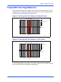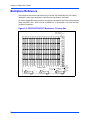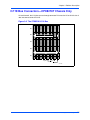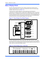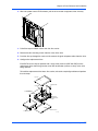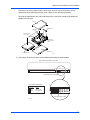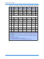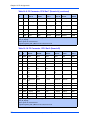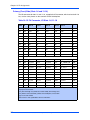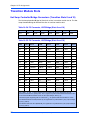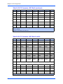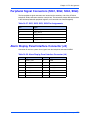
1
i
CPX8216 and CPX8216T
Installation and Use
6806800A52C
October 2008 Edition
© Copyright 2008 Emerson
All rights reserved.
Trademarks
Emerson, Business-Critical Continuity, Emerson Network Power and the Emerson Network Power logo are
trademarks and service marks of Emerson Electric Co. © 2008 Emerson Electric Co.
All other trademarks are the property of their respective owners.
PICMG®, CompactPCI®, AdvancedTCA® and the PICMG, CompactPCI and AdvancedTCA logos are
registered trademarks of the PCI Industrial Computer Manufacturers Group.
Notice
While reasonable efforts have been made to assure the accuracy of this document, Emerson assumes no
liability resulting from any omissions in this document, or from the use of the information obtained therein.
Emerson reserves the right to revise this document and to make changes from time to time in the content
hereof without obligation of Emerson to notify any person of such revision or changes.
Electronic versions of this material may be read online, downloaded for personal use, or referenced in
another document as a URL to a Emerson website. The text itself may not be published commercially in
print or electronic form, edited, translated, or otherwise altered without the permission of Emerson,
It is possible that this publication may contain reference to or information about Emerson products
(machines and programs), programming, or services that are not available in your country. Such references
or information must not be construed to mean that Emerson intends to announce such Emerson products,
programming, or services in your country.
Limited and Restricted Rights Legend
If the documentation contained herein is supplied, directly or indirectly, to the U.S. Government, the following
notice shall apply unless otherwise agreed to in writing by Emerson.
Use, duplication, or disclosure by the Government is subject to restrictions as set forth in subparagraph
(b)(3) of the Rights in Technical Data clause at DFARS 252.227-7013 (Nov. 1995) and of the Rights in
Noncommercial Computer Software and Documentation clause at DFARS 252.227-7014 (Jun. 1995).
Contact Address
Emerson Network Power - Embedded Computing
2900 South Diablo Way, Suite 190
Tempe, AZ 85282
USA
Safety Summary
The following general safety precautions must be observed during all phases of operation, service, and repair
of this equipment. Failure to comply with these precautions or with specific warnings elsewhere in this manual
could result in personal injury or damage to the equipment.
The safety precautions listed below represent warnings of certain dangers of which Emerson is aware. You,
as the user of the product, should follow these warnings and all other safety precautions necessary for the
safe operation of the equipment in your operating environment.
Ground the Instrument.
To minimize shock hazard, the equipment chassis and enclosure must be connected to an electrical ground.
If the equipment is supplied with a three-conductor AC power cable, the power cable must be plugged into
an approved three-contact electrical outlet, with the grounding wire (green/yellow) reliably connected to an
electrical ground (safety ground) at the power outlet. The power jack and mating plug of the power cable meet
International Electrotechnical Commission (IEC) safety standards and local electrical regulatory codes.
Do Not Operate in an Explosive Atmosphere.
Do not operate the equipment in any explosive atmosphere such as in the presence of flammable gases or
fumes. Operation of any electrical equipment in such an environment could result in an explosion and cause
injury or damage.
Keep Away From Live Circuits Inside the Equipment.
Operating personnel must not remove equipment covers. Only Factory Authorized Service Personnel or other
qualified service personnel may remove equipment covers for internal subassembly or component
replacement or any internal adjustment. Service personnel should not replace components with power cable
connected. Under certain conditions, dangerous voltages may exist even with the power cable removed. To
avoid injuries, such personnel should always disconnect power and discharge circuits before touching
components.
Use Caution When Exposing or Handling a CRT.
Breakage of a Cathode-Ray Tube (CRT) causes a high-velocity scattering of glass fragments (implosion). To
prevent CRT implosion, do not handle the CRT and avoid rough handling or jarring of the equipment.
Handling of a CRT should be done only by qualified service personnel using approved safety mask and
gloves.
Do Not Substitute Parts or Modify Equipment.
Do not install substitute parts or perform any unauthorized modification of the equipment. Contact your local
Emerson representative for service and repair to ensure that all safety features are maintained.
Observe Warnings in Manual.
Warnings, such as the example below, precede potentially dangerous procedures throughout this manual.
Instructions contained in the warnings must be followed. You should also employ all other safety precautions
which you deem necessary for the operation of the equipment in your operating environment.
Warning
Warning
To prevent serious injury or death from dangerous voltages, use
extreme caution when handling, testing, and adjusting this
equipment and its components.
Flammability
All Emerson PWBs (printed wiring boards) are manufactured with a flammability rating of 94V-0 by ULrecognized manufacturers.
EMI Caution
Caution
!
Caution
This equipment generates, uses and can radiate electromagnetic energy. It may cause
or be susceptible to electromagnetic interference (EMI) if not installed and used with
adequate EMI protection.
CE Notice (European Community)
Warning
!
This is a Class A product. In a domestic environment, this product may cause radio
interference, in which case the user may be required to take adequate measures.
Warning
Emerson products with the CE marking comply with the EMC Directive (89/336/EEC). Compliance with this
directive implies conformity to the following European Norms:
EN55022 “Limits and Methods of Measurement of Radio Interference Characteristics of Information
Technology Equipment”; this product tested to Equipment Class A
EN 300 386 V.1.2.1 “Electromagnetic compatibility and radio spectrum matters (ERM);
Telecommunication network equipment; Electromagnetic compatibility (EMC) requirements”
System products also fulfill EN60950 (product safety) which is essentially the requirement for the Low
Voltage Directive (73/23/EEC).
Board products are tested in a representative system to show compliance with the above mentioned
requirements. A proper installation in a CE-marked system will maintain the required EMC/safety
performance.
In accordance with European Community directives, a “Declaration of Conformity” has been made and is
on file within the European Union. The “Declaration of Conformity” is available on request. Please contact
your sales representative.
The product has been designed to meet the directive on the restriction of the use of certain hazardous
substances in electrical and electronic equipment (RoHS) Directive 2002/95/EC.
FCC Class A
This equipment has been tested and found to comply with the limits for a Class A digital device, pursuant to
Part 15 of the FCC Rules. These limits are designed to provide reasonable protection against harmful
interference when the equipment is operated in a commercial environment. This equipment generates,
uses, and can radiate radio frequency energy and, if not installed and used in accordance with the
instruction manual, may cause harmful interference to radio communications. Operation of this equipment
in a residential area is likely to cause harmful interference in which case the user will be required to correct
the interference at his own expense.
Changes or modifications not expressly approved by Emerson could void the user’s authority to operate the
equipment.
Use only shielded cables when connecting peripherals to assure that appropriate radio frequency emissions
compliance is maintained.
Industrie Canada
This product meets the requirements of the Canadian Interference-Causing Equipment Standard ICES-003.
Cet appareil numérique est conforme à la norme NMB-003 du Canada.
WEEE Compliance
To satisfy the requirements for marking electrical and electronic equipment in accordance with
article 11 (2) of Directive 2002/96/EC, Waste from Electrical and Electronic Equipment
(WEEE), Emerson includes a crossed-out bin symbol on all standard and noncustom chassis
product. This marking fulfills the requirement set out by WEEE that a producer of an electrical
or electronic appliance that bears their trade name and is put on the European Union market
after 13 August 2005, places a clearly identifiable mark on the equipment and that this mark
signifies that equipment is to be reprocessed or recycled using authorized recyclers and processes. This
minimizes the disposal of unsorted municipal waste, achieves a high level of separate collection of WEEE,
and ensures the environmentally sound disposal of electrical and electronic equipment placed on the market
after 13 August 2005.
To dispose of equipment marked with the WEEE symbol, Emerson has contracted with certified companies
that can reprocess this equipment per European Union requirements. Please visit the Emerson web site or
contact your Emerson representative to find out who to contact and how to dispose of the equipment.
Contents
About This Manual . . . . . . . . . . . . . . . . . . . . . . . . . . . . . . . . . . . . . . . . . . . . . . . . . . . . . . . . . . . . . . . . . xix
Overview of Contents . . . . . . . . . . . . . . . . . . . . . . . . . . . . . . . . . . . . . . . . . . . . . . . . . . . . . . . . . . . . . xix
Summary of Changes . . . . . . . . . . . . . . . . . . . . . . . . . . . . . . . . . . . . . . . . . . . . . . . . . . . . . . . . . . . . xx
Comments and Suggestions . . . . . . . . . . . . . . . . . . . . . . . . . . . . . . . . . . . . . . . . . . . . . . . . . . . . . . . xx
Conventions Used in This Manual . . . . . . . . . . . . . . . . . . . . . . . . . . . . . . . . . . . . . . . . . . . . . . . . . . . xxi
1
Introduction . . . . . . . . . . . . . . . . . . . . . . . . . . . . . . . . . . . . . . . . . . . . . . . . . . . . . . . . . . . . . . . . . . . . . 1
Overview . . . . . . . . . . . . . . . . . . . . . . . . . . . . . . . . . . . . . . . . . . . . . . . . . . . . . . . . . . . . . . . . . . . . . . . 1
Chassis Features . . . . . . . . . . . . . . . . . . . . . . . . . . . . . . . . . . . . . . . . . . . . . . . . . . . . . . . . . . . . . . . . . 1
2
System Architecture . . . . . . . . . . . . . . . . . . . . . . . . . . . . . . . . . . . . . . . . . . . . . . . . . . . . . . . . . . . . . . 3
Overview . . . . . . . . . . . . . . . . . . . . . . . . . . . . . . . . . . . . . . . . . . . . . . . . . . . . . . . . . . . . . . . . . . . . . . . 3
System Domains . . . . . . . . . . . . . . . . . . . . . . . . . . . . . . . . . . . . . . . . . . . . . . . . . . . . . . . . . . . . . . . . . 3
Platform Layout . . . . . . . . . . . . . . . . . . . . . . . . . . . . . . . . . . . . . . . . . . . . . . . . . . . . . . . . . . . . . . . . . . 4
CPX8216 Standard Layout . . . . . . . . . . . . . . . . . . . . . . . . . . . . . . . . . . . . . . . . . . . . . . . . . . . . . . 5
CPX8216T (H.110) Layout . . . . . . . . . . . . . . . . . . . . . . . . . . . . . . . . . . . . . . . . . . . . . . . . . . . . . . 6
Bus Access and Control . . . . . . . . . . . . . . . . . . . . . . . . . . . . . . . . . . . . . . . . . . . . . . . . . . . . . . . . . . . . 7
The Hot Swap Controller/Bridge (HSC) Module . . . . . . . . . . . . . . . . . . . . . . . . . . . . . . . . . . . . . . . . . . 7
Hot Swap Controller . . . . . . . . . . . . . . . . . . . . . . . . . . . . . . . . . . . . . . . . . . . . . . . . . . . . . . . . . . . . . . . 8
System Processor Configurations . . . . . . . . . . . . . . . . . . . . . . . . . . . . . . . . . . . . . . . . . . . . . . . . . . . . 9
The Simplex Configuration . . . . . . . . . . . . . . . . . . . . . . . . . . . . . . . . . . . . . . . . . . . . . . . . . . . . . . 9
The Active/Passive Configuration . . . . . . . . . . . . . . . . . . . . . . . . . . . . . . . . . . . . . . . . . . . . . . . . 10
The Active/Active or Load-Sharing Configuration . . . . . . . . . . . . . . . . . . . . . . . . . . . . . . . . . . . . 10
I/O Configurations . . . . . . . . . . . . . . . . . . . . . . . . . . . . . . . . . . . . . . . . . . . . . . . . . . . . . . . . . . . . . . . 11
CPU Complex Architecture . . . . . . . . . . . . . . . . . . . . . . . . . . . . . . . . . . . . . . . . . . . . . . . . . . . . . . . . 12
The CPU Module . . . . . . . . . . . . . . . . . . . . . . . . . . . . . . . . . . . . . . . . . . . . . . . . . . . . . . . . . . . . . 12
Switching Service to the Passive CPU . . . . . . . . . . . . . . . . . . . . . . . . . . . . . . . . . . . . . . . . . . . . 12
Board Insertion and Extraction Features . . . . . . . . . . . . . . . . . . . . . . . . . . . . . . . . . . . . . . . . . . . . . . 13
Staged Pins . . . . . . . . . . . . . . . . . . . . . . . . . . . . . . . . . . . . . . . . . . . . . . . . . . . . . . . . . . . . . . . . . 13
BD_SEL# . . . . . . . . . . . . . . . . . . . . . . . . . . . . . . . . . . . . . . . . . . . . . . . . . . . . . . . . . . . . . . . 13
ENUM# . . . . . . . . . . . . . . . . . . . . . . . . . . . . . . . . . . . . . . . . . . . . . . . . . . . . . . . . . . . . . . . . . 13
Typical Insertion and Extraction Processes . . . . . . . . . . . . . . . . . . . . . . . . . . . . . . . . . . . . . . . . . 14
The Hot Swap Process . . . . . . . . . . . . . . . . . . . . . . . . . . . . . . . . . . . . . . . . . . . . . . . . . . . . . . . . . . . 14
Physical Connection Process . . . . . . . . . . . . . . . . . . . . . . . . . . . . . . . . . . . . . . . . . . . . . . . . . . . 15
Hardware Connection Process . . . . . . . . . . . . . . . . . . . . . . . . . . . . . . . . . . . . . . . . . . . . . . . . . . 15
Software Connection Process . . . . . . . . . . . . . . . . . . . . . . . . . . . . . . . . . . . . . . . . . . . . . . . . . . . 15
Software Disconnection Process . . . . . . . . . . . . . . . . . . . . . . . . . . . . . . . . . . . . . . . . . . . . . . . . . 16
Hardware Resources . . . . . . . . . . . . . . . . . . . . . . . . . . . . . . . . . . . . . . . . . . . . . . . . . . . . . . . . . . . . . 16
CPX8216 and CPX8216T Installation and Use (6806800A52C)
vii
Contents
Device Drivers . . . . . . . . . . . . . . . . . . . . . . . . . . . . . . . . . . . . . . . . . . . . . . . . . . . . . . . . . . . . . . . . . . 16
3
Platform Description. . . . . . . . . . . . . . . . . . . . . . . . . . . . . . . . . . . . . . . . . . . . . . . . . . . . . . . . . . . . . 17
Overview . . . . . . . . . . . . . . . . . . . . . . . . . . . . . . . . . . . . . . . . . . . . . . . . . . . . . . . . . . . . . . . . . . . . . .
Parts of the Chassis . . . . . . . . . . . . . . . . . . . . . . . . . . . . . . . . . . . . . . . . . . . . . . . . . . . . . . . . . . . . . .
CompactPCI Card Cage Reference . . . . . . . . . . . . . . . . . . . . . . . . . . . . . . . . . . . . . . . . . . . . . . . . . .
Backplane Reference . . . . . . . . . . . . . . . . . . . . . . . . . . . . . . . . . . . . . . . . . . . . . . . . . . . . . . . . . . . . .
H.110 Bus Connectors—CPX8216T Chassis Only . . . . . . . . . . . . . . . . . . . . . . . . . . . . . . . . . . . . . .
Alarm Display Panel . . . . . . . . . . . . . . . . . . . . . . . . . . . . . . . . . . . . . . . . . . . . . . . . . . . . . . . . . . . . . .
Power/Fan Modules . . . . . . . . . . . . . . . . . . . . . . . . . . . . . . . . . . . . . . . . . . . . . . . . . . . . . . . . . . . . . .
Power Distribution Panel . . . . . . . . . . . . . . . . . . . . . . . . . . . . . . . . . . . . . . . . . . . . . . . . . . . . . . . . . .
AC Power Distribution Panel (CPX8216) . . . . . . . . . . . . . . . . . . . . . . . . . . . . . . . . . . . . . . . . . .
Dual Input DC Power Distribution Panel (CPX8216) . . . . . . . . . . . . . . . . . . . . . . . . . . . . . . . . . .
Dual Breaker DC Power Distribution Panel (CPX8216) . . . . . . . . . . . . . . . . . . . . . . . . . . . . . . .
H.110 DC Power Distribution Panel (CPX8216T) . . . . . . . . . . . . . . . . . . . . . . . . . . . . . . . . . . . .
Drive Modules . . . . . . . . . . . . . . . . . . . . . . . . . . . . . . . . . . . . . . . . . . . . . . . . . . . . . . . . . . . . . . . . . .
4
Site Preparation. . . . . . . . . . . . . . . . . . . . . . . . . . . . . . . . . . . . . . . . . . . . . . . . . . . . . . . . . . . . . . . . . 27
Overview . . . . . . . . . . . . . . . . . . . . . . . . . . . . . . . . . . . . . . . . . . . . . . . . . . . . . . . . . . . . . . . . . . . . . .
Safety and Regulatory Compliance . . . . . . . . . . . . . . . . . . . . . . . . . . . . . . . . . . . . . . . . . . . . . . . . . .
Receiving and Unpacking the Chassis . . . . . . . . . . . . . . . . . . . . . . . . . . . . . . . . . . . . . . . . . . . . . . . .
Receiving the Chassis . . . . . . . . . . . . . . . . . . . . . . . . . . . . . . . . . . . . . . . . . . . . . . . . . . . . . . . . .
Unpacking the Chassis . . . . . . . . . . . . . . . . . . . . . . . . . . . . . . . . . . . . . . . . . . . . . . . . . . . . . . . .
Preparing the Site for Installation . . . . . . . . . . . . . . . . . . . . . . . . . . . . . . . . . . . . . . . . . . . . . . . . . . . .
Guidelines for Chassis Location . . . . . . . . . . . . . . . . . . . . . . . . . . . . . . . . . . . . . . . . . . . . . . . . .
Mounting Options . . . . . . . . . . . . . . . . . . . . . . . . . . . . . . . . . . . . . . . . . . . . . . . . . . . . . . . . . . . .
Weight Distribution in a Rack . . . . . . . . . . . . . . . . . . . . . . . . . . . . . . . . . . . . . . . . . . . . . . . . . . .
Power Requirements . . . . . . . . . . . . . . . . . . . . . . . . . . . . . . . . . . . . . . . . . . . . . . . . . . . . . . . . . . . . .
Guidelines for Branch Circuits . . . . . . . . . . . . . . . . . . . . . . . . . . . . . . . . . . . . . . . . . . . . . . . . . . .
Power Circuit Protection . . . . . . . . . . . . . . . . . . . . . . . . . . . . . . . . . . . . . . . . . . . . . . . . . . . . . . .
Circuit Breakers and Receptacles . . . . . . . . . . . . . . . . . . . . . . . . . . . . . . . . . . . . . . . . . . . . . . . .
Power Cords . . . . . . . . . . . . . . . . . . . . . . . . . . . . . . . . . . . . . . . . . . . . . . . . . . . . . . . . . . . . . . . .
Cables . . . . . . . . . . . . . . . . . . . . . . . . . . . . . . . . . . . . . . . . . . . . . . . . . . . . . . . . . . . . . . . . . . . . . . . .
Cable Planning . . . . . . . . . . . . . . . . . . . . . . . . . . . . . . . . . . . . . . . . . . . . . . . . . . . . . . . . . . . . . . . . . .
Environmental Considerations . . . . . . . . . . . . . . . . . . . . . . . . . . . . . . . . . . . . . . . . . . . . . . . . . . . . . .
Enclosure Cooling Considerations . . . . . . . . . . . . . . . . . . . . . . . . . . . . . . . . . . . . . . . . . . . . . . . . . . .
5
27
27
27
27
27
28
28
28
28
28
29
29
29
30
30
30
31
31
Chassis Installation . . . . . . . . . . . . . . . . . . . . . . . . . . . . . . . . . . . . . . . . . . . . . . . . . . . . . . . . . . . . . 33
Overview . . . . . . . . . . . . . . . . . . . . . . . . . . . . . . . . . . . . . . . . . . . . . . . . . . . . . . . . . . . . . . . . . . . . . .
Tools You Will Need . . . . . . . . . . . . . . . . . . . . . . . . . . . . . . . . . . . . . . . . . . . . . . . . . . . . . . . . . . . . . .
Electrostatic Discharge (ESD) and Safety Procedures . . . . . . . . . . . . . . . . . . . . . . . . . . . . . . . . . . .
Mounting Hole Locations . . . . . . . . . . . . . . . . . . . . . . . . . . . . . . . . . . . . . . . . . . . . . . . . . . . . . . . . . .
Mounting Dimension for a 19" Frame Relay or EIA Rack . . . . . . . . . . . . . . . . . . . . . . . . . . . . . .
Mounting Dimension for a 23" Frame Relay or EIA Rack . . . . . . . . . . . . . . . . . . . . . . . . . . . . . .
viii
17
18
19
20
21
22
23
24
24
24
25
25
26
CPX8216 and CPX8216T Installation and Use (6806800A52C)
33
33
33
34
35
36
Contents
Weight Distribution Within a Rack . . . . . . . . . . . . . . . . . . . . . . . . . . . . . . . . . . . . . . . . . . . . . . . . . . .
Installing the Chassis in a Frame Relay Rack/Cabinet . . . . . . . . . . . . . . . . . . . . . . . . . . . . . . . . . . .
Installing the Chassis in an EIA Equipment Rack/Cabinet . . . . . . . . . . . . . . . . . . . . . . . . . . . . . . . . .
Connecting the Chassis Cables . . . . . . . . . . . . . . . . . . . . . . . . . . . . . . . . . . . . . . . . . . . . . . . . . . . . .
Connecting the Chassis Power Source . . . . . . . . . . . . . . . . . . . . . . . . . . . . . . . . . . . . . . . . . . . .
Connecting a SCSI Cable . . . . . . . . . . . . . . . . . . . . . . . . . . . . . . . . . . . . . . . . . . . . . . . . . . . . . .
Connecting a Serial Console . . . . . . . . . . . . . . . . . . . . . . . . . . . . . . . . . . . . . . . . . . . . . . . . . . . .
Connecting Video, Keyboard, and Mouse . . . . . . . . . . . . . . . . . . . . . . . . . . . . . . . . . . . . . . . . . .
6
Chassis Operations . . . . . . . . . . . . . . . . . . . . . . . . . . . . . . . . . . . . . . . . . . . . . . . . . . . . . . . . . . . . . 45
Overview . . . . . . . . . . . . . . . . . . . . . . . . . . . . . . . . . . . . . . . . . . . . . . . . . . . . . . . . . . . . . . . . . . . . . .
Recommended Power-On Procedures . . . . . . . . . . . . . . . . . . . . . . . . . . . . . . . . . . . . . . . . . . . . . . .
Recommended Power-Off Procedure . . . . . . . . . . . . . . . . . . . . . . . . . . . . . . . . . . . . . . . . . . . . . . . .
Emergency Power-Off Procedure . . . . . . . . . . . . . . . . . . . . . . . . . . . . . . . . . . . . . . . . . . . . . . . . . . .
Controls and Indicators . . . . . . . . . . . . . . . . . . . . . . . . . . . . . . . . . . . . . . . . . . . . . . . . . . . . . . . . . . .
Input Power Rocker Switch . . . . . . . . . . . . . . . . . . . . . . . . . . . . . . . . . . . . . . . . . . . . . . . . . . . . .
Indicators . . . . . . . . . . . . . . . . . . . . . . . . . . . . . . . . . . . . . . . . . . . . . . . . . . . . . . . . . . . . . . . . . . .
System Status Indicators . . . . . . . . . . . . . . . . . . . . . . . . . . . . . . . . . . . . . . . . . . . . . . . . . . . . . . .
Telco Alarm Indicators . . . . . . . . . . . . . . . . . . . . . . . . . . . . . . . . . . . . . . . . . . . . . . . . . . . . . . . . .
CompactPCI Slot Status Indicators . . . . . . . . . . . . . . . . . . . . . . . . . . . . . . . . . . . . . . . . . . . . . . .
Power Supply/Fan Indicators . . . . . . . . . . . . . . . . . . . . . . . . . . . . . . . . . . . . . . . . . . . . . . . . . . . .
Drive Indicators . . . . . . . . . . . . . . . . . . . . . . . . . . . . . . . . . . . . . . . . . . . . . . . . . . . . . . . . . . . . . .
Setting the Chassis ID on the CPX8216T . . . . . . . . . . . . . . . . . . . . . . . . . . . . . . . . . . . . . . . . . . . . .
Chassis Cooling . . . . . . . . . . . . . . . . . . . . . . . . . . . . . . . . . . . . . . . . . . . . . . . . . . . . . . . . . . . . . . . . .
Cooling Monitoring . . . . . . . . . . . . . . . . . . . . . . . . . . . . . . . . . . . . . . . . . . . . . . . . . . . . . . . . . . . . . . .
Power Monitoring . . . . . . . . . . . . . . . . . . . . . . . . . . . . . . . . . . . . . . . . . . . . . . . . . . . . . . . . . . . . . . . .
7
45
45
46
46
46
47
47
47
48
49
50
51
51
53
55
55
Installing Boards in the Chassis . . . . . . . . . . . . . . . . . . . . . . . . . . . . . . . . . . . . . . . . . . . . . . . . . . . 57
Before You Install or Remove a Board . . . . . . . . . . . . . . . . . . . . . . . . . . . . . . . . . . . . . . . . . . . . . . . .
Observe ESD Precautions . . . . . . . . . . . . . . . . . . . . . . . . . . . . . . . . . . . . . . . . . . . . . . . . . . . . . .
Watch for Bent Pins or Other Damage . . . . . . . . . . . . . . . . . . . . . . . . . . . . . . . . . . . . . . . . . . . .
Use Caution When Installing or Removing Boards . . . . . . . . . . . . . . . . . . . . . . . . . . . . . . . . . . .
Preserve EMI Compliance . . . . . . . . . . . . . . . . . . . . . . . . . . . . . . . . . . . . . . . . . . . . . . . . . . . . . .
Understand Hot Swap . . . . . . . . . . . . . . . . . . . . . . . . . . . . . . . . . . . . . . . . . . . . . . . . . . . . . . . . .
Recognize Different Injector/Ejector Lever Types . . . . . . . . . . . . . . . . . . . . . . . . . . . . . . . . . . . .
Verify Slot Usage . . . . . . . . . . . . . . . . . . . . . . . . . . . . . . . . . . . . . . . . . . . . . . . . . . . . . . . . . . . . .
Installing a Module . . . . . . . . . . . . . . . . . . . . . . . . . . . . . . . . . . . . . . . . . . . . . . . . . . . . . . . . . . . . . . .
Removing a Hot-Swap Module . . . . . . . . . . . . . . . . . . . . . . . . . . . . . . . . . . . . . . . . . . . . . . . . . . . . .
Installing a Transition Module . . . . . . . . . . . . . . . . . . . . . . . . . . . . . . . . . . . . . . . . . . . . . . . . . . . . . .
8
36
37
39
40
40
41
42
42
57
57
57
57
58
58
59
59
60
61
63
Drive Removal and Installation . . . . . . . . . . . . . . . . . . . . . . . . . . . . . . . . . . . . . . . . . . . . . . . . . . . . 65
Introduction . . . . . . . . . . . . . . . . . . . . . . . . . . . . . . . . . . . . . . . . . . . . . . . . . . . . . . . . . . . . . . . . . . . . 65
Overview of Hot Swapping a Drive . . . . . . . . . . . . . . . . . . . . . . . . . . . . . . . . . . . . . . . . . . . . . . . . . . 65
Overview of Carrier Frames . . . . . . . . . . . . . . . . . . . . . . . . . . . . . . . . . . . . . . . . . . . . . . . . . . . . . . . . 66
CPX8216 and CPX8216T Installation and Use (6806800A52C)
ix
Contents
Removing a Carrier Frame . . . . . . . . . . . . . . . . . . . . . . . . . . . . . . . . . . . . . . . . . . . . . . . . . . . . .
Hot Swap IDE Drives . . . . . . . . . . . . . . . . . . . . . . . . . . . . . . . . . . . . . . . . . . . . . . . . . . . . . . . . . . . . .
Installing an IDE Carrier Frame and Assigning Domains . . . . . . . . . . . . . . . . . . . . . . . . . . . . . .
Cabling the IDE Carrier Frame . . . . . . . . . . . . . . . . . . . . . . . . . . . . . . . . . . . . . . . . . . . . . . . . . .
Replacing a Hot Swap IDE Drive Module . . . . . . . . . . . . . . . . . . . . . . . . . . . . . . . . . . . . . . . . . .
Installing the IDE Hot Swap Drive Module . . . . . . . . . . . . . . . . . . . . . . . . . . . . . . . . . . . . . . . . . .
Hot Swap SCSI Drives . . . . . . . . . . . . . . . . . . . . . . . . . . . . . . . . . . . . . . . . . . . . . . . . . . . . . . . . . . . .
Installing a SCSI Carrier Frame and Assigning Domains . . . . . . . . . . . . . . . . . . . . . . . . . . . . . .
Cabling the SCSI Carrier Frame . . . . . . . . . . . . . . . . . . . . . . . . . . . . . . . . . . . . . . . . . . . . . . . . .
Replacing a Hot Swap SCSI Drive Module . . . . . . . . . . . . . . . . . . . . . . . . . . . . . . . . . . . . . . . . .
Installing the SCSI Hot Swap Drive Module . . . . . . . . . . . . . . . . . . . . . . . . . . . . . . . . . . . . . . . .
Non-Hot Swap Drive Modules . . . . . . . . . . . . . . . . . . . . . . . . . . . . . . . . . . . . . . . . . . . . . . . . . . . . . .
Replacing a Non-Hot Swap 3.5-inch Drive . . . . . . . . . . . . . . . . . . . . . . . . . . . . . . . . . . . . . . . . .
Removing the Drive from the Standard Carrier . . . . . . . . . . . . . . . . . . . . . . . . . . . . . . . . . . . . . .
Drive Configuration . . . . . . . . . . . . . . . . . . . . . . . . . . . . . . . . . . . . . . . . . . . . . . . . . . . . . . . . . . .
Configuring Non-Hot Swap SCSI Drives . . . . . . . . . . . . . . . . . . . . . . . . . . . . . . . . . . . . . . . .
Configuring Non-Hot Swap IDE Drives . . . . . . . . . . . . . . . . . . . . . . . . . . . . . . . . . . . . . . . . .
Installing the Drive In the Standard Carrier . . . . . . . . . . . . . . . . . . . . . . . . . . . . . . . . . . . . . . . . .
Installing the Drive Module into the Drive Bay . . . . . . . . . . . . . . . . . . . . . . . . . . . . . . . . . . . . . . .
Replacing a Non-Hot Swap 5.25-inch Drive . . . . . . . . . . . . . . . . . . . . . . . . . . . . . . . . . . . . . . . . . . . .
Removing a 5.25-inch Drive . . . . . . . . . . . . . . . . . . . . . . . . . . . . . . . . . . . . . . . . . . . . . . . . . . . .
Installing the 5.25-inch Drive . . . . . . . . . . . . . . . . . . . . . . . . . . . . . . . . . . . . . . . . . . . . . . . . . . . .
Cabling the SCSI or IDE Non-Hot Swap Drive . . . . . . . . . . . . . . . . . . . . . . . . . . . . . . . . . . . . . .
Replacing a Floppy Drive . . . . . . . . . . . . . . . . . . . . . . . . . . . . . . . . . . . . . . . . . . . . . . . . . . . . . . . . . .
Removal . . . . . . . . . . . . . . . . . . . . . . . . . . . . . . . . . . . . . . . . . . . . . . . . . . . . . . . . . . . . . . . . . . .
Installation . . . . . . . . . . . . . . . . . . . . . . . . . . . . . . . . . . . . . . . . . . . . . . . . . . . . . . . . . . . . . . . . . .
9
66
67
67
69
70
73
74
74
76
78
81
82
82
83
84
84
84
85
86
87
87
88
89
90
90
90
Subassembly Removal and Installation . . . . . . . . . . . . . . . . . . . . . . . . . . . . . . . . . . . . . . . . . . . . . 93
Overview . . . . . . . . . . . . . . . . . . . . . . . . . . . . . . . . . . . . . . . . . . . . . . . . . . . . . . . . . . . . . . . . . . . . . .
Fan and Power Supply Sled Removal and Installation . . . . . . . . . . . . . . . . . . . . . . . . . . . . . . . . . . .
Removal . . . . . . . . . . . . . . . . . . . . . . . . . . . . . . . . . . . . . . . . . . . . . . . . . . . . . . . . . . . . . . . . . . .
Installation . . . . . . . . . . . . . . . . . . . . . . . . . . . . . . . . . . . . . . . . . . . . . . . . . . . . . . . . . . . . . . . . . .
Fan Module Replacement . . . . . . . . . . . . . . . . . . . . . . . . . . . . . . . . . . . . . . . . . . . . . . . . . . . . .
Alarm Panel Removal and Installation (Hot Swap) . . . . . . . . . . . . . . . . . . . . . . . . . . . . . . . . . . . . . .
Removal . . . . . . . . . . . . . . . . . . . . . . . . . . . . . . . . . . . . . . . . . . . . . . . . . . . . . . . . . . . . . . . . . . .
Installation . . . . . . . . . . . . . . . . . . . . . . . . . . . . . . . . . . . . . . . . . . . . . . . . . . . . . . . . . . . . . . . . . .
AC or DC Power Distribution Panel . . . . . . . . . . . . . . . . . . . . . . . . . . . . . . . . . . . . . . . . . . . . . . . . . .
Floppy Housing Removal and Installation . . . . . . . . . . . . . . . . . . . . . . . . . . . . . . . . . . . . . . . . . . . . .
Removal . . . . . . . . . . . . . . . . . . . . . . . . . . . . . . . . . . . . . . . . . . . . . . . . . . . . . . . . . . . . . . . . . . .
Installing the Floppy Housing . . . . . . . . . . . . . . . . . . . . . . . . . . . . . . . . . . . . . . . . . . . . . . . . . . .
93
93
94
95
95
96
96
97
97
98
98
98
10 Pin Assignments . . . . . . . . . . . . . . . . . . . . . . . . . . . . . . . . . . . . . . . . . . . . . . . . . . . . . . . . . . . . . . . 101
Overview . . . . . . . . . . . . . . . . . . . . . . . . . . . . . . . . . . . . . . . . . . . . . . . . . . . . . . . . . . . . . . . . . . . . . 101
Backplane Connectors . . . . . . . . . . . . . . . . . . . . . . . . . . . . . . . . . . . . . . . . . . . . . . . . . . . . . . . . . . . 101
Primary (Front) Side I/O Connectors (Slots 1-6 and 11-16) . . . . . . . . . . . . . . . . . . . . . . . . . . . 101
x
CPX8216 and CPX8216T Installation and Use (6806800A52C)
Contents
Primary (Front) Side CPU Slot Connectors (7 and 9) . . . . . . . . . . . . . . . . . . . . . . . . . . . . . . . .
Secondary (Rear) Side I/O Connectors . . . . . . . . . . . . . . . . . . . . . . . . . . . . . . . . . . . . . . . . . . .
Primary (Front) Side I/O Connectors . . . . . . . . . . . . . . . . . . . . . . . . . . . . . . . . . . . . . . . . . . . .
Primary (Front) Side (Slots 1-6 and 11-16) . . . . . . . . . . . . . . . . . . . . . . . . . . . . . . . . . . . .
Primary (Front) Side CPU Connectors . . . . . . . . . . . . . . . . . . . . . . . . . . . . . . . . . . . . . . . .
Primary (Front) Side HSC Connectors . . . . . . . . . . . . . . . . . . . . . . . . . . . . . . . . . . . . . . . .
Secondary (Rear) Side I/O Connectors . . . . . . . . . . . . . . . . . . . . . . . . . . . . . . . . . . . . . . . . . . .
Transition Module Slots . . . . . . . . . . . . . . . . . . . . . . . . . . . . . . . . . . . . . . . . . . . . . . . . . . . . . . . . . .
Hot Swap Controller/Bridge Connectors (Transition Slots 8 and 10) . . . . . . . . . . . . . . . . . . . .
CPU Transition Module Connectors
(Transition Slots 7 and 9) . . . . . . . . . . . . . . . . . . . . . . . . . . . . . . . . . . . . . . . . . . . . . . . . . . . . .
Secondary (Rear) Side CPU Transition Module Connectors . . . . . . . . . . . . . . . . . . . . . . . . . .
Alarm Interface Connector (ALARM) . . . . . . . . . . . . . . . . . . . . . . . . . . . . . . . . . . . . . . . . . . . . . . . .
Power Supply Connectors (PS1, PS2, PS3) . . . . . . . . . . . . . . . . . . . . . . . . . . . . . . . . . . . . . . . . . .
H.110 Power Connector (CPX8216T Only) . . . . . . . . . . . . . . . . . . . . . . . . . . . . . . . . . . . . . . . . . . .
Peripheral Power Connectors (PWR1, PWR2, PWR3, PWR4) . . . . . . . . . . . . . . . . . . . . . . . . . . . .
Peripheral Signal Connectors (SIG1, SIG2, SIG3, SIG4) . . . . . . . . . . . . . . . . . . . . . . . . . . . . . . . .
Alarm Display Panel Interface Connector (J4) . . . . . . . . . . . . . . . . . . . . . . . . . . . . . . . . . . . . . . . . .
Remote Alarm Connector (J1) . . . . . . . . . . . . . . . . . . . . . . . . . . . . . . . . . . . . . . . . . . . . . . . . . . . . .
Drive Connectors . . . . . . . . . . . . . . . . . . . . . . . . . . . . . . . . . . . . . . . . . . . . . . . . . . . . . . . . . . . . . . .
Floppy Drive (FDA, FDB) . . . . . . . . . . . . . . . . . . . . . . . . . . . . . . . . . . . . . . . . . . . . . . . . . . . . . .
IDE Drive (IDEA and IDEB) . . . . . . . . . . . . . . . . . . . . . . . . . . . . . . . . . . . . . . . . . . . . . . . . . . . .
A
105
110
111
112
113
113
119
120
120
125
126
127
127
128
128
129
129
130
130
130
131
Specifications . . . . . . . . . . . . . . . . . . . . . . . . . . . . . . . . . . . . . . . . . . . . . . . . . . . . . . . . . . . . . . . . . 133
Environmental Characteristics . . . . . . . . . . . . . . . . . . . . . . . . . . . . . . . . . . . . . . . . . . . . . . . . . . . . . 133
Power Supply Electrical Specifications . . . . . . . . . . . . . . . . . . . . . . . . . . . . . . . . . . . . . . . . . . . . . . 133
NEBS . . . . . . . . . . . . . . . . . . . . . . . . . . . . . . . . . . . . . . . . . . . . . . . . . . . . . . . . . . . . . . . . . . . . . . . . 136
B
Systeminstallationsanleitung . . . . . . . . . . . . . . . . . . . . . . . . . . . . . . . . . . . . . . . . . . . . . . . . . . . . 139
Empfangen und Auspacken . . . . . . . . . . . . . . . . . . . . . . . . . . . . . . . . . . . . . . . . . . . . . . . . . . . . . .
Richtlinien zum Aufstellen des Systems . . . . . . . . . . . . . . . . . . . . . . . . . . . . . . . . . . . . . . . . . . . . .
Kühlen des Gehäuses . . . . . . . . . . . . . . . . . . . . . . . . . . . . . . . . . . . . . . . . . . . . . . . . . . . . . . . . . . .
ESE und Sicherheit . . . . . . . . . . . . . . . . . . . . . . . . . . . . . . . . . . . . . . . . . . . . . . . . . . . . . . . . . . . . .
Sicherheits- und Betriebsnormen . . . . . . . . . . . . . . . . . . . . . . . . . . . . . . . . . . . . . . . . . . . . . . . . . . .
Vorsichtshinweise zur Lithium-Batterie . . . . . . . . . . . . . . . . . . . . . . . . . . . . . . . . . . . . . . . . . . . . . .
Stromkreisbelastung . . . . . . . . . . . . . . . . . . . . . . . . . . . . . . . . . . . . . . . . . . . . . . . . . . . . . . . . . . . .
Installation in ein 19-Zoll-Rack . . . . . . . . . . . . . . . . . . . . . . . . . . . . . . . . . . . . . . . . . . . . . . . . . . . . .
Anschließen des Systems . . . . . . . . . . . . . . . . . . . . . . . . . . . . . . . . . . . . . . . . . . . . . . . . . . . . . . . .
Einschalten des Netzstroms . . . . . . . . . . . . . . . . . . . . . . . . . . . . . . . . . . . . . . . . . . . . . . . . . . . . . . .
C
139
139
140
140
141
141
141
141
142
142
Related Documentation . . . . . . . . . . . . . . . . . . . . . . . . . . . . . . . . . . . . . . . . . . . . . . . . . . . . . . . . . 145
Emerson Network Power - Embedded Computing Documents . . . . . . . . . . . . . . . . . . . . . . . . . . . . 145
Related Specifications . . . . . . . . . . . . . . . . . . . . . . . . . . . . . . . . . . . . . . . . . . . . . . . . . . . . . . . . . . . 146
CPX8216 and CPX8216T Installation and Use (6806800A52C)
xi
Contents
xii
CPX8216 and CPX8216T Installation and Use (6806800A52C)
List of Figures
Figure 2-1. Bus Domains . . . . . . . . . . . . . . . . . . . . . . . . . . . . . . . . . . . . . . . . . . . . . . . . . . . . . . . . . . . 4
Figure 2-2. CPX8216 Standard Layout . . . . . . . . . . . . . . . . . . . . . . . . . . . . . . . . . . . . . . . . . . . . . . . . 5
Figure 2-3. CPX8216T (H.110) Layout . . . . . . . . . . . . . . . . . . . . . . . . . . . . . . . . . . . . . . . . . . . . . . . . 6
Figure 2-4. CPX8216 I/O Bus Connectivity . . . . . . . . . . . . . . . . . . . . . . . . . . . . . . . . . . . . . . . . . . . . . 7
Figure 2-5. Simplex Configuration . . . . . . . . . . . . . . . . . . . . . . . . . . . . . . . . . . . . . . . . . . . . . . . . . . . . 9
Figure 2-6. Active/Passive Configuration . . . . . . . . . . . . . . . . . . . . . . . . . . . . . . . . . . . . . . . . . . . . . 10
Figure 2-7. Active/Active Configuration . . . . . . . . . . . . . . . . . . . . . . . . . . . . . . . . . . . . . . . . . . . . . . . 11
Figure 3-1. CPX8216 Front View . . . . . . . . . . . . . . . . . . . . . . . . . . . . . . . . . . . . . . . . . . . . . . . . . . . . 18
Figure 3-2. CPX8216 Rear View . . . . . . . . . . . . . . . . . . . . . . . . . . . . . . . . . . . . . . . . . . . . . . . . . . . . 18
Figure 3-3. Card Cage Rail Color Scheme - Standard Chassis . . . . . . . . . . . . . . . . . . . . . . . . . . . . 19
Figure 3-4. Card Cage Rail Color Scheme - H.110 Chassis . . . . . . . . . . . . . . . . . . . . . . . . . . . . . . . 19
Figure 3-5. CPX8216/CPX8216T Backplane - Primary Side . . . . . . . . . . . . . . . . . . . . . . . . . . . . . . 20
Figure 3-6. The CPX8216 H.110 Bus . . . . . . . . . . . . . . . . . . . . . . . . . . . . . . . . . . . . . . . . . . . . . . . . 21
Figure 3-7. Alarm Display Panel Block Diagram . . . . . . . . . . . . . . . . . . . . . . . . . . . . . . . . . . . . . . . . 22
Figure 3-8. Alarm Display Panel - Front View . . . . . . . . . . . . . . . . . . . . . . . . . . . . . . . . . . . . . . . . . . 22
Figure 3-9. AC Power Distribution Panel . . . . . . . . . . . . . . . . . . . . . . . . . . . . . . . . . . . . . . . . . . . . . . 24
Figure 3-10. Dual Input DC Power Distribution Panel . . . . . . . . . . . . . . . . . . . . . . . . . . . . . . . . . . . . 24
Figure 3-11. Dual Breaker DC Power Distribution Panel . . . . . . . . . . . . . . . . . . . . . . . . . . . . . . . . . . 25
Figure 3-12. H.110 DC Power Distribution Panel . . . . . . . . . . . . . . . . . . . . . . . . . . . . . . . . . . . . . . . 25
Figure 3-13. Ring Terminal for H.110 DC Voltage . . . . . . . . . . . . . . . . . . . . . . . . . . . . . . . . . . . . . . . 26
Figure 5-1. 19" Rack Mounting Dimensions . . . . . . . . . . . . . . . . . . . . . . . . . . . . . . . . . . . . . . . . . . . 35
Figure 5-2. 23" Rack Mounting Dimensions . . . . . . . . . . . . . . . . . . . . . . . . . . . . . . . . . . . . . . . . . . . 36
Figure 6-1. Input DC Power Rocker Switch . . . . . . . . . . . . . . . . . . . . . . . . . . . . . . . . . . . . . . . . . . . . 47
Figure 6-2. System LED Location . . . . . . . . . . . . . . . . . . . . . . . . . . . . . . . . . . . . . . . . . . . . . . . . . . . 47
Figure 6-3. Telco Alarm Indicator Location . . . . . . . . . . . . . . . . . . . . . . . . . . . . . . . . . . . . . . . . . . . . 48
Figure 6-4. Slot Status Indicator Location . . . . . . . . . . . . . . . . . . . . . . . . . . . . . . . . . . . . . . . . . . . . . 49
Figure 6-5. Power Supply/Fan Status Indicators . . . . . . . . . . . . . . . . . . . . . . . . . . . . . . . . . . . . . . . . 50
Figure 6-6. Drive Status Indicators . . . . . . . . . . . . . . . . . . . . . . . . . . . . . . . . . . . . . . . . . . . . . . . . . . 51
Figure 6-7. S2 Switch Location and J14 Header . . . . . . . . . . . . . . . . . . . . . . . . . . . . . . . . . . . . . . . . 52
Figure 6-8. Air Flow Diagram . . . . . . . . . . . . . . . . . . . . . . . . . . . . . . . . . . . . . . . . . . . . . . . . . . . . . . 54
Figure 7-1. Injector/Ejector Lever Types . . . . . . . . . . . . . . . . . . . . . . . . . . . . . . . . . . . . . . . . . . . . . . 59
CPX8216 and CPX8216T Installation and Use (6806800A52C)
xiii
List of Figures
xiv
CPX8216 and CPX8216T Installation and Use (6806800A52C)
List of Tables
Table 3-1. Alarm LED Color and Description . . . . . . . . . . . . . . . . . . . . . . . . . . . . . . . . . . . . . . . . . . . 23
Table 3-2. DC Analog Voltages for H.110 Bus . . . . . . . . . . . . . . . . . . . . . . . . . . . . . . . . . . . . . . . . . . 26
Table 6-1. System Status Indicators . . . . . . . . . . . . . . . . . . . . . . . . . . . . . . . . . . . . . . . . . . . . . . . . . 48
Table 6-2. Telco Alarm Indicators . . . . . . . . . . . . . . . . . . . . . . . . . . . . . . . . . . . . . . . . . . . . . . . . . . . 48
Table 6-3. CompactPCI Slot Status Indicators . . . . . . . . . . . . . . . . . . . . . . . . . . . . . . . . . . . . . . . . . 49
Table 6-4. Power Supply/Fan Status Indicators . . . . . . . . . . . . . . . . . . . . . . . . . . . . . . . . . . . . . . . . . 50
Table 6-5. Drive Status Indicators . . . . . . . . . . . . . . . . . . . . . . . . . . . . . . . . . . . . . . . . . . . . . . . . . . . 51
Table 6-6. Chassis ID Settings . . . . . . . . . . . . . . . . . . . . . . . . . . . . . . . . . . . . . . . . . . . . . . . . . . . . . 52
Table 7-1. Slot Usage Indicators . . . . . . . . . . . . . . . . . . . . . . . . . . . . . . . . . . . . . . . . . . . . . . . . . . . . 60
Table 10-1. P5 Connector, I/O Slots 1-6 and 11-16 (User I/O) . . . . . . . . . . . . . . . . . . . . . . . . . . . . 101
Table 10-2. P4 Connector, I/O Slots 1-6 and 11-16 (User I/O) . . . . . . . . . . . . . . . . . . . . . . . . . . . . 102
Table 10-3. P3 Connector, I/O Slots 1-6 and 11-16 (User I/O) . . . . . . . . . . . . . . . . . . . . . . . . . . . . 102
Table 10-4. P2 Connector, I/O Slots 1-6 and 11-16 (CPCI Bus) . . . . . . . . . . . . . . . . . . . . . . . . . . . 102
Table 10-5. P1 Connector, I/O Slots 1-6 and 11-16 (CPCI Bus) . . . . . . . . . . . . . . . . . . . . . . . . . . . 103
Table 10-6. P5 Connector, CPU Slots 7 and 9 . . . . . . . . . . . . . . . . . . . . . . . . . . . . . . . . . . . . . . . . 105
Table 10-7. P4 Connector, CPU Slots 7 and 9 . . . . . . . . . . . . . . . . . . . . . . . . . . . . . . . . . . . . . . . . 106
Table 10-8. P3 Connector, CPU Slots 7 and 9 . . . . . . . . . . . . . . . . . . . . . . . . . . . . . . . . . . . . . . . . 107
Table 10-9. P2 Connector, CPU Slot 7 (Domain A) . . . . . . . . . . . . . . . . . . . . . . . . . . . . . . . . . . . . . 107
Table 10-10. P2 Connector, CPU Slot 9 (Domain B) . . . . . . . . . . . . . . . . . . . . . . . . . . . . . . . . . . . . 108
Table 10-11. P1 Connector, CPU Slots 7 and 9 . . . . . . . . . . . . . . . . . . . . . . . . . . . . . . . . . . . . . . . 109
Table 10-12. P5 Connector, I/O Slots 1-6 and 11-16 (User I/O) . . . . . . . . . . . . . . . . . . . . . . . . . . . 110
Table 10-13. P4 Connector, I/O Slots 1-6 and 11-16 (User I/O) . . . . . . . . . . . . . . . . . . . . . . . . . . . 111
Table 10-14. P3 Connector, I/O Slots 1-6 and 11-16 (User I/O) . . . . . . . . . . . . . . . . . . . . . . . . . . . 111
Table 10-15. P4 Connector, I/O Slots 1-6, 11-16 . . . . . . . . . . . . . . . . . . . . . . . . . . . . . . . . . . . . . . . 112
Table 10-16. P5 Connector, HSC/Bridge (Slots 8 and 10) . . . . . . . . . . . . . . . . . . . . . . . . . . . . . . . 113
Table 10-17. P4 Connector, HSC Slots 8 and 10 . . . . . . . . . . . . . . . . . . . . . . . . . . . . . . . . . . . . . . 114
Table 10-18. P3 Connector, HSC Slots 8 and 10 . . . . . . . . . . . . . . . . . . . . . . . . . . . . . . . . . . . . . . 115
Table 10-19. P2 Connector, HSC Slot 10 . . . . . . . . . . . . . . . . . . . . . . . . . . . . . . . . . . . . . . . . . . . . 116
Table 10-20. P2 Connector, HSC Slot 8 . . . . . . . . . . . . . . . . . . . . . . . . . . . . . . . . . . . . . . . . . . . . . 117
Table 10-21. P1 Connector, HSC Slots 8 and 10 . . . . . . . . . . . . . . . . . . . . . . . . . . . . . . . . . . . . . . 118
Table 10-22. P5 Connector, I/O Slots 1-6 and 11-16 (User I/O) . . . . . . . . . . . . . . . . . . . . . . . . . . . 119
Table 10-23. P3 Connector, I/O Slots 1-6 and 11-16 (User I/O) . . . . . . . . . . . . . . . . . . . . . . . . . . . 119
Table 10-24. P5 Connector, HSC/Bridge (Slots 8 and 10) . . . . . . . . . . . . . . . . . . . . . . . . . . . . . . . 120
Table 10-25. P4 Connector, HSC/Bridge (Slots 8 and 10) . . . . . . . . . . . . . . . . . . . . . . . . . . . . . . . 120
Table 10-26. P3 Connector, HSC Slots 8 and 10 . . . . . . . . . . . . . . . . . . . . . . . . . . . . . . . . . . . . . . 121
Table 10-27. P2 Connector, HSC Slot 10 . . . . . . . . . . . . . . . . . . . . . . . . . . . . . . . . . . . . . . . . . . . . 122
Table 10-28. P2 Connector, HSC Slot 8 . . . . . . . . . . . . . . . . . . . . . . . . . . . . . . . . . . . . . . . . . . . . . 123
Table 10-29. P1 Connector, HSC Slots 8 and 10 . . . . . . . . . . . . . . . . . . . . . . . . . . . . . . . . . . . . . . 124
Table 10-30. P5 Connector, CPU Transition Module Slots . . . . . . . . . . . . . . . . . . . . . . . . . . . . . . . 125
CPX8216 and CPX8216T Installation and Use (6806800A52C)
xv
List of Tables
Table 10-31. P3 Connector, CPU Transition Slots 7 and 9 . . . . . . . . . . . . . . . . . . . . . . . . . . . . . . .
Table 10-32. ALARM Connector Pin Assignments . . . . . . . . . . . . . . . . . . . . . . . . . . . . . . . . . . . . .
Table 10-33. PS1, PS2, and PS3 Pin Assignments . . . . . . . . . . . . . . . . . . . . . . . . . . . . . . . . . . . .
Table 10-34. Fan Module Pin Assignments . . . . . . . . . . . . . . . . . . . . . . . . . . . . . . . . . . . . . . . . . .
Table 10-35. H.110 Power Connector . . . . . . . . . . . . . . . . . . . . . . . . . . . . . . . . . . . . . . . . . . . . . . .
Table 10-36. PWR1, PWR2, PWR3, PWR4 Pin Assignments . . . . . . . . . . . . . . . . . . . . . . . . . . . .
Table 10-37. SIG1, SIG2, SIG3, SIG4 Pin Assignments . . . . . . . . . . . . . . . . . . . . . . . . . . . . . . . . .
Table 10-38. Alarm Display Panel Interface Connector (J4) . . . . . . . . . . . . . . . . . . . . . . . . . . . . . .
Table 10-39. Remote Alarm Connector (J1) . . . . . . . . . . . . . . . . . . . . . . . . . . . . . . . . . . . . . . . . . .
Table 10-40. FDA and FDB Pin Assignments . . . . . . . . . . . . . . . . . . . . . . . . . . . . . . . . . . . . . . . . .
Table 10-41. IDEA and IDEB Pin Assignments . . . . . . . . . . . . . . . . . . . . . . . . . . . . . . . . . . . . . . . .
Table A-1. Total Regulation (per Output) . . . . . . . . . . . . . . . . . . . . . . . . . . . . . . . . . . . . . . . . . . . . .
Table A-2. NEBS Specification Compliance . . . . . . . . . . . . . . . . . . . . . . . . . . . . . . . . . . . . . . . . . .
Table C-1. Emerson Network Power - Embedded Computing Publications . . . . . . . . . . . . . . . . . .
Table C-2. Related Specifications . . . . . . . . . . . . . . . . . . . . . . . . . . . . . . . . . . . . . . . . . . . . . . . . . .
xvi
CPX8216 and CPX8216T Installation and Use (6806800A52C)
126
127
127
128
128
128
129
129
130
130
131
134
136
145
146
About This Manual
The CPX8216 and CPX8216T Installation and Use manual is written for system installers and
administrators. Software developers, system integrators, and service and support personnel
will also benefit from the reference information contained in this book.
This manual presents a technical discussion of installation requirements and procedures, as
well as operating information and reference material. The information in this manual applies to
these models.
Model Number
Description
CPX8216CHAS5E
CPX8216 16-Slot System Chassis
CPX8216TCHAS5E
CPX8216T 16-Slot System Chassis with H.110 backplane
Overview of Contents
This manual is divided into the following chapters and appendices:
Chapter 1, Introduction, provides a brief overview of the platform along with a features list.
Chapter 2, System Architecture, describes the system domains, platform layout, processor
configuration, and details of bus access and hot swap control.
Chapter 3, Platform Description, provides a description and reference information for the
various subassemblies of the CPX8216 and CPX8216T chassis.
Chapter 4, Site Preparation, discusses the proper placement recommendations,
environmental conditions, and installation options for the CPX8216 and CPX8216T
chassis.
Chapter 5, Chassis Installation, tells how to install the CPX8216 enclosure into both 19" and
23" frame relay or EIA racks and cabinets.
Chapter 6, Chassis Operations, provides the basic operating procedures, LEDs and
controls, power monitoring and cooling for the CPX8216 chassis. The connections to AC
and DC power are also discussed.
Chapter 7, Installing Boards in the Chassis, describes the precautions and steps you need
to follow to install and remove hot swappable boards and transition modules.
Chapter 8, Drive Removal and Installation, includes the information required to configure
and install both hot swappable IDE and SCSI drives. It provides an overview of carrier
frames and how to replace non-hot swap and floppy drives.
Chapter 9, Subassembly Removal and Installation, provides instructions on how to replace
FRUs, such as fans, power supplies, power distribution panels, and the floppy drive
housing.
CPX8216 and CPX8216T Installation and Use (6806800A52C)
xvii
About This Manual
Chapter 10, Pin Assignments, provides pin assignments and signal descriptions for the
backplane interconnects, power, and other interface connectors
Appendix A, Specifications, describes the mechanical, electrical, and power supply
characteristics of the CPX8216 chassis.
Appendix B, Systeminstallationsanleitung, describes the system installation procedures in
the German language.
Appendix C, Related Documentation, lists Emerson, vendor, and specification documents
and how to access them.
Summary of Changes
See the table below for manual revisions and changes.
Part Number
Date
Description
6806800A52B
August 2007
Corrected the wire color and configuration for the IDE drive
carrier switches
6806800A52C
October 2008
Update document to Emerson style (logo, copyright,
trademarks, etc.)
Comments and Suggestions
We welcome and appreciate your comments on our documentation. We want to know what you
think about our manuals and how we can make them better.
Mail comments to us by filling out the following online form:
http://www.emersonnetworkpowerembeddedcomputing.com/ > Contact Us > Online Form
In “Area of Interest” select “Technical Documentation”. Be sure to include the title, part number,
and revision of the manual and tell us how you used it.
xviii CPX8216 and CPX8216T Installation and Use (6806800A52C)
About This Manual
Conventions Used in This Manual
The following typographical conventions are used in this document:
bold
is used for user input that you type just as it appears; it is also used for commands, options
and arguments to commands, and names of programs, directories and files.
italic
is used for names of variables to which you assign values, for function parameters, and for
structure names and fields. Italic is also used for comments in screen displays and
examples, and to introduce new terms.
courier
is used for system output (for example, screen displays, reports), examples, and system
prompts.
<Enter>, <Return> or <CR>
represents the carriage return or Enter key.
Ctrl
represents the Control key. Execute control characters by pressing the Ctrl key and the
letter simultaneously, for example, Ctrl-d.
CPX8216 and CPX8216T Installation and Use (6806800A52C)
xix
About This Manual
xx
CPX8216 and CPX8216T Installation and Use (6806800A52C)
1
Introduction
1
Overview
The CPX8000 Series Platforms, when combined with the appropriate software, are designed
for critical telecommunications infrastructure applications that need to meet five-nines
(99.999%) availability. These platforms have built-in redundancy for active system
components—including system-slot CPU boards—enabling active modules to be exchanged
for repair or upgrade while the system continues to operate. Designed as a carrier grade
platform for operation in NEBS and ETSI environments, the CPX8216/8216T is particularly
well-suited for switching applications and deployment within unattended sites.
The CPX8000 Series Platforms, hereafter referred to as either the CPX8216 or CPX8216T
have either AC or DC power and backplane features; the CPX8216T has the H.110
telecommunications bus.
Chassis Features
The CPX8216 contains the following:
■
Dual 8-slot CompactPCI passive backplane
■
Hot-swappable CPU and I/O boards
■
N+1 or 2N redundant CPU and I/O boards
■
Up to three 400W hot-swappable, N+1 redundant power supplies
■
Wide-ranging AC and DC input versions
■
Three hot-swappable, redundant fans with filter options
■
Four drive bays for hot swap 3.5" drives (with hot swap drive carrier), standard 3.5" drives,
or 5.25" drives
■
Front access service and installation of CompactPCI boards, drives, fans, and power
supplies
■
Rear-connection I/O, allowing card removal without disconnecting field wiring
■
Detection and remote reporting of power, temperature, and fan fail conditions
■
NEBS-compliant alarm status display panel
■
Type AB connectors for rear panel I/O on the backplane, compliant to CompactPCI
specification revision 3.0
■
Full OEM configuration capability
■
Rack mountable in a number of different configurations
CPX8216 and CPX8216T Installation and Use (6806800A52C)
1
Chapter 1 Introduction
In addition, the CPX8216T has the following additional features:
2
■
H.110 across P4 on the backplane
■
BAT and Ring voltage connectors on the H.110 DC power distribution panel
CPX8216 and CPX8216T Installation and Use (6806800A52C)
2
System Architecture
2
Overview
The CPX8000 Series Platform is designed to be fully compliant with the CompactPCI Hot Swap
Specification developed by the PCI Industrial Computers Manufacturing Group (PICMG). With
the proper software support and testing, it should be possible to integrate all proprietary and
third-party I/O modules which are compatible with this specification. Further, the platform allows
the use of I/O modules which are not hot swappable, but the chassis must be powered off when
such modules are inserted and extracted.
The CPX8216 also features the ability to hot swap system processor boards, a feature which is
beyond the scope of the PICMG specification. At this point there are no third-party CPU
modules which are compatible with the CPX8216 platforms.
System Domains
The high availability and high slot count of the CPX8216 platforms are made possible by
implementing two host CPU slots and multiple CompactPCI bus segments in a single chassis.
These bus segments, along with other system resources are grouped into two logical domains,
A and B, which can be controlled by either host-HSC pair regardless of the bus segment the
host sits on.
■
Domain A includes CompactPCI bus segment A (slots 1 to 8), the power supply/fan tray
modules, and alarm controls
■
Domain B consists of the CompactPCI bus segment B (slots 9 to 16).
CPX8216 and CPX8216T Installation and Use (6806800A52C)
3
Chapter 2 System Architecture
For further information on domain control or ownership, see the section, Hot Swap Controller
on page 8.
Figure 2-1. Bus Domains
Alarm Controls
Bus A
Bus B
Drive
Bays
Domain A
Domain B
Domain A/B
P o w e r S u p p l y / F a n Tr a y s
4279 0504
Platform Layout
The CPX8216 is a 16-slot, high-availability CompactPCI chassis with two separate 6-slot
CompactPCI I/O domains and the capability to contain redundant CPU modules and redundant
Hot Swap Controller (HSC) modules. It is also possible to configure the chassis as a simplex,
high I/O system containing a single CPU-HSC pair. Even as a simplex system, the CPX8216
still provides improved availability through redundant power supplies and the control/monitoring
capabilities of the HSC, as described in The Hot Swap Controller/Bridge (HSC) Module on page
7.
4
CPX8216 and CPX8216T Installation and Use (6806800A52C)
Chapter 2 System Architecture
CPX8216 Standard Layout
The CPX8216 chassis consists of two 8-slot subsystems, or domains, each with two slots for
the host processor and six slots for nonhost CompactPCI boards. The HSC board mounts in
the rear of the chassis, behind the secondary CPU slot. The next figure provides a diagram of
this configuration.
Figure 2-2. CPX8216 Standard Layout
Rear Card Locations
Segment A
CPU Transition Module
Segment B
HSC
Segment B
Transition Slots
1
2
3
4
Segment B
CPU Transition Module
5
6
7
Segment A
HSC
9
11
Segment B
Transition Slots
12
13
14
Segment A
I/O Slots
Segment B
I/O Slots
Compact PCI
Segment A
Compact PCI Bus
Segment B
Front Card Locations
15
16
4280 0504
Each of the two independent I/O domains has its own system processor slot. Each system
processor has direct access to its local bus through an onboard PCI-to-PCI (P2P) bridge. Each
domain is also capable of supporting a Hot Swap Controller (HSC) module that contains its own
P2P bridge. Thus, in a fully redundant configuration, there are two bridges that have access to
each of the I/O buses—one associated with the CPU and one with the HSC. Only one of the
bridges may be active at a time.
CPX8216 and CPX8216T Installation and Use (6806800A52C)
5
Chapter 2 System Architecture
CPX8216T (H.110) Layout
The CPX8216T H.110 chassis consists of two 8-slot subsystems, or domains, each with one
slot for the host processor, one slot for the front-loaded HSC, and six slots for nonhost
CompactPCI boards. The next figure provides a diagram of this configuration.
Figure 2-3. CPX8216T (H.110) Layout
Rear Card Locations
Segment A
CPU Transition Module
Segment B
CPU Transition Module
Segment B
Transition Slots
1
2
3
4
Segment A
I/O Slots
Compact PCI
Segment A
Segment B
Transition Slots
5
6
7
8
CPU
A
Segment B
HSC
9
10
12
13
14
15
16
Segment B
I/O Slots
Segment A
HSC
Front Card Locations
6
11
CPU
B
CPX8216 and CPX8216T Installation and Use (6806800A52C)
Compact PCI Bus
Segment B
4281 0504
Chapter 2 System Architecture
Bus Access and Control
In the fully redundant configuration, the CPU in the left system slot, CPU A, is associated with
the HSC in the right HSC slot, HSC A (note that HSC A actually sits on the Domain B bus).
There is a local connection between each CPU-HSC pair that allows the CPU in one domain to
control the other domain through its HSC. This architecture is illustrated in the following figure.
Figure 2-4. CPX8216 I/O Bus Connectivity
Special Backplane
PCI Interconnects
CPU
HSC Bridge
I/O Slot
None
A B
B A
I/O Domain A
I/O Domain B
Primary Compact
PCI Buses
4284 0504
In addition to providing bridges to the remote I/O buses, the HSC provides the services
necessary to hot swap CPU boards and nonhost processor boards and also controls the system
alarm panel, fans, and power supplies.
The Hot Swap Controller/Bridge (HSC) Module
The HSC module connects to the CPU module through a local PCI bus, as illustrated in Figure
2-2 on page 5 and Figure 2-3 on page 6. The HSC module contains a PCI-to-PCI bridge and
also contains a Hot Swap Controller.
The functionality provided by the HSC is at the heart of the High Availability CPX8216
Platforms. Its primary functions include:
■
Providing a bridge between the two eight-slot CompactPCI buses so that they can be
managed by a single CPU module
■
Maintaining a Control Status Register which contains information on the status of each
chassis module
■
Controlling power and resets to each chassis module through radial connections
■
Monitoring and controlling CPU boards, nonhost boards, and peripherals, including power
and fan sleds, board and system LEDs, and alarms
CPX8216 and CPX8216T Installation and Use (6806800A52C)
7
Chapter 2 System Architecture
Hot Swap Controller
Each of the nonhost slots in the chassis can be controlled from either HSC. When an HSC has
control over a domain, it has control over the nonhost boards in that domain. Each host
processor/bridge pair is controlled as a single item by the other processor/bridge pair. The
bridge and the host processor are linked together so that both must be present for power to be
applied. A host processor cannot be operated without its HSC.
With the CPX8216 architecture it is important that the system initializes to a state that allows
the host processors and HSCs to be in control of the system. The default conditions are:
■
System processors and bridges are powered up (if present)
■
System processors and bridges are disconnected from their busses
■
HSCs are not in control of either domain
■
Nonhost boards are powered off
■
Peripheral bays are powered up (if present)
■
Fans and power supplies are powered on
On a power cycle, all HSC registers are reset to default values. On a host reset or host PCI reset
the HSC clears its configuration space to default values and resets its Interrupt Mask register.
Other HSC registers are not affected by host reset. This has implications for domain control. For
example, if a host is controlling Domain A at the time of reset, when the host reboots it will still
have control of Domain A and the PCI bridges and busses for Domain A will be initialized. To
ensure that a host reset does not adversely affect other boards in the system, you should
release control before reset or transfer control to the standby host. Transferring control will
prevent interruption in system service.
Note Chassis components such as fans and power supplies may be controlled by either HSC
but not both. Default control belongs to Domain A and whichever HSC has control of Domain A
has control of the system functions.
If Domain A is not controlled, nonhost boards are powered-off and all LED updates to the
display panel and power supplies are suspended. Also, monitoring of alarm inputs from the
display panel and power supplies are inhibited.
Subsequent to the default, the system software must determine the configuration of the system
and then proceed to change it.
8
CPX8216 and CPX8216T Installation and Use (6806800A52C)
Chapter 2 System Architecture
System Processor Configurations
The CPX8216 is a flexible platform that allows for multiple configurations of processor control,
I/O redundancy, and peripheral configurations. The following sections briefly touch on the three
possible processor/control configurations:
■
A simplex system containing a single CPU-HSC pair controlling both I/O domains
■
An active/passive configuration similar to the simplex configuration, but providing a warm
backup for both the CPU and the HSC
■
An active/active or load-sharing configuration in which each CPU runs a single domain
while also serving as a backup to the other CPU.
Note H.110 traffic and HA Linux do not support a load-sharing configuration.
The following sections give a general description of these configurations.
The Simplex Configuration
Because of the flexible nature of the CPX8216, it is possible to configure it with different levels
of redundancy and availability. For applications which do not require the benefits of full high
availability, it is possible to configure the CPX8216 as a simplex, 16-slot system. This
configuration provides the benefits of redundant power supplies and the system monitoring
capabilities of the fully redundant configuration.
The simplex configuration is illustrated in the following figure.
Figure 2-5. Simplex Configuration
CPU
HSC Bridge
I/O Slot
None
A
I/O Domain A
A
I/O Domain B
4285 0504
CPX8216 and CPX8216T Installation and Use (6806800A52C)
9
Chapter 2 System Architecture
The Active/Passive Configuration
In the active/passive configuration, one CPU manages all twelve I/O slots, much like in the
simplex configuration. In addition, the second CPU serves as a warm standby, ready to run the
system in the event of a failure on the active system.
The active/passive configuration is illustrated in the following figure.
Figure 2-6. Active/Passive Configuration
CPU
Active CPU
Active HSC
HSC Bridge
I/O Slot
None
A B
B A
I/O Domain A
I/O Domain B
Passive
CPU/HSC
4286 0504
The Active/Active or Load-Sharing Configuration
In the load sharing configuration, each CPU manages six of the twelve I/O slots, much like a
dual 8-slot system with the added benefit of one CPU being able to control all twelve I/O slots
if the other CPU fails. It is important in a load-sharing configuration to note that the total critical
activity does not exceed the capabilities of a single CPU, as either one of the CPUs must be
ready to take over the load carried by the other.
10
CPX8216 and CPX8216T Installation and Use (6806800A52C)
Chapter 2 System Architecture
The active/active configuration is illustrated in the following figure.
Figure 2-7. Active/Active Configuration
CPU
HSC Bridge
I/O Slot
None
A B
I/O Domain A
B A
I/O Domain B
4287 0504
Note H.110 traffic and HA Linux do not support a load-sharing configuration.
I/O Configurations
The CPX8216 contains two independent 8-slot CompactPCI buses. One slot in each bus is
dedicated to a system processor, and another is needed for the HSC. This leaves six slots on
each bus to support I/O devices or nonsystem processors.
One possible configuration is to use the CPX8216 as a high I/O CompactPCI system with
redundant CPUs. With this configuration, it is possible to run twelve independent I/O modules
within a CPX8216 system. Applications requiring dense processing power could use all twelve
I/O slots to support nonsystem processors.
Such a system would be protected against a CPU or HSC fault, but it would be vulnerable to
data losses if any of the I/O modules or nonsystem processor modules were to fail. In systems
handling critical data, it is possible to implement a 2N or an N+1 I/O redundancy strategy that
allows the level of service to be continued in the event that a module fails.
In the case of a 2N-redundant system, each I/O module or nonsystem processor module is
matched with an identical module on the other bus. The paired modules can be configured in
an active/passive arrangement or a load-sharing arrangement in which each carries half of the
load of a single module. In an N+1 arrangement, multiple modules are backed up by a single
spare. For example, a single passive nonsystem processor module can be used to back up five
others.
CPX8216 and CPX8216T Installation and Use (6806800A52C)
11
Chapter 2 System Architecture
CPU Complex Architecture
The CPU complex in the CPX8216 contains two CPU modules and their corresponding Hot
Swap Controller (HSC) modules. The figure below illustrates the architecture, including
elements on the boards as well as local connections between the CPU modules and the PCIto-PCI (P2P) connections to the local CompactPCI buses.
Local Connections between CPU Modules
Proc
RAM
RAM
HSC
Proc
HSC
Enet
Serial
Link
ISA
Enet
P2P
P2P
P2P
IDE
CompactPCI Bus
P2P
ISA
Serial
Link
IDE
CompactPCI Bus
The CPU Module
In addition to the processor, RAM, etc., each CPU module contains:
■
Up to two Ethernet controllers
■
Up to two serial communications links
■
P2P bridge to the local CompactPCI bus
■
Local PCI Bus connection to the HSC
Switching Service to the Passive CPU
The switchover from one CPU to another is initiated by the passive CPU when there is an
indication that there is something wrong with the active CPU, such as a failed heartbeat
protocol. The passive side notifies the active side that it is about to begin a switchover process.
If the active side agrees to the switchover, then the two sides coordinate the hand-off and no
bus signals, clocks, or devices should be corrupted. Bus signals, clocks, and devices attached
to the bus may be corrupted if the active system fails to cooperate with the takeover attempt.
In a more extreme takeover, it is possible for the passive CPU to power-on reset the active CPU
and to take control that way.
12
CPX8216 and CPX8216T Installation and Use (6806800A52C)
Chapter 2 System Architecture
Board Insertion and Extraction Features
The PICMG Specification details software and hardware features in order to support hotswapping of I/O boards. Hardware features include:
■
Staged pins that control voltages when inserting or extracting boards
■
BD_SEL#, HEALTHY#, and ENUM# signals
■
Hot swap control status register
Staged Pins
The PICMG CompactPCI Hot Swap Specification provides for three separate pin lengths in
order to control the insertion and extraction voltages and to notify the system when boards are
inserted or extracted.
The longest pins, which include VCC pins and GND pins, are the first to mate during the
insertion process and the last to break contact during extraction. These pins are used to supply
power to pre-charge the PCI interface signals to a neutral state before they contact the bus. This
pre-charging serves to minimize the capacitive effects of the board as it makes or breaks
contact with the bus.
The medium-length pins carry PCI and other signal traffic.
The shortest pins are used to assert signals, including BD_SEL#. During insertion, the
BD_SEL# signal enables the board to attach to the local PCI bus. On extraction, it causes the
board to logically and electrically disconnect from the PCI bus before the bus pins physically
break contact with the bus.
BD_SEL#
BD_SEL# is asserted by one of the pins that mate last on insertion and break first on extraction.
On insertion, the signal tells the board to connect to the PCI bus. On extraction, this pin breaks
first causing the board to logically and electrically disconnect from the PCI bus before the PCI
bus pins physically break contact with the bus.
ENUM#
An ENUM interrupt is generated when a board is hot inserted into the CPX8216 chassis, or
when an operator trips the board microswitch by raising its ejector handles. The signal informs
the active CPU that the status of a board has changed. The CPU then identifies the board by
polling the INSert and EXTract bits in all of the boards’ Control Status Registers.
Hot Swap Control Status Register (CSR)
The CPX8216 supports hot swap CompactPCI cards with the standard control status register
defined by the PICMG Hot Swap Specification. The register is visible in PCI configuration space
and provides hot swap control and status bits INS and EXT. The INS signal is set when ENUM#
is asserted by a board being inserted into the chassis. The EXT signal is asserted when
ENUM# is asserted by an operator triggering the microswitch in the board handles. The host
also uses these bits to acknowledge and deassert ENUM#.
CPX8216 and CPX8216T Installation and Use (6806800A52C)
13
Chapter 2 System Architecture
Typical Insertion and Extraction Processes
Many of the steps in the insertion and extraction processes are automated by software. After
the operator installs a board, it automatically advances to P1, see The Hot Swap Process. The
hardware connection process proceeds automatically and asserts the ENUM# signal to initiate
the software connection process. The host responds to the bussed ENUM# signal by reading
the Hot Swap Control Status Register of each board to find out which one is signaling an
insertion or extraction (INS or EXT bit asserted). Upon detecting an insertion, the host responds
by adding software drivers to support the newly inserted board.
Extraction is initiated when the operator opens the board ejector handle, which activates a
mechanical switch to assert ENUM#. The hot plug system driver senses ENUM# and notifies
software that board activity must be quiesced and that software device drivers should be
unloaded. The application that is using the board is informed that the resource is no longer
available. When the board is ready for extraction, software informs the operator by illuminating
the blue LED. After extraction, all system resources previously assigned to that board are made
available for other uses.
The Hot Swap Process
PICMG divided the complete hot swap process into physical, hardware and software
connection processes. These processes are formally broken down further into a group of
transitional states, which are illustrated in the following figure.
Physical
Hardware
Software
Connection States
Connection States
Connection States
P0
P1
H0
H1
H1F
H2
S0
S1
S2
S2Q
S3
S3Q
4288 0504
When a board is inserted it goes through all states from P0 to S3. Conversely, a board
transitions from S3 to P0 before being extracted. During normal operation, no states are
skipped. Extracting a board in a software connection state other than S0 is likely to disrupt
software enough to crash the system, but the CompactPCI bus, from a purely electrical point of
view, will not be disrupted enough to cause logic levels to be violated.
Certain states are overlapping. For example, when the board is fully seated (completed P1), but
has not yet started the hardware connection process (H0), it said to be in the P1/H0 state.
Similarly, a board can also be in the H2/S0 state.
14
CPX8216 and CPX8216T Installation and Use (6806800A52C)
Chapter 2 System Architecture
Physical Connection Process
The physical connection process is the basic process of putting a board into a live chassis, or
physically removing the board. The process includes two states:
■
P0 - The board is physically separate from the chassis
■
P1 - The board is fully seated, but not powered, and not active on the PCI bus. All pins are
connected.
Hardware Connection Process
The hardware connection process involves the electrical connection or disconnection of the
board. This process includes three states:
■
H0 - The board is not active on the PCI bus. This state is equivalent to P1 above.
■
H1 - The board has powered up and is sufficiently initialized to connect to the PCI bus.
■
H2 - The board is powered, and enabled for access by a PCI bus transaction (normally by
the host) in PCI configuration space only. The board configuration space is not yet
initialized.
When a newly inserted board has completed H2, the board is operable from a hardware
perspective. It has run its power up diagnostics, initialized itself, loaded EEPROM data, etc. The
blue LED is off in the H2 state, indicating that the board should not be pulled out.
Software Connection Process
The software connection process includes the tasks needed to configure and load software.
This process contains four states:
■
S0 - The Software Connection Process has not been initiated. The board’s configuration
space registers are accessible but not yet initialized.
■
S1 - The board is configured by the system. The system has initialized the board’s PCI
configuration space registers with I/O space, memory space, interrupts, and PCI bus
numbers. The board is ready to be accessed by a device driver but no drivers are loaded
at this time.
■
S2 - The necessary supporting software (drivers, etc.) have been loaded. The board is
ready for use by the OS and/or the application, but no operations involving the board are
active or pending.
■
S3 - The board is active. Software operations are either active or pending.
CPX8216 and CPX8216T Installation and Use (6806800A52C)
15
Chapter 2 System Architecture
Software Disconnection Process
The software disconnection process defines two additional states which are used when
quiescing activity on a board in preparation for extraction:
■
S3Q - The software is completing current operations, but is not allowed to start new ones.
When current operations are completed, the board transitions to S2.
■
S2Q - The board is quiesced. This is the same state as S2, except that no new operations
are allowed to be initiated.
The Software Disconnection Process proceeds as S3, S3Q, S2Q, S1, and finally S0.
Hardware Resources
This section briefly describes some of the blades that are available from Emerson that can be
used in the CPX8000 Series platforms to build a system for a variety of applications. For further
information on each of these components, refer to the specific documents listed in Appendix C,
Related Documentation. The following list is not fully representative of the different boards that
can be used, but by combining the CPX’s infrastructure with resources designed to use the
infrastructure, this architecture can provide a powerful platform that will support a wide range
of telecommunications network applications.
Application and Control Processor Blades
Application processor blades, typically based on Intel architecture processors, can be
programmed with standard Linux distributions. This makes them ideal to perform a wide range
of system functions such as: running user applications, acting as file servers, or providing an
interface to external databases. These blades include the CPN5365 Intel Pentium III, CPN5385
Intel Mobile Pentium III, CPV5370 Intel Pentium III processor boards, and associated transition
modules.
Control processor blades are typically optimized for real-time processing. They often
incorporate the latest PowerPC ® processor devices, delivering high performance with high
levels of power efficiency, while PMC sites allow extra interface customization. This makes them
ideal to run embedded control programs or to process communication protocol stacks. These
blades include the CPCI-6115 board, based on the MCP7457 PowerPC-compatible processor
family, and the related transition modules.
Device Drivers
In order to take full advantage of the high availability functions of the CPX8216 and to support
hot swap, board device drivers need to be enhanced. Drivers need to cease all activity when
the device is about to be hot-swapped, and they need to support initialization of the device
without support from the device firmware or BIOS.
Further, high availability device drivers need to be able to enter a standby mode while bus
control is being passed from one CPU to another. They also provide diagnostic interfaces for
run-time fault detection and for preinitialization testing of newly inserted boards.
16
CPX8216 and CPX8216T Installation and Use (6806800A52C)
3
Platform Description
3
Overview
This chapter provides a description and reference information for the various subassemblies of
the CPX8216 and CPX8216T chassis. It covers only those items associated with the chassis
enclosure. For information about CompactPCI board components, refer to the appropriate
chapter in this manual.
Following is a list of the chassis components covered in this chapter:
■
Parts of the Chassis
■
CompactPCI Card Cage Reference
■
Backplane Reference
■
H.110 Bus Connectors—CPX8216T Chassis Only
■
Alarm Display Panel
■
Power/Fan Modules
■
Power Distribution Panel
■
AC Power Distribution Panel (CPX8216)Dual Input DC Power Distribution Panel (CPX8216)
■
Dual Breaker DC Power Distribution Panel (CPX8216)
■
H.110 DC Power Distribution Panel (CPX8216T)
■
Drive Modules
CPX8216 and CPX8216T Installation and Use (6806800A52C)
17
Chapter 3 Platform Description
Parts of the Chassis
Figure 3-1. CPX8216 Front View
Front Peripheral Bay
Alarm Board
SYSTEM SYSTEM COMPONENT TBD
STATUS IN SERVICEOUT OF SERVICE
1
2
3
4
5
6
7
TELCO
STATUS
8
9
MINOR MAJORCRITICAL
10
11
12
13
ALARM
CONNECTION
14
15
1
2
16
CompactPCI
Cardcage
3
1
2
3
4
5
6
7
8
9
10
11
12
13
14
15
4
16
ESD BONDING
POINT
Cable
Pass-Thru
OUT OF
IN
SERVICE SERVICE
OUT OF
IN
SERVICE SERVICE
OUT OF
IN
SERVICE SERVICE
2
1
3
Power Supplies
Figure 3-2. CPX8216 Rear View
ESD
BONDING
POINT
16
15
14
13
12
11
10
9
8
7
6
16
15
14
13
12
11
10
9
8
7
6
l
0
Power Distribution Panel
18
CPX8216 and CPX8216T Installation and Use (6806800A52C)
5
4
3
2
1
5
4
3
2
1
Chapter 3 Platform Description
CompactPCI Card Cage Reference
Industry standard CompactPCI cardguides are used for the front controller boards and rear
transition boards. The CPU slot is identified with red guide rails, the I/O slots with black rails,
and the Hot Swap Controller/Bridge slots with tan rails.
Figure 3-3. Card Cage Rail Color Scheme - Standard Chassis
Rear Slots - RTM
CPU (7,9)
HSC Bridge (8,10) RTM
I/O Slot
None
Backplane
1
2
3
4
5
6
7
8
9
10 11 12 13 14 15 16
Front Slots
4282 0504
Figure 3-4. Card Cage Rail Color Scheme - H.110 Chassis
Rear Slots - RTM
CPU (7,9)
HSC Bridge (8,10)
I/O Slot
None
Backplane
1
2
3
4
5
6
7
8
9
10 11 12 13 14 15 16
Front Slots
4283 0504
Each slot, both controller and transition, has one ESD cardguide clip and one ESD alignment
pin clip. All clips are located on the bottom cardguide only.
CPX8216 and CPX8216T Installation and Use (6806800A52C)
19
Chapter 3 Platform Description
Backplane Reference
The backplane provides the interconnect for all 16-slots, 6U CompactPCI bus, N+1 power
distribution, alarm signal distribution, and IDE device signal/status distribution.
All sixteen CompactPCI slots accept any standard 6U CompactPCI board or transition module
which meet IEEE 1101.1, IEEE 1101.10, and IEEE1101.11 specifications. The slots are 64-bit,
33 MHz PCI compliant.
Figure 3-5. CPX8216/CPX8216T Backplane - Primary Side
ALARM
Secondary Side
Alarm, Floppy, IDE
PWR, and SIG Connectors
FDA FDB
P5
P4
P3
IDEA IDEB
PWR1
P2
SIG1
PWR2
PWR3
P1
SIG2
SIG3
PWR4
SIG4
PRIMARY SIDE
PS1
20
PS2
CPX8216 and CPX8216T Installation and Use (6806800A52C)
PS3
H.110 BAT
and Ring
Voltages on
Secondary
Side
(CPX8216T
Only)
Chapter 3 Platform Description
H.110 Bus Connectors—CPX8216T Chassis Only
On each domain, the H.110 bus passes through connector P4 across the I/O and HSC slots. It
does not connect to the CPU slot.
Figure 3-6. The CPX8216 H.110 Bus
P5
P4
H. 110 Bus
P3
P2
CompactPCI Bus
P1
System Slot
HSC Slot
2557 9906
CPX8216 and CPX8216T Installation and Use (6806800A52C)
21
Chapter 3 Platform Description
Alarm Display Panel
The alarm display panel provides the chassis LEDs and remote alarm functions for the
CPX8216 and the CPX8216T. It is powered and controlled from each of the two Hot Swap
Controllers within the chassis (see Figure 3-7).
In order to provide a uniform appearance, without depending on individual board
manufacturers, the CPX8216 contains a separate alarm display panel, which runs across the
top of the chassis. In addition to In Service/Out of Service LED indicators for all sixteen slots,
the alarm display panel contains LEDs for system status (System in Service/Component out of
Service/System out of Service) and for the three standard Telco levels (Critical/Major/Minor).
The three Telco alarms are also signalled through a dry contact relay.
System Alarm Conn
Figure 3-7. Alarm Display Panel Block Diagram
Telco
Relay
LEDs
Uncommitted
Digital Inputs
Alarm PLD
o
o
o
o
o
o
o
o
POR
PWR A
PWR B
POWER
System LEDs
REG
HSC IFC Conn
GND
Slot 1 LEDs
Domain A
Logic
Slot 2 LEDs
Clock A
Frame A
DOUT A
DIN A
o
o
o
Slot 6 LEDs
Slot 11 LEDs
Clock B
Frame B
Data B
o
o
o
Domain B
Logic
Slot 15 LEDs
The alarm display panel features three system status LEDs, three Telco alarm status LEDs,
three slot status LEDs for each slot, and an RJ-45 connector for Telco alarm status output to an
external interface (see the following figure). Normally, only two of the three slot status LEDs are
visible—the third is covered by the panel’s overlay.
Figure 3-8. Alarm Display Panel - Front View
SYSTEM
SYSTEM
IN SERVICE
STATUS
1
22
2
3
COMPONENT
4
5
TELCO
COMPONENT
OUT OF SERVICE
6
MINOR
MAJOR
ALARM
CRITICAL
STATUS
7
8
CONNECTION
9
10
CPX8216 and CPX8216T Installation and Use (6806800A52C)
11
12
13
14
15
16
Chapter 3 Platform Description
The alarm display panel LEDs are controlled by bits in the Hot Swap Controller’s register, which
are set by the system software. This allows full user customization of alarm event reporting. The
next table provides the color and standard nomenclature for the LEDs on the alarm panel.
Table 3-1. Alarm LED Color and Description
Alarm
Controller Board Slot Status
System Status
Telco Status
LED Color
Description
Green
In Service
Yellow
N/A (or Out of Service)
Red
Out of Service
Green
System In Service
Yellow
Component Out of Service
Red
System Out of Service
Yellow
Minor
Red
Major
Red
Critical
Power/Fan Modules
The CPX8216 chassis requires a minimum of two power/fan sled modules and a fan-only sled
module to provide adequate power and cooling for a fully loaded, nonredundant chassis. The
chassis can contain a third power supply/fan sled as part of an N+1 strategy, meaning that the
chassis can continue providing service if one of the modules fails.
Both AC and DC input power versions are available. Only one type (either AC or DC) can be
installed in a chassis at a time—AC and DC power supplies cannot be mixed in a single chassis.
Input power is brought in through a power distribution panel in the rear of the chassis. The type
of power distribution panel must match the type of power supply/fan units installed in the
chassis. For example, an AC power distribution panel used with AC power supplies, and DC
with DC power supplies.
The AC and DC power supplies are mounted on a sled along with the replaceable cooling fans
and are discussed in Chapter 9, Subassembly Removal and Installation.
The fans run at either high speed (default) or temperature controlled, which can be changed
using the operating system software via the API.
For the power coupling to the backplane, refer to the information in Power Supply Connectors
(PS1, PS2, PS3) on page 127. For the electrical specification for the power supply, refer to
Power Supply Electrical Specifications on page 133.
CPX8216 and CPX8216T Installation and Use (6806800A52C)
23
Chapter 3 Platform Description
Power Distribution Panel
The power distribution panels, located in the rear of the chassis below the transition module
card cage, distribute the AC or DC input power to the chassis’ power supplies.
The following section describes the characteristics of the AC and DC power distribution panels
for CPX8216 and CPX8216T chassis. The CPX8000 series chassis provides for the following
power inputs.
Warning
!
Warning
■
Single Input AC
■
Dual Input DC
■
Dual Breaker DC
■
H.110 Dual Input DC
This subassembly is not a field replaceable unit. Regulatory guidelines do not allow
the replacement or repair of MXP power distribution panels by the customer.
Replacement and repair must be managed by the Emerson Field Service Organization
(FSO) so the warranty and regulatory limbless are not voided. Please contact your
Emerson sales representative.
AC Power Distribution Panel (CPX8216)
This section describes the different power distribution panels available on the CPX8000 Series
chassis. For information on power hookup, refer to Chapter 5, Chassis Installation. The AC
version of the panel is shown in the figure below.
Figure 3-9. AC Power Distribution Panel
l
0
90-260 VAC
Dual Input DC Power Distribution Panel (CPX8216)
The dual input DC version allows redundant input power supplies for full high-availability
applications. It is recommended that each input source be independent of the other.
Figure 3-10. Dual Input DC Power Distribution Panel
-48 VDC
ON
ON
-48 VDC RTN
-48 VDC
-48 VDC RTN
2572 9907
24
CPX8216 and CPX8216T Installation and Use (6806800A52C)
Chapter 3 Platform Description
Dual Breaker DC Power Distribution Panel (CPX8216)
The dual breaker 48VDC version also allows redundant input power supplies for full highavailability applications. It is recommended that each input source be independent of the other.
This power distribution panel has two 30A push/pull circuit breakers and is designed for use with
a Smart cable that includes breakers and additional circuitry that detect the failure of a single
input DC power supply.
Figure 3-11. Dual Breaker DC Power Distribution Panel
The dual breaker DC power distribution panel is available without the two 30A circuit breakers,
provided that circuit breaker protection is provided elsewhere and there is allowance for a rating
of 30A for each feed.
H.110 DC Power Distribution Panel (CPX8216T)
The H.110 DC power distribution panel provides dual DC input for chassis power as well six
additional power input connectors for the H.110 BAT and Ring Voltages. The H.110 DC power
distribution panel is only compatible with the CPX8216T chassis.
Figure 3-12. H.110 DC Power Distribution Panel
-SEL VBAT
System Power
Terminal Blocks
SEL VBAT RTN
VRG
VRG RTN
H.110 BAT and
Ring Voltage
Terminal Block
-VBAT
!
Caution
The six H.110 power inputs must only be attached to approved Telephone Network
Voltage (TNV) branch circuits. TNV branch circuits must comply with all requirements
called for in these safety standards: IEC 950/EN60 950, UL #1950, and CSA #950.
Attaching those inputs to non-TNV-approved power sources will cause the chassis to
fail compliance with safety regulations and may cause damage to the chassis
backplane and chassis components.
VBAT RTN
Caution
-48 VDC
-48 VDC
RTN
ON
ON
-48 VDC
-48 VDC
RTN
2573 9907
CPX8216 and CPX8216T Installation and Use (6806800A52C)
25
Chapter 3 Platform Description
The analog voltages on the H.110 bus are:
Table 3-2. DC Analog Voltages for H.110 Bus
Description
Voltage Inputs
Battery
-48V DC
Return
Nominal 48V, range of 40V to 72V
Ringing
90 VAC nominal
SELV
24V DC nominal, range of <60V
Use 12 AWG or larger wire with a #10 ring terminal to connect the DC chassis power source to
the chassis. Use 12 AWG or larger wire with a #6 ring terminal to connect the DC TNV voltages
to the H.110 power connectors.
Figure 3-13. Ring Terminal for H.110 DC Voltage
Ring Terminal - H.110 Power
Ring Terminal - System Power
WIDTH
STUD SIZE: #6
STUD SIZE: #10
WIDTH: .490 inch (12.446 mm) or smaller
WIRE GAGE: 12AWG or bigger
WIRE GAGE: 12AWG or bigger
Drive Modules
The CPX8216 contains four hot-swappable peripheral bays, all of which support both SCSI and
EIDE protocols.
Caution
!
Caution
The hot swapping of hard drives is supported when your chassis is configured with
the appropriate software support for hot swap and when the drives are in a hot swap
drive carrier.
SCSI devices can be configured to be fully hot-swappable, and data can be hot switched
between two independent SCSI controllers. EIDE devices are assigned to a single EIDE
controller. They can be warm swapped, meaning that a failed device can be replaced once the
controller has been powered off.
The rear of the CPX8216 chassis may be configured with either single or double, fixed, floppy
drives. Floppy drives are not hot-swappable.
For more information on installing both hot-swappable and non-hot-swappable drives, refer to
Chapter 8, Drive Removal and Installation
26
CPX8216 and CPX8216T Installation and Use (6806800A52C)
4
Site Preparation
4
Overview
This chapter discusses the proper placement recommendations, environmental conditions, and
installation options for the CPX8216 and CPX8216T chassis.
Safety and Regulatory Compliance
The base chassis complies with the safety and regulatory standards applicable to componentlevel equipment. It is possible to use this product with other components that produce a chassis
not in compliance with chassis guidelines. Since Emerson cannot anticipate what equipment
may be used with this enclosure or how it may be used, the responsibility for designing a
platform that conforms overall to CSA (C/US)/VDE safety requirements and EMI/RFI emission
limits rests entirely with the system integrator and installer.
Receiving and Unpacking the Chassis
Receiving the Chassis
You should receive a packing list that lists all the parts shipped with your chassis. Upon
receiving the chassis:
✓
Compare the packing list with the items you received
✓
If the items on the packing list do not match the items received, immediately notify your
carrier agent and Emerson
✓
Save the shipping cartons for reuse
Unpacking the Chassis
To unpack your chassis, follow these steps.
1. make sure the packing carton is upright.
2. Carefully cut the sealing tape with a box cutter and open the box.
3. Remove the cardboard packing, any foam packing material, and protective plastic.
4. Lift the chassis carefully out of the carton and move it to the location designated for the
installation.
CPX8216 and CPX8216T Installation and Use (6806800A52C)
27
Chapter 4 Site Preparation
Preparing the Site for Installation
This section provides the necessary instructions and information for installing the CPX8216
chassis.
Guidelines for Chassis Location
Before you begin to set up and cable your new chassis, consider these guidelines:
■
Locate the chassis in a stable area free of excess movement and jarring
■
Install the chassis safely. Ensure that cables and cords are out of the way
■
Ensure that the set-up is comfortable for users
■
Allow room for proper air flow for cooling
■
Locate the computer where it can be easily serviced (front and rear)
■
Provide an area free of excess heat, dust, smoke and electrostatic discharge (ESD)
Mounting Options
This chassis has been designed to be mounted in an equipment rack or cabinet while
maintaining conformance to the NEBS 24" deep lineup and the ETSI 600mm deep lineup for
telecommunication equipment. The types of rack or cabinet in which the CPX8216 can be
mounted are listed below:
■
19" or 23" Frame Relay Rack/Cabinet
■
19" or 23" EIA Equipment Rack/Cabinet
■
Nonstandard or Proprietary Rack/Cabinet
Refer to Chapter 5, Chassis Installation for specific mounting instructions.
Weight Distribution in a Rack
To avoid hazards arising from uneven mechanical loading of the rack, plan your installation so
that (within the limitations of equipment and cabling):
■
The weight of the equipment is evenly distributed in the rack
■
The heaviest units are mounted towards the bottom of the rack
Power Requirements
Power for the rack chassis should come from a totally dedicated circuit breaker. Do not plug any
other electrical device into an outlet connected to the circuit breaker serving the rack
equipment.
Data loss can occur if the circuit is overloaded and the circuit breaker trips.
28
CPX8216 and CPX8216T Installation and Use (6806800A52C)
Chapter 4 Site Preparation
Guidelines for Branch Circuits
All branch circuits for the chassis must come from the same circuit breaker panel. Failure to do
this can cause power to flow in the data cables interconnecting the various devices of the
chassis.
Do not overload branch circuits. Check the manual and/or rating plate of all devices and verify
that the sum of the ampere ratings do not exceed two-thirds of the branch rating.
Laser printers and some other devices cause periodic short-duration, heavy loads that do not
appear in their ampere ratings. Connect these devices on a separate branch circuit from the
chassis.
Using power strips with separate circuit breakers does not add additional protection and may
cause unwanted power interruption. Ensure that all power strips use at least #14 AWG with
ground.
Note Do not use surge/transient suppressors without careful and expert power system
analysis. Most surge/transient suppressors can cause chassis damage from transients if used
in the typical manner.
All branch circuits must have a “third wire” type ground for the branch circuit that only goes to
the circuit breaker panel. Conduit ground is unacceptable for any portion of the system.
Blinking lights or fluctuating intensity from lighting at the computer site indicate poor power. This
may be a cause of system hang-ups. Check the electrical installation to ensure proper
operation.
Note Failure to observe proper grounding practices may cause a variety of noise, electrostatic
discharge, and radio frequency interference problems.
Power Circuit Protection
Protect the power circuit with an electrical line filter that prevents voltage spikes from reaching
the system.
Circuit Breakers and Receptacles
Make sure circuit breakers furnishing power to the system are the correct size to protect the
system. Make sure all receptacles are wired for three-wire power distribution (line, neutral, and
ground).
All power receptacles servicing any equipment that is directly cable-connected to the system
must have a single, common grounding point. The ground wire must be at true ground potential
with a resistance (measured at the power panel bus) of five ohms or less between the bus bar
and earth. The ground wire is the “third wire” type, (not conduit ground).
CPX8216 and CPX8216T Installation and Use (6806800A52C)
29
Chapter 4 Site Preparation
Power Cords
Emerson chassis have detachable power cords that you can plug in at both the wall socket and
the equipment. Place the chassis within six feet of the electric receptacle.
Note Do not use extension cords.
Cables
The CPX8216 chassis, console, and some other peripherals use shielded cables. You can
successfully use shielded cables for communication over extended distances. Reliable
communication over cables longer than 50 feet, however, depends on the absence of electrical
noise, correct ground potentials at termination points, and other variables.
Cable Planning
When planning the installation of cables, follow these guidelines.
Caution
!
Caution
30
■
Do not run signal cables parallel to AC power cables if they are within four inches of each
other
■
Do not install signal cables close to electric motors, power line regulators, relays, or power
supplies
■
Avoid laying signal cables close to air conditioners, copy machines, water coolers, and
other similar equipment that generates power line “noise”
■
Do not run signal cables near equipment that generates radio frequency interference (for
example, radio transmitters)
■
Do not expose cables to moisture or heat. If you install signal cables outdoors, use a conduit
or raceway to protect them from lightning and weather.
■
Use shielded cable to ensure radio frequency compatibility
■
Use the shortest possible cable between the single-board computer and peripherals
■
To ensure maximum protection for equipment and operators, check the protective grounds
at each power outlet to make sure they are adequate
■
Protect external interconnecting cables from physical damage without endangering users.
Install the cables under a raised floor, if possible. Avoid tight pulls against sharp corners.
To avoid the possibility of damage to equipment or components during cabling,
unplug all other devices in the chassis before you begin the installation of any
additional units.
CPX8216 and CPX8216T Installation and Use (6806800A52C)
Chapter 4 Site Preparation
Environmental Considerations
When installing the chassis in a particular environment, keep the environmental specifications
of the chassis in mind, you can refer to Appendix A, Specifications for more information. For
example, floppy and hard disk drives typically do not operate reliably above 50º C (122º F)
ambient temperature. In an enclosed environment, you need to consider the internal
temperature rise over the worst case external ambient temperature.
Enclosure Cooling Considerations
It is essential to properly cool all of the equipment used in a rack mounted chassis. The
components of the chassis require an input air temperature nominally below 45º C (113º F).
Three internal DC powered fans cool the chassis’ drives, CompactPCI modules, and transition
modules. To ensure adequate cooling:
■
Allow at least two inches of space at the front and back of the chassis
■
Make sure all panels are in place
■
Fill or cover all module slots (use filler panels in empty slots)
■
Airflow in an open frame rack must be from front to rear
■
Airflow in an enclosed cabinet must be from front to rear, bottom to top
CPX8216 and CPX8216T Installation and Use (6806800A52C)
31
Chapter 4 Site Preparation
32
CPX8216 and CPX8216T Installation and Use (6806800A52C)
5
Chassis Installation
5
Overview
This chapter discusses the installation options for the CPX8000 Series Platforms. The following
topics are discussed in this chapter.
■
Tools You Will Need
■
Mounting Hole Locations
■
Mounting Dimension for a 19" Frame Relay or EIA Rack
■
Mounting Dimension for a 23" Frame Relay or EIA Rack
■
Installing the Chassis in a Frame Relay Rack/Cabinet
■
Installing the Chassis in an EIA Equipment Rack/Cabinet
■
Connecting the Chassis Cables
Tools You Will Need
You will need the following tools to complete the installation:
■
Torque wrench
■
Phillips head screwdriver #1
■
Phillips head screwdriver #2
Electrostatic Discharge (ESD) and Safety Procedures
ESD
Use ESD
Wrist Strap
Emerson strongly recommends that you use an antistatic wrist strap and a conductive
foam pad when installing or upgrading a chassis. Electronic components, such as disk
drives, computer boards, and memory modules, can be extremely sensitive to
electrostatic discharge (ESD). After removing the component from its protective
wrapper or from the chassis, place the component flat on a grounded, static-free
surface (and, in the case of a board, component side up). Do not slide the component
over any surface.
If an ESD station is not available, you can avoid damage resulting from ESD by wearing
an antistatic wrist strap (available at electronics stores) that is attached to an active
electrical ground. Note that a chassis may not be grounded if it is unplugged.
CPX8216 and CPX8216T Installation and Use (6806800A52C)
33
Chapter 5 Chassis Installation
Note The CPX8216 has one ESD bonding point on the front of the chassis, and one on the
back of the chassis.
Mounting Hole Locations
This section provides mechanical drawings to aid in determining the correct mounting brackets
and locations for your application. Included is information on the 19" and 23" EIA or frame relay
rack/cabinets.
The following illustrations show typical mounting hole locations on the rear and side views of
the chassis enclosure.
SIDE VIEW
REAR VIEW
18.334
5.25
20.94
7.50
5.25
1.47
17.19
17.20
17.71
4147 0902
34
CPX8216 and CPX8216T Installation and Use (6806800A52C)
19.00
Chapter 5 Chassis Installation
Mounting Dimension for a 19" Frame Relay or EIA Rack
The next illustration shows the mounting hole locations and the positioning of the brackets for
mounting a chassis in a 19" frame relay rack/cabinet.
Figure 5-1. 19" Rack Mounting Dimensions
CPX8216 and CPX8216T Installation and Use (6806800A52C)
35
Chapter 5 Chassis Installation
Mounting Dimension for a 23" Frame Relay or EIA Rack
The next illustration shows the mounting hole locations and the positioning of the brackets for
mounting a chassis in a 23" frame relay rack/cabinet.
Note When mounting the chassis in an EIA equipment rack, extension brackets need to be
obtained from your rack manufacturer.
Figure 5-2. 23" Rack Mounting Dimensions
5.00
6.09
.09
2.90
07-W5432C01A
TOP VIEW
23.00
22.33
.40
6.26
5.37
17.20
2.66
5.25
Use
4 Screws
20.94
14.83
7.50
5.25
2.66
4148 0902
SIDE VIEW
FRONT VIEW
1.47
Weight Distribution Within a Rack
To avoid hazards arising from uneven mechanical loading of the rack, plan your installation so
that (within the limitations of equipment and cabling):
36
■
The weight of the equipment is evenly distributed in the rack
■
The heaviest units are mounted near the bottom of the rack
CPX8216 and CPX8216T Installation and Use (6806800A52C)
Chapter 5 Chassis Installation
Installing the Chassis in a Frame Relay Rack/Cabinet
The CPX8216 chassis can be mounted in either a 19" or 23" Frame Relay rack/cabinet, which
are common in Central Office locations. In this configuration, the CPX8216 is held along the
center of the rack with optional mounting brackets, providing a balanced weight distribution on
the chassis and aiding in reliability of the chassis when subject to earthquake, shock, or
vibration.
A separate mounting bracket kit is required to attach the CPX8216 chassis to the Frame Relay
rack/cabinet. The same kit is used for either 19" or 23" wide racks/cabinets. The kit includes four
(4) mounting brackets and 16 screws (10-32). Kits can be ordered from your local Emerson
sales office or distributor.
Mounting Bracket Part #
Fits Rack/Cabinet
Notes
CPX8216RKMT5E
19" or 23" Frame Relay
Channel width - 5" Mid mount
CPX8216RKMTN5E
23" EIA
Channel width - 5" Mid mount
The installation steps are listed below.
1. Locate the correct mounting holes by positioning the bracket against the rack and line up the
four vertical mounting holes.
Note This step should be performed before attaching the brackets to the chassis.
2. Attach two front mounting brackets to the front mounting holes located on the sides of the
CPX8216 chassis (see the figure on page 38). Use a torque setting of 7 in.-pounds.
■
For 19" racks, the long side of the bracket should be fastened to the chassis
■
For 23" racks, the short side of the bracket should be fastened to the chassis
Do not mount the chassis at the top of the rack. A top-heavy rack can tip, causing
damage to equipment and injury to personnel.
Warning
!
Warning
Two people should perform the following procedure to avoid personal injury or
damage to the equipment.
3. Slide the CPX8216 chassis into the front of the rack.
4. Attach the chassis to the rack using eight Phillips head screws that came with the bracket kit.
Do not tighten these screws until the back brackets are installed. Be sure to mount the chassis
with metal screws or bolts that give a good electrical connection between the screws or bolts
and the mounting surface.
Note Failure to observe proper grounding practices may cause a variety of noise, electrostatic
discharge, and RFI (Radio Frequency Interference) problems.
CPX8216 and CPX8216T Installation and Use (6806800A52C)
37
Chapter 5 Chassis Installation
5. Attach two mounting brackets to the rear mounting holes on the sides of the CPX8216 chassis
(see the figure on page 38).
■
For 19" racks, the long side of the bracket should be fastened to the chassis
■
For 23" racks, the short side of the bracket should be fastened to the chassis
6. Secure the rear mounting bracket to the rack with the remaining eight Phillips head screws. Be
sure to mount the chassis with metal screws or bolts that give a good electrical connection
between the screws or bolts and the mounting surface.
7. Tighten all screws using a torque setting recommended by the rack/cabinet manufacturer.
Mounting screw to Mounting screw is 18.334" Horizontal
Rear mounting
brackets
Front mounting
brackets
Mounting screw to Mounting screw is 22.33" Horizontal
FOR 19-INCH INSTALLATION
FOR 23-INCH INSTALLATION
38
CPX8216 and CPX8216T Installation and Use (6806800A52C)
2416 0900
Chapter 5 Chassis Installation
Installing the Chassis in an EIA Equipment
Rack/Cabinet
The CPX8216 can be mounted in a 19" or 23" EIA equipment rack/cabinet. If installing the
chassis in a 19" rack/cabinet, no additional mounting equipment is necessary.
The preferred method of mounting the CPX8216 chassis is to use the mid-mount brackets, as
seen in the previous illustration. However, the CPX8216 chassis may be mounted in an EIA
equipment rack/cabinet using only the front mounting flange ears. This method is intended only
for lab use and does not meet the vibration, shock, or earthquake NEBS/ETSI specifications
stated in Appendix A, Specifications.
If installing the chassis in a 23" rack/cabinet, you will need to obtain extension brackets from
your rack/cabinet manufacturer.
1. If installing the chassis in a 23-inch rack/cabinet, install the optional extension brackets as
described by your rack/cabinet manufacturer.
Do not mount the chassis at the top of the rack. A top-heavy rack can tip, causing
damage to equipment and injury to personnel.
Warning
!
Warning
Two people should perform the following procedure to avoid personal injury or
damage to the equipment.
2. Slide the CPX8216 chassis into the front of the rack.
3. Attach the chassis to the rack with eight Phillips head screws. Be sure to mount the chassis with
metal screws or bolts that give a good electrical connection between the screws or bolts and
the mounting surface. Use screws and a torque setting recommended by the rack manufacturer.
Note Failure to observe proper grounding practices may cause a variety of noise, electrostatic
discharge, and RFI (Radio Frequency Interference) problems.
CPX8216 and CPX8216T Installation and Use (6806800A52C)
39
Chapter 5 Chassis Installation
Connecting the Chassis Cables
Often, to avoid damage during shipping, all external cables are removed before packing. Refer
to the following illustrations and instructions to connect the cables to the chassis.
Connecting the Chassis Power Source
Follow these steps to connect your chassis to either AC or DC power.
Note You can find more information on the power distribution panels and cabling requirements
for the CPX8216 in Chapter 3, Platform Description
1. For AC chassis, plug the socket end of the chassis power cord (packed with your chassis) into
the AC power distribution inlet on the rear of the chassis. Plug the other end into the AC power
source.
2. For CPX8216 standard dual input DC chassis, clamp the DC leads to the terminal blocks on the
power distribution panel on the rear of the chassis. Each terminal block should be connected to
a separate power source. The DC leads should be 12 AWG gauge or larger and should be
terminated with a #10 Ring terminal.
-48 VDC
ON
ON
-48 VDC RTN
-48 VDC
-48 VDC RTN
2572 9907
Ring Terminal
WIDTH
STUD SIZE: #10
WIDTH: .490 inch (12.446 mm) or smaller
WIRE GAGE: 12AWG or bigger
For CPX8216 dual breaker DC chassis, attach the DC cables to the connectors A and B on the
power distribution panel on the rear of the chassis. Each power input should be connected to a
separate power source.
40
CPX8216 and CPX8216T Installation and Use (6806800A52C)
Chapter 5 Chassis Installation
Use either a standard DC Smart cable or the optional right-angle Smart cable (for limited space
requirements) to connect the DC power source to the chassis. Cable length is 10 feet.
Part Number
Cable Description
CPX8200SMTCON5E
HA, DC Smart cable
CPX8200SMTCBL15E
Right-angle DC Power Sense Cable
3. If you are cabling a CPX8216T chassis, connect the H.110 BAT and Ring voltage connectors
to an approved TNV voltage source. Use 12 AWG for the power leads terminated with #6 ring
terminals.
-SEL VBAT
System Power
Terminal Blocks
SEL VBAT RTN
VRG
VRG RTN
-VBAT
VBAT RTN
H.110 BAT and
Ring Voltage
Terminal Block
-48 VDC
ON
ON
-48 VDC
RTN
Ring Terminal - H.110 Power
-48 VDC
-48 VDC
RTN
Ring Terminal - System Power
2573 9907
WIDTH
STUD SIZE: #6
STUD SIZE: #10
WIDTH: .490 inch (12.446 mm) or smaller
WIRE GAGE: 12AWG or bigger
Caution
!
Caution
WIRE GAGE: 12AWG or bigger
The six H.110 power inputs must only be attached to approved Telephone Network
Voltage (TNV) branch circuits. TNV branch circuits must comply with all requirements
called for in these safety standards: IEC 950/EN60 950, UL #1950, and CSA #950.
Attaching those inputs to non-TNV approved power sources will cause the chassis to
fail compliance with safety regulations and may cause damage to the chassis
backplane and chassis components.
4. Make sure all power leads are fastened securely to the power distribution panel.
Connecting a SCSI Cable
Follow these steps to connect a SCSI cable to the chassis.
1. Make sure the ON/OFF power switch on the back of the chassis is set to OFF (O).
2. Attach the SCSI controller cable.
These steps apply to both chassis domains:
3. Connect one end of the SCSI cable (included with the chassis) to the SCSI controller (see page
41)
4. Pass the free end of the cable through the chassis’s cable pass-through
CPX8216 and CPX8216T Installation and Use (6806800A52C)
41
Chapter 5 Chassis Installation
5. Attach the other end of the SCSI cable to the SCSI connector on the back of the floppy housing
Note Typically, the Domain A SCSI controller cable will attach to the upper SCSI connector, and
the Domain B SCSI controller cable will attach to the lower connector (if present). Your chassis
may be configured differently.
Connecting a Serial Console
This section will help
Different boards used with the CPX8216 platform may have different console interfaces and
defaults. Please confirm your serial configuration defaults (baud rate, terminal type, flow control,
etc.) for the board you are using.
If using the chassis with a terminal interface, connect the terminal to the COM1 port on either
the host controller module or the rear transition module.
Note Only one of the two COM1 ports may be used at a time.
1
2
3
4
5
6
7
8
9
10
11
12
13
14
15
16
PCI MEZZANINE CARD 10/100 BASE TCOM 1
USB 1
USB 1
USB 0
USB 0
PCI MEZZANINE CARD 2
PCI MEZZANINE CARD 10/100 BASE TCOM 1
PCI MEZZANINE CARD 2
To Terminal
2845 1100
Connecting Video, Keyboard, and Mouse
If using the chassis with a monitor, keyboard, and mouse, the CPX8216 must be equipped with
an optional PMC expansion carrier and video PMC module.
1. Connect one end of the monitor (video) cable into the port on the monitor (not necessary if your
monitor comes with the cable attached) and the other end to the video connector on the front
of the video PMC module.
2. Connect the single end of the keyboard and mouse adapter cable into the keyboard/mouse port
on the rear transition module.
42
CPX8216 and CPX8216T Installation and Use (6806800A52C)
Chapter 5 Chassis Installation
3. Connect the keyboard and mouse cables into the correct ports on the split end of the keyboard
and mouse adapter cable.
Plug all power cords into a grounded, surge-protected power source.
CPX8216 and CPX8216T Installation and Use (6806800A52C)
43
Chapter 5 Chassis Installation
44
CPX8216 and CPX8216T Installation and Use (6806800A52C)
6
Chassis Operations
6
Overview
This chapter provides the basic operating procedures for the CPX8216 chassis. For softwarespecific information or information regarding the operation of third-party and add-on
components, please refer to the product’s vendor documentation. This chapter covers the
following major topics:
■
Recommended Power-On Procedures
■
Recommended Power-Off Procedure
■
Emergency Power-Off Procedure
■
Controls and Indicators
■
Setting the Chassis ID on the CPX8216T
■
Chassis Cooling
■
Power Monitoring
Recommended Power-On Procedures
Follow this procedure to power-on your chassis.
1. Verify that all chassis modules and associated data and control cables are properly configured
and installed.
2. Verify that the chassis configuration’s current loads do not exceed the power supplies’ limits.
The maximum current load of the chassis depends upon the configuration of the chassis and
can be determined from the following table which shows the single power supply output.
Voltage
Regulation
Minimum Load
Maximum
Load*
+5V
±3%
0.0A
40.0A
+3.3V
±3%
0.0A
40.0A
+12V
±5%
0.0A
10.4A
−12V
±5%
0.0A
4.0A
*Total combined output loading not to exceed 400W.
3. Verify that the chassis is connected to the AC or DC input power.
CPX8216 and CPX8216T Installation and Use (6806800A52C)
45
Chapter 6 Chassis Operations
Note The voltage on the rating label adjacent to the power receptacle must agree with the type
of line or cord and the applied voltage.
4. Flip the rocker switch in the rear of the chassis to | (ON).
Recommended Power-Off Procedure
To shut down your CPX8216 chassis, follow these steps.
1. Shut down all software operations and the operating system. For dual-configured chassis, both
domains must be shut down.
2. Flip the rocker switch in the rear of the chassis to O (OFF).
This removes input power for all the power supplies. In dual-configured chassis, both domains
will lose input power.
Emergency Power-Off Procedure
Caution
!
Caution
Performing this step results in a loss of data and may cause damage to chassis
components in a running chassis. Use the following step only when normal shutdown
procedures cannot be followed.
This step applies to both AC and DC chassis.
In the event of an emergency, flip the rocker switch in the rear of the chassis to O (OFF). This
removes input power from the power supplies and will result in an abnormal shutdown of the
chassis.
Controls and Indicators
This section describes the various locations and functions of the controls and indicators of the
CPX8216 chassis. The controls and indicators for the various CompactPCI modules available
for the platform are not covered in this section, refer to Chapter 3, Platform Description for this
information.
46
CPX8216 and CPX8216T Installation and Use (6806800A52C)
Chapter 6 Chassis Operations
Input Power Rocker Switch
The input power rocker switch is located on the Power Distribution Panel at the rear of the
chassis. See the following figure.
Figure 6-1. Input DC Power Rocker Switch
-48 VDC
ON
-48 VDC
ON
-48 VDC RTN
-48 VDC RTN
2572 9907
It has two states: ON and OFF.
■
Turning the switch ON (|) supplies power to the chassis’ power supplies
■
Turning the switch OFF (O) removes input power from the chassis’ power supplies
Indicators
All LED indicators, except for the drive activity light on the hot-swap drive modules, are
controlled by the system software and are user-configurable. Refer to your system software
documentation for information about LED activity and configuration.
System Status Indicators
The system status LEDs are located in the upper-left corner of the alarm board. See the
following figure.
Figure 6-2. System LED Location
SYSTEM STATUS
SYSTEM IN
SERVICE
COMPONENT OUT
OF SERVICE
SYSTEM OUT
0F SERVICE
CPX8000 Series
1
2
3
4
5
6
7
9
11
12
13
14
15
16
2434 9812
CPX8216 and CPX8216T Installation and Use (6806800A52C)
47
Chapter 6 Chassis Operations
These indicators are controlled by the system software and are configured by the user. The
following table provides the color scheme for the system status indicators.
Table 6-1. System Status Indicators
LED
Color
System In Service
Green
Component Out of Service
Yellow
System Out of Service
Red
Telco Alarm Indicators
The Telco alarm LEDs are located in the upper-right corner of the alarm board as shown in the
next figure.
Figure 6-3. Telco Alarm Indicator Location
TELCO
MINOR
MAJOR
CRITICAL
CPX8000 Series
1
2
3
4
5
6
7
9
11
12
13
14
15
16
2435 9812
The next table provides the LED color scheme of the Telco alarm indicators. The LEDs and
alarms are controlled by the system software and are configured by the user.
Table 6-2. Telco Alarm Indicators
48
LED
Color
Minor
Yellow
Major
Red
Critical
Red
CPX8216 and CPX8216T Installation and Use (6806800A52C)
Chapter 6 Chassis Operations
CompactPCI Slot Status Indicators
Each CompactPCI slot has three status indicators located above it on the alarm board.
Note An overlay covers the bottom LED and makes two LEDs visible to the user.
Figure 6-4. Slot Status Indicator Location
OUT OF
SERVICE
IN
SERVICE
6
CPX8000 Series
OUT OF
SERVICE
OUT OF
SERVICE
OUT OF
SERVICE
OUT OF
SERVICE
OUT OF
SERVICE
OUT OF
SERVICE
OUT OF
SERVICE
OUT OF
SERVICE
OUT OF
SERVICE
OUT OF
SERVICE
OUT OF
SERVICE
OUT OF
SERVICE
OUT OF
SERVICE
OUT OF
SERVICE
IN
SERVICE
IN
SERVICE
IN
SERVICE
IN
SERVICE
IN
SERVICE
IN
SERVICE
IN
SERVICE
IN
SERVICE
IN
SERVICE
IN
SERVICE
IN
SERVICE
IN
SERVICE
IN
SERVICE
IN
SERVICE
1
2
3
4
5
6
11
12
13
14
15
16
7
9
2436 9812
The next table provides the color scheme for these indicators:
Table 6-3. CompactPCI Slot Status Indicators
LED
Color
Out of Service
Red
In Service
Green
N/A
Yellow (not visible with the standard alarm panel overlay)
CPX8216 and CPX8216T Installation and Use (6806800A52C)
49
Chapter 6 Chassis Operations
Power Supply/Fan Indicators
Each power supply/fan is equipped with four status LEDs on the front panel.
Figure 6-5. Power Supply/Fan Status Indicators
POWER
IN
OUT OF
SERVICE
SERVICE
FAN
IN
OUT OF
SERVICE
SERVICE
2437 0900
The next table describes the functions of each power supply LED.
Table 6-4. Power Supply/Fan Status Indicators
50
Power LED
Color
In Service
Green
Out of Service
Red
Fan LED
Color
In Service
Green
Out of Service
Red
CPX8216 and CPX8216T Installation and Use (6806800A52C)
Chapter 6 Chassis Operations
Drive Indicators
The drive status indicators are located on the front of the hot-swap drive carrier (they are not
available on drives mounted in a standard carrier).
Figure 6-6. Drive Status Indicators
Drive Activity
Keyswitch
Out-of-Service
In-Service
2438 0900
The next table provides a functional description of the drive LED activity.
Table 6-5. Drive Status Indicators
LED
Color
Description
Drive Activity
Yellow
Illuminates when the drive is engaged. This LED is
controlled by the drive.
In-Service*
Green
Illuminates when the drive is installed and enabled (the
keyswitch closed). This LED is controlled by the system
software.
Out-of-Service*
Yellow
Illuminates when the drive is taken out of service. This
can be due to a drive failure or to opening the keyswitch
for drive swapping. This LED is controlled by the system
software.
*These LEDs are controlled by the system software. This table describes the typical
configuration. Your drive’s status LED activity may differ.
Setting the Chassis ID on the CPX8216T
A unique 5-bit chassis ID can be assigned for each CPX8216T chassis. Hex values are on the
rotary switches located on the HSC boards. A jumper can be added to J14 to double the number
of unique identifiers. This feature should be used if more than 15 chassis are deployed in one
location. The HSC boards are shipped with no jumper as the default. Below are some
guidelines for setting the chassis ID on your CPX8216T chassis.
■
The chassis ID bit 5’s value is 1 if no jumper is installed
■
The chassis ID bit 5’s value is 0 with a jumper installed on J14
■
Do not set the chassis ID to 1F (as 11111 is not valid per PICMG 2.5)
■
If two HSC boards are being used in the same chassis, they must be set to the same value
CPX8216 and CPX8216T Installation and Use (6806800A52C)
51
Chapter 6 Chassis Operations
The illustration below shows the S2 location of the rotary switch and J14 header.
Figure 6-7. S2 Switch Location and J14 Header
S2
1
BCD
J14
89 A
0
1
EF 2
67
34 5
2
J4
J5
J3
J2
J1
S2
U28
J14
J10
J7
J13
J11
J12
2963 0601
Table 6-6. Chassis ID Settings
52
J14 Jumper Setting
S2 Rotary Switch
Setting
HSC Register Value in
Hex
Installed
F
0
Installed
E
1
Installed
D
2
Installed
C
3
Installed
B
4
Installed
A
5
Installed
9
6
Installed
8
7
Installed
7
8
Installed
6
9
Installed
5
A
CPX8216 and CPX8216T Installation and Use (6806800A52C)
Chapter 6 Chassis Operations
Table 6-6. Chassis ID Settings (continued)
J14 Jumper Setting
S2 Rotary Switch
Setting
HSC Register Value in
Hex
Installed
4
B
Installed
3
C
Installed
2
D
Installed
1
E
Installed
0
F
Removed
F
10
Removed
E
11
Removed
D
12
Removed
C
13
Removed
B
14
Removed
A
15
Removed
9
16
Removed
8
17
Removed
7
18
Removed
6
19
Removed
5
1A
Removed
4
1B
Removed
3
1C
Removed
2
1D
Removed
1
1E
Removed
0
1F*
* Use of this setting is
discouraged
Chassis Cooling
Three fans provide forced-air cooling for the chassis power supplies, CPU and I/O controller
card cage, transition module card cage, and drive bays, as shown in the following figure. Fans
run at either high speed (default) or temperature controlled. The high setting (power-up default)
runs until the software changes it. The temperature controlled setting operates with variable fan
speeds which varies with temperature, as follows:
Temperature Speed
RPM
<25° C Low
2500
24° to 45° C
Linear increase between 2500 to 3500
>45° C High
3500
CPX8216 and CPX8216T Installation and Use (6806800A52C)
53
Chapter 6 Chassis Operations
Fans should be put in temperature controlled mode to reduce the noise level of the chassis. This
is done using API calls supplied by the operating system software.
The chassis is designed with N+1 cooling. If one fan fails, the chassis may operate at normal
operating temperatures up to 45° C air inlet temperature. Note that this is below the maximum
operating temperature of 55° C.
The fans are mounted on the front of the fan/power supply sled. In chassis equipped with only
two power supplies, the third fan is provided on a fan-only sled.
Refer to Fan and Power Supply Sled Removal and Installation on page 93 for information about
replacing a fan/power supply sled. Note: Fans must be replaced as a unit.
Figure 6-8. Air Flow Diagram
Ex
ha
Air ust
flow
flow
Air
Air
Inta
ke
4244 1103
Air filters are an optional item. Air filters will last for approximately 90 days, depending on the
conditions of the Central Office Environment. Check your air filters occasionally to make sure
they are not obstructed or damaged, or if they need to be cleaned or replaced. It is
recommended that you replace any damaged or obstructed filters. Please see the next section
for specific details on the CPX8216’s cooling monitoring features.
You can order replacement air filter media (Emerson Part Number 91-W5663C01A) from the
following manufacturer. This part number does not include the air filter frame, only the air filter.
Universal Air Filter Company
1624 Sauget Industrial Parkway
Sauget, IL 62202
Phone: (800) 541-3478
Fax: (618) 271-8808
To visit their website for more information, go to http://www.uaf.com.
54
CPX8216 and CPX8216T Installation and Use (6806800A52C)
Chapter 6 Chassis Operations
Cooling Monitoring
Input air temperature is monitored by cooling sensors located on the power supply/fan sled in
back of the fan. Two temperature trip points are hard-wired into the sensors.
■
When the input temperature rises, either through a failed fan or through an increase in the
ambient temperature, and reaches the first trip point, the sensor detects the rise in
temperature and sends a warning signal to the system
At this point, Emerson-supported devices and most other devices in the chassis are
approaching their upper temperature limits, but are not in immediate danger of damage.
Recovery can be accomplished by either replacing the failed unit or decreasing the ambient
temperature.
■
If the temperature continues to rise, and second trip-point is reached, the sensor sends a
warning that the chassis should be shut down
At this point, shut down the chassis. Replace failed units and inspect the chassis
components for heat damage. Before restarting the chassis, take measures to prevent a
recurrence of the over temperature condition.
Power Monitoring
Power supply output voltages are monitored (note, input power is not monitored). The power
supply sends a low POWER GOOD# signal to the Hot Swap Controller/Bridge register set when
the power outputs are within ±5% of the set voltage. If the output voltages stray out of tolerance,
the POWER GOOD# signal is drawn high.
Note Power supply/fan modules are included in Domain A of the CPX8216 architecture. If
Domain A is not controlled, all LED updates to the display and power supplies are suspended
and monitoring of the alarm input is inhibited.
CPX8216 and CPX8216T Installation and Use (6806800A52C)
55
Chapter 6 Chassis Operations
56
CPX8216 and CPX8216T Installation and Use (6806800A52C)
7
Installing Boards in the Chassis
7
Before You Install or Remove a Board
Boards may be damaged if improperly installed or handled. Please read and follow the
guidelines in this section to protect your equipment.
Observe ESD Precautions
ESD
Use ESD
Wrist Strap
Emerson strongly recommends that you use an antistatic wrist strap and a conductive
foam pad when installing or upgrading a system. Electronic components, such as disk
drives, computer boards, and memory modules, can be extremely sensitive to
electrostatic discharge (ESD). After removing the component from its protective
wrapper or from the system, place the component flat on a grounded, static-free
surface (and, in the case of a board, component side up). Do not slide the component
over any surface.
If an ESD station is not available, you can avoid damage resulting from ESD by wearing
an antistatic wrist strap (available at electronics stores) that is attached to an active
electrical ground. Note that a system chassis may not be grounded if it is unplugged.
Watch for Bent Pins or Other Damage
Caution
!
Caution
Bent pins or loose components can cause damage to the board, the backplane, or
other system components. Carefully inspect your board and the backplane for both pin
and component integrity before installation.
ECC and our suppliers take significant steps to ensure there are no bent pins on the backplane
or connector damage to the boards prior to leaving our factory. Bent pins caused by improper
installation or by boards with damaged connectors could void the Emerson warranty for the
backplane or boards.
If a system contains one or more crushed pins, power off the system and contact your local
sales representative to schedule delivery of a replacement chassis assembly.
Use Caution When Installing or Removing Boards
When first installing boards in an empty chassis, we recommend that you start at the left of the
card cage and work to the right when cards are vertically aligned; in horizontally aligned cages,
work from bottom to top.
CPX8216 and CPX8216T Installation and Use (6806800A52C)
57
Chapter 7 Installing Boards in the Chassis
When inserting or removing a board in a slot adjacent to other boards, use extra caution to avoid
damage to the pins and components located on the primary or secondary sides of the boards.
Preserve EMI Compliance
Caution
!
Caution
To preserve compliance with applicable standards and regulations for electromagnetic
interference (EMI), during operation all front and rear openings on the chassis or board
faceplates must be filled with an appropriate card or covered with a filler panel. If the
EMI barrier is open, devices may cause or be susceptible to excessive interference.
Understand Hot Swap
Caution
!
Caution
Inserting or removing non-hot swap cards or transition modules with power applied
may result in damage to module components. Make sure that your board manufacturer
identifies your module as hot swap ready.
The PICMG 2.1 Hot Swap specification defines varying levels of hot swap. A board that is
compliant with the specification can be inserted and removed safely with system power on
without damage to on-board circuitry. If a module is not hot swap compliant, you should remove
power to the slot or system before inserting or removing the module.
To facilitate hot swap, PICMG 2.1 specifies a blue LED on the faceplate. This LED is under
software control.
If your system is using software that provides full hot swap capabilities, the software will
illuminate the blue hot swap LED on the faceplate when software has stopped and it is safe to
remove the board.
If your system does not have hot swap-aware software running, behavior of the blue LED may
be indeterminate. In this case, you may need to manually shut down applications or operating
systems running on the board prior to board removal, even if the blue LED is lit.
Caution
!
Caution
Powering down or removing a board before the operating system or other software
running on the board has been properly shut down may cause corruption of data or
file systems.
Refer to the documents listed in Appendix C, Related Documentation for more information
about hot swap and the PCI Industrial Computer Manufacturers Group (PICMG) Hot Swap
Specification.
58
CPX8216 and CPX8216T Installation and Use (6806800A52C)
Chapter 7 Installing Boards in the Chassis
Recognize Different Injector/Ejector Lever Types
The modules you install may have different ejector handles and latching mechanisms. The
following illustration shows the typical board ejector handles used with ECC payload cards: (A)
Elma Latching, (B) Rittal Type II, (C) Rittal Type IV. All handles are compliant with the
CompactPCI specification and are designed to meet the IEEE1101.10 standards.
Figure 7-1. Injector/Ejector Lever Types
A
B
C
4243 1103
Each lever type has a latching mechanism to prevent the lever from being opened accidentally.
You must press the lever release before you can open the lever. Never force the lever. If the lever
does not open easily, you may not have pressed firmly enough on the release. If the lever does
not close easily, the board may not be properly seated in the chassis.
To open a lever, press the release and move the lever outward away from the faceplate.
To close a lever, move the lever inward toward the faceplate until the latch engages.
Verify Slot Usage
Caution
!
Prevent possible damage to module components by verifying the proper slot usage for
your configuration.
Caution
In most cases, connector keying will prevent insertion of a board into an incompatible slot.
However, as an extra precaution, you should be familiar with the glyphs and colored card rails
used to indicate slot purpose.
CPX8216 and CPX8216T Installation and Use (6806800A52C)
59
Chapter 7 Installing Boards in the Chassis
The following table lists the colors and glyphs common to ECC chassis.
Table 7-1. Slot Usage Indicators
Card Rail
Color
Tan
Glyph
none
Usage
MXP: Alarm Management Controller slot
CPX: Hot Swap Controller or Bridge slot
Red
MXP: Fabric Switch Card slot
CPX: System Controller slot
Black
MXP: Payload Card slot
CPX: Non-system Controller or I/O Card slot
Installing a Module
This section describes a recommended procedure for installing a board module in a chassis.
Before you install your module, please read all cautions, warnings, and instructions presented
in this section and the guidelines explained in Before You Install or Remove a Board on page 57.
ESD
Use ESD
Handling modules and peripherals can result in static damage. Use a grounded wrist
strap, static-dissipating work surface, and antistatic containers when handling and
storing components.
Wrist Strap
Insert the board by holding the injector levers—do not exert unnecessary pressure on
the faceplate.
Caution
!
Caution
Hot swap compliant modules may be installed while the system is powered on. If a module is
not hot swap compliant, you should remove power to the slot or system before installing the
module. See Understand Hot Swap on page 58 for more information.
60
CPX8216 and CPX8216T Installation and Use (6806800A52C)
Chapter 7 Installing Boards in the Chassis
Refer to the following illustration and perform these steps when installing modules. Note that
this illustration is for general reference only and may not accurately depict the connectors and
handles on the board you are installing.
Stage 2
(Detail)
J5
P5
J5
P5
J4
P4
J4
P4
J3
P3
J3
P3
J2
P2
J2
P2
J1
P1
J1
P1
4200 0804
Stage 1
Stage 2
Stage 3
1. Open the injector levers on your board (see Recognize Different Injector/Ejector Lever Types on
page 59).
2. Verify the proper slot for the module you are inserting (see Verify Slot Usage on page 59). Align
the edges of the module with the card cage rail guides in the appropriate slot.
3. Using your thumbs, apply equal and steady pressure as necessary to carefully slide the module
into the card cage rail guides (Stage 1). Continue to gently push until the prealignment guide
pegs engage with the backplane connector (Stage 2) and the injector levers make contact with
the chassis rails. DO NOT FORCE THE BOARD INTO THE BACKPLANE SLOT.
4. Use the injector levers to seat the module in the slot by closing the levers until they latch into
the locked position (Stage 3). If the levers do not completely latch, remove the module from the
chassis and visually inspect the slot to ensure there are no bent pins.
5. When the module you are installing is completely latched, secure it by tightening the captive
screws at both ends of the faceplate.
Removing a Hot-Swap Module
This section describes a recommended procedure for removing a board module from a chassis.
Before you remove your module, please read all cautions, warnings, and instructions presented
in this section and the guidelines explained in Before You Install or Remove a Board on page 57.
Hot swap compliant modules may be removed while the system is powered on. If a module is
not hot swap compliant, you should remove power to the slot or system before removing the
module. See Understand Hot Swap on page 58 for more information.
CPX8216 and CPX8216T Installation and Use (6806800A52C)
61
Chapter 7 Installing Boards in the Chassis
To remove a board module, follow these steps:
1. Loosen the module’s captive screws at both ends of the faceplate.
2. Begin to remove your module by unlatching the ejector lever closest to the blue LED (the lower
lever on vertically mounted boards). See Recognize Different Injector/Ejector Lever Types on
page 59. Do not remove the module immediately.
Caution
!
Caution
Powering down or removing a board before the operating system or other software
running on the board has been properly shut down may cause corruption of data or
file systems.
If your module is hot swap compliant and you are running fully functional hot swap-aware
software, unlatching this ejector lever will start the shutdown process on the board. Software
will illuminate the blue hot swap LED on the faceplate when it is safe to remove the board.
If your board or system is not running hot swap-aware software, the blue LED may illuminate
without regard to software processes still running on the board. Be sure to manually shut down
applications or operating systems running on the board prior to board removal. See Understand
Hot Swap on page 58 for more information.
3. Once the applications and operating system running on the board have stopped and it is safe
to remove the board, open both ejector levers to partially unseat the module from the backplane
connectors.
4322 0804
4. Carefully pull the module from the chassis.
62
CPX8216 and CPX8216T Installation and Use (6806800A52C)
Chapter 7 Installing Boards in the Chassis
Installing a Transition Module
Transition modules provide the interface between the standard parallel port, EIDE port, floppy
port, keyboard/mouse port, and the serial port connectors, and the CompactPCI Single Board
Computer module.All port I/O controllers reside on the Single Board Computer module. All port
circuitry on the transition module is passive, except for serial ports 3 and 4, whose circuitry
provides multiplexing and buffering functions.
Installation of the transition module is accomplished from the rear of the system chassis. The
transition modules are front I/O only and are used in the CPU slots 7 and 9 in the backplane.
Any rear panel must be removed in order to see the backplane and install the transition module.
To install the transition module in the system chassis, follow these steps:
1. If the chassis has a rear card cage, remove the filler panel(s) from the card slot 7 and 9 at the
rear of the chassis.
Note Make sure that your board manufacturer identifies your module as hot swap ready. If the
system software does not support full hot swap capabilities, you will need to shut down the slot
via the software before proceeding.
Connecting modules while power is applied may result in damage to components on
the module.
Caution
!
Caution
2. If necessary, move some of the other modules to allow space for the cables connected to the
transition module.
3. Install the jumper for serial ports 3 and 4, if needed refer to the documentation specific to your
transition module.
4. Insert the transition module into the chassis slot making sure the J3/J4/J5 connector pins are
properly aligned with the backplane connector pins. Tighten the attaching screws.
Note Make sure there is good contact with the transverse mounting rails in order to minimize
RF emissions.
CPX8216 and CPX8216T Installation and Use (6806800A52C)
63
Chapter 7 Installing Boards in the Chassis
5. Connect the power cable to the AC power source.
BACKPLANE
MCP750
TMCP700
2089 9804
For detailed information on configuring your transition module, refer to the manual specific to
your hardware.
64
CPX8216 and CPX8216T Installation and Use (6806800A52C)
8
Drive Removal and Installation
8
Introduction
The CPX8216 is equipped with a front peripheral bay that can accommodate up to four drives
of a variety of types: SCSI or IDE, 3.5-inch or 5.25-inch, removable-media or hard disk drives.
The first part of this chapter discusses the hot swapping of IDE and SCSI hard disk drives when
the drives are mounted in a hot swap drive carrier and have supporting software for hot swap.
The second part of this chapter discusses the replacement procedures for non-hot swap IDE
and SCSI drives. The CPX8216 is also equipped with a rear peripheral bay which supports up
to two 3.5-inch floppy or tape drives. Floppy and tape drives are not hot swappable.
This chapter contains the following major topics.
■
Overview of Hot Swapping a Drive
■
Overview of Carrier Frames
■
Hot Swap IDE Drives
■
Installing an IDE Carrier Frame and Assigning Domains
■
Installing the IDE Hot Swap Drive Module
■
Hot Swap SCSI Drives
■
Installing a SCSI Carrier Frame and Assigning Domains
■
Installing the SCSI Hot Swap Drive Module
■
Non-Hot Swap Drive Modules
■
Replacing a Non-Hot Swap 5.25-inch Drive
■
Replacing a Floppy Drive
Overview of Hot Swapping a Drive
The first part of this chapter discusses the process for hot swapping a drive module. A drive
module consists of a drive carrier and hard drive. To successfully complete this task, you must
meet these requirements:
■
Have your system configured with the appropriate software support for hot swap
■
Have a carrier frame and the appropriate hot swap drive carrier for your hard drive
■
Have a hot swap capable hard drive
CPX8216 and CPX8216T Installation and Use (6806800A52C)
65
Chapter 8 Drive Removal and Installation
These procedures for working with hot swap drive modules are covered in the next several
sections. Please read this information before attempting to replace your drives.
■
Overview of Carrier Frames
■
Hot Swap IDE Drives
■
Hot Swap SCSI Drives
Overview of Carrier Frames
The carrier frame provides the connectivity between the hot swap drive carrier and the system.
There are two types of drive carrier frames, one for SCSI carriers and another for IDE carriers.
The carrier frame remains in the chassis when a drive module is hot swapped. It is not removed
as part of the hot swap operation.
Removing a Carrier Frame
You need to shut down the operating system and remove the input power before performing
these procedures. The carrier frame is not hot swappable. Refer to the illustration on the next
page and follow these steps to remove either an IDE or SCSI carrier frame from your chassis.
1. Shut down the system and power off the chassis.
2. Remove the floppy housing from the rear of the chassis. Refer to Floppy Housing Removal and
Installation on page 98.
3. Detach the signal, power, and SCSI or IDE cables from the rear of the drive carrier frame being
removed.
If not replacing another drive at this time, replace the floppy bay, otherwise leave it off for access
to the cables during drive installation.
4. Remove the drive module from the drive frame:
■
Push in the switch key and turn the key counterclockwise 1/4 turn. This unlatches the drive
carrier unit from the frame, freeing it for removal
■
Pull the drive module unit straight out of the chassis
5. Remove the front drive bay bezel (loosen the four captive screws in the corners of the bezel and
pull the bezel straight from the chassis).
6. Remove the two retaining screws from the top and bottom of the drive carrier frame.
7. Pull the drive carrier frame straight out of the drive bay.
If not installing another drive module at this time, fill the drive bay with an unpopulated standard
drive carrier or filler panel.
66
CPX8216 and CPX8216T Installation and Use (6806800A52C)
Chapter 8 Drive Removal and Installation
Hot Swap IDE Drives
This section provides information specifically for the IDE drive. It details the procedures for:
installing and cabling an IDE carrier frame, setting domains, and installing an IDE drive into an
IDE drive carrier, and finally installing the drive module in the chassis.
Installing an IDE Carrier Frame and Assigning Domains
IDE hot swap carrier frames are identified by a gold keyswitch on the front of the carrier and an
IDE connector on the rear of the carrier.
To configure and install the carrier frame in your system, follow these steps.
1. Shut down the system and power off the chassis.
2. Remove the peripheral bay bezel.
3. If installed, remove the standard drive module, drive, or drive filler panel from the needed drive
bay.
Note If removing a drive, first power it off by powering off or removing its CPU.
4. If necessary, install the mounting rails on the carrier frame.
5. For an IDE carrier frame, set the carrier frame’s CPU assignment according to the following
information.
JP2
JP7
R1
R6
R4
R3
JP11
JP4
R5
Q1
Q2
J1
J2
R2
4293 0604
J1
J2
J1
J2
CPU A
Drive Type
Configuration
IDE
CPU A - J1 pins 1 and 2 and J2 pins 1 and 2
CPU B
J1
J2
CPUs
A and B
(Default)
Notes
CPU B - J1 pins 1 and 2 and J2 pins 1 and 2
CPX8216 and CPX8216T Installation and Use (6806800A52C)
67
Chapter 8 Drive Removal and Installation
Drive Type
Configuration
Notes
Notes
1.
Installing both jumpers allows both processors to notice a particular hard drive is present even though only one
processor can read the data from the drive. This enables the A processor to acknowledge the drive in the B
domain, and the B processor to acknowledge the drive in the A domain. This is done by routing a drive present
bit to the HSC if the associated signal cable is also installed. If one jumper is not installed, the “A” processor
won’t know if the hard drive in the B domain is in the system, and vice versa.
2.
Unlike SCSI drives, the IDE drive can only be controlled by one host processor even if the other host processor
acquires control of the domain.
3.
The IDE device must be configured to match the processor board’s corresponding CPU slot, either CPU A or
CPU B.
4.
IDE peripheral devices are mapped to the same domain as the physical system processor they are connected
to. A jumper on the carrier frame selects which HSC will see a PRESENT indication. When the other HSC takes
control of the domain, the IDE peripheral does not map over. IDE devices are powered on and off with their host
CPU.
6. Slide the carrier frame into the open peripheral bay and fasten with the captive screws provided
(see the following figure). The keyswitch/LED should be at the top of the drive bay.
7. Replace the front peripheral bay bezel (the bezel is required for EMI shielding).
8. Cable the carrier frame according to the instructions in Cabling the IDE Carrier Frame.
68
CPX8216 and CPX8216T Installation and Use (6806800A52C)
Chapter 8 Drive Removal and Installation
Cabling the IDE Carrier Frame
This section describes the cabling of the IDE carrier frame to the system. Follow these steps to
cable your carrier frame.
1. If necessary, remove the floppy housing from the rear of the chassis, refer to Floppy Housing
Removal and Installation on page 98.
2. Connect a power cable to the backplane power connector (PWR1, PWR2, PWR3, or PWR4).
Each connector provides two ground connections plus a +5V and a +12V output. The nominal
wire gauge should be 18, however wire gauges of 16 to 28 can be used for a connection. All
backplane power headers have the same pin-out and can be used interchangeably.
If there is a previously installed power cable with a free connector, it may be used instead of
installing a new one. No more than two drives should be powered by each connector.
3. Connect the other end of the power cable to the power connector on the back of the carrier
frame. The connectors are keyed to prevent misconnection.
4. Connect the signal cable to the appropriate signal connector header on the backplane. See the
following figure and table for locations and appropriate signal connector/drive bay use.
I
O
4084 0302
Connector
Configuration
Domain
PSIG1
Primary Master
A domain (upper drive)
PSIG2
Slave
A domain (upper drive)
PSIG3
Primary Master
B domain (lower drive)
PSIG4
Slave
B domain (lower drive)
5. Connect the other end of the signal cable to the carrier frame signal connector (JP11).
6. Connect the IDE drive cable to the backplane connector IDE A or IDE B, depending upon the
domain setting of the drive being installed.
CPX8216 and CPX8216T Installation and Use (6806800A52C)
69
Chapter 8 Drive Removal and Installation
7. Connect the other end of the IDE drive cable to the hot swap carrier frame using these
guidelines.
■
For IDE hot swap carrier frames, connect the other end of the IDE cable to the IDE
connector JP2 on the back of the frame
■
If the IDE drive is configured as Master or Single and it is the only device on the cable, it
should be located on the cable IDE connector farthest from the backplane connector
■
If the IDE drive is configured as Master or Slave, it should be located on the IDE connector
closest to the backplane connector
■
If the IDE drives are configured as Cable Select, the drive on the cable connector located
farthest from the backplane connector will be Master, and the one located closest to the
backplane connector will be Slave
8. Reinstall the rear floppy housing.
Replacing a Hot Swap IDE Drive Module
Follow these steps to remove an IDE drive module (drive carrier and hard drive) from the
chassis enclosure. This is in preparation for replacing a drive module.
Caution
!
Caution
Prior to removing power from the drive, shutdown any running processes and the
operating system. This will help prevent any data loss or damage to the operating
system.
1. Push in the keyswitch and turn it counterclockwise 1/4 turn. This alerts the system that the drive
is about to be removed and unlocks the drive module from the carrier frame.
Notes
1. Do not remove the drive module when the green LED is illuminated. When the drive module
is ready to be removed, the green status LED goes out and the yellow status LED
illuminates, indicating that the drive is off-line and ready to be removed.
2. The status LED activity is controlled by the system software. This procedure describes a
typical configuration of the status LEDs. Your system may be configured differently, and the
status LEDs may not function as indicated.
70
CPX8216 and CPX8216T Installation and Use (6806800A52C)
Chapter 8 Drive Removal and Installation
2. When the yellow status LED illuminates, pull the drive module straight out of the drive bay.
3. Pull off the top and bottom covers from the drive carrier.
4. Remove the four mounting screws from the sides of the drive.
5. Push the drive up through the carrier and disconnect all signal and power cables from the drive.
6. Configure the replacement drive.
Each IDE drive can only be replaced with a drive of the same kind (IDE with IDE) and the
replacement drive should be given the same IDE identification (master or slave) as the drive
being replaced.
To install the replacement drive into a drive carrier, refer to the sample figure below and perform
the next steps.
Top Cover
SCSI/IDE Cable
Power Cable
Drive Activity Cable
(not shown)
SCSI Address
/IDE Identification
Cables
Bottom Cover
3.5" SCSI/IDE Drive
2422 9811
CPX8216 and CPX8216T Installation and Use (6806800A52C)
71
Chapter 8 Drive Removal and Installation
7. Connect the drive activity cable, see the following illustration for cable location.
Hard Drive—FRONT VIEW
J6
Activity LED Cable Location
Wire Color
Drive Activity Cable Detail
Red
Black
Signal
LED (or POWER)
Ground
Note The location of the activity LED header varies depending upon the manufacturer of your
drive. Refer to your drive vendor’s documentation for the exact location. If a drive activity LED
header is not provided, the cable can be connected to a spare +5V power header (the activity
LED will remain lit) or be left disconnected (and remain unlit).
This header may not be available on IDE drives.
8. Connect the configuration wires.
For IDE wiring, connect the wire connectors to the IDE drive’s identification (Master, Slave,
Single, Cable Select) jumper headers. Refer to your drive manufacturer’s documentation for the
location of these headers.
There is a six-conductor cable that contains three wire pairs: red, yellow, and green. Check your
drive to verify the wire color-coding, as it may differ between manufacturers.
The wires extend the jumpers to a switch on the back of the drive carrier, so that by setting the
switch number to ON, you are in effect setting that jumper. The next table provides the
corresponding switch number for each wire. Note the location of each wire as it corresponds to
your drive’s settings. You need this information for setting the drive’s identity.
Wire Color
Configuration
Switch Number
Red
Cable Select
4
Yellow
Slave
3
Green
Master
2
9. Align the drive’s side mounting holes with the mounting holes in the drive carrier. Secure the
drive with the four mounting screws.
10. Tuck all loose cables into the drive carrier.
11. Snap on the top carrier cover. The top cover is labeled “TOP” and has a flange along the back
edge.
12. Snap on the bottom carrier cover. Note the position of the tapered corner. The bottom cover is
labeled “BOTTOM” (the label is located on the back edge).
72
CPX8216 and CPX8216T Installation and Use (6806800A52C)
Chapter 8 Drive Removal and Installation
Installing the IDE Hot Swap Drive Module
Before performing this procedure, you must have installed the carrier frame in the drive bay and
installed the drive into the hot swap drive carrier.
1. Make sure you have configured the drive identification on the back of the drive carrier. Refer to
page 72 for steps on setting the drive identification.
The IDE drive identification (Master, Slave, Single, Cable Select) for drives mounted in a hot
swap drive module is passed from the drive’s jumper location to a four-pole switch on the rear
of the carrier (see the switch location shown on the figure below).
on
1 2 3 4
2447 9812
The recommended configuration is to set the drive to Master if it is the first or the only IDE drive
to be installed on the domain, and to Slave if it is the second. Refer to page 72 for wiring
instructions.
Note Do not insert the drive module if the green LED is illuminated.
2. Align the drive module connector with the hot swap carrier frame connectors, then slide the
replacement drive module into the slot and seat firmly.
3. Push in the drive’s keyswitch and turn it clockwise 1/4 turn.
This latches the drive module into the frame to prevent accidental removal, and alerts the
system to the drive’s availability (if configured with the appropriate hot swap-aware software).
The yellow status LED goes out and the green status LED illuminates, indicating that the drive
is online and available, as controlled by the software.
Note The status LED activity is controlled by the system software. This procedure describes a
typical configuration of the status LEDs. Your system may be configured differently, and the
status LEDs may not function as indicated.
CPX8216 and CPX8216T Installation and Use (6806800A52C)
73
Chapter 8 Drive Removal and Installation
Hot Swap SCSI Drives
This section provides information specifically for the SCSI drive. It details the procedures for:
installing and cabling a SCSI carrier frame, setting domains and addresses, installing a drive
into a SCSI drive carrier, and finally installing the drive module into the drive bay.
Installing a SCSI Carrier Frame and Assigning Domains
SCSI hot swap drive carriers are identified by a gold keyswitch on the front of the carrier and a
SCSI connector on the rear of the carrier.
To configure and install the SCSI carrier frame in your system, follow these steps.
1. Shut down the system and power off the chassis.
2. Remove the peripheral bay bezel.
3. If installed, remove the standard drive carrier, drive, or drive filler panel from the needed drive
bay.
Note If removing a drive, first power it off by powering off or removing its CPU.
4. If necessary, install the mounting rails on the carrier frame.
74
CPX8216 and CPX8216T Installation and Use (6806800A52C)
Chapter 8 Drive Removal and Installation
5. For a SCSI carrier frame, set the carrier frame’s CPU assignment according to the following
information.
JP2
JP7
R1
R6
JP11
R4
R3
JP4
R5
J1
J2
R2
Q1
Q2
J1
J2
CPU A
Drive Type
Configuration
SCSI
Set CPUs using J1 and J2 on the back of
the carrier frame.
J1
J2
1.
The SCSI controller resides on a domain’s host
processor board. Configure only for that domain
(CPU A or CPU B)
2.
The device is configured to boot domain A or B
3.
Only that domain’s processor can control the SCSI
device even if the host processor for the other
domain acquires control of the domain.
4.
The SCSI controller must reside on that domain’s
processor and should be configured to belong to
that domain only.
CPU B - J2 pins 1 and 2
SCSI
The SCSI controller resides in a nonhost
system slot and is not configured to boot
the domain.
CPUs A and B
(Default)
Notes
CPU A - J1 pins 1 and 2
CPUs A and B (default) - J1 pins 1- 2 and
J2 pins 1 - 2.
2448 9812
J1
J2
CPU B
Notes
1.
Configure so that either processor board can gain
access to that device via the HSC.
2.
Example: Domain B’s host processor acquires
control of Domain A and the SCSI controller for
Domain A is in one of the nonhost system slots,
the drives attached to that SCSI controller are
available to Domain B’s host processor.
3.
Use the default configuration (both A and B).
Note SCSI peripheral devices may be mapped to both domains by setting the jumpers accordingly. This ensures
the SCSI device remains active when a system processor/bridge pair is removed or powered down. If the SCSI
device is only used by one of the system processors, it should be set like an IDE device.
When the switch is engaged, the hot swap carrier sends a PRESENT signal to the HSC module.
This setting (A/B) makes the device available to the specific domain’s processor board and
allows the domain’s host processor and HSC module to control the device’s status indicators
and power.
CPX8216 and CPX8216T Installation and Use (6806800A52C)
75
Chapter 8 Drive Removal and Installation
6. Slide the carrier frame into the open peripheral bay and fasten with the captive screws provided
(see the following figure). The keyswitch/LED should be at the top of the drive bay.
2417 9811
7. Replace the front peripheral bay bezel (the bezel is required for EMI shielding).
8. Cable the carrier frame according to the instructions in Cabling the SCSI Carrier Frame.
Cabling the SCSI Carrier Frame
This section describes the cabling of the SCSI carrier frame to the system. Follow these steps
to cable your carrier frame.
1. If necessary, remove the floppy housing from the rear of the chassis, refer to Floppy Housing
Removal and Installation on page 98.
2. If not already installed, connect a power cable to the backplane power connector (PWR1,
PWR2, PWR3, or PWR4). Each connector provides two ground connections plus a +5V and a
+12V output. The nominal wire gauge should be 18, however wire gauges of 16 to 28 can be
used for a connection. All backplane power headers have the same pin-out and can be used
interchangeably.
Note If there is a previously installed power cable with a free connector, that may be used
instead of installing a new one. It is recommended that no more than two drives be powered by
each connector.
3. Connect the other end of the power cable to the power connector on the back of the carrier
frame. The connectors are keyed to prevent misconnection.
76
CPX8216 and CPX8216T Installation and Use (6806800A52C)
Chapter 8 Drive Removal and Installation
4. Connect the signal cable to the appropriate signal connector header on the backplane (PSIG1,
PSIG2, PSIG3, PSIG4). Refer to the following figure and table for the header locations and
appropriate signal connector/drive bay use.
I
O
4084 0302
Connector
Configuration
Domain
PSIG1
0 Drive
A domain
PSIG2
1 Drive
A domain
PSIG3
0 Drive
B domain
PSIG4
1 Drive
B domain
5. Connect the other end of the signal cable to the carrier frame signal connector, JP11.
6. Connect the SCSI drive cable to the system.
For SCSI hot swap carrier frames, connect the rigid metal connector end of the two- or fourdrive SCSI drive cable to an external SCSI port on the floppy housing.
The external SCSI cable will run from this connector, through the CPX8216 cable pass-through,
to the selected SCSI controller.
7. Connect one of the cable’s free SCSI connectors to the SCSI connector on the back of the hot
swap carrier frame. Make sure the SCSI cable is properly terminated.
8. Reinstall the rear floppy housing.
CPX8216 and CPX8216T Installation and Use (6806800A52C)
77
Chapter 8 Drive Removal and Installation
Replacing a Hot Swap SCSI Drive Module
Follow these steps to remove a SCSI drive module from the chassis enclosure. This is in
preparation for replacing a drive module.
Caution
!
Caution
Prior to removing power from the SCSI drive, shutdown any running processes and the
operating system. This will help prevent any data loss or damage to the operating
system.
1. Push in the keyswitch and turn it counterclockwise 1/4 turn. This alerts the system that the drive
is about to be removed and unlocks the drive module from the carrier frame.
Note Do not remove the drive module when the green LED is illuminated. When the drive
module is ready to be removed, the green status LED goes out and the yellow status LED
illuminates, indicating that the drive is off-line and ready to be removed.
The status LED activity is controlled by the system software. This procedure describes a typical
configuration of the status LEDs. Your system may be configured differently, and the status
LEDs may not function as indicated.
2. When the yellow status LED is illuminated and the drive ceases to spin, pull the drive module
straight out of the drive bay.
2418 9811
3. Pull off the top and bottom covers from the drive carrier.
4. Remove the four mounting screws from the sides of the drives.
5. Push the drive up through the carrier and disconnect all signal and power cables from the drive.
6. Configure the replacement drive.
78
CPX8216 and CPX8216T Installation and Use (6806800A52C)
Chapter 8 Drive Removal and Installation
Each drive can only be replaced with a drive of the same kind (SCSI with SCSI) and the
replacement drive should be given the same address as the drive being replaced.
To install the replacement drive into a hot swap carrier, refer to the sample figure below and
perform the next steps.
Top Cover
SCSI/IDE Cable
Power Cable
Drive Activity Cable
(not shown)
SCSI Address
/IDE Identification
Cables
Bottom Cover
3.5" SCSI/IDE Drive
2422 9811
7. Connect the drive activity cable, see the following illustration for cable location.
Typical SCSI Hard Drive - Front view
J6
Activity LED Cable Location
Drive Activity Cable Detail
Wire Color
Red
Black
Signal
LED Anode
LED Cathode
11
1
12
2
Activity LED Cable Location
4271 0404
CPX8216 and CPX8216T Installation and Use (6806800A52C)
79
Chapter 8 Drive Removal and Installation
Note The location of the activity LED header varies depending upon the manufacturer of your
drive. Refer to your drive vendor’s documentation for the exact location. If a drive activity LED
header is not provided, the cable can be connected to a spare +5V power header (the activity
LED will remain lit) or be left disconnected (and remain unlit).
8. Refer to the next table and figure and connect the SCSI address wires.
Note The location of the address header may vary depending upon the manufacturer of your
drive. Refer to your drive vendor’s documentation for the exact location.
Typical SCSI Hard Drive - Backview
Hard disk drive SCSI
ID jumper block
A3 A2 A1 A0
Pin 1
Green
Red
Brown
Orange
Yellow
4272 0404
Wire Color
SCSI ID
GRN
SCSI ID A3
RED
SCSI ID A2
BRN
GROUND
ORN
SCSI ID A1
YLW
SCSI ID A0
9. Attach the power cable to the drive’s DC power connector. The connector is keyed for proper
orientation.
10. Attach the drive signal cable to the drive’s connector and to the hot swap drive carrier’s
connector (JP2). Be sure to align pin 1 on the cable with pin 1 on the drive.
80
CPX8216 and CPX8216T Installation and Use (6806800A52C)
Chapter 8 Drive Removal and Installation
11. Align the drive’s side mounting holes with the mounting holes in the carrier. Secure the drive
with the four mounting screws.
12. Tuck all loose cables into the drive carrier.
13. Snap on the top carrier cover. The top cover is labeled “TOP” and has a flange along the back
edge.
14. Snap on the bottom carrier cover. Note the position of the tapered corner. The bottom cover is
labeled “BOTTOM” (the label is located on the back edge).
Installing the SCSI Hot Swap Drive Module
Before performing this procedure, you must have installed the carrier frame in the drive bay and
installed the drive into the drive carrier.
1. Verify that the SCSI address has been configured and that each SCSI device attached to the
controller has a unique address.
For SCSI devices mounted in a hot swap drive module, the SCSI device address settings are
passed via cable from the SCSI device’s address jumpers to a rotary switch on the back of the
hot swap drive carrier (see next figure). The following table provides the corresponding SCSI
device addresses for the rotary switch positions.
B C D
3 4 5
7 89 A
E
6
F 12
0
2446 9812
Rotary Switch
Position
SCSI Device
Address
Rotary Switch
Position
SCSI Device
Address
0
0
8
80
1
10
9
90
2
20
A
A0
3
30
B
B0
4
40
C
C0
5
50
D
D0
6
60
E
E0
7
70
F
F0
2. Make sure the keyswitch on the carrier frame is open (1/4 turn counterclockwise).
Note Do not attempt to install the drive module if the green LED is illuminated.
CPX8216 and CPX8216T Installation and Use (6806800A52C)
81
Chapter 8 Drive Removal and Installation
3. Align the drive module connector and the carrier frame connector, then slide the replacement
drive module into the slot and seat firmly.
4. Push in the drive’s keyswitch and turn it clockwise 1/4 turn.
This latches the drive module into the frame to prevent accidental removal, and alerts the
system to the drive’s availability (if configured with the appropriate hot swap software).
The yellow status LED goes out and the green status LED illuminates, indicating that the drive
is online and available as controlled by software.
Note The status LED activity is controlled by the system software. This procedure describes a
typical configuration of the status LEDs. Your system may be configured differently, and the
status LEDs may not function as indicated.
Non-Hot Swap Drive Modules
These procedures for working with non-hot swap drive modules are covered in the next several
sections. Please read this information before attempting to replace your drives.
■
Replacing a Non-Hot Swap 3.5-inch Drive
■
Drive Configuration
■
Replacing a Non-Hot Swap 5.25-inch Drive
■
Cabling the SCSI or IDE Non-Hot Swap Drive
■
Replacing a Floppy Drive
Replacing a Non-Hot Swap 3.5-inch Drive
These instructions describe the removal and installation of a 3.5-inch hard drive. This
installation requires the use of a standard (non-hot swap) drive carrier. It applies to both SCSI
and IDE drives.
You need to shut down the operating system and remove the input power before
performing these procedures.
Caution
!
Caution
Refer to the next figure and follow these steps to remove a 3.5-inch hard drive and drive carrier
(drive module) from the drive bay.
1. Shut down the system and power off the chassis.
2. If necessary, remove the floppy housing from the rear of the chassis, refer to Floppy Housing
Removal and Installation on page 98
3. Detach the signal and power cables from the rear of the drive being removed.
If not replacing the drive with another drive at this time, replace the floppy housing, otherwise
leave it off for access to the cables during drive installation.
82
CPX8216 and CPX8216T Installation and Use (6806800A52C)
Chapter 8 Drive Removal and Installation
4. Remove the two retaining screws from the top and bottom of the drive carrier.
5. Pull the drive carrier straight out of the peripheral bay.
2420 9811
At this point you can:
■
Replace the drive module with another driver module
■
Remove the drive from the drive carrier and replace it with another drive (see Removing the
Drive from the Standard Carrier and Installing the Drive In the Standard Carrier
■
Replace the drive module with an empty carrier (needed for EMI shielding)
Removing the Drive from the Standard Carrier
These steps should be performed with the drive module resting on a flat, static-free surface with
the component side down to prevent damage to the drive.
Refer to the next figure while following these instructions.
1. Remove the screws from the guide rails. Remove the guide rails from the sides of the carrier.
2414 9811
2. Remove the four screws fastening the drive to the carrier.
If you are not going to fill the empty drive bay with another drive, reinstall the guide rails and
replace the empty drive carrier back in the slot.
CPX8216 and CPX8216T Installation and Use (6806800A52C)
83
Chapter 8 Drive Removal and Installation
3. Replace the drive bay bezel.
If you are going to install another drive in the empty drive bay, proceed to Installing the Drive In
the Standard Carrier.
Drive Configuration
This section describes the configuration of a 3.5-inch SCSI or IDE hard drive.
Configuring Non-Hot Swap SCSI Drives
Each SCSI drive must be configured with a unique SCSI address. The next figure provides the
configuration information for SCSI drives installed in a non-hot swap drive carrier.
J6
FRONT OF DRIVE
(PCB DOWN)
DRIVE ADDRESS 0
J1
Pin 1
J1-Auxiliary
Pin 1A
1st DRIVE
DRIVE ADDRESS 1
2nd DRIVE
DRIVE ADDRESS 2
3rd DRIVE
J1-DC Power
Pin 1
Pin 1
J2
Jumper
positions
Notes:
Do not use J2 jumper
plugs on J6 or
J1-Auxiliary.
Factory default is set to no term power
to SCSI bus or termination.
TE DS ME WP PDRES TP TP
Terminator Enable
(default)
Delay Motor Start
(default)
Enable Motor Start
(default)
Write Protect
(default)
Parity Disable
(default)
Term. Power from Drive
(default)
Term. Power to SCSI Bus
(default)
Term. Power from SCSI Bus
(default)
J6
J2
Drive
Front
The header locations may vary depending on the manufacturer of the drive. Refer to your drive
manufacturer’s documentation for the exact location and configuration of the drive’s headers.
After configuring the SCSI drive, go to Installing the Drive In the Standard Carrier on page 85.
Configuring Non-Hot Swap IDE Drives
Each IDE drive must have its identification (Single, Master, Slave, or Cable Select) set before
installation. The recommended configuration is to set the drive to Master if is the first or the only
IDE drive to be installed on the domain, and to Slave if it is the second.
Refer to your drive manufacturer’s documentation for information about setting the drive’s
identification.
When you have finished configuring the IDE drives, continue with the next procedures.
84
CPX8216 and CPX8216T Installation and Use (6806800A52C)
Chapter 8 Drive Removal and Installation
Installing the Drive In the Standard Carrier
After you configure the drive, follow these steps to install it in the drive carrier. Refer to the next
figure.
1. If the drive carrier has guide rails installed, remove them.
2414 9811
2. Lay the drive carrier open-side up on a flat, static-free surface.
3. Position the drive in the carrier component-side down so that the mounting holes in the drive
and the carrier line up.
4. Secure the drive to the carrier with the mounting screws provided by the drive manufacturer.
5. Attach the guide rails to the sides of the carrier.
CPX8216 and CPX8216T Installation and Use (6806800A52C)
85
Chapter 8 Drive Removal and Installation
Installing the Drive Module into the Drive Bay
After installing the drive into the carrier, follow these steps to install the drive module into the
drive bay.
1. If not already removed, remove the drive bay bezel on the front of the chassis.
2. Insert the drive module into the empty drive slot. The open end of the carrier (the top) should
face the left (towards the CompactPCI card cage). Refer to the next figure showing the drive
module installation.
2420 9811
3. Fasten the drive module to the chassis using the captive screws on the upper and lower
mounting rails.
4. Replace the drive bay bezel. The drive bay bezel is required for EMI shielding.
5. Cable the drive in the rear of the chassis according to the appropriate instructions in the section,
Cabling the SCSI or IDE Non-Hot Swap Drive.
86
CPX8216 and CPX8216T Installation and Use (6806800A52C)
Chapter 8 Drive Removal and Installation
Replacing a Non-Hot Swap 5.25-inch Drive
This section describes the removal and installation of a 5.25-inch drive from the front peripheral
bay. It applies to both SCSI and IDE drives. The 5.25-inch drive requires drive guide rails
instead of a drive carrier for installation.
You must shut down the operating system and remove the input power before performing these
procedures.
Removing a 5.25-inch Drive
Follow these procedures to remove a 5.25-inch drive from the chassis.
1. Shut down the system and power off the chassis. Remove the power input lines from the rear
of the chassis.
2. If necessary, remove the floppy housing from the rear of the chassis, refer to Floppy Housing
Removal and Installation on page 98.
3. Detach the power and drive cables from the rear of the drive being removed.
If not replacing the drive with another drive at this time, replace the floppy housing, otherwise
leave it off for access to the cables during drive installation.
4. Remove the drive bay bezel from the front of the chassis.
5. Loosen the captive screws fastening the drive to the peripheral bay.
6. Pull the drive straight out of the bay, as shown.
2419 9811
7. Remove the mounting rails from the sides of the drive.
CPX8216 and CPX8216T Installation and Use (6806800A52C)
87
Chapter 8 Drive Removal and Installation
Installing the 5.25-inch Drive
This section describes the installation and configuration of 5.25-inch drives, such as CD-ROM
drives, in the front peripheral bay.
Shut down the operating system and remove the input power before performing these
procedures.
Caution
!
Caution
1. Configure the drive according to your drive manufacturer’s instructions. Each SCSI drive must
have a unique SCSI address.
2. Attach the mounting rails to the sides of the drive, using the screws as specified by the
manufacturer, as shown.
2415 9811
3. Insert the drive into the empty slot in the peripheral bay and secure with the captive screws
provided. The top of the drive should face left (towards the CompactPCI card cage).
4. Replace the drive bay bezel and secure it with the captive screws provided.
The drive bay bezel is necessary for complete EMI shielding.
88
CPX8216 and CPX8216T Installation and Use (6806800A52C)
Chapter 8 Drive Removal and Installation
Cabling the SCSI or IDE Non-Hot Swap Drive
Follow these steps to connect the cables to either a SCSI or IDE drive. For reference, you may
refer to the sections Cabling the SCSI Carrier Frame on page 76 or Cabling the IDE Carrier
Frame on page 69.
1. If necessary, remove the floppy housing from the rear of the chassis, refer to Floppy Housing
Removal and Installation on page 98.
2. If not already installed, connect a power cable to the backplane power connector (PWR1,
PWR2, PWR3, or PWR4). All backplane power headers have the same pinout and can be used
interchangeably.
If there is a previously installed power cable with a free connector, that may be used instead of
installing a new one.
3. Connect the other end of the power cable to the power connector on the back of the drive. The
connectors are keyed to prevent misconnection.
4. Connect the appropriate drive cable to the system:
■
For IDE drives, connect the IDE cable to the backplane connector IDE A or IDE B,
depending upon the domain controlling the drive
■
For SCSI drives, connect the rigid metal connector end of the two- or four-drive SCSI cable
to an external SCSI port on the floppy housing
The external SCSI cable will run from this connector, through the CPX8216 cable passthrough, to the selected SCSI controller.
5. Connect the other end of the drive cable to the drive. Be sure to align pin 1 of the cable with pin
1 on the drive connector.
Note If connecting a SCSI drive, make sure the SCSI cable is properly terminated.
6. Reinstall the rear floppy housing.
CPX8216 and CPX8216T Installation and Use (6806800A52C)
89
Chapter 8 Drive Removal and Installation
Replacing a Floppy Drive
This section gives information on how to remove and install a floppy drive in your chassis.
Removal
Follow these steps to remove a floppy drive from the floppy housing in the rear of the chassis.
The drives mounted in this bay are not hot-swappable. Shut down the system and
remove the input power before performing these procedures.
Caution
!
Caution
1. Remove the floppy housing from the rear of the chassis. Refer to Floppy Housing Removal and
Installation on page 98.
2. Remove the power and signal cables from the drive to be removed.
3. Loosen the captive screws holding the floppy drive to the floppy drive housing and pull the drive
free, as shown below.
2445 9812
4. If not installing another drive at this time, fasten a blank filler panel over the floppy drive opening
in the floppy housing.
The filler panel must be installed to complete EMI shielding.
5. Reinstall the floppy housing (slide the housing straight into the chassis and secure the housing
to the chassis with the four captive screws provided).
Installation
The floppy drives are NOT hot swappable. You must shut down the system and remove the input
power before performing these procedures.
90
CPX8216 and CPX8216T Installation and Use (6806800A52C)
Chapter 8 Drive Removal and Installation
The floppy housing can have either one, two, or no spaces for mounting a floppy drive. Make
sure you have an available floppy drive slot before performing this procedure.
1. Remove the floppy housing from the rear of the system. Refer to Floppy Housing Removal and
Installation on page 98.
2. If present, remove the blank filler panel from the floppy drive opening in the floppy housing.
3. Insert the floppy drive into the floppy housing. The circuit side of the drive should face the side
of the housing containing the mounting holes, as shown.
2445 9812
4. Fasten the floppy drive to the floppy housing with the mounting screws specified by the
manufacturer.
5. Fasten the keyed end of the floppy drive cable (the end without the twist in the cable) to either
the FDA or the FDB connector on the backplane, depending upon which domain will be
accessing the drive. For the connector location, refer to Figure 3-5 on page 20.
6. Connect the other end of the floppy drive cable to the connector on the rear of the floppy drive.
This end is not keyed. Be sure to align pin 1 of the cable with pin 1 on the drive.
7. If not already installed, connect a power cable to the backplane power connector (PWR1,
PWR2, PWR3, or PWR4). All backplane power headers have the same pin-out and can be used
interchangeably.
If there is a previously installed power cable with a free connector, that may be used instead of
installing a new one.
8. Connect a free end of the power cable to the power connector on the back of the drive. The
connectors are keyed to prevent misconnection.
9. Reinstall the floppy housing.
CPX8216 and CPX8216T Installation and Use (6806800A52C)
91
Chapter 8 Drive Removal and Installation
92
CPX8216 and CPX8216T Installation and Use (6806800A52C)
9
Subassembly Removal and Installation
9
Overview
This chapter provides the removal and installation procedures for field-replaceable
subassemblies. Note that the CPX8216 backplane is not a field-replaceable unit.
These procedures should be performed by trained service personnel only. The list below shows
the subassembly removal/installation procedures included in this chapter.
■
Fan and Power Supply Sled Removal and Installation
■
Alarm Panel Removal and Installation (Hot Swap)
■
AC or DC Power Distribution Panel
■
Floppy Housing Removal and Installation
Fan and Power Supply Sled Removal and Installation
The CPX8216 chassis supports N+1 redundant power supplies. If the chassis is equipped with
a redundant power supply, the removal of a single power supply does not interrupt system
operation.
The following instructions describe how to remove and install a fan/power supply sled. The
instructions apply to both the AC and the DC versions of the power supply. There are also
procedures for the replacement of the fan module which is housed in the fan/power supply sled.
CPX8216 and CPX8216T Installation and Use (6806800A52C)
93
Chapter 9 Subassembly Removal and Installation
Removal
To remove a fan/power supply sled, refer to the next figure and follow these steps.
1. If the chassis is NOT equipped with a redundant power supply, and you are removing one of
them, shut the chassis down.
If the chassis IS equipped with a redundant power supply, or if the chassis is NOT equipped
with a redundant power supply but you are removing the fan-only sled, the chassis can remain
operational during this procedure.
2406 0900
2. Loosen the two captive screws located at the bottom of the fan/power supply sled to be
removed.
Do not touch any of the exposed leads or terminals. Hazardous voltages, capable of
causing death, may be present in this product.
Warning
Warning
3. Using the handle on the front of the fan/power supply sled, pull the power supply slowly straight
out of the chassis. Support the sled from the bottom and lift the back edge of it over the front lip
of the chassis.
DO NOT operate the chassis for more than one minute with a fan/power supply sled
removed.
Caution
!
Caution
94
CPX8216 and CPX8216T Installation and Use (6806800A52C)
Chapter 9 Subassembly Removal and Installation
Installation
Follow these steps to install a new power supply and fan assembly into the chassis.
1. The fan/power supply sled should be inserted with a single, steady motion. Slowly slide the
fan/power supply sled into the chassis. Guides on the chassis and rails on the sled assist in
properly aligning the sled during insertion.
Bouncing the sled during insertion may cause an alarm condition in the system. Also,
the sled should not be forced into the slot.
Caution
!
Caution
2. If the assembly hangs during insertion, back the sled out and reinsert.
3. Tighten the two captive screws located on the bottom front of the fan/power supply sled.
Fan Module Replacement
The fan module in both the power supply sled and fan-only sled is replaceable. The chassis may
remain operational during this procedure, you do not need to remove the power supply/fan sled.
To replace a fan, follow these steps.
1. Loosen the captive screws located at each corner of the fan/power supply sled to be removed.
2.
Warning
Do not touch any of the exposed leads or terminals. Hazardous voltages, capable of
causing death, may be present in this product.
Warning
3. Using the handle on the front of the fan/power supply sled, slowly pull the fan module straight
out of the sled. Be careful to lift the back edge of the module over the front lip of the chassis.
DO NOT operate the chassis for more than one minute with a fan module removed.
Caution
!
Caution
4. Install the replacement fan module by aligning the unit with the opening in the fan/power supply
sled. The handle should be at the bottom of the module. Slowly insert the module until the EMI
gaskets on the top and sides of the module have cleared. Make sure the 10-pin connector has
fully seated.
5. Secure the fan module by tightening the four captive screws.
CPX8216 and CPX8216T Installation and Use (6806800A52C)
95
Chapter 9 Subassembly Removal and Installation
Alarm Panel Removal and Installation (Hot Swap)
The alarm panel is hot swappable—it can be removed from a live chassis without affecting
system functions or performance, or the function of the alarm panel itself.
Removal
Refer to the next figure and follow these steps to remove the alarm panel from the chassis:
1. Loosen the two captive screws at the top of the alarm panel.
2. Pull the top of the alarm panel away from the chassis. You may need to pull the two captive
screws to assist you.
Alarm Panel
2407 9810
3. Guide the two tabs at the bottom of the alarm panel out of their slots in the chassis.
4. Remove the alarm cable by pushing the two retaining clips out. This forces the connector off of
the header.
Note The critical alarm is a normally closed relay. If the alarm panel is connected to remote
alarm monitoring equipment, removing the system alarm cable may result in a critical alarm
report.
96
CPX8216 and CPX8216T Installation and Use (6806800A52C)
Chapter 9 Subassembly Removal and Installation
Installation
Refer to the preceding figure and follow these instructions:
1. Push the connector on the alarm cable into header J4 on the alarm panel. The cable connector
and header are keyed—they will only fit together in the proper direction. The retaining clips
automatically close as the connector is seated.
2. Gently squeeze the retaining clips towards each other to ensure that they are fully closed and
the connector is fully seated.
3. Guide the tabs at the bottom of the alarm panel into their slots in the chassis.
4. Push the top of the alarm panel towards the top of the chassis and secure the alarm board with
the two captive screws provided.
AC or DC Power Distribution Panel
Warning
!
Warning
This subassembly is not a field-replaceable unit. Regulatory guidelines do not allow
the replacement or repair of CPX power distribution panels by the customer.
Replacement and repair must be managed by the Emerson Field Service Organization
(FSO) so the warranty and regulatory labels are not voided. Please contact your
Emerson sales representative.
The power distribution panel is not hot swappable in CPX8216 platforms. Removing
the power distribution panel disconnects all of the power supplies from the input
power. For supporting information on the power distribution panel, refer to Chapter 6,
Chassis Operations.
Warning
Warning
Warning
Warning
To prevent serious injury or death from dangerous voltages, before removing the
power supply, set the power switch to OFF (O), disconnect all power cords from their
sources, and allow one minute for the capacitors in the power supply to discharge.
Disconnect power supply before servicing.
Service personnel: If using more than one DC power circuit, disconnect all power
sources before installing or servicing any components internal to the CPX enclosure.
For important grounding information for a DC power source, please read the
instructions in Connecting the Chassis Cables on page 40.
Note The DC power inputs must only be attached to approved Telephone Network Voltage
(TNV) or SELV (Safe Extra Low Voltage) branch circuits. Branch circuits must comply with all
requirements called for in these safety standards: IEC 60950, EN 60950, CAN/CSA-C22.2 No.
60950-00. Attaching inputs to non-TNV/SELV approved power sources will cause the system
to fail compliance with safety regulations.
CPX8216 and CPX8216T Installation and Use (6806800A52C)
97
Chapter 9 Subassembly Removal and Installation
Floppy Housing Removal and Installation
The floppy housing is located in the rear of the chassis. It can accommodate up to two floppy
drives and two SCSI connectors.
The floppy housing is not hot swappable.
Removal
Refer to the next figure and follow these steps to remove the floppy housing from the chassis.
1. Shut down the operating system. If the system is configured as a dual-8 system, make sure that
both domains are shut down.
2. Disconnect the external SCSI cable(s) from the back of the floppy housing. If more than one
SCSI cable is installed, mark the cable and associated housing connector for later reinstallation.
3. Turn the chassis power off.
4. Loosen the four captive screws in the corners of the floppy housing.
5. Pull the housing straight out of the chassis.
2423 9811
Installing the Floppy Housing
Refer to the preceding figure and follow these steps to install the floppy housing in your chassis.
98
CPX8216 and CPX8216T Installation and Use (6806800A52C)
Chapter 9 Subassembly Removal and Installation
Make sure the internal floppy and SCSI drives are cabled before installing the floppy housing.
Refer to Chapter 8, Drive Removal and Installation for drive cabling information.
1. Slide the housing straight into the chassis and secure with the four captive screws in the corners
of the housing.
2. Attach the external SCSI cables to the SCSI connectors on the face of the housing.
It is important to replace these cables exactly as before—with domain A attached to the domain
A drives, and domain B to the domain B drives. Refer to Chapter 8, Drive Removal and
Installation for drive cabling information.
CPX8216 and CPX8216T Installation and Use (6806800A52C)
99
Chapter 9 Subassembly Removal and Installation
100
CPX8216 and CPX8216T Installation and Use (6806800A52C)
10
Pin Assignments
10
Overview
This chapter provides pin assignments and reference information for the backplane connectors
of the CPX8216 and CPX8216T chassis and other major connectors associated with the
chassis and transition modules.
Following is a list of the backplane and other chassis connectors covered in this chapter:
■
Backplane Connectors
■
Transition Module Slots
■
Power Supply Connectors (PS1, PS2, PS3)
■
H.110 Power Connector (CPX8216T Only)
■
Peripheral Power Connectors (PWR1, PWR2, PWR3, PWR4)
■
Peripheral Signal Connectors (SIG1, SIG2, SIG3, SIG4)
■
Alarm Display Panel Interface Connector (J4)
■
Alarm Interface Connector (ALARM)
■
Remote Alarm Connector (J1)
■
Drive Connectors
Backplane Connectors
This section provides the pin assignments for the CompactPCI connectors P1 through P5 for
the CPX8216 standard backplane.
Primary (Front) Side I/O Connectors (Slots 1-6 and 11-16)
In the front I/O slots (chassis slots 1-6 and 11-16), connectors P3, P4, and P5 are reserved for
user I/O.
Connectors P1 and P2 carry the CompactPCI bus (bus A for slots 1-6, bus B for slots 11-16).
Table 10-1. P5 Connector, I/O Slots 1-6 and 11-16 (User I/O)
POS
Row Z
Row A
Row B
Row C
Row D
Row E
Row F
22-1
GND
I/O
I/O
I/O
I/O
I/O
GND
All I/O pins pass through the backplane to the transition module, they do not make any connection
to the backplane.
CPX8216 and CPX8216T Installation and Use (6806800A52C)
101
Chapter 10 Pin Assignments
Table 10-2. P4 Connector, I/O Slots 1-6 and 11-16 (User I/O)
POS
Row Z
Row A
Row B
Row C
Row D
Row E
Row F
25-15
GND
I/O
I/O
I/O
I/O
I/O
GND
I/O
I/O
I/O
I/O
I/O
GND
14
KEY AREA
13
12
11-1
GND
All I/O pins pass through the backplane to the transition module, they do not make any connection
to the backplane.
Table 10-3. P3 Connector, I/O Slots 1-6 and 11-16 (User I/O)
POS
Row Z
Row A
Row B
Row C
Row D
Row E
Row F
19-1
GND
I/O
I/O
I/O
I/O
I/O
GND
All I/O pins pass through the backplane to the transition module, they do not make any connection
to the backplane.
Table 10-4. P2 Connector, I/O Slots 1-6 and 11-16 (CPCI Bus)
POS
Row
Z
Row A
Row B
Row C
Row D
Row E
Row
F
22
GND
GA4
GA3
GA2
GA1
GA0
GND
21
GND
GND
RSV
RSV
RSV
GND
20
GND
GND
RSV
GND
RSV
GND
19
GND
GND
GND
RSV
RSV
RSV
GND
18
GND
_BRSVP2A1
8
_BRSVP2B18
_BRSVP2C1
8
GND
_BRSVP2E
18
GND
17
GND
_BRSVP2A1
7
GND
16
GND
_BRSVP2A1
6
_BRSVP2B16
15
GND
_BRSVP2A1
5
GND
14
GND
_AD[35]
_AD[34]
_AD[33]
GND
_AD[32]
GND
13
GND
_AD[38]
GND
VIO
_AD[37]
_AD[36]
GND
12
GND
_AD[42]
_AD[41]
_AD[40]
GND
_AD[39]
GND
GND
_BRSVP2E
16
GND
GND
Signals beginning with an underscore (_) are prefixed with the bus name:
*For boards located in slots 1-6 (Domain A), the signal name is prefixed with PCI_A (for example,
PCI_A_AD[49]).
*For boards located in slots 11-16 (Domain B), the signal name is prefixed with PCI_B (for
example, PCI_B_AD[49]).
RSV signals are not connected.
Signals beginning with _BRSV are bussed, but not used.
102
CPX8216 and CPX8216T Installation and Use (6806800A52C)
Chapter 10 Pin Assignments
Table 10-4. P2 Connector, I/O Slots 1-6 and 11-16 (CPCI Bus) (continued)
POS
Row
Z
Row A
Row B
Row C
Row D
Row E
Row
F
11
GND
_AD[45]
GND
VIO
_AD[44]
_AD[43]
GND
10
GND
_AD[49]
_AD[48]
_AD[47]
GND
_AD[46]
GND
9
GND
_AD[52]
GND
VIO
_AD[51]
_AD[50]
GND
8
GND
_AD[56]
_AD[55]
_AD[54]
GND
_AD[53]
GND
7
GND
_AD[59]
GND
VIO
_AD[58]
_AD[57]
GND
6
GND
_AD[63]
_AD[62]
_AD[61]
GND
_AD[60]
GND
5
GND
_C/BE[5]#
GND
VIO
C/BE[4]
#
_PAR64
GND
4
GND
VIO
_BRSVP2B4
_C/BE[7]#
GND
_C/BE[6]
GND
3
GND
2
GND
1
GND
GND
GND
GND
GND
GND
Signals beginning with an underscore (_) are prefixed with the bus name:
*For boards located in slots 1-6 (Domain A), the signal name is prefixed with PCI_A (for example,
PCI_A_AD[49]).
*For boards located in slots 11-16 (Domain B), the signal name is prefixed with PCI_B (for
example, PCI_B_AD[49]).
RSV signals are not connected.
Signals beginning with _BRSV are bussed, but not used.
Table 10-5. P1 Connector, I/O Slots 1-6 and 11-16 (CPCI Bus)
POS
Row
Z
Row A
Row B
Row C
Row D
Row E
Row
F
25
GND
5V
_REQ64#
A_ENUM#
3.3V
5V
GND
24
GND
_AD[1]
5V
VIO
_AD[0]
_ACK64#
GND
23
GND
3.3V
_AD[4]
_AD[3]
5V
_AD[2]
GND
22
GND
_AD[7]
GND
3.3V
_AD[6]
_AD[5]
GND
21
GND
3.3V
_AD[9]
_AD[8]
_M66EN
_C/BE[0]#
GND
20
GND
_AD[12]
GND
VIO
_AD[11]
_AD[10]
GND
Signals beginning with an underscore (_) are prefixed with the bus name:
*For boards located in slots 1-6 (Domain A), the signal name is prefixed with PCI_A (for example,
PCI_A_AD[49]).
*For boards located in slots 11-16 (Domain B), the signal name is prefixed with PCI_B (for example,
PCI_B_AD[49]).
RSV signals are not connected.
Signals beginning with _BRSV are bussed, but not used.
Signal A_ENUM# in Domain A (slots 1-6), B_ENUM# in Domain B (Slots 11-16).
CPX8216 and CPX8216T Installation and Use (6806800A52C)
103
Chapter 10 Pin Assignments
Table 10-5. P1 Connector, I/O Slots 1-6 and 11-16 (CPCI Bus) (continued)
POS
Row
Z
Row A
Row B
Row C
Row D
Row E
Row
F
19
GND
3.3V
_AD[15]
_AD[14]
GND
_AD[13]
GND
18
GND
_SERR#
GND
3.3V
_PAR
_C/BE[1]
GND
17
GND
3.3V
_SDONE
_SBO#
GND
_PERR#
GND
16
GND
_DEVSEL#
GND
VIO
_STOP#
_LOCK#
GND
15
GND
3.3V
_FRAME#
_IRDY#
BD_SEL[n]#
_TRDY#
GND
1412
KEY AREA
11
GND
_AD[18}
_AD[17]
_AD[16]
GND
_C/BE[2]#
GND
10
GND
_AD[21]
GND
3.3V
_AD[20]
_AD[19]
GND
9
GND
_C/BE[3]
_IDSEL
_AD[23]
GND
_AD[22]
GND
8
GND
_AD[26]
GND
VIO
_AD[25]
_AD[24]
GND
7
GND
_AD[30]
_AD[29]
_AD[28]
GND
_AD[27]
GND
6
GND
REQ[N]#
GND
3.3V
CLK[N]
_AD[31]
GND
5
GND
_BRSVP1A5
_BRSVP1B
5
RST[N]#
GND
GNT[N]#
GND
4
GND
_BRSVP1A4
HLTY[N]#
VIO
_INTP
_INTS
GND
3
GND
_INTA#
_INTB#
_INTC#
5V
_INTD#
GND
2
GND
TCK
5V
TMS
TDO
TDI
GND
1
GND
5V
-12V
TRST#
+12V
5V
GND
Signals beginning with an underscore (_) are prefixed with the bus name:
*For boards located in slots 1-6 (Domain A), the signal name is prefixed with PCI_A (for example,
PCI_A_AD[49]).
*For boards located in slots 11-16 (Domain B), the signal name is prefixed with PCI_B (for example,
PCI_B_AD[49]).
RSV signals are not connected.
Signals beginning with _BRSV are bussed, but not used.
Signal A_ENUM# in Domain A (slots 1-6), B_ENUM# in Domain B (Slots 11-16).
104
CPX8216 and CPX8216T Installation and Use (6806800A52C)
Chapter 10 Pin Assignments
Primary (Front) Side CPU Slot Connectors (7 and 9)
Table 10-6. P5 Connector, CPU Slots 7 and 9
POS
Row
Z
Row A
Row B
Row C
Row D
Row E
Row
F
22
GND
I/O
I/O
I/O
I/O
I/O
GND
21
GND
I/O
I/O
I/O
I/O
I/O
GND
20
GND
I/O
I/O
I/O
I/O
I/O
GND
19
GND
I/O
I/O
I/O
I/O
I/O
GND
18
GND
I/O
I/O
I/O
I/O
I/O
GND
17
GND
I/O
I/O
I/O
I/O
I/O
GND
16
GND
I/O
I/O
I/O
I/O
I/O
GND
15
GND
I/O
I/O
I/O
I/O
I/O
GND
14
GND
I/O
I/O
I/O
I/O
I/O
GND
13
GND
I/O
I/O
I/O
I/O
I/O
GND
12
GND
I/O
I/O
I/O
I/O
I/O
GND
11
GND
I/O
I/O
I/O
I/O
I/O
GND
10
GND
_TR0#
_WPROT#
_RDATA#
_HDSEL#
_DSKCHG#
GND
9
GND
_MTR1#
_DIR#
_STEP#
_WDATA#
_WGATE#
GND
8
GND
_RSV1#
_INDEX#
_MTR0#
_DS1#
A_DS0#
GND
7
GND
_CS1FX#
_CS3FX#
_DA1
_DASP#
_RSV0#
GND
6
GND
_IOCS16#
I/O
_PDIAG#
_DA0
_DA2
GND
5
GND
_DMARQ
_IORDY
_DIOW#
_DMACK#
_DIOR#
GND
4
GND
_D14
_D0
I/O
_D15
_INTRQ
GND
3
GND
_D3
_D12
_D2
_D13
_D1
GND
2
GND
_D9
_D5
_D10
_D4
_D11
GND
1
GND
I/O
_RST#
_D7
_D8
_D6
GND
Signals in bold text are prefixed with IDE_A if the board resides in slot 7 or IDE_B if the board
resides in slot 9.
Signals in shaded cells are prefixed with F_A if the board resides in slot 7 or F_B if the board
resides in slot 9.
All I/O pins pass through the backplane to the transition module; they do not make any connection
to the backplane.
CPX8216 and CPX8216T Installation and Use (6806800A52C)
105
Chapter 10 Pin Assignments
Table 10-7. P4 Connector, CPU Slots 7 and 9
POS
Row Z
Row A
Row B
Row C
Row D
Row E
Row F
25
GND
_AD36
_AD35
_AD34
_AD33
_AD32
GND
24
GND
_AD40
_AD39
_AD38
GND
_AD37
GND
23
GND
_AD45
_AD44
_AD43
_AD42
_AD41
GND
22
GND
_AD49
_+3.3
_AD48
_AD47
_AD46
GND
21
GND
_AD53
_AD52
_AD51
GND
_AD50
GND
20
GND
_AD57
_+3.3
_AD56
_AD55
_AD54
GND
19
GND
_AD61
_AD60
_AD59
GND
_AD58
GND
18
GND
_CBE4#
_+3.3
_PAR64
_AD63
_AD62
GND
17
GND
_REQ64#
_CBE7#
_CBE6#
GND
_CBE5#
GND
16
GND
_AD2
_+3.3
_AD1
_AD0
_ACK64#
GND
15
GND
_AD6
_AD5
_AD4
GND
_AD3
GND
1412
KEY AREA
11
GND
_AD9
_AD8
_CBE0#
GND
_AD7
GND
10
GND
_AD13
_+5
_AD12
_AD11
_AD10
GND
9
GND
_PAR
_CBE1#
_AD15
GND
_AD14
GND
8
GND
_STOP#
_+5
_LOCK#
_PERR#
_SERR#
GND
7
GND
_FRAME#
_IRDY#
_TRDY#
GND
_DEVSEL#
GND
6
GND
_AD18
_+5
_AD17
_AD16
CBE2#
GND
5
GND
_AD21
_CLK
_AD20
GND
_AD19
GND
4
GND
_CBE3#
_+5
_IDSEL
_AD23
_AD22
GND
3
GND
_AD28
_AD27
_AD26
_AD25
_AD24
GND
2
GND
_GNT#
_REQ#
_AD31
_AD30
_AD29
GND
1
GND
_INTA#
_INTB#
_INTC#
_INTD#
_RST#
GND
The _+5 and _+3 in the shaded cells are provided by the CPU board; they are not connected to the
chassis power plane. These signals are prefixed with CPUA if the board resides in slot 7 or CPU B
if the board resides in slot 8 (for example, CPUA_+5).
Signals beginning with an underscore (_) are prefixed with the local PCI bus name:
*For boards located in slot 7 (Domain A), the signal name is prefixed with L_PCI_A (for example,
L_PCI_A_AD17).
*For boards located in slot 9 (Domain B), the signal name is prefixed with L_PCI_B (for example,
L_PCI_B_AD17).
106
CPX8216 and CPX8216T Installation and Use (6806800A52C)
Chapter 10 Pin Assignments
Table 10-8. P3 Connector, CPU Slots 7 and 9
POS
Row Z
Row A
Row B
Row C
Row D
Row E
Row F
19
GND
I/O
I/O
I/O
I/O
I/O
GND
18
GND
HS_REQ_
I/O
I/O
I/O
I/O
GND
17
GND
HS_GNT_
I/O
I/O
I/O
I/O
GND
16
GND
HS_FLT_
I/O
I/O
I/O
I/O
GND
15
GND
HS_EJ_
I/O
I/O
I/O
I/O
GND
14-1
GND
I/O
I/O
I/O
I/O
I/O
GND
All I/O pins pass through the backplane to the transition module; they do not make any
connection to the backplane.
If the CPU is mounted in slot 7, the HS signals will end with A (for example, HS_REQ_A).
If the CPU is mounted in slot 9, the HS signals will end with B (for example, HS_REQ_B).
Table 10-9. P2 Connector, CPU Slot 7 (Domain A)
PO
S
Row
Z
Row A
Row B
Row C
Row D
Row E
Row F
22
GND
GA4
GA3
GA2
GA1
GA0
GND
21
GND
CLK6
GND
RSV
RSV
RSV
GND
20
GND
CLK5
GND
RSV
GND
RSV
GND
19
GND
GND
GND
RSV
RSV
RSV
GND
18
GND
_BRSVP2A
18
_BRSVP2B
18
_BRSVP2C1
8
GND
_BRSVP2E18
GND
17
GND
_BRSVP2A
17
GND
_PRST#
_REQ6
#
GNT6#
GND
16
GND
_BRSVP2A
16
_BRSVP2B
16
_DEG#
GND
_BRSVP2E16
GND
15
GND
_BRSVP2A
15
GND
_FAL#
REQ5#
GNT5#
GND
14
GND
_AD[35]
_AD[34]
_AD[33]
GND
_AD[32]
GND
13
GND
_AD[38]
GND
VIO
_AD[37]
_AD[36]
GND
12
GND
_AD[42]
_AD[41]
_AD[40]
GND
_AD[39]
GND
11
GND
_AD[45]
GND
VIO
_AD[44]
_AD[43]
GND
10
GND
_AD[49]
_AD[48]
_AD[47]
GND
_AD[46]
GND
9
GND
_AD[52]
GND
VIO
_AD[51]
_AD[50]
GND
8
GND
_AD[56]
_AD[55]
_AD[54]
GND
_AD[53]
GND
7
GND
_AD[59]
GND
VIO
_AD[58]
_AD[57]
GND
Signals beginning with an underscore (_) are prefixed with the bus name PCI_A (for example,
PCI_A_AD[49]).
RSV signals are not connected.
Signals beginning with _BRSV are bussed, but not used.
CPX8216 and CPX8216T Installation and Use (6806800A52C)
107
Chapter 10 Pin Assignments
Table 10-9. P2 Connector, CPU Slot 7 (Domain A) (continued)
PO
S
Row
Z
Row A
Row B
Row C
Row D
Row E
Row F
6
GND
_AD[63]
_AD[62]
_AD[61]
GND
_AD[60]
GND
5
GND
_C/BE[5]#
GND
VIO
C/BE[4]
#
_PAR64
GND
4
GND
VIO
_BRSVP2B
4
_C/BE[7]#
GND
_C/BE[6]
GND
3
GND
CLK4
GND
GNT3#
REQ4#
GNT4#
GND
2
GND
CLK2
CLK3
_SYSEN#
GNT2#
REQ3#
GND
1
GND
CLK1
GND
REQ1#
GNT1#
REQ2#
GND
Signals beginning with an underscore (_) are prefixed with the bus name PCI_A (for example,
PCI_A_AD[49]).
RSV signals are not connected.
Signals beginning with _BRSV are bussed, but not used.
Table 10-10. P2 Connector, CPU Slot 9 (Domain B)
PO
S
Row
Z
Row A
Row B
Row C
Row D
Row E
Row F
22
GND
GA4
GA3
GA2
GA1
GA0
GND
21
GND
CLK16
GND
RSV
RSV
RSV
GND
20
GND
CLK15
GND
RSV
GND
RSV
GND
19
GND
GND
GND
RSV
RSV
RSV
GND
18
GND
_BRSVP2A
18
_BRSVP2B
18
_BRSVP2C
18
GND
_BRSVP2E1
8
GND
17
GND
_BRSVP2A
17
GND
_PRST#
_REQ16
#
GNT16#
GND
16
GND
_BRSVP2A
16
_BRSVP2B
16
_DEG#
GND
_BRSVP2E1
6
GND
15
GND
_BRSVP2A
15
GND
_FAL#
REQ15#
GNT15#
GND
14
GND
_AD[35]
_AD[34]
_AD[33]
GND
_AD[32]
GND
13
GND
_AD[38]
GND
VIO
_AD[37]
_AD[36]
GND
12
GND
_AD[42]
_AD[41]
_AD[40]
GND
_AD[39]
GND
11
GND
_AD[45]
GND
VIO
_AD[44]
_AD[43]
GND
10
GND
_AD[49]
_AD[48]
_AD[47]
GND
_AD[46]
GND
9
GND
_AD[52]
GND
VIO
_AD[51]
_AD[50]
GND
Signals beginning with an underscore (_) are prefixed with the bus name PCI_B (for example,
PCI_B_AD[49]).
RSV signals are not connected.
Signals beginning with _BRSV are bussed, but not used.
108
CPX8216 and CPX8216T Installation and Use (6806800A52C)
Chapter 10 Pin Assignments
Table 10-10. P2 Connector, CPU Slot 9 (Domain B) (continued)
PO
S
Row
Z
Row A
Row B
Row C
Row D
Row E
Row F
8
GND
_AD[56]
_AD[55]
_AD[54]
GND
_AD[53]
GND
7
GND
_AD[59]
GND
VIO
_AD[58]
_AD[57]
GND
6
GND
_AD[63]
_AD[62]
_AD[61]
GND
_AD[60]
GND
5
GND
_C/BE[5]#
GND
VIO
C/BE[4]#
_PAR64
GND
4
GND
VIO
_BRSVP2B
4
_C/BE[7]#
GND
_C/BE[6]
GND
3
GND
CLK14
GND
GNT13#
REQ14#
GNT14#
GND
2
GND
CLK12
CLK13
_SYSEN#
GNT12#
REQ13#
GND
1
GND
CLK11
GND
REQ11#
GNT11#
REQ12#
GND
Signals beginning with an underscore (_) are prefixed with the bus name PCI_B (for example,
PCI_B_AD[49]).
RSV signals are not connected.
Signals beginning with _BRSV are bussed, but not used.
Table 10-11. P1 Connector, CPU Slots 7 and 9
POS
Row Z
Row A
Row B
Row C
Row D
Row E
Row F
25
GND
5V
_REQ64#
A_ENUM#
3.3V
5V
GND
24
GND
_AD[1]
5V
VIO
_AD[0]
_ACK64#
GND
23
GND
3.3V
_AD[4]
_AD[3]
5V
_AD[2]
GND
22
GND
_AD[7]
GND
3.3V
_AD[6]
_AD[5]
GND
21
GND
3.3V
_AD[9]
_AD[8]
_M66EN
_C/BE[0]#
GND
20
GND
_AD[12]
GND
VIO
_AD[11]
_AD[10]
GND
19
GND
3.3V
_AD[15]
_AD[14]
GND
_AD[13]
GND
18
GND
_SERR#
GND
3.3V
_PAR
_C/BE[1]
GND
17
GND
3.3V
_SDONE
_SBO#
GND
_PERR#
GND
16
GND
_DEVSEL#
GND
VIO
_STOP#
_LOCK#
GND
Signals beginning with an underscore (_) are prefixed with the bus name:
*For boards located in slot 7 (Domain A), the signal name is prefixed with PCI_A (for example,
PCI_A_AD[49]).
*For boards located in slot 9 (Domain B), the signal name is prefixed with PCI_B (for example,
PCI_B_AD[49]).
Shaded cell A_ENUM# applies to Domain A; Domain B signal B_ENUM#.
RSV signals are not connected.
Signals beginning with _BRSV are bussed, but not used.
Signals enclosed in parentheses () are not used
CPX8216 and CPX8216T Installation and Use (6806800A52C)
109
Chapter 10 Pin Assignments
Table 10-11. P1 Connector, CPU Slots 7 and 9 (continued)
POS
Row Z
Row A
Row B
Row C
Row D
Row E
Row F
15
GND
3.3V
_FRAME#
_IRDY#
BD_SEL[n
]#
_TRDY#
GND
14-12
KEY AREA
11
GND
_AD[18}
_AD[17]
_AD[16]
GND
_C/BE[2]#
GND
10
GND
_AD[21]
GND
3.3V
_AD[20]
_AD[19]
GND
9
GND
_C/BE[3]
_IDSEL
_AD[23]
GND
_AD[22]
GND
8
GND
_AD[26]
GND
VIO
_AD[25]
_AD[24]
GND
7
GND
_AD[30]
_AD[29]
_AD[28]
GND
_AD[27]
GND
6
GND
(REQ#)
GND
3.3V
(CLK)
_AD[31]
GND
5
GND
_BRSVP1A
5
_BRSVP1B
5
RST[N]#
GND
(GNT#)
GND
4
GND
_BRSVP1A
4
HLTY[N]#
VIO
_INTP
_INTS
GND
3
GND
_INTA#
_INTB#
_INTC#
5V
_INTD#
GND
2
GND
TCK
5V
TMS
TDO
TDI
GND
1
GND
5V
-12V
TRST#
+12V
5V
GND
Signals beginning with an underscore (_) are prefixed with the bus name:
*For boards located in slot 7 (Domain A), the signal name is prefixed with PCI_A (for example,
PCI_A_AD[49]).
*For boards located in slot 9 (Domain B), the signal name is prefixed with PCI_B (for example,
PCI_B_AD[49]).
Shaded cell A_ENUM# applies to Domain A; Domain B signal B_ENUM#.
RSV signals are not connected.
Signals beginning with _BRSV are bussed, but not used.
Signals enclosed in parentheses () are not used
Secondary (Rear) Side I/O Connectors
Note I/O slot connectors P2 and P1 do not connect through to the transition module.
Table 10-12. P5 Connector, I/O Slots 1-6 and 11-16 (User I/O)
POS
Row Z
Row A
Row B
Row C
Row D
Row E
Row F
22-1
GND
I/O
I/O
I/O
I/O
I/O
GND
All I/O pins pass through the backplane to the transition module, they do
not make any connection to the backplane.
110
CPX8216 and CPX8216T Installation and Use (6806800A52C)
Chapter 10 Pin Assignments
Table 10-13. P4 Connector, I/O Slots 1-6 and 11-16 (User I/O)
POS
Row Z
Row A
Row B
Row C
Row D
Row E
Row F
25-15
GND
I/O
I/O
I/O
I/O
I/O
GND
I/O
I/O
I/O
I/O
GND
14
13
KEY AREA
12
11-1
GND
I/O
All I/O pins pass through the backplane to the transition module, they do
not make any connection to the backplane.
Table 10-14. P3 Connector, I/O Slots 1-6 and 11-16 (User I/O)
POS
Row Z
Row A
Row B
Row C
Row D
Row E
Row F
19-1
GND
I/O
I/O
I/O
I/O
I/O
GND
All I/O pins pass through the backplane to the transition module, they do
not make any connection to the backplane.
Primary (Front) Side I/O Connectors
The tables in the next few sections provide pin assignments for all I/O, HSC, and CPU slots. For
further connector pinouts, refer to the table below.
Pinout Information
for Connector:
See:
P5
Table 10-1 on page 101
P4
Table 10-15 on page 112
P3
Table 10-3 on page 102
P2
Table 10-4 on page 102
P1
Table 10-5 on page 103
CPX8216 and CPX8216T Installation and Use (6806800A52C)
111
Chapter 10 Pin Assignments
Primary (Front) Side (Slots 1-6 and 11-16)
The I/O connectors for slots 1-6 and 11-16, except for the P4 connector, which carries the H.110
bus, use the same pinouts as the standard CPX8216 backplane.
Table 10-15. P4 Connector, I/O Slots 1-6, 11-16
POS
Row
Z
Row A
Row B
Row C
Row D
Row E
Row
F
25
NP
SGA4
SGA3
SGA2
SGA1
SGA0
FG
24
NP
GA4
GA3
GA2
GA1
GA0
FG
23
NP
+12V
CT_RST[n]#
CT_EN[n]#
-12V
CT_MC
FG
22
NP
PSF0#
RSVD
RSVD
RSVD
RSVD
FG
21
NP
-SELVbat
PSF1#
RSVD
RSVD
SELVbat RTN
FG
20
NP
NP
NP
NP
NP
NP
NP
19
NP
NP
NP
NP
NP
NP
NP
18
NP
VRG
NP
NP
NP
VRG RTN
NP
17
NP
NP
NP
NP
NP
NP
NP
16
NP
NP
NP
NP
NP
NP
NP
15
NP
-Vbat
NP
NP
NP
Vbat RTN
NP
14-12
KEY AREA
11
NP
CT_D29
CT_D30
CT_D31
V(I/O)
CT_FRAME_A#
GND
10
NP
CT_D27
+3.3V
CT_D28
+5V
CT_FRAME_B#
GND
9
NP
CT_D24
CT_D25
CT_D26
GND
FR_COMP#
GND
8
NP
CT_D21
CT_D22
CT_D23
+5V
CT_C8_A
GND
7
NP
CT_D19
+5V
CT_D23
GND
CT_C8_A
GND
6
NP
CT_D16
CT_D17
CT_D18
GND
CT_NETREF_1
GND
5
NP
CT_D13
CT_D14
CT_D15
+3.3V
CT_NETREF_2
GND
4
NP
CT_D11
+5V
CT_D12
+3.3V
SCLK
GND
3
NP
CT_D8
CT_D9
CT_D10
GND
SCLK-D
GND
2
NP
CT_D4
CT_D5
CT_D6
CT_D7
GND
GND
1
NP
CT_D0
+3.3V
CT_D1
CT_D2
CT_D3
GND
NP=Not Populated. P4 implements the full H.110 Bus connections, which requires P4 to use
depopulated connectors.
CT_RST1# through CT_RST6# are routed radially to the bridge slots.
CT_EN1# is connected to BD_SEL1# on the backplane, and so forth.
[n]=n is the slot number.
Refer to the H.110 specifications for line terminations.
112
CPX8216 and CPX8216T Installation and Use (6806800A52C)
Chapter 10 Pin Assignments
Primary (Front) Side CPU Connectors
The CPU connectors on the CPX8216T H.110 backplane use the same pinouts as the
CPX8216 standard backplane.
For Pinout Information
for Connector:
See:
P5
Table 10-6 on page 105
P4
Table 10-7 on page 106
P3
Table 10-8 on page 107
P2-Domain A
Table 10-9 on page 107
P2-Domain B
Table 10-10 on page 108
P1
Table 10-11 on page 109
Primary (Front) Side HSC Connectors
The HSC/Bridge slot is unique. All five connectors (P5 through P1) use standard tails, and none
of the connectors pass through to the rear.
Table 10-16. P5 Connector, HSC/Bridge (Slots 8 and 10)
POS
Row Z
Row A
Row B
Row C
Row D
Row E
Row F
25
GND
_AD36
_AD35
_AD34
_AD33
_AD32
GND
24
GND
_AD40
_AD39
_AD38
_GND
_AD37
GND
23
GND
_AD45
_AD44
_AD43
_AD42
_AD41
GND
22
GND
_AD49
_+3.3
_AD48
_AD47
_AD46
GND
21
GND
_AD53
_AD52
_AD51
_GND
_AD50
GND
20
GND
_AD57
_+3.3
_AD56
_AD55
_AD54
GND
19
GND
_AD61
_AD60
_AD59
_GND
_AD58
GND
18
GND
_CBE4#
_+3.3
_PAR64
_AD63
_AD62
GND
17
GND
_REQ64#
_CBE7#
_CBE6#
_GND
_CBE5#
GND
16
GND
_AD2
_+3.3
_AD1
_AD0
_ACK64#
GND
15
GND
_AD6
_AD5
_AD4
_GND
_AD3
GND
1412
KEY AREA
11
GND
_AD8
_CBE0#
_GND
_AD7
GND
_AD9
The _GND, _+5 and _+3 in the shaded cells are provided by the CPU board; they are not connected
to the chassis power plane. These signals are prefixed with CPUA if the board resides in slot 10 or
CPUB if the board resides in slot 8 (for example, CPUA_+5).
Unshaded signals beginning with an underscore (_) are prefixed with the local PCI bus name:
*For boards located in slot 10 (Domain A), the signal name is prefixed with L_PCI_A (for example,
L_PCI_A_AD17).
*For boards located in slot 8 (Domain B), the signal name is prefixed with L_PCI_B (for example,
L_PCI_B_AD17).
CPX8216 and CPX8216T Installation and Use (6806800A52C)
113
Chapter 10 Pin Assignments
Table 10-16. P5 Connector, HSC/Bridge (Slots 8 and 10) (continued)
POS
Row Z
Row A
Row B
Row C
Row D
Row E
Row F
10
GND
_AD13
_+5
_AD12
_AD11
_AD10
GND
9
GND
_PAR
_CBE1#
_AD15
_GND
_AD14
GND
8
GND
_STOP#
_+5
_LOCK#
_PERR#
_SERR#
GND
7
GND
_FRAME#
_IRDY#
_TRDY#
_GND
_DEVSEL#
GND
6
GND
_AD18
_+5
_AD17
_AD16
CBE2#
GND
5
GND
_AD21
_CLK
_AD20
_GND
_AD19
GND
4
GND
_CBE3#
_+5
_IDSEL
_AD23
_AD22
GND
3
GND
_AD28
_AD27
_AD26
_AD25
_AD24
GND
2
GND
_GNT#
_REQ#
_AD31
_AD30
_AD29
GND
1
GND
_INTA#
_INTB#
_INTC#
_INTD#
_RST#
GND
The _GND, _+5 and _+3 in the shaded cells are provided by the CPU board; they are not connected
to the chassis power plane. These signals are prefixed with CPUA if the board resides in slot 10 or
CPUB if the board resides in slot 8 (for example, CPUA_+5).
Unshaded signals beginning with an underscore (_) are prefixed with the local PCI bus name:
*For boards located in slot 10 (Domain A), the signal name is prefixed with L_PCI_A (for example,
L_PCI_A_AD17).
*For boards located in slot 8 (Domain B), the signal name is prefixed with L_PCI_B (for example,
L_PCI_B_AD17).
Table 10-17. P4 Connector, HSC Slots 8 and 10
POS
Row
Z
Row A
Row B
Row C
Row D
Row E
Row F
25
NP
SGA4
SGA3
SGA2
SGA1
SGA0
FG
24
NP
GA4
GA3
GA2
GA1
GA0
FG
23
NP
+12V
CT_RST[n]#
CT_EN[n]#
-12V
CT_MC
FG
22
NP
PSF0#
RSVD
RSVD
RSVD
RSVD
FG
21
NP
-SELVbat
PSF1#
RSVD
RSVD
SELVbat RTN
FG
20
NP
NP
NP
NP
NP
NP
NP
19
NP
NP
NP
NP
NP
NP
NP
18
NP
VRG
NP
NP
NP
VRG RTN
NP
17
NP
NP
NP
NP
NP
NP
NP
16
NP
NP
NP
NP
NP
NP
NP
15
NP
-Vbat
NP
NP
NP
Vbat RTN
NP
NP=Not Populated. P4 implements the full H.110 Bus connections, which requires P4 to use
depopulated connectors.
CT_RST1# through CT_RST6# are routed radially to the bridge slots.
CT_EN1# is connected to BD_SEL1# on the backplane, and so forth.
[n]=n is the slot number.
Refer to the H.110 specifications for line terminations.
114
CPX8216 and CPX8216T Installation and Use (6806800A52C)
Chapter 10 Pin Assignments
Table 10-17. P4 Connector, HSC Slots 8 and 10 (continued)
POS
Row
Z
Row A
Row B
Row C
Row D
Row E
Row F
1412
KEY AREA
11
NP
CT_D29
CT_D30
CT_D31
V(I/O)
CT_FRAME_A#
GND
10
NP
CT_D27
+3.3V
CT_D28
+5V
CT_FRAME_B#
GND
9
NP
CT_D24
CT_D25
CT_D26
GND
FR_COMP#
GND
8
NP
CT_D21
CT_D22
CT_D23
+5V
CT_C8_A
GND
7
NP
CT_D19
+5V
CT_D23
GND
CT_C8_A
GND
6
NP
CT_D16
CT_D17
CT_D18
GND
CT_NETREF_1
GND
5
NP
CT_D13
CT_D14
CT_D15
+3.3V
CT_NETREF_2
GND
4
NP
CT_D11
+5V
CT_D12
+3.3V
SCLK
GND
3
NP
CT_D8
CT_D9
CT_D10
GND
SCLK-D
GND
2
NP
CT_D4
CT_D5
CT_D6
CT_D7
GND
GND
1
NP
CT_D0
+3.3V
CT_D1
CT_D2
CT_D3
GND
NP=Not Populated. P4 implements the full H.110 Bus connections, which requires P4 to use
depopulated connectors.
CT_RST1# through CT_RST6# are routed radially to the bridge slots.
CT_EN1# is connected to BD_SEL1# on the backplane, and so forth.
[n]=n is the slot number.
Refer to the H.110 specifications for line terminations.
Table 10-18. P3 Connector, HSC Slots 8 and 10
PO
S
Row
Z
Row A
Row B
Row C
Row D
Row E
Row
F
19
GND
A/B#
ALM_B_5V
INT_HSC_2
Per3_Pwr_ON
#
Per1_Pwr_O
N#
GND
18
GND
HS_REQ_B
HS_REQ_A
INT_HSC_1
Per3_LED1#
Per1_LED1#
GND
17
GND
HS_GNT_B
HS_GNT_A
INT_HSC_4
Per3_LED2#
Per1_LED2#
GND
16
GND
HS_FLT_B
HS_FLT_A
INT_HSC_3
Per3_PSNT_
B#
Per1_PSNT
_B#
GND
15
GND
HS_EJ_B
HS_EJ_A
INT_HSC_6
Per4_Pwr_ON
#
Per2_Pwr_O
N#
GND
14
GND
INT_HSC_8
INT_HSC_7
INT_HSC_5
Per4_LED1#
Per2_LED1#
GND
A/B# GND Domain B (slot 8).
ALM_B_5V in Domain B (slot 8); ALM_A_5V in Domain A (slot 10).
B_ENUM# in Domain B (slot 8); A_ENUM in Domain A (slot 10).
BD_SEL7# in Domain B, BD_SEL9# in Domain A.
CPX8216 and CPX8216T Installation and Use (6806800A52C)
115
Chapter 10 Pin Assignments
Table 10-18. P3 Connector, HSC Slots 8 and 10 (continued)
PO
S
Row
Z
Row A
Row B
Row C
Row D
Row E
Row
F
13
GND
A_CLK
A_DOUT#
PS_1_DIN#
Per4_LED2#
Per2_LED2#
GND
12
GND
B_CLK
B_DOUT#
PS_2_DIN#
Per4_PSNT_
B#
Per2_PSNT
_B#
GND
11
GND
ALM_A_FRA
ME#
PS_1_FRAM
E#
PS_3_DIN#
ALM_A_DIN#
10
GND
ALM_B_FRA
ME#
PS_2_FRAM
E#
PS_3_FRA
ME#
9
GND
RST3#
RST6#
HLTY10#
8
GND
RST2#
RST5#
7
GND
RST1#
6
GND
5
GND
B_ENUM#
GND
RST16#
RST13#
GND
HLTY9#
RST15#
RST12#
GND
RST4#
HLTY8#
RST14#
RST11#
GND
BD_SEL6#
HLTY6#
HLTY7#
HLTY16#
BD_SEL16#
GND
GND
BD_SEL5#
HLTY5#
BD_SEL7#
HLTY15#
BD_SEL15#
GND
4
GND
BD_SEL4#
HLTY4#
RST10#
HLTY14#
BD_SEL14#
GND
3
GND
BD_SEL3#
HLTY3#
RST9#
HLTY13#
BD_SEL13#
GND
2
GND
BD_SEL2#
HLTY2#
RST8#
HLTY12#
BD_SEL12#
GND
1
GND
BD_SEL1#
HLTY1#
RST7#
HLTY11#
BD_SEL11#
GND
A/B# GND Domain B (slot 8).
ALM_B_5V in Domain B (slot 8); ALM_A_5V in Domain A (slot 10).
B_ENUM# in Domain B (slot 8); A_ENUM in Domain A (slot 10).
BD_SEL7# in Domain B, BD_SEL9# in Domain A.
Table 10-19. P2 Connector, HSC Slot 10
PO
S
Row
Z
Row A
Row B
Row C
Row D
Row E
Row
F
22
GND
GA4
GA3
GA2
GA1
GA0
GND
21
GND
CLK6
GND
RSV
RSV
RSV
GND
20
GND
CLK5
GND
RSV
GND
RSV
GND
19
GND
GND
GND
RSV
RSV
RSV
GND
18
GND
_BRSVP2A
18
_BRSVP2B
18
_BRSVP2C
18
GND
_BRSVP2E
18
GND
17
GND
_BRSVP2A
17
GND
(_PRST#)
_REQ6#
GNT6#
GND
Signals beginning with an underscore (_) are prefixed with the bus name PCI_B (for example,
PCI_B_AD[49]).
Signals in parentheses are not used.
116
CPX8216 and CPX8216T Installation and Use (6806800A52C)
Chapter 10 Pin Assignments
Table 10-19. P2 Connector, HSC Slot 10 (continued)
PO
S
Row
Z
16
Row
F
Row A
Row B
Row C
Row D
Row E
GND
_BRSVP2A
16
_BRSVP2B
16
(_DEG#)
GND
_BRSVP2E
16
GND
15
GND
_BRSVP2A
15
GND
(_FAL#)
REQ5#
GNT5#
GND
14
GND
_AD[35]
_AD[34]
_AD[33]
GND
_AD[32]
GND
13
GND
_AD[38]
GND
VIO
_AD[37]
_AD[36]
GND
12
GND
_AD[42]
_AD[41]
_AD[40]
GND
_AD[39]
GND
11
GND
_AD[45]
GND
VIO
_AD[44]
_AD[43]
GND
10
GND
_AD[49]
_AD[48]
_AD[47]
GND
_AD[46]
GND
9
GND
_AD[52]
GND
VIO
_AD[51]
_AD[50]
GND
8
GND
_AD[56]
_AD[55]
_AD[54]
GND
_AD[53]
GND
7
GND
_AD[59]
GND
VIO
_AD[58]
_AD[57]
GND
6
GND
_AD[63]
_AD[62]
_AD[61]
GND
_AD[60]
GND
5
GND
_C/BE[5]#
GND
VIO
C/BE[4]#
_PAR64
GND
4
GND
VIO
_BRSVP2B
4
_C/BE[7]#
GND
_C/BE[6]
GND
3
GND
CLK4
GND
GNT3#
REQ4#
GNT4#
GND
2
GND
CLK2
CLK3
_SYSEN#
GNT2#
REQ3#
GND
1
GND
CLK1
GND
REQ1#
GNT1#
REQ2#
GND
Signals beginning with an underscore (_) are prefixed with the bus name PCI_B (for example,
PCI_B_AD[49]).
Signals in parentheses are not used.
Table 10-20. P2 Connector, HSC Slot 8
POS
Row
Z
Row A
Row B
Row C
Row D
Row E
Row
F
22
GND
GA4
GA3
GA2
GA1
GA0
GND
21
GND
CLK16
GND
RSV
RSV
RSV
GND
20
GND
CLK15
GND
RSV
GND
RSV
GND
19
GND
GND
GND
RSV
RSV
RSV
GND
18
GND
_BRSVP2A
18
_BRSVP2B
18
_BRSVP2C
18
GND
_BRSVP2E1
8
GND
Signals beginning with an underscore (_) are prefixed with the bus name PCI_A (for example,
PCI_A_AD[49]).
Signals in parentheses are not used.
CPX8216 and CPX8216T Installation and Use (6806800A52C)
117
Chapter 10 Pin Assignments
Table 10-20. P2 Connector, HSC Slot 8 (continued)
POS
Row
Z
Row A
Row B
Row C
Row D
Row E
Row
F
17
GND
_BRSVP2A
17
GND
(_PRST#)
_REQ16
#
GNT16#
GND
16
GND
_BRSVP2A
16
_BRSVP2B
16
(_DEG#)
GND
_BRSVP2E1
6
GND
15
GND
_BRSVP2A
15
GND
(_FAL#)
REQ15#
GNT15#
GND
14
GND
_AD[35]
_AD[34]
_AD[33]
GND
_AD[32]
GND
13
GND
_AD[38]
GND
VIO
_AD[37]
_AD[36]
GND
12
GND
_AD[42]
_AD[41]
_AD[40]
GND
_AD[39]
GND
11
GND
_AD[45]
GND
VIO
_AD[44]
_AD[43]
GND
10
GND
_AD[49]
_AD[48]
_AD[47]
GND
_AD[46]
GND
9
GND
_AD[52]
GND
VIO
_AD[51]
_AD[50]
GND
8
GND
_AD[56]
_AD[55]
_AD[54]
GND
_AD[53]
GND
7
GND
_AD[59]
GND
VIO
_AD[58]
_AD[57]
GND
6
GND
_AD[63]
_AD[62]
_AD[61]
GND
_AD[60]
GND
5
GND
_C/BE[5]#
GND
VIO
C/BE[4]#
_PAR64
GND
4
GND
VIO
_BRSVP2B
4
_C/BE[7]#
GND
_C/BE[6]
GND
3
GND
CLK14
GND
GNT13#
REQ14#
GNT14#
GND
2
GND
CLK12
CLK13
_SYSEN#
GNT12#
REQ13#
GND
1
GND
CLK11
GND
REQ11#
GNT11#
REQ12#
GND
Signals beginning with an underscore (_) are prefixed with the bus name PCI_A (for example,
PCI_A_AD[49]).
Signals in parentheses are not used.
Table 10-21. P1 Connector, HSC Slots 8 and 10
POS
Row
Z
Row A
Row B
Row C
Row D
Row E
Row
F
25
GND
5V
_REQ64#
A_ENUM#
3.3V
5V
GND
24
GND
_AD[1]
5V
VIO
_AD[0]
_ACK64#
GND
23
GND
3.3V
_AD[4]
_AD[3]
5V
_AD[2]
GND
22
GND
_AD[7]
GND
3.3V
_AD[6]
_AD[5]
GND
21
GND
3.3V
_AD[9]
_AD[8]
_M66EN
_C/BE[0]#
GND
20
GND
_AD[12]
GND
VIO
_AD[11]
_AD[10]
GND
A_ENUM# in Domain A (slot 10); B_ENUM# in Domain B (slot 8).
118
CPX8216 and CPX8216T Installation and Use (6806800A52C)
Chapter 10 Pin Assignments
Table 10-21. P1 Connector, HSC Slots 8 and 10 (continued)
POS
Row
Z
Row A
Row B
Row C
Row D
Row E
Row
F
19
GND
3.3V
_AD[15]
_AD[14]
GND
_AD[13]
GND
18
GND
_SERR#
GND
3.3V
_PAR
_C/BE[1]
GND
17
GND
3.3V
_SDONE
_SBO#
GND
_PERR#
GND
16
GND
_DEVSEL#
GND
VIO
_STOP#
_LOCK#
GND
15
GND
3.3V
_FRAME#
_IRDY#
BD_SEL[n]#
_TRDY#
GND
1412
KEY AREA
11
GND
_AD[18}
_AD[17]
_AD[16]
GND
_C/BE[2]#
GND
10
GND
_AD[21]
GND
3.3V
_AD[20]
_AD[19]
GND
9
GND
_C/BE[3]
_IDSEL
_AD[23]
GND
_AD[22]
GND
8
GND
_AD[26]
GND
VIO
_AD[25]
_AD[24]
GND
7
GND
_AD[30]
_AD[29]
_AD[28]
GND
_AD[27]
GND
6
GND
REQ[N]#
GND
3.3V
CLK[N]
_AD[31]
GND
5
GND
_BRSVP1A5
_BRSVP1B5
RST[N]#
GND
GNT[N]#
GND
4
GND
_BRSVP1A4
HLTY[N]#
VIO
_INTP
_INTS
GND
3
GND
_INTA#
_INTB#
_INTC#
5V
_INTD#
GND
2
GND
TCK
5V
TMS
TDO
TDI
GND
1
GND
5V
-12V
TRST#
+12V
5V
GND
A_ENUM# in Domain A (slot 10); B_ENUM# in Domain B (slot 8).
Secondary (Rear) Side I/O Connectors
Note I/O slot connectors P4, P2, and P1 do not connect through to the transition module.
Table 10-22. P5 Connector, I/O Slots 1-6 and 11-16 (User I/O)
POS
Row Z
Row A
Row B
Row C
Row D
Row E
Row F
22-1
GND
I/O
I/O
I/O
I/O
I/O
GND
All I/O pins pass through the backplane to the transition module, they do
not make any connection to the backplane.
Table 10-23. P3 Connector, I/O Slots 1-6 and 11-16 (User I/O)
POS
Row Z
Row A
Row B
Row C
Row D
Row E
Row F
19-1
GND
I/O
I/O
I/O
I/O
I/O
GND
All I/O pins pass through the backplane to the transition module, they do
not make any connection to the backplane.
CPX8216 and CPX8216T Installation and Use (6806800A52C)
119
Chapter 10 Pin Assignments
Transition Module Slots
Hot Swap Controller/Bridge Connectors (Transition Slots 8 and 10)
The Hot Swap Controller/Bridge for Domain A resides in transition module slot 10. The Hot
Swap Controller/Bridge for Domain B resides in transition module slot 8.
Table 10-24. P5 Connector, HSC/Bridge (Slots 8 and 10)
POS
Row Z
Row A
Row B
Row C
Row D
Row E
Row F
22-1
GND
RSVD
RSVD
RSVD
RSVD
RSVD
GND
Connector P5 is reserved for future use.
Table 10-25. P4 Connector, HSC/Bridge (Slots 8 and 10)
POS
Row Z
Row A
Row B
Row C
Row D
Row E
Row F
25
GND
_AD36
_AD35
_AD34
_AD33
_AD32
GND
24
GND
_AD40
_AD39
_AD38
_GND
_AD37
GND
23
GND
_AD45
_AD44
_AD43
_AD42
_AD41
GND
22
GND
_AD49
_+3.3
_AD48
_AD47
_AD46
GND
21
GND
_AD53
_AD52
_AD51
_GND
_AD50
GND
20
GND
_AD57
_+3.3
_AD56
_AD55
_AD54
GND
19
GND
_AD61
_AD60
_AD59
_GND
_AD58
GND
18
GND
_CBE4#
_+3.3
_PAR64
_AD63
_AD62
GND
17
GND
_REQ64#
_CBE7#
_CBE6#
_GND
_CBE5#
GND
16
GND
_AD2
_+3.3
_AD1
_AD0
_ACK64#
GND
15
GND
_AD6
_AD5
_AD4
_GND
_AD3
GND
14-12
KEY AREA
11
GND
_AD9
_AD8
_CBE0#
_GND
_AD7
GND
10
GND
_AD13
_+5
_AD12
_AD11
_AD10
GND
9
GND
_PAR
_CBE1#
_AD15
_GND
_AD14
GND
8
GND
_STOP#
_+5
_LOCK#
_PERR#
_SERR#
GND
7
GND
_FRAME#
_IRDY#
_TRDY#
_GND
_DEVSEL
#
GND
The _GND, _+5 and _+3 in the shaded cells are provided by the CPU board; they are not
connected to the chassis power plane. These signals are prefixed with CPUA if the board resides
in slot 10 or CPUB if the board resides in slot 8 (for example, CPUA_+5).
Unshaded signals beginning with an underscore (_) are prefixed with the local PCI bus name:
*For boards located in slot 10 (Domain A), the signal name is prefixed with L_PCI_A (for example,
L_PCI_A_AD17).
*For boards located in slot 8 (Domain B), the signal name is prefixed with L_PCI_B (for example,
L_PCI_B_AD17).
120
CPX8216 and CPX8216T Installation and Use (6806800A52C)
Chapter 10 Pin Assignments
Table 10-25. P4 Connector, HSC/Bridge (Slots 8 and 10) (continued)
POS
Row Z
Row A
Row B
Row C
Row D
Row E
Row F
6
GND
_AD18
_+5
_AD17
_AD16
CBE2#
GND
5
GND
_AD21
_CLK
_AD20
_GND
_AD19
GND
4
GND
_CBE3#
_+5
_IDSEL
_AD23
_AD22
GND
3
GND
_AD28
_AD27
_AD26
_AD25
_AD24
GND
2
GND
_GNT#
_REQ#
_AD31
_AD30
_AD29
GND
1
GND
_INTA#
_INTB#
_INTC#
_INTD#
_RST#
GND
The _GND, _+5 and _+3 in the shaded cells are provided by the CPU board; they are not
connected to the chassis power plane. These signals are prefixed with CPUA if the board resides
in slot 10 or CPUB if the board resides in slot 8 (for example, CPUA_+5).
Unshaded signals beginning with an underscore (_) are prefixed with the local PCI bus name:
*For boards located in slot 10 (Domain A), the signal name is prefixed with L_PCI_A (for example,
L_PCI_A_AD17).
*For boards located in slot 8 (Domain B), the signal name is prefixed with L_PCI_B (for example,
L_PCI_B_AD17).
Table 10-26. P3 Connector, HSC Slots 8 and 10
PO
S
Row
Z
Row A
Row B
Row C
Row D
Row E
Row
F
19
GND
A/B#
ALM_B_5V
INT_HSC_2
Per3_Pwr_O
N#
Per1_Pwr_O
N#
GND
18
GND
HS_REQ_B
HS_REQ_A
INT_HSC_1
Per3_LED1#
Per1_LED1#
GND
17
GND
HS_GNT_B
HS_GNT_A
INT_HSC_4
Per3_LED2#
Per1_LED2#
GND
16
GND
HS_FLT_B
HS_FLT_A
INT_HSC_3
Per3_PSNT_
B#
Per1_PSNT_
B#
GND
15
GND
HS_EJ_B
HS_EJ_A
INT_HSC_6
Per4_Pwr_O
N#
Per2_Pwr_O
N#
GND
14
GND
INT_HSC_8
INT_HSC_7
INT_HSC_5
Per4_LED1#
Per2_LED1#
GND
13
GND
A_CLK
A_DOUT#
PS_1_DIN#
Per4_LED2#
Per2_LED2#
GND
12
GND
B_CLK
B_DOUT#
PS_2_DIN#
Per4_PSNT_
B#
Per2_PSNT_
B#
GND
11
GND
ALM_A_FRA
ME#
PS_1_FRA
ME#
PS_3_DIN#
ALM_A_DIN#
10
GND
ALM_B_FRA
ME#
PS_2_FRA
ME#
PS_3_FRA
ME#
9
GND
RST3#
RST6#
HLTY10#
8
GND
RST2#
RST5#
HLTY9#
GND
B_ENUM#
GND
RST16#
RST13#
GND
RST15#
RST12#
GND
A/B# GND Domain B (slot 8).
ALM_B_5V in Domain B (slot 8); ALM_A_5V in Domain A (slot 10).
B_ENUM# in Domain B (slot 8); A_ENUM in Domain A (slot 10).
BD_SEL7# in Domain B, BD_SEL9# in Domain A.
CPX8216 and CPX8216T Installation and Use (6806800A52C)
121
Chapter 10 Pin Assignments
Table 10-26. P3 Connector, HSC Slots 8 and 10 (continued)
PO
S
Row
Z
Row A
Row B
Row C
Row D
Row E
Row
F
7
GND
RST1#
RST4#
HLTY8#
RST14#
RST11#
GND
6
GND
BD_SEL6#
HLTY6#
HLTY7#
HLTY16#
BD_SEL16#
GND
5
GND
BD_SEL5#
HLTY5#
BD_SEL7#
HLTY15#
BD_SEL15#
GND
4
GND
BD_SEL4#
HLTY4#
RST10#
HLTY14#
BD_SEL14#
GND
3
GND
BD_SEL3#
HLTY3#
RST9#
HLTY13#
BD_SEL13#
GND
2
GND
BD_SEL2#
HLTY2#
RST8#
HLTY12#
BD_SEL12#
GND
1
GND
BD_SEL1#
HLTY1#
RST7#
HLTY11#
BD_SEL11#
GND
A/B# GND Domain B (slot 8).
ALM_B_5V in Domain B (slot 8); ALM_A_5V in Domain A (slot 10).
B_ENUM# in Domain B (slot 8); A_ENUM in Domain A (slot 10).
BD_SEL7# in Domain B, BD_SEL9# in Domain A.
Table 10-27. P2 Connector, HSC Slot 10
PO
S
Row Z
Row A
Row B
Row C
Row D
Row E
Row F
22
GND
GA4
GA3
GA2
GA1
GA0
GND
21
GND
CLK6
GND
RSV
RSV
RSV
GND
20
GND
CLK5
GND
RSV
GND
RSV
GND
19
GND
GND
GND
RSV
RSV
RSV
GND
18
GND
_BRSVP2A
18
_BRSVP2B
18
_BRSVP2C
18
GND
_BRSVP2E
18
GND
17
GND
_BRSVP2A
17
GND
(_PRST#)
_REQ6#
GNT6#
GND
16
GND
_BRSVP2A
16
_BRSVP2B
16
(_DEG#)
GND
_BRSVP2E
16
GND
15
GND
_BRSVP2A
15
GND
(_FAL#)
REQ5#
GNT5#
GND
14
GND
_AD[35]
_AD[34]
_AD[33]
GND
_AD[32]
GND
13
GND
_AD[38]
GND
VIO
_AD[37]
_AD[36]
GND
12
GND
_AD[42]
_AD[41]
_AD[40]
GND
_AD[39]
GND
11
GND
_AD[45]
GND
VIO
_AD[44]
_AD[43]
GND
10
GND
_AD[49]
_AD[48]
_AD[47]
GND
_AD[46]
GND
9
GND
_AD[52]
GND
VIO
_AD[51]
_AD[50]
GND
Signals beginning with an underscore (_) are prefixed with the bus name PCI_B (for example,
PCI_B_AD[49]).
Signals in parentheses are not used.
122
CPX8216 and CPX8216T Installation and Use (6806800A52C)
Chapter 10 Pin Assignments
Table 10-27. P2 Connector, HSC Slot 10 (continued)
PO
S
Row Z
Row A
Row B
Row C
Row D
Row E
Row F
8
GND
_AD[56]
_AD[55]
_AD[54]
GND
_AD[53]
GND
7
GND
_AD[59]
GND
VIO
_AD[58]
_AD[57]
GND
6
GND
_AD[63]
_AD[62]
_AD[61]
GND
_AD[60]
GND
5
GND
_C/BE[5]#
GND
VIO
C/BE[4]#
_PAR64
GND
4
GND
VIO
_BRSVP2B
4
_C/BE[7]#
GND
_C/BE[6]
GND
3
GND
CLK4
GND
GNT3#
REQ4#
GNT4#
GND
2
GND
CLK2
CLK3
_SYSEN#
GNT2#
REQ3#
GND
1
GND
CLK1
GND
REQ1#
GNT1#
REQ2#
GND
Signals beginning with an underscore (_) are prefixed with the bus name PCI_B (for example,
PCI_B_AD[49]).
Signals in parentheses are not used.
Table 10-28. P2 Connector, HSC Slot 8
POS
Row Z
Row A
Row B
Row C
Row D
Row E
Row F
22
GND
GA4
GA3
GA2
GA1
GA0
GND
21
GND
CLK16
GND
RSV
RSV
RSV
GND
20
GND
CLK15
GND
RSV
GND
RSV
GND
19
GND
GND
GND
RSV
RSV
RSV
GND
18
GND
_BRSVP2A
18
_BRSVP2B
18
_BRSVP2C
18
GND
_BRSVP2E
18
GND
17
GND
_BRSVP2A
17
GND
(_PRST#)
_REQ16#
GNT16#
GND
16
GND
_BRSVP2A
16
_BRSVP2B
16
(_DEG#)
GND
_BRSVP2E
16
GND
15
GND
_BRSVP2A
15
GND
(_FAL#)
REQ15#
GNT15#
GND
14
GND
_AD[35]
_AD[34]
_AD[33]
GND
_AD[32]
GND
13
GND
_AD[38]
GND
VIO
_AD[37]
_AD[36]
GND
12
GND
_AD[42]
_AD[41]
_AD[40]
GND
_AD[39]
GND
11
GND
_AD[45]
GND
VIO
_AD[44]
_AD[43]
GND
10
GND
_AD[49]
_AD[48]
_AD[47]
GND
_AD[46]
GND
9
GND
_AD[52]
GND
VIO
_AD[51]
_AD[50]
GND
Signals beginning with an underscore (_) are prefixed with the bus name PCI_A (for example,
PCI_A_AD[49]).
Signals in parentheses are not used.
CPX8216 and CPX8216T Installation and Use (6806800A52C)
123
Chapter 10 Pin Assignments
Table 10-28. P2 Connector, HSC Slot 8 (continued)
POS
Row Z
Row A
Row B
Row C
Row D
Row E
Row F
8
GND
_AD[56]
_AD[55]
_AD[54]
GND
_AD[53]
GND
7
GND
_AD[59]
GND
VIO
_AD[58]
_AD[57]
GND
6
GND
_AD[63]
_AD[62]
_AD[61]
GND
_AD[60]
GND
5
GND
_C/BE[5]#
GND
VIO
C/BE[4]#
_PAR64
GND
4
GND
VIO
_BRSVP2B
4
_C/BE[7]#
GND
_C/BE[6]
GND
3
GND
CLK14
GND
GNT13#
REQ14#
GNT14#
GND
2
GND
CLK12
CLK13
_SYSEN#
GNT12#
REQ13#
GND
1
GND
CLK11
GND
REQ11#
GNT11#
REQ12#
GND
Signals beginning with an underscore (_) are prefixed with the bus name PCI_A (for example,
PCI_A_AD[49]).
Signals in parentheses are not used.
Table 10-29. P1 Connector, HSC Slots 8 and 10
POS
Row Z
Row A
Row B
Row C
Row D
Row E
Row F
25
GND
5V
_REQ64#
A_ENUM#
3.3V
5V
GND
24
GND
_AD[1]
5V
VIO
_AD[0]
_ACK64#
GND
23
GND
3.3V
_AD[4]
_AD[3]
5V
_AD[2]
GND
22
GND
_AD[7]
GND
3.3V
_AD[6]
_AD[5]
GND
21
GND
3.3V
_AD[9]
_AD[8]
_M66EN
_C/BE[0]#
GND
20
GND
_AD[12]
GND
VIO
_AD[11]
_AD[10]
GND
19
GND
3.3V
_AD[15]
_AD[14]
GND
_AD[13]
GND
18
GND
_SERR#
GND
3.3V
_PAR
_C/BE[1]
GND
17
GND
3.3V
_SDONE
_SBO#
GND
_PERR#
GND
16
GND
_DEVSEL#
GND
VIO
_STOP#
_LOCK#
GND
15
GND
3.3V
_FRAME#
_IRDY#
BD_SEL[n]
#
_TRDY#
GND
1412
KEY AREA
11
GND
_AD[18}
_AD[17]
_AD[16]
GND
_C/BE[2]#
GND
10
GND
_AD[21]
GND
3.3V
_AD[20]
_AD[19]
GND
9
GND
_C/BE[3]
_IDSEL
_AD[23]
GND
_AD[22]
GND
8
GND
_AD[26]
GND
VIO
_AD[25]
_AD[24]
GND
7
GND
_AD[30]
_AD[29]
_AD[28]
GND
_AD[27]
GND
A_ENUM# in Domain A (slot 10); B_ENUM# in Domain B (slot 8).
124
CPX8216 and CPX8216T Installation and Use (6806800A52C)
Chapter 10 Pin Assignments
Table 10-29. P1 Connector, HSC Slots 8 and 10 (continued)
POS
Row Z
Row A
Row B
Row C
Row D
Row E
Row F
6
GND
REQ[N]#
GND
3.3V
CLK[N]
_AD[31]
GND
5
GND
_BRSVP1A
5
_BRSVP1B
5
RST[N]#
GND
GNT[N]#
GND
4
GND
_BRSVP1A
4
HLTY[N]#
VIO
_INTP
_INTS
GND
3
GND
_INTA#
_INTB#
_INTC#
5V
_INTD#
GND
2
GND
TCK
5V
TMS
TDO
TDI
GND
1
GND
5V
-12V
TRST#
+12V
5V
GND
A_ENUM# in Domain A (slot 10); B_ENUM# in Domain B (slot 8).
CPU Transition Module Connectors
(Transition Slots 7 and 9)
Note CPU transition module connectors P4, P2, and P1 are not connected.
Table 10-30. P5 Connector, CPU Transition Module Slots
POS
Row Z
Row A
Row B
Row C
Row D
Row E
Row F
22
GND
I/O
I/O
I/O
I/O
I/O
GND
21
GND
I/O
I/O
I/O
I/O
I/O
GND
20
GND
I/O
I/O
I/O
I/O
I/O
GND
19
GND
I/O
I/O
I/O
I/O
I/O
GND
18
GND
I/O
I/O
I/O
I/O
I/O
GND
17
GND
I/O
I/O
I/O
I/O
I/O
GND
16
GND
I/O
I/O
I/O
I/O
I/O
GND
15
GND
I/O
I/O
I/O
I/O
I/O
GND
14
GND
I/O
I/O
I/O
I/O
I/O
GND
13
GND
I/O
I/O
I/O
I/O
I/O
GND
12
GND
I/O
I/O
I/O
I/O
I/O
GND
11
GND
I/O
I/O
I/O
I/O
I/O
GND
10
GND
RSVD
RSVD
RSVD
RSVD
RSVD
GND
9
GND
RSVD
RSVD
RSVD
RSVD
RSVD
GND
8
GND
RSVD
RSVD
RSVD
RSVD
RSVD
GND
All I/O pins pass through the backplane; they do not make any connection to the
backplane.
All RSVD pins are internally connected and pass through. They are reserved for the IDE
and Floppy drive signals; the transition module should avoid connections to these pins.
CPX8216 and CPX8216T Installation and Use (6806800A52C)
125
Chapter 10 Pin Assignments
Table 10-30. P5 Connector, CPU Transition Module Slots (continued)
POS
Row Z
Row A
Row B
Row C
Row D
Row E
Row F
7
GND
RSVD
RSVD
RSVD
RSVD
RSVD
GND
6
GND
RSVD
I/O
RSVD
RSVD
RSVD
GND
5
GND
RSVD
RSVD
RSVD
RSVD
RSVD
GND
4
GND
RSVD
RSVD
I/O
RSVD
RSVD
GND
3
GND
RSVD
RSVD
RSVD
RSVD
RSVD
GND
2
GND
RSVD
RSVD
RSVD
RSVD
RSVD
GND
1
GND
I/O
RSVD
RSVD
RSVD
RSVD
GND
All I/O pins pass through the backplane; they do not make any connection to the
backplane.
All RSVD pins are internally connected and pass through. They are reserved for the IDE
and Floppy drive signals; the transition module should avoid connections to these pins.
Table 10-31. P3 Connector, CPU Transition Slots 7 and 9
POS
Row Z
Row A
Row B
Row C
Row D
Row E
Row F
19
GND
I/O
I/O
I/O
I/O
I/O
GND
18
GND
RSVD
I/O
I/O
I/O
I/O
GND
17
GND
RSVD
I/O
I/O
I/O
I/O
GND
16
GND
RSVD
I/O
I/O
I/O
I/O
GND
15
GND
RSVD
I/O
I/O
I/O
I/O
GND
14-1
GND
I/O
I/O
I/O
I/O
I/O
GND
All I/O pins pass through the backplane, they do not make any connection to the
backplane.
All RSVD pins are internally connected and pass through. They are reserved for the IDE
and Floppy drive signals; the transition module should avoid connections to these pins.
Secondary (Rear) Side CPU Transition Module Connectors
The CPU transition module connectors use the same pinouts as the connectors in the
CPX8216 standard backplane.
Note CPU connectors P4, P2, and P1 do not pass through the backplane.
126
For Pinout Information
for Connector:
See:
P5
Table 10-30 on page 125
P3
Table 10-31 on page 126
CPX8216 and CPX8216T Installation and Use (6806800A52C)
Chapter 10 Pin Assignments
Alarm Interface Connector (ALARM)
The alarm interface connector is located on the secondary side of the backplane. Alarm signals
are routed through the backplane to the ALARM connector. The alarm board attaches to this
connector by ribbon cable.
Table 10-32. ALARM Connector Pin Assignments
Pin
Signal
Pin
Signal
1
ALM_A_CLK
2
GND
3
ALM_B_CLK
4
GND
5
ALM_A_DOUT#
6
ALM_A_5V
7
ALM_B_DOUT#
8
ALM_B_5V
9
ALM_A_FRAME#
10
ALM_B_FRAME#
11
ALM_A_DIN#
12
Power Supply Connectors (PS1, PS2, PS3)
The three power supply connectors, PS1, PS2, and PS3, are located on the primary side of the
backplane.
Note The shaded pins are high current pins. Present[n]# is grounded on the backplane.
Table 10-33. PS1, PS2, and PS3 Pin Assignments
Pin
Signal
Signal
Pin
1
GND
Present[n]#
16
2
GND
-12Vdc
17
3
+3.3Vdc
A_DOUT#
18
4
+3.3Vdc
PS[n]_DIN#
19
5
+S5Vdc
-12Vdc
20
6
-S5Vdc
N/C
21
7
+5_Share
N/C
22
8
+S3.3Vdc
N/C
23
9
-S3.3Vdc
N/C
24
10
+3.3_Share
N/C
25
11
+12Vdc
+5Vdc
26
12
+12Vdc
+5Vdc
27
13
+12Vdc
GND
28
14
A_CLK
GND
29
15
PS[n]_FRAME#
CPX8216 and CPX8216T Installation and Use (6806800A52C)
127
Chapter 10 Pin Assignments
Table 10-34. Fan Module Pin Assignments
Pin
Signal
Color
Pin
Signal
1
N/C
2
+12V_System In
3
Color
6
N/C
Grey
7
+12V_System Out
Brown
+12V_Fan
Red
8
+12V_Fan_Rtn
Black
4
Tach
Blue
9
Speed Ctl
Yellow
5
N/C
10
N/C
H.110 Power Connector (CPX8216T Only)
H.110 BAT and Ring voltages are supplied to the backplane directly from the Power Distribution
Panel. This section applies to CPX8216T chassis only.
Table 10-35. H.110 Power Connector
Pin
Signal
1
-Vbat
2
Vbat RTN
3
-SELVbat
4
SELVbat RTN
5
VRG
6
VRG RTN
Peripheral Power Connectors (PWR1, PWR2, PWR3,
PWR4)
The four peripheral power connectors are located on the secondary side of the CPX8216
backplane. All four connectors have the same pin-out and can be used interchangeably.
Table 10-36. PWR1, PWR2, PWR3, PWR4 Pin Assignments
128
Pin
Signal
1
+5 Volts
2
Ground
3
Ground
4
+12 Volts
CPX8216 and CPX8216T Installation and Use (6806800A52C)
Chapter 10 Pin Assignments
Peripheral Signal Connectors (SIG1, SIG2, SIG3, SIG4)
The four peripheral signal connectors are located on the secondary side of the CPX8216
backplane. All four connectors have the same pin-out. The connectors map to different locations
in the Hot Swap Controller peripheral registers, and cannot be used interchangeably.
Table 10-37. SIG1, SIG2, SIG3, SIG4 Pin Assignments
Pin
Signal
1
Per[n]_Pwr_ON#
2
Per[n]_LED1#
3
Per[n]_LED2#
4
Per[n]_PSNT_A#
5
Per[n]_PSNT_B#
Alarm Display Panel Interface Connector (J4)
Connector J4 receives system alarm signals from the backplane connector ALARM.
Table 10-38. Alarm Display Panel Interface Connector (J4)
Pin
Signal
Pin
Signal
1
ALM_A_CLK
2
GND
3
ALM_B_CLK
4
GND
5
ALM_A_DOUT#
6
ALM_A_5V
7
ALM_B_DOUT#
8
ALM_B_5V
9
ALM_A_FRAME#
10
ALM_B_FRAME#
11
ALM_A_DIN#
12
13
14
CPX8216 and CPX8216T Installation and Use (6806800A52C)
129
Chapter 10 Pin Assignments
Remote Alarm Connector (J1)
The RJ-45 remote alarm connector (J1) provides standard telco alarm signals to remote alarm
equipment. The connector also has a jacket shield to protective earth ground through two
separate pins (E1 and E2).
Table 10-39. Remote Alarm Connector (J1)
Pin
Signal
Signal
Pin
1
Critical Alarm
Minor Alarm
5
2
Critical Alarm Return
Minor Alarm Return
6
3
Major Alarm
Rack Alarm
7
4
Major Alarm Return
Rack Alarm Return
8
Drive Connectors
Floppy Drive (FDA, FDB)
The backplane supports two standard IDE floppy drives. The floppy drive connectors, FDA and
FDB, are located on the secondary side of the backplane. FDA is controlled by domain A, and
FDB is controlled by domain B.
Table 10-40. FDA and FDB Pin Assignments
130
Pin
Signal
Signal
Pin
1
GND
Not Connected
2
3
GND
Not Connected
4
5
Key (pin missing0
Not Connected
6
7
GND
F_[n]_INDEX#
8
9
GND
F_[n]_MTRO#
10
11
GND
F_[n]_DS1#
12
13
GND
F_[n]_DS0#
14
15
GND
F_[n]_MTR1#
16
17
GND
F_[n]_DIR#
18
19
GND
F_[n]_STEP#
20
21
GND
F_[n]_WDATA#
22
23
GND
F_[n]_WGATE#
24
25
GND
F_[n]_TR0#
26
CPX8216 and CPX8216T Installation and Use (6806800A52C)
Chapter 10 Pin Assignments
Table 10-40. FDA and FDB Pin Assignments (continued)
Pin
Signal
Signal
Pin
27
GND
F_[n]_WPROT#
28
29
GND
F_[n]_RDATA#
30
31
GND
F_[n]_HDSEL#
32
33
GND
F_[n]_DSKCHG#
34
IDE Drive (IDEA and IDEB)
The two IDE drive connectors are located on the secondary side of the backplane. IDEA is
controlled by Domain A; IDEB by Domain B.
Table 10-41. IDEA and IDEB Pin Assignments
Pin
Signal
Signal
Pin
1
IDE_[n]_RST#
GND
2
3
IDE_[n]_D7
IDE_[n]_D8
4
5
IDE_[n]_D6
IDE_[n]_D9
6
7
IDE_[n]_D5
IDE_[n]_D10
8
9
IDE_[n]_D4
IDE_[n]_D11
10
11
IDE_[n]_D3
IDE_[n]_D12
12
13
IDE_[n]_D2
IDE_[n]_D13
14
15
IDE_[n]_D1
IDE_[n]_D13
16
17
IDE_[n]_D0
IDE_[n]_D15
18
19
GND
No Connect
20
21
IDE_[n]_DMARQ
GND
22
23
IDE_[n]_DIOW#
GND
24
25
IDE_[n]_DIOR#
GND
26
27
IDE_[n]_IORDY
No Connect
28
29
IDE_[n]_DMACK#
GND
30
31
IDE_[n]_INTRQ
IDE_[n]_IOCS16#
32
33
IDE_[n]_DA1
IDE_[n]_PDIAG#
34
35
IDE_[n]_DA0
IDE_[n]_DA2
36
37
IDE_[n]_CS1FX#
IDE_[n]_CS3FX#
38
39
IDE_[n]_DASP
GND
40
CPX8216 and CPX8216T Installation and Use (6806800A52C)
131
Chapter 10 Pin Assignments
132
CPX8216 and CPX8216T Installation and Use (6806800A52C)
A
Specifications
A
Environmental Characteristics
ENVIRONMENTAL CHARACTERISTICS
Temperature
Operating:
0º to 50º C (32º to 122º F) continuous duty with linear current derating
between +50º C to +60º C (122º to 140º F) to 50% maximum rated power
Storage and Transit:
-25º TO +85º C (-13º to 185º F)
Maximum Altitude
Operating:
Linear current derating to 85% between 8,000 feet and 12,000 feet
Storage and Transit:
30,000 feet
Shock
No degradation at 25g shock of 11ms duration at 1/2 sine wave in three
planes.
Vibration
No degradation at sine 10 to 100 to 10Hz to 2g 10min/decade three planes.
Meets NEBS Bellcore TR-NWT-000063, Zone 4 Earthquake Vibration
Acoustic Noise
Maximum sound level 70dbA (measured at 1 meter from the power supply
at all points around it using a sound-level meter meeting ANSI Standard
S1.4-1983, General Purpose Sound-Level Meter)
Cooling
The power supply meets all specifications when cooled by the fan in its sub
enclosure within the restriction of the chassis enclosure.
Power Supply Electrical Specifications
AC Input
AC Voltage: 90 Vac to 132 Vac or 190 Vac to 260 Vac (autoranging)
AC Frequency: 47 Hz to 63 Hz
Power Factor: Minimum 0.98 at full load and nominal line
Turn-on Surge Current: 20 Amps at +/- 2A for one line cycle
Efficiency: -72% typical at full load and nominal line, including output Oring diodes
Input Current: Measured 6.0A maximum at 115 Vac, 3A maximum at 230 Vac at 475
watts
CPX8216 and CPX8216T Installation and Use (6806800A52C)
133
Appendix A Specifications
DC Input
DC Voltage: -36 Vdc to -72 Vdc (autoranging)
Turn-on Threshold: -38.5 Vdc to -41Vdc
Turn-on Surge Current: 20 Amps at -36 Vdc maximum in less than 4 msec.
Efficiency: 70% minimum at full load and nominal line, including output Oring diodes
Input Current: Measured 13A @ -48 Vdc at 475W
Output
All measurements are made at the output connector of the power supply. The power
supply is used in an N+1 power system. Each voltage output supports power sharing.
Minimum Load Operation: None
Total Regulation: Total regulation is any combination of line, load and cross
regulation, actual set point (as a deviation from the nominal set point), warm up, and
temperature that results in an output voltage that deviates from the nominal set point.
Table A-1 provides the total regulation for each output:
Table A-1. Total Regulation (per Output)
Output
Number
Voltage
Set Point at Load
Maximum
Current
Loads
Total
Regulation
V1
+5.0V
+5.06Vdc@20A
+/- 5 mV
40A
0 to 40A
±3%
V2
+3.3V
+3.36Vdc@20A
+/- 5 mV
40A
0 to 40A
±3%
V3
+12.0V
+12.1Vdc@4A
+/- 24 mV
10.4A cont.
(11.5A peak
for max. 5
sec.)
0 to 10.4A
±5%
V4
-12.0V
-12.1Vdc@2A
+/- 12 mV
4A
0 to 4A
±5%
Output Power
400 Watts total continuous maximum from all outputs. Any mix of outputs
totaling 400W is acceptable.
DC Output Voltage
Adjustment
No output adjustments.
Output Noise
Total periodic and random deviation (PARD) noise found on outputs of the
power module shall be, as measured at the backplane:
-From 0 to 30 MHz bandwidth for ripple <50 mV
-From 0 to 100 MHz bandwidth for spikes <75 mV
Overload Protection
All DC outputs have a method to protect the power supply from overloads
and shorts. When one output is overloaded, then all outputs are turned off.
Cycling the AC or DC input off then on will cause the power supply to
attempt recovery.
Output to Output Short The power supply provides protection when any output is shorted to any
Protection
other output. A short is considered to be any interconnection that results
in any output deviating from its regulation range by more than 0.7 Volts.
Cycling the AC or DC input off then on will cause the power supply to
attempt recovery.
134
CPX8216 and CPX8216T Installation and Use (6806800A52C)
Appendix A Specifications
Overshoot
Overshoot does not exceed 2.0% of any output voltage under the following
conditions: power failure, enabled, disabled, and AC input cycled on/off.
Overshoot is the phenomena where the magnitude of voltage of an output
temporarily exceeds its final or stabilized value.
Load Change Transient Any DC voltage returns to 1% within 2mS in response to a 25% change in
Response
the load. The +5V output does not vary more than 3% in response to a
25% change in load. The 12V output does not go out of regulation during
a 0.5A change in the +12V load.
Proper Operation During The power supply operates properly when subjected to a 10% delta
Dynamic Loads
dynamic load with a 50% duty cycle at all frequencies from zero to 2 MHz,
or 2 times the switching frequency of the power supply, whichever is
greater.
Undershoot and Reverse With respect to its normal zero reference voltage, no output voltage shall
Voltage
under any normal condition, become of a polarity opposite to its normal
operation polarity (excluding applying an external reverse voltage).
Output Risetime
The +5V output will have a monotonic rise from 2V to 4.75V. The +5V
output will transition from +2V to +4.75V in less than 50ms when loaded to
37.5A or less.
The +5V output will always be above +3.3V output.
The +3.3V output will transition from +2V to 13.3V in less than 50ms.
The skew in risetime between +5V and +3.3V outputs will be less than
50mS.
The +12V output will transition from +2V to +10.8V in less than 50ms.
The above conditions will be over the complete input range and load
range, from minimum to maximum load with a capacitive load.
Holdover Storage
Output voltage stays within regulation limits for at least 20ms from the last
peak of the line voltage cycle after input power is removed. The power
supply does not latch off during an AC line loss condition that is less than
the hold up time.
Over Voltage Protection A Single Fault condition is the failure of any one device within the power
supply. The condition includes both the shorting of any output and the
failure of any one device within the power supply.
Under any single fault condition:
The +5V outputs limit voltage at 6.4Vdc maximum.
The +3.3V output limits voltage at 4.2Vdc maximum
The ±12V outputs do not exceed ±15.0Vdc, respectively.
Control Signals
ENABLE POWER# (Input to Power Supply):
Turns on and off the power supply outputs. When the Enable Power#
signal is low, the power supply will be ON. When the Enable Power# signal
is high or open, the power supply will be OFF.
POWER GOOD# (Output from Power Supply):
This signal is low when the power supply output voltages are good. The
signal is high when the power supply voltages are bad. The voltage is good
when it is within ±5% of the set voltage.
CPX8216 and CPX8216T Installation and Use (6806800A52C)
135
Appendix A Specifications
NEBS
The CPX8216 meets the requirements of the Bellcore Network Equipment Building System
(NEBS) Requirements: Physical Protection, GR-63-CORE and the Electromagnetic
Compatibility and Electrical Safety—Generic Criteria for Network Telecommunication
Equipment, GR-1089-CORE as listed in the following table. The product has been tested to the
requirements for NEBS Level 3 criteria.
Table A-2. NEBS Specification Compliance
Criteria
Temperature
NEBS Specification
Reference
Normal: 5° C to 40° C
GR-63-CORE, R4-7
Short term: -5° C to 55° C
Relative Humidity
Normal: 5% to 85% (noncondensing and
condensing)
GR-63-CORE, R4-7
Short term: -5% to -9%
Office Vibration
0.1 G @ 5-100 Hz with 0.1 octave/min.
GR-63-CORE, R4-56
1.5 G @ 100-500 Hz with 0.25 octave/min.
GR-63-CORE, R4-57
Transportation
Vibration
0.5 G @ 5-50 Hz, 0.1 octaves/min.
GR-63-CORE
3.0 G @ 50-500 Hz, 0.5 octaves/min.
R4-58
Earthquake
N/A
GR-63-CORE, R4-44 to
O-55
Drop
Packaged: 300 mm drop height
GR-63-CORE, R4-41
Unpackaged: 25 mm drop height
GR-63-CORE, R4-43
-60 to 1800 m ASL without temp. derating
R-63-CORE, R4-8
1800 to 4000 m ASL with temp. derating
R-63-CORE, R4-9
Altitude
R-63-CORE, O4-9
Acoustic Noise
136
60 dBA @ 600 mm
CPX8216 and CPX8216T Installation and Use (6806800A52C)
GR-63-CORE, O4-62
Appendix A Specifications
Table A-2. NEBS Specification Compliance (continued)
Criteria
NEBS Specification
Reference
Heat Dissipation
Documentation
GR-63-CORE, R4-11
300/w/m2
GR-63-CORE, R4-12
/m max per shelf
38° C max. aisle-facing surface
GR-63-CORE, O4-13
temp @ 26° C ambient
Fire Resistance and
Materials
All material UL94V-1 or better.
See GR-63-CORE, Section 4.2
GR-63-CORE, R4-14 to
O4-40
Illumination
See GR-63-CORE, Section 4.7
GR-63-CORE, R4-63 to
O4-69
Airborne
Contaminant
Sulfate: 30 µg/m3
GR-63: R4-59, O4-60
3
Nitrite: 12 µg/m
Volatile organics: 12 µg/m3
Sulfur Dioxide: 12 ppb
Hydrogen Sulfide: 40 ppb
Ammonia: 50 ppb
NO: 50 ppb
NO2: 250 ppb
HNO3: 50 ppb
Ozone: 250 ppb
HCL+Cl2: 6 ppb
CPX8216 and CPX8216T Installation and Use (6806800A52C)
137
Appendix A Specifications
138
CPX8216 and CPX8216T Installation and Use (6806800A52C)
B
Systeminstallationsanleitung
B
Empfangen und Auspacken
Dem Gerät sollte eine Teileliste beiliegen, die alle im Lieferumfang des Systems enthaltenen
Teile auflistet. Vergleichen Sie diese Teileliste mit den erhaltenen Teilen. Sollte die Teileliste mit
den erhaltenen Teilen nicht übereinstimmen, benachrichtigen Sie unverzüglich den
Lieferungsagenten und Emerson. Alle mit dem System bestellten Optionen sind werkseitig
installiert und nicht separat auf der Teileliste aufgelistet. Bewahren Sie die Versandkartons auf,
um sie ggf. wiederverwenden zu können.
Hinweis Falls die Versandkartons bei Empfang beschädigt sind, sollten Sie den
Lieferungsagenten bitten, bei dem Auspacken und der Inspektion des Geräts anwesend zu
sein.
1. Stellen Sie sicher, daß sich der Verpackungskarton in aufrechter Position befindet.
2. Schneiden Sie das Verpackungsklebeband vorsichtig mit einem Schneidemesser auf, und
öffnen Sie dann den Karton.
3. Entfernen Sie die Kartonverpackung, das Schaumstoff-verpackungsmaterial und die
schützende Plastikverpackung.
4. Heben Sie das Chassis vorsichtig aus dem Karton, und plazieren Sie es an dem gewünschten
Aufstellungsort.
Richtlinien zum Aufstellen des Systems
Bei der Wahl des Systemstandorts empfiehlt es sich, folgende Punkte in Betracht zu ziehen:
1. Stabilität. Stellen Sie das System in einem Bereich auf, der vor übermäßigen Bewegungen
und Erschütterungen geschützt ist.
2. Sicherheit. Installieren Sie das System im Hinblick auf Sicherheit. Sorgen Sie dafür, daß
Kabel und Drähte den Zugang nicht behindern.
3. Zugang. Stellen Sie das System so auf, daß es problemlos gewartet werden kann. Bei
Wartungsarbeiten ist Zugang zur Vorder- und Rückseite des Systems erforderlich.
4. Betriebsumgebung. Stellen Sie das System in einem Bereich auf, an dem es Hitze, Staub,
Rauch und elektrostatischer Entladung (ESE) nicht ausgesetzt ist.
5. Kühlung. Lassen Sie Platz für eine ausreichende Luftzirkulation zur Kühlung. Stellen Sie
sicher, daß vor und hinter dem System mindestens 10 cm Freiraum gelassen wird.
(Zusätzliche Richtlinien zur Kühlung des Gerätes finden Sie im nächsten Abschnitt.)
CPX8216 and CPX8216T Installation and Use (6806800A52C)
139
Appendix B Systeminstallationsanleitung
Kühlen des Gehäuses
Es ist äußerst wichtig, daß alle Geräte eines Systems sachgemäß gekühlt werden. Die
Eingangslufttemperatur der Systemkomponenten muß im allgemeinen unter 50º C (122º F)
liegen. Interne, durch Gleichstrom betriebene Ventilatoren kühlen die Laufwerke und Module
des Systems ab. Die Übergangsmodule an der Rückseite des Chassis werden durch natürliche
Konvektion gekühlt. Um eine ausreichende Kühlung zu gewährleisten, sollten Sie:
■
Vor und hinter dem System mindestens 10 cm Freiraum lassen.
■
Sicherstellen, daß die Verkleidungen aufgesetzt, alle vorderen und rückwärtigen Schlitze
gefüllt und alle Öffnung abgedeckt sind.
■
Alle nicht verwendeten Modulschlitze abdecken.
Bei der Installation des Systems in einer bestimmten Betriebsumgebung sollten die
technischen Daten zur Betriebsumgebung der Systemkomponenten beachtet werden. Zum
Beispiel: Bei Umgebungstemperaturen über 50º C (122º F) wird der Betrieb von Disketten- und
Festplattenlaufwerken nicht mehr zuverlässig. Im Falle eines Gerätes, das in einem Gehäuse
installiert ist, sollten Sie beachten, daß die interne Umgebungstemperatur unter Umständen
über die maximal mögliche, externe Umgebungstemperatur ansteigen kann.
ESE und Sicherheit
ESD
ESE-Antistatikband
verwenden
Emerson empfiehlt, bei allen Installations- oder Aufrüstarbeiten am System ein
Antistatikband und eine ableitende Schaumstoffunterlage zu verwenden.
Elektronische Komponenten, wie z.B. Plattenlaufwerke, Platinen und Speichermodule,
können gegen ESE äußerst empfindlich sein. Nach dem Entfernen des Bauteils aus
dem System oder aus der Schutzhülle wird das Bauteil flach auf eine geerdete und
statikfreie Oberfläche gelegt, und im Falle einer Platine mit der Komponentenseite
nach oben. Das Bauteil nicht auf der Oberfläche hin und her bewegen.
Ist kein ESE-Arbeitsplatz verfügbar, so können ESE-Gefahren durch das Tragen eines
Antistatikbands (in Elektronik-Fachgeschäften erhältlich) vermieden werden. Dabei ist
ein Ende des Bandes um das Handgelenk zu legen. Das Erdungsende (normalerweise
ein Stück Kupferfolie oder eine Krokodilklemme) an einer elektrischen
Masseverbindung anschließen. Hierbei kann es sich um ein Stück Metall handeln, das
direkt zur Erde führt (z.B. ein unbeschichtetes Metallrohr) oder ein Metallteil eines
geerdeten, elektrischen Gerätes. Ein elektrisches Gerät ist geerdet, wenn es einen
dreistiftigen Schukostecker besitzt, der in eine Schuko-Steckdose gesteckt wird. Das
System selbst kann nicht als Masseverbindung verwendet werden, weil es bei allen
Arbeiten vom Netz getrennt wird.
Warning
Warnung
140
Vor dem Ausführen dieser Verfahren ist die Stromzufuhr des Systems auszuschalten
und das System vom Stromnetz zu trennen. Wenn der Strom vor dem Öffnen des
Systems nicht ausgeschaltet wird, besteht die Gefahr von Körperverletzungen und
Beschädigungen des Gerätes. Im Gerät sind gefährliche Spannungen, Strom und
Hochenergie vorhanden. An den Anschlußpunkten der Betriebsschalter können
CPX8216 and CPX8216T Installation and Use (6806800A52C)
Appendix B Systeminstallationsanleitung
gefährliche Spannungen anliegen, auch wenn sich der Schalter in der ausgeschalteten
Position befindet. Das System darf nicht bei abgenommener Gehäuseabdeckung
betrieben werden. Vor dem Einschalten des Systems ist die Gehäuseabdeckung stets
anzubringen.
Sicherheits- und Betriebsnormen
Diese Systeme entsprechen den Sicherheits- und Betriebsnormen, die für einzelne Geräteteile
gelten. Es ist jedoch möglich, dieses Produkt mit anderen Einzelteilen zusammen zu
verwenden, die ein System ergeben, welches nicht den Systemrichtlinien entspricht. Da
Emerson nicht voraussehen kann, welche Geräte mit diesem Gehäuse verwendet werden oder
wie dieses Gehäuse verwendet wird, sind der Systemintegrator und der Installateur völlig dafür
verantwortlich, daß das gesamte fertiggestellte System den Sicherheitsanforderungen von
CSA/VDE sowie den EMI/HFI-Emissionsgrenzen entspricht.
Vorsichtshinweise zur Lithium-Batterie
Dieses System enthält Lithium-Batterien.
Caution
!
Vorsicht
Caution
!
Vorsicht
Bei einem inkorrekten Auswechseln der Lithium-Batterien besteht Explosionsgefahr.
Wechseln Sie die Batterien nur mit dem gleichen oder einem gleichwertigen
Batterietyp, der von dem Gerätehersteller empfohlen ist, aus. Entsorgen Sie
gebrauchte Batterien gemäß den Herstelleranweisungen.
Bitte nehmen Sie vor Ort keine Wartung bzw. Austausch der Lithium-Batterien selber
vor. Um die Batterien sachgemäß warten oder auswechseln zu lassen, setzen Sie sich
mit Ihrem Emerson-Servicevertreter in Verbindung.
Stromkreisbelastung
Das System muß von einem völlig dedizierten Stromunterbrecher mit Netzstrom versorgt
werden. Schließen Sie kein anderes elektrisches Gerät an eine Steckdose an, die mit dem
Stromunterbrecher verbunden ist, der das Rack-Gerät mit Strom versorgt. Wenn der Stromkreis
überlastet wird und der Stromunterbrecher den Stromkreis unterbricht, besteht die Gefahr von
Datenverlust.
Installation in ein 19-Zoll-Rack
Um das Gerät in ein Rack einzubauen, gehen Sie folgendermaßen vor:
Caution
!
Befestigen Sie das Chassis nicht oben am Rack. Ein kopflastiges Rack kann Umkippen
und Geräte beschädigen sowie Personal verletzen.
Vorsicht
CPX8216 and CPX8216T Installation and Use (6806800A52C)
141
Appendix B Systeminstallationsanleitung
Um Verletzungen von Personen oder Beschädigungen der Geräte zu vermeiden sollten
folgende Schritte von zwei Personen ausgeführt werden,
1. Schieben Sie das Chassis vorne in das Rack.
2. Befestigen Sie das Chassis mit Schrauben. (Um Genaueres über die hierzu empfohlenen
Schraubenarten zu erfahren, wenden Sie sich bitte an den Hersteller des Racks.)
Anschließen des Systems
Um das System zu verkabeln, gehen Sie folgendermaßen vor:
1. Stellen Sie sicher, daß der Netzschalter (EIN/AUS) am Chassis auf AUS (O) gestellt ist. (Ist Ihr
System mit einem Spannungswahlschalter versehen, so stellen Sie den Schalter auf die Ihrem
Standort gemäße Betriebsspannung.)
2. Stecken Sie das Sockelende des im Lieferumfang des Systems enthaltenen Chassisnetzkabels
in die Netzsteckbuchse an der Rückseite des Chassis.
3. Stecken Sie das Sockelende des Bildschirmnetzkabels in die Anschlußbuchse an der
Rückseite des Datensichtgerätes.
4. Stecken Sie ein Ende des Videokabels in die Anschlußbuchse des Datensichtgeräts (Video).
(Dieser Schritt erübrigt sich, wenn das Videokabel permanent am Datensichtgerät befestigt ist.)
5. Stecken Sie das andere Ende des Videokabels in die sachgemäße Videoanschlußbuchse an
der Rückseite des Systems.
6. Stecken Sie die Kabel für Tastatur und Maus in die entsprechenden Anschlußbuchsen an der
Rückseite des Systems.
7. Stecken Sie alle Netzkabel in eine geerdete, gegen Spannungsspitzen geschützte SchukoSteckdose.
Vor Wartungsarbeiten am Chassis ist das Netzkabel vom Stromnetz zu trennen, um die
Gefahr eines elektrischen Schlages oder andere mögliche Gefahren zu reduzieren.
Warning
Warnung
Einschalten des Netzstroms
Nachdem Sie die Verkabelung des Systems vollzogen haben, können Sie den Netzstrom
einschalten.
Warning
!
Warnung
142
Decken Sie alle offenen Modulschlitze ab, und setzen Sie alle Verkleidungen auf, bevor
Sie den Netzstrom einschalten. Diese Maßnahmen sind notwendig, um das Chassis
ordnungsgemäß zu kühlen und um die Gefahr eines elektrischen Schlages und andere
mögliche Gefahren zu vermeiden. Für die Dauer des Systembetriebs müssen die
Schlitzabdeckungen und die Verkleidungen angebracht sein.
CPX8216 and CPX8216T Installation and Use (6806800A52C)
Appendix B Systeminstallationsanleitung
Um den Netzstrom einzuschalten, stellen Sie den Netzschalter (EIN/AUS) am Chassis auf EIN
(1). Die normale Startroutine des Systems erfolgt, und das System ist dann einsatzbereit.
CPX8216 and CPX8216T Installation and Use (6806800A52C)
143
Appendix B Systeminstallationsanleitung
144
CPX8216 and CPX8216T Installation and Use (6806800A52C)
C
Related Documentation
C
Emerson Network Power - Embedded Computing
Documents
The Emerson Network Power - Embedded Computing publications listed below are referenced
in this manual. You can obtain electronic copies of Emerson Network Power - Embedded
Computing publications by contacting your local Emerson sales office. For documentation of
final released (GA) products, you can also visit the following website:
http://www.emersonnetworkpowerembeddedcomputing.com > Solution Services> Technical
Documentation Search. This site provides the most up-to-date copies of Emerson Network
Power - Embedded Computing product documentation.
Table C-1. Emerson Network Power - Embedded Computing Publications
Document Title
Publication Number
CPCI-7070 CompactPCI Single Board Computer and Transition
Module Installation and Use
6806800A55
CompactPCI CPV5375 Single Board Computer and CPTM-01
Transition Module Installation and Use
CPIP5375A/IH
CPNV5375 CompactPCI Single Board Computer and CPTM-01
Transition Module BIOS and Programmer’s Reference Guide
CPIP5375A/PG
CompactPCI CPV5365 Single Board Computer and CPTM-01
Transition Module Installation and Use
CPIP5365A/IH
CPIP/CPN5385 CompactPCI Single Board Computer Installation
and Use
CPIP5385A/IH
CPIP/CPN5385 CompactPCI Single Board Computer
Programmer’s Reference Guide
CPIP5385A/PG
CPCI-6020 CompactPCI Single Board Computer Installation and
Use
6806800A51
CPCI-6020 CompactPCI Single Board Computer Programmer’s
Reference Guide
6806800E73
CPCI-6115 CompactPCI Single Board Computer Installation and
Use
6806800A68
CPCI-6115 Single Board Computer Programmer’s Reference
Guide
6806800G98
CPX8216 and CPX8216T Installation and Use (6806800A52C)
145
Appendix C Related Documentation
Table C-1. Emerson Network Power - Embedded Computing Publications
(continued)
Document Title
Publication Number
CPV8540 CompactPCI Hot Swap Carrier Card User Manual
(Single PMC)
CPV8540A/UM
CPV8540 CompactPCI Hot Swap Carrier Card User Manual
(Dual PMC)
CPV8540B/UM
PPCBug Firmware Package User’s Guide
PPCBUGA1/UM, and
PPCBUGA2/UM
TMCP700 Transition Module Installation and Use
TMCP700A/IH
Related Specifications
For additional information, refer to the following table for related specifications. For your
convenience, a source for the listed document is also provided. It is important to note that in
many cases, the information is preliminary and the revision levels of the documents are subject
to change without notice.
Table C-2. Related Specifications
Document Title and Source
Publication
Number
Electronic Industries Alliance http://www.eia.org/
Interface Between Data Terminal Equipment and Data CircuitTerminating Equipment Employing Serial Binary Data Interchange;
TIA/EIA-232
Standard
Electronic Industries Alliance;
http://global.ihs.com/index.cfm (for publications)
IEEE http://standards.ieee.org/catalog/
Versatile Backplane Bus: VMEbus
Institute of Electrical and Electronics Engineers, Inc.
OR
ANSI/IEEE
Standard 1014-1987
Microprocessor system bus for 1 to 4 byte data
Bureau Central de la Commission Electrotechnique Internationale
3, rue de Varembé
Geneva, Switzerland
IEEE Standard for Compact Embedded PC Modules
IEEE P996.1
IEEE - Common Mezzanine Card Specification (CMC)
P1386 Draft 2.0
Institute of Electrical and Electronics Engineers, Inc.
IEEE - PCI Mezzanine Card Specification (PMC)
P1386.1 Draft 2.0
Institute of Electrical and Electronics Engineers, Inc.
Bidirectional Parallel Port Interface Specification
Institute of Electrical and Electronics Engineers, Inc.
PCI Industrial Manufacturers Group (PICMG) http://www.picmg.com/
146
CPX8216 and CPX8216T Installation and Use (6806800A52C)
IEEE Standard 1284
Appendix C Related Documentation
Table C-2. Related Specifications (continued)
Document Title and Source
Publication
Number
Compact PCI Specification
CPCI Rev. 2.1
Dated 9/2/97
PCI-to-PCI Bridge Specification
PCI-ISA Specification
Rev. 1.02
Rev. 2.0
CompactPCI Hot Swap Specification
PICMG 2.1 R1.0
PCI Industrial Computers Manufacturers Group (PICMG)
PCI Special Interest Group (PCI SIG) http://www.pcisig.com/
Peripheral Component Interconnect (PCI) Local Bus Specification,
Revision 2.0, 2.1, 2.2
PCI Local Bus
Specification
PCI Special Interest Group;
CPX8216 and CPX8216T Installation and Use (6806800A52C)
147
Appendix C Related Documentation
148
CPX8216 and CPX8216T Installation and Use (6806800A52C)
Index
A
AC inputs 134
AC power distribution panel 24
acoustic noise 133
addressing SCSI drives 80, 84, 88
alarm board. See alarm display panel
alarm board. See alarm panel
alarm display panel 22–23
alarm display panel connector 129
alarm interface connector 127
alarm panel, installing 97
alarm panel, removing 96
alarm, critical 96
altitude, operating 133
assigning domains for IDE drives 67
assigning domains for SCSI drives 75
B
backplane
connectors 69, 127
reference 20
backplane power connector 69, 76
blinking lights 29
board
installation 60
board insertion, features 13
boards
hot swap 61
removal 61
boards for the CPX 16
bonding point 34
brackets, mounting 37
branch circuits 29
branch circuits, TNV 25
bridge connector slots 120
bus access in CPX8216T 7
bus connectors, H.110 21
bus segments 3
C
cable planning 30
cables
DC power cable 25
drive activity 72, 79
IDE drive 70
power 69, 76
SCSI drive 76
signal 69, 77
system, connecting 41
video 42
cabling
carrier frame 69, 76
DC or AC systems 40
drives 89
IDE drive carrier 69
mouse/keyboard 42
SCSI drive carrier 80
terminal 42
video 42
card cage reference 19
carrier frame removal 66
chassis cooling 53
chassis ID 51
circuit breakers 25
COM1 port, using 42
comments, sending xxvi
CompactPCI board standards 20
CompactPCI Hot Swap specification 3
CompactPCI slot status 49
conditions for HSC control 8
configurations
active/active 10
I/O 11
IDE drive 70
processor 9
simplex 9
configuring IDE drive 84
configuring IDE drives 67, 70
configuring non-hot swap SCSI drives 84
configuring SCSI drives 75, 84
connectors
backplane 69
IDE A 69
IDE B 69
JP2 70
connectors (CPX8216)
alarm 127
alarm display panel 129
CPU slot 105
fan module 128
floppy drive 130
HSC/bridge 120
I/O 101
I/O slot 110
IDE drive 131
power 128
power supply 127
signal 129
transition module 125
connectors (CPX8216T)
bus, H.110 21
CPU 113
CPX8216 and CPX8216T Installation and Use (6806800A52C)
149
Index
fan module 128
HSC 113, 118
I/O 111, 119
power 128
transition module 126
contents of this manual xxv
conventions used in the manual xxvii
cooling 133
fans 53
monitoring 55
sensors 55
cooling requirements 31
CPU assignment, IDE drives 67
CPU assignment, SCSI drive 75
CPU connectors, H.110 113
CPU module, features 12
CPU service switchover 12
CPU slot connectors 105
CPX8216
bus access 7
CPU modules 12
hot swap controller 12
standard system 5
subsystems 5
system description 3
CPX8216T
bus connectors, H.110 21
H.110 system 5
power connector
ring voltage 128
power distribution panel, DC 25
CPX8216T chassis ID 51
CPU assignment, SCSI 75
dual HSC 8
dual system 10
D
H.110
BAT and Ring Voltages 25
I/O connectors, secondary 119
power connector 128
power distribution panel 25
H.110 bus analog voltage 26
hardware resources 16
headers
address 80
LED 72, 80
signal connector 69, 77
hot swap
alarm panel 96
board removal 61
hot swap controller 8
connector 120
connector, H.110 113, 118
functions 7
system software 8
hot swap drive carrier frame removal 66
hot swap drive, remove 70
hot swap features
control status register 13
signals 13
staged pins 13
hot swap process 14–16
DC power distribution panel 24
DC power input 134
default conditions 8
device drivers 16
domain assignment, IDE 67
domain assignment, SCSI 74, 75
domain control 3, 7, 8
domains, HSC 120
domains, IDE drive 131
drive
5.25-inch removal 87
cabling non-hot-swap 89
carrier frame removal 66
configuring non-hot-swap SCSI 84
identification 72
installing in non-hot-swap carrier 85
removing from non-hot swap carrier 83
drive carrier, disassemble 71, 79
drive carrier, installing non-hot-swap 86
drive carrier, standard 83
drive devices, number per power connector 69, 76
drive status indicators 51
drive status LED 70, 78
drives
configuring non-hot-swap IDE 84
150
E
EIA equipment rack 39
electrical compliance 136
electrical, current loads 45
emission limits 27
enclosure, cooling 53
environmental considerations 31
environmental specifications 133
equipment rack, EIA 39
equipment rack, frame relay 37
ESD clips 19
ESD information 34
ESD precautions 57
F
fan module 95, 128
removing 95
fans, cooling 53
features of this system 1
floppy drive connectors 130
floppy drive installation 90
floppy housing installation 98
frame relay rack 37
frame relay rack, mounting brackets for 37
G
grounding 29, 37, 127
H
CPX8216 and CPX8216T Installation and Use (6806800A52C)
Index
HSC controller 75
HSC. See hot swap controller
I
I/O connectors 111
I/O connectors, primary 101
I/O connectors, secondary 110
I/O devices 11
I/O slots 19
IDE carrier frame
cabling 69
installation 67
IDE drive
carrier frame cabling 69
carrier frame installation 67
installing hot swap carrier 73
IDE drive cable, connecting 70
IDE drive connectors 131
IDE drives
assigning domains 67
configuring 67
IDE drives, configuring 84
IDE hot swap carrier
frame cabling 69
frame installation 67
installing 73
identification of IDE drives 71, 72
indicators
drive 51
power supply 50
slot status 49
system status 47
Telco alarm 48
initialization state 8
input power, power input switch 47
installation precautions 63
installing
5.25 inch drive 88
carrier 86
carrier frame 74
drives 85
environment considerations 31
fan module 95, 128
floppy housing 98
hot swap carrier 73, 81
IDE carrier frame 67
in a frame relay rack/cabinet 37
mounting brackets 38, 39
system 28
terminal interface 42
transition module 63
K
keyswitch, on IDE hot swap carrier frame 67, 68, 70
keyswitch, on SCSI hot swap carrier frame 74, 76, 78, 81
kits, mounting bracket 37
L
LED activity, drive 70, 78
151
LED indicators 47–51
LEDs, description 23
load sharing restrictions 9, 11
load-sharing configuration 10
logical system domains 3
M
manual conventions xxvii
MASTER configuration, IDE 70
module, controller 42
module, hot swap controller 75
module, PMC 42
module, transition 42
modules for the CPX 16
modules, HSC 7
mounting brackets, obtaining 37
mounting options 28
mounting rails, attaching 88
N
Network Equipment Building System (NEBS) 136
O
operating procedures xxv, 45
output power 134
output voltage 45
overview of manual xxv
P
peripherals, using in system 26
pin assignments
alarm connector 127
I/O slots H.110 112
pin assignments (CPX8216)
alarm display panel connector 129
CPU slots 105
fan module 128
floppy connector 130
HSC/bridge 120
I/O 101
I/O slots 110
IDE drive 131
power connector 128
signal connectors 129
transition module slots 125
pin assignments (CPX8216T)
fan module 128
H.110 power connector 128
HSC 113–118
I/O connectors 119
PMC expansion carrier, using 42
PMC video module, using 42
power
approved sources 25
dual breaker distribution panel 25
dual input distribution panel 24
monitoring 55
output 134
output voltage 55
CPX8216 and CPX8216T Installation and Use (6806800A52C)
Index
problems 29
supply 55
power cable, connecting 69, 76
power connectors 128
power distribution panel, 48 VDC 25
power distribution panel, DC dual 24
power distribution panel, DC, H.110 25
power distribution panel, installation 97
power distribution panels 24
POWER GOOD# 55
power header pinouts 69, 76
power load, min/max 45
power requirements 28–30
power strips, using 29
power supplies, in simplex configuration 9
power supply
connectors 127
electrical specifications 134
indicators 50
output 45
removing 94
powering down 46
powering down, emergency 46
powering up 45
preparing the site 28
R
rack installation 37–??
regulatory standards 27
remote I/O bus 7
removing
5.25 inch drive 87
alarm panel 96
boards 61
carrier frame 66
drive carrier 70
drive rails 83
fan module 95
fan/power supply sled 94, 95
floppy drive 90
floppy housing 90
hot swap drive 70
hot swap module 61
non-hot swap drive 83, 87
SCSI drive carrier 78
SCSI hot swap drive 78
replaceable fan module 128
restrictions, load sharing 9, 11
RTM connectors 126
S
safety 27
safety standards 25
SCSI cable, connecting 41
SCSI carrier frame
cabling 76
installation 74
SCSI drive
addressing 80, 84, 88
152
carrier frame cabling 76
carrier frame installation 74
configure 75
installing hot swap carrier 81
SCSI drive, configuring 84
SCSI hot swap carrier
frame cabling 76
frame installation 74
installing 81
SCSI hot swap drive, remove 78
service switchover 12
setting the chassis ID 51
shielded cables 30
shock 133
signal cable, connecting 69, 77
signal connectors 129
signal, PRESENT 75
simplex configuration, power supplies 9
single power supply output 45
site selection 28
SLAVE configuration, IDE 70
slot status indicators 49
smart cable 25, 41
software and the HSC 8
specifications
environmental 133
NEBS 136
standard drive carrier 83
standards
electrical 136
status LEDs 22
suggestions, submitting xxvi
system
active/active configuration 10
architecture 7
configurations 6
device drivers 16
EIDE devices 26
features 1
installing 33
location 28
overview 1
power and fans 23
SCSI devices 26
simplex configuration 9
slots 19
status LEDs 22
system domains, description 3
T
Telco alarm indicator 48
Telephone Network Voltage (TNV) 25
temperature, operating 133
total regulation 134
transition module 42
transition module connectors 126
transition module connectors, (CPX8216T) 126
transition modules
installing 63
CPX8216 and CPX8216T Installation and Use (6806800A52C)
Index
jumpering serial ports 63
transition slot connectors 125
typeface, meaning of xxvii
V
U
W
unpacking system 27
153
vibration 133
voltage, monitoring 55
weight distribution, rack installation 36
wire gauge, backplane power 69, 76
CPX8216 and CPX8216T Installation and Use (6806800A52C)
Index
154
CPX8216 and CPX8216T Installation and Use (6806800A52C)