1
Chapter 10 Pin Assignments
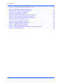
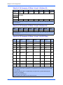
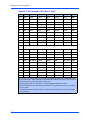
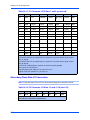
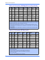
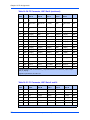
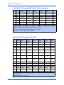
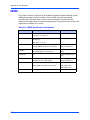
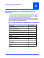
Table 10-2. P4 Connector, I/O Slots 1-6 and 11-16 (User I/O)
POS
Row Z
Row A
Row B
Row C
Row D
Row E
Row F
25-15
GND
I/O
I/O
I/O
I/O
I/O
GND
I/O
I/O
I/O
I/O
I/O
GND
14
KEY AREA
13
12
11-1
GND
All I/O pins pass through the backplane to the transition module, they do not make any connection
to the backplane.
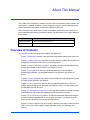
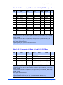
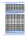
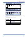
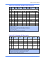
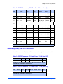
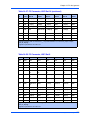
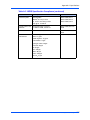
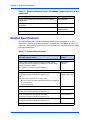
Table 10-3. P3 Connector, I/O Slots 1-6 and 11-16 (User I/O)
POS
Row Z
Row A
Row B
Row C
Row D
Row E
Row F
19-1
GND
I/O
I/O
I/O
I/O
I/O
GND
All I/O pins pass through the backplane to the transition module, they do not make any connection
to the backplane.
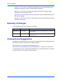
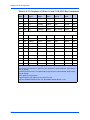
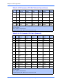
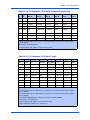
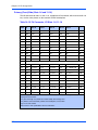
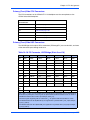
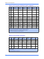
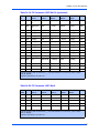
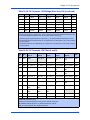
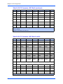
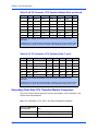
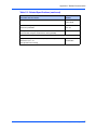
Table 10-4. P2 Connector, I/O Slots 1-6 and 11-16 (CPCI Bus)
POS
Row
Z
Row A
Row B
Row C
Row D
Row E
Row
F
22
GND
GA4
GA3
GA2
GA1
GA0
GND
21
GND
GND
RSV
RSV
RSV
GND
20
GND
GND
RSV
GND
RSV
GND
19
GND
GND
GND
RSV
RSV
RSV
GND
18
GND
_BRSVP2A1
8
_BRSVP2B18
_BRSVP2C1
8
GND
_BRSVP2E
18
GND
17
GND
_BRSVP2A1
7
GND
16
GND
_BRSVP2A1
6
_BRSVP2B16
15
GND
_BRSVP2A1
5
GND
14
GND
_AD[35]
_AD[34]
_AD[33]
GND
_AD[32]
GND
13
GND
_AD[38]
GND
VIO
_AD[37]
_AD[36]
GND
12
GND
_AD[42]
_AD[41]
_AD[40]
GND
_AD[39]
GND
GND
_BRSVP2E
16
GND
GND
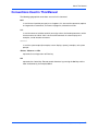
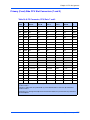
Signals beginning with an underscore (_) are prefixed with the bus name:
*For boards located in slots 1-6 (Domain A), the signal name is prefixed with PCI_A (for example,
PCI_A_AD[49]).
*For boards located in slots 11-16 (Domain B), the signal name is prefixed with PCI_B (for
example, PCI_B_AD[49]).
RSV signals are not connected.
Signals beginning with _BRSV are bussed, but not used.
102
CPX8216 and CPX8216T Installation and Use (6806800A52C)