1
External Memory Interface Handbook Volume 3 Section II.
DDR3 SDRAM Controller with ALTMEMPHY IP User
Guide
External Memory Interface Handbook Volume 3
Section II. DDR3 SDRAM Controller with ALTMEMPHY IP
User Guide
101 Innovation Drive
San Jose, CA 95134
www.altera.com
EMI_DDR3_UG-2.1
Document last updated for Altera Complete Design Suite version:
Document publication date:
10.1
December 2010
Subscribe
© 2010 Altera Corporation. All rights reserved. ALTERA, ARRIA, CYCLONE, HARDCOPY, MAX, MEGACORE, NIOS, QUARTUS and STRATIX are Reg. U.S. Pat.
& Tm. Off. and/or trademarks of Altera Corporation in the U.S. and other countries. All other trademarks and service marks are the property of their respective
holders as described at www.altera.com/common/legal.html. Altera warrants performance of its semiconductor products to current specifications in accordance
with Altera’s standard warranty, but reserves the right to make changes to any products and services at any time without notice. Altera assumes no responsibility or
liability arising out of the application or use of any information, product, or service described herein except as expressly agreed to in writing by Altera. Altera
customers are advised to obtain the latest version of device specifications before relying on any published information and before placing orders for products or
services.
External Memory Interface Handbook Volume 3
Section II. DDR3 SDRAM Controller with ALTMEMPHY IP User Guide
December 2010 Altera Corporation
Contents
Chapter 1. About This IP
Release Information . . . . . . . . . . . . . . . . . . . . . . . . . . . . . . . . . . . . . . . . . . . . . . . . . . . . . . . . . . . . . . . . . . . . . 1–2
Device Family Support . . . . . . . . . . . . . . . . . . . . . . . . . . . . . . . . . . . . . . . . . . . . . . . . . . . . . . . . . . . . . . . . . . . 1–2
Features . . . . . . . . . . . . . . . . . . . . . . . . . . . . . . . . . . . . . . . . . . . . . . . . . . . . . . . . . . . . . . . . . . . . . . . . . . . . . . . . 1–3
Unsupported Features . . . . . . . . . . . . . . . . . . . . . . . . . . . . . . . . . . . . . . . . . . . . . . . . . . . . . . . . . . . . . . . . . . . 1–5
MegaCore Verification . . . . . . . . . . . . . . . . . . . . . . . . . . . . . . . . . . . . . . . . . . . . . . . . . . . . . . . . . . . . . . . . . . . 1–5
Resource Utilization . . . . . . . . . . . . . . . . . . . . . . . . . . . . . . . . . . . . . . . . . . . . . . . . . . . . . . . . . . . . . . . . . . . . . 1–5
ALTMEMPHY Megafunction . . . . . . . . . . . . . . . . . . . . . . . . . . . . . . . . . . . . . . . . . . . . . . . . . . . . . . . . . . . 1–5
High-Performance Controller . . . . . . . . . . . . . . . . . . . . . . . . . . . . . . . . . . . . . . . . . . . . . . . . . . . . . . . . . . . 1–7
High-Performance Controller II . . . . . . . . . . . . . . . . . . . . . . . . . . . . . . . . . . . . . . . . . . . . . . . . . . . . . . . . . 1–7
System Requirements . . . . . . . . . . . . . . . . . . . . . . . . . . . . . . . . . . . . . . . . . . . . . . . . . . . . . . . . . . . . . . . . . . . . 1–8
Installation and Licensing . . . . . . . . . . . . . . . . . . . . . . . . . . . . . . . . . . . . . . . . . . . . . . . . . . . . . . . . . . . . . . . . 1–8
Free Evaluation . . . . . . . . . . . . . . . . . . . . . . . . . . . . . . . . . . . . . . . . . . . . . . . . . . . . . . . . . . . . . . . . . . . . . . . 1–9
OpenCore Plus Time-Out Behavior . . . . . . . . . . . . . . . . . . . . . . . . . . . . . . . . . . . . . . . . . . . . . . . . . . . . . . 1–9
Chapter 2. Getting Started
Design Flow . . . . . . . . . . . . . . . . . . . . . . . . . . . . . . . . . . . . . . . . . . . . . . . . . . . . . . . . . . . . . . . . . . . . . . . . . . . . 2–1
SOPC Builder Flow . . . . . . . . . . . . . . . . . . . . . . . . . . . . . . . . . . . . . . . . . . . . . . . . . . . . . . . . . . . . . . . . . . . . . . 2–2
Specifying Parameters . . . . . . . . . . . . . . . . . . . . . . . . . . . . . . . . . . . . . . . . . . . . . . . . . . . . . . . . . . . . . . . . . 2–2
Completing the SOPC Builder System . . . . . . . . . . . . . . . . . . . . . . . . . . . . . . . . . . . . . . . . . . . . . . . . . . . 2–3
MegaWizard Plug-In Manager Flow . . . . . . . . . . . . . . . . . . . . . . . . . . . . . . . . . . . . . . . . . . . . . . . . . . . . . . . 2–4
Specifying Parameters . . . . . . . . . . . . . . . . . . . . . . . . . . . . . . . . . . . . . . . . . . . . . . . . . . . . . . . . . . . . . . . . . 2–4
Generated Files . . . . . . . . . . . . . . . . . . . . . . . . . . . . . . . . . . . . . . . . . . . . . . . . . . . . . . . . . . . . . . . . . . . . . . . . . 2–6
HardCopy Device Migration Guidelines . . . . . . . . . . . . . . . . . . . . . . . . . . . . . . . . . . . . . . . . . . . . . . . . . . . 2–10
Enabling Hardcopy Migration Performance Improvement with ALTMEMPHY . . . . . . . . . . . . . . 2–10
Generating Your IP Core For a Mid-speed Grade FPGA . . . . . . . . . . . . . . . . . . . . . . . . . . . . . . . . 2–10
Compiling Your Design for a Faster Speed Grade FPGA . . . . . . . . . . . . . . . . . . . . . . . . . . . . . . . . 2–11
Chapter 3. Parameter Settings
ALTMEMPHY Parameter Settings . . . . . . . . . . . . . . . . . . . . . . . . . . . . . . . . . . . . . . . . . . . . . . . . . . . . . . . . . 3–1
Memory Settings . . . . . . . . . . . . . . . . . . . . . . . . . . . . . . . . . . . . . . . . . . . . . . . . . . . . . . . . . . . . . . . . . . . . . . 3–2
Using the Preset Editor to Create a Custom Memory Preset . . . . . . . . . . . . . . . . . . . . . . . . . . . . . . 3–3
Derating Memory Setup and Hold Timing . . . . . . . . . . . . . . . . . . . . . . . . . . . . . . . . . . . . . . . . . . . . 3–10
PHY Settings . . . . . . . . . . . . . . . . . . . . . . . . . . . . . . . . . . . . . . . . . . . . . . . . . . . . . . . . . . . . . . . . . . . . . . . . 3–11
Board Settings . . . . . . . . . . . . . . . . . . . . . . . . . . . . . . . . . . . . . . . . . . . . . . . . . . . . . . . . . . . . . . . . . . . . . . . 3–13
DDR3 SDRAM Controller with ALTMEMPHY Parameter Settings . . . . . . . . . . . . . . . . . . . . . . . . . . . . 3–13
Controller Settings . . . . . . . . . . . . . . . . . . . . . . . . . . . . . . . . . . . . . . . . . . . . . . . . . . . . . . . . . . . . . . . . . . . 3–14
Chapter 4. Compiling and Simulating
Compiling the Design . . . . . . . . . . . . . . . . . . . . . . . . . . . . . . . . . . . . . . . . . . . . . . . . . . . . . . . . . . . . . . . . . . . . 4–1
Simulating the Design . . . . . . . . . . . . . . . . . . . . . . . . . . . . . . . . . . . . . . . . . . . . . . . . . . . . . . . . . . . . . . . . . . . . 4–4
Chapter 5. Functional Description—ALTMEMPHY
Block Description . . . . . . . . . . . . . . . . . . . . . . . . . . . . . . . . . . . . . . . . . . . . . . . . . . . . . . . . . . . . . . . . . . . . . . . 5–2
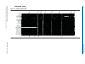
Calibration . . . . . . . . . . . . . . . . . . . . . . . . . . . . . . . . . . . . . . . . . . . . . . . . . . . . . . . . . . . . . . . . . . . . . . . . . . . 5–3
DDR3 SDRAM Without Leveling . . . . . . . . . . . . . . . . . . . . . . . . . . . . . . . . . . . . . . . . . . . . . . . . . . . . . 5–3
Step 1: Memory Device Initialization . . . . . . . . . . . . . . . . . . . . . . . . . . . . . . . . . . . . . . . . . . . . . . . . . . 5–4
Step 2: Write Training Patterns . . . . . . . . . . . . . . . . . . . . . . . . . . . . . . . . . . . . . . . . . . . . . . . . . . . . . . . 5–4
December 2010
Altera Corporation
External Memory Interface Handbook Volume 3
Section II. DDR3 SDRAM Controller with ALTMEMPHY IP User Guide
iv
Contents
Step 3: Read Resynchronization (Capture) Clock Phase . . . . . . . . . . . . . . . . . . . . . . . . . . . . . . . . . . 5–5
Step 4: Read and Write Datapath Timing . . . . . . . . . . . . . . . . . . . . . . . . . . . . . . . . . . . . . . . . . . . . . . 5–5
Step 5: Address and Command Clock Cycle . . . . . . . . . . . . . . . . . . . . . . . . . . . . . . . . . . . . . . . . . . . . 5–5
Step 6: Postamble . . . . . . . . . . . . . . . . . . . . . . . . . . . . . . . . . . . . . . . . . . . . . . . . . . . . . . . . . . . . . . . . . . . 5–5
Step 7: Prepare for User Mode . . . . . . . . . . . . . . . . . . . . . . . . . . . . . . . . . . . . . . . . . . . . . . . . . . . . . . . . 5–5
DDR3 SDRAM With Leveling . . . . . . . . . . . . . . . . . . . . . . . . . . . . . . . . . . . . . . . . . . . . . . . . . . . . . . . . . . 5–7
Step 1: Memory Device Initialization . . . . . . . . . . . . . . . . . . . . . . . . . . . . . . . . . . . . . . . . . . . . . . . . . . 5–9
Step 2: Write Leveling . . . . . . . . . . . . . . . . . . . . . . . . . . . . . . . . . . . . . . . . . . . . . . . . . . . . . . . . . . . . . . 5–10
Step 3: Write Training Patterns . . . . . . . . . . . . . . . . . . . . . . . . . . . . . . . . . . . . . . . . . . . . . . . . . . . . . . 5–10
Step 4: Read Resynchronization . . . . . . . . . . . . . . . . . . . . . . . . . . . . . . . . . . . . . . . . . . . . . . . . . . . . . 5–10
Step 5: Address and Command Path Clock Cycle . . . . . . . . . . . . . . . . . . . . . . . . . . . . . . . . . . . . . . 5–10
Step 6: Postamble . . . . . . . . . . . . . . . . . . . . . . . . . . . . . . . . . . . . . . . . . . . . . . . . . . . . . . . . . . . . . . . . . . 5–10
Step 7: Write Clock Path Setup . . . . . . . . . . . . . . . . . . . . . . . . . . . . . . . . . . . . . . . . . . . . . . . . . . . . . . 5–11
Step 8: Prepare for User Mode . . . . . . . . . . . . . . . . . . . . . . . . . . . . . . . . . . . . . . . . . . . . . . . . . . . . . . . 5–11
VT Tracking . . . . . . . . . . . . . . . . . . . . . . . . . . . . . . . . . . . . . . . . . . . . . . . . . . . . . . . . . . . . . . . . . . . . . . 5–11
Mimic Path . . . . . . . . . . . . . . . . . . . . . . . . . . . . . . . . . . . . . . . . . . . . . . . . . . . . . . . . . . . . . . . . . . . . . . . 5–11
Address and Command Datapath . . . . . . . . . . . . . . . . . . . . . . . . . . . . . . . . . . . . . . . . . . . . . . . . . . . . . . 5–11
Arria II GX Devices . . . . . . . . . . . . . . . . . . . . . . . . . . . . . . . . . . . . . . . . . . . . . . . . . . . . . . . . . . . . . . . . 5–11
Stratix III and Stratix IV Devices . . . . . . . . . . . . . . . . . . . . . . . . . . . . . . . . . . . . . . . . . . . . . . . . . . . . . 5–13
Clock and Reset Management . . . . . . . . . . . . . . . . . . . . . . . . . . . . . . . . . . . . . . . . . . . . . . . . . . . . . . . . . 5–13
Clock Management . . . . . . . . . . . . . . . . . . . . . . . . . . . . . . . . . . . . . . . . . . . . . . . . . . . . . . . . . . . . . . . . 5–13
Reset Management . . . . . . . . . . . . . . . . . . . . . . . . . . . . . . . . . . . . . . . . . . . . . . . . . . . . . . . . . . . . . . . . 5–17
Read Datapath . . . . . . . . . . . . . . . . . . . . . . . . . . . . . . . . . . . . . . . . . . . . . . . . . . . . . . . . . . . . . . . . . . . . . . . 5–18
Arria II GX Devices . . . . . . . . . . . . . . . . . . . . . . . . . . . . . . . . . . . . . . . . . . . . . . . . . . . . . . . . . . . . . . . . 5–18
Stratix III and Stratix IV Devices . . . . . . . . . . . . . . . . . . . . . . . . . . . . . . . . . . . . . . . . . . . . . . . . . . . . . 5–20
Write Datapath . . . . . . . . . . . . . . . . . . . . . . . . . . . . . . . . . . . . . . . . . . . . . . . . . . . . . . . . . . . . . . . . . . . . . . 5–22
Arria II GX Devices . . . . . . . . . . . . . . . . . . . . . . . . . . . . . . . . . . . . . . . . . . . . . . . . . . . . . . . . . . . . . . . . 5–22
Stratix III and Stratix IV Devices . . . . . . . . . . . . . . . . . . . . . . . . . . . . . . . . . . . . . . . . . . . . . . . . . . . . . 5–22
ALTMEMPHY Signals . . . . . . . . . . . . . . . . . . . . . . . . . . . . . . . . . . . . . . . . . . . . . . . . . . . . . . . . . . . . . . . . . . 5–23
PHY-to-Controller Interfaces . . . . . . . . . . . . . . . . . . . . . . . . . . . . . . . . . . . . . . . . . . . . . . . . . . . . . . . . . . . . . 5–31
Using a Custom Controller . . . . . . . . . . . . . . . . . . . . . . . . . . . . . . . . . . . . . . . . . . . . . . . . . . . . . . . . . . . . . . 5–38
Preliminary Steps . . . . . . . . . . . . . . . . . . . . . . . . . . . . . . . . . . . . . . . . . . . . . . . . . . . . . . . . . . . . . . . . . . 5–38
Design Considerations . . . . . . . . . . . . . . . . . . . . . . . . . . . . . . . . . . . . . . . . . . . . . . . . . . . . . . . . . . . . . 5–38
Clocks and Resets . . . . . . . . . . . . . . . . . . . . . . . . . . . . . . . . . . . . . . . . . . . . . . . . . . . . . . . . . . . . . . . . . 5–38
Calibration Process Requirements . . . . . . . . . . . . . . . . . . . . . . . . . . . . . . . . . . . . . . . . . . . . . . . . . . . 5–39
Other Local Interface Requirements . . . . . . . . . . . . . . . . . . . . . . . . . . . . . . . . . . . . . . . . . . . . . . . . . . 5–39
Address and Command Interfacing . . . . . . . . . . . . . . . . . . . . . . . . . . . . . . . . . . . . . . . . . . . . . . . . . . 5–39
Handshake Mechanism Between Read Commands and Read Data . . . . . . . . . . . . . . . . . . . . . . . 5–39
Handshake Mechanism Between Write Commands and Write Data . . . . . . . . . . . . . . . . . . . . . . 5–40
Partial Writes . . . . . . . . . . . . . . . . . . . . . . . . . . . . . . . . . . . . . . . . . . . . . . . . . . . . . . . . . . . . . . . . . . . . . 5–41
Chapter 6. Functional Description—High-Performance Controller
Block Description . . . . . . . . . . . . . . . . . . . . . . . . . . . . . . . . . . . . . . . . . . . . . . . . . . . . . . . . . . . . . . . . . . . . . . . 6–1
Command FIFO Buffer . . . . . . . . . . . . . . . . . . . . . . . . . . . . . . . . . . . . . . . . . . . . . . . . . . . . . . . . . . . . . . . . 6–2
Write Data FIFO Buffer . . . . . . . . . . . . . . . . . . . . . . . . . . . . . . . . . . . . . . . . . . . . . . . . . . . . . . . . . . . . . . . . 6–2
Write Data Tracking Logic . . . . . . . . . . . . . . . . . . . . . . . . . . . . . . . . . . . . . . . . . . . . . . . . . . . . . . . . . . . . . 6–3
Main State Machine . . . . . . . . . . . . . . . . . . . . . . . . . . . . . . . . . . . . . . . . . . . . . . . . . . . . . . . . . . . . . . . . . . . 6–3
Bank Management Logic . . . . . . . . . . . . . . . . . . . . . . . . . . . . . . . . . . . . . . . . . . . . . . . . . . . . . . . . . . . . . . . 6–3
Timer Logic . . . . . . . . . . . . . . . . . . . . . . . . . . . . . . . . . . . . . . . . . . . . . . . . . . . . . . . . . . . . . . . . . . . . . . . . . . 6–3
Initialization State Machine . . . . . . . . . . . . . . . . . . . . . . . . . . . . . . . . . . . . . . . . . . . . . . . . . . . . . . . . . . . . . 6–3
Address and Command Decode . . . . . . . . . . . . . . . . . . . . . . . . . . . . . . . . . . . . . . . . . . . . . . . . . . . . . . . . 6–3
PHY Interface Logic . . . . . . . . . . . . . . . . . . . . . . . . . . . . . . . . . . . . . . . . . . . . . . . . . . . . . . . . . . . . . . . . . . . 6–4
ODT Generation Logic . . . . . . . . . . . . . . . . . . . . . . . . . . . . . . . . . . . . . . . . . . . . . . . . . . . . . . . . . . . . . . . . . 6–4
Low-Power Mode Logic . . . . . . . . . . . . . . . . . . . . . . . . . . . . . . . . . . . . . . . . . . . . . . . . . . . . . . . . . . . . . . . 6–4
External Memory Interface Handbook Volume 3
Section II. DDR3 SDRAM Controller with ALTMEMPHY IP User Guide
December 2010 Altera Corporation
Contents
v
Control Logic . . . . . . . . . . . . . . . . . . . . . . . . . . . . . . . . . . . . . . . . . . . . . . . . . . . . . . . . . . . . . . . . . . . . . . . . . 6–5
Error Correction Coding (ECC) . . . . . . . . . . . . . . . . . . . . . . . . . . . . . . . . . . . . . . . . . . . . . . . . . . . . . . . . . 6–5
Interrupts . . . . . . . . . . . . . . . . . . . . . . . . . . . . . . . . . . . . . . . . . . . . . . . . . . . . . . . . . . . . . . . . . . . . . . . . . 6–8
Partial Writes . . . . . . . . . . . . . . . . . . . . . . . . . . . . . . . . . . . . . . . . . . . . . . . . . . . . . . . . . . . . . . . . . . . . . . 6–8
Partial Bursts . . . . . . . . . . . . . . . . . . . . . . . . . . . . . . . . . . . . . . . . . . . . . . . . . . . . . . . . . . . . . . . . . . . . . . . 6–9
ECC Latency . . . . . . . . . . . . . . . . . . . . . . . . . . . . . . . . . . . . . . . . . . . . . . . . . . . . . . . . . . . . . . . . . . . . . . . 6–9
ECC Registers . . . . . . . . . . . . . . . . . . . . . . . . . . . . . . . . . . . . . . . . . . . . . . . . . . . . . . . . . . . . . . . . . . . . . 6–10
ECC Register Bits . . . . . . . . . . . . . . . . . . . . . . . . . . . . . . . . . . . . . . . . . . . . . . . . . . . . . . . . . . . . . . . . . . 6–12
Example Top-Level File . . . . . . . . . . . . . . . . . . . . . . . . . . . . . . . . . . . . . . . . . . . . . . . . . . . . . . . . . . . . . . . . . 6–14
Example Driver . . . . . . . . . . . . . . . . . . . . . . . . . . . . . . . . . . . . . . . . . . . . . . . . . . . . . . . . . . . . . . . . . . . . . . 6–15
Top-level Signals Description . . . . . . . . . . . . . . . . . . . . . . . . . . . . . . . . . . . . . . . . . . . . . . . . . . . . . . . . . . . . 6–16
Chapter 7. Functional Description—High-Performance Controller II
Upgrading from HPC to HPC II . . . . . . . . . . . . . . . . . . . . . . . . . . . . . . . . . . . . . . . . . . . . . . . . . . . . . . . . . . . 7–1
Block Description . . . . . . . . . . . . . . . . . . . . . . . . . . . . . . . . . . . . . . . . . . . . . . . . . . . . . . . . . . . . . . . . . . . . . . . 7–2
Avalon-MM Data Slave Interface . . . . . . . . . . . . . . . . . . . . . . . . . . . . . . . . . . . . . . . . . . . . . . . . . . . . . . . . 7–3
Write Data FIFO Buffer . . . . . . . . . . . . . . . . . . . . . . . . . . . . . . . . . . . . . . . . . . . . . . . . . . . . . . . . . . . . . . . . 7–4
Command Queue . . . . . . . . . . . . . . . . . . . . . . . . . . . . . . . . . . . . . . . . . . . . . . . . . . . . . . . . . . . . . . . . . . . . . 7–4
Bank Management Logic . . . . . . . . . . . . . . . . . . . . . . . . . . . . . . . . . . . . . . . . . . . . . . . . . . . . . . . . . . . . . . . 7–4
Timer Logic . . . . . . . . . . . . . . . . . . . . . . . . . . . . . . . . . . . . . . . . . . . . . . . . . . . . . . . . . . . . . . . . . . . . . . . . . . 7–5
Command-Issuing State Machine . . . . . . . . . . . . . . . . . . . . . . . . . . . . . . . . . . . . . . . . . . . . . . . . . . . . . . . 7–5
Address and Command Decode Logic . . . . . . . . . . . . . . . . . . . . . . . . . . . . . . . . . . . . . . . . . . . . . . . . . . . 7–5
Write and Read Datapath, and Write Data Timing Logic . . . . . . . . . . . . . . . . . . . . . . . . . . . . . . . . . . . 7–5
ODT Generation Logic . . . . . . . . . . . . . . . . . . . . . . . . . . . . . . . . . . . . . . . . . . . . . . . . . . . . . . . . . . . . . . . . . 7–6
User-Controlled Side-Band Signals . . . . . . . . . . . . . . . . . . . . . . . . . . . . . . . . . . . . . . . . . . . . . . . . . . . . . . 7–6
User-Refresh Commands . . . . . . . . . . . . . . . . . . . . . . . . . . . . . . . . . . . . . . . . . . . . . . . . . . . . . . . . . . . . 7–6
Multi-Cast Write . . . . . . . . . . . . . . . . . . . . . . . . . . . . . . . . . . . . . . . . . . . . . . . . . . . . . . . . . . . . . . . . . . . 7–6
Low-Power Mode Logic . . . . . . . . . . . . . . . . . . . . . . . . . . . . . . . . . . . . . . . . . . . . . . . . . . . . . . . . . . . . . 7–7
Configuration and Status Register (CSR) Interface . . . . . . . . . . . . . . . . . . . . . . . . . . . . . . . . . . . . . . . . . 7–7
Error Correction Coding (ECC) . . . . . . . . . . . . . . . . . . . . . . . . . . . . . . . . . . . . . . . . . . . . . . . . . . . . . . . . . 7–7
Partial Writes . . . . . . . . . . . . . . . . . . . . . . . . . . . . . . . . . . . . . . . . . . . . . . . . . . . . . . . . . . . . . . . . . . . . . . 7–8
Partial Bursts . . . . . . . . . . . . . . . . . . . . . . . . . . . . . . . . . . . . . . . . . . . . . . . . . . . . . . . . . . . . . . . . . . . . . . . 7–9
Example Top-Level File . . . . . . . . . . . . . . . . . . . . . . . . . . . . . . . . . . . . . . . . . . . . . . . . . . . . . . . . . . . . . . . . . 7–10
Example Driver . . . . . . . . . . . . . . . . . . . . . . . . . . . . . . . . . . . . . . . . . . . . . . . . . . . . . . . . . . . . . . . . . . . . . . 7–11
Top-level Signals Description . . . . . . . . . . . . . . . . . . . . . . . . . . . . . . . . . . . . . . . . . . . . . . . . . . . . . . . . . . . . 7–12
Register Maps Description . . . . . . . . . . . . . . . . . . . . . . . . . . . . . . . . . . . . . . . . . . . . . . . . . . . . . . . . . . . . . . . 7–18
ALTMEMPHY Register Map . . . . . . . . . . . . . . . . . . . . . . . . . . . . . . . . . . . . . . . . . . . . . . . . . . . . . . . . . . 7–19
Controller Register Map . . . . . . . . . . . . . . . . . . . . . . . . . . . . . . . . . . . . . . . . . . . . . . . . . . . . . . . . . . . . . . 7–21
Chapter 8. Latency
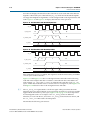
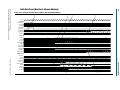
Chapter 9. Timing Diagrams
DDR3 High-Performance Controllers . . . . . . . . . . . . . . . . . . . . . . . . . . . . . . . . . . . . . . . . . . . . . . . . . . . . . . 9–1
Auto-Precharge . . . . . . . . . . . . . . . . . . . . . . . . . . . . . . . . . . . . . . . . . . . . . . . . . . . . . . . . . . . . . . . . . . . . . . . 9–2
User Refresh . . . . . . . . . . . . . . . . . . . . . . . . . . . . . . . . . . . . . . . . . . . . . . . . . . . . . . . . . . . . . . . . . . . . . . . . . 9–3
Half-Rate Read for Avalon Interface . . . . . . . . . . . . . . . . . . . . . . . . . . . . . . . . . . . . . . . . . . . . . . . . . . . . . 9–4
Half-Rate Write for Avalon Interface . . . . . . . . . . . . . . . . . . . . . . . . . . . . . . . . . . . . . . . . . . . . . . . . . . . . 9–6
Half Rate Write for Native Interface . . . . . . . . . . . . . . . . . . . . . . . . . . . . . . . . . . . . . . . . . . . . . . . . . . . . . 9–8
Initialization Timing . . . . . . . . . . . . . . . . . . . . . . . . . . . . . . . . . . . . . . . . . . . . . . . . . . . . . . . . . . . . . . . . . . 9–10
Calibration Timing . . . . . . . . . . . . . . . . . . . . . . . . . . . . . . . . . . . . . . . . . . . . . . . . . . . . . . . . . . . . . . . . . . . 9–12
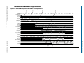
DDR3 High-Performance Controllers II . . . . . . . . . . . . . . . . . . . . . . . . . . . . . . . . . . . . . . . . . . . . . . . . . . . 9–13
Half-Rate Read (Burst-Aligned Address) . . . . . . . . . . . . . . . . . . . . . . . . . . . . . . . . . . . . . . . . . . . . . . . . 9–14
Half-Rate Write (Burst-Aligned Address) . . . . . . . . . . . . . . . . . . . . . . . . . . . . . . . . . . . . . . . . . . . . . . . 9–16
December 2010
Altera Corporation
External Memory Interface Handbook Volume 3
Section II. DDR3 SDRAM Controller with ALTMEMPHY IP User Guide
vi
Contents
Half-Rate Read (Non Burst-Aligned Address) . . . . . . . . . . . . . . . . . . . . . . . . . . . . . . . . . . . . . . . . . . . 9–18
Half-Rate Write (Non Burst-Aligned Address) . . . . . . . . . . . . . . . . . . . . . . . . . . . . . . . . . . . . . . . . . . . 9–20
Half-Rate Read With Gaps . . . . . . . . . . . . . . . . . . . . . . . . . . . . . . . . . . . . . . . . . . . . . . . . . . . . . . . . . . . . 9–22
Half-Rate Write With Gaps . . . . . . . . . . . . . . . . . . . . . . . . . . . . . . . . . . . . . . . . . . . . . . . . . . . . . . . . . . . . 9–23
Half-Rate Write Operation (Merging Writes) . . . . . . . . . . . . . . . . . . . . . . . . . . . . . . . . . . . . . . . . . . . . 9–24
Write-Read-Write-Read Operation . . . . . . . . . . . . . . . . . . . . . . . . . . . . . . . . . . . . . . . . . . . . . . . . . . . . . 9–26
Additional Information
Document Revision History . . . . . . . . . . . . . . . . . . . . . . . . . . . . . . . . . . . . . . . . . . . . . . . . . . . . . . . . . . . Info–1
How to Contact Altera . . . . . . . . . . . . . . . . . . . . . . . . . . . . . . . . . . . . . . . . . . . . . . . . . . . . . . . . . . . . . . . . Info–1
Typographic Conventions . . . . . . . . . . . . . . . . . . . . . . . . . . . . . . . . . . . . . . . . . . . . . . . . . . . . . . . . . . . . . Info–2
External Memory Interface Handbook Volume 3
Section II. DDR3 SDRAM Controller with ALTMEMPHY IP User Guide
December 2010 Altera Corporation
1. About This IP
The Altera® DDR3 SDRAM Controller with ALTMEMPHY IP provides simplified
interfaces to industry-standard DDR3 SDRAM. The ALTMEMPHY megafunction is
an interface between a memory controller and the memory devices, and performs
read and write operations to the memory. The DDR3 SDRAM Controller with
ALTMEMPHY IP works in conjunction with the Altera ALTMEMPHY megafunction.
The DDR3 SDRAM Controller with ALTMEMPHY IP and ALTMEMPHY
megafunction support DDR3 SDRAM interfaces in half-rate mode. The DDR3
SDRAM Controller with ALTMEMPHY IP offers two controller architectures: the
high-performance controller (HPC) and the high-performance controller II (HPC II).
HPC II provides higher efficiency and more advanced features.
1
DDR3 SDRAM high-performance controller denotes both HPC and HPC II unless
indicated otherwise.
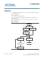
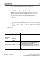
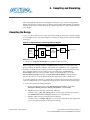
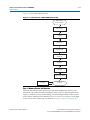
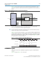
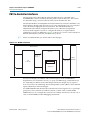
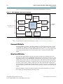
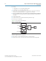
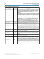
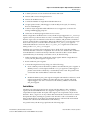
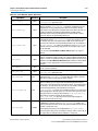
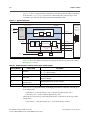
Figure 1–1 on page 1–1 shows a system-level diagram including the example top-level
file that the DDR3 SDRAM Controller with ALTMEMPHY IP creates for you.
Figure 1–1. System-Level Diagram
Example Top-Level File
ALTMEMPHY
External
Memory
Device
DLL
PLL
(1)
HighPerformance
Controller
Example
Driver
Pass or Fail
Note to Figure 1–1:
(1) When you choose Instantiate DLL Externally, delay-locked loop (DLL) is instantiated outside the ALTMEMPHY
megafunction.
The MegaWizard™ Plug-In Manager generates an example top-level file, consisting of
an example driver, and your DDR3 SDRAM high-performance controller custom
variation. The controller instantiates an instance of the ALTMEMPHY megafunction
which in turn instantiates a phase-locked loop (PLL) and DLL. You can also
instantiate the DLL outside the ALTMEMPHY megafunction to share the DLL
between multiple instances of the ALTMEMPHY megafunction. You cannot share a
PLL between multiple instances of the ALTMEMPHY megafunction, but you may
share some of the PLL clock outputs between these multiple instances.
The example top-level file is a fully-functional design that you can simulate,
synthesize, and use in hardware. The example driver is a self-test module that issues
read and write commands to the controller and checks the read data to produce the
pass or fail, and test complete signals.
December 2010
Altera Corporation
External Memory Interface Handbook Volume 3
Section II. DDR3 SDRAM Controller with ALTMEMPHY IP User Guide
1–2
Chapter 1: About This IP
Release Information
The ALTMEMPHY megafunction creates the datapath between the memory device
and the memory controller. The megafunction is available as a stand-alone product or
can be used in conjunction with Altera high-performance memory controllers. When
using the ALTMEMPHY megafunction as a stand-alone product, use with either
custom or third-party controllers.
Release Information
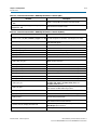
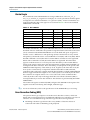
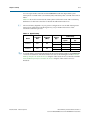
Table 1–1 provides information about this release of the DDR3 SDRAM Controller
with ALTMEMPHY IP.
Table 1–1. Release Information
Item
Description
Version
10.0
Release Date
July 2010
Ordering Codes
Product IDs
Vendor ID
IP-SDRAM/DDR3 (HPC)
IP-HPMCII (HPC II)
00C2 (DDR3 SDRAM)
00CO (ALTMEMPHY Megafunction)
6AF7
Altera verifies that the current version of the Quartus® II software compiles the
previous version of each MegaCore function. The MegaCore IP Library Release Notes
and Errata report any exceptions to this verification. Altera does not verify
compilation with MegaCore function versions older than one release. For information
about issues on the DDR3 SDRAM high-performance controller and
theALTMEMPHY megafunction in a particular Quartus II version, refer to the
Quartus II Software Release Notes.
Device Family Support
The MegaCore function provides either final or preliminary support for target Altera
device families:
■
Final support means the core is verified with final timing models for this device
family. The core meets all functional and timing requirements for the device family
and can be used in production designs.
■
Preliminary support means the core is verified with preliminary timing models
for this device family. The core meets all functional requirements, but might still be
undergoing timing analysis for the device family. It can be used in production
designs with caution.
■
HardCopy Compilation means the core is verified with final timing models for
the HardCopy® device family. The core meets all functional and timing
requirements for the device family and can be used in production designs.
■
HardCopy Companion means the core is verified with preliminary timing models
for the HardCopy companion device. The core meets all functional requirements,
but might still be undergoing timing analysis for HardCopy device family. It can
be used in production designs with caution.
External Memory Interface Handbook Volume 3
Section II. DDR3 SDRAM Controller with ALTMEMPHY IP User Guide
December 2010 Altera Corporation
Chapter 1: About This IP
Features
1–3
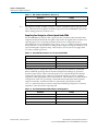
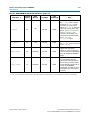
Table 1–2 shows the level of support offered by the DDR3 SDRAM Controller with
ALTMEMPHY IP to each of the Altera device families.
Table 1–2. Device Family Support
Device Family
Support
®
Arria II GX
Preliminary
HardCopy III
HardCopy Companion
HardCopy IV E
HardCopy Companion
HardCopy IV GX
HardCopy Companion
®
Stratix III
Final
Stratix IV
Final
Other device families
No support
Features
The ALTMEMPHY megafunction offers the following features:
■
Simple setup.
■
Support for the Altera PHY Interface (AFI) for DDR3 SDRAM on all supported
devices.
■
Automated initial calibration eliminating complicated read data timing
calculations.
■
Voltage and temperature (VT) tracking that guarantees maximum stable
performance for DDR3 SDRAM interface.
■
Self-contained datapath that makes connection to an Altera controller or a
third-party controller independent of the critical timing paths.
■
Easy-to-use parameter editor.
The ALTMEMPHY megafunction supports DDR3 SDRAM DIMMs with leveling and
DDR3 SDRAM components without leveling:
■
■
ALTMEMPHY with leveling is for unbuffered DIMMs (including SODIMM and
MicroDIMM) or DDR3 SDRAM components up to 80-bit total data bus width with
a layout like a DIMM that target Stratix III and Stratix IV devices:
■
Supports a fully-calibrated DDR3 SDRAM PHY for DDR3 SDRAM unbuffered
DIMM with ×4 and ×8 devices with 300-MHz to 533-MHz frequency targets.
■
Deskew circuitry is enabled automatically for interfaces higher than 400 MHz.
■
Supports single and multiple chip selects.
ALTMEMPHY supports DDR3 SDRAM components without leveling for
Arria II GX, Stratix III, and Stratix IV devices using T-topology for clock, address,
and command bus:
■
■
December 2010
Supports multiple chip selects.
The DDR3 SDRAM PHY with leveling fMAX is 533 MHz; without leveling fMAX is
400 MHz for single chip selects.
Altera Corporation
External Memory Interface Handbook Volume 3
Section II. DDR3 SDRAM Controller with ALTMEMPHY IP User Guide
1–4
Chapter 1: About This IP
Features
■
No support for data-mask (DM) pins for ×4 DDR3 SDRAM DIMMs or
components, so select No for Drive DM pins from FPGA when using ×4 devices.
■
The ALTMEMPHY megafunction supports half-rate DDR3 SDRAM interfaces
only.
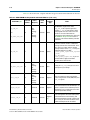
In addition, Table 1–3 shows the features provided by the DDR3 SDRAM HPC and
HPC II.
Table 1–3. DDR3 SDRAM HPC and HPC II Features (Part 1 of 2)
Controller Architecture
Features
Half-rate controller
HPC
HPC II
v
v
Support for AFI ALTMEMPHY
v
v
Support for Avalon®Memory Mapped (Avalon-MM) local interface
v
v
Support for Native local interface
v
—
Configurable command look-ahead bank management with in-order reads and
writes
—
v
Additive latency
—
v (1)
Optional support for multi-cast write for tRC mitigation
—
v
Support for arbitrary Avalon burst length
—
v
Built-in flexible memory burst adapter
—
v
Configurable Local-to-Memory address mappings
—
v
Integrated half-rate bridge for low latency option
—
v
Optional run-time configuration of size and mode register settings, and memory
timing
—
v (2)
Partial array self-refresh (PASR)
—
v
Support for industry-standard DDR3 SDRAM devices; and DIMMs
v
v
Optional support for self-refresh command
v
v
Optional support for user-controlled power-down command
v
—
Optional support for automatic power-down command with programmable
time-out
—
v
Optional support for auto-precharge read and auto-precharge write commands
v
—
Optional support for user-controller refresh
v
v
Reduced bank tracking for area optimization
—
v
Controller variable latency
—
v
Optional multiple controller clock sharing in SOPC Builder Flow
v
v
Integrated error correction coding (ECC) function 72-bit
v
v
Integrated ECC function 40-bit
—
v
Support for partial-word write with optional automatic error correction
—
v
SOPC Builder ready
v
v
Support for OpenCore Plus evaluation
v
—
External Memory Interface Handbook Volume 3
Section II. DDR3 SDRAM Controller with ALTMEMPHY IP User Guide
December 2010 Altera Corporation
Chapter 1: About This IP
Unsupported Features
1–5
Table 1–3. DDR3 SDRAM HPC and HPC II Features (Part 2 of 2)
Controller Architecture
Features
IP functional simulation models for use in Altera-supported VHDL and Verilog
HDL simulator
HPC
HPC II
v
v
Notes to Table 1–3:
(1) HPC II supports additive latency values greater or equal to tRCD-1, in clock cycle unit (tCK).
(2) This feature is not supported with DDR3 SDRAM with leveling.
Unsupported Features
The DDR3 SDRAM Controller with ALTMEMPHY IP does not support the following
features:
■
Timing simulation.
■
Partial burst and unaligned burst in ECC and non-ECC mode when DM pins are
disabled.
MegaCore Verification
Altera performs extensive random, directed tests with functional test coverage using
industry-standard Denali models to ensure the functionality of the DDR3 SDRAM
Controller with ALTMEMPHY IP.
Resource Utilization
The following sections show the resource utilization data for the ALTMEMPHY
megafunction, and the DDR3 high-performance controllers (HPC and HPC II).
ALTMEMPHY Megafunction
Table 1–4 and Table 1–5 show the typical size of the ALTMEMPHY megafunction with
the AFI in the Quartus II software version 10.0 for the following devices:
December 2010
■
Arria II GX (EP2AGX260FF35C4) devices
■
Stratix III (EP3SL110F1152C2) devices
■
Stratix IV (EP4SGX230HF35C2) devices
Altera Corporation
External Memory Interface Handbook Volume 3
Section II. DDR3 SDRAM Controller with ALTMEMPHY IP User Guide
1–6
Chapter 1: About This IP
Resource Utilization
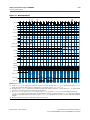
Table 1–4. Resource Utilization in Arria II GX Devices
Memory Type
DDR3 SDRAM (without
leveling)
PHY
Rate
Half
(Note 1)
Memory
Width
(Bits)
Combinational
ALUTS
Logic Registers
M9K
Blocks
Memory
ALUTs
8
1,431
1,189
2
18
16
1,481
1,264
4
2
64
1,797
1,970
12
22
72
1,874
2,038
13
2
Note to Table 1–4:
(1) The listed resource utilization refers to resources used by the ALTMEMPHY megafunction with AFI only. Memory controller overhead is
additional.
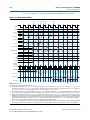
Table 1–5. Resource Utilization in Stratix III and Stratix IV Devices
Memory Type
PHY
Rate
DDR3 SDRAM
(400 MHz, without leveling
only)
DDR3 SDRAM
(400 MHz, with leveling only)
DDR3 SDRAM
(533 MHz with read and write
deskew, with leveling only)
Half
(Note 1)
Memory
Width
(Bits)
Combinational
ALUTS
Logic Registers
M9K
Blocks
Memory
ALUTs
8
1,359
1,047
1
40
16
1,426
1,196
1
80
64
1,783
2,080
1
320
72
1,871
2,228
1
360
8
3,724
2,723
2
80
16
4,192
3,235
2
160
64
6,835
6,487
5
640
72
7,182
6,984
5
720
8
4,098
2,867
2
80
16
4,614
3,391
2
160
64
7,297
6,645
5
640
72
7,641
7,144
5
720
Note to Table 1–5:
(1) The listed resource utilization refers to resources used by the ALTMEMPHY megafunction with AFI only. Memory controller overhead is
additional.
External Memory Interface Handbook Volume 3
Section II. DDR3 SDRAM Controller with ALTMEMPHY IP User Guide
December 2010 Altera Corporation
Chapter 1: About This IP
Resource Utilization
1–7
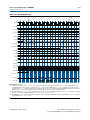
High-Performance Controller
Table 1–6 and Table 1–7 show the typical sizes for the DDR3 SDRAM HPC (including
ALTMEMPHY) for Stratix III and Stratix IV devices.
Table 1–6. Resource Utilization in Stratix III Devices
Local Data Width
(Bits)
Memory Width
(Bits)
Combinational
ALUTs
Dedicated Logic
Registers
Memory
(M9K)
32
8
1,891
1,558
2
64
16
1,966
1,707
3
256
64
2,349
2,591
9
288
72
2,442
2,739
10
Table 1–7. Resource Utilization in Stratix IV Devices
Local Data Width
(Bits)
Memory Width
(Bits)
Combinational
ALUTs
Dedicated Logic
Registers
Memory
(M9K)
32
8
1,924
1,580
2
64
16
1,987
1,724
3
256
64
2,359
2,584
9
288
72
2,449
2,728
10
High-Performance Controller II
Table 1–9 through Table 1–10 show the typical sizes for the DDR3 SDRAM HPC II
(including ALTMEMPHY) for Arria II GX, Stratix III, and Stratix IV devices.
Table 1–8. Resource Utilization in Arria II GX Devices
Local Data Width
(Bits)
Memory Width
(Bits)
Combinational
ALUTs
Dedicated Logic
Registers
Memory
(M9K)
32
8
2,516
1,945
3
64
16
2,604
2,101
5
256
64
3,121
3,021
17
288
72
3,243
3,175
18
Table 1–9. Resource Utilization in Stratix III Devices
December 2010
Local Data Width
(Bits)
Memory Width
(Bits)
Combinational
ALUTs
Dedicated Logic
Registers
Memory
(M9K)
32
8
2,430
1,776
2
64
16
2,499
1,919
3
256
64
2,902
2,809
9
288
72
3,001
2,959
10
Altera Corporation
External Memory Interface Handbook Volume 3
Section II. DDR3 SDRAM Controller with ALTMEMPHY IP User Guide
1–8
Chapter 1: About This IP
System Requirements
Table 1–10. Resource Utilization in Stratix IV Devices
Local Data Width
(Bits)
Memory Width
(Bits)
Combinational
ALUTs
Dedicated Logic
Registers
Memory
(M9K)
32
8
2,427
1,773
2
64
16
2,496
1,914
3
256
64
2,887
2,774
9
288
72
2,981
2,924
10
System Requirements
The DDR3 SDRAM Controller with ALTMEMPHY IP is a part of the MegaCore IP
Library, which is distributed with the Quartus II software and downloadable from the
Altera website, www.altera.com.
f For system requirements and installation instructions, refer to Altera Software
Installation & Licensing.
Installation and Licensing
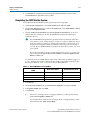
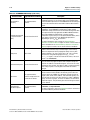
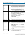
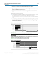
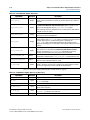
Figure 1–2 shows the directory structure after you install the DDR3 SDRAM
Controller with ALTMEMPHY IP, where <path> is the installation directory. The
default installation directory on Windows is c:\altera\<version>; on Linux it is
/opt/altera<version>.
Figure 1–2. Directory Structure
<path>
Installation directory.
ip
Contains the Alterar MegaCore IP Library and third-party IP cores.
altera
Contains the Altera MegaCore IP Library.
common
Contains shared components.
ddr3_high_perf
Contains the DDR3 SDRAM Controller with ALTMEMPHY IP files.
lib
Contains encypted lower-level design files and other support files.
You need a license for the MegaCore function only when you are completely satisfied
with its functionality and performance, and want to take your design to production.
To use the DDR3 SDRAM HPC, you can request a license file from the Altera web site
at www.altera.com/licensing and install it on your computer. When you request a
license file, Altera emails you a license.dat file. If you do not have Internet access,
contact your local representative.
To use the DDR3 SDRAM HPC II, contact your local sales representative to order a
license.
External Memory Interface Handbook Volume 3
Section II. DDR3 SDRAM Controller with ALTMEMPHY IP User Guide
December 2010 Altera Corporation
Chapter 1: About This IP
Installation and Licensing
1–9
Free Evaluation
Altera's OpenCore Plus evaluation feature is only applicable to the DDR3 SDRAM
HPC. With the OpenCore Plus evaluation feature, you can perform the following
actions:
■
Simulate the behavior of a megafunction (Altera MegaCore function or AMPPSM
megafunction) within your system.
■
Verify the functionality of your design, as well as evaluate its size and speed
quickly and easily.
■
Generate time-limited device programming files for designs that include
MegaCore functions.
■
Program a device and verify your design in hardware.
You need to purchase a license for the megafunction only when you are completely
satisfied with its functionality and performance, and want to take your design to
production.
OpenCore Plus Time-Out Behavior
OpenCore Plus hardware evaluation can support the following two modes of
operation:
■
Untethered—the design runs for a limited time
■
Tethered—requires a connection between your board and the host computer. If
tethered mode is supported by all megafunctions in a design, the device can
operate for a longer time or indefinitely
All megafunctions in a device time-out simultaneously when the most restrictive
evaluation time is reached. If there is more than one megafunction in a design, a
specific megafunction's time-out behavior may be masked by the time-out behavior of
the other megafunctions.
1
For MegaCore functions, the untethered time-out is 1 hour; the tethered time-out
value is indefinite.
Your design stops working after the hardware evaluation time expires and the
local_ready output goes low.
December 2010
Altera Corporation
External Memory Interface Handbook Volume 3
Section II. DDR3 SDRAM Controller with ALTMEMPHY IP User Guide
1–10
External Memory Interface Handbook Volume 3
Section II. DDR3 SDRAM Controller with ALTMEMPHY IP User Guide
Chapter 1: About This IP
Installation and Licensing
December 2010 Altera Corporation
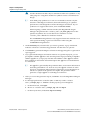
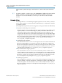
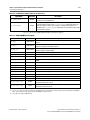
2. Getting Started
Design Flow
You can implement the DDR3 SDRAM Controller with ALTMEMPHY IP using either
one of the following flows:
■
SOPC Builder flow
■
MegaWizard Plug-In Manager flow
You can only instantiate the ALTMEMPHY megafunction using the MegaWizard
Plug-In Manager flow.
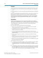
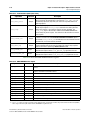
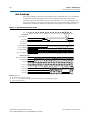
Figure 2–1 shows the stages for creating a system in the Quartus II software using
either one of the flows.
Figure 2–1. Design Flow
Select Design Flow
SOPC Builder
Flow
MegaWizard
Flow
Specify Parameters
Specify Parameters
Complete
SOPC Builder System
Optional
Perform
Functional Simulation
Does
Simulation Give
Expected Results?
Yes
Add Constraints
and Compile Design
IP Complete
Debug Design
December 2010
Altera Corporation
External Memory Interface Handbook Volume 3
Section II. DDR3 SDRAM Controller with ALTMEMPHY IP User Guide
2–2
Chapter 2: Getting Started
SOPC Builder Flow
The SOPC Builder flow offers the following advantages:
■
Generates simulation environment
■
Creates custom components and integrates them via the component wizard
■
Interconnects all components with the Avalon-MM interface
The MegaWizard Plug-In Manager flow offers the following advantages:
■
Allows you to design directly from the DDR3 SDRAM interface to peripheral
device or devices
■
Achieves higher-frequency operation
SOPC Builder Flow
The SOPC Builder flow allows you to add the DDR3 SDRAM Controller with
ALTMEMPHY IP directly to a new or existing SOPC Builder system.
You can also easily add other available components to quickly create an SOPC Builder
system with a DDR3 SDRAM controller, such as the Nios® II processor and
scatter-gather direct memory access (SDMA) controllers. SOPC Builder automatically
creates the system interconnect logic and system simulation environment.
f For more information about SOPC Builder, refer to volume 4 of the Quartus II
Handbook. For more information about how to use controllers with SOPC Builder,
refer to the ALTMEMPHY Design Tutorials section in volume 6 of the External Memory
Interface Handbook. For more information on the Quartus II software, refer to the
Quartus II Help.
Specifying Parameters
To specify the parameters for the DDR3 SDRAM Controller with ALTMEMPHY IP
using the SOPC Builder flow, perform the following steps:
1. In the Quartus II software, create a new Quartus II project with the New Project
Wizard.
2. On the Tools menu, click SOPC Builder.
3. For a new system, specify the system name and language.
4. Add DDR3 SDRAM Controller with ALTMEMPHY to your system from the
System Contents tab.
1
The DDR3 SDRAM Controller with ALTMEMPHY is in the SDRAM
folder under the Memories and Memory Controllers folder.
5. Specify the required parameters on all pages in the Parameter Settings tab.
1
To avoid simulation failure, you must set Local-to-Memory Address
Mapping to CHP-BANK-ROW-COL if you select High Peformance
Controller II for Controller Architecture.
f For detailed explanation of the parameters, refer to the “Parameter
Settings” on page 3–1.
External Memory Interface Handbook Volume 3
Section II. DDR3 SDRAM Controller with ALTMEMPHY IP User Guide
December 2010 Altera Corporation
Chapter 2: Getting Started
SOPC Builder Flow
2–3
6. Click Finish to complete parameterizing the DDR3 SDRAM Controller with
ALTMEMPHY IP and add it to the system.
Completing the SOPC Builder System
To complete the SOPC Builder system, perform the following steps:
1. In the System Contents tab, select Nios II Processor and click Add.
2. On the Nios II Processor page, in the Core Nios II tab, select altmemddr for Reset
Vector and Exception Vector.
3. Change the Reset Vector Offset and the Exception Vector Offset to an Avalon
address that is not written to by the ALTMEMPHY megafunction during its
calibration process.
c
The ALTMEMPHY megafunction performs memory interface calibration
every time it is reset, and in doing so, writes to a range of addresses. If you
want your memory contents to remain intact through a system reset, you
should avoid using these memory addresses. This step is not necessary if
you reload your SDRAM memory contents from flash every time you reset
your system.
If you are upgrading your Nios system design from version 8.1 or previous,
ensure that you change the Reset Vector Offset and the Exception Vector
Offset to AFI mode.
To calculate the Avalon-MM address equivalent of the memory address range 0×0
to 0×47, multiply the memory address by the width of the memory interface data
bus in bytes. Refer to Table 2–1 for more Avalon-MM addresses.
Table 2–1. Avalon-MM Addresses for AFI Mode
External Memory Interface
Width
Reset Vector Offset
Exception Vector Offset
8
0×60
0×80
16
0×A0
0×C0
32
0×120
0×140
64
0×240
0×260
4. Click Finish.
5. On the System Contents tab, expand Interface Protocols and expand Serial.
6. Select JTAG UART and click Add.
7. Click Finish.
1
If there are warnings about overlapping addresses, on the System menu,
click Auto Assign Base Addresses.
If you enable ECC and there are warnings about overlapping IRQs, on the
System menu click Auto Assign IRQs.
December 2010
Altera Corporation
External Memory Interface Handbook Volume 3
Section II. DDR3 SDRAM Controller with ALTMEMPHY IP User Guide
2–4
Chapter 2: Getting Started
MegaWizard Plug-In Manager Flow
8. For this example system, ensure all the other modules are clocked on the
altmemddr_sysclk, to avoid any unnecessary clock-domain crossing logic.
9. Click Generate.
1
Among the files generated by SOPC Builder is the Quartus II IP File (.qip).
This file contains information about a generated IP core or system. In most
cases, the .qip file contains all of the necessary assignments and
information required to process the MegaCore function or system in the
Quartus II compiler. Generally, a single .qip file is generated for each SOPC
Builder system. However, some more complex SOPC Builder components
generate a separate .qip file. In that case, the system .qip file references the
component .qip file.
10. Compile your design, refer to “Compiling and Simulating” on page 4–1.
MegaWizard Plug-In Manager Flow
The MegaWizard Plug-In Manager flow allows you to customize the DDR3 SDRAM
Controller with ALTMEMPHY or the stand-alone PHY with the ALTMEMPHY
megafunction, and manually integrate the function into your design.
f For more information about the MegaWizard Plug-In Manager, refer to the Quartus II
Help.
Specifying Parameters
To specify parameters using the MegaWizard Plug-In Manager flow, perform the
following steps:
1. In the Quartus II software, create a new Quartus II project with the New Project
Wizard.
2. On the Tools menu, click MegaWizard Plug-In Manager to start the MegaWizard
Plug-In Manager.
■
The DDR3 SDRAM Controller with ALTMEMPHY is in the Interfaces folder
under the External Memory folder.
■
The ALTMEMPHY megafunction is in the I/O folder.
1
The <variation name> must be a different name from the project name and
the top-level design entity name.
3. Specify the parameters on all pages in the Parameter Settings tab.
f For detailed explanation of the parameters, refer to the “Parameter
Settings” on page 3–1.
4. On the EDA tab, turn on Generate simulation model to generate an IP functional
simulation model for the MegaCore function in the selected language.
An IP functional simulation model is a cycle-accurate VHDL or Verilog HDL
model produced by the Quartus II software.
External Memory Interface Handbook Volume 3
Section II. DDR3 SDRAM Controller with ALTMEMPHY IP User Guide
December 2010 Altera Corporation
Chapter 2: Getting Started
MegaWizard Plug-In Manager Flow
2–5
c
Use the simulation models only for simulation and not for synthesis or any
other purposes. Using these models for synthesis creates a nonfunctional
design.
1
Some third-party synthesis tools can use a netlist that contains only the
structure of the MegaCore function, but not detailed logic, to optimize
performance of the design that contains the MegaCore function. If your
synthesis tool supports this feature, turn on Generate netlist.
When targeting a VHDL simulation model, the MegaWizard Plug-In
Manager still generates the <variation_name>_alt_mem_phy.v file for the
Quartus II synthesis. Do not use this file for simulation. Use the
<variation_name>.vho file for simulation instead.
The ALTMEMPHY megafunction only supports functional simulation. You
cannot perform timing or gate-level simulation when using the
ALTMEMPHY megafunction.
5. On the Summary tab, select the files you want to generate. A gray checkmark
indicates a file that is automatically generated. All other files are optional.
6. Click Finish to generate the MegaCore function and supporting files. A generation
report appears.
7. If you generate the MegaCore function instance in a Quartus II project, you are
prompted to add the .qip files to the current Quartus II project. When prompted to
add the .qip files to your project, click Yes. The addition of the .qip files enables
their visibility to Nativelink. Nativelink requires the .qip files to include libraries
for simulation.
1
The .qip file is generated by the parameter editor, and contains information
about the generated IP core. In most cases, the .qip file contains all of the
necessary assignments and information required to process the MegaCore
function or system in the Quartus II compiler. The parameter editor
generates a single .qip file for each MegaCore function.
8. After you review the generation report, click Exit to close the MegaWizard Plug-In
Manager.
9. For the high-performance controller (HPC or HPC II), set the <variation
name>_example_top.v or .vhd file to be the project top-level design file.
a. On the File menu, click Open.
b. Browse to <variation name>_example_top and click Open.
c. On the Project menu, click Set as Top-Level Entity.
December 2010
Altera Corporation
External Memory Interface Handbook Volume 3
Section II. DDR3 SDRAM Controller with ALTMEMPHY IP User Guide
2–6
Chapter 2: Getting Started
Generated Files
Generated Files
Table 2–2 shows the ALTMEMPHY generated files.
Table 2–2. ALTMEMPHY Generated Files (Part 1 of 2)
File Name
Description
alt_mem_phy_defines.v
Contains constants used in the interface. This file is
always in Verilog HDL regardless of the language you
chose in the MegaWizard Plug-In Manager.
<variation_name>.html
Lists the top-level files created and ports used in the
megafunction.
<variation_name>.ppf
Pin planner file for your ALTMEMPHY variation.
<variation_name>.qip
Quartus II IP file for your ALTMEMPHY variation,
containing the files associated with this megafunction.
<variation_name>.v/.vhd
Top-level file of your ALTMEMPHY variation, generated
based on the language you chose in the MegaWizard
Plug-In Manager.
<variation_name>.vho
Contains functional simulation model for VHDL only.
<variation_name>_alt_mem_phy_delay.vhd
Includes a delay module for simulation. This file is only
generated if you choose VHDL as the language of your
MegaWizard Plug-In Manager output files.
<variation_name>_alt_mem_phy_dq_dqs.vhd or .v
Generated file that contains DQ/DQS I/O atoms
interconnects and instance. Arria II GX devices only.
<variation_name>_alt_mem_phy_dq_dqs_clearbox.txt
Specification file that generates the
<variation_name>_alt_mem_phy_dq_dqs file using
the clearbox flow. Arria II GX devices only.
<variation_name>_alt_mem_phy_pll.qip
Quartus II IP file for the PLL that your ALTMEMPHY
variation uses that contains the files associated with
this megafunction.
<variation_name>_alt_mem_phy_pll.v/.vhd
The PLL megafunction file for your ALTMEMPHY
variation, generated based on the language you chose
in the MegaWizard Plug-In Manager.
<variation_name>_alt_mem_phy_pll_bb.v/.cmp
Black box file for the PLL used in your ALTMEMPHY
variation. Typically unused.
<variation_name>_alt_mem_phy_seq.vhd
Contains the sequencer used during calibration. This
file is always in VHDL language regardless of the
language you chose in the MegaWizard Plug-In
Manager.
<variation_name>_alt_mem_phy_seq_wrapper.v/.vhd
A wrapper file, for compilation only, that calls the
sequencer file, created based on the language you
chose in the MegaWizard Plug-In Manager.
<variation_name>_alt_mem_phy_seq_wrapper.vo/.vho
A wrapper file, for simulation only, that calls the
sequencer file, created based on the language you
chose in the MegaWizard Plug-In Manager.
External Memory Interface Handbook Volume 3
Section II. DDR3 SDRAM Controller with ALTMEMPHY IP User Guide
December 2010 Altera Corporation
Chapter 2: Getting Started
Generated Files
2–7
Table 2–2. ALTMEMPHY Generated Files (Part 2 of 2)
File Name
Description
<variation_name>_alt_mem_phy.v
Contains all modules of the ALTMEMPHY variation
except for the sequencer. This file is always in Verilog
HDL language regardless of the language you chose in
the MegaWizard Plug-In Manager. The DDR3 SDRAM
sequencer is included in the
<variation_name>_alt_mem_phy_seq.vhd file.
<variation_name>_bb.v/.cmp
Black box file for your ALTMEMPHY variation,
depending whether you are using Verilog HDL or VHDL
language.
<variation_name>_ddr_pins.tcl
Contains procedures used in the
<variation_name>_ddr_timing.sdc and
<variation_name>_report_timing.tcl files.
<variation_name>_ddr_timing.sdc
Contains timing constraints for your ALTMEMPHY
variation.
<variation_name>_pin_assignments.tcl
Contains I/O standard, drive strength, output enable
grouping, DQ/DQS grouping, and termination
assignments for your ALTMEMPHY variation. If your
top-level design pin names do not match the default
pin names or a prefixed version, edit the assignments
in this file.
<variation_name>_report_timing.tcl
Script that reports timing for your ALTMEMPHY
variation during compilation.
Table 2–3 shows the modules that are instantiated in the
<variation_name>_alt_mem_phy.v/.vhd file. A particular ALTMEMPHY variation
may or may not use any of the modules, depending on the memory standard that you
specify.
Table 2–3. Modules in <variation_name>_alt_mem_phy.v File (Part 1 of 2)
Module Name
Usage
Description
<variation_name>_alt_mem_phy_ad
dr_cmd
All ALTMEMPHY variations
Generates the address and command structures.
<variation_name>_alt_mem_phy_cl
k_reset
All ALTMEMPHY variations
Instantiates PLL, DLL, and reset logic.
<variation_name>_alt_mem_phy_dp
_io
All ALTMEMPHY variations
Generates the DQ, DQS, DM, and QVLD I/O pins.
<variation_name>_alt_mem_phy_mi
mic
DDR3 SDRAM ALTMEMPHY
variation
Creates the VT tracking mechanism for DDR3
SDRAM PHYs.
<variation_name>_alt_mem_phy_oc
t_delay
DDR3 SDRAM ALTMEMPHY
variation when dynamic OCT is
enabled.
Generates the proper delay and duration for the
OCT signals.
<variation_name>_alt_mem_phy_po
stamble
DDR3 SDRAM ALTMEMPHY
variations
Generates the postamble enable and disable
scheme for DDR3 PHYs.
<variation_name>_alt_mem_phy_re
ad_dp
All ALTMEMPHY variations
(unused for Stratix III or
Stratix IV devices)
Takes read data from the I/O through a read path
FIFO buffer, to transition from the
resyncronization clock to the PHY clock.
December 2010
Altera Corporation
External Memory Interface Handbook Volume 3
Section II. DDR3 SDRAM Controller with ALTMEMPHY IP User Guide
2–8
Chapter 2: Getting Started
Generated Files
Table 2–3. Modules in <variation_name>_alt_mem_phy.v File (Part 2 of 2)
Module Name
Usage
Description
<variation_name>_alt_mem_phy_re
ad_dp_group
DDR3 SDRAM ALTMEMPHY
variations (Stratix III and
Stratix IV devices only)
A per DQS group version of
<variation_name>_alt_mem_phy_read_dp.
<variation_name>_alt_mem_phy_rd
ata_valid
DDR3 SDRAM ALTMEMPHY
variations
Generates read data valid signal to sequencer and
controller.
<variation_name>_alt_mem_phy_se
q_wrapper
All ALTMEMPHY variations
Generates sequencer for DDR3 SDRAM.
<variation_name>_alt_mem_phy_wr
ite_dp
All ALTMEMPHY variations
Generates the demultiplexing of data from
half-rate to full-rate DDR data.
Table 2–4 through Table 2–6 show the additional files generated by the
high-performance controllers, that may be in your project directory. The names and
types of files specified in the MegaWizard Plug-In Manager report vary based on
whether you created your design with VHDL or Verilog HDL.
1
In addition to the files in Table 2–4 through Table 2–6, the MegaWizard also generates
the ALTMEMPHY files in Table 2–2, but with a _phy prefix. For example,
<variation_name>_alt_mem_phy_delay.vhd becomes
<variation_name>_phy_alt_mem_phy_delay.vhd.
Table 2–4. Controller Generated Files—All High-Performance Controllers
Filename
Description
<variation name>.bsf
Quartus II symbol file for the MegaCore function variation. You
can use this file in the Quartus II block diagram editor.
<variation name>.html
MegaCore function report file.
<variation name>.v or .vhd
A MegaCore function variation file, which defines a VHDL or
Verilog HDL top-level description of the custom MegaCore
function. Instantiate the entity defined by this file inside of your
design. Include this file when compiling your design in the
Quartus II software.
<variation name>.qip
Contains Quartus II project information for your MegaCore
function variations.
<variation name>.ppf
XML file that describes the MegaCore pin attributes to the
Quartus II Pin Planner. MegaCore pin attributes include pin
direction, location, I/O standard assignments, and drive
strength. If you launch IP Toolbench outside of the Pin Planner
application, you must explicitly load this file to use Pin Planner.
<variation name>_example_driver.v or .vhd
Example self-checking test generator that matches your
variation.
<variation name>_example_top.v or .vhd
Example top-level design file that you should set as your
Quartus II project top level. Instantiates the example driver and
the controller.
<variation_name>_pin_assignments.tcl
Contains I/O standard, drive strength, output enable grouping,
and termination assignments for your ALTMEMPHY variation.
If your top-level design pin names do not match the default pin
names or a prefixed version, edit the assignments in this file.
External Memory Interface Handbook Volume 3
Section II. DDR3 SDRAM Controller with ALTMEMPHY IP User Guide
December 2010 Altera Corporation
Chapter 2: Getting Started
Generated Files
2–9
Table 2–5. Controller Generated Files—DDR3 High-Performance Controller (HPC)
Filename
Description
<variation name>_auk_ddr_hp_controller_wrapper.vo
or .vho
VHDL or Verilog HDL IP functional simulation model.
<variation_name>_auk_ddr_hp_controller_ecc_
wrapper.vo or .vho
ECC functional simulation model.
.
Table 2–6. Controller Generated Files—DDR3 High-Performance Controller II (HPC II)
Filename
Description
<variation name>_alt_ddrx_controller_wrapper.v or .vho
A controller wrapper that instantiates the alt_ddrx_controller.v
file and configures the controller accordingly by the wizard.
alt_ddrx_addr_cmd.v
Decodes the state machine outputs into the memory address
and command signals.
alt_ddrx_afi_block.v
Generates the read and write control signals for the AFI.
alt_ddrx_bank_tracking.v
Tracks which row is open in which memory bank.
alt_ddrx_clock_and_reset.v
Contains the clock and reset logic.
alt_ddrx_cmd_queue.v
Contains the command queue logic.
alt_ddrx_controller.v
The controller top-level file that instantiates all the sub-blocks.
alt_ddrx_csr.v
Contains the control and status register interface logic.
alt_ddrx_ddr3_odt_gen.v
Generates the on-die termination (ODT) control signal for
DDR3 memory interfaces.
alt_ddrx_avalon_if.v
Communicates with the Avalon-MM interface.
alt_ddrx_decoder_40.v
Contains the 40 bit version of the ECC decoder logic.
alt_ddrx_decoder_72.v
Contains the 72 bit version of the ECC decoder logic.
alt_ddrx_decoder.v
Instantiates the appropriate width ECC decoder logic.
alt_ddrx_encoder_40.v
Contains the 40 bit version of the ECC encoder logic.
alt_ddrx_encoder_72.v
Contains the 72 bit version of the ECC encoder logic.
alt_ddrx_encoder.v
Instantiates the appropriate width ECC encoder logic.
alt_ddrx_input_if.v
The input input interface block. It instantiates the
alt_ddrx_cmd_queue.v, alt_ddrx_wdata_fifo.v, and
alt_ddrx_avalon_if.v files.
alt_ddrx_odt_gen.v
Instantiates the alt_ddrx_ddr3_odt_gen.v file selectively. It
also controls the ODT addressing scheme.
alt_ddrx_state_machine.v
The main state machine of the controller.
alt_ddrx_timers_fsm.v
The state machine that tracks the per-bank timing parameters.
alt_ddrx_timers.v
Instantiates alt_ddrx_timers_fsm.v and contains the rank
specific timing tracking logic.
alt_ddrx_wdata_fifo.v
The write data FIFO logic. This logic buffers the write data and
byte enables from the Avalon interface.
alt_avalon_half_rate_bridge_constraints.sdc
Contains timing constraints if your design has the Enable Half
Rate Bridge option turned on.
alt_avalon_half_rate_bridge.v
The integrated half-rate bridge logic block.
December 2010
Altera Corporation
External Memory Interface Handbook Volume 3
Section II. DDR3 SDRAM Controller with ALTMEMPHY IP User Guide
2–10
Chapter 2: Getting Started
HardCopy Device Migration Guidelines
HardCopy Device Migration Guidelines
In HardCopy III and HardCopy IV designs where higher core performance is
required and I/O performance is not a limiting factor, you can prototype your
HardCopy design in a faster speed grade companion FPGA. However, this practice
introduces some restrictions and limitations. For example, if you target a HardCopy
device with an FPGA device as a prototype, the Quartus II Fitter restricts the VCO
operating range of the PLL to the mid speed grade frequency, regardless of the actual
speed grade of the FPGA that the design is targeting.
Enabling Hardcopy Migration Performance Improvement with ALTMEMPHY
You can achieve improved performance when implementing an IP core for use with a
HardCopy device by first generating your IP for a lower-speed FPGA to achieve
optimal implementation, and then compiling your design for the higher-speed FPGA
companion to your HardCopy device. This process is summarized below:
1. Generate your IP core, targeting a mid-speed grade FPGA.
2. Compile your design, targeting a faster speed grade FPGA.
The following sections discuss the above steps in greater detail.
Generating Your IP Core For a Mid-speed Grade FPGA
When you parameterize and generate your controller using the ALTMEMPHY
parameter editor, the PHY, PLL, and DLL are parameterized and generated together
with the controller logic. Robust calibration and operation require that all of these
blocks operate with matched settings. To ensure that you have matched settings, any
IP that includes hard blocks should be generated in the MegaWizard Plug-In Manager
targeting a mid-speed grade FPGA rather than the C2 speed grade. By targeting a
mid-speed grade FPGA, you ensure that any process-dependant settings are
appropriately restricted when the IP core is generated, thereby maintaining a
consistent post-fit implementation throughout the compilation process. You can then
compile the design for either a mid- or high-speed grade FPGA, depending on
whether you want speed enhancements.
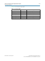
The following example illustrates this situation. Table 2–7 shows the key parameters.
Table 2–7. PHY Sequencer Parameters (Part 1 of 2)
Parameter
Setting
DLL_DELAY_BUFFER_MODE
HIGH
DLL_DELAY_CHAIN_LENGTH
10
DQS_DELAY_CTL_WIDTH
6
DQS_OUT_MODE
DELAY_CHAIN2
DQS_PHASE
7200
DQS_PHASE_SETTING
2
MEM_IF_CLK_PS
3300
MEM_IF_CLK_PS_STR
3300 ps
MEM_IF_MR_0
4641
External Memory Interface Handbook Volume 3
Section II. DDR3 SDRAM Controller with ALTMEMPHY IP User Guide
December 2010 Altera Corporation
Chapter 2: Getting Started
HardCopy Device Migration Guidelines
2–11
Table 2–7. PHY Sequencer Parameters (Part 2 of 2)
Parameter
1
Setting
PLL_STEPS_PER_CYCLE
40
MEM_IF_ADDR_CMD_PHASE
240
The sequencer in this example is set up to operate with 40 PLL phase steps per clock
cycle. (This information appears in the message panel of the ALTMEMPHY parameter
editor during generation of the IP core.)
Compiling Your Design for a Faster Speed Grade FPGA
The ALTMEMPHY parameter editor generates PLL parameters that match the PHY
requirement that the minimum PLL phase step size be one-eighth of the nominal VCO
operating period. In a C2 speed grade FPGA, the VCO is configured to run at
1515 MHz with an associated phase step of 82 ps. Table 2–8 summarizes the generated
PLL parameters. As shown, the PLL setup produces 40 phase steps per memory clock
cycle, matching the sequencer setup. This analysis, however, does not apply when
you select a HardCopy device.
Table 2–8. Generated PLL Parameters for a C2 speed grade FPGA
Parameter
Setting
VCO OPERATING FREQUENCY
1515 MHz
VCO PHASE SHIFT STEP
82 ps
MEMORY CLOCK PERIOD
3300 ps
PLL PHASE STEPS PER MEMCLK PERIOD
40
The HardCopy flow targets the center of the silicon process; therefore, all hard IP
blocks within the prototype FPGA must be configured accordingly to guarantee
functional equivalency. When a HardCopy device is selected, the Quartus II Fitter
restricts the operating range of the PLL to match the HardCopy silicon capability,
regardless of the speed grade of the selected FPGA. This restriction can alter the final
configuration of the PLL, producing a mismatch between the generated sequencer
setup stored in RTL, and the PLL behavior generated by the Quartus II Fitter.
Table 2–9 summarizes the post-fit PLL setup when HardCopy migration is selected,
regardless of the chosen FPGA speed grade.
Table 2–9. Post-fit PLL Parameters When Using a HardCopy Device
Parameter
December 2010
Setting
VCO OPERATING FREQUENCY
1212.1 MHz
VCO PHASE SHIFT STEP
103 ps
MEMORY CLOCK PERIOD
3300 ps
PLL PHASE STEPS PER MEMCLK PERIOD
32
Altera Corporation
External Memory Interface Handbook Volume 3
Section II. DDR3 SDRAM Controller with ALTMEMPHY IP User Guide
2–12
Chapter 2: Getting Started
HardCopy Device Migration Guidelines
As shown in Table 2–9, the Quartus II Fitter restricts the VCO operating range to
1212.1 MHz, rather than the 1515 MHz of Table 2–8. This restriction produces a phase
step mismatch between the PLL generated by the Quartus II Fitter and the PHY
sequencer setup written in the RTL. Because the calibration process expects a common
step size, the resulting design does not function properly in either the prototype
FPGA or in the HardCopy device.
If you choose to prototype in a slower speed grade FPGA (C4) and target a HardCopy
device, you must generate the ALTMEMPHY IP for the mid-speed grade FPGA to
ensure that proper values are chosen for both the FPGA and HardCopy devices—this
applies whether a performance improvement is desired or not.
f For information about HardCopy issues such as vertical I/O overhang, PLLs adjacent
to I/Os, performance improvement, and timing closure, refer to HardCopy III Device
I/O Features in the HardCopy III Device Handbook, Volume 1, and HardCopy IV Device
I/O Features in the HardCopy IV Device Handbook, Volume 1.
External Memory Interface Handbook Volume 3
Section II. DDR3 SDRAM Controller with ALTMEMPHY IP User Guide
December 2010 Altera Corporation
3. Parameter Settings
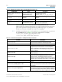
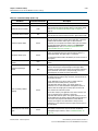
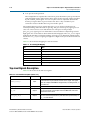
ALTMEMPHY Parameter Settings
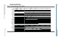
The Parameter Settings page in the ALTMEMPHY parameter editor (Figure 3–1)
allows you to parameterize the following settings:
■
Memory Settings
■
PHY Settings
■
Board Settings
Figure 3–1. ALTMEMPHY Parameter Settings Page
The text window at the bottom of the MegaWizard Plug-In Manager displays
information about the memory interface, warnings, and errors if you are trying to
create something that is not supported. The Finish button is disabled until you correct
all the errors indicated in this window.
December 2010
Altera Corporation
External Memory Interface Handbook Volume 3
Section II. DDR3 SDRAM Controller with ALTMEMPHY IP User Guide
3–2
Chapter 3: Parameter Settings
ALTMEMPHY Parameter Settings
The following sections describe the four tabs of the Parameter Settings page in more
detail.
Memory Settings
In the Memory Settings tab, you can select a particular memory device for your
system and choose the frequency of operation for the device. Under General Settings,
you can choose the device family, speed grade, and clock information. In the middle
of the page (left-side), you can filter the available memory device listed on the right
side of the Memory Presets dialog box, refer to Figure 3–1. If you cannot find the
exact device that you are using, choose a device that has the closest specifications,
then manually modify the parameters to match your actual device by clicking Modify
parameters, next to the Selected memory preset field.
Table 3–1 describes the General Settings available on the Memory Settings page of
the ALTMEMPHY parameter editor.
Table 3–1. General Settings
Parameter Name
Description
Device family
Targets device family (for example, Stratix III). Table 1–2 on page 1–3 shows supported device
families. The device family selected here must match the device family selected on the MegaWizard
page 2a.
Speed grade
Selects a particular speed grade of the device (for example, 2, 3, or 4 for the Stratix III device
family).
PLL reference clock
frequency
Determines the clock frequency of the external input clock to the PLL. Ensure that you use three
decimal points if the frequency is not a round number (for example, 166.667 MHz or 100 MHz) to
avoid a functional simulation or a PLL locking problem.
Memory clock
frequency
Determines the memory interface clock frequency. If you are operating a memory device below its
maximum achievable frequency, ensure that you enter the actual frequency of operation rather than
the maximum frequency achievable by the memory device. Also, ensure that you use three decimal
points if the frequency is not a round number (for example, 333.333 MHz or 400 MHz) to avoid a
functional simulation or a PLL locking issue.
Controller data rate
Selects the data rate for the memory controller. Sets the frequency of the controller to equal to
either the memory interface frequency (full-rate) or half of the memory interface frequency
(half-rate). The full-rate option is not available for DDR3 SDRAM devices.
This option is only available for HPC II full-rate controller.
Enable half rate bridge Turn on to keep the controller in the memory full clock domain while allowing the local side to run
at half the memory clock speed, so that latency can be reduced.
Local interface clock
frequency
Value that depends on the memory clock frequency and controller data rate, and whether or not
you turn on the Enable Half Rate Bridge option.
Local interface width
Value that depends on the memory clock frequency and controller data rate, and whether or not
you turn on the Enable Half Rate Bridge option.
1
When targeting a HardCopy device migration with performance improvement, the
ALTMEMPHY IP should target the mid speed grade to ensure that the PLL and the
PHY sequencer settings match. The compilation of the design can be executed in the
faster speed grade.
External Memory Interface Handbook Volume 3
Section II. DDR3 SDRAM Controller with ALTMEMPHY IP User Guide
December 2010 Altera Corporation
Chapter 3: Parameter Settings
ALTMEMPHY Parameter Settings
3–3
Table 3–2 describes the options available to filter the Memory Presets that are
displayed. This set of options is where you indicate whether you are creating a
datapath for DDR3 SDRAM.
Table 3–2. Memory Presets List
Parameter Name
Description
Memory type
You can filter the type of memory to display, for example, DDR3 SDRAM.
Memory vendor
You can filter the memory types by vendor. JEDEC is also one of the options, allowing you to
choose the JEDEC specifications. If your chosen vendor is not listed, you can choose JEDEC for the
DDR3 SDRAM interfaces. Then, pick a device that has similar specifications to your chosen device
and check the values of each parameter. Make sure you change the each parameter value to match
your device specifications.
Memory format
You can filter the type of memory by format, for example, discrete devices or DIMM packages.
Maximum frequency
You can filter the type of memory by the maximum operating frequency.
Using the Preset Editor to Create a Custom Memory Preset
Pick a device in the Memory Presets list that is closest or the same as the actual
memory device that you are using. Then, click the Modify Parameters button to
parameterize the following settings in the Preset Editor dialog box:
1
■
Memory attributes—These are the settings that determine your system's number
of DQ, DQ strobe (DQS), address, and memory clock pins.
■
Memory initialization options—These settings are stored in the memory mode
registers as part of the initialization process.
■
Memory timing parameters—These are the parameters that create and
time-constrain the PHY.
Even though the device you are using is listed in Memory Presets, ensure that the
settings in the Preset Editor dialog box are accurate, as some parameters may have
been updated in the memory device datasheets.
You can change the parameters with a white background to reflect your system. You
can also change the parameters with a gray background so the device parameters
match the device you are using. These parameters in gray background are
characteristics of the chosen memory device and changing them creates a new custom
memory preset. If you click Save As (at the bottom left of the page) and save the new
settings in the <quartus_install_dir>\quartus\common\ip\altera\altmemphy\lib\
directory, you can use this new memory preset in other Quartus II projects created in
the same version of the software.
When you click Save, the new memory preset appears at the bottom of the Memory
Presets list in the Memory Settings tab.
1
December 2010
If you save the new settings in a directory other than the default directory, click Load
Preset in the Memory Settings tab to load the settings into the Memory Presets list.
Altera Corporation
External Memory Interface Handbook Volume 3
Section II. DDR3 SDRAM Controller with ALTMEMPHY IP User Guide
3–4
Chapter 3: Parameter Settings
ALTMEMPHY Parameter Settings
Figure 3–2 shows the Preset Editor dialog box for a DDR3 SDRAM.
Figure 3–2. DDR3 SDRAM Preset Editor
The Advanced option is only available for Arria II GX and Stratix IV devices. This
option shows the percentage of memory specification that is calibrated by the FPGA.
The percentage values are estimated by Altera based on the process variation.
External Memory Interface Handbook Volume 3
Section II. DDR3 SDRAM Controller with ALTMEMPHY IP User Guide
December 2010 Altera Corporation
Chapter 3: Parameter Settings
ALTMEMPHY Parameter Settings
3–5
Table 3–3 through Table 3–5 describe the DDR3 SDRAM parameters available for
memory attributes, initialization options, and timing parameters.
Table 3–3. DDR3 SDRAM Attributes Settings (Part 1 of 2)
Parameter Name
Output clock pairs from FPGA
Range (1)
1–6
Units
Description
pairs
Defines the number of differential clock pairs driven from
the FPGA to the memory. Memory clock pins use the
signal splitter feature in Arria II GX, Stratix III, and
Stratix IV devices for differential signaling.
The ALTMEMPHY parameter editor displays an error on
the bottom of the window if you choose more than one
for DDR3 SDRAM interfaces.
Total Memory chip selects
Memory interface DQ width
1, 2, 4, or 8
4–288
bits
Sets the number of chip selects in your memory
interface. The number of chip selects defines the depth of
your memory. You are limited to the range shown as the
local side binary encodes the chip select address.
bits
Defines the total number of DQ pins on the memory
interface. If you are interfacing with multiple devices,
multiply the number of devices with the number of DQ
pins per device. Even though the GUI allows you to
choose 288-bit DQ width, DDR3 SDRAM variations are
only supported up to 80-bit width due to restrictions in
the board layout which affects timing at higher data
width. Furthermore, the interface data width is limited by
the number of pins on the device. For best performance,
have the whole interface on one side of the device.
On multiple rank DDR3 SDRAM DIMMs address signals
are routed differently to each rank; referred to in the
JEDEC specification as address mirroring.
Mirror addressing
—
—
Register Control Word 0–15
for Registered DIMMs
—
bits
Register Control Word values for the DDR3 registered
DIMMs. The values are available in the memory data
sheet of the respective registered DIMMs.
Elpida, JEDEC,
Micron,
Samsung, Hynix,
Nanya, other
—
Lists the name of the memory vendor for all supported
memory standards.
Memory vendor
Enter ranks with mirrored addresses in this field. There is
one bit per chip select. For example, for four chip selects,
enter 1011 to mirror the address on chip select #3, #1,
and #0.
Memory format
Discrete Device,
Unbuffered
DIMM
—
Specifies whether you are interfacing with devices or
modules. SODIMM and MicroDIMM are supported under
unbuffered DIMMs. The ALTMEMPHY megafunction for
DDR3 SDRAM interfaces does not support registered
DIMM format. Arria II GX devices only support DDR3
SDRAM components without leveling, for example,
Discrete Device memory format.
Maximum memory frequency
See the memory
device datasheet
MHz
Sets the maximum frequency supported by the memory.
10–12
bits
Defines the number of column address bits for your
interface.
Column address width
December 2010
Altera Corporation
External Memory Interface Handbook Volume 3
Section II. DDR3 SDRAM Controller with ALTMEMPHY IP User Guide
3–6
Chapter 3: Parameter Settings
ALTMEMPHY Parameter Settings
Table 3–3. DDR3 SDRAM Attributes Settings (Part 2 of 2)
Parameter Name
Range (1)
Units
Description
Row address width
12–16
bits
Defines the number of row address bits for your
interface. If your DDR3 SDRAM device’s row address bus
is 12-bit wide, set the row address width to 13 and set the
13th bit to logic-level low (or leave the 13th bit
unconnected to the memory device) in the top-level file.
Bank address width
3
bits
Defines the number of bank address bits for your
interface.
Chip selects per DIMM
1 or 2
bits
Defines the number of chip selects on each DIMM in your
interface. Currently, calibration is done with all ranks but
you can only perform timing analysis with one
single-rank DIMM.
DQ bits per DQS bit
4 or 8
bits
Defines the number of data (DQ) bits for each data strobe
(DQS) pin.
Yes or No
—
Specifies whether you are using DM pins for write
operation. Altera devices do not support DM pins with ×4
mode.
MHz
Specifies the frequency limits from the memory data
sheet per given CAS latency. The ALTMEMPHY
MegaWizard Plug-In Manager generates a warning if the
operating frequency with your chosen CAS latency
exceeds this number. The lowest frequency supported by
DDR3 SDRAM devices is 300 MHz.
Drive DM pins from FPGA
Maximum memory frequency
for CAS latency 5.0
Maximum memory frequency
for CAS latency 6.0
Maximum memory frequency
for CAS latency 7.0
Maximum memory frequency
for CAS latency 8.0
80–700
Maximum memory frequency
for CAS latency 9.0
Maximum memory frequency
for CAS latency 10.0
Note to Table 3–3:
(1) The range values depend on the actual memory device used.
Table 3–4. DDR3 SDRAM Initialization Options (Part 1 of 3)
Parameter Name
Memory burst length
Memory burst ordering
DLL precharge power down
Range
Units
4, 8, on-the-fly
beats
Description
Sets the number of words read or written per
transaction.
Sequential or
Interleaved
—
Controls the order in which data is transferred between
memory and the FPGA during a read transaction. For
more information, refer to the memory device
datasheet.
Fast exit or Slow
exit
—
Sets the mode register setting to disable (Slow exit) or
enable (Fast exit) the memory DLL when CKE is
disabled.
External Memory Interface Handbook Volume 3
Section II. DDR3 SDRAM Controller with ALTMEMPHY IP User Guide
December 2010 Altera Corporation
Chapter 3: Parameter Settings
ALTMEMPHY Parameter Settings
3–7
Table 3–4. DDR3 SDRAM Initialization Options (Part 2 of 3)
Parameter Name
Enable the DLL in the
memory devices
ODT Rtt nominal value
Dynamic ODT (Rtt_WR) value
Range
Yes or No
ODT disable,
RZQ/4, RZQ/2,
RZQ/6
Dynamic ODT off,
RZQ/4, RZQ/2
Units
Description
—
Enables the DLL in the memory device when set to Yes.
You must always enable the DLL in the memory device
as Altera does not guarantee any ALTMEMPHY
operation when the DLL is turned off. All timings from
the memory devices are invalid when the DLL is turned
off.
W
RZQ in DDR3 SDRAM interfaces are set to 240 Ω. Sets
the on-die termination (ODT) value to either 60 Ω
(RZQ/4), 120 Ω (RZQ/2), or 40 Ω (RZQ/6). Set this to
ODT disable if you are not planning to use ODT. For a
single-ranked DIMM, set this to RZQ/4.
W
RZQ in DDR3 SDRAM interfaces are set to 240 Ω. Sets
the memory ODT value during write operations to 60 Ω
(RZQ/4) or 120 Ω (RZQ/2). As ALTMEMPHY only
supports single rank DIMMs, you do not need this
option (set to Dynamic ODT off).
Output driver impedance
RZQ/6 (Reserved)
or RZQ/7
W
RZQ in DDR3 SDRAM interfaces are set to 240 Ω. Sets
the output driver impedance from the memory device.
Some devices may not have RZQ/6 available as an
option. Be sure to check the memory device datasheet
before choosing this option.
Memory CAS latency setting
5.0, 6.0, 7.0, 8.0,
9.0, 10.0
cycles
Sets the delay in clock cycles from the read command
to the first output data from the memory.
cycles
Allows you to add extra latency in addition to the CAS
latency setting.
cycles
Sets the delay in clock cycles from the write command
to the first expected data to the memory.
—
Determine whether you want to self-refresh only certain
arrays instead of the full array. According to the DDR3
SDRAM specification, data located in the array beyond
the specified address range are lost if self refresh is
entered when you use this. This option is not supported
by the DDR3 SDRAM Controller with ALTMEMPHY IP,
so set to Full Array if you are using the Altera
controller.
Memory additive CAS latency
setting
Memory write CAS latency
setting (CWL)
Disable, CL – 1,
CL – 2
5.0, 6.0, 7.0, 8.0
Full array,
Half array
{BA[2:0]=000,001,
010,011},
Memory partial array self
refresh
Quarter array
{BA[2:0]=000,001}
,
Eighth array
{BA[2:0]=000},
Three Quarters
array
{BA[2:0]=010,011,
100,101,110,111},
Half array
{BA[2:0]=100,101,
110,111},
Quarter array
{BA[2:0]=110,
111},
Eighth array
{BA[2:0]=111}
December 2010
Altera Corporation
External Memory Interface Handbook Volume 3
Section II. DDR3 SDRAM Controller with ALTMEMPHY IP User Guide
3–8
Chapter 3: Parameter Settings
ALTMEMPHY Parameter Settings
Table 3–4. DDR3 SDRAM Initialization Options (Part 3 of 3)
Parameter Name
Memory auto self refresh
method
Memory self refresh range
Range
Units
Description
—
Sets the auto self-refresh method for the memory
device. The DDR3 SDRAM Controller with ALTMEMPHY
IP currently does not support the ASR option that you
need for extended temperature memory self-refresh.
—
Determines the temperature range for self refresh. You
need to also use the optional auto self refresh option
when using this option. The Altera controller currently
does not support the extended temperature self-refresh
operation.
Manual SR
reference (SRT) or
ASR enable
(Optional)
Normal or
Extended
Table 3–5. DDR3 SDRAM Timing Parameter Settings (Part 1 of 3)
Parameter Name
Range
Units
(Note 1)
Description
Time to hold memory reset
before beginning calibration
0–1000000
µs
Minimum time to hold the reset after a power cycle
before issuing the MRS commands during the DDR3
SDRAM device initialization process.
tINIT
0.001–
1000
µs
Minimum memory initialization time. After reset, the
controller does not issue any commands to the
memory during this period.
Minimum load mode register command period. The
controller waits for this period of time after issuing a
load mode register command before issuing any other
commands.
tMRD is specified in ns in the DDR3 SDRAM
high-performance controller and in terms of tCK cycles
in Micron's device datasheet. Convert tMRD to ns by
multiplying the number of cycles specified in the
datasheet times tCK, where tCK is the memory operation
frequency and not the memory device's tCK.
tMRD
2–39
ns
tRAS
8–200
ns
Minimum active to precharge time. The controller waits
for this period of time after issuing an active command
before issuing a precharge command to the same bank.
tRCD
4–65
ns
Minimum active to read-write time. The controller does
not issue read or write commands to a bank during this
period of time after issuing an active command.
tRP
4–65
ns
Minimum precharge command period. The controller
does not access the bank for this period of time after
issuing a precharge command.
tREFI
1–65534
µs
Maximum interval between refresh commands. The
controller performs regular refresh at this interval
unless user-controlled refresh is turned on.
tRFC
14–1651
ns
Minimum autorefresh command period. The length of
time the controller waits before doing anything else
after issuing an auto-refresh command.
tWR
4–65
ns
Minimum write recovery time. The controller waits for
this period of time after the end of a write transaction
before issuing a precharge command.
External Memory Interface Handbook Volume 3
Section II. DDR3 SDRAM Controller with ALTMEMPHY IP User Guide
December 2010 Altera Corporation
Chapter 3: Parameter Settings
ALTMEMPHY Parameter Settings
3–9
Table 3–5. DDR3 SDRAM Timing Parameter Settings (Part 2 of 3)
Parameter Name
Range
(Note 1)
Units
Description
tWTR
1–6
tCK
Minimum write-to-read command delay. The controller
waits for this period of time after the end of a write
command before issuing a subsequent read command
to the same bank. This timing parameter is specified in
clock cycles and the value is rounded off to the next
integer.
tAC
0–750
ps
DQ output access time.
tDQSCK
50–750
ps
DQS output access time from CK/CK# signals.
tDQSQ
50–500
ps
The maximum DQS to DQ skew; DQS to last DQ valid,
per group, per access.
tDQSS
0–0.3
tCK
Positive DQS latching edge to associated clock edge.
ps
DQ and DM input hold time relative to DQS, which has a
derated value depending on the slew rate of the
differential DQS and DQ/DM signals. Ensure that you
are using the correct number and that the value entered
is referenced to VREF(dc), not VIH(dc) min or VIL(dc)
max. Refer to “Derating Memory Setup and Hold
Timing” on page 3–10 for more information about how
to derate this specification.
tDH
10–600
tDS
10–600
ps
DQ and DM input setup time relative to DQS, which has
a derated value depending on the slew rate of the
differential DQS signals and DQ/DM signals. Ensure
that you are using the correct number and that the
value entered is referenced to VREF(dc), not VIH(ac) min
or VIL(ac) max. Refer to “Derating Memory Setup and
Hold Timing” on page 3–10 for more information about
how to derate this specification.
tDSH
0.1–0.5
tCK
DQS falling edge hold time from CK.
tDSS
0.1–0.5
tCK
DQS falling edge to CK setup.
ps
Address and control input hold time, which has a
derated value depending on the slew rate of the CK and
CK# clocks and the address and command signals.
Ensure that you are using the correct number and that
the value entered is referenced to VREF(dc), not VIH(dc)
min or VIL(dc) max. Refer to “Derating Memory Setup
and Hold Timing” on page 3–10 for more information
about how to derate this specification.
50–1000
tIH
tIS
65–1000
ps
Address and control input setup time, which has a
derated value depending on the slew rate of the CK and
CK# clocks and the address and command signals.
Ensure that you are using the correct number and that
the value entered is referenced to VREF(dc), not VIH(ac)
min or VIL(ac) max. Refer to “Derating Memory Setup
and Hold Timing” on page 3–10 for more information
about how to derate this specification.
tQHS
0–700
ps
The maximum data hold skew factor.
tQH
0.1–0.6
tCK
DQ output hold time.
December 2010
Altera Corporation
External Memory Interface Handbook Volume 3
Section II. DDR3 SDRAM Controller with ALTMEMPHY IP User Guide
3–10
Chapter 3: Parameter Settings
ALTMEMPHY Parameter Settings
Table 3–5. DDR3 SDRAM Timing Parameter Settings (Part 3 of 3)
Parameter Name
Range
(Note 1)
Units
Description
tRRD
2.06–64
ns
The activate to activate time, per device, RAS to RAS
delay timing parameter.
tFAW
7.69–256
ns
The four-activate window time, per device.
tRTP
2.06–64
ns
Read to precharge time.
Note to Table 3–5:
(1) See the memory device data sheet for the parameter range. Some of the parameters may be listed in a clock cycle (tCK) unit. If the MegaWizard
Plug-In Manager requires you to enter the value in a time unit (ps or ns), convert the number by multiplying it with the clock period of your
interface (and not the maximum clock period listed in the memory data sheet).
Derating Memory Setup and Hold Timing
Because the base setup and hold time specifications from the memory device
datasheet assume input slew rates that may not be true for Altera devices, derate and
update the following memory device specifications in the Preset Editor dialog box:
1
■
tDS
■
tDH
■
tIH
■
tIS
For Arria II GX and Stratix IV devices, you need not derate using the Preset Editor.
You only need to enter the parameters referenced to VREF, and the deration is done
automatically when you enter the slew rate information on the Board Settings tab.
After derating the values, you then need to normalize the derated value because
Altera input and output timing specifications are referenced to VREF. When the
memory device setup and hold time numbers are derated and normalized to VREF,
update these values in the Preset Editor dialog box to ensure that your timing
constraints are correct.
The following memory device specifications and update the Preset Editor dialog box
with the derated value:
For example, according to JEDEC, 533-MHz DDR3 SDRAM has the following
specifications, assuming 1V/ns DQ slew rate rising signal and 2V/ns DQS-DQSn
slew rate:
■
Base tDS = 25
■
Base tDH = 100
■
VIH(ac) = VREF + 0.175 V
■
VIH(dc) = VREF + 0.100 V
■
VIL(ac) = VREF – 0.175 V
■
VIL(dc) = VREF – 0.100 V
External Memory Interface Handbook Volume 3
Section II. DDR3 SDRAM Controller with ALTMEMPHY IP User Guide
December 2010 Altera Corporation
Chapter 3: Parameter Settings
ALTMEMPHY Parameter Settings
3–11
The VREF referenced setup and hold signals for a rising edge are:
tDS (VREF) = Base tDS + delta tDS + (VIH(ac) – VREF)/slew_rate = 25 + 0 + 175 =
200 ps
tDH (VREF) = Base tDH + delta tDH + (VIH(dc) – VREF)/slew_rate = 100 + 0 + 100 =
200 ps
If the output slew rate of the write data is different from 1V/ns, you have to first
derate the tDS and tDH values, then translate these AC/DC level specs to VREF
specification.
For a 2V/ns DQ slew rate rising signal and 2V/ns DQS-DQSn slew rate:
tDS (VREF) = Base tDS + delta tDS + (VIH(ac) – VREF)/slew_rate = 25 + 88 + 87.5 =
200.5 ps
tDH (VREF) = Base tDH + delta tDH + (VIH(dc) – VREF)/slew_rate = 100 + 50 + 50 =
200 ps
For a 0.5V/ns DQ slew rate rising signal and 1V/ns DQS-DQSn slew rate:
tDS (VREF) = Base tDS + delta tDS + (VIH(ac) – VREF)/slew_rate = 25 + 5 + 350 = 380
ps
tDH (VREF) = Base tDH + delta tDH + (VIH(dc) – VREF)/slew_rate = 100 + 10 + 200 =
310 ps
PHY Settings
Click Next or the PHY Settings tab to set the options described in Table 3–6. The
options are available if they apply to the target Altera device.
Table 3–6. ALTMEMPHY PHY Settings (Part 1 of 2)
Parameter Name
Applicable Device Families
Description
Use dedicated PLL
outputs to drive
memory clocks
HardCopy II and Stratix II
(prototyping for
HardCopy II)
This option is disabled for DDR3 SDRAM.
Dedicated memory
clock phase
HardCopy II and Stratix II
(prototyping for
HardCopy II)
This option is disabled for DDR3 SDRAM.
Use differential DQS
Arria II GX, Stratix III, and
Stratix IV
This option is disabled for DDR3 SDRAM.
When enabling this option for HardCopy II, Stratix III, and Stratix IV
devices, the inputs to the ALTPLL_RECONFIG megafunction are
brought to the top level for debugging purposes.
Enable external access
to reconfigure PLL
prior to calibration
December 2010
HardCopy II, Stratix III, and
Stratix IV (prototyping for
HardCopy II)
Altera Corporation
This option allows you to reconfigure the PLL before calibration to
adjust, if necessary, the phase of the memory clock (mem_clk_2x)
before the start of the calibration of the resynchronization clock on
the read side. The calibration of the resynchronization clock on the
read side depends on the phase of the memory clock on the write
side.
External Memory Interface Handbook Volume 3
Section II. DDR3 SDRAM Controller with ALTMEMPHY IP User Guide
3–12
Chapter 3: Parameter Settings
ALTMEMPHY Parameter Settings
Table 3–6. ALTMEMPHY PHY Settings (Part 2 of 2)
Parameter Name
Instantiate DLL
externally
Applicable Device Families
All supported device
families.
Enable dynamic parallel
on-chip termination
Stratix III and Stratix IV
(OCT)
Description
Use this option with Stratix III, Stratix IV, HardCopy III, or
HardCopy IV devices, if you want to apply a non-standard phase
shift to the DQS capture clock. The ALTMEMPHY DLL offsetting I/O
can then be connected to the external DLL and the Offset Control
Block.
This option provides I/O impedance matching and termination
capabilities. The ALTMEMPHY megafunction enables parallel
termination during reads and series termination during writes with
this option checked. Only applicable for DDR3 SDRAM interfaces
where DQ and DQS are bidirectional. Using the dynamic
termination requires that you use the OCT calibration block, which
may impose a restriction on your DQS/DQ pin placements
depending on your RUP/RDN pin locations.
For more information, refer to either the External Memory
Interfaces in Stratix III Devices chapter in volume 1 of the Stratix III
Device Handbook or the External Memory Interfaces in Stratix IV
Devices chapter in volume 1 of the Stratix IV Device Handbook.
Clock phase
Dedicated clock phase
Board skew
Autocalibration
simulation options
Arria II GX
Adjusting the address and command phase can improve the
address and command setup and hold margins at the memory
device to compensate for the propagation delays that vary with
different loadings. You have a choice of 0°, 90°, 180°, and 270°,
based on the rising and falling edge of the phy_clk and
write_clk signals. In Stratix IV and Stratix III devices, the clock
phase is set to dedicated.
Stratix III and Stratix IV
When you use a dedicated PLL output for address and command,
you can choose any legal PLL phase shift to improve setup and
hold for the address and command signals. You can set this value
to between 180° and 359° (the default is 240°). However, generally
PHY timing requires a value of greater than 240° for half-rate
designs.
All supported device
families except Arria II GX
and Stratix IV devices
Maximum skew across any two memory interface signals for the
whole interface from the FPGA to the memory (either a discrete
memory device or a DIMM). This parameter includes all types of
signals (data, strobe, clock, address, and command signals). You
need to input the worst-case skew, whether it is within a DQS/DQ
group, or across all groups, or across the address and command
and clocks signals. This parameter generates the timing constraints
in the .sdc file.
All supported device
families
Choose between Full Calibration (long simulation time), Quick
Calibration, or Skip Calibration.
For more information, refer to the Simulation section in volume 4 of
the External Memory Interface Handbook.
External Memory Interface Handbook Volume 3
Section II. DDR3 SDRAM Controller with ALTMEMPHY IP User Guide
December 2010 Altera Corporation
Chapter 3: Parameter Settings
DDR3 SDRAM Controller with ALTMEMPHY Parameter Settings
3–13
Board Settings
Click Next or the Board Settings tab to set the options described in Table 3–7. The
board settings parameters are set to model the board level effects in the timing
analysis. The options are available if you choose Arria II GX or Stratix IV device for
your interface. Otherwise, the options are disabled.
Table 3–7. ALTMEMPHY Board Settings
Parameter Name
Units
Number of slots/discrete devices
—
Description
Sets the single-rank or multi-rank configuration.
CK/CK# slew rate (differential)
V/ns
Sets the differential slew rate for the CK and CK# signals.
Addr/command slew rate
V/ns
Sets the slew rate for the address and command signals.
DQ/DQS# slew rate (differential)
V/ns
Sets the differential slew rate for the DQ and DQS# signals.
DQ slew rate
V/ns
Sets the slew rate for the DQ signals.
Addr/command eye reduction
(setup)
ns
Sets the reduction in the eye diagram on the setup side due to the
ISI on the address and command signals.
Addr/command eye reduction
(hold)
ns
Sets the reduction in the eye diagram on the hold side due to the ISI
on the address and command signals.
DQ eye reduction
ns
Sets the total reduction in the eye diagram on the setup side due to
the ISI on the DQ signals.
Delta DQS arrival time
ns
Sets the increase of variation on the range of arrival times of DQS
due to ISI.
Min CK/DQS skew to DIMM
ns
Sets the minimum skew between the CK signal and any DQS signal
when arriving at the same DIMM over all DIMMs.
Max CK/DQS skew to DIMM
ns
Sets the maximum skew between the CK signal and any DQS signal
when arriving at the same DIMM over all DIMMs.
Max skew between
DIMMs/devices
ns
Sets the largest skew or propagation delay on the DQ signals
between ranks, especially true for DIMMs in different slots.
Max skew within DQS group
ns
Sets the largest skew between the DQ pins in a DQS group.
Max skew between DQS groups
ns
Sets the largest skew between DQS signals in different DQS groups.
ns
Sets the skew or propagation delay between the CK signal and the
address and command signals. The positive values represent the
address and command signals that are longer than the CK signals,
and the negative values represent the address and command signals
that are shorter than the CK signals.
Addr/command to CK skew
DDR3 SDRAM Controller with ALTMEMPHY Parameter Settings
The Parameter Settings page in the DDR3 SDRAM Controller with ALTMEMPHY
parameter editor (Figure 3–3) allows you to parameterize the following settings:
December 2010
■
Memory Settings
■
PHY Settings
■
Board Settings
■
Controller Settings
Altera Corporation
External Memory Interface Handbook Volume 3
Section II. DDR3 SDRAM Controller with ALTMEMPHY IP User Guide
3–14
Chapter 3: Parameter Settings
DDR3 SDRAM Controller with ALTMEMPHY Parameter Settings
The Memory Settings, PHY Settings, and Board Settings tabs provide the same
options as in the ALTMEMPHY Parameter Settings page.
Figure 3–3. DDR3 SDRAM Controller with ALTMEMPHY Settings
Controller Settings
Table 3–8 shows the options provided on the Controller Settings tab.
External Memory Interface Handbook Volume 3
Section II. DDR3 SDRAM Controller with ALTMEMPHY IP User Guide
December 2010 Altera Corporation
Chapter 3: Parameter Settings
DDR3 SDRAM Controller with ALTMEMPHY Parameter Settings
3–15
Table 3–8. Controller Settings (Part 1 of 3)
Parameter
Controller architecture
Controller Architecture
—
Description
Specifies the controller architecture.
Enable self-refresh controls
Both
Turn on to enable the controller to allow you to have control on
when to place the external memory device in self-refresh mode,
refer to “User-Controlled Self-Refresh Logic” on page 7–8
(HPC II).
Enable power down controls
HPC
Turn on to enable the controller to allow you to have control on
when to place the external memory device in power-down mode.
HPC II
Turn on to enable the controller to automatically place the
external memory device in power-down mode after a specified
number of idle controller clock cycles is observed in the
controller. You can specify the number of idle cycles after which
the controller powers down the memory in the Auto Power
Down Cycles field, refer to “Automatic Power-Down with
Programmable Time-Out” on page 7–7.
Enable auto power down
Auto power down cycles
HPC II
Determines the desired number of idle controller clock cycles
before the controller places the external memory device in a
power-down mode. The legal range is 1 to 65,535.
The auto power-down mode is disabled if you set the value to 0
clock cycles.
Enable user auto-refresh
controls
Enable auto-precharge
control
Both
Turn on to enable the controller to allow you to issue a single
refresh.
HPC
Turn on to enable the auto-precharge control on the controller
top level. Asserting the auto-precharge control signal while
requesting a read or write burst allows you to specify whether or
not the controller should close (auto-precharge) the current
opened page at the end of the read or write burst.
Allows you to control the mapping between the address bits on
the Avalon interface and the chip, row, bank, and column bits on
the memory interface.
Local-to-memory address
mapping
HPC II
If your application issues bursts that are greater than the
column size of the memory device, choose the
Chip-Row-Bank-Column option. This option allows the
controller to use its look-ahead bank management feature to
hide the effect of changing the currently open row when the
burst reaches the end of the column.
On the other hand, if your application has several masters that
each use separate areas of memory, choose the
Chip-Bank-Row-Column option. This option allows you to use
the top address bits to allocate a physical bank in the memory to
each master. The physical bank allocation avoids different
masters accessing the same bank which is likely to cause
inefficiency, as the controller must then open and close rows in
the same bank.
Command queue look-ahead
depth
December 2010
Altera Corporation
HPC II
Specifies a command queue look-ahead depth value to control
the number of read or write requests the look-ahead bank
management logic examines, refer to “Command Queue” on
page 7–4.
External Memory Interface Handbook Volume 3
Section II. DDR3 SDRAM Controller with ALTMEMPHY IP User Guide
3–16
Chapter 3: Parameter Settings
DDR3 SDRAM Controller with ALTMEMPHY Parameter Settings
Table 3–8. Controller Settings (Part 2 of 3)
Parameter
Controller Architecture
Description
Local maximum burst count
HPC II
Specifies a burst count to configure the maximum Avalon burst
count that the controller slave port accepts.
Controller latency
HPC II
Specifies a latency for the controller. The default latency is 5 but
you have the option to choose 4 to enhance the latency
performance of your design at the expense of timing closure.
HPC II
Turn on to enable run-time configuration and status retrieval of
the memory controller. Enabling this option adds an additional
Avalon-MM slave port to the memory controller top level that
allows run-time reconfiguration and status retrieving for
memory timing parameters, memory address size and mode
register settings, and controller features. If the Error Detection
and Correction Logic option is enabled, the same slave port also
allows you to control and retrieve the status of this logic. Refer
to “Configuration and Status Register (CSR) Interface” on
page 7–7.
Both
Turn on to enable error correction coding (ECC) for single-bit
error correction and double-bit error detection. Refer to “Error
Correction Coding (ECC)” on page 6–5 for HPC, and “Error
Correction Coding (ECC)” on page 7–7 for HPC II.
HPC II
Turn on to allow the controller to perform auto correction when
the ECC logic detects a single-bit error. Alternatively, you can
turn off this option and schedule the error correction at a
desired time for better system efficiency. Refer to “Error
Correction Coding (ECC)” on page 7–7.
Enable configuration and
status register interface
Enable error detection and
correction logic
Enable auto error correction
Enable multi-cast write
control
HPC II
Turn on to enable the multi-cast write control on the controller
top level. Asserting the multi-cast write control when requesting
a write burst causes the write data to be written to all the chip
selects in the memory system. When you turn on this option
together with the Enable User Auto-Refresh Controls option,
the user refresh commands are issued to all chips.
Multi-cast write is not supported for registered DIMM interfaces
or when you turn on the Enable Error Detection and Correction
Logic option.
Enable reduced bank tracking
for area optimization
Number of banks to track
HPC II
Turn on to reduce the controller’s resource usage. By turning on
this option, you reduce the number of bank tracking blocks in
the controller. Refer to “Bank Management Logic” on page 7–4
for more information.
HPC II
Specifies the number of bank tracking blocks you want for your
design. This option is only available if you turn on the Enable
Reduced Bank Tracking for Area Optimization option. The value
for this option depends on the value you specify for the
Command Queue Look-Ahead Depth option. Refer to “Bank
Management Logic” on page 7–4 for more information.
External Memory Interface Handbook Volume 3
Section II. DDR3 SDRAM Controller with ALTMEMPHY IP User Guide
December 2010 Altera Corporation
Chapter 3: Parameter Settings
DDR3 SDRAM Controller with ALTMEMPHY Parameter Settings
3–17
Table 3–8. Controller Settings (Part 3 of 3)
Parameter
Multiple controller clock
sharing
Local interface protocol
Controller Architecture
Description
Both
This option is only available in SOPC Builder Flow. Turn on to
allow one controller to use the Avalon clock from another
controller in the system that has a compatible PLL. This option
allows you to create SOPC Builder systems that have two or
more memory controllers that are synchronous to your master
logic.
HPC
Specifies the local side interface between the user logic and the
memory controller. The Avalon-MM interface allows you to
easily connect to other Avalon-MM peripherals.
The HPC II architecture supports only the Avalon-MM interface.
December 2010
Altera Corporation
External Memory Interface Handbook Volume 3
Section II. DDR3 SDRAM Controller with ALTMEMPHY IP User Guide
3–18
External Memory Interface Handbook Volume 3
Section II. DDR3 SDRAM Controller with ALTMEMPHY IP User Guide
Chapter 3: Parameter Settings
DDR3 SDRAM Controller with ALTMEMPHY Parameter Settings
December 2010 Altera Corporation
4. Compiling and Simulating
After setting the parameters for the MegaCore function, you can now integrate the
MegaCore function variation into your design, and compile and simulate your design.
The following sections detail the steps you need to perform to compile and simulate
your design.
Compiling the Design
Figure 4–1 shows the top-level view of the Altera high-performance controller design
as an example of how your final design looks after you integrate the controller and the
user logic.
Figure 4–1. High-Performance Controller System-Level Diagram
Example Top-Level File
ALTMEMPHY
External
Memory
Device
DLL
PLL
(1)
HighPerformance
Controller
Example
Driver
Pass or Fail
Note to Figure 4–1:
(1) When you choose Instantiate DLL Externally, DLL is instantiated outside the controller.
Before compiling a design with the ALTMEMPHY variation, you must edit some
project settings, include the .sdc file, and make I/O assignments. I/O assignments
include I/O standard, pin location, and other assignments, such as termination and
drive strength settings. Some of these tasks are listed in the ALTMEMPHY
Generation window. For most systems, Altera recommends that you use the
Advanced I/O Timing feature by using the Board Trace Model command in the
Quartus II software to set the termination and output pin loads for the device.
To use the Quartus II software to compile the example top-level file in the Quartus II
software and perform post-compilation timing analysis, perform the following steps:
1. Set up the TimeQuest timing analyzer:
a. On the Assignments menu, click Timing Analysis Settings, select Use
TimeQuest Timing Analyzer during compilation, and click OK.
b. Add the Synopsys Design Constraints (.sdc) file,
<variation name>_phy_ddr_timing.sdc, to your project. On the Project menu,
click Add/Remove Files in Project and browse to select the file.
c. Add the .sdc file for the example top-level design,
<variation name>_example_top.sdc, to your project. This file is only required if
you are using the example as the top-level design.
December 2010
Altera Corporation
External Memory Interface Handbook Volume 3
Section II. DDR3 SDRAM Controller with ALTMEMPHY IP User Guide
4–2
Chapter 4: Compiling and Simulating
Compiling the Design
2. You can either use the <variation_name>_pin_assignments.tcl or the
<variation_name>.ppf file to apply the I/O assignments generated by the
MegaWizard Plug-In Manager. Using the .ppf file and the Pin Planner gives you
the extra flexibility to add a prefix to your memory interface pin names. You can
edit the assignments either in the Assignment Editor or Pin Planner. Use one of the
following procedures to specify the I/O standard assignments for pins:
■
If you have a single SDRAM interface, and your top-level pins have default
naming shown in the example top-level file, run
<variation name>_pin_assignments.tcl.
or
■
If your design contains pin names that do not match the design, edit the
<variation name>_pin_assignments.tcl file before you run the script. To edit the .tcl
file, perform the following steps:
a. Open <variation name>_pin_assignments.tcl file.
b. Based on the flow you are using, set the sopc_mode value to Yes or No.
■
SOPC Builder System flow:
if {![info exists sopc_mode]} {set sopc_mode YES}
■
MegaWizard Plug-In Manager flow:
if {![info exists sopc_mode]} {set sopc_mode NO}
c. Type your preferred prefix in the pin_prefix variable. For example, to add the
prefix my_mem, do the following:
if {![info exists set_prefix}{set pin_prefix “my_mem_”}
After setting the prefix, the pin names are expanded as shown in the following:
■
SOPC Builder System flow:
my_mem_cs_n_from_the_<your instance name>
■
MegaWizard Plug-In Manager flow:
my_mem_cs_n[0]
1
If your top-level design does not use single bit bus notation for the
single-bit memory interface signals (for example, mem_dqs rather than
mem_dqs[0]), in the Tcl script you should change set single_bit {[0]} to
set single_bit {}.
or
External Memory Interface Handbook Volume 3
Section II. DDR3 SDRAM Controller with ALTMEMPHY IP User Guide
December 2010 Altera Corporation
Chapter 4: Compiling and Simulating
Compiling the Design
■
4–3
Alternatively, to change the pin names that do not match the design, you can add a
prefix to your pin names by performing the following steps:
a. On the Assignments menu, click Pin Planner.
b. On the Edit menu, click Create/Import Megafunction.
c. Select Import an existing custom megafunction and navigate to
<variation name>.ppf.
d. Type the prefix you want to use in Instance name. For example, change
mem_addr to core1_mem_addr.
3. Set the top-level entity to the top-level design.
a. On the File menu, click Open.
b. Browse to your SOPC Builder system top-level design or <variation
name>_example_top if you are using MegaWizard Plug-In Manager, and click
Open.
c. On the Project menu, click Set as Top-Level Entity.
4. Assign the DQ and DQS pin locations.
a. You should assign pin locations to the pins in your design, so the Quartus II
software can perform fitting and timing analysis correctly.
b. Use either the Pin Planner or Assignment Editor to assign the clock source pin
manually. Also choose which DQS pin groups should be used by assigning
each DQS pin to the required pin. The Quartus II Fitter then automatically
places the respective DQ signals onto suitable DQ pins within each group.
1
To avoid no-fit errors when you compile your design, ensure that you place
the mem_clk pins to the same edge as the mem_dq and mem_dqs pins, and set
an appropriate I/O standard for the non-memory interfaces, such as the
clock source and the reset inputs, when assigning pins in your design. For
example, for DDR3 SDRAM select 1.5 V. Also select in which bank or side
of the device you want the Quartus II software to place them.
The ×4 DIMM has the following mapping between DQS and DQ pins:
■
DQS[0] maps to DQ[3:0]
■
DQS[1] maps to DQ[7:4]
■
DQS[2] maps to DQ[11:8]
■
DQS[3] maps to DQ[15:12]
The DQS pin index in other ×4 DIMM configurations typically increases
sequentially with the DQ pin index (DQS[0]: DQ[3:0]; DQS[1]: DQ[7:4]; DQS[2]:
DQ[11:8])
5. For Stratix III and Stratix IV designs, if you are using advanced I/O timing, specify
board trace models in the Device & Pin Options dialog box. If you are using any
other device and not using advanced I/O timing, specify the output pin loading
for all memory interface pins.
December 2010
Altera Corporation
External Memory Interface Handbook Volume 3
Section II. DDR3 SDRAM Controller with ALTMEMPHY IP User Guide
4–4
Chapter 4: Compiling and Simulating
Simulating the Design
6. Select your required I/O driver strength (derived from your board simulation) to
ensure that you correctly drive each signal or ODT setting and do not suffer from
overshoot or undershoot.
7. To compile the design, on the Processing menu, click Start Compilation.
After you have compiled the example top-level file, you can perform RTL simulation
or program your targeted Altera device to verify the example top-level file in
hardware.
Simulating the Design
During system generation, SOPC Builder optionally generates a simulation model
and testbench for the entire system, which you can use to easily simulate your system
in any of Altera's supported simulation tools. The MegaWizard also generates a set of
ModelSim® Tcl scripts and macros that you can use to compile the testbench, IP
functional simulation models, and plain-text RTL design files that describe your
system in the ModelSim simulation software (refer to “Generated Files” on page 2–6).
f For more information about simulating SOPC Builder systems, refer to volume 4 of
the Quartus II Handbook and AN 351: Simulating Nios II Embedded Processor Designs. For
more information about how to include your board simulation results in the Quartus
II software and how to assign pins using pin planners, refer to ALTMEMPHY Design
Tutorials section in volume 6 of the External Memory Interface Handbook.
In ALTMEMPHY variations for DDR3 SDRAM with leveling and without
leveling interfaces, you have the following three simulation options:
■
Skip calibration—performs a static setup of the ALTMEMPHY megafunction to
skip calibration and go straight into user mode.
Available for ×4 and ×8 DDR3 SDRAM. Skip calibration simulation is supported
for 300 MHz through 400 MHz. There is no calibration in this simulation mode. As
no phase calibration is performed, there must be no delays in the testbench.
The ALTMEMPHY megafunction is statically configured to provide the correct
write and read latencies. Skip calibration provides the fastest simulation time for
DDR3 SDRAM interfaces. Use the generated or vendor DDR3 SDRAM simulation
models for this simulation option.
Skip calibration simulation between 300 MHz and 400 MHz supports CAS latency
of 6 and a CAS write latency of 5.
■
1
The additive latency and registered DIMMs must be disabled.
1
Skip calibration is unavailable for DDR3 RDIMMs.
Quick calibration—performs a calibration on a single pin and chip select.
Available for ×4 and ×8 DDR3 SDRAM. In quick calibration simulation mode, the
sequencer only does clock cycle calibration. So there must be no delays (DDR3
DIMM modeling for example) in the testbench, because no phase calibration is
performed. Quick calibration mode can be used between 300 MHz and 533 MHz.
Both the generated or vendor DDR3 SDRAM simulation models support burst
length on-the-fly changes during the calibration sequence.
External Memory Interface Handbook Volume 3
Section II. DDR3 SDRAM Controller with ALTMEMPHY IP User Guide
December 2010 Altera Corporation
Chapter 4: Compiling and Simulating
Simulating the Design
■
4–5
Full calibration—across all pins and chip selects. This option allows for longer
simulation time.
Available for ×4 and ×8 DDR3 SDRAM between 300 MHz and 533 MHz. You
cannot use the wizard-generated memory model, if you select Full Calibration.
You must use a memory-vendor provided memory model that supports write
leveling calibration.
1
If you are simulating your ALTMEMPHY-based design with a Denali model, Altera
recommends that you use full calibration mode.
f For more information about simulation, refer to the Simulation section in volume 4 of
the External Memory Interface Handbook.
December 2010
Altera Corporation
External Memory Interface Handbook Volume 3
Section II. DDR3 SDRAM Controller with ALTMEMPHY IP User Guide
4–6
External Memory Interface Handbook Volume 3
Section II. DDR3 SDRAM Controller with ALTMEMPHY IP User Guide
Chapter 4: Compiling and Simulating
Simulating the Design
December 2010 Altera Corporation
5. Functional Description—ALTMEMPHY
The ALTMEMPHY megafunction creates the datapath between the memory device
and the memory controller, and user logic in various Altera devices. The
ALTMEMPHY megafunction GUI helps you configure multiple variations of a
memory interface. You can then connect the ALTMEMPHY megafunction variation
with either a user-designed controller or with an Altera high-performance controller.
In addition, the ALTMEMPHY megafunction and the Altera high-performance
controllers are available for half-rate DDR3 SDRAM interfaces.
1
If the ALTMEMPHY megafunction does not meet your requirements, you can also
create your own memory interface datapath using the ALTDLL and ALTDQ_DQS
megafunctions, available in the Quartus II software. However, you are then
responsible for every aspect of the interface, including timing analysis and
debugging.
This chapter describes the DDR3 SDRAM ALTMEMPHY megafunction, which uses
AFI as the interface between the PHY and the controller.
December 2010
Altera Corporation
External Memory Interface Handbook Volume 3
Section II. DDR3 SDRAM Controller with ALTMEMPHY IP User Guide
5–2
Chapter 5: Functional Description—ALTMEMPHY
Block Description
Block Description
Figure 5–1 on page 5–2 shows the major blocks of the ALTMEMPHY megafunction
and how it interfaces with the external memory device and the controller. The
ALTPLL megafunction is instantiated inside the ALTMEMPHY megafunction, so that
you do not need to generate the clock to any of the ALTMEMPHY blocks.
Figure 5–1. ALTMEMPHY Megafunction Interfacing with the Controller and the External Memory
FPGA
ALTMEMPHY
Write
Datapath
Address
and
Command
Datapath
External
Memory
Device
Memory
Controller
User
Logic
Clock
and Reset
Management
DLL
PLL
Read
Datapath
Sequencer
The ALTMEMPHY megafunction comprises the following blocks:
■
Write datapath
■
Address and command datapath
■
Clock and reset management, including DLL and PLL
■
Sequencer for calibration
■
Read datapath
External Memory Interface Handbook Volume 3
Section II. DDR3 SDRAM Controller with ALTMEMPHY IP User Guide
December 2010 Altera Corporation
Chapter 5: Functional Description—ALTMEMPHY
Block Description
5–3
The major advantage of the ALTMEMPHY megafunction is that it supports an initial
calibration sequence to remove process variations in both the Altera device and the
memory device. In Arria series and Stratix series devices, the DDR3 SDRAM
ALTMEMPHY calibration process centers the resynchronization clock phase into the
middle of the captured data valid window to maximize the resynchronization setup
and hold margin. During the user operation, the VT tracking mechanism eliminates
the effects of VT variations on resynchronization timing margin.
Calibration
This section describes the calibration that the sequencer performs, to find the optimal
clock phase for the memory interface. The calibration sequence is similar across
families, but different depending on the following target memory interface:
■
DDR3 SDRAM Without Leveling
■
DDR3 SDRAM With Leveling
DDR3 SDRAM Without Leveling
The calibration process for the DDR3 SDRAM without leveling PHY includes the
following steps:
■
“Step 1: Memory Device Initialization”
■
“Step 2: Write Training Patterns”
■
“Step 3: Read Resynchronization (Capture) Clock Phase”
■
“Step 4: Read and Write Datapath Timing”
■
“Step 5: Address and Command Clock Cycle”
■
“Step 6: Postamble”
■
“Step 7: Prepare for User Mode”
f For more detailed information about each calibration step, refer to the Debugging
section in volume 4 of the External Memory Interface Handbook.
December 2010
Altera Corporation
External Memory Interface Handbook Volume 3
Section II. DDR3 SDRAM Controller with ALTMEMPHY IP User Guide
5–4
Chapter 5: Functional Description—ALTMEMPHY
Block Description
Figure 5–2 shows the calibration flow.
Figure 5–2. Calibration Flow—Without Leveling
Memory Device
and PHY Initialization
Write Training
Patterns
Read Resynchronization
Clock Phase
Read and Write
Datapath Timing
Address and Command
Clock Cycle
Postamble
Prepare for User Mode
VT Tracking
User Mode
Step 1: Memory Device Initialization
This step initializes the memory device according to the DDR3 SDRAM specification.
The initialization procedure includes resetting the memory device, specifying the
mode registers and memory device ODT setting, and initializing the memory device
DLL. Calibration requires overriding some of the user-specified mode register
settings, which are reverted in “Step 7: Prepare for User Mode”.
Step 2: Write Training Patterns
In this step, a pattern is written to the memory to be read in later calibration stages.
The matched trace lengths to DDR3 SDRAM devices mean that after memory
initialization, write capture functions. The pattern is 0x30F5 and comprises the
following separately written patterns:
■
All 0: ‘b0000 - DDIO high and low bits held at 0
■
All 1: ‘b1111 - DDIO high and low bits held at 1
■
Toggle: ‘b0101 - DDIO high bits held at 0 and DDIO low bits held at 1
External Memory Interface Handbook Volume 3
Section II. DDR3 SDRAM Controller with ALTMEMPHY IP User Guide
December 2010 Altera Corporation
Chapter 5: Functional Description—ALTMEMPHY
Block Description
■
5–5
Mixed: ‘b0011 - DDIO high and low bits have to toggle
Loading a mixed pattern is complex, because write latency is unknown at this time.
Two sets of write and read operations (single pin resynchronization (capture) clock
phase sweeps, (“Step 3: Read Resynchronization (Capture) Clock Phase”) are required
to accurately write the mixed pattern to memory.
1
Memory bank 0, row 0, and column addresses 0 to 55 store calibration data.
Step 3: Read Resynchronization (Capture) Clock Phase
This step adjusts the phase of the resynchronization clock to determine the optimal
phase that gives the greatest margin. The resynchronization clock captures the
outputs of DQS capture registers (DQS is the capture clock).
To correctly calibrate resynchronization clock phase, based on a data valid window,
requires 720° of phase sweep.
Step 4: Read and Write Datapath Timing
In this step, the sequencer calculates the calibrated write latency (the ctl_wlat signal)
between write commands and write data. The sequencer also calculates the calibrated
read latency (the ctl_rlat signal) between the issue of a read command and valid
read data. Both read and write latencies are output to a controller. In addition to
advertising the read latency, the sequencer calibrates a read data valid signal to the
delay between a controller issuing a read command and read data returning. The
controller can use the read data valid signal in place of the advertised read latency, to
determine when the read data is valid.
Step 5: Address and Command Clock Cycle
This step optionally adds an additional memory clock cycle of delay from the address
and command path. This delay aligns the write data to the memory commands given
in the controller clock domain. If you require this delay, this step reruns the calibration
(“Step 2: Write Training Patterns” to “Step 4: Read and Write Datapath Timing”) to
calibrate to the new setting.
Step 6: Postamble
This step sets the correct clock cycle for the postamble path. The aim of the postamble
path is to eliminate false DQ data capture because of postamble glitches on the DQS
signal, through an override on DQS. This step ensures the correct clock cycle timing of
the postamble enable (override) signal.
Step 7: Prepare for User Mode
In this step, the PHY applies user mode register settings and performs periodic VT
tracking.
VT Tracking
VT tracking is a background process that tracks the voltage and temperature
variations to maintain the relationship between the resynchronization or capture
clock and the data valid window that are achieved at calibration.
December 2010
Altera Corporation
External Memory Interface Handbook Volume 3
Section II. DDR3 SDRAM Controller with ALTMEMPHY IP User Guide
5–6
Chapter 5: Functional Description—ALTMEMPHY
Block Description
When the data calibration phase is completed, the sequencer issues the mimic
calibration sequence every 128 ms.
During initial calibration, the mimic path is sampled using the measure clock
(measure_clk has a _1x or _2x suffix, depending whether the ALTMEMPHY is a
full-rate or half-rate design). The sampled value is then stored by the sequencer. After
a sample value is stored, the sequencer uses the PLL reconfiguration logic to change
the phase of the measure clock by one VCO phase tap. The control sequencer then
stores the sampled value for the new mimic path clock phase. This sequence
continues until all mimic path clock phase steps are swept. After the control
sequencer stores all the mimic path sample values, it calculates the phase which
corresponds to the center of the high period of the mimic path waveform. This
reference mimic path sampling phase is used during the VT tracking phase.
In user mode, the sequencer periodically performs a tracking operation as defined in
the tracking calibration description. At the end of the tracking calibration operation,
the sequencer compares the most recent optimum tracking phase against the reference
sampling phase. If the sampling phases do not match, the mimic path delays have
changed due to voltage and temperature variations.
When the sequencer detects that the mimic path reference and most recent sampling
phases do not match, the sequencer uses the PLL reconfiguration logic to change the
phase of the resynchronization clock by the VCO taps in the same direction. This
allows the tracking process to maintain the near-optimum capture clock phase setup
during data tracking calibration as voltage and temperature vary over time.
The relationship between the resynchronization or capture clock and the data valid
window is maintained by measuring the mimic path variations due to the VT
variations and applying the same variation to the resynchronization clock.
Mimic Path
The mimic path mimics the FPGA elements of the round-trip delay, which enables the
calibration sequencer to track delay variation due to VT changes during the memory
read and write transactions without interrupting the operation of the ALTMEMPHY
megafunction.
The assumption made about the mimic path is that the VT variation on the round trip
delay path that resides outside of the FPGA is accounted for in the board skew and
memory parameters entered in the MegaWizard Plug-In Manager. For the write
direction, any VT variation in the memory devices is accounted for by timing analysis.
Figure 5–3 shows the mimic path in Stratix II and Stratix II GX devices, which mimics
the delay of the clock outputs to the memory as far as the pads of the FPGA and the
delay from the input DQS pads to a register in the FPGA core. During the tracking
operation, the sequencer measures the delay of the mimic path by varying the phase
of the measure clock. Any change in the delay of the mimic path indicates a
corresponding change in the round-trip delay, and a corresponding adjustment is
made to the phase of the resynchronization or capture clock.
External Memory Interface Handbook Volume 3
Section II. DDR3 SDRAM Controller with ALTMEMPHY IP User Guide
December 2010 Altera Corporation
Chapter 5: Functional Description—ALTMEMPHY
Block Description
1
5–7
The mimic path in Arria II GX, Stratix III and Stratix IV devices is similar to
Figure 5–3. The only difference is that the mem_clk[0] pin is generated by DDIO
register; mem_clk_n[0] is generated by signal splitter.
Figure 5–3. Mimic Path
datain
1
mem_clk[0]
ddiodatain
0
outclk
mem_clk_2x
combout
ALTPLL
measure_clk
mimic_data_in
alt_mem_phy_mimic
measure_clk
DDR3 SDRAM With Leveling
The calibration process for the DDR3 SDRAM PHY (with leveling) assumes an
interface in an unbuffered DIMM format, where the clock uses a fly-by termination,
refer to Figure 5–4.
Figure 5–4. DDR3 SDRAM Unbuffered Module Clock Topology
DQS/DQ
DQS/DQ
DQS/DQ
DQS/DQ
CK/CK# DQS/DQ
DQS/DQ
DQS/DQ
DQS/DQ
With fly-by termination, each DDR3 SDRAM device on the DIMM sees the CK/CKn
edges at different times. Therefore, the sequencer must adjust the clock to launch the
DQS/DQSn and DQ signals so that it is appropriately aligned to the CK/CKn signals
on each device.
The DDR3 SDRAM leveling sequencer during calibration writes to the following
locations:
December 2010
Altera Corporation
External Memory Interface Handbook Volume 3
Section II. DDR3 SDRAM Controller with ALTMEMPHY IP User Guide
5–8
Chapter 5: Functional Description—ALTMEMPHY
Block Description
■
Banks 0, 1, and 2
■
Row 0
■
All columns
Bank 0 is written to for the block training pattern and clock cycle calibration (DQ_1T
and AC_1T). Bank 1 is written to for write deskew (DQ). Bank 2 is written to for write
deskew (DM). For each bank, only row 0 is accessed. The number of columns accessed
can vary, but you should avoid writing to all columns in these banks and row 0.
The calibration process for the DDR3 SDRAM PHY with leveling includes the
following steps:
1
■
“Step 1: Memory Device Initialization”
■
“Step 2: Write Leveling”
■
“Step 3: Write Training Patterns”
■
“Step 4: Read Resynchronization”
■
“Step 5: Address and Command Path Clock Cycle”
■
“Step 7: Write Clock Path Setup”
■
“Step 8: Prepare for User Mode”
No steps can be bypassed. Therefore, even if you are using only one DDR3 SDRAM
DIMM, all the calibration sequences are performed.
The calibration assumes that the skew for all the DQS launch times is one clock period
maximum.
The VT tracking portion of the DDR3 SDRAM sequencer is similar to that of the DDR
or DDR2 SDRAM sequencer.
External Memory Interface Handbook Volume 3
Section II. DDR3 SDRAM Controller with ALTMEMPHY IP User Guide
December 2010 Altera Corporation
Chapter 5: Functional Description—ALTMEMPHY
Block Description
5–9
Figure 5–5 shows the calibration flow.
Figure 5–5. Calibration Flow—DDR3 SDRAM (with leveling)
Memory Device
and PHY Initialization
Write Leveling
Write Training
Patterns
Read Resynchronization
Clock Phase
Read and Write
Datapath Timing
Address and Command
Clock Cycle
Postamble
Write Clock
Path Setup
Prepare for User Mode
VT Tracking
User Mode
Step 1: Memory Device Initialization
This step initializes the memory device per the DDR3 SDRAM specification. The
initialization procedure includes resetting the memory device, specifying the mode
registers and memory device ODT setting, and initializing the memory device DLL.
Some of these settings may be different to those you set; however, these are changed
to the correct values (at the end of calibration) in “Step 8: Prepare for User Mode”.
December 2010
Altera Corporation
External Memory Interface Handbook Volume 3
Section II. DDR3 SDRAM Controller with ALTMEMPHY IP User Guide
5–10
Chapter 5: Functional Description—ALTMEMPHY
Block Description
1
On multiple rank DDR3 SDRAM DIMMs, address signals are routed differently to
each rank (referred to in the JEDEC specification as address mirroring). Ranks with
address mirroring can be specified in the memory Preset Editor in the Mirror
addressing field.
1
RTL simulation of address mirroring is not currently supported by the memory model
generated with the example testbench. To simulate successfully, you need a DDR3
DIMM model compatible with address mirroring.
Step 2: Write Leveling
This step aligns the DQS edge with the CK edge at each memory device in the DIMM,
which includes calibrating the write-leveling delay chains, programmable output
delay chain, and using the tDQSS-margin register in the DDR3 SDRAM to monitor the
relationship between the DQS edge and the CK edge. The calibration uses one DQ pin
per DQS group (prime DQ) for write leveling calibration.
Step 3: Write Training Patterns
This step only allows you to write a pattern to be read later to calibrate the read path.
To satisfy the DDR3 SDRAM JEDEC specification, DQ is held constant during this
step to ensure that there are no DQ timing violations. The DQS is then toggled,
followed by a write command. A combination of burst length of four and burst length
of eight operations ensure that it is correctly written. There are three different DQ
patterns written in this step:
■
All 0: 0×00, 0×00, 0×00, 0×00, 0×00, 0×00, 0×00, 0×00
■
All 1: 0×FF, 0×FF, 0×FF, 0×FF, 0×FF, 0×FF, 0×FF, 0×FF
■
Mixed: 0×00, 0×00, 0×00, 0×00, 0×FF, 0×FF, 0×FF, 0×FF
Step 4: Read Resynchronization
This step adjusts the phase of the resynchronization clock to determine the optimal
clock phase that gives the most margin, similar to the resynchronization calibration
done in DDR and DDR2 SDRAM PHYs.
This step uses the read-leveling delay chain and the PLL reconfigurable clock output
to adjust the resynchronization clock phase for each DQS group.
Step 5: Address and Command Path Clock Cycle
This step word-aligns the read data within and between each DQS group so that data
can be presented in one clock cycle.
Step 6: Postamble
This step sets the correct clock cycle and clock phase shift for the postamble path.
With the read resynchronization process, the sequencer can approximate when the
postamble enable must be asserted. The sequencer then tries to incrementally assert
the postamble enable signal (per DQS group) earlier until there is a read failure. This
ensures the optimal clock phase for the system's postamble enable signal.
External Memory Interface Handbook Volume 3
Section II. DDR3 SDRAM Controller with ALTMEMPHY IP User Guide
December 2010 Altera Corporation
Chapter 5: Functional Description—ALTMEMPHY
Block Description
5–11
Step 7: Write Clock Path Setup
After the sequencer has the optimum settings for read capture and resynchronization
setup, the sequencer calibrates the write datapath by configuring the alignment
registers in the IOE and the DQ and DQS phase shift per DQS group. This step
ensures that the write data can be presented on the same clock cycle from controller,
but launched at the appropriate time for each DQS group to the DDR3 SDRAM
memory devices.
Step 8: Prepare for User Mode
In this step, the sequencer sends the calibrated write latency between command and
write data (the ctl_wlat signal) to the controller. The PHY then applies user mode
register settings and performs setup for periodic VT tracking.
1
Deskew is automatically enabled above 400.000 MHz.
VT Tracking
f For information on VT tracking for DDR3 SDRAM with leveling, refer to “VT
Tracking” on page 5–5.
Mimic Path
f For information on mimic path for DDR3 SDRAM with leveling, refer to “Mimic
Path” on page 5–6.
Address and Command Datapath
This topic discusses the address and command datapath.
Arria II GX Devices
The address and command datapath is responsible for taking the address and
command outputs from the controller and converting them from half-rate clock to
full-rate clock. Two types of addressing are possible:
1
December 2010
■
1T (full rate)—the duration of the address and command is a single memory clock
cycle (mem_clk_2x, Figure 5–6). This applies to all address and command signals in
full-rate designs or mem_cs_n, mem_cke, and mem_odt signals in half-rate designs.
■
2T (half rate)—the duration of the address and command is two memory clock
cycles. For half-rate designs, the ALTMEMPHY megafunction supports only a
burst size of four, which means the burst size on the local interface is always set to
1. The size of the data is 4n-bits wide on the local side and is n-bits wide on the
memory side. To transfer all the 4n-bits at the double data rate, two memory-clock
cycles are required. The new address and command can be issued to memory
every two clock cycles. This scheme applies to all address and command signals,
except for mem_cs_n, mem_cke, and mem_odt signals in half-rate mode.
Refer to Table 5–1 on page 5–14 to see the frequency relationship of mem_clk_2x with
the rest of the clocks.
Altera Corporation
External Memory Interface Handbook Volume 3
Section II. DDR3 SDRAM Controller with ALTMEMPHY IP User Guide
5–12
Chapter 5: Functional Description—ALTMEMPHY
Block Description
Figure 5–6 shows a 1T chip select signal (mem_cs_n), which is active low, and disables
the command in the memory device. All commands are masked when the chip-select
signal is inactive. The mem_cs_n signal is considered part of the command code.
Figure 5–6. Arria II GX Address and Command Datapath
PHY Command Outputs
ac_clk_2x
Command
NOP
PCH
ACT
NOP
0001
0000
NOP
NOP
WR
mem_ras_n
mem_cas_n
mem_we_n
mem_cs_n
mem_addr
mem_ba
0000
0008
0004
000C
0010
0000
00
mem_dq
mem-dqs
[1] [1]
[2]
[3]
[3] [4]
[4]
[4]
The command interface is made up of the signals mem_ras_n, mem_cas_n, mem_we_n,
mem_cs_n, mem_cke, and mem_odt.
The waveform in Figure 5–6 shows a NOP command followed by five back-to-back
write commands. The following sequence corresponds with the numbered items in
Figure 5–6.
1. The commands are asserted either on the rising edge of ac_clk_2x. The ac_clk_2x
is derived from either mem_clk_2x (0° ), write_clk_2x (270° ), or the inverted
variations of those two clocks (for 180° and 90° phase shifts). This depends on the
setting of the address and command clock in the ALTMEMPHY parameter editor.
Refer to “Address and Command Datapath” on page 5–11 for illustrations of this
clock in relation to the mem_clk_2x or write_clk_2x signals.
2. All address and command signals (except for mem_cs_ns, mem_cke, and mem_odt
signals) remain asserted on the bus for two clock cycles, allowing sufficient time
for the signals to settle.
3. The mem_cs_n, mem_cke, and mem_odt signals are asserted during the second cycle
of the address/command phase. By asserting the chip-select signal in alternative
cycles, back-to-back read or write commands can be issued.
4. The address is incremented every other ac_clk_2x cycle.
1
The ac_clk_2x clock is derived from either mem_clk_2x (when you choose 0° or 180°
phase shift) or write_clk_2x (when you choose 90° or 270° phase shift).
1
The address and command clock can be 0, 90, 180, or 270° from the system clock.
External Memory Interface Handbook Volume 3
Section II. DDR3 SDRAM Controller with ALTMEMPHY IP User Guide
December 2010 Altera Corporation
Chapter 5: Functional Description—ALTMEMPHY
Block Description
5–13
Stratix III and Stratix IV Devices
The address and command clock is one of the PLL dedicated clock outputs whose
phase can be adjusted to meet the setup and hold requirements of the memory clock.
The Stratix III address and command clock, ac_clk_1x, is half rate. The command and
address pins use the DDIO output circuitry to launch commands from either the
rising or falling edges of the clock. The chip select (mem_cs_n), clock enable (mem_cke),
and mem_odt pins are enabled on one memory clock cycle basis and can be launched
from either the rising or falling edge of the ac_clk_1x signal, while the address and
other command pins are enabled for two memory clock cycles and can also be
launched from either the rising or falling edge of ac_clk_1x signal. It is the
responsibility of the controller to maintain the relative timing of the signals.
The DDR3 SDRAM PHY generates a write latency output ctl_wlat that indicates the
number of ctl_clk cycles between the write command being issued, ctl_cs_n
asserted, and ctl_dqs_burst being asserted. This ctl_wlat signal is only valid when
calibration has been successfully completed by the ALTMEMPHY sequencer and does
not change at any point during normal user mode operation. The value on ctl_wlat
includes the effect of the following as determined during calibration:
■
CAS write latency (CWL)
■
Additive latency
■
Datapath latencies and relative phases
■
Board and memory module layout
■
Address and command path latency and 1T register setting which is dynamically
set up to take into account any leveling effects
Clock and Reset Management
The clocking and reset block is responsible for clock generation, reset management,
and phase shifting of clocks. It also has control of clock network types that route the
clocks, which is handled in the <variation_name>_alt_mem_phy_clk_reset module in
the <variation_name>_alt_mem_phy.v/.vhd file.
Clock Management
The clock management feature allows the ALTMEMPHY megafunction to work out
the optimum phase during calibration, and to track voltage and temperature variation
relies on phase shifting the clocks relative to each other.
1
Certain clocks require phase shifting during the ALTMEMPHY megafunction
operation.
You can implement clock management circuitry using PLLs and DLLs.
The ALTMEMPHY MegaWizard Plug-In Manager automatically generates an
ALTPLL megafunction instance. The ALTPLL megafunction generates the different
clock frequencies and relevant phases used within the ALTMEMPHY megafunction.
The available device families have different PLL capabilities. The minimum PHY
requirement is to have 16 phases of the highest frequency clock. The PLL uses With
No Compensation option to minimize jitter. Changing the PLL compensation to a
different operation mode may result in inaccurate timing results.
December 2010
Altera Corporation
External Memory Interface Handbook Volume 3
Section II. DDR3 SDRAM Controller with ALTMEMPHY IP User Guide
5–14
Chapter 5: Functional Description—ALTMEMPHY
Block Description
The input clock to the PLL does not have any other fan-out to the PHY, so you do not
have to use a global clock resource for the path between the clock input pin to the
PLL. You must use the PLL located in the same device quadrant or side as the
memory interface and the corresponding clock input pin for that PLL, to ensure
optimal performance and accurate timing results from the Quartus II software.
You must choose a PLL and PLL input clock pin that are located on the same side of
the device as the memory interface to ensure minimal jitter. Also, ensure that the input
clock to the PLL is stable before the PLL locks. If not, you must perform a manual PLL
reset (by driving the global_reset_n signal low) and relock the PLL to ensure that the
phase relationship between all PLL outputs is properly set.
1
If the design cascades PLLs, the source (upstream) PLL should have a low-bandwidth
setting, and the destination (downstream) PLL should have a high-bandwidth setting.
Adjacent PLLs cascading is recommended to reduce clock jitter.
Cross-device cascading PLLs are only allowed in Stratix III devices with the following
conditions:
■
Upstream PLL: 0.59 MHz =< upstream PLL bandwidth < 1 MHz. The upstream
PLL should use the With No Compensation operation mode.
■
Downstream PLL: downstream PLL bandwidth > 2 MHz.
f For more information about the VCO frequency range and the available phase shifts,
refer to the Clock Networks and PLLs chapter in the respective device family handbook.
Table 5–1 shows the clock outputs that Arria II GX devices use.
Table 5–1. DDR3 SDRAM Clocking in Arria II GX Devices (Part 1 of 2)
Clock Name (1)
Postscale
Counter
Phase
(Degrees)
Clock Rate
Clock
Network Type
Notes
C0
0°
Half-Rate
Global
The only clocks parameterizable for
the ALTMEMPHY megafunction.
These clocks also feed into a
divider circuit to provide the PLL
scan_clk signal (for
reconfiguration) that must be lower
than 100 MHz.
C1
0°
Full-Rate
Global
This clock is for clocking DQS and
as a reference clock for the
memory devices.
C2
0°
Half-Rate
Global
This clock is for clocking DQS and
as a reference clock for the
memory devices.
Global
This clock is for clocking the data
out of the DDR I/O (DDIO) pins in
advance of the DQS strobe (or
equivalent). As a result, its phase
leads that of the mem_clk_2x by
90°.
phy_clk_1x
and
aux_half_rate_clk
mem_clk_2x
and
aux_full_rate_clk
mem_clk_1x
write_clk_2x
C3
–90°
Full-Rate
External Memory Interface Handbook Volume 3
Section II. DDR3 SDRAM Controller with ALTMEMPHY IP User Guide
December 2010 Altera Corporation
Chapter 5: Functional Description—ALTMEMPHY
Block Description
5–15
Table 5–1. DDR3 SDRAM Clocking in Arria II GX Devices (Part 2 of 2)
Clock Name (1)
Postscale
Counter
Phase
(Degrees)
Clock Rate
Clock
Network Type
Notes
Address and command clock.
C3
ac_clk_2x
–90°
Full-Rate
Global
The ac_clk_2x clock is derived
from either mem_clk_2x (when
you choose 0° or 180° phase
shift) or write_clk_2x (when you
choose 90° or 270° phase shift).
Refer to “Address and Command
Datapath” on page 5–11 for
illustrations of the address and
command clock relationship with
the mem_clk_2x or
write_clk_2x signals.
Memory chip-select clock.
C3
cs_n_clk_2x
resync_clk_2x
measure_clk_2x
C4
C5
–90°
Calibrated
Calibrated
Full-Rate
Full-Rate
Full-Rate
Global
The cs_n_clk_2x clock is derived
from ac_clk_2x.
Global
Clocks the resynchronization
registers after the capture
registers. Its phase is adjusted to
the center of the data valid window
across all the DQS-clocked DDIO
groups.
Global
This clock is for VT tracking. This
free-running clock measures
relative phase shifts between the
internal clock(s) and those being
fed back through a mimic path. As
a result, the ALTMEMPHY
megafunction can track VT effects
on the FPGA and compensate for
the effects.
Note to Table 5–1:
(1) The _1x clock represents a frequency that is half of the memory clock frequency; the _2x clock represents the memory clock frequency.
December 2010
Altera Corporation
External Memory Interface Handbook Volume 3
Section II. DDR3 SDRAM Controller with ALTMEMPHY IP User Guide
5–16
Chapter 5: Functional Description—ALTMEMPHY
Block Description
Table 5–2 shows the PLL outputs and their usage for Stratix III and Stratix IV devices.
Table 5–2. DDR3 SDRAM Clocking Stratix IV and Stratix III Devices (Part 1 of 2)
Clock Name (1)
Postscale
Counter
phy_clk_1x
and
C0
aux_half_rate_clk
mem_clk_2x
aux_full_rate_clk
write_clk_2x
resync_clk_2x
measure_clk_1x
C1
C2
C3
C4
C5
Phase
(Degrees)
–40°
(with
leveling)
30°
(without
leveling)
0
0°
(with
leveling)
60°
(without
leveling)
0°
(with
leveling)
–90°
(without
leveling)
Calibrated
Calibrated
Clock
Rate
Clock
Network
Type
Notes
Global
The only clock parameterizable for the
ALTMEMPHY megafunction. With
phy_clk_1x the sequencer generates
another sc_clk_dp clock with this clock
that programs the scan chains of the I/O
elements. For more information on
changing the clock network type, refer to the
ALTMEMPHY Design Tutorials section in
volume 6 of the External Memory Interface
Handbook.
Full-Rate
Special
Generates mem_clk that provides the
reference clock for the DLL. A dedicated
routing resource exists from the PLL to the
DLL, which you select with the regional
routing resource for the mem_clk using the
following attribute in the HDL:
(-name global_signal dual_regional
_clock;
-to dll~DFFIN
-name global_signal off). If you use
an external DLL, apply this attribute
similarly to the external DLL.
Full-Rate
None
A copy of mem_clk_2x that you can use in
other parts of your design.
Full-Rate
Regional
This clock feeds the write leveling delay
chains that generate the DQ, DM, DQS, and
mem_clk signals.
Regional
This clock feeds the I/O clock divider that
then reads the data out of the DDIO pins. Its
phase is adjusted in the calibration process.
The design uses an inverted version of this
clock for postamble clocking.
Regional
(2)
This clock is for VT tracking. This
free-running clock measures relative phase
shifts between the internal clock(s) and
those being fed back through a mimic path.
As a result, you can track VT effects on the
FPGA and compensate for the effects.
Half-Rate
Full-Rate
Half-Rate
External Memory Interface Handbook Volume 3
Section II. DDR3 SDRAM Controller with ALTMEMPHY IP User Guide
December 2010 Altera Corporation
Chapter 5: Functional Description—ALTMEMPHY
Block Description
5–17
Table 5–2. DDR3 SDRAM Clocking Stratix IV and Stratix III Devices (Part 2 of 2)
Postscale
Counter
Clock Name (1)
Set in the
GUI
C6
ac_clk_1x
Phase
(Degrees)
Clock
Rate
Half-Rate
Clock
Network
Type
Notes
Regional
Address and command clock.
Notes to Table 5–2:
(1) In full-rate designs a _1x clock may run at full-rate clock rate.
(2) This clock should be of the same clock network clock as the resync_clk_1x clock.
The phase-shift inputs on the PLL perform the PLL reconfiguration. The PLL
reconfiguration megafunction is not required.
Reset Management
Figure 5–8 and Figure 5–9 show the main features of the reset management block for
the DDR3 SDRAM PHY. You can use the pll_ref_clk input to feed the optional
reset_request_n edge detect and reset counter module. However, this requires the
pll_ref_clk signal to use a global clock network resource.
There is a unique reset metastability protection circuit for the clock divider circuit
because the phy_clk domain reset metastability protection registers have fan-in from
the soft_reset_n input so these registers cannot be used.
Figure 5–7. ALTMEMPHY Reset Management Block for Arria II GX Devices
seq_pll_start_reconfig
pll_reprogram_request_long_pulse
phy_clk
clk_div_reset_ams_n_r
clk_div_reset_ams_n
D SET Q
D SET Q
CLR Q
CLR Q
clk
Divider
Circuit
reset_n
clk_divider_reset_n
scan_clk
pll_reconfig_reset_ams_n
D SET Q
D SET Q
CLR Q
CLR Q
D SET Q
D SET Q
D SET Q
CLR Q
CLR Q
CLR Q
pll_
reprogram_
request
pll_reconfig_
reset_
ams_n_r
pll_new_dir
pll_locked
pll_reconfig_reset_n
Another
system
clock
phasestep locked
phaseupdown
scan_clk
refclk
pll_ref_clk
Optional
reset_ request_n
edge detect and
reset counter
global_reset_n
reset_request_n
reset_master_ams
global_pre_clear
D SET Q
D SET Q
CLR Q
CLR Q
pll_reset
areset
(active HIGH)
PLL
phy_clk_out
c0
soft_reset_n
global_or_soft_reset_n
phy_internal_reset_n
Reset
Pipes
December 2010
Altera Corporation
PHY resets
External Memory Interface Handbook Volume 3
Section II. DDR3 SDRAM Controller with ALTMEMPHY IP User Guide
5–18
Chapter 5: Functional Description—ALTMEMPHY
Block Description
Figure 5–8. ALTMEMPHY Reset Management Block for Stratix IV and Stratix III Devices
phy_clk
clk_div_reset_ams_n_r
D SET Q
D SET Q
pll_reconfig_reset_ams_n
clk
divider
circuit
clk_divider_reset_n reset_n
D SET Q
D SET Q
CLR Q
CLR Q
Internal reset signal
signal for the
PLL clock-domain
crossing registers
scan_clk
CLR Q
CLR Q
clk_div_reset_ams_n
pll_reconfig_reset_ams_n_r
pll_locked
pll_reconfig_reset_n
reset_request_n
locked
pll_ref_clk
Another
system
clock
reset_master_ams
refclk
PLL
Optional
reset_request_n
edge detect and
reset counter, not
created by the PHY
global_reset_n
pll_reset
areset
(active HIGH)
global_pre_clear
D SET Q
D SET Q
CLR Q
CLR Q
phy_clk_out
c0
soft_reset_n
global_or_soft_reset_n
phy_internal_reset_n
Reset
Pipes
PHY resets
Read Datapath
This topic discusses the read datapath.
Arria II GX Devices
The read datapath logic captures data sent by the memory device and subsequently
aligns the data back to the system clock domain. The read datapath for DDR3 SDRAM
consists of the following three main blocks:
■
Data capture
■
Data resynchronization
■
Data demultiplexing and alignment
As the DQS/DQSn signal is not continuous, the PHY also has postamble protection
logic to ensure that any glitches on the DQS input signals at the end of the read
postamble time do not cause erroneous data to be captured as a result of postamble
glitches.
External Memory Interface Handbook Volume 3
Section II. DDR3 SDRAM Controller with ALTMEMPHY IP User Guide
December 2010 Altera Corporation
Chapter 5: Functional Description—ALTMEMPHY
Block Description
5–19
Figure 5–9 shows the order of the functions performed by the read datapath and the
frequency at which the read data is handled.
Figure 5–9. DDR3 SDRAM Read Datapath in Arria II GX Devices
DDR
SDR
Data Capture
IOE
SDR/HDR
Data Resynchronization
IOE
Data Demux and Alignment
RAM Block
DQS
DQ[n]
D
Q
D
Q
D
Q
wr_data[2n] rd_data[4n]
wr_clk
D
Q
D
rd_clk
Q
FIFO
phy_clk_1x
resync_clk_2x
Data Capture and Resynchronization
The data capture and resynchronization registers for Arria II GX devices are
implemented in the I/O element (IOE) to achieve maximum performance. Data
capture and resynchronization is the process of capturing the read data (DQ) with the
DQS/DQSn strobes and resynchronizing the captured data to an internal
free-running full-rate clock supplied by the enhanced PLL. The resynchronization
clock is an intermediate clock whose phase shift is determined during the calibration
stage. The captured data (rdata_p_captured and rdata_n_captured) is synchronized
to the resynchronization clock (resync_clk_2x), refer to Figure 5–9. For Arria II GX
devices, the ALTMEMPHY instances an ALTDQ_DQS megafunction that instantiates
the required IOEs for all the DQ and DQS pins.
Data Demultiplexing
Data demultiplexing is the process of changing the SDR data into HDR data. Data
demultiplexing is required to bring the frequency of the resynchronized data down to
the frequency of the system clock, so that data from the external memory device can
ultimately be brought into the FPGA controller clock domain. Before data capture, the
data is DDR and n-bit wide. After data capture, the data is SDR and 2n-bit wide. After
data demuxing, the data is HDR of width 4n-bits wide. The system clock frequency is
half the frequency of the memory clock. Demultiplexing is achieved using a dual-port
memory with a 2n-bit wide write-port operating on the resynchronization clock (SDR)
and a 4n-bit wide read-port operating on the PHY clock (HDR). The basic principle of
operation is that data is written to the memory at the SDR rate and read from the
memory at the HDR rate while incrementing the read- and write-address pointers. As
the SDR and HDR clocks are generated, the read and write pointers are continuously
incremented by the same PLL, and the 4n-bit wide read data follows the 2n-bit wide
write data with a constant latency
December 2010
Altera Corporation
External Memory Interface Handbook Volume 3
Section II. DDR3 SDRAM Controller with ALTMEMPHY IP User Guide
5–20
Chapter 5: Functional Description—ALTMEMPHY
Block Description
Read Data Alignment
Data alignment is the process controlled by the sequencer to ensure the correct
captured read data is present in the same half-rate clock cycle at the output of the read
data DPRAM. Data alignment is implemented using memory blocks in the core of
devices.
Postamble Protection
A dedicated postamble register controls the gating of the shifted DQS signal that
clocks the DQ input registers at the end of a read operation. Any glitches on the DQS
input signals at the end of the read postamble time do not cause erroneous data to be
captured as a result of postamble glitches. The postamble path is also calibrated to
determine the correct clock cycle, clock phase shift, and delay chain settings.
Stratix III and Stratix IV Devices
The DDR3 SDRAM controller asserts ctl_doing_rd to indicate that a read command
is requested. The ctl_doing_rd signal is then used for the following purposes:
■
Control of the postamble circuit
■
Generation of ctl_rdata_valid from one bit to two bits
■
Dynamic OCT control timing
The DDR3 SDRAM ALTMEMPHY then asserts the ctl_rdata_valid signal to
indicate that the data on the read data bus is valid. The ctl_rdata_valid signal is two
bits wide to allow controllers to issue reads and writes that are aligned to either the
half-cycle of the half-rate clock.
When calibration is over, the read latency of the PHY (the ctl_rlat signal) is sent
back to the controller to indicate how long it takes in ctl_clk clock cycles from
assertion of the ctl_doing_read signal to the valid read data returning on the
ctl_rdata bus. The ctl_rlat signal is only valid when calibration has successfully
completed and never changes values during normal user mode operation.
The read datapath for DDR3 SDRAM consists of two main blocks:
■
Read data capture, resynchronization, and demultiplexing (in the dp_io_siii
module)
■
Read data alignment logic (in the read_dp module) to transfer data from the
resync_clk_2x (half-rate resynchronization) clock domain to the phy_clk clock
domain.
As the DQS/DQSn signal is not continuous, the PHY also has postamble protection
logic to ensure that any glitches on the DQS input signals at the end of the read
postamble time do not cause erroneous data to be captured as a result of postamble
glitches.
External Memory Interface Handbook Volume 3
Section II. DDR3 SDRAM Controller with ALTMEMPHY IP User Guide
December 2010 Altera Corporation
Chapter 5: Functional Description—ALTMEMPHY
Block Description
5–21
Figure 5–10 shows the order of the functions performed by the read datapath and the
frequency at which the read data is handled.
Figure 5–10. DDR3 SDRAM Data Capture and Read Data Mapping in Stratix IV and Stratix III Devices
Data Capture, Resynchronization,
and Data Demultiplexing
Read Datapath
dio_rdata3_1x
ram_rdata_1x[4n]
dio_rdata2_1x
4n bits
IOE
dio_rdata1_1x
mem_dq
dio_rdata0_1x
mem_dqs
Dual Port RAM
wr_data rd_data
wr_clk
Data
Mapping
Logic
ctl_rdata[4n]
rd_clk
resync_clk_1x
mem_dqsn
phy_clk_1x
Data Capture, Resynchronization, and Demultiplexing
The IOE in Stratix III and Stratix IV devices performs the following tasks during read
operation:
■
Captures the data
■
Resynchronizes the captured data from the DQS domain to the resynchronization
clock (resync_clk_1x) domain
■
Converts the resynchronized data into HDR data
This operation is performed by feeding the resynchronized data into the HDR
conversion block within the IOE, which is clocked by the half-rate resynchronization
clock (resync_clk_1x). The resync_clk_1x signal is generated from the I/O clock
divider module, based on the resync_clk_2x signal from the PLL.
Read Data Storage Logic
The read block performs the following two tasks:
■
Transfers the captured read data (rdata[n]_1x) from the half-rate
resynchronization clock (resync_clk_1x) domain to the half-rate system clock
(phy_clk_1x) domain using DPRAM. Resynchronized data from the DPRAM is
shown as ram_data_1x.
■
Reorders the resynchronized data (ram_rdata_1x) into ctl_mem_rdata, to be
presented in the user clock domain in the same clock cycle.
Postamble Protection
A dedicated postamble register controls the gating of the shifted DQS signal that
clocks the DQ input registers at the end of a read operation. This ensures that any
glitches on the DQS input signals at the end of the read postamble time do not cause
erroneous data to be captured as a result of postamble glitches.
December 2010
Altera Corporation
External Memory Interface Handbook Volume 3
Section II. DDR3 SDRAM Controller with ALTMEMPHY IP User Guide
5–22
Chapter 5: Functional Description—ALTMEMPHY
Block Description
The postamble path is also calibrated to determine the correct clock cycle, clock phase
shift, and delay chain settings. You can see the process in simulation if you choose
Full calibration (long simulation time) mode in the MegaWizard Plug-In Manager.
Write Datapath
This topic discusses the write datapath.
Arria II GX Devices
The write datapath logic efficiently transfers data from the HDR memory controller to
DDR3 SDRAM. The write datapath logic consists of:
■
DQ and DQ output-enable logic
■
DQS/DQSn and DQS/DQSn output-enable logic
■
DM logic
The memory controller interface outputs 4n-bit wide data (ctl_wdata[4n]) at half-rate
frequency. Figure 5-4 shows that the HDR write data (ctl_wdata[4n]) is clocked by
the half-rate clock phy_clk_1x (ctl_clk) and is converted into SDR, which is
represented by wdp_wdata_h and wdp_wdata_l and clocked by the full-rate clock
write_clk_2x. The DQ IOEs convert 2-n SDR bits to n-DDR bits.
Figure 5–11. DDR3 SDRAM Write Datapath in Arria II GX Devices
Write Datapath
Arria II GX Device
wdp_wdata_h
OE
Q
D
ctl_mem_wdata[4n]
DQ[n]
Data
Multiplexing
wdp_wdata_l
Q
D
phy_clk_1x
write_clk_2x
write_clk_2x
Stratix III and Stratix IV Devices
The memory controller interface outputs four n-bit wide data (ctl_wdata) at
phy_clk_1x frequency. The write data is clocked by the system clock phy_clk_1x at
half-data rate (HDR) and reordered into HDR of width four with n-bits each,
represented in Figure 5–12 by wdp_wdata3_1x, wdp_wdata2_1x, wdp_wdata1_1x, and
wdp_wdata0_1x.
External Memory Interface Handbook Volume 3
Section II. DDR3 SDRAM Controller with ALTMEMPHY IP User Guide
December 2010 Altera Corporation
Chapter 5: Functional Description—ALTMEMPHY
ALTMEMPHY Signals
5–23
Figure 5–12 shows the reordered or the reordered-and-delayed HDR data is then
converted to DDR data within the IOE element using both the half-rate and full-rate
clocks.
Figure 5–12. DDR3 SDRAM Write Datapath in Stratix IV and Stratix III Devices
HDR to DDR
Conversion
Data Ordering
wdp_wdata3_1x
mem_dq
ctl_wdata[4n]
wdp_wdata2_1x
wdp_wdata1_1x
Stratix III
IOE
Data
Ordering
phy_clk_1x
wdp_wdata0_1x
write_clk_2x
phy_clk_1x
[
The write datapath DDIO registers are clocked by the phy_clk_1x clock. The
write_clk_2x signal then clocks the alignment registers.
f For more information about the I/O structure, refer to the External Memory Interface
chapter in the respective device family handbook.
Figure 5–13 shows how the write data, ctl_wdata signals should be aligned from the
controller during a (half rate, normally aligned) write operation. The PHY then issues
the write data as ABCD where a is the first data to be written to the memory. (ABCD
represent two beats of data each.) The ctl_wdata_valid signal in Figure 5–13 shows
the output enable for the DQ and DM pins.
Figure 5–13. Write Data Alignment from the DDR3 SDRAM Controller
ctl_clk
ctl_dqs_burst
ctl_wdata_valid
ctl_wdata
00
10
00
--
11
00
11
00
ba
dc
--
ALTMEMPHY Signals
This section describes the ALMEMPHY megafunction signals for DDR3 SDRAM
variants.
Table 5–3 through Table 5–5 show the signals.
December 2010
Altera Corporation
External Memory Interface Handbook Volume 3
Section II. DDR3 SDRAM Controller with ALTMEMPHY IP User Guide
5–24
Chapter 5: Functional Description—ALTMEMPHY
ALTMEMPHY Signals
1
Signals with the prefix mem_ connect the PHY with the memory device; ports with the
prefix ctl_ connect the PHY with the controller.
The signal lists include the following signal groups:
■
I/O interface to the SDRAM devices
■
Clocks and resets
■
External DLL signals
■
User-mode calibration OCT control
■
Write data interface
■
Read data interface
■
Address and command interface
■
Calibration control and status interface
■
Debug interface
Table 5–3. Interface to the DDR3 SDRAM Devices (Note 1)
Signal Name
Type
Width (2)
Description
mem_addr
Output
MEM_IF_ROWADDR_WIDTH
The memory row and column address bus.
mem_ba
Output
MEM_IF_BANKADDR_WIDTH
The memory bank address bus.
mem_cas_n
Output
1
The memory column address strobe.
mem_cke
Output
MEM_IF_CS_WIDTH
The memory clock enable.
mem_clk
Bidirectional
MEM_IF_CLK_PAIR_COUNT
The memory clock, positive edge clock. (3)
mem_clk_n
Bidirectional
MEM_IF_CLK_PAIR_COUNT
The memory clock, negative edge clock.
mem_cs_n
Output
MEM_IF_CS_WIDTH
The memory chip select signal.
mem_dm
Output
MEM_IF_DM_WIDTH
The optional memory DM bus.
mem_dq
Bidirectional
MEM_IF_DWIDTH
The memory bidirectional data bus.
mem_dqs
Bidirectional
MEM_IF_DWIDTH/
MEM_IF_DQ_PER_DQS
The memory bidirectional data strobe bus.
mem_dqs_n
Bidirectional
MEM_IF_DWIDTH/
MEM_IF_DQ_PER_DQS
The memory bidirectional data strobe bus.
mem_odt
Output
MEM_IF_CS_WIDTH
The memory on-die termination control signal.
mem_ras_n
Output
1
The memory row address strobe.
mem_reset_n
Output
1
The memory reset signal. This signal is derived
from the PHY’s internal reset signal, which is
generated by gating the global reset, soft reset,
and the PLL locked signal.
mem_we_n
Output
1
The memory write enable signal.
mem_ac_parity (4)
Output
1
The address or command parity signal
generated by the PHY and sent to the DIMM.
parity_error_n (4)
Output
1
The active-low signal that is asserted when a
parity error occurs and stays asserted until the
PHY is reset.
External Memory Interface Handbook Volume 3
Section II. DDR3 SDRAM Controller with ALTMEMPHY IP User Guide
December 2010 Altera Corporation
Chapter 5: Functional Description—ALTMEMPHY
ALTMEMPHY Signals
5–25
Table 5–3. Interface to the DDR3 SDRAM Devices (Note 1)
Signal Name
mem_err_out_n (4)
Type
Width (2)
Input
Description
The signal sent from the DIMM to the PHY to
indicate that a parity error has occured for a
particular cycle.
1
Notes to Table 5–3:
(1) Connected to I/O pads.
(2) Refer to Table 5–6 for parameter description.
(3) Output is for memory device, and input path is fed back to ALTMEMPHY megafunction for VT tracking.
(4) This signal is for Registered DIMMs only.
Table 5–4. AFI Signals (Part 1 of 3)
Signal Name
Type
Width (1)
Description
Clocks and Resets
Input
pll_ref_clk
global_reset_n
soft_reset_n
Input
Input
1
The reference clock input to the PHY PLL.
1
Active-low global reset for PLL and all logic in the
PHY. A level set reset signal, which causes a
complete reset of the whole system. The PLL may
maintain some state information.
1
Edge detect reset input intended for SOPC Builder
use or to be controlled by other system reset logic.
Causes a complete reset of PHY, but not the PLL
used in the PHY.
Directly connected to the locked output of the PLL
and is intended for optional use either by automated
tools such as SOPC Builder or could be manually
ANDed with any other system-level signals and
combined with any edge detect logic as required
and then fed back to the global_reset_n input.
reset_request_n
Output
1
ctl_clk
Output
1
Half-rate clock supplied to controller and system
logic. The same signal as the non-AFI phy_clk.
ctl_reset_n
Output
1
Reset output on ctl_clk clock domain.
aux_half_rate_clk
Output
1
In half-rate designs, a copy of the phy_clk_1x
signal that you can use in other parts of your
design, same as phy_clk port.
aux_full_rate_clk
Output
1
In full-rate designs, a copy of the mem_clk_2x
signal that you can use in other parts of your
design.
Reset request output that indicates when the PLL
outputs are not locked. Use this as a reset request
input to any system-level reset controller you may
have. This signal is always low while the PLL is
locking (but not locked), and so any reset logic
using it is advised to detect a reset request on a
falling-edge rather than by level detection.
Other Signals
December 2010
Altera Corporation
External Memory Interface Handbook Volume 3
Section II. DDR3 SDRAM Controller with ALTMEMPHY IP User Guide
5–26
Chapter 5: Functional Description—ALTMEMPHY
ALTMEMPHY Signals
Table 5–4. AFI Signals (Part 2 of 3)
Signal Name
aux_scan_clk
aux_scan_clk_reset_n
Type
Output
Output
Width (1)
Description
1
Low frequency scan clock supplied primarily to
clock any user logic that interfaces to the PLL and
DLL reconfiguration interfaces.
1
This reset output asynchronously asserts (drives
low) when global_reset_n is asserted and
de-assert (drives high) synchronous to
aux_scan_clk when global_reset_n is
de-asserted. It allows you to reset any external
circuitry clocked by aux_scan_clk.
Write Data Interface
ctl_dqs_burst
Input
MEM_IF_DQS_WIDTH ×
DWIDTH_RATIO / 2
When asserted, mem_dqs is driven. The
ctl_dqs_burst signal must be asserted before the
ctl_wdata_valid signal and must be driven for
the correct duration to generate a correctly timed
mem_dqs signal.
ctl_wdata_valid
Input
MEM_IF_DQS_WIDTH ×
DWIDTH_RATIO / 2
Write data valid. Generates ctl_wdata and ctl_dm
output enables.
ctl_wdata
Input
MEM_IF_DWIDTH ×
DWIDTH_RATIO
Write data input from the controller to the PHY to
generate mem_dq.
ctl_dm
Input
MEM_IF_DM_WIDTH ×
DWIDTH_RATIO
DM input from the controller to the PHY.
Required write latency between address/command
and write data that is issued to ALTMEMPHY
controller local interface.
ctl_wlat
Output
5
This signal is only valid when the ALTMEMPHY
sequencer successfully completes calibration, and
does not change at any point during normal
operation.
The legal range of values for this signal is 0 to 31;
and the typical values are between 0 and ten, 0
mostly for low CAS latency DDR memory types.
Read Data Interface
Doing read input. Indicates that the DDR3 SDRAM
controller is currently performing a read operation.
ctl_doing_rd
Input
MEM_IF_DQS_WIDTH ×
DWIDTH_RATIO / 2
ctl_rdata
Output
DWIDTH_RATIO ×
MEM_IF_DWIDTH
External Memory Interface Handbook Volume 3
Section II. DDR3 SDRAM Controller with ALTMEMPHY IP User Guide
The controller generates ctl_doing_rd to the
ALTMEMPHY megafunction. The ctl_doing_rd
signal is asserted for one phy_clk cycle for every
read command it issues. If there are two read
commands, ctl_doing_rd is asserted for two
phy_clk cycles. The ctl_doing_rd signal also
enables the capture registers and generates the
ctl_mem_rdata_valid signal. The
ctl_doing_rd signal should be issued at the same
time the read command is sent to the ALTMEMPHY
megafunction.
Read data from the PHY to the controller.
December 2010 Altera Corporation
Chapter 5: Functional Description—ALTMEMPHY
ALTMEMPHY Signals
5–27
Table 5–4. AFI Signals (Part 3 of 3)
Signal Name
Type
Width (1)
Output
ctl_rdata_valid
Output
ctl_rlat
Description
DWIDTH_RATIO/2
Read data valid indicating valid read data on
ctl_rdata. This signal is two-bits wide (as only
half-rate or DWIDTH_RATIO = 4 is supported) to
allow controllers to issue reads and writes that are
aligned to either the half-cycle of the half-rate clock.
READ_LAT_WIDTH
Contains the number of clock cycles between the
assertion of ctl_doing_rd and the return of valid
read data (ctl_rdata). This signal is unused by
the Altera high-performance controllers.
Address and Command Interface
ctl_addr
Input
MEM_IF_ROWADDR_WIDTH
× DWIDTH_RATIO / 2
Row address from the controller.
ctl_ba
Input
MEM_IF_BANKADDR_WIDT
H × DWIDTH_RATIO / 2
Bank address from the controller.
ctl_cke
Input
MEM_IF_CS_WIDTH ×
DWIDTH_RATIO / 2
Clock enable from the controller.
ctl_cs_n
Input
MEM_IF_CS_WIDTH
×DWIDTH_RATIO / 2
Chip select from the controller.
ctl_odt
Input
MEM_IF_CS_WIDTH ×
DWIDTH_RATIO / 2
On-die-termination control from the controller.
ctl_ras_n
Input
DWIDTH_RATIO / 2
Row address strobe signal from the controller.
ctl_we_n
Input
DWIDTH_RATIO / 2
Write enable.
ctl_cas_n
Input
DWIDTH_RATIO / 2
Column address strobe signal from the controller.
ctl_rst_n
Input
DWIDTH_RATIO / 2
Reset from the controller.
Calibration Control and Status Interface
ctl_mem_clk_disable
Input
MEM_IF_CLK_PAIR_
COUNT
When asserted, mem_clk and mem_clk_n are
disabled.
ctl_cal_success
Output
1
A 1 indicates that calibration was successful.
ctl_cal_fail
Output
1
A 1 indicates that calibration has failed.
ctl_cal_req
Input
1
When asserted, a new calibration sequence is
started. Currently not supported.
ctl_cal_byte_lane_
sel_n
Input
MEM_IF_DQS_WIDTH ×
MEM_CS_WIDTH
Indicates which DQS groups should be calibrated.
Not supported.
Note to Table 5–3:
(1) Refer to Table 5–6 for parameter descriptions.
Table 5–5. Other Interface Signals (Part 1 of 4)
Signal Name
Type
Width
Description
DQS_DELA
Y_CTL_WI
DTH
Allows sharing DLL in this ALTMEMPHY instance with another
ALTMEMPHY instance. Connect the dqs_delay_ctrl_export port
on the ALTMEMPHY instance with a DLL to the
dqs_delay_ctrl_import port on the other ALTMEMPHY instance.
External DLL Signals
dqs_delay_ctrl_expor
t
December 2010
Output
Altera Corporation
External Memory Interface Handbook Volume 3
Section II. DDR3 SDRAM Controller with ALTMEMPHY IP User Guide
5–28
Chapter 5: Functional Description—ALTMEMPHY
ALTMEMPHY Signals
Table 5–5. Other Interface Signals (Part 2 of 4)
Signal Name
Width
Description
Input
DQS_DELA
Y_CTL_WI
DTH
Allows the use of DLL in another ALTMEMPHY instance in this
ALTMEMPHY instance. Connect the dqs_delay_ctrl_export port
on the ALTMEMPHY instance with a DLL to the
dqs_delay_ctrl_import port on the other ALTMEMPHY instance.
dqs_offset_delay_ctr
l_ width
Input
DQS_DELA
Y_CTL_WI
DTH
Connects to the DQS delay logic when dll_import_export is set
to IMPORT. Only connect if you are using a DLL offset, which can
otherwise be tied to zero. If you are using a DLL offset, connect this
input to the offset_ctrl_out output of the dll_offset_ctrl
block.
dll_reference_ clk
Output
1
dqs_delay_ctrl_impor
t
Type
Reference clock to feed to an externally instantiated DLL. This clock
is typically from one of the PHY PLL outputs.
User-Mode Calibration OCT Control Signals
oct_ctl_rs_value
Input
14
OCT RS value port for use with ALT_OCT megafunction if you want
to use OCT with user-mode calibration.
oct_ctl_rt_value
Input
14
OCT RT value port for use with ALT_OCT megafunction if you want to
use OCT with user-mode calibration.
Debug Interface Signals (Note 1), (Note 2)
dbg_clk
Input
1
Debug interface clock.
dbg_reset_n
Input
1
Debug interface reset.
dbg_addr
Input
DBG_A_WI
DTH
Address input.
dgb_wr
Input
1
Write request.
dbg_rd
Input
1
Read request.
dbg_cs
Input
1
Chip select.
dbg_wr_data
Input
32
Debug interface write data.
dbg_rd_data
Output
32
Debug interface read data.
dbg_waitrequest
Output
1
Wait signal.
PLL Reconfiguration Signals—Stratix III and Stratix IV Devices
pll_reconfig_enable
Input
1
This signal enables the PLL reconfiguration I/O, and is used if the
user requires some custom PLL phase reconfiguration. It should
otherwise be tied low.
pll_phasecountersele
ct
Input
4
When pll_reconfig_enable is asserted, this input is directly
connected to the PLL's phasecounterselect input. Otherwise this
input has no effect.
pll_phaseupdown
Input
1
When pll_reconfig_enable is asserted, this input is directly
connected to the PLL's phaseupdown input. Otherwise this input has
no effect.
pll_phasestep
Input
1
When pll_reconfig_enable is asserted, this input is directly
connected to the PLL's phasestep input. Otherwise this input has
no effect.
pll_phase_done
Output
1
Directly connected to the PLL's phase_done output.
I/O Delay Chain Signals—Stratix III, HardCopy III, and HardCopy IV Devices
External Memory Interface Handbook Volume 3
Section II. DDR3 SDRAM Controller with ALTMEMPHY IP User Guide
December 2010 Altera Corporation
Chapter 5: Functional Description—ALTMEMPHY
ALTMEMPHY Signals
5–29
Table 5–5. Other Interface Signals (Part 3 of 4)
Signal Name
Type
Width
Description
hc_scan_enable_
access
Input
1
This signal switches the control of the levelling delay chains from the
sequencer to the hc_scan_ signals. It should normally be tied low.
hc_scan_enable_dq
Input
MEM_IF_
DWIDTH
When hc_scan_enable_access is asserted, this bus directly
connects to the ena inputs on the IO_CONFIG atoms for every DQ
pin. Otherwise, this input has no effect.
hc_scan_enable_dm
Input
MEM_IF_D
M_
DWIDTH
When hc_scan_enable_access is asserted, this bus directly
connects to the ena inputs on the IO_CONFIG atoms for every DM
pin. Otherwise, this input has no effect.
hc_scan_enable_
dqs
Input
MEM_IF_D
QS_
DWIDTH
When hc_scan_enable_access is asserted, this bus directly
connects to the ena inputs on the IO_CONFIG atoms for every DQS
pin. Otherwise, this input has no effect.
hc_scan_enable_
dqs_config
Input
MEM_IF_D
QS_
DWIDTH
When hc_scan_enable_access is asserted, this bus directly
connects to the ena inputs on the DQS_CONFIG atoms for every DQS
pin. Otherwise, this input has no effect.
Input
MEM_IF_D
QS_
DWIDTH
When hc_scan_enable_access is asserted, this bus directly
connects to the datain inputs on the IO_CONFIG and DQS_CONFIG
atoms for every DQ, DM, and DQS pin. Otherwise, this input has no
effect.
Input
MEM_IF_D
QS_
DWIDTH
When hc_scan_enable_access is asserted, this bus directly
connects to the update inputs on the IO_CONFIG and DQS_CONFIG
atoms for every DQ, DM, and DQS pin. Otherwise, this input has no
effect.
1
When hc_scan_enable_access is asserted, this bus directly
connects to the clk inputs on the IO_CONFIG and DQS_CONFIG
atoms for every DQ, DM, and DQS pin. Otherwise, this input has no
effect.
MEM_IF_
DWIDTH
When hc_scan_enable_access is asserted, a multiplexer connects
this bus to the relevant dataout outputs of the IO_CONFIG or
DQS_CONFIG atoms for the signal group which is currently being
selected via the hc_scan_enable_ signals. Otherwise, this input
has no effect.
hc_scan_din
hc_scan_update
hc_scan_ck
Input
hc_scan_dout
Output
Calibration Interface Signals—without leveling only
rsu_codvw_phase
rsu_codvw_size
December 2010
Altera Corporation
Output
Output
—
The sequencer sweeps the phase of a resynchronization clock across
360° or 720° of a memory clock cycle. Data reads from the DIMM
are performed for each phase position, and a data valid window is
located, which is the set of resynchronization clock phase positions
where data is successfully read. The final resynchronization clock
phase is set at the center of this range: the center of the data valid
window or CODVW. This output is set to the current calculated value
for the CODVW, and represents how many phase steps were
performed by the PLL to offset the resynchronization clock from the
memory clock.
—
The final centre of data valid window size (rsu_codvw_size) is the
number of phases where data was successfully read in the
calculation of the resynchronization clock centre of data valid
window phase (rsu_codvw_phase).
External Memory Interface Handbook Volume 3
Section II. DDR3 SDRAM Controller with ALTMEMPHY IP User Guide
5–30
Chapter 5: Functional Description—ALTMEMPHY
ALTMEMPHY Signals
Table 5–5. Other Interface Signals (Part 4 of 4)
Signal Name
Type
Width
Description
rsu_read_latency
Output
—
The rsu_read_latency output is then set to the read latency (in
phy_clk cycles) using the rsu_codvw_phase resynchronization
clock phase. If calibration is unsuccessful then this signal is
undefined.
rsu_no_dvw_err
Output
—
If the sequencer sweeps the resynchronization clock across every
phase and does not see any valid data at any phase position, then
calibration fails and this output is set to 1.
—
If the sequencer sweeps the resynchronization clock across every
phase and sees multiple data valid windows, this is indicative of
unexpected read data (random bit errors) or an incorrectly
configured PLL that must be resolved. Calibration has failed and this
output is set to 1.
rsu_grt_one_dvw_
err
Output
Notes to Table 5–5:
(1) The debug interface uses the simple Avalon-MM interface protocol.
(2) These ports exist in the Quartus II software, even though the debug interface is for Altera’s use only.
Table 5–6 shows the parameters that Table 5–3 through Table 5–5 refer to.
Table 5–6. Parameters
Parameter Name
Description
DWIDTH_RATIO
The data width ratio from the local interface to the memory interface. DWIDTH_RATIO of
2 means full rate, while DWIDTH_RATIO of 4 means half rate.
LOCAL_IF_DWIDTH
The width of the local data bus must be quadrupled for half-rate and doubled for
full-rate.
MEM_IF_DWIDTH
The data width at the memory interface. MEM_IF_DWIDTH can have values that are
multiples of MEM_IF_DQ_PER_DQS.
MEM_IF_DQS_WIDTH
The number of DQS pins in the interface.
MEM_IF_ROWADDR_WIDTH
The row address width of the memory device.
MEM_IF_BANKADDR_WIDTH
The bank address with the memory device.
MEM_IF_CS_WIDTH
The number of chip select pins in the interface. The sequencer only calibrates one chip
select pin.
MEM_IF_DM_WIDTH
The number of mem_dm pins on the memory interface.
MEM_IF_DQ_PER_DQS
The number of mem_dq[] pins per mem_dqs pin.
MEM_IF_CLK_PAIR_COUNT
The number of mem_clk/mem_clk_n pairs in the interface.
External Memory Interface Handbook Volume 3
Section II. DDR3 SDRAM Controller with ALTMEMPHY IP User Guide
December 2010 Altera Corporation
Chapter 5: Functional Description—ALTMEMPHY
PHY-to-Controller Interfaces
5–31
PHY-to-Controller Interfaces
The following section describes the typical modules that are connected to the
ALTMEMPHY variation and the port name prefixes each module uses. This section
also describes using a custom controller. This section describes the AFI.
The AFI standardizes and simplifies the interface between controller and PHY for all
Altera memory designs, thus allowing you to easily interchange your own controller
code with Altera's high-performance controllers. The AFI PHY includes an
administration block that configures the memory for calibration and performs
necessary mode registers accesses to configure the memory as required (these
calibration processes are different). Figure 5–14 shows an overview of the connections
between the PHY, the controller, and the memory device.
1
Altera recommends that you use the AFI for new designs.
Figure 5–14. AFI PHY Connections
Altera Device
AFI PHY
ctl_addr
ctl_cas_n
ctl_we_n
local_wdata
AFI
Controller
Admin
mem_dqs
mem_dq
DDR3
SDRAM
Sequencer
ctl_rdata
local_rdata
For half-rate designs, the address and command signals in the ALTMEMPHY
megafunction are asserted for one mem_clk cycle (1T addressing), such that there are
two input bits per address and command pin in half-rate designs. If you require a
more conservative 2T addressing, drive both input bits (of the address and command
signal) identically in half-rate designs.
For DDR3 SDRAM with the AFI, the read and write control signals are on a per-DQS
group basis. The controller can calibrate and use a subset of the available DDR3
SDRAM devices. For example, the controller can calibrate and use two devices out of
a 64- or 72-bit DIMM for better debugging mechanism.
December 2010
Altera Corporation
External Memory Interface Handbook Volume 3
Section II. DDR3 SDRAM Controller with ALTMEMPHY IP User Guide
5–32
Chapter 5: Functional Description—ALTMEMPHY
PHY-to-Controller Interfaces
For half-rate designs, the AFI allows the controller to issue reads and writes that are
aligned to either half-cycle of the half-rate phy_clk, which means that the datapaths
can support multiple data alignments—word-unaligned and word-aligned writes and
reads. Figure 5–15 and Figure 5–16 display the half-rate write operation.
Figure 5–15. Half-Rate Write with Word-Unaligned Data
ctl_clk
ctl_dqs_burst
00
11
00
ctl_wdata_valid
ctl_wdata
--
01
00
00
10
11
01
ax
cb
xd
Figure 5–16. Half-Rate Write with Word-Aligned Data
ctl_clk
00
10
11
00
11
00
ctl_dqs_burst
ctl_wdata_valid
ctl_wdata
00
--
ba
dc
--
After calibration process is complete, the sequencer sends the write latency in number
of clock cycles to the controller.
Figure 5–17 and Figure 5–18 show word-aligned writes and reads. In the following
read and write examples the data is written to and read from the same address. In
each example, ctl_rdata and ctl_wdata are aligned with controller clock (ctl_clk)
cycles. All the data in the bit vector is valid at once. For comparison, refer Figure 5–19
and Figure 5–20 that show the word-unaligned writes and reads.
1
The ctl_doing_rd is represented as a half-rate signal when passed into the PHY.
Therefore, the lower half of this bit vector represents one memory clock cycle and the
upper half the next memory clock cycle. Figure 5–20 on page 5–37 shows separated
word-unaligned reads as an example of two ctl_doing_rd bits are different.
Therefore, for each x16 device, at least two ctl_doing_rd bits need to be driven, and
two ctl_rdata_valid bits need to be interpreted.
The AFI has the following conventions:
External Memory Interface Handbook Volume 3
Section II. DDR3 SDRAM Controller with ALTMEMPHY IP User Guide
December 2010 Altera Corporation
Chapter 5: Functional Description—ALTMEMPHY
PHY-to-Controller Interfaces
■
With the AFI, high and low signals are combined in one signal, so for a single chip
select (ctl_cs_n) interface, ctl_cs_n[1:0], where location 0 appears on the
memory bus on one mem_clk cycle and location 1 on the next mem_clk cycle.
1
■
■
5–33
This convention is maintained for all signals so for an 8 bit memory
interface, the write data (ctl_wdata) signal is ctl_wdata[31:0], where the
first data on the DQ pins is ctl_wdata[7:0], then ctl_wdata[15:8], then
ctl_wdata[23:16], then ctl_wdata[31:24].
Word-aligned and word-unaligned reads and writes have the following
definitions:
■
Word-aligned for the single chip select is active (low) in location 1 (_l).
ctl_cs_n[1:0] = 01 when a write occurs. This alignment is the easiest
alignment to design with.
■
Word-unaligned is the opposite, so ctl_cs_n[1:0] = 10 when a read or write
occurs and the other control and data signals are distributed across consecutive
ctl_clk cycles.
1
The Altera high-performance controllers use word-aligned data only.
1
The timing analysis script does not support word-unaligned reads and
writes.
1
Word-unaligned reads and writes are only supported on Stratix III and
Stratix IV devices.
Spaced reads and writes have the following definitions:
■
Spaced writes—write commands separated by a gap of one controller clock
(ctl_clk) cycle
■
Spaced reads—read commands separated by a gap of one controller clock
(ctl_clk) cycle
Figure 5–17 through Figure 5–20 assume the following general points:
December 2010
■
The burst length is four. A DDR2 SDRAM is used—the interface timing is identical
for DDR3 devices.
■
An 8-bit interface with one chip select.
■
The data for one controller clock (ctl_clk) cycle represents data for two memory
clock (mem_clk) cycles (half-rate interface).
Altera Corporation
External Memory Interface Handbook Volume 3
Section II. DDR3 SDRAM Controller with ALTMEMPHY IP User Guide
5–34
Chapter 5: Functional Description—ALTMEMPHY
PHY-to-Controller Interfaces
Figure 5–17. Word-Aligned Writes
(1)
( 2)
(4)
(3)
ctl_clk
2
ctl_wlat
ctl_ras_n
00
11
ctl_cas_n
11
00
ctl_we_n
11
00
ctl_cs_n
11
ctl_dqs_burst
ctl_wdata_valid
01
11
00
01
10
00
11
11
10
11
11
00
11
ctl_wdata
00000000
ctl_addr
00000000
0020008
ACT
WR
03020100
07060504
0b0a0908
00
0f0e0d0c
Memory
Interface
mem_clk
command
(Note 5)
mem_cs_n
mem_dqs
mem_dq
Notes to Figure 5–17:
(1) To show the even alignment of ctl_cs_n, expand the signal (this convention applies for all other signals).
(2) The ctl_dqs_burst must go high one memory clock cycle before ctl_wdata_valid. Compare with the word-unaligned case.
(3) The ctl_wdata_valid is asserted two ctl_wlat controller clock (ctl_clk) cycles after chip select (ctl_cs_n) is asserted. The ctl_wlat
indicates the required write latency in the system. The value is determined during calibration and is dependant upon the relative delays in the
address and command path and the write datapath in both the PHY and the external DDR SDRAM subsystem. The controller must drive ctl_cs_n
and then wait ctl_wlat (two in this example) ctl_clks before driving ctl_wdata_valid.
(4) Observe the ordering of write data (ctl_wdata). Compare this to data on the mem_dq signal.
(5) In all waveforms a command record is added that combines the memory pins ras_n, cas_n and we_n into the current command that is issued.
This command is registered by the memory when chip select (mem_cs_n) is low. The important commands in the presented waveforms are WR
= write, ACT = activate.
External Memory Interface Handbook Volume 3
Section II. DDR3 SDRAM Controller with ALTMEMPHY IP User Guide
December 2010 Altera Corporation
Chapter 5: Functional Description—ALTMEMPHY
PHY-to-Controller Interfaces
5–35
Figure 5–18. Word-Aligned Reads
(1)
(2)
(3)
(4)
(2)
ctl_clk
ctl_rlat
15
ctl_ras_n
11
ctl_cas_n
0
ctl_we_n 00
ctl_cs_n 11
ctl_doing_rd
00
11
01
11
11
01
00
ctl_rdata_valid
11
11
00
00
ctl_rdata
11
00
11
00
FFFFFFFF
ctl_ba
00
ctl_addr
0000000
0020008
ctl_dm
Memory
Interface
mem_clk
command
ACT
RD
mem_cs_n
mem_dqs
mem_dq
Notes to Figure 5–18:
(1) For AFI, ctl_doing_rd is required to be asserted one memory clock cycle before chip select (ctl_cs_n) is asserted. In the half-rate ctl_clk
domain, this requirement manifests as the controller driving 11 (as opposed to the 01) on ctl_doing_rd.
(2) AFI requires that ctl_doing_rd is driven for the duration of the read. In this example, it is driven to 11 for two half-rate ctl_clks, which equates
to driving to 1, for the four memory clock cycles of this four-beat burst.
(3) The ctl_rdata_valid returns 15 (ctl_rlat) controller clock (ctl_clk) cycles after ctl_doing_rd is asserted. Returned is when the
ctl_rdata_valid signal is observed at the output of a register within the controller. A controller can use the ctl_rlat value to determine when
to register to returned data, but this is unnecessary as the ctl_rdata_valid is provided for the controller to use as an enable when registering
read data.
(4) Observe the alignment of returned read data with respect to data on the bus.
December 2010
Altera Corporation
External Memory Interface Handbook Volume 3
Section II. DDR3 SDRAM Controller with ALTMEMPHY IP User Guide
5–36
Chapter 5: Functional Description—ALTMEMPHY
PHY-to-Controller Interfaces
Figure 5–19 and Figure 5–20 show spaced word-unaligned writes and reads.
Figure 5–19. Word-Unaligned Writes
(2)
(1)
(3) (4)
(5)
ctl_clk
2
ctl_wlat
ctl_ras_n
10
ctl_cas_n
01
00
ctl_we_n
01
00
ctl_cs_n
11
10
ctl_dqs_burst
00
ctl_wdata_valid
00
ctl_wdata
11
10
11
10
00000000
01
11
01
11
10
11
01
00
01
00
01000000 05040302 05040706 09080706 0d0c0b0a
0d0c0f0e
00
ctl_ba
ctl_addr
11
0000000
020000
020008
Memory
Interface
mem_clk
command
ACT
WR
mem_cs_n
mem_dqs
mem_dq
Notes to Figure 5–19:
(1) Alternative word-unaligned chip select (ctl_cs_n).
(2) As with word- aligned writes, ctl_dqs_burst is asserted one memory clock cycle before ctl_wdata_valid. You can see ctl_dqs_burst is
11 in the same cycle where ctl_wdata_valid is 10. The LSB of these two becomes the first value the signal takes in the mem_clk domain. You
can see that ctl_dqs_burst has the necessary one mem_clk cycle lead on ctl_wdata_valid.
(3) The latency between ctl_cs_n being asserted and ctl_wdata_valid going high is effectively ctl_wlat (in this example, two) controller clock
(ctl_clk) cycles. This can be thought of in terms of relative memory clock (mem_clk) cycles, in which case the latency is four mem_clk cycles.
(4) Only the upper half is valid (as the ctl_wdata_valid signal demonstrates, there is one ctl_wdata_valid bit to two 8-bit words). The write
data bits go out on the bus in order, least significant byte first. So for a continuous burst of write data on the DQ pins, the most significant half of
write data is used, which goes out on the bus last and is therefore contiguous with the following data. The converse is true for the end of the burst.
Write data is spread across three controller clock (ctl_clk) cycles, but still only four memory clock (mem_clk) cycles. However, in relative
memory clock cycles the latency is equivalent in the word-aligned and word-unaligned cases.
(5) The 0504 here is residual from the previous clock cycle. In the same way that only the upper half of the write data is used for the first beat of the
write, only the lower half of the write data is used in the last beat of the write. These upper bits can be driven to any value in this alignment.
External Memory Interface Handbook Volume 3
Section II. DDR3 SDRAM Controller with ALTMEMPHY IP User Guide
December 2010 Altera Corporation
Chapter 5: Functional Description—ALTMEMPHY
PHY-to-Controller Interfaces
5–37
Figure 5–20. Word-Unaligned Reads
(1)
(2) (3)
ctl_clk
15
ctl_rlat
ctl_ras_n
ctl_cas_n
ctl_we_n 00
ctl_cs_n
ctl_doing_rd
10
11
00
10
10
11
11
01
ctl_rdata_valid
10
10
11
11
01
0
00
ctl_rdata
10
11
01
10
11
01
00
0f0e0f0e
FFFFFFFF
00
ctl_ba
ctl_addr
0000000
ctl_dm
Memory
Interface
mem_clk
command
ACT
RD
mem_cs_n
mem_dqs
mem_dq
Notes to Figure 5–20:
(1) Similar to word-aligned reads, ctl_doing_rd is asserted one memory clock cycle before chip select (ctl_cs_n) is asserted, which for a
word-unaligned read is in the previous controller clock (ctl_clk) cycle. In this example the ctl_doing_rd signal is now spread over three
controller clock (ctl_clk) cycles, the high bits in the sequence '10','11','01','10','11','01' providing the required four memory clock cycles of
assertion for ctl_doing_rd for the two 4-beat reads in the full-rate memory clock domain, '011110','011110'.
(2) The return pattern of ctl_rdata_valid is a delayed version of ctl_doing_rd. Advertised read latency (ctl_rlat) is the number of controller
clock (ctl_clk) cycles delay inserted between ctl_doing_rd and ctl_rdata_valid.
(3) The read data (ctl_rdata) is spread over three controller clock cycles and in the pointed to vector only the upper half of the ctl_rdata bit vector
is valid (denoted by ctl_rdata_valid).
December 2010
Altera Corporation
External Memory Interface Handbook Volume 3
Section II. DDR3 SDRAM Controller with ALTMEMPHY IP User Guide
5–38
Chapter 5: Functional Description—ALTMEMPHY
Using a Custom Controller
Using a Custom Controller
The ALTMEMPHY megafunction can be integrated with your own controller. This
section describes the interface requirement and the handshake mechanism for
efficient read and write transactions.
Preliminary Steps
Perform the following steps to generate the ALTMEMPHY megafunction:
1. If you are creating a custom DDR3 SDRAM controller, generate the Altera
high-performance controller targeting your chosen Altera and memory devices.
2. Compile and verify the timing. This step is optional; refer to “Compiling and
Simulating” on page 4–1.
3. If targeting a DDR3 SDRAM device, simulate the high-performance controller
design so you can determine how to drive the PHY signals using your own
controller.
4. Integrate the top-level ALTMEMPHY design with your controller. If you started
with the high-performance controller, the PHY variation name is
<controller_name>_phy.v/.vhd. Details about integrating your controller with
Altera’s ALTMEMPHY megafunction are described in the following sections.
5. Compile and simulate the whole interface to ensure that you are driving the PHY
properly and that your commands are recognized by the memory device.
Design Considerations
This section discuss the important considerations for implementing your own
controller with the ALTMEMPHY megafunction. This section describes the design
considerations for AFI variants.
1
Simulating the high-performance controller is useful if you do not know how to drive
the PHY signals.
Clocks and Resets
The ALTMEMPHY megafunction automatically generates a PLL instance, but you
must still provide the reference clock input (pll_ref_clk) with a clock of the
frequency that you specified in the MegaWizard Plug-In Manager. An active-low
global reset input is also provided, which you can deassert asynchronously. The clock
and reset management logic synchronizes this reset to the appropriate clock domains
inside the ALTMEMPHY megafunction.
A clock output, half the memory clock frequency for a half-rate controller, is provided
and all inputs and outputs of the ALTMEMPHY megafunction are synchronous to
this clock. For AFIs, this signal is called ctl_clk.
There is also an active-low synchronous reset output signal provided, ctl_reset_n.
This signal is synchronously de-asserted with respect to the ctl_clk or phy_clk clock
domain and it can reset any additional user logic on that clock domain.
External Memory Interface Handbook Volume 3
Section II. DDR3 SDRAM Controller with ALTMEMPHY IP User Guide
December 2010 Altera Corporation
Chapter 5: Functional Description—ALTMEMPHY
Using a Custom Controller
5–39
Calibration Process Requirements
When the global reset_n is released the ALTMEMPHY handles the initialization and
calibration sequence automatically. The sequencer calibrates memory interfaces by
issuing reads to multiple ranks of DDR3 SDRAM (multiple chip select). Timing
margins decrease as the number of ranks increases. It is impractical to supply one
dedicated resynchronization clock for each rank of memory, as it consumes PLL
resources for the relatively small benefit of improved timing margin. When
calibration is complete ctl_cal_success goes high if successful; ctl_cal_fail goes
high if calibration fails. Calibration can be repeated by the controller using the
soft_reset_n signal, which when asserted puts the sequencer into a reset state and
when released the calibration process begins again.
Other Local Interface Requirements
The memory burst length for DDR3 SDRAM devices can be set at either four or eight;
but when using the Altera high-performance controller, only burst length eight is
supported. For a half-rate controller, the memory clock runs twice as fast as the clock
provided to the local interface, so data buses on the local interface are four times as
wide as the memory data bus.
Address and Command Interfacing
Address and command signals are automatically sized for 1T operation, such that for
full-rate designs there is one input bit per pin (for example, one cs_n input per
chip select configured); for half-rate designs there are two. If you require a more
conservative 2T address and command scheme, use a full-rate design and drive the
address/command inputs for two clock cycles, or in a half-rate design drive both
address/command bits for a given pin identically.
1
Although the PHY inherently supports 1T addressing, the high-performance
controllers support only 2T addressing, so PHY timing analysis is performed
assuming 2T address and command signals.
Handshake Mechanism Between Read Commands and Read Data
When performing a read, a high-performance controller with the AFI asserts
ctl_doing_read to indicate that a read command is requested and the byte lanes that
it expects valid data to return on. ALTMEMPHY uses ctl_doing_read for the
following actions:
■
Control of the postamble circuit
■
Generation of ctl_rdata_valid
■
Dynamic termination (Rt) control timing
The read latency, ctl_rlat, is advertised back to the controller. This signal indicates
how long it takes in ctl_clk clock cycles from assertion of ctl_doing_read to valid
read data returning on ctl_rdata. The ctl_rlat signal is only valid when calibration
has successfully completed and never changes values during normal user mode
operation.
December 2010
Altera Corporation
External Memory Interface Handbook Volume 3
Section II. DDR3 SDRAM Controller with ALTMEMPHY IP User Guide
5–40
Chapter 5: Functional Description—ALTMEMPHY
Using a Custom Controller
The ALTMEMPHY provides a signal, ctl_rdata_valid, to indicate that the data on
read data bus is valid. The width of this signal varies between half-rate and full-rate
designs to support the option to indicate that the read data is not word aligned.
Figure 5–21 and Figure 5–22 show these relationships.
Figure 5–21. Address and Command and Read-Path Timing—Full-Rate Design
ctl_rlat = 9
1
2
3
4
5
6
7
8
9
6
7
8
9
10
01
DX
XD
ctl_clk
ctl_addr
ctl_cs_n
ctl_doing_read
mem_dqs
mem_dq
ctl_rdata_valid
ctl_rdata
Figure 5–22. Second Read Alignment—Half-Rate Design
ctl_rlat = 9
1
2
3
4
5
ctl_clk
ctl_addr
A
ctl_cs_n
ctl_doing_read
XA
10
10
01
mem_dqs
mem_dq
ctl_rdata_valid
ctl_rdata
Handshake Mechanism Between Write Commands and Write Data
In the AFI, the ALTMEMPHY output ctl_wlat gives the number of ctl_clk cycles
between the write command that is issued ctl_cs_n asserted and ctl_dqs_burst
asserted. The ctl_wlat signal considers the following actions to provide a single
value in ctl_clk clock cycles:
■
CAS write latency
■
Additive latency
■
Datapath latencies and relative phases
■
Board layout
■
Address and command path latency and 1T register setting, which is dynamically
setup to take into account any leveling effects
External Memory Interface Handbook Volume 3
Section II. DDR3 SDRAM Controller with ALTMEMPHY IP User Guide
December 2010 Altera Corporation
Chapter 5: Functional Description—ALTMEMPHY
Using a Custom Controller
5–41
The ctl_wlat signal is only valid when the calibration has been successfully
completed by the ALTMEMPHY sequencer and does not change at any point during
normal user mode operation. Figure 5–23 shows the operation of ctl_wlat port.
Figure 5–23. Timing for ctl_dqs_burst, ctl_wdata_valid, Address, and Command—Half-Rate
Design
ctl_wlat = 2
1
2
ctl_clk
ctl_addr
AdAd
ctl_cs_n
01
ctl_dqs_burst
10
11
ctl_wdata_valid
ctl_wdata
For a half-rate design ctl_cs_n is 2 bits, not 1. Also the ctl_dqs_burst and
ctl_wdata_valid waveforms indicate a half-rate design. This write results in a burst
of 8 at the DDR. Where ctl_cs_n is driven 2'b01, the LSB (1) is the first value driven
out of mem_cs_n, and the MSB (0) follows on the next mem_clk. Similarly, for
ctl_dqs_burst, the LSB is driven out of mem_dqs first (0), then a 1 follows on the next
clock cycle. This sequence produces the continuous DQS pulse as required. Finally,
the ctl_addr bus is twice MEM_IF_ADDR_WIDTH bits wide and so the address is
concatenated to result in an address phase two mem_clk cycles wide.
Partial Writes
As part of the DDR3 SDRAM memory specifications, you have the option for partial
write operations by asserting the DM pins for part of the write signal.
For designs targeting the Arria II and Stratix III devices, deassert the ctl_wdata_valid
signal during partial writes, when the write data is invalid, to save power by not
driving the DQ outputs.
For designs targeting other devices, use only the DM pins if you require partial writes.
Assert the ctl_dqs_burst and ctl_wdata_valid signals as for full write operations, so
that the DQ and DQS pins are driven during partial writes.
The I/O difference between Stratix III devices and other devices, and the preamble
difference for DDR3 SDRAM on Arria II GX devices make it only possible to use the
ctl_dqs_burst signal for the DQS enable in Stratix III devices.
December 2010
Altera Corporation
External Memory Interface Handbook Volume 3
Section II. DDR3 SDRAM Controller with ALTMEMPHY IP User Guide
5–42
External Memory Interface Handbook Volume 3
Section II. DDR3 SDRAM Controller with ALTMEMPHY IP User Guide
Chapter 5: Functional Description—ALTMEMPHY
Using a Custom Controller
December 2010 Altera Corporation
6. Functional Description—
High-Performance Controller
The high-performance controller (HPC) architecture instantiates encrypted control
logic and the ALTMEMPHY megafunction. The controller accepts read and write
requests from the user on its local interface, using either the Avalon-MM interface
protocol or the native interface protocol. It converts these requests into the necessary
SDRAM commands, including any required bank management commands. Each read
or write request on the Avalon-MM or native interface maps to one SDRAM read or
write command.
The half-rate DDR3 SDRAM HPC accepts requests of size 1 or 2 on the local interface.
If you request a burst size of 1, the controller issues a memory burst of 4 using the
DDR3 SDRAM on-the-fly burst chop (waits for two cycles before issuing the next read
or write command). If you request a burst size of 2, the controller issues a memory
burst of 8 (issues the next read or write command back to back). Requests of size 2 on
the local interface produce better throughput because DDR3 SDRAMs cannot accept
back-to-back bursts of size 4.
The bank management logic in the controller keeps a row open in every bank in the
memory system. For example, a controller configured for a dual-rank, 8-bank DDR3
SDRAM DIMM keeps an open row in each of the 16 banks. The controller allows you
to request an auto-precharge read or auto-precharge write, allowing control over
whether to keep that row open after the request. You can achieve maximum efficiency
when you issue reads and writes to the same bank, with the last access to that bank
being an auto-precharge read or write. The controller does not do any access
reordering.
Block Description
Figure 6–1 on page 6–1 shows the top-level block diagram of the DDR3 SDRAM HPC.
Figure 6–1. DDR3 SDRAM HPC Block Diagram
local_be
local_burstbegin
local_read_req
local_refresh_req
local_size
local_wdata
local_write_req
local_autopch_req
local_powerdn_req
local_self_rfsh_req
local_init_done
local_rdata
local_rdata_valid
local_ready
local_refresh_ack
local_wdata_req
local_powerdn_ack
local_self_rfsh_ack
December 2010
Altera Corporation
DDR3 SDRAM HighPerformance Controller
Control
Logic
(Encrypted)
ALTMEMPHY
Megafunction
mem_a
mem_ba
mem_cas_n
mem_cke
mem_clk
mem_clk_n
mem_cs_n
mem_dm
mem_dq
mem_dqs
mem_dqsn
mem_odt
mem_ras_n
mem_reset_n
mem_we_n
External Memory Interface Handbook Volume 3
Section II. DDR3 SDRAM Controller with ALTMEMPHY IP User Guide
6–2
Chapter 6: Functional Description—High-Performance Controller
Block Description
Figure 6–2 shows a block diagram of the DDR3 SDRAM HPC architecture.
Figure 6–2. DDR3 SDRAM HPC Architecture Block Diagram
Timer
Logic
Initialization
State Machine
Address and
Command
Decode
Command
FIFO
Avalon-MM or Native
Slave Interface
ALTMEMPHY
Interface
Main State
Machine
PHY Interface
Logic
Write Data
FIFO
Write Data
Tracking Logic
Bank
Management
Logic
The blocks in Figure 6–2 on page 6–2 are described in the following sections.
f For information on the Avalon interface, refer to Avalon Interface Specifications.
Command FIFO Buffer
This FIFO buffer allows the controller to buffer up to four consecutive read or write
commands. It is built from logic elements, and stores the address, read or write flag,
and burst count information. If this FIFO buffer fills up, the local_ready signal to the
user is deasserted until the main state machine takes a command from the FIFO
buffer.
Write Data FIFO Buffer
The write data FIFO buffer holds the write data from the user until the main state
machine can send it to the ALTMEMPHY megafunction, which does not have a write
data buffer. In the Avalon-MM interface mode, the user logic presents a write request,
address, burst count, and one or more beats of data. The write data beats are placed
into the FIFO buffer until they are needed. In the native interface mode, the user logic
presents a write request, address, and burst count. The controller then requests the
correct number of write data beats from the user via the local_wdata_req signal, and
the user logic must return the write data in the clock cycle after the write data request
signal.
This FIFO buffer is sized to be deeper than the command FIFO buffer to prevent it
from filling up and interrupting streaming writes.
External Memory Interface Handbook Volume 3
Section II. DDR3 SDRAM Controller with ALTMEMPHY IP User Guide
December 2010 Altera Corporation
Chapter 6: Functional Description—High-Performance Controller
Block Description
6–3
Write Data Tracking Logic
The write data tracking logic keeps track of the number of write data beats in the FIFO
buffer. In native interface mode, this logic manages how much more data to request
from the user logic and issues the local_wdata_req signal.
Main State Machine
The main state machine decides what DDR commands to issue based on inputs from
the command FIFO buffer, the bank management logic, and the timer logic.
Bank Management Logic
The bank management logic keeps track the current state of each bank. It can keep a
row open in every bank in your memory system. The state machine uses the
information provided by this logic to decide whether it needs to issue bank
management commands before it reads or writes to the bank. The controller always
leaves the bank open unless the user requests an auto-precharge read or write. The
periodic refresh process also causes all the banks to be closed.
Timer Logic
The timer logic tracks whether the required minimum number of clock cycles has
passed since the last relevant command was issued. For example, the timer logic
records how many cycles have elapsed since the last activate command so that the
state machine knows it is safe to issue a read or write command (tRCD). The timer
logic also counts the number of clock cycles since the last periodic refresh command
and sends a high priority alert to the state machine if the number of clock cycles has
expired.
Initialization State Machine
The initialization state machine issues the appropriate sequence of command to
initialize the memory devices. It is specific to DDR3 as each memory type requires a
different sequence of initialization commands.
With the AFI, the ALTMEMPHY megafunction initializes the memory, otherwise the
controller is responsible for initializing the memory.
Address and Command Decode
When the state machine wants to issue a command to the memory, it asserts a set of
internal signals. The address and command decode logic turns these into the
DDR-specific RAS, CAS, and WE commands.
December 2010
Altera Corporation
External Memory Interface Handbook Volume 3
Section II. DDR3 SDRAM Controller with ALTMEMPHY IP User Guide
6–4
Chapter 6: Functional Description—High-Performance Controller
Block Description
PHY Interface Logic
When the main state machine issues a write command to the memory, the write data
for that write burst has to be fetched from the write data FIFO buffer. The relationship
between write command and write data depends on the memory type, ALTMEMPHY
interface type, CAS latency, and the full-rate or half-rate setting. The PHY interface
logic adjusts the timing of the write data FIFO read request signal so that the data
arrives on the external memory interface DQ pins at the correct time.
ODT Generation Logic
The ODT generation logic (not shown in Figure 6–2) calculates when and for how
long to enable the ODT outputs. It also decides which ODT bit to enable, based on the
number of chip selects in the system.
■
1 DIMM (1 or 2 chip selects)
In the case of a single DIMM, the ODT signal is only asserted during writes. The
ODT signal on the DIMM at mem_cs[0] is always used, even if the write command
on the bus is to mem_cs[1]. In other words, mem_odt[0] is always asserted even if
there are two ODT signals.
■
2 or more DIMMs
In the multiple DIMM case, the appropriate ODT bit is asserted for both read and
writes. Table 6–1 shows which ODT signal on the adjacent DIMM is enabled.
Table 6–1. ODT
Write or Read On
ODT Enabled
mem_cs[0]or cs[1]
mem_odt[2]
mem_cs[2] or cs[3]
mem_odt[0]
mem_cs[4] or cs[5]
mem_odt[6]
mem_cs[6] or cs[7]
mem_odt[4]
Low-Power Mode Logic
The low-power mode logic (not shown in Figure 6–2) monitors the
local_powerdn_req and local_self_rfsh_req request signals. This logic also informs
the user of the current low-power state via the local_powerdn_ack and
local_self_rfsh_ack acknowledge signals.
1
HPC supports only precharge power-down mode and not active power-down mode.
External Memory Interface Handbook Volume 3
Section II. DDR3 SDRAM Controller with ALTMEMPHY IP User Guide
December 2010 Altera Corporation
Chapter 6: Functional Description—High-Performance Controller
Block Description
6–5
Control Logic
Bus commands control SDRAM devices using combinations of the mem_ras_n,
mem_cas_n, and mem_we_n signals. For example, on a clock cycle where all three signals
are high, the associated command is a no operation (NOP). A NOP command is also
indicated when the chip select signal is not asserted. Table 6–2 shows the standard
SDRAM bus commands.
Table 6–2. Bus Commands
Command
Acronym
ras_n
cas_n
we_n
No operation
NOP
High
High
High
Active
ACT
Low
High
High
Read
RD
High
Low
High
Write
WR
High
Low
Low
Precharge
PCH
Low
High
Low
Auto refresh
ARF
Low
Low
High
Load mode register
LMR
Low
Low
Low
The DDR3 SDRAM HPC must open SDRAM banks before it accesses the addresses in
that bank. The row and bank to be opened are registered at the same time as the active
(ACT) command. The DDR3 SDRAM HPC closes the bank and opens it again if it
needs to access a different row. The precharge (PCH) command closes only a bank.
The primary commands used to access SDRAM are read (RD) and write (WR). When
the WR command is issued, the initial column address and data word is registered.
When a RD command is issued, the initial address is registered. The initial data
appears on the data bus 5 to 11 clock cycles later. This delay is the column address
strobe (CAS) latency and is due to the time required to read the internal DRAM core
and register the data on the bus. The CAS latency (of 6) depends on the speed of the
SDRAM and the frequency of the memory clock. In general, the faster the clock, the
more cycles of CAS latency are required. After the initial RD or WR command,
sequential reads and writes continue until the burst length is reached. DDR3 SDRAM
devices support fixed burst lengths of 4 or 8 data cycles or an on-the-fly mode where
the controller can request a burst of 4 or 8 for each read or write command. This
on-the-fly mode is the only mode supported. The auto-refresh command (ARF) is
issued periodically to ensure data retention. This function is performed by the DDR3
SDRAM HPC.
The load mode register command (LMR) configures the SDRAM mode register. This
register stores the CAS latency, burst length, and burst type.
f For more information, refer to the specification of the SDRAM that you are using.
Error Correction Coding (ECC)
The optional ECC logic comprises an encoder and a decoder-corrector, which can
detect and correct single-bit errors and detect double-bit errors. The ECC logic uses an
8-bit ECC for each 64-bit message. The ECC logic has the following features:
■
December 2010
Hamming code ECC logic that encodes every 64-bits of data into 72-bits of
codeword with 8-bits of Hamming code parity bits
Altera Corporation
External Memory Interface Handbook Volume 3
Section II. DDR3 SDRAM Controller with ALTMEMPHY IP User Guide
6–6
Chapter 6: Functional Description—High-Performance Controller
Block Description
■
Latency:
■
Maximum of 1 or 2 clock delay during writes
■
Minimum 1 or 3 clock delay during reads
■
Detects and corrects all single-bit errors. Also the ECC logic sends an interrupt
when the user-defined threshold for a single-bit error is reached.
■
Detects all double-bit errors. Also, the ECC logic counts the number of double-bit
errors and sends an interrupt when the user-define threshold for double-bit error
is reached.
■
Accepts partial writes
■
Creates forced errors to check the functioning of the ECC logic
■
Powers up to a ready state
Figure 6–3 shows the ECC block diagram.
Figure 6–3. ECC Block Diagram
ECC
From Local
Interface
To Local
Interface
To and From
Local Interface
Write
Message
N x 64 Bits
Write
Codeword
N x 72 Bits
Encoder
Read
Message
N x 64 Bits
32 Bits
DecoderCorrector
Read
Codeword
N x 72 Bits
Memory
Controller
N x 72 Bits
DDR or DDR2
SDRAM
ECC
Controller
The ECC comprises the following blocks:
■
The encoder—encodes the 64-bit message to a 72-bit codeword
■
The decoder-corrector—decodes and corrects the 72-bit codeword if possible
External Memory Interface Handbook Volume 3
Section II. DDR3 SDRAM Controller with ALTMEMPHY IP User Guide
December 2010 Altera Corporation
Chapter 6: Functional Description—High-Performance Controller
Block Description
■
6–7
The ECC controller—controls multiple encoder and decoder-correctors, so that the
ECC can handle different bus widths. Also, it controls the following functions of
the encoder and decoder-corrector:
■
■
■
Interrupts:
■
Detected and corrected single-bit error
■
Detected double-bit error
■
Single-bit error counter threshold exceeded
■
Double-bit error counter threshold exceeded
Configuration registers:
■
Single-bit error detection counter threshold
■
Double-bit error detection counter threshold
■
Capture status for first encountered error or most recent error
■
Enable deliberate corruption of ECC for test purposes
Status registers:
■
Error address
■
Error type: single-bit error or double-bit error
■
Respective byte error ECC syndrome
■
Error signal—an error signal corresponding to the data word is provided with
the data and goes high if a double-bit error that cannot be corrected occurs in
the return data word.
■
Counters:
■
Detected and/or corrected single-bit errors
■
Detected double-bit errors
The ECC logic can instantiate multiple encoders, each running in parallel, to encode
any width of data words assuming they are integer multiples of 64.
The ECC logic operates between the local (native or Avalon-MM interface) and the
memory controller.
The ECC logic has an N × 64-bit (where N is an integer) wide interface, between the
local interface and the ECC logic, for receiving and returning data from the local
interface. This interface can be a native interface or an Avalon-MM slave interface,
you select the type of interface in the parameter editor.
The ECC logic has a second interface between the local interface and the ECC, which
is a 32-bit wide Avalon-MM slave to control and report the status of the operation of
the ECC controller.
The encoded data from the ECC logic is sent to the memory controller using a N ×
72-bit wide Avalon-MM master interface, which is between the ECC logic and the
memory controller.
When testing the DDR3 SDRAM HPC, you can turn off the ECC.
December 2010
Altera Corporation
External Memory Interface Handbook Volume 3
Section II. DDR3 SDRAM Controller with ALTMEMPHY IP User Guide
6–8
Chapter 6: Functional Description—High-Performance Controller
Block Description
Interrupts
The ECC logic issues an interrupt signal when one of the following scenarios occurs:
■
The single-bit error counter reaches the set maximum single-bit error threshold
value.
■
The double-bit error counter reaches the set maximum double-bit error threshold
value.
The error counters increment every time the respective event occurs for all N parts of
the return data word. This incremented value is compared with the maximum
threshold and an interrupt signal is sent when the value is equal to the maximum
threshold. The ECC logic clears the interrupts when you write a 1 to the respective
status register. You can mask the interrupts from either of the counters using the
control word.
Partial Writes
The ECC logic supports partial writes. Along with the address, data, and burst
signals, the Avalon-MM interface also supports a signal vector that is responsible for
byte-enable. Every bit of this signal vector represents a byte on the data-bus. Thus, a 0
on any of these bits is a signal for the controller not to write to that particular
location—a partial write.
For partial writes, the ECC logic performs the following steps:
1. The ECC logic stalls further read or write commands from the Avalon-MM
interface when it receives a partial write condition.
2. It simultaneously sends a self-generated read command, for the partial write
address, to the memory controller.
3. Upon receiving the returned read data from the memory controller for the
particular address, the decoder decodes the data, checks for errors, and then sends
it to the ECC logic.
4. The ECC logic merges the corrected or correct dataword with the incoming
information.
5. The ECC logic sends the updated dataword to the encoder for encoding, and then
sends updated dataword to the memory controller with a write command.
6. The ECC logic stops stalling the commands from the Avalon-MM interface so that
the logic can receive new commands.
The following corner cases can occur:
■
A single-bit error during the read phase of the read-modify-write process. In this
case, the single-bit error is corrected first, the single-bit error counter is
incremented and then a partial write is performed to this corrected decoded data
word.
■
A double-bit error during the read phase of the read-modify-write process. In this
case, the double-bit error counter is incremented and an interrupt is sent through
the Avalon-MM interface. The new write word is written to the memory location.
A separate field in the interrupt status register highlights this condition.
External Memory Interface Handbook Volume 3
Section II. DDR3 SDRAM Controller with ALTMEMPHY IP User Guide
December 2010 Altera Corporation
Chapter 6: Functional Description—High-Performance Controller
Block Description
6–9
Figure 6–4 shows the partial write operation for HPC. The half-rate DDR3 SDRAM
HPC supports a local size of 1 and 2.
Figure 6–4. Partial Write for HPC
1
0
local_address
2
local_size
X1
local_be
local_wdata
XF
89ABCDEF
01234567
mem_dm
67
mem_dq
R
R
R
EF
CD
AB
89
Note to Figure 6–4:
(1) R represents the internal read-back memory data during the read-modify-write process.
Partial Bursts
DIMMs that do not have the DM pins do not support partial bursts. A minimum of
eight words must be written to the memory at the same time.
Figure 6–5 shows the partial burst operation for HPC.
Figure 6–5. Partial Burst for HPC
local_address
0
local_size
1
local_be
X1
local_wdata
01234567
mem_dm
67
mem_dq
45
23
01
ECC Latency
Using the ECC results in the following latency changes:
■
Local Burst Length 1
■
Local Burst Length 2
Local Burst Length 1
For a local burst length of 1, the write latency increases by one clock cycle; the read
latency increases by one clock cycle (including checking and correction).
A partial write results in a read followed by write in the ECC logic, so latency
depends on the time the controller takes to fetch the data from the particular address.
December 2010
Altera Corporation
External Memory Interface Handbook Volume 3
Section II. DDR3 SDRAM Controller with ALTMEMPHY IP User Guide
6–10
Chapter 6: Functional Description—High-Performance Controller
Block Description
Table 6–3 shows the relationship between burst lengths and rate.
Table 6–3. Burst Lengths and Rates
Local Burst Length
Rate
Memory Burst Length
1
Half
4
2
Full
4
Local Burst Length 2
For a local burst length of 2, the write latency increases by two clock cycles; the read
latency increases by one clock cycle (including checking and correction).
A partial write results in a read followed by write in the ECC logic, so latency
depends on the time the controller takes to fetch the data from the particular address.
For a single-bit error, the automatic correction of memory takes place without stalling
the read cycle (if enabled), which stalls further commands to the ECC logic, while the
correction takes place.
ECC Registers
Table 6–4 shows the ECC registers.
Table 6–4. ECC Registers (Part 1 of 3)
Name
Address
Size
(Bits)
Attribute
Default
Control word specifications
00
32
R/W
0000000F
This register contains all commands for
the ECC functioning.
00000001
The single-bit error counter increments
(when a single-bit error occurs) until the
maximum threshold, as defined by this
register. When this threshold is crossed,
the ECC logic generates an interrupt.
00000001
The double-bit error counter increments
(when a double-bit error occurs) until the
maximum threshold, as defined by this
register. When this threshold is crossed,
the ECC logic generates an interrupt.
00000000
The single-bit error counter increments
(when a single-bit error occurs) until the
maximum threshold. You can find the
value of the count by reading this status
register.
00000000
The double-bit error counter increments
(when a double-bit error occurs) until the
maximum threshold. You can find the
value of the count by reading this status
register.
00000000
This status register stores the last
single-bit error error address. It can be
cleared using the control word clear. If bit
10 of the control word is set high, the
first occurred address is stored.
Maximum single-bit error
counter threshold
Maximum double-bit error
counter threshold
Current single-bit error
count
Current double-bit error
count
Last or first single-bit error
error address
01
02
03
04
05
32
32
R/W
R/W
32
32
32
External Memory Interface Handbook Volume 3
Section II. DDR3 SDRAM Controller with ALTMEMPHY IP User Guide
RO
RO
RO
Description
December 2010 Altera Corporation
Chapter 6: Functional Description—High-Performance Controller
Block Description
6–11
Table 6–4. ECC Registers (Part 2 of 3)
Name
Last or first double-bit error
error address
Last single-bit error error
data
Last single-bit error
syndrome
Last double-bit error error
data
Address
06
07
08
09
Size
(Bits)
32
32
32
32
Attribute
RO
RO
RO
RO
Default
Description
00000000
This status register stores the last
double-bit error error address. It can be
cleared using the control word clear. If bit
10 of the control word is set high, the
first occurred address is stored.
00000000
This status register stores the last
single-bit error error data word. As the
data word is an Nth multiple of 64, the
data word is stored in a 2N-deep, 32-bit
wide FIFO buffer with the least significant
32-bit sub word stored first. It can be
cleared individually by using the control
word clear.
00000000
This status register stores the last
single-bit error syndrome, which
specifies the location of the error bit on a
64-bit data word. As the data word is an
Nth multiple of 64, the syndrome is
stored in a N deep, 8-bit wide FIFO buffer
where each syndrome represents errors
in every 64-bit part of the data word. The
register gets updated with the correct
syndrome depending on which part of the
data word is shown on the last single-bit
error error data register. It can be cleared
individually by using the control word
clear.
00000000
This status register stores the last
double-bit error error data word. As the
data word is an Nth multiple of 64, the
data word is stored in a 2N deep, 32-bit
wide FIFO buffer with the least significant
32-bit sub word stored first. It can be
cleared individually by using the control
word clear.
Interrupt status register
0A
5
RO
00000000
This status register stores the interrupt
status in four fields (refer to Table 6–6).
These status bits can be cleared by
writing a 1 in the respective locations.
Interrupt mask register
0B
5
WO
00000001
This register stores the interrupt mask in
four fields (refer to Table 6–7).
December 2010
Altera Corporation
External Memory Interface Handbook Volume 3
Section II. DDR3 SDRAM Controller with ALTMEMPHY IP User Guide
6–12
Chapter 6: Functional Description—High-Performance Controller
Block Description
Table 6–4. ECC Registers (Part 3 of 3)
Name
Address
Single-bit error location
status register
0C
Double-bit error location
status register
0D
Size
(Bits)
Attribute
32
R/W
32
R/W
Default
Description
00000000
This status register stores the occurrence
of single-bit error for each 64-bit part of
the data word in every bit (refer to
Table 6–8). These status bits can be
cleared by writing a 1 in the respective
locations.
00000000
This status register stores the occurrence
of double-bit error for each 64-bit part of
the data word in every bit (refer to
Table 6–9). These status bits can be
cleared by writing a 1 in the respective
locations.
ECC Register Bits
Table 6–5 shows the control word specification register.
Table 6–5. Control Word Specification Register
Bit
Name
Direction
Description
0
Count single-bit error
Decoder-corrector
When 1, count single-bit errors.
1
Correct single-bit error
Decoder-corrector
When 1, correct single-bit errors.
2
Double-bit error enable
Decoder-corrector
When 1, detect all double-bit errors and
increment double-bit error counter.
3
Reserved
N/A
Reserved for future use.
4
Clear all status registers
Controller
When 1, clear counters single-bit error and
double-bit error status registers for first and last
error address.
5
Reserved
N/A
Reserved for future use.
6
Reserved
N/A
Reserved for future use.
7
Counter clear on read
Controller
When 1, enables counters to clear on read
feature.
8
Corrupt ECC enable
Controller
When 1, enables deliberate ECC corruption
during encoding, to test the ECC.
9
ECC corruption type
Controller
When 0, creates single-bit errors in all ECC
codewords; when 1, creates double-bit errors in
all ECC codewords.
10
First or last error
Controller
When 1, stores the first error address rather
than the last error address of single-bit error or
double-bit error.
11
Clear interrupt
Controller
When 1, clears the interrupt.
External Memory Interface Handbook Volume 3
Section II. DDR3 SDRAM Controller with ALTMEMPHY IP User Guide
December 2010 Altera Corporation
Chapter 6: Functional Description—High-Performance Controller
Block Description
6–13
Table 6–6 shows the interrupt status register.
Table 6–6. Interrupt Status Register
Bit
Name
Description
0
Single-bit error
When 1, single-bit error occurred.
1
Double-bit error
When 1, double-bit error occurred.
2
Maximum single-bit error
When 1, single-bit error maximum threshold
exceeded.
3
Maximum double-bit error
When 1, double-bit error maximum threshold
exceeded.
4
Double-bit error during
read-modify-write
When 1, double-bit error occurred during a read
modify write condition. (partial write).
Reserved
Reserved.
Others
Table 6–7 shows the interrupt mask register.
Table 6–7. Interrupt Mask Register
Bit
Name
0
Description
Single-bit error
When 1, masks single-bit error.
When 1, masks interrupt when double-bit error
occurs during a normal or read-modify-write
condition (partial write).
1
Double-bit error
2
Maximum single-bit error
When 1, masks single-bit error maximum
threshold exceeding condition.
3
Maximum double-bit error
When 1, masks double-bit error maximum
threshold exceeding condition.
When 0, interrupt when double-bit error occurs
during a normal or read-modify-write condition
(partial write).
When 1, masks interrupt when double-bit error
occurs during a read-modify-write condition
(partial write).
Double-bit error during
read-modify-write
4
Others
When 0, interrupt when double-bit error occurs
during a read-modify-write condition (partial
write).
Reserved
Reserved.
Table 6–8 shows the single-bit error location status register.
Table 6–8. Single-Bit Error Location Status Register
Bit
December 2010
Name
Description
Bits N – 1 down to 0
Interrupt
When 0, no single-bit error; when 1, single-bit
error occurred in this 64-bit part.
Others
Reserved
Reserved.
Altera Corporation
External Memory Interface Handbook Volume 3
Section II. DDR3 SDRAM Controller with ALTMEMPHY IP User Guide
6–14
Chapter 6: Functional Description—High-Performance Controller
Example Top-Level File
Table 6–9 shows the double-bit error location status register.
Table 6–9. Double-Bit Error Location Status Register
Bit
Name
Description
Bits N-1 down to 0
Cause of Interrupt
When 0, no double-bit error; when 1,
double-bit error occurred in this 64-bit part.
Others
Reserved
Reserved.
Example Top-Level File
The MegaWizard Plug-In Manager helps you create an example top-level file that
shows you how to instantiate and connect the DDR3 SDRAM HPC. The example
top-level file consists of the DDR3 HPC, some driver logic to issue read and write
requests to the controller. The example top-level file is a working system that you can
compile and use for both static timing checks and board tests.
Figure 6–6 shows the testbench and the example top-level file.
Figure 6–6. Testbench and Example Top-Level File
Testbench
Example Design
pnf
test_complete
Example Driver
WizardGenerated
Memory Model
DDR3 SDRAM Controller
ALTMEMPHY
Control
Logic
DLL
PLL
clock_source
Table 6–10 describes the files that are associated with the example top-level file and
the testbench.
Table 6–10. Example Top-Level File and Testbench Files
Filename
Description
<variation name>_example_top_tb.v or .vhd
Testbench for the example top-level file.
<variation name>_example_top.v or .vhd
Example top-level file.
<variation name>_mem_model.v or .vhd
Associative-array memory model.
<variation name>_full_mem_model.v or .vhd
Full-array memory model.
<variation name>_example_driver.v or .vhd
Example driver.
<variation name> .v or .vhd
Top-level description of the custom MegaCore function.
<variation name>.qip
Contains Quartus II project information for your MegaCore
function variations.
External Memory Interface Handbook Volume 3
Section II. DDR3 SDRAM Controller with ALTMEMPHY IP User Guide
December 2010 Altera Corporation
Chapter 6: Functional Description—High-Performance Controller
Example Top-Level File
6–15
There are two Altera-generated memory models available—associative-array
memory model and full-array memory model.
The associative-array memory model (<variation name>_mem model.v) allocates
reduced set of memory addresses with a default depth of 2,048 or 2K address spaces.
This allocation allows for a larger memory array compilation and simulation which
enables you to easily reconfigure the depth of the associate array.
The full-array memory model (<variation name>_full_mem_model.v) allocates
memory for all addresses accessible by the DDR cores. This allocation makes it
impossible to simulate large memory (more than 2K address spaces) designs, because
simulators need more memory than what is available on a typical system.
Both the memory models display similar behaviors and have the same calibration
time.
1
The memory model, <variation name>_test_component.v/vhd, used in SOPC Builder
designs, is actually a variation of the full-array memory model. To ensure your
simulation works in SOPC Builder, use memory model with less than 512-Mbit
capacity.
Example Driver
The example driver is a self-checking test pattern generator for the memory interface.
It uses a state machine to write and read from the memory to verify that the interface
is operating correctly.
It performs the following tests and loops back the tests indefinitely:
■
Sequential addressing writes and reads
The state machine writes pseudo-random data generated by a linear feedback shift
register (LFSR) to a set of incrementing row, bank, and column addresses. The
state machine then resets the LFSR, reads back the same set of addresses, and
compares the data it receives against the expected data. You can adjust the length
and pattern of the bursts that are written by changing the MAX_ROW, MAX_BANK, and
MAX_COL constants in the example driver source code, and the entire memory space
can be tested by adjusting these values. You can skip this test by setting the
test_seq_addr_on signal to logic zero.
■
Incomplete write operation
The state machine issues a series of write requests that are less than the maximum
burst size supported by your controller variation. The addresses are then read
back to ensure that the controller has issued the correct signals to the memory. This
test is only applicable when the local burst size is two. You can skip this test by
setting the test_incomplete_writes_on signal to logic zero.
■
Byte enable/data mask pin operation
The state machine issues two sets of write commands, the first of which clears a
range of addresses. The second set of write commands has only one byte enable bit
asserted. The state machine then issues a read request to the same addresses and
the data is verified. This test checks if the data mask pins are operating correctly.
You can skip this test by setting the test_dm_pin_on signal to logic zero.
December 2010
Altera Corporation
External Memory Interface Handbook Volume 3
Section II. DDR3 SDRAM Controller with ALTMEMPHY IP User Guide
6–16
Chapter 6: Functional Description—High-Performance Controller
Top-level Signals Description
■
Address pin operation
The example driver generates a series of write and read requests starting with an
all-zeros pattern, a walking-one pattern, a walking-zero pattern, and ending with
an all-zeros pattern. This test checks to make sure that all the individual address
bits are operating correctly. You can skip this test by setting the test_addr_pin_on
signal to logic zero.
■
Low-power mode operation
The example driver requests that the controller place the memory into
power-down and self-refresh states, and hold it in those states for the amount of
time specified by the COUNTER_VALUE signal. You can vary this value to adjust the
duration the memory is kept in the low-power states. This test is only available if
your controller variation enables the low-power mode option.
The example driver has four outputs that allow you to observe which tests are
currently running and if the tests are passing. The pass not fail (pnf) signal goes low
once one or more errors occur and remains low. The pass not fail per byte
(pnf_per_byte) signal goes low when there is incorrect data in a byte but goes back
high again once correct data is observed in the following byte. The test_status signal
indicates the test that is currently running, allowing you to determine which test has
failed. The test_complete signal goes high for a single clock cycle at the end of the set
of tests.
Table 6–11 shows the bit mapping for each test status.
Table 6–11. Test Status[] Bit Mapping
Bit
Test
0
Sequential address test
1
Incomplete write test
2
Data mask pin test
3
Address pin test
4
Power-down test
5
Self-refresh test
6
Auto precharge test
Top-level Signals Description
Table 6–12 shows the clock and reset signals.
Table 6–12. Clock and Reset Signals (Part 1 of 2)
Name
Direction
Description
global_reset_n
Input
The asynchronous reset input to the controller. All other reset signals
are derived from resynchronized versions of this signal. This signal
holds the complete ALTMEMPHY megafunction, including the PLL, in
reset while low.
pll_ref_clk
Input
The reference clock input to PLL.
soft_reset_n
Input
Edge detect reset input intended for SOPC Builder use or to be
controlled by other system reset logic. It is asserted to cause a
complete reset to the PHY, but not to the PLL used in the PHY.
External Memory Interface Handbook Volume 3
Section II. DDR3 SDRAM Controller with ALTMEMPHY IP User Guide
December 2010 Altera Corporation
Chapter 6: Functional Description—High-Performance Controller
Top-level Signals Description
6–17
Table 6–12. Clock and Reset Signals (Part 2 of 2)
Name
Direction
Description
oct_ctl_rs_value
Input
ALTMEMPHY signal that specifies the serial termination value. Should
be connected to the ALT_OCT megafunction output
seriesterminationcontrol.
oct_ctl_rt_value
Input
ALTMEMPHY signal that specifies the parallel termination value.
Should be connected to the ALT_OCT megafunction output
parallelterminationcontrol.
Input
Allows the use of DLL in another ALTMEMPHY instance in this
ALTMEMPHY instance. Connect the export port on the ALTMEMPHY
instance with a DLL to the import port on the other ALTMEMPHY
instance.
dqs_delay_ctrl_import
Table 6–13 on page 6–17 shows the DDR3 SDRAM HPC local interface signals.
Table 6–13. Local Interface Signals (Part 1 of 4)
Signal Name
Direction
Description
Memory address at which the burst should start. The width of this bus is sized
using the following equation:
For one chip select:
width = bank bits + row bits + column bits – 2
For multiple chip selects:
width = chip bits + bank bits + row bits + column bits – 2
If the bank address is 3 bits wide, row is 14 bits wide and column is 10 bits
wide, then the local address is 25 bits wide. To map local_address to bank,
row and column address:
local_address[]
Input
local_address is 25 bits wide
local_address[24:22] = bank address [2:0]
local_address[21:8] = row address [13:0]
local_address [7:0] = col_address[9:2]
The two least significant bits (LSB) of the column address on the memory side
are ignored, because the local data width is four times that of the memory data
bus width.
1
You can get the information on address mapping from the
<variation_name>_example_top.v or vhd file.
Byte enable signal, which you use to mask off individual bytes during writes.
local_be is active high; mem_dm is active low.
To map local_wdata and local_be to mem_dq and mem_dm, consider a
full-rate design with 32-bit local_wdata and 16-bit mem_dq.
Input
local_be[]
Local_wdata = < 22334455 >< 667788AA >< BBCCDDEE >
Local_be
=<
1100
><
0110
><
1010
>
These values map to:
Mem_dq = <4455><2233><88AA><6677><DDEE><BBCC>
Mem_dm = <1 1 ><0 0 ><0 1 ><1 0 ><0 1 ><0 1 >
December 2010
Altera Corporation
External Memory Interface Handbook Volume 3
Section II. DDR3 SDRAM Controller with ALTMEMPHY IP User Guide
6–18
Chapter 6: Functional Description—High-Performance Controller
Top-level Signals Description
Table 6–13. Local Interface Signals (Part 2 of 4)
Signal Name
Direction
Description
Avalon burst begin strobe, which indicates the beginning of an Avalon burst.
This signal is only available when the local interface is an Avalon-MM interface
and the memory burst length is greater than 2. Unlike all other Avalon-MM
signals, the burst begin signal does not stay asserted if local_ready is
deasserted.
local_burstbegin
Input
For write transactions, assert this signal at the beginning of each burst transfer
and keep this signal high for one cycle per burst transfer, even if the slave has
deasserted the local_ready signal. After the slave deasserts the
local_ready signal, the master keeps all the write request signals asserted
until the local_ready signal becomes high again.
For read transactions, assert this signal for one clock cycle when read request
is asserted and the local_address from which the data should be read is
given to the memory. After the slave deasserts the local_ready signal
(waitrequest_n in Avalon), the master keeps all the read request signals
asserted until the local_ready signal becomes high again.
Input
Read request signal. You cannot assert the read request signal before the
reset_phy_clk_n signal goes high.
local_refresh_req
Input
User-controlled refresh request. If Enable user auto-refresh controls is turned
on, local_refresh_req becomes available and you are responsible for
issuing sufficient refresh requests to meet the memory requirements. This
option allows complete control over when refreshes are issued to the memory
including ganging together multiple refresh commands. Refresh requests take
priority over read and write requests unless they are already being processed.
local_size[]
Input
Controls the number of beats in the requested read or write access to memory,
encoded as a binary number. The DDR3 SDRAM HPC supports burst lengths
of 1 and 2 on the local side interface.
local_wdata[]
Input
Write data bus. The width of local_wdata is twice that of the memory data
bus for a full rate controller; four times the memory data bus for a half rate
controller.
local_write_req
Input
Write request signal. You cannot assert the write request signal before the
reset_phy_clk_n signal goes high.
local_read_req
local_autopch_req
Input
User control of precharge. If Enable Auto-Precharge Control is turned on,
local_autopch_req becomes available and you can request the controller to
issue an auto-precharge write or auto-precharge read command. These
commands cause the memory to issue a precharge command to the current
bank at the appropriate time without an explicit precharge command from the
controller. This is particularly useful if you know the current read or write is the
last one you intend to issue to the currently open row. The next time you need
to use that bank, the access could be quicker as the controller does not need to
precharge the bank before activating the row you wish to access.
External Memory Interface Handbook Volume 3
Section II. DDR3 SDRAM Controller with ALTMEMPHY IP User Guide
December 2010 Altera Corporation
Chapter 6: Functional Description—High-Performance Controller
Top-level Signals Description
6–19
Table 6–13. Local Interface Signals (Part 3 of 4)
Signal Name
local_powerdn_req
local_self_rfsh_req
Direction
Description
Input
User control of the power-down feature. If Enable Power Down Controls
option is enabled, you can request that the controller place the memory
devices into a power-down state as soon as it can without violating the relevant
timing parameters and responds by asserting the local_powerdn_ack
signal. You can hold the memory in the power-down state by keeping this
signal asserted. The controller brings the memory out of the power-down state
to issue periodic auto-refresh commands to the memory at the appropriate
interval if you hold it in the power-down state. You can release the memory
from the power-down state at any time by deasserting the
local_powerdn_ack signal once it has successfully brought the memory out
of the power-down state.
Input
User control of the self-refresh feature. If Enable Self-Refresh Controls
option is enabled, you can request that the controller place the memory
devices into a self-refresh state by asserting this signal. The controller places
the memory in the self-refresh state as soon as it can without violating the
relevant timing parameters and responds by asserting the
local_self_rfsh_ack signal. You can hold the memory in the self-refresh
state by keeping this signal asserted. You can release the memory from the
self-refresh state at any time by deasserting the local_self_rfsh_req
signal and the controller responds by deasserting the
local__self_rfsh_ack signal once it has successfully brought the memory
out of the self-refresh state.
phy_clk
Output
The system clock that the ALTMEMPHY megafunction provides to the user. All
user inputs to and outputs from the DDR HPC must be synchronous to this
clock.
reset_phy_clk_n
Output
The reset signal that the ALTMEMPHY megafunction provides to the user. It is
asserted asynchronously and deasserted synchronously to phy_clk clock
domain.
dll_reference_clk
Output
Reference clock to feed to an externally instantiated DLL.
Output
Reset request output that indicates when the PLL outputs are not locked. Use
this signal as a reset request input to any system-level reset controller you
may have. This signal is always low when the PLL is trying to lock, and so any
reset logic using it is advised to detect a reset request on a falling edge rather
than by level detection.
reset_request_n
When the memory initialization, training, and calibration are complete, the
ALTMEMPHY sequencer asserts the ctrl_usr_mode_rdy signal to the
memory controller, which then asserts this signal to indicate that the memory
interface is ready to be used.
local_init_done
Output
Read and write requests are still accepted before local_init_done is
asserted, however they are not issued to the memory until it is safe to do so.
This signal does not indicate that the calibration is successful. To find out if the
calibration is successful, look for the calibration signal, ctl_cal_success or
ctl_cal_fail.
local_rdata[]
Output
Read data bus. The width of local_rdata is four times the memory data bus.
local_rdata_error
Output
Asserted if the current read data has an error. This signal is only available if the
Enable error detection and correction logic is turned on.
December 2010
Altera Corporation
External Memory Interface Handbook Volume 3
Section II. DDR3 SDRAM Controller with ALTMEMPHY IP User Guide
6–20
Chapter 6: Functional Description—High-Performance Controller
Top-level Signals Description
Table 6–13. Local Interface Signals (Part 4 of 4)
Signal Name
Direction
Description
Output
Read data valid signal. The local_rdata_valid signal indicates that valid
data is present on the read data bus. The timing of local_rdata_valid is
automatically adjusted to cope with your choice of resynchronization and
pipelining options.
Output
The local_ready signal indicates that the DDR3 SDRAM HPC is ready to
accept request signals. If local_ready is asserted in the clock cycle that a
read or write request is asserted, that request has been accepted. The
local_ready signal is deasserted to indicate that the DDR3 SDRAM HPC
cannot accept any more requests. The controller is able to buffer four read or
write requests.
local_refresh_ack
Output
Refresh request acknowledge, which is asserted for one clock cycle every time
a refresh is issued. Even if the Enable User Auto-Refresh Controls option is
not selected, local_refresh_ack still indicates to the local interface that the
controller has just issued a refresh command.
local_wdata_req
Output
Write data request signal, which indicates to the local interface that it should
present valid write data on the next clock edge. This signal is only required
when the controller is operating in Native interface mode.
local_rdata_valid
local_ready
local_powerdn_ack
Output
Power-down request acknowledge signal. This signal is asserted and
deasserted in response to the local_powerdn_req signal from the user.
local_self_rfsh_ack
Output
Self refresh request acknowledge signal. This signal is asserted and
deasserted in response to the local_self_rfsh_req signal from the user.
Table 6–14 shows the DDR3 SDRAM interface signals.
Table 6–14. DDR3 SDRAM Interface Signals
Signal Name
Direction
Description
mem_dq[]
Bidirectional
Memory data bus. This bus is half the width of the local read and write data
busses.
mem_dqs[]
Bidirectional
Memory data strobe signal, which writes data into the DDR3 SDRAM and
captures read data into the Altera device.
mem_clk (1)
Bidirectional
Clock for the memory device.
mem_clk_n (1)
Bidirectional
Inverted clock for the memory device.
mem_a[]
Output
Memory address bus.
mem_ba[]
Output
Memory bank address bus.
mem_cas_n
Output
Memory column address strobe signal.
mem_cke[]
Output
Memory clock enable signals.
mem_cs_n[]
Output
Memory chip select signals.
mem_dm[]
Output
Memory data mask signal, which masks individual bytes during writes.
mem_odt[]
Output
Memory on-die termination control signal.
mem_ras_n
Output
Memory row address strobe signal.
mem_reset_n
Output
Memory reset signal.
mem_we_n
Output
Memory write enable signal.
Note to Table 6–14:
(1) The mem_clk signals are output only signals from the FPGA. However, in the Quartus II software they must be defined as bidirectional (INOUT)
I/Os to support the mimic path structure that the ALTMEMPHY megafunction uses.
External Memory Interface Handbook Volume 3
Section II. DDR3 SDRAM Controller with ALTMEMPHY IP User Guide
December 2010 Altera Corporation
Chapter 6: Functional Description—High-Performance Controller
Top-level Signals Description
6–21
Table 6–15 shows the ECC logic signals.
Table 6–15. ECC Logic Signals
Signal Name
December 2010
Direction
Description
ecc_addr[]
Input
Address for ECC logic.
ecc_be[]
Input
ECC logic byte enable.
ecc_read_req
Input
Read request for ECC logic.
ecc_wdata[]
Input
ECC logic write data.
ecc_write_req
Input
Write request for ECC logic.
ecc_interrupt
Output
Interrupt from ECC logic.
ecc_rdata[]
Output
Return data from ECC logic.
Altera Corporation
External Memory Interface Handbook Volume 3
Section II. DDR3 SDRAM Controller with ALTMEMPHY IP User Guide
6–22
External Memory Interface Handbook Volume 3
Section II. DDR3 SDRAM Controller with ALTMEMPHY IP User Guide
Chapter 6: Functional Description—High-Performance Controller
Top-level Signals Description
December 2010 Altera Corporation
7. Functional Description—
High-Performance Controller II
The high-performance controller II (HPC II) architecture is an upgraded controller
with higher efficiency and more features than the HPC. HPC II is recommended for all
new designs.
HPC II is pin-out compatible with your existing DDR high-performance designs. HPC
II has the following additional features:
■
Higher efficiency with in-order read and write commands, and out-of-order bank
management commands
■
Run-time programmability to configure the behavior of the controller
■
Integrated burst adapter supporting a range of burst sizes on the local interface
■
Integrated ECC logic, supporting 40-bit and 72-bit interfaces with partial word
writes and optional write back on error
■
Reduced bank tracking for area optimization
■
Controller variable latency to enhance the performance of your design
■
Support for multi-rank UDIMM and RDIMM ports
Upgrading from HPC to HPC II
If you want to migrate your designs from the existing HPC to the more efficient
HPC II, you must do the following:
■
In the Preset Editor dialog box, assign the following HPC II timing parameters to
match your memory specification. Set these parameters according to the memory
datasheet:
■
tFAW
■
tRRD
■
tRTP
For example, for Micron DDR3-800 datasheet, tFAW=40 ns, tRRD=10 ns, tRTP=10 ns.
■
December 2010
HPC II replaces the port interface level for the AFI and Avalon interface without
requiring any top-level change.
Altera Corporation
External Memory Interface Handbook Volume 3
Section II. DDR3 SDRAM Controller with ALTMEMPHY IP User Guide
7–2
Chapter 7: Functional Description—High-Performance Controller II
Block Description
■
The side-band signals differ slightly for HPC II. If you use these signals, you need
to perform the following steps.
local_refresh_req
■
You need to drive an additional active high signal, local_refresh_chip, to
control which chip to issue the user-refresh to.
local_powerdn_req
■
The user-manual power signal is no longer supported in HPC II. Instead, you
can select auto power-down on the Controller Settings tab in the MegaWizard
Plug-In Manager, and specify the desired time-out (n cyles) after which the
controller automatically powers down the memory.
1
■
Because HPC II only supports a specific memory burst length, you must update
the memory burst length to match the controller settings. For DDR3, HPC II
supports on-the-fly burst length in half-rate mode.
■
Because HPC II supports arbitrary user burst length ranging from of 1 to 64, you
can adjust the max_local_size value in HPC II. Adjusting the maximum local size
value changes the width of the local_size signal. The maximum local_size
signal value is 2n–1, where n is the width of the local_size signal. HPC has a fixed
local_size signal width of 2.
You only can migrate your HPC designs to HPC II if you are using an Avalon-MM
interface.
Block Description
Figure 7–1 shows the top-level block diagram of the DDR3 SDRAM HPC II.
Figure 7–1. DDR3 SDRAM HPC II Block Diagram
local_addr
local_be
local_burstbegin
local_read_req
local_refresh_req
local_refresh_chip
local_size
local_wdata
local_write_req
local_autopch_req
local_self_rfsh_req
local_multicast
csr_addr
csr_read_req
csr_wdata
csr_write_req
DDR3 SDRAM HighPerformance Controller II
local_init_done
local_rdata
local_rdata_valid
local_rdata_error
local_ready
local_refresh_ack
local_powerdn_ack
local_self_rfsh_ack
ecc_interrupt
csr_rdata
csr_rdata_valid
csr_waitrequest
External Memory Interface Handbook Volume 3
Section II. DDR3 SDRAM Controller with ALTMEMPHY IP User Guide
Control
Logic
mem_addr
mem_ac_parity
mem_ba
mem_cas_n
mem_cke
mem_cs_n
mem_dm
mem_odt
mem_ras_n
mem_we_n
parity_error_n
mem_dq
mem_dqs
mem_dqs_n
mem_err_out_n
ALTMEMPHY
Megafunction
December 2010 Altera Corporation
Chapter 7: Functional Description—High-Performance Controller II
Block Description
7–3
Figure 7–2 shows a block diagram of the DDR3 SDRAM HPC II architecture.
Figure 7–2. DDR3 SDRAM HPC II Architecture Block Diagram
Address and
Command
Decode
Bank
Management
Logic
Command-Issuing
State Machine
Write Data
Timing Logic
Half-Rate Bridge
Avalon-MM Data Slave Interface
Timer
Logic
ODT
Generation
Logic
AFI
Command
Queue
ECC-enabled
Write Data
FIFO
Write Data
Write
Datapath
ECC
Encoder
ECC-enabled
Read Data
Avalon-MM CSR
Slave Interface
ECC
Decoder and
Correction
Control Register
Table
Read
Datapath
PHY Register
Table
The blocks in Figure 7–2 on page 7–3 are described in the following sections.
Avalon-MM Data Slave Interface
The Avalon-MM data slave interface accepts read and write requests from the
Avalon-MM master. The width of the data, local_wdata and local_rdata, is four
times the width of the external memory.
The local address width is sized based on the memory chip, row, bank, and column
address widths. For example:
■
For multiple chip select:
width = chip bits + row bits + bank bits + column – 2
December 2010
Altera Corporation
External Memory Interface Handbook Volume 3
Section II. DDR3 SDRAM Controller with ALTMEMPHY IP User Guide
7–4
Chapter 7: Functional Description—High-Performance Controller II
Block Description
■
For single chip select:
width = row bits + bank bits + column – 2
For every Avalon transaction, the number of read or write requests cannot exceed the
the maximum local burst count of 64. Altera recommends that you set this maximum
burst count to match your system master's supported burst count.
Write Data FIFO Buffer
The write data FIFO buffer holds the write data and byte-enable from the user logic
until the main state machine requests for the data. The local_ready signal is
deasserted when either the command queue or write data FIFO buffer is full. The
write data FIFO buffer is wide enough to store the write data and the byte-enable
signals.
Command Queue
The command queue allows the controller to buffer up to eight consecutive reads or
writes. The command queue presents the next 4, 6, or 8 accesses to the internal logic
for the look-ahead bank management. The bank management is more efficient if the
look-ahead is deeper, but a deeper queue consumes more resources, and may cause
maximum frequency degradation.
In addition to storing incoming commands, the command queue also maps the local
address to memory address based on the address mapping option selected. By
default, the command queue leverages the bank interleaving scheme, where the
address increment goes to the next bank instead of the next row to increase chances of
page hit.
Bank Management Logic
The bank management logic keeps track of the current state in each bank across
multiple chips. It can keep a row open in every bank in your memory system. When a
command is issued by the state machine, the bank management logic is updated with
the latest bank status. The main state machine uses its look-ahead capability to issue
early bank management commands. The controller supports a close-page policy,
where a bank is closed after it is used.
The bank management logic also includes a reduced bank tracking feature that
reduces the controller's resource usage. This feature allows you to reduce the number
of bank tracking blocks in the bank management logic. However, the number of bank
tracking blocks used is limited because the controller is limited to the number of
pages it keeps open at any given time. This limit is determined by the controller’s
command queue look-ahead depth.
The reduced bank tracking feature provides the ability for the controller to
dynamically allocate a memory bank to be tracked to one of the available bank
tracking block. When you do not need the memory bank to be tracked anymore, the
memory bank is no longer allocated.
This feature is useful if your design is highly dependent on the total number of banks.
Using this feature may have an impact on the memory bus efficiency, but it allows a
trade-off between area and efficiency. The higher the number of banks to track, the
better the efficiency.
External Memory Interface Handbook Volume 3
Section II. DDR3 SDRAM Controller with ALTMEMPHY IP User Guide
December 2010 Altera Corporation
Chapter 7: Functional Description—High-Performance Controller II
Block Description
7–5
Timer Logic
The timer logic models the internal behavior of each bank in the memory interface
and provides status output signals to the state machine. The state machine then
decides whether to issue the look-ahead bank management command based on the
timer status signals.
Command-Issuing State Machine
The command-issuing state machine decides what DDR commands to issue based on
the inputs from the command queue, bank management logic, and timer logic. The
DDR3 SDRAM provides half-rate command-issuing state machine. The half-rate state
machine supports 2T address and command, and issues “on-the-fly” memory bursts.
1
A longer memory burst length, in this case 8 beats, increases the command bandwidth
by allowing more data cycles for the same amount of command cycles. A longer
memory burst length also provides more command cycles that ensures a more
effective look-ahead bank management. However, longer memory burst lengths are
less efficient if the bursts you issue do not provide enough data to fill the burst.
This state machine accepts any local burst count of 1 to 64. The built-in burst adapter
in this state machine maps the local burst count to the most efficient memory burst.
The state machine also supports reads and writes that start on non-aligned memory
burst boundary addresses. For effective command bus bandwidth, this state machine
supports additive latency which issues reads and writes immediately after the ACT
command. This state machine accepts additive latency values greater or equal to tRCD
– 1, in clock cycle unit (tCK).
Address and Command Decode Logic
When the main state machine issues a command to the memory, it asserts a set of
internal signals. The address and command decode logic turns these signals into
AFI-specific commands and address. This block generates the following signals:
■
Clock enable and reset signals: afi_cke, afi_rst_n
■
Command and address signals: afi_cs_n, afi_ba, afi_addr, afi_ras_n,
afi_cas_n, afi_we_n
Write and Read Datapath, and Write Data Timing Logic
The write and read datapath, and the write data timing logic generate the AFI read
and write control signals.
When the state machine issues a write command to the memory, the IP core gets the
write data for that write burst from the write data FIFO buffer. The relationship
between the write command and write data depends on the afi_wlat signal. The
write data timing logic presents the write data FIFO read request signal so that the
data arrives on the external memory interface DQ pins at the correct time.
During write, the following AFI signals are generated based on the state machine
outputs and the afi_wlat signal:
■
December 2010
afi_dqs_burst
Altera Corporation
External Memory Interface Handbook Volume 3
Section II. DDR3 SDRAM Controller with ALTMEMPHY IP User Guide
7–6
Chapter 7: Functional Description—High-Performance Controller II
Block Description
■
afi_wdata_valid
■
afi_wdata
■
afi_dm
During read, the afi_doing_read signal generates the afi_rdata_valid signal and
controls the ALTMEMPHY postamble circuit.
ODT Generation Logic
The ODT generation logic generates the necessary ODT signals for DDR3 SDRAM
HPC II memory devices, based on the scheme recommended by Altera.
Table 7–1 shows which ODT signal on the adjacent DIMM is enabled.
Table 7–1. ODT
DIMM
1
Chip Select
per DIMM
Write or Read On
ODT Enabled (Write)
ODT Enabled (Read)
Single chip select
mem_cs[0]
mem_odt[0]
— (1)
mem_cs[0]
mem_odt[0]
— (1)
mem_cs[1]
mem_odt[1]
— (1)
mem_cs[0]
mem_odt[0] and mem_odt[1]
mem_odt[1]
mem_cs[1]
mem_odt[0] and mem_odt[1]
mem_odt[0]
Dual chip select
Single chip select
2
Dual chip select
mem_cs[0]
mem_odt[0] and mem_odt[2]
mem_odt[2]
mem_cs[1]
mem_odt[1] and mem_odt[3]
mem_odt[3]
mem_cs[2]
mem_odt[0] and mem_odt[2]
mem_odt[0]
mem_cs[3]
mem_odt[1] and mem_odt[3]
mem_odt[1]
Note to Table 7–1:
(1) The controller does not drive the ODT signals during read operation.
User-Controlled Side-Band Signals
The user-controlled side-band signals consists of the following signals.
User-Refresh Commands
The user-refresh command enables the request to place the memory into refresh
mode. The user-refresh control takes precedence over a read or write request. You can
issue up to nine consecutive refresh commands to the selected memory chips.
However, if you enable the multi-cast write feature, the user refresh commands are
always issued to all chips.
Multi-Cast Write
The multi-cast write request signal allows you to ask the controller to send the current
write requests to all the chip selects. This means that the write data is written to all the
ranks in the system. The multi-cast write feature is useful for tRC mitigation where
you can cycle through chips to continuously read data without hitting tRC. The
multi-cast write is not supported for registered DIMM interfaces or when the ECC
logic is enabled.
External Memory Interface Handbook Volume 3
Section II. DDR3 SDRAM Controller with ALTMEMPHY IP User Guide
December 2010 Altera Corporation
Chapter 7: Functional Description—High-Performance Controller II
Block Description
7–7
Low-Power Mode Logic
There are two types of low-power mode logic: the user-controlled self-refresh logic
and automatic power-down with programmable time-out logic.
User-Controlled Self-Refresh Logic
When you assert the local_self_rfsh_req signal, the controller completes all
pending reads and writes before it places the memory into self-refresh mode. Once the
controller places the memory into self-refresh mode, it responds by asserting the
acknowledge signal, local_self_rfsh_ack. You can leave the memory in self-refresh
mode for as long as you choose.
To bring the memory out of self-refresh mode, you must deassert the request signal,
and the controller responds by deasserting the acknowledge signal when the memory
is no longer in self-refresh mode.
Automatic Power-Down with Programmable Time-Out
The controller automatically places the memory in power-down mode to save power
if the requested number of idle controller clock cycles is observed in the controller.
The Auto Power Down Cycles parameter on the Controller Settings tab allows you
to specify a range between 1 to 65,535 idle controller clock cycles. The counter for the
programmable time-out starts when there are no user read or write requests in the
command queue. Once the controller places the memory in power-down mode, it
responds by asserting the acknowledge signal, local_powerdown_ack.
1
HPC II supports only precharge power-down mode and not active power-down
mode.
Configuration and Status Register (CSR) Interface
The configuration and status register interface is a 32-bit wide interface that uses the
Avalon-MM interface standard. The CSR interface allows you to configure the timing
parameters, address widths, and the behavior of the controller for without leveling
interfaces. If you do not need this feature, you can disable it and all the programmable
settings are fixed to the values configured during the generation process. This
interface is synchronous to the controller clock.
1
The CSR interface is not fully supported for DDR3 SDRAM with leveling interfaces,
such as DIMMs.
f Refer to Table 7–9 through Table 7–23 in page 7–18 for detailed information about the
register maps.
Error Correction Coding (ECC)
The optional ECC logic comprises an encoder and a decoder-corrector, which can
detect and correct single-bit errors, and detect double-bit errors. The ECC logic is
available in two widths: 64/72 bit and 32/40 bit. The ECC logic has the following
features:
■
December 2010
Hamming code ECC logic that encodes every 64 or 32 bits of data into 72 or 40 bits
of codeword.
Altera Corporation
External Memory Interface Handbook Volume 3
Section II. DDR3 SDRAM Controller with ALTMEMPHY IP User Guide
7–8
Chapter 7: Functional Description—High-Performance Controller II
Block Description
■
A latency increase of one clock for both writes and reads.
■
Detects and corrects all single-bit errors.
■
Detects all double-bit errors.
■
Counts the number of single-bit and double-bit errors.
■
Accepts partial writes, which trigger a read-modify-write cycle, for memory
devices with DM pins.
■
Is able to inject single-bit and double-bit errors to trigger ECC correction for
testing and debugging purposes.
■
Generates an interrupt signal when an error occurs.
When a single-bit or double-bit error occurs, the ECC logic triggers the ecc_interrupt
signal to inform you that an ECC error has occurred. When a single-bit error occurs,
the ECC logic issues an internal read to the error address, and performs an internal
write to write back the corrected data. When a double-bit error occurs, the ECC logic
does not do any error correction but it asserts the local_rdata_error signal to
indicate that the data is incorrect. The local_rdata_error signal follows the same
timing as the local_rdata_valid signal.
Enabling auto-correction allows the ECC logic to hold off all controller pending
activities until the correction is completed. You can choose to disable auto-correction
and schedule the correction manually when the controller is idle to ensure better
system efficiency. To manually correct ECC errors, do the following:
1. When an interrupt occurs, read the SBE_ERROR register. When a single-bit error
occurs, the SBE_ERROR register is equal to one.
2. Read out the ERR_ADDR register.
3. Correct the single-bit error by doing one of the following:
■
Issue a dummy write to the memory address stored in the ERR_ADDR register. A
dummy write is a write request with the local_be signal zero, that triggers a
partial write which is effectively a read-modify-write event. The partial write
corrects the data at that address and writes it back.
or
■
Enable the ENABLE_AUTO_CORR register using the CSR interface and issue a read
request to the memory address stored in the ERR_ADDR register. The read
request triggers auto-error correction to the memory address stored in the
ERR_ADDR register.
Partial Writes
The ECC logic supports partial writes. Along with the address, data, and burst
signals, the Avalon-MM interface also supports a signal vector, local_be, that is
responsible for byte-enable. Every bit of this signal vector represents a byte on the
data-bus. Thus, a logic low on any of these bits instructs the controller not to write to
that particular byte, resulting in a partial write. The ECC code is calculated on all
bytes of the data-bus. If any bytes are changed, the ECC code must be recalculated
and the new code must be written back to the memory.
For partial writes, the ECC logic performs the following steps:
External Memory Interface Handbook Volume 3
Section II. DDR3 SDRAM Controller with ALTMEMPHY IP User Guide
December 2010 Altera Corporation
Chapter 7: Functional Description—High-Performance Controller II
Block Description
7–9
1. The ECC logic sends a read command to the partial write address.
2. Upon receiving a return data from the memory for the particular address, the ECC
logic decodes the data, checks for errors, and then merges the corrected or correct
dataword with the incoming information.
3. The ECC logic issues a write to write back the updated data and the new ECC
code.
The following corner cases can occur:
■
A single-bit error during the read phase of the read-modify-write process. In this
case, the single-bit error is corrected first, the single-bit error counter is
incremented and then a partial write is performed to this corrected decoded data
word.
■
A double-bit error during the read phase of the read-modify-write process. In this
case, the double-bit error counter is incremented and an interrupt is issued. A new
write word is written to the location of the error. The ECC status register keeps
track of the error information.
Figure 7–3 shows the partial write operation for HPC II.
Figure 7–3. Partial Write for HPC II
0
local_address
1
2
local_size
X1
local_be
local_wdata
XF
89ABCDEF
01234567
mem_dm
67
mem_dq
R
R
R
EF
CD
AB
89
Note to Figure 7–3:
(1) R represents the internal read-back memory data during the read-modify-write process.
Partial Bursts
DIMMs that do not have the DM pins do not support partial bursts. You must write a
minimum of eight words to the memory at the same time.
Figure 7–4 shows the partial burst operation for HPC II.
Figure 7–4. Partial Burst for HPC II
local_address
0
local_size
1
local_be
X1
local_wdata
01234567
mem_dm
mem_dq
December 2010
Altera Corporation
67
45
23
01
External Memory Interface Handbook Volume 3
Section II. DDR3 SDRAM Controller with ALTMEMPHY IP User Guide
7–10
Chapter 7: Functional Description—High-Performance Controller II
Example Top-Level File
Example Top-Level File
The MegaWizard Plug-In Manager helps you create an example top-level file that
shows you how to instantiate and connect the DDR3 SDRAM HPC II. The example
top-level file consists of the DDR3 SDRAM HPC II, some driver logic to issue read
and write requests to the controller, a PLL to create the necessary clocks, and a DLL
(Stratix series only). The example top-level file is a working system that you can
compile and use for both static timing checks and board tests.
Figure 7–5 shows the testbench and the example top-level file.
Figure 7–5. Testbench and Example Top-Level File
Testbench
Example Design
pnf
test_complete
Example Driver
WizardGenerated
Memory Model
DDR SDRAM Controller
ALTMEMPHY
Control
Logic
DLL
PLL
clock_source
Table 7–2 describes the files that are associated with the example top-level file and the
testbench.
Table 7–2. Example Top-Level File and Testbench Files
Filename
Description
<variation name>_example_top_tb.v or .vhd
Testbench for the example top-level file.
<variation name>_example_top.v or .vhd
Example top-level file.
<variation name>_mem_model.v or .vhd
Associative-array memory model.
<variation name>_full_mem_model.v or .vhd
Full-array memory model.
<variation name>_example_driver.v or .vhd
Example driver.
<variation name> .v or .vhd
Top-level description of the custom MegaCore function.
<variation name>.qip
Contains Quartus II project information for your MegaCore
function variations.
There are two Altera-generated memory models available—associative-array
memory model and full-array memory model.
The associative-array memory model (<variation name>_mem model.v) allocates
reduced set of memory addresses with a default depth of 2,048 or 2K address spaces.
This allocation allows for a larger memory array compilation and simulation which
enables you to easily reconfigure the depth of the associate array.
The full-array memory model (<variation name>_mem model_full.v) allocates
memory for all addresses accessible by the DDR cores. This allocation makes it
impossible to simulate large memory designs.
External Memory Interface Handbook Volume 3
Section II. DDR3 SDRAM Controller with ALTMEMPHY IP User Guide
December 2010 Altera Corporation
Chapter 7: Functional Description—High-Performance Controller II
Example Top-Level File
7–11
Both the memory models display similar behaviors and have the same calibration
time.
1
The memory model, <variation name>_test_component.v/vhd, used in SOPC Builder
designs, is actually a variation of the full-array memory model. To ensure your
simulation works in SOPC Builder, use memory model with less than 512-Mbit
capacity.
Example Driver
The example driver is a self-checking test pattern generator for the memory interface.
It uses a state machine to write and read from the memory to verify that the interface
is operating correctly.
The example driver performs the following tests and loops back the tests indefinitely:
■
Sequential addressing writes and reads
The state machine writes pseudo-random data generated by a linear feedback shift
register (LFSR) to a set of incrementing row, bank, and column addresses. The
state machine then resets the LFSR, reads back the same set of addresses, and
compares the data it receives against the expected data. You can adjust the length
and pattern of the bursts that are written by changing the MAX_ROW, MAX_BANK, and
MAX_COL constants in the example driver source code, and the entire memory space
can be tested by adjusting these values. You can skip this test by setting the
test_seq_addr_on signal to logic zero.
■
Incomplete write operation
The state machine issues a series of write requests that are less than the maximum
burst size supported by your controller variation. The addresses are then read
back to ensure that the controller has issued the correct signals to the memory. This
test is only applicable in full-rate mode, when the local burst size is two. You can
skip this test by setting the test_incomplete_writes_on signal to logic zero.
■
Byte enable/data mask pin operation
The state machine issues two sets of write commands, the first of which clears a
range of addresses. The second set of write commands has only one byte enable bit
asserted. The state machine then issues a read request to the same addresses and
the data is verified. This test checks if the data mask pins are operating correctly.
You can skip this test by setting the test_dm_pin_on signal to logic zero.
■
Address pin operation
The example driver generates a series of write and read requests starting with an
all-zeros pattern, a walking-one pattern, a walking-zero pattern, and ending with
an all-zeros pattern. This test checks to make sure that all the individual address
bits are operating correctly. You can skip this test by setting the test_addr_pin_on
signal to logic zero.
December 2010
Altera Corporation
External Memory Interface Handbook Volume 3
Section II. DDR3 SDRAM Controller with ALTMEMPHY IP User Guide
7–12
Chapter 7: Functional Description—High-Performance Controller II
Top-level Signals Description
■
Low-power mode operation
The example driver requests the controller to place the memory into power-down
and self-refresh states, and hold it in those states for the amount of time specified
by the COUNTER_VALUE signal. You can vary this value to adjust the duration the
memory is kept in the low-power states. This test is only available if your
controller variation enables the low-power mode option.
The example driver has four outputs that allow you to observe which tests are
currently running and if the tests are passing. The pass not fail (pnf) signal goes low
once one or more errors occur and remains low. The pass not fail per byte
(pnf_per_byte) signal goes low when there is incorrect data in a byte but goes back
high again once correct data is observed in the following byte. The test_status signal
indicates the test that is currently running, allowing you to determine which test has
failed. The test_complete signal goes high for a single clock cycle at the end of the set
of tests.
Table 7–3 shows the bit mapping for each test status.
Table 7–3. Test Status[] Bit Mapping
Bit
Test
0
Sequential address test
1
Incomplete write test
2
Data mask pin test
3
Address pin test
4
Power-down test
5
Self-refresh test
6
Auto precharge test
Top-level Signals Description
Table 7–4 shows the clock and reset signals.
Table 7–4. Clock and Reset Signals (Part 1 of 2)
Name
Direction
Description
global_reset_n
Input
The asynchronous reset input to the controller. All other reset signals
are derived from resynchronized versions of this signal. This signal
holds the complete ALTMEMPHY megafunction, including the PLL, in
reset while low.
pll_ref_clk
Input
The reference clock input to PLL.
phy_clk
Output
The system clock that the ALTMEMPHY megafunction provides to the
user. All user inputs to and outputs from the DDR3 HPC II must be
synchronous to this clock.
reset_phy_clk_n
Output
The reset signal that the ALTMEMPHY megafunction provides to the
user. It is asserted asynchronously and deasserted synchronously to
phy_clk clock domain.
External Memory Interface Handbook Volume 3
Section II. DDR3 SDRAM Controller with ALTMEMPHY IP User Guide
December 2010 Altera Corporation
Chapter 7: Functional Description—High-Performance Controller II
Top-level Signals Description
7–13
Table 7–4. Clock and Reset Signals (Part 2 of 2)
Name
Direction
Description
Output
An alternative clock that the ALTMEMPHY megafunction provides to
the user. This clock always runs at the same frequency as the external
memory interface. In half-rate mode, this clock is twice the frequency
of the phy_clk and can be used whenever a 2x clock is required. In
full-rate mode, this clock is driven by the same PLL output as the
phy_clk signal.
aux_half_rate_clk
Output
An alternative clock that the ALTMEMPHY megafunction provides to
the user. This clock always runs at half the frequency as the external
memory interface. In full-rate mode, this clock is half the frequency of
the phy_clk and can be used, for example to clock the user side of a
half-rate bridge. In half-rate mode, or if the Enable Half Rate Bridge
option is turned on, this clock is driven by the same PLL output that
drives the phy_clk signal.
dll_reference_clk
Output
Reference clock to feed to an externally instantiated DLL.
Output
Reset request output that indicates when the PLL outputs are not
locked. Use this signal as a reset request input to any system-level
reset controller you may have. This signal is always low when the PLL
is trying to lock, and so any reset logic using it is advised to detect a
reset request on a falling edge rather than by level detection.
aux_full_rate_clk
reset_request_n
soft_reset_n
Input
Edge detect reset input intended for SOPC Builder use or to be
controlled by other system reset logic. It is asserted to cause a
complete reset to the PHY, but not to the PLL used in the PHY.
oct_ctl_rs_value
Input
ALTMEMPHY signal that specifies the serial termination value. Should
be connected to the ALT_OCT megafunction output
seriesterminationcontrol.
oct_ctl_rt_value
Input
ALTMEMPHY signal that specifies the parallel termination value.
Should be connected to the ALT_OCT megafunction output
parallelterminationcontrol.
Input
Allows the use of DLL in another ALTMEMPHY instance in this
ALTMEMPHY instance. Connect the export port on the ALTMEMPHY
instance with a DLL to the import port on the other ALTMEMPHY
instance.
dqs_delay_ctrl_import
December 2010
Altera Corporation
External Memory Interface Handbook Volume 3
Section II. DDR3 SDRAM Controller with ALTMEMPHY IP User Guide
7–14
Chapter 7: Functional Description—High-Performance Controller II
Top-level Signals Description
Table 7–5 shows the DD3 SDRAM HPC II local interface signals.
Table 7–5. Local Interface Signals (Part 1 of 3)
Signal Name
Direction
Description
Memory address at which the burst should start.
By default, the local address is mapped to the bank interleaving scheme. You
can change the ordering via the Local-to-Memory Address Mapping option
in the Controller Settings page.
The width of this bus is sized using the following equation:
For one chip select:
width = row bits + bank bits + column bits – 2
For multiple chip selects:
width = chip bits + row bits + bank bits + column bits – 2
local_address[]
Input
If the bank address is 2 bits wide, row is 13 bits wide and column is 10 bits
wide, then the local address is 23 bits wide. To map local_address to
bank, row and column address:
local_address is 23 bits wide
local_address[22:10] = row address[12:0]
local_address[9:8] = bank address [1:0]
local_address [7:0] = column address[9:2]
Two least significant bits (LSB) of the column address on the memory side
are ignored, because the local data width is four times that of the memory
data bus width.
Byte enable signal, which you use to mask off individual bytes during writes.
local_be is active high; mem_dm is active low.
To map local_wdata and local_be to mem_dq and mem_dm, consider a
full-rate design with 32-bit local_wdata and 16-bit mem_dq.
local_be[]
Input
Local_wdata = < 22334455 >< 667788AA >< BBCCDDEE >
Local_be
=<
1100
><
0110
><
1010
>
These values map to:
Mem_dq = <4455><2233><88AA><6677><DDEE><BBCC>
Mem_dm = <1 1 ><0 0 ><0 1 ><1 0 ><0 1 ><0 1 >
Avalon burst begin strobe, which indicates the beginning of an Avalon burst.
Unlike all other Avalon-MM signals, the burst begin signal does not stay
asserted if local_ready is deasserted.
local_burstbegin
Input
For write transactions, assert this signal at the beginning of each burst
transfer and keep this signal high for one cycle per burst transfer, even if the
slave has deasserted the local_ready signal. This signal is sampled at the
rising edge of the phy_clk when the local_write_req signal is asserted.
After the slave deasserts the local_ready signal, the master keeps all the
write request signals asserted until local_ready signal becomes high
again.
For read transactions, assert this signal for one clock cycle when read
request is asserted and the local_address from which the data should be
read is given to the memory. After the slave deasserts the local_ready
signal (waitrequest_n in Avalon interface), the master keeps all the read
request signals asserted until the local_ready signal becomes high again.
External Memory Interface Handbook Volume 3
Section II. DDR3 SDRAM Controller with ALTMEMPHY IP User Guide
December 2010 Altera Corporation
Chapter 7: Functional Description—High-Performance Controller II
Top-level Signals Description
7–15
Table 7–5. Local Interface Signals (Part 2 of 3)
Signal Name
local_read_req
local_refresh_req
local_refresh_chip
Direction
Description
Input
Read request signal. You cannot assert the read request signal before the
reset_phy_clk_n signal goes high.
Input
User-controlled refresh request. If Enable User Auto-Refresh Controls
option is turned on, local_refresh_req becomes available and you are
responsible for issuing sufficient refresh requests to meet the memory
requirements. This option allows complete control over when refreshes are
issued to the memory including grouping together multiple refresh
commands. Refresh requests take priority over read and write requests,
unless the requests are already being processed.
Input
Controls which chip to issue the user-refresh to. This active high signal is
used together with the local_refresh_req signal. This signal is as wide as
the memory chip select. This signal asserts a high value to each bit that
represents the refresh for the corresponding memory chip. For example: If
the local_refresh_chip signal is assigned with a value of 4’b0101, the
controller refreshes the memory chips 0 and 2, and memory chips 1 and 3
are not refreshed.
If you turn on the Enable Multi-cast Write Control option, this signal is
ignored.
local_size[]
Input
Controls the number of beats in the requested read or write access to
memory, encoded as a binary number. The range of supported Avalon burst
lengths is 1 to 64. The width of this signal is derived based on the burst count
specified in the Local Maximum Burst Count option. With the derived width,
you choose a value ranging from 1 to the local maximum burst count
specified.
local_wdata[]
Input
Write data bus. The width of local_wdata is four times the memory data
bus for a half rate controller.
local_write_req
Input
Write request signal. You cannot assert the write request signal before the
reset_phy_clk_n signal goes high.
local_multicast
local_self_rfsh_req
local_init_done
Input
In-band multi-cast write request signal. This active high signal is used
together with the local_write_req signal. When this signal is asserted
high, data is written to all the memory chips available.
Input
User control of the self-refresh feature. If Enable Self-Refresh Controls
option is enabled, you can request that the controller place the memory
devices into a self-refresh state by asserting this signal. The controller places
the memory in the self-refresh state as soon as it can without violating the
relevant timing parameters and responds by asserting the
local_self_rfsh_ack signal. You can hold the memory in the self-refresh
state by keeping this signal asserted. You can release the memory from the
self-refresh state at any time by deasserting the local_self_rfsh_req
signal and the controller responds by deasserting the
local__self_rfsh_ack signal once it has successfully brought the
memory out of the self-refresh state.
Output
When the memory initialization, training, and calibration are complete, the
ALTMEMPHY sequencer asserts the ctrl_usr_mode_rdy signal to the
memory controller, which then asserts this signal to indicate that the memory
interface is ready to be used.
Read and write requests are still accepted before local_init_done is
asserted, however they are not issued to the memory until it is safe to do so.
This signal does not indicate that the calibration is successful.
December 2010
Altera Corporation
External Memory Interface Handbook Volume 3
Section II. DDR3 SDRAM Controller with ALTMEMPHY IP User Guide
7–16
Chapter 7: Functional Description—High-Performance Controller II
Top-level Signals Description
Table 7–5. Local Interface Signals (Part 3 of 3)
Signal Name
local_rdata[]
Direction
Description
Output
Read data bus. The width of local_rdata is twice that of the memory data
bus for a full rate controller; four times the memory data bus for a half rate
controller.
Output
local_rdata_error
Asserted if the current read data has an error. This signal is only available if
the Enable Error Detection and Correction Logic option is turned on. This
signal is asserted together with the local_rdata_valid signal.
If the controller encounters double-bit errors, no correction is made and the
controller asserts this signal.
local_rdata_valid
local_ready
local_refresh_ack
Output
Read data valid signal. The local_rdata_valid signal indicates that valid
data is present on the read data bus.
Output
The local_ready signal indicates that the controller is ready to accept
request signals. If the local_ready signal is asserted in the clock cycle that
a read or write request is asserted, that request is accepted. The
local_ready signal is deasserted to indicate that the controller cannot
accept any more requests. The controller is able to buffer eight read or write
requests.
Output
Refresh request acknowledge, which is asserted for one clock cycle every
time a refresh is issued. Even if the Enable User Auto-Refresh Controls
option is not selected, local_refresh_ack still indicates to the local
interface that the controller has just issued a refresh command.
local_self_rfsh_ack
Output
Self refresh request acknowledge signal. This signal is asserted and
deasserted in response to the local_self_rfsh_req signal from the user.
local_power_down_ack
Output
Auto power-down acknowledge signal. This signal is asserted for one clock
cycle every time auto power-down is issued.
ecc_interrupt
Output
Interrupt signal from the ECC logic. This signal is asserted when the ECC
feature is turned on, and an error is detected. This signal remains asserted
until the user logic clears the error through the CSR interface.
Table 7–6 shows the DDR3 SDRAM HPC II CSR interface signals.
Table 7–6. CSR Interface Signals (Part 1 of 2) (Part 1 of 2)
Signal Name
Direction
Description
csr_addr[]
Input
Register map address.The width of csr_addr is 16 bits.
csr_be[]
Input
Byte-enable signal, which you use to mask off individual bytes during writes.
csr_be is active high.
csr_wdata[]
Input
Write data bus. The width of csr_wdata is 32 bits.
csr_write_req
Input
Write request signal. You cannot assert csr_write_req and csr_read_req
signals at the same time.
csr_read_req
Input
Read request signal. You cannot assert csr_read_req and
csr_write_req signals at the same time.
csr_rdata[]
Output
Read data bus. The width of csr_rdata is 32 bits.
External Memory Interface Handbook Volume 3
Section II. DDR3 SDRAM Controller with ALTMEMPHY IP User Guide
December 2010 Altera Corporation
Chapter 7: Functional Description—High-Performance Controller II
Top-level Signals Description
7–17
Table 7–6. CSR Interface Signals (Part 2 of 2) (Part 2 of 2)
Signal Name
csr_rdata_valid
csr_waitrequest
Direction
Description
Output
Read data valid signal. The csr_rdata_valid signal indicates that valid data
is present on the read data bus.
Output
The csr_waitrequest signal indicates that the HPC II is busy and not ready
to accept request signals. If the csr_waitrequest signal goes high in the
clock cycle when a read or write request is asserted, that request is not
accepted. If the csr_waitrequest signal goes low, the HPC II is then ready
to accept more requests.
Table 7–7 shows the DDR3 SDRAM HPC II interface signals.
Table 7–7. DDR3 SDRAM Interface Signals
Signal Name
Direction
Description
mem_dq[]
Bidirectional
Memory data bus. This bus is half the width of the local read and write data
busses.
mem_dqs[]
Bidirectional
Memory data strobe signal, which writes data into the DDR3 SDRAM and
captures read data into the Altera device.
mem_dqs_n[]
Bidirectional
Inverted memory data strobe signal, which is used together with the mem_dqs
signal to improve signal integrity.
mem_clk (1)
Bidirectional
Clock for the memory device.
mem_clk_n (1)
Bidirectional
Inverted clock for the memory device.
mem_addr[]
Output
Memory address bus.
mem_ac_parity (2)
Output
Address or command parity signal generated by the PHY and sent to the
DIMM.
mem_ba[]
Output
Memory bank address bus.
mem_cas_n
Output
Memory column address strobe signal.
mem_cke[]
Output
Memory clock enable signals.
mem_cs_n[]
Output
Memory chip select signals.
mem_dm[]
Output
Memory data mask signal, which masks individual bytes during writes.
mem_odt
Output
Memory on-die termination control signal.
mem_ras_n
Output
Memory row address strobe signal.
mem_we_n
Output
Memory write enable signal.
parity_error_n (2)
Output
Active-low signal that is asserted when a parity error occurs and stays
asserted until the PHY is reset.
mem_err_out_n (2)
Input
Signal sent from the DIMM to the PHY to indicate that a parity error has
occured for a particular cycle.
Notes to Table 7–7:
(1) The mem_clk signals are output only signals from the FPGA. However, in the Quartus II software they must be defined as bidirectional (INOUT)
I/Os to support the mimic path structure that the ALTMEMPHY megafunction uses.
(2) This signal is for Registered DIMMs only.
December 2010
Altera Corporation
External Memory Interface Handbook Volume 3
Section II. DDR3 SDRAM Controller with ALTMEMPHY IP User Guide
7–18
Chapter 7: Functional Description—High-Performance Controller II
Register Maps Description
Table 7–8 shows the ALTMEMPHY Debug interface signals, which are located in
<variation_name>_phy.v/vhd file.
Table 7–8. ALTMEMPHY Debug Interface Signals
Signal Name
Direction
Description
dbg_clk
Input
Debug interface clock
dbg_addr
Input
Debug interface address
dbg_cs
Input
Debug interface chip select
dbg_wr
Input
Debug interface write request
dbg_wr_data
Input
Debug interface write data
dbg_rd
Input
Debug interface read request
Input
Debug interface read data
dbg_rd_data
dbg_waitrequest
Output
Debug interface wait request
Register Maps Description
Table 7–9 through Table 7–23 show the register maps for the DDR3 SDRAM HPC II.
Table 7–9. Register Map
Address
Contents
ALTMEMPHY Register Map
0x005
Mode register 0-1
0x006
Mode register 2-3
Controller Register Map
0x100
ALTMEMPHY status and control register
0x110
Controller status and configuration register
0x120
Memory address size register 0
0x121
Memory address size register 1
0x122
Memory address size register 2
0x123
Memory timing parameters register 0
0x124
Memory timing parameters register 1
0x125
Memory timing parameters register 2
0x126
Memory timing parameters register 3
0x130
ECC control register
0x131
ECC status register
0x132
ECC error address register
External Memory Interface Handbook Volume 3
Section II. DDR3 SDRAM Controller with ALTMEMPHY IP User Guide
December 2010 Altera Corporation
Chapter 7: Functional Description—High-Performance Controller II
Register Maps Description
7–19
ALTMEMPHY Register Map
The ALTMEMPHY register map allows you to control the memory components’
mode register settings. To access the ALTMEMPHY register map, connect the
ALTMEMPHY Debug interface signals in Table 7–8 using the Avalon-MM protocol.
After configuring the ALTMEMPHY register map, initialize a calibration request by
setting bit 2 in the CSR register map address 0x100 (Table 7–12) for the mode register
settings to take effect.
1
DDR3 SDRAM with leveling does not support the ALTMEMPHY register map. For
more information about DDR3 SDRAM with leveling, refer to “DDR3 SDRAM With
Leveling” on page 5–7.
Table 7–10. Address 0x005 Mode Register 0-1 (Part 1 of 2)
Bit
Name
2:0
3
Default
Access
Description
Burst length
8
RO
This value is set to 8 because the DDR3 SDRAM
HPC II only supports a burst length of 8.
BT
0
RO
This value is set to 0 because DDR3 SDRAM
SDRAM HPC II only supports sequential bursts.
CAS latency
—
RW
CAS latency setting. The default value for these bits
is set by the MegaWizard CAS Latency setting for
your controller instance. You must set this value in
the CSR interface register map 0x126 (Table 7–20)
as well.
7
Reserved
0
—
Reserved for future use.
8
DLL
0
RW
Not used by the controller, but you can set and
programm into the memory device mode register.
6:4
11:9
12
15:13
Write recovery
—
RW
Write recovery (tWR) setting. The default value for
these bits is set by the MegaWizard Write Recovery
(tWR) setting for your controller instance. You must
set this value in CSR interface register map 0x126
(Table 7–20) as well.
PD
0/1
RO
This value is set to 0 because DDR3 SDRAM HPC II
only supports power-down fast exit mode.
Reserved for future use.
Reserved
0
—
16
DLL
0
RW
17
ODS
0
RW
18
RTT
0
RW
21:19
AL
December 2010
—
Altera Corporation
RW
Not used by the controller, but you can set and
program into the memory device mode register.
Additive latency setting. The default value for these
bits is set by the MegaWizard Additive Latency
setting for your controller instance. You must set
this value in CSR interface register map 0x126
(Table 7–20) as well.
External Memory Interface Handbook Volume 3
Section II. DDR3 SDRAM Controller with ALTMEMPHY IP User Guide
7–20
Chapter 7: Functional Description—High-Performance Controller II
Register Maps Description
Table 7–10. Address 0x005 Mode Register 0-1 (Part 2 of 2)
Bit
Default
Access
RTT
0
RW
RTT/WL/OCD
0
RW
26
DQS#
0
RW
27
TDQS/RDQS
0
RW
28
QOFF
0
RW
Reserved
0
—
22
25:23
31:29
Name
Description
Not used by the controller, but you can set and
program into the memory device mode register.
Reserved for future use.
Table 7–11. Address 0x006 Mode Register 2-3
Bit
2:0
Name
Reserved
Default
Access
Description
0
—
Reserved for future use.
CAS write latency setting. The default value for
these bits is set by the MegaWizard CAS Write
Latency setting for your controller instance. You
must set this value in the CSR interface register
map 0x126 (Table 7–20) as well.
5:3
CWL
—
RW
6
ASR
0
RW
7
SRT/ET
0
RW
8
Reserved
0
—
Reserved for future use.
Not used by the controller, but you can set and
program into the memory device mode register.
10:9
RTT_WR
0
RW
Not used by the controller, but you can set and
program into the memory device mode register.
15:11
Reserved
0
—
Reserved for future use.
17:16
MPR_RF
0
RW
MPR
0
RW
Not used by the controller, but you can set and
program into the memory device mode register.
Reserved
0
—
Reserved for future use.
18
31:19
External Memory Interface Handbook Volume 3
Section II. DDR3 SDRAM Controller with ALTMEMPHY IP User Guide
December 2010 Altera Corporation
Chapter 7: Functional Description—High-Performance Controller II
Register Maps Description
7–21
Controller Register Map
The controller register map allows you to control the memory controller settings. To
access the controller register map, connect the CSR interface signals in Table 7–6 using
the Avalon-MM protocol.
Table 7–12. Address 0x100 ALTMEMPHY Status and Control Register
Bit
Name
Default
Access
Description
0
CAL_SUCCESS
—
RO
This bit reports the value of the ALTMEMPHY
ctl_cal_success output. Writing to this bit has
no effect.
1
CAL_FAIL
—
RO
This bit reports the value of the ALTMEMPHY
ctl_cal_fail output. Writing to this bit has no
effect.
Writing a 1 to this bit asserts the ctl_cal_req
signal to the ALTMEMPHY megafunction. Writing a
0 to this bit deaaserts the signal, and the
ALTMEMPHY megafunction will then initiate its
calibration sequence.
2
CAL_REQ
0
RW
7:3
Reserved
0
—
Reserved for future use.
c
You must not use this register
during the ALTMEMPHY
megafunction calibration. You
must wait until the
CAL_SUCCESS or CAL_FAIL
register shows a value of 1.
13:8
CLOCK_OFF
0
RW
Writing a 1 to any of the bits in this register causes
the appropriate ctl_mem_clk_disable signal to
the ALTMEMPHY megafunction to be asserted,
which disables the memory clock outputs. Writing
a 0 to this register deasserts the signal and
re-enables the memory clocks. The ALTMEMPHY
megafunction supports up to 6 individual memory
clocks, each bit will represent each individual clock.
30:14
Reserved
0
—
Reserved for future use.
Table 7–13. Address 0x110 Controller Status and Configuration Register (Part 1 of 2)
Bit
15:0
16
Name
AUTO_PD_CYCLES
AUTO_PD_ACK
December 2010
Altera Corporation
Default
Access
Description
0x0
RW
The number of idle clock cycles after which the
controller should place the memory into
power-down mode. The controller is considered
to be idle if there are no commands in the
command queue. Setting this register to 0
disables the auto power-down mode. The default
value of this register depends on the values set
during the generation of the design.
1
RO
This bit indicates that the memory is in
power-down state.
External Memory Interface Handbook Volume 3
Section II. DDR3 SDRAM Controller with ALTMEMPHY IP User Guide
7–22
Chapter 7: Functional Description—High-Performance Controller II
Register Maps Description
Table 7–13. Address 0x110 Controller Status and Configuration Register (Part 2 of 2)
Bit
Name
Default
Access
Description
17
SELF_RFSH
0
RW
Setting this bit, or asserting the
local_self_rfsh signal, causes the memory
to go into self-refresh state.
18
SELF_RFSH-ACK
0
RO
This bit indicates that the memory is in
self-refresh state.
19
Reserved
0
—
Reserved for future use.
00 - Chip, row, bank, column.
21:20
ADDR_ORDER
00
RW
01 - Chip, bank, row, column.
10 - Reserved for future use.
11 - Reserved for future use.
22
REGDIMM
0
RW
Setting this bit to 1 enables REGDIMM support
in controller.
These bits represent controller date rate:
00 - Full rate.
24:23
CTRL_DRATE
00
RO
01 - Half rate.
10 - Reserved for future use.
11 - Reserved for future use.
30:24
Reserved
0
External Memory Interface Handbook Volume 3
Section II. DDR3 SDRAM Controller with ALTMEMPHY IP User Guide
—
Reserved for future use.
December 2010 Altera Corporation
Chapter 7: Functional Description—High-Performance Controller II
Register Maps Description
7–23
Table 7–14. Address 0x120 Memory Address Size Register 0
Bit
Name
Default
Access
Description
7:0
Column address
width
—
RW
The number of column address bits for the
memory devices in your memory interface. The
range of legal values is 7-12.
15:8
Row address width
—
RW
The number of row address bits for the memory
devices in your memory interface. The range of
legal values is 12-16.
19:16
Bank address width
—
RW
The number of bank address bits for the memory
devices in your memory interface. The range of
legal values is 2-3.
23:20
Chip select address
width
—
RW
The number of chip select address bits for the
memory devices in your memory interface. The
range of legal values is 0-2. If there is only one
single chip select in the memory interface, set
this bit to 0.
31:24
Reserved
0
—
Reserved for future use.
Table 7–15. Address 0x121 Memory Address Size Register 1
Bit
31:0
Name
Data width
representation
(word)
Default
—
Access
Description
RW
The number of DQS bits in the memory interface.
This bit can be used to derive the width of the
memory interface by multiplying this value by the
number of DQ pins per DQS pin (typically 8).
Table 7–16. Address 0x122 Memory Address Size Register 2
Bit
Name
Default
Access
7:0
Chip select
representation
—
RW
31:8
Reserved
0
—
December 2010
Altera Corporation
Description
The number of chip select in binary
representation.
For example, a design with 2 chip selects has the
value of 00000011.
Reserved for future use.
External Memory Interface Handbook Volume 3
Section II. DDR3 SDRAM Controller with ALTMEMPHY IP User Guide
7–24
Chapter 7: Functional Description—High-Performance Controller II
Register Maps Description
Table 7–17. Address 0x123 Memory Timing Parameters Register 0
Bit
Name
Default
Access
Description
3:0
tRCD
—
RW
The activate to read or write a timing parameter.
The range of legal values is 2-11 cycles.
7:4
tRRD
—
RW
The activate to activate a timing parameter. The
range of legal values is 2-8 cycles.
11:8
tRP
—
RW
The precharge to activate a timing parameter. The
range of legal values is 2-11 cycles.
15:12
tMRD
—
RW
The mode register load time parameter. This
value is not used by the controller, as the
controller derives the correct value from the
memory type setting.
23:16
tRAS
—
RW
The activate to precharge a timing parameter. The
range of legal values is 4-29 cycles.
31:24
tRC
—
RW
The activate to activate a timing parameter. The
range of legal values is 8-40 cycles.
Table 7–18. Address 0x124 Memory Timing Parameters Register 1
Bit
Name
Default
Access
Description
3:0
tWTR
—
RW
The write to read a timing parameter. The range
of legal values is 1-10 cycles.
7:4
tRTP
—
RW
The read to precharge a timing parameter. The
range of legal values is 2-8 cycles.
15:8
tFAW
—
RW
The four-activate window timing parameter. The
range of legal values is 6-32 cycles.
31:16
Reserved
0
—
Reserved for future use.
Table 7–19. Address 0x125 Memory Timing Parameters Register 2
Bit
Name
Default
Access
Description
15:0
tREFI
—
RW
The refresh interval timing parameter. The range
of legal values is 780-6240 cycles.
23:16
tRFC
—
RW
The refresh cycle timing parameter. The range of
legal values is 12-88 cycles.
31:24
Reserved
0
—
Reserved for future use.
External Memory Interface Handbook Volume 3
Section II. DDR3 SDRAM Controller with ALTMEMPHY IP User Guide
December 2010 Altera Corporation
Chapter 7: Functional Description—High-Performance Controller II
Register Maps Description
7–25
Table 7–20. Address 0x126 Memory Timing Parameters Register 3
Bit
3:0
Name
CAS latency, tCL
Default
Access
Description
—
RW
This value must be set to match the memory CAS
latency. You must set this value in the 0x04
register map as well.
7:4
Additive latency, AL
—
RW
Additive latency setting. The default value for
these bits is set in the Memory additive CAS
latency setting in the Preset Editor dialog box.
You must set this value in the 0x05 register map
as well.
11:8
CAS write latency,
CWL
—
RW
CAS write latency setting. You must set this value
in the 0x06 register map as well.
15:12
Write recovery, tWR
—
RW
This value must be set to match the memory
write recovery time (tWR). You must set this
value in the 0x04 register map as well.
31:16
Reserved
0
—
Reserved for future use.
Table 7–21. Address 0x130 ECC Control Register
Bit
Name
Default
Access
Description
0
ENABLE_ECC
1
RW
When 1, enables the generation and checking
of ECC.
1
ENABLE_AUTO_CORR
—
RW
When 1, enables auto-correction when a
single-bit error is detected.
RW
When 1, enables the deliberate insertion of
single-bit errors, bit 0, in the data written to
memory. This bit is only used for testing
purposes.
2
GEN_SBE
0
3
GEN_DBE
0
RW
When 1, enables the deliberate insertion of
double-bit errors, bits 0 and 1, in the data
written to memory. This bit is only used for
testing purposes.
4
ENABLE_INTR
1
RW
When 1, enables the interrupt output.
5
MASK_SBE_INTR
0
RW
When 1, masks the single-bit error interrupt.
6
MASK_DBE_INTR
0
RW
When 1, masks the double-bit error interrupt
7
CLEAR
0
RW
When 1, writing to this self-clearing bit clears
the interrupt signal, and the error status and
error address registers.
9
Reserved
0
—
Reserved for future use.
Table 7–22. Address 0x131 ECC Status Register (Part 1 of 2)
Bit
Name
Default
Access
Description
0
SBE_ERROR
0
RO
Set to 1 when any single-bit errors occur.
1
DBE_ERROR
0
RO
Set to 1 when any double-bit errors occur.
Reserved
0
—
Reserved for future use.
7:2
December 2010
Altera Corporation
External Memory Interface Handbook Volume 3
Section II. DDR3 SDRAM Controller with ALTMEMPHY IP User Guide
7–26
Chapter 7: Functional Description—High-Performance Controller II
Register Maps Description
Table 7–22. Address 0x131 ECC Status Register (Part 2 of 2)
Bit
Name
Default
Access
Description
15:8
SBE_COUNT
0
RO
Reports the number of single-bit errors that have
occurred since the status register counters were
last cleared.
23:16
DBE_COUNT
0
RO
Reports the number of double-bit errors that
have occurred since the status register counters
were last cleared.
31:24
Reserved
0
—
Reserved for future use.
Table 7–23. Address 0x132 ECC Error Address Register
Bit
31:0
Name
ERR_ADDR
Default
Access
0
RO
External Memory Interface Handbook Volume 3
Section II. DDR3 SDRAM Controller with ALTMEMPHY IP User Guide
Description
The address of the most recent ECC error. This
address contains concatenation of chip, bank,
row, and column addresses.
December 2010 Altera Corporation
8. Latency
Latency is defined using the local (user) side frequency and absolute time (ns). There
are two types of latencies that exists while designing with memory controllers—read
and write latencies, which have the following definitions:
1
■
Read latency—the amount of time it takes for the read data to appear at the local
interface after initiating the read request.
■
Write latency—the amount of time it takes for the write data to appear at the
memory interface after initiating the write request.
For a half-rate controller, the local side frequency is half of the memory interface
frequency.
Altera defines read and write latencies in terms of the local interface clock frequency
and by the absolute time for the memory controllers. These latencies apply to
supported device families with the half-rate DDR3 high-performance controllers
(HPC and HPC II).
The latency defined in this section uses the following assumptions:
■
The row is already open, there is no extra bank management needed.
■
The controller is idle, there is no queued transaction pending, indicated by the
local_ready signal asserted high.
■
No refresh cycles occur before the transaction.
The latency for the high-performance controller comprises many different stages of
the memory interface.
December 2010
Altera Corporation
External Memory Interface Handbook Volume 3
Section II. DDR3 SDRAM Controller with ALTMEMPHY IP User Guide
8–2
Chapter 8: Latency
Figure 8–1 shows a typical memory interface read latency path showing read latency
from the time a local_read_req assertion is detected by the controller up to data
available to be read from the dual-port RAM (DPRAM) module.
Figure 8–1. Typical Latency Path
control_doing_rd
local_read_req
local_addr
FPGA Device
Memory Device
PHY
HighPerformance
Controller
Latency T3
(includes CAS
latency)
Latency T2
Address/Command Generation
Core
mem_cs_n
I/O
Latency T1
Latency T4
Read Datapath
local_rdata
DPRAM
Alignment and
Synchronization
Halfrate
mem_dq [ ]
Capture
mem_dqs [ ]
mem_clk [ ]
Resynchronization
Clock
PLL
0° or 180°
phy_clk
Shifted
Shifted
DQS
Clk
DQS
Clock
mem_clk_n [ ]
PLL
Table 8–1 shows the different stages that make up the whole read and write latency
that Figure 8–1 shows.
Table 8–1. High-Performance Controller Latency Stages and Descriptions
Latency Number
Latency Stage
Description
T1
Controller
local_read_req or local_write_req signal assertion to
ddr_cs_n signal assertion.
T2
Command Output
ddr_cs_n signal assertion to mem_cs_n signal assertion.
T3
CAS or WL
Read command to DQ data from the memory or write command to DQ
data to the memory.
T4
ALTMEMPHY
read data input
Read data appearing on the local interface.
T2 + T3
Write data latency
Write data appearing on the memory interface.
From Figure 8–1, the read latency in the high-performance controllers is made up of
four components:
read latency = controller latency (T1) + command output latency (T2) +
CAS latency (T3) + PHY read data input latency (T4)
Similarly, the write latency in the high-performance controllers is made up of three
components:
write latency = controller latency (T1) + write data latency (T2+T3)
External Memory Interface Handbook Volume 3
Section II. DDR3 SDRAM Controller with ALTMEMPHY IP User Guide
December 2010 Altera Corporation
Chapter 8: Latency
8–3
You can separate the controller and ALTMEMPHY read data input latency into
latency that occurred in the I/O element (IOE) and latency that occurred in the FPGA
fabric.
Table 8–2 shows the read and write latency derived from the write and read latency
definitions for half rate controller for Stratix III and Stratix IV devices.
1
The exact latency depends on your precise configuration. You should obtain precise
latency from simulation, but this figure may vary in hardware because of the
automatic calibration process.
Table 8–2. Typical Latency
Total Latency
Device
Controller
Rate
Frequency
(MHz)
Stratix III
Half
400
Stratix IV
Half
400
Latency
Type
Local Clock
Cycles
Time
(ns)
Read
23
115
Write
14
68
Read
23
115
Write
14
68
f To see the latency incurred in the IOE for both read and write paths for ALTMEMPHY
variations in Stratix IV and Stratix III devices refer to the IOE figures in the External
Memory Interfaces in Stratix III Devices chapter of the Stratix III Device Handbook and the
External Memory Interfaces in Stratix IV Devices chapter of the Stratix IV Device
Handbook.
December 2010
Altera Corporation
External Memory Interface Handbook Volume 3
Section II. DDR3 SDRAM Controller with ALTMEMPHY IP User Guide
8–4
External Memory Interface Handbook Volume 3
Section II. DDR3 SDRAM Controller with ALTMEMPHY IP User Guide
Chapter 8: Latency
December 2010 Altera Corporation
9. Timing Diagrams
This chapter details the timing diagrams for the DDR3 SDRAM high-performance
controllers (HPC) and high-performance controllers II (HPC II).
DDR3 High-Performance Controllers
This section discusses the following timing diagrams for HPC in AFI mode:
December 2010
■
“Auto-Precharge”
■
“User Refresh”
■
“Half-Rate Read for Avalon Interface”
■
“Half-Rate Write for Avalon Interface”
■
“Half Rate Write for Native Interface”
■
“Initialization Timing for HPC”
■
“Calibration Timing for HPC”
Altera Corporation
External Memory Interface Handbook Volume 3
Section II. DDR3 SDRAM Controller with ALTMEMPHY IP User Guide
9–2
Chapter 9: Timing Diagrams
DDR3 High-Performance Controllers
Auto-Precharge
The auto-precharge read and auto-precharge write commands allow you to indicate
to the memory device that this read or write command is the last access to the
currently open row. The memory device automatically closes (auto-precharges) the
page it is currently accessing so that the next access to the same bank is quicker. This
command is particularly useful for applications that require fast random accesses.
Figure 9–1. Auto-Precharge Operation for HPC
[1] [2]
[3]
phy_clk
Local Interface
local_autopch_req
local_ready
local_write_req
local_read_req
local_row_addr[13:0]
0003
0002
local_col_addr[9:0]
004
008
00C
010
000
004
008
00C
010
000
local_bank_addr[2:0]
mem_local_addr[24:0]
0C00200
0C00100
AFI Memory Interface
Memory Command[2:0]
NOP
WR
mem_addr[13:0]
0003
0000
NOP
0004 0008 000C 0410
WR
NOP
0000
WR
0004 0008 000C
NOP
0410
mem_clk
mem_clk_n
mem_cs_n
mem_dq[7:0]
00
00
mem_dqs
mem_dqsn
Notes to Figure 9–1:
(1) The auto-precharge request goes high.
(2) The local_ready signal is asserted and remains high until the auto-precharge request goes low.
(3) A new row address begins.
External Memory Interface Handbook Volume 3
Section II. DDR3 SDRAM Controller with ALTMEMPHY IP User Guide
December 2010 Altera Corporation
Chapter 9: Timing Diagrams
DDR3 High-Performance Controllers
9–3
User Refresh
Figure 9–2 shows the user refresh control interface. This feature allows you to control
when the controller issues refreshes to the memory. This feature allows better control
of worst case latency and allows refreshes to be issued in bursts to take advantage of
idle periods.
Figure 9–2. User-Refresh Operation for HPC
[1]
[2]
global_reset_n
phy_clk
Local Interface
mem_local_refresh_req
local_init_done
local_refresh_ack
local_refresh_req
local_refresh_ack
local_ready
Controller - AFI
ddr_a[13:0]
ddr_ba[2:0]
ddr_cs_n
ddr_cke_h
ddr_cke_l
ddr_ras_n
ddr_cas_n
ddr_we_n
AFI Memory Interface
Mem Command[2:0]
NOP
ARF
NOP
[3]
Notes to Figure 9–2:
(1) The local refresh request signal is asserted.
(2) The controller asserts the local_refresh_ack signal.
(3) The auto-refresh (ARF) command on the command bus.
December 2010
Altera Corporation
External Memory Interface Handbook Volume 3
Section II. DDR3 SDRAM Controller with ALTMEMPHY IP User Guide
9–4
External Memory Interface Handbook Volume 3
Section II. DDR3 SDRAM Controller with ALTMEMPHY IP User Guide
Half-Rate Read for Avalon Interface
Figure 9–3. Half-Rate Read Operation for HPC Using Avalon-MM Interface
[7]
[1] [2]
phy_clk
Local Interface
local_read_req
local_write_req
local_row_addr[13:0]
local_col_addr[9:0]
local_bank_addr[2:0]
mem_local_addr[24:0]
local_size[1:0]
local_burstbegin
local_rdata[31:0]
local_rdata_valid
0000
0002
000
000
008
010
000
008
0
0000000
0000202
0000200
0000204
0000300
0578FF82
0AF0E319
0000302
14FDDB32
28E7AB64
50D34BC8
A0BB968D
local_read_req
local_ready
Controller - AFI
ddr_a[13:0]
ddr_ba[2:0]
ddr_cs_n
ctl_addr[27:0]
ctl_ba[5:0]
ctl_cke[1:0]
ctl_cs_n[1:0]
ctl_rdata[31:0]
ctl_rdata_valid[1:0]
ctl_doing_rd[1:0]
ctl_dqs_burst[1:0]
ctl_rlat[4:0]
ctl_command[5:0]
0004
0
7
0010004
0000
1010
0000
0000
0001
0000
1000
0000
1008
0000
4001000
0000000
4021008
0000000
1010
0
0000000
0000000
00
3F
00
3
1
3
0000000
4041010
3
1
3
0004001
1
3
1
3
1
0578FF82
3
1
0AF0E319
4041010
3
14FDDB32
1
28E7AB64
50D34BC8
A0BB968D
3
3
0
3
2
3F
0C
3F
3F
0F
RD
NOP
3F
NOP
00
0000
0
1000
3F
RD
82 FF
0000
30
NOP
78 05
19 E3 F0 0A
1010
32 DB FD
14
33
PCH
64 AB E7
0000
28 C8 4B D3 50 8D
3F
NOP
0F
3F
ACT
[5]
3F
NOP
96 BB A0
0F
RD
NOP
NOP
00
0001
0000
7
[3]
[4]
0F
[6]
1000
0000
1008
Chapter 9: Timing Diagrams
DDR3 High-Performance Controllers
December 2010 Altera Corporation
Memory Interface
mem_command[2:0]
mem_dq[7:0]
mem_dqs
mem_dqsn
mem_addr[13:0]
mem_ba[2:0]
mem_cke
mem_clk
mem_clk_n
mem_cs_n
mem_odt
Chapter 9: Timing Diagrams
DDR3 High-Performance Controllers
9–5
The following sequence corresponds with the numbered items in Figure 9–3:
1. The local read request signal is asserted.
2. The controller accepts the request, the local_ready signal is asserted.
3. The controller asserts the ctl_doing_rd to tell the PHY how many clock cycles of
read data to expect.
4. The read command (RD) on the command bus.
5. The mem_dqs signal has the read data from the controller.
6. These are the data to the controller with the valid signal.
7. The controller returns the valid read data to the user logic by asserting the
local_rdata_valid signal when there is valid local read data.
December 2010
Altera Corporation
External Memory Interface Handbook Volume 3
Section II. DDR3 SDRAM Controller with ALTMEMPHY IP User Guide
9–6
External Memory Interface Handbook Volume 3
Section II. DDR3 SDRAM Controller with ALTMEMPHY IP User Guide
Half-Rate Write for Avalon Interface
Figure 9–4. Half-Rate Write Operation for HPC Using Avalon Interface
[1] [2] [3]
phy_clk
Local Interface
local_write_req
local_read_req
local_row_addr[13:0]
local_col_addr[9:0]
local_bank_addr[2:0]
mem_local_addr[24:0]
local_size[1:0]
local_be[3:0]
local_wdata[31:0]
000
0578FF82
004
008
0000100
0000101
0000102
5D6B3107
BAD6620E
69B1C41C
local_write_req
local_ready
Controller - AFI
ddr_a[13:0]
ddr_ba[2:0]
ddr_cs_n
ctl_addr[27:0]
ctl_ba[5:0]
ctl_cke[1:0]
ctl_cs_n[1:0]
ctl_odt[1:0]
ctl_wdata[31:0]
ctl_wdata_valid[1:0]
ctl_wlat[4:0]
ctl_dm[3:0]
ctl_dqs_burst[1:0]
ctl_command[5:0]
0008
0000
0000000
0020008
0000000
3
1
000C
0000
003000C
3
1
0
3
0000000
3
0578FF82
0AF0E319
3
0
2
3
2
3
2
3F
03
3F
03
3F
WR
NOP
WR
NOP
WR
82
0004
[4]
[5]
FF
78
0000
05
0008
[6]
Chapter 9: Timing Diagrams
DDR3 High-Performance Controllers
December 2010 Altera Corporation
Memory Interface
mem_command[2:0]
mem_dq[7:0]
mem_dqs
mem_dqsn
mem_addr[13:0]
mem_ba[2:0]
mem_cke
mem_clk
mem_clk_n
mem_cs_n
mem_odt
mem_dm
0000
Chapter 9: Timing Diagrams
DDR3 High-Performance Controllers
9–7
The following sequence corresponds with the numbered items in Figure 9–4:
1. The user logic requests write by asserting the local_write_req signal.
2. The local_ready signal is asserted, indicating that the controller has accepted the
request.
3. The data written to the memory for the write command.
4. The write (WR) command on the command bus.
5. The valid write data on the ctl_wdata signal.
6. The valid data on the mem_dq signal goes to the controller.
December 2010
Altera Corporation
External Memory Interface Handbook Volume 3
Section II. DDR3 SDRAM Controller with ALTMEMPHY IP User Guide
9–8
External Memory Interface Handbook Volume 3
Section II. DDR3 SDRAM Controller with ALTMEMPHY IP User Guide
Half Rate Write for Native Interface
Figure 9–5. Half-Rate Write Operation for HPC Using Native Interface
[1]
[3]
[2]
[4]
phy_clk
Local Interface
local_wdata_req
local_write_req
local_read_req
local_row_addr[13:0]
local_col_addr[9:0]
local_bank_addr[2:0]
mem_local_addr[24:0]
local_size[1:0]
local_be[3:0]
local_wdata[31:0]
0000
0001
0010
0020
000
008
080
100
0
1
5
0000000
230F7B57
0400102
6
1401020
461EF6AE
5D6B3107
1802040
BAD6620E
69B1C41C
local_write_req
local_ready
Controller - AFI
ddr_a[13:0]
ddr_ba[2:0]
ddr_cs_n
ctl_addr[27:0]
ctl_ba[5:0]
ctl_cke[1:0]
ctl_cs_n[1:0]
ctl_odt[1:0]
ctl_wdata[31:0]
ctl_wdata_valid[1:0]
ctl_wlat[4:0]
ctl_dm[3:0]
ctl_dqs_burst[1:0]
ctl_command[5:0]
0001
0000
1
0000000
0004001
3
1008
0
1
0000000
4021008
09
00
09
1
3
1
230F7B57
461EF6AE
3
2
3
3F
NOP
0
0
3C
3F
WR
03
NOP
ACT
57
1000
0000
7B
0F
23
0001
1
[5]
[6]
[7]
AE
F6
1E
46
Chapter 9: Timing Diagrams
DDR3 High-Performance Controllers
December 2010 Altera Corporation
Memory Interface
mem_command[2:0]
mem_dq[7:0]
mem_dqs
mem_dqsn
mem_addr[13:0]
mem_ba[2:0]
mem_cke
mem_clk
mem_clk_n
mem_cs_n
mem_odt
mem_dm
0000
Chapter 9: Timing Diagrams
DDR3 High-Performance Controllers
9–9
The following sequence corresponds with the numbered items in Figure 9–5:
1. The user logic requests write by asserting the local_write_req signal.
2. The local_ready signal is asserted, indicating that the controller has accepted the
request.
3. The data written to the memory for the write command.
4. The controller requests the user logic for the write data and byte-enables for the
write by asserting the local_wdata_req signal.
5. The write (WR) command on the command bus.
6. The valid write data on the ctl_wdata signal.
7. The valid data on the mem_dq signal goes to the controller.
December 2010
Altera Corporation
External Memory Interface Handbook Volume 3
Section II. DDR3 SDRAM Controller with ALTMEMPHY IP User Guide
9–10
External Memory Interface Handbook Volume 3
Section II. DDR3 SDRAM Controller with ALTMEMPHY IP User Guide
Initialization Timing
Figure 9–6. Initialization Timing for HPC
[1]
[3]
[2]
[3]
global_reset_n
pll_locked
phs_shft_busy
seq_pll_select[3:0]
seq_pll_start_reconfig
seq_pll_inc_dec_n
seq_ac_ras_n[1:0]
seq_ac_cas_n[1:0]
seq_ac_we_n[1:0]
3
3
3
memory_0_0.ck
memory_0_0.ck_n
memory_0_0.cke
memory_0_0.cs_n
memory_0_0.addr[13:0]
memory_0_0.ras_n
memory_0_0.cas_n
memory_0_0.we_n
memory_0_0.odt
memory_0_0.ba[2]
memory_0_0.ba[1]
memory_0_0.ba[0]
memory_0_0.rst_n
memory_0_0.dq[7:0]
memory_0_0.dqs
memory_0_0.dqs_n
memory_0_0.dm_tdqs
mem_dq[15:0]
mem_dqs[1:0]
mem_dqs_n[1:0]
Chapter 9: Timing Diagrams
DDR3 High-Performance Controllers
December 2010 Altera Corporation
memory_0_1.ck
memory_0_1.ck_n
memory_0_1.cke
memory_0_1.cs_n
memory_0_1.addr[13:0]
memory_0_1.ras_n
memory_0_1.cas_n
memory_0_1.we_n
memory_0_1.odt
memory_0_1.rst_n
memory_0_1.ba[1:0]
memory_0_1.ba[0]
memory_0_1.dq[7:0]
memory_0_1.dqs
memory_0_1.dqs_n
memory_0_1.dm_tdqs
Chapter 9: Timing Diagrams
DDR3 High-Performance Controllers
9–11
The following sequence corresponds with the numbered items in Figure 9–6:
1. The PHY initialization stage; wait for PLL to unlock.
2. The DRAM initialization stage; reset sequence.
3. Various SDRAM bus commands during the initialization sequence.
December 2010
Altera Corporation
External Memory Interface Handbook Volume 3
Section II. DDR3 SDRAM Controller with ALTMEMPHY IP User Guide
9–12
External Memory Interface Handbook Volume 3
Section II. DDR3 SDRAM Controller with ALTMEMPHY IP User Guide
Calibration Timing
Figure 9–7. Calibration Timing for HPC
[1]
[6]
[4]
[7]
[8]
[10]
[9]
[11]
global_reset_n
pll_locked
phs_shft_busy
seq_pll_select[3:0]
seq_pll_start_reconfig
seq_pll_inc_dec_n
state[1:0]
seq_ac_ras_n[1:0]
seq_ac_cas_n[1:0]
seq_ac_we_n[1:0]
scan_enable_dq
scan_enable_dqs
mem_cas_n
mem_ras_n
mem_we_n
memory_0_1.ba[0]
memory_0_0.ck
memory_0_0.ck_n
memory_0_0.cke
memory_0_0.cs_n
memory_0_0.addr[13:0]
memory_0_0.cas_n
memory_0_0.ras_n
memory_0_0.we_n
memory_0_0.odt
memory_0_0.ba[2:0]
memory_0_0.rst_n
memory_0_0.dq[7:0]
memory_0_0.dqs
memory_0_0.dqs_n
memory_0_0.dm_tdqs
333333333333333
3 333 3333 3
33 3 3
3
3
3
3 333 3
1
1
3
0
0
3
1
0
3
333 1 3
1 0
3
1
3
3 33
3
3
33
10 1
1
0
0
3
7
[2]
[3]
[5]
[12]
Chapter 9: Timing Diagrams
DDR3 High-Performance Controllers
December 2010 Altera Corporation
Chapter 9: Timing Diagrams
DDR3 High-Performance Controllers II
9–13
The following sequence corresponds with the numbered items in Figure 9–7:
1. The write leveling stage.
2. The write leveling coarse phase sweep.
3. Fine T9/T10 delay chain sweep.
4. The write burst training pattern.
5. Three training patterns available at different addresses—zeroes, ones, and mixed.
6. The read path setup starts with the first operation, read deskew.
7. The read path deskew increases capture margin.
8. The write deskew stage; patterns written to RAM and read back.
9. The write datapath setup; data written to DRAM to determine latency.
10. Advertise read and write latency stage.
11. Tracking setup stage to set up mimic window.
12. Calibration successful on user mode.
DDR3 High-Performance Controllers II
This section discusses the following timing diagrams for HPC II:
December 2010
■
“Half-Rate Read (Burst-Aligned Address)”
■
“Half-Rate Write (Burst-Aligned Address)”
■
“Half-Rate Read (Non Burst-Aligned Address)”
■
“Half-Rate Write (Non Burst-Aligned Address)”
■
“Half-Rate Read With Gaps”
■
“Half-Rate Write With Gaps”
■
“Half-Rate Write Operation (Merging Writes)”
■
“Write-Read-Write-Read Operation”
Altera Corporation
External Memory Interface Handbook Volume 3
Section II. DDR3 SDRAM Controller with ALTMEMPHY IP User Guide
9–14
External Memory Interface Handbook Volume 3
Section II. DDR3 SDRAM Controller with ALTMEMPHY IP User Guide
Half-Rate Read (Burst-Aligned Address)
Figure 9–8. Half-Rate Read Operation for HPC II—Burst-Aligned Address
[1]
[2]
[3]
[4]
[7]
phy_clk
Local Interface
local_address[25:0]
0000000
local_size[4:0]
local_ready
local_burstbegin
local_read_req
local_rdata[31:0]
local_rdata_valid
local_be[3:0]
0000002 0000004
0000000
2
AABBCCDD EEFF0011 AABBCCDD EEFF0011 AABBCCDD EEFF0011
Controller - AFI
afi_addr[27:0]
afi_ba[5:0]
afi_cs_n[3:0]
AFI Command[2:0]
afi_dm[3:0]
afi_dqs_burst[0]
afi_dqs_burst[1]
afi_doing_rd[1:0]
afi_rdata[31:0]
afi_rdata_valid[1:0]
4001000 0000000 4021008 0000000 4041010
B
RD
F
NOP
B
RD
F
0000000
F
B
RD
NOP
F
3
AABBCCDD EEFF0011 AABBCCDD EEFF0011 AABBCCDD EEFF0011
3
AFI Memory Interface
1000
NOP
RD
0000
NOP
1008
RD
0
0000
NOP
1010
RD
NOP
DDCCBB AA 11 00 FF EE DDCCBB AA 11 00 FF EE DDCCBB AA 11 00 FF EE
[5]
[6]
Chapter 9: Timing Diagrams
DDR3 High-Performance Controllers II
December 2010 Altera Corporation
mem_cke[1:0]
mem_clk
mem_ba[2:0]
mem_addr[13:0]
mem_cs_n[0]
Mem Command[2:0]
mem_dqs
mem_dm
mem_dq[7:0]
mem_odt[1:0]
Chapter 9: Timing Diagrams
DDR3 High-Performance Controllers II
9–15
The following sequence corresponds with the numbered items in Figure 9–8:
1. The user logic requests the first read by asserting the local_read_req signal, and
the size and address for this read. In this example, the request is a burst of length
of 2 to the local address 0×000000. This local address is mapped to the following
memory address in half-rate mode:
mem_row_address = 0×000000
mem_col_address = 0×0000
mem_bank_address = 0×00
2. The user logic initiates a second read to a different memory column within the
same row. The request for the second write is a burst length of 2. In this example,
the user logic continues to accept commands until the command queue is full.
When the command queue is full, the controller deasserts the local_ready signal.
The starting local address 0x000002 is mapped to the following memory address in
half-rate mode:
mem_row_address = 0×0000
mem_col_address = 0×0002<<2 = 0×0008
mem_bank_address = 0×00
3. The controller issues the first read memory command and address signals to the
ALTMEMPHY megafunction for it to send to the memory device.
4. The controller asserts the afi_doing_rd signal to indicate to the ALTMEMPHY
megafunction the number of clock cycles of read data it must expect for the first
read. The ALTMEMPHY megafunction uses the afi_doing_rd signal to enable its
capture registers for the expected duration of memory burst.
5. The ALTMEMPHY megafunction issues the first read command to the memory
and captures the read data from the memory.
6. The ALTMEMPHY megafunction returns the first data read to the controller after
resynchronizing the data to the phy_clk domain, by asserting the
afi_rdata_valid signal when there is valid read data on the afi_rdata bus.
7. The controller returns the first read data to the user by asserting the
local_rdata_valid signal when there is valid read data on the local_rdata bus. If
the ECC logic is disabled, there is no delay between the afi_rdata and the
local_rdata buses. If there is ECC logic in the controller, there is one or three clock
cycles of delay between the afi_rdata and local_rdata buses.
December 2010
Altera Corporation
External Memory Interface Handbook Volume 3
Section II. DDR3 SDRAM Controller with ALTMEMPHY IP User Guide
9–16
External Memory Interface Handbook Volume 3
Section II. DDR3 SDRAM Controller with ALTMEMPHY IP User Guide
Half-Rate Write (Burst-Aligned Address)
Figure 9–9. Half-Rate Write Operation for HPC II—Burst-Aligned Address
[1]
[2]
[3]
[4]
[5]
[6]
phy_clk
Local Interface
local_address[25:0]
local_size[4:0]
local_ready
local_burstbegin
local_be[3:0]
local_write_req
local_wdata[31:0]
0000002
0000004
0000000
02
AABBCCDD EEFF0011 AABBCCDD EEFF0011 AABBCCDD EEFF0011
Controller - AFI
afi_addr[27:0]
afi_ba[5:0]
afi_cs_n[3:0]
AFI Command[2:0]
afi_dm[3:0]
afi_wlat[4:0]
afi_dqs_burst[0]
afi_dqs_burst[1]
afi_wdata[31:0]
afi_wdata_valid[1:0]
B
ACT
F
NOP
0000000
B
WR
4001000 0000000 4021008 0000000 4041010
F
NOP
B
WR
0
F
NOP
F
3
0
B
WR
F
NOP
B
WR
NOP
0
AABBCCDD EEFF0011 AABBCCDD EEFF0011 AABBCCDD EEFF0011
1000
NOP
ACT
NOP
WR
3
0000
NOP
00
1000
0000
1008
0000
1010
WR
NOP
WR
NOP
WR
00
DD CC BB AA11 00 FF EE DD CC BB AA11 00 FF EE DD CC BB AA11 00 FF EE
Chapter 9: Timing Diagrams
DDR3 High-Performance Controllers II
December 2010 Altera Corporation
AFI Memory Interface
mem_cke[1:0]
mem_clk
mem_ba[2:0]
mem_addr[13:0]
mem_cs_n[0]
Mem Command[2:0]
mem_dqs
mem_dm
mem_dq[7:0]
mem_odt[1:0]
4001000
Chapter 9: Timing Diagrams
DDR3 High-Performance Controllers II
9–17
The following sequence corresponds with the numbered items in Figure 9–9:
1. The user logic asserts the first write request to row 0 so that row 0 is open before
the next transaction.
2. The user logic asserts a second local_write_req signal with size of 2 and address
of 0 (col = 0, row = 0, bank = 0, chip = 0). The local_ready signal is asserted along
with the local_write_req signal, which indicates that the controller has accepted
this request, and the user logic can request another read or write in the following
clock cycle. If the local_ready signal was not asserted, the user logic must keep
the write request, size, and address signals asserted until the local_ready signal is
registered high.
3. The controller issues the necessary memory command and address signals to the
ALTMEMPHY megafunction for it to send to the memory device.
4. The controller asserts the afi_wdata_valid signal to indicate to the ALTMEMPHY
megafunction that valid write data and write data masks are present on the inputs
to the ALTMEMPHY megafunction.
5. The controller asserts the afi_dqs_burst signals to control the timing of the DQS
signal that the ALTMEMPHY megafunction issues to the memory.
6. The ALTMEMPHY megafunction issues the write command, and sends the write
data and write DQS to the memory.
December 2010
Altera Corporation
External Memory Interface Handbook Volume 3
Section II. DDR3 SDRAM Controller with ALTMEMPHY IP User Guide
9–18
External Memory Interface Handbook Volume 3
Section II. DDR3 SDRAM Controller with ALTMEMPHY IP User Guide
Half-Rate Read (Non Burst-Aligned Address)
Figure 9–10. Half-Rate Read Operation for HPC II—Non Burst-Aligned Address
[1]
phy_clk
Local Interface
local_address[25:0]
local_size[4:0]
local_ready
local_burstbegin
local_read_req
local_rdata[31:0]
local_rdata_valid
local_be[3:0]
[3]
[2]
[6]
00000
00000 00001 00003 00005
2
AABBCCDD AABBAABBEEFF0011EEFFEEFF AABBCCDD AABBAABBEEFF0011EEFFEEFF AABBCCDD AABBAABB EEFF0011
Controller - AFI
afi_addr[27:0]
afi_ba[5:0]
afi_cs_n[3:0]
AFI Command[2:0]
afi_dm[3:0]
afi_dqs_burst[0]
afi_dqs_burst[1]
afi_doing_rd[1:0]
afi_rdata[31:0]
afi_rdata_valid[1:0]
10004 00000 20008 00000 3000C 00000 40010 00000 50014 00000 60018
00000
B
RD
NOP
F
B
F
B
NOP RD NOP RD
F
B
NOP RD
F
B
F
B
NOP RD NOP RD
00000
F
NOP
F
0
3
0
3
0
3
0
3
0
3
0
3
AABBCCDD AABBAABB EEFF0011EEFFEEFF AABBCCDD AABBAABB EEFF0011EEFFEEFF AABBCCDD AABBAABB EEFF0011
0
3
0
3
0
3
0
3
0
3
0
3
AFI Memory Interface
0000
NOP
0004
0000 0008
0000 000C 0000
0010 0000
0014 0000
0018
RD NOP RD NOP RD NOP RD NOP RD NOP RD
00
DD CC BB AA 00
[4]
11 00 FFEE 00 DD CC BB AA 00
11 00 FFEE 00
NOP
7
DD CC BB AA
[5]
Chapter 9: Timing Diagrams
DDR3 High-Performance Controllers II
December 2010 Altera Corporation
mem_cke[1:0]
mem_clk
mem_ba[2:0]
mem_addr[13:0]
mem_cs_n[0]
Mem Command[2:0]
mem_dqs
mem_dm
mem_dq[7:0]
mem_odt[1:0]
Chapter 9: Timing Diagrams
DDR3 High-Performance Controllers II
9–19
The following sequence corresponds with the numbered items in Figure 9–10:
1. The user logic requests the first read by asserting the local_read_req signal, and
the size and address for this read. In this example, the request is a burst of length
of 2 to the local address 0×000001. This local address is mapped to the following
memory address in half-rate mode:
mem_row_address = 0×0000
mem_col_address = 0×0001<<2 = 0×0004
mem_bank_address = 0×00
2. The controller issues the first read memory command and address signals to the
ALTMEMPHY megafunction for it to send to the memory device.
3. The controller asserts the afi_doing_rd signal to indicate to the ALTMEMPHY
megafunction the number of clock cycles of read data it must expect for the first
read. The ALTMEMPHY megafunction uses the afi_doing_rd signal to enable its
capture registers for the expected duration of memory burst.
4. The ALTMEMPHY megafunction issues the first read command to the memory
and captures the read data from the memory.
5. The ALTMEMPHY megafunction returns the first data read to the controller after
resynchronizing the data to the phy_clk domain, by asserting the
afi_rdata_valid signal when there is valid read data on the afi_rdata bus.
6. The controller returns the first read data to the user by asserting the
local_rdata_valid signal when there is valid read data on the local_rdata bus. If
the ECC logic is disabled, there is no delay between the afi_rdata and the
local_rdata buses. If there is ECC logic in the controller, there is one or three clock
cycles of delay between the afi_rdata and local_rdata buses.
December 2010
Altera Corporation
External Memory Interface Handbook Volume 3
Section II. DDR3 SDRAM Controller with ALTMEMPHY IP User Guide
9–20
External Memory Interface Handbook Volume 3
Section II. DDR3 SDRAM Controller with ALTMEMPHY IP User Guide
Half-Rate Write (Non Burst-Aligned Address)
Figure 9–11. Half-Rate Write Operation for HPC II—Non Burst-Aligned Address
[1]
[2]
[3]
phy_clk
Local Interface
local_address[25:0]
0000001
0000003
2
local_size[4:0]
local_ready
local_burstbegin
local_be[3:0]
local_write_req
local_wdata[31:0]
AABBCCDD EEFF0011 AABBCCDD
EEFF0011
Controller - AFI
afi_addr[27:0]
afi_ba[5:0]
afi_cs_n[3:0]
AFI Command[2:0]
afi_dm[3:0]
afi_wlat[4:0]
afi_dqs_burst[0]
afi_dqs_burst[1]
afi_wdata[31:0]
afi_wdata_valid[1:0]
0000001
0000003
0000005
0010004
0000000
0020008
0000000
003000C
0000000
0040010
B
WR
F
NOP
B
WR
F
NOP
B
WR
0
F
NOP
B
WR
0
F
AABBCCDD
3
0
0004
WR
0000
F
NOP
F
0
F
0
0
AABBCCDD
3
0
3
EEFF0011
3
0008
NOP
0000
WR
[6]
000C
NOP
DD CC BB AA
[5]
0000000
[7]
WR
00
11 00 FF EE
0000
0010
NOP
WR
00
0000
NOP
DD CC BB AA
00
11 00 FF EE
Chapter 9: Timing Diagrams
DDR3 High-Performance Controllers II
December 2010 Altera Corporation
AFI Memory Interface
mem_cke[1:0]
mem_clk
mem_ba[2:0]
mem_addr[13:0]
mem_cs_n[0]
Mem Command[2:0]
mem_dqs
mem_dm
mem_dq[7:0]
mem_odt[1:0]
[4]
Chapter 9: Timing Diagrams
DDR3 High-Performance Controllers II
9–21
The following sequence corresponds with the numbered items in Figure 9–11:
1. The user logic asserts the first local_write_req signal with a size of 2 and an
address of 0×000001. The local_ready signal is asserted along with the
local_write_req signal, which indicates that the controller has accepted this
request, and the user logic can request another read or write in the following clock
cycle. If the local_ready signal was not asserted, the user logic must keep the
write request, size, and address signals asserted until the local_ready signal is
registered high. The local address 0x000001 is mapped to the following memory
address in half-rate mode:
mem_row_address = 0×0000
mem_col_address = 0×000001<<2 = 0×000004
mem_bank_address = 0×00
2. The user logic asserts the second local_write_req signal with a size of 2 and an
address of 0×000003. The local address 0×000003 is mapped to the following
memory address in half-rate mode:
mem_row_address = 0×0000
mem_col_address = 0×000003<<2 = 0×00000C
mem_bank_address = 0×00
3. The controller issues the necessary memory command and address signals to the
ALTMEMPHY megafunction for it to send to the memory device.
4. The controller asserts the afi_wdata_valid signal to indicate to the ALTMEMPHY
megafunction that valid write data and write data masks are present on the inputs
to the ALTMEMPHY megafunction.
5. The controller asserts the afi_dqs_burst signals to control the timing of the DQS
signal that the ALTMEMPHY megafunction issues to the memory.
6. The ALTMEMPHY megafunction issues the write command, and sends the write
data and write DQS to the memory.
7. The controller generates another write because the first write is to a non-aligned
memory address, 0×0004. The controller performs the second write burst at the
memory address of 0×0008.
December 2010
Altera Corporation
External Memory Interface Handbook Volume 3
Section II. DDR3 SDRAM Controller with ALTMEMPHY IP User Guide
9–22
External Memory Interface Handbook Volume 3
Section II. DDR3 SDRAM Controller with ALTMEMPHY IP User Guide
Half-Rate Read With Gaps
Figure 9–12. Half-Rate Read Operation for HPC II—With Gaps
phy_clk
Local Interface
local_address[25:0] 0000810
local_size[4:0]
local_ready
local_burstbegin
local_read_req
local_rdata[31:0]
local_rdata_valid
local_be[3:0]
[1] [2]
[3]
0000912
0000A14
[4]
[5]
2
00000000
Controller - AFI
afi_addr[27:0]
afi_ba[5:0]
afi_cs_n[3:0]
AFI Command[2:0]
afi_dm[3:0]
afi_dqs_burst[0]
afi_dqs_burst[1]
afi_doing_rd[1:0]
afi_rdata[31:0]
afi_rdata_valid[1:0]
0000000
0000000 5101440 0004001 0000000
00
F
09
00
ACT
NOP
B
NOP
RD
4121048 0004001 0000000
09
F
12
00
ACT
NOP
B
RD
4141050
0000000
12
F
B
F
NOP
RD
F
0
3
0
3
0
3
00000000
0
3
0
3
0
3
AFI Memory Interface
7
0000
0
0001
ACT RD
0000
NOP
1
1440 0001
ACT
RD
0
0000
NOP
00
1
2
1048 0001
ACT
00
RD
0
0000
NOP
00
00
00
00
Chapter 9: Timing Diagrams
DDR3 High-Performance Controllers II
December 2010 Altera Corporation
mem_cke[1:0]
mem_clk
mem_ba[2:0]
mem_addr[13:0]
mem_cs_n[0]
Mem Command[2:0]
mem_dqs
mem_dm
mem_dq[7:0]
mem_odt[1:0]
Chapter 9: Timing Diagrams
DDR3 High-Performance Controllers II
9–23
The following sequence corresponds with the numbered items in Figure 9–12:
1. The user logic requests the first read by asserting the local_read_req signal, and
the size and address for this read. In this example, the request is a burst of length
of 2 to the local address 0×0000810. This local address is mapped to the following
memory address in half-rate mode:
mem_row_address = 0×0001
mem_col_address = 0×0010<<2 = 0×0040
mem_bank_address = 0×00
2. When the command queue is full, the controller deasserts the local_ready signal
to indicate that the controller has not accepted the command. The user logic must
keep the read request, size, and address signal until the local_ready signal is
asserted again.
3. The user logic asserts a second local_read_req signal with a size of 2 and address
of 0×0000912.
4. The controller issues the first read memory command and address signals to the
ALTMEMPHY megafunction for it to send to the memory device.
5. The ALTMEMPHY megafunction issues the read command to the memory and
captures the read data from the memory.
Half-Rate Write With Gaps
Figure 9–13. Half-Rate Write Operation for HPC II—With Gaps
[1]
phy_clk
Local Interface
local_address[25:0]
local_size[4:0]
local_ready
local_burstbegin
local_be[3:0]
local_write_req
local_wdata[31:0]
Controller - AFI
afi_addr[27:0]
afi_ba[5:0]
afi_cs_n[3:0]
AFI Command[2:0]
afi_dm[3:0]
afi_wlat[4:0]
afi_dqs_burst[0]
afi_dqs_burst[1]
afi_wdata[31:0]
afi_wdata_valid[1:0]
AFI Memory Interface
mem_cke[1:0]
mem_clk
mem_ba[2:0]
mem_addr[13:0]
mem_cs_n[0]
Mem Command[2:0]
mem_dqs
mem_dm
mem_dq[7:0]
mem_odt[1:0]
[6]
0000F1C
2
AABBCCDD
EEFF0011
0000000
F
NOP
AABBCCDD
40C1030
3F
B
WR
F
NOP
F
0
EEFF0011
AABBCCDD
0
EEFF0011
3
0
7
1030
NOP
WR
NOP
00
DD CC BB AA 11 00 FF EE
[2]
December 2010
F
Altera Corporation
[5]
[4]
00
[3]
External Memory Interface Handbook Volume 3
Section II. DDR3 SDRAM Controller with ALTMEMPHY IP User Guide
9–24
Chapter 9: Timing Diagrams
DDR3 High-Performance Controllers II
The following sequence corresponds with the numbered items in Figure 9–13:
1. The user logic asserts a local_write_req signal with a size of 2 and an address of
0×0000F1C.
2. The controller issues the necessary memory command and address signals to the
ALTMEMPHY megafunction for it to send to the memory device.
3. The controller asserts the afi_wdata_valid signal to indicate to the ALTMEMPHY
megafunction that valid write data and write data masks are present on the inputs
to the ALTMEMPHY megafunction.
4. The controller asserts the afi_dqs_burst signals to control the timing of the DQS
signal that the ALTMEMPHY megafunction issues to the memory.
5. The ALTMEMPHY megafunction issues the write command, and sends the write
data and write DQS to the memory.
6. For transactions with a local size of two, the local_write_req and local_ready
signals must be high for two clock cycles so that all the write data can be
transferred to the controller.
Half-Rate Write Operation (Merging Writes)
Figure 9–14. Write Operation for HPC II—Merging Writes
[1]
[2]
[3]
[5]
[4]
[6]
phy_clk
Local Interface
local_address[25:0]
local_size[4:0]
local_ready
local_burstbegin
local_be[3:0]
local_write_req
local_wdata[31:0]
Controller - AFI
afi_addr[27:0]
afi_ba[5:0]
afi_cs_n[3:0]
AFI Command[2:0]
afi_dm[3:0]
afi_wlat[4:0]
afi_dqs_burst[0]
afi_dqs_burst[1]
afi_wdata[31:0]
afi_wdata_valid[1:0]
0000000
0000001 0000002
0000003
00000000
22222222 33333333
00000000
0000000
F
B
ACT
AFI Memory Interface
mem_cke
mem_clk
mem_ba[2:0]
mem_addr[13:0]
mem_cs_n[0]
Mem Command[2:0]
mem_dqs
mem_dm
mem_dq[7:0]
mem_odt[1:0]
External Memory Interface Handbook Volume 3
Section II. DDR3 SDRAM Controller with ALTMEMPHY IP User Guide
4001000 0000000 4021008
F
NOP
B
WR
F
NOP
0000000
B
WR
F
NOP
0
00000000 22222222 33333333
3
ACT
NOP
1000
0000
1008
WR
NOP
WR
00000000
0
3
0000
NOP
00
22
33
00
December 2010 Altera Corporation
Chapter 9: Timing Diagrams
DDR3 High-Performance Controllers II
9–25
The following sequence corresponds with the numbered items in Figure 9–14:
1. The user logic asserts the first local_write_req signal with a size of 1 and an
address of 0×000000. The local_ready signal is asserted along with the
local_write_req signal, which indicates that the controller has accepted this
request, and the user logic can request another read or write in the following clock
cycle. If the local_ready signal was not asserted, the user logic must keep the
write request, size, and address signals asserted until the local_ready signal is
registered high. The local address 0x000000 is mapped to the following memory
address in half-rate mode:
mem_row_address = 0×0000
mem_col_address = 0×0000<<2 = 0×0000
mem_bank_address = 0×00
2. The user logic asserts a second local_write_req signal with a size of 1 and
address of 1. The local_ready signal is asserted along with the local_write_req
signal, which indicates that the controller has accepted this request. Since the
second write request is to a sequential address (same row, same bank, and column
increment by 1), this write and the first write can be merged at the memory
transaction.
3. The controller issues the necessary memory command and address signals to the
ALTMEMPHY megafunction for it to send to the memory device.
4. The controller asserts the afi_wdata_valid signal to indicate to the ALTMEMPHY
megafunction that valid write data and write data masks are present on the inputs
to the ALTMEMPHY megafunction.
5. The controller asserts the afi_dqs_burst signals to control the timing of the DQS
signal that the ALTMEMPHY megafunction issues to the memory.
6. The ALTMEMPHY megafunction issues the write command, and sends the write
data and write DQS to the memory.
December 2010
Altera Corporation
External Memory Interface Handbook Volume 3
Section II. DDR3 SDRAM Controller with ALTMEMPHY IP User Guide
9–26
External Memory Interface Handbook Volume 3
Section II. DDR3 SDRAM Controller with ALTMEMPHY IP User Guide
Write-Read-Write-Read Operation
Figure 9–15. Write-Read Sequential Operation for HPC II
[1] [2]
[3] [4]
[5]
[8]
[9]
[13]
phy_clk
Local Interface
local_address[25:0]
local_size[4:0]
local_ready
local_burstbegin
local_read_req
local_rdata[31:0]
local_rdata_valid
local_be[3:0]
local_write_req
local_wdata[31:0]
0000002
0000004 0000006
00000008
00000000
00000008
00000000
00000010
00000000
0
00000010
3
00000010 00000018
Controller - AFI
afi_addr[27:0]
afi_ba[5:0]
afi_cs_n[3:0]
AFI Command[2:0]
afi_dm[3:0]
afi_wlat[4:0]
afi_wdata[31:0]
afi_doing_rd[1:0]
afi_wdata_valid[1:0]
afi_dqs_burst[1]
afi_dqs_burst[0]
afi_rdata[31:0]
afi_rdata_valid[1:0]
0000000 0020008
F
NOP
0000000
B
WR
0020008
0000000
0040010
0000000
0040010
0000000
0060018
B
RD
F
NOP
B
WR
F
NOP
B
RD
F
NOP
B
WR
F
NOP
F
0
F
00000000
0
00000008
0
0
3
0
00000010
3
0
NOP
F
3
0
3
0
3
00000008
3
00000000
0
AFI Memory Interface
0000
NOP
0008
0000
WR
0008
NOP
RD
[7]
[6]
0010
NOP
00
00 08 00
[10]
0000
WR
08
[11]
0000
00
NOP
00
10
00
0010
0000
0018
RD
NOP
WR
00
10
00
00 18
[12]
Chapter 9: Timing Diagrams
DDR3 High-Performance Controllers II
December 2010 Altera Corporation
mem_cke[1:0]
mem_clk
mem_ba[2:0]
mem_addr[13:0]
mem_cs_n[0]
Mem Command[2:0]
mem_dqs
mem_dm
mem_dq[7:0]
mem_odt[1:0]
Chapter 9: Timing Diagrams
DDR3 High-Performance Controllers II
9–27
The following sequence corresponds with the numbered items in Figure 9–15:
1. The user logic requests the first write by asserting the local_write_req signal, and
the size and address for this write. In this example, the request is a burst length of
1 to a local address 0x000002. This local address is mapped to the following
memory address in half-rate mode:
mem_row_address = 0×0000
mem_col_address = 0×0002<<2 = 0×0008
mem_bank_address = 0×00
2. The user logic initiates the first read to the same address as the first write. The
request for the read is a burst length of 1. The controller continues to accept
commands until the command queue is full. When the command queue is full, the
controller deasserts the local_ready signal. The starting local address 0x000002 is
mapped to the following memory address in half-rate mode:
mem_row_address = 0×0000
mem_col_address = 0×0002<<2 = 0×0008
mem_bank_address = 0×00
3. The user logic asserts a second local_write_req signal with a size of 1 and
address of 0x000004.
4. The user logic asserts a second local_read_req signal with a size of 1 and address
of 0x000004.
5. The controller issues the necessary memory command and address signals to the
ALTMEMPHY megafunction for it to send to the memory device.
6. The controller asserts the afi_wdata_valid signal to indicate to the ALTMEMPHY
megafunction that valid write data and write data masks are present on the inputs
to the ALTMEMPHY megafunction.
7. The controller asserts the afi_dqs_burst signals to control the timing of the DQS
signals that the ALTMEMPHY megafunction issues to the memory.
8. The controller issues the first read memory command and address signals to the
ALTMEMPHY megafunction for it to send to the memory device.
9. The controller asserts the afi_doing_rd signal to indicate to the ALTMEMPHY
megafunction the number of clock cycles of read data it must expect for the first
read. The ALTMEMPHY megafunction uses the afi_doing_rd signal to enable its
capture registers for the expected duration of memory burst.
10. The ALTMEMPHY megafunction issues the write command, and sends the write
data and write DQS to the memory.
11. The ALTMEMPHY megafunction issues the first read command to the memory
and captures the read data from the memory.
12. The ALTMEMPHY megafunction returns the first data read to the controller after
resynchronizing the data to the phy_clk domain, by asserting the
afi_rdata_valid signal when there is valid read data on the afi_rdata bus.
December 2010
Altera Corporation
External Memory Interface Handbook Volume 3
Section II. DDR3 SDRAM Controller with ALTMEMPHY IP User Guide
9–28
Chapter 9: Timing Diagrams
DDR3 High-Performance Controllers II
13. The controller returns the first read data to the user by asserting the
local_rdata_valid signal when there is valid read data on the local_rdata bus.
If the ECC logic is disabled, there is no delay between the afi_rdata and the
local_rdata buses. If there is ECC logic in the controller, there is one or three clock
cycles of delay between the afi_rdata and local_rdata buses.
External Memory Interface Handbook Volume 3
Section II. DDR3 SDRAM Controller with ALTMEMPHY IP User Guide
December 2010 Altera Corporation
Additional Information
This chapter provides additional information about the document and Altera.
Document Revision History
The following table shows the revision history for this document.
Date
Version
December 2010
2.1
July 2010
2.0
February 2010
1.3
February 2010
Changes
Updated for 10.1.
■
Added information for new GUI parameters: Controller latency, Enable reduced bank
tracking for area optimization, and Number of banks to track.
■
Removed information about IP Advisor. This feature is removed from the DDR3 SDRAM
IP support for version 10.0.
Corrected typos.
1.2
■
Full support for Stratix IV devices.
■
Added information for Register Control Word parameters.
■
Added descriptions for mem_ac_parity, mem_err_out_n, and parity_error_n
signals.
■
Added timing diagrams for initialization and calibration stages for HPC.
November 2009
1.1
Minor corrections.
November 2009
1.0
First published.
How to Contact Altera
To locate the most up-to-date information about Altera products, refer to the
following table.
Contact (1)
Technical support
Technical training
Product literature
Contact Method
Address
Website
www.altera.com/support
Website
www.altera.com/training
Email
Website
[email protected]
www.altera.com/literature
Non-technical support (General)
Email
[email protected]
(Software Licensing)
Email
[email protected]
Note to Table:
(1) You can also contact your local Altera sales office or sales representative.
December 2010
Altera Corporation
External Memory Interface Handbook Volume 3
Section II. DDR3 SDRAM Controller with ALTMEMPHY IP User Guide
Info–2
Chapter :
Typographic Conventions
Typographic Conventions
The following table shows the typographic conventions this document uses.
Visual Cue
Meaning
Bold Type with Initial Capital
Letters
Indicate command names, dialog box titles, dialog box options, and other GUI
labels. For example, Save As dialog box. For GUI elements, capitalization matches
the GUI.
bold type
Indicates directory names, project names, disk drive names, file names, file name
extensions, software utility names, and GUI labels. For example, \qdesigns
directory, D: drive, and chiptrip.gdf file.
Italic Type with Initial Capital Letters
Indicate document titles. For example, Stratix IV Design Guidelines.
Indicates variables. For example, n + 1.
italic type
Variable names are enclosed in angle brackets (< >). For example, <file name> and
<project name>.pof file.
Initial Capital Letters
Indicate keyboard keys and menu names. For example, the Delete key and the
Options menu.
“Subheading Title”
Quotation marks indicate references to sections within a document and titles of
Quartus II Help topics. For example, “Typographic Conventions.”
Indicates signal, port, register, bit, block, and primitive names. For example, data1,
tdi, and input. The suffix n denotes an active-low signal. For example, resetn.
Courier type
Indicates command line commands and anything that must be typed exactly as it
appears. For example, c:\qdesigns\tutorial\chiptrip.gdf.
Also indicates sections of an actual file, such as a Report File, references to parts of
files (for example, the AHDL keyword SUBDESIGN), and logic function names (for
example, TRI).
r
An angled arrow instructs you to press the Enter key.
1., 2., 3., and
a., b., c., and so on
Numbered steps indicate a list of items when the sequence of the items is important,
such as the steps listed in a procedure.
■ ■
Bullets indicate a list of items when the sequence of the items is not important.
■
1
The hand points to information that requires special attention.
h
A question mark directs you to a software help system with related information.
f
The feet direct you to another document or website with related information.
c
A caution calls attention to a condition or possible situation that can damage or
destroy the product or your work.
w
A warning calls attention to a condition or possible situation that can cause you
injury.
The envelope links to the Email Subscription Management Center page of the Altera
website, where you can sign up to receive update notifications for Altera documents.
External Memory Interface Handbook Volume 3
Section II. DDR3 SDRAM Controller with ALTMEMPHY IP User Guide
December 2010 Altera Corporation