1
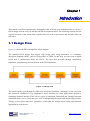
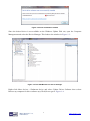
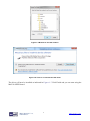
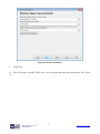
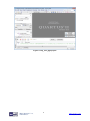
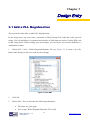
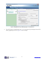
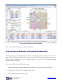
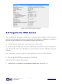
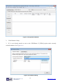
MAX10 Neek My First FPGA Manual i www.terasic.com July 8, 2015 CONTENTS Chapter 1 Introduction 1.1 Design Flow ................................................................................................................................. 1 1.2 Before You Begin ......................................................................................................................... 2 1.3 What You Will Learn.................................................................................................................... 6 Chapter 2 Assign The Device 2.1 Assign The Device ....................................................................................................................... 7 Chapter 3 Design Entry 3.1 Add a PLL Megafunction ........................................................................................................... 12 3.2 Add a Multiplexer ...................................................................................................................... 27 3.3 Assign the Pins ........................................................................................................................... 33 3.4 Create a Default TimeQuest SDC File ....................................................................................... 35 Chapter 4 Compile and Verify Your Design 4.1 Compile Your Design ................................................................................................................. 37 4.2 Program the FPGA Device ......................................................................................................... 39 4.3 Verify The Hardware .................................................................................................................. 41 Chapter 5 MAX10 NEEK Technical Support 5.1 Headquarter & Branches ............................................................................................................ 44 MAX10 Neek My First FPGA Manual ii www.terasic.com July 8, 2015 Chapter 1 Introduction This tutorial provides comprehensive information that will help you understand how to create a FPGA design and run it on you MAX10 NEEK development board. The following sections provide a quick overview of the design flow, explain what you need to get started, and describe what you will learn. 1.1 Design Flow Figure 1-1shows the FPGA design flow block diagram. The standard FPGA design flow begins with design entry using schematics or a hardware description language (HDL), such as Verilog HDL or VHDL. In this step, you can create a digital circuit that is implemented inside the FPGA. The flow then proceeds through compilation, simulation, programming, and verification in the FPGA hardware. Figure 1-1 Design Flow This tutorial guides you through all of the steps except for simulation. Although it is not covered in this document, simulation is very important to learn, and there are entire applications devoted to simulating hardware designs. There are two types of simulation, Functional and Timing Functional simulation allows you to verify that your code is manipulating the inputs and outputs appropriately. Timing (or post place-and-route) simulation verifies that the design meets timing and functions appropriately in the device. MAX10 Neek My First FPGA Manual 1 www.terasic.com July 8, 2015 1.2 Before You Begin This tutorial assumes the following prerequisites ■ You generally know what a FPGA is. This tutorial does not explain the basic concepts of programmable logic. ■ You are somewhat familiar with digital circuit design and electronic design automation (EDA) tools. ■ You have installed the Altera Quartus II 15.0 (win7 64bits) software on your computer. If you do not have the Quartus II software, you can download it from the Altera web site at www.altera.com/download. ■ You have a MAX10 NEEK Development Board on which you will test your project. Using a development board helps you to verify whether your design is really working. ■ You have gone through the quick start guide and/or the getting started user guide for your development kit. These documents ensure that you have: Installed the required software. Determined that the development board functions properly and is connected to your computer. Next step you should installed the USB-Blaster II driver, Plug in the 5-volt adapter to provide power to the board. Use the mini USB cable to connect the mini USB connector J8 (type B) on the MAX10 NEEK board to a USB port on a computer that runs the Quartus II software. Turn on the power switch on the MAX10 NEEK board. The computer will recognize the new hardware connected to its USB port, but it will be unable to proceed if it does not have the required driver already installed. The MAX10 NEEK board is programmed by using Altera USB-Blaster II mechanism. If the USB-Blaster II driver is not already installed, the Driver Software Installation window in Figure 1-2 will appear. MAX10 Neek My First FPGA Manual 2 www.terasic.com July 8, 2015 Figure 1-2 Driver Installation window Since the desired driver is not available on the Windows Update Web site, open the Computer Management and select the Device Manager. This leads to the window in Figure 1-3. Figure 1-3 The USB Blaster II in device manager Right click Other devices ->Unknown device and select Update Driver Software then selecte Browse my computer for drive software and Click Next to get to Figure 1-4. MAX10 Neek My First FPGA Manual 3 www.terasic.com July 8, 2015 Figure 1-4 Specify the location of the driver Now, choose Search for the best driver in these locations and click Browse to get to the pop-up box in Figure 1-5 Find the desired driver, which is at location C:\altera\15.0\quartus\drivers\ usb-blaster-ii. Click OK and then upon returning to Figure 1-4 click Next. At this point the installation will commence, but a dialog box in Figure 1-6 will appear indicating that the driver has not passed the Windows Logo testing. Click Install Anyway. MAX10 Neek My First FPGA Manual 4 www.terasic.com July 8, 2015 Figure 1-5 Browse to find the location Figure 1-6 There is no need to test the driver The driver will now be installed as indicated in Figure 1-7 Click Finish and you can start using the MAX10 NEEK board. MAX10 Neek My First FPGA Manual 5 www.terasic.com July 8, 2015 Figure 1-7 The driver is installed 1.3 W hat You W ill Lear n In this tutorial you will perform the following tasks: Create a design that causes LEDs on the development board to blink at a speed that is controlled by an input key—this design is easy to create and gives you a visual feedback that the design works. Of course, you can use your MAX10 NEEK board to run other designs as well. For the LED design, you will write Verilog HDL code for a simple 32-bit counter, add a phase-locked loop (PLL) megafunction as the clock source, and add a 2-input multiplexer megafunction. When the design is running on the board, you can press an input switch to multiplex the counter bits that drive the output LEDs. Becoming familiar with Quartus II design tools—This tutorial will not make you an expert, but at the end, you will understand basic concepts about Quartus II projects, such as entering a design using a schematic editor and HDL, compiling your design, and downloading it into the FPGA on your MAX10 NEEK development board. Develop a foundation to learn more about FPGAs—For example, you can create and download digital signal processing (DSP) functions onto a single chip, or build a multi-processor system, or create anything else you can imagine all on the same chip. You don’t have to scour data books to find the perfect logic device or create your own ASIC. All you need is your computer, your imagination, and an Altera MAX10 NEEK FPGA development board. MAX10 Neek My First FPGA Manual 6 www.terasic.com July 8, 2015 Chapter 2 Assign The Device You begin this tutorial by creating a new Quartus II project. A project is a set of files that maintain information about your FPGA design. The Quartus II Settings File (.qsf) and Quartus II Project File (.qpf) files are the primary files in a Quartus II project. To compile a design or make pin assignments, you must first create a project. 2.1 Assign The Device 1. In the Quartus II software, select File > New Project Wizard. The Introduction page opens. See Figure 2-1 MAX10 Neek My First FPGA Manual 7 www.terasic.com July 8, 2015 Figure 2-1 New Project Wizard introduction 2. Click Next. 3. Enter the following information about your project: a. What is the working directory for this project? Enter a directory in which you will store your Quartus II project files for this design. b. For example, E:\My_design\my_first_fpga. c. File names, project names, and directories in the Quartus II software cannot contain spaces. d. What is the name of this project? Type my_first_fpga. e. What is the name of the top-level design entity for this project? Type my_first_fpga. See Figure 2-2. MAX10 Neek My First FPGA Manual 8 www.terasic.com July 8, 2015 Figure 2-2 Project information f. Click Next. g. You will assign a specific FPGA device to the design and make pin assignments. See Figure 2-3. MAX10 Neek My First FPGA Manual 9 www.terasic.com July 8, 2015 Figure 2-3 Specify the Device Example h. Click Finish. 4. When prompted, choose Yes to create the my_first_fpga project directory. You just created your first Quartus II FPGA project. See Figure 2-4. MAX10 Neek My First FPGA Manual 10 www.terasic.com July 8, 2015 Figure 2-4 my_first_fpga project MAX10 Neek My First FPGA Manual 11 www.terasic.com July 8, 2015 Chapter 3 Design Entry 3.1 Add a PLL Megafunction This section describes How to Add a PLL Megafunction In the design entry step you create a schematic or Block Design File (.bdf) that is the top-level design. You will add library of parameterized modules (LPM) functions and use Verilog HDL code to add a logic block. When creating your own designs, you can choose any of these methods or a combination of them. 1. Choose File > New > Block Diagram/Schematic File (see Figure 3-1 to create a new file, Block1.bdf, which you will save as the top-level design. Figure 3-1 New BDF 2. Click OK. 3. Choose File > Save As and enter the following information. File name: my_first_fpga Save as type: Block Diagram/Schematic File (*.bdf) MAX10 Neek My First FPGA Manual 12 www.terasic.com July 8, 2015 4. Click Save. The new design file appears in the Block Editor (see Figure 3-2). Figure 3-2 Bank BDF 5. Add HDL code to the blank block diagram by choosing File > New > Verilog HDL File. 6. Click OK to create a new file Verilog1.v, which you will save as simple_counter.v. 7. Select File > Save As and enter the following information (see Figure 3-3). File name: simple_counter.v Save as type: Verilog HDL File (*.v, *.vlg, *.verilog) MAX10 Neek My First FPGA Manual 13 www.terasic.com July 8, 2015 Figure 3-3 Saving the Verilog HDL file The resulting empty file is ready for you to enter the Verilog HDL code. 8. Type the following Verilog HDL code into the blank simple_counter.v file (see Figure 3-4 The Verilog File of simple_counter.v). //It has a single clock input and a 32-bit output port module simple_counter ( CLOCK_50, counter_out ); input CLOCK_50 ; output [31:0] counter_out; reg [31:0] counter_out; MAX10 Neek My First FPGA Manual 14 www.terasic.com July 8, 2015 always @ (posedge CLOCK_50) // on positive clock edge begin counter_out <= #1 counter_out + 1;// increment counter end endmodule // end of module counter Figure 3-4 The Verilog File of simple_counter.v 9. Save the file by choosing File > Save, pressing Ctrl + s, or by clicking the floppy disk icon. 10. Choose File > Create/Update > Create Symbol Files for Current File to convert the simple_counter.v file to a Symbol File (.sym).You use this Symbol File to add the HDL code to your BDF schematic. 12. To add the simple_counter.v symbol to the top-level design, click the my_first_fpga.bdf tab. 13. Double-click my_first_fpga.bdf Blank area 14. Double-click the Project directory to expand it. MAX10 Neek My First FPGA Manual 15 www.terasic.com July 8, 2015 15. Select the newly created simple_counter symbol by clicking its icon. You can also double-click in a blank area of the BDF to open the Symbol dialog box (see Figure 3-5). Figure 3-5 Adding the Symbol to the BDF 16. Click OK. 17. Move the cursor to the BDF grid; the symbol image moves with the cursor. Click to place the simple_counter symbol onto the BDF. You can move the block after placing it by simply clicking and dragging it to where you want it and releasing the mouse button to place it. See Figure 3-6. MAX10 Neek My First FPGA Manual 16 www.terasic.com July 8, 2015 Figure 3-6 Placing the simple_counter symbol 18. Press the Esc key or click an empty place on the schematic grid to cancel placing further instances of this symbol. 19. Save your project regularly. Using Quartus Add a PLL Megafunction Megafunctions, such as the ones available in the LPM, are pre-designed modules that you can use in FPGA designs. These Altera-provided megafunctions are optimized for speed, area, and device family. You can increase Efficiency by using a megafunction instead of writing the function yourself. Altera also provides more complex functions, called MegaCore functions, which you can evaluate for free but require a license file for use in production designs. This tutorial design uses a PLL clock source to drive a simple counter. A PLL uses the on-board oscillator (MAX10 NEEK Board is 50 MHz) to create a constant clock frequency as the input to the counter. To create the clock source, you will add a pre-built LPM megafunction named ALTPLL 1. Tools>IP Catalog>Library >Basic Functions> clocks;PLLsand Resets 2. Click Figure 3-7) PLL There will MAX10 Neek My First FPGA Manual be a ALTPLL. 17 The IP Catalog appears (see www.terasic.com July 8, 2015 Figure 3-7 IP Catalog 3 Double click on the ALTPLL 4. In Sve IP Variation, specify the following selections (see Figure 3-8) a. Choose ALTPLL. b. Under Which type of output file do you want to create? Choose Verilog c. Under What name do you want for the output file? Type pll at the end of the already created directory name. MAX10 Neek My First FPGA Manual 18 www.terasic.com July 8, 2015 Figure 3-8 Save IP Variation Selections d. Click OK. 5. In the MegaWizard Plug-In Manager [page 1 of 12] window, make the following selections (see Figure 3-9). a. Confirm that the Current selected device family option shows the device family that corresponds to the development board you are using. b. The device speed grade is choosed 7 for MAX10 NEEK. c. Set the frequency of the inclock0 input 50 MHz. d. Click Next. MAX10 Neek My First FPGA Manual 19 www.terasic.com July 8, 2015 Figure 3-9 MegaWizard Plug-In Manager [page 1 of 12] Selections 6. Turn off all options on MegaWizard page 4. As you turn them off, pins disappear from the PLL block’s graphical preview. See Figure 3-10 for an example. MAX10 Neek My First FPGA Manual 20 www.terasic.com July 8, 2015 Figure 3-10 MegaWizard Plug-In Manager [page2 of 12] Selections 7. Click Next three times. 8. At the top of the wizard, click the tab 3 - Output Clocks to jump to the Output Clocks > clk c0 page Clock Division Settings MAX10 Neek My First FPGA Manual Figure 3-11). 21 www.terasic.com July 8, 2015 Figure 3-11 MegaWizard Plug-In Manager [page 6 of 12] Selections 9. Click Finish. 10. The wizard displays a summary of the files it creates (see Figure 3-12). Click Finish again. MAX10 Neek My First FPGA Manual 22 www.terasic.com July 8, 2015 Figure 3-12 MegaWizard Plug-In Manager [page 12 of 12] Selections Double-click my_first_fpga.bdf blank area and open the Symbol window,showing the newly created PLL megafunction. See Figure 3-13. Figure 3-13 PLL Symbol 11. Click OK and place the pll symbol onto the BDF to the left of the simple_counter symbol. You can move the symbols around by holding down the left mouse button, helping you ensure that they MAX10 Neek My First FPGA Manual 23 www.terasic.com July 8, 2015 line up properly. See Figure 3-14. Figure 3-14 Place the PLL Symbol 12. Move the mouse so that the cursor (also called the selection tool) is over the pll symbol’s c0 output pin. The orthogonal node tool (cross-hair) icon appears. 13. Click and drag a bus line from the c0 output to the simple_counter clock input. This action ties the pll output to the simple_counter input (see Figure 3-15). Figure 3-15 Draw a Bus Line connect pll c0 port to simple_counter CLOCK_50 port 14. Add an input pin and an output bus with the following steps: a. Double-click my_first_fpga.bdf blank area b. Under Libraries, libraries > primitives > pin >input. See Figure 3-16 MAX10 Neek My First FPGA Manual 24 www.terasic.com July 8, 2015 c. Click OK If you need more space to place symbols, you can use the vertical and horizontal scroll bars at the edges of the BDF window to view more drawing space. Figure 3-16 Input pin symbol d. Place the new pin onto the BDF so that it is touching the input to the pll symbol. e. Use the mouse to click and drag the new input pin to the left; notice that the ports remain connected as shown in Figure 3-17. Figure 3-17 Connecting the PLL symbol and Input port f. Change the pin name by double-clicking pin_name and typing CLOCK_50 (see Figure 3-18). This name correlates to the oscillator clock that is connected to the FPGA. MAX10 Neek My First FPGA Manual 25 www.terasic.com July 8, 2015 Figure 3-18 Change the input port name g. Using the Orthogonal Bus tool, draw a bus line connected on one side to the simple_counter output port, and leave the other end unconnected at about 4 to 8 grid spaces to the right of the simple_counter. h. Right-click the new output bus line and choose Properties. i. Type counter [31..0] as the bus name (see Figure 3-19). The notation [X ..Y] is the Quartus II method for specifying the bus width in BDF schematics, where X is the most significant bit (MSB) and Y is the least significant bit (LSB). j. Click OK. Figure 3-20 shows the BDF. MAX10 Neek My First FPGA Manual 26 www.terasic.com July 8, 2015 Figure 3-19 Change the output BUS name Figure 3-20 BDF 3.2 Add a Multiplexer This design uses a multiplexer to route the simple_counter output to the LED pins on the MAX10 NEEK development board. You will use the MegaWizard Plug-In Manager to add the multiplexer, lpm_mux. The design multiplexes two variations of the counter bus to four LEDs on the MAX10 NEEK development board 1. Choose Library 2. Click Basic Functions. MAX10 Neek My First FPGA Manual 27 www.terasic.com July 8, 2015 3. Click Miscellaneous 4. Click LPM_MUX 5. Choose the device family that corresponds to the device on the development board you are using, choose Verilog as the output file type, and name the output file counter_bus_mux.v (see Figure 3-21) Figure 3-21 Selecting lpm_mux 7. Under How many ‘data’ inputs do you want? Select 2 inputs (default). 8. Under How ‘wide’ should the data input and result output be? Select 4 (see Figure 3-22). MAX10 Neek My First FPGA Manual 28 www.terasic.com July 8, 2015 Figure 3-22 lpm_mux settings 9. Click Next. 10. Click Finish twice. The Symbol window appears (see Figure 3-23 for an example). MAX10 Neek My First FPGA Manual 29 www.terasic.com July 8, 2015 Figure 3-23 lpm_mux Symbol 11. Click OK 12. Place the counter_bus_mux symbol below the existing symbols on the BDF. See Figure 3-24. Figure 3-24 Place the lpm_mux symbol 13. Add input buses and output pins to the counter_bus_mux symbol as follows: a. Using the Orthogonal Bus tool, draw bus lines from the data1x[3..0] and data0x[3..0] Input ports to about 8 to 12 grid spaces to the left of counter_bus_mux. MAX10 Neek My First FPGA Manual 30 www.terasic.com July 8, 2015 b. Draw a bus line from the result [3..0] output port to about 4 to 8 grid spaces to the right of counter_bus_mux. c. Right-click the bus line connected to data1x[3..0] and choose Properties. d. Name the bus counter[26..23], which selects only those counter output bits to connect to the four bits of the data1x input. Because the input busses to counter_bus_mux have the same names as the output bus from simple_counter, (counter[x .. y]) the Quartus II software knows to connect these busses. e. Click OK. f. Right-click the bus line connected to data0x[3..0] and choose Properties. g. Name the bus counter [24..21], which selects only those counter output bits to connect to the four bits of the data1x input. h. Click OK. Figure 3-25 shows the renamed buses. Figure 3-25 Renamed counter_bus_mux Bus Lines If you have not done so, save your project file before continuing. 14. . Double-click my_first_fpga.bdf Blank area 15. Under Libraries, double-click quartus/libraries/ > primitives > pin > output (see Figure 3-26). MAX10 Neek My First FPGA Manual 31 www.terasic.com July 8, 2015 Figure 3-26 choose an output pin 16. Click OK. 17. Place this output pin so that it connects to the counter_bus_mux result [3..0] bus output line. 18. Rename the output pin as LEDR [3..0] as described in steps 13 c and d. (see Figure 3-27). Figure 3-27 Rename the output pin 19. Attach an input pin to the multiplexer select line using an input pin: a. Double-click the my_first_fpga.bdf Blank area. b. Under Libraries, double-click quartus/libraries/ > primitives > pin > input. c. Click OK. 20. Place this input pin below counter_bus_mux. 21. Connect the input pin to the counter_bus_mux sel pin. 22. Rename the input pin as KEY [0] (see Figure 3-28). MAX10 Neek My First FPGA Manual 32 www.terasic.com July 8, 2015 Figure 3-28 Adding the KEY [0] Input Pin You have finished adding symbols to your design. You can add notes or information to the project as text using the Text tool on the toolbar (indicated with the A symbol). For example, you can add the label “OFF = SLOW, ON = FAST” to the KEY [0] input pin and add a project description, such as “My First FPGA Project.” 3.3 Assign the Pins In this section, you will make pin assignments. Before making pin assignments, perform the following steps: 1. Choose Processing > Start > Start Analysis & Elaboration in preparation for assigning pin locations. 2. Click OK in the message window that appears after analysis and elaboration completes. To make pin assignments that correlate to the KEY [0] and CLOCK_50 input pins and LEDR[3..0] output pin, perform the following steps: 1. Choose Assignments > Pins Planner, which opens the Pin Planner, a spreadsheet-like table of specific pin assignments. The Pin Planner shows the design’s six pins. See Figure 3-29 MAX10 Neek My First FPGA Manual 33 www.terasic.com July 8, 2015 Figure 3-29 Pin Planner Example 2. In the Location column next to each of the six node names, add the coordinates (pin numbers) as shown in Table 3-1 for the actual values to use with your MAX10 NEEK board. Table 3-1 Pin Information Setting Pin Name KEY[0] LEDR[3] LEDR[2] LEDR [1] LEDR [0] CLOCK_50 FPGA Pin Location T22 C3 A3 B3 C2 N5 Double-click in the Location column for any of the six pins to open a drop-down list and type the location shown in the table alternatively, you can select the pin from a drop-down list. For example, if you type F1 and press the Enter key, the Quartus II software fills in the full PIN_F1 location name for you. The software also keeps track of corresponding FPGA data such as the I/O bank and VREF Group. Each bank has a distinct color, which corresponds to the top-view wire bond drawing in the upper right window. See Figure 3-30. MAX10 Neek My First FPGA Manual 34 www.terasic.com July 8, 2015 Figure 3-30 Completed Pin Planning Example Now, you are finished creating your Quartus II design! 3.4 Create a Default TimeQuest SDC File Timing settings are critically important for a successful design. For this tutorial you will create a basic Synopsys Design Constraints File (.sdc) that the Quartus II TimeQuest Timing Analyzer uses during design compilation. For more complex designs, you will need to consider the timing requirements more carefully. To create an SDC, perform the following steps: 1. Open the TimeQuest Timing Analyzer by choosing Tools > TimeQuest Timing Analyzer. 2. Choose File > New SDC file. The SDC editor opens. 3. Type the following code into the editor: MAX10 Neek My First FPGA Manual 35 www.terasic.com July 8, 2015 create_clock -period 20.000 -name CLOCK_50 derive_pll_clocks derive_clock_uncertainty 4. Save this file as my_first_fpga.sdc (see Figure 3-31) Figure 3-31 Default SDC Naming the SDC with the same name as the top-level file except for the .sdc extension causes the Quartus II software to using this timing analysis file automatically by default. If you used another name, you would need to add the SDC to the assignments file list. MAX10 Neek My First FPGA Manual 36 www.terasic.com July 8, 2015 Chapter 4 Compile and Verify Your Design After creating your design you must compile it. Compilation converts the design into a bitstream that can be downloaded into the FPGA. The most important output of compilation is an SRAM Object File (.sof), which you use to program the device. The software also generates other report files that provide information about your code as it compiles. 4.1 Compile Your Design If you want to store .SOF in memory device (such as flash or EEPROMs), you must first convert the SOF to a file type specifically for the targeted memory device. Now that you have created a complete Quartus II project and entered all assignments, you can compile the design. In the Processing menu, choose Start Compilation or click the Play button on the toolbar. If you are asked to save changes to your BDF, click Yes. While compiling your design, the Quartus II software provides useful information about the compilation (see Figure 4-1). MAX10 Neek My First FPGA Manual 37 www.terasic.com July 8, 2015 Figure 4-1 Compilation Message for project When compilation is complete, the Quartus II software displays a message. Click OK to close the message box. The Quartus II Messages window displays many messages during compilation. It should not display any critical warnings; it may display a few warnings that indicate that the device timing information is preliminary or that some parameters on the I/O pins used for the LEDs were not set. The software provides the compilation results in the Compilation Report tab as shown in Figure 4-2. MAX10 Neek My First FPGA Manual 38 www.terasic.com July 8, 2015 Figure 4-2 Compilation Report Example 4.2 Program the FPGA Device After compiling and verifying your design you are ready to program the FPGA on the development board. You download the SOF you just created into the FPGA using the USB-Blaster II circuitry on the board. Set up your hardware for programming using the following steps: a) Connect the power supply cable to your board and to a power outlet. b) For the MAX10 NEEK board, connect the USB-Blaster II (included in your development kit) to J9 and the USB cable to the USB-Blaster II. Connect the other end of the USB cable to the host computer. Refer to the getting started user guide for detailed instructions on how to connect the cables. c) Turn the MAX10 NEEK board on using the on/off switch. Program the FPGA using the following steps. 1. Choose Tools > Programmer. The Programmer window opens. See Figure 4-3. MAX10 Neek My First FPGA Manual 39 www.terasic.com July 8, 2015 Figure 4-3 Programmer Window 2. Click Hardware Setup. 3. If it is not already turned on, turn on the USB-Blaster II [USB-0] option under currently selected hardware. See Figure 4-4. Figure 4-4 Hardware Setting MAX10 Neek My First FPGA Manual 40 www.terasic.com July 8, 2015 4. Click Close. 5. If the file name in the Programmer does not show my_first_fpga.sof, click Add File. 6. Select the my_first_fpga.sof file from the project dir ectory (see Figure 4-5). Figure 4-5 Downloading Complete Congratulations, you have created, compiled, and programmed your first FPGA design! The compiled SRAM Object File (.sof) is loaded onto the FPGA on the development board and the design should be running. 4.3 Verify The Hardware When you verify the design in hardware, you observe the runtime behavior of the FPGA hardware design and ensure that it is functioning appropriately. Verify the design by performing the following steps: 1. Observe that the four development board LEDs appear to be advancing slowly in a binary count pattern, which is driven by the simple_counter bits [26..23]. The LEDs are active low, therefore, when counting begins all LEDs are turned on (the 0000 state). MAX10 Neek My First FPGA Manual 41 www.terasic.com July 8, 2015 2. Press and hold KEY [0] on the development board and observe that the LEDs advance more quickly. Pressing this KEY causes the design to multiplex using the faster advancing part of the counter (bits [24..21]). 3. If other LEDs emit faintness light, Choose Assignments > Device. Click Device and Options. See Figure 4-6. Figure 4-6 Device and Options Choose unused pins. Reserve all unused pins: Choose the As input tri-stated option. See Figure 4-7. MAX10 Neek My First FPGA Manual 42 www.terasic.com July 8, 2015 Figure 4-7 Setting unused pins Click twice OK. 4. In the Processing menu, choose Start Compilation. After the compilation, Choose Tools -> Programmer. Select the my_first_fpga.sof file from the project directory. Click Start. At this time you could find the other LEDs are unlighted. MAX10 Neek My First FPGA Manual 43 www.terasic.com July 8, 2015 Chapter 5 MAX10 NEEK Technical Support 5.1 Headquar ter & Branches Tel :+886-3-575-0880 Add:China/406, Jingfeng Bld. B, Intl Business Center, Special No. 1, Guang Gu Rd., Wuhan, China, 430074 Email:[email protected] / [email protected] MAX10 Neek My First FPGA Manual 44 www.terasic.com July 8, 2015