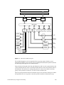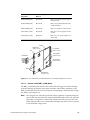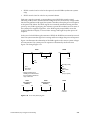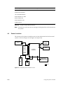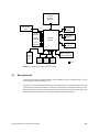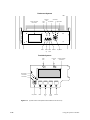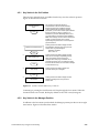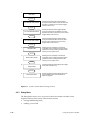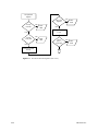
1
CHALLENGE™/Onyx™ Diagnostic Road Map Document Number 108-7045-030 Contributors Written by Kameran Kashani and Greg Morris Illustrated by Dan Young, Cheri Brown, Greg Morris, and Kameran Kashani Edited by Christina Cary Production by Lorrie Williams Engineering contributions by John Kraft, Steve Whitney, Rich Altmaier, Unmesh Agarwala, Ray Mascia, Robert Thomas, Dilip Amin, Sue Liu, Greg Wong, Ken Beck, Ken Choy, Laurent Coudrelle, Ben Fathi © Copyright 1993, 1994 Silicon Graphics, Inc.— All Rights Reserved This document contains proprietary and confidential information of Silicon Graphics, Inc. The contents of this document may not be disclosed to third parties, copied, or duplicated in any form, in whole or in part, without the prior written permission of Silicon Graphics, Inc. Restricted Rights Legend Use, duplication, or disclosure of the technical data contained in this document by the government is subject to restrictions as set forth in subdivision (c) (1) (ii) of the Rights in Technical Data and Computer Software clause at DFARS 52.227-7013 and/or in similar or successor clauses in the FAR or in the DOD or NASA FAR Supplement. Unpublished rights reserved under the Copyright Laws of the United States. Contractor/manufacturer is Silicon Graphics, Inc., 2011 North Shoreline Boulevard, Mountain View, CA 94039-7311. Silicon Graphics and R4000 are registered trademarks, and IRIX, RealityEngine2, and POWERpath-2, and R4400 are trademarks of Silicon Graphics, Inc. VME is a trademark of Mororola. UNIX is a registered trademark of UNIX System Laboratories. FCC Warning This equipment has been tested and found compliant with the limits for a Class A digital device, pursuant to Part 15 of the FCC rules. These limits are designed to provide reasonable protection against harmful interference when the equipment is operated in a commercial environment. This equipment generates, uses, and can radiate radio frequency energy and, if not installed and used in accordance with the instruction manual, may cause harmful interference to radio communications. Operation of this equipment in a residential area is likely to cause harmful interference, in which case the user will be required to correct the interference at his or her own expense. Attention This product requires the use of external shielded cables in order to maintain compliance pursuant to Part 15 of the FCC rules. CHALLENGE/Onyx Diagnostic Road Map Document Number 108-7045-030 Contents Introduction............................................................................................................... xiii 1. Theory of Operations ............................................................................................. 1-1 1.1 Overview...................................................................................................... 1-1 1.2 System Buses................................................................................................ 1-4 1.2.1 Everest Address and Data Buses ............................................ 1-6 1.2.2 Polled Serial Bus........................................................................ 1-7 1.2.3 Interface Bus (Ibus) and Peripheral Bus (Pbus) on IO4 Board........................................................................................... 1-8 1.2.4 SCSI Bus...................................................................................... 1-8 1.2.5 FCI Bus ....................................................................................... 1-9 2. Diagnostic Procedures .......................................................................................... 2-1 2.1 Overview...................................................................................................... 2-1 2.2 Examining a Frozen System ...................................................................... 2-2 2.2.1 What to Do If the System Is Still Frozen................................ 2-2 2.2.2 What to Do if the System Has Been Reset or Rebooted..................................................................................... 2-4 2.3 Diagnosing a System Panic........................................................................ 2-4 2.4 ASIC Error Detection.................................................................................. 2-5 2.4.1 Error Messages .......................................................................... 2-7 IP19 CPU Board 2-8 IP21 CPU Board 2-11 IO4 Interface Board 2-18 MC3 Memory Board 2-24 2.5 Troubleshooting ........................................................................................ 2-27 2.5.1 CPU Board (IP19 and IP21) Troubleshooting Procedures................................................................................ 2-27 Power Not Operating Within Acceptable Voltage Levels ...................................................... 2-27 Power Levels OK but the Processor LEDs Are All Off .................................................................... 2-28 Power Levels OK but Processor LEDs Are All Lit ................................................... 2-28 All Processor Slices Have Failed .......................................... 2-28 A Single Processor Slice Has Failed .................................... 2-28 iii 2.6 2.7 iv Clocks Are Good but the Processor LEDs Are All Lit................................................... 2-28 LEDs Show Failure Code After Starting Boot Pattern .................................................................... 2-29 The Enable Register Is Incorrect .......................................... 2-29 IP19 LEDs Show a Static 0xe Pattern................................... 2-29 IP21 LEDs Show a Static 0x14 Pattern ................................ 2-29 IP19 LEDs Show a Static 0xc Pattern................................... 2-29 IP21 LEDs Show a Static 0x12 Pattern ................................ 2-30 LEDs Boot to Master/Slave Patterns but UART Output is Garbled or Missing. ........................... 2-30 2.5.2 IO4 Troubleshooting Procedures.......................................... 2-30 2.5.3 Using the System Controller ................................................. 2-30 Systems With Dead Monitors or Terminals ....................... 2-30 Communicating with the System over the System Controller Port ...................................................... 2-31 Defeating the System Controller.......................................... 2-31 Communicating With a Disabled Processor ...................... 2-32 2.5.4 Using a Debug Kernel to Find System Hangs .................... 2-32 2.5.5 Procedure to Cause a Hung System to Enter POD Mode ......................................................................................... 2-33 2.5.6 Using POD to Diagnose MC3 Clock Jitter........................... 2-34 Error Message Syntax............................................................................... 2-35 Known Problems...................................................................................... 2-36 2.7.1 IRIX 5.0.1 .................................................................................. 2-36 2.7.2 Paging and File Quotas .......................................................... 2-36 2.7.3 MC3 Clock Jitter ...................................................................... 2-36 2.7.4 MC3 Error Latching................................................................ 2-37 2.7.5 ECC Check Bit Single Bit Error ............................................. 2-37 2.7.6 SIMM failures .......................................................................... 2-37 2.7.7 IP19 EAROM Corruption....................................................... 2-38 2.7.8 Ebus Parity Error/POKB Error Due to Backplane Voltage Droop ......................................................................... 2-38 2.7.9 MC3 SIMM Failure ................................................................. 2-39 2.7.10 VME Bus Error on PIO Read ................................................. 2-39 3. Power Subsystem ................................................................................................... 3-1 3.1 Overview...................................................................................................... 3-1 3.2 Power Fault Indicator Descriptions and Locations................................ 3-3 3.2.1 System Controller and Offline Switchers (OLSs) ................. 3-3 3.2.2 System and Power Boards ....................................................... 3-5 IP19 and IP21 CPU Board ....................................................... 3-5 MC3 Memory Board ................................................................ 3-5 IO4/VCAM Board ................................................................... 3-6 Remote VCAM (RMT_VCAM) Board .................................. 3-7 Mezzanine (F Mezz and S Mezz) Boards ............................. 3-8 Power Boards............................................................................ 3-9 3.2.3 SCSIBox Drive Enclosure......................................................... 3-9 3.3 Power-On Sequence.................................................................................. 3-10 3.3.1 Isolating Errors ........................................................................ 3-14 4. Using the System Controller ................................................................................ 4-1 4.1 Overview...................................................................................................... 4-1 4.2 Basic Functions ............................................................................................ 4-2 4.2.1 Overtemperature Sensor.......................................................... 4-2 4.2.2 Blower Speed Control .............................................................. 4-2 4.2.3 Power-On, Boot, and Reset Sequences................................... 4-3 4.2.4 Monitoring Normal System Operation.................................. 4-3 4.2.5 Initiating a System Power-Off................................................. 4-4 Overtemperature Faults.......................................................... 4-4 4.3 Error Messages ............................................................................................ 4-4 4.4 Sensor Locations........................................................................................ 4-10 4.5 Menu Hierarchy ........................................................................................ 4-11 4.5.1 Key Switch in the On Position .............................................. 4-13 4.5.2 Key Switch in the Manager Position .................................... 4-13 4.5.3 Debug Menu ............................................................................ 4-14 5. PROM Monitor .......................................................................................................... 5-1 5.1 Overview...................................................................................................... 5-1 5.2 Power-On Tests ........................................................................................... 5-1 5.2.1 IP19 Power-On Tests ................................................................ 5-1 5.2.2 IP21 Power-On Tests ................................................................ 5-5 5.3 Power-On Test Status Messages ............................................................. 5-10 5.4 Power-On Diagnostics Commands ........................................................ 5-12 5.5 Niblet .......................................................................................................... 5-13 v 5.6 5.7 5.8 5.9 6. Interactive Diagnostics Environment (IDE) ...................................................... 6-1 6.1 6.2 6.3 6.4 6.5 vi IP19 PROM Error and Status Messages................................................. 5-15 5.6.1 IP19 PROM Messages (Short Form) ..................................... 5-17 5.6.2 IP19 PROM Messages (Long Form) ..................................... 5-18 5.6.3 Diagnostic Codes and Their Meanings................................ 5-19 CPU Cache .............................................................................. 5-19 Memory ................................................................................ 5-19 Ebus Error Codes ................................................................... 5-19 IO4 Error Codes ...................................................................... 5-20 CPU Error Codes.................................................................... 5-20 CC Register Codes ................................................................. 5-20 FPU Error Codes .................................................................... 5-20 Miscellaneous ......................................................................... 5-20 5.6.4 Using POD to Examine HARDWARE ERROR STATE Messages................................................................................... 5-21 CPU Board Fault/Status Indicators ....................................................... 5-25 5.7.1 IP19 LED Status Codes........................................................... 5-26 5.7.2 IP19 LED Error Codes ............................................................ 5-28 5.7.3 IP21 LED Status Codes........................................................... 5-29 5.7.4 IP21 LED Error Codes ............................................................ 5-32 5.7.5 LED Power-On Status Codes ................................................ 5-33 Board Configuration Operations ............................................................ 5-33 PROM Monitor Boot Commands ........................................................... 5-34 Overview...................................................................................................... 6-1 6.1.1 Available IDE Tests .................................................................. 6-1 Running an IDE Test .................................................................................. 6-1 IO4 IDE Tests ............................................................................................... 6-2 6.3.1 IO4 Interface .............................................................................. 6-4 6.3.2 VME Adapter............................................................................. 6-5 6.3.3 SCSI Adapter ............................................................................ 6-8 6.3.4 Everest Peripheral Controller (EPC) ...................................... 6-9 IP19 IDE Tests............................................................................................ 6-11 6.4.1 IP Tests...................................................................................... 6-13 6.4.2 Translation Lookaside Buffer (TLB) Tests........................... 6-17 6.4.3 Floating-Point Unit (FPU) Tests............................................ 6-19 6.4.4 Cache Tests............................................................................... 6-23 MC3 IDE Tests........................................................................................... 6-44 7. IRIX Error Reporting ............................................................................................... 7-1 7.1 Overview...................................................................................................... 7-1 7.2 Panic Messages............................................................................................ 7-1 7.2.1 Interpreting Panic Messages ................................................... 7-2 IP19-Specific Messages ............................................................ 7-3 IP21-Specific Messages ............................................................ 7-3 7.2.2 Hardware Error State Messages ............................................. 7-3 7.3 Warning Messages...................................................................................... 7-4 7.4 Driver Messages .......................................................................................... 7-5 7.5 System Controller Daemon SYSLOG Messages ..................................... 7-5 vii Figures Figure 1-1 Figure 1-2 Figure 1-3 Figure 1-4 Figure 1-5 Figure 1-6 Figure 2-1 Figure 2-2 Figure 2-3 Figure 2-4 Figure 2-5 Figure 2-6 Figure 2-7 Figure 2-8 Figure 2-9 Figure 2-10 Figure 3-1 Figure 3-2 Figure 3-3 Figure 3-4 Figure 3-5 Figure 3-6 Figure 3-7 Figure 3-8 Figure 3-9 Figure 3-10 Figure 3-11 Figure 3-12 Figure 3-13 Figure 3-14 Everest Functional Block Diagram ......................................................... 1-2 IO4 Functional Block Diagram................................................................ 1-3 Everest System Buses ............................................................................... 1-6 Everest Buses and Interface ASICs......................................................... 1-7 Polled Serial Bus........................................................................................ 1-8 SCSI Drive Addressing ............................................................................ 1-9 Everest Bus Parity Checkpoints .............................................................. 2-7 IP19 Board Error Detection Logic........................................................... 2-8 IP19 Board Component Locations .......................................................... 2-9 IP21 Board Error Detection Logic......................................................... 2-12 IP21 Board Component Placement....................................................... 2-13 IO4/VCAM Board Error Detection Logic ........................................... 2-18 IO4/VCAM Component Locations...................................................... 2-19 MC3 Memory Board Error Detection Logic........................................ 2-25 MC3 Board Component Locations ....................................................... 2-26 MC3 SIMM Bank and Leaf Organization............................................ 2-26 Power Subsystem Block Diagram........................................................... 3-2 Rackmount and Deskside Status Panel and OLS Power and Fault Indicators.......................................................................................... 3-4 IP19 and IP21 Board Power Fault Indicators and Power Brick Locations .................................................................................................... 3-5 MC3 Board Fault Indicator and Power Brick Locations ..................... 3-6 First IO4 Board/VCAM Fault Indicator and Voltage Regulator Locations .................................................................................................... 3-7 Remote VCAM Fault Indicator and Voltage Regulator Locations .................................................................................................... 3-8 F Mezzanine Board Fault Indicator and Voltage Regulator Locations .................................................................................................... 3-9 Power Board Fault LEDs.......................................................................... 3-9 SCSIBox Fault Indicators ....................................................................... 3-10 Power OK (POKx) Signals ..................................................................... 3-11 Power-On Sequence (Part 1 of 2) .......................................................... 3-12 Power-On Sequence (Part 2 of 2) .......................................................... 3-13 Power-On Signal Timing ....................................................................... 3-14 System Controller Voltage Status Menu.............................................. 3-14 ix Figure 3-15 Figure 4-1 Figure 4-2 Figure 4-3 Figure 4-4 Figure 4-5 Figure 4-6 Figure 4-7 Figure 5-1 Figure 5-2 Figure 5-3 Figure 5-4 Figure 5-5 Figure 5-6 Figure 5-7 Figure 5-8 Figure 5-9 Figure 5-10 Figure 5-11 x Power Subsystem Voltage Monitoring ................................................ 3-16 System Controller Input/Output Signals.............................................. 4-2 Deskside System Controller Sensors.................................................... 4-10 Rackmount System Controller Sensors................................................ 4-11 System Status Panel (Deskside and Rackmount Versions)............... 4-12 System Controller Menus: Key switch On .......................................... 4-13 System Controller Menus: Manager Position ..................................... 4-14 System Controller Menus: Debug Settings ......................................... 4-16 IP19 Power-On Test Sequence (Part 1 of 4) ........................................... 5-2 Power-On Test Sequence (Part 2 of 4).................................................... 5-3 Power-On Test Sequence (Part 3 of 4).................................................... 5-4 Power-On Test Sequence (Part 4 of 4).................................................... 5-5 IP21 Power-On Test Sequence (1 of 4) ................................................... 5-6 IP21 Power-On Test Sequence (2 of 4) ................................................... 5-7 IP21 Power-On Test Sequence (3 of 4) ................................................... 5-8 IP21 Power-On Test Sequence (4 of 4) ................................................... 5-9 CPU Board Fault Indicators (IP19 Shown).......................................... 5-25 Slave Processor LED Pattern ................................................................. 5-33 CPU LED Pattern when Polling............................................................ 5-33 Tables Table 1-1 Table 2-1 Table 2-2 Table 3-1 Table 3-2 Table 3-3 Table 3-4 Table 4-1 Table 4-2 Table 4-3 Table 4-4 Table 4-5 Table 5-1 Table 5-2 Table 5-3 Table 5-4 Table 5-5 Table 5-6 Table 5-7 Table 5-8 Table 6-1 Table 6-2 Table 6-3 Table 6-4 Table 6-5 Table 6-6 Table 6-7 Table 6-8 Table 6-9 Table 6-10 Table 7-1 Bus Types in Everest Deskside and Rackmount Systems..................... 1-4 Likely Causes of Common System Problems ......................................... 2-2 System Controller Commands................................................................ 2-31 MC3 Board Fault LEDs .............................................................................. 3-6 IO4 Board Fault LEDs................................................................................. 3-7 Remote VCAM Fault LEDs........................................................................ 3-8 Voltage Ranges and Warning Thresholds............................................. 3-17 Bootmaster Arbitration Problems at Power-On or Reset...................... 4-5 System Events – Immediate Power-Off ................................................... 4-5 System Events – Delayed Power-Off ....................................................... 4-7 System Events – Informative..................................................................... 4-8 System Controller Internal Problems....................................................... 4-8 Basic Niblet Tests ...................................................................................... 5-13 Niblet Supertests ....................................................................................... 5-14 EBus Error Field Values and Descriptions ............................................ 5-24 Leaf Error Field Values and Descriptions ............................................. 5-24 IP19 Board Test Status LED Codes......................................................... 5-26 IP19 Board Power-on Test Failure LED Codes..................................... 5-28 IP21 Board Test Status LED Codes......................................................... 5-29 IP21 Board Power-On Test Failure LEDs .............................................. 5-32 IO4 IDE Report Levels................................................................................ 6-2 IO4 Interface Tests ...................................................................................... 6-4 IO4 VME Adapter Tests ............................................................................. 6-5 IO4 SCSI Adapter Tests.............................................................................. 6-8 Everest Peripheral Controller (EPC) Tests .............................................. 6-9 IP19 IDE Report Levels ............................................................................ 6-11 IP19 IP Test Summary .............................................................................. 6-13 Cache State Transition Tests.................................................................... 6-41 MC3 Report Levels ................................................................................... 6-44 MC3 Tests................................................................................................... 6-46 System Controller Alarms and Warnings from SYSLOG ..................... 7-5 xi Introduction This document describes the various diagnostic tools available with the Everest board set and their relationship to the Everest system components and to one another. This document describes each of the diagnostic tools, the physical area of the system that they test, and the possible error messages. The information contained in this document is organized as follows: • Chapter 1, “Theory of Operations,” provides the theory of operations for the Everest board set. The various buses connecting the boards are described, along with the potential bus errors on each board. • Chapter 2, “Diagnostic Procedures,” analyzes several fault-isolation procedures, including how to examine a frozen system and how to examine the IRIX and system controller error logs, and provides some general debugging hints. It also contains diagrams showing where errors are detected on the system boards and lists error messages. • Chapter 3, “Power Subsystem,” discusses the power subsystem, and illustrates the inputs and outputs of all power supplies and on-board DC-to-DC converters. It also describes the power-up sequence and the various fault LEDs and other error-detection mechanisms. • Chapter 4, “Using the System Controller,” explains the functions of the system controller, what causes various error messages to be generated, and what those messages mean. • Chapter 5, “PROM Monitor,” describes the PROM monitor, as well as the power-on tests and the power-on diagnostics (POD). System board configuration and the PROM Monitor boot commands are also discussed. • Chapter 6, “Interactive Diagnostics Environment (IDE),” supplies information on the stand-alone IDE and IRIX error reporting. • Chapter 7, “IRIX Error Reporting,” provides an overview of how the IRIX system reports errors. xiii Chapter 1 1. 1.1 Theory of Operations Overview This chapter introduces the Everest (POWERpath-2) board set and shows how those boards communicate over the various system and board buses. Figure 1-1 is a high-level functional block diagram of the Everest board set installed in a typical system. Figure 1-2 illustrates the IO4 board architecture in greater detail. As the individual diagnostic tools are discussed, similar diagrams highlight the areas affected by that tool (where appropriate). CHALLENGE/Onyx Diagnostic Road Map 1-1 System Controller MC3 1 MC3 2 IP19/IP21 2 IP19/IP21 1 (Master CPU) Status Panel Cooling Fans Offline Switchers Everest Data Bus (256 bits) Power Boards Everest Address Bus (40 bits) Ethernet IO4 VCAM FMezz SCSI Mezz VME Bus Graphics Board Set SCSI−1/SCSI−2 Buses SCSI Devices Flat Cable Interface Figure 1-1 1-2 Everest Functional Block Diagram Theory of Operations Everest Data Bus (256 bits) Everest Address Bus (40 bits) IA Chip Map RAM ID Chips IBus (64 bits) EPC Chip PROM S1 Chip P B u s NVRAM Timer F Chip F Chip Mezz Slot Mezz Slot FCI Chip VCAM FCI Chip Graphics Board Set Serial Ports (4) Fast/Wide SCSI-2 Controller SCSI Devices Kybd/ Mouse Port Fast/Wide SCSI-2 Controller SCSI Devices Parallel Port Ethernet Controller Figure 1-2 IO4 Functional Block Diagram The available diagnostic tools are separated into six groups: parity checkers, power subsystem self-checks, power-on tests, power-on diagnostics (POD), the System Controller, and the integrated diagnostics environment (IDE). Parity checkers are housed in the data and address bus ASICs on each system board, in the cache controller and CPU cache on the IP19 and IP21 boards, and in each interface ASIC on the IO4 board. The checkers are strategically placed to verify correct address and data parity at the system bus connectors, as well as at the on-board buses. The power subsystem self-checks are automatic at power on and reset. Voltages not within the specified levels, or not present, cause the System Controller to halt the power-up CHALLENGE/Onyx Diagnostic Road Map 1-3 sequence and display an error message. Error information is also provided by a series of LEDs on the off-line switchers and the system boards, but these are not visible without opening the cabinet. The power-on tests execute whenever the system is powered on or reset. Those tests verify enough of the system’s basic hardware functionality to load the standalone diagnostics from the IDE. The power-on diagnostics (POD) is a special command interpreter that is a subset of the power-on tests. POD is automatically invoked by the PROM monitor in the event of an error during the boot process, or can be manually selected by the operator. POD provides an interface that allows the operator to inspect and modify various system parameters. The standalone diagnostics are a series of functionality-oriented tests invoked from the PROM Monitor. They provide the highest degree of error isolation and the most accurate diagnosis but require their own environment (IDE) to run. Completion of the standalone diagnostics provides sufficient confidence in the system to attempt to boot UNIX, but is not a guarantee. Each group is described in detail in the following chapters. 1.2 System Buses Table 1-1 lists each bus found in a typical Everest deskside (L) or rackmount (XL) system. Table 1-1 Bus Types in Everest Deskside and Rackmount Systems Bus Category Bus Types Description Everest buses Everest data and address buses (Ebus) Interconnects the system board set. Polled Serial bus Connects the system’s CPU boards to the System Controller. Interface bus (Ibus) An internal bus on the IO4 board that connects the Ebus to the peripheral controllers and the board’s optional interface (mezzanine) cards. Peripheral bus (Pbus) Connects the Everest peripheral controller (EPC) chip on the IO4 board to a number of I/O ports, the NVRAM, and 1 MB of flash PROM. Memory bus Provides a path between the Ebus interface ASICs on the MC3 board and the memory array logic. On-board buses 1-4 Theory of Operations Table 1-1 (continued) Bus Types in Everest Deskside and Rackmount Systems Bus Category Bus Types Description Peripheral buses SCSI buses Connect a variety of storage devices to the IO4 board. The IO4 board has two built-in SCSI buses. By adding additional IO4 boards and SCSI mezzanine cards an Everest system can support up to 32 SCSI buses (depending upon the specific system configuration). Flat cable interface (FCI) Connects the graphics cards or VMEbus to the IO4 board. Like the SCSI, multiple FCI buses can be supported by adding FCI mezzanine cards. In the standard configuration, 2 FCIs are on the IO4 board. VMEbus Embedded in both the deskside and rackmount backplanes; available as an optional third cardcage (CC3) with the rackmount system. Figure 1-3 shows a block diagram of the system buses CHALLENGE/Onyx Diagnostic Road Map 1-5 . System Controller MC3 1 MC3 2 IP19/IP21 2 IP19/IP21 1 (Master CPU) Cooling Fans Offline Switchers Everest Data Bus (256 bits) Power Boards Everest Address Bus (40 bits) Ethernet IO4 VME Bus VCAM FMezz SCSI Mezz SCSI−1/SCSI−2 Buses Flat Cable Interface Figure 1-3 SCSI Devices Graphics Board Set Everest System Buses Each bus category is described in the following sections. 1.2.1 Everest Address and Data Buses The Everest system buses consist of a 256-bit, 1200-MB/sec data bus, a 40-bit address bus, and the bus interfaces. The interfaces between the system buses and the Everest boards are supplied by a set of data and address ASICs (see Figure 1-4). There are four data ASICs (D chips) and one address ASIC (A chip) on each board. This logic is not identical from board to board but performs the same basic functions. Those interface chips perform parity checking on the data, address, and control lines during every bus cycle. There are eight parity lines on the data bus and two parity lines on the address bus. ASIC parity error detection is explained in more detail in Section 2.4, “ASIC Error Detection.” 1-6 Theory of Operations IP19/IP21 D D A D IP19/IP21 D D D A D IP19/IP21 D D D A D D Data Bus (256) Address Bus (50 bits) MD MD MD MD MD MD MD MD MD MD IO4 IO4 Figure 1-4 1.2.2 Everest Buses and Interface ASICs Polled Serial Bus This dedicated bus is embedded in the system’s backplane. It connects the system’s CPU boards with the System Controller. During the boot process, the System Controller polls the CPU boards over this bus, requesting a bootmaster CPU. After the bootmaster is identified, all bring-up messages from the bootmaster CPU are sent to the System Controller display over the polled serial bus. The bootmaster CPU also outputs the bring-up messages to the system console RS-232 port (see Figure 1-5). CHALLENGE/Onyx Diagnostic Road Map 1-7 IP19/IP21 (Master CPU) D D A D IP19/IP21 D D D A D IP19/IP21 D D D A D D Polled Serial Bus ID ID IA ID ID System Controller Status Panel IO4 Figure 1-5 Polled Serial Bus The polled serial bus provides a shortened error-reporting path to the System Controller display on the front panel. The path from the bootmaster CPU to the RS-232 system console port involves the Ebus and the IO4’s Ibus. For error messages to reach the graphics monitor, they must pass through the graphics boards as well. Both of these error-reporting paths require a significant percentage of the system’s hardware to be functional before an error can be reported. 1.2.3 Interface Bus (Ibus) and Peripheral Bus (Pbus) on IO4 Board When the PROM initializes, it reads the IA configuration registers to determine what kind of devices are connected to the Ibus. On the basis of the configuration information, the PROM runs a series of diagnostics that check the integrity of the Ibus and Pbus, as well as the functionality of the devices themselves. These diagnostics cannot distinguish between a bus failure and an ASIC failure, but they are sufficient to isolate a fault to the FRU (board) level. 1.2.4 SCSI Bus The system supports 20-MB-per-second SCSI buses. These buses can be configured as single-ended or differential and as 8 or 16-bit. A five-digit drive address has been implemented to accommodate the large number of storage devices the Everest board set can manage. The first two digits represent the decimal slot number of the IO4 board. The third digit corresponds to the nth SCSI channel on the IO4 board (with possible SCSI mezzanine boards); zero and one are assigned to the two SCSI controllers on the IO4 board. Two through seven are assigned to the controllers on the mezzanine cards installed on the 1-8 Theory of Operations IO4. The fourth digit represents a specific drive; the fifth digit is the partition on the selected drive. See Figure 1-6 for an example of SCSI drive addressing. IO4 slot assignment 15 Channel 6 5 7 Mezz card 0 IO4 base board 1 3 Mezz card 2 4 Figure 1-6 1.2.5 SCSI Drive Addressing FCI Bus The flat cable interface (FCI) is a Silicon Graphics proprietary interface that connects a variety of local and remote peripheral resources, such as graphics controllers, VMEbus adapters, and FDDI adapters. The FCI operates at 160 MB per second (maximum) for graphics controllers and at a maximum of 200 MB per second with VMEbus adapters. Note: The maximum effective VMEbus transfer rate may be in the range of 50 MB per second with DMA. The transfer rate is less with PIO-driven I/O. CHALLENGE/Onyx Diagnostic Road Map 1-9 Chapter 2 2. 2.1 Diagnostic Procedures Overview This chapter describes how to • examine a frozen CHALLENGE, POWER CHALLENGE, Onyx, or POWER Onyx system • determine whether a problem is caused by hardware or software • determine where hardware problems occur in a system • use various diagnostic tools and techniques for manufacturing and field service technicians A scenario of a frozen system demonstrates how to use the debugging tools. CHALLENGE/Onyx Diagnostic Road Map 2-1 2.2 Examining a Frozen System When a system is frozen, it is either hung or the kernel has panicked. It is important to determine which case has occurred in the system you are diagnosing because the procedures for fixing a hang are different from those for fixing a kernel panic. 2.2.1 What to Do If the System Is Still Frozen Note: The best way to find a system hang or panic is to examine it while it is still frozen. If the system is at a customer site, this may not be possible, since the customer may already have reset or rebooted the system. Encourage a customer who is experiencing hangs or panics to leave the system frozen until you can examine it. If a customer must reboot a system before you can examine it, ask the customer to first generate a core dump using a nonmaskable interrupt from the System Controller. (See Section 4.5.2, “Key Switch in the Manager Position.”) If the customer does this when the system hangs, you can later examine the core file for clues to the cause of the problem. A system can be frozen six basic ways, due to either hardware or software problems, as shown in Table 2-1: System Condition Likely Cause The kernel is under such a heavy disk swapping Software problem or insufficient system load that no processes can run. resources, such as memory and swap space. The kernel is running out of a software resource Insufficient system resources, such as kernel and cannot perform normal process scheduling. buffers, memory, and swap space. One or a few processes are hung, but other processes are running fine. Software problem. No processes are running, but the kernel is still ticking at interrupt level. Software problem. Processors are stuck spinning in the kernel; interrupts are also blocked. Software problem. One or more processors are not executing instructions normally. Hardware problem. Table 2-1 Likely Causes of Common System Problems Only the last condition indicates a hardware error. Deal with the other cases by gathering appropriate information and filing a bug report. 2-2 Diagnostic Procedures If the system is still hung, follow these steps to help isolate the problem: 1. Examine the serial port console, if available. Do the last messages look like normal activity, or is the serial port console showing a panic or sitting at a DBG: prompt? If there are no signs of a kernel panic or crash, type a few characters on the serial console and see if they echo. If they echo, then the kernel is still ticking at interrupt level; this is probably a software bug. Corrective action: Generate a nonmaskable interrupt (NMI) core dump and file a bug report. See Section 4.5.2, “Key Switch in the Manager Position,” for the System Controller menu selections to create an NMI core dump. 2. Look at the power meter and open the first drive tray to see the disk LEDs. Notice if the power meter is moving. (It updates about once per second). See if disk LEDs are blinking. Note: Distinguish between an LED that is stuck on “on” and one that is blinking. Disk LEDs can sometimes blink very rapidly and might appear at first to be stuck on. If either the power meter or the disk LEDs show activity, some processes are still running on the system. A disk with an LED almost constantly on could indicate heavy swapping activity, causing what looks like a hang. If the system exhibits these symptoms, suspect a software problem Corrective action: Generate an NMI core dump and file a bug report. 3. If the system is on a network, log in to another host and try to ping the hung system by using the command /usr/etc/ping. If ping indicates 100 percent packet loss, then the kernel is not ticking at interrupt level. Try to log into the frozen system using rlogin. If you can log in successfully, type date at the shell prompt. Or, type ps -efl. If both of these commands run properly, the hang is a software problem. Corrective action: Generate an NMI core dump and file a bug report. If the date and ps commands do not run properly, proceed to the next step. 4. If there was no response to the serial console, power meter, drive LEDs, or logging in and running date or ps over the network, try to determine if processors are stuck spinning in the kernel. Perform a front-panel NMI. If one NMI causes the kernel to display PANIC: User requested vmcore dump (NMI) then processors are responding normally. This is probably a software problem. Corrective action: File a bug report. 5. If there is no response to the first NMI, then issue a second NMI. After you issue the second NMI the bootmaster processor will try to enter the PROM power-on diagnostic monitor (POD). If POD is successfully entered, follow the procedure in Section 5.6.4, “Using POD to Examine HARDWARE ERROR STATE Messages,” to see if any hardware bits are set. If any hardware bits are set, then this is probably a hardware failure. Corrective action: Based on the HARDWARE ERROR STATE messages, swap the appropriate hardware to locate and eliminate the problem. CHALLENGE/Onyx Diagnostic Road Map 2-3 If no error bits are set, then it is probably a software problem. Corrective action: File a bug report. 6. If there is no response to the second NMI, use the procedure in section Section 2.5.5, “Procedure to Cause a Hung System to Enter POD Mode,” to try to reset into POD. If there are no error bits set, then it is still probably a software problem, with corruption of kernel memory. Entering POD depends on a few words of memory being correct. Corrective action: File a bug report. Note: 2.2.2 One hardware problem that can look like a software problem under the guidelines in Table 2-1 is if some (but not all) processors are not executing instructions normally, but at least one CPU continues to execute. If you suspect this may be the case, see Section 2.5.4, “Using a Debug Kernel to Find System Hangs.” What to Do if the System Has Been Reset or Rebooted If the system has already been reset or rebooted by the time you examine it, there is nothing remaining to look at. Ask the customer to allow you to examine the system the next time it hangs. If the customer cannot wait for you to arrive after the system hangs, ask the customer to use the System Controller to issue a nonmaskable interrupt (NMI), which should create a system core dump. If the system dumps core after the customer issues an NMI, then you should suspect a software problem, in particular with the operating system (IRIX). If the system doesn’t respond, then the hardware may be at fault. If there is a hardware problem, the /var/adm/SYSLOG file may contain kernel messages preceding the hang that should be included in any bug reports. 2.3 Diagnosing a System Panic When the IRIX kernel panics, it displays one of several error messages and then stops running purposefully. There are both hardware and software causes for kernel panics. To determine the cause of the panic, collect the messages that the kernel printed at panic time and classify them. At panic time, messages are displayed on the system console; this is useful only if the system console is set to the serial port console. The kernel then attempts a core dump, in which the messages are stored. At boot time, the utility savecore(1M) copies the panic messages into the file /var/adm/SYSLOG and stores the core dump in a file called /var/adm/crash/vmcore.N.comp. In the actual filename, N is a number that identifies each particular core dump if there is more than one dump file in the crash directory. You can examine panic messages in either SYSLOG or vmcore.N.comp files. 2-4 Diagnostic Procedures To examine the messages stored in the compressed kernel core dump file, use the uncompvm(1M) command. For example, /usr/etc/uncompvm -h vmcore.N.comp The –h option uncompresses only the header of the file vmcore.n.comp where the kernel panic messages are stored. Panic messages are indicated by the string pb followed by the message number. For example, panic string: <0>PANIC: User requested vmcore dump (NMI) kernel putbuf: pb 7: pb 8: <0>PANIC: User requested vmcore dump (NMI) pb 9: pb 10: Dumping to dev 0x2000011 at block 0, space: 0x10000 pages The string pb indicates messages that were printed by the kernel routing putbuf and placed in the circular message buffer. You can also examine the text file /var/adm/SYSLOG and look for kernel putbuf messages. For example: Oct 18 16:38:47 2E:IRIS savecore: reboot after panic: <0>PANIC: User requested vmcore dump (NMI) Oct 18 16:38:47 2E:IRIS savecore: pb 0: 4>WARNING: STREAMS interrupt block unavailable. Because the panic messages are from a circular buffer, you will often see a wraparound effect. 2.4 ASIC Error Detection Some of the messages displayed when a system hangs contain clues to the origin of the problem. At various points in the Everest system, the accuracy of the information being transferred is checked. Different error-checking methods are used, depending on the particular system interface. These methods include parity bits, error correction codes (ECCs), time-outs, or a combination of several methods. Errors are generally propagated from the point of origin on throughout the system. An error is flagged at both the sending and the receiving end of every interface it crosses, and an error message is written to CPU-accessible registers. Eventually, the error is recognized by one or more CPUs, which then take appropriate action. How soon the error is recognized and whether or not the system can identify the origin of the error depends upon the type of operation that generated the fault. For example, in an IP19-based system, a memory read provides a high rate of success in tracing the error back to the origin. If an IP19 issues a memory or PIO read, and that read generates an error, the CPU takes a synchronous exception. Because the exception handler is invoked so soon after the error, there is a good possibility that the cause of the error can be determined. CHALLENGE/Onyx Diagnostic Road Map 2-5 A difficult fault to trace is one that occurs in an IP19-based system during a memory write. If an IP19 issues a memory or PIO write, and an error occurs, an error interrupt is sent to one of the CPUs. The CPU receiving the interrupt may not be the same CPU that issued the write operation. The difficulty is compounded when the error occurred during a transaction that originated in a DMA controller. The Ebus is highly pipelined, and an operation, once initiated, may not be completed until some time later. Understanding these asynchronous operations requires understanding the ways errors propagate through the hardware. In the Everest board set, all interfaces are bridged by one or more ASICs. By associating specific error bits with a particular ASIC, and by establishing the direction of information transfer within an interface, the error can generally be traced back to its point of origin (or to an FRU level). The figures in the following sections provide the locations of the error-checking logic for each board, as well as the direction in which the information is flowing when checked. The boards described are: • IP19 • IP21 • MC3 • IO4/VCAM Figure 2-1 provides an overview of the points in the system where errors are detected. Figure 2-2 through Figure 2-9 illustrate parity checking on each board. The error registers for each board are also described. 2-6 Diagnostic Procedures System Controller MC3 1 MC3 2 IP19/IP21 2 IP19/IP21 1 (Master CPU) Cooling Fans Offline Switchers Everest Data Bus (256 bits) Power Boards Everest Address Bus (40 bits) Ethernet IO4 FMezz VME Bus VCAM SCSI Mezz SCSI−1/SCSI−2 Buses Flat Cable Interface SCSI Devices Graphics Board Set Error Checking Logic Figure 2-1 2.4.1 Everest Bus Parity Checkpoints Error Messages When the hardware detects an error, IRIX and the diagnostics display it in a format called the HARDWARE ERROR STATE display. This section provides a complete list of the HARDWARE ERROR STATE messages, arranged by board type. Each message contains a number representing the location of the error-checking logic (usually a bus-to-ASIC interface), as well as a description of the error bit. Each circuit board is represented both by a functional block diagram and by a board layout showing the physical locations of the error detection logic. Following the two figures that support each board is a table listing the possible hardware errors, along with a number that identifies where the error was detected. CHALLENGE/Onyx Diagnostic Road Map 2-7 2.4.1.1 IP19 CPU Board Figure 2-2 is a functional block diagram of the IP19 board with the error detection points called out. Figure 2-3 shows the physical layout of the board and the locations of the error detection logic. Ebus Data Ebus Addr Data (64 + 4 Parity) 6 Data (24 + 4 Parity) 7 SRAM (Bus Tags) D ASIC 3 4 CC 5 CHIP CPU 0 and SCache SRAM (Bus Tags) D ASIC CPU 0 and SCache CC CHIP 1 2 SRAM (Bus Tags) A ASIC CPU 0 and SCache CC CHIP SRAM (Bus Tags) D ASIC CPU 0 and SCache CC CHIP D ASIC Addr/Data (64 + 8 ECC) Addr (17 + 1 Parity) Addr/Cmd (48 + 2 Parity) Data (256 + 8 Parity) Figure 2-2 Note: 2-8 IP19 Board Error Detection Logic Because each of the four processor slices are identical, only the registers corresponding to slice 0 are described in the following section. Diagnostic Procedures D ASIC CPU CPU CC Chip CC Chip D ASIC A ASIC Figure 2-3 CPU CPU CC Chip CC Chip D ASIC D ASIC IP19 Board Component Locations CHALLENGE/Onyx Diagnostic Road Map 2-9 IP19 Board Error Messages HARDWARE ERROR STATE: IP19 in slot 1 + A Chip Error Register: 0xffff + 0:CPU 0 CC->A parity error + 1:CPU 1 CC->A parity error + 2:CPU 2 CC->A parity error + 3:CPU 3 CC->A parity error + 4:ADDR_ERROR on EBUS 2 2 2 2 1 + 5:My ADDR_ERROR on EBUS 1 + + 8:CPU 0 CC->D parity error 7 + + + + + + + + + + + 1 2 3 0 CC->D parity error CC->D parity error CC->D parity error ADDR_HERE not asserted 13:CPU 1 ADDR_HERE not asserted 14:CPU 2 ADDR_HERE not asserted 15:CPU 3 ADDR_HERE not asserted CC in IP19 Slot 1, cpu 0 CC ERTOIP Register: 0xffff 0:ECC uncorrectable error in Scache 1:ECC correctable error in Scache 7 7 7 1 5 5 2:Parity Error on TAG RAM Data 3:Parity Error on Address from A-chip 4:Parity Error on Data from D-chip 4 3 3 + 5:MyRequest TimeOut on EBUS 1 + + a + + + + detected by D, for a cache line write or upon an EBus intervention reading a line address emitted by this A was not decoded by any board 1 1 1 + + + + 2-10 9:CPU 10:CPU 11:CPU 12:CPU this A chip detected that a board emitted an address with bad parity. some board detected a parity error in my emitted address detected by R4000 detected by R4000, upon R4000 read or upon an EBus intervention reading a line detected by CC in path from A to CC in path from D to CC, or when D receives data with bad parity from EBus. A was not able to get EBus access, to emit its request 6:MyResponse D-Resource TimeOut in A chip 1 EBus did not return a read-response to A 7:MyIntervention Response D-Resource TimeOut in A chip 2 this CC returned an intervention response to A too late 8:Address Error on MyRequest on EBUS 1 one or more boards detected parity error in A emitted address, or ADDR_HERE not asserted (no board decoded A emitted address) 9:Data Error on MyData on EBUS 1 some board detected a parity error in my emitted data 10:Internal Bus State is out of sync with A_SYNC 3 CC in IP19 Slot 1, cpu 2 CC in IP19 Slot 1, cpu 3 Diagnostic Procedures Note: 2.4.1.2 The numbers following each error message correspond to the interface where the error detection logic is located. These registers are duplicated for each installed processor. IP21 CPU Board Figure 2-4 is a functional block diagram of the IP21 board with the error detection points called out. Figure 2-5 shows the physical layout of the board and the locations of the error detection logic. CHALLENGE/Onyx Diagnostic Road Map 2-11 3 sdb 128+p D ASIC 5 DBO GCache FPU 128+p D ASIC 6 Cmd 7 Tbus Idb 128+p DB1 CC 256+p 7 2 1 A ASIC Channel 0 17+P wb Channel 17+P A_ADDR IU Bus Tag Processor Tags DBO GCache FPU 4 D ASIC Tbus ldb 128+p DB1 D ASIC CC IU Addr/Cmd (48 + 2 Parity) Bus Tag Data (256 + 8 Parity) Processor Tags sdb: stor data bus ldb: load data bus wb channel: write back channel Figure 2-4 2-12 IP21 Board Error Detection Logic Diagnostic Procedures Cache Simms Bus Tag Ram CC ASIC IU FPU Procesor Tag Rams D ASIC DB ASIC D ASIC DB ASIC A ASIC Bus Tag Rams IU CC ASIC FPU DB ASIC DB ASIC Procesor Tag Rams Figure 2-5 D ASIC D ASIC IP21 Board Component Placement CHALLENGE/Onyx Diagnostic Road Map 2-13 IP21 Board Error Messages HARDWARE ERROR STATE: IP21 in slot 1 + A Chip Error Register: 0xffff + 0:CPU 0 CC->A Channel 0 parity error + 1 + 1:CPU 0 CC->A Wback Channel parity error + 1 + 2:CPU 1 CC->A Channel 0 parity error + 1 + 3:CPU 1 CC->A Wback Channel parity error + 1 Error in the path between the indicated CC Chip and the A chip. + 4:ADDR_ERROR on EBUS 2 + 5:My ADDR_ERROR on EBUS 2 + + + + + + + + 12:CPU 13:CPU 14:CPU 15:CPU 0 0 1 1 ADDR_HERE ADDR_HERE ADDR_HERE ADDR_HERE not not not not asserted asserted asserted asserted CC in IP21 Slot 1, cpu 0 CC ERTOIP Register: 0xffff 0:DB chip Parity error DB0 1:DB chip Parity error DB1 2 2 2 2 5 6 This A Chip detected an address emitted by some board on the EBUS with bad parity. Some board detected a parity error on an address emitted by this A Chip. A Chip emitted an address that was not decoded by any board. Need to examine other error bits in the ERTOIP register to determine the cause of the problem. If bit 7 (Data Sent Error Channel 0) is set, then an error occurred between the FPU and the DB Chip. If bit 8 (Data Sent Error, Wback Channel) is set an error occurred during the write-back of a dirty cache line between the Gcache and the DB chip. If bit 9 (Data Receive Error) is set, it may indicate that the data received from the EBUS had a parity error. It can also indicate a problem with one of the 2-14 Diagnostic Procedures D chips on the IP21 board. Look for error indicators on other boards to help isolate the source of the problem. If none of bits 7, 8 or 9 are set, look for error indicators on other boards for a possible source of the error. If none of bits 7, 8 or 9 are set and no errors are indicated on other boards, then the IP21 board introduced the error in the path between the EBUS and the DB chip. + 2:A Chip Addr Parity 7 Indicates a parity Error on A_ADDR[23:0], The A chip sent something to the CC chip containing a parity error. Need to interrogate other bits to determine the cause of the error: If bit 5 (Address Error on MyReq on EBus Channel 0) or bit 6 (Address Error on MyReq on EBus Wback channel) are asserted in conjunction with bit 2, the error was introduced by the EBus. Look for error indicators on other boards. If neither bit 5 nor 6 is asserted, the error was introduced between the A and the CC chip + + 3:Time Out on MyReq on EBus Channel 0 4:Time Out on MyReq on EBus Wback Channel 7 Read Request sent to A chip, never made it to the EBUS. Indi- cates a problem between CC and A chip, a problem with the A chip, or the A Chip CHALLENGE/Onyx Diagnostic Road Map 2-15 was prevented from sending to the EBus by some other board. + + + + 5:Addr Error on MyReq on EBus Channel 0 6:Addr Error on MyReq on EBus Wback Channel 7 If bit 2 is also asserted (A Chip Addr Parity), then the error came in from the EBUS. Look for error indicators on other boards to find the source of the error. 7:Data Sent Error Channel 0 5,6 8:Data Sent Error Wback Channel 5,6 If this bit is asserted without DB error (bits 0 or 1)then the error is in the path between D chip and DB chip. If this bit is asserted with DB error, then the error is in the path between the indicated DB chip and the FPU. + 9:Data Receive Error 2 This bit is reliable when on, unreliable when off. Indicates that data with an error was received from the EBUS. Interrogate error indicators on other boards to identify the source of the error. In particular, you may see DB errors for other boards. If there are no DB errors for other boards, there may be a problem with the IO4, memory, or the IP21 processor itself. 2-16 + 10:Intern Bus vs. A_SYNC10 7 The CC chip and A chip both monitor the state of the EBUS. This bit set indicates that they disagree on what state the bus is in. Indicates an error in the either the CC or the A chip. + 11: A Chip MyResponse Data Resources Timed Out 7 Timed out on the A-chip. Read request made it to Diagnostic Procedures the bus, but never got a response. Note: It is possible for the requesting CC chip to be the cause of the error. It may have dirty sectors that could be the target of the request (for self-intervention). Possible problem with CC Chip, A Chip or Bus Tag. + 12:A Chip MyIntrvention Data Resources Time Out 2 Timed on the A-chip. Read response but no read resource allocated in the A-chip. Either an erroneous response generated by some other CC chip or a failure on the A chip. Possible problem with CC Chip, A Chip or Bus Tag. + 13:Parity Error on DB - CC shift lines 7 Local registers on the CC chip are accessed via the DB chip by shifting the values in/out (CC chip has no data path). This bit set indicates an error detected during that operation. CHALLENGE/Onyx Diagnostic Road Map 2-17 2.4.1.3 IO4 Interface Board Figure 2-6 is a functional block diagram of the IO4 board and VCAM with the error detection points called out. Figure 2-7 shows the physical layout of the IO4 board and the locations of the error detection logic. The error messages are listed in the following section. Ibus Addr/Data (64 + 4 Parity) 1 2 ID ASIC Data (16 + 2 Parity) 5 6 SCSI 0 S1 3 SCSI 1 SCSI 2 4 ID ASIC 16+1 Parity 7 Ethernet Parallel Port EPC 5 IA ASIC 6 12 13 7 ID ASIC Map RAM (SRAM) 8 9 FCI Data (32 + 2 Parity) F chip 8 12 16+1 Parity 9 Core I/O 8 9 10 ID ASIC Graphics Board Set F chip FCI Data (32 + 2 Parity) IO4 Board Ebus Addr/Cmd (48 + 2 Parity) 10 VMEbus 11 Ebus Data (256 + 8 Parity) VMECC chip VCAM Board Figure 2-6 2-18 IO4/VCAM Board Error Detection Logic Diagnostic Procedures Map RAM S1 F Chip D ASIC D ASIC A ASIC EPC D ASIC F Chip Figure 2-7 D ASIC IO4/VCAM Component Locations CHALLENGE/Onyx Diagnostic Road Map 2-19 IO4/VCAM Error Messages + IO4 board in slot 5 + IA IBUS Error Register: 0x7ffff + 0: Sticky Error + + + + + + + + + + + + + + + + + + + + 2-20 More than one occurance of one or more of the following 1: First Level Map Error for 2-Level Mapping 12 MAPRAM data parity error detected by ID 2: 2-Level Address Map Response Command Error 4 F chip detected bad parity on IBus operation from IA 3: 1-Level Map Data Error 12 MAPRAM data parity error detected by ID 4: 1-Level Address MapResponse Command Error 4 F chip detected bad parity on IBus operation from IA 5: IA Response Data Bad On IBUS 4 6: DMA Read Response Command Error 4 F chip detected bad parity on IBus operation from IA 7: GFX Write Command Error 4 F chip detected bad parity on IBus operation from IA 8: PIO Read Command Error 4 target S1/EPC/F detected bad parity on IBus operation from IA 9: PIO Write Data Bad 4 target S1/EPC/F detected bad parity on IBus data from ID 10: PIO write Command Error 4 target S1/EPC/F detected bad parity on IBus operation from IA 11: PIO ReadResponse Data Error 2 ID detected bad parity from S1/EPC/F 12: DMA Write Data Error (Data From IOA) 2 ID detected bad parity from S1/EPC/F 13: DMA Write Command Error from IOA 4 IA detected bad parity from S1/EPC/F 14: PIO Read Response Command Error from IOA 4 IA detected bad parity from S1/EPC/F 15: Command Error on OP from IOA 4 IA detected bad parity from S1/EPC/F 16: IOA number of Transaction: 7 adaptor number which caused error, only valid for errors detected by IA or ID. IA EBUS Error Register: 0xfe0003ff 0: Sticky Error 1: My DATA_ERROR Received 3 one or more boards detected a parity error in my emitted data, emitted by ID 2: ADDR_ERROR Detected 3 this IA detected either another board emitted an address with bad parity, or ADDR_HERE not asserted (no board decoded someones emitted address) Diagnostic Procedures + 3: Non Existent IOA 3 + 4: Illegal PIO 3 + a 5: My ADDR_ERROR Received 3 + 6: EBUS_TIMEOUT Received 3 + + + + + + + + + + + + + + + + + + + + + + + + No F/S1/EPC configured at specified address, probable software error CC Write Gatherer block write only allowed to F+FCG, probable software error one or more boards detected parity error in IA emitted address, or ADDR_HERE not asserted (no board decoded IA emitted address) IA was not able to get EBus access, to emit its request 7: Invalidate Dirty Exclusive Cache Line 3 EBus cache coherence protocol violation detected by IA 8: Read Resource Time Out 3 EBus did not return a read-response to IA 9: DATA_ERROR Received 3 ID detected bad parity on data from EBus 25: PIO Queue full for Adapter 1 4 S1/EPC/F is not responding 26: PIO Queue full for Adapter 2 “ 27: PIO Queue full for Adapter 3 “ 28: PIO Queue full for Adapter 4 “ 29: PIO Queue full for Adapter 5 “ 30: PIO Queue full for Adapter 6 “ 31: PIO Queue full for Adapter 7 “ IA Error Ebus Address: 0x4 Holds the EBus address of the transaction which caused a parity error on EBus. Valid if bit 5 in this register is set. 40: EBus Outgoing Command: 0x54 Command on EBus which caused parity error on EBus EPC in IO4 slot 5 adapter 1 Ibus Error Register: 0x3e6311 3..0: EPC Detected- PIO Write Request Data Error from IA 7 3..0: EPC Detected- DMA Read Response Data Error from IA 7 3..0: EPC Detected- Unexpected DMA Read Response Error from IA 7 3..0: EPC Detected- Undetermined Command Error from IA 7 11..4: EPC Observed- PIO Write Request Data Error from IA to IOA 3 7 11..4: EPC Observed- GFX Write Request Data Error from IA to IOA 3 7 11..4: EPC Observed- DMA Read Response Data Error from IA to IOA 3 7 15..12: EPC Sent- PIO (to EPC) Read Response Command Error to IA 7 Error from EPC to IA 15..12: EPC Sent- PIO (to EPC) Read Response Data Error to IA 7 Error from EPC to IA 15..12: EPC Sent- DMA (Enet) Read Request Command Error to IA CHALLENGE/Onyx Diagnostic Road Map 2-21 + + + + + + + + + + + + + + + + + + + + + + + + + + + + + + + 2-22 7 Error from EPC to IA 15..12: EPC Sent- DMA (Enet) Write Request Command Error to IA 7 Error from EPC to IA 15..12: EPC Sent- DMA (Enet) Write Request Data Error to IA 7 Error from EPC to IA 15..12: EPC Sent- Interrupt Request Command Error to IA 7 Error from EPC to IA 15..12: EPC Sent- PIO (thru EPC) Read Response Command Error to IA 7 Error from EPC to IA 15..12: EPC Sent- PIO (thru EPC) Read Response Data Error to IA 7 Error from EPC to IA 15..12: EPC Sent- DMA (PPort) Read Request Command Error to IA 7 Error from EPC to IA 15..12: EPC Sent- DMA (Pport) Write Request Command Error to IA 7 Error from EPC to IA 15..12: EPC Sent- DMA (Pport) Write Request Data Error to IA 7 Error from EPC to IA 16: Parity Error on IBusAD[15:0] 17: Parity Error on IBusAD[31:16] 7 Error from EPC to IA 18: Parity Error on IBusAD[47:32] 7 Error from EPC to IA 19: Parity Error on IBusAD[63:48] 7 Error from EPC to IA 20: Error Overrun 21: DMA Read Response 1 msec Timeout Error IBus Opcode+Address: 0x2a40 7 Holds the IBus contents if EPC detects an error in IA initiated transaction Fchip in IO4 slot 5 adapter 3, FCI master: FCG F chip connects to graphics Fchip in IO4 slot 5 adapter 2, FCI master: VMECC F chip connects to VME bus Error Status Register: 0x4ffffff 0: OverWrite 1: Loopback Received 2: Loopback Error 3: F to IBus Command Error - non-interruptable 8 IA detected parity error on command from F 4: PIO Read Response IBus Data Error - non-interruptable 8 ID detected parity error on data from F 5: DMA Read Request Timeout Error 8 IA did not return DMA read response 6: Unknown IBus Command Error 8 F detected parity error on command from IA 7: DMA Read Response Ibus Data Error 8 F detected parity error on data from ID 8: DMA Write Data FCI Error 9 F detected parity error on data from FCI 9: PIO Read Response FCI Data Error 9 F detected parity error on data from FCI 10: PIO/GFX Write IBus Data Error 8 F detected parity error on data from ID 11: Load Address Read FCI Error 9 F detected parity error on address from FCI 12: DMA Write IBus Command Error 8 IA detected parity error Diagnostic Procedures + on 13: Address Map Request IBus Command Error 8 IA on 14: Interrupt IBus Command Error 8 IA + 15: Load Address Write FCI Error 9 + 16: Unknown FCI Command Error 9 + 17: Address Map Request Timeout Error 8 + 18: Address Map Response Data Error 8 + + 19: PIO F Internal Write IBus Data Error 8 20: IBus Surprise 8 + 21: DMA Write IBus Data Error 8 + + + 22: System FCI Reset 23: Software FCI Reset 24: Master Reset 9 + + + + + + + 25: F Error FCI Reset 26: F Chip Reset in Progress 27: Drop PIO Write Mode 28: Drop DMA Write Mode 29: Fake DMA Read Mode IBus Opcode+Address: 0xa54b 9 + FCI 9 + + + + + + + + + + + + + + + + + Error Command: 0x3f 8 8 8 8 command from F detected parity error command from F detected parity error on command from F F detected parity error on data from FCI F detected parity error on command from FCI IA did not return map response F detected parity error on data from ID F internal problem F received unexpected bus-grant/DMA-response from IA ID detected parity error on data from F F received a reset request from FCI F reset FCI due to some error F unrecoverable error F unrecoverable error F unrecoverable error captures the F operation which received a parity error. captures the FCI command which had a data parity error VMECC in IO4 slot 5 adapter 2 Error Cause Register: 0x1fff 0: VME Bus Error on PIO Write (interrupts) 11 error from VME 1: VME Bus Error on PIO Read (no interrupt), return bad parity data 11 error from VME 2: VME Slave Got Parity Error (no interrupt) 10 detected error on FCI 3: VME Acquisition Timeout by PIO Master (interrupt, set dropmode) 11 error from VME 4: FCIDB Timeout (no interrupt) 10 detected error on FCI 5: FCI PIO Parity Error (interrupt) 10 detected error on FCI 6: Overrun among bit 0,1,3,4,5 7: in Dropmode VME Address Error Register: 0xa0001248 Extra VME Bus signal register: 0x19e49 AM: 0x9 IACK Read AS DS0 DS1 VME-Grant-Level: 1: VME backplane levels S1 in IO4 slot 5 adapter 4 S1 Command Status Register: 0xffff 6 : Error in SCSI Data DMA channel 0 6 detected error from SCSI CHALLENGE/Onyx Diagnostic Road Map 2-23 + + + + + + + + + + + + + + + + + + + + + + + + 2.4.1.4 7 : 8 : 9 : 10: 11: 12: Error in SCSI Data DMA Error in SCSI Data DMA PIO Read Error in SCSI PIO Read Error in SCSI PIO Read Error in SCSI PIO Write data Overrun channel 1 6 detected error from SCSI channel 2 6 detected error from SCSI 0 6 detected error from SCSI 1 6 detected error from SCSI 2 6 detected error from SCSI due to PIO FIFO Full 5 S1 internal error 13: Missing Write data during PIO write 5 S1 detected error on IBus 14: PIO with an invalid address 5 S1 detected error on IBus 15: PIO Drop mode active 5 S1 detected error on IBus S1 Ibus error Register: 0x1fffffff 1: Error on Incoming Data to S1 - multiple occurances 5 S1 detected error on IBus 2: Error on Incoming command to S1 - multiple occurances 5 S1 detected error on IBus 3: Error on Outgoing data from S1 - multiple occurances 5 S1 detected error on IBus 4: Error on Outgoing command from S1 - multiple occurances 5 S1 detected error on IBus 5: Error in DMA translation - multiple occurances 5 S1 detected error on IBus 6: Error in Channel 0 - multiple occurances 7: Error in Channel 1 - multiple occurances 8: Error in Channel 2 - multiple occurances 9: Surprising DMA Read/Ibus Grant - multiple occurances 5 S1 detected error on IBus 10: PIO Read response Error - multiple occurances 5 IA detected error in data from S1 11: PIO Write request Error - multiple occurances 5 S1 detected error on IBus 12: DMA Read response Error - multiple occurances 5 S1 detected error on IBus 13: Interrupt Error - multiple occurances 5 IA detected error IBus Opcode+Address: 0xbfe0 5 holds the S1 emitted IBus operation where a Parity error was reported by IA MC3 Memory Board Figure 2-8 is a functional block diagram of the MC3 board showing the error detection. Figure 2-9 shows the physical layout of the board and the locations of the error detection logic. The error messages are listed in the following section. 2-24 Diagnostic Procedures Ebus Data Ebus Addr 1 2 MD ASIC Data (512 + 64 ECC) Leaf 0 DRAM Addr MD ASIC 3 4 MA ASIC MD ASIC Addr Leaf 1 DRAM Data (512 + 64 ECC) MD ASIC Addr/Cmd (48 + 2 Parity) Data (256 + 8 Parity) Figure 2-8 MC3 Memory Board Error Detection Logic CHALLENGE/Onyx Diagnostic Road Map 2-25 MD ASIC MD ASIC MA ASIC MD ASIC MD ASIC Bank A B2 D2 F2 H2 Leaf 1 B0 D0 F0 H0 A1 C1 E1 G1 A2 C2 E2 G2 Bank A B1 D1 F1 H1 A3 C3 E3 G3 B3 D3 F3 H3 Leaf 0 A0 C0 E0 G0 MC3 Board Component Locations Leaf 1 Leaf 0 Figure 2-9 Figure 2-10 MC3 SIMM Bank and Leaf Organization 2-26 Diagnostic Procedures MC3 Memory Board Error Messages + + + MC3 in slot 3 MA Ebus Error register: 0xf My EBus Address Error + My EBus Data Error + EBus Address Error + EBus Data Error + + 2.5 MA Leaf 0 Error Status Register: 0xf Multiple Occurence of these errors: + Read Single Bit Error + Read Uncorrectable Error + PartialWrite Uncorrectable Error + MA Leaf 1 Error Status Register: 0xf 3 destination board detected a parity error in MA emitted read-response ? field 3 one or more boards detected a parity error in MD emitted read-response data 3 this MA detected another board emitted an address with bad parity 1 this MD received data with bad parity Shows more than one Read Single Bit Error occurred 2 correctable error in this leaf 2 uncorrectable error in this leaf 2 uncorrectable error upon reading out this leaf, to do a partial write merge Troubleshooting This section groups various troubleshooting/debugging tips. Some of the methods described require equipment that is not readily available in the field, and are better suited for use by manufacturing or a repair depot. 2.5.1 CPU Board (IP19 and IP21) Troubleshooting Procedures This section describes common CPU board problems and their solutions. 2.5.1.1 Note: Power Not Operating Within Acceptable Voltage Levels Before starting to troubleshoot the board, verify that both the 3.3V and 5.0V bricks are working within acceptable levels. If the 5.0V brick fails while the 3.3V brick continues to work, the ASICs will overheat. 1. Check the power fault LEDs on the board (see Figure 2-3). 2. If the fault LEDs are off, but the bricks are still suspect, check the voltages at the red and black test points at the back of the board. CHALLENGE/Onyx Diagnostic Road Map 2-27 Note: If the 5.0V brick has failed, it will still show approximately 2.5V, owing to the 3.3V brick pulling up through the ASICs. 2.5.1.2 Power Levels OK but the Processor LEDs Are All Off 1. There is a power or ground short. 2. The LED controller PAL has failed. 3. One or more of the R4KIO PALs has failed. Check the PALs on the failing slices. The PALs are at locations I5H1, J1M0, I3J9, and F2E1 for slices 0 through 3, respectively. 2.5.1.3 Power Levels OK but Processor LEDs Are All Lit The processors are not booting from their EAROMs and PROMs. 1. Check for missing clocks. 2. Check for bad PROMs or PALs. 3. Check for a dead processor. 2.5.1.4 All Processor Slices Have Failed The clocks may not be running. Check the clocks as follows: 1. Look for a 50-MHz ECL-level clock at pin F8. 2. Check the MC100E11 backplane clock driver at G0C8. 3. Check that the MC100E11 power supply is at 4.5V. 4. Look for a 50 or 75-MHz TTL-level clock at pin V4. 5. If no clock is present, check the local crystal at G9K7 or H5K7. 6. Check the driver at G9J8. Clock pulses should be present at pins 12, 14, 16 and 18. 2.5.1.5 1. Look for a clock at pin V4 of the failing slice’s CC chip. 2. If no clock is present, check the R4k Reset PAL. The PALs are located at F9G5, G1K7, I3J9, and I7G5 for processor slices 0 through 3, respectively. Note: 3. If the clock is running at 25 percent frequency, the EAROM is probably faulty. Check that the processor is securely seated in the socket. Remove the heat sink and check for snugness. 2.5.1.6 2-28 A Single Processor Slice Has Failed Clocks Are Good but the Processor LEDs Are All Lit 1. Check the R4kIO PAL, EAROM, and processor, as noted previously. 2. Replace the EPROM and check the board again. 3. Check the frequency of the ModeClk at N19. The frequency should be approximately 200 kHz. If no ModeClk signal is present, the processor has failed. Diagnostic Procedures 4. Check the reset line (pin 20) to the CC chip. 5. If the reset line does not pulse when the SCLR line is enabled, check pin 17 on the A chip. 6. If the A chip line doesn’t pulse either, check for a failure in the System Controller. 2.5.1.7 LEDs Show Failure Code After Starting Boot Pattern This procedure assumes that the processor is basically functional. It can fetch and execute EPROM instructions, but may be having trouble reaching the bus or ASICs beyond the CC chip. 1. Record the binary LED value and refer to Section 5.7, “CPU Board Fault/Status Indicators,” for a description of the fault. 2. Check the UART output. 2.5.1.8 1. The Enable Register Is Incorrect From a working board in the same system, read register 0 on the board under test. This is done by using the POD command dc <slot number> 0. Register 0 contains the ENABLE vector, which represents the number of processors populating the board. For the IP19, the value 0x3 corresponds to two CPUs and 0xf corresponds to four CPUs. For the IP21, the value 0x3 corresponds to one CPU and 0xf corresponds to two CPUs. 2. If the register value does not match the number of occupied slices, replace the CC_SHARED PAL at G0C0. 2.5.1.9 IP19 LEDs Show a Static 0xe Pattern The serial clock is not running. 1. Look for approximately 100 kHz at pin 20 on the CC chip. 2. If no clock is present, check the System Controller for serial clock generation. 2.5.1.10 IP21 LEDs Show a Static 0x14 Pattern The serial clock is not running. Diagnose per Section 2.5.1.9, “IP19 LEDs Show a Static 0xe Pattern.” 2.5.1.11 IP19 LEDs Show a Static 0xc Pattern System is stuck in bootmaster arbitration. Possible cause is a CC clock problem. 1. Replace the CC chip. 2. Replace the EAROM. CHALLENGE/Onyx Diagnostic Road Map 2-29 2.5.1.12 IP21 LEDs Show a Static 0x12 Pattern System is stuck in bootmaster arbitration. Diagnose per Section 2.5.1.11, “IP19 LEDs Show a Static 0xc Pattern.” 2.5.1.13 LEDs Boot to Master/Slave Patterns but UART Output is Garbled or Missing. 1. Check UART cable and connections. 2. Verify that the serial clock is matched to the UART speed. When connecting to the UART, match the speed with the System Controller speed. Note: 2.5.2 The standard System Controller produces a 9600 baud clock. IO4 Troubleshooting Procedures If an IO4 failure occurs during the boot process, the error message will continue to scroll across the System Controller display until the system is powered off. Clear the display by first turning the key switch to the Manager position. Enter the Debug Settings menu and set the Manu-Mode bit. Setting this bit sends the IP19 and IP21 PROM error messages to the external UART on the System Controller (see Section 2.5.3, “Using the System Controller”). 2.5.3 Using the System Controller This section contains various troubleshooting procedures using the System Controller. 2.5.3.1 Systems With Dead Monitors or Terminals This section shows how to connect an ASCII terminal to a system with a faulty IO4 board, bad monitor, or bad terminal. The workaround is based on the System Controller’s connection to all of the CC chips on the lowest-numbered CPU board, over the polled serial bus. The polled serial bus is composed of six address lines and two data lines, and is used primarily during the bootmaster arbitration process. The System Controller can address all of the processors through their respective CC chips, but only the bootmaster CPU is capable of responding. A port (or UART) is tied directly to the System Controller. You can attach a terminal to this port and use it to reach the CPU board by going through the controller and over the polled serial bus. On rack-mounted systems, the System Controller UART is located in the lower left corner of the midplane (when facing the front of the chassis). Deskside systems have the UART located in the lower right corner of the backplane (when facing the rear of the chassis). The port is labeled External Controller Serial on all systems. Note: 2-30 The System Controller UART is equipped with a permanently attached cable with a DB-25 connector at the terminal end. Diagnostic Procedures Select the Debug Settings menu and toggle bit 7 (the Manu-Mode bit) to select the System Controller UART. Refer to Section 4.5.2, “Key Switch in the Manager Position” for more information on the Debug Settings menu. 2.5.3.2 Communicating with the System over the System Controller Port TTT provides some commands you can use over the System Controller port. Table 2-2 System Controller Commands Task Command Comment Get processor out of slave mode <Ctrl>-x s u z <Ctrl>-y Pressing <Ctrl>-x s begins the select command, u indicates the CPU slot number, z specifies the slice number, and <Ctrl>-y executes the command. No spaces between keystrokes; do not press <Enter>. Select processor to communicate with select x x is the processor slice. The new prompt will take the form POD xx/yy>, where xx indicates the slot number and yy indicates the slice. Put all selected processors in a slot into POD mode <Ctrl>-p All processors selected with the select command are placed in POD mode. Exit POD mode reset Returns you to the PROM Monitor. Cycle system power <Ctrl>-x c <Ctrl>-y No spaces between keystrokes; do not press <Enter>. Reset the system <Ctrl>-x r <Ctrl>-y No spaces between keystrokes; do not press <Enter>. Force a non-maskable interrupt (NMI) <Ctrl>-x n <Ctrl>-y No spaces between keystrokes; do not press <Enter>. 2.5.3.3 Defeating the System Controller Defeat the System Controller when you suspect a dead controller or bad sensor. Cycling the key switch while pressing the Execute button allows the System Controller to come up without starting the power-on sequence. This is valuable if an error such as a power fault generates a repeating message on the display. The error log can then be checked and the voltage protection turned off using the Debug Settings menu (refer to Section 4.5.2, “Key Switch in the Manager Position”). CHALLENGE/Onyx Diagnostic Road Map 2-31 Return to the default debug settings by simultaneously pressing the Menu and Scroll Down buttons while cycling the key switch. Cycle the key switch to return to normal controller operation. 2.5.3.4 Communicating With a Disabled Processor When a processor fails, it is disabled by the system. Because a disabled processor is unable to talk to the system bus, you cannot use IDE to diagnose the cause of the fault. Enable the processor by first turning the key switch to the Manager position. Select the Debug Settings menu and set the No Diagnostics bit. Power cycle the system to activate the change to the debug settings menu and enable the faulty processor. See Section 4.5.2, “Key Switch in the Manager Position,” for additional information on the Debug Settings menu. 2.5.4 Using a Debug Kernel to Find System Hangs The following describes how to make and use a debug kernel to help diagnose system hangs. With a debug kernel, the debugger symmon boots along with the kernel when the system is started. Follow these steps to create and boot a debug kernel: 1. Set the system console to the serial port using the PROM monitor. 2. In /var/sysgen/system/irix.sm, find the line with idbg. Change EXCLUDE to INCLUDE. 3. Go to the end of the file and remove the asterisk (*)from the CCOPTS line containing -XNp, and add an asterisk (*) to the other CCOPTS line 4. Remove the asterisk (*) from the LDOPTS line containing -T 80100000, and add an asterisk (*) to the other LDOPTS line. Note that CCOPTS and LDOPTS lines are paired. This causes the kernel to be shifted in memory to make room for the debugger. 5. Run the command autoconfig from the command line. 6. Boot this kernel. It should automatically bring in symmon. Allow the machine to hang; induce it if the hang is repeatable, or run the system until the hang occurs. When a hang occurs, follow these steps to use the debug kernel: 1. When the hang occurs, press <Ctrl>-A on the serial console. You should see the following prompt: DBG: If there is no response when you press <Ctrl>-A on the system console, use the front panel of the System Controller to issue a nonmaskable interrupt (NMI). If there is a DBG: prompt on the console, press <Ctrl>-A again and continue with the next step. If issuing an NMI does not place the system in debug mode (no DBG: prompt is displayed), you cannot continue. Issue a second NMI to place the system in POD mode, from which you can use further diagnostics as described in Chapter 5, “PROM Monitor.” 2-32 Diagnostic Procedures 2. Enter the following command at the DBG prompt: stop 3. Next, enter the cpu command to display a list of processors: cpu You should see a list of stopped processors. Normally, all of the CPUs in the system should be listed. A hardware hang problem often shows up as a processor missing from this list. If this is the case, suspect a problem with the CPU. IP19 only: If a CPU is missing from the hardware list and the IP19 board is not at revision -007 or later, it is especially likely a CPU problem. 4. If all the CPUs are listed, enter the following commands at the DBG prompt: hwstate pb The pb command displays the last few kernel messages from the putbuffer. Look for any messages that indicate a stack underflow or stack overflow. These suggest a software problem rather than a hardware problem. Also, enter this command: ubt Reporting the results of the ubt command can help find the cause of stack overflows. 5. If the ubt stack backtrace shows the function trap(0xffffxxxx, ...), enter the efr command using the first argument to trap: efr 0xffffxxxx 2.5.5 Procedure to Cause a Hung System to Enter POD Mode Use this procedure when the system does not respond to a single NMI. 1. At the System Controller front panel, turn the key switch to the On position. 2. Press and hold the two center buttons and simultaneously turn the keyswitch to the Manager position (full clockwise). 3. Release the two center buttons. 4. Press the Menu button, and scroll to the Debug Settings menu entry (which does not appear until the preceding steps are performed). 5. Press the Execute button. 6. At this point, sixteen debug switch bits are displayed. The bit number of the cursor is at the right side of the screen. Use the two center buttons to move the cursor to bit 4, then use Execute to toggle it to 1. Move the cursor to bit 5 and use Execute to toggle it to 1. 7. Press the Menu button to finish. The Debug Settings option disappears. 8. Reset the system from the front panel. The system should automatically enter POD mode and you should see the POD mode prompt: pod >> CHALLENGE/Onyx Diagnostic Road Map 2-33 9. 2.5.6 When you are finished using POD mode, repeat steps 1 through 7, and reset bits 4 and 5 so that the system boots normally. Using POD to Diagnose MC3 Clock Jitter The following procedure, run from POD mode, can determine if an MC3 board has a clock jitter problem: 1. Enter POD mode. To enter POD mode, use the procedures outlined in Section 4.5.2, “Key Switch in the Manager Position” or Section 2.5.5, “Procedure to Cause a Hung System to Enter POD Mode.” 2. At the POD prompt, enter the command info to display boards in slots. Note which slots contain MC3 boards. 3. Enter the command dmc dd, where dd is the hex slot number of an MC3. Do this for each slot containing an MC3 board. See Section 5.6.4, “Using POD to Examine HARDWARE ERROR STATE Messages” for complete information on interpreting the output of the dmc command. 4. Examine the EBus Error and Error = fields for: EBus Error, bits 2 or 3 set (0x4 or 0x8) and Leaf 0 and Leaf 1 “Error =” field is 0 These messages indicate an MC3 problem, most likely clock jitter. To fix this requires upgrading the MC3 or trying the voltage reduction workaround described in the Challenge/Onyx Retrofit II Requirements document. If the Leaf 0 or Leaf 1 Error = field has any bits set, there is an MC3 SIMM problem. 2-34 Diagnostic Procedures 2.6 Error Message Syntax Everest hardware errors are displayed following IRIX kernel panics, in the IDE stand-alone diagnostics, and in some of the PROM-based power-on tests. The display format of the error messages is referred to as the HARDWARE ERROR STATE, and is defined as follows: • The only bits displayed are those indicating an error has been detected. Normal bits are not displayed. • The display walks through all the boards in the system and through every ASIC on each board. • A HARDWARE ERROR STATE display consists of the banner line HARDWARE ERROR STATE: followed by indented lines prefixed by a plus (+) sign. Line indentation, from left to right, indicates the board, the ASIC, the register, and the bit. For example:. HARDWARE STATE: +IP19 in slot 1 (CPU Board) +CC in IP19 slot 1, CPU 0 (ASIC on CPU Board) +CC ERTOIP Register: 0xffff (Register in the CC and its hex value) +Parity Error on TAG RAM Data (Bit in the register that is set) • Each error register’s value is shown in hexadecimal, followed by a line for each bit set. • Each board identifies its location with its board slot number. Each ASIC identifies its location with some address information: a CC by the CPU it is associated with, the EPC, F chip, or S chip by its Ibus adapter number. Note: The F chip also identifies the ASIC that is at the other end of its flat cable. • The decimal bit number precedes the name of each error bit. • Some registers have multibit values and are displayed in hexadecimal rather than as bits. The kernel will panic in response to many possible hardware errors. The HARDWARE ERROR STATE messages allow you to trace the error back to the ASIC that originally detected the fault, thereby identifying the FRU to be replaced. Relate the error message to a block diagram of the system, and walk the propagated errors backwards to determine where the fault originated. As an example, assume that a driver, executing on an IP19 CPU, attempts to read a control register on a VMEbus device. If the controller fails to respond, the VMEbus will time-out. The time-out causes the VMECC to record VME Bus Error on PIO Read. The VMECC will return an error message to the F ASIC. From the F ASIC, the error passes through the IA ASIC, the A ASIC, and the CC chip and finally reaches the CPU as a bus error. Each of the ASICs in this sequence may record the error. The kernel panics and dumps all of the set error register bits. You must understand the possible error propagation paths throughout the machine to distinguish the secondary, propagated errors from the origin of the fault. CHALLENGE/Onyx Diagnostic Road Map 2-35 2.7 Known Problems This section lists some known hardware and software problems, as of this writing. 2.7.1 IRIX 5.0.1 Bugs in IRIX 5.0.1 can cause software hangs. Try to move the customer to the latest release of the IRIX operating system. 2.7.2 Paging and File Quotas If the customer is not using paging and file quotas, make sure the customer’s system is running IRIX 5.2 (plus patch 0 and patch 22) or later. 2.7.3 MC3 Clock Jitter A likely cause of hangs is the MC3 board clock jitter problem. Diagnose it by examining the HARDWARE ERROR STATE of the MC3. Section 2.5.5 shows how to identify it, with the pod dmc command. MC3 clock jitter is usually indicated by the following error message: WARNING: (Kernel) Bus Error Exception ... HARDWARE ERROR STATE + MC3 in slot s + MA EBus Error register: 0x4 + 2: My EBus Data Error + IP19 in slot s + CC in IP19 slot s, cpu c + CC ERTOPI Register: 0x10 + 4:Parity Error on Data from D-chip The part of this message that pinpoints the MC3 is My EBus Data Error. However, if you also see this message, it may not be an MC3 clock jitter problem: + + MA Leaf 0 Error Status Register: 0x2 1: Read Uncorrectable (Multiple Bit) Error If you see the Read Uncorrectable message, it is more likely a SIMM problem. Note: 2-36 Do not consider only one part of the message in isolation; for example, when looking for the message My EBus Data Error, you must also look for the presence or absence of additional error bits. This is because when an IP19 or IP21 D chip detects a parity error incoming from the EBus, it both records bit 4 and sends a signal back to the sender. It is at that point that the MC3 that issued the EBus cycle issues the message My EBus Data Error. Diagnostic Procedures This problem also shows up as a system hang, where the system does not echo characters on the serial console, not respond to network pings, and there is no disk or power meter activity. The procedure in Section 2.5.5 can also help to pinpoint the bad MC3. To deal with the clock jitter problem, there is an MC3 board with a KL-1 daughter card. When this board is not available, there is a valuable workaround, which eliminates the problem in many MC3 boards, called the “MC3 voltage reduction workaround.” The workaround is described in the Challenge/Onyx Retrofit II Requirements document. 2.7.4 MC3 Error Latching Sometimes the MC3 does not properly record errors. When an uncorrectable memory error is detected during certain phases of data transfer, the MC3 may fail to record the error, or incorrectly signal the error on a subsequent bus cycle. Even if the error is not recorded, the MC3 still sends the data with bad parity. The CPU board then records a Parity Error on data from d-chip. This is believed to the single most frequent cause of an IP19 signaling the following message (with no other bits set): + IP19 in slot 3 + CC in IP19 Slot 3, cpu 1 + CC ERTOIP Register: 0x10 + 4:Parity Error on Data from D-chip The above symptom is probably caused by a failing MC3 or SIMM. 2.7.5 ECC Check Bit Single Bit Error This problem appears similar to MC3 clock jitter. If a single bit error is encountered on the ECC check bits, the MC3 will incorrectly signal a parity error on the EBUS. It may or may not indicate My EBus Data Error, depending on the conditions listed in Section 2.7.4, “MC3 Error Latching.” + MC3 in slot s + MA EBus Error register: 0x4 + 2: My EBus Data Error + IP19 in slot s + CC in IP19 slot s, cpu c + CC ERTOPI Register: 0x10 + 4:Parity Error on Data from D-chip This problem is also indicative of a failing MC3 (or SIMMs). 2.7.6 SIMM failures Uncommonly high error rates have been seen with type III SIMMs. A new test is now used to catch marginal or failing SIMMs in manufacturing. If ECC errors or system hangs are being seen in a system whose MC3 boards have been replaced, or are otherwise up to date, the SIMMs should be replaced. CHALLENGE/Onyx Diagnostic Road Map 2-37 2.7.7 IP19 EAROM Corruption There is an EAROM for each CPU on an IP19 board. A board problem, in IP19 boards earlier than -008 (-008 is fixed), could occasionally alter the EAROM at power-on. The fixed board also contains an EAROM updated with a checksum. With IRIX 5.1 or later, the IO4 PROM Version 1.09 automatically corrects common cases of corruption. It also displays a checksum of all EAROMs, in this message: Starting processor #1 Starting processor #2 ... Comparing EAROM checksums... EAROM checksums: 092e 092e 092e ... Checking hardware inventory... The checksum values are 16 bit hex in the processor numbering sequence. With the fixed IP19 board, where the EAROM contains a checksum, no value is displayed (it is just verified). To confirm that a system has good EAROMs, record the PROM boot messages and compare them against this table: R4400 R4400 R4400 R4400 100MHz, 150MHz, 100MHz, 150MHz, 1M 1M 4M 4M Scache: Scache: Scache: Scache: 092e 086b 0930 086d If the IO4 PROM Version 1.09 or later does not display the message Comparing EAROM checksums, then the EAROMs have tested as good. 2.7.8 Ebus Parity Error/POKB Error Due to Backplane Voltage Droop This problem produces the same message sequence as MC3 clock jitter. With a sudden burst of Ebus traffic, a power supply can take up to 3 milliseconds to supply enough current. In this period, a backplane termination voltage can droop, reducing noise the margin, or possibly triggering the System Controller low-voltage detector. This voltage droop results in either • an Ebus parity error, or • a POKB error (causing an immediate system power-off). An Ebus parity error shows up in the HARDWARE ERROR STATE messages as Parity Error on Data from D-chip along with an MC3 board showing the following message: My EBus Data Error The POKB error is displayed on the System Controller front panel. 2-38 Diagnostic Procedures If you suspect this, check the termination voltage supplied by the System Controller. Use the Voltage Status menu on the front panel. It should read 1.6 volts. If it does not, it is likely that backplane voltage droop is causing the errors. You can also use the sysctrlrd command to examine the voltages. Log in as root and enter the following command from the shell prompt: /usr/etc/sysctlrd -p To resolve this problem and ensure reliable system operation, apply deviation DA798 to increase the termination voltage for the System Controller. This deviation raises the termination voltage from 1.5 volts to 1.6 volts. 2.7.9 MC3 SIMM Failure The following message is a sign of possible MC3 SIMM failure: HARDWARE ERROR STATE: + MC3 in slot 1 + MA EBus Error register: 0x4 + 2: My EBus Data Error + MA Leaf 1 Error Status Register: 0x2 + 1: Read Uncorrectable (Multiple Bit) Error + MA Leaf 1 Bad Memory Address: 0x1df47b80 + IP19 in slot 2 + CC in IP19 Slot 2, cpu 3 + CC ERTOIP Register: 0x10 + 4:Parity Error on Data from D-chip The MC3 is showing Read Uncorrectable (Multiple Bit) Error, meaning the MC3 had an ECC error in its SIMM and therefore purposely encoded a response to the IP19 with parity error set. Therefore, the IP19 error message Parity Error on Data from D-chip is a result of the MC3 ECC problem and so is the MC3 My EBus Data Error. The ECC in the MC3 SIMM is the problem. 2.7.10 VME Bus Error on PIO Read Occasionally there is a VME bus error on a PIO read. It occurs when a driver performs a PIO read on a VME device that does not respond. The VME bus times out, and the following error message is displayed: CHALLENGE/Onyx Diagnostic Road Map 2-39 pb pb pb pb pb pb pb pb pb pb pb pb pb pb pb pb pb pb pb pb 2-40 0: + IP19 in slot 3 1: + CC in IP19 Slot 3, cpu 1 2: + CC ERTOIP Register: 0x10 3: + 4:Parity Error on Data from D-chip 4: + IO4 board in slot 11 5: + IA IBUS Error Register: 0x30800 6: + 11: PIO ReadResponse Data Error 7: + 18..16: IOA number of Transaction: 3 (VMECC) 8: + IA EBUS Error Register: 0x2 9: + 1: My DATA_ERROR Received 13: + Fchip in IO4 slot 11 adapter 3, FCI master: VMECC 14: + Error Status Register: 0x201 15: + 0: OverWrite 16: + 9: PIO Read Response FCI Data Error 17: + VMECC in IO4 slot 11 adapter 3 18: + Error Cause Register: 0x2 19: + 1: VME Bus Error on PIO Read (no interrupt), return bad parity data 20: + VME Address Error Register: 0x480bbe5c 21: + Extra VME Bus signal register: 0x1df 22: <0>PANIC: CPU 1: Bus Error Exception in User mode ... Diagnostic Procedures Chapter 3 3. 3.1 Power Subsystem Overview The power subsystem consists of the offline switchers (OLSs), the midplane and backplane power buses, the DC-to-DC converters (power bricks) on the Everest CPU, VCAM, and memory boards, and the various power boards. The following power boards can be installed: 505 (Cardcage 3 only), 512, dual 505 (also known as the 505x2), 512S (in the SCSIbox 2), and System Controller. See Figure 3-1 for a block diagram illustrating the power subsystem components. CHALLENGE/Onyx Diagnostic Road Map 3-1 PFWA OLS 1 PFW L & XL Chassis RI_L BLOA,B_TACH RIA BLOA,B_MTR OLS 2 PFW RI_L XL Chassis OLS 3 PFW RI_L XL w/CC3 PFWB RIB PFWC First SCSI Box RIC SERIAL_CLK, SERIAL_BRDIN, SERIAL_ADDR<5..0> SERIAL_CLK, SERIAL_BRDIN, SERIAL_ADDR<5..0> EXT_SERIAL_, CTS, DCD, SERIAL_BRDOUT PENA, B, C, D, E: RIA, B, C; BLOA,B_MTR SCSIbox 2 w/512S XL Chassis only EXT_SERIAL_SEND, RTS, DTR PARA All chassis: 512 power board PENE, POKE for external peripherals; XRx, XTx POKA PENA,B OVERTMP SENSE V5 1 System Controller SENSE V12 1 12V LOC 5V AUX L chassis and XL Cardcage 3: 505 power boards EBus PARA PENA,B POKA,B OVERTMP PENA,B POKA MC3 POKA,B PENA,B SENSE V5 1,2 PENB, POKB via IO4, VCAM GE10 48 VDC − 1.5 VDC XL chassis: dual−505 (505x2) boards PARA POKA PENA,B OVERTMP POKA,B SENSE V5 1,2 Figure 3-1 3-2 VCAM MEZ PENA,B MEZ First IO4 Power Subsystem Block Diagram Power Subsystem When the system is turned on, the power subsystem goes through a series of voltage checks before the boot process is allowed to start. Power is applied to the various system components in the following order: +/-5 V and +/-12 V power bricks (power for the SCSI drives in the deskside systems), 1.5 V and 3.3 V power bricks, 5 V and 12 V power bricks (power for the first internal SCSIBox in the rackmount systems), and 5 V and 12 V for external SCSI. This power sequencing is designed to prevent component damage due to incorrect or missing voltages, and to avoid placing a large transient demand on the voltage source. There are only three diagnostic tools at this point in the system’s start-up sequence: the red fault LEDs on each circuit board, the AC voltage input and DC voltage output LEDs on each OLS, and the System Controller. To effectively use these indicators to troubleshoot a system fault, refer to the fault indicator descriptions and the power-up sequence described in the following sections. 3.2 Power Fault Indicator Descriptions and Locations This section describes the power fault indicators found on each system and power board, on each OLS, on the SCSIBox backplane, and on the system Status Panel. The locations of the power fault indicators, the power bricks, the removable fuses, and the secondary regulators (where applicable) are also shown. 3.2.1 System Controller and Offline Switchers (OLSs) Two LEDs are located above the System Controller function buttons (see Figure 3-2). The green power-on LED lights to indicate that 48 volts is present at the system midplane/backplane, and remains lit as long as 48 volts are present. The amber fault LED lights briefly during the power-up sequence, but should go out when the power-on tests are complete. Each OLS also has a green and an amber LED. The amber LED lights to indicate that the AC input voltage level is within acceptable levels. The green LED lights to indicate that the DC output voltage levels are within acceptable levels. Both LEDs should remain lit during normal system operation. CHALLENGE/Onyx Diagnostic Road Map 3-3 Rackmount status panel Fault LED Display Power on LED Key Switch Deskside status panel Fault LED Off-line Switcher Fault LED Figure 3-2 3-4 Display Power Switch Off-line Switchers Power on LED Mgr Position On Position Off Position Power LED Rackmount and Deskside Status Panel and OLS Power and Fault Indicators Power Subsystem 3.2.2 System and Power Boards This section provides the locations of the power fault indicators on each of the system and power boards. 3.2.2.1 IP19 and IP21 CPU Board The IP19 and IP21 boards have two power bricks that step down the 48 volts from the midplane/backplane to 5.0 and 3.3 volts. Each brick has a corresponding power fault LED, as shown in Figure 3-3. The LEDs are red and indicate a fault when lit. Note: 3.3 V Fault LED (POKB_FAIL) Fault LEDs (one bank of four) 3.3V Power Brick MSB 5.0V Power Brick 5.0 V Fault LED (POKA_FAIL) Figure 3-3 3.2.2.2 IP19 and IP21 Board Power Fault Indicators and Power Brick Locations MC3 Memory Board The MC3 board currently has a single +5.0-volt power brick, and a corresponding fault indicator. Later versions of this board may have an additional +3.3 volt brick, as shown in Table 3-1 and Figure 3-4. Note: The LEDs are red and indicate a fault when lit. CHALLENGE/Onyx Diagnostic Road Map 3-5 LED Reference Designation Color / Meaning When Lit Description N8P2 (POKB_FAIL) Red/Fault Bad 3.3 V power brick B4P2 (POKA_FAIL) Red/Fault Bad 5.0 V power brick Table 3-1 MC3 Board Fault LEDs 3.3V Fail LED (POKB_FAIL) (not present in this version) Provision for 3.3V Power Brick (not present in this version) 5.0V Power Brick 5.0V Fail LED (POKB_FAIL) Figure 3-4 3.2.2.3 MC3 Board Fault Indicator and Power Brick Locations IO4/VCAM Board The IO4 board has a single bank of five LEDs and two secondary regulators. These regulators convert +5 volts to +1.5 volts (see Table 3-2 and Figure 3-5). The IO4 also has three replaceable fuses, as shown in Figure 3-5. The VCAM board three secondary regulators: +1.5, -12, and -5.2 volts. Note: 3-6 All LEDs are red and indicate a fault when lit. The bottom three LEDs provide power fault indications for the attached VMEbus Channel Adapter Module (VCAM). The VCAM fault LEDs are mounted on the IO4 board because the dimensions of the VCAM would make on-board LEDs extremely difficult to read. These LEDs are unlit when no VCAM is installed. Power Subsystem LED Reference Designation Color / Meaning When Lit Description M2P6 (POKB_FAIL) Red/Fault Bad 1.5 V regulator A (near top) on the IO4 board M1P6 (POKB_FAIL) Red/Fault Bad 1.5 V regulator B (near bottom) on the IO4 board M0P6 (POKB_FAIL) Red/Fault Bad 1.5 V regulator on the VCAM L9P6 (POKA_FAIL) Red/Fault Bad -12 V to -5.2 V regulator on the VCAM L8P6 (POKA_FAIL) Red/Fault Bad +12.0 V to -12.0 V regulator on the VCAM Table 3-2 IO4 Board Fault LEDs VCAM Regulator A (+5V to +1.5V) 1.5 regulator (+5V to +1.5V) IO4 -12V regulator (+12V to -5.2V) Fault LEDs M2P6 M1P6 M0P6 L9P6 L8P6 -12V regulator (+12V to -12V) Fuses Regulator B (+5V to +1.5V) Figure 3-5 3.2.2.4 First IO4 Board/VCAM Fault Indicator and Voltage Regulator Locations Remote VCAM (RMT_VCAM) Board The RMT_VCAM board has a bank of nine fault LEDs that flag power faults stemming from the Cardcage 3 backplane, the System Controller, and the three regulators on the RMT_VCAM itself. There are also six test points corresponding to the monitored voltages (see Table 3-3 and Figure 3-6). Note: The voltage levels of the three on-board voltage regulators are monitored by two sets of LEDs: the three red LEDs and the bottom three amber LEDs. The red LEDs light when a voltage error is sensed and remain lit until the system is reset. The amber LEDs provide a “hot” measurement and light only when an error is present in the monitored voltage levels. CHALLENGE/Onyx Diagnostic Road Map 3-7 LED Reference Designation Color / Meaning When Lit Description M0P6 Red/Fault Bad +1.5 V regulator on the RMT_VCAM L9P6 Red/Fault Bad -5.2 V regulator on the RMT_VCAM L8P6 Red/Fault Bad -12 V regulator on the RMT_VCAM L7P6 Green/Good 5 V input (V5_AUX) from System Controller to RMT_VCAM (should always be on) L6P6 Amber/Fault Bad +12 V input from the backplane L5P6 Amber/Fault Bad +5 V input (VCC) from the backplane L4P6 Amber/Fault Bad +1.5 V regulator on the RMT_VCAM L3P6 Amber/Fault Bad -5.2 V regulator on the RMT_VCAM L2P6 Amber/Fault Bad -12 V regulator on the RMT_VCAM Table 3-3 Remote VCAM Fault LEDs Fault LEDs M0P6 L9P6 L8P6 L7P6 L6P6 L5P6 L4P6 L3P6 L2P6 Test Points +12V VCC(+5V) +1.5V GND -5.2V -12V Figure 3-6 3.2.2.5 Remote VCAM Fault Indicator and Voltage Regulator Locations Mezzanine (F Mezz and S Mezz) Boards Both F mezzanine cards (F Mezz and Short F Mezz) have a 5 V-to-1.5 V regulator, identical to those on the IO4 and VCAM. Each F mezz board also has a single, red voltage fault LED, as shown in Figure 3-7. The LED lights when the voltage level is out of range. The S mezzanine card (not shown) has no regulators, but has three removable fuses. 3-8 Power Subsystem Voltage Fault LED G6M1(for standard F mezzanine) A1K5 (for short F mezzanine) 1.5 V Regulator F Mezzanine Board Fault Indicator and Voltage Regulator Locations Figure 3-7 3.2.2.6 Power Boards The are five different power boards that can be installed in the Challenge/Onyx deskside and rackmount systems: the System Controller, 505, 505x2, 512, and 512S. Each board has one or more power fault LEDs. Figure 3-8 shows power-fault LEDs for the System Controller, 505, 505x2, and 512 boards. System Controller (Ebus Board) 505 Board 512 Board Power Fault LED (red) 505x2 Board Power Fault LED (red) Power Fault LED (red) 5 V Power Brick Output (amber) 1.5 V Fault LED (red) Figure 3-8 3.2.3 12 V Power Brick Output (amber) 12 V Power Brick Output (amber) 5 V Power Brick Output LEDs (4 amber) Power Board Fault LEDs SCSIBox Drive Enclosure There is a +5 V and a +12 V power LED located behind each drive in the SCSIBox. Both LEDs are green and are lit during normal operation (see Figure 3-8). CHALLENGE/Onyx Diagnostic Road Map 3-9 Power fault LEDs Drive sled connector SCSIBox access door Figure 3-9 3.3 SCSIBox Fault Indicators Power-On Sequence Note: The power switch (main circuit breaker), located in the lower right corner of the front of the system cabinet, must be turned on. Turning the System Controller key switch to the On or Manager position enables the OLSs to output 48 volts to the midplane/backplane. The green power-on LED, above the front panel display, lights to indicate that voltage is present at the midplane/backplane. The step-down regulator on the System Controller power board converts the 48 volts to 5.0 volts (V5_AUX) for use by the System Controller, power brick control circuits, and LEDs. As the System Controller powers up and begins its initialization, the amber fault LED above the display lights. When the System Controller successfully initializes and the power-on tests are complete, the amber fault LED goes out. Note: If the system will not power up (green front panel LED not lit), first check the LEDs on each of the offline switchers. If the OLSs do not indicate a fault, verify that there are 48 volts at the backplane near the power-on LED. If the backplane voltage is correct, but the System Controller has not initiated the power sequencing, first check the display for an error message, then check the System Controller board and verify that the 5.0 V VS_AUX line from the System Controller is supplying power to the power bricks. The System Controller then manages the power sequencing for the rest of the system. A series of power-enable (PENx TTL_H) signals are asserted in the following sequence: 3-10 • PENA: controls +5.0, -5.2 and +/-12 volts • PENB: controls 1.5, 1.6 (System Controller termination voltage), and 3.3 volts • PENC: controls 5 and 12 volts for the first SCSIBox housing the system disk (rackmount systems only) Power Subsystem • PEND: controls 5 and 12 volts for the optional, second SCSIBox (rackmount systems only) • PENE: controls 5 and 12 volts for any external cabinets Each time a signal is asserted, a corresponding power-OK (POKx) signal is tested, indicating to the System Controller that the voltage levels are correct. If any voltage-enable line does not generate an OK signal, the System Controller will stop the power-on sequence at the point of the failure. The POKx signals are continually monitored during and after power up. Any POKx signal going low indicates a power-fail condition at one or more of the system power supplies/regulators. A low POKx signal (except POKE) causes the System Controller to display a “Power Fault” message and begin the system power-off sequence. In the case of a fault following the assertion of PENE, the POKE line is asserted 30 seconds later. The system treats this signal as a warning and does not begin the power-off sequence. Figure 3-10 illustrates the relationship of the POKx signals to the various system voltages and components. The system power-on sequence is illustrated by the flowchart in Figure 3-11 through Figure 3-12. POKA 5V 12 V POKB −5.2 V −12 V 1.5 V 3.3 V VCAM IP19 512 512S IP19 505, 505x2 Ebus (Sys Cntlr) IO4 VCAM 512, 512S Mezz Cards GE10 (if Onyx system) * Debug a POKA error by disabling the VCAM and then the 512 boards to isolate the origin of fthe fault. POKC (1st rackmount SCSIBox) 5V 12 V 512S POKD (2nd rackmount SCSIBox) 5V POKE 12 V 512S External Cabinets Figure 3-10 Power OK (POKx) Signals CHALLENGE/Onyx Diagnostic Road Map 3-11 Main power switch on. Status panel key switch in ON position. 48 VDC applied to backplane. Green Status Panel LED lit No 48 V present at midplane/backplane. System Controller generates 5V_AUX line. Blower(s) Run System Controller comes up No 48 V from OLSs. Check key switch, status panel, cable to backplane, System Controller, cable between backplanes. Check incoming AC, backplane voltage, OLS power, LEDs, OLS cabling. Blower(s) Off. Check fuses/cabling. No Check V5_AUX, V12+, DIS_VEE. No signal − Faulty System Controller Check OLS amber LEDs. DC good if lit. Yes Enables PENA Enables 5.0 V and 12 V bricks for cardcages (PENA) Start SYS_CLOCK Enables PENA POKA signal received Yes Power−on halted, "POKA Fault" displayed by System Controller. Check all fault LEDs on power boards Yes Enables 1.5 V and 3.3 V for cardcages (PENB) POKB signal received No Yes Power−on halted. "POKA Fault" displayed by System Controller. If 1.5V, 3.3V failed, check secondary regulators on IO4, MC3 and VCAM. If 3.3V failed, check power brick on IP19 A Figure 3-11 Power-On Sequence (Part 1 of 2) 3-12 Power Subsystem A Looks for good system clock. Enables 5.0 V and 12V for 1st SCSIBox (housing system disk). (PENC) System shutdown initiated. System Controller displays "No System Clock" message No Clock POKC signal received. Clock OK Yes Power−on halted, failing voltage displayed by System Controller. Check voltages on 512S power board in 1st SCSIBox. No POKC Enables 5.0 V and 12 V for optional 2nd SCSIBox (PEND) POKD signal received Yes Power−on halted, failing voltage displayed by System Controller. Check voltages on 512S power board in 2nd SCSIBox. No Enables 5.0 V and 12 V for external SCSI drive boxes. (PENE) POKE signal received Yes Power−on halted, failing voltage displayed by System Controller. Check voltages at external drive box. Power−on Sequence Complete Figure 3-12 Power-On Sequence (Part 2 of 2) When the system has successfully powered up, the System Controller deasserts the power clear (PCLR) and system clear (SCLR) signals to the address ASIC on each CPU board. The cache controllers then reset each of the system’s processors and the power-on tests are started. (Power-on tests are described in Chapter 5, “PROM Monitor.”) CHALLENGE/Onyx Diagnostic Road Map 3-13 See Figure 3-13 for the power-enable/power-ok signal timing. Note that the enable signals are PENx (TTL_H), and that the fault signals are POKx (TTL_L). 48V V5_AUX PENA POKA_0D PENB POKB_0D PENC POKC_0D PEND POKD_0D PENE PENE_0D Figure 3-13 Power-On Signal Timing Note: 3.3.1 The POKx signals (with the exception of POKE) remain high unless there is a fault. The System Controller checks for a low TTL signal to indicate a failed POK problem. Isolating Errors With the key switch in the Manager position, the voltage status menu can be called up on the Status Panel. This menu displays the actual voltages at the midplane/backplane, at the power boards, and at the VCAM. The voltage status menu is shown in . OLS 512 Board 512/505 Board 49 12.3 49 1.60 −6.3 −12.5 System Controller IO4−VCAM Figure 3-14 System Controller Voltage Status Menu If an out-of-range voltage level is sensed on either the midplane/backplane, 505, or 512 power boards, the System Controller will display a message indicating which voltage is out-of-range and whether it is high or low. The display indicates which voltage level failed, but cannot isolate the failure to an individual power board because same-level voltages are ganged together. The power-OK (POK) signals also cannot isolate a voltage fault to a specific component. The voltages at each power brick are monitored, but the power-OK lines (POKA, B, C...) are 3-14 Power Subsystem all OR-tied together, so a failure sensed by any of the POK lines indicates the failing voltage but cannot isolate the specific FRU. Also, in systems with more than one of each type of power board, identical voltages are ganged together. Finally, there are secondary regulators; one on the backplane, two on the IO4 board, one each on the MC3 and VCAM boards, and one on each of the FMezz boards, whose output voltages are only POKed. A voltage fault is isolated by inspecting the fault LEDs on all of the suspect boards before powering down or resetting the system (refer to the tables in the following section for the LED error codes). Check the system for a lit POKx LED when either a voltage fault message (such as 5 V low fault) or a POK error message (such as POKx bad) is displayed. The points where the voltages are monitored are shown in . If a CPU, blower, voltage regulator, or power brick fails, the System Controller will disable the bricks but will leave 48 volts at the midplane/backplane and the V5_AUX on. V5_AUX allows all of the fault LEDs to remain lit and provides power to the Status Panel and System Controller. If a shutdown has occurred, check the error message that is displayed and visually inspect the corresponding fault LEDs throughout the system to isolate the fault. See Section 3.2, “Power Fault Indicator Descriptions and Locations” for the locations of the fault LEDs, and Section 3.3, “Power-On Sequence,” for the System Controller error messages. Note: Check the Status Panel for error messages and inspect the cardcage(s) for lit fault LEDs before restarting the system. Repeated power cycling during fault diagnosis will eventually fill the System Controller event history log and overwrite the original error message. The bootmaster CPU can save the contents of the System Controller history log in /usr/adm/SYSLOG only after the boot process is complete. If the fault prevents the system from booting, there will be no record of the fault in UNIX. If any over-temperature fault occurs, the entire system shuts down. Isolate the fault by restarting the system with the key switch and checking the error message on the front panel display. If the temperature sensors are not given sufficient time to cool below the trip point, the system will continue to shut down. Temperature sensors are located on the CPU (IP19 and IP21), MC3, 512S, and IO4 boards, as well as on the backplane/midplane. See Section 4.2.5.1, “Overtemperature Faults” for additional information about over-temperature faults. See Figure 3-15 for a diagram illustrating the power subsystem voltage monitoring. CHALLENGE/Onyx Diagnostic Road Map 3-15 Monitors backplane voltages generated by VCAM, OLSs, 505 and 512 power boards. Also monitors internal 1.5V power brick. Does not monitor IP19, IP21, MC3, IO4 or SCSIBox. Shuts system down if voltages are out of range. Monitors the 48 V at output of OLSs. Shuts down if below 45 V or above 50 V and sends Power Fail Warning (PFW). Also shuts down for loss of AC. Offline Switcher (OLS A,B,C) 48 V PENx REMOTE_INHIBIT POKx PFW PFW (A, B, or C) System Controller REMOTE_INHIBIT OVERTEMP External Control PENE 505/512/512x2 Power Boards POKE PENA Shuts down if Voltage is out of range. Sends POK signal and turns on POKLED. Pwr Brick 5V POKA Pwr Brick 5/12 V Pwr Brick 3.3 V Pwr Brick 5.0 V PENA and B IP19/IP21/MC3 Boards Shuts down if voltage is out of range. Sends POK signal and turns on POKLED. POKA and B OVERTEMP PENB Each power brick has a monitor circuit. Shuts down of voltage is out of range. Sends POK signal and turns on POKLED. POKB GE10 Board 1.5 V Reg IO4/VCAM 1.5 V Reg −12 V Reg −5.2 V Reg PENA and B PENx (C or D) SCSIBoxes POKx (C or D) POKA and B OVERTEMP Each power brick has a monitor circuit. Shuts down if voltage is out of range. Sends POK signal and turns on POKLED. Figure 3-15 Power Subsystem Voltage Monitoring The System Controller monitors the midplane/backplane voltages: +1.5, +5, +12, -5.2, -12, and 48 volts. Any voltage out of the specified range is recorded in the history file and the system shut down. A warning is issued to the operating system (IRIX) and logged in the system controller log for voltage levels approaching out-of-spec levels. 3-16 Power Subsystem Table 3-4 provides the voltage ranges monitored by the System Controller, and two sets of voltage thresholds: the upper and lower thresholds at which a voltage warning is issued, and the upper and lower thresholds at which the system is shut down. Maximum Undervoltagea Warningb Nominal Warningc Maximum Overvoltaged 45 V ----------- 47.49 V ----------- 54 V 10.2 V 10.97 V +12.2 V 13.02 V 14.3 V 4.35 V 4.59 V +5.15 V 5.46 V 5.85 V 1.05 V 1.23 V +1.5 V 1.77 V 1.99 V -3.63 V -4.4 V -5.4 V -5.66 V -6.05 V -8.45 V -10.0 V -12.8 V -13.7 V -14.5 V Table 3-4 Voltage Ranges and Warning Thresholds a. Below this voltage the system shuts down. b. Below this voltage a warning is issued. c. Above this voltage a warning is issued. d. Above this voltage the system shutdown. Note: The POK signals are asserted at the undervoltage limits. If a specific test circuit fails to assert POK, the System Controller initiates a system shutdown. CHALLENGE/Onyx Diagnostic Road Map 3-17 Chapter 4 4. 4.1 Using the System Controller Overview The Everest System Controller is a microprocessor with a battery-backed clock and RAM. The System Controller performs three basic functions: • The System Controller manages the system’s power-on, power-off, and bootmaster arbitration processes. It also displays a running account of the status of the boot procedure and notifies the bootmaster CPU when a system event, such as power off, is initiated. • When operating conditions are within normal limits, the System Controller is a passive monitor. The only active role the System Controller plays is in monitoring the cabinet temperature and adjusting the blower speed. Its front panel LCD offers a running CPU activity graph that shows the level of each processor’s activity. Previously logged errors are not available on the status panel at boot time, but are transferred into /usr/adm/SYSLOG and a new log started. • The System Controller can also act independently to shut down the system when it detects a threatening condition. Or it can adjust electro mechanical parameters (such as blower speed) to compensate for external change. The Manager position, on the key switch, provides menus used to probe for system error information. The system serial number and event history log are stored in non-volatile RAM. The RAM, along with its battery backup and the System Controller’s real-time clock, is packaged in a single, 24-pin DIP IC. The IC is socketed on the Ebus power board at location K3C3. If the Ebus power board must be replaced, the RAM IC must be removed and installed on the new Ebus board. If the IC is not swapped, the system serial number must be written onto the new IC using the PROM Monitor serial command. The SGI part number of the RAM IC is 9018383. The manufacturer’s part numbers are DS12887 and BQ3287. Caution: Observe proper electrostatic discharge (ESD) precautions when handling this device. This chapter describes the operation of the System Controller during the power on, power off, and boot sequences, as well as during both normal system operation and during an emergency shutdown. Explanations of the possible error messages are presented in Section 4.3, “Error Messages.” Figure 4-1 illustrates the system components monitored and controlled by the System Controller. CHALLENGE/Onyx Diagnostic Road Map 4-1 Backplane Monitored Levels 48 V, 12 V, 5V , 1.5 V, −5.2 V, 12 V, BP Clock Power Control PENx, POKx, Blower(s) Status Panel Keypad/Keyswitch LCD Display System Controller Firmware−EPROM Real−time Clock NVRAM Battery Backup CPU Control PCLR_OD SCLR_OD BPNMI_L OLS Rlx_H 48 V PFWx_L Figure 4-1 4.2 Temperature Sensors Board/Chassis Sensors Inlet Temp Sensor CPU_COMMUN. SERIAL_ADDRx SERIAL_BRDOUT SERIAL_BRDIN SERIAL_CLK BLOx_MTR BLOx_TACH V5_AUX V12+ VEE_DIS Secondary Serial Ports. TXD, RXD, RTS, CTS, DCD, DTR System Controller Input/Output Signals Basic Functions This section provides a step-by-step description of the System Controller operation. 4.2.1 Overtemperature Sensor The OVERTEMP_L line is located on the midplane. When the sensor detects a temperature of 70°C, this DOT-OR line is pulled low to inform the System Controller of the fault. The System Controller then records the fault in the history fail, deasserts PENx, and asserts RI_H to remove all power from the system. Note that the key switch position must be changed to restart the system. 4.2.2 Blower Speed Control A linear temperature sensor is mounted near the analog-to-digital convertor. The tachometer output of the system’s blower(s) is monitored by the System Controller. The tachometer output is used by the System Controller to control the blower speed. An inlet temperature greater than 50°C generates an “Ambient Over Temp” message on the status panel. Low blower speed results in a “Blower RPM Failure” message. If a blower is 4-2 Using the System Controller stopped, a “Blower Failure” message is displayed. All three conditions result in a system shutdown. 4.2.3 Power-On, Boot, and Reset Sequences The System Controller plays an active role in the power-on, boot, and reset processes. The power-on process begins when the System Controller enables the OLS outputs, supplying 48 volts to the midplane. Next, the blower(s) are turned on and their speed monitored. Then the System Controller sequentially turns on a series of power-enable lines (PENA through PENE). As each system component is brought up, the System Controller tests for a valid power-OK signal (POKA through POKE), which indicates that the voltages just enabled are within the specified range. If the power-OK signal remains high, the System Controller asserts the next power-enable line in the series. If a power-OK signal is bad (goes low), the System Controller will halt the power-on sequence. When the power-on sequence is complete, the System Controller deasserts power-clear (PCLR) and system clear (SCLR). See Chapter 3, “Power Subsystem” for additional information. The PCLR/SCLR signals cause all of the system’s processors to reset, beginning the first step in the bootmaster arbitration process (see Chapter 5, “PROM Monitor”). The System Controller then polls each of the CPU boards over the Polled Serial bus. The first CPU polled is the board with the lowest address. If that CPU has successfully passed its self-test, it notifies the System Controller that it is becoming the bootmaster, and sends interrupts to any other CPUs. If the first CPU failed its self-test, the System Controller will increment the CPU address by one and offer the bootmaster role to the next CPU. The first CPU board to successfully complete its self-test and respond to the poll becomes the bootmaster. The bootmaster CPU takes control of the boot process and uses the serial link to the System Controller to transmit status and error messages. When the operator requests a reset using the status panel, the System Controller asserts the SCLR line, as it does following the power-on sequence. The processors are reset and the boot arbitration and power-on test process starts over. However, the 48 VDC is never removed from the midplane. Note: 4.2.4 Before requesting a system reset, terminate all processes and run an init 0 to halt IRIX gracefully. Monitoring Normal System Operation During normal system operation, the System Controller periodically monitors the system backplane voltages, the backplane clock, the air temperature in the cabinet, and the blower speed. The Power Fault Warning (PFW) signals, from the offline switchers, are also monitored in order to allow the system to gracefully power-off in the event of an impending loss of power. Status messages from the bootmaster CPU are transmitted to the System Controller and are available at the controller’s display. The System Controller will issue and display a warning if an abnormal condition is detected but does not warrant a system shutdown. This condition can be detected by either the System Controller’s sensors or by the bootmaster CPU. In these cases, the warning is issued only to inform the user. CHALLENGE/Onyx Diagnostic Road Map 4-3 4.2.5 Initiating a System Power-Off If a condition is detected that calls for a system shutdown, the System Controller issues an alarm. If the situation is not immediately dangerous, the System Controller will wait until it receives a “Set System Off” message or until its internal timer counts down. This delay in the shutdown sequence is designed to give UNIX ample time to perform an orderly software shutdown and to sync the system disks before power is removed. If the reason for the shutdown requires immediate action, such as an out-of-spec voltage or a voltage failure POK condition, the System Controller will log a message and shut down immediately. In these cases, the power subsystem is shut down gracefully, but the system does not have time to sync disks or to halt UNIX. Following the alarm, the System Controller disables power to the system boards and peripherals using the PENx_low signal without turning off the 48 volts from the OLSs. The System Controller displays a fault message and the fault LED next to the status panel lights. Note: First, check the status panel’s event history display for error messages. Then, inspect the corresponding Fault LEDs to localize the problem. The appropriate fault LEDs will remain lit after the system has shut down. Turning off the system power (using either the key switch or the circuit breaker) or rebooting will reset the fault LEDs only if the fault has been corrected. Restore power by turning the key switch Off for 30 seconds, and then On (turning the key switch Off clears any fault LEDs that are lit). The System Controller will begin the start-up sequence. If the fault still exists, the system will shut down again and repeat the previous fault message. Caution: 4.2.5.1 Overvoltage faults are potentially damaging to the system components. Refer to the “Error Message” section for more information. Overtemperature Faults The System Controller monitors temperature sensors on the CPU (IP19 and IP21), MC3, IO4, and 512S (rackmount systems only). Additionally, there is an inlet temperature sensor located in the upper right corner of the cardcage in the deskside systems, and in either CC3 or on the jumper board in the rackmount systems. If the System Controller shuts the system down because the temperature sensors on one or more of the boards is too high, power is removed from all system components, including the System Controller itself. To determine the origin of the fault, cycle the key switch off and then on and check the displayed error message. If the system immediately shuts down again, wait for several minutes to allow the mechanical temperature sensor switch to cool below its trip point. 4-4 Using the System Controller 4.3 Error Messages There are six categories of error messages displayed by the System Controller: • bootmaster arbitration problems at power-on or reset • bootmaster CPU messages (described in Chapter 5, “PROM Monitor”) • system events – immediate power-off • system events – delayed power-off • system events – informative, System Controller internal problems Table 4-1 through Table 4-5 describe five of the six categories of error messages listed above. Master CPU Selection Message Context and Meaning of Message BOOT ARBITRATION HAS NOT STARTED This message is briefly displayed at power-on and at reset. It disappears unless the System Controller debug switch, bit 6, is set (preventing arbitration). BOOT ARBITRATION IN PROGRESS The System Controller is scanning all slots and CPUs, looking for a response on the Serial Bus. The bootmaster CPU is expected to respond. ARBITRATION COMPLETE SLOT OXZZ The System Controller finds a responding CPU. It PROC OXZZ continues to listen only to this CPU on the Serial Bus. ARBITRATION ABORTED The System Controller stops looking for the bootmaster CPU. This happens if any status panel key is pressed during arbitration. To restart the arbitration process, use the “SCLR” menu to issue a backplane reset. BOOT IS INCOMPLETE FAULT IS NO MASTER The System Controller completes ten scans of all slots and finds no responding CPU on the Serial Bus. Either no CPU is running or the System Controller is faulty. If the System Controller has failed, the system will boot normally, but the CPU histogram will not be displayed and the IRIX SYSLOG will show no system serial number found. Table 4-1 Bootmaster Arbitration Problems at Power-On or Reset Error Message Failure Area/Possible Solution POKA FAIL The System Controller detects a power supply fault and initiates the power-off sequence (except 48 V). POKB FAIL Same as above. POKC FAIL Same as above. Table 4-2 System Events – Immediate Power-Off CHALLENGE/Onyx Diagnostic Road Map 4-5 Error Message Failure Area/Possible Solution POKD FAIL Same as above. POKE FAIL The System Controller detects a power supply fault. The condition is logged but no power-off sequence is initiated. BRD/CHASSIS OVR TEMP The System Controller detects an overtemperature condition and initiates a power-off sequence. POWER FAIL WARNING The System Controller detects an AC power failure. NO SYSTEM CLOCK The System Controller could not detect a system clock on the midplane, and initiates a power-off sequence. 1.5 V OVER VOLTAGE The System Controller detects a power supply fault and initiates a power-off sequence. The System Controller does not turn power on until the operator selects “MENU System Log.” This process guards against overvoltage damage by forcing the operator to examine the System Event Log. 5 VDC OVER VOLTAGE Same as above. 12 VDC OVER VOLTAGE Same as above. -5.2 VDC OVER VOLTAGE Same as above. -12 VDC OVER VOLTAGE Same as above. 48 VDC OVER VOLTAGE Same as above. 1.5 VDC UNDER VOLTAGE The System Controller detects a power supply fault and initiates the power-off sequence. 12 VDC UNDER VOLTAGE Same as above. -5.2 VDC UNDER VOLTAGE Same as above. -12 VDC UNDER VOLTAGE Same as above. 48 VDC UNDER VOLTAGE Same as above. 1.5 VDC HIGH WARNING The System Controller detects a voltage out-of-range. The condition is logged but no power-off sequence is initiated. 1.5 VDC LOW WARNING Same as above. 5 VDC HIGH WARNING Same as above. 5 VDC LOW WARNING Same as above. 12 VDC HIGH WARNING Same as above. 12 VDC LOW WARNING Same as above. -5.2 VDC HIGH WARNING Same as above. -5.2 VDC LOW WARNING Same as above. -12 VDC HIGH WARNING Same as above. Table 4-2 (continued) 4-6 System Events – Immediate Power-Off Using the System Controller Error Message Failure Area/Possible Solution -12 VDC LOW WARNING Same as above. 48 VDC HIGH WARNING Same as above. 48 VDC LOW WARNING Same as above. POWER CYCLE The System Controller receives a command to perform a power-off, followed by a power-on, from the System Controller serial port. Table 4-2 (continued) System Events – Immediate Power-Off Error Message Failure Area/Possible Solution AMBIENT OVER TEMP The System Controller detects an overtemperature condition. An alarm is sent to the CPU and five seconds later the System Controller initiates the power-off sequence. BLOWER A FAILURE The System Controller detects a fan problem. An alarm is sent to the CPU and five seconds later the System Controller initiates the power-off sequence (rackmount systems only). BLOWER B FAILURE Same as above (rackmount systems only). BLOWER FAILURE Same as above (deskside systems only). BLOWER A RPM FAIL The System Controller detects a fan not at speed. An alarm is sent to the CPU and five seconds later the System Controller initiates the power-off sequence (rackmount systems only). BLOWER B RPM FAIL Same as above (rackmount systems only). BLOWER RPM FAILURE Same as above (deskside systems only). TEMP SENSOR FAILURE The System Controller detects a temperature sensor with a reading so far out of range that the sensor is assumed to have failed. The condition is logged but no power-off sequence is initiated. FP BUTTON STUCK The System Controller detects a status panel button stuck in the depressed position. After a 30-second wait, the power-off sequence is initiated (the depressed button interferes with the System Controller’s normal monitoring operation). Table 4-3 System Events – Delayed Power-Off The area and possible solution for each error message in the previous table is general by default. To obtain more specific information, you can follow three possible paths: • Swap out the suspected faulty FRU and power on the system again. • Plug your laptop into the system console port (Port 1) and probe for more specific fault information. Note that if the fault lies in the IO4 or IO4 pathway, you may be unable to access the system console port CHALLENGE/Onyx Diagnostic Road Map 4-7 • Plug your laptop into the System Controller port, labeled External Controller Serial, using the cable permanently attached to the port. On rack-mounted systems, this port is located in the lower left corner of the midplane (when facing the front of the chassis). Deskside systems have the port located in the lower right corner of the backplane (when facing the rear of the chassis). Error Message Error Meaning SYSTEM ON The System Controller reports the power-on sequence completed. SYSTEM OFF The System Controller reports the power-off sequence completed. SYSTEM RESET The System Controller generates a backplane reset, due to menu selection or serial port request. NMI The System Controller generates a backplane NMI, due to menu selection. SCLR DETECTED The System Controller detects a backplane reset, then initiates the bootmaster arbitration process. BOOT ERROR System Controller bootmaster arbitration could not find any host CPU responding on the serial bus. The System Controller is not able to communication with the host CPU. The host CPU may not be running or may continue to boot normally. INVALID CPU COMMAND The System Controller detects bad command syntax from the host CPU on the Serial Bus. The command is ignored. Table 4-4 Error Message Error Meaning BAD MSG: CPU PROCESS The CPU or System Controller process has received an invalid message. BAD MSG: DISPLAY The display process has received an invalid message. BAD MSG: POK CHK The power OK check process received an invalid message. BAD MSG: SEQUENCER The sequencer process has received an invalid message. BAD MSG: SYS MON The system monitor process has received an invalid message. Table 4-5 4-8 System Events – Informative System Controller Internal Problems Using the System Controller Error Message Error Meaning COP FAILURE The Computer Operating Properly (COP) timer has exceeded time limits. The System Controller firmware must write to a COP timer port before it times out. If the firmware exceeds the time allowed between writes to a COP port, an interrupt is generated. The System Controller firmware may have entered an endless loop. COP MONITOR FAILURE A Computer Operating Properly (COP) clock monitor failure was detected. The System Controller clock oscillator is operating at less than 10 kHz. FP CONTROLLER FAULT An error was detected in the front panel LCD display control process. ILLEGAL OPCODE TRAP The System Controller’s microprocessor tried to execute an illegal instruction, probably because of a stack overrun followed by a process switch. MEMORY FAILURE The System Controller’s internal memory experienced a failure. PULSE ACCU INPUT An interrupt was detected on the pulse accumulator input port. The port is not used and an interrupt is considered an error. PULSE ACCU OVERFLOW The pulse accumulator overflow port received an interrupt. This port is unused and the interrupt is considered an error. SOFTWARE INTERRUPT A software generated interrupt was detected. This function is not supported and the interrupt is considered an error. SPI TRANSFER An interrupt was detected on the synchronous serial peripheral interface. This interface is not supported and the interrupt is an error. STACK FAULT PID 0–6 One of the seven stack areas used by a System Controller process has overflowed its assigned boundaries TIMER IN COMP 1 The timer input compare port received an interrupt. The port is not used and the interrupt is considered an error. TIMER IN COMP 2 TIMER IN COMP 3 TIMER OUT COMP 1–5 One of the five timer output compare ports received an interrupt. The port is not supported and the interrupt is considered an error. TIMER OVERFLOW A timer overflow port interrupt occurred. This port is not used and the interrupt is considered an error. SCI SERIAL COMM REAL TIME INTERRUPT Table 4-5 System Controller Internal Problems CHALLENGE/Onyx Diagnostic Road Map 4-9 Error Message Error Meaning INTERRUPT REQUEST EXTEND INT REQUEST CPU NOT RESPONDING BAD WARNING/ALARM BAD ALARM TYPE BAD WARNING TYPE FP READ FAULT System Controller Internal Problems Table 4-5 Note: 4.4 Internal errors will cause an error message to be displayed, but will not shut down the system. Sensor Locations The locations of the System Controller sensors for both the deskside and rack-mounted systems are shown in Figure 4-3 and Figure 4-4, respectively. Air Inlet Temperature Sensor External SCSI Rack System Controller Blower Voltage Termination Eveready Backplane 1.5 Volt Regulation Internal SCSI Rack Figure 4-2 4-10 Status Panel, Keyswitch, Function Buttons and LCD Offline Switcher (OLS) Sensor Deskside System Controller Sensors Using the System Controller Terminator Secondary Backplane Air Inlet Temperature Sensor External SCSI Rack System Controller Voltage Termination Terminator Midplane 1.5 Volt Regulation 4.5 Rotary Blower Fan B Keyswitch, Function Buttons, Graphics Display/Status Panel Internal SCSI Rack Figure 4-3 Rotary Blower Fan A Offline Switcher (OLS1) Offline Switcher (OLS2) Offline Switcher (OLS3) Sensor Rackmount System Controller Sensors Menu Hierarchy This section provides a sequential listing of the available System Controller menus, as well as descriptions of the menu functions. The menus are accessed and their functions executed using four function buttons. Press the Scroll Up and Scroll Down buttons to locate a specific menu. Press the Menu button to view the selected menu. Press the Execute button to perform the menu function. See Figure 4-5 for an illustration of the System Controller display and function buttons. CHALLENGE/Onyx Diagnostic Road Map 4-11 Rackmount Systems test Power On On Position LED Fault Off Position Mgr Position LED System Controller LCD Screen Menu Scroll Scroll Up Down Execute Key Switch Deskside Systems Fault LED Power On LED System Controller LCD Screen Mgr Position On Position Off Position Key Switch Figure 4-4 4-12 Menu Scroll Up Scroll Down Execute System Status Panel (Deskside and Rackmount Versions) Using the System Controller 4.5.1 Key Switch in the On Position There are four menus that are accessible when the key switch is in the On position. Figure 4-5 describes these menus. Checking Memory B+++ Scroll 1. Master CPU Selection Menu Scroll 2. Event History Log Scroll 3. CPU Activity This message is displayed following a successful boot. The second line indicates that the first of the four installed processors is the bootmaster (B) and that the remaining processors (+) are on-line. A blank space indicates that the processor is missing or dead, an "x" indicates the processor failed diagnostics, and a "d" means that the processor has been disabled. Note: This message cannot be used to identify the location of a bad processor. The symbols representing the processors do not correspond to physical locations. Pressing the Execute button displays the last boot arbitration message sent out by the bootmaster CPU. A typical message is: Arbitration Complete Slot xx Proc xx Pressing the Execute button displays the last status or error message. Repeatedly pressing either Scroll button will step through the contents of the history log. A maximum of 10 messages are stored. The 11th message causes the first to be discarded. The most recent message is at the end of the log. Pressing the Execute button displays the processor activity as a histogram. Scroll 4. Boot Status Figure 4-5 Pressing the Execute button displays the last arbitration message sent out by the bootmaster CPU. System Controller Menus: Key switch On Continuing to pressing the Scroll buttons will loop through the four menus. When the function buttons are not used, the display defaults to the CPU activity histogram. 4.5.2 Key Switch in the Manager Position In addition to the four menus just described, the Manager position provides access to eight more menus. Figure 4-6 describes these menus. CHALLENGE/Onyx Diagnostic Road Map 4-13 4. Boot Status Scroll 5. Turn External Cabinet Off/On Pressing the execute button toggles between turning the external cabinet on and off. Each time the button is pressed, the menu prompt toggles between "Off" and "on." Scroll 6. Turn Internal SCSI B Off/On Pressing the Execute button toggles between turning the optional second SCSIbox on and off. Each time the button is pressed, the menu prompt toggles between "Off" and "On." Scroll 7. Turn Internal SCSI A Off/On Pressing the Execute button toggles between turning the standard SCSIbox on and off. Each time the button is pressed, the menu prompt toggles between "Off" and "On." Scroll 8. Backplane NMI Selecting this menu displays a second-level confirmation menu. Pressing the Execute button performs the interrupt. Pressing the Menu button returns you to the system menu. Scroll 9. Reset System (SCLR) Selecting this menu displays a second-level confirmation menu. Pressing the Execute button performs the reset. Pressing the Menu button returns you to the system menu. Scroll 10. Voltage Status Pressing the Execute button displays the voltage menu (refer to Section 2.2.1). Scroll 11. Temperature Status Figure 4-6 4.5.3 Pressing the Execute button displays the blower speed in RPMs and the inlet temperature in degrees centigrade. System Controller Menus: Manager Position Debug Menu The Debug Menu allows you to set several switches that enable or disable various diagnostic features of the system. These features include: 4-14 • entering PROM debug mode • enabling a second IO4 Using the System Controller • choosing whether or not to clear memory on system reset • resetting the non-volatile RAM (NVRAM) configuration • choosing whether or not to run system power-on diagnostics • entering power-on diagnostics (POD) mode • choosing whether or not the System Controller selects the bootmaster CPU • setting “manual mode,” where all CPU (IP19 and IP21) PROM console output is sent to the external UART (serial port) on the System Controller Figure 4-7 describes how to enter the Debug Menu and set the various switches. CHALLENGE/Onyx Diagnostic Road Map 4-15 To access the Debug Settings menu: First turn the key switch to the On position. Press the Scroll Up and Scroll Down buttons simultaneously. Turn the key switch to the Manager position. Press both scroll buttons simultaneously again. Scroll through the menus until the Debug Settings menu appears. If the menu is not selected within 30 seconds, it disappears. Pressing the Execute button displays 16 bits: Debug Settings Scroll 0 0 0 0 0 0 0 0 0 0 0 0 0 0 0 0 The bits are numbered from right to left, starting with “0” and ending with “f.” A flashing cursor appears under the bit at the far right of the display. The Scroll buttons move the cursor back and forth across the screen. The Execute button toggles the bit. The bits are defined as follows: 0 0 0 0 0 0 0 0 0 0 0 0 0 0 0 0 Manu-mode No bootmaster arbitration POD mode No diagnostics PROM Debug Second IO4 Do Not Clear Mem Default NVRAM The “PROM Debug Mode” switch displays additional debugging information. The “Second IO4” switch causes the PROM to see the IO4 board in the second highest slot as the master IO4. The “Do Not Clear Memory” switch instructs the PROM not to run BIST on reset. Use to debug after a system crash. The “Default NVRAM Values” switch forces the PROM to use the default values for various environment variables, instead of reading them from the NVRAM. The default values are: dbaud 9600 The default console baud rate rbaud 19200 The alternate port baud rate fastmem 0 The memory configuration algorithm The “Manu-mode” switch sends all IP19 PROM console output to the external UART on the System Controller (External Controller Serial). The “No bootmaster arbitration” switch prevents the System Controller from selecting a processor to communicate with. This allows the individual processors to communicate via the “CC UART” connectors located on the IP19 board edge. The “POD mode” switch forces the IP19 PROM to stop initialization just before it would have loaded the IO4 PROM and jump to POD mode instead. Useful on a system with a bad IO4 board or PROM. The “No diagnostics” switch prevents the system from running power-on diagnostics. Power cycle the system to install the new settings. Figure 4-7 4-16 System Controller Menus: Debug Settings Using the System Controller Chapter 5 5. 5.1 PROM Monitor Overview This Chapter describes the power-on tests, describes how the Everest boards are configured, and explains the Monitor boot commands. 5.2 Power-On Tests The power-on tests are initiated when the System Controller sends the SCLR signal, resetting the processors. This series of tests begins with the CPU logic supporting each individual processor and expands to test and configure the entire system. Although the sequences for the IP19 and IP21 are similar, there are differences in the order and type of power-on tests. Section 5.2.1 describes the IP19 power-on tests, and Section 5.2.2 describes the IP21 power-on tests. 5.2.1 IP19 Power-On Tests The power-on test sequence for the IP19 CPU board is illustrated in the flowchart that spans Figure 5-1 through Figure 5-4. CHALLENGE/Onyx Diagnostic Road Map 5-1 Set up R4400 registers Test A chip registers Fail Flash LEDs Fail CC chip local test Flash LEDs Pass Configure the local A chip Pass CC chip config Test Fail Flash LEDs E-bus test no.1 (interrupts) Fail Flash LEDs Pass Configure the local CC chip 1 Pass Figure 5-1 5-2 IP19 Power-On Test Sequence (Part 1 of 4) PROM Monitor 1 Slave Code Configure the CC chipConfig Regs. Send "I'm Alive" Interrupt Begin Bootmaster Arbitration Wait for interrupt Wait for time determined by slot/CPU number Receive MPCONF interrupt Am I the bootmaster? Receive interrupt from another CPU Receive rearbitrate interrupt Send "Trying to talk to mem" interrupt My time expired Master Code Am I the bootmaster Fill in our slot in MPCONF Communicate with System Controller E-bus Test No. 2 Wait for an interrupt to jump mem Fail Pass Test dcache w/o mem Send out rearbitrate interuptbecome slave Jump to a location in MPCONF Fail Pass 2 Figure 5-2 Power-On Test Sequence (Part 2 of 4) CHALLENGE/Onyx Diagnostic Road Map 5-3 2 Configure cache as stack - jump to C code Configure console port Check NVRAM for things to disable Test main IO4 Fail Display message on System Controller - stop Are we disabled? Pass Configure IO4s Yes Jump to bootmaster arbitration No Test raw memory and store results* Check main EPC Fail Display message on System Controller - stop Configure memory Pass Read NVRAM Test configured memory and store results Fail Check EPC UART Display message on System Controller - continue Pass Test PROM memory Fail Pass 3 Figure 5-3 5-4 Power-On Test Sequence (Part 3 of 4) PROM Monitor 3 Load IO4 PrOM Test IO4 PROM Fail Go into POD mode Pass Test caches and bus tags Make slaves test their caches and bus tags Test I/O devices Initialize I/O PROM and drivers Call PROM Command Monitor (or GUI) Figure 5-4 5.2.2 Power-On Test Sequence (Part 4 of 4) IP21 Power-On Tests The power-on test sequence for the IP19 CPU board is illustrated in the flowchart that spans Figure 5-5 through Figure 5-8 CHALLENGE/Onyx Diagnostic Road Map 5-5 . IP21 Power−On and Configuration Tests Fail Initialize LED values, SR, and trap registers Flash LEDs Test CC config registers Pass Fail Test Icache Check EAROM Flash LEDs Configure UART Pass Check Scache Size Print IP21 PROM Header Initialize CPU Test FPU/IU data path (read/write test) Test A chip Flash LEDs Fail Flash LEDs Pass Pass Fail Check Ebus Fail Test CC local registers Flash LEDs Flash LEDs Pass Pass A Initialize CC local reg. Figure 5-5 5-6 IP21 Power-On Test Sequence (1 of 4) PROM Monitor Bootmaster Arbitration A Configure stack in dcache for C code Wait for time determined by slot number Allow 4−set associative and wirte−back in cache Am I the bootmaster? No B Slave Code Yes (time expired) Connect to System Controller Jump to C code C Invalidate dcache Invalidate gcache Figure 5-6 IP21 Power-On Test Sequence (2 of 4) CHALLENGE/Onyx Diagnostic Road Map 5-7 B Slave Code Invalidate I and D caches Send "I'm alive" interrupt Pass Wait for interrupt from master Test CC join registers Invalidate I & D cache Fail Report to Master Pass Print diagnostic Pass Test CC write gatherer register Invalidate gcache Fail Fail Print diagnostic Fail Report to Master Pass Pass Allow 4−set associative and write−back in cache Initialize process MPCONF Tell master we're OK Test slave gcache Fail Report to Master B Pass Fail Invalidate and test D cache Figure 5-7 5-8 Print diagnostic IP21 Power-On Test Sequence (3 of 4) PROM Monitor C Fail Enter POD mode Initialize IO4 Test CC write gatherer register Fail Print diagnostic Pass Init EPC UART Fail Print diagnostic Check EAROM Print IP21 PROM Vers. Pass A Interrupt slave processor(s) and check slave diag result Init hardware inventory Configure CPU Report CPU and memory enabled Init bus tag Configure memory Fail Print diagnostic Test IO4 PROM Fail Enter POD mode Pass Pass Init MPCONF Test CC join register Load IO4 PROM Fail Print diagnostic Pass Figure 5-8 IP21 Power-On Test Sequence (4 of 4) CHALLENGE/Onyx Diagnostic Road Map 5-9 5.3 Power-On Test Status Messages This section lists of all of the status messages that are displayed by the System Controller during the normal power-on process for IP19-based systems. IP21 systems vary slightly. The messages are listed in the order in which they appear. 1. Starting System... Displayed once bootmaster arbitration has completed. Indicates that the master processor has started up correctly and is capable of communicating with the system controller. 2. EBUS diags 2... Displayed immediately before we run the secondary EBUS diagnostics. The secondary EBUS diagnostics stress the interrupt logic and the EBUS. 3. PD Cache test... Displayed immediately before we run the primary data cache test. 4. Building stack... Displayed before we attempt to set up the cache as the stack. If this is the last message displayed, there is probably something wrong with the master processor. 5. Jumping to MAIN... Displayed before we switch into the C main subroutine. 6. Initing Config Info... Displayed before we attempt to do initial hardware probing and set up the everest configuration information data structure. In this phase, we simply read out the SYSCONFIG register and set the evconfig fields to rational default values. 7. Setting timeouts... Displayed before we attempt to write to the various board timeout registers. Everest requires that all of the boards be initialized with consistent timeout values, and that these timeout values be written before we actually do reads or writes to the boards (we’re safe so far because we have only touched configuration registers; this will change when we start talking to IO4 devices). 8. Initing master IO4... Displayed before we attempt to do basic initialization for all of the IO4’s in the system. Basic initialization consists of writing the large and small window registers, setting the endianess, setting up error interrupts, clearing the Ibus and Ebus error registers, and examining the IO adapters. 9. Initing EPC... Displayed before we do the first writes to the master EPC. This routine clears the EPC error registers and takes all EPC devices out of reset. 10. Initing EPC UART... Displayed when we first enter the UART configuration code. 11. Initing UART Chan B... Displayed before we begin initializing UART channel B’s control registers. 12. Initing UART Chan A... Displayed before we begin initializing UART channel A’s control registers. 5-10 PROM Monitor 13. Reading inventory... Displayed before we attempt to read the system inventory out of the IO4 NVRAM. If the inventory is invalid or we cannot read it for some reason, we initialize the inventory fields with appropriate default values. 14. Running BIST... Displayed before we run the memory hardware’s built-in self test. 15. Configuring memory... Displayed before we actually configure the banks into a legitimate. 16. Testing memory... Printed before we start executing the memory post-configuration tests. These tests simply check that memory was configured correctly. 17. Testing Bus Tags... Checks and initializes the CC bus tags, which are used by the CC chip to determine whether it should pass a coherency transaction on to a particular processor. 18. Writing CFGINFO... Displayed before we try writing the everest configuration information into main memory. 19. Initing MPCONF blk... Displayed before we initialize the everest MP configuration blocks for all of the processors. 20. Testing S Cache... Displayed before we begin testing the secondary cache on all of the processors. 21. S Cache passed... Displayed when the S cache test passes. 22. Checking slaves... Displayed when we check each slave processor to determine whether it is alive and whether it passed its diagnostics. 23. Loading IO4 PROM... Displayed when we download the IO4 PROM from the IO4 flash proms into main memory. 24. Entering IO4 PROM... Displayed when we first jump into the IO4 PROM. 25. Sizing caches... Displayed when we execute the cache sizing code. 26. Initing environment... Displayed when we try reading the NVRAM variables out of the IO4 PROM NVRAM. 27. Reiniting caches... Displayed when we recheck the caches. 28. Initing saio... Displayed when we begin initializing the stand-alone I/O routines. 29. Initing SCSI... Displayed when we begin initializing the WD95 SCSI driver. 30. Initing UART... Displayed when we initialize the IO4 EPC UART. CHALLENGE/Onyx Diagnostic Road Map 5-11 31. Initing graphics... Displayed when we initialize the graphics device (if any). 32. Starting slaves... Displayed when we kick the slave processors into the IO4 PROM slave loop. 33. Startup complete... Displayed when we’ve finished initializing everything and we’re ready to display the main menu. At this point, either the boot menu appears or the system autoboots. 5.4 Power-On Diagnostics Commands The power-on diagnostics (POD) provide an interface that allows the state of the system to be examined and modified. The PROM monitor can automatically drop into POD mode during system power-up, or in the event of an unexpected exception or diagnostic failure. POD mode can be entered manually, using the System Controller Debug Settings menu, or manually selected from the System Maintenance Menu (select 5, then type pod). The POD commands that are useful as fault isolation tools are described in the following paragraphs. Note: Set bit 5 in the Debug Settings menu to 1 in order to enter POD mode (Section 4.5.2, “Key Switch in the Manager Position”). The POD mode prompt is POD xx/yy>, where xx is the slot number of the current processor and yy is the CPU on the IP19 or IP21 board. Kill an individual microprocessor on the CPU board: At the POD prompt, use either the disable or fdisable commands. disable sets the disable bit in the stored hardware inventory. fdisable turns the specified processor off by writing to the CPU enable register. Both commands use the format disable/fdisable x y, where x is the cardcage slot number and y is the CPU number. Note: The disabled processor is unable to write to memory. It remains disabled until the system is power-cycled, or the control register is rewritten with f and the reset command is typed. Also, be aware that the IO4 boot PROM Monitor is the preferred method of enabling and disabling boards. List the physical locations of all boards installed in the system: Type info to display the board inventory. Display the contents of all of IP19 or IP21 registers: Type dr all. Display the configuration of a specific board: Type devc x, where x is the slot number of the selected board. Note: The devc command will not work if memory is not configured. Display the configuration of a specific memory board: Type dmc x, where x is the slot number of the selected board. 5-12 PROM Monitor Turn off individual banks of memory: Type disable x y, where x is the slot number of the selected memory board and y is the bank number. Note: The system must be left with enough enabled memory to successfully boot. If you attempt to disable too much memory, the command will fail. If memory is disabled, use the reconf command to reset the interleaving. Reconfigure the enabled memory: Type reconf to reconfigure the memory using the currently enabled banks. The configuration will be displayed. Display the cache error register contents: Type ecc. This command can only isolate the fault to either the primary or secondary caches. Clear the Memory Error registers: Type clear. Use this command when POD is cycling a memory error message, to determine whether the message is old or new. Start the PROM Monitor: Type io. Display the reason why the system entered POD mode: Type why. Use when the original error message has scrolled off the screen. 5.5 Niblet Niblet is a small, symmetric multiprocessing kernel with separate virtual address spaces for its processes. Niblet was originally designed as a verification tool, but has been found useful for testing boards. Niblet is composed of 13 separate tests. These tests are, in turn, combined in various combinations to form 13 test sets (supertests). When Niblet is invoked, it attempts to execute all of the tests in the selected set (Niblet cannot run individual tests). Table 5-1 lists each of the basic Niblet tests, and Table 5-2lists the available supertests. Note: Niblet attempts to run its tests on all of the processors that were present when the PROM set up the machine. If one or more processors are forced into POD mode, they are still included in Niblet’s processor count, causing the system to hang. Niblet may not run correctly if the system processors are running different versions of the IP19 PROM. However, if the processors launch successfully, Niblet will run as intended . Test Description INVALID Invalidates random TLB entries to cause more varied interactions. Table 5-1 Basic Niblet Tests CHALLENGE/Onyx Diagnostic Road Map 5-13 Test Description COUNTER Runs until a certain instruction count is reached and passed. The count is proportional to the Niblet process ID. MPMON Verifies that repetitive Everest reads and writes are identical. MPINTADD Two processors add values to a common variable, hit a barrier, and compare the final sum. MPINTADD_4 Four-processor version of MPINTADD. MPSLOCK A software locking protocol test. MPHLOCK Tests load-link and store-conditional by grabbing a lock, storing a process ID to a protected location, waiting for a delay to expire, and then checking to see that the correct process ID is still there. Multiple processors try this; a failure should result in a processor reading the wrong PID. MEMTEST Tests a range of memory by writing a value, based on a process ID, to that range of memory and then verifying it. The current version’s range is small enough to fit into a secondary cache. BIGMEM Same as above except that the range is larger than 1 MB. PRINTTEST Tests Niblet context-switching (very fast sanity check). BIGINTADD_4 Same as MPINTADD_4 except that it runs for a high number of iterations. BIGHLOCK Same as MPHLOCK except that it runs for a high number of iterations. Table 5-1 (continued) Test Description niblet 0 Runs one copy of the INVALID process. This test should always pass almost immediately. niblet 1 Runs INVALID, COUNTER, COUNTER. niblet 2 Runs MPMON, MPMON. Test takes disproportionately longer on single-processor compared to multi-processor machines. niblet 3 Runs MPINTADD, INVALID, MPINTADD. Test takes disproportionately longer on single-processor compared to multi-processor machines. niblet 4 Runs MPSLOCK, MPSLOCK, INVALID. niblet 5 Runs MPROVE, MPSLOCK, MPROVE, MPSLOCK, INVALID. Table 5-2 5-14 Basic Niblet Tests Niblet Supertests PROM Monitor Test Description niblet 6 Runs MPSLOCK, MPMON, INVALID, MPSLOCK, MPMON. Test takes disproportionately longer on single-processor compared to multi-processor machines. niblet 7 Runs MPROVE, MPROVE. niblet 8 Runs INVALID, MPMON, MPMON, MPROVE, MPROVE, MPROVE, MPINTADD, MPINTADD, MPHLOCK, MPHLOCK (total of 10 processes). niblet 9 Runs MPINTADD_4, MPINTADD_4, MPINTADD_4, MPINTADD_4, INVALID, MPROVE, MPROVE, MPROVE, MPHLOCK, MPHLOCK, MPSLOCK, MPSLOCK (total of 12 processes). Table 5-2 (continued) Niblet Supertests As long as there are more processes than processors, Niblet tests will migrate. This is why there are three copies of INVALID in “niblet b.” As long as INVALID is run on fewer than six processors, it will migrate eventually. Tests run on fewer processors will migrate more often. If there are more processors than processes, one or more processors will go into a loop waiting for the supertest to complete. Processors in this state will print No processes left to run - twiddling. Because Niblet is intended to run with one UART per processor, it only prints failure messages to the processor on which a test failed. The processor hosting the failure prints all pertinent information and then sends interrupts to the other processors. The cause of the failure is only available on the processor where the process actually failed; the other processors will print Niblet failed on an interrupt. This is particularly important when Niblet fails owing to a nonzero ERTOIP register, since the register can only be read by the processor on which the error occurred. The processor hosting the error prints ERTOIP is nonzero! (ERTOIP, CAUSE, EPC) followed by the values of ERTOIP, CAUSE, and EPC. Whenever a supertest completes, the bootmaster CPU prints Supertest PASSED/FAILED followed by Niblet Complete. None of the thirteen tests in the IP19 PROM should ever generate a Supertest FAILED message under normal circumstances. Niblet can be initiated while in POD mode by typing gm <Enter> followed by niblet n <Enter>, where n is the set of tests that you wish to run. 5.6 IP19 PROM Error and Status Messages During a normal system boot-up, the IP19 PROM provides a series of status messages that are displayed by the System Controller. In the event of a failure during the boot process, CHALLENGE/Onyx Diagnostic Road Map 5-15 the IP19 PROM causes the appropriate error message to be displayed. If the system is a server, the error message is also displayed on the terminal. Both status and error messages are displayed in the same format: A short status or error message appears near the top of the display. Immediately below it, a longer more descriptive version of the message scrolls by. This longer message is followed by a three-digit diagnostic code that corresponds to the displayed message. Status messages scroll by as the machine comes up and will pass so quickly that they will be difficult to read. A failure causes the corresponding error message to continuously scroll across the display until the return key is pressed. Note: If an IO4 failure has occurred, the error message will continue to scroll until the system is powered down. See Section 2.5.3, “Using the System Controller,” to redirect the IP19 PROM output to an external port. The following sections list the various messages and their diagnostic codes. 5-16 PROM Monitor 5.6.1 IP19 PROM Messages (Short Form) 001 002 004 005 006 040 041 042 043 044 047 048 049 050 051 070 071 072 073 074 075 078 079 080 081 082 083 084 085 086 088 089 090 091 092 093 094 087 095 123 123 124 250 251 252 253 DCACHE FAILED! DCACHE FAILED!003 SCACHE FAILED! SCACHE FAILED! ICACHE FAILED! ICACHE FAILED! MC3 CONFIG FAILED! NO GOOD MEMORY FOUND MC3 CONFIG FAILED! MC3 CONFIG FAILED! MC3 READBACK ERROR! MC3 CONFIG FAILED! MC3 CONFIG FAILED! MC3 CONFIG FAILED! INSUFFICIENT MEMORY! NO MEM BOARDS FOUND! NO IO BOARDS FOUND! IO4PROM FAILED! IO4PROM FAILED! IO4PROM FAILED! IO4PROM FAILED! IO4PROM FAILED! IO4PROM FAILED! NO EPC CHIP FOUND! IO4 CONFIG FAILED! MASTER IO4 FAILED! MASTER IO4 FAILED! MASTER IO4 FAILED! MASTER IO4 FAILED! MASTER IO4 FAILED! MASTER IO4 FAILED! MASTER IO4 FAILED! MASTER IO4 FAILED! MASTER IO4 FAILED! MASTER IO4 FAILED! MASTER IO4 FAILED! MASTER IO4 FAILED! MASTER IO4 FAILED! EPC CHIP FAILED! EPC UART FAILED! BUS TAGS FAILED! BUS TAGS FAILED! BUS TAGS FAILED! Reentering POD mode PROM EXCEPTION! PROM NMI HANDLER CPU in POD mode. CHALLENGE/Onyx Diagnostic Road Map 5-17 5.6.2 IP19 PROM Messages (Long Form) 040 Memory board configuration has failed. Cannot load IO PROM. 041 All memory banks had to be disabled to test failures. 042 The address line self-test failed. Cannot continue. 043 Memory board configuration has failed. Cannot load IO PROM. 044 Memory board configuration has failed. Cannot load IO PROM. 047 Memory board configuration has failed. Cannot load IO PROM. 048 Memory board configuration has failed. Cannot load IO PROM. 049 The PROM was unable to disable failing memory banks. 050 You must have at least 32 megabytes of working memory to load the IO PROM. 051 The IP19 PROM did not recognize any memory boards in the system. 070 The IP19 PROM did not recognize any IO4 boards in the system. 071 Diagnostics detected a problem with your IO4 PROM. 072 Diagnostics detected a problem with your IO4 PROM. 073 Diagnostics detected a problem with your IO4 PROM. 074 Diagnostics detected a problem with your IO4 PROM. 075 Diagnostics detected a problem with your IO4 PROM. 078 An exception occurred while downloading the IO4 PROM to memory. 079 There must be an EPC chip on the IO board in the highest-numbered slot. 080 An exception occurred while configuring an IO board. 081 The IA chip on the master IO4 board has failed diagnostics. 082 The IA chip on the master IO4 board has failed diagnostics. 083 The IA chip on the master IO4 board has failed diagnostics. 084 The IA chip on the master IO4 board has failed diagnostics. 085 The IA chip on the master IO4 board has failed diagnostics. 086 The IA chip on the master IO4 board has failed diagnostics. 088 The IA chip on the master IO4 board has failed diagnostics. 089 The IA chip on the master IO4 board has failed diagnostics. 090 The IA chip on the master IO4 board has failed diagnostics. 091 The IA chip on the master IO4 board has failed diagnostics. 092 The IA chip on the master IO4 board has failed diagnostics. 093 The IA chip on the master IO4 board has failed diagnostics. 094 The IA chip on the master IO4 board has failed diagnostics. 087 The EPC chip on the master IO4 board has failed diagnostics. 251 The PROM code took an unexpected exception. 252 The PROM received a nonmaskable interrupt. 5-18 PROM Monitor 5.6.3 Diagnostic Codes and Their Meanings The following diagnostic codes provide information on these areas of the system: • CPU cache • Memory • Ebus • IO4 • CPU • CC registers • FPU • Miscellaneous areas 5.6.3.1 000 001 002 003 004 005 006 007 008 009 010 011 012 013 Device passed diagnostics. Failed dcache1 data test. Failed dcache1 addr test. Failed scache1 data test. Failed scache1 addr test. Failed icache data test. Failed icache addr test. Dcache test hung. Scache/gcache test hung. Icache test hung. Cache initialization. Dcache tag ram test. Sram tag ram cache test. FPU scache tag ram test. 5.6.3.2 040 041 042 043 044 045 046 047 048 049 050 051 052 CPU Cache Memory Memory built-in self-test failed on at least 1 memory bank. No working memory was found; couldn’t configure any memory. Memory address line test failed. Memory data line test failed. Bank failed configured memory test. Slave hung writing to memory. Bank disabled due to downrev MA chip. A bus error occurred during MC3 config. A bus error occurred during MC3 testing. PROM attempted to disable the same bank twice. Not enough memory to load the IO4 PROM. No memory boards were recognized. Bank forcibly re-enabled by the PROM. CHALLENGE/Onyx Diagnostic Road Map 5-19 5.6.3.3 060 061 062 063 CPU doesn’t get interrupts from CC. Group interrupt test failed. Lost a loopback interrupt. Bit in HPIL register stuck. 5.6.3.4 070 071 072 073 074 075 078 079 080 081 082 083 084 085 086 087 088 089 090 091 092 093 094 095 IO4 Error Codes No working IO4 is present. Bad checksum on IO4 PROM. Bad entry point in IO4 PROM. IO4 PROM claims to be too long. Bad entry point in IO4 PROM. Bad magic number in IO4 PROM. Bus error while downloading IO4 PROM. No EPC chip found on master IO4. Bus error while configuring IO4. Bus error during IA register test. Bus error during IA PIO test. IA chip register test failed. Wrong error reported for bad PIO. IA error didn’t generate interrupt. IA error generated wrong interrupt. EPC register test failed. Bus error on map RAM rd/wr test. Bus error on map RAM address test. Bus error on map RAM walking 1 test. Bus error during map RAM testing. Map RAM read/write test failed. Map RAM address test failed. Map RAM walking 1 test failed. EPC UART loopback test failed. 5.6.3.5 120 123 124 125 126 127 128 Ebus Error Codes CPU Error Codes CPU can’t access memory CC bus tag data test failed. CC bus tag addr test failed. CPU forcibly re-enabled by the PROM. EAROM value can’t be corrected. EAROM checksum is bad. EAROM has been repaired ... reset. 5.6.3.6 CC Register Codes 140 CC join counter register test failed. 141 CC writer gatherer register test failed. 5.6.3.7 FPU Error Codes 142 FPU test failed 5.6.3.8 5-20 Miscellaneous PROM Monitor 240 242 243 244 245 246 247 248 249 250 251 252 253 253 254 255 5.6.4 CPU writing configuration info. Error in POD command Starting dcache test. Starting icache test. Starting scache (gcache) test. Invalidate I & D caches. Invalidate S (G) cache. Testing CC join counter register. Testing CC writer gatherer register. CPU returning from master’s code to POD mode. Unexpected exception; PROM panic. A nonmaskable interrupt (NMI) occurred. POD mode switch set or POD key pressed. Unspecified diagnostic failure; entering POD mode at user’s request. Diagnostic value unset. Device not present. Using POD to Examine HARDWARE ERROR STATE Messages When errors, crashes, hangs, and exceptions occur during PROM power-on tests or booting, additional error information can sometimes be retrieved using POD mode. The information described here is the same information that appears in an IDE or IRIX HARDWARE ERROR STATE display. In PROM, this format of display is not available in the current release. But the following procedure can be used to acquire it. From reset, the PROM bootstrap process occurs in two stages: • The IP19/IP21 PROM performs machine state initialization and power-on diagnostics. • The IO4 PROM boots. If a failure occurs during the first state, IP19 PROM operations, you see the various error messages described in this section. When a system automatically enters POD mode from a CPU board failure, the console may display messages similar to the following: Panic in IP19 PROM: General exception EPC: 0xffffffffbfc02060 Cause: 0x000000003000801c Status: 0x0000000024417c82 ErrEPC: 0xffffffff80128180 BadVA: 0x0000000010000000 Return: 0xffffffffbfc00f68 Cause = ( INT:8------- <Data Bus Err> ) *** Error/TimeOut Interrupt(s) Pending: 00000100 == EBus MyReq Addr Err Reason for entering POD mode: Unexpected exception. Press ENTER to continue. POD 03/00> If a failure occurs during in the second state, IO4 PROM booting, the PROM will normally stop at a prompt until you press Enter. You can also enter an NMI from the System Controller to enter POD mode. CHALLENGE/Onyx Diagnostic Road Map 5-21 Once the system enters POD mode, you should display error registers. Enter the following command at the POD prompt (POD 03/00>): devc all The command devc all displays boards in each EBus slot. The output looks like this: Memory size: 64 M Bus clock frequency: 47 MHz Virtual dip switches: 0x0000a400 Slot 0x01: Type = 0x31, Name = MC3 Rev: 16 Inventory: 0x00000031 Diag Value: 0x00000000, Enabled Bank 0: IP 0, IF 0, SIMM type 1, Bloc 0x00000000 Inventory 0x01, DiagVal 0x00, Enabled Bank 1: Not populated. Bank 2: Not populated. Bank 3: Not populated. Bank 4: Not populated. Bank 5: Not populated. Bank 6: Not populated. Bank 7: Not populated. Slot 0x02: Type = 0x00, Name = EMPTY Rev: 0 Inventory: 0x00000000 Diag Value: 0x00000000, Disabled Slot 0x03: Type = 0x11, Name = IP19 Rev: 3 Inventory: 0x00000011 Diag Value: 0x00000000, Enabled CPU 0: Inventory 0x00, DiagVal 0x00, DiagLoc 0x00 Virt. #0, Speed 50 MHz, Cache Size 1024 kB, Prom rev 10, Enabled CPU 1: Inventory 0x00, DiagVal 0x00, DiagLoc 0x00 Virt. #1, Speed 50 MHz, Cache Size 1024 kB, Prom rev 10, Enabled CPU 2: Inventory 0x00, DiagVal 0x00, DiagLoc 0x00 Virt. #2, Speed 50 MHz, Cache Size 1024 kB, Prom rev 10, Enabled CPU 3: Inventory 0x00, DiagVal 0x00, DiagLoc 0x00 Virt. #3, Speed 50 MHz, Cache Size 1024 kB, Prom rev 10, Enabled Slot 0x04: Type = 0x00, Name = EMPTY Rev: 0 Inventory: 0x00000000 Diag Value: 0x00000000, Enabled Slot 0x05: Type = 0x21, Name = IO4 Rev: 2 Inventory: 0x00000021 Diag Value: 0x00000000, Enabled Window Number: 1 PADAP 1: EPC (0x0e), Inventory 0x0e, DiagVal 0x00, VirtID 0, Enabled PADAP 2: F (0x0f), Inventory 0x0f, DiagVal 0x00, VirtID 0, Enabled PADAP 3: F (0x0f), Inventory 0x0f, DiagVal 0x00, VirtID 0, Enabled PADAP 4: S1 (0x0d), Inventory 0x0d, DiagVal 0x00, VirtID 0, Enabled PADAP 5: S1 (0x0d), Inventory 0x0d, DiagVal 0x00, VirtID 0, Enabled PADAP 6: Not populated. PADAP 7: Not populated. POD 03/00> 5-22 PROM Monitor Locate all the IP19 boards and their slots. Then enter a dc command for each IP19 slot, where the first argument is the hex slot number and the second argument is 6. This displays the A Chip Error Register message as described in Section 2.4, “ASIC Error Detection.” For example: dc 3 6 Slot 03, Reg 06: 0000000000001000 *** Error/TimeOut Interrupt(s) Pending: 00000100 == EBus MyReq Addr Err POD 03/00> Following the Reg 06: hex display, the next two lines show the CC ERTOIP register of the specific CPU where POD is executing; in this example it is slot 3 cpu 0. This register is described in Section 2.4.1, “Error Messages.” Locate all the IO4 boards and their slots. Then enter a dio command for each IO4 slot, where the argument is the hex slot number. For example: dio 5 Configuration of the IO board in slot 0x05 Large Window: 1, Small Window: 1 Endianness: Big Endian Adapter Control: 0x00000002 Interrupt Vector: Level 0x00000003, Destination 0x00000040 Config status: HI: 0x00000d0d, LO: 0x0f0f0e00 IBUS Error: 0x00000000 EBUS Error1: 0x00000000 EBUS Err2Hi: 0x00007000 EBUS Err2Lo: 0x00000001 The field IBUS Error is the Ibus error register described in Section 2.4, “ASIC Error Detection.” The field EBUS Error1 is the Ebus error register and is also described in Section 2.4, “ASIC Error Detection.” CHALLENGE/Onyx Diagnostic Road Map 5-23 Locate all the MC3 boards and their slots. Then enter a dmc command for each MC3 slot, where the argument is the hex slot number. For example: dmc 1 Configuration of the memory board in slot 01 EBus Error: 00000000 Leaf Enable: 0000000f Bank Enable: 00000001 BIST Result: 00000000 Leaf 0: BIST = 00014000, Error = 00000000, ErrAddrHi Syndrome 0: 0000, Syndrome 1: 0000, Syndrome Bank 0: Size = 00000001, Base = 00000000, IF Bank 1: Size = 00000007, Base = 00000000, IF Bank 2: Size = 00000007, Base = 00000000, IF Bank 3: Size = 00000007, Base = 00000000, IF Leaf 1: BIST = 00000000, Error = 00000000, ErrAddrHi Syndrome 0: 0000, Syndrome 1: 0000, Syndrome Bank 0: Size = 00000007, Base = 00000000, IF Bank 1: Size = 00000007, Base = 00000000, IF Bank 2: Size = 00000007, Base = 00000000, IF Bank 3: Size = 00000007, Base = 00000000, IF POD 03/00> = 00000000, ErrAddrLo = 00000000 2: 0000, Syndrome 3: 0000 = 00000000, IP = 00000000 = 00000000, IP = 00000000 = 00000000, IP = 00000000 = 00000000, IP = 00000000 = 00000000, ErrAddrLo = 00000000 2: 0000, Syndrome 3: 0000 = 00000000, IP = 00000000 = 00000000, IP = 00000000 = 00000000, IP = 00000000 = 00000000, IP = 00000000 The field “EBus Error” is the “MA Ebus Error register,” described in Section 2.4, “ASIC Error Detection.” Values for the EBus Error field are shown in Table 5-3: Ebus Error Field Value Description 0000 0001 EBus Data Error 0000 0002 EBus Address Error 0000 0004 My EBus Data Error 0000 0008 My EBus Address Error Table 5-3 EBus Error Field Values and Descriptions The field Error in the first line for each Leaf is the MA Leaf 0/1 Error Status register, described in Section 2.4, “ASIC Error Detection.” Values for this Error field are shown in Table 5-4 Leaf Error Field Value Description Error = 0000 0001 Partial Write Uncorrectable (Multiple Bit) Error Error = 0000 0002 Read Uncorrectable (Multiple Bit) Error Error = 0000 0004 Read Correctable (Single Bit) Error Table 5-4 5-24 Leaf Error Field Values and Descriptions PROM Monitor Leaf Error Field Value Description Error = 0000 0008 Multiple occurrence of Read correctable (Single Bit) Error Table 5-4 5.7 Leaf Error Field Values and Descriptions CPU Board Fault/Status Indicators The IP19 and IP21 CPU boards have one bank of six LEDs for each processor on the board. Thus, a four processor CPU board has twenty-four banks of fault and status LEDs. Figure 5-9 shows the location and orientation of the LEDs on a four-processor IP19 board. The location and orientation of the LEDs on two processor IP19 and IP21 boards is identical. 3.3V Power Brick Fault LEDs (one bank of four) MSB 5.0V Power Brick Figure 5-9 CPU Board Fault Indicators (IP19 Shown) Each bank of LEDs displays forty-four status values and fifteen error values. The values are displayed by the banks as a binary number, with the most significant bit represented by the topmost LED (as viewed from the front of the cardcage). There are two types of messages: • Status codes (constant values). These are indicated by constantly lit LEDs, and the error messages are prefixed with PLED (which stands for PROM LED). • Error codes (flashing values). These are indicated by flashing LEDs, and the error messages are prefixed with FLED (which stands for flashing LED). Status codes are displayed as the system progresses through the power-on tests and the LEDs stay lit for each state the system passes through. Because the LEDs stay lit (as opposed to flashing), status codes are also known as “constant values.” To determine the system’s state, note the pattern of lit LEDs and use one of the following sections to determine the status (constant) value and corresponding error code: For IP19 systems, see Section 5.7.1, “IP19 LED Status Codes.” For IP21 systems, see Section 5.7.3, “IP21 LED Status Codes.” CHALLENGE/Onyx Diagnostic Road Map 5-25 Error codes are displayed if a fatal error prevents the power-on tests from completing. The LEDs will flash the error value until the system is powered down or reset. Error codes have the prefix “FLED” (Flashing LED) attached to their descriptions. For IP19 systems, see Section 5.7.2, “IP19 LED Error Codes.” For IP21 systems, see Section 5.7.4, “IP21 LED Error Codes.” 5.7.1 IP19 LED Status Codes These binary error codes apply to all of the microprocessors resident on the board. IP19 boards are configured with all four banks of LEDs, regardless of the number of microprocessors installed. See Table 5-5. . LED Pattern Displayed X=Lit O=Unlit Description (Constant Value Displayed) LSB X O O O O O MSB PLED_CLEARTAGS (1) - Clearing the primary data cache tags. LSB O X O O O O MSB PLED_CKCCLOCAL (2) - Testing CC chip local registers. LSB X X O O O O MSB PLED_CCLFAILED_INITUART (3) - Failed the local test but trying to initialize UART. LSB O O X O O O MSB PLED _CCINIT1 (4) - Initializing the CC chip local registers. LSB X O X O O O MSB PLED_CKCCCONFIG (5) - Testing the CC chip config registers (requires usable bus to pass). If test hangs, usually means bus has failed. Check oscillator. LSB O X X O O O MSB PLED_CCLFAILED_INITUART (6) - Failed the config reg test but trying to initialize UART. LSB X X X O O O MSB PLED_NOCLK_INITUART (7) - CC clock not running. Init UART anyway. LSB O O O X O O MSB PLED_CCINIT2 (8) - Initializing the CC chip config registers. LSB X O O X O O MSB PLED_UARTINIT (9) - Initializing the CC chip UART. If test hangs, usually means bad UART clock. Check connections to System Controller. LSB O X O X O O MSB PLED_CCUARTDONE (10) - Finished initializing the CC chip UART. LSB X X O X O O MSB PLED_CKACHIP (11) - Testing the A chip registers. LSB O O X X O O MSB PLED_AINIT (12) - Initializing the A chip. LSB X O X X O O MSB PLED_CKEBUS1 (13) - Checking the Ebus with interrupts. LSB O X X X O O MSB PLED_SCINIT (14) - Initializing the System Controller. LSB X X X X O O MSB PLED_BMARB (15) - Arbitrating for a bootmaster. Table 5-5 5-26 IP19 Board Test Status LED Codes PROM Monitor LED Pattern Displayed X=Lit O=Unlit Description (Constant Value Displayed) LSB O O O O X O MSB PLED_BMASTER (16) - This processor is the bootmaster. LSB X O O O X O MSB PLED_CKEBUS2 (17) - Running second Ebus test. Run only by the bootmaster. LSB O X O O X O MSB PLED_POD (18) - Setting up this CPU slice for POD mode. LSB X X O O X O MSB PLED_PODLOOP (19) - Entering POD loop. LSB O O X O X O MSB PLED_CKPDCACHE1 (20) - Checking the primary data cache. LSB X O X O X O MSB PLED_MAKESTACK (21) - Creating a stack in the primary data cache. LSB O X X O X O MSB PLED_MAIN (22) - Jumping into C code - calling main. LSB X X X O X O MSB PLED_CKIAID (23) - Checking IA and ID chips on master IO4. LSB O O O X X O MSB PLED_CKEPC (24) - Checking EPC chip on master IO4. LSB X O O X X O MSB PLED_IO4INIT (25) - Initializing the IO4 PROM. LSB O X O X X O MSB PLED_NVRAM (26) - Getting NVRAM variables. LSB X X O X X O MSB PLED_FINDCONS (27) - Checking the path to the EPC chip, which contains the console UART. LSB O O X X X O MSB PLED_CKCONS (28) - Testing the console UART. LSB X O X X X O MSB PLED_CONSINIT (29) - Setting up the console UART. LSB O X X X X O MSB PLED_CONFIGCPUS (30) - Configuring out CPUs that are disabled. LSB X X X X X O MSB PLED_CKRAWMEM (31) - Checking raw memory (running Board Internal Self-Test [BIST]. LSB O O O O O X MSB PLED_CONFIGMEM (32) - Configuring memory. LSB X O O O O X MSB PLED_CKMEM (33) - Checking configured memory. LSB O X O O O X MSB PLED_WTCONFIG (34) - Writing evconfig structure: The bootmaster CPU writes the entire array. The slave CPUs only write their own entries. LSB X X O O O X MSB PLED_LOADPROM (35) - Loading IO4 PROM. LSB O O X O O X MSB PLED_CKSCACHE1 (36) - First pass of secondary cache testing. Tests the scache like a RAM. LSB X O X O O X MSB PLED_CKPICACHE (37) - Checking the primary instruction cache. LSB O X X O O X MSB PLED_BADEAROM (38) - The EAROM associated with the CPU is corrupt and couldn’t be repaired. Table 5-5 (continued) CHALLENGE/Onyx Diagnostic Road Map IP19 Board Test Status LED Codes 5-27 LED Pattern Displayed X=Lit O=Unlit Description (Constant Value Displayed) LSB X X X O O X MSB PLED_CKSCACHE2 (39) - Checking secondary data cache writeback mechanism. LSB O O O X O X MSB PLED_CKBT (40) - Check the bus tags. LSB X O O X O X MSB PLED_BTINIT (41) - Clearing the bus tags. LSB O X O X O X MSB PLED_CKPROM (42) - Checksumming the I/O PROM. LSB X X O X O X MSB PLED_INSLAVE (43) - This CPU is entering slave mode. LSB O O X X O X MSB PLED_PROMJUMP (44) - Jumpering to the I/O PROM. LSB X O X X O X MSB PLED_SLAVEJUMP (45) - A slave is jumping to the IO4 PROM slave code. Table 5-5 5.7.2 (continued) IP19 Board Test Status LED Codes IP19 LED Error Codes Table 5-6 lists the IP19 board power-on test failure LED codes. LED Pattern Displayed X=Lit O=Unlit Description (Flashing Value Displayed) LSB O X X X O X MSB FLED_CANTSEEMEM (46) - Flashed by slave processors if they take an exception while trying to write their evconfig entries. Often means that processor is getting D-chip parity errors. LSB X X X X O X MSB FLED_NOUARTCLK (47) - The CC UART clock is not running. No System Controller access possible. LSB O O O O X X MSB FLED_INPOSSIBLE1 (48) - System fell through an unreturning subroutine (shouldn’t be possible). LSB X O O O X X MSB FLED_DEADCOP1 (49) - Coprocessor 1 is dead (no error does not mean coprocessor is good). LSB O X O O X X MSB FLED_CCCLOCK (50) - Cache controller (CC) clock is not running. LSB X X O O X X MSB FLED_CCLOCAL (51) - Failed CC local register tests. LSB O O X O X X MSB FLED_CCCONFIG (52) - Failed CC config register tests. LSB X O X O X X MSB FLED_ACHIP (53) - Failed A chip register tests. LSB O X X O X X MSB FLED_BROKEWB (54) - By the time this CPU arrived at bootmaster arbitration barrier, the rendezvous time had passed. CPU is running too slowly, the ratio of the bus clock rate to CPU clock rate is too high, or a bit in the CC clock is stuck on. Table 5-6 5-28 IP19 Board Power-on Test Failure LED Codes PROM Monitor LED Pattern Displayed X=Lit O=Unlit Description (Flashing Value Displayed) LSB X X X O X X MSB FLED_BADCACHE (55) - CPU’s primary data cache test failed. LSB O O O X X X MSB FLED_BADIO4 (56) - IO4 board is bad (can’t get to console). LSB X O O X X X MSB FLED_UTLBMISS (57) - Took a TLB refill exception. LSB O X O X X X MSB FLED_XTLBMISS (58) - Took an extended TLB refill exception. LSB X X O X X X MSB FLED_CACHE (59) - Unused. LSB O O X X X X MSB FLED_GENERAL (60) - Took a general exception. LSB X O X X X X MSB FLED_NOTIMPL (61) - Took an unimplemented exception. LSB O X X X X X MSB FLED_ECC (62) - Took a cache error exception. Table 5-6 5.7.3 (continued) IP19 Board Power-on Test Failure LED Codes IP21 LED Status Codes Table 5-7 lists the IP21 status codes: LED Pattern Displayed X=Lit O=Unlit Description (Constant Value Displayed) LSB X O O O O O MSB PLED_STARTUP 1 (1) - PROM has started execution LSB O X O O O O MSB PLED_TESTICACHE (2) - test icache LSB X X O O O O MSB PLED_CHKSCACHESIZE (3) - check scache size LSB O O X O O O MSB PLED_INITCOP0 (4) - init cop0 registers LSB X O X O O O MSB PLED_FLUSHTLB (5) - flush tlb LSB O X X O O O MSB PLED_FLUSHSAQ (6) - flush store address queue LSB X X X O O O MSB PLED_CLEARTAGS (7) - Clearing the pd tags LSB O O O X O O MSB PLED_CKCCLOCAL (8) - Testing CC chip local registers LSB X O O X O O MSB PLED_CCLFAILED_INITUART (9) - Failed the local test but trying to initialize the UART anyway LSB O X O X O O MSB PLED_CCINIT1(10), PLED_CKCCCONFIG (11) - Testing the CC config registers requires a usable bus to pass) Hanging in this test usually means that the bus has failed. Check the oscillator. LSB X X O X O O MSB LSB O O X X O O MSB Table 5-7 PLED_CCCFAILED_INITUART (12) - Failed the config reg test but trying to initialize the UART anyway IP21 Board Test Status LED Codes CHALLENGE/Onyx Diagnostic Road Map 5-29 LED Pattern Displayed X=Lit O=Unlit Description (Constant Value Displayed) LSB X O X X O O MSB PLED_NOCLOCK_INITUART (13) - CC clock isn’t running init uart anyway LSB O X X X O O MSB PLED_CCINIT2 (14) - Init CC chip config registers LSB X X X X O O MSB PLED_UARTINIT (15) - Init CC chip UART. Hanging in this test usually means that the UART clock is bad. Check the connection to the system controller. LSB O O O O X O MSB PLED_CCUARTDONE (16) - Finished initializing the CC chip UART LSB X O O O X O MSB PLED_CKACHIP (17) - Testing A chip registers LSB O X O O X O MSB PLED_AINIT (18) - Initializing the A chip LSB X X O O X O MSB PLED_CKEBUS1 (19) - Checking the EBus with interrupts. LSB O O X O X O MSB PLED_SCINIT (20) - Init system controller LSB X O X O X O MSB PLED_BMARB (21) - Arbitrating for a bootmaster LSB O X X O X O MSB PLED_BMASTER (22) - This processor is the bootmaster LSB X X X O X O MSB PLED_CCJOIN (23) - Test CC join register LSB O O O X X O MSB PLED_WG (24) - Test write gatherer register & buffer LSB X O O X X O MSB PLED_POD (25) - Setting up this CPU slice for POD mode LSB O X O X X O MSB PLED_PODLOOP (26) - Entering POD loop LSB X X O X X O MSB PLED_CKPDCACHE1 (27) - Checking the pd cache LSB O O X X X O MSB PLED_MAKESTACK (28) - Creating a stack in the primary data cache LSB X O X X X O MSB PLED_MAIN (29) - Jumping into C code - calling main() - LSB O X X X X O MSB PLED_LOADPROM (30) - Loading IO4 prom LSB X X X X X O MSB PLED_CKSCACHE1 (31) - First pass of secondary cache testing test the scache like a RAM LSB O O O O O X MSB PLED_CKBT (32) - Check the bus tags LSB X O O O O X MSB PLED_INSLAVE (33) - This CPU is entering slave mode LSB O X O O O X MSB PLED_PROMJUMP (34) - Jumping to the IO prom LSB X X O O O X MSB PLED_NMIJUMP (35) - Jumping through the NMIVEC LSB O O X O O X MSB PLED_WRCONFIG (36) - Writing evconfig structure: The master CPU writes the whole array. The slaves only write their own entries. LSB O O O X X X MSB PLED_SCACHE_TAG_ADDR (56) Table 5-7 5-30 IP21 Board Test Status LED Codes PROM Monitor LED Pattern Displayed X=Lit O=Unlit Description (Constant Value Displayed) LSB X O O X X X MSB PLED_SCACHE_TAG_DATA (57) LSB O X O X X X MSB PLED_SCACHE_ADDR (58) LSB X X O X X X MSB PLED_SCACHE_DATA (59) LSB O O X X X X MSB PLED_SCACHE_INIT (60) LSB X O X X X X MSB PLED_SCACHE_INIT (61) Table 5-7 IP21 Board Test Status LED Codes CHALLENGE/Onyx Diagnostic Road Map 5-31 5.7.4 IP21 LED Error Codes Table 5-8 lists the IP21 board power-on test failure LED codes: LED Pattern Displayed X=Lit O=Unlit Description (Flashing Value Displayed) LSB X O X O O X MSB FLED_ICACHE_FAIL (37) LSB O X X O O X MSB FLED_CANTSEEMEM (38) - Flashed by slave processors if they take an exception while trying to write their evconfig entries. Often means the processor’s getting D-chip parity errors. LSB X X X O O X MSB FLED_SCACHE_SIZE_INCONSISTENT (39) - Scache size is inconsistent LSB O O O X O X MSB FLED_IMPOSSIBLE1 (40) - We fell through one of the supposedly unreturning subroutines. Really shouldn’t be possible. LSB X O O X O X MSB FLED_DEADCOP1 (41) - Coprocessor 1 is dead - not seeing this doesn’t mean it works. LSB O X O X O X MSB FLED_CCCLOCK (42) - Failed CC local register tests. LSB X X O X O X MSB FLED_CCLOCAL (43) - Failed CC local register tests. LSB X O X X O X MSB FLED_ACHIP (45) - Failed A Chip register tests LSB O X X X O X MSB FLED_BROKEWB (46) - By the time this CPU had arrived at the bootmaster arbitration barrier, the rendezvous time had passed. This implies that a CPU is running too slowly, the ratio of bus clock to CPU clock rate is too high, or a bit in the CC clock is stuck on. LSB X X X X O X MSB FLED_BADDCACHE (47) - This CPU’s primary data cache test failed LSB O O O O X X MSB FLED_BADIO4 (48) - The IO4 board is bad - can’t get to the console. LSB X O O O X X MSB FLED_UTLBMISS (49) - Took a TLB Refill exception LSB O X O O X X MSB FLED_KTLBMISS (50) - Took a kernel TLB Refill exception LSB X X O O X X MSB FLED_BADEAROM (51) - Scache test 2 doesn’t exist, so replace it with FLED_BADEAROM. The EAROM was corrupted and couldn’t be repaired. LSB O O X O X X MSB FLED_GENERAL (52) - Took a general exception LSB X O X O X X MSB FLED_NOTIMPL (53) - Took an unimplemented exception LSB O X X O X X MSB FLED_SCACHE_SIZE_WRONG (54) - Bad scache size LSB X X X O X X MSB FLED_SCACHE_TAG_JUMPER (55) Table 5-8 5-32 IP21 Board Power-On Test Failure LEDs PROM Monitor LED Pattern Displayed X=Lit O=Unlit Description (Flashing Value Displayed) LSB O O O X X X MSB PLED_SCACHE_TAG_ADDR (56) LSB X O O X X X MSB PLED_SCACHE_TAG_DATA (57) LSB O X O X X X MSB PLED_SCACHE_ADDR (58) LSB X X O X X X MSB PLED_SCACHE_DATA (59) LSB O O X X X X MSB PLED_SCACHE_INIT (60) LSB X O X X X X MSB PLED_SCACHE_INIT (61) Table 5-8 5.7.5 IP21 Board Power-On Test Failure LEDs LED Power-On Status Codes When the Power-on Diagnostics (POD) are running, a pair of LEDs from each bank of processor LEDs will flash alternately. After POD runs and the system enters the PROM monitor, the LEDs on the bootmaster CPU will display a fixed value (decimal 18, binary 010010). All other slave processors will loop on a pattern waiting for a command (see Figure 5-10). Figure 5-10 Slave Processor LED Pattern The bootmaster CPU will loop on the pattern shown in Figure 5-11 when polling the CC UARTs. Figure 5-11 CPU LED Pattern when Polling 5.8 Board Configuration Operations This section describes the commands used to verify and/or change the system configuration using the IO4 Boot PROM Monitor. CHALLENGE/Onyx Diagnostic Road Map 5-33 Check the current system configuration using either the hinv command, or two variations of it: hinv -b and hinv -b -v: • hinv performs exactly as it did in previous releases. • hinv -b is similar to the info command in POD and provides additional information, such as: the number of processors present, the amount of memory installed, and whether or not an IO4 board is present. • hinv -b -v supplies additional information about each processor, memory bank, and I/O adapter. Modify the system configuration using the enable and disable commands: • enable x y, where x is the board slot number and y is the memory bank number, turns on the selected memory bank on the MC3 board. The disable command works in the same way. • enable x y, where x is the cardcage slot number and y is the CPU number, turns on the selected processor on the IP19 board. The disable command works in the same way. Entering enable x, without specifying the CPU, number turns on every CPU resident in the specified cardcage slot. Note: The system must be power-cycled following an enable command, in order for the new configuration to be activated. The disable command does not require the system to be power-cycled. Change the system configuration and then power-cycle the system. Enter one of the hinv commands. The current configuration is compared to the stored hardware inventory, and any variations are flagged. Revise the stored hardware inventory to reflect the new configuration by entering update. This command rewrites the stored hardware inventory locations in the IO4 board’s NVRAM. 5.9 PROM Monitor Boot Commands This section describes how to reconfigure the system to boot from a different system disk. 1. Bring up the System Maintenance menu. 2. Type 5 to enter the Command Monitor. 3. Type printenv to display the following screen: >> printenv SystemPartition=scsi(0)disk(1)partition(8) OSLoadPartition=scsi(0)disk(1)partition(0) AutoLoad=No dbgtty=multi(0)serial(0) root=dks0d1s0 nonstop=0 rbaud=19200 TimeZone=PST8PDT console=d 5-34 PROM Monitor diskless=0 dbaud=9600 sgilogo=y netaddr=192.48.150.68 ConsoleOut=multi(0)serial(0) ConsoleIn=multi(0)serial(0) cpufreq=50 Note: The lines in bold contain the values that must be changed before the system will boot from the new disk. In this example, the address of the new system disk is “4.” 4. Use the setenv command to enter the following information: >> >> >> >> setenv systempartition dksc(0,4,8) setenv osloadpartiton dksc(0,4,0) setenv root dks0d4s0 single The system will begin to boot in single-user mode. CHALLENGE/Onyx Diagnostic Road Map 5-35 Chapter 6 6. 6.1 Interactive Diagnostics Environment (IDE) Overview This chapter describes the Everest board tests that are presently supported by the interactive diagnostics environment (IDE) and explains the various types of error messages. 6.1.1 Available IDE Tests The general sets of IDE tests are: • IO4 tests, described in Section 6.3, “IO4 IDE Tests” • IP19 tests, described in Section 6.4, “IP19 IDE Tests” • MC3 tests, described in Section 6.5, “MC3 IDE Tests” Error message syntax is described in Section 2.6, “Error Message Syntax.” Note: At the time this guide went to press for the -030 revision, the IP21 IDE diagnostics were not available. The following section describes the steps to run an IDE test. 6.2 Running an IDE Test The steps to run an IDE test are: 1. Shut the system down (if it is not shut down already). 2. Run diagnostics by selecting option 3 (Run Diagnostics) from the startup screen, or by using the Command Monitor to boot /stand/ide. 3. Set the desired test level. By changing the test level, you can see varying amounts of detail as each test runs. To set a report level, enter report=N In the above command, N is the desired report level (1-5). The available test levels and the default test levels are described in the specific board-test sections. CHALLENGE/Onyx Diagnostic Road Map 6-1 4. Select the appropriate testing modes. The different testing modes change the way that the tests run. Not all modes are available for all tests. For example, to enable quickmode, enter setenv quickmode 1 See the specific board-test section for available modes. 5. Run the specific test. For example, to check all memory addresses to see if they are writable, type the following: mem4 6. 6.3 Interpret the results and either take action to correct the problem or run more tests to obtain more information. IO4 IDE Tests The IO4 IDE tests are divided into four categories: • IO4 interface tests, described in Section 6.3.1, “IO4 Interface.” • SCSI adapter tests, described in Section 6.3.2, “VME Adapter.” • VME adapter tests, described in Section 6.3.3, “SCSI Adapter.” • Everest peripheral controller (EPC) tests, described in Section 6.3.4, “Everest Peripheral Controller (EPC).” To start an IO4 IDE test, boot IDE from the Command Monitor. See Section 6.2, “Running an IDE Test.” Set the desired report level. The default report level is 2. Available report levels are shown in Table 6-1. Report Level Function Comments Level 5 Displays debugging messages. Too much detail for most testing scenarios. Level 4 Prints out memory locations as they are Increases testing time. written. Level 3 Prints out one-line functional descriptions within tests. Level 2 (default) Prints out only errors and titles. Level 1 Table 6-1 Probably the most useful level for general testing. This is the default level. Prints out only titles and pass/fail. IO4 IDE Report Levels Each test level prints out messages for that level and all lower levels. 6-2 Interactive Diagnostics Environment (IDE) After setting the report level, choose a test mode (if desired). The following modes are available: quickmode Runs the tests slightly faster than usual. Note that currently there is little difference in testing time with quickmode enabled. To enable quickmode, enter setenv quickmode 1 To disable quickmode, enter unsetenv quickmode continue-on-error Normally, IO4 tests stop after the first error. Enabling continue-on-error mode causes the tests to continue even after an error is encountered. To enable continue-on-error mode, enter setenv cont_on_error 1 To disable continue-on-error mode, enter unsetenv cont_on_error By default, continue-on-error mode is enabled for most of the tests. io_all The io_all command runs all tests that • work properly • work reliably • do not require any operator intervention to run This command does not run any IO4 tests that are not completely functional, that are not known to be completely reliable, and that require the operator to interpret the results. To use io_all, enter io_all CHALLENGE/Onyx Diagnostic Road Map 6-3 6.3.1 IO4 Interface Table 6-2 shows the tests available for the IO4 interface. Test Function Description check_iocfg Checks the IO4 configuration against the nonvolatile RAM (NVRAM) Compares the actual setup of the IO4 board to the values specified in the NVRAM. Each IO4 board in the system is checked to see that it has all the adapters specified in the NVRAM and that they are of the specified types. If report is set to VERBOSE, the test prints configuration information about each board even if no errors are encountered. io4_regtest Read/write test of IO4 registers Tests the following registers: IO4_CONF_LW IO4_CONF_SW IO4_CONF_ADAP IO4_CONF_INTRVECTOR IO4_CONF_GFXCOMMAND IO4_CONF_ETIMEOUT IO4_CONF_RTIMEOUT IO4_CONF_INTRMASK Although these are not the only IO4 registers, they are the only ones that can be safely checked with the read/write test. io4_pioerr IO4 PIO bus error test Tries to generate an error interrupt by attempting to write to IO4 adapter 0 (which does not exist). This tests the capability of the IO4 board to generate errors and tests the path between the IO4 board and the IP19 or IP21 board. mapram_test Read/write test of IO4 map RAM Tests the IO4 mapping RAM as a small memory array. Tests memory with pattern read/write, address-in-address, and marching 1’s test patterns. check_hinv Checks type of board in each slot Prints out locations and types of all boards currently installed in the system. Table 6-2 6-4 IO4 Interface Tests Interactive Diagnostics Environment (IDE) 6.3.2 VME Adapter Table 6-3 lists the VME adapter tests Test Function Description fregs Test the VMECC F chip Checks version number for correctness. Performs read/write tests on the following registers: FCHIP_VERSION_NUMBER FCHIP_MASTER_ID FCHIP_INTR_MAP FCHIP_FIFO_DEPTH FCHIP_FCI_ERROR_CMND FCHIP_TLB_BASE FCHIP_ORDER_READ_RESP FCHIP_DMA_TIMEOUT FCHIP_INTR_MASK FCHIP_INTR_SET_MASK FCHIP_INTR_RESET_MASK FCHIP_SW_FCI_RESET FCHIP_IBUS_ERROR_CMND FCHIP_TLB_FLUSH FCHIP_ERROR FCHIP_ERROR_CLEAR FCHIP_TLB_IO0 FCHIP_TLB_IO1 FCHIP_TLB_IO2 FCHIP_TLB_IO3 FCHIP_TLB_IO4 FCHIP_TLB_IO5 FCHIP_TLB_IO6 FCHIP_TLB_IO7 FCHIP_TLB_EBUS0 FCHIP_TLB_EBUS1 FCHIP_TLB_EBUS2 FCHIP_TLB_EBUS3 FCHIP_TLB_EBUS4 FCHIP_TLB_EBUS5 FCHIP_TLB_EBUS6 FCHIP_TLB_EBUS7. A large window register test, address line test, interrupt test and a test of the ERROR register is then performed. Table 6-3 IO4 VME Adapter Tests CHALLENGE/Onyx Diagnostic Road Map 6-5 Test Function Description vmeregs Test the VMECC registers Performs a register test on the following vmecc registers: VMECC_RMWMASK VMECC_RMWSET VMECC_RMWADDR VMECC_RMWAM VMECC_RMWTRIG VMECC_ERRADDRVME VMECC_ERRXTRAVME VMECC_ERRORCAUSES VMECC_ERRCAUSECLR VMECC_DMAVADDR VMECC_DMAEADDR VMECC_DMABCNT VMECC_DMAPARMS VMECC_CONFIG VMECC_A64SLVMATCH VMECC_A64MASTER VMECC_VECTORERROR VMECC_VECTORIRQ1 VMECC_VECTORIRQ2 VMECC_VECTORIRQ3 VMECC_VECTORIRQ4 VMECC_VECTORIRQ5 VMECC_VECTORIRQ6 VMECC_VECTORIRQ7 VMECC_VECTORDMAENG VMECC_VECTORAUX0 VMECC_VECTORAUX1 VMECC_IACK1 VMECC_IACK2 VMECC_IACK3 VMECC_IACK4 VMECC_IACK5 VMECC_IACK6 VMECC_IACK7 VMECC_INT_ENABLE VMECC_INT_REQUESTSM VMECC_INT_ENABLESET VMECC_INT_ENABLECLR VMECC_PIOTIMER An address test of the vmecc it then executed. vmeintr Test the VMECC self interrupts This test installs an interrupt handler, then generates a vmecc interrupt. The occurrence of this interrupt is checked for and then the execution of the correct interrupt handler is checked for. vmeberr Test for VMECC bus errors This test generates bus errors by disabling one of the slave address spaces and doing an access to the disabled area. No response should be returned, generating a bus error interrupt. Table 6-3 6-6 IO4 VME Adapter Tests Interactive Diagnostics Environment (IDE) Test Function Description vmelpbk Test the VMECC loopback capability This test performs VME accesses in A24 PIO Loopback mode and A32 PIO Loopback Mode. Halfword accesses and word accesses are tested for each of these cases. cddata Test the cdsio interrupts The cdsio loopbacks are performed at several different baud rates. The received data from the loopback is tested for accuracy. The status bits from the serial port are tested for framing, overrun and parity errors. This test can be run with internal loopback or with an external loopback plug. cdintr Test the cdsio interrupts This test transmits a byte to the serial port in internal loopback mode. The test then waits for an interrupt or a time out condition to occur. vmedata Test the VMEcc DMA engine This test checks the VME DMA engine using the cdsio as the external controller. The DMA engine in VMECC is used to transfer data from host memory to controller memory and vice-versa. Table 6-3 IO4 VME Adapter Tests CHALLENGE/Onyx Diagnostic Road Map 6-7 6.3.3 SCSI Adapter Table 6-4 lists the IO4 SCSI adapter tests Test Function Description S1_regtest Read/write test for the S1 chip registers Tests and performs address-in-address testing for the following S1 chip registers: S1_INTF_R_SEQ_REGS 0 - 0xF S1_INTF_R_OP_BR_0 S1_INTF_R_OP_BR_1 S1_INTF_W_SEQ_REGS 0 - 0xF S1_INTF_W_OP_BR_0 S1_INTF_W_OP_BR_1 A total of 36 registers are tested. Although the registers listed above are not the only S1 registers, they are the only ones that may be used safely by the read/write tests. regs_95a Read/write test for WD95A SCSI adapter chip registers TBD; test is still being developed scsi_intr SCSI interrupt test TBD; test under development scsi_selftest SCSI device self-test TBD; test under development scsi_dma SCSI DMA error-generation test TBD; test under development Table 6-4 6-8 IO4 SCSI Adapter Tests Interactive Diagnostics Environment (IDE) 6.3.4 Everest Peripheral Controller (EPC) Table 6-5 lists tests for the Everest peripheral controller (EPC) on the IO 4 board Test Function Description epc_regtest Read/write test for EPC chip registers. Performs basic read/write tests on EPC chip registers, including the parallel port registers. Tests the following registers: EPC_IIDDUART0 EPC_IIDDUART1 EPC_IIDENET EPC_IIDPROFTIM EPC_IIDSPARE EPC_IIDPPORT EPC_IIDERROR EPC_EADDR[0-5] EPC_TCMD EPC_RCMD EPC_TBASELO EPC_TBASEHI EPC_TLIMIT EPC_TTOP EPC_TITIMER EPC_RBASELO EPC_RBASEHI EPC_RLIMIT EPC_RTOP EPC_RITIMER EPC_PPBASELO EPC_PPBASEHI EPC_PPLEN EPC_PPCTRL This is a good basic test for the parallel port. For a more thorough testing a test fixture is required. epc_nvram Table 6-5 Read/write test for EPC NVRAM Performs a read/write pattern and address-in-address testing for all the NVRAM accessible to the EPC chip. Although the NVRAM is physically on the real-time clock (RTC) chip, it occupies a separate address space and is accessed differently, and thus requires a separate test. Everest Peripheral Controller (EPC) Tests CHALLENGE/Onyx Diagnostic Road Map 6-9 Test Function Description epc_rtcreg Read/write test for the real-time Tests the RTC registers and a clock (RTC) chip and NVRAM small amount of NVRAM in the RTC address-space portion of the RTC chip. Tests the following registers: NVR_SEC NVR_SECALRM NVR_MI NVR_MINALRM NVR_HOUR NVR_HOURALRM NVR_WEEKDAY NVR_DAY NVR_MONTH NVR_YEAR NVRAM tested is in the range 0xE – 0x3F. epc_rtcinc RTC increment test Tests the ability of the RTC chip to handle time-of-day transitions. Sets the RTC to a known time and date (last second of the year), waits one second, then checks to make sure that the time and date have changed correctly. epc_rtcint RTC interrupt generation test Tests to make certain the RTC can correctly generate Alarm, Periodic, and Update interrupts. Validates the path from the RTC chip to the IP board’s master CPU. duart_loopback Dual Asynchronous Receiver/Transmitter (DUART) loopback test. Attempts to configure and test all available serial ports. Performs loopback testing at all baud rates for each port tested. Normally, the test uses the internal loopback, but if you run it with the -e option, the test assumes an external loopback fixture is being used. Table 6-5 6-10 Everest Peripheral Controller (EPC) Tests Interactive Diagnostics Environment (IDE) 6.4 IP19 IDE Tests The IP19 IDE tests are divided into four categories: • IP tests, described in Section 6.4.1, “IP Tests” • Translation lookaside buffer (TLB) tests, described in Section 6.4.2, “Translation Lookaside Buffer (TLB) Tests” • Floating-point unit (FPU) tests, described in Section 6.4.3, “Floating-Point Unit (FPU) Tests” • Cache tests, described in Section 6.4.4, “Cache Tests” To start an IP19 IDE test, boot IDE from the Command Monitor. See Section 6.2, “Running an IDE Test.” Set the desired report level. The default report level is 2. Available report levels are shown in Table 6-6. Report Level Function Comments Level 5 Displays debugging messages. Too much detail for most testing scenarios. Level 4 Prints out memory locations as they are Increases testing time. written. Level 3 Prints out one-line functional descriptions within tests. Level 2 (default) Prints out only errors and titles. Level 1 Table 6-6 Probably the most useful level for general testing. This is the default level. Prints out only titles and pass/fail IP19 IDE Report Levels Each test level prints out messages for that level and all lower levels. CHALLENGE/Onyx Diagnostic Road Map 6-11 There are several commands that run a battery of tests. These commands are: ipall Invokes tests ip1 through ip8. tlball Invokes tests tlb1 through tlb9 fpuall Invokes tests fpu1 through fpu14. cacheall Invokes tests cache1 through cache48. ip19 Invokes all IP, TLB, FPU and CACHE tests. cache49 Invokes a short version of cache48. cstate[0 - 21] Invokes individual cache state tests in cache48. quickfpu Invokes tests fpu1 through fpu13, skipping fpu14. quickcache Invokes tests cache1 through cache44, then cache47, skipping cache45, cache46 and cache48. quickip19 Invokes all IP, TLB, FPU and CACHE tests except fpu14, cache45, cache46 and cache48. ipresults Displays the test summaries for ipall. tlbresults Displays the test summaries for tlball. fpuresults Displays the test summaries for fpuall or quickfpu. cacheresults Displays the test summaries for cacheall or quickcache. ip19results Displays the test summaries for ip19 or quickip19. This command is automatically invoked at the end of ip19 and quickip19. Identifying IP19 IDE Test Messages All IP19 IDE error messages are preceded by a number that identifies the message and helps isolate the problem. The syntax for the numbers is: 01ccnnn The numbers are interpreted as follows: 01 - the board id for IP19 cc - a hint for failed component(s): 01 - A chip 02 - D chip 03 - CC chip 04 - Primary cache 05 - Secondary cache 06 - R4400 07 - Primary or secondary cache 08 - TLB 09 - FRU nnn - the error id 6-12 Interactive Diagnostics Environment (IDE) 6.4.1 IP Tests There are eight IP tests. These test components that are not covered by the TLB, FPU, and CACHE tests. Table 6-7 summarizes the IP test commands: Test Function Description ip1 (local_regtest) Checks cache-coherency (CC) local registers Performs read/write tests on some CC registers and read tests on some read-only registers. ip2 (cfig_regtest) Checks configuration registers Performs read/write tests of the configuration registers. ip3 (bustags_reg) Checks bus tags Calculates the size of bus tags based on the size of the secondary cache. Then it performs a read/write test on the bus tags. ip4 (counter) Checks R4000/R4400 count/compare registers Performs a basic write/read test on the R4000/R4400 compare register. Then it generates an interrupt using the R4000/R4400 count and compare registers. ip5 (intr_level0) Checks IP19 level 0 interrupt Generates level 0 interrupts at different priority values and execution levels. It also checks multiple level 0 interrupts occurring at the same time. ip6 (intr_level3) Checks IP19 level 3 interrupt This test generates level 3 interrupts using the EV_ERTOIP register. ip7 (intr_timer) Checks IP19 RTSC and interval timer Generates level 1 interrupts by writing a value into the EV_CMPREG configuration registers so that the RTSC will reach this value and interrupts the processor. ip8 (intr_group) Checks IP19 processor group interrupt This test generated level 0 interrupts using different processor groups at different priority levels including broadcast interrupts. Table 6-7 IP19 IP Test Summary CHALLENGE/Onyx Diagnostic Road Map 6-13 The following sections provide details about each test. ip1 (local_regtest) - Check CC Local Registers Basic write/read test for the local registers. The registers tested are limited to the following: EV_WGDST Write gatherer destination EV_WGCNTRL Write gatherer control EV_IPO Interrupts 63 - 0 EV_IP1 Interrupts 127 - 64 EV_CEL Current execution level EV_IGRMASK Interrupt group mask EV_ILE Interrupt level enable EV_ERTOIP Error/timeout interrupt EV_ECCSB_DIS ECC single-bit error disable The read-only registers are read and their contents are reported. These registers are: EV_SPNUM Slot/Processor info EV_SYSCONFIG System configuration EV_HPIL Highest pending interrupt level EV_RO_COMPARE RTC compare EV_RTC Real time clock EV_WGCOUNT Write gatherer count Possible errors: 0103001: Local register n R/W error: Wrote value1 Read value2 In the above error message, n is the register name, value1 is the value written and value2 is the value read. 6-14 Interactive Diagnostics Environment (IDE) ip2 (cfig_regtest) - Check Configuration Registers Basic write/read test for the configuration registers. The registers tested are limited to the following: EV_PGBRDEN Write gatherer destination EV_PROC_DATARATE Write gatherer control EV_WGRETRY_TOUT Interrupts 0 - 63 EV_CACHE_SZ Interrupts 64 - 127 EV_CMPREGO - 3 Timer comparator registers Note: The timer comparator registers are checked via the read-only RTC compare register. Possible error: 0103002: Configuration Register %s R/W error : Wrote 0x%llx Read 0x%llx ip3 (bustags_reg) - Check Bus Tags This test calculates the size of bus tag space based on the size of the secondary cache. Then it performs basic write/read test on the bus tags. Possible error: 0103003: Bus tag addr 0x%x R/W error : Wrote 0x%x Read 0x%x ip4 (counter) - Check R4K Count/compare Test This test performs a basic write/read test on the R4K compare register first. Then it generates an interrupt using the R4K count and compare registers. Possible errors: 0106001: 0106002: 0106003: 0106004: Compare register data error : Expected 0x%x Got 0x%x Incorrect contents in count register : Expected 0x%x Got 0x%x Phantom count/compare interrupt received No count/compare interrupt received : Count 0x%x Compare 0x%x CHALLENGE/Onyx Diagnostic Road Map 6-15 ip5 (intr_level0) - Check IP19 Level 0 Interrupt This test generates level-0 interrupts at different priority values and execution levels. It also checks multiple level-0 interrupts occurring at the same time. Possible errors: 0103004: 0103005: 0103006: 0103007: 0103002: 0103008: 0103009: 010300a: 010300b: 010300c: 010300d: 010300e: 0x%llx Level 0 interrupt pending failure : Priority 0x%x IP0 0x%llx IP1 0x%llx Level 0 highest priority interrupt level failure : HPIL 0x%llx Level 0 interrupt not indicated in Cause register 0x%x Level 0 interrupt pending not cleared : IP0 0x%llx IP1 0x%llx Configuration register %s R/W error : Wrote 0x%llx Read 0x%llx Level 0 highest priority interrupt level not cleared : HPIL 0x%llx Level 0 interrupt pending not cleared in Cause register : Cause 0x%x Level 0 current exec level mismatch : Wrote 0x%llx Read 0x%llx Level 0 interrupt not detected when priority >= CEL : Cause 0x% Level 0 interrupt detected when priority < CEL : Cause 0x%x Level 0 interrupt pending not cleared : Cause 0x%x Level 0 highest priority interrupt level incorrect : Expected 0x7f Got 010300f: Level 0 multiple interrupt pending incorrectly indicated : Expected 0x6000000000000009 Got 0x%llx 0103010: Level 0 multiple interrupt pending incorrectly indicated : Expected 0x9000000000000006 Got 0x%llx 0103011: 0103012: 0103013: 0103014: 0103015: Level Level Level Level Level 0 0 0 0 0 multiple interrupt pending not cleared : IP0 0x%llx multiple interrupt pending not cleared : IP1 0x%llx multiple interrupt HPIL not cleared : HPIL 0x%llx multiple interrupt Cause not cleared : Cause 0x%x interrupt did not occur : Priority 0x%x ip6 (intr_level3) - Check IP19 Level 3 Interrupt This test generates level-3 interrupts using the EV_ERTOIP register. Possible errors: 0103016: 0103017: 0103018: 0103019: 010301a: Level 3 interrupt pending not detected in CAUSE Interrupting error not detected in ERTOIP Level 3 interrupt pending not cleared in Cause : Cause 0x%x ERTOIP not cleared via write to CERTOIP : ERTOIP 0xllx Level 3 interrupt did not occur : ERTOIP 0x%llx ip7 (intr_timer) - Check IP19 RTSC and Interval Timer This test generates level-1 interrupt by writing a value into the EV_CMPREG configuration registers so that the RTSC will reach this value and interrupts the processor. Possible errors: 010301b: Invalid timer interrupt occurred 010301c: Interval timer interrupt did not occur 010301d: Group interrupt pending not cleared in Cause : Cause 0x%x 6-16 Interactive Diagnostics Environment (IDE) ip8 (intr_group) - Check IP19 Processor Group Interrupt This test generated level 0 interrupts using different processor groups at different priority levels including broadcast interrupts. Possible errors: 010301e: Group interrupt pending not set correctly in EV_IP0 : Expected 0x%llx Got 0x%llx 010301f: 0103020: 0103021: 0103022: 0103023: 0103024: 0103025: 6.4.2 Group Group Group Group Group Group Group highest priority interrupt level failure : HPIL 0x%llx interrupt not indicated in Cause register 0x%x interrupt pending not cleared : IP0 0x%llx IP1 0x%llx highest priority interrupt level not cleared : HPIL 0x%llx interrupt pending not cleared in Cause register : Cause 0x%x interrupt did not occur : group 0x%x priority 0x%x interrupt pending not cleared in Cause : Cause 0x%x Translation Lookaside Buffer (TLB) Tests There are nine TLB tests that check the translation lookaside buffer in the MIPS R4000/R4400. They are described in the following sections. tlb1 (tlb_ram) - Test R4K TLB as RAM Tests the TLB as a small memory array. Checks to see that all read/write bits can be toggled and that all undefined bits read back zero. Possible errors: 0108001: TLBHI entry %d R/W error: Wrote 0x%x Read 0x%x 0108002: TLBLO even entry %d R/W error: Wrote 0x%x Read 0x%x 0108003: TLBLO odd entry %d R/W error: Wrote 0x%x Read 0x%x tlb2 (tlb_probe) - Check TLB Functionality Sets up all the TLB slots and then probes them with matching addresses. Checks to ensure that there is a response for each valid address. Possible error: 0108018: TLB probe error : Expected entry %d Got entry %d vpnum %d addr 0x%x tlb3 (tlb_xlate) - Check TLB Address Translation Tests for correct virtual to physical translation via mapped TLB entries. Sets the virtual address to user segment and uncached. Possible errors: 010801b: TLB entry %d unexpected exception for addr 0x%x 010801c: TLB entry %d translation error at addr 0x%x : Wrote %d Read %d CHALLENGE/Onyx Diagnostic Road Map 6-17 tlb4 (tlb_valid) - Check TLB Valid Exception Tests to see if TLB invalid accesses generate exceptions. Maps the TLB entries to invalid addresses in k2seg and attempts to access them. Possible errors: 0108016: TLB entry %d invalid exception VADDR error : Expected 0x%x Got 0x%x 0108017: TLB entry %d invalid exception didn’t occur tlb5 (tlb_mod) - Check TLB Modification Exception This test sets up the TLB to map each page as nonwritable, then attempts to write to each of the mapped pages. It verifies that an exception is generated for each write attempt. Possible errors: 010800b: 010800c: 010800d: 010800e: TLB TLB TLB TLB %s %s %s %s entry entry entry entry %d %d %d %d mod exception VADDR error : Expected 0x%x Got 0x%x mod exception didn’t occur unexpected exception during mod mod error : Wrote 0x%x Read 0x%x tlb6 (tlb_pid) - Check TLB Refill Exception Tests each TLB slot by attempting access with both matching and nonmatching process id. It verifies that matching PID accesses are allowed and nonmatching PID accesses generate exceptions. Possible errors: 0108015: TLB %s entry %d unexpected exception with matching pid 0x%x 0108016: TLB %s entry %d refill exception VADDR error : Expected 0x%x Got 0x%x 0108017: TLB %s entry %d refill exception didn’t occur tlb7 (tlb_g) - Check Global Bit In TLB Entry Sets up all the TLB slots to allow global access, then attempts access on all slots with a variety of different PID settings. This test passes only if no invalid access exceptions occur. Possible error: 010801d: Unexpected exception occurred during global access 6-18 Interactive Diagnostics Environment (IDE) tlb8 (tlb_c) - Check C Bits In TLB Entry Attempts to access TLB-mapped memory in both cached and uncached modes. Tests all slots by writing and reading back a pattern, first in cached mode, then in uncached mode. This test checks basic functionality, and does not attempt to detect cached/uncached interactions. Possible errors: 010800f: 0108010: 0108011: 0108012: 0108013: 0108014: Exception during cached write to 0x%x Cached write to 0x%x failed TLB %s entry %d cached mode exception TLB %s entry %d cached R/W error : Wrote 0x%x Read 0x%x TLB %s entry %d uncached mode exception TLB %s entry %d uncached R/W error : Wrote 0x%x Read 0x%x tlb9 (tlb_mapuc) - Check Cached/Uncached TLB Access Checks that both cached and uncached mapped accesses work without interfering with each other. The purpose of this test is to detect the R4000/R4400 mapped uncached writeback bug. To do this, the test sets up two TLB entries for the same page of physical memory, one using cached access and the other using uncached entries. A write is done via each of the TLB entries, followed by a read. If the R4000/R4400 cache is working properly, the test will be able to read back the correct (different) pattern for each access mode, because the code avoids flushing the cache to main memory. If the bug is present, the same value will be read back via both cached and uncached access. The writes are done in both cached/uncached and uncached/cached orders. Possible errors: 0108004: 0108005: 0108006: 0108007: 6.4.3 TLB TLB TLB TLB %s %s %s %s entry entry entry entry %d %d %d %d cached/uncached cached/uncached uncached/cached uncached/cached W W W W exception error : Wrote 0x%x Read 0x%x execption error : Wrote 0x%x Read 0x%x Floating-Point Unit (FPU) Tests There are fourteen floating-point unit tests that check the FPU in the MIPS R4000/R4400. These are described in the following sections. fpu1 (fpregs) - FPU Register Test This test simply writes and reads the FPU registers, reporting any readback errors. Possible errors: 010901e: FP register %d data error : Expected 0x%x Got 0x%x 010901f: FP register %d inverted data error : Expected 0x%x Got 0x%x CHALLENGE/Onyx Diagnostic Road Map 6-19 fpu2 (fpmem) - FPU Load/Store Memory Test Loads FPU from memory and stores memory from FPU. Possible errors: 010901c: Load/store FP reg %d data error : Expected 0x%x Got 0x%x 010901d: Load/store FP reg %d inverted data error : Expected 0x%x, Got 0x%x fpu3 (faddsubs) - FPU Add/Subtract (Single Precision) Tests addition and subtraction using simple single-precision arithmetic. Possible errors: 0109004: FP single add/sub result error : Expected 0x%x Got 0x%x 0109005: FP single add/sub status error : Expected 0 Got 0x%x 0109006: Fixed to single conversion failed : Before 0x%x After 0x%x fpu4 (faddsubd) - FPU Add/Subtract (Double Precision) Tests addition and subtraction using simple double-precision arithmetic. Possible errors: 0109001: FP double add/sub result error : Expected 0x%x Got 0x%x 0109002: FP double add/sub status error : Expected 0 Got 0x%x 0109003: Fixed to double conversion failed : Before 0x%x After 0x%x fpu5 (fmuldivs) - FPU Multiply/Divide (Single Precision) Tests multiplication and division using simple single-precision arithmetic. Possible errors: 0109011: FP single divide result error : Expected 0x%x Got 0x%x 0109012: FP single multiply result error : Expected 0x%x Got 0x%x fpu6 (fmuldivd) - FPU Multiply/Divide (Double Precision) Tests multiplication and division using simple double-precision arithmetic. Possible errors: 010900f: FP double divide result error : Expected 0x%x Got 0x%x 0109010: FP double multiply result error : Expected 0x%x Got 0x%x 6-20 Interactive Diagnostics Environment (IDE) fpu7 (fmulsubs) - FPU Multiply/Subtract (Single Precision) Tests multiplication and subtraction using simple single-precision arithmetic. Possible errors: 0109016: FP single mul/div result error : Expected 0x%x Got 0x%x 0109017: Fixed to single conversion failed : Before 0x%x After 0x%x 0109018: FP single mul/div status error : 0x%x fpu8 (fmulsubd) - FPU Multiply/Subtract (Double Precision) Tests multiplication and subtraction using simple double-precision arithmetic. Possible errors: 0109013: FP double mul/sub result error : Expected 0x%x Got 0x%x 0109014: Fixed to double conversion failed : Before 0x%x After 0x%x 0109015: FP double mul/div status error : 0x%x fpu9 (finvalid) - FPU Invalid Test Simple test to see if an invalid operation exception can be generated. Divides 0.0 by itself to generate the exception. Possible errors: 010900b: Invalid exception didn’t occur 010900c: Invalid exception status error : 0x%x 010900d: Invalid exception dividend error : Expected 0x%x Got 0x%x fpu10 (fdivzero) - FPU Divided by Zero Test Divides a non-zero value by 0.0. Unlike the previous test, the floating-point status register is checked after the exception to make sure the divide-by-zero flag is set. Possible errors: 0109007: Divide by Zero exception status error : 0x%x 0109008: Dividend conversion failed : Before 0x%x After 0x%x 0109009: Divisor conversion failed : Before 0x%x After 0x%x fpu11 (foverflow) - FPU Overflow Test Generates a single-precision overflow by adding 2 at-the-limit large values. After the exception, the floating-point status register is checked to make sure the overflow flag was set. Possible error: 0109019: Overflow exception status error : 0x%x CHALLENGE/Onyx Diagnostic Road Map 6-21 fpu12 (funderflow) - FPU Underflow Test Generates a single-precision overflow by dividing an at-the-limit small value by 2. After the exception, the floating-point status register is checked to make sure the underflow flag was set. Possible errors: 0109020: Exception other than Underflow in FCR31 : 0x%x 0109021: Failed to generate Underflow Exception fpu13 (finexact) - FPU Inexact Test Generates a single-precision inexact conversion error by attempting to convert an integer value too large for a single-precision representation into a single precision value. After the error, the floating-point status register is checked to make sure the inexact conversion flag was set. Possible error: 010900a: Inexact exception status error : 0x%x fpu14 (fpcmput) - FPU Computation Test Given a list of infinite series, this test executes them a specified number of times and compares the result gotten at run-time with an expected result. Discrepancies are reported. This is a slow test. Possible errors: 010900e: FP computation unexpected exception : 0x%x 010901a: Single precision %s error : Expected 0x%x Got 0x%x 010901b: Double precision %s error : Expected 0x%x 0x%x Got 0x%x 0x%x 6-22 Interactive Diagnostics Environment (IDE) 6.4.4 Cache Tests There are forty-eight tests to check the primary and secondary cache of the MIPS R4000/R4400. They are described in the following sections. cache1 (Taghitst) - TagHi Register Test This tests the data integrity of the TagHi register. A sliding-one and a sliding-zero pattern are used. Possible errors: 0104001: Taghi register failed walking one test Expected data: 0x%08x Actual data: 0x%08x 0104002: Taghi register failed walking zero test Expected data: 0x%08x Actual data: 0x%08x cache2 (Taglotst) - TagLo Register Test This tests the data integrity of the TagLo register. A sliding-one and a sliding-zero pattern are used. Possible errors: 0104003: Taglo register failed walking one test Expected data: 0x%08x Actual data: 0x%08x 0104004: Taglo register failed walking zero test Expected data: 0x%08x Actual data: 0x%08x cache3 (pdtagwlk) - Primary Data TAG RAM Data Line Test This checks the data integrity of the primary data TAG RAM path using walking-ones and walking-zeros patterns. Possible error: 0104005: D-cache tag ram data line error Failed walking one (or zero) test at 0x%08x Expected: 0x%08x Actual 0x%08x cache4 (pdtagadr) - Primary Data TAG RAM Address Line Test This tests the address lines to the primary data cache TAG RAM by sliding a one and then a zero on the address lines. This test assumes that the TagLo register is in good working condition, and therefore you should run the cache2 (Taglotst) test before this one. Possible error: 0104006: D-cache tag ram address line error Failed walking one (or zero) test at 0x%08x Expected: 0x%08x Actual 0x%08x CHALLENGE/Onyx Diagnostic Road Map 6-23 cache5 (PdTagKh) - Primary Data TAG Knaizuk Hartmann Test This tests the data integrity of the primary data cache TAG RAM with the Knaizuk Hartmann algorithm. It treats the TAG RAM array as a ordinary memory array. The parity bit is not checked in this test. Note: This algorithm is used to perform a fast but nonexhaustive memory test. It will test a memory subsystem for stuck-at faults in both the address lines as well as the data locations. The algorithm breaks up the memory to be tested into 3 partitions. Partition 0 consists of memory locations 0, 3, 6, ...; partition 1 consists of memory locations 1,4,7,...; partition 2 consists of locations 2,5,8...; The partitions are filled with either an all-ones pattern or an all-zeros pattern. By varying the order in which the partitions are filled and then checked, this algorithm checks all combinations of possible stuck-at-faults. Possible errors: 0104007: 0104008: 0104009: 010400a: 010400b: 010400c: Partition Partition Partition Partition Partition Partition 1 2 0 1 0 2 error error error error error error after after after after after after partition partition partition partition partition partition 0 1 1 1 0 2 set set set set set set to to to to to to 0xaaaaaaaa 0xaaaaaaaa 0xaaaaaaaa 0xaaaaaaaa 0x55555555 0xaaaaaaaa For each of the above errors, the following additional information is also provided: Tag ram address: 0x%08x Expected: 0x%08x Actual: 0x%08x Xor: 0x%08x cache6 (pitagwlk) - Primary Instruction TAG RAM Data Line Test This checks the data integrity of the primary instruction cache TAG RAM path using a walking ones and zeros pattern. Possible error: 010400d: I-cache tag ram data line error Failed sliding one (or zero) test at 0x%08x Expected: 0x%08x, Actual: 0x%08x cache7 (pitagadr) - Primary Instruction TAG RAM Address Line Test This tests the address lines to the primary instruction cache TAG RAM by sliding a one and then a zero on the address lines. This test assumes that the TagLo register is in good working condition. Possible error: 010400e: I-cache tag ram address line error Failed sliding one (or zero) test at 0x%08x Expected: 0x%08x Actual 0x%08x 6-24 Interactive Diagnostics Environment (IDE) cache8 (PiTagKh) - Primary Instruction TAG RAM Knaizuk Hartmann Test This tests the data integrity of the primary instruction cache TAG RAM with the Knaizuk Hartmann algorithm. It treats the TAG RAM array as a ordinary memory array. The parity bit is not checked in this test. Possible errors: 010400f: 0104010: 0104011: 0104012: 0104013: 0104014: Partition Partition Partition Partition Partition Partition 1 2 0 1 0 2 error error error error error error after after after after after after partition partition partition partition partition partition 0 1 1 1 0 2 set set set set set set to to to to to to 0xaaaaaaaa 0xaaaaaaaa 0xaaaaaaaa 0xaaaaaaaa 0x55555555 0xaaaaaaaa For each of the above errors, the following additional information is provided: Tag ram index address: 0x%08x Expected: 0x%08x Actual: 0x%08x Xor: 0x%08x cache9 (sd_tagwlk) - Secondary TAG Data Path Test This checks the data integrity of the secondary data TAG RAM path using a walking-ones or walking-zeros pattern. Possible error: 0105015: Secondary Data TAG RAM Path Error on sliding one (or zero) pattern TAG RAM Location 0x%x Expected 0x%x Actual= 0x%x XOR= 0x%x cache10 (sd_tagaddr) - Secondary TAG Address Test This checks the address integrity to the primary data TAG RAM by using a walking address. Possible error: 0105016: Secondary Data TAG Address Error TAG RAM Location 0x%x Expected 0x%x Actual= 0x%x XOR= 0x%x cache11 (sd_tagkh) - Secondary TAG RAM Knaizuk Hartmann Test This tests the data integrity of the secondary data cache TAG RAM with the Knaizuk Hartmann algorithm. It treats the TAG RAM array as a ordinary memory array. The parity bit is not checked in this test. Possible error: 0105017: Secondary Data TAG ram data Error Address %x, error code %d expected %x, actual %x, XOR %x CHALLENGE/Onyx Diagnostic Road Map 6-25 cache12 (d_tagparity) - Primary Data TAG RAM Parity Test This tests the functionality of the parity bit in the primary data cache tag. For each tag, a stream of ones and zeros are shifted into the tag to check if the parity bit change state accordingly. Possible error: 0104018: D-cache tag ram parity bit error Tag ram address: 0x%08x expected content: 0x%08x Taglo: 0x%08x expected parity: 0x%x actual parity: 0x%x cache13 (d_tagcmp) - Primary Data TAG Comparator Test This tests the comparator at the D-cache tag for hit and miss detection. For each tag, it sets the ptag field with the values that will cause a cache hit for the Kseg0 address of 0x80002000 to 0x9fffffff. The values used are a walking-one or a walking-zero pattern. This ensure only one bit location is tested at the comparator. The cache operation Hit Invalidate is used to check for cache hit and miss situations. Possible errors: 0104019: D-cache tag comparator did not detect a miss 0104020: D-cache tag comparator did not detect a hit For each of the above errors, the following additional information is provided: Tag ram address: 0x%08x PTag field of tag: 0x%06x comparing with PFN: 0x%06x cache14 (d_tagfunct) - Primary Data TAG Functionality Test This tests the functionality of the data cache tag. Kseg0 addresses are used to load the cache from memory. The ptag and the cache state field are checked to see if they are holding expected values. Virtual addresses 0x80000000, 0x80002000, 0x80004000, 0x80008000, ... 0x90000000 are used as the base address of an 8k page which is mapped to the cache. The ptag and state of each cache line are checked against the expected value. 6-26 Interactive Diagnostics Environment (IDE) cache15 (d_slide_data) - Primary Data RAM Data Line Test Possible errors: 0104021: D-cache tag functional error in PTAG field PTag field does not contain correct tag bits Cache line address: 0x%08x Expected PTag: 0x%06x Actual PTag: 0x%06x TAGLO Register %x Re-read DTAG %x 0104022: D-cache tag functional cache state error Cache line address: 0x%08x Expected cache state: 0x%08x Actual cache state: 0x%08x TAGLO Register %x Re-read DTAG %x cache15 (d_slide_data) - Primary Data RAM Data Line Test This tests the data lines to the primary data cache. A sliding one and a sliding zero data pattern is written into the first location of the D-cache to check if each data line can be toggled individually. Possible errors: 0107023: D-cache data ram data lines failed walking one test Addr: 0x%08x Expected: 0x%08x Actual: 0x%08x Xor: 0x%08x 0107024: D-cache data ram data lines failed walking zero test Addr: 0x%08x Expected: 0x%08x Actual: 0x%08x Xor: 0x%08x cache16 (d_slide_addr) - Primary Data RAM Address Line Test This tests the address lines to the primary data cache. Each address line to the data cache is toggled once individually by sliding a one and then a zero across the address lines. Possible errors: 0107025: D-cache data ram address lines failed walking one test Addr: 0x%08x Expected: 0x%08x Actual: 0x%08x Xor: 0x%08x 0107026: D-cache data ram address lines failed walking zero test Addr: 0x%08x Expected: 0x%08x Actual: 0x%08x Xor: 0x%08x CHALLENGE/Onyx Diagnostic Road Map 6-27 cache17 (d_kh) - Primary Data RAM Knaizuk Hartmann Test This tests the data integrity of the D-cache with the Knaizuk Hartmann algorithm. Data pattern 0x55555555 and 0xaaaaaaaa are used. Possible errors: 0107027: 0107028: 0107029: 010702a: 010702b: 010702c: For each Partition 1 error after partition 0 set to 0xaaaaaaaa Partition 2 error after partition 1 set to 0xaaaaaaaa Partition 0 error after partition 1 set to 0xaaaaaaaa Partition 1 error after partition 1 set to 0xaaaaaaaa Partition 0 error after partition 0 set to 0x55555555 Partition 2 error after partition 2 set to 0xaaaaaaaa of the above errors, the following additional information is provided: Cache address: 0x%08x Expected: 0x%08x Actual: 0x%08x Xor: 0x%08x cache18 (dsd_wlk) - Primary/Secondary Data Path Test Tests the data path from memory through the secondary cache and to the primary data cache. Possible errors: 010702d: Data Path Error from Memory->Secondary->Primary Data Address %x, expected %x, actual %x, Xor %x 010702e: Data Path Error from Primary ->Secondary->Memory Data Address %x, Expected %x, Actual %x, Xor %x cache19 (sd_aina) - Secondary Data RAM (Address in Address) Test Performs an “address in address” test on the secondary data cache. Possible errors: 010502f: Secondary Memory Error on pattern 1 Address %08x expected %08x, actual %08x, XOR %08x 0105030: Secondary Memory Error on pattern 2 Address %08x expected %08x, actual %08x, XOR %08x 6-28 Interactive Diagnostics Environment (IDE) cache20 (d_function) - Primary Data Functionality Test This tests the functionality of the entire data cache. It checks the block fill, write back on a dirty line replacement, and no write back on a clean line replacement function of the data cache lines. Possible errors: 0104031: D-cache block fill error 1 Cache contains incorrect data Cache Address: 0x%08x Expected: 0x%08x Actual: 0x%08x Xor: 0x%08x 0104032: D-cache block fill error 2 Cache contains incorrect data Cache Address: 0x%08x Expected: 0x%08x Actual: 0x%08x Xor: 0x%08x 0104033: D-cache block write back error 1 Memory contains incorrect data Cache Address: 0x%08x Expected: 0x%08x Actual: 0x%08x Xor: 0x%08x 0104034: D-cache block fill error 3 Cache contains incorrect data Cache Address: 0x%08x Expected: 0x%08x Actual: 0x%08x Xor: 0x%08x 0104035: D-cache block write back error 2 Memory content is altered Write back happened on a clean line Cache Address: 0x%08x Expected: 0x%08x Actual: 0x%08x Xor: 0x%08x cache21 (d_parity) - Primary Data Parity Generation Test This tests the parity bit generation of the D-cache data RAM. Possible error: 0104036: D-cache parity generation error error %x Cache byte address: 0x%08x data:0x%02x Parity bit position: 0x%02x Expected parity: 0x%02x Actual parity:0x%02x cache22 (i_tagparity) - Primary Instruction TAG RAM Parity Bit Test This tests the functionality of the parity bit in the primary I-cache tag. For each tag, the parity bit is tested to respond to each bit change in the tag. Possible error: 0104037: I-cache tag ram parity bit error Tag ram address: 0x%08x expected content: 0x%08x Taglo: 0x%08x expected parity: 0x%x actual parity: 0x%x CHALLENGE/Onyx Diagnostic Road Map 6-29 cache23 (i_tagcmp) - Primary Instruction TAG RAM Comparitor Test This tests the comparator at the I-cache tag for hit and miss detection. Possible errors: 0104038: 0104039: 010403a: 010403d: I-cache I-cache I-cache I-cache tag tag tag tag comparator comparator comparator comparator did did did did not not not not detect detect detect detect a a a a miss (walking l) hit (walking 1) miss (walking zero) hit (walking zero) For each of the above errors, the following additional information is provided: Tag ram address: 0x%08x PTag field of tag: 0x%06x comparing with PFN: 0x%06x cache24 (i_tagfunct) - Primary Instruction TAG Functionality Test This tests the functionality of the instruction cache tag. Kseg0 addresses are used to load the cache from memory. This will test if the cache is functional on the cachable memory space. After each 8k segment of memory is loaded into the cache, the ptag and the cache state field are checked to see if they are holding expected values. Virtual addresses 0x80000000, 0x80002000, 0x80004000, 0x80008000, ..., 0x90000000 are used as the base address of each 8k page that is mapped to the cache. The ptag and cache state of each cache line are checked against the expected value. Possible errors: 010403b: I-cache tag functional error in PTAG field PTag field does not contain correct tag bits Cache line address: 0x%08x Expected PTag: 0x%06x Actual PTag: 0x%06x 010403c: I-cache tag functional cache state error Cache state not correct Cache line address: 0x%08x Expected cache state: 0x%08x Actual cache state: 0x%08x cache25 (i_slide_data) - Primary Instruction Data RAM Data Line Test This checks the data lines to the I-cache data RAM by sliding a one and zero bit across the bus. Possible errors: 010403f: I-cache data ram data lines failed walking one test Addr: 0x%08x Expected: 0x%08x Actual: 0x%08x Xor: 0x%08x PITAG %x PDTAG %x STAG % 0104040: I-cache data ram data lines failed walking zero test Addr: 0x%08x Expected: 0x%08x Actual: 0x%08x Xor: 0x%08x PTAG %x STAG %x 6-30 Interactive Diagnostics Environment (IDE) cache26 (i_aina) - Primary Instruction Data RAM Address In Address Test Performs an address in address test on the primary instruction cache. Possible error: 0107041: I-cache address in address error addr %x, exp %x, act %x, XOR %x cache27 (i_function) - Primary Instruction Functionality Test This tests the functionality of the entire instruction cache. It checks the block fill and hit write back of the instruction cache lines. Possible error: 0107042: I-cache block write back error Memory contains incorrect data Cache address: 0x%08x Expected: 0x%08x Actual: 0x%08x Xor: 0x%08x Icache TAG = %x Scache TAG = %x cache28 (i_parity) - Primary Instruction Parity Generation Test This tests the parity bit generation of the I-cache data RAM. Possible error: 0104043: I-cache parity generation error error %x Cache byte address: 0x%08x data:0x%02x Parity bit position: 0x%02 Expected parity: 0x%02x Actual parity:0x%02x cache29 (i_hitinv) - Primary Instruction Hit Invalidate Test This tests the Hit Invalidate cache operation on the instruction cache. Possible errors: 0104044: I-cache state error during initialization Cache state did not change to valid when filled from memory Cache line address: 0x%08x Expected cache state: 0x%08x Actual cache state: 0x%08x 0104045: I-cache state error Hit Invalidate changed the line to invalid on a miss Cache line address: 0x%08x Miss address: 0x%08x Expected cache state: 0x%08x Actual cache state: 0x%08x 0104046: I-cache state error on a Hit Invalidate Cache OP Hit Invalidate did not invalidate the line on a hit Cache line address: 0x%08x Expected cache state: 0x%08x Actual cache state: 0x%08x CHALLENGE/Onyx Diagnostic Road Map 6-31 cache30 (i_hitwb) - Primary Instruction Hit Writeback Test This tests the Hit Writeback cache operation on the instruction cache. Possible errors: 0104047: I-cache state error during initialization Cache state did not change to valid when filled from memory Cache line address: 0x%08x Expected cache state: 0x%08x Actual cache state: 0x%08x 0104048: I-cache state error Hit writeback happened on a cache miss Cache line address: 0x%08x Miss address: 0x%08x 0104049: I-cache Hit writeback did not happen on a cache hit Cache line address: 0x%08x expected %x, actual %x, XOR %x cache31 (ECC_reg_tst) - ECC Register Test This tests the data integrity of the ECC register. Sliding one and sliding zero patterns are used in this test. Possible errors: 010404a: ECC register failed walking one test Expected data: 0x%08x Actual data: 0x%08x 010404b: ECC register failed walking zero test Expected data: 0x%08x Actual data: 0x%08x cache32 (dd_hitinv) - Primary Data Hit Invalidate Test This tests the Hit Invalidate cache operation on the data cache. Possible errors: 010404c: D-cache state error during initialization Cache state did not change to valid when filled from memory Cache line address: 0x%08x Expected cache state: 0x%08x Actual cache state: 0x%08x 010404d: D-cache state error Hit Invalidate changed the line to invalid on a miss Cache line address: 0x%08x Miss address: 0x%08x Expected cache state: 0x%08x Actual cache state: 0x%08x 010404e: D-cache state error on a Hit Invalidate Cache OP Hit Invalidate did not invalidate the line on a hit Cache line address: 0x%08x Expected cache state: 0x%08x Actual cache state: 0x%08x 6-32 Interactive Diagnostics Environment (IDE) cache33 (d_hitwb) - Primary Data Hit Writeback Test This is hit writeback cache operation on the data cache. Possible errors: 010404f: D-cache state error during initialization Cache state did not change to valid when filled from memory Cache line address: 0x%08x Expected cache state: 0x%08x Actual cache state: 0x%08x TAGLO Reg %x Re-Read dtag %x Re-Read stag %x 0104050: D-cache state error Hit writeback happened on a clean exclusive line Cache line address: 0x%08x PTAG %x Scache TAG %x 0104051: D-cache Hit writeback happened on a cache miss Cache line address: 0x%08x Miss address: 0x%08x PTAG %x Scache TAG %x 0104052: D-cache Hit writeback did not happen on a cache hit Cache line address: 0x%08x PTAG %x Scache TAG %x 0104053: D-cache Hit Writeback clears the write back bi Cache line address: 0x%08x cache34 (d_dirtywbw) - Primary Data Dirty Writeback Word Test This verifies the block (four words) write mode in data cache. It writes to K0 (0x80020000) cached space, causing the cache to be marked dirty. Then it replace the cache line by reading 0x80022000, a different cache line with same offset. This causes the data in 0x80020000 to writeback to memory, which now has the same data as in 0x80020000. Multiple cache lines are tested back to back. Possible errors: 0104054: Unexpected Cache write through to memory addr %x, expected %x, actual %x, XOR %x Seconday TAG %x 0104055: Cache writeback did not occur on a word store to a dirty line addr %x expected %x, actual %x, XOR %x Seconday TAG %x CHALLENGE/Onyx Diagnostic Road Map 6-33 cache35 (d_refill) - Primary Data Refill from Secondary Cache Test This verifies the block write/read mode in data cache. It writes to K0 (0x80020000) cached space, causing the cache to become dirty. Then it replaces the cache line by reading 0x80022000, which is a different cache line with same offset. This causes the data in primary data cache to be written back to the secondary. The address 0x80020000 is reread and compared. There should be a cache hit in the secondary cache. Possible errors: 0104056: Unexpected Cache write through to memory addr = %x expected = %x, actual = %x, XOR %x Seconday TAG %x 0104057: Secondary Cache miss, expected a cache hit addr = %x expected = %x, actual = %x, XOR = %x Data in memory = 0xdeadbeef Seconday TAG %x cache36 (sd_dirtywbw) - Secondary Dirty Writeback (Word) Test This verifies the block (four words) write mode in the data cache. It writes to K0 (0x80020000) cached space, causing the cache become dirty. Then it replace the cache line by reading 0x80022000, which is a different cache line with same offset. This causes the data in 0x80020000 write back to secondary which now has the same data as in 0x80020000. A write to address 0x80060000 will replace the secondary lines, thus forcing a writeback from the Secondary Cache. Note that there is another flavor of this test, d_dirtywbw.c, that forces the writeback from the primary line when the secondary line is replaced. Possible errors: 0105058: Unexpected Cache write through to memory addr = %x expected = %x, actual = %x, XOR %x Seconday TAG %x 0105059: Data read replaced a dirty line in Secondary Dirty line not written back to memory addr = %x expected = %x, actual = %x, XOR %x Seconday TAG %x 6-34 Interactive Diagnostics Environment (IDE) cache37 (sd_dirtywbh) - Secondary Dirty Writeback (Half-word) Test This verifies the block (four words) write mode in data cache. It writes to K0 (0x80020000) cached space, causing the cache to become dirty. Then it replaces the cache line by reading 0x80022000, which is a different cache line with same offset. This causes the data in 0x80020000 to be written back to memory which now has the same data as in 0x80020000. Multiple cache lines are tested back to back. Half-word transactions are tested. Possible errors: 010505a: Unexpected Cache write through to memory on store halfword addr = %x expected = %4x, actual = %4x, XOR %4x Seconday TAG % 010505b: Halfword read replaced a dirty line in Secondary, dirty line not written back to memory addr = %x expected = %4x, actual = %4x, XOR %4x Seconday TAG %x cache38 (sd_dirtywbb) - Secondary Dirty Writeback (Byte) Test This verifies the block (four words) write mode in data cache. It writes to K0 (0x80020000) cached space, causing the cache to become dirty. Then it replaces the cache line by reading 0x80022000, which is a different cache line with same offset. This causes the data in 0x80020000 to be written back to memory which now has the same data as in 0x80020000. Multiple cache lines are tested back to back. Byte transactions are tested. Possible errors: 010505c: Unexpected Cache write through to memory on store byte addr = %x expected = %2x, actual = %2x, XOR %2x Seconday TAG %x 010505d: Byte read replaced a dirty line in Secondary, dirty line not written back to memory Dirty line not written back to memory addr = %x expected = %2x, actual = %2x, XOR %2x Seconday TAG %x cache39 (sd_tagecc) - Secondary TAG ECC Test This checks the data integrity of the secondary data tag RAM path, using a walking ones/zeros pattern. Possible errors: 010505e: Secondary Data TAG RAM ECC Path error (walking one as data) TAG RAM Location 0x%x Expected 0x%x Actual= 0x%x XOR= 0x%x 010505f: Secondary Data TAG RAM ECC Path error (walking zero as data) TAG RAM Location 0x%x Expected 0x%x Actual= 0x%x XOR= 0x%x CHALLENGE/Onyx Diagnostic Road Map 6-35 cache40 (sdd_hitinv) - Secondary Hit Invalidate Test This verifies the Hit Invalidate cache operation. Possible errors: 0105060: S-cache state error during initialization addr = %x expected = %x, actual = %x, XOR %x Seconday TAG %x 0105061: S-Cache error during Primary Cache dirty line writeback to Scache 0105062: S-Cache state error on a Hit Invalidate Cache OP 0105063: Data written back to memory after a Hit Invalidate on the Secondary addr = %x expected = %x, actual = %x, XOR %x Seconday TAG %x 0105064: S-Cache state error on a Hit Invalidate Cache OP 0105065: Primary Cache TAG not invalid after a Hit Invalidate on the Scache addr %x Seconday TAG %x Primary TAG %x 0105066: Data written back to memory after a Hit Invalidate on the Secondary addr = %x expected = %x, actual = %x, XOR %x Seconday TAG %x Primary TAG %x For errors 0105061, 0105062, and 0105064, the following additional information is provided: Error in Secondary Cache TAG State field OR Error in Secondary Cache TAG physical tag field OR Error in Secondary Cache TAG Virtual Address field Address 0x%08x\nSecondary TAG Data 0x%08x Expected Cache State: 0x%x = [STATE] STATE is one of the decoded cache states: Invalid, Clean Exclusive, Dirty Exclusive, Shared, and Dirty Shared. 6-36 Interactive Diagnostics Environment (IDE) cache41 (sd_hitwb) - Secondary Hit Writeback Test This verifies the hit writeback cache operation. It verifies that the data can be written back from the secondary, or in the case where the primary data is more current, that the data is written from the primary to memory. Also checked is the fact that the cache lines are not invalidated as with the hit writeback invalidate cache operation. Instead, it checks that the lines are set to the clean exclusive state. Possible errors: 0105067: Initialization error, unexpected Cache write through to memory addr = %x expected = %x, actual = %x, XOR %x Seconday TAG %x 0105068: SCache error during Primary Cache dirty line writeback to Scache 0105069: Data not written back from Scache to Memory on Hit Writeback Cache OP addr = %x expected = %x, actual = %x, XOR %x Seconday TAG %x 010506a: Initialization error, unexpected Cache write through to memory addr = %x expected = %x, actual = %x, XOR %x Seconday TAG %x 010506b: SCache state error during Hit Writeback on S-Cache dirty line 010506c: Error in Primary Cache TAG after a Hit Writeback cache Op on the SCache addr %x Expected cache state: Dirty Exclusive Primary Data TAG %x 010506d: Data not written back from D-Cache to Memory on a Hit Writeback on the S-Cache addr = %x expected = %x, actual = %x, XOR %x Seconday TAG %x Primary Data TAG %x For errors 0105068 and 010506b, the following additional information is provided: Error in Secondary Cache TAG State field OR Error in Secondary Cache TAG physical tag field OR Error in Secondary Cache TAG Virtual Address field Address 0x%08x\nSecondary TAG Data 0x%08x Expected Cache State: 0x%x = [STATE] STATE is one of the decoded cache states: Invalid, Clean Exclusive, Dirty Exclusive, Shared, and Dirty Shared. CHALLENGE/Onyx Diagnostic Road Map 6-37 cache42 (sd_hitwbinv) - Secondary Hit Writeback Invalidate Test This verifies the hit writeback invalidate cache operation. It verifies that the data can be written back from the secondary or in the case where the primary data is more current, that the data is written from the primary to memory. Also checked is that the cache lines are invalidated. Possible errors: 010506e: Initialization error, unexpected Cache write through to memory addr = %x expected = %x, actual = %x, XOR %x Seconday TAG %x 010506f: S-Cache TAG error after Hit Writeback Invalidate cacheop 0105070: Data not written back from Scache to Memory after Hit Writeback Invalidate Cacheop addr = %x expected = %x, actual = %x, XOR %x Seconday TAG %x 0105071: Initialization error, unexpected Cache write through to memory addr = %x expected = %x, actual = %x, XOR %x Seconday TAG %x 0105072: S-Cache TAG error after Hit Writeback Invalidate cacheop, test case 2 0105073: Error in Primary Cache TAG after a Hit Writeback Invalidate cacheop on the SCache addr %x Expected cache state: Invalid Primary Data TAG %x 0105074: Data not written back from D-Cache to Memory on a Hit Writeback Invalidate on the S-Cache addr = %x expected = %x, actual = %x, XOR %x Seconday TAG %x Primary Data TAG %x For errors 010506f and 0105072, the following additional information is provided: Error in Secondary Cache TAG State field OR Error in Secondary Cache TAG physical tag field OR Error in Secondary Cache TAG Virtual Address field Address 0x%08x\nSecondary TAG Data 0x%08x Expected Cache State: 0x%x = [STATE] STATE is one of the decoded cache states: Invalid, Clean Exclusive, Dirty Exclusive, Shared, and Dirty Shared. 6-38 Interactive Diagnostics Environment (IDE) cache43 (cluster) - Secondary Cluster Test Possible errors: 0105075: SCache data incorrectly written to memory during a dirty writeback operation 1st mem block Mem Address 0x%08x Expected 0x%08x, Actual 0x%08x, XOR 0x%08x 0105076: SCache data incorrectly written to memory during a dirty writeback operation 2nd mem block Mem Address 0x%08x Expected 0x%08x, Actual 0x%08x, XOR 0x%08x cache44 (clusterwb) - Secondary Cluster Writeback Test Possible errors: 0105077: SCache data incorrectly written to memory during a dirty writeback operation on 1st block Mem Address 0x%08x Expected 0x%08x, Actual 0x%08x, XOR 0x%08x 0105078: SCache data incorrectly written to memory during a dirty writeback operation on 2nd block Mem Address 0x%08x Expected 0x%08x, Actual 0x%08x, XOR 0x%08x 0105079: SCache data incorrectly written to memory during a dirty writeback operation on 3rd block Mem Address 0x%08x Expected 0x%08x, Actual 0x%08x, XOR 0x%08x cache45 (hammer_pdcache) - Stress Primary D-cache (Runs icached) Possible error: 010407b: Primary cache stress error at addr : 0x%x Expected 0x%x Got 0x%x cache46 (hammer_scache) - Stress Secondary Cache (Runs icached) Possible error: 010507c: Secondary cache stress error at addr : 0x%x Expected 0x%x Got 0x%x cache47 (cache_stress) - Cache Stress Test Write/read to one word in every page through 0x80000000 space. Possible error: 010507a: Secondary cache stress error at addr : 0x%x Expected 0x%x Got 0x%x CHALLENGE/Onyx Diagnostic Road Map 6-39 cache48 (cache_states) - Complete Cache-State Transitions Test There are twenty-two individual cache tests. Table 6-8 lists the tests and describes them. The following abbreviations are used in the descriptions: 6-40 CE Clean Exclusive DE Dirty Exclusive I Invalid Interactive Diagnostics Environment (IDE) Cache State Transition Test Description cstate0 (RHH_CE_CE) Read hit primary (CE) and secondary (CE). Check that the value is correct (the physmem addr) and that both tags are still CE. cstate1 (RHH_DE_DE) Read hit primary (DE) and secondary (DE). Check value and that both are still DE. cstate2 (WHH_CE_CE) Write hit primary (CE) and secondary (CE). Check that secondary and memory still have old value and that both cache lines are now DE. cstate3 (WHH_DE_DE) Write hit primary (DE) and secondary (DE). Check that secondary and memory still have old value and that both lines are still DE. cstate4 (RMH_I_CE) Read miss primary (I) and hit secondary (CE). Check that secondary and memory still have old value and that both lines are CE. cstate5 (RMH_I_DE) Read miss primary (I) and hit secondary (DE). Check that secondary and memory still have old value and that both lines are DE. cstate6 (RMH_CE_CE) Read miss primary (CE) and hit secondary (CE). Check that secondary and memory still have old value and that both lines are still CE. cstate7 (RMH_DE_DE) Read miss primary (DE) and hit secondary (DE). Check that secondary and memory still have old value and that both lines are still CE. cstate8 (WMH_I_CE) Write miss primary (I) and hit secondary (CE). Check that secondary and memory still have old value and that both lines are DE. cstate9 (WMH_I_DE) Write miss primary (I) and hit secondary (DE). Check that secondary and memory still have old value and that both lines are DE. cstate10 (WMH_CE_CE) Write miss primary (CE) and hit secondary (CE). Table 6-8 Cache State Transition Tests CHALLENGE/Onyx Diagnostic Road Map 6-41 Cache State Transition Test Description cstate11 (WMH_DE_DE) Write miss primary (DE) and hit secondary (DE). cstate12 (RMM_I_I) Read miss primary (I) and secondary (I). Check that value is correct, that secondary and memory still have old value and that both lines are CE. cstate13 (RMM_I_CE) Read miss primary (I) and miss secondary (CE). Check that value is correct, that secondary and memory still have old value and that both lines are CE. cstate14 (RMM_I_DE) Read miss primary (I) and miss secondary (DE). Check that secondary line matches memory, that both tags are CE, that the addr tags on both lines are correct, and that the dirty altaddr secondary line was flushed to memory. cstate15 (RMM_CE_CE) Read miss primary (CE) and miss secondary (CE). Fill cache lines with a word from physaddr+secondarycachesize; do a read, then check that the tags for both lines are CE and have the correct phys addrs, and that the alternate memory word hasn’t changed ###. cstate16 (RMM_DE_DE) Read miss primary (DE) and miss secondary (DE). Fill cache lines with a word from physaddr+secondarycachesize; do a read, then check that the tags for both lines are now CE and have the correct phys addrs, and that the alternate memory word was written when the altaddr line was flushed. cstate17 (WMM_I_I) Write miss primary (I) and secondary (I). Check that secondary line matches memory, that both tags are DE, and that the addr tags on both lines are correct. cstate18 (WMM_I_CE) Write miss primary (I) and miss secondary (CE). Check that secondary line matches memory, that both tags are DE, and that the addr tags on both lines are correct. Table 6-8 6-42 Cache State Transition Tests Interactive Diagnostics Environment (IDE) Cache State Transition Test Description cstate19 (WMM_I_DE) Write miss primary (I) and miss secondary (DE). Check that secondary line matches memory, that both tags are DE, that the addr tags on both lines are correct, and that the dirty altaddr secondary line was flushed to memory. cstate20 (WMM_CE_CE) Write miss primary (CE) and miss secondary (CE). Fill cache lines with a word from physaddr+secondarycachesize; do a store, then check that the tags for both lines are DE and have the correct phys addrs, and that the alternate memory word hasn’t changed. cstate21 (WMM_DE_DE) Write miss primary (DE) and miss secondary (DE). Check that secondary line matches memory, that both tags are DE, that the addr tags on both lines are correct, and that the dirty altaddr primary and secondary lines were flushed to memory. Table 6-8 Cache State Transition Tests Possible errors: 010707d: 010707e: 010707f: 0107080: 0107081: 0107082: 0107083: 0107084: 0107085: 0107086: OR OR 0107087: OR OR 0107088: 0107089: 010708a: RHH_CE_CE : physaddr 0x%x contents incorrect (0x%x) RHH_DE_DE : physaddr 0x%x contents incorrect (0x%x) RMH_I_CE : physaddr 0x%x contents incorrect (0x%x) RMH_I_DE : physaddr 0x%x contents incorrect (0x%x) RMH_CE_CE : physaddr 0x%x contents incorrect (0x%x) RMH_DE_DE : physaddr 0x%x contents incorrect (0x%x) RMM_I_I : physaddr 0x%x contents incorrect (0x%x) RMM_I_CE : physaddr 0x%x contents incorrect (0x%x) RMM_I_DE : physaddr 0x%x contents incorrect (0x%x) PRIMARYD cache state error at addr 0x%x : Expected 0x%x Got 0x%x PRIMARYI cache state error at addr 0x%x : Expected 0x%x Got 0x%x SECONDAR cache state error at addr 0x%x : Expected 0x%x Got 0x%x PRIMARYD addr error at slot 0x%x : Expected 0x%x Got 0x%x PRIMARYI addr error at slot 0x%x : Expected 0x%x Got 0x%x SECONDARY addr error at slot 0x%x : Expected 0x%x Got 0x%x Mem value error at addr 0x%x : Expected 0x%x Got 0x% Writeback missed 2ndary level cache at addr 0x%x 2ndary cache value error at addr 0x%x : Expected 0x%x Got 0x%x CHALLENGE/Onyx Diagnostic Road Map 6-43 6.5 MC3 IDE Tests To start an MC3 IDE test, boot IDE from the Command Monitor. See Section 6.2, “Running an IDE Test.” Set the desired report level. The default report level is 2. Available report levels are shown in Table 6-9. Report Level Function Comments Level 5 Displays debugging messages. Too much detail for most testing scenarios. Level 4 Prints out memory locations as they are Increases testing time. written. Level 3 Prints out one-line functional descriptions within tests. Level 2 (default) Prints out only errors and titles. Level 1 Table 6-9 Probably the most useful level for general testing. This is the default level. Prints out only titles and pass/fail MC3 Report Levels Each test level prints out messages for that level and all lower levels. 6-44 Interactive Diagnostics Environment (IDE) After setting the report level, choose a test mode (if desired). The following modes are available: quickmode For the memory tests, quick mode tests every nth byte instead of every byte, where n varies from 96 to 7680 depending upon the test. The goal in quickmode is to test 16 GB in about 10 minutes, which is accomplished by testing every nth byte. n varies depending upon how fast or slow a test was timed to run. To enable quickmode, enter setenv quickmode 1 To disable quickmode, enter unsetenv quickmode continue-on-error Normally, MC3 tests stop after the first error. Enabling continue-on-error mode causes the tests to continue even after an error is encountered. To enable continue-on-error mode, enter setenv cont_on_error 1 To disable continue-on-error mode, enter unsetenv cont_on_error By default, continue-on-error mode is disabled. memall Runs all MC3 diagnostic commands. Can be used in quickmode and in continue-on-error mode. memquick Runs only the fastest MC3 diagnostic commands: mem1, mem2, mem3, mem5, mem8, mem9, and mem10. The memquick command can be used in quickmode and in continue-on-error mode. There are also two special commands to help isolate memory problems in banks: ena_bnk Enable one bank at a time. dis_bnk Disable one bank at a time. CHALLENGE/Onyx Diagnostic Road Map 6-45 Table 6-10 lists and describes the available MC3 diagnostic commands. Test Function Description mem1 Read the MC3 configuration registers (very fast test) This tests reads (probes) the following MC3 configuration The mem1 test is very similar to registers: 00 - Bank enable the mem14 test, which is the POD DMC command. 01 - BoardType 02 - RevLevel 03 - AccessControl: endianness subBlockOrder ebus=64bitsOrNot 04 - MemoryErrorInterrupt 05 - EBUSErrorInterrupt 07 - BIST result 07 - DRSC timeout 0a - LeafControlEnable Reads leaf registers 10-24, 30-33 (leaf 0), 50-64, and 70-73 (leaf 1) mem2 Memory sockets connection test The memory sockets (ported from the IP17 mem1 test; connection test writes a very fast test) patterns to the first 2 KB of each configured leaf and then reads them back. By writing 2 KB, all simms are ensured of being written to regardless of the interleaving factor specified. If the pattern read back does not match, the socket is assumed to have a connection problem. mem3 Table 6-10 6-46 Walking address test This is a traditional test that (ported from the IP17 mem1 test; checks for shorts and opens a very fast test) on the address lines. Address lines that are greater or equal to the most significant address lines of the memory bounds are not tested. Testing is done by byte read/writes from first_address up to last_address. MC3 Tests Interactive Diagnostics Environment (IDE) Test Function Description mem4 Write/Read data patterns This test does word (ported from the IP17 mem3 test) read/writes of all-1’s and (4 minutes/128 MB) all-0’s patterns. It shows if all addresses appear to be writable, and that all bits may be set to both 1 and 0. However, it provides no address error or adjacent-bits-shorted detection. The flow is as follows: (w0), u(r0,w1), d(r1,w5a), u(r5a,ra5), d(ra5) – word and byte (Read as: write 0 to all locations, read 0 and write 1 to all locations in ascending order, read 1 and write 5a to all locations in descending order, read 5a and write a5 to all locations in ascending order, read a5 from all locations in descending order) The mem13 test does byte read/writes in the same pattern. The tests were separated out since the byte read/writes take a long time. mem5 Table 6-10 (continued) CHALLENGE/Onyx Diagnostic Road Map Address in address memory test This is a traditional, heuristic, (4 minutes/128 MB) rule-of-thumb, address-in-address memory test. It also puts the complement of the address in the address, and makes passes in both ascending and descending addressing order. There are both full memory store then check passes, as well as read- after-write passes (with complementing). MC3 Tests 6-47 Test Function Description mem6 Walking ones and zeros memory Another traditional test – test (slow; 40 minutes/32 MB) walking ones and walking zeros through memory. This is a whole-memory test that is very good at shaking out shorted data bits, but provides little protection for addressing errors. mem7 March X (4 minutes/128 MB) Described in van de Goor’s book, Testing Semiconductor Memories and has the following flow: (w0), u(r0,w1), d(r1,w0), (r0) Will detect address decoder faults, stuck-at-faults, transition faults, coupling faults, and inversion coupling faults (see van de Goor for definitions). mem8 March Y (4 minutes/128 MB) Described in van de Goor’s book, Testing Semiconductor Memories and has the following flow: (w0), u(r0,w1,r1), d(r1,w0,r0), (r0) Will detect address decoder faults, stuck-at-faults, transition faults, coupling faults, and linked transition faults (see van de Goor for definitions). Table 6-10 (continued) 6-48 MC3 Tests Interactive Diagnostics Environment (IDE) Test Function Description mem9 Memory with ECC test (ported from the IP17 mem6 test) This test writes to memory via uncached space and reads back through cached space (ECC exceptions enabled). Although it provides a simple level of ECC checking, its main function is to verify that cached and uncached memory addresses are accessing the same area of physical memory. The test values used are address-in-address and inverted address- in-address patterns, so a certain amount of address uniqueness checking is done as well. (2 minutes/128 MB) mem10 Table 6-10 (continued) CHALLENGE/Onyx Diagnostic Road Map This is a traditional, heuristic, Cache write-through memory test (ported from the IP17 mem9 rule-of-thumb, address-in-address memory test) (2 minutes/128 MB) test. It also puts the complement of the address in the address, making passes in ascending order only. All of memory is stored and then checked. All reads and writes are made through K0 seg, so the reads and writes are cached. However, since the size of main memory exceeds the cache sizes, all data will be written to main memory and then read back. This is not a particularly thorough test, and it depends upon a good cache to function correctly, but it is fast, at least compared to the other full-memory tests. MC3 Tests 6-49 Test Function Description mem11 User-specified pattern/location Typing mem11 with no write/read test (ported from the arguments displays a use IP17 mem7 test) message: Usage: mem11 [-b|h|w] [-r] [-l] [-v 0xpattern] RANGE This test is allows the technician to fill a range of memory with a specified test value and read it back, done as a series of byte (–b), half-word (–h), or word (–w) writes and reads. If the –v option is not used to select the test pattern, an address-in-address pattern is used instead. (–r) will do read only and will not do any writes. (–l) will loop forever. mem12 Decode a bad address into a slot, Usage: mem12 [-a leaf, bank or SIMM number 0xaddress] [-b xxxxx] [-s x] –b expects a hex number showing which bits are bad. For example, if bits 1 and 4 are bad, enter: –b 0x5 –s 1, 2, or 4 for byte, half-word or word –b defaults to 0x0 and –s defaults to 4 For example, to decode address 0x4000 with bad bits 1 and 4 and it’s a word, type: mem12 -a 0x4000 -b 0x5 -s 4 mem13 Byte read/write (slow; 15 minutes/32 MB) See mem4. mem14 Read the MC3 configuration registers. This is the same as the DMC command from POD mode. See also the mem1 command. mem15 Double-word March Y pattern test (4 mionutes/128 MB) Same as the mem8 command, but performs double-word writes/reads instead of single-word writes/reads. Table 6-10 (continued) 6-50 MC3 Tests Interactive Diagnostics Environment (IDE) Chapter 7 7. 7.1 IRIX Error Reporting Overview This section describes the various types of UNIX kernel messages displayed by the console. These messages may also appear in /var/adm/SYSLOG, where they are prefixed by “<systemname> unix:.” Not all kernel messages appear in the SYSLOG file because a daemon must be running to transfer the error message from the kernel to the file. If the system panics, the kernel messages appear only on the console and in a system core dump. There are three types of kernel messages: 7.2 • Panic messages • Warning messages • Driver messages Panic Messages The panic message syntax is PANIC CPU n: xxx, where n is the processor number and xxx is the string indicating the general area of the fault. The kernel panics when it cannot continue operation without the risk of corrupting user data. Common causes of kernel panics are: • problems in the kernel data structures • processor exceptions taken during kernel code, resulting from a software bug • processor exceptions taken during kernel code, resulting from a bus timeout when hardware doesn’t respond to a PIO operation (such as a read/write to a control register) CHALLENGE/Onyx Diagnostic Road Map 7-1 7.2.1 Interpreting Panic Messages The following message usually indicates a hardware problem: WARNING: Kernel Bus Error Exception ... HARDWARE ERROR STATE: ... PANIC: CPU n: Kernel Bus Error Exception ... This kind of message also indicates a hardware problem: WARNING: Bus Error Exception in User mode ... HARDWARE ERROR STATE: ... PANIC: CPU n: Bus Error Exception in User mode ... There are some cases in which this message displays because of software bugs. This is discussed in further detail below. Note that it is not useful to report only the Bus Error Exception message when filing a bug report. The HARDWARE ERROR STATE messages are the most useful messages. The following message means that a chip detected a problem and sent an interrupt to a CPU. This is probably a hardware problem. Received interrupt at level 0x7a due to FCHIP ERROR HARDWARE ERROR STATE: ... The following kernel fault message indicates a software bug: PANIC: CPU 1: KERNEL FAULT PC: 0x8012681c ep:ffffc888 EXC code:128, ‘Software detected SEGV ‘ (or) Read Address Error (or) Write Address Error Bad addr: 0x0, cause: 0x8<CE=0,EXC=RMISS> This message indicates the kernel read or wrote an out-of-range, or misaligned address. Despite the fact that the panic message lists a specific CPU, this message does not necessarily indicate a problem with that CPU. In general, even if a panic message is followed by a CPU number, it does not automatically indicate a hardware problem (with the exception of the cases listed above). The following message does not appear in production kernels. It should appear only in special engineering builds in which assertations are turned on: assertion failed cpu n: <some C code> file: xxx.c, line: nn This message normally indicates a software bug. 7-2 IRIX Error Reporting 7.2.1.1 IP19-Specific Messages The following message means that the R4400 detected a problem in its interface to the CC chip, or in the secondary cache SIMMs: CPU 26: ECC PANIC: Uncorrectable HARDWARE ECC error... PANIC MSG: ... XXX: ... PANIC: CPU n: Uncorrectable ecc/parity error In this kind of message, XXX is any of: primary i-cache an R4400 chip problem primary d-cache an R4400 chip problem secondary i-cache a likely IP19 Scache SIMM problem secondary d-cache a likely IP19 Scache SIMM problem CPU SysAD bus a likely problem on the IP19 board This is probably a hardware problem. Note that it does not refer to main memory. MC3 ECC errors are reported in HARDWARE ERROR STATE messages. 7.2.1.2 IP21-Specific Messages PANIC CPU 0 TFP G-chache parity error, EPC a800000000121fb8 CAUSE 30000 SR 220007ff03 7.2.2 Hardware Error State Messages The HARDWARE ERROR STATE message sequence means that the CPU received a hardware Bus Error signal in response to a read operation, or that a CPU received an error interrupt from an error detecting chip. This message format is used to convey almost all error conditions detected by the hardware itself. The CHALLENGE/Onyx hardware error state looks like: HARDWARE ERROR STATE: + <board name> in slot 1 + <Error register name>: <value> + bit number: <meaning of the bit> For a detailed description of all possible HARDWARE ERROR STATE messages, refer to Section 2.4, “ASIC Error Detection.” Important cases are described in the next section. CHALLENGE/Onyx Diagnostic Road Map 7-3 HARDWARE ERROR STATE Caused by Software The following message can be caused by software that mistakenly generates a non-existent address: A Chip ADDR_HERE not asserted A non-existent address on the EBus results in a display with the A Chip Error Register bit ADDR_HERE not asserted message. For example: pb pb pb pb pb pb pb pb pb pb pb pb 8: <4>WARNING: CPU 3 Bus Error Exception in User mode... 9: HARDWARE ERROR STATE: 10: + IP19 in slot 7 11: + A Chip Error Register: 0x8000 12: + 15:CPU 3 ADDR_HERE not asserted 13: + CC in IP19 Slot 7, cpu 3 14: + CC ERTOIP Register: 0x100 15: + 8:Address Error on MyRequest on EBUS 16: + IP19 in slot 9 17: + A Chip Error Register: 0x8000 18: + 15:CPU 3 ADDR_HERE not asserted 20: <0>PANIC: CPU 3: Bus Error Exception in User mode... Although this can be a hardware error, such as a board failing to decode its address, usually this is a software problem. IA ADDR_HERE not asserted Software can cause an IA ADDR_HERE not asserted message by programming a device to do DMA to a non-existent address. An example message might be: HARDWARE ERROR STATE: + IO4 board in slot 3 + IA EBUS Error Register: 0x24 + 2: ADDR_ERROR Detected + 5: ADDR_HERE not asserted or My ADDR_ERROR Received + IA Error EBus Address: 0xfffffff800 + 47..40: EBus Outgoing Command: 0x1 + 48: Originating IOA number = 5 + 54: DMA Read + 55: Address Map Match + Fchip in IO4 slot 3 adapter 5, FCI master: FCG - 7.3 Warning Messages The warning message syntax is: WARNING: CPU n xxx, where “n” is the processor number and “xxx” is the string indicating the general area of the fault. Warnings often result from the kernel nearly running out of some resource, indicating that a kernel software configuration change is needed. 7-4 IRIX Error Reporting 7.4 Driver Messages The driver message syntax is: dddn: xxxx, where “ddd” is a two- or three-character string indicating the driver name, “n” is a number indicating the controller, and “xxxx” is the string indicating the general area of the fault. These messages are sometimes embedded inside a warning message. Driver messages are generally hardware specific and will not directly cause a kernel panic. An example of a message from the SCSI driver is: dks0d1s6: invalid partition. Where “dks” identifies the SCSI driver, “0” indicates which SCSI bus, and “d1s6” identifies which drive and partition. 7.5 System Controller Daemon SYSLOG Messages The System Controller daemon (sysctrlrd) receives messages from the system controller and enters them in the file /var/adm/SYSLOG. The following are error messages are caused by system contoller alarms and warnings, and appear in the SYSLOG file. SYSLOG Message Type Message Meaning Alarma Overtemp alarm! The system controller is shutting down the system because it has become too hot Keyswitch off! A user has switched off the keyswitch. Blower failure! The blower is not operating at the requested speed. COP timer reset error! These messages are all System Controller internal errors which, if seen repeatedly, may indicate hardware failures. Warningb System controller crystal oscillator failed! Firmware detected illegal opcode! System controller firmware reset. Voltage out of tolerance! The system controller has detected a voltage that is out of spec but is not yet bad enough to warrant shutting down the system. Table 7-1 System Controller Alarms and Warnings from SYSLOG CHALLENGE/Onyx Diagnostic Road Map 7-5 SYSLOG Message Type Table 7-1 (continued) Message Meaning Firmware compensating for blower RPM problem. The system controller has set the blower speed to a higher speed than should be required to maintain adequate cooling. This usually indicates a blower problem. System Controller Alarms and Warnings from SYSLOG a. All of these cause a controlled shutdown if the cleanpower flag is set to “on” using the chkconfig command. b. These are logged, but no action is taken.