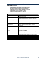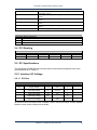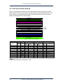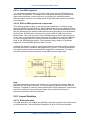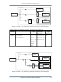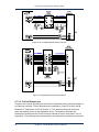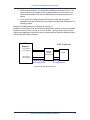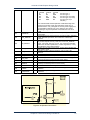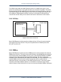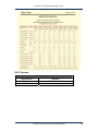
1
Advantech SOM-Express System On Module Design Guide Version 1.1 Advantech SOM-Express Design Guide Notices The copyright on this user manual remains with Advantech Co., Ltd. No part of this user manual may be transmitted, reproduced, or changed. Other companies’ product names that may be used herein remain the property of their respective owners. The product specifications, design and this user’s manuals content are subject to change without notice. If you have any questions, please contact your merchant or our service center for clarification. We are not responsible for any losses resulting from using this product no matter what the reason. Revision History Version/Revision date Version 1.0 Version 1.1 Date July, 2006 July, 2007 Part No: 20060EXP00 2 Notices Description Initial release Advantech SOM-Express Design Guide Table of Contents Chapter 1 1.1 Introduction............................................................................................9 Terminology.............................................................................................9 Table 1.1 Conventions and Terminology .......................................9 1.2 Referenced Documents.........................................................................10 Table 1.2 Referenced Documents ...............................................10 Chapter 2 SOM-Express Overview ......................................................................11 2.1 Overview................................................................................................11 2.2 Specifications ........................................................................................13 Table 2.1 SOM-Express Module ................................................13 2.2.1 SOM-5780 ....................................................................................14 Figure 2-1 SOM-5780 Block Diagram...........................................14 Table 2.2 SOM-5780 Specifications..........................................15 2.2.2 SOM-5782 ....................................................................................16 Figure 2-2 SOM-5782 Block Diagram...........................................16 2.2.3 SOM-DB5700 ...............................................................................18 Figure 2-3 SOM-DB5700 Block Diagram......................................18 Table 2.3 SOM-DB5700 Specifications .......................................18 2.3 System Resources ................................................................................19 2.3.1 SOM-5780 Resources ..................................................................19 Table 2.4 SOM-5780 IRQ Resources..........................................19 Table 2.5 SOM-5780 DMA Resources ........................................19 Table 2.6 SOM-5780 Memory Map .............................................20 Table 2.7 SOM-5780 I/O Map......................................................21 Table 2.8 SOM-5780 Alternative Device Resources ...................22 2.3.2 SOM-5782 Resources ..................................................................22 Table 2.9 SOM-5782 IRQ Resources..........................................22 Table 2.10 SOM-5782 DMA Resources ......................................22 Table 2.11 SOM-5782 Memory Map ...........................................23 Table 2.12 SOM-5782 I/O Map....................................................24 Table 2.13 SOM-5782 Alternative Device Resources .................25 2.4 PCI Routing ...........................................................................................25 Table 2.14 Advantech SOM-Express Module PCI Routing ..........25 2.5 DC Specifications ..................................................................................25 2.5.1 Interface I/O Voltage.....................................................................25 Table 2.15 DC specifications for 5V signaling of PCI Bus ...........25 Table 2.16 DC specifications for 3.3V signaling of PCI Bus ........26 Table 2.17 DC specification of USB signals ................................27 Table 2.18 AC’97 CODEC DC specification ................................27 Table 2.19 AC’97 CODEC analog I/O DC specification ..............27 Table 2.20 Hsync and Vsync signals specification ......................27 Table 2.21 RGB Voltage..............................................................27 Table 2.22 LCD I/O Voltage.........................................................28 Table 2.23 Ultra DMA modes 1-4 (5V) ........................................28 Table 2.24 Ultra DMA modes 5 (3.3V).........................................28 Table 2.25 Ethernet I/O Voltage ..................................................28 Table 2.26 TV-Out I/O Voltage ....................................................28 Table 2.27 IrDA I/O Voltage.........................................................28 Table 2.28 I2C I/O Voltage ..........................................................29 Table 2.29 SMBus I/O Voltage ....................................................29 2.6 AC Specification ....................................................................................29 2.6.1 PCI-Bus AC Spec. ........................................................................29 Table of Contents 3 Advantech SOM-Express Design Guide 2.6.2 Universal Serial Bus (USB) AC Spec. ..........................................29 2.6.3 Audio AC Spec. ............................................................................29 2.6.4 VGA AC Spec. ..............................................................................29 2.6.5 IDE AC Spec.................................................................................30 2.6.6 I2C AC Spec. ................................................................................30 2.6.7 SMBus AC Spec. ..........................................................................30 Chapter 3 Pin Assignments .................................................................................31 Table 3.1 Conventions and Terminology ......................................31 3.1 Row A ....................................................................................................32 Table 3.2 Connector A Pin Assignments ......................................32 3.2 Row B ....................................................................................................33 Table 3.3 Connector B Pin Assignments .....................................33 3.3 Row C....................................................................................................34 Table 3.4 Connector C Pin Assignments......................................34 3.4 Row D....................................................................................................35 Table 3.5 Connector D Pin Assignments......................................35 Chapter 4 General Design Recommendations ...................................................36 4.1 Nominal Board Stack-Up .......................................................................36 4.1.1 Four layer board stack-up.............................................................37 Figure 4-1 Four-Layer Stack-up...................................................37 Table 4.1: Recommended Four-Layer Stack-Up Dimensions ......37 4.1.2 Six layer board stack-up ...............................................................38 Figure 4-2 Six-Layer Stack-up ......................................................38 Table 4.2 Recommended Six-Layer Stack-Up Dimensions.........38 4.2 Differential Impedance Targets for Microstrip Routing ..........................39 Table 4.3 Differential Signals Impedance Requirement ...............39 4.3 Alternate Stack Ups...............................................................................39 Chapter 5 Carrier Board Design Guidelines .......................................................40 5.1 PCI-Bus .................................................................................................40 5.1.1 Signal Description.........................................................................40 Table 5.1 PCI Signal Description..................................................40 5.1.2 Design Guidelines.........................................................................41 Table 5.2 Carrier PCI Slots..........................................................41 Table 5.3 Carrier PCI Slots/Devices Interrupt Routing Table ......41 Figure 5-1 Routing PCI Slot/Device CSB Interrupt .......................42 Table 5.4 Clock Skew Parameters ...............................................42 Figure 5-2 Clock Skew Diagram ...................................................43 Table 5.5 Maximum Add-in Card Loading via Each Power Rail ...43 Table 5.6 Add-in Card Supplied Power Selection.........................44 5.1.3 Layout Guidelines .........................................................................44 Figure 5-3 PCI Bus Layout Example with IDSEL..........................44 Table 5.7 PCI Data Signals Routing Summary.............................45 Figure 5-4 PCI Clock Layout Example..........................................45 Table 5.8 PCI Clock Signals Routing Summary ...........................45 5.1.4 Application Notes..........................................................................46 Figure 5-5 Design Example: PCI Arbiter.......................................46 5.2 Universal Serial Bus (USB) ...................................................................47 5.2.1 Signal Description.........................................................................47 Table 5.9 USB Signals Description...............................................47 5.2.2 Design Guidelines.........................................................................47 Figure 5-6 USB Connections ........................................................47 Figure 5-7 Common Mode Choke ................................................48 5.2.3 Layout Guideline...........................................................................48 Figure 5-8 USB Layout Guidelines ...............................................49 Figure 5-9 Overcurrent Circuit ......................................................49 4 Table of Contents Advantech SOM-Express Design Guide Figure 5-10 Violation of Proper Routing Techniques....................50 Figure 5-11 Creating Unnecessary Stubs....................................50 5.3 AC Link/Azalia interface ........................................................................51 5.3.1 Signal Description.........................................................................51 Table 5.10 Audio signals description ............................................51 5.3.2 Design Guidelines.........................................................................51 Figure 5-12 AC link Connections ..................................................52 Figure 5-13 Azalia link Connections .............................................52 Figure 5-14 AC link Audio Layout Guidelines ...............................53 Figure 5-15 Sense resistor examples ...........................................53 5.3.3 Layout Guidelines .........................................................................54 Figure 5-16 Azalia – AC_SDIN Topology .....................................54 Table 5.11 Azalia – AC_SDIN Routing Summary.........................54 Figure 5-17 Azalia – AC_SDOUT/AC_SYNC/AC_BITCLK/AC_RST# Topology#1.......55 Table 5.12 Azalia – AC_SDOUT/AC_SYNC/AC_ BITCLK/AC_RST# Topology #1 ...................................................55 Figure 5-18 Azalia – AC_SDOUT/AC_SYNC/AC_BITCLK/AC_RST# Topology#2.......55 Table 5.13 Azalia – AC_SDOUT/AC_SYNC/AC_ BITCLK/AC_RST# Topology #2 ...................................................56 5.4 VGA .......................................................................................................56 5.4.1 Signal Description.........................................................................56 Table 5.14 VGA signals description..............................................56 5.4.2 Design Guidelines.........................................................................57 Figure 5-19 VGA Connections......................................................57 5.4.3 Layout Guideline...........................................................................57 Figure 5-20 VGA Layout Guidelines .............................................57 Figure 5-21 RGB Output Layout Guidelines .................................58 5.5 LVDS .....................................................................................................59 5.5.1 Signal Description.........................................................................59 Table 5-15 LVDS signals description...........................................59 5.5.2 Design Guideline ..........................................................................59 Figure 5-22 LVDS LCD Connections............................................59 Table 5-16 LVDS Signals Trace Length Mismatch Mapping ........60 5.5.3 Layout Requirements....................................................................60 Figure 5-23 LVDS Signal Routing Topology.................................60 5.6 Primary IDE0 .........................................................................................61 5.6.1 Signal Description.........................................................................61 Table 5-17 IDE signals description ..............................................61 5.6.2 Design Guidelines.........................................................................61 Figure 5-24 IDE Master/Slave Handshake Signals Connection ...62 Figure 5-25 IDE Bus Trace on Carrier Board and Cable ..............62 Figure 5-26 IDE0 Connections .....................................................63 5.6.3 Layout Guidelines .........................................................................63 Table 5-18 IDE Routing Summary................................................63 5.7 Ethernet .................................................................................................64 5.7.1 Signal Descriptions .......................................................................64 Table 5-19 Ethernet signal description .........................................64 5.7.2 Design Guidelines.........................................................................64 Figure 5-27 10/100M Ethernet Connections.................................65 Figure 5-28 Gigabit Ethernet Connections ...................................65 Figure 5-29 Ground Plane Separation..........................................65 5.7.3 Layout Guidelines .........................................................................66 Figure 5-30 Differential signals route example .............................67 Table of Contents 5 Advantech SOM-Express Design Guide Figure 5-31 Bend example ...........................................................67 Figure 5-32 10/100M Ethernet Interconnection ............................68 Figure 5-33 Gigabit Ethernet Interconnection...............................68 Figure 5-34 Critical Dimensions....................................................69 5.8 TV-Out ...................................................................................................70 5.8.1 Signal Descriptions .......................................................................70 Table 5.20 TV signals description.................................................70 5.8.2 Design Guidelines.........................................................................70 Figure 5-35 Connection of TV-out ................................................70 Figure 5-36 TV DAC Video Filter ..................................................71 Table 5-21 TV DAC Video filter component descriptions .............71 5.8.3 Layout Guidelines .........................................................................71 Figure 5-37 TV DAC Routing Topology ........................................72 5.9 Miscellaneous........................................................................................72 5.9.1 Miscellaneous Signal Descriptions ...............................................72 Table 5.22 Miscellaneous signal descriptions ..............................72 Figure 5-38 Speaker Connections ................................................73 5.9.2 I2C Bus .........................................................................................74 Figure 5-39 I2C Bus Connections.................................................74 5.9.3 SMBus 74 Figure 5-40 SMB Bus Connections ..............................................75 5.9.4 Power Good/Reset Input ..............................................................75 Figure 5-41 Power OK/Reset Input Connections..........................75 5.9.5 WDT 75 Figure 5-42 Example of a watch-dog circuit .................................76 5.10 PCI Express Bus ...................................................................................77 5.10.1 Signal Description.........................................................................77 Table 5-23 PCIE Signal Description(General purpose) ...............77 Table 5-24 PEG Signal Description(x16 Graphics) .....................77 Table 5-25 Express Card Support ...............................................77 5.10.2 Design Guidelines.........................................................................78 Figure 5-43 PCI Express Interconnect Example...........................78 Table 5-26 PCI Express Capacitor Summary..............................78 Figure 5-44 Polarity Inversion on a TX to RX Interconnect ..........79 Figure 5-45 Lane Reversal and Polarity Inversion - TX to RX Interconnect ..................................................................................79 Figure 5-46 Example of terminating unused PCI Express ports...80 5.10.3 Layout Guidelines .........................................................................81 Figure 5-47 Line equalization .......................................................81 Table 5-27 PCI Express Trace Width and Spacing for Micro-strip and Strip-line.................................................................................82 Figure 5-48 Example of “interleaved” and “non-interleaved” ........82 Figure 5-49 Topology #1 – SOM Express to PCI Express Device Down ............................................................................................83 Table 5-28 SOM Express to PCI Express ....................................83 Figure 5-50 Topology #2 and #3 – SOM Express to Express Card or Docking Conn. ..........................................................................83 Table 5-29 SOM Express to Express Card...................................83 5.11 Serial ATA .............................................................................................84 5.11.1 Signal Description.........................................................................84 Table 5-30 Serial ATA Signal Description ....................................84 5.11.2 Design Guidelines.........................................................................84 Figure 5-51 SATA interconnect example......................................84 Figure 5-52 ATA_ACT# Circuit Example ......................................85 5.11.3 Layout Guidelines .........................................................................85 6 Table of Contents Advantech SOM-Express Design Guide Figure 5-53 Example of SATA trace length pair matching............86 5.12 LPC........................................................................................................87 5.12.1 Signal Description.........................................................................87 Table 5-32 LPC signals description ..............................................87 5.12.2 Design Guidelines.........................................................................87 Table 5-33 Recommended Pull-Up Values ..................................87 5.12.3 Layout Guidelines .........................................................................87 5.12.4 Application Notes..........................................................................88 Figure 5-54 Architecture of LPC interface ....................................88 Figure 5-55 Serial Bus Connection...............................................88 Figure 5-56 Keyboard and Mouse connection..............................89 Figure 5-57 LPT Connection.........................................................90 Figure 5-58 Floppy Connection ....................................................91 Chapter 6 Power Delivery Guidelines .................................................................92 6.1 SOM-Express Power Consumption.......................................................92 Table 6.1 SOM-5780 Power Consumption ................................92 6.2 Design Guidelines .................................................................................95 6.2.1 ATX Power Delivery Block Diagram .............................................95 Figure 6-1 ATX Power Delivery Block Diagram............................95 6.2.2 AT Power Delivery Block Diagram................................................96 Figure 6-2 AT Power Delivery Block Diagram ..............................96 Chapter 7 Carrier Board Mechanical Design Guidelines...................................97 7.1 SOM-Express Mechanical Dimensions .................................................97 Figure 7-1: SOM-Express Module Board Mechanical Dimensions ......................................................................................................97 7.2 SOM Express Module Connector ..........................................................98 Figure 7-2: SOM-Express Module Receptacle .............................98 7.3 SOM Express Carrier Board Connector ................................................98 Figure 7-3: SOM-Express Carrier Board Plug (8mm Version) .............99 7.4 SOM Express Connector PCB Pattern..................................................99 Figure 7-4: SOM-Express Connector PCB Pattern..............................99 7.5 SOM Express Module Connector Pin Numbering ...............................100 Figure 7-5: SOM-Express Module Connector Pin Numbering ...........100 7.6 SOM-Express Carrier Board Connector Pin Numbering .....................100 Figure 7-6: SOM-Express Carrier Board Connector Pin Numbering...100 Chapter 8 Heatsink Recommended Design......................................................101 8.1 Material of Heatsink.............................................................................101 8.2 Thermal Interface Material...................................................................101 8.3 Attachment Method of Thermal Solution .............................................102 8.4 Grounding Issues ................................................................................102 8.5 Air intake clearance and Airflow of Heatsink .......................................102 Figure 8-1: Air Intake Clearance.................................................102 Figure 8-2: Air Flow Direction .....................................................103 8.6 SOM-Express Thermal solution Specification .....................................103 Figure 8-3: Overall Height for Heat-Spreader in SOM-Express Modules ......................................................................................103 Figure 8-4: SOM-Express Module Heat-Spreader......................105 8.7 Component Height – Module Back and Carrier Board Top .................105 Figure 8-5: Component Clearances Underneath Module ...........105 8.8 Advantech Heatsink Information..........................................................106 8.8.1 Vendor List..................................................................................106 Table 8.1: Vendor list..................................................................106 8.8.2 Heat-Spreader ............................................................................106 Figure 8-6: SOM-Express Heat-Spreader.........................................106 Figure 8-7: SOM-Express Heat-Spreader Tolerances ........................107 Table of Contents 7 Advantech SOM-Express Design Guide 8.8.3 8.8.4 8.8.5 8.8.6 8 Heat-Sink ....................................................................................107 Figure 8-8: Heatsink Dimensions................................................107 Table 8.2: Chemistry Ingredient & Temper Designation.............108 Thermal Pad ...............................................................................108 Figure 8-8: Thermal Pad.............................................................108 Table 8.3 Thermal Pad ...............................................................108 Screws 109 Table 8.4 Screws ........................................................................109 Fan 110 Table 8.5: Fan Characteristics....................................................111 Table of Contents Advantech SOM-Express Design Guide Chapter 1 Introduction This design guide organizes and provides Advantech’s SOM carrier board design recommendations for Advantech SOM-Express modules. It specifies common mechanical and electrical characteristics in order to ensure the carrier board design meets all the requirements needed to work properly. 1.1 Terminology Table 1.1 Conventions and Terminology AC’97 Audio Codec 97’ AGP Accelerated Graphics port refers to the AGP/PCI interface CPU Central processing Unit CRT Cathode Ray Tube DDR2 Double Data Rate second generation SDRAM memory technology DTOS Advantech’s Design To Order Service EMI Electromagnetic Interference ESD Electrostatic Discharge SOM-Express New generation technology of System on module FSB Front Side Bus, synonymous with Host or CPU bus GMCH Refers to the Graphics Memory Controller Hub chipset component I2C Inter-IC (a two wire serial bus created by Philips) ISA International Standards Association IDE (ATA) Integrated Drive Electronics (Advanced Technology Attachment) INTx An interrupt request signal where x stands for interrupts A, B, C, and D. LCD Liquid Crystal Display Low Voltage Differential Signaling: A high speed, low power data LVDS transmission standard used for display connections to LCD panels. MCH Refers to the Memory Controller Hub chipset component NTSC National Television Standards Committee PAL Phase Alternate Line PCI Peripheral Component Interface PCI-Express New generation PCI interface with serial interconnection technology RTC Real Time Clock SMBus System Management Bus. SOM System On Module SATA Serial ATA interface SAS Serial attached SCSI interface ULV Ultra-Low Voltage USB Universal Serial Bus Chapter 1 Introduction 9 Advantech SOM-Express Design Guide 1.2 Referenced Documents Table 1.2 Referenced Documents Document Advanced Configuration and Power Management (ACPI) Specification 3.0b Location http://www.acpi.info/spec.htm COM Express Specification http://www.picmg.org/ Ethernet(IEEE 802.3) I2C Bus Interface http://www.ieee.org/portal/site http://www.semiconductors.philips.com/ IrDA http://www.irda.org/ PCI http://www.pcisig.com/ PC104 http://www.pc104.org/technology/pc104_tech.html RS232 http://www.eia.org/ SMBus http://www.smbus.org/specs/ USB http://www.usb.org/home 10 Chapter 1 Introduction Advantech SOM-Express Design Guide Chapter 2 SOM-Express Overview SOM-Express complies with COM Express standard from the PCI Industrial Computer Manufacturers Group (PICMG) which provides next generation performance of the smallest state of the art embedded modules. With a scalable solution that meets customer's advanced CPU application development needs and reduces time-to-market. Advantech’s Design To Order Service (DTOS) helps customers develop custom CPU board solutions extremely fast and with lower investment. With DTOS, three ready-to-run engineering samples can be produced within 30 working days from order confirmation. Using SOM-DTOS, customers can reduce traditional customized CPU board development time and costs by as much as 80%. 2.1 Overview Advantech offers a wide range of SOM products to cater to each customer's demands. The modular designs allow upgrade ability and add more flexibility to the system. The COM Express form factor allows the SOM-Express modules to be easily and securely mounted on a customized solution board. The design and multiple processor choices eliminate CPU integration worries and allow fast application support for the most dynamic embedded needs. SOM is a series of reliable and widely used CPU cores with high integration features. SOM-Express supports wild range of processor and chipset solution available from the market to reach the latest technical trend such like PCI Express, Serial ATA, USB 2.0, etc. Not only does SOM allow quick design, it also provides the benefits of easy installation, maintenance and upgrade ease. Chapter 2 SOM-Express Overview 11 Advantech SOM-Express Design Guide Though small in size, SOM takes care of most complicated CPU architectures and basic common circuits. Many system integrators are finding an Advantech SOM solution already covers 80% of their feature requirements. This makes SOM a powerful time and money saver. SOM + Customer Solution Board = Your Customized Platform. System On Modules save time and money. Using SOM-DTOS allows customers to realize cost savings and most importantly, faster time to market, two keys to help ensure your product’s success in the market. 12 Chapter 2 SOM-Express Overview Advantech SOM-Express Design Guide 2.2 Specifications Advantech provides two SOM-Express modules, and each module has a different CPU type for customer to choose. Table 2.1 shows Advantech SOM-Express modules with brief descriptions. Table 2.1 SOM-Express Module SOM-5780 Series SOM-5780FL-00A1E SOM-5780FL-S0A1E SOM-5780FL-S4A1E SOM-5780FL-S8A1E SOM-5780FL-U0A1E SOM-5782 Series SOM-5782FL-00A1E SOM-5782FL-S0A1E SOM-5782FL-S7A1E SOM-5782FL-U0A1E SOM-DB5700 SOM-DB5700-00A1E Description Socket 478 Type On board Intel Celeron M ULV 373 @ 1.0G On board Intel Pentium M LV 738 @ 1.4G With Intel Pentium M 745 @ 1.8G With Intel Pentium M 760 @ 2.0G Description Socket 478 Type On board Intel Celeron M ULV 423 @ 1.06G On board Intel Core Duo L2400 @ 1.66G With Intel Core Duo T2500 @ 2.0G Description SOM Express Development Board Rev.A1 Chapter 2 SOM-Express Overview 13 Advantech SOM-Express Design Guide 2.2.1 SOM-5780 Advantech’s new SOM-5780 is the ultimate powerful SOM-Express CPU module able to drive the most demanding embedded applications requiring high performance CPU processing power & graphics support. With support for Intel® Pentium® M and Celeron® M processors & enhanced SpeedStep technology, the SOM-5780 offers developers a low power and scaleable solution that fits a range of needs. The Intel® 915GM Express Chipset for Embedded Computing, consisting of the Intel 915GM Graphic Memory Controller Hub (GMCH) and Intel I/O Controller Hub 6-M (ICH6-M) is an optimized integrated graphics solution with a 400MHz and 533MHz front-side bus. The integrated 32-bit 3D graphics engine, based on Intel Graphics Media Accelerator 900(Intel GMA 900) architecture, operates at core speeds of up to 320MHz. It features a low-power design, is validated with the Intel Pentium M and Intel Celeron M processors on 90nm process, and supports up to 2GB of DDR2 533MHz system memory. Figure 2-1 SOM-5780 Block Diagram 14 Chapter 2 SOM-Express Overview Advantech SOM-Express Design Guide SOM-5780 Main Features: Embedded Intel® Pentium® M/ Celeron M processor Intel Extreme Graphics 2 & PCI Express graphics Supports the upcoming primary datapath PCI Express Supports 8 host USB2.0 ports and 4 SATA Supports up to dual channel LVDS panels Table 2.2 SOM-5780 Specifications Item Description CPU Embedded Intel Pentium M or Celeron M processor w/64KB primary cache memory System Memory 1 x 200 pin SO-DIMM sockets, support Double DataRate2 (DDR2)128 MB to 1 GB, accept 128/256/512/ 1000 MB DR200/266/333 DRAM. 2nd Cache Memory 2/1 MB on the Pentium M processor or 512 KB on the Celeron M processor. System Chipset Intel 915GM GMCH/ ICH6-M Chipset 533 MHz FSB BIOS AWARD 4 Mbit Flash BIOS 255 levels timer interval, from 1 to 255 sec or min WatchDog Timer setup by software, jumperless selection, generates system reset Expansion Interface Support PCI Express, PCI & LPC interface MIO 1 x EIDE (UDMA 100), 2 x SATA USB 8 USB 2.0 compliant ports Intel 82562GZ, IEEE 802.3u 10/100Base-T compatible Built-in Ethernet boot ROM in Flash BIOS Optional Intel 81541PI IEEE 802.3u 1000Base-T compatible CRT Display mode Pixel resolution up to 1600 x 1200 at 85 Hz and 2048 x 1536 at 75 Hz Dual channel LVDS panel supports up to UXGA panel LCD Display mode resolution with frequency range from 25 MHz to 112 MHz Dimensions (L x W) Power Supply Voltage Power Requirement Operating Temperature Operating Humidity 95 x 125 (3.74" x 4.92") +12 V power only Max: +12 V @ 4 A 0 ~ 60û C (32 ~ 140û F) 0% ~ 90% relative humidity, non-condensing Chapter 2 SOM-Express Overview 15 Advantech SOM-Express Design Guide 2.2.2 SOM-5782 Figure 2-2 SOM-5782 Block Diagram 16 Chapter 2 SOM-Express Overview Advantech SOM-Express Design Guide SOM-5782 Main Features: Embedded Intel® Core2 Duo / Core Duo / Celeron® M Processor Intel new graphics core based on GMA 950 & external PCI Express x 16 graphics interface. Supports the upcoming primary datapath PCI Express Supports 8 host USB 2.0 ports and 2 SATA ports Supports up to dual channel LVDS panels Table 2.2 SOM-5782 Specifications Item Description Embedded Intel Intel Core 2 Duo processor / Intel Core Duo CPU processor, Intel Core Duo processor LV (Low Voltage). System Memory 1 x 200 pin SO-DIMM sockets, support Double Data Rate2 (DDR2)128 MB to 2GB, accept 128/256/512/1024/2048 MB DDR 533/667 DRAM. 2nd Cache Memory System Chipset BIOS WatchDog Timer Expansion Interface MIO USB Ethernet CRT Display mode LCD Display mode Dimensions (L x W) Power Supply Voltage Power Requirement Operating Temperature Operating Humidity 2-MB L2 cache Intel 945GM GMCH/ ICH7-M Chipset 533 MHz FSB AWARD 4 Mbit Flash BIOS 255 levels timer interval, from 1 to 255 sec or min setup by software, jumperless selection, generates system reset Support PCI Express, PCI & LPC interface 1 x EIDE (UDMA 100), 2x SATA 8 USB 2.0 compliant ports Intel 82562GZ, IEEE 802.3u 10/100Base-T compatible Built-in boot ROM in Flash BIOS Optional PCI Express Intel 82573L IEEE 802.3u 1000Base-T compatible Pixel resolution up to 1600 x 1200 at 85 Hz and 2048 x 1536 at 75 Hz Dual channel LVDS panel supports up to UXGA panel resolution with frequency range from 25 MHz to 112 MHz 95 x 125 (3.74" x 4.92") +12 V power only Max: +12 V @ 4 A 0 ~ 60°C (32 ~ 140°F) 0% ~ 90% relative humidity, non-condensing Chapter 2 SOM-Express Overview 17 Advantech SOM-Express Design Guide 2.2.3 SOM-DB5700 CD-IN CENTER/LFE ATX-POWER SURROUND AC Link HD Audio SIDESURR Codec ALC880 FRONT_OUT Primary IDE System Module LINE1/2_IN FDD(34P Standard) LPC Super IO USB 2.0 PORT x 8 COM-1 RS232 LAN RJ-45 (10/100 or Giga LAN) COM2 PCI BUS RS-232/422/485 PCIE X1 x 4 LVDS CONN PCIE X16 x 1 Mini PCI SLOT TV-OUT MIC1/2_IN W83627HF PCI SLOT-0 LPT PORT-1 PCI SLOT-1 PS2 KB/MS PCIE X16 CRT CONN SLOT-0 IT8888G PCI ISA SLOT-0 to ISA SATA x 4 PCIE X1 SLOT-1 Express Card PCIE X1 SLOT-2 PCIE X1 SLOT-3 Figure 2-3 SOM-DB5700 Block Diagram SOM-DB5700 Main Features: Offers standard PC environment PCI Express / PCI /ISA expansion interface Reference design and prototype platform ATX form factor Table 2.3 SOM-DB5700 Specifications Item Description Extended Four PCI Express bus and Three PCI bus and One ISA Display DB-15 VGA connector, LCD connector Communications DB-9 COM1 connector, 10-pin COM2 box header, RJ-45 Ethernet connector MIO EIDE/FDD/LPT/Keyboard/Mouse /USB/Audio/TV-out/SSD interface Size/Weight 304.8 x 190.5 mm (12" x 7.5"), 0.37 kg (0.81 lb) 18 Chapter 2 SOM-Express Overview Advantech SOM-Express Design Guide 2.3 System Resources This section demonstrates resources distribution of Advantech’s SOM-Express modules, including IRQ, DMA, memory map, and I/O map. 2.3.1 SOM-5780 Resources Table 2.4 IRQ 0 1 2 3 4 5 6 7 8 9 10 11 12 13 14 15 16 17 18 19 20 21 22 23 SOM-5780 IRQ Resources Description (ISA) System timer (ISA) Standard 101/102-Key or Microsoft Natural PS/2 Keyboard (ISA) Communications Port (COM2) (ISA) Communications Port (COM1) (ISA)Standard floppy disk controller (ISA)ECP Printer Port (LPT1) (ISA) System CMOS/real time clock (ISA) Microsoft ACPI-Compliant System, Intel(R) 82801FBM SMBus Controller - 24C3 (ISA) PS/2 Compatible Mouse (ISA) Numeric data processor (ISA) Primary IDE Channel (ISA) Secondary IDE Channel (PCI) Intel(R) 82915 GM Graphics Controller, Intel(R) 82801FBM USB Universal Host Controller - 24C2 (PCI) Realtek AC'97 Audio (PCI) Intel(R) 82801FBM USB Universal Host Controller - 24C7 (PCI) 19 Intel(R) 82801FBM USB Universal Host Controller - 24C4 (PCI) Intel PCI to USB Enhanced Host Controller Table 2.5 DMA 0 1 2 3 4 5 6 7 SOM-5780 DMA Resources Description Cascade to DMA4 Standard floppy disk controller ECP Printer Port (LPT1) Direct memory access controller - Chapter 2 SOM-Express Overview 19 Advantech SOM-Express Design Guide Table 2.6 SOM-5780 Memory Map Memory Address 20 Description 00000000 - 0009FFFF System board 000A0000 - 000BFFFF PCI bus 000A0000 - 000BFFFF Intel(R) 82915GM Graphics Controller 000C0000 - 000DFFFF PCI bus 000E0000 - 000EFFFF System board 000F0000 - 000F3FFF System board 000F4000 - 000F7FFF System board 000F8000 - 000FBFFF System board 000FC000 - 000FFFFF System board 00100000 - 0DFEFFFF System board 0DFF0000 - 0DFFFFFF System board 0E000000 - FEBFFFFF PCI bus D8000000 - DFFFFFFF Intel(R) 82915GM Graphics Controller E0000000 - E7FFFFFF Intel(R) 82915GM Graphics Controller E8000000 - E807FFFF Intel(R) 82915GM Graphics Controller E8080000 - E80FFFFF Intel(R) 82915GM Graphics Controller E8100000 - E81003FF Intel PCI to USB Enhanced Host Controller E8101000 - E81011FF Realtek AC'97 Audio E8102000 - E81020FF Realtek AC'97 Audio FEBFFC00 - FEBFFFFF Intel(R) 82801FBM Ultra ATA Storage Controller - 24CB FEC00000 - FECFFFFF System board FEE00000 - FEEFFFFF System board FFB00000 - FFB7FFFF System board FFB80000 - FFBFFFFF Intel(r) 82802 Firmware Hub Device FFF00000 - FFFFFFFF System board Chapter 2 SOM-Express Overview Advantech SOM-Express Design Guide Table 2.7 SOM-5780 I/O Map Memory Address 00000000 - 00000CF7 00000000 - 0000000F 00000010 - 0000001F 00000020 - 00000021 00000022 - 0000003F 00000040 - 00000043 00000044 - 0000005F 00000060 - 00000060 00000061 - 00000061 00000062 - 00000063 00000064 - 00000064 00000065 - 0000006F 00000070 - 00000073 00000074 - 0000007F 00000080 - 00000090 00000091 - 00000093 00000094 - 0000009F 000000A0 - 000000A1 000000A2 - 000000BF 000000C0 - 000000DF 000000E0 - 000000EF 000000F0 - 000000FF 00000170 - 00000177 000001F0 - 000001F7 00000274 - 00000277 00000279 - 00000279 000002F8 - 000002FF 00000376 - 00000376 00000378 - 0000037F 000003B0 - 000003BB 000003C0 - 000003DF 000003F6 - 000003F6 000003F8 - 000003FF 00000400 - 000004BF 000004D0 - 000004D1 00000500 - 0000051F 00000778 - 0000077B 00000A78 - 00000A7B 00000B78 - 00000B7B 00000BBC - 00000BBF 00000D00 - 0000FFFF 00000E78 - 00000E7B 00000F78 - 00000F7B 00000FBC - 00000FBF 0000E000 - 0000E007 0000E100 - 0000E11F 0000E200 - 0000E21F 0000E300 - 0000E31F 0000E500 - 0000E5FF 0000E600 - 0000E63F 0000F000 - 0000F00F Description PCI bus Direct memory access controller Motherboard resources Programmable interrupt controller Motherboard resources System timer Motherboard resources Standard 101/102-Key or Microsoft Natural PS/2 Keyboard System speaker Motherboard resources Standard 101/102-Key or Microsoft Natural PS/2 Keyboard Motherboard resources System CMOS/real time clock Motherboard resources Direct memory access controller Motherboard resources Direct memory access controller Programmable interrupt controller Motherboard resources Direct memory access controller Motherboard resources Numeric data processor Secondary IDE Channel Primary IDE Channel ISAPNP Read Data Port ISAPNP Read Data Port Communications Port (COM2) Secondary IDE Channel Printer Port (LPT1) Intel(R) 82915GM Graphics Controller Intel(R) 82915GM Graphics Controller Primary IDE Channel Communications Port (COM1) Motherboard resources Motherboard resources Intel(R) 82801FBM SMBus Controller - 24C3 Printer Port (LPT1) Motherboard resources Motherboard resources Motherboard resources PCI bus Motherboard resources Motherboard resources Motherboard resources Intel(R) 82915GM Graphics Controller Intel(R) 82801FBM USB Universal Host Controller - 24C2 Intel(R) 82801FBM USB Universal Host Controller - 24C4 Intel(R) 82801FBM USB Universal Host Controller - 24C7 Realtek AC'97 Audio Realtek AC'97 Audio Intel(R) 82801FBM Ultra ATA Storage Controller - 24CB Chapter 2 SOM-Express Overview 21 Advantech SOM-Express Design Guide Table 2.8 SOM-5780 Alternative Device Resources Alternative Device Resources COM1 3F8/IRQ4*, 2F8/IRQ3, 3E8/IRQ4, 2E8/IRQ3, Disable COM2 3F8/IRQ4, 2F8/IRQ3*, 3E8/IRQ4, 2E8/IRQ3, Disable LPT1 378/IRQ7*, 278/IRQ5, 3BC/IRQ7, Disable * Default setting 2.3.2 SOM-5782 Resources Table 2.9 IRQ 0 1 2 3 4 5 6 7 8 9 10 11 12 13 14 15 16 16 16 17 18 19 19 19 23 23 Table 2.10 DMA 0 1 2 3 4 5 6 7 22 SOM-5782 IRQ Resources Description (ISA) System timer (ISA) Standard 101/102-Key or Microsoft Natural PS/2 Keyboard (ISA) Communications Port (COM2) (ISA) Communications Port (COM1) (ISA) Standard floppy disk controller (ISA) ECP Printer Port (LPT1) (ISA) System CMOS/real time clock (ISA) Microsoft ACPI-Compliant System (PCI) Intel(R) 82801G(ICH7 Family) SMBus Controller - 27DA (ISA) PS/2 Compatible Mouse (ISA) Numeric data processor (ISA) Primary IDE Channel (ISA) Secondary IDE Channel (PCI) Intel(R) 82801G(ICH7 Family) PCI Express Root Port - 27D0 (PCI) Intel(R) 82801G(ICH7 Family) USB Universal Host Controller – 27CB (PCI) Mobile Intel(R) 945GM Express Chipset Family (PCI) Intel(R) PRO/1000 PL Network Connection (PCI) Intel(R) 82801G(ICH7 Family) USB Universal Host Controller – 27CA (PCI) Intel(R) 82801G(ICH7 Family) PCI Express Root Port - 27D6 (PCI) Intel(R) 82801G(ICH7 Family) USB Universal Host Controller – 27C9 (PCI) Intel(R) 82801GR/GH/GHM (ICH7 Family) PCI Express Root Port – 27E2 (PCI) Intel(R) 82801G(ICH7 Family) USB Universal Host Controller – 27CB (PCI) Intel(R) 82801G(ICH7 Family) USB2 Enhanced Host Controller – 27CC SOM-5782 DMA Resources Description Standard floppy disk controller Direct memory access controller - Chapter 2 SOM-Express Overview Advantech SOM-Express Design Guide Table 2.11 SOM-5782 Memory Map Memory Address Description 0x0000-0x9FFFF System board 0x100000-0xF6DFFFF System board 0xA0000-0xBFFFF PCI bus 0xA0000-0xBFFFF Mobile Intel(R) 945GM Express Chipset Family 0xC0000-0xDFFFF PCI bus 0xCE600-0xCFFFF System board 0xD0000000-0xDFFFFFFF Mobile Intel(R) 945GM Express Chipset Family 0xE0000-0xEFFFF System board 0xE0000000-0xEFFFFFFF Motherboard resources 0xF0000-0xF7FFF System board 0xF6E0000-0xF6FFFFF System board 0xF700000-0xFEBFFFFF PCI bus 0xF8000-0xFBFFF System board 0xFC000-0xFFFFF System board 0xFD600000-0xFD6FFFFF Intel(R) 82801G (ICH7 Family) PCI Express Root Port - 27D0 0xFD900000-0xFD9FFFFF Intel(R) 82801G (ICH7 Family) PCI Express Root Port - 27D0 0xFDA00000-0xFDAFFFFF 0xFDB00000-0xFDCFFFFF Intel(R) 82801GR/GH/GHM (ICH7 Family) PCI Express Root Port - 27E2 Intel(R) 82801GR/GH/GHM (ICH7 Family) PCI Express Root Port - 27E2 0xFDB00000-0xFDCFFFFF Intel(R) PRO/1000 PL Network Connection 0xFDCE0000-0xFDCFFFFF Intel(R) PRO/1000 PL Network Connection 0xFDD00000-0xFDDFFFFF Intel(R) 82801G (ICH7 Family) PCI Express Root Port - 27D6 0xFDE00000-0xFDEFFFFF Intel(R) 82801G (ICH7 Family) PCI Express Root Port - 27D6 0xFDF00000-0xFDF7FFFF Mobile Intel(R) 945GM Express Chipset Family 0xFDF80000-0xFDFBFFFF Mobile Intel(R) 945GM Express Chipset Family 0xFDFF8000-0xFDFFBFFF PCI Device 0xFDFFF000-0xFDFFF3FF Intel(R) 82801G (ICH7 Family) USB2 Enhanced Host Controller 27CC 0xFEC00000-0xFEC00FFF System board 0xFED13000-0xFED1DFFF System board 0xFED20000-0xFED8FFFF System board 0xFEE00000-0xFEE00FFF System board 0xFFB00000-0xFFB7FFFF System board 0xFFB80000-0xFFBFFFFF Intel(r) 82802 Firmware Hub Device 0xFFF00000-0xFFFFFFFF System board Chapter 2 SOM-Express Overview 23 Advantech SOM-Express Design Guide Table 2.12 SOM-5782 I/O Map Memory Address 0x0000-0x0CF7 0x0000-0x0CF7 0x0010-0x001F 0x0020-0x0021 0x0022-0x003F 0x0040-0x0043 0x0044-0x005F 0x0060-0x0060 0x0061-0x0061 0x0062-0x0063 0x0064-0x0064 0x0065-0x006F 0x0070-0x0073 0x0074-0x007F 0x0080-0x0090 0x0091-0x0093 0x0094-0x009F 0x00A0-0x00A1 0x00A2-0x00BF 0x00C0-0x00DF 0x00E0-0x00EF 0x00F0-0x00FF 0x0170-0x0177 0x01F0-0x01F7 0x0274-0x0277 0x0279-0x0279 0x02F8-0x02FF 0x0376-0x0376 0x0378-0x037F 0x03B0-0x03BB 0x03C0-0x03DF 0x03F0-0x03F5 0x03F6-0x03F6 0x03F7-0x03F7 0x03F8-0x03FF 0x0400-0x04BF 0x04D0-0x04D1 0x0500-0x051F 0x0680-0x06FF 0x0778-0x077B 0x0880-0x088F 0x0A78-0x0A7B 0x0B78-0x0B7B 0x0BBC-0x0BBF 0x0D00-0xFFFF 0x0E78-0x0E7B 0x0F78-0x0F7B 0x0FBC-0x0FBF 0xA000-0xAFFF 0xB000-0xBFFF 0xBF00-0xBF1F 0xC000-0xCFFF 24 Description PCI bus Direct memory access controller Motherboard resources Programmable interrupt controller Motherboard resources System timer Motherboard resources Standard 101/102-Key or Microsoft Natural PS/2 Keyboard System speaker Motherboard resources Standard 101/102-Key or Microsoft Natural PS/2 Keyboard Motherboard resources System CMOS/real time clock Motherboard resources Direct memory access controller Motherboard resources Direct memory access controller Programmable interrupt controller Motherboard resources Direct memory access controller Motherboard resources Numeric data processor Secondary IDE Channel Primary IDE Channel ISAPNP Read Data Port ISAPNP Read Data Port Communications Port (COM2) Secondary IDE Channel Printer Port (LPT1) Mobile Intel(R) 945GM Express Chipset Family Mobile Intel(R) 945GM Express Chipset Family Standard floppy disk controller Primary IDE Channel Standard floppy disk controller Communications Port (COM1) Motherboard resources Motherboard resources Intel(R) 82801G (ICH7 Family) SMBus Controller - 27DA Motherboard resources Printer Port (LPT1) Motherboard resources Motherboard resources Motherboard resources Motherboard resources PCI bus Motherboard resources Motherboard resources Motherboard resources Intel(R) 82801G (ICH7 Family) PCI Express Root Port - 27D0 Intel(R) 82801GR/GH/GHM (ICH7 Family) PCI Express Root Port - 27E2 Intel(R) PRO/1000 PL Network Connection Intel(R) 82801G (ICH7 Family) PCI Express Root Port - 27D6 Chapter 2 SOM-Express Overview Advantech SOM-Express Design Guide 0xEA00-0xEA0F Intel(R) 82801GBM/GHM (ICH7-M Family) Serial ATA Storage Controller - 27C4 Intel(R) 82801G (ICH7 Family) USB Universal Host Controller 27CB Intel(R) 82801G (ICH7 Family) USB Universal Host Controller 27CA Intel(R) 82801G (ICH7 Family) USB Universal Host Controller 27C9 Intel(R) 82801G (ICH7 Family) USB Universal Host Controller 27C8 Mobile Intel(R) 945GM Express Chipset Family 0xEB00-0xEB1F 0xEC00-0xEC1F 0xED00-0xED1F 0xEE00-0xEE1F 0xEF00-0xEF07 Table 2.13 SOM-5782 Alternative Device Resources Alternative Device Resources COM1 3F8/IRQ4*, 2F8/IRQ3, 3E8/IRQ4, 2E8/IRQ3, Disable COM2 3F8/IRQ4, 2F8/IRQ3*, 3E8/IRQ4, 2E8/IRQ3, Disable LPT1 378/IRQ7*, 278/IRQ5, 3BC/IRQ7, Disable 2.4 PCI Routing Table 2.14 Advantech SOM-Express Module PCI Routing SOM-5780 PCI Device IRQ REQ 82541PI INTB# REQ5 - GNT GNT5 - IDSEL AD25 - 2.5 DC Specifications The Advantech’s SOM-Express modules power consumption properties have been measured and list in Table 6.1 2.5.1 Interface I/O Voltage 2.5.1.1 PCI Bus Table 2.15 DC specifications for 5V signaling of PCI Bus Symbol Parameter Min Vcc Vih Vil Voh Vol Max Units Supply Voltage 4.75 5.25 V Input High Voltage 2.0 Vcc+0.5 V Input Low Voltage -0.5 0.8 V Output High Voltage 2.4 - V Output Low Voltage - 0.55 V Note *1 *1. Signals without pull-up resistors must have 3 mA low output current. Signals requiring pull up must have 6 mA; the latter include, FRAME#, TRDY#, IRDY#, DEVSEL#, STOP#, SERR#, PERR#, LOCK#, INTA#, INTB#, INTC#, INTD#. Chapter 2 SOM-Express Overview 25 Advantech SOM-Express Design Guide Table 2.16 DC specifications for 3.3V signaling of PCI Bus Symbol Parameter Min Vcc Vih Vil Vipu Voh Vol Max Units Supply Voltage 3.0 3.6 V Input High Voltage 0.5Vcc Vcc+0.5 V Input Low Voltage -0.5 0.3Vcc V Input Pull-up Voltage 0.7Vcc - V Output High Voltage 0.9Vcc - V Output Low Voltage - 0.1Vcc V Note *1 *1. This specification should be guaranteed by design. It is the minimum voltage to which pullup resistors are calculated to pull a floated network. Applications sensitive to static power utilization must assure that the input buffer is conducting minimum current at this input voltage. 26 Chapter 2 SOM-Express Overview Advantech SOM-Express Design Guide 2.5.1.2 Universal Serial Bus (USB) Table 2.17 Symbol Vbus Vbus VIL VIH VIHZ VOL VOH DC specification of USB signals Parameter High-power port supply voltage Low-power port supply voltage Input Low Voltage Input High Voltage(driven) Input High Voltage(floating) Output Low Voltage Output High Voltage Min 4.75 4.75 2.0 2.7 0 2.8 Max 5.25 5.25 0.8 3.6 0.3 3.6 Unit V V V V V V V Note 2.5.1.3 Audio Table 2.18 AC’97 CODEC DC specification Symbol Parameter Dvdd Digital supply voltage Avdd Analog supply voltage Vil Input Low Voltage Vih Input High Voltage Min Dvdd+5% 4.75 0.65Vdd Max Dvdd+5% 5.25 0.35Vdd - Unit V V V V Note *1. Dvdd=5V or 3.3V Table 2.19 AC’97 CODEC analog I/O DC specification Symbol Parameter Min AUXAL/R Full scale input voltage MIC Full scale input voltage SNDL/R Full scale output voltage - Typ 1.0 0.1 1.0 Max - Unit Vrms Vrms Vrms Note 2.5.1.4 VGA Table 2.20 Symbol VIL VIH VOL VOH Hsync and Vsync signals specification Parameter Min Input Low Voltage 0 Input High Voltage 2.4 Output Low Voltage Output High Voltage 2.0 Table 2.21 RGB Voltage Symbol Parameter R Red analog video output signal Max. luminance voltage G Green analog video output signal Max. luminance voltage B Blue analog video output signal Max. luminance voltage R Red analog video output signal min. luminance voltage G Green analog video output signal min. luminance voltage B Blue analog video output signal min. luminance voltage Max 0.5 5.5 0.8 - Unit V V V V Note Min 0.665 Max 0.77 Unit V Note 0.665 0.77 V 0.665 0.77 V 0 (Typical) V 0 (Typical) V 0 (Typical) V Chapter 2 SOM-Express Overview 27 Advantech SOM-Express Design Guide 2.5.1.5 LCD Table 2.22 Symbol VIL VIH VOL VOH LCD I/O Voltage Parameter Input Low Voltage Input High Voltage Output Low Voltage Output High Voltage Min -0.5 2.0 2.4 Max 0.8 Vcc+0.5 0.55 - Unit V V V V Note Max 5.5 0 - Unit V V V Note Iol=4.0mA Ioh=-1.0mA 2.5.1.6 IDE Table 2.23 Symbol VIH VOL VOH Ultra DMA modes 1-4 (5V) Parameter Input High Voltage Output Low Voltage Output High Voltage Min 2 Table 2.24 Ultra DMA modes 5 (3.3V) Symbol Parameter Vdd3 DC supply voltage to drivers and receivers V+ Low to High input threshold VHigh to Low input threshold Min 3.3-8% Max 3.3+8% Unit V 1.5 1.0 2.0 1.5 V V Note 2.5.1.7 Ethernet Table 2.25 Symbol VIL VIH VOL VOH Ethernet I/O Voltage Parameter Input Low Voltage Input High Voltage Ouput Low Voltage Output High Voltage Min -0.5 0.5Vcc 0.9Vcc Max 0.3Vcc Vcc+0.5 0.1Vcc Vcc Unit V V Note *1 *1. Vcc=3.0V min. to 3.6V max. 2.5.1.8 TV-Out Bus Table 2.26 Symbol VO VIH TV-Out I/O Voltage Parameter Output Voltage Input High Voltage Min 1.28 0 Max 1.28 1.4 Unit V V Note Typical=1.8 2.5.1.9 IrDA Table 2.27 Symbol VIL VIH VOL Voh ILdtx ILd 28 IrDA I/O Voltage Parameter Input Low Voltage Input High Voltage Output Low Voltage Output High Voltage Input Load Current (IRTX Signal) Input Load Current (all signal except IRTX) Min -0.5 2.0 2.4 - Max 0.8 VCC+0.5 0.4 6 1.5 Chapter 2 SOM-Express Overview Unit V V V V mA mA Note 0≦Vin≦Vcc 0≦Vin≦Vcc Advantech SOM-Express Design Guide *1. From ”Infrared Data Association – Infrared Dongle Interface v1.1” *2. Vcc=5.0V±5% 2.5.1.10 I2C Table 2.28 I2C I/O Voltage Symbol Parameter VIL Input Low Voltage VIH Input High Voltage VOL Output Low Voltage Min -0.5 Max 0.3Vdd Unit V 0.7Vdd Vdd+0.5 V 0 0.4 V Note *1. The I2C Bus Specification V2.1. *2. Vdd is the voltage which the pull-up resistor are connected. 2.5.1.11 SMBus Table 2.29 SMBus I/O Voltage Symbol Parameter VIL Input Low Voltage VIH Input High Voltage VOL Output Low Voltage Min - Max 0.8 Unit V 2.1 Vdd V - 0.4 V Note *1. System Management Bus (SMBus) Specification v2.0. *2. Vdd is the voltage which the pull-up resistor are connected. 2.6 AC Specification 2.6.1 PCI-Bus AC Spec. Refer to “PCI Local Bus Specification Revision 2.2 December 18, 1998” Chapter 4.2 for the details. 2.6.2 Universal Serial Bus (USB) AC Spec. Refer to “Universal Serial Bus Specification Revision 1.1 September 23, 1998” Chapter 7 for the details. 2.6.3 Audio AC Spec. Refer to “Audio Codec ’97 Revision 2.1 May 22, 1998” Chapter 9 for digital signals AC spec. and Chapter 10 for analog performance spec. 2.6.4 VGA AC Spec. Please refer to “VESA and Industry Standards and Guidelines for Computer Display Monitor Timing Version 1.0, Revision 0.8” for the monitor timing specification. Chapter 2 SOM-Express Overview 29 Advantech SOM-Express Design Guide 2.6.5 IDE AC Spec. Please refer to “Information Technology - AT Attachment with Packet Interface – 7 Volume 2 (ATA/ATAPI-7 V2)” Annex B.5 for the details 2.6.6 I2C AC Spec. Please refer to “THE I 2C-BUS SPECIFICATION VERSION 2.1 JANUARY 2000” for the DAC AC Characteristics 2.6.7 SMBus AC Spec. Please refer to “System Management Bus (SMBus) Specification Version 2.0 August 3, 2000” 30 Chapter 2 SOM-Express Overview Advantech SOM-Express Design Guide Chapter 3 Pin Assignments This chapter describes pin assignments and IO characteristics for the 440 pin SOMExpress. It includes four parts (A, B, C, D). There are five types of pin assignments for COM-Express. We chose type-2 pin assignments on the SOM-Express. Please refer to the COM-Express specifications to get more information. Figure 3-1 SOM-Express Diagram Table 3.1 Conventions and Terminology Convention Description ‘#’ Active-Low Signals ‘+’ and ‘-’ Differential Pairs Terminology Pin Types: I O IO OD Input Output Bi-Directional Open Drain Power Pin Types VCC2.5 +2.5 V ± 5% Volts VCC3 +3.3 V ± 5% Volts VSB3 +3.3 V ± 5% Standby Power +3.3 V and +5 V tolerance System Ground Power Supply AC coupled on module AC coupled off module VCC3/5 GND PWR AC on AC off Others I/F MISC NC P RSVD *1 REF PDS Example WAKE0# SATA0_TX+, SATA0_TX- Description Interface Miscellaneous Interface Not Connected. Reserved. Power Plane Reserved pin GND min, 3.3 V max Reference voltage output. May be sourced from a module power plane. Pull-down strap. A module output pin that is either tied to GND or is not connected. Used to signal module capabilities to the Carrier Board. Notes: 1. PWR*: The power to this pin is supplied from the carrier board connected to the power supply. 2. Please refer to Chapter 5 for detailed descriptions. Chapter 3 Pin Assignments 31 Advantech SOM-Express Design Guide 3.1 Row A Table 3.2 Connector A Pin Assignments Pin A1 A2 A3 A4 A5 A6 A7 A8 A9 A10 A11 A12 A13 A14 A15 A16 A17 A18 A19 A20 A21 A22 A23 A24 A25 A26 A27 A28 A29 A30 A31 A32 A33 A34 A35 A36 A37 A38 A39 A40 A41 A42 A43 A44 A45 A46 A47 A48 A49 A50 A51 A52 A53 A54 A55 32 Signal GND (FIXED) GBE0_MDI3GBE0_MDI3+ GBE0_LINK100# GBE0_LINK1000# GBE0_MDI2GBE0_MDI2+ GBE0_LINK# GBE0_MDI1GBE0_MDI1+ GND (FIXED) GBE0_MDI0GBE0_MDI0+ GBE0_CTREF SUS_S3# SATA0_TX+ SATA0_TXSUS_S4# SATA0_RX+ SATA0_RXGND (FIXED) SATA2_TX+ SATA2_TXSUS_S5# SATA2_RX+ SATA2_RXBATLOW# ATA_ACT# AC_SYNC AC_RST# GND (FIXED) AC_BITCLK AC_SDOUT BIOS_DISABLE# THRMTRIP# USB6USB6+ USB_6_7_OC# USB4USB4+ GND (FIXED) USB2USB2+ USB_2_3_OC# USB0USB0+ VCC_RTC EXCD0_PERST# EXCD0_CPPE# LPC_SERIRQ GND(FIXED) PCIE_TX5+ PCIE_TX5GPI0 PCIE_TX4+ I/F PWR GBE GBE GBE GBE GBE GBE GBE GBE GBE PWR GBE GBE GBE PSM SATA SATA PSM SATA SATA PWR SATA SATA PSM SATA SATA PSM SATA Audio Audio PWR Audio Audio MISC PSM USB USB USB USB USB PWR USB USB USB USB USB PWR EXCD EXCD LPC PWR PCIE PCIE MISC PCIE I/O * PWR IO IO OD OD IO IO OD IO IO * PWR IO IO REF O O O O I I * PWR O O O I I I O O O * PWR IO O I O IO IO I IO IO * PWR IO IO I IO IO * PWR O I IO * PWR O O I O P VSB3 VSB3 VSB3 VSB3 VSB3 VSB3 VSB3 VSB3 VSB3 VSB3 VSB3 *1 VSB3 AC on AC on VSB3 AC on AC on AC on AC on VSB3 AC on AC on VSB3 VCC3 VCC3 VSB3 VCC3 VCC3 VCC3 VSB3 VSB3 VSB3 VSB3 VSB3 VSB3 VSB3 VSB3 VSB3 VSB3 VSB3 VCC3 VCC3 VCC3 AC on AC on VCC3 AC on Pin A56 A57 A58 A59 A60 A61 A62 A63 A64 A65 A66 A67 A68 A69 A70 A71 A72 A73 A74 A75 A76 A77 A78 A79 A80 A81 A82 A83 A84 A85 A86 A87 A88 A89 A90 A91 A92 A93 A94 A95 A96 A97 A98 A99 A100 A101 A102 A103 A104 A105 A106 A107 A108 A109 A110 Signal PCIE_TX4GND PCIE_TX3+ PCIE_TX3GND (FIXED) PCIE_TX2+ PCIE_TX2GPI1 PCIE_TX1+ PCIE_TX1GND GPI2 PCIE_TX0+ PCIE_TX0GND(FIXED) LVDS_A0+ LVDS_A0LVDS_A1+ LVDS_A1LVDS_A2+ LVDS_A2LVDS_VDD_EN LVDS_A3+ LVDS_A3GND(FIXED) LVDS_A_CK+ LVDS_A_CKLVDS_I2C_CK LVDS_I2C_DAT GPI3 KBD_RST# KBD_A20GATE PCIE0_CK_REF+ PCIE0_CK_REFGND (FIXED) RSVD RSVD GPO0 RSVD RSVD GND VCC_12V VCC_12V VCC_12V GND (FIXED) VCC_12V VCC_12V VCC_12V VCC_12V VCC_12V VCC_12V VCC_12V VCC_12V VCC_12V GND (FIXED) Chapter 3 Pin Assignments I/F PCIE PWR PCIE PCIE PWR PCIE PCIE MISC PCIE PCIE PWR MISC PCIE PCIE PWR LVDS LVDS LVDS LVDS LVDS LVDS LVDS LVDS LVDS PWR LVDS LVDS LVDS LVDS MISC MISC MISC PCIE PCIE PWR RSVD RSVD MISC RSVD RSVD PWR PWR PWR PWR PWR PWR PWR PWR PWR PWR PWR PWR PWR PWR PWR I/O O * PWR O O * PWR O O I O O PWR* I O O * PWR O O O O O O O O O * PWR O O O IO OD I I I O O * PWR O * PWR * PWR * PWR * PWR * PWR * PWR * PWR * PWR * PWR * PWR * PWR * PWR * PWR * PWR * PWR P AC on AC on AC on AC on AC on VCC3 AC on AC on VCC3 AC on AC on VCC3 VCC3 VCC3 VCC3 VCC3 VCC3 VCC3 VCC3 VCC3 - Advantech SOM-Express Design Guide 3.2 Row B Table 3.3 Connector B Pin Assignments Pin B1 B2 B3 B4 B5 B6 B7 B8 B9 B10 B11 B12 B13 B14 B15 B16 B17 B18 B19 B20 B21 B22 B23 B24 B25 B26 B27 B28 B29 B30 B31 B32 B33 B34 B35 B36 B37 B38 B39 B40 B41 B42 B43 B44 B45 B46 B47 B48 B49 B50 B51 B52 B53 B54 B55 Signal GND (FIXED) GBE0_ACT# LPC_FRAME# LPC_AD0 LPC_AD1 LPC_AD2 LPC_AD3 LPC_DRQ0# LPC_DRQ1# LPC_CLK GND (FIXED) PWRBTN# SMB_CK SMB_DAT SMB_ALERT# SATA1_TX+ SATA1_TXSUS_STAT# SATA1_RX+ SATA1_RXGND (FIXED) SATA3_TX+ SATA3_TXPWR_OK SATA3_RX+ SATA3_RXWDT AC_SDIN2 AC_SDIN1 AC_SDIN0 GND (FIXED) SPKR I2C_CK I2C_DAT THRM# USB7USB7+ USB_4_5_OC# USB5USB5+ GND (FIXED) USB3USB3+ USB_0_1_OC# USB1USB1+ EXCD1_PERST# EXCD1_CPPE# SYS_RESET# CB_RESET# GND(FIXED) PCIE_RX5+ PCIE_RX5GPO1 PCIE_RX4+ I/F PWR GBE LPC LPC LPC LPC LPC LPC LPC LPC PWR PSM PSM PSM PSM SATA SATA PSM SATA SATA PWR SATA SATA PSM SATA SATA MISC Audio Audio Audio PWR MISC MISC MISC PSM USB USB USB USB USB PWR USB USB USB USB USB EXCD EXCD PSM PSM PWR PCIE PCIE MISC PCIE I/O PWR* OD O IO IO IO IO I I O PWR* I IO OD IO OD I O O O I I PWR* O O I I I O I I I PWR* O O IO OD I IO IO I IO IO PWR* IO IO I IO IO O I I O PWR* I I O I P VSB3 VCC3 VCC3 VCC3 VCC3 VCC3 VCC3 VCC3 VCC3 VSB3 VSB3 VSB3 VSB3 AC on AC on VSB3 AC on AC on AC on AC on VCC3 AC on AC on VCC3 VSB3 VSB3 VSB3 VCC3 VCC3 VCC3 VCC3 VSB3 VSB3 VSB3 VSB3 VSB3 VSB3 VSB3 VSB3 VSB3 VSB3 VCC3 VCC3 VSB3 VSB3 AC off AC off VCC3 AC off Pin B56 B57 B58 B59 B60 B61 B62 B63 B64 B65 B66 B67 B68 B69 B70 B71 B72 B73 B74 B75 B76 B77 B78 B79 B80 B81 B82 B83 B84 B85 B86 B87 B88 B89 B90 B91 B92 B93 B94 B95 B96 B97 B98 B99 B100 B101 B102 B103 B104 B105 B106 B107 B108 B109 B110 Signal PCIE_RX4GPO2 PCIE_RX3+ PCIE_RX3GND (FIXED) PCIE_RX2+ PCIE_RX2GPO3 PCIE_RX1+ PCIE_RX1WAKE0# WAKE1# PCIE_RX0+ PCIE_RX0PWR LVDS_B0+ LVDS_B0LVDS_B1+ LVDS_B1LVDS_B2+ LVDS_B2LVDS_B3+ LVDS_B3LVDS_BKLT_EN GND(FIXED) LVDS_B_CK+ LVDS_B_CKLVDS_BKLT_CTRL VCC5V_SBY VCC_5V_SBY VCC_5V_SBY VCC_5V_SBY RSVD VGA_RED GND (FIXED) VGA_GRN VGA_BLU VGA_HSYNC VGA_VSYNC VGA_I2C_CK VGA_I2C_DAT TV_DAC_A TV_DAC_B TV_DAC_C GND (FIXED) VCC_12V VCC_12V VCC_12V VCC_12V VCC_12V VCC_12V VCC_12V VCC_12V VCC_12V GND (FIXED) Chapter 3 Pin Assignments I/F PCIE MISC PCIE PCIE PWR PCIE PCIE MISC PCIE PCIE PSM PSM PCIE PCIE PWR* LVDS LVDS LVDS LVDS LVDS LVDS LVDS LVDS LVDS PWR LVDS LVDS LVDS PWR PWR PWR PWR RSVD VGA PWR VGA VGA VGA VGA VGA VGA TV OUT TV OUT TV OUT PWR PWR PWR PWR PWR PWR PWR PWR PWR PWR PWR I/O I O I I PWR* I I O I I I I I I O O O O O O O O O PWR* O O O PWR* PWR* PWR* PWR* O PWR* O O O O O IO OD O O O PWR* PWR* PWR* PWR* PWR* PWR* PWR* PWR* PWR* PWR* PWR* P AC off VCC3 AC off AC off AC off AC off VCC3 AC off AC off VSB3 VSB3 AC off AC off PWR VCC3 VCC3 VCC3 VCC3 VCC3 VCC3 - 33 Advantech SOM-Express Design Guide 3.3 Row C Table 3.4 Connector C Pin Assignments Pin C1 C2 C3 C4 C5 C6 C7 C8 C9 C10 C11 C12 C13 C14 C15 C16 C17 C18 C19 C20 C21 C22 C23 C24 C25 C26 C27 C28 C29 C30 C31 C32 C33 C34 C35 C36 C37 C38 C39 C40 C41 C42 C43 C44 C45 C46 C47 C48 C49 C50 C51 C52 C53 C54 C55 34 Signal GND (FIXED) IDE_D7 IDE_D6 IDE_D3 IDE_D15 IDE_D8 IDE_D9 IDE_D2 IDE_D13 IDE_D1 GND (FIXED) IDE_D14 IDE_IORDY IDE_IOR# PCI_PME# PCI_GNT2# PCI_REQ2# PCI_GNT1# PCI_REQ1# PCI_GNT0# GND (FIXED) PCI_REQ0# PCI_RESET# PCI_AD0 PCI_AD2 PCI_AD4 PCI_AD6 PCI_AD8 PCI_AD10 PCI_AD12 GND (FIXED) PCI_AD14 PCI_C/BE1# PCI_PERR# PCI_LOCK# PCI_DEVSEL# PCI_IRDY# PCI_C/BE2# PCI_AD17 PCI_AD19 GND (FIXED) PCI_AD21 PCI_AD23 PCI_C/BE3# PCI_AD25 PCI_AD27 PCI_AD29 PCI_AD31 PCI_IRQA# PCI_IRQB# GND(FIXED) PEG_RX0+ PEG_RX0TYPE0# PEG_RX1+ I/F PWR IDE IDE IDE IDE IDE IDE IDE IDE IDE PWR IDE IDE IDE PCI PCI PCI PCI PCI PCI PWR PCI PCI PCI PCI PCI PCI PCI PCI PCI PWR PCI PCI PCI PCI PCI PCI PCI PCI PCI PWR PCI PCI PCI PCI PCI PCI PCI PCI PCI PWR PCIE PCIE MISC PCIE I/O PWR* IO IO IO IO IO IO IO IO IO PWR* IO I O I O I O I O PWR* I O IO IO IO IO IO IO IO PWR* IO IO IO IO IO IO IO IO IO PWR* IO IO IO IO IO IO IO I I PWR* I I PDS I P VCC3/5 VCC3/5 VCC3/5 VCC3/5 VCC3/5 VCC3/5 VCC3/5 VCC3/5 VCC3/5 VCC3/5 VCC3/5 VCC3 VSB3/5 VCC3/5 VCC3/5 VCC3/5 VCC3/5 VCC3/5 VCC3/5 VSB3/5 VCC3/5 VCC3/5 VCC3/5 VCC3/5 VCC3/5 VCC3/5 VCC3/5 VCC3/5 VCC3/5 VCC3/5 VCC3/5 VCC3/5 VCC3/5 VCC3/5 VCC3/5 VCC3/5 VCC3/5 VCC3/5 VCC3/5 VCC3/5 VCC3/5 VCC3/5 VCC3/5 VCC3/5 VCC3/5 AC off AC off AC off Pin C56 C57 C58 C59 C60 C61 C62 C63 C64 C65 C66 C67 C68 C69 C70 C71 C72 C73 C74 C75 C76 C77 C78 C79 C80 C81 C82 C83 C84 C85 C86 C87 C88 C89 C90 C91 C92 C93 C94 C95 C96 C97 C98 C99 C100 C101 C102 C103 C104 C105 C106 C107 C108 C109 C110 Signal PEG_RX1TYPE1# PEG_RX2+ PEG_RX2GND (FIXED) PEG_RX3+ PEG_RX3RSVD RSVD PEG_RX4+ PEG_RE4RSVD PEG_RX5+ PEG_RX5GND(FIXED) PEG_RX6+ PEG_RX6SDVO_DATA PEG_RX7+ PEG_RX7GND RSVD PEG_RX8+ PEG_RX8GND(FIXED) PEG_RX9+ PEG_RX9RSVD GND PEG_RX10+ PEG_RX10GND PEG_RX11+ PEG_RX11GND (FIXED) PEG_RX12+ PEG_RX12GND PEG_RX13+ PEG_RX13GND RSVD PEG_RX14+ PEG_RX14GND (FIXED) PEG_RX15+ PEG_RX15GND VCC_12V VCC_12V VCC_12V VCC_12V VCC_12V VCC_12V GND (FIXED) Chapter 3 Pin Assignments I/F PCIE MISC PCIE PCIE PWR PCIE PCIE RSVD RSVD PCIE PCIE RSVD PCIE PCIE PWR PCIE PCIE SDVO PCIE PCIE PWR RSVD PCIE PCIE PWR PCIE PCIE RSVD PWR PCIE PCIE PWR PCIE PCIE PWR PCIE PCIE PWR PCIE PCIE PWR RSVD PCIE PCIE PWR PCIE PCIE PWR PWR PWR PWR PWR PWR PWR PWR I/O I PDS I I PWR* I I I I I I PWR* I I IO OD I I PWR* I I PWR* I I PWR* I I PWR* I I PWR* I I PWR* I I PWR* I I PWR* I I PWR* PWR* PWR* PWR* PWR* PWR* PWR* PWR* P AC off AC off AC off AC off AC off AC off AC off AC off AC off AC off AC off VCC2.5 AC off AC off AC off AC off AC off AC off AC off AC off AC off AC off AC off AC off AC off AC off AC off AC off AC off AC off - Advantech SOM-Express Design Guide 3.4 Row D Table 3.5 Connector D Pin Assignments Pin D1 D2 D3 D4 D5 D6 D7 D8 D9 D10 D11 D12 D13 D14 D15 D16 D17 D18 D19 D20 D21 D22 D23 D24 D25 D26 D27 D28 D29 D30 D31 D32 D33 D34 D35 D36 D37 D38 D39 D40 D41 D42 D43 D44 D45 D46 D47 D48 D49 D50 D51 D52 D53 D54 D55 Signal GND (FIXED) IDE_D5 IDE_D10 IDE_D11 IDE_D12 IDE_D4 IDE_D0 IDE_REQ IDE_IOW# IDE_ACK# GND (FIXED) IDE_IRQ IDE_A0 IDE_A1 IDE_A2 IDE_CS1# IDE_CS3# IDE_RESET# PCI_GNT3# PCI_REQ3# GND (FIXED) PCI_AD1 PCI_AD3 PCI_AD5 PCI_AD7 PCI_C/BE0# PCI_AD9 PCI_AD11 PCI_AD13 PCI_AD15 GND (FIXED) PCI_PAR PCI_SERR# PCI_STOP# PCI_TRDY# PCI_FRAME# PCI_AD16 PCI_AD18 PCI_AD20 PCI_AD22 GND (FIXED) PCI_AD24 PCI_AD26 PCI_AD28 PCI_AD30 PCI_IRQC# PCI_IRQD# PCI_CLKRUN# PCI_M66EN PCI_CLK GND(FIXED) PEG_TX0+ PEG_TX0PEG_LANE_RV# PEG_TX1+ I/F PWR IDE IDE IDE IDE IDE IDE IDE IDE IDE PWR IDE IDE IDE IDE IDE IDE IDE PCI PCI PWR PCI PCI PCI PCI PCI PCI PCI PCI PCI PWR PCI PCI PCI PCI PCI PCI PCI PCI PCI PWR PCI PCI PCI PCI PCI PCI PCI PCI PCI PWR PCIE PCIE PCIE PCIE I/O PWR* IO IO IO IO IO IO I O O PWR* I O O O O O O O I PWR* IO IO IO IO IO IO IO IO IO PWR* IO IO OD IO IO IO IO IO IO IO PWR* IO IO IO IO I I IO I O PWR* O O I O P VCC3/5 VCC3/5 VCC3/5 VCC3/5 VCC3/5 VCC3/5 VCC3/5 VCC3 VCC3 VCC3/5 VCC3 VCC3 VCC3 VCC3 VCC3 VCC3 VCC3/5 VCC3/5 VCC3/5 VCC3/5 VCC3/5 VCC3/5 VCC3/5 VCC3/5 VCC3/5 VCC3/5 VCC3/5 VCC3/5 VCC3/5 VCC3/5 VCC3/5 VCC3/5 VCC3/5 VCC3/5 VCC3/5 VCC3/5 VCC3/5 VCC3/5 VCC3/5 VCC3/5 VCC3/5 VCC3/5 VCC3/5 VCC3/5 VCC3/5 AC on AC on VCC3 AC on Pin D56 D57 D58 D59 D60 D61 D62 D63 D64 D65 D66 D67 D68 D69 D70 D71 D72 D73 D74 D75 D76 D77 D78 D79 D80 D81 D82 D83 D84 D85 D86 D87 D88 D89 D90 D91 D92 D93 D94 D95 D96 D97 D98 D99 D100 D101 D102 D103 D104 D105 D106 D107 D108 D109 D110 Signal PEG_TX1TYPE2# PEG_TX2+ PEG_TX2GND (FIXED) PEG_TX3+ PEG_TX3RSVD RSVD PEG_TX4+ PEG_TX4GND PEG_TX5+ PEG_TX5GND(FIXED) PEG_TX6+ PEG_TX6SDVO_CLK PEG_TX7+ PEG_TX7GND IDE_CBLID# PEG_TX8+ PEG_TX8GND(FIXED) PEG_TX9+ PEG_TX9RSVD GND PEG_TX10+ PEG_TX10GND PEG_TX11+ PEG_TX11GND (FIXED) PEG_TX12+ PEG_TX12GND PEG_TX13+ PEG_TX13GND PEG_ENABL# PEG_TX14+ PEG_TX14GND (FIXED) PEG_TX15+ PEG_TX15GND VCC_12V VCC_12V VCC_12V VCC_12V VCC_12V VCC_12V GND (FIXED) Chapter 3 Pin Assignments I/F PCIE MISC PCIE PCIE PWR PCIE PCIE RSVD RSVD PCIE PCIE PWR PCIE PCIE PWR PCIE PCIE SDVO PCIE PCIE PWR IDE PCIE PCIE PWR PCIE PCIE RSVD PWR PCIE PCIE PWR PCIE PCIE PWR PCIE PCIE PWR PCIE PCIE PWR PCIE PCIE PCIE PWR PCIE PCIE PWR PWR PWR PWR PWR PWR PWR PWR I/O O PDS O O PWR* O O O O PWR* O O PWR* O O O O O PWR* I O O PWR* O O PWR* O O PWR* O O PWR* O O PWR* O O PWR* I O O PWR* O O PWR* PWR* PWR* PWR* PWR* PWR* PWR* PWR* P AC on AC on AC on AC on AC on AC on AC on AC on AC on AC on VCC2.5 AC on AC on VCC3/5 AC on AC on AC on AC on AC on AC on AC on AC on AC on AC on AC on AC on VCC3 AC on AC on AC on AC on - 35 Advantech SOM-Express Design Guide Chapter 4 General Design Recommendations A brief description of the Printed Circuit Board (PCB) for SOM-Express based boards is provided in this section. From a cost- effectiveness point of view, a four-layer board is the target platform for the motherboard design. For better quality, a six-layer or 8layer board is preferred. 4.1 Nominal Board Stack-Up The trace impedance typically noted (55 Ω ± 10%) is the “nominal” trace impedance for a 5-mil wide external trace and a 4-mil wide internal trace. However, some stackups may lead to narrower or wider traces on internal or external layers in order to meet the 55-Ω impedance target, that is, the impedance of the trace when not subjected to the fields created by changing current in neighboring traces. Note the trace impedance target assumes that the trace is not subjected to the EMI fields created by changing current in neighboring traces. It is important to consider the minimum and maximum impedance of a trace based on the switching of neighboring traces when calculating flight times. Using wider spaces between the traces can minimize this trace-to-trace coupling. In addition, these wider spaces reduce settling time. Coupling between two traces is a function of the coupled length, the distance separating the traces, the signal edge rate, and the degree of mutual capacitance and inductance. In order to minimize the effects of trace-to-trace coupling, the routing guidelines documented in this Section should be followed. Also, all high speed, impedance controlled signals should have continuous GND referenced planes and cannot be routed over or under power/GND plane splits. 36 Chapter 4 General Design Recommendations Advantech SOM-Express Design Guide 4.1.1 Four layer board stack-up Figure 4-1 illustrates an example of a four-layer stack-up with 2 signal layers and 2 power planes. The two power planes are the power layer and the ground layer. The layer sequence of component-ground-power-solder is the most common stack-up arrangement from top to bottom. L1 Signal Layer Prepreg 62 mils L2 Ground Layer Core L3 Power Layer Total Thickness 62 mils Prepreg L4 Signal Layer Figure 4-1 Four-Layer Stack-up Table 4.1: Recommended Four-Layer Stack-Up Dimensions Dielectric Thickness (mil) Layer Layer No Type 0.7 L1 Signals 5 1.4 L2 Width (mil) 6/6 Impedance (ohm) 55+/-10% Width (mil) 6/7/6 Impedance (ohm) 100+/-10% USB differential Signals Width Impedance (mil) (ohm) 6/5/6 90+/-10% 6/6 55+/-10% 6/7/6 100+/-10% 6/5/6 Ground Core L3 5 0.7 Differential Signals Prepreg 47 1.4 Signal-End Signals Power Prepreg L4 Signals 90+/-10% Notes: Target PCB Thickness totals 62mil+/-10% Chapter 4 General Design Recommendations 37 Advantech SOM-Express Design Guide 4.1.2 Six layer board stack-up Figure 4-2 illustrates an example of a six-layer stack-up with 4 signal layers and 2 power planes. The two power planes are the power layer and the ground layer. The layer sequence of component-ground-IN1-IN2-power-solder is the most common stack-up arrangement from top to bottom. L1 Signal Layer Prepreg L2 Ground Layer Core 62 mils L3 IN1 Prepreg L4 IN2 Total Thickness 62 mils Core L5 Power Layer Prepreg L6 Signal Layer Figure 4-2 Six-Layer Stack-up Table 4.2 Recommended Six-Layer Stack-Up Dimensions Dielectric Layer Layer Single-End Signals Thickness Width Impedance No Type (mil) (mil) (ohm) 1.7 L1 Signals 5/5 55+/-10% 4 Prepreg 1.4 L2 Ground 5 Core 1.4 L3 IN1 5/5 55+/-10% 35 Prepreg 1.4 L4 IN2 5 Core 5/5 55+/-10% 1.4 L5 Power 4 Prepreg 1.7 L6 Signals 5/5 55+/-10% Differential Signals Width Impedance (mil) (ohm) 5/6/5 100+/-10% USB differential Signals Width Impedance(ohm) (mil) 5/4/5 90+/-10% 4/8/4 100+/-10% 4/5/4 90+/-10% 4/8/4 100+/-10% 4/5/4 90+/-10% 5/6/5 100+/-10% 5/4/5 90+/-10% Notes: Target PCB Thickness totals 62mil+/-10% 38 Chapter 4 General Design Recommendations Advantech SOM-Express Design Guide 4.2 Differential Impedance Targets for Microstrip Routing Table 4.3 shows the target impedance of the differential signals. The carrier board should follow the required impedance in this table. Table 4.3 Differential Signals Impedance Requirement Signal Type Impedance Host Clock DMI Ext Gfx-PCI Express Arch. SDVO LVDS SATA USB PCI Express DDR2 (clocks) DDR2 (Strobes) 100 ohm +/- 20% 100 ohm +/- 20% 100 ohm +/- 20% 100 ohm +/- 20% 100 ohm +/- 20% 100 ohm +/- 20% 90 ohm +/- 20% 100 ohm +/- 20% 70 ohm +/- 20% 85 ohm +/- 20% LAN 100 ohm +/- 20 4.3 Alternate Stack Ups When customers choose to use different stack-ups (number of layers, thickness, trace width, etc.), the following key elements should be observed: 1. Final post lamination, post etching, and post plating dimensions should be used for electrical model extractions. 2. All high-speed signals should reference solid ground planes through the length of their routing and should not cross plane splits. To guarantee this, both planes surrounding strip-lines should be GND. 3. Recommends that high-speed signal routing be done on internal, strip-line layers. High-speed routing on external layers should be minimized in order to avoid EMI. Routing on external layers also introduces different delays compared to internal layers. This makes it extremely difficult to do length matching if routing is done on both internal and external layers. Chapter 4 General Design Recommendations 39 Advantech SOM-Express Design Guide Chapter 5 Carrier Board Design Guidelines 5.1 PCI-Bus SOM-Express provides a PCI Bus interface that is compliant with the PCI Local Bus Specification, Revision 2.3. The implementation is optimized for high-performance data streaming when SOM-Express is acting as either the target or the initiator on the PCI bus. For more information on the PCI Bus interface, please refer to the PCI Local Bus Specification, Revision 2.3. 5.1.1 Signal Description Table 5-1 shows SOM-Express PCI bus signal, including pin number, signals, I/0, and descriptions. Table 5.1 PCI Signal Description Pin Signal I/O Description D50 PCI_CLK O D48 PCI_CLKRUN# I/O C22,C19, C17,D20 PCI_REQ[0..3] I C20,C18, C16,D19 PCI_GNT[0..3] O - PCI_AD[0..31] I/O D26,C33, C38,C44 PCI_C/BE[0..3] I/O D32 PCI_PAR D33 PCI_SERR# I/O I/O OD C34 PCI_PERR# I/O C15 PME# PCI_LOCK# I PCI_DEVSEL# I/O PCI 33 MHz clock output Bidirectional pin used to support PCI clock run protocol for mobile systems Bus Request signals for up to 4 external bus mastering PCI devices. When asserted, a PCI device is requesting PCI bus ownership from the arbiter. Grant signals to PCI Masters. When asserted by the arbiter, the PCI master has been granted ownership of the PCI bus. PCI Address and Data Bus Lines. These lines carry the address and data information for PCI transactions. PCI Bus Command and Byte Enables. Bus command and byte enables are multiplexed in these lines for address and data phases, respectively. Parity bit for the PCI bus. System Error. Asserted for hardware error conditions such as parity errors detected in DRAM. Parity Error. For PCI operation per exception granted by PCI 2.1 Specification. Power management event. Lock Resource Signal. This pin indicates that either the PCI master or the bridge intends to run exclusive transfers. Device Select, active low. When the target device has decoded the address as its own cycle, it will assert DEVSEL#. Target Ready. This pin indicates that the target is ready to complete the current data phase of a transaction. Initiator Ready. This signal indicates that the initiator is ready to complete the current data phase of a transaction. Stop. This signal indicates that the target is requesting that the master stop the current transaction. Cycle Frame of PCI Buses. This indicates the beginning and duration of a PCI access. PCI Bus Reset. This is an output signal to reset the entire PCI Bus. This signal is asserted during system reset. C35 C36 D35 C37 D34 D36 C23 C49,C50, D46,D47 D49 40 PCI_TRDY# PCI_IRDY# PCI_STOP# PCI_FRAME# PCI_RESET# PCI_IRQ[A…D] PCI_M66EN I/O I/O I/O I/O I/O I I PCI interrupt request lines. I Module input signal indicates whether an off-module PCI device is capable of 66 MHz operation. Pulled to GND by Carrier Board device or by Slot Card if the devices are NOT capable of 66 MHz operation. If the module is not capable of supporting 66 MHz PCI operation, this input may be a no-connect on the module. If the module is capable of supporting 66 MHz PCI operation, and if this input is held low by the Carrier Board, the module PCI interface shall operate at 33 MHz. Chapter 5 Carrier Board Design Guidelines Advantech SOM-Express Design Guide 5.1.2 Design Guidelines 5.1.2.1 Differences among PCI Slots Most PCI signals are connected in parallel to all the slots (or devices). The exceptions are the following pins from each slot or device: Table 5.2 Carrier PCI Slots IDSEL CLK INTA# ~ INTD# REQ# GNT# : Connected (through resistor) to a different AD line for each slot. : Connected to a different SOM-Express PCI clock signal for each slot. : Connected to a different SOM-Express interrupt signal for each slot. : Connected to a different SOM-Express request signal for each slot, if used. : Connected to a different SOM-Express grant signal for each slot, if used. Each signal connects differently for each of the four possible slots or devices as summarized in the following PCI Slots/Devices Table 5.3 Table 5.3 Carrier PCI Slots/Devices Interrupt Routing Table SOM-EXPRESS AD20 ( Pin D39) AD21 ( Pin C42) AD22 ( Pin D40) AD23 ( Pin C43) INTA# ( Pin C49) INTB# ( Pin C50) INTC# ( Pin D46) INTD# ( Pin D47) PCI Slot 0 PCI Slot 1 PCI Slot 2 PCI Slot 3 IDSEL - - - - IDSEL - - - - IDSEL - - - - IDSEL INTA# INTB# INTC# INTD# INTB# INTC# INTD# INTA# INTC# INTD# INTA# INTB# INTD# INTA# INTB# INTC# Chapter 5 Carrier Board Design Guidelines 41 Advantech SOM-Express Design Guide SOM-Express Module AD23 AD22 AD21 AD20 Pin C43 Pin D40 INTA# INTB# INTC# INTD# Pin C49 Pin C50 Pin D46 Pin C42 Pin D39 PCI Slot / Device 0 PCI Slot / Device 1 PCI Slot / Device 2 PCI Slot / Device 3 Pin D47 Pin A26 IDSEL Pin A26 IDSEL Pin A26 IDSEL Pin A26 IDSEL Pin A6 Pin A6 Pin A6 Pin A6 Pin B7 Pin B7 Pin B7 Pin B7 Pin A7 Pin A7 Pin A7 Pin A7 Pin B8 Pin B8 Pin B8 Pin B8 Figure 5-1 Routing PCI Slot/Device CSB Interrupt Due to different system configurations, IRQ line routing to the PCI slots should be made to minimize the sharing of interrupts between both internal chipset functions and PCI functions. However, the INTA# pin of the device should not necessarily be connected to the SOM-Express INTA# signal. Please refer to 2.3.1 System Interrupt for more details. 5.1.2.2 PCI Clock and Clock Skew The trace length for all PCI clocks should be matched and controlled. PCI clock routes should be separated as far from other signal traces as possible. PCI clock signals should be routed as controlled-impedance traces, with trace impedance of 55 Ω. Only one PCI device or slot should be driven from the SOM-Express PCI clock output. The maximum allowable clock skew is 2 ns. This specification applies not only at a single threshold point, but at all points on the clock edge that fall in the switching range. The maximum skew is measured between any two components rather than between connectors. To correctly evaluate clock skew, the system designer must take into account clock distribution on the add-in card. Table 5.4 Clock Skew Parameters Symbol 3.3 V Signaling Vtest 0.4 Vcc Tskew 2 (max) 42 5 V Signaling 1.5 2 (max) Chapter 5 Carrier Board Design Guidelines Units V ns Advantech SOM-Express Design Guide Vih Vtest Vil CLK (Device 1) Tskew Tskew Tskew Vih Vtest Vil CLK (Device 2) Figure 5-2 Clock Skew Diagram 5.1.2.3 Non-necessary Signals for Individual PCI device A PCI device implemented directly on the carrier board uses a subset of the signals shown on the slot connector. Some pins on the slot connector are used for slot and PCI card management functions and are not necessary for the operation of the PCI device itself. An individual PCI device will not have pins REQ64, ACK64, M66EN, PRSNT1, PRSNT2, SDONE, SBO#, or the reserved pins. Most devices do not implement the test pins TCK, TDO, TDI, TMS, and TRST. Most PCI devices use INTA# only and do not have a connection for INTB#, INTC# or INTD#. 5.1.2.4 Carrier Board PCI slot Power Requirements All PCI connectors require four power rails: +5 V, +3.3 V, +12 V, and -12 V. Systems that provide PCI connectors are required to provide all four rails in every system with the current budget. Systems may optionally supply 3.3 Vaux power. Systems that do not support PCI bus power management must treat the 3.3 Vaux pin as reserved. There are no specific system requirements for current per connector on the 3.3 V and 5 V rails; this is system dependent. Note that an add-in card must limit its total power consumption to 25 watts (from all power rails). The system provides a total power budget for add-in cards that can be distributed between connectors in an arbitrary way. The PRSNTn# pins on the connector allow the system to optionally assess the power demand of each add-in card and determine if the installed configuration will run within the total power budget. Table 5.5 Maximum Add-in Card Loading via Each Power Rail Power Rail Add-in card 3.3 V+/-0.3 V 7.6 A Max (System dependent) 5 V+/- 5 % 5 A Max (System dependent) 12 V+/- 5 % 500 mA Max. -12 V +/- 5 % 100 mA Max. Chapter 5 Carrier Board Design Guidelines 43 Advantech SOM-Express Design Guide 5.1.2.5 SOM-Express PCI interface supply voltage The SOM-Express PCI interface is a 3.3 V signaling environment but has 5 V tolerance for I/O signals. If a universal PCI connector is used at the carrier board, a jumper design to select Vio for 5 V and 3.3 V is necessary. Otherwise, the suitable Vio voltage should be designed for a 5 V or 3.3 V connector. Table 5.6 Add-in Card Supplied Power Selection Symbol 3.3 V Connector 5 V Connector Vio 3.3 V 5V Universal Connector Jumper select Note: 1. Note the riser card supply voltage and do not plug in the wrong supply voltage. If a universal connector is used, make sure the Vio jumper setting is correct when plugged into the riser card. 2. Advantech’s demo carrier board provides a 5 V connector and 5 V Vio for PCI slots. Plugging a 3.3 V riser card in the wrong direction will cause carrier board or riser card damage. 5.1.3 Layout Guidelines The following represents a summary of the routing guidelines for PCI devices. Simulations assume that PCI cards follow the PCI Local Bus Specification, Revision 2.3, trace length guidelines. 5.1.3.1 PCI Bus Layout Example with IDSEL The following guidelines apply to platforms with nominal impedances of 55 Ω ± 10%. 0 R_IDSEL SOMExpress W1 W2 1 R_IDSEL W1 W2 2 R_IDSEL W1 W2 3 R_IDSEL W1 Connector L1 AD BUS L2 AD BUS L3 AD BUS L4 AD BUS PCI AD Bus should be routed as daisy chain to PCI expansion slots Figure 5-3 PCI Bus Layout Example with IDSEL 44 Chapter 5 Carrier Board Design Guidelines W2 Advantech SOM-Express Design Guide Table 5.7 PCI Data Signals Routing Summary Trace PCI Routing Requirements Impedance 55 Ω +/- 10% 6 mils width, 6 mils spacing (based on stackup assumptions) Topology 2 Slots W1 = W2 = 0.5 inches, R_IDSEL = 300 to 900. 3 Slots W1 = W2 = 0.5 inches, R_IDSEL = 300 to 900. 4 Slots W1 = W2 = 0.5 inches, R_IDSEL = 300 to 900. Maximum Trace Length (unit: inch) L1 L2 L3 L4 10 1.0 10 1.0 1.0 10 1.1 1.1 1.1 5.1.3.2 PCI Clock Layout Example SOMExpress SOMExpress On Board Chipset R2 W3 PCI_CLK Clock Buffer W4 PCI slot 1 or Device 1 W2 Connector Clock Gen W1 R1 Carrier board PCI slot 2 or Device 2 PCI slot 3 or Device 3 PCI slot 4 or Device 4 W5 Figure 5-4 PCI Clock Layout Example Table 5.8 PCI Clock Signals Routing Summary Trace PCI Routing Requirements Impedance 55 Ω +/- 10% 6 mils width, 50 mils spacing (based on stackup assumptions) Topology 2~4 Devices Maximum trace Length W1: 0.5 inch W2: 5 inches W3: 15 inches W4: 0.5 inch W5: as long as needed Damping Resistor R1: 33 Ω R2: 33 Ω Note: Clock skew between PCI slots/devices should be less than 2 ns@33 MHz and 1 ns@66 MHz. The recommended value of the clock trace tolerance of W3 (a,b,c,d) is 5 inches (Max). Chapter 5 Carrier Board Design Guidelines 45 Advantech SOM-Express Design Guide 5.1.4 Application Notes 5.1.4.1 REQ/GNT These signals are used only by bus-mastering PCI devices. Most SOM-Express modules do not have enough REQ/GNT pairs available to support a bus-mastering device at every slot position. A PCI arbiter design is recommended when extra REQ/GNT pairs are required. Figure 5-5 shows an example design for PCI arbiter. PCIREQ#1 PCIGNT#1 FRAME# STOP# MS1PREQ#1 MS1PGNT#1 MS1PREQ#2 MS1PGNT#2 MS1PREQ#3 MS1PGNT#3 1 2 3 4 5 7 8 10 11 12 13 16 14 15 FRAME# STOP# SY SREQ# SY SGNT# PCIREQ1# PCIGNT1# PCIREQ2# PCIGNT2# PCIREQ3# PCIGNT3# VC3A VC3B AVCC VCC VCC PCICLKI RESET# PCICLK0 PCICLK1 PCICLK2 PCICLK3 PCICLK4 VC5A VC5B AVSS VSS VSS VSS 28 21 9 27 26 23 22 20 19 18 MS1PCICLK PCIRST# 33 33 33 33 33 PCICLK1 PCICLK2 PCICLK3 25 24 17 6 MS-1 Figure 5-5 Design Example: PCI Arbiter If there are less than four REQ/GNT pairs available for external devices, they will be assigned starting with the REQ0#/GNT0# pair. Therefore, external bus-mastering devices should be placed in the lowest numbered slot positions and non-bus mastering devices should be placed in the highest-numbered slot positions. Refer to Chapter 2.3.1 REQ/GNT for details. 5.1.4.2 PC104-Plus Connector If a PC104-Plus connector is used, the same signals are attached to the connector but the pin numbers differ because of the different connector type. See the PC/104Plus Specification Version 1.0, February 1997, PC/104 Consortium (www.pc104.org) for details. 46 Chapter 5 Carrier Board Design Guidelines Advantech SOM-Express Design Guide 5.2 Universal Serial Bus (USB) The Universal Serial Bus (USB) provides a bi-directional, isochronous, hot-attachable Plug and Play serial interface for adding external peripheral devices such as game controllers, communication devices and input devices on a single bus. SOM-Express modules provide several USB 2.0 ports. USB stands for Universal Serial Bus, an industry-standard specification for attaching peripherals to a computer. It delivers high performance, the ability to plug in and unplug devices while the computer is running, great expandability, and a wide variety of solutions. 5.2.1 Signal Description Table 5.9 shows SOM-Express USB signals, including pin number, signals, I/0 and descriptions. Table 5.9 USB Signals Description Pin Signal I/O Description - USB[0:7]+ USB[0:7]- I/O USB differential pairs, channels 0 through 7 B44 USB_0_1_OC# I A44 USB_2_3_OC# I B38 USB_4_5_OC# I A38 USB_6_7_OC# I USB over-current sense, USB channels 0 and 1. A pull-up for this line shall be present on the module. An open drain driver from a USB current monitor on the Carrier Board may drive this line low. USB over-current sense, USB channels 2 and 3. A pull-up for this line shall be present on the module. An open drain driver from a USB current monitor on the Carrier Board may drive this line low. USB over-current sense, USB channels 4 and 5. A pull-up for this line shall be present on the module. An open drain driver from a USB current monitor on the Carrier Board may drive this line low. USB over-current sense, USB channels 6 and 7. A pull-up for this line shall be present on the module. An open drain driver from a USB current monitor on the Carrier Board may drive this line low. 5.2.2 Design Guidelines Figure 5-6 shows USB connections for SOM-Express USB signals. SOM-Express USB[ 0] USB[ 0] USB[ 1] USB[ 1] USB[ 2] USB[2]USB[ 3] USB[3]- USB Connector Figure 5-6 USB Connections Chapter 5 Carrier Board Design Guidelines 47 Advantech SOM-Express Design Guide 5.2.2.1 Low ESR Capacitor You can hot plug USB devices. In fact, this is one of the virtues of USB relative to most other PC interfaces. The design of the USB power-decoupling network must absorb the momentary current surge from hot plugging an unpowered device. Reducing these values is not recommended. These capacitors should be low ESR, low inductance. 5.2.2.2 ESD or EMI suppression components The following guidelines apply to the selection and placement of common mode chokes and ESD protection devices. Some USB designs will need additional ESD or EMI suppression components on the USB data lines. These are most effective when they are placed near the external USB connector and grounded to a low-impedance ground plane. SOM-Express modules vary in the number of USB ports that are implemented. Two ports are typical. Some SOM-Express modules implement three or four ports. If the application needs more than two USB ports, a low cost USB hub IC can be integrated onto the carrier board and connected to the USB0 or USB1 ports on the SOM-Express module. This provides a larger number of USB ports regardless of which SOM-Express module is in use. A design may include a common mode choke footprint to provide a stuffing option in the event the choke is needed to pass EMI testing. Figure 5-7 shows the schematic of a typical common mode choke and ESD suppression components. The choke should be placed as close as possible to the USB connector signal pins. Figure 5-7 Common Mode Choke Note: ESD protection and common mode chokes are only needed if the design does not pass EMI or ESD testing. Basically, it is recommended to add them in the USB 2.0 interface. Footprints for common mode chokes and/or ESD suppression components should be included in the event that a problem occurs (General routing and placement guidelines should be followed). 5.2.3 Layout Guideline 5.2.3.1 Differential pairs The USB data pairs (ex. USB [0] and USB [0]-) should be routed on the carrier board as differential pairs, with a differential impedance of 90 Ω. PCB layout software 48 Chapter 5 Carrier Board Design Guidelines Advantech SOM-Express Design Guide usually allows determining the correct trace width and spacing to achieve this impedance, after the PCB stack-up configuration is known. As per usual differential pair routing practices, the two traces of each USB pair should be matched in length and kept at uniform spacing. Sharp corners should be avoided. At the SOM-Express module and connector ends of the routes, loop areas should be minimized. USB data pairs should be routed as far from other signals as possible. Recommended USB Connector SOM-Express USB[0] USB[0]Route to Minimum USB[3] USB[3]Not Recommended Figure 5-8 USB Layout Guidelines 5.2.3.2 Overcurrent Protection Overcurrent protection on external USB power lines is required to prevent faults in external USB devices or cables from causing hardware damage and/or crashing the system. The USBOC# signal is used to signal overcurrent conditions to the system hardware and software. Note that overcurrent protection typically allows relatively high currents to flow for brief periods before the current is limited or interrupted. The system power supply must be able to provide these high currents while maintaining output regulation, or else the SOM-Express module or other system components may malfunction. In case the simple resetable fuse (like shown on the reference schematic) does not switch off fast enough, overcurrent caused by an external USB device may impact the carrier boards internal power supply. In this case we recommend using active protection circuits available from various vendors. These devices may be used for per port protection of the USB power lines and allow direct connection to the USB_X_X_OC# signal. NOTE: This circuit does not get implemented on SOM-Express. Please implement it on the carrier board. F1 L38 USBVFBO VCC 11P300S 1A R49 470K USBVCC USBOC# C72 R50 C73 0.01u 560K 100 C74 0.1u Figure 5-9 Overcurrent Circuit Chapter 5 Carrier Board Design Guidelines 49 Advantech SOM-Express Design Guide 5.2.3.3 Crossing a plane split The mistake shown here is where the data lines cross a plane split. This causes unpredictable return path currents and would likely cause a signal quality failure as well as creating EMI problems. Figure 5-10 Violation of Proper Routing Techniques 5.2.3.4 Stubs A very common routing mistake is shown in Figure 5-11. Here the designer could have avoided creating unnecessary stubs by proper placement of the pull down resistors over the path of the data traces. Once again, if a stub is unavoidable in the design, no stub should be greater than 200 mils. Here is another example where a stub is created that could have been avoided. Stubs typically cause degradation of signal quality and can also affect EMI. Figure 5-11 Creating Unnecessary Stubs 50 Chapter 5 Carrier Board Design Guidelines Advantech SOM-Express Design Guide 5.3 AC Link/Azalia interface SOM-Express provides an AC Link/Azalia interface which is compliant to AC’97 Rev. 2.3 Specification and the Azalia Specification. Please establish the AC’97/Azalia CODEC on the carrier board for your application. 5.3.1 Signal Description Table 5.10 shows SOM-Express AC Link/Azalia interface signals, including pin number, signals, I/0 and descriptions. Table 5.10 Audio signals description Pin Signal I/O Description AC link / Azalia : Reset output to AC97 CODEC, active low A30 AC_RST# O AC link / Azalia : 48 kHz fixed-rate, sample-synchronization signal A29 AC_SYNC O to the CODEC(s) AC link: Bit Clock Input: This signal is a 12.288 MHz serial data clock generated by the external codec(s). This signal has an integrated pull-down resistor Azalia: Bit Clock Output: This signal is a 24.000 MHz serial data A32 AC_BITCLK I/O clock generated by SOM-Express. This signal has an integrated pull-down resistor so that AC_BITCLK does not float when an Azalia codec (or no codec) is connected but the signals are temporarily configured as AC’97. AC link / Azalia : Serial TDM data output to the CODEC A33 AC_SDOUT O B30,B29, AC link / Azalia : Serial TDM data inputs from up to 3 CODECs AC_SDIN[0:2] I B28 5.3.2 Design Guidelines Azalia is the next generation architecture for implementing audio, modem, and communications functionality in the PC. The architecture of the SOM-Express Azalialink allows a maximum of three CODECs to be connected. 5.3.2.1 Connection of AC link and Azalia 5.3.2.2 AC link: Figure 5-12 shows the connections for SOM-Express AC link signals. Clocking is provided from the primary codec on the link via AC_BITCLK, and is derived from a 24.576 MHz crystal or oscillator. Refer to the primary codec vendor for crystal or oscillator requirement. AC_BITCLK is a 12.288 MHz clock driven by the primary codec to the SOM-Express digital controller and to any other codec present. Chapter 5 Carrier Board Design Guidelines 51 Advantech SOM-Express Design Guide AC/MC/AMC SOM-Express AC_RST# AC_SDOUT AC_SYNC AC_BITCLK AC_SDIN[0] AC_SDIN[1] AC_SDIN[2] Primary Codec AC/MC/AMC Secondary Codec AC/MC/AMC Tertiary Codec Figure 5-12 AC link Connections 5.3.2.3 Azalia: Figure 5-13 shows the connections for SOM-Express Azalia signals. Azalia clocking is provided from SOM-Express via AC_BITCLK. AC_BITCLK is a 24.000 MHz clock driven by the SOM-Express to any codec present on the link AC/MC/AMC SOM-Express AC_RST# AC_SDOUT AC_SYNC AC_BITCLK AC_SDIN[0] AC_SDIN[1] AC_SDIN[2] Primary Codec AC/MC/AMC Secondary Codec AC/MC/AMC Tertiary Codec Figure 5-13 Azalia link Connections Note: Azalia and AC’97 are mutually exclusive and cannot be used at the same time on a platform. 5.3.2.4 Codec Reference and Anti-Aliasing Recommendations Place all ADC/DAC anti-aliasing filters and reference capacitors within 0.5 inches of their respective codec pins. All filter capacitors’ ground connections should attach to ground trace from the codec to the capacitors without allowing vias to the digital ground plane. The audio codec should be placed in the quietest part (away from significant current paths and ground bounce) of the carrier board. 52 Chapter 5 Carrier Board Design Guidelines Advantech SOM-Express Design Guide 5.3.2.5 Grounding Techniques Take care when grounding back panel audio jacks, especially the line in and microphone jacks. Avoid grounding the audio jacks to the ground plane directly under the connectors. Doing so raises the potential for audio noise to be induced on the inputs due to the difference in ground potential between the audio jacks and the codec’s ground point. Figure 5-14 provides an AC‘ 97 example. Analog Ground Codec Route to Minimum bead AUXAL AUXAR SNDL SNDR MIC bead bead 100 p 100 p A A bead bead 100 p A A 100 p 100 p Audio Line in Audio Line out MIC in A Figure 5-14 AC link Audio Layout Guidelines 5.3.2.6 AC link Stereo Microphone & Line In / Auxiliary In consideration Back panel microphone input signal should be independent routed, and the ground return paths should be isolated from the carrier board ground plane. Use a capacitor to filter noise from the microphone bias net feeding all microphone jacks. Route microphone traces as far away as possible from non-microphone trace and digital traces. Audio designs that support up to 2 V RMS line input signals are recommended, but not required. To support audio inputs up to 2 V RMS, designs should implement a voltage divider network to effectively reduce the input level 6 dB prior to reaching the codec. 5.3.2.7 Azalia Audio Jack Consideration The Azalia audio jack connectors should be designed to support up to two analog audio jacks, each of which can signal user connection to the operating system via sense resistor and a programmable GPIO signals. Figure 5-15 shows the example of sense resistor. Please see the codec specification to get more information. Figure 5-15 Sense resistor examples Chapter 5 Carrier Board Design Guidelines 53 Advantech SOM-Express Design Guide 5.3.3 Layout Guidelines 5.3.3.1 General Board Routing Recommendations ! ! ! ! ! ! ! Special consideration must be given for the ground return paths for the analog signals. Digital signals routed in the vicinity of the analog audio signals must not cross the power plane split. Located analog and digital signals as far as possible from each other. Partition the board with all analog components grouped together in one area and all digital components in another. Keep digital signal traces, especially the clock, as far away as possible from the analog input and voltage reference pins. All resistors in the signal path or on the voltage reference should be metal film. Carbon resistors can be used for DC voltages and the power supply path, where the voltage coefficient, temperature coefficient, and noise are not factors. Located the crystal or oscillation close to the codec. The AC link / Azalia trace impedance from codec to SOM-Express should be 55 Ω ± 15%. 5.3.3.2 EMI Consideration Any signals entering or leaving the analog area must cross the ground split through bead in the area where the analog ground is attached to the main motherboard ground. That is, no signal should cross the split/gap between the ground planes, which would cause a ground loop, thereby greatly increasing EMI emissions and degrading the analog and digital signal quality. 5.3.3.3 Azalia Layout Guidelines Figure 5-16 ~18 show the AC_SDIN, AC_SDOUT,AC_SYNC,AC_BITCLK,AC_RST# topology. Table 5-11 ~ 13 show the routing summary. Carrier board SOM-Express L1 L2 R1 Audio Codec (down) Figure 5-16 Azalia – AC_SDIN Topology Table 5.11 Azalia – AC_SDIN Routing Summary Trace Impedance 55 Ω +/- 15% 54 Azalia Requirements Trace length 4 on 7 (stripline) L1= 1“ – 11“ 5 on 7 (microstrip) L2= 0.5“ Series Termination Resistance R1= 33 Ω Chapter 5 Carrier Board Design Guidelines Signal Length Matching N/A Advantech SOM-Express Design Guide Carrier board Audio Codec (down) L3 R1 SOM-Express L2 L1 CONN L2 L3 R2 Modem Codec L4 MDC R3 CONN L2 Q Switch L2 L5 Audio Codec L6 Dock Figure 5-17 Azalia – AC_SDOUT/AC_SYNC/AC_BITCLK/AC_RST# Topology#1 Table 5.12 Azalia – AC_SDOUT/AC_SYNC/AC_ BITCLK/AC_RST# Topology #1 Trace Azalia Requirements Trace Series Impedance length Termination Resistance 55 Ω +/- 15% Signal Length Matching 4 on 7 (stripline) L1= 1“ – 11“ R1= 33 Ω+/- 5% 5 on 7 (microstrip) L2= 0.5“ R2= 39 Ω+/- 5% L3= 1“ – 15“ R3= 39 Ω+/- 5% N/A L4= 1.5“ L5≤0.5“ L6= 5“ Carrier board Audio Codec (down) L3 R1 SOM-Express L1 L2 L8 L2 R4 CONN L2 L4 R2 Modem Codec L5 MDC R3 L6 CONN L4 Q Switch L2 L7 Audio Codec Dock Figure 5-18 Azalia – AC_SDOUT/AC_SYNC/AC_BITCLK/AC_RST# Topology#2 Chapter 5 Carrier Board Design Guidelines 55 Advantech SOM-Express Design Guide Table 5.13 Azalia – AC_SDOUT/AC_SYNC/AC_ BITCLK/AC_RST# Topology #2 Trace Azalia Requirements Trace Series Impedance length Termination Resistance 55 Ω +/- 15% 4 on 7 (stripline) L1= 0.5“ R1= 39 Ω 5 on 7 (microstrip) L2≤ 0.1“ R2= 39 Ω L3= 1“ – 7“ R3= 39 Ω L4= 1 - 5“ R4= 0 Ω Signal Length Matching N/A L5= 1.5“ L6≤ 0.5“ L7= 5“ L8= 0.1“ – 6“ 5.4 VGA SOM-Express provides analog display signals. There are three signals -- red, green, and blue -- that send color information to a VGA monitor. These three signals each drive an electron gun that emits electrons which paint one primary color at a point on the monitor screen. Analog levels between 0 (completely dark) and 0.7 V (maximum brightness) on these control lines tell the monitor what intensities of these three primary colors to combine to make the color of a dot (or pixel) on the monitor’s screen. 5.4.1 Signal Description Table 5.14 shows SOM-Express VGA signals, including pin number, signals, I/0 and descriptions. Table 5.14 VGA signals description Pin Signal I/O B89 VGA_RED O B91 VGA_GRN O B92 VGA_BLU O B93 VGA_HSYNC O B94 VGA_VSYNC O B95 VGA_I2C_CK I/O B96 VGA_I2C_DAT I/O OD 56 Description Red analog video output signal for CRT monitors, designed to drive a 37.5 Ω equivalent load. Green analog video output signals for CRT monitors, designed to drive a 37.5 Ω equivalent load. Blue analog video output signals for CRT monitors, designed to drive a 37.5 Ω equivalent load. Horizontal Sync: This output supplies the horizontal synchronization pulse to the CRT monitor. Vertical Sync: This output supplies the vertical synchronization pulse to the CRT monitor. DDC clock line. It can be used for a DDC interface between the graphics controller chip and the CRT monitor DDC data line. It can be used for a DDC interface between the graphics controller chip and the CRT monitor Chapter 5 Carrier Board Design Guidelines Advantech SOM-Express Design Guide 5.4.2 Design Guidelines VESA standards require the DDC_PWR line. Some VGA monitors do not support the DDC standard. We suggest that VGA_I2C_CK and VGA_I2C_DAT signals must connect to the CRT monitor. They can be used for plug and play and monitor-type detection when standard monitors are attached. SOM-Express VGA Connector VGA_RED VGA_GRN VGA_BLU VGA_HSYNC VGA_VSYNC D-Sub15 VGA_I2C_CK VGA_I2C_DAT Figure 5-19 VGA Connections 5.4.3 Layout Guideline 5.4.3.1 RLC Components The RGB outputs are current sources and therefore require 150 ohm load resistors from each RGB line to analog ground to create the output voltage (approximately 0 to 0.7 volts). These resistors should be placed near the VGA port (a 15-pin D-SUB connector). Serial ferrite beads for the RGB lines should have high frequency characteristics to eliminate relative noise. The 39 ohm series damping resistors for HSY and VSY should be placed near the D-SUB connector. Figure 5-20 VGA Layout Guidelines Chapter 5 Carrier Board Design Guidelines 57 Advantech SOM-Express Design Guide 5.4.3.2 RGB Output Current Balance Path Analog R, G and B (red, green and blue) traces should be designed to be as short as possible. Careful design, however, will allow considerable trace lengths with no visible artifacts. GNDRGB is an "analog current balance path" for the RGB lines. In terms of layout, GNDRGB should follow 2 traces that encapsulate the RGB traces all the way to the D-shell connector (VGA Port) and should not be tied to ground until connected to the Right Angle D-type connector. 15~30 mils wide VGA Connector SOM-Express 12 mils wide VGA_R VGA_G VGA_B RGBGND RLC D-Sub 15 RGBGND "? " :ground via on RGBGND balance path Figure 5-21 RGB Output Layout Guidelines 58 Chapter 5 Carrier Board Design Guidelines Advantech SOM-Express Design Guide 5.5 LVDS 5.5.1 Signal Description Table 5-15 shows SOM-Express LVDS signals, including pin number, signals, I/0 and descriptions. Table 5-15 LVDS signals description Pin A71,73,75,78 A72,74,76,79 A81 A82 B71,73,75,77 B72,74,76,78 B81 B82 A77 B79 B83 A83 A84 Signal LVDS_A[0:3]+ LVDS_A[0:3]LVDS_A_CK+ LVDS_A_CKLVDS_B[0:3]+ LVDS_B[0:3]LVDS_B_CK+ LVDS_B_CKLVDS_VDD_EN LVDS_BKLT_EN LVDS_BKLT_CTRL LVDS_I2C_CK LVDS_I2C_DAT I/O O Description LVDS Channel A differential pairs O LVDS Channel A differential clock O LVDS Channel B differential pairs O LVDS Channel B differential clock O O O O O LVDS panel power enable LVDS panel backlight enable LVDS panel backlight brightness control I2C clock output for LVDS display use I2C data line for LVDS display use 5.5.2 Design Guideline Figure 5-22 shows LVDS LCD connections. Figure 5-22 LVDS LCD Connections 5.5.2.1 Package Length Constraints Skew minimization requires chipset die-pad to LVDS connector trace length matching of the LVDS signal pairs that belong to the same group including the clock strobe signals of that group. The reason for this is to compensate for the package length variation across each signal group in order to minimize timing variance. The chipset does not equalize package lengths internally, SOM-Express compensates for the mismatch length. Please be sure to be trace length matched on the carrier board. Table LV-2 shows the LVDS Signals Trace Length Mismatch Mapping. Each LVDS signal should be trace length matched to its associated clock strobe within ±10 mils. The Channel A clock strobe pair must also be trace length matched to the Channel B clock strobe pair within ±10 mils. Chapter 5 Carrier Board Design Guidelines 59 Advantech SOM-Express Design Guide Table 5-16 LVDS Signals Trace Length Mismatch Mapping Siganl group CHANNEL A CHANNEL B Signal matching Data Pair LVDS_A[0]+ LVDS_A[0]LVDS_A[1]+ LVDS_A[1]LVDS_A[2]+ LVDS_A[2]LVDS_A[3]+ LVDS_A[3]LVDS_B[0]+ LVDS_B[0]LVDS_B[1]+ LVDS_B[1]LVDS_B[2]+ LVDS_B[2]LVDS_B[3]+ LVDS_B[3]- Clock Matching Data To Associated Clock Matching LVDS_A_CK+ LVDS_A_CK- ±10 mils ±10 mils LVDS_B_CK+ LVDS_B_CK- ±10 mils ±10 mils Clocks Associated with the channel ±10 mils ±10 mils ±10 mils ±10 mils ±10 mils ±10 mils ±10 mils ±10 mils 5.5.3 Layout Requirements Routing for LVDS transmitter timing domain signals for different traces terminated across 100Ω ± 15% and should be routed as follows. ! ! ! ! ! ! ! ! It is necessary to maintain the differential impedance, Zdiff = 100Ω ± 15%, where all traces are closely routed in the same area on the same layer. Isolate all other signals from the LVDS signals to prevent coupling from other sources onto the LVDS lines. The LVDS transmitter timing domain signals have maximum trace length of 10 inches. Be sure that the max trace length routed on the carrier board is 7.5 inches. Clocks must be matched to the associated data signals to within 10 mils. Channel-to-Channel clock length must be matched to within 10 mils. Minimum spacing between neighboring trace pair is 20 mils. Traces must be ground referenced. When choosing cables, it is important to remember that the differential impedance of cable should be 100Ω and the length must be less than 16 inches. LVDS connector SOM-Express Carrier board Min=20mils Max=7.5 inches Figure 5-23 LVDS Signal Routing Topology 60 Chapter 5 Carrier Board Design Guidelines Receiver Advantech SOM-Express Design Guide 5.6 Primary IDE0 SOM-Express provides one IDE interface. 5.6.1 Signal Description Table 5-17 shows SOM-Express IDE signals, including pin number, signals, I/0 and descriptions. Table 5-17 IDE signals description Pin D13,14,15 D16 D17 Signal IDE_D[0..15] IDE_A[0..2] IDE_CS1# IDE_CS3# I/O I/O O O O D8 IDE_REQ I D10 IDE_ACK# O C13 IDE_IORDY I C14 IDE_IOR# O D9 IDE_IOW# O D12 D18 IDE_IRQ IDE_RESET# I O D77 IDE_CBLID# O Description Bidirectional data to/from IDE device Address lines to IDE device IDE Device Chip Select for 1F0h to 1FF0h range IDE Device Chip Select for 3F0h to 3FF0h range IDE DMA Request for IDE Master. This is the input pin from the IDE DMA request to do the IDE Master Transfer. It will active high in DMA or Ultra-33 mode and always be inactive low in PIO mode. IDE device DMA Acknowledge IDE device I/O ready input Pull low by the IDE device, active low I/O ready line to IDE device I/O write line to IDE device Data latched on trailing (rising) edge Interrupt request from IDE device Low active hardware reset (RSTISA inverted). Input from off-module hardware indicating the type of IDE cable being used. High indicates a 40-pin cable used for legacy IDE modes. Low indicates that an 80 pin cable with interleaved grounds is used. Such a cable is required for Ultra-DMA 66, 100 and 133 modes. 5.6.2 Design Guidelines 5.6.2.1 Design Considerations The IDE port can support two hard drives or other ATAPI devices. The two devices on the port are wired in parallel, which is accomplished by plugging both drives into a single flat ribbon cable equipped with two socket connectors. A jumper is typically manually set on each device to set it for master or slave operation. If two devices are used in the master/slave mode on the same IDE port, the IDE_CBLID# pins of both devices must be connected together. These pairs of pins negotiate between the master and slave devices. The devices may not function correctly unless these pins are interconnected. If two devices are plugged into a single IDE cable, the cable will interconnect the pins properly. If the two devices on one port are integrated on the carrier board or plugged into separate connectors, care should be taken to tie the corresponding pins together. Chapter 5 Carrier Board Design Guidelines 61 Advantech SOM-Express Design Guide Figure 5-24 IDE Master/Slave Handshake Signals Connection 5.6.2.2 UDMA Support Some SOM-Express modules support UDMA 33 data transfer mode. If an advanced IDE data transfer mode such as UDMA 66 is required, it requires a special 80conductor IDE cable for signal integrity. For UDMA 66 support, it is recommended the IDE bus and total cable length of carrier board do not exceed 13 inches. Total Max. Length 13 inches SOMExpress IDE bus IDE cable Carrier Board Figure 5-25 IDE Bus Trace on Carrier Board and Cable 5.6.2.3 IDE interface connections All necessary pull up/down resistors are implemented on the SOM module and do not need to be implemented on the carrier board. 62 Chapter 5 Carrier Board Design Guidelines Advantech SOM-Express Design Guide SOM-ETX IDE_D[0:15] IDE_A [ 0:2] IDE_CS#1 IDE_CS#3 IDE_IOR# IDE_IOW# IDE_REQ IDE_ACK # IDE Connector IDE_IORDY IDE_IRQ IDE_CBLID Figure 5-26 IDE0 Connections 5.6.2.4 CompactFlash Socket Implementation Notes The CompactFlash (CF) card cannot be hot-plugged (changed while the system is powered). If hot-plug support is necessary, then a PCI-based CardBus controller chip can be integrated onto the carrier board and used to control the CF socket. The CF card can be configured as a slave device when the CSEL signal is set as nonconnection. If two CF cards (or a CF card and a hard drive) are used in the master/slave mode on the same IDE port, the IDE_CBLID# pins on both devices must be connected. These pins negotiate between the master and slave devices. The devices may not function correctly unless these pins are interconnected. 5.6.3 Layout Guidelines 5.6.3.1 IDE data and strobe routing guideline This section contains guidelines for connecting and routing the IDE interface. SOMExpress provides one independent IDE channel. This section provides guidelines for IDE connector cabling and carrier board design. Additional external 0 Ω resistors can be incorporated into the design to address possible noise issues on the carrier board. If used, these resistors should be placed close to the connector. The IDE interface can be routed with 6-mil traces on 6-mil spaces (dependent upon stack-up parameters), and must be less than 10 inches long (from SOM-Express connector to carrier board IDE connector). Additionally, the maximum length difference between the data signals and the strobe signal of a channel is 450 mils. Table 5-18 IDE Routing Summary Trace Impedance IDE Routing requirements 55 Ω ± 15% 6 on 6 (Based on stack-up in chap 4) Trace length IDE Signal length matching 1 ~ 10 inches The two strobe signals must be matched within 100 mils of each other. The data lines must be within ± 450 mils of the average length of the two strobe signals Chapter 5 Carrier Board Design Guidelines 63 Advantech SOM-Express Design Guide 5.7 Ethernet SOM-Express supports the IEEE802.3 network interface and flexible dynamically loadable EEPROM algorithm. The network interface complies with the IEEE standard for 10BASE-T, 100BASE-T and 1000BASE-T Ethernet interfaces. 5.7.1 Signal Descriptions Table 5-19 shows SOM-Express Ethernet signals, including pin number, signals, I/0, power plane and descriptions. Table 5-19 Ethernet signal description Pin Signal I/O Description A13,A9,A7,A3 A12,A10,A6,A2 GBE0_MDI[0:3]+ GBE0_MDI[0:3]- I/O Gigabit Ethernet Controller 0: Media Dependent Interface Differential Pairs 0,1,2,3. The MDI can operate in 1000, 100 and 10 Mbit / sec modes. Some pairs are unused in some mode, per the following: 1000BASE-T MDI[0]+/MDI[1]+/MDI[2]+/MDI[3]+/- B2 A8 A4 GBE0_ACT# GBE0_LINK# GBE0_LINK100# OD OD OD A5 GBE0_LINK1000# OD A14 GBE0_CTREF REF 100BASE-TX B1_DA+/B1_DB+/B1_DC+/B1_DD+/- TX+/RX+/- 10BASE-T TX+/RX+/- Gigabit Ethernet Controller 0 activity indicator, active low. Gigabit Ethernet Controller 0 link indicator, active low. Gigabit Ethernet Controller 0 100 Mbit / sec link indictor, active low. Gigabit Ethernet Controller 0 1000 Mbit / sec link indictor, active low. Reference voltage for Carrier board Ethernet channel 0 magnetics center tap. The reference voltage is determined by the requirements of the module PHY and may be as low as 0 V and as high as 3.3 V. The reference voltage output shall be current limited on the module. In the case in which the reference is shorted to ground, the current shall be limited to 250 mA or less. 5.7.2 Design Guidelines 5.7.2.1 Differential Pairs Route the transmit and receive lines on the input (SOM-Express module) side of the coupling transformer on the carrier board PCB as differential pairs, with a differential impedance of 100 Ω. PCB layout software allows determination of the correct trace width and spacing to achieve this impedance after the PCB stack-up configuration is known. With 10/100M, the TX+, TX- signal pair should be well separated from the RX+, RXsignal pair. Both pairs should be well separated from any other signals on the PCB. The total routing length of these pairs from the SOM-Express module to the Ethernet jack should be made as short as practical. If the carrier board layout doesn’t specify where the Ethernet jack is located, it should be placed close to the SOM-Express module pins. 64 Chapter 5 Carrier Board Design Guidelines Advantech SOM-Express Design Guide Figure 5-27 and Figure 5-28 shows the 10/100M Ethernet and Gigabit Ethernet Connections. Figure 5-27 10/100M Ethernet Connections LAN Connector SOMExpress GBE0_MDI[0]+ GBE0_MDI[0]GBE0_MDI[1]+ GBE0_MDI[1]GBE0_MDI[2]+ GBE0_MDI[2]GBE0_MDI[3]+ GBE0_MDI[3]- Magnetic Module (Transformer) RJ45 GBE0_ACT# GBE0_LINK# GBE0_LINK100# GBE0_LINK1000# Figure 5-28 Gigabit Ethernet Connections 5.7.2.2 Power Considerations and Ethernet LED In general, any section of traces that are intended for use with high-speed signals should observe proper termination practices. Many board layouts remove the ground plane underneath the transformer and the RJ-45 jack to minimize capacitive coupling of noise between the plane and the external Ethernet cable. Figure 5-29 shows an example. Figure 5-29 Ground Plane Separation Chapter 5 Carrier Board Design Guidelines 65 Advantech SOM-Express Design Guide 5.7.2.3 Implementation of indicators Some RJ-45 include LEDs which need 3.3 volts to drive the link and action LEDs, so we need to provide 3.3 volts on the carrier board. Link and activity LEDs can be implemented by using the SOM-Express module’s GBE0_ACT#, GBE0_LINK#, GBE0_LINK100#, and GBE0_LINK1000# pins. These pin’s sink current is intended for attachment to a LED cathode. The anode of the LED should be pulled to 3.3 volts through a resistor of 220 Ω or greater. 5.7.3 Layout Guidelines Critical signal traces should be kept as short as possible to decrease the likelihood of being affected by high frequency noise from other signals; including noise carried on power and ground planes. Keeping the traces as short as possible can also reduce capacitive loading. Designing for gigabit operation is very similar to designing for 10/100 Mbps. 10/100Mbps has two differential pairs, but can be generalize for a gigabit system with four analog pairs. 5.7.3.1 Differential pairs design considerations ! ! ! ! ! ! 66 Maintain constant symmetry and spacing between the traces within a differential pair. Keep the signal trace lengths of a differential pair equal to each other. Do not use serpentines to try to match trace lengths in the differential pair. Serpentines cause impedance variations causing signal reflections, which can be a source of signal distortion. Try to keep the length difference of the differential pair less than 100 mil (~15 pS). Always go straight to the required via or pad. The total length of each differential pair should be less than 4 inches. There is 1.5 inches on SOM-Express, so keep the length of each differential pair under 2.5 inches. Figure 5-30 shows an example. L1 is 1.5 inches on the SOM-Express. On your carrier board, L2 should be less than 2.5 inches. Do not route the transmit differential traces closer than 100 mils to the receive differential traces for 10/100 Mbps. Do not route any other signal traces (including other differential pairs) parallel to the differential traces or closer than 100 mils to the differential traces. Figure 5-30 shows an example. We recommend length L3 to be kept longer than 100 mils. Separate traces within a differential pair as small as possible down to 5 to 8 mils. Close separation of the traces allow the traces to couple well to each other. For high-speed signals, it should minimize the number of corners and vias. If a 90° bend is required, it is recommended to use two 45° bends instead. Please see Figure 5-31 for an example. Chapter 5 Carrier Board Design Guidelines Advantech SOM-Express Design Guide Carrier board SOM-Express Differential Pairs L1 L2 On board chip Transformer L3 Differential Pairs Figure 5-30 Differential signals route example Figure 5-31 Bend example 5.7.3.2 Transformer We recommend using the integrated Magnetic Modules/RJ-45 connectors. If using the discrete Magnetic Modules and RJ-45 connector, the transformer should be placed close to the RJ-45 connector to limit EMI emissions. Each differential pair of data signals is required to be parallel to each other with the same trace length on the component (top) layer and to be parallel to a respective ground plane. The 49.9 Ω pull-down resistors for each differential pair are suggested to be located as close to the transformer as possible. Figure 5-32 and 5-33 show the 10/100M and Gigabit Ethernet Layout guidelines. Chapter 5 Carrier Board Design Guidelines 67 Advantech SOM-Express Design Guide Figure 5-32 10/100M Ethernet Interconnection Figure 5-33 Gigabit Ethernet Interconnection 5.7.3.3 Critical Dimensions There are two critical dimensions that must be considered during the layout phase of an Ethernet controller. These dimensions are identified in Figure 5-34 as A and B. Distance A: Transformer to RJ-45 (Priority 1). The distance labeled A should be given the highest priority in the backplane layout. The distance between the transformer module and the RJ-45 connector should be kept to less than 1 inch of separation. The following trace characteristics are important and should be observed: 68 Chapter 5 Carrier Board Design Guidelines Advantech SOM-Express Design Guide 1. Differential Impedance: The differential impedance should be 100 Ω. The single ended trace impedance will be approximately 50 Ω; however, the differential impedance can also be affected by the spacing between the traces. 2. Trace Symmetry: Differential pairs should be routed with consistent separation and with exactly the same lengths and physical dimensions (for example, width). Distance B: SOM-Express to Transformer (Priority 2) Distance B from Figure 5-34 should also be designed to extend as short as possible between devices, be sure not to go over 2.5 inches. The high-speed nature of the signals propagating through these traces requires that the distances between these components be closely observed. SOMExpress LAN Connector GBE_MDI[0]+ GBE_MDI[0]- . . . Magnetic Module (Transformer) RJ45 GBE_MDI[3]+ GBE_MDI[3]- B:2.5 inches max A:1 inches max Figure 5-34 Critical Dimensions Chapter 5 Carrier Board Design Guidelines 69 Advantech SOM-Express Design Guide 5.8 TV-Out The TV-out display (TV DAC) interface consists of 3 outputs which can be used in different combinations to support component video, S-video or composite video. 5.8.1 Signal Descriptions Table 5.20 TV signals description Pin Signal I/O B97 TV_DAC_A O B97 TV_DAC_B O B97 TV_DAC_C O Description TVDAC Channel A Output supports the following: Composite video: CVBS Component video: Chrominance (Pb) analog signal S-Video: not used TVDAC Channel B Output supports the following: Composite video: not used Component video: Luminance (Y) analog signal S-Video: Luminance analog signal TVDAC Channel C Output supports the following: Composite video: not used Component video: Chrominance (Pr) analog signal S-Video: Chrominance analog signal 5.8.2 Design Guidelines 5.8.2.1 Termination resistor, output filter and ESD protection of TV DAC output diodes There are three DAC output pins: TV_DAC_A, TV_DAC_B, and TV_DAC_C. One of the 150 Ω ± 1% parallel termination resistors is implemented on the SOMExpress module. Please place another 150 Ω ± 1% parallel termination resistor, a set of protection diodes (like BAT54S) and an output network filter on the carrier board. The video output signals should overlay the ground plane and be separated by a ground trace, inductors and ferrite beads in series. Figure 5-35 shows the connection of TV-out. SOM-Express TV_DAC_A Carrier board Video Filter 150ohm Chipset TV_DAC_B Video Filter Connector 150ohm TV_DAC_C Video Filter 150ohm Figure 5-35 Connection of TV-out 70 Chapter 5 Carrier Board Design Guidelines Advantech SOM-Express Design Guide 5.8.2.2 ESD diode ESD diodes are required for each TV DAC channel output. The diodes should connect between the 3.3 V power plane (from the regulator) and ground. These diodes should have a low C rating (~ 5 pF max) and a small leakage current (~ 10 uA at 120℃).The diodes should be placed to keep the inductance of the 3.3 V power rail connection as low as possible. The diode placement should be similar for all three channel outputs and should not be shared with any other signals, especially video or clock signals. In addition, one decoupled capacitor, C1= 0.1 uF, should be placed in close proximity and across the ESD diodes to reduce noise on the 3.3 V rail. 5.8.2.3 TV DAC Video Filter A video filter is required for each TV DAC channel output signal. This video filter is to be placed in close proximity to the connector. The separation between each of the 3 video filters for the TV DAC channels should be a minimum of 50 mils or greater if possible in order to minimize crosstalk. This is especially important for the TVDAC_B and TVDAC_C channels (S-video signals). Figure 5-36 shows the TV DAC Video Filter. TV DAC Filter FB Input C1 C2 Figure 5-36 TV DAC Video Filter The video filter is designed for a cutoff frequency of at least 30 MHz and a gain of -3 dB. Table 5-21 shows the TV DAC Video Filter component descriptions. Table 5-21 TV DAC Video filter component descriptions Component C1 C2 FB Value 6 pF 6 pF 150 Ω@ 100 MHz Tolerance Voltage/Current ± 20% ± 20% 16 V 16 V ± 25% 100 mA Type Ceramic Ceramic 5.8.3 Layout Guidelines 5.8.3.1 TV DAC routing The minimum spacing between each TV DAC signal is 40 mils, but 50 mils is preferred. A maximum amount of spacing should be used between each TV DAC signal as well as to all other toggling signals. This helps prevent crosstalk between the TV DAC signals and other toggling signals. The routing for each TV DAC signal should also be matched and balanced as much as possible. All TV DAC signals should be routed on the same layer, have a similar number of bends, the same number of vias, etc. All routing should be done with ground referencing as well. Figure 5-37 shows the TV DAC routing Topology. Chapter 5 Carrier Board Design Guidelines 71 Advantech SOM-Express Design Guide SOM-Express Carrier board 3.3 V TV_DAC_A Spacing >50 mils Zo=50O 150ohm Spacing >40 mils 3.3 V Chipset TV_DAC_B 150ohm 150ohm Spacing >40 mils Video Filter Zo=75O MAX=0.5" MAX=0.2" Zo=50O 3.3 V MAX=0.5" MAX=0.2" 150ohm Video Filter Connector 75 Ohm Coaxial Cable TV Zo=75O MAX=0.5" TV_DAC_C Zo=50O 150ohm MAX=0.2" Spacing >50 mils 150ohm Video Filter Zo=75O Figure 5-37 TV DAC Routing Topology 5.9 Miscellaneous 5.9.1 Miscellaneous Signal Descriptions Table 5.22 Miscellaneous signal descriptions Pin Signal I/O Description This is the PC speaker output signal from the SOM-Express B32 SPKR O module. Please connect this signal to the speaker. B33 I2C_CK O General purpose I2C port clock output. I/O General purpose I2C port data I/O line. B34 I2C_DAT OD Module BIOS disable input. Pull low to disable module BIOS. A34 BIOS_DISABLE# I Used to allow off-module BIOS implementations. B27 WDT O Output indicating that a watchdog time-out event has occurred. Input to module from (optional) external keyboard controller that A86 KBD_RST# I can force a reset. Pulled high on the module. This is a legacy artifact of the PC-AT. Input to module from (optional) external keyboard controller that can be used to control the CPU A20 gate line. The A20GATE A87 KBD_A20GATE I restricts memory access to the bottom megabyte and is a legacy artifact of the PC-AT. Pulled low on the module. General purpose output pins. Upon hardware reset, these A93,B54 GPO[0:3] O outputs should be low. B57,B63 General purpose input pins. Pulled high internally on the A54,A63 GPI[0:3] I module. A67,A85 I/O System Management Bus bidirectional clock line. Power B13 SMB_CK sourced through 5 V standby rail and main power rails. OD I/O System Management Bus bidirectional data line. Power B14 SMB_DAT sourced through 5 V standby rail and main power rails. OD System Management Bus Alert – active low input can be used to generate a SMI# (System Management Interrupt) or to wake B15 SMB_ALERT# I the system. Power sourced through 5 V standby rail and main power rails. The TYPE pins indicate to the Carrier Board the Pin-out Type C54 that is implemented on the module. The pins are tied on the C57 TYPE[0:2]# PDS module to either ground (GND) or are no-connects (NC). For D57 Pin-out Type 1, these pins are don’t care (X). 72 Chapter 5 Carrier Board Design Guidelines Advantech SOM-Express Design Guide TYPE2# X NC NC NC NC B12 PWRBTN# I B49 SYS_RESET# I B50 CB_RESET# O B24 PWR_OK I B18 SUS_STAT# O A15 A18 SUS_S3# SUS_S4# O O A24 SUS_S5# O B66 WAKE0# I B67 WAKE1# I A27 BATLOW# I B35 THRM# I A35 THRMTRIP# I TYPE1# X NC NC GND GND TYPE0# NC GND NC GND NC Pin-Out Type 1 Pin-Out Type 2 Pin-Out Type 3 (no IDE) Pin-Out Type 4 (no PCI) Pin-Out Type 5 (no IDE,PCI) The Carrier Board should implement combinatorial logic that monitors the module TYPE pins and keeps power off (e.g. deactivates the ATX_ON signal for an ATX power supply) if an incompatible module pin-out type is detected. The Carrier Board logic may also implement a fault indicator such as an LED. Power button to bring system out of S5 (soft off), active on rising edge. Reset button input. Active low input. System is held in hardware reset while this input is low, and comes out of reset upon release. Reset output from module to Carrier Board. Active low. Issued by module chipset and may result from a low SYS_RESET# input, a low PER_OK input, a VCC_12V power input that falls below the minimum specification, a watch dog timeout, or may be initiated by the module software. Power OK from main power supply. A high value indicates that the power is good Indicates system suspend operation; used to notify LPC devices. Indicates system is in Suspend to RAM state. Active low output. Indicates system is in Suspend to Disk state. Active low output. Indicates system is in Soft Off state. Also known as “PS_ON” and can be used to control an ATX power supply. PCI Express wake up signal. General purpose wake up signals. May be used to Implement wake-up on PS2 keyboard or mouse activity. Indicates that external battery is low. Input from off-module temp sensor indicating an over-temp situation. Active low output indicating that the CPU has entered thermal shutdown. VCC Figure 5-38 Speaker Connections Chapter 5 Carrier Board Design Guidelines 73 Advantech SOM-Express Design Guide The SPKR output from the SOM-Express module is a CMOS level signal. It can control an external FET or logic gate that drives an external PC speaker. The SOMExpress modules SPKR output should not be directly connected to either a pull-up or a pull-down resistor. The SPKR signal is often used as a configuration strap for the core chipset in SOM-Express modules. A pull-up or pull-down on this signal can override the internal setting in the module and result in malfunction of the module. 5.9.2 I2C Bus VCC Carrier board SOM-Express I2C_CK 4 3 I2C_DAT 2 1 I2C Figure 5-39 I2C Bus Connections Most SOM-Express modules provide a software-driven I2C port for communication with external I2C slave devices. This port is implemented on SOM-Express Pins I2C_DAT and I2C_CK. 5.9.3 SMBus Most SOM-Express modules provide a SMBus port for communication with external SMBus slave devices. This port is also used internally in the SOM-Express module to communicate with onboard SMBus devices such as the SPD EEPROMs on DIMMS, clock-generator chips, and hardware monitoring devices. The port is externally available on the SOM-Express pins SMB_DAT and SMB_CK. The addresses for any external SMBus devices must be chosen so that they do not conflict with the addresses that are used internally in the SOM-Express module. If the device offers externally controllable address options, it is desirable to implement carrier board resistor straps to allow the device to be set to at least two possible SMBus addresses. 74 Chapter 5 Carrier Board Design Guidelines Advantech SOM-Express Design Guide VCC Carrier board SOM-Express SMB_CLK 4 3 SMB_DAT 2 1 SMB Connecto r Figure 5-40 SMB Bus Connections 5.9.4 Power Good/Reset Input The SOM-Express Power OK Input (PWR_OK) may be attached to an external power good circuit if desired, or used as a manual reset input by grounding the pin with a momentary-contact pushbutton switch. If an external circuit asserts this signal, it should be driven by an open-drain driver and held low for a minimum of 15mS to initiate a reset. Use of this input is optional. The SOM-Express module generates its own power-on reset based on an internal monitor on the +5 V input voltage and/or the internal power supply. Figure 5-41 Power OK/Reset Input Connections 5.9.5 WDT SOM-Express provides a watch-dog function via the pin WDT. It can prevent the system from shutting down for a long time. It can generate a signal to reset the system. In SOM-Express, the WDT is low active. Figure 5-42 shows an example of the watch-dog circuit. Chapter 5 Carrier Board Design Guidelines 75 Advantech SOM-Express Design Guide Carrier board SOMExpress Vcc Power monitor WDT# Vcc MR# Header Figure 5-42 Example of a watch-dog circuit 76 Chapter 5 Carrier Board Design Guidelines Advantech SOM-Express Design Guide 5.10 PCI Express Bus SOM-Express provides a PCI Express Bus interface that is compliant with the PCI Express* Base Specification, Revision 1.0a. It supports several general purpose PCI Express port (x1) and external graphics using PCI Express architecture (x16). For more information on the PCI Express Bus interface, refer to the PCI Express* Base Specification, Revision 1.0a. 5.10.1 Signal Description Table 5-23 shows SOM-Express PCI Express bus signals for general purpose, Table 5-24 shows PCI Express bus signal for external graphics. Table 5-25 shows ExpressCard Support signals. Each table includes pin number, signals, I/0, and descriptions. Table 5-23 PCIE Signal Description(General purpose) Pin Signal A68,64,61,58,55,52 A69,65,62,59,56,53 B68,64,61,58,55,52 B69,65,62,59,56,53 PCIE_TX[0:5]+ PCIE_TX[0:5]PCIE_RX[0:5]+ PCIE_RX[0:5]PCIE_TX[16:31]+ PCIE_TX[16:31]PCIE_RX[16:31]+ PCIE_RX[16:31]PCIE_CLK_REF+ PCIE_CLK_REFWAKE0# A88 A89 B66 I/O Description O PCI Express Differential Transmit Pairs 0 through 5 I PCI Express Differential Receive Pairs 0 through 5 O I PCI Express Differential Transmit Pairs 16 through 31 These are same line as PEG_TX[0:15]+ and PCI Express Differential Receive Pairs 16 through 31 These are same line as PEG_TX[0:15]+ and - O Reference clock output for all PCI Express Graphics lanes. I PCI Express wakeup signal. Table 5-24 PEG Signal Description(x16 Graphics) Pin - Signal PEG_TX[0:15]+ PEG_TX[0:15]PEG_RX[0:15]+ PEG_RX[0:15]- I/O O I D54 PEG_LANE_RV# I D97 PEG_ENABLE#- I Description PCI Express Graphics Transmit Differential Pairs 0 through 15 Some of these are multiplexed with SDVO lines. PCI Express Graphics Receive Differential Pairs 0 through 15 Some of these are multiplexed with SDVO lines. PCI Express Graphics lane reversal input strap. Pull low on the carrier board to reverse lane order. Be aware that the SDVO lines that share this interface do not necessarily reverse order if this s strap is low. Strap to enable PCI Express x16 external graphics interface. Pull low to disable internal graphics and enable the x16 interface. Table 5-25 Express Card Support Pin Signal I/O A49,B48 EXCD[0:1]_CPPE# I A48,B47 EXCD[0:1]_RST# O Description PCI ExpressCard: PCI Express capable card request, active low, one per card PCI ExpressCard: reset, active low, one per card Chapter 5 Carrier Board Design Guidelines 77 Advantech SOM-Express Design Guide 5.10.2 Design Guidelines 5.10.2.1 PCI Express AC Coupling Capacitor Each PCI Express lane is AC coupled between its corresponding transmitter (TX) and receiver (RX). Figure 5-43 shows the connection for SOM-Express PCI Express signals. It is best to place AC coupling capacitors close to the transmitter (TX) of the SOM-Express board. Figure 5-43 PCI Express Interconnect Example We recommend using size 0603 capacitors. Use the exact same package size for the capacitor on each signal in a differential pair. Table 5-25 shows the PCI Express capacitor summary. Table 5-26 PCI Express Capacitor Summary Type Value Tolerance Placement AC Capacitor 75 nF200 nF 20% Recommended to place close to the transmit side 5.10.2.2 Length Matching Between Differential Pair As close as possible between the differential pairs Bowtie Topology Considerations: Untangling Nets It is possible that when interconnecting PCI Express devices, certain “bowtie” or signal-crossing scenarios might occur when the link is routed on the PCB. There are three main types of bow tie scenarios: (1) TX+, TX- crisscrossing within a pair. (2) Crossing of transmitter and receiver pairs within a lane. (3) Crossing of lanes within a link. The PCI Express specification provides two different features: Polarity Inverse and Lane Reversal to help system designers overcome the layout difficulties encountered 78 Chapter 5 Carrier Board Design Guidelines Advantech SOM-Express Design Guide in scenarios #1 and #3. The specification does not include any provisions to address scenario #2 ! Polarity Inversion The PCI Express spec requires polarity inversion to be supported independently by all receivers across the link, i.e. the positive signal from the transmitter (TX+) can connect to the negative signal of the receiver (RX-) in the same lane. Of course that means the negative signal from the transmitter (TX-) must now also connect to the positive signal of the receiver (RX+) in such a scenario. Figure 5-44 shows an example. But be careful, it is important that polarity inversion does not direction inversion, i.e. the TX differential pair from one device must still connect to the RX differential pair on the receiver device. Correct Wrong RX + RX - TX + TX - RX+ RX - RX+ RX - TX + TX - RX RX + TX+ TX - TX+ TX - Figure 5-44 Polarity Inversion on a TX to RX Interconnect Lane Reversal Lane reversal allows the lane number to be switched from high to low and low to high. For example the lane 15 from the SOM-Express would connect to lane 0 of the device, and lane 0 from the SOM-Express would connect to lane 15 of the device. Lane reversal need only be supported by one of the devices in the link to allow its implementation. It is important to note that similar to polarity inversion, Lane Reversal does not imply direction reversal, i.e. the TX differential pair from an upstream device must still connect to the RX differential pair on the downstream device. Figure 5-45 shows an example. ! Device 1 TX [0]+ TX [0] TX [1]+ TX [1] RX [0]+ RX [0] RX [1]+ RX [1] - Device 2 Pin 1 RX [1]+ RX [1] RX [0]+ RX [0] TX [1] TX [1] + TX [0] TX [0] + Device 1 Lane Reversal (TX [0]+) (TX [0] -) (TX [1]+) (TX [1] -) (RX [0]+) (RX [0] -) (RX [1]+) (RX [1] -) TX [0]+ TX [0] TX [1]+ TX [1] RX [0]+ RX [0] RX [1]+ RX [1] - Device 2 Pin 1 RX [1]+ RX [1] RX [0]+ RX [0] TX [1]+ TX [1] TX [0]+ TX [0] - Device 1 Polarity Inversion (RX [1]+) (RX [1] -) (RX [0]+) (RX [0] -) TX [0]+ TX [0] TX [1]+ TX [1] RX [0]+ RX [0] RX [1]+ RX [1] - Device 2 Pin 1 (RX [1] -) (RX [1]+) (RX [0] -) (RX [0]+) Figure 5-45 Lane Reversal and Polarity Inversion - TX to RX Interconnect Note: Lane Reversal is not supported for multiplexed SDVO signals on the external graphics using the PCI Express architecture interface. Chapter 5 Carrier Board Design Guidelines 79 RX [1]+ RX [1] RX [0]+ RX [0] TX [1]+ TX [1] TX [0]+ TX [0] - Advantech SOM-Express Design Guide 5.10.2.3 Terminating Unused PCI Express Ports If a PCI Express port will not be implement on the platform, the PCIE _TX+/-[x] and PCIE_RX+/-[x] signals may be left as No Connects. Note: Where “x” is the port number left as No Connect. If no PCI Express ports will be implemented on the platform, the PCIE _TX+/- [0:5] and PCIE _RX+/- [0:5] signals may be left as No Connect and the WAKE# signal should be pulled-up to VccSus 3_3 with a 680 Ω – 1 kΩ resistor. Figure 5-46 shows the circuit. SOM-Express TX [0]+ TX [0] RX [0]+ RX [0] . . . . RX [5] WAKE# VccSus 3_3 Figure 5-46 Example of terminating unused PCI Express ports 80 Chapter 5 Carrier Board Design Guidelines Advantech SOM-Express Design Guide 5.10.3 Layout Guidelines The following represents a summary of the layout and routing guideline. 5.10.3.1 Differential pairs The PCI Express signals should be routed as differential pairs. The following is a summary of general routing guidelines for the differential pair traces. In SOM-Express platforms the PCI Express differential trace impendence target is 100 Ω ± 20%. It is important to equalize the total length of the traces in the pair throughout the trace; each segment of trace length should be equal along the entire length of the pair. Figure 5-47 shows an example. LA must equal to LA ‘ , LB must equal to LB‘ …, and so on. It is preferable to route TX and RX differential pairs alternately on the same layer (TX pair next to RX pair rather than another TX pair). Tight coupling within the differential pair and increased spacing to other differential pairs helps to minimize EMI and crosstalk. It is important to maintain routing symmetry between the two signals of a differential pair. Cao TX LA LB LA' LB' Lz RX Lz' LC RX LC' Ly Lx Ly' Lx' TX Figure 5-47 Line equalization Chapter 5 Carrier Board Design Guidelines 81 Advantech SOM-Express Design Guide 5.10.3.2 Board Stack-up Considerations Table 5-27 shows the PCI Express Trace Width and Spacing for Micro-strip and Stripline base on the six layer board stack-up. Please refer to chapter 4 to get more information. Keep the required impedance based on the different board stack-up. Table 5-27 PCI Express Trace Width and Spacing for Micro-strip and Strip-line Trace Width Differential Pair Trace Spacing Differential Pair Length Matching Breakout Guideline 6 mils Adjacent Pair / Trace Spacing 20 mils Microstrip 5 mils 5 mils 8 mils 20 mils 5 mils 5 mil trace width, 5mil separation to both the differential pair signals and adjacent traces for up to 250 mils Only 4 mil trace width on 8 mils spacing is allowed Stripline 4 mils Nominal Trace Impedance (Zo) 100 Ω±20% (Differential) 100 Ω±20% (Differential) 5.10.3.3 PCI Express Topology #1 – Device Down Routing Guidelines The device down topology allows a maximum of 15 inches from SOM-Express pin to the pin of the down device. This max length takes into account all routing, including the breakout region, which should not exceed 0.25 inches per device. The TX and RX pairs can be routed “interleaved”, such that the pairs alternate between TX and RX on the carrier board, or “non-interleaved”, where TX and RX pairs are routed next to each other. Only interleaved routing can used for microstrip routing topologies. For stripline routing, It is preferable to route the TX and RX differential pairs in an interleaved fashion to reduce crosstalk. Figure 5-48 shows the example. Must be used on the micro-strip, prefereably used on the strip-line TX [ 0] RX [ 0] TX [ 1] RX [ 1] . . TX [0] TX [1] . .. Can be used on strip- line , but i t is not preferable RX [0]. RX [1] Figure 5-48 Example of “interleaved” and “non-interleaved” 82 Chapter 5 Carrier Board Design Guidelines Advantech SOM-Express Design Guide SOM-Express TX RX L1 L3 RX L2 TX PCI Express Device Figure 5-49 Topology #1 – SOM Express to PCI Express Device Down Table 5-28 SOM Express to PCI Express L1 Max = 14.75 inches 5.10.3.4 L2 Min = 0.25 inches Max = 14.5 inches L3 Max = 14.75 inches – L2 Capacitor Value 75 nF to 200 nF, Tolerance = 20%, Package: recommended to use 0603, or use 0402 if necessary PCI Express Topology #2 and #3 – Device Down Routing Both the ExpressCard and the docking topologies allow a maximum of 10 inches from SOM-Express pin to the pin of the down device. This maximum length takes into account all routing, including the breakout region, which should not exceed 0.25 inches per device. The TX and RX pairs must be routed interleaved, such that the pairs alternate between TX and RX on the carrier board to reduce crosstalk for microstrip and stripline topologies. SOM-Express TX L1 RX RX L2 TX Express Card or Docking connector Figure 5-50 Topology #2 and #3 – SOM Express to Express Card or Docking Conn. Table 5-29 SOM Express to Express Card L1 Max = 10 inches L2 Max = 10 inches Capacitor Value 75 nF to 200 nF, Tolerance = 20%, Package: recommend to use 0603, or use 0402 if necessary Chapter 5 Carrier Board Design Guidelines 83 Advantech SOM-Express Design Guide 5.11 Serial ATA SOM-Express provides up to four Serial ATA (SATA) interface. 5.11.1 Signal Description Table 5-30 shows SOM-Express Serial ATA signals for general purpose, including pin number, signals, I/0, and descriptions. Table 5-30 Serial ATA Signal Description Pin Signal A16 A17 A19 A20 B16 B17 B19 B20 A22 A23 A25 A26 B22 B23 B25 B26 A28 SATA0_TX+ SATA0_TXSATA0_RX+ SATA0_RXSATA1_TX+ SATA1_TXSATA1_RX+ SATA1_RXSATA2_TX+ SATA2_TXSATA2_RX+ SATA2_RXSATA3_TX+ SATA3_TXSATA3_RX+ SATA3_RXATA_ACT# I/O Description O Serial ATA or SAS Channel 0 transmit differential pair I Serial ATA or SAS Channel 0 receive differential pair O Serial ATA or SAS Channel 1 transmit differential pair I Serial ATA or SAS Channel 1 receive differential pair O Serial ATA or SAS Channel 2 transmit differential pair I Serial ATA or SAS Channel 2 receive differential pair O Serial ATA or SAS Channel 3 transmit differential pair I Serial ATA or SAS Channel 3 receive differential pair O ATA (parallel and serial) or SAS activity indicator, active low 5.11.2 Design Guidelines 5.11.2.1 Serial ATA AC Coupling Requirements Both the TX and RX SATA differential pairs require AC coupling capacitors. Figure 551 shows the connection for SOM-Express SATA signals. All AC coupling capacitors close to the transmitter (TX) and receiver (RX) are placed on the SOM-Express board. Please do not the place AC coupling capacitors on your carrier board. Figure 5-51 SATA interconnect example 84 Chapter 5 Carrier Board Design Guidelines Advantech SOM-Express Design Guide 5.11.2.2 Indicated LED Implementation SOM-Express provides a signal (ATA_ACT#) to indicate SATA activity. In order for this signal to work in conjunction with Parallel ATA hard drives, it is recommended that designers implement glue logic. An example is shown in the Figure 5-52. When low, ATA_ACT# indicates SATA device activity and should activate the Hard Drive LED. When tri-stated, the signal will not activate the LED. The Hard Drive LED is active low. An external pull-up to Vcc3_3 on ATA_ACT# is required if implemented. Vcc 3_3 Vcc 3_3 From IDE Connector Hard Drive LED ATA_ACT # Figure 5-52 ATA_ACT# Circuit Example 5.11.2.3 Terminating Unused SATA interface Ports If one of the SATA interface is not implemented, the unused port’s TX and RX signals may be left unconnected on the carrier board. 5.11.3 Layout Guidelines 5.11.3.1 General routing and placement ! ! ! ! ! ! SATA signals must be ground referenced. Route all traces over continuous GND planes, with no interruptions. Avoid crossing over anti-etched areas if at all possible. Any discontinuity or split in the ground plane can cause signal reflections and should be avoid. Minimize layer changes. Use as few vias per SATA trace as possible (via count should include through hole connectors as an effective via). If a layer change is necessary, ensure that trace matching for either the TX or RX pair occurs within the same layer. Do not route SATA traces under crystals, oscillators, clock synthesizers, magnetic devices or ICs that use and/or duplicate clocks. Avoid stubs whenever possible. Utilize vias and connector pads as test points instead. In SOM-Express platforms, the SATA differential trace impendence target is 100 Ω ± 20%. Use an impedance calculator to determine the trace width and spacing required for the specific board stack-up being used, keeping in mind that the target is a 100 Ω ± 20%. Please refer to chapter 4 to get more information. 5.11.3.2 ! Serial ATA Trace length The length of the SATA differential pairs should be designed as short as possible. For direct-connected topology where the SATA differential signal pair is routed Chapter 5 Carrier Board Design Guidelines 85 Advantech SOM-Express Design Guide ! directly to a mobile SATA connector, we recommend the trace length be 9.5 inches for microstrip routing and 7 inches for stripline routing. The SATA differential pair trace should be trace length matched. The difference of two line traces in a TX or RX differential pair should be restricted to less than 20 mils, but even less trace mismatch is encouraged. Figure 5-53 shows an example of SATA trace length pair matching. LA must equal to LA ‘, LB must equal to LB‘ , …and so on. We recommend minimizing layer change, ensuring that the differential pairs are equal if necessary. Figure 5-53 Example of SATA trace length pair matching 86 Chapter 5 Carrier Board Design Guidelines Advantech SOM-Express Design Guide 5.12 LPC SOM-Express provides a LPC interface to some devices like Super I/O , FWH and others. 5.12.1 Signal Description Table 5-32 shows SOM-Express LPC signals, including pin number, signals, I/0 and descriptions. Table 5-32 LPC signals description Pin B4,5,6,7 B3 B8,B9 A50 B10 Signal LPC_AD[0:3] LPC_FRAME# LPC_DRQ[0:1]# LPC_SERIRQ LPC_CLK I/O O O O O O Description LPC multiplexed address, command and data bus LPC frame indicates the start of an LPC cycle LPC serial DMA request LPC series interrupt LPC clock output – 33MHz nominal 5.12.2 Design Guidelines 5.12.2.1 LPC Design Considerations Routing requirements for the TPM’s LPC are as follows: LPC_AD[0:3] are shared with the Firmware Hub (FWH) component and the Super I/O (SIO) device. LPC_CLK should be connected to a 33 MHz clock. LPC_FRAME# (cycle termination) is shared with FWH and the SIO. LPC_SERIRQ (serialized IRQ) is shared with the SIO. 5.12.2.2 Signal Pull-Up Requirements The LPC_AD [0:3] signals require pull-up resistors to maintain their state during the turnaround (TAR) periods of a cycle. The LPC_DRQ [0:1] signals require pull-ups if they are not connected to a LPC peripheral device. This will keep them in the inactive state. See Table 5-33 below for recommended pull-up values. Some host devices will incorporate these pull-ups internally. Other signals may or may not require pull-up resistors, depending on the specific system implementation. Table 5-33 Recommended Pull-Up Values Signal Name LAD[3:0] LDRQ[1:0]# Pull-Up 15k - 100k Ω 15k - 100k Ω 5.12.3 Layout Guidelines 5.12.3.1 Placement considerations Optimum routing can typically be achieved by placing the TPM in proximity to other LPC peripherals (e.g., firmware hub, super I/O). The TPM is a security device that should be shielded as much as possible from physical access. In high-security implementations, a number of mechanisms can be utilized to detect or prevent physical system intrusion, but such mechanisms are beyond the scope of this design guide. Chapter 5 Carrier Board Design Guidelines 87 Advantech SOM-Express Design Guide 5.12.4 Application Notes Some signals from the Super I/O, like Serial port, Parallel port, Floppy, IR, KBC, etc., can connect to SOM-Express via the LPC Bus. Figure 5-54 shows the architecture of the LPC interface. We will make some examples. You can get more information in the Super I/O data sheet. Figure 5-54 Architecture of LPC interface 5.12.4.1 Serial port Sometimes, in order to avoid EMI issues, we often separate ground to frame ground (I/O ground). Adding beads and capacitors to the carrier board is necessary. Figure 5-55 shows the Serial Bus Connection. Com port frame ground SOMExpress bead bead LPC_AD[1] LPC_AD[2] LPC_AD[3] LPC_FRAME# Super I/O bead Transmitter Reciver bead LPC_DRQ[0] bead LPC_DRQ[1] bead LPC_SERIRQ LPC_CLK 1 2 3 bead LPC_AD[0] bead 180p 4 5 6 7 8 9 D-Sub 9 Figure 5-55 Serial Bus Connection 5.12.4.2 PS/2 Keyboard and Mouse For a general design concept, the keyboard and mouse should be far away from audio and VGA signal traces to avoid crosstalk. According to general keyboard and mouse power specifications, the traces of keyboard and mouse power trace should be routed to afford 1A. The power can be sourced from the system power plane through a ferrite bead and then a fuse. A capacitor should be added behind, with the ground of the capacitor place at the keyboard/mouse ground. A practical schematic is shown in figure 5-56. 88 Chapter 5 Carrier Board Design Guidelines Advantech SOM-Express Design Guide VCC SOMExpress Super I/O 1A Trace Wide Ferrite Fuse 1A Bead LPC_AD[0] Keyboard Connector Mini-dim 6P VCC LPC_AD[1] LPC_AD[2] LPC_AD[3] LPC_FRAME# LPC_DRQ[0] KBDAT KBCLK KB_DAT KB_CLK LPC_DRQ[1] LPC_SERIRQ GND LPC_CLK Digital Ground Chassis Ground Mouse Connector VCC 1A Trace Wide Mini-dim 6P Ferrite Fuse 1A MS_DAT MS_CLK Bead VCC KBDAT KBCLK GND Figure 5-56 Keyboard and Mouse connection To avoid EMI and ESD, the ground plane of the keyboard/mouse connector and other digital ground planes, should be separated with an isolation moat (which is recommended to be at least 40 mils) to the power planes. Digital ground and chassis ground should be connected via screw holes to assure the integrity of the ground plane. 5.12.4.3 LPT/Floppy 5.12.4.4 EMI Considerations I/Os like LPT ports/Floppy and COM ports, should be physically isolated from digital circuitry, analog circuitry, and power and ground planes. This isolation prevents noise sources located elsewhere on the PCB from corrupting susceptible circuits. An example is power plane noise from digital circuits entering the power pins of analog devices, audio components, I/O filters and interconnects, and so on. Each and every I/O port (or section) must have a partitioned ground/power plane. Lower frequency I/O ports may be bypassed with high-frequency capacitors located near the connectors. Trace routing on the PCB must be controlled to avoid recouping RF currents into the cable shield. A clean ground must be located at the point where cables leave the system. Both power and ground planes must be treated equally, as these planes act as a path for RF return currents. To implement a clean ground, use of a partition or moat is required. The clean area should be: 1. 100% isolated with I/O signals entering and exiting via an isolation transformer or an optical device. 2. Data line filtered; or 3. Filtered through a high-impedance common-mode inductor (choke) or protected by a ferrite bead-on-lead component. Chapter 5 Carrier Board Design Guidelines 89 Advantech SOM-Express Design Guide 5.12.4.5 ESD Protection The PCB must incorporate protection against electrostatic discharge (ESD) events that might enter at I/O signal and electrical connection points. The goal is to prevent component or system failures due to externally sourced ESD impulses that may be propagated through both radiated and conducted mechanisms. Several commonly used design techniques for ESD protection that may be implemented on a PC for high-level pulse suppression include the following: 1. High voltage capacitors. These disc-ceramic capacitors must be rated at 1500 V (1 KV) minimum. Lower-voltage capacitors may be damaged by the first occurrence of an ESD pulse. This capacitor must be located immediately adjacent to the I/O connector. 2. TVS components. These are semiconductor devices specifically designed for transient voltage suppression applications. They have the advantage of a stable and fast time constant to avalanche, and a stable clamping level after avalanche. 3. LC filters. An LC filter is a combination of an inductor and a capacitor to ground. This constitutes a low-pass LC filter that prevents high-frequency ESD energy from entering the system. The inductor presents a highimpedance source to the pulse, thus attenuating the impulse energy that enters the system. The capacitor, located on the input side of the inductor will shunt high-frequency ESD spectral level components to ground. An additional benefit of this circuit combination is enhancement of radiated EMI noise suppression. VCC 4.7k ohm Parallel Port D-Sub 25 Route to Minimum Strobe# Data 0 Data 1 Data 2 SOMExpress LPC_AD[0] Data 3 Data 4 Data 5 Data 6 Data 7 AutoFeed# Error# Initial Select Input Acknowledge Busy Out of Paper Select LPC_AD[1] LPC_AD[2] LPC_AD[3] LPC_FRAME# Super I/O LPC_DRQ[0] LPC_DRQ[1] LPC_SERIRQ LPC_CLK 33 ohm Figure 5-57 LPT Connection 90 Chapter 5 Carrier Board Design Guidelines Advantech SOM-Express Design Guide VCC Floppy 1k ohm Route to Minimum SOMExpress Index# Track# Write Protect# Read Data Diskette Change# LPC_AD[0] LPC_AD[1] LPC_AD[2] LPC_AD[3] LPC_FRAME# LPC_DRQ[0] LPC_DRQ[1] Super I/O LPC_SERIRQ LPC_CLK Motor on 0 Drive Select A# Drive Density Select# Head Select# DIR# Step# Drive Select B# Motor on 1 Write Data Write Enable Figure 5-58 Floppy Connection Chapter 5 Carrier Board Design Guidelines 91 Advantech SOM-Express Design Guide Chapter 6 Power Delivery Guidelines This chapter provides the power consumption guidelines for SOM-Express modules and the ATX/AT power supply design recommendations for customer’s reference. 6.1 SOM-Express Power Consumption The power consumption of each SOM-Express module is shown below. The power consumption for different SOM-Express module power requirements will be necessary. Table 6.1 SOM-5780 Power Consumption SOM-5780 A1013 CPU : CPU760 2.0GHz, Memory : Transcend DDRII 533 1GB +5VSB(A) +12V(A) Watts BIOS(1 min) 0.31 2.42 30.59 XP IDLE (1 min) 0.31 1.81 23.27 XP Standby(S1)(1 min) 0.31 1.11 14.87 XP Standby(S3)(1 min) 0.41 0 2.05 XP Run HCT- 11.2 (10 min) 0.31 2.62 32.99 5VSB power 0.4 0 2 SOM-5780 A1013 CPU : CPU745 1.8GHz, Memory : Transcend DDRII 533 1GB +5VSB(A) +12V(A) Watts BIOS(1 min) 0.3 2.22 28.14 XP IDLE (1 min) 0.3 1.6 20.7 XP Standby(S1)(1 min) 0.29 1.03 13.81 XP Standby(S3)(1 min) 0.41 0 2.05 XP Run HCT- 11.2 (10 min) 0.31 2.38 30.11 5VSB power 0.38 0 1.9 SOM-5780 A1013 CPU : CPU738 1.4GHz, Memory : Transcend DDRII 533 1GB +5VSB(A) +12V(A) Watts BIOS(1 min) 0.28 1.62 20.84 XP IDLE (1 min) 0.28 1.33 17.36 XP Standby(S1)(1 min) 0.28 1.06 14.12 XP Standby(S3)(1 min) 0.39 0 1.95 XP Run HCT- 11.2 (10 min) 0.28 1.75 22.4 5VSB power 0.36 0 1.8 92 Chapter 6 Power Delivery Guidelines Advantech SOM-Express Design Guide SOM-5780 A1013 CPU : CPU373 1.0GHz, Memory : Transcend DDRII 533 1GB +5VSB(A) +12V(A) Watts BIOS(1 min) 0.33 1.5 19.65 XP IDLE (1 min) 0.32 1.25 16.6 XP Standby(S1)(1 min) 0.32 1.07 14.44 XP Standby(S3)(1 min) 0.43 0 2.15 XP Run HCT- 11.2 (10 min) 0.31 1.49 19.43 5VSB power 0.42 0 2.1 Table 6.2 SOM-5782 Power Consumption SOM-5782 A1011 CPU : CPU T2500 2.0GHz Memory : Transcend DDRII 667 1GB +V5SB(A) +V12(A) Watt BIOS(1 min) 0.26 2.02 25.54 XP IDLE (1 min) 0.26 1.58 20.26 XP Standby(S1)(1 min) 0.24 1.43 18.36 XP Standby(S3)(1 min) 0.39 0 1.95 XP Run HCT- 11.2 (10 min) 0.25 2.1 26.45 5VSB power 0.29 0 1.45 SOM-5782 A1011 CPU : CPU L2400 1.66GHz Memory : Transcend DDRII 667 1GB +V5SB(A) +V12(A) Watt BIOS(1 min) 0.22 1.45 18.5 XP IDLE (1 min) 0.23 1.13 14.71 XP Standby(S1)(1 min) 0.24 0.95 12.6 XP Standby(S3)(1 min) 0.37 0 1.85 XP Run HCT- 11.2 (10 min) 0.29 1.58 20.41 5VSB power 0.24 0 1.2 SOM-5782 A1011 CPU : CPU 423 1.06GHz Memory : Transcend DDRII 667 1GB +V5SB(A) +V12(A) Watt BIOS(1 min) 0.24 1.22 15.84 XP IDLE (1 min) 0.23 1.03 13.51 XP Standby(S1)(1 min) 0.21 0.89 11.73 XP Standby(S3)(1 min) 0.32 0 1.6 XP Run HCT- 11.2 (10 min) 0.24 1.26 16.32 Chapter 6 Power Delivery Guidelines 93 Advantech SOM-Express Design Guide 5VSB power 0.24 0 1.2 SOM-5782 A1011 CPU : CPU T2600 2.16GHz Memory : Transcend DDRII 667 1GB +V5SB(A) +V12(A) Watt BIOS(1 min) 0.24 2.02 25.44 XP IDLE (1 min) 0.25 1.57 20.09 XP Standby(S1)(1 min) 0.22 1.4 17.9 XP Standby(S3)(1 min) 0.39 0 1.95 XP Run HCT- 11.2 (10 min) 0.29 2.11 26.77 5VSB power 0.24 0 1.2 Notes: 1. Operates entirely from 12 Volt input power. 2. To accommodate future modules, it is recommended that the 12 V supply be capable of delivering 5 amperes average current to the SOM-Express module (with momentary peak current up to 7.5 amperes). 3. It is also recommended that the thermal management solution is capable of removing 40 watts from the SOM-Express module’s heat spreader plate while maintaining conservative operating temperatures. 94 Chapter 6 Power Delivery Guidelines Advantech SOM-Express Design Guide 6.2 Design Guidelines 6.2.1 ATX Power Delivery Block Diagram An ATX power source will provide 12 V , -12 V , 5 V , -5 V , 3.3 V , 5 VSBY power , if other voltage is required (3.3 VSBY , LAN 2.5…. ) on the carrier board, an additional switching regulator or LDO will be necessary. Figure 6-1 ATX Power Delivery Block Diagram Chapter 6 Power Delivery Guidelines 95 Advantech SOM-Express Design Guide 6.2.2 AT Power Delivery Block Diagram An AT power source will provide 12 V and 5 V power. An additional switching regulator or LDO will be required to simulate the ATX power (3.3 V…) .There will be no standby voltage when an AT power source is used. Figure 6-2 AT Power Delivery Block Diagram 96 Chapter 6 Power Delivery Guidelines Advantech SOM-Express Design Guide Chapter 7 Carrier Board Mechanical Design Guidelines 7.1 SOM-Express Mechanical Dimensions The PCB size of the SOM-Express module is 125mm x 95mm, COM Express Basic Module. The PCB thickness may be 2mm to allow high layer count stack-ups and facilitate a standard ‘z’ dimension between the Carrier Board and the top of the heatspreader. The holes shown in this drawing are intended for mounting the module / heatspreader combination to the Carrier Board. An independent, implementation specific set of holes and spacers shall be used to attach the heat-spreader to the module. Figure 7-1 shows the SOM-Express module board mechanical dimensions. The unit is millimeter. Figure 7-1: SOM-Express Module Board Mechanical Dimensions Tolerances shall be ± 0.25mm [±0.010”], unless noted otherwise. The tolerances on the module connector locating peg holes (dimensions [15.50, 6.00] and [16.50, 18.00]) shall be ± 0.10mm [±0.004”]. The 440 pin connector pair shall be mounted on the backside of the PCB and is seen “through” the board in this view. The 5 mounting holes shown shall use 6mm diameter pads and shall have 2.7mm plated holes, for use with 2.5mm hardware. The pads shall be tied to the PCB ground plane. Chapter 7 Carrier Board Mechanical Design 97 Advantech SOM-Express Design Guide 7.2 SOM Express Module Connector The module connector for Pin-out Type 2 shall be a 440-pin receptacle that is composed of 2 pieces of a 220-pin, 0.5 mm pitch receptacle. The pair of connectors may be held together by a plastic carrier during assembly to allow handling by automated assembly equipment. The connectors shall be qualified for LVDS operation up to 6.25GHz, to support PCI Express Generation 2 signaling speeds. Sources for the individual 220-piin receptacle are AMP / Tyco 3-1318490-6 0.5mm pitch Free Height 220 pin 4H Receptacle, or equivalent AMP / Tyco 8-1318490-6 0.5mm pitch Free Height 220 pin 4H Receptacle, or equivalent (same as previous part, but with anti-wicking solution applied). A source for the combined 440-pin receptacle (composed of 2 pieces of the 220 pin receptacle held by a carrier) is: AMP / Tyco 3-1827231-6 with 0.5mm pitch Free Height 440 pin 4H Receptacle or equivalent. Note: the part number above shown with a leading ‘8’ has an anti-wicking solution applied that may help in processing with an aggressive flux. The other versions of the parts may also be made available with this solution by the vendor. The module connector is a receptacle by virtue of the vendor’s technical definition of a receptacle, and to some users it looks like a plug. Figure 7-2: SOM-Express Module Receptacle 7.3 SOM Express Carrier Board Connector The Carrier Board connector for module Pin-out Type 2 shall be a 440-pin plug that is composed of 2 pieces of a 220-pin, 0.5 mm pitch plug. The pair of connectors may be held together by a plastic carrier during assembly to allow handling by automated assembly equipment. The connectors shall be qualified for LVDS operation up to 6.25GHz, to support PCI Express Generation 2 signaling speeds. The Carrier Board plugs are available in a variety of heights. The Carrier Board shall use either the 5 mm or 8 mm heights. A source for the individual 5mm stack height 220-piin plug is AMP / Tyco 3-13272536 0.5mm pitch Free Height 220 pin 5H Plug, or equivalent A source for the combined 5mm stack height 440-pin plug ( composed of 2 pieces of the 220 pin plug held by a carrier ) is: AMP / Tyco 3-1827233-6 0.5mm pitch Free Height 440 pin 5H Plug, or equivalent 98 Chapter 7 Carrier Board Mechanical Design Advantech SOM-Express Design Guide A source for the individual 8mm stack height 220-piin plug is AMP / Tyco 3-13184916 0.5mm pitch Free Height 220 pin 8H Plug, or equivalent, AMP / Tyco 8-1318491-6 0.5mm pitch Free Height 220 pin 8H Plug, or equivalent (same as previous part, but with anti-wicking solution applied) A source for the combined 8mm stack height 440-pin plug ( composed of 2 pieces of the 220 pin plug held by a carrier ) is: AMP / Tyco 3-5353652-6 0.5mm pitch Free Height 440 pin 8H Plug, or equivalent. Note: the part number above shown with a leading ‘8’ has an anti-wicking solution applied that may help in processing with an aggressive flux. The other versions of the parts may also be made available with this solution by the vendor. The Carrier Board connector is a plug by virtue of the vendor’s technical definition of a plug, and to some users it looks like a receptacle. Figure 7-3: SOM-Express Carrier Board Plug (8mm Version) 7.4 SOM Express Connector PCB Pattern Figure 7-4: SOM-Express Connector PCB Pattern Chapter 7 Carrier Board Mechanical Design 99 Advantech SOM-Express Design Guide 7.5 SOM Express Module Connector Pin Numbering Pin numbering for 440-pin module receptacle. This is a top view of the receptacle, looking into the receptacle, as mounted on the backside of the module. Figure 7-5: SOM-Express Module Connector Pin Numbering 7.6 SOM-Express Carrier Board Connector Pin Numbering Pin numbering for 440-pin carrier-board plug. This is a top view, looking into the plug as mounted on the Carrier Board. Figure 7-6: SOM-Express Carrier Board Connector Pin Numbering 100 Chapter 7 Carrier Board Mechanical Design Advantech SOM-Express Design Guide Chapter 8 Heatsink Recommended Design 8.1 Material of Heatsink The thermal conductivity of the heatsink's material has a major impact on cooling performance. Thermal conductivity is measured in W/mK; higher values mean better conductivity. As a rule of thumb, materials with a high electrical conductivity also have a high thermal conductivity. The following materials are commonly used for heatsinks: Aluminium. It has a thermal conductivity of 205W/mK, which is good (as a comparison: steel has about 50W/mK). The production of aluminium heatsinks is inexpensive; they can be made using extrusion Due to its softness, aluminium can also be milled quickly; die-casting and even cold forging are also possible. Aluminium is also very light (thus, an aluminium heatsink will put less stress on its mounting when the unit is moved around). Copper. Copper's thermal conductivity is about twice as high as aluminium almost 400W/mK. This makes it an excellent material for heatsinks; but its disadvantages include high weight, high price, and less choice as far as production methods are concerned. Copper heatsinks can be milled, die-cast, or made of copper plates bonded together; extrusion is not possible. Combination of Aluminium and Copper. To combine the advantages of aluminium and copper, heatsinks can be made of aluminium and copper bonded together. Here, the area in contact with the heat source is made of copper, which helps lead the heat away to the outer parts of the heatsink. Keep in mind that a copper embedding is only useful if it is tightly bonded to the aluminium part for good thermal transfer. This is not always the case, especially not with inexpensive coolers. If the thermal transfer between the copper and the aluminium is poor, the copper embedding may do more harm than good. Silver. Silver has an even higher thermal conductivity than copper, but only by about 10%. This does not justify the much higher price for heatsink production - however, pulverized silver is a common ingredient in high-end thermal compounds Alloys. Alloys have lower thermal conductivity than pure metals, but may have better mechanical or chemical (corrosion) properties. 8.2 Thermal Interface Material It is important to understand and consider the impact the interface between the processor and heatsink base has on the overall thermal solution. Specifically, the bond line thickness, interface material area, and interface material thermal conductivity must be selected to optimize the thermal solution. It is important to minimize the thickness of the thermal interface material, commonly referred to as the bond line thickness. A large gap between the heatsink base and processor die yields a greater thermal resistance. The thickness of the gap is determined by the flatness of both the heatsink base and the die, plus the thickness of the thermal interface material (i.e., thermal grease), and the clamping force applied by the heatsink attachment method. To ensure proper and consistent thermal performance, the thermal interface material (TIM) and application process must be properly designed. Chapter 8 Heat Sink Recommended Design 101 Advantech SOM-Express Design Guide Alternative material can be used at the users’ discretion. The entire heatsink assembly, including the heatsink, attach method, and thermal interface material, must be validated together for specific applications. 8.3 Attachment Method of Thermal Solution The thermal solution can be attached to the motherboard in a number of ways. The thermal solutions have been designed with mounting holes in the heatsink base. A plastic rivet is currently in development that can be used to fasten smaller heatsinks. For larger and heavier heatsinks, a fastening system consisting of screws, springs, and secured with a nut should be used. The entire heatsink assembly must be validated together for specific applications, including the heatsink, attach method, and thermal interface material. 8.4 Grounding Issues The mounting holes on all Advantech SOM-Express are connected to digital circuit ground (GND) for improved EMC performance. Using conductive screws and distance keepers will also connect the heat spreader and attached heat sink to GND. In some applications the heat sink or heat spreader will be directly screwed with the inner surface of the chassis. In some cases, however, it may not be desirable to have a direct connection of circuit ground (GND) and chassis ground through the heat sink and / or heat spreader. System designers should take this into account when defining system grounding. 8.5 Air intake clearance and Airflow of Heatsink The heatsink were designed to maximize the available space within the volumetric keep-out zone. These heatsinks must be oriented in a specific direction relative to the processor keep-out zone and airflow. In order to use this design, the processor must be placed on the PCB in an orientation so the heatsink fins will be parallel to the airflow. Figure 8-1: Air Intake Clearance 102 Chapter 8 Heat Sink Recommended Design Advantech SOM-Express Design Guide Air flow Air flow (b) Side View (a) Top View Figure 8-2: Air Flow Direction 8.6 SOM-Express Thermal solution Specification Module should be equipped with a heat-spreader. This heat-spreader by itself does not constitute the complete thermal solution for a module but provides a common interface between modules and implementation-specific thermal solutions. The overall module height from the bottom surface of the module board to the heatspreader top surface shall be 13mm for SOM-Express modules. The module PCB and heat-spreader may be used which allows use of readily available standoffs. Figure 8-3: Overall Height for Heat-Spreader in SOM-Express Modules Chapter 8 Heat Sink Recommended Design 103 Advantech SOM-Express Design Guide Tolerances (unless otherwise specified): Z (height) dimensions should be ±0.8mm [±0.031”] from top of Carrier Board to top of heat-spreader. Heat-spreader surface should be flat within 0.2mm [.008”] after assembly. Interface surface finish should have a maximum roughness average (Ra) of 1.6μ m[63μin]. The critical dimension in Figure 8-3 is the module PCB bottom side to heat-spreader top side. This dimension shall be 13.00mm±0.65mm [±0.026”]. Figure 8-3 shows a cross section of a module and heat-spreader assembled to a Carrier Board using the 5mm stack height option. If 8mm Carrier Board connectors are used, the overall assembly height increases from 18.00mm to 21.00mm. All dimensions are in mm. X-Y tolerances shall be ±0.3mm [±0.012”] 104 Chapter 8 Heat Sink Recommended Design Advantech SOM-Express Design Guide Figure 8-4: SOM-Express Module Heat-Spreader The interior holes at coordinates (40, 40) and (80, 40) are tapped through holes with a M2.5 thread. The interior holes do not receive standoffs. These holes may be sealed on the module side by an adhesive backed foil, or they may be blind tapped holes with a minimum thread depth of 2.5mm. They are intended to allow additional attachment points to the heat-spreader from outside the module. 8.7 Component Height – Module Back and Carrier Board Top Parts mounted on the backside of the module (in the space between the bottom surface of the module PCB and the Carrier Board) shall have a maximum height of 3.8mm (dimension ‘B’ in Figure 8-5) With the 5mm stack option, the clearance between the Carrier Board and the bottom surface of the module’s PCB is 5 mm (dimension ‘A’ in Figure 8-5). Using the 5mm stack option, components placed on the Carrier Board topside under the module envelope shall be limited to a maximum height of 1mm (dimension ‘C’ in Figure 8-5), with the exception of the mating connectors. Using Carrier Board topside components up to 1mm allows a gap of 0.2mm between Carrier Board module bottom side components. This may not be sufficient in some situations. IN Carrier Board applications in which vibration or board flex is a concern, then the Carrier Board component height should be restricted to a value less than 1mm that yields a clearance that is sufficient for the application. If the Carrier Board uses the 8mm stack option (dimension ‘A’ in Figure 8-5), then the Carrier Board topside components within the module envelope shall be limited to a height of 4mm (dimension ‘C’ in Figure 8-5), with the exception of the mating connectors. Using Carrier Board topside components up to 4mm allows a gap of 0.2mm between Carrier Board topside components and module bottom side components. This may not be sufficient in some situation. IN Carrier Board applications in which vibration or board flex is a concern, then the Carrier Board component height should be restricted to a value less than 4mm that yields a clearance that is sufficient for the application. Figure 8-5: Component Clearances Underneath Module Chapter 8 Heat Sink Recommended Design 105 Advantech SOM-Express Design Guide 8.8 Advantech Heatsink Information 8.8.1 Vendor List Table 8.1: Vendor list Aluminum Extruded Heat-Spreader/Heat-Sink, Reference No. EID –BAN15-ALX003SS and EID-LPT13-ALX-003 CoolerMaster* Passive Heat-Spreader (includes heat-spreader, mounting clip, thermal interface material, retention mechanism, backplate, and five mounting screw) Active Heat-Sink (includes fan heat-sink, mounting clip, thermal interface material, retention mechanism, backplate, and five mounting screws) CoolerMaster* Part Number: ECC-00250-01-GP/ECC-00253-01-GP CoolerMaster 9F./ No. 786, Chung- Contact: Mike Chang Telephone: 886-2Cheng Rd. Chung Ho City Taipei 3234-0050 ext.184 Hsien, Taiwan, R.O.C [email protected] Thermal Interface Material Shin-Etsu Micro Si, Inc. 10028 S. Contact: (480)893-8898 51stSt. Phoenix, AZ 85044 http://www.microsi.com 8.8.2 Heat-Spreader Figure 8-6: SOM-Express Heat-Spreader 106 Chapter 8 Heat Sink Recommended Design Advantech SOM-Express Design Guide Figure 8-7: SOM-Express Heat-Spreader Tolerances 8.8.3 Heat-Sink Figure 8-8: Heatsink Dimensions Chapter 8 Heat Sink Recommended Design 107 Advantech SOM-Express Design Guide Table 8.2: Chemistry Ingredient & Temper Designation Mechanical Characteristics Alloy No. Designation Cutting Area Surface Extension Rate 6063 T5 Over 15kgf/㎜x㎜ 7% Chemistry Ingredient & Temper Designation Value SPECIFIED Si 0.4258 Fe 0.2037 Cu 0.0032 Mn 0.0059 Cr 0.0028 Mg 0.5147 Zn 0.0000 Ti 0.00263 8.8.4 Thermal Pad Figure 8-8: Thermal Pad Table 8.3 Thermal Pad Item CPU MCH ICH 108 Specification 80GR-HM 80GR-HM 50GR-HM Brand FUJIPOLY SARCON FUJIPOLY SARCON FUJIPOLY SARCON SIZE (mm) 19.5*19.5*0.8 19.5*19.5*0.8 19.5*19.5*0.5 Chapter 8 Heat Sink Recommended Design Flatness <0.1mm Advantech SOM-Express Design Guide 8.8.5 Screws Table 8.4 Screws Specification M2.5*6 M2.5*16 Quantity 5 5 Chapter 8 Heat Sink Recommended Design 109 Advantech SOM-Express Design Guide 8.8.6 Fan Figure 8-8: Fan 110 Chapter 8 Heat Sink Recommended Design Advantech SOM-Express Design Guide Table 8.5: Fan Characteristics Chapter 8 Heat Sink Recommended Design 111 Advantech SOM-Express Design Guide 112 Chapter 8 Heat Sink Recommended Design