1
InfiniteReality™
Digital Video Port (DVP) Specification
Document Number 007-3594-001
CONTRIBUTORS
Written by David Warren, David Naegle, and Bruce Miles
Illustrated by David Warren, David Naegle, and Cheri Brown
Production by Michael Dixon
Engineering contributions by Gordon Elder, David Warren, and David Naegle
St. Peter’s Basilica image courtesy of of ENEL SpA and InfoByte SpA . Disk Thrower
image courtesy of Xavier Berenguer, Animatic
© 1997, Silicon Graphics, Inc.— All Rights Reserved
The contents of this document may not be copied or duplicated in any form, in whole
or in part, without the prior written permission of Silicon Graphics, Inc.
RESTRICTED RIGHTS LEGEND
Use, duplication, or disclosure of the technical data contained in this document by
the Government is subject to restrictions as set forth in subdivision (c) (1) (ii) of the
Rights in Technical Data and Computer Software clause at DFARS 52.227-7013
and/or in similar or successor clauses in the FAR, or in the DOD or NASA FAR
Supplement. Unpublished rights reserved under the Copyright Laws of the United
States. Contractor/manufacturer is Silicon Graphics, Inc., 2011 N. Shoreline Blvd.,
Mountain View, CA 94043-1389.
Silicon Graphics and the Silicon Graphics logo are registered trademarks and Origin,
Origin200, Onyx, CHALLENGE, and InfiniteReality are trademarks of Silicon
Graphics, Inc. Indy is a registered trademark, used under license in the U.S. and
owned by Silicon Graphics, Inc. in other countries worldwide. Macintosh is a
trademark of Apple Computer, Inc., registered in the U.S.A. and other countries. IBM
is a registered trademark of International Business Machines Corporation. Windows
and MS-DOS are registered trademarks of Microsoft Corporation. UNIX is a
registered trademark in the United States and other countries, licensed exclusively
through X/Open Company, Ltd. PostScript is a registered trademark of Adobe
Systems, Inc.
FCC Warning
This equipment has been tested and found compliant with the limits for a Class A
digital device, pursuant to Part 15 of the FCC rules. These limits are designed to
provide reasonable protection against harmful interference when the equipment is
operated in a commercial environment. This equipment generates, uses, and can
radiate radio frequency energy and, if not installed and used in accordance with the
instruction manual, may cause harmful interference to radio communications.
Operation of this equipment in a residential area is likely to cause harmful
interference in which case the user will be required to correct the interference at his
own expense.
Attention
This product requires the use of external shielded cables in order to maintain
compliance pursuant to Part 15 of the FCC Rules.
International Special Committee on Radio Interference (CISPR)
This equipment has been tested to and is in compliance with the Class A limits per
CISPR publication 22, Limits and Methods of Measurement of Radio Interference
Characteristics of Information Technology Equipment; Germany’s BZT Class A
limits for Information Technology Equipment; and Japan’s VCCI Class 1 limits.
Canadian Department of Communications Statement
This digital apparatus does not exceed the Class A limits for radio noise emissions
from digital apparatus as set out in the Radio Interference Regulations of the
Canadian Department of Communications.
Attention
Le présent appareil numérique n’émet pas de perturbations radioélectriques
dépassant les normes applicables aux appareils numériques de Classe A prescrites
dans le Règlement sur le interferences radioélectriques établi par le Ministère des
Communications du Canada.
TUV
R
geprufte
Sicherheit
NRTL/C
InfiniteReality™ Digital Video Port (DVP) Specification
Document Number 007-3594-001
Contents
List of Figures
vii
List of Tables ix
About This Guide xi
Conventions xi
1.
DVP Specifications 1
Overview
1
Physical Charateristics 2
Signal Descriptions 4
Electrical Considerations 7
16-bit Luminance 11
Video Format Programming 11
Genlocking DG4 to External Sources 12
Signal Lists 13
v
List of Figures
Figure 1-1
Figure 1-2
Figure 1-3
Figure 1-4
Figure 1-5
DVP Block Diagram 3
Connector Physical Footprint 4
Recommended Termination of Different Signals
Recommended Receiver Design 9
DVP Clock and Data Timing 10
7
vii
List of Tables
Table 1-1
Table 1-2
DVP Transmitter (DVIO) Pinouts
DVP Transmitter (DVIO) Pinouts
13
18
ix
About This Guide
This guide describes the Digital Video Port (DVP) specifications. This information is
written for Silicon Graphics® customers who are connecting specialized, high-resolution,
digital imagery equipment to Onyx® deskside and rackmount systems. It contains one
chapter: “DVP Specifications,” which provides the Digital Video Port specifications.
Conventions
This InfiniteReality™ Digital Video Port (DVP) Specification uses the following convention:
•
References to document titles are in italics.
xi
Chapter 1
1. DVP Specifications
This chapter describes the DVP Specifications. It contains the following sections:
•
Overview
•
Physical Characteristics
•
Signal Descriptions
•
Electrical Considerations
•
16-bit Luminance
•
Video Format Programming
•
Genlock DG4 to External Sources
•
Signal Lists
Overview
The InfiniteReality™ Digital Video Port (DVP) provides digital video data from the
InfiniteReality frame buffer in raster-scan order, left-to-right, top-to-bottom, one pixel at
a time, at the pixel clock rate. Pixel data is 36 bits wide (12 bits per component, RGB).
Support is also provided for accessing 16-bit luminance information. (See “16-Bit
Luminance” on page 11 for more information.)
Latency
The DVP minimizes latency to video data. Typically, there is less than one horizontal
period of latency in the video data. The exact latency depends on the particular video
format and the pixel clock speed. There are three distinct “break-points”: 2.5 to 60
Mpix/sec, 60 to 120 Mpixels/sec, and 120 to 230 Mpixels/sec. The highest clock rate adds
3 pixel clocks of delay, the mid-range adds a total of 2 pixel clocks of delay, and the low
range adds no delay. In all three cases, the relationship of CBLANK_{H,L} to video data
is constant. (See “Timing Signals” on page 5 for more information.) The latency is
1
Chapter 1: DVP Specifications
negligible in most applications. Digital video data on the DVP appears in the same frame
as video on the analog channels.
Physical Characteristics
DVP Cable Components
The DVP physical interface consists of a single, 100-conductor, 110-ohm cable organized
as 45 differential signal pairs. These signal pairs consist of the following:
•
36 RGB data pairs
•
2 clock pairs
•
5 pairs of timing signals (horizontal and vertical sync, composite blank (video
active), even/odd field, and VOC_SWAP)
•
2 pairs of Silicon Graphics-reserved signals
There are also 7 ground connections, a receiver power indicator, and 2 signals
implementing the I2C serial control channel. The DVP cable connects the digital video
stream from the InfiniteReality graphics system to a video peripheral board located
outside the Silicon Graphics logic cabinet in a customer-supplied chassis.
Maximum Cable Length
The maximum DVP cable length is 3 meters (about 10 feet). This length guarantees
operation at the maximum specified data rate for the DVP interface. (For applications
where the pixel clock rate is reduced, longer cable lengths may be possible but have not
been characterized at this time.)
Internal DVP Interface Characteristics for Onyx
The DVP external cable plugs into a connector assembly called the DVIO1, which is
located in the door of the Onyx® logic cabinet. A special flat internal cable connects the
DVIO1 to a daughterboard mounted on the DG4 video display board. The
daughterboard is called the DVP board. This card implements a user-programmable
2
Physical Characteristics
digital video channel similar to the other analog video channels of the InfiniteReality
graphics subsystem. Figure 1-1 shows the block diagram of the DVP daughterboard.
The other end of the external DVP cable plugs into customer-designed equipment, which
complies with this specification.
Localbus
VOC
Video PLL
(1 x ICS1522)
2:1 Mux
2:1 Mux
2:1 Mux
ttl-ecl
buffer
ttl-ecl
buffer
ttl-ecl
buffer
ecl shift
register
ecl shift
register
ecl shift
register
Localbus I/F,
&
Mode Register
Clock
Generator &
Distributer
12
single-ended to
differential ecl
register
12
single-ended to
differential ecl
register
12
single-ended to
differential ecl
register
Connector
Figure 1-1
DVP Block Diagram
Connector Specification
The receiver connector must be mechanically and electrically compatible with the
following connector: 3M part number 102A0-5242VC. There should be no built-in EMI
filtering because of the deleterious effect it would have on electrical performance. (See
Figure 1-2 for the component-side connector footprint.)
3
Chapter 1: DVP Specifications
Note: The connector pin-out depends on which end of the cable it is connected. (See
Table 1-1 and Table 1-2 for the transmit and receive pinouts.)
Board edge
MTG1
52
51
2
1
Figure 1-2
Board edge
100
99
50
49
MTG2
Connector Physical Footprint
Signal Descriptions
The DVP interface features differential, 5-volt positive-ECL (5V-PECL) signalling. This
document uses the UNIX® syntactic convention of “curly braces” to show alternatives for
the signal polarity. This convention allows a single name to refer to both of the signals in
the differential pair, yet makes it obvious that there are two signals. (In actual schematics,
each differential pair signal has its own name with the polarity specified and the curly
braces omitted. For example, this document might describe a differential pair as
FOO_{H,L}, whereas actual schematics would show the pair of signals as FOO_H and
FOO_L.)
Video Data
There are 72 video data signals, which comprise 36 differential signal pairs. These are
split into three color components of 12 bits each: (RED_OUT_{H,L}[11:0],
GREEN_OUT_{H,L}[11:0], BLUE_OUT_{H,L}[11:0]). The InfiniteReality DVP interface
does not include the Alpha channel.
This document uses the following video data signal naming convention:
ColorComponentName_OUT_SignalPolarity[SignificantBit]. The last digit of the signal
name indicates the binary significance of the digital color component. For example, the
most significant bit of the positive-logic version green component is
GREEN_OUT_H[11].
4
Signal Descriptions
Video Clocks (CLK_2_{H,L}, CLK_2_QUAD_{H,L})
To control in-flight skew between clock and data caused by nonuniform group delay in
the cable, it is important to carefully match the spectral characteristics of the clocks to the
data transmitted on the DVP interface. This is accomplished by transmitting an in-phase
and a quadrature-phase version of the pixel clock, divided by 2. (See Figure 1-4 for
Silicon Graphics recommendations for recovering a full-speed pixel clock on the receiver.
See Figure 1-5 for Timing Diagram information.)
Timing Signals
CBLANK_{H,L}, CSYNC_{H,L}, VSYNC_{H,L}, FIELD_{H,L} indicate the structure of
the video raster being transmitted by the DVP interface. Except for CBLANK_{H,L} and
FIELD_{H,L}, these signals are user-programmable via the Video Format Compiler. (For
more information, see the InfiniteReality Video Format Compiler Programming Guide, part
number 007-3402-001). CBLANK serves as an indicator of active video. It has a fixed,
non-programmable, 3-pixel clock skew with respect to video. CBLANK will transition
active/inactive 3 pixel clocks (3 edges of CLK_2_QUAD) before video data. The skew
allows for easy implementation of control circuits in the receiver. FIELD_{H,L} indicates
the field that is currently being transmitted. For non-interlaced video formats, FIELD_H
is always inactive (low). For interlaced formats, FIELD_H is always active (high)
throughout the second field of the frame.
Framebuffer Swap Information (VOC_SWAP)
The VOC_SWAP signal indicates the first frame of video that occurs after the framebuffer
memory has been swapped. This is the default semantics of this signal. VOC_SWAP is
actually a catch-all signal. It may be statically programmed to send any one of the
following 6 video signals:
•
line-start
•
field-start
•
frame-start
•
tri-sync (useful for generating analog HDTV signals)
•
vdrc-enable (the window during which the VOC is allowed to request video data
from the framebuffer. VOC_SWAP is actually vdrc_en, conditioned with a latched
version of the framebuffer swap signal).
5
Chapter 1: DVP Specifications
•
VOC_SWAP can also be programmed to be continuously HI or LOW.
For more information, contact Silicon Graphics technical support or your local service
provider.
Other Signals (HMUX_SEL{1,0}_{H,L})
These signals are reserved for future development of the DVP interface. The current
implementation always asserts these two signal pairs as LOW.
Receiver Power Indicator (PWR_GOOD)
The DVP interface uses differential, 5-volt positive-ECL (5V-PECL) signalling, which
provides speed and the ability to correctly terminate transmission lines. However,
because of the circuit configuration of ECL driver circuits, damage can result if the
drivers attempt to drive powered-down receivers. For this reason, the DVP interface
expects the receiving equipment to send a voltage equal to the power supply voltage of
the 5V-PECL clock and data receiver circuits. (The voltage should be current-limited for
safety considerations.) Under normal operating conditions, this pin should provide the
DVP board with 0.1 mA of 4.6 V to 5.8 V. If PWR_GOOD is not in this range (with respect
to ground on the DVP board), the DVP PECL circuitry will be powered down to avoid
damage.
I2C signals (I2C_DATA, I2C_CLOCK)
These signals support the VESA DDC standard for communicating with video
peripherals (monitors, projectors, LCD panels, etc.) using the Phillips I2C standard. These
signals are not 5V_PECL signals. I2C_DATA is open-collector, 5V-TTL. I2C_CLOCK is
5V-TTL. The DVP board implements these signals using the Phillips PFC8584 I2C
Controller. Phillips’ application literature has more information about I2C and this
controller chip. Unless you are designing equipment that supports the VESA DDC
standard, disregard these signals and make no connection to them. (For more
information, contact Silicon Graphics technical support or your local service provider.)
6
Electrical Considerations
Electrical Considerations
Signal Termination
The video data and control signals are transmitted from MC100E151 registers clocked by
the rising edge of pixel clock. The data signals must be terminated at the receiver with
the Thevinin-equivalent network shown in Figure 1-3. The DVP interface is a
point-to-point interface.
Note: Do not bus the signals. The cable has a 110-ohm characteristic impedance, and is
designed to be used with PC boards of 55-ohm characteristic impedance traces. Be sure
that all data signal pairs are of equal length, and as short as possible. Terminations
should be at the end-of-line, within 300 mils of the differential receiver inputs.
55
55
121
Figure 1-3
Recommended Termination of Differential Signals
Pixel Clock Rate Limits
DVP pixel clock can be programmed to operate between 2.5 MHz and 175 MHz, allowing
the DVP interface to support video formats between 2.5 and 175 Mpix/sec. (The DVP
board was designed for a maximum operating rate of 230 Mpixels/sec, but is not
guaranteed beyond 175 Mpix/sec in the Onyx InfiniteReality graphics system. Contact
Silicon Graphics if your application requirements exceed 175 Mpixels/sec.)
7
Chapter 1: DVP Specifications
Suggested Receiver Design
Over most of the DVP’s operating range, clock skew is an important consideration in the
transmission of pixel clock to the video option board and distributing it to the video
option board. Because of its wide operating limits, phase-locked-loop techniques are
unsuitable for receiving the clocks on the DVP interface. Figure 1-4 shows the circuit
recommended by Silicon Graphics for receiving and regenerating a full-speed pixel
clock, the method of distributing it, and the recommended circuits for receiving DVP
video data. The recommended data receiver is a Motorola MC100E452. The
recommended clock receiver is a Synergy Semiconductor SY100EL16A.
8
Electrical Considerations
MC100E452
ts = 150psec
th = 250psec
DVP Differential
Data (typ)
On Receiver Board:
SY100EL16A
175/355 psec
Keep all clock
line lengths equal
from E111 to all
receiving registers.
SY100EL07
140/415 psec
Clock/2
SY100EL16
175/355 psec
Clock/2_quad
1:9 Differential
clock driver
MC100E111
430/630 psec
Note: allow 200psec (1.12 in.) each for the wires between the EL16A and the EL07, and for
the wires between the EL07 and the E111. Allow 750psec (4.2 in.) for the wires from the
100E111 to the 100E452 registers’ clock inputs, to get the total delay of this scheme:
1895/2550 psec. In order to meet the hold time of the 100E452, make sure the data lines
are 1.62 inches (300psec) longer to the differential data inputs of the E452 than the length of
CLK/2 and CLK/2_QUAD to the EL16A’s.
On DVP1 Board:
ELC Shft
(clk/2)
D
Q
Clock/2
*Q
D
Q
Clock/2_quad
*Q
Recovered clock
Data_pre
D
Q
Data
Clock
Figure 1-4
*Q
Recommended Receiver Design
9
Chapter 1: DVP Specifications
pixel clk
CLK_2_H
CLK_2_QUAD_H
recovered clk
DVP video data
A B C D
W X Y Z
CBLANK_H
CBLANK leads data by three clocks.
Figure 1-5
DVP Clock and Data Timing
Electromagnetic Interference Precautions
When the external DVP interface cable is not in place, the data drivers are powered down
to save power and minimize EMI interference to other equipment. 5V-PECL signals have
lower emissions than CMOS or TTL signals. Each differential pair in the external cable is
individually shielded with foil. In addition, the entire cable is shielded with a braided
shield. The external shield of the DVP cable must be tied directly to chassis ground on
both the Silicon Graphics logic cabinet and the customer’s chassis.
Site Preparation
Chassis grounds (on the Onyx rack and the customer equipment) should be at the same
potentials, supplied from the same AC mains and ground. PWR_GOOD is likely to be
out of spec if there is much difference in ground potential between the two equipment
chassis, resulting in a shutdown of the DVP interface to prevent equipment damage. (See
“Receiver Power Indicator (PWR_GOOD)” on page 6 for more information.) Both chassis
should be supplied from the same AC electrical source in order to minimize ground
differentials between chassis.
Caution: Any difference in ground potential greater than 500 millivolts (0.5 volts)
between two chassis connected by copper XIO cables can cause severe equipment
damage, and can create hazardous conditions.
10
16-Bit Luminance
The branch circuit wiring should be provided with an insulated grounding conductor
that is identical in size, insulation material, and thickness to the earthed and unearthed
branch-circuit supply conductors. The grounding conductor should be green, with or
without one or more yellow stripes. This grounding or earthing conductor should be
connected to earth at the service equipment or, if supplied by a separately derived
system, at the supply transformer or motor-generated set. The power receptacles in the
vicinity of the systems should all be of an earthing type, and the grounding or earthing
conductors serving these receptacles should be connected to earth at the service
equipment.
16-Bit Luminance
To access 16-bit luminance (high-resolution monochrome) using the DVP interface, the
application program must open a 16-bit luminance X-Windows visual. When this is
done, the DVP interface presents the 12 MSBs of luminance on the RED_OUT_{H,L}[11:0]
and (redundantly) on GREEN_OUT_{H,L}[11:0] bits. The 4 LSBs are contained on the
BLUE_OUT_{H,L}[3:0] bits. BLUE_OUT_{H,L}[11:4] contain another redundant copy of
the 8 MSBs of luminance. This provides access to 16-bit luminance without interfering
with the monochrome display of luminance on 8-bit-per-component analog video
channels, since all three color channels contain the 8 MSBs of luminance.
When considering applications of 16-bit luminance, remember that the InfiniteReality
implementation of OpenGL does not support 16-bit rendering such as lighting and
shading. However, 16-bit texturing is fully supported.
Video Format Programming
The DVP can accommodate custom video formats, if needed. InfiniteReality graphics
supports flexible, user-programmable video formats. As previously mentioned, the DVP
supports the full range of pixel clock rates available in the InfiniteReality graphics
subsystem. To load and run video formats on DVP, use the ircombine tool. For more
information about the Video Format Compiler and the ircombine tool, see the Video
Format Compiler Programming Manual (Silicon Graphics part number 007-3402-001), and
the IRcombine User Manual (Silicon Graphics part number 007-3279-001).
The DVP appears as another video channel in the ircombine tool’s user interface. Use
of the DVP does not disable any other video channel. However, the rules for combining
video formats to run on multiple channels (e.g., total memory and video bandwidth
11
Chapter 1: DVP Specifications
must not be exceeded; swap-rates must match across channels) apply to DVP as they do
to the analog video channels.
Genlocking DG4 to External Sources
The equipment connected to the DVP interface is expected to be slaved to the video
timing of the DG4 board via the DVP signals FRAME_{H,L}, VSYNC_{H,L},
CSYNC_{H,L}, and CBLANK_{H,L}. Operating the receiver in slave mode results in the
absolute minimum video data latency.
In certain applications, the DG4 video output can be slaved to the external equipment.
This should be done using the DG4 external frame-locking facility. (See DG4
documentation for more information.) The horizontal phase adjustment of DG4 genlock
circuits can be used to adjust for delays in cabling and equipment. However, the user is
cautioned against expecting pixel- or sub-pixel accuracy. In most cases, such accuracy is
not necessary. The receiving equipment may require FIFO memories to receive video
data in order to operate reliably in this mode. These FIFO memories may increase the
latency of the DVP video channel depending on their depth. Proper consideration of
these important design issues in the early stages of the receiver design will avoid
unforeseen problems later on.
12
Signal Lists
Signal Lists
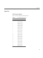
DVIO Connector Signals
Table 1-1 shows the signals on the DVIO connector.
Table 1-1
DVP Transmitter (DVIO) Pinouts
Pin No.
Pin Name
MTG1
CHASSIS_GND
1
RED_OUT_H[11]
2
RED_OUT_L[11]
3
RED_OUT_H[10]
4
RED_OUT_L[10]
5
RED_OUT_H[9]
6
RED_OUT_L[9]
7
RED_OUT_H[8]
8
RED_OUT_L[8]
9
RED_OUT_H[7]
10
RED_OUT_L[7]
11
RED_OUT_H[6]
12
RED_OUT_L[6]
13
RED_OUT_H[5]
14
RED_OUT_L[5]
15
RED_OUT_H[4]
16
RED_OUT_L[4]
17
RED_OUT_H[3]
18
RED_OUT_L[3]
13
Chapter 1: DVP Specifications
Table 1-1 (continued)
14
DVP Transmitter (DVIO) Pinouts
Pin No.
Pin Name
19
RED_OUT_H[2]
20
RED_OUT_L[2]
21
RED_OUT_H[1]
22
RED_OUT_L[1]
23
RED_OUT_H[0]
24
RED_OUT_L[0]
25
PWR_GOOD
26
GND
27
GREEN_OUT_H[11]
28
GREEN_OUT_L[11]
29
GREEN_OUT_H[10
30
GREEN_OUT_L[10]
31
GREEN_OUT_H[9]
32
GREEN_OUT_L[9]
33
GREEN_OUT_H[8]
34
GREEN_OUT_L[8]
35
GREEN_OUT_H[7]
36
GREEN_OUT_L[7]
37
GREEN_OUT_H[6]
38
GREEN_OUT_L[6]
39
GREEN_OUT_H[5]
40
GREEN_OUT_L[5]
41
GREEN_OUT_H[4]
42
GREEN_OUT_L[4]
Signal Lists
Table 1-1 (continued)
DVP Transmitter (DVIO) Pinouts
Pin No.
Pin Name
43
GREEN_OUT_H[3]
44
GREEN_OUT_L[3]
45
GREEN_OUT_H[2]
46
GREEN_OUT_L[2]
47
GREEN_OUT_H[1]
48
GREEN_OUT_L[1]
49
GREEN_OUT_H[0]
50
GREEN_OUT_L[0]
51
BLUE_OUT_H[11]
52
BLUE_OUT_L[11]
53
BLUE_OUT_H[10]
54
BLUE_OUT_L[10]
55
BLUE_OUT_H[9]
56
BLUE_OUT_L[9]
57
BLUE_OUT_H[8]
58
BLUE_OUT_L[8]
59
BLUE_OUT_H[7]
60
BLUE_OUT_L[7]
61
BLUE_OUT_H[6]
62
BLUE_OUT_L[6]
63
BLUE_OUT_H[5]
64
BLUE_OUT_L[5]
65
BLUE_OUT_H[4]
66
BLUE_OUT_L[4]
15
Chapter 1: DVP Specifications
Table 1-1 (continued)
16
DVP Transmitter (DVIO) Pinouts
Pin No.
Pin Name
67
BLUE_OUT_H[3]
68
BLUE_OUT_L[3]
69
BLUE_OUT_H[2]
70
BLUE_OUT_L[2]
71
BLUE_OUT_H[1]
72
BLUE_OUT_L[1]
73
BLUE_OUT_H[0]
74
BLUE_OUT_L[0]
75
I2C_DATA
76
I2C_DATA_GND
77
I2C_CLK
78
I2C_CLK_GND
79
CBLANK_H
80
CBLANK_L
81
CSYNC_H
82
CSYNC_L
83
VSYNC_H
84
VSYNC_L
85
FIELD_H
86
FIELD_L
87
VOC_SWAP_H
88
VOC_SWAP_L
89
HMUX_SEL1_H
90
HMUX_SEL1_L
Signal Lists
Table 1-1 (continued)
DVP Transmitter (DVIO) Pinouts
Pin No.
Pin Name
91
HMUX_SEL0_H
92
HMUX_SEL0_L
93
GND
94
GND
95
CLK_2_H
96
CLK_2_L
97
GND
98
GND
99
CLK_2_QUAD_H
100
CLK_2_QUAD_L
MTG2
CHASSIS_GND
17
Chapter 1: DVP Specifications
Receiver Connector Signals
Because of the construction of the external cable, the pinout is reversed on the receiver
connector. Table 1-2 shows the pinout of the receiver connector.
Table 1-2
18
DVP Receiver Pinouts
Pin No.
Pin Name
MTG1
CHASSIS_GND
1
CLK_2_QUAD_L
2
CLK_2_QUAD_H
3
GND
4
GND
5
CLK_2_L
6
CLK_2_H
7
GND
8
GND
9
HMUX_SEL0_L
10
HMUX_SEL0_H
11
HMUX_SEL1_L
12
HMUX_SEL1_H
13
VOC_SWAP_L
14
VOC_SWAP_H
15
FIELD_L
16
FIELD_H
17
VSYNC_L
18
VSYNC_H
19
CSYNC_L
20
CSYNC_H
Signal Lists
Table 1-2 (continued)
DVP Receiver Pinouts
Pin No.
Pin Name
21
CBLANK_L
22
CBLANK_H
23
I2C_CLK_GND
24
I2C_CLK
25
I2C_DATA_GND
26
I2C_DATA
27
BLUE_OUT_L[0]
28
BLUE_OUT_H[0]
29
BLUE_OUT_L[1]
30
BLUE_OUT_H[1]
31
BLUE_OUT_L[2]
32
BLUE_OUT_H[2]
33
BLUE_OUT_L[3]
34
BLUE_OUT_H[3]
35
BLUE_OUT_L[4]
36
BLUE_OUT_H[4]
37
BLUE_OUT_L[5]
38
BLUE_OUT_H[5]
39
BLUE_OUT_L[6]
40
BLUE_OUT_H[6]
41
BLUE_OUT_L[7]
42
BLUE_OUT_H[7]
43
BLUE_OUT_L[8]
44
BLUE_OUT_H[8]
19
Chapter 1: DVP Specifications
Table 1-2 (continued)
20
DVP Receiver Pinouts
Pin No.
Pin Name
45
BLUE_OUT_L[9]
46
BLUE_OUT_H[9]
47
BLUE_OUT_L[10]
48
BLUE_OUT_H[10]
49
BLUE_OUT_L[11]
50
BLUE_OUT_H[11]
51
GREEN_OUT_L[0]
52
GREEN_OUT_H[0]
53
GREEN_OUT_L[1]
54
GREEN_OUT_H[1]
55
GREEN_OUT_L[2]
56
GREEN_OUT_H[2]
57
GREEN_OUT_L[3]
58
GREEN_OUT_H[3]
59
GREEN_OUT_L[4]
60
GREEN_OUT_H[4]
61
GREEN_OUT_L[5]
62
GREEN_OUT_H[5]
63
GREEN_OUT_L[6]
64
GREEN_OUT_H[6]
65
GREEN_OUT_L[7]
66
GREEN_OUT_H[7]
67
GREEN_OUT_L[8]
68
GREEN_OUT_H[8]
Signal Lists
Table 1-2 (continued)
DVP Receiver Pinouts
Pin No.
Pin Name
69
GREEN_OUT_L[9]
70
GREEN_OUT_H[9]
71
GREEN_OUT_L[10]
72
GREEN_OUT_H[10]
73
GREEN_OUT_L[11]
74
GREEN_OUT_H[11]
75
GND
76
PWR_GOOD
77
RED_OUT_L[0]
78
RED_OUT_H[0]
79
RED_OUT_L[1]
80
RED_OUT_H[1]
81
RED_OUT_L[2]
82
RED_OUT_H[2]
83
RED_OUT_L[3]
84
RED_OUT_H[3]
85
RED_OUT_L[4]
86
RED_OUT_H[4]
87
RED_OUT_L[5]
88
RED_OUT_H[5]
89
RED_OUT_L[6]
90
RED_OUT_H[6]
91
RED_OUT_L[7]
92
RED_OUT_H[7]
21
Chapter 1: DVP Specifications
Table 1-2 (continued)
22
DVP Receiver Pinouts
Pin No.
Pin Name
93
RED_OUT_L[8]
94
RED_OUT_H[8]
95
RED_OUT_L[9]
96
RED_OUT_H[9]
97
RED_OUT_L[10]
98
RED_OUT_H[10]
99
RED_OUT_L[11]
100
RED_OUT_H[11]
MTG2
CHASSIS_GND
Tell Us About This Manual
As a user of Silicon Graphics products, you can help us to better understand your needs
and to improve the quality of our documentation.
Any information that you provide will be useful. Here is a list of suggested topics:
•
General impression of the document
•
Omission of material that you expected to find
•
Technical errors
•
Relevance of the material to the job you had to do
•
Quality of the printing and binding
Please send the title and part number of the document with your comments. The part
number for this document is 007-3594-001.
Thank you!
Three Ways to Reach Us
•
To send your comments by electronic mail, use either of these addresses:
–
On the Internet: [email protected]
–
For UUCP mail (through any backbone site): [your_site]!sgi!techpubs
•
To fax your comments (or annotated copies of manual pages), use this
fax number: 650-965-0964
•
To send your comments by traditional mail, use this address:
Technical Publications
Silicon Graphics, Inc.
2011 North Shoreline Boulevard, M/S 535
Mountain View, California 94043-1389


![FHC3310(A) - FAST CORPORATION[株式会社ファースト]](http://vs1.manualzilla.com/store/data/006571158_2-3d1f6b645c9e23bdec6eaf846b016daf-150x150.png)