1
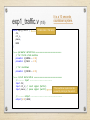
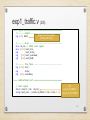
My First FPGA for
Altera DE2-115 Board
數位電路實驗
TA: 吳柏辰
Author: Trumen
Outline
•
•
•
•
•
•
•
Complete Your Verilog Design
Assign The Device
Add a PLL Megafunction
Assign the Pins
Create a Default TimeQuest SDC File
Compile and Verify Your Design
Configuring the Cyclone IV E FPGA
2
Complete Your Verilog
Design
3
exp1_traffic.v (1/5)
module exp1_traffic (
clk,
rst_n,
pause,
HEX0
);
It is a 10 seconds
countdown system.
module name = file name
//==== parameter definition ===============================
// for finite state machine
parameter S_NORMAL = 1'd0;
parameter S_PAUSE = 1'd1;
// for countdown
parameter C_PERIOD = 4'd9;
//==== in/out declaration ==================================
//-------- input --------------------------input clk;
input rst_n; // reset signal (button)
The countdown system can be
input pause; // pause signal (switch)
paused by turning on the switch.
//-------- output -------------------------------------output [6:0] HEX0;
4
exp1_traffic.v (2/5)
//==== reg/wire declaration ================================
//-------- output -------------------------------------Output should be register.
reg [6:0] HEX0;
(Critical path issue)
//-------- wires --------------------------------------wire clk_16; // 16MHz clock signal
wire [23:0] next_clks;
reg
next_state;
reg
[3:0] next_countdown;
reg
[6:0] next_HEX0;
//-------reg [23:0]
reg
reg [3:0]
flip-flops ---------------------------------clks;
state;
countdown;
//==== combinational part ==================================
// clock signal
clksrc clksrc1 (clk, clk_16);
assign next_clks = (state==S_PAUSE)? clks: clks+24'd1;
PLL
(input: clk, 50MHz)
(output: clk_16, 16MHz)
5
exp1_traffic.v (3/5)
// finite state machine (state)
always@(*) begin
case(state)
S_NORMAL: begin
if(pause==1) next_state = S_PAUSE;
else next_state = S_NORMAL;
end
S_PAUSE: begin
if(pause==1) next_state = S_PAUSE;
else next_state = S_NORMAL;
end
endcase
end
Cover every possible branch of
every if or case to avoid latches.
// countdown
always@(*) begin
if(clks[23]==1'b1 && next_clks[23]==1'b0)
1Hz
next_countdown = (countdown==0)? C_PERIOD: countdown-4'd1;
else
next_countdown = countdown;
end
Cover
every
possible
branch.
6
exp1_traffic.v (4/5)
// 7-segment Displays
always@(*) begin
case(countdown)
7'd0: next_HEX0 = 7'b1000000;
7'd1: next_HEX0 = 7'b1111001;
7'd2: next_HEX0 = 7'b0100100;
7'd3: next_HEX0 = 7'b0110000;
7'd4: next_HEX0 = 7'b0011001;
7'd5: next_HEX0 = 7'b0010010;
7'd6: next_HEX0 = 7'b0000010;
7'd7: next_HEX0 = 7'b1111000;
7'd8: next_HEX0 = 7'b0000000;
7'd9: next_HEX0 = 7'b0010000;
default: next_HEX0 = 7'b1111111;
endcase
end
Cover every possible branch.
7
exp1_traffic.v (5/5)
//==== sequential part =====================================
always@( posedge clk_16 or negedge rst_n ) begin
if( rst_n==0 ) begin
clks
<= 24'd0;
state
<= S_NORMAL;
countdown <= C_PERIOD;
HEX0
<= 7'h7f;
end
else begin
clks
<= next_clks;
state
<= next_state;
countdown <= next_countdown;
HEX0
<= next_HEX0;
end
end
endmodule
8
Notepad++ (1/5)
1
2
3
Highlight
9
Notepad++ (2/5)
1
2
3
4
5
10
Notepad++ (3/5)
Column Mode Editing
1. Alt + Mouse dragging
2. Alt + Shift + Arrow keys
11
Notepad++ (4/5)
1
4
3
2
12
Notepad++ (5/5)
13
Assign The Device
14
Introduction to FPGA (1/3)
• A field-programmable gate array (FPGA) is an
integrated circuit designed to be configured by
a designer after manufacturing.
• An electronic device is said to be fieldprogrammable if it can be modified "in the field".
15
Introduction to FPGA (2/3)
• FPGAs contain programmable logic
components called "logic blocks", and a
hierarchy of reconfigurable interconnects that
allow the blocks to be "wired together".
• FPGAs can be used to implement any logical
function that an ASIC could perform.
16
Introduction to FPGA (3/3)
• Xilinx and Altera are the current FPGA market
leaders and long-time industry rivals.
• Both Xilinx and Altera provide free Windows and
Linux design software (ISE and Quartus)
17
Altera's Main FPGA Products
• Stratix series FPGAs are the largest, highest
bandwidth devices, with up to 1.1 million logic
elements.
• Cyclone series FPGAs and are the company's
lowest cost, lowest power FPGAs.
• Arria series FPGAs are between the two
device families above.
18
Altera® Development Kits
http://www.altera.com/products/devkits/kit-dev_platforms.jsp
• Development kits include software, reference
designs, cables, and programming hardware
(development board).
19
Installed The USB-Blaster driver
(1/3)
• Plug in the 12-volt adapter to provide power to the
board.
• Use the USB cable to connect the leftmost USB
connector (the one closest to the power switch) on the
DE2-115 board to a USB port on a computer that runs
the Quartus II software.
• Turn on the power switch on the DE2-115 board.
USB cable
12-volt adapter
power
20
Installed The USB-Blaster driver
(2/3)
• The computer will recognize the new hardware
connected to its USB port.
• But it will be unable to proceed if it does not have
the required driver already installed.
• The DE2-115 board is programmed by using Altera
USB-Blaster mechanism. If the USB-Blaster driver
is not already installed, the New Hardware Wizard
will appear.
• Next →Next →… →OK!
21
Installed The USB-Blaster driver
(3/3)
• If the New Hardware Wizard does not appear,
check the website below ⇓
http://www.altera.com/download/drivers/usb-blaster/dri-usb-blaster-vista.html
22
Setup Licensing (1/2)
1
2
23
Setup Licensing (2/2)
Only for IP 140.112.*.*
1
Make sure these items appear, and
now you can compile your design.
24
2
Create a New Project
1
2
3
25
1
2
same as (top-level) file name
3
26
1
2
3
27
1
2
for DE2-115
3
28
29
3
2
1
4
30
1
2
3
31
Add a PLL
Megafunction
32
Using Quartus Add a PLL
Megafunction
• A PLL uses the on-board oscillator (50 MHz
for DE2-115 Board) to create a constant clock
frequency as the input to the counter.
• To create the clock source, you will add a prebuilt library of parameterized modules (LPM)
megafunction named ALTPLL.
33
1
2
34
1
35
1
36
2
1
3
37
1
for DE2-115
2
3
38
Uncheck all the options
1
39
1
40
1
41
1
42
1
43
2
1
2
44
Assign the Pins
45
Assign the Pins
• Before making pin assignments…
1
2
3
46
1
2
47
2
1
for DE2-115
Type “M23”, then push Enter
48
Now, you are finished creating your Quartus II design!
Create a Default
TimeQuest SDC File
49
Create a Default TimeQuest
SDC File
• Timing settings are critically important for a
successful design.
• For this tutorial you will create a basic
Synopsys Design Constraints File (.sdc) that
the Quartus II TimeQuest Timing Analyzer
uses during design compilation.
• For more complex designs, you will need to
consider the timing requirements more
carefully.
50
1
2
51
1
2
52
create_clock -period 20 [get_ports clk]
create_clock -period 62.5 -name clk_16
derive_pll_clocks
derive_clock_uncertainty
set_input_delay 0 -clock clk_16 [all_inputs]
set_output_delay 0 -clock clk_16 [all_outputs]
If we do not use pll:
create_clock -period 20 [get_ports clk]
derive_clock_uncertainty
set_input_delay 0 -clock clk [all_inputs]
set_output_delay 0 -clock clk [all_outputs]
53
1
2
4
3
54
Compile and Verify
Your Design
55
Compile Your Design
• After creating your design you must compile it.
• Compilation converts the design into a
bitstream that can be downloaded into the
FPGA.
• The most important output of compilation is an
SRAM Object File (.sof), which you use to
program the device.
56
1
57
Compilation Report
• Make sure there is no error.
58
Program the FPGA Device
• After compiling and verifying your design you
are ready to program the FPGA on the
development board.
• You download the SOF you just created into
the FPGA using the USB-Blaster circuitry on
the board.
USB cable
12-volt adapter
power
59
1
2
60
1
61
1
2
62
1
63
~~Finish~~
64
Demo Video
• 10 seconds countdown system
65
Configuring the
Cyclone IV E FPGA
66
Configuring the FPGA
• JTAG programming
In this method of programming, named after the IEEE standards Joint Test
Action Group, the configuration bit stream is downloaded directly into the
Cyclone IV E FPGA. The FPGA will retain this configuration as long as
power is applied to the board; the configuration information will be lost
when the power is turned off.
• AS programming
In this method, called Active Serial programming, the configuration bit
stream is downloaded into the Altera EPCS64 serial configuration device. It
provides non-volatile storage of the bit stream, so that the information is
retained even when the power supply to the DE2-115 board is turned off.
When the board's power is turned on, the configuration data in the EPCS64
device is automatically loaded into the Cyclone IV E FPGA.
67
JTAG Chain (1/2)
• To use JTAG interface for configuring FPGA
device, the JTAG chain on DE2-115 must form
a close loop that allows Quartus II programmer
to detect FPGA device.
68
JTAG Chain (2/2)
• Shorting pin1 and pin2 on JP3 can disable the JTAG signals
on HSMC connector that will form a close JTAG loop chain on
DE2-115 board. Thus, only the on board FPGA device
(Cyclone IV E) will be detected by Quartus II programmer.
69
Configuring the FPGA in
JTAG Mode (1/2)
• This figure illustrates the JTAG configuration
setup.
70
Configuring the FPGA in
JTAG Mode (2/2)
1. Ensure that power is applied to the DE2-115 board.
2. Configure the JTAG programming circuit by setting the
RUN/PROG slide switch (SW19) to the RUN position.
3. Connect the supplied USB cable to the USB Blaster
port on the DE2-115 board.
4. The FPGA can now be programmed by using the
Quartus II Programmer to select a configuration bit
stream file with the .sof filename extension.
71
Configuring the EPCS64 in
AS Mode (1/2)
• This figure illustrates the AS configuration
setup.
72
Configuring the EPCS64 in
AS Mode (2/2)
1.
2.
Ensure that power is applied to the DE2-115 board.
3.
Configure the JTAG programming circuit by setting the
RUN/PROG slide switch (SW19) to the PROG position.
4.
The EPCS64 chip can now be programmed by using the
Quartus II Programmer to select a configuration bit stream file
with the .pof filename extension.
5.
Once the programming operation is finished, set the
RUN/PROG slide switch back to the RUN position and then
reset the board by turning the power switch off and back on; this
action causes the new configuration data in the EPCS64 device
to be loaded into the FPGA chip.
Connect the supplied USB cable to the USB Blaster port on the
DE2-115 board.
73
Programmer Object File
• Programmer Object File is a binary file (with
the extension .pof) containing the data for
programming a configuration device.
• A Programmer Object File for a configuration
device can be generated by the Convert
Programming Files command (File menu).
74
1
for DE2-115
3
7
4
8
2
5
6
9
75
1
2
3
4
5
76
2
1
77
~~Finish~~
78
The End.
Any question?
Reference
1. http://en.wikipedia.org/wiki/Fieldprogrammable_gate_array
2. "My First FPGA for Altera DE2-115 Board" by
Terasic Technologies Inc.
3. "DE2-115 User Manual" by Terasic
Technologies Inc.
80