1
i
“I hereby declare that I have read this thesis and in
my opinion this thesis is sufficient in terms of scope and
quality for the award of the degree of Bachelor’s Degree of
Electrical Engineering (Microelectronic).”
Signature
: ………………………………….…
Name of Supervisor : Dr. Ooi Chia Yee
Date
: ………………………………….…
ii
A DESIGN OF PROCESSOR CORE
FOR RFID IMPLEMENTATION
AMIR ZAKI BIN AMRAN
A report submitted in partial fulfillment of the
requirements for the award of the degree of
Bachelor of Electrical Engineering (Microelectronic)
Faculty of Electrical Engineering
Universiti Teknologi Malaysia
MAY 2009
iii
Specially dedicated to
my beloved parents
Amran Bin Jamaludin, Norzakiah Binti Ahmad
and all my friends
for their never ending support
iv
ACKNOWLEDGEMENTS
I would like to thank my supervisor, Dr Ooi Chia Yee, for her help and
guidance for the past two semesters. It is not easy to supervise a topic proposed by a
student, but she took the task and has become a steady source of support throughout
the project. Her reasoning has always been beneficial to this project, and I am
thankful to her.
My appreciation also goes to my family who has been supporting me all over
these years. I am grateful for their encouragement, love, steady patience, prayers and
financial supports that they had given to me and have faith in me.
I also would like to offer my special thanks to my colleagues, Logeish Al Raj
and Muhammad Juffri for their advices and giving a helping hand which greatly
making this project and thesis a reality.
v
ABSTRACT
The design of processor core on a FPGA board nowadays is not a rocket
science and it is very popular due to their advantages which ASIC does not have.
This project is mainly on designing the FPGA-based processor core using Altera
DE2 FPGA Cyclone II device. This work will only cover the complete methods of
designing the instruction set and its architecture of the processor. Meanwhile, the
hardware design language of this design is written in Verilog using Altera Quartus II
8.1. As an application of this FPGA-based processor core, this design was intended
to control a RFID Reader. The processor core produced a good result on the
instruction designed where all of it follows all the desired operation. It can be
concluded that the processor core design is a simple but reliable and as a great
alternative to processor designer where design requirements always change.
vi
ABSTRAK
Rekabentuk teras pemproses di atas FPGA sekarang ini bukanlah sesuatu yang luar
biasa lagi tambahan pula ia sangat popular kerana kelebihan dan fleksibilitasi di
mana ASIC tiada kelebihan tersebut. Projek ini hanya meliputi rekabentuk sebuah
pemproses di pengkalan FPGA mengunakan Altera DE2 FPGA Cyclone II. Kerja ini
hanya menyentuh cara merekabentuk sepenuhnya sebuah teras pemproses
berdasarkan suruhan data yang telah siap dibina. Sementara itu, Bahasa rekabentuk
perkakas projek ini di tulis di dalam bahasa Verilog mengunakan Altera Quartus II
8.1. Sebagai aplikasi teras pemproses ini, rekabentuk ini akan di gunakan pada
Pembaca RFID . Teras pemproses ini telah menghasilkan keputusan yang baik
berdasarkan suruhan data yang direkabentuk dahulu malah memenuhi semua
kehendak suruhan data dengan baik. Dengan ini, dapat disimpulkan bawah teras
pemproses ini adalah mudah tetapi sangat boleh dipercayai dan menjadi alternatif
yang terbaik utk perekabentuk pemproses yang selalu mengubah kehendak
rekabentuk.
vii
TABLE OF CONTENTS
CHAPTER
TITLE
PAGE
DECLARATION OF THESIS
i
ACKNOWLEDGEMENTS
iv
ABSTRACT
v
ABSTRAK
vi
TABLE OF CONTENTS
vii
LIST OF TABLES
xi
LIST OF FIGURES
xii
LIST OF ABBREVIATIONS
xiv
LIST OF APPENDICES
xvi
CHAPTER 1 INTRODUCTION
1.1
Background
1
1.2
Basis of Project
3
1.3
Problem Statement
3
1.4
Problem Objective
3
1.5
Scope of Project
4
viii
CHAPTER 2 LITERATURE REVIEW
2.1
Discrete Processor
5
2.2
Hard Processor Core
5
2.3
Soft Processor Core
7
2.4
Customizable Processor Core
7
2.5
Board-level Configurability
8
2.6
Multiple Processors
9
2.7
Complex Instruction Set Computer (CISC)
10
2.8
Reduced Instruction Set Computer (RISC)
11
CHAPTER 3 PROJECT METHODOLOGY
3.1
Intoduction
12
3.2
Design Flow
13
3.3
Altera Quartus
15
3.4
Verilog-HDL
16
3.5
Altera DE2 Board
16
CHAPTER 4 INSTRUCTION SET ARCHITECTURE
4.1
Central Processing Unit
18
4.2
Instruction Set
20
CHAPTER 5 PROCESSOR CORE DESIGN
5.1
Overview
23
ix
5.2
Architecture Overview
24
5.3
Program Counter
25
5.4
Instruction Memory
26
5.5
Decoder
27
5.6
General Purpose Register
28
5.7
Operand Selection
29
5.8
Arithmetic Logic Unit and Conditional Codes
30
5.9
ROM Register
33
5.10
PORT
34
5.11
Universal Asynchronous Receiver Transmitter and Shift Register 34
CHAPTER 6 RESULTS AND DISCUSSIONS
6.1
6.2
Results
6.1.1
Processor Core Simulation
37
6.1.2
Implementation of RFID on UART
41
Discussions
6.2.1
Instruction Set
43
6.2.2
Memory Initialization File
44
6.2.3
Negedge Clock
44
6.2.4
The RFID and Receiver Design System
45
x
CHAPTER 7 CONCLUSION AND RECOMMENDATIONS
7.1
Recommendation for Future Works
46
7.2
Conclusion
47
REFERENCES
APPENDICES
xi
LIST OF TABLES
TABLE NO TITLE
PAGE
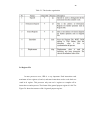
Table 4.1
Six instruction formats
20
Table 4.2
Designed Instructions
22
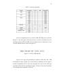
Table 5.1
The decoder organization
28
Table 5.2
Instruction grouping
31
xii
LIST OF FIGURES
FIGURE NO TITLE
PAGE
Figure 1.1: Basis block diagram of the proposed system
3
Figure 3.1: Project Methodology Flow
12
Figure 3.2: Processor Core Design Flow
13
Figure 3.3: Quartus II Design Flow
15
Figure 3.4: Altera DE2 FPGA Board
16
Figure 4.1: Processor Flow
18
Figure 5.1: Architecture overview
24
Figure 5.2: The processor four stages RISC processor flow
25
Figure 5.3: Instruction hexcode
27
Figure 5.4: GPR Structure
29
Figure 5.5: The GPR Write Enable Multiplexer
29
Figure 5.6: The Operand Selection
30
Figure 5.7: ALU for ADD and SUB
31
Figure 5.8: The multiplexing stages
32
Figure 5.9: Conditional Codes
32
Figure 5.10: Conditional Codes Vector
33
xiii
Figure 5.11: Portion of Program Control Coding
34
Figure 5.12: TTL/CMOS Serial Logic Waveform
35
Figure 5.13: The Asynchronous Receiver I/O
35
Figure 5.14: Parameter Values
36
Figure 6.1: Final.txt control program
38
Figure 6.2: Timing simulation of Final.txt control program
38
Figure 6.3: Last.txt control program
39
Figure 6.4: Timing simulation of Final.txt control program
40
Figure 6.5: VB6 RFID card verification
41
Figure 6.6: Output waveform of RxD RFID Reader
42
Figure 6.7: Flow of RFID card serial number verification on DE2 board
42
Figure 6.8: Shifted and converted data of 12 bytes RFID card serial number
43
Figure 6.9: Negedge clock solve the timing problem for read and write
45
xiv
LIST OF ABBREVIATIONS
ASIC – Application Specific Integrated Circuit
ALU – Arithmetic Logic Unit
CPU – Central Processing Unit
CISC – Complex Instruction Set Computer
DDR - Double Data Rate
DMIPS – Dhrystone Million Instructions Per Second
FPGA - Field Programmable Gate Array
GPIO - General Purpose Input/Output
GPR - General Purpose Registers
HDL – Hardware Design Language
IC – Integrated Circuit
IR – Instruction Register
MIF - Memory Initialization File
OTS – off-the-shelf
PC – Program Counter
PCI - Peripheral Component Interconnect
PIC – Peripheral Interface Controller
xv
RAM – Random Access Memory
RFID – Radio Frequency Identification
RISC – Reduced Instruction Set Computer
ROM – Read Only Memory
RTL - Register Transfer Level
SDRAM - Synchronous Dynamic Random Access Memory
SRAM - Synchronous Dynamic Random Access Memory
SoPC - System on a Programmable Chip
UART - Universal Asynchronous Receiver Transmitter
USART - Universal Synchronous Asynchronous Receiver Transmitter
xvi
LIST OF APPENDICES
APPENDIX A
Processor Core Verilog Module
APPENDIX B
Instruction Memory Verilog Module
APPENDIX C
Decoder Verilog Module
APPENDIX D
Register File Verilog Module
APPENDIX E
ALU and Conditional Codes Verilog Module
APPENDIX F
ROM Register Verilog Module
APPENDIX G
Port Verilog Module
APPENDIX H
Asynchoronous Receiver
APPENDIX I
Control Program to Test (Assembly Language)
APPENDIX J
Control Program Hexcode (Machine Language)
APPENDIX K
Timing Simulation of Control Program
APPENDIX L
Twelve Stages of Shift Register
xvii
APPENDIX M
Converter ASCII to 7 Segment
APPENDIX N
Asynchronous Receiver System to catch 12 data bytes
APPENDIX O
Visual Basic for RFID card verification
1
CHAPTER 1
INTRODUCTION
This section gives an overview about the project such as the background and
the basic idea of the project.
1.1
Background
Soft-core processors on field-programmable gate array (FPGA) chips are
becoming an increasingly popular software implementation platform, due to their
custom logics. A soft-core processor is synthesized onto the FPGA’s fabric. On the
FPGA device, soft-core processors have the advantages of utilizing standard mass
produced and hence lower-cost FPGA parts and enabling a custom number of
microprocessors per FPGA – over 100 soft-core processors can fit on modern highend FPGAs as described by David Sheldon, Rakesh Kumar, Roman Lysecky, Frank
Vahid and Dean Tullsen (2006).
FPGA soft-core processors have the instruction sets, arithmetic-logic units,
register files and other features specifically tailored to efficiently use FPGA
resources and can be reconfigured. The re-configurability of FPGA gives FPGA
designers an advantage over ASIC designers. They can tune, develop, debugging and
testing the processor configuration much faster and more accurate using simulation
2
to enhance the processor. The flexibility of FPGAs provides unique opportunities in
FPGA processor design.
A FPGA designer can change their FPGA processor
configuration whenever design requirements change. An ASIC designer cannot
change their ASIC processor configuration without creating a new ASIC.
Jari Nurmi (2007) explained in his book the challenge of FPGA processor
design is to accommodate the different relative performance of FPGA resources like
logic elements, RAMs, multipliers and routing because not all FPGA manufacturers
produced the same chip for their FPGA and there is wide range of FPGA chips
nowadays. However, soft-core processor has the disadvantages of reduced processor
performance, higher power consumption and larger size.
Processor design is not rocket science and is no longer the exclusive realm of
elite designers in large companies. Jan Gray (2000) said FPGAs are now large and
fast enough for many embedded systems, with processor core speed in the 33-100
MHz range. HDL synthesis tools and FPGA place-and-route tools are now fast,
inexpensive and open source software tools help to bridge the compiler chasm.
1.2
Basis of Project
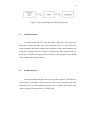
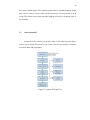
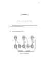
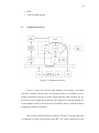
The idea behind this project is to design a processor core that will be
implemented on FPGA. Then with dedicated pins as PORT, the processor core can
interact with peripherals such as RFID reader.
3
Figure 1.1: Basis block diagram of the proposed system
1.3
Problem Statement
A microcontroller like PIC from Microchip usually uses 40% of the total
instructions, making the other 60% of the instruction since it is not used for the
control program coded. More complex microcontrollers require more transistors and
design time, making them more expensive to manufacture. With proposed soft-core
processor, we could now use the processor to run the control program such as RFID
reader with the reduced instruction set.
1.4
Problem Objective
From the problem statement, I have come up with an objective. The objective
of this project is to design a soft-core processor with a set of instructions and a few
peripherals to act as a microcontroller processor core on a FPGA board where it can
control a program for targeted device, a RFID reader.
4
1.5
Scope of Project
The aim of the project is to design a soft-core processor that can run control
program for the RFID reader. The soft-core processor must be able to fit into a
targeted FPGA device, which is the Altera Cyclone II 2C35, provided on Altera DE2
Education Board. The HDL used to write the processor core is Verilog HDL.
5
CHAPTER 2
LITERATURE REVIEW
This chapter consists of compilation of researches, information, articles, and
theories done on specific parts or components or system that make up the whole
project. This chapter highlights the basic concepts and fundamental theories of each
chosen parts.
2.1
Discrete Processor
A discrete off-the-shelf (OTS) microprocessor solution is the traditional
approach that designers have used. These types of processors are available from a
multitude of vendors and have a wide range of features. A discrete microprocessor is
implemented as an ASIC with a specific peripheral set along with the processor core
[4].
6
Selecting a discrete processor that meets the application’s cost and functional
requirements can be a time consuming process. There are times, however, where an
OTS processor solution will not meet those requirements. An example would be an
application that requires custom logic or a significant amount of peripheral
functionality that is not available in a discrete solution. In this case, the logical place
to look is at a processor and peripheral set that can be tailored to the application and
included with the custom logic that is needed for the application [4].
2.2
Hard Processor core
A hard processor core is different from Discrete Processor and Soft-core
Processor because it has dedicated silicon on the FPGA. The dedicated silicon allows
it to operate with a core frequency and have a DMIPS rating similar to that of a
discrete microprocessor. The benefit of a hard-core provides is that it exists in an
environment where the surrounding peripherals can be customized for the
application.
The hard processor core does not provide the ability to adjust the core for the
application, nor does it allow for the flexibility of adding a processor to an existing
design or an additional processor for more processing capabilities. In addition, only
specific FPGAs will have the option of having a hard-core; therefore, the choice of
vendors and FPGAs are limited [4].
7
2.3 Soft Processor Core
A soft-core processor solution is one that is implemented entirely in the logic
primitives of an FPGA. Because of this implementation, the processor will not
operate at the speeds or have the performance of a hard-core or a discrete solution. In
many embedded applications, the high performance achieved by the previous two
processing options is not required, and performance can be traded for expanded
functionality and flexibility.
Soft-core processors may be appropriate for a simple system, where the only
functionalities are the manipulation of GPIO (General Purpose Input/Output).
Moreover, they may also fit a complex system, where an operating system is
incorporated and interfaces include Ethernet, PCI (Peripheral Component
Interconnect), and DDR SDRAM (Double Data Rate Synchronous Dynamic Random
Access Memory), and any other custom IP [4].
2.4 Customizable Processor Core
A soft-core processor also offers the flexibility of tailoring the core itself for
the application. There are a few different levels of how this can be accomplished,
depending on the vendor. On one level, things such as cache size can be easily
adjusted [4].
Most toolsets offer the option to configure different cache sizes to suit what
the application requires. A vendor may also offer different versions of the processor
that have varying levels of performance. In this case, a higher performance version of
8
the processor would have more pipeline stages, increasing throughput. This offers
more flexibility to the user [4].
It is important to note that along with a performance increase there will also
be an increase in the amount of logic elements that the processor will consume or the
amount of memory that the processor will consume, leaving fewer resources for
peripherals and custom logic [4].
On a higher level of complexity, a designer can take the source code for the
processor core and modify it to meet the needs of the application. Being able to
modify the source code to the actual processor core offers the greatest of flexibility
that one can obtain. Not all vendors will offer source code for their soft-core
processor solution; sometimes the core is encrypted [4].
2.5
Board-level Configurability
Using a System on a Programmable Chip (SoPC) solution also offers
flexibility external to the FPGA. A discrete microprocessor solution has a fixed
pinout, sometimes making routing difficult. Since an SoPC exists in an FPGA, the
pinout is flexible. This gives the board designer almost complete freedom with
component placement, provided the FPGA still meets the timing constraints with the
final pin placement [4].
Another benefit is that there are more GPIO available in an SoPC solution
compared to a discrete microprocessor. The FPGA can be scaled up in size if
necessary to accommodate any additional IO that is needed, whereas an ASIC
solution restricts the IO use to what is on the IC; no expansion is available [4].
9
An SoPC solution also provides more options with prototyping possible
solutions without a significant change to the hardware. This benefit in flexibility is
mostly realizable when using hardware provided in the form of a development kit
from the vendor [4].
2.6
Multiple Processors
More complex embedded systems could benefit from the use of multiple
processors to decrease the execution time by executing tasks in parallel. Soft-core
processors and their accompanying toolsets can make the task of implementing
multiple processor cores that interface with a common set of peripherals much more
feasible and appealing to designers.
Also, there are not any additional BOM costs for adding a soft-core processor
in an FPGA as long as there is enough space in the FPGA for the implementation.
The only restriction on how many processors can be in an SoPC is the logic available
in the FPGA. Therefore, when using an SoPC in a design where more parallel
processing is required, adding another soft-core processor is a viable solution that
does not impact hardware significantly.
For the most part, the soft-core design process is not too different from any
other embedded development. Perhaps the only major differences are additional roles
that may not be found in other development approaches and the stress on continuous
communication between the different designer roles to maximize the use of
additional features that may be available.
10
2.7
Complex Instruction Set Computer (CISC)
Computers had only a small number of instructions and used simple
instruction sets, forced mainly by the need to minimize the hardware used to
implement them. As digital hardware become cheaper, computer instructions tended
to increase both in number and complexity. These computers also employ a variety
of data types and a large number of addressing modes. A computer with a large
number of instructions, are known as complex instruction set computer, abbreviated
CISC. Major characteristics of CISC architecture are [6]:
A large number of instructions – typically from 100 to 250 instructions [6].
Some instructions that perform specialized tasks and are used infrequently
[6].
A large variety of addressing modes – typically from 5 to 20 different modes
[6].
2.8
Variable-length instruction formats [6].
Instructions that manipulate operands in memory [6].
Reduced Instruction Set Computer (RISC)
The concept was developed by John Cocke of IBM Research during 1974.
His argument was based upon the notion that a computer uses only 20% of the
instructions, making the other 80% superfluous to requirement [9]. A processor
based upon this concept would use few instructions, which would require fewer
transistors and make them cheaper to manufacture. By reducing the number of
transistor and instructions to only those most frequently used, the computer would
get more done in a shorter amount of time. The term 'RISC' (short for Reduced
11
Instruction Set Computer) was later coined by David Patterson, a teacher at the
University of California in Berkeley [9]. These are the features that are associated
with RISC [3]:
Provides basic primitives, not complete solutions such as instruction. This
leads to the reduced instruction set [3].
Orthogonality and regularity in the instruction as much as possible [3].
Single-cycle execution of most instructions [3].
Easy to pipeline [3].
A lot of general purpose registers (GPR) [3].
Arithmetic and logic operation are done for register operands or immediate
(the load-store architecture principle) [3].
12
CHAPTER 3
PROJECT METHODOLOGY
This chapter elaborates the procedure of the whole project corresponding to
the objective of the project.
3.1
Introduction
Figure 3.1: Project Methodology Flow
13
The first stage of this project was literature review. A lot of papers and books
gave good information to learn how to design a processor core. Such as Digital
Systems Verilog Design by Dr Mohammed Khalil Hani, Design of a RISC
Microcontroller by D. Sulik, M. Vasilko, D. Durackova and P. Fuchs and others.
Then, the next stage is FPGA. The FPGA also influenced the design because the
processor core is implemented on FPGA. The device used must be concerned,
because afraid the design does not meet the requirement of FPGA device. Then to
use the FPGA to control of RFID, the I/O RFID reader and what being data contains
in RFID card must be covered to get correct data extracted. After these 3 stages done,
the design of processor core can be started.
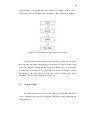
3.2
Design Flow
Figure 3.2: Processor Core Design Flow
Figure 2 above shows the processor core design flow. The design flow can be
divided into 2 main parts, first is the microcontroller design (with Verilog-HDL) and
second is the FPGA implementation.
14
There are eight stages of design flow in order to complete the processor core
design. The first step is to define the technical specification by capturing the
requirements for the processor. In my case of project, this is a general processor core,
yet it can be used to control specific device such as RFID reader. Then the next step
is to define the microcontroller architectural specification from which way you want
the microcontroller it has to be such as Universal Asynchronous Receiver
Transmitter (UART).
The next big step which leads the processor core strength is to has an abstract
of the instructions or prototype instructions that support efficient execution of the
known algorithms. We also have to figure out how we can address the operands, and
what type of data we will processing the instructions. In a simple case the operations
can be sketched by looking at the algorithm descriptions, in a more complicated case
some profiling is need to find out how frequently some operations, operation patterns
or common subroutines are executed. Then we can design the instruction set and the
coding.
Then we must start capturing the organizational architecture. This can be
accomplished by pen-and-paper methods, with spread-sheet calculations of cycle
counts, etc. independently of the method used, the estimation of the foreseen
implementation based on the architectures explored is the key importance.
FPGA implementation is performed by downloading the design into the
targeted FPGA devices, we have to make sure the device used is sufficient with our
microcontroller design from view of architecture such as ROM and RAM. After done
selecting the correct device and downloaded it to FPGA, the FPGA implementation
testing in real physical environment can be done by running the control program for
the RFID reader. But before the microcontroller is downloaded into FPGA, the
control program for RFID reader must be written such as to load data extracted from
15
the reader to ROM register. The control program at first is assembly language format
then I have to convert it to hex code so that the processor core can proceed to do its
works. The convert process from assembly language to hexcode is manually, there is
no assembler.
3.3
Altera Quartus II
Quartus II is free software provided by Altera. It has many functions thus it
will be used to design the processor core, where it has its own compiler, simulator,
waveform editor and programmer.
Figure 3.3: Quartus II Design Flow
16
3.4
Verilog-HDL
Verilog is a hardware description language (HDL) used to model electronic
systems. It is used to design, verify and implement digital logic chips at the Register
Transfer Level (RTL) of abstraction. The Altera Quartus 2 compiler uses the
Verilog-20001 standard.
3.5
Altera DE2 Board
Figure 3.4: Altera DE2 FPGA Board
The FPGA device used in my design is from Altera DE2 Board where the
device is Altera Cyclone II 2C35. The DE2 board has many features that allow me to
implement a wide range of designed circuits. The features of Cyclone II 2C35 that
related to my verilog system design are:
17
33,216 Logic Elements(LE)
105 M4k RAM blocks
483,480 total RAM bits
35 embedded multipliers
4 Phase-locked Loop PLLs
475 user I/O pins
18
CHAPTER 4
INSTRUCTION SET ARCHITECTURE
This chapter gives the information of the proposed processor core design
from the view of processor instructions.
4.1
Central Processing Unit (CPU)
Figure 4.1: Processor Flow
19
The operation of a processor core is rather simplistic in nature, it repeatedly
fetches an instruction from memory, decodes it, executes it and then return to the
fetch cycle and fetch the next instruction. The next instruction to be executed is
normally the next instruction sequence in memory. So Figure 4.1 shows the
processor core flow of my design. This processor core of this design is nonpipelined.
For the initial condition of my processor, the instruction fetched out is the
first instruction inside the instruction memory since the address of the instruction is
zero in program counter (PC). The instruction fetched is copied from cache into
instruction register (IR).
After fetching an instruction, the instruction will be decoded. From the
decoded instruction, the processor knows what to do next, what operands address to
calculate and what arithmetic operation is performed. For example, ADD instruction
adds the contents of source register and destination register and place the result into
destination register. Prior to that, the values of both source and destination registers
need to be fetched out from the register file to perform the addition. While for ADDI
operation, data will be fetched from a register and an immediate value will be
extracted from the instruction. Then, the addition of the data and the immediate value
will be performed.
For the data operation which is normally executed by arithmetic logic unit
(ALU), it will do specific operation according to the decoded instruction. The
proposed processor has operations such as add, subtract, load, store, multiply, AND,
OR and branching. For my processor core, the only memory access occurs during
load and store instructions. The memory being accessed is the data cache. Then the
result of the operation being performed in ALU, is to write back to the appropriate
register in the register file. Lastly, the value of Program Counter (PC) will be
20
updated by increment one, PC ← PC + 1. However, on branch and jump instructions,
PC can be updated to other addresses.
4.2
Instruction Set
The operation of the processor is determined by the instructions it executes,
referred as machine instructions or computer instructions. There are six instruction
formats in this design as shown on Table 4.1. Each instruction consists of 16-bit, the
16-bit is divided into several sections for the processor to do its works. For general
information of this design, a simple architecture has been made, where there are 16
8-bit registers in general purpose register file and 16 8-bit registers in the memory
register file for communication with real memory such as RAM and ROM.
Table 4.1: Six instruction formats
These kinds of formats are simple and useful for beginner of FPGA soft-core
processor. For the first format, rr is the instruction that handles register and register
operation. The instruction bits from 12 to 15 are the opcode section where all
instructions have different values of opcode so that we can differentiate each
instruction. The instruction bits of 8-11 are set to 0 so that we can differentiate rr
format with other instruction formats. Then, there are two kind of registers here: rs is
21
the source register whose address is represented by bit 4-7 and destination register
whose address is represented by bit 0-3. These two kinds of registers hold the data
for the ALU operands to operate. For example ADD instruction, the result takes data
from rs and adds with rd data to complete the arithmetic operation. Then, it will write
back the result to rd. For the second format, there is no much different. Instruction bit
from 4 to11 changed to immediate value and rd is still the same. The best example of
second format is ADDI, where an immediate value is added with data register value
and stored into rd.
For rm and mr format, I specially designed to let data of GPR interact with
data memory register. So load-store data can be done easily here. But, there is one
limitation here; when we are using SRAM, SDRAM and Flash memory on Altera
DE2 board, only 8 bits data can be accessed at one time. The value of instruction bits
8-11 is set to 1 for rm and mr format.
For branching instruction, it depends on the conditional codes of ALU
operation. For BEQ, if the flag of zero in conditional codes goes high after ALU
operation, then branching occurs, displacement (disp) values will decides where it
will branch to. While for jump instruction, JMP, there is no conditional codes need
to be considered. It will go directly to values of disp. The instruction bits of 8-11, is
to differentiate JMP instruction with other instructions.
22
Table 4.2 : Designed Instructions
Table 4.2 shows all instructions designed in this processor core. Note that all
instructions are one cycle, but they are not in pipelined way but in ordinary
sequential implementation. Thus this processor is a bit slower than pipelined
processor.
23
CHAPTER 5
PROCESSOR CORE DESIGN
This chapter explains about the full design of the processor core according to
designed instruction set in previous chapter.
5.1
Overview
The design of the processor core is divided into several sections which it explains
each design modules. This processor core is sequential processor where it will
process and complete one instruction in one cycle before it fetches a new instruction
for the next cycle. The modules inside the processor core are:
Program Counter
Instruction Memory
Decoder
General Purpose Register
Operand Selection
ALU and Conditional Codes
ROM register
24
5.2
PORT
UART and Shift Register
Architecture Overview
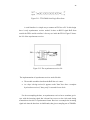
Figure 5.1: Architecture overview
Figure 5.1 shows the top-level block diagram of the design, every block
represents a module of the processor. At first glance, there are 10 modules are to be
designed separately using the top down design approach. Some modules like the
decoder are easy to design, but modules like ALU require a lot of understanding. The
overall dataflow and bus structure between all modules must be understood before
designing the modules individually.
Buses provide connection between modules. This bus is a common bus, such
as connection to PORT, ROM register and GPR. It is called common bus in the
25
design because it is being shared by many modules. For example, GPR can receive
data from the data bus. The other modules can receive and send data to the data bus.
Figure 5.2: The processor four stages RISC processor flow
The following text will briefly introduce the whole system. The system can
be divided into four stages, the fetch stage, execute stage and write back stage. Fetch
stage is in charge of fetching the next instruction. Decode stage is in charge of
decoding the 16-bit instruction to several parts. The execute unit is used to execute
the instruction and write back is to write the result of execution into desired
destination. The flow can be illustrated by Figure 5.2.
5.3
Program Counter
The first instruction is at the reset vector address. The following instructions
can be categorized into three types: sequential instruction, branch instruction and
jump instruction.
26
For then branch instruction, first it will consider the conditional codes of the
instruction. For BEQ, it will consider the zero flag, Z. If the Z is valid or high,
branch will be taken and PC is incremented by the displacement value coded. JMP
instruction is much simpler. It will go straight to effective address pointed by the
displacement value coded. Both displacement values need to be size-extended
because instruction memory size is 16-bit.
Other than branch and jump, execution continues with the next sequential
instruction. The current instruction address will be added up with one to move to
next instruction in next cycle.
5.4
Instruction Memory
As its name suggests, instruction memory is the place to store the instructions
in order to be executed in the processor. Then, the instruction fetched from the
memory will be loaded into Instruction Register (IR). The IR will only latch the new
instruction in if the HIT signal is asserted. HIT signal is a signal to verify whether
the instruction is valid or not. For simplicity, HIT is always asserted high. The
instruction that will be fetched out depends on the address of PC from previous
module. The data fetched out is the 16-bit instruction and will be decoded in Decoder
Module. The size of the instruction memory can be changed to desired size in the
Verilog module of Instruction Memory.
27
Figure 5.3: Instruction hexcode
The program control coding of processor core is at first in the form of
assembly language stage for programmer’s view. Then, it will be converted into
machine code in order to allow the processor to work with it. In this case, there is no
assembler, so I have to convert it manually. Figure 5.3 shows how the instructions
arranged in the Instruction Memory and the address of PC in instruction memory
started after @0. The format in the instruction memory is in hexadecimal format.
5.5
Decoder
Decoder is playing an important role in the processor core. This is a place
where the instruction will be decoded into several parts. The input of the decoder is
16-bit instruction from the Instruction Memory. There are five parts here as we can
see in Table 5.1.
28
Table 5.1: The decoder organization
5.6 Register File
In most processor cores, GPR is a very important. Each instruction reads
maximum of two registers (rd and rs) and some instructions need to write back one
result in rd register. This processor only runs on 16 registers to complete all its
instruction execution process. The format of the general purpose register is 8-bit. The
Figure 5.4 shows the structure of the 16 general purpose register.
29
Figure 5.4: GPR Structure
The rd and rs fields select registers that are read out onto the dreg and sreg
buses which these two will be used as inputs to ALU. The data bus is connected
directly to the destination register for write back process. As shown in Figure 5.5, the
write enable for GPR is MUXed to distinguish MOV(into ROM PORT register),
JMP, CMP and SB because these four instructions are not used to write back result
onto register file of GPR.
Figure 5.5: The GPR Write Enable Multiplexer
5.7
Operand Selection
Reviewing the instruction set architecture of Section 4.2, we can see that
there are several in instruction formats that influence the input of ALU. For rr and ri,
all instructions have two operands; one is either an immediate constant or the register
selected by rd and rs and the other is the register selected by rd. For memory-register
(rm and mr), it also has two operands; one is the output from the memory and the
other is rd or rs. From there we can obtain operands a and b as shown in Figure 5.6.
30
Figure 5.6: The Operand Selection
Operand a is the data from register file addressed by rd or 0. The zero will be
selected only when there is instruction of LB, CLR or SB. Operand b is the data from
ROMout2, immediate value or rs data. For LB which is loading ROM register data to
GPR, output from ROM register is needed. For ri format and MOV instruction, an
immediate value is taken into ALU. For all other instruction, the rs data is taken from
GPR.
5.8
Arithmetic Logic Unit (ALU) and Conditional Codes
With the 8-bit operand of a and b, we can perform arithmetic and logic
operation. The add, subtract and logic units operate concurrently upon two operands.
Then, a multiplexer selects one of these destinations to write the result of the
instruction. Table 5.2 shows how the ALU is being organized. rf_we signal is
asserted if the result of ALU will be written back to the destination register. Note that
rf_we us a register control signal. While the weX signal is asserted only when it is
SB instruction operation.
31
Table 5.2: Instruction grouping
The most straightforward way to code the ADD and SUB groups as shown in
Figure 5.6. The add signal is from the processor core that is determined from the
instruction such as ADDI and ADD. The cout signal asserted is when there is carryout in the addition process as shown in Figure 5.6.
Figure 5.7: ALU for ADD and SUB
There are five logic unit operations here which are AND, OR, NOT, XOR
and XNOR. To make it simple to be fit into design, a multiplexer for five stages is
needed to distinguish all five logic units operation. The result of the each logic
operation will be stored in a destination register. The flow of how these operations
are performed can be explained in Figure 5.5.
32
Figure 5.8: The multiplexing stages
Figure 5.9: Conditional Codes
The ALU is also determining the condition codes(ZNCV) which are zero,
negative, carry and overflow as shown in Figure 5.8. This is also used for conditional
branch instruction that may follow. The zero condition is self evident and any two’s
complement number is negative if its most-significant bit is set. Carry is the carryout of the most significant-bit of the add/sub operation and complemented for
33
subtracts. For overflow detection, an addition overflows if the most-significant bit of
a, b, sum and the carry-out is high. Then the values of z, n, co and v captured into
conditional codes vector which are ccz, ccn, ccc and ccv as each instruction
completes as shown in Figure 5.9. If rst signal is asserted, the ccz, ccn, ccc and ccv
will go the zeroes, but if the instruction is valid the z, n, co, v will be transfer into
ccz, ccn, ccc, ccv.
Figure 5.10: Conditional Codes Vector
5.9
ROM Register
ROM (Random Access Memory) register is like GPR from the way it
operates. The difference is the ROM registers provide register for memory and
register transfer. The memory we are talking now is the real ROM, which contains
ROM non-volatile data. The non-volatile refer to the content of memory which
remains even though the power is plugged off. The instructions using this ROM
register are LB and SB.
34
5.10
PORT
There is one 8-bits one-directional output port in the design. This is because
the port is intended to show some output such as LED. The output has its own
register at RTL design. The data bus is connected directly to this register. When
writing a data to the PORT, data is received from the data bus and the write signal to
the respected PORT’s register is asserted. Figure 5.10 shows the portion of program
control coding how to write data into PORT register.
MOV 11,RD1
MOV 01,PORT
ADDI 03,RD4…
Figure 5.10: Portion of Program Control Coding
5.11
Universal Asynchronous Receiver Transmitter (UART) and Shift
Register
The UART is implemented for RS-232 communication usage. Figure 5.11
shows RS-232 communication is asynchronous. This means the clock signal is not
sent with the data. Each word is synchronized using its start bit, and an internal clock
on each side, keeps tabs on the timing. For this design, format 9600-8-N-1 is used.
The diagram above shows the expected waveform from the UART when using the
common 8N1 format. 9600-8-N-1 signifies 9600 baudrate, 8 Data bits, No Parity and
1 Stop Bit. The RS-232 line, when idle is in the Mark State (Logic 1). A transmission
starts with a Start Bit which is (Logic 0). Then each bit is sent down the line, one at a
time. The LSB (Least Significant Bit) is sent first. A Stop Bit (Logic 1) is then
appended to the signal to make up the transmission..
35
Figure 5.11: TTL/CMOS Serial Logic Waveform
A serial interface is a simple way to connect an FPGA to a PC. In this design
there is only asynchronous receiver needed. It takes an RS232 signal RxD from
outside the FPGA and de-serializes it for easy use inside the FPGA. Figure X shows
the I/O of the asynchronous receiver.
Figure 5.12: The asynchronous receiver I/O
The implementation of asynchronous receiver works like this:
The module assembles data from the RxD line as it comes.
As a byte is being received, it appears on the "data" bus. Once a complete
byte has been received, "data_ready" is asserted for one clock.
For the oversampling the date, an asynchronous receiver has to somehow get insync with the incoming signal but it doesn't have access to the clock used during
transmission since this is asynchronous format. Receivers oversample the incoming
signal at 8 times the baud rate. At 9600 bauds, that gives a sampling rate of 76800Hz.
36
The baudrate and the clock for the asynchronous receiver have been parameterized
for easier future usage as shown in Figure 5.13
Figure 5.13: Parameter Values
This shift register was intended to shift 8-bit data for 12 stages. The input of the shift
register is from the RxD asynchronous receiver. Then the control signal to move the
8-bit stage by stage is from the data_ready of asynchronous receiver.
37
CHAPTER 6
RESULTS AND DISCUSSIONS
This chapter discussed the results obtained from the work done.
6.1
Results
6.1.1 The Processor Core
The processor was tested with two control programs. The first control
program is Final.txt as in Figure 6.1. The objective to test the processor core
with Final.txt is to determine whether the processor core is calculating the
correct values or not. According to Figure 6.2, it can be proved that the
processor cores with all designed instructions are operating in correct manner.
38
Figure 6.1: Final.txt control program
Figure 6.2: Timing simulation of Final.txt control program
39
Figure 6.3: Last.txt control program
Then, the processor core was tested with second control program named
Last.txt. The Last.txt is actually to show the process when UART detects 12 bytes
data from RxD asynchronous receiver, RXDATA. Then, these 12 data bytes are
moved into Register File first and again moved to ROM memory. From Figure 6.4
we can see that data are moved correctly from RXDATA1-RXDATA12 taken from
shift register to ROM1-ROM12 memory.
40
Figure 6.4: Timing simulation of Final.txt control program
41
6.1.2
Implementation of Radio Frequency Identification (RFID) Mifare Type
Technology and UART
The processor core was intended to implement on RFID reader type to
control the RFID reader. Where the processor can save the data on ROM register that
are sent out from the RFID reader. But before the processor can control well the
RFID reader, it must be tested first whether the Receive UART of the DE2 FPGA
receive correct data from the RFID reader. The RFID actually has two main parts;
the RFID card and the RFID reader. The RFID card contains 10 digits of decimal
number as serial number. This 10 digits will be sent out from RFID reader to UART
with a format of STX-10 decimal digits data-ETX (12 bytes). This format is in
ASCII when they are being sent out to UART of Receiver. For the verification of
RFID card 10 digits data, a Visual Basic 6 GUI has been made to display the data,
but the RFID reader must be connected DB-9 RS-232 on the back of computer
instead of DE2 FPGA. The format of RS-232 in the VB6 GUI is 9600-8-N-1. This is
the output on Figure 6.5 when touch the RFID card to RFID reader when it is
connected to computer.
Figure 6.5: VB6 RFID card verification
The coding for VB6 GUI of Mifare ID is in Appendix O. The example output
waveform of the RxD RFID reader when connected to oscilloscope in the Figure 6.6
below. From the Figure 6.6, we can see the 12 bytes of RFID serial number being
sent out.
42
Figure 6.6: Output waveform of RxD RFID Reader
Thus, this 12 bytes data must be received by the RxD asynchronous receiver of
UART on FPGA. These 12 bytes data, must be shifted for 12 stages for RXDATA1RXDATA12, then converted to normal hexadecimal of ASCII since the 12 bytes of
8-bit, the LSB bit is none parity which we do not use as the character of 10 digits of
the RFID card serial number.
Figure 6.7: Flow of RFID card serial number verification on DE2 board
Figure 6.8 shows the flow when the RFID reader and DE2 board connected together
for verification. Unfortunately when UART implemented on the Altera DE2 FPGA
board with RFID reader connected, the data received on UART is only STX which is
02 of ASCII is not as desired operation, it was wrong. Figure 6.8 shows result when
the RFID card is touched onto RFID reader.
43
Figure 6.8: Shifted and converted data of 12 bytes RFID card serial number
6.2
Discussion
6.2.1
Instruction Set
16 instructions set was designed. It consists of addition, subtraction, load and
store data from memory to register or register to memory, branching and jumping
and logic operation. All instructions except JMP and BEQ are using data from
Register File and memory data, ROM register. The most difficult instruction to
design is BEQ because there are few steps need to be. First it needs to check whether
instruction executed before BEQ was zero high in conditional codes. It can be
executed. The displacement value pointed by BEQ instruction in control program is
in 8-bit format. Then it will be extended to 16-bit to follow format of program
counter. The easiest instruction is subtraction and addition because these two
operations just only need to consider two data from either ROM register memory or
Reigster File. After execution in ALU, it will be write back into desired location.
44
6.2.2
Memory Initialization File
The control program at first is written in text format. Then it will be
converted to hexcode as processor core only understand machine language. Altera
Quartus has special function named MIF to initialize desired data and then it can be
called. So to make it easier to understand, this MIF will be used to store the control
program hexcode. Then it will be called using function $readmemh in specific design
module. In my design case, the MIF of control program hexcode is called in module
inst_mem_mushy.
6.2.3
Design of Negedge Clock
At first, the design was using posedge clock design for all verilog design
related to clock. At that stage, the design and simulation is in functional simulation.
The problem using functional simulation is that, operation like read and write for
Register File is wrong. Then when simulated in timing simulation, I can see there is a
gap when posedge clock and instruction executed, thus it affects read and write for
register file where its operation is late for one clock. This will make the read and
write take the wrong address. Then I overcame this problem with changing all
posedge clock condition to negedge condition. This action made the read and write
for all process not only for Register File are correct. Figure 6.9 shows the correct
operation for read and write.
45
Figure 6.9: Negedge clock solve the timing problem for read and write
6.2.4
The RFID and Receiver Design System
The design module consists of asynchronous receiver, 12 stages shift register,
convertor and 7 Segment to retrieve 12 data bytes and to display. However, the
system does not work. From Figure 6.8 we can see that data received on the
asynchronous receiver after shifted and converted is only STX(02h) for few shift
register stages, while some stages contain no data at all. Thus, this verification of
RFID card serial number on DE2 FPGA has failed and for the processor core to
control the RFID reader cannot be proceed. This must be due to fast multiple data
transfer of 9600bps at 50MHz or shifted register that did not works well when
implemented in real application. This module is also done in slower baudrate and
25Mhz clock. But the result on 7 Segment was worst. There was nothing displayed.
This asynchronous receiver was done to receive one data byte, it was correct but
when it comes to multiple data transfer, the data received is not correct. It is also
possible that the data shift register control signal to shift the data received is not
enough one clock since if we see from example output waveform of RFID 12 bytes
data RxD, the receiver is on asynchronous mode where the data send is free of clock.
Then it makes the transition of each byte is not synchronized with clock while the
control signal of shift register is synchronized with clock. This problem can be solves
by easier way using Universal Synchronous Asynchronous Receiver Transmitter
(USART) where there are clock synchronizing the data transition.
46
CHAPTER 7
CONCLUSION AND RECOMMENDATIONS
This chapter explains about the project conclusion and the recommendation
for future works of this project to readers.
7.1
Recommendation for Future Works
At first the processor core does not connected to real ROM or RAM. So the
memory-register design in the processor core is just at low level where it provides
the data of 8-bit at register level. With real implementation of memory such as ROM
and RAM, it will make the LB and SB instructions shows benefit to the processor.
The processor core is sequential processor, where each instruction must
complete first then the processor can fetch new instruction to process. So this made
the processor runs a bit slower, with the pipelining design implementation to this
processor core. It will make the processor runs at faster rate, when fetch, decode,
execute and write back can be done in one cycle.
47
For processor core to runs a control program for the RFID reader, the first
stage of extracting the serial numbers from the RFID card must be done well. The
problem is whether at UART or shift register control signal made this
implementation cannot be done. To solve the uncontrolled transition of data retrieve,
a USART design module can be replaced with UART.
7.2
Conclusion
As a conclusion, this project for the processor core has been completed
successfully fulfilling the objective and scope specified for the processor core design.
But the processor core is not implemented well on the Altera DE2 FPGA, due to
problem of UART and RFID. If this problem can be overcome, this processor can
work nicely. It is possible for mere mortal to build a compact, reasonably fast
embedded processor or even a complete system-on-a-chip in a small fraction of a
small FPGA, if the processor and system are designed to make the best use of FPGA.
48
REFERENCES
1. Dr.Mohamed Khalil Hani, Digital Systems: VHDL & Verilog Design. 2nd
edition., UTM Skudai, Malaysia Prentice Hall. 2007
2. D. Sulik, M. Vasilko, D. Durackova and P. Fuchs, Design of a RISC
Microcontroller Core in 48 Hours, Bournemouth University , UK
3. Jari Nurmi. Processor Design SoC Computing for ASICs and FPGAs,
Tamper University of Technology Finland, Springer 2007
4. Don Arbinger and Jeremy Erdmann, Designing and Embedded Soft-core
Processor, The Plexus Technology Group. 2006
5. Jan Gray, Designing a Simple FPGA-Optimized RISC CPU and System-ona-Chip, Gray Research LLC, Bellevue. 2000
6. Yap Zi He, Building A RISC Microcontroller in an FPGA, UTM Skudai.
2002
7. David Sheldon, Rakesh Kumar, Roman Lysecky, Frank Vahid and Dean
Tullsen, Application-specific Cuztomization of Parameterized FPGA Softcore Processors, ICCAD’06, San Jose. 2006.
8. DE2 Development and Education Board User Manual, Version 1.4 , Altera,.
2006
9. Gareth Knight. “CISC vs RISC”,
http://www.amigau.com/aig/riscisc.html
49
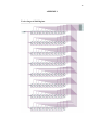
APPENDIX A
The Processor Core Verilog Module
module MushyProcessorv18
(
clk, rst, rdy, RXDATA, insn_reg, op, rd, rs, imm,
bus_writing,dreg2, sreg2, a, b, sum,
ccz, ccn, ccc, ccv,
weX, addr, ROMout2, weY,PortOUTdataout1,
out1111, pcinc, branch, jump, next_pc, prog_c,
proc_rst);
input
clk;
input
rst;
input [AN:0] proc_rst; //reset vector
input
rdy;
input [7:0] RXDATA;
assign hit = 1;
parameter N = 7;
// register MSB
parameter AN = 15;
// address MSB
parameter IN = 15;
// instruction MSB
// opcode decoding
`define ADDI
(op==0)
`define SUBI
(op==1)
`define ADD
(op==2)
`define SUB
(op==3)
`define LB
(op==4)
50
`define SB
(op==5)
`define CMP
(op==6)
`define MOV
(op==7)
`define AND
(op==8)
`define XOR
(op==9)
`define JMP
(op==10)
`define BEQ
(op==11)
`define XNOR
(op==12)
`define OR
(op==13)
`define CLR
(op==14)
`define NOT
(op==15)
// FETCH
inst_mem_mushy fetch(next_instruction,clk,insn);
output [15:0] insn_reg = insn;
wire [15:0] insn;
wire [15:0] next_instruction = next_pc;
// DECODE PROCESS
Decoder dec(insn, op, rd, rs, imm, disp);
output [3:0] op;
output [3:0] rd;
output [3:0] rs;
output [7:0] imm;
//disp = out1111
// Register file
wire [N:0] dreg2, sreg2;
wire valid_insn_ce = hit & insn_ce;
//if the instruction is valid
assign en = valid_insn_ce;
51
wire rf_we = (insn[11:8]==15 | `JMP)? 0 :
((`SB|`CMP) ? 0 : (valid_insn_ce & ~rst));
RegFile16x8bit regfile
(rd,rs, writing, rf_we, clk, dreg1, sreg1, dreg2,
sreg2); //TEST DECODER IS OK
wire [7:0] bus_writing = (`MOV&&insn[11:8]==8) ?
RXDATA : (`CLR ? sreg2 : (`XNOR ? a~^b : (`OR ? a|b :
(`NOT ? ~a :(`AND ? a&b : (`XOR ? a^b : sum))))));
output [7:0] dreg2, sreg2;
output [7:0] bus_writing;
//Operand Selection
wire [N:0] a = (`LB|`CLR|`SB) ? 0 : dreg2;
wire [N:0] b = `LB ? ROMout2 : ((`ADDI|`SUBI|`MOV) ?
imm : sreg2);
//EXECUTION PROCESS
//ALU and conditional codes
wire add = ~(`SUBI|`SUB|`CMP);
ALUandCCT alucct
(add, a, b, sum, cout, valid_insn_ce, clk, rst, ccz,
ccn, ccc, ccv, z );
output [N:0] a, b;
output [N:0] sum;
output ccz, ccn, ccc, ccv;
//ROM/
52
wire [3:0] addr = `SB ? rs : ( `LB ? rs : 0);
wire weX = (insn[11:8]==15)? 0 : (`SB ? 1 : 0);
ROM16x8bit ROM
(clk, weX, writing, addr, ROMout1, ROMout2);
output weX;
output [3:0] addr;
output [7:0] ROMout2;
// PORTout
PortOut port_out
(weY, clk, dataY, PortOUTdataout1, PortOUTdataout2);
wire weY = (`MOV & (insn[11:8]==15)) ? 1 : 0;
wire [7:0] dataY = insn[7:0];
output weY;
output [7:0] PortOUTdataout1;
// PROGRAM COUNTER AND INSTRUCTION FETCH
// conditional branch for BEQ
reg t;
always@(negedge clk )
begin
if ((op==11)&& ccz)
t =1;
else
t = 0;
end
53
assign out1111 = insn[7:0];
//disp
assign branch = hit & t;
output [7:0]out1111 ;
output [15:0]pcinc;
output branch, jump;
output [15:0] next_pc;
output [15:0] prog_c;
wire [15:0] ext16 = {8'b00000000,insn[7:0]};
//branch
reg [15:0] increment;
always@(negedge clk)
begin
increment <= ext16;
end
//jump
reg [15:0] for_jump;
always@(negedge clk)
begin
for_jump <= ext16;
end
reg jump;
always @ (negedge clk)
begin
if (hit && `JMP)
jump <= 1;
else
jump <= 0;
end
54
//last PC check
wire [AN:0] pcinc = branch ? increment: (pc + 1);
assign next_pc = jump ? for_jump : pcinc;
reg [AN:0] pc;
always @ (negedge clk)
begin
if (rst)
pc <= proc_rst;
else if (valid_insn_ce)
pc <= next_pc;
end
assign insn_ce = rst | ~(0 & ~rdy);
assign prog_c
endmodule
= pc;
55
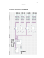
APPENDIX B
Instruction Memory Verilog Module
module inst_mem_mushy(addr_pc,clk,data_out);
input clk;
input [15:0] addr_pc;//i_ad
output [15:0] data_out;
reg [15:0] mem[0:60];
initial
begin
$readmemh("LAST.txt", mem);
end
assign data_out=mem[addr_pc];
endmodule
56
APPENDIX C
Decoder Verilog Module
module Decoder (insn, op, rd, rs, imm, disp);
input [15:0] insn;
output [3:0] op, rd, rs;
output [7:0] imm;
output [7:0] disp;
wire [3:0] op;
wire [3:0] rd;
wire [3:0] rs;
wire [7:0] imm;
wire [7:0] disp;
// instruction decoding
assign
op = insn[15:12];
assign
rd = insn[3:0];
assign
rs = insn[7:4];
assign
imm = insn[11:4];
assign
disp = insn[7:0];
endmodule
57
APPENDIX D
Register File Verilog Module
module RegFile16x8bit
(rd,rs, data, we, clk, dreg1, sreg1, dreg2, sreg2);
input [3:0] rd , rs;
input we, clk;
input [7:0] data;
reg [7:0] mem[0:15];
reg [7:0] dreg1, sreg1;
output [7:0] dreg1, sreg1, dreg2, sreg2;
always @(negedge clk)
begin
if (we)
begin
mem[rd]<=data;
end
dreg1 = mem[rd];
sreg1 = mem[rs];
end
assign dreg2 = mem[rd];
assign sreg2 = mem[rs];
endmodule
58
APPENDIX E
ALU and Conditional Codes Verilog Module
module ALUandCCT
(add, a, b, sum, cout, valid_insn_ce, clk, rst, ccz,
ccn, ccc, ccv,z);
input
add;
input
[7:0] a, b;
output [7:0] sum;
output cout;
input valid_insn_ce;
input clk, rst;
output ccz, ccn, ccc, ccv, z;
wire x;
assign {cout,sum}= add ? {a}+{b}: {a}-{b};
// condition codes
wire c_W = cout;
assign z = sum == 0;
// zero
assign n = sum[7];
// negative
assign co = add ? c_W : ~c_W;
// carry-out
assign v = c_W^sum[7]^a[7]^b[7];
// overflow
reg ccz, ccn, ccc, ccv; // CC vector
59
always @(negedge clk)
if (rst)
{ccz,ccn,ccc,ccv} <= 0;
else if (valid_insn_ce)
{ccz,ccn,ccc,ccv} <= {z,n,co,v};
endmodule
60
APPENDIX F
ROM Register Verilog Module
module ROM16x8bit
(clk, we, data, addr, ROMout1, ROMout2);
input clk, we;
input [7:0] data;
input [3:0] addr;
output [7:0] ROMout1, ROMout2;
reg [7:0] mem[0:15];
reg [7:0] ROMout1;
always @ (negedge clk)
begin
if (we)
begin
mem[addr]<=data;
end
ROMout1 = mem[addr];
end
assign ROMout2 = mem[addr];
endmodule
61
APPENDIX H
Port Verilog Module
module PortOut
(we, clk, data, PortOUTdataout1, PortOUTdataout2);
input we, clk;
input [7:0] data;
reg [7:0] PortOUTdataout1;
output [7:0] PortOUTdataout1, PortOUTdataout2;
always @(negedge clk)
begin
if (we)
PortOUTdataout1<=data;
end
assign PortOUTdataout2 = data;
endmodule
62
APPENDIX H
Asynchoronous Receiver
// RS-232 RX module
// (c) fpga4fun.com KNJN LLC - 2003, 2004, 2005, 2006
module async_receiver
(clk, RxD, RxD_data_ready, RxD_data, RxD_endofpacket,
RxD_idle);
input clk, RxD;
output RxD_data_ready;
// onc clock pulse when RxD_data is valid
output [7:0] RxD_data;
parameter ClkFrequency = 50000000; // 50MHz
parameter Baud = 9600;
/*We also detect if a gap occurs in the received stream
of characters. That can be useful if multiple characters
are sent in burst. So that multiple characters can be
treated as a "packet" */
output RxD_endofpacket;
/*one clock pulse, when no more data is received
(RxD_idle is going high)*/
output RxD_idle;// no data is being received
// Baud generator (we use 8 times oversampling)
parameter Baud8 = Baud*8;
63
parameter Baud8GeneratorAccWidth = 16;
wire [Baud8GeneratorAccWidth:0] Baud8GeneratorInc =
((Baud8<<(Baud8GeneratorAccWidth7))+(ClkFrequency>>8))/(ClkFrequency>>7);
reg [Baud8GeneratorAccWidth:0] Baud8GeneratorAcc;
always @(posedge clk)
Baud8GeneratorAcc<=Baud8GeneratorAcc[Baud8GeneratorA
ccWidth-1:0] + Baud8GeneratorInc;
wire Baud8Tick =
Baud8GeneratorAcc[Baud8GeneratorAccWidth];
reg [1:0] RxD_sync_inv;
always @(posedge clk)
if(Baud8Tick) RxD_sync_inv <= {RxD_sync_inv[0],
~RxD};
/* we invert RxD, so that the idle becomes "0", to
prevent a phantom character to be received at startup*/
reg [1:0] RxD_cnt_inv;
reg RxD_bit_inv;
always @(posedge clk)
if(Baud8Tick)
begin
if( RxD_sync_inv[1] && RxD_cnt_inv!=2'b11)
RxD_cnt_inv <= RxD_cnt_inv + 2'h1;
else
if(~RxD_sync_inv[1] && RxD_cnt_inv!=2'b00)
RxD_cnt_inv <= RxD_cnt_inv - 2'h1;
if(RxD_cnt_inv==2'b00) RxD_bit_inv <= 1'b0;
else
if(RxD_cnt_inv==2'b11) RxD_bit_inv <= 1'b1;
64
end
reg [3:0] state;
reg [3:0] bit_spacing;
/* "next_bit" controls when the data sampling occur
depending on how noisy the RxD is, different values might
work better with a clean connection, values from 8 to 11
work*/
wire next_bit = (bit_spacing==4'd10);
always @(posedge clk)
if(state==0)
bit_spacing <= 4'b0000;
else
if(Baud8Tick)
bit_spacing <= {bit_spacing[2:0] +
4'b0001} | {bit_spacing[3], 3'b000};
always @(posedge clk)
if(Baud8Tick)
case(state)
4'b0000: if(RxD_bit_inv) state <= 4'b1000;
// start bit found?
4'b1000: if(next_bit) state <= 4'b1001;
// bit 0
4'b1001: if(next_bit) state <= 4'b1010;
// bit 1
4'b1010: if(next_bit) state <= 4'b1011;
// bit 2
4'b1011: if(next_bit) state <= 4'b1100;
// bit 3
4'b1100: if(next_bit) state <= 4'b1101;
// bit 4
4'b1101: if(next_bit) state <= 4'b1110;
// bit 5
4'b1110: if(next_bit) state <= 4'b1111;
// bit 6
4'b1111: if(next_bit) state <= 4'b0001;
// bit 7
4'b0001: if(next_bit) state <= 4'b0000;
// stop bit
65
default: state <= 4'b0000;
endcase
reg [7:0] RxD_data;
always @(posedge clk)
if(Baud8Tick && next_bit && state[3]) RxD_data <=
{~RxD_bit_inv, RxD_data[7:1]};
reg RxD_data_ready, RxD_data_error;
always @(posedge clk)
begin
RxD_data_ready <= (Baud8Tick && next_bit &&
state==4'b0001 && ~RxD_bit_inv);
// ready only if
the stop bit is received
RxD_data_error <= (Baud8Tick && next_bit &&
state==4'b0001 &&
RxD_bit_inv);
// error if the
stop bit is not received
end
reg [4:0] gap_count;
always @(posedge clk) if (state!=0)
gap_count<=5'h00; else if(Baud8Tick & ~gap_count[4])
gap_count <= gap_count + 5'h01;
assign RxD_idle = gap_count[4];
reg RxD_endofpacket; always @(posedge clk)
RxD_endofpacket <= Baud8Tick & (gap_count==5'h0F);
endmodule
66
APPENDIX I
Control Program to Test (Assembly Language)
1. Control Program for Final.txt
Final.txt
67
2. Control Program for last.txt
Last.txt
68
APPENDIX J
Control Program Hexcode (Machine Language)
Final_hexcode.txt
69
Last_hexcode.txt
70
APPENDIX K
Timing Simulation of Control Program
1. Control Program for Final.txt
71
2. Control Program for Last.txt
72
APPENDIX L
Twelve Stages of Shift Register
73
APPENDIX M
Converter ASCII to 7 Segment
module ASCII27SEG(a,z);
input [6:0] a;
output [6:0] z;
reg [6:0] z;
always@(a)
begin
case (a)
7'b0110001 : z = 7'b1111001;//1
7'b0110010 : z = 7'b0100100;//2
7'b0110011 : z = 7'b0110000;//3
7'b0110100 : z = 7'b0011001;//4
7'b0110101 : z = 7'b0010010;//5
7'b0110110 : z = 7'b0000010;//6
7'b0110111 : z = 7'b1111000;//7
7'b0111000 : z = 7'b0000000;//8
7'b0111001 : z = 7'b0011000;//9
7'b0000010 : z = 7'b0011100;//STX
7'b0000011 : z = 7'b0101011;//ETX
7'b0001010 : z = 7'b0000110;//LF
7'b0001101 : z = 7'b0001000;//CR
default : z = 7'b1111111 ;
endcase
end
endmodule
74
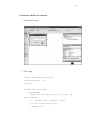
APPENDIX N
Asynchronous Receiver System to catch 12 data bytes
APPENDIX O
75
Visual Basic for RFID card verification
1. The Interface Design
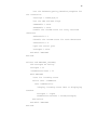
2. The Coding
Private Sub cmdClearID_Click()
txtMifareID.Text = ""
End Sub
Private Sub Form_Load()
With MSComm1
'make sure the serial port is not open (by
this program)
If .PortOpen Then .PortOpen = False
'set the active serial port
.CommPort = 12
76
'set the badurate,parity,databits,stopbits for
the connection
.Settings = "9600,N,8,1"
'set the DRT and RTS flags
.DTREnable = True
.RTSEnable = True
'enable the oncomm event for every reveived
character
.RThreshold = 1
'disable the oncomm event for send characters
.SThreshold = 0
'open the serial port
.PortOpen = True
End With 'MSComm1
End Sub
Private Sub MSComm1_OnComm()
Dim strInput As String
strInput = ""
'txtMifareID.Text = ""
With MSComm1
'test for incoming event
Select Case .CommEvent
Case comEvReceive
'display incoming event data to displaying
textbox
strInput = .Input
txtMifareID.SelText = Trim$(strInput)
End Select
End With 'MSComm1
End Sub