1
Colour Television
Chassis
A02U
AA
E_13950_000.eps
030304
Contents
Page
1. Technical Specifications, Connections,
and Chassis Overview
2
2. Safety Instructions, Warnings, and Notes
4
3. Directions for Use
6
4. Mechanical Instructions
8
5. Service Modes, Error Codes, and Faultfinding 11
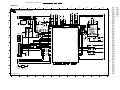
6. Block Diagrams, Testpoint Overviews,
and Waveforms
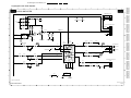
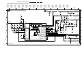
Wiring Diagram
21
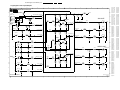
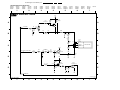
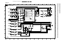
Block Diagram LSP Supply and Deflection
22
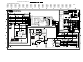
Testpoint Overview LSP and CRT
23
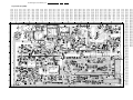
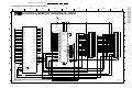
Block Diagram 1 Audio & Video
24
Block Diagram 2 Audio & Video
25
Testpoint Overview SSB
26
I2C Overview
27
Supply Lines Overview
28
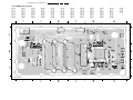
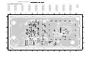
7. Circuit Diagrams and PWB Layouts
Diagram
LSP: Main Supply
(Diagr. A1A) 29
LSP: Main Supply
(Diagr. A1B) 30
LSP: Standby Supply
(Diagr. A2) 31
LSP: Line Deflection
(Diagr. A3) 32
LSP: Frame Defl. & E/W Drive
(Diagr. A4) 33
LSP: Rotation Circuitry
(Diagr. A5) 34
LSP: Headphone Amplifier
(Diagr. A7) 34
LSP: Audio Amplifier
(Diagr. A6) 35
LSP: Tuner SIMM Conn. (Fem.)
(Diagr. A8) 36
LSP: Front
(Diagr. A10) 37
LSP: Inputs/Outputs
(Diagr. A11) 38
SSB: If & SAW Filter
(Diagr. B1) 45
SSB: Video Source Sel. & Data Link(Diagr. B2) 46
SSB: Audio Source Select
(Diagr. B3) 47
SSB: MPIF-Supply, E.W, & Control (Diagr. B4) 48
SSB: Video Decoder
(Diagr. B5) 49
SSB: Feature Box
(Diagr. B6) 50
Contents
PWB
39-44
39-44
39-44
39-44
39-44
39-44
39-44
39-44
39-44
39-44
39-44
62-63
62-63
62-63
62-63
62-63
62-63
8.
9.
10
11
Page
SSB: RGB Processing
(Diagr. B7)
SSB: Sync & Deflection Proc.
(Diagr. B8)
SSB: Protection
(Diagr. B9)
SSB: Audio Processing
(Diagr. B10)
SSB: Control
(Diagr. B11)
SSB: Contr.-Mem.y Interf. (EBIU) (Diagr. B12)
SSB: Contr.-Mem. Interf. (SDRAM) (Diagr. B13)
SSB: ADOC Supply
(Diagr. B14)
SSB: Low Voltage Supply ADOC (Diagr. B15)
SSB: 3D COMB Filter
(Diagr. B17)
SSB: Connector Interface
(Diagr. B18)
Side I/O Panel
(Diagr. D)
CRT Amplifier
(Diagr. F1)
Auto SCAVEM
(Diagr. F2)
DC Shift Panel
(Diagr. G)
VDAF Panel + 2nd Orders
(Diagr. I)
Front Interface Panel (FL13)
(Diagr. J)
Front Interface Panel (PV2)
(Diagr. J)
HDMI: Panellink Receiver
(Diagr. M1)
HDMI: Input Selection
(Diagr. M2)
HDMI: Sync Selection & I/O Exp. (Diagr. M3)
Side I/O Panel
(Diagr. O)
Top Control Panel (FL13)
(Diagr. P)
Top Control Panel (PV2)
(Diagr. P)
Alignments
Circuit Descriptions
Abbreviation List
IC Data Sheets
Spare Parts List (not applicable)
Revision List
51
52
53
54
55
56
57
58
59
60
61
64
66
67
70
71
73
75
77
78
79
82
84
86
89
98
112
115
117
118
62-63
62-63
62-63
62-63
62-63
62-63
62-63
62-63
62-63
62-63
62-63
65
68-69
68-69
70
72
74
76
80-81
80-81
80-81
83
85
87
©
Copyright 2004 Philips Consumer Electronics B.V. Eindhoven, The Netherlands.
All rights reserved. No part of this publication may be reproduced, stored in a
retrieval system or transmitted, in any form or by any means, electronic,
mechanical, photocopying, or otherwise without the prior permission of Philips.
Published by BB 0463 Service PaCE
Printed in the Netherlands
Subject to modification
EN 3122 785 13980
EN 2
1.
Technical Specifications, Connections, and Chassis Overview
A02U AA
1. Technical Specifications, Connections, and Chassis Overview
1.2
Index of this chapter:
1. Technical Specifications
2. Connections
3. Chassis Overview
Note: Figures below can deviate slightly from the actual
situation, due to the different set executions.
1.1
Connections
Note: The following connector color abbreviations are used
(acc. to DIN/IEC 757): Bk= Black, Bu= Blue, Gn= Green, Gy=
Grey, Rd= Red, Wh= White, Ye= Yellow.
1.2.1
Top Control and Front / Side Connections
Technical Specifications
TOP CONTROL (for PV2 styling)
1.1.1
Vision
Display type
Screen size(s)
Tuning system
IF frequency
Color systems
Channel selections
Video playback
Aerial input
1.1.2
:
:
:
:
:
:
:
:
:
:
:
:
:
:
:
- VOLUME
DV-CRT-RF
26 inch - 16:9
27 inch - 4:3
30 inch - 16:9
32 inch - 4:3
34 inch - 16:9
PLL
45.75 MHz
NTSC M (3.58-4.5)
181 presets
Full cable, UHF
ATSC
480p
1080i
75 ohm, F-type
MENU
- CHANNEL +
CH
TOP CONTROL (for FL13 styling)
- VOLUME
+
MENU
- CHANNEL +
FRONT I/O
RED IR LIGHT SENSOR
LED
(OPTIONAL)
Sound
Sound systems
Maximum power
+
MENU
: BTSC DBX
: 2 x 10 W_rms (int.)
SIDE I/O
S-VIDEO
1.1.3
Miscellaneous
Mains voltage
Mains frequency
Ambient temperature
Maximum humidity
Power consumption
- Normal operation
- Standby
VIDEO
:
:
:
:
110 V_ac
50 / 60 Hz
+5 to +45 deg. C
90 % R.H.
: ≈ 159 W
: <1W
L
AUDIO
R
E_13950_006.eps
110304
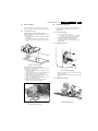
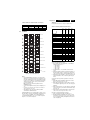
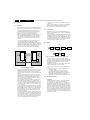
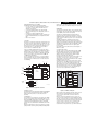
Figure 1-1 Top control and Front / Side connections
Hosiden: SVHS - In
1 -Y
Ground
2 -C
Ground
3 -Y
1 V_pp / 75 ohm
4 -C
0.3 V_pp / 75 ohm
H
H
j
j
Audio / Video In
Ye - Video (CVBS) 1 V_pp / 75 ohm
Wh - Audio - L
0.2 V_rms / 10 kohm
Rd - Audio - R
0.2 V_rms / 10 kohm
H
jq
jq
Mini Jack: Headphone - Out
- Headphone 32 - 600 ohm / 10 mW
ot
Technical Specifications, Connections, and Chassis Overview
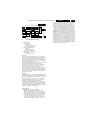
1.2.2
AV2 In (SVHS)
1 - Ground
2 - Ground
3 -Y
4 -C
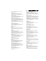
Rear Connections
AV5
IN
AV4
IN
Y
Pb
L
L
Pr
R
R
VIDEO
75 Ohm
AUDIO
MONITOR
OUT
AUDIO
HDMI
AV1
IN
AV2
IN
VIDEO
Y
V
Pb
L
V
L
Pr
R
R
AUDIO
R
COMPONENT VIDEO INPUT
S-VIDEO
E_13950_001.eps
030304
Figure 1-2 Rear connections
Aerial In
- F-type
Coax, 75 ohm
1.3
D
Monitor Out
Ye - Video (CVBS) 1 V_pp / 75 ohm
Wh - Audio - L
0.5 V_rms / 1 kohm
Rd - Audio - R
0.5 V_rms / 1 kohm
kq
kq
kq
AV1 In
Gn - Y
0.7 V_pp / 75 ohm
Bu - Pb
0.7 V_pp / 75 ohm
Rd - Pr
0.7 V_pp / 75 ohm
Ye - Video (CVBS) 1 V_pp / 75 ohm
Wh - Audio - L
0.5 V_rms / 10 kohm
Rd - Audio - R
0.5 V_rms / 10 kohm
jq
jq
jq
jq
jq
jq
AV2 In
Ye - Video (CVBS) 1 V_pp / 75 ohm
Wh - Audio - L
0.5 V_rms / 10 kohm
Rd - Audio - R
0.5 V_rms / 10 kohm
1.
EN 3
H
H
jq
jq
GND
GND
1 V_pp / 75 ohm
0.3 V_pp / 75 ohm
AV4 In (not used for 27/32MS series)
Wh - Audio - L
0.5 V_rms / 10 kohm
Rd - Audio - R
0.5 V_rms / 10 kohm
L/Mono
SERVICE
CONNECTOR
A02U AA
jq
jq
jq
jq
jq
HDMI (not used for 27/32MS series)
1 - RX2+
Data channel
2 - GND
Ground
3 - RX2Data channel
4 - RX1+
Data channel
5 - GND
Ground
6 - RX1Data channel
7 - RX0+
Data channel
8 - GND
Ground
9 - RX0Data channel
10 - RXC+
Data channel
11 - GND
Ground
12 - RXCData channel
13 - n.c.
14 - n.c.
15 - DDC SCL DDC clock
16 - DDC SDA DDC data
17 - GND
Ground
18 - +5V
19 - HPD
20 - GND
Ground
21 - GND
Ground
22 - GND
Ground
23 - GND
Ground
24 - GND
Ground
AV5 In
Gn - Y
Bu - Pb
Rd - Pr
Wh - Audio - L
Rd - Audio - R
j
H
j
j
H
j
j
H
j
j
H
j
j
jk
H
j
j
H
H
H
H
H
jq
jq
jq
jq
jq
0.7 V_pp / 75 ohm
0.7 V_pp / 75 ohm
0.7 V_pp / 75 ohm
0.5 V_rms / 10 kohm
0.5 V_rms / 10 kohm
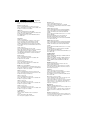
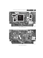
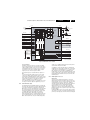
Chassis Overview
F
CRT PANEL
D
SIDE I/O PANEL
B
SMALL SIGNAL BOARD
M
HDMI PANEL
TOP CONTROL PANEL
E
LARGE SIGNAL PANEL
A
FRONT INTERFACE PANEL
DC SHIFT PANEL
(OPTIONAL)
VDAF + 2ND ORDERS
PANEL
J
G
I
E_13950_002.eps
270204
Figure 1-3 PWB location
EN 4
2.
A02U AA
Safety Instructions, Warnings, and Notes
2. Safety Instructions, Warnings, and Notes
2.1
Safety Instructions
2.3
Warnings
•
Safety regulations require that during a repair:
• Due to the chassis concept, a very large part of the circuitry
(incl. deflection) is 'hot'. Therefore, connect the set to the
mains via an isolation transformer.
• Replace safety components, indicated by the symbol h,
only by components identical to the original ones. Any
other component substitution (other than original type) may
increase risk of fire or electrical shock hazard.
• Wear safety goggles when you replace the CRT.
In order to prevent damage to ICs and transistors, avoid all
high voltage flashovers. In order to prevent damage to the
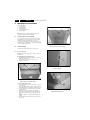
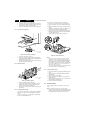
picture tube, use the method shown in Fig. 2-1, to
discharge the picture tube. Use a high voltage probe and a
multi-meter (position V_dc). Discharge until the meter
reading is 0 V (after approx. 30 s).
V
Safety regulations require that after a repair, you must return
the set in its original condition. Pay, in particular, attention to
the following points:
• General repair instruction: as a strict precaution, we advise
you to re-solder the solder connections through which the
horizontal deflection current is flowing. In particular this is
valid for the:
1. Pins of the line output transformer (LOT).
2. Fly-back capacitor(s).
3. S-correction capacitor(s).
4. Line output transistor.
5. Pins of the connector with wires to the deflection coil.
6. Other components through which the deflection current
flows.
E_06532_007.eps
110204
Figure 2-1 Discharge picture tube
•
Note: This re-soldering is advised to prevent bad connections
due to metal fatigue in solder connections, and is therefore only
necessary for television sets more than two years old.
•
•
•
•
2.2
Check the insulation of the mains cord for external
damage.
Check the strain relief of the mains cord for proper function,
to prevent the cord from touching the CRT, hot
components, or heat sinks.
Check the electrical DC resistance between the mains plug
and the secondary side (only for sets that have an isolated
power supply). Do this as follows:
1. Unplug the mains cord and connect a wire between the
two pins of the mains plug.
2. Turn on the main power switch (keep the mains cord
unplugged!).
3. Measure the resistance value between the pins of the
mains plug and the metal shielding of the tuner or the
aerial connection of the set. The reading should be
between 4.5 MΩ and 12 MΩ.
4. Switch the TV 'off' and remove the wire between the
two pins of the mains plug.
Check the cabinet for defects, to prevent the possibility of
the customer touching any internal parts.
Maintenance Instructions
We recommend a maintenance inspection carried out by
qualified service personnel. The interval depends on the usage
conditions:
• When a customer uses the set under normal
circumstances, for example in a living room, the
recommended interval is three to five years.
• When a customer uses the set in an environment with
higher dust, grease, or moisture levels, for example in a
kitchen, the recommended interval is one year.
• The maintenance inspection includes the following actions:
1. Perform the 'general repair instruction' noted above.
2. Clean the power supply and deflection circuitry on the
chassis.
3. Clean the picture tube panel and the neck of the picture
tube.
•
•
•
•
All ICs and many other semiconductors are susceptible to
electrostatic discharges (ESD, w). Careless handling
during repair can reduce life drastically. Make sure that,
during repair, you are connected with the same potential as
the mass of the set by a wristband with resistance. Keep
components and tools also at this potential. Available ESD
protection equipment:
– Complete kit ESD3 (small tablemat, wristband,
connection box, extension cable and ground cable)
4822 310 10671.
– Wristband tester 4822 344 13999.
Together with the deflection unit and any multi-pole unit,
flat square picture tubes form an integrated unit. The
deflection and the multi-pole units are set optimally at the
factory. We do not recommend adjusting this unit during
repair.
Be careful during measurements in the high voltage
section and on the picture tube.
Never replace modules or other components while the unit
is 'on’.
When you align the set, use plastic rather than metal tools.
This will prevent any short circuits and the danger of a
circuit becoming unstable.
2.4
Notes
2.4.1
General
•
•
•
•
Measure the voltages and waveforms with regard to the
chassis (= tuner) ground (H), or hot ground (I), depending
on the tested area of circuitry.
The voltages and waveforms shown in the diagrams are
indicative. Measure them in the Service Default Mode (see
chapter 5) with a color bar signal and stereo sound (L: 3
kHz, R: 1 kHz unless stated otherwise) and picture carrier
at 475.25 MHz (PAL) or 61.25 MHz (NTSC, channel 3).
Where necessary, measure the waveforms and voltages
with (D) and without (E) aerial signal. Measure the
voltages in the power supply section both in normal
operation (G) and in standby (F). These values are
indicated by means of the appropriate symbols.
The picture tube panel has printed spark gaps. Each spark
gap is connected between an electrode of the picture tube
and the Aquadag coating.
Safety Instructions, Warnings, and Notes
•
•
The semiconductors indicated in the circuit diagram and in
the parts lists, are interchangeable per position with the
semiconductors in the unit, irrespective of the type
indication on these semiconductors.
Manufactured under license from Dolby Laboratories.
‘Dolby’, ‘Pro Logic’ and the ‘double-D symbol’, are
trademarks of Dolby Laboratories.
2.4.4
•
Schematic Notes
•
•
•
•
•
2.4.3
All resistor values are in ohms and the value multiplier is
often used to indicate the decimal point location (e.g. 2K2
indicates 2.2 kohm).
Resistor values with no multiplier may be indicated with
either an "E" or an "R" (e.g. 220E or 220R indicates 220
ohm).
All capacitor values are expressed in micro-farads (µ= x
10^-6), nano-farads (n= x 10^-9), or pico-farads (p= x 10^12).
Capacitor values may also use the value multiplier as the
decimal point indication (e.g. 2p2 indicates 2.2 pF).
An "asterisk" (*) indicates component usage varies. Refer
to the diversity tables for the correct values.
The correct component values are listed in the Electrical
Replacement Parts List. Therefore, always check this list
when there is any doubt.
Rework on BGA (Ball Grid Array) ICs
General
Although (LF)BGA assembly yields are very high, there may
still be a requirement for component rework. By rework, we
mean the process of removing the component from the PWB
and replacing it with a new component. If an (LF)BGA is
removed from a PWB, the solder balls of the component are
deformed drastically so the removed (LF)BGA has to be
discarded.
Device removal
As is the case with any component that, it is essential when
removing an (LF)BGA, the board, tracks, solder lands, or
surrounding components are not damaged. To remove an
(LF)BGA, the board must be uniformly heated to a temperature
close to the reflow soldering temperature. A uniform
temperature reduces the chance of warping the PWB.
To do this, we recommend that the board is heated until it is
certain that all the joints are molten. Then carefully pull the
component off the board with a vacuum nozzle. For the
appropriate temperature profiles, see the IC data sheet.
Area preparation
When the component has been removed, the vacant IC area
must be cleaned before replacing the (LF)BGA.
Removing an IC often leaves varying amounts of solder on the
mounting lands. This excessive solder can be removed with
either a solder sucker or solder wick. The remaining flux can be
removed with a brush and cleaning agent.
After the board is properly cleaned and inspected, apply flux on
the solder lands and on the connection balls of the (LF)BGA.
Note: Do not apply solder paste, as this has shown to result in
problems during re-soldering.
Device replacement
The last step in the repair process is to solder the new
component on the board. Ideally, the (LF)BGA should be
aligned under a microscope or magnifying glass. If this is not
possible, try to align the (LF)BGA with any board markers.
EN 5
Practical Service Precautions
Figure 2-2 Dolby Prologic
•
2.
To reflow the solder, apply a temperature profile according to
the IC data sheet. So as not to damage neighboring
components, it may be necessary to reduce some
temperatures and times.
•
2.4.2
A02U AA
•
It makes sense to avoid exposure to electrical shock.
While some sources are expected to have a possible
dangerous impact, others of quite high potential are of
limited current and are sometimes held in less regard.
Always respect voltages. While some may not be
dangerous in themselves, they can cause unexpected
reactions - reactions that are best avoided. Before reaching
into a powered TV set, it is best to test the high voltage
insulation. It is easy to do, and is a good service precaution.
Before powering up the TV set with the back cover off
(or on a test fixture), attach a clip lead to the CRT DAG
ground and to a screwdriver blade that has a well insulated
handle. After the TV is powered "on" and high voltage has
developed, probe the anode lead with the blade, starting at
the case of the High Voltage Transformer (flyback - IFT).
Move the blade to within two inches of the connector of the
CRT. If there is an arc, you found it the easy way,
without getting a shock! If there is an arc to the
screwdriver blade, replace the part that is causing the
problem; the High Voltage Transformer or the lead (if it is
removable)
(Virtual Dolby) Button - Press to set various factory Surround Sound listening
does not contain these PIP features, therefore these buttons will have no functionality when
pressed.
PIC(TURE) SIZE Button - Press to adjust the picture format.
NOTE: These buttons are dedicated to the PIP feature within certain models. This TV
3
7
5
8
4
7
LIST
A/CH
MAIN
FREEZE
TV/VCR
3121 233 45861
PIC SIZE
PROGRAM
REC
SAP
QuadraSurf TM
0
6
9
2
3
H
CH
EXIT
STATUS
PICTURE
1
MUTE
OK
CLOCK
8
VOL
MENU
SELECT
CONTROL
4
SOUND
CC
ACTIVE
Select
AV
SLEEP
VCR DVD SAT AMP ACC
POWER
–
+
CHANNEL
–
2 3
Remote Sensor
Window
Remote Control
(shown from the bottom)
1
VOLUME
Audio, Video, S-Video
and Headphone Jacks
located on the side of
the television.
1
1
ACTIVE CONTROL
ACTIVE
CONTROL
POWER
VOLUME
2
3
+
2
–
2
+
CHANNEL
3
–
Audio, Video, S-Video
and Headphone Jacks
located on the side of
the television.
MENU
Example Models:
30PW8502/37
34PW8502/37
TV/VCR (A/CH) Button - TV/VCR – Press while in the VCR mode (the VCR
indicator on the front of the VCR will light) to view the playback of a tape. Press again
to place in the TV position (the VCR indicator light will go off) to view one program
while recording another program. A/CH – Press to toggle between the currently viewed
channel and the previously viewed channel.
FREEZE Button - Press to freeze the picture on the TV screen. Press a second time to
resume normal viewing. The signal being received during the time the picture is frozen will
be lost. When the picture is unfrozen, the video will return to real time broadcast.
Program List Button - Press to display a list of channel numbers and their names
(See pages 26 for proper setup). Each channel will appear as a selectable menu item.
The current channel will be highlighted by default. Only five channels will be shown
onscreen at one time; press the CURSOR UP or CURSOR DOWN button to scroll the
list and highlight a channel. Press the CURSOR RIGHT button to tune to the highlighted channel. Channels marked “Skipped” in the “Channel Edit” control will not appear in
the list. Each channel that is being blocked by AutoLock™ will appear with a padlock
icon to indicate that the channel is not viewable.
QuadraSurf™ Buttons - (Red, Green, Yellow, Blue) Allows you to store and surf
up to 10 channels you choose for each colored button.
colored buttons.
Channel (+) or (–) Buttons - Press to change the tuned channel.
FROWNIE Button - Press to delete channels in the “QuadraSurf” lists. Works with all
previous level.
Mute Button - Press to turn the TV sound OFF. Press again to return the sound to its
Status/Exit Button - Press to see the current channel number on the TV screen. Also
press to clear the TV screen after control adjustments.
OK Button - Press to activate selection when programming remote control.
Picture Button - Press to select an AutoPicture™ control. Choose from four factoryset controls (MOVIES, SPORTS, WEAK SIGNAL, and MULTI MEDIA) and a PERSONAL control that you set according to your own preferences through the onscreen
PICTURE menu. The four factory-set controls will tailor the TV picture so as to
enhance the particular type of program you are watching, or to improve the picture of a
program that has a weak signal.
Also, press this button to Fast Forward a prerecorded tape.
Clock/¢ Button - Press the CLOCK button to access the onscreen Clock menu.
8 (Pause) Button - Press to pause the viewing of a prerecorded video. The picture
will freeze on the screen until the Play or Pause buttons are pressed again.
CC/2 Button - Press to select Closed Captioning options within the menu. Also, press
this button to being playback of a prerecorded video.
Power Button - Press to turn the TV ON and OFF.
Note: Some models may show the
remote control with the PIP feature
buttons labeled, there is no need to
call the call center or to return the
product to the store.
across the accessory mode dial. Stop pressing when the mode you desire is lighted. The
light will stay on for 2 seconds and then begin blinking to indicate the remote is in your
desired mode. Once the mode is selected, you must press a button within 60 seconds
for the remote to remain in the selected mode or it will default back to the TV mode.
SLEEP Button - Press to set the TV to automatically turn itself OFF at a given amount
of time.
AV (4) Button - Press repeatedly to select the different signal sources connected to the
A/V inputs on the TV.
SOUND Button - Press to select an AutoSound™ control. Choose from four factory-set
controls (Speech, Music, Movie, and Multimedia) and a PERSONAL to tailor the TV
sound to enhance the particular type of program you are watching.
ACTIVE CONTROL (7) Button - Press repeatedly to toggle the Active Control to
ON , Display Logo, Display On, and Off. When ON, the sharpness and noise reduction
will be continuously monitored.
Cursor Buttons (Left, Right, Up, Down) - Press these buttons to highlight, select,
and adjust items on the TV's onscreen menu. Also, press the left or right cursor buttons to
adjust the picture format.
Menu (Select) Button - Press for the onscreen menu to appear. Pressing the menu button after menu selections are made will eliminate the menu from the display.
Volume (+) or (–) Buttons - Press to adjust the TV sound level.
Number Buttons - Press the number buttons to select TV channels. When selecting single-digit channels, press the number of the desired channel. The TV will pause for a few
seconds and then tune to the selected channel. (Note: You can press 0, then the number
also.) For channels 100 and above, first press 1 then the next two numbers of the desired
channel.
SMILEY Button - Press to add channels in the “QuadraSurf” lists. Works with all colored buttons.
Rec(ord)/SAP Button - Press to start the recording of a videotape. Also, this button
activates or deactivates the SAP feature (if available).
modes.
POWER
+
Volume and Channel buttons are located
on the top of the television cabinet.
REMOTE OPERATION
Example Models:
26PW8402/37
30PW8402/37
34PW8402/37
AND
Select (VCR DVD SAT AMP ACC) - Press to set the TV this button to cycle
REMOTE CONTROL BUTTONS
Be sure to point the remote at the Remote Sensor window on the
front of the television when using it to operate the television.
Reattach the battery compartment door.
Place the batteries (2-AA) in the remote. Make sure the (+)
and (–) ends of the batteries line up correctly (the inside of
the case is marked).
Remove the battery compartment door on the back of
the remote.
o load the supplied batteries into the remote:
1
2
3
T
REMOTE CONTROL BATTERIES
3
2
Press the POWER button on the front of the TV cabinet to turn
the TV ON.
Note: With AutoChron ON, the TV will search for a PBS channel to set the clock before powering itself on. This can take several seconds.
Press the VOLUME + button to increase the sound level or the
VOLUME - button to lower the sound level.
Pressing both buttons at the same time will display the
onscreen menu for models 26PW8402/37, 30PW8402/37, and
34PW8402/37. Press the menu button on top of the set for models 30PW8502/37 and 34PW8502/37. After you are in the menu,
use the Volume + or - buttons to make adjustments or selections.
Press the CHANNEL + (Up) or - (DOWN) button to select
TV channels. Use these buttons to make adjustments or selections in the onscreen menu.
There is also a set of Audio and Video Input jacks located on the side of
the television cabinet. Refer to the Side AV3 Input section on page 4 of
this Quick Use and Hookup Guide.
1
television has a set of controls located on the top and front
Your
of the cabinet for use when the remote control is not needed.
TELEVISION
BASIC TV
AV1 Input Connections . . . . . . . . . . . . . . . . . . . . . .3
AV2 Input Connections . . . . . . . . . . . . . . . . . . . . . .3
S-Video Input Connection . . . . . . . . . . . . . . . . . . . .3
Component Video Input Connections . . . . . . . . . . .3
AV4 Input Connection . . . . . . . . . . . . . . . . . . . . . . .4
Monitor Output Connections . . . . . . . . . . . . . . . . . .4
Side (AV3) Audio/Video Input Connection . . . . . . .4
Connect the open end of the round Cable Company supplied cable to the 751 input on the TV. Screw it down finger
tight.
Connect the other end of the round coaxial cable to the
751 input on the back of the television. Screw it down finger
tight.
Using a separate round coaxial cable, connect one end to the
OUT(put) (TO TV) plug on the back of the Cable Box.
Connect the open end of the round Cable Company supplied cable to the cable signal IN(put) plug on the back of
the Cable Box.
Using a RCA type Audio Left and Right Cable, connect one
end to the left and right Audio Out L & R jacks on the
cable box. Connect the other end to the AV1 Audio L & R
Input jacks on the TV.
Using a RCA type Video Cable, connect one end of the
cable to the Video (or ANT, your cable box may be labeled
differently) Out jack on the cable box and the other end to the
AV1 Video Input on the TV.
Connect the open end of the round Cable Company supplied cable to the cable signal IN(put) plug on the back of
the Cable Box.
ANTENNA TV
2
3
1
Plug the television in to the wall outlet and turn the TV
on. Refer to the TUNER and AUTOPROGRAM features
within the Directions for Use. TUNER should be set to the
ANTENNA option. AUTOPROGRAM can be set to program
all the available channels on your antenna signal into the television’s memory.
Push the round end of the adapter (or antenna) onto the
751 (ohm) plug on the back of the TV. If the round end of
the antenna wire is threaded, screw it down finger tight.
If your antenna has a round cable (75 ohm) on the end,
then you're ready to connect it to the TV.
If your antenna has flat, twin-lead wire (300 ohm), you
first need to attach the antenna wires to the screws on a
300- to 75-ohm adapter.
combination antenna receives normal broadcast channels (VHF 2–13 and UHF 14–69). Your connection is
easy because there is only one 751 (ohm) antenna plug on
the back of your TV, and that’s where the antenna goes.
A
NOTE: Use the AV button on the TV remote control to tune to the
AV1 channel for the cable box signal. Once tuned, change channels at
the cable box, not the television. Pressing the AV button repeatedly
will scroll all the AV Input channels, including the presently tuned
channel.
3
1
2
This connection will supply Stereo sound to the TV.
Cable Box (w/Audio/Video Outputs):
NOTE: Be sure to set the OUTPUT CHANNEL SWITCH on the
back of the cable box to CH 3 or 4, then tune the cable box on the
TV to the corresponding channel. Once tuned, change channels at
the cable box, not the television.
1
2
3
This connection will NOT supply Stereo sound to the TV. The sound
from the cable box will be mono.
Cable Box (w/RF In/Outputs):
1
This connection will supply Stereo sound to the TV.
Direct Cable Connections:
Jack Panel Back of TV
Round 751
Coaxial Cable
Jack Panel Back of TV
Output Channel Switch
2
Twin
Lead Wire
Round 751
Coaxial Cable
from Antenna
300 to 75-ohm
Adapter
Outdoor or Indoor Antenna
(Combination VHF/UHF)
The combination antenna receives normal
broadcast channels 2-13 (VHF) and 14-69 (UHF).
Antenna Connection:
Video Cable (Yellow)
Cable Signal IN
from the Cable
Company
Jack Panel
Back of TV
Audio Cables
L & R (Red, White)
Jack Panel Back of TV
Jack Panel Back
of Cable Box with A/V Outputs
Cable Box with Audio/Video Outputs Connection:
Cable Signal
IN from the
Cable
Company
Power Plug
from back of TV
AC Power
Wall Outlet
Jack Panel Back
of Cable Box
Model 26PW8402/37 will not have HDMI Inputs, it is
only available in the 30PW8402/37, 34PW8402/37,
30PW8502/37, and the 34PW8502/37.
Cable Box with RF Inputs and Outputs Connection:
Cable signal
coming from
Cable Company
(Round 751
coaxial cable)
A02U AA
4
Important Notice/Warning . . . . . . . . . . . . . . . . . . . . .1
Basic TV Operation . . . . . . . . . . . . . . . . . . . . . . . . . .1
Remote Battery Installation . . . . . . . . . . . . . . . . . . .1
Remote Control Button Descriptions . . . . . . . . . . . .1
Hooking up the Television
Basic Cable/Cable Box TV Connections . . . . . . . . .2
Basic Antenna TV Connections . . . . . . . . . . . . . . . .2
IMPORTANT
NOTE: This owner's manual is used with several
different television models. Not all features (and
drawings) discussed in this manual will necessarily
match those found with your television set. This is
normal and does not require that you contact your
dealer or request service.
WARNING: TO PREVENT FIRE OR SHOCK
HAZARD DO NOT EXPOSE THIS UNIT TO
RAIN OR EXCESSIVE MOISTURE.
Y
our Cable TV input into your home may be a single (75 ohm)
cable or use a cable box decoder. In either case the connection is very simple. Follow the steps below to connect your cable
signal to your new television.
TELEVISION
3.
CONTENTS
Quick Use and Hookup Guide
Color TV
THE
Direct Cable Connection:
HOOKING UP
CABLE/CABLE BOX TV
EN 6
Direction for Use
3. Direction for Use
S-VIDEO INPUTS
With either of the VCRs (or accessory devices) ON and a
prerecorded tape (CD, DVD, etc.) inserted, press the
PLAY button to view the tape on the television.
Press the AV button on the remote control to select the
AV1 channel for accessory device number one, or the AV2
channel for accessory device number two. AV1 or AV2 will
appear in the upper left corner on the TV screen depending
on the channel chosen.
Turn the VCR (either one or two) or accessory device
and the TV ON.
Connect the AUDIO (red and white) cables to the
AUDIO (left and right) OUT jacks on the rear of the VCR
(either one or two) or accessory device being used.
Connect the VIDEO (yellow) cable to the VIDEO OUT
jack on the back of the VCR (either one or two) or accessory device being used.
Connect the AUDIO (red and white) cables to the
AUDIO (left and right) AV1 in (or AV2 in) jacks on the
rear of the TV.
Connect the VIDEO (yellow) cable to the VIDEO AV1 in
(or AV2 in) jack on the back of the TV.
COMPONENT VIDEO INPUTS
Now your ready to place a prerecorded video tape in the
VCR and press the PLAY 䊳 button.
Press the SELECT Button on the remote control to select
the VCR accessory.
Press the AV button on the remote to scroll the channels
until AV2 appears in the upper left corner of the TV screen.
Turn the VCR and the TV ON.
Connect other end of the S-VIDEO CABLE to the SVIDEO OUT jack on the back of the VCR. Then connect
the other ends of the AUDIO (red and white) CABLES to
the AUDIO (left and right) OUT jacks on the rear of the
VCR.
Connect one end of the S-VIDEO CABLE to the SVIDEO jack on the back of the TV. Then connect one end
the AUDIO (red and white) CABLES to the AV2 in
AUDIO L and R(left and right) jacks on the rear of the TV.
2
3
4
5
1
Insert a DVD disc into the DVD player and press the
PLAY 䊳 button on the DVD Player.
Press the AV button to scroll the available channels until
CVI appears in the upper left corner of the TV screen.
Turn the TV and the DVD (or digital accessory device)
ON.
Connect the red and white AUDIO CABLES to the
Audio (left and right) output jacks on the rear of the accessory device to the Audio (L and R) AV1 in Input Jacks on
the TV.
Connect the Component (Y, Pb, Pr) Video OUT jacks
from the DVD player (or similar device) to the (Y, Pb, Pr)
in(put) jacks on the TV. When using the Component Video
Inputs, it is best not to connect a signal to the AV1 in Video
Jack.
omponent Video inputs provide for the highest possible color
and picture resolution in the playback of digital signal source
material, such as with DVD players. The color difference signals
(Pb, Pr) and the luminance (Y) signal are connected and received
separately, which allows for improved color bandwidth information (not possible when using composite video or S-Video connections).
C
3
4
5
6
1
2
NOTE: The accessory device must have an S-VIDEO OUT(put)
jack in order for you to complete the connection on this page.
he S(uper)-Video connection on the rear of the TV can provide
you with better picture detail and clarity for the playback of
accessory sources than the normal antenna picture connections.
T
7
1
2
3
4
5
6
POWER
2
5
8
4
7
PROGRAM
LIST
REC
8
CLOCK
MAIN
FREEZE
TV/VCR
A/CH
9
6
3
CH
EXIT
STATUS
PICTURE
AUDIO IN
(RED/WHITE)
c CHECK IT OUT
VCR ONE (or accessory device)
(EQUIPPED WITH VIDEO AND
AUDIO OUTPUT JACKS)
BACK OF VCR 1
AV1
Connection
VIDEO IN (YELLOW)
BACK
OF TV
VCR TWO (or accessory device)
(EQUIPPED WITH VIDEO AND
AUDIO OUTPUT JACKS)
BACK OF VCR 2
AV2
Connection
VIDEO IN
(YELLOW)
AUDIO IN
(RED/WHITE)
5
PIP
8
CLOCK
POWER
CC
3
Select
7
STATUS
5
8
4
7
QuadraSurf TM
0
6
9
2
3
H
CH
EXIT
1
MUTE
OK
8
CLOCK
PICTURE
VOL
MENU
SELECT
CONTROL
ACTIVE
SOUND
AV
SLEEP
VCR DVD SAT AMP ACC
MAIN
FREEZE
TV/VCR
A/CH
9
6
3
CH
EXIT
STATUS
PICTURE
4
SOURCE
LIST
ON/OFF
PROGRAM
PIC SIZE
REC
TM
SAP
QuadraSurf
0
8
2
7
1
H
MUTE
OK
CONTROL
4
VOL
MENU
SELECT
SOUND
CC
3
7
Select
ACTIVE
AV
4
SLEEP
VCR DVD SAT AMP ACC
POWER
AUDIO CABLE
(RED/WHITE)
HELPFUL HINT
COMPONENT
VIDEO CABLES
(Green, Blue, Red)
VCR
(EQUIPPED WITH
S-VIDEO JACKS)
BACK OF VCR
S-VIDEO
CABLE
HELPFUL HINT
ACCESSORY DEVICE
EQUIPPED WITH COMPONENT VIDEO OUTPUTS.
AUDIO CABLES
(RED/WHITE)
The CVI connection will be dominate over the AV1 in Video
Input. When a Component Video
Device is connected as described,
it is best not to have a video signal connected to the AV1 in
Video Input jack.
BACK OF TV
Note: The S-Video and Audio
cables needed for this connection
are not supplied with your TV.
Please contact your dealer or
Philips at 800-531-0039 for
information about purchasing the
needed cables.
The S-VIDEO and VIDEO AV2
in(puts) are in parallel. The SVIDEO input is dominant when
in use. If separate video signals
are connected to the S-VIDEO
and VIDEO AV2 in(puts), the
signal from the VIDEO AV2
in(put) will not be usable.
AV 5 INPUTS
With both the HD Receiver and the television ON, Press the
AV button on the remote to tune to the AV 4 Channel and view
the video input from the HDMI supplied signal.
Connect the Audio L(eft) and R(ight) cables from the
AUDIO Outputs on the HD Receiver to the AV4 AUDIO
Inputs on the back of the TV.
Connect a HDMI cable from the HDMI OUT on the HD
Receiver to the AV4 HDMI Input jack on the back of the TV.
Connect another 751 round cable from the OUT TO TV
jack on the HD Receiver to the 751 IN on the back of the TV.
MONITOR OUTPUTS
Press the PLAY button on the DVD (or digital accessory
device) to view the program on the television.
Press the AV button on the remote to tune to the AV5 channel.
Turn the TV and the DVD (or digital accessory device) ON.
Connect the red and white AUDIO CABLES to the Audio
(left and right) output jacks on the rear of the accessory device
to the Audio (L and R) AV5 in(put) jacks on the TV.
Connect the Component (Y, Pb, Pr) Video OUT jacks from
the DVD player (or similar device) to the (Y, Pb, Pr) AV5
in(put) jacks on the TV.
Turn the TV and audio system ON. You can now adjust
the sound level coming from the audio system with the
VOLUME (+) or (–) button on the TV or remote control.
Connect one end of the R(ight) and L(eft) AUDIO
(Monitor Out) jacks on the TV to the R and L audio input
jacks on your amplifier or sound system. Set the audio system’s volume to a normal listening level.
Turn the Second VCR ON, insert a black VHS tape and
it’s ready to record what’s being viewed on the TV screen.
Connect one end of the red and white Audio cable from
the Monitor out AUDIO L and R plugs on the TV to the
AUDIO IN plugs on the VCR.
Connect one end of the yellow Video Cable to the
Monitor out VIDEO plug. Connect the other end to the
VIDEO IN plug on the second VCR.
1
2
3
4
5
Press the AV button on the remote control to tune the TV
to the side input jacks. “AV3” will appear on the TV
screen.
Press the PLAY 䊳 button on the accessory device to
view playback, or to access the accessory device (camera,
gaming unit, etc.).
Connect the video (yellow) cable from the Video output
on the accessory device to the Video (yellow) Input located
on the SIDE of the TV.
Connect the audio cable (red and white) from the Audio
Left and Right Outputs on the accessory device to the
Audio Left and right Inputs on the SIDE of the television.
Turn the TV and the accessory device ON.
udio and Video Side Inputs are available for a quick connection of a VCR, to playback video from an accessory device.
A
SIDE (AV3) AUDIO/VIDEO INPUTS
3
4
5
The following steps allow you to connect a second VCR to
record the program while your watching it.
NOTE: Refer to the previous page for the proper hookup of the
first VCR. Follow the instructions on how to tune to the AV 1
channel to view a pre-recorded tape.
For Second VCR Connection/Recorder:
1
2
For Audio System Connection:
he Monitor (Audio/Video) out jacks are great for recording
with a VCR or used to connect an external audio system for
better sound reproduction.
T
1
2
3
4
5
he AV5 Input Jacks provide Component Video Inputs for accessories like Digital Video Players.
Connecting a Digital device using the COMPONENT VIDEO
Inputs:
T
1
2
3
4
5
If using a Satellite Dish, Cable signal or Antenna signal, connect the 751 round cable from a Satellite Dish to the SATELLITE IN and/or the Cable and Antenna signals to the ANTENNA “A” or “B” IN on the back of the HD Receiver.
Connect an HD Reviver to the HDMI Input:
Please refer to your Receiver’s Owner’s Manual for more detailed
hookup options.
THE
POWER
2
5
8
CLOCK
6
3
CH
EXIT
STATUS
PICTURE
SATELLITE
IN
1
ACCESS CARD
2
5
8
4
7
2
H
MUTE
1
VOL
MENU
SELECT
OK
CONTROL
ACTIVE
Select
CC
9
6
3
CH
EXIT
STATUS
PICTURE
CLOCK
VCR DVD SAT AMP ACC
SLEEP
AV
SOUND
4
1
3
POWER
CC
3
Select
7
SELECT
OK
CONTROL
ACTIVE
SLEEP
AV
SOUND
4
CLOCK
8
IN
OUT
VIDEO
STATUS
4
PICTURE
4
SECOND VCR
VCR DVD SAT AMP ACC
AV3
5 3
ANTENNA
OUT
ANTENNA
IN
VIDEO CABLE
(Yellow)
L
IN
OUT
AUDIO
R
4
Optional
Headphones
R
L
In
Pb
Pr
L
L
AUDIO
VIDEO
OUT TO TV
OUT
S-VIDEO
R
L
AUDIO SYSTEM
with AUDIO INPUTS
PHONO INPUT
AUX/TV INPUT
L
OUT
IN
VIDEO
FIRST VCR
(accessory device)
(Hookup from AV1 on previous page.)
IN
R AUDIO
OUT
ANTENNA
OUT
ANTENNA
IN
Coaxial Cable Lead-in
Coaxial Cable
fromfrom
Cable
Outlet,
Lead-in
Cable
Outlet,
Converter
ConverterBox,
Box, or
VHF/UHF
or
VHF/UHFAntenna
Antenna
1
Model
26PW8402/37 will
not have HDMI
Inputs, it is only
available in the
30PW8402/37,
34PW8402/37,
30PW8502/37, and
the 34PW8502/37.
S-VIDEO
Jack Panel
of Accessory Device
When headphones re used the sound coming
from the TV speakers will be mute.
AUDIO
VIDEO
LEFT RIGHT
2
3
5
This TV’s side jack also has an S-Video input. This
can be used instead of the Video cable.
Video Cable
(yellow)
1
L
R
5
OUT
AUDIO
2
1
ANTENNA A
IN
AUDIO CABLES
(Red & White)
OUT
VIDEO
ANTENNA B
IN
S-VIDEO
3
JACK PANEL
Located on the back of the TV
2
4
Audio Cables
(red & white)
AUDIO
VIDEO
S-VIDEO
R
R
Coaxial
Lead-in
Coaxial Cable
Cable Lead-in
from
RF
from Alternate
Alternate RF
Signal
Source
Signal Source
COMP VIDEO
1
3
Y
VCR
CONTROL
4
PHONE JACK
DIGITAL AUDIO
OUTPUT
Jack Panel located
on the Side of TV
AUDIO CABLES
(Red & White)
3
Monitor OUT
VIDEO &AUDIO
L(eft) and R(ight)
Second VCR Connection/Recorder
AV OUT
AUDIO L(eft) and R(ight)
JACK PANEL
Located on the back of the TV
Audio System Connection
4
AV5
AV5 Component Video Connection
QuadraSurf TM
0
Coaxial Cable
Coaxial
Cable
8
9
7
Lead-in
from
Lead-in from
Satellite
Dish
Satellite Dish
1
H
MUTE
OK
CONTROL
CC
3
7
Select
ACTIVE
4
VOL
MENU
SELECT
SOUND
4
AV
SLEEP
VCR DVD SAT AMP ACC
5
TELEVISION
AV4 HDMI Connection
HOOKING UP
he AV4 Input Jacks provide HDMI Inputs at 1080i, for accessories
like HD Receivers.
T
AV 4 INPUTS
3.
3
The description for the component video connectors may differ depending on the DVD player or accessory
digital source equipment used (for example, Y, Pb, Pr; Y, B-Y, R-Y; Y, Cr, Cb). Refer to your DVD or digital accessory owner’s manual for definitions and connection details.
AV2
Note: The Audio/Video cables needed for this connection are not supplied with your TV. Please contact
your dealer or Philips at 800-531-0039 for information about purchasing the needed cables.
PIC SIZE
SAP
QuadraSurf TM
0
H
1
MUTE
OK
VOL
MENU
SELECT
SOUND
3
7
4
CONTROL
CC
ACTIVE
Select
VCR DVD SAT AMP ACC
SLEEP
AV
4
AV1 & AV2 INPUTS
4
he TV’s audio/video input jacks are for direct picture and
sound connections between the TV and a VCR (or similar
device) that has audio/video output jacks. Both the AV1 and AV2
Input Jack connections are shown to the right, but either one can be
connected alone. Follow the easy steps below to connect your accessory device to the AV1 and AV2 in Jacks located on the back of the
TV.
4
T
TELEVISION
A02U AA
4
THE
4
HOOKING UP
Direction for Use
EN 7
EN 8
4.
A02U AA
Mechanical Instructions
4. Mechanical Instructions
Index of this chapter:
1. Service connector
2. Set Disassembly
3. Service Positions
4. Assies / Panels Removal
5. Set Reassembly
Note: figures below can deviate slightly from the actual
situation, due to the different set executions.
4.1
1
Service Connector (for ComPair)
For service diagnostics with ComPair, it is not necessary to
disassemble the set. You only have to connect the ComPair
interface box via the appropriate cable, to the service
connector on the rear of the set (see figure "Rear connections"
in chapter "Technical specifications, ..."), and start the program
(see also chapter "Service Modes .... ").
4.2
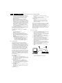
E_13950_011 .eps
030304
Figure 4-2 Rear cover (for FL13 styling)
Set Disassembly
Follow the disassemble instructions in described order.
4.2.1
Rear Cover Removal
Warning: disconnect the mains power cord before you remove
the rear cover.
For PV2 styling (for 8402 and 8302 sets)
1. Manually unlock and remove the two plastic cover cups (1)
(if present) on the top of TV.
2. Remove all the fixation screws of the rear cover.
3. Remove the rear cover.
2
E_13950_012 .eps
100304
1
Figure 4-3 Opening
E_13950_010.eps
030304
Figure 4-1 Rear cover (for PV2 styling)
For FL13 styling (for 8502 sets)
1. Remove all screws. If you do not remove them, you cannot
access the clips.
2. Tilt the set a little forward, so that you can release the two
clickfit clamps that are located at the bottomplate of the set.
3. Four openings (1) can be found at the top. The openings
are very small (2).
Note: Some sets only have the two inner openings.
4. Underneath every opening there is a clip. Push this clip
down with a very thin piece of metal (3), until you hear a
click.
Caution: do not use a screwdriver, this will damage the
cabinet.
5. When all four clips are pushed down, the back cover can
be removed.
3
E_13950_013.eps
030304
Figure 4-4 Pushing clips down
Mechanical Instructions
4.3
4.4
Service Positions
This chassis has several predefined service positions, for
better accessibility. They are explained below in more detail.
4.3.1
A02U AA
4.
EN 9
Assies/Panels Removal
Sometimes, it can be necessary to swap a complete assy or
Printed Wiring Board (PWB). How that can be done is
explained below.
Large Signal Panel (LSP)
4.4.1
Service position 1 - Component Side of the LSP
For better accessibility of the LSP, do the following (see Figure
"Service position 1"):
1. Remove the LSP-bracket from the bottom tray by pulling it
backwards.
2. Hook the bracket in the first row of fixation holes of the
bottom tray. In other words, reposition the bracket from (1)
to (2).
Top Control Assy/Panel
1. Remove the two fixation screws:
– PV2 styling: assy is mounted into the front cabinet;
– FL13 styling: assy is mounted into the rear cover.
2. Push the assy a little bit upwards, and then pull it
backwards to release it from the front hinge.
3. Lift the panel from its bracket, while releasing the four
fixation clamps.
4.4.2
Side I/O Assy and Panel
1
2
1
2
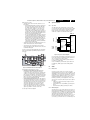
E_13950_007.eps
100304
Figure 4-5 Service position 1
Service position 2 - Solder Side of the LSP
To get access to the bottom side (solder side) of the LSP, do
the following (see figure above):
1. Remove the DC-Shift assy (1) (see paragraph "DC-Shift
Assy/Panel" below).
2. Release the Front interface assy from the bottom plate (2)
(see paragraph "Top Control Assy/Panel" below).
3. Disconnect the degaussing coil from the LSP. Therefore
remove the cable from the connector 1502 .
4. Release some wiring from their fixation clamps, in order to
get room for repositioning the LSP.
5. Flip the LSP 90 degrees clockwise (3), and place it
vertically on the bottom plate and a table.
E_14480_050.eps
170204
Figure 4-7 Side-I/O assy/panel
1. Remove the two fixation screws, and remove the complete
Side I/O assembly.
2. Release the two fixation clamps, and lift the panel from the
bracket.
4.4.3
HDMI Assy/Panel Removal
2
1
4
3
4
3
2
2
1
E_13950_004.eps
030304
E_13950_009.eps
040304
Figure 4-6 Service position 2
Figure 4-8 HDMI assy/panel
EN 10
4.
Mechanical Instructions
A02U AA
1. Remove the fixation screw (1) (if present).
2. Release the two pegs (2), by pushing them towards CRT.
3. At the same time, pull the complete module away from the
LSP bracket (3). It hinges in the LSP bracket.
4. Remove the four fixing screws (4), and remove the panel.
4.4.4
To get access to the SSB test points, do the following:
1. Put the LSP in service position 1 (as described above).
2. Remove the fixation screws, which hold the SSB-bracket
(1).
3. Release the clamping jaw at the top of the SSB bracket (2)
and (3).
4. Push the two clamping lugs outwards, and pull the top of
the bracket at the same time upwards (4) and (5).
5. Now you can remove the complete bracket. Push it, at the
height of the LSP-bracket, towards the CRT (6) and lift it
out of the LSP-bracket (7).
6. Take the SSB out, disconnecting it from the LSP.
Front Interface Assy/Panel
3
1
2
2
1
2
2
6
1
6
3
1
7
5
4
7
4
3
3
E_13950_005.eps
270204
E_13950_003.eps
030304
Figure 4-9 Front Interface assy/panel
Figure 4-11 Small signal board
1. Remove the two fixation screws (1).
2. Remove the complete module from the bottom plate, by
pulling the two fixation clamps upward (2), while sliding the
module away from the CRT (3).
3. Release the two clamps (4) at the sides of the bracket and
lift panel out (it hinges at one side).
4.4.5
Notes:
• For better access to the SSB, it is possible to order an
"extension tool" with cables. You can use this service
extension tool to connect a Small Signal Board (SSB) of an
Axx or EMx chassis, via two "IDE" cables to the SIMM
connector in the set. In this way, you can service the SSB
more easily outside the TV set. You can order this tool
under 12nc: 9965 000 14526.
• If necessary for the measurement, you can put the LSP in
the "service position 2" (as described above).
VDAF Assy/Panel
1
4.4.7
4
1. Remove the HDMI assy (see paragraph "HDMI assy/panel
above).
2. Remove the SSB (see paragraph "Small Signal Board
(SSB)" above).
3. Disconnect the necessary cables.
4. Remove the fixation screw, which is located nearby the
SIMM-connector.
5. Release the fixation clamps on the left of the LSP-bracket
(the panel hinges at the right side).
6. Remove the panel from the bracket.
4
2
3
3
E_13950_014.eps
040304
Figure 4-10 VDAF assy/panel
1. Remove the fixation screw (1) (if present).
2. Push down the fixation clamp (2), and pull the complete
bracket at the same time away from the CRT (3). The
module is now free from the LSP-bracket.
3. Release the two clamps (4) at the sides of the bracket and
lift panel out.
4.4.6
Small Signal Board (SSB)
In fact, there is no predefined service position for the SSB. Most
test points are located on the A-side (side that is facing the
tuner).
If you have to replace ICs, you must take the complete SSB
module out of the SIMM-connector.
Large Signal Panel (LSP)
4.5
Set Re-assembly
To re-assemble the whole set, do all processes in reverse
order.
Note: be sure that, before the rear cover is mounted:
• The mains cord is mounted correctly in its guiding brackets.
• All wires/cables are returned in their original positions. This
is very important due to the large "hot" area of the set
Service Modes, Error Codes, and Fault Finding
A02U AA
5.
EN 11
5. Service Modes, Error Codes, and Fault Finding
Index of this chapter:
1. Test points
2. Service Modes
3. Problems and solving tips (related to CSM)
4. ComPair
5. Error Codes
6. The blinking LED procedure
7. Protections
8. Repair tips
9. Software downloading
5.1
Test Points
See chapter 6 " Block Diagrams, Test point Overview, and
Waveforms".
Perform measurements under the following conditions:
• Service Default Mode.
• Video: color bar signal.
• Audio: 3 kHz left, 1 kHz right.
5.2
Service Modes
Service Default Mode (SDM) and Service Alignment Mode
(SAM) offer several features for the service technician, while
the Customer Service Mode (CSM) is used for communication
between a Philips Customer Care Center (P3C) and a
customer.
There is also the option of using ComPair, a hardware interface
between a computer (see requirements below) and the TV
chassis. It offers the ability of structured troubleshooting, test
pattern generation, error code reading, software version
readout, and software upgrading.
Minimum requirements: a Pentium processor, Windows 95/
98, and a CD-ROM drive (see also paragraph "ComPair").
5.2.1
Service Default Mode (SDM)
Purpose
• To create a pre-defined setting, to get the same
measurement results as given in this manual.
• To override SW protections (only when SDM is entered via
shorting the SDM pins on the SSB).
• To start the blinking LED procedure.
• Inspection of error buffer, life timer, and software version.
Specifications
• Tuning frequency: 61.25 MHz (channel 3).
• Color system: NTSC M.
• All picture settings at 50 % (brightness, color, contrast).
• All sound settings at 50 %, except volume at 25 %.
• All service-unfriendly modes (if present) are disabled, like:
– (Sleep) timer.
– Child/parental lock.
– Blue mute.
– Automatic volume limiter (AVL).
– Auto switch-off (when no video signal was received for
10 minutes).
– Skip/blank of non-favorite pre-sets.
– Hotel or hospital mode.
– Local keyboard block.
– Smart modes.
– Auto store of personal presets.
– Auto user menu time-out.
5.2.2
Service Alignment Mode (SAM)
Purpose
How to enter SDM
Use one of the following methods:
• Use the standard RC-transmitter and key in the code
"062596", directly followed by the "MENU" button.
Note: It is possible that, together with the SDM, the main
menu will appear. To switch it "off", push the "MENU"
button again.
• Short circuit, during switch "on" of the set, the two solder
pads on the SSB with the indication "FOR SERVICE".
These solder pads are located at the "tuner" side of the
SSB (just above the large BGA IC).
Caution: If the SDM is entered via these pins, all the
software-controlled protections are de-activated for 15 s.
When these 15 s are expired, the set will shutdown to
protection mode.
• Use the DST-emulation feature of ComPair.
• Use the "DEFAULT" button on the Dealer Service Tool
(RC7150).
After entering this mode:
• "SDM" will appear in the upper right corner of the screen.
• Also, the error buffer, operating hours, and software
version are displayed (can be toggled "on/off" with the
"STATUS / OSD / [i+]" button).
• Blinking LED procedure will be started.
• All software-controlled protections are overridden for 15 s.
When these 15 s are expired, the set will shutdown to
protection mode.
Contents of SDM:
• HRS. Displays the accumulated total of operation hours
(not the standby hours) in a hexadecimal value.
• SW ID. Displays the date of the software and the software
version of the ROM
Example: A02EB1_1.00 = AAABBC-X.YY.
– AAA= chassis name.
– BB= region and/or function name: E= Europe, A= Asia
Pacific, U= NAFTA, L= LATAM, B= Basic, T= Top, P=
PAL, N= NTSC, S= Stereo, M= Mono.
– C= the language cluster number.
– X.Y= the software version, where X is the main version
number (different numbers are not compatible with one
another) and Y is the sub version number (a higher
number is always compatible with a lower number).
• ERR (followed by maximal 8 errors). The most recent error
is displayed at the upper left (for an error explanation see
paragraph "Error Codes").
How to navigate
• When you press the "MENU" button on the RC transmitter,
the set will toggle between the SDM and the normal user
menu (with the SDM mode still active in the background).
• When you press the "STATUS" button on the RC
transmitter, the set will toggle only display "SDM". This
mode is useful when performing measurements, then the
OSD info will not generate interference.
How to exit SDM
Use one of the following methods:
• Switch the set to STANDBY via a standard customer RCtransmitter (the error buffer is erased).
• Via a standard customer RC-transmitter: key in "00"sequence (the error buffer is not erased).
•
•
•
To perform alignments.
To change option settings.
To easily identify the used software version.
EN 12
•
•
5.
A02U AA
Service Modes, Error Codes, and Fault Finding
To view operation hours.
To display / clear the error code buffer.
•
Specifications
• Operating hours counter.
• Software version.
• Option settings.
• Error buffer reading and erasing.
• Software alignments.
• Disable service unfriendly modes.
How to enter SAM
Use one of the following methods:
• Via a standard RC transmitter: key in the code "062596"
directly followed by the "STATUS" button.
• Use the DST-emulation feature of ComPair.
• Press the "ALIGN" button on the DST while the set is in the
normal operation
After entering this mode, "SAM" will appear in the upper right
corner of the screen.
Contents of SAM:
• HRS. Displays the accumulated total of operation hours
(not the standby hours) in a hexadecimal value
Note: every time the set is switched "on" by the AC power
switch or the RC, the timer is increased by 0.5.
• SW ID. Displays the date of the software and the software
version of the ROM (example: A02UB1-1.00 = AAABBCX.YY).
– AAA= chassis name.
– BB= region and/or function name: E= Europe, A= Asia
Pacific, U= NAFTA, L= LATAM, B= Basic, T= Top, P=
PAL, N= NTSC, S= Stereo, M= Mono.
– C= the language cluster number.
– X.Y= the software version, where X is the main version
number (different numbers are not compatible with one
another) and Y is the sub version number (a higher
number is always compatible with a lower number).
• ERR (followed by maximal 8 errors). The most recent error
is displayed at the upper left (for an error explanation see
paragraph "Error Codes").
• OPTIONS. Extra feature for Service to set the Option
Codes.
• CLEAR ERRORS. When you press the "OK" button, the
error buffer is reset.
• AKB. Disable (off) or enable (on) the "black current loop"
(AKB= Auto Kine Bias). For Vg2 alignment.
• TUNER. This will activate the "TUNER" alignments submenu.
• WHITE TONE. This will activate the "WHITE TONE"
alignments sub-menu.
• GEOMETRY. This will activate the "GEOMETRY"
alignments sub-menu.
• SOUND. This will activate the "SOUND" alignments submenu.
• SMART SETTINGS. This will activate the "SMART
SETTINGS" alignments sub-menu.
• STORE. This will save the new settings/alignments.
• EEPROM TEST. This will report if the SW checksum is OK.
Convenient after SW upgrading.
• VID RAM TEST. This will check the continuity of the
address bus and data bus of the Video RAM.
• VG2. This feature is not implemented yet. Do not use.
Note: Alignments are described in chapter 8 "Alignments".
How to navigate
• In SAM, you can select the menu items with the "CURSOR
UP/DOWN" key on the RC-transmitter. The selected item
will be highlighted. When not all menu items fit on the
screen, move the "CURSOR UP/DOWN" key to display the
next/previous menu items.
• With the "CURSOR LEFT/RIGHT" keys, it is possible to:
– (De) activate the selected menu item.
– Change the value of the selected menu item.
– Activate the selected submenu.
When you press the "MENU" button on the RC transmitter,
the set will toggle between the SAM and the normal user
menu (with the SAM mode still active in the background).
How to exit SAM
Use one of the following methods:
• Switch the set to STANDBY via the RC-transmitter (the
error buffer is erased).
• Via a standard customer RC-transmitter: key in "00"sequence (the error buffer is not erased).
5.2.3
Customer Service Mode (CSM)
Purpose
When a customer is having problems with his TV-set, he can
call his dealer or the Philips helpdesk (P3C). The service
technician can than ask the customer to activate the CSM, in
order to identify the status of the set. Now, the service
technician can judge the severity of the complaint. In many
cases, he can advise the customer how to solve the problem,
or he can decide if it is necessary to visit the customer.
The CSM is a read only mode; therefore, modifications in this
mode are not possible.
How to enter CSM
Key in the code "123654" via the standard RC transmitter.
Note: set must be in "Widescreen" mode (via button "PIC
SIZE" on the remote control)
Notes:
• Activation of the CSM is only possible if there is no (user)
menu on the screen!
• During CSM, sound volume is set to 25% of the scale,
"Smart Sound" is set to "Theatre" mode, and "Smart
Picture" is set to "Rich/Movies" mode temporarily to ensure
a good picture and sound of the working set. After leaving
CSM, the original settings are restored.
How to navigate
By means of the "CURSOR-DOWN/UP" knob on the RCtransmitter, you can navigate through the menus.
Contents of CSM
The following information is displayed on screen:
• Text "CSM" on the first line.
• Line number for every line (to make CSM language
independent).
• Option code information.
• Configuration information.
• Service-unfriendly modes.
CSM 1
1. SET TYPE (if displayed). Type/model number according to
the Philips standard.
2. SOFTWARE. Software version AAABBC-X.YY.
3. HOURS ON. Operating hours (in hexadecimal).
4. CODE 1. Shows the contents of the error buffer (the word
"error" may not be used on this screen, instead "codes" is
used).
5. CODE 2. Shows the contents of the error buffer (the word
"error" may not be used on this screen, instead "codes" is
used).
6. OPTION 1. Option code information (for more details see
chapter 8 "Alignments").
7. OPTION 2. Option code information (for more details see
chapter 8 "Alignments").
8. OPTION 3. Option code information (for more details see
chapter 8 "Alignments").
9. OPTION 4. Option code information (for more details see
chapter 8 "Alignments").
Service Modes, Error Codes, and Fault Finding
10. SIGNAL. State of the "ident" signal.
11. TIMER (if present). State of the timer (in "FEATURE"
menu).
5.3
EN 13
Black and white picture
Check in CSM line COLOR. In case the value is low (< 10),
increase the "Color" value. The new value is automatically
stored for all TV channels.
No colors/color lines around picture elements or colors
not correct or unstable picture
1. Check in CSM line SYSTEM. If a "strange" system pops
up, something has gone wrong during installation. Reinstall the channel.
Menu text not sharp enough
1. Press "SMART PICTURE". In case picture improves,
decrease the "Contrast" value. The new value(s) are
automatically stored for all TV channels.
2. Check in CSM line CONTRAST. If the value of this line is
high (> 50), decrease the "Contrast" value.
5.3.2
Sound Problems
No sound from left and right speaker
Check in CSM line VOLUME. If the value is low, increase the
value of "Volume". The new value(s) are automatically stored
(in "personal" pre-set) for all TV channels.
Problems and Solving Tips (related to CSM)
Note: Below described problems are all related to the TV
settings. The procedures to change the value (or status) of the
different settings are described above. New value(s) are
automatically stored.
5.3.1
5.
Blue picture and/or unstable picture
A scrambled or decoded signal is received.
CSM 2
1. CHANNEL (if present). State of the Child Lock.
2. PRESET (if present). State of the Current channel.
3. HOTELMODE (if present). Shows if the HOTEL mode is
activated.
4. SOURCE. Selected source before entry of CSM.
5. SOUND. Selected SOUND mode prior entry to CSM.
6. VOLUME. Volume level before entry of CSM.
7. BALANCE. Balance level before entry of CSM.
8. BRIGHTNESS. Brightness level before entry of CSM.
9. COLOR. Color level before entry of CSM.
10. CONTRAST. Contrast level before entry of CSM.
11. HUE (if present). Hue level before entry of CSM.
How to exit CSM
Use one of the following methods:
• After you press a key on the RC-transmitter (with exception
of the "CHANNEL", "VOLUME" and digit (0-9) keys), or
• After you switch the TV-set "off" with the AC power switch.
• After 15 min. no RC or local keyboard actions.
A02U AA
Sound too loud for left and right speaker
Check in CSM line VOLUME. If the value is low, decrease the
value of "Volume". The new value(s) are automatically stored
(in "personal" pre-set) for all TV channels.
Picture Problems
Picture too dark
1. Press SMART PICTURE several times on the RC. In case
the picture improves, increase the "Brightness" or the
"Contrast" value.
2. Check in CSM lines BRIGHTNESS and/or CONTRAST. If
the value of line BRIGHTNESS is low (< 10) or the value of
line CONTRAST is low (< 10), increase them. The new
value(s) are automatically stored (in "personal" pre-set) for
all TV channels.
5.4
ComPair
5.4.1
Introduction
ComPair (Computer Aided Repair) is a service tool for Philips
Consumer Electronics products. ComPair is a further
development on the European DST (service remote control),
which allows faster and more accurate diagnostics. ComPair
has three big advantages:
ComPair helps you to quickly get an understanding on how to
repair the chassis in a short time by guiding you systematically
through the repair procedures.
ComPair allows very detailed diagnostics (on I2C level) and is
therefore capable of accurately indicating problem areas. You
do not have to know anything about I2C commands yourself
because ComPair takes care of this.
ComPair speeds up the repair time since it can automatically
communicate with the chassis (when the microprocessor is
working) and all repair information is directly available. When
ComPair is installed together with the SearchMan electronic
manual of the defective chassis, schematics and PWBs are
only a mouse click away.
Picture too bright
1. Press SMART PICTURE several times on the RC. In case
the picture improves, decrease the "Brightness" or the
"Contrast" value.
2. Check in CSM lines BRIGHTNESS and/or CONTRAST. If
the value of line BRIGHTNESS is high (> 40) or the value
of line CONTRAST is high (> 50), decrease the
"Brightness" or the "Contrast" value. The new value(s) are
automatically stored (in "personal" pre-set) for all TV
channels.
White line around picture elements and text
1. Press SMART PICTURE several times on the RC. In case
the picture improves, decrease the "Sharpness" value.
2. Check in CSM line SHARPNESS. Decrease the
"Sharpness" value. The new value is automatically stored
for all TV channels. The new value is automatically stored
(in "personal" pre-set) for all TV channels.
No picture
Check in CSM line 7. In case this line shows NO SIGNAL,
check the aerial cable/aerial system.
Blue picture
No proper signal is received. Check the aerial cable/aerial
system.
5.4.2
Specifications
ComPair consists of a Windows based faultfinding program
and an interface box between PC and the (defective) product.
The ComPair interface box is connected to the PC via a serial
(or RS232) cable.
For this chassis, the ComPair interface box and the TV
communicate via a bi-directional service cable via the service
connector.
The ComPair faultfinding program is able to determine the
problem of the defective television. ComPair can gather
diagnostic information in two ways:
• Automatic (by communication with the television):
ComPair can automatically read out the contents of the
entire error buffer. Diagnosis is done on I2C level. ComPair
EN 14
5.
A02U AA
Service Modes, Error Codes, and Fault Finding
•
Pre-condition: Step 2 is done. No protection faults
detected.
• Post-condition: Deflection is switched "on". The horizontal
deflection fault protections are enabled.
Step 4: TV "on".
• Pre-condition: Step 3 is done. No protection faults
detected.
• Post-condition: Picture tube is switched "on". Sound
amplifiers are demuted. The X-ray/beam current fault
protections are enabled.
can access the I2C bus of the television. ComPair can
send and receive I2C commands to the micro controller of
the television. In this way, it is possible for ComPair to
communicate (read and write) to devices on the I2C
busses of the TV-set.
• Manually (by asking questions to you): Automatic
diagnosis is only possible if the micro controller of the
television is working correctly and only to a certain extends.
When this is not the case, ComPair will guide you through
the faultfinding tree by asking you questions (e.g. Does the
screen give a picture? Click on the correct answer: YES /
NO) and showing you examples (e.g. Measure test-point I7
and click on the correct oscillogram you see on the
oscilloscope). You can answer by clicking on a link (e.g.
text or a waveform picture) that will bring you to the next
step in the faultfinding process.
By a combination of automatic diagnostics and an interactive
question / answer procedure, ComPair will enable you to find
most problems in a fast and effective way.
Beside fault finding, ComPair provides some additional
features like:
• Up- or downloading of pre-sets.
• Managing of pre-set lists.
• Emulation of the Dealer Service Tool (DST).
• If both ComPair and SearchMan (Electronic Service
Manual) are installed, all the schematics and the PWBs of
the set are available by clicking on the appropriate
hyperlink.
Example: Measure the DC-voltage on capacitor C2568
(Schematic/Panel) at the Mono-carrier.
– Click on the "Panel" hyperlink to automatically show
the PWB with a highlighted capacitor C2568.
– Click on the "Schematic" hyperlink to automatically
show the position of the highlighted capacitor.
5.4.3
Stepwise Start-up
This is realized via ComPair and is very helpful when a
protection is activated (see also chapter "Protections").
Under normal circumstances, a fault in the power supply, or an
error during start-up, will switch the television to protection
mode. ComPair can take over the initialization of the television.
In this way, it is possible to distinguish which part of the startup routine (hence which circuitry) is causing the problem.
Take notice that the transition between two steps can take
some time, so give the set some time to reach a stable state.
During the transition time, the LED can blink strangely.
On entering Service mode, protections and other errors can be
trapped by powering the TV in stepwise fashion as explained
below. The "stepwise start-up" mode is done in the specified
sequence. Before entering this mode, all the protections are
disabled and are only enabled step-by-step, to trap the errors
more appropriately.
The following steps are involved.
Step 0: Standby.
• Pre-condition: The set is in protection mode.
• Post-condition: The set is switched to the stepwise start-up
mode. Only the necessary Standby Supply is present, all
other supplies are switched "off".
Step 1: Power "on".
• Pre-condition: All protections are disabled, sound
amplifiers are muted, and general initialization is done.
• Post-condition: 8V and 5V supplies are "on". Degaussing
is "on" and switched "off" after 3 s. The supply fault
protections are enabled.
Step 2: Initialized.
• Pre-condition: Step 1 is done. No supply protection faults
are detected.
• Post-condition: ADOC, MPIF, and Tuner components are
initialized.
Step 3: Deflection "on".
Note: When the set is in stepwise mode and, due to steppingup, a protection is activated, the set will really go into protection
(blinking LED). The set will not leave the stepwise-mode
however. If state X is the state where the set went to protection,
stepwise start-up will return to state X-1. At state (X-1)
diagnostic measurements can be performed. Also, in the short
time, the set is in state X but not in protection, you can also do
some measurements.
5.4.4
How To Connect
1. First, install the ComPair Browser software (see the Quick
Reference Card for installation instructions).
2. Connect the RS232 interface cable between a free serial
(COM) port of your PC and the PC connector (marked with
"PC") of the ComPair interface.
3. Connect the AC power adapter to the supply connector
(marked with "POWER 9V DC") of the ComPair interface.
4. Switch the ComPair interface "off".
5. Switch the television set "off" with the AC power switch.
6. Connect the ComPair interface cable between the
connector on the rear side of the ComPair interface
(marked with "I2C") and the ComPair connector at the rear
side of the TV (for its location see figure "Top view LSP" in
chapter "Alignments").
7. Plug the AC power adapter in a AC power outlet, and
switch the interface "on". The green and red LEDs light up
together. The red LED extinguishes after approx. 1 second
while the green LED remains lit.
8. Start the ComPair program and read the "Introduction"
chapter.
TO SERVICE
CONNECTOR
PC
VCR
Power
9V DC
I2C
E_06532_008.eps
190204
Figure 5-1 ComPair Interface connection
Service Modes, Error Codes, and Fault Finding
5.4.5
A02U AA
5.
EN 15
How To Order
Table 5-1 Error Code Table
ComPair order codes:
• ComPair Software: ST4191.
• ComPair Interface Box: 4822 727 21631.
• AC Adapter: T405-ND.
• ComPair Quick Start Guide: ST4190.
Error
Description
0
No error
1
Horizontal Protection (via NOHFB bit in ADOC)
3
+8V error (missing/protection active by checking
MPIF ASUP bit))
Note: If you encounter any problems, contact your local
support desk.
4
X-ray/High beam current
XPROT bit in ADOC)
5
Hardware Protection is active
5.5
Error Codes
7
11
MPIF I2C communication failure / MPIF test failed
5.5.1
Introduction
12
BC-loop not stabilised within the time limit (i.e. after
timer is expired)
The error code buffer contains all detected errors since the last
time the buffer was erased. The buffer is written from left to
right, new errors are logged at the left side, and all other errors
shift one position to the right.
When an error has occurred, the error is added to the list of
errors, provided the list is not full or the error is a protection
error.
When an error occurs and the error buffer is full, then the new
error is not added, and the error buffer stays intact (history is
maintained), except when the error is a protection error.
To prevent that an occasional error stays in the list forever, the
error is removed from the list after 50+ operation hours.
When multiple errors occur (errors occurred within a short time
span), there is a high probability that there is some relation
between them.
13
NVM I2C communication failure
5.5.2
5.5.3
How to clear the Error Buffer
Use one of the following methods:
• By activation of the "CLEAR ERRORS" command in the
SAM menu.
• With a normal RC, key in sequence "MUTE" followed by
"062599" and "OK".
• When you transmit the commands "DIAGNOSE" - "99" "OK" with ComPair (or with a DST).
• If the content of the error buffer has not changed for 50+
hours, it resets automatically.
5.5.4
Error Codes
Error codes are required to indicate failures in the TV set. In
principle a unique error is available for every:
• I2C device error.
• I2C bus error (for every bus containing two or more I2C
devices).
• Protection error (e.g. +8V protection or Horizontal
protection).
• Error not related to an I2C device, but of importance (e.g.
BC-loop, RAM error).
14
Main tuner I2C failure UV13xx
15
HDMI Panel Link Receiver
17
3D Combfilter I2C communication failure
18
PIP Tuner I2C failure
21
PIP IF demodulator IC TDA988x communication
failed (only for PIP/DW sets)
22
Flash over protection error (to register CRT flashovers, via FPR bit in ADOC)
Service tips:
• In case of non-intermittent faults, clear the error buffer
before you begin the repair. This to ensure that old error
codes are no longer present. Before clearing the buffer,
write down the content, as this history can give you
significant information.
• If possible, check the entire contents of the error buffer. In
some situations, an error code is only the result of another
error code and not the actual cause (e.g., a fault in the
protection detection circuitry can also lead to a protection).
How to read the Error Buffer
Use one of the following methods:
• On screen via the SAM (only if you have a picture).
Examples:
– 0 0 0 0: No errors detected
– 6 0 0 0: Error code 6 is the last and only detected error
– 9 6 0 0: Error code 6 was first detected and error code
9 is the last detected error
• Via the blinking LED procedure (when you have no
picture). See next paragraph.
• Via ComPair.
Under-voltage protection
protection signal (via
5.6
The Blinking LED Procedure
5.6.1
Introduction
Via this procedure, you can make the contents of the error
buffer visible via the front LED. This is especially useful for fault
finding, when there is no picture.
When the SDM is entered, the front LED will show (blink) the
contents of the error-buffer. Error-codes > 10 are shown as
follows:
1. A long blink of 750 ms (which is an indication of the decimal
digit),
2. A pause of 1500 ms,
3. "n" short blinks (where "n" = 1 - 9),
4. When all the error-codes are displayed, the sequence
finishes with a LED blink of 3000 ms,
5. The sequence starts again.
Example: Error 12 9 6 0 0.
After activation of the SDM, the front LED will show:
1. 1 long blink of 750 ms (which is an indication of the decimal
digit) followed by a pause of 1500 ms,
2. 2 short blinks of 250 ms, followed by a pause of 3000 ms,
3. 9 short blinks of 250 ms, followed by a pause of 3000 ms,
4. 6 short blinks of 250 ms, followed by a pause of 3000 ms,
5. 1 long blink of 3000 ms to finish the sequence,
6. The sequence starts again.
EN 16
5.6.2
5.
A02U AA
Service Modes, Error Codes, and Fault Finding
fault detection/protection must be enabled only after the
chassis power supply has been established. Likewise, after the
line drive starts, the deflection detection/protection must be
enabled. To prevent false activation of protection mode during
power mode transitions, interrupts related to supply fault and
deflection fault are disabled.
How to Enter
Use one of the following methods:
• Enter the SDM (only via soldering pads marked "FOR
SERVICE" on the SSB). The blinking front LED will show
the entire contents of the error buffer (this works in "normal
operation" mode and in "protection" mode). In order to
avoid confusion with RC5 signal reception blinking, this
LED blinking procedure is terminated when an RC5
command is received.
• Transmit the commands "MUTE", "06250x", and "OK" with
a normal RC (where "x" is the position in the error buffer
that has to be displayed). With x= 1, the last detected error
is shown, x= 2 the second last error, etc.... When x= 0, all
errors are shown.
• "DIAGNOSE X" with the DST (where "x" is the position in
the error buffer that has to be displayed). With x= 1, the last
detected error is shown, x= 2 the second last error, etc....
When x= 0, all errors are shown.
Note: It can take some seconds before the blinking LED starts.
5.7
Protections
5.7.1
Introduction
Fault protections are introduced to avoid unacceptable
temperature rising and burning hazards. If a fault situation is
detected, an error code will be generated and if necessary, the
set is put in protection mode.
The protection mode is indicated by the blinking of the front
LED at a frequency of 3 Hz (or by a coded blinking in special
cases). For the customer, it is made impossible to switch "on"
the set during a protection.
It is possible to determine the type of fault by interpreting the
blinking pattern of the LED indicator. It is also possible to read
out the error codes from the NVM via ComPair. It is possible to
de-activate the protection states in Service Default Mode.
The following protections are implemented:
Table 5-2 Protections overview
Protection
Detection
method
Bit name
5.7.2
I2C Related Protections
In normal operation, some registers of the I2C controlled ICs
are refreshed every 200 ms. During this sequence, the I2C
busses and the I2C ICs are checked.
An I2C protection will take place if the SDA and SCL lines are
short-circuited to ground, or to each other. An I2C error will also
occur, if the power supply of the IC is missing.
5.7.3
ADOC Related Protections
If a protection is detected at an ADOC input, the uP will start to
scan all protection inputs every 200 ms for five times. If the
protection on one of the inputs is still active after 1 s, the
microprocessor will put the set in the protection mode. Before
the scanning is started, a so-called "ESD refresh" is carried out.
This is done, because the interrupt on one of the inputs is
possibly caused either by a flash or by ESD. As a flash or ESD
can influence IC settings, the key ICs are initialized again, to
ensure the normal picture and sound conditions of the set.
Under Voltage Protection
The under voltage protection is needed due to the non-isolated
chassis architecture used in A02. Whenever there is a short
circuit in the Deflection yoke coil or in the Audio power supply,
the averaged Horizontal Flyback Voltage (HFB_XRAY_PROT)
will fall. After signal conditioning, this voltage is fed to the
"KEYBOARD_ADC" input. When this input of the MIPS
controller is less than a certain level, the under voltage
protection is activated. This is done by the normal keyboard
polling mechanism.
The protection mode is activated after five consecutive
occurrences. Response time required is 2 s. This is to avoid set
going to under voltage protection mode during start up, since
the HFB will only be stable w.r.t. mains on for about 1.6 s.
-Ve
Threshold
Detection
Switch
DOP
+Ve
Threshold
Via MPIF_IRQ ASUP
MPIF internal
register
Horizontal
fly-back
Via interrupts
ADOC internal
register (DOP)
NOHFB
FLASH
EHT-INFO
Under Voltage Via ADC (KB) ADC (KB) ADC input
+8V Supply
ADOC
When hor. Defl. coil or sound amp
BCL
s/c, HFB
will drop at <16Vpp level.
The switch will put ADC keybd to low.
Signal
conditioning
Signal
conditioning
HFB_X-RAY-
-Ve
Threshold
NOHFB
Inverter
Switch
XPROT
<16Vp-p
X-ray
Via interrupts
Beam Current Via interrupts
XPROT
BCF
ADOC internal
register (DOP)
ADOC internal
register (DOP)
Flash
Hardware ctrl
-
Hardware
Arc
Hardware ctrl
-
Hardware
Vertical
Hardware ctrl
-
Hardware
East/West
Hardware ctrl
-
Hardware
Bridge coil
Hardware ctrl
-
Hardware
The protections are split up in the following order:
• I2C related protections.
• ADOC related protections (via polling on I/O pins or via
algorithms).
• DOP related protections (mainly for deflection items).
• Hardware errors that are not sensed by the OTC (e.g.
vertical flyback protection, bridge coil protection, E/W
protection, arcing protection).
All faults detected are re-checked five times before the
protection mode is triggered. It should be noted that supply
MIPS CORE
Voltage
divider
Switch
+8V
MPIF
ADC
KEYBOARD
MPIF IRQ
E_13950_016.eps
040304
Figure 5-2 Under Voltage Protection
+8V Protection
Hardware is employed for the detection of +8V supply fault. A
hardware interrupt (MPIF-IRQ) is generated by the MPIF when
the +8V supply falls below the IC specification.
To avoid false detection, the corresponding interrupt sub
routine checks the status of "ASUP" bit in the MPIF status
register for five times consecutively with an interval of 200 ms
before triggering the protection mode. Response time required
is 1.2 s.
Service Modes, Error Codes, and Fault Finding
-Ve
Threshold
Switch
5.
EN 17
Once the XRAY protection status is confirmed, the "PRD" bit
has to be set to "1" by software. This enables an automatic stop
of the H-out via Slow Stop initiated by auto-clearing the DFL bit.
Now, the protection mode is activated.
ADOC
DOP
+Ve
Threshold
A02U AA
FLASH
EHT-INFO
Signal
conditioning
-Ve
Threshold
BCL
Switch
ADOC
DOP
+Ve
Threshold
HFB_X-RAY-
-Ve
Threshold
FLASH
EHT-INFO
Signal
conditioning
NOHFB
If EHT is too high at defined level,
BCL
the switch
will set XPROT to High
(over voltage).
Signal
conditioning
Switch
Inverter
Voltage
devider
XPROT
Detection by MPIF. ASUP status bit will set to
High if +8V falls below threshold level.
MIPS CORE
Signal
conditioning
HFB_X-RAY-
ADC
KEYBOARD
Switch
-Ve
Threshold
NOHFB
XPROT
MIPS CORE
Voltage
divider
MPIF
+8V
Switch
Inverter
>27Vp-p
MPIF_IRQ
ADC
KEYBOARD
Switch
ASUP
+8V
MPIF
E_13950_017.eps
040304
MPIF IRQ
E_13950_018.eps
040304
Figure 5-3 +8V Protection
Figure 5-5 X-Ray Protection
5.7.4
DOP Related Protections
Beam Current Protection
A hardware interrupt is generated by the DOP core when the
current at the BCL input of the ADOC IC exceeds the limit.
To avoid false detection, the corresponding interrupt sub
routine checks the status of "BCF" bit in DOP core for five times
consecutively with an interval of 50 ms before triggering the
protection mode. Once the BCL protection status is confirmed,
the "PRD" bit has to be set to "1" by software. This enables an
automatic stop of the H-out via Slow Stop initiated by autoclearing the "DFL" bit. Now, the protection mode is activated.
The uP reads every 200 ms the status register of the DOP (via
the I2C bus). If a protection signal is detected on one of the
inputs of the DOP, the relevant error bit in the register is set to
"high". If this error bit is still "high" after 1 s, the OTC will store
the error code in the error buffer of the NVM and, depending on
the relevancy of the error bit, the set will either go into the
protection mode or not.
Horizontal Fly Back Protection
Hardware is employed for the detection of a horizontal
deflection fault. The DOP core generates a hardware interrupt
when consecutive three horizontal flyback pulses are not
received at the HFB input of the DOP block of the ADOC IC.
To avoid false detection, the corresponding interrupt sub
routine checks the status of "NOHFB" status bit in the DOP
core for five times consecutively with an interval of 50 ms
before triggering the protection mode. The response time for
this protection needed is 300 ms.
-Ve
Threshold
+Ve
Threshold
EHT-INFO
Signal
conditioning
Switch
BCL
Signal
conditioning
HFB_X-RAY-
-Ve
Threshold
Switch
XPROT
MIPS CORE
Switch
MPIF
ADC
KEYBOARD
MPIF IRQ
E_13950_019.eps
040304
NOHFB
Inverter
Switch
XPROT
Switch
MPIF
Figure 5-6 Beam Current Protection
MIPS CORE
Voltage
divider
+8V
Inverter
Voltage
divider
+8V
Signal
conditioning
NOHFB
ADOC
DOP for 5 cycles
Consecutively check
FLASH
for the presence of flyback pulses
+Ve
Threshold
EHT-INFO
-Ve
Threshold
When beam current is too high, at
defined level and will set BCL input
ADOC
to=<1.2V, e7365. This
bit is checked
for 5 consecutive cycles to ensure
DOP
not caused
by
other
defect
FLASH
(i.e flash-over).
BCL
Signal
conditioning
HFB_X-RAY-
-Ve
Threshold
Switch
ADC
KEYBOARD
MPIF IRQ
E_13950_015.eps
040304
Figure 5-4 Horizontal Fly Back Protection
X-Ray Protection (Over Voltage, USA only)
Hardware is employed for the detection of X-ray fault. A
hardware interrupt is generated by the DOP core when the
"XPROT" input of ADOC IC is pulled "HIGH" (flyback pulses
are > 27 V_pp).
To avoid false detection, the corresponding interrupt sub
routine checks the status of "XPROT" bit in DOP core for five
times consecutively with an interval of 50 ms before triggering
the protection mode. It should be noted that the "XPROT"
status is not reset on reading. It should be cleared by the
software explicitly.
Flash Protection
Flash detection is used to shutdown the set only if the Flash
occurs more than five times and is persistent. Therefore, this is
a method to protect the set from undue electrical stress
because of picture tube flashes. The flash detector circuitry
uses the "EHT_INFO" signal as input. Its output is connected
to the "FLASH" input of the DOP block of the ADOC.
When the "FLASH" input is pulled "HIGH", the ADOCs
horizontal drive output stops immediately and the "FPR" status
bit of the DOP core is set to "1". The status is latched until
readout. With the absence of any other disturbances, the
horizontal drive output will restart after the "FLASH" input is
"LOW" again. No software interaction is required in this case.
The "FPR" bit has to be readout by polling at an interval of 500
ms. If the "FPR" status bit has been set to "1" for more than five
times consecutively, then the protection mode is triggered.
Setting the "FPR" bit for less than five times by the "FLASH"
input does not trigger the protection mode (shutting down of the
H-drive is enough).
EN 18
5.
A02U AA
-Ve
Threshold
Service Modes, Error Codes, and Fault Finding
Switch
DOP
+Ve
Threshold
5.8
Repair tips
5.8.1
Miscellaneous
ADOC
FLASH
EHT-INFO
Signal
conditioning
Signal
conditioning
HFB_X-RAY-
-Ve
Threshold
NOHFB
Inverter
Switch
XPROT
MIPS CORE
Voltage
divider
Switch
+8V
The relay you hear when you switch the set "on" (from Standby
or via the AC power switch), is from the degaussing circuitry. It
is not used for switching the Power Supply (as done in the MGchassis).
• Where the circuitry was too "crowded" for service printing,
you can find the correct location on the "test point
overviews" in this manual.
• A very large part of the LSP is "hot", such as:
– The primary part of the Standby Supply.
– The whole Main supply (except for the secondary
Audio supply).
– And the complete deflection circuitry (so notice that the
deflection coil is hot!).
BCL
MPIF
ADC
KEYBOARD
MPIF_IRQ
E_13950_020.eps
040304
5.8.2
Start-up/Shut-down Sequence
Figure 5-7 Flash Protection
5.7.5
For a detailed description, see chapter 9 " Circuit Descriptions,
Abbreviation List, and IC Data Sheets".
Hardware Related Protections
Due to the architecture (read: "hot" deflection), some
protections cannot be sensed by the microprocessor. These
protections will lead to a protection on set level (Standby mode
and blinking LED).
Arc Protection
If there are "open" connections (e.g. bad solder joints) in the
high-energy deflection circuitry, this can lead to damaging
effects (read: fire). For that reason, the E/W current is sensed
(via 3479//3480). If this current becomes too high, the
"thyristor" circuit (TS7653 and TS7654) is triggered. TS7442 is
switched "on" and TS7443 is forced into conduction. The "SUPENABLE" signal is shorted now to ground level, which will force
the Main Power Supply to Standby mode. This prevents further
arcing.
5.8.3
ComPair
This chassis does not have an IR transmitting LED (as in MGsets). Therefore, a "Service" (ComPair) connector is
implemented at the rear side of the set, which is directly
accessible. In addition to this, there is also a blinking LED
procedure to show the contents of the error buffer.
When you use ComPair, you have the possibility to activate a
"stepwise start-up" mode. With this mode, you can initiate the
start-up sequence step by step. This also means that in certain
steps, some protections are not activated. This is sometimes
very convenient during repair.
5.8.4
Protections
Vertical Protection
If the frame stage generates no pulses, TS7641 will block.
TS7443 is now switched "on", which will lead to Standby mode.
Therefore, in normal operation condition, TS7641 and TS7652
are conducting, while TS7443 is blocked.
Activating SDM via the "service pads" will overrule the
processor-controlled protections, but not the hardware
protections.
Caution: When doing this, the service technician must know
what he is doing, as it could lead to damaging the set.
EW protection
Several faults in the defection circuit can cause excessive
currents through MOSFET 7480. The temperature of this
device can become too high, causing an unsafe situation. The
power supply is shut down in the above-mentioned way.
Caution: All hardware deflection protections can be disabled
by interrupting R3403 on the LSP.
However, be careful: unsafe situations (heat) can occur or the
picture tube can be destroyed.
The "ARC"- and/or "BRIDGECOIL" protection are hardly ever
triggered, however:
• When you suspect the "ARC" protection, look for bad
solder joints and smell. By interrupting resistor 3497, this
protection is disabled (special attention needed!).
• When you suspect the "BRIDGECOIL" protection, which
can also be due to a too wide picture amplitude, shorten G
and S of the E/W MOSFET 7480. This will disable the
protection. You will now have minimal horizontal amplitude.
Re-align the horizontal amplitude in the SAM menu and
remove the G/S short of TS7480.
Bridge coil protection
According safety regulations, every coil may be short-circuited.
By doing this in the secondary winding of coil L5422, high
currents will flow in the winding. With no safety circuit, the coil
will begin to burn soon.
This is sensed via the "EW" signal going to the base of TS7652
(via R3495 and D6499). In a normal situation, the voltage on
C2498 (diagram A4) is high and TS7652 is conducting. When
bridge coil 5422 (diagram A3) is short circuited, the voltage on
C2498 changes to low, which will block TS7652. In this case,
also TS7641 will block and the voltage on 2642 will rise until
TS7443 is forced in conduction. The "SUP-ENABLE" signal (in
normal operating condition -20 V) is shorted now to ground
level, which will force the Main Power Supply to Standby mode.
Note: Maximum EW width settings can also cause a
protection.
Service Modes, Error Codes, and Fault Finding
5.8.5
A02U AA
5.
EN 19
(first connect ground to measuring equipment, than measure
the gate).
Main Supply
1. Replace FET 7504 and zener 6505.
2. Disconnect the SSP panel.
3. Short B and E of TS7529, in order to put the Main Supply
in "on"-mode (TS7529 is blocking then).
Caution: To prevent that R3403 and TS7443 will be
damaged, first disable the HW-protection of the
deflection circuit. Therefore, short-circuit C2642 on the
LSP (diagram A4).
4. Attach a load of 500 ohm to the V_BAT capacitor C2515
(the supply can not work without a minimum load).
5. Use a variac, and slowly increase the V_MAINS. Measure
over sensing resistors R3514//15, if a nice sawtooth
voltage becomes available.
6. Also, measure the V_BAT. This may never exceed +141 V.
If it does, there is something wrong in the feedback circuitry
(e.g. regulator 7506).
Note: Be careful when measuring on the gate of FET TS7504.
This circuitry is very high ohmic and can easily be damaged
5.8.6
Frame Deflection
Caution: When the Frame Deflection circuitry is suspected,
one must be careful. Because there is a DC-voltage on the
frame deflection, the beam current could damage the CRT
neck, leading to a defective CRT.
To prevent this from happening, you must:
1. Interrupt the resistors 3403 and 3404 on the CRT panel
(diagram F), in order to remove the "filament" voltage from
the tube (no beam current, so no chance of destroying the
CRT).
2. Interrupt resistor 3403 on the LSP (diagram A4) to disable
the "SUP-ENABLE" line.
3. Measure with a multi-meter, or better with an oscilloscope,
the functionality of the Frame stage.
4. After you have found the cause, exchange the defective
component (e.g. TDA8177), and re-solder the interrupted
resistors.
Table 5-3 Repair tips
Phenomenon
Possible Cause
Repair tip
No picture, no LED.
Standby Supply defective.
Measure circuitry (see diagram A2). Start at test-point A19.When the Mains switch is "on", this voltage
must always be available.
No picture, LED blinking at 3 Hz.
Set is in protection due to various
causes. For error codes see errorcode list.
You have no picture, so: read the error buffer via ComPair (error buffer is accessible when set is in
protection, ComPair-file will guide you to this). Read the blinking LED information via standard remote
command mute-06250x-ok. Or you read the error code sequence via standard remote command mute062500-ok. When you have found the error, check the circuitry related to the supply voltage and I2Ccommunication or the circuitry that triggers the protection.
No picture, LED blinking with code 8-8-8etc or 9-9-9-etc.
No communication on slow I2C- or
fast I2C-bus.
As processor cannot communicate with one of the 2 busses it the standby-LED spontaneously starts
blinking 8-8-8-etc or 9-9-9-etc... If in the error buffer somewhere is an error 8 or 9, these will have the
highest priority starting the mentioned blinking. Measure dependent of the error on the I2C-bus which
device is loading the bus (use the I2C-overview)
No picture, LED blinking with code 13-13- No communication on NVM-I2C
13-etc.
bus to the uP.
As the uP cannot communicate with the NVM I2C bus, it spontaneously starts blinking 13-13-13-etc. Note:
when there is no access to the NVM, a lot of picture setting can go wrong.
No picture, no sound. Set is making
audible squeaking sound
Possible causes: V_BAT is shorted (caused by short circuited line transistor 7421), the sound winding is
shorted (amplifier is shorting the power supply lines), or D6514 is shorted (due to a too high V_BAT).
Remove excessive load, to see what causes the failure, or check feedback circuit. See repair tip "Main
Power Supply" (supply needs a minimal load).
Supply is possibly in hiccup-mode,
which is audible via a squeaking
supply transformer.
No picture, no sound. Front LED works fine Supply does not work correctly.
If e.g. V_BAT is only about 90 V, it is possible that the regulator IC (7506) is defective.
No RC-reception. Front LED does not
echo RC-commands.
uP circuitry or RC-receiver is
defective.
In case the set does react on a local keyboard operation, you must check the RC-receiver circuitry
(diagram J).
Relay (degaussing) is not audible, when
set is switched from "off" or "standby" to
"on".
uP is not working correctly. When
line "DEGAUS" is low, the
degaussing must be activated.
Check RESET-circuitry (IC7581 on diagram B11). Check the level on line "DEGAUS" when you switch the
set "on". Signal must be low initially and go to high after approx. 12 s.
Picture is rotated.
Rotation circuitry (if present) on
diagram A5, or related supply to it,
malfunctions.
Measure test points on diagram A5.
Picture is continuously switching "off" and 200 V is missing on CRT panel.
"on", showing heavy "switch" spots (set
does not go into protection).
Probably a bad connection from LSP connector 1424 to CRT connector 1424 (diagram F), or an
interruption of the 200 V supplies line (e.g. R3341 on circuit F1 is interrupted).
Picture is not sharp.
Focus is possibly mis-aligned or
SCAVEM-circuitry does not work
correctly.
Re-align the "FOCUS" potmeter on the Line Output Transformer, or check the SCAVEM circuitry on the
CRT-panel (diagram F). It is also possible that the DAF circuitry is defective (see diagram I). Check the
V_dc values.
Picture is distorted.
Check video-path in Service Default Investigate whether there is an error code present in the error buffer. In case there is one, check the I2CMode.
bus and/or supply lines (see overview supply lines). Measure and check signal path Tuner-MPIF-ADOCRGB amplifier. In case it is a geometry issue, check on diagram A4 opto-coupler 7482, OpAmps 7440/
7450 and the Frame circuitry alignments or a possible corrupted NVM (IC7525 on diagram B11).
No menu, no OSD.
Probably a defective uP (ADOC).
No Teletext.
IC7730 defective or not powered.
Check circuitry around IC7730 on diagram B13.
Strange switch "off" behaviour
TS7445 possibly defective.
Check, with a multi-meter, whether transistor TS7445 is well functioning. (diagram A3).
Various symptoms, due to missing local
supply voltage.
An interrupted fuse, NFR-resistor or When no symptom or error code leads you to a specific circuitry, use the supply lines overview (see supply
connection.
lines overview), for a quick scan of all supply lines.
EN 20
5.9
5.
A02U AA
Service Modes, Error Codes, and Fault Finding
Software Downloading
In this chassis, you can upgrade the software via ComPair.
You can find more information on how this procedure works in
the ComPair file. It is possible that not all sets are equipped
with the hardware, needed to make software upgrading
possible. To speed up the programming process the firmware
of the ComPair interface can be upgraded. See paragraph
"How To Order" for the order number
Block Diagrams, Testpoint Overview, and Waveforms
A02U AA
6.
21
6. Block Diagrams, Testpoint Overview, and Waveforms
Wiring Diagram
E
DEGAUSSING COIL
TOP CONTROL PANEL
CRT
AQUADAG
0215
3p
F
CRT PANEL
EHT
ROTATING
COIL
(COMPONENT VIEW)
11p
1435
1010
2p
1483
3p
1940
1009
2p
RED
SPEAKER R
SPEAKER L
BLACK
CRT
SOCKET
A
MAINS
SWITCH
0203
1951
CRT PANEL
0202
0201
2p
2p
LSP(LARGE SIGNAL PANEL)
3p
SIDE
I/O PANEL
D
5p
F
1424
7p
1434
FRONT
INTERFACE
PANEL
J
SCAVEM
COIL
MAINS
CORD
1620
SVHS
1505
0240
2p
11p
CVBS (YELLOW)
LEFT (WHITE)
1947
1502
2p
5p
RIGHT (RED)
HEADPHONE
1735
1201
SSB
SMALL SIGNAL
BOARD
5p
1491
80p
2p
1940
I
1417
B
VDAF +
2ND ORDERS
PANEL
2p
1497
1491
LOT
1499
2p
G
DC
SHIFT
(OPTIONAL)
1943
Compair
connector
3642
CINCH
2p
I/O
2p
X
1417
2p
1424
7p
2p
1418
1625
4p
1419
2p
0317
2p
2p
11p
1117
1936
11p
7p
1116
1951
TUNER
TUNER
B
1117
11p
4p
1116
7p
1510
11p
1951
5p
M
3p
1945
HDMI PANEL
1498
E_13950_065.eps
120304
Block Diagrams, Testpoint Overview, and Waveforms
A02U AA
6.
22
Block Diagram LSP Supply and Deflection
2
1
4
1
MAIN SUPPLY
0202
1951
3
2
1505
2
1
1
0+
6525
GBU4J
4-
3509
RS
7505, 7506, 7503
2
1503
1
+
2516
3
1
+375V
DEGAUSSING
SUP-ENABLE
6109
A8
7102
STP3NB60
A11
G
5
6
3
7
3161
8
1
10
GND-STB
5106
3120 -20V
-20V
2102
7141
+5V
S A21
D
6
3456
G
CONTROL
-20V
3173
G
5
CONTROL
CIRCUIT
4
A3
3514
3
4
10
HOT
ADOC
A33
3479
A34
3658
FILAMENT
3
7
A30
5461
6460
A29
+11D
4
3480
HFB_X-RAY-PROT.
3460
12
3461
B8
ADOC
7445
POR
FRAME DEFLECTION
B11
POR
ADOC
2
7450-A
1
EW
3463
+13V - LOT
6462
3462
2462
5621
1
6
5
10
3465
7614
6465
A32
-15V - LOT
+13V-LOT
5465
7641
7443
7652
3464
6464
2464
3635
A50
A36
A35
6463
A31
5463
+8V6
3
AUDIO
COLD
HOT
HOT COLD
6491
EW
PROTECTION
CIRCUIT
+8V-S
PROTECTION
CIRCUIT
SUP-ENABLE
1
3636
7613
TL431
3657
+13V LOT
3
3498
COLD
COLD
3449
3627
HOT
1495
1
2
3637
2
-15V_LOT
HOT
CRT
B8 B9
6
B8
ADOC
FRAMEDRIVE-
N.C.
2
F
5
A6
7455
7440-A
1
4
EHT-INFO
3437
3483
3641
3
3499
3
A49
+11D
-12V8
4
+8Vb
1
6627 6626 6625
VBATT
ADJUSTMENT
A5
1
3530
3
+8V-S
3507
3510
ACTIVATING
CIRCUIT
6514
6620
3660
2523 2515
7611
TV
3640
3631
3642
3643
3527
SUP-ENABLE
GND-FB
3526
GND-SUP
3638 7620
TDA8177
3630
3632
7612
3634
2
THERMAL
PROTECTION
A40
4
-15V-LOT
SUP-ENABLE
+11V_ROT
125mA
3623
A43 3647
5
OP. AMP
COLD
1601
3
6
HOT
A42
FLYBACK
GENERATOR
A39
ROTATING CIRCUITRY
6619
2622
7
1
GND-FB
A5
+13V-LOT
A6
+VBATT
7506
TL431CZP 2
TO
1424
B8 B9
9
7487
3459
+
2542
COLD
3506
HOT GROUND
200V
2443
7442, 7654
7653
B8
5514
+
2546
2442
A45 7486
2
A3
ADOC
+11V_STBY
GND-AUD
3520
2
-20V
+
2512
9
1
A4
7507
TCET1103
7529
7
3
A7
5
2457
HFB_X-RAY-PROT
+28V
6539
A2
3531
6
6535
3484
4
FRAMEDRIVE +
5507
7482
3
A28
6400
3400
6480
5467
7480
3488
STP3NB60 A47
D
A46
G
S
A48
3481
3493
1
A38
2404
+8V6
B11
S
DAF
7450-B
7
3419 7441
STANDBY
5517
5506 OR
5512
EHT-INFO
11
7440-B
7
5
7132
7502
7530
+141V
3492
CURRENT
SOURCE
3457
2403
7140
7504
0.4
D
2
HFB_X-RAY-PROT.
3451
3455
STP16NE06
A16
1424
1
6
TO 1693
+8Vb
+8Vb
+5V-SWITCH
3114
GND-STB
1
FILAMENT
+11D
3450
10
+8V-S
+5.2V
1A6
6122
3124
2
3431
2431
I
A37
+5.2V_MP
6111
5
6
MPIF
1147
6103
3
+11D
5421
A19
CONTROL
3113
4
7133
7130
6456
EW-DRIVE 1
B4
5103
2
E/W - DRIVE
3654
2126
G
7103 OR 1
7104
5
A13
5102
+8V6
STP16NE06
GND-STB
6107
2430
8
FRAME DEFLECTION
E/W DRIVE
1693
A4
A18
+8V6-SWITCH
7131
S A20
D
3118
A15
1
1492
COLD HOT
1A25
5111 6130 5130
1491
CRT
VG2
EW
CORR.
VER. DAF
CIRCUIT
(OPTIONAL)
+11D
6118
6148
+11V
2
FOCUS B
+
7408
1148
S
A12
5113
3108
A23
3404
5104
D
6
1
E/W
DRIVE
TO
F
LINE
OUTPUT
CIRCUIT
+11V_STBY
6117 6119 +11V_ROT
A10
7100
7101
7105
7120
1
COLD
HOR. DAF
CIRCUIT
1693
TO
A4
FOCUS A
9
ADOC
3116
5100
5109
CONTROL
CIRCUIT
MAINS
SUPPLY
3416
A24
7409
A22
LINEDRIVE 1 2492 3406 3414
+
B8
4
EHT
LINE
DEFLECTION
COIL
HOT
1497
1
DYNAMIC FOCUS
1
5410
+5.2V
VTUN
6113
5800
7421 A26
BU2520DX
A25
B11
3115
A17
5101
+375V
A1B
3415
+11D
V-START
STARTUP
2
LOT
6408
6110
5112
2
5
6407
STAND-BY SUPPLY
2
COLD
ADOC
A2
1
1417
5430
A2
+5.2V_MP
1418
1
HOT
COLD
ACTIVATING
CIRCUIT
QUICK
SWITCH
OFF
MAIN SUPPLY
2
1417
1
5401
5400
+VBATT
HOT
1550
4
7501
7528
GND-STB
2
DEG.
COIL
1
F2.5AH
400 mA
DAF
I
1
+141V
1502
3
2
A1
+
V-START
5502 5511
5503 5516
5504
2
1430
0317
1
RP
3
MAINS
FILTER
+VBATT
DCSHIFT
CIRCUIT
8+ 1
1501
1419
DC-SHIFT (OPTIONAL)
G
3550
2
V
LINE DEFLECTION
A3
MAINS SWITCH (not for USA)
T5AH
DEFLECTION
A1A
ARC-PROT
0201
2
FILAMENT
PULSES
FRONT INTERFACE
SUP-ENABLE
J
5620
A44
3620
7680
TDA7052
1625
1
TILT
B7
2
VERT.
DEFL.
COIL
ADOC
1
+Vp
5
3686
2
3
7681
7682
SWITCH OFF
CIRCUIT
IN STAND-BY
2
3684
3685
8
6
6080
1620
1
3
ROTATION
DEFLECTION
COIL
E_13950_066.eps
120304
TO
PANEL
ON
CRT
NECK
(optional)
Block Diagrams, Testpoint Overview, and Waveforms
A02U AA
6.
23
Testpoint Overview LSP and CRT
LSP COPPER TRACK SIDE
2
1
3
4
5
6
7
8
9
10
A1
A2
A3
A4
A5
A6
A7
A10
A11
A12
A13
A14
A15
A16
A17
A18
A19
A20
A21
A22
A23
A24
A25
A26
A28
A29
A30
A31
A32
A33
A34
A35
A36
A37
A38
A39
A40
A41
A42
A43
A44
A45
A46
A47
A48
A49
A50
A56
A57
S
A20
G
G
1
A59
A
D 7131
+8V6
A18
8
D
A19
A68
A21
S 7141
+5V
7680
ROTATION
6
A15
A16
A56
C
10
1
5
A58
1
A33
A4
A35
D
S
S
A37
A23
A36
A3
A22
G 7504
MAIN
SUPPLY
D
A25
D
A24
A26
A50
G
A2
S
7480
E/W
A46
E
A38
A34
A12
G 7102
STANDBY
SUPPLY
C
A49
A57
A5
D
A13
B
A6
A11
A14
12
1
SSB
80
5506
A10
D
7701
AUDIO
AMPL
TRAFO
STANDBY
SUPPLY
5 TRAFO 1
5100
A45
B
C
7421
LINE
A48
A39
E
A31
A47
A1
A42
1
A44
7
A43
A41
56 8
4
9
3
10
2
11
1
12
LOT 5430
A71
E
A40
A32
7620
FRAME
F
A
A70
MAINS
10 SUPPLY 6
A17
5 4
A69
A7
14
B
TUNER
11
F
A29
G
G
ATTENTION:
LIVE PARTS
COLD HOT
1
2
3
A28
HOT
4
5
6
A30
COLD
7
8
9
E4
D3
D4
C4
C4
C5
A4
C2
C2
D3
D1
D1
C1
C1
B1
A1
A3
A2
A3
D8
D8
D8
D8
D7
G9
G10
G10
E9
E9
C8
D9
C9
D10
D9
C9
D10
E10
E10
E10
F10
E10
D7
E6
E7
E7
C9
D9
C6
B6
A58
A59
A68
A69
A70
CRT PANEL (COPPER TRACK SIDE)
C6
B5
A9
A10
A10
F1
F2
F3
F4
F5
F6
F7
F10
F11
F12
F13
14
A15
A16
A17
A18
A19
A20
A21
A22
A23
A24
1424
1
7
F10
F15
F11
F12
F13
F4
F5
G
R
7307
9
F9
F7
B
F8
F6
F14
F1
1
F3
E4
D3
D4
C4
C4
C5
A4
C2
C2
D3
D1
D1
C1
C1
B1
A1
A3
A2
A3
D8
D8
D8
SC3
1435
11
1
3139 123 5746.2
F1
F2
1 V / div DC
20µs / div
F3
1 V / div DC
20µs / div
1 V / div DC
20µs / div
F7
F9
F8
20 V / div DC
20µs / div
F13
20 V / div DC
20µs / div
20 V / div DC
20µs / div
F10
20 V / div DC
20µs / div
20 V / div DC
20µs / div
F6
F5
F4
20 V / div DC
20µs / div
F12
50mV / div DC
20µs / div
1 V / div DC
20µs / div
SC3
Measured across
6, 10, 5300
1 V / div DC
20µs / div
20 V / div AC
20µs / div
10
3139 123 5523.1
A1
PM3394B
50V / div DC
2us / div
A21: 5V1 DC
A2
PM3394B
50V / div DC
5us / div
A22
PM3394B
1V / div DC
10us / div
A40
PM3394B
2 V / div AC
5ms / div
A41
PM3394B
2 V / div AC
5ms / div
A3
PM3394B
50V / div DC
5us / div
A23
PM3394B
200mV / div DC
10us / div
A42
PM3394B
10 V / div AC
5ms / div
A4
PM3394B
50V / div DC
5us / div
A24
PM3394B
5V / div DC
10us / div
A43
PM3394B
10V / div DC
2ms / div
A5
PM3394B
5V / div DC
10us / div
A25
PM3394B
A6
PM3394B
A7: 33V DC
20V / div DC
10us / div
A26:
A10
PM3394B
50V / div DC
5us / div
A28: 206 V DC
A29: 11V4 DC
200 V / div DC
10µs / div
A44
PM3394B
200mV / div DC
2ms / div
A11
PM3394B
5V / div DC
5us / div
A30
PM3394B
A12
PM3394B
A13
PM3394B
2V / div DC
5us / div
5V / div DC
10us / div
A31: 13V DC
A32: 15V DC
50 V / div DC
10µs / div
A45
PM3394B
1V / div DC
10µs / div
A46
PM3394B
500mV / div DC
10µs / div
A47
PM3394B
50V / div DC
10µs / div
A48
PM3394B
500mV / div DC
10µs / div
A14
PM3394B
A50: *V DC
PM3394B
200mV / div DC
10us / div
500mV / div DC
5ms / div
A33
A34
PM3394B
500mV / div DC
2ms / div
A49: *V3 DC
A15
A56
PM3394B
20mV / div AC
1ms / div
PM3394B
500mV / div DC
2ms / div
A57
PM3394B
500mV / div AC
1ms / div
A16
PM3394B
5V / div DC
5ms / div
A35
PM3394B
A17
PM3394B
20V / div DC
5us / div
A36
PM3394B
A18
PM3394B
5V / div DC
5us / div
A37
PM3394B
A19
PM3394B
1V / div DC
5us / div
A38
PM3394B
500mV / div DC
2ms / div
200mV / div DC
10us / div
500mV / div DC
2ms / div
200mV / div DC
10us / div
A58
A59
A68
A69
PM3394B
20mV / div AC
200µs / div
PM3394B
500mV / div AC
1ms / div
PM3394B
500mV / div AC
20µs / div
A20: 8V DC
PM3394B
2 V / div DC
100ms / div
A39
PM3394B
2V / div DC
10us / div
A70
PM3394B
2 V / div DC
100ms / div
CL 36532058_007.eps
071003
Block Diagrams, Testpoint Overview, and Waveforms
A02U AA
6.
24
Block Diagram 1 Audio & Video (A02 NAFTA IF_video_source_ select)
B1
VTUN
VIDEO SOURCE SELECT & DATA LINK
B2
IF & SAW FILTER
7063
7100-B
MPIF VIDEO SWITCH
+5Vb
6200
7,3
11
110
7100-C
13 IF-TER
2101
4101
2
1113
VIFINP
7
4104
5
VIFINN
8
3
CVBS/Y prim
MPIF IF
107
7060
108
2062
120
Sound
Traps
14
4
123
CLAMP
A
1
SCL
TUNER_AGC
105
SIF A/D
0230
48
15
99
SDA0
SCL0
126
100
EF
116
QSS Mixer
AM Demod.
LPF
(PIP/DW)
AM Int
2ndSIFEXT
B11
113
122
125
118
1 CVBS-2
Y-CVBS-SC2_AV2-IN
4 CVBS/Y-3
C-SC2_SVHS-IN
5 C3
STROBE1N
B17
STROBE1P
61
STROBE1P
(NAFTA 87xx
series ONLY)
DATA1N
62
DATA1N
DATA1P
63
DATA1P
2115
7860 7862
9 C4
Data
Link
3
A
D
15 Y-COMB
50
STROBE3N
STROBE3P
51
STROBE3P
DATA3N
53
DATA3N
DATA3P
54
DATA3P
4152
+2V5D
59
SDA1
4121
V
5
AGC
14
Note: 27/32MS series does not
A11
5
L
4087
AUD-L2
6
R
4091
AUD-R2
7
L
4085
AUD-L1
2
AUD-R1
4089
B18
0230
REAR IO
3242
7
19
1
+33V
8
8
VTUN
+8V
+5V
SCL
11
7
7
2
2
+5V
13
10
PIP-AUDIO
1
SIF_MAIN
3
CVBS2_PIP_TUN2
SIDE IO PANEL
(PV0 & PV2)
4
SEL-SVHS-RR_STATUS2
SVHS 2
L
R
L-SC1_AV1-IN
R-SC1_AV1-IN
B/Pb/U1
30
G-Y-2FH
31
1117
Yyuv
YUV
32
A
D
RGB
CLAMP
R/Pr/V2
Data
Link
2
U,V
LPF
U
Source
G/Y/Y-2
A
V
D
49
AUD-L1
4
5
64
CVBS-SC3
CLP prim
CLP Yyuv
STROBE2N
STROBE2P
56
STROBE2P
DATA2N
57
DATA2N
DATA2P
58
DATA2P
HV-PRIM
46
HV_PRIM
HV-SEC
45
HV_SEC
CLP sec
Timing
Circuit
A8
4
7
7
AUD_R2
B3
7
PIP-AUDIO
3
SIF_MAIN
AUDIO SOURCE SELECT
+5V
SIMM CONN
62
17
AM EXT
L-SC1_AV1-IN
86
L1
A7
66
R-FRONT-IN
3150
LPF
3151
Supply
+
Ref.
A
7150-B
B8
D
21
Mono sec
+5V
20
R prim
+
B10
VREF_AUD_POS
D
LPF
Mono sec
Dig
3152
VREF_DEFL
B11
3153
R-SC1_AV1-IN
85
R1
AUD-L1
84
L2
AUD-R1
83
R2
IRQ
42
L-SC2_AV2-IN
82
L3
SDA
43
R-SC2_AV2-IN
81
R3
SCL
44
SCL1
L-FRONT-IN
80
L4
XREF
40
F_REF
R-FRONT-IN
79
R4
EWVIN
36
EW_MPIF
EWIOUT
37
EW-DRIVE
SCART2R
65
R-SC2-OUT
SCART2L
66
L-SC2-OUT
SCART1R
69
R-SC1_AV-OUT
SCART1L
70
L-SC1_AV-OUT
LINER
67
R-CL_VL-OUT
LINEL
68
L-CL_VL-OUT
HEADPH-R
8
8
LPF
D
14,28,35
HEADPH-L
L-FRONT-IN
R
3
FRONT-DETECT
65
6
PIP-AUDIO
7150-A
2
A
LR prim
C-FRONT-IN
6
L
+8V
L prim
AM
Int
A
Y-CVBS-FRONT-IN
2
MPIF AUDIO SWITCH
98,88
Dig
63
2
7100-D
CVBS2_PIP_TUN2
3242
CVBS
COUT-COMB
MPIF-SUPPLY
EW & CONTROL
B4
SIF_PIP
B11
11
YOUT-COMB
CLP Yyuv
VCC-I2D
91,77
+5V
1
64
7818,
7807
B5
AUD_L2
B18
SIMM
CONN
7816 -
+8Vd
B2
N.C.
6
7
83
7800 7803
Mono Sec.
Dig.
B/Pb/U2
VCC-DIG
55
ACO
84
RESET
7875
STROBE2N
AUD_L2
127
L5
AUD_R2
128
R5
LR
prim
A/D
Mono
sec
A/D
LR
Line
LR
Scart
I2 C
EW
V
+5V
MPIF-IRQ
SDA1
I
R
CVBS
53
L-SC2_AV2-IN
58
R-SC2_AV2-IN
2
G-SC1-IN_Y-IN
10
HP
DSNDL1
11
75
74
DSNDR1
DSNDL2
73
DSNDL2
DSNDR2
72
DSNDR2
AUDIO
1936
MON. OUT
1
L
O
B-SC1-IN_U-IN
U
3
R-SC1-IN_V-IN
9
CVBS-SC2_MON-OUT
56
L-CL_VL-OUT
61
R-CL_VL-OUT
EUROPE ONLY
DSNDL1
DSNDR1
Y
R
AYO
Switch
AUD-R1
RSTB
CLP sec
+3V3SW
27
R-P R-2FH
XO
57
27/54 MHz
5
10
CVBS-SC1_AV1-IN
60
H-2FH
B-SC1-IN_U-IN
B-P B-2FH
7
Y-CVBS-SC2_AV2-IN
52
B5
4062
C
AV1
L
4153
1
5
AV3
AV2
FBL
26
G/Y/Y-1
XI
48
Yyuv
7100-A
SIF_PIP
Y
CVBS
B-P B-2FH
4
2
SDA-S
+5V
CVBS
3
G-SC1-IN_Y-IN
8
EF
Y
6
G-Y-2FH
R/Pr/V1
+5V
SCL-S
1
1
SDA
10
3242
B11
9
+8V
C-SC2_SVHS-IN
3241
9
CVBS sec
B3
12
EF
O
SIMM CONN
SVHS 1
C
17
7203
SEL
7202
I2S
DAC
1117
contain HDMI components, i.e.
only have AV5 (YPbPr) inputs
R
2
De-modulator
TDA9887
TO/FROM 1117 SSB
AV5
Audio
AV4
Audio
16
7003
Audio
2
3
7201
14
1116
M
SAW
Filter
Tuner
1115
4
2
7101
0230
H
Y
Pb
1951
1951
3
4122
R-P R-2FH
25
V-2FH
TO/FROM HDMI PANEL
YPbPr-IN
Pr
1
6
2
1936
B
4096
4095
R-SC1_V-IN
5
1937
NVM
C
1937
G
1
1115
R
0240
11
3
5
3
AV5
10
4
DW/PIP PANEL (Optional)
VIF
7003
2
1
SDA
12
SIF
6
7
1,2
74
SCL
7071
8
SIMM
CONN
2
SEL_P-N
75
15
+5V
5
CVBS-outB
7823
SDA
47
1883
LPF
2Fh
A8
4
4
23,24
16
SDA
6
HDMI PANELLINK
RECEIVER
AV4
RX
5
+8V
SEL
9202
SCL
B2
7002
TO/FROM 1116 SSB
HDMI
1116
M
60
12 CVBS-DTV
22
SCL
SCL1
SIFA/D
CLAMP
5
CSI
+3V3SW
SIF_PIP
4094
AYI
76
54MHz
16 C-COMB
CVBS-SC3
+8Vd
88
8 CVBS/Y-4
COUT-COMB
7808 7812
+3V3SW
STROBE3N
Y-CVBS-FRONT-IN
B17
+5Vd
3D COMB
FILTER
LR prim
Dig
+
C-FRONT-IN
YOUT-COMB
+5Va
Data
Link
1
54MHz
Yyuv
2Fh
CVBS2_PIP_TUN2
SIF_MAIN
LPF
C prim
CVBS-1
7131
3132
AGC
SIMM
CONN
60
D
CLP prim
CVBS-SC1_AV1-IN
49
STROBE1N
B18
CVBS_SC2_MON_OUT
LPF
CVBS-IF
SDA
B18
19
Ident
9
0230
1200
CVBS-outA
+8Vd
+5V
+2V5D
TUNER
A4
SIDE IO PANEL
(FL13B)
3835
3850
CVBS
V
SVHS 2
C
B2
AV3
B10
L
Y
AMPs
2 ND SCART
1 ST & 3 RD SCART
AUDIO-OUT OR
MONITOR-OUT
HP
R
Rev 0.5 26-Dec-2003
E_13950_021.eps
110304
Block Diagrams, Testpoint Overview, and Waveforms
A02U AA
6.
25
Block Diagram 2 Audio & Video (A02 NAFTA Video Audio class-B Output)
W
VDDQ
E
B11
B7
53 RB
R
FROM
FLASH_RST
G
B6
7
1940
1940
0230
1483
G
CRT
CUTOFF
3
8
5
11
11
CUT_OFF
33
4
4
EHT-INFO
32
2
2
HFB_X-RAY-PROT
3
X-RAY-PROT_HFB
4
EHT-INFO
2
FILAMENT PULSES
21
B
ADC
ADC
IBCRANGE
LEAKAGE
COMPASATOR
3349
7356
SCL
TILT
B8
WC_
EHT-INFO
HFB_X-RAY-PROT
B9
3334
3402
7
A3
3404
200V
COMM_LINE (SCART)
P2-4
SEL-2FH-SRC_STATUS3
B18
E
KEYBOARD
79
RC5
78
ON-OFF-LED
77
TOP CONTROL
E
(FOR FL13B)
1
2
2
1701~5
(5-BUTTON)
(FOR PV2 & PV0)
0203
2
2
1091~4
(4-BUTTON)
SOUND-ENABLE
TO/FROM LINE
DEFLECTION
(FOR FL13B STYLING)
A3
1004
6050
3
2
1051
J
3080
1
5
3
FRONT INTERFACE
J
TOP CONTROL
FRONT
N.C.
0345
P2-2
A10
0215
37
LIGHT-SENSOR
SIMM
CONN
+5V-STANDBY
0203
A8
SEL-IF-LL
2
5
5
1
STANDBY
1008
3
1
+5V2
FRONT INTERFACE
(FOR PV0 & PV2 STYLING)
1002
4
DEGAUSS
P3-2
FROM LOT
3347
3403
1434
SCL0
P3-0
EHT
+8V
SDA0
P0-6
FOCUSB
NVM
P0-7
GPIO
8
FOCUSA
SDA
ADC5
MPIF-IRQ
R
3,10
1424
8
P0-4
B4
8
IBC
1945
P0-5
(FROM 0223)
SEL-2FH-SRC_STATUS3
7525
RGB
CUTOFF
B1
ADC1
FOR 2FH I/P or SCART-3
3
9
A3
6
P1-1
SDM
8
9
OF LSP
5
4564
P1-0
P0-3
23
TO/FROM 1424
4565
A/D
DTV_EXPENSION
FRONT-DETECT
FIXED
BEAM
CURRENT
SWITCH
OFF
VDDE
SCL1
RGB
GAIN
1947
ADC
7346
BLENDER
CONTROL
RES
I2C
ADC2
B-CRT
0230
SDA1
P1-2
ADC3
3
7340
3,10
P1-5
SEL-SHVS-RR_STATUS2
7
1435
6
7350
SCAVEM
P2-6
(SCART)
200V
+8V_12V
24
8
BOUTP
B4
ADC4
STATUS1_PIP-AFT-50-60HZ
G-CRT
COIL
VG2
F_REF
MPIFCLK
ADC0
RC5
6
25
CDAC
B
0230
GFX
GEN
P0-2
CDAC
GOUTP
SCAVEM
7330
P1-3
B18
6
SCAVEM
PROC.
2
7320
DRIVE
ADJUST
GFX
TIMER
LIGHT-SENSOR
R-CRT
1
5
7330
BLANKING
16
PI-PI
BRIDGE
SLOW
PI_BUS
KEYBOARD
5
+8V
7310
ROUTP
BLENDER
RB
2582
RB
41
SVMP
ADOC RGB
GFX
RP
XIN
XOUT
Y-SCAVEM
7300-H
15
5300
Y-SCAVEM-IN
7
SRAM
128KB
2581
1581
VPP
G
9,37
43
CRT PANEL
VG1
FAST
PI_BUS
A1..A21 D0..D15
VDDE
EBIU
MIPS
ADCVDDA
F
SIMM
CONN
7304
VDDA
VDD
5570
VDDE
VDDE
FLASH
EBIU BUS
XVDD
VDDCO
A8
RGB PROCESSING
7790
VDDA
ADOC-uP & CONTROL
5583
B7
MEMORY INTERFACE
CDAC1-
B12
7300-A,C,E & K
CDAC2-
CONTROL
B11
+5V_RC
1000
51
P0-1
POR_FLASH
2
36
50
A3
FLASH_RST
B10
3583
AUDIO PROCESSING
+16V+19V
Demodulation and Decoding DSP
+5V2
DDEP
Down
Mix
SSIF
Preprocessing
7433
AUDIO-R
LOW VOLTAGE SUPPLY - ADOC
AUDIO-L
Decimation
Filter
EXT. MONO
AUD_SPK_SW
+1V8
Audio Processing DSP
2651
XBar
AUD_SPK_SL
DAC
B4
VREF_AUD_POS
7430*
4
6
3
1
Ext/Int. PASSIVE
SUBWOOFER
* = Reserved
for DPL
A7
HEADPHONE AMP
DSNDL2
4434*
7300-B
N.C.
WS02
SCK02
3652
SD02
VREF_AUD_NEG
WSI
Gnd
B4
73
B18
DSNDR1
5
AUDIO-C
LEFT
AUDIO-SURR
DSNDR2
I2SOUT
2447
Vfb
Vcc
I2SIN
SCKI
+3V3
3651
Vgate
Vc
6
7650
SDI
1
1
4433*
AUD_HP_R
AUD_HP_L
8
12
RIGHT
AUD_SPK_C
O/P
WS PLL
74
7480
DSNDL1
2
1
8
N.C.
B3
6
7
HEADPHONE-R
68
0230
6651
Noise Shaper
+5V2
I/P
X-Bar
AUDIO-SW
7431*
5600
Level
Adj.
4
10
75
5
AUD_SPK_L
VDDCO
+16V+19V
7434
AUD_SPK_R
7651
13
14
7432
B5
EXT. STEREO
7701
1
Dematrix
and Select
SRC
76
4
0230
3586
SDAC1-VDDA
ADOC SOUND & AUDIO PROCESSING
5
3582
3
SUBWOOFER
2
SOUND
ENABLE
7300-x
1735
4
VDDE
SDAC1-3V3
SYSTEM
RESET
(50ms)
VDDCO
1740
Int. ACTIVE
7581
1738
VDDE
B15
POR
Ext. ACTIVE
SUBWOOFER
(via 3rd SCART
Panel)
A3
POR
1
3
A2
STANDBY
RESET_
3590
AUDIO AMPLIFIER (CLASS-B)
A1
DEGAUSSING
B8
POR_FLASH
A6
SOUND-ENABLE
80
1739
0230
3001
4703
HEADPH-R
4704
HEADPH-L
+5V
HEADPHONE-L
67
A8
Rev 0.4 26-Dec-2003
E_13950_022.eps
090304
Block Diagrams, Testpoint Overview, and Waveforms
A02U AA
6.
26
Testpoint Overview SSB
1009
1009
F014
F014
F015
F015
F016
F016
F017
F017
F020
F020
B2
B2
B2
B2
B2
B2
B4
B4
B4
B4
C1
C1
F021
F021
F041
F041
F042
F042
F045
F045
F046
F046
F047
F047
A2
B2
A1
A1
B1
B1
A1
A1
C1
C1
C1
C1
F060
F060
F064
F064
F074
F074
F075
F075
F076
F076
F077
F077
C1
C1
B1
B1
B2
B2
B2
B2
B1
B1
B1
B1
F078
F078
F080
F080
F088
F088
F089
F089
F114
F114
F115
F115
B1
B1
C1
C1
B2
B2
B2
B2
C1
C1
D2
D2
F116
F116
F132
F132
F134
F134
F135
F135
F137
F137
F138
F138
F139
F139
F150
F150
F152
F152
F159
F159
F281
F281
F282
F282
D1
D1
C1
C1
C2
C2
C2
C2
C2
C2
C2
C2
C2
C2
B1
B1
D1
D1
B1
B1
B3
B3
B4
B4
F341
F341
F346
F346
F348
F348
F351
F351
F354
F354
F355
F355
C3
C3
C3
C3
B1
B1
C4
C4
C3
C3
C4
C4
F357
F357
F358
F358
F381
F381
F382
F382
F383
F383
F384
F384
D4
D4
D4
D4
C3
C3
C3
C4
C3
C3
D3
D3
F385
F385
F386
F386
F387
F387
F389
F389
F390
F390
F391
F391
C3
C3
D3
D3
C2
C2
C3
C3
C3
C3
C3
C3
F437
F437
F438
F438
F439
F439
F448
F448
F449
F449
F480
F480
B3
B3
B3
B3
B3
B3
B3
B3
B4
B4
B4
B4
F481
F481
F508
F508
F509
F509
F510
F510
F511
F511
F512
F512
B4
B4
C3
C3
C3
C3
B3
B3
B3
B3
B3
B3
F513
F513
F514
F514
F515
F515
F516
F516
F517
F517
F518
F518
B3
B3
B3
B3
B5
B5
B3
B3
B3
B3
B3
B3
F519
F519
F520
F520
F521
F521
F522
F522
F523
F523
F524
F524
B3
B3
C3
C3
C3
C3
B3
B3
B3
B3
C3
C3
F527
F527
F532
F532
F533
F533
F534
F534
F537
F537
F538
F538
C2
C2
C3
C3
B3
B3
C3
C3
C3
C3
C3
C3
F539
F539
F540
F540
F541
F541
F542
F542
F543
F543
F544
F544
B3
B3
C3
C3
C3
C3
C3
C3
B3
C3
C3
C3
F550
F550
F551
F551
F570
F570
F582
F582
F584
F584
F601
F601
B3
B3
C3
C3
B4
B4
B5
B5
B5
B5
B4
B4
2583
2582
S5
F014
F015
F016
F017
F060
F080
F064
F088
F650
F650
F651
F651
F652
F652
F730
F730
F790
F790
F791
F791
F792
F792
F793
F793
F794
F794
F795
F795
F797
F797
F798
F798
F799
F799
F800
F800
F814
F814
F815
F815
F816
F816
F829
F829
F831
F831
F834
F834
F835
F835
F850
F850
F852
F852
F855
F855
F867
F867
F870
F870
F872
F872
F890
F890
F899
F899
F901
F901
F902
F902
F903
F903
F904
F904
F905
F905
F906
F906
F907
F907
F909
F909
F910
F910
F911
F911
F913
F913
F915
F915
F918
F918
F919
F919
C5
C5
B5
B5
C5
C5
C4
C4
C4
C4
C4
C4
C4
C5
C4
C5
C4
C4
C4
C4
C5
C5
C4
C5
C5
C5
A2
A2
A3
A3
A2
A2
A2
A2
A3
A3
A2
A2
A2
A2
A2
A2
A2
A2
A1
A1
A1
A1
A3
A3
A3
A3
A3
A3
A4
A4
A3
A3
D1
D1
D1
D1
D1
D1
D1
D1
D2
D2
D1
D1
C1
D1
D1
D1
D2
D2
D2
D2
D2
D2
D2
D2
D2
D2
D2
D2
F920
F920
F921
F921
F923
F923
F924
F924
F925
F925
F926
F926
F928
F928
F929
F929
F931
F931
F932
F932
F933
F933
F935
F935
F936
F936
F937
F937
F938
F938
F939
F939
F940
F940
F941
F941
F943
F943
F944
F944
F947
F947
F948
F948
F949
F949
F950
F950
F951
F951
F952
F952
F953
F953
F955
F955
F956
F956
F958
F958
F959
F959
F960
F960
F961
F961
F962
F962
F963
F963
F964
F964
F965
F965
F966
F966
F967
F967
F968
F968
F969
F969
F970
F970
F972
F972
D2
D2
D2
D2
D2
D2
D2
D2
D2
D2
D2
D3
D3
D3
D3
D3
D2
D2
D2
D2
D3
D3
D2
D2
D2
D2
D2
D2
D3
D3
D2
D2
D3
D3
D3
D3
D4
D4
D4
D4
C4
D4
D4
D4
D4
D4
D4
D4
D4
D4
D4
D4
D4
D4
D4
D4
D4
D4
D4
D4
D4
D4
D4
D4
D4
D4
D4
D5
D5
D5
D5
D5
D5
D5
D5
D5
D5
D5
D5
D5
D5
D5
D5
D5
D5
D5
F973
F973
F974
F974
F975
F975
F976
F976
F977
F977
F978
F978
F979
F979
F980
F980
I001
I001
I002
I002
I003
I003
I004
I004
I005
I005
I006
I006
I007
I007
I008
I008
I009
I009
I010
I010
I061
I061
I062
I062
I063
I063
I064
I064
I101
I101
I102
I102
I103
I103
I104
I104
I105
I105
I106
I106
I107
I107
I108
I108
I151
I151
I152
I152
I153
I153
I154
I154
I281
I281
I301
I301
I302
I302
I303
I303
I304
I304
I305
I305
I306
I306
I307
I307
I308
I308
I309
I309
I310
I310
I341
I341
I342
I342
I343
I343
I344
I344
I345
I345
I346
I346
I347
I347
I348
I348
I349
I349
I350
I350
I381
I381
I382
I382
I431
I431
I432
I432
I433
I433
I434
I434
I435
I435
I436
I436
I437
I437
I438
I438
I439
I439
I440
I440
I441
I441
I442
I442
I443
I443
I444
I444
I445
I445
I446
I446
I447
I447
I448
I448
I501
I501
I502
I502
I601
I601
I651
I651
I801
I801
I802
I802
I803
I803
I804
I804
I805
I805
I807
I807
D5
D5
D5
D5
D5
D5
D5
D5
D5
D5
D5
D5
D5
D5
D5
D5
C1
C1
B2
B2
B1
B1
C1
C1
C1
C1
B2
B2
B2
B2
B2
B2
B2
B2
B2
B2
C1
C1
C1
C1
C1
C1
B1
B1
C1
C1
C2
C2
C2
C2
C2
C2
C1
C1
C2
C2
C2
C2
C2
C2
B1
B1
B1
B1
B1
B1
B1
B1
D1
D1
C4
D4
D4
D4
C3
C3
C3
C3
C4
C4
D4
D4
D3
D3
D3
D3
D3
D3
D3
D3
C4
C4
C4
C4
C4
C4
C4
C4
D4
D5
C4
C4
D4
D4
D4
D4
D4
D4
C4
D4
D3
D3
C3
C3
A3
A3
B3
B3
A3
A3
A3
A3
B4
B4
B3
B3
B3
B3
B3
B3
B3
B3
B3
B3
B4
B4
B3
B4
B4
B4
B4
B4
B4
B4
B4
B4
A5
B5
B5
B5
C3
C3
D5
D5
C4
C4
C5
C5
A1
A1
A2
A2
A3
A3
A4
A4
A3
A3
A2
A2
63
S4
62
S3
61
S2
60
S1
SIDE B
S1
S2
S3
S4
S5
100mV / div DC
20µs / div
100mV / div DC
20µs / div
100mV / div DC
20µs / div
100mV / div DC
20µs / div
500mV / div DC
50ns / div
F509
F601: 1V8 DC
F650: 3V2 DC
F651: 1V8 DC
F652
F911
F913
500mV / div DC
500ns / div
500mV / div DC
20µs / div
500mV / div AC
10µs / div
F480
F481
F383: 0V DC
100mV / div AC
1ms / div
100mV / div AC
1ms / div
F967
F968
F969
F970
I306
I308
I310
I436
I437
I438
200mV / div AC
1ms / div
200mV / div AC
1ms / div
500mV / div AC
1ms / div
500mV / div AC
1ms / div
200mV / div DC
10µs / div
200mV / div DC
10µs / div
200mV / div DC
10µs / div
20mV / div AC
500µs / div
20mV / div AC
200µs / div
100mV / div AC
1ms / div
F089
F150: 3V2 DC
F508
F152: 3V2 DC
F281: 3V2 DC
F381: 0V DC
1 V / div DC
1ms / div
F923
1 V / div DC
10µs / div
1 V / div DC
1ms / div
F924
1 V / div DC
10µs / div
500mV / div DC
1ms / div
500mV / div DC
1ms / div
500mV / div DC
20µs / div
500mV / div DC
20µs / div
500mV / div DC
20µs / div
F925
F926
F928
F929
F931
500mV / div DC
5ms / div
500mV / div DC
5ms / div
1 V / div DC
10µs / div
1 V / div DC
10µs / div
1 V / div DC
5ms / div
1 V / div DC
20µs / div
F941
2 V / div DC
20µs / div
1 V / div DC
20µs / div
F382: 0V DC
1 V / div DC
500µs / div
1 V / div DC
200µs / div
E_13950_070.eps
120304
Block Diagrams, Testpoint Overview, and Waveforms
A02U AA
6.
27
I2C Overview
I2C Overview
B11
+5V2
CONTROL
+5V2
B1
B18
SSB.
CONN.
A7
A8
M2
TUNER
INPUT SELECTION
M1
HDMI PANELLINK RECEIVER
+3V3
ADOC
3509
0230 1205
3510
AF6
SDA0
AE6
SCL0
1951
1951
48
SDA-S
1
1
49
SCL-S
2
2
3200 3261
3201
A70
A69
5
3016
D
7009
BSN20
ERR
14
7300-C
+3V3
3019
2
D
HDMI
RECEIVER
3031
74
S
3
1200
TUNER
TEDE9
7002
SII9993CT400
G
3262 1943
1
4
3032
75
S
7010
BSN20
ERR
15
G
COMPAIR
CONNECTOR
FOR SERVICE
(REACHABLE VIA
HOLE IN REAR
COVER)
+3V3
+3V3
VDDE
VDDE
B1
B4
MPIF
1021
16
3513
3515
F508
3511
AF7
3512
AD6
SDA1
HDMI
CONNECTOR
SCL1
F509
43
5
AF8
7300-k
WC
7
7025
M24C64
(NVM)
EEPROM
+3V3
G
D
3031
77
S
7007
BSN20
44
G
7100-D
MPIF
ERR
13
+3V3
DIGITAL
BLOCK
F-REF
AF2
3032
76
S
7006
BSN20
18
6
3581
A26
D
15
3026
VDEE
3523
3027
+5VHDMI
40
IRQ-MPIF
42
ERR
11
3017
5
7003
M24C02
EEPROM
B12
3015
6
DATA
7790
M58LW032A
RAM
Error
ADDRESS
7300-E
FLASH
CONN.
DATA
FLASH
CONN.
ADDRESS
0291
0290
Description
0
No error
1
Horizontal Protection (via NOHFB bit in ADOC)
3
+8V error (missing/protection active by checking MPIF ASUP bit))
4
X -ray/High beam current protection signal (via XPROT bit in ADOC)
5
Hardware Protection is active
7
Und er -voltage protection
11
MPIF I2C communication failure / MPIF test failed
12
BC -loop not stabilised within the time limit (i.e. after timer is expired)
13
NVM I2C communication failure
14
Main tuner I2C failure UV13xx
15
HDMI Panel Link Receiver
17
3D Combfilter I2C communication failure
18
PIP Tuner I2C failure
21
PIP IF demodulator IC TDA988x communication failed (only for PIP/DW sets)
22
Flash over protection error (to register CRT flash-overs, via FPR bit in ADOC)
E_13950_067.eps
120304
Block Diagrams, Testpoint Overview, and Waveforms
A02U AA
6.
28
Supply Lines Overview
J
FRONT INTERFACE
0201
2
MAINS SUPPLY
0202
1951
1
2
4
2
1505
2
1
3
1
1
A1A
M2 INPUT SELECTION
1951
4
+5V
5
+8V
MAINS SWITCH (not for USA)
1951
4
M1 HDMI RECEIVER
M3 SYNC
7001
5095
3098
5
+5VS
3
2
+3V3
5096
+8VAUDIO
3099
+5VS
+5VS
5098
+8VVIDEO
+8VVIDEO
3550
8+ 1
2
T5AH
V
3509
MAINS
FILTER
2
2
B15 LOW VOLTAGE SUPPLY-ADOC
1502
2
3
1503
1
3
DEG.
COIL
1
F2.5AH
1
+
+375V
0203
1
+5V2
+3V3
DEGAUSSING
A8
+VBATT
V-START
6109
STARTUP
MAINS
SUPPLY
6117
5100
5109
5
6
3161
A10
7100
7101
7105
7120
+375V
SUP-ENABLE
A1B
3
7102
STP3NB60
A11
G
CONTROL
CIRCUIT
1148
2
8
1A25
1
10
5111 6130 5130
IN
+11V
3910
6111
4
2102
7141
2x
+8V
43
+8V
6x
+1V8
To W4-7300-H (ADOC)
+5VT
5904
45
+5VA
8x
+5V
4x
5601
VDDCO
+5v
VDDE
+8v
VDDCO
VDDE
3358
To L1 - 7300-F (ADOC)
+8V
VDDCO
5342
To M1-7300-F (ADOC)
VDDE
3340
To AA4 - 7300-F (ADOC)
5345
+8V
To R3 - 7300-F (ADOC)
+8V
B1 IF & SAW FILTER
+8VS
44
5134
46
+11V
5112
47
9909
+5V2
IN
OUT
+3V3
S A21
36
9980
+5V
STANDBY
B11
To M1 - 7300-F (ADOC)
+5Va
+11V5
+5.2V_MP
To L2 - 7300-F (ADOC)
5342
5135
5x
+3V3
To N4 - 7300-F (ADOC)
+5V
+8VS2
+3V3
5344
5343
+5V
+11V 5903
+5V
B8 SYNC & DEFLECTION
+3V3
F601
5600
7910
D
+8V
5300
VDDE
+3V3
3941
STP16NE06
3114
GND-STB
+5V2
+3V3
5901
1A6
6122
3124
2
5902
A19
+5.2V
+5V-SWITCH
3113
6103
B14 B14 ADOC SUPPLY
1000
40
3904
CONTROL
6107
7650
CS51033YDR8
8x
7133
7130
1147
7103 OR 1
7104
5
A13
5102
5103
CONTROL
7.3
7911
L78L05
OUT
2126
G
A15
GND-STB
1205
+5V2
7912
MC78M05
+8V6
STP16NE06
3118
+5V
+8v
F650
+8V
A18
+8V6-SWITCH
7131
S A20
D
GND-STB
-20V
6119 +11V_ROT
5104
D
A12
5113
3108
3120 -20V
3907
6118
6148
7
S
5106
6200
-C33
3116
6113
+11V_STBY
5101
9203
9 1200
TEDE9
TUNER
VTUN
VTUN
5112
+3V3
B18 SBB
CONNECTOR
TUNER
SIM CONN.
9904
A2
5659
+3V3
+5v
B11
3115
A17
6110
+1V8
7651
STS5PF30L
9972
ADOC
STAND-BY SUPPLY
5651
+5.2V_MP
ACTIVATING
CIRCUIT
GND-STB
1947
1
5654
+5V2
FRONT
J
FRONT
9970
COLD
7501
7528
QUICK
SWITCH
OFF
MAIN SUPPLY
A10
HOT
1550
4
B7 RGB PROCESSING
F651
A1
+
V-START
7505, 7506, 7503
RS
3
6525
GBU4J
4-
2516
1501
RP
0+
5502 5511
5503 5516
5504
+8V
+5Vb
+5Vd
5102
+8Va
3134
+8Vc (For PIP D/W Only)
B9 PROTECTION
+3V3
3V3
G
+8v
7140
CONTROL
A16
+8V
STANDBY
+8V6
VDDE
3388
To W1-7300-G (ADOC)
7132
A7
STANDBY
5517
-20V
MAIN SUPPLY
3173
5
3514
3
A7
5514
+
2512
+
2546
1
10
A6
+28V
5061
To 64 7100-B (MPIF)
3721
+28V
COLD
+8V
1
+11V5
13-7701
(AUDIO AMPL.)
+5V
HOT
A3
3507
A6
6514
LINE
DEFLECTION
+VBATT
2523 2515
5400 +141V
5401
COLD
+8V
LOT
3526
GND-SUP
1940
1
EHT
F
FOCUS 1
HOT
COLD
+5V2
GND-FB
LINE
DRIVE
SUP-ENABLE
HOT GROUND
5410
7421
EW
3464
LINE
OUTPUT
STAGE
5465
6465
+13V-LOT
8
3400
9410
6
1424
7
6400
N.C.
+11V_ROT
125mA
A4
7680
TDA7052
+11D
FRAME
DEFLECTION
E/W DRIVE
3449
+8Vb
2
7620
TDA8177
4
+11D
1
-15V-LOT
-15V-LOT
3498
3499
3
1
3
5150
5151
To 28 7100-D (MPIF)
To 35 7100-D (MPIF)
B5 VIDEO DECODER
11VDC
1492
1
3
VDDE
To 9, 37, 43, - 7790 (RAM)
VDDE
5730
To 1, 14, 27, 7730
5731
To 3, 9 43, 49, 7730
5285
To AF3 7300-J (ADOC)
3809
VDDE
3807
VDDE
To F23 7300-J (ADOC)
To P23 7300-J (ADOC)
DAF
B12 CONTROL MEMORY (RAM)
B13 CONTROL MEMORY (SDRAM)
5281
5282
+11D
I
(IF APPLICABLE)
5152
3403
VDDCO
PANEL ON CRT
NECK
VDEE
To 14 7100-D (MPIF)
3
1499
1
VDDE
+5V
200V
1492
1
1485
+13V-LOT
VDDCO
3404
2
HOT COLD
7813
-15V-LOT
COLD HOT
FILAMENT
PULSES
1498
1
+5V2
FILAMENT CRT
6
+11D
3635
+5V
SCAVEM
+5V
+11D
TO
3450
3451
5441
3461
+8V-S
+5V
VDDCO
3300
5461 6460
3
6463
ROTATING
CIRCUITRY
B11 CONTROL
+8V
+8V
3463
+141V
+13V-LOT
To 98 7100-A (MPIF)
+5V2
3460
12
6462
+13V-LOT
3010
To 88 7100-A (MPIF)
1424
7
2
FILAMENT
9
3465
3462
5463
3019
B4 MPIF - SUPPLY
1
6464
+11V_ROT
1601
1
To AC22-7300-B (ADOC)
+5V
3011
FOCUS 2
+11D
COLD
HOT
-15V-LOT
A5
5450
5
SUP-ENABLE
+VBATT
CRT
F
5430
3527
GND-FB
VDDE
3018
HOT
+VBATT
3510
ACTIVATING
CIRCUIT
5452
To 77 7100-A (MPIF)
3530
7506
TL431CZP 2
VDDCO
To AD22-7300-B (ADOC)
SOURCE
B3 AUDIO
SELECTION
6
+8V
3722
VBATT
ADJUSTMENT
A5
3
5480
To 8 - 7480 (HP AMPL.)
1
1
+5V
1940
N.C.
3520
B10 AUDIO PROCESSING
+8v
3720
GND-AUD
COLD
3506
SUP-ENABLE
To 49 7100-B (MPIF)
AUDIO AMPLIFIER
+
2542
9
HOT
2
7529
6535
7
3
4
A4
7507
TCET1103
-20V
5507
6539
A3
3531
6
4
+5V
5060
5506 OR
5512
CONTROL
CIRCUIT
+5V
+5V
+11V_STBY
7504
7502
STP5NB60FP
7530
D
G
S
A2
SOURCE
B2 VIDEO
SELECTION
HEADPHONE
AMPL.
3808
5283
To N23 7300-J (ADOC)
E_13950_068.eps
120304
Circuit Diagrams and PWB Layouts
A02U AA
7.
29
7. Circuit Diagrams and PWB Layouts
Large Signal Panel: Main Supply
4
5
6
7
4
4
1
5511
3
3
2
9501
2
RES
1590
3501
DSP
3562
DSP
100R
1591
100R
1
3
2
4
3521
4M7
5 6
9502
*
2 5503 3
1503
2 5502 3
2507
470n
GND-STB
1
4
1
3500
9504
F2,5AH-250V
for AP-PAL
6525
2537
22n
9503
T6,3AH-250V
for US
4
2509
2508
22n
22n
1R
F4AH-250V for
US AP NTSC
143V FOR 120V SETS
277V FOR 230V SETS
GND-STB
B
Rp
7528 D8
9501 A2
1503 A9
1505 A1
9502 B2
9503 A6
1510 F2
1550 D8
9504 B6
9507 A7
1590 A4
1591 A6
9513 B6
9516 B2
2505 E1
2507 A4
9518 C6
9519 B6
2521 E2
2528 E9
GND-STB
B
2529 F6
2533 F9
2537 A7
2539 E4
2545 D4
2547 C2
2
+t
1K
1501 A3
1502 B1
2517 B9
2520 C2
3500 B6
3501 A5
1
2520
100n
100n
2547
2
3
7505 E5
7508 D5
2509 A8
2516 B8
3516
Rs
+t
33u
3537
1
TO
DEGAUSSING
COIL
* 3550
232266296
2
5515
1502
*
0043 C1
1500 A2
2508 A8
9519
4
9518
1
A1-8
+375V
A2-8
9513
2 5504 3
9516
A
A1
GBU4J
9507
1501
1
MAINS SWITCH
PANEL
2
T5AH- 250V FOR AP
V
1505
3509
FROM
0202 OF
1500
SDDF
9
A2-42
5516
54A-0018
1
MAIN SUPPLY
A
8
10n
3
2517
2
2516
1
1
C
C
3502 E2
3503 E1
3509 A3
3516 C6
HOT
3521 A3
3524 E9
COLD
A2-43
0043
6522
MCL4148
7508
BF423
7505
BC857B
2521
470p
2505 *
E
3555
680K
GND-SUP
3556
47K
3502
3503
4M7
2539
10u
3561
1M
3559
10K
3558
47K
3560
1M2
TUNERGND
GND-SSP
F
HOT
COLD
3557
220K
2529
100n
BAS216
3551 F6
3554 D3
3555 E3
3556 E4
7501
E
3524
33K
47K
5502 A6
5503 A4
5504 B4
5511 A7
GND-SSP
HOT
COLD
GND-SUP
3541
2533
22R
4n7
GND-SUP
6511 D8
6512 D8
A3-A4-23
GND-FB
6513 E6
6522 D4
ABOUT DC VOLTAGE MEASUREMENT
Normal
3139 123 5752.2
1
E_13950_023.eps
240304
standby ( )
2
F
5515 B2
5516 A5
6507 D6
6508 E6
GND-FB
COLD HOT
3559 E5
3560 E3
3561 E4
3562 A7
3534
3551
330R
FOR LATAM - AP SETS
3557 F4
3558 E5
A8-30
BC847B
7503
BT151
3537 C2
3541 F8
3548 F6
3550 B6
2528
1u
3528
10K
1510
TO
0301 OF
6512
6507
7528
BC337-25
3548
1K
4M7
D
3529
4K7
6508
2545
1n
A1-8
6513
3554
6M8
BZX384-C56 BZX384-C56 BZX384-C47
VBATT
BAS216
VBATT
D
3532 D9
3534 E9
3532
47K
2
1
6511
4
1550
GND-STB
3
2
1
3528 E8
3529 D9
3
HEATSINK
3
4
5
6
7
8
9
6525 A8
7501 E8
7503 F7
Circuit Diagrams and PWB Layouts
A02U AA
7.
30
Large Signal Panel: Main Supply
1
2
3
4
5
6
7
8
9
10
11
1506
VA
2
A
A2-12
A1-8
MAIN SUPPLY
GND-STB
3513
330K
6510
BZX79-C15
39K
3538
33K
3544
39K
3511
2K2
6539
6535
32V
STPS8H100
9572
3508
15R
3547
3545
220R
15K
6518
2503
6519
BZX284-C27 BYD33D
3504
7502
BC547B
2K2
3546
1n5
5
10
4
11
2
5
A7
2546
2m2
2512
1m
2542
470u
GND-AUD
6
7
8
A6
2501
1n
TCET1103(G)
3520
4 7507 1
33K
9
GND-AUD
1
5520
83R
10
COLD
HOT
VBATT
2
3525
47R
*
7506
TL431 1
2514
2n2
16V6
3
3523
1M
2V5
F
3522
6K8
2531
*
3530
2
E
3536
GND-FB
1K5
6517
*3519
2V2
BAT254
*
3510
820R
2524
10n
GND-SUP
GND-FB
Vbe=0V7
(Vbe=0V)
1K
2502
10n 2506
2523
47u
GND-SUP
3517
GND-FB 47K
7529
BC546B
2515
47u
9510
GND-STB
3507
160K
3540
A5
220p
6537
6509
BAS216
2513
470p
3506 5K6
2510
5505
83R
3531
*
2538
10n
D
470p
6534
6538
BY359X-1500
2527
A4
E
2n2
C
5506
3
3
B
+28V
13
4
D
83R
5514 33u
9511
GND-STB
3505
*
BAS316
2504
22n
BAT254
6506
6520
3553
*
2525
9
2519
12
3512
*
*
7530
BC847B
6
BZT03-C
3552
*
5507
5512
S419C4-01
*
1N4148
2544
*
BYV28
*
3539
BAS316
6505
3514
*
30R
6530
3535
47R
3515
*
143V
BYV95C
6515
BZV85-C6V8
5518
C
5519
0V
BZX79-C33
3518
*
3543
6516
7504
A3
330p
144V
A2
B
2518
*
2530
1u
2532
3533
1u
15R
A3-A4-23
BAS216
5517
83R
GND-FB
2541
6514
277V
2535
4n7
A
HOT COLD
1
2526
2n2
F
* 2540
G
GND-SUP
3542 9571
0R15
BAS216
6533
3549
220K
6523
9505
3527
2K
BAS216
0V
GND-FB
GND-FB
A2-44
3526
0R1
G
GND-FB
H
H
E_13950_024.eps
240304
3139 123 5752.2
1
2
3
4
5
6
7
8
9
10
11
1506 A2
2501 D3
2502 F6
2503 B8
2504 D2
2506 F6
2510 D8
2512 B11
2513 E5
2514 F5
2515 D9
2518 A7
2519 B10
2523 D10
2524 F6
2525 C4
2526 A1
2527 D8
2530 F9
2531 F6
2532 F10
2535 C1
2538 E4
2540 F10
2541 A7
2542 B11
2544 C2
2546 B10
3504 C3
3505 C4
3506 E5
3507 E6
3508 B5
3510 F7
3511 B7
3512 C5
3513 A3
3514 C2
3515 C1
3517 E8
3518 B3
3519 F8
3520 D5
3522 F5
3523 F5
3525 E5
3526 G7
3527 F7
3530 F6
3531 E7
3533 F10
3535 C1
3536 E9
3538 B7
3539 B7
3540 E6
3542 G7
3543 A8
3544 B7
3545 C3
3546 C3
3547 C3
3549 F7
3552 C2
3553 C2
5505 E8
5506 C8
5507 B9
5512 B9
5514 B10
5517 A2
5518 C1
5519 B2
5520 D7
6505 B2
6506 C4
6509 E4
6510 A4
6514 D9
6515 C1
6516 F9
6517 E9
6518 B4
6519 B4
6520 C3
6523 G7
6530 D3
6533 G8
6534 D7
6535 B10
6537 F8
6538 D4
6539 B10
7502 C5
7504 B2
7506 F4
7507 D4
7529 F7
7530 C2
9505 G7
9510 E9
9511 C7
9571 G7
9572 B10
Circuit Diagrams and PWB Layouts
A02U AA
7.
31
Large Signal Panel: Standby Supply
1146 F15
1147 D15
1148 C11
2100 E8
2103 A5
2104 D9
2105 A5
2106 B15
2109 F9
2110 E5
2111 E6
2112 E6
2116 B9
2118 D11
2119 D10
2120 C11
2123 E6
2124 F6
2126 B15
2130 D14
2140 F13
2141 C13
2143 C11
2144 E5
2148 B11
2149 G9
2150 C14
2151 F3
2154 B13
2155 F1
2156 F1
2157 F2
2161 B3
2162 C15
2163 B4
3101 B4
3104 D6
3105 B5
3106 E3
3107 E2
3111 B5
3113 E10
3114 F9
3115 B10
3118 E7
3120 G3
3121 F3
3123 F10
3126 F4
3127 F5
3130 B13
3131 C12
3134 D14
3135 C14
3136 D13
3137 D11
3141 F13
3142 F13
3143 F13
3144 B12
3147 F6
3148 E6
3149 E6
3150 D6
3153 C14
3155 F13
3156 B14
3157 D14
3160 E6
3161 C10
3162 B12
3164 B13
3167 E9
3168 B14
3169 F1
3170 F1
5100 C7
5101 B7
5102 G3
5103 C9
5106 G2
5107 D7
5108 E7
5109 C7
5112 C10
5113 D7
5130 A13
5131 F1
6105 D6
6106 F4
6107 C9
6108 E5
6111 C9
6112 B13
6113 C11
6114 G5
6117 C12
6118 D12
6119 D12
6120 G10
6130 B11
6132 C14
6133 C12
6134 B12
6144 E5
6147 E7
6148 C11
6149 C15
7102 C6
7103 F8
7104 F8
7105 E6
7131 B13
7132 D14
7133 C13
7140 E14
9102 D12
9103 F8
9106 F8
9107 C12
9122 D11
9123 F3
9126 E15
9128 F3
2101 B6
2102 F3
2107 D9
2108 C6
2114 B4
2115 C9
2121 G2
2122 G2
2131 B13
2132 B14
2145 D5
2147 E13
2152 C7
2153 F7
2159 C5
2160 B5
3102 B5
3103 B6
3108 E7
3109 E9
3116 B10
3117 D5
3124 F9
3125 F4
3132 C13
3133 D15
3138 B4
3140 B14
3145 G6
3146 F7
3151 C14
3152 E5
3158 C15
3159 D13
3165 C15
3166 E9
3171 C10
3172 C10
5104 C7
5105 C10
5110 C9
5111 C11
6103 G3
6104 B4
6109 B3
6110 B9
6115 D6
6116 E7
6121 G10
6122 F10
6141 E14
6142 E5
7100 F4
7101 D5
7120 F2
7130 C14
7141 E14
9101 B7
9108 D12
9112 C10
9129 E3
2
3
4
5
6
7
8
HOT
A1-8
1
STAND-BY SUPPLY
9
10
11
12
13
14
15
COLD
+375V
A
A
2103
2105
100p
100p
5130
100R
2104
2107
6105
3n3
2100
6119
3124
2n2
2106
3156
100R
4K7
3168
3140
2m2
2126
47R
1u0
2162
BZX384-C6V8
6132
10u
4K7
100R
6149
100R
10n
3158
2150
3165
3130
6133
MCL4148
15n
6141
2147
3155
100R
2K7
3142
2140
VTUN
+11V
1N4148
3
N.C.
4
GND-SSP
G
1N4148
6120
2
5
+5.2V_MP
6121
3145
220R
10R
2
2149
6114
F
GND-SSP
100R
7104
TCDT1102G
4
1
3143
3123
220R
3114
1
A16
BYD33D
1146
68R
5
3127
+5V
5V(0V)
GND-SSP
3K3
2
E
5V1 (0V)
(0V)
3141
7103
9103
5K6
BZX79-B3V9
6122
1
4
3146
47R
9106
TO
MCL4148
TCET1102
A13
6103
BYD33D
30R
220n
5106
-20V
2121
A1-44
A21
(0V3)
7140
BC847B
4V6
(0V)
A15
3120
10R
G
22R
3113
+8V6
GND-STB
10u
5102
220n
2122
9126
5V2 (5V3)
19v(0V)
1u0
6142
5108
GND-STB
2156
10n
1A6
MP160
7141
STP16NE06
680R
A1-43
+5.2V_MP
680R
3166
3
7100
BC557B
1147
GND-SSP
680R
3167
2109
2124
10u
BZM55-C5V6
6116
BAT254
1u0
6108
10K
3147
2K2
+5.2V
GND-SSP
GND-SSP
D
47K
+5V -switch
1u0
1K
RES
BC847B
+5.2V_MP
15n
2151
100u
BC557B
STANDBY
+11V_STBY
3133
1K
3109
*
2153
6106
2157
3n3
2111
47n
GND-STB
GND-STB
BZX79-B22
9128
7120
BC847B
3169
9123
2155
100n
3126
2102
100u
3121
10R
F
3125
1K
15R
GND-STB
3170
47K
100n
A8-9
3134
0V(0V7)
18V(0V)
GND-SSP
GND-STB
2123
7105
3106
5131
100u
10K
BAT254
2144 1u0
3152 1K
6144
9129
3107
1K
2110
MCL4148
GND-STB
GND-SSP
7132
10R
BZM55-C15
*
3149
E
3137
4K7
+11V_ROT
9102
6147
*
BZX79-C6V8
3148
22R
3118
3108
1K
2112 10n
3160
470p
2145
GND-SSP
100R
C
BC847B
GND-SSP
3136
GND-SSP
3150
7101
BC337-25
GND-SSP
GND-SSP
7130
BYV27-200
2118
1m
30R
5113
83R
6115 BAT254
A14
6134
1A25
MP125
9122
+11V
A12
5107
D
2n2
6148
3132
47R
A3-48
1148
10u
3104
47R
2143
GND-SSP
MCL4148
3161
STPS8H100
A10
A18
2m2
BZX79-C15
A19
SB360
6107 2
1
83R
A11
83R
5105
2u2
6111
5103
3135
100R
+11V_STBY
100R
10
6113
B
1n
3151
8
1
2131
GND-SSP
13V1
(0V)
+8V SWITCH
BZX384-C10
3164 100K
10K
2
1n5
5112
7
2m2
47R
3117
5104
83R
6112
7133
BC857B
3159
9112
2119
STP3NB60
150V
7102
2120
2141
6
3
GND-STB
5111
BYW29EX
GND-SSP
GND-STB
470R
3131
5
C
*
2132
2n2
8V5(0V)
+8V6
470R
5100
S22992-02
*
A20
9107
2152
10n
2108
2115 22u
5110
83R
GND-STB
33n 10V5
3162
9108
*
220R
6117
3115
100p
3n3
BAS316
2116
VTUN
2154
6118
*
12V
3144
BAS316
6110
5109
220n
2159
GND-STB
470p
9101
GND-STB
A8-47 35v(0V)
3116
2148
BAS316
GND-STB
BYV27-200
2
2163
100n
STP16NE06
7131
A17
6130
1K
STPS8H100
2114
100n
3103
1K
1
2161
680p
3105
1K
3172
B
3102
3171
166V
6109
5101
A1-42
6104
V-START
13V
83R
10n
2n2
100K
1K5
3153
1M
2130
2101
4M7
10K
3111
3157
3138
470p
1N5062 (COL)
3101
2160
138V
PDZ-27B
A1-12
STARTUP
GND-SSP
H
H
E_13950_025.eps
240304
3139 123 5752.2
1
2
3
4
5
6
7
8
9
10
11
12
13
14
15
Circuit Diagrams and PWB Layouts
A02U AA
7.
32
Large Signal Panel: Line Deflection
1492 D14
1493 B10
1495 H13
1498 C13
1499 C14
2400 G2
2401 B8
2402 C12
2405 E10
2409 D3
2418 B5
2419 D7
2420 C5
2421 E7
2422 E7
2412 C3
2413 C3
2414 C3
2415 D2
2417 C4
1
2423 E7
2424 D8
2425 B5
2426 C6
2430 C8
2431 D8
2432 E7
2433 E7
2434 E8
2435 B6
2
2440 F3
2441 F12
2442 E11
2443 F12
2444 G10
2445 F12
2450 B10
2460 D13
2461 D12
2462 H11
3
2463 H11
2464 I11
2465 I11
2468 C11
2469 C10
2488 B6
2492 D2
2494 A5
2495 A6
3400 C11
4
3401 B9
3402 B9
3404 D3
3406 C2
3407 D3
3409 B4
3410 A5
3411 B3
3414 C3
3415 B3
3416 B3
3417 D4
3423 B7
3425 D6
3426 D6
5
3431 D8
3435 E8
3436 E8
3437 E11
3440 F2
3441 F2
3442 F3
3443 F3
3444 E11
3445 E11
6
3446 E12
3447 E12
3448 G11
3450 B10
3451 B11
3462 H11
3463 H11
3464 H11
3465 I11
3469 D12
3452 G11
3453 F12
3454 E11
3460 D11
3461 D11
7
3498 H12
3499 H13
3689 C10
5400 G2
5401 A9
5423 B6
5424 E6
5425 D5
5426 B5
5430 A10
5402 A6
5410 C4
5411 C4
5421 D7
5422 F7
8
5461 D12
5463 H10
5465 I10
5466 D10
5469 C10
9
6400 C11
6401 F12
6406 D2
6407 B3
6408 A3
10
6434 E8
6435 E8
6460 D12
6462 H11
6463 H11
6414 F10
6415 F10
6421 B6
6422 D6
6423 B7
6409 E10
6410 E11
6411 E11
6412 E10
6413 F10
7421 B5
7445 F2
9401 A9
9410 C10
9417 C5
6464 I11
6465 I11
7407 G11
7408 D4
7409 C3
11
9423 B6
9425 D6
9426 B5
9484 B12
9623 C4
12
13
14
LINE DEFLECTION
A
HOT A
COLD
RES
6
1K
2469
2468
3n3
5466
5400
RES
BYD33J
+11D
NC
1m
2460
1K
6460
+11D1
BYV95C
1492
TO
1492
2
3
VDAF
10R
3447
xx
6411
RES
6n8
RES
xx
3437
3446
6412
#
BAS316
RES
BYD33J
1R
xx
2442
E
100R
560p
2443
22n
2441
6413
xx
x
= AC FILAMENT
#
= USA XRAY PROT
6415
#
F
#
7407 100R
BC817-25
#
A8-41
BAS316
470R
3452
#
6401
3453
#
3448
1u
2444
#
22n
xx
2445
6414
#
PDZ-8.2B
x x = DC FILAMENT
PDZ-15B
GND-SUP
#
BAS316
RES
1n5
G
+141V
COLD
HOT
47u
33u
2400
D
x
3454
3444
6435
33K
6434
RES 3435
2
FILAMENT PULSES
6410
6409
1 CU15 2
3 5424 4
2
C
+11D
470p
RES
RES
GND-SUP
VBATT
1
A30
2K7
G
1498 1499
1
2461
5461
1R
1 CU20 2
*
470K
4 5422 3
0V6
+11D
A29
3460
1R
3461
*
A28
470p
22u
470n
2432
*
680n
2434
*
33u
4
3689
SIN
A8-41
1491
2402
GND-SUP
6400
3469
150R
3431
3u6
5421
1430
1
BYV95C
1R
1R
RES3423
2419
6422
BY229X-600
RES 10R
TO
RES
1K
BC847B
TO
1491
VDAF
5469
12
3400
3445
6421
BY359X-1500
9423
430n
5423
RES 560n
9n1
2488
2420
1n2
220n
9417
5
GND-SUP
3442
A3-48
7
A8-20
RES
2405
1u
680K
2440
3443
22K
3441
9
B
6
EHT-INFO
2424
2u2 RES
680n *
7445
PANEL
0V 1
2431
1u2 *
2421
3440 0V
233V
11
3n3
A3-48
CRT
4
0V 2
470n *
2422
A6-A8-45
1493
1 SIN
LINE
DEFLECTION
COIL
BC368
*
3
5V8
TO
0224
0V 5
GND-SUP
POR-CIRCUIT
9484 -1V4
0V
8
2
2423
F
G2
1
9410
E
2
EHT-INFO
1417
470R
3404
A8-4
GND-LINEDRIVE
TO
FOCUS
1
33K
A23
0V
0V
FILAMENT
3n3
6V6
7408
1
10
RES 3436
0V4
EHT
CRT PANEL
680n
2433
10K
220p
3407
47p
2415
6406
MCL4148
2409
27R
3402
3
10R
3426
330R
0V4
D
2417
7409
BC847B
6n8
2430
5425
100R
2492
A24
3414
10R
3406
3417
100u
6V6
3401
120R
27n
2426
560n
47n
A22
11n
2435
2425
5411
*
*
RES 3425
0V1
2418
3409
1K
9623
*
7421
BU2520DX
83R
9425
2414
C
9 CE165T 6
1 5410 4
2412
47n
10u
2413
GND-SUP
A26
RES 470p
A25
39R
3411
B
90R
9426
100R
15R
3416
3415
MCL4148
5V2
A8-3
LINEDRIVE1
LINE DEFLECTION
6407
+5.2V
2401
0V
10K
220n
10K
150u
3451
220n
5430
OV2076
18u
3450
47R
1424
5401
+141V
100n
2495
2450
5402
BY228/20
HOT
2494
A1-A4-23
COLD
BYD33D
3410
470p
10V4
SUP-ENABLE
6408
11V2
9401
6R8
6423
+11D
5426
0040 H2
1417 B8
1424 A13
1430 C9
1491 C13
A31
3462
+13V-LOT
470p
BYW76
6463
0040
BYV29X-500
3464
3
GND-SUP
4
5
6
5465
GND-SUP
3139 123 5752.2
1
2
1R
3465
3
4
5
5R6
-15V-LOT
2465
5R6
3
6464
6465
4
-15V2
I
GND-SUP
E_13950_026.eps
240304
BYV29X-500
7
8
9
10
N.C
470p
0V4
6
H
2
3499
-12V8
A32
1495
1
BYW76
1R
A4-46
I
2
EW
1
0V
3498
13V7
0V
HEATSINK
GND-SUP
2464
1R
13V7
+13V-LOT
1m
6462
GND-SUP
1m
1R
3463
2462
5463
H
2463
11
12
13
14
Circuit Diagrams and PWB Layouts
A02U AA
7.
33
Large Signal Panel: Frame Deflection & E/W Drive
3458 E3
3459 E2
3466 E12
3467 A12
3472 F12
3474 F13
3475 F11
3478 F11
3479 G10
3480 G11
3481 F10
3482 F9
3483 G9
3484 F8
3486 F3
3487 G3
3488 E9
3489 G10
3490 E5
3491 G12
3492 E8
3495 F13
3496 G8
3497 D13
3610 B5
3611 C3
3620 E11
3621 E11
3623 E10
3624 C11
3625 C12
3626 D12
3627 D12
3628 A7
3629 C12
3418 F9
3457 D4
3476 E12
3485 G7
3493 F8
3622 E11
3630 C8
3
8Vb
5
6
3639 C6
3640 A7
3641 C6
3642 B8
3643 B8
3644 B12
3645 A11
3638 B8
3646 C12
7
3647 C12
3648 E11
3652 B12
3653 D11
3654 G4
3655 B2
3656 C2
3658 C2
3659 C2
3660 B6
3661 D12
3662 B6
3663 D13
3664 C2
3657 C3
3665 B12
8
3688 G10
3690 C7
5467 F10
5620 C11
5621 B5
6405 A12
6442 B12
6456 G3
6457 G2
6458 G3
6480 F10
6481 G9
6482 G8
6483 G10
6493 F12
6494 G12
6499 F14
6614 D5
6615 E5
6616 C5
6617 B6
6619 C11
6620 B10
6621 B10
6622 B10
6623 B11
6624 C12
6625 A7
6627 A6
6628 C13
7440-A C3
7440-B D3
7441 D3
7442 E13
7443 A13
7450-B F5
7455 E3
7480 F10
7482 F6
7483 F6
7486 F9
7487 G8
7612 D6
7613 B9
7614 D5
7620 B10
7641 B12
7652 B13
7653 G13
6455 E3
6491 F13
6618 B6
6626 A7
7450-A C4
7611 B7
7654 F12
9
10
8Vb
MCL4148
MCL4148
MCL4148
6627
6626
6625
+13V-LOT
3628
A50
100R
11
12
9405 G4
9481 G5
9482 F7
9483 F7
9499 F13
9620 B10
9622 B11
13
14
+141V
PROTECTION CIRCUIT
FRAME DEFLECTION
+8V-S
A
6405
RES
BC847B
7443
-10V
GND-SUP
2487
100K
10u
3467
3644
220R
47R
BZX284-C15
6442
RES 3665
2448
470p
RES
MCL4148
6624
6628
MCL4148
RES100R
120R
3629
47K
3625
C
FRAME
2
DEFLECTION
3
150R
150R
3663
3661
RES
1627
1
2
22K
3627
3626
100R
2629
COIL
100n
2R2
3647
3646
BYD33D
6619
10u
3653
470n
2627
220n
470n
3
D
100n
E
3n3
7654
BC857B
2499
3474
6491
21V1
GND-SUP
100R
4K7
BAT254
GND-SUP
7653
BC847B
33K
G
GND-SUP
GND-SUP
BRIDGECOIL PROTECTION (5422) IS TRIGGERED VIA EW (SEE DIAGRAM A3 ALSO)
H
E_13950_027.eps
240304
3139 123 5752.2
1
F
3495
10u
47K
2491
3491
1n
2660
GND-SUP
0V3
6499
9499
6493
MCL4148
RES 6494
3475
EW
A3-46
A3-46
GND-SUP
RES
21V1
3478
4R7
3479
4R7
3480
6483
A48
100K
3688
A46
1PS76SB10
BZX384-C10
220K
39K
2497
21V2
56K
RES
1R
3R3
3648
1R
3622
33K
4K7
33n
3476
3472
6480
BYD33D
5467
56K
3489 15K
BAT254
4K7
3418
BZX284-C15
3482
100R
4n7
6481
2480
D
100R
GND-SUP
GND-SUP
3497
7442
BC857B
100n
3466
A47
S
EW
GND-SUP
7480
STP3NB60
3481 G
2n2
2481 RES
1K8
3483
1V
VDAF
GND-SUP
680K
3488
150K
3493
TO
BAS216
7487
+141V
-11V7
GND-SUP
47n
2482
3n3
4
3496
1693
2493
4K7
2
3485
3654
A38
7486
BC847B
BC847B
9481
4
1V2
0V6
A45
6482
1V2
GND-SUP
5V7
2K7
3
5 7V8
7482
TCDT1102G
22V5
22V7
3484
2
1
6
9405
6456
BAV99
2
7450-B
LM393D
7
RES
3
8
9482
1
5
100u
2490
9483
4
21V2
2466
3492
100R
3K3
RES
7483
TCET1102
0V
7V9
*
3n3
+141V
EW - FRAME
*
1R
3621
2653
+8V-S
1K8
3412
*
3620
18K
3623
GND-SUP
3490
6615
MCL4148
15n
2457
3458
0V
A37
8K2
MCL4148
100u
6623
6622
2642
1R5
3624
2630
2u2
220n
2620
2624
22K
22K
3636
2u2
2631
3630
33K
2604 RES
2625
1625
1
GND-SUP
6K8
3486
0V3
A44
GND-SUP
8Vb
0V7
15n
3487
2454
GND-SUP
-15V-LOT
7441
BC857B
470R
MCL4148
6455
8Vb
BZV85-C
9622
470K
3638
3642
47K
RES
2661
1n
RES
7612
BC847B
6458
BZX384-C5V6
1m
6457
2451
BZX384-C2V7
3449
100R
2K2
3631
3633
56K
2603
220p
39K
1K
-15V2
0V5
A49
G
THERMAL
PROTECTION
4V1
-0V9
1V6
NOTE
56K
7614
BC847B
0V
7455
PMBT2369
470K
3459
+11D
5620
90R
GND
0V7
7652
BC847B
A43
OUT 5
POWER
AMPLIFIER
2621
3K3
A8-6
GND-SUP
GND-SUP
B
0V
100R
12V3
3
FLYB
FLYBACK
GENERATOR
3n3
6
470R
A42
A1-A3-23
SUP-ENABLE
3403
100R
3652
0V1
EW-DRIVE
H
3639
1n
39K
1
F
7 IN+
(SEE NOTE)
GND-SUP
6
VSUPO
A40
3634
3419
560p
HFB_X-RAY-PROT
7620
TDA8177 2
VSUP
GND-SUP
2633
7440-B
1n
8
LM358N
7 2V4 3422
1n 1V5
9620
-16V
0V9
100u
1 IN-
3690
A39
1K5
3457
3K3
3420
5
4
2458
BYD33D
13V5 2622
BYV27-200
A41
3V5
2403
2404
A8-41
1K5
3662
6K8
3610
8Vb
BAT254
3K3
6K8
470K
6620
GND-SUP
3643
470R
2K2
3659
22n
2659
3455
8Vb
RES
6614
8Vb
1V5
2
4
2n2
6n8
3421
3456
2V6
22K
2623
330K
GND-SUP
3632
RES
E
6617
MCL4148
GND-SUP
7V9
3657
22K
2662
15K
8Vb
D
A34
3658
3664
3611
0V
1V1
0V
0V4
10
470R
3641
4
1
7613
TL431CZ
7611
BC847B
BC847B
7641
-3V6
6618
7450-A
LM393D
MCL4148
7440-A
LM358N
4
1V3
2K2
1K2
3656
2656
2
3
0V4
2
1
A36
1
1V3
1V1
A8-11
FRAMEDRIVE-
8 7V9
1V2
A35
8
3660
6
5K6
6616
2605
3
22n
3
A33
A8-10
FRAMEDRIVE+
C
5
10n
2657
12K
3655
B
MCL4148
6621
3 1V9
3637
GND-SUP
5621
S13974
100n
3V
BZX79-C47
0V
13V7
10K
100u
1
1 2635 2
HOT
2628
COLD
2K2
3640
8V2
2498
FRAME DEFLECTION
E/W DRIVE
4
3631 C7
3632 C7
3633 C7
3634 C9
3635 A9
3636 A9
3637 B9
470n
2656 C2
3419 E3
3420 D3
3421 D2
3422 D3
3449 G2
3455 D2
3456 E2
3645
A
2628 A8
2
2657 B3
2659 C2
2660 G11
2661 D8
2662 C3
3403 B13
3412 E5
150K
2605 C5
2629 D12
2630 C9
2631 C9
2633 D7
2635 B8
2642 B11
2653 E10
+13V-LOT
2490 F8
1
2620 D9
2621 D10
2622 B10
2623 C3
2624 C11
2625 C10
2627 D11
3635
2491 G12
2493 G4
2497 F12
2498 G14
2499 F13
2603 C6
2604 D9
330R
2454 G3
2457 E4
2458 E2
2466 E12
2480 G9
2481 F9
2482 G10
2487 A13
+8V-S
1625 C13
1627 D13
1693 G4
2403 D3
2404 E2
2448 B12
2451 G2
2
3
4
5
6
7
8
9
10
11
12
13
14
Circuit Diagrams and PWB Layouts
A02U AA
7.
34
Large Signal Panel: Rotation Circuitry
1601 A2
1620 C4
2601 C2
3649 D1
3681 D2
3682 E2
3683 D1
3684 C2
3685 C1
3686 B1
1
Large Signal Panel: Headphone Amplifier
3687 C3
4601 D3
6080 C2
6081 B3
2
6082 B2
6083 C4
6084 C1
7680 B2
2751 B4
2752 B4
2754 B1
2755 C4
7681 D2
7682 D3
3
2756 C3
2757 C2
2758 D1
2759 E4
4
2760 E3
2761 E2
2762 C2
2763 D2
2764 B3
3752 B2
3753 C2
3754 C3
1
ROTATION CIRCUITRY
3755 C3
3756 C2
3757 C3
3758 D2
3759 D2
3760 E3
3761 E3
3762 E3
2
3763 E2
3764 A3
4703 E1
4704 C1
4705 B2
5750 A2
7712 B3
7751-A B3
3
7751-B D3
9716 A2
c703 D4
4
HEADPHONE AMPLIFIER
+11V_ROT
FOR EMG-STAR SET
A
A
9716
A
A
5750
3764
0u68
470R
4705
1n
2762
3753
100K
2
2V5
4
100u
2752
GND-STAR GND-STAR
3757
100K
C
DEFLECTION
*
C
GND-STAR
GND-STAR
GND-STAR
COIL
2756
C
33p
3756
3755
12K
12K
3754
1620
RES
6083
1
ROTATION
7751-A
NJM4556AM
1 2V5
68R
6081
2
8
2V5
2757
+11V_ROT
OV6 820R
3
1u
OV
BZM55-C15
3687
MCL4148
6080
BZX384-C15
6084
6
7
5V
2754
3
8
4
+11V_ROT
GND-STAR
B
100n
RES
A8-34
HEADPHONE-L
RES
BZM55-C15
100n
2601
3684
27K
3685
3
OV6
2764
2751
5
C
7712
BC847B
100n
B
47K
B
3752
1
+Vp
2
56K
10V 470u
13V1
3686
6K8
TILT
7680
TDA7052
4704
FROM A8-49
RES
B
6082
BAT254
1601
125mA
MP13
+5V
2755
GND-STAR
A8-37
100u
470R
2V5
1u
2V5
0V1
GND-STAR
4703
E
GND-STAR
GND-STAR
E
3763
100n
E
4
c703
3762
100K
*
100K
3682
6
12K
2761
OV6
0V1
7682
BC368
1n
7681
BC847B
2763
1V3
7751-B
8
NJM4556AM
7 2V5
5
3759
100K
10K
D
5V
2758
4601
3683
A8-35
HEADPHONE-R
GND-STAR
GND-AUD
2760
33p
3761
12K
GND-STAR
3760
D
1V2
68R
D
3758
* FOR A02 SSB
D
47K
3681
10K
3649
HEADPH-L
E
100u
2759
A8-38
E_13950_028.eps
120304
3139 123 5752.2
1
2
3
4
HEADPH-R
E_13950_030.eps
120304
3139 123 5752.2
1
2
3
4
Circuit Diagrams and PWB Layouts
A02U AA
7.
35
Large Signal Panel: Audio Amplifier
1
2
3
4
5
6
7
8
9
1735 D8
1738 E8
AUDIO AMPLIFIER
1R
3721
+28V
32V
GND-STAR 1
A8-19
AUDIO-SW
2722
2710
10K
100n
50V 100u
1m
A
3726
2709
3720
1739 A8
1740 B8
2701 E3
2702 E2
1739
2703 C2
2
GND-STAR 3
A
2706 D2
2707 B4
N.C.
GND-STAR
GND-STAR GND-STAR
2708 D3
2709 A6
1R
3722
2710 A6
2711 D7
FOR ACTIVE SUBWOOFER
7711
1
10K
1u
3725
BC847B
2718 E7
2719 E7
GND-STAR 1740
2721 D2
2722 A3
3719
POR
A8-45
GND-STAR
10K
3724
47K
C
GND-STAR
32V
GND-STAR
GND-STAR
* 9710
GND-STAR
7701
TDA7497
A56
3703
2703
14V
1K
220n
9702
2704
1n
3704
10K
AUDIO-R
A8-14
2
4R7
VS-C
1m
13
VS
1 INR
3714
OR 14
14V
1K
1u
2706
1n
3706
10K
AUDIO-SW
GND-STAR
GND-STAR
14V
5 INL
14V
6 INC
2
1m
14V
14V
2713
A59
3715 E6
3716 B3
4R7
47n
47n
GND-STAR
3719 C2
3720 A1
7 SVR
1K
220n
3721 A1
3722 B1
FOR PASSIVE SUBWOOFER
4
SGND
11 15
1738
1m
8
3723 B2
3724 C1
1
9712
2702
1n
3702
A8-13
10K
AUDIO-L
E
A58
*
2
2717
3715
2718
2719
4R7
47n
47n
GND-STAR GND-STAR
GND-STAR
E
3
F
GND-STAR
3725 B4
3726 A2
4702 D4
7701 C5
GND-STAR
9715
3713 D7
3714 C7
2712
OPAMP
PGND-C PGND
3701
D
3713
470u
2701
3710 B3
3711 B2
1
1735
3703 C2
3704 D2
3707 B2
3708 B2
10W 8E L
2711
OC 3
2708
10W 8E R
3
SPK-L
3701 E2
3702 E2
3705 D2
3706 D2
MAIN SPEAKERS
4
OPAMP
1u
A57
SPK-R
2714
OPAMP
OL 12
2721
47n
GND-STAR
CENTER MUTE/STBY
L/R PROTECT
D
3705
47n
C
2716
10 MUTE1
GND-STAR
2705
2715
9 MUTE2
4702
GND-STAR
A8-19
2714 C7
2715 C7
2716 C7
2717 E6
2
2707
10K
B
3
10K
10K
7710
BC847B
3707
SOUND-ENABLE
4
MUTE = 5V
NORMAL = 0V
3716
3711
2712 D7
2713 D7
5
3710
47K
50K
3708
B
GND-STAR
47K
3723
1R
9722
A8-2
2704 D2
2705 D1
7710 C2
7711 B3
c701
9702 D4
9710 C5
c702
9712 E5
9715 F4
F
GND-SSP
GND-AUD
GND-STAR
9722 B1
c701 F5
c702 F5
* ONLY FOR SUBWOOFER
E_13950_029.eps
240304
3139 123 5752.2
1
2
3
4
5
6
7
8
9
Circuit Diagrams and PWB Layouts
A02U AA
7.
36
Large Signal Panel: Tuner SIMM Connector (Female)
1
2
3
4
5
6
7
8
TUNER SIM CONNECTOR (FEMALE)
9
10
11
12
13
3432
100K
4
5
2
+8V
CRT
1966
10
10K
3944
2917
560R
N.C.
2
G
9998
A1-30
DEGAUSSING
A10-24
A10-27
A10-25
2
3
4
5
6
7
8
9
10
11
-..-
A11
3V
80
3V3
79
73
4V3
0V
3139 123 5752.2
1
H
I
72
71
KEYBOARD
AUDIO-SL
A6-14
N.C
AUDIO-C
A11-73
A11-72
GND-AUD
0V
A11-74
L-CL_VL-OUT
R-CL_VL-OUT
0V
0V
4V5
68
69
70
A7-35
A7-34
HEADPHONE-L
4V5
67
R-FRONT-IN
L-FRONT-IN
0V
0V
66
64
65
C-FRONT-IN
0V
Y_CVBS-FRONT-IN
FRONT-DETECT
0V8
0V
63
61
62
R-SC1_AV1-IN
0V
R-SC1_AV-OUT
A11-56
A8-58
0V
60
59
58
57
55
56
54
53
52
51
50
49
48
47
46
45
44
43
42
41
40
39
38
37
36
35
34
33
32
31
30
29
28
27
26
25
24
23
22
21
20
19
18
17
16
15
13
14
12
11
9
10
7
8
6
5
4
3
2
1
HEADPHONE-R
A11-82
R-SC2-OUT
0V
A11-81
0V
L-SC1_AV-OUT
A11-57
0V
GND-SCART-AV
R-SC2_AV2-IN
A11-64
0V
A11-65
GND-SCART-AV
L-SC2-OUT
0V
L-SC2_AV2-IN
0V
0V
5V
5V
3V5
3V5
5V1
3V5
0V
2V8
5V2
0V
A6-2
A11-55
L-SC1_AV1-IN
A6-45
A3-45
POR
SCL-S
SDA-S
83R
5904
100n
2943
100n
2942
+3V3
8V1
Y-SCAVEM
100n
SOUND-ENABLE
3V2
+8V
+5.2V
PIP-MONO
2941
0V
1n
TILT
2947
4u7
STANDBY
0V A10-31 LIGHT-SENSOR
2V3
+5VA
+3V3
0V
EHT-INFO
2455
4V
DYN-FASE-COR
6V
1V4
HFB_X-RAY-PROT
GND
EW-DRIVE
0V
1V6
FRAMEDRIVE0V9
FRAMEDRIVE+
GND-LINEDRIVE
0V
1V1
R-CRT
3V
2V5
LINEDRIVE1
B-CRT
G-CRT
3V
3V
0V
5V7
GND-RGB-CRT
CUTOFF
P50
SEL-SVHS-RR_STATUS2
0V
3V2
PIP-CVBS
A8-61SC1-STATUS
GND-PIP
0V
0V
CVBS-PIP_TUN1-2-CVBS-IN
AGC
4V1
GND-CVBS-OUT
0V
0V
IF-TER
GND-CVBS-OUT
0V
A11-59 CVBS-SC1_AV1-IN
CVBS-TER-OUT
2V7
0V
C-SC2_SVHS-IN
0V
GND-CVBS-IN
CVBS-SC2_MON-OUT
2V7
0V
Y_CVBS-SC2_AV2-IN
0V
GND-RGB-SC1_YUV
0V
0V
+5V
1205
0V
TO
1000
0V
0V
FBL-SC1-IN
R-SC1_V-IN
B-SC1-IN_U-IN
G-SC1-IN_Y-IN
* components with diversity
IRQ-DIGITAL
A2-9
A5-49
A3-20
A4-6
A4-41 A3-41
A4-11
A3-3
A11-67
2V6
A11-69
22K
A3-4
A2-47
VTUN
3250
AUDIO-R
5V711
2u2
CUTOFF
2u2ON-OFF-LED
9
2946
8
3V
3V5
3V
B-CRT
75
G-CRT
76
9215
100n
A11-68
SC2-CVBS_MON-OUT
6202
c002
SIM CONN MALE
3903
2V7
RESERVED
A6-19
7
1
*
*
F
+8VS
2
3V
GND-RGB-CRT 0V
6201
10K
3943
7902
BC847B
2V7
100R
1
2918
9905
PANORAMA
TO 0340
c001
GND-LINEDRIVE
3210
5
R-CRT
2950
H
GND
8V1
CVBS-SC2_MON-OUT
3938
1932
A6-13
2203
100u
BZM55-C33
6200
10n
220n
N.C.
10n
SUPPLY
5
4
6
8V4
+8V
3
TO
1510
3
220n
2945 AUDIO-L
1V7
33V
1201 1
1n
E
A11-66
SC2-C-OUT
2944
1V1
4
SCL-S 2
7908
BC847B
1V7
3945
100R
2V8
100R
3940
9
6V
220n
TO 0200
OF
2T PIP
DW PANEL
SDA-S 1
4V9
1AGC
TU2
2202
220n
2951
2201
3
EHT-INFO
1955
A70
2
Y_CVBS-SC2_AV2-IN
A11-71
3942
1
2930
2
0V 3
100R
AS
MB1
6
HFB_X-RAY-PROT
2929
560R
*
1935
C-SC2_SVHS-IN
A11-70
1
0V
D
3
8V1
1940
5V
N.C.
3
11
A4-10
7
4
9205
10
9982
TO 1630
2
VA
+8VS2
C-FRONT-IN
+11V5
SDA-S
A68
SCL
7210
BC847B
1952
CVBS-SC1_AV1-IN
5V
1
1
SCL-S
TEDE9
1200
MB2
+5VT
3201
100R
3200
TER-CVBS-OUT
1948
HA
SDA-S
IF1
5
SDA
TUNER
4V9
A69
9225
9903
AUDIO-SL
NOT EUR
9
HEADPH-R A7-38
3
SCL-S
11
15 14 13 12
2
GND
100R
3262
8
NC
9250
9251
HEADPH-L A7-37
SCL-S 2
3261
0V
8
9206
PIP-CVBS
10
9902
100R
3939
10u
2914
2V2
R-FRONT-IN
GND-AUD
SDA-S 1
FROM
EXTERNAL
FM
7
PIP-MONO
2
1943
1
TO/FROM
SIDE IO
9226
6R8
3941
6R8
3904
10u
2915
1997
FRONT-DETECT
PROT_AUDIOSUPPLY
+8V
5
+8VS
3
4
6
9901
3212
TO 0236
OF
2T PIP
DW PANEL
2
Y_CVBS-FRONT-IN
3
TO
COMPAIR
CONNECTOR
7211
BC847B
1953
1
C
8
9
VTUN
2K7
10K
3930
1n
C-FRONT-IN
7
9201
+11V5
2931
1936
L-FRONT-IN
9203
+8V
N.C.
1
C-FRONT-IN
6
+5VA
15R
10K
2200
2
9904
+5.2V
NOT EUR
3213
RES
5
1
A11-60
10
I
N.C.
4
L-CL_VL-OUT
A11-54
TER-CVBS-OUT
FM
G
R-CL_VL-OUT
1
Y_CVBS-FRONT-IN
F
HD JACK
PANEL
9983
HFB_X-RAY-PROT
3V6
2
TO 0201
OF
2T PIP/DW
PANEL
5
2
74
SC1-B-IN_U-IN
3
AUDIO-SW
A11-51
CVBS-TER-OUT
SC1-FBL-IN
D
B
4
3V5
3
AUDIO-SL
9907
VTUN
+8V
2
SCL-S
2
100n
SC1-R_V-IN
SC1-G-IN_Y-IN
100R
1
2K2
3V
TO 1933
4
9908
9906
5
SDA-S
1961
1
1965
+8VS2
4
+8V
3
OUT
+8V
E
4n7
0V
GND
100K
0V
IN
2483
1933
A11-52
2V4
0V
3429
+5V
EW-DRIVE
3211
10u
7911
L78L05
6402
1K
+5VT
OUT
3929
GND
7901
BC847B
560R
IN
+8V
3928
5901
4V9
7V5
330p
8V1
9987
9990
+8VS
10u
C
GND
BAS316
1937
A11-53
2916
68R
47R
7912
MC78M05
HD JACK
PANEL
3428
330K
6
3910
3907
TO 1934
100u
9909
+5.2V
B-SC1-IN_U-IN
+3V3
OUT
2940
B
3
FBL-SC1-IN
9980
GND
2
G-SC1-IN_Y-IN
RC
7910
LD1086
R-SC1_V-IN
A
TO 1951
OF 3D-COMB
FILTER PANEL
3
3V1
9292
IN
100K
6901
2
78
+11V5
33u
+5V
SCL-S
1
9988
5903
+11V
56K
1934
1K
1
3430
0V
+8V
33u
10n
+8V6
1951
SDA-S
BZX384-C5V6
3427
EHT-INFO
9228
9229
77
3999
2496
5902
9989
A
12
13
E_13950_031.eps
120304
1200 F2
1201 G1
1205 I2
1932 F9
1933 B6
1934 A6
1935 E8
1936 D6
1937 B13
1940 E6
1943 E4
1948 D13
1951 A13
1952 D8
1953 D8
1955 F4
1961 B8
1965 C6
1966 G8
1997 E3
2200 C2
2201 F1
2202 G1
2203 G2
2455 I6
2483 B8
2496 A7
2914 E2
2915 E1
2916 C3
2917 E11
2918 F11
2929 E10
2930 E8
2931 C8
2940 B2
2941 I7
2942 I8
2943 I8
2944 E12
2945 H12
2946 I12
2947 I7
2950 G2
2951 G1
3200 F3
3201 F3
3210 D9
3211 C10
3212 D10
3213 C10
3250 H3
3261 E3
3262 E4
3427 A7
3428 A8
3429 B8
3430 A8
3432 A8
3903 F11
3904 D1
3907 C1
3910 C1
3928 C3
3929 D3
3930 D3
3938 F10
3939 G10
3940 G10
3941 D2
3942 E11
3943 E11
3944 C11
3945 F11
3999 A2
5901 C1
5902 A1
5903 A1
5904 H8
6200 G2
6201 G3
6202 G3
6402 A8
6901 A8
7210 D10
7211 C10
7901 C3
7902 F11
7908 E11
7910 B2
7911 C1
7912 C1
9201 C12
9203 C12
9205 E8
9206 D8
9215 G2
9225 D8
9226 D8
9228 A4
9229 A3
9250 E5
9251 E5
9292 A3
9901 C12
9902 C12
9903 C12
9904 C12
9905 F8
9906 E2
9907 B10
9908 C3
9909 B1
9980 B1
9982 F6
9983 C10
9987 B6
9988 B5
9989 B5
9990 B5
9998 I12
c001 H1
c002 H1
Circuit Diagrams and PWB Layouts
A02U AA
7.
37
Large Signal Panel: Front
1
2
3
FRONT
1947
TO
0214
9978 KEYBOARD
5
4914
4
4912
3
FRONT
INTERFACE
PANEL
A
A8-24
RC
4911
2
3911
1
1949
B
ON-OFF-LED
A8-25
A8-27
9970
+5.2V
9973
+8V
10K
A
B
2
A8-24
NC
RC
1
1946
1
A8-27
2 2V
3 3V1
4 5V2
C
1K
ON-OFF-LED
3914
TO
0241
+5.2V
5 0V
MAINS SWITCH
PANEL
6
KEYBOARD
A8-25
A8-31
8 0V
1n
3913
8V2
10K
LIGHT-SENSOR
3912
+8V
8K2
2952
D
C
0V
7 3V3
9
A8-24
RCOUT
D
A8-25
KEYBOARD
E
E
1945
0V1
TO
0215
3V3 2
0V 3
3139 123 5752.2
1
TOP CONTROL
PANEL E_13950_032.eps
120304
2
3
1945 E3
1946 B1
1947 A1
1949 B1
2952 D2
3911 B2
3912 D3
3913 D2
3914 C2
4911 A2
4912 A2
4914 A2
9970 A3
9973 B3
9978 A2
Personal Notes:
Circuit Diagrams and PWB Layouts
A02U AA
7.
38
Large Signal Panel: Inputs/Outputs
1
2
3
4
5
6
7
8
9
2996
3982
2u2
10R
100u
1984
1999
150R
150R
22
19
R
C
100R
2u2
4903
1K
3978
270R
3976
AUDIO-OUT
AUDIO-SL
150R
150R
2987
3951
1K
3989
1K
3988
3987
100R
3997
D
SURROUND
1982
2995
330p
3959
39K
470R
100K
3
6
YKC21-2675
1902-C
SC1-R_V-IN
A8-53
100R
A8-59
3990
2u2
10R
BC857B
7990
L-CL_VL-OUT
A8-74
3946
3947
150R
150R
2986
CVBS-SC1_AV1-IN
2997
3993
1981
75R
75R
12
3964
1900-I
A8-62
330p
3960
3962
1995
CVBS
3955
100R
3963
1994
E
3956
10R
3961
25
9
R-SC2-OUT
BC857B
7994
7991
BC847B
AV1:
L
1900-J
A8-73
1900-G
13
16
V
20
1998
7995
BC847B
3975
75R
3958
1983
1996
75R
U
23
3977
1900-H
14
17
D
150R
2991
A8-51
3957
18
15
1900-F
B
1K
3973
1K
3972
A8-65
3974
Y
150R
2992
1K
A8-61
SC1-B-IN_U-IN
L-SC2_AV2-IN
100p
1989
C
3953
330p
3970
5
2999
2
L
100K
3971
1900-B
L-SC2-OUT
3954
330p
4902
A8-64
100p
1K
2989
1K
150R
3984
27K
3983
R-SC2_AV2-IN
2998
1990
4
75R
1900-K
3969
1
A8-68
CVBS
A8-52
180R
1900-A
R
100n
2988
1K
SC1-G-IN_Y-IN
1900-L
24
21
3952
SC2-CVBS_MON-OUT
3985
A8-71
100R
75R
B
3968
1991
6
AV2 OUT:
BC857B
7992
3967 Y_CVBS-SC2_AV2-IN
3
1900-C
3981
7993
BC847B
3986
10 11
1988
CVBS
9
1
+8VS
5u6
A8
A
A8-70
75R
1901-B
2
AV2:
6
5
1987
4
7
1K
100R
3980
3
100K
8
SEL-SVHS-RR_STATUS2
A8-69
3996
C-SC2_SVHS-IN
3995
A
:
3979
1901-A
YKF51-5347
5900
10K
SVHS-IN:
3950
INPUTS/OUTPUTS
2
5
YKC21-2675
1902-B
L
E
1K
150R
4904
1980
2985
150R
1
4
YKC21-2675
1902-A
R
1900-D
100p
E_13950_033.eps
120304
2
3
1900-F D1
1900-G D1
3966 F2
3967 B3
1900-H D1
1900-I E1
3968 B2
3969 B2
1900-J C9
1900-K B9
3970 C2
3971 C5
1900-L A9
3972 C5
1901-A A1
1901-B A1
3973 C6
3974 C4
1902-A F9
1902-B E9
3975 D5
3976 D5
1902-C D9
1980 F9
3977 C5
3978 D6
1981 E9
1982 D9
3979 A5
3980 A5
1983 D1
1984 B9
3981 A6
3982 A4
1987 A2
1988 B1
3983 B5
3984 B5
1989 C2
1990 B2
3985 B5
3986 B6
1991 B2
1992 F1
3987 D5
3988 D5
1993 F1
1994 E1
3989 D6
3990 E4
1995 E1
1996 D1
3991 E5
3992 E5
1998 C9
1999 B9
3993 E5
3994 E6
2985 F8
2986 E8
3995 A2
3996 A3
2987 D8
2988 A7
3997 D7
4902 B4
2989 A7
2991 B8
4903 D4
4904 F4
2992 C8
2993 F2
5900 A7
7990 E6
2994 F2
2995 D4
7991 E5
7992 A6
2996 A4
2997 E4
7993 A5
7994 C6
2998 B2
2999 C2
7995 C5
3952 A8
3953 B8
3956 C7
3957 C2
A8-56
3139 123 5752.2
1
3964 E2
3965 F2
3954 B7
3955 C8
R-SC1_AV1-IN
2994
1K
1992
R
3966
10
1900-D F1
1900-E F1
3950 A2
3951 D8
F
F
7
3962 E2
3963 E2
3948 F7
3949 F8
3949
330p
3994
330R
3992
A8-72
A8-55
100p
3948
R-CL_VL-OUT
L-SC1_AV1-IN
2993
1K
1993
L
3965
11
39K
3991
1900-E
3961 D2
1900-B C1
1900-C B1
3946 E7
3947 E8
100R
8
1900-A B1
4
5
6
7
8
9
3958 D2
3959 D2
3960 D2
Circuit Diagrams and PWB Layouts
A02U AA
7.
39
Layout LSP (Top Side)
0040
0043
1146
1147
1148
1200
1201
1205
1417
1424
1430
1491
1492
1493
1495
1498
1499
B6
C4
E2
E2
E2
E8
E5
E7
A6
A8
B7
A6
A8
A7
B8
A8
C8
1500
1501
1502
1503
1505
1506
1510
1550
1590
1591
1601
1620
1625
1627
1693
1735
1738
A2
A2
A3
B3
A2
B3
C5
B2
A3
A3
E1
D1
A8
A8
C7
E5
E4
1739
1740
1900
1901
1902
1932
1933
1934
1935
1936
1937
1940
1943
1945
1946
1947
1948
3139 123 5752.2
D5
C5
D8
C8
E8
D6
D8
D8
D7
D6
E6
E7
E8
E4
E4
E3
E6
1949
1950
1951
1952
1953
1955
1961
1965
1966
1997
2100
2101
2102
2104
2107
2108
2111
E2
A1
E6
E7
D6
E6
E6
D8
D6
E8
D3
C2
C2
D3
D3
B2
C1
2114
2115
2116
2118
2119
2120
2121
2122
2124
2126
2132
2140
2141
2143
2148
2151
2152
B1
D2
D1
D2
E3
E2
D2
C2
B1
E2
E2
E3
E2
D2
D2
C1
D3
2157
2161
2163
2200
2203
2400
2401
2402
2405
2413
2418
2419
2420
2421
2422
2423
2424
C2
B2
B1
E8
E8
A5
A6
A8
A6
C7
B7
B6
B6
A5
A5
A5
B5
2425
2426
2430
2431
2432
2433
2434
2435
2450
2451
2460
2461
2462
2463
2464
2465
2468
B6
B5
A6
A6
A5
A5
A5
B6
A8
C8
A8
A8
B8
B8
B8
B7
A8
2469
2487
2488
2490
2491
2492
2501
2503
2505
2506
2507
2508
2509
2510
2512
2515
2516
A6
A6
B6
B5
A5
C7
C4
C3
C4
D4
A2
A4
A4
C3
E4
C4
B4
2517
2518
2519
2520
2521
2523
2526
2527
2531
2537
2539
2540
2541
2542
2546
2547
2622
B3
B2
E4
A3
A2
C3
C3
B3
D4
A3
B4
D3
B3
E4
E4
A3
B8
2624
2625
2627
2628
2642
2708
2709
2711
2714
2717
2722
2752
2755
2759
2764
2900
2914
A8
B8
A8
B8
A5
D5
C5
E5
C5
E4
C6
C6
D6
D6
C6
A1
E8
2915
2940
2947
2989
3101
3102
3103
3104
3105
3106
3107
3108
3111
3113
3114
3115
3116
D7
E6
E2
E8
B2
C2
C2
C2
C2
C1
C1
B2
C2
D2
D1
E2
E2
3117
3118
3123
3124
3125
3126
3127
3137
3141
3144
3161
3162
3171
3172
3213
3400
3401
C2
B2
D1
D1
C1
C1
C1
E1
E3
D2
D2
D2
D1
D1
E6
A8
A6
3402
3403
3409
3411
3415
3416
3417
3418
3423
3425
3426
3431
3435
3436
3449
3450
3451
A6
A6
B7
C7
C7
C7
B7
B5
B6
B5
B5
A6
A5
A5
C7
A8
A8
3460
3461
3462
3463
3464
3465
3469
3476
3478
3479
3480
3488
3492
3493
3495
3498
3499
A8
A8
B7
B7
B7
B7
A8
A5
B5
B5
B5
B5
C6
B5
A5
B8
B8
3500
3501
3502
3503
3505
3507
3508
3509
3511
3513
3514
3515
3516
3518
3520
3521
3526
A3
A3
C5
C5
C3
D4
C3
A2
C3
B2
C4
C4
B3
B3
D3
A2
C4
3533
3537
3540
3541
3542
3543
3545
3546
3548
3550
3551
3554
3559
3562
3620
3621
3622
D3
A3
D3
C4
D4
C3
C3
C3
B4
B3
B4
B4
B4
A3
B8
B8
B8
3623
3624
3625
3626
3628
3634
3635
3641
3642
3645
3648
3661
3663
3681
3687
3689
3716
B8
A8
B8
B8
C7
B8
B7
C8
B8
A5
B8
B8
B8
E1
E1
A7
C5
3720
3721
3722
3725
3726
3754
3760
3904
3941
3952
3958
3960
3962
3963
3964
3968
3992
C5
C5
C5
C5
C5
D6
D6
D7
E8
D8
D8
D8
D8
D8
D8
C8
D8
3994
3995
5100
5101
5102
5103
5104
5105
5108
5109
5110
5111
5112
5113
5130
5131
5400
D8
C8
D2
B2
C1
D2
C2
D2
B2
B2
D1
D2
D2
C2
E2
C2
B5
5401
5402
5410
5411
5421
5422
5423
5424
5425
5426
5430
5461
5463
5465
5466
5467
5469
A6
A6
C7
B7
A6
A5
B5
A5
B5
B6
A7
A8
B8
B7
A7
B5
A6
5502
5503
5504
5505
5506
5507
5511
5512
5514
5515
5516
5517
5518
5520
5620
5621
5750
A4
A3
A3
C3
D4
E4
A4
D4
E4
A3
A4
C3
C4
C3
A8
C8
C6
5900
5901
5902
5903
5904
6103
6105
6106
6107
6109
6110
6111
6113
6114
6120
6121
6122
D8
E7
E2
E1
E7
C2
C2
B1
D3
B2
D1
D2
D2
C2
D1
D1
D1
6130
6147
6148
6400
6405
6408
6421
6422
6423
6434
6435
6460
6462
6463
6464
6465
6480
E2
B2
D2
A7
A6
C7
C6
C6
B6
B5
B5
A8
B8
B8
B7
B7
B6
6505
6510
6514
6515
6519
6520
6525
6530
6534
6535
6539
6619
6620
6621
6622
6900
7100
C3
B3
B4
C4
C3
C3
B4
C3
C3
E3
E3
A8
B8
B8
B8
A1
C1
7101
7102
7103
7104
7105
7131
7141
7408
7421
7440
7480
7482
7483
7502
7503
7504
7506
B2
C2
D1
D1
B1
E2
E3
C6
B7
C7
C5
C6
C6
C3
C4
C3
D3
7507
7508
7528
7529
7613
7620
7680
7682
7701
7910
7911
7912
9101
9102
9112
9114
9117
D3
B4
B2
D3
B8
B8
E1
E1
D5
E5
E8
E7
B2
E3
D2
C2
D2
9118
9119
9120
9121
9122
9123
9124
9125
9126
9127
9223
9224
9227
9250
9260
9261
9263
E_13950_034.eps
120304
E2
E2
E2
E3
E2
C1
D2
E2
E3
C2
E6
E6
E5
D6
D8
C8
C8
9264
9266
9267
9268
9269
9270
9292
9401
9402
9403
9404
9405
9406
9408
9409
9410
9411
9412
9413
9414
9415
9423
9425
9426
9484
9501
9502
9503
9504
9507
9508
9509
9510
9511
9513
9516
9517
9518
9519
9551
9552
9554
9556
9557
9558
9563
9564
9565
9566
9570
9571
9572
9620
9622
9623
9650
9652
9655
9656
9658
9659
9660
9661
9663
9664
9665
9666
9667
9669
9670
9671
9674
9675
9678
9700
9701
9702
9703
9704
9705
9706
9707
9708
9709
9710
9711
9712
9713
9714
9715
9716
9717
9718
9719
9722
9901
9902
9903
9906
9907
9909
9910
9911
9912
9913
9914
9915
9916
9917
9918
C8
D8
D8
C8
C8
D8
E5
A6
A4
B4
B4
C7
A6
B8
A8
A7
A8
C7
C7
C7
C7
B6
B5
B6
A8
A2
A2
A4
A4
A3
C4
B4
B3
B3
A4
A3
C3
B3
B3
A4
D4
B4
C4
D3
D3
C4
B3
A3
C3
D4
C4
E4
B8
B8
B7
B8
A8
A8
A8
B7
A5
A5
A5
A5
B8
B7
B6
B6
C6
B6
A5
A6
A8
A8
C5
D5
D5
D5
C6
D5
D5
D5
C5
D5
D5
D4
D5
D6
D4
E5
C6
C6
D4
E5
C5
E6
E6
E6
E8
E6
E5
D6
D7
D7
D7
D7
D7
D7
D7
C8
9919
9920
9921
9922
9923
9924
9925
9926
9929
9930
9931
9932
9933
9934
9935
9936
9937
9938
9939
9940
9942
9943
9944
9945
9946
9947
9948
9949
9950
9951
9952
9953
9954
9955
9956
9957
9958
9959
9961
9963
9964
9965
9967
9968
9969
9971
9972
9973
9974
9975
9976
9977
9980
9982
9996
D7
D7
D7
D8
D8
D8
D8
D8
E7
E7
E8
E7
D8
E8
E8
E8
E6
E7
E6
E7
E6
E7
E7
E7
E7
E7
D7
D6
E6
E1
E5
E5
E6
E5
E5
A1
A1
E8
D6
E8
E3
E3
E5
D7
D7
E8
E8
E4
E5
E3
A1
D7
E5
E6
E6
Circuit Diagrams and PWB Layouts
A02U AA
7.
40
Layout LSP (Overview Bottom Side)
2103
2105
2106
2109
2110
2112
2123
2130
2131
2144
2145
2147
2149
2150
C2
C2
A2
B1
D1
D1
D1
A2
A1
D1
D1
A2
B1
A1
2153
2154
2155
2156
2159
2160
2162
2201
2202
2403
2404
2409
2412
2414
C1
B2
C1
C1
C1
C1
A2
A8
A8
C7
C7
C6
C6
C6
2415
2417
2440
2441
2442
2443
2444
2445
2448
2454
2455
2457
2458
2466
3139 123 5752.2
C6
D6
C7
E7
E7
E7
E7
E7
E5
C7
B6
C8
C6
E5
2480
2481
2482
2483
2493
2494
2495
2496
2497
2498
2499
2502
2504
2513
D4
D4
C4
A7
C7
D6
E6
A7
E5
E5
E5
B3
C2
C3
2514
2524
2525
2528
2529
2530
2532
2533
2535
2538
2544
2545
2601
2603
B3
B3
B2
D1
D4
B3
B3
C4
C3
B3
C3
D4
A1
C8
2604
2605
2620
2621
2623
2629
2630
2631
2633
2635
2653
2656
2657
2659
D8
C7
D8
D8
C7
E8
D8
D8
D8
D7
D8
C7
C7
C7
2660
2661
2662
2701
2702
2703
2704
2705
2706
2707
2710
2712
2713
2715
E4
D8
C7
B5
B5
B5
B5
B5
B4
B4
B5
A4
A5
B4
2716
2718
2719
2721
2751
2754
2756
2757
2758
2760
2761
2762
2763
2916
B4
A5
A5
B4
C6
B5
B6
B5
C5
C6
C5
C6
C5
A7
2917
2918
2929
2930
2931
2941
2942
2943
2944
2945
2946
2950
2951
2952
B7
A8
B6
B7
B5
A6
A6
A6
B7
B5
B5
A8
A7
A4
2985
2986
2987
2988
2991
2992
2993
2994
2995
2996
2997
2998
2999
3109
A8
A8
B8
B8
B8
B8
C8
C8
B8
B8
B8
C8
C8
A1
3120
3121
3130
3131
3132
3133
3134
3135
3136
3138
3140
3142
3143
3145
C1
C1
A1
A2
A1
B2
A2
A1
A2
D1
B1
A2
A3
C1
3146
3147
3148
3149
3150
3151
3152
3153
3155
3156
3157
3158
3159
3160
D1
D1
D1
D1
D1
A1
D1
B1
A2
A2
A2
A1
A2
D1
3164
3165
3166
3167
3168
3169
3170
3200
3201
3210
3211
3212
3250
3261
A2
A1
A1
A1
B1
C1
C1
A8
A8
A5
A5
A5
A7
A8
3262
3404
3406
3407
3410
3412
3414
3419
3420
3421
3422
3427
3428
3429
A8
C6
C6
C6
D6
C7
C6
C7
C7
C7
C7
A7
A6
A7
3430
3432
3437
3440
3441
3442
3443
3444
3445
3446
3447
3448
3452
3453
A6
A7
E7
C7
C7
C7
C7
E7
E7
E7
E7
E7
E7
E7
3454
3455
3456
3457
3458
3459
3466
3467
3472
3474
3475
3481
3482
3483
E7
C7
C7
C7
C6
C6
E5
E5
E5
E5
E4
D4
D4
C5
3484
3485
3486
3487
3489
3490
3491
3496
3497
3504
3506
3510
3512
3517
C5
C6
C7
C7
D4
C6
E5
C5
E5
C3
B3
B3
C3
B3
3519
3522
3523
3524
3525
3527
3528
3529
3530
3531
3532
3534
3535
3536
B3
B3
B3
D1
B3
B3
D1
D1
B3
B3
D1
D1
C3
B3
3538
3539
3544
3547
3549
3552
3553
3555
3556
3557
3558
3560
3561
3610
C2
C2
C2
C3
B3
C3
C3
D3
D4
D4
D3
D3
D3
C7
3611
3627
3629
3630
3631
3632
3633
3636
3637
3638
3639
3640
3643
3644
C7
E8
E8
D8
D8
D8
D8
C7
D7
D8
C8
D7
D8
E5
3646
3647
3649
3652
3653
3654
3655
3656
3657
3658
3659
3660
3662
3664
E8
E8
A1
E5
E8
C7
C7
C7
C7
C7
C7
C8
C7
C7
3665
3682
3683
3684
3685
3686
3688
3690
3701
3702
3703
3704
3705
3706
E5
A1
A1
A1
A1
A1
D5
D8
B5
B5
B5
B5
B4
B4
3707
3708
3710
3711
3713
3714
3715
3719
3723
3724
3752
3753
3755
3756
B5
B5
B5
B5
A4
B4
A5
C5
B5
B5
B5
B5
B6
B6
PART 1
E_13950_035a.eps
PART 2
E_13950_035b.eps
PART 3
E_13950_035c.eps
PART 4
E_13950_035d.eps
3757
3758
3759
3761
3762
3763
3764
3900
3901
3902
3903
3907
3910
3911
B6
C5
C5
B5
C6
B5
C6
E1
E1
E1
B7
A7
A7
A3
3912
3913
3914
3928
3929
3930
3938
3939
3940
3942
3943
3944
3945
3946
A4
A4
A3
A7
A7
A8
A8
A8
A8
B6
B7
A6
B7
A8
3947
3948
3949
3950
3951
3953
3954
3955
3956
3957
3959
3961
3965
3966
A8
A8
A8
B8
A8
B8
B8
B8
B8
B8
B8
B8
C8
C8
3967
3969
3970
3971
3972
3973
3974
3975
3976
3977
3978
3979
3980
3981
C8
C8
C8
B8
C8
B8
B8
C8
C8
C8
C8
B8
B8
B8
3982
3983
3984
3985
3986
3987
3988
3989
3990
3991
3993
3996
3997
3999
B8
B8
B8
B8
B8
B8
B8
B8
B8
B8
B8
C8
A8
E1
4601
4702
4703
4704
4705
4790
4901
4902
4903
4904
4905
4911
4912
4913
E_13950_035.eps
110304
A1
B5
B5
B5
C6
C5
A3
B8
B8
B8
B8
A3
A1
A1
4914
5106
5107
5519
6080
6081
6082
6083
6084
6104
6108
6112
6115
6116
6117
6118
6119
6132
6133
6134
6141
6142
6144
6149
6200
6201
6202
6401
6402
6406
6407
6409
6410
6411
6412
6413
6414
6415
6442
6455
6456
6457
6458
6481
6482
6483
6491
6493
6494
6499
6506
6507
6508
6509
6511
6512
6513
6516
6517
6518
6522
6523
6533
6537
6538
6614
6615
6616
6617
6618
6623
6624
6625
6626
6627
6628
6901
7120
7130
7132
7133
7140
7210
7211
7407
7409
7441
7442
7443
7445
7450
7455
7486
7487
7501
7505
7530
7611
7612
7614
7641
7652
7653
7654
7681
7710
7711
7712
A3
B2
C2
C3
A1
A1
A1
B1
A1
C1
D1
A2
D1
D1
B1
B1
A1
A2
A1
B2
A3
D1
D1
A1
A7
A7
A7
E7
A7
C6
C6
E7
E7
E7
E7
E7
E7
E7
E8
C6
C7
B7
C7
D5
C5
D5
E4
E5
E5
E5
C2
C4
C4
C3
D2
D2
D4
B3
B3
C2
D4
B3
B3
B3
B3
C7
C6
C7
C8
D8
E5
D8
C7
C7
C7
E8
A6
C1
A1
A2
A1
A3
A5
A5
E7
C6
C7
E5
E5
C7
C7
C6
C5
C5
D1
D4
C3
D7
D8
C8
E5
E5
E5
E5
A1
B5
B5
C6
7751
7901
7902
7908
7990
7991
7992
7993
7994
7995
9103
9106
9107
9108
9111
9128
9129
9130
9200
9201
9202
9203
9204
9205
9206
9207
9208
9209
9210
9211
9212
9214
9215
9216
9217
9218
9219
9221
9222
9225
9226
9228
9229
9251
9271
9272
9273
9274
9275
9276
9277
9278
9279
9280
9281
9282
9283
9284
9285
9288
9289
9291
9294
9295
9296
9297
9298
9417
9418
9421
9422
9424
9427
9428
9429
9430
9431
9432
9433
9434
9435
9436
9437
9438
9440
9441
9443
9481
9482
9483
9499
9505
9560
9561
9567
9621
9624
9676
9677
9904
9905
9908
9927
9928
9960
9962
9966
9970
B6
A8
A8
B7
B8
B8
B8
B8
C8
C8
C1
C1
A1
B1
C1
C1
C1
A2
A6
A6
A7
A6
A6
A7
A7
A6
A6
E1
B6
B6
A7
A7
A7
A8
A8
A8
A8
A1
A2
A7
A7
A2
A3
B5
B8
B8
B8
B8
A8
B8
C8
C8
C8
C8
C8
C8
C8
B8
B8
B8
B8
B8
C8
C8
C8
C8
B8
D6
E4
C7
B6
C5
C7
C7
C7
C7
C7
C7
C6
C7
C7
C7
C6
D8
A1
D8
C6
C7
C6
C6
E5
B3
C3
B3
C3
A1
C5
C7
C8
A6
B6
A8
B6
A5
A4
A4
A3
A3
9978
9979
9981
9983
9985
9986
9987
9988
9989
9990
9991
9992
9993
9994
9997
9998
A4
A3
A7
A6
B7
B7
B7
B7
B7
B7
B8
B7
B8
B8
B6
B5
Circuit Diagrams and PWB Layouts
A02U AA
7.
41
Layout LSP (Part 1 Bottom Side)
PART 1
E_13950_035a.eps
240304
Circuit Diagrams and PWB Layouts
A02U AA
7.
42
Layout LSP (Part 2 Bottom Side)
PART 2
E_13950_035b.eps
240304
Circuit Diagrams and PWB Layouts
A02U AA
7.
43
Layout LSP (Part 3 Bottom Side)
PART 3
3139 123 5752.2
E_13950_035c.eps
240304
Circuit Diagrams and PWB Layouts
A02U AA
7.
44
Layout LSP (Part 4 Bottom Side)
PART 4
E_13950_035d.eps
240304
Circuit Diagrams and PWB Layouts
A02U AA
7.
45
Small Signal Board: If & SAW Filter
2132 B10
2133 B1
2134 A2
2135 B1
2126 A6
2127 A6
2128 C6
2130 E7
2
3106 D1
3112 D3
3116 D6
3131 D7
3102 C4
3103 B3
3104 B3
3105 D3
3
4
IF & SAW FILTER
4107
+5Vd
5112
2119
10n
4104
7
3
8
3138
2127
111 VIFPLL
1V9
390R
100n
1113-A
OFWK3953L
+8Va
F138
IF PLL
CALIBRATOR
VCO
FFI,IFO
2
3
VIFINN
7
8
VIFINP
LOCK
AFC
AFA
AFB
IFA/B/C,IFLH
107
5128
1u0 108
1V9
7V9
99
5129
1u0 100
2V
I105
SIFINN
I106
10n
+8Va
VIFINN
PMOD
ST1...0
QSS
SIFINP
BPF
3102
2K2
DTVOUTN 117
16
17
2V
VIDEO AGC
DET
I/V
2nd SIF
AGC
6
9
13
10
15
11
18
14
4
6
9
16
12
17
NC
13
10
15
11
18
14
16
12
17
B
B2-12
2132
10n
SIF_MAIN
3137
+5Va
1K
+5Vd
VCC2-VSW 125
+5Va
2NDSIFAGC 114 I107
LPF
2V
C
FOR PIP/DW
ONLY
2136
10u
SLPM
LPF
A
NC
NC
VCC1-VSW 122
22K
F137
7104
BC847BW
3116 2ndSIFEXT
10n
220R
F134
113 2NDSIFEXT
TO
GATING PMOD,AGC O/I
106 FUSE4
3112
47K
0V
+5V
DTVIFAGC 102
NC
124
4V9
2115
TESTPIN1
VSW
3105
121
27K
LPF
GND2-IF
B11-7
SIF AGC
DET
115
3106
12
B1-2
TO AM INTERNAL
AUDIO SWITCH
105 TUNERAGC
3101
2K2
SEL-IF-LL
18
7131
BC847BW
3135
100R
VCC-SUP 118
101 SIFAGC
5
QSSOUT
2ndSIF A/D
6102
1SS356
104
103
109
DTVOUTP 116
LPF
HPF
6101
1SS356
D
2103
1n
3131
10K
FOR /93 ONLY
TUNER_AGC
3132
100R
I108
SIF_PIP
PIP_AUDIO
B18-11
B3-3
3133
15K
2130
22n
B1-1
(TO CON 0221)
AGC
1115
SIF_MAIN
B1-2
SIF_PIP
E
NC
B1-1
CVBS_PIP_TUN2
1
2
3
4
5
6
7
8
9
TO/FROM 1115 OF PIP PANEL
D
GD
DSIF,DDIF
SIFINN
2V
2128
2u2
+8Va
7101
BC847BW
14
11
CVBSOUTIF
CVBSOUTIF 120
GND-SUP
5101
0u82
10
15
+8Vc
GROUP
DELAY
SOUND
TRAP
LPF
5
4
VIFINP
2101
B18-5
6
NC
13
2V2
VAI, VA1...0
1V9
LPF
C
9
1114-B
OFWK3955L
MT
1
I104
SIFNP
1114-A
OFWK3955L
3104
2K2
LOCK
1
DTVIFINN
I103
2
NC
7100-C
MPIF
100p
I102
4101
4102
3103
6K8
IF-TER
MT
5
1113-B
OFWK3953LMT
F135
F139
2126
119
B
1
4
+5Vb
100MHZ/220R
2137
100u
2133
100n
+5Vb
3
4103
2135
10u
10
1112-B
OFWK9656L
1112-A
OFWK9656L
2134
100n
+8Vc
9
4108
2138
100n
5134
I101
I107 C9
I108 E6
8
100MHZ/220R
3134
10R
I103 A4
I104 B6
I105 B6
I106 C6
F138 B4
F139 A8
I101 B1
I102 A4
8
DTVIFINP
A
7
F132 E10
F134 D6
F135 A9
F137 D3
7
100MHZ/220R
2102
10n
6
7131 B10
F114 E10
F115 D10
F116 E10
6102 C4
7100-C A6
7101 D2
7104 D4
5129 B6
5134 A2
5135 A2
6101 C2
2
+5Va
5135
5
5101 C1
5102 A1
5112 B2
5128 B6
110
5102
100MHZ/220R
4103 B3
4104 B3
4107 A3
4108 A3
DTVIFPLL
+8Va +5V
3137 C10
3138 A6
4101 A3
4102 A3
FUSE5
+8V
3132 D7
3133 E7
3134 B1
3135 B9
112
1
2136 C10
2137 B2
2138 A2
3101 C2
VCC-IF
2102 A1
2103 D2
2115 D5
2119 B2
GND1-IF
1114-A B5
1114-B A10
1115 D10
2101 C1
1112-A A4
1112-B A10
1113-A B4
1113-B A10
B2-4
CL 36532058_022.eps
211103
3139 123 5536.2
1
2
3
4
5
6
7
8
9
10
E
Circuit Diagrams and PWB Layouts
A02U AA
7.
46
Small Signal Board: Video Source Selection & Data Link
2064 C2
2065 C2
2066 D2
2067 D2
1116 E1
2060 A3
2062 B4
2063 C2
2072 E2
2073 E2
2074 E2
2075 E2
2068 D2
2069 D2
2070 D2
2071 D2
1
2076 E2
2078 E3
2079 F4
2081 F3
2082 A7
2083 C4
2084 C4
2085 D3
2086 D4
2087 C2
2088 A8
3060 A2
2
3061 A8
3062 B3
3063 B3
3064 C2
3065 C2
3066 A8
3067 B7
3068 B7
3
3074 E3
4062 E2
4152 D1
4153 E2
3070 B1
3071 B3
3072 E3
3073 E3
4
7060-B B2
7062 B8
7063 B7
7100-B B4
5060 E3
5061 F3
5063 A8
7060-A A3
5
F060 B1
F064 B7
F074 E2
F075 F1
F076 E1
F077 E1
F078 E1
F080 B4
6
F088 F7
F089 F7
I061 C3
I062 C3
I063 D3
I064 D3
7
8
9
VIDEO SOURCE SELECTION AND DATA LINK
CVBS_TER_OUT
+5V
B18-29
+5V
A
A
5063
100MHz/220R
+5V
B3-15
B1-12
3070
CVBS-TERR
100R
7060-A
BC847BPN
2082
2u2
2060
100n
7100-B
MPIF
2V8
7060-B
BC847BPN
F060
CVBSOUTIF
3060
2K2
2V2
2V2
IDENT
3062
180R
B
7063
BC857B
2062 100n
VID
CVBS-OUTA 19
CVBS-OUTA
CVBS/Y PRIM
VIM
1V6
F080
CLAMP
CVBS-OUTB 22
LPF
C- PRIM
3067
1K0
3061
2K2
3066
2K2
2088
2u2
CVBS-SC2_MON-OUT
(CONNECT TO 3D COMB FILTER)
1V9
1V4
B17-14
B
ICPL
3068
1K0
STROBE1N 60 0V3
3063
180R
126 CVBS-1
3071
B18-16
2063
CVBS-SC1_AV1-IN
RES
3064
150R
C
B1-4
B18-17
CVBS_PIP_TUN2
Y-CVBS-SC2_AV2-IN
100n
2064
100n
2087
100n
2065
100n
100R
2083
100n
I061
CVBS
DM 1...0
D
12 CVBS-DTV
LPF
2084
100n
B18-19
Y-CVBS-FRONT-IN
2067
C-FRONT-IN
2068
B17-27
YOUT-COMB
B3-21
100n
LPF
CLP
SEC
D
2nd
SIF
A/D
100n
2085
CVBS-SC3
2069
4152
STROBE3N 50
STROBE3N
B5-35
STROBE3P 51
STROBE3P
B5-36
DATA3N 52
DATA3N
B5-37
DATA3P 53
DATA3P
54
MHz
B5-38
TEST
HV-P/S
DIG
6 GND-VSW
2086
100n
I063
100n
PRI 3...0
SEC 3...0
CVO 3...0
I064
2071
100n
25 R|PR|V-1
B18-23
G-SC1-IN_Y-IN
2072
100n
26 G|Y|Y-1
B18-24
B-SC1-IN_U-IN
R-PR-2FH
G-Y-2FH
1116
B-PB-2FH
CVBS SEC
S2
S3
S4
S1
S2
S3
S4
100mV / div DC
20µs / div
100mV / div DC
20µs / div
100mV / div DC
20µs / div
100mV / div DC
20µs / div
2073
F076
2074
F077
2075
F078
2076
4153
FBL
F074
100n
27 B|PB|U-1
3072
100n
3073
100n
3074
100n
+5V
4062
100R
30 R|PR|V-2
100R
31 G|Y|Y-2
100R
RGB
CLAMP
SOURCE
F075
DVD
MAT
LPF
D
LPF
V
2078
100n
D
LPF
ICPL
DATA
LINK
3
27MHz
54MHz
CLK
PLL
ROK
47 VD2V5
CLP PRIM
CLP SEC
CLP yuv
54 FUSE10
64 VCC-I2D
STROBE2N 55
STROBE2N
B5-39
STROBE2F 56
STROBE2P
B5-40
DATA2N 57
DATA2N
B5-41
DATA2P 58
DATA2P
B5-42
297MHz
DATA
LINK
PLL
HV-PRIM 46
F088 0V3
HV_PRM
B5-43
HV-SEC 45
F089 0V4
HV_SEC
B5-44
TIMING
CIRCUIT
H-2FH
V-2FH
3139 123 5536.2
2
3
4
F
CLPS
59 GND-I2D
1
E
MONO
SEC
DIG
DM 1...0
49 VCC-DIG
2079
100n
U,V
A
RSEL
5061
100HZ/220R
2081
100n
A
ICPL
48 GND-DIG
+5V
Yyuv
U
INVERSE
PAL
MATRIX
SWITCH
32 B|PB|U-2
5060
D
DM 1...0
LEVEL
ADAPT
CLP
yuv
100HZ/220R
OR
TO/FROM 1103 OF 3RD SCART PNL
C
Yyuv
2Fh
CLPS
CLON
HDTV
YUV
TO/FROM 1002 OF 2Fh IO PNL
F
B5-34
16 C-COMB
R-SC1_V-IN
1
2
3
4
5
6
7
DATA1P
100n
100n
E
B5-33
DATA1P 63 0V3
100n
2070
B18-22
DATA
LINK
3
A
9 C-4
COUT-COMB
B17-28
DATA1N
S1
CLAMP
15 Y-COMB
D
B5-32
DATA1N 62 0V3
+
8 CVBS|Y-4
B18-20
B5-31
STROBE1P
I062
5 C-3
2066
STROBE1N
STROBE1P 61 0V3
54 Yyuv LR
MHz 2Fh PRIM
DIG
4 CVBS|Y-3
C-SC2_SVHS-IN
DATA
LINK
1
A
1 CVBS-2
RES
3065
150R
B18-18
B18-30
7062
BC857B
F064
CLP
PRIM
123 CVBS-IF
5062
100MHz/220R
5
6
7
8
9
B5-25
B5-26
CL 36532058_023.eps
030903
Circuit Diagrams and PWB Layouts
A02U AA
7.
47
Small Signal Board: Audio Source Select
1009 A8
1117 E1
1118 B9
2002 A9
2003 A9
2004 C1
2005 A8
2006 A8
2007 B2
2008 B2
2009 C1
2010 C1
2011 D1
2012 B2
2013 C2
2014 C3
2015 C2
2016 C2
2018 C2
2019 C2
2021 D2
2022 D2
2024 D2
2025 D2
1
2027 E2
2028 E2
2029 A10
2030 D9
2031 C9
2032 E9
2033 D9
2037 C9
2038 C9
2039 D9
2040 D9
2041 E4
2
2042 E4
2043 E3
2044 E3
2045 A2
2046 A2
2047 A2
2048 A2
2049 A2
2050 A2
2051 B2
3002 D2
3003 C2
3
3004 C2
3005 C2
3006 A9
3007 A9
3008 E3
3009 E3
3010 A2
3011 B2
3012 E3
3013 E3
3016 A1
3018 A1
4
3019 A1
3022 D9
3024 E9
3026 C9
3027 D9
3028 A10
5
3029 A10
3030 C10
3031 D10
3032 D10
3033 E10
6029 A10
6030 A10
7029-1 A9
7029-2 A9
7030-1 C9
7030-2 D9
7031-1 D9
6
7031-2 E9
7100-A A4
F014 E8
F015 E8
F016 E8
F017 E8
F020 E8
F021 E8
F041 E2
F042 E2
F045 B10
F046 E2
7
F047 E2
I001 B3
I002 E3
I003 E3
I004 E3
I005 E3
I006 A8
I007 C9
I008 C9
I009 D9
I010 D9
8
9
10
AUDIO SOURCE SELECT
+5V
3016
220R
2045
2u2 50V
I006
2048
100n
3018
+5V
3019
5V
2049
100n
2046
22u 16V
4R7
4V9
77 VCC-AADC
7V9
98 VCC1-ASW
7V9
88 VCC2-ASW
L1/AM-INT
R1/AM-EXT
10R
0R
2047
10u 16V
2050
100n
MIC1/L2/PIPM
3011
NC
B1-3
MIC
AMPS
MIC2/R2
LPF
A
LPF
A
LPF
LPF
1009
D
2005
1n
DLINK2
A
MUTE_SSB_1
B10
AUDIO SWITCH
( DIGITAL OUT )
2013
470p
3004
47K
2014
100n
90 VAADCN
I007
97 GND1-ASW
2015
470p
2031
1n
I008
71 FUSE3
2018
470p
87 GND2-ASW
3V6
3V6
3V6
3V6
2025
470n
B18-52 L-FRONT-IN
3V6
3V6
2021
470p
17
2011
100p
D
3002
47K
3V6
3V6
2022
470n
B18-51 R-SC2_AV2-IN
2030
1n
I009
3V6
2033
1n
I010
2028
470n
2032
1n
2027
470p
TO/FROM 1062 OF 2Fh IO PNL
1117
E
F042
F041
1
2
3
4
5
100R
100R
100R
100R
3009
3008
3012
3013
2043
1n
F046
F047
6
7
8
9
10
11
R-SC1_AV-OUT
B3-59
2038
10u
R-SC1_AV-OUT
B3-59
B18-67
3026
47K
C
3030
7030-1
BC847BS
1K8
I002
I003
I004
I005
2044
1n
AUD-R1
3022
47K
L-SC1_AV-OUT
B3-58
B18-66
3027
47K
3024
47K
F016
F017
AUD_L2
AUD_R2
F020
NC
1K8
R-CL_VL-OUT
B18-60
7031-1
BC847BS
1K8
L-CL_VL-OUT
B18-61
3033
7031-2
BC847BS
1K8
DSNDR2
B10-62
DSNDL2
B10-63
DSNDR1
B10-64
DSNDL1
B10-65
CVBS-SC3
F021
SEL-2FH-SRC_STATUS3
B2-21
B11-53
E_13950_036.eps
120304
3139 123 5560.2
1
2
3
4
5
6
7
D
3032
2040
10u
F015
AUD-L1
3031
7030-2
BC847BS
2039
10u
F014
2042
1n
2041
1n
2037
3V6
2024
470p
B18-54 R-FRONT-IN
B
L-SC1_AV-OUT
B3-58
10u
DSNDL1
75 DSNDR1
74
DSNDL2
73 DSNDR2
72
LINEL
68 LINER
67
SCART1L
70 SCART1R
69
SCART2L
66 SCART2R
65
3003
47K
1
2
3
4
5
76 GND-AADC
AMEXT
2010
100p
CVBS-TERR
B2-15
F045
1118
AUDIO
AMPS
78 FUSE2
2019
470n
B18-50 L-SC2_AV2-IN
6030
BAS316
D
L1
86 R1
85
L2
84 R2
83
L3
82 R3
81
L4
80 R4
79
L5
127 R5
128
2009
100p
1K8
A
96 FUSE1
C
MUTE_SSB
B11
3029
7029-2
BC847BS
D
89 VAADCREF
2016
470n
B18-49 R-SC1_AV1-IN
A
L-SC2-OUT
B18-56
3007
47K
AUDIO SWITCH
2012
470n
3005
47K
6029
BAS316
2029
1u0
DLINK1
D
( ANALOG OUT )
2004
100p
1K8
2003
10u
AM
I001
2008
1n
B18-48 L-SC1_AV1-IN
POR_FLASH_1
B18
3028
7029-1
BC847BS
6.75 MHz
2007
470n
PIP_AUDIO
MIC2N
MIC2P
MIC1N
MIC1P
AM
SOUND
B
2051
100n
92
93
94
95
MIC1
0R
3006
47K
91 VAADCP
3010
+8V
R-SC2-OUT
B18-57
TO/FROM 1104 OF
3RD SCART PNL
A
2006
1n
7100-A
MPIF
2002
10u
8
9
10
E
Circuit Diagrams and PWB Layouts
A02U AA
7.
48
Small Signal Board: MPIF-Supply, E/W, & Control
1
2
3
4
5
6
7
8
+5V
MPIF-SUPPLY,E/W, & CONTROL
2150
100n
7150-A
BC847BS
A
F150
VAUDO 2
VAUDS 3
B10-68
3V3
I151
3151
1K2
1V3
SUPPLY
B
&
A
3V2 DC
3150
1K8
7100-D
MPIF
VREF_AUD_POS
VDEFLO 20
3V9
B
7150-B
BC847BS
REFERENCE
VDEFLS 21
RREF 13
I152
I153
1V3
3154
3152
1K8
47K
F152
BAND GAP
BGDEC 7
B8-69
3V2 DC
2152
100n
C
VREF_DEFL
I154
2151
2u2
3153
1K2
2154
10u 16V
C
FUSE9 33
BAND GAP
FUSE8 10
FUSE7 23
+5V
GND-FILT 11
5150
GND-RGB 29
100MHZ/220R
2155
100n
GND-VADC 34
+5V
D
D
VCC-FILT 14
5151
100MHZ/220R
2156
100n
VCC-RGB 28
VCC-VADC 35
5152
TESTPIN3 18
100MHZ/220R
2157
100n
NC
+5V
TESTPIN2 24
E
EWVIN 36
EW
3155
REW 38
I
V
EW_MPIF
B8-70
B18-71
2V5
EW-DRIVE
SCL 44
3V2
SCL1
SDA 43
3V2
IRQ 42
3V2
XREF 40
0V8
BLOCK
SDA1
F159
IRQ_MPIF
B11-72
F_REF
B11-73
ADR 39
FUSE6 41
CL 36532058_025.eps
211103
3139 123 5536.2
1
2
3
E
820R
EWIOUT 37
DIGITAL
F
2V
4
5
6
7
8
F
2150 A5
2151 C4
2152 C4
2154 C5
2155 D5
2156 D5
2157 E5
3150 A5
3151 B5
3152 B5
3153 C5
3154 B4
3155 E4
5150 D5
5151 D5
5152 E5
7100-D A2
7150-A A5
7150-B B5
F150 A8
F152 C8
F159 F8
I151 B3
I152 B3
I153 B3
I154 C3
Circuit Diagrams and PWB Layouts
A02U AA
7.
49
Small Signal Board: Video Decoder
2281 A9
2282 C9
2284 D9
2285 D9
1
3281 C1
3282 D2
2
3283 D2
3284 D2
3
5281 A9
5282 C9
5283 D9
4
5285 D9
5
7300-J A3
F281 D9
6
F282 C2
I281 D2
7
8
9
VIDEO DECODER
7300-J
ADOC
EXT MAIN STEREO CHANNEL
( A-ADC1, A-ADC2 )
CVBS-YYC-DELTA FREQ-SELECT
+DAV
INCR
SSIF
DELTA OVERFL.
DAV.
EXT SUB MONO-CHANNEL
GEN
UV-DELTA
( A-ADC3 )
A
B2-32
B2-33
B2-34
B
B2-35
B2-36
B2-37
B2-38
B2-39
B2-40
C
B2-41
B2-42
STROBE1N
H23 DLINK1SN
STROBE1P
H24 DLINK1SP
DATA1N
H25 DLINK1DN
DATA1P
E25 DLINK3DN
DATA3P
G24 DLINK2DN
DATA2P
G25 DLINK2DP
P25 VSYNC2
3282
1K
B2-44
HV_SEC
B2-43
HV_PRM
2281
100n
AMP-YYC
CVBS-Y-GAIN
ITS
DLINK-VSSA G26
DEMUX
DLINK-VSSD J23
B
COMB
I 2 D3
SRC-YYUV-CYC
AMP-YYUV-CYC
SRC-UYUV
AMP-UYUV
SRC-VYUV
AMP-VYUV
FORMAT
YC DET
HV-INFO
UV-GAIN
PRF-SYNC-2FH
I 2 D2
FBLANK
FBLANK
FIFO
SWITCH
SYNCMODULE2FH
H/V
SYNC
Y
UV
VDDCO
DELAY AND FAST-BLANK
EXT
SYNCMUX
2282
100n
N25 HSYNCFBL2
3284
1K
I281
VDDE
VID1-DTC-VSSA N26
N24 HSYNCFBL1
3283
1K
TDCANA
TDCDIG
EXTSYNC
3V2 DC
FBL+DELTA
F281
2284
100n
VDDCO
PLLVSSA AE3
’SRC’ FOR HFB1/H-SYNC
R23 HVINFO2
5283
100Mhz / 220R
VID1-DTC-VDD3 N23
HSYNC+DELTA
HSYNC-FBL+DELTA
P26 HVINFO1
5285
100Mhz / 220R
PLLVDDA AF3
2285
100n
CL 36532058_026.eps
211103
3139 123 5536.2
1
C
5282
100Mhz / 220R
SEC DECODER
VID1-DTC-VDDA P23
P24 VSYNC1
3281
1K
H-2FH
SYNC-GAIN
F25 DLINK2SP
DATA2N
B2-25
AMP-SYNCYC
F24 DLINK2SN
STROBE2P
FBL-SC1-IN
SYNC-GAIN
SRC-YYC
E26 DLINK3DP
STROBE2N
DLINK-VDDA F23
DMSD
AGC
SRC
2
3
A
5281
100Mhz / 220R
PI-A
PI-D
DLINK-VDDD D26
E24 DLINK3SP
DATA3N
B18-45
REGISTER
AND
PI INTERF
DEC
F282
D
DATA
SYNC
E23 DLINK3SN
STROBE3P
V-2FH
INCR
PRI DECODER
H26 DLINK1DP
STROBE3N
B2-26
DTO
+DAV
A-ADC4
I 2 D1
VDDCO
VIDDEC-INT
FORMATTER
B2-31
BANDOUTS
INCR
4
5
6
7
8
9
D
Circuit Diagrams and PWB Layouts
A02U AA
7.
50
Small Signal Board: Feature Box
FEATURE BOX
7300
BACK END PROCESSING
LUMINANCE SHARPNESS
256
SHARPNESS
MEASURE
FROM MBF
Y
COMPENSATION
DELAY
Y
U
UV
Y
V
Y
Y
DYNAMIC
PEAKING
SKIN
U
PANORAMA
V
DCTI
COLOUR FEATURES
LTI
U
COMPENSATION
DELAY
V
BLUE
GREEN
TONE
CONTROL
STRETCH ENHANCE
R
R
COLOUR
U
V
SPACE
CONVERSION
FRAME
G
B
PROCESSING
G
B
TO DOP
FILTERS
CONTROL INTERFACE
PI-DTL MMIO ADAPTER
7300
MEMORY BASED PROCESSING
YUV
SUB
CHANNEL
SDRAM
VIA
MMI
VERTICAL
COMPRESSION
HORIZONTAL
COMPRESSION
NOISE
SHAPE
DTL INTERFACE
SUB
FIFO CACHE
MEMORY BUS
DEVICE
INTERFACE
MAIN
CHANNEL
YUV
FROM
VIDDEC2
SAMPLE RATE
CONVERTER
YUV
FROM
VIDDEC1
SAMPLE RATE
CONVERTER
BLACK
STRETCH
SCAN RATE
CONVERSION
INPUT
BLACK
STRETCH
NOISE
SHAPE
HISTOGRAM
MODIFY
SWITCH
MATRIX
MAIN
FIFO CACHE
HORIZONTAL
COMPRESSION
YUV
SUB CHANNEL
TO MBF
UNDITHER
UNDITHER
YUV
7300
FRONT END PROCESSING
YUV
MAIN CHANNEL
TO MBF
MEASUREMENT BLOCKS
HISTOGRAM
MEASURE
DNR
Y
OUTPUT
UNDITHER
TO BEF
YUV
MULTIPLEXER
BLACKBAR
DETECTION
Y BLACKLEVEL
DETECTION
NOISE
MEASURE
CONTROL INTERFACE
MODE CONTROL
DISPLAY CONTROLLER
MEMORY BASED FEATURES
DTL MMIO
CONTROL INTERFACE
MMIO ADAPTER
PI-DTL MMIO ADAPTER
PI-BUS
3139 123 5536.2
CL 36532058_027.eps
020903
Circuit Diagrams and PWB Layouts
A02U AA
7.
51
Small Signal Board: RGB Processing
2300 B1
2305 E6
2307 A6
2308 A5
2310 A9
2311 A9
2317 B6
2318 B5
2319 A8
2321 B9
2324 D4
2325 C5
2326 C6
2327 B6
2328 B5
2329 B8
2331 C9
2339 D8
2346 E5
3302 B1
3303 D7
3304 D7
3305 E7
3306 E7
3307 A8
1
3308 A5
3309 A8
3310 A8
3311 A8
3312 A8
2
3313 A8
3316 B8
3317 A5
3318 D5
3319 B8
3320 B8
3321 C8
3322 C8
3323 C8
3324 D5
3
3326 D4
3328 C5
3329 C8
3330 C8
3331 D8
3332 D8
3333 D8
3334 A4
3335 B4
3336 B4
3337 B4
3338 D8
3339 B5
3343 E4
3345 E5
4
3347 D6
3348 D6
3349 C6
3356 E5
5300 A1
5
5307 A5
5317 B5
5327 B5
5328 C5
6301 E7
6326 D4
6327 E5
7300-H A1
7301 A8
7302 C8
6
7303 D8
7304 D7
7310-A A8
7310-B A9
7320-A B8
7320-B B9
7330-A D8
7330-B D9
7346 D5
7356 E5
7
I301 C5
I302 C6
I303 D4
I304 D5
I305 A5
I306 A6
I307 A5
I308 A6
I309 B5
I310 B6
8
9
+8V
RGB PROCESSING
3309
330R
VDDE
7310-A
BC847BPN
3308
0R
1V5
2308
220p
5300
100Mhz / 220R
RES
2307
RES
5307
2u2
7300-H
ADOC
3307
18R
B
BLENDER
CTRL
SCAVEM
RGB
GAIN
RGB
CUTOFF
CDAC
Y3 CDAC2-VSSA
RGB
ROUTN
U2
3334
ROUTP
U3
33R
COUTN V2
3335
GOUTP V3
33R
BOUTN W2
3336
BOUTP W3
33R
U1 CDAC-REF
3302
1K2
FIXED
BEAM
CURRENT
SWITCH OFF
SVMN Y1
3337
SVMP Y2
33R
2318
220p
LEAKAGE
COMPENSATOR
3316
18R
I301
ADC
I302
IBCRANGE AA2
2325
82p
C
2321
10n
3320
1K2
B
7V3
RES
2329
100p
7302
BC857B
0V5
RES
2326
RES
5328
2u2
B18-75
1V5
3328
33R
IBC N1
RGB
7320-A
BC847BPN
RES
2327
RES
5327
2u2
R-CRT
+8V
I310
I309
3V9
3313
330R
3319
330R
3339
0R
A
7310-B
BC847BPN
3312 1K2
RES
2317
RES
5317
2u2
2328
220p
3311
33R
I308
I307
DRIVE
ADJUST
U4 CDAC1-VSSA
POWER
SOURCE
V1 CDAC1-VDDA
2300
100n
BLANKING
BLENDER
GFX
3317
0R
RES
2319
100p
7301
BC857B
0V5
W4 CDAC2-VDDA
7V3
I306
I305
A
2310
10u 16V
2311
10n
3310
1K2
3322
7320-B
BC847BPN
3V9
G-CRT
1K2
B18-76
3323
330R
3321
33R
+8V
C
+8V
3349
47K
3329
330R
+5V
5V6
D
3347
22K
3303
6K8
3326
4K7
5V6
1V5
+8V
7304
BC847BW
0V9
3348
22K
2305
3345
6K8
1u0
RES
2339
100p
3304
330R
0V5
3318
1K2
7V3
1V5
3338
18R
I304
I303
2324
100p
+8V
5V6
RES
3324
47K
RES
6326
BAS316
7330-A
BC847BPN
7346
BC857B
+3V3
3331
33R
7303
BC857B
3333
330R
2331
10n
3330
1K2
7330-B
BC847BPN
3V9
B-CRT
3305
1K2
6301
BAS316
3356
820R
3343
10K
3306
33R
E
1V7
7356
BC857B
1V
D
Y-SCAVEM
B18-78
6327
PDZ-2.7B
E
B18-77
3332 1K2
CUTOFF
B18-79
2346
100n
TILT
B18-112 E_13950_037.eps
3139 123 5560.2
1
120304
2
3
4
5
6
7
8
9
Circuit Diagrams and PWB Layouts
A02U AA
7.
52
Small Signal Board: Sync & Deflection Processing
2341 B2
2342 C2
2343 C2
2344 C1
2345 C1
2350 A7
2351 A8
2352 A9
2358 D7
2359 C6
2360 C6
2361 C8
2362 B9
2363 B7
2364 C8
2365 D7
2366 C10
2371 D9
2372 D9
2377 E10
1
2379 E10
3340 A2
3341 B2
3346 D2
3350 A8
3351 A7
3352 A9
3353 A9
3354 A10
3355 C6
2
3357 C7
3358 A6
3360 B8
3361 B8
3362 B9
3363 B9
3364 B9
3365 C8
3366 C10
3367 B10
3
3368 C10
3371 D9
3372 C8
3373 C7
3374 E9
4
3375 E9
3376 D8
3377 C8
3378 B8
4361 C9
4363 B8
4369 B9
5342 C2
5343 C2
5344 C1
5
5345 C1
6341 C1
6353 A9
6361 B9
6365 C9
6367 C10
6368 C9
6369 C9
7300-F B3
7361 B8
6
7365 C8
F341 C3
F346 E3
F348 D10
F351 E6
F354 A9
F355 B8
F357 C7
F358 C9
I341 C6
7
I342 C6
I343 C6
I344 C7
I345 B9
I346 B8
I347 C8
I348 C10
I349 E10
I350 E10
8
9
10
+5V
SYNC & DEFLECTION PROCESSING
3350
220R
3351
1K
3358
LINEDRIVE1
2351
10p
2350
100u 16V
6353
BAV99
A
F354
VDDE
+8V
7300-F
ADOC
VREF_DEFL
B4-69
VDDE
6341
BAS316
C
VDDE
5345
100Mhz /
220R
2345
100n
VDDE
5344
100Mhz /
220R
2344
100n
VDDCO
3360
15K
RES
6361
BAS316
2V4
RES
4363
+8V
3364
2362
10n
HOR.
DRIVE
FIRST
CTRL
LOOP
SECOND
CTRL
LOOP
PH1-2
3V2
AA4 SEL2FH
PH1-2
SLOW START
AND
SLOW START
LOW POWER
SUPPLY
HIRES
TIMING
GENERATOR
3363
27K
1/64 CLOCK
IMEAS-VREF-C M3 1V2
HORIZONTAL TIME BASE GEN.
DTO AND CONTROL LOOP
F341
HFB L3 0V3
IMEAS-VREF-R M4 1V2
T1 SDAC-VDDA
M1 DOP-DTC-VDDA
VERT.
DRIVE
IMEAS-CAL P2 1V2
VERTICAL
DRIVER
VERTICAL
SAWTOOTH
EW
WAVEFORM
ADC
2359
100n
I342
3355
I343
22K
IMEAS-ZERO P3 1V2
L2 DOP-DTC-VDD3
EHT N3 1V2
2360
7365
BC847B
4V
100p
I344
C
2366
2u2
6368
BZX384-C6V8
F357
I348
3373
10K
2358
100p
3368
8K2
F358
RES
4361
3V5
3357
22K
BZX384-C22 BZX384-C22
6365
BAV99
I347
3367
1K
6367
6369
3372
330K
7V9
I341
B
4369
3365
0R
HDROUT L1 1V7
EHT-INFO B18-84
68K
F355
+8V
2341
100n
2342
100n
2343
100n
3361
15K
3378
1M 5
5342
100Mhz /
220R
5343
100Mhz /
220R
I345
2V9
2363
100p
B18-83
3362
100K
7361
BC847B
I346
HFB_X-RAY-PROT
10K
3352
47K
2352
10p
RES
3341
1K0
A
3354
10K
3353
+8V
3340
1K0
B
B18-82
+3V3
10R
2361
2u2
2364
2u2
3377
2M2
3366
2K2
N4 IMEAS-VDDA
2365
100p
BCL N2 1V2
R3 SDAC-3V3
3376
10K
FBCIN AA3 0V
D
POR_FLASH B18-87
EWP T2 2V
VDDE
P1 IMEAS-VSSA
VERTICAL
WAVEFORM
SDAC
3371
1K
VDRP R1 1V5
EW_MPIF
D
B4-70
R4 SDAC-VSSA
2371
1n
VDRN R2 1V4
3346
1K0
M2 DOP-DTC-VSSA
F348
DAFP Y4
GEOMETRY
NSP AA1 NC
AC1 BPA
3V2
2372
1n
F346
AUXP T3
3374
2K7
F351
E
3375
2K7
I349
FRAMEDRIVE+ B18-88
2377
2n2
I350
FRAMEDRIVE- B18-89
2379
2n2
E_13950_038.eps
120304
3139 123 5560.2
1
2
3
4
5
6
7
8
9
10
E
Circuit Diagrams and PWB Layouts
A02U AA
7.
53
Small Signal Board: Protection
2380 B2
2386 B5
2395 E5
2395 D6
2397 D3
3380 B2
3382 A4
3384 E5
3385 B5
3386 B5
3388 C5
3390 C5
1
3394 D4
3395 E5
3396 D4
3391 E4
3392 E3
3393 D5
2
3397 C4
3398 C2
6381 A3
6382 A3
6384 B3
6385 A4
3
4
PROTECTION
A
F384
B18-91
EHT-INFO
3380
10K
F383 C6
F384 A4
F385 B3
7393 D5
F381 C6
F382 C6
5
F386 B2
F387 E4
F389 C3
6
F390 C4
F391 B4
I381 A2
I382 C4
7
+8V
6382
BZX284-C47
I381
7382 A4
7383-A E6
7383-B E5
6397 C3
6398 C3
7300-G C6
6385
BAS316
3382
1K
A
7V9
7382
BC857B
6381
BAV99
2380
470p
3385
47K
F391
F385
F386
0V
6384
BZX384-C22
B
2386
10p
B
3386
27K
VDDE
7300-G
ADOC
RES
3388
1K0
0V DC F381
0V DC
C
F382
W1 VGUARD
F383
3390
1K0
+3V3
B18-92
HFB_X-RAY-PROT
3398
100R
6397
BZX384-C27
F389
F390
6398
3397
470R
I382
0V
AB1 FLASH
PROTECTION
AB2 XPROT
0V DC
7393
BC847BW
BAS316
3396
470R
2397
100n
D
0V
3393
3K3
2395
10n
D
+8V
RES
3394
10K
3392
47K
10V4
F387
3391
39K
E
B18-91
7383-B
BC847BPN
0V
7383-A
BC847BPN 3V2
3384
0V
10K
3395
10K
E
2384
1n
KEYBOARD
CL 36532058_030.eps
211103
3139 123 5536.2
1
2
C
3
4
5
6
7
Circuit Diagrams and PWB Layouts
A02U AA
7.
54
Small Signal Board: Audio Processing
2454 A4
2457 A2
2458 C6
2461 E9
2462 E9
2465 A5
2467 C6
2444 E7
2445 E7
2447 D1
2450 C4
2451 A8
2452 C4
2453 A7
1
2
2487 C9
2488 D10
2489 D10
3433 B9
3434 B8
3435 A8
3436 A8
2468 B6
2480 C8
2481 E8
2483 C9
2484 D8
2485 E9
2486 C9
3
4
5
AUDIO PROCESSING
+8V
A
2457
2u2
+8V
7433-B
BC847BPN
3452
1K2
3453
47K
I431
3445
47K
I432
4V
3454
56K
3450
1K2
2454
2u2
7433-A
BC847BPN
2V7
2V7
PREPROCESSING
4430
4431
DEMATRIX AND
SELECT
B18-95
4452
AUDIO-SW
B18-96
4453
AUDIO-C
B18-97
R_TV_IN
A
SW_TV_IN
C_TV_IN
7430-A
BC847BPN
AUDIO-SURR
3465
B18-98
PROVISION FOR DVD INTERFACE
REFER TO SHT B10a
ALL STRAPS TO BE
REMOVE FOR DVD
1K5
3433
1K2
3434
56K
VDDE
VDDCO
5450
100MHZ / 220R
TO AUDIO
PROCESSING
2450
2452
2434
470n
2435
470n
2467
470n
2436
470n
2437
470n
10n
10n
I436
I437
I438
I439
I440
F448
7300-B
ADOC
F449
SDAC1-3V3
AUD-SPKR-R-VRPOS
AUD-SPKR-R-VRNEG
AUD-SPKR-L-VRPOS
AUD-SPKR-L-VRNEG
AUD-SPKR-SW-VRPOS
AUD-SPKR-SW-VRNEG
AUD-SPKR-C-VRPOS
AUD-SPKR-C-VRNEG
AUD-SPKR-SL-VRPOS
AUD-SPKR-SL-VRNEG
AUD-DAC2-R-VRPOS
AUD-DAC2-R-VRNEG
AUD-DAC2-L-VRPOS
AUD-DAC2-L-VRNEG
AUD-HP-R-VRPOS
AUD-HP-R-VRNEG
AUD-HP-L-VRPOS
AUD-HP-L-VRNEG
AUD-DAC1-R-VRPOS
AUD-DAC1-R-VRNEG
AUD-DAC1-L-VRPOS
AUD-DAC1-L-VRNEG
INPUT
X-BAR
PROCESSING
5D/A
I2SIN
B3-63
2480
470n
8K2
3480
1n
2483
C
2K7
I445
2458
1n
2432
1n
2431
1n
100MHZ / 220R
2430
1n
2486
100n
2487
10u 16V
4V9
3
2V5
AUD-SPKR-L AD25
2440
1n
AUD-SPKR-C AE23
2441
1n
2D/A
WS PLL
AUD-DAC2-R W23
AUD-DAC2-L W26
1V6
2484
10u 16V
I442
1V6
AUD-DAC1-L AA24
F481
I443
1V6
I444
2443
1n
1V6
8
3481
470n
2K7
6
2V5
4
7480-B
TDA1308T
2444
1n
2V5
2489
100u
3487
1K8
6481
BZX384-C12
7486-B
BC847BS
1n
3485
8K2
4481
B3
HEADPHONE-L
B18-100
I448
AE22
SDAC1-VSSA
AE19
SCKO1
SDO1
7486-A
BC847BS
4V9
D
F480
F481
I436
I437
I438
100mV / div AC
1ms / div
100mV / div AC
1ms / div
20mV / div AC
500µs / div
20mV / div AC
200µs / div
100mV / div AC
1ms / div
2461
470n
2462
470n
DSNDR1
DSNDL1
B3-64
B3-65
F437
F439 F438
4437
3
2481
3486
1K8
4K7
2485
2445
1n
WSO1
AE18
AE17
AD19
SCKO2
SDO2
WSO2
AD18
AD17
AE16
AD16
WSI
SCKI
3139 123 5536.2
3484
HEADPHONE-R
B18-99
6480
BZX384-C12
7
AUD-DAC1-R Y25
4436
7480-A
TDA1308T
4
5
2V5
AUD-HP-L AB26
I2SOUT
2
2V5
I446
AUD-HP-R AC25
4D/A
2488
100u
1
2V5
3482
4K7
2442
1n
I447
8
I441
AUDIO DSP
SDI
DSNDL2
3483
4480
F480
AUD-SPKR-SL AB23
NOISE
SHAPER
AF16
B3-62
AUD-SPKR-SW AE24
4435
2
DSNDR2
470n
+5V
2433
1n
VREF_AUD_NEG
E
470n
AUD-SPKR-R AE26
DAC
LEVEL
ADJ
2438
2439
HEADPHONE AMPLIFIER
5480
SDAC1-VDDA
FROM AUDIO DEMDEC & DD-DSP
INPUT
X-BAR
UAB 12 NEED TO BE RAISE :
AE25 : AUD-SPKR-R-VRNEG
AF26 : AUD-SPKR-R-VRPOS
AE25
B4-68 VREF_AUD_POS
AF26
AD24
AD26
AF25
AF24
AF23
AD23
AA26
AB24
V26
2447
W24
Y23
100u
W25
AC26
AC24
AB25
AC23
Y24
Y26
AA25
AA23
5452
100MHZ / 220R
2468 3468
1n 100R
B
4434
4433
4432
DDEP
DECIMATION
FILTER
1
B18-94
AUDIO-L
3435
56K
1K5
3442
1K2
3443
56K
AUDIO-R
4451
DEMDEC & DD_DSP
C
D
1K5
4450
L_TV_IN
3444
3462
1K2
10
7430-B
BC847BPN
3437
1K2
I446 D8
I447 D10
I448 E10
I439 C6
I440 C7
I441 D5
I442 D5
I443 E5
I444 E5
I445 C8
SOUND-ENABLE_2
A_ADC1
A_ADC2
A_ADC3
A_ADC4
3436
47K
I435
BC847BPN
3463
3461
56K
7431-B
BC847BPN
7431-A
BC847BPN
3448
1K2
9
+8V
3441
56K
7434-A
I432 A4
I433 A5
I434 A7
I435 A8
I436 C5
I437 C6
I438 C6
F438 E4
F439 E4
F448 C4
F449 C4
F480 C7
F481 E8
I431 A2
8
2451
2u2
AUDSPKR_SR
SRC
2453
2u2
AUDSPKR_C
DOWNMIX
3440
1K2
AD22
FROM VIDDEC
SSIF
3439
47K
I434
7434-A A6
7434-B A6
7480-A D9
7480-B E9
7486-A D10
7486-B E10
F437 E4
7430-B A9
7431-A A7
7431-B A7
7432-A A4
7432-B A4
7433-A A3
7433-B A3
FOR DPL SET +8V
3459
56K
1K5
3447
56K
3456
1K2
AC22
B
2465
2u2
5450 C4
5452 C4
5480 C8
6480 D10
6481 E10
7300-B C2
7430-A A8
7
7434-B
BC847BPN
3460
1K2
AUDSPKR_L
AUDIO DEMODULATION
3458
47K
I433
3449
1K5
7300
6
7V3
7432-A
BC847BPN
3457
3455
56K
7432-B
BC847BPN
4437 E3
4450 A10
4451 A10
4452 A10
4453 A10
4480 C8
4481 E8
4430 B3
4431 B4
4432 B6
4433 B7
4434 B8
4435 E3
4436 E3
+8V
FOR
SUBWOOFER
SET
4V
3446
56K
7V3
3481 E8
3482 D8
3483 C9
3484 D9
3485 E9
3486 D10
3487 E10
3460 A6
3461 B5
3462 B6
3463 A6
3465 A9
3468 B6
3480 C8
3453 A2
3454 A3
3455 B3
3456 B3
3457 A3
3458 A5
3459 A5
3445 A4
3446 A4
3447 B4
3448 B4
3449 A5
3450 A4
3452 A3
3437 A8
3439 A7
3440 A7
3441 A7
3442 B7
3443 B7
3444 A7
AUDSPKR_R
2437 C7
2438 B9
2439 B9
2440 D7
2441 D7
2442 D8
2443 E7
2430 C7
2431 C6
2432 C6
2433 C5
2434 C5
2435 C6
2436 C6
4
5
6
CL 36532058_031.eps
211103
7
8
9
10
E
Circuit Diagrams and PWB Layouts
A02U AA
7.
55
Small Signal Board: Control
2
3
4560 D8
4570 E9
4571 E9
4573 E9
5570 E7
5583 D4
3581 C4
3582 E4
3583 E6
3586 E6
3590 D6
4501 E9
3565 D8
3570 E8
3571 E9
3572 E9
3573 E8
3580 C3
4
6589 C10
7300-A E8
7300-C A4
7300-D A8
7300-K C6
7525 D2
5
7581 E5
F508 B1
F509 B1
F510 C10
F511 C10
F512 C10
F513 C10
F514 B10
F515 B10
F516 B9
F517 B9
F518 B9
6
F519 C10
F520 A9
F521 A9
F522 A9
F523 A9
F524 A4
F527 A1
F532 D2
F533 B7
F534 B3
F537 A4
F538 B3
7
8
10K
F527
3507
B18-108SOUND-ENABLE
B4-72 IRQ_MPIF
B
3508
10K
4K7
3V2
B18-109 SDA0
3509
4K7
SCL0
3510
4K7
B18-110
SDA1 3511 100R F508
SCL1
3512 100R F509
3513
3515
0V
3V2
4V9
4V9
4K7
F534
4K7
CONNECT
TO 3D 2516 2514
18p
COMB
18p
FILTER
F551
F538
VDDE
7300-C
ADOC
F537
AC3
AD1
AD2
AD3
AE1
AE2
AF1
AF2
AF6
AE6
AF7
AD6
AD7
AF8
AE8
AD8
INTERFACE
3504
AF15
AE15
P3-7|TXD
AD15
GEN CLK
BLOCK
P0-0|INT0
DCU
UART
GRAPHICS GEN.
P0-1|INT1
P0-2|INT2
P0-3|INT3
P0-4|INT4
P0-5|INT5
P0-6|INT6
P0-7|MPIF-INT
SLOW PI-BUS
P1-0|SDA0
P1-1|SCL0
P1-2|SDA1
SLAVE GROUP INTERFACE
P1-3|SCL1
P1-4|GPT0-CNT
P1-5|GPT0-GATE TIMER I2C GPIO ADC
P1-6|GPT0-CAP
P1-7|GPT0-PWM
FAST PI-BUS
SRAM
CTRL
SUB-SYSTEM
A/D
SDRAM
P2-0|GPT1-CNT0
P2-1|GPT1-CNT1
P2-2|GPT1-GATE
P2-3|GPT1-CAP0
P2-4|GPT1-CAP1
P2-5|GPT1-PWM
P2-6|RCIN
P2-7|RCOUT
P3-0|RCRXPWR
P3-1|RCCARDET
P3-2
P3-3
E-JTAG
EBIU
PI-PI
BRIDGE
MMI
F544
AF9
AE9
F541
AF10
AE10
F542
AF11
AE11
AF12
F539
AE12
F540
AF13
AE13
NC
F533
AD13
F543
AF14
3V2
2V6
VDDE
3581
2581
3V2 8
F508
5583
SDA
5 3V2
EEPROM
(NVM)
S6
TRST_
AF17
F550 3543
33R
DCLK
AE20
F518 3546
33R
PCST2
AD20
F517 3549
33R
PCST1
AD21
F516 3548
33R
PCST0
AE21
TCK
AF21
TMS
AF18
TD0
AF22
TD1
AF19
VDDE-JTAG
AF20
B18-111
2584
100n
7581
NE56610-45
MR
3530
100K
COMM_LINE
P50_INT
+5V2
E
1582
SKQR
F_REF
33R
VDDE
2546
100n
19
20
17
18
15
16
13
14
11
12
F515
9
10
F514
7
8
F513
5
6
F512
3
4
F511 1
2
B
C
F519
F510
SEL-2FH-SRC_STATUS3
10K
3564
10K
I502
VOUT
RC5
B18-113
DEGAUSS
B18-114
STAND-BY
B18-115
RESET_3D
B17-??
KEYBOARD
B18-116
FRONT-DETECT
B18-117
10K
F570
ADC-VDDA
4
5570
100Mhz / 220R
3583
18K
3573
10K
7300-A
J26 ADOC
3570
2K2
3571
2K7
FOR SERVICE ONLY
SDM
3572
10K
4501
ADC0 K23 3V2
ADC1 K24 1V
ADC2 K25
ANALOG TO
DIGITAL
CONVERTER
2571
100n
3586
22K
4571
ADC3 K26 0V
ADC4 L23 3V2
ADC5 L24
4570
4573
STATUS1_PIP-AFT_PIP-50-60HZ
B18-118
SEL-SVHS-RR_STATUS2
B18-119
LIGHTSENSOR
B18-120
SEL-2FH-SRC_STATUS3
(TO CONNECTOR 0222)
B3-53
(FOR USE WITH SCART3 ONLY)
L25
FLASH_RST B12
CL 36532058_032.eps
211103
3139 123 5536.2
2
3
4
5
D
3590
1K0
ADC-VSSA
1
0201
TYPE
VDDE
3563
3565
VDDE
3582
10K
SDA0
SCL1
10K
VDDE
F582
B4-73
3547
A
+5V2
SCL0
3541
10K
F584
EEPROM
1
1 V / div DC
200µs / div
3561
RESET_
500mV / div DC
50ns / div
RES
3542
10K
4560
AC2
+5V2
F509
10
AF5 XGND
S5
4
8
9
RST_JTAG
+5V
XTAL & RESET
S5
VSS
7
SDA1
FOR FACTORY &
DEVELOPMENT USE ONLY
7300-K
ADOC
AF4 XVDD
2583
100n
6
AD4 XOUT
0V9
100Mhz / 220R
+5V2
1 V / div DC
500µs / div
0V9
5
WC_
F532
AE4 XIN
13.5MHZ
22p
VCC
SCL
2582
GND
D
6
7
E2
7525
M24C64
VDDCO
SUB
3V2
0V
E1
VCC
3
2
3
E0
RES
3544
10K
3550
4K7
A26 MPIFCLK
1581
CP15C
4
5
0V
RESET-SEL
22p
2
1
F520
AB3
3580
1K0
2525
100n
F521
3
VDDE
SRAM 96KB
1K0
F522
TYPE
2
+5V2
3523
10K
C
0202
1
F523
BAT254
SEL-IF-LL
10K
10
6589
B1-7
3503
AD14
P3-5|CTS
3502
10K
+5V2
P3-4|RTS
P3-6|RXD
E-JTAG
B18-107 ON-OFF-LED
3501
10K
MIPSPR1910
VDDE
B18-106 DTV_EXPANSION
9
DEBUGGING
3518
10K
RB
F524
A
B12
UART
VDDE VDDE
I501
I502 E6
F550 B9
F551 B3
F570 E7
F582 E5
F584 D6
I501 A1
7300-D
ADOC
CONTROL
B8-121 POR_FLASH
F539 B7
F540 B7
F541 B7
F542 B7
F543 B7
F544 B7
3557 47R
1
3549 B9
3550 A9
3557 C9
3561 D8
3563 D8
3564 D9
3542 A9
3543 B9
3544 A9
3546 B9
3547 C9
3548 B9
3513 B2
3515 B2
3518 A3
3523 C3
3530 E3
3541 A10
3507 B3
3508 B2
3509 B3
3510 B3
3511 B1
3512 B1
100p
2583 D5
2584 D5
3501 A3
3502 A4
3503 A2
3504 A2
2525 C3
2546 C9
2557 C9
2571 E7
2581 C4
2582 C4
2557
0201 A10
0202 A10
1581 C5
1582 E4
2514 B1
2516 C1
6
7
8
9
10
E
Circuit Diagrams and PWB Layouts
A02U AA
7.
56
Small Signal Board: Control-Memory Interface (EBIU)
1
2
3
4
5
6
7
8
9
CONTROL-MEMORY INTERFACE (EBIU)
VDDE
A
A
5792
100MHZ / 220R
A(4)
D2
A(5)
E3
A(6)
F2
A(7)
G1
A(8)
G3
EBIU-A3
EBIU-D3
EBIU-A4
EBIU-D4
EBIU-A5
EBIU-D5
EBIU-A6
EBIU-D6
EBIU-A7
A(9)
H1
A(10)
G2
A(11)
F3
A(12)
F1
A(13)
E1
A(14)
D1
A(15)
C1
A(16)
B1
A(17)
B3
A(18)
H3
A(19)
J2
A(20)
J1
A(21)
J3
A7
D(2)
A9
D(3)
C10
D(4)
C8
D(5)
B6
D(6)
C7
D(7)
A4
D(8)
A6
D(9)
A8
D(10)
A10
D(11)
B9
D(12)
B7
D(13)
C5
D(14)
15
C4
D(15)
55
EBIU-D7
EBIU-A8
EBIU-D8
EBIU-A9
EBIU-D9
EBIU-D10
EBIU-A10
EBIU-A11
EBIU-D11
EBIU-A12
EBIU-D12
EBIU-A13
EBIU-D13
EBIU-D14
EBIU-A14
EBIU-D15
EBIU-A15
A(1)
A(2)
A(3)
A(4)
A(5)
A(6)
A(7)
A(8)
A(9)
A(10)
A(11)
A(12)
A(13)
A(14)
A(15)
A(16)
A(17)
A(18)
A(19)
A(20)
A(21)
28
27
26
25
24
23
22
20
19
18
17
13
12
11
10
8
7
6
5
4
3
14
EBIU-A16
EBIU-A17
K1
FLASH_RST
EBIU-WE_
EBIU-A18
A3
F798
EBIU-OE_
EBIU-A19
EBIU-CS0_
A2
16
29
F799
31
C6 F793
EBIU-A20
D3 F794
4791
EBIU-CS2_
C9
1
30
32
56
RAM
2Mx16
A
NC
0
1
2
3
4
5
6
7
8
9
10
11
12
13
14
15
D
W
E
G
A(21)
A(20)
A(19)
A(18)
A(17)
A(16)
A(15)
A(14)
A(13)
A(12)
0
2048k-1
VPP
33
35
38
40
44
46
49
51
34
36
39
41
45
47
50
52
D(0)
D(1)
D(2)
D(3)
D(4)
D(5)
D(6)
D(7)
D(8)
D(9)
D(10)
D(11)
D(12)
D(13)
D(14)
D(15)
FLASH_RST
A(11)
A(10)
A(9)
A(8)
A(7)
A(6)
A(5)
A(4)
A(3)
A(2)
A(1)
2
4
6
8
10
12
14
16
18
20
22
24
26
28
30
32
34
36
38
40
42
44
46
48
50
52
54
56
58
60
1
3
5
7
9
11
13
15
17
19
21
23
25
27
29
31
33
35
37
39
41
43
45
47
49
51
53
55
57
59
NC
NC
1
3
5
7
9
11
13
15
17
19
21
23
25
27
29
31
33
35
37
39
41
43
45
47
49
51
53
55
57
59
D(15)
D(7)
D(14)
D(6)
D(13)
D(5)
D(12)
D(4)
NC
D(11)
D(3)
D(10)
D(2)
D(9)
D(1)
D(8)
D(0)
NC
NC
NC
NC
NC
2
4
6
8
10
12
14
16
18
20
22
24
26
28
30
32
34
36
38
40
42
44
46
48
50
52
54
56
58
60
C
NC
L
RB
K
R
RB
53
2
B11
F797
E
EBIU-BOOT8
F790 K2
F791 A11
D
RP
EBIU-CS1_
EBIU-A21
E
54
F795
1
2
3
4
5
6
7
8
9
10
11
12
13
14
15
16
17
18
19
20
21
B
0291
TYPE
43
C2
EBIU-D2
0290
TYPE
7790
M58LW032A
VDDQ
A(3)
EBIU-A2
D(1)
VSSQ
C3
EBIU-D1
D(0)
A5
42
A(2)
EBIU-A1
B4
37
EBIU-D0
9
EBIU
VDD
EBIU-A0|A22
48
D
K3
A1
VSS
C
NC
A(1)
21
B
2793
100n
2792
100n
7300-E
ADOC
EBIU-ENL|LBA
EBIU-ENH|BAA
F792 B11
EBIU-CLK-OUT
4790
F
F
D(0:15)
A(1:21)
CL 36532058_033.eps
211103
3139 123 5536.2
1
2
3
4
5
6
7
8
9
0290 B7
0291 B9
2792 B4
2793 B6
4790 F1
4791 E4
5792 A4
7300-E B1
7790 B4
F790 E1
F791 E1
F792 F1
F793 E3
F794 E3
F795 D3
F797 E5
F798 E3
F799 E3
Circuit Diagrams and PWB Layouts
A02U AA
7.
57
Small Signal Board: Control-Memory Interface (SDRAM)
1
2
3
4
5
6
8
7
CONTROL-MEMORY INTERFACE (SDRAM)
A
VDDE
5730
5731
100Mhz /
220R
100Mhz /
220R
2730
100n
2731
100n
2732
100n
A
VDDE
2733
100n
2734
100n
7300-I
ADOC
SA(5)
B18
SA(6)
A18
SA(7)
C17
SDRAM-A2
SDRAM-D2
SDRAM-A3
SDRAM-D3
SDRAM-A4
SDRAM-A5
SA(8)
B17
SA(9)
C11
SA(10)
C20
SA(11)
A12
F730
C26
SD(2)
A25
SD(3)
C24
SD(4)
SDRAM-D6
SDRAM-D7
SDRAM-A8
SDRAM-D8
SDRAM-A9
SDRAM-D9
SDRAM-A10
SDRAM-D10
SDRAM-A11
SDRAM-D11
SDRAM-A12
SDRAM-D12
B12
B24
SD(5)
A24
SD(6)
C23
SD(7)
B14
SD(8)
C14
SD(9)
A15
SD(10)
B21
SDRAM-BS0
SDRAM-D14
SDRAM-BS1
SDRAM-D15
B15
SD(11)
C15
SD(12)
C16
SD(13)
A16
SD(14)
C12
SD(0)
DQ1 4
SD(1)
DQ2 5
SD(2)
DQ3 7
SD(3)
DQ4 8
SD(4)
DQ5 10
SD(5)
DQ6 11
SD(6)
DQ7 13
SD(7)
DQ8 42
SD(8)
DQ9 44
SD(9)
DQ10 45
SD(10)
DQ11 47
SD(11)
DQ12 48
SD(12)
LATENCY &
BURST LENGTH
DQ13 50
SD(13)
DQ14 51
SD(14)
PROGRAMMING
REGISTER
DQ15 53
SD(15)
24 A1
REGISTER
SA(2)
25 A2
SA(3)
26 A3
29 A4
30 A5
SA(6)
31 A6
SA(7)
32 A7
SA(8)
33 A8
SA(9)
34 A9
SA(10)
22 A10|AP
SA(11)
35 A11
LCKE
3737
38 CLK
SDRAM-CLK-OUT
33R
LRAS
37 CKE
SDRAM-CKE
19 CS_
E
49
DQ0 2
SA(1)
A14
A13
SDRAM-CLK-IN
43
VDDQ
DATA INPUT
SDRAM-UDQM
C13
9
BANK
SELECT
SD(15)
B23
SDRAM-LDQM
3
23 A0
SA(5)
A17
A21
27
SA(0)
SA(4)
SDRAM-D13
D
14
VDD
21 BA1
SDRAM-D5
SDRAM-A7
1
20 BA0
SDRAM-D4
SDRAM-A6
K4S641632D
C22
SDRAM-CASN
18 RAS_
A22
SDRAM-RASN
17 CAS_
SDRAM-WEN
16 WE_
SDRAM-CSN
39 UDQM
A23
C21
LCBR
1M x 16
1M x 16
1M x 16
1M x 16
LWE
LDQM
OUTPUT BUFFER
C18
SD(1)
I/O CONTROL
SA(4)
C25
SENSE AMP
A19
SDRAM-D1
ROW DECODER
SA(3)
SDRAM-A1
B
7730
COL. BUFFER
C19
SD(0)
COLUMN
DECODER
LCAS
SA(2)
B26
SDRAM-D0
ROW BUFFER
REFRESH COUNTER
A20
SDRAM
LRAS
SA(1)
SDRAM-A0
LCBR
B20
ADDRESS REGISTER
C
SA(0)
TIMING REGISTER
B
LWCBR
NC
15 LDQM
D
E
36
NC|RFU 40
LWE
C
N.C.
LQDM
VSS
28
41
VSSQ
54
6
12
46
52
F
F
CL 36532058_034.eps
030903
3139 123 5536.2
1
2
3
4
5
6
7
8
2730 B6
2731 B6
2732 B5
2733 B7
2734 B7
3737 E4
5730 A6
5731 A7
7300-I B2
7730 B6
F730 D2
2645
10u 16V
1
RES
2649
100u
2
3
4
2638
100n
5
2634
100n
2633
100n
D
6
1V8 DC F601
2630
100n
100n
5601
100Mhz / 30R
7
2622
100n
2620
100n
8
2618
100n
2615
100n
2612
100n
2611
100n
9
100n
100n
2604
3139 123 5536.2
10
J25
U26
V23
AC19
AC18
AC17
AC11
AC6
VDDE21
VDDE20
VDDE19
VDDE18
VDDE17
VDDE16
VDDE15
VDDE14
VDDE13
VDDE12
VSSE1
VSSE2
VSSE3
VSSE4
VSSE5
VSSE6
VSSE7
VSSE8
VSSE9
VSSE10
VSSE11
VSSE12
VSSE13
VSSE14
VSSE15
VSSE16
VSSE17
VSSE18
VSSE19
B25
B22
B19
B16
B13
B10
B8
B5
B2
E2
H2
T4
AE7
AD11
AE14
AC20
AC21
V24
T26
J24
9
2601
100n
2609
100n
2607
AC5
AC4
VDDE11
VDDE10
VDDE9
VDDE8
VDDE7
VDDE6
VDDE5
VDDE4
VDDE3
VSSE20
L11
L12
8
H4
E4
D4
D5
D8
D10
D13
VDDE1
VDDE2
VSSE21
VSSE22
L13
L14
L15
L16
7
D16
D19
D22
D25
VDDI12
VDDI11
VDDI10
VSSE23
VSSE24
VSSE25
VSSE26
7300-M A1
F601 C1
D9
D11
VDDI9
VDDI8
VDDI7
VDDI6
M11
6
D15
D21
D24
M23
VSSE27
M12
M13
5601 D7
7300-L B6
2623
100n
VDDI5
VDDI4
ADOC
7300-L
R26
AC14
VSSE28
VSSE29
M14
M15
M16
N11
2649 C2
5600 C1
AC12
VDDI3
NC
VDDI2
VSSE30
VSSE31
VSSE32
VSSE33
N12
5
AC9
VDDI1
VSSIS18
VSSIS17
VSSE34
N13
N14
N15
N16
2644 D7
2645 C1
AB4
J4
D7
D12
VSSIS16
VSSE35
VSSE36
VSSE37
P12
P11
2634 C6
2638 C2
D14
VSSIS15
VSSIS14
VSSIS13
VSSE38
VSSE39
VSSE40
4
D18
D20
D23
VSSIS12
VSSIS11
VSSIS10
VSSIS9
P13
P14
P15
P16
2630 C6
2633 C6
L26
M25
M24
AC15
VSSE41
VSSE42
VSSE43
VSSE44
R11
R12
R13
3
VSSIS8
VSSIS7
VSSIS6
VSSIS5
VSSE45
VSSE46
VSSE47
R14
2628 C7
2629 C6
AD12
AD10
AD9
VSSIS4
VSSIS3
VSSIS2
VSSE48
R15
R16
T11
T12
2622 C7
2623 C7
AC7
AE5
AD5
K4
VSSIS1
VSSE49
VSSE50
VSSE51
VSSE52
T13
T14
T15
2
G4
VDDCO8
VDDCO7
VDDCO6
VDDCO5
VSSE53
VSSE54
VSSE55
2618 C8
2620 C8
2628
100Mhz/ 30R
D6
V25
D17
U25
R25
M26
R24
AC16
U23
VDDCO4
G23
VDDCO3
T25
AC13
V4
F26
VDDCO2
T16
1
AC10
T24
VSSE56
T23
VDDCO1
7300-M
ADOC
2612 C9
2615 C8
7.
100n
+1V8
2609 C9
2611 C9
A02U AA
2629
C
NC
2604 C10
2607 C9
AC8
F4
B
L4
P4
NC
2600 C10
2601 C10
NC
Circuit Diagrams and PWB Layouts
58
Small Signal Board: ADOC Supply
I601 D8
10
ADOC SUPPLY
A
A
U24
SUPPLY
B
5600
VDDCO
C
2600
100n
I601
+3V3
2644
22u 16V
VDDE
D
CL 36532058_035.eps
030903
Circuit Diagrams and PWB Layouts
A02U AA
7.
59
Small Signal Board: Low Voltage Supply ADOC
1
Personal Notes:
3
2
4
5
LOW VOLTAGE SUPPLY - ADOC
A
A
RES 5652
I651
5654
+5V2
4V9
1u
2655
10u
2654
10u
8
7
3
2
1
1V7
6
5
10u
F651
5651
10u
1V8 DC
+1V8
2652
10u
6651
SS14
7651
2651
100u
STS5PF30L
4
2V9
Compts. Close to each other
with star point ground
B
B
+3V3
5659
6u8
C
C
3V2 DC
F650
2659
220n
7650
CS51033YDR8
6
VCC
VCC
VC 8
F652
3 COSC
VGATE 1
A1
1V9
G1
R
S
RES
PGND 2
F2
2657
100p
D
Q
3651
1K2
2658
100n
3652
2K7
3653
2K7
Q_
G2
VFB 5
D
1V3
A6
RES
F652
G4
VCC
500mV / div DC
500ns / div
E
A4
G3
E
7 CS
2V5
R
A2
Q
F1
2656
100n
G5
S
Q_
A3
F
F
GND
4
CL 36532058_036.eps
211103
3139 123 5536.2
1
2
3
4
5
2651 A4
2652 A4
2654 A2
2655 A2
2656 E2
2657 D2
2658 D5
2659 C2
3651 D5
3652 D5
3653 D5
5651 A4
5652 A4
5654 A2
5659 C2
6651 A3
7650 C2
7651 B3
F650 C3
F651 A5
F652 D2
I651 A2
Circuit Diagrams and PWB Layouts
A02U AA
7.
60
Small Signal Board: 3D COMB Filter
1
2
3
4
5
6
7
8
9
+8V
3809
330R
BZX384-C12
7
3861
4K7
6
3879
100K
SDA1
3821
180R
3824
330R
3828
2K7
3829
10R
3826
560R
7860
BC847BW
3865
2K2
2863
1n0
F829
3866
220K
3874
2K2
2816
22p
2817
22p
I801
2842
100n
2843
2844
2845
100n
100n
100n
2846
2847
100n
100n
5835
100 MHz / 120R
3841
820R NC
1
4810
3834
220R
+2V5D
3840
470R
2849
100n
2853
100n
3842
3K3
6
3837
470R
5849
100 MHz / 120R
F835
7812
BF550
5806
4FUS
7
3835
220R
3
10n
100n
2895
22p
2882
3881
3882
2879
47R
47R
F834
7810
BC847BW
3848
220R
2835
1u
4811
7808
BC847BW
F
2834
47u
7811
BC847BW
2831
100u
3846
220R
2833
100n
5841
100 MHz / 120R
2839
22p
I802
I803
2836 2837
10u
16V 100n
7809
BC847BW
3847
12K
3843
1K5
3839
10R
NC
3892
2K7
3844
10R
81
82
83
84
85
86
87
88
89
90
91
92
93
94
95
96
NC
97
98
NC 99
100
2854
100n
AVDD3
CBPC
ACO
AYO
CBPY
AGND3
AGND4
AYI
VCLY
VRBY
VRTY
AVDD4
AVDD5
VRTC
VRBC
ACI
AGND5
TEST25
TEST26
DVDD3
7823
UPD64083GF
3894
330R
2893
150p
3895
1K
D
3896
100R
FSCO
AGND1
XO
XI
AVDD1
DVDD1
TEST24
TEST23
TEST22
TEST21
DGND2
TEST20
DVDIO
TEST19
TEST18
TEST17
TEST16
TEST15
DVDRAM2
DVDRAM1
50
49
48
47
46
45
44
43
42
41
40
39
38
37
36
35
34
33
32
31
2883
22p
3884
220R
1883
DSX151GA
20M
2884
22p
+2V5P
+2V5D
2885
2886
100n
100n
+3V3SW
NC
100n
I805
2888
100n
+2V5D
5888
5889
10u
100 MHz / 120R
2889
10u 16V
NC
E_13950_039.eps
120304
2
3
4
5
6
7
8
E
2887
3139 123 5560.2
1
2894
150p
1
2
3
4
5
6
7
8
9
10
11
12
13
14
15
16
17
18
19
20
21
22
23
24
25
26
27
28
29
30
CVBS-COMB
3838
10R
3836
10R
100n
100n
100 MHz / 120R
3
10R
2840
2841
4
3833
2
3832
12K
5840
100 MHz / 120R
MT
3845
100R
8
E
+8Vd
5832
F831
NC
15u
330R
2897
150p
80
79
78
77
76
75
74
73
72
71
70
69
68
67
66
65
64
63
62
61
60
59
58
57
56
55
54
53
52
51
10R
CVBS-SC2_MON-OUT
B2-14
F867
3827
6
120R
3830
5K6
100n
5891
3893
DGND4
KIL
LINE
RPLL
CSI
ALTF
DYCO9
DYCO8
DYCO7
DYCO6
DYCO5
DYCO4
DYCO3
DYCO2
DYCO1
DYCO0
DVDD2
NSTD
ST1
ST0
SDA
SCL
SLA0
RSTB
CLK8
DGND3
CKMD
AVDD2
FSCI
AGND2
3823
22p
+2V5A
5804
4FUS
8
3817
270R
2881
C
2890 2891
100n 10u 16V
BC847BW
2892
10n
3
NC
2864
5890
10u
7890
+2V5P
DGND1
TESTIC1
TESTIC2
TEST01
TEST02
TEST03
TEST04
TEST05
TEST06
TEST07
TEST08
TEST09
TEST10
TEST11
TEST12
TEST13
TEST14
EXTALTF
EXTDYCO0
EXTDYCO1
EXTDYCO2
EXTDYCO3
EXTDYCO4
EXTDYCO5
EXTDYCO6
EXTDYCO7
EXTDYCO8
EXTDYCO9
DGNDRAM1
DGNDRAM2
3825
5K6
2
3822
120R
3820
330R
3867
470R
4
3818
100R
1
3831
47R
7
D
7816
BC847BW
F816
MT
B2-28
BAS17
3890
1K5
2829
22p
7818
BF570
6876
1PS76SB10
+3V3SW
RESET_3D
4801
3860
470R
B
6875
I804
+2V5D
COUT-COMB
+2V5D
3891
10R
7807
BC857BW
7817
BC857BW
A
3876
150R
3883
1K
2878
22p
BC847BW
2862
1u
3864
220R
F872
2872
10u 16V
F890
F814
7862
3819
47R
5870
10u
3878
100K
2875
22p
SCL1
2877
22p
3816
47R
3875
1K
RESET_
2861
100n
F899
C
+2V5D
F870
7875
LM809M3X-3.08
7861
BC857BW
10R
47u
+3V3SW
3
2
3812
8
3815
1K8
3862
27K
4
2801
22p
3808
2856
100n
SUPPLY CIRCUIT
NC
3863
1K
+8Vd
F855
10u2855
2871
10u 16V
VCC
3810
5K6
120R
+2V5P
+2V5D
2852
100u 16V
+3V3SW
5802
4FUS
2800
22p
3855
1R
100 MHz / 120R
3806
120R
3803
120R
10K
5852
10u
5860
3805
330R
3802
120R
B
6850
7802
BF570
7800
BC847BW
MT
3800
47R
3850
2851
47u 16V
3814
10R
1
YOUT-COMB
B2-27 F800
+8V
F815
3811
560R
7801
BC857BW
2850
10u
7850
SI2306DS
5855
+2V5A
F852
IN GND OUT
2802
47u
2803
100n
7803
BC857BW
5851
10u
2
3807
120R
+3V3SW +3V3SW
1
3804
47R
3813
2K7
F850
GND
3801
33R
+3V3
5801
100 MHz / 120R
I807
A
7851
LF25C
+8Vd
3D COMB FILTER
9
F
1883 D9
2800 B1
2801 B2
2802 A4
2803 A4
2816 D1
2817 D2
2829 D4
2831 F1
2833 E4
2834 E4
2835 E4
2836 E5
2837 E5
2839 E4
2840 E5
2841 E5
2842 E5
2843 E5
2844 E5
2845 E5
2846 F5
2847 F5
2849 F5
2850 A6
2851 A7
2852 A7
2853 F5
2854 F6
2855 A9
2856 A9
2861 B6
2862 C5
2863 C5
2864 D6
2871 A9
2872 A9
2875 B8
2877 C7
2878 C7
2879 D8
2881 D7
2882 D8
2883 D9
2884 E9
2885 E9
2886 E9
2887 E9
2888 F8
2889 F9
2890 C9
2891 C9
2892 D8
2893 D9
2894 D9
2895 D8
2897 D8
3800 B1
3801 A1
3802 B1
3803 B1
3804 A1
3805 B2
3806 B1
3807 A1
3808 B2
3809 A2
3810 B2
3811 A3
3812 B3
3813 A3
3814 A4
3815 B2
3816 C1
3817 D1
3818 D1
3819 C1
3820 D2
3821 C1
3822 D1
3823 D2
3824 C2
3825 D2
3826 C3
3827 D3
3828 C3
3829 C4
3830 D2
3831 D1
3832 E1
3833 E1
3834 F1
3835 F1
3836 E1
3837 F2
3838 E2
3839 E2
3840 F2
3841 F3
3842 F3
3843 E3
3844 F4
3845 E1
3846 F1
3847 F1
3848 F1
3850 A5
3855 A9
3860 C6
3861 B6
3862 B5
3863 B5
3864 C5
3865 C5
3866 C5
3867 D6
3874 C7
3875 B8
3876 B9
3878 B9
3879 B8
3881 D7
3882 D7
3883 C8
3884 D9
3890 C9
3891 C9
3892 D9
3893 D9
3894 D9
3895 D9
3896 D8
4801 C7
4810 F2
4811 F2
5801 A4
5802 B3
5804 D3
5806 F2
5832 E4
5835 F4
5840 E5
5841 E5
5849 F5
5851 A7
5852 A8
5855 A9
5860 B6
5870 A9
5888 F9
5889 F9
5890 C9
5891 D9
6850 A5
6875 B9
6876 B9
7800 B1
7801 A1
7802 B2
7803 A4
7807 C4
7808 F1
7809 E1
7810 F2
7811 E2
7812 F3
7816 D1
7817 C1
7818 D2
7823 E7
7850 A5
7851 A7
7860 C6
7861 B6
7862 C6
7875 B8
7890 C9
F800 B1
F814 C8
F815 A4
F816 D1
F829 C4
F831 E1
F834 F4
F835 F4
F850 A6
F852 A8
F855 A9
F867 D6
F870 A9
F872 A9
F890 C8
F899 C7
I801 E3
I802 E5
I803 E5
I804 C9
I805 F9
I807 A4
Circuit Diagrams and PWB Layouts
A02U AA
7.
61
Small Signal Board: Connector Interface
0230 A8
1901 A5
1902 A5
1903 B5
1904 A2
1906 B5
1907 C5
1909 C5
1910 D5
1911 D5
1913 D5
1915 E5
1918 B2
1919 B2
1920 C2
1921 C2
1923 C2
1924 D2
1925 D2
1926 E2
1928 E2
1929 F2
1931 G6
1932 F2
1
1933 F2
1934 G2
1935 G2
1936 H2
1937 H2
1938 H2
2
1939 H6
1941 H13
1948 H13
1949 H13
1950 G13
1951 G13
1952 H10
1953 G10
1955 G10
1956 F10
1958 F10
1959 F10
1960 E10
1961 E10
1962 F13
1963 D10
1964 D10
1965 C10
3
1966 C10
1967 F13
1968 F13
1969 B10
1970 B10
1972 E13
1973 E13
1974 D13
1975 D13
1976 C13
1977 C13
1978 C13
1979 B13
1980 B13
2904 A2
2915 E5
2918 B2
2919 B2
4
2920 B2
2932 F2
2933 F2
2935 G2
2936 H2
2937 H2
2938 H2
2941 H13
2948 H13
2949 H13
2950 G13
2951 G13
5
2962 F13
2967 F13
2968 F13
2972 E13
2973 E13
2974 D13
6
2975 D13
2976 C13
2977 C13
2978 C13
2979 B13
3901 A5
3902 A5
3903 B5
3904 A2
3909 C4
3911 D4
3918 B2
3919 B2
3928 E2
3929 E2
3936 G2
3937 H2
3938 H2
3939 H5
3950 G13
3951 G13
3962 F13
3963 D11
3964 D11
7
3972 E13
3973 D13
3974 D13
3975 D13
3976 C13
3977 C13
8
3978 B13
3979 B13
3980 B13
F901 A7
F902 A7
F903 A7
9
F904 A7
F905 B7
F906 B7
F907 B7
F909 B7
F910 B7
F911 B7
F913 C7
F915 C7
F918 C7
F919 D7
F920 D7
F921 D7
F923 D7
F924 D7
F925 D7
F926 E7
F928 E7
F929 E7
F931 E7
F932 E7
F933 F7
F935 F7
F936 F7
10
F937 F7
F938 F7
F939 F7
F940 G8
F941 G8
F943 F8
F944 F8
F947 F8
F948 F8
F949 E8
F950 E8
F951 E8
F952 E8
F953 E8
F955 E8
F956 D8
F958 D8
F959 D8
11
F960 D8
F961 D8
F962 D8
F963 C8
F964 C8
F965 C8
F966 C8
F967 C8
F968 C8
F969 C8
F970 B8
F972 B8
12
F973 B8
F974 B8
F975 B8
F976 B8
F977 A8
F978 A8
13
F979 A8
F980 A8
14
SSB-CONNECTOR INTERFACE
TO/FROM 1205 OF LSSB
B-SC1-IN_U-IN
3904
2904
100p
0230
CON-BOARD-EDGE
3901
75R 1901
1904
A
F901
G-SC1-IN_Y-IN
100R
SEL-SVHS-RR_STATUS2
B11-119
B
F978
1918
2919
100p
77
5
76
F977
F976
6
75
7
74
8
73
3979
F972
9
72
10
71
11
70
B2-18
12
69
13
68
MPIF
1910
17
64
18
63
L-FRONT-IN
19
62
1976
20
61
3964
C-FRONT-IN
F961
1964
F960
21
60
22
59
B2-20
100R
F959
1911
3963
F958
F923
23
58
24
57
1963
F924
1913
25
56
26
55
1915
27
54
28
53
29
1928
30
1973
31
50
32
49
33
48
34
47
35
46
1959
+3V3
36
45
37
44
1958
F938
2933
100p
38
43
39
42
F944
F943 +8V
L-SC1_AV-OUT
+5V2
40
1931
1962
41
B3-56
1951
1934
1955
G
TILT
B11-112
STAND-BY
B11-115
2951
1n
POR_FLASH
1950
1935
1953
100R
2950
100p
B8-87
G
B11-121
SCL0
B11-110
L-SC1_AV1-IN
2936
100p
PIP_AUDIO
B4-71
1936
B3-48
1949
3939
1952
2949
100p
SDA0
B11-109
1939
2937
100p
1948
1937
H
2948
100p
Y-SCAVEM
3938
100R
2938
100p
1941
1938
B7-78
2941
100p
E_13950_040.eps
120304
3139 123 5560.2
1
SOUND-ENABLE
B11-108
100R
3937
100R
DTV_EXPANSION
B11-106
F
B3-50
100R
H
B11-117
3936
100R
LIGHTSENSOR
B11-120
FRONT-DETECT
100R
2962
1n
3950
POR_FLASH_1
L-SC2_AV2-IN
2935
100p
B10-100
2967
1n
3951
F940
L-SC2-OUT
HEADPHONE-L
B3-66
1956
F941
B10-99
2968
1n
3962
F939
EW-DRIVE
B4-71
1933
HEADPHONE-R
B3-51
1967
F937
EHT-INFO
B8-84
B9-91
R-SC2_AV2-IN
+5V
F936
1932
E
2972
1n
F935
2932
100p
B9-92
B10-98
B3-57
1968
F947
AUDIO-SURR
2973
1n
F949
R-SC2-OUT
B10-97
100R
1960
F948
AUDIO-C
B3-49
1972
F933
1929
D
2974
1n
3972
R-SC1_AV1-IN
F950
B10-96
100R
51
F932
HFB_X-RAY-PROT
B8-83
B3-67
1961
52
F931
AUDIO-SW
100R
F951
3929
3974
F952
100R
B10-95
2975
1n
3973
F953
F929
AUDIO-L
100R
R-SC1_AV-OUT
F928
2915
100p
1975
F955
AGC
B10-94
100R
2976
1n
3975
1974
F926
B1-11
B2-19
AUDIO-R
100R
F956
F925
B1-9
Y-CVBS-FRONT-IN
C
2977
100p
3976
F962
F921
B1-5
100R
B3-52
1965
F963
ON-OFF-LED
B11-107
100R
65
F920
CVBS_TER_OUT
3928
1966
RC5
B11-113
2978
100p
3977
1977
F919
IF-TER
1926
66
F918
3911
100R
LINEDRIVE1
B8-82
15
F964
B2-29
1925
67
16
1909
CVBS-SC1_AV1-IN
B2-16
R-CRT
B7-75
14
B3-54
F965
3909
100R
1924
100R
F966
B2-30
G-CRT
B7-76
3978
F969
R-FRONT-IN
B
2979
100p
F970
F968
F915
CVBS-SC2_MON-OUT
1923
1979
F967
KEYBOARD
B11-116
100R
1978
F913
1907
1921
B3-61
1969
F911
C-SC2_SVHS-IN
1920
B-CRT
B7-77
F
100R
1980
L-CL_VL-OUT
F910
1906
C
FRAMEDRIVEB8-89
B3-60
1970
F974
F909
DEGAUSS
B11-114
3980
R-CL_VL-OUT
F975
F907
Y-CVBS-SC2_AV2-IN
B2-17
1919
CUTOFF
B7-79
ADOC
78
4
F973
2920
82p
E
3
F906
3903
75R 1903
A
F979
F905
COMM_LINE
B11-111
FRAMEDRIVE+
B8-88
79
3919
100R
D
2
F904
R-SC1_V-IN
B2-22
2918
100p
80
F903
3902
75R 1902
STATUS1_PIP-AFT_PIP-50-60HZ
3918
B11-118
F980
1
F902
B2-23
ADOC
100R
B2-24
MPIF
FBL-SC1-IN
B5-45
2
3
4
5
6
7
8
9
10
11
12
13
14
Circuit Diagrams and PWB Layouts
A02U AA
7.
62
Layout SSB (Top Side)
3139 123 5560.2
E 13950-041.eps
120304
0225
1113
1116
1118
1581
1582
2002
2006
2009
2011
2014
2015
2016
2021
2022
2031
2032
2033
2038
2039
2040
2043
2044
2045
2046
2047
2048
2049
2050
2051
2060
2062
2078
2079
2081
2082
2088
2101
2102
2103
2115
2119
2126
2127
2128
2130
2132
2133
2134
2135
2136
2137
2138
2150
2151
2152
2154
2155
2156
2157
2281
2282
2284
2285
2300
2305
2310
2324
2325
2326
2341
2342
2343
2344
2345
2346
2350
2351
2352
2358
2359
2360
2371
2372
2377
2379
2430
2431
2432
2433
2434
2435
2436
2437
2438
2439
2440
2441
2442
2443
2444
2445
2447
2450
2451
2452
2453
2454
2457
2458
2461
2462
2465
2467
2468
2480
2481
2483
2484
2485
2486
2487
2488
2489
2514
A5
C2
B1
B1
C3
B5
B2
B2
B2
B2
B2
B2
B2
B2
B2
B2
B2
B2
B2
B2
B2
C1
C1
B2
B2
B2
B2
B2
B2
B2
C1
C1
B2
B2
B2
B1
B1
C2
C1
C2
C1
C2
C2
C2
C2
C2
C1
C1
C2
C2
C2
B1
C1
B1
C1
B1
C1
B1
B1
B1
B4
B4
B4
C3
C3
D4
D3
C4
C3
D4
C4
C4
C4
C4
C4
C3
C4
C4
C4
C4
C4
C4
C4
C4
C4
C4
B3
B3
B3
B3
B3
B3
B3
B4
B3
B3
B3
B3
B3
B3
B4
B4
B3
B3
B4
B3
B3
B3
B3
B3
B4
B4
B3
B3
B3
A4
B4
A5
B4
B5
B5
B5
B5
B5
C3
2516
2525
2546
2557
2571
2581
2582
2583
2584
2600
2601
2604
2607
2609
2611
2612
2615
2618
2620
2622
2623
2628
2629
2630
2633
2634
2638
2644
2645
2649
2651
2652
2654
2655
2656
2657
2658
2659
2730
2731
2732
2733
2734
2792
2793
2800
2801
2816
2817
2829
2836
2837
2839
2840
2841
2842
2843
2844
2845
2846
2847
2849
2850
2851
2852
2853
2854
2871
2872
2875
2877
2878
2879
2881
2882
2885
2886
2887
2888
2889
2890
2891
2892
2893
2894
2895
2897
2904
2915
2918
2919
2920
2937
2938
2941
2948
2949
2950
2951
2962
2967
2968
2972
2973
2974
2975
2976
2977
2978
2979
3002
3004
3006
3010
3011
3012
3013
3016
3018
3019
3024
3026
3027
3060
3061
C3
C3
B3
B3
B4
C3
C3
C3
B5
B4
B4
B3
C3
C3
C4
C4
C4
B4
B4
C4
C4
B4
B4
C3
C3
C4
B3
C4
C4
B4
C5
B5
C5
C5
C5
C5
D5
C5
B5
B5
B5
B5
B5
C5
C5
A2
A3
A2
A2
A2
A3
A3
A2
A3
A3
A3
A3
A3
A3
A3
A3
A3
A1
A1
A2
A3
A3
A3
A1
A3
A3
A3
A3
A3
A3
A3
A3
A3
A3
A3
A4
A3
A4
A4
A4
A3
A4
D1
D2
D2
D2
D2
D2
D3
D4
D3
D3
D3
D3
D5
D5
D5
D5
D5
D5
D5
D5
D3
D2
D5
B2
B2
B2
B2
B2
C1
C1
B2
B2
B2
B2
B2
B2
C1
B1
3062
3063
3066
3067
3068
3070
3101
3102
3103
3104
3105
3106
3112
3116
3131
3132
3133
3134
3135
3137
3138
3150
3151
3152
3281
3282
3283
3284
3302
3303
3304
3305
3306
3318
3324
3326
3328
3334
3335
3336
3337
3340
3341
3343
3346
3347
3348
3349
3350
3351
3352
3355
3357
3358
3371
3374
3375
3388
3390
3433
3434
3435
3436
3437
3439
3440
3441
3442
3443
3444
3445
3446
3447
3448
3449
3450
3452
3453
3454
3455
3456
3457
3458
3459
3460
3461
3462
3463
3465
3468
3480
3481
3482
3483
3484
3485
3486
3487
3501
3502
3503
3504
3507
3508
3511
3512
3513
3514
3515
3518
3523
3530
3541
3542
3543
3544
3546
3547
3548
3549
3550
3557
3561
3563
3564
C1
C1
B1
B1
B1
A1
C2
C2
C2
C2
C2
C2
C2
C1
C2
C2
C2
D2
C1
C1
C2
B1
B1
B1
B4
B4
B4
B4
C4
D4
D3
D4
D4
C3
D3
C3
D4
D4
D3
D4
C3
C3
C3
C3
C3
D3
D3
D3
C4
C4
C4
C4
C4
D4
C3
C4
C4
C3
C3
B4
B4
B4
B4
A4
B3
A3
B3
B3
B3
A3
B3
B3
B3
B3
A3
A3
A3
B3
B3
B3
B3
A3
B3
B3
A3
B3
B3
A3
A4
B3
A5
B4
B4
A5
B4
B4
D5
D5
C3
C3
C3
C3
C3
C3
C3
C3
C3
C3
C3
C3
C3
C3
B5
B3
B3
B3
B3
B3
B3
B3
B3
B3
B3
C3
C3
3565
3570
3571
3572
3573
3580
3581
3582
3583
3586
3590
3651
3652
3653
3737
3800
3801
3802
3803
3804
3805
3806
3807
3808
3809
3810
3811
3812
3813
3814
3815
3816
3817
3818
3819
3820
3821
3822
3823
3824
3825
3826
3827
3828
3829
3830
3831
3874
3875
3876
3878
3879
3881
3882
3883
3890
3891
3892
3893
3894
3895
3896
3901
3902
3903
3904
3909
3911
3918
3919
3928
3929
3937
3938
3950
3951
3962
3963
3964
3972
3973
3974
3975
3976
3977
3978
3979
3980
4062
4108
4153
4430
4431
4432
4433
4434
4435
4436
4437
4450
4451
4452
4453
4480
4481
4560
4570
4571
4573
4790
4791
4801
5060
5061
5062
5063
5101
5102
5112
5128
5134
5135
5150
5151
5152
C3
B4
B4
B4
B4
B4
B4
B5
B5
B5
B5
D5
D5
D5
C4
A2
A2
A2
A2
A2
A2
A2
A2
A2
A2
A2
A2
A2
A2
A2
A2
A2
A2
A2
A2
A2
A2
A2
A2
A2
A2
A2
A2
A2
A2
A2
A2
A3
A3
A3
A3
A3
A3
A3
A3
A4
A4
A4
A4
A4
A4
A4
D1
D1
D1
D1
D2
D2
D2
D2
D4
D4
D2
D3
D3
D3
D5
D2
D2
D5
D5
D5
D5
D5
D3
C2
D5
D2
C1
C2
C1
A3
A3
A3
A3
A4
B3
B3
B3
A5
B5
A5
A5
B4
B4
C3
B4
B4
B4
C5
C5
A3
B2
B2
B1
B1
C2
C2
C2
C2
C2
C1
B2
B1
B1
5281
5282
5283
5285
5300
5328
5342
5343
5344
5345
5450
5452
5480
5570
5583
5600
5601
5651
5652
5654
5659
5730
5731
5792
5802
5804
5840
5841
5849
5851
5852
5870
5888
5889
5890
5891
6101
6102
6301
6326
6327
6341
6480
6481
6589
6651
6875
6876
7060
7062
7063
7101
7104
7131
7150
7304
7346
7430
7431
7432
7433
7434
7480
7486
7525
7581
7650
7651
7800
7801
7802
7803
7807
7816
7817
7818
7851
7875
7890
B4
B4
B4
C3
C4
D4
C4
C4
C4
C4
B3
B3
B5
B4
C3
B5
C4
B5
C5
C5
C5
B5
B5
C5
A2
A2
A3
A3
A3
A1
A1
A3
A3
A3
A4
A4
C2
C2
D4
C3
D3
C4
A5
B4
B5
C5
A3
A3
C1
B1
B1
C2
C2
C1
B1
D4
D3
B4
B3
B3
B3
B3
B5
D5
C3
B5
C5
C5
A2
A2
A2
A2
A2
A2
A2
A2
A1
A3
A4
Circuit Diagrams and PWB Layouts
A02U AA
7.
63
Layout SSB (Bottom Side)
3139 123 5560.2
E_13950_042.eps
120304
0201
0202
0290
0291
1112
1114
1115
1117
1883
2003
2004
2005
2007
2008
2010
2012
2013
2018
2019
2024
2025
2027
2028
2029
2030
2037
2041
2042
2063
2064
2065
2066
2067
2068
2069
2070
2071
2072
2073
2074
2075
2076
2083
2084
2085
2086
2087
2307
2308
2311
2317
2318
2319
2321
2327
2328
2329
2331
2339
2361
2362
2363
2364
2365
2366
2380
2384
2386
2395
2397
2802
2803
2831
2833
2834
2835
2855
2856
2861
2862
2863
2864
2883
2884
2932
2933
2935
2936
3003
3005
3007
3008
3009
3022
3028
3029
3030
3031
3032
3033
3064
3065
3071
3072
3073
3074
3153
3154
3155
3307
3308
3309
3310
3311
3312
3313
3316
3317
3319
3320
3321
3322
3323
3329
3330
3331
3332
3333
3338
3339
B3
C3
C1
C1
C4
C4
B5
B5
A2
B4
B4
B4
C5
B5
B4
B4
B4
B4
B4
B4
B4
B4
B4
C1
B4
B4
B5
B5
C5
C5
C5
C5
C5
C5
C5
B5
B5
B5
B5
B5
B5
B5
C5
C5
B5
B5
C5
C2
D2
D2
C3
D3
D2
D3
C3
D3
D3
D3
D3
D2
D2
D2
D2
C2
D2
D3
C3
C3
C3
C4
A4
A4
A5
A4
A4
A4
A5
A5
A4
A4
A4
A4
A2
A2
D3
D3
D4
D4
B4
B4
B4
B5
B5
B4
C1
C1
C1
C1
C1
C1
C5
C5
C5
B5
B5
B5
B5
B5
B5
D2
D2
D2
D2
C2
D2
D2
D3
D3
D2
D3
C2
D2
D2
D3
D3
C3
D3
D3
D3
D3
3345
3353
3354
3356
3360
3361
3362
3363
3364
3365
3366
3367
3368
3372
3373
3376
3377
3378
3380
3382
3384
3385
3386
3391
3392
3393
3394
3395
3396
3397
3398
3509
3510
3832
3833
3834
3835
3836
3837
3838
3839
3840
3841
3842
3843
3844
3845
3846
3847
3848
3850
3855
3860
3861
3862
3863
3864
3865
3866
3867
3884
3936
3939
4101
4102
4103
4104
4107
4152
4361
4363
4369
4501
4810
4811
5129
5307
5317
5327
5801
5806
5832
5835
5855
5860
6029
6030
6353
6361
6365
6367
6368
6369
6381
6382
6384
6385
6397
6398
6850
7029
7030
7031
7100
7300
7301
7302
7303
7310
7320
7330
7356
7361
7365
7382
7383
7393
7730
7790
7808
7809
7810
7811
7812
7823
7850
7860
7861
7862
C4
D3
C3
D4
D2
D2
D2
D2
D2
D2
D2
D2
D2
D2
D2
D2
D2
D2
D3
D3
D3
C3
C3
C3
C3
C3
C3
C3
C3
C3
C3
C3
C3
A5
A5
A4
A4
A4
A4
A4
A4
A4
A4
A4
A4
A4
A4
A4
A5
A4
A5
A4
A4
A4
A4
A4
A4
A4
A4
A4
A2
D4
D4
C4
C4
C4
C4
C4
C5
D2
D1
D2
B1
A4
A4
B4
C2
C3
C3
A5
A4
A4
A4
A5
A4
C1
C1
C4
D1
D2
D2
D2
D2
D3
D3
C3
D3
C3
C4
A5
C1
C1
C1
B4
C2
D2
D3
D3
D2
D3
D3
D4
D1
D2
D3
D3
C3
B1
C1
A4
A4
A4
A4
A4
A3
A5
A4
A4
A4
Circuit Diagrams and PWB Layouts
A02U AA
7.
64
Side I/O Panel
Personal Notes:
0240 A4
0241 C4
0242 C4
1254 D1
1255-A D1
1255-B C1
1255-C B1
1256-A A1
1256-B A1
2286 A3
2288 B3
2292 C3
2294 C3
2296 E3
2297 E3
3285 A3
3286 A3
3287 B3
3288 A3
3289 B2
3291 B2
3292 C3
3293 C2
3294 C3
3295 D3
3296 E2
3297 E3
4201 A2
1
4202 A2
6291 E2
6292 E2
6293 E2
6294 E2
6295 A3
6296 A2
6297 A2
2
3
4
SIDE IO PANEL
S_VHS
C
8
Y6
5
4
4201
3
A
3286
100R
6296
SG02
7
11 10
3285
75R
9
2286
100p
6295
1256-B
YKF51-5347
4202
3
3288
100R
6297
C_FRONT_IN 4
2288
100p
3287
75R
SG01
VIDEO IN
B
3
5
L_FRONT_IN
9
HP_OUT_L
5
6
TO 1936 OF
LSP
2292
470p
3292
47K
SG03
10
HP_OUT_R 11
3291
1K
LEFT
YKC21-5599 4
1255-B
C
3293
1K
RIGHT
8
9
3294
47K
SG04
2294
470p
0241
EH-B
YKC21-5599 7
1255-A
SG05
D
B
8
R_FRONT_IN
SG08
YKC21-5599 1
1255-C
C
6
FRONT_DETECT 7
3289
1K8
2
A
Y_CVBS_FRONT 2
2
YKF51-5347 1
1256-A
1
0240
EH-B
3295
3K9
5
HEADPHONE
1254
YKB21-5101A
4
2
7
6292
SG07
SG06
6293
3296
10K
1
E
2296
10n
3297
10K
6291
1
2
2
3
3
4
4
5
5
D
2297
10n
FOR SUBWOOFER
CONNECTIVITY
6294
CL 36532058_021.eps
210803
3139 123 5291.5
1
1
TO 1740 OF
LSP
3
8
0242
EH-B
2
3
4
E
Circuit Diagrams and PWB Layouts
A02U AA
7.
Layout Side I/O Panel (Top Side)
Layout Side I/O Panel (Bottom Side)
0240
0241
0242
1254
1255
1256
2286
2288
2292
2294
2296
2297
3285
3286
3287
3288
3289
3291
3293
3295
9231
9232
3139 123 5291.5
65
CL 36532023_031.eps
071003
3292 B1
3294 C1
3296 D1
3297 D1
4201 B1
4202 A1
4241 B1
4242/2243 D1
4243 C1
6291 C1
6292 D1
6293 D1
6294 D1
6295 B1
6296 B1
6297 B1
C1
A1
A1
D1
C1
A1
B1
A1
B1
C1
D1
D1
B1
B1
A1
A1
A1
C1
C1
B1
C1
D1
3139 123 5291.5
CL 36532023_032.eps
071003
Circuit Diagrams and PWB Layouts
A02U AA
7.
66
CRT Panel: CRT Amplifier
1298-K F14
1424 H2
2318 G12
2319 G9
2358 B13
2359 B13
2504 D4
2505 E3
3339 E10
3340 D10
3401 G5
3402 G3
3508 B4
3509 A4
3519 C4
3520 C5
3530 E5
3531 C3
3541 D2
3542 E2
4507 F2
4508 F3
5502 F3
6301 E9
6420 A9
6421 A9
7340 C6
7350 E6
9300 A14
9301 F10
9315 A12
9401 G7
0035 A7
1237-A F14
1298-B F13
1298-C E11
1434 H15
1435 C11
2324 H14
2338 A7
2403 H8
2404 H8
2506 F4
2510 A10
3341 H4
3345 G8
3403 G4
3404 G4
3510 A5
3511 D2
3521 F2
3522 F2
3532 D4
3533 C4
3543 F2
3544 A10
4509 E4
5303 B12
6302 D10
6303 D9
6422 A9
6426 A8
7500 A2
7501 A4
9302 G11
9303 A6
9402 A14
9403 B14
1237-B G11
1298-D F13
1940 A1
2339 B7
2405 G7
2511 A10
3346 G10
3501 B2
3512 D3
3523 F3
3534 D4
3999 D1
5304 F9
6305 C9
6427 A8
7502 A5
9304 B5
9501 A4
1237-C F13
1237-D E11
1298-E E11
1298-F F11
2301 A4
2302 C4
2340 D7
2341 F5
2407 A15
2408 G1
3301 H5
3303 D1
3347 H14
3348 G13
3502 B2
3503 B3
3513 D3
3514 D3
3524 F3
3525 E3
3535 A2
3536 C2
4501 B2
4502 A3
5308 A12
5309 H4
6306 D9
6307 D9
6428 A8
6430 A10
7503 C2
7504 D4
9305 A7
9306 C6
9502 C4
9503 E4
1237-E F13
1237-F E11
1298-G F11
1298-H D11
2303 E4
2312 A10
2342 B9
2347 A13
2409 H3
2501 A3
3304 E1
3305 A12
3349 G12
3350 D9
3504 B3
3505 A3
3515 B8
3516 B8
3526 F4
3527 E4
3537 E2
3538 A2
4503 A4
4504 D2
5310 H4
5400 G5
6400 H7
6405 G7
6500 B2
6501 D2
7505 C5
7506 E2
9307 C5
9308 E6
9504 C14
9505 C15
1237-G F11
1237-H H11
1298-I F11
1298-J G11
2313 H5
2317 H14
2348 A13
2357 H10
2502 B4
2503 C3
3334 G12
3338 E10
3351 E9
3352 E9
3506 B4
3507 A4
3517 B9
3518 C9
3528 F4
3529 E4
3539 B3
3540 C2
4505 D3
4506 C4
5500 B3
5501 D3
6406 B9
6407 B9
6502 F2
7330 A6
7507 F4
7508 E5
9309 E5
9314 C7
9506 G10
6
7
8
9
CRT AMPLIFIER
10
6428
11
12
13
14
2510
6427
BC847B
1p
470R
SDL
9
4
2V8 3 VIN
+
7 BLS
+
-
IOM
+
-
7507
GND_RGB
NC
GND
9
4
6307
10n
2348
2347
6430
BAS321
3401
1R
100R
6400
2 Filament Pulses
10n
2359
RES
100u
1298-D
7
VG2
VG1
1K
G
GND_RGB
1298-J
13
1237-H
11
RES
H2
10n
2409
GND_RGB
3139 123 5726.2
5310
3301
100u
2K7
2
3
4
5
TO
H
LINE DEFLECTION
GND_LS1
GND_RGB
E_13950_043.eps
240304
VSVM
2
820p
2317
1
1K5
2324
47u
F15
GND_LS1
2313
150R
2357
+200A
5u6
3347
10n
6V3
7 200V
1
GND
3341
5309
5
NC
3349
1K
TO
LOT
1434
4 EHT-INFO
LINE DEFLECTION
6
3334
F
EHT
GND-BL
BYW76
3 HFB_X-RAY-PROT
* DIVERSITY
100u
BYV29X-500
1 GND LS2
2403
6405 RES
1424
H
10n
GND_LS1
39u
1R
TO/FROM
1424
2319
* 9401
CRT THOMSON
+8V
5400
3403
GND_LS1
1237-B
5
*9506
GND_RGB
470p
2404
-1V4
RES
*
GND_LS1
3346
10R
3402
3n3
2408
33R
2405 RES
3404
GND
G1
* 9301
50R
G1
5304
1237-C
6
GND_RGB
GND_RGB
V
GND_RGB
3345
G
1298-F
9
H1
1298-G
10
H2
1298-I
12
GND_RGB
2322593
820R
H1
100n
2341
RES
3526
GND_RGB
GND_RGB
680R
1K5
1K5
3523
3524
3528
2358
470u
RES
BZM55-C5V6
6407
BAS321
1237-G
10
9302
GND_RGB
GND_RGB
SDL
560R
3521
3543
560R
6502
BAS316
470R
E
Red
CR
CR
1p
F
1298-E
8
1298-B
5
2506
1237-F
9
3348
BC847B
5502
3522
5
1K
22n
4508
4507
IOM
100R
CG
SG2
+
7 BLS
3338
CRT
Green
CG
SG1
3 VIN
8
F9
3352
1298-C
6
1298-K
2
* 9309
7508
VOC
1237-D
7
FOCUSB
GND_RGB
BC857B
2 GS
1K
F6
GND_RGB
VDD
& THERMAL
PROT.
3339
CB
G2
* 9308
100R
1p
* 9503
GND_RGB
6
1 VIP BIAS CIRC.
3351
100R
CB
1298-A
1
B
3530
4509
7350
TDA61118JF
1237-I
12
F8
Blue
1M
3529
GND_RGB
100R
3527
470R
1K2
3525
2505
7506
BC847B
1K
1298-H
11
6301
+8V
2303
100R
BAS321
2340
+8V
100n
3340
F5
0033
D
F7
3350
+200A
100n
3532
1K5
1K5
3514
3513
560R
680R
GND_RGB
1599
6306
GND_RGB
GND_RGB
100R
3537
100R
3542
1K
E
BAS321
FOCUSA
4
G2
GND
9
F4
GND_RGB
180R
RES
6305
NC
1237-E
8
GND_RGB
820R
+8V
F129
1
BAS321
2318
2504
C
5V4
3534
+8V
3304
* 9314
5
GND_RGB
BAS321
6302
* 9307
1K
F128
330p
3518
100R
3519
BC847B
SDL
GND_RGB GND_RGB
2342
3516
GND_RGB
100R
BC857B
GND_RGB
AQUADAG
1435
150V
8
9505
GND_RGB
7504
GND_RGB
F127
GND_RGB
GND_RGB
VOC
GND_X
GND_RGB
GND_RGB
& THERMAL
PROT.
2 GS
B
GND_X
GND_LS1
9504
VDD
1 VIP BIAS CIRC.
1p
3511
560R
6501
3541
4V7
* 9306
3520
6
9403
GND_X
+200A
1p
5501
3512
7340
TDA61118JF
G
7505
470R
BAS316
3303
4506
* 9502
F118
1K2
F126
+8V-SVM
5u6
0031
6303
GND_RGB
4505
3999
3533
2302
7503
BC847B
4504
BZX79-C3V3
RES
GND_RGB
470R
1K2
3531
100n
2503
1K
6406
+8V
+8V
100R
C
F117
GND_RGB
GND_RGB
5303
CUT_OFF
RES 82K
3506
GND_RGB GND_RGB+8V
GND_RGB
CUT_OFF
GND_RGB
D
GND_RGB
100n
2339
6500
+200A
GND_RGB
GND_RGB
100R
3536
11 CUT OFF
3540
0V
GND_LS1
GND_RGBGND_RGB
GND_RGB
+8V
10
5V3
100n
+8V
GND
GND_RGB
BAS316
9 B-CRT
3V1
* 9305
680R
1K5
1K5
3504
3503
3539
560R
3501
560R
+8V_+12V
8 G-CRT
3V1
5
NC
820R
7 R-CRT
3V1
GND_RGB
5u6
3517
6 +8V_+12V
8V1
IOM
A
9300
+8V
1R
220K
6420
BAV99
5308
+8V_+12V
3544
1N4148
3508
Y-SCAVEM_In
5
3V8
8
+
-
7 BLS
3305
+200A
VOC
+
3 VIN
*9304
2502
5500
3502
4 EHT-INFO
6V3
B
7501
4502
4501
GND_SSB
3
0V
GND_RGB
7502
2 HFB_X-RAY-PROT
-1V4
2 GS
6426
GND_RGB
9315
GND_RGB
GND_RGB
BZX384-C12
1
1 VIP
* 9303
100R
BC857B
VDD
BIAS CIRC.
& THERMAL
PROT.
100n
6421
BAV99
6
2312
7500
BC847B
1940
4503
1p
* 9501
GND_RGB
R
3510
*
1N4148
7330
TDA61118JF
47K
2501
3509
3507
2301
2511
GND_RGB
100R
100n
470R
1K2
3505
3535
TO/FROM
1940
OF
100R
3538
100R
+8V
A
*
GND_RGB
470u
+8V
GND_SSB
100n
6422
BAV99
0035
3515
+8V
1N4148
100n
2338
+200A
+8V
15
CRT THOMSOM
5
9402
4
SG1
3
4n7
RES
2
1237-A
1
1
470p
1237-I D11
1298-A F14
2407
0031 C7
0033 E7
6
7
8
9
10
11
12
13
14
15
Circuit Diagrams and PWB Layouts
A02U AA
7.
67
CRT Panel: Auto SCAVEM
1483 E8
2410 B4
2430 B2
2432 A3
2437 B4
2438 B4
3411 B5
3412 B5
3421 C3
3422 B3
3427 C8
3428 B2
3451 B2
3452 D3
3458 B5
3460 B5
3474 D3
3477 D5
6402 C6
6403 B7
6411 D4
6431 B1
7425 D3
7426 E5
7431 D3
7432 D4
2411 D2
2433 B3
2439 C8
3413 C5
3423 B4
3429 E4
3453 D3
3470 C7
3478 C6
6404 A7
7414 A5
7427 A3
9310 D7
2420 B4
2434 D5
3310 E8
3416 B8
3424 B4
3448 A8
3454 C8
3471 B8
3488 A3
6408 B3
7415 B5
7428 B3
9311 E7
2427 D8
2428 D8
2435 E5
2436 A5
3356 E8
3410 A5
3417 B8
3420 C3
3425 B4
3426 D8
3449 A8
3450 B2
3455 E3
3456 E3
3472 A7
3473 A6
5300 E7
6401 B6
6409 A3
6410 D4
7422 A2
7423 D5
7429 B7
7430 B7
9316 B4
9405 E1
1
2
3
9406 B6
9407 E1
4
5
6
7
8
9
* 9316
2M2
2M2
7415
C
GND_X
GND_X
C
GND_X
GND_X
RES
3
7426
GND_X
3
GND_X
TO
SCAVEM
COIL
2
S13974
1
10
1K
5300
1K
3310
3p3
2435
1K
3429
SC3
6
BC857B
9407
GND_X
2439
9310
RES
5
GND_X
2M2
2n2
D
RES
GND_X GND_X
2M2
2n2
2428
3356
180R
3456
4K7
3455
RES
3427
BC847B
RES
BFS20
22n
2427
7423
3477
BAS316
BAS316
7425
6411
2411
6410
7431
D
2n2
RES
10R
BFS20
3p3
2434
1K
3474
3K9
3453
47K
3452
7432
BF824
3426
+8V-SVM
+8V-SVM
E
820R
RES
3448
6403
2R2
3478
820R
3413
GND_X
2R2
10R
3470
470R
15R
10R
6402
BAS316
3421
2n2
GND_X
B
3471
BCP56
3460
3420
BCP56
BAS316
56K
3412
68R
68R
3428
3451
2437
7429
* 9406
2410
GND_X
56K
3425
3416
3424
56K
10R
3417
2n2
3454
2n2
6401
4R7
7430
BAS316
3458
56K
2420
3411
2438
820R
10R
7428
3423
22n
GND_X
10R
BCP53
RES
GND_X
3449
6404
BAS316
820R
A
7414
BC857B
RES
VSVM
2R2
3472
22u
2436
VSVM
BCP53
3422
2433
3p3
1K
GND_X
B
VSVM
GND_X
3488
3450
GND_X
BC847B
BAS316
6408
3p3
RES
2430
6431
BAS316
Y-SCAVEM_In
7427
BAS316
6409
BFS20
3410
RES
7422
4R7
A
3p3
2432
VSVM
2R2
AUTOSCAVEM
3473
+8V-SVM
1
E
RES
9405
1483
9311
RES
GND_RGB
GND_X
* DIVERSITY
E_13950_044.eps
240304
3139 123 5726.2
1
2
3
4
5
6
7
8
9
Circuit Diagrams and PWB Layouts
A02U AA
7.
68
Layout CRT Panel (Top Side)
3139 123 5726.2
E_13950_045.eps
090304
0031
0033
0035
1237
1298
1424
1434
1435
1483
1940
2313
2317
2319
2324
2338
2339
2340
2347
2357
2358
2403
2404
2405
2436
3301
3303
3304
3305
3334
3338
3339
3340
3341
3345
3346
3347
3348
3349
3350
3351
3352
3401
3402
3403
3404
3470
3472
3473
3478
3510
3520
3530
3544
5300
5303
5304
5308
5309
5310
B1
B2
B3
C4
D4
D1
C5
D3
E1
A5
C1
C5
C2
B5
B2
B3
B3
B5
C2
E5
C2
C2
C2
E4
D5
D4
C3
A5
B5
B3
C3
C3
D1
D2
D5
C5
D5
C5
B2
B1
B3
D1
C1
D2
D2
D3
E3
E4
E3
A3
A1
A2
B1
E1
C5
C2
B5
D1
D1
5400
5500
5501
5502
6400
6405
6406
6426
6427
6428
7330
7340
7350
9304
9309
9310
9311
9405
9406
9407
9416
9417
9418
9419
9423
9424
9430
9431
9435
9436
9451
9506
D1
B5
A4
A4
D3
D2
A3
B2
B1
B3
B3
B1
B2
B3
B2
E1
E1
D5
E3
A5
D1
E3
D4
D5
A5
B4
A4
C1
A2
B5
C2
D5
Circuit Diagrams and PWB Layouts
A02U AA
7.
69
Layout CRT Panel (Bottom Side)
3139 123 5726.2
E_13950_046.eps
090304
2301
2302
2303
2312
2318
2341
2342
2348
2359
2407
2408
2409
2410
2411
2420
2427
2428
2430
2432
2433
2434
2435
2437
2438
2439
2501
2502
2503
2504
2505
2506
2510
2511
3310
3356
3410
3411
3412
3413
3416
3417
3420
3421
3422
3423
3424
3425
3426
3427
3428
3429
3448
3449
3450
3451
3452
3453
3454
3455
B1
B2
A3
B3
C1
B4
A2
B2
E1
A1
C5
D5
E2
D1
E2
E2
E2
D1
E1
E1
E1
D1
E2
E2
E2
B1
B1
A1
B3
B2
A3
B4
B5
E5
E5
E2
E3
E2
E2
E2
E2
E2
E2
E2
E2
E2
E2
E2
E2
E1
D1
D2
E2
E1
E1
D1
E1
E2
D1
3456
3458
3460
3471
3474
3477
3488
3501
3502
3503
3504
3505
3506
3507
3508
3509
3511
3512
3513
3514
3515
3516
3517
3518
3519
3521
3522
3523
3524
3525
3526
3527
3528
3529
3531
3532
3533
3534
3535
3536
3537
3538
3539
3540
3541
3542
3543
3999
4501
4502
4503
4504
4505
4506
4507
4508
4509
6301
6302
E1
E2
E2
E2
E1
E2
E2
B1
B1
B1
A1
B1
B1
B1
B1
B1
A1
A2
A2
A2
A3
B3
A3
A3
B3
A2
B2
A2
A2
A2
A3
B3
A3
A3
B2
B2
B2
B2
B1
A1
A2
B1
B1
A1
A1
B2
A2
A5
B1
B1
A1
A1
A2
B3
A2
A2
A3
B3
B4
6303
6305
6306
6307
6401
6402
6403
6404
6407
6408
6409
6410
6411
6420
6421
6422
6430
6431
6500
6501
6502
7414
7415
7422
7423
7425
7426
7427
7428
7429
7430
7431
7432
7500
7501
7502
7503
7504
7505
7506
7507
7508
9300
9301
9302
9303
9305
9306
9307
9308
9314
9315
9316
9401
9402
9403
9427
9428
9432
B4
B4
B5
B3
E3
E3
E4
D2
A3
E1
E1
E1
E1
A4
A5
B3
A4
D1
A1
A1
A1
E3
E4
E1
E1
E1
E1
E1
E1
D4
D3
E1
E1
B1
B1
A1
A1
B2
B3
A2
A3
A3
C5
C3
C3
B3
B4
B5
C5
B4
B4
B1
E2
D4
A1
D4
A2
A1
A3
9433
9437
9450
9452
9453
9501
9502
9503
9504
9505
E2
B3
B3
C4
C4
B1
B2
A3
C3
B2
Circuit Diagrams and PWB Layouts
A02U AA
7.
70
DC Shift Panel
1
2
3
Personal Notes:
4
DC-SHIFT
318
A
N.C.
A
1430
1
400mA
MP 40
2
5430
9493
1
TO 1419
I
2
DAF
4
5493
317 B1
318 A1
1430 A3
2430 B3
2431 B4
2493 B2
5430 A3
5493 B2
6430 B3
6431 B4
6432 B3
6433 B4
3
317
BYD33V
6433
470p
6431
2431
470p
2430
BY228/20
68n
BY228/20
2493
6430
2
BYD33V
CU15
6432
1
B
C
B
C
CL 26532041_034.eps
211103
3104 303 3654.5
1
2
3
4
Layout DC Shift Panel
317 A3
318 A2
1430 A2
3104 303 3654.5
2430 A2
2431 A1
2493 A3
5430 A1
5493 A3
6430 A2
6431 A2
6432 A2
6433 A2
9493 A3
CL 26532041_049.eps
260603
Circuit Diagrams and PWB Layouts
A02U AA
7.
71
VDAF Panel + 2nd Orders
-VERTICAL DAF-
3809
100u
2809
4K7
B
4u7
3814
4M7
100K
4K7
I2
7820
BC847B
1
15R
1492
2
3
B
V_Parabool
1490
3
4K7
3816
C
3998
10u
3812
3827
22R
470K
7822
BC847B
100K
10n
3828
2818
4K7
3813
BC857B
7821
7818
BC847B
A
3807
1
BC857B
7823
BZX79-C22
1
1K
6812
3818
1u
10u
4K7
3K3
1693
4K7
3826
1693
3815
7810
STP3NB80
2
1
5K6
3820
2825
3833
2824
I3
27K
2813
4K7
3819
3824
I1
10n
3811
2 CU15 1
47K
2814
3831
2812
BYD33V
3830
2823
4u7
2892
4K7
3808
1492
470K
100n
47K
220p
3810
100n
3822
1K8
3832
3823
2822
3821
2816 RES
6810
2820
9
11V DC
10R
A
C
8
3 5810 4
VDAF +
2ND ORDERS
7
100R
9800
9805
TO
DEFLECTION
COIL
-HORIZONTAL DAF-
1497
3805
2
DAF OUTPUT
TO dynamic
focus input
of LOT
1
4M7
2
2322592
D
330p
2891 RES
270p
3
2890
4
330p
2
2803 RES
5
330p
1
2800
1R
3897
9804
1417
6
V
1
3898
D
1418
E
2322592
S21975
5800
2
V
1
1417
3899
E
DAF GND
TO
0318
1491
TO
1491
1
1419
1
9803
V_Parabool
VDAF SIGNAL
2
4 5801 3
F
F
-2ND ORDER S-
DC-SHIFT
1 CU15 2
2821
68n
CL 26532067_040.eps
260603
3104 303 3748.3
1
2
3
4
5
6
7
8
9
1417 E1
1418 D1
1419 F1
7818 C2
7820 C3
7821 C3
1490 C8
1491 E9
1492 A9
1497 D9
1693 C1
2800 E4
2803 E4
2809 A5
2812 A7
2813 C7
2814 B8
2816 A7
2818 C1
2820 A3
2821 F2
2822 A5
2823 B4
2824 C4
2825 B5
2890 E5
2891 E5
2892 B3
3805 D6
7822 C5
7823 C5
9800 D2
9803 F2
9804 E2
9805 D6
3807 A8
3808 A8
3809 A6
3810 A7
3811 B6
3812 C7
3813 C6
3814 B7
3815 B6
3816 C7
3818 C1
3819 B2
3820 C2
3821 A3
3822 A3
3823 A3
3824 B3
3826 C4
3827 C4
3828 C1
3830 B4
3831 B5
3832 A5
3833 C5
3897 E2
3898 D5
3899 E5
3998 C9
5800 E3
5801 F2
5810 A8
6810 A7
6812 C6
7810 B7
[I] VDAF+2ND ORDER S
Item
1492
1693
2800
2800
2800
2809
2812
2813
2814
2821
2822
2824
2825
2890
2890
2890
2890
3807
3808
3809
3810
3811
3812
3813
3814
3815
3816
3816
3818
3820
3821
3822
3823
3824
3826
3827
3828
3830
3831
3832
3833
5801
5810
6810
6812
7810
7818
7822
7823
9800
9803
X
X
X
X
X
X
X
X
X
X
X
X
X
X
X
36RF
6
34RF/38RF
5
28RF/32RF
4
29RF
3
1n
2
1K8
1
X
X
X
X
X
X
X
X
X
X
X
X
X
X
X
X
X
X
X
X
X
X
X
X
X
X
X
X
X
X
X
X
X
X
X
X
X
X
X
X
X
X
X
X
X
X
X
X
X
X
X
X
X
X
X
X
X
X
X
X
X
X
X
X
X
X
X
X
X
X
X
X
X
X
X
X
X
X
X
X
X
X
X
X
X
X
X
X
X
X
X
X
X
X
X
X
X
X
X
X
X
X
X
X
X
X
X
X
X
X
X
X
X
X
X
X
X
X
X
Description
3p
1p
330pF
470pF
390pF
100µF
10nF
10µF
1nF
68nF
4nF
10µF
1µF
270pF
220pF
470pF
390pF
15R
15R
10R
470kR
4.7MR
27kR
470kR
100kR
1kR
4.7kR
2.2kR
33kR
Jumper
Jumper
Jumper
1.5kR
33kR
3.3kR
5.6kR
100kR
47kR
4.7kR
1.8kR
4.7kR
Transformer
Bridge coil
BYD33V
BZX79-C22
STP3NB80FP
BC847B
BC847B
BC857B
Wire
Wire
Circuit Diagrams and PWB Layouts
A02U AA
7.
72
Layout VDAF + 2ND Order Panel (Top Side)
3104 303 3748.3
Layout VDAF + 2ND Order Panel (Bottom Side)
CL 26532041_052.eps
260603
1417
1418
1419
1490
1491
1492
1497
1693
2800
2803
2809
2812
2813
2814
2816
2820
2821
2822
2823
2824
2825
2890
2891
2892
3805
3807
3808
3809
3810
3811
3812
3813
3814
3815
3816
3897
3898
3899
3998
5800
5801
5810
6810
6812
7810
9800
9803
9804
9805
A1
A1
A1
C2
A3
C3
A3
B3
A3
A3
B3
C2
C3
B2
C3
B3
B1
B3
B3
B3
B3
A3
A3
A3
A3
C3
C3
B3
B3
B3
C3
C3
B3
B3
C3
A2
A3
A3
B1
A2
A1
B2
C2
B3
B3
B3
A2
A2
A3
2818
3818
3819
3820
3821
3822
3823
3824
3826
3827
3828
3830
3831
3832
3833
7818
7820
7821
7822
7823
3104 303 3748.3
CL 26532041_053.eps
260603
B1
B1
A1
A1
A1
A1
B1
B1
B1
B1
B1
B1
B1
B1
B1
B1
A1
B1
C1
C1
Circuit Diagrams and PWB Layouts
A02U AA
7.
73
Front Interface Panel (FL13 Styling)
1
2
3
4
FRONT INTERFACE PANEL
(FOR FL13B CABINET)
A
A
5V-STANDBY
B
TLHG5400
3052
680R
KEYBOARD
ON_OFF_LED
RC5
5
4
3
2
1
TO 1947
OF
B
6050
1004 C2
1050 C2
1051 C3
2040 E4
2080 F1
2082 F2
2083 E2
2084 E3
2085 E3
3040 D4
3052 B3
3080 C3
3081 E1
3082 F2
3083 E3
3084 F2
3086 E2
3087 E1
3088 F1
3089 E3
3090 E3
6050 B3
7080 F1
7081 E2
7082 F1
7083 E4
5V-STANDBY
1050
1051
N.C.
C
3080
560R
1004
VS
OUT
GND
C
3
N.C.
2
N.C.
1
6
5
N.C.
4
3
RC5
1
2
RC5-RECEIVER
5V-STANDBY
5V-STANDBY
3089
100K
3083
15K
3086
15K
3081
E
LIGHT_SENSOR
2084
470n
3090
2K0
E
7083
BC847B
2085
470n
7081
BC847B
1M5
2082
470n
7080
BC847B
3088
1K0
10M
2083
470n
3087
220R
5V-STANDBY
10u 16V
5V-STANDBY
3040
D
2040
D
3084
1K0
OPTION FOR LIGHTSENSOR
F
F
7082
2080
100n
BPW46
3082
1K0
E_13950_047.eps
240304
3139 123 5872.2
1
2
3
4
E_06532_012.eps
130204
Circuit Diagrams and PWB Layouts
A02U AA
7.
74
Layout Front Interface Panel FL13 Styling (Top Side)
Layout Front Interface Panel FL3 Styling (Bottom Side)
1004
1050
1051
2040
3080
6050
7082
9001
9003
9004
3139 123 5872.2
E_13950_048.eps
090304
A1
A3
D1
A1
C2
B1
C1
A2
B1
A2
2080
2082
2083
2084
2085
3040
3052
3081
3082
3083
3084
3086
3087
3088
3089
3090
7080
7081
7083
3139 123 5872.2
E_13950_049.eps
090304
B3
B3
B3
B2
B2
A3
B3
B3
B3
B2
B3
B3
B3
B3
B2
B2
B3
B3
B2
Circuit Diagrams and PWB Layouts
A02U AA
7.
75
Front Interface Panel (PV2 Styling)
1
2
3
4
5
6
7
FRONT INTERFACE PANEL
3982
*
1910
TSOP1836
5
VS
OUT
1
3978
2
470R
4
RC 5 OUT
I913
A
TO 1947
3
2K2
RES
GND
OF
2
1
6901
4901
7900
BC857BW
B
7901
BC847BW
3987
220R
3988
RES
3986
4903
47R
B
0203
100K
1K5
3985
5V2
3981
3984
BZX284-C3V3
6953
RES
A
ON-OFF-LED
3
220R
100u
2930
330R
3989
1
D
6954
0202
2
4
1
2
1
3
2
TO 1505
OF
3M3
1
3966
C
3
T4.0AE
5 6
0201
220V
1K
* 1951
SDDF
AC MAINS
INPUT
22n
D
4
7903
TCET1101G
2
2
3991
4
2932
C
1
4904
5
7902
TCDT1102G
1N4148
47u
2931
3990
100K
1K
4900
RES
3983
1K
*
3M3
E
3957
E
*
I915
CL 36532058_018.eps
030903
3139 123 5499.2
1
2
3
4
5
6
7
0201 D2
0202 D7
0203 A5
1910 A2
1951 D3
2930 A1
2931 C4
2932 D5
3957 E3
3966 E3
3978 A3
3981 B3
3982 A2
3983 C3
3984 A1
3985 B5
3986 B5
3987 B6
3988 B4
3989 B4
3990 C3
3991 C5
4900 C3
4901 B3
4903 B3
4904 D6
6901 B3
6953 A1
6954 C6
7900 B4
7901 B3
7902 C5
7903 C6
Circuit Diagrams and PWB Layouts
A02U AA
7.
Layout Front Interface Panel PV2 Styling (Top Side)
0201 B1
0202 A1
0203 A2
1910 A3
1951 C2 2930 A3
2931 A3
2932 A1
3957 B2
3966 B2
3982 A3
76
Layout Front Interface Panel PV2 Styling (Bottom Side)
3991 A2
6901 B3
6954 A2
7902 B3
7903 A3
3978 A2
3981 A2
3983 B1
3984 B1
3985 A1
3986 A1
3987 A1
3988 A1
3989 A1
3990 A1
4900 B1
4901 A2
4903 A2
4904 B1
6953 B1
7900 A1
7901 A1
3978
3988
3985
3989
3987
4903
4901
3981
3986
3990
4904
3984
4900
3983
3139 123 5499.2
CL 36532058_019.eps
030903
3139 123 5499.2
CL 36532058_020.eps
030903
Circuit Diagrams and PWB Layouts
A02U AA
7.
77
HDMI Panel
1
2
3
4
5
6
7
8
9
10
11
12
HDMI PANELLINK RECEIVER
+3V3
+3V3
7004
BC847B
1n0
2059
1n0
2053 1n0
1n0
2069
7005
BC847B
3034
4K7
6002
BAV99
HDMI
CONNECTOR
3005
33R
3031
4K7
27
26
75
+3V3
7007
BSN20
7006 +3V3
BSN20
77
76
18
19
83
3027
100R
D
2
84
1
86
87
AV4
1021
1
2
RX2- 3
RX1+ 4
5
RX1- 6
RX0+ 7
8
RX0- 9
RXC+ 10
11
RXC- 12
CEC 13
14
DDC_SCL 15
DDC_SDA 16
17
+5VHDMI 18
HPD 19
91
RX2+
E
F
92
96
97
3037
91R
2023
10u 16V
100n
2061
1n0
1n0
1n0
2054
1n0
2050 1n0
9
2027
10n
24
2026
47n 16V
3014
25
3K9 NC
VCC
RESET
MCLKIN
Φ
HDMI
PANELLINK
RECEIVER
10u
NC
MCLKOUT
RSVDL
CSCL
RSVDO
CSDA
0
1
2
3
4
5
6
7
8
9
10
Q 11
12
13
14
15
16
17
18
19
20
21
22
23
DSCL
DSDA
RXCRXC+
RX0RX0+
RX1RX1+
RX2RX2+
ANGY
RSET
COMP
ANBPB
PLLIN
SPDIF
3036
390R
3030
1K0
DC1R019WDA
33
34
WS
EXT-RES
SCK
DE
INT
7001
LD1117DT33
5Vs
3
2005
IN
OUT
10u 16V
13
BCK
2
WS
3
DATAI
3
4 NC
6
70
69
68
63
62
61
60
59
58
55
54 NC
53
52
51
50
49
48
44
43
42
39
38
37
36
B
VDDD
DIGITAL
INTERFACE
DE-EMPHASIS
SFOR0
11
SFOR1
7
SYSCLK
8
MUTE
9
DEEM
10
PCS
18
73
19
20
100n
4
14
INTERPOLATION
FILTER
C
NOISE SHAPER
VOL
2013
1u0 10V
VOR
VSSA
3042
15
VSSD
16
VREF-DAC
5
12
2025
1u0 10V
3044
R_HDMI
2
100R
100R
3043
220K
2015 3045
100n 220K
2016
47u 6.3V
2014
10n
D
2008
10n
L_HDMI
5006
3010
75R
2019
33p
3009
75R
2018
33p
3008
75R
2017
33p
1u5
Pr|R_HDMI
2
2
2022
33p
3013
75R
E
7
5005
12
15
29
1u5
3012
75R
Y|G_HDMI
2
Pb|B_HDMI
2
2021
33p
NC
30
31
1u5
3011
75R
2020
33p
F
32
46 NC
IO_6
3
GND_HS
71
G
101
78
66
57
45
OGND
28
DACGNDG
DACGNDR
DACGNDB
13
10
5
2
22
79
99
65
41
PGND
35
+3V3
2
COM
1
2001
10u
GND
AGND
16
V_HDMI
98
3
94
H_HDMI
90
PLLIN
3
88
1
DACGND
COMP
85
G
A
HSYNC
VSYNC
ODCK
1
47u 6.3V
2012
5004
PLLOUT
SDO
81
1
67
56
47
14
6
11
21
OVCC1
2028
21 20
23 22
24
2011
47u 6.3V
2010
VDDA
AVCC
1
3041
1R0
2009
100n
7011
UDA1334BT/N2
1n0
ANRPR
8
5012
100n
2060
3040
1R0
33R
33R
33R
33R
+3V3
74
3026
100R
1n0
2042
8
7
6
4
+3V3
3032
4K7
1n0
2048
1
AUDIO DAC
1
2
3
5
C
10u 16V
2057
PLLIN
COMP
+3V3
3007-1
3007-2
3007-3
3007-4
3035
4K7
+3V3
10u 16V
2055
DACVCCB
+3V3
1n0
2043
DACVCCR
7002
SII9993CT100
+3V3
1n0
2039
1
2007
1u0
7009 +3V3 7010
BSN20
BSN20
100n
2036
DACVCCG
2034
1n0
100n
2040
1n0
72
6003
BAV99
47u 6.3V
2030
2004
DACVCC
3003
330R
2049
47u 6.3V
2041
5011
1n0
2051
2037
2003
23
3002
1K0
5
SDA
1n0
2033
1M0
6
SCL
ADR
4
B
0
1
2
1n0
2046
3033
1K0
80
1
2
3
6001
BZX384-C3V3
3001
7
WC
3004
10K
PVCC2
(256x8)
EEPROM
3017
4K7
2035
100n
PVCC1
Φ
3015
4K7
100R
100
8
3018
4K7
100n
2052
+3V3
5008
5Vs
64
3019
7003
M24C02-WMN6
100n
2047
100R
40
SCL
2031
47u 6.3V
2032
17
3016
5Vs
2
2044
95
SDA
2
+3V3
+3V3
47u 6.3V
2045
100R
93
3020
89
IO_8
3
82
A
5031
5049
DAC
5010
5009
DAC
+3V3
+3V3
2002
22u 16V
2000
100n
H
H
E_13950_050.eps
120304
3139 123 5743.2
1
2
3
4
5
6
7
8
9
10
11
12
1021 E2
2000 H2
2001 H1
2002 H2
2003 A7
2004 A7
2005 H1
2007 B4
2008 D12
2009 B10
2010 B10
2011 B11
2012 B11
2013 D10
2014 D10
2015 D11
2016 D11
2017 F10
2018 E10
2019 E10
2020 F11
2021 E11
2022 E11
2023 E5
2025 D12
2026 F5
2027 F5
2028 F5
2030 A9
2031 A6
2032 A6
2033 B6
2034 C3
2035 A3
2036 A9
2037 A8
2039 A8
2040 A8
2041 A8
2042 B9
2043 A9
2044 A6
2045 A6
2046 B6
2047 A6
2048 B8
2049 A9
2050 B8
2051 B6
2052 A6
2053 B6
2054 B9
2055 B7
2057 B7
2059 B6
2060 B7
2061 B7
2069 B6
3001 B4
3002 B4
3003 B4
3004 A5
3005 C5
3007-1 C9
3007-2 C9
3007-3 C9
3007-4 C9
3008 F10
3009 E10
3010 E10
3011 F11
3012 E11
3013 E11
3014 F5
3015 A3
3016 A3
3017 A3
3018 A3
3019 A3
3020 A3
3026 C2
3027 D2
3030 F2
3031 C5
3032 C5
3033 A5
3034 C4
3035 C4
3036 F5
3037 E5
3040 A11
3041 A11
3042 D10
3043 D10
3044 D12
3045 D11
5004 F10
5005 E10
5006 E10
5008 A7
5009 A8
5010 A6
5011 A7
5012 F2
5031 A6
5049 A9
6001 B4
6002 C3
6003 C2
7001 G2
7002 B6
7003 A2
7004 B5
7005 B5
7006 C4
7007 C4
7009 C4
7010 C4
7011 B10
Circuit Diagrams and PWB Layouts
A02U AA
7.
78
HDMI Panel
1
2
3
4
5
6
7
8
9
10
11
12
INPUT SELECTION
1116
1071-A
YKC21-5637 1
8Vvideo
YPbPr-SELECTION
2
6071
PLVA2656A
1076
Pr|R
2110 22p
5110
2111
680n
RES
3072
68p
390n
5111
2071
NC
4u7
IOCNTR
16
2112 2113
68p
2114
15p
120p
2115
33p
1071-B
YKC21-5637 3
RES
3073
3071
75R
2073
2
SELECTABLE
CLAMP
VIDIa1
4u7
VIDOa
A
3
+5V
3
H
5u6
2095
47u 6.3V
12
V
5095
5Vs
RES
3075
TO 1116 OF
SSB
* * *
DECODING
8Vvideo
1
2
3
4
5
6
7
4094
AV5
RED
7071
TDA8601T
4095
4110
4096
A
R
G
B
SCL
1,3
SDA
1,3
4111
AV5
BLUE
4
1077
Pb|B
6074
PLVA2656A
B
2127 22p
5112
2116
680n
8Vvideo
68p
2119
15p
8Vvideo
1071-C
YKC21-5637 5
4112
Y|G
1078
6077
PLVA2656A
C
2128 22p
5115
680n
2123 2124
68p 120p
2122
4
2077
390n
5116
D
Pr|R_HDMI
1
Pb|B_HDMI
1
Y|G_HDMI
2126
33p
* AV5-V
BLACK
2079
VIDIc2
5
SEL
15
FBI1
14
FBI2
8Vvideo
SELECTABLE
CLAMP
4
5
3096
1K0
RES
3079
FBO
5u6
2098
22u 16V
3R3
8Vvideo
3-STATE
Vp
3082
GND
100R
D
1
9
2094
220n
RES
3081
2083
47p
6083
PLVA2656A
3
AV5-L
WHITE
E
3086
4
1072-2
YKC21-5637
2085
1K0
3087
1K0
1081
2u2
*
4101
3090
6
1072-3
YKC21-5637
1K0
3091
1K0
1083
*
4089
8Vaudio
F
8Vaudio
BLACK
3084
100R
16
12
MUXDX
13
2084
47p
1073-2
YKC21-5912
E
RES
3108
RES
3107
SEL
AUD-L2
AUD-R2
TO 1117 OF
SSB
3100
4K7
RES
2108
*
14
AUD-R1
AUD-L1
7100
BC847BW
RES
3109
F
4100
3101
IO_7
10K
3
L_HDMI
1
R_HDMI
1
2
2y0
4
5
6
1
3088
2087
1K0
3089
1K0
2u2
*
4087
2088
47p
5
3
1073-3 7
8
3092
1084
9
AV4-R
RED YKC21-5912
2091
1K0
3093
1K0
10
2u2
G
2y1
4
6088
PLVA2656A
H
3
15
1082
AV4-L
WHITE
RES
2106
1y1
6085
PLVA2656A
G
8Vaudio
NC
11
1y0
3085
1K0
1080
RES
3106
7072
74HC4053
VCC G3 6
2093
100n
*
RES
8Vvideo
AUDIO-SELECTION
2090
47p
6086
PLVA2656A
1073-1
YKC21-5912 1
2
AV5-H
3
3
H_AV4
1
2
3
4
NC
5
6
7
8
9
NC 10
11
6087
PLVA2656A
2u2
3
1117
2086
47p
2089
SEL
V_AV4
4085
5
AV5-R
RED
C
3099
5098
13
NC
2081
4u7
3083
1K0
3R3
10
3-STATE
RES
3080
1079
5u6
4u7
8Vvideo
2
1072-1
YKC21-5637
8
TO 1951 OF
LSP
3
2096
22u 16V
VIDOc
2
3098
5096
8Vaudio
RES
3078
1
RES
3095
1K0
8Vvideo
RES
3105
2125
15p
11
3-STATE
SELECTABLE
CLAMP
VIDIc1
4u7
1951
1
VIDOb
SELECTABLE
CLAMP
VIDIb2
RES
3104
68p
3077
75R
1
7
B
2097
47u 6.3V
SELECTABLE
CLAMP
VIDIb1
RES
3103
3074
75R
6
AV5
GREEN
3
4u7
2120
33p
3094
1K0
3-STATE
SELECTABLE
CLAMP
VIDIa2
RES
3102
2075
2117 2118
68p 120p
6
RES
3076
390n
5113
9
3y0
3y1
VEE GND
*
4091
7
8
2092
47p
H
6092
PLVA2656A
E_13950_051.eps
120304
3139 123 5743.2
1
2
3
4
5
6
7
8
9
10
11
12
1071-A A2
1071-B B2
1071-C C2
1072-1 E1
1072-2 E1
1072-3 F1
1073-1 F1
1073-2 G1
1073-3 H2
1076 A2
1077 B2
1078 C2
1079 D2
1080 G2
1081 E2
1082 G2
1083 F2
1084 H2
1116 A11
1117 F11
1195 B11
2071 A4
2073 B4
2075 B4
2077 C4
2079 D4
2081 D4
2083 D3
2084 G3
2085 E3
2086 E3
2087 G3
2088 G3
2089 F3
2090 F3
2091 H3
2092 H3
2093 F5
2094 D8
2095 B9
2096 C9
2097 B9
2098 C10
2106 F7
2108 F7
2110 A2
2111 A3
2112 B2
2113 B2
2114 B3
2115 B3
2116 B3
2117 B2
2118 B2
2119 B3
2120 B3
2122 C3
2123 C2
2124 C2
2125 C3
2126 C3
2127 B2
2128 C2
3071 B3
3072 A5
3073 B5
3074 C3
3075 B4
3076 B4
3077 C3
3078 C5
3079 D5
3080 D4
3081 D4
3082 D3
3083 D3
3084 F3
3085 G3
3086 E3
3087 E3
3088 G3
3089 G3
3090 F3
3091 F3
3092 H3
3093 H3
3094 B8
3095 C8
3096 C8
3098 C10
3099 C10
3100 F9
3101 F10
3102 B5
3103 C5
3104 C4
3105 C4
3106 F6
3107 F6
3108 F7
3109 F7
4085 E4
4087 G4
4089 F4
4091 H4
4094 A8
4095 A8
4096 A8
4100 F10
4101 E11
4110 A3
4111 B3
4112 C3
5095 B10
5096 C10
5098 C10
5110 A2
5111 A3
5112 B2
5113 B3
5115 C2
5116 C3
6071 A2
6074 B2
6077 C2
6083 E2
6085 G2
6086 F2
6087 E2
6088 G2
6092 H2
7071 A5
7072 F6
7100 F9
Circuit Diagrams and PWB Layouts
A02U AA
7.
79
HDMI Panel
2
3
4X EXCLUSIVE OR GATE
MUXDX
1y0
14
3131
100R
10K
7131-1
74HCT86
1
3132
100K
1
2y0
1
V_HDMI
3
2132
10n
3140
100R
7131-2
74HCT86
4
4
2
1
H_AV4
5
H_HDMI
3
3141
1M0
9
3y0
3137
100R
3138
1K0
B
6
5
5Vs
3y1
7
B
3136
22K
2
10
2y1
A
7133
PMBT2369
2134
100p
7
V_AV4
3134
100R
3135
15
2
3133
1K0
2131
100n
11
1y1
2133
100n
5Vs
2
14
A
2
8
V
2121
100n
SYNC SELECTION
7
5Vs
7121
16
74HC4053
VCC G3 6
13
6
4121
8Vvideo
12
5
I021
*
SYNC SELECTION
& I/O EXPANDER
4
14
1
H
2
VEE GND
8
2143
100n
7131-3
74HCT86
9
C
2
3144
8
NC
10
2142
100p
3142
10K
100R
4122
7141
PMBT2369
2145
100p
7
*
3143
1K0
14
7
2141
100n
SEL
2144
100p
C
14
7131-4
74HCT86
12
3145
22K
11
NC
3146
100R
3147
1K0
7
13
3151
RESERVE
5Vs
15
CS2
14
4
IO_1
5
6
7
9
10
11
3152
SDA
2
SCL 2
SDA 3
5Vs
VDD 13
GND 8
E
2153
100n
D7
D6
D5
3155
4K7
D4
3154
4K7
D0
3153
4K7
D3
E
D2
5Vs
D
RES
2152 100R
C BUS 2 I
SHIFT
TRANSCEIVER
REG
8
8
8
IN
I/O OUT PWR
RES
DATA LATCHES
8
8
8
I/O PORT
D1
SO
2
7150
M62320
16
CHIP SELECT
1
NC
SCL
100R
CS0
I/O-expander
CS1
D
RES
2151
12
IO_2
IO_3
IO_4
F
F
IO_5
1
IO_6
IO_7
IO_8
E_13950_052.eps
120304
3139 123 5743.2
1
2
3
4
5
6
7
8
2121 A2
2131 A5
2132 B4
2133 A7
2134 A8
2141 B4
2142 C6
2143 B7
2144 C7
2145 C8
2151 D6
2152 D6
2153 E6
3131 A4
3132 A4
3133 A7
3134 A8
3135 A7
3136 A7
3137 B7
3138 B7
3140 B4
3141 B4
3142 C6
3143 B7
3144 C8
3145 C7
3146 C7
3147 D7
3151 D6
3152 D6
3153 E2
3154 E2
3155 E3
4121 A3
4122 C3
7121 A3
7131-1 A5
7131-2 B5
7131-3 B5
7131-4 C5
7133 A7
7141 C7
7150 D5
Circuit Diagrams and PWB Layouts
A02U AA
7.
80
Layout HDMI Panel (Top Side)
1021
1071
1072
1073
1116
1117
1951
2000
2001
2002
2003
2004
2005
C2
E2
D2
C2
D1
C1
F1
B1
A1
B1
B2
A3
A1
3139 123 5743.2
2007
2008
2009
2010
2011
2012
2013
2014
2015
2016
2017
2018
2019
B2
A3
A3
A3
A2
A2
A3
A3
A3
A3
B3
B3
B3
2020
2021
2022
2023
2025
2026
2027
2028
2030
2031
2032
2036
2037
A3
B3
B3
B3
A3
A3
B3
A3
A2
A2
A2
A3
B3
2039
2040
2041
2042
2043
2044
2045
2048
2049
2050
2052
2054
2055
B3
B3
B3
A2
B2
C3
B2
B3
A1
B3
A3
A2
B2
2057
2059
2061
2069
2095
2096
2097
2098
2131
2132
2133
2134
2141
A3
A2
A3
B2
F2
F2
F2
F1
E2
E2
E2
E2
E2
2142
2143
2144
2145
2151
2152
2153
3001
3002
3003
3004
3005
3007
E2
F2
F2
F2
F2
F3
E3
B2
B1
B2
A1
A2
A2
3008
3009
3010
3011
3012
3013
3014
3016
3019
3020
3031
3032
3033
B3
B3
B3
A3
B3
B3
A3
B1
B2
B2
B2
B2
B2
3034
3035
3036
3037
3040
3041
3042
3043
3044
3045
3098
3099
3131
B2
B2
B2
B3
A3
A2
A3
A3
A3
A3
F1
F1
E2
3132
3133
3134
3135
3136
3137
3138
3140
3141
3142
3143
3144
3145
E2
E2
E2
E2
E2
E2
E2
E2
E2
E2
F2
F2
F1
3146
3147
3151
3152
3153
3154
3155
5004
5005
5006
5008
5009
5010
E2
E2
F3
F3
E3
E3
E3
A3
B3
B3
B2
B3
B3
5011
5031
5049
5095
5096
5098
6001
7001
7002
7004
7005
7006
7007
A3
A2
A2
F1
F1
F1
B1
B1
B2
A2
A2
B2
B2
7009
7010
7011
7131
7133
7141
7150
B2
B2
A3
E2
E2
F2
E3
E_13950_053.eps
120304
Circuit Diagrams and PWB Layouts
A02U AA
7.
81
Layout HDMI Panel (Bottom Side)
2033
2034
2035
2046
2047
2051
2053
2060
2071
2073
2075
2077
B2
B2
A2
B2
B2
B2
B2
B2
E1
E3
E2
E3
3139 123 5743.2
2079
2081
2083
2084
2085
2086
2087
2088
2089
2090
2091
2092
E2
E3
D2
C3
D2
D2
C2
C2
D1
D1
C2
C1
2093
2094
2106
2108
2110
2111
2112
2113
2114
2115
2116
2117
C3
E3
C3
D3
D1
D1
D1
D1
D1
E2
D2
D2
2118
2119
2120
2121
2122
2123
2124
2125
2126
2127
2128
3015
D2
D2
E2
D3
E2
E2
E2
E2
E2
D2
E2
B2
3017
3018
3026
3027
3030
3071
3072
3073
3074
3075
3076
3077
B2
B2
B2
B2
B2
E1
E1
E1
E2
E3
E3
E2
3078
3079
3080
3081
3082
3083
3084
3085
3086
3087
3088
3089
E2
E2
E3
E3
D2
D2
D3
C3
D2
D2
C2
C2
3090
3091
3092
3093
3094
3095
3096
3100
3101
3102
3103
3104
D1
D1
C1
C1
D3
D3
D3
B3
B3
E2
E2
E3
3105
3106
3107
3108
3109
4085
4087
4089
4091
4094
4095
4096
E3
C3
C3
D3
D3
D1
C2
D1
C3
D3
D3
D3
4100
4101
4110
4111
4112
4121
4122
5012
5110
5111
5112
5113
B3
B3
D1
D2
E2
D3
D3
C2
D1
D1
D2
D2
5115
5116
6002
6003
6071
6074
6077
6083
6085
6086
6087
6088
E2
E2
A2
B2
E1
E2
E2
D2
D2
D1
D2
D2
6092
7003
7071
7072
7100
7121
D1
A2
E3
C3
B3
D3
E_13950_054.eps
120304
Circuit Diagrams and PWB Layouts
A02U AA
7.
82
Side I/O Panel
1
2
3
4
5
8
9
+8V6
9811
9810
75R
3801
6807
BZX284-C6V8
1
2
3 GND
4 GND
5
6 GND
7
8
9
10
11
5800
100u
*
C
Y
L
DETECT
R
GND
+8V6
+8V6
N.C
2811
33n
6808
1328
YKF51-5304
A
+8V6
* 3808
7
6
*
2810
5
7813
BC847B
220n
BZX284-C6V8
1
3
4
2
Y
* 3809
1333
16/9
3K3
2807
5K6
10K
3849
1806
A
10K
3847
4K7
* 4805
3846
3845
c/ 16/9
3848
1K8
B
7
3850
SIDE I/O
SVHS
6
B
BC857B
7812
100u
2
4804
2813
2K2
2u2
3K9
3813
150K
680K
3814
3812
3810
39K
39R
39R
3811
3816
3815
CVBS
RES (SDM-EMG_S)
1936
C
3803
1326-C
100p
2804
33K
3805
680p
3K9
3835
100p
2805
680p
GND_AUD
3826
120R
3827
120R
1802
GNDB
680p
2840
7
8
3828
120R
3829
120R
GNDB
10n
3842
GNDB
2832
1346
2
3
E
10K
4
1804
1327
2806
6805
GND_AUD
5
HEADPHONE-OUT
1K0
BZX284-C10
6806
GND_AUD
E
D
3804
BZX284-C10
9
1800
8
GND_AUD
4801
R
* 4809
L
*4810
R
GNDB
1
2
3
4806
1
* *
10n
2834
4803
SOUND R-HEADPHONE-OUT
*4811
3999
9800
150R
GNDB
2
1
2
3
N.C
GNDB
3139 123 5796.1
1
F
1344
*4812
SOUND L-HEADPHONE-OUT
I823
* DIVERSITY
GNDB
N.C
GND_AUD
10K
GNDB
3830
2841
F
680p
GNDB
GNDB
1803
YKB21-5101A
C
FROM/TO
1936
OF
GND_AUD
33K
GND_AUD
7
D
GNDB
SOUND L-HEADPHONE-OUT
SOUND R-HEADPHONE-OUT
3806
4800
2803
6
L
DETECT
R
1K0
BZX284-C10
5
6804
1801
GND_AUD
L
6803
BZX284-C10
4
1326-B
1
2
3
4
5
6
7
8
9
10
11
Y
4808
9812
C
75R
6802
1
1326-A
CVBS
3802
6801
BZX284-C6V8
1805
BZX284-C6V8
BC857B
7811
3
GNDB
4
GND_AUD
5
GNDB
6
F023
F024
E_13950_055.eps
120304
7
8
9
1326-A C1
1326-B C1
1326-C D1
1327 E1
1328 B1
1333 A9
1344 F9
1346 E9
1800 E2
1801 C2
1802 F2
1803 F2
1804 E3
1805 B2
1806 A2
1936 C9
2803 C3
2804 C4
2805 D4
2806 D3
2807 A3
2810 B4
2811 B5
2813 C6
2832 E6
2834 F4
2840 F2
2841 F2
3801 A3
3802 C3
3803 C3
3804 D3
3805 C3
3806 D3
3808 A4
3809 A3
3810 C4
3811 C4
3812 B4
3813 B5
3814 C5
3815 C3
3816 B3
3826 E5
3827 E5
3828 F3
3829 F3
3830 F4
3835 D5
3842 E5
3845 A3
3846 A4
3847 A4
3848 A5
3849 A5
3850 A4
3999 F6
4800 D2
4801 D2
4803 F5
4804 C6
4805 A3
4806 F8
4808 F9
4809 E8
4810 F8
4811 F8
4812 F8
5800 A8
6801 B3
6802 C2
6803 C3
6804 D2
6805 D3
6806 E2
6807 A3
6808 B2
7811 B4
7812 B5
7813 A5
9800 F6
9810 A6
9811 A6
9812 F9
Circuit Diagrams and PWB Layouts
A02U AA
Layout Side I/O Panel (Top Side)
83
Layout Side I/O Panel (Bottom Side)
1326
1327
1328
1333
1344
1346
1936
2811
2813
3802
3803
3804
3826
3827
3828
3829
3830
3835
3842
3850
3999
5800
9800
9802
9803
9804
9805
9806
9810
9811
9812
3139 123 5796.1
7.
E 13950-056.eps
120304
D2
C2
E2
B1
A2
C1
B1
D1
B1
E2
D1
C2
A2
A2
B2
B2
B2
B2
A2
E1
A1
C1
C1
B1
C1
C1
D1
A2
B1
D1
B2
2803
2804
2805
2806
2807
2810
2832
2834
2840
2841
3801
3805
3806
3808
3809
3810
3811
3812
3813
3814
3815
3816
3845
3846
3847
3848
3849
4800
4801
4802
4803
4804
4805
4806
4808
4809
4810
4811
4812
4813
6801
6802
6803
6804
6805
6806
6807
6808
7811
7812
7813
3139 123 5796.1
E 13950_057.eps
120304
D1
D1
C1
D1
E1
E2
A2
A2
B1
B1
E2
D1
C1
D2
E2
E2
D2
E2
D2
C2
E1
E2
E2
E2
E2
E2
E2
C1
C2
B2
B2
C2
E1
C2
C2
C2
B1
A1
A2
B1
E2
E1
D1
D1
C1
D1
E2
E2
D2
D2
E2
Circuit Diagrams and PWB Layouts
A02U AA
7.
84
Top Control Panel (FL13 Styling)
0345 A4
1701 A1
1702 A1
1703 A2
1704 A2
1705 A1
3008 B2
3010 B2
3011 B1
3013 B1
3014 B1
3999 C3
Personal Notes:
9000 C3
9001 C3
9002 C4
1
2
3
4
TOP CONTROL (FL13)
0345
1
2
3
1703
B
910R
3008
1K5
1704
3010
2K
1705
3011
3K3
3013
5K1
3014
B
1702
A
1701
A
9000
C
9001
9002
C
GNDESD
F006
3999
F007
2K2
E_13950_058.eps
120304
3139 123 5877.1
1
2
3
4
Circuit Diagrams and PWB Layouts
A02U AA
7.
85
Layout Top Control Panel FL13 Styling (Top Side)
0345 A7
1701 A1
1702 A3
1703 A7
1704 A5
1705 A4
E_13950_059.eps
120304
3139 123 5877.1
Layout Top Control Panel FL13 Styling (Bottom Side)
3008 A1
3010 A3
3139 123 5877.1
3011 A4
3013 A6
3014 A7
3999 A6
9000 A4
9001 A4
9002 A3
E_13950_060.eps
120304
Circuit Diagrams and PWB Layouts
A02U AA
7.
86
Top Control Panel (PV2 Styling)
Personal Notes:
1
2
P
A
TO 1945
OF
FRONT
(LSP)
3
4
TOP CONTROL PANEL (PV2)
0215
1
2
4091
4092
4093
*3091
560R
*3092
390R
*3093
560R
390R
*3094
*
A
270R
3
3095
2010
10n
A10
3086
4094
3K3
C-
C+
1091
V+
1093
1095
1092
6091
C
5 Keys
B
PLUG&PLAY
MENU BUTTON FOR
5 KEYS CONFIGURATION
200R
*
1K5
3087
3K3
6093
*
3096
*
BAT254
1K5
3098
*
2K
3097
*
3088
BAT85
RES
3089
1K1
4091
4092
4093
4094
3090
3089
3088
3087
3086
1091
1092
1093
1094
1095
620R
4089
2010
3091
3092
3093
3094
3095
3096
3097
3098
4090
4089
6093
1091
1092
1093
1094
1095
3090
4 Keys
2010
3091
3092
3093
3094
3095
3096
4090
4089
6091
1091
1092
1093
1094
4090
B
BAT254
6092
V-
1094
*
C
MENU
D
D
E
E
E_13950_069.eps
120304
3139 123 5640.1
1
2
3
4
0215 A1
1091 B2
1092 B3
1093 B4
1094 B4
1095 B3
2010 A1
3086 A4
3087 B4
3088 B3
3089 B3
3090 B2
3091 A1
3092 A2
3093 A2
3094 A3
3095 A4
3096 B4
3097 B3
3098 B3
4089 B2
4090 B2
4091 A2
4092 A2
4093 A2
4094 A3
6091 B4
6092 B4
6093 B3
Circuit Diagrams and PWB Layouts
Layout Top Control Panel PV2 Styling (Top Side)
0215
0216
0217
1090
1091
1092
1093
1094
1095
2011
2015
6092
3139 123 5440.5
CL 36532038_030.eps
260603
A02U AA
7.
87
Layout Top Control Panel PV2 Styling (Bottom Side)
A1
D1
C1
D1
A1
A1
B1
C1
B1
D1
D1
A1
2010
2012
2013
2014
2016
2017
2018
2019
2020
3010
3011
3012
3086
3087
3088
3089
3090
3091
3092
3093
3094
3095
3096
3097
3098
4010
4011
4089
4090
4091
4092
4093
4094
6091
6093
7091
3139 123 5440.5
CL 36532038_031.eps
260603
A1
C1
C1
C1
C1
C1
D1
D1
D1
D1
C1
C1
B1
B1
A1
A1
A1
A1
A1
A1
A1
B1
B1
B1
B1
C1
D1
A1
A1
A1
A1
A1
A1
B1
B1
C1
Circuit Diagrams and PWB Layouts
A02U AA
7.
88
Alignments
A02U AA
8.
EN 89
8. Alignments
Index of this chapter:
1. General alignment conditions
2. Hardware alignments
3. Software alignments
4. Option settings
8.1
1502
B
General Alignment Conditions
Warning
Default Alignment Settings
Perform all electrical adjustments under the following
conditions:
• Power supply voltage: 120 V_ac / 60 Hz (± 10 %).
• Connect the set to the mains via an isolation transformer
with low internal resistance.
• Allow the set to warm up for approximately 20 to 30
minutes.
• Measure voltages and waveforms in relation to chassis
ground (with the exception of the voltages on the primary
side of the power supply). Caution: never use heatsinks as
ground.
• Test probe: Ri > 10 Mohm, Ci < 20 pF.
• Use an isolated trimmer/screwdriver to perform
alignments.
Perform all electrical adjustments with the following default
settings (for all CRTs):
• Choose "Weak" picture mode with the (Smart) "Picture"
button on the remote control.
• Set "Dynamic Contrast" (accessible via MENU ->
PICTURE) and "Active Control" (on remote control) to "off"
(if either one of them is present).
• Set "Brightness" (accessible via MENU -> PICTURE) to
aligned value unless otherwise specified.
8.1.2
Adjustment Sequence
Use the following adjustment sequence:
1. Set the correct TV-set OPTIONS as described in
paragraph "Options". After storing, re-start the set.
2. Rough adjustment of VG2 and FOCUS.
3. RF-AGC alignment.
4. IF-PLL OFFSET adjustment.
5. Rough adjustment of GEOMETRY.
6. Allow the set to warm up.
7. Precise adjustment of VG2 and FOCUS.
8. Precise adjustment of GEOMETRY.
9. PIP alignments (if present).
10. COLOR alignments.
11. Other software alignments.
8.2
Hardware Alignments
Notes:
• The Service Alignment Mode (SAM) is described in chapter
5 "Service Modes, Error Codes, and Fault Finding".
• Use the cursor-, menu-, and OK-buttons of the remote
control (RC) transmitter for navigation.
All alignments
are on hot-part !
5430
C
SSB
8.1.1
LOT
Focus 1
Focus 2
Screen
VG2
3642
TUNER
A
CINCH
I/O
V.SHIFT
E_13950_061.eps
120304
Figure 8-1 Top view LSP
8.2.1
Vg2 Adjustment
Notes:
• For adjusting the Vg2 in A10 sets, the vertical scan had to
be disabled by the VSD bit (Vertical Scan Disable).
However, do not use this option in this chassis (when
present, because not used in all software), as it will lead to
a "beam current" protection!
• Also, the option "VG2" in the SAM does not function yet.
Please, do not use!
In the frame-blanking period of the R, G, and B signals applied
to the CRT, the video processor inserts a measuring pulse with
different DC levels. Measure the black level pulse during the
vertical flyback at the RGB cathodes of the CRT.
1. Connect the RF output of a pattern generator to the
antenna input. Input a "black" picture (blank screen on CRT
without any OSD info) test pattern.
2. Use the MENU key to enter the "user" menu, select
"Picture", and set "Brightness" and "Contrast" to minimum
(write down the original settings).
3. Set the oscilloscope to 20 V/div and the time base to 20 us/
div. Use external triggering on the vertical pulse (caution:
use a trigger point on the "cold" side!)
4. Ground the scope on the CRT panel ("cold" side) and
connect a 10:1 probe to one of the cathodes of the picture
tube socket (see circuit diagram F).
5. Measure at test points F017, F018 and F019 on the picture
tube socket (or pins 6, 8, and 11) the DC-level of the
measuring pulse (1st full line after the frame blanking) with
respect to earth.
6. Select the pin with the highest level found and adjust
V_cutoff by means of the Vg2-potmeter (lowest-one) on the
Line Output Transformer (LOT) to 165 +/- 5 V_dc (for all
screen sizes).
7. Reset "Contrast" and "Brightness" to their original values
(as written down).
max.
VCUTOFF [VDC]
0V Ref.
E_06532_011.eps
110204
Figure 8-2 Waveform Vg2 alignment
EN 90
8.2.2
8.
A02U AA
Alignments
decremented by pressing the right/left CURSOR button on
the RC.
6. After alignment, save the value(s) with the STORE
command in the SAM main menu.
Focus alignment
The LOT has the following outline:
– Focus 1 (F1)= Static alignment (black wire).
– Focus 2 (F2)= Dynamic alignment (red wire).
1. Use an external video pattern generator to input a "circle"
or "crosshatch" test pattern to the set.
2. Choose "Weak" picture mode with the (Smart) "Picture"
button on the remote control transmitter.
3. Adjust the "dynamic focus 2" potentiometer (in the middle
on the LOT) until the horizontal lines at the centre of the
screen are of minimum width without introducing a visible
haze.
4. Adjust the "static focus 1" potentiometer (highest of the
LOT) until the horizontal lines at the sides of the screen are
of minimum width without introducing a visible haze.
5. Repeat these two steps to achieve the best result.
8.3
Software Alignments
Put the set in the SAM (see the "Service Modes, Error Codes
and Fault Finding" section). The SAM menu will now appear on
the screen. The different alignment parameters are described
further on.
2nd AGC
Same alignment as AGC-alignment however for a second
tuner (when applicable, e.g. PIP or DW).
8.3.2
WHITE TONE
In the WHITE TONE sub menu, the color values for the
different color temperatures can be aligned.
The color temperature mode (NORMAL, DELTA COOL,
DELTA WARM) can be selected per color (R, G, and B) with
the RIGHT/LEFT cursor keys. The mode or value can be
changed with the UP/DOWN cursor keys.
First, the values for the NORMAL color temperature must be
aligned. Then the offset values for the DELTA COOL and
DELTA WARM mode can be aligned. Note that the alignment
values are non-linear.
Alignment
No adjustments needed. Use the given default values:
8.3.1
TUNER
IF PLL OFFSET
No adjustments needed: default value is "35".
If the mentioned default value does not give the required result,
use the following alignment method:
1. Set an external pattern generator to a crosshatch video
signal and connect the RF output to the aerial input of the
TV. Set the amplitude to 10 mV and the frequency to 61.25
MHz. Use system NTSC M if possible, otherwise match the
system of your generator with the received signal in the set.
– For "Negative modulation", the sound signal must be
a non-modulated FM signal.
– For "Positive modulation", the video signal must have
high modulation (100% or above).
2. Put the set in the SAM mode.
3. Select via the TUNER menu, the IF-PLL OFFSET submenu.
4. Measure and align:
– For "Negative modulation", on MONITOR OUT
(audio): Adjust IF-PLL OFFSET until the largest Signal
Noise Ratio (SNR) is reached.
– For "Positive modulation", on MONITOR OUT (video):
Adjust IF-PLL OFFSET until you get minimal V-sync
disturbance.
AGC
1. Set an external pattern generator to a color bar video signal
and connect the RF output to the aerial input of the TV. Set
the amplitude to 10 mV and the frequency to 61.25 MHz.
Use system NTSC M if possible, otherwise match the
system of your generator with the received signal in the set.
2. Put the set in the SAM mode.
3. Select via the TUNER menu, the AGC sub-menu.
4. Connect a DC multi-meter to pin 1 of the tuner (item 1200
on the LSP).
5. Adjust the AGC until the voltage at pin 1 of the tuner is 3.3
V (+/- 0.1 V). The value can be incremented or
34PW8402/37
30PW8402/37
32PT8302/37
27PT8302/37
Parameter
Table 8-1 White tone alignment (default values)
Notes:
• All changes to menu items and alignments must be stored
manually.
• If an empty EAROM (permanent memory) is detected, all
settings are set to pre-programmed default values, so the
set must be re-aligned.
Normal Red
10
0
0
0
Normal Green
3
-8
-7
-8
Normal Blue
2
1
-6
1
Red BL Offset
7
7
7
7
Green BL Offset
7
7
7
7
Blue BL Offset
7
7
7
7
Delta Cool Red
0
0
0
0
Delta Cool Green
2
3
2
2
Delta Cool Blue
11
12
12
10
Delta Warm Red
0
0
0
0
Delta Warm Green
-7
-6
-8
-7
Delta Warm Blue
-22
-20
-24
-21
If the mentioned default values do not give the required result,
use the following alignment method:
1. Set the external pattern generator to a 100% white pattern,
and connect the RF output to the aerial input of the TV. Set
the amplitude at least 1 mV_rms (60 dBuV) and the
frequency to 61.25 MHz. Use system NTSC M if possible,
otherwise match the system of your generator with the
received signal in the set.
2. Set "Smart Picture" to "Weak".
3. Set "Dynamic NR" to "off" (accessible via MENU ->
Features).
4. Put the set in the SAM mode.
5. Set NORMAL GREEN to "32".
6. Measure with the color analyzer (Minolta CA100 Color
Analyzer or equivalent), calibrated with the spectra, on the
centre of the screen.
7. Adjust with the cursor left/right command the Red and Blue
register for the right xy-coordinates (see next table).
8. Repeat the white tone adjustment also for the color
temperatures COOL and WARM.
Alignments
Table 8-2 White tone alignment (with color analyzer)
y
Cool
12000 K
+-0.003
270 +/- 8 280 +/- 8
Warm
6500 K
+-0.003
315 +/- 8 325 +/- 8
Table 8-3 Geometry alignment (default values)
0
0
0
0
VER.AMPL
-17
8
-15
-8
VER.SCOR
19
12
6
6
VER.U_LIN
0
-3
0
0
GEOMETRY
VERT.SHIFT
1
VERT. SLOPE
2
VERT. SHIFT
3
VERT. AMPLITUDE
4
V.S-CORRECTION
5
HOR. SHIFT
6
HOR. AMPLITUDE
7
E/W PARABOLE
8
UPPER E/W CORNER
9
34PW8402/37
282 +/- 8 298 +/- 8
30PW8402/37
+-0.003
32PT8302/37
x
9300 K
EN 91
27PT8302/37
DUV
Normal
8.
Alignment
No adjustments needed. Use the given default values:
Item
8.3.3
White D mode Temperature
A02U AA
VER.L_LIN
0
17
0
0
HOR.SHIFT
-54
-69
50
-42
EW.WIDTH
-55
-93
45
-40
EW_1
-85
-100
-73
-80
EW_2
-54
-54
-37
-45
EW_3
-31
-10
-19
-25
EW_4
-10
30
-6
-9
EW_5
0
50
0
0
EW_6
0
50
0
0
EW_7
-7
35
-7
-7
EW_8
-27
-1
-22
-24
EW_9
-51
-52
-41
-49
EW_10
-64
-76
-110
-76
HOR.BOW
0
4
2
3
HOR.PARALLEL
0
1
2
1
HOR.LIN
0
-12
0
0
HOR.SCOR
0
0
0
0
HOR.IN_PIN
0
0
0
0
LOWER E/W CORNER
10
E/W TRAPEZIUM
11
HOR. PARALLELOGRAM
12
HOR. BOW
E_06532_010.eps
110204
Figure 8-3 Geometry Alignments
Notes:
• Set an external pattern generator to a crosshatch video
signal and connect the RF output to the aerial input of the
TV. Set the amplitude at least 1 mV_rms (60 dBuV) and the
frequency to 61.25 MHz. Use system NTSC M if possible,
otherwise match the system of your generator with the
received signal in the set.
Note: Do not use the internal test pattern from the
GEOMETRY menu!
• Use the default alignment settings, but set "Brightness" to
"32".
• For wide screen models, set to "wide screen" mode, for
"classic" models, set to "4:3".
• After alignment, save the value(s) with the STORE
command in the SAM main menu.
Service tip: When the set is equipped with a rotation coil, use
this menu item to check its correct alignment. If alignment is not
correct, go to the user MENU, choose FEAUTURES, and
select ROTATION. With the use of a crosshatch test pattern,
align it to a correct horizontal picture.
If the mentioned default values do not give the required result,
use the following alignment method:
1. Before starting the vertical alignment, set (in SAM) the
following parameters to "0":
– VER. SHIFT,
– VER. SCOR,
– VER. U_LIN,
– VER. L_LIN.
2. Set SERV. BLK to "on", to blank the lower half of the
screen.
3. Adjust the "VERTICAL SHIFT" potentiometer (R3642 on
the LSP) until the picture is centered (to the mechanical
centre of the picture tube), and switch SERV. BLK to "off".
4. Adjust VER. U_LIN and VER. L_LIN such, that upper and
lower horizontal lines of the crosshatch pattern are just
visible.
Use then the following software regulations to modify the
geometry:
1. VER. AMPL (Vertical Amplitude): Align for the vertical
picture centre, range from -32 to +32.
2. VER. SHIFT (Vertical Shift): Compensating for any gain
error in amplifier, adjust range from -32 to +32 to the proper
amplitude.
3. VER. SCOR (Vertical S-Correction): Align for equal height
of the blocks in the top, the bottom and the middle, range
from -63 to +63.
4. HOR. SHIFT (Horizontal Shift): Adjust for the horizontal
centre of the screen, range from -127 to +128.
Next step is to align the East/West geometry.
1. First, set the parameters EW_5 and EW_6 to "0"
2. EW. WIDTH (East-West Width): This sets the (overall)
horizontal size of the picture on the screen. Range from 63 to +63 (with the following EW alignments, these lines
can be straightened).
Alignments
8.3.4
8.3.5
SMART SETTINGS
No adjustments needed. Use the given default values (differs
per selected source):
Table 8-4 Smart settings (default values)
MOVIES
SPORTS
WEAK
SOUND
MULTI
No adjustments needed. Use the given default values:
• PRESCALE LEVEL
– FM: "+1".
– EXTAM Gain: "0".
– PIPMONO: "0".
– ExtLR-in: "0".
– SAP: "0".
• TRESHOLD LEVEL
– Over Mod Tresh: "+3dB".
– NoiseTres SC2: "+2".
– NoiseHyst SC2: "+4".
– NoiseTres SAP: "+4".
– NoiseHyst SAP: "0".
– Nmute BTSC Hyst: "+7".
– Nmute BTSC Thr: "+4".
• EFFECTS LEVEL
– BMT CutOffFrq: "50Hz".
– Incredible SND: "60%".
– VDolby: "100%".
HD-source
(1080i)
3. EW_1 (East-West parameter 1): Has effect on the length of
the upper part of the vertical E/W lines.
4. EW_2 (East-West parameter 2): Has effect on the length of
the vertical E/W lines just below EW_1.
5. EW_3 (East-West parameter 3): Has effect on the length of
the vertical E/W lines just below EW_2.
6. EW_4 (East-West parameter 4): Has effect on the length of
the vertical E/W lines just below EW_3.
7. EW_5 (East-West parameter 5): Has effect on the length of
the vertical E/W lines just below EW_4.
8. EW_6 (East-West parameter 6): Has effect on the length of
the vertical E/W lines just below EW_5.
9. EW_7 (East-West parameter 7): Has effect on the length of
the vertical E/W lines just below EW_6.
10. EW_8 (East-West parameter 8): Has effect on the length of
the vertical E/W lines just below EW_7.
11. EW_9 (East-West parameter 9): Has effect on the length of
the vertical E/W lines just below EW_8.
12. EW_10 (East-West parameters 10): Has effect on the
length of the lowest part of the vertical E/W lines.
13. HOR. BOW (Horizontal Bow): Align the EW parabola to be
symmetrical, range from -63 to +63.
14. HOR. PARALLEL (Horizontal Parallel): Align for straight
vertical lines on the picture sides, range from -63 to +63.
15. HOR. LIN (Horizontal Linearity): Align for equal width of
horizontal blocks on the left, the right and the centre, range
from 0 to +127.
16. HOR. IN_PIN (Horizontal Inner Pincushion): Align for the
inner straight vertical lines, range from 0 to +32.
AV-source
(480i, 480p)
A02U AA
RF-source
8.
Smart setting
EN 92
BGT
42
42
40
COL
46
46
46
CON
60
55
65
SHP
3
3
3
HUE
52
52
46
BGT
51
46
44
COL
50
50
48
CON
90
85
90
SHP
5
5
5
HUE
52
52
46
42
BGT
46
44
COL
46
46
46
CON
75
70
75
SHP
1
1
1
HUE
52
52
46
BGT
51
48
46
COL
55
55
50
CON
95
90
95
SHP
6
6
6
HUE
52
52
46
BGT= Brightness, COL= Color, CON= Contrast,
SHP= Sharpness, HUE= Hue.
8.4
OPTIONS
8.4.1
Introduction
The microprocessor communicates with a large number of I2C
ICs in the set. To ensure good communication and to make
digital diagnosis possible, the microprocessor has to know
which ICs to address. The presence / absence of these specific
ICs (or functions) is made known by the option codes.
Notes:
• After changing the option(s), leave the OPTIONS
submenu, and save them with the STORE command.
• The set must be disconnected from AC power to change
and store the option codes. If the television is only turned
"off" with the Power switch, the option code settings are
NOT read by the microprocessor.
• When the EAROM is replaced, all options will require
resetting. To be certain that the factory settings are
reproduced exactly, you must set all option number lines.
Normally, you can find the correct option numbers on the
CRT sticker inside the TV set. If the CRT sticker is
damaged or not present, you can use the options listed in
the option code table below.
Example: The CRT sticker (or SAM menu) shows the following
option numbers:
• OB1= 8331
• OB2= 225
• OB3= 913
• Etc.
Every number represents 16 bits (so the maximum number will
be 65536 if all options are set to on).
Alignments
27PT8302/37
32PT8302/37
30PW8402/37
34PW8402/37
Table 8-5 Option byte settings
OB1
8331
8331
24715
24715
OB2
225
225
225
225
OB3
657
657
913
913
OB4
129
129
129
129
OB5
64
64
64
64
OB6
20480
20480
20480
20480
OB7
6720
6720
6720
6720
OB8
5
261
261
261
OB9
24017
24017
24017
24017
OB10
793
795
2843
2843
OB11
7309
7309
7309
7309
OB12
11008
11008
11008
11008
OB13
704
704
704
704
Changing a single option
It is also possible to change an option one at a time. Therefore,
select the option with the CURSOR UP/DOWN keys and
change its setting with the LEFT/RIGHT keys.
32PT8302/37
27PT8302/37
Changing multiple options by changing option byte values
An option number (or "option byte") represents a number of
different options. When you change these numbers directly,
you can set all options very quickly. All options are controlled
via these option numbers.
• To change the option numbers, select the Option Byte you
want to change with the CURSOR UP/DOWN keys, and
key in the new value. See table "Option bit overview" for
more details. An explanation per option is listed in
paragraph "Option Bit Definition".
• Changes to the option codes must be stored manually.
34PW8402/37
Options are used to control the presence / absence of certain
features and hardware. There are two ways to change the
option settings, which are explained below. Selecting STORE
and pressing the CURSOR RIGHT key save all changes in the
option settings. Some changes will only take affect after the set
has been switched "off" and "on" with the mains switch (cold
start).
Table 8-6 Option bit settings
30PW8402/37
Changing options
Option Byte
8.4.2
8.
Option Bit
When all the correct options are set, the sum of the decimal
values of each Option Byte (OB) will give the option number.
A02U AA
2CVI
On
On
On
On
HDMI
On
On
On
On
ASPR
On
On
Off
Off
EXCF
Off
Off
Off
Off
DCMU
On
On
On
On
HIST
On
On
On
On
DCMU
On
On
On
On
DNR
On
On
On
On
BBD
Off
Off
Off
Off
HDSF
Off
Off
Off
Off
CZOM
Off
Off
Off
Off
HSHT
On
On
Off
Off
SSHT
On
On
Off
Off
APC
On
On
On
On
ROTI
On
On
On
On
ISMU
On
On
On
On
AAVL
On
On
On
On
SPKC
On
On
On
On
DBYV
On
On
On
On
EQTO
Off
Off
Off
Off
BASF
DBE
DBE
DBE
DBE
AOUT
On
On
On
On
HPMN
Off
Off
Off
Off
QPEAK
Off
Off
Off
Off
PITN
Off
Off
Off
Off
FUNN
Off
Off
Off
Off
USTN
On
On
On
On
SURF
On
On
On
On
SZAP
On
On
On
On
PLST
On
On
On
On
PIPC
Off
Off
Off
Off
PIPT
Off
Off
Off
Off
W4X3
Off
Off
Off
Off
W169
Off
Off
Off
Off
SMCK
On
On
On
On
TIME
On
On
On
On
CCAP
On
On
On
On
VCBK
On
On
On
On
VBNR
On
On
On
On
SOSD
On
On
On
On
BNUM
On
On
On
On
STOR
Off
Off
Off
Off
SBNP
On
On
On
On
AUSB
On
On
On
On
HOSP
Off
Off
Off
Off
EN 93
EN 94
8.4.3
8.
A02U AA
Alignments
Option Bit Definition
Note: This chassis is global. Therefore all available options are
listed below. It depends on the region which options are used
in the set.
Sources
CVI: AV1 CVI source.
Function: Disabled/Enabled AV1 CVI source.
Values: OFF= Disabled, AV1 CVI source is not available. ON=
Enabled, AV1 CVI source is available.
AV3: Side AV source.
Function: Disabled/Enabled side AV source.
Values: OFF= Disabled, side AV source is not available. ON=
Enabled, side AV source is available.
SCT3: SCART 3 input.
Function: Disabled/Enabled SCART3 input.
Values: OFF= Disabled. ON= Enabled.
VGA: 2FH VGA input.
Function: Disabled/Enabled 2FH VGA input.
Values: OFF= Disabled. ON= Enabled.
2CVI: 2FH CVI input.
Function: Disabled/Enabled 2FH CVI input.
Values: OFF= Disabled. ON= Enabled.
HDMI: HDMI input.
Function: Disabled/Enabled HDMI input.
Values: OFF= Disabled. ON= Enabled.
Video
ASPR: Aspect Ratio Setting.
Function: Select between 4 by 3 or 16 by 9 set.
Values: OFF= 4 by 3 set. ON= 16 by 9 set.
VMUT: Video Mute.
Function: Disabled/Enabled video mute (blanking) during
channel change.
Values: OFF= Disabled. ON= Enabled.
EXCF: External Comb Filter.
Function: To determine the availability of 3D comb filter on the
SSB.
Values: OFF= Disabled, the 3D comb filter is not available.
ON= Enabled, the 3D comb filter is available.
DCMU: Dynamic Contrast via Menu.
Function: Disabled/Enabled Dynamic Contrast menu item.
Values: OFF= Disabled, Dynamic Contrast menu item is not
available. ON= Enabled, Dynamic Contrast menu item is
available.
Note: Dynamic Contrast via RC should always work (for all
region).
DNR: Dynamic Noise Reduction.
Function: Disable/Enable (Dynamic) Noise Reduction function.
Values: OFF=Disabled. ON= Enabled.
BBD: Black Bar Detection.
Function: Disable/Enable Black Bar Detection.
Values: OFF=Disabled, Black Bar Detection not available. ON=
Enabled, Black Bar Detection available.
Note: The Auto Screen Fit will not be included in the picture
size loop when BBD is OFF.
ASF: Auto Screen Fit.
Function: Disable/Enable Auto Screen Fit.
Values: OFF=Disabled, Auto Screen Fit is not available. ON=
Enabled, Auto Screen is Fit available.
Note: This option is only applicable to A02E 2003 (EU Basic).
HDSF: High Definition Screen Fit.
Function: Disabled/Enabled High Definition Screen Fit.
Values: OFF=Disabled, High Definition Screen Fit is not
available. ON= Enabled, High Definition Screen is Fit available.
CZOM: Continuous Zoom.
Function: Disable/Enable Continuous Zoom.
Values: OFF=Disabled. ON= Enabled.
HSHT: Heading Shift.
Function: Disable/Enable Heading Shift.
Values: OFF=Disabled. ON= Enabled.
SSHT: Subtitle Shift.
Function: Disable/Enable Subtitle Shift.
Values: OFF=Disabled. ON= Enabled.
APC: Auto Picture Control (Auto TV).
Function: Disable/Enable Auto picture control.
Values: OFF= Disabled. ON= Enabled.
WSSB: Wide Screen Signaling Bit.
Function: Disable/Enable Wide screen Signaling bit function.
Values: OFF= Disabled. ON= Enabled.
ROTI: Rotation Tilt.
Function: Change the tilt level of picture tube.
Values: OFF= Disabled, menu item ROTATION is not
available. ON= Enabled, menu item ROTATION is available.
DGSC: Digital Scan.
Function: Enable/Disable the Digital Scan in the DIGITAL OPT
menu.
Values: OFF= Disabled, menu item DIG SCAN is not available.
ON= Enabled, menu item DIG SCAN is available.
SCAVM: SCAVEM.
Function: Enable/Disable SCAVEM.
Values: OFF= Disabled. ON= Enabled.
Audio
ISMU: Incredible Surround through Menu.
Function: Disabled/Enabled incredible stereo (through Menu)
function.
Values: OFF= Disabled, menu item INCREDIBLE STEREO
(through Menu) is not available. ON= Enabled, menu item
INCREDIBLE STEREO (through Menu) available.
AAVL: Automatic Volume Level control.
Function: Disable/Enable automatic volume leveler function.
Values: OFF=Disabled, menu item AVL is not available. ON=
Enabled, menu item AVL is available.
SPKC: Speaker Control.
Function: Disabled/Enabled internal speakers.
Values: OFF= Disabled, menu item SPEAKERS is not
available. ON= Enabled, menu item SPEAKERS is available.
Note: SPEAKERS menu item is present in SOUND submenu
when SPKC is ON.
DBYV: Dolby Virtual.
Function: Select surround setting.
Values: OFF= Disabled, DOLBY VIRTUAL setting is not
available. ON= Enabled, DOLBY VIRTUAL setting is available.
Note: Incredible surround & Dolby virtual are mutually
exclusive.
EQTO: Equalizer or Tone control.
Function: Selection between Equalizer and Tone control (Bass
and Treble).
Values: OFF= Tone control (Bass and Treble). ON= Equalizer.
Note: Equalizer and Tone (Bass and treble) control are
mutually exclusive.
BASF: Bass Feature.
Function: Select Dynamic (DBE) and Ultra Bass (DUB).
Alignments
Values: 00= Disable DBE and DUB, 01= Enable DBE, 10=
Enable DUB, 11= Not used.
AOUT: Audio Out.
Function: Disable/Enable menu item AUDIO OUT.
Values: OFF= Disabled, menu item AUDIO OUT is not
available. ON= Enabled, menu item AUDIO OUT is available.
HPMN: Headphone Menu.
Function: Disable/Enable headphone menu.
Values: OFF= Disabled, Headphone submenu is not available.
ON= Enabled, Headphone submenu is available.
QPEAK: AV Sound Mode detection.
Function: The current Sound Mode detection in AV is not
working correctly. The optimal threshold value for the correct
sound mode detection is still being investigated. Therefore, this
is needed to disable the Sound Mode detection in AV until the
correct threshold is identified.
Value: OFF= Disabled, AV sound auto detection is not
available. ON= Enabled. AV sound auto detection is available.
SWOF: Subwoofer Selection.
Function: Disabled/Enabled Subwoofer.
Values: 00= Disabled, Subwoofer not available, 01= Enabled,
Subwoofer is available, 10= Not Used, 11= Not used.
Note: This option is only for AP.
Tuning
PITN: Philips Tuner.
Function: Choose the tuner type that is configured in the
hardware.
Values: 00= Disabled, ALPS compatible tuner is used. 01=
Enabled, Philips compatible tuner is used, 10= Not Used, 11=
Not Used.
CHNA: China.
Function: Set China Tuning IF Frequency.
Values: OFF= Disabled, Tuning is not for China TV set, ON=
Enabled, Tuning is for China TV set.
Note: This option is also used to differentiate the AP China and
AP Multi clusters. If CHNA is set to OFF, it is referring to AP
Multi. If CHNA is ON, it is referring to AP China.
FUNN: Fine Tuning.
Function: Disabled/Enabled submenu, which allows fine-tuning
of channel and storing the adjusted value.
Values: OFF= Disabled, menu item MANUAL is not available.
ON= Enabled, menu item MANUAL is available
USTN: USA Tuning.
Function: Disabled/Enabled USA Tuning.
Values: OFF= Disabled. ON= Enabled.
Installation
ACI: Automatic Channel Installation.
Function: Disable/Enable automatic channel installation.
Values: OFF= Disabled Automatic Channel Installation. ON=
Enabled Automatic Channel Installation.
Note: Download present program when ACI is ON.
ATS: Automatic Tuning System.
Function: Disable/Enable automatic tuning system.
Values: OFF= Disabled, automatic tuning system is ignored.
ON= Enabled Automatic Tuning System, sort the program in an
ascending order starting from Program 1.
Note: Sort the program in an ascending order starting from
Program 1 when ATS is ON.
MALY: Malay Language.
Function: Disabled/Enabled Malay Language.
Values: OFF= Disabled. ON= Enabled.
VMOD: Virgin Mode.
A02U AA
8.
EN 95
Function: Disable/Enable virgin mode.
Values: OFF= Disabled, cannot access virgin mode. ON=
Enabled, can access virgin mode.
Note: Plug and Play menu item will be displayed to perform
installation at the initial start up of the TV when MOD is "on" and
after installation is done, VMOD will be automatically set to
OFF.
UKPNP: UK Plug and Play.
Function: Disable/Enable UK’s default Plug and Play setting.
Values: OFF= Disabled, UK’s default Plug and Play setting is
not available. ON= Enabled, UK’s default Plug and Play setting
is available.
Note: When UKPNP and VMOD are "on" at the initial set-up,
LANGUAGE= ENGLISH, COUNTRY= GREAT BRITAIN and
after auto store is complete, VMOD will be set automatically to
"off" while UKPNP remain ON.
Program Selection
SURF: Surf.
Function: Disabled/Enabled surf feature.
Values: OFF= Disabled, Surf feature is not available. ON=
Enabled, Surf feature is available.
SZAP: Smart Zapper.
Function: Disable/Enable Smart Zapper.
Values: OFF= Disabled. ON= Enabled.
PLST: Program List.
Function: Disable/Enable Program List function.
Values: OFF= Disabled, the access to Program List Command
is ignored. ON= Enabled, the access to Program List
Command is processed.
Picture In Picture
PIPC: PIP Control.
Function: Disable/Enable submenu to adjust PIP Picture
settings
Values: OFF= Disabled, PIP feature is not available. ON=
Enabled, PIP feature is available
Note: PIP is present in FEATURES submenu when PIPC is
ON. When PIPC is switched OFF, bits PIPT, W4X3, and W169
must be automatically set to OFF.
PIPT: PIP Tuner.
Function: To determine the presence of second tuner.
Values: OFF= Disabled, second tuner is not available. ON=
Enabled, second tuner is available.
Note: When PIPC is switched OFF, bits PIPT, W4X3, and
W169 must be automatically set to OFF.
W4X3: DW 4:3
Function: Disabled/Enabled Double window with 4:3 Main
Picture.
Values: OFF= Disabled, Double Window with 4:3 Main Picture
is not available. ON= Enabled, Double Window with 4:3 Main
Picture is available.
W169: DW 16:9.
Function: Disabled/Enabled Double Window two compressed
16:9 pictures.
Values: OFF= Disabled, Double Window with compressed 16:9
is not available. ON= Enabled, Double Window with
compressed 16:9 is available.
Clock
SMCK: Smart Clock/Autochron.
Function: Disable/Enable smart clock/AutoChron function.
Values: OFF= Disabled, menu item smart clock function not
available. ON= Enabled, menu item smart clock function
available.
Note: For NAFTA, AUTOCHRON is present in INSTALL
submenu when SMCK is ON. For AP-PAL and EUROPE,
EN 96
8.
A02U AA
Alignments
Smart clock downloaded from Teletext is enabled when SMCK
is ON.
NVCK: Non-Volatile Clock.
Function: Disabled/Enabled Non Volatile Clock function.
Values: OFF= Disabled, non-volatile clock not available. ON=
Enabled, non-volatile clock is available.
TIME: Timer.
Function: Disable/Enable menu item TIMER.
Values: OFF= Disabled, menu item TIMER not available. ON=
Enabled, menu item TIMER available.
Note: TIMER submenu is present in FEATURES submenu
when TIME is ON.
Data Service
CCAP: Closed Caption.
Function: Disabled/Enabled a submenu to set the Caption
mode or Text mode, and to enable/disable CC display.
Values: OFF= Disabled menu item CLOSE CAP is not
available. ON= Enabled menu item CLOSE CAP. Available.
Note: CLOSED CAP is present in FEATURES submenu when
CCAP is ON.
CTXT: Caption Text.
Function: Disabled/Enabled Text mode setting.
Values: OFF= Disabled, TEXT mode settings are not available.
ON= Enabled, TEXT mode settings are available.
Note: TEXT mode settings (TEXT 1 to TEXT 4) are present in
CAPTION MODE menu item in the CLOSE CAP submenu
when CTXT is ON.
DTXT: Dual Text.
Function: Disable/Enable Dual Text.
Values: OFF= Disabled. Dual text is not available. ON=
Enabled. Dual text is available.
VTXT: Video Text.
Function: Disabled/Enabled Video Text.
Values: OFF= Disabled, Videotext is not available. ON=
Enabled, Videotext is available.
RCMX: RC for Teletext Mix Mode.
Function: Disable/Enable RC for Teletext Mix mode support.
Values: OFF= Disabled. RC for mix mode is not available. ON=
Enabled, RC for mix mode is available.
FAPG: Favorite Page.
Function: Disable/Enable favorite page in Teletext mode.
Values: OFF= Disabled favorite page in Teletext mode. ON=
Enabled favorite page in Teletext mode.
T1H0: 100-Page Text.
Function: Disable/Enable 100-page Text.
Values: OFF= Disabled. 100-page text is not available. ON=
Enabled, 100-page text is available.
T2H5: 250-Page Text.
Function: Disable/Enable 250-page Text.
Values: OFF= Disabled. 250-page text is not available. ON=
Enabled, 250-page text is available.
T12H: 1200-Page Text.
Function: Disable/Enable 1200-page Text.
Values: OFF= Disabled. 1200-page text is not available. ON=
Enabled, 1200-page text is available.
Lock Features
CHLK: Child Lock.
Function: Disable / Enabled function to block/unblock
channels.
Values: OFF= Disabled. ON= Enabled.
Note: This option is applicable to EU and AP.
AULK: Auto Lock.
Function: Disabled/Enabled Auto Lock.
Values: OFF= Disabled, AUTOLOCK is not available
(CHILDLOCK is used). ON= Enabled, AUTOLOCK is available
i.s.o. CHILDLOCK.
VCBK: Vchip Block Unrated.
Function: Disabled/Enabled menu item BLOCK UNRATED.
Values: OFF= Disabled, menu item BLOCK UNRATED not
available. ON= Enabled, menu item BLOCK UNRATED
available
Note: For NAFTA and LATAM, VCHP must be "on" to enable
BLOCK UNRATED.
Note: BLOCK UNRATED is present in AUTOLOCK /
BLOCKED OPTION submenu when VCBK is ON.
Note: BLOCK UNRATED is present in AUTOLOCK REVIEW
screen when VCBK is ON.
VBNR: Vchip Block No Rating.
Function: Disabled/Enabled menu item BLOCK NO RATING.
Values: OFF= Disabled, menu item BLOCK NO RATING not
available. ON= Enabled, menu item BLOCK NO RATING
available.
Note: For NAFTA and LATAM, VCHP must be "on" to enable
NO RATING.
Note: NO RATING is present in AUTOLOCK / BLOCKED
OPTION submenu when VBNR is ON.
Note: NO RATING is present in AUTOLOCK REVIEW screen
when VBNR is ON.
OSD/Menu Related
SOSD: Smart OSD.
Function: Disable/Enable full display of SMART SOUND and
SMART PICTURE OSD.
Values: OFF= Disabled, full display of SMART SOUND and
SMART PICTURE OSD not available. ON= Enabled, full
display of SMART SOUND and SMART PICTURE OSD
available.
BNUM: Bar Numeric Items.
Function: Disabled/Enabled the numerical values to be
displayed beside the slider bar.
Values: OFF= Disabled, the numerical values is not display
beside the slider bar. ON= Enabled, the numerical values is
display beside the slider bar.
STOR: Store.
Function: Store Picture and Sound settings.
Values: OFF= Disabled, menu item STORE is not available.
ON= Enabled, menu item STORE is available.
Note: STORE is present in PICTURE and SOUND submenu
when STOR is ON.
APCL: Active Control Logo Display.
Function: Enable/Disable the selection of Display logo in the
sequence when Active Control key is pressed.
Values: OFF= Disabled, the sequence for Active Control (with
wrap around) is Off -> On -> Display On. ON= Enabled, the
sequence for Active Control (with wrap around) is Off -> On ->
Display On -> Display Logo.
Miscellaneous
SBNP: Auto Standby with No Picture.
Function: Disable/Enable automatic switch to standby after 15
minutes when no ident.
Values: OFF= Disabled, no automatic switch to standby. ON=
Enabled, set switches to standby after 15 minutes when no
ident.
AUSB: Auto Standby Auto On.
Function: Disable/Enable automatic switch to standby if no RC
or local keyboard response after 4 hours provided that the set
is "on" from standby mode by the timer.
Alignments
Values: OFF= Disabled, no automatic switch to standby. ON=
Enabled, set switches to standby after 4 hours.
EPG: Electronic Program Guide.
Function: Disable/Enable EPG feature.
Values: OFF= Disabled, EPG feature is not available. ON=
Enabled, EPG feature is available.
P50: P50 (Easylink).
Function: Disable/Enable P50 feature.
Values: OFF= Disabled, P50 feature not available. ON=
Enabled, P50 feature is available.
HOSP: Hospitality.
Function: Disabled/Enabled hospitality mode.
Values: OFF= Disabled, hospitality mode is disabled. ON=
Enabled, hospitality mode is enabled.
Region
TWKE: Taiwan/Korea.
Function: Select between Taiwan and Korea.
Values: OFF= Korea. ON= Taiwan
MIDE: Middle East.
Function: Select Middle East region.
Values: OFF= Non-Middle East. ON= Middle East
Note: This option is also used to differentiate the AP PAL
(2AP1) and AP Middle-east (2AP2) clusters. If MIDE is set to
OFF, it is referring to 2AP1 cluster. If MIDE is ON, it is referring
to 2AP2 Cluster.
EWEU: East/West Europe region.
Function: This option is used to allow the development team to
trigger the NVM initialization process during the development
phase.
Values: OFF= Pressing the Freeze key in the Aux mode will
NOT change the password of the NVM. ON= Pressing the
Freeze key in the Aux mode will change the password of the
NVM. The NVM will be re-initialized with the default values
when the TV is wakeup from standby.
Note: This option is only applicable A02E 2003
A02U AA
8.
EN 97
EN 98
9.
A02U AA
Circuit Descriptions, Abbreviation List, and IC Data Sheets
9. Circuit Descriptions, Abbreviation List, and IC Data Sheets
Index of this chapter:
1. Introduction
2. Block diagrams
3. Power supply
4. HDMI
5. Video
6. Synchronization
7. Audio
8. Control
9. Protections
10. Software upgrading
11. Abbreviation list
•
•
•
•
•
9.1
As this is a global chassis, the circuit descriptions are
meant for all regions. Where necessary, a split up is made
per region.
Only new circuits (circuits that are not published recently)
are described.
For the "known" LSP circuits, see the R8 (NAFTA) or EM5
(EU & AP) chassis manual.
Figures can deviate slightly from the actual situation, due
to different set executions.
For a good understanding of the following circuit
descriptions, please use the diagrams in chapter 6 and 7.
Where necessary, you will find a separate drawing for
clarification.
9.1.1
Large Signal Panel
The chassis has a full sized LSP, which is identical to the one
in the R8 chassis.
The main functionalities of the LSP are:
• Supply,
• Deflection,
• Sound amplification.
The LSP (single sided) is built up very conventional, with hardly
any surface mounted components on the copper side. It has a
large "hot" part, including both deflection coils.
9.1.2
Small Signal Board
The SSB is a high tech module (four layer, 2 sides reflow
technology, full SMC) with very high component density.
Despite this, it is designed in such a way, that repair on
component level is possible. To achieve this, attention was
paid to:
• Accessibility of the test points. The SSB has good
accessible service positions.
• Clearance around surface mounted ICs (for replacing).
• Detailed diagnostics and fault finding is possible via
ComPair.
• Software upgrading is possible via ComPair.
Introduction
The A02 is intended as the Mainstream TV platform for the
years 2003 and 2004 and successor to the A10. Covering three
ranges (Digital Ready, Digital Prepared, and Digital Integrated)
with screen sizes of 28 inch WS to 36 inch WS RF (16:9) and
29 inch to 38 inch RF (4:3). The platform supports 50 Hz, 100
Hz, and progressive scan.
It is based on the SALSA system (System Application for Lower
Segment Analog television), which is a highly integrated
solution for TV. The system comprises two ICs: the ADOC
(Analog Digital One Chip) and the MPIF (Multi Platform
InterFace). The MPIF IC performs analog processing for IF,
source selection, and analog to digital conversion. The ADOC
IC incorporates video and audio processing as well as the
complete TV control functionality. The ADOC aims at the low
and mid range market segment.
As one of the first Philips chassis, it is equipped with a HDMI
(High Definition Multimedia Interface) connector, for interfacing
(HD) digital audio and video sources.
The split-up between an analog (MPIF) and a digital part
(ADOC) has the following advantages:
• High frequent parts (IF) can be included in the concept.
• Less A/D and D/A converters needed for source switching.
• Better performance for AD converters (realized in analog
design environment, more accurate, less tolerance).
• Critical items like reference voltages can be realized in the
analog environment.
• Integrated SCART buffers.
The new A02 chassis has the following features:
• An LSP (Large Signal Panel) that is based on the existing
R8 chassis.
• A new SSB (Small Signal Board) with very high integration.
• Upgradeable main software (via ComPair). The software is
a large and re-engineered version of the 'MG' software
used by Philips CE for several years.
The main functionalities of the SSB are:
• Tuner input,
• I/O interface provisions,
• TXT and Control,
• Video and Audio decoding,
• Feature Box,
• Sync and Geometry control.
Further features of the SSB are:
• The PIP functionality (when present) is integrated on the
SSB.
• The 3D Comb filter functionality (for USA) is integrated on
the SSB.
On the photographs you can see where the key components
are located on the SSB (Note: The actual PWB can differ from
these photographs. They are only meant to give a general
overview):
Circuit Descriptions, Abbreviation List, and IC Data Sheets
A02U AA
9.
EN 99
SERVICE PINS
SD RAM
7730
ADOC
1112
7300
SAW
MPIF
FLASH
7790
7100
SAW
1114
CL 36532058_060.eps
281003
Figure 9-1 SSB top view (tuner side)
7480
Headphone
Amplifier
SAW
1113
XTL
NVM
7525
1581
Supply
7697 1V8
FET
Supply
7650 1V8
Driver
CL 36532058_061.eps
271003
Figure 9-2 SSB bottom view (LOT side)
EN 100
9.2
9.
Circuit Descriptions, Abbreviation List, and IC Data Sheets
A02U AA
Block Diagrams
Tuner/SAW
IF/
Mono Sound
The Main Supply, a SMPS based on the "boost converter"
principle, generates the 140 V (V_BAT) and the +/- 28 V for the
audio part.
7730
7790
7525
SDRAM
FLASH
NVM
(TXT)
(SET SW)
(SETTINGS)
9.3
Power Supply
9.3.1
Introduction
2nd tuner
PIP-channel
Tuner/SAW
RGB
Amp.
MPIF
R
G
B
ADOC
The power supply circuitry is located on the large signal PWB,
together with the audio amplifier and the deflection. It
comprises of:
• Mains entrance with fuse.
• Separate standby -supply.
• Mains harmonic circuit.
• Mains rectifier.
• Main-supply: is able to deliver a continuous power between
100 W and 160 W.
• Degaussing.
Audio
Amp.
IR
Local
keyboard
CL 36532058_064.eps
281003
Figure 9-3 Chassis block diagram
The tuner is a PLL tuner and delivers the IF-signal, via a SAWfilter, to the MPIF IC (Multi Platform InterFace). This is an
analog video and audio pre-processing unit for the ADOC TV
processor. It contains the high frequent IF part and all the
analog video and audio source switching for external in- and
outputs. The MPIF can handle CVBS, Y/C, RGB (1fH/2fH) and
YPbPr (1fH/2fH) video signals as well as stereo, I2S, and
second sound IF audio signals. The MPIF converts the
selected video and audio streams from the analog to the digital
domain. Via three high-speed serial data links (I2D), the
digitized audio and video signals are streamed to the ADOC IC
for further processing.
The ADOC (Analog Digital One Chip) is a fully integrated,
digitally implemented TV processor for audio, video, VBI
(Vertical Blanking Interval) services, graphics, and control. It is
a global, multi-standard system primarily designed for the
reception and processing of analog broadcast signals.
Internal video processing is done in the ADOC with YUVsignals. It also handles the video control, geometry part, and
the insertion of the TXT/CC/OSD RGB-signals. The video part
delivers the RGB signals to the CRT-panel and the geometry
part delivers the H-drive, V-drive (differential output), and E/Wdrive.
An integrated MIPS 1910 processor runs the chassis software
and takes care of the set control, error generation TXT/CC/
OSD input-, and output processing. The NVM (Non Volatile
Memory) is used to store the settings, the Flash-RAM contains
the set software, and the SDRAM stores the Teletext pages (in
some versions, this is stored in the internal memory of the
ADOC).
Both deflection circuits are located on the LSP and are driven
by the ADOC. The horizontal output stage generates also
some supply voltages and the EHT-, focus- and Vg2-voltages.
The RGB amplifiers on the CRT-panel are integrated in one IC
and are supplied with 200 V from the LOT. The SCAVEM circuit
modulates transitions of the Luminance (Y) signal on the
horizontal deflection current, giving a sharper picture.
Sound IF processing, audio source selection, and audio
analog-digital signal conversions are done in the MPIF IC. The
ADOC contains a digital TV sound processor for analog and
digital multi-channel sound systems in TV sets. By hardware
programming, several applications can be scaled.
The audio output stage is built around a balanced amplifier,
and is located on the LSP. It uses a monolithic integrated power
amplifier IC, the TDA7497. The gain of the amplifier is constant.
This means that volume control is done via the ADOC.
There is a separate Standby Supply, in order to reduce the
Standby power consumption. During Standby, the Main Supply
is switched "off" (via TS7529).
A relay (1550) is used to switch the Degaussing circuit. It is
switched "on" after set start-up and switched "off" by the
microprocessor after 12 s.
For a detailed circuit description, see the R8 (NAFTA) or EM5
(EU & AP) Service Manual.
9.3.2
Power Supply architecture
The A02 SSB is supplied by +5V, +5.2V, +3.3V and +8V supply
lines from the LSP. The SSB contains:
• A DC/DC converter which steps down +5.2V to +1V8,
• A switch to cut off the 3V3 supply to the 3D Comb in
"Standby" mode, and
• A regulator to generate the 2V5.
When the set is in "Power STANDBY" mode, the +5.2V, +3.3V
supply lines are present. Consequently, only the ADOC IC
(+3V3 and +1V8), the SDRAM (+3V3), the Flash memory
(+3V3), and the NVM memory (+3V3) are supplied. Other than
NVM, all the other devices are powered down in "Standby"
mode. See section below for more details on the power modes.
OFF Mode
The set is completely switched "off" from the mains. This is
done with the mains switch for Europe and AP (for NAFTA it
would mean disconnecting the TV from the mains by pulling out
the mains cable). Depending upon the last Standby Status
(stored in NVM), this mode can transit to "on" mode or
"STANDBY" mode.
The transition timing for a Cold start from "off" state to "on" shall
be such that from the instance the ADOC gets a hard reset,
within 3 seconds one will hear the audio and within 7 seconds
one will see the picture.
ON Mode
This is the normal operating mode. All the power supply lines
on the A02 SSB and LSP are available. All the circuits in the set
are active. From this mode, it is possible to transit to
"STANDBY", ""SEMI-STANDBY", "PROTECTION", or "OFF"
mode.
STANDBY Mode
The total power consumption of the TV set in this mode is equal
or less than 1 W. The LED will indicate the Standby state. In
this state only the ADOC, SDRAM, Program Memory, NVM,
and all means to wake-up the set are powered. Rest of the A02
sub-systems is disconnected. A STANDBY control port
controls this.
The transition timing from "STANDBY" to "ON" state is such
that within 3 seconds, one will hear the audio and within 7
seconds, one will see the picture. From this mode, it is possible
to transit to "ON", "SEMI-STANDBY", or "OFF" mode.
SEMI-STANDBY Mode
All the circuits in the set (ADOC, MPIF, etc), except the Audio
output, Deflection, and hence CRT display, are powered up
and fully active. The Audio Mute is activated. The set, however,
Circuit Descriptions, Abbreviation List, and IC Data Sheets
will appear to behave and to look like "STANDBY" mode to the
user. The user is totally oblivious of the existence of this mode.
The status of the power supply lines and the estimated total
power consumption of the SSB are the same as "ON" mode.
In this mode, the ADOC ICs horizontal deflection drive output
is disabled, while the STANDBY control port is disabled. This
consequently causes the LOT stage on the LSP to be inactive
(although V_batt voltage is present) that, in turn, will cause the
EHT to be cut off. This in turn will cause the CRT display to be
inactive.
From this mode, it is possible to transit to "ON" mode,
"STANDBY" mode, "PROTECTION" mode or "OFF" mode.
PROTECTION Mode
Power profile for protection mode is as low as required to allow
"soft" diagnostics, error detection, and to indicate LED flashes
to flag the type of fault. The horizontal deflection is "off" in this
mode. From the protection mode, the only possible transition is
to "OFF" mode.
9.3.3
Start Up Sequence
1. When we start the set (cold start), initially 5V2, 3V3, and
1V8 will be available. These come from the Standby
module of the power supply.
2. After this, the microprocessor resets (tied to 1V8 and 3V3
supplies) and checks the last status of the supply from the
NVM. Accordingly, the set will be put in "STANDBY" or in
the normal "on" condition.
3. Now, 5V and 8V are available if the last status was "on"
condition, and the DOP is initialized by the microcontroller
through the PI bus (not via the I2C).
4. The H-drive will become available from the DOP, which is
the source for the "SUP_ENABLE" signal.
5. Via the "SUP-ENABLE" signal, the Main Supply is switched
"on" and will deliver the V_BAT to the Line deflection stage.
6. EHT generation is now started.
7. The uP will un-blank the picture.
8. When you switch "off" the set, this is done in a controlled
way via the POR (Power On Reset) signal.
Note: Standby is controlled by the STANDBY Line of the uP
(not by the DOP).
9.3.4
Shut Down Sequence
This section describes the processes that need to be handled
by hardware and software when power is disconnected from
the set.
Some system requirements:
• To handle CRT discharge.
• To handle "switch off" plops.
• To prevent NVM corruption at switch "off".
• To effectively distinguish between the condition of mains
interruptions and shutdown and handle them properly.
• The "power down" detection is acquired from the deflection
supply (+11V) and the level is translated to +3.3V (this
event has the highest interrupt priority to trigger SW
shutdown procedure).
• Power down detection is fed to the FBCIN input, initiates a
slow stop, and hence ensures CRT discharge (it is
important that the slow-stop is maintained for at least 50
ms to assist good discharge).
• The microcontroller, hence the system, shall have a clean
power "on" and power "off" reset with respect to its supply.
The microcontroller shall not be operational when the
supply voltage is below the recommended limits. The
transition between active and reset is fast.
• The microcontroller "off" reset must occur much later (> 45
ms) than the POWER DOWN signal (P.DN).
When the POWER DOWN interrupt occurs, there is no way of
knowing whether it is due to Medium Mains Interruptions or due
to shutdown. Hence, there is no choice but to initiate shutdown
A02U AA
9.
EN 101
procedure as described further below. The definition of Mains
Interruption is given below:
• Short Mains Interruptions. Duration of the interrupts <=
55 ms. The set shall continue to work properly. The "power
off" acquisition circuit shall filter such events.
• Medium Mains Interruptions. Interruptions are of the
order 70 to 80 ms. This is a typical situation when the
"power off" acquisition circuit, signals that the power is
going down but the microcontroller does not get a reset. In
this condition, a POWER DOWN signal is generated but no
POWER OFF RESET signal is available.
• Long Mains Interruption or Shutdown. Any interrupt
above 80 ms shall cause a microcontroller reset and hence
a cold start. This happens, when the power is disconnected
long enough to get a "Power Off Reset" as well as the
microcontroller reset. After this situation, the system would
automatically cold start when the power resumes.
ADO C IC
+11V
(LOT)
POWER-DOWN
DETECTION
P.DN signal
(POR_FLASH)
FBCIN
POWER-DOWN
Interrupt (P0_1|INT1)
RESET
+5V2
STANDBY
SUPPLY
UP RESET
Generator
uP RESET
Signal
CL 36532058_081.eps
281003
Figure 9-4 Shut down block diagram
Shutdown Procedure
1. Exclude all processes and do not respond to any interrupts
- including RC events. However, during the following
defined conditions of stopping the deflection (DFL-bit= 0),
ignore the P.DN interrupt and rest of the procedure:
– The system switched from ON to Standby by the user.
– Protection event that forces the H-Deflection to stop.
– Any other SW controlled event that causes the
deflection to stop.
2. Since the P.DN signal is connected to FBCIN input, the
DOP shall slow stop immediately - no software intervention
is required. The precondition for this is that the FBDM bit in
DOP is set to "1". The slow -stop process will continue for
the next 40 ms or so.
3. Mute Audio Output / Sound Enable line.
4. Mute audio external outputs (in ADOC).
5. Set the DFL-bit to "0", such that deflection shall not restart
after the slow -stop process is done.
6. Disable NVM access. Do the following:
– Put the NVM in standby state to stop I2C write to NVM,
by sending the Universal Reset Sequence.
– Set Write Enable high: this avoids any further Write
sequence to the NVM.
7. Disable all the I2C hardware communication.
8. Wait for 200 ms and execute a cold start when there is no
microcontroller-reset signal. This is considered as
"medium mains interruption".
9. After the cold start, the set should resume to the last status
of user settings.
EN 102
9.
Circuit Descriptions, Abbreviation List, and IC Data Sheets
A02U AA
9.4
HDMI
9.4.1
Introduction
Note: Text below is an summary from the"HDMI Specification"
that is issued by the HDMI founders (see http://www.hdmi.org).
compressed (e.g. surround-sound) stream at sample rates up
to 192 kHz.
The DDC is used by the Source to read the Sink’s Enhanced
Extended Display Identification Data (E-EDID) in order to
discover the Sink’s configuration and/or capabilities.
9.4.2
The High-Definition Multimedia Interface is developed for
transmitting digital television audiovisual signals from DVD
players, set-top boxes and other audiovisual sources to
television sets, projectors and other video displays.
HDMI can carry high quality multi-channel audio data and can
carry all standard and high-definition consumer electronics
video formats. Content protection technology is available.
HDMI can also carry control and status information in both
directions.
As shown in the HDMI block diagram, the HDMI connector
carries four differential pairs that make up the TMDS
(Transition Minimized Differential Signaling) data and clock
channels. These channels are used to carry video, audio, and
auxiliary data. In addition, HDMI carries a VESA DDC channel.
The DDC is used for configuration and status exchange
between a single Source device and a single Sink device.
Implementation
HDMI input signals are fed to the HDMI Panellink Receiver
(item 7002 on diagram M1). This IC consists of a flexible audio
and video interface.
The video part delivers RGB/YPbPr output, that directly is fed
to the MPIF source selector on the SSB (The IC is also capable
of RGB input, assuring backwards compatability with DVI).
The audio part delivers a 2-channel I2S digital audio signal that
is fed to the audio DAC (item 7011). After DA conversion the
signals are also fed to the MPIF source selector.
9.5
Video
EMG
Inputs
HIP
HDMI Source
PICNIC
PROZONIC
HOP
HOP
HDMI Sink
A02 SALSA
Inputs
Video
Video
MPIF
TMDS Channel 0
Audio
Transmitter
TMDS Channel 2
ADOC
CL 36532058_063.eps
271003
TMDS Channel 1
Receiver
Audio
Figure 9-6 Signal processing A02- versus EMG-chassis.
TMDS Clock Channel
The SALSA video processing part is a highly integrated
solution. It comprises only two ICs, the ADOC (Analog Digital
One Chip) and the MPIF (Multi Platform InterFace), while in the
R8-chassis, this was handled by four ICs (HIP, PICNIC,
PROZONIC, and HOP).
The MPIF uses a nominal 8 V and 5 V supply, while the ADOC
requires nominal supplies of 1.8 V and 3.3 V.
EDID
ROM
Display Data Channel (DDC)
E_13950_062.eps
120304
The video processing of the SALSA system can be spilt into six
parts:
• Initial source selection and analog to digital conversion
performed by MPIF.
• Demodulator (VIDDEC) performed by the ADOC.
• Front End Features (FEF) performed by the ADOC.
• Memory Based Features (MBF) performed by the ADOC.
• Back End Features (BEF) performed by the ADOC.
• Digital Output Processing (DOP) performed by the ADOC.
Figure 9-5 HDMI block diagram
Audio, video, and auxiliary data is transmitted across the three
TMDS data channels. The video pixel clock is transmitted on
the TMDS clock channel and is used by the receiver as a
frequency reference for data recovery on the three TMDS data
channels.
Video data is carried as a series of 24-bit pixels on the three
TMDS data channels. TMDS encoding, converts the 8 bits per
channel into the 10 bit DC-balanced transition minimized
sequence, which is then transmitted serially across the pair at
a rate of 10 bits per pixel clock period.
Video pixel rates can range from 25 MHz to 165 MHz. Video
formats with rates below 25 MHz (e.g. 13.5 MHz for 480i/
NTSC) can be transmitted using a pixel-repetition scheme. The
video pixels can be encoded in either RGB, YCBCR 4:4:4, or
YCBCR 4:2:2 formats. In all three cases, up to 24 bits per pixel
can be transferred.
In order to transmit audio and auxiliary data across the TMDS
channels, HDMI uses a packet structure. In order to attain the
higher reliability required of audio and control data, this data is
protected with a BCH error correction code and is encoded
using a special error reduction coding to produce the 10-bit
word that is transmitted.
Basic audio functionality consists of a single IEC 60958 audio
stream at sample rates of 32 kHz, 44.1 kHz or 48 kHz. This can
accommodate any normal stereo stream. Optionally, HDMI can
carry a single such stream at sample rates up to 192 kHz or
from two to four such streams (3 to 8 audio channels) at sample
rates up to 96 kHz. HDMI can also carry IEC 61937
9.5.1
MPIF Analog Frond End
Introduction
The MPIF (Multi Platform InterFace, type number PNX3000,
item number 7100) is an analog video and audio preprocessing unit for the ADOC TV processor. It contains the
high frequent IF part and all the analog video and audio source
switching for external in- and outputs. The MPIF can handle
CVBS, Y/C, RGB (1fH/2fH) and YPbPr (1fH/2fH) video signals
as well as stereo, I2S, and second sound IF audio signals. The
MPIF converts the selected video and audio streams from the
analog to the digital domain. Via three high-speed serial data
links (I2D), the digitized audio and video signals are streamed
to the ADOC IC for further processing. Following figure shows
the MPIF block diagram.
Circuit Descriptions, Abbreviation List, and IC Data Sheets
Control
Video
Sound
CVBS_out
Video
IF
Video
IF Processing
Sound IF
Processing
Sound
low-IF
AM
Demod.
Audio
Base
band
Video
ADC
Video
Source
Selection
Video
Base
band
Sound
IF
Video
output
Selection
Multiplexer
Sound
2nd IF
Selection
Sound
IF ADC
Audio
Base band
Selection
Audio
Base band
ADC
Audio
Output
Selection
Clocking
LR_out
I2D
Link
I2D
•
I2C
Interface
I2C
CL 36532058_065.eps
281003
Figure 9-7 MPIF block diagram
Some MPIF features:
• IF Processing:
– Amplifier, AGC.
– Down mixer to base band.
– Sound trap, low pass filter.
• Video base band switching:
– CVBS, Y/C.
– RGB, YPbPr (1fH/2fH).
• Audio base band switching.
• Video and audio A/D conversion.
• I2D formatter:
– Data transfer to ADOC.
Vision IF
The video signal is demodulated by means of an alignmentfree PLL carrier regenerator with an internal VCO. This VCO is
calibrated by means of a digital control circuit, which uses an
external crystal frequency as reference. The frequency setting
for the various standards (33.4, 33.9, 38.0, 38.9, 45.75 and
58.75 MHz) is realized via the I2C bus.
The AFC output is generated by the digital control circuit of the
IF-PLL demodulator and can be read via the I2C bus.
The AGC-detector operates on top sync or top white level.
The MPIF IC has an integrated sound trap filter. The trap
frequencies can be switched via the I2C-bus.
Also, a group delay correction filter is integrated. The filter can
be switched between the PAL BG curve and a flat group delay
response characteristic. This has the advantage that in multistandard receivers the video SAW filter does not need to be
switchable (cost effective).
Sound IF
The MPIF has a separate sound IF input to enable Quasi Split
Sound (QSS) applications. The sound IF amplifier is similar to
the vision IF amplifier and has a gain control range of about 55
dB.
The AGC detector measures the SIF carrier levels (average
level of AM or FM carriers) and ensures a constant signal
amplitude for the AM demodulator and QSS mixer.
For applications without SIF SAW filter, the IC can also be used
in intercarrier mode. In this mode, the composite video signal
from the VIF amplifier is fed to the QSS mixer and converted to
the intercarrier frequency. AM sound demodulation is realized
in the analog domain with the QSS mixer.
Source Selection
The following selector parts can be identified:
• CVBS/YC source selector. The video input selector
consists of four independent source selectors, that can
select between the CVBS signal coming from the IF part
and four external CVBS signals. Two of the external CVBS
inputs can also be used as YC input. One selector is used
for selection of the primary video channel. A second
selector selects the CVBS or YC signal for the secondary
channel. The third and fourth selectors are used for
A02U AA
9.
EN 103
selection of analog CVBS outputs A and B for SCART or
line output. The primary channel can be a CVBS or YC
signal. If an YC signal is selected for the secondary
channel or external CVBS outputs A or B, the luminance
and chrominance signals are added so that a CVBS signal
is obtained. The video identification circuit detects the
presence of a video signal on the CVBS_IF input (CVBS0).
The identification output can be read via I2C bus and is
normally used to detect transmitters during search tuning.
RGB/YPbPr source selector. The IC has two RGB inputs.
Both inputs can also be used as YPbPr input for connection
of video sources with an YPbPr output like a DVD player.
The RGB inputs can also be used for fast insertion of RGB
signals (for instance on screen display menu’s) in the
primary CVBS signal. The fast insertion switch is located in
the digital video processor. The RGB signals are converted
to YUV before further processing. The YUV output signal is
digitized with the help of two A to D converters. The U and
V components have half the bandwidth of the Y signal,
because the U and V signals are multiplexed and digitized
with the help of one A to D converter.
EN 104
9.
Circuit Descriptions, Abbreviation List, and IC Data Sheets
A02U AA
7063
7100-B
MPIF VIDEO SWITCH
CVBS-outA 19
Ident
CVBS/Y prim
CLAMP
CVBS_SC2_
MON_OUT
LPF
A
123 CVBS-IF
CVBS-SC1_AV1-IN
CVBS2_PIP_TUN2
1 CVBS-2
Y-CVBS-SC2_AV2-IN
4 CVBS/Y-3
C-SC2_SVHS-IN
5 C3
Y-CVBS-FRONT-IN
8 CVBS/Y-4
NT-IN
YOUT-COMB
COUT-COMB
STROBE1P
DATA1N 62
DATA1N
DATA1P 63
DATA1P
STROBE3N
STROBE3P 51
STROBE3P
D
DATA3N 53
DATA3N
DATA3P 54
DATA3P
STROBE2N 55
STROBE2N
56
Data STROBE2P
Link
DATA2N 57
2
STROBE2P
DATA2P 58
DATA2P
HV-PRIM 46
HV_PRIM
HV-SEC 45
HV_SEC
54MHz
R-SC1_V-IN
25 R/Pr/V1
G-SC1-IN_Y-IN
26 G/Y/Y-1
27 B/Pb/U1
30 R/Pr/V2
31 G/Y/Y-2
5V
STROBE1P 61
STROBE3N 50
Data
Link
3
A
16 C-COMB
22 CVBS-outB
B-PB 2FH
STROBE1N
LR prim
Dig
15 Y-COMB
CVBS-TERR
G-Y-2FH
Yyuv
2Fh
9 C4
12 CVBS-DTV
R-PR -2FH
Data
Link
1
54MHz
+
CVBS-SC3 4152
7062
B-SC1-IN_U-IN
LPF
C prim
126 CVBS-1
STROBE1N 60
D
CLP prim
SIFA/D
CVBS sec
CLAMP
LPF
Yyuv
2Fh
CLP sec
Yyuv
YUV
D
RGB
CLAMP
Source
U
V
Switch
27/54 MHz
64
VCC-DIG
U,V
LPF
32 B/Pb/U2
49
A
CLP Yyuv
A
D
DATA2N
Mono Sec.
Dig.
CLP prim
CLP sec
Timing
Circuit
CLP Yyuv
VCC-I2D
CL 36532058_073.eps
071003
Figure 9-8 MPIF Video source selection
•
Audio source selectors. The MPIF contains two different
audio source selectors. The first selector selects which
audio signals are routed to the audio ADCs for further
processing in the digital domain. The selector has two
outputs, a primary channel and a secondary channel:
– The primary audio channel is used for one stereo
signal. The secondary audio channel can carry a
second stereo signal or AM sound signal.
– The second selector selects which audio signals are
fed to the analog audio outputs for SCART (EU only)
and line out. This selector has also two stereo inputs
for demodulated sound signals coming from the digital
video processor.
Circuit Descriptions, Abbreviation List, and IC Data Sheets
A02U AA
7100-A
MPIF AUDIO SWITCH
98,88
+8V
L prim
AM
Int
LPF
3
17
AM EXT
L-SC1_AV1-IN
86
L1
R-SC1_AV1-IN
85
R1
AUD-L1
84
L2
AUD-R1
83
L-SC2_AV2-IN
82
R-SC2_AV2-IN
81
A
D
R prim
3151
7150-B
20
21
+
Mono sec
LPF
A
D
+5V
3152
VREF_DEFL
3153
Mono sec
Dig
14,28,35
MPIF-IRQ
L3
SDA 43
SDA1
R3
80
L4
79
R4
127
L5
128
LPF
Supply
+
Ref.
R2
R-FRONT-IN
AUD_R2
VREF_AUD_POS
IRQ 42
L-FRONT-IN
AUD_L2
3150
D
LR prim
Dig
PIP-AUDIO
7150-A
2
A
LR
prim
A/D
Mono
LR
sec
Line
A/D
I2C
LR
Scart
EW
V
75
DSNDL1
DSNDR1
74
DSNDR1
DSNDL2
73
DSNDL2
DSNDR2
72
DSNDR2
SCL 44
SCL1
XREF 40
F_REF
EWVIN 36
EW_MPIF
EWIOUT 37
EW-DRIVE
SCART2R 65
R-SC2-OUT
I
R5
DSNDL1
EN 105
+5V
7100-D
91,77
+5V
9.
AUDIO
AMPs
B10
SCART2L 66
L-SC2-OUT
SCART1R 69
R-SC1_AV-OUT
SCART1L 70
L-SC1_AV-OUT
LINER 67
R-CL_VL-OUT
LINEL 68
L-CL_VL-OUT
CL 36532058_074.eps
071003
Figure 9-9 MPIF Audio source selection
streams (or one 54 MHz sampled 2fH video stream) and two
audio channels sampled at 6.75 MHz.
A to D Converters
The MPIF contains four video ADCs for analog and digital
video broadcast signals. The clock frequency for these ADCs
is either 27 MHz or 54 MHz. In some cases, two analog signals
are multiplexed at the input of one ADC. In these cases, the
clock frequency of the ADCs is 54 MHz, while the sample
frequency for each of the two signals is 27 MHz.
The sample frequency for standard 1fH video signals is 27
MHz.
For the YUV channel the sample frequency of the U and V
components is half the sample frequency of the Y signal.
For 2fH YPbPr or RGB input signals (for instance 480p or 1080i
ATSC signals), the frequency that is used to sample the YUV
signals is twice as high as for 1fH signals. The sample
frequency is 54 MHz for Y and 27 MHz for U and V.
Due to the high sample frequency, two data links are needed
for transport of the video data to the digital video processor.
9.5.2
Data Link Interface (I2D)
The digital interface between MPIF and ADOC is called Data
Link (or I2D Link). Data Link is a pin efficient, EMC friendly and
power efficient serial interface that transfers the data from
MPIF to ADOC over three Data Link interfaces. Each Data Link
has a data signal and a strobe signal. The synchronization
information is distributed over the data and the strobe signal.
To minimize EMC, both signal outputs are low voltage
differential swing signals, with a swing of about 300 mV.
Each Data Link has four lines, one differential pair for the data,
and one differential pair for the strobe. The data rate is 594
Mbit/s. Each Data Link can carry two 27 MHz sampled video
In the MPIF, the (video and audio) data to be transmitted is
multiplexed in an output register of 42 bits. The content of that
42 bits register is serial transmitted on one of the three data
links. In the ADOC, the serial data is de-multiplexed into
parallel streams. The data on the data link is divided in several
groups of signals (video, audio and strobe signals). Obvious it
is important that the transmitter and receiver are in the same
transmitting mode.
9.5.3
ADOC Digital TV Processor
Introduction
The A02 system is built around the ADOC IC. This chip
implements all TV functions in digital technology. Only a few
functions (like AD-conversion, IF processing and source select)
are implemented in an analog companion IC, the MPIF.
The ADOC (Analog Digital One Chip, type number PNX30013008, item number 7300) is a fully integrated, digitally
implemented TV processor for audio, video, VBI services,
graphics, and control. It is a global, multi-standard system
primarily designed for the reception and processing of analog
broadcast signals.
An integrated MIPS 1910 processor runs the chassis software.
This software is stored in a non-volatile external flash memory
(item 7790). Following figure shows the ADOC block diagram.
9.
Circuit Descriptions, Abbreviation List, and IC Data Sheets
A02U AA
VDDCO
Front
End
Features
Back
End
Features
Memory
based
Features
Digital
Output
Processor
RGB
DATA1P
Defl.
STROBE3N
DATA3N
I2D3
DATA3P
MIPS
PR1910
Graphics
STROBE2N
SSIF
STROBE2P
DATA2N
SOUND
Dec.
(DSP)
SOUND
Switch
AUDIO
Features
(DSP)
I2D2
SEC
DATA SYNC
STROBE3P
128KB
SRAM
Memory
SOUND
Dem.
Sync
Mux.
PRI
DMSD
DEMUX
CHR.
MUX
AGC_AMP
Main
Sub
select
I2D1
B8
HVSYNC
VIDDEC2
FASTBLANK
FIFO
FAST
BLANK
SWITCH
FORMATER
DATA2P
EBIU
Interface
Peripherals
H-2FH
V-2FH
FBL-SC1-IN
DAC
PLLVDDA
STROBE1P
DATA1N
ADOC VIDDEC (PRI & SEC)
EXT. STEREO
SAMPLE RATE CONVERTER
I2D
Link
Second
ary
colour
decoder
DMSD=Digital Multi Standard Decoder
7300-J
STROBE1N
VID1-DTC-VDDA
SDRAM
SDRAM
MMI
Primary
colour
decoder
VDDE
Sound
DLINK-VDDA
Video
DLINK-VDDD
Control
VID1-DTC-VDD3
EN 106
B6
VIDDEC1
EXT. MONO
Ext
Syn
c
Mux
SRC for
HFB1/
H-Sync
SYNC
2Fh
HV
INFO
HV_PRIM
I2S
L/R/HP/MON/...
ROM/FLASH/SRAM
CL 36532058_066.eps
281003
HV_SEC
CL 36532058_067.eps
281003
Figure 9-10 ADOC block diagram
The dual stream architecture of the ADOC system allows audio
and video processing of two A/V sources simultaneously. The
two video streams can be displayed in several programmable
ways (main screen, PIP or DW). The two audio streams are
audible via the TV loudspeakers and/or the headphones.
For the memory-based features (like scan rate conversion, 3DComb filtering, dynamic noise reduction, and PIP/DW
applications), external SDRAM is used (item 7730).
The ADOC also has 128 kBytes of internal SRAM memory.
This memory is used to run low latency, timing critical parts of
the software. The internal memory is also used if the system
operates in a single scan 50/60 Hz interlace application without
any other kind of memory based features. Under these
circumstances, no external SDRAM is needed.
Some ADOC features:
• Video Decoding:
– 2-Colour Decoder (PAL, NTSC, SECAM).
– 2D and 3D Comb filter.
• Memory Based Features:
– PIP/DW, DNR, Scan Rate conversion.
• Picture Improvements:
– CTI, LTI, Color correction.
• Digital Output Processor:
– RGB processing, Scavem, Deflection control.
• Audio Processing:
– Demodulator/Decoder (A2, NICAM, BTSC).
– Tone, Volume, Balance, Dolby ProLogic.
• VBI (Vertical Blank Interval) Services:
– Teletext or Closed Caption, V-chip.
• TV Control:
– I2C, UART, IR, Keyboard.
• Graphics:
– Character based.
Video Decoding (VIDDEC)
The Video Decoder (VIDDEC) is the video input processor and
color decoder. There are two VIDDECs: the primary and the
secondary VIDDEC. The VIDDEC processes all CVBS, Y/C,
and 1fH/2fH component (e.g. RGB) video input signals.
Figure 9-11 VIDDEC block diagram
Primary VIDDEC (1fH/2fH)
The primary VIDDEC supports the following functionality:
• Conversion of the digitized samples from MPIF into
orthogonal samples (meaning fixed number of pixels per
line, independently of line frequency).
• Correction for any amplitude errors of the input signals
(CVBS, YC, or YCbCr) by means of an Automatic Gain
Control (AGC).
• Standard detection of PAL/NTSC or SECAM and various
1fH/2fH component input formats.
• Color decoding for PAL, NTSC, or SECAM input signals.
• Sync identification (to be used for channel search).
• Sync processing for any 1fH or 2fH input signal.
• Fast-blank insertion of RGB signals (supplied via MPIF) on
CVBS input signals.
• 2D Comb filtering. 3D Comb filtering is implemented in the
Memory Based Feature block of the Feature Box.
Secondary VIDDEC (1fH)
The secondary VIDDEC is mainly intended for use with PIP/
DW. It supports the following functionality:
• Conversion of the digitized samples from MPIF into
orthogonal samples (meaning fixed number of pixels per
line, independently of line frequency).
• Correction for any amplitude errors of the input signals
(CVBS) by means of an Automatic Gain Control (AGC).
• Standard detection of PAL/NTSC or SECAM and various
1fH component input formats.
• Color decoding for PAL, NTSC, or SECAM input signals.
• Sync identification (to be used for channel search).
• Sync processing for any 1fH input signal.
• CVBS 1fH input signals only.
Data Synchronizer and Sample Rate Converter
The data synchronizer is a de-multiplexer that separates the
UV stream into a separate U and V data stream. The sample
rate converter converts the video samples from the crystal
clock domain to the so-called line locked clock domain, 720
pixels per line.
Automatic Gain Control (AGC)
The AGC amplifier block controls the gain of the signal and is
controlled directly by the chassis software. This gain will
depend on the amplitude of the output signal (signal amplitude
and/or sync amplitude) as measured by the AGC gain block. As
a secondary function, it controls both the offset at the input and
the offset at the output of the gain control.
Circuit Descriptions, Abbreviation List, and IC Data Sheets
In the 3D comb filter implementation (for USA only), the 2D
comb filter processing in ADOC IC (on the Main-Video path) is
disabled via SW. The signal input for the 3D YC comb-filter
circuit is derived from the CVBS-SC2_MON-OUT signal path.
The processed signal is re-inserted back via YCOMB and
CCOMB inputs of the MPIF IC.
The 3D Comb filter is integrated in one IC (type uPD64083).
The block diagram of the 3D Comb panel is indicated in the
next figure (re-use of R8 manual, does not reflect the actual
circuit exactly).
+2.5 V
+8.0 V
Y to HIP
Input
Y Output
Amp & Fil ter
C to HIP
Input
C Output
Amp & Fil ter
Power On
Reset
Sync
Amp
84
76
57
50
52
+8.0 V
CVB S From
HIP Output
83
CVB S Input
Amp & Filter
NEC
PD64083
88
PLL Filter
Analog Supply
Decoupling
48
47
Xtal
Memory Supply
Decoupling
+8.2 V
8.0 V Fil ter
+8.0 V
+5.0 V
2.5 V Reg
+2.5 V
3.3 V Reg
+3.3 V
The FEF part of the FBX implements all signal analysis
functions as well as black stretch and histogram correction.
The MBF part applies spatial scaling, temporal noise reduction
and up-conversion to either progressive scan or a double field
rate (100 Hz).
The BEF part implements spatial picture enhancement
functions like sharpness and color enhancement functions,
sharpness measurement and horizontal scaling and panorama
The FBX has two video inputs coming from VIDDDEC 1 and 2,
and outputs one RGB video stream to the display output
processor (DOP).
The following sections describe the three functional parts of
FBX in more detail.
Front End Features (FEF)
The FEF consists of several signal analysis functions (HME,
BLD, BBD, NEST), histogram correction (HMO) and blackstretch (BS). Following figure shows the functional block
diagram of the video frond-end features (FEF). All signal
processing in the FEF is nine bits based.
The FEF has two video inputs coming from the VIDDECs. For
every block, one video source can be chosen as input,
independently for every block. The FEF has two video outputs,
designated as "main" and "sub".
Histogram modification can only be performed on the main
channel; therefore, the HME block is general connected to the
same video source as the main channel. Besides the two
VIDDEC inputs, there is also a third virtual input, the "blanking"
input. Only main and sub can be connected to this blanking
input, and at the same time, it can be specified which sync
source has to be used (VIDDEC1 or VIDDEC2).
7300
ADOC FEF
VIDDEC2
(YUV)
Digital Supply
Decoupling
Video Clamp
and Filters
From Main
Chassis
Supplies
+3.3 V
EN 107
Feature Box
The Feature Box (FBX) in the ADOC can be divided into three
functional parts: The front-end features (FEF), memory-based
features (MBF), and back end features (BEF).
B5
CONVERTER
Comb Filter
The ADOC 2D comb works purely in the vertical direction, but
can bypass the entire signal as luminance straight away. The
2D comb uses the 180 degrees phase shift of the color carrier
between successive lines or two lines apart. Adaptive two or
four delay lines 2D Y/C comb filtering is only possible for
sources routed onto the Main-Video path.
9.
(in this scenario, the DMSD cannot be used any more for CVBS
input signals, and as such, VBI data slicing cannot be done).
SAMPLE RATE
Digital Multi Standard Decoder (DMSD)
This DMSD block contains the following functionality:
• Decodes a CVBS or Y/C (primary VIDDEC) signal and
converts it to an YCbCr signal format. All world color
standards are supported.
• YC detection (primary VIDDEC) via a SW algorithm.
• 50/60 Hz, interlace/progressive, field polarity, and no-YC
detection.
• A chroma notch with programmable width.
• 2D Comb filter (primary VIDDEC). The 3D Comb filter uses
the attached SDRAM memory and is implemented in the
FBX.
• Macro vision detection.
A02U AA
VIDDEC1
(YUV)
INPUT
SWITCH
MATRIX
BLACK
STRETCH
BLACK
STRETCH
HISTOG.
MEAS.
SUB
CH.
HISTOG.
MODIFY
MAIN
CH.
MEASUREMENT
BLOCKS
BLACK
BAR DET.
BLACK
LEVEL DET
NOISE
MEAS.
CL 26532058_016.eps
050602
CL 36532058_069.eps
071003
Figure 9-12 Block diagram 3D comb filter
Standard Detection
The Standard Detection part identifies PAL/NTSC/SECAM/BW
but also involves Horizontal and Vertical sync identification
(both 1fH and 2fH) as well as YC detection (via a SW
algorithm).
YUV Multiplexer
The YUV mixer selects between the YUV output of the DMSD
and 1fH component video input signals (RGB, YPbPr) or 2fH
input signals (RGB, YPbPr, ATSC). The YUV mixer can also be
controlled via a fast blanking input (SCART) to insert RGB
signals, such as descrambler OSD or full RGB insertion of DVD
players.
When a 2fH input signal is selected as an input, the complete
primary VIDDEC is running at 2fH (54 MHz), including DMSD
Figure 9-13 FEF block diagram
When a single stream is displayed, the main output is used for
this stream. Also, all signal analysis functions should be
connected to the same VIDDEC as the main channel is
connected to.
When two streams are displayed, then there are two user
scenarios: Picture In Picture (PIP) and Double Window (DW).
In the PIP scenario, the full screen picture is displayed via the
main channel, and the PIP stream is switched to sub. In the DW
scenario, selection of the video sources for main and sub
depends on if the two streams have a different vertical
resolution and how the system has to cope with this difference.
EN 108
9.
Circuit Descriptions, Abbreviation List, and IC Data Sheets
A02U AA
Following blocks are present:
• Black Stretch (BS). The function of BS is to pull the dark
areas in a picture to even darker levels. BS is available in
both the main and sub channel.
• Histogram (HMx). This block measures of every field in a
programmable (measurement-) window the histogram of
the luminance signal. The measurement window is set-up
such that the area that contains the subtitles or black bars
does not contribute to the histogram.
• Black Bar Detection (BBD). Many broadcasts or software
played on TVs produce a so-called "letterboxed" picture.
Black bars appear above and below the picture. Due to bad
standardization of the aspect ratio, e.g. the size of the black
bars, there is a need to actively analyze the picture and
determine of the picture is in letterbox format and what the
size of the black bars is. Black bars are detected by
determining if a defined number of pixels (analyzed within
a programmable window located in active video) are black.
The output of the BBD is the first non-black line and the last
non-black line.
• Black Level Detection (BLD). The BLD determines within
a programmable (measurement) window the "black level"
of a picture. The BLD will be used for the BS, but if
required, it can also be used for the BBD. The BLD function
records in multiple small windows within the measurement
window the maximum luminance. The minimum luminance
level of the various recorded maximum luminance levels is
the true black level. By measuring the maximum luminance
level in a small window, the BLD is not sensitive to "black"
spikes.
• Noise Estimation (NEST). The NEST block analyses the
video and outputs a number correlating to the amount of
noise in the picture. A basic problem is that picture detail is
also ‘recognized’ as noise. Several control- and statusregisters are added to compensate this. The video signal is
only analyzed when it is within a programmable
(measurement) window. This window coincides with a
rectangular shaped part of the (visible) picture. Normally
this is the centre part of the picture.
Memory Based Features (MBF)
The Memory Based Features (MBF) block embodies a set of
functions that require (shared) memory.
The main and sub video streams can be spatially compressed
in order to produce a mixed output in the form of several PIP
combinations or DW.
The main video stream can be passed through a temporal
noise reduction circuit (DNR).
The 3D Comb filter is also implemented in this block.
The main and sub streams are merged when reading from
memory. The merged video stream can be up-converted to
either a double line rate (progressive scan) or to a double field
rate (100 Hz). The up-conversion is done by means of a digital
scan function. Following figure shows the functional block
diagram of the video memory based features (MBF).
Back End Features (BEF)
The Back End Features (BEF) block embodies a collection of
spatial picture enhancement functions.
The video display has to be blanked during AV switching,
channel switching, V-chip, and Child Lock modes. This is done
inside the BEF block of the ADOC IC. The fast blanking signal
input from SCART1and SCART3 (TV SCART inputs) for RGB
video insertion is connected to the ADOC IC.
Sharpness functions are:
• Luminance Transient Improvement (LTI),
• Dynamic Peaking, and
• Digital Color Transient Improvement (DCTI).
The panorama block does the non-linear scaling for displaying
4:3 formats on a wide-screen display.
Color enhancement functions are:
• Skin Tone Control,
• Blue Stretch, and
• Green Enhancement.
A color Space Converter can convert the video signal from
YUV to RGB format. The Frame Processing block can insert
frames and borders such as a colored frame around the Picture
in Picture (PIP). Following figure shows the structure of the
Back End Feature block.
7300
27 / 54 MHz
@ 1440 ppl
13.5 / 27 MHz
@ 720 ppl
ADOC BEF
LUMINANCE SHARPNESS
F SHARPNESS
I
L
T
E
R
Y
Y
MEASURE
LTI
DYN.
PEAKING
R
RGB
MATRIX
PANORAMA
U
DCTI
UV
V
FRAME
PROC.
G
TO
B7
Y
Y
U
V
SKIN
TONE
CONTROL
BLUE
STRETCH
GREEN
ENHANCE
B
U
V
COLOUR FEATURES
CL 36532058_071.eps
071003
Figure 9-15 BEF block diagram
Digital Output Processor (DOP)
The DOP is a display processor block, and contains the
following functions:
• RGB control processor with linear RGB input for the main
video signal, a linear RGB input for OSD/text signals with
blending, and an RGB output stage with black current
stabilization which is realized with the continuous cathode
calibration (2-point black current measurement) system.
• Programmable deflection processor, driven by an
external crystal clock, which generates the drive signals for
the horizontal, east-west, north-south and vertical
deflection with extensive geometry correction capabilities.
• The circuit can be used in both single scan (50 or 60 Hz)
and double scan (100 or 120 Hz) applications.
7730
SDRAM
1,14,27
VDDE
3,9,43,49
HVSYNC
B5
MMI BUS
FIELD MEMORY & TXT PG
7300
7300-I
ADOC MBF
SUB
CH.
(YUV)
HOR.
COMPRESS
VERT.
COMPRESS
NOISE
SHAPER
DTL I/F
MAIN
CH.
(YUV)
HOR.
COMPRESS
MAIN
FIFO
CACHE
NOISE
SHAPER
SA0...SA11
SD0...SD15
1st
CONTROL
LOOP
SEL2FH
MEMORY
CTRL/SWI.
2nd
CONTROL
LOOP
FLASH
SLOW START/STOP
L0W POWER STARTUP
HFB
HIRES.
TIMING
GEN.
HOR.
Hor. TIMEBASE
TIMEBASEGEN.
GEN.
DTO & CONTROL LOOP
UNDITHER
VERT.
DRIVER
VERT.
SAWTOOTH
UNDITHER
HDROUT
EHT
EAST-WEST
WAVEFORM
LINE DRIVERS
EHT INFO
ADC
BCL
BPA
MEMORY
BUS
DEVICE
INTERF.
SUB
FIFO
CACHE
X-PROT
ADOC DOP
VDD
VDDQ
FBCIN
POR FLASH
VDRP
FRAME DRIVE+
VDRN
FRAME DRIVE -
DOP-DTC-VDDA
SCAN
RATE
CONVERT
DOP-DTC-VDD3
IMEAS-VDDA
VERT.
WAVEFORM
SDAC
EWP
SDAC-3V3
EW-DRIVE
DNR
SDAC-VDDA
UNDITHER
MODE CONTROL
OUTPUT
MUX.
Y
CL 36532058_068.eps
071003
UV
DISPLAY CONTROL
CL 36532058_070.eps
071003
Figure 9-14 MBF block diagram
Figure 9-16 DOP block diagram
Circuit Descriptions, Abbreviation List, and IC Data Sheets
9.6
Synchronization
9.6.1
Sync Flow
9.
EN 109
The CVBS signal on the SCART1/AV1 connector (CVBSSC1_AV1-IN system signal path; designated as EXT 1 CVBS)
is used to provide synchronization for the EXT1 RGB input.
Besides providing synchronization for RGB source, EXT1
CVBS is also required for SCART2/AV2 CVBS output.
ADOC IC
SCART 1
SBL
FBL
R
G
B
CVBS
MPIF
IC
NC
R1/Pr1/V1
G1/Y1/Y1
B1/Pb1/U1
CVBS1
HV sync Clamp1
SBL
FBL/Hsync1
Vsync1
Clamp1
DLink1
DLink2
DLink3
HV sync Clamp2
2fH CVI
or VGA
RGB Control Processing
• The RGB control circuit of the DOP contains two sets of
input signals:
– The first RGB input (RGB), 10 bits wide, is intended for
the normal video signals coming from the BEF part.
The "RGB" signals will first enter a contrast control
stage, followed by a brightness control stage, both
influenced by a combination of user control, Beam
Current Limiter and Peak White Limiter, followed by a
soft clipper stage. Then the signal will be applied to the
blender stage. The blender input signal will be used as
an input for the peak white limiting system.
– The second RGB input (GFX), 4 bits wide, is intended
for OSD and Teletext signals. The switching between
the internal signal and the OSD signal is realized via a
blending function. The "GFX" input signals will be reformatted to 10 bits wide internally before entering the
Beam Current Control brightness correction stage,
followed by the hard clip stage. Then the signal will also
be applied to the blender stage.
• The blender combines the two input data streams into one
stream. A third data stream controls this blender.
• The next block is the "Drive Adjust" part. It contains a
Picture Tube Biasing system, a Beam Current Control, and
Peak White Limiting part.
A02U AA
In order to enhance the spatial bandwidth of the CRT display,
Scan Velocity Modulation (SCAVEM) is implemented on the
CRT-panel.
PR/ R
Y/G
P B/ B
Hsync
Vsync
Clamp2
R2/Pr2/V2
G2/Y2/Y2
B2/Pb2/U2
FBL/Hsync2
Vsync2
CL 36532058_082.eps
281003
VDDE
7304
B6
VDDA
VDDA
7310
ROUTP
G
BLANKING
R
FROM
Figure 9-18 Sync flow block diagram
SVMP
ADOC RGB
GFX
BLENDER
B11
CDAC1-
Y-SCAVEM 41
CDAC2-
7300-H
R-CRT 25
For 1fH CVI input, synchronization is derived from sync-on-Y.
For the 2fH CVI input, synchronization signal is derived from
sync-on-Y input or the H_SYNC/V_SYNC.
In case of VGA input, synchronization signal is taken from
H_SYNC and V_SYNC inputs
In case of HDMI input, synchronization signal is taken from
H_HDMI and V_HDMI outputs from the HDMI panellink
receiver.
7320
DRIVE
ADJUST
CDAC
CDAC
G-CRT 24
GOUTP
7330
BOUTP
B
B-CRT 23
SCAVEM
BLENDER
CONTROL
FIXED
BEAM
CURRENT
SWITCH
OFF
7346
RGB
GAIN
RGB
CUTOFF
CUTOFF 21
IBC
ADC
ADC
LEAKAGE
COMPASATOR
7356
IBCRANGE
B8
TILT
CL 36532058_076.eps
071003
9.7
Audio
9.7.1
Introduction
Figure 9-17 ADOC RGB control block diagram
Synchronization and Deflection Processing
• Horizontal synchronization and drive circuit. The
horizontal drive signal is obtained from an internal
oscillator, which runs at a fixed frequency of 54 MHz. This
oscillator is synchronized to the incoming horizontal H_D
pulse by means of a digital PLL. The horizontal drive signal
is generated by a second control loop, which compares the
phase of the reference signal (applied from the internal
DTO) to the horizontal flyback pulse HFB.
• Vertical deflection and drive circuit. The drive signals for
the vertical and E/W deflection circuits are generated by a
vertical divider, which derives its reference signal from the
Horizontal Time base Generator. The incoming V_D pulse,
generated by the input processor or the Feature Box,
synchronizes this divider. The vertical drive output is
realized by a differential voltage, which is generated by
SDACs. The outputs must be DC-coupled to the vertical
output stage (TDA8177, item 7620 on the LSP).
See also figure "DOP block diagram"
Sound IF processing, audio source selection, and audio
analog-digital signal conversions are done in the MPIF IC. SIF
demodulation, sound system auto-detection, audio base-band,
and headphone processing is done in the ADOC IC. Therefore,
the ADOC contains a digital TV sound processor for analog
and digital multi-channel sound systems in TV sets. By
hardware programming, several applications can be scaled.
The sound processing of the SALSA system can be split into
three parts:
• Initial source selection and analog to digital conversion
performed by MPIF.
• Demodulator and Decoder (DEMDEC) performed by the
ADOC.
• Back End Features (BEF) performed by the ADOC.
9.7.2
MPIF Sound part
The (main) Tuner receives an RF signal and converts it to IF.
Via the appropriate SAW filters, the SIF signal is delivered to
the QSS mixer stage of the MPIF IC and if channels according
to standard L/L' are received also to the AM demodulator. The
Quasi Split Sound demodulation generates the SSIF or
intercarrier signal. By the SSIF switch, it is possible to choose
between the internally derived intercarrier and an external
second SIF (e.g. from a PIP front end or 10.7 MHz radio). The
EN 110
9.
Circuit Descriptions, Abbreviation List, and IC Data Sheets
A02U AA
"demultiplexed", and forwarded to the Audio DSP for further
processing (volume, tone control, effects etc.).
selected SSIF passes some anti-alias filtering, is amplified in
an AGC amplifier and is then converted from analog to digital
(SSIF AGC/ADC). Together with other signals, the digitized
SSIF is transferred via an I2D-Link to the ADOC IC.
The audio signal out of the AM demodulator is connected to the
analog X-bar in the MPIF IC. All other inputs to this multiplexer/
audio switch come from external, either from the PIP front end
(AMEXT/PIPMONO) or SCART/CINCH (AUDxin) or the DAC1,
DAC2 output signals from ADOC. The audio AD converters are
digitizing the audio signals foreseen for further digital
processing in ADOC. Three stereo outputs (AUDx out, LINE
out) are available for connections to SCART/CINCH sockets.
The sound part of ADOC consists of the demodulator/decoder
(DEMDEC), sample rate conversion (SRC), a digital input Xbar, the digital audio processing for the loudspeaker,
headphone and DAC channels, the I2S processing and
interfacing as well as the DA conversion. This part will be
described in the next chapter.
Pre-processing
This part contains the sound system identification and
demodulation circuitry.
Audio Sample Rate Conversion (SRC)
All input signals pass through a sample rate conversion to the
actual output sample rate (usually 48 kHz) such that the output
rate does not need to be synchronized with any of the input
rates. Up to five separate channels can be converted.
Audio Processing DSP
This block applies several filters, like down-sampling and deemphasis, noise reduction processing, performs a sample rate
conversion (SRC) to the current audio sample rate, and routes
the decoded signals to the output channels.
The generic processing controls are Volume, Bass, Treble,
Balance, Incredible Surround, Spatial (incredible mono), DBE,
Dynamic Ultra Bass II (for non-woofer sets only), AVL, SubWoofer, and 5-band Graphic equalizer.
The Headphone volume can be separately controlled in the
Headphone menu without affecting the master volume (the
setting of the volume tables will be adapted after fine tuning).
For variable volume output for USA, the DAC1 output will
switch to the Main channel and therefore the same volume
curve for the Main Channel can be used.
ADOC Sound part
Introduction
The ADOC sound part contains two DSP cores as shown in the
block diagram. The first core called DEMDEC-DSP is
combined with DEMDEC (Demodulation/Decoding) hardware
and the second core is the AUDIO-DSP. The DEMDEC-DSP is
used for the decoder and demodulator tasks, plus the sample
rate conversion.
The AUDIO-DSP is used for the sound features, from the level
adjust unit up to the output cross bar. Audio DACs and I2S
hardware (optional) are converting the processed signals to
analog or digital audio.
All I2D data links carry sound signals. The data link processing
splits them from the other signals as video so that the DEMDEC
block receives the second sound IF (SSIF) and the audio
signals from the audio ADCs of the MPIF IC. The SSIF needs
some hardware processing before it enters the DEMDEC DSP.
The DEMDEC processing will be described in the next chapter.
The audio signals from the audio ADCs of the MPIF are
passing the DEMDEC DSP only for source selection and
sample rate conversion.
In this chassis, two of the DAC outputs are used to feed a
headphone. Two other DAC stereo outputs are provided for the
audio feedback to the MPIF IC. They are located to pins of the
ADOC that suit best for connection to MPIF.
9.7.4
Audio Amplifier
Speakers (diagram A6)
The audio output stage is built around IC7701, which is a
balanced amplifier, and is located on the LSP. It uses a
monolithic integrated power amplifier IC, the TDA7497. The
gain of the amplifier is constant. This means that volume
control is done via the ADOC.
The supply voltage is +28 V, generated by the power supply via
L5506 (or L5512). The TDA7497 delivers an output of 3 x 10
W_rms to two full range speakers and a (optional) subwoofer.
Figure 9-19 ADOC sound processing block diagram
Muting
There are three types of muting available: system mute,
headphone status mute, and user mute.
• System mute. System muting is implemented for "special
events" such as channel/source change event, loss of
identification signal, "on/off" switching of the set, during
search and auto store/program, and/or sound mode
change. This muting is transparent to the user. Audio
output is muted before the above "special events"
occurred, to prevent problems such as audible plop. Muting
is done via the SOUND-ENABLE (software controlled) and/
or POR (hardware controlled) line connected (via TS7710
and 7711) to pin 10 of the amplifier-IC and coming from the
ADOC microprocessor.
• Headphone status mute. A headphone status is available
to detect the presence of the headphone and mute the
main speakers if the headphone is detected. The
microprocessor will read the FRONT-DETECT status.
• User mute. This is a mute option available to the user. The
user select the MUTE option on the remote control to
switch "off/on" the sound output to the main loudspeaker
and the (optional) subwoofer.
DEMDEC DSP
The output signals of the above-mentioned hardware blocks,
plus four audio ADC channels are read in by the DEMDEC
DSP, processed, converted to the current audio sample rate,
Headphone amplifier (diagram A7)
The headphone amplifier is built around IC7751 (NJM4556),
which is a high-gain, high output current dual operational
amplifier. The supply voltage is +5 V.
VDDCO
VDDE
ADOC SOUND & AUDIO PROCESSING
Demodulation and Decoding DSP
DDEP
Down
Mix
SSIF
B5
Preprocessing
EXT. STEREO
SRC
SDAC1-3V3
SDAC1-VDDA
7300-x
Dematrix
and Select
Decimation
Filter
EXT. MONO
AUD_SPK_R
AUD_SPK_L
AUD_SPK_SW
Audio Processing DSP
WS PLL
O/P
XBar
Noise Shaper
I/P
XBar
Level
Adj.
AUD_SPK_C
AUD_SPK_SL
DAC
AUD_HP_R
AUD_HP_L
I2SIN
I2SOUT
DSNDR2
DSNDL2
7300-B
N.C.
N.C.
WS02
SCK02
SD02
WSI
SCKI
DSNDR1
SDI
9.7.3
Down Mixer
The digitized SSIF input signal is fed to the mixers, which mix
one or both input sound carriers down to zero IF.
DSNDL1
CL 36532058_077.eps
281003
Circuit Descriptions, Abbreviation List, and IC Data Sheets
9.8
Control
9.8.1
Introduction
5583
VDDCO
FAST
PI_BUS
VDD
A1..A21 D0..D15
MIPS
ADCVDDA
VDDE
EBIU
W
XOUT
PI-PI
BRIDGE
B7
SLOW
PI_BUS
GFX
GEN
B4
B18
ADC0
LIGHT-SENSOR
ADC4
RC5
P2-6
(SCART)
STATUS1_PIP-AFT-50-60HZ
ADC2
SEL-SHVS-RR_STATUS2
A/D
ADC3
DTV_EXPENSION
P1-1
ADC1
(FROM 0223) FOR 2FH I/P or SCART-3
SEL-2FH-SRC_STATUS3
5
4564
6
7
7525
8
SDA
NVM
SCL
WC_
SDA0
SCL0
B1
P0-5
SDM
B4
P1-0
P0-3
FRONT-DETECT
4565
P1-5
ADC
VDDE
SCL1
RES
I2C
SEL-IF-LL
P2-2
COMM_LINE (SCART) B18
P2-4
SEL-2FH-SRC_STATUS3
ADC5
P0-4
MPIF-IRQ
P0-7
P0-6
GPIO
External Bus Structure
I2C Bus
The system has two system I2C buses; one for the devices on
the SSB and the other for the devices used in the external
modules.
• The I2C-1 system bus, comprises of SCL and SDA, is used
to control all the I2C devices on the LSP (the main tuner)
and other I2C devices connected to other external panels
(PIP Front-End demodulation IC, PIP tuner, etc.). The I2C1 is a 100 kHz bus and is called as "slow" bus. It is
connected to the +5V supply. All these devices are
powered down in the Standby mode.
• The I2C-2 system bus, comprises of SCL2 and SDA2, is
used to control all the I2C devices (MPIF, 3D-Comb, NVM,
etc.) present on the SSB. The I2C-2 is a 400 kHz bus and
is called as "fast" bus. It is connected to the +3.3V supply.
SDA1
P1-3
KEYBOARD
9.8.4
F_REF
MPIFCLK
P1-2
TIMER
P0-2
43
15
GFX
2582
RB
9,37
53 RB
RB
RP
16
FLASH_RST
XIN
1581
VPP
G
SRAM
128KB
2581
VDDQ
E
Microprocessor Reset
The reset of the device is split between three functions:
• Power-On-Reset (POR). Output is fed to the Power Clock
Reset (PCR) block generating a Hard reset (all functions
reset).
• PCR. In simplified terms two outputs are available:
– Hard reset, all blocks within ADOC are reset.
– Soft reset, a limited number of blocks within the control
core are reset.
• GP registers are used to allow software control of the reset
to certain blocks within ADOC.
VDDE
FLASH
BUS
XVDD
5570
9.8.3
7790
ADOC-uP & CONTROL
EN 111
Extension Bus Interface Unit
The Extension Bus Interface Unit (EBIU) allows various types
of memory (ROM/FLASH/SRAM) to be attached to the ADOC
IC and must therefore be configured per memory type (in terms
of chip select lines, bus width used, and access times). This
enables the hardware of the EBIU to correctly address the
external memories and apply the correct number of wait states.
MEMORY INTERFACE
7300-A,C,E & K
9.
• Video PI Bus.
• Sound PI Bus.
The individual segments of the PI bus are interconnected via
PI-PI bridges. When several devices are connected to a bus
system section only one of these may have control (ownership)
of the bus section at any instant in time. The device that has
control is referred to as the bus master, the remaining devices
are referred to as slaves. Each bus segment section has a Bus
Control Unit (BCU), which allocates bus ownership to the
various modules that are capable of being bus masters. A bus
master may have ownership of one or more sections of the PI
bus.
The MIPS processor within the ADOC performs the control of
the complete SALSA system. This part of the document will
examine the functions that enable the MIPS to operate and
control the remainder of the SALSA system.
Some control features:
• MIPS1910 processor (MIPS).
• Embedded SRAM.
• External Bus Interface Unit (EBIU) for external memory
access.
• SDRAM Interface.
• Interrupt Controller.
• Power and Clock management.
• General Purpose I/O (GPIO).
• Analog to Digital conversion.
• Two x I2C master/slave.
• Two x General Purpose Timers.
• UART.
• Two x Multi-standard VBI Data Capture Unit.
• EJTAG (for debug and boundary scan functions).
• Remote Control (Infra Red) pre-processing.
• Graphics.
A02U AA
P3-0
P3-2
SOUND-ENABLE
DEGAUSS
STANDBY
9.9
Protections
P0-1
B8
POR_FLASH
RESET_
POR_FLASH
3590
For a detailed description, see chapter 5 "Service Modes, Error
Codes, and Fault Finding".
FLASH_RST
VDDE
7581
1
SYSTEM
RESET
(50ms)
4
9.10 Software Upgrading
3583
5
3582
3586
+5V2
CL 36532058_075.eps
071003
Figure 9-20 ADOC control block diagram
9.8.2
Internal Bus Structure
PI Bus
The Peripheral Interconnect (PI) bus connects all of the
functional blocks within the ADOC device. Physically it is split
into four distinct sections. These are referred to as:
• Fast PI Bus.
• Slow PI Bus.
In this chassis, you can upgrade the software via ComPair.
This offers the possibility, to replace the entire SW image
without having to remove the flash-RAM from its socket. You
can find more information on how this procedure works in the
ComPair file. It is possible that not all sets are equipped with
the hardware, needed to make software upgrading possible. To
speed up the programming process, the firmware of the
ComPair interface can be upgraded. See Chapter "Service
Modes ..." paragraph "ComPair" - "How To Order" for the order
number.
EN 112
9.
A02U AA
Circuit Descriptions, Abbreviation List, and IC Data Sheets
9.11 Abbreviation list
Table 9-1 Abbreviations
Abbreviation Description
0/6/12
SCART switch control signal on A/V board. 0 = loop through (AUX
to TV), 6 = play 16:9 format, 12 = play 4:3 format
2CS
2 Carrier Stereo
A2
Commonly known as two carriers sound (2CS) system
AC (or ac)
Alternating Current
ACI
Automatic Channel Installation: algorithm that installs TV channels
directly from a cable network by means of a predefined TXT page
ADC
Analogue to Digital Converter
Abbreviation Description
EMI
Electro Magnetic Interference
EPG
Electronic Program Guide: system used by broadcasters to
transmit TV guide information (= NexTView)
EPLD
Erasable Programmable Logic Device
EU
Europe
EW
East West, related to horizontal deflection of the set
EW-DRIVE
East -West correction drive signal.
EXT
EXTernal (source), entering the set by SCART or by Cinches
(jacks)
FBL
Fast BLanking: DC signal accompanying RGB signals
FBX
Feature Box: module which contains 100 Hz processing, Pixel
Plus, and AutoTV algorithms (FBX6= based on PICNIC, FBX7=
based on PICNIC and Eagle)
ADOC
Analogue Digital One Chip
FE
Front End
AFC
Automatic Frequency Control: control signal used to tune to the
correct frequency
Field
Each interlaced broadcast FRAME is composed of two Fields,
each Field consists of either Odd or Even lines
AGC
Automatic gain control (feedback) signal to the tuner.
FILAMENT
Filament of CRT
AM
Amplitude Modulation
FLASH
FLASH memory
ANR
Automatic Noise Reduction: one of the algorithms of Auto TV
FM
Field Memory / Frequency Modulation
AP / A/P
Asia Pacific
FM Radio
Audio receiver which can receive the FM Band 87.5 - 108 MHz
AR
Aspect Ratio: 4 by 3 or 16 by 9
FMR
FM Radio
ASD
Automatic Standard Detection
Frame
A complete TV picture comprising of all lines (625/525)
AV
External Audio Video
Automatic Volume Level control
FRAMEDRIV
E-
Differential frame (vertical) drive signal (negative)
AVL
B
Blue
Monochrome TV system. Sound carrier distance is 5.5 MHz
FRAMEDRIV
E+
Differential frame (vertical) drive signal (positive)
B/G
BBD
Black Bar Detection
FRC
Frame Rate Converter
BCL
Beam Current Limiter
BC-PROT
PROTection signal to the microprocessor for a too high Beam
Current.
FRONTDETECT
Control line for detection of headphone insertion, Service Mode
jumper, power failure detection.
System B and G
FRONTY_CVBS
Front input luminance or CVBS (SVHS)
BG
BLC-INFO
BLack Current INFO
BLD
Black Level Detection
BS
Black Stretch
BTSC
Broadcast Television Standard Committee. Multiplex FM stereo
sound system, originating from the USA and used e.g. in LATAM
and AP-NTSC countries
C
Chroma (video) / Centre channel (audio)
CL
Constant Level: audio output to connect with an external amplifier
CLUT
Colour Look Up Table
ComPair
Computer aided rePair
CRT
Cathode Ray Tube or picture tube
CSM
Customer Service Mode
CTI
Colour Transient Improvement: manipulates steepness of chroma
transients
CVBS
Composite Video Blanking and Synchronization
CVI
Component Video Input
D/K
Monochrome TV system. Sound carrier distance is 6.5 MHz
DAC
Digital to Analogue Converter
DBE
Dynamic Bass Enhancement: extra low frequency amplification
DC (or dc)
Direct Current
DCC
Dynamic Contrast Control
DC-filament
Filament supply voltage
DEGAUSS
Control line. Logic LOW to enable CRT degaussing. Logic HIGH
to disable the CRT degaussing.
DFU
Directions For Use: owner's manual
DNR
Digital Noise Reduction: noise reduction feature of the set
DOP
Digital Output Processor (Part of ADOC which takes care of RGB
control and delection)
G
Green
Gb/s
Giga bits per second
H
H_sync to the module
H_2FH
Horizontal sync input for the 2fH source.
H_A50
Horizontal Acquisition 1fH: horizontal sync pulse coming out of the
HIP
H_D100
Horizontal Drive 2fH: horizontal sync pulse coming out of the
feature-box
H_DRIVE
Horizontal Drive
H_FLYBACK
Horizontal Flayback
H_OUT
H_sync output of the module
H_OUT
Horizontal Output pulse
HA
Horizontal Acquisition: horizontal sync pulse coming out of the
BOCMA
HD
High Definition
HDMI
High Definition Multimedia Interface: Interface that supports RGB
or YCbCr digital video at rates up to 5Gbps, up to eight channels
of digital audio, along with a AV-link capability. Is meant as
succesor of DVI.
HEADPHONE Stereo headphone (Left) signal output.
-L
HEADPHONE Stereo headphone (Right) signal output.
-R
HFB
Horizontal Flyback Pulse: horizontal sync pulse from large signal
deflection
HP
HeadPhone
HW
Hardware
I
Monochrome TV system. Sound carrier distance is 6.0 MHz
I2C
Integrated IC bus (same as IIC)
DPL
Dolby Pro Logic
I2S
Integrated IC Sound bus
DRAM
Dynamic RAM
IC
Integrated Circuit
DS
Digital Scan
IDRIVE-
Vertical drive -
DSP
Digital Signal Processing
IDRIVE+
Vertical drive +
DST
Dealer Service Tool: special remote control designed for dealers
to enter e.g. service mode (a DST-emulator is available in
ComPair)
IF
Intermediate Frequency
DTS
Digital Theatre Sound
DVD
Digital Versatile Disc
DVI(-d)
Digital Visual Interface (d= digital only)
DW
Double Window
IO
In/Out
DYN-FASECOR
Dynamic phase correction, to correct the phase of the H-drive
IR
Infra Red
IROM
Internal ROM (inside uP)
EEPROM
Electrically Erasable and Programmable Read Only Memory
IRQ
Interrupt ReQuest
EHT
Extra High Tension
ITV
Institutional TV
EHT-INFO
Extra High Tension INFOrmation, used for contrast reduction,
vertical and horizontal amplitude correction, beam current
protection, and flash detection
JTAG
Joint Test Action Group. Definition for a standardised serial test
interface
KEYB
Front panel keyboard
IF-TER
IF signal from main tuner
IIC
Integrated IC bus (same as I2C)
Interlaced
Scan mode where two fields are used to form one frame. Each
field contains half the number of the total amount of lines. The
fields are written in "pairs", causing line flicker.
Circuit Descriptions, Abbreviation List, and IC Data Sheets
A02U AA
9.
EN 113
Abbreviation Description
Abbreviation Description
KEYBOARD
Input line: carries the voltage value of the corresponding tact
switch on TOP-control or FRONT-control keypad
PCB
PCM
Pulse Code Modulation
L
Left audio channel
PILOT
Pilot Signal
L/L'
Monochrome TV system. Sound carrier distance is 6.5 MHz. L' is
Band I, L is all bands except for Band I
PIP
Picture In Picture
PLL
Phase Locked Loop. Used for e.g. FST tuning systems. The
customer can give directly the desired frequency
Last Status
The settings last chosen by the customer and read and stored in
RAM or in the NVM. They are called at startup of the set to
configure it according to the customer's preferences
LATAM
Latin America
LCD
Liquid Crystal Display
L-CL_VLOUT
Printed Circuit Board (same as "PWB")
POR
Power On Reset, signal to reset the microprocessor
POR_FLASH
Signal that informs the micro controller (painter) that set will switch
off
REAR CINCH stereo output
Progressive
Scan
Scan mode where all scan lines are displayed in one frame at the
same time, creating a double vertical resolution.
LED
Light Emitting Diode
PTC
Positive Temperature Coefficient, non linear resistor
LFE
Low Frequency Enhancement audio channel
PTP
Picture Tube Panel
L-FRONT-IN
EXT3 stereo input
PWB
Printed Wiring Board (same as "PCB")
LIGHTSENSOR
Ambient light intensity signal.
PWM
Pulse Width Modulation
LINE DRIVE
Line drive signal (for the Line transistor)
LINEDRIVE1
Horizontal (line) deflection drive signal.
LNA
Low Noise Adapter / Low Noise Amplifier
LOT
Line Output Transformer
LPD
LG.Philips Displays
LS
Loudspeaker
Ls, Rs
Left surround and Right surround channel (audio)
LSP
Large signal panel
Lt, Rt
Left total and Right total in case of a Dolby ProLogic encoded
signal (audio)
LTI
Luminance Transient Improvement
LTP
Luminance Transient Processor
LUT
Look Up Table
LVDS
Low Voltage Differential Signalling, data transmission system for
high speed and low EMI communication.
M/N
Monochrome TV system. Sound carrier distance is 4.5 MHz
Mb/s
Mega bits per second
MCS
Multi Channel Sound: refers to Dolby Pro Logic Surround in A02
ADOC
QSS
Quasi Split Sound
R
Right audio channel
R
Red
RAM
Random Access Memory
RC
Remote Control transmitter
RC5
Remote Control system 5, the signal from the remote control
RC5 / RC6
Signal protocol from the remote control receiver
RDS
Radio Data System
RESET
RESET signal
RF
Real Flat / Radio Frequency
RGB
Red, Green, and Blue. The primary colour signals for TV. By
mixing levels of R,G, and B, all colours (Y/C) are reproduced.
RGBHV
Red, Green, Blue, Horizontal sync, and Vertical sync
RISC
Reduced Instructions Set Computer
RMS
Root Mean Square value
ROM
Read Only Memory
S
Surround channel or mono surround channel (audio)
S/C
Short Circuit
S/PDIF
Sony Philips Digital InterFace
MDO
Mode control data output
SALSA
System Application for Low Segment of Analogue TV
MIPS
Microprocessor without Interlocked Pipeline-Stages. A RISCbased microprocessor.
SAM
Service Alignment Mode
SAP
Second Audio Program
Mips
Million instructions per second
SAW
Surface Acoustics Wave
MMI
Multi Media Interface
SC
SandCastle: two-level pulse derived from sync signals / SCART
MOSFET
Metal Oxide Semiconductor Field Effect Transistor
SCART
MPEG
Motion Pictures Experts Group
Syndicat des Constructeurs d'Appareils Radiorecepteurs et
Televisieurs
MPIF
Multi Platform InterFace (Part of Salsa chipset, sister-chip of
ADOC IC)
SCAVEM
Scan Velocity Modulation
SCL
Serial Clock I2C
Multi Picture in Picture: commercial feature showing several
frozen or moving pips
SCL-F
CLock Signal on Fast I2C bus
SD
Standard Definition
MPX
MultiPleX
SDA
Serial Data I2C
MSP
Multi-standard Sound Processor: ITT sound decoder
SDA-F
Data Signal on Fast I2C bus
MUTE
MUTE Line
SDAM
Service Default / Alignment Mode
NAFTA
North American Free Trade Area (NAFTA & USA are used
interchangeable)
SDRAM
Synchronous DRAM
SECAM
NC
Not Connected
SEequence Couleur Avec Memoire: Colour system mainly used in
France and East Europe. Colour carriers= 4.406250 MHz and
4.250000 MHz
MPIP
NDF
No vertical Deflection: vertical fly back protection
NHF
No Horizontal deflection: horizontal fly back protection
SEL
Control signal
NICAM
Near Instantaneously Companded Audio Multiplexing. This is a
digital sound system, mainly used in Europe.
SIF
Sound Intermediate Frequency
SIMM
NTC
Negative Temperature Coefficient, non-linear resistor
Single In-line Memory Module: 80-fold connector between LSP
and SSB
NTSC
National Television Standard Committee. Colour system mainly
used in North America and Japan. Colour carrier NTSC M/N=
3.579545 MHz, NTSC 4.43= 4.433619 MHz (this is a VCR norm,
it is not transmitted off-air)
SL
Audio Surround Left
SLDP
Smart Local Dooming Prevention (HW and SW)
SMC
Surface Mounted Compoments
SMPS
Switched Mode Power Supply
NVM
Non Volatile Memory: IC containing data such as alignments,
stations
SND
SouND
Synchronous No parity Eight bit Reception and Transmit
O/C
Open Circuit
SNERT
OB
Option Byte
SOG
Sync On Green
OC
Open Circuit
SOPS
Self Oscillating Power Supply
ON/OFF LED
On/Off control signal for the LED
On/Standby
SOUNDENABLE
Control line to do hardware mute or un-mute of loudspeakers.
ON/STBY
ON-OFF-LED Active-LOW control line. Logic LOW = red LED on, HIGH = red
LED off.
SR
Audio Surround Right
SRAM
Static RAM
OP
Option Byte
SS
Small Screen
OSD
On Screen Display
ST_BY
Standby
P50
Project 50: communication protocol between TV and peripherals
PAL
Phase Alternating Line. Colour system mainly used in West
Europe (colour carrier= 4.433619 MHz) and South America
(colour carrier PAL M= 3.575612 MHz and PAL N= 3.582056
MHz)
STANDBY
(POR)
Signal coming from Main Supply informing the supply is switching
off
STATUS
Status signal from pin 8 on SCART connector
STBY
Standby
SURR
Surround (mono) signal
SVHS
Super Video Home System
PC
Personal Computer
EN 114
9.
A02U AA
Circuit Descriptions, Abbreviation List, and IC Data Sheets
Abbreviation Description
SW
Software / Subwoofer
SW1
Switch 1
TBD
To Be Defined
THD
Total Harmonic Distortion
TILT
PWM Output signal (variable DC level) to control the picture tilt
from the DOP block of the ADOC.
Trinorma
Video standard, combination of PAL N, PAL M, NTSC M
TXT
Teletext
TXTSW
Teletext switch
U_100
U from Feature Box
UART
Universal Asynchronous Receiver Transmitter
UBE
Ultra Bass Enhancement
uC
Micro controller
UI
User Interface
UOC
Ultimate One Chip
uP
Microprocessor
UV
Colour difference signals
V
V_sync
V_100
V from Feature Box
V_2FH
Vertical sync input for the 2fH source.
V_A50
Vertical Acquisition 1fH
V_AMP
Vertical Amplitude DAC output
V_BAT
Main supply for deflection (usually 141 V)
V_D100
Vertical Drive 2fH: vertical sync pulse from deflection
V_DNEG
One of the symmetrical drive signals for the DC frame output
stage.
V_DPOS
One of the symmetrical drive signals for the DC frame output
stage.
V_OSD
Vertical OSD
VA
Vertical Acquisition
VBI
Vertical Blank Interval
V-chip
Violence chip
VCR
Video Cassette Recorder
VD
Vertical Drive: vertical sync pulse coming from the feature box
VDS
Virtual Dolby Surround
VERT
Vertical Output pulse
VESA
Video Electronics Standards Association
VGA
Video Graphics Array: 640x480 (4:3)
VGND
Video ground
VGUARD
Vertical guard voltage
VIF
Video Intermediate Frequency
VL
Variable Level out: processed audio output toward external
amplifier
VMEM
Voltage supplied for EEPROM
VMICRO
Power supply for micro controller
VOL
Volume
VSYNC
Pulse derived of 530 s-circuit behind the HOP, to vertically
synchronize the Painter
WD
Watch Dog
WE-NVM
NVM write enable control line.
WS
Wide Screen
WSS
Wide Screen Signaling, used by broadcasters to transmit e.g.
PALPLUS and Aspect Ratio
WST
World System Teletext
WXGA
1280x768 (15:9)
WYSIWYR
What You See Is What You Record: record selection that follows
main picture and sound
XGA
Extended Graphics Array: 1024x768 (4:3)
XTAL
Quartz crystal
Y
Luminance signal
YC (or Y/C)
Luminance (Y) and Chrominance (C) signal (analogue video
encoding format)
YPbPr
Component video (Y= Luminance, Pb/ Pr= Colour difference
signals)
YUV
Component video
Circuit Descriptions, Abbreviation List, and IC Data Sheets
A02U AA
9.12 IC Data Sheets
This section shows the internal block diagrams and pin layouts
of ICs that are drawn as "black boxes" in the electrical diagrams
(with the exception of "memory" and "logic" ICs).
INT
9.12.1 Diagram M1, SiI 9993 (IC7002)
RESET#
I2C
DSCL
Slave
I2 C
Slave
Registers
---------------Configuration
Logic Block
HDCP
Keys
EEPROM
Mode
Control
MCLKIN
SCK
WS
SD0
DE
control
signals
RX2±
Video
Color
Space
Converter
Up/Down
Sampling
control
signals
HSYNC
VSYNC
ODCK
24
Video
DAC
Q14
Q15
Q16
OVCC
ODCK
OGND
Q17
Q18
Q19
GND
VCC
Q20
Q21
Q22
Q23
DE
VSYNC
HSYNC
SCK
WS
SDO
SPDIF
OGND
MCLKIN
MCLKOUT
50
49
48
47
46
45
44
43
42
41
40
39
38
37
36
35
34
33
32
31
30
29
28
27
26
RSET
30
Q13
51
25
N/C
Q12
52
24
PLLIN
Q11
53
23
Q10
54
22
PGND2
Q9
55
21
OVCC
OVCC
56
20
RSVDO
OGND
57
19
RSVDO
Q8
58
18
RSVDL
Q7
59
17
VCC
Q6
60
Q5
61
Q4
62
Q3
63
VCC
64
GND
65
OGND
66
OVCC
Q2
AnGY
11
DACVCCG
(Top View)
10
DACGNDG
67
9
RSET
68
8
COMP
Q1
69
7
AnRPr
Q0
70
6
DACVCCR
INT
71
5
DACGNDR
RESET#
72
4
N/C
RSVDL
73
3
N/C
CSCL
74
2
DACGND
CSDA
75
1
DACVCC
GND
VCC
RX2+
AGND
AGND
RX1RX1+
AVCC
AGND
AVCC
RX2-
PGND1
PVCC1
EXT_RES
AVCC
RXC-
DSDA
DSCL
97
98
99
100
DACGNDB
12
92
93
94
95
96
13
90
91
DACVCCB
100-Pin
TQFP
86
87
88
89
AnBPb
14
77
78
79
80
81
GND
15
76
16
OGND
Q[23:0]
AnGY
AnRPr
AnBPb
PVCC2
SiI 9993
RXC+
AGND
RX0RX0+
AGND
AVCC
RX1±
MCLKOUT
SPDIF
82
83
84
85
RX0±
PanelLink
TMDS TM
Digital
Core
MCLK
Gen
Audio
Data
Decode
Logic
Block
R_EXT
RXC±
CSCL
Aux Data
Logic
Block
HDCP
Decryption
Engine
XOR
Mask
CSDA
COMP
DSDA
Figure 9-21 Internal block diagram and pin configuration
E_13950_063.eps
110304
9.
EN 115
EN 116
9.
Circuit Descriptions, Abbreviation List, and IC Data Sheets
A02U AA
9.12.2 Diagram B17, uPD64083 (IC7823)
Block Diagram
DYCO
S elect
Error
detection
VC LY
E XTD Y C O 9-0
D YC O 9-0
EXTALTF
ALT F
AYI
VR T Y
VR B Y
C lam p
AC I
VR T C
VR B C
B ias
10bit
Y-A DC
YCN R
D elay
E XTD Y C O S
EXAD IN S
10bit
C -AD C
H
YCN R
KIL
Line Com b
Filter
H
C hrom a
Mixer
YCNR
Y-high freq.
peaking
R ecursive
YNR
10bit
Y-D AC
AYO
C BP Y
10bit
C -DA C
AC O
C BP C
4fSC
YCN R
MN N R
C3
Line Com b
Filter
4M bit
Flam e
D elay
Mem ory
Y-high freq.
coring
C -B P F& delay
A djustm ent
Motion
D etection
H
Line Com b
Filter
H
R ecursive
CNR
SD A
SC L
SLA 0
R ST B
2
I C Bus
Interface
Y -V ertical
A perture
com pensation
YCNR
MNNR
H
W CV -ID
D ecoder
ID -1
Encoder
Sync
Separation
C SI
C KM D
C LK 8
FSC I
8fSC
PLL
BP F
ID -1
D ecoder
HV
C ounter
8fSC
4fSC
10bit
fSC -D AC
N onstandard
signal
detection
fSC
Generator
FSC O
XO
XI
Pin Configuration (Top View)
100-pin plastic QFP (14
20)
1
2
3
4
5
6
7
8
9
10
11
12
13
14
15
16
17
18
19
20
21
22
23
24
25
26
27
28
29
30
80
79
78
77
76
75
74
73
72
71
70
69
68
67
66
65
64
63
62
61
60
59
58
57
56
55
54
53
52
51
DGND
KIL
LINE
RPLL
CSI
ALTF
DYCO9
DYCO8
DYCO7
DYCO6
DYCO5
DYCO4
DYCO3
DYCO2
DYCO1
DYCO0
DVDD
NSTD
ST1
ST0
SDA
SCL
SLA0
RSTB
CLK8
DGND
CKMD
AVDD
FSCI
AGND
DVDDRAM
DVDDRAM
TEST15
TEST16
TEST17
TEST18
TEST19
DVDDIO
TEST20
DGND
TEST21
TEST22
TEST23
TEST24
DVDD
AVDD
XI
XO
AGND
FSCO
31
32
33
34
35
36
37
38
39
40
41
42
43
44
45
46
47
48
49
50
DGND
TESTIC1
TESTIC2
TEST01
TEST02
TEST03
TEST04
TEST05
TEST06
TEST07
TEST08
TEST09
TEST10
TEST11
TEST12
TEST13
TEST14
EXTALTF
EXTDYCO0
EXTDYCO1
EXTDYCO2
EXTDYCO3
EXTDYCO4
EXTDYCO5
EXTDYCO6
EXTDYCO7
EXTDYCO8
EXTDYCO9
DGNDRAM
DGNDRAM
100
99
98
97
96
95
94
93
92
91
90
89
88
87
86
85
84
83
82
81
DVDD
TEST26
TEST25
AGND
ACI
VRBC
VRTC
AVDD
AVDD
VRTY
VRBY
VCLY
AYI
AGND
AGND
CBPY
AYO
ACO
CBPC
AVDD
PD64083GF-3BA
Figure 9-22 Internal block diagram and pin configuration
E_13950_064.eps
110304
Spare Parts List
10. Spare Parts List
Not applicable.
A02U AA
10.
EN 117
EN 118
11.
A02U AA
11. Revision List
First release.
Revision List