1
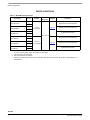
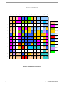
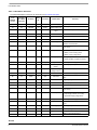
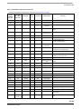
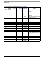
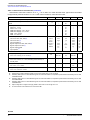
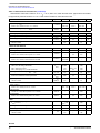
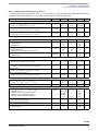
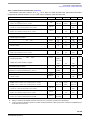
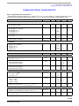
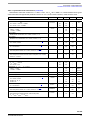
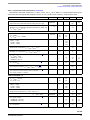
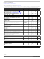
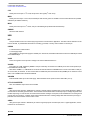
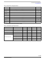
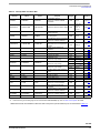
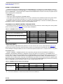
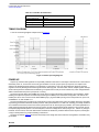
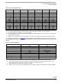
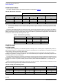
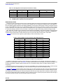
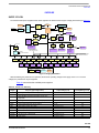
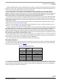
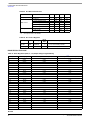
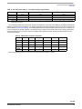
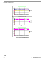
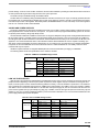
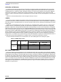
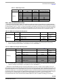
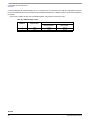
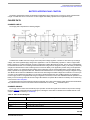
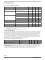
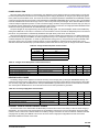
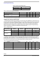
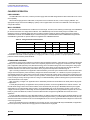
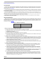
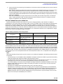
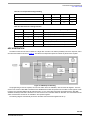
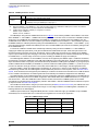
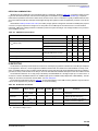
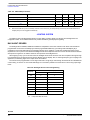
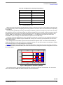
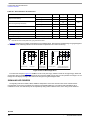
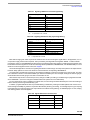
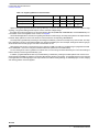
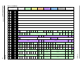
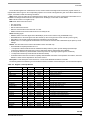
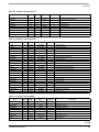
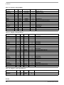
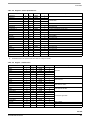
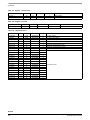
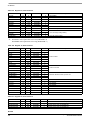
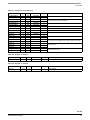
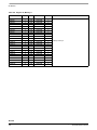
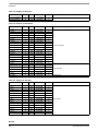
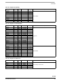
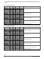
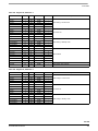
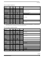
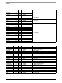
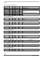
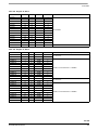
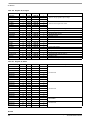
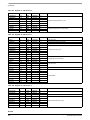
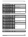
SPI BITMAP The 24 bit wide registers are numbered from 0 to 63, and are referenced throughout this document by register number, or representative name as given in the corresponding captions. The contents of all registers are given in the tables defined in this chapter; each table includes the following information: Name: Name of the bit. Spare bits are implemented in the design for future use, but are not assigned. Unused bits are not available in the design. Reserved bits are not implemented in the design, but are used on other PMICs. Bit #: The bit location in the register (0-23) R/W: Read / Write access and control • R is read access • W is write access • R/W is read and write access • RW1C is read and write access with write 1 to clear • RWM is read and write access while the device can modify the bit Reset: Resetting signal • RESETB, which is the same signal as the RESETB pin (so bit is held in reset as long as RESETB is low) • RTCPORB which is the reset signal of the RTC module (so bit is no longer held in reset once RTC power is good) • OFFB which is an internal signal generated when transitioning into the Off state • NONE. There is no reset signal for hardwired bits nor for the bits of which the state is determined by the power up mode settings Default: The value after reset as noted in the Default column of the SPI map. • Fixed defaults are explicitly declared as 0 or 1. • * corresponds to Read / Write bits that are initialized at startup based on power up mode settings (board level pin connections) validated at the beginning of Cold or Warm Start. Bits are subsequently SPI modifiable. • S corresponds to Read only sense bits that continuously monitor an input signal (sense signal is not latched). • L corresponds to Read only sense bits that are latched at startup. • X indicates that the state does not have an explicitly defined default value which can be specified. For instance, some bits default to a value which is dependent on the version of the IC. Description: A short description of the bit function, in some cases additional information is included The following tables are intended to give a summarized overview, for details on the bit description, see the individual chapters. Table 112. Register 0, Interrupt Status 0 R/W Reset ADCDONEI Name Bit # 0 RW1C RESETB 0 ADC has finished requested conversions ADCBISDONEI 1 RW1C RESETB 0 ADCBIS has finished requested conversions TSI 2 RW1C RESETB 0 Touch screen wake-up VBUSVALIDI 3 RW1C OFFB 0 VBUSVALID detect IDFACTORYI 4 RW1C RESETB 0 ID factory mode detect USBOVI 5 RW1C RTCPORB 0 USB over-voltage detection CHGDETI 6 RW1C OFFB 0 Charger attach CHGFAULTI 7 RW1C RTCPORB 0 Charger fault detection CHGREVI 8 RW1C RESETB 0 Charger path reverse current CHGSHORTI 9 RW1C RESETB 0 Charger path short circuit CCCVI 10 RW1C RESETB 0 Charger path CC / CV transition detect CHGCURRI 11 RW1C RESETB 0 Charge current below threshold warning BPONI 12 RW1C OFFB 0 BP turn on threshold LOBATLI 13 RW1C RESETB 0 Low battery low threshold warning LOBATHI 14 RW1C RESETB 0 Low battery high threshold warning Reserved 15 R 0 For future use BVALIDI 16 RW1C 0 USB B-session valid interrupt Reserved 17 R 0 For future use Reserved 18 R 0 For future use IDFLOATI 19 RW1C RESETB 0 USB ID float detect IDGNDI 20 RW1C RESETB 0 USB ID ground detect OFFB Default Description MC13892 Analog Integrated Circuit Device Data Freescale Semiconductor 123