Download Sharp QT-27H Service manual

Transcript
QT-CD210/C
SERVICE MANUAL
No. SY964QTCD210/
QT-CD210(BL)
QT-CD210(S)
QT-CD210(WH)
QT-CD210C(S)
Illustration: QT-CD210
• In the interests of user-safety the set should be restored to its
original condition and only parts identical to those specified should
be used.
CONTENTS
Page
IMPORTANT SERVICE NOTES (FOR QT-CD210 ONLY) ............................................................................................... 2
SPECIFICATIONS ............................................................................................................................................................. 2
NAMES OF PARTS ........................................................................................................................................................... 3
FITTING OF DIAL POINTER ............................................................................................................................................. 3
DISASSEMBLY .................................................................................................................................................................. 4
REMOVING AND REINSTALLING THE MAIN PARTS ..................................................................................................... 4
ADJUSTMENT ................................................................................................................................................................... 6
SCHEMATIC DIAGRAM .................................................................................................................................................... 8
WIRING SIDE OF P.W.BOARD ....................................................................................................................................... 10
NOTES ON SCHEMATIC DIAGRAM .............................................................................................................................. 12
TYPES OF TRANSISTOR ............................................................................................................................................... 12
WAVEFORMS OF CD CIRCUIT ...................................................................................................................................... 13
TROUBLESHOOTING (CD SECTION) ........................................................................................................................... 14
FUNCTION TABLE OF IC ................................................................................................................................................ 18
PARTS GUIDE/EXPLODED VIEW
PACKING OF THE SET (FOR QT-CD210 ONLY)
SHARP CORPORATION
–1–
This document has been published to be used
for after sales service only.
The contents are subject to change without notice.
QT-CD210/C
FOR A COMPLETE DESCRIPTION OF THE OPERATION OF THIS UNIT, PLEASE REFER
TO THE OPERATION MANUAL.
IMPORTANT SERVICE NOTES (FOR QT-CD210 ONLY)
BEFORE RETURNING THE AUDIO PRODUCT
(Fire & Shock Hazard)
Before returning the audio product to the user, perform the
following safety checks.
1. Inspect all lead dress to make certain that leads are not
pinched or that hardware is not lodged between the chassis
and other metal parts in the audio product.
2. Inspect all protective devices such as insulating materials,
cabinet, terminal board, adjustment and compartment
covers or shields, mechanical insulators etc.
3. To be sure that no shock hazard exists, check for leakage
current in the following manner.
* Plug the AC line cord directly into a 120 volt AC outlet.
* Using two clip leads, connect a 1.5k ohm, 10 watt resistor
paralleled by a 0.15µF capacitor in series with all exposed
metal cabinet parts and a known earth ground, such as
conduit or electrical ground connected to earth ground.
* Use a VTVM or VOM with 1000 ohm per volt, or higher,
sensitivity to measure the AC voltage drop across the
resistor (See diagram).
* Connect the resistor connection to all exposed metal parts
having a return path to the chassis (antenna, metal cabinet,
screw heads, knobs and control shafts, escutcheon, etc.)
and measure the AC voltage drop across the resistor.
VTVM
AC SCALE
1.5k ohms
10W
0.15 µ F
TO EXPOSED
METAL PARTS
TEST PROBE
CONNECT TO
KNOWN EARTH
GROUND
All check must be repeated with the AC line cord plug connection
reversed.
Any reading of 0.3 volt RMS (this corresponds to 0.2 milliamp.
AC.) or more is excessive and indicates a potential shock
hazard which must be corrected before returning the audio
product to the owner.
SPECIFICATIONS
● General
Power source: AC 120 V, 60 Hz
DC 9 V [ "D" size (UM/SUM-1, R20
or HP-2) battery × 6]
Power
consumption: 12 W
(For QT-CD210)
Output power: FTC; 2.0 W min. RMS per channel
into 4 ohms from 150 Hz to 20
kHz, with no more than 10 % total
harmonic distortion.
RMS; 2.3 W/CH
(DC operation, 10 % T.H.D.)
Speakers:
4" (10 cm) full-range speaker x 2
Dimensions: Width; 15-3/4" (400 mm)
Height; 6-1/4" (158 mm)
Depth; 8-3/8" (212 mm)
Weight:
6.0 lbs. (2.7 kg) without batteries
(For QT-CD210C)
Output power: RMS; 2.3 W/CH
(DC operation, 10 % T.H.D.)
Speakers:
10 cm (4") full-range speaker x 2
Dimensions: Width; 400 mm (15-3/4")
Height; 158 mm (6-1/4")
Depth; 212 mm (8-3/8")
Weight:
2.7 kg (6.0 lbs.) without batteries
● Compact disc player
Type:
Compact disc
Signal
Non-contact, 3-beam semireadout:
conductor laser pickup
Audio
channels:
2
Filter:
8-times oversampling digital filter
D/A
converter:
1-bit D/A converter
Wow and
Unmeasurable
flutter:
(less than 0.001% W. peak)
● Radio
Frequency
range:
FM; 87.6 - 108 MHz
AM; 530 - 1,720 kHz
● Tape recorder
Frequency
response:
50 - 14,000 Hz (Normal tape)
Signal/noise
ratio:
50 dB
Wow and
flutter:
0.25 % (WRMS)
Motor:
DC 9 V electric governor
Bias system: AC bias
Erase
system:
Magnet erase
Specifications for this model are subject to change without
prior notice.
–2–
QT-CD210/C
NAMES OF PARTS
11.
12.
13.
14.
15.
16.
17.
18.
19.
10.
11.
12.
13.
14.
15.
16.
17.
18.
19.
20.
(TAPE) Record Button
(TAPE) Play Button
1 2 3 4 5 6
7
8
(TAPE) Rewind Button
(TAPE) Fast Forward Button
(TAPE) Stop/Eject Button
9
(TAPE) Pause Button
Cassette Compartment
CD Compartment
Tuning Control
10 11 12
(CD) Stop Button
(CD) Track Down/Review Button
13 14 15
16
17
Volume Control
Function Selector/Power Switch
(CD) Track Up/Cue Button
(CD) Play/Pause Button
(CD) Play Indicator
(CD) Pause Indicator
Battery Compartment
FM Telescopic Rod Aerial
AC Power Input Socket
18
19
20
FITTING OF DIAL POINTER
Setting method of the dial pointer
1. Remove the front cabinet. (Refer to Fig.4-1 on page 4,
"Disassembly method".)
2. Remove the dial pointer.
3. Insert the dial pointer from A of the top cabinet so that it
engages with the drum gear.
4. Fully turn the drum in the opposite direction of B and set
it to the FL marks.
5. Reassemble the front cabinet.
Top Cabinet
Dial
Pointer
Drum
Top Cabinet
Tuning
Knob
A
B
Drum
Dial Pointer
Main
PWB
Dial Pointer
FL Mark
Carved Seal
Drum
FH
Top Cabinet
Main
PWB
FL
Mark
Variable Capacitor
Figure 3-1
Figure 3-2
–3–
QT-CD210/C
DISASSEMBLY
Caution on Disassembly
Follow the below-mentioned notes when disassembling the
unit and reassembling it, to keep it safe and ensure excellent
performance:
1. Take cassette tape and compact disc out of the unit.
2. Be sure to remove the power supply plug from the wall
outlet before starting to disassemble the unit.
3. Take off nylon bands or wire holders where they need to
be removed when disassembling the unit. After servicing
the unit, be sure to rearrange the leads where they were
before disassembling.
4. Take sufficient care on static electricity of integrated
circuits and other circuits when servicing.
STEP
REMOVAL
PROCEDURE
FIGURE
1
Top Cabinet/
Front Cabinet
1. Screw ................... (A1) x7
2. Socket .................. (A2) x1
4-1
2
Power PWB
1. Screw ................... (B1) x2
2. Hook ..................... (B2) x2
3. Socket .................. (B3) x1
4. Hook ..................... (B4) x2
4-2
1. Socket .................. (C1) x1
2. Screw ................... (C2) x7
3. Screw ................... (C3) x1
4. Solder ................... (C4) x3
5. Socket .................. (C5) x3
6. Screw ................... (C6) x2
4-2
3
Main PWB/
CD Control PWB
(Note)
(B3)x1
(C1)x1
Main PWB
(C4)x3
(B4)x2
(B2)x2
Top Cabinet
AC Socket
Power
Transformer
(B1)x2
ø3x12mm
Figure 4-2
(D1)x3
ø2.5x10mm
4-3
CD Mechanism
(C5)x2
(E1)x4
ø3x10mm
Washer
CD Mechanism
1. Screw ................... (D1) x3
4-3
5
Tape Mechanism
1. Screw ................... (E1) x4
4-3
Front Cabinet
CD Lid
Switch
(C2)x7
ø3x12mm
Power PWB
4
Top Cabinet
(C3)x1
ø2.5x8mm
(C5)x1
Main
PWB
(A2)x1
Tape
Mechanism
(C6)x2
ø3x8mm
(A1)x4
ø3x12mm
Top Cabinet
CD Control
PWB
(A1)x3
ø3x12mm
Figure 4-1
Figure 4-3
REMOVING AND REINSTALLING THE MAIN PARTS
CD MECHANISM SECTION
(A1) x2
ø2.6 x6mm
Perform steps 1 to 4 of the disassembly method to remove the
CD mechanism.
CD
Mechanism
Pickup
How to remove the pickup (See Fig. 4-4.)
1. Remove the screws (A1) x 2 pcs., to remove the shaft (A2)
x1 pc.
2. Remove the stop washer (A3) x1 pc., to remove the gear
(A4) x 1 pc.
3. Remove the pickup.
Note : (Figure 4-3 and Figure 4-4)
After removing the connector for the optical pickup from the
connector, wrap the conductive aluminium foil around the
front end of connector to protect the optical pickup from
electrostatic damage.
Shaft
(A2) x1
Gear
(A4) x1
Figure 4-4
–4–
Stop
Washer
(A3) x1
QT-CD210/C
TAPE MECHANISM SECTION
(A1) x1
ø2x7mm
(A1) x1
ø2x3mm
Hook
(A2)x2
Perform steps 1 to 5 of the disassembly method to remove the
tape mechanism. (See page 4.)
How to remove the record / playback and erase
heads (See Fig. 5-1.)
Record/Playback
Head
Erase Head
1. Remove the screws (A1) x 2 pcs., to remove the record/
playback head.
2. Remove the hooks (A2) x 2 pcs., toward the center position
as shown in Fig. 5-1. and then extract the erase head
upward.
Note:
After replacing the heads and performing the azimuth
adjustment, be sure to apply screwlock.
Figure 5-1
How to remove the pinch roller (See Fig. 5-2.)
1. Carefully bend the pinch roller pawl in the direction of the
arrow <A>, and remove the pinch roller (B1) upwards.
<A>
Pinch Roller
Pawl
Pinch Roller
(B1)x1
Figure 5-2
How to remove the belts (See Fig. 5-3.)
Main Belt
(C1)x1
1. Remove the main belt (C1) x 1 pc., from the motor pulley.
2. Remove the FF/REW belt (C2) x 1 pc., from the REW/FF
roller.
3. Put on the belts in the reverse order of removal.
Note:
When putting on the belt, ascertain that the belt is not twisted,
and clean it.
Motor
Flywheel
REW/FF
Clutch Ass'y
FF/REW Belt
(C2)x1
Figure 5-3
How to remove the motor
(See Figs. 5-4.)
(D2)x2
Special
Screw
1. Remove the mainbelt.
2. Remove the screw (D1) x 1 pc., to remove the motor mount.
3. Remove the screws (D2) x 2 pcs., to remove the motor.
Note:
When mounting the motor, pay attention to the motor mounting
angle.
Motor
Mount
(D1)x1
Special
Screw
Motor
Motor
Motor Mount
Figure 5-4
How to remove the flywheel (See Fig. 5-5.)
(E1) x 1
Stop Washer
1. Remove the belt.
2. Remove the stop washer (E1) x 1 pc., with a small precision
screwdriver to extract the flywheel from the capstan metal.
Note:
When the stop washer is deformed or damaged, replace it
with a new one.
Washer
Flywheel
How to reinstall the parts
Install each part in the reverse order of the removal with care.
Figure 5-5
–5–
QT-CD210/C
ADJUSTMENT
MECHANISM SECTION
• Driving Force Check
• AM IF/RF
Torque Meter
Specified Value
PLAY: TW-2412
Test Stage
Over 120 g
• Torque Check
Torque Meter
Specified Value
Play: TW-2111
25 to 65 g.cm
Fast Forward: TW-2231
60 to 130 g.cm
Rewind: TW-2231
60 to 130 g.cm
Instrument
Connection
Specified
Value/Adjusting
Point
AM IF
T3
Input: Antenna
Output: Pin 18 of IC1
AM
Band Coverage
AM Tracking
fL: L4
fH: TC4
fL: 600 kHz: L3
fH: 1,400 kHz: TC3
Input: Antenna
Output: Speaker
Terminal (CNP201
Load resistance: 4
ohms)
• Head Azimuth
Torque Meter
Specified Value
MTT-114
Output: Speaker Terminal
(CNP201 Load resistance: 4 ohms)
CNP101 4 3 2 1
Test
Tape
SW102
L301
• Tape Speed
Adjusting
Point
MTT-111 Variable
resistor in
motor. (M601)
Specified
Value
Instrument
Connection
3,000 ± 90 Hz
Output: Speaker
Teaminal
(CNP201 Load
resistance: 4 ohms)
BIAS OSC.
IC101
1
11
12
2
CNP201
1
123
CNP602
TAPE SECTION
Position of each switch or control
Volume control
Function switch
Max
Tape/Power Off
VR201
• Bias Oscillation
Adjustment Point
Specified Value
82 kHz ± 6 kHz
L301
Instrument
Connection
Pin 1 of CNP101
SW201
• Playback Amplifier Sensitivity Check
Test Tape
Specified Value
MTT-118
1.1 V ± 3 dB
Instrument Connection
Speaker Terminal
(Load resistance: 4 ohms)
TUNER SECTION
FM ROD
ATENNA
fL: Low-range frequency
fH: High-range frequency
IC803
MAIN PWB
• FM IF/RF
Test Stage
Specified
Value/Adjusting
Point
Instrument
Connection
T2
FM Detection
T2
Input: Pin 1 of IC1
Output: Pin 18 of IC1
FM
Band Coverage
fL: L2
fH: TC2
FM Tracking
fL: 88.0 MHz: L1
fH: 108.0 MHz: TC1
Iuput: Antenna
Output: Speaker
Terminal (CNP201
Load resistance: 4
ohms)
AM IF
FM
DETECTION
T3
1
12
IC1
13
18 24
L2
FM BAND
COVERAGE
fL
fH
fH FM
fL TRACKING
TC2
TC4
L4
L1
TC1
TC3
fH
fL
L3
AM BAR
ANTENNA
AM
TRACKING
fH
fL
AM BAND
COVERAGE
Figure 6 ADJUSTMENT POINTS
–6–
QT-CD210/C
CD SECTION
Since this CD system incorporates the following automatic
adjustment function, when the pickup is replaced, it is not
necessary to reajust it.
Since this CD unit does not need adjustment, the combination
of PWB and laser pickup unit is not restricted.
TEST MODE
Start
While holding down the "PLAY" button, move the FUNCTION/POWER switch to "CD".
Note
1. When the CD LID switch is in the OFF position, (CD LID is open) the unit will be able to enter the test mode.
However, can use the "UP/CUE" and "DOWN/REVIEW" button only.
2. You can only move the pickup.
3. The LCD display should be the same as it is for normal CD operations.
Operation
1
2
The use of the "UP/CUE" button will move the pickup to the outermost position.
The use of the "DOWN/REVIEW" button will move the pickup to the innermost position.
When the "PLAY" button is pressed, the laser will be lit. If the laser is lit and the "PLAY" button is pressed again,
play back will start from the current pickup position . In the playback operation, the "STOP" button is pressed,
the laser will be geve out and the playback is stopped.
LCD MODE
Start
After connecting of the 10kΩ resistor between IC802 27 pin and GND and holding down the "PLAY" button, move
the FUNCTION/POWER switch to "CD".
Display
–7–
QT-CD210/C
( ): CD STOP
3.72V R801
1.87V
(5.0V) 22
(1.45V)
MAIN PWB-A1
Q801
KTA1266 GR
SWITCHING
MON
A
K
E
B
K
E
A
A
F
C
B
F
2200P
R802
2.2K
5
5
5
4
4
4
3
3
3
2
2
2
1
1
1
+B
K
E
RFN 24
1 VCC
R805
39K
A
2 FNI
B
3 FPI
F
4 TPI
6 MDI
7 LDO
1M
F+
FG
FO-
PD
B
VR
TR-
SP+
SP-
M
SL+
SL-
-
PU-IN
GND
SW702
PICKUP IN
C
3
4
4
4
5
5
5
6
6
6
7
7
7
8
8
8
+
-
+
M701
SLED
MOTOR
2
3
6
6
6
5
5
4
4
4
3
3
3
2
2
2
1
1
1
C820
0.1(ML)
9
10 2VRO
R811
22K
GND
C826
47P
R820
47K
R827 C82
15K 0.0
C830
0.01(ML)
RFIS 18
R828
10K
10
C833
0.033(ML)
VRO 16
C822
0.047
FEN 15
C821
100/10
R803
82K
PD
FEO 14
VR
R830
10K
C841
0.047
C814
0.047
R831
3.3K
DM+
DM-
R833
3.3K
C842
0.047
FM+
FMSLT+
C834
470P
SLTC843
47/16
C835
470P
FOO
NC
NC
REG IN RES
VG3
VIN3
GND
VO3+
7
8
9 10 11 12 13 14 15
1
2
3
C
0.
+B
IC803
FOCUS/
TRACKING/
SPIN/
SLED DRIVER
LA6541D
C807
0.047
L801
0.82µH
+B
C805
0.022
NC
NC
VIN
6
VG2
VO2+
GND
5
VO2-
GND
REG OUT
GND
GND
VO3-
2
3
GND
NC
VO4-
VO4+
VG4
2 3 4
1
CD
VO1-
VG1
IC803
LA6541D
VO1+
VIN4
VCC
MT
NC
VCC
VIN1
0V
0.24V
2.13V
2.09V
4.03V
3.38V
0V
0V
0V
3.70V
3.71V
2.09V
2.11V
2.10V
8.14V
VREF
30 29 28 27 26 25 24 23 22 21 20 19 18 17 16
VOLTAGE
8.15V
1.08V
2.12V
2.10V
4.0V
3.42V
0V
0V
0V
3.85V
3.60V
2.09V
2.09V
6.02V
7.47V
C836
0.047(ML)
C837
0.047(ML)
C838
0.047(ML)
C839
0.047(ML)
8.15V
8.21V
(8.3V)
(8.3V)
D801
Q802
1N4004
7.48V
KTA1273 Y
(7.59V)
SWITCHING
R850
( ): CD STOP
1.5K
+B
3 4.97V(5.0V)
0V
(0V) 2
Q803
0V 1 KRC107 M
SWITCHING
(0V)
C856
0.001
C806
330/16
R852
2.2K
D
IC803
PIN
NO.
16
17
18
19
20
21
22
23
24
25
26
27
28
29
30
C854
0.0068
C863
47/16
SBAD 13
12 TEO
LD
TRO
VOLTAGE
C829
0.0047
C819
0.1(ML)
11 TEN
R851
2.2K
PIN
NO.
1
2
3
4
5
6
7
8
9
10
11
12
13
14
15
C828
0.0027
C832
47/16
AGCI 21
RFGC 20
RFRP 17
9 TEB
FC-
C818
56P
VOLTAGE
2.86V(0.99V)
2.12V
2.05V
2.05V
2.63V(1.15V)
2.04V
2.07V
2.17V
2.04V
1.47V(0.77V)
0V
2.05V
): CD STOP
RFGO 19
8 SEL
FC+
R806
2.7K
IC801
PIN
NO.
13
14
15
16
17
18
19
20
21
22
23
24
(
VOLTAGE
4.84V
2.04V
2.04V
2.12V(0V)
2.11V(0V)
0.18V(0V)
2.84V(0V)
2.41V(0V)
2.05V
4.08V
2.05V
2.08V
R853
2.2K
CD MOTOR PWB-B
TR-
C813
47/16
5
CNP803
M
1
2
3
CNS803
M702
SPINDLE
MOTOR
1
2
CNS801
LD
1
BI801
R+
FO+
R807
1K
RFO 22
BI803
TR+
TR+
C804
2P
(CH)
GND 23
8
5 TNI
1M
PIN
NO.
1
2
3
4
5
6
7
8
9
10
11
12
R804
68K
C801
0.01
2200P
R-
C816
0.022
IC801
SERVO PRE AMP.
TA2109F
C802
0.022
BI802
CNS802
LD
C817
100/10
2.97V
(4.39V)
C825
47/16
+B
C815
47/16
IC801
TA2109F
PICK-UP UNIT
+B
R456
15K
FMO
DMO
R458
1K
R455
15K
R457
1K
L4
AM OSC.
D2
1N4148
TUN
NC LED
LED L-CH
FM
R-CH
DET
7
NC ST
6
9 10 11 12
8
C15
10P
(CH)
C22
0.1/50
2
2
CF1
10.7MHz
FM IF
1
3
AM IF
NC
R8
10K
NC
3
1
3
4
4
ERASE HEAD
9 8 7
P
R
SW102-C
SW102
RECORD/PLAYBACK
H
GND(AUDIO)
17
16
15
14
R108
1K
C106
0.0027
OUT1
8
VCC
IC101
BA3311L
FILTER 10
0V
R110
120
C110
270P
C114
47/16
7
0V
C118
10/16
R114
8.2K
C116
0.018(ML)
R116
3.9K
C121
0.01
D101
1N4148
4.62V
ALC T 2
0V
OUT2
12 1.89V
GND
6
SW102
RECORD/
PLAYBACK
SW102-E
P
R
22 23 24
2
R118
3.9K
R106
10K
3
12
L-CH
SW201
FUNCTION
SELECTOR
13 R-CH
SW201-C
R123
3.3K
R126
100
C123
220/10
R125
680K
IC101
REC./
P.B. EQUALIZER AMP.
BA3311L
SW102
RECORD/
PLAYBACK
C122
0.01
13 14 15
P
R
SW102-H
R124
3.3K
SW102-D
SW10
P
R
10 RECO
12 11
PLAY
4
6
L301
BIAS OSC.
3
2
1
C351
0.0022
(ML)
R122
1.8K
C352
100/10
• The numbers 1 to 17 are waveform numbers shown in page 13.
1
SW201-B
4.67V
VOLTAGE:
PLAY and REC
4 0V
R119
3.3K
C119
2.2/50
C107
820P
16 17 18
P
R
SW102-G
NF1
5 IN1
0V
9 IN2
NF2
0.6V 11
C112
330P
C117
10/16
3 0.6V PRE AMP 1.88V 1
0V
C111
330P
C108
820P
6 5 4
P
R
SW102-B
TAPE 8
AM 9
FM 10
CD 11
R11
2.2K
NC
2
R10
2.2K
TAPE
AM
FM
CD
NC
2
3
C113
47/16
R117
3.9K
C120
47/16
1
C109
270P
R115
3.9K
D102
1N4148
1
C105
0.0027
R109
120
SW102
R101 RECORD/
PLAYBACK
150
SW102-F
R107
R
P
1K
19 20 21
R113
8.2K
R120
3.3K
R-CH
SW102
RECORD/
PLAYBACK
R6
100
COR1
CORE
R121
1.8K
C115
0.018(ML)
R103
12K
NC
L-CH
SW102-A
P
R
3 2 1
CNP101
TAPE
RECORD/
PLAYBACK HEAD
CNS101
R102
150
C19
0.015
(ML)
R9
10K
T2
FM DETECTION
R105
10K
G
R7
120
NC
T3
AM IF
R104
12K
L-CH(CD)
R-CH(CD)
C9
0.1/50
FM IF
IN
LPF2
VCO
GND
VCC
CF3
460KHz
NC
R4
2.2K
15
C12
4.7/50
IC1
FM/AM IF MPX.
TA2111N
C8
0.1/50
16
LPF1
AM/FM
AM
AGC
17
C17
1/50
D1
1N4148
19 18
IC1
TA2111N
5
3 4
14 13
20
MPX IN
FM
OSC
2
C10
1/50
R2
2.7K
C16
1/50
1
R5
3.3K
DET
21
C6
330P
C7
2.2/50
C18
0.015(ML)
VOLTAGE
1.22V(1.22V)
1.22V(1.22V)
3.20V(3.14V)
3.14V(3.92V)
0.7V(0.70V)
1.08V(1.01V)
0.4V(1.02V)
3.92V(3.85V)
3.92V(3.86V)
3.92V(3.86V)
3.92V(3.86V)
3.92V(3.82V)
( ): AM
22
C11
0.47/50
VOLTAGE
0.82V(0V)
0V(0V)
0.35V(1.03V)
3.81V(3.82V)
0V(0.13V)
3.92V(3.86V)
3.39V(3.18V)
3.92V(3.86V)
0V(0V)
0V(0.14V)
0.32V(0.32V)
3.14V(3.29V)
23
FM RF
OUT
C4
4P(CH)
R3
220K
C20
0.047
1 2 3
FM OSC.
FM RF
IN
RF
GND
AM LOW
CUT
MIX
OUT
AM RF
IN
F1
FM ROD
ANTENNA
IC1
PIN
NO.
13
14
15
16
17
18
19
20
21
22
23
24
24
C1
0.022
FM BAND
PASS FILTER
PIN
NO.
1
2
3
4
5
6
7
8
9
10
11
12
L2
L1
FM IF
6
AM IF
IN
TC1
2 C2 6
18P
(CH)
fH TC1
fL L1
fH TC2
FM BAND
COVERAGE fL L2
F
FM OSC.
VC2
TC2
1 C3
22P(UJ)
FM
AFC
fH TC4
AM BAND
COVERAGE fL L4
FM
TRACKING
AM ANT
FM ANT
VC1
4
4
AM
OSC
2
C21
2P(CH)
3
2
1
C13
220/10
fH TC3
fL L3
RF
VCC
AM
TRACKING
4
TC4
VC4
AM OSC.
5
R1
330
E
3
TC3
VC3
C14
0.022
L3
AM BAR ANTENNA
1
3
4
Figure 8 SCHEMATIC DIAGRAM (1/2)
–8–
5
6
R351
100
C354
0.022
R35
150
QT-CD210/C
C825
47/16
12
C823
0.022
+B
R824
10K
C826
47P
0V 0V 0V 0V 0V 0V
12
57 RFI 2.10V
+B
C833
0.033(ML)
R829
3.3K
6
1
66 FOO 2.18V
NC
2.49V SEG13
13
NC
12
70 TEBC 2.10V
2.49V SEG11
11
2.49V SEG10
NC
10
R834
3.3K
72 DMO 2.17V
2.49V SEG9
NC
9
2.49V SEG8
NC
8
2.49V SEG7
NC
7
2.49V SEG6
NC
6
15
4
75 VDD2 4.97V
76 VSS2 0V
LCD801
LCD DISPLAY
COM2 2.33V
COM3
COM1 2.33V
MVDD 4.96V
MXO 4.96V
MXI 0.30V
NC
NC
2.49V SEG3 3
MVSS 0V
REMO-IN 4.96V
RYNCREC 0V
0V
NC
RESET 4.95V
DVSL 0V
2.49V SEG4 4
NC 0V
DVRL 2.36V
LO 2.47V
16
DVDD 4.72V
DVSR
4.92V
R840
10
3
C845
0.047
RO 2.48V
78 XI 2.08V
79 XO 2.57V
80 XVDD
DVRR 2.37V
X801
16.93MHz
1
CD CONTROL PWB-A2
2.49V SEG5 5
17
77 XVSS 0V
2.49V SEG2 2
NC 1 NC
SEG1 2.49V
10
+B
FW806
10
1
+B
2
5 6
3 4
7 8
81 82 83 84 85 86 87 88 89 90 91 92 93 94 95 96 97 98 99 100 2.33V
0V
C839
0.047(ML)
14
NC
2
RECORD SIGNAL
0V CDSEL0 15
2.49V SEG14
NC
C840
0.047
PLAYBACK SIGNAL
R861
3.3K
0V CDSEL1 16
2.49V SEG12
C834
470P
C836
0.047(ML)
C837
0.047(ML)
C838
0.047(ML)
NC
0V DOOR IN 17
11
14
C824
0.022
0V DOOR OUT 18
69 RFGC 2.14V
71 FMO 2.10V
CD SIGNAL
4.98V MVDD1 19
IC802
SERVO/
SIGNAL CONTROL
TC9457F0
R832
3.3K
73 2VREF 4.18V
74 SEL 2.47V(0V)
C835
470P
NC
TEST0
TEST1
TEST2
TEST3
TEST4
TEST5
NC
NC
NC
NC
4.97V /HSO
2.49V SPCK
1.66V COFS
0.43V(2.36V) SPDA
NC
5
AM SIGNAL
R846
330
0V MVSS1 20
2.33V
R833
3.3K
NC
21
67 TRO 2.11V
68 VREF 2.10V
R831
3.3K
NC
NC
R862
22K
COM4
R830
10K
0V SBSY
0V TRAY CLOS
7
FM SIGNAL
0V PUSEL0 23
60 RFZI 2.10V
65 TEZI 2.14V
+B
R844
3.3K
4.98V PUSEL 24
22
63 SBAD 2.94V(0.989V)
C854
0.0068
OPEN/CLOSE
R843
3.3K
0V DISPLAY 25
NC
64 TEI 2.14V
R821
22K
4.98V ADIN1 26
( ): STOP
0V TRAY OPEN
62 FEI 2.30V(2.1V)
SW810
CD LID
0V
0V MUTE 28
59 RFCT 2.10V
61 RFRP 2.73V(1.15V)
R812
1K
PUSEL2 30
4.97V PU IN 29
53 2.10V
58 AVDD 4.98V
R828
10K
0V
4.98V ADIN2 27
51 2.10V(1.34V)
52 2.01V(4.12V)
56 SLCO 2.10V
C829
0.0047
2.46V DOUT
0V VSS1
13
55 AVSS 0V
C828
0.0027
C832
47/16
4.98V VDD1
52 LPFO
53 PVREF
54 VCOF 1.50V
C830
0.01(ML)
4.97V(0V) SBOK
TMAX
51 LPFN
2.10V PDO
R827 C827
15K 0.015(ML)
50 49 48 47 46 45 44 43 42 41 40 39 38 37 36 35 34 33 32 31 0V
2.08V
(0V)
4.18V P2VREF
R826
220K
R820
47K
+B
C844
100/10
R836
270
D801
1N4004
+B
STOP
R839
47K
C846
10/16
C855
0.022
C848
22/16
L801
0.82µH
C853
0.022
C847
22/16
+B
R860
100
1
MUTE
R835
270
1
+B
R849
6.8K
R847
1K
R848
2.2K
SW802
STOP
SW803
REVIEW/
DOWN
C850 C849
0.0022 0.0022
+B
4.97V(5.0V)
C851
3.3/50
C852
3.3/50
+B
Q803
KRC107 M
SWITCHING
R456
15K
SW801
PLAY/
PAUSE
R837
10K
R838
10K
SW804
CUE/UP
R458
1K
R455
15K
R457
1K
C233
470/10
R221
1K
9 0.56V
VOLUME
C216
0.1(ML)
R216
2.2K
C221
0.001
VR201-A
20K(B)
R231
120
C222
0.001
R222
1K
C218
0.0015
5 0V
4.27V 2
+B
1
L-CH
8.02V
2
2
3
3
SP201
L-CH
4 OHM
SPEAKERS
-
SP202
R-CH
4 OHM
+
SW201
FUNCTION
SELECTOR
17
16
15
14
13 R-CH
SW201-C
SW102-D
SW102
P
R
10 RECORD/
12 11
PLAYBACK
+B
C204
0.022
R203
560
19
R202
4.7K
D203
1N4148
ZD201
DZ5.1BSB
0V
C353
R354
0.0056(ML)
4.7
8.44V
4.96V
RECORDING
BIAS OSCILATOR
Q351
KTC3199 GR
4.39V
R352
150
3.32V
Q205
KTC3199 GR
R351
100
C354
R353
0.022(ML) 33K
9.05V
D202
SWITCHING 1N4148
C352
100/10
SW201
FUNCTION
SELECTOR
0.68V
1
+B
8.44V
NC
L301
BIAS OSC.
4
3
6
2
5.08V
SW201-D
Q204
KTA1046 Y
REGULATOR
C203
0.01
23
22
21
20
D651
1N4004
D652
1N4004
D653
1N4004
C652
0.022
1
2
C653
0.022
SW201
FUNCTION
SELECTOR
+B
SW201-A
TAPE 2 NC
AM 3
1
FM 4
CD 5
1
2
C651
0.022
D654
1N4004
CNP602
POWER PWB-A3
+B
C351
0.0022
(ML)
-
C226
0.022
D201
1N4148
ALIZER AMP.
1
C234
470/10
12
8.35V
C227
3300/16
+
1
C240
0.1
C238
100/10
6
0.56V
SW201-B
12
+
CNS602
TAPE
AM
FM
CD
8.01V 3
C241
47/16
C220
1/50
TAPE 8
AM 9
FM 10
CD 11
IC201 13
TA8227P 4.33V
POWER
14
AMP.
9.05V
4
R232
120
VR201-B
20K(B)
VOLUME
R220
2.7K
C225
100/10
0V
CNS201
R219
1K
C215
0.1(ML)
C239
0.1
C235
100/10
CNP201
R215
2.2K
0V 11
C237
100/10
+
-
4.67V 10
C217
0.0015
C236
100/10
+5V(CD)
8 0V
GND(CD)
GND(AUDIO)
GND(POWER)
7 0V
L-CH(CD)
R-CH(CD)
C219
1/50
C654
0.022
TAPE
AM
FM
CD
SO651
AC INLET
SOCKET
AC120V,60Hz
T651
POWER
TRANSFORMER
AC INPUT
AC/DC
R201
2.2K
SELECTOR
BATTERY
DC 9V ["D" size (UM/SUM-1,R20 orHP-2)
battery x 6]
SW601
TAPE
MAIN
R230
2.7
C202
47/16
+
-
M
M601
TAPE
MOTOR
• NOTES ON SCHEMATIC DIAGRAM can be found on page 12.
7
8
9
10
Figure 9 SCHEMATIC DIAGRAM (2/2)
–9–
11
12
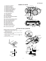
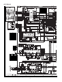
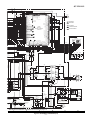
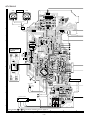
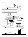
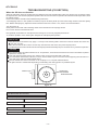
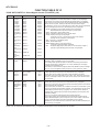
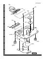
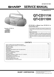
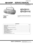
QT-CD210/C
SPEAKERS
SP201
L-CH
SP202
R-CH
CNP101
12 34
3 2 1
C106
R106
R116
R114
R102
C114 C116
R126
R353
C353
L301
R118
C118
C119
C354
R122
R120
C117
R125
R354
E C B Q351
R351
R352
2 4 6 8 10 12
C123 D102
C351
C352
C112
R110
R107
IC101
C122
CNP201
H
1 3 5 7 9 11
C120
C121
R123
R124
B
R109
C113 C109
R121
1 2 3
R117
R119
WH
BK
RD
CNS201
G
R108
F
D
C110
E
C
C111 C107
C108
B
R101
REC. A
C105
R113 R105
R104
R115
R103
D101
C115
PLAY
SW102
RECORD/
PLAYBACK
A
CNP602
YL
1 2
R230
RD
C236
R232
Q802
E
C
B
D801
Q803
1
2
3
6
9
IC801
C836
C804
C829
R802
Q801
R806
25
R851
6
C807
5
WH
GY
GY
GY
GY
GY
1
TC2
VC1
VC2
VC3
VC4
TC3
TC4
R9
R8
13
10
C18
15
C3
L2
TC1
C13
20
12
C16
C15
24
IC1
C4
C19
R5
L1
5
C20
C1
C2
1
C8
C11
1 2 3
C9
D2
F1
13
12
R10
R11
CF1
3
2
1 2 3 1
C12
CF3
R3
C14
R1
BK
R4
C856
30
T2
T3
C22
R6
G
C806
COR1
R7
BK
8
7
6
5
4
3
2
1
CNS801
7
5
2
3
MAIN PWB-A1
20
C805
R821
C834
R853
16
15
10
C825
SW810
CD LID
L3 AM BAR ANTENNA
R811
C822
R803
C821
C837
C842
R824
C843
C835
1
2
3
4
5
WH
WH
WH
WH
WH
WH
WH
BK
1
BI801
C7
R861
BCE
R801
C841
51
50
1
OPEN/CLOSE
5
8
C816
C815 C802
BI803
16
1
C801
C817
17
F
C828
R804
CNS802
BK
WH
WH
WH
WH
C830
30 31
R843
C863
24
R2
R846
C824
SW804
CUE/UP
R844
R862
R849
R805
10 BI802
1
5
C6
100
1
85 75
90
70
95
65
60
5
10 IC802 55
15
45
20
40
25 35
C820 20
IC803
C855
10
81 80
15
C839
C853
12
13
C819
C838
C844
C814
R807
R852
C847
C846
R828
R836
R832
1
2
3
4
5
6
7
8
C848
C833
R835
R834
R833
R831
R830
R829
R826
C827
R827
C826
R820
1
R838
C823
L801
C832
R840
C845
C840
D
C813
C818
C854
R860
C851
C852 C849
X801
FW806
R812
R837
A
10
8
R455
C17
R457
CD
R456
R839
LCD801
4
5
6
SW201
10
SW801
PLAY/
PAUSE
14
C220
C850
E
C238
R458
4
1
9
8
7
14
15
11
1
C234
C221
R847
R848
13
C235
R231
C219
1
2
3
C222
AM FM
SW803
REVIEW/DOWN
12
11
10
R222
C215
TAPE
SW802
STOP
C204
C10
C217
VR201-A
B C
SW201
FUNCTION
SELECTOR
ON
POWER
OFF
D
Q205
C225
R219
CD CONTROL
PWB-A2
C241
R850
R215
D201
E
C
B
IC201
VR201
VOLUME
R216
C240
Q204
C237
C
B
C
E
C239
C226
R201
C202
ZD201
C203
D203
D202
R203
R221
VR201-B
R202
C216
R220
C218
BK
C227
C233
D1
L4
C21
H
• The numbers 1 to 17 are waveform numbers shown in page 13.
1
2
3
4
Figure 10 WIRING OF P.W.BOARD (1/2)
– 10 –
5
6
QT-CD210/C
TAPE
RECORD/PLAYBACK
HEAD(240-4)
SW601
TAPE MAIN
(240-7)
WH
RD
BK
ERASE HEAD
(240-5)
M601
TAPE MOTOR
(240-6)
BK
CNS101
WH
1 BK
2
3 RD
4 BK
BK
YL
BR
RD
BK
(230)
T651
POWER
TRANSFORMER
BATTERYS
DC9 V [ "D" size(UM/SUM-1,
R20 or HP2) battery x 6 ]
(229)
YL
C653
C652
YL
RD
D653
D652
C651
D654
D651
RD
BK
RD
1
SO651
AC INLET
SOCKET
AC 120V,
60Hz
2
CNS602
C654
POWER PWB-A3
OR
OR
PICK UP UNIT
CD MOTOR PWB-B
+
5 4 3 2 1
CNS803
1
2
3
4
5
6
F3895AF
M702
SPENDLE MOTOR
SW702
PICKUP IN
+
-
WH
GY
GY
GY
GY
GY
CNP803
1
2
3
4
5
6
-
8 7 6 5 4 3 2 1
M701
SLED MOTOR
(233)
COLOR TABLE
BR
FM ROD ANTENNA(237)
7
8
9
10
Figure 11 WIRING OF P.W.BOARD (2/2)
– 11 –
BROWN
RD(R)
RED
OR
ORANGE
YL
YELLOW
GR
GREEN
BL
BLUE
VL
VIOLET
GY
GRAY
WH(W)
WHITE
BK
BLACK
PK
PINK
11
12
QT-CD210/C
NOTES ON SCHEMATIC DIAGRAM
• Resistor:
To differentiate the units of resistors, the symbol as K and M
are used: the symbol K means 1000 ohm and the symbol M
means 1000 kohm and the resistor without any symbol is an
ohm resistor. The resistor designated "Fusible" is a fuse type
resistor
• Capacitor:
To indicate the unit of capacitor, a symbol P is used: this
symbol P means micro-micro-farad and the unit of the capacitor
without such a symbol is microfarad. As to electrolytic capacitor,
the expression “capacitance/withstand voltage” is used.
(CH), (TH), (RH), (UJ): Temperature compensation
(ML): Mylar type
(P.P.): Polypropylene type
• The indicated voltage in each section is the one measured by
Digital Multimeter between such a section and the chassis
with no signal given.
REF. NO
DESCRIPTION
1. Tuner
( ): AM mode
Marking except for ( ): FM mode
2. CD
( ): Play mode
Marking except for ( ): Stop state
3. Deck section
( ): Record mode
Marking except for ( ): Playback mode
Display / Control section:
( ): Active state
Marking except for ( ): CD Function mode at stop state
• Schematic diagram and Wiring Side of P.W.Board for this
model are subject to change for improvement without prior
notice.
• Parts marked with “
”(
) are important for
maintaining the safety of the set. Be sure to replace these
parts with specified ones for maintaining the safety and
performance of the set.
POSITION
SW102
RECODE/PLAYBACK
REC—P.B.
SW201
FUNCTION SELECTOR
TAPE/OFF—AM/ON—
FM/ON—CD/ON
SW601
TAPE MAIN
OFF—ON
SW702
PICKUP IN
OFF—ON
SW801
PLAY/PAUSE
OFF—ON
SW802
STOP
OFF—ON
SW803
REVIEW/DOWN
OFF—ON
SW804
CUE/UP
OFF—ON
SW810
CD LID
OFF—ON
FRONT
VIEW
E C B
(S) (G) (D)
(1) (2) (3)
KRC107 M
KTA1046 Y
KTA1266 GR
KTA1273 Y
KTC3199 GR
Figure 12 TYPES OF TRANSISTOR
– 12 –
QT-CD210/C
WAVEFORMS OF CD CIRCUIT
NO DISC FOCUS SEARCH
1
STOP
FO+
FO-
SEL
TRO
2
FMO
3
PLAY
CUE
6
1
TEI
1
TRO
2
FMO
3
IC802 64pin
SBAD
11
2
IC802 67pin
RFO
15
3
IC802 71pin
IC801 22pin
STOP
PLAY
REVIEW
6
1
FEI
TEI
1
TRO
2
FMO
3
IC802 64pin
IC802 62pin
RFGO
11
2
IC801 19pin
IC802 67pin
RFRP
15
3
IC801 17pin
IC802 71pin
STOP
TEI
PLAY
TCD-782 TNO-02 PLAYBACK
16
1
IC802 64pin
LO
1
RO
2
IC802 86pin
TRO
2
SBAD
3
IC802 67pin
7
1
IC802 71pin
IC802 63pin
11
15
3
FEI
6
TEI
IC802 67pin
IC802 62pin
10
11
2
STOP
9
PLAY
IC802 64pin
TEI
5
6
1
FEI
8
3
STOP
IC802 64pin
7
DMO
TOC IL
IC802 62pin
5
2
IC802 72pin
IC802 74pin
6
SBOK
14
3
FOCUS SEARCH
5
1
IC802 45pin
IC803 21pin
4
13
2
IC803 20pin
3
TMAX
IC802 50pin
IC802 66pin
2
12
1
FOO
PLAY
17
IC802 82pin
IC802 63pin
– 13 –
QT-CD210/C
TROUBLESHOOTING (CD SECTION)
When the CD does not function
When the CD section does not operate when the objective lens of the optical pickup is dirty, this section may not operate. Clean
the objective lens, and check the playback operation. When this section does not operate even after the above step is taken,check
the following items.
Remove the cabinet and follow the troubleshooting instructions.
"Track skipping and/or no TOC (Table Of Contents) may be caused by build up of dust other foreign matter on the laser pickup
lens. Before attempting any adjustment make certain that the lens is clean. If not, clean it as mentioned below."
Turn the power off.
Gently clean the lens with a lens cleaning tissue and a small amount of isopropyl alcohol.
Do not touch the lens with the bare hand.
Dust gradually accumulates on the objective lens during use, and it may degrade performance.
To avoid this problem, use a cleaning disc designed for CD optical pickup lenses.
HOW TO USE
1. Using the brush in the cleaner cap, apply 1 or 2 drops of the cleaning fluid to the brush on the CD cleaner disc which has
the mark next to it.
2. Place the CD cleaner disc onto the CD disc tray with the brush side down, then press the play button.
3. You will hear music for about 20 seconds and the CD player will automatically stop. If it continues to turn, press the stop button.
CAUTION
The CD lens cleaner should be effective for 30 - 50 operations, however if the brushes become worn out earlier then please
replace the cleaner disc.
If the CD cleaner brushes become very wet then wipe off any excess fluid with a soft cloth.
Do not drink the cleaner fluid or allow it to come in contact with the eyes. In the event of this happening then drink and / or
rinse with clean water and seek medical advice.
The CD cleaner disc must not be used on car CD player or on computer CD ROM drives.
All rights reserved. Unauthorized duplicating, broadcasting and renting product is prohibited by law.
Cleaning Disc
PARTS CODE:
UDSKA0004AFZZ
Cleaner Liquid
Figure 14
• The CD function will not work.
The CD operating keys don't work.
Yes
Check the power supply, 16.93 MHz clock, and reset terminal.
Yes
Check the pickup-in switch (SW702) position.
Yes
Check the Focus system.
– 14 –
QT-CD210/C
• Laser failure.
Is +5V applied to the emiter of Q204 ?
Check the PWB pattern of Q204.
No
Yes
Is +5V applied to the collector of Q204 ?
Check the peripheral parts of IC803 and Q204.
No
Yes
No
Check the PWB pattern between collector of Q204 and pin 75 of
IC802.
No
Check the PWB pattern between collector of Q204 and pin 1 of
IC801.
No
Check the laser come on when pattern cut between pin 8 (SEL) of
IC801 and pin 74 (SEL) of IC802.
No
Check the peripheral parts of IC801 and Q801. If it is normal, the
optical pickup is faulty.
No
Check as stated in item "FOCUS SERVO SAWTOOTH WAVE
FAILURE".
Is +5V applied to the pin 75 (VDD) of IC802 ?
Yes
Is +5V applied to the pin 1 (VCC) of IC801 ?
Yes
Is +0V applied to the pin 74 (SEL) of IC802 ?
Yes
Is approx. 1.8V applied to the collector of Q801.
Yes
Check BI801/CNS801. If it is normal, the optical pickup is
faulty.
• Focus failure.
Does the optical pickup move up and down when the disc is
removed?
Yes
Is the following waveform ouput at the pin 62 (FEI) of IC802
when the disc is set?
Check the periphery of IC801 and BI801/CNS801. Is it normal?
No
Yes
Yes
pin 62
The optical pickup is faulty.
(FEI)
pin 86
(FOO)
pin 63
(SBAD)
Is the waveform shown above input at the pin 63 (SBAD) of
IC802?
No
Yes
IC801 is faulty.
– 15 –
Check the pattern between pin 13 of IC801 and pin 63 of IC802.
Check the periphery of IC801 and BI801/CNS801.
QT-CD210/C
• Focus servo sawtooth wave failure.
Is sawtooh wave output to the pin 66 (FOO) of IC802 ?
No
IC802 is faulty.
Yes
1.5~2.5sec
Check the PWB pattern of IC803.
Is +8.1V applied to the pins 1 and 30 (VCC) of IC803 ?
No
Yes
Check the PWB pattern of IC803.
Is sawtooth wave obtained between pins 20 and 21 of IC803 ?
No
Yes
1.5~2.5sec
Is sawtooth wave obtained between pins 3 and 4 of BI801/
CNS801 ? (as shown above)
Check the PWB pattern between BI801/CNS801 and IC803.
No
Yes
BI801/CNS801 connection failure or optical pickup failure.
• Spindle motor clv servo failure.
Is following wave output to the pin 55 (DMO) of IC802 when
the Function is changed to "PLAY" from "STOP" ?
No
Check the procedure in "HF ERROR".
If OK. IC802 is faulty.
No
Check the PWB pattern between pin 72 (DMO) of IC802 and pins
5 and 6 of IC803. If OK. IC803 is faulty.
Yes
DMO
Is above wave obtained between pins 5 and 6 of IC803 ?
Yes
Is above wave obtained between pins 5 and 6 of BI803/
CNS803 ?
Check the PWB pattern between BI803/CNS803 and IC803.
No
Yes
BI803/CNS803 connection failure or optical pickup failure.
– 16 –
QT-CD210/C
• Track search failure
Does the sled motor run in FF/REW state when the CD
TEST MODE is set?
No
Check as stated in item "SLED MOTOR OPERATION FAILURE".
Yes
Is the following wave output to the pin 67 (TRO) of IC802
during track search in normal playback?
No
IC802 failure.
Yes
TRO
Is the following wave output to the pins 12 (TEO) of IC801
during track search in normal playback?
No
Yes
TEO
TEI
Check the PWB pattern between pin 67 (TRO) of IC802 and pin
28 of IC803.
Check the PWB pattern between pins 25 and 26 of IC803 and
Optical pickup.
If OK. Optical pickup failure.
TEZI
Is the above wave output to the pins 64 (TEI) and 65 (TEZI)
of IC802 during track serch in normal playback?
No
Check the PWB pattern between pin 12 (TEO) of IC801 and pins 64
(TEI) and 65 (TEZI) of IC802. If OK. IC801 failure.
No
Check the PWB pattern between pin 22 (RFO) and 18 (RFIS), 17
(RFRP) of IC801 and pins 60 and 61 of IC802. If OK. IC801 failure.
Yes
Is the following wave output to the pin 60 (RFZI) and 61
(RFRP) of IC802 during track search in normal playback?
Yes
RFRP
RFZI
Normal.
• Sled motor operation failure.
Is following sled feed signal output the pin 71 (FMO) of IC802
when FF/REW key is pressed after the CD TEST MODE is
seted?
Yes
FF
IC802 is faulty.
No
REW
FMO
Is following sled feed signal input the pins 12 and 13 of IC803
when FF/REW key is pressed after the CD TEST MODE is
seted?
FF
Yes
No
Check the PWB pattern between pin 71 of IC802 and pins 12 and
13 of IC803.
REW
SL ±
Is sled feed signal output the pins 10 and 11 of IC803?
No
Check the peripheral parts of IC803. If OK, IC803 is faulty.
Yes
Is sled feed voltage applied between both terminals of sled
motor?
Yes
No
Check the BI803/CNS803.
Check the CD mechanism (periphery of sled motor).
If the sled motor does not run when DC2.0V is applied to
both terminals of sled motor, the sled motor is faulty.
• Sled servo failure.
Is following sled signal output the pin 71 (FMO) of IC802
during playback?
IC802 is faulty.
No
Yes
FMO
Normal.
– 17 –
QT-CD210/C
FUNCTION TABLE OF IC
IC802 VHiTC9457F0-1: Servo/Signal Control (TC9457F0) (1/4)
Pin No.
Port Name
1*
2
3
4
5
6*
7*
8*
9*
10*
11*
(OT5)S1
(OT6)S2
(OT7)S3
(OT8)S4
(OT9)S5
(OT10)S6
(OT11)S7
(OT12)S8
(OT13)S9
(OT14)S10
(CLCK/OT15)
S11
(DATA/OT16)
S12
(SFSY/OT17)
S13
(LRCK/OT18)
S14
(BCK/S15)
P8-0
(AOUT/S16)
P8-1
(MBOV/S17)
P8-2
(IPF/S18)
P8-3
12*
13*
14*
15
16
17
18
Terminal Name
Input/Output
Function
SEG1
SEG2
SEG3
SEG4
SEG5
SEG6
SEG7
SEG8
SEG9
SEG10
SEG11
Output
Output
Output
Output
Output
Output
Output
Output
Output
Output
Output
SEG12
Output
SEG13
Output
SEG14
Output
CDSEL0
Output
Segment signal output to the LCD panel.
Up to 72 segments in a matrix with COM1 to COM4 can be displayed.
All of the S1 to S18 pins can be switched for output ports by a program.
Also, the S15 to S18 pins each can be switched for I/O ports individually.
When set for I/O ports, these pins become Nch open-drain output.
Furthermore, the S11 to S14 and the P8-0 to P8-3 pins can be switched for
use as CD signal (CLCK to IPF) input/output pins by a program.
• CLCK: Subcodes P thru W data readout clock input/output.
Selected between input and output by a command.
• DATA: Subcodes P thru W data output.
• SFSY: Playback system frame sync signal output.
• LRCK: Channel clock (44.1kHz) output.
It outputs a low for L channel and a high for R channel.
Polarity can be inverted by a command.
• BCK : Bit clock (1.4122MHz) output.
• AOUT: Audio data output.
• MBOV: Buffer memory-over signal output.
It outputs a high when buffer overflows.
• IPF : Correction flag output. When AOUT is C2 correction output, it
outputs a high indicating that correction is impossible.
CDSEL1
Output
DOOR IN
Output
DOOR OUT
Output
19
20
MVDD
MVSS
MVDD1
MVSS1
—
—
Power supply pins.
Normally, apply a voltage of 4.5 to 5.5V to VDD.
In a backup state (when the CKSTP instruction executed), the device's
current consumption is reduced to 1µA or less, allowing for the supply
voltage to be lowered to 2.0V.
The device is reset and the program starts from address 0 when a voltage
of 2.7V or more is applied to this pin when it is at 0V (power-on reset).
21*
22*
23
24
(K0)P1-0
(K1)P1-1
(K2)P1-2
(K3)P1-3
TRAY CLOSE
TRAY OPEN
PUSEL0
PUSEL1
Input
Input
Input
Input
4-bit CMOS I/O ports.
These ports can be set for input or output bit for bit by a program.
These pins can be pulled up to VDD or down to GND by program.
Therefore, they can be used as key input pins. Also, when they are set for
I/O port, a change of state in this input can be used to clear the clock stop
or wait mode.
25
26
27
28
29
(DCREF)P3-0
(ADin1)P3-1
(ADin2)P3-2
(ADin3)P3-3
(BUZR/
ADin4)P4-0
DISPLAY
ADIN1
ADIN2
MUTE
PU IN
Input
Input
Input
Input
Input
5-bit CMOS I/O ports.
These ports can be set for input or output bit for bit by a program.
The P3-0 to P4-0 pins serve dual purposes as analog inputs for the internal
6-bit 4-channel A/D converters.
The internal A/D converters can complete conversion in 6 instruction cycles
using a successive approximation method. The required pins can be set for
A/D analog input bit for bit by a program. P3-0 can be set for reference
voltage input, and the internal power supply (MVDD) can be used for this
reference voltage.
The P4-0 pin serves dual purposes as a buzzer output pin.
The buzzer output can be selected from 8 frequencies, 0.625 to 3kHz.
Each selected frequency can be output in one of four modes: continuous,
single, 10Hz intermittent, and 10Hz intermittent at 1Hz interval.
Whether or not to use and how to control the A/D converter and buzzer all
can be set by a prograam.
In this unit, the terminal with asterisk mark (*) is (open) terminal which is not connected to the outside.
– 18 –
QT-CD210/C
IC802 VHiTC9457F0-1: Servo/Signal Control (TC9457F0) (2/4)
Pin No.
Port Name
30
31*
(S12)P4-1
(SO/S11/
SDA)P4-2
(SCK/SCL)
P4-3
PUSEL2
NC
Input
Input/Output
NC
Input/Output
33
34
35
36
37
38
TEST0
TEST1
TEST2
TEST3
TEST4
TEST5
TEST0
TEST1
TEST2
TEST3
TEST4
TEST5
Input
Input
Input
Input
Input
Input
39*
40*
41*
42*
(OT19)/HSO
(OT20)SPCK
(OT21)SPDA
(OT22)COFS
/HSO
SPCK
SPDA
COFS
Output
Output
Output
Output
43*
DOUT
DOUT
Input/Output
Digital output pin.
44*
SBSY
SBSY
Input/Output
Subcode block sync output pin. It outputs a high at the S1 position when
subcode sync is detected.
45*
SBOK
SBOK
Input/Output
Subcode Q data CRCC determination result output pin. It outputs a high
when CRCC check is found OK.
46
47
VDD
VSS
VDD1
VSS1
Input/Output
Input/Output
CD unit's digital block power supply pins.
Normally, apply 5V to VDD.
When not using a CD (CD off), this power supply can be turned off, with
only the controller power supply kept active, so that the contrller alone is
operating. In this case, the CD off bit must be set to 1. When this bit is set
to 1, pins 11 through 18 and pins 39 through 42 all are changed for output
ports if they have been set for CD control signal input/output pins.
48
P2VREF
P2VREF
Input/Output
PLL block-2 VREF pin.
49
PDO
PDO
Input/Output
This pin outputs a phase error between EFM and PLCK signals.
50
TMAX
TMAX
Input/Output
TMAX detection result output pin.
Selected by command bit TMPS.
Longer than preset period: Outputs P2VREF.
Shorter than preset period: Low level (Vss).
Within preset period: High impedance.
51
LPFN
LPFN
Input/Output
Inverted input of low-pass filter amp.
52
LPFO
LPFO
Input/Output
Output of low-pass filter amp.
53
PVREF
PVREF
Input/Output
PLL block VREF pin.
54
VCOF
VCOF
Input/Output
VCO filter pin.
55
AVSS
AVSS
Input/Output
Analog block ground pin.
56
SLCO
SLCO
Input/Output
DAC output pin for data slice level generation.
57
RFI
RFI
Input/Output
RF signal input pin.
58
AVDD
AVDD
Input/Output
Analog block power supply pin.
59
RFCT
RFCT
Input/Output
RFRP signal center level input pin.
60
RFZI
RFZI
Input/Output
RFRP zero-cross input pin.
61
RFRP
RFRP
Input/Output
RF ripple signal input pin.
62
FEI
FEI
Input/Output
Focus error signal input pin.
32*
Terminal Name
Input/Output
Function
3-bit CMOS I/O ports.
These ports can be set for input or output bit for bit by a program.
These pins serve dual purposes as input or output pins for the serial
interface circuit (SIO).
The SIO is a 2-wire/3-wire compatible serial interface. 4 or 8 bits of serial
data, beginning with the MSB or LSB, are serially output from the SO/SDA,
pin at each clock edge on the SCK/SCL pin, and the data on S11 or S12
pin is serially input to the device.
The serial clock (SCK/SCL) allows selection between the internal (450/225/
150/75 kHz) and external sources and a selection of the active edge, rise or
fall. Moreover, since the clock and data can be output via Nch open-drain
outputs, variouts, device controls and communication between controllers
can be greatly facilitated.
When an SIO interrupt is enabled, an interrupt is generated at completion
of SIO execution and the program jumps to address 4.
All inputs to SIO contain a Schmitt trigger circuit.
Test mode control input pins.
The test mode is selected when these pins are set high and normal
operation is selected when they are low.
CD control output pins.
• /HSO: Playback speed mode output.
High = normal speed; Low = double speed.
• SPCK: Processor status signal readout clock output (176.4kHz)
• SPDA: Processor status signal output.
• COFS: Correction system frame clock output (7.35kHz)
These pins can be switched for output ports by a program.
In this unit, the terminal with asterisk mark (*) is (open) terminal which is not connected to the outside.
– 19 –
QT-CD210/C
IC802 VHiTC9457F0-1: Servo/Signal Control (TC9457F0) (3/4)
Pin No.
Port Name
63
SBAD
SBAD
Terminal Name
Input/Output
Input/Output
Subbeam add signal input pin.
64
TEI
TEI
Input/Output
Tracking error input pin.
This input is read when tracking servo is on.
65
TEZI
TEZI
Input/Output
Tracking error zero-cross input pin.
66
FOO
FOO
Input/Output
Focus equalizer output pin.
67
TRO
TRO
Input/Output
Tracking equalizer output pin.
68
VREF
VREF
Input/Output
Analog reference power supply pin.
69
RFGC
RFGC
Input/Output
RF amplitude adjusting control signal output pin. It outputs 3-level PWM
signals. (PWM carrier = 88.2kHz)
70
TEBC
TEBC
Input/Output
Tracking balance control signal output pin. It outputs 3-level PWM signals.
(PWM carrier = 88.2kHz)
71
FMO
FMO
Input/Output
Focus equalizer output pin. It outputs 3-level PWM signals.
(PWM carrier = 88.2kHz)
72
DMO
DMO
Input/Output
Disc equalizer output pin. It outputs 3-level PWM signals.
(PWM carrier = DSP block 88.2kHz, synchronized to PXO)
73
2VREF
2VREF
Input/Output
Analog reference power supply pin. (2 x VREF)
74
SEL
SEL
Input/Output
APC circuit on/off signal output pin.
When laser is on, this pin goes to a high-impedance state when UHS = low
and outputs a high when UHS = high
75
76
VDD
VDD
VDD2
VSS2
Input/Output
Input/Output
CD unit's digital block power supply pins.
Normally, apply 5V to VDD.
When not using a CD (CD off), this power supply can be turned off, with
only the controller power supply kept active, so that the contrller alone is
operating. In this case, the CD off bit must be set to 1. When this bit is set
to 1, pins 11 through 18 and pins 39 through 42 all are changed for output
ports if they have been set for CD control signal input/output pins.
77
XVSS
XVSS
Input/Output
CD's crystal oscillator power supply pins.
Normally, connect these pins to the power supply lines that are used in
common for the VDD and VSS pins.
78
79
XI
XO
XI
XO
Input/Output
Input/Output
CD's crystal oscillator input/output pins.
Normally, connect 16.934MHz here. This clock is used as the system clock
for the CD. After a system reset, it also is used as the system clock on the
controller side.
80
XVDD
XVDD
Input/Output
CD's crystal oscillator input/output pins.
Normally, connect these pins to the power supply lines that are used in
common for the VDD and VSS pins.
81
DVSR
DVSR
Input/Output
R-channel D/A converter unit ground pin.
82
RO
RO
Input/Output
R-channel data forward output pin.
83
DVRR
DVRR
Input/Output
R-channel reference voltage pin.
84
DVDD
DVDD
Input/Output
D/A converter unit power supply pin.
85
DVRL
DVRL
Input/Output
L-channel reference voltage pin.
86
LO
LO
Input/Output
L-channel data forward output pin.
87
DVSL
DVSL
Input/Output
L-channel D/A converter unit ground pin.
88
89*
NC
NC/VPP
NC
NC
Input/Output
Input/Output
NC pins. Normally, connect these pins to ground or leave them open.
90
/RST
RESET
Input
Function
Device's system reset signal input pin.
The device remains reset while RESET is held low and when RESET is
released back high, the CD unit becomes operational and the program
starts from address 0. Normally, a system reset is asserted when a voltage
of 2.7V or more is applied to VDD when it is at 0V (power-on reset).
Therefore, this pin must be pulled high when used for this purpose.
In this unit, the terminal with asterisk mark (*) is (open) terminal which is not connected to the outside.
– 20 –
QT-CD210/C
IC802 VHiTC9457F0-1: Servo/Signal Control (TC9457F0) (4/4)
Pin No.
Port Name
91
/HOLD
92
Terminal Name
Input/Output
Function
RYNCREC
Input
This pin is used to input a signal that requests or clears the hold mode.
Normally, use this pin for CD mode select signal input or battery detection
signal input.
There are two hold modes: clock stop mode (crystal oscillator turned off)
and a wait mode (CPU stopped). These modes are entered by executing
the CKSTP and WAIT instructions, respectively.
The clock stop mode can be requested by a programmed input: low level
detection on HOLD pin or forced execution, and can be cleared by
detecting a high on the HOLD pin or a change of state in its input signal.
When the CKSTP instruction is executed, the clock generator and the CPU
stop operating and the device is placed in a memory backup state. During
this state, the device's current consumption is reduced to 1µA or less.
At the same time, the display output and CMOS output ports are
automatically set low, and the Nch open-drain outputs are turned off.
The wait mode is executed regardles of the input state on the HOLD pin,
with the device's current consumption reduced.
This mode is cleared by a change of state in the HOLD input.
INTR
REMO-IN
Input
External interrupt input pin.
When the interrupt facility is enabled and a pulse of 1.11 to 2.22µs in
duration is applied to this pin, an interrupt is generated and the program
jumps to address 1. Input logic and the active edge (rise or fall) can be
selected for each interrupt input.
Also, the internal 8-bit time clock can be chosen for this interrupt input, in
which case it is possible to count pulses or generate an interrupt at a given
pulse count (address 3).
93*
94*
MXO
MXI
MXO
MXI
—
—
Crystal oscillator pins for the controller.
The oscillator clock is used as the timebase for the clock facility or as the
controller's system clock. Connect a 4.5MHz or 75kHz crystal resonator to
the MXO and MXI pins. Since these pins do not contain internal feedback
resistors, etc, an amp resistor or output resistor must be added external to
the chip.
When using the clock generated by the CD unit's crystal oscillator for
clocking the entire device operation, fix the MXI pin to the GND level.
Oscillation is stopped by executing a CKSTP instruction.
Select the crystal oscillator and control its operation by a program.
95
96
MVSS
MVDD
MVSS
MVDD
—
—
Power supply pins.
Normally, apply a voltage of 4.5 to 5.5V to VDD.
In a backup state (when the CKSTP instruction executed), the device's
current consumption is reduced to 1µA or less, allowing for the supply
voltage to be lowered to 2.0V.
The device is reset and the program starts from address 0 when a voltage
of 2.7V or more is applied to this pin when it is at 0V (power-on reset).
97
98
99
100
OT1
OT2
OT3
OT4
COM1
COM2
COM3
COM4
Output
Output
Output
Output
Common signal outputs to the LCD panel.
Up to 72 segments in a matrix with S1 to S18 can be displayed.
Three voltage levels MVDD, VEE (1/2 MVDD), and GND are output for
83Hz period at 2ms intervals.
After a system reset and after deassertion of a clock stop instruction, the
VEE voltage is output and the DISP OFF bit is set to 0 before common
signals are output.
In this unit, the terminal with asterisk mark (*) is (open) terminal which is not connected to the outside.
– 21 –
QT-CD210/C
—MEMO—
– 22 –
QT-CD210/C
PARTS GUIDE
MODEL
QT-CD210(BL)
QT-CD210(S)
QT-CD210(WH)
QT-CD210C(S)
“HOW TO ORDER REPLACEMENT PARTS”
To have your order filled promptly and correctly, please furnish the
following information.
1. MODEL NUMBER
2. REF. No.
3. PART NO.
4. DESCRIPTION
For U.S.A. only
Contact your nearest SHARP Parts Distributor to order.
For location of SHARP Parts Distributor,
Please call Toll-Free;
1-800-BE-SHARP
MARK: SPARE PARTS-DELIVERY SECTION
Explanation of capacitors/resistors parts codes
Capacitors
Resistors
VCC ....................... Ceramic type
VCK ........................ Ceramic type
VCT ........................ Semiconductor type
VC • • MF ............... Cylindrical type (without lead wire)
VC • • MN ............... Cylindrical type (without lead wire)
VC • • TV ................ Square type (without lead wire)
VC • • TQ ............... Square type (without lead wire)
VC • • CY ............... Square type (without lead wire)
VC • • CZ ............... Square type (without lead wire)
VC • • • • • • • • • J .. The 13th character represents capacity difference.
("J" ±5%, "K" ±10%, "M" ±20%, "N" ±30%,
"C" ±0.25 pF, "D" ±0.5 pF, "Z" +80-20%.)
VRD ....................... Carbon-film type
VRS ........................ Carbon-film type
VRN ....................... Metal-film type
VR • • MF ............... Cylindrical type (without lead wire)
VR • • MN ............... Cylindrical type (without lead wire)
VR • • TV ................ Square type (without lead wire)
VR • • TQ ............... Square type (without lead wire)
VR • • CY ............... Square type (without lead wire)
VR • • CZ ............... Square type (without lead wire)
VR • • • • • • • • • J .. The 13th character represents error.
("J" ±5%, "F" ±1%, "D" ±0.5%.)
If there are no indications for the electrolytic capacitors, error is ±20%.
If there are no indications for other parts, the resistors are ±5%
carbon-film type.
NOTE:
Parts marked with “
” are important for maintaining the safety of the set.
Be sure to replace parts with specified ones for maintaining the safety and performance of the set.
QT-CD210/C
NO.
PRICE
RANK
PARTS CODE
DESCRIPTION
INTEGRATED CIRCUITS
IC1
IC101
VHITA2111N/-1
VHIBA3311L/-1
J
J
IC201
IC801
IC802
IC803
VHITA8227P/-1
VHITA2109F/-1
VHITC9457F0-1
VHILA6541D/-1
J
J
J
J
AN FM/AM IF MPX.,TA2111N
AK REC./P.B.Equalizer Amp.,
BA3311L
AH Power Amp.,TA8227P
AL Servo Pre Amp.,TA2109F
AZ Servo/Signal Control,TC9457F0
AW Focus/Tracking/Spin/Sled Driver,
LA6541D
TRANSISTORS
Q204
Q205
Q351
Q801
Q802
Q803
VSKTA1046Y/-1
VSKTC3199GR-1
VSKTC3199GR-1
VSKTA1266GR-1
VSKTA1273Y/-1
VSKRC107M//-1
J
J
J
J
J
J
AC
AB
AB
AB
AE
AC
Sillicon,PNP,KTA1046 Y
Silicon,NPN,KTC3199 GR
Silicon,PNP,KTA1266 GR
Silicon,PNP,KTA1273 Y
Digital,NPN,KRC107 M
VHD1N4148//-1
VHD1N4148//-1
VHD1N4148//-1
VHD1N4004//-1
VHD1N4004//-1
VHEDZ5R1BSB-1
J
J
J
J
J
J
AA
AA
AA
AB
AB
AC
Silicon,1N4148
Silicon,1N4148
Silicon,1N4148
Silicon,1N4004
Silicon,1N4004
Zener,5.1V,DZ5.1BSB
RFILF0001SJZZ
RFILA0001SJZZ
RFILR0001SJZZ
J
J
J
AD FM IF,10.7 MHz
AD AM IF,460 kHz
AD FM Band Pass Filter
RCILI0006SJZZ
RCILI0007SJZZ
RTRNP0036SJZZ
J
J
J
AC FM Detection
AC AM IF
AQ Power
RCORF0005SJZZ
RCILR0001SJZZ
RCILB0004SJZZ
RCILA0001SJZZ
RCILB0002SJZZ
RCILB0003SJZZ
VP-DHR82K0000
J
J
J
J
J
J
J
AB
AB
AD
AD
AC
AD
AE
J
AE 20 kohms (B),Semi-VR [Volume]
DIODES
D1,2
D101,102
D201~203
D651~654
D801
ZD201
FILTERS
CF1
CF3
F1
TRANSFORMERS
!
T2
T3
T651
COILS
COR1
L1
L2
L3
L4
L301
L801
Core
FM RF
FM Oscillation
AM Bar Antenna
AM Oscillation
Bias Oscillation
0.82 µH,Choke
VARIABLE RESISTOR
VR201
RVR-B0001SJZZ
VARIABLE CAPACITORS
VC1~4
RVC-R0001SJZZ
J
AK Variable Capacitor with Trimmer
(TC1~4)
J
AE Ceramic,16.93 MHz
J
J
J
J
J
J
J
J
J
J
J
J
J
J
J
J
AB
AA
AA
AA
AA
AB
AB
AB
AA
AB
AB
AB
AA
AB
AB
AB
VIBRATOR
X801
RCRM-0002SJZZ
CAPACITORS
C1
C2
C3
C4
C6
C7
C8,9
C10
C11
C12
C13
C14
C15
C16,17
C18,19
C20
VCKYPA1HF223Z
VCCCPA1HH180J
VCCUPA1HJ220J
VCCCPA1HH4R0C
VCKYPA1HB331K
RC-GZA225AF1H
RC-GZA104AF1H
RC-GZA105AF1H
RC-GZA474AF1H
RC-GZA475AF1H
RC-GZA227AF1A
VCKYPA1HF223Z
VCCCPA1HH100J
RC-GZA105AF1H
VCQYKA1HM153K
VCKYPA1HF473Z
0.022 µF,50V
18 pF (CH),50V
22 pF (UJ),50V
4 pF (CH),50V
330 pF,50V
2.2 µF,50V,Electrolytic
0.1 µF,50V,Electrolytic
1 µF,50V,Electrolytic
0.47 µF,50V,Electrolytic
4.7 µF,50V,Electrolytic
220 µF,10V,Electrolytic
0.022 µF,50V
10 pF (CH),50V
1 µF,50V,Electrolytic
0.015 µF,50V,Mylar
0.047 µF,50V
NO.
C21
C22
C105,106
C107,108
C109,110
C111,112
C113,114
C115,116
C117,118
C119
C120
C121,122
C123
C202
C203
C204
C215,216
C217,218
C219,220
C221,222
C225
C226
C227
C233,234
C235~238
C239,240
C241
C351
C352
C353
C354
C651~654
C801
C802
C804
C805
C806
C807
C813
C814
C815
C816
C817
C818
C819,820
C821
C822
C823,824
C825
C826
C827
C828
C829
C830
C832
C833
C834,835
C836~839
C840~842
C843
C844
C845
C846
C847,848
C849,850
C851,852
C853
C854
C855
C856
C863
PRICE
RANK
PARTS CODE
VCCCPA1HH2R0C
RC-GZA104AF1H
VCKYPA1HB272K
VCKYPA1HB821K
VCKYPA1HB271K
VCKYPA1HB331K
RC-GZA476AF1C
VCQYKA1HM183K
RC-GZA106AF1C
RC-GZA225AF1H
RC-GZA476AF1C
VCKYPA1HF103Z
RC-GZA227AF1A
RC-GZA476AF1C
VCKYPA1HF103Z
VCKYPA1HF223Z
VCQYKA1HM104K
VCKYPA1HB152K
RC-GZA105AF1H
VCKYPA1HB102K
RC-GZA107AF1A
VCKYPA1HF223Z
RC-GZW338AF1C
RC-GZA477AF1A
RC-GZA107AF1A
VCQYKA1HM104K
RC-GZA476AF1C
VCQYKA1HM222K
RC-GZA107AF1A
VCQYKA1HM562K
VCQYKA1HM223K
VCKYPA1HF223Z
VCKYPA1HF103Z
VCKYPA1HF223Z
VCCCPA1HH2R0C
VCKYPA1HF223Z
RC-GZA337AF1C
VCKYPA1HF473Z
RC-GZA476AF1C
VCKYPA1HF473Z
RC-GZA476AF1C
VCKYPA1HF223Z
RC-GZA107AF1A
VCCSPA1HL560J
VCQYKA1HM104K
RC-GZA107AF1A
VCKYPA1HF473Z
VCKYPA1HF223Z
RC-GZA476AF1C
VCCSPA1HL470J
VCQYKA1HM153K
VCKYPA1HB272K
VCKYPA1HB472K
VCQYKA1HM103K
RC-GZA476AF1C
VCQYKA1HM333K
VCKYPA1HB471K
VCQYKA1HM473K
VCKYPA1HF473Z
RC-GZA476AF1C
RC-GZA107AF1A
VCKYPA1HF473Z
RC-GZA106AF1C
RC-GZA226AF1C
VCKYPA1HB222K
RC-GZA335AF1H
VCKYPA1HF223Z
VCKYPA1HB682K
VCKYPA1HF223Z
VCKYPA1HB102K
RC-GZA476AF1C
DESCRIPTION
J
J
J
J
J
J
J
J
J
J
J
J
J
J
J
J
J
J
J
J
J
J
J
J
J
J
J
J
J
J
J
J
J
J
J
J
J
J
J
J
J
J
J
J
J
J
J
J
J
J
J
J
J
J
J
J
J
J
J
J
J
J
J
J
J
J
J
J
J
J
J
AA
AB
AA
AA
AA
AA
AB
AB
AB
AB
AB
AB
AB
AB
AB
AB
AB
AA
AB
AA
AB
AB
AF
AC
AB
AB
AB
AA
AB
AA
AB
AB
AB
AB
AA
AB
AC
AB
AB
AB
AB
AB
AB
AA
AB
AB
AB
AB
AB
AA
AB
AA
AB
AA
AB
AB
AA
AB
AB
AB
AB
AB
AB
AB
AA
AB
AB
AB
AB
AA
AB
2 pF (CH),50V
0.1 µF,50V,Electrolytic
0.0027 µF,50V
820 pF,50V
270 pF,50V
330 pF,50V
47 µF,16V,Electrolytic
0.018 µF,50V,Mylar
10 µF,16V,Electrolytic
2.2 µF,50V,Electrolytic
47 µF,16V,Electrolytic
0.01 µF,16V
220 µF,10V,Electrolytic
47 µF,16V,Electrolytic
0.01 µF,16V
0.022 µF,50V
0.1 µF,50V,Mylar
0.0015 µF,50V
1 µF,50V,Electrolytic
0.001 µF,50V
100 µF,10V,Electrolytic
0.022 µF,50V
3300 µF,16V,Electrolytic
470 µF,10V,Electrolytic
100 µF,10V,Electrolytic
0.1 µF,50V,Mylar
47 µF,16V,Electrolytic
0.0022 µF,50V,Mylar
100 µF,10V,Electrolytic
0.0056 µF,50V,Mylar
0.022 µF,50V,Mylar
0.022 µF,50V
0.01 µF,16V
0.022 µF,50V
2 pF (CH),50V
0.022 µF,50V
330 µF,16V,Electrolytic
0.047 µF,50V
47 µF,16V,Electrolytic
0.047 µF,50V
47 µF,16V,Electrolytic
0.022 µF,50V
100 µF,10V,Electrolytic
56 pF,50V
0.1 µF,50V,Mylar
100 µF,10V,Electrolytic
0.047 µF,50V
0.022 µF,50V
47 µF,16V,Electrolytic
47 pF,50V
0.015 µF,50V,Mylar
0.0027 µF,50V
0.0047 µF,50V
0.01 µF,50V,Mylar
47 µF,16V,Electrolytic
0.033 µF,50V,Mylar
470 pF,50V
0.047 µF,50V,Mylar
0.047 µF,50V
47 µF,16V,Electrolytic
100 µF,10V,Electrolytic
0.047 µF,50V
10 µF,16V,Electrolytic
22 µF,16V,Electrolytic
0.0022 µF,50V
3.3 µF,50V,Electrolytic
0.022 µF,50V
0.0068 µF,50V
0.022 µF,50V
0.001 µF,50V
47 µF,16V,Electrolytic
J
J
J
J
J
J
J
J
AA
AA
AA
AA
AA
AA
AA
AA
330 ohms,1/6W
2.7 kohms,1/6W
220 kohms,1/6W
2.2 kohms,1/6W
3.3 kohms,1/6W
100 ohm,1/6W
120 ohms,1/6W
10 kohm,1/6W
RESISTORS
R1
R2
R3
R4
R5
R6
R7
R8,9
–1–
VRD-ST2CD331J
VRD-ST2CD272J
VRD-ST2CD224J
VRD-ST2CD222J
VRD-ST2CD332J
VRD-ST2CD101J
VRD-ST2CD121J
VRD-ST2CD103J
QT-CD210/C
NO.
R10,11
R101,102
R103,104
R105,106
R107,108
R109,110
R113,114
R115~118
R119,120
R121,122
R123,124
R125
R126
R201
R202
R203
R215,216
R219,220
R221,222
R230
R231,232
R351
R352
R353
R354
R455,456
R457,458
R801
R802
R803
R804
R805
R806
R807
R811
R812
R820
R821
R824
R826
R827
R828
R829
R830
R831~834
R835,836
R837,838
R839
R840
R843,844
R846
R847
R848
R849
R850
R851~853
R860
R861
R862
PRICE
RANK
PARTS CODE
VRD-ST2CD222J
VRD-ST2CD151J
VRD-ST2CD123J
VRD-ST2CD103J
VRD-ST2CD102J
VRD-ST2CD121J
VRD-ST2CD822J
VRD-ST2CD392J
VRD-ST2CD332J
VRD-ST2CD182J
VRD-ST2CD332J
VRD-ST2CD684J
VRD-ST2CD101J
VRD-ST2CD222J
VRD-ST2CD472J
VRD-ST2CD561J
VRD-ST2CD222J
VRD-ST2CD272J
VRD-ST2CD102J
VRD-ST2EE2R7J
VRD-ST2CD121J
VRD-ST2CD101J
VRD-ST2CD151J
VRD-ST2CD333J
VRD-ST2CD4R7J
VRD-ST2CD153J
VRD-ST2CD102J
VRD-ST2EE220J
VRD-ST2CD222J
VRD-ST2CD823J
VRD-ST2CD683J
VRD-ST2CD393J
VRD-ST2CD272J
VRD-ST2CD102J
VRD-ST2CD223J
VRD-ST2CD102J
VRD-ST2CD473J
VRD-ST2CD223J
VRD-ST2CD103J
VRD-ST2CD224J
VRD-ST2CD153J
VRD-ST2CD103J
VRD-ST2CD332J
VRD-ST2CD103J
VRD-ST2CD332J
VRD-ST2CD271J
VRD-ST2CD103J
VRD-ST2CD473J
VRD-ST2EE100J
VRD-ST2CD332J
VRD-ST2CD331J
VRD-ST2CD102J
VRD-ST2CD222J
VRD-ST2CD682J
VRD-ST2CD152J
VRD-ST2CD222J
VRD-ST2CD101J
VRD-ST2CD332J
VRD-ST2CD223J
J
J
J
J
J
J
J
J
J
J
J
J
J
J
J
J
J
J
J
J
J
J
J
J
J
J
J
J
J
J
J
J
J
J
J
J
J
J
J
J
J
J
J
J
J
J
J
J
J
J
J
J
J
J
J
J
J
J
J
AA
AA
AA
AA
AA
AA
AA
AA
AA
AA
AA
AA
AA
AA
AA
AA
AA
AA
AA
AA
AA
AA
AA
AA
AA
AA
AA
AA
AA
AA
AA
AA
AA
AA
AA
AA
AA
AA
AA
AA
AA
AA
AA
AA
AA
AA
AA
AA
AA
AA
AA
AA
AA
AA
AA
AA
AA
AA
AA
DESCRIPTION
NO.
2.2 kohms,1/6W
150 ohms,1/6W
12 kohms,1/6W
10 kohm,1/6W
1 kohm,1/6W
120 ohms,1/6W
8.2 kohms,1/6W
3.9 kohms,1/6W
3.3 kohms,1/6W
1.8 kohms,1/6W
3.3 kohms,1/6W
680 kohms,1/6W
100 ohm,1/6W
2.2 kohms,1/6W
4.7 kohms,1/6W
560 ohms,1/6W
2.2 kohms,1/6W
2.7 kohms,1/6W
1 kohm,1/6W
2.7 ohms,1/4W
120 ohms,1/6W
100 ohm,1/6W
150 ohms,1/6W
33 kohms,1/6W
4.7 ohms,1/6W
15 kohms,1/6W
1 kohm,1/6W
22 ohms,1/4W
2.2 kohms,1/6W
82 kohms,1/6W
68 kohms,1/6W
39 kohms,1/6W
2.7 kohms,1/6W
1 kohm,1/6W
22 kohms,1/6W
1 kohm,1/6W
47 kohms,1/6W
22 kohms,1/6W
10 kohm,1/6W
220 kohms,1/6W
15 kohms,1/6W
10 kohm,1/6W
3.3 kohms,1/6W
10 kohm,1/6W
3.3 kohms,1/6W
270 ohms,1/6W
10 kohm,1/6W
47 kohms,1/6W
10 ohm,1/4W
3.3 kohms,1/6W
330 ohms,1/6W
1 kohm,1/6W
2.2 kohms,1/6W
6.8 kohms,1/6W
1.5 kohms,1/6W
2.2 kohms,1/6W
100 ohm,1/6W
3.3 kohms,1/6W
22 kohms,1/6W
!
!
QCNWN0158SJZZ
QCNWN0159SJZZ
QCNWN0115SJZZ
QCNCW001DSJZZ
QCNCW001CSJZZ
QCNCW002BSJZZ
QCNCM932FAFZZ
QCNWN0010SJZZ
QCNWN0157SJZZ
QCNWN0162SJZZ
QCNWN0163SJZZ
RV-LX0006SJZZ
9GD192112346
RMOTV0409AFM1
RMOTV0408AFM3
QSOCA0001SJZZ
QSOCA0005SJZZ
VSPA010PB014S
QSW-S0001SJZZ
J
J
J
J
J
J
J
J
J
J
J
J
J
J
J
J
J
J
J
SW201
QSW-S0002SJZZ
J
SW601(240-7)
SW702
SW801
SW802
SW803
SW804
SW810
9GD640101149
QSW-F9001AWZZ
QSW-K0001SJZZ
QSW-K0001SJZZ
QSW-K0001SJZZ
QSW-K0001SJZZ
QSW-F0001SJZZ
J
J
J
J
J
J
J
DESCRIPTION
AD Switch,Slide Type
[Function Selector]
Switch,Leaf Type [Tape Main]
AE Switch,Push Type [Pickup In]
AC Switch,Key Type [Play/Pause]
AC Switch,Key Type [Stop]
AC Switch,Key Type [Review/Down]
AC Switch,Key Type [Cue/Up]
AD Switch,Leaf [CD Lid]
CD MECHANISM PARTS
!
301
302
303
304
305
306
701
702
703
704
M701
M702
SW702
NGERH0586AFZZ
NGERH0587AFZZ
MLEVP1054AFZZ
NSFTM0291AFFW
PCUSG0613AFZZ
DCTRH8003SJ01
XBSSD26P06000
XHBSD20P05000
XBBSD20P03000
LX-WZ1070AFZZ
RMOTV0409AFM1
RMOTV0408AFM3
QSW-F9001AWZZ
J
J
J
J
J
J
J
J
J
J
J
J
J
AC
AC
AC
AD
AC
AA
AA
AA
AA
AN
AN
AE
Gear,Middle
Gear,Drive
Rail,Guide
Shaft,Guide
Cushion
Pickup Unit Ass’y
Screw,ø2.6×6mm
Screw,ø2×5mm
Screw,ø2×3mm
Washer,ø1.5×ø3.8×0.25mm
Motor with Gear [Sled]
Motor with Chassis [Spindle]
Switch,Push Type [Pickup In]
CABINET PARTS
OTHER CIRCUITRY PARTS
BI801/CNS801
BI802/CNS802
BI803/CNS803
CNP101
CNP201
CNP602
CNP803
CNS101
CNS201
CNS602
FW806
LCD801
M601(240-6)
M701
M702
SO651
SO651
SP201,202
SW102
PRICE
RANK
PARTS CODE
AF
AD
AE
AC
AC
AC
AC
AG
AC
AC
AD
AF
AX
AN
AN
AE
Connector Ass’y,8/8Pin
Connector Ass’y,5/5Pin
Connector Ass’y,6/6Pin
Plug,4Pin
Plug,3Pin
Plug,2Pin
Plug,6Pin
Connector Ass’y,4Pin
Connector Ass’y,3Pin
Connector Ass’y,2Pin
Flat Wire,10Pin
LCD Display
Motor with Pulley [Tape]
Motor with Gear [Sled]
Motor with Chassis [Spindle]
AC Inlet Socket [QT-CD210/C]
AC Inlet Socket [QT-CD210C]
AG Speaker,Woofer
AD Switch,Slide Type
[Record/Playback]
–2–
201
202
203
204
204- 1
204- 2
GCABA1038SJM1
GCABB1038SJSA
GFTAT1004SJSA
CHLDM1001SJ01
PMAGF0002AWZZ
————
J
J
J
J
J
AV
AN
AF
AG
AE
—
205
206
208
209
210
211
212
213
214
215
216
217
218
219
220
221
222
223
224
225
226
227
228
229
230
231
232
233
234
235
236
237
238
240
240- 1
240- 2
240- 3
240- 4
240- 5
240- 5
240- 6(M601)
240- 7(SW601)
601
602
603
604
605
GFTAB1009SJSA
GFTAC1004SJSA
HDECQ0027SJSA
HPNLC1042SJSA
HSSND0001SJSA
JBTN-0013SJSA
JBTN-0014SJSA
JBTN-0015SJSA
JBTN-0016SJSA
JBTN-0017SJSA
JBTN-0018SJSA
JHNDP1003SJSA
JKNBK0023SJSA
JKNBK0024SJSA
JKNBZ0031SJSA
JKNBZ0032SJSA
CGERH0001SJ01
LANGK0001SJFW
LANGZ0003SJZZ
LHLDA1001SJZZ
LHLDW1001SJZZ
RCORF0002SJZZ
LHLDZ1021SJZZ
MSPRC0004SJFN
MSPRC0005SJFD
MSPRD0002SJFD
MSPRD0009SJFD
MSPRZ0002SJFD
NDRM-0003SJZZ
PGUMS0001SJZZ
PSLDM3003SJFW
QANTR0003SJZZ
MSPRP0002SJFW
CMECB0003SJ01
9GD192104309
9GD19210703
9GD19210938
9GD62140116
9GD62071008
9GD62091010
9GD192112346
9GD640101149
XBBSD25P06000
XUBSD25P10000
XUBSD30P08000
XUBSD30P10000
XUBSD30P12000
J
J
J
J
J
J
J
J
J
J
J
J
J
J
J
J
J
J
J
J
J
J
J
J
J
J
J
J
J
J
J
J
J
J
J
J
J
J
J
J
J
J
J
J
J
J
J
AC
AE
AB
AC
AB
AB
AB
AB
AB
AB
AB
AE
AB
AB
AD
AC
AF
AC
AE
AC
AD
AC
AB
AC
AB
AB
AB
AB
AL
AC
AZ
AR
AE
AT
AQ
AM
AX
AB
AB
AA
AA
AA
Front Cabinet
Top Cabinet
CD Lid
Stabilizer Ass’y
Magnet
Holder,Stabilizer
(Not Replacement Item)
Battery Compartment Lid
Cassette Holder
Decoration Plate,Dial Window
Panel,Control
Dial Pointer
Button,Pause
Button,Stop/Eject
Button,Fast Forward
Button,Rewind
Button,Play
Button,Record
Handle
Knob,Volume
Button,Function
Button,CD
Knob,Tuning
Damper Gear Ass’y
Bracket,Button
Bracket,Battery
Holder,AM Bar Antenna
Nylon Band
Core
Holder,LCD
Spring,Battery,Spring,Battery,+/Spring,CD Lid
Spring,Cassette Holder Up
Spring,Rod Antenna
Drum
Cushion,CD Lid
Bracket,Shield
Rod Antenna
Bracket,Record
Tape Mechanism Ass’y
Pinch Roller Arm Ass’y
Belt,REW/FF
Belt,Main
Head,Record/Playback
Head,Erase
Head,Erase
Motor with Pulley [Tape]
Switch,Leaf Type [Tape Main]
Screw,ø2.5×6mm
Screw,ø2.5×10mm
Screw,ø3×8mm
Screw,ø3×10mm
Screw,ø3×12mm
QT-CD210/C
NO.
606
607
608
610
PRICE
RANK
PARTS CODE
XUPSD25P08000
XWHSD28-08120
XWSSJ26-06000
XHPSD20P03000
J
J
J
J
AB
AB
AA
AA
DESCRIPTION
NO.
Screw,ø2.5×8mm
Washer,ø2.8×ø12×0.8mm
Washer,ø2.7×ø5.3×0.6mm
Screw,ø2×3mm
PACKING PARTS (For Canada/Central America)
SPAKA0036SJZZ
SPAKC0091SJZZ
SPAKZ0013SJZZ
SPAKZ0014SJZZ
SSAKH0001SJZZ
SSAKK0002SJZZ
J
J
J
J
J
J
AC
AC
TLABR1082SJZZ
TLABZ0015SJZZ
J
J
AB
AC
Packing Add.,Left/Right
Packing Case
Top Pad,Packing Case
Polyethylene Sheet,Unit
Polyethylene Bag,Unit
Polyethylene Bag,
AC Power Supply Cord
Label,Bar Code,Packing Case
Label,VJ No.,Packing Case
ACCESSORIES
!
QACCD0006AW00 J
!
QACCU0001SJ00
J
TINSE0031SJZZ
J
TINSK0023SJZZ
J
TLABZ0041SJZZ
J
AP AC Power Supply Cord
[For QT-CD210C]
AR AC Power Supply Cord
[For QT-CD210]
AC Operation Manual
[For QT-CD210]
Operation Manual
[For QT-CD210C]
AH Label,Feature
P.W.B. ASSEMBLY (Not Replacement Item)
PWB-A1~4
DCEK-0007SJ03
J
—
PWB-B
QPWBF3895AFZZ
J
Main/CD Control/Power/Washer
(Combined Ass’y)
AC CD Motor (PWB Only)
J
AZ
OTHER SERVICE PART
UDSKA0004AFZZ
CD Pickup Lens Cleaner
–3–
PARTS CODE
PRICE
RANK
DESCRIPTION
QT-CD210/C
306
701
A
304
701
B
704
302
702
C
301
303
D
703x2
E
M702
F
305
M701
305x2
G
SW702
H
PWB-B
1
2
3
4
Figure 4 CD MECHANISM EXPLODED VIEW
–4–
5
6
QT-CD210/C
217
206
203
237
235
216 215214
213
212
211
A
223
605x2
222
204
202
B
235 231
604
240(240-1,
240-2, 240-3,
240-4, 240-5
240-6(M601),
240-7(SW601))
204-1
204-2
603x2
605x2
205
209
C
232
238
610
228
606
233
606
TAPE
MECHANISM
210 603x2
601
220
D
SW810
PWB-A4
604x4
LCD801
221
608
PWB-A2
CD
MECHANISM
607x3
234
605x2
604
602x3
605x2
PWB-A1
SO651
236
E
T651
224
604x7
SP201
225
604x4
F
PWB-A3
201
229
227
208
219
230
604x4
G
BELT CONNECTION
Main Belt
SP202
218
605x3
H
Motor
M601
Flywheel
226
FF/REW Belt
REW/FF
Clutch
Note: Only the unit and consumale parts are supplied as parts supply for the Tape mechanism.
1
2
3
4
Figure 5 CABINET EXPLODED VIEW
–5–
5
6
QT-CD210/C
PACKING OF THE SET (FOR QT-CD210 ONLY)
• Setting position of switches and knobs
Tape Mechanism Control
STOP STATE
TUNING
LOW
FUNCTION SELECTOR
OFF/TAPE
VOLUME
LOW
Polyethylene Bag, Unit
SSAKH0001SJZZ
Operation Manual
AC Power
Supply Cord
Packing Add., Left/Right
SPAKA0036SJZZ
L
Feature Label
Top Pad, Packing Case
SPAKZ0013SJZZ
FR
ON
T
Polyethylene Sheet,Unit
SPAKZ0014SJZZ
Polyethylene Bag,
AC Power Supply Cord
SSAKK0002SJZZ
R
FR
ON
T
FR
ON
T
Bar Code Label
TLABR1082SJZZ
VJ No. Label
TLABZ0015SJZZ
Packing Case
SPAKC0091SJZZ
: Not Replacement Item
–6–
QT-CD210/C
—MEMO—
–7–
QT-CD210/C
—MEMO—
–8–
QT-CD210/C
COPYRIGHT © 2000 BY SHARP CORPORATION
ALL RIGHTS RESERVED.
No part of this publication may be reproduced,
stored in a retrieval system, or transmitted in
any form or by any means, electronic, mechanical,
photocopying, recording, or otherwise, without
prior written permission of the publisher.
SHARP CORPORATION
Communication Systems Group
Quality & Reliability Control Center
Higashihiroshima, Hiroshima 739-0192, Japan
Printed in Japan
A0001-2062NS•HA•C
SC • SL • LAG