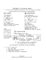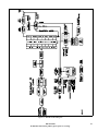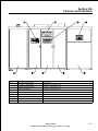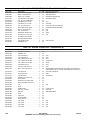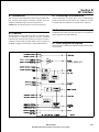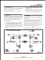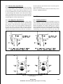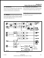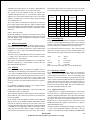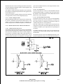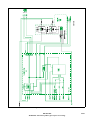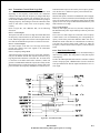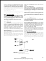
1
TECHNICAL MANUAL
888-2339-002
DX100-3F
994-9369-103
T.M. No. 888-2339-002
© Copyright HARRIS CORPORATION
2003, 2004 All rights reserved
Returns And Exchanges
Damaged or undamaged equipment should not be returned unless written approval and a Return
Authorization is received from HARRIS CORPORATION, Broadcast Communications Division.
Special shipping instructions and coding will be provided to assure proper handling. Complete
details regarding circumstances and reasons for return are to be included in the request for return.
Custom equipment or special order equipment, that is not defective, is not returnable. In those
instances where return or exchange of equipment is at the request of the customer, or convenience
of the customer, a restocking fee will be charged. All returns will be sent freight prepaid and
properly insured by the customer. When communicating with HARRIS CORPORATION, Broadcast
Systems Division, specify the HARRIS Order Number or Invoice Number.
Unpacking
Carefully unpack the equipment and preform a visual inspection to determine that no apparent
damage was incurred during shipment. Retain the shipping materials until it has been determined
that all received equipment is not damaged. Locate and retain all PACKING CHECK LISTs. Use
the PACKING CHECK LIST to help locate and identify any components or assemblies which are
removed for shipping and must be reinstalled. Also remove any shipping supports, straps, and
packing materials prior to initial turn on.
Technical Assistance
HARRIS Technical and Troubleshooting assistance is available from HARRIS Field Service during normal business hours (8:00 AM - 5:00 PM Central Time). Emergency service is available 24
hours a day. Telephone 217/222-8200 to contact the Field Service Department or address correspondence to Field Service Department, HARRIS CORPORATION, Broadcast Communications Division, P.O. Box 4290, Quincy, Illinois 62305-4290, USA. The HARRIS factory may also be contacted through a FAX facility (217/221-7096).
Replaceable Parts Service
Replacement parts are available 24 hours a day, seven days a week from the HARRIS Service
Parts Department. Telephone 217/222-8200 to contact the service parts department or address correspondence to Service Parts Department, HARRIS CORPORATION, Broadcast Communications
Division, P.O. Box 4290, Quincy, Illinois 62305-4290, USA. The HARRIS factory may also be
contacted through a FAX facility (217/221-7096) or e-mail at [email protected].
NOTE
The # symbol used in the parts list means used with (e.g. #C001 = used with C001).
WARNING
THE CURRENTS AND VOLTAGES IN THIS EQUIPMENT ARE DANGEROUS. PERSONNEL MUST AT ALL TIMES OBSERVE SAFETY WARNINGS, INSTRUCTIONS
AND REGULATIONS.
This manual is intended as a general guide for trained and qualified personnel who are aware of the dangers inherent in
handling potentially hazardous electrical/electronic circuits. It is not intended to contain a complete statement of all safety
precautions which should be observed by personnel in using this or other electronic equipment.
The installation, operation, maintenance and service of this equipment involves risks both to personnel and equipment, and
must be performed only by qualified personnel exercising due care. HARRIS CORPORATION shall not be responsible for
injury or damage resulting from improper procedures or from the use of improperly trained or inexperienced personnel
performing such tasks.
During installation and operation of this equipment, local building codes and fire protection standards must be observed. The
following National Fire Protection Association (NFPA) standards are recommended as reference:
- Automatic Fire Detectors, No. 72E
- Installation, Maintenance, and Use of Portable Fire Extinguishers, No. 10
- Halogenated Fire Extinguishing Agent Systems, No. 12A
WARNING
ALWAYS DISCONNECT POWER BEFORE OPENING COVERS, DOORS, ENCLOSURES, GATES, PANELS OR SHIELDS. ALWAYS USE GROUNDING STICKS AND
SHORT OUT HIGH VOLTAGE POINTS BEFORE SERVICING. NEVER MAKE INTERNAL ADJUSTMENTS, PERFORM MAINTENANCE OR SERVICE WHEN ALONE OR
WHEN FATIGUED.
Do not remove, short-circuit or tamper with interlock switches on access covers, doors, enclosures, gates, panels or shields.
Keep away from live circuits, know your equipment and don’t take chances.
WARNING
IN CASE OF EMERGENCY ENSURE THAT POWER HAS BEEN DISCONNECTED.
WARNING
IF OIL FILLED OR ELECTROLYTIC CAPACITORS ARE UTILIZED IN YOUR EQUIPMENT, AND IF A LEAK OR BULGE IS APPARENT ON THE CAPACITOR CASE
WHEN THE UNIT IS OPENED FOR SERVICE OR MAINTENANCE, ALLOW THE
UNIT TO COOL DOWN BEFORE ATTEMPTING TO REMOVE THE DEFECTIVE CAPACITOR. DO NOT ATTEMPT TO SERVICE A DEFECTIVE CAPACITOR WHILE IT
IS HOT DUE TO THE POSSIBILITY OF A CASE RUPTURE AND SUBSEQUENT INJURY.
888-2339-002
WARNING: Disconnect primary power prior to servicing.
i
i
888-2339-002
WARNING: Disconnect primary power prior to servicing.
FIRST-AID
Personnel engaged in the installation, operation, maintenance or servicing of this equipment are urged to become familiar
with first-aid theory and practices. The following information is not intended to be complete first-aid procedures, it is a brief
and is only to be used as a reference. It is the duty of all personnel using the equipment to be prepared to give adequate
Emergency First Aid and thereby prevent avoidable loss of life.
Treatment of Electrical Burns
1.
Extensive burned and broken skin
a.
Cover area with clean sheet or cloth. (Cleanest available cloth article.)
b.
Do not break blisters, remove tissue, remove adhered particles of clothing, or apply any salve or ointment.
c.
Treat victim for shock as required.
d.
Arrange transportation to a hospital as quickly as possible.
e.
If arms or legs are affected keep them elevated.
NOTE
If medical help will not be available within an hour and the victim is
conscious and not vomiting, give him a weak solution of salt and soda:
1 level teaspoonful of salt and 1/2 level teaspoonful of baking soda to
each quart of water (neither hot or cold). Allow victim to sip slowly
about 4 ounces (a half of glass) over a period of 15 minutes. Discontinue fluid if vomiting occurs. (Do not give alcohol.)
2.
Less severe burns - (1st & 2nd degree)
a.
Apply cool (not ice cold) compresses using the cleanest available cloth article.
b.
Do not break blisters, remove tissue, remove adhered particles of clothing, or apply salve or ointment.
c.
Apply clean dry dressing if necessary.
d.
Treat victim for shock as required.
e.
Arrange transportation to a hospital as quickly as possible.
f.
If arms or legs are affected keep them elevated.
REFERENCE:
ILLINOIS HEART ASSOCIATION
AMERICAN RED CROSS STANDARD FIRST AID AND PERSONAL SAFETY MANUAL (SECOND
EDITION)
888-2339-002
WARNING: Disconnect primary power prior to servicing.
ii
TABLE OF CONTENTS
Section I
Introduction/Specifications
Scope and Purpose . . . . . . . . . . . . . . . . . . . . . . . . . . . . . . . .
Equipment Description . . . . . . . . . . . . . . . . . . . . . . . . . . . . .
Block Diagram . . . . . . . . . . . . . . . . . . . . . . . . . . . . . . . . . . .
Available Options . . . . . . . . . . . . . . . . . . . . . . . . . . . . . . . . .
1-1
1-2
1-2
1-2
2-1
2-1
2-1
2-1
2-2
2-2
2-2
Section III
Operators Guide
Introduction . . . . . . . . . . . . . . . . . . . . . . . . . . . . . . . . . . . . . .
Operating Procedures . . . . . . . . . . . . . . . . . . . . . . . . . . . . . .
Daily Preoperational Checkout. . . . . . . . . . . . . . . . . . . . . . .
Transmitter Turn-On Procedure . . . . . . . . . . . . . . . . . . . . . .
Transmitter Turn-Off Procedure. . . . . . . . . . . . . . . . . . . . . .
Transmitter Operations . . . . . . . . . . . . . . . . . . . . . . . . . . . . .
3-1
3-1
3-1
3-1
3-2
3-2
Section IIIA
Controls and Indicators
Section IV
Overall System Theory
Introduction . . . . . . . . . . . . . . . . . . . . . . . . . . . . . . . . . . . . . . 4-1
Block Diagram Description . . . . . . . . . . . . . . . . . . . . . . . . . 4-1
Protection Of Personnel . . . . . . . . . . . . . . . . . . . . . . . . . . . . 4-7
Transmitter Protection . . . . . . . . . . . . . . . . . . . . . . . . . . . . . 4-8
RF Circuits In The Transmitter . . . . . . . . . . . . . . . . . . . . . . 4-8
Transmitter AC Power Circuits . . . . . . . . . . . . . . . . . . . . . 4-11
Drive Multimeter. . . . . . . . . . . . . . . . . . . . . . . . . . . . . . . . . 4-16
Control Multimeter . . . . . . . . . . . . . . . . . . . . . . . . . . . . . . . 4-18
5-1
5-1
5-1
5-2
Section VI
Troubleshooting
Introduction . . . . . . . . . . . . . . . . . . . . . . . . . . . . . . . . . . . . . . 6-1
Making Safe Measurements . . . . . . . . . . . . . . . . . . . . . . . . . 6-1
Troubleshooting Control Front Panel Indicators Faults . . . 6-1
Troubleshooting Faults In The RF Chain . . . . . . . . . . . . . . 6-2
Troubleshooting Frequency Control Panel Faults . . . . . . . 6-13
Troubleshooting Faults on the Power Supply Status
Panel. . . . . . . . . . . . . . . . . . . . . . . . . . . . . . . . . . . . . . . . . . 6-18
System Faults With No Indication On The Front
Panel. . . . . . . . . . . . . . . . . . . . . . . . . . . . . . . . . . . . . . . . . . 6-19
Troubleshooting Low Voltage Supplies. . . . . . . . . . . . . . . 6-20
Measuring RF Drive Level And Phase . . . . . . . . . . . . . . . 6-22
Measuring RF Drain Waveform And Phase . . . . . . . . . . . 6-22
iii
6-1
6-1
6-2
6-3
SECTION VII
PARTS LIST
Section II
Initial Turn-On
Initial Power On . . . . . . . . . . . . . . . . . . . . . . . . . . . . . . . . . .
Frequency Change . . . . . . . . . . . . . . . . . . . . . . . . . . . . . . . .
Low Power Tune. . . . . . . . . . . . . . . . . . . . . . . . . . . . . . . . . .
Medium Power Check . . . . . . . . . . . . . . . . . . . . . . . . . . . . .
High Power Tune . . . . . . . . . . . . . . . . . . . . . . . . . . . . . . . . .
Antenna VSWR Null . . . . . . . . . . . . . . . . . . . . . . . . . . . . . .
Recording Normal Meter Readings . . . . . . . . . . . . . . . . . . .
Section V
Maintenance/Alignments
Introduction . . . . . . . . . . . . . . . . . . . . . . . . . . . . . . . . . . . . . .
Frequency Change Procedures . . . . . . . . . . . . . . . . . . . . . . .
Maintenance . . . . . . . . . . . . . . . . . . . . . . . . . . . . . . . . . . . . .
Preventive Maintenance . . . . . . . . . . . . . . . . . . . . . . . . . . . .
Section VIA
Emergency Operating Procedures
Introduction . . . . . . . . . . . . . . . . . . . . . . . . . . . . . . . . . . . . .
RF System Bypassing . . . . . . . . . . . . . . . . . . . . . . . . . . . . .
Audio/Digital Modulation System Bypassing . . . . . . . . . .
Frequency Control Bypassing . . . . . . . . . . . . . . . . . . . . . . .
Section A
Synthesizer Interface
Introduction . . . . . . . . . . . . . . . . . . . . . . . . . . . . . . . . . . . . .
Function . . . . . . . . . . . . . . . . . . . . . . . . . . . . . . . . . . . . . . . .
Oscilloscope Waveform Plots . . . . . . . . . . . . . . . . . . . . . . .
Location . . . . . . . . . . . . . . . . . . . . . . . . . . . . . . . . . . . . . . . .
Block Diagram Description. . . . . . . . . . . . . . . . . . . . . . . . .
Detailed Circuit Description . . . . . . . . . . . . . . . . . . . . . . . .
Troubleshooting . . . . . . . . . . . . . . . . . . . . . . . . . . . . . . . . . .
Removal\Replacement . . . . . . . . . . . . . . . . . . . . . . . . . . . . .
Alignment. . . . . . . . . . . . . . . . . . . . . . . . . . . . . . . . . . . . . . .
A-1
A-1
A-1
A-1
A-1
A-2
A-6
A-7
A-7
Section B
RF Interface
Introduction . . . . . . . . . . . . . . . . . . . . . . . . . . . . . . . . . . . . .
Function . . . . . . . . . . . . . . . . . . . . . . . . . . . . . . . . . . . . . . . .
Oscilloscope Waveform Plots . . . . . . . . . . . . . . . . . . . . . . .
Location . . . . . . . . . . . . . . . . . . . . . . . . . . . . . . . . . . . . . . . .
Block Diagram Description. . . . . . . . . . . . . . . . . . . . . . . . .
Detailed Circuit Description . . . . . . . . . . . . . . . . . . . . . . . .
RF Interface Troubleshooting . . . . . . . . . . . . . . . . . . . . . . .
Removal\Replacement . . . . . . . . . . . . . . . . . . . . . . . . . . . . .
Alignment. . . . . . . . . . . . . . . . . . . . . . . . . . . . . . . . . . . . . . .
B-1
B-1
B-1
B-1
B-1
B-2
B-3
B-4
B-4
Section C
Driver Combiner Motherboard (A5)
Introduction . . . . . . . . . . . . . . . . . . . . . . . . . . . . . . . . . . . . . C-1
Function . . . . . . . . . . . . . . . . . . . . . . . . . . . . . . . . . . . . . . . . C-1
Location . . . . . . . . . . . . . . . . . . . . . . . . . . . . . . . . . . . . . . . . C-1
Detailed Circuit Description . . . . . . . . . . . . . . . . . . . . . . . . C-1
Troubleshooting . . . . . . . . . . . . . . . . . . . . . . . . . . . . . . . . . . C-2
Driver Combiner Motherboard Removal/Replacement . . . C-5
Buffer Amplifier (A4) . . . . . . . . . . . . . . . . . . . . . . . . . . . . . C-7
Predriver, PD1 . . . . . . . . . . . . . . . . . . . . . . . . . . . . . . . . . . C-12
Drivers, D1 through D14. . . . . . . . . . . . . . . . . . . . . . . . . . C-14
Section D
Predriver Tuning Board
Introduction . . . . . . . . . . . . . . . . . . . . . . . . . . . . . . . . . . . . .
Function . . . . . . . . . . . . . . . . . . . . . . . . . . . . . . . . . . . . . . . .
Location . . . . . . . . . . . . . . . . . . . . . . . . . . . . . . . . . . . . . . . .
Detailed Circuit Description . . . . . . . . . . . . . . . . . . . . . . . .
Predriver Tuning Board Troubleshooting . . . . . . . . . . . . . .
Removal\Replacement . . . . . . . . . . . . . . . . . . . . . . . . . . . . .
Alignment. . . . . . . . . . . . . . . . . . . . . . . . . . . . . . . . . . . . . . .
D-1
D-1
D-1
D-1
D-1
D-2
D-2
Section E
Driver Encoder (A7)
Introduction . . . . . . . . . . . . . . . . . . . . . . . . . . . . . . . . . . . . . E-1
Function . . . . . . . . . . . . . . . . . . . . . . . . . . . . . . . . . . . . . . . . E-1
Oscilloscope Waveform Plots . . . . . . . . . . . . . . . . . . . . . . . E-1
888-2339-002
WARNING: Disconnect primary power prior to servicing.
Location . . . . . . . . . . . . . . . . . . . . . . . . . . . . . . . . . . . . . . . .
Block Diagram Description . . . . . . . . . . . . . . . . . . . . . . . . .
Detailed Circuit Description . . . . . . . . . . . . . . . . . . . . . . . .
Troubleshooting . . . . . . . . . . . . . . . . . . . . . . . . . . . . . . . . . .
Removal and Replacement . . . . . . . . . . . . . . . . . . . . . . . . .
Alignments . . . . . . . . . . . . . . . . . . . . . . . . . . . . . . . . . . . . . .
E-1
E-1
E-2
E-7
E-9
E-9
Section F
RF Combiner Motherboards (A10-A19)
Introduction . . . . . . . . . . . . . . . . . . . . . . . . . . . . . . . . . . . . .
Function . . . . . . . . . . . . . . . . . . . . . . . . . . . . . . . . . . . . . . . .
Location . . . . . . . . . . . . . . . . . . . . . . . . . . . . . . . . . . . . . . . .
Detailed Circuit Description - Main RF Combiner
Motherboard . . . . . . . . . . . . . . . . . . . . . . . . . . . . . . . . . . . .
Detailed Circuit Description - Binary RF Combiner
Motherboard . . . . . . . . . . . . . . . . . . . . . . . . . . . . . . . . . . . .
Troubleshooting . . . . . . . . . . . . . . . . . . . . . . . . . . . . . . . . . .
RF Combiner Motherboard Removal . . . . . . . . . . . . . . . . .
RF Combiner Motherboard Replacement . . . . . . . . . . . . . .
F-1
F-2
F-2
F-2
Section G
RF Amplifier Module
Introduction . . . . . . . . . . . . . . . . . . . . . . . . . . . . . . . . . . . . .
Function . . . . . . . . . . . . . . . . . . . . . . . . . . . . . . . . . . . . . . . .
Location . . . . . . . . . . . . . . . . . . . . . . . . . . . . . . . . . . . . . . . .
Block Diagram Description . . . . . . . . . . . . . . . . . . . . . . . . .
Detailed Circuit Description . . . . . . . . . . . . . . . . . . . . . . . .
Maintenance . . . . . . . . . . . . . . . . . . . . . . . . . . . . . . . . . . . . .
Troubleshooting RF Amp Modules. . . . . . . . . . . . . . . . . . .
G-1
G-1
G-1
G-2
G-2
G-5
G-6
F-1
F-1
F-1
F-1
Section H
Output Monitor/Output Sample
Introduction . . . . . . . . . . . . . . . . . . . . . . . . . . . . . . . . . . . . . H-1
Function . . . . . . . . . . . . . . . . . . . . . . . . . . . . . . . . . . . . . . . . H-1
Oscilloscope Waveform Plots . . . . . . . . . . . . . . . . . . . . . . . H-1
Location . . . . . . . . . . . . . . . . . . . . . . . . . . . . . . . . . . . . . . . . H-1
Block Diagram Description . . . . . . . . . . . . . . . . . . . . . . . . . H-2
Detailed Circuit Description . . . . . . . . . . . . . . . . . . . . . . . . H-2
Troubleshooting the Output Monitor Board . . . . . . . . . . . . H-7
Removal and Replacement . . . . . . . . . . . . . . . . . . . . . . . . . H-9
Alignment . . . . . . . . . . . . . . . . . . . . . . . . . . . . . . . . . . . . . . . H-9
Output Sample Board. . . . . . . . . . . . . . . . . . . . . . . . . . . . . H-11
Introduction . . . . . . . . . . . . . . . . . . . . . . . . . . . . . . . . . . . . H-11
Location . . . . . . . . . . . . . . . . . . . . . . . . . . . . . . . . . . . . . . . H-11
Function . . . . . . . . . . . . . . . . . . . . . . . . . . . . . . . . . . . . . . . H-11
Detailed Circuit Description . . . . . . . . . . . . . . . . . . . . . . . H-11
Troubleshooting . . . . . . . . . . . . . . . . . . . . . . . . . . . . . . . . . H-11
Removal and Replacement . . . . . . . . . . . . . . . . . . . . . . . . H-11
Alignments . . . . . . . . . . . . . . . . . . . . . . . . . . . . . . . . . . . . . H-11
Section J
Analog Input Board
Introduction . . . . . . . . . . . . . . . . . . . . . . . . . . . . . . . . . . . . .
Function . . . . . . . . . . . . . . . . . . . . . . . . . . . . . . . . . . . . . . . .
Location . . . . . . . . . . . . . . . . . . . . . . . . . . . . . . . . . . . . . . . .
Oscilloscope Waveform Plots . . . . . . . . . . . . . . . . . . . . . . .
Block Diagram Description . . . . . . . . . . . . . . . . . . . . . . . . .
Detailed Circuit Description . . . . . . . . . . . . . . . . . . . . . . . .
Troubleshooting . . . . . . . . . . . . . . . . . . . . . . . . . . . . . . . . . .
Removal and Replacement . . . . . . . . . . . . . . . . . . . . . . . . .
Alignments . . . . . . . . . . . . . . . . . . . . . . . . . . . . . . . . . . . . . .
J-1
J-1
J-1
J-1
J-1
J-2
J-6
J-8
J-8
Section K
Analog To Digital Converter
Introduction . . . . . . . . . . . . . . . . . . . . . . . . . . . . . . . . . . . . .
Function. . . . . . . . . . . . . . . . . . . . . . . . . . . . . . . . . . . . . . . .
Location. . . . . . . . . . . . . . . . . . . . . . . . . . . . . . . . . . . . . . . .
Block Diagram Description . . . . . . . . . . . . . . . . . . . . . . . .
Detailed Circuit Description. . . . . . . . . . . . . . . . . . . . . . . .
Troubleshooting . . . . . . . . . . . . . . . . . . . . . . . . . . . . . . . . .
Removal and Replacement . . . . . . . . . . . . . . . . . . . . . . . . .
Alignments . . . . . . . . . . . . . . . . . . . . . . . . . . . . . . . . . . . . .
K-1
K-1
K-1
K-1
K-2
K-4
K-6
K-6
Section L
Modulation Encoders (A25-A29)
Introduction . . . . . . . . . . . . . . . . . . . . . . . . . . . . . . . . . . . . . . L-1
Function. . . . . . . . . . . . . . . . . . . . . . . . . . . . . . . . . . . . . . . . . L-1
Location. . . . . . . . . . . . . . . . . . . . . . . . . . . . . . . . . . . . . . . . . L-1
Big Step Modulation Encoders . . . . . . . . . . . . . . . . . . . . . . L-1
Binary Modulation Encoder (A25) . . . . . . . . . . . . . . . . . . L-14
Section M
Controller (A31)
Introduction . . . . . . . . . . . . . . . . . . . . . . . . . . . . . . . . . . . . . M-1
Function. . . . . . . . . . . . . . . . . . . . . . . . . . . . . . . . . . . . . . . . M-1
Location. . . . . . . . . . . . . . . . . . . . . . . . . . . . . . . . . . . . . . . . M-1
Block Diagram Description . . . . . . . . . . . . . . . . . . . . . . . . M-1
Detailed Circuit Description. . . . . . . . . . . . . . . . . . . . . . . . M-3
Troubleshooting . . . . . . . . . . . . . . . . . . . . . . . . . . . . . . . . M-23
Removal and Replacement . . . . . . . . . . . . . . . . . . . . . . . . M-25
Alignments . . . . . . . . . . . . . . . . . . . . . . . . . . . . . . . . . . . . M-25
LED Board . . . . . . . . . . . . . . . . . . . . . . . . . . . . . . . . . . . . M-25
Switch Board/Meter Panel . . . . . . . . . . . . . . . . . . . . . . . . M-25
Section N
External Interface (A23)
Introduction . . . . . . . . . . . . . . . . . . . . . . . . . . . . . . . . . . . . .
Function. . . . . . . . . . . . . . . . . . . . . . . . . . . . . . . . . . . . . . . .
Location. . . . . . . . . . . . . . . . . . . . . . . . . . . . . . . . . . . . . . . .
Detailed Circuit Description. . . . . . . . . . . . . . . . . . . . . . . .
Troubleshooting . . . . . . . . . . . . . . . . . . . . . . . . . . . . . . . . .
Removal and Replacement . . . . . . . . . . . . . . . . . . . . . . . . .
Alignments . . . . . . . . . . . . . . . . . . . . . . . . . . . . . . . . . . . . .
N-1
N-1
N-1
N-1
N-4
N-5
N-5
Section P
Transmitter Interface
Introduction . . . . . . . . . . . . . . . . . . . . . . . . . . . . . . . . . . . . . .
Function. . . . . . . . . . . . . . . . . . . . . . . . . . . . . . . . . . . . . . . . .
Location. . . . . . . . . . . . . . . . . . . . . . . . . . . . . . . . . . . . . . . . .
Detailed Circuit Description. . . . . . . . . . . . . . . . . . . . . . . . .
Troubleshooting Transmitter Interface. . . . . . . . . . . . . . . . .
Removal and Replacement . . . . . . . . . . . . . . . . . . . . . . . . . .
Alignments . . . . . . . . . . . . . . . . . . . . . . . . . . . . . . . . . . . . . .
P-1
P-1
P-1
P-1
P-3
P-4
P-4
Section Q
Frequency Control Board
Introduction . . . . . . . . . . . . . . . . . . . . . . . . . . . . . . . . . . . . .
Function. . . . . . . . . . . . . . . . . . . . . . . . . . . . . . . . . . . . . . . .
Location. . . . . . . . . . . . . . . . . . . . . . . . . . . . . . . . . . . . . . . .
Block Diagram Description . . . . . . . . . . . . . . . . . . . . . . . .
Detailed Circuit Description. . . . . . . . . . . . . . . . . . . . . . . .
Troubleshooting . . . . . . . . . . . . . . . . . . . . . . . . . . . . . . . . .
Removal\Replacement . . . . . . . . . . . . . . . . . . . . . . . . . . . .
Alignment . . . . . . . . . . . . . . . . . . . . . . . . . . . . . . . . . . . . . .
Q-1
Q-1
Q-1
Q-1
Q-1
Q-5
Q-6
Q-6
888-2339-002
WARNING: Disconnect primary power prior to servicing.
iv
Section R
Frequency Control Interface
Introduction . . . . . . . . . . . . . . . . . . . . . . . . . . . . . . . . . . . . . R-1
Function. . . . . . . . . . . . . . . . . . . . . . . . . . . . . . . . . . . . . . . . R-1
Location. . . . . . . . . . . . . . . . . . . . . . . . . . . . . . . . . . . . . . . . R-1
Block Diagram Description . . . . . . . . . . . . . . . . . . . . . . . . R-1
Detailed Circuit Description . . . . . . . . . . . . . . . . . . . . . . . . R-2
Troubleshooting . . . . . . . . . . . . . . . . . . . . . . . . . . . . . . . . . R-9
Removal\Replacement . . . . . . . . . . . . . . . . . . . . . . . . . . . R-10
Alignment . . . . . . . . . . . . . . . . . . . . . . . . . . . . . . . . . . . . . R-11
Section S
3F Select Board
Introduction . . . . . . . . . . . . . . . . . . . . . . . . . . . . . . . . . . . . . . S-1
Function. . . . . . . . . . . . . . . . . . . . . . . . . . . . . . . . . . . . . . . . . S-1
v
Location . . . . . . . . . . . . . . . . . . . . . . . . . . . . . . . . . . . . . . . . S-1
Section T
3F Controller Board
Introduction . . . . . . . . . . . . . . . . . . . . . . . . . . . . . . . . . . . . .
Function . . . . . . . . . . . . . . . . . . . . . . . . . . . . . . . . . . . . . . . .
SERVO CONTROL . . . . . . . . . . . . . . . . . . . . . . . . . . . . . .
Location . . . . . . . . . . . . . . . . . . . . . . . . . . . . . . . . . . . . . . . .
T-1
T-1
T-1
T-1
Section U
Servo Calibration
Servo Calibration . . . . . . . . . . . . . . . . . . . . . . . . . . . . . . . . . U-1
Appendix A
DX Digital Modulation Technology and Concepts
DX Digital Modulation Technology and Concepts . . . . . . . a-1
888-2339-002
WARNING: Disconnect primary power prior to servicing.
Section I
Introduction/Specifications
1.1 Scope and Purpose
Control Multimeter (A41)
This technical manual contains the information necessary to
install and maintain the DX100-3F. The various sections of this
technical manual provide the following types of information.
• Section I, Introduction/Specifications, provides general
•
•
•
•
manual layout, frontispiece, equipment description, block
diagram, and available options.
Section II, Installation/Initial Turn-On, provides initial turn
on instructions.
Section III, Operators Guide, provides normal turn-on/turnoff procedures, taking meter readings, and transmitter operations.
Section III-A, Controls/Indicators, provides identification
and functions of all external panel controls and indicators,
plus multimeter reading log sheets.
Section IV, Overall System Theory provides block diagram
and detailed theory of operation of the transmitter and
various sections that apply to the overall transmitter. It
includes the following:
RF Section
Predriver Splitter (A46) and Driver Drive Cables
RF Splitter (A6) and RF Drive Cables
Output Network
Power Supply Section
Low Voltage Power Supply
RF Amplifier Power Supply
Driver Multimeter (A9)
• Section V, Maintenance/Alignments, provides a transmitter
frequency change procedure.
• Section V-A, Cabinet Views, provides drawings that show
the location of major components and modules in the
cabinets.
• Section VI, Troubleshooting, provides simplified flow style
troubleshooting procedures down to the board level.
• Section VI-A, Emergency Operating Procedures, provides
methods to maintain on-air operation of the transmitter in
the event of a failure.
• Section VII, Parts List, provides a parts list for the overall
transmitter as well as individual modules.
The following subsections provide principles of operations for
boards and modules in the DX100-3F:
• Section A, Synthesizer Interface (A1) [A2 optional]
• Section B, RF Interface (A3)
• Section C, Driver Combiner Motherboard (A5)
Buffer Amplifier (A4)
Predriver (PD1)
Drivers (D1-D14)
• Section D, Predriver Tuning Board (A54)
• Section E, Driver Encoder (A7)
• Section F, RF Combiner Motherboards
Main Combiner Motherboards (A11-A19)
Binary Combiner Motherboard (A10)
Figure 1-1. Front View of Transmitter
888-2339-002
WARNING: Disconnect primary power prior to servicing.
1-1
• Section G, RF Amplifiers
• Section H, Output Monitor (A21)
•
•
•
•
•
•
•
•
•
1-2
Output Sample (2A1)
VSWR Compensation (A56)
Section J, Analog Input Board (A22)
Section K, Analog To Digital Converter (A32)
Section L, Modulation Encoders
Big Step Modulation Encoders (A26-A29)
Binary Modulation Encoder (A25)
Air Flow Monitors (A3, A24, A47-A49)
Section M, Controller (A31)
LED Board (A42)
Switch Board/Meter Panel (A35)
Section N, External Interface (A23)
Section P, Transmitter Interface (A30)
Section Q, Frequency Control Board (A51)
Section R, Frequency Control Interface (A50)
Appendix A, Digital Terms and Concepts
1.2 Equipment Description
The DX100-3F is a 3 frequency agile solid state medium wave
amplitude modulation transmitter with a rated power output level
of 100 kilowatts. The transmitter is capable of 110 kilowatts and
has three power level selections that are user set. The frequency
selections are 585 kHz, 684 kHz and 936 kHz.
1.3 Block Diagram
A Block Diagram description is contained in Section IV, Overall
System Theory.
1.4 Available Options
480VAC to 240VAC Stepdown Transformer
A2 Synthesizer Interface B
888-2339-002
WARNING: Disconnect primary power prior to servicing.
Figure 1-2. DX100-3F Block Diagram
888-2339-002
WARNING: Disconnect primary power prior to servicing.
1-3
1-4
888-2339-002
WARNING: Disconnect primary power prior to servicing.
Section II
Initial Turn-On
The following procedure assumes that the transmitter has already
been correctly installed and is ready for turn-on.
Note
If AC power is loss for an extended period of time and the Battery Backup Voltage falls too low to store the Frequency references, you will need follow the procedure under “Initial Power
On”. If AC loss for an extended period of time happens often you
may want to provide an external battery backup via TB1 1-2 on
the Transmitter Interface. Refer to P.4.3.1.2 “External Battery Input”.
2.1 Initial Power On
a.
b.
c.
d.
e.
Select the Servo Breaker to the OFF position.
Enable the Low Voltage and Main Breaker.
Wait for 60 seconds then ENABLE the SERVO Breaker.
Select S100 to the NORM position.
Select a different frequency other than the one that is
already selected. This is to insure the relays and servos are
in the proper location.
f. Depress the Reset button on the Control front.
g. On the Controller move S1 from NORM to MUTE position.
h. On the Analog Input board, rotate R65, R66, and R67 fully
counter clockwise and set S1 to the CALIBRATE position.
2.2 Frequency Change
a. Select one of the three available frequencies for operation
that is listed on the Factory Test Data Sheets.
b. Verify the TUNE meter indicates the same as the new 2L2
number per Transmitter Band Chart.
c. Verify the LOAD meter indicates the same as the new 2C1
number per transmitter Band Chart.
d. Set S100 to the CALIBRATE position.
2.3 Low Power Tune
If an Antenna VSWR overload occurs before 10 kW is reached,
skip to the Antenna Null adjustment following this section and
return here when completed.
h. Do an RF Amp temperature test by moving your hand
about 1 inch (2.54 cm) in front of the RF Amp doors to
feel the air temperature. It should only be slightly warm.
The left PA compartment temperature will be slightly
warmer than the other compartments. This is normal since
these are the RF Amps being turned on.
i. Check the 10 kW meter readings with the readings on the
Factory Test Data Sheets under PA Voltage, PA Current,
and Number Of Steps On. If all are within 10%, continue
with the next step.
2.4 Medium Power Check
a. Press the LOW power switch on the front panel. The Power
meter selector switch should be in FWD.
b. On the Controller move S1 from MUTE to NORM and
begin raising the RF forward power by slowly turning R66
clock- wise.
c. Stop increasing power when Forward power is 10 kilowatts.
d. Using the front panel meters, verify the following conditions:
1. PA +VDC = 240 to 250 volts.
2/18/04
2. PA Current = 60 to 80 amps.
3. Number of RF Amplifiers (steps) ON should be 21 to
23 (Open the left front door and count the number of
illuminated green LED’s on the RF Amplifiers along
the left side of the compartment starting at the bottom
and counting upward).
e. The TUNE SERVO Raise/Lower may now be adjusted for
a peak in power output.
f. The LOAD SERVO Raise/Lower is adjusted in conjunction with the power control potentiometer to properly
adjust the Number of steps that are turned on for 10 kW.
1. Use the number of steps turned on from the Factory
Test Data to help determine if the LOADING needs
adjusting; e.g. if the desired number of steps is 22 and
you have more than 22 on, adjust the Low power control
R66 on the Analog Input board counter clockwise until
22 steps are turned on. Then adjust the LOAD Servo
Raise/Lower until 10 kW is reached.
If you have less than 22 steps on, adjust the Low power
control R66 on the Analog Input Board clock-wise until
22 steps are turned on. Then adjust the LOAD Servo
Raise/Lower until 10 kW is reached.
g. Repeat the TUNE and LOAD SERVO adjustments as they
interact with each other.
a. Depress the MEDIUM power switch on the front panel.
b. Slowly adjust R67 CW until the indicated output on the
power meter shows 50 kW.
c. Check the 50 kW meter readings with the readings on the
Factory Test Data Sheets under PA Voltage, PA Current,
and Number Of Steps On. If all are within 10%, continue
with the next step.
d. If the readings are not within 10%, retune the output
network according to the Low Power Tune described
above.
888-2339-002
WARNING: Disconnect primary power prior to servicing.
2-1
If an Antenna VSWR overload occurs before 50 kW is reached,
skip to the Antenna Null adjustment following this section and
return here when completed.
2.5 High Power Tune
a. Depress the High Power switch on the front panel.
b. Adjust R65 clockwise until 100 kW is reached.
c. Using the front panel meters, verify the following conditions:
1. PA +VDC = 225 to 235 volts.
2. PA Current = 460 to 470 amps.
3. Number of RF Amps ON = 64 to 66 (Open the left front
door and count the number of illuminated green LED’s
on the RF Amplifiers along the left side of the compartment starting at the bottom and counting upward).
d. The TUNE SERVO Raise/Lower may now be adjusted for
a peak in power output.
Note
Reference 3F Controller potentiometer settings.
e. The LOAD SERVO Raise/Lower is adjusted in conjunction with the power control potentiometer to properly
adjust the Number of steps that are turned on for 100 kW.
1. Use the number of steps turned on from the Factory Test
Data to help determine if the LOADING needs adjusting; e.g. if the desired number of steps is 65 and you
have more than 65 on, adjust the High power control
R65 on the Analog Input board counter clockwise until
65 steps are turned on. Then adjust the LOAD Servo
Raise/Lower until 100 kW is reached.
If you have less than 65 steps on, adjust the High power
control R65 on the Analog Input Board clock-wise until
65 steps are turned on. Then adjust the LOAD Servo
Raise/Lower until 100 kW is reached.
f. Repeat the TUNE and LOAD SERVO adjustments as they
interact with each other.
2-2
NOTE
It is preferred to leave the tuning slightly on the inductive side of
resonance for optimum efficiency and performance.
The inductive side of resonance is achieved by turning 2C1A
counter clockwise from the point where the power peak is found.
The capacitive side of resonance is normally indicated by a drop
in current but does not drop as fast as the power when 2C1A is
tuned off the peak. The transmitter should not be operated more
that 8kW off of the power peak.
g. Do an RF Amp temperature test by moving your hand
about 1 inch in front of the RF Amp doors to feel the air
temperature flowing over the RF AMPS.
h. Return S1 on the Analog Input board to the NORMAL
Position.
i. Refer to Section U for Servo Calibration.
j. Return S100 to the NORM Position.
2.6 Antenna VSWR Null
If an Antenna VSWR overload occurs before 100 kW is reached,
note the Antenna Null position on the front panel multimeter.
Increase or decrease the number in 1 step increments until the
meter indication is nulled.
Additionally, “Fine Tuning” of the VSWR Null may be accomplished by using the Phase and Amplitude adjustments of the
Output Monitor Board.
2.7 Recording Normal Meter Readings
Check all meter readings against the Factory Test Data sheets. It
is strongly recommend that a permanent record of ALL meter
readings be made on a recurring basis, i.e. weekly or monthly. A
sample form for meter readings is contained in the operators
guide section of this Manual.
888-2339-002
WARNING: Disconnect primary power prior to servicing.
2/18/04
Section III
Operators Guide
3.1 Introduction
This section contains information on day-to-day operation for
the non-technical operator.
3.2 Operating Procedures
These procedures describe normal daily operation of the DX1003F, including:
a. Daily pre-operational checkout
b. Transmitter turn-on procedures.
c. Transmitter turn-off procedures.
d. Transmitter operations.
It is important that the operator be aware of normal transmitter
operation and performance, and note any changes or fault indications. Changes in operation may indicate a need for maintenance or corrective action before more serious problems develop.
NOTE
The following procedure assumes that the transmitter has been
previously tuned to the correct frequency and is operating properly. For Frequency Change instructions, refer to the Maintenance Section of this manual.
WARNING
ALL SERVICE SHOULD ONLY BE PERFORMED BY QUALIFIED
PERSONNEL. DANGEROUS VOLTAGES OR CURRENTS MAY BE
PRESENT INSIDE WHEN DOORS ARE OPEN.
Normal operation and monitoring of the transmitter is accomplished through front panel controls, meters, and indicators.
Read Section IIIA: Controls and Indicators.
NOTE
If remote/extended control of the transmitter is used, the station
chief engineer or qualified technical staff member should provide
instructions for operator use.
3.3 Daily Preoperational Checkout
The following paragraphs describe checks to be made before
normal daily turn-on.
a. Check the transmitter maintenance log to make sure that
maintenance performed on the transmitter, or other abnormal conditions, do not place any restrictions on transmitter
operation. An example is a requirement to operate at reduced power.
b. Ensure that the transmitter RF output is properly terminated into the antenna. This may include determining that
antenna pattern switching is correct.
c. Observe the Power Supply Status Panel located near the
top of the right most cabinet. The indicators under 3PH
A/C MAINS PROTECTION PH1, PH2, PH3 and under
SINGLE PHASE A/C MAINS PROTECTION PH1, PH2
should all be illuminated GREEN. If an indicator is not
GREEN, it is possible that the transmitter will operate, but
contact maintenance personnel immediately.
d. Observe the Frequency Control front panel, there should
be no RED indicators illuminated.
e. Check the Control front panel on the center front of the
transmitter. If the transmitter is ready for operation, all the
status, interlock, and overload LEDs will be green. If any
LEDs are red, note which indicators are red so that information may be entered into the station maintenance log,
then press the RESET button. All indicators should change
to green when the RESET button is pushed and released.
If any indicators are still red after operating the RESET, do
not attempt to turn on the transmitter and contact maintenance personnel.
f. If no LEDs are lit, place the Low Voltage Enable switch to
the STANDBY MODE and continue with the following
steps.
3.4 Transmitter Turn-On Procedure
When the Preoperational Checkout has been completed and no
problems are present, the transmitter is ready to turn on.
a. Set the selector switch below the POWER meter on the
meter panel to FORWARD, if it is not already in that
position.
b. Depress the LOW, the MEDIUM, or the HIGH pushbutton
on the meter panel, depending on power level desired. Each
of these pushbuttons will turn the transmitter on at the
power level which has been preset.
c. The pushbutton you have operated should illuminate
green, and power will come up to the preset level. (You
should also hear three ‘clicks’ as contactors operate, then
the blowers should start, then power will come up).
NOTE
During the Step Start sequence, you should see the following: RF
Mute LED turns red for an instant, the VSWR test LED turns red
for 4 seconds, and the Power meter will go to 1/4 of the power
selected and then advance to the desired power level. This should
take between .5 and 3 seconds.
d. Should FORWARD POWER not be correct, verify that
you have selected the correct power level (LOW, MEDIUM, or HIGH). If not, depress the proper power level
button, and check forward power again.
e. When the correct power level has been selected, but an
adjustment in power is still needed, press the RAISE button
to INCREASE power, or the LOWER button to DECREASE power. When you hold the button depressed and
watch the FORWARD POWER indication, the power will
change slowly. Hold the button until the power is correct.
888-2339-002
WARNING: Disconnect primary power prior to servicing.
3-1
NOTE
RAISE and LOWER buttons will only change power level if the
transmitter is operating in the HIGH, MEDIUM, or LOW function. This new power level will become the preset power until it
is changed again. The Raise and Lower pushbuttons will adjust
power +/-10% of the selected power level.
f. Check transmitter panel meter readings for normal values.
If an abnormal meter reading is obtained, maintenance
personnel should be contacted.
3.5 Transmitter Turn-Off Procedure
a. To turn off (de-energize) the transmitter, depress the OFF
pushbutton.
b. The HIGH, MEDIUM, or LOW lamp will go out, you
should hear the contactor as it de-energizes, and the blowers will stop.
c. With the POWER switch in the FORWARD position, the
Power meter should indicate zero power. Supply voltage and
supply current meters should both indicate zero readings.
3.6 Transmitter Operations
The following is intended to make the operator aware of some
basic operational characteristics of the transmitter.
3.6.1 Routine Meter Readings
A sample logsheet is provided on in Section IIIA, Controls and
Indicators. Copies can be made of the logsheet for station records. We suggest these readings be taken monthly at a minimum,
however more frequent logs can be an important tool in assisting
maintenance personnel.
3.6.2 Fault Conditions
The following describes normal transmitter actions for certain
possible fault conditions. It is very important that operators log
all abnormal operation, such as incorrect meter readings, overloads, fault indications, and transmitter shut-downs. A log or
record of abnormal operating conditions will be useful to maintenance personnel in locating and correcting transmitter or other
system problems.
3.6.2.1 Transmitter Shuts Off
The operator should first check for overload or fault indications
that are RED and log any fault indications that are found. Press
the RESET button on the Control front panel to clear fault
indications. Control front panel indicators should change from
RED to GREEN.
If any LEDs are still RED, contact maintenance personnel.
When the fault indicators are GREEN, follow the normal turn-on
procedure.
If the transmitter shuts off again, and the same overload or fault
indication comes on, try turning the transmitter on by using the
LOW power button. Under some overload/fault conditions, a
3-2
transmitter may operate satisfactorily at reduced power. If it will
not come on at LOW power, contact maintenance personal.
3.6.2.2 AC Power Failure
If Battery Backup has been installed into the transmitter, no
operator action is required for ac power failures of less than
approximately 96 hours. The transmitter will automatically return to an on-air condition, at the same power level as before the
power failure.
If Battery Backup has not been installed and ac power is off for
more than about 10 minutes and power is restored you should
have the following indications: the 3PH AC MAINS indicators
PH1, PH2, PH3 and SINGLE PHASE AC MAINS indicators
PH1 and PH2 on the Power Supply Status Panel have returned
to GREEN. The transmitter will have to be manually turned on
and retuned to the operating frequency before operation can
resume. Contact maintenance personnel immediately.
3.6.2.3 RF Amp Power Supply Current Fault
During a Current Fault condition the transmitter will shut off and
the indicator will change to RED. The transmitter will attempt to
restart by itself when the fault is no longer present.
a. If the transmitter turns back on and stays on, check program modulation level. If overmodulating on positive
peaks, reduce audio level to reduce modulation level.
b. If the transmitter shuts off again and no longer automatically restarts. Log or record the fault, RESET the fault
indicator, and try turning the transmitter on.
c. If the fault occurs again, try operating at LOW power. If
the transmitter will operate at LOW power, operation may
continue on a temporary, emergency basis.
3.6.2.4 Power Reduction
The transmitter will reduce the power output in steps during
certain faults. When the fault is no longer present, the transmitter
will increase the power output in steps back to the original level.
This is done automatically by the transmitter and no operator
intervention is required.
If the fault was only a temporary condition, the recovery process
can be advanced by depressing the FAULT RESET pushbutton.
If the indicator will not reset or the power level of the transmitter
has been lowered drastically, contact maintenance personnel
immediately.
If the power output has been reduced and the Analog Input Power
Foldback indicator is RED, the transmitter has responded to one
of the following faults.
3.6.2.5 VSWR Faults
If the OUTPUT MONITOR NETWORK VSWR, ANTENNA
VSWR, OR VSWR TEST indicators are RED or are flashing
RED, the following may be the cause:
a. This may be a normal occurrence during a thunderstorm,
rain storm, blowing sand, or under conditions of ice on the
antenna and will stop when the weather conditions improve.
888-2339-002
WARNING: Disconnect primary power prior to servicing.
b. The indicators may flash RED when overmodulation occurs. Reducing modulation to normal levels may correct
the condition.
c. If the indicators remain RED and weather conditions or
overmodulation are not the cause, transmitter and/or antenna problems are indicated.
3.6.2.7 Air Flow Faults
If the AIR FLOW REDUCED indicator is RED, the following
may be the cause:
a. Obstruction of air flow at the air intake on the transmitter
rear doors or at the air outlet on the transmitter top.
b. Dirty or clogged air filters.
3.6.2.6 Temperature Faults
3.6.2.8 RF Amp Fuse
If the RF AMP TEMP or RF AMP POWER SUPPLY TEMP
FAULT indicator is RED, the following may be the cause:
The transmitter will continue to operate safely, although power
output will be slightly reduced. The fault indication can not be
RESET. The fault must be corrected to clear the fault indication.
Continue normal operation and contact maintenance personnel.
a. Failure of the building cooling system (high ambient temperatures).
b. Possible transmitter mistuning.
888-2339-002
WARNING: Disconnect primary power prior to servicing.
3-3
3-4
888-2339-002
WARNING: Disconnect primary power prior to servicing.
Section IIIA
Controls and Indicators
REF.
1
2
3
4
5
6
7
8
9
CONTROL/INDICATOR
Frequency Control Panel
Switch Board/Meter Panel
Control Front Panel
Power Supply Status Panel
Output Network Cabinet
Left PA Cabinet
Center PA Cabinet
Right PA Cabinet
Power Supply Cabinet
FUNCTION
See Table 3-1 and Figure 3-1.
See Table 3-2 and Figure 3-2.
See Table 3-3 and Figure 3-3.
See Table 3-4 and Figure 3-4.
888-2339-002
WARNING: Disconnect primary power prior to servicing.
3A-1
Figure 3-1
Frequency Control Panel Controls and Indicators
3A-2
888-2339-002
WARNING: Disconnect primary power prior to servicing.
Table 3-1. Frequency Control Panel
Controls and Indicators
REF.
1
2
3
4
5
6
7
8
9
10
11
12
CONTROL/INDICATOR
FUNCTION
FREQUENCY SYNTHESIZER LED GREEN indicates desired frequency is acceptable. RED indicates desired
frequency is out of range.
TUNE POSITION
NOTE - The following assumes S2 on the Frequency Control board is in the
METER/FREQUENCY CONTROL NORMAL position. When in the FREQUENCY CHANGE Mode, the meter
BOARD MULTIMETER
indicates the proper position for the TUNE SERVO. When in the LOW POWER
TUNE or HIGH POWER TUNE Mode, the meter indicates the actual position
of the TUNE SERVO. When in the NORMAL OPERATION Mode, the meter is
turned off. NOTE - If S3 on the Frequency Control board is depressed in any
mode, the meter will indicate the proper position for the TUNE SERVO. NOTE If S2 on the Frequency Control board is in the METER position, the TUNE
meter becomes a Multimeter for the Frequency Control board - refer to Figure 37 and Table 3-7 for more information.
LOAD POSITION METER
When in the FREQUENCY CHANGE Mode, the meter indicates the proper
position for the LOAD SERVO. When in the LOW POWER TUNE or HIGH
POWER TUNE Mode, the meter indicates the actual position of the LOAD
SERVO. When in the NORMAL OPERATION Mode, the meter is turned off.
FREQUENCY SELECT SWITCHES Used to select the operating frequency in kHz of 585, 684 or 936kHz.
BANDSWITCH DRIVERS FAULT GREEN indicates normal operation. RED indicates a cable is disconnected, 2L1
LED
switch not in the proper position, or loss of +24Vdc relay supply.
TUNE SERVO SWITCH
In the normal (center) position, the tuning servo motor is not active. In the
RAISE (upper) position, the tuning servo motor is rotating clockwise (as viewed
from the rear of the transmitter) and the capacitance is decreased. In the
LOWER (down) position, the tuning servo motor is rotating counter-clockwise
(as viewed from the rear of the transmitter) and the capacitance is increased.
TUNE SERVO FAULT LED
GREEN indicates the tuning servo motor is in the proper position. RED
indicates the tuning servo motor is not in the proper position.
LOAD SERVO SWITCH
In the normal (center) position, the loading servo motor is not active. In the
RAISE (upper) position, the loading servo motor is rotating clockwise (as
viewed from the rear of the transmitter) and the inductance is decreased. In the
LOWER (down) position, the loading servo motor is rotating counter-clockwise
(as viewed from the rear of the transmitter) and the inductance is increased.
LOAD SERVO FAULT LED
GREEN indicates the loading servo motor is in the proper position. RED
indicates the loading servo motor is not in the proper position.
FREQUENCY CONTROL SUPPLY GREEN indicates normal operation. RED indicates failure of a power supply on
FAULT LED
the Frequency Control board.
NORMAL OPERATION LED
Illuminated GREEN only when in this mode.
FREQUENCY CHANGE LED
Illuminated YELLOW only when in this mode.
888-2339-002
WARNING: Disconnect primary power prior to servicing.
3A-3
Figure 3-2. Switch Board/Meter Panel
Controls and Indicators
3A-4
888-2339-002
WARNING: Disconnect primary power prior to servicing.
Table 3-2
Switchboard/Meter Panel Controls and Indicators
REF.
1
2
3
CONTROL/INDICATOR
VOLTAGE multimeter
SUPPLY CURRENT meter
POWER meter
4
POWER, selector
5
6
OFF, pushbutton
LOWER, pushbutton
7
RAISE, pushbutton
8
HIGH, pushbutton
9
MEDIUM, pushbutton
10
LOW, pushbutton
11
MULTIMETER switch
FUNCTION
Indicates voltages at points selected by the Multimeter Switch (Ref. 11).
Indicates the 230V supply current being supplied to the Power Amplifier.
Indicates either FORWARD or REFLECTED power at the transmitter
output, whichever is selected by the POWER METER selector switch (Ref.
4).
Selects Forward power output or Reflected power, to be read on the POWER
meter.
Used to turn the transmitter off.
Used to adjust power level. When the transmitter is in the LOW, MEDIUM,
or HIGH power mode, depress to LOWER power output and hold until
desired power is reached. INDICATOR illuminates while power is being
lowered.
Used to adjust power level. When the transmitter is in the LOW, MEDIUM,
or HIGH power mode, depress to RAISE power output and hold until
desired power is reached. INDICATOR illuminates while power is being
raised.
Used to turn the transmitter on at the preset HIGH power level, or to change
power to the preset HIGH power level. The pushbutton will illuminate when
in the HIGH power mode.
Used to turn the transmitter on at the preset MEDIUM power level, or to
change power to the preset MEDIUM power level. The pushbutton will
illuminate when in the MEDIUM power mode.
Used to turn the transmitter on at the preset LOW power level, or to change
power to the preset LOW power level. The pushbutton will illuminate when
in the LOW power mode.
Selects the desired function to be monitored by the VOLTAGE multimeter.
888-2339-002
WARNING: Disconnect primary power prior to servicing.
3A-5
Figure 3-3
Control Front Panel Controls and Indicators
Table 3-3
Control Front Panel Controls and Indicators
CONTROL/INDICATOR
FREQUENCY SYNTHESIZER
BUFFER AMP
PREDRIVER
DRIVER
HIGH DRIVE
LOW DRIVE
RF AMP
FUSE
TEMP
OUTPUT MONITOR
NETWORK VSWR
ANTENNA VSWR
VSWR TEST, pushbutton
VSWR TEST indicator
SUPPLY FAULT
3A-6
FUNCTION
Indicates Frequency Synthesizer board rf output status. GREEN indicates normal rf
output; RED indicates low or no rf output.
Indicates buffer amplifier rf output status. GREEN indicates normal rf output; RED
indicates low or no rf output.
Indicates predriver rf output status. GREEN indicates normal rf output; RED
indicates low or no rf output.
GREEN indicates normal drive level. RED indicates excessive rf drive level to the
RF Amplifiers.
GREEN indicates normal drive level. RED indicates low rf drive level to the RF
Amplifiers.
GREEN indicates a normal, no fault condition. RED indicates a failure of an RF
Amplifier fuse.
GREEN indicates normal temperature of RF1. RED indicates excessive temperature
of RF1.
GREEN indicates that there is no detected VSWR in the network filter; RED
indicates detected VSWR.
GREEN indicates there is no detected VSWR in the antenna. RED indicates detected
VSWR.
Used to test operation of VSWR logic, result of test is displayed on VSWR TEST
indicator. When the pushbutton is depressed, the VSWR TEST indicator will turn
RED for 4 seconds. If it returns to GREEN, a successful VSWR TEST has been
performed. If it remains RED, a VSWR TEST has failed.
Indicates result of VSWR TEST. GREEN indicates VSWR protection logic is
functioning normally. RED indicates VSWR logic fault.
GREEN indicates normal operation. RED indicates a power supply failure.
888-2339-002
WARNING: Disconnect primary power prior to servicing.
Table 3-3
Control Front Panel Controls and Indicators
(Continued)
CONTROL/INDICATOR
ANALOG INPUT
POWER FOLDBACK
FUNCTION
GREEN indicates normal operation. RED indicates transmitter has responded to a
fault by reducing current power level.
GREEN indicates normal operation. RED indicates a power supply failure.
SUPPLY FAULT
A/D CONVERTER
CONVERSION ERROR
SUPPLY FAULT
ENCODERS
MODULE/CABLE INTERLOCK
SUPPLY FAULT
RF AMP POWER SUPPLY
A/C MAINS FAULT
CURRENT FAULT
VOLTAGE FAULT
TEMP FAULT
REMOTE CONTROL
LOCAL/REMOTE switch
LOCAL, indicator
REMOTE, indicator
INTERLOCKS
DOOR INTERLOCKS
EXTERNAL INTERLOCKS
CONTROLLER
RF MUTE
SUPPLY FAULT
FAULT RESET pushbutton
AIR FLOW
REDUCED
FAULT
GREEN indicates normal operation of A/D converter. RED indicates conversion error
in A/D converter.
GREEN indicates normal operation. RED indicates power supply failure.
GREEN indicates all cables and modules are properly installed; RED indicates that a
cable or module is not installed or connected.
GREEN indicates normal operation. RED indicates a power supply fault.
GREEN indicates normal operation. RED indicates a fault in the RF Amp Power
Supply.
GREEN indicates normal status. RED indicates either average or peak RF Amp
Power Supply overcurrent.
GREEN indicates normal status. RED indicates RF Amp Power Supply voltage is not
within limits.
GREEN indicates normal operation. RED indicates an overtemperature of RF AMP
Power Supply.
Selects LOCAL or REMOTE control of the transmitter.
RED LED indicates that the remote control inputs to the transmitter are disabled, and
only local control is possible.
GREEN LED indicates that the transmitter remote control inputs are active. (The
transmitter may still be controlled with the panel pushbuttons as well.)
GREEN indicates all doors are closed. RED indicates that a door is open, or not fully
closed.
GREEN indicates a completed circuit. RED indicates an open circuit.
GREEN indicates normal operation. RED indicates controller responsed to a fault by
reducing power to 0.
GREEN indicates normal operation. RED indicates a power supply fault.
Resets the overload indicators; when depressed, overload indicators will change from
RED to GREEN if the cause of the overload has been cleared.
GREEN indicates normal air flow. RED indicates less than normal air flow.
GREEN indicates normal air flow. RED indicates severe loss of air flow.
888-2339-002
WARNING: Disconnect primary power prior to servicing.
3A-7
Figure 3-4
Power Supply Status Panel Cotrols and Indicators
Table 3-4
Power Supply Status Panel Cotrols and Indicators
CONTROL/INDICATOR
FUNCTION
RF AMPLIFIER POWER SUPPLIES
3PH A/C MAINS PROTECTION ACTIVE
PH1
GREEN indicates protection active. No illumination indicates failed protection or
loss of phase at input.
PH2
GREEN indicates protection active. No illumination indicates failed protection or
loss of phase at input.
PH3
GREEN indicates protection active. No illumination indicates failed protection or
loss of phase at input.
3PH A/C MAINS INPUT MONITOR
A/C PRESENT
GREEN indicates proper A/C input. No illumination indicates loss of A/C input.
RF AMPLIFIER POWER SUPPLY
230VDC PRESENT
GREEN indicates supply voltage. No illumination indicates no supply voltage or
transmitter is off.
FAN STATUS
LEFT PA COMPARTMENT
GREEN indicates all fans operational. No illumination indicates a failed fan(s) or
transmitter is off.
CENTER PA COMPARTMENT
GREEN indicates all fans operational. No illumination indicates a failed fan(s) or
transmitter is off.
RIGHT PA COMPARTMENT
GREEN indicates all fans operational. No illumination indicates a failed fan(s) or
transmitter is off.
POWER SUPPLY/OUTPUT NETWORK GREEN indicates all fans operational. No illumination indicates a failed fan(s) or
transmitter is off.
LOW VOLTAGE POWER SUPPLIES
SINGLE PHASE A/C MAINS PROTECTION ACTIVE
PH1
GREEN indicates protection active. No illumination indicates failed protection or
loss of phase at input.
3A-8
888-2339-002
WARNING: Disconnect primary power prior to servicing.
Table 3-4
(Continued)
CONTROL/INDICATOR
PH2
MAIN BREAKER
UP
DOWN
CONTROLLER BREAKER
UP
DOWN
ENABLE SWITCH
NORMAL
STANDBY
LOW VOLTAGE BREAKER
UP
DOWN
SERVO
UP
DOWN
FUNCTION
GREEN indicates protection active. No illumination indicates failed protection or
loss of phase at input.
Single Phase A/C Mains applied to Controller and Low Voltage Power Supply
Breakers & Enable Switch
Single Phase A/C Mains disconnected from Controller and Low Voltage Power
Supply Breakers & Enable Switch
Single Phase A/C Mains applied to Controller Power Supply.
Single Phase A/C Mains disconnected from Controller Power Supply.
Single Phase A/C Mains disconnected from Low Voltage Power Supply Breakers
until transmitter is turned on.
Single Phase A/C Mains applied to Low Voltage Power Supply Breakers when
transmitter is turned off.
Single Phase A/C Mains applied to Low Voltage Power Supply A.
Single Phase A/C Mains disconnected from Low Voltage Power Supply A.
Single Phase A/C Mains applied to Servo Power Supply.
Single Phase A/C Mains disconnected from Servo Power Supply.
888-2339-002
WARNING: Disconnect primary power prior to servicing.
3A-9
Figure 3-5
Table 3-5
CONTROL MULTIMETER
POSITION
PROBE PK AC
PROBE +VDC
PROBE +VDC
PROBE -VDC
+/-22VDC
+/-8VDC
B+/B-VDC
+12VDC
A/D IN +VDC
A/D OUT +VDC
B- DRIVE -VDC
3A-10
FUNCTION
Probe will measure peak alternating current voltages 0 to 30 Vac
Probe will measure direct current voltages 0 to +3 Vdc
Probe will measure direct current voltages 0 to +30 Vdc
Probe will measure direct current voltages 0 to -30 Vdc
Normally measures the +22 Vdc power supply voltages 0 to +30
Vdc. When S1 on the transmitter interface is pressed and held
down measures the -22 Vdc power supply voltage 0 to -30 Vdc
Normally measures the +8 Vdc power supply voltages 0 to +10
Vdc. When S1 on the transmitter interface is pressed and held
down measures the -8 Vdc power supply voltage 0 to -10 Vdc
Normally measures the B+ Vdc power supply voltages 0 to +30
Vdc. When S1 on the transmitter interface is pressed and held
down measures the B- Vdc power supply voltage 0 to -30 Vdc
Measures the +12 Vdc power supply voltage 0 to +30 Vdc
Measures the audio +DC input to the A/D converter 0 to +10 Vdc
Measures the reconstructed audio +DC output of the A/D
converter 0 to +10 Vdc
Measures the B- drive signal out of the analog input 0 to -10 Vdc
888-2339-002
WARNING: Disconnect primary power prior to servicing.
Figure 3-6
Table 3-6
DRIVER MULTIMETER
POSITION
PROBE PK AC
PROBE +VDC
PROBE +VDC
PROBE -VDC
PREDRIVER IDC
PREDRIVER +VDC
CONTROL +VDC
DRIVER +VDC
DRIVER IDC
DRIVER 14A +VDC
DRIVER 14B +VDC
FUNCTION
Probe will measure peak AC voltages 0 to 30 Vac
Probe will measure positive direct current voltages 0 to +3 Vdc
Probe will measure positive direct current voltages 0 to +30 Vdc
Probe will measure negative direct currrent voltages 0 to -30 Vdc
Measures Predriver current 0 to +10 A
Measures Predriver voltage 0 to +300 Vdc
Measures Driver Supply Regulator reference voltage 0 to 100
Vdc
Measures Driver Supply voltage 0 to 300 Vdc
Measures Driver Supply current 0 to +100 A
Measures Driver D14 “A” supply voltage 0 to +300 Vdc
Measures Driver D14 “B” supply voltage 0 to +300 Vdc
888-2339-002
WARNING: Disconnect primary power prior to servicing.
3A-11
Figure 3-7
Table 3-7
FREQUENCY CONTROL POSITION
-20
+20
+24
+15V
+5V
-5V
EXT(TP11)
SYNTH SYNC
BUFFER
PREDRIVER
DRIVER
3A-12
MULTIMETER FUNCTION
Measures transmitter -20Vdc power supply
Measures transmitter +20Vdc power supply
Measures transmitter +24Vdc power supply
Measures Frequency Control board +15Vdc power supply
Measures Frequency Control board +15Vdc power supply
Measures Frequency Control board +15Vdc power supply
Measures any voltage connected to TP11
Measures relative phase difference between the Synthesizer
output and Synthesizer sync signal
Measures relative RF output of the Buffer Amplifier
Measures relative RF output of the Predriver Amplifier
Measures relative RF output of the Driver section
888-2339-002
WARNING: Disconnect primary power prior to servicing.
DX100-3F ROUTINE METER READINGS
DATE
TEST CONDITIONS:
MODULATION:
FREQUENCY
POWER LEVEL
FRONT PANEL METERS
FORWARD POWER
REFLECTED POWER
PA CURRENT
FRONT PANEL MULTIMETER
PA VOLTS
NETWORK NULL
ANTENNA NULL
RF DRIVE
FREQUENCY CONTROL METERS
TUNE SERVO
LOAD SERVO
-10
+20
+24
+15V
+5V
-5V
EXT (TP11)
SYNTH SYNC
BUFFER
PREDRIVER
DRIVER
CONTROL MULTIMETER
-22V
+22V
-8V
+8V
B+
B+12V
A/D INPUT
A/D OUTPUT
B- DRIVE
DRIVER MULTIMETER
PREDRIVER CURRENT
PREDRIVER VOLTAGE
BUFFER VOLTAGE
DRIVER SUPPLY VOLTS
DRIVER SUPPLY CURRENT
LEFT DRIVER VOLTS
RIGHT DRIVER VOLTS
LOW
MEDIUM
888-2339-002
WARNING: Disconnect primary power prior to servicing.
HIGH
3A-13
3A-14
888-2339-002
WARNING: Disconnect primary power prior to servicing.
Section IV
Overall System Theory
4.1 Introduction
This section of the maintenance manual will present the overall
principles of operation for the transmitter, including a description
of circuits not included on circuit boards described in sections A
through R of this Technical Manual.
This section is organized as follows:
•
•
•
•
•
Block Diagram Description
Digital Modulation Process
Protection of Personnel
Transmitter Protection
RF Circuits in the Transmitter
RF Driver Combiner
Output Network
• AC Power Circuits in the Transmitter
Low Voltage Power Supply
RF Amp Power Supply
Servo Power Supply
• Driver Multimeter
• Control Multimeter
4.2 Block Diagram Description
If you refer to Figure 4-1, the Transmitter Block Diagram, you
can see that there are two signal paths to the RF Amplifier section.
One is an RF signal path, and the other is a digital audio signal
path.
Most of the blocks on the block diagram represent printed circuit
boards in the transmitter.
4.2.1 RF Section
The RF Section includes the Synthesizer Interface through the
Output Network.
The RF Section generates an RF signal, then amplifies the signal
to a level adequate to drive the RF Amplifier stage. The RF
Amplifier outputs are combined and go through a Bandpass
Filter/Output Matching Network to the 50 ohm RF output connector.
4.2.1.1 Synthesizer Interface
The RF signal path begins at the Synthesizer Interface board with
a frequency synthesizer module or it can be brought in externally
from another source. The most common uses of the external input
are AM Stereo or combined transmitter operations. A second
Synthesizer Interface board is available as an option.
4.2.1.2 RF Interface
The RF Interface selects which Frequency Synthesizer is to be
used to supply the transmitter. Its output drives the Buffer Amplifier.
4.2.1.3 Buffer Amplifier
The plug in Buffer Amplifier module amplifies the RF Interface
output from a TTL level to approximately 20 Vp-p. There are two
12/16/03
separate amplifiers on the Buffer amplifier module. Buffer A and
Buffer B are driven in parallel.
4.2.1.4 Predriver
The Predriver amplifies the Buffer signal to a level adequate to
drive the 14 RF Amplifiers used in the RF Driver. There are two
Predrivers, Predriver A and Predriver B. Only one of the Predrivers is active at any one time. The Predriver module is interchangeable with the 14 Driver RF Amplifiers, and any of the 160
Big Step and Binary RF Amplifiers.
4.2.1.5 Predriver Tuning
The Predriver Tuning board resonates the active Predriver output
and provides RF drive to the next stage.
4.2.1.6 RF Drivers
Up to 14 RF Drivers are used in the transmitter to amplify the
RF signal from the Predriver to provide the proper RF drive level
for the 160 Big Step and Binary RF Amplifiers. These 14 RF
Drivers are interchangeable with any of the 160 RF Amplifiers
and the Predriver.
4.2.1.7 Driver Combiner
The outputs from the RF Drivers are combined in the Driver
Combiner. Each RF Driver feeds its own combiner transformer
and the outputs are added together by a copper pipe and connected to the RF Splitter.
4.2.1.8 Driver Tuning
Driver Tuning resonates the RF Driver output.
4.2.1.9 RF Splitter
The purpose of the RF Splitter is to divide the combined output
of the Driver Combiner and provide each RF Power Amplifier
with the proper RF drive level.
4.2.1.10 Driver Encoder
The Driver Encoder provides the control signals for the Predriver,
and RF Drivers D1-D14. The switch for Buffer/Predriver A or
Buffer/Predriver B is located on this board. The Driver Encoder
board also contains Buffer, Predriver, and High/Low Fault Sense
& metering circuitry.
4.2.1.11 RF Power Amplifiers
The RF Power Amplifiers consists of 160 plug-in modules.
Encoded audio signals from the Modulation Encoder turn on as
many RF Amplifiers as required at any instant by the required
carrier level and the modulating signal. Of the 160 RF Amplifiers, 156 are Big Step Amplifiers and 4 are Binary Amplifiers. The
method of digital modulation employed in the transmitter uses a
combination of whole Big Steps and fractional Binary Steps.
4.2.1.12 Main Combiners and Binary Combiner
9 Main Combiners and 1 Binary Combiner make up the PA
Combiner. The output of each RF Power Amplifier Big Step or
Binary step feeds its own combiner transformer and the outputs
are added together and connected to the Output Network.
4.2.1.13 Output Network
The Output Network transforms the impedance of the PA Combiner output, at about 8 Ohms, to 50 Ohms. This is done in two
888-2339-002
WARNING: Disconnect primary power prior to servicing.
4-1
Figure 4-1. Overall Block Diagram
4-2
888-2339-002
WARNING: Disconnect primary power prior to servicing.
12/16/03
basic sections, the Bandpass Filter stage and the Output Matching stage.
4.2.1.14 Output Monitor
The Output Monitor detects any high VSWR condition in the
Output Network and/or Antenna. If the VSWR is high enough,
the Output Monitor board will generate an RF Mute that will turn
all RF Power Amplifiers OFF momentarily; then resume operation. If the high VSWR persists, the transmitter will foldback
power to a safe operating level and return to normal power if the
VSWR condition was temporary. For continuing severe VSWR,
the transmitter will shut off.
4.2.2 Modulation Section
The purpose of the modulation section is to turn on and turn off
the RF Amplifiers as required to create the proper carrier and
modulation level simultaneously.
4.2.2.1 Audio Input
Audio is fed into the Analog Input board where it is added to a
DC component which is used to determine the carrier power. A
power control attenuates or increases the Audio + DC signal to
provide HIGH, MEDIUM and LOW RF power output (as well
as Fine power control). The audio + DC signal is then sent to the
A/D Converter.
4.2.3.5 Frequency Control Interface
The function of the Frequency Control Interface board is to take
the Band Select Data and use this information to switch the
appropriate components for the desired frequency. This board
performs both binary weighted switching of relays and servo
controlled adjustment of the tuning and loading of the transmitter
for fine tuning. Also on this board is the fault circuitry for
protecting the transmitter in case of a bandswitch or servo fault
along with the required control logic for operating the transmitter
during frequency change and subsequent tune up.
4.2.4 Power Supplies
The power supplies section includes the low voltage supplies,
servo supplies, and the RF Amplifier power supplies.
4.2.4.1 Low Voltage Power Supplies
The voltages generated are + and -8VDC, + and -12VDC (unregulated B+ and B-), + and -22VDC. The Controller has its own
separate 12VDC supply. All of the printed circuit boards in the
transmitter operate from the low voltage supplies.
4.2.4.2 Servo Supplies
The voltages generated are +24VDC and + and -20VDC. All of
the bandswitching relays and servos operate from these supplies.
4.2.2.2 Analog To Digital Converter
The A/D (ANALOG TO DIGITAL) Converter board converts the
Audio + DC signal into a 12 bit digital audio signal.
4.2.2.3 Modulation Encoders
The 5 Modulation Encoders convert the 12-bit digital audio
information into control signals which turn the PAN RF power
amplifier modules on and off, as required to maintain the transmitter carrier power level and the instantaneous modulation
level.
4.2.3 Control Section
The Control section consists of the Controller board, LED board,
and External Interface board.
4.2.3.1 Controller
The Controller provides transmitter turn on and turn off functions, fault and overload sensing, and executes operations to
protect the transmitter as necessary.
4.2.3.2 LED Board
The LED Board provides visual LED status indications. All
status indications are latched, to provide fault indications until
they are reset, even if the transmitter is turned off.
4.2.3.3 External Interface
The External Interface provides remote control inputs, status
outputs, and selected metering outputs.
4.2.4.3 RF Amplifier Power Supplies
The voltages generated are +230VDC, +115VDC, and +60VDC.
The Buffer, Predriver, RF Drivers, and RF Amplifiers operate
from the RF Amplifier power supplies.
4.2.5 Digital Modulation Overview
A general review of the Digital Modulation process is included
here for users that may not be familiar with this technology.
The amplitude modulation process in the transmitter takes place
in three steps.
1. The audio input signal is converted into a series of 12
bit digital words, in an Analog to Digital Converter. This
digital data stream is a “digital audio” signal.
2. The digital data stream from the A/D Converter is
changed by the Modulation Encoder into on/off commands to the 160 RF Power Amplifiers.
3. The individual RF Power Amplifier outputs are
summed in the RF Power Combiner. The amplitude of
the RF output signal is varied higher or lower by the
number of RF Power Amplifiers switched on according
to the incoming digitized audio signal. This is Digital
Amplitude Modulation.
Refer to Figure 4-2, A/D-D/A for the following discussion.
4.2.3.4 Frequency Control Board
The Frequency Control board is basically a control, metering,
and status panel for the frequency agile transmitter. It provides
front panel control of the transmitter frequency, mode of operation, and other fine adjustments of transmitter tuning and loading. Status indicators are used for reporting of frequency mode
and fault status, while multimeters indicate servo voltages required for tuning and loading.
12/16/03
4.2.6 Digital Modulation In More Detail
4.2.6.1 A/D Conversion
The Analog to Digital (A/D) Conversion process takes place in
two steps. First, the amplitude (voltage) of the input signal is
sampled. Secondly, for each sample a digital word (i.e
101001000001) is constructed that represents the input signal.
888-2339-002
WARNING: Disconnect primary power prior to servicing.
4-3
Figure 4-2. A/D-D/A
4.2.6.1.1
A/D Input - Audio And DC Voltage
The input signal to the A/D Converter is a combination of a
positive DC voltage (presented on the wiper of the potentiometer) and the audio input.
4.2.6.1.2
A/D Output - Digital Audio Signal
The digital audio signal consists of a stream of 12-bit digital
words on the 12 outputs of the A/D Converter. The 12 bits are
referred to as B1 through B12, where B1 is the Most Significant
Bit (MSB) and B12 is the Least Significant Bit (LSB).
4.2.6.2 Modulation Encoding
The control signals from the Modulation Encoder Latch and
ROM outputs turn the 160 Big Step and Binary RF Amplifiers
on and off. Each digital word consists of two groups of information to be encoded, B1 through B8 and B9 through B12.
4.2.6.2.1
Bits 9-12, Binary Step Control
The 4 fractional Binary Step RF Amplifiers are directly controlled by bits B9-B12, via Latches. B9 controls the 1/2 Step, B10
controls the 1/4 Step, B11 control the 1/8 Step, and B12 controls
the 1/16 Step.
4.2.6.2.2
Bits 1-8, Big Step Control
The 156 equal Big Step RF Amplifiers are directly controlled by
the bits B1-B8, via ROM #1 through ROM #20. The eight MSB
of the digital word address memory locations in each of the
ROM’s, and the information stored in each ROM memory location turns on the required Big Step RF Amplifier. Each ROM has
4-4
eight outputs and therefore controls eight Big Steps, the chart
lists the ROM # and the Steps Controlled.
4.2.6.2.3
A/D Converter Output Chart
Refer to Figure 4-3, A/D Converter Output Chart for the following discussion.
The top of the chart lists the 12 outputs B12 through B1 of the
A/D Converter and the RF Amps turned “ON”. With 0VDC at
the input of the A/D Converter, the first line shows that all outputs
will be 0 or a logic low and no RF Amplifiers are on.
1. As the input voltage begins to go slightly positive (by
turning the potentiometer), B12 will be 1 or a logic high
and the latch will turn on the 1/16 Step.
2. If the input goes more positive, B12 will go to 0 and
B11 will be 1. The 1/16 Step will turn off and the 1/8
Step will turn on.
3. If the input goes more positive, both B12 and B11 will
be 1, and both the 1/16 and 1/8 Steps will be turned on.
4. As the input continues to increase, the digital audio
signal will continue to count up in a binary fashion until,
B12 through B9 will be 1 and the 1/16, 1/8, 1/4, and 1/2
Steps are all turned on.
5. If the input goes more positive, B12 through B9 will be
0 and the 1/16, 1/8, 1/4, and 1/2 Steps are all turned off.
B8 will be 1, and the first output from ROM #1 will turn
on Big Step #1.
888-2339-002
WARNING: Disconnect primary power prior to servicing.
12/16/03
(MSB)
B1
(LSB) RF
B2
B3
B4
B5
B6
B7
B8
B9
B10
B11
B12 AMPS
ON
128
64
32
16
8
4
2
1
1/2
1/4
1/8
1/16 (DECIMAL EQUIVALENT)
0
0
0
0
0
0
0
0
0
0
0
0
0
0
0
0
0
0
0
0
0
0
0
0
1
1/16
0
0
0
0
0
0
0
0
0
0
1
0
1/8
0
0
0
0
0
0
0
0
0
0
1
1
1/16+1/8
0
0
0
0
0
0
0
0
0
1
0
0
1/4
0
0
0
0
0
0
0
0
0
1
0
1
1/16+1/4
0
0
0
0
0
0
0
0
0
1
1
0
1/8+1/4
0
0
0
0
0
0
0
0
0
1
1
1
1/16+1/8+1/4
0
0
0
0
0
0
0
0
1
0
0
0
1/2
0
0
0
0
0
0
0
0
1
0
0
1
1/16+1/2
0
0
0
0
0
0
0
0
1
0
1
0
1/8+1/2
0
0
0
0
0
0
0
0
1
0
1
1
1/16+1/8+1/2
0
0
0
0
0
0
0
0
1
1
0
0
1/4+1/2
0
0
0
0
0
0
0
0
1
1
0
1
1/16+1/4+1/2
0
0
0
0
0
0
0
0
1
1
1
0
1/8+1/4+1/2
0
0
0
0
0
0
0
0
1
1
1
1
1/16+1/8+1/4+1/2
0
0
0
0
0
0
0
1
0
0
0
0
B.S. 1
0
0
0
0
0
0
0
1
0
0
0
1
B.S. 1+1/16
0
0
0
0
0
0
0
1
0
0
1
0
B.S. 1+1/8
0
0
0
0
0
0
1
0
0
0
0
0
B.S. 1+2
0
0
0
0
0
0
1
1
0
0
0
0
B.S. 1+2+3
0
0
0
0
0
1
0
0
0
0
0
0
B.S. 1+2+3+4
Figure 4-3. A/D Converter Output Chart
12/16/03
888-2339-002
WARNING: Disconnect primary power prior to servicing.
4-5
6. If the input goes more positive, B8 will remain 1 and
B12 will go from 0 to 1. Big Step #1 and the 1/16 Step
will be on.
7. As the input continues to increase, the digital audio
signal will continue to count up in a binary fashion until,
B12 through B8 will be 1 and Big Step #1 and the 1/16,
1/8, 1/4, and 1/2 Steps are all turned on.
8. If the input goes more positive, B12 through B8 will go
to 0 and B7 will be 1. The 1/16, 1/8, 1/4, and 1/2 Steps
will all turn off, however the first output of ROM #1
will keep Big Step #1 on and the second output from
ROM #1 will turn on Big Step #2. The important point
to note is that the ROMs basically convert B1-B8 into
the Big Step decimal equivalent. B8 is the 1’s column,
B7 is the 2’s, B6 is the 4’s, B5 is the 8’s, B4 is the 16’s,
B3 is the 32’s, B2 is the 64’s, and B1 is the 128’s column
(as shown on the chart).
For example, if B12 through B1 respectively was
0000/00000010, ROMs 1 through 9 would recognize this as
having a decimal equivalent of 64 and signals would go out to
the first 64 equal Big Step RF Amplifiers turning them on. This
occurs when the A/D Converter input voltage is approximately
2.0VDC and is the 100 kW carrier condition.
If B12 through B1 respectively was 1111/00111001, ROMs 1
through 20 would recognize this as having a decimal equivalent
of 156 and signals would go out to all 156 equal Big Step RF
Amplifiers turning them on. The latch will also turn on the 1/2,
1/4, 1/8, and 1/16 fractional Binary Step RF Amplifiers. This
occurs when the A/D Converter input voltage is approximately
5.0VDC and is the maximum power output obtainable.
4.2.6.3 RF Power Combiner
The RF Power Combiner sums all the individual Power Amplifiers into a single amplitude modulated RF output.
4.2.6.3.1
RF Power Amplifier Combiner
The summing or combining of the individual PA modules is done
by a multi-turn primary/single turn secondary transformer/combiner. Each RF Power Amplifier is connected to its own toroid.
The secondary of this circuit is a copper rod which is connected
to ground on one end and to the Output Filter on the other end.
The RF energy is coupled by the multi-turn primary toroids to
the single turn secondary (copper rod). The copper rod passes
through the center of the toroids, receives the RF energy and
carries it to the Bandpass Filter.
The RF voltage is low or zero at the ground point of the secondary
rod and increases along the way to the Output Network.
voltage of a Big Step, and the 1/16 Step produces 1/16 the RF
voltage of a Big Step. The Binary Amplifiers are the same RF
modules as used in the Big Step RF Amplifiers however the
fractional Big Step voltage is obtained by running the modules
at lower DC voltage and by using a different turns ratio on their
toroids.
4.2.6.3.2
Bandpass Filter and Output Matching
The RF output of the Combiner then passes through a series
tuned Bandpass Filter which smooths the digitally created AM
signal so that the AM signal is now identical to a standard analog
AM signal except for its improved quality. From the Bandpass
Filter the AM signal goes through an Output Matching Network
and third harmonic filter. The output Matching Network allows
the transmitter to match loads up to 1.2:1 to 1:1 for a nominal 50
ohm output.
4.2.6.3.3
Digital Amplitude Modulation Summary
Any desired transmitter output from zero to 110 kW can be
produced by turning on the appropriate number of equal RF
voltage Big Step and fractional RF voltage Binary RF Amplifiers. Turning more RF Amplifiers on increases the transmitter’s
RF output, normally 64 Big Step RF Amplifiers are turned on for
100 kW RF output.
Refer to the Modulation Encoder Counting Order Diagram (8435155- 162) and VIEWS 10, 12, and 14 in Section VA for the
following discussion.
Each of the 156 Big Step RF Amplifiers is numbered, from RF1
thought RF156 and the Binary Step RF Amplifiers are numbered
B9 (1/2) through B12 (1/16).
The Big Step RF Amplifiers turn on in the following sequence
from 0 to full output power.
1. Left side of left compartment, second from the bottom
to the top, RF1 through RF31.
2. Right side of left compartment, second from the bottom
to the top, RF32 through RF62.
3. Left side of center compartment, second from the bottom to the top, RF63 through RF93.
4. Right side of center compartment, second from the
bottom to the top, RF94 through RF124.
5. Left side of right compartment, from the bottom to the
top, below the Binary Steps, RF125 through RF136.
6. Right side of right compartment, second from the bottom to the middle, RF137 through RF151.
7. The bottom of the left and right sides of the left
(RF152/RF153) and center (RF154/RF155) compartments, & the bottom right side of the right compartment
RF156, respectively.
The dual action of the combiner and Big Step RF Amplifiers
produces EQUAL RF VOLTAGE steps at the output, not RF
power steps. Switching on twice as many Big Step RF Amplifiers
will produce twice the RF VOLTAGE output (and four times the
power output).
4.2.6.3.4
The Binary RF Amplifiers produce FRACTIONAL RF VOLTAGES when compared to the Big Steps. The 1/2 Step produces
1/2 the RF voltage of a Big Step, the 1/4 Step produces 1/4 the
RF voltage of a Big Step, the 1/8 Step produces 1/8 the RF
If an audio signal is summed together with the DC voltage at the
A/D input and begins to increase, more RF Amplifiers will be
turned on. If the audio signal decreases, some of the RF Amplifiers will be turned off. As the audio signal changes from instant
4-6
Audio Modulation
Refer to Figure 4-4, Digital AM Modulation for the following
discussion.
888-2339-002
WARNING: Disconnect primary power prior to servicing.
12/16/03
Figure 4-4. Digital AM Modulation
to instant, the number of RF amplifiers that are switched on also
changes.
For a positive modulation peak, which requires a high RF voltage
(and power) at the transmitter output, a large number of RF
Amplifiers are turned on. For a 100% negative modulation peak,
which corresponds to zero transmitter RF voltage (and power)
output, all the RF Amplifiers are turned off.
An important point to note is that the transmitter reaches it’s
positive peak modulation capability when all the RF Power
Amplifiers are turned on and it’s negative peak (-100%) when all
the modules are turned off.
4.2.6.4 Conclusion
The transmitter uses Digital Amplitude Modulation for superior
audio performance and highest AC to RF efficiency.
Digital Amplitude Modulation is created by a two step process.
1. Audio +DC (carrier level) is converted into digital
words by an A/D Converter.
2. The digital words are used to turn on/off the 160 RF
Power Amplifiers which create amplitude variations of
the RF according to the incoming audio signal and
carrier set level.
The peak positive modulation of the transmitter occurs when all
160 RF Power Amplifiers are turned on.
The peak negative modulation (-100%) occurs when all the RF
Power Amplifiers are turned off.
WARNING
ENSURE THAT THE TRANSMITTER IS TURNED OFF AND ALL
PRIMARY POWER IS TURNED OFF AT THE WALL DISCONNECT
SWITCH BEFORE OPENING ANY DOOR OR PANEL. BEFORE
REMOVING PANELS OR OPENING DOORS, VERIFY THAT THE
RF AMP POWER SUPPLY IS DISCHARGED BY CHECKING
“PA+VDC” ON THE FRONT PANEL MULTIMETER. USE A VOLTMETER TO VERIFY THE POWER SUPPLIES HAVE BEEN DISCHARGED PRIOR TO TOUCHING ANY COMPONENTS.
4.3 Protection Of Personnel
The following is a list of protection devices installed in the
transmitter designed for the safety of maintenance personnel. It
12/16/03
888-2339-002
WARNING: Disconnect primary power prior to servicing.
4-7
includes a brief discussion of each device and references to other
sections of this manual where applicable.
4.3.1 Doors And Panels
Inner front and rear access doors and panels are secured with
quarter-turn fasteners, and tools are required to remove them.
4.3.2 Door Interlocks
Interlock switches have been installed on the inner front doors
and the rear hinged doors of the transmitter, all panels of the
power supply and the front panel and rear door of the output
cabinet. Control circuits will turn the transmitter OFF if any
interlocked door is opened. The transmitter must be manually
turned on again after the door is properly closed. For a description of interlock circuits and logic, refer to Section P, Transmitter
Interface board, and Section M, Controller board.
4.3.3 External Interlock
The External Interlock will turn off the transmitter the instant the
interlock continuity is opened. The External Interlock circuit
requires that the transmitter be turned back on manually after an
interruption. Refer to Section N, External Interface.
4.3.4 RF Amplifier Power Supply Discharging
The RF Amplifier Power Supply consists of the +230 VDC, +115
VDC, and +60 VDC supplies. Each electrolytic supply filter
capacitor for these supplies has its own discharge resistor
mounted directly across the terminals of the capacitor. The
+230VDC and +115VDC supplies are also discharged by the
Crowbar Assembly, which connects these supplies to ground
through 2.5 Ohms of resistance whenever the OFF button is
depressed or the transmitter shuts itself off. Refer to the Crowbar
circuit description later in this section.
4.3.5 Mechanical Shorting Switches
When an inner front door or a rear hinged door is opened, heavy
mechanical shorting switches in parallel with the crowbar circuit
provide a direct path from the +230 Volt supply to ground.
4.4 Transmitter Protection
The following is a list of protection devices installed in the
transmitter. They are designed to protect the transmitter from
undesirable external conditions. It includes a brief discussion of
each device.
4.4.1 A/C Transients
MOVs (metal oxide varistors) are used to absorb transient voltages on the incoming ac lines. Two are used on the single phase
feed, and three are placed across the 3-phase lines.
4.4.2 3 Phase AC Undervoltage And Loss Of Phase
An A/C line monitor K10 is connected to the 3 PH A/C input.
This monitor will turn off the transmitter in the event of a phase
imbalance of 8% or greater, or if the incoming voltage is 20%
less than the specified input.
4-8
4.4.3 3 Phase AC Overvoltage
If the 3 Phase A/C incoming voltage is too high, circuits that
monitor the RF Amplifier Power Supply +230VDC will turn off
the transmitter.
4.4.4 Single Phase AC Undervoltage And Overvoltage
IC voltage regulators on printed circuit boards include protection
against low regulated output voltages.
4.4.5 Air Flow Monitors
Dirty or clogged air filters, backpressure, or loss of a fan will
reduce air flow and therefore reduce cooling. Air Flow Monitors
are located in the Output cabinet, and Left, Center, and Right PA
Compartments. If the reduction of air flow is enough, the transmitter will continually foldback power output until a safe operating level is reached. If air flow reduction is severe enough, the
transmitter will shut OFF.
4.4.6 Spark Gap
A spark gap at the transmitter’s RF output protects the transmitter
against high transient voltages caused by lightning or electrostatic discharge.
4.4.7 ARC Detectors
An upper ARC detector and lower ARC detector monitor the two
sections of the Output Network. Should an ARC occur, the fault
is treated exactly as a Network VSWR fault.
4.4.8 Discharge Ground
In the lower rear and upper front of the output network, discharge
sticks are provided for ensuring that any residual voltages have
been depleted. The discharge sticks should be removed from their
respective mechanical clamps and used to short to ground capacitors and other assemblies that may have collected an electrical
charge.
4.4.9 VSWR
If high VSWR is detected in the Network or Antenna, the
transmitter will foldback power until a safe operating level is
reached. If the VSWR is severe, the transmitter will shut off.
4.4.10 Temperature Sensing
Temperature sensors are attached to the heat sink of RF Amplifier, RF1, and the rectifier heatsinks in the RF Amp Power
Supply. If the ambient air intake temperature increases above 70
degrees C, or the transmitter is severely mistuned, the heat sink
temperature will also increase. If the output of the sensor rises
above the preset threshold, the transmitter will foldback power
to a safe operating range. If the temperature increase is severe,
the transmitter will shut off.
4.5 RF Circuits In The Transmitter
4.5.1 RF Driver Section
The RF Driver section receives from the RF Interface board a
5Vp-p input signal (at the transmitter’s operating frequency). The
888-2339-002
WARNING: Disconnect primary power prior to servicing.
12/16/03
RF Driver section includes three basic stages of amplification.
This is to provide enough RF drive for the 160 Big Step and
Binary RF Amplifiers. The section normally operates below its
capacity, and is capable of providing the additional RF drive
when required.
The RF Driver section is contained in the Right PA compartment. The components that make up the section are located in
the top half and in the rear of this compartment behind interlocked doors.
See VIEWS 10 & 15 for a more exact location of the components.
NOTE - The following sections describe the RF signal flow in
general, for more detail refer to the Buffer Amplifier, Predriver,
and RF Drivers in Section C, Driver Combiner Motherboard.
Refer to Figure 4-5, RF Driver Section for the following discussion.
4.5.1.1 Buffer Amplifier
The plug in Buffer Amplifier amplifies the RF Interface output
from a TTL level to approximately 20 Vp-p. There are two
separate amplifiers on the Buffer Amplifier board, Buffer A and
Buffer B, which are driven in parallel. Buffer A output drives
Predriver A, while Buffer B output drives Predriver B. Buffer A
and Buffer B are both active at the same time. However, only
one of the Buffers is in the RF chain at any one time. The use of
Buffer A or Buffer B is selected by the Predriver A/Predriver B
control on the Driver Encoder board.
4.5.1.2 Predriver RF Amplifier
The Predriver amplifies the Buffer signal to a level adequate to
drive the 14 Driver RF Amplifiers via the Predriver Tuning
board. There are two Predrivers, Predriver A and Predriver B,
which are constantly being driven by their respective Buffer
Amplifier output. Only one of the Predrivers is active at any one
time. Predriver A or Predriver B is selected on the Driver
Encoder board.
The Predriver RF Amplifier, the 14 Driver RF Amplifiers and
the 160 Big Step and Binary RF Amplifiers are fully interchangeable.
4.5.1.3 Predriver Tuning
The input of the Predriver Tuning board is driven by the Predriver Amplifier. The selected Predriver RF output passes
through a series-tuned inductive/capacitive network and the
primary windings of the transformer on the Predriver Splitter.
The value of inductance and capacitance is frequency determined. This board also controls the Predriver voltage by relay
contacts across dropping resistor R1.
4.5.1.4 Predriver Splitter A46 and Driver Drive Cables
The secondary of the Predriver Splitter divides the RF signal and
drives the 14 Driver RF Amplifiers, D1-D14. There are 4 connectors on the outside of the splitter to which the Driver Drive
Cables connect. The other end of these cables connect to the
Driver Combiner Motherboard.
Figure 4-5. RF Driver Section
12/16/03
888-2339-002
WARNING: Disconnect primary power prior to servicing.
4-9
4.5.1.5 RF Drivers
The RF Driver consists of fourteen Driver RF Amplifiers, D1
through D14. The RF drive inputs are from the Predriver Splitter,
and the RF outputs go to the RF Driver Combiner.
The number of Drivers used is determined by the Driver Encoder
board. All Drivers operate from +115VDC.
Drivers D1 through D7 are always turned on, D8 - D10 are
frequency determined Drivers and D11 - D14 are AGC Drivers.
By varying the number of Drivers turned on, the Driver Encoder
regulates the RF drive to the 160 RF Amplifiers.
These 14 Driver RF Amplifiers are interchangeable with the
Predriver and any of the 160 Big Step and Binary RF Amplifiers.
4.5.1.6 RF Driver Combiner
Each Driver RF Amplifier feeds its own ferrite toroidal combiner transformer primary and a copper rod passing through the
fourteen toroids acts as secondary windings connected in series.
The combiner toroids adds RF voltages from the Drivers as the
secondary passes from one transformer to the next. The RF
voltage is low or zero at the ground point of the secondary rod
and increases along the way to the RF Splitter.
The RF Output Network is contained in the Output Network
cabinet, see VIEW 19, 25, 26, & 27.
NOTE - The Output Sample boards and ARC Detectors are
detailed in Section H.
Refer to Figure 4-6, Output Network for the following description.
4.5.2.1 Bandpass Filter
The bandpass filter/output network is both a filter and an impedance matching network. The combiner output impedance is low
(about 8 Ohms) and is matched or stepped up to 50 Ohms. The
bandpass filter section of the Output Network consists of L1 and
C1. L1 has switched amounts of inductance that is resonated
with C1 at the selected frequency. C5 (in the output network
cabinet) and C1 (5 9100 pF capacitors in parallel), C2, C3 and
C49 are used to resonate out the inductance of the combiner pipe
at the ground end. C2 and C3 are switched by relays K2 and K3.
C49 is switched by relay K4.
K3 and K4 are turned on / off by Bit0 logic from the frequency
control interface (1C1 Drive). K2 is controlled by Bit1 logic
also from the frequency control interface.
4.5.1.8 Boost Transformer
The bandpass filter also smoothes the small steps that are present
in the PA’s output; the small steps result from sidebands outside
the audio frequency range which are attenuated in the filter. Any
other harmonic and spurious signals in the RF power amplifier
section output are also attenuated by the bandpass filter.
Toroid transformer T1 provides a frequency determined
boost/no boost step up action of the RF drive to the Drivers.
4.5.2.2 π Matching Network
4.5.1.7 Driver Tuning
The Driver Tuning Assembly provides variable inductive and
capacitive tuning to resonate the combiner pipe.
4.5.1.9 RF Drive Splitter A6 And RF Drive Cables
The purpose of the RF Splitter is to divide the combined output
of the Driver Combiner and provide each Big Step and Binary
RF Amplifier with the proper RF drive level.
The bottom end of the combiner rod bolts to the A6 board, which
contains a large ferrite toroid transformer and conductive RF and
ground planes.
There are 20 connectors, J1 through J20, which provide a total
of 320 outputs, one for each half-quad on each of the 160 Big
Step and Binary RF Amplifiers. Each connector provides connections for two sets of eight coaxial cables, the eight cables
from each connector form a cable bundle which goes to the input
connectors on Big Step and Binary Combiner Motherboards.
An additional connector J21 on the splitter assembly provides
RF sample signals to other parts of the transmitter, as follows:
a. A synchronizing RF signal for the A/D Conversion process on the Driver Encoder.
b. An RF drive sample for Low Drive and High Drive Fault
sensor circuits, and the Relative RF Drive metering also
on the Driver Encoder.
4.5.2 Output Network Description
The Output Network transforms the impedance of the RF Combiner output, at about 8 Ohms, to 50 Ohms. This is done in two
basic sections, the Bandpass Filter stage and the Output Matching stage.
4-10
The π Matching Network consists of C2, L2, C3, and C4. L2 is
a variable inductor that is varied by the LOAD Servo control.
C2 and C4 are comprised of a combination of capacitors in
parallel to form the input/output leg of the π network. C3 is
adjusted to resonate with L2 at 3fc. The parallel resonant circuit
provides further attenuation of the 3rd harmonic while passing
the carrier frequency. A static drain choke and arc gap provide
further protection at the RF Output connector.
4.5.2.3 RF Output Combiner RF Samples
A number of RF samples are picked up from various points in
the RF Combiner and distributed to circuits elsewhere in the
transmitter. (See VIEWS 15 & 19 for locations of the following).
T3 - Network Current Sample
At the ground point of the combiner, an RF current sample is
picked up by a current transformer and compared to the RF
voltage sample at the input of the Bandpass Filter. R5 is made
up of 4 two watt resistors in parallel to provide a termination
across T3 and to set the sample level.
T4 - Synthesizer Sync Sample
Ferrite inductor transformer T4 samples the current at the combiner output. The current sample goes to the Synthesizer Interface board.
C7 - Network Voltage Sample
At the input of the Bandpass Filter, an RF voltage sample is
coupled by 3 capacitors and compared to the RF current sample
at the ground end of the combiner pipe.
888-2339-002
WARNING: Disconnect primary power prior to servicing.
12/16/03
4.6 Transmitter AC Power
Circuits
NOTE: 230VAC is used in the following text
for simplicity, however the Single Phase A\C
MAINS can be from 198-251 VAC.
4.6.1 Single Phase AC Input
Refer To Figure 4-7 and VIEW 5 for the following discussion. Single phase 230VAC input is
connected to contacts on the fuse block for F1
and F2 and is connected to Low Voltage Supplies Main breaker CB1. RV7 and RV8 protect
the low voltage supplies from AC transients.
These MOVs are connected to the single phase
AC input through F1 and F2. Normally DS4
and DS5 on the Power Supply Status Panel are
illuminated GREEN when 230 VAC is present
and the protection is active. If an MOV should
fail, F1 and/or F2 will open and DS4 and/or
DS5 will not be illuminated GREEN.
When CB1 is set to the upper “ON” position,
the high side of the single phase 230VAC is
applied to the Controller Supply circuit breaker
CB2, LV Supplies Enable circuit breaker CB3,
K5 the Normal/Standby solid state relay, and
Servo Supply breaker CB6.
4.6.1.1 Controller Supply
Refer to Figure 4-7 and see VIEW 7 for component location. When CB1, the Low Voltage
Supplies Main breaker, is in the upper “ON”
position, single phase 230VAC is applied to the
Controller Supply circuit breaker CB2. If CB2
is in the upper “ON” position, single phase
230VAC is applied to T5. Multiple primary taps
on T5 allow operation of the transformer from
different input voltages. The secondary of T5
supplies 14 VAC to the AC connections on
bridge rectifier CR46. The negative output of
CR46 is grounded. The positive output is connected to filter capacitor C7 and bleeder resistor
R7 and forms the +12VDC Controller Supply.
This supply is also connected to the anode of
K5 through R6. The purpose of this supply is
to accommodate the Standby Mode of operation.
4.6.1.2 Normal/Standby Mode
Figure 4-6. Output Network
12/16/03
Refer to Figure 4-7. When CB1, CB4, and CB2
are in the upper “ON” position and CB3 LV
Supplies Enable is in the Standby position, the
transmitter is in the “Sleep Mode.” All low
voltage supplies are turned off, except for the
+12VDC Controller Supply. This active
+12VDC supply will allow the controller to
respond to a turn on command. When the transmitter is turned on from the front panel or from
888-2339-002
WARNING: Disconnect primary power prior to servicing.
4-11
extended/remote control, a turn on signal from the Controller
will be applied to relay K5. K5 contacts will close and allow
single phase 230VAC to be applied to low voltage supply
transformers T6 and T7. At this time, the low voltage supplies
will be turned on and the transmitter will start the step start
sequence and turn on. When the transmitter is shut OFF, the
drive signal to K5 will be removed and the low voltage supplies
will be turned off.
When CB3 LV Supplies Enable is in the Normal position, single
phase 230VAC will be applied directly to T6 and T7 and the low
voltage supplies will turn on and stay on whether the transmitter
is on or off. The Normal mode should be used for initial turn on,
frequency change, or troubleshooting.
4.6.1.3 Low Voltage Power Supply A
Voltage Power Supply provides six different unregulated DC
voltages +8VDC, - 8VDC, +12VDC, -12VDC, +22VDC and
-22VDC. All transmitter logic and other circuits, except the
Buffer, Predriver, and RF Power Amplifiers, operate from the
Low Voltage supply.
Transformer T6 is a single phase transformer, with a tapped
primary winding for operation from different input voltages.
Circuit breaker CB4 protects the supply against overloads or
shorts on the supply output. T6 has a secondary winding with
taps to provide the different supply voltages.
The top winding provides 24 Volts AC to the AC input of bridge
rectifier CR43. The negative output of CR43 is connected to
filter capacitor C9, bleeder resistor R9, and is the -22VDC
output. The positive output of CR43 is connected to filter
capacitor C8 and bleeder resistor R8 and is the +22VDC output.
Refer to Simplified Low Voltage Power Supply diagram Figure
4-7, and/or Power Supply Schematic (843-5155-552). The Low
Figure 4-7. Simplified Low Voltage Supply
4-12
888-2339-002
WARNING: Disconnect primary power prior to servicing.
12/16/03
The middle winding provides 12 Volts AC to the AC input of
bridge rectifier CR44. The negative output of CR44 is connected
to filter capacitor C11 and bleeder resistor R11. This supply is
further filtered by L3 and C14. Bleeder resistor R38 is connected
across C14. This forms the -12VDC or unregulated B- supply.
The positive output of CR44 is connected to filter capacitor C8
and bleeder resistor R8. This supply is the +12VDC or unregulated B+ supply. Filter capacitor C210 and bleeder resistor R210
are installed to further filter the supply.
The lower winding provides 10 Volts AC to the AC input of
bridge rectifier CR45. The negative output of CR45 is connected
to filter capacitor C13 and bleeder resistor R13 and is the -8VDC
output. The positive output of CR45 is connected to filter
capacitor C12 and bleeder resistor R12 and is the +8VDC
output.
4.6.1.4 Power Distribution Boards
The Power Distribution Board distributes + and -8V, + and -12V
and + and -22V to other transmitter printed circuit boards. The
only components on the Power Distribution board are seven
connectors.
4.6.1.5 Servo Power Supply
The Servo Power Supply provides +24VDC, +20VDC, and
-20VDC. All Servos and switching relays are operated from this
supply.
Transformer T7 is a single phase transformer, with a tapped
primary winding for operation from different input voltages.
Circuit breaker CB6 protects the supply against overloads or
shorts on the supply output. T7 has a secondary winding with
taps to provide the different supply voltages.
The top winding provides AC to bridge rectifier CR49, which
forms the +24VDC supply. The output is connected to filter
capacitor C18 and bleeder resistor R39.
The middle winding provides AC to bridge rectifier CR48. The
negative output is connected to filter capacitor C19 and bleeder
resistor R41, and this forms the -20VDC supply.
The positive output is connected to filter capacitor C20 and
bleeder resistor R39, and this forms the +20VDC.
4.6.1.6 2L1 Motor Switch Supply
Two sets of wires are connected across the primary taps of T7,
that provide 110VAC for the 2L1 motors.
4.6.2 3 Phase AC Input
NOTE: 480V is used for simplicity, however the 3 Phase A\C
MAINS input can be from 365-505VAC.
3 Phase AC input conductors are directly wired to the top set of
contacts of K2 (SEE VIEW 5). RV1/RV2, RV3/RV4, and
RV5/RV6 protect the RF Amplifier Power Supplies from AC
transients. These MOV’s are connected to the 3 phase AC input
through F3, F4, and F5. Normally DS1, DS2, and DS3 on the
Power Supply Control Panel are illuminated GREEN when 480
VAC is present and the protection is active. If the MOV’s should
fail after they have provided protection from a transient, F3, F4,
and/or F5 will open and DS1, DS2, and/or DS3 will not be
illuminated GREEN. AC line monitor K10 is connected to the
12/16/03
3 Phase AC input and monitors the line for “phase imbalance”
and low line voltage. Should either of these conditions occur,
the monitor status line at terminal 7 will go low and turn OFF
the transmitter and display an RF AMP POWER SUPPLY A/C
MAINS FAULT.
4.6.2.1 Step Start Sequence
Refer to Figure 4-8, Simplified RF Amplifier Power Supply
Diagram and/or Schematic (843-5155-552), and VIEW 5 for
component location. When the RF Amplifier Power Supply is
first turned on, turn-on control logic on the Controller board
energizes solid state relay K3. K3 in turn energizes K1, the Step
Start relay, and 3 Phase ac power is supplied to transformers
A1T1A and A2T1A through three low-resistance high wattage
resistors R1, R2 and R3. The series resistance limits surge
current as power supply capacitors charge. When K1 energizes,
an auxiliary contact also closes and provides a +22 Volt “K1 has
closed” logic signal to turn-on control logic on the Controller
board.
After one second, the turn-on control logic energizes solid state
relay K4 which then energizes contactor K2. Heavy contacts on
K2 apply primary power directly to transformer A1T1A and
A2T1A. An auxiliary contact on K2 provides a +22 Volt “K2
has closed” logic signal to the turn-on control logic. About half
a second later, K3 opens and step-start contactor K1 is de-energized, completing the Step Start sequence.
4.6.2.2 RF Amp Power Supply
Refer to Figure 4-8, Simplified RF Amplifier Power Supply
Diagram and/or (843-5155-552). RF AMP Power supply A and
B are exactly the same except for component designators. For
discussion purposes supply A will be covered.
4.6.2.3 RF Amplifier Power Supplies
The voltages generated by the RF Amplifier Power Supplies are:
a. +60VDC, for the Buffer Amplifier and the 1/8 and 1/16
step Binary amplifiers.
b. +115VDC, for the Predriver, RF Drivers D1-D14 and the
Driver Supply Regulator.
c. +230VDC, for the PAN RF Amplifiers, and the control
section of the Driver Supply Regulator.
Transformer T1A is a 3-phase, open frame power transformer.
The multiple windings in the primary allow an input voltage
range from 365 Vac to 505 Vac. Three sets of secondary windings
provide the ac power for the +230VDC and +115 VDC rectifier
assemblies.
The 12-phase, 230 Volt supply is derived from two of the
secondaries wired in an extended delta configuration and operating in parallel. The 230 volt, 6-phase rectified outputs from
CR1A through CR12A and CR1B through CR12B are combined through Interphase transformer A1T2. Each pair of rectifiers are fused separately by fuses F1 through F12. Capacitors
C1 and C2 along with MOV’s RV9 and RV10 provide filtering
and protection for each rectifier assembly respectively.
The third secondary of T1A feeds the rectifier assembly of CR25
through CR30. The output from these rectifiers forms the +115
VDC. The rectifiers are fused by F13 through F15.
888-2339-002
WARNING: Disconnect primary power prior to servicing.
4-13
Figure 4-8. Simplified RF Amp Power Supply
4-14
888-2339-002
WARNING: Disconnect primary power prior to servicing.
12/16/03
The neutral of this WYE configuration is brought out to provide
60 VDC. L1 and C5 provide additional filtering for 150-180 Hz
ripple.
4.6.2.4 +230VDC Power Supply Crowbar Discharge Circuit
This circuit is comprised of four power MOSFETs operating in
parallel to discharge the +230VDC and +115VDC supply anytime K1 and K2 are de-energized. Q1, Q2, Q3, and Q4 function
as switches which will be open when the supply is energized.
When K1 or K2 de-energize, a control voltage is applied to each
gate to activate the MOSFETs. This control voltage comes from
the 230VDC supply bus and is routed through R34 and “Normally Closed” auxiliary contacts on K1 and K2 to the individual
gate circuits. Therefore the discharge path is self contained, i.e.
no additional supply is needed to activate the circuit. R25, R26,
R27, and R28 are in series with each MOSFET for current
limiting. Each MOSFET has a zener diode across the gate to
source to limit the gate voltage to 10V. The 115VDC supply will
discharge through CR47 when the Crowbar activates.
4.6.2.5 +230VDC Supply Current Meter
The negative side of the A and B rectifier assemblies are tied
together on one end of the +230VDC power supply current
meter shunt SH1. The total +230 VDC supply current returns to
ground at this point.
12/16/03
Meter shunt SH1 is located in lower rear section of the right PA
compartment. The Supply Current meter (M2) is located on the
center PA compartment front door, and is connected across the
shunt.
The voltage across the shunt, which is proportional to supply
current, also goes to the supply current overload circuit on the
Analog Input board, through the switch board/meter panel. The
current overload circuit provides a remote supply current metering output as well.
4.6.2.6 Blower Supplies
The 13 blowers operate from 3 Phase 480VAC and obtain their
supply from F11, F12, and F13 which are connected to the
primary of A1T1A. Two of the three phases are directly connected to each blower, while the third phase passes through
blower current monitors K6 through K9. K6 monitors the Left
Compartment, K7 the Center Compartment, K8 the Right Compartment, and K9 monitors both the Output Cabinet and the
Power Supply Cabinet. Normally when the transmitter is operating and the blowers are functioning properly, DS6, DS7, DS8,
and DS9 will be illuminated GREEN on the Power Supply status
panel. Should a blower failure occur, the drop in blower current
will be sensed and the transmitter will foldback to a safe operating level. (See VIEW 1 for component locations).
888-2339-002
WARNING: Disconnect primary power prior to servicing.
4-15
4.7 Drive Multimeter
4.7.1 Introduction
This section describes the Drive Multimeter board.
The Drive Multimeter provides metering of the Predriver and
RF Driver sections of the transmitter. A probe, with four meter
positions, is also provided for AC and DC voltage measurements
on printed circuit boards in the transmitter’s non-interlocked
compartment.
4.7.2 Location
The Drive Multimeter is located on the back side of the right PA
compartment front door. (See Fig. 4-9).
4.7.3 Principles of Operation
The meter has a 100 microampere movement, and two scales,
0-3 and 0-10. The meter switch positions are labeled with the
name of the metered function and the scale used. For some
positions, a X10 or X100 multiplier is applied to the meter scale
reading.
Refer to the Drive Multimeter schematic diagram for the following circuit discussion. Meter M1 is protected against excessive
voltages and currents by 1-Amp rectifier diodes CR4 and CR5.
Capacitor C3 provides an RF bypass around the meter movement.
4.7.3.1 Metering Driver Section Parameters
For 0-3 Volt, 0-30 Volt, and 0-300 Volt DC ranges, the multimeter is a 10,000 Ohms per Volt meter. For current ranges, the meter
acts as a voltmeter, measuring the voltage drop across a resistor
in the DC current path. One side of the meter is grounded
through a section of switch S1 for driver section voltage measurements. The meter is isolated from ground for current measurements.
Figure 4-9. Driver Multimeter Switch
Location and Positions
4-16
888-2339-002
WARNING: Disconnect primary power prior to servicing.
12/16/03
The Drive Multimeter positions are defined and detailed in the
Sections where the meter resistors are located.
4.7.4 Multimeter Probe
The multimeter uses a flexible coiled patch cord with a clip-on
probe for convenient measurement of voltages in the noninterlocked compartment. Measurement ranges available are 0
to 30 VAC Peak, 0 to +3 VDC, 0 to +30 VDC, and 0 to -30 VDC.
Resistor R5, 29.4K 1%, is the multiplier resistor for the 0-3 Volt
range. The total 30K resistance required for this range includes
the meter resistance.
Resistor R3, a 301K 1% resistor, is the multiplier resistor for the
0-30 Volt range. Positive and negative voltage ranges are obtained by grounding either the negative or positive meter terminal through S1.
For AC Voltage measurements, CR1, R4, C1 and R1 make up a
peak detector. Resistor R2 is the multiplier resistor for the ac
voltage range.
4.7.5 Maintenance
There are no maintenance adjustments on the Drive Multimeter
board.
4.7.6 Troubleshooting
The following information contains general troubleshooting tips
and any precautions if applicable.
12/16/03
Check connectors to be certain they are properly and firmly
inserted. Check ribbon cables for possible damage, such as
crimping.
Visually check S1. Liquid or spray contact cleaners should be
used with caution; don’t use any cleaner that could leave a
residue that might collect dirt and dust.
Use an accurate digital multimeter to measure resistances. It
may be necessary to remove plug-in modules or other connectors to eliminate parallel resistance paths that could affect the
measurement.
CAUTION
When measuring resistances in any metering circuit, change the multimeter position to some OTHER range. Ohmmeters could provide
enough current to damage the sensitive meter movement.
When checking the meter, remove all power from the transmitter
and disconnect P4 and P5 from the multimeter board to eliminate any possible parallel current paths. Use a battery or lowvoltage DC power supply and current limiting resistor to provide
a low current (50 to 100 microamperes) through the meter
movement, with a low-current meter of known accuracy in series
with M1.
888-2339-002
WARNING: Disconnect primary power prior to servicing.
4-17
4.8 Control Multimeter
The Control Multimeter has eight (8) inputs as follows:
4.8.1 Introduction
This section describes only the inputs to the Control Multimeter.
Since the Control Multimeter is exactly the same as the Drive
Multimeter except for the inputs to the meter, please refer to the
Drive Multimeter section for a more detailed description of the
actual meter circuits.
4.8.2 Location
The Control Multimeter is mounted in the center PA compartment on the upper right hand side (See Fig. 4-10).
4.8.3 Control Multimeter Inputs
Refer to the Control Multimeter schematic diagram for the
following circuit discussion.
1. A/D Input
2. B+/B- Unregulated
3. +12 VDC
4. A/D Output
5. B- Drive
6. +22/-22(+) and +22/-22(-)
7. +8/-8 VDC
8. Probe Input
With the exception of the A/D input and A/D output positions,
the Control Multimeter is used to monitor the Low Voltage
Supplies to the circuit boards. For more information on the
purpose of these monitor points refer to Section K, A/D Converter board.
Figure 4-10. Control Multimeter Location
and Positions
4-18
888-2339-002
WARNING: Disconnect primary power prior to servicing.
12/16/03
Section V
Maintenance/Alignments
5.1 Introduction
This Section provides transmitter frequency change procedure
and general system preventative maintenance information.
than the other compartments. This is normal since these
are the RF Amps being turned on.
f. Check the 10 kW meter readings with the readings on the
Factory Test Data Sheets under PA Voltage, PA Current,
and Number Of Steps On. If all are within 10%, continue
with the next step.
5.2 Frequency Change Procedures
If a complete frequency change is desired this procedure can be
followed in order. To allow a faster frequency change, procedures
which are performed to achieve optimum transmitter performance will be covered last.
NOTE
The following procedure assumes the transmitter is operating in
the Normal Operation mode at 100 kW with no faults.
5.2.1 Frequency Change
a. Select the new frequency of operation on the Frequency
Select switches.
b. The transmitter should shut OFF.
c. Using the Transmitter Band Chart and note the 2C1 & 2L2
Volts for the new frequency.
d. Verify the TUNE meter indicates the same as the new 2L2
number.
e. Verify the LOAD meter indicates the same as the new 2C1
number.
f. Verify the NORMAL LED is illuminated on the front panel
of the Frequency Control board.
5.2.2 Low Power
a. Press the LOW power switch on the front panel. The Power
meter selector switch should be in FWD.
b. Begin raising the RF forward power by slowly turning R66
clock- wise.
c. Stop increasing power when Forward power is 10 kilowatts.
d. Using the front panel meters, verify the following conditions:
1. PA +VDC = 240 to 250 volts.
2. PA Current = 60 to 80 amps.
3. Number of RF Amplifiers (steps) ON should be 21 to
23 (Open the left front door and count the number of
illuminated green LED’s on the RF Amplifiers along
the left side of the compartment starting at the bottom
and counting upward).
If an Antenna VSWR overload occurs before 10 kW is reached,
skip to the Antenna Null adjustment following this section and
return here when completed.
e. Do an RF Amp temperature test by moving your hand
about 1 inch (2.54 cm) in front of the RF Amp doors to feel
the air temperature. It should only be slightly warm. The
left PA compartment temperature will be slightly warmer
2/5/04
5.2.3
a.
b.
c.
High Power
Depress the High Power switch on the front panel.
Adjust R65 clockwise until 100 kW is reached.
Using the front panel meters, verify the following conditions:
1. PA +VDC = 225 to 235 volts.
2. PA Current = 460 to 470 amps.
3. Number of RF Amps ON = 64 to 66 (Open the left front
door and count the number of illuminated green LED’s
on the RF Amplifiers along the left side of the compartment starting at the bottom and counting upward).
d. Do an RF Amp temperature test by moving your hand
about 1 inch in front of the RF Amp doors to feel the air
temperature flowing over the RF AMPS.
5.2.4 Antenna VSWR Null
If an Antenna VSWR overload occurs before 100 kW is reached,
note the Antenna Null position on the front panel multimeter.
Refer to the ANT/NET NULL setup in Section ???
Additionally, “Fine Tuning” of the VSWR Null may be accomplished by using the Phase and Amplitude adjustments of the
Output Monitor Board for each frequency.
5.2.5 Completion Of Basic Frequency Change
This completes all the basic requirements in changing the frequency of the transmitter. Use the provided forms at the end of
the Controls And Indicators Section IIIA to log all meter readings
for future reference.
5.3 Maintenance
5.3.1 Maintenance and Daily Records
It is strongly recommended that a station keep separate logbooks
for daily operation and for maintenance. The daily logbook
should consist of routine meter readings and note any discrepancies that are found during normal operation. The maintenance
logbook should contain more detailed information concerning
external meter voltage readings taken from boards and components, any action taken during the routine maintenance period,
and a record of repairs and observations made during maintenance.
888-2339-002
WARNING: Disconnect primary power prior to servicing.
5-1
5.4 Preventive Maintenance
Preventive maintenance should mainly consist of three operations: inspecting, cleaning, and tightening.
5.4.1 Inspecting
This is a visual and physical inspection of the transmitter looking for loose connections, signs of corrosion and dirt, broken or
overheated components and wear on moving parts.
5.4.2 Cleaning
This is the stage in which the dirt and/or corrosion is removed
from the transmitter and the air filters are cleaned and/or re-
5-2
placed. The transmitter should be cleaned using an approved
solvent and/or vacuum or compressed air device. The air system
should be checked and the filters cleaned or replaced as needed.
5.4.3 Tightening
This is the stage when the loose component connections discovered during inspection and cleaning are tightened. Areas to pay
particular attention to are high current points, high power compartments and moving parts such as fans and tuning controls.
Caution should be taken not to overtighten a connection as this
may damage the connection.
888-2339-002
WARNING: Disconnect primary power prior to servicing.
2/5/04
Section VI
Troubleshooting
6.1 Introduction
This section of the technical manual will contain troubleshooting
procedures for the transmitter.
points and points where test leads are attached before touching
any points or removing test leads.
This troubleshooting section is divided as follows:
a. Troubleshooting Control Front Panel Indicators (Page 6-1)
b. Troubleshooting Frequency Control Front Panel Indicators (Page 6-13)
c. Troubleshooting Power Supply Status Panel Faults (Page 6-18)
d. System Faults With No Front Panel Indication (Page 6-19)
e. Troubleshooting Low Voltage Power Supplies (Page 6-20)
f. Measuring RF Amplifier Drive/Drain Amplitude And
Phase (Page 6-22)
This section is a troubleshooting guide for the transmitter as a
system. The purpose of this section is to isolate the problem to a
board or circuit then the troubleshooting for that board will be
covered in the section of the manual for that particular board.
6.2 Making Safe Measurements
This equipment to be opened, operated, and maintained by
authorized personnel only.
Never work when alone or tired.
Read safety warning and first aid information in the front of this
manual before proceeding.
After the transmitter has been turned off, verify that the RF AMP
Power Supply is discharged by checking “PA+VDC” on the front
panel multimeter.
Use breakers or disconnect switches to remove all primary power
to transmitter and peripheral equipment before opening enclosures, or removing any panel or shield.
Do not rely on internal contactors, relays, interlock, or switching
devices to remove all dangerous voltages.
Use a volt-meter to verify the power supplies have been discharged prior to touching any components.
If a voltage reading or waveform analysis is required, route test
leads through an opening in the cabinet to the desired measurement point. Secure leads away from any circuit with voltages
beyond the break down point of their insulation or the insulation
rating of the measurement device.
Do not hold the measuring device in your hand while the equipment is energized. Securely ground the chassis of any scope,
analyzer, or other test equipment.
Do not operate with doors, shields or panels removed.
After taking reading, use breakers or disconnect switches to
again remove all primary power to transmitter and peripheral
equipment before opening enclosure where test leads were
routed or connected. Verify the discharge of all high voltage
6.3 Troubleshooting Control Front Panel
Indicators Faults
The following is a list of all the transmitter faults that appear on
the Control front panel of the transmitter.
RF Flow Indicators
FRQUENCY SYNTHESIZER
Page 6-2
BUFFER AMP
Page 6-2
PREDRIVER
Page 6-3
DRIVER
HIGH DRIVE
Page 6-4
LOW DRIVE
Page 6-3
RF AMP
FUSE
Page 6-5
TEMP
Page 6-5
OUTPUT MONITOR
NETWORK VSWR
Page 6-6
ANTENNA VSWR
Page 6-7
VSWR TEST
Page 6-7
SUPPLY FAULT
Page 6-8
Digital Audio Flow Indicators
ANALOG INPUT
POWER FOLDBACK
Page 6-8
SUPPLY FAULT
Page 6-8
A/D CONVERTER
CONVERSION ERROR
Page 6-8
SUPPLY FAULT
Page 6-8
ENCODERS
MODULE/CABLE INTERLOCK
Page 6-8
SUPPLY FAULT
Page 6-9
Control and Power Supply Indicators
CONTROLLER
RF MUTE
Page 6-12
SUPPLY FAULT
Page 6-12
RF AMP POWER SUPPLY
A/C MAINS FAULT
Page 6-10
CURRENT FAULT
Page 6-10
VOLTAGE FAULT
Page 6-11
TEMP FAULT
Page 6-11
AIR FLOW
REDUCED
Page 6-12
FAULT
Page 6-13
INTERLOCKS
DOOR
Page 6-11
EXTERNAL
Page 6-12
888-2339-002
WARNING: Disconnect primary power prior to servicing.
6-1
6.4 Troubleshooting Faults In The RF
Chain
If a fault occurs somewhere in the RF chain, all stages after the
faulty stage will also indicate a fault. If the fault sensing circuitry
has failed, the transmitter will still be on, with an RF Mute
applied. Begin troubleshooting at the first stage of an indicated
fault.
6.4.1 Frequency Synthesizer/Buffer Amplifier/Pre-
driver/Low Drive
If these Control front panel LEDs are all illuminated RED, this
would indicate that the drive from the Synthesizer Interface
output is low.
6.4.1.1 Selecting Synthesizer Interface B
If the transmitter is equipped with optional Synthesizer Interface
B:
a. Select B by moving S2, on the RF Interface, to the B
position or providing the correct remote control input.
b. Turn the transmitter on again. If the transmitter operates
normally the fault is on Synthesizer Interface A.
NOTE
The transmitter can be operated normally using Synthesizer Interface B, until time can be scheduled to continue troubleshooting Synthesizer Interface A.
c. If the fault is still present, switch back to Synthesizer
Interface A and continue.
1. If no RF is present, move the oscilloscope to J4-8 on
Synthesizer Interface A. A 4 to 5 Volt squarewave at
carrier frequency should be present.
2. If the waveform is not correct, troubleshoot the Synthesizer Interface by turning to the Troubleshooting
section for the Synthesizer Interface.
6.4.2 Buffer Amplifier/Predriver/Low Drive
If these Control front panel LEDs are illuminated RED, this
indicates that the Buffer Amplifier output RF drive to the Predriver is low.
6.4.2.1 Select Buffer Amplifier B
The transmitter is equipped with two Buffer Amplifiers. To
select B:
a. Move S1, Predriver Select Switch, on the Driver Encoder
to the B position or provide the correct control input.
(Note that the Buffer and Predriver switch together).
b. Turn the transmitter on again, and observe the Control
front panel.
6.4.2.2 Defective Buffer Amplifier A
a. If the transmitter returns with no fault, refer to the Troubleshooting section for the Buffer Amplifier.
NOTE
The transmitter can be operated normally with Buffer Amplifier
B, until time can be scheduled to continue troubleshooting Buffer Amplifier A.
6.4.1.2 Synthesizer Interface “A” Troubleshooting:
a. Check for +22VDC on F1, -22VDC on F2, and +8VDC
on F3 on Synthesizer Interface A. If present, then continue. If not present, troubleshoot the Low Voltage supplies.
b. With an oscilloscope, monitor TP5 RF OUT on the RF
Interface board. Verify that S2 is in the A position.
Figure 6-1. Control Front Panel
6-2
888-2339-002
WARNING: Disconnect primary power prior to servicing.
WARNING
ENSURE THAT THE TRANSMITTER IS TURNED OFF AND ALL
PRIMARY POWER IS TURNED OFF AT THE WALL DISCONNECT
SWITCH BEFORE OPENING ANY DOOR OR PANEL. BEFORE
REMOVING PANELS OR OPENING DOORS, VERIFY THAT THE
RF AMP POWER SUPPLY IS DISCHARGED BY CHECKING
“PA+VDC” ON THE FRONT PANEL MULTIMETER. USE A VOLTMETER TO VERIFY THE POWER SUPPLIES HAVE BEEN DISCHARGED PRIOR TO TOUCHING ANY COMPONENTS.
b. Check for open fuses on the Buffer Amplifier. If open
fuses are found, replace and troubleshoot the Buffer Amplifier.
6.4.2.3 No Buffer Amplifier Power Supply
a. Use the Driver Multimeter to measure the Buffer Voltage
during the step-start sequence. During step-start there
should be a +20-45VDC signal.
1. If the supply is not present, troubleshoot the +60VDC
power supply.
6.4.2.4 No Buffer Amplifier RF Input
a. With an oscilloscope, determine that the waveform on
TP5 of the RF Interface board is present and at the correct
frequency.
b. With an oscilloscope, look at the input to the Buffer
Amplifier on the ungrounded end of R16.
1. The level should measure 4-4.5Vpp.
2. If not refer to the overall diagram to troubleshoot the
circuit back to the RF Interface board.
6.4.3 Predriver/Low Drive
If these Control front panel LEDs are illuminated RED,it would
indicate that the RF drive level to the Driver stage is low.
6.4.3.1 Select Predriver B
The transmitter is equipped with two Predrivers. To select B:
a. Move S1, Predriver Select Switch, on the Driver Encoder
to the B position or provide the correct control input.
(Note that the Buffer and Predriver switch together).
b. Turn the transmitter on again, and observe the Control
front panel.
6.4.3.2 Defective Predriver A
a. If the transmitter returns with no fault, refer to the Troubleshooting section for the RF Amplifier.
NOTE
The transmitter can be operated normally with Predriver B, until
time can be scheduled to continue troubleshooting Predriver A.
WARNING
ENSURE THAT THE TRANSMITTER IS TURNED OFF AND ALL
PRIMARY POWER IS TURNED OFF AT THE WALL DISCONNECT
SWITCH BEFORE OPENING ANY DOOR OR PANEL. BEFORE
REMOVING PANELS OR OPENING DOORS, VERIFY THAT THE
RF AMP POWER SUPPLY IS DISCHARGED BY CHECKING
“PA+VDC” ON THE FRONT PANEL MULTIMETER. USE A VOLTMETER TO VERIFY THE POWER SUPPLIES HAVE BEEN DISCHARGED PRIOR TO TOUCHING ANY COMPONENTS.
NOTE
The power supply for the Predrivers is fused on the Buffer Amplifier. F1 supplies Predriver A and F2 supplies Predriver B.
b. Check for open Predriver supply fuses on the Buffer
Amplifier. If open fuses are found, replace the fuses and
troubleshoot the Predriver.
6.4.3.3 No Predriver Power Supply
a. Use the Driver Multimeter to measure the Predriver Voltage during the step-start sequence. During step-start there
should be a +90-115VDC signal.
b. If the supply is not present, troubleshoot the +115VDC
power supply.
6.4.3.4 Observe DS3
a. If DS3 on the Predriver is not illuminated GREEN during
the step-start sequence:
6.4.3.5 No Predriver RF Input
NOTE
Refer to “Measuring RF Drive” at the end of this section for the
following discussion.
a. With an oscilloscope, determine that the RF drive waveform on the Predriver is present and at the correct frequency.
1. If there is little or no RF drive, refer to the overall
diagram to troubleshoot the circuit back to the Buffer
Amplifier.
6.4.3.6 Loss of Turn-On Command
a. Measure J1-5 on the Driver Encoder, this point should be
at least -2VDC.
1. If it is not, refer to the Troubleshooting portion for the
Driver Encoder.
b. If the voltage is correct, use the overall wiring diagram
and the Driver Combiner schematic to check continuity
up to the Predriver input.
6.4.3.7 Failed Predriver Tuning Components
It is possible for one of the components on the Predriver Tuning
board to have failed and therefore de-tune the output. Failed
components like capacitors and inductors can sometimes be
identified by checking for abnormal heating after operating for
a short time. Refer to the Predriver Tuning board to test the relay
switching circuits and to the Frequency Control Interface board
to determine if the correct bandswitched outputs exist. If the
setting of the Predriver Tuning coil L1 has been adjusted, it can
be retuned for maximum Predriver Current on the Drive multimeter when operating at 1600 kHz.
6.4.4 Low Drive
Low Drive Control front panel LED is illuminated RED.
This would alert you that the RF drive to the RF Amplifiers is
not sufficient.
The transmitter is equipped with AGC circuits on the Driver
Encoder, such that if Driver Amplifiers fail others will take their
place and RF drive level will be maintained. However, if too
many Drivers have failed it may not be possible for the Driver
Encoder to keep the RF drive level within the lower limit.
888-2339-002
WARNING: Disconnect primary power prior to servicing.
6-3
6.4.4.1 Loss of Driver Amplifiers
6.4.4.5 Loss of Turn-On Command
a. Turn the transmitter on, and observe DS1 and DS2 on all
Driver Amplifiers.
1. If any of these indicators turn RED during the step-start
sequence the Driver Amplifier side associated with the
indicator will need to be repaired. Refer to the Troubleshooting section for the RF Amplifier.
Note
If Driver amplifiers have failed, it may be possible to return to
normal operation without repairing the RF Amplifiers immediately. Refer to Section 6A, Emergency Operating Procedures,
Paragraph Title: Driver Amplifier Failure.
6.4.4.2 Loss of 115VDC Supply.
a. Separately select LEFT and RIGHT DRIVER +VDC
positions on the Driver Multimeter and turn on the transmitter.
1. If the meter does not deflect upscale, troubleshoot the
+115VDC power supply.
WARNING
ENSURE THAT THE TRANSMITTER IS TURNED OFF AND ALL
PRIMARY POWER IS TURNED OFF AT THE WALL DISCONNECT
SWITCH BEFORE OPENING ANY DOOR OR PANEL. BEFORE
REMOVING PANELS OR OPENING DOORS, VERIFY THAT THE
RF AMP POWER SUPPLY IS DISCHARGED BY CHECKING
“PA+VDC” ON THE FRONT PANEL MULTIMETER. USE A VOLTMETER TO VERIFY THE POWER SUPPLIES HAVE BEEN DISCHARGED PRIOR TO TOUCHING ANY COMPONENTS.
b. If the supply is ok, check fuses F1 and F2 in the rear of
the Driver Compartment.
c. If the fuse(s) check ok, test for continuity from the F1 and
F2 clips to the respective fuse clips on the Driver Amplifiers.
d. If either fuse is open, measure the resistance from the fuse
clip to ground.
e. If a short is found, pull all of the Driver Amplifiers and
recheck.
f. If still shorted, suspect a filter capacitor.
6.4.4.3 Observe DS3 on All Driver Amplifiers
a. If DS3 on the Driver Amplifier(s) is not illuminated
GREEN during the step-start sequence:
6.4.4.4 No Driver Amplifier(s) RF Input
NOTE
Refer to “Measuring RF Drive” at the end of this section for the
following discussion.
a. With an oscilloscope, determine that the RF drive waveform on all Driver Amplifiers is present and at the correct
frequency.
1. If there is little or no RF drive, refer to the overall
diagram to troubleshoot the circuit back to the Predriver Tuning circuits.
6-4
a. Check the Driver Amplifier turn-on signals on the Driver
Encoder board at J1-1, 3, 11, 13, 15, and J2-1. Each point
should be approximately -2VDC.
b. Check the Driver Amplifier turn-on signals on the Driver
Encoder board at J2-11, 13, and 15.
NOTE
Driver Amplifiers D8 through D10 are frequency determined.
Refer to the Detailed Circuit Description in the Driver Encoder
section to determine if these Driver Amplifiers should be turned
on.
c. Check the Driver Amplifier turn-on signals on the Driver
Encoder board at J2-1, 3, 5, and 7.
1. Only D11 and D12 should be turned on during the
step-start sequence.
d. If these outputs are not correct, refer to the Troubleshooting section for the Driver Encoder.
e. If the voltage is correct, use the overall wiring diagram
and the Driver Combiner schematic to check continuity
up to the Driver Amplifier inputs.
Note
If Driver Encoder outputs are not correct, it may be possible to
return to normal operation. Refer to Section 6A, Emergency Operating Procedures, Paragraph Title: Driver Encoder Bypassing.
6.4.4.6 Failed Driver Tuning Components
It is possible for one of the components in the Driver Tuning
board to have failed and therefore de-tune the output. Failed
components like capacitors and inductors can sometimes be
identified by checking for abnormal heating after operating for
a short time. Test the relay switching circuits and refer to the
Frequency Control Interface board to determine if the correct
bandswitched outputs exist.
6.4.4.7 Fault Sensing
a. If the above checks do not reveal the source of the problem, it is possible that the RF drive level sensing circuit
has failed. Refer to the Troubleshooting section of the
Driver Encoder, to determine the fault.
6.4.5 High Drive
If the transmitter has turned itself off, and the HIGH DRIVE
Control panel LED is illuminated RED, the RF drive level to the
RF Amplifiers is over the upper limit. If there is too much drive:
6.4.5.1 Too Many Drivers Turned On
a. Turn on the transmitter and observe DS3 on each Driver
that is not normally operational at the current frequency.
b. If DS3 turns GREEN during the step-start sequence,
monitor the turn-on lines at J2 on the Driver Encoder for
the Drivers that are turned on but should not be in service.
c. If during the step-start sequence, any of these lines go to
-2VDC refer to the Troubleshooting section of the Driver
Encoder.
d. If the turn-on signals for these Drivers does not go to
-2VDC, but DS3 is illuminated GREEN during the stepstart sequence, troubleshoot the turn-on/turn-off circuits
888-2339-002
WARNING: Disconnect primary power prior to servicing.
on those Drivers. Refer to the Troubleshooting section of
the RF Amplifier.
6.4.5.2 Fault Sensing
a. If the above checks do not reveal the source of the problem, it is possible that the RF drive level sensing circuit
has failed. Refer to the Troubleshooting section of the
Driver Encoder, to determine the fault.
6.4.6 RF Amp Temp
If the transmitter is operating at reduced power or has shut itself
off, and the RF AMP TEMP/ANALOG INPUT POWER
FOLDBACK Control front panel LEDs are illuminated RED,
then the temperature of RF1 or the ambient air has exceeded 70
degrees C. The amount of power reduction depends upon how
long the transmitter has been operating in the overtemperature
condition. A prolonged over-temperature condition will eventually turn the transmitter off.
a. Measure the intake air for the left PA cabinet, if it is greater
than 50 degrees C then additional cooling will be required
for the transmitter facility.
b. Check the intake air filters of the transmitter. A plugged
or dirty filter can cause a lack of proper airflow and
excessive heat in the PA compartments. Replace as
needed.
c. Verify that the exhaust is not restricted. Correct as needed.
d. Check the tuning of the transmitter. Mistuning of the
transmitter can cause the RF Amplifiers to run less efficiently therefore generating more heat.
e. If the intake air temperature is less than 50 degrees C, the
filters are clean and the exhaust is unrestricted, it is
possible that RF1 is defective.
WARNING
ENSURE THAT THE TRANSMITTER IS TURNED OFF AND ALL
PRIMARY POWER IS TURNED OFF AT THE WALL DISCONNECT
SWITCH BEFORE OPENING ANY DOOR OR PANEL. BEFORE
REMOVING PANELS OR OPENING DOORS, VERIFY THAT THE
RF AMP POWER SUPPLY IS DISCHARGED BY CHECKING
“PA+VDC” ON THE FRONT PANEL MULTIMETER. USE A VOLTMETER TO VERIFY THE POWER SUPPLIES HAVE BEEN DISCHARGED PRIOR TO TOUCHING ANY COMPONENTS.
1. Turn off the transmitter and open the left cabinet inner
front door.
2. Remove RF1 and feel the heatsink. If it is extremely
hot compared to the other RF Amplifier heatsinks,
troubleshoot the amplifier using the Troubleshooting
portion of Section G, RF Amplifier.
f. If the amplifier is not hot, it is possible that the temperature
detector circuit, or the temperature sensor and cable assembly is defective.
1. Turn on the transmitter, and monitor TP3 on the Modulation Encoder A29 with a voltmeter.
2. If voltage at TP33 is less than the voltage at U37-8 or
U37-6, refer to the Troubleshooting portion of Section
L, Modulation Encoder to determine the cause.
6.4.7 RF Amp Fuse
If the transmitter is operating at reduced power and/or the RF
AMP FUSE Control front panel LED is illuminated RED, then:
a. One or more fuses (230VDC or RF Drive) on one or more
RF Amplifiers is open.
b. RF drive on one or more RF Amplifiers is low, or
c. One or more 230VDC fuses on a Fuse Board is open or
any combination of the above.
Note
The fuse detector circuit has no function other than to illuminate
the LED.
To determine which RF Amplifier(s) has an open fuse(s):
a. Open the left, center, and right front doors and observe
each of the five Modulation Encoders.
b. If any of these Modulation Encoders has DS6 illuminated
RED, then an RF Amplifier(s) connected to that Modulation Encoder has an open fuse(s).
For example:
Suppose that DS6 is illuminated RED on Modulation Encoder A29, then any RF Amplifier, RF1 through RF31 and
RF152, could have an open fuse(s). We will be using this
example for the rest of the discussion, it applies to all other
Modulation Encoders. Which type fuse(s) is open depends
upon the symptoms or other indicators.
c. Turn on the transmitter and observe DS1 and DS2 on RF
Amplifiers RF1 through RF31 and RF152, if any of these
indicators is illuminated RED, then the +230VDC fuse
associated with that RF Amplifier is open. To repair the
module refer to the Troubleshooting portion of Section G,
RF Amplifiers.
d. If DS1 and DS2 are not illuminated RED on RF Amplifiers RF1 through RF31 and RF152, then use the Control
Multimeter Probe on the PROBE +VDC (0-30) scale and
measure the voltages on TP2, TP16, TP17, and TP18 on
the A29 Modulation Encoder. Normally these test points
should measure 12.5VDC. If one measures 7.5VDC or
less then check all of the fuses for that group of eight RF
Amplifiers.
For example:
If TP2 measures 7.5VDC, then ohmmeter check all of the
fuses (+230VDC and RF) on RF Amplifiers RF24 through
RF31. If an open fuse(s) is found troubleshoot the module(s) referring to the Troubleshooting portion of Section
G, RF Amplifier. If needed refer to the overall wiring diagram and the Modulation Encoder section to determine
which groups of eight RF Amplifiers are connected to
each fuse detector.
888-2339-002
WARNING: Disconnect primary power prior to servicing.
6-5
Note
WARNING
The Network VSWR circuit is inhibited during any Antenna
VSWR condition.
ENSURE THAT THE TRANSMITTER IS TURNED OFF AND ALL
PRIMARY POWER IS TURNED OFF AT THE WALL DISCONNECT
SWITCH BEFORE OPENING ANY DOOR OR PANEL. BEFORE
REMOVING PANELS OR OPENING DOORS, VERIFY THAT THE
RF AMP POWER SUPPLY IS DISCHARGED BY CHECKING
“PA+VDC” ON THE FRONT PANEL MULTIMETER. USE A VOLTMETER TO VERIFY THE POWER SUPPLIES HAVE BEEN DISCHARGED PRIOR TO TOUCHING ANY COMPONENTS.
e. If no open fuse(s) were found on the RF Amplifiers, open
the left PA cabinet rear door and ohmmeter test all of the
35A fuses on the Fuse Boards A39 and A40 for the above
example.
f. If an open fuse(s) is found, replace it with the proper size
and ohmmeter test the fuse clip to ground. This will also
test the filter capacitors associated with that fuse. A
shorted capacitor will open the 35A fuse each time the
+230VDC supply is present.
g. If no open 35A fuses were found, check for RF Drive on
both sides of all eight RF Amplifiers. Refer to paragraph
entitled “Measuring RF Drive Level” in this section.
h. If drive is low or not present, ohmmeter check the drive
fuses F3 and F4 on the modules.
i. If no open fuses are found, use the Drive Cable Interconnect Diagram, 843-5155-161, to determine which cables
connect the modules to the RF Splitter, A6. Use an ohmmeter to test the continuity of the cables in question.
j. In the event all of the above tests check ok, and TP2, TP16,
TP17, or TP18 on the Modulation Encoder still measures
7.5VDC, measure TP32.
1. If this test point is 0VDC, troubleshoot the comparators
on the Modulation Encoder.
2. If this test point is +5VDC, troubleshoot the fault
latches and fault handling IC’s on the Controller.
6.4.8 Output Monitor Network VSWR
6.4.8.1 Multiple VSWR or ARC Conditions
If the transmitter is operating at reduced power or has shut itself
off, and the OUTPUT MONITOR NETWORK VSWR/ANALOG INPUT POWER FOLDBACK Control front panel LEDs
are illuminated RED, then more than five VSWR or ARC trips
have occurred within twenty seconds in the transmitter output
network. If enough successive VSWR conditions have occurred,
the transmitter will foldback in power and eventually shut off.
6.4.8.2 Single VSWR or ARC
a. If the VSWR TEST Control front panel LED is illuminated RED and eventually returns to GREEN, less than
five VSWR or ARC conditions have occurred within
twenty seconds in the transmitter output network.
b. The NET NULL position on the front panel will normally
be 0 on the meter if the transmitter is properly tuned into
the antenna. Any Network VSWR will show up as an
upscale meter deflection on this position.
6-6
6.4.8.3 Clear The Fault
a. The first step is to clear the fault by pressing the RESET
switch on the Control front panel.
1. If the fault clears, the transmitter should return to the
normal power level and the OUTPUT MONITOR
NETWORK VSWR LED should return to GREEN. If
this occurs, then VSWR or Arcing is no longer present
but should be monitored in the future.
6.4.8.4 Fault Will Not Clear
a. If the fault remains RED, the source of the VSWR or ARC
must be repaired before full power operation can continue.
6.4.8.5 Network VSWR
a. Observe DS3 on the Output Monitor, if this indicator is
flashing RED for .5 seconds, a VSWR fault is being
detected.
6.4.8.6 Network ARC
a. Observe DS4 on the Output Monitor, if this indicator is
illuminated RED, an Upper ARC fault is being detected.
b. Observe DS5 on the Output Monitor, if this indicator is
illuminated RED, a Lower ARC fault is being detected.
c. Press the S22 reset switch, if the fault does not clear:
WARNING
ENSURE THAT THE TRANSMITTER IS TURNED OFF AND ALL
PRIMARY POWER IS TURNED OFF AT THE WALL DISCONNECT
SWITCH BEFORE OPENING ANY DOOR OR PANEL. BEFORE
REMOVING PANELS OR OPENING DOORS, VERIFY THAT THE
RF AMP POWER SUPPLY IS DISCHARGED BY CHECKING
“PA+VDC” ON THE FRONT PANEL MULTIMETER. USE A VOLTMETER TO VERIFY THE POWER SUPPLIES HAVE BEEN DISCHARGED PRIOR TO TOUCHING ANY COMPONENTS.
d. Turn off the transmitter and visually inspect and feel the
output network components.
e. Components that are arcing will leave a black residue and
possibly leave pitting marks on the inner walls, shelves
and components in the transmitter.
f. If any capacitors have failed, they may feel warmer than
the rest of the components in the output network.
g. If no component failures can be detected, turn on the
transmitter with the air filters removed from the rear door.
It might be possible to determine where the arcing is
occurring by looking into the output network through the
blowers.
It is possible for the network VSWR detector to be at fault.
6.4.8.7 Testing the Network VSWR Detector:
a. Turn on the transmitter and apply an RF Mute by selecting
the RF MUTE position of S1 on the Controller. This keeps
the power in the output network at 0W and therefore no
actual VSWR should be generated.
888-2339-002
WARNING: Disconnect primary power prior to servicing.
b. Press the VSWR TEST pushbutton on the Control front
panel. The VSWR TEST LED on the panel should turn
RED for 5 seconds and then return to GREEN.
c. If it does not change or remains RED, the VSWR test
circuit is not operating correctly and the transmitter
should not be operated until the problem is resolved.
6.4.9 Output Monitor Antenna VSWR
6.4.9.1 Multiple VSWR Conditions
If the transmitter is operating at reduced power or has shut itself
off, and the OUTPUT MONITOR ANTENNA VSWR/ANALOG INPUT POWER FOLDBACK Control front panel LEDs
are illuminated RED, then more than five VSWR events have
occurred within twenty seconds. If enough successive VSWR
conditions have occurred, the transmitter will foldback in power
and eventually shut off.
6.4.9.2 Single VSWR
a. If only the OUTPUT MONITOR ANTENNA VSWR
Control panel LED is illuminated RED and the transmitter
is still at the normal power, less than five VSWR events
have occurred within twenty seconds.
b. The ANT NULL position on the front panel will normally
be 0 on the meter if the transmitter is properly tuned into
the antenna. Any antenna VSWR will show up as an
upscale meter deflection.
6.4.9.3 Clear The Fault
a. The first step is to clear the fault by pressing the RESET
switch on the Control front panel.
1. If the fault clears, the transmitter should return to the
normal power level and the OUTPUT MONITOR
NETWORK LED should return to GREEN. If this
occurs, then a VSWR fault is no longer present but
should be monitored in the future.
6.4.9.4 Fault Will Not Clear
a. If the fault remains RED, the source of the VSWR fault
must be repaired before full power operation can continue.
Some possible causes of antenna VSWR are:
a. ARCING
1. Static discharge or discharge due to lightning across
ball gaps, guy wire insulators, or possibly across components already operating close to their voltage ratings.
2. Static charge buildup can occur on towers that do not
have provision made for static discharge, such as static
drain chokes.
3. Static charge buildup can occur during under conditions of rain, snow, or even blowing dust or sand.
4. Dirt build up or moisture (including condensation) on
insulating surfaces and inside a transmission line can
cause the voltage breakdown rating to be reduced. This
can occur if pressurized gas filled lines lose pressure
or if the dehydrator in the line pressurization unit fails.
5. In new systems, insufficient voltage rating of components, such as capacitors, insulators, or spark gaps may
be set too close.
b. TRANSIENT signal pickup may occur during thunderstorms, even from distant lightning strikes in some cases.
Lightning strokes may induce currents in towers, causing
currents on the transmission lines that can reach the phase
detectors and give a VSWR overload indication.
c. INTERFERENCE: Other nearby stations’signals can also
induce voltages and currents in antenna systems that are
large enough to be detected by the phase detector and
cause VSWR overloads. The solution in such cases may
be a trap or filter in the antenna impedance matching
network or phaser.
d. LOAD IMPEDANCE CHANGES - The Reflected Power
reading and Antenna Null position on the front panel
multimeter is the best indication of the antenna operating
impedance once initially tuned into the antenna. If the
Reflected Power and Antenna null indications change this
indicates an impedance change of the transmitter load.
The load impedance should be checked with proper impedance measuring equipment, and the improper load
should be corrected if possible.
It is possible for the network VSWR detector to be at fault.
6.4.9.5 Testing the Antenna VSWR Detector:
a. Turn on the transmitter and apply an RF Mute by selecting
the RF MUTE position with S1 on the Controller.
b. This keeps the power in the output network to 0W and
therefore no actual VSWR should be generated.
c. Press the VSWR TEST pushbutton on the Control panel.
The VSWR TEST LED on the panel should turn RED for
4 seconds and then return to GREEN.
d. If it remains RED, the VSWR test circuit is not operating
correctly and the transmitter should not be operated until
the problem is resolved.
6.4.10 VSWR Test
The VSWR TEST LED is an indicator that the transmitter is
performing a VSWR TEST, a VSWR fault or ARC has just
occurred, or that the VSWR detector has failed. When the
transmitter is first turned on or when a different power level is
selected, this LED should illuminate RED for 4 seconds and then
return to GREEN. If during normal operation, the LED is
illuminated RED and does not return to green within 4 seconds,
the VSWR circuits may have failed and should be tested to
determine if they are operating properly.
Note
Pressing the front panel reset has no effect on this indicator.
This LED can only be reset by a successful completion of the
VSWR test. If the LED remains RED after 4 seconds, troubleshoot the VSWR TEST circuit.
a. If the VSWR TEST pushbutton is pressed while S21 is
depressed and held down on the Output Monitor, the
VSWR TEST LED should remain RED. If this occurs, the
VSWR TEST circuit (which is Inhibited by S21) will not
have detected a VSWR and should remain illuminated
RED indicating that the circuit failed the test. This is a
888-2339-002
WARNING: Disconnect primary power prior to servicing.
6-7
way of being sure that the detector circuit will return a
fault to the front panel, if one does occur.
6.4.11 Output Monitor Supply Fault
If the transmitter has shut itself off or is operating with an RF
Mute indicator lit, and the OUTPUT MONITOR SUPPLY
FAULT LED on the Control front panel is illuminated RED, then
one or more power supplies has failed on this board. With the
low voltage on, measure the following voltages on the Output
Monitor.
a. F1 should measure +22VDC, F2 should measure +8VDC,
and F3 should measure -22VDC. If any one of these
supplies is not present, troubleshoot the low voltage power
supplies.
b. If all of these supplies are present, refer to the Troubleshooting section of the Output Monitor board.
6.4.12 Analog Input Power Foldback
This LED is not a fault indicator, but rather an indication that
the transmitter is, or has been, in a self protection mode.
6.4.12.1 Reset the Fault
a. If the FAULT RESET pushbutton on the Control front
panel is pressed and the LED returns to GREEN, then the
fault that caused the foldback is no longer present and the
condition should be monitored.
b. If the LED remains RED after the FAULT RESET pushbutton is pressed, then the fault that caused the foldback
is still present.
1. The transmitter will normally be in the foldback mode
due to Antenna/Network VSWR or ARC, RF
Amp/Power Supply Temp, or Air Flow Reduced faults.
2. The transmitter can also be in this mode due to failures
of the sensing and control circuitry. Refer to the appropriate fault section or to the troubleshooting guide of
the Controller and/or Analog Input board as needed.
6.4.13 Analog Input Supply Fault
If the transmitter has shut itself off or is operating with an RF
Mute indication, and the Analog Input Supply Fault LED on the
Control front panel is illuminated RED, then one or more power
supplies has failed on this board. With the low voltage on,
measure the following voltages on the Analog Input board.
a. F3 should measure +22VDC, F2 should measure
–22VDC, and F1 should measure -+8VDC. If any one of
these supplies is not present, troubleshoot the low voltage
power supplies.
b. If all of these supplies are present, refer to the Troubleshooting portion of Section J, Analog Input board.
6.4.14 A/D Converter Conversion Error
If the transmitter is operating but has 0W output, and the RF
MUTE and A/D Converter Conversion Error LEDs on the
Control front panel are illuminated RED, then the RF sample
required by the A/D Converter is not present or there is a fault
in the A/D conversion process.
6-8
a. With an oscilloscope, measure the RF squarewave signal
across R11, on the A/D Converter.
1. If the RF squarewave signal is present across R11, refer
to the Troubleshooting section for the A/D Converter.
b. If no signal is present, check the RF signal at TP4 A/D
Phase on the Driver Encoder.
1. If the signal is present at TP4, then check the continuity
of the cable that connects the A/D Converter to the
Driver Encoder, through the Transmitter Interface.
c. If the RF signal is not present at TP4, check for an RF
signal across R106 on the Driver Encoder.
d. If there is no signal across R106, then check continuity of
the cable that connects the Driver Encoder to the RF
Splitter.
e. If the signal is present at R106 but not at TP4, refer to the
Troubleshooting section for the Driver Encoder.
6.4.15 A/D Converter Supply Fault
If the transmitter has shut itself off or is operating with an RF
Mute indicator lit, and the A/D Converter Supply Fault LED on
the Control panel is illuminated RED, then one or more power
supplies has failed on this board. With the low voltage on,
measure the following voltages on the A/D Converter board.
a. F1 should measure +22VDC, F2 should measure 22VDC, F3 should measure +8VDC, and F4 should measure -8VDC. If any one of these supplies is not present,
troubleshoot the low voltage power supplies.
b. If all of these supplies are present, refer to the Troubleshooting portion of Section K, A/D Converter board.
6.4.16 Encoder Module/Cable Interlock
If the transmitter has shut itself off and the above LED is
illuminated RED on the Control front panel, an RF Amplifier(s),
Driver(s), or encoder cable(s) has been disconnected.
a. Open all of the front doors and observe DS2-Interlock 4,
DS3-Interlock 3, DS4-Interlock 2, and DS5-Interlock 1
on all Modulation Encoders and DS8-Interlock on the
Driver Encoder.
b. If any one of these LEDs are illuminated RED, the cause
of the fault has been detected by that circuit.
c. If no indicator is lit, then an open exists between the
different Modulation encoders or the fault sensing circuit
has failed.
1. Check the inputs and output of U3 on the Transmitter
Interface board to discover which signal is being interrupted.
2. Ohmmeter check the appropriate cable if an input is
missing or low.
3. Refer to the Troubleshooting Section of the Controller
if the output of U3 is high.
6.4.16.1 Modulation Encoder Module/Cable Interlock
a. If DS2, DS3, DS4, or DS5 is illuminated RED on a
Modulation Encoder, refer to the Modulation Encoder
888-2339-002
WARNING: Disconnect primary power prior to servicing.
Firing Order Diagram to determine which set of eight RF
Amplifiers is connected to that interlock.
For example:
If DS3 is illuminated RED on the A27 Modulation Encoder then RF Amplifiers RF101 through RF108 or the
encoder cable is not connected or open. This example will
be used for the rest of the troubleshooting procedures, and
applies to any other interlock that is illuminated RED.
To find a Module/Cable interlock fault, based on the above
example, use the following procedures:
b. Use an ohmmeter to measure for continuity from Cathode
of CR39 to R122 (J3-9 to J3-19). If the resistance measures open, then disconnect the J3 plug and measure for
continuity from J3-9 to J3-10 and the continuity from
J3-19 to J3- 20.
1. If the resistance from 9 to 10 is open, the cable that
connects to J18 on RF Combiner Motherboard, A13,
is open or RF Amplifiers RF101 through RF104 are
not properly making connection to the RF Combiner
Motherboard edge connectors.
2. If the resistance from 19 to 20 is open, the cable that
connects to J19 on RF Combiner Motherboard, A13,
is open or RF Amplifiers RF105 through RF108 are
not properly making connection to the RF Combiner
Motherboard edge connectors.
3. Try pulling out each RF Amplifier and pushing it back
into the connector, verify that the cables are properly
inserted into the connectors on the RF Combiner Motherboard, and if needed ohmmeter check the encoder
cable wires.
c. If the ohmmeter resistance from J3-9 to J3-19 measures 0
Ohms, disconnect the J3 plug and check the resistance
across CR39. A normal diode reading should be obtained.
If not then troubleshoot the Modulation Encoder by referring to the Troubleshooting portion of Section L, Modulation Encoder.
6.4.16.2 Driver Encoder Module/Cable Interlock
If DS8 is illuminated RED on the Driver Encoder, then one of
the Driver amplifiers or the encoder cables is not connected or
open.
a. Using an ohmmeter, measure for continuity from J2-20 to
J2-9. If continuity exists, then disconnect J2 and repeat
the measurement. The resistance should rise. If not, troubleshoot the Cable Interlock circuitry by referring to the
Troubleshooting section for the Driver Encoder.
b. If there is no continuity between J2-20 and J2-9 then
disconnect J2 from the Driver Encoder and measure for
continuity between P2-20 and P2-19 and between P2-9
and P2-10.
1. If the resistance from 19 to 20 is open, the cable that
connects to the Driver Combiner Motherboard is open
or one of 4 Driver Amplifiers is not properly making
connection.
2. If the resistance from 9 to 10 is open, the cable that
connects to the Driver Combiner Motherboard is open
or one of 4 Driver Amplifiers is not properly making
connection.
c. Using an ohmmeter, measure for continuity from J1-20 to
J1-9. If continuity exists, then disconnect J1 and repeat
the measurement. The resistance should rise. If not, troubleshoot the Cable Interlock circuitry by referring to the
Troubleshooting section for the Driver Encoder.
d. If there is no continuity between J1-20 and J1-9 then
disconnect J1 from the Driver Encoder and measure for
continuity between P1-20 and P1-19 and between P1-9
and P1-10.
1. If the resistance from 19 to 20 is open, the cable that
connects to the Driver Combiner Motherboard is open
or one of 4 Driver Amplifiers is not properly making
connection.
2. If the resistance from 9 to 10 is open, the cable that
connects to the Driver Combiner Motherboard is open
or one of 4 Driver Amplifiers is not properly making
connection.
WARNING
ENSURE THAT THE TRANSMITTER IS TURNED OFF AND ALL
PRIMARY POWER IS TURNED OFF AT THE WALL DISCONNECT
SWITCH BEFORE OPENING ANY DOOR OR PANEL. BEFORE
REMOVING PANELS OR OPENING DOORS, VERIFY THAT THE
RF AMP POWER SUPPLY IS DISCHARGED BY CHECKING
“PA+VDC” ON THE FRONT PANEL MULTIMETER. USE A VOLTMETER TO VERIFY THE POWER SUPPLIES HAVE BEEN DISCHARGED PRIOR TO TOUCHING ANY COMPONENTS.
e. Try pulling out each Driver Amplifier and pushing it back
into the connector, verify that the cables are properly
inserted into the connectors on the Driver Combiner
Motherboard, and if needed ohmmeter check the Encoder
cable wires.
6.4.17 Encoders Supply Fault
If the transmitter has shut itself off, and the above LED is
illuminated RED, a power supply on one of the Modulation
Encoders, or on the Driver Encoder has failed. The first step is
to determine if it is a Modulation Encoder or Driver Encoder
Fault.
a. Depress S6, and observe DS9 on each Modulation Encoder and DS7 on the Driver Encoder.
6.4.17.1 Modulation Encoder Supply Fault
a. If DS9 on a Modulation Encoder is illuminated RED,
depress S6 on that encoder and hold for a few seconds
while observing DS8, B+ and DS11, B-.
b. DO NOT DEPRESS S6 FOR LONGER THAN 1 MINUTE.
1. If either of the LEDs do not illuminate GREEN, check
for -10VDC at TP22 and +10VDC at TP10. If either of
these voltages are not present, troubleshoot the low
voltage supplies.
888-2339-002
WARNING: Disconnect primary power prior to servicing.
6-9
Note
The B- LED, DS11, will probably be dimmer than the B+ LED,
DS8.
NOTE
It is possible to bypass a failed Modulation Encoder and operate
the transmitter at a reduced power level. Refer to the Emergency
Bypass section in the manual for the proper procedure.
2. If the supplies are present, troubleshoot the B+/Bregulators referring to the Troubleshooting section for
the Modulation Encoders.
3. If both LEDs illuminate GREEN, troubleshoot the
B+/B-fault comparators referring to the Troubleshooting section for the Modulation Encoders.
6.4.17.2 Driver Encoder Supply Fault
d. Repeat this procedure for all phase combinations. Then
shut off all power at the wall disconnects, remove the test
leads and replace all covers before reapplying power to
the transmitter.
e. If this fault occurs only intermittently, the power supply
balance is marginal and is probably alarming on low
frequency modulation peaks.
1. Measure the +12 Volt Controller power supply at C7.
2. If the voltage is 10.5 Volts or less, measure one phase
and verify transformer taps of T5.
f. Measure the voltage on U22-7 of the Controller. If this
voltage is a logic high then refer to the Troubleshooting
section of the Controller.
DS8 on the Driver Encoder is illuminated RED.
a. Check for +22VDC on J5-1, +8VDC on J5-5, and 22VDC on J5-7. If any of these voltages are not present,
troubleshoot the low voltage power supplies.
1. If the supplies are present, troubleshoot the regulators
referring to the Troubleshooting section for the Driver
Encoder.
6.4.18 RF Amp Power Supply A/C Mains Fault
If the transmitter has shut itself off and the above LED is
illuminated RED on the Control front panel, then
a. Low or high voltage A/C input is no longer present, or
b. An imbalance (low phase) exists in the 3-phase A/C input
supply, or
c. The 3-phase A/C input supply voltage is low, or
d. There is a failure in the fault sensing circuit.
Observe 3PH A/C MAINS PROTECTION ACTIVE indicators
PH1/PH2/PH3 and SINGLE PHASE A/C MAINS PROTECTION ACTIVE indicators PH1/PH2 on the power supply control panel.
a. If any of these indicators are not illuminated GREEN,
measure the A/C input feeding the transmitter.
WARNING
ENSURE THAT THE TRANSMITTER IS TURNED OFF AND ALL
PRIMARY POWER IS TURNED OFF AT THE WALL DISCONNECT
SWITCH BEFORE OPENING ANY DOOR OR PANEL. BEFORE
REMOVING PANELS OR OPENING DOORS, VERIFY THAT THE
RF AMP POWER SUPPLY IS DISCHARGED BY CHECKING
“PA+VDC” ON THE FRONT PANEL MULTIMETER. USE A VOLTMETER TO VERIFY THE POWER SUPPLIES HAVE BEEN DISCHARGED PRIOR TO TOUCHING ANY COMPONENTS.
b. Due to the voltages present it will be necessary to clip test
leads between any 2 phases on the top of K2 and route the
test leads outside the transmitter to an A/C voltmeter.
Replace the cover before reapplying power. Do not hold
the meter in your hand.
c. Determine that the 3 phase line voltages are within 8% of
each other and not less than 80% of the rated supply. If
the line voltages are not in balance, the power source
should be checked in order to rectify the problem.
6-10
6.4.19 RF Amp Power Supply Current Fault
If the transmitter has shut itself off and the above LED is
illuminated RED on the Control front panel, a current fault has
occurred two times in succession, i.e. a second fault was detected
within four seconds of the transmitter restart. If the transmitter
is still operating, only one current fault has occurred. The current
fault circuit monitors the actual supply current and will generate
a fault any time the peak current reaches a preset overload level
or the average current limiting cannot limit the maximum supply
current of 900A. Turn on the transmitter and observe fault
symptoms.
a. If the transmitter has random faults with audio, and the
current limiting LED on the Analog Input board is red, or
flashing red, this indicates that the average overload current is being exceeded. This is most commonly caused by
excessive audio levels, excessive low frequencies or by
subaudible signals overmodulating the transmitter. The
modulation level should not exceed +13dBm over the
normal audio level. Check your modulation level on an
oscilloscope to see if audio level should be reduced to
prevent overmodulation. This would be indicated by severe clipping.
b. If the transmitter will not stay on because of the overload,
set the RF MUTE switch to ON.
1. If PA current meter on the front panel moves upscale
when the step-start sequence is started, then the problem is most likely due to a problem in the power supply.
(The power supply can be isolated from the RF Amplifiers by removing fuses on the Fuse Boards as described in the Initial Turn-On Procedure Section.)
Note
If there is a Current fault and Voltage fault on the Control front
panel display, then there is most likely a short on the 230VDC
supply. This would also be accompanied by Buffer, Predriver,
Low Drive and A/D Conversion Error indicators.
c. If the PA Current meter does not deflect, and the fault is
not repeated with the RF Mute on, refer to the troubleshooting portion of Section J, Analog Input and/or
Section K, A/D Converter.
888-2339-002
WARNING: Disconnect primary power prior to servicing.
6.4.20 RF Amp Power Supply Voltage Fault
If the transmitter has shut itself off and the above LED is
illuminated RED on the Control front panel, the supply voltage
is either over 270VDC or under 115VDC.
a. Turn on the transmitter and observe the PA+VDC front
panel meter position.
b. If the transmitter will remain on the air long enough to
measure the Supply voltage on the front panel multimeter,
compare this reading to that recorded on the factory test
data sheet.
c. If the reading is significantly lower, a short may exist in
the high voltage supply. This is because a voltage fault
will be detected before a current trip by the Controller.
Note
If the PA +VDC is high or low, check the A/C mains for a variation from the normal readings. If the A/C main voltages are
significantly different from when the transmitter was installed,
and appear to be stable at the new voltage level, it may be necessary to retap the transformers.
WARNING
ENSURE THAT THE TRANSMITTER IS TURNED OFF AND ALL
PRIMARY POWER IS TURNED OFF AT THE WALL DISCONNECT
SWITCH BEFORE OPENING ANY DOOR OR PANEL. BEFORE
REMOVING PANELS OR OPENING DOORS, VERIFY THAT THE
RF AMP POWER SUPPLY IS DISCHARGED BY CHECKING
“PA+VDC” ON THE FRONT PANEL MULTIMETER. USE A VOLTMETER TO VERIFY THE POWER SUPPLIES HAVE BEEN DISCHARGED PRIOR TO TOUCHING ANY COMPONENTS.
1. The 230VDC bus bar grounding switches should be
checked for an open when the door is closed.
2. The High Voltage Crowbar circuit should be checked
for shorts.
3. The fuses on the High voltage transformer should also
be checked for any opens.
d. If the voltage is within the Test Data limits then the sensing
circuitry may have failed. Refer to the Controller section
for Troubleshooting the failure.
6.4.21 RF Amp Power Supply Temp Fault
If the transmitter has shut itself off or is running at a reduced
power level and the above LED is illuminated RED on the
Control front panel, possibly along with the ANALOG INPUT
POWER FOLDBACK, then the temperature inside the power
supply is too high. Temperature sensors U1, U2, U3, and U4 are
mounted on the power supply rectifier heatsinks and monitor the
temperature for Supply A and Supply B.
a. Open the right PA cabinet and observe DS1 and DS2 on
the Driver Encoder.
1. If DS2 is illuminated RED, Supply A is overtemperature and if DS1 is illuminated RED Supply B is
overtemperature.
6.4.21.1 Indicator DS1 or DS2 Illuminated
a. Measure the ambient intake air, it should be less than 50
degrees C.
b. Inspect the air filters, if they are clogged with dirt or sand
they will reduce air flow.
c. Verify the blowers are operational and that no blades are
loose. Also check the exhaust air path to make sure there
are no obstructions that could cause excessive back pressure to the cabinet.
d. If intake air and air flow are normal, one of the supplies
could have failed. If the temperature of the rectifier
heatsinks is more than 65°C troubleshoot the +230VDC
power supplies.
e. Excessive current with a high ambient temperature and/or
a slight imbalance in the power supply can cause excessive
heating of the rectifier heatsinks.
6.4.21.2 No Indicators Illuminated
a. If no indicator is lit and the transmitter has reduced power
to a low level or a failure in the fault sensing circuit has
occurred:
1. Depress the Fault Reset button on the Control front
panel.
2. If the power returns to normal, monitor the transmitter
and Driver Encoder DS1 and DS2 LEDs for a repetition of the fault.
3. If the transmitter does not return to full power and no
DS1 or DS2 indicators are lit on the Driver Encoder
then the fault sensing circuitry has failed.
b. Check the voltage at the cathode of CR5 on the Transmitter Interface Board.
1. If this is a logic high then refer to the Controller Section
of the manual for troubleshooting.
2. If low refer to the troubleshooting section of the Driver
Encoder to locate this fault.
6.4.22 Remote Control, Local
If the above LED is illuminated RED on the Control front panel,
the transmitter is in the local control mode and all extended/remote control functions are no longer active. Local control is
active even when the Remote control is enabled.
6.4.23 Remote Control, Remote
If the above LED is illuminated GREEN, the transmitter is in
the remote control mode and all extended/remote control functions are active. All local functions are also still active.
6.4.24 Door Interlock
If the transmitter has shut itself off or cannot be turned on and
the above LED is illuminated RED on the Control front panel,
a door interlock or ground stick switch has not been properly
closed.
a. Open the front center door and observe DS1 and DS2 on
the Transmitter Interface.
b. If DS1 is illuminated RED, check to make sure that the
captive hardware is securely fastening all three front doors
of the compartments containing the PA and RF driver
modules to the cabinet. When all front doors are properly
closed, DS1 will extinguish. Observe DS2.
888-2339-002
WARNING: Disconnect primary power prior to servicing.
6-11
c. If DS2 is illuminated RED, check to make sure that the
captive hardware is securely fastening all five rear doors
to the cabinet.
d. If DS2 is still illuminated:
WARNING
ENSURE THAT THE TRANSMITTER IS TURNED OFF AND ALL
PRIMARY POWER IS TURNED OFF AT THE WALL DISCONNECT
SWITCH BEFORE OPENING ANY DOOR OR PANEL. BEFORE
REMOVING PANELS OR OPENING DOORS, VERIFY THAT THE
RF AMP POWER SUPPLY IS DISCHARGED BY CHECKING
“PA+VDC” ON THE FRONT PANEL MULTIMETER. USE A VOLTMETER TO VERIFY THE POWER SUPPLIES HAVE BEEN DISCHARGED PRIOR TO TOUCHING ANY COMPONENTS.
e. Open the rear door of the Output Network cabinet and
ensure that both grounding sticks are properly inserted
into their holders.
f. If the doors appear to be closing properly and the ground
stick switches are closed, then measure the voltage at the
cathode of CR7 on the Transmitter Interface.
1. If the transmitter is in the Standby mode, this voltage
should be near +12VDC.
2. If the transmitter is in the Normal mode, this voltage
should be +22VDC.
3. If no voltage is present, refer to troubleshooting the low
voltage power supplies, in this section.
g. Check the input to U24-18 on the Controller. If this is a
logic high then refer to the Controller section of the
Manual for troubleshooting.
Note
It is possible, although unlikely, that one of the interlock
switches is defective, or that there is an open in one of the interconnecting wires.
6.4.25 External Interlock
If the transmitter has shut itself off and the above LED is
illuminated RED on the Control front panel, the external interlock is open.
a. Measure the resistance of the wires connecting to J6-10
and J6-11 on the External Interface.
WARNING
c. If the resistance measurement is 0 Ohms, measure the
voltage at the cathode of CR37 on the External Interface.
1. This voltage should be +12VDC if the transmitter is in
the Standby mode and +22VDC in the Normal mode.
2. If no voltage is present, verify that the combiner interlock, P29, on the External Interface is in the correct
position.
3. If no voltage is present, troubleshoot the low voltage
supplies.
d. Check the input of U24 on the Controller. If this is a logic
high, refer to the Controller Section for troubleshooting.
6.4.26 Controller RF Mute
If the transmitter is operating at 0W output and the above LED
is illuminated RED on the Control front panel, the transmitter
is responding to another fault by applying an RF MUTE or a
control input has been activated. Check that an external RF Mute
or S1 on the controller is not in the Mute position.
If no other indicators are lit refer to the Controller Section of the
Manual for troubleshooting the Controller.
6.4.27 Controller Supply Fault
If above LED is illuminated RED on the Control front panel,
then one of the power supplies on this board has failed. With
the low voltage on, measure the following voltages on the
Controller.
a. If P53 on the Controller is jumpered 2-3, TP21 should
measure +12VDC.
b. If P53 is jumpered 1-2, TP22 should measure +10VDC.
c. If any one of these supplies is not present, troubleshoot
the low voltage power supplies.
d. If all of these supplies are present, refer to the Troubleshooting portion of Section M, Controller board.
6.4.28 Air Flow Reduced
If the transmitter is operating at a reduced power level, and the
above LED along with the ANALOG INPUT POWER FOLDBACK is illuminated RED on the Control front panel, then air
cooling for the transmitter is reduced.
To determine which cabinet(s) have reduced airflow, open all
front doors and observe DS7 on all Modulation Encoders and
DS1 on the Output Monitor.
ENSURE THAT THE TRANSMITTER IS TURNED OFF AND ALL
PRIMARY POWER IS TURNED OFF AT THE WALL DISCONNECT
SWITCH BEFORE OPENING ANY DOOR OR PANEL. BEFORE
REMOVING PANELS OR OPENING DOORS, VERIFY THAT THE
RF AMP POWER SUPPLY IS DISCHARGED BY CHECKING
“PA+VDC” ON THE FRONT PANEL MULTIMETER. USE A VOLTMETER TO VERIFY THE POWER SUPPLIES HAVE BEEN DISCHARGED PRIOR TO TOUCHING ANY COMPONENTS.
Modulation Encoder A28 monitors the Left PA Cabinet
Modulation Encoder A26 monitors the Center PA Cabinet
Modulation Encoder A25 monitors the Right PA Cabinet
The Output Monitor Board monitors the Output Network
Cabinet
If any of these LEDs is illuminated RED, perform the following
checks for that cabinet.
b. If the resistance measurement is open, check all devices
connected to these terminals, (phaser door interlock,
dummy load, etc.) to make sure that the device is providing closed contacts in the normal operating condition.
a. Measure the ambient intake air, it should be less than 50
degrees C.
b. Inspect the air filters, if they are clogged with dirt or sand
they will reduce air flow.
6-12
a.
b.
c.
d.
888-2339-002
WARNING: Disconnect primary power prior to servicing.
c. Verify the blowers are operational and that no blades are
loose.
d. Check that the exhaust airflow is not obstructed creating
excessive back pressure in the cabinet(s).
6.4.29 Air Flow Fault
If the transmitter has shut itself off and the above LED is
illuminated RED on the Control front panel, air flow has been
reduced enough to turn off the transmitter.
Refer to the above AIR FLOW REDUCED section to determine
the problem.
6.5 Troubleshooting Frequency Control
Panel Faults
NOTE
All faults of this type will cause an RF Mute to be applied to the
transmitter
6.5.1 Frequency Synthesizer/RF Mute
If these front panel LEDs are illuminated RED, this indicates
that the selected frequency is out of range.
6.5.1.1 Incorrect Frequency Switch Outputs
b. Measure the logic level inputs to the Synthesizer Interface
on J6. They should be as follows:
Input
Logic Level
MSD1
0
MSD2
0
MSD4
0
MSD8
0
2MSD1
1
2MSD2
0
2MSD4
1
2MSD8
0
3MSD1
0
3MSD2
0
3MSD4
0
3MSD8
1
LSD1
1
LSD2
0
LSD4
1
LSD8
0
c. If the inputs are incorrect, check the 3F Control Board.
d. If the inputs are correct, refer to the troubleshooting
section for the Synthesizer Interface board.
6.5.2 Bandswitch Fault/RF Mute
If these front panel LEDs are illuminated RED, this indicates a
loss of +24VDC or an open interconnect cable in one of the
Bandswitched circuits.
Check the 4-4 bit BCD input to the Synthesizer Interface Board.
a. Select F1 on the front panel.
Figure 6-2. Frequency Control Front Panel
888-2339-002
WARNING: Disconnect primary power prior to servicing.
6-13
NOTE
WARNING
It is normal to see a Bandswitch Fault during the short time
when the 2L1 Inductor Switch assemblies A8 and A9 are between their open/closed positions.
6.5.2.1 Measure the +24VDC relay supply using TUNE
Multimeter. If the supply is missing, check F12 and
troubleshoot the supply.
6.5.2.2 Make sure all cables on the Frequency Control Interface board are connected.
6.5.2.3 Observe LED bar graph DS10 and make the following measurements on the Frequency Control Interface board.
ENSURE THAT THE TRANSMITTER IS TURNED OFF AND ALL
PRIMARY POWER IS TURNED OFF AT THE WALL DISCONNECT
SWITCH BEFORE OPENING ANY DOOR OR PANEL. BEFORE
REMOVING PANELS OR OPENING DOORS, VERIFY THAT THE
RF AMP POWER SUPPLY IS DISCHARGED BY CHECKING
“PA+VDC” ON THE FRONT PANEL MULTIMETER. USE A VOLTMETER TO VERIFY THE POWER SUPPLIES HAVE BEEN DISCHARGED PRIOR TO TOUCHING ANY COMPONENTS.
1. If the pins are open, use the overall wiring diagram
and the schematic for the Efficiency Coil boards to find
the open connection.
6.5.2.6 Right Compartment Illuminated
6.5.2.4 Left Compartment Illuminated
a. Ensure that P3 is properly installed.
b. Measure the voltage across F6, it should be 0VDC.
1. If it measures +24VDC, replace the fuse and measure
again. If the fuse opens again, measure the interlock
line resistance using another interlock line as a reference.
c. Measure the voltage at TP11, it should be +24VDC.
1. If the voltage is +24VDC, refer to the troubleshooting
section for the Frequency Control Interface board.
d. If the voltage is 0VDC, unplug P3 and ohmmeter check
the resistance from P3-3 to P3-8.
WARNING
a. Ensure that P5 is properly installed.
b. Measure the voltage across F3, it should be 0VDC.
1. If it measures +24VDC, replace the fuse and measure
again. If the fuse opens again, measure the interlock
line resistance using another interlock line as a reference.
c. Measure the voltage at TP9, it should be +24VDC.
1. If the voltage is +24VDC, refer to the troubleshooting
section for the Frequency Control Interface board.
d. If the voltage is 0VDC, unplug P5 and ohmmeter check
the resistance from P5-3 to P5-8.
WARNING
ENSURE THAT THE TRANSMITTER IS TURNED OFF AND ALL
PRIMARY POWER IS TURNED OFF AT THE WALL DISCONNECT
SWITCH BEFORE OPENING ANY DOOR OR PANEL. BEFORE
REMOVING PANELS OR OPENING DOORS, VERIFY THAT THE
RF AMP POWER SUPPLY IS DISCHARGED BY CHECKING
“PA+VDC” ON THE FRONT PANEL MULTIMETER. USE A VOLTMETER TO VERIFY THE POWER SUPPLIES HAVE BEEN DISCHARGED PRIOR TO TOUCHING ANY COMPONENTS.
1. If the pins are open, use the overall wiring diagram and
the schematic for the Efficiency Coil boards to find the
open connection.
1. If the pins are open, use the overall wiring diagram and
the schematic for the Efficiency Coil boards to find the
open connection.
6.5.2.5 Center Compartment Illuminated
a. Ensure that P4 is properly installed.
b. Measure the voltage across F5, it should be 0VDC.
1. If it measures +24VDC, replace the fuse and measure
again. If the fuse opens again, measure the interlock
line resistance using another interlock line as a reference.
c. Measure the voltage at TP8, it should be +24VDC.
1. If the voltage is +24VDC, refer to the troubleshooting
section for the Frequency Control Interface board.
d. If the voltage is 0VDC, unplug P4 and ohmmeter check
the resistance from P4-3 to P4-8.
6-14
6.5.2.7 Driver Illuminated
a. Ensure that P6 is properly installed.
b. Measure the voltage across F4, it should be 0VDC.
1. If it measures +24VDC, replace the fuse and measure
again. If the fuse opens again, measure the interlock
line resistance using another interlock line as a reference.
c. Measure the voltage at TP10, it should be +24VDC.
1. If the voltage is +24VDC, refer to the troubleshooting
section for the Frequency Control Interface board.
d. If the voltage is 0VDC, unplug P6 and ohmmeter check
the resistance from P6-3 to P6-8.
888-2339-002
WARNING: Disconnect primary power prior to servicing.
WARNING
ENSURE THAT THE TRANSMITTER IS TURNED OFF AND ALL
PRIMARY POWER IS TURNED OFF AT THE WALL DISCONNECT
SWITCH BEFORE OPENING ANY DOOR OR PANEL. BEFORE
REMOVING PANELS OR OPENING DOORS, VERIFY THAT THE
RF AMP POWER SUPPLY IS DISCHARGED BY CHECKING
“PA+VDC” ON THE FRONT PANEL MULTIMETER. USE A VOLTMETER TO VERIFY THE POWER SUPPLIES HAVE BEEN DISCHARGED PRIOR TO TOUCHING ANY COMPONENTS.
1. If the pins are open, use the overall wiring diagram and
the schematic for the Efficiency Coil boards to find the
open connection.
NOTE
There are only two Efficiency Coil boards on the Driver Combiner Motherboard.
6.5.2.8 Predriver Illuminated
a. Ensure that P1 is properly installed.
b. Measure the voltage across F1, it should be 0VDC.
1. If it measures +24VDC, replace the fuse and measure
again. If the fuse opens again, measure the interlock
line resistance using another interlock line as a reference.
c. Measure the voltage at TP1, it should be +24VDC.
1. If the voltage is +24VDC, refer to the troubleshooting
section for the Frequency Control Interface board.
d. If the voltage is 0VDC, unplug P1 and ohmmeter check
the resistance from P1-8 to P1-15.
WARNING
ENSURE THAT THE TRANSMITTER IS TURNED OFF AND ALL
PRIMARY POWER IS TURNED OFF AT THE WALL DISCONNECT
SWITCH BEFORE OPENING ANY DOOR OR PANEL. BEFORE
REMOVING PANELS OR OPENING DOORS, VERIFY THAT THE
RF AMP POWER SUPPLY IS DISCHARGED BY CHECKING
“PA+VDC” ON THE FRONT PANEL MULTIMETER. USE A VOLTMETER TO VERIFY THE POWER SUPPLIES HAVE BEEN DISCHARGED PRIOR TO TOUCHING ANY COMPONENTS.
1. If the pins are open, use the overall wiring diagram and
the schematic for the Predriver Tuning board to find
the open connection.
6.5.2.9 Driver Illuminated
a. Ensure that P2 is properly installed.
b. Measure the voltage across F2, it should be 0VDC.
1. If it measures +24VDC, replace the fuse and measure
again. If the fuse opens again, measure the interlock
line resistance using another interlock line as a reference.
c. Measure the voltage at TP5, it should be +24VDC.
1. If the voltage is +24VDC, refer to the troubleshooting
section for the Frequency Control Interface board.
d. If the voltage is 0VDC, unplug P2 and ohmmeter check
the resistance from P2-8 to P2-15.
1. If the pins are open, visually inspect the jumper on the
plug and the contacts to find the open connection.
6.5.2.10 2C2/2L1 Illuminated
a. Ensure that P7, P8, and P21 are properly installed.
b. Measure the voltage across F7, it should be 0VDC.
1. If it measures +24VDC, replace the fuse and measure
again. If the fuse opens again, measure the interlock
line resistance using the 2C3/2C4 interlock line as a
reference.
c. Measure the voltage at TP15, it should be +24VDC.
1. If the voltage is +24VDC, refer to the troubleshooting
section for the Frequency Control Interface board.
d. If the voltage is 0VDC, unplug P8 and ohmmeter check
the resistance from P8-15 to P8-8.
1. If the pins are open, visually inspect the jumper on the
plug and the contacts to find the open connection.
e. Unplug P21 and ohmmeter check the resistance from
P21-9 to P21-5.
1. If the pins are open, visually inspect the jumper on the
plug and the contacts to find the open connection.
f. Unplug P7 and ohmmeter check the resistance from P7-9
to P7-5.
WARNING
ENSURE THAT THE TRANSMITTER IS TURNED OFF AND ALL
PRIMARY POWER IS TURNED OFF AT THE WALL DISCONNECT
SWITCH BEFORE OPENING ANY DOOR OR PANEL. BEFORE
REMOVING PANELS OR OPENING DOORS, VERIFY THAT THE
RF AMP POWER SUPPLY IS DISCHARGED BY CHECKING
“PA+VDC” ON THE FRONT PANEL MULTIMETER. USE A VOLTMETER TO VERIFY THE POWER SUPPLIES HAVE BEEN DISCHARGED PRIOR TO TOUCHING ANY COMPONENTS.
1. If the pins are open, visually inspect the position of the
2A8 and 2A9 Inductor Switches. They should either be
fully retracted (switch open) or fully extended (switch
closed) position.
g. If either switch is between positions, measure the AC
supply, ohmmeter check the motor, and troubleshoot the
K1 control circuits.
h. If both switches are in the proper position measure the
resistance from J2-9 to J3-9, it should normally be 0
Ohms.
1. If it measures open, ohmmeter test S3 & S4 and replace
if required.
WARNING
ENSURE THAT THE TRANSMITTER IS TURNED OFF AND ALL
PRIMARY POWER IS TURNED OFF AT THE WALL DISCONNECT
SWITCH BEFORE OPENING ANY DOOR OR PANEL. BEFORE
REMOVING PANELS OR OPENING DOORS, VERIFY THAT THE
RF AMP POWER SUPPLY IS DISCHARGED BY CHECKING
“PA+VDC” ON THE FRONT PANEL MULTIMETER. USE A VOLTMETER TO VERIFY THE POWER SUPPLIES HAVE BEEN DISCHARGED PRIOR TO TOUCHING ANY COMPONENTS.
888-2339-002
WARNING: Disconnect primary power prior to servicing.
6-15
2. If the switches check normal, use the overall wiring
diagram to trace the interconnecting wires and cables
between the assemblies to find the open circuit.
6.5.2.11 2C3/2C4 Illuminated
a. Ensure that P10 is properly installed.
b. Measure the voltage across F8, it should be 0VDC.
1. If it measures +24VDC, replace the fuse and measure
again. If the fuse opens again, measure the interlock
line resistance using another interlock line as a reference.
c. Measure the voltage at TP20, it should be +24VDC.
1. If the voltage is +24VDC, refer to the troubleshooting
section for the Frequency Control Interface board.
d. If the voltage is 0VDC, unplug P10 and ohmmeter check
the resistance from P10-8 to P10-15.
1. If the pins are open, visually inspect the jumper on the
plug and the contacts to find the open connection.
6.5.3 Tune Servo Fault/RF Mute
If these front panel LEDs are illuminated RED, this indicates
that the Tune Servo may be out of position.
NOTE
In the Normal Operation mode, the Tune Servo Fault LED is not
illuminated and the Multimeter is turned off. If this fault occurs
the LED will be illuminated RED and the Multimeter will be
automatically turned on.
6.5.3.1 Position Out Of Range
This fault occurs when the Position voltage is more than .5V
from the Reference voltage in either a positive or negative
direction. For example if the servo Reference is set for 2.5 and
the servo Position is 3.0, the fault will occur. If the servo
Reference is 2.5 and the Position is 2.1, the fault will not occur.
Possible reasons why this fault might occur are as follows:
a. Improperly set Reference voltage when in the Frequency
Change mode.
1. Check to make sure the Reference voltage is properly
set using the Transmitter Band Chart.
b. If the peak in power occurs far enough away from the
Reference to cause the fault, it indicates a possible failure
of Bandswitched components 1C1, 2C5, or 2L1.
c. Use the Band Indicator on the Frequency Control Interface board to check for the proper relay drive outputs for
the selected frequency.
WARNING
ENSURE THAT THE TRANSMITTER IS TURNED OFF AND ALL
PRIMARY POWER IS TURNED OFF AT THE WALL DISCONNECT
SWITCH BEFORE OPENING ANY DOOR OR PANEL. BEFORE
REMOVING PANELS OR OPENING DOORS, VERIFY THAT THE
RF AMP POWER SUPPLY IS DISCHARGED BY CHECKING
“PA+VDC” ON THE FRONT PANEL MULTIMETER. USE A VOLTMETER TO VERIFY THE POWER SUPPLIES HAVE BEEN DISCHARGED PRIOR TO TOUCHING ANY COMPONENTS.
6-16
1. If the outputs are correct measure the coil resistance of
the relays, check the Inductor Switch operation, and
visually inspect the components.
2. If the outputs are not correct, refer to the Troubleshooting section for the Frequency Control Interface board.
6.5.3.2 A/C Power Failure
This fault will occur along with the Load Servo Fault when A/C
power has been removed long enough for the battery backup
supply to depleted. The transmitter will have to be manually
retuned to the selected frequency before normal operation can
resume.
6.5.3.3 Servo Supplies Missing
a. With only the low voltage on, observe the +20VDC DS7
and -20VDC DS9 indicators on the Frequency Control
Interface board.
1. If they are not illuminated GREEN, verify that the
Servo Supply circuit breaker is in the on (up) position
and that F13 and F14 on the Frequency Control Interface board are not open.
2. Troubleshoot the Servo Supply if needed.
b. Observe the +15VDC DS1 and -15VDC DS2 indicators
on the Frequency Control Interface board when the Tune
Raise/Lower switch is activated.
1. If both indicators do not illuminate GREEN for 60
seconds, refer to the Troubleshooting section for the
Frequency Control Interface board.
c. Measure voltages at the Tune Servo Output on TP38.
d. When the servo Raise/Lower is activated, the voltage
should switch between + and - output polarity.
1. If there is no output or no change, refer to the Troubleshooting section for the Frequency Control Interface board.
e. Measure the Position Feedback at J13-1 if the servo is
operational.
f. The voltage should vary from 0 .7VDC to 13VDC as the
servo travels from one mechanical stop to the other.
WARNING
ENSURE THAT THE TRANSMITTER IS TURNED OFF AND ALL
PRIMARY POWER IS TURNED OFF AT THE WALL DISCONNECT
SWITCH BEFORE OPENING ANY DOOR OR PANEL. BEFORE
REMOVING PANELS OR OPENING DOORS, VERIFY THAT THE
RF AMP POWER SUPPLY IS DISCHARGED BY CHECKING
“PA+VDC” ON THE FRONT PANEL MULTIMETER. USE A VOLTMETER TO VERIFY THE POWER SUPPLIES HAVE BEEN DISCHARGED PRIOR TO TOUCHING ANY COMPONENTS.
1. If the voltage does not change, visually inspect and
measure the resistance of the position potentiometer on
the assembly.
888-2339-002
WARNING: Disconnect primary power prior to servicing.
6.5.3.4 Mechanical
WARNING
ENSURE THAT THE TRANSMITTER IS TURNED OFF AND ALL
PRIMARY POWER IS TURNED OFF AT THE WALL DISCONNECT
SWITCH BEFORE OPENING ANY DOOR OR PANEL. BEFORE
REMOVING PANELS OR OPENING DOORS, VERIFY THAT THE
RF AMP POWER SUPPLY IS DISCHARGED BY CHECKING
“PA+VDC” ON THE FRONT PANEL MULTIMETER. USE A VOLTMETER TO VERIFY THE POWER SUPPLIES HAVE BEEN DISCHARGED PRIOR TO TOUCHING ANY COMPONENTS.
a. Visually inspect the belts, gears, pulleys, couplers, and
contacts of the assembly.
6.5.4 Load Servo Fault/RF Mute
If these front panel LEDs are illuminated RED, this indicates
that the Load Servo may be out of position.
NOTE
In the Normal Operation mode, the Load Servo Fault LED is not
illuminated and the Multimeter is turned off. If this fault occurs
the LED will be illuminated RED and the Multimeter will be
automatically turned on.
6.5.4.1 Position Out Of Range
This fault occurs when the Position voltage is more than .5V
from the Reference voltage in either a positive or negative
direction. For example if the servo Reference is set for 2.5 and
the servo Position is 3.0, the fault will occur. If the servo
Reference is 2.5 and the Position is 2.1, the fault will not occur.
Possible reasons why this might happen are as follows:
a. Improperly set Reference voltage when in the Frequency
Change mode.
1. Check the to make sure the Reference voltage is properly set using the Transmitter Band Chart.
b. If the peak in power occurs far enough away from the
Reference to cause the fault, it indicates a possible failure
of Bandswitched components 2C2, 2C3, or 2C4.
c. Use the Band Indicator on the Frequency Control Interface board to check for the proper relay drive outputs for
the selected frequency.
WARNING
ENSURE THAT THE TRANSMITTER IS TURNED OFF AND ALL
PRIMARY POWER IS TURNED OFF AT THE WALL DISCONNECT
SWITCH BEFORE OPENING ANY DOOR OR PANEL. BEFORE
REMOVING PANELS OR OPENING DOORS, VERIFY THAT THE
RF AMP POWER SUPPLY IS DISCHARGED BY CHECKING
“PA+VDC” ON THE FRONT PANEL MULTIMETER. USE A VOLTMETER TO VERIFY THE POWER SUPPLIES HAVE BEEN DISCHARGED PRIOR TO TOUCHING ANY COMPONENTS.
1. If the outputs are correct measure the coil resistance of
the relays and visually inspect the components.
2. If the outputs are not correct, refer to the Troubleshooting section for the Frequency Control Interface board.
6.5.4.2 A/C Power Failure
This fault will occur along with the Tune Servo Fault when A/C
power has been removed long enough for the battery backup
supply to depleted. The transmitter will have to be manually
retuned to the selected frequency before normal operation can
resume.
6.5.4.3 Servo Supplies Missing
a. With only the low voltage on, observe the +20VDC DS7
and -20VDC DS9 indicators on the Frequency Control
Interface board.
1. If they are not illuminated GREEN, verify that the
Servo Supply circuit breaker is in the on (up) position
and that F13 and F14 on the Frequency Control Interface board are not open.
2. Troubleshoot the Servo Supply if needed.
b. Observe the +15VDC DS1 and -15VDC DS2 indicators
on the Frequency Control Interface board when the Tune
Raise/Lower switch is activated.
1. If both indicators do not illuminate GREEN for 60
seconds, refer to the Troubleshooting section for the
Frequency Control Interface board.
c. Measure voltages at the Load Servo Output on TP37.
d. When the servo Raise/Lower is activated, the voltage
should switch between + and - output polarity.
1. If there is no output or no change, refer to the Troubleshooting section for the Frequency Control Interface board.
e. Measure the Position Feedback at J13-3 if the servo is
operational.
f. The voltage should vary from 0 .7VDC to 13VDC as the
servo travels from one mechanical stop to the other.
WARNING
ENSURE THAT THE TRANSMITTER IS TURNED OFF AND ALL
PRIMARY POWER IS TURNED OFF AT THE WALL DISCONNECT
SWITCH BEFORE OPENING ANY DOOR OR PANEL. BEFORE
REMOVING PANELS OR OPENING DOORS, VERIFY THAT THE
RF AMP POWER SUPPLY IS DISCHARGED BY CHECKING
“PA+VDC” ON THE FRONT PANEL MULTIMETER. USE A VOLTMETER TO VERIFY THE POWER SUPPLIES HAVE BEEN DISCHARGED PRIOR TO TOUCHING ANY COMPONENTS.
1. If the voltage does not change, visually inspect and
measure the resistance of the position potentiometer on
the assembly.
6.5.4.4 Mechanical
WARNING
ENSURE THAT THE TRANSMITTER IS TURNED OFF AND ALL
PRIMARY POWER IS TURNED OFF AT THE WALL DISCONNECT
SWITCH BEFORE OPENING ANY DOOR OR PANEL. BEFORE
REMOVING PANELS OR OPENING DOORS, VERIFY THAT THE
RF AMP POWER SUPPLY IS DISCHARGED BY CHECKING
“PA+VDC” ON THE FRONT PANEL MULTIMETER. USE A VOLTMETER TO VERIFY THE POWER SUPPLIES HAVE BEEN DISCHARGED PRIOR TO TOUCHING ANY COMPONENTS.
a. Visually inspect the belts, gears, pulleys, couplers, and
contacts of the assembly.
888-2339-002
WARNING: Disconnect primary power prior to servicing.
6-17
6.5.5 Power Supply Fault/RF Mute
If these front panel indicators are illuminated, a power supply
fault has occurred on the Frequency Control or Frequency
Control Interface board. Observe the Power Supply Fault indicators on both boards.
6.5.5.1 DS16 On Frequency Control Board Illuminated RED
a. Measure the +8VDC at J7-5.
1. If the supply is not present, troubleshoot the Low
Voltage Supplies.
2. If the supply is present, refer to the Troubleshooting
section for the Frequency Control board.
6.5.5.2 DS3 On Frequency Control Interface Board Illuminated RED
a. Measure the +22VDC, 8VDC, and -22VDC inputs at J11.
1. If any supply(s) is not present, troubleshoot the Low
Voltage Supplies.
2. If all the supplies are present, refer to the Troubleshooting section for the Frequency Control board.
6.6 Troubleshooting Faults on the Power
WARNING
ENSURE THAT THE TRANSMITTER IS TURNED OFF AND ALL
PRIMARY POWER IS TURNED OFF AT THE WALL DISCONNECT
SWITCH BEFORE OPENING ANY DOOR OR PANEL. BEFORE
REMOVING PANELS OR OPENING DOORS, VERIFY THAT THE
RF AMP POWER SUPPLY IS DISCHARGED BY CHECKING
“PA+VDC” ON THE FRONT PANEL MULTIMETER. USE A VOLTMETER TO VERIFY THE POWER SUPPLIES HAVE BEEN DISCHARGED PRIOR TO TOUCHING ANY COMPONENTS.
To check the RF Amp Power Supply Discharge circuit:
a. Remove the upper Front Power Supply Panel.
b. With an ohmmeter, check for a short on the power supply
by connecting the negative lead to the ground stud above
TB11 and the positive lead to the TB12-8 (see VIEW 6).
The resistance should be 450 Ohms +/-10%.
1. If the resistance is less than 450 Ohms check the
MOSFETs Q1 through Q4.
c. Also, check to verify the Door Shorting Switches open
when the doors are closed.
6.6.3 No Single Phase A/C Protection Active
If both of these indicators are out there is no single Phase A/C
present in the transmitter or the protection circuitry has failed.
Supply Status Panel
The faults on the Power Supply Front Panel are indicated by a
light being extinguished or a breaker tripped.
6.6.1 3 PH A/C Mains Protection Active
If these lights are out and the A/C Mains Input Monitor indicates
A/C present then an MOV has shorted and/or the associated fuse
has failed.
WARNING
ENSURE THAT THE TRANSMITTER IS TURNED OFF AND ALL
PRIMARY POWER IS TURNED OFF AT THE WALL DISCONNECT
SWITCH BEFORE OPENING ANY DOOR OR PANEL. BEFORE
REMOVING PANELS OR OPENING DOORS, VERIFY THAT THE
RF AMP POWER SUPPLY IS DISCHARGED BY CHECKING
“PA+VDC” ON THE FRONT PANEL MULTIMETER. USE A VOLTMETER TO VERIFY THE POWER SUPPLIES HAVE BEEN DISCHARGED PRIOR TO TOUCHING ANY COMPONENTS.
Check the MOV before replacing the fuse.
If only one of the lights is out, there has been a change in the
Main A/C Supply to the transmitter that resulted in one of the
Phases being grounded to provide 120V to ground. If this has
occurred refer to the Installation section, Initial Turn On, to
adapt the circuit to the new power configuration.
6.6.2 RF Amplifier Power Supply 230 Volts Present
If this light is extinguished along with an A/C Mains fault on the
Control front panel, the transmitter main contactor is not engaged or the RF Amp Power Supply Discharge circuit has failed.
6-18
WARNING
ENSURE THAT THE TRANSMITTER IS TURNED OFF AND ALL
PRIMARY POWER IS TURNED OFF AT THE WALL DISCONNECT
SWITCH BEFORE OPENING ANY DOOR OR PANEL. BEFORE
REMOVING PANELS OR OPENING DOORS, VERIFY THAT THE
RF AMP POWER SUPPLY IS DISCHARGED BY CHECKING
“PA+VDC” ON THE FRONT PANEL MULTIMETER. USE A VOLTMETER TO VERIFY THE POWER SUPPLIES HAVE BEEN DISCHARGED PRIOR TO TOUCHING ANY COMPONENTS.
a. To check the protection circuit,
1. Ohmmeter test F1 and F2 on the rear wall next to the
Main Contactor for an open.
2. If a fuse is open check the MOV before replacing the
fuse.
b. If only one indicator is illuminated the protection for that
side of the A/C line has failed or the A/C power is
configured such that one side of the A/C line is ground.
c. If the incoming A/C measures 120 Volts to ground from
either leg, check the fuse (F1 or F2) associated with that
line for an open.
1. If the fuse is open check the MOV before replacing the
fuse.
6.6.4 Fan Status
If any of these indicators are not illuminated a fan is defective
or a fan fuse has opened. Observe the fans by looking under the
filter to locate the inoperative fan in the door indicated by the
Status LED. If a fan is not running with the transmitter on, turn
off the transmitter.
888-2339-002
WARNING: Disconnect primary power prior to servicing.
WARNING
ENSURE THAT THE TRANSMITTER IS TURNED OFF AND ALL
PRIMARY POWER IS TURNED OFF AT THE WALL DISCONNECT
SWITCH BEFORE OPENING ANY DOOR OR PANEL. BEFORE
REMOVING PANELS OR OPENING DOORS, VERIFY THAT THE
RF AMP POWER SUPPLY IS DISCHARGED BY CHECKING
“PA+VDC” ON THE FRONT PANEL MULTIMETER. USE A VOLTMETER TO VERIFY THE POWER SUPPLIES HAVE BEEN DISCHARGED PRIOR TO TOUCHING ANY COMPONENTS.
Access the fuses for the fan by removing the cover plate from
the center of the door and check for an open fuse. An open fuse
would indicate a defective fan or a loss of three phase power to
that fan.
If all the fans are operating, suspect the current monitor in the
Power Supply cabinet to be defective.
6.7 System Faults With No Indication On
The Front Panel
6.7.1 Circuit Breaker Tripping
Refer to troubleshooting Low Voltage supplies if a breaker has
tripped on the Power Supply Display panel.
This part of the troubleshooting section deals with problems that
may occur with the transmitter that cannot be diagnosed from
the Control front panel display.
6.7.2 Transmitter Does Not Turn On, No RED Indi-
cators on Control Front Panel.
6.7.2.1 A/C Check
a. Determine the presence of three phase and single phase
A/C. A quick check is to see if the A/C protection Circuit
active indicators on the Power Supply Display panel are
illuminated.
b. If any of these indicators are not illuminated GREEN,
measure the A/C input feeding the transmitter.
WARNING
ENSURE THAT THE TRANSMITTER IS TURNED OFF AND ALL
PRIMARY POWER IS TURNED OFF AT THE WALL DISCONNECT
SWITCH BEFORE OPENING ANY DOOR OR PANEL. BEFORE
REMOVING PANELS OR OPENING DOORS, VERIFY THAT THE
RF AMP POWER SUPPLY IS DISCHARGED BY CHECKING
“PA+VDC” ON THE FRONT PANEL MULTIMETER. USE A VOLTMETER TO VERIFY THE POWER SUPPLIES HAVE BEEN DISCHARGED PRIOR TO TOUCHING ANY COMPONENTS.
1. Due to the voltages present it will be necessary to clip
test leads between any 2 phases on the top of K2 and
route the test leads outside the transmitter to an A/C
voltmeter. Replace the cover before reapplying power.
Do not hold the meter in your hand.
2. Determine that the 3 phase line voltages are within 8%
of each other and not less than 80% of the rated supply.
If the line voltages are not in balance, the power source
should be checked in order to rectify the problem.
3. Repeat this procedure for all phase combinations. Then
shut off all power at the wall disconnects, remove the
test leads and replace all covers before reapplying
power to the transmitter.
c. Verify that the transmitter starts from the Standby mode
when a Power button is depressed. This is indicated by all
LEDs illuminated on the Control front panel.
d. If the transmitter does not start from the Standby mode,
switch CB3 on the Power Supply Display panel to the
Normal position. If the LEDs do not illuminate refer to
the Troubleshooting Low Voltage Supplies procedure in
this section.
6.7.2.2 No Step-Start
a. If the transmitter does not start from the Standby mode
and no action of the step-start contactor is heard, check
DS1 and DS2 on the Transmitter Interface board. If either
of these is illuminated an open interlock exists. Refer to
the Transmitter Interface Section for a diagram of the
interlock flow.
WARNING
ENSURE THAT THE TRANSMITTER IS TURNED OFF AND ALL
PRIMARY POWER IS TURNED OFF AT THE WALL DISCONNECT
SWITCH BEFORE OPENING ANY DOOR OR PANEL. BEFORE
REMOVING PANELS OR OPENING DOORS, VERIFY THAT THE
RF AMP POWER SUPPLY IS DISCHARGED BY CHECKING
“PA+VDC” ON THE FRONT PANEL MULTIMETER. USE A VOLTMETER TO VERIFY THE POWER SUPPLIES HAVE BEEN DISCHARGED PRIOR TO TOUCHING ANY COMPONENTS.
b. If no indicator on the Transmitter Interface is illuminated,
determine the presence of +22VDC at K3.
1. Since K3 is in a compartment with high voltages, it will
be necessary to clip test leads to the appropriate points
and then route the leads outside the transmitter to a
voltmeter. Be sure to replace all covers and doors
before returning power to transmitter.
2. If the 22VDC is not present, then an interlock is open.
Refer to the Transmitter Interface Section for a diagram
of the Interlock Control String.
3. If the +22VDC is present on K3 Turn off the A/C
power, remove the meter leads and attach the cover
back in place.
c. Restore all A/C power to the transmitter and check U43-7
on the Controller for a Low pulse when a power button is
depressed.
1. If a pulse is not observed, refer to the Controller
Troubleshooting Section to continue.
2. If a pulse is observed on U43-7, check K3, K1 and the
wiring at TB4 in the Power Supply Cabinet.
6.7.2.3 Step Start Pulls In, Run Contactor Does Not
a. If the transmitter step start contactor pulls in and then
drops out without the Run Contactor pulling in,
888-2339-002
WARNING: Disconnect primary power prior to servicing.
6-19
b. Check the cathode of CR88 on the Controller for a logic
high pulse when the Step Start Contactor engages.
1. If this pulse is not present, suspect dirty aux contacts
of K1, or an open cable.
2. If the Pulse is present on CR88 cathode, check U43-1
on the Controller for a low pulse after the step start
contactor engages.
3. If the low is present suspect K4, K2 or an open cable.
4. If the low is not present on U43 refer to the Controller
Section to troubleshoot loss of Turn on.
6.7.2.4 Step Start and Run Pull In Then Drop Out
a. This would usually be followed by some type of indication on the Control front panel display. If there are no
indications on the display, then suspect:
1. A weak K2 coil, or
2. A loss of A/C voltage, or
3. A Controller fault.
g. Shut off the Single Phase A/C wall disconnect and remove
the test leads from the transmitter. Be sure to replace all
covers before operating the transmitter.
6.8.1 Main Breaker (CB1) Trips
If CB1 trips upon applying Single phase A/C, then
a. Turn off CB4 (Low Voltage Supply), CB6 (Servo Supply),
and CB2 (Controller Supply).
b. Apply A/C single Phase to the transmitter,
1. If CB1 trips suspect a shorted cable, failed K5 or failed
CB1.
2. If CB1 does not trip, turn on CB4.
3. If CB1 trips and CB4 does not suspect a weak CB1.
4. If CB4 trips, refer to the above procedure for CB4 trips.
c. Turn off CB4 and turn on CB2; if CB1 trips and CB2 does
not, suspect a weak CB1.
d. Turn off CB2 and turn on CB6; if CB1 trips and CB6 does
not, suspect a weak CB1.
6.8.2 Low Voltage Supply (CB4) Trips
6.8 Troubleshooting Low Voltage Supplies
Refer to the Simplified Low Voltage Supply Diagram in the
Overall System Theory section to aid in troubleshooting as
needed.
Begin by verifying presence of Single Phase A/C input.
a. If the AC input is present then the “Single Phase A/C
Mains Protection” indicators, on the front panel, should
be lit (unless RV7 or RV8 have activated, which would
cause the light to go out).
WARNING
ENSURE THAT THE TRANSMITTER IS TURNED OFF AND ALL
PRIMARY POWER IS TURNED OFF AT THE WALL DISCONNECT
SWITCH BEFORE OPENING ANY DOOR OR PANEL. BEFORE
REMOVING PANELS OR OPENING DOORS, VERIFY THAT THE
RF AMP POWER SUPPLY IS DISCHARGED BY CHECKING
“PA+VDC” ON THE FRONT PANEL MULTIMETER. USE A VOLTMETER TO VERIFY THE POWER SUPPLIES HAVE BEEN DISCHARGED PRIOR TO TOUCHING ANY COMPONENTS.
b. If the A/C input is not present, then with the transmitter
off, ohmmeter check F1 and F2. If either is open, replace
both the fuse and the MOV (RV7 or RV8).
c. With the transmitter still off, clip meter leads to the input
side of F1 and F2. Route the leads outside the transmitter
and replace the cover.
d. Turn on the single phase A/C disconnect and verify A/C
presence in the transmitter.
e. If it is not present, troubleshoot building A/C and the
Disconnect.
f. If the voltage is present, ensure that all breakers on the
Power Supply Panel are in the ON position and that CB3
is in the Normal position.
6-20
WARNING
ENSURE THAT THE TRANSMITTER IS TURNED OFF AND ALL
PRIMARY POWER IS TURNED OFF AT THE WALL DISCONNECT
SWITCH BEFORE OPENING ANY DOOR OR PANEL. BEFORE
REMOVING PANELS OR OPENING DOORS, VERIFY THAT THE
RF AMP POWER SUPPLY IS DISCHARGED BY CHECKING
“PA+VDC” ON THE FRONT PANEL MULTIMETER. USE A VOLTMETER TO VERIFY THE POWER SUPPLIES HAVE BEEN DISCHARGED PRIOR TO TOUCHING ANY COMPONENTS.
a. If CB4 continually trips:
1. Disconnect the connectors on the Power Distribution
boards A33 and A34.
2. Restore Single Phase A/C.
3. If CB4 does not trip, there is a short on a board or in
the cabling.
WARNING
ENSURE THAT THE TRANSMITTER IS TURNED OFF AND ALL
PRIMARY POWER IS TURNED OFF AT THE WALL DISCONNECT
SWITCH BEFORE OPENING ANY DOOR OR PANEL. BEFORE
REMOVING PANELS OR OPENING DOORS, VERIFY THAT THE
RF AMP POWER SUPPLY IS DISCHARGED BY CHECKING
“PA+VDC” ON THE FRONT PANEL MULTIMETER. USE A VOLTMETER TO VERIFY THE POWER SUPPLIES HAVE BEEN DISCHARGED PRIOR TO TOUCHING ANY COMPONENTS.
b. If CB4 still trips, then the most likely components to check
would be:
1. Rectifiers, CR43, CR44 and CR45.
2. Filter capacitors, C8 through C13.
3. Transformer, T6.
4. Breaker, CB4 could be weak.
888-2339-002
WARNING: Disconnect primary power prior to servicing.
6.8.3 Controller Breaker (CB2) Trips
If CB2 trips when CB1 is set to the on position:
a. Turn off A/C power.
WARNING
ENSURE THAT THE TRANSMITTER IS TURNED OFF AND ALL
PRIMARY POWER IS TURNED OFF AT THE WALL DISCONNECT
SWITCH BEFORE OPENING ANY DOOR OR PANEL. BEFORE
REMOVING PANELS OR OPENING DOORS, VERIFY THAT THE
RF AMP POWER SUPPLY IS DISCHARGED BY CHECKING
“PA+VDC” ON THE FRONT PANEL MULTIMETER. USE A VOLTMETER TO VERIFY THE POWER SUPPLIES HAVE BEEN DISCHARGED PRIOR TO TOUCHING ANY COMPONENTS.
b. Disconnect wires 161 and 162 from CR46.
c. Turn the transmitter back on.
d. If CB2 trips, then suspect:
1. Rectifier, CR46
2. Transformer T5, or
3. A weak CB2.
e. If CB2 does not trip, then suspect:
1. A short on the +12 Volt line. This could be a cabling
short or a failure on one of the boards. Use the Overall
wiring diagram and individual board sections to trace
the problem.
2. Defective filter capacitor C7, or
3. Defective bleeder resistor R7.
6.8.4 Servo Supply Breaker (CB6) Trips
If CB6 trips when CB1 is set to the on position:
2. Defective filter capacitor C18, C19, or C20.
6.8.5 Supply Missing
If one or more of the supplies are missing on the Control
Multimeter, check TB3 in the Power Supply Cabinet terminals
1 through 11, for the following voltages:
WARNING
ENSURE THAT THE TRANSMITTER IS TURNED OFF AND ALL
PRIMARY POWER IS TURNED OFF AT THE WALL DISCONNECT
SWITCH BEFORE OPENING ANY DOOR OR PANEL. BEFORE
REMOVING PANELS OR OPENING DOORS, VERIFY THAT THE
RF AMP POWER SUPPLY IS DISCHARGED BY CHECKING
“PA+VDC” ON THE FRONT PANEL MULTIMETER. USE A VOLTMETER TO VERIFY THE POWER SUPPLIES HAVE BEEN DISCHARGED PRIOR TO TOUCHING ANY COMPONENTS.
TB3-1 +22
TB3-2 -22
TB3-3 +8
TB3-4 -8
TB3-5 +12
TB3-6 B+
TB3-7 BTB3-8 Ground
TB3-9 +24
TB3-10 +20
TB3-11 -20
If these voltages are all present then check interconnect cabling
and the Power distribution boards for an open. Refer to the
Overall wiring diagram as needed.
If all of these voltages are missing:
a. Turn off A/C power.
WARNING
ENSURE THAT THE TRANSMITTER IS TURNED OFF AND ALL
PRIMARY POWER IS TURNED OFF AT THE WALL DISCONNECT
SWITCH BEFORE OPENING ANY DOOR OR PANEL. BEFORE
REMOVING PANELS OR OPENING DOORS, VERIFY THAT THE
RF AMP POWER SUPPLY IS DISCHARGED BY CHECKING
“PA+VDC” ON THE FRONT PANEL MULTIMETER. USE A VOLTMETER TO VERIFY THE POWER SUPPLIES HAVE BEEN DISCHARGED PRIOR TO TOUCHING ANY COMPONENTS.
b. Disconnect wires 190, 191, and 192 from CR49 and
CR48.
c. Turn the transmitter back on.
d. If CB6 trips, then suspect:
1. Rectifier, CR49 or CR48
2. Transformer T7, or
3. A weak CB6.
e. If CB6 does not trip, then suspect:
1. A short on the +24VDC, +20VDC, or -20VDC line.
This could be a cabling short or a failure on one of the
bandswitched circuits or servo assemblies. Use the
Overall wiring diagram and individual board sections
to trace the problem.
WARNING
ENSURE THAT THE TRANSMITTER IS TURNED OFF AND ALL
PRIMARY POWER IS TURNED OFF AT THE WALL DISCONNECT
SWITCH BEFORE OPENING ANY DOOR OR PANEL. BEFORE
REMOVING PANELS OR OPENING DOORS, VERIFY THAT THE
RF AMP POWER SUPPLY IS DISCHARGED BY CHECKING
“PA+VDC” ON THE FRONT PANEL MULTIMETER. USE A VOLTMETER TO VERIFY THE POWER SUPPLIES HAVE BEEN DISCHARGED PRIOR TO TOUCHING ANY COMPONENTS.
a. Check for 240VAC on the Primary of T6 by connecting
test leads to T6 and routing those leads outside the transmitter to a voltmeter. Be sure to replace the cover before
turning on any voltage.
1. If there is no voltage on T6, remove the test leads and
check CB4 and CB1 for an open.
2. If there is voltage on the primary of T6, and one or more
of the voltages are missing, check the following components associated with that supply:
+-22 CR43, C9, C10, T6
+-8 CR45, C13, C1, T6
B-B+ CR44, C10, C11, T6
+12 CR46, C7, T5
888-2339-002
WARNING: Disconnect primary power prior to servicing.
6-21
6.8.6 Distortion
The areas of the transmitter that have an effect on distortion are:
a. Output Network Tuning
b. RF Amp failures (missing steps)
c. Analog Input Board
d. Driver Encoder (A/D Phasing)
e. A to D Converter (spikes, spurious pulses) and,
f. Modulation Encoders (missing steps).
Refer to the Installation Section for Optimizing Tuning for Best
distortion and the alignment or Troubleshooting sections of the
individual boards as needed.
A suggested order to check the sections is
a.
b.
c.
d.
e.
f.
RF Amp Failures
Output Network Tuning
A/D Converter Phasing
Analog Input
Modulation Encoders, and
A/D converter
6.9 Measuring RF Drive Level And Phase
The following procedures will be referred to from other parts of
the Troubleshooting section and from other sections in this
manual.
6.9.1 Measuring RF Drive Level
Remember that there are two sections of each RF Amplifier and
each will have an individual drive signal applied to the input.
NOTE
When measuring RF Amplifier drive amplitude, the amplifier to
be measured must be turned “ON” to give a correct drive measurement. The drive waveform of an “OFF” amplifier will be below 0.0VDC and the peaks will probably be clipped. LED indicators DS3 will illuminate GREEN when an amplifier is on and
drive level is at an adequate level.
NOTE
For maximum protection of personnel it is recommended to use
the scope probe (610-1131-000) or equivalent X10 scope probe
to access this point since the long tip will reach through the air
slots in the inner door.
a. Connect the probe to the scope set up to measure an RF
waveform at approximately 24Vp-p, and ensure that the
scope case is properly grounded.
b. Connect the ground clip of the probe to the edge of the
inner front door of the transmitter nearest to the RF
Amplifier being measured.
c. With the insulated extended tip securely fastened to the
X10 scope probe, insert the tip of the probe through the
rectangular cutout and touch the ungrounded end of CR3
(left side) which is located in front of the heatsink.
d. Make the measurement while holding the scope probe tip
on CR3 and be careful not to touch other parts of the
circuit.
6-22
e. Make the same measurement on the ungrounded end of
CR4 (left side).
6.9.2 Measuring RF Drive Phasing
Remember that there are two sections of each RF Amplifier
module and each section has an individual drive signal fed into
it. Measure the RF Drive Phase using the same procedure and
precautions as above.
a. Scope Setup - set the scope on DC coupled, 5V per
division and the trace is at center of the screen. Connect
the external sync of the scope to J5 on the Synthesizer
Interface board and make sure the scope sync is set to
External. Adjust the horizontal vernier on the scope so that
one full RF cycle occupies 7.2 divisions on the screen.
Each division now equals 50 degrees of phase shift. Using
the Horizontal positioning and triggering level on the
scope place the zero crossing of the waveform on the
center crossing of the vertical and horizontal lines of the
scope. Increase the vertical sensitivity of the scope to
expand the waveform. Switch the scope to the X10 position and readjust the horizontal position so that the RF
transition again crosses the center line of the scope. This
will be the reference for the phase measurements. If
another RF Amp transition occurs at the first large division
on the left, this amplifier is operating at 5 degrees lagging
from the reference.
b. Now that a reference phase has been established, without
changing any of the scope settings, move the scope probe
to the desired RF Amp to be measured. It is usually a good
idea to first measure the drive phase of the Steps 1-6A then
set your reference phase to the module that is typical of
the six. There may be 4 modules operating at near the same
phase and the other two may a few degrees off.
c. Again set the reference to the most common phase. Also
note that there will be some phase difference between the
A side and B side of the same module, but typically the A
sides of the RF Amps should all line up as well as all the
B sides should be within specifications. Typically there
may be 2 to 4 degrees difference between A and B sides
and there should be no more than +/-4 degrees difference
between all the A sides when referenced to an A side. +/-4
degrees is also maximum phase difference between B
sides when referenced to a B side. Also keep the ground
lead of the probe close to the RF Amplifier being measured.
6.10 Measuring RF Drain Waveform
And Phase
6.10.1 Measuring RF Drain Waveform
Remember that there are two sections of each RF Amplifier and
each will have an individual drain signal at the output.
888-2339-002
WARNING: Disconnect primary power prior to servicing.
NOTE
When measuring RF Amplifier drain waveform, the amplifier to
be measured must be turned “ON” to give a correct measurement. There will be no drain waveform from an “OFF” amplifier. LED indicators DS3 will illuminate GREEN when an amplifier is on.
NOTE
For maximum protection of personnel it is recommended to use
the scope probe (610-1131-000) or equivalent X10 scope probe
to access this point since the long tip will reach through the air
slots in the inner door.
a. Connect the probe to the scope set up to measure an RF
waveform at approximately 230Vp-p, and ensure that the
scope case is properly grounded.
b. Connect the ground clip of the probe to the edge of the
inner front door of the transmitter nearest to the RF
Amplifier being measured.
c. With the insulated extended tip securely fastened to the
X10 scope probe, insert the tip of the probe through the
rectangular cutout and touch TP1 which is located in front
of the heatsink.
d. Make the measurement while holding the scope probe tip
on TP1 and be careful not to touch other parts of the
circuit.
e. Make the same measurement on TP2.
6.10.2 Measuring RF Drain Phasing
Remember that there are two sections of each RF Amplifier
module and each has an individual drive signal fed into it.
Measure the RF Drain Phase using the same procedure and
precautions as above.
a. Scope Setup - set the scope on AC coupled, 50V per
division, and the trace is centered on the screen.
b. Measure RF Drain Phase using the same procedure found in
paragraph “Measuring RF Drive Phasing” in this section.
888-2339-002
WARNING: Disconnect primary power prior to servicing.
6-23
6-24
888-2339-002
WARNING: Disconnect primary power prior to servicing.
Section VIA
Emergency Operating Procedures
6.1 Introduction
WARNING
The following section is intended to make the maintenance
personnel aware of some of the bypass modes of operation that
are possible in the transmitter. If certain failures occur, it is
possible to temporarily bypass the source of the problem and
remain operational at the highest possible power level until
proper maintenance can be performed.
ENSURE THAT THE TRANSMITTER IS TURNED OFF AND ALL
PRIMARY POWER IS TURNED OFF AT THE WALL DISCONNECT
SWITCH BEFORE OPENING ANY DOOR OR PANEL. BEFORE
REMOVING PANELS OR OPENING DOORS, VERIFY THAT THE
RF AMP POWER SUPPLY IS DISCHARGED BY CHECKING
“PA+VDC” ON THE FRONT PANEL MULTIMETER. USE A VOLTMETER TO VERIFY THE POWER SUPPLIES HAVE BEEN DISCHARGED PRIOR TO TOUCHING ANY COMPONENTS.
6.2 RF System Bypassing
6.2.3.2 Change RF Amplifier/Driver Positions
6.2.1 Synthesizer Interface Failure
They can be manually switched with the highest Big Step RF
Amplifiers. RF156 should be used first, RF155 second, and so on.
6.2.1.1 Optional Synthesizer Interface Installed
If the transmitter is equipped with optional Synthesizer Interface
B A3, select B by moving S2 on the RF Interface to the B position
or providing the correct control input.
6.2.1.2 Optional Synthesizer Interface Not Installed
On the Synthesizer Interface board, it is possible to bypass the
Synthesizer.
6.2.1.2.1
External RF Input
If the Synthesizer fails, it is possible of feed in an External RF
Input. Two jumpers will have to be moved, before the BNC
connection is made:
a. Turn off the Main Breaker for the Low Voltage Power
Supplies.
b. Move JP2 from the Internal position of 1-2 to the External
position of 2-3.
c. Ensure that JP3 is in the correct position for the source
impedance used. JP3 2-3 for a 4.0-4.5 VP-P TTL level
input or JP3 2-1 for 0-50 dBm 50 Ohm input.
6.2.2 Buffer/Predriver Failure
The transmitter is equipped with two Buffer/Predriver Amplifiers. Normally Buffer/Predriver A is selected for operation.
6.2.2.1 Select Buffer/Predriver B
To select Buffer/Predriver Amplifier B move S1 on the Driver
Encoder A7 to the B position or provide the correct control input.
6.2.3 Driver Amplifier Failure
6.2.3.1 Multiple Driver Failures
If the operation of the AGC circuit is not sufficient to maintain
the proper RF drive level, the transmitter will turn OFF due to a
Low Drive Fault. After using the Troubleshooting Section to
determine the location of the failed Drivers it is possible to:
6.2.4 Big Step RF Amplifier Failure
FLEXPATCH
Flexpatch is a method of substituting a failed Big Step RF
Amplifier’s turn on/off control line with one of the Programmable Big Steps. There are five Programmable Big Steps in the
transmitter, their locations are:
a. Left Compartment, the bottom left and right amplifier
slots. Normally programmed to be Big Steps RF 152(L)
by Modulation Encoder A29 and RF153(R) by Modulation
Encoder A28.
b. Center Compartment, the bottom left and right amplifier
slots. Normally programmed to be Big Steps RF 154(L)
by Modulation Encoder A27 and RF155(R) by Modulation
Encoder A26.
c. Right Compartment, the bottom right amplifier slot. Normally programmed to be Big Step RF156(R) by Modulation Encoder A25.
These Programmable Steps are the five highest steps in the
transmitter. If they are substituted for lower steps, only a reduction in positive peak modulation will occur.
To substitute a failed step, the gold jumper for the step will have
to be removed and the switch positions on S7 and S8 will have
to be reset on the appropriate Modulation Encoder.
USING FLEXPATCH
a. Example 1 - Step 9 has failed.
The Modulation Encoder for this step is A29 (SEE VIEWS
14 & 21A for the following discussion).
1. The gold jumper for Step 9 is P3-7, as shown on the
right side of P3. Carefully remove this jumper.
2. Using the FLEXCODE chart, rotate S7 from 8 to 9 and
rotate S8 from 9 to 0.
3. Now the Step that was RF152 is effectively Step 9.
b. Example 2 - Step 133 has failed.
The Modulation Encoder for this step is A25 (SEE VIEWS
10 & 23 for the following discussion).
1. The gold jumper for Step 133 is P1B-8, as shown on the
right side of P1B. Carefully remove this jumper.
888-2339-002
WARNING: Disconnect primary power prior to servicing.
6A-1
2. Using the FLEXCODE chart, rotate S7 from 12 to 5 and
rotate S8 from 9 to 8.
3. Now the Step that was RF156 is effectively Step 133.
6.3 Audio/Digital Modulation System By-
passing
6.3.1 Analog Input Bypassing
On the Analog Input board, three types of bypassing are possible
without compromising transmitter protection. They are as follows:
6.3.1.1 Power Control
If it has been determined that the HIGH, MED, and LOW power
level control is not operating properly, a fourth Bypass Power
Level control can be made operational as follows:
a. Apply an RF Mute with S1 on the Controller and turn the
transmitter on HIGH.
b. Move P4 from the Normal position of 2-3 to the Bypass
position of 2-1.
c. Turn R68 Bypass Power Level fully counterclockwise.
d. Remove the RF Mute and adjust R68 to the desired power
level.
NOTE
R68 can adjust the power level from 10 to 100 kW. If the power
level needs to be changed while in the Bypass mode, it must be
done manually by adjusting R68.
CAUTION
DO NOT SWITCH TO THE MEDIUM OR LOW POWER LEVELS THE MODULATION MONITOR SAMPLE WILL BE MUCH HIGHER
AND COULD POSSIBLY DAMAGE SOME EQUIPMENT.
6.3.1.2 Fine Power Control
If it has been determined that the Fine Power Control is not
operating properly, it can be bypassed as follows:
a. Turn off the Main Breaker for the Low Voltage Power
Supplies.
b. Move P6 from the Normal position of 2-3 to the Bypass
position of 2-1.
c. Turn on the transmitter at the desired power level.
NOTE
To make fine adjustments to the power level, use R66 for LOW,
R67 for MED, and R65 for HIGH.
6.3.1.3 Correction
If it has been determined that the Correction signal is causing
transmitter problems, it can be bypassed as follows:
a. Turn off the Main Breaker for the Low Voltage Power
Supplies.
b. Move P5 from the Normal position of 2-1 to the Bypass
position of 2-3.
c. Turn on the transmitter at the desired power level.
6A-2
NOTE
It may be necessary on adjustments to readjust the power level
with the Raise/Lower control.
6.3.2 Modulation Encoder Bypass
If a Modulation Encoder has generated a Supply Fault that has
turned off the transmitter, it is possible to bypass the encoder and
operate at a lower power level. The amount of power reduction
depends upon the failed encoder.
After using the Troubleshooting Section to determine the location of the encoder to bypass:
a. Turn off the Main Breaker for the Low Voltage Power
Supplies.
b. Move the jumper plug on the encoder from the Normal
position J13 and place it in the Bypass position J12.
NOTE
To remove the jumper, grasp the ends while pressing on the outside tabs and pull the jumper straight out. To reinstall the
jumper, simply align and press straight in until the tabs click
when properly seated.
c. Turn on the Main Breaker again, and operate the transmitter at the reduced power level.
NOTE
Only one Modulation Encoder may be bypassed at any time.
The following is a list of the maximum power level obtainable at
100 % modulation for the following encoders when bypassed:
a.
b.
c.
d.
A25 - 90kW
A26 - 52kW
A27 - 24kW
A28 - 5kW
NOTE
If the A29 Encoder has failed, it is still possible to bypass the
board and run full power with a lower level of modulation to
prevent distortion.
6.3.3 Changing Modulation Encoder ROM’S
If one of the A29,28,or A27 encoders has failed, it is possible to
bypass the board and move it’s ROM determining jumpers to the
A26 encoder. This will make the A26 encoder control the steps
of the bypassed encoder and allow the highest level of carrier
power and modulation.
The maximum power level obtainable at 100 % modulation when
the A29, A28, or A27 Modulation Encoder is bypassed is 52kW.
Use the following procedure:
a. Turn off the Main Breaker for the Low Voltage Power
Supplies.
b. Carefully remove JP1, JP2, JP4, and JP5 from the A26
Modulation Encoder. These dip jumper plugs are labeled
ME13, ME14, ME15, and ME16.
NOTE
Use an IC extraction tool or a small screwdriver to carefully pull
the plug straight out of the socket without bending any of the
leads.
888-2339-002
WARNING: Disconnect primary power prior to servicing.
6.3.3.1 A29 Bypass And ROM Switching
a. Bypass the encoder using the procedure described earlier.
b. Carefully remove JP1, JP2, JP4, and JP5 from the A29
Modulation Encoder. These dip jumper plugs are labeled
ME1, ME2, ME3, and ME4.
NOTE
Carefully align pin 1 of the jumper to pin 1 of the socket and
ensure the rest of the pins are in the correct position. Push the
jumper straight into the socket until all pins are seated into the
socket.
c. On the A26 encoder:
1. Install ME1 into JP1
2. Install ME2 into JP4
3. Install ME3 into JP5
4. Install ME4 into JP2
d. On the A29 encoder:
1. Install ME13 into JP2
2. Install ME14 into JP5
3. Install ME15 into JP4
4. Install ME16 into JP1
e. RF Amplifiers RF94 through RF124 are now actually
turning on for steps RF1 through RF31.
6.3.3.2 A28 Bypass And ROM Switching
a. Bypass the encoder using the procedure described earlier.
b. Carefully remove JP1, JP2, JP4, and JP5 from the A28
Modulation Encoder. These dip jumper plugs are labeled
ME5, ME6, ME7, and ME8.
NOTE
Carefully align pin 1 of the jumper to pin 1 of the socket and
ensure the rest of the pins are in the correct position. Push the
jumper straight into the socket until all pins are seated into the
socket.
c. On the A26 encoder:
1. Install ME5 into JP1
2. Install ME6 into JP4
3. Install ME7 into JP5
4. Install ME8 into JP2
d. On the A28 encoder:
1. Install ME13 into JP1
2. Install ME14 into JP4
3. Install ME15 into JP5
4. Install ME16 into JP2
e. RF Amplifiers RF94 through RF124 are now actually
turning on for steps RF32 through RF62.
6.3.3.3 A27 Bypass And ROM Switching
a. Bypass the encoder using the procedure described earlier.
b. Carefully remove JP1, JP2, JP4, and JP5 from the A27
Modulation Encoder. These dip jumper plugs are labeled
ME9, ME10, ME11, and ME12.
NOTE
Carefully align pin 1 of the jumper to pin 1 of the socket and
ensure the rest of the pins are in the correct position. Push the
jumper straight into the socket until all pins are seated into the
socket.
c. On the A26 encoder:
1. Install ME9 into JP1
2. Install ME10 into JP4
3. Install ME11 into JP5
4. Install ME12 into JP2
d. On the A27 encoder:
1. Install ME13 into JP2
2. Install ME14 into JP5
3. Install ME15 into JP4
4. Install ME16 into JP1
e. RF Amplifiers RF94 through RF124 are now actually
turning on for steps RF63 through RF93.
6.4 Frequency Control Bypassing
6.4.1 Frequency Control Interface
6.4.1.1 Bandswitch Bypassing
If it has been determined that the output of an encoder PAL on
the Frequency Control Interface board is incorrect, it is possible
to manually program the input to the relay drivers.
a. With the transmitter turned OFF, remove the gold jumper
plug that is connected to the relay driver input at J6,7,8,10,
or 11.
1. If the PAL output should be logic low (relay on) but is
not, connect the input to the relay driver to ground at
any one of the number 8 or number 9 pins of J6,7,8,10,
or 11.
2. If the PAL output should be logic high (relay off) but is
not, connect the input to the relay driver to +5Vdc at
any one of the number 7 or number 10 pins of J6,7,8,10,
or 11.
b. Turn on the transmitter and retune as needed at very low
power levels, progressively increasing to full power.
6.4.2 Servo Bypassing
If it has been determined that one of the Reference voltages for
a servo is incorrect, it is possible to manually adjust the servo.
a. With the transmitter turned OFF, place JP3 or JP2 to the
Bypass position.
b. The servo can be manually tuned with the Bypass Reference Adjustment, using the Position voltage as the new
Reference voltage for the selected frequency.
c. Turn on the transmitter and retune as needed at very low
power levels, progressively increasing to full power.
NOTE
Only slight adjustments should be made to the pot for fine tuning.
888-2339-002
WARNING: Disconnect primary power prior to servicing.
6A-3
6.4.3 Driver Encoder Bypassing
If it has been determined that the output of an encoder PAL on
the Driver Encoder is incorrect, it is possible to manually program the input to the Driver.
a. With the transmitter turned OFF, remove the gold jumper
plug that is connected to the inverter input at JP2 or JP3.
6A-4
1. If the PAL output should be logic low (Driver off) but
is not, connect the input to the inverter to ground.
2. If the PAL output should be logic high (Driver on) but
is not, connect the input to the relay driver to +5Vdc at
JP3-1 or JP3-16.
888-2339-002
WARNING: Disconnect primary power prior to servicing.
SECTION VII
PARTS LIST
Replaceable Parts List Index
Table 7-1.
Table 7-2.
Table 7-3.
Table 7-4.
Table 7-5.
Table 7-6.
Table 7-7.
Table 7-8.
Table 7-9.
Table 7-10.
Table 7-11.
Table 7-12.
Table 7-13.
Table 7-14.
Table 7-15.
Table 7-16.
Table 7-17.
Table 7-18.
Table 7-19.
Table 7-20.
Table 7-21.
Table 7-22.
Table 7-23.
Table 7-24.
Table 7-25.
Table 7-26.
Table 7-27.
Table 7-28.
Table 7-29.
Table 7-30.
Table 7-31.
Table 7-32.
Table 7-33.
Table 7-34.
Table 7-35.
Table 7-36.
Table 7-37.
Table 7-38.
Table 7-39.
Table 7-40.
Table 7-41.
Table 7-42.
Table 7-43.
Table 7-44.
Table 7-45.
Table 7-46.
Table 7-47.
Table 7-48.
10/21/04
XMTR DX100-3F MW . . . . . . . . . . . . .
POWER AMPLIFIER CABINET . . . . . . .
PWA, IPA PWR SPLITTER,ESD SAFE .
PWA, MULTIMETER/PROBE,ESD SAFE
*PWA, DX SWITCH, . . . . . . . . . . .
PWA, FUSE,
ESD SAFE . . . . .
PWA, FUSE,
ESD SAFE . . . . .
RF AMPLIFIER MODULE . . . . . . . .
PWA, PWR DISTRIBUTION,ESD SAFE .
LED BD . . . . . . . . . . . . . . . . . .
CONTROLLER BD . . . . . . . . . . . .
PWA, A/D BOARD . . . . . . . . . . . .
MOD ENCODER BD . . . . . . . . . . .
MOD ENCODER BD/BINARY . . . . . .
BUFFER AMP BD . . . . . . . . . . . .
PWA, RF SPLITTER, ESD SAFE . . .
PAC CABLE PKG FA . . . . . . . . . . .
AIR FLOW MONITOR . . . . . . . . . .
PWA, DRIVER MOTHERBD, ESD SAFE
EFFICIENCY COIL OCTAL,ESD SAFE .
EFFICIENCY COIL OCTAL,ESD SAFE .
PWA, MAIN MOTHERBD, ESD SAFE . .
PWA, BINARY MOTHERBD, ESD SAFE
PRE DRIVER TUNING BD, . . . . . . . .
DRIVER TUNING ASSY . . . . . . . . .
ANALOG INPUT BD. . . . . . . . . . . .
OUTPUT NETWORK CABINET . . . . . . .
RIBBON CABLES, ONC . . . . . . . . .
CABLE ONC 100KW FA . . . . . . . . .
PWA, OUTPUT SAMPLE, ESD SAFE .
CAPACITOR SERVO DRIVE . . . . . . .
INDUCTOR SERVO DRIVE . . . . . . .
MOTORIZED SWITCH . . . . . . . . . .
PWA, ARC DETECTOR . . . . . . . . .
POWER SUPPLY CABINET . . . . . . . . .
POWER SUPPLY DISCHARGE . . . . .
UNIQUE PARTS 100-3F . . . . . . . . . . .
PAINTED PLUG BUTTON . . . . . . . .
PSC/PAC PLATE . . . . . . . . . . . . .
CLOSEOUT PLATE . . . . . . . . . . .
PAC METER/DISPLAY PNL . . . . . . .
VIEW LOCATION PLATE . . . . . . . . .
CABLE, SHUNT METER . . . . . . . . .
PANEL, 3 FREQUENCY CONTROL . . .
CABLE, FA100 PWR DIST . . . . . . . .
CABLE PAC R-DOOR AC DIST. . . . . .
FREQUENCY CONTROL BD . . . . . .
FREQ CTRL INTFC BD . . . . . . . . . .
.
.
.
.
.
.
.
.
.
.
.
.
.
.
.
.
.
.
.
.
.
.
.
.
.
.
.
.
.
.
.
.
.
.
.
.
.
.
.
.
.
.
.
.
.
.
.
.
.
.
.
.
.
.
.
.
.
.
.
.
.
.
.
.
.
.
.
.
.
.
.
.
.
.
.
.
.
.
.
.
.
.
.
.
.
.
.
.
.
.
.
.
.
.
.
.
.
.
.
.
.
.
.
.
.
.
.
.
.
.
.
.
.
.
.
.
.
.
.
.
.
.
.
.
.
.
.
.
.
.
.
.
.
.
.
.
.
.
.
.
.
.
.
.
.
.
.
.
.
.
.
.
.
.
.
.
.
.
.
.
.
.
.
.
.
.
.
.
.
.
.
.
.
.
.
.
.
.
.
.
.
.
.
.
.
.
.
.
.
.
.
.
.
.
.
.
.
.
.
.
.
.
.
.
.
.
.
.
.
.
.
.
.
.
.
.
.
.
.
.
.
.
.
.
.
.
.
.
.
.
.
.
.
.
.
.
.
.
.
.
.
.
.
.
.
.
.
.
.
.
.
.
.
.
.
.
.
.
.
.
.
.
.
.
.
.
.
.
.
.
.
.
.
.
.
.
.
.
.
.
.
.
.
.
.
.
.
.
.
.
.
.
.
.
.
.
.
.
.
.
.
.
.
.
.
.
.
.
.
.
.
.
.
.
.
.
.
.
.
.
.
.
.
.
.
.
.
.
.
.
.
.
.
.
.
.
994 9369 103 (F)
992 8518 002 (D)
992 5889 002 (D)
992 6752 005 (B)
992 6784 002 (J)
992 8007 003 (F)
992 8007 004 (G)
992 8179 001 (L)
992 8187 001 (B)
992 8188 001 (J)
992 8189 001 (Y)
992 8191 003 (M)
992 8193 001 (AC)
992 8193 002 (AB)
992 8196 001 (J)
992 8201 001 (B)
992 8354 002 (N)
992 8363 001 (H)
992 8538 001 (U)
992 8539 002 (E1)
992 8539 003 (B)
992 8548 001 (R)
992 8549 001 (N)
992 8604 001 (E2)
992 8605 002 (A)
992 8882 001 (T)
992 8519 002 (C)
943 5155 812 (B1)
952 9180 009 (S3)
992 8203 001 (M)
992 8551 001 (H)
992 8552 001 (G)
992 8555 001 (H)
992 8677 001 (E)
992 8520 002 (B)
992 8684 002 (H)
992 8585 004 (F)
917 2150 605 (A)
922 0999 585 (A)
922 0999 623 (A)
943 5155 091 (D)
943 5155 691 (A)
943 5155 804 (A)
943 5523 981 (A)
952 9180 505 (J3)
952 9180 509 (B1)
992 8525 003 (B)
992 8526 003 (A)
888-2339-002
WARNING: Disconnect primary power prior to servicing.
7-3
7-3
7-8
7-9
7-9
7-10
7-10
7-11
7-12
7-12
7-13
7-15
7-17
7-20
7-23
7-24
7-24
7-24
7-25
7-26
7-26
7-26
7-27
7-28
7-28
7-29
7-32
7-35
7-35
7-36
7-37
7-37
7-38
7-38
7-39
7-42
7-42
7-43
7-43
7-43
7-43
7-44
7-44
7-44
7-44
7-45
7-45
7-47
7-1
Table 7-49.
Table 7-50.
Table 7-51.
Table 7-52.
Table 7-53.
Table 7-54.
Table 7-55.
Table 7-56.
Table 7-57.
Table 7-58.
7-2
DRIVER ENCODER BD, . . . .
XMTR INTERFACE BD, . . . . .
SYNTHESIZER INTERFACE BD
RF INTERFACE BD, . . . . . .
EXTERNAL INTERFACE BD, . .
POWER SUPPLY INTERFACE .
PWA, DX100-3F CONTROLLER
PWA, 3 FREQ SELECT . . . . .
INSTALLATION KIT . . . . . . . .
AIR FILTER SET . . . . . . . . . .
.
.
.
.
.
.
.
.
.
.
.
.
.
.
.
.
.
.
.
.
.
.
.
.
.
.
.
.
.
.
.
.
.
.
.
.
.
.
.
.
.
.
.
.
.
.
.
.
.
.
.
.
.
.
.
.
.
.
.
.
.
.
.
.
.
.
.
.
.
.
.
.
.
.
.
.
.
.
.
.
.
.
.
.
.
.
.
.
.
.
.
.
.
.
.
.
.
.
.
.
.
.
.
.
.
.
.
.
.
.
.
.
.
.
.
.
.
.
.
.
992 8537 005 (A)
992 8540 003 (A)
992 8588 001 (R)
992 8629 001 (G)
992 8631 001 (G)
992 8643 001 (F)
992 9511 588 (B)
992 9764 500 (A)
992 8642 002 (B)
994 9511 001 (B)
888-2339-002
WARNING: Disconnect primary power prior to servicing.
7-50
7-52
7-53
7-55
7-56
7-57
7-58
7-58
7-59
7-59
10/21/04
Table 7-1. XMTR DX100-3F MW - 994 9369 103 (F)
Harris PN
646 1662 015
646 1662 030
988 2339 002
992 8518 002
992 8519 002
992 8520 002
992 8585 004
992 8642 002
994 9511 001
.........
.........
.........
.........
.........
.........
.........
.........
.........
Description
QTY UM Reference Designators
NAMEPLATE, DX100. . . . . . . . . . . . . . . . . . 1 . . . . .
PRODUCT LINE IS OK WITH STANDARD DX100 NAMEPLATE
NAMEPLATE, HARRIS . . . . . . . . . . . . . . . . 1 . . . . .
DP, DX100-3F XMTR . . . . . . . . . . . . . . . . . . 0 . . . . .
POWER AMPLIFIER CABINET . . . . . . . . . . 1 . . . EA
OUTPUT NETWORK CABINET. . . . . . . . . . 1 . . . EA
POWER SUPPLY CABINET . . . . . . . . . . . . 1 . . . EA
UNIQUE PARTS 100-3F . . . . . . . . . . . . . . . 1 . . . EA
INSTALLATION KIT . . . . . . . . . . . . . . . . . . . 1 . . . EA
AIR FILTER SET . . . . . . . . . . . . . . . . . . . . . 0 . . EA
Table 7-2. POWER AMPLIFIER CABINET - 992 8518 002 (D)
Harris PN
007 4030 023 . . . . . . . . .
041 1310 025 . . . . . . . . .
041 6030 014 . . . . . . . . .
200000000000001733 . .
200000000000001734 . .
302 0401 000 . . . . . . . . .
302 0411 000 . . . . . . . . .
302 0551 000 . . . . . . . . .
302 0693 000 . . . . . . . . .
302 0713 000 . . . . . . . . .
302 0722 000 . . . . . . . . .
302 0723 000 . . . . . . . . .
328 0070 000 . . . . . . . . .
328 0073 000 . . . . . . . . .
336 1137 000 . . . . . . . . .
350 0157 000 . . . . . . . . .
354 0624 000 . . . . . . . . .
354 0625 000 . . . . . . . . .
358 0002 000 . . . . . . . . .
358 0437 000 . . . . . . . . .
358 0960 000 . . . . . . . . .
358 1214 000 . . . . . . . . .
358 2401 000 . . . . . . . . .
358 2511 000 . . . . . . . . .
358 2628 000 . . . . . . . . .
358 2995 000 . . . . . . . . .
358 3095 000 . . . . . . . . .
358 3110 000 . . . . . . . . .
358 3122 000 . . . . . . . . .
358 3131 000 . . . . . . . . .
358 3171 000 . . . . . . . . .
358 3325 000 . . . . . . . . .
358 3370 000 . . . . . . . . .
384 0694 000 . . . . . . . . .
398 0186 000 . . . . . . . . .
398 0471 000 . . . . . . . . .
10/21/04
Description
QTY UM Reference Designators
BRZ, PH GND BAR 97-744-05. . . . . . . . . . . 90 . . EA
RUB SILICONE SPONGE . . . . . . . . . . . . . . 1.575 RL
CHANNEL 1/16 MTL . . . . . . . . . . . . . . . . . . 10.5 FT
SPACER, OUTPUT MONITOR PWB. . . . . . 2 . . EA
SPACER, OUTPUT MONITOR PWB. . . . . . 2 . . EA
SCR, 4-40 X 1/4 . . . . . . . . . . . . . . . . . . . . . . 44 . . EA
SCR, 6-32 X 3/8 . . . . . . . . . . . . . . . . . . . . . . 150 . EA
SCR, SOC HD SHOULDER . . . . . . . . . . . . . 3 . . . EA
SCREW, 1/4-28 X .625. . . . . . . . . . . . . . . . . 18 . . EA
SCR, 5/16-18 X .75 LG. . . . . . . . . . . . . . . . . 44 . . EA
SCR, 10-32 X 1 . . . . . . . . . . . . . . . . . . . . . . 12 . . EA
SCREW, 6-32 X 1. . . . . . . . . . . . . . . . . . . . . 33 . . EA
WASHER CUPPED BLACK WEAR . . . . . . . 27 . . EA
WASHER, RETAINER . . . . . . . . . . . . . . . . . 27 . . EA
PIN, SPRING . . . . . . . . . . . . . . . . . . . . . . . . 6 . . . EA
RIVET 3/16 ALUM .251/.375 . . . . . . . . . . . . 4 . . . EA
TERMINAL, MALE . . . . . . . . . . . . . . . . . . . . 12 . . EA
TERMINAL, FEMALE . . . . . . . . . . . . . . . . . . 12 . . EA
*BRACKET RESISTOR MTG. . . . . . . . . . . . 2 . . . EA #R002
BUSHING PANEL .252 ID . . . . . . . . . . . . . . 1 . . . EA
CPLR, 1/4"X1/4" SHAFT . . . . . . . . . . . . . . . 1 . . . EA
SCREWLOCK, FEMALE . . . . . . . . . . . . . . . 1 . . . EA #A054
STANDOFF, HINGED 1/4 OD . . . . . . . . . . . 2 . . . EA 2#A1
STANDOFF, 10-32 X 3/4 . . . . . . . . . . . . . . . 42 . . EA
CABLE PUSH MOUNT. . . . . . . . . . . . . . . . . 7 . . . EA
END PLATE, 261 TERM BD . . . . . . . . . . . . 1 . . . EA #TB004
STUD, BRS 6-32 X 3/4. . . . . . . . . . . . . . . . . 32 . . EA
STUD, BRS 8-32 X 1-1/4 . . . . . . . . . . . . . . . 2 . . . EA #R005
STUD, BRS 10-32 X 1-1/4 . . . . . . . . . . . . . . 45 . . EA
STUD, BRS 1/4-20 X 1. . . . . . . . . . . . . . . . . 3 . . . EA #C004 2#A008
STUD 1/4 TURN PHILLPS HD. . . . . . . . . . . 12 . . EA
STUD 1/4 TURN PHILLIPS HD . . . . . . . . . . 15 . . EA
STDOFF 1/4 HEX X 1.0 LG . . . . . . . . . . . . . 72 . . EA
LED RED CART 12V . . . . . . . . . . . . . . . . . . 4 . . . EA DS001,DS002,DS003,DS004
FUSE 1 TIME 30A 250V. . . . . . . . . . . . . . . . 2 . . . EA F001,F002
FUSE, TIME-DELAY, 1.5 AMP 500V . . . . . . 27 . . EA A43F001,A43F002,A43F003,A43F004,A43F005,A43F006,A43F007,A43F00
8,A43F009,A44F001,A44F002,A44F003,A44F004,A44F005,A44F006,A44F
007,A44F008,A44F009,A45F001,A45F002,A45F003,A45F004,A45F005,A4
5F006,A45F007,A45F008,A45F009
888-2339-002
WARNING: Disconnect primary power prior to servicing.
7-3
402 0014 000. . . . . . . . . . FUSE HOLDER, 2 POLE . . . . . . . . . . . . . . . 1 . . EA
402 0130 000. . . . . . . . . . FUSE HOLDER, 3 POLE . . . . . . . . . . . . . . . 9 . . EA
410 0008 000. . . . . . . . . . INSULATOR ROUND NS5W 0205 . . . . . . . . 2 . . EA
424 0001 000. . . . . . . . . . GROMMET 3/8 MTG DIA . . . . . . . . . . . . . . . 1 . . EA
424 0023 000. . . . . . . . . . GROMMET 1 IN MTG DIA . . . . . . . . . . . . . . 10.00EA
424 0055 000. . . . . . . . . . BUMPER RUBBER 3/8" ID . . . . . . . . . . . . . . 4 . . EA
424 0602 000. . . . . . . . . . GROMMET 1-1/4 MTG DIA . . . . . . . . . . . . . 7 . . EA
430 0217 000. . . . . . . . . . FAN BLADE,16" 20DEG PITCH . . . . . . . . . . 9 . . EA
430 0221 000. . . . . . . . . . *FAN GUARD 17.3 DIA . . . . . . . . . . . . . . . . . 9 . . EA
436 0294 000. . . . . . . . . . MOTOR 1/2 HP 50/60 HZ 3PH . . . . . . . . . . . 9 . . EA
448 0884 000. . . . . . . . . . LATCH, FLUSH, LIFT & TURN . . . . . . . . . . . 3 . . EA
448 0957 000. . . . . . . . . . HINGE DOOR POSITIONING. . . . . . . . . . . . 12 . EA
448 0959 000. . . . . . . . . . FILTER, AIR . . . . . . . . . . . . . . . . . . . . . . . . . 27 . EA
456 0144 000. . . . . . . . . . SPRING, EJECTOR . . . . . . . . . . . . . . . . . . . 27 . EA
492 0309 000. . . . . . . . . . INDUCTOR VAR 28UH . . . . . . . . . . . . . . . . . 1 . . EA
494 0424 000. . . . . . . . . . CHOKE RF 8.8UH. . . . . . . . . . . . . . . . . . . . . 1 . . EA
504 0439 000. . . . . . . . . . CAP 9100PF 8KV 5% (293) . . . . . . . . . . . . . 8 . . EA
516 0413 000. . . . . . . . . . CAP, RF, 10PF 7.5KV 10% NPO . . . . . . . . . 2 . . EA
524 0219 000. . . . . . . . . . CAP 5500 UF 200V -10, +50% . . . . . . . . . . . 3 . . EA
524 0322 000. . . . . . . . . . CAP 15000UF 100WVDC -10, +75% . . . . . . 1 . . EA
524 0341 000. . . . . . . . . . CAP 5100 UF 350WVDC -10, +50%. . . . . . . 39 . EA
540 1600 018. . . . . . . . . . RES 5.1 OHM 3W 5% . . . . . . . . . . . . . . . . . . 3 . . EA
540 1600 405. . . . . . . . . . RES 15K OHM 3W 5% . . . . . . . . . . . . . . . . . 2 . . EA
540 1600 422. . . . . . . . . . RES 75K OHM 3W 5% . . . . . . . . . . . . . . . . . 41 . EA
552 0085 000. . . . . . . . . . RES, ADJ 50 OHM 50W . . . . . . . . . . . . . . . . 1 . . EA
552 0173 000. . . . . . . . . . RES, ADJ 10 OHM 175W . . . . . . . . . . . . . . . 1 . . EA
580 0009 000. . . . . . . . . . RELAY, VACUUM, SPST . . . . . . . . . . . . . . . 3 . . EA
580 0010 000. . . . . . . . . . RELAY, VAC SPDT 26.5VDC . . . . . . . . . . . . 1 . . EA
604 1079 000. . . . . . . . . . SW DPST 15A 125/250 VAC . . . . . . . . . . . . 6 . . EA
614 0056 000. . . . . . . . . . TERM BD 12 TERM . . . . . . . . . . . . . . . . . . . 2 . . EA
614 0718 000. . . . . . . . . . JUMPER MODEL 601-J/141J . . . . . . . . . . . . 2 . . EA
614 0786 000. . . . . . . . . . TERM BD, 2C MODULAR 261 . . . . . . . . . . . 5 . . EA
620 0455 000. . . . . . . . . . ADPT BNC UG492A/U . . . . . . . . . . . . . . . . . 1 . . EA
620 0573 000. . . . . . . . . . CONN, ANCHOR INS 1-5/8 . . . . . . . . . . . . . 1 . . EA
632 1133 000. . . . . . . . . . AMMETER, 0-3ADC, 4.5",[W] . . . . . . . . . . . . 1 . . . . .
632 1163 000. . . . . . . . . . WATTMETER, 0-200KW, 4.5",[W] . . . . . . . . 1 . . . . .
632 1164 000. . . . . . . . . . AMMETER, 0-1000ADC, 4.5",[W] . . . . . . . . . 1 . . . . .
638 0028 000. . . . . . . . . . SHUNT, METER 1000A 50MV . . . . . . . . . . . 1 . . . . .
638 0029 000. . . . . . . . . . SHUNT, METER 30A 250MV . . . . . . . . . . . . 1 . . . . .
646 0726 000. . . . . . . . . . MARKER STRIP MS-6-141. . . . . . . . . . . . . . 1 . . . . .
646 1250 000. . . . . . . . . . LABEL SAFETY INSTR. . . . . . . . . . . . . . . . . 3 . . . . .
646 1253 000. . . . . . . . . . *LABEL WARNING ROTATING BLADES. . . 3 . . . . .
646 1253 201. . . . . . . . . . LABEL, WARNING . . . . . . . . . . . . . . . . . . . . 9 . . . . .
646 1254 000. . . . . . . . . . LABEL DANGER HI VOLTAGE . . . . . . . . . . 3 . . . . .
646 1255 201. . . . . . . . . . LABEL, WARNING . . . . . . . . . . . . . . . . . . . . 1 . . . . .
646 1350 000. . . . . . . . . . MARKER STRIP 12 TERM . . . . . . . . . . . . . . 2 . . . . .
646 1353 000. . . . . . . . . . NAMEPLATE, XMTR EQUIPMENT . . . . . . . 1 . . . . .
650 0028 000. . . . . . . . . . KNOB RD SKIRT 1.135" DIA . . . . . . . . . . . . 5 . . . . .
813 4999 030. . . . . . . . . . STDOFF 6-32X1.00 1/4 HEX . . . . . . . . . . . . 32 . . . .
7-4
XF1-2
A43XF1-XF9 A44XF1-XF9 A45XF1-XF9
#R005
L001
T004
C001A,C001B,C001C,C001D,C001E,C001F,C001G,C001H
C004,C005
C006,C047,C048
C008
C007,C009,C010,C011,C012,C013,C014,C015,C016,C017,C018,C019,C02
0,C021,C022,C023,C024,C025,C026,C027,C028,C029,C030,C031,C032,C
033,C034,C035,C036,C037,C038,C039,C040,C041,C042,C043,C044,C045
,C046
R005A,R005B,R005C
R047,R048
R006,R007,R008,R009,R010,R011,R012,R013,R014,R015,R016,R017,R01
8,R019,R020,R021,R022,R023,R024,R025,R026,R027,R028,R029,R030,R
031,R032,R033,R034,R035,R036,R037,R038,R039,R040,R041,R042,R043
,R044,R045,R046
R002
R001
K002,K003,K004
K001
S001,S002,S003,S004,S005,S006
TB001,TB002
TB004
J001
M001
M003
M002
SH001
SH002
#TB006
PLACE ON 939 7930 611 DRIVER MM HOUSING
#TB001,#TB002
888-2339-002
WARNING: Disconnect primary power prior to servicing.
10/21/04
813 4999 031
813 5000 030
813 5007 041
813 5009 005
817 2150 001
817 2150 004
817 2150 013
817 2150 033
817 2150 034
817 2150 037
822 0922 018
822 0922 027
822 0922 033
822 0922 048
822 0922 075
822 0922 112
822 0922 137
822 0922 150
822 0922 165
822 0999 001
822 0999 002
822 0999 003
822 0999 018
822 0999 019
822 0999 024
822 0999 025
822 0999 029
822 0999 033
822 0999 038
822 0999 040
822 0999 041
822 0999 061
822 0999 071
822 0999 072
822 0999 126
829 9009 142
829 9009 250
839 7855 021
839 7855 042
839 7855 086
839 7930 061
839 7930 063
839 7930 064
839 7930 072
839 7930 073
839 7930 074
839 7930 075
839 7930 076
839 7930 077
839 7930 078
839 7930 079
839 7930 080
839 7930 081
839 7930 091
843 5155 161
10/21/04
.........
.........
.........
.........
.........
.........
.........
.........
.........
.........
.........
.........
.........
.........
.........
.........
.........
.........
.........
.........
.........
.........
.........
.........
.........
.........
.........
.........
.........
.........
.........
.........
.........
.........
.........
.........
.........
.........
.........
.........
.........
.........
.........
.........
.........
.........
.........
.........
.........
.........
.........
.........
.........
.........
.........
STDOFF 6-32X1-1/4 1/4 HEX . . . . . . . . . . .
STDOFF 8-32X1 5/16 HEX . . . . . . . . . . . . .
STDOFF 6-32 X 1.63 X .25D . . . . . . . . . . . .
STDOFF .38 X .38RD X 6-32 . . . . . . . . . . . .
STANDOFF . . . . . . . . . . . . . . . . . . . . . . . . .
SHUNT TAPPING BAR . . . . . . . . . . . . . . . .
RT TOP CONTACT PLT . . . . . . . . . . . . . . .
CONTACT PLT. . . . . . . . . . . . . . . . . . . . . . .
CONTACT PLT. . . . . . . . . . . . . . . . . . . . . . .
GROUNDING PLATE. . . . . . . . . . . . . . . . . .
SPLITTER INS SHT . . . . . . . . . . . . . . . . . . .
MIDDLE RF COND. . . . . . . . . . . . . . . . . . . .
FRT DOOR HINGE PLATE . . . . . . . . . . . . .
SWITCH PLUNGER . . . . . . . . . . . . . . . . . . .
DOOR HINGE PIN . . . . . . . . . . . . . . . . . . . .
STDOFF 1 X 1 X 1/4-20 . . . . . . . . . . . . . . . .
CLOSEOUT PLATE . . . . . . . . . . . . . . . . . . .
RF SAMPLE PLATE. . . . . . . . . . . . . . . . . . .
SHAFT 3.3". . . . . . . . . . . . . . . . . . . . . . . . . .
BINARY RF COND. . . . . . . . . . . . . . . . . . . .
BTM RF COND. . . . . . . . . . . . . . . . . . . . . . .
MID RF COND . . . . . . . . . . . . . . . . . . . . . . .
PAC/PSC DISPLAY TRIM . . . . . . . . . . . . . .
PAC METER TRIM. . . . . . . . . . . . . . . . . . . .
CABLE MTG CHANNEL. . . . . . . . . . . . . . . .
PAC BUS STDOFF . . . . . . . . . . . . . . . . . . .
COMB COVER TOP MTG PLT . . . . . . . . . .
COND SUPPORT BAR . . . . . . . . . . . . . . . .
DOOR STOP ARM . . . . . . . . . . . . . . . . . . . .
DOOR STOP BLOCK. . . . . . . . . . . . . . . . . .
SHORTING SWITCH CVR. . . . . . . . . . . . . .
SWITCH PLUNGER . . . . . . . . . . . . . . . . . . .
SHIELD 8.5 X 16.5 . . . . . . . . . . . . . . . . . . . .
SHIELD 8.5 X 12.5 . . . . . . . . . . . . . . . . . . . .
SWITCH SHIELD . . . . . . . . . . . . . . . . . . . . .
CLIP, METER MTG . . . . . . . . . . . . . . . . . . .
ADJUSTMENT COUPLING . . . . . . . . . . . . .
STIFFENER . . . . . . . . . . . . . . . . . . . . . . . . .
RF AMP ACCESS PNL HINGE . . . . . . . . . .
RF AMP ACCESS PNL HINGE . . . . . . . . . .
DRIVE CABLE SUPPORT . . . . . . . . . . . . . .
FUSE BD BUS BAR . . . . . . . . . . . . . . . . . . .
TOP BUS BAR . . . . . . . . . . . . . . . . . . . . . . .
AIR FLOW SENSOR DUCT . . . . . . . . . . . . .
STIFFENER . . . . . . . . . . . . . . . . . . . . . . . . .
STIFFENER . . . . . . . . . . . . . . . . . . . . . . . . .
RF COND COVER . . . . . . . . . . . . . . . . . . . .
BTM RF COND COVER. . . . . . . . . . . . . . . .
BTM RT COND COVER. . . . . . . . . . . . . . . .
TOP RF COND COVER . . . . . . . . . . . . . . . .
MID RF COND COVER . . . . . . . . . . . . . . . .
RT TOP RF COND COVER . . . . . . . . . . . . .
DRVR RF COND COVER . . . . . . . . . . . . . .
PAC CLOSEOUT PLT . . . . . . . . . . . . . . . . .
DIAGRAM, DRV CBL INTRCONN . . . . . . . .
55 . . . .
4.....
11 . . . .
12 . . . .
19 . . . .
1.....
1.....
16 . . . .
6.....
3.....
2.....
4.....
3.....
3.....
3.....
1.....
3.....
1.....
1.....
1.....
3.....
2.....
2.....
2.....
7.....
8.....
4.....
2.....
6.....
6.....
3.....
3.....
1.....
2.....
3.....
6.....
1.....
2.....
3.....
3.....
2.....
2.....
1.....
6.....
1.....
1.....
2.....
2.....
1.....
2.....
2.....
1.....
1.....
1.....
0.....
USED TO MOUNT OUTPUT MONITOR
#L002
888-2339-002
WARNING: Disconnect primary power prior to servicing.
7-5
843 5155 162. . . . . . . . . . DIAGRAM, MOD ENC FIRING . . . . . . . . . . . 0 . . . . .
917 2150 009. . . . . . . . . . PLATE, BTM CONTACT . . . . . . . . . . . . . . . . 3 . . EA
917 2150 029. . . . . . . . . . TEMP SENSOR . . . . . . . . . . . . . . . . . . . . . . 1 . . EA
917 2150 535. . . . . . . . . . STANDOFF . . . . . . . . . . . . . . . . . . . . . . . . . . 44 . EA
917 2150 539. . . . . . . . . . RES MTG BRACKET . . . . . . . . . . . . . . . . . . 2 . . EA
917 2150 540. . . . . . . . . . RES MTG PLUG . . . . . . . . . . . . . . . . . . . . . . 2 . . EA
917 2150 541. . . . . . . . . . THREADED ROD . . . . . . . . . . . . . . . . . . . . . 1 . . EA
917 2150 562. . . . . . . . . . LT ACCESS PNL . . . . . . . . . . . . . . . . . . . . . 1 . . EA
917 2150 563. . . . . . . . . . RT ACCESS PNL . . . . . . . . . . . . . . . . . . . . . 1 . . EA
917 2150 566. . . . . . . . . . STANDOFF, SPLITTER . . . . . . . . . . . . . . . . 4 . . EA
917 2150 596. . . . . . . . . . STDOFF 0.75 X 1.25 X10-32 . . . . . . . . . . . . 6 . . EA
917 2150 599. . . . . . . . . . CAP MTG PLATE . . . . . . . . . . . . . . . . . . . . . 1 . . EA
917 2150 797. . . . . . . . . . STRAP 1.0 X 3.0 LG . . . . . . . . . . . . . . . . . . . 1 . . EA
917 2150 798. . . . . . . . . . STRAP, 1.0 X 6.0 LG . . . . . . . . . . . . . . . . . . 1 . . EA
917 2150 799. . . . . . . . . . STRAP, 1.0 X 12.0 LG . . . . . . . . . . . . . . . . . 1 . . EA
917 2558 079. . . . . . . . . . PATENT LABEL- AM XMTRS . . . . . . . . . . . 1 . . EA
922 0922 046. . . . . . . . . . SWITCH HOT PLATE ASSY. . . . . . . . . . . . . 3 . . EA
922 0922 047. . . . . . . . . . SW SPRING CONTACT ASSY. . . . . . . . . . . 3 . . EA
922 0922 091. . . . . . . . . . SWITCH MTG ANGLE . . . . . . . . . . . . . . . . . 3 . . EA
922 0922 161. . . . . . . . . . TRANSFORMER. . . . . . . . . . . . . . . . . . . . . . 1 . . EA
922 0922 212. . . . . . . . . . INSULATION, DOOR 21 X 48. . . . . . . . . . . . 1 . . EA
922 0922 213. . . . . . . . . . INSULATION, DOOR 21 X 21. . . . . . . . . . . . 3 . . EA
922 0922 214. . . . . . . . . . INSULATION, DOOR 21 X 6. . . . . . . . . . . . . 1 . . EA
922 0999 016. . . . . . . . . . Z BRACE. . . . . . . . . . . . . . . . . . . . . . . . . . . . 8 . . EA
922 0999 039. . . . . . . . . . DOOR STOP BRACE . . . . . . . . . . . . . . . . . . 6 . . EA
922 0999 044. . . . . . . . . . SHORTING SWITCH ASSY . . . . . . . . . . . . . 3 . . EA
922 0999 045. . . . . . . . . . SHORTING SW CONTACT ASSY . . . . . . . . 3 . . EA
922 0999 522. . . . . . . . . . HINGE PLT . . . . . . . . . . . . . . . . . . . . . . . . . . 12 . EA
922 0999 570. . . . . . . . . . MODULE STOP BAR . . . . . . . . . . . . . . . . . . 10 . EA
922 0999 571. . . . . . . . . . MODULE STOP BAR 1. . . . . . . . . . . . . . . . . 1 . . EA
922 0999 572. . . . . . . . . . MODULE STOP BAR 2. . . . . . . . . . . . . . . . . 1 . . EA
922 0999 576. . . . . . . . . . OUTPUT CROSSOVER COND. . . . . . . . . . . 1 . . EA
922 0999 581. . . . . . . . . . ONC/PAC PLATE . . . . . . . . . . . . . . . . . . . . . 1 . . EA
922 0999 591. . . . . . . . . . CTR CONDUCTOR. . . . . . . . . . . . . . . . . . . . 1 . . EA
922 0999 603. . . . . . . . . . PAC/PSC DISPLAY TRIM. . . . . . . . . . . . . . . 2 . . EA
922 0999 605. . . . . . . . . . TRANSFORMER. . . . . . . . . . . . . . . . . . . . . . 1 . . EA
922 0999 606. . . . . . . . . . BOOST XFMR. . . . . . . . . . . . . . . . . . . . . . . . 1 . . EA
922 0999 607. . . . . . . . . . DRVR RF CONDUCTOR . . . . . . . . . . . . . . . 1 . . EA
922 0999 620. . . . . . . . . . BRK’T, STRAIN RELIEF . . . . . . . . . . . . . . . . 4 . . EA
922 0999 622. . . . . . . . . . RING, DRIVE CABLE SUPPORT . . . . . . . . . 1 . . EA
922 0999 641. . . . . . . . . . TERMINAL COVER . . . . . . . . . . . . . . . . . . . 2 . . EA
922 0999 643. . . . . . . . . . ENTRY COVER PLATE . . . . . . . . . . . . . . . . 1 . . EA
922 0999 697. . . . . . . . . . RELAY MTG BRKT . . . . . . . . . . . . . . . . . . . . 1 . . EA
922 0999 723. . . . . . . . . . STRAP . . . . . . . . . . . . . . . . . . . . . . . . . . . . . 2 . . EA
922 0999 724. . . . . . . . . . STRAP . . . . . . . . . . . . . . . . . . . . . . . . . . . . . 2 . . EA
922 0999 725. . . . . . . . . . STRAP . . . . . . . . . . . . . . . . . . . . . . . . . . . . . 4 . . EA
922 1238 391. . . . . . . . . . STANDOFF, DOOR LATCH STOP. . . . . . . . 2 . . EA
922 1238 512. . . . . . . . . . SHIELD, 8.5 X 11.5 . . . . . . . . . . . . . . . . . . . . 1 . . EA
939 7930 067. . . . . . . . . . FUSE BD BUS BAR . . . . . . . . . . . . . . . . . . . 1 . . EA
939 7930 087. . . . . . . . . . CAP MTG PLT . . . . . . . . . . . . . . . . . . . . . . . 2 . . EA
939 7930 588. . . . . . . . . . CAP MTG BRACKET . . . . . . . . . . . . . . . . . . 20 . EA
939 7930 592. . . . . . . . . . PAC CAP BRACKET. . . . . . . . . . . . . . . . . . . 1 . . EA
939 7930 603. . . . . . . . . . OUTER COND ASSY . . . . . . . . . . . . . . . . . . 1 . . EA
939 7930 611. . . . . . . . . . DRVR MM HOUSING . . . . . . . . . . . . . . . . . . 1 . . EA
939 7930 615. . . . . . . . . . CROSSOVER COVER . . . . . . . . . . . . . . . . . 1 . . EA
7-6
U001
#C004,C005
C49 #K4 TO
#C49,C50 TO
#RF COND GND PLATE TO K4
T003
#TB001,#TB002
XK004
K002 RF COND K003 RF COND (2) K2-C2 (2) K3-C3
#C001,C002,C003
888-2339-002
WARNING: Disconnect primary power prior to servicing.
10/21/04
939 7930 616
939 7930 617
939 7930 618
939 7930 619
939 7930 620
939 7930 621
939 7930 623
939 7930 624
939 7930 625
939 7930 626
939 7930 627
939 7930 628
939 7930 629
939 7930 660
939 7930 662
939 7930 663
939 7930 664
939 7930 665
939 7930 666
939 7930 680
939 7930 681
939 7930 682
943 5155 112
943 5155 114
943 5155 572
943 5155 574
943 5155 602
943 5155 603
943 5155 604
943 5155 605
943 5155 606
943 5155 607
943 5155 608
943 5155 609
943 5155 610
943 5155 611
943 5155 612
943 5155 613
943 5155 627
943 5155 628
943 5155 630
943 5155 631
943 5155 640
943 5155 643
943 5155 656
943 5155 659
943 5155 660
943 5155 661
943 5155 662
943 5155 663
943 5155 664
943 5155 665
943 5155 666
943 5155 667
943 5155 668
10/21/04
.........
.........
.........
.........
.........
.........
.........
.........
.........
.........
.........
.........
.........
.........
.........
.........
.........
.........
.........
.........
.........
.........
.........
.........
.........
.........
.........
.........
.........
.........
.........
.........
.........
.........
.........
.........
.........
.........
.........
.........
.........
.........
.........
.........
.........
.........
.........
.........
.........
.........
.........
.........
.........
.........
.........
PA CROSSOVER COND . . . . . . . . . . . . . . .
PAC INNER PNL ANG FRT . . . . . . . . . . . . .
TOP CROSSOVER COND. . . . . . . . . . . . . .
CROSSOVER DUCT . . . . . . . . . . . . . . . . . .
DRIVE CABLE SUPPORT CHNL. . . . . . . . .
PAC CAP RF SHLD . . . . . . . . . . . . . . . . . . .
PAC INNER PNL ANG REAR . . . . . . . . . . .
BASE RBN SHLD. . . . . . . . . . . . . . . . . . . . .
UPPER RBN CBL SHIELD. . . . . . . . . . . . . .
RBN CBL SHIELD . . . . . . . . . . . . . . . . . . . .
RBN CBL SHIELD . . . . . . . . . . . . . . . . . . . .
RBN CBL SHIELD . . . . . . . . . . . . . . . . . . . .
LOWER CBL SHIELD . . . . . . . . . . . . . . . . .
HANDLE, ACCESS PNL RF AMP . . . . . . . .
RT OUTER PNL RBN SHLD . . . . . . . . . . . .
LT INNER PNL RT RBN SHLD . . . . . . . . . .
LT OUTER PNL RBN SHLD. . . . . . . . . . . . .
RT INNER PNL RT RBN SHLD . . . . . . . . . .
BOTTOM POS BUS BAR. . . . . . . . . . . . . . .
RF COND GND PLT. . . . . . . . . . . . . . . . . . .
CAP BRKT . . . . . . . . . . . . . . . . . . . . . . . . . .
CAP BRKT . . . . . . . . . . . . . . . . . . . . . . . . . .
RT COMBINER SUPPORT . . . . . . . . . . . . .
RT COMBINER SUPPORT . . . . . . . . . . . . .
PAC DOOR COVER ASSY . . . . . . . . . . . . .
PAC REAR DOOR . . . . . . . . . . . . . . . . . . . .
PWR AMP CAB . . . . . . . . . . . . . . . . . . . . . .
PAC TOP . . . . . . . . . . . . . . . . . . . . . . . . . . .
RT COMBINER FRT SUPPORT . . . . . . . . .
LT COMBINER FRT SUPPORT. . . . . . . . . .
PAC BASE SHIELD . . . . . . . . . . . . . . . . . . .
PAC LT OUTER PNL . . . . . . . . . . . . . . . . . .
PAC RT OUTER PNL. . . . . . . . . . . . . . . . . .
PAC LT INNER PNL. . . . . . . . . . . . . . . . . . .
PAC RT INNER PNL . . . . . . . . . . . . . . . . . .
PAC CTR FRONT DOOR. . . . . . . . . . . . . . .
PAC RT FRONT DOOR . . . . . . . . . . . . . . . .
RF AMP ACCESS PNL . . . . . . . . . . . . . . . .
LT COMBINER FRT SUPPORT. . . . . . . . . .
RT COMBINER FRT SUPPORT . . . . . . . . .
RT FRT DOOR SHIELD . . . . . . . . . . . . . . . .
CTR FRT DOOR SHIELD. . . . . . . . . . . . . . .
PAC LT FRONT DOOR . . . . . . . . . . . . . . . .
BOTTOM DRVR SHELF . . . . . . . . . . . . . . .
PREDRIVER TUNE MTG PLT . . . . . . . . . . .
SHIELD, FRT PA CROSSOVER . . . . . . . . .
REAR PA CROSSOVER SHIELD . . . . . . . .
LT COMBINER SUPPORT. . . . . . . . . . . . . .
FRT OUTPUT XOVER COVER . . . . . . . . . .
REAR OUTPUT XOVER COVER . . . . . . . .
LT COMBINER SUPPORT. . . . . . . . . . . . . .
RT COMBINER SUPPORT . . . . . . . . . . . . .
LT COMBINER SUPPORT. . . . . . . . . . . . . .
LT COMBINER SUPPORT. . . . . . . . . . . . . .
RT COMBINER SUPPORT . . . . . . . . . . . . .
1...
2...
1...
3...
1...
2...
2...
3...
3...
2...
5...
2...
5...
3...
1...
1...
1...
1...
1...
1...
1...
1...
1...
1...
3...
3...
1...
1...
1...
1...
1...
1...
1...
1...
1...
1...
1...
1...
2...
2...
1...
1...
1...
1...
1...
1...
1...
1...
1...
1...
1...
1...
1...
1...
1...
EA
EA
EA
EA
EA
EA
EA
EA
EA
EA
EA
EA
EA
EA
EA
EA
EA
EA
EA
EA
EA
EA
EA
EA
EA
EA
EA
EA
EA
EA
EA
EA
EA
EA
EA
EA
EA
EA
EA
EA
EA
EA
EA
EA
EA
EA
EA
EA
EA
EA
EA
EA
EA
EA
EA
#C1D E
#C1A B C
888-2339-002
WARNING: Disconnect primary power prior to servicing.
7-7
943 5155 669. . . . . . . . . . TOP DRVR SHELF . . . . . . . . . . . . . . . . . . . . 1 . .
943 5155 698. . . . . . . . . . SPLITTER DECK . . . . . . . . . . . . . . . . . . . . . 1 . .
943 5155 828. . . . . . . . . . SHIELD, LEFT FRONT DOOR, PAC . . . . . . 1.0 .
943 5450 357. . . . . . . . . . DRIVER DRIVE CABLE . . . . . . . . . . . . . . . . 4 . .
943 5450 469. . . . . . . . . . RF DRIVE CABLE. . . . . . . . . . . . . . . . . . . . . 20 .
992 5889 002. . . . . . . . . . PWA, IPA PWR SPLITTER,ESD SAFE . . . . 1 . .
992 6752 005. . . . . . . . . . PWA, MULTIMETER/PROBE,ESD SAFE . . 2 . .
992 6784 002. . . . . . . . . . *PWA, DX SWITCH, . . . . . . . . . . . . . . . . . . . 1 . .
992 8007 003. . . . . . . . . . PWA, FUSE,
ESD SAFE . . . . . . . . . . 1 . .
992 8007 004. . . . . . . . . . PWA, FUSE,
ESD SAFE . . . . . . . . . . 4 . .
992 8179 001. . . . . . . . . . RF AMPLIFIER MODULE . . . . . . . . . . . . . . . 175
EA
EA
EA
EA
EA
EA
EA
EA
EA
EA
EA
992 8187 001. . . . . . . . . . PWA, PWR DISTRIBUTION,ESD SAFE. . . . 3 . .
992 8188 001. . . . . . . . . . LED BD . . . . . . . . . . . . . . . . . . . . . . . . . . . . . 1 . .
992 8189 001. . . . . . . . . . CONTROLLER BD . . . . . . . . . . . . . . . . . . . . 1 . .
992 8191 003. . . . . . . . . . PWA, A/D BOARD . . . . . . . . . . . . . . . . . . . . 1 . .
992 8193 001. . . . . . . . . . MOD ENCODER BD . . . . . . . . . . . . . . . . . . . 4 . .
992 8193 002. . . . . . . . . . MOD ENCODER BD/BINARY. . . . . . . . . . . . 1 . .
992 8196 001. . . . . . . . . . BUFFER AMP BD . . . . . . . . . . . . . . . . . . . . . 1 . .
992 8201 001. . . . . . . . . . PWA, RF SPLITTER, ESD SAFE . . . . . . . 1 . .
992 8354 002. . . . . . . . . . PAC CABLE PKG FA . . . . . . . . . . . . . . . . . . 1 . .
992 8363 001. . . . . . . . . . AIR FLOW MONITOR . . . . . . . . . . . . . . . . . . 4 . .
992 8538 001. . . . . . . . . . PWA, DRIVER MOTHERBD, ESD SAFE . . . 1 . .
992 8539 002. . . . . . . . . . EFFICIENCY COIL OCTAL,ESD SAFE . . . . 1 . .
992 8539 003. . . . . . . . . . EFFICIENCY COIL OCTAL,ESD SAFE . . . . 21 .
EA
EA
EA
EA
EA
EA
EA
EA
EA
EA
EA
EA
EA
992 8548 001. . . . . . . . . . PWA, MAIN MOTHERBD, ESD SAFE . . . . . 9
992 8549 001. . . . . . . . . . PWA, BINARY MOTHERBD, ESD SAFE . . . 1
992 8604 001. . . . . . . . . . PRE DRIVER TUNING BD,. . . . . . . . . . . . . . 1
992 8605 002. . . . . . . . . . DRIVER TUNING ASSY . . . . . . . . . . . . . . . . 1
992 8882 001. . . . . . . . . . ANALOG INPUT BD.. . . . . . . . . . . . . . . . . . . 1
EA
EA
EA
EA
EA
..
..
..
..
..
A046
A009,A041
A035
A036
A037,A038,A039,A040
RF,RF001,RF002,RF003,RF004,RF005,RF006,RF007,RF008,RF009,RF01
0,RF011,RF012,RF013,RF014,RF015,RF016,RF017,RF018,RF019,RF020,
RF021,RF022,RF023,RF024,RF025,RF026,RF027,RF028,RF029,RF030,RF
031,RF032,RF033,RF034,RF035,RF036,RF037,RF038,RF039,RF040,RF04
1,RF042,RF043,RF044,RF045,RF046,RF047,RF048,RF049,RF050,RF051,
RF052,RF053,RF054,RF055,RF056,RF057,RF058,RF059,RF060,RF061,RF
062,RF063,RF064,RF065,RF066,RF067,RF068,RF069,RF070,RF071,RF07
2,RF073,RF074,RF075,RF076,RF077,RF078,RF079,RF080,RF081,RF082,
RF083,RF084,RF085,RF086,RF087,RF088,RF089,RF090,RF091,RF092,RF
093,RF094,RF095,RF096,RF097,RF098,RF099,RF100,RF101,RF102,RF10
3,RF104,RF105,RF106,RF107,RF108,RF109,RF110,RF111,RF112,RF113,
RF114,RF115,RF116,RF117,RF118,RF119,RF120,RF121,RF122,RF123,RF
124,RF125,RF126,RF127,RF128,RF129,RF130,RF131,RF132,RF133
A033,A034,A052
A042
A031
A032
A026,A027,A028,A029
A025
A004
A006
A024,A047,A048,A049
A005
A010A1
A005A1,A005A2,A010A2,A011A1,A011A2,A012A1,A012A2,A013A1,A013A
2,A014A1,A014A2,A015A1,A015A2,A016A1,A016A2,A017A1,A017A2,A018
A1,A018A2,A019A1,A019A2
A011,A012,A013,A014,A015,A016,A017,A018,A019
A010
A054
A053
A022
Table 7-3. PWA, IPA PWR SPLITTER,ESD SAFE - 992 5889 002 (D)
Harris PN
Description
QTY UM Reference Designators
610 0873 000. . . . . . . . . . HEADER KIT, 20 PIN EJECT . . . . . . . . . . . . 4 . . EA J001,J002,J003,J004
839 5695 273. . . . . . . . . . PC BD, IPA PWR SPLITTER . . . . . . . . . . . . 1 . . . . .
843 5400 267. . . . . . . . . . COMPONENT LOCATOR, IPA POWER . . . 0 . . . . .
7-8
888-2339-002
WARNING: Disconnect primary power prior to servicing.
10/21/04
Table 7-4. PWA, MULTIMETER/PROBE,ESD SAFE - 992 6752 005 (B)
Harris PN
384 0431 000
384 0612 000
516 0530 000
516 0555 000
548 2400 401
548 2400 446
548 2400 543
548 2400 547
548 2400 550
600 0606 000
604 0605 000
610 0978 000
610 0980 000
610 1210 000
632 1133 000
700 1305 000
839 6208 302
843 4038 202
999 2446 001
.........
.........
.........
.........
.........
.........
.........
.........
.........
.........
.........
.........
.........
.........
.........
.........
.........
.........
.........
Description
QTY UM Reference Designators
RECT. 1N4001 ESD . . . . . . . . . . . . . . . . . . 2 . . . EA CR004,CR005
DIODE 1N3070 ESD . . . . . . . . . . . . . . . . . . 1 . . . EA CR001
CAP .01UF 10% 100V X7R . . . . . . . . . . . . . 1 . . . EA C003
CAP .047UF 10% 100V X7R . . . . . . . . . . . . 1 . . . EA C001
RES 10K OHM 1/2W 1% . . . . . . . . . . . . . . . 1 . . . EA R004
RES 29.4K OHM 1/2W 1%. . . . . . . . . . . . . . 1 . . . EA R005
RES 274K OHM 1/2W 1% . . . . . . . . . . . . . . 1 . . . EA R002
RES 301K OHM 1/2W 1% . . . . . . . . . . . . . . 1 . . . EA R003
RES 324K OHM 1/2W 1% . . . . . . . . . . . . . . 1 . . . EA R001
SW, ROTARY 2P 6 POS . . . . . . . . . . . . . . . 2 . . . EA S001,S002
SW, TGL DPDT ALT ACTION . . . . . . . . . . . 1 . . . EA S003
*HDR 10C RT ANG 2ROW TOP LATCH . . . 1 . . . EA J005
*HDR 20C RT ANG 2ROW TOP LATCH . . . 1 . . . EA J004
JUMPER, FLEX 10C X 2" LG. . . . . . . . . . . . 1 . . . EA FS001
AMMETER, 0-3ADC, 4.5",[W] . . . . . . . . . . . 1 . . . . .
M001
PROBE W/COILED LEAD, 4 FT . . . . . . . . . 1 . . . . .
E001
SCH, MULTIMETER. . . . . . . . . . . . . . . . . . . 0 . . . . .
PWB, MULTIMETER . . . . . . . . . . . . . . . . . . 1 . . . . .
HARDWARE LIST . . . . . . . . . . . . . . . . . . . . 1 . . . EA
Table 7-5. *PWA, DX SWITCH, - 992 6784 002 (J)
Harris PN
358 1928 000
358 3545 003
380 0189 000
380 0190 000
382 0463 000
382 0774 000
382 0781 000
382 0791 000
382 0800 000
382 0882 000
382 1043 000
382 1210 000
382 1387 000
382 1542 000
384 0725 000
384 0827 000
384 0849 000
384 0854 000
384 0858 000
384 0892 000
404 0673 000
404 0674 000
404 0675 000
404 0766 000
404 0829 000
492 0839 000
516 0453 000
10/21/04
.........
.........
.........
.........
.........
.........
.........
.........
.........
.........
.........
.........
.........
.........
.........
.........
.........
.........
.........
.........
.........
.........
.........
.........
.........
.........
.........
Description
QTY UM Reference Designators
JUMPER 1/4 LG 1/8H . . . . . . . . . . . . . . . . . 1 . . . EA JP001
STANDOFF, PEM 3/8" H SNAP-TOP . . . . . 4 . . . EA
XSTR, NPN 2N3904 ESD . . . . . . . . . . . . . . 4 . . . EA Q002,Q003,Q004,Q005
XSTR, PNP 2N3906 ESD . . . . . . . . . . . . . . 1 . . . EA Q001
IC, 4051/14051
ESD. . . . . . . . . . . . . . . . 2 . . . EA U003,U010
IC 74HC14
ESD . . . . . . . . . . . . . . . . . 1 . . . EA U007
IC, 74HC74
ESD . . . . . . . . . . . . . . . . 1 . . . EA U011
IC, 74HC138 ESD . . . . . . . . . . . . . . . . . . . . 1 . . . EA U008
IC, 74HC161 ESD . . . . . . . . . . . . . . . . . . . . 1 . . . EA U006
IC, 78L05A ESD . . . . . . . . . . . . . . . . . . . . . 1 . . . EA U012
IC UDN2595
ESD. . . . . . . . . . . . . . . . . 1 . . . EA U001
IC CD4538B ESD . . . . . . . . . . . . . . . . . . 1 . . . EA U013
IC MAX637 ESD . . . . . . . . . . . . . . . . . . . . . 1 . . . EA U014
IC, OP490
ESD . . . . . . . . . . . . . . . . . 4 . . . EA U002,U004,U005,U009
RECT 1N5818 ESD. . . . . . . . . . . . . . . . . . . 1 . . . EA CR002
LED LIGHT BAR, GREEN ESD . . . . . . . . . 5 . . . EA DS001,DS002,DS003,DS004,DS005
LED LIGHT BAR, GREEN ESD . . . . . . . . . 1 . . . EA DS008
DIODE ARRAY, 8 ISOLATED ESD. . . . . . . 1 . . . EA CR001
LED LIGHT BAR, YELLOW ESD . . . . . . . . 1 . . . EA DS009
LED 4 SEG LIGHTBAR, GRN ESD. . . . . . . 2 . . . EA DS006,DS007
SOCKET, DIP, 8 PIN (DL) . . . . . . . . . . . . . . 1 . . . EA #U014
SOCKET, DIP, 14 PIN (DL) . . . . . . . . . . . . . 6 . . . EA #U002,#U004,#U005,#U007,#U009,#U011
SOCKET, DIP, 16 PIN (DL) . . . . . . . . . . . . . 8 . . . EA #CR001,#DS006,#DS007,#U003,#U006,#U008,#U010,#U013
SOCKET, DIP, 18 PIN (DL) . . . . . . . . . . . . . 1 . . . EA #U001
SOCKET, SIP20, STRAIGHT. . . . . . . . . . . . 3 . . . EA #DS001,#DS002,#DS003,#DS004,#DS005,#DS008,#DS009
IND 330 UH 10% 500MA . . . . . . . . . . . . . . . 1 . . . EA L001
CAP .1UF 100V 20% X7R . . . . . . . . . . . . . . 30 . . EA C002,C004,C007,C010,C011,C012,C013,C014,C015,C016,C017,C018,C01
9,C020,C021,C023,C024,C027,C028,C029,C030,C034,C035,C036,C037,C
038,C039,C040,C041,C042
888-2339-002
WARNING: Disconnect primary power prior to servicing.
7-9
516 0530 000. . . . . . . . . . CAP .01UF 10% 100V X7R. . . . . . . . . . . . . . 1
516 0792 000. . . . . . . . . . CAP NETWORK .1UF 10%. . . . . . . . . . . . . . 2
516 0907 000. . . . . . . . . . CAP 0.330UF 10% 50V. . . . . . . . . . . . . . . . . 1
522 0531 000. . . . . . . . . . CAP 1UF 50V 20% . . . . . . . . . . . . . . . . . . . . 1
522 0548 000. . . . . . . . . . CAP 10UF 50V 20% . . . . . . . . . . . . . . . . . . . 6
522 0569 000. . . . . . . . . . CAP 100UF 50V 20% . . . . . . . . . . . . . . . . . . 1
540 1383 000. . . . . . . . . . RES NETWORK 100K OHM 2%. . . . . . . . . . 2
540 1387 000. . . . . . . . . . RES NETWORK 10K OHM 2%. . . . . . . . . . . 4
540 1408 000. . . . . . . . . . RES NETWORK 2000 OHM 2% . . . . . . . . . . 1
540 1440 000. . . . . . . . . . RES NETWORK 2000 OHM 2% . . . . . . . . . . 1
540 1461 000. . . . . . . . . . RES NETWORK 100 OHM 2% . . . . . . . . . . . 9
540 1462 000. . . . . . . . . . RES NETWORK 1000 OHM 2% . . . . . . . . . . 1
548 2400 401. . . . . . . . . . RES 10K OHM 1/2W 1%. . . . . . . . . . . . . . . . 2
548 2400 436. . . . . . . . . . RES 23.2K OHM 1/2W 1% . . . . . . . . . . . . . . 1
548 2400 456. . . . . . . . . . RES 37.4K OHM 1/2W 1% . . . . . . . . . . . . . . 1
548 2400 477. . . . . . . . . . RES 61.9K OHM 1/2W 1% . . . . . . . . . . . . . . 1
548 2400 530. . . . . . . . . . RES 200K OHM 1/2W 1%. . . . . . . . . . . . . . . 2
550 0949 000. . . . . . . . . . TRIMPOT 100K OHM 1/2W 10% . . . . . . . . . 2
550 0958 000. . . . . . . . . . TRIMPOT 10K OHM 1/2W 10% . . . . . . . . . . 1
604 1111 000. . . . . . . . . . SW PB GRAY MOM W/O LED . . . . . . . . . . . 2
604 1119 000. . . . . . . . . . SW PB RED MOM W/O LED . . . . . . . . . . . . 1
604 1121 000. . . . . . . . . . SW PB BLUE MOM W/O LED . . . . . . . . . . . 2
604 1152 000. . . . . . . . . . SW PB GRN MOM W/O LED . . . . . . . . . . . . 3
610 0933 000. . . . . . . . . . JUMPER, PWB TEST POINT . . . . . . . . . . . . 8
610 0991 000. . . . . . . . . . HDR, STR, 6 PIN, 0.025 SQ . . . . . . . . . . . . . 1
610 1043 000. . . . . . . . . . *HDR 40C VERT 2ROW TOP LATCH . . . . . 1
610 1210 000. . . . . . . . . . JUMPER, FLEX 10C X 2" LG . . . . . . . . . . . . 3
839 6208 301. . . . . . . . . . SCH, SWITCH/METER . . . . . . . . . . . . . . . . . 0
843 4038 201. . . . . . . . . . PWB, SWITCH/METER . . . . . . . . . . . . . . . . 1
Table 7-6. PWA, FUSE,
. . EA
. . EA
. . EA
. . EA
. . EA
. . EA
. . EA
. . EA
. . EA
. . EA
. . EA
. . EA
. . EA
. . EA
. . EA
. . EA
. . EA
. . EA
. . EA
. . EA
. . EA
. . EA
. . EA
. . EA
. . EA
. . EA
. . EA
.....
.....
C022
C031,C032
C025
C003
C001,C005,C006,C009,C026,C033
C008
R006,R007
R001,R005,R012,R023
R003
R002
R004,R026,R027,R028,R029,R030,R032,R033,R034
R024
R010,R016
R015
R011
R025
R009,R017
R013,R014
R008
S007,S008
S006
S004,S005
S001,S002,S003
TP001,TP002,TP003,TP004,TP005,TP006,TP007,TP008
J002
J001
FS001,FS002,FS003
ESD SAFE - 992 8007 003 (F)
Harris PN
Description
QTY UM Reference Designators
324 0257 000. . . . . . . . . . NUT, CAPTIVE 6-32 . . . . . . . . . . . . . . . . . . . 2 . . EA 2#F009
324 0321 000. . . . . . . . . . NUT, CAPTIVE 10-32 . . . . . . . . . . . . . . . . . . 14 . EA 2#F001 2#F002 2#F003 2#F005 2#F006 2#F007 2#F008
384 0341 000. . . . . . . . . . RECTIFIER 1N5404 ESD . . . . . . . . . . . . . . 8 . . EA CR001,CR002,CR003,CR005,CR006,CR007,CR008,CR009
398 0436 000. . . . . . . . . . FUSE 1 TIME 20A 250VAC . . . . . . . . . . . . . 1 . . EA F009
398 0458 000. . . . . . . . . . FUSE, 35A 250V CRTG.. . . . . . . . . . . . . . . . 7 . . EA F001,F002,F003,F005,F006,F007,F008
402 0004 000. . . . . . . . . . CLIP, FUSE .812 60A 250V . . . . . . . . . . . . . 14 . EA 2#F001 2#F002 2#F003 2#F005 2#F006 2#F007 2#F008
402 0069 000. . . . . . . . . . CLIP, FUSE BRONZE. . . . . . . . . . . . . . . . . . 2 . . EA 2#F009
540 1600 419. . . . . . . . . . RES 56K OHM 3W 5% . . . . . . . . . . . . . . . . . 2 . . EA R025,R026
542 0095 000. . . . . . . . . . RES 10K OHM 5% 12W . . . . . . . . . . . . . . . . 1 . . EA R010
542 0121 000. . . . . . . . . . RES 150 OHM 5% 20W . . . . . . . . . . . . . . . . 8 . . EA R001,R002,R003,R005,R006,R007,R008,R009
839 7930 030. . . . . . . . . . SCHEMATIC, FUSE BOARD . . . . . . . . . . . . 0 . . . . .
843 5100 029. . . . . . . . . . PWB, FUSE. . . . . . . . . . . . . . . . . . . . . . . . . . 1 . . . . .
999 2576 003. . . . . . . . . . HARDWARE LIST. . . . . . . . . . . . . . . . . . . . . 1 . . EA
Table 7-7. PWA, FUSE,
ESD SAFE - 992 8007 004 (G)
Harris PN
Description
QTY UM Reference Designators
324 0321 000. . . . . . . . . . NUT, CAPTIVE 10-32 . . . . . . . . . . . . . . . . . . 16 . EA 2#F001 2#F002 2#F003 2#F004 2#F005 2#F006 2#F007 2#F008
384 0341 000. . . . . . . . . . RECTIFIER 1N5404 ESD . . . . . . . . . . . . . . 8 . . EA CR001,CR002,CR003,CR004,CR005,CR006,CR007,CR008
398 0458 000. . . . . . . . . . FUSE, 35A 250V CRTG.. . . . . . . . . . . . . . . . 8 . . EA F001,F002,F003,F004,F005,F006,F007,F008
402 0004 000. . . . . . . . . . CLIP, FUSE .812 60A 250V . . . . . . . . . . . . . 16 . EA #F001,#F002,#F003,#F004,#F005,#F006,#F007,#F008
7-10
888-2339-002
WARNING: Disconnect primary power prior to servicing.
10/21/04
508 0549 000
542 0095 000
542 0121 000
548 2400 385
548 2400 401
548 2400 407
548 2400 466
548 2400 518
548 2400 547
610 0999 000
620 0515 000
839 7930 030
843 5100 029
999 2576 004
.........
.........
.........
.........
.........
.........
.........
.........
.........
.........
.........
.........
.........
.........
CAP .33UF 5% 400VDC. . . . . . . . . . . . . . . .
RES 10K OHM 5% 12W. . . . . . . . . . . . . . . .
RES 150 OHM 5% 20W . . . . . . . . . . . . . . . .
RES 7.5K OHM 1/2W 1%. . . . . . . . . . . . . . .
RES 10K OHM 1/2W 1% . . . . . . . . . . . . . . .
RES 11.5K OHM 1/2W 1%. . . . . . . . . . . . . .
RES 47.5K OHM 1/2W 1%. . . . . . . . . . . . . .
RES 150K OHM 1/2W 1% . . . . . . . . . . . . . .
RES 301K OHM 1/2W 1% . . . . . . . . . . . . . .
HDR, 10 PIN, PC BD . . . . . . . . . . . . . . . . . .
RECP, SCREW ON SMC. . . . . . . . . . . . . . .
SCHEMATIC, FUSE BOARD . . . . . . . . . . . .
PWB, FUSE . . . . . . . . . . . . . . . . . . . . . . . . .
HARDWARE LIST . . . . . . . . . . . . . . . . . . . .
1 . . . EA
1 . . . EA
8 . . . EA
1 . . . EA
1 . . . EA
1 . . . EA
2 . . . EA
4 . . . EA
1 . . . EA
1 . . . EA
1 . . . EA
0.....
1.....
1 . . . EA
C003
R010
R001,R002,R003,R004,R005,R006,R007,R008
R021
R024
R018
R022,R023
R016,R017,R019,R020
R027
J002
J001
.........
.........
.........
.........
.........
.........
.........
.........
.........
.........
.........
.........
.........
.........
.........
.........
.........
.........
.........
.........
.........
.........
.........
.........
.........
.........
.........
.........
.........
.........
.........
.........
.........
.........
.........
.........
.........
Description
QTY UM Reference Designators
NUT, CAPTIVE 4-40. . . . . . . . . . . . . . . . . . . 2 . . . EA
WASHER, STEEL COMPRESSION . . . . . . 4 . . . EA #Q001,#Q002,#Q007,#Q008
XSTR, PNP 2N4403 ESD . . . . . . . . . . . . . . 2 . . . EA Q017,Q018
XSTR, NPN MPS6602 ESD . . . . . . . . . . . . 2 . . . EA Q009,Q010
XSTR MPS6652 40V 1A ESD . . . . . . . . . . . 4 . . . EA Q011,Q012,Q013,Q014
XSTR, NPN 2N6718 ESD . . . . . . . . . . . . . . 2 . . . EA Q015,Q016
XSTR IRFP360 ESD . . . . . . . . . . . . . . . . . . 8 . . . EA Q001,Q002,Q003,Q004,Q005,Q006,Q007,Q008
RECTIFIER 1N4007 ESD . . . . . . . . . . . . . . 2 . . . EA CR011,CR012
DIODE 1N3070 ESD . . . . . . . . . . . . . . . . . . 4 . . . EA CR017,CR018,CR019,CR020
LED, GRN, T 1-3/4, RT ANG ESD . . . . . . . 1 . . . EA DS003
TRANSZORB, BIPOLAR 18V 5% ESD. . . . 4 . . . EA CR001,CR002,CR003,CR004
RECT MUR-120 200V ESD. . . . . . . . . . . . . 8 . . . EA CR007,CR008,CR009,CR010,CR015,CR016,CR021,CR022
LED, RED, T1, RT ANG ESD . . . . . . . . . . . 2 . . . EA DS001,DS002
RECT, SCHOTTKY, CRSH2-3 ESD . . . . . . 2 . . . EA CR005,CR006
ZENER, 1N4747A 20V ESD . . . . . . . . . . . . 1 . . . EA CR025
FUSE, FAST CART 2A 250V . . . . . . . . . . . . 2 . . . EA F003,F004
FUSE 1TIME MIDGET 6A 250V. . . . . . . . . . 2 . . . EA F001,F002
CLIP FUSE BRONZE . . . . . . . . . . . . . . . . . . 4 . . . EA 2#F001 2#F002
CLIP, FUSE 5MM DIA FUSE . . . . . . . . . . . . 4 . . . EA 2#F003 2#F004
THERMAL INTERFACE, TO-247. . . . . . . . . 8 . . . EA #Q001,#Q002,#Q003,#Q004,#Q005,#Q006,#Q007,#Q008
FERRITE TOROID, 0.155 OD . . . . . . . . . . . 4 . . . EA #Q005,#Q006,#Q007,#Q008
CHOKE RF 10UH. . . . . . . . . . . . . . . . . . . . . 6 . . . EA L001,L002,L003,L004,L005,L006
CHOKE RF 33.0UH . . . . . . . . . . . . . . . . . . . 1 . . . EA L011
CAP, MICA, 220PF 500V 5% . . . . . . . . . . . . 0 . . . EA C009,C010
CAP, MICA, 100PF 500V 5% . . . . . . . . . . . . 0 . . . EA C009,C010
CAP, MICA, 300PF 500V 5% . . . . . . . . . . . . 0 . . . EA C009,C010
CAP, MICA, 200PF 500V 5% . . . . . . . . . . . . 0 . . . EA C009,C010
CAP, MICA, 430PF 500V 5% . . . . . . . . . . . . 0 . . . EA C009,C010
CAP, MICA, 620PF 300V 5% . . . . . . . . . . . . 0 . . . EA C009,C010
CAP, MICA, 820PF 300V 5% . . . . . . . . . . . . 0 . . . EA C009,C010
CAP, MICA, 1000PF 100V 5% . . . . . . . . . . . 0 . . . EA C009,C010
CAP, MICA, 2700PF 500V 5% . . . . . . . . . . . 2 . . . EA C007,C008
CAP, MICA, 1800PF 500V 5% . . . . . . . . . . . 3 . . . EA C005,C006,C016
CAP .0033UF 100V 5% . . . . . . . . . . . . . . . . 2 . . . EA C021,C022
CAP, 0.022UF 100V 5%. . . . . . . . . . . . . . . . 2 . . . EA C011,C012
CAP, 0.033UF 100V 5%. . . . . . . . . . . . . . . . 2 . . . EA C013,C014
CAP 2.2UF 10% 400VDC. . . . . . . . . . . . . . . 2 . . . EA C001,C002
Table 7-8. RF AMPLIFIER MODULE - 992 8179 001 (L)
Harris PN
324 0281 000
328 0071 000
380 0126 000
380 0653 000
380 0708 000
380 0712 000
380 0722 000
384 0253 000
384 0612 000
384 0661 000
384 0802 000
384 0803 000
384 0810 000
384 0817 000
386 0100 000
398 0465 000
398 0466 000
402 0194 000
402 0198 000
410 0413 000
414 0343 000
494 0249 000
494 0404 000
500 0754 000
500 0759 000
500 0784 000
500 0787 000
500 0834 000
500 0839 000
500 0842 000
500 0844 000
500 0903 000
500 1164 000
506 0235 000
506 0239 000
506 0240 000
506 0264 000
10/21/04
888-2339-002
WARNING: Disconnect primary power prior to servicing.
7-11
508 0550 000. . . . . . . . . . CAP .1UF 600V 5%. . . . . . . . . . . . . . . . . . . . 1
516 0419 000. . . . . . . . . . CAP .05 UF 500V . . . . . . . . . . . . . . . . . . . . . 2
540 1600 017. . . . . . . . . . RES 4.7 OHM 3W 5% . . . . . . . . . . . . . . . . . . 2
540 1600 412. . . . . . . . . . RES 30K OHM 3W 5% . . . . . . . . . . . . . . . . . 1
540 1600 419. . . . . . . . . . RES 56K OHM 3W 5% . . . . . . . . . . . . . . . . . 2
542 1600 000. . . . . . . . . . RES 0.1 OHM 5W 5% . . . . . . . . . . . . . . . . . . 2
546 0313 000. . . . . . . . . . RES 50 OHM 5W 5% . . . . . . . . . . . . . . . . . . 4
548 2400 101. . . . . . . . . . RES 10 OHM 1/2W 1% . . . . . . . . . . . . . . . . . 4
548 2400 201. . . . . . . . . . RES 100 OHM 1/2W 1% . . . . . . . . . . . . . . . . 2
548 2400 218. . . . . . . . . . RES 150 OHM 1/2W 1% . . . . . . . . . . . . . . . . 6
548 2400 230. . . . . . . . . . RES 200 OHM 1/2W 1% . . . . . . . . . . . . . . . . 2
548 2400 342. . . . . . . . . . RES 2.67K OHM 1/2W 1% . . . . . . . . . . . . . . 2
548 2400 430. . . . . . . . . . RES 20K OHM 1/2W 1%. . . . . . . . . . . . . . . . 2
548 2400 566. . . . . . . . . . RES 475K OHM 1/2W 1%. . . . . . . . . . . . . . . 2
610 0933 000. . . . . . . . . . JUMPER, PWB TEST POINT . . . . . . . . . . . . 2
839 7930 001. . . . . . . . . . SCHEM, RF AMPLIFIER. . . . . . . . . . . . . . . . 0
843 5155 001. . . . . . . . . . PWB, RF AMPLIFIER . . . . . . . . . . . . . . . . . . 1
922 0922 156. . . . . . . . . . TRANSFORMER. . . . . . . . . . . . . . . . . . . . . . 2
943 5155 064. . . . . . . . . . HEATSINK SET . . . . . . . . . . . . . . . . . . . . . . 1
999 2561 002. . . . . . . . . . HARDWARE LIST. . . . . . . . . . . . . . . . . . . . . 1
. . EA
. . EA
. . EA
. . EA
. . EA
. . EA
. . EA
. . EA
. . EA
. . EA
. . EA
. . EA
. . EA
. . EA
. . EA
.....
.....
. . EA
. . EA
. . EA
C015
C003,C004
R007,R008
R031
R001,R002
R027,R028
R009,R010,R013,R014
R003,R004,R005,R006
R025,R026
R021,R022,R023,R024,R029,R030
R017,R018
R015,R016
R019,R020
R011,R012
TP001,TP002
T001,T002
Table 7-9. PWA, PWR DISTRIBUTION,ESD SAFE - 992 8187 001 (B)
Harris PN
Description
QTY UM Reference Designators
610 1107 000. . . . . . . . . . HDR,12PIN,1ROW,STRT,POL . . . . . . . . . . . 10 . EA J001,J002,J003,J004,J005,J006,J007,J008,J009,J010
839 7930 016. . . . . . . . . . SCHEM, POWER DISTRIBUTION . . . . . . . . 0 . . . . .
843 5155 016. . . . . . . . . . PWB, POWER DISTRIBUTION . . . . . . . . . . 1 . . . . .
999 2640 001. . . . . . . . . . HARDWARE LIST. . . . . . . . . . . . . . . . . . . . . 1 . . EA
Table 7-10. LED BD - 992 8188 001 (J)
Harris PN
Description
QTY UM Reference Designators
335 0262 000. . . . . . . . . . DF137A INSULATING WASHER . . . . . . . . . 2 . . EA U005
354 0309 000. . . . . . . . . . TERM SOLDER . . . . . . . . . . . . . . . . . . . . . . 6 . . EA TP001,TP002,TP003,TP004,TP005,TP006
358 1928 000. . . . . . . . . . JUMPER 1/4 LG 1/8H . . . . . . . . . . . . . . . . . . 5 . . EA JP001,JP007,JP008,JP010,JP012
358 2177 000. . . . . . . . . . SPACER, LED MOUNT .380 LG. . . . . . . . . . 29 . EA #DS001,#DS002,#DS003,#DS004,#DS005,#DS006,#DS007,#DS008,#DS0
09,#DS010,#DS011,#DS012,#DS013,#DS014,#DS015,#DS016,#DS017,#D
S018,#DS019,#DS020,#DS021,#DS022,#DS023,#DS024,#DS025,#DS026,
#DS027,#DS028,#DS029
380 0319 000. . . . . . . . . . XSTR, MPS-A14 ESD . . . . . . . . . . . . . . . . . 1 . . EA Q001
382 0184 000. . . . . . . . . . IC, 340T-5/7805 +5V REG ESD . . . . . . . . . . 1 . . EA U005
382 0817 000. . . . . . . . . . IC, 74HC244 ESD . . . . . . . . . . . . . . . . . . . . 4 . . EA U006,U007,U008,U009
382 1171 000. . . . . . . . . . IC 74HC540
(ESD) . . . . . . . . . . . . . . . . 4 . . EA U001,U002,U003,U004
384 0610 000. . . . . . . . . . * LED, GREEN T-1 3/4 ESD . . . . . . . . . . 1 . . EA DS029
384 0611 000. . . . . . . . . . *LED, RED T1-3/4
ESD. . . . . . . . . . . . 1 . . EA DS028
384 0651 000. . . . . . . . . . RECTIFIER 1N5401 ESD . . . . . . . . . . . . . . 2 . . EA CR003,CR004
384 0719 000. . . . . . . . . . TRANSZORB 1N6373 5V 5W ESD . . . . . . . 1 . . EA CR002
384 0720 000. . . . . . . . . . TRANSZORB 1N6377 15V 5W ESD . . . . . . 1 . . EA CR001
384 0806 000. . . . . . . . . . LED, BI-COLOR RED/GREEN ESD . . . . . . 27 . EA DS001,DS002,DS003,DS004,DS005,DS006,DS007,DS008,DS009,DS010,D
S011,DS012,DS013,DS014,DS015,DS016,DS017,DS018,DS019,DS020,DS
021,DS022,DS023,DS024,DS025,DS026,DS027
404 0513 000. . . . . . . . . . HEAT SINK PA1-1CB . . . . . . . . . . . . . . . . . . 1 . . EA #U005
404 0675 000. . . . . . . . . . SOCKET, DIP, 16 PIN (DL). . . . . . . . . . . . . . 4 . . EA XR001,XR002,XR003,XR004
404 0767 000. . . . . . . . . . SOCKET, DIP, 20 PIN (DL). . . . . . . . . . . . . . 8 . . EA XU001,XU002,XU003,XU004,XU006,XU007,XU008,XU009
7-12
888-2339-002
WARNING: Disconnect primary power prior to servicing.
10/21/04
410 0405 000
516 0453 000
522 0550 000
540 1434 000
540 1457 000
548 2400 401
548 2400 566
604 0905 000
604 1089 000
610 1043 000
839 7930 006
843 5155 006
999 2624 001
.........
.........
.........
.........
.........
.........
.........
.........
.........
.........
.........
.........
.........
THERMAL INTERFACE, TO220 . . . . . . . . .
CAP .1UF 100V 20% X7R . . . . . . . . . . . . . .
CAP 100UF 25V 20%. . . . . . . . . . . . . . . . . .
RES NETWORK 330 OHM 2% . . . . . . . . . .
RES NETWORK 330 OHM 2% . . . . . . . . . .
RES 10K OHM 1/2W 1% . . . . . . . . . . . . . . .
RES 475K OHM 1/2W 1% . . . . . . . . . . . . . .
SW, PB MOMENTARY. . . . . . . . . . . . . . . . .
SW, TGL SPDT PC MOUNT . . . . . . . . . . . .
*HDR 40C VERT 2ROW TOP LATCH . . . . .
SCHEM, LED BOARD . . . . . . . . . . . . . . . . .
PWB, LED BOARD. . . . . . . . . . . . . . . . . . . .
HARDWARE LIST . . . . . . . . . . . . . . . . . . . .
1 . . . EA
10 . . EA
1 . . . EA
1 . . . EA
4 . . . EA
2 . . . EA
2 . . . EA
2 . . . EA
1 . . . EA
2 . . . EA
0.....
1.....
1 . . . EA
U005
C002,C003,C004,C005,C006,C007,C008,C009,C010,C011
C001
R009
R001,R002,R003,R004
R006,R007
R005,R008
S002,S003
S001
J001,J002
Table 7-11. CONTROLLER BD - 992 8189 001 (Y)
Harris PN
Description
QTY UM Reference Designators
354 0309 000 . . . . . . . . . TERM SOLDER . . . . . . . . . . . . . . . . . . . . . . 31 . . EA TP001,TP002,TP003,TP004,TP005,TP006,TP007,TP008,TP009,TP010,TP
011,TP012,TP013,TP014,TP015,TP016,TP017,TP018,TP019,TP020,TP021
,TP022,TP023,TP024,TP025,TP026,TP027,TP028,TP029,TP030,TP031
358 3423 000 . . . . . . . . . JUMPER 0.4" LG 1/8" HEIGHT . . . . . . . . . . 4 . . . EA JP055,JP056,JP057,JP061
380 0125 000 . . . . . . . . . XSTR, NPN 2N4401 ESD . . . . . . . . . . . . . . 1 . . . EA Q001
380 0126 000 . . . . . . . . . XSTR, PNP 2N4403 ESD . . . . . . . . . . . . . . 2 . . . EA Q002,Q003
380 0678 000 . . . . . . . . . *XSTR, ARRAY QUAD 2222 ESD . . . . . . . 4 . . . EA U040,U041,U042,U043
382 0184 000 . . . . . . . . . IC, 340T-5/7805 +5V REG ESD. . . . . . . . . . 2 . . . EA U051,U052
382 0739 000 . . . . . . . . . IC 555 CMOS
ESD. . . . . . . . . . . . . . . . 1 . . . EA U020
382 0800 000 . . . . . . . . . IC, 74HC161 ESD . . . . . . . . . . . . . . . . . . . . 5 . . . EA U015,U016,U017,U018,U019
382 0817 000 . . . . . . . . . IC, 74HC244 ESD . . . . . . . . . . . . . . . . . . . . 5 . . . EA U030,U031,U032,U033,U034
382 0882 000 . . . . . . . . . IC, 78L05A ESD . . . . . . . . . . . . . . . . . . . . . 1 . . . EA U053
382 1065 000 . . . . . . . . . IC 74HCT273
ESD . . . . . . . . . . . . . . . . 6 . . . EA U021,U022,U023,U024,U025,U026
382 1084 000 . . . . . . . . . IC, LP339N ESD . . . . . . . . . . . . . . . . . . . . . 2 . . . EA U036,U037
382 1171 000 . . . . . . . . . IC 74HC540
(ESD) . . . . . . . . . . . . . . . . 1 . . . EA U014
384 0321 000 . . . . . . . . . *DIODE 5082-2800 ESD . . . . . . . . . . . . . . . 5 . . . EA CR102,CR105,CR107,CR129,CR130
384 0431 000 . . . . . . . . . RECT. 1N4001 ESD . . . . . . . . . . . . . . . . . . 5 . . . EA CR143,CR144,CR148,CR153,CR155
384 0610 000 . . . . . . . . . * LED, GREEN T-1 3/4 ESD. . . . . . . . . . 2 . . . EA DS005,DS006
384 0612 000 . . . . . . . . . DIODE 1N3070 ESD . . . . . . . . . . . . . . . . . . 46 . . EA CR007,CR017,CR018,CR019,CR021,CR025,CR026,CR027,CR028,CR035
,CR036,CR038,CR039,CR040,CR041,CR042,CR043,CR046,CR047,CR048
,CR049,CR058,CR059,CR060,CR061,CR062,CR063,CR064,CR065,CR066
,CR067,CR068,CR069,CR070,CR071,CR072,CR073,CR125,CR127,CR131
,CR132,CR133,CR142,CR157,CR158,CR159
384 0651 000 . . . . . . . . . RECTIFIER 1N5401 ESD . . . . . . . . . . . . . . 2 . . . EA CR140,CR141
384 0719 000 . . . . . . . . . TRANSZORB 1N6373 5V 5W ESD. . . . . . . 28 . . EA CR001,CR002,CR003,CR004,CR006,CR014,CR015,CR016,CR029,CR030
,CR031,CR032,CR033,CR034,CR037,CR092,CR093,CR094,CR095,CR103
,CR104,CR106,CR108,CR109,CR110,CR126,CR139,CR145
384 0720 000 . . . . . . . . . TRANSZORB 1N6377 15V 5W ESD. . . . . . 1 . . . EA CR160
384 0806 000 . . . . . . . . . LED, BI-COLOR RED/GREEN ESD . . . . . . 4 . . . EA DS001,DS002,DS003,DS004
386 0078 000 . . . . . . . . . ZENER, 1N4734A 5.6V ESD. . . . . . . . . . . . 2 . . . EA CR122,CR123
386 0135 000 . . . . . . . . . ZENER, 1N4733A 5.1V ESD. . . . . . . . . . . . 47 . . EA CR008,CR009,CR010,CR011,CR012,CR013,CR020,CR022,CR023,CR052
,CR053,CR054,CR055,CR056,CR057,CR074,CR075,CR076,CR077,CR078
,CR079,CR080,CR081,CR082,CR083,CR084,CR085,CR086,CR087,CR088
,CR089,CR090,CR091,CR096,CR097,CR098,CR099,CR100,CR101,CR111
,CR114,CR116,CR117,CR118,CR119,CR124,CR128
386 0428 000 . . . . . . . . . DIODE LM385-1.2 1.235V 1% ESD . . . . . . 1 . . . EA CR138
398 0465 000 . . . . . . . . . FUSE, FAST CART 2A 250V . . . . . . . . . . . . 6 . . . EA F001,F002,F003,F004,F005,F006
402 0198 000 . . . . . . . . . CLIP, FUSE 5MM DIA FUSE . . . . . . . . . . . . 12 . . EA 2#F001 2#F002 2#F003 2#F004 2#F005 2#F006
10/21/04
888-2339-002
WARNING: Disconnect primary power prior to servicing.
7-13
404 0513 000. . . . . . . . . . HEAT SINK PA1-1CB . . . . . . . . . . . . . . . . . . 2 . .
404 0673 000. . . . . . . . . . SOCKET, DIP, 8 PIN (DL). . . . . . . . . . . . . . . 1 . .
404 0674 000. . . . . . . . . . SOCKET, DIP, 14 PIN (DL). . . . . . . . . . . . . . 6 . .
404 0675 000. . . . . . . . . . SOCKET, DIP, 16 PIN (DL). . . . . . . . . . . . . . 5 . .
404 0767 000. . . . . . . . . . SOCKET, DIP, 20 PIN (DL). . . . . . . . . . . . . . 12 .
EA
EA
EA
EA
EA
404 0797 000. . . . . . . . . . SOCKET, DIP, 24 PIN (DL). . . . . . . . . . . . . . 13 . EA
506 0234 000. . . . . . . . . . CAP .0022UF 100V 5%. . . . . . . . . . . . . . . . . 1 . . EA
506 0245 000. . . . . . . . . . CAP, 0.33UF 63V 5% . . . . . . . . . . . . . . . . . . 1 . . EA
516 0453 000. . . . . . . . . . CAP .1UF 100V 20% X7R. . . . . . . . . . . . . . . 47 . EA
516 0530 000. . . . . . . . . . CAP .01UF 10% 100V X7R. . . . . . . . . . . . . . 1 . .
516 0736 000. . . . . . . . . . CAP .001UF 10% 100V X7R. . . . . . . . . . . . . 8 . .
516 0790 000. . . . . . . . . . CAP NTWK 1000PF 10% 50V . . . . . . . . . . . 9 . .
516 0792 000. . . . . . . . . . CAP NETWORK .1UF 10%. . . . . . . . . . . . . . 1 . .
522 0550 000. . . . . . . . . . CAP 100UF 25V 20% . . . . . . . . . . . . . . . . . . 4 . .
526 0108 000. . . . . . . . . . CAP 4.7UF 35V 20%. . . . . . . . . . . . . . . . . . . 1 . .
526 0374 000. . . . . . . . . . CAP 1.0F 5.5V . . . . . . . . . . . . . . . . . . . . . . . 2 . .
540 1353 000. . . . . . . . . . RES NETWORK 4700 OHM 2% . . . . . . . . . . 1 . .
540 1356 000. . . . . . . . . . RES NETWORK 10K OHM 2%. . . . . . . . . . . 11 .
540 1359 000. . . . . . . . . . RES NETWORK 3300 OHM . . . . . . . . . . . . . 2 . .
540 1365 000. . . . . . . . . . RES NETWORK 36 OHM 2% . . . . . . . . . . . . 2 . .
540 1366 000. . . . . . . . . . RES NETWORK 100 OHM 2% . . . . . . . . . . . 8 . .
540 1382 000. . . . . . . . . . RES NETWORK 47K OHM 2%. . . . . . . . . . . 1 . .
540 1386 000. . . . . . . . . . RES NETWORK 10K OHM 2%. . . . . . . . . . . 1 . .
540 1457 000. . . . . . . . . . RES NETWORK 330 OHM 2% . . . . . . . . . . . 1 . .
540 1493 000. . . . . . . . . . RES NETWORK 100K OHM. . . . . . . . . . . . . 6 . .
548 2400 151. . . . . . . . . . RES 33.2 OHM 1/2W 1% . . . . . . . . . . . . . . . 2 . .
548 2400 201. . . . . . . . . . RES 100 OHM 1/2W 1% . . . . . . . . . . . . . . . . 13 .
EA
EA
EA
EA
EA
EA
EA
EA
EA
EA
EA
EA
EA
EA
EA
EA
EA
EA
548 2400 251. . . . . . . . . . RES 332 OHM 1/2W 1% . . . . . . . . . . . . . . . . 3 . .
548 2400 301. . . . . . . . . . RES 1K OHM 1/2W 1%. . . . . . . . . . . . . . . . . 1 . .
548 2400 366. . . . . . . . . . RES 4.75K OHM 1/2W 1% . . . . . . . . . . . . . . 3 . .
548 2400 380. . . . . . . . . . RES 6.65K OHM 1/2W 1% . . . . . . . . . . . . . . 1 . .
548 2400 401. . . . . . . . . . RES 10K OHM 1/2W 1%. . . . . . . . . . . . . . . . 33 .
EA
EA
EA
EA
EA
548 2400 405. . . . . . . . . . RES 11K OHM 1/2W 1%. . . . . . . . . . . . . . . . 1 . .
548 2400 412. . . . . . . . . . RES 13K OHM 1/2W 1%. . . . . . . . . . . . . . . . 1 . .
548 2400 413. . . . . . . . . . RES 13.3K OHM 1/2W 1% . . . . . . . . . . . . . . 1 . .
548 2400 430. . . . . . . . . . RES 20K OHM 1/2W 1%. . . . . . . . . . . . . . . . 1 . .
548 2400 455. . . . . . . . . . RES 36.5K OHM 1/2W 1% . . . . . . . . . . . . . . 1 . .
548 2400 458. . . . . . . . . . RES 39.2K OHM 1/2W 1% . . . . . . . . . . . . . . 1 . .
548 2400 466. . . . . . . . . . RES 47.5K OHM 1/2W 1% . . . . . . . . . . . . . . 6 . .
548 2400 474. . . . . . . . . . RES 57.6K OHM 1/2W 1% . . . . . . . . . . . . . . 1 . .
548 2400 485. . . . . . . . . . RES 75K OHM 1/2W 1%. . . . . . . . . . . . . . . . 1 . .
548 2400 487. . . . . . . . . . RES 78.7K OHM 1/2W 1% . . . . . . . . . . . . . . 1 . .
548 2400 501. . . . . . . . . . RES 100K OHM 1/2W 1%. . . . . . . . . . . . . . . 11 .
548 2400 542. . . . . . . . . . RES 267K OHM 1/2W 1%. . . . . . . . . . . . . . . 1 . .
548 2400 547. . . . . . . . . . RES 301K OHM 1/2W 1%. . . . . . . . . . . . . . . 2 . .
548 2400 558. . . . . . . . . . RES 392K OHM 1/2W 1%. . . . . . . . . . . . . . . 1 . .
548 2400 566. . . . . . . . . . RES 475K OHM 1/2W 1%. . . . . . . . . . . . . . . 1 . .
EA
EA
EA
EA
EA
EA
EA
EA
EA
EA
EA
EA
EA
EA
EA
7-14
#U051,#U052
XU020
XU036,XU037,XU040,XU041,XU042,XU043
XU015,XU016,XU017,XU018,XU019
XU014,XU021,XU022,XU023,XU024,XU025,XU026,XU030,XU031,XU032,X
U033,XU034
XU001,XU002,XU003,XU004,XU005,XU006,XU007,XU008,XU009,XU010,X
U011,XU012,XU013
C070
C045
C001,C002,C003,C004,C005,C006,C007,C008,C009,C010,C011,C012,C01
3,C014,C015,C016,C017,C019,C020,C021,C022,C023,C024,C025,C026,C
027,C030,C031,C032,C033,C034,C036,C037,C038,C039,C040,C042,C043
,C044,C048,C050,C051,C059,C060,C063,C065,C071
C064
C052,C053,C054,C055,C066,C067,C068,C073
C101,C103,C104,C105,C106,C107,C108,C109,C110
C102
C049,C061,C062,C072
C069
C046,C047
R145
R102,R107,R108,R109,R110,R122,R127,R128,R129,R130,R168
R170,R171
R105,R125
R101,R103,R104,R106,R121,R123,R124,R126
R165
R143
R169
R142,R146,R147,R148,R149,R150
R035,R049
R011,R012,R027,R028,R031,R037,R074,R082,R083,R084,R085,R096,R09
7
R014,R054,R062
R047
R034,R052,R056
R046
R001,R002,R003,R004,R005,R006,R007,R008,R013,R022,R023,R025,R02
6,R040,R041,R045,R055,R057,R060,R063,R064,R075,R076,R077,R078,R
081,R086,R087,R088,R089,R090,R091,R094
R015
R042
R048
R095
R043
R061
R029,R036,R039,R050,R051,R092
R016
R093
R033
R009,R010,R017,R019,R021,R024,R059,R067,R073,R079,R080
R044
R053,R069
R066
R071
888-2339-002
WARNING: Disconnect primary power prior to servicing.
10/21/04
548 2400 581
548 2400 601
604 0905 000
604 1089 000
610 0679 000
610 0900 000
610 0918 000
610 0981 000
610 1043 000
610 1070 000
610 1107 000
612 0904 000
612 1184 000
839 7930 021
843 5155 021
917 2210 001
917 2210 002
917 2210 003
917 2210 004
917 2210 005
917 2210 006
917 2210 007
917 2210 008
917 2210 009
917 2210 010
917 2210 011
999 2626 001
.........
.........
.........
.........
.........
.........
.........
.........
.........
.........
.........
.........
.........
.........
.........
.........
.........
.........
.........
.........
.........
.........
.........
.........
.........
.........
.........
RES 681K OHM 1/2W 1% . . . . . . . . . . . . . .
RES 1MEG OHM 1/2W 1% . . . . . . . . . . . . .
SW, PB MOMENTARY. . . . . . . . . . . . . . . . .
SW, TGL SPDT PC MOUNT . . . . . . . . . . . .
PLUG, SHORTING, .25" CTRS . . . . . . . . . .
HEADER 3 CKT STRAIGHT . . . . . . . . . . . .
HEADER SINGLE ROW 16 PIN. . . . . . . . . .
*HDR 20C VERT 2ROW TOP LATCH . . . . .
*HDR 40C VERT 2ROW TOP LATCH . . . . .
HDR 6 PIN STRAIGHT. . . . . . . . . . . . . . . . .
HDR,12PIN,1ROW,STRT,POL . . . . . . . . . .
JACK, PC MT GOLD PLATED . . . . . . . . . . .
SHUNT JUMPER 0.1" CENTERS . . . . . . . .
SCHEM, CONTROLLER . . . . . . . . . . . . . . .
PWB, CONTROLLER. . . . . . . . . . . . . . . . . .
FBTIM 8.0 FIRMWARE . . . . . . . . . . . . . . . .
FGATE1 8.0 FIRMWARE . . . . . . . . . . . . . . .
FGATE2 8.0 FIRMWARE . . . . . . . . . . . . . . .
FLDBK 8.0 FIRMWARE . . . . . . . . . . . . . . . .
FLT1 8.0 FIRMWARE. . . . . . . . . . . . . . . . . .
FTIM 8.0 FIRMWARE. . . . . . . . . . . . . . . . . .
LR 8.0 FIRMWARE . . . . . . . . . . . . . . . . . . .
OPR 8.0 FIRMWARE . . . . . . . . . . . . . . . . . .
PTIM 8.0 FIRMWARE . . . . . . . . . . . . . . . . .
PWR 8.0 FIRMWARE. . . . . . . . . . . . . . . . . .
LATCH 8.0 FIRMWARE . . . . . . . . . . . . . . . .
HARDWARE LIST . . . . . . . . . . . . . . . . . . . .
1 . . . EA
2 . . . EA
5 . . . EA
1 . . . EA
1 . . . EA
1 . . . EA
1 . . . EA
2 . . . EA
9 . . . EA
1 . . . EA
3 . . . EA
3 . . . EA
2 . . . EA
0.....
1.....
1 . . . EA
1 . . . EA
1 . . . EA
1 . . . EA
1 . . . EA
1 . . . EA
1 . . . EA
1 . . . EA
1 . . . EA
1 . . . EA
3 . . . EA
1 . . . EA
R072
R065,R070
S002,S003,S004,S005,S006
S001
P053
#P050
J016
J004,J014
J001,J002,J003,J005,J006,J007,J008,J012,J013
#P052
J009,J010,J011
#P053
P050,P052
U002
U009
U010
U001
U003
U004
U006
U005
U008
U007
U011,U012,U013
Table 7-12. PWA, A/D BOARD - 992 8191 003 (M)
Harris PN
Description
QTY UM Reference Designators
354 0309 000 . . . . . . . . . TERM SOLDER . . . . . . . . . . . . . . . . . . . . . . 21 . . EA TP001,TP002,TP003,TP004,TP005,TP006,TP007,TP009,TP010,TP011,TP
012,TP013,TP016,TP017,TP018,TP019,TP020,TP021,TP022,TP023,TP024
358 1928 000
380 0125 000
380 0126 000
382 0184 000
382 0359 000
382 0360 000
382 0472 000
382 0646 000
382 0749 000
382 0781 000
382 0817 000
382 0865 000
382 0882 000
382 0965 000
382 1065 000
382 1080 000
382 1084 000
382 1627 000
382 1628 000
383 0287 000
384 0431 000
10/21/04
.........
.........
.........
.........
.........
.........
.........
.........
.........
.........
.........
.........
.........
.........
.........
.........
.........
.........
.........
.........
.........
JUMPER 1/4 LG 1/8H . . . . . . . . . . . . . . . . .
XSTR, NPN 2N4401 ESD . . . . . . . . . . . . . .
XSTR, PNP 2N4403 ESD . . . . . . . . . . . . . .
IC, 340T-5/7805 +5V REG ESD. . . . . . . . . .
IC, 7815 ESD. . . . . . . . . . . . . . . . . . . . . . . .
IC, 7915 ESD. . . . . . . . . . . . . . . . . . . . . . . .
IC, LM318 ESD . . . . . . . . . . . . . . . . . . . . . .
* IC DAC0808
ESD. . . . . . . . . . . . . . . .
IC NE5532A
ESD . . . . . . . . . . . . . . . .
IC, 74HC74
ESD . . . . . . . . . . . . . . . .
IC, 74HC244 ESD . . . . . . . . . . . . . . . . . . . .
IC, 74HC4538 ESD . . . . . . . . . . . . . . . . . . .
IC, 78L05A ESD . . . . . . . . . . . . . . . . . . . . .
IC, D/A CONVERTER ESD . . . . . . . . . . . . .
IC 74HCT273
ESD . . . . . . . . . . . . . . . .
IC 74HCT04 HEX INVERTER ESD. . . . . . .
IC, LP339N ESD . . . . . . . . . . . . . . . . . . . . .
IC OP27 OPAMP
ESD . . . . . . . . . . . .
IC LM4040AIZ-5.0
ESD . . . . . . . . . . . .
IC ADC12662 1.5MHZ
ESD . . . . . . . . .
RECT. 1N4001 ESD . . . . . . . . . . . . . . . . . .
4...
5...
1...
1...
1...
1...
3...
1...
2...
1...
2...
1...
1...
1...
2...
1...
1...
3...
1...
1...
5...
EA
EA
EA
EA
EA
EA
EA
EA
EA
EA
EA
EA
EA
EA
EA
EA
EA
EA
EA
EA
EA
JP008,JP014,JP018,JP019
Q001,Q002,Q003,Q005,Q006
Q004
U023
U021
U022
U016,U018,U019
U015
U012,U014
U004
U008,U009
U030
U026
U011
U006,U007
U010
U025
U001,U031,U032
CR001
U003
CR005,CR006,CR007,CR021,CR022
888-2339-002
WARNING: Disconnect primary power prior to servicing.
7-15
384 0612 000. . . . . . . . . . DIODE 1N3070 ESD . . . . . . . . . . . . . . . . . . 6 . .
384 0661 000. . . . . . . . . . LED, GRN, T 1-3/4, RT ANG ESD . . . . . . . . 3 . .
384 0662 000. . . . . . . . . . LED RED ESD . . . . . . . . . . . . . . . . . . . . . . . 2 . .
384 0719 000. . . . . . . . . . TRANSZORB 1N6373 5V 5W ESD . . . . . . . 1 . .
384 0720 000. . . . . . . . . . TRANSZORB 1N6377 15V 5W ESD . . . . . . 2 . .
398 0465 000. . . . . . . . . . FUSE, FAST CART 2A 250V . . . . . . . . . . . . 3 . .
402 0198 000. . . . . . . . . . CLIP, FUSE 5MM DIA FUSE . . . . . . . . . . . . 6 . .
404 0513 000. . . . . . . . . . HEAT SINK PA1-1CB . . . . . . . . . . . . . . . . . . 3 . .
404 0673 000. . . . . . . . . . SOCKET, DIP, 8 PIN (DL). . . . . . . . . . . . . . . 8 . .
404 0674 000. . . . . . . . . . SOCKET, DIP, 14 PIN (DL). . . . . . . . . . . . . . 3 . .
404 0675 000. . . . . . . . . . SOCKET, DIP, 16 PIN (DL). . . . . . . . . . . . . . 2 . .
404 0682 000. . . . . . . . . . SOCKET, DIP, 24 PIN (DL). . . . . . . . . . . . . . 1 . .
404 0767 000. . . . . . . . . . SOCKET, DIP, 20 PIN (DL). . . . . . . . . . . . . . 4 . .
404 0797 000. . . . . . . . . . SOCKET, DIP, 24 PIN (DL). . . . . . . . . . . . . . 1 . .
404 0830 000. . . . . . . . . . SOCKET, PLCC-44, THROUGH HOLE . . . . 1 . .
484 0334 000. . . . . . . . . . LINE,DELAY 60+/-2.0 NSEC . . . . . . . . . . . . 1 . .
494 0218 000. . . . . . . . . . CHOKE, WIDE BAND 2.5 TURN . . . . . . . . . 1 . .
494 0411 000. . . . . . . . . . CHOKE RF 220.0UH. . . . . . . . . . . . . . . . . . . 1 . .
494 0418 000. . . . . . . . . . CHOKE RF 820.0UH. . . . . . . . . . . . . . . . . . . 2 . .
500 0754 000. . . . . . . . . . CAP, MICA, 220PF 500V 5% . . . . . . . . . . . . 2 . .
500 0756 000. . . . . . . . . . CAP, MICA, 330PF 500V 5% . . . . . . . . . . . . 2 . .
500 0759 000. . . . . . . . . . CAP, MICA, 100PF 500V 5% . . . . . . . . . . . . 1 . .
500 0805 000. . . . . . . . . . CAP, MICA, 12PF 500V 5% . . . . . . . . . . . . . 1 . .
500 0814 000. . . . . . . . . . CAP, MICA, 36PF 500V 5% . . . . . . . . . . . . . 1 . .
500 0834 000. . . . . . . . . . CAP, MICA, 430PF 500V 5% . . . . . . . . . . . . 1 . .
500 0844 000. . . . . . . . . . CAP, MICA, 1000PF 100V 5% . . . . . . . . . . . 2 . .
506 0239 000. . . . . . . . . . CAP, 0.022UF 100V 5% . . . . . . . . . . . . . . . . 1 . .
516 0453 000. . . . . . . . . . CAP .1UF 100V 20% X7R. . . . . . . . . . . . . . . 39 .
EA
EA
EA
EA
EA
EA
EA
EA
EA
EA
EA
EA
EA
EA
EA
EA
EA
EA
EA
EA
EA
EA
EA
EA
EA
EA
EA
EA
516 0530 000. . . . . . . . . . CAP .01UF 10% 100V X7R. . . . . . . . . . . . . . 15 . EA
516 0725 000. . . . . . . . . . CAP 1.0UF 50V 20%. . . . . . . . . . . . . . . . . . . 11 .
516 0765 000. . . . . . . . . . CAP 10PF 5% 100V C0G . . . . . . . . . . . . . . . 4 . .
522 0548 000. . . . . . . . . . CAP 10UF 50V 20% . . . . . . . . . . . . . . . . . . . 5 . .
522 0555 000. . . . . . . . . . CAP 100UF 50V 20% . . . . . . . . . . . . . . . . . . 4 . .
540 1600 215. . . . . . . . . . RES 390 OHM 3W 5% . . . . . . . . . . . . . . . . . 1 . .
548 2400 169. . . . . . . . . . RES 51.1 OHM 1/2W 1% . . . . . . . . . . . . . . . 3 . .
548 2400 201. . . . . . . . . . RES 100 OHM 1/2W 1% . . . . . . . . . . . . . . . . 3 . .
548 2400 251. . . . . . . . . . RES 332 OHM 1/2W 1% . . . . . . . . . . . . . . . . 3 . .
548 2400 268. . . . . . . . . . RES 499 OHM 1/2W 1% . . . . . . . . . . . . . . . . 2 . .
548 2400 269. . . . . . . . . . RES 511 OHM 1/2W 1% . . . . . . . . . . . . . . . . 2 . .
548 2400 277. . . . . . . . . . RES 619 OHM 1/2W 1% . . . . . . . . . . . . . . . . 2 . .
548 2400 301. . . . . . . . . . RES 1K OHM 1/2W 1%. . . . . . . . . . . . . . . . . 6 . .
548 2400 309. . . . . . . . . . RES 1.21K OHM 1/2W 1% . . . . . . . . . . . . . . 2 . .
548 2400 326. . . . . . . . . . RES 1.82K OHM 1/2W 1% . . . . . . . . . . . . . . 2 . .
548 2400 337. . . . . . . . . . RES 2.37K OHM 1/2W 1% . . . . . . . . . . . . . . 2 . .
548 2400 342. . . . . . . . . . RES 2.67K OHM 1/2W 1% . . . . . . . . . . . . . . 1 . .
548 2400 351. . . . . . . . . . RES 3.32K OHM 1/2W 1% . . . . . . . . . . . . . . 4 . .
548 2400 358. . . . . . . . . . RES 3.92K OHM 1/2W 1% . . . . . . . . . . . . . . 1 . .
548 2400 373. . . . . . . . . . RES 5.62K OHM 1/2W 1% . . . . . . . . . . . . . . 3 . .
548 2400 385. . . . . . . . . . RES 7.5K OHM 1/2W 1% . . . . . . . . . . . . . . . 2 . .
548 2400 389. . . . . . . . . . RES 8.25K OHM 1/2W 1% . . . . . . . . . . . . . . 1 . .
548 2400 393. . . . . . . . . . RES 9.09K OHM 1/2W 1% . . . . . . . . . . . . . . 1 . .
7-16
EA
EA
EA
EA
EA
EA
EA
EA
EA
EA
EA
EA
EA
EA
EA
EA
EA
EA
EA
EA
EA
EA
CR002,CR003,CR004,CR008,CR009,CR013
DS001,DS002,DS003
DS005,DS006
CR016
CR017,CR019
F001,F002,F003
2/F001 2/F002 2/F003
XU021,XU022,XU023
XU001,XU012,XU014,XU016,XU018,XU019,XU031,XU032
XU004,XU010,XU025
XU015,XU030
XU011
XU006,XU007,XU008,XU009
XU005
XU003
DL001
RFC1
L003
L001,L002
C002,C004
C024,C049
C081
C012
C041
C034
C032,C033
C085
C005,C007,C009,C011,C013,C014,C015,C016,C017,C018,C019,C020,C02
1,C023,C0
25,C027,C028,C030,C031,C037,C038,C039,C040,C044,C045,C051,C052,C
055,C056,C062,C066,C070,C071,C072,C075,C076,C077,C078,C084
C006,C008,C022,C026,C029,C043,C046,C047,C050,C053,C054,C057,C07
3,C082,C083
C001,C003,C036,C042,C060,C061,C064,C065,C068,C069,C086
C035,C048,C058,C080
C010,C074,C079,C087,C088
C059,C063,C067,C089
R077
R010,R011,R082
R029,R073,R074
R047,R071,R072
R038,R048
R033,R036
R019,R022
R013,R044,R046,R055,R056,R069
R045,R084
R075,R076
R017,R037
R059
R012,R039,R041,R050
R018
R023,R024,R025
R034,R035
R051
R066
888-2339-002
WARNING: Disconnect primary power prior to servicing.
10/21/04
548 2400 401 . . . . . . . . . RES 10K OHM 1/2W 1% . . . . . . . . . . . . . . . 27 . . EA
548 2400 402
548 2400 428
548 2400 431
548 2400 434
548 2400 442
548 2400 451
548 2400 501
548 2400 577
548 2400 581
604 1064 000
610 0811 000
610 0900 000
610 0979 000
610 1043 000
610 1107 000
610 1121 000
612 1184 000
620 0515 000
843 5458 471
843 5458 473
917 2210 014
999 2630 002
.........
.........
.........
.........
.........
.........
.........
.........
.........
.........
.........
.........
.........
.........
.........
.........
.........
.........
.........
.........
.........
.........
RES 10.2K OHM 1/2W 1%. . . . . . . . . . . . . .
RES 19.1K OHM 1/2W 1%. . . . . . . . . . . . . .
RES 20.5K OHM 1/2W 1%. . . . . . . . . . . . . .
RES 22.1K OHM 1/2W 1%. . . . . . . . . . . . . .
RES 26.7K OHM 1/2W 1%. . . . . . . . . . . . . .
RES 33.2K OHM 1/2W 1%. . . . . . . . . . . . . .
RES 100K OHM 1/2W 1% . . . . . . . . . . . . . .
RES 619K OHM 1/2W 1% . . . . . . . . . . . . . .
RES 681K OHM 1/2W 1% . . . . . . . . . . . . . .
SWITCH, ROCKER DIP 2-SPST . . . . . . . . .
PROGRAM HEADER 16 PIN DIP . . . . . . . .
HEADER 3 CKT STRAIGHT . . . . . . . . . . . .
*HDR 10C VERT 2ROW TOP LATCH . . . . .
*HDR 40C VERT 2ROW TOP LATCH . . . . .
HDR,12PIN,1ROW,STRT,POL . . . . . . . . . .
HDR 4C 2ROW STRAIGHT . . . . . . . . . . . . .
SHUNT JUMPER 0.1" CENTERS . . . . . . . .
RECP, SCREW ON SMC. . . . . . . . . . . . . . .
SCH, A/D BOARD . . . . . . . . . . . . . . . . . . . .
PWB, A/D . . . . . . . . . . . . . . . . . . . . . . . . . . .
FIRMWARE, A/D FAULT DETECT . . . . . . .
HARDWARE LIST, *PWA, A/D BD . . . . . . .
1 . . . EA
1 . . . EA
1 . . . EA
4 . . . EA
1 . . . EA
1 . . . EA
6 . . . EA
1 . . . EA
2 . . . EA
1 . . . EA
2 . . . EA
1 . . . EA
1 . . . EA
1 . . . EA
1 . . . EA
1 . . . EA
3 . . . EA
1 . . . EA
0.....
1.....
1 . . . EA
1 . . . EA
R001,R004,R006,R007,R014,R015,R016,R020,R021,R030,R031,R040,R05
3,R057,R058,R063,R064,R067,R068,R070,R083,R086,R088,R089,R090,R
092,R093
R002
R060
R003
R052,R054,R062,R065
R049
R042
R026,R032,R043,R078,R080,R087
R005
R079,R081
S001
R027,R028
JP017
J004
J001
J002
JP011
1/#JP017,2/#JP011
J003
U005
Table 7-13. MOD ENCODER BD - 992 8193 001 (AC)
Harris PN
Description
QTY UM Reference Designators
324 0281 000 . . . . . . . . . NUT, CAPTIVE 4-40. . . . . . . . . . . . . . . . . . . 2 . . . EA #U042
354 0309 000 . . . . . . . . . TERM SOLDER . . . . . . . . . . . . . . . . . . . . . . 35 . . EA #CR055,#CR056,TP001,TP002,TP003,TP004,TP005,TP006,TP007,TP008,
TP009,TP010,TP011,TP012,TP013,TP014,TP015,TP016,TP017,TP018,TP
019,TP020,TP021,TP022,TP023,TP024,TP025,TP026,TP027,TP028,TP029
,TP030,TP031,TP032,TP033
356 0084 000 . . . . . . . . . CABLE TY RAP . . . . . . . . . . . . . . . . . . . . . . 1.0 . EA TO BE MODIFIED BY ‘OP’ INSTRUCTION SHEETS AND USED AS A
WASHER
358 2684 000 . . . . . . . . . PC BD STANDOFF 4-40X.125. . . . . . . . . . . 6 . . . EA
380 0125 000 . . . . . . . . . XSTR, NPN 2N4401 ESD . . . . . . . . . . . . . . 4 . . . EA Q002,Q003,Q004,Q005
380 0126 000 . . . . . . . . . XSTR, PNP 2N4403 ESD . . . . . . . . . . . . . . 1 . . . EA Q001
380 0678 000 . . . . . . . . . *XSTR, ARRAY QUAD 2222 ESD . . . . . . . 1 . . . EA U035
382 0184 000 . . . . . . . . . IC, 340T-5/7805 +5V REG ESD. . . . . . . . . . 2 . . . EA U043,U046
382 0443 000 . . . . . . . . . IC, CD4053BE
ESD . . . . . . . . . . . . . . . 1 . . . EA U044
382 0594 000 . . . . . . . . . *IC TL074ACN
ESD . . . . . . . . . . . . . . . 1 . . . EA U038
382 0746 000 . . . . . . . . . IC, 79L05AC ESD . . . . . . . . . . . . . . . . . . . . 1 . . . EA U039
382 0749 000 . . . . . . . . . IC NE5532A
ESD . . . . . . . . . . . . . . . . 1 . . . EA U047
382 0774 000 . . . . . . . . . IC 74HC14
ESD . . . . . . . . . . . . . . . . . 4 . . . EA U003,U015,U048,U049
382 1031 000 . . . . . . . . . IC, LM338K ESD . . . . . . . . . . . . . . . . . . . . . 1 . . . EA U042
382 1065 000 . . . . . . . . . IC 74HCT273
ESD . . . . . . . . . . . . . . . . 5 . . . EA U001,U016,U021,U022,U033
382 1084 000 . . . . . . . . . IC, LP339N ESD . . . . . . . . . . . . . . . . . . . . . 3 . . . EA U034,U036,U037
382 1150 000 . . . . . . . . . IC 74HC682 (ESD) . . . . . . . . . . . . . . . . . . 1 . . . EA U004
382 1199 000 . . . . . . . . . IC, LM35 ESD . . . . . . . . . . . . . . . . . . . . . . . 1 . . . EA U040
382 1202 000 . . . . . . . . . IC PA 02 ESD . . . . . . . . . . . . . . . . . . . . . . . 1 . . . EA U045
382 1204 000 . . . . . . . . . IC TC4423
ESD . . . . . . . . . . . . . . . . . 16 . . EA U007,U008,U009,U010,U011,U012,U013,U014,U023,U024,U027,U028,U02
9,U030,U031,U032
384 0431 000 . . . . . . . . . RECT. 1N4001 ESD . . . . . . . . . . . . . . . . . . 4 . . . EA CR005,CR042,CR043,CR058
10/21/04
888-2339-002
WARNING: Disconnect primary power prior to servicing.
7-17
384 0612 000. . . . . . . . . . DIODE 1N3070 ESD . . . . . . . . . . . . . . . . . . 24 . EA
384 0661 000. . . . . . . . . . LED, GRN, T 1-3/4, RT ANG ESD . . . . . . . . 5 . .
384 0662 000. . . . . . . . . . LED RED ESD . . . . . . . . . . . . . . . . . . . . . . . 8 . .
384 0664 000. . . . . . . . . . LED YELLOW ESD . . . . . . . . . . . . . . . . . . . 1 . .
384 0719 000. . . . . . . . . . TRANSZORB 1N6373 5V 5W ESD . . . . . . . 7 . .
384 0838 000. . . . . . . . . . TRANSZORB 1N6380 36V 5W ESD . . . . . . 2 . .
386 0016 000. . . . . . . . . . ZENER 1N2974A 10V 10W 10% ESD. . . . . 1 . .
386 0082 000. . . . . . . . . . ZENER, 1N4744A 15V 1W 5% ESD . . . . . . 4 . .
386 0100 000. . . . . . . . . . ZENER, 1N4747A 20V ESD . . . . . . . . . . . . 4 . .
386 0123 000. . . . . . . . . . ZENER, 1N4732A 4.7V ESD . . . . . . . . . . . . 1 . .
386 0425 000. . . . . . . . . . ZENER 1N2974(R) 10V 10W ESD . . . . . . . 1 . .
398 0020 000. . . . . . . . . . FUSE, FAST CART 3A 250V . . . . . . . . . . . . 1 . .
398 0021 000. . . . . . . . . . FUSE, FAST CART 4A 250V . . . . . . . . . . . . 1 . .
398 0022 000. . . . . . . . . . FUSE, FAST CART 5A 250V . . . . . . . . . . . . 1 . .
398 0465 000. . . . . . . . . . FUSE, FAST CART 2A 250V . . . . . . . . . . . . 3 . .
402 0129 000. . . . . . . . . . CLIP, 1/4 DIA FUSE . . . . . . . . . . . . . . . . . . . 6 . .
402 0198 000. . . . . . . . . . CLIP, FUSE 5MM DIA FUSE . . . . . . . . . . . . 6 . .
404 0509 000. . . . . . . . . . SOCKET, DIP, 28 PIN (DL). . . . . . . . . . . . . . 4 . .
404 0513 000. . . . . . . . . . HEAT SINK PA1-1CB . . . . . . . . . . . . . . . . . . 2 . .
404 0673 000. . . . . . . . . . SOCKET, DIP, 8 PIN (DL). . . . . . . . . . . . . . . 17 .
EA
EA
EA
EA
EA
EA
EA
EA
EA
EA
EA
EA
EA
EA
EA
EA
EA
EA
EA
404 0674 000. . . . . . . . . . SOCKET, DIP, 14 PIN (DL). . . . . . . . . . . . . . 11 . EA
404 0675 000. . . . . . . . . . SOCKET, DIP, 16 PIN (DL). . . . . . . . . . . . . . 8 . . EA
404 0767 000. . . . . . . . . . SOCKET, DIP, 20 PIN (DL). . . . . . . . . . . . . . 8 . . EA
404 0790 000. . . . . . . . . . HEATSINK, 8-PIN DIP . . . . . . . . . . . . . . . . . 16 . EA
404 0797 000. . . . . . . . . . SOCKET, DIP, 24 PIN (DL). . . . . . . . . . . . . . 1 . .
410 0382 000. . . . . . . . . . INSULATOR #4 SCREW . . . . . . . . . . . . . . . 2 . .
410 0385 000. . . . . . . . . . INSULATOR TO-3 SILICON . . . . . . . . . . . . . 1 . .
410 0440 000. . . . . . . . . . INSULATOR PAD FOR TO-247,. . . . . . . . . . 2.0 .
494 0196 000. . . . . . . . . . CHOKE RF 100UH . . . . . . . . . . . . . . . . . . . . 2 . .
500 0753 000. . . . . . . . . . CAP, MICA, 56PF 500V 5% . . . . . . . . . . . . . 3 . .
500 0837 000. . . . . . . . . . CAP, MICA, 510PF 500V 5% . . . . . . . . . . . . 1 . .
500 0845 000. . . . . . . . . . CAP, MICA, 2000PF 500V 5% . . . . . . . . . . . 1 . .
506 0235 000. . . . . . . . . . CAP .0033UF 100V 5%. . . . . . . . . . . . . . . . . 32 .
EA
EA
EA
EA
EA
EA
EA
EA
EA
516 0453 000. . . . . . . . . . CAP .1UF 100V 20% X7R. . . . . . . . . . . . . . . 77 . EA
516 0511 000. . . . . . . . . . CAP 0.47UF 100V 20%. . . . . . . . . . . . . . . . . 1 . . EA
516 0530 000. . . . . . . . . . CAP .01UF 10% 100V X7R. . . . . . . . . . . . . . 15 . EA
522 0550 000. . . . . . . . . . CAP 100UF 25V 20% . . . . . . . . . . . . . . . . . . 7 . . EA
526 0050 000. . . . . . . . . . CAP 1UF 35V 20% . . . . . . . . . . . . . . . . . . . . 16 . EA
526 0108 000. . . . . . . . . . CAP 4.7UF 35V 20%. . . . . . . . . . . . . . . . . . . 1 . . EA
526 0109 000. . . . . . . . . . CAP 22UF 25V 20% . . . . . . . . . . . . . . . . . . . 1 . . EA
7-18
CR002,CR003,CR004,CR006,CR007,CR008,CR017,CR021,CR024,CR025
,CR026,CR027,CR028,CR029,CR030,CR031,CR035,CR038,CR044,CR045
,CR046,CR047,CR048,CR051
DS008,DS011,DS012,DS013,DS014
DS002,DS003,DS004,DS005,DS006,DS007,DS009,DS010
DS001
CR033,CR034,CR036,CR037,CR041,CR054,CR057
CR049,CR050
CR055
CR018,CR020,CR022,CR039
CR019,CR023,CR032,CR040
CR001
CR056
F004
F002
F003
F001,F005,F006
XF002,XF003,XF004
XF001,XF005,XF006
XU005,XU006,XU025,XU026
#U043,#U046
XU007,XU008,XU009,XU010,XU011,XU012,XU013,XU014,XU023,XU024,X
U027,XU028,XU029,XU030,XU031,XU032,XU047
XU003,XU015,XU019,XU020,XU034,XU035,XU036,XU037,XU038,XU048,X
U049
XS007,XS008,XU044 XJP001 XJP002 XJP003 XJP004 XJP005
XU001,XU004,XU016,XU017,XU018,XU021,XU022,XU033
#U007,#U008,#U009,#U010,#U011,#U012,#U013,#U014,#U023,#U024,#U0
27,#U028,#U029,#U030,#U031,#U032
XU002
#U042
#U042
#U043,#U046
L001,L002
C039,C065,C066
C069
C067
C020,C021,C022,C026,C028,C030,C032,C034,C036,C038,C040,C092,C09
3,C094,C095,C096,C097,C098,C099,C100,C101,C102,C103,C104,C105,C
106,C107,C108,C109,C112,C113,C114
C013,C014,C015,C016,C023,C024,C041,C042,C043,C044,C045,C046,C04
7,C048,C049,C051,C054,C057,C059,C061,C062,C063,C068,C070,C073,C
076,C077,C080,C081,C082,C083,C086,C087,C090,C091,C111,C115,C116
,C117,C118,C119,C120,C121,C122,C123,C124,C125,C126,C127,C128,C1
29,C130,C131,C132,C133,C134,C135,C136,C137,C138,C139,C140,C141,C
147,C148,C149,C151,C152,C153,C154,C156,C157,C158,C159,C160,C163
,C165
C164
C001,C002,C003,C004,C009,C010,C011,C012,C056,C142,C143,C144,C14
5,C146,C162
C052,C058,C060,C064,C072,C155,C161
C005,C006,C007,C008,C017,C018,C019,C071,C074,C075,C078,C079,C08
4,C085,C088,C089
C055
C110
888-2339-002
WARNING: Disconnect primary power prior to servicing.
10/21/04
540 1380 000
540 1386 000
540 1430 000
540 1443 000
540 1493 000
540 1496 000
540 1600 115
.........
.........
.........
.........
.........
.........
.........
RES NETWORK 10K OHM 2% . . . . . . . . . .
RES NETWORK 10K OHM 2% . . . . . . . . . .
RES NETWORK, 10K OHM 2%. . . . . . . . . .
RES NETWORK 27 OHM 2% . . . . . . . . . . .
RES NETWORK 100K OHM . . . . . . . . . . . .
RES NETWORK 100 OHM . . . . . . . . . . . . .
RES 39 OHM 3W 5% . . . . . . . . . . . . . . . . . .
8...
4...
4...
2...
2...
4...
32 . .
EA
EA
EA
EA
EA
EA
EA
540 1600 201 . . . . . . . . . RES 100 OHM 3W 5% . . . . . . . . . . . . . . . . . 32 . . EA
540 1600 208
542 0051 000
542 1600 000
544 1662 000
548 2400 030
548 2400 185
548 2400 201
548 2400 219
548 2400 230
548 2400 251
548 2400 258
548 2400 266
548 2400 269
548 2400 281
548 2400 285
548 2400 301
548 2400 321
548 2400 330
548 2400 334
548 2400 339
548 2400 347
548 2400 351
548 2400 366
548 2400 385
548 2400 389
548 2400 401
.........
.........
.........
.........
.........
.........
.........
.........
.........
.........
.........
.........
.........
.........
.........
.........
.........
.........
.........
.........
.........
.........
.........
.........
.........
.........
RES 200 OHM 3W 5% . . . . . . . . . . . . . . . . .
RES 3 OHM 5% 12W . . . . . . . . . . . . . . . . . .
RES 0.1 OHM 5W 5% . . . . . . . . . . . . . . . . .
RES 30 OHM 20W 2% TO-220 . . . . . . . . . .
RES 2 OHM 1/2W 1% . . . . . . . . . . . . . . . . .
RES 75 OHM 1/2W 1% . . . . . . . . . . . . . . . .
RES 100 OHM 1/2W 1% . . . . . . . . . . . . . . .
RES 154 OHM 1/2W 1% . . . . . . . . . . . . . . .
RES 200 OHM 1/2W 1% . . . . . . . . . . . . . . .
RES 332 OHM 1/2W 1% . . . . . . . . . . . . . . .
RES 392 OHM 1/2W 1% . . . . . . . . . . . . . . .
RES 475 OHM 1/2W 1% . . . . . . . . . . . . . . .
RES 511 OHM 1/2W 1% . . . . . . . . . . . . . . .
RES 681 OHM 1/2W 1% . . . . . . . . . . . . . . .
RES 750 OHM 1/2W 1% . . . . . . . . . . . . . . .
RES 1K OHM 1/2W 1% . . . . . . . . . . . . . . . .
RES 1.62K OHM 1/2W 1%. . . . . . . . . . . . . .
RES 2K OHM 1/2W 1% . . . . . . . . . . . . . . . .
RES 2.21K OHM 1/2W 1%. . . . . . . . . . . . . .
RES 2.49K OHM 1/2W 1%. . . . . . . . . . . . . .
RES 3.01K OHM 1/2W 1%. . . . . . . . . . . . . .
RES 3.32K OHM 1/2W 1%. . . . . . . . . . . . . .
RES 4.75K OHM 1/2W 1%. . . . . . . . . . . . . .
RES 7.5K OHM 1/2W 1%. . . . . . . . . . . . . . .
RES 8.25K OHM 1/2W 1%. . . . . . . . . . . . . .
RES 10K OHM 1/2W 1% . . . . . . . . . . . . . . .
2...
3...
1...
1...
1...
3...
2...
1...
1...
6...
5...
2...
2...
2...
1...
11 . .
1...
2...
4...
1...
1...
3...
1...
1...
2...
37 . .
EA
EA
EA
EA
EA
EA
EA
EA
EA
EA
EA
EA
EA
EA
EA
EA
EA
EA
EA
EA
EA
EA
EA
EA
EA
EA
548 2400 413
548 2400 430
548 2400 434
548 2400 438
548 2400 440
548 2400 451
548 2400 458
548 2400 469
548 2400 501
548 2400 512
548 2400 589
548 2400 601
550 0858 000
550 0959 000
600 0579 000
.........
.........
.........
.........
.........
.........
.........
.........
.........
.........
.........
.........
.........
.........
.........
RES 13.3K OHM 1/2W 1%. . . . . . . . . . . . . .
RES 20K OHM 1/2W 1% . . . . . . . . . . . . . . .
RES 22.1K OHM 1/2W 1%. . . . . . . . . . . . . .
RES 24.3K OHM 1/2W 1%. . . . . . . . . . . . . .
RES 25.5K OHM 1/2W 1%. . . . . . . . . . . . . .
RES 33.2K OHM 1/2W 1%. . . . . . . . . . . . . .
RES 39.2K OHM 1/2W 1%. . . . . . . . . . . . . .
RES 51.1K OHM 1/2W 1%. . . . . . . . . . . . . .
RES 100K OHM 1/2W 1% . . . . . . . . . . . . . .
RES 130K OHM 1/2W 1% . . . . . . . . . . . . . .
RES 825K OHM 1/2W 1% . . . . . . . . . . . . . .
RES 1MEG OHM 1/2W 1% . . . . . . . . . . . . .
TRIMPOT 5K OHM 1/2W 10% . . . . . . . . . . .
TRIMPOT 20K OHM 1/2W 10% . . . . . . . . . .
SW, ROTARY 4PDT. . . . . . . . . . . . . . . . . . .
1...
1...
2...
1...
1...
4...
1...
2...
8...
4...
2...
4...
1...
1...
2...
EA
EA
EA
EA
EA
EA
EA
EA
EA
EA
EA
EA
EA
EA
EA
10/21/04
R020,R038,R049,R053,R097,R118,R135,R205
R025,R029,R035,R040
R012,R028,R034,R062
R021,R022
R051,R052
R044,R045,R046,R054
R001,R004,R006,R013,R024,R031,R037,R043,R047,R064,R066,R068,R07
1,R074,R076,R078,R079,R082,R136,R179,R180,R182,R184,R187,R188,R
191,R193,R195,R196,R197,R198,R199
R002,R003,R005,R007,R008,R009,R010,R011,R027,R033,R041,R063,R06
5,R067,R069,R070,R072,R073,R075,R077,R080,R081,R112,R147,R181,R
183,R185,R186,R189,R190,R192,R194
R166,R168
R132,R133,R211
R144
R115
R145
R105,R110,R114
R143,R171
R125
R226
R059,R092,R093,R094,R095,R096
R116,R155,R163,R172,R212
R085,R138
R139,R169
R126,R156
R124
R016,R050,R055,R056,R057,R058,R060,R083,R084,R146,R152
R221
R157,R161
R014,R158,R200,R202
R222
R107
R099,R102,R103
R203
R130
R201,R207
R015,R017,R018,R019,R023,R061,R088,R091,R098,R117,R120,R122,R12
3,R127,R128,R137,R149,R153,R154,R159,R160,R165,R167,R175,R176,R
177,R178,R204,R206,R208,R216,R218,R219,R220,R223,R224,R225
R129
R100
R140,R142
R131
R104
R086,R089,R101,R119
R164
R148,R151
R109,R113,R141,R209,R210,R214,R215,R217
R087,R090,R106,R121
R108,R111
R134,R170,R173,R174
R150
R213
S007,S008
888-2339-002
WARNING: Disconnect primary power prior to servicing.
7-19
604 0905 000. . . . . . . . . . SW, PB MOMENTARY . . . . . . . . . . . . . . . . . 1 . . EA
610 0870 000. . . . . . . . . . PLUG, NON-INS SHORTING . . . . . . . . . . . . 34 . EA
610 0900 000. . . . . . . . . . HEADER 3 CKT STRAIGHT . . . . . . . . . . . . . 2 . . EA
610 0980 000. . . . . . . . . . *HDR 20C RT ANG 2ROW TOP LATCH . . . 4 . . EA
610 0981 000. . . . . . . . . . *HDR 20C VERT 2ROW TOP LATCH . . . . . 1 . . EA
610 1043 000. . . . . . . . . . *HDR 40C VERT 2ROW TOP LATCH . . . . . 1 . . EA
610 1054 000. . . . . . . . . . HEADER STRAIGHT MNT 8 PIN . . . . . . . . . 1 . . EA
610 1098 000. . . . . . . . . . HDR, 4 PIN IN-LINE . . . . . . . . . . . . . . . . . . . 2 . . EA
610 1106 000. . . . . . . . . . HDR, 8PIN, 1ROW, STRT,POL . . . . . . . . . . 1 . . EA
610 1107 000. . . . . . . . . . HDR,12PIN,1ROW,STRT,POL . . . . . . . . . . . 1 . . EA
612 0904 000. . . . . . . . . . JACK, PC MT GOLD PLATED . . . . . . . . . . . 1 . . EA
612 1176 000. . . . . . . . . . DIP STRIP, FEMALE 10 POS. . . . . . . . . . . . 4 . . EA
612 1184 000. . . . . . . . . . SHUNT JUMPER 0.1" CENTERS. . . . . . . . . 2 . . EA
612 1369 000. . . . . . . . . . JACK, PCB MT, .051 PIN . . . . . . . . . . . . . . . 10 . EA
839 7930 011. . . . . . . . . . SCHEM, MOD ENCODER . . . . . . . . . . . . . . 0 . . . . .
839 7930 105. . . . . . . . . . MOD ENCODER HS . . . . . . . . . . . . . . . . . . . 1 . . . . .
843 5155 011. . . . . . . . . . PWB, MOD ENCODER. . . . . . . . . . . . . . . . . 1 . . . . .
917 2150 054. . . . . . . . . . FIRMWARE, MOD ENCODER . . . . . . . . . . . 4 . . EA
917 2150 803. . . . . . . . . . 4 PIN PLUG, JUMPER PIN1-2, 3-4 . . . . . . . 1.0 . EA
917 2210 016. . . . . . . . . . ROM 8.0 FIRMWARE . . . . . . . . . . . . . . . . . . 4 . . EA
917 2542 001. . . . . . . . . . ASSY, AIR SENSOR. . . . . . . . . . . . . . . . . . . 1 . . EA
999 2660 001. . . . . . . . . . HARDWARE LIST. . . . . . . . . . . . . . . . . . . . . 1 . . EA
S006
#P001A,#P002,#P003,#P004,#P010
XP005,XP006
J001,J002,J003,J004
J009
J008
J006
J012,J013
J007
J005
P011
P001A,P002,P003,P004
P005,P006
XU042,XU045
JP001,JP002,JP004,JP005
P012
U005,U006,U025,U026
#R115,U041
Table 7-14. MOD ENCODER BD/BINARY - 992 8193 002 (AB)
Harris PN
Description
QTY UM Reference Designators
324 0281 000. . . . . . . . . . NUT, CAPTIVE 4-40 . . . . . . . . . . . . . . . . . . . 2 . . EA #U042
354 0309 000. . . . . . . . . . TERM SOLDER . . . . . . . . . . . . . . . . . . . . . . 35 . EA #CR055,#CR056,TP001,TP002,TP003,TP004,TP005,TP006,TP007,TP008,
TP009,TP010,TP011,TP012,TP013,TP014,TP015,TP016,TP017,TP018,TP
019,TP020,TP021,TP022,TP023,TP024,TP025,TP026,TP027,TP028,TP029
,TP030,TP031,TP032,TP033
356 0084 000. . . . . . . . . . CABLE TY RAP. . . . . . . . . . . . . . . . . . . . . . . 1.0 . EA TO BE MODIFIED BY ‘OP’ INSTRUCTION SHEETS AND USED AS A
WASHER
358 2684 000. . . . . . . . . . PC BD STANDOFF 4-40X.125 . . . . . . . . . . . 6 . . EA
380 0125 000. . . . . . . . . . XSTR, NPN 2N4401 ESD . . . . . . . . . . . . . . 4 . . EA Q002,Q003,Q004,Q005
380 0126 000. . . . . . . . . . XSTR, PNP 2N4403 ESD . . . . . . . . . . . . . . 1 . . EA Q001
380 0678 000. . . . . . . . . . *XSTR, ARRAY QUAD 2222 ESD . . . . . . . . 1 . . EA U035
382 0184 000. . . . . . . . . . IC, 340T-5/7805 +5V REG ESD . . . . . . . . . . 2 . . EA U043,U046
382 0443 000. . . . . . . . . . IC, CD4053BE
ESD . . . . . . . . . . . . . . . 1 . . EA U044
382 0580 000. . . . . . . . . . IC, 74LS32 ESD . . . . . . . . . . . . . . . . . . . . . . 2 . . EA U019,U020
382 0594 000. . . . . . . . . . *IC TL074ACN
ESD . . . . . . . . . . . . . . . . 1 . . EA U038
382 0746 000. . . . . . . . . . IC, 79L05AC ESD . . . . . . . . . . . . . . . . . . . . 1 . . EA U039
382 0749 000. . . . . . . . . . IC NE5532A
ESD . . . . . . . . . . . . . . . . . 1 . . EA U047
382 0774 000. . . . . . . . . . IC 74HC14
ESD . . . . . . . . . . . . . . . . . 4 . . EA U003,U015,U048,U049
382 1031 000. . . . . . . . . . IC, LM338K ESD . . . . . . . . . . . . . . . . . . . . . 1 . . EA U042
382 1065 000. . . . . . . . . . IC 74HCT273
ESD . . . . . . . . . . . . . . . . 7 . . EA U001,U016,U017,U018,U021,U022,U033
382 1084 000. . . . . . . . . . IC, LP339N ESD . . . . . . . . . . . . . . . . . . . . . 3 . . EA U034,U036,U037
382 1150 000. . . . . . . . . . IC 74HC682 (ESD). . . . . . . . . . . . . . . . . . . 1 . . EA U004
382 1199 000. . . . . . . . . . IC, LM35 ESD . . . . . . . . . . . . . . . . . . . . . . . 1 . . EA U040
382 1202 000. . . . . . . . . . IC PA 02 ESD. . . . . . . . . . . . . . . . . . . . . . . . 1 . . EA U045
382 1204 000. . . . . . . . . . IC TC4423
ESD. . . . . . . . . . . . . . . . . . 16 . EA U007,U008,U009,U010,U011,U012,U013,U014,U023,U024,U027,U028,U02
9,U030,U031,U032
384 0431 000. . . . . . . . . . RECT. 1N4001 ESD. . . . . . . . . . . . . . . . . . . 4 . . EA CR005,CR042,CR043,CR058
384 0612 000. . . . . . . . . . DIODE 1N3070 ESD . . . . . . . . . . . . . . . . . . 24 . EA
7-20
888-2339-002
WARNING: Disconnect primary power prior to servicing.
10/21/04
384 0661 000
384 0662 000
384 0664 000
384 0719 000
384 0838 000
386 0016 000
386 0082 000
386 0100 000
386 0123 000
386 0425 000
398 0020 000
398 0021 000
398 0022 000
398 0465 000
402 0129 000
402 0198 000
404 0509 000
404 0513 000
404 0673 000
.........
.........
.........
.........
.........
.........
.........
.........
.........
.........
.........
.........
.........
.........
.........
.........
.........
.........
.........
LED, GRN, T 1-3/4, RT ANG ESD . . . . . . .
LED RED ESD. . . . . . . . . . . . . . . . . . . . . . .
LED YELLOW ESD . . . . . . . . . . . . . . . . . . .
TRANSZORB 1N6373 5V 5W ESD. . . . . . .
TRANSZORB 1N6380 36V 5W ESD. . . . . .
ZENER 1N2974A 10V 10W 10% ESD . . . .
ZENER, 1N4744A 15V 1W 5% ESD . . . . . .
ZENER, 1N4747A 20V ESD . . . . . . . . . . . .
ZENER, 1N4732A 4.7V ESD. . . . . . . . . . . .
ZENER 1N2974(R) 10V 10W ESD . . . . . . .
FUSE, FAST CART 3A 250V . . . . . . . . . . . .
FUSE, FAST CART 4A 250V . . . . . . . . . . . .
FUSE, FAST CART 5A 250V . . . . . . . . . . . .
FUSE, FAST CART 2A 250V . . . . . . . . . . . .
CLIP, 1/4 DIA FUSE . . . . . . . . . . . . . . . . . . .
CLIP, FUSE 5MM DIA FUSE . . . . . . . . . . . .
SOCKET, DIP, 28 PIN (DL) . . . . . . . . . . . . .
HEAT SINK PA1-1CB. . . . . . . . . . . . . . . . . .
SOCKET, DIP, 8 PIN (DL) . . . . . . . . . . . . . .
5...
8...
1...
7...
2...
1...
4...
4...
1...
1...
1...
1...
1...
3...
6...
6...
4...
2...
17 . .
EA
EA
EA
EA
EA
EA
EA
EA
EA
EA
EA
EA
EA
EA
EA
EA
EA
EA
EA
404 0674 000 . . . . . . . . . SOCKET, DIP, 14 PIN (DL) . . . . . . . . . . . . . 11 . . EA
404 0675 000 . . . . . . . . . SOCKET, DIP, 16 PIN (DL) . . . . . . . . . . . . . 8 . . . EA
404 0767 000 . . . . . . . . . SOCKET, DIP, 20 PIN (DL) . . . . . . . . . . . . . 8 . . . EA
404 0790 000 . . . . . . . . . HEATSINK, 8-PIN DIP . . . . . . . . . . . . . . . . . 16 . . EA
404 0797 000
410 0382 000
410 0385 000
410 0440 000
494 0196 000
500 0753 000
500 0837 000
500 0845 000
506 0235 000
.........
.........
.........
.........
.........
.........
.........
.........
.........
SOCKET, DIP, 24 PIN (DL) . . . . . . . . . . . . .
INSULATOR #4 SCREW . . . . . . . . . . . . . . .
INSULATOR TO-3 SILICON . . . . . . . . . . . .
INSULATOR PAD FOR TO-247, . . . . . . . . .
CHOKE RF 100UH. . . . . . . . . . . . . . . . . . . .
CAP, MICA, 56PF 500V 5% . . . . . . . . . . . . .
CAP, MICA, 510PF 500V 5% . . . . . . . . . . . .
CAP, MICA, 2000PF 500V 5% . . . . . . . . . . .
CAP .0033UF 100V 5% . . . . . . . . . . . . . . . .
1...
2...
1...
2.0 .
2...
3...
1...
1...
32 . .
EA
EA
EA
EA
EA
EA
EA
EA
EA
516 0453 000 . . . . . . . . . CAP .1UF 100V 20% X7R . . . . . . . . . . . . . . 77 . . EA
516 0511 000 . . . . . . . . . CAP 0.47UF 100V 20% . . . . . . . . . . . . . . . . 1 . . . EA
516 0530 000 . . . . . . . . . CAP .01UF 10% 100V X7R . . . . . . . . . . . . . 15 . . EA
522 0550 000 . . . . . . . . . CAP 100UF 25V 20%. . . . . . . . . . . . . . . . . . 7 . . . EA
526 0050 000 . . . . . . . . . CAP 1UF 35V 20%. . . . . . . . . . . . . . . . . . . . 16 . . EA
526 0108 000 . . . . . . . . . CAP 4.7UF 35V 20% . . . . . . . . . . . . . . . . . . 1 . . . EA
526 0109 000 . . . . . . . . . CAP 22UF 25V 20%. . . . . . . . . . . . . . . . . . . 1 . . . EA
10/21/04
CR002,CR003,CR004,CR006,CR007,CR008,CR017,CR021,CR024,CR025
,CR026,CR027,CR028,CR029,CR030,CR031,CR035,CR038,CR044,CR045
,CR046,CR047,CR048,CR051
DS008,DS011,DS012,DS013,DS014
DS002,DS003,DS004,DS005,DS006,DS007,DS009,DS010
DS001
CR033,CR034,CR036,CR037,CR041,CR054,CR057
CR049,CR050
CR055
CR018,CR020,CR022,CR039
CR019,CR023,CR032,CR040
CR001
CR056
F004
F002
F003
F001,F005,F006
XF002,XF003,XF004
XF001,XF005,XF006
XU005,XU006,XU025,XU026
#U043,#U046
XU007,XU008,XU009,XU010,XU011,XU012,XU013,XU014,XU023,XU024,X
U027,XU028,XU029,XU030,XU031,XU032,XU047
XU003,XU015,XU019,XU020,XU034,XU035,XU036,XU037,XU038,XU048,X
U049
XS007,XS008,XU044 XJP001 XJP002 XJP003 XJP004 XJP005
XU001,XU004,XU016,XU017,XU018,XU021,XU022,XU033
#U007,#U008,#U009,#U010,#U011,#U012,#U013,#U014,#U023,#U024,#U0
27,#U028,#U029,#U030,#U031,#U032
XU002
#U042
#U042
#U043,#U046
L001,L002
C039,C065,C066
C069
C067
C020,C021,C022,C026,C028,C030,C032,C034,C036,C038,C040,C092,C09
3,C094,C095,C096,C097,C098,C099,C100,C101,C102,C103,C104,C105,C
106,C107,C108,C109,C112,C113,C114
C013,C014,C015,C016,C023,C024,C041,C042,C043,C044,C045,C046,C04
7,C048,C049,C051,C054,C057,C059,C061,C062,C063,C068,C070,C073,C
076,C077,C080,C081,C082,C083,C086,C087,C090,C091,C111,C115,C116
,C117,C118,C119,C120,C121,C122,C123,C124,C125,C126,C127,C128,C1
29,C130,C131,C132,C133,C134,C135,C136,C137,C138,C139,C140,C141,C
147,C148,C149,C151,C152,C153,C154,C156,C157,C158,C159,C160,C163
,C165
C164
C001,C002,C003,C004,C009,C010,C011,C012,C056,C142,C143,C144,C14
5,C146,C162
C052,C058,C060,C064,C072,C155,C161
C005,C006,C007,C008,C017,C018,C019,C071,C074,C075,C078,C079,C08
4,C085,C0 88,C089
C055
C110
888-2339-002
WARNING: Disconnect primary power prior to servicing.
7-21
540 1380 000. . . . . . . . . . RES NETWORK 10K OHM 2%. . . . . . . . . . . 8 . .
540 1386 000. . . . . . . . . . RES NETWORK 10K OHM 2%. . . . . . . . . . . 4 . .
540 1430 000. . . . . . . . . . RES NETWORK, 10K OHM 2% . . . . . . . . . . 4 . .
540 1443 000. . . . . . . . . . RES NETWORK 27 OHM 2% . . . . . . . . . . . . 2 . .
540 1493 000. . . . . . . . . . RES NETWORK 100K OHM. . . . . . . . . . . . . 2 . .
540 1496 000. . . . . . . . . . RES NETWORK 100 OHM . . . . . . . . . . . . . . 4 . .
540 1600 115. . . . . . . . . . RES 39 OHM 3W 5% . . . . . . . . . . . . . . . . . . 32 .
EA
EA
EA
EA
EA
EA
EA
540 1600 201. . . . . . . . . . RES 100 OHM 3W 5% . . . . . . . . . . . . . . . . . 28 . EA
540 1600 203. . . . . . . . . . RES 120 OHM 3W 5% . . . . . . . . . . . . . . . . . 1 . .
540 1600 204. . . . . . . . . . RES 130 OHM 3W 5% . . . . . . . . . . . . . . . . . 1 . .
540 1600 205. . . . . . . . . . RES 150 OHM 3W 5% . . . . . . . . . . . . . . . . . 2 . .
540 1600 208. . . . . . . . . . RES 200 OHM 3W 5% . . . . . . . . . . . . . . . . . 2 . .
542 0051 000. . . . . . . . . . RES 3 OHM 5% 12W . . . . . . . . . . . . . . . . . . 3 . .
542 1600 000. . . . . . . . . . RES 0.1 OHM 5W 5% . . . . . . . . . . . . . . . . . . 1 . .
544 1662 000. . . . . . . . . . RES 30 OHM 20W 2% TO-220. . . . . . . . . . . 1 . .
548 2400 030. . . . . . . . . . RES 2 OHM 1/2W 1% . . . . . . . . . . . . . . . . . . 1 . .
548 2400 185. . . . . . . . . . RES 75 OHM 1/2W 1% . . . . . . . . . . . . . . . . . 3 . .
548 2400 201. . . . . . . . . . RES 100 OHM 1/2W 1% . . . . . . . . . . . . . . . . 2 . .
548 2400 219. . . . . . . . . . RES 154 OHM 1/2W 1% . . . . . . . . . . . . . . . . 1 . .
548 2400 230. . . . . . . . . . RES 200 OHM 1/2W 1% . . . . . . . . . . . . . . . . 1 . .
548 2400 251. . . . . . . . . . RES 332 OHM 1/2W 1% . . . . . . . . . . . . . . . . 6 . .
548 2400 258. . . . . . . . . . RES 392 OHM 1/2W 1% . . . . . . . . . . . . . . . . 5 . .
548 2400 266. . . . . . . . . . RES 475 OHM 1/2W 1% . . . . . . . . . . . . . . . . 2 . .
548 2400 269. . . . . . . . . . RES 511 OHM 1/2W 1% . . . . . . . . . . . . . . . . 2 . .
548 2400 281. . . . . . . . . . RES 681 OHM 1/2W 1% . . . . . . . . . . . . . . . . 2 . .
548 2400 285. . . . . . . . . . RES 750 OHM 1/2W 1% . . . . . . . . . . . . . . . . 1 . .
548 2400 301. . . . . . . . . . RES 1K OHM 1/2W 1%. . . . . . . . . . . . . . . . . 11 .
548 2400 321. . . . . . . . . . RES 1.62K OHM 1/2W 1% . . . . . . . . . . . . . . 1 . .
548 2400 330. . . . . . . . . . RES 2K OHM 1/2W 1%. . . . . . . . . . . . . . . . . 2 . .
548 2400 334. . . . . . . . . . RES 2.21K OHM 1/2W 1% . . . . . . . . . . . . . . 4 . .
548 2400 339. . . . . . . . . . RES 2.49K OHM 1/2W 1% . . . . . . . . . . . . . . 1 . .
548 2400 347. . . . . . . . . . RES 3.01K OHM 1/2W 1% . . . . . . . . . . . . . . 1 . .
548 2400 351. . . . . . . . . . RES 3.32K OHM 1/2W 1% . . . . . . . . . . . . . . 3 . .
548 2400 366. . . . . . . . . . RES 4.75K OHM 1/2W 1% . . . . . . . . . . . . . . 1 . .
548 2400 385. . . . . . . . . . RES 7.5K OHM 1/2W 1% . . . . . . . . . . . . . . . 1 . .
548 2400 389. . . . . . . . . . RES 8.25K OHM 1/2W 1% . . . . . . . . . . . . . . 2 . .
548 2400 401. . . . . . . . . . RES 10K OHM 1/2W 1%. . . . . . . . . . . . . . . . 37 .
EA
EA
EA
EA
EA
EA
EA
EA
EA
EA
EA
EA
EA
EA
EA
EA
EA
EA
EA
EA
EA
EA
EA
EA
EA
EA
EA
EA
EA
548 2400 413. . . . . . . . . . RES 13.3K OHM 1/2W 1% . . . . . . . . . . . . . . 1
548 2400 430. . . . . . . . . . RES 20K OHM 1/2W 1%. . . . . . . . . . . . . . . . 1
548 2400 434. . . . . . . . . . RES 22.1K OHM 1/2W 1% . . . . . . . . . . . . . . 2
548 2400 438. . . . . . . . . . RES 24.3K OHM 1/2W 1% . . . . . . . . . . . . . . 1
548 2400 440. . . . . . . . . . RES 25.5K OHM 1/2W 1% . . . . . . . . . . . . . . 1
548 2400 451. . . . . . . . . . RES 33.2K OHM 1/2W 1% . . . . . . . . . . . . . . 4
548 2400 458. . . . . . . . . . RES 39.2K OHM 1/2W 1% . . . . . . . . . . . . . . 1
548 2400 469. . . . . . . . . . RES 51.1K OHM 1/2W 1% . . . . . . . . . . . . . . 2
548 2400 501. . . . . . . . . . RES 100K OHM 1/2W 1%. . . . . . . . . . . . . . . 8
548 2400 512. . . . . . . . . . RES 130K OHM 1/2W 1%. . . . . . . . . . . . . . . 4
548 2400 589. . . . . . . . . . RES 825K OHM 1/2W 1%. . . . . . . . . . . . . . . 2
548 2400 601. . . . . . . . . . RES 1MEG OHM 1/2W 1%. . . . . . . . . . . . . . 4
EA
EA
EA
EA
EA
EA
EA
EA
EA
EA
EA
EA
7-22
..
..
..
..
..
..
..
..
..
..
..
..
R020,R038,R049,R053,R097,R118,R135,R205
R025,R029,R035,R040
R012,R028,R034,R062
R021,R022
R051,R052
R044,R045,R046,R054
R001,R004,R006,R013,R024,R031,R037,R043,R047,R064,R066,R068,R07
1,R074,R076,R078,R079,R082,R136,R179,R180,R182,R184,R187,R188,R
191,R193,R195,R196,R197,R198,R199
R008,R009,R010,R011,R027,R033,R041,R063,R065,R067,R069,R070,R07
2,R073,R075,R077,R080,R081,R112,R147,R181,R183,R185,R186,R189,R
190,R192,R194
R003
R005
R002,R007
R166,R168
R132,R133,R211
R144
R115
R145
R105,R110,R114
R143,R171
R125
R226
R059,R092,R093,R094,R095,R096
R116,R155,R163,R172,R212
R085,R138
R139,R169
R126,R156
R124
R016,R050,R055,R056,R057,R058,R060,R083,R084,R146,R152
R221
R157,R161
R014,R158,R200,R202
R222
R107
R099,R102,R103
R203
R130
R201,R207
R015,R017,R018,R019,R023,R061,R088,R091,R098,R117,R120,R122,R12
3,R127,R128,R137,R149,R153,R154,R159,R160,R165,R167,R175,R176,R
177,R178,R204,R206,R208,R216,R218,R219,R220,R223,R224,R225
R129
R100
R140,R142
R131
R104
R086,R089,R101,R119
R164
R148,R151
R109,R113,R141,R209,R210,R214,R215,R217
R087,R090,R106,R121
R108,R111
R134,R170,R173,R174
888-2339-002
WARNING: Disconnect primary power prior to servicing.
10/21/04
550 0858 000
550 0959 000
600 0579 000
604 0905 000
610 0870 000
610 0900 000
610 0980 000
610 0981 000
610 1043 000
610 1054 000
610 1098 000
610 1106 000
610 1107 000
612 0904 000
612 1176 000
612 1184 000
612 1369 000
839 7930 011
839 7930 105
843 5155 011
917 2150 054
917 2150 803
917 2210 012
917 2210 016
917 2542 001
999 2660 002
.........
.........
.........
.........
.........
.........
.........
.........
.........
.........
.........
.........
.........
.........
.........
.........
.........
.........
.........
.........
.........
.........
.........
.........
.........
.........
TRIMPOT 5K OHM 1/2W 10% . . . . . . . . . . .
TRIMPOT 20K OHM 1/2W 10% . . . . . . . . . .
SW, ROTARY 4PDT. . . . . . . . . . . . . . . . . . .
SW, PB MOMENTARY. . . . . . . . . . . . . . . . .
PLUG, NON-INS SHORTING. . . . . . . . . . . .
HEADER 3 CKT STRAIGHT . . . . . . . . . . . .
*HDR 20C RT ANG 2ROW TOP LATCH . . .
*HDR 20C VERT 2ROW TOP LATCH . . . . .
*HDR 40C VERT 2ROW TOP LATCH . . . . .
HEADER STRAIGHT MNT 8 PIN. . . . . . . . .
HDR, 4 PIN IN-LINE . . . . . . . . . . . . . . . . . . .
HDR, 8PIN, 1ROW, STRT,POL . . . . . . . . . .
HDR,12PIN,1ROW,STRT,POL . . . . . . . . . .
JACK, PC MT GOLD PLATED . . . . . . . . . . .
DIP STRIP, FEMALE 10 POS . . . . . . . . . . .
SHUNT JUMPER 0.1" CENTERS . . . . . . . .
JACK, PCB MT, .051 PIN. . . . . . . . . . . . . . .
SCHEM, MOD ENCODER . . . . . . . . . . . . . .
MOD ENCODER HS . . . . . . . . . . . . . . . . . .
PWB, MOD ENCODER . . . . . . . . . . . . . . . .
FIRMWARE, MOD ENCODER. . . . . . . . . . .
4 PIN PLUG, JUMPER PIN1-2, 3-4 . . . . . . .
CLIP 8.0 FIRMWARE . . . . . . . . . . . . . . . . . .
ROM 8.0 FIRMWARE. . . . . . . . . . . . . . . . . .
ASSY, AIR SENSOR . . . . . . . . . . . . . . . . . .
HARDWARE LIST . . . . . . . . . . . . . . . . . . . .
1 . . . EA
1 . . . EA
2 . . . EA
1 . . . EA
34 . . EA
2 . . . EA
4 . . . EA
1 . . . EA
1 . . . EA
1 . . . EA
2 . . . EA
1 . . . EA
1 . . . EA
1 . . . EA
4 . . . EA
2 . . . EA
10 . . EA
0.....
1.....
1.....
5 . . . EA
1.0 . EA
1 . . . EA
4 . . . EA
1 . . . EA
1 . . . EA
R150
R213
S007,S008
S006
#P001B,#P002,#P003,#P004,#P010
XP005,XP006
J001,J002,J003,J004
J009
J008
J006
J012,J013
J007
J005
P011
P001B,P002,P003,P004
P005,P006
XU042,XU045
.........
.........
.........
.........
.........
.........
.........
.........
.........
.........
.........
.........
.........
.........
.........
.........
.........
.........
.........
.........
.........
.........
.........
.........
.........
Description
QTY UM Reference Designators
TERM SOLDER . . . . . . . . . . . . . . . . . . . . . . 5 . . . EA TP001,TP002,TP003,TP004,TP005
XSTR, NMOS IRL520 ESD . . . . . . . . . . . . 4 . . . EA Q001,Q002,Q003,Q004
IC TC4423
ESD . . . . . . . . . . . . . . . . . 2 . . . EA U001,U002
DIODE 1N3070 ESD . . . . . . . . . . . . . . . . . . 4 . . . EA CR002,CR004,CR007,CR009
LED, GRN, T 1-3/4, RT ANG ESD . . . . . . . 2 . . . EA DS002,DS004
LED RED ESD. . . . . . . . . . . . . . . . . . . . . . . 4 . . . EA DS001,DS003,DS005,DS006
TRANSZORB, BIPOLAR 18V 5% ESD. . . . 4 . . . EA CR003,CR005,CR008,CR010
ZENER, 1N4740A 10V ESD . . . . . . . . . . . . 1 . . . EA CR015
ZENER 1N5338B 5.1V 5W 5% ESD . . . . . . 6 . . . EA CR001,CR006,CR011,CR012,CR013,CR014
FUSE, FAST CART 2A 250V . . . . . . . . . . . . 2 . . . EA F003,F004
FUSE, FAST CART 4A 250V . . . . . . . . . . . . 2 . . . EA F001,F002
CLIP, 1/4 DIA FUSE . . . . . . . . . . . . . . . . . . . 8 . . . EA 2#F001 2#F002 2#F003 2#F004
HEAT SINK PA1-1CB. . . . . . . . . . . . . . . . . . 4 . . . EA #Q001,#Q002,#Q003,#Q004
SOCKET, DIP, 8 PIN (DL) . . . . . . . . . . . . . . 2 . . . EA XU001,XU002
CHOKE RF 0.27UH . . . . . . . . . . . . . . . . . . . 2 . . . EA L001,L003
CHOKE 0.33UH 10% 780MA . . . . . . . . . . . . 2 . . . EA L002,L004
CAP, 0.1UF 63V 5%. . . . . . . . . . . . . . . . . . . 4 . . . EA C008,C010,C018,C020
CAP, 0.47UF 63V 5%. . . . . . . . . . . . . . . . . . 6 . . . EA C002,C004,C006,C012,C014,C016
CAP .22 UF 100V 10%. . . . . . . . . . . . . . . . . 2 . . . EA C009,C019
CAP, DISC .01UF 1KV 20%. . . . . . . . . . . . . 4 . . . EA C003,C005,C013,C015
CAP 100UF 63V 20%. . . . . . . . . . . . . . . . . . 2 . . . EA C001,C011
CAP 2.7UF 35V 10% . . . . . . . . . . . . . . . . . . 2 . . . EA C007,C017
RES 4.7 OHM 3W 5% . . . . . . . . . . . . . . . . . 8 . . . EA R010,R013,R015,R020,R026,R029,R031,R036
RES 10 OHM 3W 5% . . . . . . . . . . . . . . . . . . 6 . . . EA R009,R012,R014,R025,R028,R030
RES 4.3K OHM 3W 5% . . . . . . . . . . . . . . . . 2 . . . EA R005,R021
JP001,JP002,JP003,JP004,JP005
P012
U005,U006,U025,U026
#R115,U041
Table 7-15. BUFFER AMP BD - 992 8196 001 (J)
Harris PN
354 0309 000
380 0728 000
382 1204 000
384 0612 000
384 0661 000
384 0662 000
384 0802 000
386 0085 000
386 0297 000
398 0019 000
398 0021 000
402 0129 000
404 0513 000
404 0673 000
494 0377 000
494 0378 000
506 0233 000
506 0246 000
508 0378 000
516 0081 000
522 0566 000
526 0342 000
540 1600 017
540 1600 101
540 1600 316
10/21/04
888-2339-002
WARNING: Disconnect primary power prior to servicing.
7-23
540 1600 401. . . . . . . . . . RES 10K OHM 3W 5% . . . . . . . . . . . . . . . . . 4
542 0051 000. . . . . . . . . . RES 3 OHM 5% 12W . . . . . . . . . . . . . . . . . . 2
542 0062 000. . . . . . . . . . RES 200 OHM 5% 12W . . . . . . . . . . . . . . . . 4
546 0313 000. . . . . . . . . . RES 50 OHM 5W 5% . . . . . . . . . . . . . . . . . . 1
548 2400 101. . . . . . . . . . RES 10 OHM 1/2W 1% . . . . . . . . . . . . . . . . . 4
548 2400 201. . . . . . . . . . RES 100 OHM 1/2W 1% . . . . . . . . . . . . . . . . 4
839 7930 014. . . . . . . . . . SCHEM, BUFFER AMP . . . . . . . . . . . . . . . . 0
843 5155 014. . . . . . . . . . PWB, BUFFER AMP . . . . . . . . . . . . . . . . . . . 1
939 5695 054. . . . . . . . . . TRANSFORMER, TOROID. . . . . . . . . . . . . . 2
999 2629 001. . . . . . . . . . HARDWARE LIST. . . . . . . . . . . . . . . . . . . . . 1
. . EA
. . EA
. . EA
. . EA
. . EA
. . EA
.....
.....
. . EA
. . EA
R001,R002,R003,R004
R007,R023
R006,R022,R037,R038
R016
R011,R019,R027,R035
R008,R018,R024,R034
T001,T002
Table 7-16. PWA, RF SPLITTER,
ESD SAFE - 992 8201 001 (B)
Harris PN
Description
QTY UM Reference Designators
414 0310 000. . . . . . . . . . TOROID, FERRITE . . . . . . . . . . . . . . . . . . . . 2 . . EA
610 0998 000. . . . . . . . . . HDR, 6 PIN, PC BD. . . . . . . . . . . . . . . . . . . . 1 . . EA J021
610 1086 000. . . . . . . . . . HDR 34 PIN/ACTION PINS. . . . . . . . . . . . . . 20 . EA J001,J002,J003,J004,J005,J006,J007,J008,J009,J010,J011,J012,J013,J014
,J015,J016,J017,J018,J019,J020
610 1088 000. . . . . . . . . . LATCH .576 FOR EJECTION . . . . . . . . . . . . 40 . EA 2#J001 2#J002 2#J003 2#J004 2#J005 2#J006 2#J007 2#J008 2#J009
2#J010 2#J011 2#J012 2#J013 2#J014 2#J015 2#J016 2#J017 2#J018
2#J019 2#J020
817 2099 044. . . . . . . . . . TRANSFORMER STAPLE . . . . . . . . . . . . . . 24 . . . .
843 5155 005. . . . . . . . . . PWB, RF SPLITTER . . . . . . . . . . . . . . . . . . . 1 . . . . .
Table 7-17. PAC CABLE PKG FA - 992 8354 002 (N)
Harris PN
Description
QTY UM Reference Designators
917 2150 796. . . . . . . . . . POWER CABLE, . . . . . . . . . . . . . . . . . . . . . . 1 . . EA #A56
922 0999 659. . . . . . . . . . CABLE DRIVER BINARY . . . . . . . . . . . . . . . 1 . . EA
929 9009 153. . . . . . . . . . DOOR RESTRAINT . . . . . . . . . . . . . . . . . . . 5 . . EA
943 5155 670. . . . . . . . . . CABLE SYNTH/OSC INTERFACE . . . . . . . . 1 . . EA
943 5155 682. . . . . . . . . . RIBBON CABLES . . . . . . . . . . . . . . . . . . . . . 1 . . EA
943 5155 814. . . . . . . . . . TEMP SENSOR CABLE . . . . . . . . . . . . . . . . 1 . . EA
952 9180 004. . . . . . . . . . UPPER FUSE BD CABLE. . . . . . . . . . . . . . . 2 . . EA
952 9180 005. . . . . . . . . . LOWER FUSE BD CABLE . . . . . . . . . . . . . . 3 . . EA
952 9180 007. . . . . . . . . . ENCODER CABLES . . . . . . . . . . . . . . . . . . . 1 . . EA
952 9180 502. . . . . . . . . . PA BLOWERS CABLE . . . . . . . . . . . . . . . . . 3 . . EA
952 9180 503. . . . . . . . . . MAIN CABLE. . . . . . . . . . . . . . . . . . . . . . . . . 1 . . EA
952 9180 506. . . . . . . . . . ENC INTERCONNECT CABLE. . . . . . . . . . . 1 . . EA
952 9180 507. . . . . . . . . . EFF.COIL CABLE . . . . . . . . . . . . . . . . . . . . . 1 . . EA
952 9180 510. . . . . . . . . . PAC INTERLOCK CABLE. . . . . . . . . . . . . . . 1 . . EA
952 9180 532. . . . . . . . . . PAC LED CABLES . . . . . . . . . . . . . . . . . . . . 1 . . EA
Table 7-18. AIR FLOW MONITOR - 992 8363 001 (H)
Harris PN
Description
QTY UM Reference Designators
356 0084 000. . . . . . . . . . CABLE TY RAP. . . . . . . . . . . . . . . . . . . . . . . 1.0 . EA TO BE MODIFIED BY ‘OP’ INSTRUCTION SHEETS AND USED AS A
WASHER
382 0428 000. . . . . . . . . . IC, LM358
ESD . . . . . . . . . . . . . . . . . 1 . . EA U003
382 1199 000. . . . . . . . . . IC, LM35 ESD . . . . . . . . . . . . . . . . . . . . . . . 1 . . EA U002
404 0673 000. . . . . . . . . . SOCKET, DIP, 8 PIN (DL). . . . . . . . . . . . . . . 1 . . EA XU003
516 0453 000. . . . . . . . . . CAP .1UF 100V 20% X7R. . . . . . . . . . . . . . . 6 . . EA C001,C002,C003,C006,C007,C008
526 0050 000. . . . . . . . . . CAP 1UF 35V 20% . . . . . . . . . . . . . . . . . . . . 2 . . EA C004,C005
544 1662 000. . . . . . . . . . RES 30 OHM 20W 2% TO-220. . . . . . . . . . . 1 . . EA R001
7-24
888-2339-002
WARNING: Disconnect primary power prior to servicing.
10/21/04
548 2400 142
548 2400 185
548 2400 501
548 2400 589
610 0978 000
839 7930 022
843 5155 022
917 2542 001
999 2657 001
.........
.........
.........
.........
.........
.........
.........
.........
.........
RES 26.7 OHM 1/2W 1% . . . . . . . . . . . . . . .
RES 75 OHM 1/2W 1% . . . . . . . . . . . . . . . .
RES 100K OHM 1/2W 1% . . . . . . . . . . . . . .
RES 825K OHM 1/2W 1% . . . . . . . . . . . . . .
*HDR 10C RT ANG 2ROW TOP LATCH . . .
SCHEM, AIR FLOW MON . . . . . . . . . . . . . .
PWB, AIR FLOW MON. . . . . . . . . . . . . . . . .
ASSY, AIR SENSOR . . . . . . . . . . . . . . . . . .
HARDWARE LIST . . . . . . . . . . . . . . . . . . . .
1 . . . EA
2 . . . EA
2 . . . EA
2 . . . EA
1 . . . EA
0.....
1.....
1 . . . EA
1 . . . EA
R008
R004,R005
R003,R006
R002,R007
J001
#R001,U001
Table 7-19. PWA, DRIVER MOTHERBD, ESD SAFE - 992 8538 001 (U)
Harris PN
324 0257 000
358 1928 000
358 2714 000
358 2837 000
358 3093 000
358 3164 000
.........
.........
.........
.........
.........
.........
384 0431 000
384 0612 000
494 0392 000
494 0404 000
500 0852 000
500 0903 000
508 0562 000
516 0453 000
522 0630 000
540 1600 207
540 1600 422
548 1505 000
548 2400 201
548 2400 335
548 2400 391
548 2400 401
548 2400 501
548 2400 601
548 2400 630
574 0472 000
610 0981 000
610 1051 000
.........
.........
.........
.........
.........
.........
.........
.........
.........
.........
.........
.........
.........
.........
.........
.........
.........
.........
.........
.........
.........
.........
610 1084 000
610 1088 000
610 1106 000
610 1141 000
610 1143 000
.........
.........
.........
.........
.........
620 0515 000
620 1677 000
817 2150 053
822 0922 109
822 0999 017
.........
.........
.........
.........
.........
10/21/04
Description
QTY UM Reference Designators
NUT, CAPTIVE 6-32. . . . . . . . . . . . . . . . . . . 4 . . . EA
JUMPER 1/4 LG 1/8H . . . . . . . . . . . . . . . . . 2 . . . EA
STUD, PC BD 6-32 X 3/8 . . . . . . . . . . . . . . . 16 . . EA
STUD, PC BD 4-40 X 5/16 . . . . . . . . . . . . . . 2 . . . EA
STUD, BRS 6-32 X 1/2. . . . . . . . . . . . . . . . . 16 . . EA
CARD GUIDE . . . . . . . . . . . . . . . . . . . . . . . . 32 . . EA 2#J001 2#J002 2#J003 2#J004 2#J005 2#J006 2#J007 2#J008 2#J009
2#J010 2#J011 2#J012 2#J013 2#J014 2#J015 2#J016
RECT. 1N4001 ESD . . . . . . . . . . . . . . . . . . 1 . . . EA CR007
DIODE 1N3070 ESD . . . . . . . . . . . . . . . . . . 3 . . . EA CR001,CR003,CR005
CHOKE RF 4.70UH . . . . . . . . . . . . . . . . . . . 1 . . . EA L003
CHOKE RF 33.0UH . . . . . . . . . . . . . . . . . . . 2 . . . EA L001,L002
CAP, MICA, 1000PF 500V 5% . . . . . . . . . . . 1 . . . EA C011
CAP, MICA, 2700PF 500V 5% . . . . . . . . . . . 2 . . . EA C012,C013
CAP, 1.0UF +/- 10% 400VDC . . . . . . . . . . . 1 . . . EA C007
CAP .1UF 100V 20% X7R . . . . . . . . . . . . . . 3 . . . EA C009,C010,C014
CAP 100 UF 400V 20% . . . . . . . . . . . . . . . . 7 . . . EA C001,C002,C003,C004,C005,C006,C008
RES 180 OHM 3W 5% . . . . . . . . . . . . . . . . . 2 . . . EA R011,R012
RES 75K OHM 3W 5%. . . . . . . . . . . . . . . . . 4 . . . EA R001,R002,R003,R004
RES .2 OHM 10 W 1% . . . . . . . . . . . . . . . . . 1 . . . EA R020
RES 100 OHM 1/2W 1% . . . . . . . . . . . . . . . 1 . . . EA R013
RES 2.26K OHM 1/2W 1%. . . . . . . . . . . . . . 2 . . . EA R005,R006
RES 8.66K OHM 1/2W 1%. . . . . . . . . . . . . . 2 . . . EA R022,R023
RES 10K OHM 1/2W 1% . . . . . . . . . . . . . . . 3 . . . EA R015,R017,R019
RES 100K OHM 1/2W 1% . . . . . . . . . . . . . . 3 . . . EA R014,R016,R018
RES 1MEG OHM 1/2W 1% . . . . . . . . . . . . . 11 . . EA R007,R009,R021,R024,R025,R026,R027,R028,R030,R031,R032
RES 2MEG OHM 1/2W 1% . . . . . . . . . . . . . 3 . . . EA R008,R010,R029
RELAY SPDT 12VDC 10A . . . . . . . . . . . . . . 2 . . . EA K001,K002
*HDR 20C VERT 2ROW TOP LATCH . . . . . 2.0 . EA J031,J034
HOUSING 28 DUAL POSITIONS. . . . . . . . . 16 . . EA J001,J002,J003,J004,J005,J006,J007,J008,J009,J010,J011,J012,J013,J014
,J015,J016
HDR 10 PIN/ACTION PINS . . . . . . . . . . . . . 4 . . . EA J025,J026,J027,J028
LATCH .576 FOR EJECTION . . . . . . . . . . . 8 . . . EA 2#J25 2#J26 2#J27 2#J28
HDR, 8PIN, 1ROW, STRT,POL . . . . . . . . . . 2 . . . EA J029,J032
HEADER 10 POS RIGHT ANGLE . . . . . . . . 8 . . . EA J017,J018,J019,J020,J021,J022,J023,J024
PLUG, RIVET TYPE BANANA . . . . . . . . . . . 30 . . EA P013,P014,P021,P022,P023,P024,P031,P032,P033,P034,P041,P042,P043
,P044,P051,P052,P053,P054,P061,P062,P063,P064,P071,P072,P073,P074
,P081,P082,P083,P084
RECP, SCREW ON SMC. . . . . . . . . . . . . . . 1 . . . EA J030
RECEPTACLE, PC MT, BNC. . . . . . . . . . . . 1 . . . EA J033
STRAP . . . . . . . . . . . . . . . . . . . . . . . . . . . . . 2 . . . . .
STDOFF,.25 X 5.35 X 4-40 . . . . . . . . . . . . . 2 . . . . .
SUPPORT, COMBINER COVER . . . . . . . . . 2 . . . . .
888-2339-002
WARNING: Disconnect primary power prior to servicing.
7-25
839 7930 504. . . . . . . . . . SCHEM, COMBINER MB,DRIVER . . . . . . . . 0 . . . . .
843 5155 504. . . . . . . . . . PWB, COMBINER MB, DRIVER. . . . . . . . . . 1 . . . . .
917 2150 603. . . . . . . . . . SPACER . . . . . . . . . . . . . . . . . . . . . . . . . . . . 16 . EA
922 0922 156. . . . . . . . . . TRANSFORMER. . . . . . . . . . . . . . . . . . . . . . 2 . . EA
922 0999 598. . . . . . . . . . STANDOFF . . . . . . . . . . . . . . . . . . . . . . . . . . 16 . EA
922 0999 617. . . . . . . . . . XFMR PAIR. . . . . . . . . . . . . . . . . . . . . . . . . . 6 . . EA
922 0999 618. . . . . . . . . . XFMR PAIR. . . . . . . . . . . . . . . . . . . . . . . . . . 2 . . EA
922 0999 625. . . . . . . . . . DRIVER RF COND SUPPORT . . . . . . . . . . . 3 . . EA
999 2717 001. . . . . . . . . . HARDWARE LIST. . . . . . . . . . . . . . . . . . . . . 1 . . EA
T020
T3/T14 T4/T13 T5/T12 T6/T11 T7/T10 T8/T9
T1/T16 T2/T15
Table 7-20. EFFICIENCY COIL OCTAL,ESD SAFE - 992 8539 002 (E1)
Harris PN
Description
QTY UM Reference Designators
051 0001 023. . . . . . . . . . *ADHESIVE, DP-190 GRAY . . . . . . . . . . . . . 0 . . EA
2520247000A . . . . . . . . . *WIRE, STRD 18AWG YEL . . . . . . . . . . . . . 16 . . FT
356 0082 000. . . . . . . . . . CABLE TIE TY RAP . . . . . . . . . . . . . . . . . . . 4 . . EA
384 0357 000. . . . . . . . . . RECTIFIER 1N4004 ESD . . . . . . . . . . . . . . 2 . . EA CR001,CR002
492 0774 000. . . . . . . . . . COIL AIR-WOUND . . . . . . . . . . . . . . . . . . . . 8 . . EA L001,L002,L003,L004,L005,L006,L007,L008
516 0453 000. . . . . . . . . . CAP .1UF 100V 20% X7R. . . . . . . . . . . . . . . 6 . . EA C001,C002,C003,C004,C005,C006
574 0492 000. . . . . . . . . . RELAY DPDT 24VDC 10ADC. . . . . . . . . . . . 8 . . EA K001,K002,K003,K004,K005,K006,K007,K008
610 1107 000. . . . . . . . . . HDR,12PIN,1ROW,STRT,POL . . . . . . . . . . . 2 . . EA J001,J002
612 1376 000. . . . . . . . . . JACK, PANEL MOUNT BANANA . . . . . . . . . 16 . EA J003,J004,J005,J006,J007,J008,J009,J010,J011,J012,J013,J014,J015,J016
,J017,J018
839 7930 503. . . . . . . . . . SCHEM, EFF COIL BOARD . . . . . . . . . . . . . 0 . . . . .
843 5155 503. . . . . . . . . . PWB, EFFICIENCY COIL . . . . . . . . . . . . . . . 1 . . . . .
939 7930 605. . . . . . . . . . EFF COIL SUPPORT PLATE . . . . . . . . . . . . 1 . . EA
Table 7-21. EFFICIENCY COIL OCTAL,ESD SAFE - 992 8539 003 (B)
Harris PN
Description
QTY UM Reference Designators
051 0001 023. . . . . . . . . . *ADHESIVE, DP-190 GRAY . . . . . . . . . . . . . 0 . . EA
2520247000A . . . . . . . . . *WIRE, STRD 18AWG YEL . . . . . . . . . . . . . 16 . . FT
356 0082 000. . . . . . . . . . CABLE TIE TY RAP . . . . . . . . . . . . . . . . . . . 4 . . EA
384 0357 000. . . . . . . . . . RECTIFIER 1N4004 ESD . . . . . . . . . . . . . . 2 . . EA CR001,CR002
492 0774 000. . . . . . . . . . COIL AIR-WOUND . . . . . . . . . . . . . . . . . . . . 8 . . EA L001,L002,L003,L004,L005,L006,L007,L008
516 0453 000. . . . . . . . . . CAP .1UF 100V 20% X7R. . . . . . . . . . . . . . . 6 . . EA C001,C002,C003,C004,C005,C006
574 0492 000. . . . . . . . . . RELAY DPDT 24VDC 10ADC. . . . . . . . . . . . 4 . . EA K001,K003,K005,K007
610 1107 000. . . . . . . . . . HDR,12PIN,1ROW,STRT,POL . . . . . . . . . . . 2 . . EA J001,J002
612 1376 000. . . . . . . . . . JACK, PANEL MOUNT BANANA . . . . . . . . . 16 . EA J003,J004,J005,J006,J007,J008,J009,J010,J011,J012,J013,J014,J015,J016
,J017,J018
843 5155 503. . . . . . . . . . PWB, EFFICIENCY COIL . . . . . . . . . . . . . . . 1 . . . . .
843 5155 843. . . . . . . . . . SCHEM, EFF COIL BOARD . . . . . . . . . . . . . 0 . . . . .
939 7930 605. . . . . . . . . . EFF COIL SUPPORT PLATE . . . . . . . . . . . . 1 . . EA
Table 7-22. PWA, MAIN MOTHERBD, ESD SAFE - 992 8548 001 (R)
Harris PN
Description
QTY UM Reference Designators
200000000000000024. . . SCR, #4 X 5/8 PPH SELF-TAP. . . . . . . . . . . 32 . EA 2#J001,2#J002,2#J003,2#J004,2#J005,2#J006,2#J007,2#J008,2#J009,2#J
010,2#J011,2#J012,2#J013,2#J014,2#J015,2#J016
324 0257 000. . . . . . . . . . NUT, CAPTIVE 6-32 . . . . . . . . . . . . . . . . . . . 4 . . EA
358 2714 000. . . . . . . . . . STUD, PC BD 6-32 X 3/8 . . . . . . . . . . . . . . . 16 . EA
358 2837 000. . . . . . . . . . STUD, PC BD 4-40 X 5/16 . . . . . . . . . . . . . . 2 . . EA
358 3093 000. . . . . . . . . . STUD, BRS 6-32 X 1/2 . . . . . . . . . . . . . . . . . 16 . EA
358 3164 000. . . . . . . . . . CARD GUIDE . . . . . . . . . . . . . . . . . . . . . . . . 32 . EA
7-26
888-2339-002
WARNING: Disconnect primary power prior to servicing.
10/21/04
522 0630 000 . . . . . . . . . CAP 100 UF 400V 20% . . . . . . . . . . . . . . . . 8 . . . EA
540 1600 422 . . . . . . . . . RES 75K OHM 3W 5%. . . . . . . . . . . . . . . . . 4 . . . EA
610 1051 000 . . . . . . . . . HOUSING 28 DUAL POSITIONS. . . . . . . . . 16 . . EA
610 1084 000
610 1088 000
610 1141 000
610 1143 000
.........
.........
.........
.........
HDR 10 PIN/ACTION PINS . . . . . . . . . . . . .
LATCH .576 FOR EJECTION . . . . . . . . . . .
HEADER 10 POS RIGHT ANGLE . . . . . . . .
PLUG, RIVET TYPE BANANA . . . . . . . . . . .
4...
8...
8...
32 . .
EA
EA
EA
EA
822 0922 109
822 0999 017
839 7930 505
843 5155 505
917 2150 603
922 0999 100
922 0999 598
922 0999 624
.........
.........
.........
.........
.........
.........
.........
.........
STDOFF,.25 X 5.35 X 4-40 . . . . . . . . . . . . .
SUPPORT, COMBINER COVER . . . . . . . . .
SCHEM, COMBINER MB, MAIN . . . . . . . . .
PWB, COMBINER MB, MAIN. . . . . . . . . . . .
SPACER. . . . . . . . . . . . . . . . . . . . . . . . . . . .
XFMR PAIR . . . . . . . . . . . . . . . . . . . . . . . . .
STANDOFF . . . . . . . . . . . . . . . . . . . . . . . . .
RF COND SUPPORT. . . . . . . . . . . . . . . . . .
2.....
2.....
0.....
1.....
16 . . EA
8 . . . EA
16 . . EA
3 . . . EA
2#J001 2#J002 2#J003 2#J004 2#J005 2#J006 2#J007 2#J008 2#J009
2#J010 2#J011 2#J012 2#J013 2#J014 2#J015 2#J016
C001,C002,C003,C004,C005,C006,C007,C008
R001,R002,R003,R004
J001,J002,J003,J004,J005,J006,J007,J008,J009,J010,J011,J012,J013,J014
,J015,J016
J025,J026,J027,J028
2#J25 2#J26 2#J27 2#J28
J017,J018,J019,J020,J021,J022,J023,J024
P011,P012,P013,P014,P021,P022,P023,P024,P031,P032,P033,P034,P041
,P042,P043,P044,P051,P052,P053,P054,P061,P062,P063,P064,P071,P072
,P073,P074,P081,P082,P083,P084
T1/T16 T2/T15 T3/T14 T4/T13 T5/T12 T6/T11 T7/T10 T8/T9
Table 7-23. PWA, BINARY MOTHERBD, ESD SAFE - 992 8549 001 (N)
Harris PN
324 0257 000
358 2714 000
358 2837 000
358 3093 000
358 3164 000
.........
.........
.........
.........
.........
522 0630 000
540 1600 422
610 1005 000
610 1051 000
.........
.........
.........
.........
610 1084 000
610 1088 000
610 1141 000
610 1143 000
.........
.........
.........
.........
612 1012 000
817 2150 024
822 0922 109
822 0999 017
839 7930 506
843 5155 506
917 2150 603
922 0999 598
922 0999 624
992 8360 001
999 2718 001
.........
.........
.........
.........
.........
.........
.........
.........
.........
.........
.........
10/21/04
Description
QTY UM Reference Designators
NUT, CAPTIVE 6-32. . . . . . . . . . . . . . . . . . . 4 . . . EA
STUD, PC BD 6-32 X 3/8 . . . . . . . . . . . . . . . 16 . . EA
STUD, PC BD 4-40 X 5/16 . . . . . . . . . . . . . . 2 . . . EA
STUD, BRS 6-32 X 1/2. . . . . . . . . . . . . . . . . 16 . . EA
CARD GUIDE . . . . . . . . . . . . . . . . . . . . . . . . 32 . . EA 2#J001 2#J002 2#J003 2#J004 2#J005 2#J006 2#J007 2#J008 2#J009
2#J010 2#J011 2#J012 2#J013 2#J014 2#J015 2#J016
CAP 100 UF 400V 20% . . . . . . . . . . . . . . . . 8 . . . EA C001,C002,C003,C004,C005,C006,C007,C008
RES 75K OHM 3W 5%. . . . . . . . . . . . . . . . . 6 . . . EA R001,R002,R003,R004,R005,R006
PLUG, SHORTING .040 PINS . . . . . . . . . . . 4 . . . EA P030,P031,P032,P033
HOUSING 28 DUAL POSITIONS. . . . . . . . . 16 . . EA J001,J002,J003,J004,J005,J006,J007,J008,J009,J010,J011,J012,J013,J014
,J015,J016
HDR 10 PIN/ACTION PINS . . . . . . . . . . . . . 4 . . . EA J025,J026,J027,J028
LATCH .576 FOR EJECTION . . . . . . . . . . . 8 . . . EA 2#J25 2#J26 2#J27 2#J28
HEADER 10 POS RIGHT ANGLE . . . . . . . . 8 . . . EA J017,J018,J019,J020,J021,J022,J023,J024
PLUG, RIVET TYPE BANANA . . . . . . . . . . . 32 . . EA P011,P012,P013,P014,P021,P022,P023,P024,P031,P032,P033,P034,P041
,P042,P043,P044,P051,P052,P053,P054,P061,P062,P063,P064,P071,P072
,P073,P074,P081,P082,P083,P084
JACK PC MT .040 PINS. . . . . . . . . . . . . . . . 16 . . EA 4#J30 4#J31 4#J32 4#J33
JUMPER. . . . . . . . . . . . . . . . . . . . . . . . . . . . 2 . . . . .
STDOFF,.25 X 5.35 X 4-40 . . . . . . . . . . . . . 2 . . . . .
SUPPORT, COMBINER COVER . . . . . . . . . 2 . . . . .
SCHEM, COMBINER MB,BINARY . . . . . . . 0 . . . . .
PWB, COMBINER MB, BINARY . . . . . . . . . 1 . . . . .
SPACER. . . . . . . . . . . . . . . . . . . . . . . . . . . . 16 . . EA
STANDOFF . . . . . . . . . . . . . . . . . . . . . . . . . 16 . . EA
RF COND SUPPORT. . . . . . . . . . . . . . . . . . 3 . . . EA
XFMR PKG. . . . . . . . . . . . . . . . . . . . . . . . . . 1 . . . EA
HARDWARE LIST . . . . . . . . . . . . . . . . . . . . 1 . . . EA
888-2339-002
WARNING: Disconnect primary power prior to servicing.
7-27
Table 7-24. PRE DRIVER TUNING BD, - 992 8604 001 (E2)
Harris PN
Description
QTY UM Reference Designators
051 0001 023. . . . . . . . . . *ADHESIVE, DP-190 GRAY . . . . . . . . . . . . . 0 . . EA #L001,#L002,#L003
2520247000A . . . . . . . . . *WIRE, STRD 18AWG YEL . . . . . . . . . . . . . 2 . . . FT #L001,#L002,#L003
2540004000A . . . . . . . . . *WIRE, BUS CU 16AWG . . . . . . . . . . . . . . . 1 . . . FT #C007,#C008,#C009,#JP002
354 0010 000. . . . . . . . . . LUG #10 RING BLU 16-14AWG . . . . . . . . . . 3 . . EA #C007,#C008,#C009
402 0189 000. . . . . . . . . . CLIP, ADJ COIL 12AWG MAX . . . . . . . . . . . 5 . . EA
504 0267 000. . . . . . . . . . CAP 2000PF 5KV 5% (272) . . . . . . . . . . . . . 1 . . EA C007
504 0368 000. . . . . . . . . . CAP 3000PF 3 KV 5% (272) . . . . . . . . . . . . . 2 . . EA C008,C009
516 0453 000. . . . . . . . . . CAP .1UF 100V 20% X7R. . . . . . . . . . . . . . . 6 . . EA C001,C002,C003,C004,C005,C006
574 0492 000. . . . . . . . . . RELAY DPDT 24VDC 10ADC. . . . . . . . . . . . 6 . . EA K001,K002,K003,K004,K005,K006
610 0947 000. . . . . . . . . . RECP, D, 15 PIN, RT ANG . . . . . . . . . . . . . . 1 . . EA J001
610 1098 000. . . . . . . . . . HDR, 4 PIN IN-LINE . . . . . . . . . . . . . . . . . . . 1 . . EA J003
614 0727 000. . . . . . . . . . TERM BD 8C 1ROW PC MT. . . . . . . . . . . . . 1 . . EA TB001
620 1677 000. . . . . . . . . . RECEPTACLE, PC MT, BNC . . . . . . . . . . . . 1 . . EA J002
839 7930 511. . . . . . . . . . SCHEMATIC, PRE-DRIVER . . . . . . . . . . . . . 0 . . . . .
843 5155 511. . . . . . . . . . PWB, PRE-DRIVER TUNING . . . . . . . . . . . . 1 . . . . .
922 0999 612. . . . . . . . . . COIL MODIFICATION. . . . . . . . . . . . . . . . . . 3 . . EA L001,L002,L003
999 2709 001. . . . . . . . . . HARDWARE LIST. . . . . . . . . . . . . . . . . . . . . 1 . . EA
Table 7-25. DRIVER TUNING ASSY - 992 8605 002 (A)
Harris PN
Description
QTY UM Reference Designators
358 1214 000. . . . . . . . . . SCREWLOCK, FEMALE. . . . . . . . . . . . . . . . 1 . . EA
448 0224 000. . . . . . . . . . HANDLE ALUM. . . . . . . . . . . . . . . . . . . . . . . 2 . . EA
504 0075 000. . . . . . . . . . CAP .003UF 6KV 5% . . . . . . . . . . . . . . . . . . 1 . . EA C006
504 0094 000. . . . . . . . . . CAP .006UF 5KV 5% . . . . . . . . . . . . . . . . . . 1 . . EA C005
504 0441 000. . . . . . . . . . CAP 11,000PF 8KV 5% (293) . . . . . . . . . . . . 1 . . EA C004
504 0446 000. . . . . . . . . . CAP 12,000PF 5KV 5% (293) . . . . . . . . . . . . 2 . . EA C001B,C001C
504 0447 000. . . . . . . . . . CAP 13,000PF 5KV 5% (293) . . . . . . . . . . . . 1 . . EA C001A
504 0523 000. . . . . . . . . . CAP 22000PF 5KV 5% . . . . . . . . . . . . . . . . . 1 . . EA C003
504 0525 000. . . . . . . . . . CAP, MICA, .039UF 5KV 5% . . . . . . . . . . . . 1 . . EA C002
580 0010 000. . . . . . . . . . RELAY, VAC SPDT 26.5VDC . . . . . . . . . . . . 5 . . EA K003A,K003B,K004,K005,K006 HAD TO DOUBLE UP ON K3 DUE TO
THE CURRENT THRU C3. C2 WAS HARD WIRED INTO THE CIRCUIT
917 2150 572. . . . . . . . . . CAP GND STUD . . . . . . . . . . . . . . . . . . . . . . 6 . . EA C002,C003,C004 3#C001
917 2150 573. . . . . . . . . . SUPPORT BLOCK . . . . . . . . . . . . . . . . . . . . 7 . . EA #L001
917 2150 577. . . . . . . . . . CAP GND STUD . . . . . . . . . . . . . . . . . . . . . . 2 . . EA #C005,#C006
917 2150 624. . . . . . . . . . STDOFF,0.50 X 1.70 X10-32 . . . . . . . . . . . . 2 . . EA
922 0999 507. . . . . . . . . . NUT BUSHING . . . . . . . . . . . . . . . . . . . . . . . 1 . . EA
922 0999 589. . . . . . . . . . DRVR BOX CTR COND CONN . . . . . . . . . . 1 . . EA
922 0999 590. . . . . . . . . . DRVR COND MTG BLOCK BOX . . . . . . . . . 1 . . EA
922 0999 610. . . . . . . . . . COIL . . . . . . . . . . . . . . . . . . . . . . . . . . . . . . . 1 . . EA L004
922 0999 611. . . . . . . . . . STRAP . . . . . . . . . . . . . . . . . . . . . . . . . . . . . 1 . . EA
922 0999 673. . . . . . . . . . TUBING STRAP . . . . . . . . . . . . . . . . . . . . . . 1 . . EA L4TOP-L2L3PLT
929 8305 421. . . . . . . . . . COIL ASSY, 6 TURNS . . . . . . . . . . . . . . . . . 2 . . EA L005,L006
929 8305 649. . . . . . . . . . BAR MOD . . . . . . . . . . . . . . . . . . . . . . . . . . . 4 . . EA #L005,#L006 2#L004
939 7930 631. . . . . . . . . . PLATE . . . . . . . . . . . . . . . . . . . . . . . . . . . . . . 1 . . EA
939 7930 632. . . . . . . . . . CAP PLATE. . . . . . . . . . . . . . . . . . . . . . . . . . 1 . . EA
939 7930 633. . . . . . . . . . SHORT DIVIDER . . . . . . . . . . . . . . . . . . . . . 1 . . EA
939 7930 634. . . . . . . . . . RELAY BOX TOP . . . . . . . . . . . . . . . . . . . . . 1 . . EA
939 7930 635. . . . . . . . . . COIL STRAP . . . . . . . . . . . . . . . . . . . . . . . . . 1 . . EA L001
939 7930 636. . . . . . . . . . COIL STRAP . . . . . . . . . . . . . . . . . . . . . . . . . 1 . . EA L001
939 7930 637. . . . . . . . . . COIL STRAP . . . . . . . . . . . . . . . . . . . . . . . . . 1 . . EA L001
939 7930 638. . . . . . . . . . COIL STRAP . . . . . . . . . . . . . . . . . . . . . . . . . 1 . . EA L001
7-28
888-2339-002
WARNING: Disconnect primary power prior to servicing.
10/21/04
939 7930 639
939 7930 641
939 7930 642
939 8127 001
939 8127 002
939 8127 003
939 8127 004
939 8127 005
939 8127 006
939 8127 009
939 8127 010
939 8127 011
939 8127 012
939 8127 013
939 8127 014
943 5155 635
943 5155 636
943 5155 637
943 5155 638
943 5155 671
943 5155 672
943 5155 673
943 5155 683
994 7784 002
994 7784 003
.........
.........
.........
.........
.........
.........
.........
.........
.........
.........
.........
.........
.........
.........
.........
.........
.........
.........
.........
.........
.........
.........
.........
.........
.........
COIL STRAP . . . . . . . . . . . . . . . . . . . . . . . .
COIL MTG BRKT . . . . . . . . . . . . . . . . . . . . .
CONN BRKT . . . . . . . . . . . . . . . . . . . . . . . .
STRAP . . . . . . . . . . . . . . . . . . . . . . . . . . . . .
STRAP . . . . . . . . . . . . . . . . . . . . . . . . . . . . .
STRAP . . . . . . . . . . . . . . . . . . . . . . . . . . . . .
STRAP . . . . . . . . . . . . . . . . . . . . . . . . . . . . .
STRAP . . . . . . . . . . . . . . . . . . . . . . . . . . . . .
STRAP . . . . . . . . . . . . . . . . . . . . . . . . . . . . .
STRAP . . . . . . . . . . . . . . . . . . . . . . . . . . . . .
STRAP . . . . . . . . . . . . . . . . . . . . . . . . . . . . .
STRAP . . . . . . . . . . . . . . . . . . . . . . . . . . . . .
STRAP . . . . . . . . . . . . . . . . . . . . . . . . . . . . .
STRAP . . . . . . . . . . . . . . . . . . . . . . . . . . . . .
STRAP . . . . . . . . . . . . . . . . . . . . . . . . . . . . .
DRVR BOX SIDE PNL . . . . . . . . . . . . . . . . .
DRVR BOX TOP . . . . . . . . . . . . . . . . . . . . .
DRVR BOX END PNL . . . . . . . . . . . . . . . . .
DRVR BOX BASE . . . . . . . . . . . . . . . . . . . .
RELAY BOX LT SIDE. . . . . . . . . . . . . . . . . .
RELAY BOX RT SIDE . . . . . . . . . . . . . . . . .
LONG DIVIDER . . . . . . . . . . . . . . . . . . . . . .
DRVR TUNING CABLE . . . . . . . . . . . . . . . .
COIL CLIP 3/8 RIBBON . . . . . . . . . . . . . . . .
COIL CLIP 1/2 RIBBON . . . . . . . . . . . . . . . .
1...
1...
1...
1...
1...
1...
1...
1...
3...
4...
1...
1...
1...
1...
1...
2...
1...
2...
1...
1...
1...
1...
1...
2...
1...
EA
EA
EA
EA
EA
EA
EA
EA
EA
EA
EA
EA
EA
EA
EA
EA
EA
EA
EA
EA
EA
EA
EA
EA
EA
L001
#L006
L6BTM-L2L3PLT
L5BTM-L2L3PLT
L5CT-K5NC
K5C-C1PLT
K5NO-C5
K2ANC-L2 K2BNC-L2 K3NC-L3
K3ANO-K3BNO
K3C-C1PLT
K6C-C1PLT
K4C-C1PLT
K4NO-C4
K4NC-L4CT
Table 7-26. ANALOG INPUT BD. - 992 8882 001 (T)
Harris PN
Description
QTY UM Reference Designators
354 0309 000 . . . . . . . . . TERM SOLDER . . . . . . . . . . . . . . . . . . . . . . 41 . . EA TP001,TP002,TP003,TP004,TP005,TP007,TP008,TP009,TP010,TP011,TP
012,TP013,TP014,TP015,TP016,TP017,TP018,TP019,TP020,TP021,TP022
,TP023,TP024,TP025,TP026,TP027,TP028,TP029,TP030,TP031,TP032,TP
033,TP034,TP035,TP036,TP037,TP038,TP039,TP040,TP041,TP042
358 1928 000 . . . . . . . . . JUMPER 1/4 LG 1/8H . . . . . . . . . . . . . . . . . 2 . . . EA JP011,JP013
380 0125 000 . . . . . . . . . XSTR, NPN 2N4401 ESD . . . . . . . . . . . . . . 3 . . . EA Q001,Q002,Q003
382 0184 000 . . . . . . . . . IC, 340T-5/7805 +5V REG ESD. . . . . . . . . . 1 . . . EA U022
382 0359 000 . . . . . . . . . IC, 7815 ESD. . . . . . . . . . . . . . . . . . . . . . . . 1 . . . EA U024
382 0360 000 . . . . . . . . . IC, 7915 ESD. . . . . . . . . . . . . . . . . . . . . . . . 1 . . . EA U023
382 0463 000 . . . . . . . . . IC, 4051/14051
ESD. . . . . . . . . . . . . . . . 1 . . . EA U012
382 0594 000 . . . . . . . . . *IC TL074ACN
ESD . . . . . . . . . . . . . . . 3 . . . EA U009,U011,U027
382 0648 000 . . . . . . . . . IC, LM339A ESD . . . . . . . . . . . . . . . . . . . . . 1 . . . EA U013
382 0676 000 . . . . . . . . . IC, 74LS05N ESD . . . . . . . . . . . . . . . . . . . . 2 . . . EA U014,U026
382 0711 000 . . . . . . . . . *PRECISION IC MULTIPLIER ESD . . . . . . 1 . . . EA U016
382 0742 000 . . . . . . . . . IC AD7524
ESD . . . . . . . . . . . . . . . . . 1 . . . EA U018
382 0749 000 . . . . . . . . . IC NE5532A
ESD . . . . . . . . . . . . . . . . 7 . . . EA U001,U002,U003,U004,U007,U008,U010
382 0774 000 . . . . . . . . . IC 74HC14
ESD . . . . . . . . . . . . . . . . . 1 . . . EA U025
382 0867 000 . . . . . . . . . IC, 4053BC ESD . . . . . . . . . . . . . . . . . . . . . 1 . . . EA U017
382 0882 000 . . . . . . . . . IC, 78L05A ESD . . . . . . . . . . . . . . . . . . . . . 1 . . . EA U029
382 1011 000 . . . . . . . . . IC, 14541/4541 ESD . . . . . . . . . . . . . . . . . . 1 . . . EA U028
382 1084 000 . . . . . . . . . IC, LP339N ESD . . . . . . . . . . . . . . . . . . . . . 1 . . . EA U015
384 0321 000 . . . . . . . . . *DIODE 5082-2800 ESD . . . . . . . . . . . . . . . 4 . . . EA CR004,CR028,CR030,CR031
384 0431 000 . . . . . . . . . RECT. 1N4001 ESD . . . . . . . . . . . . . . . . . . 5 . . . EA CR017,CR018,CR019,CR020,CR027
384 0612 000 . . . . . . . . . DIODE 1N3070 ESD . . . . . . . . . . . . . . . . . . 9 . . . EA CR006,CR007,CR012,CR013,CR022,CR023,CR024,CR025,CR026
384 0661 000 . . . . . . . . . LED, GRN, T 1-3/4, RT ANG ESD . . . . . . . 3 . . . EA DS001,DS002,DS003
384 0662 000 . . . . . . . . . LED RED ESD. . . . . . . . . . . . . . . . . . . . . . . 2 . . . EA DS004,DS005
10/21/04
888-2339-002
WARNING: Disconnect primary power prior to servicing.
7-29
384 0719 000. . . . . . . . . . TRANSZORB 1N6373 5V 5W ESD . . . . . . . 1 . .
384 0720 000. . . . . . . . . . TRANSZORB 1N6377 15V 5W ESD . . . . . . 2 . .
384 0731 000. . . . . . . . . . * DIODE, SWITCHING 1N4607 ESD . . . . . . 1 . .
384 0799 000. . . . . . . . . . DIODE, BIPOLAR ESD . . . . . . . . . . . . . . . . 2 . .
386 0123 000. . . . . . . . . . ZENER, 1N4732A 4.7V ESD . . . . . . . . . . . . 1 . .
386 0135 000. . . . . . . . . . ZENER, 1N4733A 5.1V ESD . . . . . . . . . . . . 3 . .
386 0427 000. . . . . . . . . . ZENER LM-313H 1.22VDC ESD . . . . . . . . . 1 . .
398 0465 000. . . . . . . . . . FUSE, FAST CART 2A 250V . . . . . . . . . . . . 3 . .
402 0198 000. . . . . . . . . . CLIP, FUSE 5MM DIA FUSE . . . . . . . . . . . . 6 . .
404 0513 000. . . . . . . . . . HEAT SINK PA1-1CB . . . . . . . . . . . . . . . . . . 3 . .
404 0673 000. . . . . . . . . . SOCKET, DIP, 8 PIN (DL). . . . . . . . . . . . . . . 7 . .
404 0674 000. . . . . . . . . . SOCKET, DIP, 14 PIN (DL). . . . . . . . . . . . . . 9 . .
404 0675 000. . . . . . . . . . SOCKET, DIP, 16 PIN (DL). . . . . . . . . . . . . . 3 . .
404 0797 000. . . . . . . . . . SOCKET, DIP, 24 PIN (DL). . . . . . . . . . . . . . 5 . .
494 0415 000. . . . . . . . . . CHOKE RF 470.0UH. . . . . . . . . . . . . . . . . . . 2 . .
494 0418 000. . . . . . . . . . CHOKE RF 820.0UH. . . . . . . . . . . . . . . . . . . 2 . .
500 0844 000. . . . . . . . . . CAP, MICA, 1000PF 100V 5% . . . . . . . . . . . 3 . .
500 0845 000. . . . . . . . . . CAP, MICA, 2000PF 500V 5% . . . . . . . . . . . 2 . .
506 0230 000. . . . . . . . . . CAP .001UF 100VAC 5% . . . . . . . . . . . . . . . 1 . .
506 0232 000. . . . . . . . . . CAP, 0.01UF 100V 5% . . . . . . . . . . . . . . . . . 8 . .
506 0236 000. . . . . . . . . . CAP, 0.0047UF 100V 5% . . . . . . . . . . . . . . . 2 . .
506 0240 000. . . . . . . . . . CAP, 0.033UF 100V 5% . . . . . . . . . . . . . . . . 2 . .
506 0246 000. . . . . . . . . . CAP, 0.47UF 63V 5% . . . . . . . . . . . . . . . . . . 6 . .
516 0453 000. . . . . . . . . . CAP .1UF 100V 20% X7R. . . . . . . . . . . . . . . 48 .
EA
EA
EA
EA
EA
EA
EA
EA
EA
EA
EA
EA
EA
EA
EA
EA
EA
EA
EA
EA
EA
EA
EA
EA
516 0765 000. . . . . . . . . . CAP 10PF 5% 100V C0G . . . . . . . . . . . . . . . 10 .
516 0774 000. . . . . . . . . . CAP 56PF 5% 100V C0G . . . . . . . . . . . . . . . 6 . .
516 0792 000. . . . . . . . . . CAP NETWORK .1UF 10%. . . . . . . . . . . . . . 2 . .
522 0554 000. . . . . . . . . . CAP 4.7UF 50V 20%. . . . . . . . . . . . . . . . . . . 1 . .
522 0561 000. . . . . . . . . . CAP 100UF 63V 20% . . . . . . . . . . . . . . . . . . 4 . .
522 0570 000. . . . . . . . . . CAP 2.2UF 50V 20%. . . . . . . . . . . . . . . . . . . 3 . .
526 0108 000. . . . . . . . . . CAP 4.7UF 35V 20%. . . . . . . . . . . . . . . . . . . 3 . .
526 0321 000. . . . . . . . . . CAP 3.3UF 15/16V 20% . . . . . . . . . . . . . . . . 1 . .
526 0359 000. . . . . . . . . . CAP 47UF 25V 10% . . . . . . . . . . . . . . . . . . . 1 . .
540 1380 000. . . . . . . . . . RES NETWORK 10K OHM 2%. . . . . . . . . . . 12 .
540 1386 000. . . . . . . . . . RES NETWORK 10K OHM 2%. . . . . . . . . . . 2 . .
540 1386 000. . . . . . . . . . RES NETWORK 10K OHM 2%. . . . . . . . . . . 2 . .
540 1421 000. . . . . . . . . . RES NETWORK 4700 OHM 2% . . . . . . . . . . 1 . .
540 1496 000. . . . . . . . . . RES NETWORK 100 OHM . . . . . . . . . . . . . . 5 . .
540 1600 221. . . . . . . . . . RES 680 OHM 3W 5% . . . . . . . . . . . . . . . . . 1 . .
540 1600 408. . . . . . . . . . RES 20K OHM 3W 5% . . . . . . . . . . . . . . . . . 1 . .
548 2400 101. . . . . . . . . . RES 10 OHM 1/2W 1% . . . . . . . . . . . . . . . . . 2 . .
548 2400 143. . . . . . . . . . RES 27.4 OHM 1/2W 1% . . . . . . . . . . . . . . . 3 . .
548 2400 205. . . . . . . . . . RES 110 OHM 1/2W 1% . . . . . . . . . . . . . . . . 7 . .
548 2400 218. . . . . . . . . . RES 150 OHM 1/2W 1% . . . . . . . . . . . . . . . . 1 . .
548 2400 247. . . . . . . . . . RES 301 OHM 1/2W 1% . . . . . . . . . . . . . . . . 1 . .
548 2400 251. . . . . . . . . . RES 332 OHM 1/2W 1% . . . . . . . . . . . . . . . . 2 . .
548 2400 254. . . . . . . . . . RES 357 OHM 1/2W 1% . . . . . . . . . . . . . . . . 2 . .
548 2400 258. . . . . . . . . . RES 392 OHM 1/2W 1% . . . . . . . . . . . . . . . . 3 . .
548 2400 269. . . . . . . . . . RES 511 OHM 1/2W 1% . . . . . . . . . . . . . . . . 2 . .
548 2400 277. . . . . . . . . . RES 619 OHM 1/2W 1% . . . . . . . . . . . . . . . . 1 . .
548 2400 279. . . . . . . . . . RES 649 OHM 1/2W 1% . . . . . . . . . . . . . . . . 1 . .
548 2400 281. . . . . . . . . . RES 681 OHM 1/2W 1% . . . . . . . . . . . . . . . . 2 . .
EA
EA
EA
EA
EA
EA
EA
EA
EA
EA
EA
EA
EA
EA
EA
EA
EA
EA
EA
EA
EA
EA
EA
EA
EA
EA
EA
EA
7-30
CR015
CR016,CR021
CR003
CR009,CR010
CR014
CR001,CR002,CR011
CR029
F001,F002,F003
2XF001 2XF002 2XF003
#U022,#U023,#U024
XU001,XU002,XU003,XU004,XU007,XU008,XU010
XU009,XU011,XU013,XU014,XU015,XU025,XU026,XU027,XU028
XU012,XU017,XU018
XU005,XU006,XU019,XU020,XU021
L005,L006
L007,L008
C004,C010,C053
C054,C056
C050
C002,C034,C038,C046,C057,C059,C063,C109
C020,C021
C022,C023
C024,C025,C026,C027,C048,C049
C006,C007,C016,C017,C018,C019,C035,C037,C045,C047,C058,C062,C06
6,C067,C071,C072,C073,C074,C075,C076,C077,C078,C079,C084,C085,C
086,C087,C088,C089,C090,C091,C092,C093,C094,C095,C096,C097,C098
,C099,C100,C101,C102,C103,C104,C105,C106,C107,C108
C003,C032,C033,C040,C041,C042,C044,C060,C061,C064
C028,C029,C030,C031,C051,C055
C001,C008
C011
C065,C068,C069,C070
C012,C013,C014
C036,C039,C052
C009
C005
R001,R002,R003,R010,R011,R014,R015,R016,R020,R021,R134,R152
R013,R100
R006,R028
R018
R005,R007,R008,R009,R012
R096
R095
R034,R062
R082,R098,R148
R038,R039,R045,R048,R179,R180,R181
R109
R057
R044,R047
R090,R126
R043,R046,R097
R059,R147
R078
R159
R049,R050
888-2339-002
WARNING: Disconnect primary power prior to servicing.
10/21/04
548 2400 285
548 2400 295
548 2400 301
548 2400 312
548 2400 330
548 2400 332
548 2400 335
548 2400 342
548 2400 347
548 2400 351
548 2400 354
548 2400 364
548 2400 366
548 2400 368
548 2400 369
548 2400 373
548 2400 389
548 2400 401
.........
.........
.........
.........
.........
.........
.........
.........
.........
.........
.........
.........
.........
.........
.........
.........
.........
.........
RES 750 OHM 1/2W 1% . . . . . . . . . . . . . . .
RES 953 OHM 1/2W 1% . . . . . . . . . . . . . . .
RES 1K OHM 1/2W 1% . . . . . . . . . . . . . . . .
RES 1.3K OHM 1/2W 1%. . . . . . . . . . . . . . .
RES 2K OHM 1/2W 1% . . . . . . . . . . . . . . . .
RES 2.1K OHM 1/2W 1%. . . . . . . . . . . . . . .
RES 2.26K OHM 1/2W 1%. . . . . . . . . . . . . .
RES 2.67K OHM 1/2W 1%. . . . . . . . . . . . . .
RES 3.01K OHM 1/2W 1%. . . . . . . . . . . . . .
RES 3.32K OHM 1/2W 1%. . . . . . . . . . . . . .
RES 3.57K OHM 1/2W 1%. . . . . . . . . . . . . .
RES 4.53K OHM 1/2W 1%. . . . . . . . . . . . . .
RES 4.75K OHM 1/2W 1%. . . . . . . . . . . . . .
RES 4.99K OHM 1/2W 1%. . . . . . . . . . . . . .
RES 5.11K OHM 1/2W 1%. . . . . . . . . . . . . .
RES 5.62K OHM 1/2W 1%. . . . . . . . . . . . . .
RES 8.25K OHM 1/2W 1%. . . . . . . . . . . . . .
RES 10K OHM 1/2W 1% . . . . . . . . . . . . . . .
3...
1...
4...
3...
4...
1...
1...
1...
2...
4...
1...
1...
1...
1...
2...
1...
1...
34 . .
EA
EA
EA
EA
EA
EA
EA
EA
EA
EA
EA
EA
EA
EA
EA
EA
EA
EA
548 2400 405
548 2400 407
548 2400 411
548 2400 418
548 2400 425
548 2400 430
548 2400 434
548 2400 438
548 2400 439
548 2400 442
548 2400 443
548 2400 454
548 2400 458
548 2400 466
548 2400 469
548 2400 477
548 2400 480
548 2400 485
548 2400 489
548 2400 493
548 2400 501
548 2400 520
548 2400 547
548 2400 566
548 2400 581
548 2400 601
550 0858 000
550 0914 000
550 0941 000
550 0949 000
550 0958 000
550 0959 000
550 0961 000
550 0984 000
550 1070 000
.........
.........
.........
.........
.........
.........
.........
.........
.........
.........
.........
.........
.........
.........
.........
.........
.........
.........
.........
.........
.........
.........
.........
.........
.........
.........
.........
.........
.........
.........
.........
.........
.........
.........
.........
RES 11K OHM 1/2W 1% . . . . . . . . . . . . . . .
RES 11.5K OHM 1/2W 1%. . . . . . . . . . . . . .
RES 12.7K OHM 1/2W 1%. . . . . . . . . . . . . .
RES 15K OHM 1/2W 1% . . . . . . . . . . . . . . .
RES 17.8K OHM 1/2W 1%. . . . . . . . . . . . . .
RES 20K OHM 1/2W 1% . . . . . . . . . . . . . . .
RES 22.1K OHM 1/2W 1%. . . . . . . . . . . . . .
RES 24.3K OHM 1/2W 1%. . . . . . . . . . . . . .
RES 24.9K OHM 1/2W 1%. . . . . . . . . . . . . .
RES 26.7K OHM 1/2W 1%. . . . . . . . . . . . . .
RES 27.4K OHM 1/2W 1%. . . . . . . . . . . . . .
RES 35.7K OHM 1/2W 1%. . . . . . . . . . . . . .
RES 39.2K OHM 1/2W 1%. . . . . . . . . . . . . .
RES 47.5K OHM 1/2W 1%. . . . . . . . . . . . . .
RES 51.1K OHM 1/2W 1%. . . . . . . . . . . . . .
RES 61.9K OHM 1/2W 1%. . . . . . . . . . . . . .
RES 66.5K OHM 1/2W 1%. . . . . . . . . . . . . .
RES 75K OHM 1/2W 1% . . . . . . . . . . . . . . .
RES 82.5K OHM 1/2W 1%. . . . . . . . . . . . . .
RES 90.9K OHM 1/2W 1%. . . . . . . . . . . . . .
RES 100K OHM 1/2W 1% . . . . . . . . . . . . . .
RES 158K OHM 1/2W 1% . . . . . . . . . . . . . .
RES 301K OHM 1/2W 1% . . . . . . . . . . . . . .
RES 475K OHM 1/2W 1% . . . . . . . . . . . . . .
RES 681K OHM 1/2W 1% . . . . . . . . . . . . . .
RES 1MEG OHM 1/2W 1% . . . . . . . . . . . . .
TRIMPOT 5K OHM 1/2W 10% . . . . . . . . . . .
POT, 10K OHM . . . . . . . . . . . . . . . . . . . . . .
POT 50K OHM 1/2W 20% . . . . . . . . . . . . . .
TRIMPOT 100K OHM 1/2W 10% . . . . . . . . .
TRIMPOT 10K OHM 1/2W 10% . . . . . . . . . .
TRIMPOT 20K OHM 1/2W 10% . . . . . . . . . .
TRIMPOT 50K OHM 1/2W 10% . . . . . . . . . .
TRIMPOT 500K OHM 1/2W 10% . . . . . . . . .
TRIMPOT 100 OHM 1/2W 10% . . . . . . . . . .
1...
1...
1...
3...
2...
1...
1...
1...
1...
2...
1...
1...
1...
1...
1...
1...
1...
2...
1...
1...
5...
1...
1...
1...
2...
8...
1...
2...
1.0 .
3...
2...
3...
1...
1.0 .
2...
EA
EA
EA
EA
EA
EA
EA
EA
EA
EA
EA
EA
EA
EA
EA
EA
EA
EA
EA
EA
EA
EA
EA
EA
EA
EA
EA
EA
EA
EA
EA
EA
EA
EA
EA
10/21/04
R053,R175,R176
R165
R022,R036,R156,R157
R089,R131,R160
R023,R084,R085,R105
R094
R086
R122
R027,R093
R075,R081,R091,R141
R061
R158
R074
R110
R037,R083
R145
R140
R004,R030,R031,R032,R040,R041,R042,R060,R063,R064,R073,R077,R10
1,R112,R115,R117,R121,R123,R133,R136,R137,R138,R142,R146,R149,R
150,R151,R154,R162,R163,R166,R167,R169,R177
R103
R024
R132
R055,R099,R124
R092,R178
R120
R017
R072
R130
R125,R153
R135
R058
R071
R102
R116
R139
R164
R106,R108
R070
R144
R025,R079,R128,R129,R155
R069
R119
R076
R033,R114
R051,R052,R087,R088,R107,R111,R127,R161
R056
R065,R067
R066
R029,R054,R068
R113,R118
R035,R104,R143
R173
R171
R019,R026
888-2339-002
WARNING: Disconnect primary power prior to servicing.
7-31
604 1089 000. . . . . . . . . . SW, TGL SPDT PC MOUNT. . . . . . . . . . . . . 1
610 0900 000. . . . . . . . . . HEADER 3 CKT STRAIGHT . . . . . . . . . . . . . 5
610 0979 000. . . . . . . . . . *HDR 10C VERT 2ROW TOP LATCH . . . . . 1
610 0981 000. . . . . . . . . . *HDR 20C VERT 2ROW TOP LATCH . . . . . 1
610 1043 000. . . . . . . . . . *HDR 40C VERT 2ROW TOP LATCH . . . . . 1
610 1070 000. . . . . . . . . . HDR 6 PIN STRAIGHT . . . . . . . . . . . . . . . . . 2
610 1107 000. . . . . . . . . . HDR,12PIN,1ROW,STRT,POL . . . . . . . . . . . 1
610 1121 000. . . . . . . . . . HDR 4C 2ROW STRAIGHT . . . . . . . . . . . . . 1
612 1184 000. . . . . . . . . . SHUNT JUMPER 0.1" CENTERS. . . . . . . . . 8
839 7930 534. . . . . . . . . . SCHEM, ANALOG INPUT BD. . . . . . . . . . . . 0
843 5155 534. . . . . . . . . . PWB, ANALOG INPUT BD . . . . . . . . . . . . . . 1
917 2150 780. . . . . . . . . . FIRMWARE, RAMP 1.0 . . . . . . . . . . . . . . . . 1
917 2150 781. . . . . . . . . . FIRMWARE, FB-COMP 1.0 . . . . . . . . . . . . . 1
917 2210 013. . . . . . . . . . TRIM 8.0 FIRMWARE . . . . . . . . . . . . . . . . . . 3
999 2766 001. . . . . . . . . . HARDWARE LIST, ANALOG . . . . . . . . . . . . 1
. . EA
. . EA
. . EA
. . EA
. . EA
. . EA
. . EA
. . EA
. . EA
.....
.....
. . EA
. . EA
. . EA
. . EA
S001
JP004,JP005,JP006,JP007,JP008
J003
J001
J002
JP001,JP002
J004
JP009
#JP001,#JP002,#JP004,#JP005,#JP006,#JP007,#JP008,#JP009
U006
U005
U019,U020,U021
Table 7-27. OUTPUT NETWORK CABINET - 992 8519 002 (C)
Harris PN
Description
QTY UM Reference Designators
007 4030 023. . . . . . . . . . BRZ, PH GND BAR 97-744-05 . . . . . . . . . . . 20 . EA
200000000000000794. . . CAP PLATE, TOP CONTACT. . . . . . . . . . . . 1 . . EA #C001 WORKS FOR BOTH JENNINGS AND COMET STYLE CAPS
328 0070 000. . . . . . . . . . WASHER CUPPED BLACK WEAR . . . . . . . 4 . . EA
328 0073 000. . . . . . . . . . WASHER, RETAINER . . . . . . . . . . . . . . . . . 4 . . EA
336 1135 000. . . . . . . . . . PIN, SPRING. . . . . . . . . . . . . . . . . . . . . . . . . 3 . . EA #C001
336 1137 000. . . . . . . . . . PIN, SPRING. . . . . . . . . . . . . . . . . . . . . . . . . 4 . . EA
344 0017 000. . . . . . . . . . SCREW, SET 10-32 X 3/16 . . . . . . . . . . . . . 4 . . EA
358 3089 000. . . . . . . . . . STANDOFF-MALE/FEMALE 6-32 . . . . . . . . 3 . . EA
358 3092 000. . . . . . . . . . STUD, BRS 6-32 X 3/8 . . . . . . . . . . . . . . . . . 2 . . EA #C007,#C008
358 3121 000. . . . . . . . . . STUD, BRS 10-32 X 1. . . . . . . . . . . . . . . . . . 20 . EA
358 3131 000. . . . . . . . . . STUD, BRS 1/4-20 X 1 . . . . . . . . . . . . . . . . . 20 . EA
358 3236 000. . . . . . . . . . DRIVE, RIGHT ANGLE GEAR . . . . . . . . . . . 1 . . EA
358 3325 000. . . . . . . . . . STUD 1/4 TURN PHILLIPS HD. . . . . . . . . . . 4 . . EA
398 0471 000. . . . . . . . . . FUSE, TIME-DELAY, 1.5 AMP 500V . . . . . . 6 . . EA
402 0004 000. . . . . . . . . . CLIP, FUSE .812 60A 250V . . . . . . . . . . . . . 4 . . EA #GND HOOK
402 0130 000. . . . . . . . . . FUSE HOLDER, 3 POLE . . . . . . . . . . . . . . . 2 . . EA A2XF1-XF6
424 0602 000. . . . . . . . . . GROMMET 1-1/4 MTG DIA . . . . . . . . . . . . . 2 . . EA
424 0616 000. . . . . . . . . . BELT, HTD TIMING 1050MM . . . . . . . . . . . . 1 . . EA
430 0217 000. . . . . . . . . . FAN BLADE,16" 20DEG PITCH . . . . . . . . . . 2 . . EA
436 0294 000. . . . . . . . . . MOTOR 1/2 HP 50/60 HZ 3PH . . . . . . . . . . . 2 . . EA A2B1 A2B2
438 0158 000. . . . . . . . . . PULLEY, HTD TIMING 34G . . . . . . . . . . . . . 3 . . EA
438 0159 000. . . . . . . . . . PULLEY, HTD TIMING 20G . . . . . . . . . . . . . 1 . . EA
448 0957 000. . . . . . . . . . HINGE DOOR POSITIONING. . . . . . . . . . . . 3 . . EA
448 0958 000. . . . . . . . . . FILTER, AIR . . . . . . . . . . . . . . . . . . . . . . . . . 4 . . EA
448 0959 000. . . . . . . . . . FILTER, AIR . . . . . . . . . . . . . . . . . . . . . . . . . 2 . . EA
450 0026 000. . . . . . . . . . BEARING, FLANGE TYPE . . . . . . . . . . . . . . 10 . EA #C001
456 0144 000. . . . . . . . . . SPRING, EJECTOR . . . . . . . . . . . . . . . . . . . 4 . . EA
492 0743 000. . . . . . . . . . COIL, AIR-WOUND 125UH. . . . . . . . . . . . . . 1 . . EA L003
504 0398 000. . . . . . . . . . CAP 270PF 30KV 5% . . . . . . . . . . . . . . . . . . 1 . . EA C004F
504 0459 000. . . . . . . . . . CAP 330PF 30KV 5% . . . . . . . . . . . . . . . . . . 1 . . EA C003B
512 0056 000. . . . . . . . . . CAP, 500PF 15KV. . . . . . . . . . . . . . . . . . . . . 3 . . EA C002D,C002N,C004E
512 0325 000. . . . . . . . . . CAP 1000PF 15KV TEST . . . . . . . . . . . . . . . 3 . . EA C002M,C004A,C004D
512 0350 000. . . . . . . . . . CAP VAC 2000PF 15KV . . . . . . . . . . . . . . . . 10 . EA C002A,C002B,C002E,C002F,C002G,C002H,C002J,C002K,C002L,C004C
512 0360 000. . . . . . . . . . * CAP 2000PF 35KV TEST . . . . . . . . . . . . . . 1 . . EA C001A
514 0339 000. . . . . . . . . . CAP. VAR-12-500PF 15KV. . . . . . . . . . . . . . 1 . . EA C003A
514 0341 000. . . . . . . . . . CAP, VAR 2000PF 35KV . . . . . . . . . . . . . . . 3 . . EA C001B,C001C,C001D
7-32
888-2339-002
WARNING: Disconnect primary power prior to servicing.
10/21/04
516 0208 000
530 0002 000
530 0005 000
530 0008 000
580 0009 000
.........
.........
.........
.........
.........
CAP, RF, 50PF 15KV 10% NPO . . . . . . . . .
FLANGE, MOUNTING, VACUUM CAP . . . .
FLG MTG TERMINAL FM2 . . . . . . . . . . . . .
FLANGE MOUNT FM2S . . . . . . . . . . . . . . .
RELAY, VACUUM, SPST. . . . . . . . . . . . . . .
1...
8...
1...
1...
11 . .
580 0010 000
604 1079 000
646 1253 201
817 2150 037
817 2150 044
817 2150 050
822 0981 047
822 0999 087
917 2150 063
917 2150 509
917 2150 512
917 2150 513
917 2150 514
917 2150 515
917 2150 518
917 2150 519
917 2150 520
917 2150 523
917 2150 525
917 2150 526
917 2150 531
917 2150 532
917 2150 534
917 2150 537
917 2150 538
917 2150 553
917 2150 583
917 2150 584
917 2150 591
917 2150 597
917 2150 598
917 2150 601
917 2150 716
917 2150 717
922 0922 091
922 0999 516
922 0999 517
922 0999 518
922 0999 536
922 0999 537
922 0999 538
922 0999 540
922 0999 543
922 0999 546
922 0999 547
922 0999 548
922 0999 549
922 0999 550
922 0999 552
.........
.........
.........
.........
.........
.........
.........
.........
.........
.........
.........
.........
.........
.........
.........
.........
.........
.........
.........
.........
.........
.........
.........
.........
.........
.........
.........
.........
.........
.........
.........
.........
.........
.........
.........
.........
.........
.........
.........
.........
.........
.........
.........
.........
.........
.........
.........
.........
.........
RELAY, VAC SPDT 26.5VDC . . . . . . . . . . .
SW DPST 15A 125/250 VAC . . . . . . . . . . . .
LABEL, WARNING . . . . . . . . . . . . . . . . . . . .
GROUNDING PLATE. . . . . . . . . . . . . . . . . .
FLOW MONITOR ANGLE . . . . . . . . . . . . . .
OUTPUT ROD . . . . . . . . . . . . . . . . . . . . . . .
GND ROD HANDLE . . . . . . . . . . . . . . . . . . .
HINGE PLATE . . . . . . . . . . . . . . . . . . . . . . .
STRAP, CAPACITOR. . . . . . . . . . . . . . . . . .
SHAFT BEARING BLOCK . . . . . . . . . . . . . .
STANDOFF . . . . . . . . . . . . . . . . . . . . . . . . .
RELAY STANDOFF . . . . . . . . . . . . . . . . . . .
CAP STANDOFF . . . . . . . . . . . . . . . . . . . . .
CAP STANDOFF . . . . . . . . . . . . . . . . . . . . .
BEARING BLOCK SPACER . . . . . . . . . . . .
CAP COUPLING SHAFT . . . . . . . . . . . . . . .
CAP DRV/DLER . . . . . . . . . . . . . . . . . . . . . .
COIL SUPPORT ROD . . . . . . . . . . . . . . . . .
CAP DRV SHAFT. . . . . . . . . . . . . . . . . . . . .
CAP MAIN DRV SHAFT. . . . . . . . . . . . . . . .
STANDOFF . . . . . . . . . . . . . . . . . . . . . . . . .
GND HOOK . . . . . . . . . . . . . . . . . . . . . . . . .
COUPLING. . . . . . . . . . . . . . . . . . . . . . . . . .
WASHER . . . . . . . . . . . . . . . . . . . . . . . . . . .
WASHER . . . . . . . . . . . . . . . . . . . . . . . . . . .
CAP TOP COND ROD . . . . . . . . . . . . . . . . .
COUPLING. . . . . . . . . . . . . . . . . . . . . . . . . .
COUPLING. . . . . . . . . . . . . . . . . . . . . . . . . .
SHAFT COUPLING . . . . . . . . . . . . . . . . . . .
STANDOFF . . . . . . . . . . . . . . . . . . . . . . . . .
STANDOFF . . . . . . . . . . . . . . . . . . . . . . . . .
STANDOFF . . . . . . . . . . . . . . . . . . . . . . . . .
STRAP . . . . . . . . . . . . . . . . . . . . . . . . . . . . .
STRAP . . . . . . . . . . . . . . . . . . . . . . . . . . . . .
SWITCH MTG ANGLE . . . . . . . . . . . . . . . . .
INNER CONDUCTOR 4-1/2" . . . . . . . . . . . .
INSULATOR . . . . . . . . . . . . . . . . . . . . . . . . .
WASHER . . . . . . . . . . . . . . . . . . . . . . . . . . .
COUPLING 3/8 TO 1/2. . . . . . . . . . . . . . . . .
IND DRIVE SHAFT. . . . . . . . . . . . . . . . . . . .
CAP DRIVE SHAFT . . . . . . . . . . . . . . . . . . .
RT ANG DRIVE PLATE . . . . . . . . . . . . . . . .
COIL MTG PLT. . . . . . . . . . . . . . . . . . . . . . .
SWITCH SUPPORT ANGLE . . . . . . . . . . . .
BEARING BLOCK . . . . . . . . . . . . . . . . . . . .
CAP PLT MTG ANGLE . . . . . . . . . . . . . . . .
IND SHELF MTG ANGLE. . . . . . . . . . . . . . .
IND SHELF MTG ANGLE. . . . . . . . . . . . . . .
STANDOFF . . . . . . . . . . . . . . . . . . . . . . . . .
1 . . . EA
4 . . . EA
2.....
1.....
1.....
1.....
2.....
3.....
1 . . . EA
2 . . . EA
2 . . . EA
10 . . EA
16 . . EA
4 . . . EA
5 . . . EA
3 . . . EA
1 . . . EA
1 . . . EA
4 . . . EA
1 . . . EA
6 . . . EA
2 . . . EA
1 . . . EA
1 . . . EA
2 . . . EA
1 . . . EA
2 . . . EA
2 . . . EA
5 . . . EA
1 . . . EA
2 . . . EA
4 . . . EA
1 . . . EA
2 . . . EA
1 . . . EA
1 . . . EA
1 . . . EA
1 . . . EA
2 . . . EA
1 . . . EA
1 . . . EA
1 . . . EA
2 . . . EA
2 . . . EA
10 . . EA
2 . . . EA
1 . . . EA
1 . . . EA
4 . . . EA
10/21/04
EA
EA
EA
EA
EA
C005
#C002D,#C002N,#C004B,#C004E
#C003A
#C003A
K002EF,K002L,K002M,K002N,K003B,K004C,K004D,K004E,K004F,K200GH
,K200JK
K005
S001,S002,S003,S007
#J002
OUTPUT SAMPLE STRAP
#A008,#A009
#C001
#C002D,#C002N,#C004B,#C004E
#C004
#C001
#C001
#L001
#C001
#C001
#C004
L3-J2
K5COM-C5 K5NO-RF
#S001
#J002
#J002
#J002
#L002
#C001
#C001
#L003
#C001
#C001
#L002
888-2339-002
WARNING: Disconnect primary power prior to servicing.
7-33
922 0999 553. . . . . . . . . . STANDOFF . . . . . . . . . . . . . . . . . . . . . . . . . . 2 . .
922 0999 556. . . . . . . . . . COND ASSY . . . . . . . . . . . . . . . . . . . . . . . . . 1 . .
922 0999 557. . . . . . . . . . GND HOOK MTG ANGLE. . . . . . . . . . . . . . . 2 . .
922 0999 558. . . . . . . . . . SWITCH MTG ANGLE . . . . . . . . . . . . . . . . . 2 . .
922 0999 559. . . . . . . . . . SPARK GAP BAR 4-1/2 . . . . . . . . . . . . . . . . 1 . .
922 0999 562. . . . . . . . . . SHIPPING PLATE. . . . . . . . . . . . . . . . . . . . . 1 . .
922 0999 577. . . . . . . . . . SUPPORT BAR MTG ANGLE . . . . . . . . . . . 2 . .
922 0999 594. . . . . . . . . . STANDOFF . . . . . . . . . . . . . . . . . . . . . . . . . . 4 . .
922 0999 595. . . . . . . . . . STANDOFF . . . . . . . . . . . . . . . . . . . . . . . . . . 3 . .
922 0999 596. . . . . . . . . . CAP MTG PLATE . . . . . . . . . . . . . . . . . . . . . 4 . .
922 0999 626. . . . . . . . . . STRAP . . . . . . . . . . . . . . . . . . . . . . . . . . . . . 4 . .
922 0999 627. . . . . . . . . . STRAP . . . . . . . . . . . . . . . . . . . . . . . . . . . . . 1 . .
922 0999 628. . . . . . . . . . STRAP . . . . . . . . . . . . . . . . . . . . . . . . . . . . . 18 .
EA
EA
EA
EA
EA
EA
EA
EA
EA
EA
EA
EA
EA
922 0999 629. . . . . . . . . . STRAP . . . . . . . . . . . . . . . . . . . . . . . . . . . . . 2
922 0999 630. . . . . . . . . . STRAP . . . . . . . . . . . . . . . . . . . . . . . . . . . . . 8
922 0999 631. . . . . . . . . . STRAP . . . . . . . . . . . . . . . . . . . . . . . . . . . . . 2
922 0999 632. . . . . . . . . . STRAP . . . . . . . . . . . . . . . . . . . . . . . . . . . . . 1
922 0999 633. . . . . . . . . . STRAP . . . . . . . . . . . . . . . . . . . . . . . . . . . . . 2
922 0999 634. . . . . . . . . . STRAP . . . . . . . . . . . . . . . . . . . . . . . . . . . . . 2
922 0999 635. . . . . . . . . . STRAP . . . . . . . . . . . . . . . . . . . . . . . . . . . . . 2
922 0999 636. . . . . . . . . . STRAP . . . . . . . . . . . . . . . . . . . . . . . . . . . . . 2
922 0999 637. . . . . . . . . . STRAP . . . . . . . . . . . . . . . . . . . . . . . . . . . . . 2
922 0999 638. . . . . . . . . . STRAP . . . . . . . . . . . . . . . . . . . . . . . . . . . . . 2
922 0999 639. . . . . . . . . . STRAP . . . . . . . . . . . . . . . . . . . . . . . . . . . . . 2
922 0999 640. . . . . . . . . . STRAP . . . . . . . . . . . . . . . . . . . . . . . . . . . . . 2
922 0999 736. . . . . . . . . . SWITCH MTG ANGLE . . . . . . . . . . . . . . . . . 1
922 0999 738. . . . . . . . . . TUBE STRAP . . . . . . . . . . . . . . . . . . . . . . . . 1
922 0999 742. . . . . . . . . . TUBE STRAP . . . . . . . . . . . . . . . . . . . . . . . . 1
922 0999 743. . . . . . . . . . TUBE STRAP . . . . . . . . . . . . . . . . . . . . . . . . 1
922 0999 746. . . . . . . . . . TUBE STRAP . . . . . . . . . . . . . . . . . . . . . . . . 1
927 1701 001. . . . . . . . . . YOKE COUPLING ASSY . . . . . . . . . . . . . . . 1
927 1701 002. . . . . . . . . . YOKE COUPLING ASSY . . . . . . . . . . . . . . . 9
939 7930 566. . . . . . . . . . PSC/ONC FAN ACCESS PLT . . . . . . . . . . . 1
939 7930 569. . . . . . . . . . FLANGE 4-1/2" . . . . . . . . . . . . . . . . . . . . . . . 1
939 7930 576. . . . . . . . . . ONC REAR ACCESS PNL . . . . . . . . . . . . . . 1
939 7930 582. . . . . . . . . . CAP SHELF ANGLE . . . . . . . . . . . . . . . . . . . 1
939 7930 583. . . . . . . . . . CAP MTG PLATE . . . . . . . . . . . . . . . . . . . . . 2
939 7930 584. . . . . . . . . . SAMPLE BD MTG ANGLE . . . . . . . . . . . . . . 2
939 7930 590. . . . . . . . . . COND. STRAP . . . . . . . . . . . . . . . . . . . . . . . 1
939 7930 591. . . . . . . . . . COND. SUPPORT BAR . . . . . . . . . . . . . . . . 1
939 7930 593. . . . . . . . . . INDUCTOR LEAD . . . . . . . . . . . . . . . . . . . . . 1
939 7930 602. . . . . . . . . . DRIVE PNL DOUBLER PLT . . . . . . . . . . . . . 1
939 7930 604. . . . . . . . . . CAP MTG PLATE . . . . . . . . . . . . . . . . . . . . . 1
939 7930 655. . . . . . . . . . INDUCTOR . . . . . . . . . . . . . . . . . . . . . . . . . . 1
939 7930 656. . . . . . . . . . LT COIL MTG CHNL . . . . . . . . . . . . . . . . . . . 1
939 7930 657. . . . . . . . . . RT COIL MTG CHNL. . . . . . . . . . . . . . . . . . . 1
939 7930 658. . . . . . . . . . BTM COIL MTG CHNL . . . . . . . . . . . . . . . . . 1
939 7930 659. . . . . . . . . . RELAY MTG BRKT . . . . . . . . . . . . . . . . . . . . 1
939 7930 661. . . . . . . . . . CAP MTG BRKT . . . . . . . . . . . . . . . . . . . . . . 1
943 5155 560. . . . . . . . . . COIL ASSY . . . . . . . . . . . . . . . . . . . . . . . . . . 1
943 5155 564. . . . . . . . . . PSC/ONC DOOR COVER ASSY . . . . . . . . . 1
943 5155 565. . . . . . . . . . PSC/ONC REAR DOOR . . . . . . . . . . . . . . . . 1
943 5155 579. . . . . . . . . . ONC ASSEMBLY . . . . . . . . . . . . . . . . . . . . . 1
943 5155 583. . . . . . . . . . ONC BASE SHIELD . . . . . . . . . . . . . . . . . . . 1
EA
EA
EA
EA
EA
EA
EA
EA
EA
EA
EA
EA
EA
EA
EA
EA
EA
EA
EA
EA
EA
EA
EA
EA
EA
EA
EA
EA
EA
EA
EA
EA
EA
EA
EA
EA
EA
EA
EA
EA
EA
7-34
..
..
..
..
..
..
..
..
..
..
..
..
..
..
..
..
..
..
..
..
..
..
..
..
..
..
..
..
..
..
..
..
..
..
..
..
..
..
..
..
..
#L002
#J002
#J002
#L003
#C002D,#C002N,#C004B,#C004E
C2J - C2K C2A - C2B C2E - C2F C2G - C2H
C2B - L2-2
C004A,C004B (2) K2JK - C2K (2) K2N - C2N (2) K2M - C2M (2) C2A C2D (2) C2A - K2GH (2) K2L - C2L (2) K2GH - C2G (2) K2EF - C2E
(2) K2EF - C2D
(2) K2JK - COND (2) K2N - COND (2) K2M - COND (2) K2L - COND
(2) COND - C2A
COND - C2A
(2) K4E - C4E
(2) K4F - C4F
(2) K4D - C4D
(2) K4C - C4C
(2) K3B - C3A
(2) K3B - C3B
L2 - L2
(2) K3B - K4F
#S007
C3A - L2 FRT
C4A - C3A
C3B - C3A
L2 FRT - L2 ROTOR
#J002
#C003A
#L001
#C003B
L001
#L001
#L001
#L001
L002
888-2339-002
WARNING: Disconnect primary power prior to servicing.
10/21/04
943 5155 584
943 5155 585
943 5155 586
943 5155 587
943 5155 588
943 5155 589
943 5155 590
943 5155 591
943 5155 592
943 5155 593
943 5155 594
943 5155 595
943 5155 596
943 5155 807
943 5155 811
943 5155 812
952 9180 009
992 8203 001
992 8363 001
992 8552 001
992 8555 001
992 8677 001
.........
.........
.........
.........
.........
.........
.........
.........
.........
.........
.........
.........
.........
.........
.........
.........
.........
.........
.........
.........
.........
.........
ONC TOP . . . . . . . . . . . . . . . . . . . . . . . . . . .
CAP MTG CHANNEL . . . . . . . . . . . . . . . . . .
CAP MTG PLATE. . . . . . . . . . . . . . . . . . . . .
CAP BTM CONTACT PLT . . . . . . . . . . . . . .
ONC LT INNER PNL . . . . . . . . . . . . . . . . . .
ONC RT INNER PNL . . . . . . . . . . . . . . . . . .
CAP SHELF . . . . . . . . . . . . . . . . . . . . . . . . .
RELAY MTG ANGLE . . . . . . . . . . . . . . . . . .
RELAY HOUSING . . . . . . . . . . . . . . . . . . . .
IND SHELF. . . . . . . . . . . . . . . . . . . . . . . . . .
CAP SHELF . . . . . . . . . . . . . . . . . . . . . . . . .
FRONT PANEL . . . . . . . . . . . . . . . . . . . . . .
DRIVE COVER. . . . . . . . . . . . . . . . . . . . . . .
TUBE STRAP . . . . . . . . . . . . . . . . . . . . . . . .
OUTPUT MONITOR COAX . . . . . . . . . . . . .
RIBBON CABLES, ONC. . . . . . . . . . . . . . . .
CABLE ONC 100KW FA . . . . . . . . . . . . . . .
PWA, OUTPUT SAMPLE, ESD SAFE . . . .
AIR FLOW MONITOR . . . . . . . . . . . . . . . . .
INDUCTOR SERVO DRIVE . . . . . . . . . . . . .
MOTORIZED SWITCH. . . . . . . . . . . . . . . . .
PWA, ARC DETECTOR . . . . . . . . . . . . . . . .
1...
2...
1...
1...
1...
1...
1...
1...
1...
1...
1...
1...
1...
1...
1...
1...
1 ..
1 ..
1 ..
1 ..
2 ..
2 ..
EA
EA
EA
EA
EA
EA
EA
EA
EA
EA
EA
EA
EA
EA
EA
EA
EA
EA
EA
EA
EA
EA
#C001
#C001
#C001
L2 FRT - J2
A001
A003
A007
A008,A009
A004,A005
Table 7-28. RIBBON CABLES, ONC - 943 5155 812 (B1)
Harris PN
2500341000A . . . . . . . . .
250 0454 000 . . . . . . . . .
612 0995 000 . . . . . . . . .
612 0996 000 . . . . . . . . .
646 1324 000 . . . . . . . . .
646 1325 000 . . . . . . . . .
843 5155 812 . . . . . . . . .
Description
QTY UM Reference Designators
*CABLE, RIBBON 20 COND 28 AWG . . . . . 6.100 FT
CABLE, FLAT 5 PAIRS 28AWG. . . . . . . . . . 3.300 FT
RECP 10C 2 ROW STRAIGHT IDC. . . . . . . 4 . . . EA
RECP 20C 2 ROW STRAIGHT IDC. . . . . . . 3 . . . EA
MARKER, CABLE .8 X 1.437" . . . . . . . . . . . 4 . . . . .
MARKER, CABLE 1.9" X 3.19 . . . . . . . . . . . 3 . . . . .
CABLES, RIBBON, ONC . . . . . . . . . . . . . . . 0 . . . . .
Table 7-29. CABLE ONC 100KW FA - 952 9180 009 (S3)
Harris PN
250 0212 000 . . . . . . . . .
250 0305 000 . . . . . . . . .
250 0366 000 . . . . . . . . .
2520002000A . . . . . . . . .
2520006000A . . . . . . . . .
253 0031 000 . . . . . . . . .
253 0074 000 . . . . . . . . .
2540017000A . . . . . . . . .
296 0019 000 . . . . . . . . .
296 0253 000 . . . . . . . . .
296 0261 000 . . . . . . . . .
296 0262 000 . . . . . . . . .
296 0263 000 . . . . . . . . .
296 0264 000 . . . . . . . . .
296 0265 000 . . . . . . . . .
296 0271 000 . . . . . . . . .
354 0001 000 . . . . . . . . .
10/21/04
Description
QTY UM Reference Designators
CABLE, 6 PR 12C 22AWG. . . . . . . . . . . . . . 17 . . FT
CABLE 2C 16AWG TWISTED PR . . . . . . . . 31.900FT............................................................
..............
CABLE, 10C 24AWG 5 PR. . . . . . . . . . . . . . 2.500 FT
*WIRE, STRD 22AWG GRN . . . . . . . . . . . . 0.200 FT
*WIRE, STRD 14AWG BLU . . . . . . . . . . . . . 105.600
FT ............................................................
.............
WIRE, 2C 20AWG STRD . . . . . . . . . . . . . . . 30.700FT............................................................
..............
CABLE 4C 22AWG 400V . . . . . . . . . . . . . . . 6.200 FT
*WIRE, ROPE 10AWG . . . . . . . . . . . . . . . . . 3.500 FT
PLASTIC TUBE 4AWG CLEAR . . . . . . . . . . 3.500 FT
TUBING, SHRINK 3/16 WHITE . . . . . . . . . . 0.160 FT
TUBING, SHRINK 1/8 WHITE . . . . . . . . . . . 1 . . . FT
TUBING, SHRINK 1/4 WHITE . . . . . . . . . . . 3.300 FT
TUBING, SHRINK 3/8 WHITE . . . . . . . . . . . 0.200 FT
TUBING, SHRINK 1/2 WHITE . . . . . . . . . . . 1.400 FT
TUBING, SHRINK 1/16 WHITE . . . . . . . . . . 2.200 FT
TUBING, SHRINK 3/4 WHITE . . . . . . . . . . . 0.080 FT
LUG #6 RING RED 22-18 AWG. . . . . . . . . . 11 . . EA
888-2339-002
WARNING: Disconnect primary power prior to servicing.
7-35
354 0008 000. . . . . . . . . . LUG #6 RING BLUE 16-14AWG. . . . . . . . . . 1 . . EA
354 0009 000. . . . . . . . . . LUG #8 RING BLUE 16-14AWG. . . . . . . . . . 1 . . EA
354 0010 000. . . . . . . . . . LUG #10 RING BLU 16-14AWG . . . . . . . . . . 1 . . EA
354 0015 000. . . . . . . . . . LUG BLUE SPADE 6 . . . . . . . . . . . . . . . . . . 11 . EA
354 0023 000. . . . . . . . . . LUG #6 RING YEL 12-10AWG . . . . . . . . . . . 3 . . EA
354 0252 000. . . . . . . . . . TERM 250 FEM BLU 16-14 . . . . . . . . . . . . . 28 . EA
354 0287 000. . . . . . . . . . LUG #10 RING N/INS 7-9AWG. . . . . . . . . . . 1 . . EA
354 0289 000. . . . . . . . . . LUG .25 RING N/INS 7-9AWG . . . . . . . . . . . 1 . . EA
354 0697 000. . . . . . . . . . CONTACT, SOCKET . . . . . . . . . . . . . . . . . . 8 . . EA
354 0796 000. . . . . . . . . . CONTACT, PIN 20-14 AWG . . . . . . . . . . . . . 24 . EA
354 0797 000. . . . . . . . . . CONTACT, SOCKET 20-14 AWG . . . . . . . . 8 . . EA
358 2995 000. . . . . . . . . . END PLATE, 261 TERM BD . . . . . . . . . . . . . 2 . . EA
358 3358 000. . . . . . . . . . D CONN SHIELD METAL CAST. . . . . . . . . . 2 . . EA
358 3360 000. . . . . . . . . . JACKSCREW 2.7L . . . . . . . . . . . . . . . . . . . . 4 . . EA
358 3366 000. . . . . . . . . . D CONN SHIELD PLATED . . . . . . . . . . . . . . 1 . . EA
358 3367 000. . . . . . . . . . D CONN SHIELD PLATED . . . . . . . . . . . . . . 1 . . EA
358 3378 000. . . . . . . . . . BACKSHELL METAL CAST 15PD . . . . . . . . 3 . . EA
358 3380 000. . . . . . . . . . D CONN EMI BACKSHELL. . . . . . . . . . . . . . 1 . . EA
610 0843 000. . . . . . . . . . HOUSING 12 PIN CONN PLUG . . . . . . . . . . 1 . . EA
610 1104 000. . . . . . . . . . HOUSING 4 PIN CONN CAP . . . . . . . . . . . . 1 . . EA
610 1129 000. . . . . . . . . . D CONN 9P PLUG . . . . . . . . . . . . . . . . . . . . 1 . . EA
610 1144 000. . . . . . . . . . HOUSING 12 PIN CONN CAP . . . . . . . . . . . 1 . . EA
612 1326 000. . . . . . . . . . HOUSING, 4 PIN CONN PLUG . . . . . . . . . . 4 . . EA
612 1384 000. . . . . . . . . . D CONN 15P RECEPTACLE . . . . . . . . . . . . 3 . . EA
612 1387 000. . . . . . . . . . RECEPTACLE 9P D IDC . . . . . . . . . . . . . . . 4 . . EA
614 0786 000. . . . . . . . . . TERM BD, 2C MODULAR 261 . . . . . . . . . . . 22 . EA
618 0705 000. . . . . . . . . . COAX CABLE,RG316/U 50 OHM . . . . . . . . . 3 . . . FT
620 0566 000. . . . . . . . . . PLUG, RT ANGLE UG1466/U SMC . . . . . . 2 . . EA
817 2150 536. . . . . . . . . . CADS, ONC CABLE . . . . . . . . . . . . . . . . . . . 0 . . . . .
852 9180 501. . . . . . . . . . CABLE LAYOUT (*), ONC RIZ . . . . . . . . . . . 0 . . . . .
Table 7-30. PWA, OUTPUT SAMPLE, ESD SAFE - 992 8203 001 (M)
Harris PN
Description
QTY UM Reference Designators
358 1928 000. . . . . . . . . . JUMPER 1/4 LG 1/8H . . . . . . . . . . . . . . . . . . 1 . . EA JP004
358 3092 000. . . . . . . . . . STUD, BRS 6-32 X 3/8 . . . . . . . . . . . . . . . . . 3 . . EA #C012,#C013,#C014
494 0394 000. . . . . . . . . . CHOKE 6.80UH. . . . . . . . . . . . . . . . . . . . . . . 2 . . EA L001,L002
500 0843 000. . . . . . . . . . CAP, MICA, 910PF 100V 5% . . . . . . . . . . . . 2 . . EA C015,C016
500 0878 000. . . . . . . . . . CAP, MICA, 1500PF 500V 5% . . . . . . . . . . . 2 . . EA C008,C017
516 0202 000. . . . . . . . . . CAP, RF, 50PF 7.5KV 10% NPO . . . . . . . . . 1 . . EA C007
516 0413 000. . . . . . . . . . CAP, RF, 10PF 7.5KV 10% NPO . . . . . . . . . 6 . . EA C009,C010,C011,C012,C013,C014
546 0318 000. . . . . . . . . . RES 56 OHM 5W 5% . . . . . . . . . . . . . . . . . . 8 . . EA R010,R011,R012,R013,R014,R015,R016,R017
546 0319 000. . . . . . . . . . RES 30 OHM 5W 5% . . . . . . . . . . . . . . . . . . 4 . . EA R001,R002,R003,R004
548 2400 166. . . . . . . . . . RES 47.5 OHM 1/2W 1% . . . . . . . . . . . . . . . 2 . . EA R018,R019
610 0679 000. . . . . . . . . . PLUG, SHORTING, .25" CTRS. . . . . . . . . . . 2 . . EA P001,P002
610 0980 000. . . . . . . . . . *HDR 20C RT ANG 2ROW TOP LATCH . . . 1 . . EA J001
612 1012 000. . . . . . . . . . JACK PC MT .040 PINS . . . . . . . . . . . . . . . . 6 . . EA 3#P001 3#P002
620 0515 000. . . . . . . . . . RECP, SCREW ON SMC . . . . . . . . . . . . . . . 1 . . EA J004
620 1677 000. . . . . . . . . . RECEPTACLE, PC MT, BNC . . . . . . . . . . . . 1 . . EA J002
817 2150 049. . . . . . . . . . CAP PLATE. . . . . . . . . . . . . . . . . . . . . . . . . . 1 . . . . .
#C012,#C013,#C014
839 7930 018. . . . . . . . . . SCHEMATIC, OUTPUT SAMPLE. . . . . . . . . 0 . . . . .
843 5155 018. . . . . . . . . . PWB, OUTPUT SAMPLE . . . . . . . . . . . . . . . 1 . . . . .
922 0922 025. . . . . . . . . . TRANSFORMER. . . . . . . . . . . . . . . . . . . . . . 2 . . EA T001,T002
999 2631 001. . . . . . . . . . HARDWARE LIST. . . . . . . . . . . . . . . . . . . . . 1 . . EA
7-36
888-2339-002
WARNING: Disconnect primary power prior to servicing.
10/21/04
Table 7-31. CAPACITOR SERVO DRIVE - 992 8551 001 (H)
Harris PN
306 0052 000
336 0264 000
354 0147 000
356 0087 000
358 2995 000
424 0149 000
424 0623 000
438 0054 000
450 0055 000
450 0056 000
450 0173 000
548 0402 000
548 2400 218
552 0827 000
614 0127 000
614 0786 000
614 0787 000
839 7930 717
917 2150 600
922 0999 527
922 0999 528
922 0999 530
922 0999 619
922 0999 676
939 7930 575
939 7930 768
943 5155 582
.........
.........
.........
.........
.........
.........
.........
.........
.........
.........
.........
.........
.........
.........
.........
.........
.........
.........
.........
.........
.........
.........
.........
.........
.........
.........
.........
Description
QTY UM Reference Designators
NUT, STOP 3/8-16 . . . . . . . . . . . . . . . . . . . . 1 . . . EA
PIN SPRING. . . . . . . . . . . . . . . . . . . . . . . . . 1 . . . EA
LUG, SHAKE #6 45 DEG . . . . . . . . . . . . . . . 1 . . . EA E002
CABLE TIE TY RAP . . . . . . . . . . . . . . . . . . . 2 . . . EA
END PLATE, 261 TERM BD . . . . . . . . . . . . 1 . . . EA #TB001
BELT NO-SLIP 126 T . . . . . . . . . . . . . . . . . . 1 . . . EA
BELT 710MM 60 DEG V-FLEX . . . . . . . . . . 1 . . . EA
PULLEY, NO-SLIP . . . . . . . . . . . . . . . . . . . . 1 . . . EA
BEARING, BALL FS3KDD . . . . . . . . . . . . . . 1 . . . EA
BEARING, BALL FS1KDD7 . . . . . . . . . . . . . 1 . . . EA
BEARING, THRUST 3/8 ID . . . . . . . . . . . . . 2 . . . EA
RES .5 OHM 10W 1% . . . . . . . . . . . . . . . . . 2 . . . EA R004,R005
RES 150 OHM 1/2W 1% . . . . . . . . . . . . . . . 1 . . . EA R003
POT 10K 2W 5% . . . . . . . . . . . . . . . . . . . . . 1 . . . EA R001
TERM STRIP 1 TERM . . . . . . . . . . . . . . . . . 1 . . . EA E003
TERM BD, 2C MODULAR 261. . . . . . . . . . . 1 . . . EA #TB001
TERM BD, 4C MODULAR 261. . . . . . . . . . . 5 . . . EA #TB001
SCHEM, SERVO DRIVE ASSY . . . . . . . . . . 0 . . . . .
MOTOR ASSY - DRIVE UNITS . . . . . . . . . . 1 . . . EA B001
POT ADJUST PLT . . . . . . . . . . . . . . . . . . . . 1 . . . EA
POT ASSY ADJUST PLT . . . . . . . . . . . . . . . 1 . . . EA
MOTOR MTG PLT . . . . . . . . . . . . . . . . . . . . 1 . . . EA
CAP SRV SHAFT ASSY . . . . . . . . . . . . . . . 1 . . . EA
SERVO STOP BLOCK . . . . . . . . . . . . . . . . . 1 . . . EA
SERVO END PLT. . . . . . . . . . . . . . . . . . . . . 1 . . . EA
SERVO ASSY CABLE . . . . . . . . . . . . . . . . . 1 . . . EA
SERVO BASE PLT. . . . . . . . . . . . . . . . . . . . 1 . . . EA
Table 7-32. INDUCTOR SERVO DRIVE - 992 8552 001 (G)
Harris PN
306 0052 000
336 0264 000
354 0147 000
356 0087 000
358 0412 000
358 2995 000
424 0149 000
424 0615 000
424 0623 000
438 0054 000
450 0055 000
450 0056 000
450 0173 000
548 0402 000
548 2400 218
552 0827 000
614 0127 000
614 0786 000
614 0787 000
839 7930 717
917 2150 600
10/21/04
.........
.........
.........
.........
.........
.........
.........
.........
.........
.........
.........
.........
.........
.........
.........
.........
.........
.........
.........
.........
.........
Description
QTY UM Reference Designators
NUT, STOP 3/8-16 . . . . . . . . . . . . . . . . . . . . 1 . . . EA
PIN SPRING. . . . . . . . . . . . . . . . . . . . . . . . . 1 . . . EA
LUG, SHAKE #6 45 DEG . . . . . . . . . . . . . . . 1 . . . EA E002
CABLE TIE TY RAP . . . . . . . . . . . . . . . . . . . 2 . . . EA
RING RETAINING .375 . . . . . . . . . . . . . . . . 1 . . . EA
END PLATE, 261 TERM BD . . . . . . . . . . . . 1 . . . EA #TB001
BELT NO-SLIP 126 T . . . . . . . . . . . . . . . . . . 1 . . . EA
BELT, HTD TIMING 600MM. . . . . . . . . . . . . 1 . . . EA
BELT 710MM 60 DEG V-FLEX . . . . . . . . . . 1 . . . EA
PULLEY, NO-SLIP . . . . . . . . . . . . . . . . . . . . 1 . . . EA
BEARING, BALL FS3KDD . . . . . . . . . . . . . . 3 . . . EA
BEARING, BALL FS1KDD7 . . . . . . . . . . . . . 1 . . . EA
BEARING, THRUST 3/8 ID . . . . . . . . . . . . . 2 . . . EA
RES .5 OHM 10W 1% . . . . . . . . . . . . . . . . . 2 . . . EA R004,R005
RES 150 OHM 1/2W 1% . . . . . . . . . . . . . . . 1 . . . EA R003
POT 10K 2W 5% . . . . . . . . . . . . . . . . . . . . . 1 . . . EA R001
TERM STRIP 1 TERM . . . . . . . . . . . . . . . . . 1 . . . EA E003
TERM BD, 2C MODULAR 261. . . . . . . . . . . 1 . . . EA #TB001
TERM BD, 4C MODULAR 261. . . . . . . . . . . 5 . . . EA #TB001
SCHEM, SERVO DRIVE ASSY . . . . . . . . . . 0 . . . . .
MOTOR ASSY - DRIVE UNITS . . . . . . . . . . 1 . . . EA B001
888-2339-002
WARNING: Disconnect primary power prior to servicing.
7-37
922 0999 527. . . . . . . . . . POT ADJUST PLT . . . . . . . . . . . . . . . . . . . . 1
922 0999 528. . . . . . . . . . POT ASSY ADJUST PLT . . . . . . . . . . . . . . . 1
922 0999 529. . . . . . . . . . PULLEY RETAINING CVR . . . . . . . . . . . . . . 1
922 0999 530. . . . . . . . . . MOTOR MTG PLT . . . . . . . . . . . . . . . . . . . . 1
922 0999 534. . . . . . . . . . IDLER PULLEY . . . . . . . . . . . . . . . . . . . . . . . 1
922 0999 535. . . . . . . . . . IDLER SHAFT . . . . . . . . . . . . . . . . . . . . . . . . 1
922 0999 614. . . . . . . . . . COIL SERVO SHAFT ASSY . . . . . . . . . . . . . 1
922 0999 615. . . . . . . . . . INDUCTOR SRV SHAFT ASSY . . . . . . . . . . 1
922 0999 676. . . . . . . . . . SERVO STOP BLOCK . . . . . . . . . . . . . . . . . 1
939 7930 575. . . . . . . . . . SERVO END PLT . . . . . . . . . . . . . . . . . . . . . 1
939 7930 768. . . . . . . . . . SERVO ASSY CABLE . . . . . . . . . . . . . . . . . 1
943 5155 582. . . . . . . . . . SERVO BASE PLT . . . . . . . . . . . . . . . . . . . . 1
..
..
..
..
..
..
..
..
..
..
..
..
EA
EA
EA
EA
EA
EA
EA
EA
EA
EA
EA
EA
Table 7-33. MOTORIZED SWITCH - 992 8555 001 (H)
Harris PN
Description
QTY UM Reference Designators
336 1135 000. . . . . . . . . . PIN, SPRING. . . . . . . . . . . . . . . . . . . . . . . . . 2 . . EA
336 1137 000. . . . . . . . . . PIN, SPRING. . . . . . . . . . . . . . . . . . . . . . . . . 1 . . EA
358 1214 000. . . . . . . . . . SCREWLOCK, FEMALE. . . . . . . . . . . . . . . . 4 . . EA
384 0020 000. . . . . . . . . . RECTIFIER IN4005 ESD . . . . . . . . . . . . . . . 1 . . EA CR001
404 0200 000. . . . . . . . . . RELAY SOCKET. . . . . . . . . . . . . . . . . . . . . . 1 . . EA XK001
450 0127 000. . . . . . . . . . CAM YOKE FOLLOWER . . . . . . . . . . . . . . . 1 . . EA
542 0170 000. . . . . . . . . . RES 50 OHM 5% 25W . . . . . . . . . . . . . . . . . 1 . . EA R001
572 0127 000. . . . . . . . . . RELAY 4PDT 24VDC . . . . . . . . . . . . . . . . . . 1 . . EA K001
604 0624 001. . . . . . . . . . SW, SIMLTD ROLLER, SPDT, 11A . . . . . . . 4 . . EA S001,S002,S003,S004
610 1129 000. . . . . . . . . . D CONN 9P PLUG . . . . . . . . . . . . . . . . . . . . 2 . . EA
829 0213 001. . . . . . . . . . CONTACT SPRING . . . . . . . . . . . . . . . . . . . 1 . . . . .
839 7930 716. . . . . . . . . . SCHEM, MOTORIZED SWITCH. . . . . . . . . . 0 . . . . .
916 7727 001. . . . . . . . . . MOTOR MODIFICATION . . . . . . . . . . . . . . . 1 . . EA B001
917 2150 507. . . . . . . . . . SW ROD MTG BLOCK . . . . . . . . . . . . . . . . . 1 . . EA
917 2150 508. . . . . . . . . . SWITCH TRIP ROD . . . . . . . . . . . . . . . . . . . 1 . . EA
917 2150 509. . . . . . . . . . SHAFT BEARING BLOCK . . . . . . . . . . . . . . 1 . . EA
917 2150 510. . . . . . . . . . SW CONTACT BLOCK . . . . . . . . . . . . . . . . . 1 . . EA
917 2150 511. . . . . . . . . . SW PIVOT BLOCK . . . . . . . . . . . . . . . . . . . . 1 . . EA
917 2150 516. . . . . . . . . . SWITCH PIVOT NUT . . . . . . . . . . . . . . . . . . 1 . . EA
917 2150 517. . . . . . . . . . SHAFT COUPLING. . . . . . . . . . . . . . . . . . . . 1 . . EA
917 2150 521. . . . . . . . . . SWITCH CAM ARM . . . . . . . . . . . . . . . . . . . 1 . . EA
917 2150 522. . . . . . . . . . SWITCH CAM PLATE. . . . . . . . . . . . . . . . . . 1 . . EA
922 0999 539. . . . . . . . . . IND SWITCH SHAFT . . . . . . . . . . . . . . . . . . 1 . . EA
922 0999 544. . . . . . . . . . MICROSWITCH SHIELD . . . . . . . . . . . . . . . 2 . . EA
922 0999 545. . . . . . . . . . SW CAM PLATE GUIDE. . . . . . . . . . . . . . . . 2 . . EA
939 7930 577. . . . . . . . . . SWITCH BASE . . . . . . . . . . . . . . . . . . . . . . . 1 . . EA
939 7930 578. . . . . . . . . . SWITCH TOP . . . . . . . . . . . . . . . . . . . . . . . . 1 . . EA
939 7930 579. . . . . . . . . . SWITCH SW ANGLE . . . . . . . . . . . . . . . . . . 1 . . EA
939 7930 580. . . . . . . . . . SWITCH MOTOR ANGLE. . . . . . . . . . . . . . . 1 . . EA
939 7930 581. . . . . . . . . . SWITCH COVER . . . . . . . . . . . . . . . . . . . . . 1 . . EA
939 7930 769. . . . . . . . . . MOTOR SWITCH CABLE . . . . . . . . . . . . . . . 2 . . EA
Table 7-34. PWA, ARC DETECTOR - 992 8677 001 (E)
Harris PN
Description
QTY UM Reference Designators
335 0244 000. . . . . . . . . . WASHER, SHLDR 5/16 SCREW . . . . . . . . . 2 . . EA XR001,XR002
358 1928 000. . . . . . . . . . JUMPER 1/4 LG 1/8H . . . . . . . . . . . . . . . . . . 2 . . EA JP001,JP002
516 0453 000. . . . . . . . . . CAP .1UF 100V 20% X7R. . . . . . . . . . . . . . . 4 . . EA C001,C002,C003,C004
7-38
888-2339-002
WARNING: Disconnect primary power prior to servicing.
10/21/04
548 2400 142
610 0978 000
670 0049 000
839 7930 517
843 5155 517
.........
.........
.........
.........
.........
RES 26.7 OHM 1/2W 1% . . . . . . . . . . . . . . .
*HDR 10C RT ANG 2ROW TOP LATCH . . .
PHOTOCELL TO-8 HERMETIC. . . . . . . . . .
SCHEM, ARC DETECTOR BD . . . . . . . . . .
PWB, ARC DETECTOR . . . . . . . . . . . . . . . .
2 . . . EA
1 . . . EA
2.....
0.....
1.....
R003,R004
J001
R001,R002
Table 7-35. POWER SUPPLY CABINET - 992 8520 002 (B)
Harris PN
328 0070 000
328 0071 000
328 0073 000
335 0252 000
354 0624 000
354 0625 000
354 0760 000
358 0003 000
358 0300 000
358 2628 000
358 2995 000
358 2998 000
358 3000 000
358 3122 000
358 3246 000
380 0722 000
384 0695 000
384 0702 000
384 0705 000
.........
.........
.........
.........
.........
.........
.........
.........
.........
.........
.........
.........
.........
.........
.........
.........
.........
.........
.........
384 0761 000
384 0839 000
384 0840 000
384 0939 000
386 0085 000
396 0250 000
398 0431 000
398 0432 000
398 0455 000
398 0456 000
398 0457 000
.........
.........
.........
.........
.........
.........
.........
.........
.........
.........
.........
398 0463 000
398 0471 000
402 0014 000
402 0087 000
402 0130 000
402 0177 000
410 0413 000
424 0602 000
430 0217 000
436 0294 000
448 0224 000
448 0957 000
448 0958 000
.........
.........
.........
.........
.........
.........
.........
.........
.........
.........
.........
.........
.........
10/21/04
Description
QTY UM Reference Designators
WASHER CUPPED BLACK WEAR . . . . . . . 16 . . EA
WASHER, STEEL COMPRESSION . . . . . . 4 . . . EA #Q001,Q002,Q003,Q004
WASHER, RETAINER . . . . . . . . . . . . . . . . . 16 . . EA
WASHER, TEFLON . . . . . . . . . . . . . . . . . . . 8 . . . EA #CR25 - ALL ODD TO #CR37#CR38
TERMINAL, MALE . . . . . . . . . . . . . . . . . . . . 4 . . . EA #A1J1
TERMINAL, FEMALE . . . . . . . . . . . . . . . . . . 4 . . . EA #P005
TAB ADAPTOR 250 SERIES . . . . . . . . . . . . 3 . . . EA
BRACKET RESISTOR MTG . . . . . . . . . . . . 9 . . . EA #R025,#R026,#R027,#R028,#R034,#R035,#R037
PLUG BUTTON .625 HOLE . . . . . . . . . . . . . 1 . . . EA #CB005
CABLE PUSH MOUNT. . . . . . . . . . . . . . . . . 8 . . . EA
END PLATE, 261 TERM BD . . . . . . . . . . . . 4 . . . EA #TB007,#TB009,#TB010,#TB011
PLATE, END COVER (281, 3-COND) . . . . . 13 . . EA 13#TB8
PLATE, END STOP, DIN RAIL MT . . . . . . . 2 . . . EA 2#TB8
STUD, BRS 10-32 X 1-1/4 . . . . . . . . . . . . . . 19 . . EA
STUD 1/4 TURN PHILLIPS HD . . . . . . . . . . 10 . . EA
XSTR IRFP360 ESD . . . . . . . . . . . . . . . . . . 4 . . . EA Q001,Q002,Q003,Q004
LED GREEN CART 12V ESD . . . . . . . . . . . 6 . . . EA DS006,DS007,DS008,DS009,DS010,DS012
RECT FW BRIDGE 600V 35A ESD . . . . . . 5 . . . EA CR043,CR045,CR046,CR048,CR049
RECT 85A 1000V PIV ESD. . . . . . . . . . . . . 15 . . EA CR025,CR026,CR027,CR028,CR029,CR030,CR031,CR032,CR033,CR034
,CR035,CR036,CR037,CR038,CR047
BRIDGE, FW 100A 200V ESD . . . . . . . . . . 1 . . . EA CR044
RECT 1000PIV 275A 1N4056 ESD. . . . . . . 24 . . EA CR1A,CR1B,CR23A,CR23B - ALL ODD TO - ALL ODD TO
RECT 1000PIV 275A 1N4056R ESD . . . . . 24 . . EA CR2A -ALL EVEN TO -CR24ACR2B -ALL EVEN TO -CR24B
RECT FW BRIDGE 1KV 35A ESD . . . . . . . 1 . . . EA CR050
ZENER, 1N4740A 10V ESD . . . . . . . . . . . . 4 . . . EA CR039,CR040,CR041,CR042
LAMP, NEON GRN INDICATOR . . . . . . . . . 5 . . . EA DS001,DS002,DS003,DS004,DS005
FUSE 1 TIME 3A 250VAC . . . . . . . . . . . . . . 1 . . . EA F014
FUSE 1 TIME 10A 250VAC . . . . . . . . . . . . . 3 . . . EA F015 A1F16 A2F16
FUSE, TIME-DELAY, 15 AMP 500V . . . . . . 8 . . . EA F001,F002,F003,F004,F005,F011,F012,F013
FUSE, TIME-DELAY, 1 AMP 500V . . . . . . . 3 . . . EA F006,F007,F008
FUSE, SEMICONDUCTOR, 250A . . . . . . . . 24 . . EA A1F1 A1F2 A1F3 A1F4 A1F5 A1F6 A1F7 A1F8 A1F9 A1F10 A1F11
A1F12 A2F1 A2F2 A2F3 A2F4 A2F5 A2F6 A2F7 A2F8 A2F9 A2F10
A2F11 A2F12
FUSE 40A 250V . . . . . . . . . . . . . . . . . . . . . . 6 . . . EA A1F13-A1F15 A2F13-A2F15
FUSE, TIME-DELAY, 1.5 AMP 500V . . . . . . 6 . . . EA F001,F002,F003,F004,F005,F006
FUSE HOLDER, 2 POLE . . . . . . . . . . . . . . . 3 . . . EA XF14-15 A1XF16-17 A2XF16-17
FUSE HOLDER, 60A 250V . . . . . . . . . . . . . 2 . . . EA A1XF13-15 A2XF13-15
FUSE HOLDER, 3 POLE . . . . . . . . . . . . . . . 5 . . . EA XF3-5,XF6-8,XF11-13 A3XF1-3 A3XF4-6
FUSE BLOCK, 2 POLE, 600V . . . . . . . . . . . 1 . . . EA XF1-2
THERMAL INTERFACE, TO-247. . . . . . . . . 8 . . . EA #Q001,#Q002,#Q003,#Q004
GROMMET 1-1/4 MTG DIA . . . . . . . . . . . . . 10 . . EA
FAN BLADE,16" 20DEG PITCH. . . . . . . . . . 2 . . . EA
MOTOR 1/2 HP 50/60 HZ 3PH . . . . . . . . . . 2 . . . EA
HANDLE ALUM . . . . . . . . . . . . . . . . . . . . . . 2 . . . EA
HINGE DOOR POSITIONING . . . . . . . . . . . 3 . . . EA #A001
FILTER, AIR . . . . . . . . . . . . . . . . . . . . . . . . . 4 . . . EA
888-2339-002
WARNING: Disconnect primary power prior to servicing.
7-39
448 0959 000. . . . . . . . . . FILTER, AIR . . . . . . . . . . . . . . . . . . . . . . . . . 2 . .
456 0144 000. . . . . . . . . . SPRING, EJECTOR . . . . . . . . . . . . . . . . . . . 16 .
472 1660 000. . . . . . . . . . XFMR, PWR . . . . . . . . . . . . . . . . . . . . . . . . . 2 . .
472 1666 000. . . . . . . . . . XFMR, INTERPHASE . . . . . . . . . . . . . . . . . . 2 . .
472 1685 000. . . . . . . . . . XFMR, PWR 817-2150-006 . . . . . . . . . . . . . 1 . .
472 1686 000. . . . . . . . . . XFMR, PWR, 817-2150-008 . . . . . . . . . . . . . 1 . .
472 1700 000. . . . . . . . . . XFMR, PWR, CT . . . . . . . . . . . . . . . . . . . . . . 1 . .
476 0416 000. . . . . . . . . . CHOKE, FLTR 10MHY 12.5ADC . . . . . . . . . 3 . .
506 0090 000. . . . . . . . . . * CAP .47UF 600V 10% . . . . . . . . . . . . . . . . 1 . .
508 0537 000. . . . . . . . . . CAP .047 UF 600WVDC 5% . . . . . . . . . . . . . 1 . .
508 0539 000. . . . . . . . . . CAP 2 UF 400VDC 10% . . . . . . . . . . . . . . . . 4 . .
508 0554 000. . . . . . . . . . CAP 3300PF 600WVDC . . . . . . . . . . . . . . . . 2 . .
516 0411 000. . . . . . . . . . CAP .1UF 50V DISC . . . . . . . . . . . . . . . . . . . 1 . .
524 0181 000. . . . . . . . . . CAP 2700UF 25V . . . . . . . . . . . . . . . . . . . . . 1 . .
524 0313 000. . . . . . . . . . CAP 25,000UF 40VDC -10, +75% . . . . . . . . 5 . .
524 0322 000. . . . . . . . . . CAP 15000UF 100WVDC -10, +75% . . . . . . 2 . .
524 0342 000. . . . . . . . . . CAP 76000UF 40WVDC -10, +75% . . . . . . . 3 . .
524 0380 000. . . . . . . . . . CAP 120,000UF 50WVDC -10, +75%. . . . . . 3 . .
530 0094 000. . . . . . . . . . BRACKET, CAP, 1.375"ID . . . . . . . . . . . . . . 1 . .
540 1600 015. . . . . . . . . . RES 3.9 OHM 3W 5% . . . . . . . . . . . . . . . . . . 2 . .
540 1600 101. . . . . . . . . . RES 10 OHM 3W 5% . . . . . . . . . . . . . . . . . . 1 . .
540 1600 118. . . . . . . . . . RES 51 OHM 3W 5% . . . . . . . . . . . . . . . . . . 1 . .
540 1600 208. . . . . . . . . . RES 200 OHM 3W 5% . . . . . . . . . . . . . . . . . 3 . .
540 1600 213. . . . . . . . . . RES 330 OHM 3W 5% . . . . . . . . . . . . . . . . . 4 . .
540 1600 215. . . . . . . . . . RES 390 OHM 3W 5% . . . . . . . . . . . . . . . . . 2 . .
540 1600 218. . . . . . . . . . RES 510 OHM 3W 5% . . . . . . . . . . . . . . . . . 10 .
540 1600 301. . . . . . . . . . RES 1K OHM 3W 5% . . . . . . . . . . . . . . . . . . 2 . .
540 1600 408. . . . . . . . . . RES 20K OHM 3W 5% . . . . . . . . . . . . . . . . . 3 . .
540 1600 410. . . . . . . . . . RES 24K OHM 3W 5% . . . . . . . . . . . . . . . . . 2 . .
540 1600 415. . . . . . . . . . RES 39K OHM 3W 5% . . . . . . . . . . . . . . . . . 3 . .
540 1600 419. . . . . . . . . . RES 56K OHM 3W 5% . . . . . . . . . . . . . . . . . 2 . .
542 0095 000. . . . . . . . . . RES 10K OHM 5% 12W . . . . . . . . . . . . . . . . 1 . .
542 0287 000. . . . . . . . . . RES 10 OHM 5% 100W . . . . . . . . . . . . . . . . 5 . .
542 0293 000. . . . . . . . . . RES 250 OHM 5% 100W . . . . . . . . . . . . . . . 2 . .
542 1729 000. . . . . . . . . . RES 2.8 OHM 744W 10% . . . . . . . . . . . . . . . 3 . .
560 0049 000. . . . . . . . . . MOV, 275WVAC, 75J, 14MM DISC . . . . . . . 2 . .
560 0077 000. . . . . . . . . . MOV, 275WVAC, 400J, 40MM DISC . . . . . . 12 .
EA
EA
EA
EA
EA
EA
EA
EA
EA
EA
EA
EA
EA
EA
EA
EA
EA
EA
EA
EA
EA
EA
EA
EA
EA
EA
EA
EA
EA
EA
EA
EA
EA
EA
EA
EA
EA
570 0355 000. . . . . . . . . . CONTACTOR, 400A 3 PHASE . . . . . . . . . . . 1
570 0372 000. . . . . . . . . . CONTACTOR 90A 3 POLE 50HZ. . . . . . . . . 1
574 0436 000. . . . . . . . . . RELAY, SS, AC, 10A, SPST . . . . . . . . . . . . . 3
584 0306 000. . . . . . . . . . *AUXILIARY CONTACT SET 1 N.O. . . . . . . 1
584 0343 000. . . . . . . . . . AUXILIARY CONTACT SET N.C. . . . . . . . . . 1
604 1079 000. . . . . . . . . . SW DPST 15A 125/250 VAC . . . . . . . . . . . . 5
606 0480 000. . . . . . . . . . BREAKER, CKT 5A. . . . . . . . . . . . . . . . . . . . 1
606 0828 000. . . . . . . . . . CB, 1 POLE, 0.5 AMP 250VAC. . . . . . . . . . . 1
606 0830 000. . . . . . . . . . CKT BREAKER 2 POLE . . . . . . . . . . . . . . . . 1
606 0853 000. . . . . . . . . . CKT BREAKER 2 POLE 7A . . . . . . . . . . . . . 1
606 0873 000. . . . . . . . . . CKT BREAKER 2 POLE . . . . . . . . . . . . . . . . 1
614 0052 000. . . . . . . . . . TERM BD 8 TERM . . . . . . . . . . . . . . . . . . . . 4
614 0056 000. . . . . . . . . . TERM BD 12 TERM . . . . . . . . . . . . . . . . . . . 1
614 0438 000. . . . . . . . . . TERM, STANDOFF. . . . . . . . . . . . . . . . . . . . 1
614 0774 000. . . . . . . . . . *INTERFACE, 40 PIN, TB/HDR . . . . . . . . . . 1
614 0786 000. . . . . . . . . . TERM BD, 2C MODULAR 261 . . . . . . . . . . . 9
614 0787 000. . . . . . . . . . TERM BD, 4C MODULAR 261 . . . . . . . . . . . 5
EA
EA
EA
EA
EA
EA
EA
EA
EA
EA
EA
EA
EA
EA
EA
EA
EA
7-40
..
..
..
..
..
..
..
..
..
..
..
..
..
..
..
..
..
A1T1 A2T1
A1T2 A2T2
T006
T005
T007
L001,L002,L003
C017
C015
C001,C002,C003,C004
C021,C022
C016
C007
C008,C009,C012,C013,C014
C005,C006
C018,C019,C020
C010,C011,C210
#C007
R044,R045
R022
R036
R010,R011,R210
R029,R030,R031,R032
R042,R043
R006,R007,R008,R009,R012,R013,R038,R039,R040,R041
R020,R021
R015,R017,R019
R023,R024
R014,R016,R018
R004,R005
R033
R025,R026,R027,R028,R037
R034,R035
R001,R002,R003
RV013,RV014
RV001,RV002,RV003,RV004,RV005,RV006,RV007,RV008,RV009,RV010,R
V011,RV012
K002
K001
K003,K004,K005
#K001
#K001
S003,S005,S006,S007,S008
CB003
CB002
CB006
CB001
CB004
TB001,TB005,TB006,TB013
TB003
TB004
1#TB11 2#TB10 2#TB9 4#TB7
4#TB11 1#TB7
888-2339-002
WARNING: Disconnect primary power prior to servicing.
10/21/04
614 0793 000
614 0817 000
646 0973 000
646 1253 201
646 1350 000
646 1386 000
740 1183 000
740 1185 000
813 4999 034
813 5007 026
817 2150 023
817 2150 037
822 0922 040
822 0922 048
822 0999 010
822 0999 018
822 0999 049
822 0999 050
822 0999 051
822 0999 053
822 0999 055
822 0999 060
822 0999 064
822 0999 076
822 0999 086
822 0999 087
822 0999 094
822 0999 095
822 0999 122
829 9009 187
839 7930 114
839 7930 133
839 7930 134
843 5155 552
917 2150 029
917 2150 535
917 2150 544
917 2150 545
917 2150 548
917 2150 554
917 2150 610
917 2244 001
917 2332 049
922 0999 054
922 0999 059
922 0999 068
922 0999 070
922 0999 091
922 0999 584
922 0999 599
922 0999 600
922 0999 736
939 7930 104
939 7930 120
939 7930 566
10/21/04
.........
.........
.........
.........
.........
.........
.........
.........
.........
.........
.........
.........
.........
.........
.........
.........
.........
.........
.........
.........
.........
.........
.........
.........
.........
.........
.........
.........
.........
.........
.........
.........
.........
.........
.........
.........
.........
.........
.........
.........
.........
.........
.........
.........
.........
.........
.........
.........
.........
.........
.........
.........
.........
.........
.........
TERM BLOCK,3C MODULAR 281. . . . . . . .
JUMPER, TERM BLK, 20 POS . . . . . . . . . .
*LABEL, 230V. . . . . . . . . . . . . . . . . . . . . . . .
LABEL, WARNING . . . . . . . . . . . . . . . . . . . .
MARKER STRIP 12 TERM . . . . . . . . . . . . .
STRIP, MKR 8 TERM. . . . . . . . . . . . . . . . . .
MONITOR, CURRENT . . . . . . . . . . . . . . . . .
MONITOR, PHASE/VOLTAGE . . . . . . . . . .
STDOFF 6-32X2.00 1/4 HEX . . . . . . . . . . . .
STDOFF 6-32X1/2 1/4 DIA. . . . . . . . . . . . . .
BUS BAR INSULATOR . . . . . . . . . . . . . . . .
GROUNDING PLATE. . . . . . . . . . . . . . . . . .
STDOFF, 1 X 2 X 5/16 . . . . . . . . . . . . . . . . .
SWITCH PLUNGER . . . . . . . . . . . . . . . . . . .
STDOFF 1.0 X 4.0 X 5/16 . . . . . . . . . . . . . .
PAC/PSC DISPLAY TRIM . . . . . . . . . . . . . .
POS BUS BAR ANGLE . . . . . . . . . . . . . . . .
NEG BUS BAR . . . . . . . . . . . . . . . . . . . . . . .
NEG BUS BAR TERM . . . . . . . . . . . . . . . . .
MTG TERM BOARD. . . . . . . . . . . . . . . . . . .
PSC RECTIFIER HS . . . . . . . . . . . . . . . . . .
PSC CABLE CLAMP . . . . . . . . . . . . . . . . . .
STDOFF 1.0 X 1.25 X 10-32 . . . . . . . . . . . .
BUS BAR . . . . . . . . . . . . . . . . . . . . . . . . . . .
TERM BLOCK COVER . . . . . . . . . . . . . . . .
HINGE PLATE . . . . . . . . . . . . . . . . . . . . . . .
PSC SHORTING SWITCH CVR . . . . . . . . .
CROWBAR SHIELD. . . . . . . . . . . . . . . . . . .
STRAP . . . . . . . . . . . . . . . . . . . . . . . . . . . . .
MOUNTING PLATE TERM BLOCK . . . . . . .
XFMR PLATE . . . . . . . . . . . . . . . . . . . . . . . .
RELAY COVER . . . . . . . . . . . . . . . . . . . . . .
DISPLAY PANEL COVER . . . . . . . . . . . . . .
SCHEM, POWER SUPPLY . . . . . . . . . . . . .
TEMP SENSOR . . . . . . . . . . . . . . . . . . . . . .
STANDOFF . . . . . . . . . . . . . . . . . . . . . . . . .
STANDOFF . . . . . . . . . . . . . . . . . . . . . . . . .
STANDOFF . . . . . . . . . . . . . . . . . . . . . . . . .
STOP WASHER . . . . . . . . . . . . . . . . . . . . . .
STANDOFF . . . . . . . . . . . . . . . . . . . . . . . . .
PWR SUPPLY CABLE PKG. . . . . . . . . . . . .
SPACER, 1.0 LG .75 DIA . . . . . . . . . . . . . . .
INSULATOR, 3/8 D. X 1 LG. . . . . . . . . . . . .
PSC DISPLAY PNL ANGLE. . . . . . . . . . . . .
PSC REAR ACCESS ANGLE . . . . . . . . . . .
SWITCH HOT PLATE ASSY . . . . . . . . . . . .
SW SPRING CONTACT ASSY . . . . . . . . . .
CROWBAR PLATE . . . . . . . . . . . . . . . . . . .
PSC CAP BRACKET . . . . . . . . . . . . . . . . . .
XFMR SUPPORT ANGLE . . . . . . . . . . . . . .
XFMR SUPPORT CHNL . . . . . . . . . . . . . . .
SWITCH MTG ANGLE . . . . . . . . . . . . . . . . .
FRT PNL MTG ANGLE . . . . . . . . . . . . . . . .
REAR BASE ANGLE . . . . . . . . . . . . . . . . . .
PSC/ONC FAN ACCESS PLT . . . . . . . . . . .
12 . . EA
1 . . . EA
4.....
4.....
1.....
4.....
4 . . . EA
1 . . . EA
4.....
4.....
1.....
3.....
28 . . . .
1.....
12 . . . .
2.....
1.....
1.....
1.....
1.....
2.....
2.....
3.....
2.....
3.....
3.....
1.....
1.....
1.....
1.....
2.....
1.....
1.....
0.....
4 . . . EA
8 . . . EA
8 . . . EA
8 . . . EA
6 . . . EA
6 . . . EA
1 . . . EA
4 . . . EA
2 . . . EA
2 . . . EA
3 . . . EA
1 . . . EA
1 . . . EA
1 . . . EA
2 . . . EA
4 . . . EA
2 . . . EA
4 . . . EA
1 . . . EA
1 . . . EA
1 . . . EA
12#TB8
#TB004
TB003
#TB001,#TB005,#TB006,#TB013
K006,K007,K008,K009
K010
#A2
#K005
U001,U002,U003,U004
#T006
#R001,#R002,#R003
#R001,#R002,#R003
#R044,#R045
#S005,#S006,#S007,#S008
888-2339-002
WARNING: Disconnect primary power prior to servicing.
7-41
939 7930 592. . . . . . . . . . PAC CAP BRACKET. . . . . . . . . . . . . . . . . . . 2
939 7930 594. . . . . . . . . . RECTIFIER HEATSINK . . . . . . . . . . . . . . . . 8
939 7930 595. . . . . . . . . . RECTIFIER BUS BAR. . . . . . . . . . . . . . . . . . 4
939 7930 596. . . . . . . . . . PSC CAP BRACKET. . . . . . . . . . . . . . . . . . . 1
939 7930 597. . . . . . . . . . CLOSEOUT PLATE, REAR . . . . . . . . . . . . . 1
939 7930 598. . . . . . . . . . CLOSEOUT PLATE, REAR . . . . . . . . . . . . . 1
939 7930 599. . . . . . . . . . REAR ACCESS PANEL . . . . . . . . . . . . . . . . 1
939 7930 600. . . . . . . . . . REAR ACCESS PANEL . . . . . . . . . . . . . . . . 1
939 7930 640. . . . . . . . . . CABLE SUPPORT BAR . . . . . . . . . . . . . . . . 1
943 5155 137. . . . . . . . . . PSC DIVIDER PNL . . . . . . . . . . . . . . . . . . . . 1
943 5155 146. . . . . . . . . . REAR SIDE ANGLE . . . . . . . . . . . . . . . . . . . 2
943 5155 564. . . . . . . . . . PSC/ONC DOOR COVER ASSY . . . . . . . . . 1
943 5155 565. . . . . . . . . . PSC/ONC REAR DOOR . . . . . . . . . . . . . . . . 1
943 5155 620. . . . . . . . . . POWER SUPPLY CABINET . . . . . . . . . . . . . 1
943 5155 621. . . . . . . . . . PSC SHELF ANGLE . . . . . . . . . . . . . . . . . . . 1
943 5155 622. . . . . . . . . . PSC RT OUTER PNL . . . . . . . . . . . . . . . . . . 1
943 5155 623. . . . . . . . . . PSC SHELF . . . . . . . . . . . . . . . . . . . . . . . . . 1
943 5155 624. . . . . . . . . . PSC LT OUTER PNL . . . . . . . . . . . . . . . . . . 1
943 5155 625. . . . . . . . . . PSC TOP. . . . . . . . . . . . . . . . . . . . . . . . . . . . 1
943 5155 626. . . . . . . . . . REAR ANGLE . . . . . . . . . . . . . . . . . . . . . . . . 2
943 5155 629. . . . . . . . . . PSC LT INNER PNL . . . . . . . . . . . . . . . . . . . 1
943 5155 632. . . . . . . . . . PSC DISPLAY PNL. . . . . . . . . . . . . . . . . . . . 1
943 5155 633. . . . . . . . . . PSC LOWER FRT PNL. . . . . . . . . . . . . . . . . 1
943 5155 634. . . . . . . . . . PSC UPPER FRT PNL . . . . . . . . . . . . . . . . . 1
943 5155 827. . . . . . . . . . RIGHT INNER PANEL, PSC. . . . . . . . . . . . . 1
992 8684 002. . . . . . . . . . POWER SUPPLY DISCHARGE . . . . . . . . . . 1
..
..
..
..
..
..
..
..
..
..
..
..
..
..
..
..
..
..
..
..
..
..
..
..
..
..
EA
EA
EA
EA
EA
EA
EA
EA
EA
EA
EA
EA
EA
EA
EA
EA
EA
EA
EA
EA
EA
EA
EA
EA
EA
EA
A2
Table 7-36. POWER SUPPLY DISCHARGE - 992 8684 002 (H)
Harris PN
Description
QTY UM Reference Designators
328 0071 000. . . . . . . . . . WASHER, STEEL COMPRESSION . . . . . . . 4 . . EA #Q001,#Q002,#Q003,#Q004
380 0722 000. . . . . . . . . . XSTR IRFP360 ESD . . . . . . . . . . . . . . . . . . 4 . . EA Q001,Q002,Q003,Q004
386 0085 000. . . . . . . . . . ZENER, 1N4740A 10V ESD . . . . . . . . . . . . 4 . . EA CR004,CR005,CR008,CR009
410 0413 000. . . . . . . . . . THERMAL INTERFACE, TO-247 . . . . . . . . . 4 . . EA #Q001,#Q002,#Q003,#Q004
508 0539 000. . . . . . . . . . CAP 2 UF 400VDC 10% . . . . . . . . . . . . . . . . 2 . . EA C001,C003
516 0864 000. . . . . . . . . . CAP DISC .02UF 1KV +/-20% . . . . . . . . . . . 4 . . EA C008,C009,C013,C014
540 1600 001. . . . . . . . . . RES 1 OHM 3W 5% . . . . . . . . . . . . . . . . . . . 2 . . EA R001,R003
540 1600 110. . . . . . . . . . RES 24 OHM 3W 5% . . . . . . . . . . . . . . . . . . 4 . . EA R008,R009,R013,R014
540 1600 401. . . . . . . . . . RES 10K OHM 3W 5% . . . . . . . . . . . . . . . . . 4 . . EA R006,R007,R011,R012
614 0727 000. . . . . . . . . . TERM BD 8C 1ROW PC MT. . . . . . . . . . . . . 2 . . EA TB001,TB002
839 7930 518. . . . . . . . . . SCHEM, PWR SUP DISCHARGE . . . . . . . . 0 . . . . .
843 5155 518. . . . . . . . . . PWB, PWR SUPPLY DISCHARGE . . . . . . . 1 . . . . .
917 2150 682. . . . . . . . . . DISCHARGE HEATSINK . . . . . . . . . . . . . . . 1 . . EA
999 2781 002. . . . . . . . . . HARDWARE LIST, PWR SUP . . . . . . . . . . . 1 . . EA
Table 7-37. UNIQUE PARTS 100-3F - 992 8585 004 (F)
Harris PN
Description
QTY UM Reference Designators
200000000000001029. . . BRACKET, SWITCH MTG. . . . . . . . . . . . . . . 1 . . EA S100
200000000000001179. . . CABLE, CONTROL DX100-3F . . . . . . . . . . . 1 . . EA
200000000000001556. . . SUB ASSY LOCATION PLATE. . . . . . . . . . . 1 . . EA
424 0042 000. . . . . . . . . . GROMMET .381 MTG DIA . . . . . . . . . . . . . . 1 . . EA S100
604 0460 000. . . . . . . . . . SW, TGL DPDT. . . . . . . . . . . . . . . . . . . . . . . 1 . . EA S100
700 1332 000. . . . . . . . . . FREQ SYNTHESIZER MODULE . . . . . . . . . 1 . . . . .
1A1A1
7-42
888-2339-002
WARNING: Disconnect primary power prior to servicing.
10/21/04
817 2435 974
917 2150 564
917 2150 605
922 0999 585
922 0999 623
943 5155 091
943 5155 691
943 5155 804
943 5523 981
952 9180 505
952 9180 509
992 8179 001
992 8526 003
992 8537 005
992 8540 003
992 8588 001
992 8629 001
992 8631 001
992 8643 001
992 9511 588
992 9764 500
.........
.........
.........
.........
.........
.........
.........
.........
.........
.........
.........
.........
.........
.........
.........
.........
.........
.........
.........
.........
.........
PROG INSTR,FIRMWARE DX100-3F CONTROLLER0 ............................................................
.............
1A56 SOFTWARRE
WINDOW . . . . . . . . . . . . . . . . . . . . . . . . . . . 1 . . . EA
PAINTED PLUG BUTTON . . . . . . . . . . . . . . 4 . . . EA
PSC/PAC PLATE . . . . . . . . . . . . . . . . . . . . . 1 . . EA
CLOSEOUT PLATE . . . . . . . . . . . . . . . . . . . 1 . . EA
PAC METER/DISPLAY PNL . . . . . . . . . . . . 1 . . EA
VIEW LOCATION PLATE. . . . . . . . . . . . . . . 1 . . EA
CABLE, SHUNT METER . . . . . . . . . . . . . . . 1 . . EA
PANEL, 3 FREQUENCY CONTROL . . . . . . 1.0 . EA
CABLE, FA100 PWR DIST. . . . . . . . . . . . . . 1 . . EA
CABLE PAC R-DOOR AC DIST. . . . . . . . . . 1 . . EA
RF AMPLIFIER MODULE . . . . . . . . . . . . . . 3 . . EA SPARE PA’S
FREQ CTRL INTFC BD . . . . . . . . . . . . . . . . 1 . . EA 1A050
DRIVER ENCODER BD, . . . . . . . . . . . . . . . 1 . . EA 1A007
XMTR INTERFACE BD, . . . . . . . . . . . . . . . . 1 . . EA 1A030
SYNTHESIZER INTERFACE BD . . . . . . . . . 1 . . EA 1A1
RF INTERFACE BD, . . . . . . . . . . . . . . . . . . 1 . . EA 1A003
EXTERNAL INTERFACE BD, . . . . . . . . . . . 1 . . EA 1A023
POWER SUPPLY INTERFACE . . . . . . . . . . 1 . . EA 1A55
PWA, DX100-3F CONTROLLER . . . . . . . . . 1 . . EA 1A56
PWA, 3 FREQ SELECT . . . . . . . . . . . . . . . . 1 . . EA 1A57
Table 7-38. PAINTED PLUG BUTTON - 917 2150 605 (A)
Harris PN
Description
QTY UM Reference Designators
817 2150 605 . . . . . . . . . ASSY INSTR, PAINTED PLUG . . . . . . . . . . 0 . . . . .
358 0267 000 . . . . . . . . . NO LONGER AVAILABLE . . . . . . . . . . . . . . 1 . . . EA
Table 7-39. PSC/PAC PLATE - 922 0999 585 (A)
Harris PN
Description
QTY UM Reference Designators
001 5010 020 . . . . . . . . . AL, SH .190 THK . . . . . . . . . . . . . . . . . . . . . 0.334 LB
822 0999 585 . . . . . . . . . ASSY INSTR, PSC/PAC PLATE . . . . . . . . . 0 . . . . .
Table 7-40. CLOSEOUT PLATE - 922 0999 623 (A)
Harris PN
Description
QTY UM Reference Designators
822 0999 623 . . . . . . . . . ASSY INSTR,CLOSEOUT PLATE . . . . . . . . 0 . . . . .
001 5010 070 . . . . . . . . . AL, SH .090 THK . . . . . . . . . . . . . . . . . . . . . 0.160 LB
Table 7-41. PAC METER/DISPLAY PNL - 943 5155 091 (D)
Harris PN
839 7855 016
839 7930 057
839 7930 058
843 5155 091
001 5010 060
358 3544 003
358 1551 000
358 2890 000
10/21/04
.........
.........
.........
.........
.........
.........
.........
.........
Description
QTY UM Reference Designators
SILKSCREEN. . . . . . . . . . . . . . . . . . . . . . . . 0 . . . . .
SILKSCREEN, DISPLAY . . . . . . . . . . . . . . . 0 . . . . .
SILKSCREEN, SWITCH. . . . . . . . . . . . . . . . 0 . . . . .
ASSY INSTR, PAC METER/ . . . . . . . . . . . . 0 . . . . .
AL, SH .063 THK . . . . . . . . . . . . . . . . . . . . . 4.350 LB
STANDOFF, PEM 3/8" H SNAP-TOP . . . . . 7 . . . EA
STANDOFF BLIND 6-32 X 1/2 . . . . . . . . . . . 8 . . . EA
STANDOFF BLIND 6-32 X 3/8 . . . . . . . . . . . 6 . . . EA
888-2339-002
WARNING: Disconnect primary power prior to servicing.
7-43
Table 7-42. VIEW LOCATION PLATE - 943 5155 691 (A)
Harris PN
Description
QTY UM Reference Designators
839 7930 643. . . . . . . . . . SILKSCREEN . . . . . . . . . . . . . . . . . . . . . . . . 0 . . . . .
843 5155 691. . . . . . . . . . ASSY INSTR, VIEW LOCATION . . . . . . . . . 0 . . . . .
001 5010 030. . . . . . . . . . AL, SH .032 THK. . . . . . . . . . . . . . . . . . . . . . 1.407 LB
Table 7-43. CABLE, SHUNT METER - 943 5155 804 (A)
Harris PN
Description
QTY UM Reference Designators
253 0052 000. . . . . . . . . . WIRE, 2C 16AWG SHLD . . . . . . . . . . . . . . . 15.100FT
............................................................
..............
354 0008 000. . . . . . . . . . LUG #6 RING BLUE 16-14AWG. . . . . . . . . . 1 . . EA
354 0010 000. . . . . . . . . . LUG #10 RING BLU 16-14AWG . . . . . . . . . . 4 . . EA
817 2150 700. . . . . . . . . . CADS, SHUNT METER CABLE . . . . . . . . . . 0 . . . . .
843 5155 804. . . . . . . . . . CABLE LAYOUT, SHUNT METER . . . . . . . . 0 . . . . .
Table 7-44. PANEL, 3 FREQUENCY CONTROL - 943 5523 981 (A)
Harris PN
Description
QTY UM Reference Designators
839 7930 780. . . . . . . . . . SILKSCREEN, FREQ CNTL PANEL . . . . . . 0 . . . . .
843 5523 981. . . . . . . . . . FAB INST, FREQ CNTL PANEL . . . . . . . . . . 0 . . . . .
001 5010 060. . . . . . . . . . AL, SH .063 THK. . . . . . . . . . . . . . . . . . . . . . 2.1 . . LB
358 1551 000. . . . . . . . . . STANDOFF BLIND 6-32 X 1/2 . . . . . . . . . . . 11.0 EA
358 2890 000. . . . . . . . . . STANDOFF BLIND 6-32 X 3/8 . . . . . . . . . . . 4.0 . EA
Table 7-45. CABLE, FA100 PWR DIST - 952 9180 505 (J3)
Harris PN
Description
QTY UM Reference Designators
250 0212 000. . . . . . . . . . CABLE, 6 PR 12C 22AWG . . . . . . . . . . . . . . 22 . . FT
250 0451 000. . . . . . . . . . CABLE, 12C 18AWG . . . . . . . . . . . . . . . . . . 7.500 FT
2520004000A . . . . . . . . . *WIRE, STRD 18AWG YELLOW . . . . . . . . . 155 . FT
2520004000B . . . . . . . . . *WIRE, STRD 18AWG YELLOW . . . . . . . . . 155 . FT
2520006000A . . . . . . . . . *WIRE, STRD 14AWG BLU . . . . . . . . . . . . . 55 . . FT
2520007000A . . . . . . . . . *WIRE, STRD 12AWG WHT . . . . . . . . . . . . . 35 . . FT
354 0005 000. . . . . . . . . . TERM LUG RED SPADE 6 . . . . . . . . . . . . . . 11 . EA
354 0010 000. . . . . . . . . . LUG #10 RING BLU 16-14AWG . . . . . . . . . . 25 . EA
354 0015 000. . . . . . . . . . LUG BLUE SPADE 6 . . . . . . . . . . . . . . . . . . 5 . . EA
354 0028 000. . . . . . . . . . TERM LUG YEL SPADE 6 . . . . . . . . . . . . . . 3 . . EA
354 0324 000. . . . . . . . . . LUG #10 RING YEL 12-10AWG . . . . . . . . . . 15 . EA
358 3307 000. . . . . . . . . . KEYING PLUG, MTA156,FLUSH . . . . . . . . . 3 . . EA
358 3355 000. . . . . . . . . . SPLIT RING FERRULE. . . . . . . . . . . . . . . . . 4 . . EA
358 3360 000. . . . . . . . . . JACKSCREW 2.7L . . . . . . . . . . . . . . . . . . . . 2 . . EA
358 3368 000. . . . . . . . . . D CONN SHIELD PLATED . . . . . . . . . . . . . . 2 . . EA
358 3378 000. . . . . . . . . . BACKSHELL METAL CAST 15PD . . . . . . . . 2 . . EA
610 1151 000. . . . . . . . . . D CONN 15P PLUG . . . . . . . . . . . . . . . . . . . 1 . . EA
612 1338 000. . . . . . . . . . RECP,12PIN,1RW,STRT,UNPOL. . . . . . . . . 3 . . EA
612 1384 000. . . . . . . . . . D CONN 15P RECEPTACLE . . . . . . . . . . . . 3 . . EA
618 0051 000. . . . . . . . . . COAX CABLE RG58C, 50 OHM . . . . . . . . . . 6.600 FT
620 1959 000. . . . . . . . . . PLUG BNC RIGHT ANGLE. . . . . . . . . . . . . . 2 . . EA
817 2150 547. . . . . . . . . . CADS, FA100 PWR DIST . . . . . . . . . . . . . . . 0 . . . . .
852 9180 505. . . . . . . . . . CABLE LAYOUT, FA100 PWR . . . . . . . . . . . 0 . . . . .
7-44
888-2339-002
WARNING: Disconnect primary power prior to servicing.
10/21/04
Table 7-46. CABLE PAC R-DOOR AC DIST. - 952 9180 509 (B1)
Harris PN
2520006000A . . . . . . . . .
296 0262 000 . . . . . . . . .
354 0010 000 . . . . . . . . .
354 0015 000 . . . . . . . . .
354 0796 000 . . . . . . . . .
612 1326 000 . . . . . . . . .
817 2150 570 . . . . . . . . .
852 9180 509 . . . . . . . . .
Description
QTY UM Reference Designators
*WIRE, STRD 14AWG BLU . . . . . . . . . . . . . 127.600
FT ............................................................
.............
TUBING, SHRINK 1/4 WHITE . . . . . . . . . . . 0.250 FT
LUG #10 RING BLU 16-14AWG . . . . . . . . . 3 . . . EA
LUG BLUE SPADE 6 . . . . . . . . . . . . . . . . . . 23 . . EA
CONTACT, PIN 20-14 AWG . . . . . . . . . . . . 12 . . EA
HOUSING, 4 PIN CONN PLUG . . . . . . . . . . 3 . . . EA
CADS, PAC R-DOOR AC DIST. . . . . . . . . . 0 . . . . .
CABLE LAYOUT (*),PAC REAR . . . . . . . . . 0 . . . . .
Table 7-47. FREQUENCY CONTROL BD - 992 8525 003 (B)
Harris PN
Description
QTY UM Reference Designators
354 0309 000 . . . . . . . . . TERM SOLDER . . . . . . . . . . . . . . . . . . . . . . 15 . . EA TP001,TP002,TP003,TP004,TP005,TP006,TP007,TP008,TP009,TP010,TP
011,TP012,TP013,TP014,TP015
358 1928 000 . . . . . . . . . JUMPER 1/4 LG 1/8H . . . . . . . . . . . . . . . . . 2 . . . EA JP007,JP008
358 2177 000 . . . . . . . . . SPACER, LED MOUNT .380 LG . . . . . . . . . 9 . . . EA #DS001,#DS002,#DS003,#DS004,#DS005,#DS006,#DS007,#DS008,#DS0
09
380 0189 000 . . . . . . . . . XSTR, NPN 2N3904 ESD . . . . . . . . . . . . . . 1 . . . EA Q002
380 0708 000 . . . . . . . . . XSTR MPS6652 40V 1A ESD . . . . . . . . . . . 1 . . . EA Q001
382 0184 000 . . . . . . . . . IC, 340T-5/7805 +5V REG ESD. . . . . . . . . . 1 . . . EA U013
382 0359 000 . . . . . . . . . IC, 7815 ESD. . . . . . . . . . . . . . . . . . . . . . . . 1 . . . EA U012
382 0443 000 . . . . . . . . . IC, CD4053BE
ESD . . . . . . . . . . . . . . . 1 . . . EA U008
382 0605 000 . . . . . . . . . IC 7905C
ESD . . . . . . . . . . . . . . . . . 1 . . . EA U014
382 0676 000 . . . . . . . . . IC, 74LS05N ESD . . . . . . . . . . . . . . . . . . . . 1 . . . EA U007
382 0739 000 . . . . . . . . . IC 555 CMOS
ESD. . . . . . . . . . . . . . . . 1 . . . EA U016
382 0817 000 . . . . . . . . . IC, 74HC244 ESD . . . . . . . . . . . . . . . . . . . . 2 . . . EA U002,U004
382 0882 000 . . . . . . . . . IC, 78L05A ESD . . . . . . . . . . . . . . . . . . . . . 1 . . . EA U011
382 1084 000 . . . . . . . . . IC, LP339N ESD . . . . . . . . . . . . . . . . . . . . . 1 . . . EA U015
382 1147 000 . . . . . . . . . CONVERTER A/D 3-1/2 DIGIT ESD. . . . . . 2 . . . EA U009,U010
382 1171 000 . . . . . . . . . IC 74HC540
(ESD) . . . . . . . . . . . . . . . . 1 . . . EA U005
384 0431 000 . . . . . . . . . RECT. 1N4001 ESD . . . . . . . . . . . . . . . . . . 6 . . . EA CR001,CR004,CR005,CR007,CR008,CR010
384 0610 000 . . . . . . . . . * LED, GREEN T-1 3/4 ESD. . . . . . . . . . 1 . . . EA DS001
384 0661 000 . . . . . . . . . LED, GRN, T 1-3/4, RT ANG ESD . . . . . . . 3 . . . EA DS014,DS015,DS020
384 0662 000 . . . . . . . . . LED RED ESD. . . . . . . . . . . . . . . . . . . . . . . 2 . . . EA DS016,DS017
384 0679 000 . . . . . . . . . *LED, YELLOW T1-3/4
ESD . . . . . . . . . 1 . . . EA DS002
384 0719 000 . . . . . . . . . TRANSZORB 1N6373 5V 5W ESD. . . . . . . 2 . . . EA CR002,CR006
384 0720 000 . . . . . . . . . TRANSZORB 1N6377 15V 5W ESD. . . . . . 1 . . . EA CR003
384 0743 000 . . . . . . . . . DIODE ARRAY DUAL 8 ESD . . . . . . . . . . . 1 . . . EA U001
384 0806 000 . . . . . . . . . LED, BI-COLOR RED/GREEN ESD . . . . . . 5 . . . EA DS005,DS006,DS007,DS008,DS009
384 0824 000 . . . . . . . . . LED DISPLAY .560 INCH ESD . . . . . . . . . . 4 . . . EA DS010,DS011,DS012,DS013
386 0082 000 . . . . . . . . . ZENER, 1N4744A 15V 1W 5% ESD . . . . . . 1 . . . EA CR009
398 0465 000 . . . . . . . . . FUSE, FAST CART 2A 250V . . . . . . . . . . . . 3 . . . EA F001,F002,F003
402 0198 000 . . . . . . . . . CLIP, FUSE 5MM DIA FUSE . . . . . . . . . . . . 6 . . . EA 2XF001 2XF002 2XF003
404 0511 000 . . . . . . . . . SOCKET, DIP, 40 PIN (DL) . . . . . . . . . . . . . 2 . . . EA XU009,XU010
404 0513 000 . . . . . . . . . HEAT SINK PA1-1CB. . . . . . . . . . . . . . . . . . 1 . . . EA #U013
404 0673 000 . . . . . . . . . SOCKET, DIP, 8 PIN (DL) . . . . . . . . . . . . . . 1 . . . EA XU016
404 0674 000 . . . . . . . . . SOCKET, DIP, 14 PIN (DL) . . . . . . . . . . . . . 3 . . . EA XU001,XU007,XU015
404 0675 000 . . . . . . . . . SOCKET, DIP, 16 PIN (DL) . . . . . . . . . . . . . 1 . . . EA XU008
404 0767 000 . . . . . . . . . SOCKET, DIP, 20 PIN (DL) . . . . . . . . . . . . . 3 . . . EA XU002,XU004,XU005
404 0797 000 . . . . . . . . . SOCKET, DIP, 24 PIN (DL) . . . . . . . . . . . . . 2 . . . EA XU003,XU006
500 0759 000 . . . . . . . . . CAP, MICA, 100PF 500V 5% . . . . . . . . . . . . 2 . . . EA C008,C013
506 0244 000 . . . . . . . . . CAP, 0.22UF 63V 5%. . . . . . . . . . . . . . . . . . 2 . . . EA C011,C030
10/21/04
888-2339-002
WARNING: Disconnect primary power prior to servicing.
7-45
516 0453 000. . . . . . . . . . CAP .1UF 100V 20% X7R. . . . . . . . . . . . . . . 31 . EA
516 0790 000. . . . . . . . . . CAP NTWK 1000PF 10% 50V . . . . . . . . . . . 1 . . EA
516 0792 000. . . . . . . . . . CAP NETWORK .1UF 10%. . . . . . . . . . . . . . 5 . . EA
516 0834 000. . . . . . . . . . CAP 0.047UF 10% 50V. . . . . . . . . . . . . . . . . 2 . . EA
522 0550 000. . . . . . . . . . CAP 100UF 25V 20% . . . . . . . . . . . . . . . . . . 3 . . EA
522 0570 000. . . . . . . . . . CAP 2.2UF 50V 20%. . . . . . . . . . . . . . . . . . . 1 . . EA
540 1356 000. . . . . . . . . . RES NETWORK 10K OHM 2%. . . . . . . . . . . 1 . . EA
540 1365 000. . . . . . . . . . RES NETWORK 36 OHM 2% . . . . . . . . . . . . 7 . . EA
540 1387 000. . . . . . . . . . RES NETWORK 10K OHM 2%. . . . . . . . . . . 3 . . EA
540 1416 000. . . . . . . . . . RES NETWORK 10K OHM 2%. . . . . . . . . . . 1 . . EA
540 1457 000. . . . . . . . . . RES NETWORK 330 OHM 2% . . . . . . . . . . . 1 . . EA
540 1493 000. . . . . . . . . . RES NETWORK 100K OHM. . . . . . . . . . . . . 3 . . EA
548 1486 000. . . . . . . . . . * RES 4.99K OHM 1/2W 0.1% . . . . . . . . . . . 2 . . EA
548 2400 169. . . . . . . . . . RES 51.1 OHM 1/2W 1% . . . . . . . . . . . . . . . 1 . . EA
548 2400 251. . . . . . . . . . RES 332 OHM 1/2W 1% . . . . . . . . . . . . . . . . 3 . . EA
548 2400 254. . . . . . . . . . RES 357 OHM 1/2W 1% . . . . . . . . . . . . . . . . 2 . . EA
548 2400 258. . . . . . . . . . RES 392 OHM 1/2W 1% . . . . . . . . . . . . . . . . 2 . . EA
548 2400 269. . . . . . . . . . RES 511 OHM 1/2W 1% . . . . . . . . . . . . . . . . 1 . . EA
548 2400 279. . . . . . . . . . RES 649 OHM 1/2W 1% . . . . . . . . . . . . . . . . 1 . . EA
548 2400 301. . . . . . . . . . RES 1K OHM 1/2W 1%. . . . . . . . . . . . . . . . . 1 . . EA
548 2400 312. . . . . . . . . . RES 1.3K OHM 1/2W 1% . . . . . . . . . . . . . . . 3 . . EA
548 2400 333. . . . . . . . . . RES 2.15K OHM 1/2W 1% . . . . . . . . . . . . . . 1 . . EA
548 2400 334. . . . . . . . . . RES 2.21K OHM 1/2W 1% . . . . . . . . . . . . . . 1 . . EA
548 2400 335. . . . . . . . . . RES 2.26K OHM 1/2W 1% . . . . . . . . . . . . . . 1 . . EA
548 2400 347. . . . . . . . . . RES 3.01K OHM 1/2W 1% . . . . . . . . . . . . . . 1 . . EA
548 2400 351. . . . . . . . . . RES 3.32K OHM 1/2W 1% . . . . . . . . . . . . . . 2 . . EA
548 2400 369. . . . . . . . . . RES 5.11K OHM 1/2W 1% . . . . . . . . . . . . . . 2 . . EA
548 2400 401. . . . . . . . . . RES 10K OHM 1/2W 1%. . . . . . . . . . . . . . . . 11 . EA
548 2400 411. . . . . . . . . . RES 12.7K OHM 1/2W 1% . . . . . . . . . . . . . . 1 . . EA
548 2400 447. . . . . . . . . . RES 30.1K OHM 1/2W 1% . . . . . . . . . . . . . . 1 . . EA
548 2400 501. . . . . . . . . . RES 100K OHM 1/2W 1%. . . . . . . . . . . . . . . 2 . . EA
548 2400 513. . . . . . . . . . RES 133K OHM 1/2W 1%. . . . . . . . . . . . . . . 1 . . EA
548 2400 566. . . . . . . . . . RES 475K OHM 1/2W 1%. . . . . . . . . . . . . . . 4 . . EA
548 2400 601. . . . . . . . . . RES 1MEG OHM 1/2W 1%. . . . . . . . . . . . . . 5 . . EA
550 0959 000. . . . . . . . . . TRIMPOT 20K OHM 1/2W 10% . . . . . . . . . . 2 . . EA
574 0366 000. . . . . . . . . . RELAY DPDT 12VDC . . . . . . . . . . . . . . . . . . 1 . . EA
604 0903 000. . . . . . . . . . SWITCH, TGL SPDT MOM OFF. . . . . . . . . . 2 . . EA
604 0905 000. . . . . . . . . . SW, PB MOMENTARY . . . . . . . . . . . . . . . . . 1 . . EA
604 0979 000. . . . . . . . . . SW, THUMBWHEEL SP-16 POS . . . . . . . . . 1 . . EA
604 1089 000. . . . . . . . . . SW, TGL SPDT PC MOUNT. . . . . . . . . . . . . 1 . . EA
610 0900 000. . . . . . . . . . HEADER 3 CKT STRAIGHT . . . . . . . . . . . . . 1 . . EA
610 0981 000. . . . . . . . . . *HDR 20C VERT 2ROW TOP LATCH . . . . . 1 . . EA
610 1043 000. . . . . . . . . . *HDR 40C VERT 2ROW TOP LATCH . . . . . 2 . . EA
610 1107 000. . . . . . . . . . HDR,12PIN,1ROW,STRT,POL . . . . . . . . . . . 1 . . EA
610 1150 000. . . . . . . . . . HDR, 10C 1ROW STRAIGHT . . . . . . . . . . . . 4 . . EA
612 1184 000. . . . . . . . . . SHUNT JUMPER 0.1" CENTERS. . . . . . . . . 1 . . EA
839 7930 501. . . . . . . . . . SCHEM, FREQ CTRL . . . . . . . . . . . . . . . . . . 0 . . . . .
839 7930 781. . . . . . . . . . SCHEM, FREQ CTRL . . . . . . . . . . . . . . . . . . 0 . . . . .
843 5155 501. . . . . . . . . . PWB, FREQ CTRL . . . . . . . . . . . . . . . . . . . . 1 . . . . .
917 2150 731. . . . . . . . . . FIRMWARE, STATUS 1.0. . . . . . . . . . . . . . . 1 . . EA
917 2150 732. . . . . . . . . . FIRMWARE, BAND-ENC 1.0 . . . . . . . . . . . . 1 . . EA
999 2704 001. . . . . . . . . . HARDWARE LIST. . . . . . . . . . . . . . . . . . . . . 1 . . EA
7-46
C006,C007,C009,C012,C014,C015,C016,C017,C018,C021,C023,C024,C02
5,C026,C027,C029,C031,C032,C033,C034,C035,C036,C037,C038,C039,C
041,C042,C043,C044,C045,C058
C001
C002,C003,C004,C005,C059
C010,C028
C019,C020,C022
C040
R014
R005,R006,R007,R008,R009,R011,R062
R001,R002,R013
R069
R004
R003,R010,R012
R028,R037
R064
R015,R065,R068
R039,R058
R046,R054
R019
R052
R051
R043,R049,R053
R040
R038
R050
R041
R048,R055
R022,R032
R016,R017,R018,R021,R026,R029,R031,R059,R060,R061,R063
R042
R067
R024,R034
R066
R023,R025,R033,R035
R020,R030,R044,R045,R047
R027,R036
K001
S004,S005
S003
S007
S002
JP001
J003
J001,J002
J007
J004,J005,J006,J008
#JP001
888-2339-002
WARNING: Disconnect primary power prior to servicing.
10/21/04
Table 7-48. FREQ CTRL INTFC BD - 992 8526 003 (A)
Harris PN
2520002000A . . . . . . . . .
296 0253 000 . . . . . . . . .
324 0281 000 . . . . . . . . .
354 0309 000 . . . . . . . . .
358 1214 000
358 2684 000
358 3377 000
380 0189 000
380 0614 000
380 0728 000
380 0740 000
382 0184 000
382 0359 000
382 0360 000
382 0676 000
382 0739 000
382 0742 000
382 0749 000
382 0774 000
382 0775 000
382 0882 000
382 1011 000
382 1054 000
382 1084 000
382 1305 000
382 1307 000
382 1664 000
384 0431 000
.........
.........
.........
.........
.........
.........
.........
.........
.........
.........
.........
.........
.........
.........
.........
.........
.........
.........
.........
.........
.........
.........
.........
.........
384 0612 000
384 0661 000
384 0662 000
384 0719 000
384 0720 000
384 0743 000
384 0803 000
384 0891 000
386 0082 000
386 0137 000
386 0439 000
398 0024 000
398 0465 000
398 0472 000
402 0129 000
402 0198 000
.........
.........
.........
.........
.........
.........
.........
.........
.........
.........
.........
.........
.........
.........
.........
.........
404 0513 000 . . . . . . . . .
404 0673 000 . . . . . . . . .
404 0674 000 . . . . . . . . .
10/21/04
Description
QTY UM Reference Designators
*WIRE, STRD 22AWG GRN . . . . . . . . . . . . 6.700 FT #P051
TUBING, SHRINK 3/16 WHITE . . . . . . . . . . 0.900 FT #P051
NUT, CAPTIVE 4-40. . . . . . . . . . . . . . . . . . . 4 . . . EA #Q003,#Q005
TERM SOLDER . . . . . . . . . . . . . . . . . . . . . . 49 . . EA TP001,TP002,TP003,TP004,TP005,TP006,TP007,TP008,TP009,TP010,TP
011,TP012,TP013,TP014,TP015,TP016,TP017,TP018,TP019,TP020,TP021
,TP022,TP023,TP024,TP025,TP026,TP027,TP028,TP029,TP030,TP031,TP
032,TP033,TP034,TP035,TP036,TP037,TP038,TP039,TP040,TP041,TP042
,TP043,TP044,TP045,TP046,TP047,TP048,TP049
SCREWLOCK, FEMALE . . . . . . . . . . . . . . . 6 . . . EA
PC BD STANDOFF 4-40X.125. . . . . . . . . . . 7 . . . EA #HEATSINK
LOCKING POST. . . . . . . . . . . . . . . . . . . . . . 5 . . . EA #J001,#J002,#J008,#J010,#J013
XSTR, NPN 2N3904 ESD . . . . . . . . . . . . . . 1 . . . EA Q004
XSTR, NPN MJ11028 ESD . . . . . . . . . . . . . 1 . . . EA Q003
XSTR, NMOS IRL520 ESD . . . . . . . . . . . . 2 . . . EA Q001,Q002
XSTR, MJ11029 PNP ESD . . . . . . . . . . . . 1 . . . EA Q005
IC, 340T-5/7805 +5V REG ESD. . . . . . . . . . 1 . . . EA U035
IC, 7815 ESD. . . . . . . . . . . . . . . . . . . . . . . . 1 . . . EA U037
IC, 7915 ESD. . . . . . . . . . . . . . . . . . . . . . . . 1 . . . EA U036
IC, 74LS05N ESD . . . . . . . . . . . . . . . . . . . . 1 . . . EA U012
IC 555 CMOS
ESD. . . . . . . . . . . . . . . . 1 . . . EA U021
IC AD7524
ESD . . . . . . . . . . . . . . . . . 2 . . . EA U026,U033
IC NE5532A
ESD . . . . . . . . . . . . . . . . 2 . . . EA U028,U031
IC 74HC14
ESD . . . . . . . . . . . . . . . . . 2 . . . EA U007,U011
IC, 74HC20 ESD . . . . . . . . . . . . . . . . . . . . . 1 . . . EA U016
IC, 78L05A ESD . . . . . . . . . . . . . . . . . . . . . 1 . . . EA U038
IC, 14541/4541 ESD . . . . . . . . . . . . . . . . . . 1 . . . EA U023
IC, 74HC273
ESD . . . . . . . . . . . . . . . . 1 . . . EA U006
IC, LP339N ESD . . . . . . . . . . . . . . . . . . . . . 4 . . . EA U009,U014,U039,U043
IC, PA51
ESD. . . . . . . . . . . . . . . . . . . 2 . . . EA U040,U041
IC, 2597 SINK DRIVER ESD. . . . . . . . . . . . 5 . . . EA U001,U010,U019,U024,U030
IC, OP AMP, TL054 ESD . . . . . . . . . . . . . . 2 . . . EA U042,U044
RECT. 1N4001 ESD . . . . . . . . . . . . . . . . . . 16 . . EA CR001,CR002,CR003,CR004,CR005,CR006,CR007,CR008,CR009,CR010
,CR012,CR013,CR015,CR016,CR017,CR021
DIODE 1N3070 ESD . . . . . . . . . . . . . . . . . . 5 . . . EA CR011,CR025,CR026,CR027,CR032
LED, GRN, T 1-3/4, RT ANG ESD . . . . . . . 8 . . . EA DS001,DS002,DS004,DS005,DS006,DS007,DS008,DS009
LED RED ESD. . . . . . . . . . . . . . . . . . . . . . . 1 . . . EA DS003
TRANSZORB 1N6373 5V 5W ESD. . . . . . . 1 . . . EA CR018
TRANSZORB 1N6377 15V 5W ESD. . . . . . 6 . . . EA CR019,CR020,CR030,CR031,CR034,CR035
DIODE ARRAY DUAL 8 ESD . . . . . . . . . . . 3 . . . EA U003,U004,U005
RECT MUR-120 200V ESD. . . . . . . . . . . . . 4 . . . EA CR023,CR028,CR029,CR033
LED 10 SEG BARGRAPH, GRN ESD . . . . 2 . . . EA DS10,DS011
ZENER, 1N4744A 15V 1W 5% ESD . . . . . . 1 . . . EA CR014
ZENER, 1N4746A 18V ESD . . . . . . . . . . . . 1 . . . EA CR024
ZENER, 1N5353B 16V 5W 5% ESD . . . . . . 1 . . . EA CR022
FUSE, FAST CART 8A 250V . . . . . . . . . . . . 1 . . . EA F012
FUSE, FAST CART 2A 250V . . . . . . . . . . . . 11 . . EA F001,F002,F003,F004,F005,F006,F007,F008,F009,F010,F011
FUSE, FAST CART 250V 12A . . . . . . . . . . . 2 . . . EA F013,F014
CLIP, 1/4 DIA FUSE . . . . . . . . . . . . . . . . . . . 6 . . . EA XF012,XF013,XF014
CLIP, FUSE 5MM DIA FUSE . . . . . . . . . . . . 22 . . EA XF001,XF002,XF003,XF004,XF005,XF006,XF007,XF008,XF009,XF010,XF
011
HEAT SINK PA1-1CB. . . . . . . . . . . . . . . . . . 1 . . . EA #U035
SOCKET, DIP, 8 PIN (DL) . . . . . . . . . . . . . . 3 . . . EA XU021,XU028,XU031
SOCKET, DIP, 14 PIN (DL) . . . . . . . . . . . . . 14 . . EA
888-2339-002
WARNING: Disconnect primary power prior to servicing.
7-47
404 0675 000. . . . . . . . . . SOCKET, DIP, 16 PIN (DL). . . . . . . . . . . . . . 11 . EA
404 0767 000. . . . . . . . . . SOCKET, DIP, 20 PIN (DL). . . . . . . . . . . . . . 8 . . EA
404 0797 000. . . . . . . . . . SOCKET, DIP, 24 PIN (DL). . . . . . . . . . . . . . 13 . EA
410 0382 000. . . . . . . . . . INSULATOR #4 SCREW . . . . . . . . . . . . . . . 4 . . EA
410 0385 000. . . . . . . . . . INSULATOR TO-3 SILICON . . . . . . . . . . . . . 2 . . EA
516 0453 000. . . . . . . . . . CAP .1UF 100V 20% X7R. . . . . . . . . . . . . . . 78 . EA
516 0736 000. . . . . . . . . . CAP .001UF 10% 100V X7R. . . . . . . . . . . . . 5 . .
516 0765 000. . . . . . . . . . CAP 10PF 5% 100V C0G . . . . . . . . . . . . . . . 2 . .
516 0774 000. . . . . . . . . . CAP 56PF 5% 100V C0G . . . . . . . . . . . . . . . 4 . .
516 0790 000. . . . . . . . . . CAP NTWK 1000PF 10% 50V . . . . . . . . . . . 3 . .
516 0792 000. . . . . . . . . . CAP NETWORK .1UF 10%. . . . . . . . . . . . . . 12 .
522 0531 000. . . . . . . . . . CAP 1UF 50V 20% . . . . . . . . . . . . . . . . . . . . 9 . .
522 0550 000. . . . . . . . . . CAP 100UF 25V 20% . . . . . . . . . . . . . . . . . . 3 . .
540 1356 000. . . . . . . . . . RES NETWORK 10K OHM 2%. . . . . . . . . . . 3 . .
540 1365 000. . . . . . . . . . RES NETWORK 36 OHM 2% . . . . . . . . . . . . 6 . .
540 1378 000. . . . . . . . . . RES NETWORK 5600 OHM 2% . . . . . . . . . . 2 . .
540 1380 000. . . . . . . . . . RES NETWORK 10K OHM 2%. . . . . . . . . . . 15 .
EA
EA
EA
EA
EA
EA
EA
EA
EA
EA
EA
540 1383 000. . . . . . . . . . RES NETWORK 100K OHM 2%. . . . . . . . . . 1 . .
540 1387 000. . . . . . . . . . RES NETWORK 10K OHM 2%. . . . . . . . . . . 6 . .
540 1392 000. . . . . . . . . . RES NETWORK 4700 OHM 2% . . . . . . . . . . 2 . .
540 1416 000. . . . . . . . . . RES NETWORK 10K OHM 2%. . . . . . . . . . . 2 . .
540 1422 000. . . . . . . . . . RES NETWORK 330 OHM 2% . . . . . . . . . . . 2 . .
540 1492 000. . . . . . . . . . RES NETWORK 1.8K 9 SIP . . . . . . . . . . . . . 1 . .
540 1493 000. . . . . . . . . . RES NETWORK 100K OHM. . . . . . . . . . . . . 1 . .
540 1496 000. . . . . . . . . . RES NETWORK 100 OHM . . . . . . . . . . . . . . 2 . .
540 1600 212. . . . . . . . . . RES 300 OHM 3W 5% . . . . . . . . . . . . . . . . . 2 . .
542 1631 000. . . . . . . . . . RES 0.075 OHM 5W 5% . . . . . . . . . . . . . . . . 4 . .
548 0393 001. . . . . . . . . . RES 0.5 OHM 1W 1% . . . . . . . . . . . . . . . . . . 2 . .
548 2400 042. . . . . . . . . . RES 2.67 OHM 1/2W 1% . . . . . . . . . . . . . . . 29 .
EA
EA
EA
EA
EA
EA
EA
EA
EA
EA
EA
EA
548 2400 155. . . . . . . . . . RES 36.5 OHM 1/2W 1% . . . . . . . . . . . . . . . 6
548 2400 169. . . . . . . . . . RES 51.1 OHM 1/2W 1% . . . . . . . . . . . . . . . 1
548 2400 201. . . . . . . . . . RES 100 OHM 1/2W 1% . . . . . . . . . . . . . . . . 1
548 2400 251. . . . . . . . . . RES 332 OHM 1/2W 1% . . . . . . . . . . . . . . . . 1
548 2400 254. . . . . . . . . . RES 357 OHM 1/2W 1% . . . . . . . . . . . . . . . . 1
548 2400 258. . . . . . . . . . RES 392 OHM 1/2W 1% . . . . . . . . . . . . . . . . 1
548 2400 279. . . . . . . . . . RES 649 OHM 1/2W 1% . . . . . . . . . . . . . . . . 1
548 2400 285. . . . . . . . . . RES 750 OHM 1/2W 1% . . . . . . . . . . . . . . . . 2
548 2400 301. . . . . . . . . . RES 1K OHM 1/2W 1%. . . . . . . . . . . . . . . . . 6
548 2400 312. . . . . . . . . . RES 1.3K OHM 1/2W 1% . . . . . . . . . . . . . . . 3
548 2400 318. . . . . . . . . . RES 1.5K OHM 1/2W 1% . . . . . . . . . . . . . . . 2
548 2400 333. . . . . . . . . . RES 2.15K OHM 1/2W 1% . . . . . . . . . . . . . . 1
548 2400 335. . . . . . . . . . RES 2.26K OHM 1/2W 1% . . . . . . . . . . . . . . 1
EA
EA
EA
EA
EA
EA
EA
EA
EA
EA
EA
EA
EA
7-48
..
..
..
..
..
..
..
..
..
..
..
..
..
XU003,XU004,XU005,XU007,XU009,XU011,XU012,XU014,XU016,XU023,X
U039,XU042,XU043,XU044
XR005,XR007,XR009,XR014,XR015,XR046,XR056,XR061,XR072,XU026,X
U033
XU001,XU006,XU010,XU019,XU024,XU030 XDS010 XDS011
XU002,XU008,XU013,XU015,XU017,XU018,XU020,XU022,XU025,XU027,X
U029,XU032,XU034
#Q003,Q005
#Q003,#Q005
C001,C002,C009,C010,C011,C013,C014,C015,C019,C020,C023,C025,C02
6,C028,C029,C030,C031,C032,C033,C034,C035,C036,C037,C038,C039,C
041,C042,C043,C044,C045,C046,C047,C049,C050,C051,C052,C054,C057
,C058,C059,C060,C061,C062,C064,C066,C067,C068,C069,C070,C071,C0
72,C073,C074,C075,C076,C077,C081,C082,C084,C086,C087,C088,C089,C
090,C093,C096,C099,C100,C101,C106,C108,C109,C110,C111,C112,C113
,C114,C115
C004,C018,C024,C102,C105
C053,C063
C098,C103,C104,C107
C003,C005,C006
C007,C008,C012,C016,C017,C021,C022,C027,C048,C055,C056,C065
C040,C083,C085,C091,C092,C094,C095,C097,C116
C078,C079,C080
R005,R046,R056
R007,R009,R014,R015,R061,R072
R068,R079
R003,R004,R017,R051,R060,R076,R088,R093,R094,R095,R103,R104,R10
8,R121,R126
R016
R098,R100,R106,R107,R116,R129
R080,R099
R064,R77
R040,R044
R130
R047
R105,R120
R127,R164
R043,R062,R089,R092
R502,R503
R134,R135,R136,R137,R138,R139,R140,R141,R142,R143,R144,R145,R14
6,R147,R148,R149,R150,R151,R152,R153,R154,R155,R156,R157,R158,R
159,R160,R161,R162
R011,R013,R018,R070,R085,R087
R128
R001
R054
R035
R024
R031
R109,R115
R032,R039,R045,R053,R123,R124
R029,R034,R036
R021,R022
R027
R033
888-2339-002
WARNING: Disconnect primary power prior to servicing.
10/21/04
548 2400 343
548 2400 347
548 2400 351
548 2400 364
548 2400 377
548 2400 401
.........
.........
.........
.........
.........
.........
RES 2.74K OHM 1/2W 1%. . . . . . . . . . . . . .
RES 3.01K OHM 1/2W 1%. . . . . . . . . . . . . .
RES 3.32K OHM 1/2W 1%. . . . . . . . . . . . . .
RES 4.53K OHM 1/2W 1%. . . . . . . . . . . . . .
RES 6.19K OHM 1/2W 1%. . . . . . . . . . . . . .
RES 10K OHM 1/2W 1% . . . . . . . . . . . . . . .
3...
1...
1...
1...
1...
34 . .
548 2400 411
548 2400 425
548 2400 449
548 2400 466
548 2400 469
548 2400 477
548 2400 501
548 2400 538
548 2400 547
548 2400 601
550 0858 000
550 0949 000
550 0958 000
574 0366 000
610 0870 000
610 0900 000
610 0947 000
610 0981 000
610 0991 000
610 1043 000
610 1098 000
610 1107 000
610 1156 000
612 0784 000
612 1162 000
612 1176 000
612 1184 000
612 1369 000
843 5155 502
843 5155 844
917 2150 561
917 2150 736
917 2150 737
917 2150 738
917 2150 739
917 2150 740
917 2150 742
917 2150 743
917 2150 744
917 2150 745
917 2150 746
917 2150 800
939 7930 609
999 2703 001
.........
.........
.........
.........
.........
.........
.........
.........
.........
.........
.........
.........
.........
.........
.........
.........
.........
.........
.........
.........
.........
.........
.........
.........
.........
.........
.........
.........
.........
.........
.........
.........
.........
.........
.........
.........
.........
.........
.........
.........
.........
.........
.........
.........
RES 12.7K OHM 1/2W 1%. . . . . . . . . . . . . .
RES 17.8K OHM 1/2W 1%. . . . . . . . . . . . . .
RES 31.6K OHM 1/2W 1%. . . . . . . . . . . . . .
RES 47.5K OHM 1/2W 1%. . . . . . . . . . . . . .
RES 51.1K OHM 1/2W 1%. . . . . . . . . . . . . .
RES 61.9K OHM 1/2W 1%. . . . . . . . . . . . . .
RES 100K OHM 1/2W 1% . . . . . . . . . . . . . .
RES 243K OHM 1/2W 1% . . . . . . . . . . . . . .
RES 301K OHM 1/2W 1% . . . . . . . . . . . . . .
RES 1MEG OHM 1/2W 1% . . . . . . . . . . . . .
TRIMPOT 5K OHM 1/2W 10% . . . . . . . . . . .
TRIMPOT 100K OHM 1/2W 10% . . . . . . . . .
TRIMPOT 10K OHM 1/2W 10% . . . . . . . . . .
RELAY DPDT 12VDC . . . . . . . . . . . . . . . . .
PLUG, NON-INS SHORTING. . . . . . . . . . . .
HEADER 3 CKT STRAIGHT . . . . . . . . . . . .
RECP, D, 15 PIN, RT ANG . . . . . . . . . . . . .
*HDR 20C VERT 2ROW TOP LATCH . . . . .
HDR, STR, 6 PIN, 0.025 SQ . . . . . . . . . . . .
*HDR 40C VERT 2ROW TOP LATCH . . . . .
HDR, 4 PIN IN-LINE . . . . . . . . . . . . . . . . . . .
HDR,12PIN,1ROW,STRT,POL . . . . . . . . . .
PLUG 15P D STRT PCB . . . . . . . . . . . . . . .
RECP 9 CONT . . . . . . . . . . . . . . . . . . . . . . .
HOUSING 6 CKT . . . . . . . . . . . . . . . . . . . . .
DIP STRIP, FEMALE 10 POS . . . . . . . . . . .
SHUNT JUMPER 0.1" CENTERS . . . . . . . .
JACK, PCB MT, .051 PIN. . . . . . . . . . . . . . .
PWB, FREQ CTRL INTFC . . . . . . . . . . . . . .
SCHEM, FREQ CTRL INTFC. . . . . . . . . . . .
STANDOFF . . . . . . . . . . . . . . . . . . . . . . . . .
FIRMWARE, TX-CTRL 2.0. . . . . . . . . . . . . .
FIRMWARE, SERVO 1.0 . . . . . . . . . . . . . . .
FIRMWARE, REF-CNT 1.0 . . . . . . . . . . . . .
FIRMWARE, P-DRIVER 1.0. . . . . . . . . . . . .
FIRMWARE, DRIVER 2.0 . . . . . . . . . . . . . .
FIRMWARE, 2C2 2.0 . . . . . . . . . . . . . . . . . .
FIRMWARE, 2C3-2C4 1.0 . . . . . . . . . . . . . .
FIRMWARE, VSWR 2.0 . . . . . . . . . . . . . . . .
FIRMWARE, SYN-SYNC 2.0 . . . . . . . . . . . .
FIRMWARE, A/D 2.0 . . . . . . . . . . . . . . . . . .
FIRMWARE, COMBINER REV 2.0A,. . . . . .
FREQ CTRL INTFC HS . . . . . . . . . . . . . . . .
HARDWARE LIST . . . . . . . . . . . . . . . . . . . .
1 . . . EA
1 . . . EA
1 . . . EA
2 . . . EA
1 . . . EA
1 . . . EA
3 . . . EA
2 . . . EA
3 . . . EA
3 . . . EA
2 . . . EA
4 . . . EA
2 . . . EA
1 . . . EA
40 . . EA
4 . . . EA
2 . . . EA
3 . . . EA
6 . . . EA
4 . . . EA
1 . . . EA
2 . . . EA
3 . . . EA
6 . . . EA
2 . . . EA
5 . . . EA
4 . . . EA
20 . . EA
1.....
0.....
18 . . EA
1 . . . EA
1 . . . EA
1 . . . EA
1 . . . EA
1 . . . EA
1 . . . EA
1 . . . EA
1 . . . EA
1 . . . EA
1 . . . EA
1 . . . EA
1 . . . EA
1 . . . EA
10/21/04
EA
EA
EA
EA
EA
EA
R057,R058,R059
R028
R111
R125
R084
R006,R008,R010,R012,R019,R020,R023,R037,R042,R048,R050,R052,R05
5,R067,R071,R082,R083,R102,R110,R113,R114,R117,R118,R119,R122,R
132,R133,R163,R165,R501,R504,R508,R515,R516
R112
R096
R065
R074,R075
R086
R066
R041,R049,R101
R063,R097
R002,R038,R069
R025,R026,R030
R510,R512
R073,R081,R511,R513
R090,R091
K001
8#JP006 8#JP007 8#JP008 8#JP010 8#JP011
JP002,JP003,JP004,JP009
J001,J008
J009,J017,J018
J051,J052,J053,J054,J055,J056
J015,J016,J019,J020
J014
J011,J012
J002,J010,J013
J003,J004,J005,J006,J007,J021
#P051
JP006,JP007,JP008,JP010,JP011
#JP002,#JP003,#JP004,#JP009
2#Q003 2#Q005 8#U040 8#U041
2#J002 2#J003 2#J004 2#J005 2#J006 2#J007 2#J010 2#J013 2#J021
U015
U018
U027,U034
U002
U008
U025
U032
U029
U013
U017
U020
888-2339-002
WARNING: Disconnect primary power prior to servicing.
7-49
Table 7-49. DRIVER ENCODER BD, - 992 8537 005 (A)
Harris PN
Description
QTY UM Reference Designators
354 0309 000. . . . . . . . . . TERM SOLDER . . . . . . . . . . . . . . . . . . . . . . 23 . EA TP001,TP002,TP003,TP004,TP005,TP006,TP007,TP008,TP009,TP010,TP
011,TP012,TP013,TP014,TP015,TP016,TP017,TP018,TP019,TP020,TP021
,TP022,TP023
358 1928 000. . . . . . . . . . JUMPER 1/4 LG 1/8H . . . . . . . . . . . . . . . . . . 2 . . EA JP012,JP013
380 0125 000. . . . . . . . . . XSTR, NPN 2N4401 ESD . . . . . . . . . . . . . . 6 . . EA Q004,Q005,Q006,Q007,Q008,Q009
380 0653 000. . . . . . . . . . XSTR, NPN MPS6602 ESD . . . . . . . . . . . . . 1 . . EA Q003
380 0728 000. . . . . . . . . . XSTR, NMOS IRL520 ESD . . . . . . . . . . . . 1 . . EA Q001
382 0184 000. . . . . . . . . . IC, 340T-5/7805 +5V REG ESD . . . . . . . . . . 1 . . EA U030
382 0359 000. . . . . . . . . . IC, 7815 ESD . . . . . . . . . . . . . . . . . . . . . . . . 1 . . EA U029
382 0415 000. . . . . . . . . . IC, 324
ESD . . . . . . . . . . . . . . . . . . . 1 . . EA U025
382 0594 000. . . . . . . . . . *IC TL074ACN
ESD . . . . . . . . . . . . . . . . 2 . . EA U019,U020
382 0605 000. . . . . . . . . . IC 7905C
ESD. . . . . . . . . . . . . . . . . . 1 . . EA U031
382 0774 000. . . . . . . . . . IC 74HC14
ESD . . . . . . . . . . . . . . . . . 4 . . EA U012,U013,U016,U024
382 0817 000. . . . . . . . . . IC, 74HC244 ESD . . . . . . . . . . . . . . . . . . . . 1 . . EA U022
382 0882 000. . . . . . . . . . IC, 78L05A ESD . . . . . . . . . . . . . . . . . . . . . . 1 . . EA U033
382 1084 000. . . . . . . . . . IC, LP339N ESD . . . . . . . . . . . . . . . . . . . . . 7 . . EA U002,U014,U015,U017,U026,U027,U032
382 1112 000. . . . . . . . . . IC, 74HCT74N
ESD . . . . . . . . . . . . . . . 1 . . EA U021
382 1204 000. . . . . . . . . . IC TC4423
ESD. . . . . . . . . . . . . . . . . . 9 . . EA U003,U004,U005,U006,U008,U009,U010,U011,U023
384 0321 000. . . . . . . . . . *DIODE 5082-2800 ESD . . . . . . . . . . . . . . . 2 . . EA CR006,CR007
384 0431 000. . . . . . . . . . RECT. 1N4001 ESD. . . . . . . . . . . . . . . . . . . 5 . . EA CR011,CR012,CR013,CR016,CR017
384 0612 000. . . . . . . . . . DIODE 1N3070 ESD . . . . . . . . . . . . . . . . . . 7 . . EA CR001,CR003,CR004,CR005,CR010,CR021,CR023
384 0661 000. . . . . . . . . . LED, GRN, T 1-3/4, RT ANG ESD . . . . . . . . 3 . . EA DS004,DS005,DS006
384 0662 000. . . . . . . . . . LED RED ESD . . . . . . . . . . . . . . . . . . . . . . . 4 . . EA DS001,DS002,DS007,DS008
384 0719 000. . . . . . . . . . TRANSZORB 1N6373 5V 5W ESD . . . . . . . 4 . . EA CR008,CR015,CR018,CR019
384 0720 000. . . . . . . . . . TRANSZORB 1N6377 15V 5W ESD . . . . . . 1 . . EA CR014
384 0847 000. . . . . . . . . . *LED 10 SEG BARGRAPH, GRN ESD . . . . 1 . . EA DS003
386 0082 000. . . . . . . . . . ZENER, 1N4744A 15V 1W 5% ESD . . . . . . 3 . . EA CR009,CR020,CR025
386 0100 000. . . . . . . . . . ZENER, 1N4747A 20V ESD . . . . . . . . . . . . 2 . . EA CR022,CR024
386 0135 000. . . . . . . . . . ZENER, 1N4733A 5.1V ESD . . . . . . . . . . . . 1 . . EA CR002
398 0465 000. . . . . . . . . . FUSE, FAST CART 2A 250V . . . . . . . . . . . . 3 . . EA F001,F002,F003
402 0198 000. . . . . . . . . . CLIP, FUSE 5MM DIA FUSE . . . . . . . . . . . . 6 . . EA 2XF001 2XF002 2XF003
404 0513 000. . . . . . . . . . HEAT SINK PA1-1CB . . . . . . . . . . . . . . . . . . 3 . . EA #U029,#U030,#U031
404 0673 000. . . . . . . . . . SOCKET, DIP, 8 PIN (DL). . . . . . . . . . . . . . . 9 . . EA XU003,XU004,XU005,XU006,XU008,XU009,XU010,XU011,XU023
404 0674 000. . . . . . . . . . SOCKET, DIP, 14 PIN (DL). . . . . . . . . . . . . . 15 . EA XU002,XU012,XU013,XU014,XU015,XU016,XU017,XU019,XU020,XU021,X
U024,XU025,XU026,XU027,XU032
404 0675 000. . . . . . . . . . SOCKET, DIP, 16 PIN (DL). . . . . . . . . . . . . . 2 . . EA #S002,#S003
404 0767 000. . . . . . . . . . SOCKET, DIP, 20 PIN (DL). . . . . . . . . . . . . . 2 . . EA #DS003,XU022
404 0797 000. . . . . . . . . . SOCKET, DIP, 24 PIN (DL). . . . . . . . . . . . . . 3 . . EA XU001,XU007,XU018
484 0415 000. . . . . . . . . . LINE, DELAY 20-620NS ESD . . . . . . . . . . . 1 . . EA U018
494 0392 000. . . . . . . . . . CHOKE RF 4.70UH. . . . . . . . . . . . . . . . . . . . 1 . . EA L006
494 0404 000. . . . . . . . . . CHOKE RF 33.0UH. . . . . . . . . . . . . . . . . . . . 2 . . EA L004,L005
500 0753 000. . . . . . . . . . CAP, MICA, 56PF 500V 5% . . . . . . . . . . . . . 3 . . EA C056,C057,C058
500 0852 000. . . . . . . . . . CAP, MICA, 1000PF 500V 5% . . . . . . . . . . . 1 . . EA C026
500 0903 000. . . . . . . . . . CAP, MICA, 2700PF 500V 5% . . . . . . . . . . . 3 . . EA C031,C032,C042
500 1227 000. . . . . . . . . . CAP, MICA, 6800PF 100V 5% . . . . . . . . . . . 1 . . EA C004
506 0235 000. . . . . . . . . . CAP .0033UF 100V 5%. . . . . . . . . . . . . . . . . 15 . EA C001,C003,C005,C006,C007,C008,C009,C010,C014,C015,C016,C017,C01
8,C019,C020
516 0453 000. . . . . . . . . . CAP .1UF 100V 20% X7R. . . . . . . . . . . . . . . 57 . EA C002,C022,C028,C029,C033,C037,C039,C040,C041,C043,C046,C049,C05
1,C052,C053,C054,C061,C064,C065,C066,C067,C069,C070,C071,C073,C
074,C077,C078,C079,C080,C081,C082,C083,C084,C085,C086,C087,C088
,C089,C090,C091,C092,C093,C094,C095,C096,C097,C098,C099,C100,C1
01,C102,C103,C104,C105,C106,C107
516 0530 000. . . . . . . . . . CAP .01UF 10% 100V X7R. . . . . . . . . . . . . . 7 . . EA C012,C027,C034,C048,C055,C059,C062
7-50
888-2339-002
WARNING: Disconnect primary power prior to servicing.
10/21/04
516 0736 000
516 0792 000
522 0561 000
526 0050 000
526 0097 000
526 0106 000
526 0358 000
540 1365 000
540 1366 000
540 1380 000
.........
.........
.........
.........
.........
.........
.........
.........
.........
.........
CAP .001UF 10% 100V X7R . . . . . . . . . . . .
CAP NETWORK .1UF 10% . . . . . . . . . . . . .
CAP 100UF 63V 20%. . . . . . . . . . . . . . . . . .
CAP 1UF 35V 20%. . . . . . . . . . . . . . . . . . . .
CAP 47UF 35V 20%. . . . . . . . . . . . . . . . . . .
CAP 27UF 35V 10%. . . . . . . . . . . . . . . . . . .
CAP 22UF 35V 10%. . . . . . . . . . . . . . . . . . .
RES NETWORK 36 OHM 2% . . . . . . . . . . .
RES NETWORK 100 OHM 2% . . . . . . . . . .
RES NETWORK 10K OHM 2% . . . . . . . . . .
1...
2...
5...
4...
2...
1...
1...
1...
1...
14 . .
EA
EA
EA
EA
EA
EA
EA
EA
EA
EA
540 1383 000
540 1416 000
540 1443 000
540 1460 000
540 1493 000
540 1496 000
540 1600 105
540 1600 201
540 1600 205
540 1600 213
548 2400 126
548 2400 158
.........
.........
.........
.........
.........
.........
.........
.........
.........
.........
.........
.........
RES NETWORK 100K OHM 2% . . . . . . . . .
RES NETWORK 10K OHM 2% . . . . . . . . . .
RES NETWORK 27 OHM 2% . . . . . . . . . . .
RES NETWORK 510 OHM 2% . . . . . . . . . .
RES NETWORK 100K OHM . . . . . . . . . . . .
RES NETWORK 100 OHM . . . . . . . . . . . . .
RES 15 OHM 3W 5% . . . . . . . . . . . . . . . . . .
RES 100 OHM 3W 5% . . . . . . . . . . . . . . . . .
RES 150 OHM 3W 5% . . . . . . . . . . . . . . . . .
RES 330 OHM 3W 5% . . . . . . . . . . . . . . . . .
RES 18.2 OHM 1/2W 1% . . . . . . . . . . . . . . .
RES 39.2 OHM 1/2W 1% . . . . . . . . . . . . . . .
2...
1...
1...
1...
3...
1...
1...
1...
1...
2...
1...
15 . .
EA
EA
EA
EA
EA
EA
EA
EA
EA
EA
EA
EA
548 2400 169 . . . . . . . . . RES 51.1 OHM 1/2W 1% . . . . . . . . . . . . . . . 3 . . . EA
548 2400 201 . . . . . . . . . RES 100 OHM 1/2W 1% . . . . . . . . . . . . . . . 21 . . EA
548 2400 254
548 2400 258
548 2400 269
548 2400 279
548 2400 285
548 2400 301
548 2400 312
548 2400 330
548 2400 334
548 2400 340
548 2400 351
548 2400 359
548 2400 369
548 2400 373
548 2400 377
548 2400 381
548 2400 385
548 2400 388
548 2400 401
.........
.........
.........
.........
.........
.........
.........
.........
.........
.........
.........
.........
.........
.........
.........
.........
.........
.........
.........
RES 357 OHM 1/2W 1% . . . . . . . . . . . . . . .
RES 392 OHM 1/2W 1% . . . . . . . . . . . . . . .
RES 511 OHM 1/2W 1% . . . . . . . . . . . . . . .
RES 649 OHM 1/2W 1% . . . . . . . . . . . . . . .
RES 750 OHM 1/2W 1% . . . . . . . . . . . . . . .
RES 1K OHM 1/2W 1% . . . . . . . . . . . . . . . .
RES 1.3K OHM 1/2W 1%. . . . . . . . . . . . . . .
RES 2K OHM 1/2W 1% . . . . . . . . . . . . . . . .
RES 2.21K OHM 1/2W 1%. . . . . . . . . . . . . .
RES 2.55K OHM 1/2W 1%. . . . . . . . . . . . . .
RES 3.32K OHM 1/2W 1%. . . . . . . . . . . . . .
RES 4.02K OHM 1/2W 1%. . . . . . . . . . . . . .
RES 5.11K OHM 1/2W 1%. . . . . . . . . . . . . .
RES 5.62K OHM 1/2W 1%. . . . . . . . . . . . . .
RES 6.19K OHM 1/2W 1%. . . . . . . . . . . . . .
RES 6.81K OHM 1/2W 1%. . . . . . . . . . . . . .
RES 7.5K OHM 1/2W 1%. . . . . . . . . . . . . . .
RES 8.06K OHM 1/2W 1%. . . . . . . . . . . . . .
RES 10K OHM 1/2W 1% . . . . . . . . . . . . . . .
4...
1...
4...
1...
1...
8...
2...
1...
2...
1...
3...
2...
1...
1...
1...
1...
1...
1...
32 . .
EA
EA
EA
EA
EA
EA
EA
EA
EA
EA
EA
EA
EA
EA
EA
EA
EA
EA
EA
548 2400 413
548 2400 418
548 2400 451
548 2400 462
548 2400 466
548 2400 469
548 2400 493
.........
.........
.........
.........
.........
.........
.........
RES 13.3K OHM 1/2W 1%. . . . . . . . . . . . . .
RES 15K OHM 1/2W 1% . . . . . . . . . . . . . . .
RES 33.2K OHM 1/2W 1%. . . . . . . . . . . . . .
RES 43.2K OHM 1/2W 1%. . . . . . . . . . . . . .
RES 47.5K OHM 1/2W 1%. . . . . . . . . . . . . .
RES 51.1K OHM 1/2W 1%. . . . . . . . . . . . . .
RES 90.9K OHM 1/2W 1%. . . . . . . . . . . . . .
1...
2...
2...
1...
2...
1...
4...
EA
EA
EA
EA
EA
EA
EA
10/21/04
C021
C030,C038
C023,C068,C072,C075,C076
C047,C050,C060,C063
C024,C025
C035
C036
R003
R030
R005,R006,R007,R008,R028,R029,R076,R077,R114,R117,R132,R134,R14
6,R157
R004,R133
R072
R144
R009
R018,R032,R042
R115
R109
R108
R061
R066,R106
R051
R001,R011,R014,R016,R019,R021,R023,R026,R031,R034,R036,R038,R04
0,R043,R045
R078,R090,R093
R002,R013,R015,R017,R020,R022,R024,R025,R033,R035,R037,R039,R04
1,R044,R046,R047,R113,R128,R150,R155,R184
R124,R125,R164,R167
R176
R012,R111,R112,R182
R173
R082
R053,R055,R074,R75,R105,R120,R171,R179
R159,R174
R73
R162,R165
R168
R161,R163,R166
R118,R123
R050
R081
R088
R095
R083
R136
R049,R052,R054,R056,R057,R058,R059,R060,R065,R069,R080,R089,R09
1,R092,R094,R098,R099,R101,R102,R103,R104,R110,R119,R126,R127,R
130,R156,R158,R175,R178,R181,R183
R160
R064,R135
R177,R180
R085
R096,R097
R087
R116,R139,R147,R152
888-2339-002
WARNING: Disconnect primary power prior to servicing.
7-51
548 2400 501. . . . . . . . . . RES 100K OHM 1/2W 1%. . . . . . . . . . . . . . . 7 . . EA
548 2400 530. . . . . . . . . . RES 200K OHM 1/2W 1%. . . . . . . . . . . . . . . 1 . . EA
548 2400 601. . . . . . . . . . RES 1MEG OHM 1/2W 1%. . . . . . . . . . . . . . 5 . . EA
550 0949 000. . . . . . . . . . TRIMPOT 100K OHM 1/2W 10% . . . . . . . . . 1 . . EA
550 0958 000. . . . . . . . . . TRIMPOT 10K OHM 1/2W 10% . . . . . . . . . . 2 . . EA
578 0026 000. . . . . . . . . . RELAY DPDT 12VDC 2 AMP . . . . . . . . . . . . 1 . . EA
600 0579 000. . . . . . . . . . SW, ROTARY 4PDT . . . . . . . . . . . . . . . . . . . 2 . . EA
604 0904 000. . . . . . . . . . SW, TGL SPDT . . . . . . . . . . . . . . . . . . . . . . . 1 . . EA
610 0870 000. . . . . . . . . . PLUG, NON-INS SHORTING . . . . . . . . . . . . 16 . EA
610 0900 000. . . . . . . . . . HEADER 3 CKT STRAIGHT . . . . . . . . . . . . . 2 . . EA
610 0979 000. . . . . . . . . . *HDR 10C VERT 2ROW TOP LATCH . . . . . 1 . . EA
610 0981 000. . . . . . . . . . *HDR 20C VERT 2ROW TOP LATCH . . . . . 2 . . EA
610 1027 000. . . . . . . . . . HEADER, MALE 12 PIN . . . . . . . . . . . . . . . . 1 . . EA
610 1043 000. . . . . . . . . . *HDR 40C VERT 2ROW TOP LATCH . . . . . 3 . . EA
610 1106 000. . . . . . . . . . HDR, 8PIN, 1ROW, STRT,POL . . . . . . . . . . 1 . . EA
612 1176 000. . . . . . . . . . DIP STRIP, FEMALE 10 POS. . . . . . . . . . . . 2 . . EA
612 1184 000. . . . . . . . . . SHUNT JUMPER 0.1" CENTERS. . . . . . . . . 2 . . EA
620 0515 000. . . . . . . . . . RECP, SCREW ON SMC . . . . . . . . . . . . . . . 1 . . EA
843 5155 510. . . . . . . . . . PWB, DRIVER ENCODER . . . . . . . . . . . . . . 1 . . . . .
843 5155 846. . . . . . . . . . SCHEMATIC, DRIVER ENCODER. . . . . . . . 0 . . . . .
917 2150 733. . . . . . . . . . FIRMWARE, LEFT DRIVERS . . . . . . . . . . . . 1 . . EA
917 2150 734. . . . . . . . . . FIRMWARE, RIGHT DRIVERS. . . . . . . . . . . 1 . . EA
922 0922 156. . . . . . . . . . TRANSFORMER. . . . . . . . . . . . . . . . . . . . . . 1 . . EA
999 2708 001. . . . . . . . . . HARDWARE LIST. . . . . . . . . . . . . . . . . . . . . 1 . . EA
R027,R048,R071,R121,R122,R131,R137
R079
R063,R068,R169,R170,R172
R086
R084,R100
K001
S002,S003
S001
8#JP002 8#JP003
JP001,JP009
J008
J001,J002
J007
J003,J004,J009
J005
JP002,JP003
#JP001,#JP009
J006
T001
Table 7-50. XMTR INTERFACE BD, - 992 8540 003 (A)
Harris PN
Description
QTY UM Reference Designators
354 0309 000. . . . . . . . . . TERM SOLDER . . . . . . . . . . . . . . . . . . . . . . 15 . EA TP001,TP002,TP003,TP004,TP005,TP006,TP007,TP008,TP009,TP010,TP
011,TP012,TP013,TP014,TP015
358 1928 000. . . . . . . . . . JUMPER 1/4 LG 1/8H . . . . . . . . . . . . . . . . . . 3 . . EA JP051,JP052,JP056
358 2997 000. . . . . . . . . . END PLATE,236 TERM MODULE . . . . . . . . 1 . . EA #TB001
358 3327 000. . . . . . . . . . BATTERY HOLDER, 4 AA CELL . . . . . . . . . 1 . . EA #B001
380 0189 000. . . . . . . . . . XSTR, NPN 2N3904 ESD . . . . . . . . . . . . . . 1 . . EA Q001
380 0678 000. . . . . . . . . . *XSTR, ARRAY QUAD 2222 ESD . . . . . . . . 1 . . EA U006
382 0749 000. . . . . . . . . . IC NE5532A
ESD . . . . . . . . . . . . . . . . . 2 . . EA U001,U002
382 0773 000. . . . . . . . . . IC 74HC11 ESD . . . . . . . . . . . . . . . . . . . . . . 1 . . EA U003
382 0817 000. . . . . . . . . . IC, 74HC244 ESD . . . . . . . . . . . . . . . . . . . . 1 . . EA U004
382 1174 000. . . . . . . . . . IC, 696
ESD . . . . . . . . . . . . . . . . . 1 . . EA U005
384 0431 000. . . . . . . . . . RECT. 1N4001 ESD. . . . . . . . . . . . . . . . . . . 7 . . EA CR007,CR012,CR013,CR014,CR015,CR016,CR017
384 0612 000. . . . . . . . . . DIODE 1N3070 ESD . . . . . . . . . . . . . . . . . . 6 . . EA CR001,CR002,CR003,CR004,CR005,CR006
384 0662 000. . . . . . . . . . LED RED ESD . . . . . . . . . . . . . . . . . . . . . . . 2 . . EA DS001,DS002
384 0719 000. . . . . . . . . . TRANSZORB 1N6373 5V 5W ESD . . . . . . . 1 . . EA CR018
384 0838 000. . . . . . . . . . TRANSZORB 1N6380 36V 5W ESD . . . . . . 2 . . EA CR008,CR009
386 0123 000. . . . . . . . . . ZENER, 1N4732A 4.7V ESD . . . . . . . . . . . . 2 . . EA CR010,CR011
404 0673 000. . . . . . . . . . SOCKET, DIP, 8 PIN (DL). . . . . . . . . . . . . . . 2 . . EA XU001,XU002
404 0674 000. . . . . . . . . . SOCKET, DIP, 14 PIN (DL). . . . . . . . . . . . . . 2 . . EA XU003,XU006
404 0675 000. . . . . . . . . . SOCKET, DIP, 16 PIN (DL). . . . . . . . . . . . . . 1 . . EA XU005
404 0767 000. . . . . . . . . . SOCKET, DIP, 20 PIN (DL). . . . . . . . . . . . . . 1 . . EA XU004
442 0116 000. . . . . . . . . . THERMOSTAT, 70 DEG C +/-5 . . . . . . . . . . 1 . . EA S002
506 0230 000. . . . . . . . . . CAP .001UF 100VAC 5% . . . . . . . . . . . . . . . 2 . . EA C002,C003
516 0453 000. . . . . . . . . . CAP .1UF 100V 20% X7R. . . . . . . . . . . . . . . 12 . EA C004,C005,C006,C007,C008,C009,C010,C011,C012,C014,C015,C020
516 0792 000. . . . . . . . . . CAP NETWORK .1UF 10%. . . . . . . . . . . . . . 1 . . EA C001
526 0374 000. . . . . . . . . . CAP 1.0F 5.5V . . . . . . . . . . . . . . . . . . . . . . . 1 . . EA C013
540 0308 000. . . . . . . . . . *RES 100 OHM 1W 10%. . . . . . . . . . . . . . . . 1 . . EA R043
7-52
888-2339-002
WARNING: Disconnect primary power prior to servicing.
10/21/04
540 0563 000
540 0587 000
540 1365 000
540 1380 000
540 1416 000
540 1421 000
540 1427 000
540 1493 000
548 2400 301
548 2400 330
548 2400 369
548 2400 401
548 2400 447
548 2400 449
548 2400 485
548 2400 501
548 2400 547
604 1070 000
610 0900 000
610 0978 000
610 0979 000
610 0980 000
610 0981 000
610 1043 000
610 1107 000
610 1117 000
612 1184 000
614 0790 000
620 0515 000
843 5155 512
843 5155 847
999 2712 001
.........
.........
.........
.........
.........
.........
.........
.........
.........
.........
.........
.........
.........
.........
.........
.........
.........
.........
.........
.........
.........
.........
.........
.........
.........
.........
.........
.........
.........
.........
.........
.........
*RES 10 OHM 2W 10% . . . . . . . . . . . . . . . .
*RES 100 OHM 2W 10% . . . . . . . . . . . . . . .
RES NETWORK 36 OHM 2% . . . . . . . . . . .
RES NETWORK 10K OHM 2% . . . . . . . . . .
RES NETWORK 10K OHM 2% . . . . . . . . . .
RES NETWORK 4700 OHM 2% . . . . . . . . .
RES NETWORK 4700 OHM 2% . . . . . . . . .
RES NETWORK 100K OHM . . . . . . . . . . . .
RES 1K OHM 1/2W 1% . . . . . . . . . . . . . . . .
RES 2K OHM 1/2W 1% . . . . . . . . . . . . . . . .
RES 5.11K OHM 1/2W 1%. . . . . . . . . . . . . .
RES 10K OHM 1/2W 1% . . . . . . . . . . . . . . .
RES 30.1K OHM 1/2W 1%. . . . . . . . . . . . . .
RES 31.6K OHM 1/2W 1%. . . . . . . . . . . . . .
RES 75K OHM 1/2W 1% . . . . . . . . . . . . . . .
RES 100K OHM 1/2W 1% . . . . . . . . . . . . . .
RES 301K OHM 1/2W 1% . . . . . . . . . . . . . .
SWITCH, PB MOM 3P . . . . . . . . . . . . . . . . .
HEADER 3 CKT STRAIGHT . . . . . . . . . . . .
*HDR 10C RT ANG 2ROW TOP LATCH . . .
*HDR 10C VERT 2ROW TOP LATCH . . . . .
*HDR 20C RT ANG 2ROW TOP LATCH . . .
*HDR 20C VERT 2ROW TOP LATCH . . . . .
*HDR 40C VERT 2ROW TOP LATCH . . . . .
HDR,12PIN,1ROW,STRT,POL . . . . . . . . . .
HDR 10C 1 ROW STRAIGHT . . . . . . . . . . .
SHUNT JUMPER 0.1" CENTERS . . . . . . . .
TERM MODULE,1C PC MTG 236 . . . . . . . .
RECP, SCREW ON SMC. . . . . . . . . . . . . . .
PWB, XMTR INTERFACE . . . . . . . . . . . . . .
SCHEMATIC, XMTR INTERFACE. . . . . . . .
HARDWARE LIST . . . . . . . . . . . . . . . . . . . .
1 . . . EA
2 . . . EA
2 . . . EA
1 . . . EA
1 . . . EA
1 . . . EA
1 . . . EA
1 . . . EA
3 . . . EA
3 . . . EA
1 . . . EA
10 . . EA
6 . . . EA
1 . . . EA
2 . . . EA
9 . . . EA
3 . . . EA
1 . . . EA
1 . . . EA
2 . . . EA
1 . . . EA
1 . . . EA
2 . . . EA
9 . . . EA
4 . . . EA
3 . . . EA
3 . . . EA
2 . . . EA
3 . . . EA
1.....
0.....
1 . . . EA
R041
R042,R047
R012,R013
R033
R005
R045
R007
R008
R006,R048,R051
R044,R046,R049
R011
R001,R004,R014,R019,R024,R029,R031,R032,R034,R035
R017,R018,R022,R023,R027,R028
R025
R037,R038
R009,R010,R020,R021,R030,R036,R039,R040,R052
R015,R016,R026
S001
JP001
J019,J022
J011
J025
J005,J006
J001,J004,J010,J012,J013,J014,J015,J017,J018
J007,J008,J009,J016
J020,J021,J023
#JP001
TB001
J002,J003,J024
Table 7-51. SYNTHESIZER INTERFACE BD - 992 8588 001 (R)
Harris PN
Description
QTY UM Reference Designators
354 0309 000 . . . . . . . . . TERM SOLDER . . . . . . . . . . . . . . . . . . . . . . 14 . . EA TP001,TP002,TP003,TP004,TP005,TP006,TP007,TP008,TP009,TP010,TP
011,TP012,TP013,TP014
358 1928 000 . . . . . . . . . JUMPER 1/4 LG 1/8H . . . . . . . . . . . . . . . . . 2 . . . EA JP010,JP011
358 3314 000 . . . . . . . . . STANDOFF 4-40 X .250 L . . . . . . . . . . . . . . 2 . . . EA
380 0083 000 . . . . . . . . . XSTR, 2N2369 ESD . . . . . . . . . . . . . . . . . . 2 . . . EA Q003,Q005
380 0126 000 . . . . . . . . . XSTR, PNP 2N4403 ESD . . . . . . . . . . . . . . 1 . . . EA Q004
380 0728 000 . . . . . . . . . XSTR, NMOS IRL520 ESD . . . . . . . . . . . . 1 . . . EA Q001
382 0174 000 . . . . . . . . . IC, MC4044P ESD. . . . . . . . . . . . . . . . . . . . 1 . . . EA U008
382 0184 000 . . . . . . . . . IC, 340T-5/7805 +5V REG ESD. . . . . . . . . . 1 . . . EA U015
382 0262 000 . . . . . . . . . IC, SN7414N ESD . . . . . . . . . . . . . . . . . . . . 1 . . . EA U013
382 0359 000 . . . . . . . . . IC, 7815 ESD. . . . . . . . . . . . . . . . . . . . . . . . 1 . . . EA U016
382 0360 000 . . . . . . . . . IC, 7915 ESD. . . . . . . . . . . . . . . . . . . . . . . . 1 . . . EA U007
382 0594 000 . . . . . . . . . *IC TL074ACN
ESD . . . . . . . . . . . . . . . 1 . . . EA U014
382 0774 000 . . . . . . . . . IC 74HC14
ESD . . . . . . . . . . . . . . . . . 1 . . . EA U012
382 0817 000 . . . . . . . . . IC, 74HC244 ESD . . . . . . . . . . . . . . . . . . . . 3 . . . EA U001,U002,U006
382 1054 000 . . . . . . . . . IC, 74HC273
ESD . . . . . . . . . . . . . . . . 2 . . . EA U009,U010
382 1077 000 . . . . . . . . . IC 301 ANALOG SWITCH SPDT ESD . . . . 1 . . . EA U004
382 1204 000 . . . . . . . . . IC TC4423
ESD . . . . . . . . . . . . . . . . . 2 . . . EA U003,U005
384 0431 000 . . . . . . . . . RECT. 1N4001 ESD . . . . . . . . . . . . . . . . . . 3 . . . EA CR001,CR004,CR014
10/21/04
888-2339-002
WARNING: Disconnect primary power prior to servicing.
7-53
384 0612 000. . . . . . . . . . DIODE 1N3070 ESD . . . . . . . . . . . . . . . . . . 7 . .
384 0661 000. . . . . . . . . . LED, GRN, T 1-3/4, RT ANG ESD . . . . . . . . 2 . .
384 0719 000. . . . . . . . . . TRANSZORB 1N6373 5V 5W ESD . . . . . . . 1 . .
384 0720 000. . . . . . . . . . TRANSZORB 1N6377 15V 5W ESD . . . . . . 1 . .
384 0823 000. . . . . . . . . . LED 10 SEG BARGRAPH, RED ESD . . . . . 1 . .
386 0429 000. . . . . . . . . . ZENER 1N5346A 9.1V 5W 10% ESD . . . . . 1 . .
398 0465 000. . . . . . . . . . FUSE, FAST CART 2A 250V . . . . . . . . . . . . 3 . .
402 0198 000. . . . . . . . . . CLIP, FUSE 5MM DIA FUSE . . . . . . . . . . . . 6 . .
404 0513 000. . . . . . . . . . HEAT SINK PA1-1CB . . . . . . . . . . . . . . . . . . 2 . .
404 0673 000. . . . . . . . . . SOCKET, DIP, 8 PIN (DL). . . . . . . . . . . . . . . 2 . .
404 0674 000. . . . . . . . . . SOCKET, DIP, 14 PIN (DL). . . . . . . . . . . . . . 5 . .
404 0675 000. . . . . . . . . . SOCKET, DIP, 16 PIN (DL). . . . . . . . . . . . . . 4 . .
404 0767 000. . . . . . . . . . SOCKET, DIP, 20 PIN (DL). . . . . . . . . . . . . . 6 . .
404 0797 000. . . . . . . . . . SOCKET, DIP, 24 PIN (DL). . . . . . . . . . . . . . 2 . .
484 0415 000. . . . . . . . . . LINE, DELAY 20-620NS ESD . . . . . . . . . . . 1 . .
500 0845 000. . . . . . . . . . CAP, MICA, 2000PF 500V 5% . . . . . . . . . . . 1 . .
506 0230 000. . . . . . . . . . CAP .001UF 100VAC 5% . . . . . . . . . . . . . . . 3 . .
516 0453 000. . . . . . . . . . CAP .1UF 100V 20% X7R. . . . . . . . . . . . . . . 26 .
EA
EA
EA
EA
EA
EA
EA
EA
EA
EA
EA
EA
EA
EA
EA
EA
EA
EA
516 0736 000. . . . . . . . . . CAP .001UF 10% 100V X7R. . . . . . . . . . . . . 1 . . EA
516 0792 000. . . . . . . . . . CAP NETWORK .1UF 10%. . . . . . . . . . . . . . 3 . . EA
522 0550 000. . . . . . . . . . CAP 100UF 25V 20% . . . . . . . . . . . . . . . . . . 2 . . EA
526 0106 000. . . . . . . . . . CAP 27UF 35V 10% . . . . . . . . . . . . . . . . . . . 2 . . EA
526 0108 000. . . . . . . . . . CAP 4.7UF 35V 20%. . . . . . . . . . . . . . . . . . . 1 . . EA
526 0342 000. . . . . . . . . . CAP 2.7UF 35V 10%. . . . . . . . . . . . . . . . . . . 1 . . EA
540 0573 000. . . . . . . . . . *RES 27 OHM 2W 10%. . . . . . . . . . . . . . . . . 1 . . EA
540 1356 000. . . . . . . . . . RES NETWORK 10K OHM 2%. . . . . . . . . . . 2 . . EA
540 1366 000. . . . . . . . . . RES NETWORK 100 OHM 2% . . . . . . . . . . . 1 . . EA
540 1380 000. . . . . . . . . . RES NETWORK 10K OHM 2%. . . . . . . . . . . 1 . . EA
540 1460 000. . . . . . . . . . RES NETWORK 510 OHM 2% . . . . . . . . . . . 1 . . EA
540 1493 000. . . . . . . . . . RES NETWORK 100K OHM. . . . . . . . . . . . . 3 . . EA
546 0295 000. . . . . . . . . . RES 50 OHM 3.25W 5% . . . . . . . . . . . . . . . . 4 . . EA
546 0322 000. . . . . . . . . . RES 100 OHM 3.25W 5% . . . . . . . . . . . . . . . 1 . . EA
548 2400 155. . . . . . . . . . RES 36.5 OHM 1/2W 1% . . . . . . . . . . . . . . . 3 . . EA
548 2400 169. . . . . . . . . . RES 51.1 OHM 1/2W 1% . . . . . . . . . . . . . . . 2 . . EA
548 2400 201. . . . . . . . . . RES 100 OHM 1/2W 1% . . . . . . . . . . . . . . . . 3 . . EA
548 2400 234. . . . . . . . . . RES 221 OHM 1/2W 1% . . . . . . . . . . . . . . . . 2 . . EA
548 2400 254. . . . . . . . . . RES 357 OHM 1/2W 1% . . . . . . . . . . . . . . . . 1 . . EA
548 2400 269. . . . . . . . . . RES 511 OHM 1/2W 1% . . . . . . . . . . . . . . . . 1 . . EA
548 2400 289. . . . . . . . . . RES 825 OHM 1/2W 1% . . . . . . . . . . . . . . . . 1 . . EA
548 2400 301. . . . . . . . . . RES 1K OHM 1/2W 1%. . . . . . . . . . . . . . . . . 8 . . EA
548 2400 312. . . . . . . . . . RES 1.3K OHM 1/2W 1% . . . . . . . . . . . . . . . 1 . . EA
548 2400 334. . . . . . . . . . RES 2.21K OHM 1/2W 1% . . . . . . . . . . . . . . 1 . . EA
548 2400 366. . . . . . . . . . RES 4.75K OHM 1/2W 1% . . . . . . . . . . . . . . 1 . . EA
548 2400 369. . . . . . . . . . RES 5.11K OHM 1/2W 1% . . . . . . . . . . . . . . 2 . . EA
548 2400 373. . . . . . . . . . RES 5.62K OHM 1/2W 1% . . . . . . . . . . . . . . 1 . . EA
548 2400 401. . . . . . . . . . RES 10K OHM 1/2W 1%. . . . . . . . . . . . . . . . 12 . EA
548 2400 412. . . . . . . . . . RES 13K OHM 1/2W 1%. . . . . . . . . . . . . . . . 2 . . EA
548 2400 430. . . . . . . . . . RES 20K OHM 1/2W 1%. . . . . . . . . . . . . . . . 1 . . EA
548 2400 501. . . . . . . . . . RES 100K OHM 1/2W 1%. . . . . . . . . . . . . . . 2 . . EA
548 2400 601. . . . . . . . . . RES 1MEG OHM 1/2W 1%. . . . . . . . . . . . . . 2 . . EA
578 0026 000. . . . . . . . . . RELAY DPDT 12VDC 2 AMP . . . . . . . . . . . . 1 . . EA
600 0579 000. . . . . . . . . . SW, ROTARY 4PDT . . . . . . . . . . . . . . . . . . . 1 . . EA
610 0777 000. . . . . . . . . . OBS, USE FFF 610-1455-000 . . . . . . . . . . . 1 . . . . .
7-54
CR005,CR006,CR007,CR008,CR009,CR010,CR015
DS001,DS002
CR002
CR003
DS003
CR013
F001,F002,F003
2-XF001 2-XF002 2-XF003
#U015,#U016
XU003,XU005
XU004,XU008,XU012,XU013,XU014
XR002,XR003,XR030,XS001
XU001,XU002,XU006,XU009,XU010 XDS003
XU011,XU018
U018
C004
C017,C018,C039
C003,C005,C007,C009,C010,C012,C014,C015,C016,C019,C020,C021,C02
2,C023,C024,C025,C026,C027,C029,C030,C031,C033,C034,C035,C040,C
043
C032
C001,C002,C038
C006,C028
C041,C042
C008
C036
R039
R002,R003
R030
R010
R006
R001,R032,R035
R013,R017,R031,R038
R037
R004,R060,R061
R029,R064
R005,R022,R025
R028,R036
R011
R007
R062
R015,R016,R026,R027,R044,R050,R053,R063
R012
R023
R034
R049,R051
R024
R008,R009,R019,R021,R033,R043,R045,R054,R055,R056,R057,R059
R048,R052
R014
R046,R058
R018,R020
K001
S001
J003
888-2339-002
WARNING: Disconnect primary power prior to servicing.
10/21/04
610 0900 000
610 0979 000
610 0999 000
610 1043 000
612 1184 000
612 1382 000
620 1677 000
839 7930 508
843 5155 508
917 2150 730
999 2706 001
.........
.........
.........
.........
.........
.........
.........
.........
.........
.........
.........
HEADER 3 CKT STRAIGHT . . . . . . . . . . . .
*HDR 10C VERT 2ROW TOP LATCH . . . . .
HDR, 10 PIN, PC BD . . . . . . . . . . . . . . . . . .
*HDR 40C VERT 2ROW TOP LATCH . . . . .
SHUNT JUMPER 0.1" CENTERS . . . . . . . .
CONN, EDGECARD 44C 2 ROW . . . . . . . .
RECEPTACLE, PC MT, BNC. . . . . . . . . . . .
SCHEMATIC, SYNTHESIZER . . . . . . . . . . .
PWB,SYNTHESIZER INTERFACE . . . . . . .
FIRMWARE, SYN-FLT 1.0 . . . . . . . . . . . . . .
HARDWARE LIST . . . . . . . . . . . . . . . . . . . .
3 . . . EA
1 . . . EA
2 . . . EA
1 . . . EA
3 . . . EA
1 . . . EA
2 . . . EA
0.....
1.....
1 . . . EA
1 . . . EA
JP001,JP002,JP003
J007
J001,J004
J006
#JP001,#JP002,#JP003
J008
J002,J005
Table 7-52. RF INTERFACE BD, - 992 8629 001 (G)
Harris PN
Description
QTY UM Reference Designators
354 0309 000 . . . . . . . . . TERM SOLDER . . . . . . . . . . . . . . . . . . . . . . 13 . . EA TP001,TP002,TP003,TP004,TP005,TP006,TP007,TP008,TP009,TP010,TP
011,TP012,TP016
358 1726 000 . . . . . . . . . SPRING, HOLD DOWN . . . . . . . . . . . . . . . . 1 . . . EA #K001
358 1928 000 . . . . . . . . . JUMPER 1/4 LG 1/8H . . . . . . . . . . . . . . . . . 2 . . . EA JP050,JP052
380 0125 000 . . . . . . . . . XSTR, NPN 2N4401 ESD . . . . . . . . . . . . . . 1 . . . EA Q001
382 0184 000 . . . . . . . . . IC, 340T-5/7805 +5V REG ESD. . . . . . . . . . 1 . . . EA U003
382 0359 000 . . . . . . . . . IC, 7815 ESD. . . . . . . . . . . . . . . . . . . . . . . . 1 . . . EA U004
382 1084 000 . . . . . . . . . IC, LP339N ESD . . . . . . . . . . . . . . . . . . . . . 1 . . . EA U002
382 1204 000 . . . . . . . . . IC TC4423
ESD . . . . . . . . . . . . . . . . . 1 . . . EA U001
384 0431 000 . . . . . . . . . RECT. 1N4001 ESD . . . . . . . . . . . . . . . . . . 3 . . . EA CR002,CR009,CR010
384 0612 000 . . . . . . . . . DIODE 1N3070 ESD . . . . . . . . . . . . . . . . . . 1 . . . EA CR008
384 0661 000 . . . . . . . . . LED, GRN, T 1-3/4, RT ANG ESD . . . . . . . 4 . . . EA DS001,DS002,DS003,DS004
384 0720 000 . . . . . . . . . TRANSZORB 1N6377 15V 5W ESD. . . . . . 1 . . . EA CR007
386 0082 000 . . . . . . . . . ZENER, 1N4744A 15V 1W 5% ESD . . . . . . 1 . . . EA CR003
386 0135 000 . . . . . . . . . ZENER, 1N4733A 5.1V ESD. . . . . . . . . . . . 2 . . . EA CR001,CR006
398 0465 000 . . . . . . . . . FUSE, FAST CART 2A 250V . . . . . . . . . . . . 1 . . . EA F001
402 0198 000 . . . . . . . . . CLIP, FUSE 5MM DIA FUSE . . . . . . . . . . . . 2 . . . EA 2XF001
404 0161 000 . . . . . . . . . SOCKET RELAY 9KH2 . . . . . . . . . . . . . . . . 1 . . . EA XK001
404 0513 000 . . . . . . . . . HEAT SINK PA1-1CB. . . . . . . . . . . . . . . . . . 2 . . . EA #U003,#U004
404 0673 000 . . . . . . . . . SOCKET, DIP, 8 PIN (DL) . . . . . . . . . . . . . . 1 . . . EA XU001
404 0674 000 . . . . . . . . . SOCKET, DIP, 14 PIN (DL) . . . . . . . . . . . . . 1 . . . EA XU002
506 0232 000 . . . . . . . . . CAP, 0.01UF 100V 5%. . . . . . . . . . . . . . . . . 3 . . . EA C015,C016,C017
506 0233 000 . . . . . . . . . CAP, 0.1UF 63V 5%. . . . . . . . . . . . . . . . . . . 1 . . . EA C018
516 0453 000 . . . . . . . . . CAP .1UF 100V 20% X7R . . . . . . . . . . . . . . 6 . . . EA C002,C003,C004,C005,C006,C013
522 0548 000 . . . . . . . . . CAP 10UF 50V 20%. . . . . . . . . . . . . . . . . . . 1 . . . EA C001
540 0580 000 . . . . . . . . . NLA, USE NFFF 540 1600 118 . . . . . . . . . . 1 . . . EA R019
540 1380 000 . . . . . . . . . RES NETWORK 10K OHM 2% . . . . . . . . . . 4 . . . EA R008,R009,R011,R017
548 2400 251 . . . . . . . . . RES 332 OHM 1/2W 1% . . . . . . . . . . . . . . . 1 . . . EA R016
548 2400 301 . . . . . . . . . RES 1K OHM 1/2W 1% . . . . . . . . . . . . . . . . 2 . . . EA R007,R014
548 2400 318 . . . . . . . . . RES 1.5K OHM 1/2W 1%. . . . . . . . . . . . . . . 1 . . . EA R018
548 2400 334 . . . . . . . . . RES 2.21K OHM 1/2W 1%. . . . . . . . . . . . . . 2 . . . EA R021,R022
548 2400 401 . . . . . . . . . RES 10K OHM 1/2W 1% . . . . . . . . . . . . . . . 1 . . . EA R020
548 2400 434 . . . . . . . . . RES 22.1K OHM 1/2W 1%. . . . . . . . . . . . . . 2 . . . EA R013,R024
548 2400 466 . . . . . . . . . RES 47.5K OHM 1/2W 1%. . . . . . . . . . . . . . 2 . . . EA R010,R012
574 0156 000 . . . . . . . . . RELAY 12VDC 4PDT . . . . . . . . . . . . . . . . . . 1 . . . EA K001
604 1089 000 . . . . . . . . . SW, TGL SPDT PC MOUNT . . . . . . . . . . . . 1 . . . EA S002
610 0679 000 . . . . . . . . . PLUG, SHORTING, .25" CTRS . . . . . . . . . . 2 . . . EA JP001,JP002
610 0978 000 . . . . . . . . . *HDR 10C RT ANG 2ROW TOP LATCH . . . 3 . . . EA J010,J011,J012
610 0999 000 . . . . . . . . . HDR, 10 PIN, PC BD . . . . . . . . . . . . . . . . . . 2 . . . EA J003,J008
610 1106 000 . . . . . . . . . HDR, 8PIN, 1ROW, STRT,POL . . . . . . . . . . 3 . . . EA J001,J002,J009
10/21/04
888-2339-002
WARNING: Disconnect primary power prior to servicing.
7-55
612 0904 000. . . . . . . . . . JACK, PC MT GOLD PLATED . . . . . . . . . . . 6
620 0515 000. . . . . . . . . . RECP, SCREW ON SMC . . . . . . . . . . . . . . . 1
620 1677 000. . . . . . . . . . RECEPTACLE, PC MT, BNC . . . . . . . . . . . . 1
839 7930 515. . . . . . . . . . SCHEM, RF INTERFACE BD. . . . . . . . . . . . 0
843 5155 515. . . . . . . . . . PWB, RF INTERFACE BD. . . . . . . . . . . . . . . 1
999 2752 001. . . . . . . . . . HARDWARE LIST, RF INTERFC . . . . . . . . . 1
. . EA
. . EA
. . EA
.....
.....
. . EA
3JP001 3JP002
J007
J004
Table 7-53. EXTERNAL INTERFACE BD, - 992 8631 001 (G)
Harris PN
Description
QTY UM Reference Designators
354 0309 000. . . . . . . . . . TERM SOLDER . . . . . . . . . . . . . . . . . . . . . . 12 . EA TP001,TP002,TP003,TP004,TP005,TP006,TP007,TP008,TP011,TP012,TP
013,TP014
358 1928 000. . . . . . . . . . JUMPER 1/4 LG 1/8H . . . . . . . . . . . . . . . . . . 7 . . EA JP002,JP005,JP006,JP007,JP009,JP014,JP015
358 2997 000. . . . . . . . . . END PLATE,236 TERM MODULE . . . . . . . . 1 . . EA #TB001
358 3377 000. . . . . . . . . . LOCKING POST . . . . . . . . . . . . . . . . . . . . . . 6 . . EA #J001,#J002,#J003,#J004,#J005,#J006
358 3411 000. . . . . . . . . . STANDOFF 4-40 X .437 L . . . . . . . . . . . . . . 12 . EA 2-#J001 2-#J002 2-#J003 2-#J004 2-#J005 2-#J006
380 0125 000. . . . . . . . . . XSTR, NPN 2N4401 ESD . . . . . . . . . . . . . . 1 . . EA Q001
382 0184 000. . . . . . . . . . IC, 340T-5/7805 +5V REG ESD . . . . . . . . . . 2 . . EA U003,U005
382 0359 000. . . . . . . . . . IC, 7815 ESD . . . . . . . . . . . . . . . . . . . . . . . . 2 . . EA U002,U004
382 0360 000. . . . . . . . . . IC, 7915 ESD . . . . . . . . . . . . . . . . . . . . . . . . 1 . . EA U001
382 0594 000. . . . . . . . . . *IC TL074ACN
ESD . . . . . . . . . . . . . . . . 4 . . EA U006,U007,U009,U010
382 0774 000. . . . . . . . . . IC 74HC14
ESD . . . . . . . . . . . . . . . . . 1 . . EA U018
382 1070 000. . . . . . . . . . IC, ILQ-1 OPTO-ISOLATOR ESD . . . . . . . . 3 . . EA U017,U019,U020
382 1307 000. . . . . . . . . . IC, 2597 SINK DRIVER ESD . . . . . . . . . . . . 3 . . EA U012,U014,U016
384 0431 000. . . . . . . . . . RECT. 1N4001 ESD. . . . . . . . . . . . . . . . . . . 13 . EA CR001,CR002,CR003,CR004,CR005,CR006,CR010,CR011,CR018,CR019
,CR021,CR022,CR025
384 0612 000. . . . . . . . . . DIODE 1N3070 ESD . . . . . . . . . . . . . . . . . . 2 . . EA CR014,CR016
384 0661 000. . . . . . . . . . LED, GRN, T 1-3/4, RT ANG ESD . . . . . . . . 3 . . EA DS001,DS002,DS003
384 0662 000. . . . . . . . . . LED RED ESD . . . . . . . . . . . . . . . . . . . . . . . 2 . . EA DS004,DS005
384 0719 000. . . . . . . . . . TRANSZORB 1N6373 5V 5W ESD . . . . . . . 2 . . EA CR008,CR009
384 0720 000. . . . . . . . . . TRANSZORB 1N6377 15V 5W ESD . . . . . . 5 . . EA CR007,CR012,CR013,CR015,CR020
384 0743 000. . . . . . . . . . DIODE ARRAY DUAL 8 ESD. . . . . . . . . . . . 5 . . EA U008,U011,U013,U015,U022
384 0799 000. . . . . . . . . . DIODE, BIPOLAR ESD . . . . . . . . . . . . . . . . 2 . . EA CR023,CR024
398 0465 000. . . . . . . . . . FUSE, FAST CART 2A 250V . . . . . . . . . . . . 2 . . EA F001,F002
402 0198 000. . . . . . . . . . CLIP, FUSE 5MM DIA FUSE . . . . . . . . . . . . 4 . . EA XF001,XF002
404 0513 000. . . . . . . . . . HEAT SINK PA1-1CB . . . . . . . . . . . . . . . . . . 2 . . EA #U004,#U005
404 0674 000. . . . . . . . . . SOCKET, DIP, 14 PIN (DL). . . . . . . . . . . . . . 10 . EA XU006,XU007,XU008,XU009,XU010,XU011,XU013,XU015,XU018,XU022
404 0675 000. . . . . . . . . . SOCKET, DIP, 16 PIN (DL). . . . . . . . . . . . . . 3 . . EA XU017,XU019,XU020
404 0767 000. . . . . . . . . . SOCKET, DIP, 20 PIN (DL). . . . . . . . . . . . . . 3 . . EA XU012,XU014,XU016
500 0837 000. . . . . . . . . . CAP, MICA, 510PF 500V 5% . . . . . . . . . . . . 2 . . EA C026,C029
516 0453 000. . . . . . . . . . CAP .1UF 100V 20% X7R. . . . . . . . . . . . . . . 26 . EA C001,C002,C003,C004,C005,C006,C007,C008,C009,C020,C021,C022,C02
3,C037,C038,C039,C040,C047,C048,C049,C052,C053,C055,C057,C058,C
064
516 0725 000. . . . . . . . . . CAP 1.0UF 50V 20%. . . . . . . . . . . . . . . . . . . 2 . . EA C018,C025
516 0736 000. . . . . . . . . . CAP .001UF 10% 100V X7R. . . . . . . . . . . . . 1 . . EA C061
516 0774 000. . . . . . . . . . CAP 56PF 5% 100V C0G . . . . . . . . . . . . . . . 16 . EA C015,C016,C017,C019,C028,C030,C031,C032,C033,C034,C035,C036,C04
2,C043,C044,C045
516 0792 000. . . . . . . . . . CAP NETWORK .1UF 10%. . . . . . . . . . . . . . 7 . . EA C024,C027,C041,C050,C051,C054,C059
522 0561 000. . . . . . . . . . CAP 100UF 63V 20% . . . . . . . . . . . . . . . . . . 4 . . EA C010,C011,C012,C013
526 0318 000. . . . . . . . . . CAP 10UF 35V 20% . . . . . . . . . . . . . . . . . . . 1 . . EA C014
540 1357 000. . . . . . . . . . RES NETWORK 1000 OHM 2% . . . . . . . . . . 2 . . EA R021,R022
540 1370 000. . . . . . . . . . RES NETWORK 220 OHM 2% . . . . . . . . . . . 2 . . EA R047,R082
540 1375 000. . . . . . . . . . RES NETWORK 1000 OHM 2% . . . . . . . . . . 1 . . EA R038
540 1380 000. . . . . . . . . . RES NETWORK 10K OHM 2%. . . . . . . . . . . 5 . . EA R017,R018,R041,R044,R066
540 1383 000. . . . . . . . . . RES NETWORK 100K OHM 2%. . . . . . . . . . 1 . . EA R040
7-56
888-2339-002
WARNING: Disconnect primary power prior to servicing.
10/21/04
540 1386 000
540 1391 000
540 1443 000
540 1493 000
540 1496 000
540 1530 000
540 1600 101
540 1600 204
546 0295 000
548 2400 101
548 2400 269
548 2400 285
548 2400 301
548 2400 318
548 2400 351
548 2400 401
548 2400 418
548 2400 430
548 2400 534
548 2400 601
550 0961 000
574 0366 000
610 0900 000
610 0978 000
610 0981 000
610 1043 000
610 1107 000
610 1112 000
612 1184 000
.........
.........
.........
.........
.........
.........
.........
.........
.........
.........
.........
.........
.........
.........
.........
.........
.........
.........
.........
.........
.........
.........
.........
.........
.........
.........
.........
.........
.........
RES NETWORK 10K OHM 2% . . . . . . . . . .
RES NETWORK 220 OHM 2% . . . . . . . . . .
RES NETWORK 27 OHM 2% . . . . . . . . . . .
RES NETWORK 100K OHM . . . . . . . . . . . .
RES NETWORK 100 OHM . . . . . . . . . . . . .
RES NETWORK 10 OHM 2% . . . . . . . . . . .
RES 10 OHM 3W 5% . . . . . . . . . . . . . . . . . .
RES 130 OHM 3W 5% . . . . . . . . . . . . . . . . .
RES 50 OHM 3.25W 5% . . . . . . . . . . . . . . .
RES 10 OHM 1/2W 1% . . . . . . . . . . . . . . . .
RES 511 OHM 1/2W 1% . . . . . . . . . . . . . . .
RES 750 OHM 1/2W 1% . . . . . . . . . . . . . . .
RES 1K OHM 1/2W 1% . . . . . . . . . . . . . . . .
RES 1.5K OHM 1/2W 1%. . . . . . . . . . . . . . .
RES 3.32K OHM 1/2W 1%. . . . . . . . . . . . . .
RES 10K OHM 1/2W 1% . . . . . . . . . . . . . . .
RES 15K OHM 1/2W 1% . . . . . . . . . . . . . . .
RES 20K OHM 1/2W 1% . . . . . . . . . . . . . . .
RES 221K OHM 1/2W 1% . . . . . . . . . . . . . .
RES 1MEG OHM 1/2W 1% . . . . . . . . . . . . .
TRIMPOT 50K OHM 1/2W 10% . . . . . . . . . .
RELAY DPDT 12VDC . . . . . . . . . . . . . . . . .
HEADER 3 CKT STRAIGHT . . . . . . . . . . . .
*HDR 10C RT ANG 2ROW TOP LATCH . . .
*HDR 20C VERT 2ROW TOP LATCH . . . . .
*HDR 40C VERT 2ROW TOP LATCH . . . . .
HDR,12PIN,1ROW,STRT,POL . . . . . . . . . .
HDR 4C 2R STRT NP . . . . . . . . . . . . . . . . .
SHUNT JUMPER 0.1" CENTERS . . . . . . . .
2...
2...
1...
1...
2...
3...
3...
1...
4...
5...
1...
1...
8...
2...
2...
12 . .
1...
3...
1...
2...
4...
1...
2...
1...
1...
2...
1...
12 . .
14 . .
EA
EA
EA
EA
EA
EA
EA
EA
EA
EA
EA
EA
EA
EA
EA
EA
EA
EA
EA
EA
EA
EA
EA
EA
EA
EA
EA
EA
EA
R064,R076
R045,R046
R016
R020
R068,R070
R050,R051,R053
R052,R089,R091
R083
R004,R005,R006,R007
R036,R084,R085,R088,R090
R003
R025
R013,R024,R026,R027,R028,R029,R031,R055
R001,R002
R074,R075
R008,R009,R010,R012,R019,R030,R037,R039,R042,R043,R057,R059
R011
R014,R048,R049
R058
R015,R023
R032,R033,R034,R035
K001
JP003,JP010
J011
J008
J007,J009
J010
P001,P002,P003,P004,P005,P006,P007,P009,P010,P011,P012,P013
#JP003,#JP010,#P001,#P002,#P003,#P004,#P005,#P006,#P007,#P009,#P
010,#P011,#P012,#P013
J001,J002,J003,J004,J005,J006
TB001
612 1389 000
614 0790 000
839 7930 516
843 5155 516
999 2749 002
.........
.........
.........
.........
.........
RECEPTACLE 37P D PCBD . . . . . . . . . . .
TERM MODULE,1C PC MTG 236 . . . . . . . .
SCHEM, EXTERNAL INTERFACE . . . . . . .
PWB, EXTERNAL INTERFACE . . . . . . . . . .
HARDWARE LIST, EXT INTER- . . . . . . . . .
6 . . . EA
16 . . EA
0.....
1.....
1 . . . EA
.........
.........
.........
.........
.........
.........
.........
.........
.........
.........
.........
.........
.........
.........
.........
.........
Description
QTY UM Reference Designators
TERM SOLDER . . . . . . . . . . . . . . . . . . . . . . 8 . . . EA TP001,TP002,TP003,TP004,TP005,TP006,TP007,TP008
JUMPER 1/4 LG 1/8H . . . . . . . . . . . . . . . . . 4 . . . EA JP001,JP003,JP006,JP007
LOCKING POST. . . . . . . . . . . . . . . . . . . . . . 5 . . . EA #J001,#J002,#J003,#J004,#J011
XSTR, NPN 2N4401 ESD . . . . . . . . . . . . . . 1 . . . EA Q002
XSTR, PNP 2N4403 ESD . . . . . . . . . . . . . . 1 . . . EA Q001
IC, 7815 ESD. . . . . . . . . . . . . . . . . . . . . . . . 1 . . . EA U012
*IC TL074ACN
ESD . . . . . . . . . . . . . . . 2 . . . EA U010,U014
IC, ILQ-1 OPTO-ISOLATOR ESD . . . . . . . . 8 . . . EA U001,U003,U004,U005,U006,U007,U008,U009
IC, 2597 SINK DRIVER ESD. . . . . . . . . . . . 2 . . . EA U002,U013
RECT. 1N4001 ESD . . . . . . . . . . . . . . . . . . 3 . . . EA CR002,CR003,CR004
* LED, GREEN T-1 3/4 ESD. . . . . . . . . . 1 . . . EA DS001
TRANSZORB 1N6377 15V 5W ESD. . . . . . 1 . . . EA CR001
DIODE ARRAY DUAL 8 ESD . . . . . . . . . . . 1 . . . EA U011
FUSE, FAST CART 2A 250V . . . . . . . . . . . . 1 . . . EA F001
CLIP, FUSE 5MM DIA FUSE . . . . . . . . . . . . 2 . . . EA 2-XF001
SOCKET, DIP, 14 PIN (DL) . . . . . . . . . . . . . 3 . . . EA XU010,XU011,XU014
Table 7-54. POWER SUPPLY INTERFACE - 992 8643 001 (F)
Harris PN
354 0309 000
358 1928 000
358 3377 000
380 0125 000
380 0126 000
382 0359 000
382 0594 000
382 1070 000
382 1307 000
384 0431 000
384 0610 000
384 0720 000
384 0743 000
398 0465 000
402 0198 000
404 0674 000
10/21/04
888-2339-002
WARNING: Disconnect primary power prior to servicing.
7-57
404 0675 000. . . . . . . . . . SOCKET, DIP, 16 PIN (DL). . . . . . . . . . . . . . 21 . EA
404 0767 000. . . . . . . . . . SOCKET, DIP, 20 PIN (DL). . . . . . . . . . . . . . 2 . . EA
516 0453 000. . . . . . . . . . CAP .1UF 100V 20% X7R. . . . . . . . . . . . . . . 8 . . EA
516 0792 000. . . . . . . . . . CAP NETWORK .1UF 10%. . . . . . . . . . . . . . 7 . . EA
522 0550 000. . . . . . . . . . CAP 100UF 25V 20% . . . . . . . . . . . . . . . . . . 1 . . EA
540 1356 000. . . . . . . . . . RES NETWORK 10K OHM 2%. . . . . . . . . . . 1 . . EA
540 1365 000. . . . . . . . . . RES NETWORK 36 OHM 2% . . . . . . . . . . . . 5 . . EA
540 1380 000. . . . . . . . . . RES NETWORK 10K OHM 2%. . . . . . . . . . . 4 . . EA
540 1391 000. . . . . . . . . . RES NETWORK 220 OHM 2% . . . . . . . . . . . 7 . . EA
548 2400 042. . . . . . . . . . RES 2.67 OHM 1/2W 1% . . . . . . . . . . . . . . . 1 . . EA
548 2400 266. . . . . . . . . . RES 475 OHM 1/2W 1% . . . . . . . . . . . . . . . . 1 . . EA
548 2400 301. . . . . . . . . . RES 1K OHM 1/2W 1%. . . . . . . . . . . . . . . . . 1 . . EA
548 2400 312. . . . . . . . . . RES 1.3K OHM 1/2W 1% . . . . . . . . . . . . . . . 1 . . EA
548 2400 366. . . . . . . . . . RES 4.75K OHM 1/2W 1% . . . . . . . . . . . . . . 2 . . EA
548 2400 401. . . . . . . . . . RES 10K OHM 1/2W 1%. . . . . . . . . . . . . . . . 3 . . EA
610 0900 000. . . . . . . . . . HEADER 3 CKT STRAIGHT . . . . . . . . . . . . . 3 . . EA
610 1043 000. . . . . . . . . . *HDR 40C VERT 2ROW TOP LATCH . . . . . 5 . . EA
610 1107 000. . . . . . . . . . HDR,12PIN,1ROW,STRT,POL . . . . . . . . . . . 1 . . EA
612 1184 000. . . . . . . . . . SHUNT JUMPER 0.1" CENTERS. . . . . . . . . 3 . . EA
612 1388 000. . . . . . . . . . RECEPTACLE 9P D . . . . . . . . . . . . . . . . . . . 1 . . EA
612 1389 000. . . . . . . . . . RECEPTACLE 37P D PCBD . . . . . . . . . . . 4 . . EA
839 7930 509. . . . . . . . . . SCH, POWER SUPPLY INTRFC . . . . . . . . . 0 . . . . .
843 5155 509. . . . . . . . . . PWB, PWR SUPPLY INTERFACE . . . . . . . . 1 . . . . .
917 2150 561. . . . . . . . . . STANDOFF . . . . . . . . . . . . . . . . . . . . . . . . . . 10 . EA
999 2748 001. . . . . . . . . . HARDWARE LIST, PWR SUPPLY . . . . . . . . 1 . . EA
XR004,XR005,XR006,XR008,XR010,XR011,XR015,XR016,XR018,XR023,X
R024,XR027,XR033,XU001,XU003,XU004,XU005,XU006,XU007,XU008,XU
009
XU002,XU013
C003,C004,C008,C009,C010,C013,C014,C016
C001,C002,C005,C006,C007,C012,C015
C011
R033
R004,R010,R023,R024,R027
R021,R022,R031,R032
R005,R006,R008,R011,R015,R016,R018
R003
R030
R025
R020
R001,R002
R026,R028,R029
JP002,JP004,JP005
J006,J007,J008,J009,J010
J005
#JP002,#JP004,#JP005
J011
J001,J002,J003,J004
2-#J001 2-#J002 2-#J003 2-#J004 2-#J011
Table 7-55. PWA, DX100-3F CONTROLLER - 992 9511 588 (B)
Harris PN
Description
QTY UM Reference Designators
000 0000 010. . . . . . . . . . B/M NOTE: . . . . . . . . . . . . . . . . . . . . . . . . . . 0 DWG SOFTWARE IS DEPENDANT ON APPLICATION. REFER TO
9949807016 FOR APPLICATIONS
358 1928 000. . . . . . . . . . JUMPER 1/4 LG 1/8H . . . . . . . . . . . . . . . . . . 2 . . EA JP1,JP11
358 3383 000. . . . . . . . . . JUMPER, 0.1" LG, 0.125" H . . . . . . . . . . . . . 13 . EA JP2,JP3,JP4,JP5,JP6,JP7,JP8,JP9,JP10,JP12,JP13,JP14,JP15
404 0675 000. . . . . . . . . . SOCKET, DIP, 16 PIN (DL). . . . . . . . . . . . . . 1 . . EA XUK001
574 0485 000. . . . . . . . . . RELAY DPDT 12VDC 2 AMP . . . . . . . . . . . . 1 . . EA K1
610 1069 000. . . . . . . . . . HEADER 9 PIN SINGLE ROW . . . . . . . . . . . 1 . . EA J11
610 1145 000. . . . . . . . . . HDR, 6PIN, 1ROW, STRT,POL . . . . . . . . . . 1 . . EA J13
610 1235 000. . . . . . . . . . HEADER, STRAIGHT 4 PIN . . . . . . . . . . . . . 1 . . EA J15
610 1423 010. . . . . . . . . . HDR, 10C 1ROW VERTICAL . . . . . . . . . . . . 11 . EA J1,J2,J3,J4,J5,J6,J7,J8,J9,J10,J14
612 1575 000. . . . . . . . . . RECPT 9 PIN D RT ANGLE, PCB . . . . . . . . 1 . . EA J12
843 5155 842. . . . . . . . . . SCH, 3F CONTROLLER . . . . . . . . . . . . . . . . 0 . . . . .
992 9511 589. . . . . . . . . . PWA DX100-3F CONTROLLER SMT. . . . . 1 . . EA
Table 7-56. PWA, 3 FREQ SELECT - 992 9764 500 (A)
Harris PN
Description
QTY UM Reference Designators
384 0431 000. . . . . . . . . . RECT. 1N4001 ESD. . . . . . . . . . . . . . . . . . . 6 . . EA CR1,CR2,CR3,CR4,CR5,CR6
404 0675 000. . . . . . . . . . SOCKET, DIP, 16 PIN (DL). . . . . . . . . . . . . . 3 . . EA XK001,XK002,XK003
548 2400 257. . . . . . . . . . RES 383 OHM 1/2W 1% . . . . . . . . . . . . . . . . 3 . . EA R1,R2,R3
574 0485 000. . . . . . . . . . RELAY DPDT 12VDC 2 AMP . . . . . . . . . . . . 3 . . EA K1,K2,K3
604 1120 000. . . . . . . . . . SW PB GRN MOM W/GRN LED. . . . . . . . . . 3 . . EA S1,S2,S3
610 1423 010. . . . . . . . . . HDR, 10C 1ROW VERTICAL . . . . . . . . . . . . 3 . . EA J1,J2,J3
7-58
888-2339-002
WARNING: Disconnect primary power prior to servicing.
10/21/04
843 5523 971 . . . . . . . . . SCH, 3 FREQ SELECT . . . . . . . . . . . . . . . . 0 . . . . .
843 5523 973 . . . . . . . . . PWB, 3 FREQ SELECT . . . . . . . . . . . . . . . . 1 . . . . .
Table 7-57. INSTALLATION KIT - 992 8642 002 (B)
Harris PN
086 0001 001
302 0215 000
302 0320 000
310 0009 000
310 0011 000
314 0009 000
314 0011 000
464 0169 000
464 0246 000
614 0807 000
992 8179 001
992 8364 001
992 9266 004
.........
.........
.........
.........
.........
.........
.........
.........
.........
.........
.........
.........
.........
Description
QTY UM Reference Designators
*SEALANT, MILD STRENGTH . . . . . . . . . . 1 . . . EA
SCR, 1/4-20 X 3/4 . . . . . . . . . . . . . . . . . . . . 20 . . EA
SCR, 3/8-16 X 1-1/2 . . . . . . . . . . . . . . . . . . . 12 . . EA
WASHER, FLAT 1/4 . . . . . . . . . . . . . . . . . . . 20 . . EA
WASHER, FLAT 3/8 . . . . . . . . . . . . . . . . . . . 12 . . EA
WASHER, SPLIT-LOCK 1/4. . . . . . . . . . . . . 20 . . EA
WASHER, SPLIT-LOCK 3/8. . . . . . . . . . . . . 12 . . EA
TOOL, TRIMMER ADJUSTMENT . . . . . . . . 1 . . . EA
TOOL KIT DX100 . . . . . . . . . . . . . . . . . . . . . 1 . . . EA
*INTERFACE, 37PIN, TB/"D" . . . . . . . . . . . . 3 . . . EA
RF AMPLIFIER MODULE . . . . . . . . . . . . . . 1 . . . EA SPARE
INSTALLATION KIT, DX100 . . . . . . . . . . . . 1 . . . EA
KIT, SPARE HARDWARE,. . . . . . . . . . . . . . 1 . . . EA
Table 7-58. AIR FILTER SET - 994 9511 001 (B)
Harris PN
Description
QTY UM Reference Designators
448 0958 000 . . . . . . . . . FILTER, AIR . . . . . . . . . . . . . . . . . . . . . . . . . 8 . . . EA
448 0959 000 . . . . . . . . . FILTER, AIR . . . . . . . . . . . . . . . . . . . . . . . . . 31 . . EA
10/21/04
888-2339-002
WARNING: Disconnect primary power prior to servicing.
7-59
7-60
888-2339-002
WARNING: Disconnect primary power prior to servicing.
10/21/04
Section A
Synthesizer Interface
A.1 Introduction
This section covers the Synthesizer Interface board(s). Topics
include function, location, block diagram description, detailed
circuit description, troubleshooting, and removal/replacement.
NOTE: Parts List for this board is in Section VII.
A.2 Function
The function of the Synthesizer Interface board is to provide a
variable frequency source of RF drive that can be remotely
programmed. The Synthesizer Interface board contains the circuitry to physically and electrically interface the Syntest SM-101
synthesizer card to the rest of the transmitter.
The output Synthesizer Interface board passes through the RF
Interface board and is then amplified by the Buffer Amplifier.
Normally, Synthesizer Interface A is selected by the RF Interface
board. If optional Synthesizer Interface B is installed, it can also
be selected for operation locally or by remote control.
A.3 Oscilloscope Waveform Plots
Actual oscilloscope waveform plots of key troubleshooting
points are located at the end of this section. All plots were taken
at 100kW with no modulation at 540 kHz carrier frequency.
A.4 Location
The Synthesizer Interface is located inside the right front PA
compartment on the upper left hand side. (SEE VIEW 10)
A.5 Block Diagram Description
Refer to Sheet 1 of the schematic for the Synthesizer Interface
board 839-7930-508 for the following discussion.
A.5.1 SM-101 Synthesizer Module Interface
The Synthesizer module used is the Syntest SM-101. This is a
single PC card with connections made by a 44 pin edge connector
mounted on the Synthesizer Interface board. In addition to providing a convenient way to physically interface to the transmitter,
there are other circuits that require some electrical interface from
the transmitter to the Syntest module.
A.5.2 Frequency\Range Selection Circuits
The method to select frequency of the Synthesizer is by a 4 bit
binary code for each digit. In order to allow the front panel
Frequency Select switches to display the frequency always in
kHz, a shift of the input BCD codes is required into the Synthesizer module.
A BCD To Binary Converter and Band Switch Logic in conjunction with the Digit Shift Circuits are used to encode the (4) 4-Bit
BCD inputs from the Frequency Select switches such that the
proper (4) 4-Bit Binary code is provided to the Synthesizer.
The Frequency Fault Detector’s function is to read the BCD
program switch information and to produce a Synthesizer Fault
if the selected frequency is out of the 525 to 1605 kHz range of
the transmitter.
NOTE - All of the circuits described above are contained within
the SYNTH PAL and three Tri-State Digit Shift Buffers.
The frequency program data is latched by the Frequency Data
Latch before going into the synthesizer to prevent inadvertent
changing of frequency.
When the transmitter is operated below 1600 kHz, the 100 Hz
Step Adjustment allows fine XXXX.1 to XXXX.9 kHz frequency selection.
A.5.3 Synthesizer Output Circuits
The output of the Synthesizer module goes through the Sync
Switch, which will normally pass the output directly to the RF
Driver and on to the RF Interface Board.
The RF Output Detector monitors the output signal and will
generate a fault if there is no output. The Frequency Monitor
Output is used as a frequency measuring test point and can also
be used as a oscilloscope sync for other measurements.
Input and output connections as well as selection jumpers are
also provided if an External RF Input is used in place of the
synthesizer and\or the transmitter is in a combined mode.
A.5.4 Synthesizer Sync Circuits
During VSWR fault conditions, the VSWR Switch Input will
activate the Synthesizer Sync Switch Control and the Synthesizer
Interface output is connected to a phase compensated RF sample
from the output network.
Proper phasing of the Combiner Current Sample to the Synthesizer output signal is performed using the Synthesizer Sync Data
Input, a 6 bit binary code from the Frequency Control Interface
board. The Synthesizer Sync Circuit uses a programmable digital
delay line in the Digital Phase Adjustment. Band Indicators are
provided as a visual indication of 6 bit binary code. The Most
Significant Bit is used to switch between the Q and Q Not outputs
for 180 degrees of phase shift.
The Synthesizer Sync Detector circuit produces a DC voltage
relative to the difference in phase of the Synthesizer output and
the Synthesizer Sync circuit output. This voltage can be measured on the TUNE Multimeter and is used as a reference voltage
only.
888-2339-002
WARNING: Disconnect primary power prior to servicing.
A-1
A.5.5 Power Supplies
+22VDC is regulated down to +15VDC and +9VDC, and
+8VDC is regulated to +5VDC for on board circuits.
The Range 1 input is controlled by the SYNTH FAULT/BAND
LOGIC PAL, U11.
A.6.1.3 Power Supply Inputs
A.5.6 Synthesizer SYNC Circuit
The function of this circuit is to synchronize the Synthesizer
Interface board RF output with an RF combiner current sample
during any VSWR fault condition. This RF SYNC switching is
controlled by the VSWR logic circuits on the Output Monitor
board.
+22VDC and +8VDC are used by the Synthesizer module to
power its own internal circuits.
A.6.1.4 Other Interface Inputs
+5VDC is connected to the Range 2 and 4 inputs in addition to
the Enable RF Output.
A.6.1.5 RF Output
A.6 Detailed Circuit Description
Refer to the schematic diagram for the Synthesizer Interface
board (839-7930-508) for all descriptions in this section.
A.6.1 SM-101 Synthesizer Module Interface
The Syntest SM-101 module is mounted underneath the Synthesizer Interface by a 44 pin edge connector, J8. The hinged rear
standoffs allow access to the module when the front screws are
removed. The following lists the inputs and outputs that are part
of the interface connector.
A.6.1.1 Binary Frequency Inputs
The Synthesizer module requires 4-4 Bit Binary inputs to control
the output frequency. Each of the 4 groups of 4 Bits ranges from
the MSB Most Significant Bit Group to the LSB Least Significant Bit Group. Each individual group of 4 Bits has a binary value
of 1, 2, 4, or 8. All 16 inputs are Latched by U9 and U10 prior to
entering the module, the following list demonstrates the structure
of the inputs from MSB Group to LSB Group.
NOTE - The inputs to the Synthesizer module are referred to as
MSB, Most Significant Binary.
MSB
MSB
MSB
MSB
2MSB
2MSB
2MSB
2MSB
3MSB
3MSB
3MSB
3MSB
LSB
LSB
LSB
LSB
1
2
4
8
1
2
4
8
1
2
4
8
1
2
4
8
A.6.2 Frequency\Range Selection
The function of the SYNTH PAL and the Tri-State Digit Shift
Buffers is to take the 4-4 Bit BCD Frequency Select program
switch information from the Frequency Control Panel and convert it to the appropriate 4-4 Bit Binary input to the Synthesizer.
For frequencies from 525 kHz to 1599 kHz, the Synthesizer is to
operate on the Low Band which covers the range of 100 kHz to
1599 kHz. In this Band, the Most Significant Bit MSB on the
input of the Synthesizer accepts numbers from 1-15.
When 1600 kHz and above is required, the Synthesizer must
switch to the High Band to accept frequencies from 1.0 MHz to
15 MHz. In this Band, the Most Significant Bit MSB input of the
Synthesizer is only required to be 1.
A.6.2.1 Frequency Select BCD Inputs
The Frequency Select BCD Inputs enter the board on J6. They
are organized in a manner similar to the 4-4 Bit Binary inputs
for the Synthesizer, except that they are Binary Coded Decimal.
These 16 inputs are connected to the SYNTH PAL and the
Tri-State Digit Shift Buffers. The following list demonstrates the
structure of the inputs from MSB Group to LSB Group.
NOTE - The inputs to the Synthesizer Interface are referred to as
MSD, Most Significant Digit.
A.6.1.2 Range 1 Input
When the Synthesizer is selected to operate in the Low Band,
from 525 to 1599 kHz, the Range 1 input must be a logic low.
When the Synthesizer is selected to operate in the High Band,
from 1600 to 1605 kHz, the Range 1 input must be a logic high.
A-2
The RF Output from the Synthesizer is a 5Vp-p squarewave at
the selected carrier frequency and is connected to the Synthesizer
Interface at J8-42.
MSD
MSD
MSD
MSD
2MSD
2MSD
2MSD
2MSD
3MSD
3MSD
3MSD
3MSD
LSD
LSD
LSD
LSD
1
2
4
8
1
2
4
8
1
2
4
8
1
2
4
8
888-2339-002
WARNING: Disconnect primary power prior to servicing.
A.6.3 SYNTH PAL
The SYNTH PAL U11 has four main functions, Band Switch
Logic, BCD to Binary Conversion, Digit Shifting, and Frequency
Fault Detection.
When the enable input on pin 1 is a logic low, the IC functions
like a normal buffer. When the input is a logic high, all of the
output pins are an open circuit.
Refer to Figure A-1 for the following discussion.
When a Low Band frequency has been selected, the Band Low
output of the SYNTH PAL U11-22 will be a logic low:
A.6.3.1 Band Switch Logic
NOTE - All of the Low Band Buffers are active and all of the
High Band Buffers are disconnected.
The 3 Most Significant Groups of MSD inputs (MSD, 2MSD,
and 3MSD) are connected to the Band Switch Logic. This circuit
reads the BCD input codes and is basically used as decoder which
produces the following outputs:
If a Low Band frequency has been selected:
a. The Band L output will be a logic low, enabling the Low
Band buffers of U6, U2, and U1.
b. The Band H output will be a logic high, disabling the High
Band Buffers of U6, U2, and U1.
c. The Range 1 output will be a logic low, allowing the
Synthesizer to operate in the 525 to 1599 kHz frequency
range, and this also disables the Digit Shifter.
If a High Band frequency has been selected:
a. The Band L output will be a logic high, disabling the Low
Band buffers of U6, U2, and U1.
b. The Band H output will be a logic low, enabling the High
Band Buffers of U6, U2, and U1.
c. The Range 1 output will be a logic high, allowing the
Synthesizer to operate in the 1600 to 1605 kHz frequency
range, and this also enables the Digit Shifter.
A.6.3.2 Frequency Fault Detector
A.6.4.1 Low Band Digit Shifting
a. The MSD 4 Bit and 2MSD 4 Bit input are connected to the
SYNTH PAL. The output of the Digit Shift inside the
SYNTH PAL is directly connected to the MSB 4 Bit
Synthesizer input.
b. The 3MSD 4 Bit input is connected to the 2MSB 4 Bit
Synthesizer input via the Data Latch U9.
c. The LSD 4 Bit input is connected to the 3MSB 4 Bit
Synthesizer input via the Data Latch U10.
d. The 100Hz Step Adjustment switch S1 is connected to the
LSB 4 Bit Synthesizer input via the Data Latch U10.
A.6.4.1.1
100Hz Step Adjustment
When in the Low Band, the 100 Hz Step Adjustment switch S1
supplies the LSB 4 Bit input to the Synthesizer. This is a manual
adjustment switch that is not part of the Frequency Select
switches, and allows fine XXXX.1 to XXXX.9 kHz frequency
selection.
Refer to Figure A-2, Band Switching Logic, for the following
discussion.
If a frequency of 0525 kHz (upper left corner) was entered on the
Frequency Control Panel Frequency Select switches:
The Frequency Fault Detector’s function is to read the same BCD
program switch information as the Band Switch Logic and to
produce a Synthesizer Fault if the selected frequency is out of the
525 to 1605 kHz range of the transmitter. This fault will apply
an RF Mute to the transmitter and illuminate the corresponding
LED RED on the Frequency Control Panel.
a. The logic level of the BCD inputs is listed on the left side
of chart.
b. The logic level of the Binary inputs to the Synthesizer is
listed on the right side of the chart.
NOTE - In Low Band operation, the Decimal Point follows the
3MSB so the Binary input is 525.0 (100Hz Step Adjustment = 0)
A.6.3.3 BCD To Binary Converter And Digit Shift
If a frequency of 1599 kHz (upper right corner) was entered on
the Frequency Control Panel Frequency Select switches:
The 2 Most Significant Groups of MSD inputs (MSD and 2MSD)
are connected to the BCD To Binary Converter. This circuit reads
the 2-4 Bit BCD input codes and converts them to the 4 Bit Binary
MSB output to the Digit Shift.
a. The logic level of the BCD inputs is listed on the left side
of chart.
The Digit Shift output to the Synthesizer is dependent upon the
Range 1 output from the Band Switch Logic.
a. If the Range 1 output is a logic low (Low Band operation),
the Digit Shift output will be the same output as from the
BCD To Binary Converter. This output range is therefore
from 1 to 15 depending upon the frequency selected.
b. If the Range 1 output is a logic high (High Band operation),
the Digit Shift output will be 1 only.
A.6.4 Tri-State Digit Shift Buffers
The Tri-State Digit Shift Buffers U6, U2, and U1 are used to
transfer the frequency selected BCD information to the appropriate Synthesizer Binary input depending on the band required.
Figure A-1
888-2339-002
WARNING: Disconnect primary power prior to servicing.
A-3
Figure A-2
A-4
888-2339-002
WARNING: Disconnect primary power prior to servicing.
b. The logic level of the Binary inputs to the Synthesizer is
listed on the right side of the chart.
NOTE - In Low Band operation, the Decimal Point follows the
3MSB so the Binary input is 1599.0 (100Hz Step Adjustment = 0)
A.6.4.2 High Band Digit Shifting
When a High Band frequency has been selected, the Band High
output of the SYNTH PAL U11-21 will be a logic low:
NOTE - All of the High Band Buffers are active and all of the
Low Band Buffers are disconnected.
a. The MSD 4 Bit and 2MSD 4 Bit input is connected to the
SYNTH PAL. The output of the Digit Shift inside the
SYNTH PAL is directly connected to the MSB 4 Bit
Synthesizer input.
b. The 2MSD 4 Bit input is connected to the 2MSB 4 Bit
Synthesizer input via the Data Latch U9.
c. The 3MSD 4 Bit input is connected to the 3MSB 4 Bit
Synthesizer input via the Data Latch U10.
d. The LSD 4 Bit input is connected to the LSB 4 Bit
Synthesizer input via the Data Latch U10.
If a frequency of 1600 kHz (lower left corner) was entered on
the Frequency Control Panel Frequency Select switches:
a. The logic level of the BCD inputs is listed on the left side
of chart.
b. The logic level of the Binary inputs to the Synthesizer is
listed on the right side of the chart.
NOTE - In High Band operation, the Decimal Point follows the
MSB so the Binary input is 1.600 (100Hz Step Adjustment not
active)
If a frequency of 1605 kHz (lower right corner) was entered on
the Frequency Control Panel Frequency Select switches:
a. The logic level of the BCD inputs is listed on the left side
of chart.
b. The logic level of the Binary inputs to the Synthesizer is
listed on the right side of the chart.
NOTE - In High Band operation, the Decimal Point follows the
3MSB so the Binary input is 1.605 (100Hz Step Adjustment not
active)
A.6.5 Data Latches
The frequency program data is latched by the Frequency Data
Latches U9 and U10, before going into the Synthesizer to
prevent inadvertent changing of frequency. No change in frequency can occur unless the Band Latch Input is clocked high.
This clock input at J6-17, is a 4 kHz clock from the Frequency
Control Interface board when the transmitter is in the FREQUENCY CHANGE MODE ONLY.
A.6.6 Synthesizer RF Output Buffer/Driver
The output of the Synthesizer, a squarewave at J8-42, is inverted
by buffer U5-7. This signal will normally pass through JP2 1-2,
JP1 2-1, and the normally closed contacts of U4 4-2 and is
applied to U3-2. The output impedance of inverter U3-7 is very
low, and resistor R31 sets the 50-Ohm output impedance of the
Synthesizer Interface board. The output signal at J4-8 is a 4-4.5
Vp-p square wave and connects to the RF Interface.
A.6.7 Synthesizer Detector Output
The RF output from U3-7 is converted to positive and negative
dc voltages by peak detectors CR7-C18 and CR6-C17. These
dc voltages go to a fault circuits on RF Interface, through
resistors R19 and R21. With a normal squarewave output, the
(+) voltage is greater that the (-) voltage output. If the RF output
from the Synthesizer Interface board is a continuous logic high
or logic low, the (-) will become greater that the (+) and a
Synthesizer Fault will be generated on the RF Interface.
A.6.8 External Input
An AM stereo generator or high-stability external oscillator can
be connected to BNC jack J2, which is located on the Synthesizer Interface board. The external input impedance is either 50
Ohms or approximately 20k Ohms, depending on the position
of jumper plug P3. The high impedance input is for use with
TTL level (4 to 4.5 Volt peak-to-peak square wave). With a 50
Ohm input impedance, RF input levels from 0 to +25 dBm can
be accommodated. (At 50 Ohms, 0 to +25 dBm is 1 mW to 316
mW, or 0.22 V rms to 4 V rms).
Amplifier Q3 and buffer/driver U5-5 provide a logic-level signal
to JP2 3. Diodes CR8 and CR9 at Q3 input provide protection
against excessive input voltages.
A.6.9 Internal/External Synthesizer and Combined
Transmitter Operation
Jumper plug JP1 is used to select either the internal Synthesizer
or an external combiner RF Input. JP1 2-1 selects the internal
Synthesizer while JP1 2-3 disconnects the internal Synthesizer
and passes the external input to U4-4.
NOTE - If the transmitter is operated in a combined mode, refer
to the combiner Technical Manual for more information on the
RF drive system.
A.6.10 Frequency Monitor Output
Inverter U3-5 provides an output signal to a frequency monitor
or counter. Resistor R17 sets the output impedance at 50 Ohms.
The frequency monitor output signal, at BNC connector J5, will
be a 4-4.5 Volt peak-to-peak square wave at the transmitter
operating frequency when the load impedance is 50 Ohms. This
RF signal can be used as an oscilloscope external RF sync signal
when making other RF measurements.
A.6.11 Synthesizer SYNC Circuit
The function of this circuit is to synchronize the Synthesizer
Interface board RF output with a RF combiner current sample
during any VSWR fault condition. This RF SYNC switching is
controlled by the VSWR logic circuits on the Output Monitor
board.
A.6.11.1 Combiner Current Sample
The combiner output current sample from T4, is brought to the
Synthesizer Interface board at J3-1. R37 provides a 100-Ohm
input impedance.
888-2339-002
WARNING: Disconnect primary power prior to servicing.
A-5
A.6.12 Phase Adjustment
After the RF is phase lead shifted, the RF is clamped to TTL
levels by the diodes CR5 and CR10. The RF squarewave is
inverted by U13-4 and connected to U18-6.
Inverters U13-6 and U13-8 along with C30 and Q4 form a
power-up reset circuit for U8. Q4 will allow the +5VB supply
to come up for U8 only after the Synthesizer SYNC signal is
present.
A.6.12.1 Digital Phase Adjustment
A.6.13 Power Supplies
DC supply inputs to the Synthesizer Interface board are
+22VDC, - 22VDC and +8VDC, from the low voltage power
supply. Each input is fused, with 2 A fuses F1, F2 and F3, and
regulated to +15VDC, -15VDC and +5VDC using regulators
U16, U7,and U15. The +15VDC and +5VDC supplies have a
green Status LED that lights when the regulator is operational.
The output of these regulators are transient protected by tranzorbs CR3 and CR2.
U18 is a programmable digital delay line that will change the
phase lag delay of a TTL input signal in discreet nS steps
depending on the Bit 0 through Bit 5 inputs.
The MSB Bit 5 is used to select which output of the Digital Phase
Adjustment is used. This allows 180 degrees of phase shift
required by certain frequencies.
A.6.12.2 Synthesizer SYNC Data Input
The Bit 0 (LSB) through Bit 5 (MSB) enters the board on J6-1
through J6-11 (all odd numbered pins). All Bit 0 - 4 inputs are
applied to U18, and Bit 5 is connected to MOSFET switch Q1
for driving K1.
The +15 VDC supply is connected to a shunt zener diode CR13
that forms the +9VDC supply.
A.6.12.3 Band Indicators
A 10 segment Band Indicator LED is used to give a visual
indication of the Synthesizer SYNC Data Input. If the Bit input
is a logic high, inverter U12 applies a logic low to the cathode
of the appropriate LED, illuminating the indicator RED.
A.6.12.4 Synthesizer SYNC Switch
Integrated Circuit U4 is a CMOS analog switch, which selects
one of two RF signals. During normal operation, the Synthesizer
RF output from JP1 and is connected through U4 to inverter U3
and on the RF Interface board.
During a VSWR fault, the VSWR-H input at J7-5 goes logic
high and saturates Q5. U4-6 is then grounded and U4 switches
so that the Synthesizer SYNC RF sample is used as the transmitter’s RF drive.
A.6.12.5 Synthesizer SYNC Detector
In order to have a single indicator of Synthesizer SYNC, a
detector is used which will produce an output voltage relative to
the difference in phase between the Synthesizer RF output signal
and the Synthesizer SYNC signal output from the phase adjustment circuitry. U8 is a PLL Phase Locked Loop detector that is
triggered on the input risetime of Synthesizer RF output and the
Synthesizer SYNC signal.
This makes the phase detector only indicate errors due to phase
difference and not duty cycle changes which can occur on the
Synthesizer Sync circuit especially at lower power levels.
If the two inputs are both high or low the output will be 0. If the
two inputs are different a 5 VDC output pulse occurs for as long
as the two signals are out of phase. This series of pulses is
integrated by the RC combination to produce a voltage output
relative to the phase difference.
Buffer amplifiers U14-1 and U14-7 connect these outputs to a
Differential amplifier formed by U14-8 and associated components. The Synthesizer SYNC Error output voltage at TP9 is
connected to the Frequency Synthesizer Interface board at J615. This voltage is metered on the TUNE Multimeter, which is
controlled by the Frequency Control board.
A-6
A.7 Troubleshooting
The following information contains general troubleshooting tips
and any precautions if applicable.
Failure of the Synthesizer Interface will result in a FREQUENCY SYNTHESIZER FAULT and a LOW DRIVE
FAULT
A.7.1 Measure The Power Supplies
a. Check the dc voltage at each side of F1, F2, and F3. All
supplies should be present any time low voltage ac power
is on provided the Low Voltage Power Supply is in the
“NORMAL” mode. The Control Multimeter will indicate
whether transmitter low voltage power supply voltages
are present.
b. Check the voltages at TP8 +15VDC, TP1 +5VDC, TP3
+9VDC, and TP14 -15VDC. If one voltage is missing, a
regulator may be shorted or there may be a short in a
circuit supplied by that voltage.
A.7.2 Measure The VSWR-H Input
Observe the voltage at J7-5, if this voltage is more than about
+1 Volts when the transmitter if off, there is probably a fault on
the Output Monitor board. (When VSWR faults are detected,
logic high pulses will appear at J7-5.).
A.7.3 Measure The RF Output Signal
Using an oscilloscope and frequency counter, check for RF
output at J8-42 (a convenient place to check this is past the
inverter at JP2-1). A square wave of 4-4.5 Volts peak-to-peak at
the transmitter carrier frequency should be present.
A.7.3.1 No RF Signal Present
a. Check that the proper voltages are present on the Synthesizer module interface connector J8.
b. Check the logic levels of the MSB input signals into the
Synthesizer module. Changing the frequency to a value
shown in Figure A-2 and using the levels in the chart may
be useful.
888-2339-002
WARNING: Disconnect primary power prior to servicing.
1. If the above checks appear correct, replace the Synthesizer module.
A.7.3.2 RF Signal Present
If an RF signal is present, sequentially check the following test
points.
a. TP5 SYNTH RF
1. If no RF signal is present, check jumpers JP1 and JP2
along with inverter U5-7.
b. J4-8 Synthesizer RF Output
1. If no RF signal is present, check switch U14 and
inverter U3-7.
2. If an RF signal is present, measure and troubleshoot
the RF Output Detector voltages.
A.7.3.3 RF Signal Wrong Frequency
a. Make sure that the Frequency Change mode has been
selected.
b. Check that the proper voltages are present on the Synthesizer module interface connector J8.
c. Check the logic levels of the MSB input signals into the
Synthesizer module. Changing the frequency to a value
shown in Figure A-2 and using the levels in the chart may
be useful.
1. If the above checks appear correct, replace the Synthesizer module.
A.8 Removal\Replacement
With the low voltage power supplies shut off, remove all connectors and top outside mounting screws.
When installing a new board, verify that all jumpers on the new
board are in the same position as the corresponding jumpers on
the original board.
A.9 Alignment
There are no alignments on this board.
JP2-1
Upper Trace CH2 TP5
Lower Trace CH1 TP4
888-2339-002
WARNING: Disconnect primary power prior to servicing.
A-7
J4-8
J5-1
J3-1
A-8
888-2339-002
WARNING: Disconnect primary power prior to servicing.
Figure A-3. Synthesizer Interface Board
Controls and Indicators
888-2339-002
WARNING: Disconnect primary power prior to servicing.
A-9
Figure A-4. Synthesizer Interface Board
Component Locator
A-10
888-2339-002
WARNING: Disconnect primary power prior to servicing.
Section B
RF Interface
B.1 Introduction
B.3 Oscilloscope Waveform Plots
This section covers the RF Interface board. Topics include function, location, block diagram description, detailed circuit description, troubleshooting, and removal\replacement.
Actual oscilloscope waveform plots of key troubleshooting
points are located at the end of this section. All plots were taken
at 100 kW with no modulation at 540 kHz carrier frequency.
NOTE: Parts List for this board is covered in Section VII.
B.4 Location
B.2 Function
The RF Interface board contains circuits for selecting Synthesizer Interface A or optional Synthesizer Interface, combined
transmitter RF switching and interfacing, and active Frequency
Synthesizer fault sensing. The RF output of this board goes to
the Buffer Amplifier via the Driver Combiner Motherboard.
The RF Interface board is located in the right front compartment
on the upper left side. (SEE VIEW 10)
B.5 Block Diagram Description
Refer to Figure B-1, RF Interface Block Diagram, for the following discussion.
Figure B-1. RF Interface Block Diagram
888-2339-002
Warning: Disconnect primary power prior to servicing.
B-1
B.5.1 Synthesizer Interface Switching
Normally, Synthesizer Interface A is selected for operation and
a relay on the RF Interface supplies Sythesizer Interface A with
+22VDC and +8VDC in addition to selecting the Sythesizer
Interface A RF output. Optional Synthesizer Interface B, if
installed, can be selected by switching the relay to the opposite
position.
B.5.2 Fault Sensing
Fault sensing for the active Synthesizer Interface is accomplished
by applying the Synthesizer Detector Output to a comparator. If
the Synthesizer Interface output is not present, the comparator
sends a Synthesizer Fault to the Controller board.
The inactive Synthesizer Interface comparator is inhibited from
causing a Synthesizer Fault.
B.5.3 Power Supplies
+22VDC is regulated down to +15VDC and +5VDC to power
circuits on the board.
B.5.4 Combined Transmitter RF Switching
Several circuits on the board are reserved for combined transmitter applications and are not used in a single system transmitter.
Refer to the combiner technical manual for information regarding the use and function of these circuits.
B.6 Detailed Circuit Description
Refer to the schematic diagram for the RF Interface board (8397930-515) for all descriptions in this section.
NOTE - Any part of the schematic that is contained within dashed
lines is not being used in this application and therefore the parts
are not installed.
B.6.1 Power Supply Switching
Relay K1 and Synthesizer Select switch S2 are shown in the
normal Synthesizer Interface A selected position. +22VDC and
+8VDC are connected to Synthesizer Interface A at J2 by K1
contacts 12 and 4 and K1 contacts 11 and 3 respectively. Indicator
DS3, Syntheiszer Interface A Selected, is connected to the
+22VDC supply and will be illuminated GREEN.
When K1 is energized, the supplies are connected to optional
Synthesizer Interface B at J9 and DS4, Synthesizer Interface B
Selected, will illuminate.
Crystal Heater Select jumpers P1 and P2 are normally jumpered
2-3, they are disconnected when an RF Interface board is used
with a Synthesizer that does not require crystal heaters.
B.6.2 RF Interface Output Switching
B.6.2.1 Synthesizer Interface A Selected
Transmitter Drive Out (from Synthesizer Interface board A)
enters at J3-1 and passes through the K1 contacts 2 and 10 to TP5
RF Out and J7-1. Transmitter RF Drive at J7-1 then connects to
the Driver Combiner Motherboard and eventually to the Buffer
Amplifier.
B.6.2.2 Synthesizer Interface B Selected
If selected, Transmitter Drive Out (from Synthesizer Interface
B), enters at J8-1 and passes through the K1 contacts 6 and 9 to
TP5 and J7-1.
B.6.2.3 Relay Supply
Zener diodes CR1 and CR6 are connected to the +22VDC, and
are in series with the relay coil. This drops the +22VDC to
+12VDC for the relay coil at pin 13. If the Synthesizer Select
switch, S1, is in the B position, a ground is applied to the relay
coil at pin 14 and the relay energizes. Likewise, a remote/extended control input will deliver Remote RF Select-H logic high
to J11-7 that turns Q1 fully on and also applies a ground to K1.
B.6.3 Fault Sensing Comparators
B.6.3.1 Synthesizer Interface A
Normally, when Synthesizer Interface A is selected, the RF(-)
input at J12-3 is -.6VDC and RF(+) input at J12-1 is +3.5VDC,
and comparator U2-2 output at TP11 is a logic high.
Should Synthesizer Interface A fail, the RF(-) voltage will be
greater than the RF(+) voltage and TP11 will go to a logic low.
The voltage at U2-9 will be 2.6VDC, established by a resistor
divider, R8 and R10.
B.6.3.2 Synthesizer Interface B
When Synthesizer Interface B is selected, the same voltages are
supplied to J10-3 and J10-1, and the output of U2-1 at TP12 is a
logic high. If a failure occurs, the voltage at U2-11 will be
2.6VDC.
B.6.4 Fault Sensing Selection
B.6.4.1 Synthesizer Interface A Selected
TP5
B-2
K1 is de-energized and approximately +10VDC is supplied to
U2-8 through the relay coil. Normally U2-9 is +15VDC and the
output of U2-14 at TP6 Synthesizer Fault is logic high.
888-2339-002
Warning: Disconnect primary power prior to servicing.
When TP11 goes low and U2-9 goes to +2.6VDC, the output of
U2-14 goes LOW and TP6 is a logic low. A Synthesizer Fault-L
is generated and sent to the Controller via the Transmitter Interface.
Diode CR8 pulls up U2-11 to the +10VDC supply, so a fault can
not be generated by U2-13 (Synthesizer Interface B Fault).
B.6.4.2 Synthesizer Interface B Selected
K1 is energized and 0VDC is applied to U2-8 to prevent U2-14
(Synthesizer Interface A Fault) from going logic low. Diode CR8
is reversed biased, and the voltage at U2-10 is set at +4.6VDC
by R13 and R8. Should Synthesizer Interface B fail, U2-11 goes
to +2.6VDC and U2-13 goes to a logic low, generating a Synthesizer Fault-L to the Controller via the Transmitter Interface.
B.6.5 VSWR Control Line
If the Output Monitor generates a VSWR-H signal, a logic high
appears at J11-5 and TP16 for 250nS. This voltage is distributed
to Synthesizer Interface A at J12-5 and optional Synthesizer
Interface B at J10-5 for SYNC switching.
B.6.6 Power Supplies
+22VDC passes through F1 and is regulated down to +15VDC
by U4. U3 is connected to the +15VDC and forms a +5VDC
supply. Indicators DS2 and DS1 illuminate GREEN when the
respective supplies are operational.
B.7 RF Interface Troubleshooting
Problems on this board can be classified into three areas. These
are:
a. Power Supply
b. Signal Switching, and
c. Fault Sensing.
Refer to the RF Interface Schematic (839-7930-515) as needed
for this section. Troubleshooting the circuitry associated with the
combined transmitter mode is covered in the combined transmitter manual.
B.7.1 Power Supply
Begin troubleshooting by:
a. Checking that the +15VDC (DS2) and +5VDC (DS1)
LED’s are lit with the low voltage on only.
b. If DS1 is out but DS2 is lit:
1. Check TP1 for +5VDC.
2. If not present, check U3, and associated circuitry.
c. If both indicators are out:
1. Check F1, and replace if open.
2. If F1 is not open, then check for +22VDC on J1-1 and
-22 VDC on J1-3.
3. If not present, refer to the Transmitter Troubleshooting
section to troubleshoot the Low Voltage Supply.
4. If +22VDC is present, check TP2 for +15VDC.
5. If not present, check U4 and associated circuitry.
After repairs are made to the Power Supply, check the output of
the supplies to ground with an ohmmeter for shorts before
applying power to the board.
B.7.2 Signal Switching
If the transmitter will not switch between Synthesizer Interface
A and Synthesizer Interface B and/or there is no signal at TP5
(RF Out), the Synthesizer Interface Select Circuit may have
failed.
Note
If remotely switched to Synthesizer Interface B, local control will
have no effect.
a. Toggle the Synthesizer Select Switch (S2).
1. The Synthesizer Selected indicator (DS3 or DS4)
should light and extinguish as the switch is activated
and relay K1 should change states.
2. If no indicator lights and K1 does not change states, then
check TP3 for +22VDC.
3. If not present, refer to the Transmitter troubleshooting
section for troubleshooting the Low Voltage Supplies.
b. If the indicators switch and K1 changes state but there is
no signal at TP5, check for the presence of RF at the
contacts of K1. Pins 2 and 6 are the input to the relay and
pin 10 is the output.
1. If there is no input check the connector associated with
the selected Synthesizer Interface for a signal.
2. If not present, refer to the Troubleshooting section of
the Synthesizer Interface and/or check cable for an open
or short.
c. If the input is present, but there is no output at pin 10,
disconnect J7 on the board.
1. If the signal returns, refer to the Troubleshooting section of the Driver Combiner Motherboard and/or check
the cable for a short.
2. If the signal is still not present, replace K1.
d. If DS3 indicator remains on and K1 does not change states
when S2 is toggled, check the cathode of CR2 for
+12VDC.
1. If not present, check CR1, CR6 and F1.
2. If the +12VDC is present, check for +8 Volt on the
anode of CR2 when Synthesizer Interface A is selected
and 0VDC when Synthesizer Interface B is selected.
3. If the voltage changes but no action is seen on K1 or the
LED’s fail to switch, replace K1.
4. If voltage on the anode of CR2 does not change from
+8 Volts, verify low resistance to ground when S2 is in
the B position.
5. If no change is seen in resistance, replace S2.
e. If DS4 is lit and the voltage at the anode of CR2 remains
at 0VDC, verify that the Remote RF Select line from the
Transmitter Interface board is not active (High), to be sure
888-2339-002
Warning: Disconnect primary power prior to servicing.
B-3
it is the local control causing K1 to activate not a remote
control input.
1. If active, refer to the Transmitter Interface section of the
manual.
2. If not active, check U1 and/or CR3.
B.7.3 Fault Sensing
Begin Troubleshooting as follows:
a. Check the state of TP6 (Synthesizer Fault).
1. If this is logic high, the transmitter should not display
a fault on the front panel.
2. If a fault is displayed, refer to the Controller section of
the manual for further troubleshooting.
b. If this line is a logic low, select Sythesizer B (if equipped)
with S2.
1. Verify that DS4 lights indicating that Synthesizer B is
selected.
2. If not, refer to Signal Switching Section of this procedure.
c. After selecting Synthesizer Interface B, check TP6 for a
logic high.
1. If present, troubleshoot Synthesizer Interface A sensing
circuit.
2. If there is no change, troubleshoot Synthesizer Interface
B sensing circuit.
3. If the transmitter is not equipped with Synthesizer Interface B troubleshoot Synthesizer Interface A sensing.
B.7.4 Synthesizer Interface A Sensing
a. Check the voltage on TP11 for a logic high.
1. If the high is present, unplug J12 and monitor TP11, the
voltage should go to a logic low.
2. If not, change U2.
b. If the high is not present on TP11, check the input to U2-4.
It should be approximately -0.6VDC.
1. Check the input to U2-5. It should be approximately
+3.5VDC.
2. If these are not correct, refer to Troubleshooting the
Synthesizer Interface Detector Output sample lines.
Also check the cabling for opens or shorts.
c. If the inputs to U2 are correct, replace U2.
B-4
d. If TP11 changes states when J12 is unplugged, check the
inputs to U2-8 and U2-9.
1. U2-8 should be approximately 2.6VDC and U2-9
should be the logic high presented at TP11.
2. If U2-8 is greater than 2.6VDC check CR3 and U2.
3. If U2-8 is zero or low check CR3, U2, R8, and U1.
B.7.5 Synthesizer Interface B Sensing
a. Check the voltage on TP12 for a logic high.
1. If the high is present, unplug J10 and monitor TP12, the
voltage should go to a logic low.
2. If not, change U2 and/or check CR8.
b. If the high is not present on TP12, check the input to U2-6.
It should be approximately -.6VDC.
1. Check the input to U2-7 it should be approximately
+3.5VDC.
2. If these are not correct, refer to the Troubleshooting the
Synthesizer Interface Detector Output sample lines.
Also check the cabling for opens or shorts.
c. If the inputs to U2 are correct, replace U2.
1. If TP12 changes states when J10 is unplugged, check
the inputs at U2-10 and U2-11.
2. U2-10 should be approximately 2.6VDC and U2-11
should be the high presented at TP12.
3. If U2-10 is greater than 2.6VDC check the voltage
divider (R13 and R8) and U2.
4. If U2-10 is zero or low check, U2, C18, and R13.
B.8 Removal\Replacement
With the low voltage power supplies shut off, remove all connectors and top outside mounting screws.
When installing a new board, verify that all jumpers on the new
board are in the same position as the jumpers on the original
board.
B.9 Alignment
There are no alignments on this board.
888-2339-002
Warning: Disconnect primary power prior to servicing.
Figure B-2. RF Interface Controls and Indicators
888-2339-002
Warning: Disconnect primary power prior to servicing.
B-5
Figure B-3. RF Interface Component Locator
B-6
888-2339-002
Warning: Disconnect primary power prior to servicing.
Section C
Driver Combiner Motherboard (A5)
C.1 Introduction
C.4 Detailed Circuit Description
This section describes the Driver Combiner Motherboard. Topics
include function, location, detailed circuit description, troubleshooting, and removal/replacement.
Refer to Driver Combiner Motherboard Schematic Diagram
(839-7930- 504), and Figure C-1 Driver Combiner Motherboard
for the following discussion.
Following this section, the Buffer, Predriver, and RF Drivers will
be discussed since they are boards that plug-in to the Driver
Combiner Motherboard.
C.4.1 Buffer Amplifier Connections - J1
C.4.1.1 RF Input
NOTE: For more information about the RF Driver Section, refer
to the Overall System Theory Section.
The signal from the RF Interface board enters the Driver Combiner Motherboard at J30-1, and is routed directly to the Buffer
Amplifier RF input at J1-15.
NOTE: Parts List for this board is in Section VII.
C.4.1.2 Power Supply
C.2 Function
A +60VDC line from the RF Amp Power Supply passes through R37
& tapped resistor R2, and enters the Driver Combiner Motherboard
at J32-3. It is connected to the Buffer Amplifier at J1-41, and can be
varied from 20 to 45VDC by R2, Buffer Voltage Adjust.
The purpose of the Driver Combiner Motherboard is to provide
the input/output connections for the Buffer, Predriver, and 14 RF
Driver amplifiers. Other functions include Predriver Switching,
Buffer and Predriver RF Sense, and RF Driver Combining.
C.4.1.3 RF Output
The Buffer Amplifier RF output for Section A enters the Driver
Combiner Motherboard at J1-49 and is routed to J2-49.
The Buffer Amplifier RF output for Section B enters the Driver
Combiner Motherboard at J1-53 and is routed to J2-53.
C.4.1.4 Buffer RF Sense
C.3 Location
The Driver Combiner Motherboard is located in the upper right
PA compartment. (SEE VIEWS 10 & 15)
Peak detectors provide a Buffer Amplifier RF Sense signal for
Section A and Section B outputs to fault and overload circuits on
the Driver Encoder board.
Figure C-1. Driver Combiner Motherboard
888-2339-002
WARNING: Disconnect primary power prior to servicing.
C-1
The Section A goes to a peak detector formed by CR3 and C9.
When RF is present, J31-13 will have a positive voltage approximately 1/2 the peak-to-peak waveform. Zener diode CR4 limits
the detectors’ maximum dc output voltage.
The Section B detector is formed by CR5/C8, connected to
J31-11, and protected by CR6.
C.4.2 Predriver Connections - J2
C.4.2.1 RF Input
C.4.2.5 Predriver RF Sense
One of the unused RF feeds from the A46 Predriver Splitter is
used to provide the Predriver RF sense sample. The sample
enters the Motherboard at J17-1 and is routed the Predriver
Output Sense network and the primary of T20. A peak detector
is formed by a secondary winding of T20, CR1, and C10. When
RF is present, J31- 15 will have a positive voltage approximately
1/2 the peak-to- peak waveform. Zener diode CR2 limits the
detectors’ maximum dc output voltage.
The RF output from Buffer Amplifier Section A enters the
Predriver Section A RF Input at J2-49.
C.4.3 Driver Connections - J3 through J16
The RF output from Buffer Amplifier Section B enters the
Predriver Section B RF Input at J2-53.
The RF drive inputs are obtained from the A46 Predriver Splitter
secondary and the driver drive cables that are connected to J18
through J24. Each Driver is provided two equal amplitude and
phase RF drive inputs at pins 49 and 53 of each RF Driver
connector.
C.4.2.2 Power Supply
A +115VDC line from the RF Amp Power Supply passes
through tapped resistor R1, and enters the Driver Combiner
Motherboard at J32-1. It can be varied from 90 to 115VDC by
R1, Predriver Voltage Adjust.
It passes through metering circuit resistor R20 and is connected
to the common of K1.
C.4.2.3 Predriver Switching
Relays K1 and K2 are controlled by the Driver Encoder and
select which Section of the Predriver is active. A Predriver Relay
Supply of +15 VDC is supplied to both relays at J31-19.
C.4.2.3.1
Predriver A Selected
Normally Predriver Section A is selected, and the Predriver
Relay Drive input at J31-17 is an open circuit. Both relays are
in the de-energized state as drawn.
K1 switches the supply voltage to J1-1 which loops through the
Predriver A fuse on the Buffer Amplifier and is sent to J2-23.
K2 grounds the inactive Predriver B output at J2-8.
Predriver A RF output at J33-1 is connected to Predriver Tuning
board at J2 and returned through a series-tuned L1 to ground at
J32-6.
C.4.2.3.2
Predriver B Selected
When Predriver Section B is selected, and the Predriver Relay
Drive input at J31-17 is grounded. Both relays are energized and
connected opposite as drawn.
K1 switches the supply voltage to J1-8 which loops through the
Predriver B fuse on the Buffer Amplifier and is sent to J2-29.
C.4.3.1 RF Input
C.4.3.2 Power Supply
Four fused +115VDC lines from the RF Amp Power Supply
enters the Driver Combiner Motherboard at E1 through E4. It is
connected to each Driver connector at pin 23 and can not be
adjusted.
C.4.3.3 RF Output
Each Driver output is connected to a combiner toroid T3 through
T16 at pins 1 and 7. The Efficiency Coil boards plug into the
Driver Combiner Motherboard at J3-J16 at pins 1 and 4, and
their taps are frequency determined.
C.4.4 Driver Encoder Connections - J25 through
J28
C.4.4.1 Turn-On Control Signals
On each of the four Driver Encoder connectors, pins 1, 3, 5, and
7 are connected to pin 45 on four Driver connectors. When the
voltage is -2VDC on a pin, the Driver is turned on. The same is
true for the Predriver on J25-5.
C.4.4.2 Cable Interlock
When an amplifier is properly inserted a connection is made
between pins 35/36 and pins 37/38 on the amplifier connector.
On each of the four Driver Encoder connectors, pin 9 will loopthrough connecting traces/amplifiers/connectors and return to
pin 10 with very low resistance. If an amplifier is disconnected,
pin 9 and pin 10 will be open circuit.
K2 grounds the inactive Predriver A output at J2-2.
Predriver B RF output at J32-6 passes through L1 and to
Predriver Tuning board TB1-7 and returns to ground at J33-1.
C.4.2.4 Predriver Metering
The voltage drop across R20 depends on the Predriver current,
and when the RF Multimeter is switched to the “Predriver IDC”
position, it acts as a voltmeter, measuring this voltage drop; R23
and R22 are the voltmeter’s series multiplier resistors. Resistors
R21 and R24-R26 are the voltmeter multiplier resistor when the
RF Multimeter is switched to the “Predriver +VDC” position.
C-2
C.5 Troubleshooting
Most failures on this board can usually be visually identified as
burned resistors, open traces, cracked toroids, and loose or
damaged connectors. To speed up locating the fault, this section
is grouped by major symptom.
888-2339-002
WARNING: Disconnect primary power prior to servicing.
CAUTION
THE TRANSMITTER MUST NOT BE OPERATED UNLESS THE
COMBINER COVER IS IN PLACE AND ALL SCREWS HOLDING
THE COVER TO THE GROUNDING BLOCKS ARE INSTALLED
AND PROPERLY TIGHTENED. THE COMBINER COVER CARRIES
MOST OF THE COMBINER RETURN CURRENTS.
5. If no Drive problem is found refer to the Driver Encoder Troubleshooting section to trace the lost turn on
signal.
d. If the amplifier has RF drive, control signal and supply
voltage, inspect the motherboard for a bad connector,
open trace or cracked toroid.
C.5.1 Driver Troubleshooting
C.5.1.3 Amplifier Repeatedly Fails in Same Position
C.5.1.1 No +115VDC to a Driver Amplifier(s)
If an amplifier position repeatedly fails a Driver Amplifier the
most likely causes are:
a. Check the +115VDC supply by watching the DRIVER
+VDC position on the Driver Multimeter. It should deflect
upscale during step start. If not, then Refer to Section VI,
Troubleshooting, to troubleshoot the +115VDC supply.
b. If the +115VDC is present on the meter, but it is suspected
that one or more modules is not receiving voltage, then
shut the transmitter off for the following checks.
1. Check continuity of the +115VDC supply fuses and
connections to each of the driver modules.
a.
b.
c.
d.
e.
f.
No or low drive on the amplifier
Cracked output toroid
Bad module connector on motherboard
Improperly tapped or connected efficiency coil, or
An open Drive trace on the motherboard
Check the level of RF drive on the amplifier. Refer to
Section VI, Troubleshooting, Paragraph Title “Measuring
RF Drive Level”.
CAUTION
It may be necessary to remove the Efficiency Coil Board to accomplish
this. DO NOT attempt to turn on the Transmitter with this board removed,
amplifier damage will result.
2. If the continuity check does not reveal the problem,
then suspect either the capacitors on the module side
of the motherboard or the filter capacitors.
C.5.1.2 No Output from a Driver Amplifier
a. Drivers D8, D9, and D10 may not be on because they are
frequency determined.
b. Check the DRIVER IDC position on the Driver multimeter, and compare to the factory test data sheet, or a previous
log reading.
1. If the reading is low, this indicates that one or more of
the modules is not operating. Be sure that the Auto
Spare driver is off when taking this reading.
2. Another indication a module is not operating would be
the Regulated Driver, 14A and 14B +VDC positions
on the Driver multimeter. The 14A +VDC reading will
have increased and the 14B +VDC reading may have
also increased, to compensate for the lower drive level.
c. If it is suspected that one or more modules is not operating
then:
1. Look for lit red blown fuse LEDs on the driver modules
either while the transmitter is running or during step
start. Repair any module with a red LED lit.
2. If no red indicators are lit on the modules, then check
for lit Green indicators on the drivers that are supposed
to be turned on.
3. A module that is supposed to be turned on, but does
not have the green LED lit has either lost RF Drive or
the module Turn on signal from the Driver Encoder.
4. To check RF Drive on the drivers, Refer to Section VI,
Troubleshooting Paragraph Title “MEASURING RF
DRIVE.”
WARNING
ENSURE THAT THE TRANSMITTER IS TURNED OFF AND ALL
PRIMARY POWER IS TURNED OFF AT THE WALL DISCONNECT
SWITCH BEFORE OPENING ANY DOOR OR PANEL. BEFORE
REMOVING PANELS OR OPENING DOORS, VERIFY THAT THE
RF AMP POWER SUPPLY IS DISCHARGED BY CHECKING
“PA+VDC” ON THE FRONT PANEL MULTIMETER. USE A VOLTMETER TO VERIFY THE POWER SUPPLIES HAVE BEEN DISCHARGED PRIOR TO TOUCHING ANY COMPONENTS.
1. If RF Drive is low or missing inspect the RF drive
cable, RF drive connector, and the Predriver Splitter
(A46) for a short or open.
g. To locate a cracked toroid, bad connector, or open Drive
trace on the motherboard:
1. A visual inspection should be done first.
2. If the visual inspection has revealed nothing an ohmmeter check should be conducted of the traces leading
to that amplifier position.
C.5.2 Predriver Troubleshooting
C.5.2.1 No Predriver A or B Voltage
This section starts by assuming there is no voltage to either side
of the Predriver Amplifier, when the Predriver select control is
operated.
a. If there is no Multimeter reading of Predriver Voltage,
verify that the supply is present on the Predriver when
Step Start sequence is initiated by observing the PREDRIVER IDC position on the Driver Multimeter. If the
voltage is present then there will be a current indication.
1. If not, refer to the Troubleshooting section of the
manual for troubleshooting the supply.
888-2339-002
WARNING: Disconnect primary power prior to servicing.
C-3
WARNING
ENSURE THAT THE TRANSMITTER IS TURNED OFF AND ALL
PRIMARY POWER IS TURNED OFF AT THE WALL DISCONNECT
SWITCH BEFORE OPENING ANY DOOR OR PANEL. BEFORE
REMOVING PANELS OR OPENING DOORS, VERIFY THAT THE
RF AMP POWER SUPPLY IS DISCHARGED BY CHECKING
“PA+VDC” ON THE FRONT PANEL MULTIMETER. USE A VOLTMETER TO VERIFY THE POWER SUPPLIES HAVE BEEN DISCHARGED PRIOR TO TOUCHING ANY COMPONENTS.
2. If the supply is present check R20, on the Driver
Combiner Motherboard, for an open.
3. If R20 checks correct, then check for continuity (low
resistance) from J32-1 to pins 1 through 4 on Buffer
connector J1.
4. If no continuity refer to the paragraphs that follow.
CAUTION
It may be necessary to remove the Efficiency Coil Board to accomplish
this. DO NOT attempt to turn on the transmitter with this board removed,
as AMPLIFIER DAMAGE WILL RESULT.
5. If continuity exists, check for continuity from pins 1
through 4 on the Buffer connector J1 to pins 23 through
26 on Predriver connector J2. (The Buffer Amplifier
should be in its connector).
6. If continuity exists, suspect a bad connector.
7. If this line measures open, check for continuity between pins 1 through 4 on J1 to pins 23 through 26 on
Buffer connector J1 with Buffer Amplifier in place.
8. If continuity exists, then a trace is open between J1 and
J2.
9. If no continuity then suspect a bad J1 or open F1 on the
Buffer Amplifier.
10. If no continuity exists between J32-1 and Pins 1
through 4 on J1 then remove the Buffer and Predriver
modules.
C.5.2.2 Verify Predriver Select Relay Operation, K1 and K2
a. Switch between Predriver A and B on the Driver Encoder
Board and verify that K1 and K2 are operating.
1. If only one relay operates the non-switching relay is
defective or a trace is open.
2. If K1 operates but there is no continuity between J32-1
and Pins 1 through 4 on J1 in the “A” position then
suspect bad contacts of K1 or an open trace.
3. If K1 operates and there is no continuity between J32-1
and Pins 7 through 12 on J1 in the “B” position, suspect
bad contacts of K1 or an open trace.
b. If K1 and K2 do not operate check for +15VDC on J3117 when A is selected and for 0 VDC when B is selected.
1. If J31-17 does not change states, check for an open
trace on the board or open cable coming from the
Driver Encoder. Refer to the Driver Encoder Troubleshooting Section to continue.
C-4
c. If the signal changes state but the relays do not operate,
an open coil on K1 or K2, or a shorted CR7 may be at
fault.
C.5.2.3 No RF Out of Predriver A or B
a. Verify that it is not an amplifier fault by swapping the
Predriver with another position Driver Amplifier.
b. If still no output, check for turn on signal presence during
step start (Green LED on).
1. If no signal is present, check for an open trace on the
motherboard or an open cable from Driver Encoder.
2. If no problem is found, refer to the Driver Encoder
Troubleshooting Section.
c. Check for Supply Voltage for the Predriver during Step
Start sequence with the PREDRIVER +VDC position on
the Driver Multimeter.
1. If the voltage is present at the meter, then check the
PREDRIVER IDC reading. No current indication
would mean the voltage is not getting to the Predriver
module.
2. If the voltage or current reading is not present, then
refer to “No Predriver A or B Voltage” of this section
to troubleshoot loss of the supply.
d. Remove the Predriver Module and verify that K2 on the
Motherboard operates when the Predrivers are selected on
the Driver Encoder.
1. If K2 does not operate refer to previous paragraph titled
“Verify Predriver Select Relay Operation, K1 and K2".
e. Determine that RF drive is getting to the Predriver during
the Step Start sequence. Refer to Section VI, Troubleshooting, Paragraph Title “Measuring RF Drive
Level”.
1. If no Drive is present at the Predriver, refer to the Buffer
Amplifier Troubleshooting Section and/or inspect the
motherboard for an open trace or bad connector.
C.5.3 Loss of Metering and\or RF Sensing
The metering and RF sensing circuits are all connected to J31
on the motherboard.
To begin:
a. Verify the presence of the signal on the connector.
1. If missing, an open resistor, shorted diode, or open
trace associated with that metering circuit on the motherboard may be at fault.
2. If present refer to the overall wiring diagram to trace
the wiring to the proper board.
888-2339-002
WARNING: Disconnect primary power prior to servicing.
C.6 Driver Combiner Motherboard Re-
moval/Replacement
C.6.1 Removal
WARNING
ENSURE THAT THE TRANSMITTER IS TURNED OFF AND ALL
PRIMARY POWER IS TURNED OFF AT THE WALL DISCONNECT
SWITCH BEFORE OPENING ANY DOOR OR PANEL. BEFORE
REMOVING PANELS OR OPENING DOORS, VERIFY THAT THE
RF AMP POWER SUPPLY IS DISCHARGED BY CHECKING
“PA+VDC” ON THE FRONT PANEL MULTIMETER. USE A VOLTMETER TO VERIFY THE POWER SUPPLIES HAVE BEEN DISCHARGED PRIOR TO TOUCHING ANY COMPONENTS.
a. Remove the Buffer, Predriver and 14 Driver RF Amplifiers from the front.
b. Remove the four Efficiency Coil Boards from the motherboard.
c. Disconnect all wiring and cables from the motherboard.
d. Remove the 24 Allen screws and pull the combiner cover
out the rear of the transmitter.
CAUTION
LOCATE AND REMOVE ANY HARDWARE THAT IS DROPPED. IF
LOST HARDWARE IS REPLACED, MAKE SURE NONE OF IT HAS
LODGED ON ANY RF AMPLIFIER.
e. The secondary combiner rod will have to be removed
through the top of the transmitter.
1. Remove the bolt that attaches the combiner rod to the
RF Splitter.
2. Remove the access plate on top of the transmitter above
the L1/C2 assembly.
3. Disconnect the L1 assembly from the top of the combiner rod.
4. Loosen the two set screws that are on the fiberglass
supports on the motherboard that hold the rod in place.
5. Lift the combiner rod out the top of the transmitter.
f. Remove the following motherboard fastening hardware.
1. Two 4-40 screws in the front center card guide support.
The 4-40 screws to be removed can be identified by the
6 inch (15cm) aluminum rods attached to the card
guide support bar.
2. Six screws on the outside right and left sides of the
motherboard.
3. Four screws on the inside top and bottom of the motherboard.
g. Carefully remove the motherboard out the rear of the
transmitter, tilting it somewhat to clear the driver drive
cables housing unit.
C.6.2 Replacement
Replacement of the motherboard is essentially the reverse of the
removal procedure, however note the following:
a. During installation of a motherboard, it may not appear to
fit in as easily as it came out. This is due to the blue card
guides not fitting back in their slots at the same time. It is
recommended that the board be installed and just a few of
the screws be installed that mount the board to the supports. Then from the front of the compartment, place the
card guides into their respective slots.
b. Tighten the Allen screws on the copper rod to 150 inch/lbs.
c. Retighten the set screws on the motherboard.
CAUTION
REPLACE ALL COMBINER COVER SCREWS. THE MAJORITY OF
COMBINER RF GROUND CURRENT FLOWS THROUGH THE
COMBINER COVERS.
888-2339-002
WARNING: Disconnect primary power prior to servicing.
C-5
Figure C-2. Driver Combiner MB - Component Locator
C-6
888-2339-002
WARNING: Disconnect primary power prior to servicing.
C.7.5 Block Diagram Description
C.7 Buffer Amplifier (A4)
C.7.1 Introduction
This section covers the Buffer Amplifier board. Topics include
function, location, block diagram description, detailed circuit
description, troubleshooting, and removal/replacement.
NOTE: For more information about the RF Driver Section, refer
to the Overall System Theory Section.
NOTE: Parts List for this board is covered in Section VII.
C.7.2 Function
The Buffer Amplifier includes Buffer and Push Pull Amplifiers
used to amplify the RF signal. The Buffer Amplifier RF input
comes from the RF Interface, and the amplified RF output signal
drives both sections of the Predriver. All connections to and from
the Buffer Amplifier as well as Buffer Amplifier Fault Sensing
are made on the Driver Combiner Motherboard.
C.7.3 Oscilloscope Waveform Plots
Actual oscilloscope waveform plots of key troubleshooting
points are located at the end of this section. All plots were taken
at 100kW with no modulation at 540kHz carrier frequency.
C.7.4 Location
The Buffer Amplifier board is located inside the right PA compartment, behind the inner door, at the top left hand corner. (SEE
VIEW 10)
C.7.5.1 RF Flow
Refer to Buffer Amplifier Block Diagram, Figure C-3 for the
following discussion.
The Buffer Amplifier board contains two identical halves, Section A and Section B which are always actively driving separate
halves of the Predriver. Each section has two levels of amplification. Buffers accept the 4 to 4.5Vp-p RF input from the RF
Interface board and drive the second stage using coupling Transformers. Class D Push-Pull Amplifiers stages are Filtered and
drive both sections of the Pre-Driver board.
C.7.5.2 Power Supplies
A single variable dc supply (+20 to +45VDC) is regulated to
+15VDC for the Buffers and is applied directly to the Push-Pull
Amplifiers.
C.7.5.3 Predriver Supply
The Predriver Supply voltage is fused on the Buffer Amplifier
before being sent to the Predriver. Only one half of the Predriver
has dc voltage at a time. This is determined by switch S5, on the
Driver Encoder Board, and relay K1, on the Driver Combiner
Motherboard.
C.7.6 Detailed Circuit Description
Refer to the Buffer Amplifier Schematic Diagram (839-7930014), for the following discussion.
Figure C-3. Buffer Amplifier Block Diagram
888-2339-002
WARNING: Disconnect primary power prior to servicing.
C-7
Since the two sections of the Buffer Amplifier Module are
identical only Section A will be described here.
driver B supply is present. All indicators are visible from the
transmitter’s non-interlocked compartment.
C.7.6.1 Buffer Amplifier
C.7.7 Troubleshooting
The Buffer Amplifier supply voltage will not be present when
the transmitter is off. The first step in troubleshooting this board
is to observe the red LEDs on the module during Step Start.
The RF input at P1-15 from the RF Interface board is a 4 to
4.5Vp-p square wave into the 50-ohm impedance provided by
R16. The first RF amplifier stage consists of U1, two parallel
drivers, used as a buffer-driver stage. The output of U1 is a
square wave at TP1 A drive, with an amplitude of approximately
15 Vp-p. Diodes CR2 and CR4 provide protection against
possible transients and overvoltages.
C.7.6.2 Transformer
C8, C10, L1, and R12 are a broadband series tuned coupling
network, between amplifier U1 and the primary winding of
coupling transformer T1. The upper secondary is connected to
the gate of Q1 and the output at TP2, the lower secondary is
connected to the gate of Q2 and ground.
C.7.6.3 Push-Pull Amplifier
This RF amplifier stage consists of two power MOSFETs in
series, which are driven in Class D (switching) mode. The two
RF drive signals to the MOSFET gates are 180° out of phase.
Q1 and Q2 are therefore turned on alternately, and the output of
the stage alternates between ground and the supply voltage.
CR3 and CR5 protect the MOSFET gates against overvoltages
and resistors R9 and R14 are for parasitic suppression.
C.7.6.4 Filter
The output of the Q1-Q2 amplifier stage at TP2, A Out, is
applied to a broad-band coupling network formed by C9, L2 and
a swamping resistor network. RF OUT SIDE A at P1-49 is
connected to the Driver Combiner Motherboard, where it is sent
to the Predriver.
C.7.6.5 Power Supplies
The Buffer Amplifier is connected to the +60VDC supply
through 3F14 (in the Power Supply Compartment), Buffer Supply Adjust 1R2, and enters the Driver Combiner Motherboard
at J32-3. The supply voltage input at P1-41 can vary between
+20-45 VDC and is used to set the RF drive level to the Predriver.
The input is fused with 2 amp fuses F3 and F4. Red LED
indicators DS5 and DS6 will illuminate when F3 or F4 are open,
and are visible from the non-interlocked compartment.
The Push-Pull Amplifier stage operates directly from the input
supply. R7 and the associated capacitors form a de-coupling
network.
U1 operates from +15VDC, regulated by three 5.1V zener
diodes CR1, CR11 and CR12 and dropping resistors R6 and
R37.
If Buffer Amplifier Section A has failed, there will be no RF
drive to Predriver A. Switching to Predriver B will select Buffer
Amplifier Section B output for operation. Move the Predriver
Select Switch S5 on the Driver Encoder to the B position, and
turn on the transmitter again. If the transmitter stays on with no
Buffer Amplifier fault, Buffer Amplifier Section A has failed.
C.7.7.1.1
DS5 illuminated
If DS5 is lit, F3 has failed.
a. Check MOSFET’s Q1 and Q2 for a short and replace as
needed.
b. If the MOSFET’s measure correctly with an Ohmmeter,
check for a shorted CR1, CR11, and/or CR12.
c. If the diodes check okay, measure the capacitors C1
through C5 on that line to ground.
C.7.7.1.2
DS6 Illuminated
If DS6 is lit, F4 has failed.
a. Check MOSFET’s Q3 and Q4 for a short and replace as
needed.
b. If the MOSFET’s measure correctly with an Ohmmeter,
check for a shorted CR6, CR13, and/or CR14.
c. If the diodes check okay, measure the capacitors C12
through C15 on that line to ground.
C.7.7.1.3
DS1 or DS2 Illuminated
If these LEDs are lit, F1 or F2 respectively has failed.
This indicates that the Predriver or the Driver Combiner has a
fault. Refer to the RF AMP Section to troubleshoot the Predriver
Module and the Driver Combiner Section to continue.
C.7.7.1.4
No Red Indicators Illuminated
Note
Buffer A and Buffer B are identical, therefore only Buffer A will
be discussed here. To Troubleshoot Buffer B simply use the appropriate component or Test Points as they relate to Buffer B.
If Buffer A has no output and DS5 is not illuminated during Step
Start:
a. First determine if the Buffer is receiving RF Drive.
WARNING
C.7.6.6 Predriver Supply
The Predriver supply voltage is fused on the Buffer Amplifier
by F1 and F2 in order to provide proper fusing of 4 amps (fuses
on the RF Amplifier Module are 6A). This allows any of the RF
Amplifiers to be used in the Predriver position (except the Buffer
Amplifier). Red LED indicators DS1 and DS3 will illuminate
when F1 or F2 are open. Green LED indicator DS2 will illuminate when Predriver A supply is present, and DS4 when Pre-
C-8
C.7.7.1 Switch To Predriver B
ENSURE THAT THE TRANSMITTER IS TURNED OFF AND ALL
PRIMARY POWER IS TURNED OFF AT THE WALL DISCONNECT
SWITCH BEFORE OPENING ANY DOOR OR PANEL. BEFORE
REMOVING PANELS OR OPENING DOORS, VERIFY THAT THE
RF AMP POWER SUPPLY IS DISCHARGED BY CHECKING
“PA+VDC” ON THE FRONT PANEL MULTIMETER. USE A VOLTMETER TO VERIFY THE POWER SUPPLIES HAVE BEEN DISCHARGED PRIOR TO TOUCHING ANY COMPONENTS.
888-2339-002
WARNING: Disconnect primary power prior to servicing.
1. Pull out the Buffer module and attach a clip lead onto
the front end of R16.
2. Reinsert Buffer Module
3. Route the clip lead through the air holes in the inner
door so the door can be closed.
4. Connect a scope probe to the clip lead, and turn on only
the Low voltage. There should be a 4 to 4.5Vp-p RF
signal present.
5. If not, then refer to the overall wiring diagram and
Frequency Synthesizer Troubleshooting to trace the
loss of signal.
6. If the RF is present, then check the DC supply voltage
to the Buffer.
b. Determining that the DC Supply voltage is present on the
module during Step Start sequence can be done by placing
the probe (610-1131-000) or equivalent X10 probe on the
Drain of Q1. During step start you should see a +2045VDC signal.
1. If this is not present refer to Section VI, Troubleshooting, the Overall wiring diagram, and the Driver Combiner schematic to trace the missing voltage.
c. If the supply voltage is present, verify that an RF drive
waveform is present at the output of Buffer A during the
Step Start sequence.
1. Then look at Buffer B output and verify the presence
of the same waveform.
2. If both outputs have an RF signal refer to the Driver
Combiner Schematic to locate a missing trace or bad
connector.
3. If both outputs do not have an RF signal, check TP1
for a 15Vp-p RF signal during step start and replace
U1 if missing. (RF Drive to the input of U1 was verified
in a previous step).
888-2339-002
WARNING: Disconnect primary power prior to servicing.
C-9
C-10
P1-15
TP1
TP2
P1-49
888-2339-002
WARNING: Disconnect primary power prior to servicing.
Figure C-4. Buffer Amp Component Locator
888-2339-002
WARNING: Disconnect primary power prior to servicing.
C-11
C.8 Predriver, PD1
C.8.1 Introduction
This section describes the Predriver module. Topics include
Function, Location, and Troubleshooting.
NOTE: For more information about the RF Driver Section, refer
to the Overall System Theory Section.
NOTE: For detailed circuit description and troubleshooting
refer to Section G, RF Amplifiers.
C.8.2 Function
The Predriver module, PD1, is used to amplify the Buffer
Amplifier output and provide RF Drive to Drivers D1-D14. The
Predriver module is a plug in RF amplifier identical to and
interchangeable with any of the RF Amplifiers.
C.8.3 Oscilloscope Waveform Plots
Actual oscilloscope waveform plots of key troubleshooting
points are located at the end of this section. All plots were taken
at 100kW with no modulation at 540kHz carrier frequency.
C.8.4 Location
The Predriver module (PD1) is located in the right PA compartment behind the inner door on the upper left hand side. (See
VIEW 10)
is activated at a time. Each half of the Predriver receives RF drive
from the corresponding half of the Buffer amplifier. The output
of the Predriver goes through the Predriver Tuning board then
to Predriver Splitter, A46, which feeds the RF Drivers, D1- D14.
C.8.6 Power Supply
The Predriver dc supply is switched by the Predriver Tuning
board and R1, Predriver Voltage Adjust. The Predriver dc supply
voltage, fuses and indicators are on the Buffer Amplifier. This
makes the Predriver interchangeable with the other RF Amplifiers in the transmitter without having to change the fuses.
Predriver Voltage and current metering samples are taken from
the Driver Combiner/Motherboard, and can be checked at the
Driver Multimeter.(SEE VIEW 11)
C.8.7 Troubleshooting
C.8.7.1 Predriver Select
Predriver A should be selected for normal operation. If Predriver
A should happen to fail it will be necessary to switch to Predriver
B. This can be done by remote control or manually by activating
S5 on the Driver Encoder. S5 will activate K1 and K2 on the
Driver Combiner/Motherboard. K1 switches the Predriver supply from Predriver A to Predriver B and K2 removes the ground
from Predriver B output and places the ground on Predriver A
output.
C.8.5 Block Diagram Description
Refer to Figure C-5, Predriver Select Simplified Block Diagram.
C.8.5.1 Predriver Switching
The Predriver module is used in the Single-ended or Half Quad
configuration, which means that only one half of the amplifier
Figure C-5. Predriver Select Simplified Block Diagram
C-12
888-2339-002
WARNING: Disconnect primary power prior to servicing.
P1-50
Q7 Gate
TP1
888-2339-002
WARNING: Disconnect primary power prior to servicing.
C-13
C.9 Drivers, D1 through D14
C.9.1 Introduction
This section describes the Driver Amplifiers. Topics include,
Function and Location.
NOTE: For more information about the RF Driver Section, refer
to the Overall System Theory Section and to the Driver Encoder.
NOTE: For detailed circuit description and troubleshooting
refer to Section G, RF Amplifiers.
C.9.2 Function
The Driver RF Amplifiers, D1 through D14 are used to amplify
the Predriver output and provide RF Drive to all Big Step and
Binary RF Amplifiers. The Driver RF Amplifiers are plug in RF
Amplifiers identical to and interchangeable with any of the Big
Step and Binary RF Amplifiers and the Predriver.
C.9.3 Oscilloscope Waveform Plots
Actual oscilloscope waveform plots of key troubleshooting
points are located at the end of this section. All plots were taken
at 100kW with no modulation at 540kHz carrier frequency.
Q7 Gate
C.9.4 Location
The Driver RF Amplifiers are located behind the inner front door
on the left, center, and right Compartments. (SEE VIEW 10).
P1-50
C-14
CH1 TP1
888-2339-002
WARNING: Disconnect primary power prior to servicing.
Section D
Predriver Tuning Board
D.1 Introduction
This section covers the Predriver Tuning board. Topics include
function, location, detailed circuit description, troubleshooting,
and removal\replacement.
NOTE: Parts List for this board is covered in Section VII.
D.2 Function
The function of the Predriver Tuning board is to series tune the
output of the Predriver amplifier to resonance through the frequency range of the transmitter. The Predriver Tuning board
contains the tuning inductance and capacitance along with
switching relays that are controlled by an external 5 Bit signal.
The Predriver Tuning board also contains the Predriver Level
Adjust relay.
D.4.4 Switching Relays
Relays K1 through K5 require +24VDC across the coil to energize. They are controlled by the 5 Bit input from J1, all of the +
pin 1 inputs are connected to +24VDC. The - pin 2 inputs are
connected to current switches to ground via the Frequency Control Interface board.
D.4.5 Bit 0 through Bit 4 Input
The 5 Bit input from the Frequency Control Interface enter the
board on J1. They are frequency determined inputs that are used
to activate the relays and tune the circuit. The use of 5 bits yields
32 bands which have low enough Q to allow the Predriver to be
at resonance at any RF frequency to produce sufficient Driver
RF drive.
The most significant bits BIT 4 and BIT 3 use both contacts of
the relay to select between inductance and capacitance. The least
significant bits only switch in and out binary weighted values of
inductance.
NOTE
For more details on the 5 Bit input, refer to the Transmitter Band
Chart information in the Frequency Control Interface section.
D.3 Location
The Predriver Tuning board is located in the left rear PA compartment on the upper right side. (SEE VIEW 15)
D.4 Detailed Circuit Description
Refer to the schematic diagram for the Predriver Tuning board
(839-7930-511) for all descriptions in this section.
D.4.1 RF Input
The Predriver amplifier RF output from J33 on the Driver Combiner Motherboard, is connected to this board via a BNC J2. It
is connected to L1 and K1.
D.4.2 Tuning Components
Series tuning through the frequency range is accomplished by
switching in inductors and/or capacitors in a binary weighted
manner. Inductors L1 and L3 have taps, while L2 and C7 through
C9 have fixed values. Most points in the circuit are connected to
relay contacts to allow different arrangements.
D.4.3 RF Output
The output of the tuning assembly is found at terminal strip TB1
which allows a direct connection to the Predriver Splitter transformer. The remainder of the series tuned circuit is completed
with the variable inductor L1 which is used for fine adjustment
of resonance during initial setup.
The taps on the Predriver Splitter transformer JP1 through JP3
allow selection of optimum loading of the Predriver. This adjustment is intended to be a one time adjustment to cover the entire
frequency range.
D.4.6 Predriver Level Adjustment
This board also controls the switchable tapped resistor on the
Predriver input voltage for optimizing Predriver output depending on the transmitter frequency. The Predriver Level Adjust
Relay K6 is controlled by Bit 0 from the Frequency Control
Interface board. When energized the relay will short out a section
of tapable resistor R1, which is in series with the Predriver power
supply.
D.4.7 Interlock
A single trace jumpers from J1-15 to J1-8, and is part of the
+24VDC Interlock circuit.
D.5 Predriver Tuning Board Trou-
bleshooting
The following information contains general troubleshooting tips
and any precautions if applicable.
Failure of the Predriver Tuning board would most likely result in
a Predriver and Low Drive Fault.
D.5.1 Verify The 5 Bit Input
Check that the correct control voltages for the relays is present
on the Frequency Control Interface, using the Transmitter Band
Chart as a guide.
NOTE
For more details on the 5 Bit input, refer to the Transmitter Band
Chart information in the Frequency Control Interface section.
The +24VDC supply may be measured on J1-9 through J1-14.
If the relay is to be energized, the Bit input must be 0VDC as
888-2339-002
WARNING: Disconnect primary power prior to servicing.
D-1
measured on the output pin of U1. If the relay is to be de-energized, the Bit input must be an open circuit and should therefore
measure +24VDC.
D.5.2 Relay Ohmmeter Testing
Relays may be ohmmeter tested using a power supply, by applying +24VDC to the + pin 1 input and ground to the - pin 2 input.
The relay should make a “clicking” sound when energizing. The
contacts can also be checked for open/closed continuity.
D.5.3 Visual Inspection
With the assembly removed, visually inspect the tapped inductor
connections and the capacitor mounting hardware for loose
contacts.
NOTE
The Predriver Tuning board is mounted to a metal angle bracket
assembly that is held in place by 3 screws.
Remove all connectors and the single front screw from the inside
of the right PA compartment. Remove the 2 remaining screws
from the rear of the transmitter and lift out the assembly from
behind. Remove connections from TB1.
When installing a new board, verify that all jumpers on the new
board are in the same position as the jumpers on the original
board.
D.7 Alignment
There are no alignments on this board.
D.6 Removal\Replacement
WARNING
The board is factory tuned and should not require readjustment.
However if mistuning of the Predriver is suspected, operate at
1600 kHz and adjust Predriver Tuning L1 for a peak in Predriver
current as indicated on the Drive Multimeter.
ENSURE THAT THE TRANSMITTER IS TURNED OFF AND ALL
PRIMARY POWER IS TURNED OFF AT THE WALL DISCONNECT
SWITCH BEFORE OPENING ANY DOOR OR PANEL. BEFORE
REMOVING PANELS OR OPENING DOORS, VERIFY THAT THE
RF AMP POWER SUPPLY IS DISCHARGED BY CHECKING
“PA+VDC” ON THE FRONT PANEL MULTIMETER. USE A VOLTMETER TO VERIFY THE POWER SUPPLIES HAVE BEEN DISCHARGED PRIOR TO TOUCHING ANY COMPONENTS.
D-2
888-2339-002
WARNING: Disconnect primary power prior to servicing.
Figure D-1. Predriver Tuning Board Component Locator
888-2339-002
WARNING: Disconnect primary power prior to servicing.
D-3
D-4
888-2339-002
WARNING: Disconnect primary power prior to servicing.
Section E
Driver Encoder (A7)
E.1 Introduction
This section covers the Driver Encoder board. Topics include
function, location, block diagram description, detailed circuit
description, troubleshooting, removal/replacement, and alignment.
NOTE: Parts List for this board is in Section VII.
E.5.2 Encoder Outputs
When a Turn On Request is received from the Controller, the
Driver Encoder Logic will turn on the fixed Drivers, Bandswitched Drivers, AGC Drivers, and the Predriver through the
Encoder Output Drivers. The number of RF Drivers turned on
will be determined by the Driver Level Band Data, the Driver
AGC Comparators, and the Run Contactor Status input.
When the Turn On Request is removed, the Predriver and all RF
Drivers are turned off.
E.2 Function
The main function of the Driver Encoder board is to provide
turn-on control signals to the Predriver and 14 RF Driver Amplifiers. It also monitors RF drive levels and provides Buffer,
Predriver, and High/Low Drive Fault sensing and metering. The
board provides for selection of Predriver A or B, and monitors
Module and Cable Interlock status lines. It receives an RF drive
sample and processes the sample for the A/D Converter. This
board also has circuitry to monitor the temperature of the
+230VDC RF Amplifier Power Supply rectifier heat sinks.
E.3 Oscilloscope Waveform Plots
Actual oscilloscope waveform plots of key troubleshooting
points are located at the end of this section. All plots were taken
at 100 kW with no modulation at 540 kHz carrier frequency.
E.4 Location
The Driver Encoder is located inside the right front PA compartment on the lower right hand side. (SEE VIEW 10)
E.5 Block Diagram Description
Refer to Sheet 1 of the schematic for the Driver Encoder board
839-7930-510 for the following discussion.
E.5.1 A/D Sample Drive
The RF Drive Sample In from the RF Splitter is applied to the
Digital Phase Adjustment circuits and a Programmable Frequency Divider will divide the frequency if required.
The Output Buffer connects the RF phase shifted TTL level
squarewaves that form the A/D Sample Drive, to the A/D Converter board.
A/D Phase Data Inputs are used to control the amount of phase
adjustment, while the A/D Frequency Data Input controls the
divider. Band indicators allow a visual indication of input data,
and manual adjustments are not used in non-frequency agile
applications.
E.5.3 RF Drive Level Sensing
An RF Drive Sample from the RF Splitter is applied to the Drive
Input Circuit, which simulates the input of an RF Amplifier. The
output of this circuit feeds a Drive Rectifier, which converts the
RF signal to a DC voltage proportional to the RF drive level
applied to all RF Amplifiers.
This DC voltage is applied to a High Drive Comparator and a
Low Drive Comparator. If the RF drive level is too high, it will
be detected by the High Drive Comparator and a High Drive Fault
will be sent to the Controller. If the RF drive level is too low, it
will be detected by the Low Drive Comparator and a Low Drive
Fault will be sent to the Controller.
The same DC voltage is connected to the Driver AGC Comparators whose outputs are used by the Driver Encoder Logic to
control the AGC Drivers.
The same DC voltage is applied to a Sample Buffer that provides
a Driver Sample for metering purposes.
The Auto Driver On/Off Comparator and the Auto Driver Select
switch are installed on the board, however they are not being used
in this configuration.
E.5.4 Module/Cable Interlock
The Driver Encoder Board provides a Module/Cable Interlock
status output signal to the Controller. If the Predriver, or any one
of the 14 RF Driver Amplifiers modules is removed (or not fully
connected), a Cable Interlock Fault will prevent the transmitter
from being turned on.
If an encoder cable between the Driver Encoder board and the
Driver Combiner Motherboard is disconnected, the same fault
occurs.
E.5.5 Predriver B Select
Predriver A is normally in operation, but should it be necessary,
Predriver B can be used. This is accomplished by either the
Predriver Select switch or Remote Predriver B Select control
input. Either input to the Predriver Select circuits will generate a
Predriver Mute while a Predriver Relay Drive output switches to
Predriver B.
E.5.6 Buffer/Predriver Sensing
RF output samples are taken from the Driver Combiner Motherboard for Buffer Amplifier A and Buffer Amplifier B and applied
888-2339-002
WARNING: Disconnect primary power prior to servicing.
E-1
to Fault Sensing circuits. Both Buffer Amplifiers are continuously operating and normally Predriver A is selected for operation. Fault Sensing therefore monitors Buffer A output, until
Predriver B is selected at which time Buffer B is monitored.
Should the Buffer Amplifier sample being monitored not be
present, a Buffer Fault will be sent to the Controller.
The same DC voltages are applied to a Sample Buffer that
provides a Buffer Sample for metering purposes.
An RF output sample is taken from the Driver Combiner Motherboard for the active Predriver A or B and applied to a Fault
Sensing circuit. Should the active Predriver sample not be present, a Predriver Fault will be sent to the Controller.
The same DC voltages are applied to a Sample Buffer that
provides a Predriver Sample for metering purposes.
E.5.7 Power Supply Temperature Sensing
The Power Supply Temperature Sensor Inputs, from the RF Amp
Power Supply rectifier heat sinks, are connected to Sensor Buffers and then to the Power Supply Fault Comparators. If the heat
sink temperature should rise above a preset reference level, a
Power Supply Temperature-Foldback Fault will be generated and
the transmitter power output will automatically Foldback in
steps. If the heat sink temperature continues to rise, a Power
Supply Temperature-Off Fault will be generated and the transmitter will shut off.
E.5.8 Power Supplies
An unregulated +22VDC is regulated down to +15VDC, +8VDC
is regulated down to +5VDC, and -8VDC is regulated down to
-5VDC, to power circuits on the board.
used so that approximately 21Vp-p of RF drive is applied all 160
Big Step and Binary RF Amplifiers over the entire frequency
band. Drivers D1 though D7 are always turned on, Drivers D8
through D10 are frequency determined, and Drivers D11 through
D14 are part of the AGC system.
E.6.2 L DRIVERS PAL
Refer to Figure E-1, L DRIVERS PAL, for the following discussion.
NOTE
Many of the inputs to U7 are not being used by the PAL.
E.6.2.1 Predriver Control
Normally the PD_On input is logic high, and when the transmitter is turned on, the TX On Enable input at J3 will go logic high.
The D0 output of the PAL will also be logic high and the
Predriver is turned on.
Whenever the Predriver Select switch S1 is changed, the PD_On
input will momentarily go logic low and mute the Predriver while
the relays on the Driver Encoder are switched. The input will go
back logic high and the Predriver will be turned on again.
When the transmitter is OFF, the TX On Enable will go logic low,
and the Predriver is turned off.
E.6.2.2 Driver D1 - D6 Control
Whenever the +5VDC supply is present, the D1 through D6
outputs will be logic high. These Drivers will always be turned
on.
E.6.3 R DRIVERS PAL
Refer to Figure E-2, R DRIVERS PAL, for the following discussion.
A Fault Sensing circuit monitors these supplies and will generate
a Supply Fault for the Controller.
E.6 Detailed Circuit Description
Refer to the schematic diagram for the Driver Encoder board
(839- 7930-510) for all descriptions in this section.
E.6.1 Driver Amplifier Control
The Driver Amplifier control uses 2 PALS that provide the
turn-on/off control voltages for the 14 Driver Amplifiers. It is
Figure E-1. L Drivers PAL
E-2
Figure E-2. R Drivers PAL
888-2339-002
WARNING: Disconnect primary power prior to servicing.
E.6.3.1 Driver D7 Control
Whenever the +5VDC supply is present, the D7 output will be
logic high. This Driver will always be turned on.
E.6.3.2 Driver D8 - D10 Control
Driver Level Inputs Bit 0 (LSB) and Bit 1 (MSB) from the
Frequency Control Interface enter the board at J9. Both are
connected to an Encoder inside the PAL and depending upon the
input, control Drivers D8 - D10. When the output is a logic high,
the Driver is turned on. The following chart lists the function of
the encoder:
Inputs
B0 B1
0 0
1 0
0 1
1 1
Outputs
D8 D9
0 0
1 0
1 1
1 1
Drivers On (Outputs High)
D10
0
0
0
1
0
D8
D8, D9
D8, D9, and D10
E.6.3.3 Driver D11 - D14 Control
Pull-down resistors on each input holds the input low if the gold
jumper plug is removed.
E.6.4.2 Inverters
Each inverter output goes to a voltage divider, made up of a series
resistor and a second resistor to the -5VDC supply. The junction
of the resistors is the Driver RF Amplifier turn-on/turn- off
control circuit’s input.
When the input is low, the inverter output is connected to
+5VDC. Due to the voltage divider action, the output to the
Driver is about +2.2VDC and the Driver is turned OFF.
When the input is high, the inverter output is connected to
ground. Due to the voltage divider action, the output to the Driver
is about -1.4VDC and the Driver is turned ON.
Connectors J1 and J2 carry the turn on/off signals to the Driver
Combiner Motherboard where it is distributed to each Driver
Amplifier.
NOTE
These Drivers are controlled by the AGC 0 through AGC 3 inputs
from the comparators. The TX On Enable and the Run Status
inputs are also used in the control of these Drivers.
For more detailed information on the inverter and voltage divider, refer to the Modulation Encoder section.
When the transmitter is first turned on, the TX On Enable input
is logic high, and the Run Status input is logic high. At this point
in the step-start sequence, Drivers D11 and D12 will be turned
on by the OR gate, while D13 and D14 will be held off by the
AND gate.
E.6.5 Predriver B Select
Predriver A is normally in operation. Should it be necessary,
Predriver B can be selected. This is accomplished by either the
Local Predriver Select switch or with a Remote Predriver B
Select control input.
After the step-start sequence has energized the Run contactor, the
Run Status input will go logic low. If any one of the AGC inputs
goes logic high, the corresponding Driver output will also be
logic high and turn on the appropriate Driver.
Either will generate a Predriver Mute, while the Predriver Select
Relay on the Driver Combiner Motherboard switches between
the Predrivers. The RF Mute is lifted after the relay has closed.
When the transmitter is OFF, the TX On Enable input will be
logic low, and all Drivers will be turned off.
The positive (+) inputs to the Predriver relays coils are supplied
+15VDC at J8. The other sides (-) of the coils are returned to the
board on the Predriver Relay On line.
E.6.3.4 Driver Test
Turn on signals can be applied to all Drivers without turning on
the transmitter. This feature is provided as an aid to troubleshooting and is accomplished through the use of Driver Test. When
JP9 is in the 2-3 Test position, a logic high is supplied to the PAL
and all outputs from the PAL should be logic high. All Driver
Amplifier Driver outputs at J1 should be a negative voltage.
P1 is normally left in the 2-1 position and the TX On enable input
is used for control of the Drivers.
E.6.4 Driver Amplifier Drivers
The Drivers U3 through U6 and U8 through U11 convert logic
high or low PAL outputs to the proper voltages for each Driver.
E.6.4.1 Jumper Plugs
A jumper plug is in series with the input to each inverter, and can
be used during troubleshooting and in emergency bypass operations.
If the jumper plug is removed and a logic high supplied to the
input pin of the inverter, the Driver should be turned on.
If the jumper plug is removed and a logic low supplied to the
input pin of the inverter, the Driver should be turned off.
E.6.5.1 Predriver Relay Supply
E.6.5.2 Predriver Select Switch
Normally, S1 is in the Predriver A open position and the switch
is open. The Predriver Relay Drive line will be +15VDC and the
relays will de-energized.
If S1 is moved from the Predriver A to the Predriver B position,
the Predriver relays will be energized through S1 and R51,
selecting Predriver B. The current through the resistor will develop a positive voltage and charge C23 through the base/emitter
of Q4. This will cause the collector of the transistor and the
PD_ON input to the L DRIVERS PAL to be pulled logic low
momentarily. The D0 output of the PAL will go low turning off
the Predriver while the output is switched. When the capacitor is
charged, the PD_ON input will go back to a logic high and turn
on the Predriver again.
If S1 is moved from the Predriver B to the Predriver A position,
the Predriver relays will be de-energized, selecting Predriver A.
The PD Relay On line will be +15VDC and charge C24 through
the base/emitter of Q5. This will cause the collector of the
transistor and the PD_ON input to the L DRIVERS PAL to be
pulled logic low momentarily. The D0 output of the PAL will go
low turning off the Predriver while the output is switched. When
888-2339-002
WARNING: Disconnect primary power prior to servicing.
E-3
the capacitor is charged, the PD_ON input will go back to a logic
high and turn on the Predriver again.
The High_D output of the other comparator is not being used in
this configuration.
E.6.5.3 Remote Predriver Select Transistor
E.6.9.2 Low Drive Comparator
Transistor Q3 is used as a switch that is in parallel with S5. When
the Predriver Select - H input at J3 is logic high, Q3 will be turned
on and Predriver B will be selected.
This RF drive level dc voltage from TP7 is sent to the positive
(+) input of the Low Drive Fault comparator. A reference voltage
is set, on the negative (-) input of the comparator at TP6 Low
Drive, by the Low Drive Adjust R86. Normally the voltage at the
positive (+) input will be higher than the voltage at the negative
(-) terminal, and the output of the comparator will be logic high.
E.6.6 Drive Level Detector
An RF Sample from the RF Splitter board is applied to the Drive
Level Detector input at J7. The transformer and components on
its primary, simulate the input of an RF Amplifier. One of the
transformer secondaries is connected to a rectifier and filter
capacitor. This rectifier converts the RF signal to a dc voltage
proportional to the RF drive level applied to all Big Step and
Binary RF Amplifiers and can be measured at TP7 Drive.
E.6.7 Driver AGC
The RF drive level dc voltage from TP7 is connected to a buffer
amplifier and to one input of a differential amplifier formed by
U20. The other input of the differential amplifier is an adjustable
Automatic Gain Control dc voltage set by R100. It is adjusted
such that approximately 21Vp-p of RF drive is applied to all 160
RF Amplifiers over the entire frequency band. The output of the
differential amplifier is connected to 4 comparators.
E.6.8 AGC Comparators
The RF drive level dc voltage from TP7 is connected to the (+)
inputs of 4 comparators labeled AGC0 through AGC3. The (-)
inputs of the comparators are connected to resistive voltage
divider that supplies +2VDC, +3VDC, +4VDC, and +5VDC as
the threshold inputs.
When the output of the differential amplifier goes more positive
than the threshold of each comparator, the output of the comparator will go logic high.
When the output of the differential amplifier goes less positive
than the threshold of each comparator, the output of the comparator will go logic low.
These 4 outputs are used by the R DRIVERS PAL to control the
D11 through D14 Driver Amplifiers.
E.6.9 Drive Level Fault Sensing
Drive Level Fault Sensing is used to protect the transmitter under
two fault conditions.
E.6.9.1 High Drive Comparator
The RF drive level dc voltage from TP7 is also connected to the
to the negative (-) input of the High Drive Fault comparator. A
reference voltage is set, on the positive (+) input of the comparator at TP5 High Drive, with the High Drive Adjust control R84.
Normally the voltage at the positive (+) input will be higher than
the voltage at the negative (-) terminal, and the output of the
comparator will be logic high.
If the RF drive level dc voltage increases above the reference
voltage, the comparator output will go logic low. This sends a
High Drive Fault - Low to the Controller at J3, which is an
Overload fault.
E-4
If the RF drive level dc voltage drops below the reference voltage,
the comparator output will go logic low. A Low Drive Fault Low will be sent to the Controller at J3, which is an Overload
fault.
The Low_D output of the other comparator is not being used in
this configuration.
E.6.9.3 Low Drive Comparator Threshold
Transistor Q6 is used to disable the Low Drive Fault comparator
while the transmitter is OFF.
When the transmitter is OFF, the TX_ON_EN input is logic low
and anode of CR3 is pulled logic high by the inverter. Capacitor
C36 charges from ground through resistors and the transistor is
turned on. The collector of the transistor and the (-) input of the
comparator is pulled logic low. This disables the Low Drive Fault
sensing.
When the transmitter is turned on, the TX_ON_EN line will be
logic low. This will reverse bias the diode and allow the capacitor
to discharge through the base of the transistor. The transistor
slowly turns off, allowing the reference voltage to rise on (-) input
of the comparator and enables the Low Drive fault comparator.
This delay allows time for the RF drive system to reach normal
operating parameters during the step-start sequence.
E.6.10 Driver Level Output
The RF drive level dc voltage from TP7 is also connected to a
Drive Sample Buffer and eventually becomes the Relative Drive
Level reading on the front panel multimeter and the Driver
Sample on the Frequency Control board Multimeter.
E.6.11 Buffer Level Sensing
Separate rectified RF output samples from Buffer Amplifier A
and B from the Driver Combiner Motherboard are applied to the
fault sensing circuit inputs at J8.
Both Buffer Amplifiers are normally in operation. The Buffer
Fault Sensing circuit however, will monitor only the Buffer
Amplifier being used. This is determined by the Predriver Relay
Drive signal.
E.6.11.1 Buffer A
Normally Predriver A is selected for operation and +15VDC is
present on the Predriver Relay Drive (PD_Relay_On) output at
J8. This +15VDC provides a reference voltage at the (-) input of
Buffer A fault comparator U15 through a resistive voltage divider.
The RF level dc voltage sample from Buffer A output supplies a
positive voltage at the (+) input of the comparator at TP2 Buffer
888-2339-002
WARNING: Disconnect primary power prior to servicing.
A. Normally the voltage at the positive (+) input will be higher
than the voltage at the negative (-) terminal, and the output of the
comparator will be logic high.
E.6.16.1 Divider
If this dc voltage drops below the reference voltage, the output
of the comparator will go logic low and a Buffer Fault - L will
be sent to the Controller at J3. An RF MUTE will be applied to
the transmitter.
E.6.16.2 Tri-State Buffer Switch
The same +15VDC disables the Buffer B Fault sensor by pulling
the (+) input of the comparator logic high through CR1.
When the A/D Frequency Bit 0 from the frequency Interface
board at J9 is logic low, JP8-2 is connected to the output at TP4
A/D Phase via U22-9. Inverter U13 supplies the other half of U22
with a logic high, and the output at U22-18 is disconnected.
E.6.11.2 Buffer B
If Predriver B is selected, the Predriver Relay Drive line will be
0VDC. This will disable Buffer A Fault sensor by lowering the
reference voltage on the (-) input to a logic low. With the
Predriver Relay Drive line logic low, the diode is reverse biased
and Buffer Amplifier B output is monitored at TP1 Buffer B.
If the Buffer Amplifier sample drops below the reference voltage,
a Buffer Fault - L will be sent to the Controller and an RF Mute
will be applied to the transmitter.
E.6.12 Predriver Level Sensing
A rectified RF level dc voltage sample from the active Predriver
(A or B) is taken from the Driver Combiner Motherboard. This
dc voltage at TP3 Predriver is applied to the (+) input of a
comparator. The (-) input is a fixed voltage from a resistive
voltage divider.
Should the active Predriver sample drop below the reference, a
Predriver Fault will be sent to the Controller and an RF Mute will
be applied to the transmitter.
E.6.13 A/D Phasing
A sample of the RF drive to all 160 RF Amplifier is also used as
a Start Encode pulse squarewave for the A/D Converter board.
Depending upon the frequency of operation, the signal will either
be at the carrier or 1/2 the carrier frequency.
E.6.14 RF Drive Input Conditioning
The RF drive sample from J21 on the RF Splitter board is
connected to the Driver Encoder at J7. An input resistor provides
a 330-Ohm input impedance. The RF is clamped to TTL levels
by the diodes CR5 and CR10. The RF squarewave is inverted by
U13-4 and connected to U18-6.
E.6.15 Digital Phase Adjustment
U18 is a programmable digital delay line that will change the
phase lag delay of a TTL input signal in discreet nS steps
depending on the Bit 0 through Bit 5 inputs.
Normally the phase shifted output at U18-2 passes through JP8
1-2 and is connected to the A/D Frequency Switch. If a complete
180 degree phase shift is required, the relay that is activated by
the bit 5 input will energize and the output will be shifted 180
degrees.
E.6.16 A/D Frequency Switch
The phase shifted carrier frequency squarewave output at JP8-2
is connected to a divide by 2 circuit and a tri-state buffer.
The Q output of the frequency divider U21 will be 1/2 the carrier
frequency and is connected to a tri-state buffer.
The A/D Frequency Bit 0 input from the Frequency Control
Interface Board enters the board at J9 and is connected to tristate buffer U22.
When Bit 0 is logic high, U21-5 is connected to the output at TP4
A/D Phase via U22-18 and the output at U22-9 is disconnected.
JP10 is not being used on this configuration.
E.6.17 Output A/D Sample
The output at TP4 A/D Phase signal, that is either at carrier or
1/2 carrier frequency, is connected to the Transmitter Interface
and then passed on to the A/D Converter board.
E.6.18 A/D Phase Data Input
The BIT0 (LSB) through BIT5 (MSB) enter the board on J6; pins
11, 9, 7, 5, 3 and 1. Bits 0 through 4 are applied to U18. Bit5 is
applied to Q1 which acts as a relay driver for K1. K1 contacts
13-9 (energized) is used to select an inverted or non-inverted
output from U18.
E.6.19 Band Indicators
A 10 segment Band Indicator LED is used to give a visual
indication of the A/D Phase Data Input, Driver Level Data Input,
and FC or 1/2 FC operation. If the BIT input is a logic high, an
inverter applies a logic low to the cathode of the appropriate LED,
illuminating the indicator RED. The operational tri-state buffer
provides +5VDC for the appropriate division indicator.
E.6.20 Power Supply Temperature Sensing
The temperature sensor function is provided by four 10mV/degree C precision temperature sensors mounted on the heat sinks
of the RF Amplifier Power Supply rectifiers.
E.6.20.1 Power Supply Temperature Inputs
Each sensor is supplied +5VDC & ground and the voltages from
the sensors enter the board on J4. The voltages are amplified by
a factor of 10 by operational amplifier U25.
E.6.20.2 Power Supply Fault Comparators
Voltage divider R118, R120, and R123 provides a reference
voltage at the positive (+) input terminals of comparators U26
and U27.
Since the operation of all four sensor circuits is identical, only
one circuit will be discussed.
As the temperature of the sensor for Power Supply A at J4-1 starts
to increase, the voltage at TP11, the negative (-) inputs of U27-6
and U26-6 will also start to increase. Due to the reference voltage
divider action, the output of U27-1 will go low at a temperature
of 66 degrees C and the output of U26-1 at 83 degrees C.
888-2339-002
WARNING: Disconnect primary power prior to servicing.
E-5
When U27-1 goes low, DS5 Power Supply A Overtemp will be
illuminated RED, indicating a temperature warning. Comparator
U2-1 will go high, turning on Q7 which sends a Power Supply
Temp-L signal to the Controller. This will initiate a transmitter
power FOLDBACK. Every four minutes that this line remains
low, a further reduction in power will occur until the transmitter
is turned off.
E.6.22.2 Voltage Divider
If the sensor temperature continues to rise, the output of U26-1
will go low and will provide a continuous logic low Power
Supply Temp Fault-L. This action will cause the transmitter to
turn OFF.
When an interlock connection between J2-20 and J2-9 is opened,
by removing a Driver Encoder cable or unplugging a Driver, the
voltage at the positive (+) input of the comparator will be lower
than the voltage at the negative (-) terminal due to the additional
voltage drop provided by CR20.
E.6.21 Drive Sample Buffers
Operational amplifier U19-1 takes the Driver Level dc voltage
from the Drive Level Detectors and buffers the signal. The
Relative Drive Level output at J3 is eventually connected to the
front panel Relative RF Drive multimeter position. The samples
at J9 are eventually connected to the TUNE multimeter on the
Frequency Control board.
Under these conditions, the output of the comparator will go
logic low. DS8 Cable Interlock will be illuminated RED and
transistor Q9 will turn on, pulling the voltage at J3-9 low.
E.6.22 Module/Cable Interlock Function
Refer to Figure E-3, Driver Cable Interlock Detection Circuit for
the following discussion.
E.6.22.1 Closed Loop
The cable interlock function is provided by two sets of series
connections. When all the Drivers and Driver Encoder cables are
properly installed, a closed circuit is established from J2-20 to
J2-9 via the Predriver & Drivers D1 through D6 and from J1-19
to J1-10 via Drivers D7 through D14. Since both interlock
circuits are the same, only one will be discussed.
Due to the voltage divider action of R177, R178, R5(7,8),
R4(5,6), R5(5,6) and R4(3,4), the voltage at the positive (+) input
of comparator will be greater than the voltage at the negative (-)
input. Under these conditions, the output of the comparator will
be logic high and DS8 will be off.
E.6.22.3 Open Loop
This will cause the transmitter to turn OFF, and the Encoder
Module/Cable Interlock LED on the Control front panel will be
illuminated RED.
E.6.23 Power Supplies
DC supply inputs to the board are +22VDC, +8VDC, and 8VDC, from the low voltage power supply. Each input is fused,
with 2A fuses F1, F2 and F3, and regulated to +15VDC, +5VDC,
and -5VDC using regulators U29, U30, and U31. Each regulator
output has a GREEN Status LED that illuminates when the
regulator is operational. The output of the regulators are transient
protected by zeners CR14, CR15, and CR18.
Figure E-3. Driver Cable Interlock Detection Circuit
E-6
888-2339-002
WARNING: Disconnect primary power prior to servicing.
E.6.23.1 Regulator Status
In order to be able to have an on-board visual status indication
of regulator operation, it is necessary to have a supply voltage on
the board that does not depend on the regulated supplies. The
+22VDC supply goes to CR9 and CR11 and +8VDC goes
through CR12 to a 5 Volt regulator, U33. This +5 Volts is
designated +5VB and can be measured at TP19.
The +5VB is used as a reference to inputs of comparator U32
through a series voltage divider network. Each supply is connected to a voltage divider and then connected to the other inputs
of the comparator. With the non-inverting inputs more positive
than the inverting inputs the comparator output is a logic high.
This is the NORMAL condition with no faults.
If one of the regulated supplies fails or drops low by more than
20%, the corresponding comparator output will go logic low.
DS7 Supply Fault will be illuminated RED and transistor Q8 will
turn on, pulling the voltage at J3-3 low.
This will cause the transmitter to turn OFF, and the Encoder
Supply Fault LED on the Control front panel will be illuminated
RED.
E.7 Troubleshooting
Circuitry on this board can be classified into these major areas:
a. Power Supply
b. Fault Sensing
c. Driver Control
d. A/D Phasing and
e. Cable Interlock.
Refer to the corresponding section for the area being addressed.
E.7.1 Power Supply
If an Encoder supply fault is displayed on the Control front panel,
and with only the low voltage on, check the LED indicators on
the Driver Encoder:
a. DS1 (+5V)
b. DS2 (-5V)
c. DS3 (+15V)
Each of these LED indicators should be Lit if the individual
supplies are operating normally.
a. If DS7 is illuminated RED:
b. Use the Multimeter to measure the +15VDC, +5VDC, and
-5VDC power supplies.
c. If either supply has been reduced by 20% or more:
1. Check the input fuse and replace if necessary.
2. If fuse is not open, measure input TP for the unregulated
voltage.
3. If the unregulated input is correct, replace the regulator.
d. If all supplies measure correct:
1. Check TP10 for +5VDC and replace U11 if necessary.
2. If TP10 is okay, measure the voltages on the comparator
inputs and outputs to determine if the comparator is
faulty.
E.7.2 Fault Sensing
E.7.2.1 High Drive Sensing
With the transmitter OFF, and only the Low Voltage ON, begin
troubleshooting as follows:
a. Measure the output J3-11 on this board. A logic low
indicates a fault.
1. If this point is low, unplug J7 from the board and
recheck the output.
2. If this point goes to a logic high, a fault may exist in the
wiring, Transmitter Interface, or Controller.
3. If the output remains low, check the voltage on TP5. If
it is more positive than TP7, (TP7 should read 0 Volts
with the transmitter off) replace U17.
b. If the comparator checks okay, then the drive sample could
be the problem.
1. Check the RF Drive Splitter RF Sample level across the
input at J7 during the step-start sequence.
2. If it is higher than normal, inspect the transformer
assembly and associated circuitry on the Driver Encoder and the sample connection and cables coming to
the Driver Encoder. Refer to the overall wiring diagram
as needed.
E.7.2.2 Low Drive Sensing
With the transmitter OFF, and only the Low Voltage ON, begin
troubleshooting as follows:
a. Measure the output at J3 on this board. A logic low indicates a fault.
1. If this point goes to a logic High, then a fault exists in
the wiring, Transmitter Interface, or Controller.
b. If the output is low, the following can be checked during
the step-start sequence.
1. Compare the voltages at TP7 and TP6. TP7 should be
greater than TP6.
2. If it is, and the output is still logic low, replace U17.
c. If the comparator checks okay, then the drive sample could
be the problem.
1. Check the RF Drive Splitter RF Sample level across the
input at J7 during the step-start sequence.
2. If it is lower than normal, inspect the transformer assembly and associated circuitry on the Driver Encoder
and the sample connection and cables coming to the
Driver Encoder. Refer to the overall wiring diagram as
needed.
E.7.2.3 Power Supply Temperature Fault
Note
Troubleshooting the Temperature indicator will require that the
fault be active at the time of troubleshooting. This procedure assumes that the fault is active and cannot be reset from the Control front panel display.
888-2339-002
WARNING: Disconnect primary power prior to servicing.
E-7
Start troubleshooting by checking to see which Power Supply
Indicator DS5 or DS6 is illuminated.
E.7.2.4 Power Supply A Overtemp
If Power Supply Overtemp A indicator is illuminated, proceed
as follows,
a. Measure the voltage on TP11. Multiply this reading by 10
to obtain a temperature reading in degrees Centigrade.
b. If this appears high or abnormal compared to the suspected
actual temperature of the rectifier heatsinks, the sensor or
U3 may be faulty.
1. The voltage on TP11 should be 10 times greater than
the voltage on the input amplifier.
2. If the voltage is at the proper level, replace the sensor.
3. If not, replace the amplifier and or associated circuitry.
If the reading for TP11 seems normal, repeat the above
procedure at TP12.
c. If TP11 and TP12 appear normal, compared to the suspected rectifier heatsinks, troubleshoot the fault comparators. The outputs should be a logic low during a fault
condition.
1. Check to see if the voltage at the (+) input is more
positive than the (-) input.
2. If it is, replace the comparator.
E.7.2.5 No Indicator Illuminated
a. If no indicator is lit and the transmitter is on with foldback
active, check U2 and the transistor Q7 for proper operation.
E.7.2.6 Power Supply B Overtemp
If Power Supply Overtemp B indicator is illuminated, use the
same procedure as above using the corresponding test points.
E.7.2.7 Buffer Fault Sensing
If a Buffer Fault indicator is illuminated on the Control front
panel and the transmitter may be turned on with an RF MUTE
applied, start troubleshooting as follows.
a. If the Buffer Fault output is logic low at J3, measure the
reference voltages when Predriver A is selected.
1. U15-4 should be +2.5VDC and TP1 should be
+4.3VDC.
2. If not present, check for a defective CR1 or CR2.
b. Check for the Buffer sample.
1. Measure TP1 and TP2 for a voltage greater than the
previously measured reference voltage.
2. If the sample is not greater than the reference, check for
a failed U1, an open cable, or a fault on the Driver
Combiner Motherboard. Refer to the overall wiring
diagram and the Driver Combiner Section as needed.
3. If the sample is greater than the reference, replace the
comparator.
c. If the Buffer Fault output at J3 is a logic high, refer to the
overall wiring diagram, Transmitter Interface, and the
Controller schematics to determine the cause of the logic
low.
E-8
E.7.2.8 Predriver Fault Sensing
If a Predriver Fault indicator is illuminated on the Control front
panel and the transmitter may be turned on with an RF MUTE
applied, start troubleshooting as follows:
a. Check the Predriver Fault output at J3 for a logic low.
b. If low, check the reference voltage on the (-) input of the
comparator, should be 2VDC.
1. If the voltage is less than 2VDC, remove the comparator
and re-check.
c. Check the Predriver sample.
1. If the voltage on TP3 is less than the reference, check
for a failed U1, an open cable, or a fault on the Driver
Combiner Motherboard. Refer to the overall wiring
diagram and the Driver Combiner Section as needed.
2. If the sample is greater than the reference, replace the
comparator.
d. If the Predriver Fault output at J3 is logic high, refer to the
overall wiring diagram, Transmitter Interface, and the
Controller schematics to determine the cause of the logic
low.
E.7.3 Driver Control
There are two types of driver control present on the Driver
Encoder Board:
a. Predriver Select
b. Driver Turn On
Refer to the corresponding section below for problem being
addressed.
E.7.3.1 Predriver Select
If the Predriver cannot be switched on when S1 is toggled, begin
troubleshooting as follows:
a. Check for +15VDC on the collector of Q3 when S1 is in
the Predriver A position.
1. If missing, check J8-9 on this board for +15VDC.
2. If J8-9 has +15VDC refer to the overall wiring diagram
and Driver Combiner Motherboard schematic to trace
where the +15VDC is being lost. J8-9 supplies
+15VDC to the Predriver Select relays on the Driver
Combiner Motherboard, while J8-7 is the return line
back to the Driver Encoder.
b. If Q3 has +15VDC present, then switch to the Predriver B
position and check to see that the collector has gone logic
low.
1. If not, the switch could be defective or R51 could be
open.
c. If the above circuits and components check good, the
Predriver Select relay on the Driver Combiner may have
failed. Refer to the Driver Combiner Troubleshooting Section to continue.
E.7.3.2 Predriver and Drivers D1 - D6 Will Not Turn On
a. If the Predriver is not being turned on, check the D0 output
of the PAL for a logic high, when JP9 is in the TEST
position.
888-2339-002
WARNING: Disconnect primary power prior to servicing.
1. If logic low, check U7-2. If also logic low check transistors and capacitors connected to the input.
2. If logic high, replace the PAL.
b. If D0 is a logic high, then check the output at J1 for a
-1.4VDC.
1. If J1 is +2.2VDC, replace the inverter driver.
c. If Drivers D1 through D6 are not being turned on, check
the D1 thorough D6 outputs of the PAL for a logic high.
1. If any outputs are logic low, replace the PAL.
d. If D0 is a logic high, then check the output at J1 for a
-1.4VDC.
1. If J1 is +2.2VDC, replace the inverter driver.
E.7.3.3 Drivers D7 - D14 Will Not Turn On
If any or all of the Drivers will not turn on, begin troubleshooting
as follows.
a. Place the Driver Test Jumper JP9 in the TEST position.
b. Measure the D7 through D14 outputs of the PAL.
1. If the outputs are not all logic high, replace the PAL.
c. If the outputs are all high, measure the outputs of the
inverter.
1. All outputs at J1 should be -1.4VDC, if any one is not,
replace the inverter driver.
2. If the negative voltages are present, inspect connector
J2 and refer to the Driver Combiner Troubleshooting
section to continue.
d. Measure the AGC inputs to the PAL. With the transmitter
OFF, all inputs should be logic high. If they are not, replace
U14 and U20.
e. Return the Driver Test Jumper back to the Normal position.
f. Measure the TX On Enable during the step-start sequence.
1. This input at J3 should go logic high when the transmitter is turned on. If it does not, refer to the overall wiring
diagram and the Transmitter Interface Section as
needed.
1. If the (+) input voltage is greater than the (-) input,
replace the comparator.
2. If the (+) input voltage is less than the (-) input, check
the resistors and diodes.
e. If the output at J3 is logic high, refer to the overall wiring
diagram and the Transmitter Interface schematic section to
locate the fault.
E.7.4 A/D Phasing
a. Check for a carrier frequency or 1/2 carrier frequency
squarewave signal at TP4 of 5Vp-p when the transmitter is
on.
1. If not present, check JP8-2. If a carrier frequency signal
is present check the divider and the tri-state buffer.
b. If a carrier frequency signal is not present JP8-2, check for
a carrier frequency squarewave signal at the input of U18
of 0.7V to 4.3 Volts peak to peak when the transmitter is
on. If a signal is present, replace U18.
1. If not present at the U18 input, check the input circuitry.
There should be an RF signal detected across the input
resistor.
2. If there is no signal present, refer to the overall wiring
diagram to find the loss of signal from the RF Splitter.
c. If the correct output at TP4 is present, refer to the overall
wiring diagram and the A/D Converter Troubleshooting
section to continue.
E.8 Removal and Replacement
With the low voltage power supplies shut off, remove all connectors and top outside mounting screws. The cable connectors are
keyed for identification during replacement. When installing the
replacement board, reverse the above procedure. Ensure that all
jumpers and switches on the new board are set to the same
position as corresponding ones on the original board.
E.7.3.4 Cable Interlock
If DS8 is illuminated RED on the Driver Encoder, there are three
basic possibilities,
a. Start by ensuring that the RF modules and cables are firmly
inserted into the Driver Encoder and Driver Combiner
Motherboard.
b. If the fault remains use a clip lead to jumper the cathode
of CR20 to R177 (J2-20 to J2-9).
1. If the LED extinguishes, refer to the Overall wiring
diagram and the Driver Combiner section to trace the
open.
c. If the LED is still illuminated, use another clip lead and
jumper R180 to the cathode of CR25 (J1-19 and J1-10).
1. If DS7 goes out refer to the Overall wiring diagram and
the Driver Combiner Section to trace the open.
d. If the LED remains illuminated when both clip leads are
in place, measure the voltages at the (+) input and (-) inputs
to the comparators.
E.9 Alignments
E.9.1 High & Low Drive Thresholds
Measure the voltage on TP5, High Drive, and adjust R5 to the
same as the recorded value from the factory test data sheet.
Measure the voltage on TP6, Low Drive with the transmitter on,
and adjust R6 to the same as the recorded value from the factory
test data sheet.
NOTE
If the transmitter turns OFF, due to a Low Drive Fault, turn R6
CW clock-wise 1 turn and repeat the adjustment.
E.9.2 AGC
Turn on the transmitter and observe the Relative RF Drive on the
front panel meter. Adjust R100 for the same reading as obtained
from the factory test data sheet for the specified frequency.
888-2339-002
WARNING: Disconnect primary power prior to servicing.
E-9
CH1 J7-3
CH2 TP4
E-10
888-2339-002
WARNING: Disconnect primary power prior to servicing.
J6-1
J7-5
Upper Trace - TP7
Lower Trace - TP6
NOTE - Taken During Turn-On Sequence
High to Low Signal - Anode of CR3
Low to High Ramp Signal - TP6
NOTE - Taken During Turn-On Sequence
Low to High Signal - J3-1
Low to High Ramp Signal - JP9-1
NOTE - Taken During Turn-On Sequence
888-2339-002
WARNING: Disconnect primary power prior to servicing.
E-11
Figure E-4. Driver Encoder Controls and Indicators
E-12
888-2339-002
WARNING: Disconnect primary power prior to servicing.
Figure E-5. Driver Encoder Component Locator
888-2339-002
WARNING: Disconnect primary power prior to servicing.
E-13
E-14
888-2339-002
WARNING: Disconnect primary power prior to servicing.
Section F
RF Combiner Motherboards (A10-A19)
F.1 Introduction
This section describes the Main and Binary RF Combiner Motherboards. Topics include function, location, detailed circuit description, and removal/replacement.
NOTE: For more information about the RF Combiner, refer to
the Overall System Theory Section.
NOTE: Parts List for this board is covered in Section VII, and
RF Amplifiers are described in Section G.
F.2 Function
The purpose of the Main RF Combiner Motherboards is to
provide the input/output connections for the Big Step RF Amplifiers.
The purpose of the Binary RF Combiner Motherboard is to
provide the input/output connections for 12 Big Step RF Amplifiers, and 4 Binary RF Amplifiers.
F.3 Location
amplitude and phase RF drive inputs at pins 49 and 53 of each
RF Driver connector.
F.4.1.2 Power Supply
Four fused +230VDC lines from the RF Amp Power Supply
enters the Main RF Combiner Motherboard at E1 through E4. It
is connected to each RF Amplifier connector at pin 23 and 29,
and can not be adjusted.
F.4.1.3 RF Output
Each RF Amplifier output is connected to one of the combiner
toriods (T1 through T16) at pins 1 and 7. Each of the toroids has
a turns ratio of 16:1, sixteen turns for the primary winding and
one turn for the secondary. The Efficiency Coil boards plug into
P1 through P8 on the Main RF Combiner Motherboard and their
taps are frequency determined.
F.4.1.4 Modulation Encoder Connections - J25 through J28
F.4.1.4.1
F.4.1.4.2
The A10 Binary RF Combiner Motherboard and the A11 Main
RF Combiner Motherboard are located in the right compartment.
(SEE VIEW 15).
The A12 through A15 Main RF Combiner Motherboards are
located in the center compartment. (SEE VIEW 16).
The A16 through A19 Main RF Combiner Motherboards are
located in the left compartment. (SEE VIEW 17).
Turn-On Control Signals
On each of the four Modulation Encoder connectors, pins 1, 3,
5, and 7 are connected to pin 45 on four RF Amplifier connectors.
When the voltage is -2VDC on a pin, the RF Amplifier is turned
on.
Cable Interlock
When an amplifier is properly inserted a connection is made
between pins 35/36 and pins 37/38 on the amplifier connector.
On each of the four Modulation Encoder connectors, pin 9 will
loop- through connecting traces/amplifiers/connectors and return to pin 10 with very low resistance. If an amplifier is disconnected, pin 9 and pin 10 will be an open circuit.
F.5 Detailed Circuit Description - BiF.4 Detailed Circuit Description - Main
RF Combiner Motherboard
Refer to the Main Combiner Motherboard Schematic Diagram
(drawing 839-7930-002) for the following description.
Each Main RF Combiner Motherboard contains combiner transformer toroids (T1 through T16 on each board) and a printed
circuit board socket for 16 RF Amplifiers. The RF Amplifiers are
mounted in two rows of 8 connectors.
F.4.1 Big Step RF Amplifier Connections - J1
through J16
F.4.1.1 RF Input
The RF drive inputs are obtained from the A6 RF Splitter
secondary and the RF drive cables that are connected to J17
through J24. There is a separate RF drive cable for each halfquad, so there are two separate RF drive cables for each amplifier.
All RF drive coaxial cables are the same length, so all RF drive
signals are in phase. Each RF Amplifier is provided two equal
nary RF Combiner Motherboard
Refer to the Binary RF Combiner Motherboard Schematic Diagram (drawing 839-7930-003) for the following description.
The Binary RF Combiner Motherboard is similar to the Main
Combiner Motherboard, with some additional components and
differences.
F.5.1 Binary RF Amplifier Connections J1 through J4
F.5.1.1 Power Supply
The B9 1/2 Step and B10 1/4 Step operate from +115VDC that
enters at E5. The B11 1/8 Step and B12 1/16 Step operate from
+60VDC that enters at E1.
NOTE: +230VDC is connected to E2 and loops through E7/E8
and E9/E10 to supply the other four RF Amplifiers.
F.5.1.2 RF Output
The Binary Steps employ tapped transformer primary windings
for fine adjustments. The tap positions depend on operating
frequency and are selected with P30, P31, P32, and P33.
888-2339-002
WARNING: Disconnect primary power prior to servicing.
F-1
F.6 Troubleshooting
Troubleshooting on the RF Combiner Motherboards consists
essentially of visual inspection. Possible problem areas include:
a. Inspect connectors carefully, including removing RF Amplifiers if necessary to inspect pc board edge connectors.
b. Physically check connectors; plugs should be properly
inserted into jacks or sockets.
1. Connectors loose.
2. Connector damage.
NOTE
Replacement edge connector sockets will have to be soldered in
place.
c. Damage to printed circuit traces.
d. Cracked ferrite toroid cores.
1. The shield over the combiner must be removed to check
combiner transformer cores. (If transformers must be
replaced, be certain that the replacement has the same
number of turns of wire as the original).
2. Possible dirt build up around toroids and combiner pipe
after several years of operation and unfiltered air.
e. Loose taps, or incorrectly set taps on air-core inductors L1
through L16.
f. Loose connections where combiner rod sections join.
g. Failed electrolytic capacitors, used in the RC filtering in
supply voltage lines on each board.
F.7 RF Combiner Motherboard Removal
WARNING
ENSURE THAT THE TRANSMITTER IS TURNED OFF AND ALL
PRIMARY POWER IS TURNED OFF AT THE WALL DISCONNECT
SWITCH BEFORE OPENING ANY DOOR OR PANEL. BEFORE
REMOVING PANELS OR OPENING DOORS, VERIFY THAT THE
RF AMP POWER SUPPLY IS DISCHARGED BY CHECKING
“PA+VDC” ON THE FRONT PANEL MULTIMETER. USE A VOLTMETER TO VERIFY THE POWER SUPPLIES HAVE BEEN DISCHARGED PRIOR TO TOUCHING ANY COMPONENTS.
All RF Combiner Motherboards are of similar construction and
therefore will require the same basic procedure.
a. Remove all 16 RF Amplifier modules from the front.
b. Disconnect all wiring and cables from the motherboard
that is being replaced.
c. Remove all screws on the Efficiency Coil supports.
d. Remove Efficiency Coil supports.
e. Remove Efficiency Coil support standoffs (1/4" hex).
f. Remove Efficiency Coil interconnect cables from J1 and J2.
g. Use Lifting Loops to pull Efficiency Coil boards from
Motherboard. (NOTE: Try to progressively “walk” the
board from the Mothterboard to prevent damage to banana
connectors located along the board.)
F-2
h. Remove only as much of the combiner cover as necessary
from the rear of the transmitter.
CAUTION
LOCATE AND REMOVE ANY HARDWARE THAT IS DROPPED. IF
LOST HARDWARE IS REPLACED, MAKE SURE NONE OF IT HAS
LODGED ON ANY RF AMPLIFIER MODULE.
i. Remove the 2 end screws from the combiner secondary
rod.
j. Remove the motherboard fastening hardware beginning
with the two 4-40 screws in the front center card guide
support. The 4-40 screws to be removed can be identified
by the 6 inch (15cm) aluminum rods attached to the card
guide support bar.
1. Six screws on the outside right and left sides of the
motherboard.
2. Four screws on the inside top and bottom of the motherboard.
k. Carefully remove the motherboard out the rear of the
transmitter.
F.8 RF Combiner Motherboard Re-
placement
Replacement of the Main Combiner/Motherboards is essentially
the reverse of the removal procedure.
a. During installation of a motherboard, it may not appear to
fit in as easily as it came out. This is due to the blue card
guides not fitting back in their slots at the same time. It is
recommended that the board be installed and just a few of
the screws be installed that mount the board to the supports.
Then from the front of the compartment, place the card
guides into their respective slots.
b. Once the motherboard has been fully mounted insert the
Allen screws that bolt the Combiner rods together in place
but do not fully tighten.
c. Loosen the two set screws that are on the fiberglass supports
on the motherboard that hold the rod in place. Now tighten
the Allen screws on the copper rod to 150 inch/lbs.
d. Retighten the set screws on the motherboard. Replace the
Combiner cover, RF Amplifier modules, and the interconnection plugs.
e. Reverse of Removal Procedure.
CAUTION
REPLACE ALL COMBINER COVER SCREWS. THE MAJORITY OF
COMBINER RF GROUND CURRENT FLOWS THROUGH THE COMBINER COVERS.
F.8.1 Adjustments
The only adjustments available are efficiency coil tap positions
and the four Binary transformer tap settings, refer to the Frequency Change Procedure in Section V.
888-2339-002
WARNING: Disconnect primary power prior to servicing.
Figure F-1. Binary Combiner Motherboard (Front)
Component Locator
888-2339-002
WARNING: Disconnect primary power prior to servicing.
F-3
Figure F-2. Binary Combiner Motherboard (Rear)
Component Locator
F-4
888-2339-002
WARNING: Disconnect primary power prior to servicing.
Figure F-3. Efficiency Coil Board Component Locator
Component Locator
888-2339-002
WARNING: Disconnect primary power prior to servicing.
F-5
F-6
888-2339-002
WARNING: Disconnect primary power prior to servicing.
Section G
RF Amplifier Module
G.1 Introduction
This section covers the RF Amplifier module. Topics include
function, location, block diagram description, detailed circuit
description, and troubleshooting.
NOTE: Parts List for this board is covered in Section VII.
G.2 Function
The transmitter contains a total of 175 RF Amplifier modules.
Each module is a plug-in RF power amplifier which includes
Class D Switching MOSFETs, RF Drive Transformers, On/Off
Control Switches, and Cable Interlock/Fuse Fault Detectors.
All 175 RF Amplifiers are identical, and can be used in any of
the following locations:
a. One (1) RF Amplifier Module, is used to amplify the
Buffer Amplifier output and provide RF drive to the Drivers, D1- D14. It is referred to as the Predriver, PD1.
b. Fourteen (14) RF Amplifier modules, D1-D14, are used to
amplify the Predriver output and provide RF drive to the
Big Step and Binary Steps. They are referred to as the
Drivers.
c. Four (4) RF Amplifier modules, B9-B12, are used to
generate part of the RF Output signal. They are referred to
as the Binary Steps.
d. One hundred and fiftysix (156) RF Amplifier modules,
RF1-RF156, are used to generate the RF output signal.
They are referred to as the Big Step Amplifiers.
G.3 Location
All RF Amplifier modules plug into combiner/motherboards,
and are accessible from the front of the transmitter behind
interlocked doors.
The Predriver (PD1), Drivers (D1-D14), Binary Steps, (B9-B12),
and Big Steps RF136 to RF150 and RF156 are located in the right
compartment behind the inner door. (SEE VIEW 10)
Big Steps RF63 to RF124, RF154 and RF155 are located in the
center compartment behind the inner door. (SEE VIEW 12)
Big Steps RF1 to RF62, RF152 and RF153 are located in the left
compartment behind the inner door. (SEE VIEW 14)
NOTE
Each RF Amplifier module contains the same identical circuits.
The only difference will be the inputs and outputs to the module
Figure G-1. RF Amplifier Block Diagram
888-2339-002
WARNING: Disconnect primary power prior to servicing.
G-1
as determined by the function required. The following discussion
applies to all RF Amplifiers, regardless of their location or use.
G.4 Block Diagram Description
The RF amplifier module is a Class D, Quad Bridged configuration.
Refer to Figure G-1 for the following discussion.
G.4.1 RF Flow
G.4.1.1 RF Drive
Two separate but identical RF drive sinewave signals (exactly
equal in Phase and Amplitude), enter the module, and each is
applied to an RF Transformer. Each RF Transformer, in turn,
feeds pairs of MOSFET Switches with signals that are 0 and 180
degrees out of phase, referenced to the phase of the input RF drive
signal.
G.4.1.2 MOSFET Switches
“ON” and the Control Switches are open. This allows drive on
the lower pair of MOSFET Switches.
G.4.2 Cable Interlock
A single trace on the printed circuit board connects two pins of
the corresponding edge connector together. If the module is
missing or not properly connected to the edge connector, the
Cable Interlock string will be broken and the transmitter cannot
be turned on. Front Panel Module/Cable Interlock LED will be
lit.
G.4.3 Fuse Open Detector
RF Drive and Supply Voltage Fuses are located on the module
for protection of other circuits in the transmitter. Should any one
of the fuses open, a lower than normal voltage is present on the
Cable Interlock line that will activate Fuse Fault detection circuits.
G.5 Detailed Circuit Description
Refer to Fig. 1, RF Amplifier Block diagram for the following
discussion. The module is divided into two halves, Section A and
Section B. Section A consists of a pair of MOSFET switches
(with each switch consisting of two paralleled MOSFETs) which
are in series from the Supply Voltage to ground. Section B is
identical, but is driven 180 degrees out of phase with Section A.
A Combiner Transformer Primary is connected across the two
pairs, in between the MOSFET switches. This is referred to as a
Quad Bridged Configuration. Each MOSFET Switch is alternately driven into cutoff or saturation depending on the phase of
the signal from the RF Transformer, thereby acting like a switch.
The MOSFETs require a positive voltage on the Gate with
respect to Source to turn ON. Therefore the MOSFETs Turn ON
for one half of the RF input cycle, and turn OFF for the other
half. For example, (See Figure G-2) for the first half cycle of the
RF Drive input, if the upper switch in Section A is ON then the
lower switch is OFF. Section B would be exactly opposite, in that
the lower switch would be ON and the upper switch would be
OFF. For the next half cycle of the RF Drive input, the lower
switch in Section A would be ON and the upper switch would be
OFF. Section B again would be the opposite and the upper switch
would be ON and the lower switch would be OFF. The output
signal across the Combiner Transformer Primary, for either half
cycle is then switched between ground, (about zero Volts) and
the positive supply voltage at an RF rate. Since the amplifier is
a bridged configuration, the effective voltage across the Combiner Transformer Primary will be approximately twice the
supply voltage.
This action presents the same RF impedance to the driving source
when the module is “OFF” that it has when the module is “ON”.
The same is true of Q16, Q18, R8, and C6 for section B.
G.4.1.3 On/Off Control Switches
G.5.1.2 Secondary
The Turn ON/OFF Signal is applied to Control Switches that are
connected to the drive signal on the lower pair of MOSFET
Switches and ground. When the Turn ON/OFF Signal is high
(positive), the module is turned “OFF” and the Control Switches
are closed. Drive to the lower pair of MOSFET Switches is
removed and therefore they remain in an open condition. When
the Turn ON/OFF Signal is low (negative), the module is turned
G-2
Refer to the RF Amplifier Schematic Diagram (839-7930-001),
for the following discussion.
Refer to other Simplified Diagrams as requested.
G.5.1 RF Drive
G.5.1.1 Primary
RF drive for section A enters the module at P1-49 and RF drive
for section B enters at P1-53. There is a separate RF fuse (F3 and
F4) for each section, so that if a section should fail, the fuse opens
and the failed section is disconnected from the driving source.
A network in parallel with each RF drive transformer primary
broadbands the input circuit, so that no component changes are
required for operation at any frequency in the AM broadcast
band. For T1, this network consists of all the inductors, capacitors, and resistors drawn to the left of T1. The same is true for
the components drawn to the right of T2.
When the module is turned “OFF”, the voltage at the base of Q15
and Q17 is positive. Q15 is saturated and connects R7 and C5 to
ground, meanwhile Q17 is turned off.
When the module is turned “ON”, the voltage at the base of Q15
and Q17 is negative. Q15 is turned off and opens the ground for
R7 and C5, while Q17 is saturated and grounds the base of Q15.
Each RF drive transformer has two pairs of secondary windings,
which provide two pairs of drive signals, 180° out of phase, for
the upper and lower MOSFET pairs in each section. On the
schematic diagram, small circles at one end of each transformer
winding indicate RF phasing.
Tranzorbs (Back-to-back zener diodes) CR1, CR2, CR3, and CR4
protect the MOSFET gates against overvoltages, including possible
888-2339-002
WARNING: Disconnect primary power prior to servicing.
transient voltages. Each of these diodes conducts if the voltage
across them exceeds 20 Volts, either positive or negative.
G.5.2 MOSFET Switches - Full Quad, Bridged
Configuration
Figure G-2 shows the four pairs of MOSFETs as switches. The
phase of the RF drive signals is such that only two combinations
are possible for the switches when the module is “ON”. During
one half of the RF cycle (Figure G-2A), Q1/Q3 and Q6/Q8 are
both driven to cutoff (open), while Q2/Q4 and Q5/Q7 are saturated (closed). During the other half of the cycle (Figure G-2B),
Q1/Q3 and Q6/Q8 are saturated, and Q2/Q4 and Q5/Q7 are cut
off.
Each section produces a square wave output, but the two square
waves are 180 degrees out of phase. This switching action effectively applies the full supply voltage across the combiner transformer primary winding with opposite polarities on each half cycle
of the RF Drive signal. Being a Bridged amplifier, this gives an
effective RF output of twice the power supply voltage. Section A
output at TP1 leaves the module through P1-1, and section B output
at TP2 leaves the module through P1-7. The combiner motherboard
connects the transformer to these two points. To prevent a direct dc
current path through the combiner transformer winding to ground
(for example if MOSFET’s should fail), a capacitor C8 is placed in
series with one section’s RF output.
Small ferrite beads have been placed on the drain leads of
MOSFETs Q5, Q6, Q7 and Q8, to prevent high frequency
currents or oscillations.
G.5.3 MOSFET Switches - Half Quad, Single Ended
The RF Amplifier was designed to have a separate supply voltage
and RF drive inputs to allow the “A” half to operate independently of the “B” half. This feature of the RF module is
utilized in the Regulated Driver Module D14A and D14B, and
in the Predriver module PD1. Figure G-3 shows the MOSFETs
as switches for Section “A.” Section “B” is identical in operation
except, Q2,Q4 and Q6,Q8 are used. The squarewave RF output
Waveform, at the junction of Q1,Q3 source and Q5,Q7 drain, will
be approximately from 0 Volts to the supply voltage, at the
transmitter’s RF operating frequency. In this mode the RF output
voltage is about half of the Bridged mode of operation. This
provides some degree of redundancy because it is possible that
one of the Full Quad, Bridged RF amplifiers could have a failure
of only section “A,” or only Section “B.” Since a failure of either
section would most likely be either a shorted MOSFET or an
open fuse, the other half of the module would continue to operate
normally. In this case it becomes a Half Quad module and would
operate at reduced RF output voltage.
G.5.4 Control Switches
Figure G-4 shows the control switches for section A in the “ON”
and “OFF” conditions. The same principals apply to section B
Figure G-2. RF Amplifier Full Quad Bridged Operation
888-2339-002
WARNING: Disconnect primary power prior to servicing.
G-3
circuitry. ON/OFF control signals (from the appropriate Mod
Encoder) enter at P1-45 and P1-46.
G.5.4.1 Module Turned “ON”
A negative control signal input (about -2 to -5 Volts) will saturate
PNP transistors Q11 and Q13, so they act essentially as a short
circuit. NPN transistor Q9 will be cut-off and effectively an open
circuit.
A ground is therefore applied to the lower part of the two
secondary windings of T1 and RF drive is then provided to Q5
and Q7 so they switch on when gate drive is positive. Diodes CR7
and CR9 rectify the positive RF gate drive and illuminate DS3
“RF AMPLIFIER ON” GREEN.
G.5.4.2 Module Turned “OFF”
A positive control signal of about +4.5V will cut-off Q11 and
Q13, so they act as an open circuit, and will saturate Q9 essentially making it a short circuit. By shutting off Q11 and Q13, the
ground for T1 is removed, and the RF drive to the gates of
MOSFET’s Q5 and Q7 are clamped to a diodes drop above
ground by Q9 through CR7 and CR9. The positive voltage
required to turn ON the MOSFET’s (approximately +2 to +4
Volts gate relative to source) is taken away, therefore they remain
open switches.
Schottky diode CR5 connected to Q11/Q13 and diode CR15
connected to Q9, protect the transistors from transient voltages.
When the polarity of the induced voltage in the combiner transformer is as shown in the diagram, a low-impedance RF current
path is available through the reverse diodes inside Q1/Q3, bypass
capacitors C1, C3, C4, and C2, through MOSFETs Q2/Q4,
which are “ON,” and through C8.
When the polarity of the voltage induced in the transformer
winding reverses, Q1/Q3 must turn ON, and the current flow will
now be through the reverse diodes in Q2/Q4.
G.5.5 Cable Interlock
The cable interlock control signal loops through the RF Amplifier on pins P1-35/36 and P1-37/38. The interlock signal originates and is processed on the Mod Encoder controlling the RF
Amplifier.
G.5.6 Supply Voltage
The supply voltage for Section A goes through P1-23, and
through P1-29 for Section B. Resistors R27 and R28 are placed
in the supply line for filtering, and the drains of Q1/Q3 and
Q2/Q4 are bypassed to ground by C1 and C3, and C2 and C4.
A separate 6 Ampere fuse is used for each section, and a RED
LED indicator is across each fuse. DS1-R1 are for F1 and
DS2-R2 are for F2. R1 and R2 limit LED current based on 230
VDC. The LED will always illuminate when a fuse opens due to
a short circuit (i.e. failed MOSFET’s or bypass capacitors).
Refer to Figure G-5.
The LED will also illuminate when the circuit is okay with the
fuse open and the amplifier switched “ON”. This also means that
the LED may not be illuminated when a fuse is open of an
amplifier assigned near the peak of modulation which is seldom
switched “ON”.
When an RF Amplifier module is “OFF,” there is no current flow
from the supply through the combiner transformer primary,
therefore the module does not supply any power to the combiner.
Current will still flow through the combiner secondary, and will
induce RF voltages in the toroidal transformer primary windings
for all inactive modules.
G.5.7 Fuse Open Detector
The Fuse Open Detector circuit is formed by diodes CR11/CR12
for Supply voltage fuses and by CR17/CR18 for RF fuses.
Normally P1- 35 is established at about +15VDC by circuitry on
the encoder when all fuses are ok.
Capacitor C16, connected between Q11/Q13 collector and
Q12/Q14 collector on section B, improves the turn-on/turn-off
characteristics of the amplifier.
Figure G-3. RF Amplifier Half Quad Operation
G-4
888-2339-002
WARNING: Disconnect primary power prior to servicing.
G.5.8 RF Drive Fuse Open Detector
RF Drive passed by F3 will conduct through CR19 and charge
C11 to about 20VDC. CR17 is therefore reversed biased and
P1-35 remains at +15VDC. If F3 opens, the charge on C11 will
be removed and 20K ohms of resistance will effectively be placed
to ground through CR17 and R19. This will lower the voltage
going to the Mod Encoder and is used to trip a fault comparator
which lights the RF Amp Fuse LED on the Front Panel. The same
operation applies to circuitry connected to F4.
20 Volts on the fuse open detector line (P1-35), thereby protecting the Mod Encoder.
G.5.9 DC Supply Fuse Open Detector
If F1 opens due to shorted MOSFETs on section A, the voltage
at P1-35 (normally +15VDC) will be shunted to ground through
R31 and CR11. This will lower the voltage going to the Mod
Encoder and is used to trip a fault comparator which lights the
RF Amp Fuse LED on the Front Panel. The same operation
applies to circuitry connected to F2. If CR11 or CR12 short, R31
and CR25 will clamp the 230 VDC present at F1 or F2 down to
G.6.1 Handling MOSFETs
Due to the fragile nature of the gate of a MOSFET, special care
in their handling is required. The gate junction may be destroyed
by static electricity if the static electricity is allowed to discharge
through the MOSFET. For example, walking across a carpet to
pick up a MOSFET that is not protected by antistatic packaging
could result in the destruction of the MOSFET. A static charge
could build up on a person as they walk across the carpet. This
NOTE: For more information on the Fuse Fault circuitry refer to
Section L, Modulation Encoders.
G.6 Maintenance
Figure G-4. RF Amplifier Simplified Control Circuit
Figure G-5. Induced RF Current Path for Module
OFF Condition
888-2339-002
WARNING: Disconnect primary power prior to servicing.
G-5
static charge will eventually have to be discharged. Discharging
to the MOSFET could damage the MOSFET.
process would then have to be repeated which can be very
frustrating.
NOTE
Blowing a fuse on one half of the amplifier does not effect the
other half of the amplifier.
MOSFET transistors which are in circuit are immune to this
damage.
MOSFETs that appear to be undamaged after testing should be
kept as spares for use if new replacements are not available. Also
keep in mind that the amplifiers used in the Driver and PA are
identical except that the Driver amplifiers operate at half voltage.
This allows you to rotate a repaired module into the Driver
position if so desired.
The MOSFET transistors are shipped in antistatic packaging.
The transistors should remain in this packaging until they are to
be used or tested.
G.6.2 Testing MOSFETs
The MOSFETs will have to be removed from the circuit in order
to perform the following test.
Observe the precautions in the paragraph entitled “Handling
MOSFET’S” in this section.
The following test applies to all MOSFET’s used in the transmitter, but is not necessarily applicable to MOSFET’s used in other
equipment.
The MOSFET’s used in the transmitter may be checked with an
ohmmeter. However there is a requirement which restricts the use
of some ohmmeters. If the battery voltage is too low (under 3V)
or too high (over 20V) the ohmmeter cannot be used. A battery
voltage less than 3V will not give an operational check of the
transistor and a battery voltage greater than 20V may result in
damage to the transistor under test. A Simpson 260, which uses
a 9V battery on the Rx10k scale works quite well.
This test will show how a MOSFET can be switched “on” and
“off” by charging and discharging the gate of the MOSFET.
Refer to Figure G-6 for the following test. Connect the positive
lead of the ohmmeter to the drain or case of the transistor.
Connect the negative lead to source. Alternately touch a jumper
from gate to source and then from gate to drain. The ohmmeter
should read towards infinity or at least 2 megohms when the
MOSFET is switched off and less than 90k ohms when the
MOSFET is switched on. (To switch the MOSFET on hard, near
zero ohms, use +5 VDC gate to source signal.) When doing this
test, lay the MOSFET on a flat surface or hold sides of the case.
The resistance of your finger tips and skin will effect the readings
when you touch the leads.
G.6.3 Replacing MOSFETs
When repairing an RF Amplifier, it is recommended that all four
MOSFET’s of the failed half of a module be replaced. Even
though only one or two of the four MOSFETs are found to be
shorted, the remaining MOSFETs may have been stressed internally and may fail when supply voltage is reapplied. The repair
NOTE
In most cases, the transistor will stick to the heatsink because of
seal created by the transistor pad. This seal will have to be broken before a heatsink can be removed. Pry the transistor out,
away from its heatsink. DO NOT TRY TO PRY THE HEATSINK
AWAY FROM THE PC BOARD WITH TRANSISTORS STUCK
TO THE HEATSINK OR THE PC BOARD MAY BE DAMAGED
AND THE HEATSINK MAY DISTORT. Sometimes the transistor
pad will tear when the seal is broken, Remove stuck pieces and
replace pad.
a. Remove all the screws from heatsinks and transistors.
b. Remove the heatsinks one at a time starting with the outer
most sink. Break seals on transistor pads as each pair is
exposed.
c. Replace failed transistors. Save and reuse the ferrite bead
on the center leads of Q5/Q7 and Q6/Q8. Do not solder
leads until heatsinks are in place.
d. Reattach the heatsinks in the reverse order in which they
were removed in step b. Tighten heatsink and pc board
screws first and then tighten transistor screws (torque to 3
inch-lbs).
e. Make sure the ferrite beads are on the center leads of
Q5/Q7 and Q6/Q8.
f. Solder transistor leads and trim.
g. Replace blown fuse(s).
G.7 Troubleshooting RF Amp Modules
This section deals with faults on a single module. For problems
involving multiple modules refer to the Transmitter Troubleshooting Section first.
Before troubleshooting the module, verify that the problem exists
on the module by swapping the suspected bad module with
another working module in the transmitter. If the problem does
not follow the module refer to the Combiner Section to continue.
After it has been verified that the problem is on the module, begin
troubleshooting by observing the LEDs on the Module when the
transmitter is running.
Figure G-6. Pin Identification of MOSFET
G.7.1 DS3 Not Illuminated
If this LED is not illuminated, the module is not being turned on
or no RF drive is present.
a. Move the module to a position that has DS3 illuminated.
G-6
888-2339-002
WARNING: Disconnect primary power prior to servicing.
1. If the LED still does not light, check F3 and F4.
2. If the fuse(s) are open, check for a shorted T1, T2, C11
or C12.
b. If the fuses are not open:
1. Verify the presence of RF drive on the RF Amplifier.
Refer to Section VI, Troubleshooting paragraph title
“Measuring RF Drive.”
2. It should be 22 to 25 Volts p-p with a negative DC offset.
3. If the RF Drive waveform has no DC offset (is centered
on the 0VDC axis) that side is on, check Q9 and Q10
and DS3 for a short.
WARNING
ENSURE THAT THE TRANSMITTER IS TURNED OFF AND ALL
PRIMARY POWER IS TURNED OFF AT THE WALL DISCONNECT
SWITCH BEFORE OPENING ANY DOOR OR PANEL. BEFORE
REMOVING PANELS OR OPENING DOORS, VERIFY THAT THE
RF AMP POWER SUPPLY IS DISCHARGED BY CHECKING
“PA+VDC” ON THE FRONT PANEL MULTIMETER. USE A VOLTMETER TO VERIFY THE POWER SUPPLIES HAVE BEEN DISCHARGED PRIOR TO TOUCHING ANY COMPONENTS.
4. If the signal on CR3 and/or CR4 is negative, turn off the
transmitter and remove the module.
5. Using an Ohmmeter check Q15, Q17, Q13, Q11, Q9 for
side A and Q10, Q12, Q14, Q18, and Q16 for side B.
G.7.2 DS3 Illuminated
This is a normal condition when the step should be turned on.
a. If the LED will not extinguish when the module should be
turned off:
1. Turn off the transmitter and remove the module.
P1-50
2. Using an Ohmmeter check Q15, Q17, Q13, Q11, Q9 for
side A and Q10, Q12, Q14, Q18,and Q16 for side B.
G.7.3 DS1 Illuminated RED
If DS1 is illuminated, this indicates that F1 is open and that the
MOSFETs Q1, Q3, Q5, and/or Q7 may have failed.
a. Remove the module from the transmitter and ohmmeter
check the transistors using the Testing MOSFETs steps in
the Maintenance part of this section.
b. If a single MOSFET in a pair is found to have failed
(Example Q3 shorted Q1 okay), the entire set of 4 MOSFETs should be replaced.
G.7.4 DS2 Illuminated RED
If DS2 is illuminated this indicates that F2 is open and that the
MOSFET’s Q2, Q4, Q6, and/or Q8 may have failed.
a. Remove the module from the transmitter and ohmmeter
check the transistors using the Testing MOSFETs steps in
the Maintenance part of this section.
b. If a single MOSFET in a pair is found to have failed
(Example Q2 shorted Q4 okay), the entire set of 4 MOSFETs should be replaced.
G.7.5 Excessive Drive Phase Difference
a. Measure the drive phase on the RF Ampifier using the
procedure provided in Section V.
b. If a module is out of specifications on drive phasing, first
substitute a new module.
c. If the module is the problem it is most likely caused by:
1. A defective drive transformer, T1 or T2 or
2. A defective MOSFET, or associated circuitry.
d. If a module has just been repaired, check the ON/OFF
components, such as transistors and diodes. A poor solder
P1-50 (RFA OFF)
888-2339-002
WARNING: Disconnect primary power prior to servicing.
G-7
connection can cause a drive phase problem on an RF
module. Substitution is the only way to troubleshoot this
problem.
d. The only other cause of drain phasing problems on a
module would be the MOSFETs themselves. Substitution
is the only way to troubleshoot this problem.
G.7.6 Excessive Drain Phase Difference
a. Measure the drain phase on the RF Ampifier using the
procedure provided in Section V.
b. If a module is out of specifications on drain phasing, first
substitute a new module.
c. If the module is not the problem the drive phasing should
be checked.
G.7.7 Open Fuse Sensing Failure
If the Control front panel displays an RF AMP fuse fault and it
has been traced to a failure in the module sensing, use an
ohmmeter and check diodes CR11, CR12, CR25, CR17, CR18,
CR19, CR20. Check C11 and C12 for a short if the diodes test
correctly.
CH1 P1-50
CH2 Q7 Gate
CH1 Q7 Gate
CH2 Q8 Gate
G-8
CH1 P1-50
CH2 Q8 Gate
CH1 Q7 Gate
CH2 Q8 Gate
(RFA OFF)
888-2339-002
WARNING: Disconnect primary power prior to servicing.
CH1 TP1
CH2 TP2
(230V p-p)
P1-45 (RFA OFF)
Junction of L11 and C17 (RFA OFF)
888-2339-002
WARNING: Disconnect primary power prior to servicing.
G-9
Figure G-7. RF Amp Component Locator
G-10
888-2339-002
WARNING: Disconnect primary power prior to servicing.
Section H
Output Monitor/Output Sample
H.1 Introduction
H.3 Oscilloscope Waveform Plots
This section covers the Output Monitor board. Topics include
function, location, block diagram description, detailed circuit
description, troubleshooting, and removal/replacement.
Actual oscilloscope waveform plots of key troubleshooting
points are located at the end of this section. All plots were taken
at 100 kW with no modulation at 585 kHz carrier frequency.
Note: Parts List for this board is covered in Section VII.
H.4 Location
H.2 Function
The Output Monitor board includes VSWR Detectors, VSWR
Self Test, ARC Detectors, Directional Coupler, Modulation
Monitor Sample Equalization circuits, Audio Detector, Airflow
Monitoring, and Supply Fault circuits.
The Output Monitor board is located in the left side of the Left
PA compartment. (SEE VIEW 14)
Figure H-1. Output Monitor Block Diagram
02/17/04
888-2339-002
WARNING: Disconnect primary power prior to servicing.
H-1
H.5 Block Diagram Description
amplifier which provides Forward/Reflected Power DC Samples
for front panel metering.
H.5.1 VSWR Detectors
Two types of VSWR detectors are provided: Antenna and Network VSWR. The purpose of the Antenna VSWR detector is to
sense an impedance change external to the transmitter. The
Network VSWR detector is for sensing a problem within the
output network. Both detectors are metered on the front panel,
plus initiate fault protection circuits in the event these values
exceed safe limits.
H.5.6 Modulation Monitor Sample
An RF Sample from the output is connected to Sample Equalization circuits. The AGC Control takes a sample of the Demodulated Audio to control the amount of Equalization so that the
External Modulation Monitor Sample is the same over the three
power levels.
H.5.2 ARC Detectors
Upper/Lower ARC Sensor Inputs are connected to their respective ARC Detectors and connected to the VSWR Test Logic
circuits. Either type fault is treated as a Network VSWR Fault.
H.5.7 Audio Detector
A Detector, Audio Filter, and Buffer amplifier are connected to
the Sample Equalization circuit and provides a Demodulated
Audio signal for testing purposes.
H.5.3 VSWR Logic
If either type VSWR is severe enough, VSWR Comparators will
generate signals that are applied to the VSWR Logic. Either input
will cause the VSWR Pulse Generator to produce an RF Mute
and activate the VSWR Synthesizer Sync Switchover function.
If VSWR is severe, the VSWR Foldback will produce Antenna/Network VSWR Faults that will cause power level Foldback, until a safe operating level is reached.
H.5.4 VSWR Self Test
When a VSWR Self Test Request is received, the VSWR Self
Test and VSWR Test Logic will purposely create both types of
Faults. The VSWR Test Status output is used to indicate the
condition of the protection circuits.
H.5.5 Directional Coupler
Antenna RF Voltage and RF Current samples from the Output
Sample board are applied to the Directional Coupler. These
samples are then applied to a Rectifier, Filter, and a Buffer
H.5.8 Air flow Monitor
An Air Flow Sensor in the Output Cabinet is connected to the Air
Flow Monitor. The Monitor can generate an Air Flow Foldback
Fault if the Sensor determines it is required.
H.5.9 Power Supplies
An unregulated +22VDC, -22VDC and +8VDC are regulated to
+15VDC, - 15VDC and +5VDC respectively to power circuits
on the board.
A Supply Fault Monitor monitors these supplies and can generate
a Supply Fault to the Controller.
H.6 Detailed Circuit Description
Refer to the schematic diagram for the Output Monitor board
(8435400851) for all descriptions in this section.
Figure H-2. VSWR Detector
H-2
888-2339-002
WARNING: Disconnect primary power prior to servicing.
02/17/04
H.6.1 VSWR Detectors
The Antenna VSWR Detector and the Network VSWR Detector
operate on the same general principle, with a detector transformer and rectifiers responding to changes between two RF
samples.
Current and voltage samples are taken from the output network,
and are matched in amplitude and phase, using various tuning
and phase shift components. These two samples are then applied
to the primary side of the detector transformer. When they are
matched in amplitude and phase, there is no differential voltage
across the transformer primary, and thus no output from the
transformer. Any change in impedance then causes a change in
the relationship between the current and voltage samples. This
causes a voltage differential, and the VSWR reading will rise. If
severe enough, a VSWR fault is initiated by the comparator
circuitry that is fed by the detector rectifier circuit.
Refer to the functional diagram, Figure H2. In the case of the
Network VSWR circuit, a current sample is taken by a toroid near
the ground end of the combiner rod, and a voltage sample is taken
from the combiner rod where it connects to the output network.
A capacitive voltage divider is used to sample the voltage on the
combiner rod.
Shunt tuning elements are provided on the Output Monitor board
so that the phase of the current sample can be made to match that
of the voltage sample. This is done by a selection of coils and
capacitors. The coils are switched in by relays, and the capacitors
are switched in by FETs.
The amplitude of the voltage sample is adjusted by varying the
amount of capacitance in the voltage divider circuit. This allows
the amplitude of the voltage sample to be adjusted to match that
of the current sample. This is accomplished using a binary
weighted selection of capacitors that are switched in by FETs.
Adding more capacitance to the circuit by switching on more
FETs reduces the voltage sample.
The voltage sample from the combiner rod is rich in harmonics,
and so it is necessary to filter out the harmonic energy such that
we have a clean signal. A series tuned filter on the output of buffer
amplifier U1 provides this filtering. Relays control which capacitors and inductors are in circuit for a given frequency.
When properly adjusted, amplitude of the voltage sample is set
to equal the amplitude of the current sample, and the phase of the
current sample is adjusted to match the phase of the voltage
sample. When this is accomplished the signals on the ends of the
primary winding of the detector transformer are equal in amplitude and phase. Thus, with the circuit nulled (no voltage differential), there will be zero voltage on the secondary of the
transformer, and thus a zero reading on the VSWR detector. Any
subsequent change in impedance causes a change in the relation-
Figure H-3. VSWR Logic Timing Diagram
02/17/04
888-2339-002
WARNING: Disconnect primary power prior to servicing.
H-3
ship between the voltage and current. This results in output from
the detector circuit.
The Antenna VSWR detector circuit is very similar to the Network VSWR circuit. However, the RF samples are taken near the
output terminal of the transmitter by the Output Sample board.
H.6.2 Frequency Selection
There are 3 independent setups for the Antenna VSWR, Network
VSWR, Forward Power, and Reflected Power. These 3 setups are
used to satisfy the alignment for each of the 3 frequencies of
operation.
Refer to sheet 4 of schematic diagram 8435400851. Control
signals at J8-5, J8-7, and J8-9 determine which of the 3 frequencies is selected. An active Low lights the corresponding led, and
drives the corresponding Schmitt trigger output high. Only one
input is driven Low at a time, as determined by the frequency
select control circuit on another board.
The voltage on U5 outputs 2, 4, and 6 provide control voltages
designated as “Control 1”, “Control 2”, and “Control 3”. These
voltages drive the FETs that determine which RF components
are in circuit. In the case of the Forward and Reflected metering
circuits shown on sheet 4, U5 drives Q40, Q41, and Q42 to select
the calibration components for each frequency. In the case of the
VSWR detection circuits, the control voltages are applied to the
array of switches that select which RF components are in effect.
Diodes are used to OR the voltages to the appropriate FET so
that one switch setting does not interfere with another.
H.6.2.1 Normal/Calibrate Test Switch
The Normal/Cal switch is used during factory testing to verify
proper resonating of the transformer primary circuit. When the
switch is in the Cal position, the current samples are connected
to ground. The voltage samples will apply an RF voltage to one
end of the transformer primary. With an oscilloscope connected
to the other end of the winding, the circuit is tuned to resonance
when the RF voltage indication on the oscilloscope is minimum.
H.6.3 Network VSWR Detector
The secondary winding of T1 is connected to a full wave rectifier
and filter capacitor. The output DC voltage can be measured at
TP19 Network VSWR and is connected to the Network VSWR
Comparator and the Network VSWR Buffer.
H.6.4 Network Fault Comparator
This circuit uses a very high-speed differential comparator, U7.
One input to the comparator is an adjustable positive reference
voltage from the Output Network VSWR Threshold control,
R139, and the other input is the dc signal from the detector.
Diodes protect the comparator’s input from transient voltages.
Normally, the detector output will be essentially zero volts, and
the comparator’s output will be logic low. When the detector
output exceeds the reference voltage during a VSWR fault condition, the comparator output will go logic high.
H.6.5 Network VSWR Buffer
The detector output is buffered and connected to the NET NULL
position on the front panel multimeter. This is a relative reading
H-4
only and when the detector is properly balanced the meter should
read near zero.
H.6.6 Antenna VSWR Detector
The secondary winding of T3 is connected to a full wave rectifier
and filter capacitor. The output DC voltage can be measured at
TP7 Antenna VSWR and is connected to the Antenna VSWR
Comparator and the Antenna VSWR Buffer.
H.6.7 Antenna Fault Comparator
This circuit uses a very high-speed differential comparator, U10.
One input to the comparator is an adjustable positive reference
voltage from the Antenna VSWR Threshold control, R130, and
the other input is the dc signal from the detector. Diodes protect
the comparator’s input from transient voltages. Normally, the
detector output will be essentially zero volts, and the comparator’s output will be logic low. When the detector output exceeds
the reference voltage during a VSWR fault condition, the comparator output will go logic high.
H.6.8 Antenna VSWR Buffer
The detector output is buffered and connected to the ANT NULL
position on the front panel multimeter. This is a relative reading
only and when the detector is properly balanced the meter should
read near zero.
H.6.9 VSWR Pulse Generator
When either the Antenna or Network VSWR Comparator output
goes active high, several events occur:
H.6.9.1 Local RF MUTE
The active high output turns on the transistor that generates an
active high RF MUTE Local at TP30. This serves two functions:
a. First, another transistor turns on pulling the RF MUTE line
J6-21 and TP28 low for 12mS. This action turns all the Big
Step and Binary RF Amplifiers off for 12ms.
b. Second, a third transistor is turned on for 250nS and its
output is inverted. The 250nS VSWR-H signal at TP29 and
J6-19 is sent to the Synthesizer Interface board for activating the Synthesizer Sync circuit.
H.6.9.2 VSWR One-Shot
a. At the same time, the B input of one-shot also goes logic
high, and this starts a timing cycle that lasts 0.5 seconds.
b. The Antenna VSWR or Output Network VSWR LED will
be illuminated RED for this duration to give a visual
indication of the fault.
1. The input to the VSWR PAL will also go logic high for
this duration and be counted by the PAL as 1 VSWR
trip.
NOTE
In the case of Antenna VSWR only, a inverter disables the Network VSWR input to the PAL.
H.6.9.3 Power-Up Reset
When low voltage is first applied to the board, the Power-Up
Reset supplies a logic low that clears the one-shots.
888-2339-002
WARNING: Disconnect primary power prior to servicing.
02/17/04
H.6.10 VSWR PAL
This PAL contains resettable VSWR trip counters.
H.6.10.1 Single VSWR Trip
When the VSWR PAL U11 receives a single active high VSWR
trip signal from either one-shot, it executes the following functions:
a. The 4 Second Timer Request output will go logic high and
start the 4 Second Timer. The 4 Second Timer output will
go logic high, and is connected back into the PAL.
b. During the 4 Second long Timeout, the Blink output is
logic high, and the VSWR Test Status and J6-9 is logic low.
This low pulse holds the VSWR Test Status LED on the
Control front panel RED for 4 seconds. This keeps the LED
on long enough for the operator to see that a VSWR trip
occurred.
c. The VSWR PAl will count to one internally.
d. After the Timeout pulse goes low, the LED will return to
GREEN and the PAL counter will reset itself to zero.
H.6.10.2 Multiple VSWR Trips
If 5 VSWR trips occur within approximately 20 seconds, the
transmitter will Foldback power by one step. One VSWR trip is
uncounted or removed every 4 seconds.
Refer to Figure H-3, VSWR Logic Timing Diagram, for the
following discussion.
When the VSWR PAL receives more than one Antenna VSWR
trip signal from the one-shot, the PAL will continually count the
number of trips.
a. If only two trips occur as shown on the left side of the
drawing, the Blink output will only go high for 4 seconds,
and 8 seconds after the last Antenna VSWR pulse, the
counter will be reset to zero.
b. If four trips occur as shown in the center of the drawing,
the counter will count up to four and begin counting down
again if no additional trips occur.
c. The right side of the drawing shows that if the counter is
set to two and three more trips are registered, the Antenna
VSWR output goes high for 250uS.
When Antenna VSWR goes high, TP34 Antenna VSWR Foldback goes low and generates a 250uS Antenna VSWR-L at J6-1.
a. This will cause the Controller to foldback the power level
by one increment (0.5 dB is the first increment) and latch
the Antenna VSWR and Analog Input Power Foldback
LED’s on the Control front panel RED.
b. If five more VSWR trips occur, the power output reduced
by additional steps.
Operation for Network VSWR is the same, except the output is
at J6-5.
Refer to the Controller Section for more information concerning
the foldback levels and recovery time.
02/17/04
H.6.11 VSWR Self Test
The VSWR Self Test logic circuits are located on the Controller
and Output Monitor board. The Controller generates a VSWR
Test Request-L pulse, whenever any of these conditions occurs:
a. The transmitter is turned on at any power level.
b. The power level is changed. For example, LOW to MED
or MED to HIGH.
c. The VSWR TEST push-button on the LED board is depressed.
H.6.11.1 Successful VSWR Test
On the Output Monitor board, the incoming VSWR Test Request-L pulse at J6 performs the following:
a. Both VSWR Test Circuits Drivers pull the inverting inputs
of both VSWR Comparators high, simulating VSWR
faults.
b. U11-4 goes logic high, which triggers the 4 Second Timer
and activates the Blink output to turn the VSWR Test LED
RED.
c. Inverter U14-2 goes logic high and forms a pullup supply
for Q46 via CR154. This allows a Network VSWR fault to
be generated at the same time as an Antenna VSWR fault.
d. If the VSWR PAL receives both the Antenna and Output
Network input signals within the 4 Second Timeout pulse,
the Blink signal is released after four seconds and the
VSWR Test LED returns back to GREEN. This is the
indication that a successful VSWR Test has been performed.
H.6.11.2 Unsuccessful VSWR Test
a. If the VSWR PAL does not detect both VSWR trips before
the Timeout, the Latch output will go high and remain
high. This will latch the VSWR Test Status LED RED to
indicate that the test failed.
NOTE
The only way to clear the LED is to pass a successful test.
H.6.11.3 Testing The VSWR Test Circuit
A method of testing the VSWR Self Test logic is as follows:
a. Press and hold the VSWR Inhibit switch S21 on the Output
Monitor.
b. Press the VSWR Self Test push-button on LED board.
c. After 4 Seconds, the VSWR Self Test LED should remain
RED.
d. Release the VSWR Inhibit and press the Self Test again.
e. After 4 Seconds, the VSWR Self Test LED should return
to GREEN.
H.6.12 Manual VSWR Trip
Manual VSWR Trip push-button switches are available on the
Output Monitor board to test VSWR trip comparators and VSWR
fault counting logic. Switch S11 is a manual trip for the Antenna
VSWR logic, and switch S4 is a manual trip for the Network
VSWR logic. Each switch simulates a VSWR by grounding one
side of the detector transformer. This causes current to flow
through transformer which is rectified into a positive DC voltage
888-2339-002
WARNING: Disconnect primary power prior to servicing.
H-5
which trips the comparator thereby simulating a VSWR condition. Upon transmitter foldback to extremely low power levels,
these switches have no effect because the samples have been
lowered enough not to trip the detectors.
H.6.13 VSWR Inhibit
Push-button switch S21 shunts the inputs of the VSWR Comparators to ground through diodes. This keeps the VSWR Comparators from being able to detect a VSWR fault. It should only be
used when testing the VSWR Self Test.
H.6.14 Directional Coupler
The Directional Coupler, like the VSWR Detectors, depends on
phase and amplitude relationships of voltage and current samples
to provide a dc output voltage. In the Directional Coupler, the
current and voltage samples are applied to opposite ends of a
diode.
H.6.15.1 Lower ARC Detector
The Lower ARC Detector 2A5 monitors the Bandpass Filter at
the bottom of the Output Network. A photocell is connected from
+15VDC to the input of a comparator. The Lower Detector
Threshold control R60 sets the threshold voltage for the comparator. If an ARC occurs, the voltage at the (-) input will be greater
that the (+) input and the output will go logic low. This inverted
output is connected to the Network VSWR Test line that will trip
the Output Network VSWR Comparator. This output will also
latch the DS5 Lower ARC indicator RED for a visual indication,
until manually reset by the ARC Fault Indicator Reset switch
S22. If the cable at J9 is disconnected, a ground for the interlock
is removed, and the fault will be generated.
H.6.15.2 Upper ARC Detector
The Upper ARC Detector 2A4 monitors the Pi Matching Network at the top of the Output Network. Two photocells are used
because more ambient light enters from the top.
Reference Sensor
H.6.14.1 Forward Power
H.6.15.2.1
For forward power, the current and voltage samples are 180° out
of phase with each other. The voltage across the diode and
corresponding dc current output depends on the magnitude of the
samples. As RF power output is raised, the sample voltages
increase and the dc output becomes greater.
The reference sensor photocell output is connected to the input
of differential amplifier U16. The Sensor Balance control R97 is
used to adjust this voltage at TP15, ARC Reference.
Jumper plugs JP4 and JP5 allow reversing the current sample
phase so that the forward coupler reads “reflected power” and
the coupler can be balanced by adjustment of the Forward
Balance capacitors.
Diode CR41 is the forward power coupler’s diode. An RF choke
and capacitor form a filter to remove the RF component, while a
resistor and capacitor create a low-pass filter to remove audiofrequency variations due to modulation from the coupler’s output.
The voltage follower U9 drives the Forward Power Meter on
Switch Board/Meter Panel and the Remote Metering amplifier
on the External Interface board. The Forward Power calibration
adjustment is located on the Switch Board/Meter Panel.
H.6.14.2 Reflected Power
The reflected coupler operates in the same way as the forward
coupler, except that the samples are in phase with each other.
When sample amplitudes are the same, no voltage appears across
the diode. No current will flow through the diode, and there will
be no dc voltage at the output. When a VSWR fault occurs, the
phase and/or voltage relationship at the ends of the diode change,
so that current begins flowing through the diode and the output
voltage will increase.
The voltage follower U9 drives the Reflected Power Meter on
Switch Board/Meter Panel and the Remote Metering amplifier
on the External Interface board. The Reflected Power calibration
adjustment is located on the Switch Board/Meter Panel.
H.6.15 ARC Detectors
There are two detectors, a Lower ARC Detector and a Upper
ARC Detector. Both detector outputs are treated exactly as a
Output Network VSWR Fault.
H-6
H.6.15.2.2
ARC Sensor
The actual ARC sensor photocell output is also connected to the
input of differential amplifier U16. This voltage can be measured
at TP14, Upper ARC Sense.
H.6.15.2.3
Differential Amplifier
U16 is a differential amplifier that has the outputs of both sensors
connected to its inputs. The Sensor Balance control is adjusted
so that the reference sensor voltage is the same as the actual
sensor output, and therefore the output of the differential amplifier, at TP25 ARC Level, will be 0VDC.
H.6.15.2.4
Compensated Comparator
Should an actual ARC occur, the output of the differential amplifier will increase and the voltage at the (-) input of the
comparator will be greater than the (+) input, and the comparator
output will go logic high. This output will perform the same
functions as the Lower ARC Detector.
H.6.15.2.5
Absolute Comparator
If the amount of ambient light entering through the top of the
Output Network is too great, ARC detection might not be possible. Under these conditions, an Absolute Comparator will generate the same fault.
H.6.16 Modulation Monitor Sample Equalization
The modulation monitor sample input at J3 is taken from a tapped
inductor in the output network compartment. This input is buffered by U2 and connected to the Modulation Monitor Sample
output at J4. A light dependent resistor (LDR) CR11 is connected
from the buffer input to ground. The resistance of this device will
change due to the AGC circuit from the Audio Demodulator,
which will maintain a constant RF output over the entire frequency and power range of the transmitter. If the AGC function
is undesirable or defective, the circuit may be bypassed, by
moving JP1 from 1-2 to 2-3.
888-2339-002
WARNING: Disconnect primary power prior to servicing.
02/17/04
NOTE
In the Bypass mode, the tap on the coil should be adjusted for the
desired level of RF sample at the highest power level (normally
100 kW). Failure to do so might result in external monitoring
equipment damage.
The modulation monitor should provide a 50-Ohm termination
for the mod monitor sample output. It may be necessary to use a
50-Ohm termination at the monitor to meet this requirement.
H.6.17 Audio Demodulator
The primary of transformer T2 is also connected to the modulation monitor sample at J4. Full wave rectifiers demodulate the
amplitude modulated secondary windings of the transformer.
Carrier filter capacitors leave TP22 with a recovered audio signal.
A direct coupled unbalanced to balanced amplifier provides
Demod Audio (+) and Demod Audio (-) at J6. This balanced
signal is connected to the External Interface via traces on the
Transmitter Interface.
H.6.18 Modulation Monitor Sample Equalization
A sample of the Demod Audio (+) is connected to an active high
pass filter that will remove the audio component while passing a
dc voltage proportional to the carrier level. This output becomes
one input to a comparator that drives transistor Q19. The other
input of the comparator is an adjustable positive dc voltage that
is set by R172 AGC. The output of the comparator controls the
conduction of the transistor, which varies the voltage applied to
the LED internal to the LDR. When the AGC voltage is set, the
LDR will maintain a constant RF output at J4.
H.6.19 Air Flow Monitoring
The Air Flow sense circuitry is used to monitor the air flow in
the Output Network Cabinet. Air flow Monitor 2A3 is connected
to the Output Monitor at J7.
For a circuit description of the Air Flow Monitor refer to the
Modulation Encoder Section, Onboard Air Flow Monitor.
When the transmitter is turned on, the TX Enable-H will turn on
a transistor and supply B+ to the Air Flow Monitor.
The incoming Air Flow voltage is applied to amplifier U4 with
an adjustable gain control R58, Air Flow Calibration. The voltage
at TP8 Air is fed to the (+) inputs of two comparators.
The cable connecting the Air Flow Monitor presents J7-7 Interlock with +5 VDC and establishes voltages at the (-) inputs of
the comparator through a voltage divider network.
If airflow in the Output Network Cabinet is reduced, the voltage
at TP8 will eventually be greater than the reference and the
comparator output will go logic high. Transistors are turned on
illuminating DS1 Air Flow Fault RED and sending an Air Reduced-L low signal at J6 to the Controller. If TP8 continues to
rise, an Air Flow Fault-L low will turn the Transmitter OFF.
H.6.20 Power Supplies
DC supply inputs from the low voltage power supply to the board
are +22VDC, +8VDC, and -22VDC, and are regulated to
+15VDC, +5VDC, and -15VDC using regulators U23, U24,
02/17/04
U25, and U26. Each input is fused, with 2A fuses F1, F2 and F3.
The output of the regulators are transient protected by zeners.
H.6.20.1 Power Supply Fault Sensing
In order to be able to have an on-board visual status indication
of regulator operation, it is necessary to have a supply voltage on
the board that does not depend on the regulated supplies. The
+22VDC supply goes to R199 and CR175 and +8VDC goes
through CR176 to a 5 volt regulator, U28. This +5 Volts is
designated B+ and can be measured at TP40.
The B+ is used as a reference to inputs of comparator U22
through a series voltage divider network. Each supply is connected to a voltage divider and then connected to the other inputs
of the comparator. With the non-inverting inputs more positive
than the inverting inputs the comparator output is a logic high.
This is the NORMAL condition with no faults.
If one of the regulated supplies fails or drops low by more than
20%, the corresponding comparator output will go logic low.
DS9 Supply Fault will be illuminated RED and the Supply Fault
output at J6 will be logic low.
This will cause the transmitter to apply an RF Mute, and the
Output Monitor Supply Fault LED on the Control front panel
will be illuminated RED.
H.7 Troubleshooting the Output Monitor
Board
The circuitry contained on this board can be classified into the
following sections:
a. Power Supply.
b. VSWR Sensing.
c. Airflow monitor.
d. Power Metering.
e. Monitor Equalization.
f. Audio Demodulator.
Refer to the proper section for the circuit being addressed.
H.7.1 Power Supply
If an Output Monitor supply fault is displayed on the Control
front panel, with only the low voltage on, check the LED indicators on the Output Monitor:
DS10 (+15V)
DS12 (+5V)
DS11 (-15V)
Each of these LED indicators should be lit if the individual
supplies are operating normally.
a. If DS9 is illuminated RED:
b. Use a multimeter to measure the +15VDC, +5VDC, and 15VDC power supplies.
c. If any supply voltage has been reduced by 20% or more:
1. Check the input fuse and replace if necessary.
888-2339-002
WARNING: Disconnect primary power prior to servicing.
H-7
2. If the fuse is not open, measure the input TP for the
unregulated voltage.
3. If the unregulated input is correct, replace the regulator.
d. If all supplies measure correct:
1. Check TP40 for +5VDC and replace U28 if necessary.
2. If TP40 is okay, measure the voltages on the comparator
inputs and outputs to determine if the comparator is
faulty.
H.7.2 Antenna VSWR
If the transmitter Control front panel displays an ANTENNA
VSWR and ANALOG INPUT POWER FOLDBACK, check for
an upscale reading on the ANT NULL position on the front panel
multimeter when the transmitter is operating.
H.7.2.1 ANT NULL Reads Upscale
a. The first step is to verify that the Load for the transmitter
is of the proper output impedance. It should be thoroughly
checked and any problems repaired before troubleshooting
the transmitter.
H.7.2.2 TP5 and TP6 not equal in Phase and/or Amplitude
Check that the relays and FETs for the corresponding switch
closures are closed or ON as expected. Check that a 4V control
voltage is being applied to the gate of the FETs, and that the drain
is near zero volts for each FET where the corresponding switch
is in an ON condition.
H.7.2.3 TP5 and TP6 matched in Phase and Amplitude
a. Check TP7 for a null or minimum signal (less than 0.5V
p-p at 100kW carrier). The signal should be composed of
only RF harmonics.
1. If the null is not present and both TP5 and TP6 are equal
in phase and amplitude, check CR90, CR94 and T3.
b. If there is a DC level, check the cathode of CR7 for a logic
high.
1. If present, refer to the Controller Section and troubleshoot the VSWR Test Request Line.
H.7.3 Output Network VSWR
The troubleshooting procedure is basically the same as the Antenna, with the exception of the ARC Detector input as a possible
cause.
H.7.3.1 DS5 Lower ARC Illuminated RED
a. If it has been determined that no arcing is occurring in the
Output Network, troubleshoot as follows:
b. Check that the cable is correctly inserted into J9.
WARNING
ENSURE THAT THE TRANSMITTER IS TURNED OFF AND ALL
PRIMARY POWER IS TURNED OFF AT THE WALL DISCONNECT
SWITCH BEFORE OPENING ANY DOOR OR PANEL. BEFORE
REMOVING PANELS OR OPENING DOORS, VERIFY THAT THE
RF AMP POWER SUPPLY IS DISCHARGED BY CHECKING
“PA+VDC” ON THE FRONT PANEL MULTIMETER. USE A VOLTMETER TO VERIFY THE POWER SUPPLIES HAVE BEEN DISCHARGED PRIOR TO TOUCHING ANY COMPONENTS.
c. Check that the cable is correctly inserted into the 2A5
Lower ARC Detector board.
d. If the voltage at TP25 is not 0VDC, check the alignment
of the Sensor Balance and replace U16 and the sensors if
needed.
e. If TP25 is 0VDC, and the voltage at TP17 matches the
factory test data, replace U6 and/or U19.
f. If the indicator can not be reset, replace U20.
H.7.3.2 DS4 Upper ARC Illuminated RED
H.7.2.4 ANT NULL Reads Zero
a. Check for a logic high on U10-6.
b. If present check the voltage on TP21 and compare this to
the Test data readings.
1. If the voltage on TP21 agrees with the Test Data replace
U10.
2. If TP21 does not agree with the Test Data, check the
voltage divider and replace U10.
H.7.2.5 ANT NULL Reads Zero, RF MUTE LED Illuminated Only
a. To verify that the RF mute is coming from this board, check
TP30 for a logic high.
1. If TP30 is low, check Q48, Q51, and U18.
2. If TP30 is a logic high, check Q44, U18, and U13.
H.7.2.6 ANT NULL Reads Zero, VSWR, and Foldback Illuminated Only
If only these faults are displayed and return soon after the reset
is pressed:
H-8
a. Start by checking U13-2, U13-13, and observe DS2.
1. If U13-2 is logic high and DS2 is not illuminated,
replace U13.
b. U13-13 should be logic low when U13-2 is low, if not
replace U13.
c. If U11-3 is logic low, and U11-23 is high, replace U11.
a. If it has been determined that no arcing is occurring in the
Output Network and the ambient light not above normal,
troubleshoot as follows:
b. Check that the cable is correctly inserted into J9.
WARNING
ENSURE THAT THE TRANSMITTER IS TURNED OFF AND ALL
PRIMARY POWER IS TURNED OFF AT THE WALL DISCONNECT
SWITCH BEFORE OPENING ANY DOOR OR PANEL. BEFORE
REMOVING PANELS OR OPENING DOORS, VERIFY THAT THE
RF AMP POWER SUPPLY IS DISCHARGED BY CHECKING
“PA+VDC” ON THE FRONT PANEL MULTIMETER. USE A VOLTMETER TO VERIFY THE POWER SUPPLIES HAVE BEEN DISCHARGED PRIOR TO TOUCHING ANY COMPONENTS.
c. Check that the cable is correctly inserted into the 2A4
Upper ARC Detector board.
d. Replace U6 if needed.
888-2339-002
WARNING: Disconnect primary power prior to servicing.
02/17/04
H.7.4 Power Metering
H.7.4.1 Forward Power
a. Check for a dc voltage at U9-5 with carrier only. This
voltage should change as the power is raised or lowered.
b. If there is no DC or the level does not change, check CR41
anode for an RF signal.
1. If there is no RF signal refer to the Overall wiring
diagram to trace the loss of signal.
2. If there is RF on CR41, check CR41, the other input
diodes, and U9.
H.7.4.2 Reflected Power
a. Turn off the transmitter and put P4 and P5 in the Cal
position.
b. Turn on the transmitter and check for a DC level at U9-3
with carrier only. This voltage should change as the power
is raised or lowered.
c. If there is no DC or the level does not change, check CR45
anode for an RF signal.
1. If there is no RF signal refer to the Overall wiring
diagram to trace the loss of signal.
2. If there is RF on CR45, check CR45, the other input
diodes, and U9.
H.7.5 Air Flow Sensing
If the Control front panel displays an Air Reduced or Air Flow
indication and DS1 is illuminated on this board:
a. If no air flow problem actually exists, begin troubleshooting by checking TP8 for a DC voltage less than 2.5VDC.
b. If TP8 is greater than 2.5 Volts check TP9 for less than
0.6VDC.
1. If TP9 is greater than 0.6 Volts troubleshoot the Air Flow
Sensor board in the Output Network Compartment.
2. If TP9 is 0.6 Volts or less, check or replace U4.
c. If TP8 is 2.5VDC or less measure the voltage on U3-6. It
should be approximately 3 Volts.
1. If the voltage is missing, suspect an open cable running
to the Output Network Air Flow Sensor. Refer to the
Overall wiring diagram to trace the cable.
d. If the voltage is correct, replace U3 and check Q45 and
Q47 as needed.
H.7.6 Monitor Equalization
Failures of this circuit would be noticed as no modulation monitor level change as each power level is selected.
H.7.6.1 Incorrect Modulation Sample
a. If the modulation level is incorrect on J4, check for the
presence of RF on J3. (This can be done by checking the
center solder connection to ground since J3 is on the back
side of the board.)
b. If RF is present on J3 but not J4, replace U2.
1. If there is no RF present on J3 refer to the overall wiring
diagram to trace the cable to 2L3.
02/17/04
c. If RF is present on J3, measure the voltage across the LED
inside the LDR when changing the power.
1. If the voltage changes, replace the LDR.
2. If the voltage does not change, replace U21 and check
Q19.
H.7.7 Audio Demodulator
a. Begin by checking for the presence of RF on the cathode
of CR54.
1. If RF is not present, check for a shorted T2 or a problem
in the Modulation equalization circuit.
b. If RF is present on CR54, check TP22 for a clean audio
signal.
1. If the signal is distorted check CR54, and CR83.
c. If the signal at TP22 is correct, check U9-8 and U9-14.
1. If the signal is incorrect, replace U9.
H.8 Removal and Replacement
With the low voltage power supplies shut off, remove all connectors and top outside mounting hardware.
Carefully pull the board forward and unplug J1, J3, J7 and J9
from the back of the board.
When installing the replacement board, reverse the above procedure. Ensure that all jumpers and switches on the new board are
set to the same positions as the jumpers on the original board.
H.9 Alignment
The following alignments should be done when the Output
Monitor board has been replaced.
H.9.1 Antenna and Network VSWR Threshold
a. Measure the voltage on TP21, Antenna VSWR Threshold,
and adjust R130 to the same as the recorded value from the
factory test data sheet.
b. Measure the voltage on TP20, Network VSWR Threshold,
and adjust R139 to the same as the recorded value from the
factory test data sheet.
H.9.2 Upper And Lower ARC Detector Threshold
a. Measure the voltage on TP17, Upper ARC Threshold, and
adjust R110 to the same as the recorded value from the
factory test data sheet.
b. Measure the voltage on TP12, Lower ARC Threshold, and
adjust R60 to the same as the recorded value from the
factory test data sheet.
H.9.3 Sensor Balance
a. Adjust the Sensor Balance control R97 for minimum voltage at TP25, ARC Level.
888-2339-002
WARNING: Disconnect primary power prior to servicing.
H-9
H.9.4 AGC
a. With the transmitter operating at 100kW, adjust R172 AGC
for 6Vp-p of RF at J4.
H.9.5 Forward and Reflected Power Null Adjust-
ments
a. With the transmitter operating at 440 to 460A of PA
Current, select the Reflected power position on the front
panel meter.
b. Adjust the Reflected Balance capacitor for each frequency,
on the Output Monitor to null the meter indication to zero.
C56 should be used for frequency 1, C57 for frequency 2,
and C58 for frequency 3.
c. Depress the front panel OFF button to turn off the transmitter.
d. Move the jumper plugs of JP4 and JP5 from position 1-2,
to position 1-3 on both plugs.
e. Turn the transmitter back on at 440 to 460A of PA Current.
Note that the Reflected power meter position indicates
forward power.
f. Move the Forward/Reflected meter switch to the Forward
power position. Note that it now indicates reflected power.
H-10
g. For each frequency, adjust the forward balance capacitors
to null out this indication to zero. For frequency 1, use C65,
for frequency 2 use C62, and for frequency 3 use C63.
h. Depress the OFF button and move the jumpers on JP4 and
JP5 back to position 1-2.
i. Forward and Reflected directional couplers are now
nulled.
H.9.6 Air Flow Calibration
a. Verify that the following requirements have been satisfied:
1. All fans are operational
2. Air filters are clean
3. There is no back pressure present from the exhaust
system
b. Operate the transmitter at 100kW with normal program
material.
c. Measure the DC voltage at TP8 on the Output Monitor
board.
d. This voltage should be +2.5VDC. If it is not, adjust R30
Air Flow Calibration until the voltage at TP4 is +2.5VDC
or the pot reaches the end of range.
888-2339-002
WARNING: Disconnect primary power prior to servicing.
02/17/04
H.10 Output Sample Board
Output Monitor board via J1, and will be used for the Forward
Power meter reading.
H.14.2.2 Reflected Voltage Sample
H.11 Introduction
This Section describes the Output Sample board. Topics include
function, location, detailed circuit description, troubleshooting,
and removal/replacement.
The Reflected Voltage Sample is taken from a capacitive divider
made up of capacitors, C7, C13, C10 and C16. It is sent to the
Output Monitor board via J1, and will be used for the Reflected
Power meter reading.
H.14.2.3 Antenna VSWR Voltage Sample
The Antenna VSWR Voltage Sample is taken from a capacitive
divider made up of capacitors, C7, C12, C9 and C17. It is sent to
the Output Monitor board, via J1-11, where it will be used by the
Antenna VSWR Sense circuit.
H.12 Location
The Output Sample board is located in the Output Network
Cabinet toward the top of the compartment (SEE VIEW 19).
NOTE: Parts List for this board is in Section VII.
H.13 Function
The Output Sample board includes current sample and voltage
sample circuits for VSWR fault phase angle detectors and the
power meter’s directional couplers.
H.14 Detailed Circuit Description
H.14.2.4 Network Voltage Sample
The Network Voltage Sample is taken from a Capacitive voltage
divider made up of C7, C8, and C9, all three of which are attached
to the RF input of the Output Network, and another C8, which is
on the Output Sample board. It is sent to the Output Monitor
board, via J2 where it will be used as part of the Network VSWR
Sense circuits.
H.15 Troubleshooting
Troubleshooting this board would mainly involve a visual inspection looking for a cracked toroid, open or broken capacitor,
or a loose connection.
H.14.1 RF Current Samples
H.14.1.1 VSWR Phase Angle RF Current Sample
The current sample for the phase angle detector includes a current
transformer, with the copper rod carrying the RF current as the
primary, and a toroid or ferrite core inductor, T1, as the secondary. Resistors are connected across the secondary to load the
winding and to convert the current sample in the secondary
winding to a voltage sample for the phase angle detector.
H.14.1.2 Directional Coupler Current Sample
The current sample for the directional coupler comes from current transformer T2 on the Output Sample board. The current
transformer’s primary winding is the copper tube in the output
network. Resistors R10 through R17 convert the current into two
RF voltages, 180° out of phase with each other, and also load the
winding to prevent the high voltages that would appear across
the unloaded winding. The 2 voltages are used as the Forward
and Reflected samples for the Directional Coupler.
H.14.2 RF Voltage Samples
H.16 Removal and Replacement
WARNING
ENSURE THAT THE TRANSMITTER IS TURNED OFF AND ALL
PRIMARY POWER IS TURNED OFF AT THE WALL DISCONNECT
SWITCH BEFORE OPENING ANY DOOR OR PANEL. BEFORE
REMOVING PANELS OR OPENING DOORS, VERIFY THAT THE
RF AMP POWER SUPPLY IS DISCHARGED BY CHECKING
“PA+VDC” ON THE FRONT PANEL MULTIMETER. USE A VOLTMETER TO VERIFY THE POWER SUPPLIES HAVE BEEN DISCHARGED PRIOR TO TOUCHING ANY COMPONENTS.
a. Remove the connectors.
b. Remove the copper tube running through the Sample
board.
c. Remove the 4 mounting screws. Reverse this procedure for
installing the replacement.
H.14.2.1 Forward Voltage Sample
The Forward Voltage Sample is taken from a capacitive divider
made up of capacitors, C7, C14, C11 AND C15. It is sent to the
H.17 Alignments
There are no alignments available on this board.
02/17/04
888-2339-002
WARNING: Disconnect primary power prior to servicing.
H-11
H-12
CH1 TP3
CH2 TP2
CH1 TP6
CH2 TP5
CH1 J1-15
CH2 J1-5
CH1 J1-13
CH2 J1-3
888-2339-002
WARNING: Disconnect primary power prior to servicing.
02/17/04
CH1 J4
CH2 TP22
02/17/04
CH1 J6-33
CH2 J6-31
888-2339-002
WARNING: Disconnect primary power prior to servicing.
H-13
Figure H-4. Output Monitor Component Locator
H-14
888-2339-002
WARNING: Disconnect primary power prior to servicing.
02/17/04
Figure H-5. Output Sample Component Locator
02/17/04
888-2339-002
WARNING: Disconnect primary power prior to servicing.
H-15
Figure H-6. VSWR Compensation Component Locator
H-16
888-2339-002
WARNING: Disconnect primary power prior to servicing.
02/17/04
Section J
Analog Input Board
J.1 Introduction
J.4 Oscilloscope Waveform Plots
This section describes the Analog Input board. Topics include
Function, Location, Block Diagram Description, Detailed Circuit Description, Troubleshooting, and Removal/Replacement
and Oscilloscope plots of key points.
Actual oscilloscope waveform plots of key troubleshooting
points are located at the end of this section. All plots were taken
at 100 kW with 100% 1 kHz modulation at 540 kHz carrier
frequency, unless otherwise noted.
NOTE: Parts List for this board is in Section VII.
J.5 Block Diagram Description
J.2 Function
The Analog Input board includes an audio input amplifier, power
control adjustments, circuits for optimizing audio performance,
and +230VDC current overload and monitoring. The output
signal from this board is an audio signal with a DC component,
which goes to the A/D Converter board. The DC component
determines the transmitter’s unmodulated or carrier power output, and the audio component changes the instantaneous power
output.
J.3 Location
The Analog Input board is located in the center PA cabinet, on
the back of the front door. (SEE VIEW 13)
J.5.1 Audio Flow
The audio input signal passes through a Bessel filter to the
transformerless Balanced To Unbalanced Amplifier.
An (Audio + DC) Power Level Summer adds a negative DC
offset that sets the maximum unmodulated carrier power level.
A +230VDC power supply sample correction voltage is processed by the Correction Signal Processor and is sent to the
Correction/Overload Summing Amplifier to improve low frequency distortion. This signal is added to the (Audio + DC) signal
in the Power Supply Correction circuit to correct for changes in
the power supply voltage in order to maintain a constant carrier
level.
Power Foldback is accomplished by a resistive attenuator which
will reduce the (Audio + DC) signal should the carrier level need
to be reduced due to VSWR or other faults.
Figure J-1. Analog Input Block Diagram
888-2339-002
WARNING: Disconnect primary power prior to servicing.
J-1
Power control attenuates or increases the (Audio + DC) signal to
provide High, Medium and Low power output.
Refer to the Installation Section for determining the proper
termination.
Fine Power Control will raise or lower the (Audio + DC) by plus
or minus 10% of the current power level.
J.6.1.1 Bessel Filter
Any time the transmitter is turned ON, the current power level is
changed to HIGH, MED, or LOW, or when an RF Mute is
applied, the Power Step Up will hold the power level to one
quarter of the current power level for one second then allow the
power to come up to full current power level (via the Ramp-Up
circuitry) after the RF Mute is removed.
A 72 kHz triangle wave signal from the Dither Generator controlled by the Dither Sync signal is added to the (Audio + DC)
signal in the Dither Summing amplifier to improve transmitter
signal to noise ratio (S/N).
The output from the Dither Summing amplifier is applied to the
A/D Converter board and is also applied to the Mod B- Predistortion Network. This network will process the (Audio + DC)
signal such that it will be ready to drive each Modulation Encoder
with a balanced Mod B- Audio Drive.
J.5.2 +230VDC Current Monitoring
A sample of the voltage across the +230VDC power supply
current shunt is amplified by the Supply Current Buffer and fed
to an Average I Detector and a Peak I Overload Comparator.
The output of the Average I Detector is sent to the External
Interface board for the Remote +230VDC Supply Current Sample and is also applied to an Integrator. The Integrator further
averages the current sample and sends a current limiting signal
to the Correction/Overload Summing Amplifier if current limiting is required due to overmodulation. The output of the Integrator also feeds an Average I Overload Comparator.
Should the average or peak voltages across the shunt trip these
comparators, a Power Supply Fault will be generated.
J.5.3 Power Supplies
+22VDC, -22VDC and +8VDC are regulated down to +15VDC,
-15VDC and +5VDC respectively by separate regulators to
power circuits on the board.
A Supply Fault Sense circuit monitors these supplies and will
generate a Supply Fault for the Controller and an RF Mute which
will drop the current power level to 0 kW until the fault is cleared.
J.6 Detailed Circuit Description
J.6.1 Audio Input
The audio input signal connection to the transmitter is made at
TB1-1(+) and TB1-2(-) on the External Interface board. Backto-back zener diodes on the External Interface board provide
protection against transients and excessive voltage at the input.
A shielded audio cable carries the audio to connector J1-19(+)
and J1-17(-) on the Analog Input board. Jumpers P1 and P2 are
used to select the correct input impedance for the audio source.
J-2
The first circuit in the audio signal path is a Bessel Filter, using
passive components L5 through L8, C20 through C23, and
terminating resistors R49 and R50.
J.6.1.2 Input Coupling
The audio signal from the Bessel Filter is ac coupled to the input
amplifier, through C26/C27 and C24/C25. Input Coupling jumpers P7 and P8 are normally connected 2-1. If they are jumpered
2-3, the audio input is directly coupled. Back-to-back zener
diodes CR10 and CR9, and shunt resistors R51 and R52, provide
additional overvoltage protection.
J.6.1.3 Balanced To Unbalanced Amplifier
The first section of the amplifier includes two non-inverting
amplifiers with high-impedance inputs U1-5 and U1-2. Both
non- inverting amplifiers have the same gain, which can be
adjusted with Audio Gain Adjust control R54. This control
allows audio input levels from -10 dBm to +10 dBm to be used.
The second section of the amplifier is a differential amplifier
U2-1, which has two balanced inputs at U2-2 and U2-3 and a
single unbalanced output at U2-1.
J.6.2 (Audio + DC) Summation
The output of U2-1 goes through a voltage divider to the input
of Buffer Amplifier U3-1. The audio input to the buffer amplifier
can be observed at TP12. U3-7 is a summing amplifier, the (+)
input is an adjustable negative voltage. The output at TP15 will
be the audio signal with a negative DC component. The Maximum Power Adjust control R56, limits the highest power level
obtainable to 110 kW when the raise control is at maximum. This
signal will be referred to as (Audio + DC) for discussion purposes.
J.6.3 Power Supply Correction
A Power Supply Correction circuit compensates for power supply variations. The (Audio + DC) signal from U3-7 is the Z input
of multiplexer, U16 at pin 6, and the correction voltage sample
is the X input. If the +230VDC supply sags, the power supply
sample decreases slightly, and the (Audio + DC) output of U16-4
at TP11 increases to compensate.
J.6.3.1 Correction Voltage Sample
The Correction Voltage at J1-9 is determined by the Supply
Voltage Sample Divider sample on Fuse board A39, and is
connected to JP5. When JP5 is in the NORMAL position the
Correction Input Sample, at TP28, is applied to a DC amplifier
U27-2 and an AC amplifier U27- 9.
The DC Amplifier has fixed gain, and there will be a negative
DC voltage at the output pin 1. This voltage is normally -5.5VDC
and changes with the incoming Correction Voltage.
The AC amplifier is a low pass filter with adjustable gain. At low
modulation frequencies (30Hz), the output at pin 8 has a small
audio component of less that 1Vp-p with no DC offset. At higher
modulation frequencies, the audio component is less due to the
rolloff characteristics of the amplifier. The AC amplifier has an
888-2339-002
WARNING: Disconnect primary power prior to servicing.
adjustable gain control R143 Low Frequency THD Null, this
control is adjusted to improve low frequency distortion.
The outputs of the DC amplifier and the AC amplifier are
combined and applied to U27-13. A current limit voltage is also
added to U27-13 and will be discussed later. U27-14 is a buffer
amplifier, its output is the correction voltage and goes to input
X1 of multiplexer U16.
This circuit induces a Pre-Distortion component to cancel any
power supply ripple or hum and power supply variations caused
by the lower frequency modulation signals. The 100K variable
resistor R29 (THD Null) may be adjusted for minimum output
distortion.
J.6.3.1.1
Power Up Circuit
Diodes CR12 and CR13, capacitor C39, and the resistive voltage
divider comprised of R61 and R62 form a power up circuit such
that when supply voltage is applied U16 will properly respond
to the Correction signal.
J.6.4 Differential Amplifier
The output of the power supply correction divider U16-4 is
buffered by a section of U4. R64 connects this signal to Foldback
through R10-6 and sends the signal to the (+) input of differential
amplifier U4-5. The (-) input of the differential amplifier U4-6
is connected to P6-2.
The Power Step Up and Foldback circuits are connected to the
(+) input at U4-5. The Fine Power Control circuit is normally
connected to the (-) input at P6-3.
The purpose of the differential amplifier U4-7 is to amplify the
difference between the (+) input and the (-) input to allow the
three functions described above.
J.6.5 Foldback
Power levels upon startup and during any foldback series of
commands are controlled using resistive attenuation of the Audio
+ DC. This is accomplished using U12 and resistors R69 through
R75. Switch U12 is given binary instructions (FBOUT1, 2 & 3)
and it in turn connects one of the above resistors to R64. This
gives another path for the (Audio + DC) to ground and controls
the level of (Audio + DC) that reaches the input of U4-5 (Power
Control).
U5 (Foldback Comparator) receives 3 sets of inputs; Master
Foldback, Internal Foldback and Ramp.
NOTE: Master Foldback inputs Bits 1, 2 & 3 are not used in this
configuration so they are always low.
This Comparator determines which request is greater and feeds
that to FBOUT1, 2 & 3 which is in turn fed to U12, discussed in
previous paragraph.
In the normal on-air non-foldback condition, DB1, DB2 and
DB3 are all low, as are RAMP1, RAMP2 and RAMP3 and the
switch is not connected, effectively an open circuit. If the Controller has determined that the transmitter should be in foldback
-.5 dB, DB1 (J2-17) will go high (+5VDC). Level Shifters U25-2
and U14-2 will convert the +5vDC to a high (+15VDC) and the
switch will be connected from U12-3 to U12-14. This connects
R69 and the voltage divider action reduces the power to 89 kW.
The following chart lists the Foldback steps and power levels.
Foldback
Level
0 dB
-0.5 dB
-1.0 dB
-2.0 dB
-3.0 dB
-6.0 dB
-10.0 dB
-12.0 dB
DB1 DB2 DB3
L
H
H
L
L
H
H
L
L
L
H
H
H
H
L
L
L
L
L
L
H
H
H
H
U12-3
connected
to
U12-13
U12-14
U12-12
U12-15
U12-2
U12-4
U12-5
U12-1
Power
100 kW
89 kW
79 kW
63 kW
50 kW
25 kW
10 kW
6 kW
J.6.6 Power Ramp Up
Ramp up is the process of starting the transmitter at a relatively
low power level and then advancing the power level (in steps) to
full power. The rate of the steps (and therefore the time required
to come to full power) is adjustable by using Jumper JP9.
The 16 Hz clock comes into U5 at Pin 1. JP9 is a three position
jumper set. The three positions are Fast, Normal and Slow. The
table below shows the approximate times for each setting of JP9:
Speed
JP9
Approx.
Time
Fast
2-4
0.5 Seconds
Normal
3-4
2 Seconds
Slow
1-2
3 Seconds
This is fed to the clock input (pin 1) of U6, the Ramp PAL.
J.6.7 Fine Power Control
Fine Power Control allows the power output to be varied plus or
minus 10 percent by using the Raise and Lower front panel
controls which activate PAL U21, U20 or U19 depending upon
the power level selected. The PAL’s are programmed to act as up
/ down counters which send a digital word to the digital potentiometer. The Fine Power Controls are centered in its 3 ranges by
placing S1 in the Calibrate position, and adjusting the three
power levels for the desired output. R65 sets the HIGH power
level, R67 sets MED, and R66 for LOW.
J.6.7.1 Digital Potentiometer
A signal from U4-1 is applied to buffer input U7-3 and is then
fed to the input of a digital potentiometer U18-15. U18 is a
digitally Controlled potentiometer. That is the value of the digital
word on the input pins results in an attenuation of the signal on
the output. The output of the digital potentiometer U18-1 is
buffered by U7-7 and connected to P6-3. When P6 is in the
NORMAL position, this signal is connected to the (-) input of
differential amplifier U4-6.
When the resistance of the digital pot changes, the voltage at the
(-) input of the differential amplifier varies and so does the
output. U18 is controlled by the eight bit digital word DB0 (LSB)
888-2339-002
WARNING: Disconnect primary power prior to servicing.
J-3
through DB7 (MSB) on the input pins U18-11 through U18-4
that comes from the Trim PALS.
When S1 is in the calibrate position and the unmodulated power
output is set to 100 kW, the voltage U4-7 is 1.47VDC and U4-6
is - .64VDC.
If S1 is returned to the Normal position and the Raise control is
depressed and held until the power output is 110 kW, the voltage
at U4-7 is 1.54VDC and U7-7 is -1.28VDC.
If the Lower control is depressed and held until the power output
is 90 kW, the voltage at U4-7 is 1.40VDC and U7-7 is 0VDC.
J.6.7.2 Trim PALS
The eight bit digital word for the digital pot is supplied by the
Trim PALS. They basically function as Up/Down counters with
a reset to center range control. Each PAL has the same program.
U21 is used for HIGH power, U20 for MED, and U19 for LOW.
The operation of each PAL is the same, so only High power PAL
U21 will be discussed.
When the transmitter is on at the HIGH power level, J2-27 receives
a high signal from the Controller. This signal is sent to U21-6 and
activates the PAL, at this time U20 and U19 are inactive.
When the Raise control is depressed, J2-15 receives a high signal
from the Controller. This signal is sent to U21-4 and the PAL begins
to count up in binary fashion until U21-14 through U21-21 are all
high. At this point the power output should be 110 kW and the upper
limit of the Fine Power Control has been reached.
When the Lower control is depressed, J2-13 receives a high
signal from the Controller. This signal is sent to U21-5 and the
PAL begins to count down in binary fashion until U21-14
through U21-21 are all low. At this point the power output should
be 90 kW and the lower limit has been reached.
switch “A” to close, connecting U17-14 to U17-13. Potentiometer R65 HIGH is now part of a voltage divider along with R76.
Clockwise rotation will raise power output and counter-clockwise rotation will lower power output.
When the transmitter is turned on at MED power, the Controller
places a high on J2-29. Level Shifters U25-10 and U14-10 apply
a high at U17-10. This causes switch “B” to close, connecting
U17-15 to U17-1. Potentiometer R67 MED is now part of a
voltage divider along with R76. Clockwise rotation will raise
power output and counter-clockwise rotation will lower power
output.
When the transmitter is turned on at LOW power, the Controller
places a high on J2-31. Level Shifters U25-8 and U14-8 apply a high
at U17-9. This causes switch “C” to close, connecting U17-4 to
U17-3. Potentiometer R66 LOW is now part of a voltage divider
along with R76. Clockwise rotation will raise power output and
counter-clockwise rotation will lower power output.
J.6.8.1 Power Control Bypass
If P4 is moved to the Bypass position 2-1, the Bypass Power
Level pot R68 remains in the voltage divider circuit regardless
of the power level.
Refer to the Emergency Operating Procedures Section VI - A for
the bypass procedure.
J.6.9 Output Amplifier
The output of the power control voltage divider is connected to
the (-) input of Output Amplifier U8-2. Summed together with
the (Audio + DC) is a small Dither signal on the (+) input U8-3.
The output of U8-1 -(Audio + DC) is connected to J3-5 where it
continues on to the A/D Converter board.
J.6.7.3 S1 Calibrate
When S1 is placed in the Calibrate position, U21-2 is grounded.
This resets the PAL to the center range, regardless of previous
Raise or Lower commands. U21-14 through U21-20 will be low
and U21- 21 will be high, and the three power levels can be set.
When S1 is switched back to the normal position, U21 is still in
the center range. The PAL can then respond to Raise or Lower
controls.
J.6.7.4 Fine Power Control Bypass
If P6 is moved from 2-3 to 2-1, Fine Power Control is Bypassed.
The previous differential amplifier U4-7 now becomes a non-inverting amplifier with the (-) input connected to ground through
R164. Power Step Up and Foldback functions are still active.
Refer to the Emergency Operating Procedures Section VI - A for
the bypass procedure.
J.6.8 Power Control
The output of the differential amplifier is normally connected
through P4 2-3, to distribute the signal to three switches inside
U17. The switch U17 is shown in the transmitter OFF condition.
When the transmitter is turned on at HIGH power, the Controller
places a high (+5VDC) on J2-27. Level Shifters U25-12 and
U14-12 convert the high to +15VDC at U17-11. This causes
J-4
J.6.10 Modulated B- Drive
The output of U8-1 also is fed to the (+) input of amplifier U8 at pin
5. The (-) input of U8-6 is a positive voltage, adjustable with
OFFSET control R104. The output of U8-7 is an audio signal with
an adjustable DC offset. The signal passes through a Non-linearity
circuit formed by several resistors and diodes. The purpose of this
network is to reshape the waveform to control RF Amplifier turn
on/off times on the Modulation Encoders.
When the -(Audio + DC) output of U8-7 is small (corresponding
to a negative modulation peak), changes in the voltage result in
roughly proportional changes in the voltage at the output.
As the -(Audio + DC) output becomes more negative (corresponding to a positive modulation peak), it is clipped more and
more heavily and changes in the output of U8-7 result in much
smaller changes in the voltage at the input to U10-6 and in the
Modulated B- supply output voltage.
The output of the predistortion network is connected to single
ended to balanced amplifiers at U10-6 and U10-3. This balanced
output signal at U10-7 and U10-3 (J1-3 (+) and J1-1 (-)) goes to
each Modulation Encoder where it modulates a negative supply
to provide the Modulated B- Supply.
888-2339-002
WARNING: Disconnect primary power prior to servicing.
J.6.11 Dither Circuits
The Dither signal optimizes noise performance in the transmitter
by introducing a small 72 kHz triangle wave on the -(Audio +
DC) signal
J.6.11.1 Dither Oscillator
The Dither Oscillator is made up of an integrator U9-8 and a
square wave generator U9-1. The output of the Dither Oscillator
at U9-8 is a triangle wave with an amplitude of 1 Vp-p. Dither
Frequency Adjust, R19, sets the Dither frequency to a nominal
72 kHz. A voltage divider R25 and Dither Level Adjust potentiometer R26 reduces the Dither signal to a very low level at U8-3.
J.6.11.2 Dither Sync
A Dither Sync signal from A/D Converter on J3-8 is buffered by
U9- 7. This signal synchronizes the Dither signal so that it
increases just as the transmitter output switches from a condition
where all Binary Steps are ON to the next step where a Big Step
turns ON and all Binary Steps turn OFF. The A/D input is forced
higher quickly enough to prevent switching back and forth
between the two conditions.
When the transmitter output is decreasing, the dither signal is
synchronized so that it is also decreasing just as the RF Amplifiers switche from a state with all Binary Steps OFF to the next
step down, where a Big Step turns off and all the Binary Steps
turn ON.
J.6.12 RF Mute
An RF MUTE signal from the Controller board or generated by
the Analog Input board presents a low at J2-9. A low signal turns
the RF Amplifiers off by inhibiting the Power Control switch
U17 and the Digital Potentiometer U18. This action takes the
Analog Input board’s output to zero. When the RF Mute is lifted,
the Power Step Up is activated.
J.6.13 Overcurrent Protection
Either a Peak Current Overload or an Average Current Overload
will cause an RF Amplifier Current Fault.
U11-1 is a differential amplifier, which amplifies the voltage
drop across +230VDC current shunt SH1. The signals from
opposite ends of current shunt SH1 are routed to the differential
amplifier inputs. The current shunt is between the negative side
of the +230VDC Power Supply and ground. Zero Adjust resistor
R35 is used to zero the output to the remote indicator under
conditions of no RF Power being transmitted. The output of the
differential amplifier U11-1 is connected to TP25 RF Amp Power
Supply Current and applied to the peak and average current
comparators.
J.6.13.1 Peak Current Overload
Comparator U13-1 senses peak current overloads. The comparator voltage reference is set by Peak Current Threshold control
R113. The comparator has an open collector output which goes
to +5 Volts through R162. Normally the comparator output is
HIGH but if peak supply current exceeds the preset threshold the
comparator output goes LOW. This sends an RF Amp Current
Fault -L to the Controller via J2-5.
J.6.13.2 Average Current Overload And Supply Current Metering
Resistor R15 and capacitor C52 form a low-pass filter which
removes audio frequency components from the supply current
sample, so that only the average supply current remains at the
output of voltage follower U11-14. The voltage follower output
goes to U13-9 (input for current sensing) and provides a Remote
RF Amp Supply Current output, at J1-5, to the External Interface
for remote metering. This output may be “zeroed” by applying
an RF Mute to the operating transmitter and adjusting R35 “Zero
Adjust”. R35, R33 and R34 make up an offset circuit for zeroing
the sensed RF Amp Supply Current from the Controller.
The voltage follower also goes to the noninverting input of
comparator U13-9. The comparator’s inverting input is a reference voltage set by R118, the Average Current Threshold control.
If the average current exceeds the preset threshold, the comparator output at U13-14 goes HIGH. C9 begins charging thru CR23
and as long as U13-14 remains high, the Current Limit voltage
increases. This voltage is applied to two comparators and one
amplifier. If the (-) input at U13-10 becomes greater than the (+)
input, U13-13 goes low and illuminates Current Limit indicator
DS5 RED.
Average current limiting is activated, producing a foldback signal
at U27-7 that reduces the power output to keep the current at a
safe level. Further increases in the voltage will cause U13- 2, and
TP30 Current Fault, to go LOW. This sends an RF Amp Current
Fault -L to the Controller via J2-5.
J.6.14 Power Supplies
DC supply inputs from the low voltage power supply to the
Analog Input board are +22, -22 and +8 Volts, and are regulated
to +15, - 15 and +5 Volts respectively using regulators U2, U22,
and U23. Each input is fused, with 2A fuses F1, F2 and F3. Each
regulator output has a GREEN Status LED that illuminates when
the regulator is operational. The output of the regulators are
transient protected by zeners CR21, CR16, AND CR15.
J.6.14.1 Regulator Status
In order to be able to have an on-board visual status indication
of regulator operation, it is necessary to have a Supply voltage
on the board that does not depend on the regulated supplies. The
+22 Volt supply goes to R96 and CR20 and +8 Volts goes thru
CR27 to a 5 Volt regulator, U29. This +5 Volts is designated
+5VB.
The +5VB is used as the reference to the inverting input for
comparator U15 thru a series voltage divider network. Each
supply is connected to a voltage divider and then connected to
the - inputs of U15. With the non-inverting inputs more positive
than the inverting inputs the outputs of U15 are at +5 VDC. This
is the NORMAL condition with no faults. This is also fed to the
+ input of the third comparator, U15-10, and (-) input is referenced at +2.5 VDC. In normal conditions, the output of U15-13
will be 0 VDC. If one of the regulated supplies fails or drops too
low, the corresponding comparator output will go to 0 VDC and
illuminate DS4 Supply Fault RED. This will cause output of
U15-13 to go high and two commands are sent to the Controller.
888-2339-002
WARNING: Disconnect primary power prior to servicing.
J-5
One is an RF MUTE at the collector of Q2 to turn all Big Step
and Binary RF Amplifiers off. The other is a Supply Fault, when
Q1 turns on, which shuts the transmitter OFF.
J.7 Troubleshooting
J.7.1 Power Supply
If an Analog Input supply fault is displayed on the Control front
panel, then with only the low voltage on, check the LED indicators on the Analog Input board:
a. DS1 (+5V)
b. DS2 (-15V)
c. DS3 (+15V)
Each of these LED indicators should be Lit, if the individual
supplies are operating normally.
J.7.1.5 All LED Indicators lit (except DS4)
If all the LED indicators are lit, it is possible the fault sensing
circuitry has failed. Procede as follows,
a. Check TP22 for +5VDC and replace U29 if necessary.
b. If TP22 is okay, measure the voltage on TP42.
c. If this is a logic high, the signal is correct and no fault exists
on this board. Refer to the Controller section of the manual
and to the transmitter overall wiring diagram to continue
troubleshooting this fault.
d. If the TP42 is low, and TP19, TP20, and TP21 have the
correct voltages, then troubleshoot U15 and associated
circuitry and replace if necessary.
J.7.2 Audio Input
Problems in this circuit would be characterized by:
a. Poor high frequency Response, or
b. No audio with carrier present
J.7.1.1 DS4 Illuminated
DS4 will light under 2 basic conditions,
a. If any of the Low voltage supplies or regulators fail, or
b. If one of the regulated outputs is less than 80% of normal.
This means that DS1, DS2, or DS3 could be lit and a supply
fault still be detected, turning on DS4. The input supply
voltages and the regulated supply voltages will have to be
checked closely to determine why DS4 is lit.
J.7.1.2 No +5V (DS1 out)
a. If DS1 is not illuminated, check fuse F2 and replace if
necessary.
b. If F2 is not open, measure TP18 for +8VDC.
c. If TP18 does measure +8VDC, replace U22.
d. If TP18 does not measure +8VDC then refer to the overall
wiring diagram and the Transmitter troubleshooting section to troubleshoot a problem with the Low Voltage Supply.
J.7.1.3 No -15V (DS2 out)
a. If DS2 is not illuminated, check fuse F1 and replace if
necessary.
b. If F1 is not open, measure TP17 for -22VDC.
c. If TP17 does measure -22VDC, replace U23.
d. If TP17 does not measure -22VDC then refer to the overall
wiring diagram and the Transmitter troubleshooting section to troubleshoot a problem with the Low Voltage Supply.
a. Verify that P1 and P2 are in the correct position for the
source impedance of the generator.
b. For more information on this, see the Installation section
on setting Audio Source Impedance.
c. If the proper position is selected, check R39, R49, C20 thru
C23 and L5 through L7.
J.7.4 No Audio but Normal Carrier is Present
a. Verify that audio is connected to the transmitter and P1 and
P2 are in the correct position.
b. Check TP12 for an audio signal.
1. If present, suspect U3.
2. If the signal at TP12 is not symmetrical suspect U1.
3. If it is not present, replace U1.
J.7.5 RF Amp Power Supply Current Fault
Several areas on this board could cause an RF Amplifier Power
Supply Current Fault. These include:
a. Overcurrent Sensing
b. Max Power Adjust
c. Power Supply Correction
J.7.5.1 Overcurrent Sensing
J.7.1.4 No +15V (DS3 out)
a. If DS3 is not illuminated, check fuse F3 and replace if
necessary.
b. If F3 is good, measure TP29 for +22VDC.
c. If TP29 does measure +22VDC, replace U24.
d. If TP29 does not measure +22VDC then refer to the overall
wiring diagram and the Transmitter troubleshooting section to troubleshoot a problem with the Low Voltage Supply.
J-6
J.7.3 Poor High Frequency Response
The circuitry that would effect this problem on the Analog Input
board is the Bessel Filter.
If the Control front panel displays an RF Amp Power Supply
Current fault, apply an RF Mute with S1 on Controller board and
turn on the transmitter.
J.7.5.1.1
RF AMP Supply Fault Does Not Return
a. If the RF Amp supply fault does not return after the RF
Mute is applied, check the voltage on TP23 and TP24 and
compare them against the factory test data.
b. If they are not correct check R113 and R118.
888-2339-002
WARNING: Disconnect primary power prior to servicing.
c. If these voltages are correct a true Supply Fault exists.
Refer to the Transmitter Troubleshooting Section to locate
the Supply fault.
g. If present, refer to the overall wiring diagram to trace the
missing correction voltage.
Note
J.7.5.1.2
RF Amp Supply Fault Returns
a. If the fault returns and the Supply current meter does not
deflect upward, start troubleshooting by checking the voltage on TP30 of the analog input board.
b. If this is a logic high, the Analog Input board is not
generating the fault. Refer to the Controller, Transmitter
Interface Sections and Overall Wiring Diagram to track
down the fault.
c. If TP30 is a logic low, check the voltages on TP23 and
TP24 and compare them against the Factory test data.
d. If the voltage on either test point is different from the test
data check R113, R118, U13 and the +15 Volt supply.
e. If TP23 and TP24 measure correctly, check TP4 for a logic
high when the transmitter is turned on.
f. If TP4 is high, DS5 should also illuminate.
g. If TP4 is a logic high check TP25 for a voltage less than
what was measured on TP23 when the transmitter is turned
on.
h. If TP25 is greater than TP23 then, suspect a failed U11 or
incorrect sample from the Controller.
i. If TP25 is less than TP23, measure the voltage on TP26
when the transmitter is turned on and compare it to the
voltage on TP24.
j. If TP26 is higher than TP24 suspect a failed U11.
k. If TP26 is less than TP24, suspect a failed U13.
J.7.5.2 Max Power Adjust
If the fault is a true power supply current fault, and not a sensing
problem, then there could be a problem with the DC level being
added to the audio. Proceed as follows:
a. First, with the transmitter OFF, check the MAX POWER
ADJUST circuit.
b. Measure TP15 for -1.15VDC (within 0.2VDC) with no
audio. A voltage reading more negative than -1.35VDC
would indicate a malfunction of U3 or a misadjustment of
the MAX POWER ADJUST, R56.
c. If TP15 is too far off, measure TP14. It should measure one
half of the voltage on TP15. If not, replace U3.
d. If TP15 is within range, move on to the Power Supply
Correction circuit.
J.7.5.3 Power Supply Correction
If the sample is in the Bypass Mode, power level will not track
changes in power line variances, and higher than normal low
frequency THD may be noticed.
J.7.6 Power Control
Power control faults can be classed into four areas: Power Control, Fine Power Control, Power Step Up and Foldback. These
areas all have an effect on the (Audio + DC) circuitry.
J.7.6.1 Power Control
If the transmitter appears “stuck” in one power mode even though
the front panel indicators show a different power level has been
selected:
a. Turn off the transmitter and move P4 to the Bypass position.
b. Turn the transmitter back on and adjust Bypass Power
Level (R68) for the power output desired.
1. If R68 has no effect suspect U8 and or a fault on the
A-D Converter board.
2. If the power can be changed by R68, turn off the
transmitter and put P4 back in the normal position.
c. Turn on the transmitter and adjust the potentiometer on the
Analog Input board R65, R67 or R66 for the selected
power level.
d. If this has no effect on the power output, check the input
of U17 for a high (+15V) on pins 9(Low), 10(Med),or
11(High) when a power level is selected.
e. If the high is present change U17.
f. If the high is not present when a power level is selected
suspect U14 or U25.
J.7.6.2 Fine Power Control
a. If the fine power control (Raise, Lower function) does not
operate on any power level suspect U18 or U7.
b. If the fine power control does not work at some power
levels, suspect the PAL for that power level. (U21 for High,
U20 for Medium and U19 for Low power.) These PALS
have the same program and can be interchanged to verify
that a PAL is defective.
J.7.6.3 Foldback
a. If TP15 measures correctly, check TP11. It should measure
-1.25VDC (within 0.2VDC).
b. If not, measure TP2. It should be approximately 0VDC.
c. If TP2 measures correctly, and TP11 does not, replace U16.
d. If TP11 and TP2 both measure correctly, then with the RF
Mute ON, turn the transmitter on and measure TP2 again.
e. TP2 should measure approximately 5.6VDC.
f. If not, place jumper J5 in the Bypass position, 2-3, and
again check TP2 for approximately 5.6VDC.
If the transmitter is in Foldback check the inputs to U25 at pins
1, 3, and 5 to verify that a fault with this board exists.
a. If any of these pins are a logic high a fault is being
generated from the Controller. Refer to the Controller and
Transmitter Troubleshooting Section to Continue.
b. If the inputs to U25 are low check TP36, TP35 and TP34
for a high of +15 VDC.
c. If any of these inputs are high suspect U25 or U14.
d. If the testpoints measure a logic low suspect U12.
888-2339-002
WARNING: Disconnect primary power prior to servicing.
J-7
J.7.6.4 Modulated B-
If a Modulated B- problem occurs, use the plots and voltages
from another Encoder to determine where the differences are.
Also, verify the proper B- voltage from the test data sheets.
J.8 Removal and Replacement
Remove the 8 screws and 4 connectors from the board. When
installing a replacement board, before operating the transmitter
perform the Alignment for this board listed in this section of the
manual.
J.9.1 Audio Gain
J.9.1.1 Setting Audio Input Level
The Audio Input sensitivity of the transmitter can be adjusted
with the AUDIO GAIN ADJ control on the Analog Input board,
so that audio input levels of -10 Dbm to +10 dBm at 600 Ohms
will produce 100% modulation. This is Factory set for +10dBm.
If a level other than +10dBm is desired, use the following
procedure to for this adjustment:
a. Set the Audio Generator for the desired audio level for
100% modulation. (Typical levels are 0 dBm or +8 dBm,
but the transmitter can accommodate reference levels from
-10 dBm to +10 dBm at 600 Ohms.)
b. Switch the transmitter to HIGH power.
c. Adjust the “Audio Gain Adjust” control (R54, on the
Analog Input Board) so that modulation level is 100%, as
read on the modulation monitor.
d. This completes audio input level adjustment.
d.
e.
f.
g.
Maximum Power Adjustment
Turn on the transmitter at HIGH power.
Set S1 to the Calibrate position.
Slowly adjust R65 fully CW or until the transmitter power
reaches 110 kW.
Adjust the maximum power pot R56 for 100 kW. This will
allow the transmitter to operate to 110 kW when the Fine
Power adjustment is at maximum (+10%).
Switch to LOW power and adjust R37 until the desired
Low power level is reached.
Switch to MEDIUM power and adjust R67 until the desired power level is reached.
Set S1 back to the Normal position.
J.9.3 Bypass Power Level Adjustment
a. Apply an RF Mute with S1 on the Controller and turn the
transmitter on HIGH.
b. Move P4 from the Normal position of 2-3 to the Bypass
position of 2-1.
J-8
NOTE
R68 can adjust the power level from 10 to 100 kW. If the power
level needs to be changed while in the Bypass mode, it must be
done manually by adjusting R68.
CAUTION
DO NOT SWITCH TO THE MEDIUM OR LOW POWER LEVELS THE MODULATION MONITOR SAMPLE WILL BE MUCH HIGHER
AND COULD POSSIBLY DAMAGE SOME EQUIPEMENT.
J.9.4 THD Null
Operate the transmitter at 100 kW and modulate using an IMD
4:1 signal. Adjust R29 for minimum IMD Distortion.
J.9 Alignments
J.9.2
a.
b.
c.
c. Turn R68 Bypass Power Level fully counterclockwise.
d. Remove the RF Mute and adjust R68 to the desired power
level.
J.9.5 Low Frequency THD Null
Operate the transmitter at 100 kW, 95% modulation at a frequency between 30 and 60 Hz. If the low frequency THD is not
acceptable readjust R134 for minimum.
J.9.6 Dither Frequency
Connect a frequency counter to TP1 on the Analog Input board
and adjust R19 for 72 kHz. The frequency is not critical but
should be within 70 to 74 kHz.
J.9.7 Dither Level
a. Modulate the transmitter at 100 kW with a 1 kHz sinewave
to 95% negative peaks.
b. Set a reference level on the distortion analyzer from the
demodulated audio out of the modulation monitor.
c. Turn the audio off and measure noise.
d. Adjust R26 on the Analog input board for minimum noise.
J.9.8 Modulated B- Adjustment
a. Modulate the transmitter at 100 kW with a 1 kHz sine wave
at 95% negative peak modulation.
b. Connect a scope to TP27 MOD B- on the Analog Input
board. Displayed will be the Modulated B- waveform.
c. Set the scope for 200mV per division, 500uS sweep, DC
coupled and the 0.0VDC line on the top graticule, since
this is a waveform at a negative voltage.
d. The positive peak of this waveform should be from -.5 to
-.7VDC. The negative peak should occur between -1.5 and
-1.6VDC.
e. The Offset adjustment R104 will affect the positive peak
of the Modulated B- signal. When this control is fully CW
the B- waveform will begin to flatten at the positive most
portion and when then adjusted in a CCW direction, the
flattening will decrease until it disappears and the B- will
begin to become more negative going.
f. If the B- waveform is not within the range specified above
adjust R130 B- Voltage Adjust per the Test Data Sheet. Use
the Plots as a second option.
888-2339-002
WARNING: Disconnect primary power prior to servicing.
J.9.9 Peak And Average Current Overload
a. Turn the Average current overload R17 fully CW.
b. Preset the Peak current overload R113 for 9.5VDC measured at TP23.
c. Operate the transmitter at 100kW and modulate with a
20Hz sinewave at 100% negative peaks.
d. Increase the audio level by 1.4 dB, PA current should be
between 750 and 850 A.
e. Adjust the Peak current overload R113 until the current
limit LED DS5 just begins to illuminate RED with modulation.
f. Reset the audio for 100% negative peaks.
g. Increase the audio by .5 dB and adjust the Average current
overload R17 until DS5 just begins to illuminate RED.
h. Increase the audio in 1dB steps noting the PA current
should not increase further than near full scale on the PA
current meter.
i. Keep increasing audio level until the transmitter shuts off
and recycles back on. If the audio level is not reduced, it
may shut off and stay off at this time.
j. The Overcurrent LED will illuminate RED and can be reset
from the LED panel.
k. Turn the transmitter back on and verify that the transmitter
should take at least 10dB of audio overdrive before shutting off.
J.9.10 Zero Adjust
Operate the transmitter at 100 kW and apply an RF Mute. Adjust
R35 Zero Adjust for a zero indication at the Remote Indicator.
888-2339-002
WARNING: Disconnect primary power prior to servicing.
J-9
J-10
TP12
TP15
TP11
TP5
888-2339-002
WARNING: Disconnect primary power prior to servicing.
TP16
TP1
TP7
TP27
888-2339-002
WARNING: Disconnect primary power prior to servicing.
J-11
J-12
U10-7
U10-1
TP31
TP32
888-2339-002
WARNING: Disconnect primary power prior to servicing.
TP25
TP2
TP9
888-2339-002
WARNING: Disconnect primary power prior to servicing.
J-13
J-14
Upper Trace - CH1 - TP28
Lower Trace - CH2 - TP2
NOTE - 100Hz 95% Modulation 100kW
Upper Trace - CH1 - TP31
Lower Trace - CH2 - TP32
NOTE - 100Hz 95% Modulation 100kW
Upper Trace - CH1 - TP28
Lower Trace - CH2 - TP2
NOTE - 30Hz 95% Modulation 100kW
Upper Trace - CH1 - TP31
Lower Trace - CH2 - TP32
NOTE - 30Hz 95% Modulation 100kW
888-2339-002
WARNING: Disconnect primary power prior to servicing.
Figure J-2. Analog Input Controls and Indicators
888-2339-002
WARNING: Disconnect primary power prior to servicing.
J-15
Figure J-3. Analog Input Component Locator
J-16
888-2339-002
WARNING: Disconnect primary power prior to servicing.
Section K
Analog To Digital Converter
K.1 Introduction
This section describes the Analog to Digital Converter board, and
includes Function, Location, Block Diagram Description, troubleshooting information and oscilloscope plots of key points.
NOTE: Parts List for this board is in Section VII.
Reconstructed Audio signals, for use in other sections of the
transmitter, are also generated by circuits on this board.
K.3 Location
The Analog to Digital board is located in the center control
compartment (SEE VIEW 13).
K.2 Function
The Analog to Digital Converter board converts the (Audio +
DC) signal from the Analog Input board into a Digital Audio
Signal.
The Digital Audio Signal determines how many RF Amplifiers
are to be turned on at any instant, via the Modulation Encoders.
Conversion functions, conversion fault logic, and data latches are
included to accommodate these functions. Big Step Sync and
K.4 Block Diagram Description
K.4.1 RF Flow
An A/D Sample Pulse that is processed on the Driver Encoder is
applied to a Buffer amplifier. The output frequency of the Buffer
Amplifier is at the carrier frequency or 1/2 the carrier frequency
depending upon the transmitter frequency. The output of the
Figure K-1. Analog To Digital Converter Block Diagram
888-2339-002
WARNING: Disconnect primary power prior to servicing.
K-1
buffer amplifier goes to a Carrier Detector and the A/D PAL. The
Divider is not being used in this application. The Carrier Detector
will send a fault signal to the A/D PAL should no RF signal be
present.
K.4.2 (Audio + DC) Flow
The (Audio + DC) signal from the Analog Input is buffered by a
Buffer amplifier and sent to the A/D Converter. The analog signal
is sampled approximately once every two microseconds (the
sampling rate depends on the transmitter frequency) and converted into a 12-bit digital audio signal by a high-speed analog
to digital (A/D) converter. A Buffer amplifier is also driven by
the (Audio + DC) and its output is called A/D Input. It is sent to
the Control Multimeter for testing purposes.
K.4.3 A/D Converter
The A/D Converter and the A/D PAL operate in sync with each
other. (Audio + DC) from the Buffer and a Start Encode signal
from the A/D PAL allows the A/D Converter to convert the
instantaneous (Audio + DC) analog signal to a 12 Bit digital word
that digitally represents the analog signal. When the A/D Converter has finished the conversion process, it sends a Data Ready
signal back to the A/D PAL and the 12 Bit digital word is present
at the 12 outputs B1-B12 of the A/D Converter.
K.4.4 Latches And Buffers
The 12 Bit digital word is transferred into the Latches by the Load
Output signal from the A/D PAL. Data Latches store the digital
data after each conversion and hold the data until the next
conversion is completed. These 12 data lines are sent to Buffers
and applied to each Modulation Encoder.
K.4.5 A/D PAL
The A/D PAL accepts the A/D Sample Pulse from the Divider
and provides the A/D Converter with Start Encode signals. When
the conversion process is finished by the A/D Converter, a Data
Ready pulse is sent back to the A/D PAL.
A Load Output from the A/D PAL is used to transfer in the 12
Bit digital word into the Latches.
A Data Strobe output from the A/D PAL is inverted by an Inverter
and applied to each Modulation Encoder to latch in the current
12 Bit digital word.
The A/D PAL also monitors the timing sequence described above
and can generate an RF MUTE, Conversion Error, or stop the
Start Encode signals if a carrier loss or supply fault is detected.
Big Step Sync pulses are Buffered and sent to the Analog Input
board to trigger the Dither Oscillator.
K.4.7 Power Supplies
The Voltages +22VDC, -22VDC, +8VDC and -8VDC are regulated to +15VDC , -15VDC, +5VDC and -5VDC respectively.
The resulting regulated voltages are used to power circuits on
this board.
A Supply Fault Sense circuit monitors these supplies and can
generate a Supply Fault for the A/D PAL and the Controller.
K.5 Detailed Circuit Description
Refer to the schematic diagram for the A/D Converter (839-7930009) for all descriptions in this section.
K.5.1 Analog Input
The A/D converter analog input signal, at J4-10, is the (Audio +
DC) from the Analog Input board. The DC component determines the unmodulated transmitter power output by turning on
the required number of Big Step RF Amplifiers via the Modulation Encoders. Typically 66 Big Steps RF Amplifiers are turned
on at 100 kilowatts).
The analog signal level at the board’s input is high so that
inverting amplifier U28 has a gain of less than 1 to provide the
proper signal level to the A/D Converter.
A very small amount of “Big Step sync” is added to the input
signal at the inverting input of U1 (pin 2, via R5). When a Big
Step RF Amplifier turns on, a small amount of the Big Step Sync
component forces the input to the A/D higher. This is sufficient
to ensure that the A/D Converter will not switch back to the
previous step.
K.5.2 A/D Converter
A high-speed 12-bit analog to digital converter is used in the
transmitter. The analog input voltage range is 0 to +5 Volts. An
input of zero Volts gives a digital output of “0000 0000 0000.”
An input of +5 Volts gives an output of “1111 1111 1111".
The Analog to Digital converter has two signal inputs, an analog
signal input at pin 22, and a TTL logic START CONVERT input
at pin 18. The conversion is started by the Start Convert pulse.
K.5.2.1 A/D Converter Timing
K.4.6 D/A Outputs
A full 12 Bit digital word is applied to a D/A Converter which
converts the digital word back into a analog signal. The output
after passing through a Reconstruction Filter (Audio + DC) is
present at the output of the filter. The reconstructed signal is
Buffered and sent to the Control Multimeter position labeled A/D
OUTPUT. This meter position is used for troubleshooting purposes.
The Start Encode pulse at TP2 (see plots and A/D Timing
Sequence) goes high for 840nS and then returns low. The DATA
READY pulse at TP3 that is normally high, goes low 528nS after
the START ENCODE signal. The DATA READY remains low
for 140nS. The DATA STROBE which is an inverted output of
U5-15 at U10-2 is normally high. 564nS after the START ENCODE the line goes low for 140nS. The LOAD OUTPUT is
normally low and it goes high for 140nS, about 624nS after the
START ENCODE signal.
A second D/A Converter accepts the 6 most significant Bits
B1-B6 and converts this partial digital word into pulses. These
The twelve TTL level output lines are at pins 1 through 8 and 37
through 40. Pin 37 is the least significant binary bit (LSB), and
K-2
888-2339-002
WARNING: Disconnect primary power prior to servicing.
pin 8 is the most significant bit (MSB). Pin 9 is a DATA READY
TTL logic output.
K.5.3 Data Latches
The digital Data Latches store the digitized audio information
while the A/D converter is performing the next conversion. When
the next conversion is completed, the LOAD OUTPUT signal
from the TIMFLT PAL clocks the data latches and stores the new
digital audio information.
U6 stores the 6 most significant bits (MSB’s), and U7 stores the
6 least significant bits (LSB’s).
A logic LOW signal to the clear the latches at Pin 1, will cause
all outputs to go LOW. All outputs will remain LOW as long as
the CLEAR input remains low, no matter what the data or clock
inputs are. The CLEAR input is normally High, and will only go
low when a timing fault has occured. The Clock input to the Data
Latches is the LOAD OUTPUT pulse. The positive-going edge
of the pulse is the Clock input, which causes the output of each
data latch to go to the same state as its input at that instant. The
outputs will then remain in that state, storing the data, until
another clock input, or until the latch’s CLEAR input goes low.
K.5.4 Buffers
Buffers provide data outputs to drive the inputs on the modulation encoder board. Hex buffers U8 and U9 each contain eight
sections, When a buffer input is high (logic 1), its output is also
high, and when a buffer input is low (logic 0), its output is also
low.
K.5.5 Frequency Dividers
The frequency divider’s output at TP4, CLOCK, is the input
frequency, because the jumper plug is installed in P10-2 to 1 in
this application.
The frequency divider output goes to the TIMFLT PAL and to
the carrier detector.
K.5.6 Data Strobe
The DATA STROBE signal Clocks the data latches on the
Modulation Encoders, so that digital audio data is stored in the
Modulation Encoders after the A/D conversion is complete.
The Data Strobe signal is derived from the LOAD OUTPUT
signal from the TIMFLT PAL. When the conversion process is
completed, the LOAD OUTPUT signal is delayed 60 nanoseconds by DL1, and becomes the Data Strobe signal at J1-35.
Buffer U10-1 inverts the DATA STROBE signal and drives the
circuits on the Modulation Encoder board.
K.5.7 Conversion Error Logic
Conversion Error logic on the TIMFLT PAL generates a DATA
CLEAR logic signal which clears all digital data in latches U6
and U7 on the Modulation Encoder boards, and also generates a
“Conversion Error” logic input, via the data strobe, to the Controller. The LOAD OUTPUT is measureable at TP3 and goes to
the CLEAR inputs of latches U6 and U7.
K.5.8 Big Step Sync
The Big Step Sync circuit produces a pulse each time a Big Step
RF Amplifier turns on. A Big Step occurs whenever one or more
of the six most significant bits (MSB’s) in the digital audio signal
changes. The Big Step sync pulses synchronize the Dither oscillator on the Analog Input board, and a small amount of Big Step
signal is also added to the analog input (Audio + DC) signal at
the A/D Converter input.
K.5.9 D/A Converter
An 8-bit D/A converter is used to convert the six most significant
bits of the digital audio signal back into an analog signal. The
D/A converter output, at U15-4, is a zero to -1 Volt signal, made
up only of Big Steps.
Switch S1 is provided for use in other transmitters. Both sections
of S2 are open in the DX100-3F.
The output of the D/A converter is amplified by U16-U18.
Low-pass filter R39-C49 removes any sample frequency and
other high frequency components. A small stepped “big-step
sync” signal which is added, through R70, to the Analog Input
Signal. R41 and C81 form a differentiator, which produces a
pulse each time a Big Step transition occurs. The pulses can be
observed at the output of U19 at TP21, BIG STEP SYNC. The
output signal from U19 goes to the Dither Oscillator circuit on
the Analog Input board.
K.5.10 D/A Converter/Audio Reconstruction Filter
The 12-bit digital audio signal is converted back to an analog
signal in by D/A converter circuit U11. The unfiltered D/A
converter circuit’s output is at U12-7, and is available for viewing
at test point TP9. The unfiltered output at TP9 includes a DC
component, and at full power with 100% modulation varies
between zero and about +5 Volts. At lower power levels and/or
lower modulation levels, the maximum signal amplitude at TP9
will be smaller.
The Reconstruction Filter is a low-pass filter which passes the
audio components and removes the higher frequency components in the “steps,” effectively smoothing the output. Two
620-Ohm resistors, R19 and R22, are the terminating resistances
at the input and the output of the filter. Operational amplifier U12
drives the A/D output meter position on the Control Multimeter,
and Reconstructed audio is present at TP19.
K.5.11 Power Supplies
Three regulated voltages are provided by on-board regulators.
Each regulator circuit is fused and transient protected.
a. U20 is used as a -15 Volt regulator.
b. U21 provides a +15 olt output and U23 provides a +5 Volt
output.
DC supply inputs to the A/D Converter are +22 Volts, -22 Volts,
+8 Volts and -8 Volts.
Each of these is from the low voltage power supply. The inputs are
fused with 2A fuses F1, F2, F3 and F4 and regulated to +15, -15,
+5 and -5 Volts using regulators U21, U22, U23 and U24, respectively. Each regulator output has a green Status LED that lights when
888-2339-002
WARNING: Disconnect primary power prior to servicing.
K-3
the regulator is operational. The output of the regulators are
transient protected by tranzorbs CR17, CR19, CR16 AND CR18.
In order to be able to have an on-board visual status indication of
regulator operation, it is necessary to have a supply voltage on the
board that does not depend on the regulated supplies. The +22 and
+8 volt supplies go through diodes CR21 and CR22 to regulator
U26. The supply will be active if either F1 or F3 opens. This +5VB
is used as the reference to the inputs of comparator U25 thru series
voltage divider networks. The output of U25-1,2 will go low if either
the +15VDC or +5VDC supply is lost. The output of U25-13,14
will go low if either the -15VDC or - 5VDC supply is missing. The
low output turns Q4 on and establishes +2.5VDC at the base of Q5.
TP11, Supply Fault will go low illuminating DS6 RED when Q5
turns on. This Supply Fault-L signal is applied to the TIMFLT PAL
U5 and gies to the controller via J1-1.
K.6 Troubleshooting
K.6.1 Power Supply
K.6.2 Power Supply
If an A/D Converter supply fault is displayed on the Control front
panel, then with only the low voltage on, check the LED indicators DS1 (+15V), DS2 (-15V), DS3 (+5V), DS4 (-5V) on the
Driver Encoder.
Each of these LED indicators should be on if the individual
supplies are operating normally.
K.6.2.1 DS6 Illuminated
DS6 will light under 2 basic conditions,
a. If any of the Low voltage supplies or regulators fail, or
b. If one of the regulated outputs is less than 80% of normal.
This means that DS1, DS2, DS3 or DS4 could be lit and a
supply fault still be detected, turning on DS6. The input
supply voltages and the regulated supply voltages will have
to be checked closely to determine why DS6 is lit.
K.6.2.2 No -5V (DS4 out)
a. If DS4 is not illuminated, check fuse F4 and replace if
necessary.
b. If F4 is not open, measure F4 for -8VDC.
c. If F4 does measure -8VDC, replace U24.
d. If TPF4 does not measure -8VDC refer to the overall
transmitter wiring diagram and the Transmitter troubleshooting section to troubleshoot the Low Voltage Supply.
K.6.2.3 No +5V (DS3 out)
a. If DS3 is not illuminated, check fuse F3 and replace if
necessary.
b. If F3 is not open, measure F3 for +8VDC.
c. If F3 does measure +8VDC, replace U23.
d. If F3 does not measure +8VDC then refer to the overall
wiring diagram and the Transmitter troubleshooting secK-4
tion to troubleshoot a problem with the Low Voltage Supply.
K.6.2.4 No -15V (DS2 out)
a. If DS2 is not illuminated, check fuse F2 and replace if
necessary.
b. If F2 is not open, measure F2 for -22VDC.
c. If F2 does measure -22VDC, replace U22.
d. If F2 does not measure -22VDC then refer to the overall
wiring diagram and the Transmitter troubleshooting section to troubleshoot a problem with the Low Voltage Supply.
K.6.2.5 No +15V (DS1 out)
a. If DS1 is not illuminated, check fuse F1 and replace if
necessary.
b. If F1 is not open, measure F1 for +22VDC.
c. If F1 does measure +22VDC, replace U21.
d. If F1 does not measure +22VDC then refer to the overall
wiring diagram and the Transmitter troubleshooting section to troubleshoot a problem with the Low Voltage Supply.
K.6.2.6 All LED Indicators lit
If all the LED indicators are lit, it is possible the fault sensing
circuitry has failed. Proceed as follows,
a. Check TP24 for +5VDC and replace U26 if necessary.
b. If TP24 is okay, measure the voltage on TP11.
c. If this is a logic high, the signal is correct and no fault exists
on this board. Refer to the Controller section of the manual
and to the transmitter overall wiring diagram to continue
troubleshooting this fault.
d. If TP11 is low, and TP5, TP6, TP7 and TP8 all have the
correct voltages, then troubleshoot U25 and associated
circuitry and replace if necessary.
K.6.3 Big Step Sync
Begin troubleshooting this circuit by:
a. Turning on the transmitter and modulating it with a 400 Hz
tone to 95%. Observe the waveform at U16-6. (see plot).
b. If this audio signal is not present check for a signal on
U16-3.
c. If an audio signal is not present on U16-3, replace U15.
d. If a signal is present at U16-3 replace U16.
e. If U16-6 is correct check for an audio signal at U18- 6. (see
plot).
f. If this signal is not present replace U18.
g. If present check TP21 for a series of pulses (see plot).
h. If these pulses are not present replace U19.
K.6.4 A/D Converter
Faults with the A/D converter IC would be characterized by no
or full output or by a series of spikes or on the audio.
NOTE
To provide maximum protection to the transmitter during troubleshooting of A to D faults it is recommended to unplug J1 on
888-2339-002
WARNING: Disconnect primary power prior to servicing.
A/D Timing Sequence
888-2339-002
WARNING: Disconnect primary power prior to servicing.
K-5
the A/D board. This will display an RF MUTE, A/D Supply Fault
and Conversion Error on the Control front panel when the transmitter is turned on.
K.6.4.1 Transmitter goes to maximum power (All RF AMPS
on)
a. Check the A/D input meter on the Transmitter Multimeter
located in the Right PA compartment.
b. Compare this to the normal reading from the Factory test
data or station log.
c. If this is not correct, check for the (Audio + DC) signal at
TP22.
d. If this signal is correct check U1, CR1, CR2, and U14. If
the A/D input is correct:
e. Apply an RF MUTE with S1 on the Controller. The meter
reading should drop to zero.
f. Check the inputs to Latches U6 and U7. They should all
be at logic low.
g. If any of these are high suspect a bad U3.
h. If these are all low check the output pins for a logic low.
i. If any of these are high, replace the Latch (U6 or U7) and
or check U15.
j. If these outputs are low, check U8 and U9 for correct
action.
K.6.4.2 No power output
Begin by observing if Conversion Error DS5 is illuminated on
the A/D Board when the transmitter is turned on.
K.6.4.2.1
c. If the pulses are not present at R12, refer to the overall
wiring diagram and the Driver Encoder Section to continue.
d. If the pulses are present check Q1, CR3, U10 and U4.
e. If the clock pulse is present on TP4, check for a series of
Start Encode pulses at TP2 with the transmitter on.
f. If the start encode pulses are not present suspect a bad U5.
g. If the start encode pulses are present on TP2, apply audio
to the transmitter and check the A/D input meter on the
Transmitter Multimeter located in the Right PA compartment.
h. Compare this to normal reading from the Factory test data
or station log.
i. If this is not correct, check for the audio +DC signal at
TP22.
j. If this signal is correct check U1, CR1, CR2, and U14.
k. If the A/D input is correct, replace U5, and if fault remains
replace U3.
K.7 Removal and Replacement
Remove the 10 screws and 4 connectors from the board. Reverse
the procedure for replacement. When replacing the board set S1,
P11 and P10 to the same setting as the removed board.
DS5 Illuminated
If the conversion fault is present, then while the transmitter is on:
a. Check TP4 for a clock pulse.
b. If this pulse is not present check for the pulses coming from
the Driver Encoder at R12 of this board.
K-6
K.8 Alignments
There are no alignments needed on this board.
888-2339-002
WARNING: Disconnect primary power prior to servicing.
TP22
U3-22
TP1
J3-1
888-2339-002
WARNING: Disconnect primary power prior to servicing.
K-7
K-8
TP4
U12-7
TP19
U15-4
888-2339-002
WARNING: Disconnect primary power prior to servicing.
U18-6
U16-6
Upper Trace - CH2 - TP22
Lower Trace - CH1 - TP21
888-2339-002
WARNING: Disconnect primary power prior to servicing.
K-9
Figure K-2. Analog to Digital Converter
Component Locator
K-10
888-2339-002
WARNING: Disconnect primary power prior to servicing.
Section L
Modulation Encoders (A25-A29)
L.1 Introduction
L.4 Big Step Modulation Encoders
This section describes the Big Step Modulation Encoder and the
Binary Encoder boards. Topics include Function, Location,
Block Diagram Description, Detailed Circuit Description, Troubleshooting, and Removal/Replacement.
L.4.1 Block Diagram Description
Refer to Figure L-1 Modulation Encoder block diagram for the
following discussion.
NOTE: Parts List for this board is in Section VII.
L.4.1.1 Digital Audio Flow
L.2 Function
The Digital Audio Input from the A/D Converter is transferred
into the Input Latches on each Modulation Encoder board.
The Modulation Encoder board main function is to convert the
12 bit digital audio signal from the A/D converter into Turn
ON/Turn OFF signals for the 156 Big Step and 4 Binary Step RF
Amplifiers.
Each Modulation Encoder also has Module/Cable Interlock,
Fuse Fault Detectors, and a Programmable Big Step RF Amplifier. Certain Encoders will monitor Air Flow and one detects RF
Amp Temperature. If an RF Mute is applied, the Modulation
Encoders will turn-off all RF Amplifiers and the power will drop
to zero Watts, without turning off the RF Amp Power Supply.
The DX100-3F uses five Modulation Encoder boards (A25A29).
A29 controls the Big Steps RF1-RF31/RF152 and monitors the
temperature of RF1.
A28 controls the Big Steps RF32-RF62/RF153 and monitors the
air flow in the left PA compartment.
A27 controls the Big Steps RF63-RF93/RF154.
A26 controls the Big Steps RF94-RF124/RF155 and monitors
the air flow in the center PA compartment.
For the following discussion, refer to Fig. L-1, Mod Encoder
Simplified Diagram.
The Data Strobe signal drives the clock input of the Input Latches
and EPROM Encoder Latches. It transfers the data present at the
inputs to the Latch outputs and holds the outputs at a constant
level until the next Data Strobe signal from the A/D Converter
occurs.
The eight Most Significant Bits of the Digital Audio Input B1
through B8 address EPROM Encoders. Each EPROM encodes
the 8 bits and provides 8 outputs in a counting pattern determined
by the Program Selector. One EPROM Encoder controls 8 RF
Amplifiers, with 4 EPROMs per Modulation Encoder. The outputs of the EPROM are stored by Latches until the next Data
Strobe.
The outputs of the Latches go to Encoder Output Drivers which
are powered by the B+ and B- voltages. Their output provides
proper turn-on/turn-off voltages for the RF Amplifiers assigned
to that Modulation Encoder.
A Program Selector Switch and a Programmable RF Amplifier
Control circuit will allow the user to substitute a designated
programmable RF Amplifier in place of another RF Amplifier
should it be required.
A25 controls the Big Steps RF125-RF151/RF156, Binary Amplifiers B9-B12 and monitors the Air Flow in the right PA
compartment.
If an RF Mute is received or generated by the RF Mute Control,
the Encoder Outputs will turn-off all RF Amplifiers.
Big Steps RF152-RF156 are the Programmable RF Amplifiers.
When the TX On Enable input goes high from the Controller, the
B+/B- Enable switch will turn on the B+ and B- Regulators and
the Output Fault Sense detectors for both supplies. Should either
supply be incorrect, a Supply Fault will be sent to the Controller
and the transmitter will be shut OFF.
L.3 Location
Mod Encoders A29 and A28 are located in the left PA compartment (SEE VIEW 14).
Mod Encoders A27 and A26 are located in the center PA compartment (SEE VIEW 12).
Mod Encoder A25 is located in the right PA compartment (SEE
VIEW 10).
L.4.1.2 B+/B- Regulators
When the TX On Enable input goes low, the B+/B- Enable switch
will shut down the B+/B- Regulators and disable the Output Fault
Sense detectors.
+12VDC is applied to the B+ Unregulated Input, where it supplies the +5 Volt Regulators, Bypass Fusing and Regulation for
the Bypass mode, and Fusing And Protection for the B+ Regulator.
The output of the B+ Regulator is a constant voltage that passes
through Output Protection and is applied to the Normal Mode
jumper. -12VDC is applied to Fusing And Protection and supplies the B- Regulator. +12VDC from the Fusing And Protection
also supplies the B- Regulator.
888-2339-002
WARNING: Disconnect primary power prior to servicing.
L-1
Figure L-1. Mod Encoder, Simplified Block Diagram
L-2
888-2339-002
WARNING: Disconnect primary power prior to servicing.
Modulated B- Drive from the Analog Input board feeds a Balanced To Unbalanced Amplifier that drives the B- Regulator and
the B- Fault Tracking circuit.
The output B- voltage from the B- Regulator varies with modulation and passes through Output Protection and is applied to the
Normal Mode jumper.
Since the B- signal is constantly changing, the B- Fault Tracking
circuit provides a reference for the Output Fault Sense.
L.4.1.4.2
Fuse Fault Detector
The Fuse Fault Detector circuits on each Modulation Encoder
board will indicate an RF or +230VDC fuse(s) has opened on an
RF Amplifier. This will illuminate the RF AMP FUSE indicator
RED on the Control front panel.
L.4.1.5 Air Flow/Temperature Sensing
L.4.1.3 Normal And Bypass Mode
When the Modulation Encoder is operated in the Normal mode,
B+ and B- is distributed to all Encoder Output Drivers. If the
jumper is moved to the Bypass mode, B+ is supplied to all
Encoder Output Drivers and all RF Amplifiers are turned OFF.
L.4.1.4 Module/Cable Interlock And Fuse Fault Detectors
L.4.1.4.1
gate on the Transmitter Interface, and a single fault line is then
sent to the Controller.
Module/Cable Interlock Detector
The Module/Cable Interlock Detector circuits on each Modulation Encoder board will generate a Module/Cable Interlock fault
that will turn the transmitter OFF whenever an RF Amplifier is
not inserted or an Encoder Output cable is disconnected. The
Module/Cable interlock line from all 5 Mod Encoders, as well
as from the Driver Encoder, are combined in a six input AND
The Function Selector on the A25, A26, and A28 Modulation
Encoders is jumpered for Air Flow monitoring. An onboard Air
Flow Sensor and up to 2 additional Air Flow Sensor Inputs are
combined and sent to the Air Flow Detector.
If air flow is reduced up to a certain level, the Air Flow Detector
will generate an Air Flow Fault-TX Foldback that will cause the
Controller to foldback power output until a safe operating level
is reached.
If a further reduction in air flow occurs, the Air Flow Detector
will generate an Air Flow Fault-TX OFF, which will turn OFF
the transmitter.
The Function Selector on the A29 Modulation Encoder is jumpered for temperature sensing. An external thermal monitor U1
Figure L-2. Simplified Encoder Output Drivers
888-2339-002
WARNING: Disconnect primary power prior to servicing.
L-3
mounted on RF1 is connected to the Temperature Sensor Input
and fed to the Temperature Detector.
The outputs of the latches go to Encoder Output Drivers, which
provide turn-on/turn-off signals for Big Step RF Amplifiers.
Similar to the Air Flow Detector, the Temperature Detector can
generate a TX Foldback and TX OFF if the temperature reaches
certain levels.
A logic high on any output will turn on the associated RF Amp.
A logic low turns the RF Amp off.
L.4.1.6 Power Supplies
Refer to the Modulation Encoder Order Diagram (843-5155162) and to VIEWS 10, 12 & 14 for the following discussion.
The +5 Volt Regulators generate a +5A supply to power the
digital audio circuits and a +5B supply to power control circuits
on the board.
+22VDC is supplied to power the Module/Cable Interlock and
Fuse Fault Detectors.
L.4.2 Detailed Circuit Description
Refer to the schematic diagram for the Modulation Encoder
board (839-7930-011) for the following discussion.
L.4.2.1 Input Latch
The 12-bit digital audio input from the A/D Converter board is
connected to J8 pins 1 through 23 (all odd numbered pins) on
each Mod Encoder board.
Big Step Mod Encoders only use the eight most significant bits
(B1 through B8) for control of the Big Step RF Amplifiers. They
are connected to the input of Data Latch U16, which latches the
data when a Data Strobe signal is present.
U17, U18, and U19 are not installed in the Big Step Mod Encoder
boards.
The low-to-high transition at the leading edge of each Data
Strobe pulse causes the outputs of U16 to change to the same
logic state as it’s input. All outputs will then remain in that state
until the next Data Strobe pulse.
The output of U16 is distributed to the input of the five EPROM
Encoders and to the Programmable RF AMP Selector.
L.4.2.2 EPROM Encoders
L.4.2.4 Encoder Positioning Jumpers
Mod Encoders on the left hand wall of the Left and Center
Compartment are pointing upward (the heatsink is toward the
bottom). P5 is jumpered 2-1 and P6 is jumpered 2-3 so that
counting order sequence is from the second pin from the bottom
of P4 straight up through to the top pin of P1A.
Mod Encoders on the right hand wall of the Left and Center
Compartment are pointing downward (the heatsink is toward the
top). P5 is jumpered 2-3 and P6 is jumpered 2-1 so that counting
order sequence is from the second pin from the bottom of P1A
straight up through to the top pin of P4.
Observing the rectangular blue jumpers with the gold plugs
installed into P1A, P2, P3, and P4 is the fastest way to verify
counting order and use the RF Amp Test function.
The blue jumper plug will always be installed in the P1A position
for a Big Step Mod encoder, because it will always control 8 Big
Step RF Amplifiers.
A logic high on any pin will turn on the associated RF Amp. A
logic low or removal of the gold plug turns the RF Amp off.
L.4.2.5 Encoder Output Drivers
Up to this point the turn-on/turn-off logic signal for each RF Amp
is a TTL level (0 to +5VDC).
The Encoder Output Drivers U7 through U14, U23, U24, and U27
through U32 convert this level to proper voltages for RF Amp
turn-on/turn-off control. There is one driver for each RF Amp.
The eight bits (B1 through B8) from the Input Latch U16 are
connected to the input of EPROMs U5, U6, U26 and U25 on pins
3 through 10.
Pull-down resistors on each input holds the input low if the gold
jumper plug is removed.
Each EPROM contains the same program and has eight outputs,
pins 11 through 19. A single spare EPROM can be used in any
location on any Mod Encoder (Big Step or Binary).
Refer to Figure L-2, Simplified Encoder Output Drivers for the
following discussion.
L.4.2.5.1
Inverters
Each EPROM encodes the incoming 8 bits by outputting a digital
counting pattern that controls eight RF Amplifiers.
The output circuits of the TSC4426 drivers used have two internal MOSFETs, one to the IC’s V+ terminal (B+) and one to the
GND terminal (ground).
The Program Selector jumper plugs are installed into each Mod
Encoder in JP1, JP2, JP4, and JP5. They determine which eight
bit word the EPROM responds to and in which sequence.
The drivers output goes to a voltage divider, made up of a resistor
from the driver output and a second resistor to the Modulated BSupply.
The outputs of the EPROMs are connected to Output Latches U1,
U21, U22 and U33.
The junction of the resistors is the RF Amp turn-on/turn-off
control circuit’s input.
L.4.2.3 Output Latches
When the input is low, the upper MOSFET switch is closed and
the inverter output is connected to B+. Due to the voltage divider
action, the output to the RF Amp is approximately +2.5VDC and
the RF Amp is turned OFF.
The output of each EPROM U5, U6, U25, and U26 is connected
to Output Latches U21, U1, U33, and U22 respectively.
The low-to-high transition at the leading edge of each Data
Strobe pulse causes the outputs of the Latches to change to the
same logic state as it’s input. All outputs will then remain in that
state until the next Data Strobe pulse.
L-4
When the input is high, the lower MOSFET switch is closed and
the inverter output is connected to ground. Due to the voltage
divider action, the output to the RF Amp is approximately -1VDC
888-2339-002
WARNING: Disconnect primary power prior to servicing.
(depending upon the Modulated B- Voltage) and the RF Amp is
turned ON.
Connectors J1, J2, J3, and J4 carry the signal to the Big Step
Combiner Motherboards where it is distributed to each RF Amp.
L.4.2.6 FLEXPatch™ - Programmable RF Amp Selector
A Programmable RF Amplifier is assigned to each Mod Encoder,
therefore there are a total of five available in the transmitter.
This Programmable RF Amp is always at the bottom of the lowest
Combiner Motherboard and therefore it’s turn-on/turn-off control line is the very bottom gold jumper plug on the associated
Mod Encoder.
Normally the Program Selector switches on each Mod Encoder
designate the steps as RF Amps RF152 through RF156, the
highest possible steps in the transmitter.
If an RF Amp should fail, one of these Programmable RF Amps
can be substituted it its place. Only a slight reduction in positive
peak modulation capability will result.
L.4.2.6.1
Digital Comparator
U4 is a Digital Comparator that controls the Programmable RF
Amplifier.
Program Selector Switches S7 LSB and S8 MSB are used to
provide an eight bit digital word to the Q comparator inputs Q0
through Q7.
The eight bit digital audio input (B1-B8) from U16 is applied to
the P comparator inputs P0 through P7.
When the incoming eight bit digital word value from U16 is
lower than the programmed eight bit digital word value, both
U4-1 and U4-19 are high and the Programmable RF Amp is
turned OFF.
Figure L-3. Cable Interlock and Fuse Fault
Detection Circuits
888-2339-002
WARNING: Disconnect primary power prior to servicing.
L-5
When the incoming eight bit digital word from U16 matches the
programmed eight bit digital word, U4-19 goes low.
to any on board indicator. A Cable Interlock Fault will not allow
the transmitter to be turned ON until the fault is cleared.
The anode of CR2 is grounded and a voltage divider applies
+3VDC to the base of Q1.
There are 4 interlock circuits on each Mod Encoder, each interlock circuit monitors 8 RF Amplifier modules.
This saturates the transistor and the collector is pulled high. This
high signal is applied to Encoder Positioning Jumpers P5 and P6,
and will turn ON the Programmable RF Amp.
Since all interlock and associated control circuits are the same,
only one interlock will be discussed.
When the incoming eight bit digital word from U16 is greater
than the programmed eight bit digital word, U4-19 goes high and
U4-1 goes low. The Programmable RF Amp is still turned ON.
For more information on setting the Programmable RF Amp see
the Emergency Bypass procedures in Section 6A.
L.4.2.7 Data Strobe
A Data Strobe signal from the A/D Board enters at J8-25 and
drives the Clock inputs of the Latches.
Each Latch is clocked by a low-to-high transition, so the Data
Strobe-L pulse must be inverted.
Inverter U15-2 provides the low-to-high transition at the beginning of the Data Strobe-L pulse. This results in the eight bit
digital word present at the inputs of the Latches being transferred
to the outputs at the same constant level until the next Data Strobe
signal occurs.
L.4.2.8 RF Mute
The RF Mute line is tied to the Clear input on all Latches.
When the RF mute line is low all latch outputs go low, turning
OFF all Big Step RF Amplifiers. Inverter U15-6 goes high and
DS1 RF Mute is illuminated YELLOW.
An RF Mute signal is generated when any of the following occur:
a. The transmitter is turned off and in the Test Mode.
b. A Manual RF Mute is activated on the Controller board.
c. A Remote Control RF Mute is activated via the External
Interface board.
d. A Cable Interlock-L fault exists on any of the 5 Mod
Encoder Boards.
e. The Output Monitor board detects excessive VSWR.
f. The A/D Converter detects a conversion error.
The cable interlock function is provided by two series connections. When all the RF Amps and Mod Encoder cables are
properly connected, a closed circuit is established from J1-9 to
J1-10 (by four RF Amps and one cable) and from J1-20 to J1-19
(by four RF Amps and one cable).
Due to the voltage divider action of R89, R91, R53(7,8),
R52(6,1), and R53(5,6) and R52(4,1), the voltage at the + input
of comparator U34-9 will be greater than the voltage at the - input
U34-8.
When the interlock connection between J2-20 and J2-9 is opened
by removing the encoder cable or unplugging an RF Amplifier,
the voltage at the + input will be lower than the voltage at the input due to the additional voltage drop provided by CR22.
The output of U34-14 would go low and diode CR25 will
conduct and establish approximately 0.6VDC at the input of
U48-1.
Inverter U3-2 will go high and the Interlock 1 indicator DS5 will
be illuminated RED.
Whenever U48-1 is pulled low by CR25, CR27, CR29, CR31,
or CR4, Inverter U48-12 goes high and saturates transistor Q2.
An RF MUTE-L is applied to turn ALL Big Step and Binary RF
Amplifiers OFF.
Inverter U48-10 goes high and saturates the transistor inside
U35- 8. J7-7 goes low and the Controller will shut the transmitter
OFF.
L.4.2.10.1
Interconnection Cable Interlock
When J8 is connected, J8-31 receives +5VDC from the Transmitter Interface. If this cable is disconnected, inverters U482/U48-4 and diode CR4 will pull U48-1 Cable Interlock low.
Due to the diode gating, none of the Interlock indicators will be
illuminated RED.
L.4.2.9 RF Amplifier Test
The RF Amp Test allows testing of the Encoder Output Drivers,
connecting cables, and the RF Amp turn-on/turn-off control
circuits by presenting a high on the input to the Encoder Output
Drivers.
The circuit consists of a P10 1-4 which is connected to +5VA
through limiting resistor R85.
L.4.2.10 Module/Cable Interlock
Refer to Figure L-3 Cable Interlock and Fuse Fault Detection
Circuits for the following discussion.
The Cable Interlock circuit will turn the transmitter OFF if any
of the interconnecting cables between the Modulation Encoder
Boards and Combiner Motherboards are disconnected, or any RF
Amplifiers are not installed. If any circuit generates a fault, the
Encoder Cable Interlock LED will illuminate RED in addition
L-6
L.4.2.11 Fuse Fault Detectors
Refer to Figure L-3 Cable Interlock and Fuse Fault Detection
Circuits for the following discussion.
The open fuse detector circuits will cause the RF Amp Fuse LED
to illuminate RED when one or more of the 160 Big Step or
Binary RF Amplifiers has an open Supply Voltage or RF Drive
fuse.
Other than the visual indication, no other action is taken by the
transmitter.
L.4.2.11.1
Supply Voltage Open Fuse Detection
There are 4 detector circuits on each Mod Encoder, each detector
monitors 8 RF Amplifier modules. Since all detector and associated control circuits are the same, only one detector will be
discussed.
888-2339-002
WARNING: Disconnect primary power prior to servicing.
The cable interlock function is provided by two series connections. When all the RF Amps and Mod encoder cables are
properly connected, a closed circuit is established from J1-9 to
J1-10 (by four RF Amps and one cable) and from J1-20 to J1-19
(by four RF Amps and one cable).
This pulls U34-11 lower than U34-10, which causes U34-13 to
go low, causing the same transmitter action as explained in the
previous paragraphs.
L.4.2.11.3
Fuse Fault Enable
Due to the voltage divider action of R89, R91, R53(7,8),
R52(6,1), and R53(5,6) and R52(4,1), the voltage at the + input
of comparator U34-11 will be greater than the voltage at the
-input U34-10.
When the transmitter is ON, the B+/B- Enable switch U44
supplies +5VDC at pin 12. This voltage is connected to the anode
of DS6 Fuse Fault via R96. The Fuse Fault indicator is enabled
at this time.
The voltage established at J1-9 and J1-19 is approximately
15VDC.
When the transmitter is OFF, the +230VDC supply and the RF
Drive to each RF Amplifier is also off.
Normally, when the transmitter is ON the fuses short the
+230VDC around the 56k resistors and LEDs.
However, the Fuse Fault indicator DS6 will not illuminate RED
because the supply from the B+/B- Enable switch U44-12 will
be 0VDC.
This reverse biases diodes CR11 & CR12 which does not allow
any current to flow from the +22 Volt Supply through the 30k
resistor on the RF Amp.
Typically what causes a supply voltage fuse to open is one or
more shorted MOSFETs on one side of an RF Amp.
For example, shorted MOSFETs on the “A” side of the RF Amp
apply a ground to the cathodes of the diode CR11 and LED DS1.
The supply fuse will open and current flows through the 56K
resistor from the supply voltage illuminating the indicator RED
on the RF Amp with the open fuse.
L.4.2.12 Air Flow Monitoring - Mod Encoders A26 and A28
Only
The Air Flow Sense circuitry on the A26 and A28 Mod Encoders
consists of an Onboard Air Flow Monitor and an External Air
Flow Monitor that are summed together.
Mod Encoder A26 uses Air Flow Monitor A48 and monitors the
Center compartment.
Mod Encoder A28 uses Air Flow Monitor A49 and monitors the
Left Compartment.
Current also flows from the +22V Supply on the Mod Encoder
Board through the 30K resistor and diode on the RF Amp.
Loss of a blower or restriction of air flow due to dirty filters or a
loose fan blade, will cause an Air Flow Reduced - TX Foldback.
Therefore the voltage level at U34-11 drops below that at U34-10
forcing the output at U34-13 to go low.
The Controller will Foldback the power -6dB (1/4 the selected
power).
When the output of U34-11 goes low, diode CR25 will conduct
and establish approximately 0.6VDC at U48-9, Fuse Fault-L.
Further losses will cause an Air Flow Fault - TX OFF.
Whenever U48-9 is pulled low by CR24, CR26, CR28 and
CR30:
a. Inverter U48-8 goes high and saturates the transistor inside
U35-14. A Fuse Fault-L at J9-29 is sent to the Controller.
b. Inverter U48-6 goes low illuminating the Fuse Fault indicator DS6 RED.
The Cable Interlock line U34-14 will not go low because when
U34-11 voltage decreases the reference at U34-8 also decreases,
and U34-14 will stay high.
L.4.2.12.1
Onboard Air Flow Monitor
The Onboard Air Flow Monitor consists of an ambient temperature sensor, a “heated” temperature sensor, and a differential
amplifier.
The ambient temperature sensor U40 is mounted under the board.
Its output is connected to the differential amplifier - input U382.
The RF Drive Fuse detection circuits operate on the same daisy
chain as the supply fuses, and in basically the same manner.
The heated temperature sensor U41 is thermally connected to a
30 Ohm 20W resistor R115 by an angle bracket. Both are
mounted underneath the board, in front of the heatsink that is
cooled by the air channel in the compartment. Its output is
connected to the differential amplifier + input U38-3.
Normally, with good fuses, the RF Drive is rectified by CR19,
allowing C11 to charge up to approximately +20V.
The differential amplifier U38-1 will only amplify the difference
between these two inputs.
This reverse biases CR17 and the detector chain is unaffected.
Whenever the transmitter is ON, B+ voltage is supplied to heat
the resistor.
L.4.2.11.2
RF Drive Open Fuse Detection
If F3 were to open, the voltage on C11 would discharge through
the 20k Ohm resistor R19.
This causes CR17 to be forward biased, which pulls the voltage
on the Interlock chain to ground through CR17 and R19.
The output voltage of the heated sensor will increase as the
resistor heats up and then will eventually stabilize because air
flow is passing over both components.
Normal air flow in the transmitter will cause the voltage at U38-1
to stabilize. If air flow in the transmitter is decreased, the output
voltage will rise.
888-2339-002
WARNING: Disconnect primary power prior to servicing.
L-7
L.4.2.12.2
External Air Flow Monitor
Refer to the schematic diagram for the Air Flow Monitor (8397930- 022) for the following discussion.
Operation of this monitor is exactly the same as the onboard
monitor, except for the added cable interlock.
The 10 conductor ribbon cable from J1 on the Air Flow Monitor
is connected to J9 pins 1 through 10. J9 is a 20 pin jack. This
supplies the monitor with +5VDC at J9-3 and B+ voltage at J9-1.
The Air Flow In voltage from the monitor at J9-5 can be measured
at TP29.
When the cable is connected, the monitor presents J9-2 Interlock
with a ground. If the cable is disconnected, R205-1 is not
connected to ground and the transmitter can not be turned ON
due to an Air Flow Fault- TX OFF.
L.4.2.12.3
Summing Amplifier
The voltage from the Onboard Air Flow Monitor at U38-1 is
summed together by resistors with the voltage from the External
Air Flow Monitor at R208. This summed voltage is connected to
U38-13.
Summing amplifier U38-14 has an adjustable gain control R213
Air Flow Calibrate that is used to set the air flow trip point.
The voltage at U38-14 is fed to the Sensor Select Jumper J7-5.
L.4.2.14 Sensor Select Fault Comparators
Operation of the Sensor Select Fault Comparators is the same if
it is connected to the Air Flow Sense or the Temperature Sense
circuits.
The voltage at J7-8 is buffered and inverted by U38-8 and can be
measured at TP33.
U37-1 and U37-14 form a two level fault comparator circuit. A
resistive voltage divider establishes voltages at the - inputs of the
comparators, +3.0VDC at U37-6 and +3.5VDC at U37-8.
The + inputs U37-7 and U37-9 are connected together.
If the voltage at U37-7 and U37-9 continues to increase, it will
become greater than the reference and U37-1 will go high.
When the output goes high, it will saturate the transistor inside
U35-1 and an Air Reduced/Temperature Fault-L TX Foldback at
J8-39 is sent to the Controller.
Inverter U49-6 will illuminate DS7 Air/Temp Fault RED, as a
visual indication of the warning.
If the voltage at U37-9 continues to rise, the U37-14 will go high
and saturate the transistor inside U35-7.
An Air/Temp Fault-L TX OFF will be sent to the Controller via
J8- 37.
L.4.2.15 B+ Voltage
A wire jumper on the plug J7 will connect J7-5 to J7-8 so that
the Air Flow Sense circuit is connected to the Sensor Select fault
comparators.
The B+ Supply provides a nominal +7.2VDC to the Encoder
Output Drivers. See Factory Test Data Sheets for actual voltage.
This voltage is fixed and does not vary. It is used in conjunction
with the Modulated B- voltage to control the RF Amp turnon/turn-off time.
L.4.2.13 Temperature Monitor - Mod Encoder A29 Only
L.4.2.15.1
The Temperature Sense circuitry on the A29 Mod Encoder
consists of an External Temperature Sensor U1 that is mounted
on the heatsink of Big Step RF Amplifier RF1.
Poor cooling, high ambient temperature, or RF Amp overdissipation due to mistuning or VSWR fault conditions will cause an
Air Flow Reduced - TX Foldback. The Controller will Foldback
the power in selected steps until a safe operating level is reached.
Further increases in temperature will cause an Air Flow Fault TX OFF.
B+ Regulator
The input Unregulated B+ voltage at J5-7,8 can be measured at
TP10 Unreg B+. This input is fused by F3, while diode CR49
and capacitors C62 and C64 bypass transients and high frequency noise on the unregulated input.
The B+ Regulator U42 is a variable voltage regulator in a TO-3
case. It is mounted to the heatsink underneath the board. Pin 1 is
the unregulated input, pin 2 the reference voltage, and pin 3 is
the regulated output.
The 3 conductor cable from U1 is connected to J6. This supplies
the sensor with +5VDC at J6-1 and ground at J6-4.
The output voltage is determined by the reference voltage at pin
2 that is established by the voltage sample divider R124 and
R125.
The Temperature Sensor In voltage from the sensor can be
measured at J6-2.
Diodes CR42 and CR43 protect the regulator against incoming
transient voltages.
The voltage from the sensor is buffered by U38-7. As the temperature of the sensor starts to increase, the voltage at TP6
Temperature will also start to increase.
When the B+ Regulator is enabled, the output B+ voltage is a
nominal +7.2VDC and can be measured at TP12 B+. Indicator
DS8 will be illuminated GREEN.
The voltage at U38-7 is fed to the Sensor Select Jumper J7-6. A
wire jumper on the plug J7 will connect J7-6 to J7-8 so that the
Temperature Sense circuit is connected to the Sensor Select fault
comparators.
When P13 is in the Normal position, J13 pins 2 and 1 connects
B+ to Encoder Output Drivers U7 through U14, U23 & U24,
and U27 through U32. Should the B+ voltage become too
positive, zener diode CR55 will clamp the line at +10VDC.
If the cable is disconnected at J6, U38-5 will be pulled low to
+6VDC and the transmitter can not be turned ON.
NOTE - No indication of this condition will be visible.
L-8
888-2339-002
WARNING: Disconnect primary power prior to servicing.
Approximate Modulated B- Supply Output Voltages
L.4.2.16 Modulated B- Voltage
L.4.2.16.3
The Modulated B- Supply provides a negative voltage to the
Encoder Output Drivers, which varies with the transmitter’s
audio input and power level.
At an operating power of 100 kilowatts and with 1kHz 100%
modulation, the instantaneous Modulated B- voltage should vary
between roughly -3 and -7.5 Volts.
The effect of the modulated B- voltage is to control RF Amp turnon/turn-off times. Turn-on/turn-off times depend on loading on
each RF Amp, which in turn depends on the total number of RF
Amps which are operating.
At negative 100% modulation peaks, the instantaneous voltage
should be approximately -3 Volts, and at positive 100% peaks,
the instantaneous voltage should be approximately -7.5 Volts.
At low power levels (including negative modulation peaks), only
a few Big Steps are ON, and each RF Amp is lightly loaded. As
additional Big Steps turn ON, the loading changes considerably
and the required turn-on/turn-off times also change.
For an operating power of 10 kilowatts, instantaneous Modulated
B- voltage should be on the order of -2.8 Volts at -100% peaks
and - 6.5 Volts at +100% peaks.
At higher power levels (more RF Amps turned ON), the loading
on each RF Amp does not change nearly as rapidly when additional RF Amps turn ON (or turn OFF).
The B+/B- Enable circuitry will turn on the B+ and B- regulators
when the transmitter is ON and shut them off when the transmitter is OFF.
The B- voltage must be more negative on positive peaks, but must
change more slowly as the transmitter’s instantaneous output
becomes greater (and more RF Amps are turned ON). Therefore,
the B- voltage must vary in a non-linear manner as the -(Audio
+ DC) sample changes.
The TX-ON Enable-H from the Controller enters at J8-35 and is
connected to the base of Q3 through the normally closed contacts
of Regulator Test switch S6.
L.4.2.16.1
Modulated B- Drive Differential Amplifier
The balanced Modulated B- Drive from the Analog Input board,
is applied to J7-1(-) and J7-3(+).
Differential Amplifier U47-1 accepts the balanced signal and
converts it to a single ended output at TP15.
The signal at TP15 is used to drive the B- Regulator and the BFault Tracking amplifier.
L.4.2.16.2
Modulated B- Regulator
The Modulated B- Regulator U45 uses both the Unregulated B+
and Unregulated B-supplies.
The input Unregulated B+ voltage (described in the B+ Regulator section) is connected to U45-2.
The input Unregulated B- voltage at J5-10,11 can be measured
at TP22 Unreg B-. This input is fused by F4, diode CR50 and
capacitors C60 and C61 bypass transients and high frequency
noise on the unregulated input. The voltage is connected to
U45-7.
The B- Regulator U45 is a high power operational amplifier in a
TO-3 case. It is mounted to the heatsink underneath the board.
This voltage range will be less at lower operating powers.
L.4.2.17 B+/B- Enable
L.4.2.17.1
Regulators Enabled
When the TX-ON Enable line is high, transistor Q3 is saturated
and TP14 goes low causing the following actions:
a. Pins 9, 10, and 11 of U44 are pulled low and the 3 analog
switches are in the positions as shown on the schematic.
Switch A provides +5VB for the Fuse Fault Enable.
a. Transistor Q4 is cutoff and the voltage reference for U42-2
is normal.
L.4.2.17.2
Regulators Disabled
When the TX-ON Enable line is low, transistor Q3 is cutoff and
the Shutdown line goes high causing the following actions:
a. Pins 9, 10, and 11 of U44 are pulled high and the 3 analog
switches are in the position opposite to the one shown on
the schematic.
1. Switch A does not provide +5VB for the Fuse Fault
Enable.
2. Switch B grounds the input to the B- regulator.
3. Switch C pulls the + inputs of the B+/B- Fault Sense
comparators high via CR44 and CR45, disabling the
circuits.
b. Transistor Q4 is saturated and voltage reference for U42-2
is grounded.
L.4.2.17.3
Regulator Test
U45 is connected as a non-inverting amplifier with adjustable
gain control R150.
Regulator Test switch S6 is used for troubleshooting the B+/BRegulators when the transmitter is turned OFF.
When the B- Regulator is Enabled, the output B- voltage depends
on the modulated B-drive from U47-1. It can be measured at
TP11 B- and indicator DS11 will be illuminated GREEN.
If the switch is depressed and held down, DS8 B+ and DS11 Bshould illuminate GREEN, DS9 Supply Fault should not be
illuminated RED.
Should the B+ voltage become too negative, zener diode CR56
will clamp the line at -10VDC.
NOTE: Do not hold down the switch for longer than 1 minute
without air flow cooling the heatsink.
When P13 is in the Normal position, J13 pins 4 and 3 connects
B- to all Encoder Output Drivers U7 through U14, U23 & U24,
and U27 through U32.
L.4.2.18 B+/B- Fault Sense
Should the B+ voltage become too low (less positive) or the
Modulated B- voltage become too low (less negative), Fault
888-2339-002
WARNING: Disconnect primary power prior to servicing.
L-9
Sense comparators will generate an Encoder Supply Fault-L that
will turn the transmitter OFF.
L.4.2.18.1
+5VDC Regulators
The Mod Encoder uses two +5VDC supplies, +5VA and +5VB.
The +5VA supply is used to power all the digital audio circuits.
B+ Comparator
U37-2 is the B+ fault comparator. A resistive voltage divider
formed by R128 and R20-8 supplies one-half the B+ voltage to
the + input U37-5. A similar voltage divider establishes the
2.8VDC threshold on the - input U27-4.
Should the B+ voltage become lower than the threshold, the
output U37-2 will go low.
Inverter U49-2 will go high and saturate Q5, causing a Supply
Fault-L to be sent to the Controller at J8-33. Inverter U49-4 will
also go high and illuminate DS9 Supply Fault RED.
L.4.2.18.2
L.4.2.20.2
B- Comparator and B- Fault Tacking
The +5VB supply is used to power the fault and control circuits.
Both supplies are identical circuits and only the +5VA regulator
will be discussed.
The Unregulated B+ input from J5-7, 8 is fused by F5 and
connected to In terminal of U46-1. Bypass capacitors are used
on the input and output terminals along with a protection diode
CR58.
The output +5VDC at U46-3 can be measured at TP8 and DS13
will be illuminated GREEN when the supply is present.
L.4.2.20.3
-5VDC Regulator
U37-13 is the B- fault comparator. A resistive voltage divider
formed by R131 and R20-5 supplies a sample of the B- voltage
the - input U37-10.
U39 is a -5VDC regulator that is connected to a -12VDC supply
formed by dropping resistor R171. The output -5VDC is used by
the B+/B- Enable switch U44-7.
The B- Fault Tracking amplifier U47-7 takes a sample of the
modulated B- drive prior to the B- regulator. A similar voltage
divider establishes a reference signal of the modulated B- drive
on the + input U27-4.
L.4.3 Troubleshooting Big Step Modulation Encoders
This board can be temporarily bypassed in an emergency. Refer
to Section 6A for Emergency Bypass Procedure.
Should the B- sample become greater than the reference signal,
the output U37-13 will go low.
Since all five modulation encoders contain the same circuitry, use
this procedure on any of the Mod Encoders A25-A29.
This produces the same response as a B+ fault.
Faults with an encoder board can be classed into
L.4.2.19 Normal/Bypass Jumper
a. Interlock/Fuse Fault
b. Air Flow Sensing
c. Supply Regulators, and
d. RF AMP turn on encoding.
Refer to the proper section for the area being addressed.
Refer to the Emergency Operating Procedures for more information on Mod encoder bypassing.
L.4.2.19.1
Normal Position
P13 is usually inserted into J13, the Normal position.
In this location, J13 1-2 connects regulated B+ to the B+ buss
(for Encoder Output Drivers) and the B+ Fault Sense. J13 4-3
connects modulated B- to the B- buss (for Encoder Output
Drivers) and the B- Fault Sense.
L.4.2.19.2
Bypass Position
When P13 is inserted into J12, the Mod Encoder is in the Bypass
mode.
In this location, J12 1-2 and 3-4 connects an unregulated B+
voltage supplied by resistors R132, R133, R211, and fused by
F2 to both the B+ buss and B- buss. This will turn OFF all RF
Amps controlled by the Mod Encoder by supplying a positive
voltage to the RF Amp turn-on/turn-off control line.
The B- Fault Comparator is bypassed because the + input of
U37-11 is pulled high by CR47 and R146. When this positive
unregulated B+ voltage is on the B- buss, indicator DS10 Bypass
will be illuminated RED.
L.4.3.1 Interlock/Fuse Fault
If the Control Front Panel Displays a Module/Cable Interlock
Fault upon Step Start, and the Transmitter troubleshooting section has referred to this section, begin troubleshooting by observing which Indicator DS1, DS2 through DS5, and DS6, is
illuminated on the Mod Encoders. This can be done with only
the Low Voltage on.
L.4.3.2 Cable Interlock DS2, DS3, DS4, or DS5 illuminated
NOTE
The circuitry for each indicator is identical therefore only one
example will be given. Use the example for DS2 listed and refer
to the schematic for the appropriate component locators for troubleshooting DS3, DS4 and DS5 indicator illuminated.
If DS2 is illuminated RED on the Modulation Encoder, one of
the RF amplifiers or the encoder cable is not connected or open,
or the Interlock circuitry has failed.
L.4.2.20 Power Supplies
L.4.2.20.1
+22VDC
The unregulated +22VDC supply is used for the Module/Cable
Interlock and Fuse Fault functions. It enters the board at J5-1 and
is fused by F1. Indicator DS12 +22 will be illuminated GREEN
when the supply is present and this voltage can be measured at
TP9.
L-10
888-2339-002
WARNING: Disconnect primary power prior to servicing.
WARNING
ENSURE THAT THE TRANSMITTER IS TURNED OFF AND ALL
PRIMARY POWER IS TURNED OFF AT THE WALL DISCONNECT
SWITCH BEFORE OPENING ANY DOOR OR PANEL. BEFORE
REMOVING PANELS OR OPENING DOORS, VERIFY THAT THE
RF AMP POWER SUPPLY IS DISCHARGED BY CHECKING
“PA+VDC” ON THE FRONT PANEL MULTIMETER. USE A VOLTMETER TO VERIFY THE POWER SUPPLIES HAVE BEEN DISCHARGED PRIOR TO TOUCHING ANY COMPONENTS.
a. Start by ensuring that the RF modules are firmly inserted
in the Combiner Motherboard.
b. If the fault remains follow the steps below.
1. Using a clip lead, jumper the cathode of CR30 to R120
(J4-19 to J4-9).
2. If DS2 goes out, refer to the Overall wiring diagram and
the Combiner Motherboard section to trace an open
cable.
3. If DS2 is still illuminated, check the voltage on U36-2
for a logic low.
4. If U36-2 is a logic low, check the voltage on TP18 and
compare this to the voltage on U36-5.
5. If TP18 is higher than U36-5, check CR35, R49, R120,
C90 and CR32.
6. If TP18 is lower than U36-5, replace U36.
7. If U36-2 is a logic high, replace U3.
8. If no indicator (DS2-DS5) is illuminated then check the
cathode of CR34 for a logic low.
9. If CR34 is a logic high refer to the Transmitter Interface
and Controller Sections to continue.
10. If CR34 is a logic low check U35-9 for a logic high.
11. If U35-9 is high replace U48.
12. If U35-9 is low, suspect U35 or CR35.
L.4.3.3 Fuse Fault
L.4.3.3.1
DS6 illuminated
a. If DS6 is illuminated and no RF AMPS indicate blown
fuses (DS1 or DS2) check TP32 for a logic low.
b. If TP32 is a logic high, suspect U48,C110, and U35.
c. If TP32 is a logic low determine which stage is producing
the fault by checking for a logic low on the cathodes of
CR24, CR26, CR28 and CR30.
NOTE
Since the circuitry is the same for all fuse faults only one (CR24
low) will be used as an example. Refer to the Mod Encoder schematics to find the correct component for the actual stage producing the fault.
1. If the cathode of CR24 is low, compare the voltages on
U34 pins 10 and 11.
2. If U34-11 is lower than pin 10, suspect R53 or CR22.
3. If these components are okay it may be possible that the
modules being protected by that circuit are not being
turned on or a fuse on one of the fuse boards is blown.
4. Refer to the transmitter Troubleshooting section on
Control front panel indicators and the Overall wiring
Diagram to Continue.
5. If U34-11 is higher than pin 10 replace U34.
L.4.3.3.2
None are Illuminated
If none of the LEDs are illuminated on any of the Mod Encoders
check the cathodes of CR33 and CR34 for a logic low. The diode
with the logic low is on the board generating the fault. Check
U35, CR35 and CR34 on that Encoder board.
L.4.3.3.3
Air Flow and Temperature Sensing
There are three types of sensing circuits on this board that are
summed together to generate air flow or temperature faults.
a. The Air Flow sensor in the cabinet
b. The on Board air Flow sensing for the B+ heatsink, and
c. The temperature sensor mounted on RF1.
If the Control front panel display shows an Air Flow Reduced,
Air Flow fault, Temp and/or a Foldback fault and the Transmitter
troubleshooting section has referred to the Modulation Encoder,
begin troubleshooting by observing if DS7 is illuminated on the
Mod Encoder board.
NOTE
The Fault must be active at the time of troubleshooting. This can
be determined by the fact that Fault Reset on the Control front
panel does not clear the fault.
If DS7 is illuminated:
a. Check TP7 and TP6 for a voltage greater than 3VDC.
b. If TP7 is greater than 3V then the temperature sensing
circuit for RFA1 is faulty.
c. If TP6 is greater than 2.5VDC then an air flow sensing
circuit has failed.
L.4.3.3.4
RF1 Temperature Sensing
a. If TP6 measures greater than 3VDC, the ambient air temperature is less than 50 Degrees C., and air flow to the
modules is not restricted, then:
b. Check the circuitry by removing power and carefully
bending U6-6 out of the socket.
c. Turn on the transmitter.
d. If the fault remains, replace U6.
e. If the fault clears replace the temperature sensor on the RF
Amp Module.
L.4.3.3.5
Air Flow Sensor
If TP7 is greater than 3 VDC, the ambient air temperature is less
than 50 degrees C, and air flow is not restricted to the compartment or over the Modulation Encoder board heatsink,then:
a. Check U38-2 for approximately +5VDC.
b. If not present suspect an open cable from the external air
flow sensor.
c. If the voltage is present on U38-2, check U38 pins 2 and
3.
d. If pin 2 is greater than pin 3 replace U38 or U41, or check
external air flow sensor, if used.
e. If pin 2 is less than pin 3 suspect a faulty U44.
888-2339-002
WARNING: Disconnect primary power prior to servicing.
L-11
L.4.3.3.6
Supply Regulators
If the Encoder section of the Control front panel displays a supply
fault begin troubleshooting by:
a. Observing if the indicators DS12, DS13 and DS14 are
illuminated on each Mod Encoder board with CB3 on the
Power Supply Display panel in the STANDBY position.
b. If all these indicators are illuminated, turn on the transmitter and monitor DS9 on each board for a flash that would
indicate the board generating the supply fault.
c. If DS9 does not illuminate on any board suspect a Controller or cabling problem.
d. If DS9 flashes on all boards suspect a fault with the
Unregulated supply. Refer to the transmitter troubleshooting section to troubleshoot the low voltage supply.
L.4.3.3.7
DS12 not illuminated
This indicates that the unregulated +22 Volts is not present on the
board. Check F1 and if not open, troubleshoot the Low Voltage
Supply.
L.4.3.3.8
DS13 not illuminated
This indicates that the +5VA supply has failed.
a. Check F5 for approximately +12VDC. If not present refer
to the transmitter troubleshooting section to troubleshoot
the Low Voltage supply.
b. If F5 checks okay, suspect C73, C72 or U46.
c. If U46 is replaced check for a short on the +5VA supply
by measuring the resistance from CR41 cathode to ground
before applying power to the circuit
L.4.3.3.9
DS14 not illuminated
This indicates that the +5VB supply has failed.
a. Check F6 for approximately +12VDC. If not present refer
to the transmitter troubleshooting section to troubleshoot
the Low Voltage supply.
b. If F6 checks okay, suspect C156, C155 or U43.
c. If U43 is replaced check for a short on the +5VB supply
by measuring the resistance from CR54 cathode to ground
before applying power to the circuit.
L.4.3.3.10
DS9 illuminated
This indicates a B+ or B- supply is not active. To discover which
is at fault check DS8 and DS10 for illumination when switch S6,
on this board, is depressed.
CAUTION
DO NOT HOLD S6 DEPRESSED FOR LONGER THAN 1 MINUTE AT
A TIME. THIS WILL PREVENT DAMAGE OR OVERHEATING OF
THE REGULATORS.
L.4.3.3.11
DS8 Not Illuminated
If DS8 does not illuminate when S6 is depressed:
a. Check F3 for an open or +12 VDC.
b. If F3 is open check CR49, C62, C64 and U42.
c. If F3 is not open, remove Jumper J13 and depress S6 again
while monitoring DS8. If DS8 does not illuminate when
L-12
S6 is depressed, suspect U42, Q4, C51 or C52. Verify that
DS8 will illuminate before installing J13 back in the board.
d. If DS8 Illuminates suspect a short on the B+ line. Then see
sheet 3 of the schematic for the IC and bypass capacitors
and also check the Air flow sensor and CR55.
e. If +12 Volts is not present on F3 refer to the transmitter
troubleshooting section for the Low Voltage Supply.
L.4.3.3.12
DS11 Not illuminated
If DS11 is not illuminated when S6 is depressed:
a. Remove J13 and depress S6 again.
b. If DS11 illuminates suspect a fault on the B- line. Refer to
the schematic to locate the components involved.
c. If DS11 does not illuminate measure the voltage on TP22.
It should be approximately -12VDC.
d. If this voltage is not present refer to the overall troubleshooting section to troubleshoot the Low Voltage supply.
e. IF TP22 measures correctly check F4.
f. If F4 is open suspect CR50, C60, C61 and U45.
g. If F4 is not open carefully remove U44 from its socket and
depress S6 again.
h. If DS11 illuminates Replace U44.
i. If DS11 does not illuminate, suspect U47 or U45 and
associated components.
L.4.3.4 Supply Fault Sensing
If all supply indicators illuminate properly, suspect the fault
sensing circuit. To begin:
a. Check for a logic low on the cathode of CR57.
b. If the low is not present the board is not generating the
fault. Refer to the overall wiring diagram, Transmitter
interface schematic and the Controller section as needed
to trace the fault.
c. If CR57 is low, observe if DS9 is illuminated.
d. If DS9 is not on, check Q5, C54 and CR57.
e. If DS9 is not illuminated suspect U37 or U49 associated
components.
L.4.3.5 RF Amp Turn On
L.4.3.5.1
All Off In Column
If all of the RF amps that are controlled by an encoder board will
not turn on, then:
a. Observe that all supply indicators are illuminated when the
transmitter is turned on.
b. If not refer to the supply troubleshooting portion of this
section.
c. If the supply checks correctly, check TP3 for Data strobe
signals.
d. If not present, check U15 and cabling from the Transmitter
Interface board.
e. If the Data strobe is present check DS1 and/or TP4 for a
logic low.
888-2339-002
WARNING: Disconnect primary power prior to servicing.
f. If the low is present verify that an RF mute has not been
selected by the Controller or Remote control.
g. If no RF mute is being given then suspect one of the IC
Latches is pulling the line low. The latches can be removed
one at a time to locate the failed one.
L.4.3.5.2
One or Scattered Amps With No Turn On
a. First verify that the amp is not at fault by moving the
module to another compartment.
b. If the amp checks okay, then see the Mod Encoder Counting Order diagram (843-5155-162) in the Drawing Package to trace the signal flow to the module.
As an example: RF amp 85 does not turn on. The signal flow
from the diagram indicates that the path is RF85 to P2-1 to U23-7
to U22-2 to U26-11. To troubleshoot this example:
a.
b.
c.
d.
e.
f.
g.
Check for a turn on pulse at U23-7.
If present suspect cable or Combiner Motherboard.
If not present, check U22-2 for a logic high turn on.
If present check P2 and U23.
If not present check U26-11 for a logic high.
If present replace U22.
If not present replace U26.
NOTE
The Latches and EPROMs can be swapped to another location
on the board to verify whether they are operating correctly.
L.4.4 Removal and Replacement
Remove the mounting screws and cables to remove the board
from the transmitter. When replacing the board, ensure that the
Jumpers JP1-JP5 and Plugs P5 and P6 are in the correct position
for the location of the board.
L.4.5 Alignments
L.4.5.1 Air Flow Calibration
a. Operate the transmitter at 100 kW with normal program
material.
b. Measure the DC voltage at TP7 on the board. This voltage
should be +2.5VDC with the front door closed.
c. If it is not adjust R213 Air Flow Calibration on the board
until the voltage at TP7 is +2.5VDC.
L.4.5.2 B- Supply
Set B- pot R150 for the Factory Test Data value as measured on
TP11. If the test data is not available coarse set this for - 6VDC
and refer to the Analog Input Section to align the B-.
888-2339-002
WARNING: Disconnect primary power prior to servicing.
L-13
L.5 Binary Modulation Encoder (A25)
L.5.1 Introduction
This section describes the Binary Modulation Encoder board.
Topics include Function, Location, Block Diagram Description,
and Detailed Circuit Description.
NOTE: Parts List for this board is in Section VII.
L.5.2 Function
A25 controls the Big Steps RF125-RF151/RF156, Binary Amplifiers B9-B12 and monitors the Air Flow in the right PA
compartment.
L.5.3 Location
Mod Encoder A25 is located in the right PA compartment (SEE
VIEW 10).
L.5.4 Block Diagram Description
Refer to the block diagram description for the Big Step Modulation Encoders, A26-A29.
L.5.5 Detailed Circuit Description
The following description will only contain information on the
differences in the Binary Modulation Encoder A25, which is
designated by the dashed lines on the drawing.
L.5.5.1 Binary Encoder
The Binary RF Amplifiers are directly controlled by the four Least
Significant Bits of the Digital Audio Signal, B9 through B12.
L.5.5.1.1
Input Latches
B9 through B12 enter the board on J8-1 through J8-7 (odd
numbered connections). They are connected to the input of Data
Latch U17 on pins 14, 13, 8, and 7 which latches the data when
a Data Strobe signal is present. The output of U17 is distributed
to another Latch U18 that is connected to OR gates.
L.5.5.1.2
OR Gates
The other input of the OR gate U19 comes from the Binary Clip
circuit. Normally this input is low and the Binary RF Amps are
controlled by B9-B12.
If the bit is high, then the associated Binary RF Amp is turned
ON. If the bit is low, then the associated RF Amp is turned OFF.
L.5.5.1.3
P1B
In order for the board to control the Binary RF Amps, it is
necessary for jumper P1 to be installed in the P1-B position. This
will distribute B9 to J1-17, B10 to J1-15, B11 to J1-13 and B12
to J1-11. The other four positions are used by U5 to control Big
Step RF Amps 133 through 136.
L.5.5.1.4
Connector Inversion
Connectors J3 and J4 are physically located on the back side of
the board and are offset by one pin to accommodate the control
of the other Big Step RF Amps.
L.5.5.2 Binary Clip PAL
The Binary Clip PAL produces a flat topped positive peak
modulation if the audio input level exceeds the maximum positive peak modulation capabilities of the transmitter.
When all Big Step and Binary RF Amps are turned ON, a further
increase in audio input will hold all Binary RF Amps ON.
Binary Clip PAL U2-20 will go high and is connected to all inputs
of OR gate U19 via JP3-5.
This high input holds all OR gate outputs high and all Binary
Steps ON, as long as the CLIP signal is present.
When the audio input level returns back to normal, the Clip output will
go back low and the Binary RF Amps are controlled again by B9-B12.
L.5.5.3 Binary RF Amplifier Failure
If a Binary Step fails it is necessary to turn the Transmitter OFF and
physically replace the failed Binary Amp. If a spare is not available,
CH1 J7-3
CH2 J7-1
L-14
888-2339-002
WARNING: Disconnect primary power prior to servicing.
TP15
move the RF Amp in Step 156 to the faulty Binary location. Then
place the failed RF Amp in the Step 156 location.
TP11
TP11 (50kW)
TP11 (10kW)
Upper Trace CH1 U37-11
Lower Trace CH2 U37-10
888-2339-002
WARNING: Disconnect primary power prior to servicing.
L-15
Figure L-4. Modulation Encoder Controls and Indicators
L-16
888-2339-002
WARNING: Disconnect primary power prior to servicing.
Figure L-5. Modulation Encoder Component Locator
888-2339-002
WARNING: Disconnect primary power prior to servicing.
L-17
Figure L-6. Airflow Monitor Component Locator
L-18
888-2339-002
WARNING: Disconnect primary power prior to servicing.
Section M
Controller (A31)
M.1 Introduction
This section describes the Controller board. Topics include Function, Location, Block Diagram Description, Detailed Circuit
Description, Troubleshooting, and Removal/Replacement.
NOTE: Parts List for this board is on Section VII.
M.2 Function
The purpose of the Controller is to provide Local/Remote StepStart Sequence control of the Low/Med/High power levels,
monitor transmitter operation and protectively respond to external or internal fault conditions, and provide metering functions
in addition to status indicators.
a TOR (Turn-On Request) when a power level is selected. This
TOR is sent to the PWR and PTIM PALs.
Both PALs provide outputs to the Switch board, External Interface, and to the Analog Input board for status and control functions. Transistor Inverters provide the proper voltage levels for
operation.
During power level selection, power level change, or by a Manual
VSWR Test, the LR PAL generates the VSWR Test signal that is
used by the Output Monitor board. The Pass/Fail results of this
test are determined on the Output Monitor board.
After the transmitter is operational on the selected power level,
the Lower/Raise controls are activated and fine power level
changes can be made to the transmitter.
M.4.2 Step-Start Sequence Control - PWR and
PTIM PALs
M.3 Location
The Controller board is located on the back of the center control
compartment front door (SEE VIEW 13).
M.4 Block Diagram Description
The Controller uses PAL integrated circuits (Programmable Array Logic). These PALs are grouped to perform various functions. PALs are devices that can be programmed to implement
complex logic functions with up to twenty-two inputs and ten
outputs. The 22V10 PAL used in the transmitter uses AND/OR
logic array structure, which directly implements sum-of-products equations. The equations are programmed into the device
through electrically-erasable floating-gate cells in the AND logic
array. The fixed OR logic array offers a varied number of product
terms per output and can be programmed as registered active high
or active low.
These PALs work together to generate the Step-Start Sequence
outputs to the transmitter and the Enables used by the Fault
Handling PALs on the Controller.
When a Turn-On Request (TOR) is received by both the PWR
(Power) and PTIM (Power Timing) PALs, the PTIM PAL starts
the initial sequence by sending a Time pulse to the PWR PAL 1.5
seconds after the TOR is produced.
The PWR PAL sequentially controls the Step-Start function by
activating Relay Driver Transistors that control relays in the RF
Amp Power Supply and activating the TX ON Enable that is used
by several other boards in the transmitter.
When the relays close sequentially, the Low Voltage Supply
Sensing and Status signals tell the PWR PAL the transmitter has
responded properly and it is acceptable to go the next step.
The PWR PAL must receive Time signals from the PTIM PAL,
before executing each step.
The PWR PAL also generates the Enable 1, Enable 2, and Enable 3
signals that are used by the Fault Handing and Latch PALs.
Refer to Figure M-1 Controller Power Control Block Diagram
for the following discussion.
An 8 kHz Clock is Divided down several times to provide six
different clock frequencies used by different PALs.
M.4.1 Power Level Selection and Power Lower/Raise
Refer to Figure M-2 Controller Fault Handling Block Diagram
for the following discussion.
Control - OPR and LR PALs
These PALs work together to generate the Turn On Request when
a power level is selected, control the Lower/Raise function, and
produce the VSWR Test signal when required.
The OFF, LOW, MED, HIGH, LOWER, and RAISE control
inputs from the External Interface board are processed by the
OPR (Operator) PAL and the LR (Lower/Raise) PAL.
These same inputs from the Switch board on the front panel are
applied to Transistor Inverters and connected to the OPR and LR
PALs.
If there are no present faults, the ENTOR (Enable Turn On
Request) from the FLT1 PAL will allow the LR PAL to generate
M.4.3 Fault Types and Fault Input Latches
All fault inputs generated by the transmitter are applied to Fault
Input Latches and can be categorized by the type of Controller
response:
RF MUTE
This type fault will lower the power to zero by turning all Big
Step and Binary RF Amplifiers OFF, but it does not to turn the
transmitter OFF.
FOLDBACK FAULT
Foldback faults will reduce the power output in steps, the amount
of attenuation is determined by the type and length of the fault. If
888-2339-002
WARNING: Disconnect primary power prior to servicing.
M-1
the original fault is of short duration or no longer present, the
transmitter can recover in steps back to the original power. If the
transmitter is at maximum foldback, and another power reduction is requested, then the transmitter will be shut off.
that no inhibitive faults are present. Conversely, loss of ENTOR
recoverably faults the transmitter OFF.
A/C RESTART FAULT (FACR)
FLT1 is the source of the FLT Master Reset that is connected to
most PALs. When activated, this signal halts all activity and
clears the PALs to their off or ready state.
If the A/C power is lost, the transmitter will turn OFF and wait
for the A/C to return to normal. When it does, the transmitter will
automatically turn back ON at the same power level output as
before.
OVERLOAD FAULT (FOVR)
This type fault turns the transmitter OFF, the Controller attempts
once to recover when the fault is removed. If the fault is not
present on the retry, the transmitter will remain ON. If the fault
is still present on the retry, the transmitter will turn OFF and
remain in this condition until restarted by an operator after the
fault has been corrected.
FAULT OFF (FOFF)
This type fault will turn the transmitter OFF, and the transmitter
must be restarted by an operator after the fault has been corrected.
M.4.4 Power Foldback/Recovery Control - FLDBK
and FBTIM PALs
These PALs work together to respond to Foldback Faults by
controlling the transmitter power output.
Faults that require Foldback/Recovery are applied to the FLDBK
(Foldback) PAL. Outputs DB1,2,3 are used to vary the transmitter
power output level via controls on the Analog Input board.
The FBTIM (Foldback Timing) PAL receives the Status of the
FLDBK PAL. It sends timing signals for the Down Timing
(Foldback) and the Up Timing (Recovery) to the FLDBK PAL.
If the maximum amount of Foldback is not enough to protect the
transmitter, Foldback Limit will upgrade the fault to a Fault OFF
fault.
M.4.5 RF Mute Faults - FGATE 1
Faults that require the power output to be set to zero, but not to
turn the transmitter OFF are applied to FGATE 1 (Fault Gate 1).
These RF Mute faults, manual RF Mute, or requests from the
FLT1 PAL are generated by this PAL and sent to the Transmitter
Interface where it is distributed to several boards.
M.4.6 OFF-A/C Restart-Overload Faults - FGATE 2
These faults or manual Fault Switches designed to simulate the
faults are connected to the FGATE 2 (Fault Gate 2) PAL.
The PAL categorizes these faults into FOFF, FACR, or FOVR
and applies them to the FLT1 PAL for transmitter control.
M.4.7 Fault Handling - FLT1 and FTIM
These PALs work together to control the transmitter response to
these three fault types.
The FTIM (Fault Timing) PAL provides the Timeout signals to
FLT1 based upon the Status of the fault in progress.
M.4.8 Latch PALs and Fault LED Latches
All fault inputs can be registered by the three Latch PALs when
the appropriate Enable is activated.
The purpose of the Latch PALs and Fault LED Latches is to hold
or store a fault that has occurred so that it can visibly illuminate
an indicator on the LED Board and provide Summary Faults to
the External Interface.
Refer to Figure M-3 Controller Power Supplies/Monitoring
Block Diagram for the following discussion.
M.4.9 Controller Power Supplies
The +12VDC supply powers two +5VDC Regulators that are
diode “OR”ed together to form the +5VDC supply. Should either
regulator fail, the other regulator is capable providing all the
required current. A Voltage Detector will generate a Controller
Supply Fault that only provides a visual indication of the fault.
If the single phase A/C power fails, an Unregulated Supply Loss
Detector will create a Controller Unregulated Loss Fault. This is
an A/C Restart Fault that will also turn LEDs off to conserve
power via the Supplies Present Detector and the LED Inhibit.
A Backup Capacitor will hold up the +5VDC supply for about
10 minutes. If the Backup Capacitor voltage begins to drop too
low, a Backup Voltage Detector and Battery Backup Switch will
connect +6VDC from the Battery Backup on the Transmitter
Interface to the Controller +5VDC supply. This will hold up the
+5VDC supply for about four days.
Another +5VDC Regulator is used to supply circuits on the
Transmitter Interface.
M.4.10 Controller Monitoring
A sample of the RF Amp Power Supply is connected to an Overvoltage and Undervoltage Detector that can create a Power Supply
Voltage Error if the voltage is not within the required limits.
When the transmitter is in the STANDBY Mode, the LV supplies
are active. +8 VDC is connected to the Low Voltage Supply
Sensing circuit which generates a high KLVX output signal that
is used by the PWR PAL. When the transmitter is in the Standby
Mode, the LV supplies are not active. The KLVX output will be
low.
A Remote Control Input, Control front panel Fault Reset, or the
onboard Reset switch is used by the Reset Detector to produce
the Reset used by the Controller.
The FLT1 (Fault 1) PAL accepts the FOFF, FACR, and FOVR
faults from FGATE2 and the Foldback Limit from FLDBK.
It responds to these faults by controlling the Enable Turn-On
Request that is sent to the LR PAL. ENTOR signals the LR PAL
M-2
888-2339-002
WARNING: Disconnect primary power prior to servicing.
M.5 Detailed Circuit Description
Refer to the Controller Schematic Diagram (839-7930-021), for
the following discussion.
Refer to other Simplified Diagrams as requested.
NOTE
On all Simplified Diagrams if a bar is placed over the top of the
input or output mnemonics, this designates the function as an
active low signal. When the signal is low, the function is activated. If no bar is placed over the top of the mnemonic, the function is an active high signal. When the signal is high, the function
is activated.
NOTE
All inputs/outputs to/from the Controller are fully transient and
overvoltage protected as well as RFI filtered. This is accomplished by use of resistor voltage dividers (10k and 100k Ohm),
zener diodes (5.1VDC), and capacitors (.001uF).
M.5.1.4 Local/Remote Transmitter Status Outputs
When the power level selection is made, the corresponding Low
Med or High, logic high output from the OPR PAL will directly
send a high output signal to the Analog Input board via J1-27,
29, or 31. This will activate the Power Control switch on the
Analog Input board that controls the power output.
This logic high signal will also turn on a transistor inverter U42
that sends a low signal to illuminate the lamp inside the pushbutton switch on the Switch board and activates the Remote Status
Output on the External Interface board.
The outputs to the Switch board are on J3-25, 26, and 27. The
outputs to the External Interface are on J5-3, 5, and 7. A convenient place to measure these active low signals are at TP10
(HIGH), TP11 (MED), and TP12 (LOW).
M.5.1 LR and OPR PALs
When the transmitter is OFF, an inverter transistor pulls TP13 low
and this signal is sent to the External Interface board via J5-1.
M.5.1.1 Switch Board And External Interface Inputs
M.5.1.5 Lower/Raise Fine Power Control
From the transmitter front panel Switch board, High, Medium,
Low, Off, and Raise and Lower power level control buttons
provide active high inputs to the Controller on J3-30 through
J3-35. These inputs are buffered by transistor inverters U40 and
U41, and passed to the LR and OPR PAL as active low signals
labeled XXX.IN (example HIGH.IN, MED.IN, etc).
After Enable 3 has been generated by the PWR PAL, and as long
as the Keypress is low, the LOWER.IN and RAISE.IN inputs to
the LR PAL are active. The Priority Select circuit gives the Lower
command priority over the Raise command if both inputs are low
at the same time.
From the External Interface Board, the same extended/remote
control inputs provide active low inputs to the controller on J4-9,
11, 13, 15, 17, and 19. They are enabled by the Local/Remote
Control front panel switch and operate identically to the front
panel switches. These active low signals are paralleled with the
Switch board inputs.
Refer to Figure M-4, LR and OPR PALs.
M.5.1.2 Power Level Selection
When a power level is selected, the corresponding XXX.IN to
the OPR PAL will go low.
Gating logic and a Priority Selector in the OPR PAL will generate
a latched Off, Low, Med, or High logic high output that is sent
to the Lower/Raise (LR) PAL and Local/Remote Transmitter
Status Output transistors.
If multiple XXX.IN inputs go low simultaneously, only a single
OFF, LOW, MED, or HIGH command will be generated (in this
order) as determined by the Priority Encoder.
M.5.1.3 Turn On Request Generation
When the power level selection is made, the high input to the LR
PAL will generate a high Turn On Request (TOR) as long as the
Enable Turn On Request (ENTOR) is high.
The ENTOR comes from the FLT1 PAL, and it must be high for
the LR PAL to generate a TOR.
The TOR is applied to the PWR PAL and the PTIM PAL to begin
the Step Start Sequence.
When the transmitter is manually turned OFF or if the ENTOR
goes low (from a fault condition), the TOR signal goes low and
the transmitter is shut OFF.
The active logic high LOWER output is sent to the Analog Input
board via J1-1 to control the Fine Power Control PALs. A transistor
inverter U41 pulls TP15 and J3-29 low, which illuminates the lamp
inside the pushbutton switch on the Switch board.
The same action occurs for the RAISE output at J1-15, and
TP14/J3-28. A transistor inverter U41 pulls TP14 and J3-28 low,
which illuminates the lamp inside the pushbutton switch on the
Switch board.
M.5.1.6 VSWR Self Test Request
When the transmitter is first turned ON, or the selected power
level is changed, or when the Manual VSWR Self Test switch S5
is depressed, the Detect Any Change circuit in the LR PAL
generates a VSWR Self Test (VST).
The VST output at U6-18 will go high for 8mS. This turns on Q1
and J7-9 VSWR Self Test Request goes low. This low signal is
sent to the Output Monitor for testing the VSWR detectors via
the Transmitter Interface. The results of the test are determined
on the Output Monitor.
The VSWR Self Test can also be activated by the VSWR Test
switch on the Control front panel, which is connected to J2-11
on the Controller.
M.5.1.7 Keypress
Anytime a XXX.IN input is low or if the transmitter is in the
process of an A/C Restart, the Keypress - A/C Restart Detector
inside the OPR PAL will generate a high Keypress signal. This
signal is connected to the LR PAL and inhibits any Raise or
Lower command input.
M.5.1.8 Fault Input
If the FLT line Master Reset from the FLT1 PAL goes high, the
Priority Select circuit on the OPR PAL is reset and the Operator
888-2339-002
WARNING: Disconnect primary power prior to servicing.
M-3
Error (OPR.ERR) output will go low illuminating the OPR PAL
Fault Indicator DS3 RED.
On the LR PAL, both the Priority Select and the Detect Any
Change circuits are reset and the Lower Raise Error (LR.ERR)
will go low illuminating the LR PAL Fault Indicator DS2 RED.
M.5.2 PWR and PTIM PALs
Refer to Figure M-5, PWR and PTIM PALs.
M.5.2.1 Turn On Request
The Turn On Request from the LR PAL is used to start the
Step-Start Sequence. When the PTIM PAL receives this signal it
starts the Turn On Sequence Timer that generates a high output
TIME pulse 1.5 seconds later. This first Time pulse is sent to the
PWR PAL which tells it to go to the Ready State.
M.5.2.2 Step Start Sequence Control
The following is a shortened version of the Turn-On Sequence,
refer to the Turn On Sequence at the end of this section for a more
detailed explanation. Refer to the Step Start Sequence Chart as
needed.
M.5.2.2.6
K2
This signal will turn on the Run contactor K2. The high signal is
also sent back to U8-3 to tell the PTIM PAL that K2 is activated.
An auxiliary contact on K2 sends a high signal back to the
Controller called K2X.X that allows the Turn On Sequence
Controller to go to the next step.
M.5.2.2.7
Enable 3
This signal is used by the Controller to activate some fault inputs
connected to FGATE1 and FLT1 in addition to clocking the
LATCH PAL U13. When Enable 3 goes high the RF Mute
generated by FGATE 1 is removed.
M.5.2.3 UNFLT
This pulse is generated after the final power-up state is achieved,
and every two seconds afterwards. It is used by the FLT1 PAL
for overload fault timing.
This completes the Step Start Sequence, and all PAL outputs
remain in this condition until loss of TOR or the FLT input is
activated.
M.5.2.4 Loss Of TOR
When the PWR PAL is in the ready state, Time pulses from the
PTIM PAL Turn On Sequence Timer tell the Turn On Sequence
Controller in the PWR PAL to execute the next step.
Response to a loss of the TOR (an OFF command or fault
condition) is independent of these inputs and the transmitter is
sequentially shut down. The Turn-On Sequence Controller and
the Turn-On Sequence Timer are reset.
The following outputs from the PWR PAL are activated in this
order:
M.5.2.5 K2 Overload Fault
M.5.2.2.1
KLV
This signal turns on the low voltage power supply(s) and they
begin to charge up. The high signal is also sent back to U8-6 to
tell the PTIM PAL that KLV is activated. When the +8 VDC
supply is charged up, the output of the Voltage Supply Sensing
comparitor KLVX will go high allowing the Turn On Sequence
Controller to go to the next step.
M.5.2.2.2
Enable 1
This signal is used by the Controller to activate some fault inputs
connected to FGATE1 and FGATE2 in addition to clocking the
Latch PAL U-12. The high signal is also sent to U8-7 to tell the
PTIM PAL that Enable 1 is activated.
M.5.2.2.4
K1
This signal will turn on the Step Start contactor K1, and remains
high for 1.7 seconds. The high signal is also sent to U8-4 to tell
the PTIM PAL that K1 is activated. An auxiliary contact on K1
sends a high signal back to the Controller called K1X.X that
allows the Turn On Sequence Controller to go to the next step.
M.5.2.2.5
Enable 2
This signal is used by the Controller to activate some fault inputs
connected to FGATE1, FGATE2, FLT1, and the FLDBK PALs in
addition to clocking the Latch PAL U-11. The high signal is also
sent to U8-8 to tell the PTIM PAL that Enable 2 is activated.
M-4
M.5.2.6 Fault Input
If the Master Reset FLT line from the FLT1 PAL goes high, the
transmitter is shut down and both the Turn On Sequence Controller and the Turn On Sequence Timer are reset.
M.5.2.7 Error Output
MODENC
This signal is sent to the Transmitter Interface and called the TX
ON ENABLE-H. It controls functions on the Modulation and
Driver Encoder boards and the Output Monitor.
M.5.2.2.3
If the K2X.X auxiliary contact signal is not received by the PWR
PAL, an internal NAND gate will generate a low K2OV signal.
This K2 Overload is sent to the FLT1 PAL and is treated as a
special Overload Fault.
PWR ERR (PWR Error) continuously monitors the Turn-On
Sequence Controller for erroneous states.
M.5.3 Fault Input Latches
All fault inputs generated by other boards in the transmitter are
connected to either J1, J6, J7, or J8 and are applied to Fault Input
Latches U21 through U25. All faults are active low inputs,
meaning that if the input is low the fault condition is present.
The purpose of the Fault Input Latches is to hold the fault so the
Fault Handling PALs can properly respond to the input. They are
clocked by FCLK0 (Fault Clock 0) which is the 4kHz clock that
has been inverted by the FGATE1 PAL.
Once the fault input has been latched it is designated as Abbreviated Fault Type.X. For example, once the Predriver Fault-L
input at J6-17 is latched by U21 - it is then called PD.RF.X. From
the output of the latches, each fault type is distributed to the
appropriate Fault Handling PAL.
M.5.4 Fault Handling
As explained in the Block Diagram Description, fault types are
broken down into four categories depending upon the Controller
888-2339-002
WARNING: Disconnect primary power prior to servicing.
response to the fault. Each category has PAL(s) assigned to
handle the fault type.
M.5.5 RF Mute - FGATE1 PAL
Faults that require the power output to be set to zero, but not to turn
the transmitter OFF are applied to FGATE 1 (Fault Gate 1).
Fault Input Latches and Fault Clock 1 is connected to the
Transmitter Interface at J7-19 where it is sent to the VSWR PAL
on the Output Monitor board.
M.5.6 Power Foldback/Recovery Control - FLDBK
and FBTIM PALs
When an RF MUTE is generated by FGATE 1, it will turn all
Big Step and Binary RF Amplifiers OFF by setting all latches
on the Modulation Encoder boards to zero.
Faults that require the power output to be reduced/increased are
applied to the FLDBK (Foldback) PAL. The FBTIM (Foldback
Timing) PAL provides timing signals used by the FLDBK PAL.
Refer to Figure M-6, FGATE 1 PAL.
When a fault occurs, the power output is reduced in steps and
this condition is called Foldback. The amount of attenuation
from the selected power level is determined by the type and
length of the fault.
FGATE 1 PAL contains multiple input/single output RF Mute
Logic. When any one of the inputs is low (with the exception of
Enable 3), the RF MUTE A output will also be low.
M.5.5.1 Transmitter RF MUTE Faults
The following are RF MUTE faults and their abbreviations.
OSCILLATOR FAULT
BUFFER AMP FAULT
PREDRIVER FAULT
OUTPUT MONITOR NETWORK VSWR
OUTPUT MONITOR ANTENNA VSWR
OUTPUT MONITOR SUPPLY FAULT
ANALOG INPUT SUPPLY FAULT
A/D SUPPLY FAULT
A/D CONVERSION ERROR
OSC.RF.X
BR.RF.X
PR.RF.X
OM.ON.X
OM.AV.X
OM.SF.X
AI.SF.X
AD.SF.X
AD.CE.X
M.5.5.2 Controller RF MUTE
A Manual RF MUTE can be applied by moving S1 to the MUTE
position. This will apply a low to the MUTE PB input, and is
used for troubleshooting purposes.
When the FLT 1 PAL is responding to FOFF, FOVR, or FACR
faults, it will generate a MUTE Request that will generate an RF
MUTE during the duration of the fault handling.
During the Step Start Sequence, an RF MUTE is generated until
Enable 3 goes high. The purpose of this is to hold all Big Step
and Binary RF Amplifiers OFF during the time that the RF AMP
Power Supply is charging up.
M.5.5.3 RF MUTE Summing
The RF MUTE A output from FGATE 1 PAL is summed
together with RF MUTE lines from the A/D Converter board at
J8-5 and the Analog Input board at J1-9.
The RF MUTE A also is connected to the FLDBK PAL however
currently there is no action taken by the FLDBK PAL.
The RF MUTE used by the Modulation Encoder boards is
connected to the Transmitter Interface at J7-21.
The MUTE LED signal is latched by U25-16 and labeled
MUTE.LED.X. It is passed on to the Fault LED Latching
circuits formed by U33 and U34 and eventually is sent to the
LED board at J2-15 and labeled RF MUTE.Q. When the transmitter is OFF an RF MUTE is still applied, however diode CR21
pulls the line high so the Control front panel Controller RF
MUTE LED is illuminated GREEN.
M.5.5.4 Clock Inverters
There are two inverters connected to the 4kHz clock that are used
to generate FCLK0 and FCLK1. Fault Clock 0 is used by the
If the original fault is no longer present after a certain level of
Foldback, the power output will be increased in steps back to
the original power level. This is called Recovery.
When Foldback/Recovery is generated by the FLDBK PAL, it
will control a resistive attenuator switch U12 on the Analog
Input board.
Refer to Figure M-7, FLDBK and FBTIM PALs.
The following are Foldback faults and their abbreviations:
NETWORK VSWR
ANTENNA VSWR
AIR FLOW REDUCED
OVERTEMP FOLDBACK
OM.ON.X
OM.AV.X
AF.R.X
OT.FB.X
M.5.6.1 Foldback/Recovery Outputs
Depending upon the type and length of fault, the Foldback
Controller in the FLDBK PAL can be up to 8 different Foldback/Recovery levels.
The outputs that are used to control the amount of Foldback/Recovery are called DB1, DB2, and DB3. They are sent to the
Analog Input board via J1-17, 19, and 21 respectively.
If the transmitter is not in Foldback, these outputs will all be low.
If Foldback/Recovery is in progress, the following chart lists the
amounts of attenuation and the DB 1, 2, and 3 logic levels.
Foldback Level
0dB
-.5dB
-1.0dB
-2.0dB
-3.0dB
-6.0dB
-10.0dB
-12.0dB
DB1
L
H
H
L
L
H
H
L
DB2
L
L
H
H
H
H
L
L
DB3
L
L
L
L
H
H
H
H
Power
100kW
89kW
79kW
63kW
50kW
25kW
10kW
6kW
M.5.6.2 VSWR Foldback
Antenna or Network VSWR faults are treated the same, for
discussion purposes the Antenna VSWR fault will be described.
The Foldback Controller can not respond to these faults until
Enable 2 has been generated by the PWR PAL (FGATE 1 is
generating an RF MUTE until Enable 3 goes high, which occurs
after Enable 2, so this fault can not occur prior to Enable 2).
888-2339-002
WARNING: Disconnect primary power prior to servicing.
M-5
If the VSWR PAL on the Output Monitor receives five Antenna
VSWR pulses within a 20 second period, the OM.AV.X line will
go low for 250 uS.
The Up pulse will start the 4 Minute Recovery Timer in the
FBTIM PAL, which will sent a UPTIM (Up Timing) back to the
Recovery Controller.
The Foldback Controller will immediately (within 250 uS)
Foldback the power -.5dB.
This UPTIM pulse will cause the Recovery Controller to move
to the next step of less attenuation and generate another Up pulse
to restart the 4 Minute Recovery Timer.
If additional 250 uS OM.AV.X low pulses are received, the
Foldback Controller will continue to step down the power level
until the pulses stop (Antenna VSWR fault ends) or until the
Foldback Limit output goes high and shuts OFF the transmitter.
The following chart lists the Foldback levels for VSWR faults.
ATTEN
MINIMUM TIME
0dB
.5dB
7.5 Seconds
1dB
7.5 Seconds
2dB
7.5 Seconds
3dB
7.5 Seconds
6dB
7.5 Seconds
10dB
7.5 Seconds
12dB
7.5 Seconds
OFF
When the first Foldback level occurs, the Down output from the
Foldback Controller goes high for 250 uS and starts the 4 Minute
Foldback Down Timer in the FBTIM PAL.
If additional Foldback levels occur, the Down output will continually reset the 4 Minute Timer.
Once Foldback has reduced the power output to a safe operating
level (assuming it has not shut OFF), the offending fault will no
longer be present at the input.
After 4 minutes, the DNTIM (Down Timing) output from the
FBTIM PAL will go high for 250 uS. This pulse is sent back to the
Foldback Controller and signals it to check the fault input again.
When the Foldback Controller sees that the fault input is high, it
will generate a 250 uS Up pulse that starts the Recovery process.
M.5.6.3 VSWR Recovery
When Recovering from Foldback, the Recovery time to the next
highest step is 4 minutes. For example, if there has been a -6dB
Foldback - it will take 20 minutes to Recover back to 0 attenuation.
The following chart lists the Recovery levels for VSWR faults.
ATTEN
MINIMUM TIME
0dB
.5dB
4 min.
1dB
4 min.
2dB
4 min.
3dB
4 min.
6dB
4 min.
10dB
4 min.
12dB
4 min.
If the transmitter folds back to OFF there is no automatic recovery.
The transmitter must be activated by selecting a power level.
This process will continue in 4 minute steps until the attenuation
is 0dB.
M.5.6.4 Temperature Foldback
Temperature Faults that can cause Foldback originate from the
following sources:
a. The RF Amp temperature sensor on Big Step #1 (sensed
on Modulation Encoder board A29).
b. The RF Amp Power Supply temperature sensors on the
rectifier heat sinks (sensed on the Driver Encoder).
c. The Ambient temperature sensor on the Transmitter Interface board (this fault will illuminate the RF AMP TEMP
indicator on Control front panel).
These three faults are summed together on the Transmitter Interface
board, sent to the Controller at J7-33, and called Overtemp Foldback-L. Once latched, the fault is called OT.FB.X.
The Foldback Controller can not respond to this fault until
Enable 2 has been generated by the PWR PAL.
The Foldback process for the Temperature Fault is basically the
same as for VSWR with only two differences.
First, the levels of attenuation are different.
Secondly, when the OT.FB.X input goes low the first level of
Foldback is immediate. From this point on, the Foldback Controller will wait 4 minutes to check the fault input again to
determine whether to Foldback again or begin to Recover. The
reason for this time delay is to allow for thermal time constants
(cooling of components).
The following chart lists the Foldback levels for the Overtemperature fault.
ATTEN
MINIMUM TIME
0dB
3dB
250 uS
6dB
4 min.
10dB
4 min.
12dB
4 min.
OFF
If Foldback is still insufficient to properly cool the transmitter
at the reduced power levels, Temperature Monitoring circuits on
the Modulation Encoder board and the Driver Encoder board
can still generate an Overtemperature Fault-L (OT.OFF.X)that
will turn the transmitter OFF at any time during Foldback.
Refer to the FGATE 2 PAL for more information.
When the Foldback Controller generates the first 250 uS Up
pulse it will also Recover to the next step of less attenuation.
M-6
888-2339-002
WARNING: Disconnect primary power prior to servicing.
M.5.6.5 Temperature Recovery
M.5.6.9 Foldback Limit
The Recovery process for the Overtemperature Fault is the same as
for VSWR Recovery.
If the maximum amount of Foldback is not enough to protect
the transmitter during VSWR and Over Temperature faults, the
Foldback Limit output that is sent to the FLT 1 PAL will go high
and turn the transmitter OFF.
The following chart lists the Recovery levels for the Over
Temperature fault.
ATTEN
0dB
.5dB
1dB
2dB
3dB
6dB
10dB
12dB
MINIMUM TIME
M.5.6.10 Reset Input
The Fault Reset will clear the Foldback/Recovery Controller. If
the offending fault is still present, Foldback will again attenuate
the power output. If the fault is no longer present, the transmitter
will return to full power.
4 min.
4 min.
4 min.
4 min.
4 min.
4 min.
4 min.
M.5.6.11 Fault Input
If the Master Reset FLT line from the FLT1 PAL goes high, the
Foldback/Recovery Controller is reset and the FLDBK.ERR
output will go low.
M.5.6.6 Air Flow Foldback
M.5.6.12 Error Output
Air Flow Faults that can cause Foldback originate from the
following sources:
If the Foldback/Recovery Controller detects any invalid state or
if the FLT input goes high, the FLDBK.ERR (Foldback Error)
output will go low. This will illuminate the PAL Fault Indicator
DS1 RED.
a. The Air Flow Monitoring on the A25, A26 and A28
Modulation Encoder boards.
b. The Air Flow Monitoring on the Output Monitor board.
c. The blower current monitors K6 through K9 in the Power
Supply Compartment.
These faults inputs are summed together on the Transmitter
Interface board, sent to the Controller on J6-5, and called Air
Flow Reduced-L. Once latched, the fault is called AF.R.X.
The Foldback Controller can not respond to this fault until
Enable 2 has been generated by the PWR PAL.
When the AF.R.X input goes low, the Foldback Controller will
immediately attenuate the power output -6dB. This is the only
amount of reduction possible.
M.5.7 AC Restart-Overload-OFF Faults - FGATE 2
These faults and manual fault switch inputs are connected to the
FGATE 2 (Fault Gate 2) PAL.
They are categorized into either FACR, FOVR, or FOFF type
faults and applied to the FLT 1 PAL for processing. They can be
measured at TP3, TP2, and TP1 respectively.
Refer to Figure M-6, FGATE 2 PAL.
The FGATE 2 PAL has several logic gates interconnected to
accomplish the necessary fault categorization.
M.5.7.1 A/C Restart Faults
ATTEN
MINIMUM TIME
0dB
6dB
250 uS
If air flow is still insufficient to properly cool the transmitter at
the reduced power level, Air Flow Monitoring circuits on the
Modulation Encoder boards and the Output Monitor board can
still generate a Air Flow Fault-L (AF.FLT.X) that will turn the
transmitter OFF.
The following are FACR faults and their abbreviations.
Refer to the FGATE 2 PAL for more information.
The following are FOVR faults and their abbreviations:
M.5.6.7 Air Flow Recovery
MINIMUM TIME
RF AMP POWER SUPPLY CURRENT FAULT
PS.OC.X
RF AMP POWER SUPPLY VOLTAGE FAULT
PS.VE.X
DRIVER OVERDRIVE FAULT
DR.OD.X
The PS.VE.X fault is generated by the RF Amp Power Supply
Voltage Detector on the Controller.
250 uS
M.5.7.3 Off Faults
If the AF.R.X input goes high, the Recovery Controller will
immediately step back up to full power.
ATTEN
0dB
6dB
AC MAINS FAULT
PS.PE.X
CONTROLLER UNREGULATED LOSS C.UL.X
The PS.PE.X fault can be generated by either by the AC Mains Fault
from the 3PH A/C Monitor K10 in the Power Supply Compartment
that enters the controller at J6-33 or the Controller Unregulated Loss
Detector (PC.UL.ACR) U36-13 (TP19) on the Controller.
M.5.7.2 Overload Faults
The following are FOFF faults and their abbreviations.
M.5.6.8 Foldback Output
When Foldback is in progress the Foldback output will go low
for the duration of Foldback and illuminate the Analog Input
Power Foldback indicator RED on the Control front panel.
This output is latched and the indicator remains RED even if
Recovery has stepped the power back up to full output.
External Interlock
Door Interlock
Encoder Supply Fault
Encoder Cable Interlock
Overtemperature Fault
Air Flow Fault
I.EXT.X
I.DOOR.X
E.SF.X
E.CI.X
OT.OFF.X
AF.FLT.X
888-2339-002
WARNING: Disconnect primary power prior to servicing.
M-7
M.5.7.4 Fault Enables
During the Step Start Sequence when most transmitter circuits
have not yet reached their steady state condition, some fault
inputs must be ignored.
The FTIM (Fault Timing) PAL gives the timing sequence of
events for the FLT1 PAL. TAC and TOV are timeout signals for
FACR and FOVR recovery respectively. These signals are sent
back to the FLT1 PAL to indicate fault timeouts.
Faults that are active all of the time and that the Controller can
immediately respond to are:
Refer to Figure M-8, FLT 1 and FTIM PALs.
PS.PE.X
M.5.8.1 A/C Restart Handling
FACR triggers an immediate, fully recovering, shutdown of the
transmitter by canceling the ENTOR signal.
C.UL.X
P.S.OC.X
I.EXT.X
I.DOOR.X
Other faults are responded to only when Enable inputs are present.
M.5.7.5 Enable 1 Input
Faults that are active only when Enable 1 is present are:
E.SF
E.CI
Loss of ENTOR to the LR PAL cancels the TOR output from
LR PAL to the PWR PAL. It does not assert FLT, allowing PALs
to retain memory of operation mode. In particular, OPR retains
the coarse power level selection.
AC1 and AC0 provide fault status from the A/C Restart Fault
Handling in the FLT 1 PAL to the 160mS A/C Restart Timer in
the FTIM PAL. The TAC output of this timer is sent back to the
FLT 1 PAL.
When the FACR input goes low, the Mute Request output goes
low and the AC0 output will go high.
M.5.7.6 Enable 2 Input
Faults that are active only when Enable 2 is present are:
OT.OFF.X
AF.FLT.X
One clock cycle (250 uS) later, the ENTOR output will go low
and the AC1 output goes high.
When both AC0 and AC1 outputs are high, the 160mS A/C
Restart Timer is started and 160mS later the TAC output will go
high for 250 uS. The AC0 output will go back low at the end of
the TAC pulse.
DR.OD.X
P.S.VE.X
M.5.7.7 Manual Fault Switches
The Manual Fault Switches can be used to test the Controller
response to these three types of faults.
When the Manual A/C Restart switch S3 is depressed and held
down, the transmitter will shut OFF and remain that way. When
the switch is released, the transmitter will automatically return
to the same power level as before the switch was depressed.
When the Manual Overload Fault switch S4 is depressed and
held down, the transmitter will shut off and remain that way.
When the switch is released, the transmitter will automatically
return to the same power level as before the switch was depressed. If the switch is depressed once more within 5.5 seconds,
the transmitter will shut OFF and remain OFF.
When the Manual Fault Off switch S2 is depressed the transmitter will shut OFF and remain OFF even after S2 is released.
M.5.7.8 I.EXT.A and I.DOOR.A Outputs
If the FACR input is not low at this time, 250 uS later the Mute
Request and ENTOR lines will go high and the AC1 output will
go low. This will generate a new TOR and the transmitter will
return to operation.
If the FACR input is still low at this time, the outputs will remain
in this state. When the input does go back high (up to four days
with battery backup installed), 250 uS later the Mute Request
and ENTOR lines will go high and the AC1 output will go low.
This will generate a new TOR and the transmitter will return to
operation.
Upon reoccurrence, this fault is not upgraded to an FOFF. An
FACR will co-exist with an in progress FOVR, each will recover
according to its own timing and requirements.
M.5.8.2 Overload Fault Handling
These outputs are connected to the Fault LED Latching circuits.
FOVR triggers an immediate, fully recovering, shutdown of the
transmitter by canceling the ENTOR signal.
M.5.8 Fault Handling - FLT1 and FTIM
The FLT1 (Fault 1) PAL accepts the FOFF, FACR, and FOVR faults
from FGATE2 and the Foldback Limit from the FLDBK PAL.
Loss of ENTOR to the LR PAL cancels the TOR output from
LR PAL to the PWR PAL. It does not assert FLT, allowing PALs
to retain memory of operation mode. In particular, OPR retains
the coarse power level selection.
It responds to these faults by controlling the Enable Turn-On
Request that is sent to the LR PAL. ENTOR signals the LR PAL
that no inhibitive faults are present. Conversely, loss of ENTOR
recoverably faults the transmitter OFF.
It is the source of the FLT Master Reset that is connected to most
PALs. It will halt all PAL activity and clear them to an off or
ready state.
M-8
OV1 and OV0 provide fault status from the Overload Fault
Handling in the FLT 1 PAL to the 160mS Overload Restart
Timer in the FTIM PAL. The TOV output of this timer is sent
back to the FLT 1 PAL.
When the FOVR input goes low, the Mute Request and ENTOR
outputs will immediately go low and the AC1 output goes high.
888-2339-002
WARNING: Disconnect primary power prior to servicing.
The outputs will remain in this state, until the FOVR input goes
back high. When the input does go back high, the OV1 output
will go high.
M.5.8.6 LED Enable
When both OV0 and OV1 outputs are high, the 160mS Overload
Restart Timer is started and 160mS later the TOV output will go
high for 250 uS.
KLVX Supply Low Voltage Sensing and C.UL Controller Unregulated Loss provide status of low voltage supplies. Both must
be high for these indicators to be illuminated.
The OV0 and OV1 outputs will go back low, and the Mute
Request and ENTOR lines will go high. This will generate a new
TOR and the transmitter will return to operation.
Should either input go low, the LEDEN output will go high and the
indicators are turned off to conserve battery backup voltage.
After 5.6 seconds, a high UNFLT pulse from the PTIM PAL is
sent to the FLT 1 PAL.
If another FOVR fault occurs within this time, the FLT 1 PAL
will upgrade it to an FOFF Fault.
If another FOVR fault occurs after this time, the FLT 1 PAL will
respond to it as another FOVR Fault.
An FOVR will co-exist with an in progress FACR, each will
recover according to its own timing and requirements.
M.5.8.3 Other Overload Faults
There are two types of special Overload Faults.
DRIVER UNDERDRIVE FAULT
DR.UD.X
(LOW DRIVE)
RELAY K2 FAULT
K2OV
The DR.UD.X input at J6-13 will occur anytime RF Drive to the
Big Step and Binary RF Amplifiers is reduced to less than 80%
of normal. If the offending fault was created in the RF Chain,
the Control front panel should indicate the location.
The K2OV Fault from the PWR PAL input announces main
contactor dropout at inappropriate times, and is designed to
protect the step-start system. There is no status indication for
this fault.
Both are recognized after ENBL2 is generated by the PWR PAL.
If either fault input goes low, the ENTOR output is removed and
then returned 160mS after a TOV pulse.
If the fault is still present after Enable 2 is generated on the retry,
the FLT 1 PAL will upgrade it to an FOFF Fault.
M.5.8.4 OFF Fault Handling
Fault OFF triggers an immediate, non-recovering, shutdown of
the transmitter by generating a Mute Request and canceling the
ENTOR signal.
The OFF Fault Handling asserts the FLT line to asynchronously
clear all PAL state machines.
The transmitter must be manually restarted after the fault has
been corrected.
An FOFF will override an in progress FOVR or FACR.
M.5.8.5 Foldback Limit
The FBLIM input from the FLDBK PAL indicates maximum
Foldback has been reached.
When this input goes high, it becomes an FOFF Fault.
The LEDEN output controls enabling of the Fault LED Latching
circuits and therefore the Control front panel indicator LEDs.
M.5.9 PAL Fault Indicators
Bicolor indicators DS1, DS2, DS3, and DS4 are controlled by
U14 and provide a visual status indication for their designated
PALs.
When the LEDINH (LED Inhibit) output from U36-2 is low, the
indicators are active.
GREEN illumination indicates normal operation, RED illumination indicates a internal fault condition.
Refer to each individual PAL for the more specific information.
When a Controller Unregulated Loss is detected, The LED
Inhibit line will be high and the indicators are turned off to
conserve battery backup voltage.
M.5.10 Clock Generator
The 8 kHz master clock is generated by a 555 timer U20 running
in an astable configuration. This clock is divided down by a
string of synchronous dividers U15 through U19. Six different
clock frequencies are generated and distributed, most of which
can be measured on TP4 though TP8.
M.5.11 LATCH PALs
Most of the faults to which the Controller has responded, except
the RF MUTE and VSWR Test, are latched by the three LATCH
PALs U11, U12, and U13.
Refer to Figure M-9, LATCH PAL.
Each of the three LATCH PALs has exactly the same internal circuits.
They contain 10 fault inputs, 10 latches, and 10 alarm outputs.
After the Enable input is high, if the fault input to the PAL is or
goes low, the Alarm output will go low and remain in that state
until the Reset input goes high.
U12 is connected to Enable 1, U11 is connected to Enable 2, and
U13 is connected to Enable 3, and the Reset is connected to pin
13. LATCH PAL alarm outputs are connected to the Fault LED
Latching inputs.
M.5.12 Other Latches
U26 and U33 function in a manner similar to the LATCH PALs,
except that they use diode steering logic to accomplish this task
and are always enabled by FCLK0.
When the input of U26 goes low, the output of U33 goes low.
The input of U26 is then held low to +.6VDC by the diode drop,
and the output of U33 remains low.
It is not possible for the output of U33 to go back high until the
Reset input is high.
888-2339-002
WARNING: Disconnect primary power prior to servicing.
M-9
The I.EXT.A input from FGATE 2 PAL can be jumpered P50
2-3 for a latched fault or 2-1 for a unlatched fault. This is the
only fault in the transmitter that is programmable.
generated. It can be measured at TP17 Supply Fault and provides
a visual indication on the Control front panel only.
M.5.15.5 Backup Capacitor
M.5.13 Fault LED Latching
Outputs from the Fault LED Latching circuits are connected to
the LED board on the odd numbered pins of J2 and J12.
The backup supply uses two one farad capacitors, C46 and C47.
They are initially charged from the +5 Volt supply, through
diodes CR140 and CR141.
Octal buffers U30 through U32, and U34 will allow lighting of
the indicators on the Control front panel when the LEDEN input
is low.
If there is a loss of Single Phase A/C power, diodes CR140 and
CR141 will be reverse biased so that the backup capacitors
discharge only into the circuits on the Controller and Analog
Input boards.
When the LED Enable input from the FTIM PAL is high, all
outputs assume a high impedance off state and therefore disables
the LED board indicators.
M.5.14 Summary Faults and Remote Fault Indicator
Outputs
Summary Fault outputs are sent to the External Interface board
on J5-13 through J5-31 for extended/remote indicators.
Table M-1 lists the Summary Faults and their causes.
The capacitors alone can maintain PAL memory at least 10
minutes or until the voltage at TP16 reaches 4.5 VDC.
M.5.15.6 Battery Backup Detector And Battery Backup Switch
When the voltage at TP16 lowers to 4.5 VDC, the voltage at the
- input of U37-7 will equal the 1.2 VDC Reference Voltage.
Comparator U37-1 will go low and turn on Q3 which connects
the +5VDC Controller Supply to the +6VDC Battery Supply
(assuming it is installed) through diodes CR131 and CR132.
The Battery IN voltage at J11-12 should maintain PAL memory
for at least four days.
M.5.15 Power Supplies
M.5.15.1 Input Power Distribution
A power distribution cable from the Transmitter Interface board is
connected to J11 on the Controller. J9 and J10 connect the low
voltage supplies to the Analog Input and A/D Converter boards.
When P53 is in the Normal position, the +12VDC Controller
Supply is connected to the LED & Switch boards and to the
Controller Power Supplies. The transmitter can be operated in
the Standby Mode.
If P53 is in the Bypass position, the B+ power supply is used to
power these boards and the transmitter must be in the
STANDBY Mode for operation.
M.5.15.2 Controller +5VDC Supply
Two regulators U51 and U52 are diode OR-ed together by
CR141 and CR140 and supply +5VDC for all logic circuits on
the Controller board.
Respectively, the regulators are separately fused by F4 and F3,
offset to provide +5.6 VDC output (to overcome the OR’ing
diode drops) by diodes CR148 and CR144, and indicators DS6
and DS5 provide a GREEN visual indication of operation.
The output voltage can be measured at TP16, and is connected to
the Analog Input board at J1-33 where is called the +5VC supply.
If either regulator fails, the Controller can operate normally from
the other regulator.
M.5.15.3 1.2VDC Reference
A dropping resistor R44 and zener diode regulator CR138 form a
1.2VDC reference supply. This voltage is connected to six comparators that use this reference as a indication of the +5VDC supply.
M.5.15.4 Controller Supply Fault Voltage Detector
Should either +5 VDC regulator fail, diodes CR130 or CR129
will be forward biased and establish +.6VDC at the + input of
U36-9. The output will go low and Controller Supply Fault is
M-10
M.5.15.7 Transmitter Interface +5VDC Supply
A third regulator U53 supplies +5 Volts for the Transmitter
Interface board. It is fused by F2 and connected to J7-23.
M.5.16 Controller Monitoring
NOTE
The following Controller Monitoring circuits use the 1.2 VDC
Reference Voltage as an input to their fault detection process.
M.5.16.1 Controller Unregulated Loss
If the Single Phase A/C Mains fails, the Unregulated Supply
Loss Detector will create a Controller Unregulated Loss Fault.
A resistive voltage divider normally establishes 1.3VDC at the
+ input of U36-11. When the Controller Supply begins to
discharge due to a power failure, this voltage becomes less than
the 1.2VDC reference and the output of the comparator U36-19
will go low.
This is an A/C Restart Fault that can be measured at TP19 and
is distributed to four other circuits.
a. The C.UL.ACR output is summed together with the 3
Phase A/C Mains Fault at J6-33 and latches as a PS.PE.
b. The output to the LED board at J2-3 will disable the Local
and Remote LEDs on the Control front panel.
c. The C.UL output will disable the LED Enable from the
FTIM PAL and becomes a latched C.UL.X that is sent to
the FGATE 2 PAL.
d. The output that is connected to the -input of U36-4 will
generate a LED Inhibit.
When TP19 returns high after the power has been restored, the A/C
Restart Handling in the FLT1 PAL will restart the transmitter.
888-2339-002
WARNING: Disconnect primary power prior to servicing.
M.5.16.2 LED Inhibit
When the C.UL input at U36-4 goes low, the LED INH output
of U36-2 will go high. The LED Inhibit will disable the PAL
Fault Indicators.
position, Remote Control line is high and active. When in the
Local position, Remote Control line is low and inactive.
If P52 is jumpered 3-4, Remote Control is always active.
If P52 is jumpered 1-2, Remote Control is always inactive.
M.5.16.3 Reset
The Reset output will clear any latched faults contained by the
LATCH PALs and will also clear any Foldback in progress.
Each of the following will produce the Reset used by the
Controller because the - input of U37-8 will be pulled low and
therefore the output at U37-14 will go high:
a. A Remote Reset-L input at J5-39 that turns on Q2.
b. The Control front panel Fault Reset switch is depressed
causing a low at J2-5.
c. The onboard Reset switch S6 is depressed.
M.5.18 Turn-On Sequence
The transmitter turn-on control logic, turns the transmitter on in
stages or steps, and provides logic outputs to other parts of the
transmitter during the turn-on sequence. If an error occurs
during the turn-on sequence, turn-on will be aborted immediately.
The following procedure assumes that the transmitter is normal
and has not incurred any faults that affect the normal turn-on
sequence.
The sequence of events when the transmitter is turned-on at
HIGH power while in the Standby Mode is as follows:
M.5.16.4 Low Voltage Supply Sensing
When the +8VDC supply is operational, a resistive voltage
divider will establish 1.6VDC reference at the + input at U36-7,
U36-1 will generate a high KLVX signal that tells the PWR PAL
the low voltage power supplies are active. When the supply is
off the Output of U36-1 will be low.
M.5.17 Other Controller Monitoring
M.5.17.1 RF AMP Power Supply Voltage Detector
A voltage sample of the +230VDC RF Amp Power Supply that
is derived from the Supply Voltage Fault Sample on the A39 Fuse
Board is connected to J6-15.
An Overvoltage Comparitor U37-2 and an Undervoltage Comparitor U37-13 can create a Power Supply Voltage Error if the
+230VDC rises over 268VDC or falls under 115VDC. The
PS.VE is treated as an Overload Fault.
Under normal +230VDC conditions, the input voltage to U37-4
and 11 is 3.0VDC, and a resistive voltage divider establishes
1.5VDC at U37-10 and 3.5VDC at U37-5.
M.5.17.2 Remote Control Interface
When P52 is jumpered 5-6, the Remote Control output voltage
to the External Interface at J5-9 is determined by the Remote
Control switch in the Control front panel. When in the Remote
NOTE
Up until the point that Enable 3 goes high, FGATE1 will be
generating an RF Mute to hold the Big Step and Binary RF Amplifiers off during the turn-on sequence.
a. When the HIGH power pushbutton switch on the Switch
Board is depressed +12VDC is applied to the Controller
at J3-32.
1. This active high input turns on the transistor inside
U40, causing pin 8 to low.
b. This logic low is applied to the Operator PAL U5-3 (High
In).
1. U5-23 (High) goes high and is sent to LR PAL U6-3
(High) to generate a TOR (Turn-On Request).
2. U5-23 also turns on transistor U42-8 which pulls TP10
low. When TP10 is low:
a) J3-27 illuminates the lamp inside the High power
pushbutton switch.
b) J5-3 activates the Remote Status Output on the
External Interface.
3. U5-15 (Keypress) which connects to the LR PAL U610 goes high as long as any button is pressed and
inhibits any Raise or Lower command input.
Table M-1. Summary Faults and Their Causes
Output
Summary Fault Output
Foldback
RF Drive Chain Fault
RF Amp Fault
VSWR Fault
Power Supply Fault
A/C Mains Fault
Air Flow Fault
Low Voltage Supply Fault
Interlock Open I.
Caused By
Any fault in the transmitter, it is diode OR’ed together with all outputs.
Anytime the Controller initiates Foldback.
DR.UD.Q, BR.RF.Q, OSC.RF.Q, DR.OD.Q, PR.RF.Q.
FUSES.Q, OT.RFA.Q.
VST.STAT.X, OM.AV.Q, OM.ON.Q.
PS.OC.Q, PS.VE.Q, OT.PS.Q.
PS.PE.Q.
AF.FLT.Q, AF.R.Q
C.SF.Q, E.SF.Q, AI.SF.Q, OM.SF.Q, AD.CE.Q, AD.SF.Q.
DOOR.Q, I.EXT.Q, E.CI.Q.
888-2339-002
WARNING: Disconnect primary power prior to servicing.
M-11
c. The high input at the LR PAL U6-3 (High) will generate
a high Turn-On Request at U6-21 (TOR) as long as U6-13
(ENTOR)is high.
1. The ENTOR (Enable Turn-On Request) comes from
the FLT1 PAL U3-21. It must be high for the LR PAL
to generate a TOR.
2. The VSWR Test output at U6-18 will go high for 8mS,
this turns on Q1 and J7-9 VSWR Self Test Request
goes low. This low signal is sent to the Output Monitor
for testing the VSWR detectors.
d. Refer to Figure M-10, Step-Start Timing Diagram for the
following discussion.
e. The TOR from U6-21 is applied to the PWR PAL U7-11
and the PTIM PAL U8-10.
1. The high TOR input to U8-10 generates a high output
pulse at U8-20 1.5 seconds later. This output is sent to
U7-13 and is the signal that tells the PWR PAL to go
to the Ready State.
f. 32 ms later, on the second Time pulse, the output of U7-20
(KLV) will go high.
1. This signal turns on the transistor inside U43-8 and
J14-19 goes low. The solid state relay K5 closes and
single phase AC is applied to the low voltage power
supply(s) and they begin to charge up.
2. The high signal is also sent back to U8-6 to tell the
PTIM PAL that K5 has closed.
3. When the +8 VDC supply is charged up, the output of
the Supply Voltage Sensing comparator U36-1
(KLVX) will go high and this signal is sent back to
U7-3.
g. On the third Time pulse, 32ms later, the output of U7-16
(MODENC) will go high.
1. This signal is connected to J14-20 and a TX ON
ENABLE-H is sent to the Transmitter Interface. The
TX ON ENABLE will:
a) Turn on the B+ and B- regulators, activate the fault
sensing, and supply the voltage for the fuse fault
detector on all of the Modulation Encoders.
b) Turn on the Predriver and applicable Drivers, delay
the Auto Driver Control for 1.5 Seconds, and delay
the Low Drive Fault sensing on the Driver Encoder.
c) Activate the Air Flow Monitor A3 in Output Cabinet
via the control on the Output Monitor.
h. 32 ms later, on the fourth Time pulse, the output on U7-19
(Enable 1) will go high.
1. This signal is used by the Controller to activate some
fault inputs connected to FGATE1 and FGATE2 in
addition to clocking the Latch PAL U-12.
2. The high signal is also sent back to U8-7 to tell the
PTIM PAL that Enable 1 is activated.
i. Also on the fourth Time Pulse, the output of U7-22 (K1)
will go high.
M-12
1. This signal will turn on the transistor U43-7 and J14-18
goes low. The step start solid state relay K3 closes and
single phase AC is applied to the Step Start contactor
K1. When K1 closes, 3 Phase AC mains are applied to
the RF AMP Power Supplies through the step start
resistors R1, R2 and R3. The supplies begin to charge
up through these current limiting resistors.
a) This signal remains high for 1.7 Seconds.
b) The high signal is also sent back to U8-4 to tell the
PTIM PAL that K1 is activated.
c) An auxiliary contact on K1 sends a high signal from
the +22VDC supply to J6-37 Step Start Status-H.
This signal is latched by U22-9 and K1X.X is sent
to U7-4.
j. On the sixth Time pulse, the output on U7-18 (Enable 2)
will go high.
1. This signal is used by the Controller to activate some
fault inputs connected to FGATE1, FGATE2, FLT1,
and the FLDBK PALs in addition to clocking the Latch
PAL U-11.
2. The high signal is also sent back to U8-8 to tell the
PTIM PAL that Enable 2 is activated.
k. Also on the sixth Time pulse, the output of U7-23 (K2)
will go high.
1. This signal will turn on the transistor U43-1 and J14-17
goes low. The run solid state relay K4 closes and single
phase AC is applied to the Run contactor K2. When K2
closes, 3 Phase AC is applied directly to the RF AMP
Power Supplies.
2. The high signal is also sent back to U8-4 to tell the
PTIM PAL that K1 is activated.
3. An auxiliary contact on K2 sends a high signal from
the +22VDC supply to J6-39 Run Status-H. This signal
is latched by U22-12 and K2X.X is sent to U7-5.
l. 128 ms later on the seventh time pulse, a 128 ms delay
timer is started.
m. 128 ms later on the eighth time pulse a 64 ms delay timer
is started.
n. 64 ms later the Time pulse, the output on U7-17 (Enable
3), will go high.
1. This signal is used by the Controller to activate some
fault inputs connected to FGATE1 and FLT1 in addition to clocking the Latch PAL U-13.
2. Up until the point that Enable 3 goes high, FGATE1
has been generating an RF Mute low on U9-20 to hold
the Big Step and Binary RF Amplifiers off during the
turn-on sequence. When U9-9 goes high, U9-22 goes
high and the RF Mute is removed. The transmitter
power output goes up to the one quarter of the selected
power level and then steps to full power via the Power
Ramp circuit on the Analog Input board.
o. Two seconds later and repeated every two seconds afterwards an Unfault pulse is generated for the FLT1 PAL.
This completes the Turn On Sequence.
888-2339-002
WARNING: Disconnect primary power prior to servicing.
Figure M-1. Power Control Block Diagram
888-2339-002
WARNING: Disconnect primary power prior to servicing.
M-13
Figure M-2. Fault Handling Block Diagram
M-14
888-2339-002
WARNING: Disconnect primary power prior to servicing.
Figure M-3. Power Supplies and Monitoring
888-2339-002
WARNING: Disconnect primary power prior to servicing.
M-15
Figure M-4. LR and OPR PALs
M-16
888-2339-002
WARNING: Disconnect primary power prior to servicing.
Figure M-5. PWR and PTIM PALs
888-2339-002
WARNING: Disconnect primary power prior to servicing.
M-17
Figure M-6. FGATE 1 and FGATE 2 PALs
M-18
888-2339-002
WARNING: Disconnect primary power prior to servicing.
Figure M-7. FLDBK and FBTIM PALs
888-2339-002
WARNING: Disconnect primary power prior to servicing.
M-19
Figure M-8. FLT 1 and FTIM PALs
M-20
888-2339-002
WARNING: Disconnect primary power prior to servicing.
Figure M-9. LATCH PAL
888-2339-002
WARNING: Disconnect primary power prior to servicing.
M-21
Figure M-10. Step-Start Sequence Timing Diagram
M-22
888-2339-002
WARNING: Disconnect primary power prior to servicing.
Table M-2. Fault Abbreviation Chart
RF MUTE Faults
OSCILLATOR FAULT
BUFFER AMP FAULT
PREDRIVER FAULT
OUTPUT MONITOR NETWORK VSWR
OUTPUT MONITOR ANTENNA VSWR
OUTPUT MONITOR SUPPLY FAULT
ANALOG INPUT SUPPLY FAULT
A/D SUPPLY FAULT
A/D CONVERSION ERROR
Foldback Faults
NETWORK VSWR
ANTENNA VSWR
AIR FLOW REDUCED
OVERTEMP FOLDBACK
A/C Restart Faults
AC MAINS FAULT
CONTROLLER UNREGULATED LOSS
Overload Faults
RF AMP POWER SUPPLY CURRENT FAULT
RF AMP POWER SUPPLY VOLTAGE FAULT
DRIVE HIGH FAULT
DRIVE LOW FAULT
Off Faults
EXTERNAL INTERLOCK
DOOR INTERLOCK
ENCODER SUPPLY FAULT
ENCODER CABLE INTERLOCK
OVERTEMPERATURE FAULT
AIR FLOW FAULT
M.6 Troubleshooting
NOTE
Before troubleshooting the Controller it is suggested that the
back up batteries be removed from the Transmitter Interface.
Before removing any components from the board, it is also suggested that the Capacitor backup be discharged by grounding
TP16. Failure to do so could result in short battery life and
failure of components.
Due to the nature of PAL operation this troubleshooting procedure is grouped by symptom of problem and then list some steps
that will help in determining which PAL or pair of PALs may be
defective. Refer to the Controller Schematic (839-7930-021) as
needed.
OSC.RF.X
BR.RF.X
PR.RF.X
OM.ON.X
OM.AV.X
OM.SF.X
AI.SF.X
AD.SF.X
AD.CE.X
OM.ON.X
OM.AV.X
AF.R.X
OT.FB.X
PS.PE.X
C.UL.X
PS.OC.X
PS.VE.X
DR.OD.X
DR.UD.X
I.EXT.X
I.DOOR.X
E.SF.X
E.CI.X
OT.OFF.X
AF.FLT.X
M.6.1 LED Observation
The first step in troubleshooting a Controller problem is to put
CB3 on the Power Supply Status Panel in the STANDBY
position and observe the LEDs on the board.
a. DS5 and DS6 should be illuminated GREEN indicating
both +5VDC power supplies are active.
b. DS1 through DS4 should be illuminated GREEN indicating that there are no faults inhibiting turn-on and all four
PALs are operational.
M.6.1.1 Troubleshooting The Power Supplies
There are duplicate +5VDC power supplies on this board, if
either supply is not present a Controller Supply Fault will be
visible on the Control front panel. A non-illuminated DS5 or
DS6 means that supply is faulty, begin by checking the fuse for
888-2339-002
WARNING: Disconnect primary power prior to servicing.
M-23
that supply. If open, check the input capacitors and the regulator
before replacing the fuse.
If both indicators are illuminated the fault sensing circuitry has
failed. Suspect U36 and associated components to locate the fault.
M.6.1.2 All PAL Fault Indicators Are Illuminated RED
This symptom could be caused by either an External or Door
Interlock. In either case, the transmitter can not be turned on.
Begin by measuring the fault input on the appropriate Fault
Input Latch. If the input is high, no real fault present, sequentially replace the latch, FGATE2, and FLT1 PAL as required.
M.6.1.3 One Or More PAL Fault Indicators Are Illuminated RED
If one or more of the PAL Fault Indicators is illuminated RED,
replace the PAL associated with the LED.
M.6.2 Turn-On Sequence Incorrect.
Use the information in the Turn-On Sequence procedure, described above, to aid in troubleshooting. The following information assumes that the problem exists on the Controller and is not
a fault input that is aborting the sequence and the most likely
cause of any problem would be a defective PAL.
NOTE
Place CB3 on the Power Supply Status Panel in the STANDBY
Mode, to activate the low voltage power supplies.
M.6.2.1 LR And OPR PALs
Problems with these PALs would be indicated by no turn-on
sequence action, no Lower/Raise control, or no VSWR Self Test
function.
a. Check for a logic low input to the OPR PAL when a Power
Level pushbutton switch is depressed. If the low is not
present, suspect U40 or a loss of signal from the pushbutton.
b. If the input is low, check the input to U6 for a logic high.
If not present check for a clock signal on pin 1 of U5. If
there is no clock pulse, troubleshoot the clock generator.
If the clock pulse is present replace U5.
c. If U6 input is a logic high, check U6-13 (ENTOR) for a
high.
1. If ENTOR is low refer to troubleshooting faulty PALs
in this section.
2. If ENTOR is high, check U6-21 for a high (TOR). If
this is not present, check for a clock pulse on U6-1. If
not present troubleshoot clock generator. If clock pulse
is present and U6-13 is high, replace U6.
d. If TOR is high, check the Local/Remote Transmitter
Status Output Test Point for a logic low. If not present
suspect U42 or U6.
e. If the Raise/Lower control is not functional, check the
inputs to the LR PAL.
1. If no inputs, suspect U40,U41,and associatedcomponents.
2. If the inputs are correct, check outputs of the PAL. If
no outputs, replace U6.
3. If the outputs are correct, suspect U41 and associated
components.
M-24
f. If the VSWR Self Test function is incorrect, depress S5 on
the board and observe U6-18.
1. If the test pulse is not present, replace U6.
2. If the test pulse is present, suspect Q1 and associated
components.
M.6.2.2 PWR And PTIM PALs
Problems with these PALs would be indicated by no or improper
turn-on sequence action.
a. If a high TOR is sent to both of these PALs, begin checking
the PWR PAL outputs and the Time pulses from the PTIM
PAL. If no outputs are being activated, check for a clock
pulse on both PALs. If the clock is not present troubleshoot clock generator. If the clock is present, replace
U7 and if needed U8.
b. If the PWR PAL is receiving Time pulses and activating
outputs, but no contactor action is occurring in the transmitter, check for active low outputs on J14. If not present
suspect U43 and associated components.
c. Also check that the inputs from the contactors are reaching
the PWR PAL. If not, suspect the Fault Input Latch.
M.6.2.3 FGATE1 And FGATE2 PALs
To troubleshoot these PALs start by verifying if the fault indicated is not an active low by measuring the input to the Controller board.
a. If the input is high, check the input to the PAL for a logic
high.
1. If a low is present replace the Latch for that fault.
2. If a high is present, check for the clock input. If no
clock input, troubleshoot the clock generator.
b. If the input is high, and the fault output is low, replace the PAL.
M.6.2.4 FLT1 And FTIM PALs
Problems with these PALs would be indicated by an incorrect
ENTOR signal or no/improper A/C Restart or Overload fault
response.
a. If the ENTOR output is low, check the FOFF, FOVR,
FACR, and FBLIM inputs.
1. If all inputs are high, check the clock inputs to both
PALs. If not present, troubleshoot the clock generator.
If present, replace U3 and U4 if needed.
b. If the A/C Restart and Overload functions are incorrect,
replace both PALs.
M.6.2.5 FLDBK and FBTIM PALs
This should be accomplished using the same method as the Fault
PALs.
M.6.2.6 Troubleshooting Clock Generator
The clock generator consists of an 8kHz clock that is divided
down. Troubleshoot this circuit by using a scope and/or frequency counter to measure each divider IC for the proper
frequency output at TP4 through TP8.
888-2339-002
WARNING: Disconnect primary power prior to servicing.
M.7 Removal and Replacement
Remove the mounting screws and unplug all cables. In replacing
the board, verify that P50, P52 and P53 are in the correct
position.
M.8 Alignments
There are no alignments on this board.
M.9 LED Board
M.9.1 Introduction
This section describes the LED board, and includes circuit
functions and descriptions, and maintenance and troubleshooting information.
NOTE: Parts List for this board is in Section VII.
M.9.2 Function
The LED board includes status indicator drivers for the Transmitter Status Panel. All the transmitter’s front panel LED indicators are mounted on the LED board. The LED’s are almost all
Bicolor, meaning the LED can be either RED, for “Fault” or
GREEN for “Normal”.
M.9.3 Location
The LED board is located in the center PA cabinet on the back
of the front door. (SEE VIEW 13)
M.9.4 Description
Refer to the LED Board schematic (839-7930-006) for the
following. All LED Board inputs come from the Controller
board, via J1 and J2. All Fault indicator inputs are active LOW,
which means the LED will be RED when the Fault input is LOW.
This means that the Fault input lines are normally HIGH, and
the LED is GREEN. With no Faults present all LEDs on the
Status Panel should be illuminated GREEN.
NOTE
Refer to Section M, Controller, for information on Transmitter
fault types and Detailed descriptions.
M.9.4.1 Tri-State Buffers
U6, U7, U8 and U9 are used as Tri-State Buffers for all inputs
to the LED board. Since it is a Buffer, the output will be the same
as the input, provided the ENABLE line, pins 1 and 19 (of each
chip) is LOW. If the enable line is HIGH, the LEDs will not light.
This is done during Single Phase A/C failure to shut off all LEDs
to save battery backup power.
Each output of the Tri-State Buffers go two places. Each goes
to one side of the LEDs and at the same time goes to the input
side of either U1, U2, U3 or U4.
M.9.4.2 Tri-State Inverters
U1, U2, U3 and U4 are used as Tri-State Inverters. The outputs
of these inverters go to the LEDs on the side opposite of the
Tri-State Buffer outputs. This assures that the LEDs will have a
LOW on one side and a HIGH on the other, so the LEDs have
to be either RED or GREEN. For example, if the oscillator RF
Present line at J2-25 was HIGH, U6-18 would be high, which
means the right side of DS1 would be HIGH (+5V), and the
Inverter output U1-18 would be LOW making the left side of
DS1 LOW, and the LED would be GREEN. This indicates a
normal condition. If J2-25 was LOW, U6-18 would be LOW,
which means the right side of DS1 would be LOW (0V), and the
Inverter output U1-18 would be HIGH making the left side of
DS1 HIGH, and the LED would be RED. This indicates a Fault
condition.
M.9.5 Remote/Local Switch
Switch S1 is used to select either Remote or Local operation of
the Transmitter. S1 is tied to +5.7 Volts and depending on
whether it is in Remote or Local position determines which line
to the Controller is also tied to +5.7 Volts, J1-9 Local or J1-7
Remote.
Provided that J1-3, Local Remote Enable is HIGH, Q1 will be
saturated and will supply a ground to the cathode side of DS28
and DS29. With S1 in Local position, DS28 will light RED on
the front Panel, and when in Remote position, DS29 will light
GREEN. In the SLEEP mode, J1-3 Local Remote Enable, will
be LOW and the Remote/Local LEDs, DS28 and DS29 will be
disabled.
For more information on Remote/Local operation refer to Section M, Controller.
M.9.6 VSWR Test
VSWR test is a momentary switch used to test the transmitter
VSWR protection circuitry. This supplies a LOW to the Controller which will then initiate the VSWR test. For more information on VSWR test and circuitry refer to Section H, Output
Monitor/Output Sample and Section M, Controller.
M.9.7 Fault Reset
Indications can be RESET by depressing the “RESET” pushbutton on the transmitter’s status panel or by providing, a remote
“Reset” command. The indications will then change from RED
to GREEN if the fault has cleared.
EXCEPTIONS: DOOR INTERLOCK and EXTERNAL INTERLOCK status indications clear as soon as the door is properly closed or the cause of the external interlock is corrected.
M.10 Switch Board/Meter Panel
M.10.1 Introduction
This section describes the Switch Board/Meter Panel. Topics
include Function, Location, Detailed Curcuit Description, and
Troublehsooting.
NOTE: Maintenance/Alignments for this board are covered in
Section V and Parts List in Section VII.
888-2339-002
WARNING: Disconnect primary power prior to servicing.
M-25
M.10.2 Function
Components mounted on the Switch Board/Meter Panel include
the transmitter’s on/off and raise/lower control pushbutton
switches and status indicators, forward/reflected power metering and calibration, 230VDC power supply voltage metering
and calibration control, 230VDC power supply current metering, and protective diodes and bypass capacitors for the meters.
M.10.4.4 Multimeter M1
M.10.3 Location
The Switch Board/Meter Panel is located on the back side of the
center cabinet’s front door. (SEE VIEW 13)
M.10.4.5 Supply Current Meter M2
A 2-pole 11 position switch (with 8 positions used) connects the
meter to the desired metering circuit. For voltage scales, meter
multiplier resistors are located on other transmitter circuit
boards. For current scales, the multimeter acts as a voltmeter,
measuring the voltage drop across a resistor in the desired
current path. In the PA +VDC position, potientometer R4 and
series resistor R3 are used for calibration purposes.
M.10.4 Detailed Circuit Description
Refer to the Switch Board/Meter Panel Schematic Diagram
(839- 6208-098), for the following discussion.
The meter M2 is connected directly across shunt SH1. The
current shunt is connected from the negative side of the 230 Volt
power supply to ground. The voltage developed across the meter
shunt is proportional to the power supply current. This voltage
is also routed to the Controller Board for overcurrent fault
sensing.
M.10.4.1 Pushbutton Switches S1-S6
M.10.4.6 Power Meter M3
When each pushbutton switch is depressed, it provides a +15
Volt input to the transmitter on/off control circuits on the Controller Board.
M.10.4.2 Indicator Lamps DS1-DS5
The indicator lamps are physically located behind the pushbutton switch caps, so that the pushbutton switch illuminates when
the indicator lamp is on. One side of each indicator lamp is
connected to the +15 Volt bus on the circuit board, and the other
side of each lamp goes to a transistor collector on the Controller
Board.
M.10.4.3 Meter Protection
Each meter is protected with two 1-Ampere diodes connected
across the meter terminals. Excessive voltage across the meter
movement will cause the diodes to conduct, shunting current
around the meter. An RF bypass capacitor is also placed across
the meter terminals. All protective components are located on
the switch board/meter panel printed circuit board.
M-26
The power meter circuit includes a switch to select either the
Forward Directional Coupler output or the Reflected Directional Coupler output, and potentiometers to calibrate the meter
indications. The directional couplers are located on the Output
Monitor Board.
M.10.5 Troubleshooting
M.10.5.1 Changing Indicator Lamps
To change indicator lamps, carefully remove the plastic cap from
the pushbutton switch to gain access to the indicator lamp. The
plastic cap can be removed by carefully pulling it straight out
from the front of the panel.
M.10.5.2 Metering Circuit Fault
Failure of the operational amplifier driving the meter could
cause either no indication or a full scale indication. If it is
suspected that multiplier resistor values have changed value,
they can be checked in-circuit, if the multimeter is switched to
some other position to eliminate parallel resistance paths.
888-2339-002
WARNING: Disconnect primary power prior to servicing.
Figure M-11. Controller Controls and Indicators
888-2339-002
WARNING: Disconnect primary power prior to servicing.
M-27
Figure M-12. Controller Component Locator
M-28
888-2339-002
WARNING: Disconnect primary power prior to servicing.
Figure M-13. LED Display Board Component Locator
888-2339-002
WARNING: Disconnect primary power prior to servicing.
M-29
Figure M-14. Switch Bd/Meter Panel Component Locator
M-30
888-2339-002
WARNING: Disconnect primary power prior to servicing.
Section N
External Interface (A23)
N.1 Introduction
This section describes the External Interface board. Topics include function, location, detailed circuit description, troubleshooting, and removal/replacement.
NOTE: Parts List for this board is covered in Section VII.
N.2 Function
The External Interface board receives Remote Control Inputs and
provides Remote Status and Metering Outputs. It also contains the
Audio Input Connections and the External Interlock circuit.
N.3 Location
The External Interface Board is located behind the center front
door.(SEE VIEW 12)
N.4 Detailed Circuit Description
Refer to the External Interface Schematic (839-7930-017) and to
the External Interface Chart (839-7930-162) for the following
discussion.
NOTE
Several circuits on the External Interface board have been reserved for use only when in a combined transmitter operation. If
any part of the schematic is blocked in using dashed lines, these
components may not have been installed for single transmitter
operation. Their use in combined operation is discussed in the
manual for combined transmitters.
N.4.1 Remote Status Outputs
Several fault indications, as well as LOW, MEDIUM, HIGH, and
OFF transmitter modes can be monitored using the status outputs. J7 supplies inputs from the Controller to the status output
drivers U1, U2, and U6, except for the RF Mute Status.
The operation of all the output drivers are the same. These drivers
provide isolation between the Controller and the external remote
control circuits. When the input to an output driver is pulled low
by the Controller, the driver’s output also goes low.
This output can be used to illuminate an LED or turn on an optoisolated status input to a remote control system. The output can
also be used to activate a relay, however current through the
output driver and the output resistor should be limited to 100 mA.
The voltage must be limited to a maximum of +15 VDC.
Examples of TTL logic and Relay outputs are shown in Figure N-1.
Should transient voltages develop on the remote status lines,
protection diodes on the output of each driver will clamp the
output at +15.6 VDC or -0.6 VDC.
A regulated +15 VDC at 100 mA is provided at J4-18 for use
with the Remote Status Outputs. If a larger current supply is
needed, an external power supply should be used.
Two drivers have jumpers on their input. The Interlock Open and
the LV Supply Fault status drivers will have jumpers P25 and P26
positioned from 1-2 for single transmitter operation.
The Transmitter Select Switch S1 is also provided for combined
transmitter operation. For single transmitter operation S1 is
jumpered to the Master position and therefore supplies a Switch
Ground for U1 and U6.
A second output for LOW, MEDIUM, HIGH, and OFF is provided
for combined transmitter operation through J3-1 thru 4.
N.4.2 Remote Control Inputs
All Remote Control functions are accomplished through optically
isolated control inputs using opto-isolators U3, U4 and U5. All inputs
are programmable to accept either high or low control inputs.
The Remote Control Inputs are enabled by an active high from
the Controller board at J7-9. This voltage will turn on transistor
Q1, which provides a ground for the emitter of each opto-isolator.
The only exception is the RF Mute Control. Remote Control
Active status is provided by Q5.
A jumper plug is provided on the input of each opto-isolator to
allow programming for high or low control logic.
NOTE
All inputs must be configured the same way.
With the input jumpers P1 thru P11 positioned as shown in Figure
N-2, a ground applied to the control input will activate the control
function.
With the input jumpers P1 thru P11 positioned as shown in Figure
N-3, +5 VDC applied to the control input will activate the control
function.
Figures N-4 and N-5 show examples of remote control from relay
contact or TTL logic level inputs.
The Remote Control Inputs are connected to 37 pin “D” connector J6. A terminal strip adapter is provided for use with the “D”
connector.
A regulated +5 VDC is provided at J6-18 for use with the Remote
Control Inputs. If an external power supply is used it should be
limited to a maximum of +15 VDC.
Parallel inputs are provided for combined transmitter operation
via J5 for LOW, MEDIUM, HIGH, OFF and RF MUTE.
N.4.3 Metering Outputs
N.4.3.1 Remote Metering
Operational amplifiers U14, U15 and U16 provide Remote Metering for six transmitter parameters.
888-2339-002
WARNING: Disconnect primary power prior to servicing.
N-1
FORWARD POWER, SUPPLY VOLTAGE and SUPPLY CURRENT outputs will be between 2 and 4 VDC under normal
operating conditions.
REFLECTED POWER, ANTENNA NULL and NETWORK
NULL outputs should be near 0 VDC and will increase as
corresponding front panel meter readings increase.
NOTE: Refer to the Installation Section for Typical Remote
Metering applications.
N.4.3.2 External Metering
Four additional customer selected parameters may be monitored
on both the front panel multimeter and from remote metering by
utilizing operational amplifiers U8 thru U11. These parameters
may be from inside or outside the transmitter, but maximum
voltage limits should be observed.
For EXT 1 and 3, a maximum voltage of +8 VDC can provide a
full scale reading on the front panel multimeter.
Figure N-1. TTL Logic and Relay Outputs
Figure N-2. Ground Switching
N-2
888-2339-002
WARNING: Disconnect primary power prior to servicing.
Figure N-3. Voltage Switching
Figure N-4. Remote Control for Ground Switching
Figure N-5. Remote Control for Voltage Switching
888-2339-002
WARNING: Disconnect primary power prior to servicing.
N-3
For EXT 2 and 4, a maximum voltage of +15 VDC can provide
a full scale on the front panel multimeter.
N.5 Troubleshooting
Inputs to the operational amplifiers are through terminal board
TB1. The outputs at J8 are sent to the front panel multimeter
switch and “D” connector J2 provides remote External Metering
outputs.
N.5.1 Remote Control Input(s) Do Not Operate
a. If +15VDC from J4-18 or +5VDC from J6-18 is used,
check for presence of this voltage.
b. If voltage is missing, check the associated power supply
input and voltage regulator.
c. If a customer-supplied battery or power supply is used,
check its output voltage.
d. While monitoring the DC voltage between the control
input terminals on J6, activate the remote control equipment.
e. If the voltage between the terminals is 15 Volts or more,
the problem is in the transmitter.
f. If the voltage is small, the problem is a shorted opto-isolator input or the problem is external to the transmitter.
g. To determine whether the opto-isolator or transmitter logic
is at fault:
1. Monitor the voltage across the opto-isolator’s output
terminals or J8, while activating the remote control
input again.
2. If the voltage across the opto-isolator’s output terminals
drops to less than 0.5 Volts, the opto-isolator is operating properly.
Additional Notes: Current through the control input terminal
circuit turns on an opto-isolator by illuminating an internal LED.
A current between 40 and 70 milliamperes is required to illuminate the LED and activate the photo transistor.
There are no provisions within the transmitter for calibration of
the remote EXT outputs. This may be accomplished with the use
of a potentiometer in series with the remote meter or control
device.
N.4.4 Demodulated Audio Sample
A demodulated audio sample from the Output Monitor board, is
buffered by U17 and is available at terminal board TB1-15 and
16. This audio sample, although it has reasonably low distortion,
is intended for general monitoring use. A modulation monitor is
recommended for performance measurements.
N.4.5 External Interlock
When the transmitter is in the Test Mode, the External Interlock
relay K1 is held energized from the +22 VDC power supply,
through P29 1-2 and the normally closed customer supplied
External Interlock contacts from TB1-7 to TB1-8. When the
transmitter is in the Standby Mode, the +12 VDC supply is used
to energize K1.
When the relay is energized, a logic high is sent to the Controller
at J9-29 from the closed contacts of K1 4-7.
If the External Interlock is opened, the relay contacts will open
and the voltage at J9-27 will be low. The Controller will turn the
transmitter OFF.
NOTE
The transmitter will not operate if there is an open circuit between the External Interlock terminals.
Jumper plug P29 and a second set of contacts on the External
Interlock relay are provided for combined transmitter operation.
N.4.6 Audio Input
The audio input is applied across terminal board TB1-1 (+) and
TB1-2 (-). Bipolar zener diodes CR66 and CR67 from each side
of the balanced audio input to ground and provides overvoltage
protection. Audio is then sent to the Analog Input board where
jumpers are used to select an input impedance of between 50
Ohms and 600 Ohms.
N.4.7 Power Supplies
Three voltages are supplied from the Power Distribution board. A
+22 VDC and -22 VDC are regulated down to +15 VDC and -15
VDC by U18 and U19. The +12 VDC input is regulated down to
+5 VDC and is current limited by R75 and R76. These supplies are
used to power various circuits on the External Interface board. In
addition, the +15 VDC and +5 VDC supplies may be used to power
Remote Control Inputs and Status Outputs.
N-4
N.5.2 Incorrect Status Output(s)
A positive voltage through circuits external to the transmitter
must be supplied to each status output used, at the proper terminal
of J4.
For each Remote Status Output, when there is no red status
indication on the transmitter status panel or illuminated pushbutton switch, there should be a positive voltage on the corresponding terminal of J4.
a. Determine the source of the supply voltage for external
status circuits, then check that supply.
b. Use a voltmeter or logic probe to check the input voltage
to the status interface circuit.
c. When there is a “status” indication (red LED or illuminated
pushbutton switch), the corresponding terminal should be
low.
d. If the input is low, the output should also be low.
e. If not suspect a defective driver.
f. If the input is high, the problem is in the transmitter fault
logic.
Further troubleshooting depends on remote control unit or remote indicator circuits used.
888-2339-002
WARNING: Disconnect primary power prior to servicing.
N.5.3 Incorrect Remote Metering
Each analog voltage to the monitor output terminals is buffered
by a voltage follower. Measure the +15 and -15VDC supplies,
and check output zener diodes. Failure of the zener diode might
result in low or no output from the op amp.
the connectors are numbered and keyed to aid in making the
connections.
N.6 Removal and Replacement
N.7 Alignments
Remove the cable connectors going to this board. Then remove
the mounting screws to remove the board from the transmitter.
Reverse the above procedure when replacing the board. Note that
If the External Metering options are used, adjust the appropriate
potentiometers for previous recorded readings. Ensure that all
jumpers are in the correct positions.
Note all jumper positions and verify the replacement board is
properly jumpered.
888-2339-002
WARNING: Disconnect primary power prior to servicing.
N-5
Figure N-6. External Interface Controls & Indicators
N-6
888-2339-002
WARNING: Disconnect primary power prior to servicing.
Figure N-7. External Interface Component Locator
888-2339-002
WARNING: Disconnect primary power prior to servicing.
N-7
N-8
888-2339-002
WARNING: Disconnect primary power prior to servicing.
Section P
Transmitter Interface
P.1 Introduction
This section describes the Transmitter Interface board. Topics
include function, location, detailed circuit description, troubleshooting, and removal/replacement.
NOTE - Parts List for this board is covered in Section VII.
P.2 Function
The primary function of the Transmitter Interface board is to act
as a tie point for inputs/outputs to and from the Controller board,
to the rest of the transmitter. In this way, the Transmitter Interface
greatly increases reliability by decreasing the number of cables
and connections to and from the circuitry mounted on the hinged
front door, most of which go to the Controller.
Other functions include Cable Interlock summing, Control Multimeter monitoring, Power Supply interconnections, Battery
Backup connections, and Interlocks.
P.4.3 Power Supply Interconnect
All power supply voltages from the Power Distribution board pass
through the Transmitter Interface and on to the Controller where
they are then distributed to the rest of the boards mounted on the
door. Test points, TP1 thru TP7, are provided on the Transmitter
Interface for the +22, -22, +8, -8, B+ and B- voltages.
The Controller supplies +5 VDC at J1-23 to several circuits on
the Transmitter Interface. It can be measured at TP8. This same
+5 VDC supply is then sent, via J10-35, to the External Interface
board where it becomes +5VB.
The External Interface supplies +15 VDC and -15 VDC for the
Control Multimeter on the Transmitter Interface at J10-37 and
39. These voltages can be measured on TP12 and TP13.
P.4.3.1 Battery Back-up
Battery holders for 4 AA size batteries are mounted on the
Transmitter Interface. If you desire memory back-up for longer
than 10 minutes when primary power is removed, AA size
primary cells (batteries) should be installed in the holders. Diodes prevent reverse current flow through the batteries.
NOTE
P.3 Location
The Transmitter Interface board is mounted in the center PA
compartment on the left hand wall (SEE VIEW 12).
Do not use rechargeable batteries, such as NiCad batteries. This
circuit is not designed to recharge batteries.
Ordinary carbon batteries can be used, but alkaline batteries are
recommended, as they are less likely to leak and their longer
“shelf life” will be an advantage in this low-current application.
P.4 Detailed Circuit Description
Refer to the Transmitter Interface Schematic 839-7930-512 for
the following discussion.
P.4.1 Cable Interlock
All Cable Interlock inputs from the 5 Modulation Encoders and
the Driver Encoder are applied to inputs of AND gate U3.
Provided all of the inputs are high, the output of U3-8 will also
be high and this will allow normal transmitter operation. If a
Cable Interlock - L is generated on any of the 5 Modulation
Encoder boards or the Driver Encoder board, the output of U3-8,
will go low and the Controller will shut the transmitter OFF.
P.4.2 Control Multimeter
Switch S1, along with U1 and U2, allows metering of 3 positive and
3 negative voltages on the Control Multimeter using only 3 of the
meter positions.
With S1 relaxed, monitoring of the +22, +8, and B+ voltages is
accomplished by moving the Control Multimeter switch to the
respective positions.
With S1 depressed, monitoring of the -22, -8, and B- voltages is
accomplished using the same three respective positions on the
Control Multimeter.
Note
Do not install back-up batteries unless C46 and C47 are charged
(+5B voltage at TP16 is greater than 4.5 Volts). Current drain
from the batteries during charging of C46 and C47 will shorten
battery life.
P.4.3.1.1
Replacing Batteries
Because of the very low current drain, the life of back-up batteries should approach the battery shelf life. It is recommended that
batteries be replaced at least once every 6 months. This will
ensure that they will operate properly should they be required.
P.4.3.1.2
External Battery Input
Any +6VDC voltage source may be connected to TB1-1 (+) and
TB1-2 (-) to be used as a battery backup.
Both the External Battery Input and the Internal Batteries are
connected to the Controller at J16-12.
P.4.3.1.3
Power Supply Monitor
U5 normally connects the +5VDC supply from the Controller at
J1-23 to the +5VDC output that is connected to the Frequency
Control Interface. If AC power is lost, at the point where the
Controller will switch to the Battery supply at J16-12, U5 will
also connect the +5VC supply to J16-12, via 3 dropping diodes.
The +5VC supply is used to maintain memory for the frequency
control circuits.
888-2339-002
WARNING: Disconnect primary power prior to servicing.
P-1
P.4.4 Interlocks
The transmitter contains dual contact interlock switches on all rear
doors and on the inner front doors. One set of contacts is used for
the Door Interlock and the other is used for the Control Chain
Interlock. If any of the eight hinged doors are opened both interlock
strings will be broken and the transmitter will be shut OFF.
NOTE
The Power Supply Access Interlock is not used in single transmitter operation.
P.4.4.1 Door Interlocks
Refer to Figure P-1, Simplified Front and Rear Door Interlock
Status String for the following discussion.
P.4.4.1.1
Front Door Interlock String
“Front Door”, in this case, is referring to the Inner doors, inside
the 3 PA compartments. When the transmitter is in the Standy
Mode, +12 VDC is applied thru diode CR12 to the interlock
string at J7-5. When the transmitter is in the Normal Mode, +22
VDC is applied thru diode CR7 to J7-5 and diode CR12 is then
reverse biased. In either case, a voltage is supplied to the interlock
string at J7-5.
When all 3 doors are closed, the voltage will be present at J7-6,
and to the base of Q2 via R46 and R45. This will saturate Q2 and
shut off DS1, indicating all front doors are safely fastened.
When all Rear Doors are also closed and the ground sticks are in
the clip holders, J1-27 will be connected to this voltage and the
transmitter is operational.
If any of the front doors are opened, J7-6 would go low and Q2
will turn off and illuminate DS1 RED. The Door Interlock line
at J1-27 will also go low because the voltage has been removed,
and the Controller will shut OFF the transmitter.
P.4.4.1.2
Rear Door Interlock String
When the Front Door Interlocks are closed, the voltage will be
applied to this string at J7-7. This string includes the 5 rear doors,
both ground stick interlocks, and 4 terminal strip connections. If
all doors are closed and both ground sticks are in place, J1-27
will be high and Q1 will be saturated turning DS2 off.
When a Rear door is opened, the Door Interlock line at J1-27 will
go low shutting the transmitter OFF and Q1 will illuminate DS2
RED.
NOTE
If both a rear door and a front door are open at the same time,
only DS1 will be illuminated. Once the front door is closed, DS1
will shut off and DS2 will then illuminate. Once the rear door is
closed, DS2 will shut off.
P.4.4.2 Control Chain Interlock
Refer to Figure P-2 , Interlock Control Chain for this discussion.
If the External Interlocks have been implemented on the External
Interface, a similar +22/+12 VDC from the External Interface is
Figure P-1. Front & Rear Door Interlock Status String
P-2
888-2339-002
WARNING: Disconnect primary power prior to servicing.
supplied to J10-29 on the Transmitter Interface. This voltage is
sent out on J7-1 to the three inner front door interlocks. If all the
front inner doors are closed the voltage returns to the Transmitter
Interface board on J7-2. This voltage is sent back out on J7-4 to
the five rear interlocks. If all the doors and ground stick switches
are closed the voltage is connected to the anodes of the solid
state relays K3 and K4. When the Controller calls for a Contactor
to close to turn on the transmitter the Controller supplies a ground
to the cathode of the respective solid state relay through the
Transmitter Interface board and Driver Encoder board.
P.5.2 Metering Amps
The samples +22VDC, -22VDC, +8VDC, -8VDC, B+ and Bfor the Control Multimeter are generated on this board.
If any one of the eight doors are opened, the voltage for both solid
state relays is disconnected and the transmitter is shut OFF.
P.5.3 Cable Interlock
The five Mod Encoder Interlocks are summed on this board at
U3.
P.4.5 Circuit Board Interfaces
The rest of the Transmitter Interface board is input and output
connections between the circuit boards mounted on the back of
the front door and other boards in the transmitter.
P.5 Troubleshooting Transmitter Interface
a. If any of these are lost, verify the presence of the voltage
on U1 or U2.
b. If the voltage is present replace the U1 or U2 associated
with that sample.
c. If not present refer to the overall wiring diagram to trace
the missing voltage.
a. If a fault is suspected check U3-8.
b. If this is low check the input pins 1 through 5 and 13 for a
logic high.
c. If all the pins are high replace U3.
d. If any of these are low refer to the Mod Encoder section to
troubleshoot an interlock fault.
The rest of the board consists of pass through connections. Refer
to the Transmitter Interface Schematic to trace the signal through
the Interface board.
P.5.1 Interlock Status
Troubleshooting the interlock is done by using the Interlock
Status and Interlock Control Diagrams located at the end of this
section and a meter to measure continuity and voltage.
Figure P-2. Interlock Control Chain
888-2339-002
WARNING: Disconnect primary power prior to servicing.
P-3
P.6 Removal and Replacement
P.7 Alignments
Remove the 24 cable connectors going to this board. Then
remove the 8 mounting screws to remove the board from the
transmitter. Reverse the above order when replacing the board.
Note that the connectors are numbered and keyed to aid in
making the connections. Note all jumper positions and verify the
replacement board is properly jumpered.
There are no alignments needed on this board; however, ensure
that P1 is in the proper position.
P-4
888-2339-002
WARNING: Disconnect primary power prior to servicing.
Figure P-3. Transmitter Interface
Controls and Indicators
888-2339-002
WARNING: Disconnect primary power prior to servicing.
P-5
Figure P-4. Transmitter Interface Componet Locator
P-6
888-2339-002
WARNING: Disconnect primary power prior to servicing.
Section Q
Frequency Control Board
Q.1 Introduction
This section covers the Frequency Control board. Topics include
function, location, block diagram description, detailed circuit
description, troubleshooting, removal/replacement, and alignments.
NOTE: Parts List for this board is in Section VII.
Q.2 Function
The Frequency Control board is basically a control, metering,
and status panel for the three frequency transmitter. It provides
front panel control of the transmitter frequency, mode of operation, and other fine adjustments of transmitter tuning and loading. Status indicators are used for reporting of frequency mode
and fault status, while multimeters indicate servo voltages required for tuning and loading.
Q.3 Location
The Frequency Control board is located behind the left front PA
compartment door. (SEE VIEW 24)
Q.4 Block Diagram Description
Refer to Sheet 1 of the schematic for the Frequency Control board
839-7930-501 for the following discussion.
Q.4.1 Frequency Control Section
The Frequency Select Switches do not actually reside on the
board. Their BCD outputs are connected from the 3F Controller
to the board and passed as the Frequency Select Data for the
Synthesizer Interface board. The BCD frequency information is
encoded by the Frequency To Band Encoder PAL into Band
Select Data for use on the Frequency Control Interface board for
switching relays, and servo reference voltages.
Q.4.1.1 Normal Mode
The transmitter operates normally at the desired frequency with
all transmitter power modes available for operation.
Q.4.1.2 Frequency Change Mode
In this mode the transmitter is interlocked off and all frequency
adjustments are activated such as the frequency adjustment and
servo controls.
Q.4.2 Indicator Logic
The mode control information and Frequency Control Fault
inputs are connected to the LED Indicator Logic, which controls
the Tune Mode Indicator LED Drivers and the Enables for the
Fault Status Indicator LED Drivers.
The Tune Mode Indicator LED Drivers are used to illuminate the
proper mode LEDs.
The Frequency Control Fault inputs are applied to the Fault
Status Indicator LED Drivers and in conjunction with the Enables, allow these faults to be displayed when applicable.
Q.4.3 Meter Circuits
Two identical Multimeters are used for indicating the TUNE and
LOAD servo parameters simultaneously during the tuning process. The two parameters measured are the servo Reference voltage and the servo Position Feedback voltage.
The Multimeter Switch Logic uses the mode information to
Enable the LED Displays and to control the Multimeter Auto
Switch that switches between the two servo samples. An additional function of the circuit is to switch the servo multimeters
to the servo reference samples at any time.
The TUNE Multimeter may also be used along with the Multimeter Select Switch to measure Servo Supply Voltages and
Drive Chain Meter Samples.
Q.4.4 TUNE And LOAD Servo Control
The Raise/Lower fine adjustments of the servos on the Frequency
Control Interface board can be controlled by front panel center
off toggle switches on this board.
Q.4.5 Power Supplies
+22VDC, -8VDC, and +8VDC are regulated down to +15VDC,
-5VDC, and +5VDC respectively to power circuits on this board.
The +5VDC supply is monitored by the Power Supply Fault
Detector, which will generate a Supply Fault if the supply becomes defective.
Q.5 Detailed Circuit Description
Refer to the schematic diagram for the Frequency Control board
(839-7930-501) for all descriptions in this section.
Q.5.1 Mode Control Section
In order to provide a means to change frequency both quickly
and in as foolproof a manner as possible, modes of operation are
switch selectable in order to provide the proper transmitter
operation for the different phases of frequency change.
NOTE
The following is a description of what functions are active during
the different modes of operation.
Q.5.2 Normal Mode
The transmitter operates normally at the desired frequency with
all transmitter power modes available for operation.
Q.5.2.1 Frequency Control
No servo adjustments are active and the frequency and band
information cannot be changed even if the front panel Frequency
888-2339-002
WARNING: Disconnect primary power prior to servicing.
Q-1
Selector switches are changed. The Antenna VSWR Null
switches are active and can be used to null the front panel meter
position if required.
Q.5.2.2 TUNE And LOAD Multimeters
The LOAD Multimeter is turned off.
If the Tune Meter Select switch is in the Normal position, the
TUNE Multimeter is also turned off. If the Tune Meter Select
switch is in the Multimeter position, the TUNE Multimeter is
turned on and can measure up to 12 meter sample inputs.
Q.5.2.3 Fault Status
The TUNE and LOAD Servo Fault inputs are not active and the
indicators on the front panel are extinguished.
The Frequency Synthesizer, Bandswitch Drivers, and Frequency
Control Fault indicators should be illuminated GREEN. If any
of these faults occur, the front panel indicator will turn RED, the
TUNE and LOAD Multimeters will be turned on, and an RF
MUTE will be applied to the transmitter.
Q.5.3 Frequency Change Mode
In this mode the transmitter is turned OFF and all frequency
adjustments are activated.
Q.5.3.1 Frequency Control
The frequency entered into the Frequency Select switches will
be latched into the Synthesizer when another mode is selected.
It cannot be changed unless the frequency change mode is
entered again.
The TUNE and LOAD Servo Raise/Lower controls are active.
Each Servo Raise/Lower control switch will be adjusted using
the appropriate Multimeter to a Servo Reference Voltage listed
on the Transmitter Band Chart for the selected frequency.
The Antenna VSWR Null switches can be preset to values from
the Transmitter Band Chart.
Q.5.3.2 TUNE And LOAD Multimeters
Both Multimeters will be turned on, and the Servo Reference
Voltages will be displayed. Each Multimeter is used along with
the Servo Raise/Lower controls to preset the appropriate Servo
Reference Voltage listed on the Transmitter Band Chart for the
selected frequency.
The TUNE Multimeter may be used as a Multimeter for checking
meter sample inputs if desired.
Q.5.3.3 Fault Status
All Fault inputs are active, and each front panel indicator should
be illuminated GREEN. If a fault occurs, the front panel indicator
will turn RED and an RF MUTE will be applied to the transmitter.
Q.5.4 STATUS PAL
The purpose of STATUS PAL U3 is to display the mode of
operation and depending upon that mode, control the multimeter
functions and provide fault status indications.
Refer to Figure Q-1, STATUS PAL, for the following discussion.
Q.5.4.1 Mode Indicator Inverters
When the one of the mode inputs to the PAL is logic high, an
inverter connected to an output pin of the PAL will be a logic low
and illuminate the corresponding LED. Note that all indicators
are YELLOW with the exception of the GREEN Normal Operation Mode LED.
Q.5.4.2 Tune Meter Select Switch
When the Tune Meter Select toggle switch S2 is in the Normal
position, a logic high is supplied to U3-11. This input is connected to the MTR Norm output at U3-17, which causes the Tune
Multimeter to monitor tune servo parameters depending upon the
mode of operation. When S2 is in the M/M position, the logic
low input/output signal causes the Tune Multimeter to switch to
the Multimeter function, regardless of the mode selected.
Figure Q-1. Status PAL
Q-2
888-2339-002
WARNING: Disconnect primary power prior to servicing.
Q.5.4.3 Servo Meter Select Switch
When the Servo Meter Select push-button switch S3 is in the
Normal relaxed position, a logic high is supplied to U3-13. This
input is connected to the MTR Ref output at U3-16, which causes
the Tune and Load Multimeters to monitor tune servo parameters
depending upon the mode of operation. When S2 is depressed to
the Ref position, the logic low input/output signal causes the
Tune and Load Multimeters to switch to the servo Reference
voltage, regardless of the mode selected.
Q.5.4.4 Fault Inputs
All 5 of the fault inputs from J2 are connected to the input of the
STATUS PAL. If any fault occurs, the input to the PAL will go
logic low.
Q.5.4.5 Fault 1 Enable
U3-19 is internally connected to ground within the PAL, and this
logic low output is connected to U4-19 and U5-1. It is used by
the Fault Status Indicator circuit to provide the status of the
Synthesizer, Bandswitch, and Power Supply fault inputs, regardless of the mode of operation.
Q.5.4.6 Servo Fault Enable
U3-18 is internally connected to the output of a inverter/multiinput OR gate within the PAL. The output is connected to U4-1
and depending upon the PAL inputs:
a. It is used by the Fault Status Indicator circuit to provide
the status of the Tune and Load Servo fault inputs.
b. Turns on the LED Display Switch so that the Multimeter
may be used.
When the following PAL input conditions are present, the Servo
Fault Enable will be logic high:
a. Normal Operation mode
b. S2 and S3 in the Normal position
c. No Faults
When any of the following PAL input conditions is present, the
Servo Fault Enable output will be logic low:
a. Frequency Change, Low Power Tune, or High Power Tune
modes
b. S2 in the Multimeter position
c. S3 in the REF position
d. Any active Fault input
Q.5.5 Fault Status Indicators
The purpose of tri-state buffer U4 and octal buffer U5 is to control
the 5 LED indicators that display the fault status.
Q.5.5.1 Synthesizer/Bandswitch/Supply Faults
These fault inputs are always displayed on the front panel in any
mode. The Enable 1 from U3-19 is always active low and tri-state
buffer U4 connects these inputs to the octal inverter U5. The fault
input is normally logic high, and the input to inverter and the
anode of the GREEN LED’s also logic high. The inverted output
that is connected to the cathode of the GREEN LED is logic low
and the LED is illuminated GREEN. When the fault input goes
logic low, the voltages reverse and the RED LED is illuminated.
Q.5.5.2 TUNE And LOAD Servo Faults
These fault inputs are only displayed on the front panel when the
Servo Fault Enable from U3-18 is active low. Tri-state buffer U4
connects these inputs to the octal inverter U5. The fault input is
normally logic high, and the input to inverter and the anode of
the GREEN LED’s also logic high. The inverted output that is
connected to the cathode of the GREEN LED is logic low and
the LED is illuminated GREEN. When the fault input goes logic
low, the voltages reverse and the RED LED is illuminated.
When U3-18 is a logic high the output pins of the tri-state buffer
are disconnected. The faults are not active and the neither LED
is illuminated.
Q.5.6 LED Display Switch
Transistor Q1 controls the +5VA supply to the Multimeter LED
Displays.
When the Servo Fault Enable output goes logic low, this enables
U4-14 which supplies a ground for the voltage divider that turns
on Q1. The +5VDC supply is connected to the +5VA supply for
the Display LED’s through Q1, and the Multimeters are turned
on.
Q.5.7 Frequency To Band Encoder
The Frequency to Band Encoder takes the BCD transmitter
frequency information and encodes it into a 6 Bit Binary output
that divides the operating frequency range into 64 bands.
Q.5.7.1 Frequency Select Switch Inputs
The 4-4 Bit BCD active high inputs from the front panel Frequency Select switches S13 enter the board on J4 and J5. All 16
BCD inputs are directly connected to the Synthesizer Interface
board at J3, which is used to program the Synthesizer operating
frequency.
Q.5.7.2 BAND ENC PAL
The Frequency to Band Encoder PAL U6 uses the 3 most
significant BCD inputs from the Frequency Select Switches to
produce the 6 Bit Band Select Data Outputs.
Refer to Figure Q-2, ENCODER PAL, for the following discussion.
The program for the PAL basically divides the transmitter
frequency range of 525 kHz to 1605 kHz into 64 bands, each
of which is 20 kHz wide.
Figure Q-2. Encoder PAL
888-2339-002
WARNING: Disconnect primary power prior to servicing.
Q-3
If a frequency of 936 kHz was entered on the front panel, the
transmitter will be in Band 40, and the 6 Bit outputs from the
BAND ENC PAL will be as seen below.
BCD INPUT
6 BIT OUTPUT
BAND 0
MSD1
1
MSD2
0
MSD4
0
MSD8
0
Bit 5
1 MSB
2MSD1
0
Bit 4
0
2MSD2
1
Bit 3
1
2MSD4
1
Bit 2
0
2MSD8
0
Bit 1
0
3MSD1
0
Bit 0
0
LSB
3MSD2
0
3MSD4
0
3MSD8
0
If a frequency of 585 kHz was entered on the front panel, the
transmitter will be in Band 60, and all 6 Bit outputs from the
BAND ENC PAL will be logic high.
BCD INPUT
MSD1
0
MSD2
0
MSD4
0
MSD8
0
2MSD1
1
2MSD2
0
2MSD4
1
2MSD8
0
3MSD1
0
3MSD2
0
3MSD4
0
3MSD8
1
6 BIT OUTPUT
BAND 0
Q.5.9 Multimeters
Multimeters U9 and U10, are 3 1/2 digit multimeters with LED
readouts. In this application, the meter is fixed reading of 2 digits
in the mantissa and 1 digit for decimal indication. A display of
the polarity is automatically provided.
Q.5.9.1 Supply Voltages
Each Multimeter requires +5VDC and -5VDC power supplies,
and a +2.00VDC reference voltage. These references are developed by adjustable voltage dividers R27 and R36 which may be
measured at TP1 and TP2.
Q.5.9.2 Multimeter Inputs
The input to U9 is connected to K1-8 and the input to U10 is
connected to U8-4, both part of the Multimeter Autoswitch. The
actual DC voltage at either of these two inputs, will be the voltage
that the Multimeter will display when activated.
Q.5.9.3 Lamp Test
Bit 5
Bit 4
Bit 3
Bit 2
Bit 1
Bit 0
1
1
1
1
0
0
MSB
The Lamp Test Function is used to verity that all LED displays
are functional. When JP1 is jumpered 2-3, both Multimeters
should display -88.8.
Q.5.9.4 LED +5VA Voltage
LSB
NOTE
Refer to the Transmitter Band Chart, for the following example.
If operating at a Transmitter Frequency of 684 kHz, the chart
shows that the Frequency Band is 54. By converting this decimal
number back to its binary equivalent, the logic levels of the
BAND ENC PAL outputs may be determined.
OUTPUT
Bit 5
Bit 4
Bit 3
Bit 2
Bit 1
Bit 0
LOGIC LEVEL DECIMAL EQUIVALENT
1
32
32
1
16
16
0
8
1
4
4
1
2
2
0
1
__
54
This Band Select Data is connected to the Frequency Control
Interface board at J1, and is used to encode into the proper outputs
for each bandswitched component.
Q.5.8 TUNE And LOAD Multimeters
The Frequency Control board has two identical Multimeters used
for indicating the loading and tuning servo parameters simultaneously for use in the tuning process. The two parameters measured are the servo reference voltage used for presetting the servo
Q-4
during the Frequency Change mode and the servo feedback
voltage used to monitor the actual location of the servo during
the fine tuning adjustments. The TUNE Multimeter may also be
used as a Multimeter is measure other voltages.
The LED displays only become activated when the Servo Fault
Enable from the STATUS PAL goes logic low. The +5VA supply
is activated by the LED Display Switch, the Multimeters are
illuminated and may be used.
Q.5.10 Multimeter Autoswitch
It is necessary to monitor the servo reference voltage during the
Frequency Change mode in order to preset the reference voltage.
It is necessary to monitor the servo feedback voltage during fine
tuning. The purpose of this circuit is therefore to switch the
desired sample depending upon the mode selected.
Q.5.10.1 Meter Sample Inputs
The servo voltage meter samples enter on J1 and are connected
to analog switch U8. The Multimeter samples enter on J2 and are
connected to S7.
Q.5.10.2 Analog Switch
Analog switch U8 is shown with S3 in the Servo Meter Normal
position and in either the Low or High Power Tune mode. The B
and C inputs at U8-10 and U8-9 will be logic low, and the
switches are in the position drawn.
The TUNE Position meter sample passes from U8-2 to U8-15
and then through K1-2 to K1-8 and is connected to the input of
the TUNE Multimeter.
The LOAD Position meter sample passes from U8-5 to U8-4 and
is then connected to the input of the LOAD Multimeter.
When in the Frequency Change mode or if the Servo Meter
Reference is selected by S3, the B and C inputs are a logic high,
and each Multimeter input is switched to the Reference meter
sample.
888-2339-002
WARNING: Disconnect primary power prior to servicing.
Q.5.11 TUNE Multimeter
Since the multimeter is a full range meter, the TUNE Multimeter
also provides a second function as a Multimeter for other meter
samples.
go logic low and generate a Supply Fault at J2-9. It is sent to the
Frequency Control Interface board and will generate an RF
MUTE.
Q.5.11.1 Relay Switch
Relay switch K1 is shown with S2 in the Tune Meter Normal
position. Transistor Q2 is cutoff, K1 is de-energized, and the
contacts are in the position drawn.
When the TUNE Meter Multimeter is selected by S2, transistor
Q2 is saturated and K1 is energized. The TUNE Multimeter input
is switched to the output of S7, and the Decimal Point of the
TUNE Multimeter is connected to a timer.
Q.5.11.2 Multimeter Select Switch
S7 is a multi-position switch that is used to select one of 12 inputs
to be measured by the Multimeter. When switched to the EXT
Meter position, any voltage under 70VDC may be connected to
TP11 and measured on the Multimeter.
Q.5.11.3 Decimal Point Timer
To avoid operator confusion, when K1 is energized the Decimal
Point input of U9 is connected to the output of timer U16. The
flashing Decimal Point is an indication that the Tune Multimeter
is in the Multimeter function.
Q.5.12 Power Supplies
DC supply inputs to the board are +22VDC, +8VDC, and 8VDC, from the low voltage power supply. Each input is fused,
with 2A fuses F1, F2 and F3, and regulated to +15VDC, +5VDC
and -5VDC using regulators U12, U13,and U14. All supplies
have a green Status LED that lights when the regulator is operational. The output of these regulators are transient protected by
transzorbs.
Q.5.12.1 Regulator Status
In order to be able to have an on-board visual status indication
of regulator operation, it is necessary to have a supply voltage on
the board that does not depend on the regulated supplies. The
+22VDC supply goes to CR8 and CR9 and +8VDC goes through
CR1 to a 5 Volt regulator, U11. This +5 Volts is designated +5VB
and can be measured at TP10.
The +5VB is used as the reference to inputs of comparator U15
through a series voltage divider network. Each supply is connected to a voltage divider and then connected to the other inputs
of U15. With the non-inverting inputs more positive than the
inverting inputs the outputs of U15 are at logic high. This is the
NORMAL condition with no faults.
The +15VDC and -5VDC supplies are used for the multimeter
circuit only.
If one of the regulated supplies fails or drops too low, the
corresponding comparator output will go logic low and illuminate DS17 +15/-5V Supply Fault RED. No additional transmitter action is performed since these are non critical supplies.
The main +5VDC supply comparator output is connected the +
input of a second comparator and DS16. If the supply drops too
low, the comparator output will go logic low and illuminate the
+5V Supply Fault RED. This will cause the output of U15-1 to
Q.6 Troubleshooting
The following information contains general troubleshooting tips
and any precautions if applicable.
Faults on this board may be classified into:
a. Frequency Control
b. Metering
c. Power Supplies
Q.6.1 Frequency Control
a. If frequency related faults occur, such as Frequency Synthesizer, go to the Frequency Change mode:
b. Select F1 on the front panel. Check the logic level of all
BCD inputs at J3 and all 6 Bit Binary outputs at J1. They
should match the data shown in the chart as described
above.
c. Select F2 on the front panel. Check the logic level of all
BCD inputs at J3 and all 6 Bit Binary outputs at J1. They
should match the data shown in the chart as described
above.
1. If the BCD inputs are incorrect, check 3F Controller
switches.
2. If the 6 Bit Binary output is incorrect, replace the
BAND ENC PAL.
Q.6.2 Metering
a. If both Multimeters fail to turn on, check the +5VA supply.
1. If no +5VA supply, check Q1, U4, and the STATUS
PAL.
b. If the Multimeter readings do not switch between Reference and Position voltages:
c. Check the U8 switch control voltage, it should show a logic
low for Position, and a logic high for Reference voltage.
1. If the voltages are correct, suspect U8.
2. If the voltages are not correct, suspect the STATUS
PAL.
d. If the Multimeters are operational, but give the wrong
measurements:
1. Check the +2.00VDC, +5VDC, and -5VDC supplies.
2. Use the Lamp Test to test all LED display segments.
Q.6.3 Power Supply
a. If DS17 is illuminated RED:
b. Use the Multimeter to measure the +15VDC and -5VDC
power supplies.
c. If either supply has been reduced to less then 80% of
normal:
1. Check the input fuse and replace if necessary.
888-2339-002
WARNING: Disconnect primary power prior to servicing.
Q-5
2. If fuse is not open, measure input TP for the unregulated
voltage.
3. If the unregulated input is correct, replace the regulator.
d. If DS16 is illuminated RED:
e. Use the Multimeter to measure the +5VDC power supply.
f. If the supply has been reduced to less than 80% of normal:
1. Check the input fuse and replace if necessary.
2. If the fuse is not open, measure input TP for the unregulated voltage.
3. If the unregulated input is correct, replace the regulator.
g. If all supplies measure correct:
1. Check TP10 for +5VDC and replace U11 if necessary.
2. If TP10 is okay, measure the voltages on the comparator
inputs and outputs to determine if the comparator is
faulty.
Q-6
Q.7 Removal\Replacement
With the low voltage power supplies shut off, remove the allen
screws from the front panel knob and pull it straight out. Remove
all connectors and top outside mounting screws.
When installing the replacement board, reverse the above procedure. Ensure that all jumpers and switches are set to the same
position as the original board.
When installing a new board, verify that all jumpers are in the
same position as the original board.
Q.8 Alignment
Verify that the voltages at TP1 and TP2 are +2.00VDC. If they
are not, adjust R27 for TP1 and R36 for TP2.
888-2339-002
WARNING: Disconnect primary power prior to servicing.
Figure Q-3. Frequency Control Board
Controls and Indicators
888-2339-002
WARNING: Disconnect primary power prior to servicing.
Q-7
Figure Q-4. Frequency Control Board
Component Locator
Q-8
888-2339-002
WARNING: Disconnect primary power prior to servicing.
Section R
Frequency Control Interface
R.4.2.2 Driver Encoder Band Encoder
R.1 Introduction
This section covers the Frequency Synthesizer Interface board.
Topics include function, location, block diagram description,
detailed circuit description, troubleshooting, and removal/replacement, and alignment.
NOTE: Parts List for this board is in Section VII.
The output of the Encoder is used to encode the A/D Phasing,
A/D Frequency, and Driver Level signals for the Driver Encoder
board.
R.4.2.3 Predriver/Driver Band Encoder And Relay Drivers
The output of the Encoder And Relay Drivers is used to encode
the Predriver Tune, Driver Tune, and Predriver Level outputs for
the Predriver Tuning Board and the Driver Tuning assembly.
R.4.2.4 Efficiency Coils/2L1/1C1/2C5 Band Encoder And Relay Drivers
R.2 Function
The function of the Frequency Control Interface board is to take
the Band Select Data and use this information to switch the
appropriate components for the desired frequency. This board
performs both binary weighted switching of relays and servo
controlled adjustment of the tuning and loading of the transmitter
for fine tuning. Also on this board is the fault circuitry for
protecting the transmitter in case of a bandswitch or servo fault
along with the required control logic for operating the transmitter
during frequency change and subsequent tune up.
The output of the Encoder And Relay Drivers is used to encode
the outputs for the Efficiency Coils boards, the large series tuned
inductor in the Output Network, the series capacitance at the
ground end of the combiner, and the shunt capacitor at the input
of the Output Network.
R.4.2.5 2C2 Band Encoder
The output of the Encoder And Relay Drivers is used to encode
the output for the large shunt matching capacitor in the Output
Network.
R.4.2.6 2C3/2C4 Band Encoder
The output of the Encoder And Relay Drivers is used to encode
the output for tuning the 3rd harmonic trap and the output shunt
capacitor.
R.3 Location
The Frequency Control Interface board is located inside the right
front PA compartment on the upper left hand side. (SEE VIEW
14)
R.4 Block Diagram Description
Refer to Sheet 1 of the schematic for the Frequency Control
Interface board 839-7930-502 for the following discussion.
For more detailed drawing information, refer to the Simplified
Overall Block Diagram 843-5155-550.
R.4.1 Band Select Data Latch
The 6 Bit Binary Band Select Data information from the Frequency Control Board, is passed on to the Band Select Data
Latch.
R.4.2 Bandswitched Circuits
The following circuits require switching of some type of reactance to track the operating frequency. A basic description of
what is required to change is included for reference.
R.4.2.1 Synthesizer SYNC Band Encoder
The output of the Band Encoder is a Synthesizer SYNC Data
signal to drive a programmable delay device on the Frequency
Synthesizer Interface board.
The Osc Drive Phasing Drive is not used in this application.
R.4.2.7 Antenna/Network VSWR Band Encoder
The output of the Encoder And Relay Drivers is used to switch
components on the Output Monitor VSWR Detectors.
The External Adjustment input is used for nulling the Antenna
VSWR Detector in single transmitter applications.
R.4.3 Servo Circuits
The main purpose of the Servo circuits is to allow the output
tuning and loading to be quickly adjusted to the optimum point
for each given frequency using a front panel electrical control.
The Servo circuit requires a reference voltage which is used to
tell the servo what position is required. The Position voltage is
feedback from a potentiometer mechanically connected to the
servo mechanism. When the servo is activated, the Servo will
always try to make the position voltage from the feedback pot
the same as the reference voltage. The Tune and Load circuits
function in the same manner.
R.4.3.1 Reference Counter/Reference Digital Pot
The function of the Reference Digital Pot is to develop a reference voltage that can be varied in increments as a function of the
particular band chosen. The Reference Counter is used to provide
Raise/Lower adjustment of the reference voltage as needed during fine tuning. The Reference Digital Pot works in conjunction
with the Reference Counter to provide full range and fine range
adjustments.
888-2339-002
WARNING: Disconnect primary power prior to servicing.
R-1
R.4.3.2 Servo Amp
The Servo Amp is a single device that will compare the reference
voltage with the Servo Feedback Position voltage. If there is a
difference in the two voltages, the Servo Amp will produce
sufficient Motor Output Drive current to drive the servo motor
to the correct position.
R.4.3.3 Servo Fault Detector
This circuit will compare the Reference voltage with the Position
voltage and produce a Fault output if the two voltages are not
within an acceptable range. These two voltages are metered on
the Frequency Control board.
R.4.3.4 Servo Control Logic
The Servo Logic circuitry is responsible for turning on/off the
servo circuits and the Servo Power Supply Relay when the
transmitter is in the proper mode.
R.4.3.5 Servo Power Supply Regulators
Regulators use unregulated + and - 20VDC from the Servo Power
Supply to generate the Servo Regulated + and - 15VDC for the
Servo Amplifiers.
R.4.4 Transmitter Control/Fault Logic
R.4.4.1 Control Logic
The function of this circuit is to change the Transmitter Control
Outputs (OFF, LOW, HIGH, RF MUTE) to the Transmitter
Interface, depending upon the input Tune Mode Data. It also
takes the External Clock and provides a Band Latch clock to the
Band Select Data Latch when in the Frequency Change Mode.
R.4.4.2 Fault Logic
The Fault Logic monitors the Tune, Load, Synthesizer, Bandswitch (which could be Efficiency Coil Cable Interlock or loss
of +24VDC), and Power Supply (which could be on-board or
from the Frequency Control board). The Frequency Control Fault
Status outputs to the Frequency Control board provides an indication when a fault occurs in the frequency change circuitry.
R.5 Detailed Circuit Description
Refer to the schematic diagram for the Frequency Control
Interface board (839-7930-502) for all descriptions in this section.
R.5.1 Power Supplies
DC supply inputs to the board are +22VDC, +8VDC, and 22VDC, from the low voltage power supply. Each input is fused,
with 2A fuses F11, F9 and F10, and regulated to +15VDC,
+5VDC, and -15VDC using regulators U37, U35, and U36. Each
regulator output has a GREEN Status LED that illuminates when
the regulator is operational. The outputs of the regulators are
transient protected by zeners CR20, CR18, and CR19.
R.5.1.1 Power Supply Fault Sensing
In order to be able to have an on-board visual status indication
of regulator operation, it is necessary to have a supply voltage on
the board that does not depend on the regulated supplies. The
+22VDC supply goes to CR14 and CR13 and the +8VDC goes
through CR12 to a 5 Volt regulator, U38. This +5 Volts is
designated +5VB and can be measured at TP29.
The +5VB is used as a reference to inputs of comparator U39
through a series voltage divider network. Each supply is connected to a voltage divider and then connected to the other inputs
of the comparator. With the non-inverting inputs more positive
than the inverting inputs the comparator output is a logic high.
This is the NORMAL condition with no faults.
If one of the regulated supplies fails or drops to less than 80% of
normal, the corresponding comparator output will go logic low.
DS3 Supply Fault will be illuminated RED and the voltage at
J3-3 will be logic low.
This will cause the transmitter to apply an RF Mute, and the
Supply Fault LED on the Frequency Control front panel will be
illuminated RED.
R.5.1.2 Servo/Relay Supplies
R.4.5 Power Supplies
+22VDC, +8VDC, and -22VDC is regulated down to +15VDC,
+5VDC, and -15VDC respectively to power circuits on this
board. The supplies are monitored by the Power Supply Fault
Detector, which will generate a Supply Fault if the supply becomes defective.
The +24VDC Unregulated Relay Supply input is connected to
the Band Switch Drivers via the Driver Fuses. Part of the Bandswitch Fault Detector monitors the Driver fuses and can generate
this fault if required.
R.4.6 Meter Interface
This board connects the SYNTH SYNC, Buffer, Predriver, and
Driver meter samples to the Frequency Control board.
R-2
Unregulated +24VDC, +20VDC, and -20VDC power supply
inputs enter the board at J12. Each input is fused and has a green
status indicator along with a meter sample resistor.
R.5.1.3 Battery Backup
+5VDC from the Transmitter Interface board enters at J18 and
is designated +5VC. It is used as the power supply for circuits
that require memory when the transmitter has lost A/C power.
This voltage may be measured at TP7 and is also connected to
the Frequency Control board at J20.
R.5.2 Band Select Latch
The 6 Bit Binary 64 Band information that is encoded on the
Frequency Control Board is connected to this board at J19. The
Band information is passed on to the Band Select Data Latch U6.
When in the Frequency Change Mode, the Band Latch Clock
input is active and the Band information is allowed to switch
components. When in any of the other modes, the last clocked
input remains at the output of the Latch. The output latched Band
information is passed to several PALs for complete switching
functions.
888-2339-002
WARNING: Disconnect primary power prior to servicing.
R.5.3 Transmitter Control/Fault Logic PAL
The function of this PAL is to control the transmitter mode
depending on the frequency control mode. The transmitter
should be shut OFF when the frequency is changed and major
component values are switched. The transmitter must be operated at LOW and HIGH power during the initial tune up stage in
changing frequency. The fault logic section also determines what
action to take when a fault occurs in the frequency change
circuitry.
Refer to Figure R-1, TX CTRL/FLT PAL, for the following
discussion.
R.5.3.1 Control Inputs
The inputs to the PAL are the active high Tune Mode Data from
the Frequency Control board at J19, the internal 12.5Hz Control
Clock, and the logic high Auto Tx Power Control input from JP4.
Note that the Normal Mode input does not connect to the PAL.
R.5.3.2 Control Outputs
All control outputs of the PAL are active high, and inverters
present open collector active low signals to the Transmitter
Interface board at J18.
R.5.3.2.1
Frequency Change Mode
When the Frequency Change input goes logic high, simultaneously the RF MUTE and TX OFF outputs of the PAL also go
logic high and the transmitter is shut OFF. The 12.5 kHz Clock
is connected to the Band Latch Pulse Generator, which will
generate a 100mS Band Latch Pulse output (after a delay) at TP2
when both entering or exiting the Frequency Change mode. This
pulse will allow new Frequency Band Data to be latched by U6.
This Band Latch output is also used by the Frequency Synthesizer Interface at J17 and the Frequency Control board at J19.
R.5.3.3 Fault Inputs
Internal fault inputs to the PAL are Bandswitch, Power Supply,
Efficiency Coil, Tune, and Load. External fault input are Synthesizer at J17 and Frequency Control Power Supply at J20. All fault
inputs are active low, except for Bandswitch and Efficiency Coil
faults which are active high.
R.5.3.4 Fault Outputs
When any fault input goes active low, the PAL will produce an
RF MUTE and the power output will drop to 0kW to protect the
transmitter.
The 5 active low fault outputs are connected to the Frequency
Control board at J20 for illuminating the corresponding frequency control front panel LED indicator RED. Note that a
Bandswitch Fault could either be a Bandswitch or Efficiency
Coil Fault and a Power Supply Fault could be for either the
Frequency Control board or the Frequency Control Interface
board.
R.5.4 Band Switch Encoding
To optimize the frequency tuning process, the bandswitching is
done in binary fashion. This will produce a fairly flat response
with frequency.
To allow the 6 Bit input Band Select Data to switch the resultant
circuit at the proper point, a Band Encoder is used to encode the
6 bit input band into the desired output band whether it is a 1 to
6 bit output.
Figure R-1. TX CTRL/FLT PAL
888-2339-002
WARNING: Disconnect primary power prior to servicing.
R-3
To do this a programmable device PAL is used for flexibility. This
programmable device can therefore be changed easily without
circuit board changes.
R.5.5 Relay Encoding Example
NOTE
Refer to the Transmitter Band Chart, for the following examples.
Refer to Figure R-1 PAL Encoder for the following example.
For example, if the Frequency Band is 36 (1000 kHz transmitter
frequency) and the Encoder is for the Driver Relay Drive, the
Driver Band is 17. The output of the Encoder will be as follows:
OUTPUT
Bit 5
Bit 4
Bit 3
Bit 2
Bit 1
Bit 0
ENC OUT DEC EQUIV
PAL OUTPUT
0
32
1
1
16 16
0
0
8
1
0
4
1
0
2
1
1
1 1
0
BAND = 17
Since this Encoder is for Relay Drivers, all 6 outputs from the
Encoder are connected to the PAL output via inverters.
R.5.5.1 Relay Drivers
When the PAL output is logic high, the open collector relay driver
output at J21 will be +24VDC. The relay connected to the output
will be de-energized.
When the PAL output is logic low, the open collector relay driver
output will be connected to ground. The relay connected to the
output will be energized.
R.5.6 Active High Output Encoding Example
For example, if the Frequency Band is 36 (1000 kHz transmitter
frequency) and the Encoder is for the Synthesizer Sync, the Band
is 50. The output of the Encoder will be as follows:
OUTPUT
Bit 5
ENC OUT
1
DEC EQUIV
32 32
PAL OUTPUT
1
Bit 4
Bit 3
Bit 2
Bit 1
Bit 0
1
0
0
1
0
16 16
1
8
0
4
0
2 2
1
0
1
BAND = 50
Since this Encoder is a Active High Output, the PAL outputs will
be the same as the Encoder Outputs.
R.5.7 Bandswitched Circuits
The following circuits require switching of some type of reactance to track the operating frequency. A description of what is
required to change is included in this section, refer to the Output
Network Schematic 843-5155-553 and the Power Amplifier
Schematic 843-5155-551 for the following discussion.
R.5.8 COMBINER PAL
The COMBINER PAL receives the Band Select Data and encodes the outputs for the Efficiency Coil boards, 1C1, 2L1, and
2C5.
R.5.8.1 Efficiency Coil Band Switching
For optimum transmitter efficiency, the efficiency coils must be
switched at various transmitter bands. This 2 bit system basically
switches two relays in binary fashion to achieve the four inductance values. Each relay is a DPDT type and two contacts are
switched at once.
Refer to Sheet 1 of the schematic for the Efficiency Coil board
839-7930-503 for the following discussion.
R.5.8.2 Efficiency Coil Relay Drivers
There are 20 Efficiency Coil boards located in the Left, Center,
and Right Compartments and on the Driver Section. Each Efficiency Coil has 8 relays on the board.
All the odd number relays of the Efficiency Coil boards are
connected to the B0 MOSFET switch Q2 at J3 through J6. All
the even number relays of the Efficiency Coil boards are connected to the B1 MOSFET switch Q2 at J3 through J6.
Figure R-2. PAL Encoder
R-4
888-2339-002
WARNING: Disconnect primary power prior to servicing.
When the Bit output of the PAL is logic high, the corresponding
MOSFET switch is turned on and the relay will be energized.
NOTE
The Truth Table on the schematic lists the Turns In Use per each
Band.
R.5.8.3 1C1 Band Switching
The series capacitance at the ground end of the combiner is used
to resonate with the combiner inductance to reduce the peak
voltage on the combiner pipe. Capacitors C2, C3, C49 and C50
are in parallel with a group of 5 fixed capacitors. The total
capacitance value is changed in 3 bands by three relays K2 (Bit
1), K3 (Bit 1) and K4(Bit 0).
The relay driver outputs are at J21.
R.5.8.4 2L1 Band Switching
The large series tuned inductor in the output network is bandswitched to allow the series variable capacitor 2C1 to be in range
for the entire frequency range. Motor Drive Assemblies 2A8 (Bit
1) and 2A9 (Bit 0) are used to short out unused turns of the coil
depending on the 3 bands.
R.5.8.4.1
Inductor Switch Assemblies
When the outputs of the PAL are both logic low, both shorting
contacts of S5 and S6 will be away from the coil, using the full
inductance. When S5 is closed, 5 turns of the coil are shorted out.
When S6 is closed, 3 turns of the coil are shorted out.
The Inductor Switch outputs are at J7.
R.5.8.5 2C5 Band Switching
A small value of capacitance 2C5 is switched in by a vacuum
relay K5 at the output of the combiner. This shifts the resonance
of the combiner at a few frequencies where the combiner may go
resonant at a harmonic of the carrier frequency. Only B0 is used
to control this 2 band circuit. The relay driver output is at J7.
R.5.9 2C3/2C4 PAL
The 2C3/2C4 PAL receives the Band Data and encodes the
outputs for the 2C3 and 2C4.
NOTE
The External Phase Adjustment B0 through B5 are not being
used by the PAL in this application.
R.5.9.1 2C4 Band Switching
2C4 is the output Pi matching shunt capacitance. It is used in
conjunction with the transmitter loading to match antenna impedances. This 4 Bit system basically switches four vacuum
relays K4C through K4F in binary fashion to achieve the desired
value in 15 bands. The relay driver outputs are at J10.
R.5.9.2 2C3 Band Switching
K2E through K2N in binary fashion to achieve the desired value
in 26 bands. The relay driver outputs are at J8.
NOTE
There are two relays connected to the bit 4 output.
R.5.11 SYNTH PAL
For optimum VSWR protection the Synthesizer Interface output
must be synced to the combiner current during a VSWR fault
condition. This sync signal must be optimized for each frequency. This circuit basically involves changing the delay of the
combiner sample such that the oscillator and combiner sample
are in phase. This output is a TTL active high logic 6 bit signal
that divides the range into 58 bands. The output to the Frequency
control Interface board at J17.
R.5.12 PREDRIVER PAL
The PREDRIVER PAL receives the Band Data and encodes the
outputs for the Predriver tuning components and the Predriver
level.
R.5.12.1 Predriver Tuning
The Predriver is tuned by a binary combination of inductance and
Capacitance that is switched by relays on the Predriver Tuning
board. The Predriver tuning is a 5 bit signal for frequency tuning
in 31 bands. The relay outputs are at J1.
R.5.12.2 Predriver Level
The Bit 0 output is a 2 band output for switching the series
resistance in the power supply line for optimum Predriver output
level.
R.5.13 A/D PAL
The A/D PAL receives the Band Data and encodes the outputs
for the A/D Phase, A/D Frequency, and Driver Level on the
Driver Encoder at J16.
R.5.13.1 A/D Phase
The transmitter A/D phasing is also frequency dependant and
must be optimized for each frequency. This circuit basically
involves changing the delay of the A/D sample frequency such
that the RF Amplifier switches at the optimum time. This output
is a TTL logic 6 bit signal to drive a programmable delay device
in 63 bands.
R.5.13.2 A/D Frequency
Also required is the ability to switch the A/D sample frequency
from the same as the carrier frequency (below Fc of 1 MHz) to
1/2 of the carrier frequency when the transmitter carrier is over
1 MHz. When the output is logic low, the sample frequency will
equal the transmitter frequency.
A small value of capacitance C3B is switched in a single band
by vacuum relay K3B, to allow the variable capacitor 2C3 to trap
out the third harmonic for the entire frequency range. Only B0
is used to control this 2 band circuit. The relay driver output is at
J10.
R.5.13.3 Driver Level
R.5.10 2C2 PAL
2C2 is the shunt capacitance in the input of the Pi matching
network. This 5 bit system basically switches six vacuum relays
R.5.14 DRIVER PAL
The DRIVER PAL receives the Band Data and encodes the
outputs for the Driver Tuning Assembly and the Driver Level
toroid, at J2.
The Driver Level output is used to control the frequency determined Drivers on the Driver Combiner Motherboard. This is a 2
bit active high output that breaks the frequency range into 4
bands.
888-2339-002
WARNING: Disconnect primary power prior to servicing.
R-5
R.5.14.1 Driver Tuning
The Driver Combiner pipe is tuned to series resonance by the
Driver Tuning Assembly. A binary combination of inductor L1
through L6 and capacitors C1 though C6 are switched by vacuum
relays K1 through K5. The Driver tuning is a 5 bit signal that
breaks the frequency range into 31 bands.
R.5.14.2 Driver Level
The Bit 0 output is a 2 band output for switching the toroid T1
via K1 into the boost (de-energized)/no boost (energized) connections.
R.5.15 Servo Circuit Descriptions
The main purpose of the servo drive circuits is to allow the PA
tuning and loading to be quickly adjusted to the optimum point
for each given frequency.
The servo circuit requires a reference voltage which determines
the correct servo position. The reference voltages required for the
servos are recorded on the Transmitter Band Chart for the different frequencies. The position voltage is feedback from a potentiometer mechanically connected to the servo mechanism. When
the servo is activated, the servo will always try to make the
position voltage from the feedback pot the same as the reference
voltage.
NOTE
The SERVO REFERENCE PAL U22 is not used in this application.
R.5.16 Tune Servo Assembly
The Tune Servo motor B1 in the 2A6 Servo Drive Assembly is
connected via a gear assembly to 3 variable capacitors, 2C1B
through 2C1D. This group of three capacitors is connected across
fixed capacitor 2C1A. As the servo is varied, the total capacitance
changes, and the input bandpass filter is tuned to resonance.
R.5.17 Tune Servo Amplifier
The Tune Servo Amplifier U41 is a high power operational
amplifier in a TO-3 case mounted on the heatsink underneath the
board.
The +17/-15VDC supplies are connected to the supply pins.
This amplifier will compare the reference voltage at the (-) input
with the servo position voltage at the (+) input. If there is a
difference in the two voltages, the servo amp output at J14 will
produce sufficient current of the proper polarity to drive the servo
motor B1 to the correct location and make the position voltage
the same as the reference.
The Tune Gain feedback potentiometer R81 is adjusted so that
when the circuit is active, hunting or oscillations do not occur in
the system.
Feedback resistors from the output limit the maximum drive
current to 6.5A, and diodes from the output to the supplies
clamps any voltage spikes for driving the inductive load.
R.5.18 Digital Reference Circuit
The function of the Digital Reference circuit is to develop the
reference voltage for the servo amplifier. This voltage is varied
in increments as a function of the particular frequency chosen.
A frequency shiftable digital up/down counter and digital potentiometer is used to provide coarse/fine adjustment of the reference voltage as needed during the different tuning modes.
R.5.19 Tune Reference Digital Potentiometer
The digital reference circuit consists of an 8 bit digital potentiometer U33, which will produce an output voltage of negative
0-14VDC depending on the 8 bit input.
The Tune Upper Limit pot R510 sets the maximum +14VDC
input reference voltage possible, which corresponds to the upper
mechanical stop of the assembly.
If all 8 DB0 through DB7 inputs are logic high, the output voltage
at U33-1 will be +12.7VDC. When all inputs are logic low
(except DB0 discussed later), the output will be 0VDC. The
output reference voltage is inverted and connected to the Tune
Reference Bypass Jumper JP3.
When JP3 is in the Normal position, the output is connected to
inverter buffer. If in the Bypass position, the servo can be manually tuned with the Tune Bypass Reference Adjustment R91.
R.5.19.1 Inverter Buffer
The negative 0-14VDC input is inverted to a positive voltage by
U31 and connected to the Servo Amplifier (-) input, the Tune
Servo Fault Detector, and the Tune Reference Multimeter at J19.
The Tune Lower Limit pot R511 is adjusted so that when the
input is 0VDC, the output is approximately +.7VDC. This corresponds to the lower mechanical stop of the assembly. (This
voltage is 1.2VDC for the Load Servo).
R.5.20 REFERENCE COUNTER PAL
The REFERENCE COUNTER PAL is a 5 bit two frequency
up/down counter that controls the digital pot that provides variations in the reference voltage. It also contains some of the logic
for detecting a Tune Servo Fault.
Refer to Figure R-3 REFERENCE COUNTER PAL Encoder for
the following example.
R.5.20.1 Up/Down Counter Clocks
When in the Frequency Change mode, the clock input from the
SERVO PAL will be 12.5Hz and the active high Raise/Lower
inputs will cause fast up/down binary counting of the 8 bit output
and corresponding servo movement.
When in the Low or High Power Tune modes, the clock input
from the SERVO PAL will be 3.1Hz and the active high
Raise/Lower inputs will cause slower up/down binary counting
of the 8 bit output and corresponding servo movement.
R.5.20.2 Counter Reset
The highest up count 8 bit output is all logic high. The lowest
down count output is 00000001 from DB7 to DB0 respectively.
If the A/C power is lost and the battery backed-up +5VC is
depleted, the Reset input will be logic low. When the power
R-6
888-2339-002
WARNING: Disconnect primary power prior to servicing.
returns, the counter will reset to 00000000 respectively, and the
servo will return to the lower limit. The output of the Digital
Comparator will generate a Servo Fault that applies an RF Mute
to the transmitter when manually turned on again. The Servo
Fault in conjunction with the A/C Mains Fault will alert station
personnel to go the Frequency Change mode to reset the reference voltage for the selected frequency.
When in the Normal Mode, the reference voltage can not be
changed.
R.5.22.2 Servo Supply Enable
R.5.20.3 Servo Fault
When any of the raise/lower outputs is active high, the Timer
Trigger output will be logic high. This will activate retriggerable
one-shot timer U23. The Time Input on U18-13 will be logic high
and if the Door Interlock is logic high, the Servo Enable will turn
on the servo supplies.
If the Tune Fault input from the detector or the Digital Comparator output is logic low, a Servo fault will be generated.
When all raise/lower outputs go to a logic low, 60 seconds later
the Servo Enable will go low and turn off the supplies.
R.5.21 Load Servo Circuits
The Load Servo motor B1 in the 2A7 Servo Drive Assembly is
connected via a gear assembly to variable inductor L2. As the
servo is varied, the total inductance changes, and the output
matching is tuned to the proper value.
Anytime an interlocked door is opened, the supplies will be shut
off.
The Load Servo circuits are the same as the Tune circuits.
R.5.22 SERVO PAL
The servo logic circuitry is responsible for turning on the servo
circuits when a need to tune the transmitter occurs. To prevent
the servos from operating full time, the logic detects when a
request for servo action is required and powers the servo drive
circuits long enough to allow the tuning to occur. The servo
control circuits do not allow the reference to be changed unless
the transmitter is in the proper Frequency Change mode.
Refer to Figure R-4 SERVO Encoder for the following example.
R.5.22.1 Clock Shifter
When the Frequency Change input is logic high, the Clock output
will be 12.5Hz, and the active high Tune Raise/Lower and Load
Raise/Lower are enabled.
When the Low Power Tune of High Power Tune input is logic
high, the Clock output will be 3.1Hz, and the active high Tune
Raise/Lower and Load Raise/Lower are enabled.
R.5.23 Servo Supply Regulators
Regulators are used for the servo driver amplifier supply voltage
to allow steady state voltage to be available to the amplifier when
required. One minute after the last servo raise/lower movement,
the regulators are turned off.
R.5.23.1 +17/-15 Volt Servo Supplies
The + and - 20VDC supplies are connected to zener regulated
pass transistors Q3 and Q5 that provide the respective voltages.
An indicator will be illuminated GREEN when the supply is
activated and the voltage may be measured at the test point.
R.5.23.2 Servo supplies Relay Enable
When K1 is de-energized, the base voltage is shorted to ground
and the supplies are turned off. When Servo the Enable output
from U18-14 is logic high, Q4 is turned on, K1 is energized, and
the supplies are turned on.
R.5.24 Tune Servo Fault Detector
This circuitry will also compare the reference voltage with the
position voltage and produce a fault output if the two voltages
are not the same. This condition would occur if there was a
problem with the servo circuit such that the servo motor could
not produce the same position voltage as the reference. Examples
Figure R-3. Reference Counter PAL
888-2339-002
WARNING: Disconnect primary power prior to servicing.
R-7
of servo faults would include mechanical problems with the
servo or electrical problems with the motor, servo drive amp, or
power supply. This fault would not allow the transmitter to put
out power since the transmitter may not be at the proper tuning
point.
R.5.25 Tune Servo Position Sample
Two voltages are taken from the Tune Servo Assembly and used
in the servo control.
R.5.25.1 Tune Servo Position Feedback
A potentiometer is mechanically connected to the servo and
provides the position voltage. A resistor is in series with the wiper
that makes the output voltage non-linear, such that it tracks
circuit Q.
nected to the Servo Amplifier (+) input, the Tune Position Multimeter at J19, and to the Tune Servo Fault Detector.
R.5.25.4 Tune Servo Differential Amplifier
Both the reference and position voltages are applied to inputs of
differential amplifier U44. If both inputs are equal, as they should
be, the output voltage will 0VDC. A resistive level shifter at the
output applies 7.5VDC to the window detector at TP48.
R.5.25.5 Tune Servo Window Detector
If the 2 voltages at the differential amplifier are not the same, the
input voltage to U43 will increase or decrease. If the voltage at
TP48 is greater than 8VDC or less than 7VDC, the comparator
output will go logic low and generate a Tune Fault at TP45. This
output is connected to the Tune REFERENCE COUNTER PAL
which will generate a Tune Servo Fault.
R.5.25.2 Tune Servo Motor Current Feedback
A low value shunt resistor is connected from the motor to ground.
The voltage across the shunt will be very small and change in
polarity, depending upon the motor direction.
R.5.25.3 Tune Servo Low Pass Summing Amplifier
Both sample inputs are connected to a summing amplifier and
buffer U44. The output Load Position voltage at TP43 is con-
R.5.26 Load Servo Fault Detector
The Load Servo Fault Detector is the same as the Tune.
R.5.27 Efficiency Coil Board Interlocks
The Bit 0 and Bit 1 information loops through the interconnections for the 8 Efficiency Coil boards inside the respective
Figure R-4. Servo Encoder
R-8
888-2339-002
WARNING: Disconnect primary power prior to servicing.
compartments. If a cable is disconnected, the relays on the board
might not be in the correct position.
NOTE
The Driver Section has only 2 Efficiency Coil boards.
R.5.27.1 Closed Loop
A single +24VDC supply leaves the Frequency Control Interface
board and loops through all connections, and eventually returns
back to the input of a comparator. If all connections are made,
the voltage at the (+) input will be greater than the (-) inputs. The
output is logic high, which is the normal condition.
R.5.27.2 Open Loop
If any of the connections are open, the output of the comparator
will go logic low. This will generate a logic low Bandswitch Fault
via U16 and illuminate appropriate indicator of DS10 RED. An
RF MUTE will be applied to the transmitter and the front panel
Bandswitch Fault LED will be illuminated RED on the Frequency Control Panel.
R.5.28 Band Fault Detectors
The same basic circuit is duplicated for the Predriver connector
J1, Driver connector J2, 2L1/2C2 connector J7, and 2C3/2C4
connector J10. When any one is disconnected, the appropriate
indicator of DS10 and the Bandswitch Fault indicators will be
illuminated RED.
R.5.29 VSWR PAL
The VSWR PAL receives the Band Data and encodes the active
high outputs for the Antenna and Network VSWR Detectors on
the Output Monitor at J15. For the Antenna VSWR output, the
PAL uses the External Adjustment BCD input and converts it to
a binary output. Each output is a 5 bit system.
R.5.30 RF Samples Interface
The Synthesizer Sync, Buffer, Predriver, and Driver voltage
samples are connected to Multimeter Selector Switch on the
Frequency Control board at J20.
R.5.31 Bandswitch Indicators
DS11 may be used to check the output levels of the relay drivers.
To use, simply connect the five conductor cable from J51 to any
of the J52 through J56 connectors. If the output is 0VDC,
meaning the relay should be energized, the indicator will be
illuminated RED.
NOTE
Depending upon the particular connector, the indicators may
monitor different bit outputs.
R.5.32 Power Distribution
R.5.32.1 +24VDC
The +24VDC supply input is fused by F1 through F7 and
connected to the all of the relays and interlock circuits.
R.5.32.2 +15VDC
The +15VDC supply is connected to the Tune Load raise/lower
control switches on the Frequency Control board at J13.
R.6 Troubleshooting
Circuitry on this board can be classified into these major areas:
a.
b.
c.
d.
e.
Power Supply
Bandswitching
Tune Mode Control
Faults
Servo Control
R.6.1 Power Supply
When a Power Supply fault is displayed on the Frequency control
front panel, then with only the low voltage on, check the LED
indicators on the board:
a. DS5 (+5V)
b. DS4 (-15V)
c. DS6 (+15V)
Each of these LED indicators should be illuminated, if the
individual supplies are operating normally.
a. If DS3 is illuminated RED:
b. Use a multimeter to measure the +15VDC, +5VDC, and 15VDC power supplies.
c. If any supply has been reduced to less than 80% of normal:
1. Check the input fuse and replace if necessary.
2. If fuse is not open, measure input TP for the unregulated
voltage.
3. If the unregulated input is correct, replace the regulator.
d. If all supplies measure correct:
1. Check TP29 for +5VDC and replace U38 if necessary.
2. If TP29 is okay, measure the voltages on the comparator
inputs and outputs to determine if the comparator is
faulty.
R.6.2 Bandswitching
NOTE
If a failure has occurred in a bandswitching circuit, it is possible
to bypass the problem. Refer to the Emergency Operating Procedures for more information.
R.6.2.1 Band Latch
a. Check the inputs/outputs of the Band Latch when switching from Low Power Tune to the Frequency Change mode.
b. Verify the 100ms output pulse.
1. If not correct, check the Band Latch clock input, verify
U15-5 is logic high and has the 12.5Hz clock input.
2. If not correct, replace Band Latch, U15, or U21 if
needed.
R.6.2.2 Encoder PALs
a. Check the Encoder outputs at a given frequency.
b. Use the Encoding Examples to determine the logic levels
out of the PAL.
1. Check the PAL inputs.
2. Use the Band Indicator jumper to check the output
status of the PAL
3. Replace the PAL if needed.
888-2339-002
WARNING: Disconnect primary power prior to servicing.
R-9
R.6.5 Servo Control
R.6.2.3 Relay Drivers
a. If the PAL output is correct, but the relay(s) does/do not
switch.
b. Remove the input jumper plug for the driver.
1. Connect the input to ground, the driver output should
be 0VDC at the output connector.
2. Connect the input to +5VDC, the driver output should
be +24VDC low at the output connector.
3. If incorrect measure the +24VDC supply, and ohmmeter test the relay coil at the connector, or replace the
driver if needed.
R.6.3 Tune Mode Control
R.6.3.1 Mode Switching
a. Check for active high inputs to the PAL from the Mode
Select Switch.
b. Check for 12.5Hz clock input at PAL.
c. Check for the active high out pulse high in Low Power
Tune and High Power Tune.
1. If inputs are corrects, but PAL outputs are not, replace
the PAL.
2. If the PAL outputs are correct, check the inverter levels
and replace if needed.
R.6.4 Fault Outputs
R.6.4.1 Efficiency Coil/Bandswitch Faults
a. Measure the comparator (+) input, which should be greater
than the (-) input. The comparator output should be logic
high.
1. If the inputs are correct but the output is not, replace the
comparator.
b. If all comparator outputs are logic high but the fault input
to the PAL is logic low, replace the NAND gate.
c. If both fault inputs to the PAL are logic high, replace the
PAL.
R.6.4.2 Servo Faults
a. Measure the Reference voltage and the Position voltage at
the input test points of the differential amplifier, and the
fault output test point at the window comparator.
b. If the voltages are not the same, skip to servo comparison
troubleshooting.
c. If the voltages are the same, measure the 7.5VDC test
point.
1. If not 7.5VDC, replace the differential amplifier.
2. If 7.5VDC and the fault output test point is logic low,
measure the window voltages and replace the comparator if needed.
d. If the fault output test point is logic high and the REFERENCE COUNTER PAL has not been reset, replace the
PAL.
R-10
R.6.5.1 Servos Do Not Turn On
a. If both servos do not turn on, check for active high
raise/lower inputs to the SERVO PAL.
1. If not present, check the inputs at J19 and the Frequency
Control front panel switches.
2. Check the Door Interlock input.
b. Measure the Timer Trigger output and 60 second Timer
input to the PAL.
1. If raise/lower inputs go high and the Timer Trigger does
not, replace the PAL.
2. If the 60 second Timer input is not high for 60 seconds,
replace U23.
c. Check the servo relay enable PAL output at U18-14. If
high, K1 should energize and the green DS1 and DS2
should illuminate.
1. If no enable is present, replace the PAL.
2. If the enable is high, check Q4 and K1.
3. If K1 energizes, measure the regulated and unregulated
voltages, check the pass transistors & the zener voltages.
R.6.5.2 Servos Do Not Change
a. Measure the clock input and output of the PAL. The output
should be 12.5Hz when the Frequency Change input is
high, and should be 3.1Hz when the Low or High Power
Tune inputs are high.
1. If no 12.5Hz clock input, replace U21.
2. If no or incorrect clock output, replace the PAL.
3. If no active high mode inputs check the input at J19 and
the Frequency Control board.
b. Measure the active high tune and load raise/lower outputs.
1. If the inputs go high but the outputs do not, replace the
PAL.
NOTE
If a failure has occurred in the reference circuit, it is possible to
bypass the problem. Refer to the Emergency Operating Procedures for more information.
R.6.5.3 Servo Comparison
a. If one servo is active and can be changed, use this operational circuit as a reference for comparing the voltages on
both circuits.
R.7 Removal\Replacement
With the low voltage power supplies shut off, remove all connectors and top outside mounting screws.
When installing the replacement board, reverse the above procedure. Ensure that all jumpers and switches are set to the same
position as the original board.
888-2339-002
WARNING: Disconnect primary power prior to servicing.
R.8 Alignment
The same procedure may be used for both the Tune and Load
Servos
R.8.1 Lower Electrical Stop
a. Monitor the Position voltage for the servo.
b. Lower servo until meter stops decreasing, and note the
number.
c. Shut off the Servo Breaker.
d. Monitor the Reference voltage and hold down the Lower
switch until the counter stops.
e. Adjust the Lower Limit pot until the meter reads the same
as the voltage noted earlier plus 0.1 Volts.
R.8.2 Upper Electrical Stop
a. Monitor the Position voltage for the servo.
b. Raise servo until meter stops increasing, and note the
number.
c. Shut off the Servo Breaker.
d. Monitor the Reference voltage and hold up the Raise
switch until the counter stops.
e. Adjust the Upper Limit pot until the meter reads the same
as the voltage noted earlier minus 0.1 Volts.
888-2339-002
WARNING: Disconnect primary power prior to servicing.
R-11
Figure R-5. Frequency Control Interface
Controls and Indicators
R-12
888-2339-002
WARNING: Disconnect primary power prior to servicing.
Figure R-6. Frequency Control Interface
Component Location
888-2339-002
WARNING: Disconnect primary power prior to servicing.
R-13
R-14
888-2339-002
WARNING: Disconnect primary power prior to servicing.
Section S
3F Select Board
S.1 Introduction
This section describes the 3Frequency select Board. Topics include Function and Location.
Parts list for this board is in Section VII.
Board #
843 5523 973
Schematic # 843 5523 971
PWA #
992 9764 500
Frequency. LED’s imbedded in the switches tell you what the
current Freq is by 3 latching relays. In the event of an AC failure
and when AC is restored the last state that the Relays were in will
represent the current state.
S.3 Location
The 3F select board is located on the Left PAC front Door. Next
to the Frequency Control Board. See View 24.
Refer to Schematic # 843 5523 973 for the following discussion.
S.2 Function
The 3F select board is used to select 1 of 3 predetermined
frequencies. By selecting 1 of the 3 Frequency Pushbuttons a
command will then be issued to the 3F controller (described
later). Also on this board is the current status of the Transmitters
12/16/03
Frequency 1 Selection. Switch # 1 is a momentary pushbutton
switch. When activated a Gnd is sent to the 3F controller. The
controller will send a Set command to K1 and a Reset command
to K2 and K3.
888-2339-002
WARNING: Disconnect primary power prior to servicing.
S-1
Section T
3F Controller Board
T.1 Introduction
This section describes the 3 Frequency Controller Board. Topics
include Function, Location, and troubleshooting.
Board #
843 5400 733
Schematic # 843 5515 842
PWA #
992 9511 588
Depending on the distance the servo has to travel in order to reach
its reference will determine the speed of the servo.
If the Difference between the Tune Ref Voltage and Tune Pos
Voltage is greater than 2.45V than the 3F controller will Active
the Tune Raise/Lower.
If the Difference between the Tune Ref Voltage and Tune Pos
Voltage is less than 2.45V and greater than 1.22 volts than the 3F
controller will pulse the Tune Raise/Lower .every 0.125 seconds.
T.2 Function
The 3F Control Board is used to send 1 of 3 frequencies to the
synthesizer module. Depending on the 3 inputs lines that come
from the 3F select board will determine the Frequency.
When a Frequency is selected on the 3F Select board the 3F
Controller will issue a frequency change command to the freq
control board. The transmitter will shut off and the transmitter
will change to the frequency selected.
The frequency change will be removed once both servos have
reached the reference within 0.060 Volts or the NORM/CALIBRATE switch (S100) is in the CALIBRATE position.
NOTE:
When S100 (NORM/CALIBRATE) is in the CALIBRATE position
neither the FREQUENCY CHANGE or the NORMAL LED on the
front panel will be illuminated.
The 3F controller will issue an F1, F2 or F3 command to the freq
Controller this will determine the Ant and Net VSWR settings
The 3F controller will issue the correct binary value for the freq
selected to freq controller, which will decode that value and
select the appropriate settings throughout the transmitter.
If the Difference between the Tune Ref Voltage and Tune Pos
Voltage is less than 1.22V and greater than 0.060 volts than the
3F controller will pulse the Tune Raise/Lower .every 0.5 seconds.
If the Tune Ref Pos is Greater than the Tune Ref Voltage then the
Tune Lower will be activated.
If the Tune Ref Pos is less than the Tune Ref Voltage then the
Tune Raise will be activated.
The Tune Raise/Lower command stops once the Difference
between the Tune Ref Voltage and Tune Pos Voltage is less than
0.060 volts
Once the servos have reached that position the 3F controller will
issue a Normal command to the Freq Controller.
You are then able to select Low, Med, or High power level.
NOTE:
If the servos do not reach the position required then the 3F Controller will not issue a Normal Command. An RF Mute will be
generated until the difference between the Ref & Pos voltages is
less than 0.3 Volts.
T.4 Location
The 3F Controller board is located on the Left PAC front Door.
Above the Frequency Control Board. See View 24
T.3 SERVO CONTROL
The servos will travel to a predetermined position control by the
variable potentiometer. See chart below.
Freq
1
2
3
U31 pin
6
7
8
U31 pin
5
2/12/04
Tune REF
R44 & R57
R48 & R52
R27 & R56
Tune POS
R47 & R51
U31 pin
10
11
12
Load REF
R26 & R50
R46 & R55
R25 & R54
U31 pin Load POS
13
R45 & R49
888-2339-002
WARNING: Disconnect primary power prior to servicing.
T-1
T-2
888-2339-002
WARNING: Disconnect primary power prior to servicing.
2/12/04
Section U
Servo Calibration
U.1 Servo Calibration
When S100 is in the Calibrate Position Adjust the Tune and Load
servos for a Power Peak and the amount of current for the # of
Modules ON.
When this is achieved, Adjust the following:
TUNE SECTION
POTS
MEASURE
MEASURE FREQUENCY
R44,R57 U31 PIN 6 = U31 PIN 5 FREQ 1
R48,R52 U31 PIN 7 = U31 PIN 5 FREQ 2
R27,R56 U31 PIN 8 = U31 PIN 5 FREQ 3
LOAD SECTION
POTS
MEASURE
R26,R50 U31 PIN 10
R46,R55 U31 PIN 11
R25,R54 U31 PIN 12
MEASURE
= U31 PIN 13
= U31 PIN 13
= U31 PIN 13
FREQUENCY
FREQ 1
FREQ 2
FREQ 3
888-2339-002
WARNING: Disconnect primary power prior to servicing.
U-1
Appendix A
DX Digital Modulation Technology and Concepts
a.1 DX Digital Modulation Technology
and Concepts
a.1.1 Digital Terms and Concepts
The discussion of Analog to Digital and Digital to Analog
Conversion will include some terms, abbreviations, and concepts
used in this Technical Manual which may not be familiar to some
Broadcast Station engineers and technicians. A summary is
included here for review or reference.
a. ANALOG refers to something that has a continuous range
of values, rather than changing in steps. Examples of
analog signals are the audio signals from a microphone, a
turntable cartridge, or a normal tape playback head.
b. DIGITAL is related to digits, or discrete quantities. An
analog signal changes continuously, but a digital signal
changes in steps. An analog signal has an infinite number
of possible values, and a digital signal has a finite, or
limited, number of possible values.
c. BINARY: Has only two possible values. A BINARY
NUMBER is a number represented using only the digits 0
and 1. This is useful in electronic circuitry because a circuit
can be ON or OFF (two states). A logic signal may be one
of two different Voltages, referred to as HIGH (binary 1)
or LOW (binary 0) in this Technical Manual.
d. BINARY can also refer to a series where each step is either
multiplied or divided by two to get the next step. An
example, in the transmitter, is the Binary RF combiner
steps, which are 1/2 step, 1/4 step, 1/8 step, and 1/16 step.
In this series, each step is divided by two to get the next
step.
e. BIT: A Binary digit, 0 or 1.
f. DIGITAL WORD: A DIGITAL WORD is a series of
numbers, or a group of bits, representing a complete piece
of digital information. The term “DIGITAL WORD”,
when used here, will always refer to a binary number,
which is a series of ones and zeros. The number of BITS
in a DIGITAL WORD is the total number of digits (ones
and zeros). Examples of a six bit digital word are “010010“
and “110101.” A 12 bit digital word is “0100 1000 1101.”
g. MSB: Abbreviation for MOST SIGNIFICANT BIT. In a
digital word, as in a decimal number, the first digit represents the largest change, and is the MSB.
h. LSB: Abbreviation for LEAST SIGNIFICANT BIT. In a
digital word, as in a decimal number, the last digit represents the smallest change, and is the LSB.
i. BIT 1, BIT 2, etc.: In a 12-bit digital word, the bits are
numbered from 1 through 12, where Bit 1 is the MSB, and
Bit 12 is the LSB.
j. A/D: Also written “A to D.” Abbreviation for “Analog to
Digital.”
k. D/A: Also written “D to A.” Abbreviation for “Digital to
Analog.”
l. ADC: Abbreviation for “Analog to Digital Converter.
m. DAC: Abbreviation for “Digital to Analog Converter.
Some Basic Digital Circuit Concepts, which will be used in the
following discussion and in circuit descriptions, are also included
for review or reference.
In logic circuits, representing a digit by either zero or one is
useful because it can be represented by a switch or a circuit that
is either “off” or “on.” The digits “zero” and “one” may also be
represented by a Voltage that is LOW for “zero” and HIGH for
“one.”
In circuit descriptions and on schematic diagrams, the terms
“logic LOW” and “logic HIGH” are used. These terms may also
be represented by the letters “L” and “H,” particularly on schematic diagrams. In most of the digital logic circuits, normal TTL
(transistor-transistor logic) levels are used, and a “logic LOW”
is represented by a Voltage near zero (between approximately
zero and one Volt), and a “logic HIGH” is represented by a
Voltage near +5 Volts (between approximately +3.5 and +5
Volts). On block diagrams and on schematic diagrams in this
Technical Manual, when a signal description is followed by “-L”
or “-H,” the letter indicates the logic state when the signal is
ACTIVE. Examples: “RESET-L” indicates that when the signal
is logic LOW, a RESET will occur, or a RESET command is
being given. “VSWR-H” indicates that when the signal is logic
HIGH, a VSWR fault has occurred.
A DIGITAL WORD can represent only a finite number of
quantities or steps, depending on the number of bits in the digital
word.
If n = the number of bits in the digital word, then:
2n = the number of quantities that may be represented by that
word.
If a digital word has 12 bits, it may represent 212=4096 quantities.
“VALUE” OF EACH BIT: The least significant bit (LSB) represents one unit. The next least significant bit represents two units.
The most significant bit represents 2n-1 units. Example: In a 5 bit
digital word":
Bit 1 (MSB) represents 16 units
Bit 2 represents 8 units
Bit 3 represents 4 units
Bit 4 represents 2 units
Bit 5 (LSB) represents 1 unit.
The basic principles of this new modulation technique are not
difficult to understand, especially if we first review some basic
principles of amplitude modulation and digital electronics technology. A basic discussion is included in the following paragraphs, as an introduction or review for technical personnel who
888-2339-002
WARNING: Disconnect primary power prior to servicing.
a-1
are not familiar with A/D and D/A conversion techniques. This
discussion will provide a background for a discussion of these
sections of the transmitter.
a.1.2 Analog to Digital Conversion Process
Before continuing with a description of transmitter circuits, the
Analog to Digital (A/D) and Digital to Analog (D/A) conversion
processes will be reviewed. This review will provide a background for discussing the transmitter’s modulation section.
The Analog to Digital (A/D) conversion process takes place in
three steps:
a. Divide the time scale into equal intervals.
1. At each time interval, the amplitude (voltage) of the
analog signal is sampled and recorded.
2. For each recorded sample, a digital word is constructed
that represents the analog sample.
In the following explanation of these steps, the numbers used do
not represent Voltages used in the transmitter, but are used only
as an example.
STEP 1:
Divide the time scale into equal intervals.
The analog input signal is a signal which changes with time. (In
the transmitter, this is an audio signal). Each interval or division
will be a “sample interval.”
STEP 2:
Sample and record the analog signal.
The analog to digital converter takes a finite amount of time to
convert the analog signal into a digital word. The input to the
analog to digital converter should not change during the time that
the conversion is taking place. It is necessary to sample the
Voltage, then store or record it during the conversion. The signal
is sampled at the beginning of the time interval.
STEP 3:
For each sample point, construct a digital word that best approximates the analog sample.
A digital word is represented by a series of zeros and ones. Each
digit in the digital word is called a “BIT.” Each digital word
represents a range of analog Voltages.
If a five-bit digital word is used, there are 32 possible words, from
“00000" to ”11111." The total analog Voltage range, then, is
divided into 32 equal Voltage ranges and each digital word
represents one of these Voltage ranges. Table 4-1 shows some
Voltage ranges and five-bit digital words for a 0.00 to +8.00 Volt
signal. Each digital word represents a range of Voltages of
(8.00/32=0.25) Volt.
For each time interval in Step 1 (for each “sample interval”), the
digital word corresponds to the Voltage at the beginning of the
time interval, because the analog signal is sampled at the beginning of each time interval. Note that the analog signal amplitude
has INFINITE precision (many decimal places), but the digital
word has a finite word length, and each digital word length
represents a range of Voltages. This results in a round off or
a-2
quantization error. For the 5 bit digital word in the example, the
round off error could be as large as 0.25 Volts.
If a longer digital word had been used (more bits in the digital
word), the round off or quantization error would be smaller. For
example, if the digital word length were 8 bits, it could have any
of 256 values (from 0000 0000 through 1111 1111). For an
analog signal varying from 0.000 Volts through +8.000 Volts,
“0000 0000" would now represent Voltages from 0.000 through
+0.03125 Volts; ”1000 0000" would represent Voltages from
4.000 through 4.03125 Volts, and so on. By increasing the digital
word length from 5 bits to 8 bits, the maximum round off or
quantization error would be reduced from 0.25 Volts to 0.03125
Volts.
A 12 bit digital word could have any of 4096 values, from
0000\0000\0000 through 1111\1111\1111, and would have a still
smaller quantization error. As the quantization or round off error
becomes smaller, the series of digital words represents the analog
signal more closely.
A key point in Analog to Digital Conversion, then, is:
THE MORE BITS THERE ARE IN THE DIGITAL WORD,
THE MORE ACCURATE THE REPRESENTATION OF THE
ANALOG SIGNAL WILL BE.
The RESOLUTION may be expressed as the number of bits in
the digital word. If “n” is the number of bits, the number of steps
represented by a digital word is (2n-1) when the “zero” step is not
counted. For a 5 bit word, 25-1 = 31 steps; for an 8 bit word, 28-1
= 255 steps; and for a 12 bit word 212-1 = 4095 steps.
Sample Time Interval
The sample time interval used must be short enough so that each
significant change in the analog signal is represented by a new
digital word. The sample frequency must be at least two times
the highest frequency for proper recovery of the analog signal.
Higher sample frequencies will reproduce the analog signal more
accurately. (The sample time interval, “t” is the inverse of the
highest sample frequency “f” so that t=1/f.)
The sampling time interval must also be long enough to allow
the analog to digital conversion process to take place. The high
speed A/D converter used in the transmitter requires about 0.9
microseconds (900 nanoseconds) for a conversion.
In the transmitter, a 12 bit analog to digital converter (ADC or
A/D converter) is used for high resolution. The effective resolution of the digital to analog conversion (DAC or D/A conversion)
process in the transmitter’s RF power amplifier stage is about
11.4 bits, or about 2,800 steps (211.4 is approximately 2800). RF
power amplifier resolution is less than 12 bits because a linear
D/A converter is not used; this will be explained later. The sample
frequency is between 400 kHz and 820 kHz, depending on the
transmitter carrier frequency.
a.1.3 Digital To Analog Conversion
The digital to analog conversion process (D/A conversion) is
simply the reverse of the analog to digital (A/D) process, and
takes place in two steps:
888-2339-002
WARNING: Disconnect primary power prior to servicing.
1. Re-create the analog Voltage represented by the digital
word by turning on or off units of dc Voltage (or RF
Voltage) and holding it constant for one time interval.
2. Pass the reconstructed audio through a low pass filter to
remove the steps. This low pass filter may also be called
a reconstruction filter. It acts as a “smoothing filter,”
removing the steps to provide a high quality analog
signal.
STEP 1:
Re-create the analog Voltage represented by the digital word.
Each bit of the digital word represents some amount of Voltage.
For a five bit digital word and an analog Voltage range of zero to
eight Volts (used in Table 1), each bit represents a Voltage as
follows:
Bit 1, 4.00 Volt (MSB)
Bit 2, 2.00 Volt
Bit 3, 1.00 Volt
Bit 4, 0.50 Volt
Bit 5, 0.25 Volt (LSB)
Note that the Most Significant Bit (MSB) represents one-half of
the maximum analog Voltage, and each additional bit represents
one-half of the Voltage of the bit before it.
The analog Voltage can be reconstructed by providing a Voltage
source, either dc or RF, for each of the Voltages represented by
bits in the digital word, then using these Voltages as inputs to a
summing circuit with a switch to turn each Voltage OFF if the bit
is zero or ON if the bit is one. An example from Table 7-1 will
be used to illustrate this process. When the input to the A/D
converter is +3.914 Volts, the digital word constructed is 01111.
The D/A converter, then, sums (2.00 + 1.00 + 0.50 + 0.25) for a
total of 3.75 Volts. If the digital word is 00101, the output of the
D/A converter is (1.00 + 0.25) = 1.25 Volts.
The least significant bit in the digital word represents 0.25 Volts
in this example, so that the output of the D/A converter must
change in 0.25 Volt steps. Note that this is the same as the 0.25
Volt quantization error in the example of the Analog to Digital
conversion used in the previous section. The analog input Voltage
to the Analog to Digital converter changes in continuous manner,
but the output of the Digital to Analog converter changes in steps.
The re-created Voltage at the output of the D/A converter is an
approximation of the original analog input Voltage. The maximum round off or quantization error in the re-created analog
Voltage is the size of the steps. As the number of bits in the digital
word increases, the Voltage step represented by the least significant bit becomes smaller, the steps in the re-created analog
Voltage from the D/A converter become smaller, and the re-created Voltage more closely approximates the original analog
Voltage.
STEP 2:
Pass the reconstructed audio through a low pass filter to remove
the steps. Because the low pass filter smoothes the steps, it may
be called a “smoothing filter”; it is also called a “reconstruction
filter” because it reconstructs a better approximation of the
original audio signal from the stepped output of the D/A converter.
Sharp “corners,” steps, or transitions in a waveform are caused
by high frequency harmonics in the signal. The low pass filter
attenuates or removes these harmonic frequencies, and therefore
also smoothes or removes the sharp corners or steps in the
waveform.
The Digital to Analog converter output can be any desired
Voltage, limited only by the switching circuits in the converter.
For example, the bits in the digital word could be used to switch
Voltages of 100, 50, 25, 12.5, and 6.25 Volts, so that the digital
word 00101 would produce a D/A converter output of (25 + 6.25)
= 31.25 Volts, instead of (1.00 + 0.25) = 1.25 Volts as in the
example. The bits in the digital word can also be used to switch
Radio Frequency signal Voltages on and off to produce a varying
or amplitude modulated RF signal.
Digital amplitude modulation simply takes the digital words and
turns on and off units of RF Voltage instead of DC Voltage to
create amplitude modulation. Then the transmitter output bandpass filter removes the steps to provide a high quality analog
amplitude modulated signal.
888-2339-002
WARNING: Disconnect primary power prior to servicing.
a-3
a-4
888-2339-002
WARNING: Disconnect primary power prior to servicing.