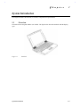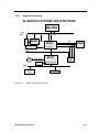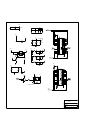
1
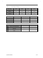
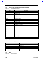
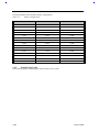
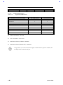
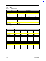
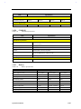
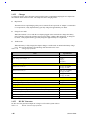
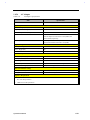
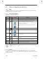
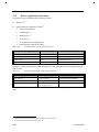
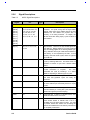
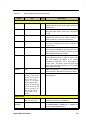
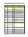
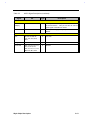
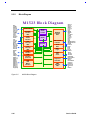
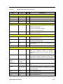
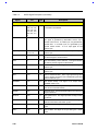
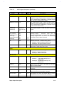
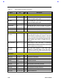
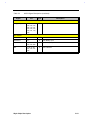
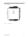
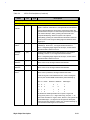
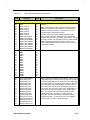
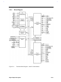
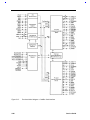
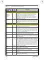
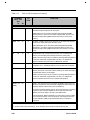
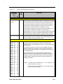
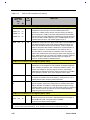
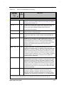
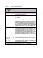
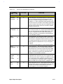
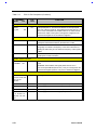
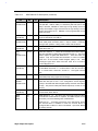
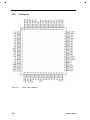
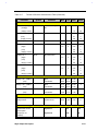
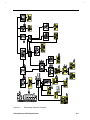
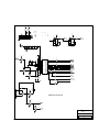
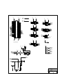
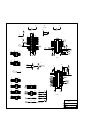
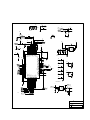
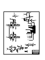
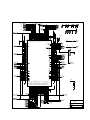
Table 2-4
Name
M7101 Pin Descriptions (Continued)
No.
Type
Description
General purpose I/O interface(24)
General purpose I/O group A
GPIOA6
(70)
I
Speak input. When offset 0F6h D6=‘1’, this pin will be speaker
input. The input signal will xor with SPKCTL internally.
(69)
O
External General Purpose I/O B write. When SQWO is pull low
4.7K, the GPIOA5 will become GPIOWA. External General purpose
A R/W control pulse, When write index 0F0h with a byte or a word.
A 74373 latch pulse will be generated at this pin. The 74373 input
should be connected to PCI AD[23:16] if a byte command. If a word
command, two 74373s will be used and inputs are connected to PCI
AD[31:16]. The write action also will write into the internal register.
So when reading the offset, the value will be sent by M7101 to host.
(68)
O
External General Purpose I/O B read. When SQWO is pull low
4.7K, the GPIOA0 will become GPIORAJ. External General
purpose A Read control pulse. When Read index 0F1h with a byte
or a word, a 74245 OEJ pulse will be generated at this pin. The
74245 output should be connected to PCI AD[23:16] if a byte
command. If a word command, two 74245 will be used and4
outputs are connected to PCI AD[31:16]. When read index 0E1h,
M7101 will send DEVSELJ, TRDYJ but float the AD[31:0] because
the data will be sent by 74245. The write action has no meaning
and nothing will be done.
(67)
O
Contrast2. When offset 0F6h D14=‘0’ and D9=‘1’, this pin will be
the LCD contrast output 2. It is a 1Khz signal with programmable
duty cycle controlled by offset 0FBh D[15:13].
/SPEKIN
GPIOA5
/GPIOWB
GPIOA4
/GPIORBJ
GPIOA3
/O
/CONTRAST2
/SLOWDOW
N
GPIOA2
SLOWDOWN (default). When offset 0F6h D14=‘1’, this pin will be
the slow down clock control output pin.
(66)
O
Contrast1. When offset 0F6h D14=’0’ and D8=’1’, this pin will be
the LCD contrast output1. It is a 1 KHz signal with programmable
duty cycle controlled by offset 0FBh D[12:8].
(65)
O
External General Purpose I/O A write. When SPKCTL is pull low
4.7K, the GPIOA1 will become GPIOWA. External General purpose
A R/W control pulse, When write index 0E0h with a byte or a word.
A 74373 latch pulse will be generated at this pin, The 74373 input
should be connected to PCI AD[23:16] if a byte command. If a word
command , two 74373s will be used and inputs are connected to
PCI AD[31:16]. The write action also will write into the internal
register. So when reading the offset, the value will be sent by
M7101 to host.
/CONTRAST1
GPIOA1
/GPIOWA
2-30
Service Guide