1
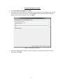
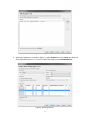
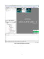
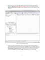
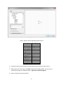
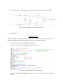
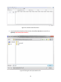
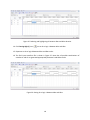
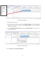
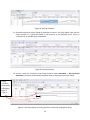
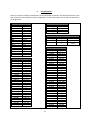
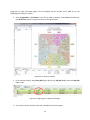
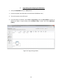
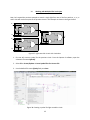
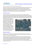
Quartus II Introduction
Software version:
Quartus II version 13.0 or later
Altera board:
DE2 board
Topics to be covered:
I.
Create a new project
II.
Create a schematic design entry. Or create a VHDL design entry
III.
Compile the design
IV.
Simulate the designed circuit
V.
Assign pins
VI.
Program and configure the FPGA device
VII.
Work with multiple design files in a project
This document is created based on:
•
Quartus II Introduction Using Schematic Designs from Altera
1
I.
Creating a New Quartus II Project
1. Select File > New Project Wizard. Click Next.
2. You should create a new folder for each project. Set this folder as the working directory. You will
need to select a name for the project. Choose tutorial for both the project and the top-level
design entity as shown in Figure 1. Then, click Next.
Figure 1. Creating a new project.
3. Specify any design files you want to include in this project. Assuming that we don’t have any
existing files, click Next.
2
Figure 2. Adding existing files.
4. Specify the FPGA device as shown in Figure 3. Select Cyclone II from the Family drop down list.
Select EP2C35F672C6 (or EP2C70F896C6 if DE2-70 is used) from the Available devices.
Figure 3. Selecting a device.
3
5. Keep all EDA Tools settings (Figure 4). Click Next.
Figure 4. Setting EDA Tools (default).
6. Click Next at the Summary window.
7. Click Finish.
8. A new project named tutorial should be created in the Quartus window as shown in Figure 5.
4
Figure 5. Quartus II window with a new project.
5
II.
Creating a New Schematic Block Diagram
As a design example, we will use the two-way light controller circuit shown in Figure 6. The circuit can be
used to control a single light from either of the two switches, x1 and x2. Note that this can be achieved by
an XOR gate, but we will implement it using the gates shown.
x1
f
x2
Figure 6. Light controller circuit with 2 switches.
Steps to create a new block diagram for the light controller circuit:
1. Select File > New to get the window in Figure 7, choose Block Diagram/Schematic File, and click
OK.
Figure 7. Creating a new block diagram
6
2. Specify a name for the file. Select File > Save As. Save this file in the same project directory
(default) as light.bdf. Note that a filename must have no spaces. Put a checkmark in the box
Add file to current project. Click Save. This step should open a Graphic Editor window as shown
in Figure 8.
Figure 8. A Graphic Editor window.
3. Double click inside the Graphic Editor window to bring up the Symbol Importing window as
shown in Figure 9. Select the item you want from the Libraries list box. To expand or contract
the list click on the plus or minus sign respectively. Note that most items you need will be in the
primatives/logic or primatives/pin folder. Alternatively, you may type the name of the item
you want in the Name box from Table 1. and2 (2-input AND gate) in this case. Click OK.
7
Figure 9. Importing a logic symbol from libraries.
Table 1. Devices and corresponding symbol names.
Device/Gate
Input
Output
2 Input AND
3 Input AND
2 Input OR
Inverter
XOR
2 Input NOR
JK FlipFlop
D FlipFlop
T Flip Flop
Freq Divider
Ground (low)
Vcc (high)
Text Entry
input
output
and2
and3
or2
not
xor
nor2
jkff
dff
tff
freqdiv
gnd
vcc
4. Using the mouse, move the symbol to a desirable location and click to place it there.
5. Repeat steps 3 and 4 to import one and2, one or2, and two not symbols. You can rotate a
symbol by clicking on the symbol to select it, right click > Rotate by Degrees.
6. Import 2 inputs and 1 output symbols.
8
7. Assign name to input and output symbols. For example, double click on the first input and type
x1 in the Pin name(s) box as shown in Figure 10. Assign x2 to the second input and f to the
output symbols.
Figure 10. Assigning input name.
Figure 11. Assigning names to input and output symbols.
9
8. Connect the symbols by drawing lines (wires) with the Orthogonal Node Tool (icon
).
Figure 12. Block diagram for a light controller circuit.
9. Save the file.
Creating a VHDL File
Instead of creating your design with a schematic file, you can implement your design with VHDL. For
example, to implement the light controller circuit above, we can follow these steps:
1. Select File > New and choose VHDL File, and click OK.
2. Type in your VHDL code for the design as shown in Figure 13.
Figure 13. VHDL code for a light controller circuit.
1. Save the VHDL file as light_vhdl.vhd. Note that the entity name and the file name must be the
same.
10
III.
Compiling the Design File/Circuit
1. From the Quartus II window, click on the Files tab. Right click file that you want to compile
(light.bdf) and Set as Top-Level Entity. This step instructs the compiler to look for the correct
design file to compile.
Figure 14. Setting the top-level entity.
2. Run the Compiler by selecting Processing > Start Compilation. Alternatively, you may clicking on
the toolbar icon
that looks like a purple triangle. When the compilation is finished with no
errors, a summary window will be displayed as shown in Figure 15. If errors occur, the compiler
should indicate what these errors are in the message box. Warnings can be ignored.
Figure 15. Summary of a successful compilation.
11
Figure 16. Message box indicates 0 errors, 12 warnings.
Note that every time a change is made to the any files, the project must be saved and compiled again.
12
IV.
Simulating the Designed Circuit
Before implementing the designed circuit in the FPGA chip, it is important to simulate it to verify the
correct functionality of the circuit. First, we need to create waveforms for all the input signals of the
circuit. The simulator will generate the output waveforms after successful simulation.
1. From Quartus II software, select File > New…. Then, click on the University Program
VWF option.
Figure 17. Create a new input waveform file.
2. A simulation waveform editor will be displayed as shown in Figure 18.
13
Figure 18. Simulation Waveform Editor.
3. From the Simulation Waveform Editor window, Select File > Save As and save the file as
light.vwf in the same project directory.
Figure 19. Saving the new input waveform file.
14
4. Set the simulation time by selecting Edit > Set End Time from the Waveform Editor. Entering 1us
for the simulation time.
Figure 20. Setting simulation time.
5. Add input and output signals. Click Edit > Insert > Insert Node or Bus (or double click on the left
pane of the waveform) to open a node finder window.
Figure 21. Insert Node or Bus window.
6. Click Node Finder button. Make sure to select Pins: all from the drop down list of the Filter field
then click List button.
7. Click >> button.
15
Figure 22. Node finder window.
8. Click OK button to close Node Finder window. Again, Click OK button close Insert Node or Bus
window.
Figure 23. Waveform file with inputs and output.
9. Note that it is possible to rearrange the waveforms. To move a waveform up or down in the
Waveform Editor window, click within the node’s row (i.e. on its name, icon, or value) and
16
release the mouse button. The waveform is now highlighted to show the selection. Click again
on the waveform and drag it up or down in the Waveform Editor. Move f waveform to the
bottom.
10. Specify logic values for all input waveforms. Ideally, we want to specify all possible combinations
of the input signals. For large circuit, it may not be possible to generate all possible
combinations, so we have to select a small but representative number of combinations. For this
example, it is simple enough to generate all combinations of input signals.
11. Click on waveform x2 to highlight it. Then click the Count Value icon (
Count every field. Click OK button.
). Enter 20ns in the
Figure 24. Simulating input signal x2 to toggle every 20 ns.
12. Click on waveform x1 to highlight it. Then click the Count Value icon (
). Enter 40ns in the
Count every field. Note that all combinations of the two input waveforms x1 and x2 are
generated within the first 80 ns of the simulation window (they repeat the same patterns after
that).
13. Sometimes you will need to modify the input signals manually for specific time periods to better
simulate the circuit behavior. For instance, in this example, only one switch should be changed
at a time. However, with the current settings, both switches are sometimes changed at the
same time. Click on x2 waveform at 40ns mark, hold and drag the mouse to 60ns mark and
release the mouse to highlight that duration (40ns to 60ns).
17
Figure 25. Selecting and highlighting x2 between 40ns and 60ns duration.
14. Click Forcing High (1) icon (
) to set x2 to logic 1 between 40ns and 60ns.
15. Repeat to set x2 to logic 0 between 60ns and 80ns marks.
16. The final input waveform file is shown in Figure 27. Note that all possible combinations of
switches x1 and x2 are generated appropriately between 0 and 160ns marks.
Figure 26. Setting x2 to logic 1 between 40ns and 60ns.
18
All possible
combinations
of x1 and x2
(ie. 00, 01, 10,
11) are
generated in
80 ns.
Figure 27. Input waveforms.
17. Save the input waveform file.
18. To verify the correctness of the circuit, perform functional simulation. To include propagation
delay of the circuit in the simulation, perform timing simulation. We will use functional
simulation in this example.
19. From the Simulation Waveform Editor window, click Simulation Options. Then, select one of
the installed simulators.
Figure 28. Simulation settings.
20. Select Simulation > Run Functional Simulation.
19
Figure 29. Starting simulation.
21. Simulation Waveform Report should be displayed as shown in the figure below. Note that the
output waveform f is generated based on the behavior of the designed circuit. Verify its
correctness for all possible input combinations.
Figure 30. Simulation Report.
22. Exercise: repeat the simulation using timing simulation mode (Simulation > Run Functional
Simulation). The output should show propagation delay as illustrated in the figure below.
Timing
simulation
mode shows
propagation
delay of
5.139 ns.
Figure 31. Simulation Report for timing simulation mode (with propagation delay).
20
V.
Pin Assignments
Some of the most commonly used features of the DE2 board are listed in the table below. Refer to the
user manual for the complete list of pin assignments. For DE2-70 boards, refer to the user manual for
pin assignments.
Toggle Switches
Signal Name
FPGA Pin No.
SW[0]
PIN_N25
SW[1]
PIN_N26
SW[2]
PIN_P25
SW[3]
PIN_AE14
SW[4]
PIN_AF14
SW[5]
PIN_AD13
SW[6]
PIN_AC13
SW[7]
PIN_C13
SW[8]
PIN_B13
SW[9]
PIN_A13
SW[10]
PIN_N1
SW[11]
PIN_P1
SW[12]
PIN_P2
SW[13]
PIN_T7
SW[14]
PIN_U3
SW[15]
PIN_U4
SW[16]
PIN_V1
SW[17]
PIN_V2
Pushbuttons
Signal Name
FPGA Pin No.
KEY[0]
PIN_G26
KEY[1]
PIN_N23
KEY[2]
PIN_P23
KEY[3]
PIN_W26
Signal Name
CLOCK_27
CLOCK_50
EXT_CLOCK
Clock Signals
FPGA Pin No.
Description
PIN_D13
27 MHz clock input
PIN_N2
50 MHz clock input
PIN_P26
External (SMA) clock
input
7-Segment Displays 0-4
Signal Name
FPGA Pin No.
HEX0[0]
PIN_AF10
HEX0[1]
PIN_AB12
HEX0[2]
PIN_AC12
HEX0[3]
PIN_AD11
HEX0[4]
PIN_AE11
HEX0[5]
PIN_V14
HEX0[6]
PIN_V13
HEX1[0]
PIN_V20
HEX1[1]
PIN_V21
HEX1[2]
PIN_W21
HEX1[3]
PIN_Y22
HEX1[4]
PIN_AA24
HEX1[5]
PIN_AA23
HEX1[6]
PIN_AB24
HEX2[0]
PIN_AB23
HEX2[1]
PIN_V22
HEX2[2]
PIN_AC25
HEX2[3]
PIN_AC26
HEX2[4]
PIN_AB26
HEX2[5]
PIN_AB25
HEX2[6]
PIN_Y24
HEX3[0]
PIN_Y23
HEX3[1]
PIN_AA25
HEX3[2]
PIN_AA26
HEX3[3]
PIN_Y26
HEX3[4]
PIN_Y25
HEX3[5]
PIN_U22
HEX3[6]
PIN_W24
HEX4[0]
PIN_U9
HEX4[1]
PIN_U1
HEX4[2]
PIN_U2
HEX4[3]
PIN_T4
HEX4[4]
PIN_R7
HEX4[5]
PIN_R6
HEX4[6]
PIN_T3
Red and Green LEDs
Signal Name
FPGA Pin No.
LEDR[0]
PIN_AE23
LEDR[1]
PIN_AF23
LEDR[2]
PIN_AB21
LEDR[3]
PIN_AC22
LEDR[4]
PIN_AD22
LEDR[5]
PIN_AD23
LEDR[6]
PIN_AD21
LEDR[7]
PIN_AC21
LEDR[8]
PIN_AA14
LEDR[9]
PIN_Y13
LEDR[10]
PIN_AA13
LEDR[11]
PIN_AC14
LEDR[12]
PIN_AD15
LEDR[13]
PIN_AE15
LEDR[14]
PIN_AF13
LEDR[15]
PIN_AE13
LEDR[16]
PIN_AE12
LEDR[17]
PIN_AD12
LEDG[0]
PIN_AE22
LEDG[1]
PIN_AF22
LEDG[2]
PIN_W19
LEDG[3]
PIN_V18
LEDG[4]
PIN_U18
LEDG[5]
PIN_U17
LEDG[6]
PIN_AA20
LEDG[7]
PIN_Y18
LEDG[8]
PIN_Y12
21
Assign pins to input and output signals. For this example, we will use SW1 for x2, SW0 for x1, and
LEDG(0) (green LED 0) for output f.
1. Select Assignments > Pin Planner. From the Pin Planner window, select View and make sure
that All Pins List option is checked as shown in the Figure below.
Figure 32. Pin Planner window.
2. In the Location column, assign PIN_AE22 (green LED 0) to f, PIN_N25 (SW0) to x1, and PIN_N26
(SW1) to x2.
Figure 33. Assigning pins to inputs and output.
3. Close the Pin Planner window. Save and re-compile the Quartus project.
22
VI.
Programming and Configuring the FPGA Device
1. Verify the RUN/PROG switch is in Run position.
2. Connect the power and USB cables to the DE2 board (USB Blaster Port).
3. Turn on the power to the DE2 board.
4. From the Quartus II software, select Tools > Programming. Note that No Hardware is shown as
default (as shown in Figure below), press Hardware Setup… button and select USB-Blaster
[USB-0].
Figure 34. Programming window.
23
Figure 35. USB-Blaster hardware setup.
Figure 36. Programming the DE2 board with USB-Blaster cable.
5. The configuration file tutorial.sof should be selected and shown as default. Press Start.
6. You can now test the designed circuit with SW0, SW1, and LEDG0.
24
VII.
Working with Multiple Files in a Project
Now, let’s expand the previous example to control a single light from one of the four switches, x1, x2, x3
and x4. We will use three copies of the previous circuit in this example as shown in the figure below.
x1
x2
f
x3
x4
Figure 37. Light controller circuit with 4 switches.
1. First we will create a symbol for the previous circuit. From the Quartus II software, open the
schematic file name light.bdf.
2. Select File > Create/Update > Create Symbol Files for Current File.
3. Use the default file name light.bsf and press Save.
Figure 38. Creating a symbol for light controller circuit.
25
4. Create a new schematic file by selecting File > New and choosing Block Diagram/Schematic File,
and click OK.
5. Double click in the empty schematic file to bring up the Symbol window. Click the arrow ( )
next to the Project folder to see all components in your project. You should have a component
named light under the Project folder as shown in the Figure below.
Figure 39. Inserting new light component.
6.
Insert 3 light components, 4 inputs, and one output.
7. Connect all components to create a new circuit as shown in the figure below.
Figure 40. Drawing the new design with 4 switches.
26
8. Save the new file as light2.bdf.
9. Set the light2.bdf as the Top Level Entity. Then, compile and simulate the design as before.
Verify the correctness of the new design.
10. Assign pins to 4 switches and LEDG(0).
11. Compile the project again. Then program the DE2 board with the new design.
12. Verify the design using 4 switches and LEDG(0) on the DE2 board.
27