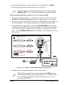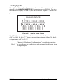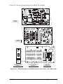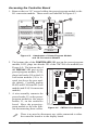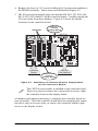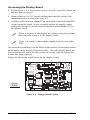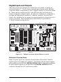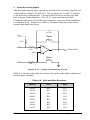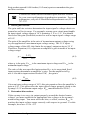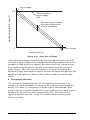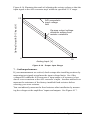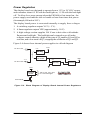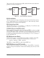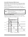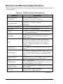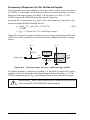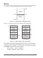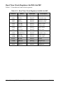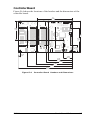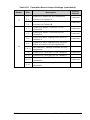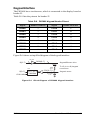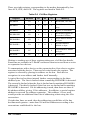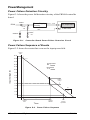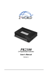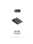
1
PK2600 Integrated Control System Users Manual Revision C PK2600 Users Manual Part Number 019-0061 Revision C Last revised on July 20, 2000 Printed in U.S.A. Copyright © 1999 Z-World, Inc. All rights reserved. Z-World reserves the right to make changes and improvements to its products without providing notice. Trademarks ® Dynamic C is a registered trademark of Z-World, Inc. ® Windows is a registered trademark of Microsoft Corporation PLCBus is a trademark of Z-World, Inc. ® Hayes Smart Modem is a registered trademark of Hayes Microcomputer Products, Inc. Notice to Users When a system failure may cause serious consequences, protecting life and property against such consequences with a backup system or safety device is essential. The buyer agrees that protection against consequences resulting from system failure is the buyers responsibility. This device is not approved for life-support or medical systems. All Z-World products are 100 percent functionally tested. Additional testing may include visual quality control inspections or mechanical defects analyzer inspections. Specifications are based on characterization of tested sample units rather than testing over temperature and voltage of each unit. Z-World may qualify components to operate within a range of parameters that is different from the manufacturers recommended range. This strategy is believed to be more economical and effective. Additional testing or burn-in of an individual unit is available by special arrangement. Company Address Z-World, Inc. 2900 Spafford Street Davis, California 95616-6800 USA Telephone: Facsimile: Web Site: E-Mail: (530) 757-3737 (530) 753-5141 http://www.z w orld.com [email protected] TABLE OF CONTENTS About This Manual ix Chapter 1: Overview 13 Chapter 2: Getting Started 19 Chapter 3: Hardware Features 25 Chapter 4: Hardware Configurations 35 Features ............................................................................................... 15 Options ............................................................................................ 16 Flexibility and Customization ............................................................... 16 Development and Evaluation Tools ..................................................... 18 Developers Kit ................................................................................ 18 Software .......................................................................................... 18 Initial PK2600 Setup ............................................................................. 20 Parts Required ................................................................................. 20 Setting Up the PK2600 .................................................................... 20 Connecting the PK2600 to a Host PC ................................................... 22 Running Dynamic C ............................................................................. 24 Operating Modes ................................................................................. 26 Changing the Operating Mode ........................................................ 27 Using Run and Program Modes: Example ..................................... 27 Liquid Crystal Display (LCD) ............................................................... 28 Contrast Adjustment ....................................................................... 28 Coordinate Systems ........................................................................ 29 Digital Inputs/Outputs ......................................................................... 30 Digital Group 1 ................................................................................ 30 Digital Group 2 ................................................................................ 30 Analog Inputs ...................................................................................... 31 Serial Channels ..................................................................................... 32 PLCBus ................................................................................................ 33 PK2600 Assembly ................................................................................ 36 Accessing the Controller Board ...................................................... 38 Accessing the Display Board .......................................................... 40 PK2600 Table of Contents s iii Digital Inputs and Outputs .................................................................. 41 External Connections ....................................................................... 41 Digital Inputs ................................................................................... 42 Operating Modes and Configuration ............................................ 42 Digital Outputs ................................................................................ 45 Operating Modes and Configuration ............................................ 45 High-Voltage Drivers ..................................................................... 45 Using Output Drivers .................................................................... 49 TTL/CMOS Outputs ..................................................................... 50 Pulse-Width Modulation (PWM) Configuration .......................... 51 Analog Inputs ...................................................................................... 52 Operating Modes and Configuration .............................................. 52 Drift ............................................................................................... 59 Low-Pass Filter ............................................................................. 59 Excitation Resistors ....................................................................... 60 Using the Unconditioned Converter Channels ............................... 60 Internal Test Voltages ...................................................................... 60 Power-Down Mode ......................................................................... 61 External Connections ....................................................................... 61 Serial Channels ..................................................................................... 62 Operating Modes and Configuration .............................................. 63 Configuring a Multidrop Network ................................................... 65 RS-485 Termination ....................................................................... 65 External Connections ....................................................................... 65 PLCBus ................................................................................................ 68 Liquid Crystal Display (LCD) ............................................................... 69 Contrast Adjustments ..................................................................... 69 Background ..................................................................................... 69 Chapter 5: Subsystems 71 Controller Board Subsystems .............................................................. 72 Microprocessor Core Module ......................................................... 72 Display Board Subsystems .................................................................. 74 Computing Module ......................................................................... 74 Power Regulation ............................................................................ 75 Serial Communication ...................................................................... 76 691 Supervisor Chip ............................................................................. 77 System Reset ................................................................................... 79 Z180 Serial Ports ................................................................................... 80 Use of the Serial Ports ..................................................................... 82 iv s Table of Contents PK2600 Asynchronous Serial Communication Interface ................................... 83 ASCI Status Registers ..................................................................... 83 /DCD0 (Data Carrier Detect) .......................................................... 83 TIE (Transmitter Interrupt Enable) ................................................ 83 TDRE (Transmitter Data Register Empty) ..................................... 83 CTS1E (CTS Enable, Channel 1) .................................................... 84 RIE (Receiver Interrupt Enable) ..................................................... 84 FE (Framing Error) ......................................................................... 84 PE (Parity Error) ............................................................................. 84 OVRN (Overrun Error) ................................................................... 84 RDRF (Receiver Data Register Full) .............................................. 84 ASCI Control Register A ................................................................. 85 MOD0MOD2 (Data Format Mode Bits) ...................................... 85 MPBR/EFR (Multiprocessor Bit Receive/Error Flag Reset) .......... 85 /RTS0 (Request to Send, Channel 0) ............................................. 85 CKA1D (CKA1 Disable) ............................................................... 85 TE (Transmitter Enable) ................................................................ 85 RE (Receiver Enable) ..................................................................... 86 MPE (Multiprocessor Enable) ....................................................... 86 ASCI Control Register B ................................................................. 86 SS (Source/Speed Select) .............................................................. 86 DR (Divide Ratio) .......................................................................... 87 PEO (Parity Even/Odd) ................................................................. 87 /CTS/PS (Clear to Send/Prescaler) ................................................ 87 MP (Multiprocessor Mode) .......................................................... 87 MPBT (Multiprocessor Bit Transmit) ........................................... 87 Chapter 6: Software Development 89 Supplied Software ................................................................................ 90 Digital I/O ............................................................................................. 91 Digital Inputs ................................................................................... 91 How to Read the Input .................................................................... 91 Sample Program ............................................................................. 92 Digital Outputs ................................................................................ 93 Sample Program ............................................................................. 94 Pulse-Width Modulated (PWM) Outputs ....................................... 95 How to Use the PWM Feature ...................................................... 95 PWM Software ............................................................................. 96 Sample Program ............................................................................. 97 Analog Inputs ...................................................................................... 98 Using the Analog Inputs ................................................................. 98 Sample Program ............................................................................... 99 PK2600 Table of Contents s v Serial Channels ................................................................................... 100 RS-232 Communication .................................................................. 100 RS-485 Communication .................................................................. 100 Software ........................................................................................ 101 Sample Program ............................................................................. 101 Display Board Functions ................................................................... 102 Display Hardware Control ............................................................. 102 Display Images .............................................................................. 102 Touchscreen Functions ................................................................. 106 Additional Software ........................................................................... 108 Real-Time Clock (RTC) .................................................................. 108 Flash EPROM ................................................................................ 108 Other Software .............................................................................. 110 Sample Programs ................................................................................ 110 Chapter 7: Graphics Programming 113 Appendix A: Troubleshooting 121 Initialization ........................................................................................ 114 Drawing Primitives ............................................................................. 114 Plot a Pixel ..................................................................................... 114 Plot a Line ...................................................................................... 115 Plot a Circle .................................................................................... 115 Plot a Polygon ............................................................................... 115 Fill a Circle ..................................................................................... 115 Fill a Polygon ................................................................................. 115 Draw a Bitmap ............................................................................... 115 Printing Text ....................................................................................... 116 Keypad Programming ......................................................................... 117 Initialization ................................................................................... 117 Scanning the Keypad .................................................................... 117 Reading Keypad Activities ............................................................ 117 Font and Bitmap Conversion ............................................................. 118 Using the Font/Bitmap In Your Program ....................................... 119 Out of the Box .................................................................................... 122 Dynamic C Will Not Start ................................................................... 123 PK2600 Repeatedly Resets ................................................................. 123 Dynamic C Loses Serial Link .............................................................. 123 Common Programming Errors ............................................................. 124 vi s Table of Contents PK2600 Appendix B: Specifications 125 Appendix C: Memory, I/O Map, and Interrupt Vectors 133 Appendix D: Circuit Board Reference 145 Appendix E: PLCBus 161 Electronic and Mechanical Specifications .......................................... 126 PK2600 Mechanical Dimensions ................................................... 128 Protected Digital Inputs ..................................................................... 129 Frequency Response for the Protected Inputs .............................. 130 High-Voltage Drivers .......................................................................... 131 Sinking Driver ................................................................................ 131 Sourcing Driver ............................................................................. 132 Memory .............................................................................................. 134 Execution Timing ........................................................................... 135 Memory Map ..................................................................................... 136 Input/Output Select Map .............................................................. 136 Z180 Internal Input/Output Registers Addresses 00-3F ................ 136 Real-Time Clock Registers 0x41800x418F .................................... 138 Other Registers .............................................................................. 139 Controller Board .......................................................................... 139 Display Board ............................................................................. 140 Interrupt Vectors ................................................................................ 141 Nonmaskable Interrupts ................................................................ 142 Jump Vectors ................................................................................. 142 Interrupt Priorities ......................................................................... 143 Power/Program Module ..................................................................... 146 Core Module ...................................................................................... 146 I/O Conversion Module ..................................................................... 146 Controller Board ................................................................................. 147 Headers ......................................................................................... 148 Jumper Settings ............................................................................. 154 Display Board .................................................................................... 157 Keypad Interface ................................................................................ 159 PLCBus Overview .............................................................................. 162 Allocation of Devices on the Bus ...................................................... 166 4-Bit Devices ................................................................................. 166 8-Bit Devices ................................................................................. 167 Expansion Bus Software ..................................................................... 167 PK2600 Table of Contents s vii Appendix F: Serial Interface Board 2 173 Appendix G: Advanced Topics 177 Appendix H: Battery 189 Index 193 Introduction ....................................................................................... 174 External Dimensions ........................................................................... 175 Power Management ........................................................................... 178 Power Failure Detection Circuitry .................................................. 178 Power Failure Sequence of Events ................................................ 178 Simulated EEPROM ............................................................................ 180 Pulse-Width Modulation (PWM) Software ........................................ 181 PWM Addressing Detail ............................................................... 181 PWM Software .............................................................................. 185 Sample Program ............................................................................. 187 Battery Life and Storage Conditions .................................................. 190 Replacing Soldered Lithium Battery ................................................... 190 Battery Cautions ................................................................................ 191 viii s Table of Contents PK2600 ABOUT THIS MANUAL This manual provides instructions for installing, testing, configuring, and interconnecting the Z-World PK2600 integrated touchscreen control system. Instructions are also provided for using Dynamic C functions. Assumptions Assumptions are made regarding the user's knowledge and experience in the following areas. Ability to design and engineer the target system that interfaces with the PK2600. Understanding of the basics of operating a software program and editing files under Windows on a PC. Knowledge of the basics of C programming. $ For a full treatment of C, refer to the following texts. The C Programming Language by Kernighan and Ritchie C: A Reference Manual by Harbison and Steel Knowledge of basic Z80 assembly language and architecture. $ For documentation from Zilog, refer to the following texts. Z180 MPU User's Manual Z180 Serial Communication Controllers Z80 Microprocessor Family User's Manual PK2600 About This Manual s ix Acronyms Table 1 lists and defines the acronyms that may be used in this manual. Table 1. Acronyms Acronym Meaning EPROM Erasable Programmable Read-Only Memory EEPROM Electronically Erasable Programmable Read-Only Memory LCD Liquid Crystal Display LED Light-Emitting Diode NMI Nonmaskable Interrupt PIO Parallel Input/Output Circuit (Individually Programmable Input/Output) PRT Programmable Reload Timer RAM Random Access Memory RTC Real-Time Clock SIB Serial Interface Board SRAM Static Random Access Memory UART Universal Asynchronous Receiver Transmitter Icons Table 2 displays and defines icons that may be used in this manual. Table 2. Icons Icon $ ( Meaning Refer to or see Please contact Caution )' Icon Meaning ! Note 7LS Tip High Voltage Factory Default x s About This Manual PK2600 Conventions Table 3 lists and defines the typographic conventions that may be used in this manual. Table 3. Typographic Conventions Example Description while Courier font (bold) indicates a program, a fragment of a program, or a Dynamic C keyword or phrase. // IN-01… Program comments are written in Courier font, plain face. Italics Indicates that something should be typed instead of the italicized words (e.g., in place of filename, type a file’s name). Edit Sans serif font (bold) signifies a menu or menu selection. ... An ellipsis indicates that (1) irrelevant program text is omitted for brevity or that (2) preceding program text may be repeated indefinitely. [ ] Brackets in a C function’s definition or program segment indicate that the enclosed directive is optional. < > Angle brackets occasionally enclose classes of terms. a | b | c A vertical bar indicates that a choice should be made from among the items listed. A black square indicates pin 1 of all headers. Pin 1 J1 Pin Number 1 Measurements All diagram and graphic measurements are in inches followed by millimeters enclosed in parenthesis. PK2600 About This Manual s xi Blank xii s About This Manual PK2600 CHAPTER 1: OVERVIEW Chapter 1 provides a comprehensive overview and description of the PK2600. The following sections are included. Features Flexibility and Customization Development and Evaluation Tools PK2600 Overview s 13 The PK2600 Integrated Control System is designed as an off-the-shelf system that integrates an established Z-World controller with a ¼VGA LCD. The PK2600 is ideal for systems that require an integrated graphic interface. The feature-rich controller has modular digital and analog I/O that allows easy custom modification. The display has a large storage area for bitmaps, display lists, and screens. Both the controller and the display are programmed using Dynamic C, Z-Worlds version of the C programming language. Figure 1-1 shows a block diagram of the PK2600. SERIAL PORT 3 PC Dynamic C programming SIB2 SERIAL PORT 2 SERIAL PORT 1 PK2600 RS-232/ RS-232/ RS-232 RS-485 RS-485 PLCBus Controller Board Digital SIB Programming Port PLCBus I/O DIGITAL GROUP 1 Digital I/O DIGITAL GROUP 2 Analog Inputs ANALOG INPUTS RS-232 POWER RS-232 Display SIB Programming Port Board LCD Figure 1-1. PK2600 Block Diagram 14 s Overview PK2600 Features The PK2600 is equipped with a gas-tight bezel conforming to a NEMA Type 4 enclosure rating. The PK2600 features an 18.432 MHz clock with the Z180 microprocessor, and the display uses a 9.216 MHz clock. The PK2600 includes the following features. Controller The controller uses a core module (Z-World part number 129-0099) designed for easy, in-system programming. The core module includes the CPU, 32K SRAM, 128K flash EPROM, real-time clock, and microprocessor watchdog circuitry. The following I/O are available on the PK2600. Serial channelsThree full-duplex serial channels interface directly with serial I/O devices. RS-232 and RS-485 signals are supported. Digital I/OThe 32 I/O lines can be ordered as inputs or outputs in banks of eight. The PK2600 comes standard with 16 protected digital inputs and 16 high-voltage, high-current sinking outputs capable of driving resistive and inductive loads. The sinking outputs can be converted to sourcing outputs with an optional sourcing driver kit. Pulse-width modulated outputsUp to 7 digital outputs can provide pulse-width modulation. Analog inputsEight conditioned 12-bit analog inputs, each with userconfigurable bias and gain, interface directly with many sensors. Two unconditioned analog inputs are also available. Expansion busI/O expansion via built-in PLCBus. The PLCBus uses inexpensive off-the-shelf Z-World expansion boards. Display The display offers the following features. LCD240 × 320, ¼ VGA LCD (with touchscreen on PK2600). Contrast controlsoftware-controlled contrast is enabled/disabled with jumper settings, automatic temperature compensation for LCD contrast changes. There is also an opening to access the contrast adjustment manually. Backlightsoftware-controlled cold-cathode fluorescent backlighting. Memory128K SRAM, 256K flash EPROM for program, 256K flash EPROM for screen bitmaps. $ PK2600 Appendix B provides detailed specifications for the PK2600. Overview s 15 Options The PK2600 has two versions. Table 1-1 lists their standard features. Table 1-1. PK2600 Series Features Model Features PK2600 Standard integrated system with serial graphic display, touchscreen, blue and white screen, ¼VGA LCD, bezel mount, software contrast control PK2610 PK2600 with no touchscreen, manual contrast control The PK2600 may be used in either a portrait or a landscape orientation. Flexibility and Customization The PK2600 was designed with customization in mind. The design was optimized for cost effective, quick-turn, custom manufacturing. Surface mount technology is used extensively in order to reduce both size and cost while providing the flexibility to meet individual design needs. For quantity orders, the PK2600 can be customized to better meet the needs of your application. The options include the following configurations. Core module configurationCM7100 and CM7200 core modules can be used on the PK2600. Customization options include RAM size, flash EPROM size, flash EPROM or regular EPROM, and clock speed. ! CM7100 and CM7200 core modules must have a 5-pin header installed at H1, and the BIOS must be customized for these core modules to be used on the PK2600. Digital I/O configurationoptional TTL level I/O. Analog input configurationgain and offset configuration. Serial channel configurationRS-485, 3-wire RS-232, or 5-wire RS-232 serial ports. Backgroundpositive (blue images on white background) or negative (white images on blue background). The following accessories are available for the PK2600. Sourcing driver kit. SIB2 to allow programming through the SIB ports, leaving all the serial ports available for the application being developed. ! The SIB2 is required to program the display board. 16 s Overview PK2600 Table 1-2 lists the various configuration options and the factory default configurations for the PK2600. Table 1-2. PK2600 Configuration Options Configuration Item Factory Default Alternatives Controller SERIAL PORT 1 RS-232 N/A SERIAL PORT 2 RS-232 with DCD and DTR RS-485 SERIAL PORT 3 RS-232 RS-485 16 digital inputs 8 digital inputs & 8 digital outputs OR 16 digital outputs (outputs can be sinking or sourcing) DIGITAL GROUP 1 Outputs can be sinking or sourcing DIGITAL GROUP 2 16 digital outputs (sinking) ANALOG INPUTS 8 conditioned inputs over range of 0 V to 10 V, 2 unconditioned inputs Conditioned inputs can be reconfigured for different voltage ranges Memory, Clock 32K SRAM, 128K flash EPROM, 18.432 MHz clock Core module may be replaced with one having 256K flash EPROM and/or 9.216 MHz clock 8 digital inputs & 8 digital outputs OR 16 digital inputs Display LCD Contrast LCD Background PK2600—software adjustable PK2610—manually adjustable White Software or manually adjustable Blue $ See Chapter 4, Hardware Configurations, for information on how to change the jumper settings for alternative configurations. ( For ordering information, or for more details about the various options and prices, call your Z-World Sales Representative at (530) 757-3737. PK2600 Overview s 17 Development and Evaluation Tools Developers Kit The PK2600 is supported by a Developers Kit that includes everything needed to start development with the PK2600. Software Dynamic C, Z-Worlds Windows-based real-time C language development system, is used to develop software for the PK2600. The host PC downloads the executable code through the SIB2 or one of the serial ports to flash EPROM. Library functions provide an easy and robust interface to the PK2600. ! Dynamic C Deluxe must be used when developing applications for the PK2600. The standard version of Dynamic C does not allow sufficient access to extended memory. $ Z-Worlds Dynamic C reference manuals provide complete software descriptions and programming instructions. 18 s Overview PK2600 CHAPTER 2: GETTING STARTED Chapter 2 provides instructions for connecting the PK2600 to a host PC and running a sample program. The following sections are included. Initial PK2600 Setup Connecting the PK2600 to a Host PC Establishing Communication with the PK2600 Running a Sample Program PK2600 Getting Started s 19 Initial PK2600 Setup Parts Required 24 V unregulated DC power supply capable of delivering up to 1.1 A (included only in Developers Kits for North America) DE9 to DE9 serial cable The necessary parts are supplied with the Developers Kit. The PK2600 Developers Kit also includes the following items. Three DB25 male plugs and covers to allow custom I/O cable assemblies to be made Extended PLCBus ribbon cable PK2600 Users Manual with schematics (this document). Setting Up the PK2600 1. Remove the green power connector shown in Figure 2-1 from the back of the PK2600. 2. Attach the bare leads from the power supply to the power connector as shown in Figure 2-1. K GND GND to power supply GND DCIN SERIAL PORT 3 PLCBUS EXP DIGITAL GROUP 1 DCIN GND GND GND K 3. Plug the connector back into the Figure 2-1. Wiring PK2600 power connection at the back of Power Supply Connector the PK2600. Watch the polarity of the connection so that the banded wire from the power supply goes to DCIN as shown in Figure 2-2. POWER 2900 SPAFFORD ST. DAVIS CA 95616 1-530-757-3737 WWW.ZWORLD.COM S/ N: Figure 2-2. PK2600 Power Supply Connections 4. Plug the power supply into a wall outlet. The display should now light up with the demonstration screens shown in Figure 2-3. 20 s Getting Started PK2600 PK2600 SERIES CONTROLLER Menu SUPPORT FEATR Z-WORLD TECHNICAL SUPPORT 15307573737 DEMO SUPRT www.zworld.com EXIT EXIT Control Features -> -> -> -> -> -> -> Exit Display Bitmaps Exit Press Keys Before Tiimeout Runs at 18.432 MHz 16 protected inputs 16 high-current outputs Ten 12-bit analog inputs 3 full-duplex serial channels PLCBus interface Also a really neat display! Clock Bklit Ctrst Beep EXIT Figure 2-3. PK2600 Demo Screens PK2600 Getting Started s 21 Connecting the PK2600 to a Host PC The PK2600 can be programmed using a PC through an RS-232 serial port with the DE9 to DE9 programming cable provided in the Developers Kit. You can also use Z-Worlds SIB2 to program the PK2600. Using the SIB2 frees all the serial channels for the application during development. The SIB2 is not part of the standard Developers Kit. Both programming methods are described below. ( For SIB2 ordering information, call your Z-World Sales Representative at (530) 757-3737. Connecting the PK2600 to a PC using the serial port. 1. Make sure that Dynamic C is installed on your PC as described in the Dynamic C Technical Reference manual. Unplug the power supply. 2. Connect the DE9 to DE9 programming cable from SERIAL PORT 1 on the PK2600 to the appropriate COM port of your computer as shown in Figure 2-4. H V CAUTION: High-Voltage Transformer. Only qualified persons may open this case. ANALOG INPUTS SERIAL PORT 1 PROG D C SERIAL PORT 2 CONTROLLER DIGITAL GROUP 1 SERIAL PORT 3 DCIN GND GND GND K DISPLAY PLCBUS EXPANSION PORT DIGITAL GROUP 2 RUN POWER 2900 SPAFFORD ST. DAVIS CA 95616 1-530-757-3737 WWW.ZWORLD.COM S/ N: Programming Cable To PC Figure 2-4. PK2600 Serial Port 1 Programming Connections Use only the transformer and programming cable supplied by Z-World. 22 s Getting Started PK2600 3. Set the C Run/Program switch on the back of the PK2600 to PROG. 4. Plug the power supply transformer into a wall socket. ! Only the controller may be programmed at this time through SERIAL PORT 1. The SIB2 is required to program the display. Connecting the PK2600 controller to a PC using the SIB2. 1. Make sure that Dynamic C is installed on your PC as described in the Dynamic C Technical Reference manual. Unplug the power supply. 2. Connect an RJ-12 cable between the RJ-12/DE9 adapter attached to the PC and the SIB2. The cable and adapter are supplied with the SIB2. 3. Plug the SIB2s 8-pin connector onto the CONTROLLER header located on the back of the PK2600, as shown in Figure 2-5. Make sure that pin 1 on the ribbon cable connector (on the striped side) matches up with pin 1 on the CONTROLLER header (indicated by a small black dot next to the header). H V CAUTION: High-Voltage Transformer. Only qualified persons may open this case. ANALOG INPUTS SERIAL PORT 1 PROG D C SERIAL PORT 2 PLCBUS EXPANSION PORT DIGITAL GROUP 2 Marked Conductor to Pin 1 RUN CONTROLLER SERIAL PORT 3 DCIN GND GND GND K DISPLAY DIGITAL GROUP 1 POWER 2900 SPAFFORD ST. DAVIS CA 95616 1-530-757-3737 WWW.ZWORLD.COM S/N: To PC Figure 2-5. PK2600 SIB2 Programming Connections 4. Plug the power supply transformer into a wall socket. ! PK2600 The Run/Program switches must remain in the RUN position when using the SIB2 to program the PK2600. The SIB2 takes care of setting the PK2600 to program mode while it is connected to the PK2600. Getting Started s 23 Connecting the PK2600 display to a PC using the SIB2. 1. Make sure that Dynamic C is installed on your PC as described in the Dynamic C Technical Reference manual. Unplug the power supply. 2. Connect an RJ-12 cable between the RJ-12/DE9 adapter attached to the PC and the SIB2. The cable and adapter are supplied with the SIB2. 3. Plug the SIB2s 8-pin connector onto the DISPLAY header located on the back of the PK2600, as shown in Figure 2-5. Make sure that pin 1 on the ribbon cable connector (on the striped side) matches up with pin 1 on the DISPLAY header (indicated by a small black dot next to the header). 4. Plug the power supply transformer into a wall socket. Running Dynamic C With the SIB2 connected to the DISPLAY header, double-click the Dynamic C icon to start the software. Note that the PC attempts to communicate with the PK2600 each time Dynamic C is started. No error messages are displayed once communication is established. The communication rate, port, and protocol are all selected by choosing Serial Options from Dynamic Cs OPTIONS menu. The SIB2 and the PK2600 both set their baud rate automatically to match the communication rate set on the host PC using Dynamic C (9600 bps, 19,200 bps, 28,800 bps or 57,600 bps). To begin, adjust the communications rate to 19,200 bps. Make sure that the PC serial port used to connect the serial cable (COM1 or COM2) is the one selected in the Dynamic C OPTIONS menu. Select the 1-stop-bit protocol. $ See Appendix A, Troubleshooting, if an error message such as Target Not Responding or Communication Error appears. ! Once the necessary changes have been made to establish communication between the host PC and the display board, use the Dynamic C shortcut <Ctrl Y> to reset the controller and initiate communication. At this point, the LCD should be blank and the backlight should be off. Once communication is established, load the sample program DEFDEMOL.C in the Dynamic C SAMPLES\QVGA subdirectory. Compile and run the program by pressing F9 or by selecting Run from the Run menu. The PK2600 should now alternately display the large font (17x × 35h) and the small font (6w × 8h). The fonts should scroll across the display. ! Compiling and running this sample program will overwrite the Z-World demonstration program shown in Figure 2-3. 24 s Getting Started PK2600 CHAPTER 3: HARDWARE FEATURES Chapter 3 describes the PK2600 hardware. The following sections are included. Operating Modes Liquid Crystal Display Keypad Interface Digital Inputs/Outputs Serial Channels PLCBus PK2600 Hardware Features s 25 Operating Modes The PK2600 has two mutually exclusive operating modes, Run Mode and Program Mode. Each mode is explained in detail below. Program Mode In Program mode, the PK2600 runs under the control of the PC that is running Dynamic C. The PK2600 must be in this mode to compile a program to the PK2600 or to debug a program. The PK2600 will run a program without polling when the PK2600 is in Program mode. Dynamic C manuals provide a complete description of $ The program polling. ! In Program mode, the PK2600 matches the baud rate of the PC COM port up to 57,600 bps. Run Mode In Run mode, the PK2600 runs standalone. At power-up, the PK2600 checks to see if its onboard memory contains a program. If a program exists, the PK2600 executes the program immediately after power-up. ! In Run mode, the PK2600 does not respond to Dynamic C running on the PC. A program cannot be compiled or debugged when the PK2600 is in Run mode. The PK2600 has two DIP switches to set the Run or Program modes one for the controller (C) and one for the display (D). Tip Although the controller and the display are programmed separately, both DIP switches should be set to RUN for the PK2600 to run standalone. Figure 3-1 shows the location of the DIP switches used to set the Run or Program modes. 26 s Hardware Features PROG D C RUN CONTROLLER DISPLAY Figure 3-1. Location of Run/ Program DIP Switches PK2600 Changing the Operating Mode 1. Locate the Run/Program DIP switch (see Figure 3-1). 2. Select whether the display or the controller is to have its operating mode changed, and set the corresponding DIP switch to the desired operating mode. 3. Cycle the power off and back on to switch the PK2600 to the selected mode. Using Run and Program Modes: Example 1. Place the PK2600 display in Program mode and cycle the units power. 2. Select a sample program from the Dynamic C SAMPLES\QVGA directory and open the program. 3. Select the Compile command from the Compile menu, or press F3 on the PC keyboard. 4. If no errors are detected, Dynamic C compiles the program and automatically downloads it into the displays flash memory. 5. Return the DIP switch setting to Run mode, and cycle the power off and on to reset the PK2600. The downloaded program begins to run immediately. The program is now loaded in the PK2600 displays flash EPROM. This program runs automatically every time the PK2600 powers up in Run mode until you load another program. Similar steps can be followed to download a program into the controllers flash memory. The downloaded program begins to run as soon as the power is applied. Pay close attention after downloading programs to the controller so that any electronic or mechanical devices connected to the PK2600 do not cause any damage. PK2600 Hardware Features s 27 Liquid Crystal Display (LCD) The 240 × 320 ¼ VGA LCD supports both graphics and text. Automatic contrast control is built in so that the contrast, once set, does not drift as the PK2600 warms up or is moved. Figure 3-2 provides a block diagram of the LCD control and RAM circuits. U3 A0 D[0–7] VA[0–14] VD[0–7] U2 FRAME ON/OFF /RESET XD[0–3] /INT0 U1 A[0–14] D[0–7] SED1335F LCD Control VRAMCS1 VCC /CS VCC A[0–14] D[0–7] RAM /CS VCC VRAMCS2 VCC RAM FRAME ON/OFF XD[0–3] VCC R26 10 kΩ R31 2.5 kΩ Manual Software Contrast Adjustment VCC VEE LCD + ADJUST Figure 3-2. Block Diagram LCD Control and Memory The LCD is connected to the PK2600 display circuit board through header J1 or J3 on the display circuit board. Contrast Adjustment 28 s Hardware Features MANUAL CONTRAST ADJUSTMENT PLCBUS EXPANSION PORT Figure 3-3 shows the location of the manual contrast adjustment access. Insert a small screwdriver to adjust the variable resistor inside the enclosure. This contrast adjustment is the factory default for the PK2610. The PK2600 is configured with software contrast control as the factory default. With software contrast control, the contrast level may be set via a software function call. Since it is hard to guess the correct level in software, buttons defined on the touchscreen and in software can be used to adjust the contrast. T S A R T N O C Figure 3-3. Location of PK2600 Manual Contrast Adjustment PK2600 Coordinate Systems Figure 3-4 shows the coordinate systems for the 8 × 8 LCD matrix. 7,0 7,7 LANDSCAPE 0,0 0,7 7,7 0,7 PORTRAIT 7,0 0,0 Figure 3-4. LCD Coordinate System (row, column) PK2600 Hardware Features s 29 Digital Inputs/Outputs Digital Group 1 The factory default is for the controller digital inputs to be pulled up. Figure 3-5 shows the pinout. 13 12 11 10 9 8 HVA09 HVA08 HVA03 HVA02 HVA01 HVA00 HVA11 HVA10 GND GND GND K K DIGITAL GROUP 1 6 7 4 5 3 2 1 GND GND K K HVA15 HVA14 HVA13 HVA12 HVA07 HVA06 HVA05 HVA04 25 24 23 22 21 20 19 18 17 16 15 14 Figure 3-5. Digital Group 1 Pinout Digital Group 2 The factory default is for sinking controller digital outputs. Figure 3-6 shows the pinout. 13 12 11 10 9 8 7 HVB09 HVB08 HVB03 HVB02 HVB01 HVB00 HVB11 HVB10 GND GND GND K K DIGITAL GROUP 2 6 5 4 3 2 1 GND GND K K HVB15 HVB14 HVB13 HVB12 HVB07 HVB06 HVB05 HVB04 25 24 23 22 21 20 19 18 17 16 15 14 Figure 3-6. Digital Group 2 Pinout $ Chapter 4, Hardware Configurations, provides instructions to reconfigure these two groups of digital I/O in groups of eight. 30 s Hardware Features PK2600 Analog Inputs The eight conditioned analog inputs on the controller are connected directly to the ANALOG INPUTS DB25 connector on the PK2600. The two unconditioned inputs, A8 and A9, are also available. Figure 3-7 shows the pinout. 13 12 11 10 9 8 7 A1 A0 A7 A6 A5 A4 A3 A2 GND ADREF +5 V A8 A9 ANALOG INPUTS 6 5 4 3 2 1 GND GND GND GND GND GND GND GND GND GND GND GND 25 24 23 22 21 20 19 18 17 16 15 14 Figure 3-7. Analog Inputs Pinout The PK2600 comes with gain and bias resistors installed for an input range of 0 V to 10 V for A0-A7. The two unconditioned inputs, A8 and A9, have an input range of 0 V to 2.5 V. $ PK2600 Chapter 4, Hardware Configurations, provides instructions to reconfigure the conditioned analog inputs for different input voltage ranges. Hardware Features s 31 Serial Channels Three serial channels are available on the PK2600. One channel, SERIAL PORT 1, is a dedicated RS-232 channel. The other two channels may be configured as either RS-232 or RS-485. SERIAL PORT 1 is connected to the controller Z180s Serial Channel 0. SERIAL PORT 2 and SERIAL PORT 3 are controlled by the Serial Communications Controller (SCC) chip on the PK2600 controller board; these two ports also have hardware support for synchronous communication. Baud rates up to 57,600 bps are supported. The factory-default configuration for SERIAL PORT 2 and SERIAL PORT 3 is five-wire RS-232. SERIAL PORT 2 also provides DCD and DTR signals. Synchronous communication is possible on these channels, but is not supported by Dynamic C drivers at this time. Figure 3-8 provides the factory-default pinouts for the three serial ports. 7 6 9 2 3 4 8 7 232RTSB 232CTSB 8 5 1 232RTS0 232CTS0 9 2 3 4 GND 232RX0 232TX0 GND 5 232RXB 232TXB SERIAL PORT 3 SERIAL PORT 1 FD 1 6 FD GND 232RXA 232TXA 232DTRA SERIAL PORT 2 5 8 7 1 6 232RTSA 232CTSA 232DCDA 9 2 3 4 FD Figure 3-8. Serial Port Pinouts $ Chapter 4, Hardware Configurations, provides instructions to reconfigure SERIAL PORT 2 and SERIAL PORT 3 for RS-485 serial communication. 32 s Hardware Features PK2600 PLCBus The PLCBus connector on the PK2600 allows expansion boards to be connected to the PK2600. Expansion boards allow additional I/O, A/D converters, D/A converters, relay boards, and stepper motor controllers to be connected to the PK2600. $ PK2600 Refer to Appendix E, PLCBus, for more detailed information on the PLCBus and Z-Worlds expansion boards. Hardware Features s 33 Blank 34 s Hardware Features PK2600 CHAPTER 4: HARDWARE CONFIGURATIONS Chapter 4 describes alternative hardware configurations for the PK2600. The back cover of the PK2600 must be removed, and some boards need to be taken apart to access the appropriate configuration jumpers. The following sections are included. PK2600 Assembly Digital Inputs and Outputs Analog inputs Serial Channels PLCBus Liquid Crystal Display PK2600 Hardware Configurations s 35 The configurations described in Chapter 3 are the factory-default configurations. The configurations are available without having to open the PK2600 enclosure. Other configurations are possible, and are described in this chapter. ( Z-World offers the PK2600 for quantity orders with these other configurations set at the factory. For ordering information, call your Z-World Sales Representative at (530) 757-3737. PK2600 Assembly The PK2600 assembly is contained in an enclosure. Remove the back cover from the enclosure by removing the two 4 x 1-3/8" screws shown in Figure 4-1. All power to the PK2600 must be disconnected. H V CAUTION: High-Voltage Transformer. Only qualified persons may open this case. ANALOG INPUTS SERIAL PORT 1 PROG D C SERIAL PORT 2 CONTROLLER DIGITAL GROUP 1 SERIAL PORT 3 DCIN GND GND GND K DISPLAY PLCBUS EXPANSION PORT DIGITAL GROUP 2 RUN POWER 2900 SPAFFORD ST. DAVIS CA 95616 1-530-757-3737 WWW.ZWORLD.COM S/ N: Figure 4-1. PK2600 Back Cover Attachment The PK2600 assembly has the following five layers from top to bottom. 1. Power/program module. 2. I/O conversion module and CM7200 core module. 3. Controller board. 4. Display board. 5. LCD. 36 s Hardware Configurations PK2600 Figure 4-2 shows an exploded view of these five boards. C1 R22 J5 LS1 R30 Q1 J6 T1 C10 EPLD U2 U26 C38 J3 R28 R27 R15 U20 Reg. JP1 D2 R30 U28 2954 RN3 J7 R29 C43 U19 C44 C46 U18 C33 U17 J8 U27 C45 R14 Y2 R32 RS-232 Flash C32 C13 R13 C31 C12 C39 C40 C41 C42 U16 RN2 U6 C5 R2 JP4 U24 U25 C30 Flash Z180 C6 U4 R23 R24 R25 R26 JP3 D1 Y1 C7 J9 RTC U15 C34 C4 U23 R21 U14 U13 C29 U3 Display Board ’691 C28 C11 R1 LCD Control MV1 MV2 C36 U12 PAL SRAM SRAM J1 U11 U10 R8 R9 R10 C26 R11 R12 U5 C3 R20 U9 C35 C25 C9 R5 R6 R7 C2 U8 U7 R31 U21 U22 Q2 Q3 C24 C27 R4 RT1 C48 Battery R16 R17 JP2 RN1 C37 L1 Transformer C23 C22 C14 C15 C16 C17 C18 C19 C20 C21 C8 J2 D3 J11 L2 C47 J4 SIB2 H15 C14 U24 U23 H8 C13 C12 H14 H12 J8 H9 H10 H13 MV6 MV5 MV4 MV3 MV2 MV1 J7 U20 L1 U17 C7 U15 U22 U21 U18 U16 C6 D2 SW1 U19 U11 U13 U14 U10 U7 SCC J5 U5 U12 U8 U6 U4 U3 J6 RN1 Controller Board Battery U2 H5 H6 H7 H11 J4 D1 U9 C1 J3 H3 U1 J2 H2 H4 J1 H1 J18 S1 J19 J3 J6 J2 J5 J1 J4 JP1 J4 J3 H1 J17 U2 RAM H2 J2 Power/Program Module U3 Flash EPROM U1 RTC I/O Conversion Module CM7200 Core Module Figure 4-2. Exploded View of PK2600 Boards (Top View, Case Removed) PK2600 Hardware Configurations s 37 Accessing the Controller Board 1. Remove the two 3/8" screws holding the power/program module to the I/O conversion module. These screws are labeled 1 in Figure 4-3. 2 1 2 J18 S1 J19 J3 J6 J2 J5 J1 J4 JP1 U1 RTC J17 J4 CM7200 Core Module J3 H1 U3 Flash EPROM U2 RAM H2 J2 I/O Conversion Module 2 2 Power/Program Module 1 Figure 4-3. Attachment of Power/Program Module and I/O Conversion Module 2. The bottom side of the CONTROLLER SIB port on the power/program module, J4/J5, plugs into header JP1 of the CM7200 core module (see Figure 4-4). The bottom side of the DISPLAY SIB port on the JP1 power/program module, J3/J6, U1 RTC plugs into header J19 on the I/O conversion module (J19 is located just above the core module cutout). Carefully unplug JP4/J5 and J3/J6 from JP1 (core module) and J19 (I/O conversion module). 3. A wire assembly connects the power header, J2, on the power/ program module to the power header, J1, on the controller board. Move the power/program module to the side without disconnecting these cables. ! H1 U3 Flash EPROM U2 RAM H2 Figure 4-4. CM7200 Core Module There is no need to disconnect any cables connected to either the controller board or to the display board. 38 s Hardware Configurations PK2600 4. Remove the four 4 x 3/4" screws holding the I/O conversion module to the PK2600 assembly. These screws are labeled 2 in Figure 4-3. 5. The I/O conversion module plugs into headers H8H11, H7H10, H6 H9, J5, H12, H14 and H15 on the controller board. Carefully unplug the I/O conversion from these headers. Figure 4-5 shows the header locations on the controller board. Remove to access Display Board Standoffs H15 C14 U24 U23 H8 C13 C12 H13 MV6 MV5 MV4 MV3 MV2 MV1 J7 H12 J8 H9 H10 H14 U20 L1 U17 C7 U15 U22 U21 U18 U16 C6 D2 SW1 U19 U11 U13 JP1 U14 U10 U7 U1 RTC SCC J5 U5 U12 U8 J6 U6 RN1 U4 H1 U3 U3 Flash Battery EPROM U2 RAM H5 H6 H7 H11 J4 D1 U9 U2 H2 C1 J3 U1 Controller Board H3 H2 J2 Remove to access Display Board H4 J1 H1 CM7200 Core Module Figure 4-5. Attachment of Controller Board to Display Board and I/O Conversion Module ! The CM7200 core module is attached to the controller board. There is no need to remove the core module to access either the controller board or the display board. All headers and jumpers necessary to configure the controller board are now accessible. Once the controller board has been reconfigured, repeat the above steps in reverse order, or remove the controller board to gain access to the display board. PK2600 Hardware Configurations s 39 Accessing the Display Board 1. Follow Steps 15 in the section on Accessing the Controller Board on the previous two pages.. 2. Remove the two 4 x 1/2" screws holding the controller board to the mounting bracket as shown in Figure 4-5. 3. A ribbon cable connects header J8 on the display board to header H13 on the controller board. A wire assembly carries the supply voltage from power header J1 on the controller board to power header J11 on the display board. ! There is no need to disconnect the cables connected to either the controller board or to the display board. ! There is no need to removed the display board to access the LCD. The controller board may now be lifted off the bracket, leaving the headers and jumpers on the display board accessible. Once the display board has been reconfigured, repeat the above steps in reverse order to replace the boards that were removed. Figure 4-6 shows the board layout for the display board. C1 R22 J5 LS1 R30 Q1 J6 T1 C10 EPLD U16 J3 U20 J7 U19 RN3 C43 R23 R24 R25 R26 J8 U28 2954 JP1 R32 RS-232 U27 R29 R28 R27 R15 U18 C33 Y2 U17 C32 C12 C38 Flash C39 C40 C41 C42 U15 C45 U4 U26 D2 R30 C30 RN2 U6 Y1 C5 R2 JP4 U24 RTC Flash Z180 C6 C13 R13 C31 C7 JP3 U25 C34 C4 J9 D1 R14 Display Board R21 U14 U13 C29 U3 LCD Control C28 U23 C11 R1 J1 ’691 SRAM SRAM C36 U12 PAL MV1 MV2 Reg. C47 C46 U2 U11 U10 R31 R20 U9 C35 C25 R8 R9 R10 C26 R11 R12 U5 C3 U8 U21 U22 Q2 Q3 C24 C9 R5 R6 R7 C2 U7 C27 R4 RT1 C48 Battery R16 R17 JP2 RN1 C37 L1 Transformer C23 C22 C14 C15 C16 C17 C18 C19 C20 C21 C8 J2 C44 D3 J11 L2 J4 SIB2 Figure 4-6. Display Board Layout 40 s Hardware Configurations PK2600 Digital Inputs and Outputs The digital inputs and outputs are divided into two banks, A and B, as shown in Figure 4-7. The 16 factory-default digital inputs on the PK2600 controller board occupy Bank A, and 16 digital outputs are located on Bank B. Future and/or custom versions of the PK2600 may have both or no banks configured as digital inputs. In order for a bank to be configured as an input, the appropriate interface ICs must be installed. In order for a bank to be configured as an output, the appropriate high-voltage driver ICs must be installed. These modifications should only be performed at Z-Worlds manufacturing facility. H15 C14 U24 U23 H8 C13 C12 H10 H14 MV6 MV5 MV4 MV3 MV2 MV1 J7 H12 J8 H9 U20 L1 U17 C7 U15 U22 H13 C6 U21 D2 SW1 U19 U18 U11 U13 U16 JP1 U14 U10 U7 U1 RTC SCC J5 U5 U12 U8 U6 U4 U3 J6 RN1 H1 U3 Flash Battery EPROM U2 RAM U2 H5 H11 J4 D1 U9 J3 H7 H2 H6 U1 Bank B H3 H2 C1 J2 H4 J1 H1 Bank A Figure 4-7. PK2600 Controller Board Banks A and B External Connections Bank A signals appear on controller board headers H6 and H9. Bank B signals appear on headers H7 and H10. The Bank A digital inputs/outputs are brought out to the PK2600 DIGITAL GROUP 1 DB25 connector, and Bank B digital inputs/outputs are brought out to the DIGITAL GROUP 2 DB25 connector through the I/O conversion module. PK2600 Hardware Configurations s 41 Digital Inputs The PK2600 can provide up to 32 protected digital inputs designed as logical data inputs, returning a 1 or 0. Their normal operating range is -20 V DC to +24 V DC, and they are protected from voltages between -48 V DC and +48 V DC. The inputs can detect logic-level signals and have a nominal logic threshold of 2.5 V DC. This means an input returns a 0 if the input voltage is below 2.5 V DC and a 1 if the input voltage is above 2.5 V DC. The inputs can be pulled up to +5 V or down to ground. A low-pass filter on each input channel has a time constant of TRC = 220 µs (4.5 kHz). The digital inputs may be configured as pull-up or pull-down in groups of fours and eights. The configuration of each input should be determined by normal operating conditions, power-down mode and possible failure modes including open or shorted conditions. These factors will influence your decision about configuring the inputs as pull-up or pull-down. Operating Modes and Configuration Inputs may be pulled up to +5 V or pulled down to ground by configuring the jumpers on the PK2600 controller board headers J2 and J3. J2 jumpers select pull-up/pull-down resistors for Bank A. Jumpers on J3 select pull-up/pull-down resistors for inputs for Bank B. To change an input from the factory default of pull-up, simply place a jumper across the appropriate two pins of J2 and/or J3. Tables 4-1 and 4-2 illustrate the jumper settings for pull-up and pull-down configurations for the controller boards Bank A and Bank B inputs. FD The factory default is for the digital inputs to be pulled up to +5 V. 42 s Hardware Configurations PK2600 Table 4-1. PK2600 Controller Board Bank A Digital Input Jumper Configurations Jumper Settings Channel Inputs Pulled Up Inputs Pulled Down J2 J2 HVA 0–3 Bank A Channels 8–11 (Physical Channels 24–27) 1 2 1 2 3 4 3 4 5 6 5 6 7 8 7 8 9 10 9 10 11 12 11 12 FD J2 J2 HVA 4–7 Bank A Channels 12–15 (Physical Channels 28–31) 1 2 1 2 3 4 3 4 5 6 5 6 7 8 7 8 9 10 9 10 11 12 FD 12 11 J2 J2 HVA 8–15 Bank A Channels 0–7 (Physical Channels 16–23) PK2600 1 2 1 2 3 4 3 4 5 6 5 6 7 8 9 10 11 12 FD 7 8 9 10 11 12 Hardware Configurations s 43 Table 4-2. PK2600 Controller Board Bank B Digital Input Jumper Configurations Jumper Settings Channel Inputs Pulled Up Inputs Pulled Down J3 J3 HVB 0–3 Bank B Channels 0–3 (Physical Channels 0–3) 1 2 1 2 3 4 3 4 5 6 5 6 7 8 7 8 9 10 9 10 11 12 11 12 J3 HVB 4–7 Bank B Channels 4–7 (Physical Channels 4–7) J3 1 2 1 2 3 4 3 4 5 6 5 6 7 8 7 8 9 10 9 10 11 12 11 12 J3 HVB 8–15 Bank B Channels 8–15 (Physical Channels 8–15) ! J3 1 2 1 2 3 4 3 4 5 6 5 6 7 8 7 8 9 10 9 10 11 12 11 12 The high-voltage driver chips must be removed from Bank B and interface chips must be installed before the Bank B inputs can be used as digital inputs. 44 s Hardware Configurations PK2600 Digital Outputs Up to 32 high-voltage, high-current digital outputs are possible on the PK2600. The digital outputs can be configured in groups of eight for either sinking or sourcing operation by setting jumpers and installing the appropriate driver ICs. Sinking drivers can sink up to 500 mA at voltages up to 48 V DC. Sourcing drivers can source up to 250 mA at voltages up to 30 V DC. All outputs are diode protected against inductive spikes. TTL/CMOS level outputs are also possible by bypassing the driver ICs. This option is for quantity orders only, and should be performed at Z-Worlds manufacturing facility. High-voltage outputs are diode protected against inductive spikes. All outputs are individually addressable. Operating Modes and Configuration The digital inputs and outputs are divided into two banks, Bank A and Bank B. In the factory default, digital outputs occupy Bank B and digital inputs are located on Bank A. In order for a bank to be configured as an output, the appropriate interface ICs must be installed. Z-World recommends that this be done only at Z-Worlds manufacturing facility. High-Voltage Drivers Outputs may be configured for either sinking or sourcing current. The configuration is determined by the type of driver ICs installed and the jumper settings. For Bank A, U5 drives outputs 8-15 and U15 drives outputs 07. For Bank B, U7 drives outputs 8-15 and U17 drives outputs 07. The jumpers placed on H3 configure sourcing/sinking modes for the outputs on Bank B. Jumpers on H2 configure sourcing/sinking modes for the outputs on Bank A (if it is configured for output). Tables 4-3 and 4-4 show the jumper settings for sinking and sourcing configurations. The sinking driver chips used on the PK2600 controller board are ULN2803 or equivalent. The sourcing driver chips are UDN2985 or equivalent. To configure drivers for sinking outputs (default for Bank B), install the ULN2803 driver chips in the appropriate socket locations. For sourcing outputs, install UDN2985 driver chips. PK2600 Hardware Configurations s 45 Table 4-3. PK2600 Controller Board Bank B Digital Output Jumper Configurations Jumper Settings Bank B Sinking Outputs Sourcing Outputs H3 HVB 0–7 Channels 0–7 H3 1 2 1 2 3 4 3 4 5 6 5 6 7 8 7 8 FD U17 = ULN2803 U17 = UDN2985 H3 H3 HVB 8–15 Channels 8–15 1 2 1 2 3 4 3 4 5 6 5 6 7 8 7 8 FD U7 = ULN2803 U7 = UDN2985 Table 4-4. PK2600 Controller Board Bank A Digital Output Jumper Configurations Jumper Settings Bank A Sinking Outputs Sourcing Outputs H2 HVA 0–7 Channels 8–15 HVA 8–15 Channels 0–7 H2 1 2 1 2 3 4 3 4 5 6 5 6 7 8 7 8 U5 = ULN2803 U5 = UDN2985 H2 H2 1 2 1 2 3 4 3 4 5 6 5 6 7 8 7 8 U15 = ULN2803 46 s Hardware Configurations U15 = UDN2985 PK2600 ! The digital interface chips must be removed from Bank A and high-voltage driver chips must be installed before the Bank A inputs can be used as outputs. Figure 4-8 shows the location of the driver chips and the headers whose jumpers need to be changed. U17 U15 U7 U5 Battery H3 J1 H2 Figure 4-8. Locations of Headers and Sinking Drivers Pay particular attention to the orientation of the jumpers when changing the driver output from sinking to sourcing. Exercise caution when installing sourcing drivers in the field. 1. Be sure power is removed from the controller. 2. Remove the ULN2803 sinking drivers from the IC sockets. Note that regular PK2600 controller boards have two ULN2803 chips (at U7 and U17) and only PK2600s that have been customized for more than 16 outputs will have chips at U5 and U15. 3. Install the jumpers on header H3 for the sourcing configuration, as shown in Tables 4-3 and 4-4. Note the location of pin number 1 in Figure 4-8. 4. Install UDN2985 sourcing driver chips into the IC sockets. Be sure the jumper settings conform to what is specified. Failure to install jumpers correctly may damage your PK2600 controller board. PK2600 Hardware Configurations s 47 Figure 4-9 shows a typical sinking driver output configuration. I # 500 mA/channel K Freewheel Diode VSAT # 1.6 V DC External Load Flyback Current Path +DC ULN2803 Figure 4-9. Sinking Driver Output Figure 4-10 shows a typical sourcing driver output. K VSAT # 1.6 V DC +DC Freewheel Diode External Load UDN2985 Figure 4-10. Sourcing Driver Output ( Z-World also offers all PK2600 integrated control systems for quantity orders with factory-installed sourcing drivers. For ordering information, call your Z-World Sales Representative at (530) 757-3737. 48 s Hardware Configurations PK2600 Connections to Bank A are made on headers H6 and H9. Connections to Bank B are made on headers H7 and H10. The pinouts for headers H6, H7, H9 and H10 are shown in Figure 4-7. $ See Appendix B, Specifications, for detailed specifications on the high-voltage drivers. Using Output Drivers The common supply for all eight channels supplied by a driver chip is called K, and is labeled as such on the PK2600 pinouts. K must be powered up to allow proper operation. The K connection performs two vital functions to the high-voltage driver circuitry on the PK2600. 1. K supplies power to driver circuitry inside the driver chip. 2. K also allows a diode internal to the driver chip to snub voltage transients produced during the inductive kick associated with switching inductive loads. (Relays, solenoids, and speakers are examples of inductive loads.) Long leads may present enough induction to also produce large potentially damaging voltage transients. The anodes of the protection diodes for each channel are common, and so only one voltage supply can be used for all high-voltage driver loads. The following points summarize the functions of K. K provides power to the driver chip circuitry. K provides clamping for all high-voltage driver loads. It is mandatory to connect K regardless of whether sourcing or sinking. The loads supply must have a common ground with all other supplies in your system. All loads must use same supply voltage. Refer to Figures 4-11 and 4-12 when connecting K. PK2600 Hardware Configurations s 49 To PK2600 Controller Board K Connection To Load Power (+DC source) LOAD K Connection Sinking Configuration To BL1700 High-Voltage Output Figure 4-11. K Connections (Sinking Configuration) To PK2600 Controller Board K Connection To Load Power (+DC source) To BL1700 High-Current Output LOAD K Connection Sourcing Configuration Figure 4-12. K Connections (Sourcing Configuration) K must be connected to the power supply used for the highvoltage load. See Figures 4-11 and 4-12. TTL/CMOS Outputs Z-World also offers TTL- or CMOS-compatible outputs for the PK2600. Input and output channels may be configured independently in any combination. However, the functionality of each input is not independent; the inputs are still characterized in groups of four or eight. ( Z-World offers all PK2600 integrated control systems in quantity with factory-installed TTL- or CMOS-compatible outputs. For ordering information, call your Z-World Sales Representative at (530) 757-3737. 50 s Hardware Configurations PK2600 Pulse-Width Modulation (PWM) Configuration In order to use the PWM feature of the digital outputs, header J8 on the controller board must be jumpered from pin 4 to pin 6. See Figure 4-13. J8 J8 J8 1 2 1 2 1 2 3 4 3 4 3 4 5 6 5 6 5 6 7 8 7 8 7 8 9 10 9 10 9 10 11 12 11 12 11 12 /DREQ0 used for PWM /DREQ0 used for SCC /DREQ0 available for user application FD Figure 4-13. /DREQ0 Jumper Settings PK2600 Hardware Configurations s 51 Analog Inputs The PK2600 provides 10 single-ended analog-to-digital conversion channels with 12-bit resolution. Eight channels are conditioned and two are unconditioned. The eight conditioned inputs can measure bipolar or unipolar signals. User-installable resistors determine the signal conditioning for your application. Two inputs are connected directly to the A/D converter. Operating Modes and Configuration User-selected gain and bias resistors determine voltage ranges for the conditioned input signals. FD Standard PK2600 integrated control systems come with 2370 Ω gain resistors and 39.2 kΩ bias resistors. These resistors provide a gain of 0.25 for a unipolar input signal range of 0 V to 10 V. Table 4-5 lists the gain and bias resistors for other selected input-voltage ranges. A step-by-step procedure follows to explain how to calculate the values for the gain and bias resistors for a particular input-voltage range. Table 4-5. Representative Analog Input Setups Input Voltage Range (V) Gain Rgain (Ω) Rbias (Ω) -10.0 to +10.0 0.125 1180 8060 -5.0 to +5.0 0.250 2370 6650 -2.5 to +2.5 0.500 4750 4990 -2.0 to +2.0 0.625 5900 4530 -1.0 to +1.0 1.250 11,800 2870 -0.5 to +0.5 2.500 23,700 1690 -0.25 to +0.25 5.000 47,500 931 -0.10 to +0.10 12.500 118,000 392 0 to + 10.0 0.250 2370 39,200 0 to +5.0 0.500 4750 20,000 0 to +2.5 1.000 9530 10,000 0 to +1.0 2.500 23,200 4020 52 s Hardware Configurations PK2600 1. Set up the analog inputs. The first eight analog input signals are routed to the inverting input of one of the eight op-amps in U9 and U12. The op-amps in U9 and U12 operate in an inverting configuration. User-selectable resistors set the gain and bias voltages of the amplifiers. The 10 kΩ input resistors are fixed. Feedback capacitors roll off the high-frequency response of the amplifiers to attenuate noise. Figure 4-14 shows a schematic diagram of the conditioned input amplifier circuit. 0.01 µF Rgain 10 kΩ – 10 kΩ VRn- ANA0-ANA7 + VRn+ Rbias 10 kΩ Figure 4-14. Analog Conditioning Circuit Table 4-6 lists the gain and bias resistors for each of the eight conditioned analog input channels. Table 4-6. Gain and Bias Resistors PK2600 Channel Rbias Rgain ANA0 R20 R21 ANA1 R19 R34 ANA2 R6 R22 ANA3 R18 R35 ANA4 R51 R36 ANA5 R52 R49 ANA6 R53 R37 ANA7 R50 R38 Hardware Configurations s 53 Strip sockets spaced 0.400 inches (10.2 mm) apart accommodate the gain and bias resistors. ( Z-World can install surface-mounted gain and bias resistors for your exact configuration in production quantities. For more information, call your Z-World Sales Representative at (530) 757-3737. 2. Select gain resistor. The gain and bias resistors determine the input signals voltage relative to ground as well as its range. For example, assume your circuit must handle an input signal voltage range of 10 V spanning -5 V to +5 V. You should first select the gain (feedback) resistor to suit an input signal voltage range of 10 V. The gain of the amplifier is the ratio of its maximum output-voltage swing to your applications maximum input-voltage swing. The 2.5 V inputvoltage range of the A/D chip limits the op-amps output swing to 2.5 V. Therefore, Equation (4-1) expresses an amplifiers gain in terms of its inputvoltage range. g= 2.5 V VIN max − VIN min (4-1) where g is the gain, VINmax is the maximum input voltage and VINmin is the minimum input voltage. The ratio of the user-specified gain resistor Rgain to its associated fixed input resistor determines an amplifiers gain. For the amplifier in Figure 4-14 with its input resistor fixed at 10 kΩ, the gain is g= R gain 10,000 Ω . (4-2) Given an input voltage range of 10 V, this gain equation fixes the amplifiers gain at 0.25. This gain scales the input signals range properly down to the op-amps 2.5 V maximum output range. Rgain must therefore be 2500 Ω. 3. Determine bias resistor. If the op-amp is to servo its output properly around the desired center voltage, you must establish the appropriate bias voltage at the op-amps noninverting input. You must select the bias, or offset, resistor, Rbias, to position the input-voltage range correctly with respect to ground. For this example, let us use -5 V to +5 V. 54 s Hardware Configurations PK2600 Because the value for Rgain has already been selected, the maximum input voltage, VINmax, determines the maximum voltage seen at the amplifiers summing junction (inverting input)circuit nodes VR0 through VR7. Compute VR0 through VR7 using Equation (4-3). g VR0 = VIN max × 1+ g (4-3) For each op-amp, the bias voltage, Vbias, must equal its corresponding VRn. A voltage divider, comprising a bias resistor and a fixed 10 kΩ resistor, derive the bias voltage from VREF+. Note that VREF+ is not necessarily the same as REF+. REF+ is the positive reference voltage the A/D chip uses. VREF+ is 2.5 V and Rbias is R bias = Vbias × 10,000 Ω 2.5 V - Vbias (4-4) . Continuing the example for an input-voltage range that necessitates a gain of 0.25, and for which VMAX is +5 V, Vbias is then 1.0 V. Therefore, Rbias is 6667 Ω in absolute mode. Now suppose that the input range is 0 V to +10 V instead of 5 V to +5 V. Vmax is now +10 V and Vbias becomes 2.0 V. Rbias is then 40 kΩ. 4. Choose resistor values. The calculated values, of course, will not always be available as standard resistor values. In these cases, use the nearest standard resistor value. For example, rather than 6667 Ω, use 6650 Ω if you are using 1% resistors, or use 6800 Ω if you are using 5% resistors. 5. Bracket input range. To be sure of accurately measuring signals at the extremes of an input range, you must be aware of the interaction between the 10 kΩ fixed resistors and the resistors you install. In the ideal case, if you were to measure a signal at the minimum input level, the A/D converters input would be at the maximum expected value of 2.5 V. However, in the real world, resistor values vary within their rated tolerance bands. Thus, if the fixed input resistor is lower than its nominal value, and the installed resistor is slightly higher than its nominal value, the actual input to the A/D converter would be greater than 2.5 V. A loss of accuracy then results because the A/D converter input would reach its maximum input value before the true signal input reaches the minimum expected input level, as shown in Figure 4-15. PK2600 Hardware Configurations s 55 Out of range 2.5 Op-Amp Output (A/D IC Input) (V) A/D converter's input voltage limit Op-amp output voltage deviation arising from resistor variations Out of range 0 Analog Input (V) 10 Figure 4-15. Input Out of Range A deviation from nominal values in the bias network could skew the A/D converters input voltage away from the theoretically computed value. For example, a small positive or negative deviation of the bias voltage arising from variances in the resistive divider would offset the A/D converters input voltage. This offset would be positive or negative, tracking the deviations sign, and would be equal to the bias deviation multiplied by the amplifiers gain plus one. Both of these effects could occur in the same circuit. 6. Pick proper tolerance. Use care when compensating for any discrepancies discovered. For example, if you use standard 5% resistors, the values are spaced approximately 10% apart. If your gain is too high by just a small amount, then going to the next smallest standard 5% value could result in a drop in gain, and an A/D converter excursion approaching 10%. The same caveat applies to the bias network. Using 1% resistors allows a more precise choice of values. 56 s Hardware Configurations PK2600 Figure 4-16 illustrates the result of adjusting the resistor values so that the input signal to the A/D converter stays within its specified 2.5 V range. 2.5 Op-Amp Output (A/D IC Input) (V) A/D converter's input voltage limit Op-amp output voltage deviation arising from resistor variations 0 10 Analog Input (V) Figure 4-16. Proper Input Range 7. Confirm performance. If your measurements are critical, check setups after installing resistors by measuring test signals at and near the input-voltage limits. See if the voltages fall within the A/D converters input range or if accuracy is lost due to over-excursions at the A/D converters input. Another method is to measure the resistance of the factory-installed fixed resistors before selecting your own resistors. You can indirectly measure the fixed resistors after installation by measuring the voltages at the amplifiers inputs and outputs. See Figure 4-17. PK2600 Hardware Configurations s 57 VRn0.01 µF Rgain VOUT 10 kΩ – 10 kΩ ANA0-ANA7 + VREF Rbias VRn+ Figure 4-17. Signal Conditioning Test Points Using Channel 0 as an example, ground the input A0 at pin 1 of H11. Then measure the voltages at VR0- and the amplifiers output. Because the currents through the input resistor and the feedback resistor are essentially identical, the ratio of the voltages across the resistors is equivalent to the ratio of the resistors. Therefore, the gain is gain = VOUT - VR0 VR0 - . (4-5) Again using Channel 0 as an example, measure the voltage of VREF and the voltage at VR0+. Because the current into the op-amp input is negligible, the resistance ratio of the two resistors in the voltage divider alone determines VR0+. You can then compute the value of the fixed resistor in the divider once you know both the value of the resistor you installed and the value of VR0+. 8. Calibrate the PK2600 A/D converter. Mathematically derived values provide good baseline gain values. Calibration is necessary because the inherent component-to-component variations of resistors can completely swamp the 0.25% resolution of the A/D converter. To achieve the highest accuracy possible, calibrate the PK2600 controller board. 58 s Hardware Configurations PK2600 Dynamic C provides a routine to compute calibration coefficients and store the coefficients in nonvolatile memory. The routine uses two reference points to compute the coefficients. Each reference point comprises a pair of values: the actual applied test voltage and raw converted A/D value (a 12-bit integer). The supplied Z-World A/D software will automatically use these calibration coefficients to correct all subsequent A/D readings. The factory installed fixed resistors have a 1% tolerance. Calibration constants for the factory installed resistors are stored in simulated EEPROM during testing. 9. Recalibrate the PK2600. To recalibrate a PK2600, apply two known test voltages to each channel you plan to use. Get the converted reading for each test voltage and pass them, along with the test voltages, to the function eioBrdACalib to calculate the conversion coefficients for that channel. eioBrdACalib will automatically store the coefficients in the flash EPROM. Sample program BL17AIN.C in the Dynamic C SAMPLES directory shows how to calibrate the conditioned analog input channels of a PK2600 manually, assuming test voltages of 1.00 V and 9.00 V. Drift The AD680JT voltage reference displays a voltage drift of 10 ppm/°C (typ) to 30 ppm/°C (max). This drift corresponds to 25 mV/°C to 75 mV/°C, or 1.75 mV to 5.25 mV over the temperature range of 0°C to 70°C. The LMC660C operational amplifier exhibits an offset-voltage drift of 1.3 V/ °C (typ), or 91 mV over the operating temperature range. Low-Pass Filter The 0.01 mF feedback capacitors in the amplifiers feedback path transform the amplifiers into low-pass filters. These filters attenuate any highfrequency noise that may be present in your signal. These filters characteristics depend on the resistors your select. The 3 dB corner frequency of a filter is f 3 db = 1 2π × R g × 0.01 µF (4-6) . For the case above with a gain of 0.25 using a 1% feedback resistor of 2490 Ω, the 3 dB corner frequency is 6392 Hz. PK2600 Hardware Configurations s 59 Excitation Resistors Some transducers require an excitation voltage. For example, a thermistor, serving as one leg of a voltage divider (having a fixed resistor in the other leg), measures temperature. The voltage at the dividers junction will vary with temperature. 10 kΩ excitation resistors are installed on the inputs of the eight conditioned analog channels. The excitation resistors are tied to the +5 V analog supply. Using the Unconditioned Converter Channels The eight conditioned channels use the first eight channels, AIN0AIN7, of the A/D converter chip. Two additional channels are also available. You can access these channels with software by inserting your desired channel number in the library functions. These signals are available on headers H8 and H11. For optimum results, drive these channels with low output impedance voltage sourcesless than 50 Ω. Op-amps are ideal for this purpose. High output impedance sources, on the other hand, are susceptible to coupled noise. In addition, only a low-impedance source can quickly charge the sampling capacitors within the A/D converter. When designing the signal sources to drive the extra channels, be sure to consider whether the amplifiers you choose can handle the capacitance of the cable that connects to the analog input connectors. Internal Test Voltages In addition to the external input channels of the A/D converter chip, three additional internal channels exist to measure reference points within the A/D converter chip. Unfortunately, the A/D converter compares its internal nodes to REF+ and REF- so the conversions yield either all 1s or all 0s. You may access these channels using ordinary library routines by specifying the appropriate channel address when calling the functions. Table 4-7. Internal Test Voltages Channel Internal Voltage Read Channel 11 (VREF+ – VREF−) ÷ 2 Channel 12 VREF− Channel 13 VREF+ 60 s Hardware Configurations PK2600 Power-Down Mode If you select Channel 14, the A/D converter chip enters a power-down mode in which all circuitry within the chip goes into a low-current, standby mode. Upon power-up and before the first conversion, the chip also goes into the power-down mode. The chip remains in the power-down mode until you select a channel other than 14. The normal operating current of the A/D converter chip is 1 mA to 2.5 mA. In power-down mode this consumption is reduced to 4 µA to 25 µA. External Connections The analog inputs on headers H8 and H11 are brought out to the PK2600 ANALOG INPUTS DB25 connector throught the I/O conversion module. PK2600 Hardware Configurations s 61 Serial Channels There are four serial channels on the PK2600 controller board. One channel, Channel 1, is a dedicated RS-232 communication channel, and is connected to the display board. Channel 0 is a dedicated RS-232 communication channel. The remaining two channels may be either RS-232 or RS-485. Channel 0 and Channel 1 are connected to the Z180s Serial Channel 0 and Serial Channel 1, respectively. Channel A and Channel B are controlled by the Serial Communications Controller (SCC) chip on the controller board; these two ports also have hardware support for synchronous communication. Serial channel signals are routed to either RS-232 or RS-485 converters via configuration jumpers. Baud rates up to 57,600 bps are supported. Table 4-8 summarizes the operating modes for the four channels. Table 4-8. Serial Channel Configuration Options Channel Configurations Channel 0 Three-wire or five-wire RS-232 only Channel 1 Three-wire RS-232 connection to display board Channel A Two-wire RS-485 or five-wire RS-232, plus DCD and DTR Channel B Two-wire RS-485 or five-wire RS-232 Channel 0 Channel 0 may be used as the controller boards RS-232 programming port, and is configured as three-wire or five-wire RS-232. Channel 0 cannot be reconfigured. Channel A Channel A is a general-purpose serial channel controlled by a Zilog Serial Communication Controller (SCC) chip on the controller board. Channel A can be configured as two-wire RS-485 or five-wire RS-232. When configured as RS-232, Channel A also provides DCD and DTR signals. Synchronous communication is possible on this channel, but is not supported by Dynamic C drivers at this time. Channel B Channel B is a general-purpose serial channel. Along with Channel A, it is controlled by the Serial Communication Controller chip. Channel B can be configured as two-wire RS-485 or five-wire RS-232. Synchronous communication is possible on this channel, but is not supported by Dynamic C drivers at this time. 62 s Hardware Configurations PK2600 Operating Modes and Configuration Tables 4-9 and 4-10 show the operating modes and jumper configurations for the serial channels on the PK2600 controller board. Table 4-9. Serial Channel Configuration Jumper Settings Jumper Settings Channel RS-232 Communication Channel 0 RS-485 Communication No jumper settings J2 J2 Channel A 1 2 1 2 3 4 3 4 5 6 5 6 7 8 7 8 9 10 9 10 11 12 11 12 FD 5-wire RS-232 +DCD +DTR 2-wire RS-485 J8 Channel B J8 1 2 1 2 3 4 3 4 5 6 5 6 7 8 7 8 9 10 9 10 11 12 11 12 5-wire RS-232 PK2600 FD 2-wire RS-485 Hardware Configurations s 63 Table 4-10. Serial Channel Configuration Jumper Settings Jumper Settings Channel SCC Option User Application Option J8 J8 Channel A 1 2 1 3 4 3 4 5 6 5 6 7 8 9 10 11 12 FD /DREQ0 used for SCC Channel A 7 8 9 10 11 12 /DREQ0 available for user application J8 Channel B J8 1 2 1 3 4 3 4 5 6 5 6 7 8 9 10 11 12 FD /DREQ1 used for SCC Channel B 2 7 8 9 10 11 12 /DREQ1 available for user application J4 Channel A and Channel B 2 J4 1 2 1 2 3 4 3 4 5 6 5 6 7 8 7 8 FD /INT0 used for serial communication on Channel A and Channel B 64 s Hardware Configurations /INT0 available for user application PK2600 Configuring a Multidrop Network Configure the serial channels that you wish to use for RS-485 communication. On all networked controllers, connect RS-485+ to RS-485+ and RS-485to RS-485- using single twisted pair wires (nonstranded, tinned). $ Refer to the Dynamic C manuals for more details on masterslave networking. RS-485 Termination Termination and bias resistors are required in a multidrop network to minimize reflections (echoing), and to keep the network line active in an idle state. Typically, termination resistors are installed at the master node and the physical end node of an RS-485 network. A bias resistor is installed only at the master node. Termination resistors are provided on the PK2600 controller board for the RS-485 configuration for Channels A and B. When configuring a multidrop network, be sure to enable the 220 Ω termination resistors on both the master network controller and the end slave controller. Figure 4-18 illustrates a multidrop network, and Table 4-11 provides the jumper settings to enable/disable the termination resistors. External Connections Each serial channel has its own individual header for external connections. Both Channel A and Channel B RS-232 and RS-485 signal lines are brought out to the serial channels 10-pin header. Only one set of signals, RS-232 or RS-485, is active. The three-wire RS-232 interface provides the following signals. RX TX GND The five-wire RS-232 interface provides the following signals. RX TX RTS CTS GND The two-wire RS-485 interface provides the following signals. RS-485+ RS-485PK2600 Hardware Configurations s 65 PK2600 SERIAL PORT2/ 3 Enable termination resistors on the master controller and end controller only Ground recommended PK2600 SERIAL PORT2/ 3 PK2600 SERIAL PORT2/ 3 PK2600 SERIAL PORT2/ 3 Figure 4-18. Multidrop Network The RS-485 drivers supplied on the PK2600 controller board support up to 32 nodes. The transmission bandwidth may be reduced as additional nodes over the benchmark quantity of 32 are added to the network. Contact Z-World Technical Support for assistance with large-scale network design. 66 s Hardware Configurations PK2600 Table 4-11. Termination Resistor Jumper Settings Jumper Settings Channel Termination Resistors Enabled Termination Resistors Disabled Channel 0 No RS-485 available Channel 1 Used for LCD and display board J7 J7 Channel A 1 2 1 2 3 4 3 4 5 6 5 6 7 8 7 8 FD J7 J7 2 1 2 3 4 3 4 5 6 5 6 7 8 7 8 1 Channel B FD Serial channels 0, A and B are brought out to the PK2600 SERIAL PORT DE9 connectors through the I/O conversion module. The pinouts for SERIAL PORT 2 and SERIAL PORT 3 are shown in Figure 4-19. 5 8 7 1 6 RS485A 232RTSA 232CTSA 232DCDA 9 2 3 4 GND RS485B+ 232RXB 232TXB SERIAL PORT 3 5 9 2 3 4 8 7 1 6 RS485B 232RTSB 232CTSB GND RS485A+ 232RXA 232TXA 232DTRA SERIAL PORT 2 Figure 4-19. PK2600 DE9 Pinouts for Serial Channels A and B PK2600 Hardware Configurations s 67 PLCBus Some PLCBus expansion boards use the /AT line on the PLCBus. Jumpers on the PK2600 controller boards header J4 determine whether the /INT1 signal is connected to the PLCBus /AT line, as shown in Table 4-12. If you intend to use a PLCBus expansion board that uses the /AT signal, make sure that a jumper is installed in the JP4:7-8 position. If you want to use the /INT1 signal for another external signal, and it is not needed for the PLCBus, then remove the jumper from the J4:7-8 position. Table 4-12. PK2600 PLCBus Jumper Settings /INT1 used as /AT on PLCBus /INT1 external use only J4 J4 1 2 1 2 3 4 3 4 5 6 7 8 5 6 7 8 FD 68 s Hardware Configurations PK2600 Liquid Crystal Display (LCD) The contrast adjustments and the background of the LCD can be configured using jumpers on selected headers on the display board. Contrast Adjustments Figure 4-20 shows the jumper settings for the contrast control options. Software Contrast Adjustment Manual Contrast Adjustment 3 3 2 2 1 JP2 LS1 Battery JP2 1 JP2 U21 U22 OP7110 FD OP7120 FD OP7100 OP7130 Figure 4-20. Display Board Contrast Control Jumper Configurations Background The LCD on the PK2600 comes factory-configured to display blue characters on a white (positive) background. The jumpers on header JP1 on the display board may be rearranged as shown in Figure 4-21 to display white characters on a blue (negative) background. 2 4 6 8 10 12 FD JP1 1 3 5 7 9 11 Positive Background (white with blue graphics) 2 4 6 8 10 12 1 3 5 7 U4 JP1 JP1 9 11 Negative Background (blue with white graphics) Figure 4-21. LCD Background Jumper Settings PK2600 Hardware Configurations s 69 Blank 70 s Hardware Configurations PK2600 CHAPTER 5: PK2600 SUBSYSTEMS Subsystems s 71 Controller Board Subsystems The PK2600 controller board consists of several subsystems, including a microprocessor core module, serial communications channels, digital I/O, analog inputs, and PLCBus expansion port. Figure 5-1 illustrates these subsystems. RS-232 (Ch 0) RS-232 (Ch 1) to Display Board Z180 RS-232 or RS-485 (Ch A) RS-232 or RS-485 (Ch B) SCC Watchdog Supervisor Flash EPROM LED 2543 Analog Inputs 2 ADC AIN [8 –9] AIN [0 –7] 8 AD REF Ref. 2.5 V RAM PLCBus Battery RTC CM7200 +5 V GND Bank A HVA [00 –15] 16 Input or output but not both Digital Inputs +5 V K 2803 Sinking Driver standard 2985 Sourcing Driver optional TTL or CMOS output optional Digital Outputs GND Bank B HVB [00 –15] HVA[00–15] 16 16 HVB [00–15] 16 Input or output but not both K Figure 5-1. Controller Board Block Diagram $ Only the subsystems associated with the CM7200 core module are included in this chapter. See Chapter 4, Hardware Configurations, for a description of the configurable subsystems. Microprocessor Core Module The controller board is built around a Z-World CM7200 Series microprocessor core module. The core module consists of a Zilog Z180 microprocessor, 32K of battery-backed static RAM, 128K of flash EPROM, a real-time clock, and a watchdog timer/microprocessor supervisor. The Z180 CPU runs at 18.432 MHz. Internal to the Z180 are two asynchronous serial ports, two DMA channels, two programmable-reload timers (PRTs), and three interrupt lines. Six chip-select lines (/CS1/CS6) enable one of six groups of 64 I/O addresses. These lines are used to access peripherals on the controller board. The power-supervisor IC performs several functions. It provides a watchdog timer function, performs power-failure detection, RAM protection, and battery backup when the CM7200 is unpowered. 72 s Subsystems PK2600 Your program can obtain the time and the date from the real-time clock. Figure 5-2 shows a block diagram of the CM7200 microprocessor core module. A6–A8 Clocked Serial I/O DMA Request DMA End Interrupt Z180 (2) PRTs (2) Serial Ports (2) DMA Channels MMU A0–A19 VBAT /CS1–/CS6 A0–A5 D0–D7 SRAM EPROM 32K–512K 32K–512K +5 V GND VRAM Supervisor Watchdog Timer Power Failure Warning Reset Control Battery Backup Control Decoder RTC CS VRAM Figure 5-2. CM7200 Block Diagram The core module also provides connections to the Clock Serial I/O (CSIO) port on the Z180. This port can be used to program the controller board using Z-Worlds SIB2. This allows programming and debugging of the PK2600 while providing access to all the onboard serial channels. The EEPROM is simulated in flash EPROM for consistency with Z-World controllers whose software libraries rely on exchanging information with the EEPROM. $ PK2600 See Appendix G, Advanced Topics, for more information about the simulated EEPROM. Subsystems s 73 Display Board Subsystems The PK2600 display board consists of several subsystems, including a computing module, serial communication channels, LCD, a buzzer, and a keypad interface. Figure 5-3 provides a block diagram of the PK2600 display board. Z180 SRAM Batt. To Controller Board Flash1 Flash2 RTC ’691 super. LCD Control RS-232 Ch. 1 VRAM1 VRAM2 EPLD Backlight Drive 8 Sense 8 LCD 320 x 240 Keypad Interface Buzzer Touchscreen Optional Software Contrast Adjustment Contrast Adjustment Figure 5-3. Display Board Block Diagram Computing Module The computing module consists of a Zilog Z180 microprocessor, 128K of battery-backed static RAM, and 512K of flash EPROM. The computing module operates in tandem with a real-time clock and a watchdog timer/ microprocessor supervisor. The Z180 CPU runs at 18.432 MHz, and the LCD controller runs at 9.216 MHz. The watchdog timer/microprocessor chip provides a watchdog timer function, power-failure detection, RAM protection, and battery backup. The real-time clock provides time and date information to applications running on the display board. ! The EEPROM is simulated in flash EPROM for consistency with Z-World controllers whose software libraries rely on exchanging information with the EEPROM. The simulated EEPROM in the display board is unused at the present time, but addresses 0 and 1 are reserved for future use. Do not use these addresses in your application. 74 s Subsystems PK2600 Power Regulation The display board was designed to operate from a 12 V to 30 V DC source, and consumes about 4.5 W with the backlight on, 1.5 W with the backlight off. To allow for a surge current when the PK2600 is first turned on, the power supply used must be able to handle at least four times this power (for example, 800 mA at 24 V). The display board power is converted internally to supply three voltages. 1. A switching regulator outputs VCC (+ 5 V). 2. A linear regulator outputs VEE (approximately 20 V). 3. A high-voltage section supplies 300 V rms to drive the cold-cathode fluorescent backlight. The backlight can be turned on or off under software control whereby a high on the gate of Q3 enables Q1 and Q2 to oscillate, and a low turns off Q3, stopping the oscillation of Q1 and Q2. Figure 5-4 shows these internal power supplies in a block diagram 1230 V DC VCC U28 J10:9 2575 Sw Reg U27 2951 Lin Power J11:5 1230 V DC U25 7662 Sw Reg U23 VEE 7662 Sw Reg VCC Backlight Power 300 V rms, 32.7 kHz, to CCFL backlight Q3 from EPLD Figure 5-4. Block Diagram of Display Board Internal Power Regulators PK2600 Subsystems s 75 Serial Communication The display board has two serial channels that support asynchronous communication at baud rates from 300 bps to 57,600 bps. The serial channels are factory-configured as two 3-wire RS-232 channels. Figure 5-5 illustrates the configuration of these serial channels. U24 TXA1 RXA1 EN485 D R DE RE A 485 B U26 TXA0 TX1 RXA0 RX1 TXA0 RTS0 RXA0 CTS0 T1IN T2IN R1OUT R2OUT T1OUT T2OUT R1IN R2IN to J8 232A Figure 5-5. Display Board Serial Channels ! Although the display board may be configured for RS-485 serial communication, the factory-default RS-232 configuration is required for the connection to the controller board. Neither the second RS-232 channel nor the RS-485 channel is accessible when the display board is used with the PK2600. Serial channel z1 of the display board is connected by a ribbon cable from display board header J8 to serial channel z1 on the controller board through header H13 on the controller board. 76 s Subsystems PK2600 691 Supervisor Chip Both the display board and the controller board have an onboard 691 supervisor. A voltage divider across the DC input provides a PFI signal to the 691 watchdog supervisor. The 691 chip performs the following services. Watchdog timer resets the microprocessor if software hangs. Power-failure shutdown and reset. Generates an early warning power-failure interrupt (PFI) that lets the system know when power is about to fail. Memory protection feature prevents writes to RAM when power is low. Supports battery backup. Handling Power Fluctuations During a normal power-down, an interrupt service routine is used in response to a nonmaskable interrupt (NMI) to save vital state information for the application for when power recovers. The amount of code that the interrupt service routine can execute depends on how fast the voltage drops. Theoretically, a power failure would cause a single NMI. Then, the interrupt service routine would restore data from the previous state when the voltage recovers. However, fluctuations in the DC input line could cause the 691 to see multiple crossings of the 1.3 V input power-reset threshold. These multiple negative-edge transitions would, in turn, cause the Z180 to see multiple NMIs. When the Z180 generates an NMI, it saves the program counter (PC) on the processors stack. It next copies the maskable interrupt flag, IEF1, to IEF2 and zeroes IEF1. The Z180 will restore saved state information when it executes a RETN (return from nonmaskable interrupt) instruction. Ideally, the Z180 should be able to pop the stack and return to the location where the program was first interrupted. But the original IEF1 flag is not recoverable because the second and subsequent NMIs will have saved IEF1 = 0 to IEF2. Also, depending on the number of fluctuations of the DC input (and hence, the number of stacked NMIs), the processors stack can overflow, possibly into your programs code or data. PK2600 Subsystems s 77 The following sample program shows how to handle an NMI. main(){ ... } ... char dummy[24]; ... #define NMI_BIT 0 ; bit 0 #JUMP_VEC NMI_VEC myint #asm myint:: ld sp,dummy+24 ; ; ; ; force stack pointer to top of dummy vector to prevent overwriting code or data do whatever service, within allowable execution time loop: call hitwd ld bc,NMI in a,(c) bit jr NMI_BIT, a z,loop timeout: jp #endasm timeout ; ; ; ; ; ; ; ; ; ; ; ; make sure no watchdog reset while low voltage load the read NMI register to bc read the read NMI register for /PFO check for status of /PFO wait until the brownout clears then...a tight loop to force a watchdog timeout, resetting the Z180 Of course, if the DC input voltage continues to decrease, then the PK2600 will just power down. Call the Dynamic C function hitwd during the power-failure service routine to make sure that the watchdog timer does not time out and thereby reset the processor. The controller can continue to run at low voltages, and so it might not be able to detect the low-voltage condition after the watchdog timer resets the processor. Watchdog Timer To increase reliability, the 691s watchdog timer forces a system reset if a program does not notify the supervisor nominally at least every second. 78 s Subsystems PK2600 The assumption is that if the program fails to hit the watchdog, the program must be stuck in a loop or halted. The Dynamic C function for hitting the watchdog timer is hitwd. To hold the watchdog timer at bay, make a call to hitwd in a routine that runs periodically at the lowest software priority level. A program can read the state of the WDO line with a call to wderror. This makes it possible to determine whether a watchdog timeout occurred. The following sample program shows how to do this when a program starts or restarts. main(){ if( wderror() ) wd_cleanup(); hitwd(); ... } Power Shutdown and Reset When VCC (+5 V) drops below VMIN (between 4.5 V and 4.75 V), the 691 supervisor asserts /RESET and holds it until VCC goes above VMIN and stays that way for at least 50 ms. This delay allows the systems devices to power up and stabilize before the CPU starts. PFI Early Warning When PFI drops below 1.3 V ± 0.05 V (i.e., DCIN drops below ~7.9 V for the controller board or ~10 V for the display board), the supervisor asserts / NMI (nonmaskable interrupt), and allows the program to clean up and get ready for shutdown. The underlying assumption here is that PFI will cause the interrupt during a power failure before the 691 asserts /RESET. Memory Protection When /RESET is active, the 691 supervisor disables the RAM chip-select line, preventing accidental writes. Battery Backup The backup battery protects data in the RAM and the real-time clock (RTC). VRAM, the voltage supplied to the RAM and RTC, can also protect other devices attached to the system against power failures. The 691 supervisor switches VRAM to VBAT or VCC, whichever is greater. (To prevent hunting, the switchover actually occurs when Vcc is 50 mV higher than VBAT.) The circuit draws no current from the battery once regular power is applied. System Reset The 691 chip drives the /RESET line. The /RESET line is not pulled up internally. PK2600 Subsystems s 79 Z180 Serial Ports The Z180s two independent, full-duplex asynchronous serial channels have a separate baud-rate generator for each channel. The baud rate can be divided down from the microprocessor clock, or from an external clock for either or both channels. The serial ports have a multiprocessor communications feature. When enabled, this feature adds an extra bit to the transmitted character (where the parity bit would normally go). Receiving Z180s can be programmed to ignore all received characters except those with the extra multiprocessing bits enabled. This provides a 1-byte attention message that can be used to wake up a processor without the processor having to intelligently monitor all traffic on a shared communications link. The block diagram in Figure 5-6 shows Serial Channel 0. Serial Channel 1 is similar, but control lines for /RTS and /DCD do not exist. The five unshaded registers shown in Figure 5-6 are directly accessible as internal registers. Microprocessor Internal Bus RXA0 RDR0 TDR0 RSR0 TSR0 Shift Register In /RTS0 /CTS0 /DCD0 CNTLA0 CNTLB0 Baud-Rate Generator TXA0 Shift Register Out CKA0 STAT0 Figure 5-6. Z180 Serial Channel 0 80 s Subsystems PK2600 The serial ports can be polled or interrupt-driven. A polling driver tests the ready flags (TDRE and RDRF) until a ready condition appears (transmitter data register empty or receiver data register full). If an error condition occurs on receive, the routine must clear the error flags and take appropriate action, if any. If the /CTS line is used for flow control, transmission of data is automatically stopped when /CTS goes high because the TDRE flag is disabled. This prevents the driver from transmitting more characters because it thinks the transmitter is not ready. The transmitter will still function with /CTS high, but exercise care because TDRE is not available to synchronize loading the data register (TDR) properly. An interrupt-driven port works as follows. The program enables the receiver interrupt as long as it wants to receive characters. The transmitter interrupt is enabled only while characters are waiting in the output buffer. When an interrupt occurs, the interrupt routine must determine the cause: receiver data register full, transmitter data register empty, receiver error, or / DCD0 pin high (channel 0 only). None of these interrupts is edge-triggered. Another interrupt will occur immediately if interrupts are re-enabled without disabling the condition causing the interrupt. The signal /DCD0 is grounded on the display board. Table 3-3 lists the interrupt vectors. Table 5-1. Serial Port Interrupt Vectors Address Name 0E SER0_VEC Z180 Serial Port 0 (higher priority) 10 SER1_VEC Z180 Serial Port 1 PK2600 Description Subsystems s 81 Use of the Serial Ports If you plan to use the serial ports extensively, or if you intend to use synchronous communications, Z-World recommends that you obtain copies of the following Zilog technical manuals, available from Zilog, Inc, in Campbell, California. Z180 MPU Users Manual Z180 SIO Microprocessor Family Users Manual Each serial port appears to the CPU as a set of registers. Each port can be accessed directly with the inport and outport library functions using the symbolic constants shown in Table 5-2. Table 5-2. Z180 Serial Port Registers Address Name Description 00 CNTLA0 Control Register A, Serial Channel 0 01 CNTLA1 Control Register A, Serial Channel 1 02 CNTLB0 Control Register B, Serial Channel 0 03 CNTLB1 Control Register B, Serial Channel 1 04 STAT0 Status Register, Serial Channel 0 05 STAT1 Status Register, Serial Channel 1 06 TDR0 Transmit Data Register, Serial Channel 0 07 TDR1 Transmit Data Register, Serial Channel 1 08 RDR0 Receive Data Register, Serial Channel 0 09 RDR1 Receive Data Register, Serial Channel 1 82 s Subsystems PK2600 Asynchronous Serial Communication Interface The Z180 incorporates an asynchronous serial communication interface (ACSI) that supports two independent full-duplex channels. ASCI Status Registers A status register for each channel provides information about the state of each channel and allows interrupts to be enabled and disabled. STAT0 (04H) 7 6 5 4 3 2 1 RDRF OVRN PE R R R 0 FE RIE /DCD0 TDRE TIE R R/W R R R/W STAT1 (05H) 7 6 5 4 3 2 1 0 RDRF OVRN PE FE RIE CTS1E TDRE TIE R R R R R/W R R R/W /DCD0 (Data Carrier Detect) This bit echoes the state of the /DCD0 input pin for Channel 0. However, when the input to the pin switches from high to low, the data bit switches low only after STAT0 has been read. The receiver is held to reset as long as the input pin is held high. This function is not generally useful because an interrupt is requested as long as /DCD0 is a 1. This forces the programmer to disable the receiver interrupts to avoid endless interrupts. A better design would cause an interrupt only when the state of the pin changes. This pin is tied to ground in the CM7200. TIE (Transmitter Interrupt Enable) This bit masks the transmitter interrupt. If set to 1, an interrupt is requested whenever TDRE is 1. The interrupt is not edge-triggered. Set this bit to 0 to stop sending. Otherwise, interrupts will be requested continuously as soon as the transmitter data register is empty. TDRE (Transmitter Data Register Empty) A 1 means that the channel is ready to accept another character. A high level on the /CTS pin forces this bit to 0 even though the transmitter is ready. PK2600 Subsystems s 83 CTS1E (CTS Enable, Channel 1) The signals RXS and CTS1 are multiplexed on the same pin. A 1 stored in this bit makes the pin serve the CTS1 function. A 0 selects the RXS function. (The pin RXS is the CSI/O data receive pin.) When RXS is selected, the CTS line has no effect. RIE (Receiver Interrupt Enable) A 1 enables receiver interrupts and 0 disables them. A receiver interrupt is requested under any of the following conditions: /DCD0 (Channel 0 only), RDRF (read data register full), OVRN (overrun), PE (parity error), and FE (framing error). The condition causing the interrupt must be removed before the interrupts are re-enabled, or another interrupt will occur. Reading the receiver data register (RDR) clears the RDRF flag. The EFR bit in CNTLA is used to clear the other error flags. FE (Framing Error) A stop bit was missing, indicating scrambled data. This bit is cleared by the EFR bit in CNTLA. PE (Parity Error) Parity is tested only if MOD1 in CNTLA is set. This bit is cleared by the EFR bit in CNTLA. OVRN (Overrun Error) Overrun occurs when bytes arrive faster than they can be read from the receiver data register. The receiver shift register (RSR) and receiver data register (RDR) are both full. This bit is cleared by the EFR bit in CNTLA. RDRF (Receiver Data Register Full) This bit is set when data is transferred from the receiver shift register to the receiver data register. It is set even when one of the error flags is set, in which case defective data is still loaded to RDR. The bit is cleared when the receiver data register is read, when the /DCD0 input pin is high, and by RESET and IOSTOP. 84 s Subsystems PK2600 ASCI Control Register A Control Register A affects various aspects of the asynchronous channel operation. CNTLA0 (00H) 7 6 5 4 3 2 1 0 MOD2 MOD1 MOD0 MPE RE TE /RTS0 MPBR/ EFR R/W R/W R/W R/W R/W R/W R/W R/W 5 4 3 2 1 0 MOD2 MOD1 MOD0 R/W R/W R/W CNTLA1 (01H) 7 6 MPE RE TE R/W R/W R/W MPBR/ CKA1D EFR R/W R/W MOD0MOD2 (Data Format Mode Bits) MOD0 controls stop bits: 0 ⇒ 1 stop bit, 1 ⇒ 2 stop bits. If 2 stop bits are expected, then 2 stop bits must be supplied. MOD1 controls parity: 0 ⇒ parity disabled, 1 ⇒ parity enabled. (See PEO in ASCI Control Register B for even/odd parity control.) MOD2 controls data bits: 0 ⇒ 7 data bits, 1 ⇒ 8 data bits. MPBR/EFR (Multiprocessor Bit Receive/Error Flag Reset) Reads and writes on this bit are unrelated. Storing a byte when this bit is 0 clears all the error flags (OVRN, FE, PE). Reading this bit obtains the value of the MPB bit for the last read operation when the multiprocessor mode is enabled. /RTS0 (Request to Send, Channel 0) Store a 1 in this bit to set the RTS0 line from the Z180 high. This bit is essentially a 1-bit output port without other side effects. CKA1D (CKA1 Disable) This bit controls the function assigned to the multiplexed pin (CKA1/ ~TEND0): 1 ⇒ ~TEND0 (a DMA function) and 0 ⇒ CKA1 (external clock I/ O for Channel 1 serial port). TE (Transmitter Enable) This bit controls the transmitter: 1 ⇒ transmitter enabled, 0 ⇒ transmitter disabled. When this bit is cleared, the processor aborts the operation in progress, but does not disturb TDR or TDRE. PK2600 Subsystems s 85 RE (Receiver Enable) This bit controls the receiver: 1 ⇒ enabled, 0 ⇒ disabled. When this bit is cleared, the processor aborts the operation in progress, but does not disturb RDRF or the error flags. MPE (Multiprocessor Enable) This bit (1 ⇒ enabled, 0 ⇒ disabled) controls multiprocessor communication mode which uses an extra bit for selective communication when a number of processors share a common serial bus. This bit has effect only when MP in Control Register B is set to 1. When this bit is 1, only bytes with the MP bit on will be detected. Others are ignored. If this bit is 0, all bytes received are processed. Ignored bytes do not affect the error flags or RDRF. ASCI Control Register B Control Register B configures the multiprocessor mode, parity, and baud rate for each channel. CNTLB0 (02H) and CNTLB1 (03H) 7 6 5 4 3 2 1 0 MPBT MP /CTS PS PEO DR SS2 SS1 SS0 R/W R/W R/W R/W R/W R/W R/W R/W SS (Source/Speed Select) Coupled with the prescaler (PS) and the divide ratio (DR), the SS bits select the source (internal or external clock) and the baud rate divider, as shown in Table 5-3. Table 5-3. Baud Rate Divide Ratios for Source/Speed Select Bits SS2 SS1 SS0 Divide Ratio 0 0 0 0 1 1 1 1 0 0 1 1 0 0 1 1 0 1 0 1 0 1 0 1 ÷1 ÷2 ÷4 ÷8 ÷ 16 ÷ 32 ÷ 64 external clock* * 86 s Subsystems May not exceed system clock ÷ 40 PK2600 The prescaler (PS), the divide ratio (DR), and the SS bits form a baud-rate generator, as shown in Figure 5-7. Processor Clock Prescaler (PS) ÷10 Divider 1 2 or ... ÷30 64 External Clock Divide Ratio (DR) 16 or 64 Figure 5-7. Z180 Baud-Rate Generator DR (Divide Ratio) This bit controls one stage of frequency division in the baud-rate generator. If 1 then divide by 64. If 0 then divide by 16. This is the only control bit that affects the external clock frequency. PEO (Parity Even/Odd) This bit affects parity: 0 ⇒ even parity, 1 ⇒ odd parity. It is effective only if MOD1 is set in CNTLA (parity enabled). /CTS/PS (Clear to Send/Prescaler) When read, this bit gives the state of external pin /CTS: 0 ⇒ low, 1 ⇒ high. When /CTS is high, RDRF is inhibited so that incoming receive characters are ignored. When written, this bit has an entirely different function. If a 0 is written, the baud-rate prescaler is set to divide by 10. If a 1 is written, it is set to divide by 30. MP (Multiprocessor Mode) When this bit is set to 1, the multiprocessor mode is enabled. The multiprocessor bit (MPB) is included in transmitted data as shown here. start bit, data bits, MPB, stop bits The MPB is 1 when MPBT is 1 and 0 when MPBT is 0. MPBT (Multiprocessor Bit Transmit) This bit controls the multiprocessor bit (MPB). When MPB is 1, transmitted bytes will get the attention of other units listening only for bytes with MPB set. PK2600 Subsystems s 87 Table 5-4 relates the Z180s ASCI Control Register B to the baud rate. Table 5-4. Baud Rates for ASCI Control Register B Baud Rate at 9.216 MHz Baud Rate at 18.432 MHz Baud Rate at 9.216 MHz Baud Rate at 18.432 MHz (bps) (bps) (bps) (bps) 00 57,600 115,200 01 28,800 57,600 20 19,200 38,400 21 9600 19,200 02 or 08 14,400 03 or 09 7200 28,800 22 or 28 4800 9600 14,400 23 or 29 2400 4800 04 or 0A 3600 7200 24 or 2A 1200 2400 05 or 0B 1800 3600 25 or 2B 600 1200 06 or 0C 900 1800 26 or 2C 300 600 0D 450 900 2D 150 300 0E 225 450 2E 75 150 ASCI B Value 88 s Subsystems ASCI B Value PK2600 CHAPTER 6: SOFTWARE DEVELOPMENT Chapter 6 describes the software function calls used to develop applications with the PK2600. The following major sections are included. Supplied Software Digital I/O Analog Inputs Serial Channels Display Board Functions Additional Software PK2600 Software Development s 89 Supplied Software Software drivers for controlling the PK2600s inputs/outputs and serial ports are provided with Dynamic C. In order to use these drivers, it is necessary to include the appropriate Dynamic C libraries. These libraries are listed in Table 6-1. Table 6-1. PK2600 Software Libraries Library Description General Libraries AASC.LIB All serial communication applications DRIVERS.LIB General drivers SYS.LIB General drivers Controller Board Libraries AASCURT2.LIB XP8700 applications only EZIOBL17.LIB All controller board applications EZIOPBDV.LIB All expansion board applications EZIOPLC2.LIB All expansion board applications Display Board Libraries EZIOOP71.LIB All OP7100 applications GLCD.LIB LCD applications KP_OP71.LIB Touchscreen read applications LQVGA.LIB Landscape image VGA drivers PQVGA.LIB Portrait image VGA drivers Your application program can use these libraries by including them in your program. To include these libraries, use the #use directive as shown below. #use drivers.lib ! Since the controller and the display boards are programmed separately, remember to #use the corresponding libraries from Table 6-1, depending on which board is being programmed. ! The SIB2 is needed to program the display board. $ See the Dynamic C Technical Reference manual for more information on #use and other libraries. 90 s Software Development PK2600 Digital I/O Digital Inputs The PK2600 controller board is equipped with protected digital inputs designed as logical data inputs that return a 1 when the input is high or 0 when the input is low. A low-pass filter on each input channel has a time constant of: TRC = 220 µs (4.5 kHz). If the signals present on the digital inputs change states faster than this, the readings on the inputs may not be accurate. How to Read the Input This section provides information on using the Dynamic C software drivers for the controller boards protected digital inputs. The following software drivers read the status of the protected digital inputs. unsigned BankA( unsigned eioAddr ) unsigned BankB( unsigned eioAddr ) BankA converts eioAddr to a value of 1631 for addressing the correct input or output assignments. BankB converts eioAddr to a value of 015. PARAMETER: eioAddr specifies channel number from 015. RETURN VALUE: the formatted I/O assignment, or 1 if the parameter eioAddr is out of range. int eioBrdDI( unsigned eioAddr ) Reads the state from one of the 32 physical digital inputs. Sets eioErrorCode if eioAddr is out of range. PARAMETER: eioAddr specifies the input to be read. Valid numbers are from 0 to 31. 015 represents Bank B. 1631 represents Bank A. RETURN VALUE: 0 if input reads low, 1 if input reads high. unsigned inport( unsigned port ) Reads a value from an I/O port. PARAMETER 1: port is the PK2600 controller board port address to read. When used to read the digital inputs, port is one of four groups of eight inputs. There are two groups of eight inputs for each bank. RETURN VALUE: The value read from the port. PK2600 Software Development s 91 Table 6-2 lists the addresses and corresponding headers of the digital input ports on the controller board. Table 6-2. Digital Input Addresses Bank Header Channels Bank B H10 Bank A H7 H6 H9 HVB00–HVB07 HVB08–HVB15 HVA08–HVA15 HVA00–HVA07 Physical Channels 0–7 8–15 24–31 16–23 Address 0x4040 0x4041 0x4042 0x4043 FD The factory default is for Bank A to be configured for digital inputs. The lower eight bits of the value read back by the inport function represent the status of the inputs. Bit 0 represents inputs 0, 8, 16, or 24, depending on which address is read. Bit 1 represents inputs 1, 9, 17, or 25, and so forth. Sample Program The sample program BL17DIO.C shows how to use the digital I/O. It can be found in the Dynamic C SAMPLES\BL17XX subdirectory. 92 s Software Development PK2600 Digital Outputs The PK2600 controller board provides up to 32 high-voltage, high-current driver outputs. Some outputs can also function as pulse width modulated (PWM) outputs. This section provides information on the Dynamic C software drivers for the controller boards high-voltage driver outputs. The following software function turns a specified high-voltage driver ON or OFF. unsigned BankA( unsigned eioAddr ) unsigned BankB( unsigned eioAddr ) BankA converts eioAddr to a value of 1631 for addressing the correct input or output assignments. BankB converts eioAddr to a value of 015. PARAMETER: eioAddr specifies channel number from 015. RETURN VALUE: the formatted I/O assignment, or -1 if the parameter eioAddr is out of range. int eioBrdDO( unsigned eioAddr, char state ) Sets the state of a digital output. Sets eioErrorCode if parameter eioAddr is out of range. PARAMETERS: eioAddr specifies the output to be set. Valid numbers are from 0 to 31. 015 represents Bank B. 1631 represents Bank A. state is the desired output state for the specified output. A non-zero value turns the output on. A zero turns the output off. RETURN VALUE: Returns 0 if successful, -1 if eioAddr is out of range. void outport( unsigned port, unsigned value ) Writes data to an I/O port. PARAMETERS: port is the PK2600 controller board port address to be written. When used to write to the digital outputs, port is one of four groups of eight outputs. There are two groups of eight outputs for each bank. value is the data to be written to the port. When used to write to the digital outputs, data bits D3, D2, and D1 determine which output in a group is selected. Data bit D0 determines the state of the output. Data bits D7 through D4 are unused. PK2600 Software Development s 93 Table 6-3 shows the address and data values used with the outport function for writing to the digital outputs. Table 6-3. Digital Output Addresses Bank B HVB00–HVB15 H10 H7 FD Address OFF data ON data 0 0x4100 0 1 1 0x4100 2 3 2 0x4100 4 5 3 0x4100 6 7 4 0x4100 8 9 5 0x4100 10 6 0x4100 7 0x4100 8 9 Bank A HVA00–HVA15 Address OFF data ON data 16 0x4110 0 1 17 0x4110 2 3 18 0x4110 4 5 19 0x4110 6 7 20 0x4110 8 9 11 21 0x4110 10 11 12 13 22 0x4110 12 13 14 15 23 0x4110 14 15 0x4108 0 1 24 0x4118 0 1 0x4108 2 3 25 0x4118 2 3 10 0x4108 4 5 26 0x4118 4 5 11 0x4108 6 7 27 0x4118 6 7 12 0x4108 8 9 28 0x4118 8 9 13 0x4108 10 11 29 0x4118 10 11 14 0x4108 12 13 30 0x4118 12 13 15 0x4108 14 15 31 0x4118 14 15 H9 H6 The factory default is for Bank B to be configured for digital outputs. Sample Program The sample program BL17DIO.C shows how to use the digital I/O. It can be found in the Dynamic C SAMPLES\BL17XX subdirectory. 94 s Software Development PK2600 Pulse-Width Modulated (PWM) Outputs Digital outputs 06 on Bank B can produce fixed-frequency, pulse-width modulated (PWM) signals. When these outputs are being used for PWM operation, Channel 7 is used by software to support PWM and cannot be used for your application. The periods of the PWM signals are fixed at 13.3 ms (75 Hz), with a resolution of 256 divisions per period (8-bit resolution). Using the supplied software, generating PWM signals consumes about 8% of controllers processing power. When PWM functions are used, serial communication baud rates may be affected because of an overloading of the microprocessors resources. Contact Z-World Technical Support at (530)757-3737 for further assistance with PWM functions. How to Use the PWM Feature The PK2600 controller board can produce fixed-frequency, fixed-phase, variable-duty-cycle square waves from up to seven of its outputs. Figures 6-1 and 6-2 show PWM transition and DMA timing. Composite Edge = 52.08 µs Single Edge = 13.02 µs Output 0 Output 1 Output 2 Output 3 Figure 6-1. Transition Timing PK2600 Software Development s 95 Wave Period: 13.33 ms Next Possible Transisition (256 - n0) x 52.08 µs n0 x 52.08 µs Output 0 Output 1 Output 2 Output 3 n0 = number of divisions per period, 0 - 256 52.08 µs Figure 6-2. DMA Timing Notice that each square waves period is exactly 1024 divisions. One division equals 120 clock cycles (120/9.216 MHz = 13.02 µs) for the PWM function. Consequently, the period of each square wave is 1024 × 13.02 µs = 13.33 ms. Notice also that the square waves are displaced slightly from each other in phase. That is, output 1s output starts and ends one division after output 0s, output 2s one division after output 1s, and output 3s one division after output 2s. As a result, although the period of each wave is 1024 divisions, a change to one particular channel is possibly only every 4 divisions. Therefore, the resolution of the transition edge in the wave is 1/256. PWM Software The supplied software provides two levels of support. The first level provides easy-to-use fixed PWM functions for only four of the outputs (outputs 03). The periods of the PWM signals are fixed at 13.3 ms (75 Hz), with a resolution of 256 division per period (8-bit resolution). Using the supplied software, generating PWM signals consumes about 8% of the controllers processing power. The second PWM support level allows you to create custom PWM functions for seven of the outputs (outputs 06). 96 s Software Development PK2600 The following three functions are the first level functions. They are designed for ease of use. These functions are located in EZIODPWM.LIB that is automatically included when EZIOBL17.LIB is included. int eioBrdAO( unsigned eioAddr, unsigned state ) Specifies the duty cycle for a particular output channel. Set eioErrorCode if eioAddr is out of range. PARAMETERS: eioAddr is a number ranging from 0 to 3. state is a placeholder for a number ranging from 0 (to turn off the channel) to 256 (to turn-on the channel, 100% duty cycle). The duty cycle is state/256 (e.g., 128 for 50% duty cycle, 64 for 25% duty cycle). RETURN VALUE: 0 if successful, 1 if not. The PWM functions use the Z180s built-in DMA hardware. The use of DMA-driven PWM effectively makes the Z180 run at least 8% more slowly. Be sure your application calls _eioBrdAORf at least every 25 ms to refresh the drivers period. Contact Z-World Technical Support at (530)757-3737 for further assistance with PWM functions. void _eioSetupAO1st () Initializes the PWM hardware. _eioSetupAO1st must be called before using eioBrdAO. int _eioBrdAORf () Refreshes the DMA counter and address pointer. Your program must call it every 25 ms (or more frequently) after _eioSetupAO1st is called. RETURN VALUE: The function returns -1 if the DMA count is zero (PWM has stopped), and returns 0 otherwise. If the function returns -1, the driver is either not initialized (by calling _eioSetupAO1st), or _eioBrdAORf is not called at least every 25 ms. Sample Program BL17PWM4.C is a sample program that shows how to use the pulse width modulation feature using the functions listed above. It can be found in the Dynamic C directory under SAMPLES\BL17XX. PK2600 Software Development s 97 Analog Inputs The PK2600s analog inputs provide an easy-to-use interface to a wide variety of sensors and transducers. The PK2600 provides 10 single-ended A/D conversion channels with 12-bit resolution. Using the Analog Inputs The factory calibrates each PK2600, storing each units individual zero offset and actual gain for its eight primary channels in simulated EEPROM. Your application can use library functions to access the simulated EEPROMs calibration constants to correct measurements for offset and gain error. void eioBrdInit( int flags ) Initializes the analog-to-digital converter to the default output mode. The default mode is unipolar input, 12-bit data length, most significant bit first. PARAMETER: flags is not used at this level and should be set to 0. ! Call eioBrdInit before calling eioBrdAI. int eioBrdAI( unsigned eioAddr ) Reads one of the 10 voltage inputs and performs analog-to-digital conversion. Sets eioErrorCode if eioAddr is out of range. PARAMETER: eioAddr specifies an input number of 0 to 9 or 16 to 25 to be read. eioAddr values 0 through 9 represent analog inputs 0 through 9, and will cause the function to return the voltage read on an input. eioAddr values 16 through 25 also represent analog inputs 0 through 9, but cause the function to return a 12-bit raw data value for the analog input. RETURN VALUE: The function returns the voltage read as a real number in a floating-point representation for eioAddr values 09 if the read is successful. For eioAddr values 1625, if the read is successful, the function returns a floating-point representation of an unsigned integer value (04095) for the 12-bit raw data value read from the A/D converter. int eioBrdAdcMode( int datalen, int dataformat, int polarformat ) Sets the analog-to-digital conversion data length, data format, and polarity format other than default. Call this function after eioBrdInit and before eioBrdAI. RETURN VALUE: returns 1 if successful, -1 if an invalid parameter is passed to the function. 98 s Software Development PK2600 ! Call eioBrdAdcMode after calling eioBrdInit and before calling eioBrdAI. Table 6-4 shows the parameters datalen, dataformat, and polarformat. Table 6-4. Analog-to-Digital Converter Modes Parameter Value datalen 0 – 12-bit data length 1 – 8-bit data length 2 – 12-bit data length 3 – 16-bit data length dataformat 0 – most significant bit first 1 – least significant bit first polarformat 0 – unipolar 1 – bipolar int eioBrdACalib( int eioAddr, unsigned d1, unsigned d2, float v1, float v2 ) Calculates the calibration constants for an analog input channel using two known voltages and two corresponding raw data readings. Stores the calibration constants in EEPROM. PARAMETERS: eioAddr is the analog input channel. d1 is the raw data corresponding to v1. d2 is the raw data corresponding to v2. v1 is the known voltage used to obtain d1. v2 is the known voltage used to obtain d2. RETURN VALUE: 0 if successful, 1 if eioAddr is out of range. ! Since the PK2600 is calibrated at the factory, it is only necessary to use this function to recalibrate the PK2600 controller board. Sample Program BL17AIN.C is a sample program that shows how to use the analog inputs. It can be found in the Dynamic C directory under SAMPLES\BL17XX. PK2600 Software Development s 99 Serial Channels The PK2600 provides three serial communication channels. Two ports can be configured as RS-232 or RS-485; the remaining port, SERIAL PORT 1, is RS-232 only. This section provides information on RS-232 and RS-485 communications. $ Chapter 4, Hardware Configurations, provides information on configuring the serial channels. RS-232 Communication The RS-232 channels and the supplied Dynamic C software allow the PK2600 to communicate with other computers or controllers. By adding a modem, remote communications can be achieved (including remote downloading) using the X-modem protocol. Examples of RS-232 software drivers can be found in the Dynamic C \SAMPLES\AASC directory. $ Refer to your Dynamic C manuals for additional information on remote downloading. Tip Use the SIB2 if you need to make all the serial channels available to your application during software development. See Chapter 2, Getting Started, and Appendix D, Serial Interface Board 2, for more information. RS-485 Communication The PK2600 controller board can be configured to provide up to three channels of RS-485 communications. RS-485 is an asynchronous multidrop half-duplex standard that provides multidrop networking with maximum cable lengths up to 4000 feet. Dynamic C provides library functions for master-slave two-wire half-duplex RS-485 9th-bit binary communications. This RS-485 hardware standard supports up to 32 controllers on one network. The supplied software supports 1 master unit, plus up to 255 slave units (which may consist of any combination of Z-World controllers that support the RS-485 protocol). 100 s Software Development PK2600 Software Serial channel 0 is supported by Dynamic C library functions. Serial channels A and B are driven by U13 (a Zilog Serial Communication Controller) on the controller board. Serial channels A and B have additional capabilities beyond those supported by the Dynamic C libraries. If you would like to use these additional capabilities, refer to the Zilog Serial Communication Controllers Manual. $ Comprehensive information on the serial channel software and programming can be found in the Dynamic C Function Reference manual and the Dynamic C Application Frameworks manual. The following functions are used with the RS-485 serial channels. int sccSw485( unsigned channel, unsigned state ) Enables or disables the RS-485 drivers for Channel A or Channel B on the SCC. PARAMETERS: channel is SCC_A or SCC_B. state is 1 to enable the driver, 0 to disable it. RETURN VALUE: 0 if channel is valid, -1 if not. int z1Sw485( unsigned state ) Enables or disables the RS-485 driver for Channel 1. PARAMETER: state is 1 to enable the driver, 0 to disable it. RETURN VALUE: 0 if channel is valid. Sample Program BL17SCC.C is a serial communication sample program found in the Dynamic C SAMPLES\BL17XX directory. PK2600 Software Development s 101 Display Board Functions Display Hardware Control The following functions from the Dynamic C EZIOOP71.LIB library are used to control the hardware aspects of the display, including the backlight, the contrast, and the beeper. void op71BackLight( int onOff ) Turns the backlight of the PK2600 on or off. PARAMETER: onOff is non-zero to turn the backlight on, zero to turn the backlight off. void op71SetContrast( unsigned contrast ) Controls the contrast of the LCD. PARAMETER: contrast values range from 0 to 127, 0 for the least contrast (minimum VEE), 127 for the most contrast (maximum VEE). void eioBeep( int onOff ) Turns the buzzer on or off. PARAMETER: onOff is non-zero to turn the buzzer on, zero to turn the buzzer off. Display Images The following functions from the Dynamic C GLCD.LIB library are used to control the appearance of the fonts, lines, and bitmaps on the LCD. void glFontInit( struct _fontInfo *pInfo, char pixWidth, char pixHeight, unsigned startChar, unsigned endChar, char *bitmapBuffer ) Initializes a font descriptor with the bitmap defined in the root memory. For fonts with bitmaps defined in xmem, use glXFontInit. PARAMETERS: pInfo is a pointer to the font descriptor to be initialized. pixWidth is the width of each font item (pixWidth must be uniform for all items). pixHeight is the height of each font item (pixHeight must be uniform for all items). startChar is the offset to the first useable item (useful for fonts for ASCII or other fonts with an offset). endChar is the index of the last useable font item. bitmapBuffer is a pointer to a linear array of the font bitmap. The bitmap is a column with the major byte aligned. 102 s Software Development PK2600 glXFontInit( struct _fontInfo *pInfo, char pixWidth, char pixHeight, unsigned startChar, unsigned endChar, unsigned long xmemBuffer ) Initializes a font descriptor that has the bitmap defined in xmem. For bitmaps defined in root memory, use glFontInit. PARAMETERS: pInfo is a pointer to the font descriptor to be initialized. pixWidth is the width of each font item (pixWidth must be uniform for all items). pixHeight is the height of each font item (pixHeight must be uniform for all items). startChar is the offset to the first useable item (useful for fonts for ASCII or other fonts with an offset). endChar is the index of the last useable font item. xmemBuffer is a pointer to a linear array of the font bitmap. The bitmap is a column with the major byte aligned. void glSetBrushType( int type ) Sets the type of brush type and controls how pixels are drawn on the screen until the next call to glSetBrushType. PARAMETER: type is the type of the brush. The four macros described below have been defined for valid values to pass to the function. Macro Description Effect GL_SET Pixels specified by subsequent gl functions will turn on the LCD pixels LCDPix = LCDPix | newPix GL_CLEAR Pixels specified by subsequent gl functions will turn off the LCD pixels LCDPix = LCDPix & ~newPix GL_XOR Pixels specified by subsequent gl functions will toggle the LCD pixels LCDPix = LCDPix ^ newPix GL_BLOCK Pixels specified by subsequent gl functions will be displayed on the LCD as is LCDPix = newPix ! PK2600 All four brush types can be used to display text or bitmaps. Do not use GL_BLOCK for glPlot or glFill graphics primitive functions. Software Development s 103 int glInit() Initializes the LCD module (software and hardware). RETURN VALUE: the status of the LCD. If the initialization was successful, this function returns 0. Otherwise, the returned value indicates the LCD status. int glPlotDot( int x, int y ) Plots one pixel on the screen at coordinate (x,y). PARAMETERS: x is the x coordinate of the pixel to be drawn. y is the y coordinate of the pixel to be drawn. RETURN VALUE: Status of the LCD after the operation. void glPlotLine( int x1, int y1, int x2, int y2 ) Plots a line on the LCD. PARAMETERS: x1 is the x coordinate of the first endpoint. y1 is the y coordinate of the first endpoint. x2 is the x coordinate of the second endpoint. y2 is the y coordinate of the second endpoint. void glPrintf( int x, int y, struct _fontInfo *pInfo, char *fmt,... ) Prints a formatted string (much like printf) on the LCD screen. PARAMETERS: x is the x coordinate of the text (left edge). y is the y coordinate of the text (top-edge). *pInfo is the pointer to the font descriptor used for printing on the LCD screen. *fmt is the pointer to the format string void glPlotCircle( int xc, int yc, int rad ) Draws a circle on the LCD. PARAMETERS: xc is the x coordinate of the center. yc is the y coordinate of the center. rad is the radius of the circle. void glFillCircle( int xc, int yc, int rad ) Draws a filled-in circle on the LCD. PARAMETERS: xc is the x coordinate of the center. yc is the y coordinate of the center. rad is the radius of the circle. 104 s Software Development PK2600 void glPlotVPolygon( int n, int *pFirstCoord ) Plots a filled-in polygon. PARAMETERS: n is the number of vertices. *pFirstCoord is an array of vertex coordinates (x1,y1), (x2,y2), void glPlotPolygon( int n, int x1, int y1, int x2, int y2,... ) Plots the outline of a polygon. PARAMETERS: n is the number of vertices. x1 is the x coordinate of the first vertex. y1 is the y coordinate of the first vertex. x2 is the x coordinate of the second vertex. y2 is the y coordinate of the second vertex. void glFillVPolygon( int n, int *pFirstCoord ) Fills in a polygon. PARAMETERS: n is the number of vertices. *pFirstCoord is an array of vertex coordinates (x1,y1), (x2,y2), void glFillPolygon( int n, int x1, int y1, int x2, int y2,... ) Fllls in a polygon. PARAMETERS: n is the number of vertices. x1 is the x coordinate of the first vertex. y1 is the y coordinate of the first vertex. x2 is the x coordinate of the second vertex. y2 is the y coordinate of the second vertex. void glPutBitmap( int x, int y, int bmWidth, int bmHeight, char *bm ) Displays a bitmap stored in root memory on the LCD. For bitmaps defined in xmem memory, use glXPutBitmap. PARAMETERS: x is the x coordinate of the bitmap left edge. y is the y coordinate of the bitmap top edge. bmWidth is the width of the bitmap. bmHeight is the height of the bitmap. bm is a pointer to the bitmap. The bitmap format is a column with the major byte aligned for each column. PK2600 Software Development s 105 void glXPutBitmap( int x, int y, int bmWidth, int bmHeight, unsigned long bmPtr ) Displays a bitmap stored in xmem on the LCD. For bitmaps stored in root memory, use glPutBitmap. PARAMETERS: x is the x coordinate of the bitmap left edge. y is the y coordinate of the bitmap top edge. bmWidth is the width of the bitmap. bmHeight is the height of the bitmap. bmPtr is a pointer to the bitmap. The bitmap format is a column with the major byte aligned for each column. Touchscreen Functions The following functions from the Dynamic C KP.LIB library are used to control the touchscreen. void kpInit( int (*changeFn)() ) Initializes the kp module. Call this function before calling other functions in this library. If the default keypad scanning routine will be used, use kpDefInit instead of this function. PARAMETER: changeFn is a pointer to a function that will be called when the driver detects a change (when kpScanState is called). Two arguments are passed to the callback function. The first argument is a pointer to an array that indicates the current state of the keypad. The second is a pointer to an array that indicates what keypad positions are changed and detected by kpScanState. The byte offset in the array represents the line pulled high (row number), and the bits in a byte represents the positions (column number) read back. int kpScanState() Scans the keypad and detects any changes to the keypad status. If kpInit is called with a non-NULL function pointer, that function will be called with the state of the keypad. This function should be called periodically to scan for keypad activities. RETURN VALUE: 0 if there is no change to the keypad, non-zero if there is any change to the keypad. 106 s Software Development PK2600 int kpDefStChgFn( char *curState, char *changed ) This is the default state change function for the default get key function kpDefGetKey. This function is called back by kpScanState when there is a change in the keypad state. If the current key is not read by kpDefGetKey, the new key pressed will not be registered. PARAMETERS: curState points to an array that reflects the current state of the keypad (bitmapped, 1 indicates key is not currently pressed). changed points to an array that reflects the CHANGE of keypad state from the previous scan. (bitmapped, 1 indicates there was a change). RETURN VALUE: -1 if no key is pressed. Otherwise kpScanState returns the normalized key number. The normalized key number is 8*row+col+edge*256. edge is 1 if the key is released, and 0 if the key is pressed. int kpDefGetKey() This is the default get key function. It returns the key previously pressed (i.e., from the one-keypress buffer). The key pressed is actually interpreted by kpDefStChgFn, which is called back by kpScanState. kpDefInit should be used to initialize the module. RETURN VALUE: -1 if no key is pressed. Otherwise, kpDefGetKey returns the normalized key number. The normalized key number is 8*row+col+edge*256. edge is 1 if the key is released, and 0 if the key is pressed. void kpDefInit() Initializes the library to use the default state change function to interpret key presses when kpScanState is called. Use kpDefGetKey to get the code of the last key pressed. PK2600 Software Development s 107 Additional Software Real-Time Clock (RTC) The controller board and the display board each have an RTC. The RTC stores time and date information, and accounts for the number of days in a month, and for leap year. A backup battery allows the values in the RTC to be preserved if a power failure occurs. The Dynamic C function library DRIVERS.LIB provides the following RTC functions. tm_rd Reads time and date values from the RTC. tm_wr Writes time and date values into the RTC. $ The Dynamic C Function Reference manual describes these functions and the associated data structure tm. The following points apply when using the RTC. 1. The AM/PM bit is 0 for AM, 1 for PM. The RTC also has a 24-hour mode. 2. Set the year to 96 for 1996, 97 for 1997, and so on. ! Constantly reading the RTC in a tight loop will result in a loss of accuracy. Flash EPROM The controller board has one flash EPROM, and the display board has two flash EPROM. The following function from the Dynamic C DRIVERS.LIB library is used to write to the controller flash EPROM and to the program flash EPROM on the display board. int WriteFlash( unsigned long physical_addr, char *buf, int count ) Writes count number of bytes pointed to by buf to the program flash EPROM absolute data location physical_addr. Allocate data location by declaring the byte arrays as initialized arrays or declare an initialized xdata array. If byte array is declared, convert logical memory to physical memory with phy_adr(array). For initialized xdata, you can pass the array name directly. 108 s Software Development PK2600 PARAMETERS: physical_addr is the absolute data location in the flash EPROM. *buf is a pointer to the bytes to write. count is the number of bytes to write. RETURN VALUES: 0 if WriteFlash is okay. -1 if the program flash EPROM is not in used. -2 if physical_addr is inside the BIOS area. -3 if physical_addr is within the symbol area or the simulated EEPROM area. -4 if WriteFlash times out. The following functions from the Dynamic C SYS.LIB library are associated with the second flash EPROM on the display board. int sysChk2ndFlash( struct _flashInfo *pInfo ) Checks for the existence and configuration of the second flash EPROM mapped to memory space. PARAMETER: pInfo is a pointer to struct _flashInfo, which stores the configuration of the flash. RETURN VALUE: 0 is returned if the second flash EPROM exists and the configuration is valid; otherwise, a negative number is returned. void sysRoot2FXmem( struct _flashInfo *pInfo, void *src, unsigned long int dest, unsigned integer len ) Copies memory content from the root memory space to the second flash EPROM mapped to memory space. PARAMETERS: pInfo is a pointer to struct _flashInfo (initialized by sysChk2ndFlash). src points to the beginning of the block in root memory to be copied to the second flash EPROM. dest (a physical address) points to the beginning of the block in the second flash EPROM mapped to memory space. len is the length of the block to be copied. ! PK2600 Flash EPROM is rated for 10,000 writes. In practice, flash EPROM has performed for up to 100,000 writes. Z-World recommends that any writes to the flash EPROM be made by the programmer rather than automatically by the software to maximize the life of the flash EPROM. Software Development s 109 Other Software For watchdog information, refer to descriptions of the function hitwd in your Dynamic C manuals. For simulated EEPROM information, refer to descriptions of the functions ee_rd and ee_wr in Appendix F. For power failure flag information, refer to the descriptions of the function _sysIsPwrFail and sysIsPwrFail in your Dynamic C manuals. For resetting the board information, refer to descriptions of the functions sysForceSupRst, sysIsSuperReset, _sysIsSuperReset, sysForceReset, _sysIsWDTO, and sysIsWDTO in your Dynamic C manuals. Sample Programs Two sample programs have been written to illustrate the use of the display board and the controller board. These sample programs are available from the Z-World Web site, http://www.zworld.com, in the Products and Services section for the PK2600. With a power supply connected to the PK2600 as described in Chapter 2, Getting Started, in the users manual, connect the SIB2 to the DISPLAY or the CONTROLLER port on the back of the PK2600 as shown in Figure 1. CAUTION: High-Voltage Transformer. Only qualified persons may open this case. ANALOG INPUTS SERIAL PORT 1 PROG D C DIGITAL GROUP 2 Marked Conductor to Pin 1 SERIAL PORT 2 CONTROLLER SERIAL PORT 3 DCIN GND GND GND K DISPLAY DIGITAL GROUP 1 RUN PLCBUS EXPANSION PORT H V POWER 2900 SPAFFORD ST. DAVIS CA 95616 1-530-757-3737 WWW.ZWORLD.COM S/N: To PC To 120 V Figure 6-3. PK2600 SIB2 and Power Supply Connections 110 s Software Development PK2600 With Dynamic C installed on your PC, download the PK26CONT.C and the PK26DISP.C sample programs from the Z-World Web site. PK26CONT.C illustrates the use of the controller board. Use PK26CONT.C with the SIB2 connected to the CONTROLLER header on the back of the PK2600. PK26DISP.C illustrates the use of the display board. Use PK26DISP.C with the SIB2 connected to the DISPLAY header on the back of the PK2600. The communication rate, port, and protocol are all selected by choosing Serial Options from Dynamic Cs OPTIONS menu. The SIB2 and the PK2600 both set their baud rate automatically to match the communication rate set on the host PC using Dynamic C (9600 bps, 19,200 bps, 28,800 bps or 57,600 bps). To begin, use the default communication rate of 19,200 bps. Make sure that the PC serial port used to connect the serial cable (COM1 or COM2) is the one selected in the Dynamic C OPTIONS menu. Select the 1-stop-bit protocol. Depending on whether the SIB2 is connected to the CONTROLLER or to the DISPLAY header, select PK26CONT.C or PK26DISP.C, and compile and run the program by pressing F9 or by selecting Run from the Run menu. PK2600 Graphics Programming s 111 Blank 112 s Graphics Programming PK2600 CHAPTER 7: GRAPHICS PROGRAMMING Chapter 5 provides helpful guidelines for drawing graphics on the PK2600. PK2600 Graphics Programming s 113 Initialization The PK2600, unlike most other Z-World controllers, uses the maximum I/O and memory wait states when main() gets control. The wait states can be reduced to improve performance. The following statement sets up the proper wait states for the standard (using a 90 ns flash memory) PK2600 display board. outport(DCNTL,(inport(DCNTL)&0xf)|0x60); The graphic LCD can be set up by a simple function call to glInit(); This function initializes and starts the LCD controller before supplying voltage to the LCD screen. The backlight is controlled by op71BackLight(int onOff). Pass zero to turn off the backlight (default) or a non-zero value to turn on the backlight. If you have a PK2600 equipped with software contrast control, call op71SetContrast(unsigned level) to change contrast. The range of level is from 0 to 127. A level of 63 usually yields reasonable contrast at room temperature. Drawing Primitives You can draw various objects on the LCD. Before doing any drawing, specify the type of the "brush" by calling glSetBrushType(int flag). Four brush macros are supported: GL_SET sets the pixels as specified by the plot commands, but leaves other pixels alone; GL_CLEAR clears the pixels as specified by the plot commands, but leaves other pixels alone; GL_XOR toggles the pixels as specified by the plot command, but leaves other pixels alone; GL_BLOCK forces the value of pixels in groups of eight vertical pixels. GL_BLOCK is useful when speed is important, the current pixels need to be overwritten, and the overwriting pixels are aligned in eight-pixel rows. Plot a Pixel int glPlotDot(int x, int y); x and y are the coordinates, the upper left corner is (0,0). 114 s Graphics Programming PK2600 Plot a Line void glPlotLine(int x1, int y1, int x2, int y2); (x1,y1) and (x2,y2) are the endpoints of the line. Plot a Circle void glPlotCircle(int xc, int yc, int r); (xc,yc) is the center of the circle, r is the radius. Plot a Polygon void glPlotPolygon(int n, int x1, int y1,...); n is the number of vertices, (x1,y1) is the first vertex, followed by the other vertices in the x-first order. Fill a Circle void glFillCircle(int xc, int yc, int r); Similar to glPlotCircle, but paints the circle solid. Fill a Polygon void glFillPolygon(int n, int x1, int y1,...); Similar to glPlotPolygon, but paints the polygon solid. Note that this function works for polygons with concave angles. Draw a Bitmap void glPutBitmap(int x, int y, int w, int h, char *bm); or void glXPutBitmap(int x, int y, int w, int h, unsigned long xBm); (x,y) is the location of the upper left corner of the bitmap, w is the width, h is the height of the bitmap, bm points to the first byte of the bitmap, xBm is the physical address of the bitmap if the bitmap is stored in xmem (instead of root memory). PK2600 Graphics Programming s 115 Printing Text Printing text involves setting the font information structures. Call void glFontInit(struct _fontInfo *pInfo, char pixWidth, char pixHeight, unsigned startChar, unsigned endChar, char *bitmapBuffer); to initialize a font information structure if the font is stored in root memory. pInfo points to a font information structure, pixWidth is the width of each character (fixed pitch), pixHeight is the height of each character, startChar is the ASCII code of the first character in the font, endChar is the ASCII code of the last character in the font, and bitmapBuffer points to the font table stored in root memory. Call void glXFontInit(struct _fontInfo *pInfo, char pixWidth, char pixHeight, unsigned startChar, unsigned endChar, unsigned long xmemBuffer); to initialize a font information structure if the font is stored in xmem. This is similar to glFontInit, but xmemBuffer is a physical address pointing to the font table stored in xmem. Z-World supplies five font sizes for the PK2600. The smallest font, engFont6x8, compiles to xmem, and each character is 6 pixels wide by 8 pixels high. The largest font, engFont17x35, also compiles to xmem, and each character is 17 pixels wide by 35 pixels high. When you need to print text to the LCD, call void glPrintf(int x, int y, struct _fontInfo *pInfo, char *fmt,...); where (x,y) is the upper left corner of the text, pInfo points to a font information structure, fmt points to a format string (much like printf), and the rest of the parameters specify what to print for each field in the format string (same as printf). 116 s Graphics Programming PK2600 Keypad Programming The sample program KPDEFLT.C in the Dynamic C SAMPLES\QVGA subdirectory demonstrates how to read the keypad. Add the following directives at the top of the program to make it possible to use the keypad routines. #use lqvga.lib (landscape orientation) OR #use pqvga.lib (portrait orientation) #use ezioop71.lib #use kp_op71.lib Initialization To initialize the keypad driver, call kpDefInit(). This must be performed before other keypad operations. Scanning the Keypad The function kpScanState() must be called periodically to scan the keypad for changes. In a cooperative multitasking (big-loop style), this function should be called every 25 ms or so. If you are using a real-time kernel, you can also attach this function to one of the tasks and have it invoked approximately every 25 ms. Note that this function scans for changes, but it does not report what was changed. Reading Keypad Activities The function kpDefGetKey() returns the interpretation of the state change detected by kpScanState() into key activities. The means that the kpDefGetKey() function must be called no less frequently than kpScanState() to ensure no key activity is lost. The function kpDefGetKey() returns an integer. If the integer is 1, no key activity was detected. Otherwise, bits 02 indicates the index of the sense line of the key (= column), and bits 35 indicate the index of the drive line of the key (= row). Bit 8 indicates whether the key has been "pressed"the key was pressed if bit 8 is a 1. Note that if two key activities occur between two calls to kpScanState(), only one key activity is interpreted by the kpDefGetKey() function even though both activities may be registered by the kpScanState() function. The priority of key interpretation is from drive line 0 (highest priority) to drive line 7. On the same drive line, the priority is from sense line 0 (highest priority) to sense line 7. Once a key activity is detected by kpScanState(), no further key activities will be detected by further calls to kpScanState() unless kpDefGetKey() is called. PK2600 Graphics Programming s 117 Font and Bitmap Conversion Customers are encouraged to design their own fonts and bitmaps. These restrictions must be followed. Save bitmaps as Windows bitmaps ( .bmp), not OS/2 bitmaps. The bitmap can only have two colors. Color 0 is the background, and color 1 is the foreground. This is the reverse of most bitmap editors. Fonts must be bitmapped (not true type) and must be of fixed pitch. Save font files as .fnt (version 3). The PK2600 uses a "vertical stripe" display logic format. The conversion utility programs fntstrip.exe (landscape image) and fntcvtr.exe (portrait image) convert the .fnt and .bmp file format to the Z-World vertical stripe format. Follow these instructions to use these utilities. 1. Create the .fnt or .bmp file that conforms to the restrictions listed above. 2. Start fntstrip or fntcvtr. 3. Specify the file to convert (select the file from the menu List files of type), and choose either .fnt or .bmp. Tip Entering *.fnt or *.bmp in the File name window will not work. The file must be selected after clicking on Font files or Bitmap files in the List files of type window. 4. Click the OK button or double-click on the file to convert. At this point, the software asks the destination of the conversion. Specify a file to store the result (text file) of the conversion. Click OK when the file is specified. 5. The title bar displays "[inactive]" when the conversion is done. Close the window. Dynamic C may be used to edit the text file that was generated. The generated file typically looks as follows. /*Automatic output from Font Converter font file is U:\TEST\DC5X\SAMPLES\QVGA\6X8.OUT. dfVersion = 0x300 dfSize = 5148 dfCopyright = (c) Copyright 1997,1998 Z-World. All rights reserved. dfType = 0x0 horizontal size is 6 pixels. vertical size is 8 pixels. first character is for code 0x20. 118 s Graphics Programming PK2600 last character is for code 0xff. make call to glFontInit(&fi, 6, 8, 32, 127, fontBitMap) to initialize table*/ char fontBitMap[] = { /* char 0x20 of width 6 at 0x5da */ '\x0', '\x0', '\x0', '\x0', '\x0', '\x0', ... '\x0' }; The first task is to rename the array so that it is unique. Then you can decide whether the font/bitmap should be stored in root memory or in extended memory. Because bitmaps can be large and root memory space is precious, Z-World recommends you to use xmem to store the font/bitmap. To store the font/bitmap in xmem, you need to change the following line. char fontBitMap[] = { to xdata fontBitMap { Once these changes are made, you can copy and paste the font (as an initialized character array or as an initialized xdata item) into your program or library. ! Remember to #use either the LQVGA.LIB (landscape image) or the PQVGA.LIB (portrait image) library in your program. Using the Font/Bitmap In Your Program The array does not store the dimensions of the font or the bitmap. This information is contained in the comments. The following lines in the comments indicate the dimensions of the font. /*horizontal size is 6 pixels. vertical size is 8 pixels.*/ For fonts, the comments also indicate the starting character and the ending character code with the following line. /*make call to glFontInit(&fi, 6, 8, 32, 127, fontBitMap)*/ The fourth argument is the first character code mapped to the font and the fifth argument is the last character code mapped to the font. PK2600 Graphics Programming s 119 To initialize a font information structure (of type struct _fontInfo), you can call glFontInit for a font stored in root memory or glXFontInit for a font stored in xmem. To display a bitmap, call glPutBitmap to display a bitmap stored in root memory, and call glXPutBitmap to display a bitmap stored in xmem. 120 s Graphics Programming PK2600 APPENDIX A: TROUBLESHOOTING Appendix A provides procedures for troubleshooting system hardware and software. The following sections are included. Out of the Box Dynamic C Will Not Start Finding the Correct COM Port and Baud Rate PK2600 Repeatedly Resets Troubleshooting Software PK2600 Troubleshooting s 121 Out of the Box Check the items listed below before starting development. Rechecking may help to solve problems found during development. Do not connect any boards with PLCBus, RS-485 or any other I/O devices until you verify that the PK2600 runs standalone. Verify that your entire system has a good, low-impedance ground. The PK2600 is often connected between the PC and some other device. Any differences in ground potential from unit to unit can cause serious, hard-to-diagnose problems. Double-check the connecting cables. Do not connect analog ground to digital ground anywhere. Verify that your PCs COM port actually works. Try connecting a known-good serial device to your COM port. Remember that on a PC COM1/COM3 and COM2/COM4 share interrupts. User shells and mouse software, particularly, often interfere with proper COM-port operation. For example, a mouse running on COM1 can preclude your running Dynamic C on COM3, unless the interrupt is changed. Use the supplied Z-World power supply. If you must use your own power supply, verify that it has enough capacity and filtering to support the PK2600. Use the supplied Z-World cables. The most common fault of homemade cables is their failure to properly assert CTS at the RS-232 port of the PK2600. Without CTSs being asserted, the PK2600s RS-232 port will not transmit. You can assert CTS by either connecting the RTS signal of the PCs COM port or looping back the PK2600s RTS. Experiment with each peripheral device you connect to your PK2600 to determine how it appears to the PK2600 when it is powered up, powered down, when its connecting wiring is open, and when its connecting wiring is shorted.. 122 s Troubleshooting PK2600 Dynamic C Will Not Start If Dynamic C will not start, an error message on the Dynamic C screen (for example, Target Not Responding or Communication Error), announces a communication failure. The following list describes situations causing an error message and possible resolutions. Wrong Communication Mode Both sides must be talking RS-232. Wrong COM Port A PC generally has two serial ports, COM1 and COM2. Specify the one being used in the Dynamic C Target Setup menu. Use trial and error, if necessary. ! Some PCs have special programs to reconfigure their port assignments. You may need to run such a program to make a given COM port appear at an external back panel D connector. Wrong Operating Mode Communication with Dynamic C will be lost when the PK2600 is configured for standalone operation. Make sure the DIP switch on the back of the PK2600 is set to PROGRAM mode as described in Chapter 2, Getting Started, for the controller board or the display, depending on which board is to be programmed. You need to reset the PK2600 by unplugging the transformer from the wall, waiting a moment, then plugging the transformer back. If all else fails, connect the serial cable to the PK2600 after power up. If the PCs RS-232 port supplies a large current (most commonly on portable and industrial PCs), some RS-232 level converter ICs go into a nondestructive latch-up. Connect the RS-232 cable after power up to eliminate this problem. PK2600 Repeatedly Resets If the program fails to hit the watchdog timer periodically, the watchdog timer causes a reset every 1.0 seconds. When you debug a program using the Dynamic C debugger, Dynamic C hits the watchdog timer. If your program does not hit the watchdog timer , then you will have trouble running your program in standalone mode. (To hit the watchdog, make a call to the Dynamic C library function hitwd). Dynamic C Loses Serial Link If your program disables interrupts for a more than 50 ms, Dynamic C may lose its link with the PK2600. PK2600 Troubleshooting s 123 Common Programming Errors Values for constants or variables out of range. Table A-1 lists acceptable ranges for variables and constants. Table A-1. Ranges of Dynamic C Function Types Type Range int –32,768 (–215) to +32,767 (215 – 1) long int −2,147,483,648 (−231) to +2147483647 (231 – 1) float 1.18 × 10-38 to 3.40 × 1038 char 0 to 255 Mismatched types. For example, the literal constant 3293 is of type int (16-bit integer). However, the literal constant 3293.0 is of type float. Although Dynamic C can handle some type mismatches, avoiding type mismatches is the best practice. Counting up from, or down to, one instead of zero. In software, ordinal series often begin or terminate with zero, not one. Confusing a functions definition with an instance of its use in a listing. Not ending statements with semicolons. Not inserting commas as required in functions parameter lists. Leaving out ASCII space character between characters forming a different legalbut unwantedoperator. Confusing similar-looking operators such as && with &, == with =, and // with /. Inadvertently inserting ASCII nonprinting characters into a sourcecode file. If the DMA-driven PWM correctly drives the output for a while, then suddenly some channels remain ON, others remain off, most likely the function _eioBrdAORf() is not called frequently enough. There are three possible solutions. 1. Increase the frequency of calling _eioBrdAORf(). 2. Increase the size of the waveform pattern buffer. 3. Slow down the clock CKA1. 124 s Troubleshooting PK2600 APPENDIX B: SPECIFICATIONS Appendix B provides comprehensive PK2600 physical, electronic and environmental specifications. PK2600 Specifications s 125 Electronic and Mechanical Specifications Table B-1 lists the electronic, mechanical, and environmental specifications for the PK2600. Table B-1. PK2600 General Specifications Parameter Specification Enclosure Back Cover Size 4.511″ × 6.930″ × 2.500″ (115 mm × 175 mm × 63.5 mm) Front Bezel Size 8.00" × 5.4" × 0.156" (203 mm × 137 mm × 4.0 mm) with gasket Operating Temperature 0°C to 50°C, may be stored at –20°C to 70°C Humidity 25% to 65%, noncondensing Power 15 V DC to 30 V DC, 8.7 W with backlight on, 5.7 W with backlight off Backlight Replaceable dual cold-cathode fluorescent tube rated at 20,000 h to 30,000 h with software on/off control LCD FSTN, 320 × 240 pixels, blue on white background. Pixel matrix is 115.2 mm × 86.4 mm, 0.36 mm pitch. Viewing area is 121 mm × 91 mm. Adjustable contrast with temperature compensation. Touchscreen 8 × 8 matrix, 225 touch switches rated 106 contacts Digital Inputs 16 standard, continuous operation from –20 V to +24 V, logic threshold at 2.5 V, protected against spikes ±48 V, 10 kΩ pull-up or pull-down resistors Digital Outputs 16 standard, at 25°C one channel can sink up to 500 mA continuously, load limit is 48 V Analog Inputs Ten 12-bit channels: • 8 conditioned, factory configured 0 V to 10 V • 2 unconditioned, 0 V to 2.5 V Analog Outputs Pulse-width modulated, on digital output lines, up to 7 channels Processor Z180 at 18.432 MHz (controller) Z180 at 18.432 MHz (display) continued… 126 s Specifications PK2600 Table B-1. PK2600 General Specifications (concluded) Parameter Specification SRAM 32K standard, supports up to 512K (controller) 128K standard, supports up to 512K (display) VRAM 32K standard, supports up to 64K (display) Flash EPROM 128K standard, supports up to 256K (controller) Two 256K (display) EEPROM Simulated in flash EPROM Serial Ports • 1 full-duplex RS-232 • 2 configurable as full-duplex RS-232 or as RS-485 Serial Rate Up to 57,600 bps Watchdog Yes Time/Date Clock Backup Battery PK2600 Yes (controller and display) • Panasonic BR2325-1HG 3 V DC lithium ion, rated life 190 mA"h (controller) • Renata CR2325RH 3 V DC lithium ion, rated life 165 mA⋅h (display) Specifications s 127 PK2600 Mechanical Dimensions Figure B-1 shows the mechanical dimensions for the PK2600. 0.125R typ. (137) 5.400 (61) (122) 4.800 (91) 3.583 LCD aperture is 122 x 92 mm Pixel matrix (320 x 240) is 115.17 x 86.37 mm 2.400 (3.18) 4-40-8 studs, 8x 0.125R, typ 7.36 0.320 typ (8.1) 1.619 typ (41) 2.120 typ (54) 4.763 (187) (121) 3.76 8.00 (96) (203) 5.984 1.500 (38.1) 0.909 (23.1) 0.300 (7.6) (3.18) (152) Controller (63.5) 2.500 (34.2) (17.7) 0.696 Display 1.347 0.156 (4.0) 6.930 (176) Figure B-1. PK2600 Dimensions 128 s Specifications PK2600 Protected Digital Inputs Table B-2 lists the specifications for the protected digital inputs. Table B-2. Protected Digital Input Specifications Protected Digital Inputs Absolute Maximum Rating Input Voltage -20 V DC to +24 V DC, protected against spikes to ±48 V Logic Threshold 2.5 V Input Current –15 mA to +15 mA Leakage Current 5 µA Noise/Spike Filter Low-pass filter, RC time constant 220 µs Frequency Response (worst case) PK2600 • Faster than 656 Hz • Not slower than 1.52 ms (input at 5 V DC) Specifications s 129 Frequency Response for the Protected Inputs The protection network comprises a low-pass filter with a corner frequency of 724 Hz. For example, if the driving source of a protected input is a step function, that step becomes available 1.38 ms later as a valid +5 V DC CMOS input to the PK2600 controller boards data bus. Equation (B-1) shows how RIN and C affect the frequency response of the protected inputs HVA00 through HVA15. fc = [2πRINC]-1 = [(2π)(22 × 103)(10-8)]-1 fc = 724 Hz (B-1) τ = [fc]-1 = 1.38 ms (at 0.707 of full input value) Figure B-2 shows the protected input circuitry for protected inputs HVA00 to HVA15 on the controller board in the factory default pulled-up configuration. +5 V +5 V High Impedance 10 kΩ Digital Input RIN 22 kΩ C 10 nF CMOS Input To uP Data Bus Figure B-2. Protected Input Circuitry, HVA00 through HVA15 If a faster frequency response is needed, it is possible to replace RIN with a smaller value. For example, if the digital input is being driven by a +5 V DC CMOS compatible driver, RIN can be replaced with a zero-ohm 0805 resistor. Replacing RIN with a zero-ohm resistor will adversely affect the noise immunity of the PK2600s digital inputs. 130 s Specifications PK2600 High-Voltage Drivers Table B-3 lists the high-voltage driver characteristics when sinking drivers or sourcing drivers are used. Table B-3. High-Voltage Driver Characteristics Sinking Driver Characteristic Sourcing Driver FD IC 2803 2985 Number of Channels 8 8 Max. Current per Channel (all channels ON) 75 mA @ 60°C 75 mA @ 60°C 125 mA @ 50°C 125 mA @ 50°C Voltage Source Range 2 V to 48 V DC 3 V to 30 V DC Package Power Dissipation 2.2 W 2.2 W Max. Current (all channels ON) 1.38 A 1.38 A Max. Collector-Emitter Voltage (VCE) 1.6 V 1.6 V Derating 18 mW/°C (55°C/W) 18 mW/°C (55°C/W) Output Flyback Diode (K) Yes Yes Max. Diode-Drop Voltage (K) 2 V DC 2 V DC ( For additional information on maximum operating conditions for the PK2600 high-voltage drivers, call Z-World Technical Support at (530) 757-3737. Sinking Driver The sinking-driver IC can handle a maximum of 1.38 A (500 mA for any channel), or 75 mA per channel on average if all channels are ON, at 60°C. The absolute maximum power that the driver IC can dissipate depends on several factors. The sinking ICs saturation voltage is 1.6 V DC max per channel. The sinking drivers source voltage must range from 2 V to 48 V DC. PK2600 Specifications s 131 Sourcing Driver The sourcing-driver IC can handle a maximum of 1.38 A (250 mA for any channel), or 75 mA per channel on average if all channels are ON, at 60°C. The sourcing IC can dissipate a maximum of 2.2 W. The saturation voltage is 1.6 V DC max per channel. The sourcing drivers source voltage must range from 3 V to 30 V DC. The minimum output sustaining voltage is 15 V DC. Operating the driver at more than 15 V without providing for energy dissipation may destroy the driver when an inductive load is connected. $ For more information on sinking and sourcing high-voltage drivers, refer to the Motorola (DL128) or Allegro (AMS 502Z) linear data books. 132 s Specifications PK2600 MEMORY, I/O MAP, AND INTERRUPT VECTORS APPENDIX C: Appendix C provides detailed information on memory and an I/O map. The interrupt vectors are also listed. PK2600 Memory, I/O Map, and Interrupt Vectors s 133 Memory The controller board and the display board each have a Z180 microprocessor. Figure C-1 shows the memory map of the 1M address space. 1024K Socket U8 RAM 512K 0x80000 Socket U7 EPROM 0x00000 Figure C-1. Memory Map of 1M Address Space Figure C-2 shows the memory map within the 64K virtual space. 64K XMEM XMEM UNITIALIZED DATA UNITIALIZED DATA STACK STACK RAM UNUSED UNUSED USER CODE USER CODE RAM ROM LIBRARY ROM LIBRARY 0 RAM-Based ROM-Based Figure C-2. Memory Map of 64K Virtual Space The various registers in the input/output (I/O) space can be accessed in Dynamic C by the symbolic names listed below. These names are treated as unsigned integer constants. The Dynamic C library functions inport and outport access the I/O registers directly. data_value = inport( CNTLA0 ); outport( CNTLA0, data_value ); 134 s Memory, I/O Map, and Interrupt Vectors PK2600 Execution Timing The times reported in Table C-1 were measured using Dynamic C and they reflect the use of Dynamic C libraries. The time required to fetch the arguments from memory, but not to store the result, is included in the timings. The times are for a 9.216 MHz clock with 0 wait states. Table C-1. CM7000 Execution Times for Dynamic C Execution Time (µs) Operation DMA copy (per byte) 0.73 Integer assignment (i=j;) 3.4 Integer add (j+k;) 4.4 Integer multiply (j*k;) 18 Integer divide (j/k;) 90 Floating add (p+q;) (typical) 85 Floating multiply (p*q;) 113 Floating divide (p/q;) 320 Long add (l+m;) 28 Long multiply (l*m;) 97 Long divide (l/m;) 415 Floating square root (sqrt(q);) 849 Floating exponent (exp(q);) 2503 Floating cosine (cos(q);) 3049 The execution times can be adjusted proportionally for clock speeds other than 9.216 MHz. Operations involving one wait state will slow the execution speed about 25%. PK2600 Memory, I/O Map, and Interrupt Vectors s 135 Memory Map Input/Output Select Map The Dynamic C library functions IBIT, ISET, and IRES in the BIOS.LIB library allow bits in the I/O registers to be tested, set, and cleared. Both 16bit and 8-bit I/O addresses can be used. Z180 Internal Input/Output Registers Addresses 00-3F The internal registers for the I/O devices built into to the Z180 processor occupy the first 40 (hex) addresses of the I/O space. These addresses are listed in Table C-2. Table C-2. Z180 Internal I/O Registers Addresses 0x00–0x3F Address Name Description 0x00 CNTLA0 Serial Channel 0, Control Register A 0x01 CNTLA1 Serial Channel 1, Control Register A 0x02 CNTLB0 Serial Channel 0, Control Register B 0x03 CNTLB1 Serial Channel 1, Control Register B 0x04 STAT0 Serial Channel 0, Status Register 0x05 STAT1 Serial Channel 1, Status Register 0x06 TDR0 Serial Channel 0, Transmit Data Register 0x07 TDR1 Serial Channel 1, Transmit Data Register 0x08 RDR0 Serial Channel 0, Receive Data Register 0x09 RDR1 Serial Channel 1, Receive Data Register 0x0A CNTR Clocked Serial Control Register 0x0B TRDR Clocked Serial Data Register 0x0C TMDR0L Timer Data Register Channel 0, least 0x0D TMDR0H Timer Data Register Channel 0, most 0x0E RLDR0L Timer Reload Register Channel 0, least 0x0F RLDR0H Timer Reload Register Channel 0, most 0x10 TCR Timer Control Register 0x11–0x13 — Reserved 0x14 TMDR1L Timer Data Register Channel 1, least 0x15 TMDR1H Timer Data Register Channel 1, most 0x16 RLDR1L Timer Reload Register Channel 1, least 0x17 RLDR1H Timer Reload Register Channel 1, most continued… 136 s Memory, I/O Map, and Interrupt Vectors PK2600 Table C-2. Z180 Internal I/O Registers Addresses 0x00–0x3F (concluded) Address Name Description 0x18 FRC Free-running counter 0x19–0x1F — Reserved 0x20 SAR0L DMA source address Channel 0, least 0x21 SAR0H DMA source address Channel 0, most 0x22 SAR0B DMA source address Channel 0, extra bits 0x23 DAR0L DMA destination address Channel 0, least 0x24 DAR0H DMA destination address Channel 0, most 0x25 DAR0B DMA destination address Channel 0, extra bits 0x26 BCR0L DMA Byte Count Register Channel 0, least 0x27 BCR0H DMA Byte Count Register Channel 0, most 0x28 MAR1L DMA Memory Address Register Channel 1, least 0x29 MAR1H DMA Memory Address Register Channel 1, most 0x2A MAR1B DMA Memory Address Register Channel 1, extra bits 0x2B IAR1L DMA I/O Address Register Channel 1, least 0x2C IAR1H DMA I/O Address Register Channel 1, most 0x2D — Reserved 0x2E BCR1L DMA Byte Count Register Channel 1, least 0x2F BCR1H DMA Byte Count Register Channel 1, most 0x30 DSTAT DMA Status Register 0x31 DMODE DMA Mode Register 0x32 DCNTL DMA/WAIT Control Register 0x33 IL Interrupt Vector Low Register 0x34 ITC Interrupt/Trap Control Register 0x35 — Reserved 0x36 RCR Refresh Control Register 0x37 — Reserved 0x38 CBR MMU Common Base Register 0x39 BBR MMU Bank Base Register 0x3A CBAR MMU Common/ Bank Area Register 0x3B–0x3D — Reserved 0x3E OMCR Operation Mode Control Register 0x3F ICR I/O Control Register PK2600 Memory, I/O Map, and Interrupt Vectors s 137 Real-Time Clock Registers 0x41800x418F Table C-3 lists the real-time clock registers. Table C-3. Real-Time Clock Registers 0x4180–0x418F Address Name Data Bits Description 4180 4181 SEC1 SEC10 D0–D7 D0–D7 seconds, units seconds, tens 4182 4183 MIN1 MIN10 D0–D7 D0–D7 minutes, units minutes, tens 4184 4185 HOUR1 HOUR10 D0–D7 D0–D7 hours, units hours, tens 4186 4187 DAY1 DAY10 D0–D7 D0–D7 days, units days, tens 4188 4189 MONTH1 MONTH10 D0–D7 D0–D7 months, units months, tens 418A 418B YEAR1 YEAR10 D0–D7 D0–D7 years, units years, tens 4180C WEEK D0–D7 weeks 418D TREGD D0–D7 Register D 418E TREGE D0–D7 Register E 418F TREGF D0–D7 Register F 138 s Memory, I/O Map, and Interrupt Vectors PK2600 Other Registers Controller Board Table C-4 lists the addresses that control I/O devices external to the Z180 processor. Table C-4. Controller Board External I/O Device Registers Address Name R/W 0x4000 EN485A W D0 = RS-485 Channel 1 Enable 0x4040 ENDI1 R D0-D7 = Digital Input[00–15] 0x4040 TE485B W D0 = RS-485 Channel B Transmit Enable 0x4042 ENDI2 R D0-D7 = Digital Input[16–31] 0x4042 TE485A W D0 = RS-485 Channel A Transmit Enable 0x40C0 ADEOC R D0 = ADC end of conversion 0x40D0 ADOUT R D0 = ADC output 0x40D0 ADIN W D2 = ADC instruction 0x40D0 ADCS W D1 = ADC chip select 0x40D0 ADCLK W D0 = ADC clock 0x40E0 LCD R/W PLCBus LCD line 0x40F0 /STB R/W 0x4100 /ENHV1 W Digital Output [00–07] 0x4108 /ENHV2 W Digital Output [08–15] 0x4110 /ENHV3 W Digital Output [16–23] 0x4118 /ENHV4 0x4120 SCC W Function PLCBus strobe Digital Output [24–31] R/W Serial Channel B, Control 0x4121 R/W Serial Channel A, Control 0x4122 R/W Serial Channel B, Data 0x4123 R/W Serial Channel A, Data 0x4142 0x417F PK2600 LED W D0 = LED status R D7 = Run/Program Mode, D6–D0 = ID Memory, I/O Map, and Interrupt Vectors s 139 Display Board Table C-5 lists the other registers. Table C-5. Other Display Board I/O Addresses Address Name Data Bits Description 4000–403F CS1 Chip Select 1 4040–407F CS2 Chip Select 2 4080–40BF CS3 Chip Select 3 40C0–40FF CS4 Chip Select 4 4100–413F COLUMN Chip Select 5 4140–417F I/O 41C0–41FF WDOG 8000 FSHWE A000 NMI C000 WDO Chip Select 6 D0 Watchdog Flash EPROM write enable D0 Bit 0 is the power-failure (NMI) state. Watchdog output 140 s Memory, I/O Map, and Interrupt Vectors PK2600 Interrupt Vectors Table C-6 presents a suggested interrupt vector map. Most of these interrupt vectors can be altered under program control. The addresses are given here in hex, relative to the start of the interrupt vector page, as determined by the contents of the I-register. These are the default interrupt vectors set by the boot code. Table C-6. Interrupt Vectors for Z180 Internal Devices Address Name Description — NMI_VEC Used for power-failure detection — INT0 Available for use. 0x00 INT1_VEC Available for use as expansion bus attention INT1 vector 0x02 INT2_VEC Not available 0x04 PRT0_VEC PRT Timer Channel 0 0x06 PRT1_VEC PRT Timer Channel 1 0x08 DMA0_VEC DMA Channel 0 0x0A DMA1_VEC DMA Channel 1 0x0C CSIO_VEC Available for programming (CM7200), not available for use on CM7100 0x0E SER0_VEC Asynchronous Serial Port Channel 0 0x10 SER1_VEC Asynchronous Serial Port Channel 1 To vector an interrupt to a user function in Dynamic C, use a directive such as the following. #INT_VEC 0x10 myfunction The above example causes the interrupt at offset 10H (Serial Port 1 of the Z180) to invoke the function myfunction(). The function must be declared with the interrupt keyword, as shown below. interrupt myfunction() { ... } $ PK2600 Refer to the Dynamic C manuals for further details on interrupt functions. Memory, I/O Map, and Interrupt Vectors s 141 Nonmaskable Interrupts The /NMI line normally connects to the power-failure output of the 691 supervisor. A nonmaskable interrupt (NMI) occurs when PFI falls to 1.25 V ± 0.05 V. This advanced warning allows the program to perform some emergency processing before an unwanted power-down occurs. The NMI is edge-sensitive and cannot be masked by software. When activated, the NMI disables all other interrupts (except TRAP), and begins execution from logical address 0x66. The following example shows how to handle a power-failure interrupt. #JUMP_VEC NMI_VEC myint interrupt retn myint(){ body of interrupt routine while(!IBIT(WDO,0)){} // input voltage is still below the threshold // that triggered the NMI return; // if just a power glitch, return } Jump Vectors These special interrupts occur in a different manner. Instead of loading the address of the interrupt routine from the interrupt vector, these interrupts cause a jump directly to the address of the vector, which contains a jump instruction to the interrupt routine. The following example illustrates a jump vector. 0x66 nonmaskable power-failure interrupt Since nonmaskable interrupts (NMI) can be used for Dynamic C communications, an interrupt vector for power failure is normally stored just in front of the Dynamic C program. Use the command #JUMP_VEC NMI_VEC name to store the vector here. The Dynamic C communication routines relay to the jump vector when the NMI is caused by a power failure rather than by a serial interrupt. 142 s Memory, I/O Map, and Interrupt Vectors PK2600 Interrupt Priorities Table C-7 lists the interrupt priorities. Table C-7. Interrupt Priorities Interrupt Priorities (Highest Priority) Trap (illegal instruction) NMI (nonmaskable interrupt) INT 0 (maskable interrupts, Level 0; three modes) INT 1 (maskable interrupts, Level 1; PLCBus attention line interrupt) INT 2 (maskable interrupts, Level 2) PRT Timer Channel 0 PRT Timer Channel 1 DMA Channel 0 DMA Channel 1 Z180 Serial Port 0 (Lowest Priority) PK2600 Z180 Serial Port 1 Memory, I/O Map, and Interrupt Vectors s 143 Blank 144 s Memory, I/O Map, and Interrupt Vectors PK2600 APPENDIX D: CIRCUIT BOARD REFERENCE Appendix D provides comprehensive information about the individual boards in the PK2600 assembly. PK2600 Circuit Board Reference s 145 Power/Program Module Figure D-1 shows the dimensions of the power/program module. Core Module Figure D-2 shows the dimensions of the CM7200 core module. 1.8 (46) (40) 1.57 3.800 J4 J3 (96.5) S1 J2 0.96 1.000 (25) (25.4) 2.05 (52) Figure D-1. Power/Program Module Dimensions Figure D-2. CM7200 Core Mdule Dimensions I/O Conversion Module (8.3) (19.0) (2.5) (7.6) 0.375 0.325 0.098 0.300 Figure D-3 shows the dimensions of the power/program module. J18 3.768 1.452 (95.7) (36.9) 0.600 (107) (14.0) J4 4.200 J1 J17 (29.8) J5 1.174 J2 (16.0) J6 0.628 J3 0.550 J19 (15.2) 1.921 (48.8) 0.761 (19.3) 6.450 (164) Figure D-3. I/O Conversion Module Dimensions 146 s Circuit Board Reference PK2600 Controller Board Figure D-4 shows the locations of the headers and the dimensions of the controller board. 4.1 (104) J8 H15 H14 H13 J7 H8 H12 H9 2.54 (64.5) H10 4.20 (107) SW1 3.275 (83.2) J5 J6 J4 H7 H6 H5 H4 J3 J2 H3 H2 H1 0.2 typ (5) 0.925 (23.5) H11 J1 0.2 typ (5) 1.035 (26.3) 2.775 (70.5) 3.05 (77.5) 5.275 (134) 4.25 (108) 6.25 (159) Figure D-4. Controller Board Headers and Dimensions PK2600 Circuit Board Reference s 147 Headers Table D-1 lists the input/output and serial communication headers. Table D-1. Controller Board Headers Header H1, H4 Function Not used H6 Digital input/output, Bank A H7 Digital input/output, Bank B H8 Analog input H9 Digital input/output, Bank A H10 Digital input/output, Bank B H11 Analog input H12 Channel 0 RS-232 serial communication port H13 Channel 1 RS-232 (connected to display board) H14 Channel A RS-232/RS-485 serial communication port H15 Channel B RS-232/RS-485 serial communication port J1 Power input J5 PLCBus 148 s Circuit Board Reference PK2600 Table D-2 provides a pin mapping from DIGITAL GROUP 1 to the headers on the controller board. Table D-2. PK2600 Digital Group 1 Pin Mapping Controller Digital Signal Controller Pin No. 1 1 HVA01 3 14 HVA02 5 2 HVA03 7 15 9 11, 12, 13 HVA04 HVA05 Header H9 HVA00 GND 2 3 4 16 HVA06 6 4 HVA07 8 17 10 9, 10 HVA08 1 5 HVA09 3 18 HVA10 5 6 HVA11 GND HVA12 HVA13 Header H6 K 7 19 9 24, 25 2 7 4 20 HVA14 6 8 HVA15 8 21 10 22, 23 K PK2600 PK2600 DB25 Pin No. Circuit Board Reference s 149 Table D-3 provides a pin mapping from DIGITAL GROUP 2 to the headers on the controller board. Table D-3. PK2600 Digital Group 2 Pin Mapping Controller Digital Signal Controller Pin No. PK2600 DB25 Pin No. 1 1 HVB01 3 14 HVB02 5 2 7 15 9 11, 12, 13 2 3 4 16 HVB06 6 4 HVB07 8 17 10 9, 10 HVB08 1 5 HVB09 3 18 HVB10 5 6 7 19 9 24, 25 2 7 4 20 HVB14 6 8 HVB15 8 21 10 22, 23 HVB03 GND HVB04 HVB05 Header H10 HVB00 HVB11 GND HVB12 HVB13 Header H7 K K 150 s Circuit Board Reference PK2600 Figure D-5 shows the pinouts for controller board headers H6, H7, H9, and H10, which are connected to DIGITAL GROUP 1 and to DIGITAL GROUP 2 on the PK2600. Bank A Bank B H6 H7 HVA08 1 2 HVA12 HVB08 1 2 HVB12 HVA09 3 4 HVA13 HVB09 3 4 HVA13B HVA10 5 6 HVA14 HVB10 5 6 HVB14 HVA11 7 8 HVA15 HVB11 7 8 HVB15 10 K GND 9 10 K GND 9 H10 H9 HVA00 1 2 HVA04 HVB00 1 2 HVB04 HVA01 3 4 HVA05 HVB01 3 4 HVB05 HVA02 5 6 HVA06 HVB02 5 6 HVB06 HVA03 7 8 HVA07 HVB03 7 8 HVB07 GND 9 10 K GND 9 10 K Figure D-5. Pinouts for PK2600 Controller Board Digital I/O PK2600 Circuit Board Reference s 151 Table D-4 provides a pin mapping from the ANALOG INPUTS to the headers on the controller board. Table D-4. PK2600 Analog Inputs Pin Mapping Controller Digital Signal Controller Pin No. PK2600 DB25 Pin No. 1 1 A1 3 2 A2 5 3 7 4 9 11 11 12 13 9 Header H11 A0 A3 +5 V ADREF A8 GND 2, 4, 6, 8, 10, 12, 14 13, 14, 15, 16, 17, 18, 19 1 5 A5 3 6 A6 5 7 7 8 Header H8 A4 A7 +5 V ADREF A9 GND 9 11 11 12 13 10 2, 4, 6, 8, 10, 12, 14 20, 21, 22, 23, 24, 25 Figure D-6 shows the pinouts for controller board headers H8 and H11, which are connected to the ANALOG INPUTS on the PK2600. H11 H8 ANA4 1 2 GND ANA0 1 2 GND 4 GND 6 GND ANA5 3 4 GND ANA1 3 ANA6 5 6 GND ANA2 5 ANA7 7 8 GND ANA3 7 8 GND +5ANA 9 10 GND +5ANA 9 10 GND ADREF 11 12 GND ADREF 11 12 GND ANAA9 13 14 GND ANA8 13 14 GND Figure D-6. Pinouts for PK2600 Controller Board Analog Inputs 152 s Circuit Board Reference PK2600 Figure D-7 shows the pinouts for controller board headers H12H15, which are connected to the three serial ports on the PK2600. H13 H12 1 2 232TX0 3 4 232RX0 5 6 7 8 9 10 GND 1 2 232CTS0 232TX1 3 4 232RTS0 232RX1 5 6 7 8 9 10 GND Channel 0 (to Serial Port 1) Channel 1 (to Display) H14 H15 232DTRA 1 2 232DCDA 232TXA 3 4 232CTSA 232RXA 5 6 232RTSA RS485A+ 7 8 RS485B+ 7 8 GND 9 10 GND 9 10 RS485A- Channel A (to Serial Port 2) 1 2 232TXB 3 4 232CTSB 232RXB 5 6 232RTSB RS485B- Channel B (to Serial Port 3) Figure D-7. Pinouts of PK2600 Controller Board Serial Ports PK2600 Circuit Board Reference s 153 Jumper Settings Table D-5 lists the jumper configurations for the configurable headers on the controller board. Table D-5. Controller Board Jumper Settings Header H3 J2 J4 Pins Description 1–2 3–4 Connect for HVB00–HVB07 sinking output 1–3 4–4 Connect for HVB00–HVB07 sourcing output 5–6 7–8 Connect for HVB08–HVB15 sinking output 5–7 6–8 Connect for HVB08–HVB15 sourcing output 1–3 Connect for HVA0–HVA03 inputs pulled up 3–5 Connect for HVA00–HVA03 inputs pulled down 2–4 Connect for HVA04–HVA07 inputs pulled up 4–6 Connect for HVA04–HVA07 inputs pulled down 7–9 Connect for HVA08–HVA15 inputs pulled up 9–11 Connect for HVA08–HVA15 inputs pulled down 8–10 Connect for 5-wire RS-232, DCD and DTR on Channel A 10–12 Connect for 2-wire RS-485 on Channel A Factory Default Connected Connected Connected Connected Connected Connected 1–2 3–4 Connect to enable RS-485 termination resistors for Channel 1 Connected 5–6 Connect for /INT0 serial communication on Channel A and Channel B, disconnect to allow /INT0 for user application Connected 7–8 Connect to allow /INT1 to be used as /AT on PLCBus, disconnect for /INT1 external use only Connected continued… 154 s Circuit Board Reference PK2600 Table D-5. Controller Board Jumper Settings (concluded) Header J7 Pins Factory Default 1–2 3–4 Connect to enable RS-485 termination resistors for Channel A Connected 5–6 7–8 Connect to enable RS-485 termination resistors for Channel B Connected 1–3 Connect to enable 5-wire RS-232 on Channel B Connected 3–5 Connect to enable 2-wire RS-485 for Channel B Connected 2–4 Connect to allow /DREQ0 to be used for Channel A Connected 4–6 Connect to allow /DREQ0 to be used for PWM, disconnect for user application 2, 4, 6 Disconnected, /DREQ0 available for user application 7–9 Connect for 3-wire RS-232 on Channel 1 9–11 Connect for 2-wire RS-485 on Channel 1 10–12 Connect to allow /DREQ1 to be used for Channel B 8–10 Connect to allow user application for Channel B J8 PK2600 Description Connected Connected Circuit Board Reference s 155 Table D-6 lists the jumper settings for optional controller board configurations. These optional configurations involve adding or removing input interface or high-voltage driver ICs, which are surface-mounted. This work is most easily done in the factory in response to customer needs. Table D-6. Controller Board Jumper Setting for Optional Inputs/Outputs Header Pins Description Bank A Digital Outputs H2 1–2 3–4 Connect for HVA00–HVA07 sinking output 1–3 4–4 Connect for HVA00–HVA07 sourcing output 5–6 7–8 Connect for HVA08–HVA15 sinking output 5–7 6–8 Connect for HVA08–HVA15 sourcing output Bank B Digital Inputs J3 ( 1–3 Connect for HVB0–HVB03 inputs pulled up 3–5 Connect for HVB00–HVB03 inputs pulled down 2–4 Connect for HVB04–HVB07 inputs pulled up 4–6 Connect for HVB04–HVB07 inputs pulled down 7–9 Connect for HVB08–HVB15 inputs pulled up 9–11 Connect for HVB08–HVB15 inputs pulled down For ordering information, or for more details about the various options and prices, call your Z-World Sales Representative at (530) 757-3737. 156 s Circuit Board Reference PK2600 Display Board Table D-7 lists the header functions for the headers on the display board. Figure D-8 shows the header locations and the dimensions of the display board. Table D-7. Display Board Header Functions Header Description J1 LCD (hard-wired) J2 Backlight J3 LCD (ribbon cable) J4 Programming port J5 Touchscreen interface J6 Keypad interface J8 RS-232 port (header) J11 DC power supply, RS-485 port J5 J6 J2 R31 JP2 J9 JP4 4.390 (112) JP3 J1 J3 J11 J7 JP1 0.2 typ (5) J8 J4 0.25 typ (6.4) 6.400 (163) Figure D-8. Display Board Headers and Dimensions PK2600 Circuit Board Reference s 157 Table D-8 lists the jumper configurations for the configurable headers on the display board. Table D-8. Display Board Jumper Settings Header JP1 JP2 JP3 Pins Connected Function Factory Default 1–2 5–6 7–8 11–12 Positive LCD background (blue characters on white background) FD 1–3 4–6 7–9 10–12 Negative LCD background (white characters on blue background) 1–2 Software contrast adjustment PK2600 2–3 Manual contrast adjustment PK2610 1–2 5–6 9–10 11–12 One 5-wire RS-232, one RS-485 1–2 5–6 One 3-wire RS-232, one RS-485 3–4 7–8 Two 3-wire RS-232 3–4 5–6 RS-485 on J11: 2–3 1–2 7–8 RS-232 on J11: 2–3 1–2 3–4 Connect to enable termination resistors, disconnect to disable termination resistors JP4 J9 ! FD Not available on PK2600 Not available on PK2600 Headers JP3, JP4, J4, and J9 are provided for the display board to be used outside the PK2600. Do not change the factory default settings on these headers when using the display board as part of the PK2600. 158 s Circuit Board Reference PK2600 Keypad Interface The PK2600 has a touchscreen, which is connected to the display board at header J5. Table D-9 lists the pinouts for header J5. Table D-9. PK2600 Keypad Header Pinout Signal Header J5/J6 Pin Signal Header J5/J6 Pin ROW0 1 COL0 9 ROW1 2 COL1 10 ROW2 3 COL2 11 ROW3 4 COL3 12 ROW4 5 COL4 13 ROW5 6 COL5 14 ROW6 7 COL6 15 ROW7 8 COL7 16 Figure D-9 shows a simplified diagram of the keypad interface. U8, U9 Q[07] 8 ROW[07] VCC U10 D[07] /COLUMN 8 Y[07] A[07] 74HC244 RN1 47 kΩ COL[07] 8 C14C21 1 nF Keypad/Buzzer drive To J5 (or to J6) keypad connectors Keypad sense Figure D-9. Block Diagram of PK2600 Keypad Interface PK2600 Circuit Board Reference s 159 Blank 160 s Circuit Board Reference PK2600 APPENDIX E: PLCBUS Appendix E provides the pin assignments for the PLCBus, describes the registers, and lists the software drivers. PK2600 PLCBus s 161 PLCBus Overview The PLCBus is a general-purpose expansion bus for Z-World controllers. The PLCBus is available on the BL1200, BL1600, BL1700, PK2100, PK2200, and PK2600 controllers. The BL1000, BL1100, BL1300, BL1400, and BL1500 controllers support the XP8300, XP8400, XP8600, and XP8900 expansion boards using the controllers parallel input/output port. The BL1400 and BL1500 also support the XP8200 and XP8500 expansion boards. The ZB4100s PLCBus supports most expansion boards, except for the XP8700 and the XP8800. The SE1100 adds expansion capability to boards with or without a PLCBus interface. Table E-1 lists Z-Worlds expansion devices that are supported on the PLCBus. Table E-1. Z-World PLCBus Expansion Devices Device Description EXP-A/D12 Eight channels of 12-bit A/D converters SE1100 Four SPDT relays for use with all Z-World controllers XP8100 Series 32 digital inputs/outputs XP8200 “Universal Input/Output Board” —16 universal inputs, 6 high-current digital outputs XP8300 Two high-power SPDT and four high-power SPST relays XP8400 Eight low-power SPST DIP relays XP8500 11 channels of 12-bit A/D converters XP8600 Two channels of 12-bit D/A converters XP8700 One full-duplex asynchronous RS-232 port XP8800 One-axis stepper motor control XP8900 Eight channels of 12-bit D/A converters Multiple expansion boards may be linked together and connected to a Z-World controller to form an extended system. Figure E-1 shows the pin layout for the PLCBus connector. GND A0X LCDX D1X D3X D5X D7X GND GND GND GND +24 V (+5 V) VCC 26 24 22 20 18 16 14 12 10 8 6 4 2 25 23 21 19 17 15 13 11 9 7 5 3 1 VCC (+5 V) /RDX /WRX D0X D2X D4X D6X A1X A2X A3X strobe /STBX attention /AT GND Figure E-1. PLCBus Pin Diagram 162 s PLCBus PK2600 Two independent buses, the LCD bus and the PLCBus, exist on the single connector. The LCD bus consists of the following lines. LCDXpositive-going strobe. /RDXnegative-going strobe for read. /WRXnegative-going strobe for write. A0Xaddress line for LCD register selection. D0X-D7Xbidirectional data lines (shared with expansion bus). The LCD bus is used to connect Z-Worlds OP6000 series interfaces or to drive certain small liquid crystal displays directly. Figure E-2 illustrates the connection of an OP6000 interface to a controller PLCBus. Yellow wire on top PLCBus Header Note position of connector relative to pin 1. From OP6000 KLB Interface Card Header J2 Pin 1 Figure E-2. OP6000 Connection to PLCBus Port The PLCBus consists of the following lines. /STBXnegative-going strobe. A1XA3Xthree control lines for selecting bus operation. D0XD3Xfour bidirectional data lines used for 4-bit operations. D4XD7Xfour additional data lines for 8-bit operations. /ATattention line (open drain) that may be pulled low by any device, causing an interrupt. The PLCBus may be used as a 4-bit bus (D0XD3X) or as an 8-bit bus (D0XD7X). Whether it is used as a 4-bit bus or an 8-bit bus depends on the encoding of the address placed on the bus. Some PLCBus expansion cards require 4-bit addressing and others (such as the XP8700) require 8-bit addressing. These devices may be mixed on a single bus. PK2600 PLCBus s 163 There are eight registers corresponding to the modes determined by bus lines A1X, A2X, and A3X. The registers are listed in Table E-2. Table E-2. PLCBus Registers Register Address A3 A2 A1 Meaning BUSRD0 C0 0 0 0 Read data, one way BUSRD1 C2 0 0 1 Read data, another way BUSRD2 C4 0 1 0 Spare, or read data BUSRESET C6 0 1 1 Read this register to reset the PLCBus BUSADR0 C8 1 0 0 First address nibble or byte BUSADR1 CA 1 0 1 Second address nibble or byte BUSADR2 CC 1 1 0 Third address nibble or byte BUSWR CE 1 1 1 Write data Writing or reading one of these registers takes care of all the bus details. Functions are available in Z-Worlds software libraries to read from or write to expansion bus devices. To communicate with a device on the expansion bus, first select a register associated with the device. Then read or write from/to the register. The register is selected by placing its address on the bus. Each device recognizes its own address and latches itself internally. A typical device has three internal latches corresponding to the three address bytes. The first is latched when a matching BUSADR0 is detected. The second is latched when the first is latched and a matching BUSADR1 is detected. The third is latched if the first two are latched and a matching BUSADR2 is detected. If 4-bit addressing is used, then there are three 4bit address nibbles, giving 12-bit addresses. In addition, a special register address is reserved for address expansion. This address, if ever used, would provide an additional four bits of addressing when using the 4-bit convention. If eight data lines are used, then the addressing possibilities of the bus become much greatermore than 256 million addresses according to the conventions established for the bus. 164 s PLCBus PK2600 Place an address on the bus by writing (bytes) to BUSADR0, BUSADR1 and BUSADR2 in succession. Since 4-bit and 8-bit addressing modes must coexist, the lower four bits of the first address byte (written to BUSADR0) identify addressing categories, and distinguish 4-bit and 8-bit modes from each other. There are 16 address categories, as listed in Table E-3. An x indicates that the address bit may be a 1 or a 0. Table E-3. First-Level PLCBus Address Coding First Byte Mode Addresses Full Address Encoding – – – – – – – – – – – – – – – – 0 0 0 0 0 0 0 0 0 0 1 1 0 1 0 1 4 bits × 3 256 256 256 256 – – – – – – – – – – – – x x x x 0 0 0 0 1 1 1 1 0 0 1 1 0 1 0 1 5 bits × 3 2,048 2,048 2,048 2,048 – – x x 1 0 0 0 – – x x 1 0 0 1 6 bits × 3 16,384 16,384 – – x x 1 0 1 0 6 bits × 1 4 xx1010 – – – – 1 0 1 1 4 bits × 1 1 1011 (expansion register) x x x x 1 1 0 0 8 bits × 2 4,096 x x x x 1 1 0 1 8 bits × 3 1M x x x x 1 1 1 0 8 bits × 1 16 xxxx1110 x x x x 1 1 1 1 8 bits × 1 16 xxxx1111 0000 0001 0010 0011 xxxx xxxx xxxx xxxx x0100 x0101 x0110 x0111 xxxx xxxx xxxx xxxx xxxxx xxxxx xxxxx xxxxx xxxxx xxxxx xxxxx xxxxx xx1000 xxxxxx xxxxxx xx1001 xxxxxx xxxxxx xxxx1100 xxxxxxxx xxxx1101 xxxxxxxx xxxxxxxx This scheme uses less than the full addressing space. The mode notation indicates how many bus address cycles must take place and how many bits are placed on the bus during each cycle. For example, the 5 × 3 mode means three bus cycles with five address bits each time to yield 15-bit addresses, not 24-bit addresses, since the bus uses only the lower five bits of the three address bytes. PK2600 PLCBus s 165 Z-World provides software drivers that access the PLCBus. To allow access to bus devices in a multiprocessing environment, the expansion register and the address registers are shadowed with memory locations known as shadow registers. The 4-byte shadow registers, which are saved at predefined memory addresses, are as follows. SHBUS0 Bus expansion SHBUS0+1 BUSADR0 SHBUS1 SHBUS0+2 BUSADR1 SHBUS1+1 SHBUS0+3 BUSADR2 Before the new addresses or expansion register values are output to the bus, their values are stored in the shadow registers. All interrupts that use the bus save the four shadow registers on the stack. Then, when exiting the interrupt routine, they restore the shadow registers and output the three address registers and the expansion registers to the bus. This allows an interrupt routine to access the bus without disturbing the activity of a background routine that also accesses the bus. To work reliably, bus devices must be designed according to the following rules. 1. The device must not rely on critical timing such as a minimum delay between two successive register accesses. 2. The device must be capable of being selected and deselected without adversely affecting the internal operation of the controller. Allocation of Devices on the Bus 4-Bit Devices Table E-4 provides the address allocations for the registers of 4-bit devices. Table E-4. Allocation of Registers A1 A2 A3 000j 000j xxxj digital output registers, 64 registers 64 × 8 = 512 1-bit registers 000j 001j xxxj analog output modules, 64 registers 000j 01xj xxxj digital input registers, 128 registers 128 × 4 = 512 input bits 000j 10xj xxxj analog input modules, 128 registers 000j 11xj xxxj 128 spare registers (customer) 001j xxxj xxxj 512 spare registers (Z-World) j x 166 s PLCBus Meaning controlled by board jumper controlled by PAL PK2600 Digital output devices, such as relay drivers, should be addressed with three 4-bit addresses followed by a 4-bit data write to the control register. The control registers are configured as follows bit 3 A2 bit 2 A1 bit 1 A0 bit 0 D The three address lines determine which output bit is to be written. The output is set as either 1 or 0, according to D. If the device exists on the bus, reading the register drives bit 0 low. Otherwise bit 0 is a 1. For digital input, each register (BUSRD0) returns four bits. The read register, BUSRD1, drives bit 0 low if the device exists on the bus. 8-Bit Devices Z-Worlds XP8700 and XP8800 expansion boards use 8-bit addressing. Refer to the XP8700 and XP8800 manual. Expansion Bus Software The expansion bus provides a convenient way to interface Z-Worlds controllers with expansion boards or other specially designed boards. The expansion bus may be accessed by using input functions. Follow the suggested protocol. The software drivers are easier to use, but are less efficient in some cases. Table E-5 lists the libraries. Table E-5. Dynamic C PLCBus Libraries Library Needed Controller DRIVERS.LIB All controllers EZIOTGPL.LIB BL1000 EZIOLGPL.LIB BL1100 EZIOMGPL.LIB BL1400, BL1500 EZIOPLC.LIB BL1200, BL1600, PK2100, PK2200, ZB4100 EZIOPLC2.LIB BL1700, PK2600 PBUS_TG.LIB BL1000 PBUS_LG.LIB BL1100, BL1300 PLC_EXP.LIB BL1200, BL1600, PK2100, PK2200 PK2600 PLCBus s 167 There are 4-bit and 8-bit drivers. The 4-bit drivers employ the following calls. void eioResetPlcBus() Resets all expansion boards on the PLCBus. When using this call, make sure there is sufficient delay between this call and the first access to an expansion board. LIBRARY: EZIOPLC.LIB, EZIOPLC2.LIB, EZIOMGPL.LIB. void eioPlcAdr12( unsigned addr ) Specifies the address to be written to the PLCBus using cycles BUSADR0, BUSADR1, and BUSADR2. PARAMETER: addr is broken into three nibbles, and one nibble is written in each BUSADRx cycle. LIBRARY: EZIOPLC.LIB, EZIOPLC2.LIB, EZIOMGPL.LIB. void set16adr( int adr ) Sets the current address for the PLCBus. All read and write operations access this address until a new address is set. PARAMETER: adr is a 16-bit physical address. The high-order nibble contains the value for the expansion register, and the remaining three 4bit nibbles form a 12-bit address (the first and last nibbles must be swapped). LIBRARY: DRIVERS.LIB. void set12adr( int adr ) Sets the current address for the PLCBus. All read and write operations access this address until a new address is set. PARAMETER: adr is a 12-bit physical address (three 4-bit nibbles) with the first and third nibbles swapped. LIBRARY: DRIVERS.LIB. void eioPlcAdr4( unsigned addr ) Specifies the address to be written to the PLCBus using only cycle BUSADR2. PARAMETER: addr is the nibble corresponding to BUSADR2. LIBRARY: EZIOPLC.LIB, EZIOPLC2.LIB, EZIOMGPL.LIB. 168 s PLCBus PK2600 void set4adr( int adr ) Sets the current address for the PLCBus. All read and write operations access this address until a new address is set. A 12-bit address may be passed to this function, but only the last four bits will be set. Call this function only if the first eight bits of the address are the same as the address in the previous call to set12adr. PARAMETER: adr contains the last four bits (bits 811) of the physical address. LIBRARY: DRIVERS.LIB. char _eioReadD0( ) Reads the data on the PLCBus in the BUSADR0 cycle. RETURN VALUE: the byte read on the PLCBus in the BUSADR0 cycle. LIBRARY: EZIOPLC.LIB, EZIOPLC2.LIB, EZIOMGPL.LIB. char _eioReadD1( ) Reads the data on the PLCBus in the BUSADR1 cycle. RETURN VALUE: the byte read on the PLCBus in the BUSADR1 cycle. LIBRARY: EZIOPLC.LIB, EZIOPLC2.LIB, EZIOMGPL.LIB. char _eioReadD2( ) Reads the data on the PLCBus in the BUSADR2 cycle. RETURN VALUE: the byte read on the PLCBus in the BUSADR2 cycle. LIBRARY: EZIOPLC.LIB, EZIOPLC2.LIB, EZIOMGPL.LIB. char read12data( int adr ) Sets the current PLCBus address using the 12-bit adr, then reads four bits of data from the PLCBus with BUSADR0 cycle. RETURN VALUE: PLCBus data in the lower four bits; the upper bits are undefined. LIBRARY: DRIVERS.LIB. PK2600 PLCBus s 169 char read4data( int adr ) Sets the last four bits of the current PLCBus address using adr bits 8 11, then reads four bits of data from the bus with BUSADR0 cycle. PARAMETER: adr bits 811 specifies the address to read. RETURN VALUE: PLCBus data in the lower four bits; the upper bits are undefined. LIBRARY: DRIVERS.LIB. void _eioWriteWR( char ch) Writes information to the PLCBus during the BUSWR cycle. PARAMETER: ch is the character to be written to the PLCBus. LIBRARY: EZIOPLC.LIB, EZIOPLC2.LIB, EZIOMGPL.LIB. void write12data( int adr, char dat ) Sets the current PLCBus address, then writes four bits of data to the PLCBus. PARAMETER: adr is the 12-bit address to which the PLCBus is set. dat (bits 03) specifies the data to write to the PLCBus. LIBRARY: DRIVERS.LIB. void write4data( int address, char data ) Sets the last four bits of the current PLCBus address, then writes four bits of data to the PLCBus. PARAMETER: adr contains the last four bits of the physical address (bits 811). dat (bits 03) specifies the data to write to the PLCBus. LIBRARY: DRIVERS.LIB. The 8-bit drivers employ the following calls. void set24adr( long address ) Sets a 24-bit address (three 8-bit nibbles) on the PLCBus. All read and write operations will access this address until a new address is set. PARAMETER: address is a 24-bit physical address (for 8-bit bus) with the first and third bytes swapped (low byte most significant). LIBRARY: DRIVERS.LIB. 170 s PLCBus PK2600 void set8adr( long address ) Sets the current address on the PLCBus. All read and write operations will access this address until a new address is set. PARAMETER: address contains the last eight bits of the physical address in bits 1623. A 24-bit address may be passed to this function, but only the last eight bits will be set. Call this function only if the first 16 bits of the address are the same as the address in the previous call to set24adr. LIBRARY: DRIVERS.LIB. int read24data0( long address ) Sets the current PLCBus address using the 24-bit address, then reads eight bits of data from the PLCBus with a BUSRD0 cycle. RETURN VALUE: PLCBus data in lower eight bits (upper bits 0). LIBRARY: DRIVERS.LIB. int read8data0( long address ) Sets the last eight bits of the current PLCBus address using address bits 1623, then reads eight bits of data from the PLCBus with a BUSRD0 cycle. PARAMETER: address bits 1623 are read. RETURN VALUE: PLCBus data in lower eight bits (upper bits 0). LIBRARY: DRIVERS.LIB. void write24data( long address, char data ) Sets the current PLCBus address using the 24-bit address, then writes eight bits of data to the PLCBus. PARAMETERS: address is 24-bit address to write to. data is data to write to the PLCBus. LIBRARY: DRIVERS.LIB. void write8data( long address, char data ) Sets the last eight bits of the current PLCBus address using address bits 1623, then writes eight bits of data to the PLCBus. PARAMETERS: address bits 1623 are the address of the PLCBus to write. data is data to write to the PLCBus. LIBRARY: DRIVERS.LIB. PK2600 PLCBus s 171 Blank 172 s PLCBus PK2600 APPENDIX F: SERIAL INTERFACE BOARD 2 Appendix F provides technical details and baud rate configuration data for Z-Worlds SIB2. The following sections are included. Introduction Dimensions PK2600 Serial Interface Board 2 s 173 Introduction The SIB2 is an interface adapter used to program the PK2600. The SIB2 is contained in an ABS plastic enclosure, making it rugged and reliable. The SIB2 enables both the controller board and the display board to communicate with Dynamic C via the Z180s clocked serial I/O (CSI/O) port, freeing the serial ports for use by the application during programming and debugging. The SIB2s 8-pin cable plugs into the target PK2600s processor through an aperture in the backplate, and a 6-conductor RJ-12 phone cable connects the SIB2 to the host PC. The SIB2 automatically selects its baud rate to match the communication rates established by the host PC (9600, 19,200, or 57,600 bps). However, the SIB2 determines the hosts communication baud rate only on the first communication after reset. To change baud rates, change the COM baud rate, reset the target PK2600 board (which also resets the SIB2), then select Reset Target from Dynamic C. $ Chapter 2 provides detailed information on connecting the SIB2 to the PK2600. The SIB2 receives power and resets from the target board on the PK2600 via the 8-pin connector J1. Therefore, do not unplug the SIB2 from the PK2600 while power is applied. To do so could damage both the PK2600 and the SIB2; additionally, the target may reset. Never connect or disconnect the SIB2 with power applied to the controller. The SIB2 consumes approximately 60 mA from the +5 V supply. The targetsystem current consumption therefore increases by this amount while the SIB2 is connected to the PK2600. 174 s Serial Interface Board 2 PK2600 External Dimensions Figure F-1 illustrates the external dimensions for the SIB2. 2.25 (57.2) 12.0 (305) Top View 3.60 (91.4) 0.8 (20) 1.525 (38.7) 1.625 (41.3) Side View Figure F-1. SIB2 External Dimensions PK2600 Serial Interface Board 2 s 175 Blank 176 s Serial Interface Board 2 PK2600 APPENDIX G: ADVANCED TOPICS Appendix G provides more advanced information to help the user needing to implement special applications. The following topics are included. Power Management Simulated EEPROM Pulse-Width Modulation Software PK2600 Advanced Topics s 177 Power Management Power Failure Detection Circuitry Figure G-1 shows the power fail detection circuitry of the PK2600 controller board. 1N581 Power Supply VCC = +5 V Circuitry DCIN 51 kΩ 1% PFI uP Supervisor CM7200 PFI 4.99 kΩ 1% 1N5230 Figure G-1. Controller Board Power-Failure Detection Circuit Power Failure Sequence of Events Figure G-2 shows the events that occur as the input power fails. Power Fails 15.0 14.0 Input Voltage (V) 13.0 12.0 Unregulated DC 11.0 Regulated +5 V 10.0 9.0 8.0 7.0 Dropout Voltage 6.0 5.0 4.0 C 3.0 Slope = C/-I 2.0 I 1.0 tH 691 Asserts PFO Time 691 Asserts RESET 691 Ceases Operation Figure G-2. Power Failure Sequence 178 s Advanced Topics PK2600 1. The power-management IC triggers a power-fail /NMI (nonmaskable interrupt) when the DC input voltage falls within the range of 14.44 V to 14.72 V DC. 2. At some point, the raw input voltage will not be sufficient for the regulator to provide 5 V DC to the controller board due to dropout voltage. At that point the regulated output begins to drop. The powermanagement IC triggers a reset when the regulated 5 V DC output falls within the range of 4.50 V to 4.75 V DC. This causes the power-fail routine to be invoked. The power-fail routine can be used to store important state data. Tip Use a power supply with a large capacitance if you need to increase the holdup time. This will provide additional time for the controller board to execute a safe shutdown. 3. The power management IC switches power for the time/date clock and SRAM to the lithium backup battery when the regulated voltage falls below the battery voltage of approximately 3 V DC. 4. The 691 power management IC keeps the system in reset until the regulated voltage drops below 1 V DC. At this point the powermanagement IC ceases operating. By this time, the portion of the circuitry not battery-backed has already ceased functioning. The ratio of your power supplys output capacitors value to your circuits current draw determines the actual holdup time. A situation similar to a continuous low input (brownout) can occur if the power supply is overloaded. For example, when a high-current device such as a relay turns ON, the raw voltage supplied to the PK2600 may dip below 14.44 V DC. The interrupt routine performs a shutdown. This shutdown turns off the relay, clearing the problem. However, if the cause of the overload persists, the system oscillates, alternately experiencing an overload and then resetting. Using a power supply with a sufficiently large current capacity will correct this problem. If you remove the power cable abruptly from the controller board side, then only the capacitors on the board provide power, reducing computing time to a few microseconds. These times can vary considerably depending on system configuration and loads on the controller board power supplies. The interval between the power-failure detection and entry to the powerfailure interrupt routine is approximately 100 µs, or less if Dynamic C /NMI communication is not in use. PK2600 Advanced Topics s 179 Simulated EEPROM The PK2600 uses a section of the flash EPROM on the controller board to simulate EEPROM. The size of the simulated EEPROM is 512 bytes (not Kbytes). Locations 0x02 through 0x3D are used to store the analog input calibration constants. The rest of the simulated EEPROM is free for use by the application. These functions are used to read/write from/to the simulated EEPROM. int ee_rd( int address ) Reads and returns data from flash EPROM storage location address. The function returns 1 if it is unable to read data. LIBRARY: BIOS.LIB int ee_wr( int address, int data ) Writes data to flash EPROM storage location address. The function returns 1 if it is unable to write data. LIBRARY: BIOS.LIB Locations 0x02 through 0x3D on the display board are reserved for a simulated EEPROM, but are not presently used. 180 s Advanced Topics PK2600 Pulse-Width Modulation (PWM) Software PWM Addressing Detail The driver of the PWM on the PK2600 controller board is fairly complicated. This is because it uses the clock output from communication port 1 (CKA1) to drive the request line DMA Channel 0 in edge detection mode. The simple interface previously described in Chapter 4 provides PWM support for output 0 to output 3. If the application requires more PWM channels or require specific frequencies or precision, the application engineer may need to make trade-offs. This section describes how PWM channels are driven, as well as how to customize PWM resource allocation to compromise number of modulated channels, frequency, and resolution. 1. Determine the number of channels, frequency, and resolution. A pulse-width modulated waveform has a frequency and a resolution. The frequency states how many times the pattern repeats itself in a second (Hz). The resolution states how many divisions within one waveform can be resolved (distinguished). As a collection, the PWM driver also needs to know the total number of channels to be pulse-width modulated. The calculations in this section are made with the assumption that all channels have the same frequency and resolution. The clock output from communication port 1 (CKA1) must have a frequency, f1 = Nch × fw × Rw , where which f1 is the frequency of CKA1, Nch is the number of channels PW modulated, fw is the frequency of each channel, and Rw is the resolution in number of divisions per wave. For example, the driver interface, _eioSetupAO1st, makes the following assumptions. Nch = 4 f1 = 76,800 Hz Rw = 256 Consequently, fw = 76,800 Hz/(4 × 256) = 75 Hz. 2. Declare storage for the WPB (waveform pattern buffer). Memory must be allocated to store the waveform pattern. PK2600 Advanced Topics s 181 3. Set up the waveform. The PWM functions use the Z180s built-in DMA mechanism to transfer PWM edges from memory to the high-current ports at specific time intervals. Each edge is a byte whose least-significant four bits select one of the high-current outputs, output 0 through output 6. The least significant bit is a 1 to turn the specified port on (rising PWM edge) or a 0 to turn the specified port off (falling PWM edge). Edges for the channels being pulse-width modulated are then grouped into composite transitions. Each composite transition is a series of edges, each representing one possible transition for an individual channel. For example, if output 0 and output 1 are the only pulse-width modulated channels, a composite transition consists of two bytes. The first byte specifies a possible transition for channel output 0. The second byte specifies a possible transition for channel output 1. Let us assume the first byte in the composite transition corresponds to output 0, and the second byte corresponds to output 1. The composite PWM waveform is a series of composite transitions (CTs) that specify the duty cycle of the pulse-width modulated channels. For example, if output 0 is to have a 0.375 duty cycle, output 1 is to be at 0.75 duty cycle, and the resolution is 8 divisions per cycle, a simple wave form would be as follows. CT1: turn on output 0, turn on output 1. CT2: do nothing. CT3: do nothing. CT4: turn off output 0. CT5: do nothing. CT6: do nothing. CT7: turn off output 1. CT8: do nothing. Go back to CT1. 182 s Advanced Topics PK2600 Outputting the byte 0x01 turns on output 0, 0x00 turns off output 0, 0x03 turns on output 1, and 0x02 turns off output 1. The byte 0x0E is an noop and it does nothing. The composite transitions (with no-ops) can be translated into the following byte sequence to be sent to the I/O address 0x4100. CT1: 0x01, 0x03 CT2: 0x0E, 0x0E CT3: 0x0E, 0x0E CT4: 0x00, 0x0E CT5: 0x0E, 0x0E CT6: 0x0E, 0x0E CT7: 0x0E, 0x02 CT8: 0x0E, 0x0E Go back to CT1 The equivalent byte stream (contents in the waveform pattern buffer) is a repeating pattern of the following. 0x01, 0x03, 0x0E, 0x0E, 0x0E, 0x0E, 0x00, 0x0E, 0x0E, 0x0E, 0x0E, 0x0E, 0x0E, 0x02, 0x0E, 0x0E The driver library provides a function, dmapwmSetBuf, that allows the application engineer to modify the content of the waveform pattern buffer. 4. Set up the clock. The DMA device transfer from memory to I/O port address 0x4100 is driven by falling edges on signal /DREQ0. Since /DREQ0 is connected to CKA1 (the clock output of communication channel 1), the communication speed of communication channel 1 determines how frequently the DMA device transfer memory to I/O. Each transfer corresponds to one edge in the previous section. $ Refer to the Zilog users manual for more information on how to set up the CKA1 frequency for the Z80180/Z180 or to the Hitachi users manual for the 64180 MPU. The driver does include a function, dmapwmInit, that sets up the frequency of CKA1. The function is described later in this appendix. The PWM interface sets up CKA1 to clock at 76,800 Hz in the call _eioSetupAO1st(). PK2600 Advanced Topics s 183 5. Refresh the DMA counter and source address. The DMA device does not automatically reload the counter and source address registers when the specified amount of bytes is transferred. When the DMA device finishes transferring the specified amount of bytes, it stops and optionally causes an interrupt. In other words, the PWM waveform is abruptly ended when the DMA finishes. To overcome this limitation, the application program must periodically refresh the counter and source address registers of the DMA device. The refresh should check whether the counter is less than a critical number. If so, both the counter and the source address registers must be rewound to a previous state (a larger counter value and a corresponding lower source address). Note that the PWM waveforms cannot be disrupted while it is refreshing the registers. In other words, the previous state to which the refresh routine restores must be phase synchronized with the PWM waveforms at the moment. The driver library provides a refresh routine, _eioBrdAORf, to refresh the DMA counter and source address registers. _eioBrdAORf() can be called from a preemptive task or from the main program. The refresh routine must be called frequently enough so that the DMA counter never reaches 0. The following inequality states the requirement. fr ≥ f1/(lwpb/2) in which fr is the refresh frequency, f1 is the frequency of CKA1, and lwpb is the total length of the waveform pattern buffer. For example, _eioSetupAO1st() sets up f1 = 76,800 Hz and lwpb = 4096. As a result, the application engineer must ensure fr ≥ 37.5 Hz. 6. Changing duty cycles. Once the PWM waveforms are up and running, the application may need to change the duty cycles for the channel(s). This poses two problems. First, the change should only be done to the channel that needs a change of duty cycle, all other channels should remain the same. Second, the change must become effective phase synchronized with the current waveform. The solution to the first problem depends on how the edges are represented. In particular, it depends on whether the no-op edges are used. If the no-op edges are used, changing duty cycle is a matter of moving the edges that are not no-op. For example, in our example in the set up the 184 s Advanced Topics PK2600 waveform section, if we wish to change the duty cycle of output 0 to 0.25, we change the waveform from 0x01, 0x03, 0x0E, 0x0E, 0x0E, 0x0E, 0x00, 0x0E, 0x0E, 0x0E, 0x0E, 0x0E, 0x0E, 0x02, 0x0E, 0x0E to 0x01, 0x03, 0x0E, 0x0E, 0x00, 0x0E, 0x0E, 0x0E, 0x0E, 0x0E, 0x0E, 0x0E, 0x0E, 0x02, 0x0E, 0x0E The underlined edges are the only ones affected. Of course, the waveform pattern buffer may have the pattern repeated many times. Each occurrence of the pattern in the buffer must be modified in the same manner. However, although the use of no-op edges seems to be compute-time inexpensive, it does require the application to maintain the location of the non-no-op edges. In other words, besides the waveform pattern buffer, the application program must maintain a duty cycle variable for each channel. Recall that the second problem of changing the duty cycle is the requirement for the change to be phase synchronized to the current waveform. Many of the involved issues are similar to those of refreshing the DMA counter and pointer. The driver software library provides the function dmapwmSwBuf to switch waveform pattern buffers. PWM Software The functions shown below are second level functions that allow more PWM outputs. They are also more complex and require a more in-depth understanding of PWM and DMA generation. These functions are located in EZIODPWM.LIB. void dmapwmSetBuf ( char *pBufStart, char bufLength256, unsigned step, char outChar ) Formats part of the waveform pattern buffer for DMA-driven PWM. In other words, dmapwmSetBuf does the following: starting at the address pointed to by pBufStart, for bufLength256 many 256-byte pages, change every step bytes to outChar. PARAMETERS: pBufStart points to the first byte to be formatted. Note that pBufStart does not always have to point to a 256-byte aligned address. bufLength256 is the length of the buffer, including the overflow area. step is the number of bytes to skip between outputting outChar. outChar is the actual bytes to send to the I/O address. PK2600 Advanced Topics s 185 void dmapwmSwBuf ( unsigned newBuf256 ) In order to facilitate all-or-none duty cycle transitions, you should use two buffers. While one buffer is being used by the DMA mechanism to generate the PWM output, modify the other buffer for the new PWM pattern. When the new buffer is ready, this function should be called to switch to use the buffer at the address pointed to by newBuf256 in 256-byte units. char *dmapwmBufBeg ( char *bufPtr ) The buffer used by the PWM mechanism starts at 256-byte boundaries. Normal data definition declarations such as char buffer[0x2000] start at byte boundaries. dmapwmBufBeg returns a character pointer that points to the first 256-byte aligned root address larger than or equal to the parameter bufPtr. void dmapwmInit( unsigned phyBuffer256, unsigned bufSize256, unsigned resSize256, unsigned ioAddr, char cka1rate ) Initializes the DMA PWM mechanism. When the function returns, CKA1 of communication port 1 generates clock pulses at cka1rate * 19.2 kHz to /DREQ0. DMA Channel 0 would then perform memory to I/O transfer for each clock pulse falling edge. PARAMETERS: phyBuffer256 is the 256 byte aligned physical address of the buffer in 256-byte units. In general, if the buffer is defined as an array in root memory (that is, of type (char *)), the following expression should be passed to this parameter (unsigned)((xmadr(buffer)+255)>>8) in which buffer is a pointer of type (char *) to the array. bufsize256 is the size of the buffer, in 256 byte units. This size should not include the overflow area. resSize256 is the size of the overflow area in 256 byte units. ioAddr is the port to which the DMA should transfer memory content. cka1rate is the clock rate generated by CKA1 in 19.2 kHz units. Allowed numbers are 2, 4, and 8. 186 s Advanced Topics PK2600 Sample Program BL17PWM1.C and BL17PWM2.C are sample programs which show how to use the pulse width modulation feature using the functions listed above. They can be found in the Dynamic C SAMPLES\BL17XX directory. The PWM functions use the Z180s built-in DMA hardware. Using this DMA-driven PWM limits the communication speed of the Z180s Serial Port 1 to 4800 bps, and the Z180 runs effectively at least 8% slower. In addition you must ensure your application calls _eioBrdAORf at least every 25 ms to refresh the drivers period. If necessary, call Z-World Technical Support at (530)757-3737 for assistance. PK2600 Advanced Topics s 187 Blank 188 s Advanced Topics PK2600 APPENDIX H: BATTERY Appendix H provides information about the onboard lithium backup batteries. PK2600 Battery s 189 Battery Life and Storage Conditions The batteries on the PK2600 controller board and display board will provide approximately 9,000 h of backup time for the onboard real-time clock and static RAM. However, backup time longevity is affected by many factors, including the amount of time the PK2600 is unpowered and the static RAM size. Most systems are operated on a continuous basis, with the battery supplying power to the real-time clock and the static RAM during power outages and/or during routine maintenance. The time estimate reflects the shelf life of a lithium ion battery with occasional use rather than the ability of the battery to power the circuitry full time. The battery on the controller board has a capacity of 190 mA·h. At 25°C, the real-time clock draws 3 µA when idle, and the 32K SRAM draws 2 µA. If the PK2600 were unpowered 100 percent of the time, the battery would last 38,000 hours (4.3 years). The battery on the display board has a capacity of 165 mA·h. At 25°C, the real-time clock draws 3 µA when idle, and the 128K SRAM draws 4 µA. If the PK2600 were unpowered 100 percent of the time, the battery would last 23,570 hours (2.7 years). To maximize the battery life, the PK2600 should be stored at room temperature in the factory packaging until field installation. Take care that the PK2600 is not exposed to extreme temperature, humidity, and/or contaminants such as dust and chemicals. To ensure maximum battery shelf life, follow proper storage procedures. Replacement batteries should be kept sealed in the factory packaging at room temperature until installation. Protection against environmental extremes will help maximize battery life. Replacing Soldered Lithium Battery Use the following steps to replace the battery. 1. Locate the three pins on the bottom side of the printed circuit board that secure the battery to the board. 2. Carefully de-solder the pins and remove the battery. Use a solder sucker to clean up the holes. 3. Install the new battery and solder it to the board. Use only a Panasonic BR2325-1HG or its equivalent for the controller board, and a Renata CR2325RH or its equivalent for the display board. 190 s Battery PK2600 Battery Cautions Caution (English) There is a danger of explosion if the battery is incorrectly replaced. Replace only with the same or equivalent type recommended by the manufacturer. Dispose of used batteries according to the manufacturers instructions. Warnung (German) Explosionsgefahr durch falsches Einsetzen oder Behandein der Batterie. Nur durch gleichen Typ oder vom Hersteller empfohlenen Ersatztyp ersetzen. Entsorgung der gebrauchten Batterien gemäb den Anweisungen des Herstellers. Attention (French) Il y a danger dexplosion si la remplacement de la batterie est incorrect. Remplacez uniquement avec une batterie du même type ou dun type équivalent recommandé par le fabricant. Mettez au rebut les batteries usagées conformément aux instructions du fabricant. Cuidado (Spanish) Peligro de explosión si la pila es instalada incorrectamente. Reemplace solamente con una similar o de tipo equivalente a la que el fabricante recomienda. Deshagase de las pilas usadas de acuerdo con las instrucciones del fabricante. Waarschuwing (Dutch) Explosiegevaar indien de batterij niet goed wordt vervagen. Vervanging alleen door een zelfde of equivalent type als aanbevolen door de fabrikant. Gebruikte batterijen afvoeren als door de fabrikant wordt aangegeven. Varning (Swedish) Explosionsfära vid felaktigt batteribyte. Använd samma batterityp eller en likvärdigt typ som rekommenderas av fabrikanten. Kassera använt batteri enligt fabrikantens instruktion. PK2600 Battery s 191 Blank 192 s Battery PK2600 INDEX Symbols #INT_VEC ................................. 141 #JUMP_VEC ............................... 142 /AT ............................................. 163 /CS1/CS6 ................................ 140 /CTS ...............................81, 83, 87 /CTS/PS ....................................... 87 /DCD0 .................................... 8084 line to ground .......................... 81 /DREQ0 ..................................... 186 /INT1 configuration .......................... 68 /NMI ........................................... 142 /RDX .......................................... 163 /RESET ........................................ 79 /RTS0 .......................................... 85 /RTS1 .......................................... 80 /STBX ........................................ 163 /TEND0 ........................................ 85 /WDO .......................................... 79 /WRX ......................................... 163 =(assignment) use ........................................ 124 4-bit bus operations ...... 163, 164, 166 5 × 3 addressing mode .............. 165 691 supervisor ............... 7779, 142 system reset ............................ 79 8-bit bus operations ...... 163, 165, 167 A A/D converter internal test voltages .............. 60 power-down mode .................. 61 A0X ........................................... 163 A1X, A2X, A3X ................. 163, 164 accessories ................................. 16 SIB2 ......................................... 16 sourcing driver kit ................... 16 PK2600 AdcMode ................................... 200 addresses EEPROM (simulated) ............ 180 encoding ............................... 165 modes .................................... 165 other controller board registers .. .......................................... 139 PLCBus .........................164, 165 analog inputs ....................... 52, 98 bias resistors ........................... 54 calibrating ............................... 58 calibration constants .............. 99 conditioned channels ........ 5254 data format .............................. 98 drift ......................................... 59 drivers ..................................... 98 excitation resistors .................. 60 gain bias resistors ................ 52, 53 component tolerance ... 56, 59 deviation ............................. 55 gain resistors .......................... 54 initializing ................................ 98 input range ....................... 52, 55 low-pass filter .......................... 59 op-amps ........................... 53, 54 performance ............................ 57 reading .................................... 98 sample program ....................... 99 setting up ......................... 53, 54 software .................................. 98 unconditioned .................. 52, 60 ASCI ..............................85, 86, 88 Control Register A .................. 85 Control Register B ................... 86 status registers ....................... 83 asynchronous channel operation 85 attention line ............................. 163 Index s 193 B background negative (blue with white characters) .......................... 69 positive (white with blue characters) .......................... 69 background routine ................... 166 backlight ..................................... 15 backup battery ..................... 77, 79 cautions ................................ 190 Bank A ................................. 91, 93 Bank B .................................. 91, 93 battery replacing ............................... 190 baud rates ...................... 76, 87, 88 bidirectional data lines .............. 163 bitmap conversion .................... 118 BL17AIN.C ................................. 99 BL17DIO.C .......................... 92, 94 BL17PWM1.C ............................. 187 BL17PWM2.C ............................. 185 BL17PWM4.C ............................... 97 block diagram internal power regulators ........ 75 keypad interface .................... 159 LCD ......................................... 28 serial channels ........................ 76 Z180 Serial Channel 0 .............. 80 bus control registers .................... 167 digital inputs ......................... 167 expansion ...................... 162167 4-bit drivers ....................... 168 8-bit drivers ....................... 170 addresses .......................... 166 devices ......................166, 167 functions ................... 168171 rules for devices ................ 166 software drivers ................ 167 LCD ....................................... 163 operations 4-bit .................. 163, 164, 166 8-bit ...........................163, 167 194 s Index BUSADR0 .........................163, 165 BUSADR1 .........................164, 165 BUSADR2 .........................164, 165 BUSADR3 .........................170, 171 BUSRD0 ........... 167, 168, 169, 171 BUSRD1 ............................167, 168 BUSWR ..................................... 168 C circuit board assembly ................ 37 CKA1 .......................................... 85 CKA1 disable .............................. 85 CKA1/~TEND0 ........................... 85 CKA1D ....................................... 85 Clear to Send/prescaler ............... 87 clock real-time .......................... 79, 108 time/date ........................ 79, 108 clock frequency system ............................... 8688 CM7200 ................................ 72, 73 CMOS outputs ............................ 50 CNTLA ....................................... 84 CNTLB ........................................ 86 common problems programming errors ............... 124 communication Dynamic C ............................. 142 RS-232 ..................................... 76 RS-485 ..................................... 76 serial ....... 76, 8083, 85, 86, 88, 136 computing module ...................... 74 connections PC via SERIAL PORT 1 ............. 22 via SIB2 ............................... 23 power supply .......................... 20 connectors 26-pin PLCBus pin assignments ................ 162 contrast control .................... 15, 28 PK2600 controller board dimensions ............................ 147 subsystems ............................. 72 core module .......................... 72, 73 dimensions ............................ 147 CSI/O (clocked serial I/O) ............ 84 CTS ............................................. 84 CTS enable .................................. 84 CTS1 ........................................... 84 customization .............................. 16 D D0XD7X .................................. 163 data carrier detect ........................ 83 data format mode bits .................. 85 DCIN ........................................... 79 default jumper settings .....154, 158 demonstration screen displays ... 21 Developers Kit ........................... 18 packing list .............................. 20 digital inputs ............................... 42 addresses ................................ 92 Bank A .................................... 41 Bank B ..................................... 41 connecting to .............41, 61, 67 frequency response .............. 129 input current ......................... 129 logic threshold ........................ 42 low-pass filter .......................... 42 operating range ....................... 42 operating voltage .................. 129 opto-isolation .............41, 61, 67 pull-down resistors ................. 42 pull-up resistors ...................... 42 reading .................................... 91 sample program ....................... 92 software .................................. 91 specifications ........................ 129 digital outputs ............................. 45 addresses ................................ 94 Bank A .................................... 45 Bank B ..................................... 45 PK2600 digital outputs (continued) connecting to .......................... 49 high-voltage driver specifications ......................... 131 PWM ...................................... 95 sample program ....................... 94 software .................................. 93 writing ..................................... 93 dimensions controller board ..................... 147 core module ........................... 147 display board ........................ 157 I/O conversion module ......... 146 PK2600 .................................. 128 power/program module ......... 147 SIB2 ....................................... 175 DIP relays .................................. 162 display liquid crystal. See LCD display board dimensions ............................ 157 divide ratio .................................. 87 DMA and PWM ................................ 97 dmapwmBufBeg ......................... 186 dmapwmInit ..................... 183, 186 dmapwmSetBuf ......................... 185 dmapwmSwBuf ........................... 186 DR ............................................... 87 draw a bitmap ............................ 115 drivers ......................................... 90 expansion bus ....................... 167 4-bit ................................... 168 8-bit ................................... 170 relay ...................................... 167 DRIVERS.LIB ...................108, 167 Dynamic C ............................ 18, 24 communication ...................... 142 sample programs ..................... 24 serial options .......................... 24 will not start .......................... 123 Index s 195 E ee_rd ........................................ 180 ee_wr ........................................ 180 EEPROM (simulated) ........... 73, 74 addresses .............................. 180 constants .............................. 141 reserved addresses ................. 74 simulated in flash EPROM ......... 73, 74 software ............... 108, 110, 124 EFR ............................................. 84 EFR bit ........................................ 84 eioBeep ................................... 102 eioBrdACalib ........................... 99 eioBrdAI ................................... 98 eioBrdAO ................................... 97 eioBrdAORf ...................... 97, 184 eioBrdDI ................................... 91 eioBrdDO ................................... 93 eioBrdInit ............................... 98 eioPlcAdr12 ........................... 168 eioReadD0 ............................... 169 eioReadD1 ............................... 169 eioReadD2 ............................... 169 eioResetPlcBus ..................... 168 eioSetupAO1st ................ 97, 183 eioWriteWR ............................. 170 electrical specifications ............. 126 environmental specifications .... 126 EPROM flash ............................... 72, 180 execution times ......................... 135 Exp-A/D12 ................................. 162 expansion boards reset ...................................... 168 expansion bus ................... 162167 4-bit drivers ........................... 168 8-bit drivers ........................... 170 addresses .............................. 166 devices ..........................166, 167 digital inputs ......................... 167 functions ....................... 168171 rules for devices .................... 166 software drivers .................... 167 196 s Index expansion register ..................... 166 EZIOBL17.LIB ........................... 90 EZIOLGPL.LIB ......................... 167 EZIOMGPL.LIB ......................... 167 EZIOOP71.LIB .................102, 117 EZIOPL2.LIB ........................... 167 EZIOPLC.LIB ........................... 167 EZIOTGPL.LIB ......................... 167 F FE ......................................... 84, 85 features ....................................... 15 fill a circle .................................. 115 fill a polygon ............................. 115 flash EPROM ..................... 72, 180 flexibility ...................................... 16 float use ........................................ 124 fntcvtr.exe ........................... 118 fntstrip.exe ......................... 118 font and bitmap conversion ...... 118 sample program ..................... 118 using in program ................... 119 framing error ................................ 84 frequency LCD controller ......................... 74 system clock ..............86, 87, 88 Z180 ........................................ 74 function libraries ....................... 164 G GLCD.LIB ................................. 102 glFillCircle .................104, 115 glFillPolygon ............... 105, 115 glFillVPolygon ..................... 105 glFontInit ..................... 102, 116 glInit .............................104, 114 glPlotCircle .................104, 115 glPlotDot .......................104, 114 glPlotLine ..................... 104, 115 glPlotPolygon ............... 105, 115 glPlotVPolygon ..................... 105 glPrintf .........................104, 116 glPutBitmap ...................105, 115 PK2600 glSetBrushType .............103, 114 macros ...........................103, 114 glXFontInit ...................103, 116 glXPutBitmap .................106, 115 graphics programming drawing primitives ................. 114 draw a bitmap .................... 115 fill a circle .......................... 115 fill a polygon ..................... 115 plot a circle ........................ 115 plot a line .......................... 115 plot a pixel ......................... 114 plot a polygon ................... 115 font and bitmap conversion .. 118 initialization ........................... 114 keypad programming ............ 117 printing text ........................... 116 H H1 controller board ..................... 148 H10 controller board 41, 49, 61, 67,148 H11 controller board ................ 61, 148 H12 controller board ................ 65, 148 H13 controller board ................ 65, 148 H14 controller board ................ 65, 148 H15 controller board ................ 65, 148 H2 controller board ....................... 45 H3 controller board ....................... 45 H4 controller board ..................... 148 H6 controller board 41, 49, 61, 67,148 H7 controller board 41, 49, 61, 67,148 PK2600 H8 controller board ................ 61, 148 H9 controller board 41, 49, 61, 67,148 headers controller board H1 ...................................... 148 H10 ........... 41, 49, 61, 67, 148 H11 ...............................61, 148 H12 ...............................65, 148 H13 ...............................65, 148 H14 ...............................65, 148 H15 ...............................65, 148 H2 ................................. 45, 156 H3 ................................. 45, 154 H4 ...................................... 148 H6 ............. 41, 49, 61, 67, 148 H7 ............. 41, 49, 61, 67, 148 H8 ................................. 61, 148 H9 ............. 41, 49, 61, 67, 148 J1 ....................................... 148 J2 ........................... 42, 63, 154 J3 .................................. 42, 156 J4 .................... 63, 65, 68, 154 J5 ....................................... 148 J7 .................................. 65, 155 J8 ........................... 51, 63, 155 display board J1 .................................. 28, 157 J11 ..................................... 157 J2 ....................................... 157 J3 .................................. 28, 157 J4 ....................................... 157 J5 ....................................... 157 J6 ....................................... 157 J8 ....................................... 157 J9 ....................................... 158 JP1 ................................69, 158 JP2 ................................69, 158 JP3 ..................................... 158 JP4 ..................................... 158 Index s 197 high-voltage drivers K ............................................. 49 specifications ........................ 131 high-voltage outputs .................. 45 hitwd ................................... 78, 79 I I/O conversion module dimensions ............................ 146 I/O expansion .............................. 68 IEF1 ............................................. 77 IEF2 ............................................. 77 inport ...... 82, 91, 134, 142, 168, 169, 171 input voltage ............................. 179 inputs/outputs devices .................................. 136 map ....................................... 136 space ..................................... 136 int type specifier, use ................. 124 interface asynchronous serial ports ...... 80 serial communications ............. 88 interrupts ..... 81, 83, 84, 141, 142, 163, 166 interrupt service routines ...... 142 interrupt vectors .... 81, 141, 142 default ............................... 141 nonmaskable ......................... 142 power failure ................. 142, 179 priorities ................................ 143 routines ................................. 166 serial ...................................... 142 ISR. See interrupt service routines J J1 controller board ..................... 148 display board ...................28, 157 J11 display board ........................ 157 198 s Index J2 J3 J4 J5 J6 J7 J8 controller board ................ 42, 63 display board ........................ 157 controller board ....................... 42 display board ...................28, 157 controller board .......... 63, 65, 68 display board ........................ 157 controller board ..................... 148 display board ........................ 157 display board ........................ 157 controller board ....................... 65 controller board ................ 51, 63 display board ........................ 157 jump vectors ............................. 142 jumper settings /DREQ0 ................................... 51 J8 ......................................... 51 /INT1 J4 ......................................... 68 Bank A digital inputs ....................... 43 digital outputs ..................... 47 H2 ........................................ 47 J2 ......................................... 43 Bank B digital inputs ....................... 44 J3 ......................................... 44 contrast control ....................... 69 controller board default settings ......... 154, 155 H2 ...................................... 156 H3 ...................................... 154 J2 ....................................... 154 J3 ....................................... 156 J4 ....................................... 154 J7 ....................................... 155 J8 ....................................... 155 PK2600 jumper settings (continued) display board default settings ................. 158 J9 ....................................... 158 JP1 ..................................... 158 JP2 ..................................... 158 JP3 ..................................... 158 JP4 ..................................... 158 LCD background ..................... 69 serial channel configuration .. 63, 64 J2 ......................................... 63 J4 ......................................... 64 J8 .................................. 63, 64 K K ................................................. 49 keypad interface ........................ 159 keypad programming ................ 117 reading keypad ..................... 117 scanning keypad ................... 117 KP_OP71.LIB ................... 106, 117 kpDefGetKey ................... 107, 117 kpDefInit ....................... 101, 117 kpDefStChgFn ......................... 107 kpInit ..................................... 106 kpScanState ................... 106, 117 L LCD .............................. 15, 28, 163 background color .................... 69 contrast adjustment ................ 28 contrast control jumper configurations ................................. 69 manual contrast adjustment .... 28 matrix coordinates ................... 29 software contrast adjustment .. 28 LCD bus .................................... 163 LCD controller ............................. 74 LCDX ........................................ 163 libraries ....................................... 90 function ................................. 164 liquid crystal display. See LCD PK2600 literal (C term) use ........................................ 124 lithium battery ........................... 190 M mechanical dimensions ............. 128 mechanical specifications ......... 126 memory random access ................. 77, 79 read-only ............................... 180 memory cycles execution timing .................... 135 memory map .............................. 134 MOD0 ......................................... 85 MOD1 .................................. 86, 87 MOD2 ......................................... 85 modes addressing ............................ 165 changing ................................. 27 operating ................................. 26 program ................................... 26 run ........................................... 26 standalone .............................. 27 MP ....................................... 86, 87 MPBR/EFR .................................. 85 MPBT .......................................... 87 MPE ............................................ 86 multiprocessor bit receive/error flag reset .................................... 85 multiprocessor bit transmit ......... 87 multiprocessor enable ................. 86 multiprocessor mode ............ 85, 87 N NMI .................................... 77, 142 power failure ........................... 77 NMI_VEC ................................... 142 O op71BackLight ....................... 102 op71SetContrast ................... 102 operating modes ......................... 26 Index s 199 outport .... 82, 93, 114, 134, 136, 168, 169, 171 outputs CMOS ..................................... 50 TTL ......................................... 50 overrun ....................................... 84 overrun error ............................... 84 overview ..................................... 14 OVRN ................................... 84, 85 P parity ........................................... 87 parity error .................................. 84 parity even/odd ........................... 87 PE ......................................... 84, 85 PEO ............................................. 87 peripheral addresses ................. 139 PFI ................................ 77, 79, 142 pinouts analog inputs ................... 31, 152 H11 .................................... 152 H8 ...................................... 152 digital I/O ......................... 30, 151 Bank A .............................. 151 Bank B ............................... 151 H10 .................................... 151 H6 ...................................... 151 H7 ...................................... 151 H9 ...................................... 151 PLCBus ................................. 162 RS-232 serial ports .................. 32 RS-232/RS-485 serial ports ...... 67 serial communication headers H12 .................................... 153 H13 .................................... 153 H14 .................................... 153 H15 .................................... 153 PK2600 models ..................................... 16 PK26CONT.C ............................. 111 PK26DISP.C ............................. 111 200 s Index PLCBus ....................... 68, 162167 26-pin connector pin assignments ................ 162 4-bit operations ............. 163, 165 8-bit operations ............. 163, 165 addresses ...................... 164, 165 configuration .......................... 68 memory-mapped I/O register ..... 164 operating modes ..................... 68 reading data .......................... 164 relays DIP .................................... 162 drivers ............................... 167 writing data ........................... 164 plot a circle ................................ 115 plot a line .................................. 115 plot a pixel ................................. 114 plot a polygon ........................... 115 ports serial ...........................18, 81, 82 asynchronous ..................... 80 multiprocessor communication feature ................................. 80 power ................................. 79, 142 SIB2 ....................................... 154 power failure ............................... 77 detection circuit .................... 178 interrupts ......................142, 179 NMI ......................................... 77 reset ...................................... 179 sample program ....................... 78 sequence of events ............... 178 software ............... 108, 110, 124 power supply backlight ................................. 75 connections ............................ 20 high voltage ............................ 75 VCC ......................................... 75 VEE ......................................... 75 power/program module dimensions ............................ 147 prescaler ...................................... 87 PK2600 printing text ............................... 116 Program mode ............................. 26 programming ............................... 18 PWM ................................... 51, 95 addressing ............................ 181 advanced programming ......... 181 PWM (continued) buffers ................................... 186 DMA refresh ........................... 97 duty cycle ............................... 97 initialization .................... 97, 186 sample program ....................... 97 sample programs ................... 187 software complex ............................. 185 waveform pattern buffer ........ 185 R RAM ........................................... 72 static ................................ 77, 79 RDR ............................................. 84 RDRF ............................. 81, 84, 86 RE ................................................ 86 read data register full .................. 84 read12data ............................. 169 read24data ............................. 171 read4data ............................... 170 read8data ............................... 171 reading data on the PLCBus .......... 164, 169 real-time clock (RTC) ..... 72, 79, 108 software ............... 108, 110, 124 receiver data register ................... 84 receiver data register full ............. 84 receiver enable ............................ 86 receiver interrupt enable ............. 84 receiver interrupts .......... 81, 83, 84 receiver shift register .................. 84 registers Z180 ...................................... 136 request to send ........................... 85 reset ............................. 77, 79, 179 expansion boards .................. 168 software ............... 108, 110, 124 PK2600 RETN .......................................... 77 RJ-12 ......................................... 174 RS-232 serial communication ......... 32, 62, 76 RS-485 serial communication ......... 32, 62, 76, 100 software ................................ 101 terminating resistors ............... 65 RSR ............................................. 84 RTS0 ............................................ 85 Run mode .................................... 26 running sample program ............. 24 RXS ............................................. 84 S sample programs analog input ............................ 99 digital inputs ........................... 92 digital outputs ......................... 94 font and bitmap conversion .. 118 PWM ............................. 97, 187 serial communication ............ 101 use of display and controller boards ............................... 110 use of controller board PK26CONT.C ..................... 111 use of display board PK26DISP.C ..................... 111 SCC ...................................... 32, 62 sccSw485 ................................. 101 SE1100 ....................................... 162 select PLCBus address ............. 168 Serial Channel 0 block diagram .......................... 80 Serial Channel 1 ........................... 80 serial channels ..................... 32, 62 Channel 0 ......................... 32, 62 Channel 1 ......................... 32, 62 Channel A ........................ 32, 62 Channel B ......................... 32, 62 configuration .......................... 63 drivers ................................... 101 networking .............................. 65 operating modes ..................... 63 Index s 201 serial channels (continued) RS-485 ............................ 65, 100 software ................................ 101 serial communication ..... 76, 8083, 85, 86, 88, 136 external connections ............... 65 sample program ..................... 101 signals ..................................... 65 serial communication controller ..... 32, 62 Serial Interface Board 2. See SIB2 serial interrupts ......................... 142 serial ports ..................... 18, 81, 82 asynchronous ......................... 80 multiprocessor communications feature ................................. 80 set12adr ................................. 168 set16adr ................................. 168 set24adr ................................. 170 set4adr ................................... 169 set8adr ................................... 171 shadow registers ....................... 166 SIB2 ...................................... 16, 23 baud rate ............................... 174 dimensions ............................ 175 power .................................... 174 sinking drivers ............................ 45 specifications ........................ 131 software ............................... 18, 90 backlight on/off ..................... 102 buzzer on/off ......................... 102 contrast control ..................... 102 LCD ...............................102, 109 libraries ................................. 164 read/write flash EPROM ............. 108, 109 real-time clock ....................... 108 touchscreen .......................... 106 source (C term) use ........................................ 124 source/speed select .................... 86 sourcing drivers .......................... 45 specifications ........................ 131 202 s Index specifications ..................... 125, 145 electrical ................................ 126 environmental ....................... 126 mechanical ............................ 126 SS0 .............................................. 86 SS1 .............................................. 86 SS2 .............................................. 86 standalone mode ......................... 27 STAT0 ......................................... 83 subsystems ................................. 72 supervisor (691) ............ 7779, 142 system reset ............................ 79 SYS.LIB ................................... 109 sysChk2ndFlash ..................... 109 sysRoot2FXmem ....................... 109 system clock frequency ...... 80, 86, 87, 88 system reset ................................ 79 T TDR ...................................... 81, 85 TDRE ............................. 81, 83, 85 TE ................................................ 85 TIE .............................................. 83 time/date clock .......................... 108 registers ................................ 138 timer watchdog ...................77, 78, 79 tm_rd ........................................ 108 tm_wr ........................................ 108 touchscreen initialization ........................... 106 reading .......................... 106, 107 transmitter data register .............. 83 empty ...................................... 83 transmitter enable ........................ 85 transmitter interrupt .................... 81 transmitter interrupt enable ......... 83 TRAP ........................................ 142 troubleshooting ........................ 121 board resets .......................... 123 cables .................................... 122 COM port .............................. 123 PK2600 troubleshooting (continued) communication mode ............ 123 grounding ............................. 122 operating mode ..................... 123 PC COM ports ....................... 122 TTL outputs ................................ 50 U write4data ............................. 170 write8data ............................. 171 WriteFlash ............................. 108 writing data on the PLCBus ........... 164, 170 X VBAT .......................................... 79 VEE ............................................. 75 VMIN .......................................... 79 VRAM ......................................... 79 XP8100 ...................................... 162 XP8200 ...................................... 162 XP8300 ...................................... 162 XP8400 ...................................... 162 XP8500 ...................................... 162 XP8600 ...................................... 162 XP8700 ..................... 162, 163, 167 XP8800 ..............................162, 167 XP8900 ...................................... 162 W Z watchdog timer ....... 72, 77, 78, 79 software ............... 108, 110, 124 wderror ..................................... 79 write12data ........................... 171 write24data ........................... 170 Z180 internal I/O registers ............. 136 Serial Port 1 ........................... 141 z1Sw485 ................................... 101 UDN2985 ..................................... 45 ULN2803 ..................................... 45 V PK2600 Index s 203 Blank 204 s Index PK2600 Z-World, Inc. 2900 Spafford Street Davis, California 95616-6800 USA Telephone: Facsimile: Web Site: E-Mail: (530) 757-3737 (530) 753-5141 http://www.z w orld.com [email protected] Part No. 019-0061 Revision C Printed in U.S.A.