1
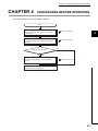
SAFETY PRECAUTIONS
(Read these precautions before using this product.)
Before using this product, please read this manual and the relevant manuals carefully and pay full attention
to safety to handle the product correctly.
The precautions given in this manual are concerned with this product only. For the safety precautions of the
programmable controller system, refer to the user's manual for the CPU module used.
In this manual, the safety precautions are classified into two levels: "
WARNING" and "
CAUTION".
WARNING
Indicates that incorrect handling may cause hazardous conditions,
resulting in death or severe injury.
CAUTION
Indicates that incorrect handling may cause hazardous conditions,
resulting in minor or moderate injury or property damage.
Under some circumstances, failure to observe the precautions given under "
CAUTION" may lead to
serious consequences.
Observe the precautions of both levels because they are important for personal and system safety.
Make sure that the end users read this manual and then keep the manual in a safe place for future
reference.
[Design Precautions]
WARNING
● Do not write any data to the "system area" and "write-protect area" (R) of the buffer memory in the
intelligent function module. Also, do not use any "use prohibited" signals as an output signal from the
programmable controller CPU to the intelligent function module.
Doing so may cause malfunction of the programmable controller system.
[Design Precautions]
CAUTION
● Do not install the control lines or communication cables together with the main circuit lines or power
cables. Keep a distance of 100mm or more between them. Failure to do so may result in malfunction
due to noise.
● Do not install the analog signal cables together with the main circuit lines; power cables; or load
cables of external devices other than the programmable controller. Keep a distance of 150mm or
more between them. Failure to do so may result in malfunction due to noise.
1
[Installation Precautions]
WARNING
● Shut off the external power supply (all phases) used in the system before mounting or removing a
module. Failure to do so may result in electric shock or cause the module to fail or malfunction.
[Installation Precautions]
CAUTION
● Use the programmable controller in an environment that meets the general specifications in the Safety
Guidelines provided with the CPU module or head module. Failure to do so may result in electric
shock, fire, malfunction, or damage to or deterioration of the product.
● To interconnect modules, engage the respective connectors and securely lock the module joint levers
until they click. Incorrect interconnection may cause malfunction, failure, or drop of the module.
● Tighten the screws within the specified torque range. Undertightening can cause drop of the screw,
short circuit, or malfunction. Overtightening can damage the screw and/or module, resulting in drop,
short circuit, or malfunction.
● Do not directly touch any conductive parts and electronic components of the module. Doing so can
cause malfunction or failure of the module.
[Wiring Precautions]
WARNING
● After installation and wiring, attach the included terminal cover to the module before turning it on for
operation. Failure to do so may result in electric shock.
2
[Wiring Precautions]
CAUTION
● Individually ground the FG terminal of the programmable controller with a ground resistance of 100
or less. Failure to do so may result in electric shock or malfunction.
● Tighten the terminal block screws within the specified torque range. Undertightening can cause short
circuit, fire, or malfunction. Overtightening can damage the screw and/or module, resulting in drop,
short circuit, or malfunction.
● Prevent foreign matter such as dust or wire chips from entering the module. Such foreign matter can
cause a fire, failure, or malfunction.
● A protective film is attached to the top of the module to prevent foreign matter, such as wire chips,
from entering the module during wiring. Do not remove the film during wiring. Remove it for heat
dissipation before system operation.
● Mitsubishi programmable controllers must be installed in control panels. Connect the main power
supply to the power supply module in the control panel through a relay terminal block. Wiring and
replacement of a power supply module must be performed by qualified maintenance personnel with
knowledge of protection against electric shock. For wiring methods, refer to the MELSEC-L CPU
Module User's Manual (Hardware Design, Maintenance and Inspection).
[Startup and Maintenance Precautions]
WARNING
● Do not touch any terminal while power is on. Doing so will cause electric shock or malfunction.
● Shut off the external power supply (all phases) used in the system before cleaning the module or
retightening the terminal block screws. Failure to do so may result in electric shock.
[Startup and Maintenance Precautions]
CAUTION
● Do not disassemble or modify the module. Doing so may cause failure, malfunction, injury, or a fire.
● Shut off the external power supply (all phases) used in the system before mounting or removing a
module. Failure to do so may cause the module to fail or malfunction.
● Tighten the terminal block screws within the specified torque range. Undertightening can cause drop
of the component or wire, short circuit, or malfunction. Overtightening can damage the screw and/or
module, resulting in drop, short circuit, or malfunction.
● After the first use of the product (module, display unit, and terminal block), do not connect/disconnect
the product more than 50 times (in accordance with IEC 61131-2). Exceeding the limit may cause
malfunction.
● Before handling the module, touch a conducting object such as a grounded metal to discharge the
static electricity from the human body. Failure to do so may cause the module to fail or malfunction.
3
[Disposal Precautions]
CAUTION
● When disposing of this product, treat it as industrial waste.
4
CONDITIONS OF USE FOR THE PRODUCT
(1) Mitsubishi programmable controller ("the PRODUCT") shall be used in conditions;
i) where any problem, fault or failure occurring in the PRODUCT, if any, shall not lead to any major
or serious accident; and
ii) where the backup and fail-safe function are systematically or automatically provided outside of
the PRODUCT for the case of any problem, fault or failure occurring in the PRODUCT.
(2) The PRODUCT has been designed and manufactured for the purpose of being used in general
industries.
MITSUBISHI SHALL HAVE NO RESPONSIBILITY OR LIABILITY (INCLUDING, BUT NOT
LIMITED TO ANY AND ALL RESPONSIBILITY OR LIABILITY BASED ON CONTRACT,
WARRANTY, TORT, PRODUCT LIABILITY) FOR ANY INJURY OR DEATH TO PERSONS OR
LOSS OR DAMAGE TO PROPERTY CAUSED BY the PRODUCT THAT ARE OPERATED OR
USED IN APPLICATION NOT INTENDED OR EXCLUDED BY INSTRUCTIONS, PRECAUTIONS,
OR WARNING CONTAINED IN MITSUBISHI'S USER, INSTRUCTION AND/OR SAFETY
MANUALS, TECHNICAL BULLETINS AND GUIDELINES FOR the PRODUCT.
("Prohibited Application")
Prohibited Applications include, but not limited to, the use of the PRODUCT in;
• Nuclear Power Plants and any other power plants operated by Power companies, and/or any
other cases in which the public could be affected if any problem or fault occurs in the PRODUCT.
• Railway companies or Public service purposes, and/or any other cases in which establishment of
a special quality assurance system is required by the Purchaser or End User.
• Aircraft or Aerospace, Medical applications, Train equipment, transport equipment such as
Elevator and Escalator, Incineration and Fuel devices, Vehicles, Manned transportation,
Equipment for Recreation and Amusement, and Safety devices, handling of Nuclear or
Hazardous Materials or Chemicals, Mining and Drilling, and/or other applications where there is a
significant risk of injury to the public or property.
Notwithstanding the above, restrictions Mitsubishi may in its sole discretion, authorize use of the
PRODUCT in one or more of the Prohibited Applications, provided that the usage of the PRODUCT
is limited only for the specific applications agreed to by Mitsubishi and provided further that no
special quality assurance or fail-safe, redundant or other safety features which exceed the general
specifications of the PRODUCTs are required. For details, please contact the Mitsubishi
representative in your region.
5
INTRODUCTION
Thank you for purchasing the Mitsubishi MELSEC-L series programmable controllers.
This manual describes the functions and programming of a dual channel isolated high resolution analog-digital
converter module (hereafter abbreviated as A/D converter module).
Before using this product, please read this manual and the relevant manuals carefully and develop familiarity with the
functions and performance of the MELSEC-L series programmable controller to handle the product correctly.
When applying the program examples introduced in this manual to an actual system, ensure the applicability and
confirm that it will not cause system control problems.
Target module: L60AD4-2GH
Remark
● Unless otherwise specified, this manual describes the program examples in which the I/O numbers of X/Y00 to X/Y0F are
assigned for an A/D converter module.
For I/O number assignment, refer to the following.
MELSEC-L CPU Module User's Manual (Function Explanation, Program Fundamentals)
● Operating procedures are explained using GX Works2. When using GX Developer, refer to the following.
• When using GX Developer (
6
Page 297, Appendix 7)
COMPLIANCE WITH EMC AND LOW VOLTAGE
DIRECTIVES
(1) Method of ensuring compliance
To ensure that Mitsubishi programmable controllers maintain EMC and Low Voltage Directives when incorporated
into other machinery or equipment, certain measures may be necessary. Please refer to one of the following
manuals.
• MELSEC-L CPU Module User's Manual (Hardware Design, Maintenance and Inspection)
• MELSEC-L CC-Link IE Field Network Head Module User's Manual
• Safety Guidelines
(This manual is included with the CPU module or head module.)
The CE mark on the side of the programmable controller indicates compliance with EMC and Low Voltage
Directives.
(2) Additional measures
No additional measures are necessary for the compliance of this product with EMC and Low Voltage Directives.
7
RELEVANT MANUALS
(1) CPU module user's manual
Manual name
Description
<Manual number (model code)>
MELSEC-L CPU Module User's Manual (Hardware Design,
Specifications of the CPU modules, power supply modules, display
Maintenance and Inspection)
unit, branch module, extension module, SD memory cards, and
batteries, information on how to establish a system, maintenance
<SH-080890ENG, 13JZ36>
and inspection, and troubleshooting
MELSEC-L CPU Module User's Manual (Function Explanation,
Program Fundamentals)
Functions and devices of the CPU module, and programming
<SH-080889ENG, 13JZ35>
(2) Head module User's Manual
Manual name
Description
<Manual number (model code)>
MELSEC-L CC-Link IE Field Network Head Module User's Manual
<SH-080919ENG, 13JZ48>
Specifications, procedures before operation, system configuration,
installation, wiring, settings, and troubleshooting of the head module
(3) Operating manual
Manual name
Description
<Manual number (model code)>
GX Works2 Version 1 Operating Manual (Common)
<SH-080779ENG, 13JU63>
GX Developer Version 8 Operating Manual
GX Works2, which are common to Simple projects and Structured
projects
Operating methods of GX Developer, such as programming,
<SH-080373E, 13JU41>
8
System configuration, parameter settings, and online operations of
printing, monitoring, and debugging
Memo
9
CONTENTS
CONTENTS
SAFETY PRECAUTIONS . . . . . . . . . . . . . . . . . . . . . . . . . . . . . . . . . . . . . . . . . . . . . . . . . . . . . . . . . . . . . 1
CONDITIONS OF USE FOR THE PRODUCT . . . . . . . . . . . . . . . . . . . . . . . . . . . . . . . . . . . . . . . . . . . . . 5
INTRODUCTION . . . . . . . . . . . . . . . . . . . . . . . . . . . . . . . . . . . . . . . . . . . . . . . . . . . . . . . . . . . . . . . . . . . . 6
COMPLIANCE WITH EMC AND LOW VOLTAGE DIRECTIVES . . . . . . . . . . . . . . . . . . . . . . . . . . . . . . . 7
RELEVANT MANUALS . . . . . . . . . . . . . . . . . . . . . . . . . . . . . . . . . . . . . . . . . . . . . . . . . . . . . . . . . . . . . . . 8
MANUAL PAGE ORGANIZATION . . . . . . . . . . . . . . . . . . . . . . . . . . . . . . . . . . . . . . . . . . . . . . . . . . . . . . 13
TERMS . . . . . . . . . . . . . . . . . . . . . . . . . . . . . . . . . . . . . . . . . . . . . . . . . . . . . . . . . . . . . . . . . . . . . . . . . . 16
PACKING LIST . . . . . . . . . . . . . . . . . . . . . . . . . . . . . . . . . . . . . . . . . . . . . . . . . . . . . . . . . . . . . . . . . . . . 16
CHAPTER 1 A/D CONVERSION MODULE
1.1
1.2
Application . . . . . . . . . . . . . . . . . . . . . . . . . . . . . . . . . . . . . . . . . . . . . . . . . . . . . . . . . . . . . . . . 17
Features . . . . . . . . . . . . . . . . . . . . . . . . . . . . . . . . . . . . . . . . . . . . . . . . . . . . . . . . . . . . . . . . . . 18
1.2.1
Main features . . . . . . . . . . . . . . . . . . . . . . . . . . . . . . . . . . . . . . . . . . . . . . . . . . . . . . . . . . . . . 18
1.2.2
Advantages with the main features . . . . . . . . . . . . . . . . . . . . . . . . . . . . . . . . . . . . . . . . . . . . 20
1.2.3
Other features . . . . . . . . . . . . . . . . . . . . . . . . . . . . . . . . . . . . . . . . . . . . . . . . . . . . . . . . . . . . 21
CHAPTER 2 PART NAMES
23
CHAPTER 3 SPECIFICATIONS
25
3.1
General Specifications . . . . . . . . . . . . . . . . . . . . . . . . . . . . . . . . . . . . . . . . . . . . . . . . . . . . . . . 25
3.2
Performance Specifications . . . . . . . . . . . . . . . . . . . . . . . . . . . . . . . . . . . . . . . . . . . . . . . . . . . 26
3.2.1
Number of parameter settings . . . . . . . . . . . . . . . . . . . . . . . . . . . . . . . . . . . . . . . . . . . . . . . . 28
3.3
Function List . . . . . . . . . . . . . . . . . . . . . . . . . . . . . . . . . . . . . . . . . . . . . . . . . . . . . . . . . . . . . . . 29
3.4
I/O Signal List . . . . . . . . . . . . . . . . . . . . . . . . . . . . . . . . . . . . . . . . . . . . . . . . . . . . . . . . . . . . . . 31
3.5
List of Buffer Memory Addresses . . . . . . . . . . . . . . . . . . . . . . . . . . . . . . . . . . . . . . . . . . . . . . . 32
CHAPTER 4 PROCEDURES BEFORE OPERATION
45
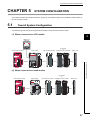
CHAPTER 5 SYSTEM CONFIGURATION
47
5.1
Overall System Configuration . . . . . . . . . . . . . . . . . . . . . . . . . . . . . . . . . . . . . . . . . . . . . . . . . . 47
5.2
Applicable System . . . . . . . . . . . . . . . . . . . . . . . . . . . . . . . . . . . . . . . . . . . . . . . . . . . . . . . . . . 48
5.3
Restrictions when the A/D Converter Module Is Connected to a Head Module . . . . . . . . . . . . 48
CHAPTER 6 INSTALLATION AND WIRING
49
6.1
Installation Environment and Installation Position . . . . . . . . . . . . . . . . . . . . . . . . . . . . . . . . . . 49
6.2
Terminal Block . . . . . . . . . . . . . . . . . . . . . . . . . . . . . . . . . . . . . . . . . . . . . . . . . . . . . . . . . . . . . 50
6.3
Wiring . . . . . . . . . . . . . . . . . . . . . . . . . . . . . . . . . . . . . . . . . . . . . . . . . . . . . . . . . . . . . . . . . . . . 52
6.4
External Wiring . . . . . . . . . . . . . . . . . . . . . . . . . . . . . . . . . . . . . . . . . . . . . . . . . . . . . . . . . . . . . 53
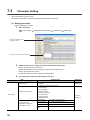
CHAPTER 7 VARIOUS SETTINGS
10
17
56
7.1
Addition of Modules . . . . . . . . . . . . . . . . . . . . . . . . . . . . . . . . . . . . . . . . . . . . . . . . . . . . . . . . . 56
7.2
Switch Setting . . . . . . . . . . . . . . . . . . . . . . . . . . . . . . . . . . . . . . . . . . . . . . . . . . . . . . . . . . . . . . 57
7.3
Parameter Setting. . . . . . . . . . . . . . . . . . . . . . . . . . . . . . . . . . . . . . . . . . . . . . . . . . . . . . . . . . . 58
7.4
Auto Refresh. . . . . . . . . . . . . . . . . . . . . . . . . . . . . . . . . . . . . . . . . . . . . . . . . . . . . . . . . . . . . . . 61
7.5
Offset/gain Setting . . . . . . . . . . . . . . . . . . . . . . . . . . . . . . . . . . . . . . . . . . . . . . . . . . . . . . . . . . 62
7.5.1
Setting from "Offset/Gain Setting" of GX Works2. . . . . . . . . . . . . . . . . . . . . . . . . . . . . . . . . . 62
7.5.2
Setting from a program . . . . . . . . . . . . . . . . . . . . . . . . . . . . . . . . . . . . . . . . . . . . . . . . . . . . . 65
CHAPTER 8 FUNCTIONS
69
8.1
Modes . . . . . . . . . . . . . . . . . . . . . . . . . . . . . . . . . . . . . . . . . . . . . . . . . . . . . . . . . . . . . . . . . . . . 69
8.2
Processing Each Function . . . . . . . . . . . . . . . . . . . . . . . . . . . . . . . . . . . . . . . . . . . . . . . . . . . . 71
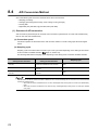
8.3
A/D Conversion Enable/Disable Function. . . . . . . . . . . . . . . . . . . . . . . . . . . . . . . . . . . . . . . . . 73
8.4
A/D Conversion Method . . . . . . . . . . . . . . . . . . . . . . . . . . . . . . . . . . . . . . . . . . . . . . . . . . . . . . 74
8.5
Input Range Extended Mode Function . . . . . . . . . . . . . . . . . . . . . . . . . . . . . . . . . . . . . . . . . . . 94
8.6
Maximum Value/Minimum Value Hold Function . . . . . . . . . . . . . . . . . . . . . . . . . . . . . . . . . . . . 95
8.7
Input Signal Error Detection Function. . . . . . . . . . . . . . . . . . . . . . . . . . . . . . . . . . . . . . . . . . . . 96
8.8
Warning Output Function . . . . . . . . . . . . . . . . . . . . . . . . . . . . . . . . . . . . . . . . . . . . . . . . . . . . 102
8.8.1
Process alarm . . . . . . . . . . . . . . . . . . . . . . . . . . . . . . . . . . . . . . . . . . . . . . . . . . . . . . . . . . . 102
8.8.2
Rate alarm . . . . . . . . . . . . . . . . . . . . . . . . . . . . . . . . . . . . . . . . . . . . . . . . . . . . . . . . . . . . . . 105
8.9
Scaling Function . . . . . . . . . . . . . . . . . . . . . . . . . . . . . . . . . . . . . . . . . . . . . . . . . . . . . . . . . . . 110
8.10
Shift Function . . . . . . . . . . . . . . . . . . . . . . . . . . . . . . . . . . . . . . . . . . . . . . . . . . . . . . . . . . . . . 117
8.11
Digital Clipping Function . . . . . . . . . . . . . . . . . . . . . . . . . . . . . . . . . . . . . . . . . . . . . . . . . . . . . 122
8.12
Difference Conversion Function . . . . . . . . . . . . . . . . . . . . . . . . . . . . . . . . . . . . . . . . . . . . . . . 126
8.13
Logging Function . . . . . . . . . . . . . . . . . . . . . . . . . . . . . . . . . . . . . . . . . . . . . . . . . . . . . . . . . . 130
8.13.1 Logging load detection function . . . . . . . . . . . . . . . . . . . . . . . . . . . . . . . . . . . . . . . . . . . . . . 137
8.13.2 Stopping the logging operation. . . . . . . . . . . . . . . . . . . . . . . . . . . . . . . . . . . . . . . . . . . . . . . 148
8.13.3 Logging hold request . . . . . . . . . . . . . . . . . . . . . . . . . . . . . . . . . . . . . . . . . . . . . . . . . . . . . . 152
8.13.4 Level trigger . . . . . . . . . . . . . . . . . . . . . . . . . . . . . . . . . . . . . . . . . . . . . . . . . . . . . . . . . . . . . 154
8.13.5 Logging outside trigger. . . . . . . . . . . . . . . . . . . . . . . . . . . . . . . . . . . . . . . . . . . . . . . . . . . . . 157
8.13.6 Setting method of a hold trigger (a request to stop logging) . . . . . . . . . . . . . . . . . . . . . . . . 159
8.14
Trigger Conversion Function . . . . . . . . . . . . . . . . . . . . . . . . . . . . . . . . . . . . . . . . . . . . . . . . . 162
8.15
Error Log Function . . . . . . . . . . . . . . . . . . . . . . . . . . . . . . . . . . . . . . . . . . . . . . . . . . . . . . . . . 170
8.16
Module Error Collection Function . . . . . . . . . . . . . . . . . . . . . . . . . . . . . . . . . . . . . . . . . . . . . . 173
8.17
Error Clear Function . . . . . . . . . . . . . . . . . . . . . . . . . . . . . . . . . . . . . . . . . . . . . . . . . . . . . . . . 174
8.18
Saving and Restoring Offset/gain Values . . . . . . . . . . . . . . . . . . . . . . . . . . . . . . . . . . . . . . . . 175
CHAPTER 9 DISPLAY UNIT
181
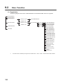
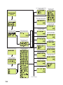
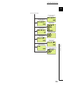
9.1
Display Unit. . . . . . . . . . . . . . . . . . . . . . . . . . . . . . . . . . . . . . . . . . . . . . . . . . . . . . . . . . . . . . . 181
9.2
Menu Transition . . . . . . . . . . . . . . . . . . . . . . . . . . . . . . . . . . . . . . . . . . . . . . . . . . . . . . . . . . . 182
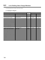
9.3
List of Setting Value Change Windows. . . . . . . . . . . . . . . . . . . . . . . . . . . . . . . . . . . . . . . . . . 186
9.4
Checking and Clearing Errors. . . . . . . . . . . . . . . . . . . . . . . . . . . . . . . . . . . . . . . . . . . . . . . . . 195
CHAPTER 10 PROGRAMMING
197
10.1
Procedure for Programming . . . . . . . . . . . . . . . . . . . . . . . . . . . . . . . . . . . . . . . . . . . . . . . . . . 197
10.2
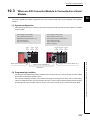
When Using the Module in a Standard System Configuration . . . . . . . . . . . . . . . . . . . . . . . . 198
10.3
When an A/D Converter Module Is Connected to a Head Module . . . . . . . . . . . . . . . . . . . . . 207
11
CHAPTER 11 TROUBLESHOOTING
217
11.1
Checking on the Module Detailed Information . . . . . . . . . . . . . . . . . . . . . . . . . . . . . . . . . . . . 218
11.2
Checking by Latest Error Code (Un\G19). . . . . . . . . . . . . . . . . . . . . . . . . . . . . . . . . . . . . . . . 219
11.3
Checking on the Module Error Collection Function . . . . . . . . . . . . . . . . . . . . . . . . . . . . . . . . 220
11.4
Error Code List . . . . . . . . . . . . . . . . . . . . . . . . . . . . . . . . . . . . . . . . . . . . . . . . . . . . . . . . . . . . 221
11.5
Alarm Code List . . . . . . . . . . . . . . . . . . . . . . . . . . . . . . . . . . . . . . . . . . . . . . . . . . . . . . . . . . . 226
11.6
Troubleshooting . . . . . . . . . . . . . . . . . . . . . . . . . . . . . . . . . . . . . . . . . . . . . . . . . . . . . . . . . . . 227
11.7
Checking the Status of the A/D Converter Module by the System Monitor . . . . . . . . . . . . . . 231
APPENDICES
232
Appendix 1 Details of I/O Signals. . . . . . . . . . . . . . . . . . . . . . . . . . . . . . . . . . . . . . . . . . . . . . . . . . . 232
Appendix 1.1
Input signal . . . . . . . . . . . . . . . . . . . . . . . . . . . . . . . . . . . . . . . . . . . . . . . 232
Appendix 1.2
Output signal . . . . . . . . . . . . . . . . . . . . . . . . . . . . . . . . . . . . . . . . . . . . . . 238
Appendix 2 Details of Buffer Memory Addresses. . . . . . . . . . . . . . . . . . . . . . . . . . . . . . . . . . . . . . . 240
Appendix 3 I/O Conversion Characteristic of A/D Conversion . . . . . . . . . . . . . . . . . . . . . . . . . . . . . 279
Appendix 4 A/D Conversion Accuracy . . . . . . . . . . . . . . . . . . . . . . . . . . . . . . . . . . . . . . . . . . . . . . . 284
Appendix 5 Dedicated Instruction . . . . . . . . . . . . . . . . . . . . . . . . . . . . . . . . . . . . . . . . . . . . . . . . . . 285
Appendix 5.1
Instruction list . . . . . . . . . . . . . . . . . . . . . . . . . . . . . . . . . . . . . . . . . . . . . 285
Appendix 5.2
G(P).OFFGAN . . . . . . . . . . . . . . . . . . . . . . . . . . . . . . . . . . . . . . . . . . . . . 286
Appendix 5.3
G(P).OGLOAD . . . . . . . . . . . . . . . . . . . . . . . . . . . . . . . . . . . . . . . . . . . . 288
Appendix 5.4
G(P).OGSTOR . . . . . . . . . . . . . . . . . . . . . . . . . . . . . . . . . . . . . . . . . . . . 292
Appendix 6 Checking Serial Number and Function Version . . . . . . . . . . . . . . . . . . . . . . . . . . . . . . 296
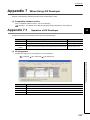
Appendix 7 When Using GX Developer . . . . . . . . . . . . . . . . . . . . . . . . . . . . . . . . . . . . . . . . . . . . . . 297
Appendix 7.1
Operation of GX Developer . . . . . . . . . . . . . . . . . . . . . . . . . . . . . . . . . . . . 297
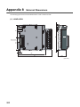
Appendix 8 External Dimensions . . . . . . . . . . . . . . . . . . . . . . . . . . . . . . . . . . . . . . . . . . . . . . . . . . . 300
INDEX
301
INSTRUCTION INDEX
303
REVISIONS . . . . . . . . . . . . . . . . . . . . . . . . . . . . . . . . . . . . . . . . . . . . . . . . . . . . . . . . . . . . . . . . . . . . . . 304
WARRANTY . . . . . . . . . . . . . . . . . . . . . . . . . . . . . . . . . . . . . . . . . . . . . . . . . . . . . . . . . . . . . . . . . . . . . 305
12
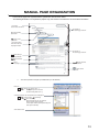
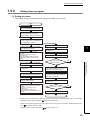
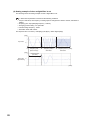
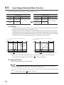
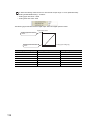
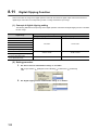
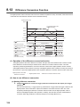
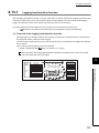
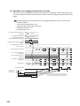
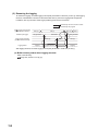
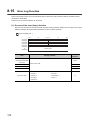
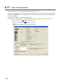
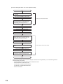
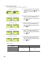
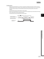
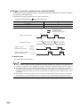
MANUAL PAGE ORGANIZATION
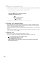
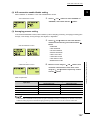
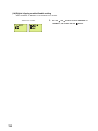
In this manual, pages are organized and the symbols are used as shown below.
The following illustration is for explanation purpose only, and should not be referred to as an actual documentation.
"" is used for
screen names and items.
The chapter of
the current page is shown.
shows operating
procedures.
shows mouse
operations.*1
[ ] is used for items
in the menu bar and
the project window.
The section of
the current page is shown.
Ex. shows setting or
operating examples.
shows reference
manuals.
shows notes that
requires attention.
shows
reference pages.
shows useful
information.
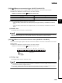
*1
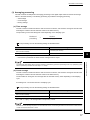
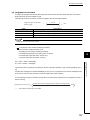
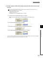
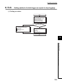
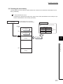
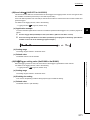
The mouse operation example is provided below. (For GX Works2)
Menu bar
Ex.
[Online]
[Write to PLC...]
Select [Online] on the menu bar,
and then select [Write to PLC...].
A window selected in the view selection area is displayed.
Ex.
[Parameter]
Project window
[PLC Parameter]
Select [Project] from the view selection
area to open the Project window.
In the Project window, expand [Parameter] and
select [PLC Parameter].
View selection area
13
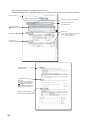
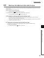
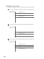
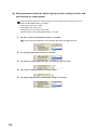
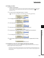
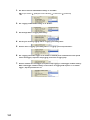
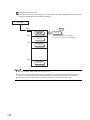
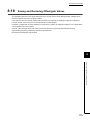
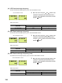
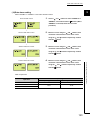
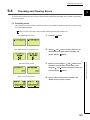
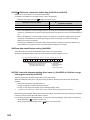
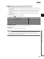
Pages describing instructions are organized as shown below.
The following illustration is for explanation purpose only, and should not be referred to as an actual documentation.
Instruction name
Execution condition of the instruction
Structure of the instruction
in the ladder mode
shows the devices
applicable to the instruction
Descriptions of
setting data and data type
Descriptions of
control data (if any)
Detailed descriptions
of the instruction
Conditions for the error and
error codes
For the errors not described in
this manual, refer to the following.
MELSEC-L CPU Module
User's Manual (Hardware Design,
Maintenance and Inspection)
Simple program example(s)
and descriptions of the devices used
14
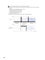
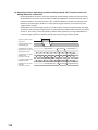
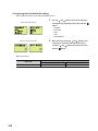
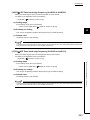
Setting side
User : Device value is set by the user.
System: Device value is set by
the CPU module.
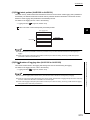
• Instructions can be executed under the following conditions.
Execution condition
Any time
Symbol
No symbol
On the rising
During on
edge
During off
On the falling
edge
• The following devices can be used.
Internal device
Setting
(system, user)
data
Applicable
device*1
Bit
Word
X, Y, M, L,
SM, F, B,
SB, FX,
T, ST, C, D,
W, SD,
SW, FD,
@
FY*2
Link direct
Intelligent
File
device
function module
register
J\
device
Bit
R, ZR
Word
-
U\G
U\G
Index
register
Zn
Z
*1
For details on each device, refer to the following.
*2
*3
MELSEC-L CPU Module User's Manual (Function Explanation, Program Fundamentals)
FX and FY can be used for bit data only, and FD for word data only.
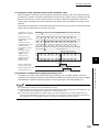
In the "Constant" and "Others" columns, a device(s) that can be set for each instruction is shown.
Constant
Others
*3
*3
K, H, E, $
P, I, J, U,
D, X, DY,
N, BL,
TR, BL\S,
V
• The following data types can be used.
Data type
Description
Bit
Bit data or the start number of bit data
BIN 16-bit
16-bit binary data or the start number of word device
BIN 32-bit
32-bit binary data or the start number of double-word device
BCD 4-digit
Four-digit binary-coded decimal data
BCD 8-digit
Eight-digit binary-coded decimal data
Real number
Floating-point data
Character string
Character string data
Device name
Device name data
15
TERMS
Unless otherwise specified, this manual uses the following terms.
Term
Description
Another term for the MELSEC-L series dual channel isolated high resolution analog-digital converter
A/D converter module
module
Head module
The abbreviation for the LJ72GF15-T2 CC-Link IE field network head module
Display unit
A liquid crystal display to be attached to the CPU module
Programming tool
A generic term for GX Works2 and GX Developer
Factory default setting
A generic term for analog input ranges of 0 to 10V, 0 to 5V, 1 to 5V, -10 to 10V, 0 to 20mA, and 4 to 20mA
GX Works2
The product name of the software package for the MELSEC programmable controllers
GX Developer
A memory in an intelligent function module, where data (such as setting values and monitoring values)
Buffer memory
exchanged with a CPU module are stored.
FIR filter
The abbreviation for a finite impulse response filter. An FIR filter is a type of a digital filter.
Low pass filter
A filter that blocks out unnecessary high-frequency components in a signal
High pass filter
A filter that blocks out unnecessary low-frequency components in a signal
Band pass filter
A filter that passes only necessary frequency in a signal and blocks out the others
Pass band
Frequency bandwidth that passes through the filter without being attenuated
Attenuation band
Frequency bandwidth whose attenuation rate through the filter is in a transition state
Stop band
Frequency bandwidth attenuated by the filter
Pass band edge frequency
The boundary frequency between a pass band and an attenuation band
Trigger conversion request
Hold trigger
A generic term for External trigger convert request (external input terminal) and Inside trigger conversion
request (Un\G161)
A request to stop logging
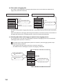
PACKING LIST
The following items are included in the package of this product. Before use, check that all the items are included.
L60AD4-2GH
L60AD4-2GH
16
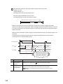
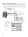
Before Using the Product
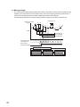
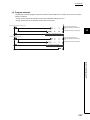
CHAPTER 1 A/D CONVERSION MODULE
CHAPTER 1
A/D CONVERSION MODULE
1
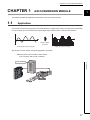
This chapter describes the applications and features of the A/D converter module.
1.1
Application
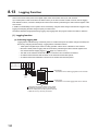
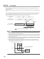
This module converts analog values input from external devices to digital output values, and inputs the converted data
to a CPU module. The CPU module can accept the digital output values from the conversion as information.
Analog to digital
conversion
Analog signal (continuous signal)
Digital signal (discrete signal)
With the A/D converter module, the following application is possible.
Measuring the heat from a heater or other devices
in the connection with a power conditioner
1.1 Application
Power conditioner
Heater
17
1.2
Features
1.2.1
Main features
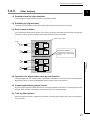
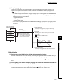
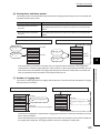
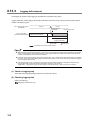
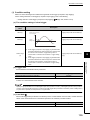
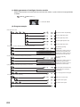
(1) High-speed continuous logging
With the logging function, 10000 points of logging data of digital output values from A/D conversion can be
collected through the high-speed continuous logging.
In addition, the logging load detection function enables the A/D converter module to transfer logging data stored
in the buffer memory of the module to the file register of a CPU module without stopping the logging operation.
The transfer enables more than 10000 points of logging data to be stored.
Workpiece
Sensor for the
inspection
Tire geometry
inspection
Sensor
Device memory of
the CPU module
Transfer
Logging is
completed.
Logging
1 to 1000th data
L60AD4-2GH
1 to 1000th data
1001 to 2000th data
Transferring 100000 points
of logging data by using
an interrupt program.
2001 to 3000th data
3001 to 4000th data
4001 to 5000th data
Waiting for
logging
5001 to 6000th data
6001 to 7000th data
7001 to 8000th data
8001 to 9000th data
9001 to 10000th data
18
Interrupt processing
Stores the logging data of This logging load
pointer in an index register.
Stores the value of Logging load points
monitor value in a register.
Stores the write position of the save
destination file register in the index register.
Stores the points of logging data that is set
in Logging load points monitor value in the
save destination file register.
Adds the points of Logging load points monitor
value to the write position of the save destination
file register. And stores the obtained value as the
write position for the next logging.
100000
points
CHAPTER 1 A/D CONVERSION MODULE
1
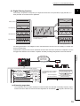
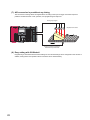
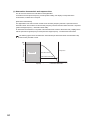
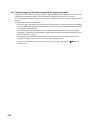
(2) Digital filtering function
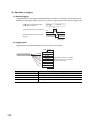
Unnecessary components of a frequency in a signal can be removed. A low pass filter, a high pass filter, or a
band pass filter can be selected as a digital filter.
Direct current
0
0
After low pass filter
Low frequency
0
0
Mid frequency
0
After band pass filter
Waves containing direct current,
low frequency, mid frequency,
and high frequency
High frequency
0
0
After high pass filter
Just setting parameters in the intelligent function module allows the function to be used, leading to reduced manhours for programming.
A filtered A/D conversion value can be obtained at the same time as the A/D conversion is completed. Thus, the
throughput time between A/D conversion completion and filter processing being started can be also reduced.
1.2 Features
1.2.1 Main features
Measuring flatness
Remove the
components with
different asperity.
Sensor
Workpiece
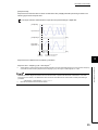
Example) Low pass filter processing using a ladder program
To perform
the filter processing using
a program, 3000 lines or
more ladders
are required.
The programming
is not required
when filtering with
this function.
The throughput time to perform
digital filtering using a ladder
program
The time required
for A/D conversion
Using this function reduces
the processing time.
The time required
for the program processing
(filter processing)
(a) Extracting target data
The combination of a test sensor and the A/D converter module can attenuate unnecessary frequency output
from the test sensor. Noise is removed and thus target data can be obtained. (
Page 80, Section 8.4 (5))
19
1.2.2
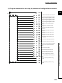
Advantages with the main features
Expensive devices for tests are not required by using the following functions of the module.
• Digital filtering function (low pass filter, high pass filter, band pass filter)
• Logging load detection function
The digital filtering function (low pass filter, high pass filter, band pass filter) removes noise by attenuating unnecessary
frequency data. Thus, target frequency data is obtained through digital output values output from a test sensor.
The logging load detection function enables more than 10000 points of logging data of the obtained data to be stored
continuously at high-speed conversion without stopping the logging operation.
More than 10000 points of logging data
can be stored by transferring the logging data
to a device memory of the CPU module.
Device memory of the CPU module
1 to 1000th data
Transferring logging data
by using an interrupt program
Target data
Interrupt processing
Stores the logging data of This logging load
pointer in an index register.
Stores the value of Logging load points
monitor value in a register.
Stores the write position of the save
destination file register in the index register.
Stores the points of logging data that is set
in Logging load points monitor value in the
save destination file register.
Adds the points of Logging load points monitor
value to the write position of the save destination
file register. And stores the obtained value as the
write position for the next logging.
Logging is
completed.
Logging
1 to 1000th data
1001 to 2000th data
2001 to 3000th data
3001 to 4000th data
Logging of the
converted data
After low pass filter
4001 to 5000th data
Waiting for
logging
5001 to 6000th data
6001 to 7000th data
After band pass filter
7001 to 8000th data
8001 to 9000th data
9001 to 10000th data
After high pass filter
Using the digital filtering function,
the target data are processed preferred data.
20
CHAPTER 1 A/D CONVERSION MODULE
1.2.3
Other features
1
(1) Detailed control by high resolution
In all analog input ranges, the high resolution of 1/32000 is achieved.
(2) Reliability by high accuracy
The accuracy for the maximum value of the digital output value is ±0.05% (reference accuracy).
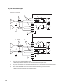
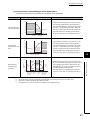
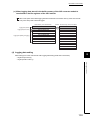
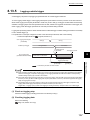
(3) Dual channel isolation
Four channels are divided into two groups of two and the two groups are isolated from each other. This prevents
the effects of noise from other channels and the measurement becomes more stable.
A/D converter module
Sensor
V+
I+
V-/I-
A/D
conversion
CH2
V+
I+
V-/I-
A/D
conversion
CH3
V+
I+
V-/I-
A/D
conversion
CH4
V+
I+
V-/I-
A/D
conversion
Dual channel isolation
Isolate between CH1/CH2 and
CH3/CH4 to prevent the effects
of noise.
1.2 Features
1.2.3 Other features
CH1
(4) Operation of a digital output value by each function
The digital clipping function, scaling function, shift function, and difference conversion function can represent the
digital output value in an easily understandable value according to the use environment.
(5) Comparing/monitoring target devices
By using the input signal error detection function, input range extended mode function, or warning output function
(process alarm, rate alarm), the status of connected devices can be monitored easily.
(6) Time lag filter function
With a time lag filter constant, a digital output value with smoothed noise is output. Man-hours for programming
can be reduced.
21
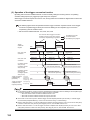
(7) A/D conversion is possible at any timing
The conversion of analog values into digital values according to the input of Trigger conversion request is
possible. The effectiveness of use, operation, and programming are improved.
Analog input signal
Displacement sensor
Trigger conversion request by
the external input terminal
(8) Easy setting with GX Works2
Programming is reduced because the initial settings or auto refresh settings can be configured on the window. In
addition, setting status and operation status of modules can be checked easily.
22
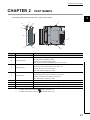
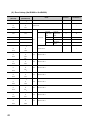
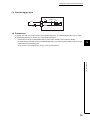
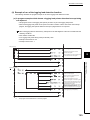
CHAPTER 2 PART NAMES
CHAPTER 2
PART NAMES
2
The following table shows part names of the A/D converter module.
1)
1)
2)
4)
3)
7)
6)
5)
1)
8)
1)
Number
1)
Name
Module joint levers
Description
Levers for connecting modules
Indicates the operating status of the A/D converter module.
2)
RUN LED (green)
ON: The module is operating normally.
Flashing: In the offset/gain setting mode
OFF: The 5V power off or watchdog timer error has occurred.
Indicates the errors and status of the A/D converter module.
3)
ERR. LED (red)
ON: An error has occurred except for error code: 112*1
Flashing: Error code: 112 has occurred.*1
OFF: The module is operating normally.
Indicates the warning status of the A/D converter module.
ON: Warning (process alarm or rate alarm) is occurring*2
4)
ALM LED (red)
5)
DIN rail hook
A hook used to mount the module to a DIN rail
6)
Terminal block
A 18-point screw terminal block for connecting input signal lines of external devices.
7)
Terminal block cover
A cover for preventing electric shock while the power is on
8)
Serial number display
Displays the serial number printed on the rating plate.
Flashing: Input signal error detection is occurring*2
OFF: The module is operating normally.
*1
For details, refer to Error Code List (
*2
For details, refer to Alarm Code List (
Page 221, Section 11.4).
Page 226, Section 11.5).
23
Memo
24
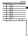
CHAPTER 3 SPECIFICATIONS
CHAPTER 3
SPECIFICATIONS
This chapter describes general specifications, performance specifications, function list, list of I/O signals, and list of
buffer memory addresses.
3.1
3
General Specifications
For the general specifications of the A/D converter module, refer to the following.
The manual "Safety Guidelines" included with the CPU module or head module
3.1 General Specifications
25
3.2
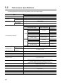
Performance Specifications
The following table lists the performance specifications of the A/D converter module.
Model
Item
L60AD4-2GH
Number of analog input points
Analog input
4 points (4 channels)
Voltage
-10 to 10VDC (input resistance 1M )
Current
0 to 20mADC (input resistance 250 )
Digital output
-32000 to 32000
When using the
-32768 to 32767
scaling function
Analog input range
Digital output value
Maximum
resolution
0 to 10V
312.5µV
0 to 5V
0 to 32000
156µV
-10 to 10V
-32000 to 32000
312.5µV
1 to 5V (Extended mode)
-8000 to 32000
125µV
-32000 to 32000
200µV*2
1 to 5V
Voltage
I/O characteristics, resolution*1
125µV
User range setting
(bi-polar: voltage)
0 to 20mA
0 to 32000
4 to 20mA
Current
4 to 20mA (Extended mode)
500nA
0 to 32000
400nA*2
User range setting
Reference accuracy*4
(accuracy for the
maximum value of the
digital output value)
*3
Temperature
coefficient*5
Conversion speed
Absolute maximum input
Offset/gain setting count*7
500nA
-8000 to 32000
(uni-polar: current)
Accuracy
625nA
Within ±0.05% (±16digit)
±40.1ppm/°C or lower
40µ/2 channels
Voltage: ±15V, Current: 30mA*6
Up to 100000 counts
Between I/O terminals and programmable controller power supply:
Insulation method
photocoupler isolation
Between analog input channels: dual channel transformer insulation
Dielectric withstand voltage
Insulation resistance
Number of occupied I/O points
Between I/O terminals and programmable controller power supply: 500VAC for 1 minute
Between analog input channels: 1000VAC for 1 minute
Between I/O terminals and programmable controller power supply:
500VDC 10M or higher
16 points (I/O assignment: 16 points for intelligent)
Connected terminal
18-point terminal block
Applicable wire size
0.3 to 0.75mm2
Applicable solderless terminal
R1.25-3 (solderless terminals with sleeve are not usable)
Internal current consumption (5VDC)
0.76A
Weight
0.20kg
26
CHAPTER 3 SPECIFICATIONS
Model
Item
L60AD4-2GH
Input points
1 point
Rated input voltage
24VDC (+20%/-15%, ripple ratio: within 5%)
Rated input current
6,0mA TYP. (at 24VDC)
ON voltage/ON
current
Outside trigger input
OFF voltage/OFF
current
13V or higher/3mA or higher
Input resistance
OFF
Response
ON
time
ON
3
8V or lower/1.6mA or lower
OFF
3.9k
40µs
40µs
*1
For details on the I/O conversion characteristic, refer to the following.
*2
*3
*4
*5
I/O Conversion Characteristic of A/D Conversion (
Page 279, Appendix 3)
Maximum resolution in the user range setting.
Except when receiving noise influence.
Accuracy under the ambient temperature when the offset/gain setting is performed.
Accuracy when the temperature changes 1°C.
Ex. Accuracy when the temperature changes from 25°C to 30°C
*6
*7
0.05% + 0.00401%/°C (temperature coefficient) × 5°C (temperature change) = 0.070%
A momentary input current value which does not cause damage to internal resistors of the module. The maximum input
current value for constant application is 24mA.
If the number of offset/gain settings exceeds 100000 times, an error occurs.
• The error code (170) is stored in Latest error code (Un\G19), Error flag (XF) turns on, then the ERR. LED turns on.
3.2 Performance Specifications
27
3.2.1
Number of parameter settings
Set the initial settings of the A/D converter module and the parameter settings of the auto refresh setting so that the
number of parameters, including those of other intelligent function modules, does not exceed the number of
parameters that can be set in a CPU module.
For the maximum number of parameters that can be set in a CPU module (maximum number of parameter settings),
refer to the following.
MELSEC-L CPU Module User's Manual (Hardware Design, Maintenance and Inspection)
MELSEC-L CC-Link IE Field Network Head Module User's Manual
(1) Number of the A/D converter module's parameters
The following number of parameters can be set in a single A/D converter module.
Target module
L60AD4-2GH
Initial setting
Auto refresh setting
11
57
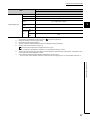
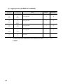
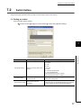
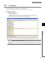
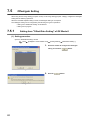
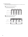
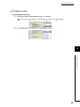
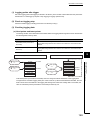
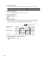
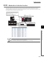
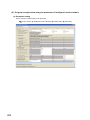
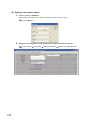
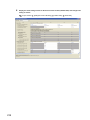
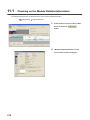
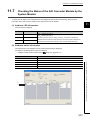
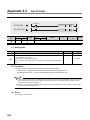
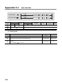
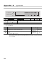
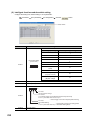
(2) Checking method
The maximum number of the parameter settings and the number of the parameter settings set for an intelligent
function module can be checked with the following operation.
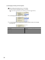
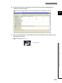
Project window
[Intelligent Function Module]
Right-click
[Intelligent Function Module Parameter List]
1)
No.
28
2)
3)
4)
Description
1)
The total number of the parameters in the initial settings selected on the window
2)
The maximum number of the parameter settings in the initial settings
3)
The total number of the parameters in the auto refresh settings selected on the window
4)
The maximum number of the parameter settings in the auto refresh settings
CHAPTER 3 SPECIFICATIONS
3.3
Function List
The following table lists the functions of the A/D converter module.
Item
Description
Set whether to enable or disable A/D conversion for each channel.
A/D conversion enable/disable function
Disabling the A/D conversion for unused channels reduces the
conversion cycles.
Sampling processing
Reference
Page 73,
Section 8.3
The A/D converter module executes the A/D conversion of the analog
Page 76,
input value sequentially and stores the digital output value to the buffer
Section 8.4
memory.
3
(2)
The A/D converter module executes the A/D conversion for set time, and
Time
average
stores the average of the total value excluding the maximum and the
Page 77,
minimum values to the buffer memory. The number of processing time
Section 8.4
within the setting time changes depending on the number of channels
(3) (a)
used (the number of channels set to A/D conversion enabled).
The A/D converter module executes the A/D conversion for set time, and
Averaging
Count
processing
average
stores the average of the total value excluding the maximum and the
minimum values to the buffer memory. Time for the count average value
stored in the buffer memory changes depending on the used channel
Page 77,
Section 8.4
(3) (b)
numbers (the number of channels set to A/D conversion enabled).
A/D conversion
The A/D converter module averages digital output values of set number
method
Moving
average
of times which are measured every sampling cycle, and stores them in
Page 78,
the buffer memory. Since the averaging processing is performed on a
Section 8.4
moving set of sampling processing, the latest digital output values can be
(3) (c)
obtained.
Digital filter
constant calculated by the setting value.
Low pass
The A/D converter module outputs the digital value whose unnecessary
filter
high-frequency component in a signal is removed.
High pass
The A/D converter module outputs the digital value whose unnecessary
filter
low-frequency component in a signal is removed.
Band pass
The A/D converter module passes only necessary frequency in a signal
filter
and outputs the digital value with the unnecessary frequency removed.
Page 79,
Section 8.4
(4)
Page 80,
Section 8.4
(5)
The input range to use can be selected from the following ranges:
• Industrial shipment setting (4 to 20mA, 0 to 20mA, 1 to 5V, 0 to 5V, -10
to 10V, 0 to 10V)
Range switching function
• User range (User range setting (uni-polar: current)), User range setting
(bi-polar: voltage))
Page 57,
Section 7.2
• Extended mode range (4 to 20mA (Extended mode), 1 to 5V (Extended
mode))
Offset/gain setting function
This function compensates for errors in digital output values.
This function extends the input range. By combining this function with the
Input range extended mode function
input signal error detection function, simple disconnection detection can
be executed.
Page 62,
Section 7.5
Page 94,
Section 8.5
The A/D converter module stores the maximum and minimum values of
Maximum value/minimum value hold function
the digital operation values for each channel to the buffer memory.
Page 95,
The maximum and minimum values of channels with the averaging
Section 8.6
processing specified are also stored to the buffer memory.
29
3.3 Function List
The A/D converter module outputs averaged digital values with the time
Time lag filter
Item
Description
Reference
This function detects the analog input value which exceeds the setting
Input signal error detection function
range.
The upper lower limit detection, upper limit detection, lower limit
Page 96,
Section 8.7
detection, and disconnection detection can be executed.
Warning output
function
Process alarm
Rate alarm
This function outputs a warning when a digital operation value enters the
preset range.
This function outputs a warning when a change rate of a digital output
value exceeds the setting range.
Page 102,
Section 8.8.1
Page 105,
Section 8.8.2
This function enables scale conversion on the output digital values. The
Scaling function
values are converted within the range of the set scaling upper limit value
Page 110,
and scaling lower limit value. This omits the programming for scale
Section 8.9
conversion.
This function adds the set shifting amount to conversion value to the
Shift function
digital operation value and stores the result in the buffer memory. Fine
adjustment can be performed easily when the system starts.
When the input voltage or current exceeds the input range, the maximum
Digital clipping function
value of the digital operation value can be set to 32000, and the minimum
value can be set to 0 or -32000.
This function subtracts the difference conversion reference value from the
Difference conversion function
digital operation value and stores the acquired value in the buffer
memory.
Page 117,
Section 8.10
Page 122,
Section 8.11
Page 126,
Section 8.12
This function logs the digital output value or digital operation value. 10000
Logging function
points of data can be logged for each channel. By combining this function
with the logging load detection function, more than 10000 points of
Page 130,
Section 8.13
logging data can be obtained.
This function converts analog values into digital values according to the
input of Trigger conversion request.
Trigger conversion function
The method of the trigger conversion request can be selected from the
following two types.
Page 162,
Section 8.14
• External trigger convert request by the external input terminal
• Internal trigger conversion request by the buffer memory
Error log function
Module error collection function
Error clear function
Saving and restoring offset/gain values
30
The function stores up to latest 16 errors and alarms that occurred in the
A/D converter module to the buffer memory.
This function collects errors and alarms that occurred in the A/D converter
module and stores them to the CPU module.
This function clears the error from the system monitor when an error
occurs.
The offset/gain value of the user range setting (uni-polar: current) and
user range setting (bi-polar: voltage) can be saved or restored.
Page 170,
Section 8.15
Page 173,
Section 8.16
Page 174,
Section 8.17
Page 175,
Section 8.18
CHAPTER 3 SPECIFICATIONS
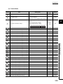
3.4
I/O Signal List
The following table lists the I/O signals of the A/D converter module.
For details on the I/O signals, refer to the following.
• Details of I/O Signals (
Page 232, Appendix 1)
Input signal
Device number
X0
Signal name
Module READY
Device number
Y1
X2
Y2
X3
Y3
Use prohibited
Y4
X5
Y5
X6
Y6
X7
Y7
X8
Warning output signal
Signal name
Y0
X1
X4
Use prohibited
Y8
X9
Operating condition setting completed flag
Y9
Operating condition setting request
XA
Offset/gain setting mode flag
YA
User range write request
XB
Channel change completed flag
YB
Channel change request
XC
Input signal error detection signal
YC
Use prohibited
XD
Maximum value/
minimum value reset completed flag
3
Output signal
YD
Maximum value/
minimum value reset request
A/D conversion completed flag
YE
Use prohibited
XF
Error flag
YF
Error clear request
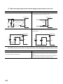
● The I/O number (X/Y) described above shows the case that the start I/O number of the A/D converter module is set to "0".
● Do not use the "Use prohibited" signals shown above because the system uses them. If users use (turn on) the signals,
the functions of the A/D converter module cannot be guaranteed.
31
3.4 I/O Signal List
XE
3.5
List of Buffer Memory Addresses
The following table lists the buffer memory addresses of the A/D converter module.
For details on the buffer memory addresses, refer to the following.
• Details of Buffer Memory Addresses (
Page 240, Appendix 2)
Do not write data to the system area and the area where the data cannot be written from the program in the buffer memory.
Writing data to these areas may lead the module to malfunction.
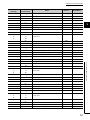
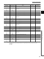
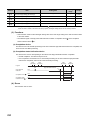
(1) Un\G0 to Un\G1799
32
Address
Address
(decimal)
(hexadecimal)
0
0H
1
1H
2
2H
3
3H
4
4H
5
5H
Name
A/D conversion enable/disable setting
CH1 Time Average/Count Average/
Moving Average/Time lag filter constant
CH2 Time Average/Count Average/
Moving Average/Time lag filter constant
CH3 Time Average/Count Average/
Moving Average/Time lag filter constant
CH4 Time Average/Count Average/
Moving Average/Time lag filter constant
System area
Default*1
Read/Write*2
0000H
R/W
0
R/W
0
R/W
0
R/W
0
R/W
–
–
to
to
8
8H
9
9H
Averaging process setting (for Q64AD)
0000H
R/W
10
AH
A/D conversion completed flag
0000H
R
11
BH
CH1 Digital output value
0
R
12
CH
CH2 Digital output value
0
R
13
DH
CH3 Digital output value
0
R
14
EH
CH4 Digital output value
0
R
15
FH
to
to
System area
–
–
18
12H
19
13H
Latest error code
0
R
20
14H
Setting range
0000H
R
21
15H
System area
–
–
22
16H
Offset/gain setting mode Offset specification
0000H
R/W
23
17H
Offset/gain setting mode Gain specification
0000H
R/W
24
18H
Averaging process setting
0000H
R/W
25
19H
26
1AH
–
–
27
1BH
Input signal error detection setting
0000H
R/W
28
1CH
System area
–
–
System area
CHAPTER 3 SPECIFICATIONS
Address
Address
(decimal)
(hexadecimal)
29
1DH
Digital clipping enable/disable setting
30
1EH
31
Default*1
Read/Write*2
000FH
R/W
CH1 Maximum value
0
R
1FH
CH1 Minimum value
0
R
32
20H
CH2 Maximum value
0
R
33
21H
CH2 Minimum value
0
R
34
22H
CH3 Maximum value
0
R
35
23H
CH3 Minimum value
0
R
36
24H
CH4 Maximum value
0
R
37
25H
CH4 Minimum value
0
R
38
26H
to
to
System area
–
–
45
2DH
46
2EH
Offset/gain range specification
0000H
R/W
47
2FH
System area
–
–
48
30H
Warning output setting
0F0FH
R/W
49
31H
Input signal error detection flag
0000H
R
50
32H
Warning output flag (Process alarm)
0000H
R
51
33H
Warning output flag (Rate alarm)
0000H
R
52
34H
System area
–
–
53
35H
Scaling enable/disable setting
000FH
R/W
54
36H
CH1 Digital operation value
0
R
55
37H
CH2 Digital operation value
0
R
56
38H
CH3 Digital operation value
0
R
57
39H
CH4 Digital operation value
0
R
58
3AH
to
to
System area
–
–
61
3DH
62
3EH
CH1 Scaling lower limit value
0
R/W
63
3FH
CH1 Scaling upper limit value
0
R/W
64
40H
CH2 Scaling lower limit value
0
R/W
65
41H
CH2 Scaling upper limit value
0
R/W
66
42H
CH3 Scaling lower limit value
0
R/W
67
43H
CH3 Scaling upper limit value
0
R/W
68
44H
CH4 Scaling lower limit value
0
R/W
69
45H
CH4 Scaling upper limit value
0
R/W
70
46H
to
to
System area
–
–
85
55H
86
56H
CH1 Process alarm lower lower limit value
0
R/W
87
57H
CH1 Process alarm lower upper limit value
0
R/W
88
58H
CH1 Process alarm upper lower limit value
0
R/W
89
59H
CH1 Process alarm upper upper limit value
0
R/W
Name
3
3.5 List of Buffer Memory Addresses
33
34
Address
Address
(decimal)
(hexadecimal)
Name
Default*1
Read/Write*2
90
5AH
CH2 Process alarm lower lower limit value
0
R/W
91
5BH
CH2 Process alarm lower upper limit value
0
R/W
92
5CH
CH2 Process alarm upper lower limit value
0
R/W
93
5DH
CH2 Process alarm upper upper limit value
0
R/W
94
5EH
CH3 Process alarm lower lower limit value
0
R/W
95
5FH
CH3 Process alarm lower upper limit value
0
R/W
96
60H
CH3 Process alarm upper lower limit value
0
R/W
97
61H
CH3 Process alarm upper upper limit value
0
R/W
98
62H
CH4 Process alarm lower lower limit value
0
R/W
99
63H
CH4 Process alarm lower upper limit value
0
R/W
100
64H
CH4 Process alarm upper lower limit value
0
R/W
101
65H
CH4 Process alarm upper upper limit value
0
R/W
102
66H
to
to
System area
–
–
117
75H
118
76H
CH1 Rate alarm detection cycle setting value
1
R/W
119
77H
CH2 Rate alarm detection cycle setting value
1
R/W
120
78H
CH3 Rate alarm detection cycle setting value
1
R/W
121
79H
CH4 Rate alarm detection cycle setting value
1
R/W
122
7AH
to
to
System area
–
–
125
7DH
126
7EH
CH1 Rate alarm upper limit value
0
R/W
127
7FH
CH1 Rate alarm lower limit value
0
R/W
128
80H
CH2 Rate alarm upper limit value
0
R/W
129
81H
CH2 Rate alarm lower limit value
0
R/W
130
82H
CH3 Rate alarm upper limit value
0
R/W
131
83H
CH3 Rate alarm lower limit value
0
R/W
132
84H
CH4 Rate alarm upper limit value
0
R/W
133
85H
CH4 Rate alarm lower limit value
0
R/W
134
86H
System area
–
–
to
to
141
8DH
142
8EH
CH1 Input signal error detection setting value
50
R/W
143
8FH
CH2 Input signal error detection setting value
50
R/W
144
90H
CH3 Input signal error detection setting value
50
R/W
145
91H
CH4 Input signal error detection setting value
50
R/W
146
92H
to
to
System area
–
–
149
95H
150
96H
CH1 Shifting amount to conversion value
0
R/W
151
97H
CH2 Shifting amount to conversion value
0
R/W
152
98H
CH3 Shifting amount to conversion value
0
R/W
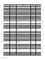
CHAPTER 3 SPECIFICATIONS
Address
Address
(decimal)
(hexadecimal)
153
99H
154
9AH
Default*1
Read/Write*2
CH4 Shifting amount to conversion value
0
R/W
System area
–
–
Mode switching setting
0
R/W
Name
to
to
157
9DH
158
9EH
159
9FH
160
A0H
A/D conversion timing monitor value
0
R
161
A1H
Inside trigger conversion request
0
R/W
162
A2H
Trigger conversion completed flag
0
R
163
A3H
Trigger conversion completed clear request
0
R/W
164
A4H
to
to
System area
–
–
171
ABH
172
ACH
CH1 Difference conversion trigger
0
R/W
173
ADH
CH2 Difference conversion trigger
0
R/W
174
AEH
CH3 Difference conversion trigger
0
R/W
175
AFH
CH4 Difference conversion trigger
0
R/W
176
B0H
System area
–
–
to
B3H
180
B4H
CH1 Difference conversion reference value
0
R
181
B5H
CH2 Difference conversion reference value
0
R
182
B6H
CH3 Difference conversion reference value
0
R
183
B7H
CH4 Difference conversion reference value
0
R
184
B8H
to
to
System area
–
–
189
BDH
190
BEH
CH1 Difference conversion status flag
0
R
191
BFH
CH2 Difference conversion status flag
0
R
192
C0H
CH3 Difference conversion status flag
0
R
193
C1H
CH4 Difference conversion status flag
0
R
194
C2H
System area
–
–
0000H
R/W
to
to
199
C7H
200
C8H
Pass data classification setting
201
C9H
System area
–
–
202
CAH
CH1 Industrial shipment setting offset value (L)
0
R/W
203
CBH
CH1 Industrial shipment setting offset value (H)
0
R/W
204
CCH
CH1 Industrial shipment setting gain value (L)
0
R/W
205
CDH
CH1 Industrial shipment setting gain value (H)
0
R/W
206
CEH
CH2 Industrial shipment setting offset value (L)
0
R/W
207
CFH
CH2 Industrial shipment setting offset value (H)
0
R/W
208
D0H
CH2 Industrial shipment setting gain value (L)
0
R/W
3.5 List of Buffer Memory Addresses
to
179
3
35
36
Address
Address
(decimal)
(hexadecimal)
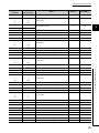
209
D1H
210
D2H
211
Default*1
Read/Write*2
CH2 Industrial shipment setting gain value (H)
0
R/W
CH3 Industrial shipment setting offset value (L)
0
R/W
D3H
CH3 Industrial shipment setting offset value (H)
0
R/W
212
D4H
CH3 Industrial shipment setting gain value (L)
0
R/W
213
D5H
CH3 Industrial shipment setting gain value (H)
0
R/W
214
D6H
CH4 Industrial shipment setting offset value (L)
0
R/W
215
D7H
CH4 Industrial shipment setting offset value (H)
0
R/W
216
D8H
CH4 Industrial shipment setting gain value (L)
0
R/W
217
D9H
CH4 Industrial shipment setting gain value (H)
0
R/W
218
DAH
CH1 User range setting offset value (L)
0
R/W
219
DBH
CH1 User range setting offset value (H)
0
R/W
220
DCH
CH1 User range setting gain value (L)
0
R/W
221
DDH
CH1 User range setting gain value (H)
0
R/W
222
DEH
CH2 User range setting offset value (L)
0
R/W
223
DFH
CH2 User range setting offset value (H)
0
R/W
224
E0H
CH2 User range setting gain value (L)
0
R/W
225
E1H
CH2 User range setting gain value (H)
0
R/W
226
E2H
CH3 User range setting offset value (L)
0
R/W
227
E3H
CH3 User range setting offset value (H)
0
R/W
228
E4H
CH3 User range setting gain value (L)
0
R/W
229
E5H
CH3 User range setting gain value (H)
0
R/W
230
E6H
CH4 User range setting offset value (L)
0
R/W
231
E7H
CH4 User range setting offset value (H)
0
R/W
232
E8H
CH4 User range setting gain value (L)
0
R/W
233
E9H
CH4 User range setting gain value (H)
0
R/W
234
EAH
to
to
System area
–
–
299
12BH
300
12CH
CH1 LPF Pass band edge frequency
0
R/W
301
12DH
CH2 LPF Pass band edge frequency
0
R/W
302
12EH
CH3 LPF Pass band edge frequency
0
R/W
303
12FH
CH4 LPF Pass band edge frequency
0
R/W
304
130H
to
to
System area
–
–
307
133H
308
134H
CH1 HPF Pass band edge frequency
0
R/W
309
135H
CH2 HPF Pass band edge frequency
0
R/W
310
136H
CH3 HPF Pass band edge frequency
0
R/W
311
137H
CH4 HPF Pass band edge frequency
0
R/W
312
138H
to
to
System area
–
–
315
13BH
Name
CHAPTER 3 SPECIFICATIONS
Address
Address
(decimal)
(hexadecimal)
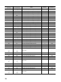
316
13CH
317
13DH
318
Default*1
Read/Write*2
CH1 BPF Pass band edge frequency (Low)
0
R/W
CH1 BPF Pass band edge frequency (High)
0
R/W
13EH
CH2 BPF Pass band edge frequency (Low)
0
R/W
319
13FH
CH2 BPF Pass band edge frequency (High)
0
R/W
320
140H
CH3 BPF Pass band edge frequency (Low)
0
R/W
321
141H
CH3 BPF Pass band edge frequency (High)
0
R/W
322
142H
CH4 BPF Pass band edge frequency (Low)
0
R/W
323
143H
CH4 BPF Pass band edge frequency (High)
0
R/W
324
144H
to
to
System area
–
–
331
14BH
332
14CH
CH1 Attenuation band width
0
R/W
333
14DH
CH2 Attenuation band width
0
R/W
334
14EH
CH3 Attenuation band width
0
R/W
335
14FH
CH4 Attenuation band width
0
R/W
336
150H
to
to
System area
–
–
999
3E7H
1000
3E8H
CH1 Logging enable/disable setting
1
R/W
1001
3E9H
CH2 Logging enable/disable setting
1
R/W
1002
3EAH
CH3 Logging enable/disable setting
1
R/W
1003
3EBH
CH4 Logging enable/disable setting
1
R/W
1004
3ECH
System area
–
–
Name
to
3EFH
1008
3F0H
CH1 Logging hold request
0
R/W
1009
3F1H
CH2 Logging hold request
0
R/W
1010
3F2H
CH3 Logging hold request
0
R/W
1011
3F3H
CH4 Logging hold request
0
R/W
1012
3F4H
to
to
System area
–
–
1015
3F7H
1016
3F8H
CH1 Logging hold flag
0
R
1017
3F9H
CH2 Logging hold flag
0
R
1018
3FAH
CH3 Logging hold flag
0
R
1019
3FBH
CH4 Logging hold flag
0
R
1020
3FCH
System area
–
–
to
to
1023
3FFH
1024
400H
CH1 Logging data setting
1
R/W
1025
401H
CH2 Logging data setting
1
R/W
1026
402H
CH3 Logging data setting
1
R/W
1027
403H
CH4 Logging data setting
1
R/W
3.5 List of Buffer Memory Addresses
to
1007
3
37
38
Address
Address
(decimal)
(hexadecimal)
1028
404H
to
to
1031
407H
1032
Default*1
Read/Write*2
System area
–
–
408H
CH1 Logging cycle setting value
4
R/W
1033
409H
CH2 Logging cycle setting value
4
R/W
1034
40AH
CH3 Logging cycle setting value
4
R/W
1035
40BH
CH4 Logging cycle setting value
4
R/W
1036
40CH
to
to
System area
–
–
1039
40FH
1040
410H
CH1 Logging cycle unit setting
1
R/W
1041
411H
CH2 Logging cycle unit setting
1
R/W
1042
412H
CH3 Logging cycle unit setting
1
R/W
1043
413H
CH4 Logging cycle unit setting
1
R/W
1044
414H
System area
–
–
Name
to
to
1047
417H
1048
418H
CH1 Logging points after trigger
5000
R/W
1049
419H
CH2 Logging points after trigger
5000
R/W
1050
41AH
CH3 Logging points after trigger
5000
R/W
1051
41BH
CH4 Logging points after trigger
5000
R/W
1052
41CH
to
to
–
–
1055
41FH
1056
420H
CH1 Hold trigger condition setting
0000H
R/W
1057
421H
CH2 Hold trigger condition setting
0000H
R/W
1058
422H
CH3 Hold trigger condition setting
0000H
R/W
1059
423H
CH4 Hold trigger condition setting
0000H
R/W
1060
424H
System area
–
–
System area
to
to
1063
427H
1064
428H
CH1 Trigger data
54
R/W
1065
429H
CH2 Trigger data
55
R/W
1066
42AH
CH3 Trigger data
56
R/W
1067
42BH
CH4 Trigger data
57
R/W
1068
42CH
to
to
System area
–
–
1071
42FH
1072
430H
Level data 0
0
R/W
1073
431H
Level data 1
0
R/W
1074
432H
Level data 2
0
R/W
1075
433H
Level data 3
0
R/W
1076
434H
Level data 4
0
R/W
CHAPTER 3 SPECIFICATIONS
Address
Address
(decimal)
(hexadecimal)
1077
435H
1078
436H
1079
Default*1
Read/Write*2
Level data 5
0
R/W
Level data 6
0
R/W
437H
Level data 7
0
R/W
1080
438H
Level data 8
0
R/W
1081
439H
Level data 9
0
R/W
1082
43AH
CH1 Trigger setting value
0
R/W
1083
43BH
CH2 Trigger setting value
0
R/W
1084
43CH
CH3 Trigger setting value
0
R/W
1085
43DH
CH4 Trigger setting value
0
R/W
1086
43EH
to
to
System area
–
–
1089
441H
1090
442H
CH1 Head pointer
0
R
1091
443H
CH2 Head pointer
0
R
1092
444H
CH3 Head pointer
0
R
1093
445H
CH4 Head pointer
0
R
1094
446H
to
to
System area
–
–
1097
449H
1098
44AH
CH1 Latest pointer
0
R
1099
44BH
CH2 Latest pointer
0
R
1100
44CH
CH3 Latest pointer
0
R
1101
44DH
CH4 Latest pointer
0
R
1102
44EH
System area
–
–
Name
to
451H
1106
452H
CH1 Number of logging data
0
R
1107
453H
CH2 Number of logging data
0
R
1108
454H
CH3 Number of logging data
0
R
1109
455H
CH4 Number of logging data
0
R
1110
456H
to
to
System area
–
–
1113
459H
1114
45AH
CH1 Trigger pointer
0
R
1115
45BH
CH2 Trigger pointer
0
R
1116
45CH
CH3 Trigger pointer
0
R
1117
45DH
CH4 Trigger pointer
0
R
1118
45EH
System area
–
–
(s)
0
R
(ms)
0
R
(µs)
0
R
to
to
1121
461H
1122
462H
1123
463H
1124
464H
CH1 Logging cycle monitor value
3.5 List of Buffer Memory Addresses
to
1105
3
39
40
Address
Address
(decimal)
(hexadecimal)
Default*1
Read/Write*2
(s)
0
R
(ms)
0
R
Name
1125
465H
1126
466H
1127
467H
(µs)
0
R
1128
468H
(s)
0
R
1129
469H
(ms)
0
R
1130
46AH
(µs)
0
R
1131
46BH
(s)
0
R
1132
46CH
(ms)
0
R
1133
46DH
(µs)
0
R
1134
46EH
to
to
–
–
1153
481H
1154
482H
0
R
1155
483H
1156
484H
1157
485H
1158
486H
1159
487H
1160
488H
1161
489H
1162
48AH
1163
48BH
1164
48CH
1165
48DH
1166
48EH
1167
48FH
1168
490H
CH2 Logging cycle monitor value
CH3 Logging cycle monitor value
CH4 Logging cycle monitor value
System area
CH1 Trigger
detection time
First two
Last two
digits of the
digits of the
year
year
Month
Day
0
R
Hour
Minute
0
R
0
R
0
R
Second
CH2 Trigger
detection time
CH3 Trigger
week
First two
Last two
digits of the
digits of the
year
year
Month
Day
0
R
Hour
Minute
0
R
0
R
0
R
Second
detection time
Day of the
Day of the
week
First two
Last two
digits of the
digits of the
year
year
Month
Day
0
R
Hour
Minute
0
R
0
R
0
R
Second
Day of the
week
First two
Last two
digits of the
digits of the
year
year
Month
Day
0
R
Minute
0
R
0
R
System area
–
–
CH4 Trigger
detection time
Hour
Day of the
1169
491H
1170
492H
to
to
1199
4AFH
1200
4B0H
CH1 Loading interrupt enable/disable setting
1
R/W
1201
4B1H
CH2 Loading interrupt enable/disable setting
1
R/W
1202
4B2H
CH3 Loading interrupt enable/disable setting
1
R/W
Second
week
CHAPTER 3 SPECIFICATIONS
Address
Address
(decimal)
(hexadecimal)
1203
4B3H
1204
4B4H
Default*1
Read/Write*2
CH4 Loading interrupt enable/disable setting
1
R/W
System area
–
–
Name
to
to
1207
4B7H
1208
4B8H
CH1 Logging load points setting value
1000
R/W
1209
4B9H
CH2 Logging load points setting value
1000
R/W
1210
4BAH
CH3 Logging load points setting value
1000
R/W
1211
4BBH
CH4 Logging load points setting value
1000
R/W
1212
4BCH
to
to
System area
–
–
1215
4BFH
1216
4C0H
CH1 This logging load pointer
-1
R
1217
4C1H
CH2 This logging load pointer
-1
R
1218
4C2H
CH3 This logging load pointer
-1
R
1219
4C3H
CH4 This logging load pointer
-1
R
1220
4C4H
System area
–
–
to
4C7H
1224
4C8H
CH1 Last logging load pointer
-1
R
1225
4C9H
CH2 Last logging load pointer
-1
R
1226
4CAH
CH3 Last logging load pointer
-1
R
1227
4CBH
CH4 Last logging load pointer
-1
R
1228
4CCH
to
to
System area
–
–
1231
4CFH
1232
4D0H
CH1 Logging load points monitor value
0
R
1233
4D1H
CH2 Logging load points monitor value
0
R
1234
4D2H
CH3 Logging load points monitor value
0
R
1235
4D3H
CH4 Logging load points monitor value
0
R
1236
4D4H
System area
–
–
to
to
1799
707H
*1
*2
3.5 List of Buffer Memory Addresses
to
1223
3
The default value is a value set after power-on or after resetting the CPU module.
This shows whether whether reading the data from or writing the data to the area with programs is possible.
R: Readable
W: Writable
41
(2) Error history (Un\G1800 to Un\G4999)
42
Address
Address
(decimal)
(hexadecimal)
1800
708H
1801
709H
to
to
1809
711H
1810
712H
1811
713H
1812
714H
1813
715H
1814
716H
1815
717H
to
to
1819
71BH
1820
71CH
to
to
1829
725H
1830
726H
to
to
1839
72FH
1840
730H
to
to
1849
739H
1850
73AH
to
to
1859
743H
1860
744H
to
to
1869
74DH
1870
74EH
to
to
1879
757H
1880
758H
to
to
1889
761H
1890
762H
to
to
1899
76BH
Default*1
Read/Write*2
Latest address of error history
0
R
System area
–
–
0
R
0
R
Name
Error code
Error time
No.1
First two
Last two
digits of the
digits of the
year
year
Month
Day
0
R
Hour
Minute
0
R
0
R
–
–
Second
System area
No.2
Same as No. 1
No.3
Same as No. 1
No.4
Same as No. 1
No.5
Same as No. 1
No.6
Same as No. 1
No.7
Same as No. 1
No.8
Same as No. 1
No.9
Same as No. 1
Day of the
week
CHAPTER 3 SPECIFICATIONS
Address
Address
(decimal)
(hexadecimal)
1900
76CH
to
to
1909
775H
1910
776H
to
to
1919
77FH
1920
780H
to
to
1929
789H
1930
78AH
to
to
1939
793H
1940
794H
to
to
1949
79DH
1950
79EH
to
to
1959
7A7H
1960
7A8H
to
to
1969
7B1H
1970
7B2H
to
4999
1387H
*1
*2
No.10
Same as No. 1
No.11
Same as No. 1
No.12
Same as No. 1
No.13
Same as No. 1
No.14
Same as No. 1
No.15
Same as No. 1
No.16
Same as No. 1
System area
Default*1
Read/Write*2
3
–
3.5 List of Buffer Memory Addresses
to
Name
–
The default value is a value set after power-on or after resetting the CPU module.
This shows whether whether reading the data from or writing the data to the area with programs is possible.
R: Readable
W: Writable
43
(3) Logging section (Un\G5000 to Un\G49999)
Address
Address
(decimal)
(hexadecimal)
5000
1388H
to
to
14999
3A97H
15000
3A98H
to
to
24999
61A7H
25000
61A8H
to
to
34999
88B7H
35000
88B8H
to
to
44999
AFC7H
45000
AFC8H
to
to
49999
C34FH
*1
*2
44
Default*1
Read/Write*2
CH1 Logging data
0
R
CH2 Logging data
0
R
CH3 Logging data
0
R
CH4 Logging data
0
R
System area
–
–
Name
The default value is a value set after power-on or after resetting the CPU module.
This shows whether whether reading the data from or writing the data to the area with programs is possible.
R: Readable
W: Writable
CHAPTER 4 PROCEDURES BEFORE OPERATION
CHAPTER 4
PROCEDURES BEFORE OPERATION
This chapter describes the procedures before operation.
Start
Module mounting
Mount the A/D converter module in any desired
configuration.
(
Page 47, Section 5.1 )
Wiring
Connects external devices to the A/D converter
module.
(
Page 53, Section 6.4 )
4
NO
Use user range settings?
YES
Offset/gain setting
To use user range settings, set the offset/gain
values.
(
Page 62, Section 7.5 )
Programming and debugging
Creates and checks a program.
45
Memo
46
CHAPTER 5 SYSTEM CONFIGURATION
CHAPTER 5
SYSTEM CONFIGURATION
This chapter describes the overall configuration, number of connectable modules, and compatible software version of
the A/D converter module.
5.1
Overall System Configuration
The following figure shows system configuration examples for using the A/D converter module.
(1) When connected to a CPU module
5
Display unit
(optional)
Power supply module
CPU module
A/D converter module
I/O module
or
intelligent function module
END cover
5.1 Overall System Configuration
(2) When connected to a head module
Power supply module
Head module
A/D converter module
I/O module
or
intelligent function module
END cover
47
5.2
Applicable System
(1) Number of connectable modules
For the number of connectable modules, refer to the following.
MELSEC-L CPU Module User's Manual (Hardware Design, Maintenance and Inspection)
MELSEC-L CC-Link IE Field Network Head Module User's Manual
(2) Compatible software version
For the compatible software versions, refer to the following.
Software
GX Works2
5.3
Version
Version 1.98C or later
Restrictions when the A/D Converter Module Is
Connected to a Head Module
The following describes the restriction when the A/D converter module is connected to a head module.
• Dedicated instructions cannot be used.
48
CHAPTER 6 INSTALLATION AND WIRING
CHAPTER 6
INSTALLATION AND WIRING
This chapter describes the installation and wiring of the A/D converter module.
6.1
Installation Environment and Installation Position
For precautions for installation environment and installation position, refer to the following.
MELSEC-L CPU Module User's Manual (Hardware Design, Maintenance and Inspection)
MELSEC-L CC-Link IE Field Network Head Module User's Manual
6
6.1 Installation Environment and Installation Position
49
6.2
Terminal Block
(1) Precautions
Tighten the terminal block screws within the following specified torque range.
Screw type
Tightening torque range
Terminal screw (M3 screw)
0.42 to 0.58N • m
Terminal block mounting screw (M3.5 screw)
0.66 to 0.89N • m
The following table lists applicable solderless terminals connected to the terminal block. When wiring, use
applicable wires and an appropriate tightening torque. Use UL-approved solderless terminals and, for
processing, use a tool recommended by their manufacturer. Sleeved solderless terminals cannot be used.
Solderless terminal
Model
R1.25-3
Tightening
torque
0.42 to 0.58N • m
Wire
Diameter
Type
Material
22 to 18 AWG
Stranded
Copper
Temperature
rating
75°C or more
(2) Signal names of the terminal block
The following table shows signal names of the terminal block.
Pin number
Signal name
1
2
CH2
V+
CH2
I+
CH1
V+
CH1
I+
CH2
V-/I-
CH4
V+
CH4
I+
V-/II+
4
V+
CH2
6
I+
7
FG
8
SLD
9
10
V-/I-
V+
CH3
V-/I-
FG
11
I+
CH3
V+
12
V+
SLD
CH3
V-/I-
CH1
3
5
CH1
V-/I-
V+
CH3
I+
CH4
V-/IFG
SLD
TRG
13
CH4
14
V-/II+
15
FG
16
SLD
17
TRG*1
18
GND
GND
*1
50
The TRG terminal (an external input terminal) is used for both the logging outside trigger of the logging function and the
external trigger conversion request (external input terminal) of the trigger conversion function.
CHAPTER 6 INSTALLATION AND WIRING
(3) Removal and installation of the terminal block
The following procedures show how to remove and install the terminal block.
(a) Removal procedure
1.
Open the terminal cover and loosen the terminal
block mounting screw.
Terminal block
mounting screw
2.
Use the terminal block fixing holes as a fulcrum and
6
remove the terminal block.
1.
Terminal block fixing hole
Fully insert the projections on the top of the
terminal block into the terminal block fixing holes
and press the terminal block until it snaps into
place.
2.
Open the terminal cover and tighten the terminal
block mounting screw.
Terminal block
mounting screw
51
6.2 Terminal Block
(b) Installation procedure
6.3
Wiring
(1) Wiring to a terminal block
The following figures show wirings to a terminal block.
(a) For the voltage input
CH1
CH1
V-/ICH2
V+
CH2
CH2
I+
CH1
V+
CH1
I+
CH2
V-/IFG
SLD
CH3
CH3
V-/ICH4
V+
CH4
CH4
I+
CH3
V+
CH3
I+
CH4
V-/IFG
SLD
TRG
GND
(b) For the current input
CH1
CH1
V-/ICH2
V+
CH2
CH2
I+
CH1
V+
CH1
I+
CH2
V-/IFG
SLD
CH3
CH3
V-/ICH4
V+
CH4
CH4
I+
CH3
V+
CH3
I+
CH4
V-/IFG
SLD
TRG
GND
52
CHAPTER 6 INSTALLATION AND WIRING
6.4
External Wiring
The following figures show the external wiring.
(1) For the voltage input
Signal source -10 to 10V
*1
Shield
*2
500k
CH1
V+
CH1
I+
CH1
V-/ICH2
V+
CH2
I+
CH2
V-/I-
CH1
CH2
*3
500k
*3
500k
*2
SLD
*4
FG
6
500k
*3
Insulation
6.4 External Wiring
*1
Shield
*2
500k
CH3
V+
CH3
I+
CH3
V-/ICH4
V+
CH4
I+
CH4
V-/I-
CH3
CH4
*3
500k
500k
*3
500k
*2
SLD
*4
*1
*2
*3
*4
FG
*3
For the wire, use the shielded twisted pair cable.
In addition, keep a distance of 150mm or more from the main circuit lines or power cables.
This indicates the input resistance of the A/D converter module.
The grounds of FG between CH1 and CH2, FG between CH3 and CH4, and the internal circuit have been isolated.
Always connect the shielded wire for each channel to the shield terminal and ground the FG terminal.
In addition, ground the FG terminal of the power supply module.
53
(2) For the current input
Signal source 0 to 20mA
*1
Shield
*4
*2
CH1
V+
CH1
I+
CH1
V-/ICH2
V+
CH2
I+
CH2
V-/I-
CH1
CH2
500k
250
*3
500k
500k
250
*3
500k
*2
SLD
*5
FG
*3
Insulation
*1
Shield
*4
*2
CH3
V+
CH3
I+
CH3
V-/ICH4
V+
CH4
I+
CH4
V-/I-
CH3
CH4
500k
250
*3
500k
500k
250
*3
500k
*2
SLD
*5
*1
*2
*3
*4
*5
54
FG
*3
For the wire, use the shielded twisted pair cable.
In addition, keep a distance of 150mm or more from the main circuit lines or power cables.
This indicates the input resistance of the A/D converter module.
The grounds of FG between CH1 and CH2, FG between CH3 and CH4, and the internal circuit have been isolated.
For the current input, always connect the terminals (V+) and (I+).
Always connect the shielded wire for each channel to the shield terminal and ground the FG terminal.
In addition, ground the FG terminal of the power supply module.
CHAPTER 6 INSTALLATION AND WIRING
(3) Outside trigger input
3.9k
1000pF 1.2k
TRG
GND
24VDC
(4) Precautions
In unused channels, if the circuit between two terminals is kept open, an undefined digital value may be output.
To prevent this phenomenon, perform any of the following measures.
• Set the A/D conversion enable/disable setting in the unused channel to A/D conversion disable.
Note that changing the A/D conversion enable/disable setting from A/D conversion enable to A/D conversion
disable reduces the sampling cycle.
6
• Short-circuit the input terminals (V+) and (V-) of the unused channel.
6.4 External Wiring
55
CHAPTER 7
VARIOUS SETTINGS
This chapter describes the setting procedures of the A/D converter module.
● After writing the setting of a new module, parameters, and auto refresh into the CPU module, reset the CPU module,
switch STOP RUN STOP RUN, or power off then on the module to validate the setting.
● After writing the switch setting to the CPU module, reset the CPU module or power off then on the module to validate the
setting.
7.1
Addition of Modules
Add the model name of an A/D converter module to use on the project.
(1) Addition procedure
Open the "New Module" window.
Project window
[Intelligent Function Module]
Item
Module Selection
Mount Position
Title setting
56
Right-click
[New Module]
Description
Module Type
Set "Analog Module".
Module Name
Select the name of the module to be connected.
Mounted Slot No.
Set the slot No. where the module is connected.
Specify start XY
The start I/O number (hexadecimal) of the module is set according to the
address
slot No. Setting any start I/O number is also possible.
Title
Set any title.
CHAPTER 7 VARIOUS SETTINGS
7.2
Switch Setting
Set the input range, operation mode, and A/D conversion timing used in each channel.
(1) Setting procedure
Open the "Switch Setting" window.
Project window
[Intelligent Function Module]
module name
[Switch Setting]
7
Description
7.2 Switch Setting
Item
Setting value
• 4 to 20mA (default value)
• 0 to 20mA
• 1 to 5V
• 0 to 5V
Input Range Setting
Set the input range used in each
• -10 to 10V
channel.
• 0 to 10V
• 4 to 20mA (Extended Mode)
• 1 to 5V (Extended Mode)
• User Range Setting (Unipolar: Current)
• User Range Setting (Bipolar: Voltage)
Drive Mode Setting
A/D Conversion Timing
Set the operation mode of the A/D
• Normal (A/D Converter Processing) Mode (default value)
converter module.
• Offset-Gain Setting Mode
Set the timing of the A/D
conversion.
• Normal (Internal Scan) (default value)
• External Trigger Convert Request (External Input Terminal)
• Internal Trigger Conversion Request (Buffer Memory)
57
7.3
Parameter Setting
Set the parameters of each channel.
By setting the parameters, the setting by programming becomes unnecessary.
(1) Setting procedure
Open the "Parameter" window.
1.
Start "Parameter".
Project window
[Intelligent Function Module]
module name
[Parameter]
Items to be selected from
pull-down menus
Items to be entered in the text boxes
2.
Double-click the item to change the setting, and input the setting value.
• Items to be input from the pull-down list
Double-click the item to be set to display the pull-down list. Select the item.
• Items to be input from the text box
Double-click the item to be set, and input the setting value.
3.
For setting CH2 to CH4, follow the operation of step 2.
Item
Setting value
A/D conversion enable/
0: Enable (default value)
disable setting
1: Disable
Reference
Page 73,
Section 8.3
0: Sampling Processing (default value)
1: Time Average
2: Count Average
Averaging process setting
3: Moving Average
4: Primary Delay Filter
5: Low Pass Filter
Basic setting
6: High Pass Filter
Page 74,
7: Band Pass Filter
Section 8.4
Time Average
2 to 5000ms (default value: 0)
Time Average/Count
Count Average
4 to 65000 times (default value: 0)
Average/Moving Average/
Moving Average
2 to 1000 times (default value: 0)
Time lag filter constant
Primary Delay
Filter
58
1 to 500 times (default value: 0)
CHAPTER 7 VARIOUS SETTINGS
Item
Attenuation band width
Low-pass filter
Digital filter
High-pass filter
setting
Setting value
40µs: 330 to 12000Hz (default value: 0Hz)
80µs: 170 to 6000Hz (default value: 0Hz)
LPF Pass band
40µs: 0 to 12000Hz (default value: 0Hz)
edge frequency
80µs: 0 to 6000Hz (default value: 0Hz)
HPF Pass band
40µs: 0 to 12000Hz (default value: 0Hz)
edge frequency
80µs: 0 to 6000Hz (default value: 0Hz)
BPF Pass band
edge frequency
Band-pass filter
(High)
BPF Pass band
edge frequency
(Low)
Warning output setting
Process alarm upper upper limit
value
Process alarm upper lower limit
value
Process alarm lower upper limit
Warning output
value
function
Process alarm lower lower limit
value
Rate alarm output setting
Rate alarm detection cycle setting
value
Reference
40µs: 0 to 12000Hz (default value: 0Hz)
Page 74,
Section 8.4
80µs: 0 to 6000Hz (default value: 0Hz)
40µs: 0 to 12000Hz (default value: 0Hz)
80µs: 0 to 6000Hz (default value: 0Hz)
0: Enable
1: Disable (default value)
-32768 to 32767 (default value: 0)
Page 102,
-32768 to 32767 (default value: 0)
Section
8.8.1
-32768 to 32767 (default value: 0)
7
-32768 to 32767 (default value: 0)
0: Enable
1: Disable (default value)
Page 105,
1 to 32000 Times (default value: 1 Times)
-3276.8 to 3276.7% (default value: 0.0%)
Rate alarm lower limit value
-3276.8 to 3276.7% (default value: 0.0%)
8.8.2
0: Disable (default value)
1: Upper and Lower Detection
Input signal error
Input signal error detection setting
2: Lower Detection
3: Upper Detection
detection
4: Disconnection Detection
Input signal error detection setting
value
Scaling enable/disable setting
Page 96,
Section 8.7
0.0 to 25.0% (default value: 5.0%)
0: Enable
1: Disable (default value)
Page 110,
Scaling upper limit value
-32000 to 32000 (default value: 0)
Section 8.9
Scaling lower limit value
-32000 to 32000 (default value: 0)
Digital clipping
Digital clipping function enable/
0: Enable
function
disable setting
1: Disable (default value)
Scaling function
Shift function
Shifting amount to conversion
value
-32768 to 32767 (default value: 0)
Page 122,
Section 8.11
Page 117,
Section 8.10
59
7.3 Parameter Setting
Rate alarm upper limit value
Section
Item
Logging enable/disable setting
Logging data setting
Setting value
Reference
0: Enable
1: Disable (default value)
0: Digital Output Value
1: Digital Operation Value (default value)
µs: 40 to 32767 (default value: 4)
Logging cycle setting value
ms: 1 to 32767 (default value: 4)
s: 1 to 3600 (default value: 4)
0: µs
Logging cycle unit specification
1: ms (default value)
2: s
Logging points after trigger
1 to 10000 (default value: 5000)
0: Logging Hold Request (default value)
Logging function
1: Level Trigger (Conditions: Rise)
Hold trigger condition setting
2: Level Trigger (Conditions: Fall)
3: Level Trigger (Conditions: Rise/Fall)
4: External Trigger
0 to 4999
(CH1 default value: 54)
(CH2 default value: 55)
Trigger data
(CH3 default value: 56)
(CH4 default value: 57)
60
Trigger setting value
-32768 to 32767 (default value: 0)
Loading interrupt enable/
0: Enabled
disable setting
1: Disabled (default value)
Logging load points setting value
10 to 10000 (default value: 1000)
Page 130,
Section 8.13
CHAPTER 7 VARIOUS SETTINGS
7.4
Auto Refresh
This function transfers data in the buffer memory to specified devices.
By the auto refresh setting, reading/writing data by programming becomes unnecessary.
(1) Setting procedure
Open the "Auto_Refresh" window.
1.
Start "Auto_Refresh".
Project window
2.
[Intelligent Function Module]
module name
[Auto_Refresh]
Click the item to be set, and input the auto refresh target device.
7
7.4 Auto Refresh
Available devices are X, Y, M, L, B, T, C, ST, D, W, R, and ZR.
When a bit device X, Y, M, L, or B is used, set the number that is divisible by 16 points (example: X10, Y120, M16). Data in
the buffer memory are stored in 16 points of devices from the set device No. (Example: When X10 is set, the data are stored
in X10 to X1F.)
61
7.5
Offset/gain Setting
When using the user range setting (uni-polar: current) or user range setting (bi-polar: voltage), configure the offset/gain
setting with the following operations.
When the industrial shipment setting is used, the offset/gain setting is not required.
The offset/gain setting can be configured by the following two types of operations.
• Setting from "Offset/Gain Setting" of GX Works2
• Setting from a program
7.5.1
Setting from "Offset/Gain Setting" of GX Works2
(1) Setting procedure
Open the "Offset/Gain Setting" window.
[Tool]
[Intelligent Function Module Tool]
1.
[Analog Module]
[Offset/Gain Setting...]
Select the module to configure the offset/gain
setting, and click the
2.
62
Click the
button.
button.
CHAPTER 7 VARIOUS SETTINGS
3.
Select Unipolar (Current) or Bipolar (Voltage) in
"Range Setting".
4.
Select the channel to use the offset/gain setting, and
click the
button.
7
5.
Input the offset value voltage or current in the target
channel terminal, and click the
button.
6.
Check that "Offset Status" is changed to "Changed",
and click the
button.
63
7.5 Offset/gain Setting
7.5.1 Setting from "Offset/Gain Setting" of GX Works2
7.
Input the gain value voltage or current in the target
channel terminal, and click the
button.
8.
Check that "Gain Status" is changed to "Changed",
and click the
button.
9.
End
64
Click the
button.
CHAPTER 7 VARIOUS SETTINGS
7.5.2
Setting from a program
(1) Setting procedure
The following describes the procedures when setting the offset/gain from a program.
Start
2)
Switch to the offset/gain setting mode.*1
Confirm that the module is in the
Offset/gain range setting mode by
checking that the RUN LED is flashing.
1)
Set Uni-polar (current: 000EH) or
Bi-polar (voltage: 000FH) to Offset/gain
range specification (Un\G46).
Turn on Channel change request (YB).
Apply the voltage or current equivalent
to the offset value to be set.
7
Check that Channel change completed
flag (XB) is on.
Set the channel to adjust the offset to
Offset/gain setting mode Offset specification
(Un\G22).
More than one channel can be set
simultaneously.
Note that Offset/gain setting mode Gain
specification (Un\G23) must be set as 0,
though.
Is it required to adjust
other channels?
YES
1)
7.5 Offset/gain Setting
7.5.2 Setting from a program
Turn on Channel change request (YB).
Turn off Channel change request (YB).
NO
Check that Channel change completed
flag (XB) is on.
Register the offset/gain setting to the
A/D converter module by turning on
User range write request (YA).
Turn off Channel change request (YB).
Check that Offset/gain setting mode
flag (XA) is off, and then turn off User
range write request (YA).
Apply the voltage or current equivalent
to the gain value to be set.
Set the channel to adjust the gain to
Offset/gain setting mode Gain specification
(Un\G23).
More than one channel can be set
simultaneously.
Note that Offset/gain setting mode
Offset specification (Un\G22) must be set as
0, though.
Check that Offset/gain setting mode
flag (XA) is on.
Is the ERR. LED on?
YES
2)
NO
Switch to the normal mode.*1
End
*1
The following shows the procedure for switching the mode (normal mode offset/gain setting mode normal mode).
• Dedicated instruction (G(P).OFFGAN) (
•
Page 286, Appendix 5.2)
Setting for Mode switching setting (Un\G158, Un\G159) and turning on then off Operating condition setting request
(Y9) (
Page 255, Appendix 2 (26))
• Intelligent function module switch setting (
Page 57, Section 7.2)
65
● Configure the offset/gain setting in accordance with the actual use situation.
● Offset and gain values are recorded in the flash memory in the A/D converter module by turning on then off User range
write request (YA). Once recorded, the values are not deleted even after the module is powered off.
When the values are written 26 times in succession, an error occurs and error code (162) is stored in Latest error code
(Un\G19) to prevent an improper write to the flash memory. Error flag (XF) turns on and the ERR. LED turns on.
● Configure the offset/gain setting in the range satisfying the following condition.
When the setting value out of the range is configured, the resolution and accuracy of the module may not fall within the
range shown in the following performance specifications.
• I/O Conversion Characteristic of A/D Conversion (
Page 279, Appendix 3)
● Offset/gain setting can be configured for multiple channels at the same time, however, the setting must be configured for
offset and gain channels separately.
When offset and gain channels are set at the same time, an error occurs. The error code (500) is stored in Latest error
code (Un\G19), Error flag (XF) turns on, then the ERR. LED turns on.
● If a value other than Bi-polar (voltage: 000FH) or Uni-polar (current: 000EH) is set to the range setting when Channel
change request (YB) is turned on, an error occurs. The error code (171) is stored in Latest error code (Un\G19), Error flag
(XF) turns on, then the ERR. LED turns on.
● When User range write request (YA) is turned on, the integrity between the offset values and gain values is checked.
When an error occurs even in one channel, offset/gain values are not written to the module.
Check the value in Latest error code (Un\G19) and perform the following procedures to reconfigure the offset/gain setting
from the beginning.
• Error Code List (
Page 221, Section 11.4)
● When the mode is switched from the offset/gain setting mode to the normal mode by the setting of the dedicated
instruction (G(P).OFFGAN) or Mode switching setting (Un\G158, Un\G159), Module READY (X0) turns off then on.
Note the initial setting process is performed at the switching of the mode if a sequence program executes the initial
setting when Module READY (X0) turns on.
● To validate the intelligent function module switch setting after writing the setting to the CPU module, reset the CPU
module or power off then on the module.
(2) Program example
(a) Device
Ex. I/O number of the A/D converter module is X/Y30 to X/Y3F (when the L26CPU-BT is used).
The following table lists the devices used in the program example.
Device
Function
M0
Offset/gain range specification (uni-polar: current)
M1
Offset/gain range specification (bi-polar: voltage)
M2
Channel selection
M3
Offset setting
M4
Gain setting
M5
Channel change command
M6
Write command to module of offset/gain setting value
M7
Mode switching
D0
Storage device for the specified channel
D1
Storage device for the setting value of the dedicated instruction (G(P).OFFGAN)
D2
Storage device for the specified user range
If the L02CPU is used, assign I/O of the A/D converter module to X/Y30 to X/Y3F so that the I/O assignment of the A/D
converter module is the same as that in the above system.
66
CHAPTER 7 VARIOUS SETTINGS
(b) Switching the mode by the dedicated instruction (G(P).OFFGAN)
This program performs the following:
• Switching the mode to the offset/gain setting mode by the dedicated instruction (G(P).OFFGAN)
• Switching the channels for which the offset/gain setting is configured
• Writing the offset/gain value to the A/D converter module
• Switching the mode back to the normal mode
Switches to the offset/gain setting mode.
Stores the setting data of the
dedicated instruction (G.OFFGAN)
in D1.
Dedicated instruction (G.OFFGAN)
Offset/gain range specification (uni-polar: current)
Stores the uni-polar (current) in D2
Offset/gain range specification (bi-polar: voltage)
Stores the bi-polar (voltage) in D2
Channel selection
Stores the target channel number
in D0.
Sets a channel to the offset setting.
7
Offset/gain range specification
Specifies the offset target channel.
Sets "0" for the gain target
channel.
Sets a channel to the gain setting.
Offset/gain range specification
7.5 Offset/gain Setting
7.5.2 Setting from a program
Specifies the gain target channel.
Sets "0" for the offset target
channel.
Switches the channel to offset/gain setting.
Turns on Channel change request
(Y3B).
Turns off Channel change request
(Y3B).
Registers the result of offset/gain setting to the module.
Turns on User range write
request (Y3A).
Turns off User range write
request (Y3A).
Switches to the normal mode.
Stores the setting data of the
dedicated instruction (G.OFFGAN)
in D1.
Dedicated instruction (G.OFFGAN)
Processing in normal mode
The part enclosed by the dotted line is common to the following three programs.
• Switching the mode by the dedicated instruction (G(P).OFFGAN)
• Switching the mode by setting Mode switching setting (Un\G158, Un\G159) and by Operating condition setting
request (Y9)
• Switching the mode by the intelligent function module switch setting
67
(c) Switching the mode by setting Mode switching setting (Un\G158, Un\G159) and by
Operating condition setting request (Y9)
Switches to the offset/gain setting mode.
Sets 4144H to Mode
switching setting 1 (U3\G158).
Sets 0964H to Mode
switching setting 2 (U3\G159).
Turns on Operating condition
setting request (Y39).
Turns off Operating condition
setting request (Y39).
Common program
Switches to the normal mode.
Sets 0964H to Mode
switching setting 1 (U3\G158).
Sets 4144H to Mode
switching setting 2 (U3\G159).
Turns on Operating condition
setting request (Y39).
Resets the operating condition setting request.
Turns off Operating condition
setting request (Y39).
Processing in normal mode
(d) Switching the mode by the intelligent function module switch setting
Only the common program is required.
68
CHAPTER 8 FUNCTIONS
CHAPTER 8
FUNCTIONS
This chapter describes the functions of the A/D converter module and the setting procedures for those functions.
For details on the I/O signals and the buffer memory, refer to the following.
• Details of I/O Signals (
Page 232, Appendix 1)
• Details of Buffer Memory Addresses (
8.1
Page 240, Appendix 2)
Modes
The A/D conversion module has the normal mode and the offset/gain setting mode. Change the mode according to the
function used.
The following describe each mode.
(1) Normal (A/D Converter Processing) Mode
The normal (A/D Converter Processing) mode normally has External Trigger Convert Request (External Input
Terminal) and Internal Trigger Conversion Request (Buffer Memory). In this manual, the description of "normal
mode" indicates External Trigger Convert Request (External Input Terminal) and Internal Trigger Conversion
Request (Buffer Memory).
8
(a) Normal
The normal A/D conversion is performed in this mode. The input analog values are converted into digital
values.
Conversion Request (Buffer Memory)
The trigger conversion is performed in this mode. The input analog values are converted into digital values
according to the input of Trigger conversion request.
For details on the trigger conversion function, refer to the following.
• Trigger Conversion Function (
Page 162, Section 8.14)
(2) Offset/gain setting mode
The offset/gain setting is performed in this mode.
For details on the offset/gain setting, refer to the following.
• Offset/gain Setting (
Page 62, Section 7.5)
69
8.1 Modes
(b) External Trigger Convert Request (External Input Terminal) and Internal Trigger
(3) Mode transitions
The following figure and table describe the transition condition for each mode.
At the power-on or at the
reset of the CPU module
5)
2)
*1
1)
4)
Trigger
conversion mode
Normal (A/D Converter
Processing) Mode
No.
1)
2)
Offset-Gain
Setting Mode
3)
Transition condition
Set "Drive Mode Setting" to "Normal (A/D Converter Processing) Mode" and "A/D Conversion Timing" to "Normal (Internal
Scan)" in "Switch Setting" of GX Works2.
Set "Drive Mode Setting" to "Offset-Gain Setting Mode" and "A/D Conversion Timing" to "Normal (Internal Scan)" in "Switch
Setting" of GX Works2.
Perform G(P).OFFGAN (Argument
S
: 0 (normal output mode)).
Set the following values for Mode switching setting (Un\G158, Un\G159) and turn on then off Operating condition setting
3)
request (Y9).
• Un\G158: 0964H
• Un\G159: 4144H
Perform G(P).OFFGAN (Argument
S
: 1 (offset/gain setting mode)).
Set the following values for Mode switching setting (Un\G158, Un\G159) and turn on then off Operating condition setting
4)
request (Y9).
• Un\G158: 4144H
• Un\G159: 0964H
Set "Drive Mode Setting" to "Normal (A/D Converter Processing) Mode" and "A/D Conversion Timing" to "External Trigger
5)
Convert Request (External Input Terminal)" or "Internal Trigger Conversion Request (Buffer Memory)" in "Switch Setting" of
GX Works2.
70
CHAPTER 8 FUNCTIONS
8.2
Processing Each Function
The functions are processed in the order shown below. If multiple functions are enabled, the output of the first
processed function is used as the input of the next function.
Analog input
(CH1 to CH4)
Trigger
conversion
function
Input signal
error detection
function
Averaging
processing
Digital clipping
function
Scaling function
Shift function
8
Difference
conversion
function
Warning output
function
Process alarm
8.2 Processing Each Function
Rate alarm
Logging function
CH Digital output value
(Un\G11 to Un\G14)
CH Maximum value
(Un\G30, Un\G32,
Un\G34, Un\G36)
CH
Digital operation value
(Un\G54 to Un\G57)
CH Minimum value
(Un\G31, Un\G33,
Un\G35, Un\G37)
71
(1) Digital output values
These are digital values after sampling processing or averaging processing has been performed.
(2) Digital operation values
These are values obtained by operating the digital output value using the digital clipping function, scaling
function, shift function, or difference conversion function.
(3) Maximum and minimum values
The maximum and minimum values of the digital operation values are stored.
● If averaging processing (time average/count average) is performed, the digital values are stored on the averaging
process cycle.
● If the following processing is performed, the digital values are stored on the sampling cycle.
• Sampling processing
• Moving average
• Time lag filter
• Low pass filter
• High pass filter
• Band pass filter
72
CHAPTER 8 FUNCTIONS
8.3
A/D Conversion Enable/Disable Function
Set whether to enable or disable A/D conversion for each channel.
(1) Setting procedure
Set "A/D conversion enable/disable setting" to "0: Enable".
Project window
[Intelligent Function Module]
module name
[Parameter]
8
8.3 A/D Conversion Enable/Disable Function
73
8.4
A/D Conversion Method
One of the following A/D conversion methods can be set for each channel.
• Sampling processing
• Averaging processing (time average, count average, moving average)
• Time lag filter
• Digital filter (low pass filter, high pass filter, band pass filter)
(1) Overview of A/D conversion
A/D conversion is performed per two channels. A/D conversion is performed for CH1 and CH3 simultaneously,
then for CH2 and CH4 simultaneously.
(a) Conversion speed
Conversion speed is the time taken for the A/D converter module to convert analog input values into digital
values.
(b) Sampling cycle
Sampling cycle is the internal A/D conversion cycle. This cycle varies depending on the setting of the number
of A/D conversion-enabled channels (
Page 73, Section 8.3).
The following table lists the sampling cycles depending on the setting of A/D conversion-enabled channels.
A/D conversion enable/disable
A/D conversion enable/disable
setting for CH1 and CH3
setting for CH2 and CH4
Conversion enabled for CH1 or CH3, or both
channels
Conversion disabled for both channels
Conversion disabled for both channels
Conversion enabled for CH2 or CH4, or both
channels
Conversion enabled for CH1 or CH3, or both
Conversion enabled for CH2 or CH4, or both
channels
channels
Sampling cycle
40µs
40µs
80µs
A/D conversion can be set whether to enable or disable for each channel. Disabling the A/D conversion for unused channels
reduces the sampling cycle.
• When A/D conversion is disabled for CH1 to CH3, CH Digital output value (Un\G11 to Un\G13) is updated every
80µs.
• When A/D conversion is enabled for CH1 and CH3 only, CH Digital output value (Un\G11 to Un\G13) is updated
every 40µs.
74
CHAPTER 8 FUNCTIONS
(c) Conversion cycle
Digital output values are updated on the conversion cycle of sampling cycle, time average, count average,
moving average, time lag filter, low pass filter, high pass filter, or band pass filter.
The following table lists the conversion cycles of each A/D conversion method.
A/D conversion
Conversion cycle
method
Sampling processing
Sampling cycle
*1
Time average
The time set to Time Average/Count Average/Moving Average/Time lag filter constant
Sampling cycle
Sampling cycle
Count average
(The number set to Time Average/Count Average/Moving Average/Time lag filter constant) × Sampling cycle
Moving average
Sampling cycle
Time lag filter
Sampling cycle
Low pass filter
Sampling cycle
High pass filter
Sampling cycle
Band pass filter
Sampling cycle
*1
Values after the decimal point are rounded off.
8
8.4 A/D Conversion Method
75
(2) Sampling processing
The A/D converter module executes the A/D conversion of the analog input value sequentially and stores the
digital output value to the buffer memory on the sampling cycle.
Ex. The sampling cycle is 40µs under the following settings.
• Averaging process setting: Sampling processing
• A/D conversion-enabled channels: CH1, CH3
Sampling
cycle: 40 s
Sampling
cycle: 40 s
Sampling
cycle: 40 s
Sampling
cycle: 40 s
Conversion
processing for
CH1/CH3
Conversion
processing for
CH1/CH3
Conversion
processing for
CH1/CH3
Conversion
processing for
CH1/CH3
CH1 Digital output value (Un\G11)
Conversion
value for
CH1
Conversion
value for
CH1
Conversion
value for CH1
CH3 Digital output value (Un\G13)
Conversion
value for CH3
Conversion
value for CH3
Conversion
value for CH3
A/D conversion processing
of the module
Ex. The sampling cycle is 80µs under the following settings.
• Averaging process setting: Sampling processing
• A/D conversion-enabled channels: CH1, CH2
Sampling cycle: 80 s
Sampling cycle: 80 s
Conversion speed
Conversion speed
Conversion speed
Conversion speed
for CH1/CH3 (40 s) for CH2/CH4 (40 s) for CH1/CH3 (40 s) for CH2/CH4 (40 s)
A/D conversion processing
of the module
CH1 Digital output value (Un\G11)
CH2 Digital output value (Un\G12)
76
Conversion
processing
for CH1
Conversion
processing
for CH2
Conversion
value for CH1
Conversion value for CH2
Conversion
processing
for CH1
Conversion
value for CH1
Conversion
processing
for CH2
Conversion
value for CH1
Conversion value for CH2
CHAPTER 8 FUNCTIONS
(3) Averaging processing
The A/D converter module performs averaging processing on the digital output values and stores the average
values to the buffer memory. The following processing is provided for averaging processing.
• Time average
• Count average
• Moving average
(a) Time average
The A/D converter module executes the A/D conversion for set time, and stores the average of the total value
excluding the maximum and the minimum values to the buffer memory.
The processing count in the setting time varies depending on the sampling cycle.
Number of
processing
=
Set time
Sampling cycle
Ex. The processing count for the following settings is calculated below:
Item
Number of channels used (the number of channels set to
A/D conversion enabled)
Setting time
Setting
4 channels (CH1 to CH4)
15ms
8
15 0.08 = 187.5 (times) ... Values after the decimal point are omitted.
Conversion is processed 187 times and the averaged value is output.
(b) Count average
The A/D converter module executes the A/D conversion for set time, and stores the average of the total value
excluding the maximum and the minimum values to the buffer memory.
The time taken for storing the count average value to the buffer memory varies depending on the sampling
cycle.
Processing time = Set number of times × Sampling cycle
Ex. The processing count for the following settings is calculated below:
Item
Number of channels used (the number of channels set to
A/D conversion enabled)
Set number of times
Setting
4 channels (CH1 to CH4)
20 times
20 × 0.08 = 1.6 (ms) An average value is output every 1.6 ms.
Because the count average requires a sum of at least two counts, not counting the maximum and minimum values, the set
number of times should be four or more.
77
8.4 A/D Conversion Method
The valid lower limit setting value for the time average is calculated by "(minimum processing count of 4) × (sampling cycle)".
When 4 (maximum) channels are used: 80µs × 4 = 320µs
(c) Moving average
The A/D converter module averages digital output values of set number of times which are measured every
sampling cycle, and stores them in the buffer memory. Since the averaging processing is performed on a
moving set of sampling processing, the latest digital output values can be obtained.
The following figure shows the moving average processing of when the set number of times is four.
Sampling cycle
Digital output value
32000
2)
3)
4)
5)
1)
6)
7)
8)
9)
12)
10) 11)
16000
1st storage (a)
2nd storage (b)
3rd storage (c)
0
CH1 Digital output
value (Un\G11)
Time [ms]
0
(a)
(b)
(c)
ON
A/D conversion
completed flag (XE)
Data transition in buffer memory
78
1st storage (a)
2nd storage (b)
3rd storage (c)
1) + 2) + 3) + 4)
2) + 3) + 4) + 5)
3) + 4) + 5) + 6)
4
4
4
CHAPTER 8 FUNCTIONS
(4) Time lag filter
The A/D converter module outputs digital output values with smoothed noise.
To use the time lag filter, set the time lag filter for averaging processing and the time lag filter constant.
Time constant = Sampling cycle × Time lag filter constant
The A/D converter module performs time lag filter processing using the time constant calculated by multiplying
the set time lag filter constant by the sampling cycle.
The following are the relational expressions of time constants and digital output values. Set CH Time
Average/Count Average/Moving Average/Time lag filter constant (Un\G1 to Un\G4) according to application.
[n = 1*1]
Yn = 0
[n = 2]
Yn = yn-1 +
t
t + TA
(yn - yn-1)
[n 3]
t
t + TA
Yn = Yn-1 +
Yn
Yn-1
n
TA
: Present digital output value
yn
: Digital output value before smoothing
: Last digital output value
: Number of sampling
: Time constant
yn-1
t
: Last digital output value before smoothing
: Conversion time (Sampling cycle)
8
A/D conversion completed flag (XE) turns on when n 2.
[Digital output value when the analog input value is changed from 0 to 1V]
The following figure shows the change of the digital output value with the input range of 0 to 10V and the time
constant (Sampling cycle × Time lag filter constant) of 20ms.
After 20ms from the analog input value becomes 1V, the digital output value reaches 63.2% of the digital output
value of when the sampling processing is selected.
Analog input value
Digital output value
1.2
3840
1.0
3200
2560
0.8
63.2%
Analog input value (V) 0.6
1920 Digital output value
0.4
1280
0.2
640
0
0
0
20
Time (ms)
79
8.4 A/D Conversion Method
*1
(yn - Yn-1)
[Digital output value of when the analog input value change forms a waveform containing ringing]
The following figure shows the change ratio of the digital output value with the input range of 0 to 10V and the
moving average processing of 16 times under the following conditions.
• Sampling cycle × Time lag filter constant (Time constant): 40ms
• Sampling cycle × Time lag filter constant (Time constant): 20ms
• Moving average processing: 16 times
Analog input value
Digital output value (Moving
average processing:16 times)
Digital output value (Time constant setting: 20ms)
Digital output value (Time constant setting: 40ms)
1.2
3840
1.0
3200
0.8
2560
0.6
1920
0.4
1280
0.2
640
Analog input value (V)
Digital output value
0
0
0
Time (ms)
(5) Digital filter
When data is obtained from a sensor connected with the A/D converter module, the converted values may be
output with unnecessary noise from the sensor. This function removes noise by attenuating unnecessary
frequency data. Thus, only digital values with target frequency data can be obtained.
Select the low pass filter, the high pass filter, or the band pass filter according to a sensor connected. When the
high pass filter or the band pass filter is used, direct signals are eliminated.
Direct current
0
0
After low pass filter
Low frequency
0
0
Mid frequency
0
After band pass filter
Waves containing direct current,
low frequency, mid frequency,
and high frequency
High frequency
0
0
After high pass filter
80
CHAPTER 8 FUNCTIONS
(a) Characteristics and advantages of the digital filters
The following table lists the characteristics and advantages of the digital filters.
Filter type
Characteristic
Advantage
[dB]
• Performed every sampling cycle (conversion cycle).
0
frequency pass filter)
Attenuation rate
Low pass filter (low
• This filter attenuates frequency signals between a
pass band edge frequency and the pass band edge
frequency + an attenuation band width, cutting off
Pass band (*1)
Attenuation
band (*2)
Attenuation
band width
Stop band (*3)
-53
0
Pass band edge f [Hz]
frequency + Attenuation
band width
Pass band
edge
frequency
[dB]
filter)
• This filter attenuates frequency signals between a
Attenuation rate
(high frequency pass
same as, or lower than 1/2 of Sampling frequency*4.
• Performed every sampling cycle (conversion cycle).
0
High pass filter
frequency signals higher than the attenuation band.
• The target frequency of the filtering should be the
pass band edge frequency and the pass band edge
Stop band (*3)
Attenuation
band (*2)
frequency - an attenuation band width, cutting off
Pass band (*1)
Attenuation
band width
-53
Pass band edge
Pass band
f [Hz]
frequency
edge frequency
- Attenuation band width
0
frequency signals lower than the attenuation band.
• The target frequency of the filtering should be the
same as, or lower than 1/2 of Sampling frequency*4.
8
[dB]
Band pass filter
(band frequency
pass filter)
Attenuation
rate
0
Pass
band
(*1)
Stop
band
(*3)
• Performed every sampling cycle (conversion cycle).
Attenuation
band
(*2)
Attenuation
band width
• Both a low pass filter (low frequency pass filter) and a
Stop
band
(*3)
Attenuation
band width
-53
0 Pass band
Pass band
edge
edge
frequency (Low) frequency
- Attenuation
(Low)
band width
*1
*2
*3
*4
Pass band
edge
frequency
(High)
Pass band
f [Hz]
edge
frequency (High)
+ Attenuation
band width
high pass filter (high frequency pass filter) are set
simultaneously. As a result, only frequency within a
specified bandwidth passes this filter.
• The target frequency of the filtering should be the
same as, or lower than 1/2 of Sampling frequency*4.
Pass band: Frequency bandwidth which passes through the filter without being attenuated
Attenuation band: Frequency bandwidth whose attenuation rate through the filter is in a transition state
Stop band: Frequency bandwidth attenuated by the filter
Sampling frequency: The reciprocal of the sampling cycle (1/Sampling cycle)
81
8.4 A/D Conversion Method
Attenuation
band
(*2)
(b) How to use the digital filters
To use the digital filtering function, set a digital filter (Low pass filter (5), High pass filter (6), or Band pass filter
(7)) to Averaging process setting (Un\G24), set a pass band edge frequency and an attenuation band width,
and turn on then off Operating condition setting request (Y9).
The following table lists the setting ranges for each digital filter.
Digital filter
Buffer memory
Description of setting and setting range
Averaging process setting
Set a relevant bit of a channel where filter processing is necessary to Low
(Un\G24)
pass filter (5).
Set a pass band edge frequency for the low pass filter.
The following table shows the setting range of the frequency.
When a frequency out of the setting range is set, an error occurs. Error code
(230) is stored in Latest error code (Un\G19), Error flag (XF) turns on, then
the ERR. LED turns on.
CH LPF Pass band edge
Sampling cycle
frequency (Un\G300 to Un\G303)
40µs
Low pass filter
Setting range
• Pass band edge frequency + Attenuation band
width 12000
• 330 attenuation band width
• 0 pass band edge frequency
• Pass band edge frequency + Attenuation band
80µs
width 6000
• 170 attenuation band width
• 0 pass band edge frequency
Set an attenuation band width for each channel.
Set an attenuation band. The sum of an LPF pass band edge frequency and
CH Attenuation band width
the attenuation band width becomes the boundary between the attenuation
(Un\G332 to Un\G335)
band and a stop band.
The frequency higher than the sum of the LPF pass band edge frequency
and attenuation band width is attenuated.
Averaging process setting
Set a relevant bit of a channel where filter processing is necessary to High
(Un\G24)
pass filter (6).
Set a pass band edge frequency for the high pass filter.
The following table shows the setting range of the frequency.
When a frequency out of the setting range is set, an error occurs. Error code
(231) is stored in Latest error code (Un\G19), Error flag (XF) turns on, then
the ERR. LED turns on.
CH HPF Pass band edge
Sampling cycle
frequency (Un\G308 to Un\G311)
40µs
High pass filter
Setting range
• 0<Pass band edge frequency - Attenuation
band width
• 330 Attenuation band width
• Pass band edge frequency 12000
• 0<Pass band edge frequency - Attenuation
80µs
band width
• 170 attenuation band width
• Pass band edge frequency 6000
Set an attenuation band width for each channel.
Set an attenuation band width. The difference between an HPF pass band
CH Attenuation band width
edge frequency and the attenuation band width becomes the boundary
(Un\G332 to Un\G335)
between the attenuation band and a stop band.
The frequency lower than the difference between the HPF pass band edge
frequency and attenuation band width is attenuated.
82
CHAPTER 8 FUNCTIONS
Digital filter
Buffer memory
Description of setting and setting range
Averaging process setting
Set a relevant bit of a channel where filter processing is necessary to Band
(Un\G24)
pass filter (7).
Set a pass band edge frequency for the band pass filter.
The following table shows the setting range of the frequency.
When frequency out of the setting range is set, an error occurs. Error code
(232) is stored in Latest error code (Un\G19), Error flag (XF) turns on, then
the ERR. LED turns on.
Sampling cycle
• Pass band edge frequency (High) + Attenuation
• CH BPF Pass band edge
band width 12000
frequency (Low) (Un\G316,
Un\G318, Un\G320, Un\G322)
• CH BPF Pass band edge
Setting range
• 0<Pass band edge frequency (Low) 40µs
Attenuation band width
• 330 attenuation band width
frequency (High) (Un\G317,
• Pass band edge frequency (Low) < Pass band
Un\G319, Un\G321, Un\G323)
edge frequency (High)
• Pass band edge frequency (High) + Attenuation
Band pass filter
band edge 6000
• 0<Pass band edge frequency (Low) 80µs
Attenuation band width
• 170 attenuation band width
• Pass band edge frequency (Low) < Pass band
edge frequency (High)
8
This setting is common to both lower and higher sides.
Set an attenuation band width for each channel.
• The difference between a BPF pass band edge frequency (Low) and the
attenuation band width is the boundary between the lower attenuation
(Un\G332 to Un\G335)
The frequency lower than the difference between the BPF pass band edge
frequency (Low) and attenuation band width is attenuated.
• The sum of the BPF pass band edge frequency (High) and attenuation
band width is the boundary between the higher attenuation band and stop
band.
The frequency higher than the sum of the BPF pass band edge frequency
(High) and attenuation band width is attenuated.
83
8.4 A/D Conversion Method
band and a stop band.
CH Attenuation band width
(c) Attenuation characteristic and response time
The AD converter module uses FIR filters as the digital filters.
A FIR filter has linear phase response, provides system stability, and displays a steep attenuation
characteristic, but takes time to respond.
[Attenuation characteristic]
The digital filters of the A/D converter module set the boundary frequency between a pass band and an
attenuation band. Also the filters set the boundary frequency between the attenuation band and a stop band
(pass band edge frequency + attenuation band width).
An attenuation characteristic is composed of the attenuation band and the attenuation rate (-53(dB)) shown
with the pass band edge frequency and the pass band edge frequency + the attenuation band width.
Ex. The following figure shows the attenuation characteristic (the attenuation band and attenuation rate)
when the low pass filter is used.
[dB]
Attenuation rate
0
Stop band
Pass band
Attenuation band
Attenuation band width
-53
0
84
Pass band edge
frequency
Pass band edge frequency f [Hz]
+ Attenuation band width
CHAPTER 8 FUNCTIONS
[Response time]
Response time is the time taken to obtain an attenuation rate (-53(dB)) after filter processing is started. The
following figure shows response time.
Ex. The output waveform obtained after an input SIN wave passed through a digital filter.
[Amplitude]
Input wave 0
[Amplitude] 0
[ms]
Wave after
digital filter 0
0
Response
time
Start filter
processing
[ms]
Timing where the attenuation
characteristic is reached
8
Response time is obtained from the following calculation.
Response time = Sampling cycle × Filter degree*1
A filter degree is a value that the system internally derives from a pass band edge frequency and a conversion frequency
of the A/D converter module (reciprocal of the sampling cycle). The range of a filter degree is 1 to 255.
Decimals of the filter degree are raised to the next whole number to preserve its attenuation characteristic. If the value
becomes an even number, 1 is added to the value so that the value becomes an odd number and that phase shifting is
prevented.
*1
• Filter degree = ((Filter degree + 1) / 2)*1 × 2 + 1
Decimals are raised to the next whole number.
85
8.4 A/D Conversion Method
*1
(d) Setting example of when a digital filter is set
The following shows the setting example of when a digital filter is set.
Ex. 1: When the low pass filter is used under the following conditions
• To input a SIN wave, the frequency of analog inputs is changed from 100Hz to 400Hz, and 400Hz to
1000Hz.
• Sampling cycle: 80µs (Sampling frequency: 12.5kHz)
• Averaging process setting: Low pass filter
• Pass band edge frequency: 140Hz
• Attenuation band width: 200Hz
The response time is 16.72ms (= Sampling cycle (80µs) × Filter degree (209)).
[digit]
Input wave
0
0
[digit]
100Hz
400Hz
Frequency that
passes through
Frequency that is
attenuated
1000Hz
Frequency that is
attenuated
[Time]
Response time
(16.72ms)
Wave after
digital filtering 0
0
86
[Time]
CHAPTER 8 FUNCTIONS
Ex. 2: When the high pass filter is used under the following conditions
• To input a SIN wave, the frequency of analog inputs is changed from 100Hz to 400Hz, and 400Hz to
1000Hz.
• Sampling cycle: 80µs (Sampling frequency: 12.5Hz)
• Averaging process setting: High pass filter
• Pass band edge frequency: 340Hz
• Attenuation band width: 200Hz
The response time is 16.72ms (= Sampling cycle (80µs) × Filter degree (209)).
[digit]
Input wave
0
100Hz
0
[digit]
Frequency that is
attenuated
400Hz
Frequency that
passes through
1000Hz
Frequency that
passes through
[Time]
Response time
(16.72ms)
Wave after
digital filtering 0
8
0
[Time]
8.4 A/D Conversion Method
87
Ex. 3: When the band pass filter is used under the following conditions
• To input a SIN wave, the frequency of analog inputs is changed from 100Hz to 400Hz, and 400Hz to
1000Hz.
• Sampling cycle: 80µs (Sampling frequency: 12.5Hz)
• Averaging process setting: Band pass filter
• Pass band edge frequency (Low): 320Hz
• Pass band edge frequency (High): 580Hz
• Attenuation band width: 200Hz
The response time is 16.72ms (= Sampling cycle (80µs) × Filter degree (209)).
[digit]
Input wave
0
0
[digit]
100Hz
Frequency that is
attenuated
400Hz
Frequency that
passes through
1000Hz
Frequency that is [Time]
attenuated
Response time
(16.72ms)
Wave after
digital filtering 0
0
88
[Time]
CHAPTER 8 FUNCTIONS
(6) Setting procedure
(a) Sampling processing
1.
Set "A/D conversion enable/disable setting" to "0: Enable".
Project window
2.
[Intelligent Function Module]
module name
[Parameter]
Set "Averaging process setting" to "0: Sampling Processing".
8
8.4 A/D Conversion Method
89
(b) Averaging processing and Time lag filter
Ex. When "Averaging process setting" is set to "1: Time Average"
1.
Set "A/D conversion enable/disable setting" to "0: Enable".
Project window
[Intelligent Function Module]
module name
[Parameter]
2.
Set "Averaging process setting" to "1: Time Average".
3.
Set "Time Average/Count Average/Moving Average/Time lag filter constant" to an averaging
processing value.
Setting item
Time average
90
Setting range
2 to 5000ms
Count average
4 to 65000 times
Moving average
2 to 1000 times
Time lag filter
1 to 500 times
CHAPTER 8 FUNCTIONS
(c) Low pass filter
1.
Set "A/D conversion enable/disable setting" to "0: Enable".
Project window
[Intelligent Function Module]
module name
[Parameter]
2.
Set "Averaging process setting" to "5: Low Pass Filter".
3.
Set "LPF Pass band edge frequency" to a pass band edge frequency.
4.
Set "Attenuation band width" to an attenuation band width. The difference between the HPF pass
band edge frequency and attenuation band width is the boundary between the attenuation band
and a stop band. The frequency lower than the difference between the HPF pass band edge
frequency and attenuation band width is attenuated.
8
8.4 A/D Conversion Method
91
(d) High pass filter
1.
Set "A/D conversion enable/disable setting" to "0: Enable".
Project window
[Intelligent Function Module]
module name
[Parameter]
2.
Set "Averaging process setting" to "6: High Pass Filter".
3.
Set "HPF Pass band edge frequency" to a pass band edge frequency.
4.
Set "Attenuation band width" to an attenuate band width. The difference between the HPF pass
band edge frequency and attenuation band width is the boundary between the attenuation band
and a stop band. The frequency lower than the difference between the HPF pass band edge
frequency and attenuation band width is attenuated.
92
CHAPTER 8 FUNCTIONS
(e) Band pass filter
1.
Set "A/D conversion enable/disable setting" to "0: Enable".
Project window
[Intelligent Function Module]
module name
[Parameter]
2.
Set "Averaging process setting" to "7: Band Pass Filter".
3.
Set "BPF Pass band edge frequency (Low)" and "BPF Pass band edge frequency (High)" to pass
band edge frequencies.
4.
Set an attenuation band width.
93
8
8.4 A/D Conversion Method
The difference between the BPF pass band edge frequency (Low) and attenuation band width is
the boundary between the lower attenuation band and a stop band.
The frequency lower than the difference between the BPF pass band edge frequency (Low) and
attenuation band width is attenuated.
The sum of the BPF pass band edge frequency (High) and attenuation band width is the boundary
between the higher attenuation band and a stop band.
The frequency higher than the sum of the BPF pass band edge frequency (High) and attenuation
band width is attenuated.
8.5
Input Range Extended Mode Function
This function extends the input range of 4 to 20mA and that of 1 to 5V.
Normal mode
Input range
setting
Input range
4 to 20mA
4 to 20mA
Extended mode
Input range
setting
Input range
4 to 20mA
(Extended mode)
0.0 to 20.0mA
1 to 5V
(Extended mode)
0.0 to 5.0V
Digital output value
Digital output value
-8000 to 32000
0 to 32000
1 to 5V
1 to 5V
(1) Overview
• An analog input value can be monitored even when an error in measurement is great and the value is less
than 4mA or 1V in the input range of 4 to 20mA and 1 to 5V.
• Although the slope of the I/O characteristic in the extended mode is the same as that in the normal mode,
the upper limit value and the lower limit value of the input range and the digital output value are extended.
• The resolution is the same as that the input range of 4 to 20mA and 1 to 5V has. Therefore, A/D conversion
with higher resolution than that of the input range of 0 to 20mA and 0 to 5V is achieved.
Input/output characteristic in 4 to 20mA (Extended mode)
Input/output characteristic in 1 to 5V (Extended mode)
Digital output value
Digital output value
32767
32000
32767
32000
4 to 20mA
(Extended mode)
4 to 20mA
1 to 5V
Extended the mode
to 0 to 20mA.
1 to 5V
(Extended mode)
0
0
-8000
-8768
0
4
10
20
-8000
-8768
0
Analog input current (mA)
1
Extended
Extended
5
Analog input voltage (V)
Extended
For details on the current input characteristic and the voltage input characteristic, refer to the following.
• I/O Conversion Characteristic of A/D Conversion (
Page 279, Appendix 3)
(2) Setting procedure
Set with the input range setting of the switch setting.
When the input range extended mode function is used with the scaling function, the shift function, and the difference
conversion function, digital output values may exceed the range of -32768 to 32767.
In that case, the value fixed at the upper limit value (32767) or the lower limit value (-32768) is stored as a digital operation
value.
• Processing Each Function (
94
Page 71, Section 8.2)
CHAPTER 8 FUNCTIONS
8.6
Maximum Value/Minimum Value Hold Function
The A/D converter module stores the maximum and minimum values of the digital operation values for each channel in
the buffer memory.
Values are refreshed every conversion cycle.
For the conversion cycle, refer to the following.
• Conversion cycle (
Page 75, Section 8.4 (1) (c))
For the buffer memory address where the values are stored, refer to the following.
• List of Buffer Memory Addresses (
Page 32, Section 3.5)
(1) Resetting the maximum value and the minimum value
• The maximum value and the minimum value are refreshed with present values by turning on then off
Maximum value/minimum value reset request (YD).
• The maximum value and the minimum value are refreshed with digital operation values by turning on then off
Operating condition setting request (Y9).
(2) Target value for maximum value and minimum value
The maximum and minimum values of digital operation values are stored in the buffer memory.
For details, refer to the following.
• Processing Each Function (
Page 71, Section 8.2)
8
8.6 Maximum Value/Minimum Value Hold Function
95
8.7
Input Signal Error Detection Function
This function detects an analog input value which exceeds a setting range.
Detected
Not detected
Included
Analog
input value
Input signal error
detection upper
limit value
CH1 Analog input
value
Normal input value
Input signal error
detection lower
limit value
Time
ON
CH1 Input signal error
detection flag (Un\G49.b0)
OFF
ON
Input signal error detection signal (XC)
CH1 A/D conversion
completed flag (Un\G10.b0)
OFF
ON
OFF
ON
Error clear request (YF)
96
OFF
CHAPTER 8 FUNCTIONS
(1) Detection condition
Detection
Detection condition
method
Analog
input value
Upper lower limit
detection
At the input signal error detection upper limit value or
above, and at the input signal error detection lower limit
Input signal error
detection upper
limit value
Error
detection
value or below
Input signal error
detection lower
limit value
Error
detection
Time
Analog
input value
Lower limit
detection
At the input signal error detection lower limit value or
Input signal error
detection upper
limit value
No error
detection
below
Input signal error
detection lower
limit value
8
Error
detection
Time
Upper limit
detection
At the input signal error detection upper limit value or
Input signal error
detection upper
limit value
Error
detection
above
Input signal error
detection lower
limit value
No error
detection
Time
Disconnection
detection
Performs disconnection detection. For details, refer to the following.
• Disconnection detection (
Page 98, Section 8.7 (1) (a))
97
8.7 Input Signal Error Detection Function
Analog
input value
(a) Disconnection detection
This function provides simple disconnection detection in combination with the input range extended mode
function. When either of following conditions is satisfied, Input signal error detection flag (Un\G49) turns on and
a disconnection occurs.
Input range
Disconnection detection condition
4 to 20mA (Extended mode)
Input analog value 2mA
1 to 5V (Extended mode)
Input analog value 0.5V
Analog
input value
2mA or 0.5V
Error
detection
Time
The setting for CH Input signal error detection setting value (Un\G142 to Un\G145) is ignored.
(2) Notifying input signal error
When an analog input value satisfies a preset detection condition of the detection method, the error is notified
with Input signal error detection flag (Un\G49), Input signal error detection signal (XC) and flashing of ALM LED.
In addition, alarm code (11
) is stored in Latest error code (Un\G19). The value of the alarm code varies
depending on the condition (upper limit, lower limit, or disconnection detection) under which an error of the
analog input value is detected.
11
Fixed
The channel where an input signal error has occurred
The detection method
1: Upper limit detection
2: Lower limit detection
3: Disconnection detection
For details on the alarm codes, refer to the following.
• Alarm Code List (
Page 226, Section 11.5)
(3) Operation of the input signal error detection function
An error-detected channel holds the digital value just before the error was detected, and A/D conversion
completed flag (Un\G10) and A/D conversion completed flag (XE) turn off.
When the analog input value returns within the setting range, A/D conversion resumes regardless of the reset on
Input signal error detection flag (Un\G49) and Input signal error detection signal (XC). A/D conversion completed
flag (Un\G10) of this channel turns on again after the first refresh. (ALM LED remains flashing.)
(4) Detection cycle
This function works on the sampling cycle.
98
CHAPTER 8 FUNCTIONS
(5) Clearing input signal errors
After the analog input value returns within the setting range, turn on then off Error clear request (YF).
The A/D converter module arranges the following status when an input signal error is cleared.
• Clears Input signal error detection flag (Un\G49).
• Turns off Input signal error detection signal (XC).
• Turns off the ALM LED.
• Clears alarm code (11
) stored in Latest error code (Un\G19).
(6) Setting method of the input signal error detection upper limit value and the
input signal error detection lower limit value
Set the input signal error detection upper limit value and input signal error detection lower limit value to a value
based on the input signal error detection setting value. (Set in a unit of 1 (0.1%).)
Both the input signal error detection upper limit value and the input signal error detection lower limit value reflect
the input signal error detection setting value.
(a) Input signal error detection upper limit value
This value is calculated by adding "Input range width (gain value - offset value) × Input signal error detection
setting value" to a gain value. The input signal error detection setting value is calculated by the following
formula.
Input signal error detection
setting value
=
Input signal error detection
upper limit value
-
Gain value of each range
Gain value of each range
-
Offset value of each range
8
1000
(b) Input signal error detection lower limit value
8.7 Input Signal Error Detection Function
This value is calculated by subtracting "Input range width (gain value - offset value) × Input signal error
detection setting value" from the lower limit value of the input range (offset value). The input signal error
detection setting value is calculated by the following formula.
Input signal error detection
setting value
=
Lower limit value of each
range
Gain value of each range
Input signal error detection
lower limit value
Offset value of each range
-
1000
Remark
The following table lists the lower limit value, offset value, and gain value for each range.
Analog input range
Lower limit value
Offset value
0V
10V
0 to 5V
0V
5V
1 to 5V
Voltage
-10 to 10V
1V
User range setting
(Bi-polar: voltage)
5V
-10V
0V
1 to 5V (Extended mode)
Current
Gain value
0 to 10V
1V
The analog input value of
when the digital output value
is -32000
10V
5V
The analog input value set as
an offset value by users
The analog input value set as
a gain value by users
0 to 20mA
0mA
4 to 20mA
4mA
20mA
4 to 20mA (Extended mode)
4mA
20mA
User range setting
(Uni-polar: current)
The analog input value set as
an offset value by users
The analog input value set as
an offset value by users
20mA
The analog input value set as
a gain value by users
99
(7) Setting example of input signal error detection
Ex. To detect an error when the analog input value becomes lower than 2.4mA at a channel with the input
range of 4mA to 20mA:
Assign the following values to the calculation formula of the input signal error detection lower limit value.
• Input signal error detection lower limit value: 2.4mA
• The lower limit value of the input range (offset value): 4.0mA
• Gain value: 20.0mA
4.0 - 2.4
Input signal error detection =
setting value
=
1000
20.0 - 4.0
100(10.0%)
Thus, set the input signal error detection setting value to "100(10.0%)".
The following figure shows the graph of the input signal error detection value in the above case. (Since the setting
value is "100(10.0%)", the error is detected not only at 2.4mA, but also at 21.6mA.)
Error
detection
Input signal error detection
upper limit value
21.6mA
1.6mA
(10.0% of 16mA)
Gain value
20mA
16mA
(Gain value - Offset value)
Input range
lower limit value
(Offset value)
4mA
1.6mA
(10.0% of 16mA)
2.4mA
Input signal error detection
lower limit value
100
Error
detection
CHAPTER 8 FUNCTIONS
(8) Setting procedure
1.
Set "A/D conversion enable/disable setting" to "0: Enable".
Project window
[Intelligent Function Module]
module name
2.
Set a detection method in "Input signal error detection setting".
3.
Set a value in "Input signal error detection setting value".
Item
Input signal error detection setting value
[Parameter]
Setting range
0 to 25.0%
When "4: Disconnection Detection" is set to a channel whose input range is not 4 to 20mA (Extended mode) or 1 to 5V
(Extended mode), an error occurs. Error code (82) is stored in Latest error code (Un\G19), Error flag (XF) turns on, then
the ERR. LED turns on.
8
8.7 Input Signal Error Detection Function
101
8.8
Warning Output Function
This section describes process alarms and rate alarms used as the warning output function.
8.8.1
Process alarm
This function outputs a warning when a digital operation value enters the preset range.
Warning output range
Out of warning output range
Digital
operation
value
Included
Warning
Upper upper
limit value
Warning
Upper lower
limit value
Warning cleared
Warning cleared
CH1 digital operation value
Warning cleared
Lower upper
limit value
CH2 digital operation value
Lower lower
limit value
Warning
Time
ON
CH1 Warning output flag
(Process alarm upper limit value)
(Un\G50.b0)
OFF
ON
CH1 Warning output flag
(Process alarm lower limit value)
(Un\G50.b1)
OFF
ON
CH2 Warning output flag
(Process alarm upper limit value)
(Un\G50.b2)
OFF
ON
Warning output signal (X8)
102
OFF
CHAPTER 8 FUNCTIONS
(1) Operation when a warning is output
When a digital operation value is equal to or greater than the process alarm upper upper limit value, or the value
is equal to or smaller than the process alarm lower lower limit value and hence the value is within the warning
output range, a warning is output as follows.
• Alarm ON (1) is stored in Warning output flag (Process alarm) (Un\G50).
• Warning output signal (X8) turns on.
• The ALM LED turns on.
• Alarm code (10
) is stored in Latest error code (Un\G19).
The following figure shows the alarm code stored.
10
Fixed
Process alarm channel number
2: Process alarm upper limit
3: Process alarm lower limit
However, digital conversion continues on the channel where a warning was output.
(2) Operation after a warning was output
When a digital operation value is smaller than the process alarm upper lower limit value or larger than the
process alarm lower upper limit value and thus return to within the setting range after a warning is output, 0 is
stored to the corresponding channel number bit of Warning output flag (Process alarm) (Un\G50).
When digital output values in all the channels are within the setting range, Warning output signal (X8) turns off
8
and the ALM LED turns off.
However, alarm code (10
) stored in Latest error code (Un\G19) is not cleared. Turn on then off Error clear
).
(3) Detection cycle
When time average is specified, the function works at every interval of the average time. When count average is
specified, the function works at every average count.
When the sampling processing, moving average, the time lag filter, the low pass filter, the high pass filter, or the
band pass filter is specified, the function works on the sampling cycle.
(4) Target value for warning output
CH Digital operation value (Un\G54 to Un\G57) is the target value for process alarms.
Set values for CH1 Process alarm lower lower limit value (Un\G86) to CH4 Process alarm upper upper limit value
(Un\G101) considering digital clipping, scale conversion, shift conversion, and difference conversion.
103
8.8 Warning Output Function
8.8.1 Process alarm
request (YF) to clear alarm code (10
(5) Setting procedure
1.
Set "A/D conversion enable/disable setting" to "0: Enable".
Project window
[Intelligent Function Module]
module name
[Parameter]
2.
Set "Warning output setting" to "0: Enable".
3.
Set values to "Process alarm upper upper limit value", "Process alarm upper lower limit value",
"Process alarm lower upper limit value", and "Process alarm lower lower limit value".
Item
Setting range
Process alarm upper upper limit value
Process alarm upper lower limit value
Process alarm lower upper limit value
-32768 to 32767
Process alarm lower lower limit value
The warning output setting must meet the following condition:
Process alarm upper upper limit value Process alarm upper lower limit value Process alarm lower upper limit value
Process alarm lower lower limit value
104
CHAPTER 8 FUNCTIONS
8.8.2
Rate alarm
When a change rate of a digital output value is equal to or more than the rate alarm upper limit value (%/s) or the rate
is equal to or less than the rate alarm lower limit value (%/s), a warning is output.
Digital output
value
Change rate of
digital output
value (%)
Rate alarm
warning
detection
period
CH1 Digital output value
Rate alarm
warning
detection
period
Time
Rate alarm
upper limit
value
Change of
CH1 Digital
output value
0
Time Rate alarm
lower limit
value
CH1 Warning output flag
(Rate alarm upper limit
value) (Un\G51.b0)
8
ON
OFF
OFF
ON
OFF
Warning output signal (X8)
OFF
OFF
ON
8.8 Warning Output Function
8.8.2 Rate alarm
CH1 Warning output flag
(Rate alarm lower limit
value) (Un\G51.b1)
ON
OFF
OFF
Controlled by the A/D converter module
105
(1) Operation when a warning is output
Digital output values are monitored on the rate alarm detection cycle, and when a change rate of a digital output
value (from a previous value) is equal to or more than the rate alarm upper limit value (%/s), or the rate is equal
to or less than the rate alarm lower limit value (%/s), a warning is output as follows.
• Alarm ON (1) is stored in Warning output flag (Rate alarm) (Un\G51).
• Warning output signal (X8) turns on.
• The ALM LED turns on.
• Alarm code (10
) is stored in Latest error code (Un\G19).
The following shows the alarm code stored.
10
Fixed
Rate alarm channel number
2: Rate alarm upper limit
3: Rate alarm lower limit
However, digital conversion continues on the channel where a warning was output.
(2) Operation after a warning was output
When a digital output value is smaller the rate alarm upper limit value or larger than the rate alarm lower limit
value and return to within the setting range after a warning is output, 0 is stored to the corresponding channel
number bit of Warning output flag (Rate alarm) (Un\G51).
When all the channels return to within the setting range, Warning output signal (X8) turns on and the ALM LED
turns off.
However, alarm code (10
) stored in Latest error code (Un\G19) is not cleared. Turn on then off Error clear
request (YF) to clear alarm code (10
).
(3) Detection cycle
Set the rate alarm detection cycle in the rate alarm detection cycle setting.
The rate alarm detection cycle is calculated by multiplying the set value by the conversion cycle.
Ex. The rate alarm detection cycle under the following conditions
• A/D conversion-enabled channels: CH1 to CH3
• CH1 Rate alarm detection cycle: 5 (times)
The rate alarm detection cycle is 400µs. (80µs × 5 (Times)) A digital output value is compared in 400µs
intervals to check the change rate.
106
CHAPTER 8 FUNCTIONS
(4) Judgment of rate alarm
A change rate is judged with the rate alarm upper limit value and the rate alarm lower limit value converted to
digital values per rate alarm detection cycle.
The following shows the conversion formula of judgment value for rate alarm detection.
Judgement value for rate alarm
detection (digit)
=
RH or RL
1000
Item
DMax
Description
RH
Rate alarm upper limit value (Unit: 0.1%)
RL
Rate alarm lower limit value (Unit: 0.1%)
DMax
Maximum digital output value of the input range: 32000
Values after the decimal point are omitted.
Ex. The judgment value under the following conditions
• A/D conversion-enabled channels: CH1
• Averaging process setting: Sampling processing
• CH1 Rate alarm detection cycle setting value: 10 (times)
8
• CH1 Rate alarm upper limit value: 250 (25.0%)
• CH1 Rate alarm lower limit value: 50 (5.0%)
50 × 0.001 × 32000 = 1600 (digit)
The present value is compared to the previous value in a rate alarm detection cycle of 400µs (sampling cycle ×
10).
A digital value is judged if it increases 8000digits (25.0%) or more, or judged if the increase is 1600digits or less
(5%) from the previous value. (when the maximum digital output value is 32000)
Use the following formula to calculate a change rate to be set with the change amount of voltage and current to
detect a warning.
Change rate to be set (0.1%) =
*1
Change amount of the voltage (current) to detect a warning (V(mA))
Gain voltage (current) (V(mA)) - Offset voltage (current) (V(mA))
*1
1000
Values after the decimal point are omitted.
107
8.8 Warning Output Function
8.8.2 Rate alarm
250 × 0.001 × 32000 = 8000 (digit)
(5) Examples to use a rate alarm
The change rate of digital output values in a limited range can be monitored easily as follows:
Ex. 1: To monitor that a rising rate of a digital output value is within the specified range
Change rate of digital
output value (%)
Rate alarm upper limit
+30%
+20%
Rate alarm lower limit
0
Time
Ex. 2: To monitor that a drop rate of a digital output value is within the specified range
Change rate of digital
output value (%)
0
Time
Rate alarm upper limit
-20%
-30%
Rate alarm lower limit
Ex. 3: To monitor that a change rate of a digital output value is within the specified range
Change rate of digital
output value (%)
Rate alarm upper limit
+10%
0
Time
-10%
Rate alarm lower limit
108
CHAPTER 8 FUNCTIONS
(6) Setting procedure
1.
Set "A/D conversion enable/disable setting" to "0: Enable".
Project window
[Intelligent Function Module]
module name
2.
Set "Rate alarm output setting" to "0: Enable".
3.
Set a value to "Rate alarm detection cycle setting value".
Item
Rate alarm detection cycle setting value
[Parameter]
Setting value
1 to 32000 (Times)
An error occurs when a value out of the above setting range is set. Error code (71) is stored in Latest error code (Un\G19),
Error flag (XF) turns on, then the ERR. LED turns on.
4.
8
Set values to "Rate alarm upper limit value" and "Rate alarm lower limit value".
Rate alarm upper limit value
Rate alarm lower limit value
8.8 Warning Output Function
8.8.2 Rate alarm
Item
Setting value
-3276.8 to 3276.7%
● Ser the rate alarm upper limit value and the rate alarm lower limit value in a unit of 0.1% of the digital output value
corresponding to the rate alarm upper limit value.
● The rate alarm setting must meet the following condition:
Rate alarm upper limit value > Rate alarm lower limit value
● An error occurs when a value out of the above setting range is set. Error code (70) is stored in Latest error code
(Un\G19), Error flag (XF) turns on, then the ERR. LED turns on.
109
8.9
Scaling Function
This function enables scale conversion on the output digital values. The values are converted within the range of the
set scaling upper limit value and scaling lower limit value.
The converted values are stored in CH Digital operation value (Un\G54 to Un\G57).
(1) Concept of scaling setting
Ex. When the input range is set to -10 to 10V:
For the scaling lower limit value, set a value corresponding to the lower limit of the input range (-32000),
and for the scaling upper limit value, set a value corresponding to the upper limit of the input range
(32000).
(2) Calculation of the digital operation value
For A/D conversion, use the values produced by the following formulas. (Values after the decimal point are
omitted during scale conversion.)
• Voltage
: 0 to 10V, 0 to 5V, 1 to 5V, user range setting (bi-polar: voltage), 1 to 5V (Extended mode)*1
• Current
: 0 to 20mA, 4 to 20mA, user range setting (uni-polar: current), 4 to 20mA (Extended mode)*1
Digital operation value =
• Voltage
DX
(SH - SL)
+ SL
32000
: -10 to 10V
Digital operation value =
DX
(SH - SL)
64000
+
(SH + SL)
2
Item
Digital output value
SH
Scaling upper limit value
SL
Scaling lower limit value
*1
Although the digital output value range in the extended mode is -8000 to 32000, this function scales digital output values
within the range of 0 to 32000. For the example of scaling setting with the extended mode, refer to the following.
• Example of scaling setting(
110
Description
Dx
Page 112, Section 8.9 (4))
CHAPTER 8 FUNCTIONS
(3) Setting procedure
1.
Set "A/D conversion enable/disable setting" to "0: Enable".
Project window
[Intelligent Function Module]
module name
[Parameter]
2.
Set "Scaling enable/disable setting" to "0: Enable".
3.
Set values for "Scaling upper limit value" and "Scaling lower limit value".
Item
Scaling upper limit value
Scaling lower limit value
Setting range
-32000 to 32000
8
● Even when the scaling upper limit value and the scaling lower limit value are set so that the change is greater than the
resolution, the resolution will not increase.
8.9 Scaling Function
● Scaling setting must meet the following condition:
Scaling upper limit value > Scaling lower limit value
111
(4) Example of scaling setting
Ex. 1: When the following values are set for a channel with an input range of 0 to 5V:
• "Scaling enable/disable setting": "0: Enable"
• "Scaling upper limit value": 16000
• "Scaling lower limit value": 4000
The following figure and table show the digital output values and digital operation values.
Digital output value
Scaling upper limit value 16000
32000
Scaling lower limit value 4000
Analog input voltage (V)
112
0
0
5
Analog input voltage (V)
Digital output value
Digital operation value
0
0
4000
1
6400
6400
2
12800
8800
3
19200
11200
4
25600
13600
5
32000
16000
CHAPTER 8 FUNCTIONS
Ex. 2: When the following values are set for a channel with an input range of -10 to 10V:
• "Scaling enable/disable setting": "0: Enable"
• "Scaling upper limit value": 16000
• "Scaling lower limit value": 4000
The following figure and table show the digital output values and digital operation values.
Digital output value
Scaling upper limit value 16000
32000
0
Scaling lower limit value 4000
-32000
-10
0
Analog input voltage (V)
10
Analog input voltage (V)
Digital output value
Digital operation value
-10
-32000
4000
-5
-16000
7000
0
0
10000
5
16000
13000
10
32000
16000
8
8.9 Scaling Function
113
Ex. 3: When the following values are set for a channel with an input range of 1 to 5V (Extended mode):
• "Scaling enable/disable setting": "0: Enable"
• "Scaling upper limit value": 16000
• "Scaling lower limit value": 4000
The following figure and table show the digital output values and digital operation values.
Digital output value
Scaling upper limit value:
16000
Scaling lower limit value:
4000
114
32000
0
0 1
5
Analog input voltage (V)
Analog input voltage (V)
Digital output value
Digital operation value
0
-8000
1000
1
0
4000
2
8000
7000
3
16000
10000
4
24000
13000
5
32000
16000
5.5
32767
16287
CHAPTER 8 FUNCTIONS
Ex. 4: When the following values are set for a channel with a user range setting (bi-polar: voltage) of 2 to 10V:
• "Scaling enable/disable setting": "0: Enable"
• "Scaling upper limit value": 16000
• "Scaling lower limit value": 4000
The following figure and table show the digital output values and digital operation values.
Digital output value
Scaling upper limit value: 16000
32000
Digital
operation
value
16000
Digital output value
Scaling lower limit value: 4000
1600
0
-8000
-32000
-6
8
Analog input voltage (V)
0
2
10
Digital output value
Digital operation value
-6
-32000
-8000
-4
-24000
-5000
-2
-16000
-2000
0
-8000
1000
2
0
4000
4
8000
7000
6
16000
10000
8
24000
13000
10
32000
16000
8.9 Scaling Function
Analog input voltage (V)
When the scaling function is used with the digital clipping function, scale conversion is executed on the digital operation
values after digital clipping.
• Processing Each Function (
Page 71, Section 8.2)
115
Ex. 5: When the following values are set for a channel with a user range setting (uni-polar: current) of 2 to
18mA:
• "Scaling enable/disable setting": "0: Enable"
• "Scaling upper limit value": 16000
• "Scaling lower limit value": -16000
The following figure and table show the digital output values and digital operation values.
Digital output value
Scaling upper limit value: 16000
32000
Digital output
value
16000
Digital operation value
Scaling lower limit value: -16000
0
Analog input current (mA)
-16000
0
Analog input current (mA)
116
2
18
Digital output value
Digital operation value
2
0
-16000
6
8000
-8000
10
16000
0
14
24000
8000
18
32000
16000
CHAPTER 8 FUNCTIONS
8.10
Shift Function
This function adds (shifts) a set shifting amount to conversion value to the digital output value and stores the result in
the buffer memory. The digital operation value reflects the change in the shifting amount to conversion value on a realtime basis. Therefore, fine adjustment can be easily performed when the system starts.
1) CH Digital output value
(Un\G11 to Un\G14)
32000
2) Digital operation value
(after adjustment)
31990
+
CH
Shifting amount to
conversion value
(Un\G150 to Un\G153)
+10
1) Digital output value
(before adjustment)
2) CH Digital operation value
(Un\G54 to Un\G57)
0
5
Analog input voltage (V)
-10
Input voltage CH Digital output value
(V)
(Un\G11 to Un\G14)
0
-10
5
31990
Input voltage CH Digital operation value
(V)
(Un\G54 to Un\G57)
0
0
5
32000
(1) Operation of the shift function
A set shifting amount to conversion value is added to the digital operation value. The digital operation value with
8
shift addition is stored in CH Digital operation value (Un\G54 to Un\G57). The shift amount is added in every
sampling cycle for sampling processing and is added in every averaging process cycle for averaging processing.
8.10 Shift Function
Then, those added values are stored in CH Digital operation value (Un\G54 to Un\G57).
If a value is set to the shift amount (to conversion value), the shifting amount to conversion value is added
regardless of turning on then off Operating condition setting request (Y9).
117
(2) Setting procedure
1.
Set "A/D conversion enable/disable setting" to "0: Enable".
Project window
2.
[Intelligent Function Module]
module name
[Parameter]
Set a value to "Shifting amount to conversion value".
Item
Setting range
Shifting amount to conversion value
-32768 to 32767
If the digital output value exceeds the range of -32768 to 32767 as a result of shift addition, the digital output value is fixed to
the lower limit value (-32768) or the upper limit value (32767).
118
CHAPTER 8 FUNCTIONS
(3) Setting example
Ex. When the following values are used for a channel with an input range of -10 to 10V:
• "Shifting amount to conversion value": 16000
The following figure and table show the values stored in CH1 Digital output value (Un\G11) and CH1 Digital
operation value (Un\G54).
2) Digital operation value
(after adjustment)
1) CH1 Digital output value
(Un\G11)
48000
32767
32000
+
CH1 Shifting amount
to conversion value
(Un\G150)
2) CH1 Digital operation value
(Un\G54)
+16000
1) Digital output value
(before adjustment)
0
-16000
-32000
-10
10
8
Analog input voltage (V)
CH1 Digital operation value
Analog input voltage (V)
CH1 Digital output value (Un\G11)
-10
-32000
-16000
-5
-16000
0
8.10 Shift Function
*1
0
(Un\G54)
0
0
16000
5
16000
32000
10
32000
32767*1
Because the value exceeds the range of -32768 to 32767, the value is fixed to 32767 (the upper limit value).
119
(4) Setting example of when both the scaling function and shift function are used
Ex. When the following values are used for the A/D converter module with an input range of 0 to 5V:
• "Scaling enable/disable setting": "0: Enable"
• "Scaling upper limit value": 12000
• "Scaling lower limit value": 2000
• "Shifting amount to conversion value": 2000
1.
Set "A/D conversion enable/disable setting" to "0: Enable".
Project window
120
[Intelligent Function Module]
module name
[Parameter]
2.
Set "Scaling enable/disable setting" to "0: Enable".
3.
Set values for "Scaling upper limit value" and "Scaling lower limit value".
4.
Set a value to "Shifting amount to conversion value".
CHAPTER 8 FUNCTIONS
The following figure and table show the values stored in CH1 Digital output value (Un\G11) and CH1 Digital
operation value (Un\G54).
1) CH1 Digital output value
(Un\G11)
32000
1) Digital output value
Scaling
Upper limit value: 32000 12000
Lower limit value: 0 2000
14000
12000
2) Value after scaling
3) Digital operation value
Shift addition
Adds 2000 to the value
after scaling
3) CH1 Digital operation
value (Un\G54)
2) Value after scaling
4000
2000
0
Analog input voltage (V)
5
0
Analog input
CH1 Digital output value
voltage (V)
(Un\G11)
Value after scaling
CH1 Digital operation
value (Un\G54)
0
0
2000
4000
1
6400
4000
6000
2
12800
6000
8000
3
19200
8000
10000
4
25600
10000
12000
5
32000
12000
14000
8
(
Page 124, Section 8.11 (4))
121
8.10 Shift Function
When the shift function is used with the digital clipping function and scaling function, shift addition is executed on the value
obtained after digital clipping and scale conversion. Therefore, the range of the digital operation value is determined as
- 32768 to 32767.
For a setting example of when the digital clipping function, scaling function, and shift function are used together, refer to the
following.
• Setting example of when the digital clipping function, scaling function, and shift function are used together
8.11
Digital Clipping Function
This function fixes the range of the digital operation value with the maximum digital output value and the minimum
digital output value when the corresponding current or voltage exceeds the input range.
(1) Concept of digital clipping setting
The following table lists the output range of the digital operation value when the digital clipping function is enabled
for each range.
Output range of the digital operation value
Input range
Digital clipping function enabled
Digital clipping function disabled
0 to 32000
-768 to 32767
-32000 to 32000
-32768 to 32767
-8000 to 32000
-8768 to 32767
4 to 20mA
0 to 20mA
1 to 5V
0 to 5V
0 to 10V
User range setting (uni-polar: current)
-10 to 10V
User range setting (bi-polar: voltage)
4 to 20mA (Extended mode)
1 to 5V (Extended mode)
(2) Setting procedure
1.
Set "A/D conversion enable/disable setting" to "0: Enable".
Project window
2.
122
[Intelligent Function Module]
module name
Set "Digital clipping function enable/disable setting" to "0: Enable".
[Parameter]
CHAPTER 8 FUNCTIONS
(3) Setting example of when both the digital clipping function and scaling function
are used
Ex. When the following values are used for the A/D converter module with an input range of 0 to 5V:
• "Scaling enable/disable setting": "0: Enable"
• "Scaling upper limit value": 32000
• "Scaling lower limit value": 0
• "Digital clipping function enable/disable setting": "0: Enable"
1.
Set "A/D conversion enable/disable setting" to "0: Enable".
Project window
[Intelligent Function Module]
module name
[Parameter]
Set "Scaling enable/disable setting" to "0: Enable".
3.
Set values for "Scaling upper limit value" and "Scaling lower limit value".
4.
Set "Digital clipping function enable/disable setting" to "0: Enable".
8
In this case, scale conversion is performed on the digital-clipped digital operation value. Therefore, the digital
output range of the digital operation value is determined as 0 to 32000.
123
8.11 Digital Clipping Function
2.
(4) Setting example of when the digital clipping function, scaling function, and
shift function are used together
Ex. When the following values are used for the A/D converter module with an input range of 0 to 5V:
• "Scaling enable/disable setting": "0: Enable"
• "Scaling upper limit value": 12000
• "Scaling lower limit value": 2000
• "Shifting amount to conversion value": 2000
• "Digital clipping function enable/disable setting": "0: Enable"
1.
Set "A/D conversion enable/disable setting" to "0: Enable".
Project window
124
[Intelligent Function Module]
module name
[Parameter]
2.
Set "Scaling enable/disable setting" to "0: Enable".
3.
Set values for "Scaling upper limit value" and "Scaling lower limit value".
4.
Set a value to "Shifting amount to conversion value".
5.
Set "Digital clipping function enable/disable setting" to "0: Enable".
CHAPTER 8 FUNCTIONS
The following figure and table show the values stored in the digital output values and digital operation values.
Digital output value
1) Digital output value
Digital clipping
Output range: -768 to 32767
32767
32000
Output range: 0 to 32000
1) Digital output value
2) Value after digital clipping
2) Value after digital clipping
14000
12000
Scaling
Upper limit value: 32000 12000
Lower limit value: 0 2000
3) Value after scaling
3) Value after scaling
Shift addition
Adds 2000 to the value
after scaling
4000
2000
0
Analog input voltage (V)
-768
4) Digital operation value
0
4) Digital operation value
5
Analog input voltage (V)
Digital output value
Digital operation value
-0.12
-768
4000
0
4000
1
6400
6000
2
12800
8000
3
19200
10000
4
25600
12000
5
32000
14000
5.12
32767
14000
8
When the digital clipping function is used with the scaling function, shift function, and difference conversion function, scale
conversion, shift addition, and difference conversion are executed on the value obtained after digital clipping.
For details, refer to the following.
• Processing Each Function (
Page 71, Section 8.2)
125
8.11 Digital Clipping Function
0
8.12
Difference Conversion Function
The digital operation value at the start of this function is treated as 0 (reference value). Thereafter, values that increase
or decrease from the reference value are stored in the buffer memory.
Digital operation value
32000
CH Digital operation value
(Un\G54 to Un\G57)
16000
12000
8000
4000
Time
0
-4000
CH Difference conversion
trigger
(Un\G172 to Un\G175)
CH
Digital operation value
CH Difference conversion
reference value
(Un\G180 to Un\G183)
CH Digital operation value
(Un\G54 to Un\G57)
Trigger request (1)
No request (0)
9600 12000 16000 16000
0
No request (0)
12000 12000
12000
9600
0
4000
CH Difference conversion
Not converted (0)
status flag
(Un\G190 to Un\G193)
4000
Converting difference (1)
12000 12000
Not converted (0)
(1) Operation of the difference conversion function
The digital operation value at the difference conversion start (the data stored inside the A/D converter module
before difference conversion starts) is determined as a difference conversion reference value. The value
acquired by subtracting the difference conversion reference value from the digital operation value is stored in
CH Digital operation value (Un\G54 to Un\G57). CH Digital operation value (Un\G54 to Un\G57) at the start of
this function is 0. (since the digital operation value equals the difference conversion reference value at the start)
Digital operation value after
difference conversion
= Digital operation value - Difference conversion reference value
(2) How to use difference conversion
(a) Starting difference conversion
1.
Change CH Difference conversion trigger (Un\G172 to Un\G175) from No request (0) to Trigger
request (1).
The rise of No request (0) Trigger request (1) is detected as a trigger. When the trigger is detected, the
digital operation value at the start is output to the difference conversion reference value. The value
acquired by subtracting the difference conversion reference value from the digital operation value is
stored in CH Digital operation value (Un\G54 to Un\G57). After the value is stored, CH Difference
conversion status flag (Un\G190 to Un\G193) changes to Converting difference (1).
126
CHAPTER 8 FUNCTIONS
(b) Stopping difference conversion
1.
Change CH Difference conversion trigger (Un\G172 to Un\G175) from Trigger request (1) to No
request (0).
The fall of Trigger request (1) No request (0) is detected as a trigger. When the trigger is detected, the
difference conversion stops, and CH Difference conversion status flag (Un\G190 to Un\G193) changes
to Not converted (0). After that, the digital operation value is stored as it is in CH Digital operation value
(Un\G54 to Un\G57).
(3) Points for the use of the difference conversion function
(a) Operation of when an input signal error occurs
When an input signal error occurs, even if CH Difference conversion trigger (Un\G172 to Un\G175) changes
from No request (0) to Trigger request (1), the difference conversion does not start. After the analog input value
returns within the setting range, change CH Difference conversion trigger (Un\G172 to Un\G175) from No
request (0) to Trigger request (1) again. If an input signal error occurs in the status of Trigger request (1), the
difference conversion starts just when the analog input value returns within the setting value, treating the digital
operation value as the difference conversion reference value.
Detected
Not detected
Included
Analog input value (mA)
8
4
CH
Analog input value
8.12 Difference Conversion Function
2.2
2
Input signal error is occurring.
Time
Timing when an analog
input value reached back
in the set range.
0
ON
Input signal error detection
flag (Un\G49)
OFF
Input signal error detection
signal (XC)
OFF
ON
ON
A/D conversion
completed flag (Un\G10)
CH Difference conversion
trigger
(Un\G172 to Un\G175)
CH Difference conversion
reference value
(Un\G180 to Un\G183)
CH Difference conversion
status flag
(Un\G190 to Un\G193)
OFF
No request (0)
Trigger request (1)
0
Not converted (0)
Digital value in approximately 2.2mA
Converting difference (1)
127
(b) Operation of when Operating condition setting request (Y9) is turned on then off
during difference conversion
• During the difference conversion, even when Operating condition setting request (Y9) is turned on then
off, the difference conversion continues without refreshing the difference conversion reference value. To
refresh the difference conversion reference value, restart the difference conversion by changing CH
Difference conversion trigger (Un\G172 to Un\G175) from Trigger request (1) to No request (0), then
Trigger request (1) again.
• CH Difference conversion trigger (Un\G172 to Un\G175) does not become valid even when the trigger
changes from No request (0) to Trigger request (1) when Operating condition setting request (Y9) is turned
off then on. After turning on then off Operating condition setting request (Y9), change CH Difference
conversion trigger (Un\G172 to Un\G175) from No request (0) to Trigger request (1) again.
ON
OFF
Operating condition setting
request (Y9)
ON
Operating condition setting
completed flag (X9)
OFF
CH Difference conversion
trigger (Un\G172 to Un\G175)
Trigger request (1)
Digital operation value
9950
10001
CH Difference conversion
reference value
(Un\G180 to Un/G183)
10000
10000 10000 10000
CH Digital operation value
(Un\G54 to Un\G57)
-50
10100 10010 10510
No request (0)
Trigger request (1)
12000
12100
13250 13000 13310
10000
10000
10000
10000 13000
510
2000
12100
13250
Updated
13000
Not updated
CH Difference conversion
status flag
(Un\G190 to Un\G193)
128
1
100
10
Converting difference (1)
Not converted (0)
0
310
Converting difference (1)
CHAPTER 8 FUNCTIONS
(c) Operation of the maximum value and the minimum value
When the difference conversion starts, the maximum value and the minimum value of the values acquired by
the difference conversion are stored in CH Maximum value (Un\G30, Un\G32, Un\G34, Un\G36) and CH
Minimum value (Un\G31, Un\G33, Un\G35, Un\G37). By turning on Maximum value/minimum value reset
request (YD), the maximum value and the minimum value after the start of the difference conversion can be
checked.
When Maximum value/minimum value reset request (YD) is not turned on, the maximum values and minimum
values before and after difference conversion are mixed.
CH Difference conversion
trigger (Un\G172 to Un\G175)
Digital operation value
No request (0)
9950
Trigger request (1)
10001 10000 10210
CH Difference conversion
reference value
(Un\G180 to Un/G183)
0
0
CH Digital operation value
(Un\G54 to Un\G57)
9950
10001
CH Difference conversion
status flag
(Un\G190 to Un\G193)
10000 10000
0
210
10510
12000
12100 13250
10000
10000
10000
510
2000
2100
Not converted (0)
9950
10100
10000 10000 10000
3250
-50
100
Converting difference (1)
Maximum value/minimum value
after starting difference conversion
CH Maximum value
(Un\G30, Un\G32,
Un\G34, Un\G36)
10001
CH Minimum value
(Un\G31, Un\G33,
Un\G35, Un\G37)
600
10001 10001 10001
600
0
0
10001
10001
2100
3250
3250
3250
0
0
2100
2100
-50
-50
8
ON
Maximum value/minimum
value reset request (YD)
ON
OFF
(d) Operation of when the averaging processing is set
If the difference conversion starts after the averaging processing is set, the digital operation value at the
completion of the averaging processing is determined as the difference conversion reference value. In addition,
CH Difference conversion status flag (Un\G190 to Un\G193) changes to Converting difference (1).
● The difference conversion function can be started at any timing.
● When the difference conversion function is used with the digital clipping function, scaling function, and shift function, each
digital operation value is determined as a difference conversion reference value.
● If a value other than No request (0) or Trigger request (1) is set in CH Difference conversion trigger (Un\G172 to
Un\G175) during the difference conversion, an error occurs. Error code (37) is stored in Latest error code (Un\G19),
Error flag (XF) turns on, then the ERR. LED turns on. However, the difference conversion continues.
129
8.12 Difference Conversion Function
Maximum value/minimum value
reset completed flag (XD)
OFF
8.13
Logging Function
This function stores 10000 points of the digital output values in the buffer memory for each channel.
Up to 10000 points of data are stored to the buffer memory of the A/D converter module. However, with the logging
load detection function, more than 10000 points of data can be stored by transferring the data to the file register of the
CPU module.
In addition, maintainability of user's system can be increased by using the status change of the data as a trigger to stop
logging and analyzing the data change to specify a trouble cause.
The data is refreshed at high speed during logging. Stop logging when the program needs to be used for reference.
(1) Logging function
(a) Collecting logging data
Logging data is collected during a fixed time period. A trouble cause (such as sudden change of the data) can
be found by analyzing the data change. Logging data is collected as follows.
• 10000 points of digital output values or scaling operation values can be collected for each channel.
• More than 10000 points of logging data can be stored by transferring the data to the file register of the
CPU module without stopping logging. (
Page 137, Section 8.13.1)
• The data can be collected at intervals of 40µs at a minimum and of 3600s at a maximum.
• An address where the latest data is stored can be checked with the latest pointer.
• An address where the oldest data is stored can be checked with the head pointer.
Digital output value
or
digital operation value
Logging
cycle
1st data
2nd data
3rd data
4th data
5th data
6th data
9999th data
10000th data
Head pointer
The address of the oldest logging data can be checked.
Latest pointer
The address of the latest logging data can be checked.
Logging data are stored in buffer memory areas.
The data are overwritten from the 1st data area
when the 10000 points of data (maximum amount
of data the memory can store) are stored.
130
CHAPTER 8 FUNCTIONS
(b) Stopping logging
Logging can be stopped by the following operations. Since the data after a hold trigger (a request to stop
logging) occurs (a trouble occurs) can be saved, the data of the trouble cause can be quickly specified.
(
Page 148, Section 8.13.2)
• The status change in data is used as a trigger. Logging stops at a hold trigger to save the data after the
trigger occurred. One of the following three signals can be selected as a hold trigger (a request to stop
logging). Combination is not available.
• Logging hold request
• Level trigger
• Logging outside trigger
• The number of logging data points to be collected after a hold trigger (a request to stop logging) occurs
can be set.
Logging data are stored
in buffer memory areas.
Logging hold request
Generating a hold trigger from a program at certain timings.
1st data
2nd data
3rd data
4th data
5th data
6th data
Hold trigger
(a request to stop logging)
9999th data
10000th data
Level trigger
Logging points after trigger
Logging is stopped when the set
points of data are collected after
the hold trigger is generated.
Monitoring a stored value of a certain device and generating
a hold trigger if the value satisfies the preset condition as
shown below.
Ex. A request to stop logging is processed if the stored
value reaches the setting value.
8
Stored value of a device
to be monitored
A trigger is
generated.
A trigger is
generated.
Time
Logging outside trigger
Generating a hold trigger when an outside trigger is detected.
(2) Application
(a) Storing more than 10000 points of data without stopping logging
More than 10000 points of data can be stored by transferring the logging data stored in the buffer memory of
the A/D converter module to file registers of the CPU module without stopping logging.
The takt time of a test which requires high-speed conversion can be shortened. (
Page 137, Section
8.13.1)
(b) Investigating error causes stopping logging and saving the data before and after an
error occurs.
Since the data before and after a hold trigger (a request to stop logging) occurs (a trouble occurs) can be
saved, the data of the trouble cause can be quickly specified. (
Page 148, Section 8.13.2)
131
8.13 Logging Function
Trigger
setting value
(3) Operation of logging
(a) Starting logging
Logging starts when CH Logging enable/disable setting (Un\G1000 to Un\G1003) is set to Enabled (0) and
Operating condition setting request (Y9) is turned on then off. Logging is performed on the preset logging cycle.
CH Logging enable/disable setting
(Un\G1000 to Un\G1003)
Disabled
(1)
Enabled (0)
ON
Operating condition setting request (Y9)
OFF
ON
ON
Operating condition setting completed
flag (X9)
OFF
Start logging
(b) Logging data
Logging data is stored to the following buffer memory areas for each channel.
Buffer memory
Data to be collected
1st data
2nd data
3rd data
4th data
5th data
6th data
When data is stored in the 10000th
data point area, data is overwritten
from the 1st data area.
9999th data
10000th data
Channel
132
Storage area for logging data
CH1
CH1 Logging data (Un\G5000 to Un\G14999)
CH2
CH2 Logging data (Un\G15000 to Un\G24999)
CH3
CH3 Logging data (Un\G25000 to Un\G34999)
CH4
CH4 Logging data (Un\G35000 to Un\G44999)
CHAPTER 8 FUNCTIONS
(c) When logging data stored in the buffer memory of the A/D converter module is
transferred to the file registers of the CPU module
Ex. When 1000 points of the latest logging data are transferred to the device memory of the CPU module
every time 1000 points of data are logged
Buffer memory of the L60AD4-2GH
Logging data (Saved)
Logging data (Not saved)
Logging data (Waiting for logging)
1 to 1000th data
1001 to 2000th data
2001 to 3000th data
3001 to 4000th data
4001 to 5000th data
5001 to 6000th data
6001 to 7000th data
7001 to 8000th data
8001 to 9000th data
9001 to 10000th data
Transfer Device memory of the CPU module
1 to 1000th data
1001 to 2000th data
(4) Logging data setting
8
Select data type for each channel with CH Logging data setting (Un\G1024 to Un\G1027).
• Digital output value (0)
• Digital operation value (1)
8.13 Logging Function
133
(5) Logging cycle
Set the logging cycle for each channel with CH Logging cycle setting value (Un\G1032 to Un\G1035) and CH
Logging cycle unit setting (Un\G1040 to Un\G1043).
Set the logging intervals to CH Logging cycle setting value (Un\G1032 to Un\G1035) and the unit of the logging
intervals to CH Logging cycle unit setting (Un\G1040 to Un\G1043).
Setting value of CH Logging cycle unit setting
Setting range of CH Logging cycle setting value
(Un\G1040 to Un\G1043)
(Un\G1032 to Un\G1035)
µs(0)
40 to 32767
ms (1)
1 to 32767
s (2)
1 to 3600
The logging cycle must be an integral multiple of the conversion cycle. When the set logging cycle is not an
integral multiple of the conversion cycle, the logging function operates in a maximum cycle which is an integral
multiple within the setting range.
For the conversion cycle, refer to the following.
• Conversion cycle (
Page 75, Section 8.4 (1) (c))
Ex. Under the following setting, the conversion cycle is 80µs and the actual logging cycle is 6960µs (an
integral multiple of 80µs).
• A/D conversion-enabled channels: CH1 to CH3
• Averaging process setting: Sampling processing
• CH1 Logging cycle setting value: 7000
• CH1 Logging cycle unit setting: µS
960 is stored to CH1 Logging cycle monitor value (Un\G1124).
The logging function becomes disabled in the following conditions.
The logging function is disabled when even one of the following errors occurs after the logging function is
enabled and Operating condition setting request (Y9) is turned on then off.
• Error code (20): Setting error of CH Time Average/Count Average/Moving Average/Time lag filter
constant (Un\G1 to Un\G4)
• Error code (30): Setting error of CH Time Average/Count Average/Moving Average/Time lag filter
constant (Un\G1 to Un\G4)
• Error code (31): Setting error of CH Time Average/Count Average/Moving Average/Time lag filter
constant (Un\G1 to Un\G4)
• Error code (200 to 207): Setting error of the parameter settings of the logging function
• Error code (250 to 251): Setting error of the parameter settings of the logging load detection function
When the logging cycle determined by CH Logging cycle setting value (Un\G1032 to Un\G1035) and CH Logging cycle
unit setting (Un\G1040 to Un\G1043) is shorter than the conversion cycle, an error occurs and logging does not start. Error
code (202) is stored in Latest error code (Un\G19), Error flag (XF) turns on, then the ERR. LED turns on.
134
CHAPTER 8 FUNCTIONS
(6) Head pointer and latest pointer
The storage location of the latest data and the oldest data in the logging data storage area can be checked with
the following buffer memory areas.
Buffer memory
Description
Stores a number indicating the address where the oldest data is stored in the
CH Head pointer (Un\G1090 to
logging data storage area for each channel. The number is a count from the start
Un\G1093)
address.
Stores a number indicating the address where the latest data is stored in the
CH Latest pointer (Un\G1098 to
logging data storage area for each channel. The number is a count from the start
Un\G1101)
address.
When 10000 points or less data are collected
CH
CH
Head pointer
=1
Latest pointer
=5
1st data
2nd data
3rd data
4th data
5th data
6th data
When data more than 10000 points are collected
1st data
2nd data
3rd data
4th data
5th data
6th data
the oldest
CH
Latest pointer
=5
the latest
CH
9999th data
10000th data
Head pointer
=6
the latest
the oldest
9999th data
10000th data
8
CH Head pointer (Un\G1090 to Un\G1093) does not change until all the addresses of the logging data
data is stored in the first address of the logging data storage area. When the existing data is overwritten, the
value of CH Head pointer (Un\G1090 to Un\G1093) increases by one.
(7) Number of logging data
The number of valid logging data in the logging data storage area can be checked with CH Number of logging
data (Un\G1106 to Un\G1109).
When 10000 points or less data are collected
1st data
2nd data
3rd data
4th data
5th data
6th data
9999th data
10000th data
Valid data
CH
Number of logging data = 5
Invalid data
(Data stored in this area is not reliable.)
When data more than 10000 points are collected
1st data
2nd data
3rd data
4th data
5th data
6th data
Valid data
CH
Number of logging data = 10000
9999th data
10000th data
The number of logging data in CH Number of logging data (Un\G1106 to Un\G1109) increases by one every
time a new point is stored.
When all the addresses of the logging data storage area are filled, the next data is stored in the first address of
the logging data storage area. The logging operation continues overwriting the existing data.
135
8.13 Logging Function
storage area are used after logging starts (The value is fixed to 0). When all the addresses are filled, the next
(8) Checking logging data without stopping the logging operation
Logging data can be checked during logging operation with CH Head pointer (Un\G1090 to Un\G1093), CH
Latest pointer (Un\G1098 to Un\G1101), and CH Number of logging data (Un\G1106 to Un\G1109).
To check logging data, adjust the logging cycle to prevent the logging data from being refreshed while the data is
read out.
In addition, check the following precautions.
• Set CH Logging cycle setting value (Un\G1032 to Un\G1035) to the cycle that data checking and reading
surely complete before logging data is refreshed. If the logging cycle is short, logging data may be refreshed
while checking and reading data.
• After obtaining the logging data which need to be checked, monitor the variation of CH Head pointer
(Un\G1090 to Un\G1093) and CH Number of logging data (Un\G1106 to Un\G1109). Obtain logging data
after the stored value changes.
• If the data refresh and the data being checked do not synchronize due to the relationship between the
logging cycle and the scan time of the CPU module, adjust the logging cycle.
• To check the data without paying attention to logging cycle, use Logging hold request. (
Section 8.13.2)
136
Page 148,
CHAPTER 8 FUNCTIONS
8.13.1
Logging load detection function
With the logging load detection function, more than 10000 points of data can be stored by transferring the device data
stored in the buffer memory of the A/D converter module to the file registers of the CPU module without stopping
logging. The takt time of a test which requires high-speed conversion can be shortened.
The data transferred to the file registers of the CPU module can be saved using the latch function.
•
MELSEC-L CPU Module User's Manual (Function Explanation, Program Fundamentals)
(1) Overview of the logging load detection function
After logging starts, an interrupt request is sent to the CPU module and an interrupt program is executed every
time the preset number of data to be read is logged.
The A/D converter module has four points of the interrupt cause (SI) corresponding to the logging load detection
of each channel.
For the setting of interrupt pointers, refer to the following.
• Setting of interrupt pointers (
Page 143, Section 8.13.1 (6) (b))
Ex. When 1000 points of the latest logging data are transferred to the device memory of the CPU module
every time 1000 points of data are logged
1 to 1000th data
L60AD4-2GH
Logging is
completed.
Logging
1 to 1000th data
1001 to 2000th data
4001 to 5000th data
5001 to 6000th data
6001 to 7000th data
7001 to 8000th data
8001 to 9000th data
8.13 Logging Function
8.13.1 Logging load detection function
Transferring logging data
by using an interrupt program
2001 to 3000th data
3001 to 4000th data
Waiting for
logging
8
Device memory of
the CPU module
Transfer
Interrupt processing
Stores the logging data of This logging load
pointer in an index register.
Stores the value of Logging load points
monitor value in a register.
Stores the write position of the save
destination file register in the index register.
Stores the points of logging data that is set
in Logging load points monitor value in the
save destination file register.
Adds the points of Logging load points monitor
value to the write position of the save destination
file register. And stores the obtained value as the
write position for the next logging.
9001 to 10000th data
137
(2) Setting of interrupt pointers
Assign the interrupt causes (SI) of the A/D converter module and interrupt pointers of the CPU module with the
intelligent function module interrupt pointer setting of the programming tool.
• Set a start number of the interrupt pointers used for "Interrupt Pointer Start No.".
• Set "Interrupt Pointer Count" to a maximum number of the channels where this function is enabled.
The following table lists the interrupt causes of the logging load pointer detection.
SI No.
Interrupt cause
0
CH1 Logging load pointer detection
1
CH2 Logging load pointer detection
2
CH3 Logging load pointer detection
3
CH4 Logging load pointer detection
Interrupt causes used must be assigned to the interrupt pointers of the CPU module. If the causes are not assigned, an error
may occur on the CPU module side.
138
CHAPTER 8 FUNCTIONS
1.
Set the interrupt pointers of the CPU module to SI No. 0 to No. 3.
Ex. When the logging load pointer detection interrupts (SI0 to SI3) are assigned to the interrupt pointers (I60
and later) of the CPU module
Project window
[Parameter]
[PLC Parameter]
[PLC System]
button
8
To use only specific SI No., choose one of the following methods.
● Using IMASK instruction of the program
With the IMASK instruction, setting whether to enable or disable (interrupt-mask) the interrupt program for each interrupt
pointer number is possible.
● For details on the interrupt programs, refer to the following.
MELSEC-L CPU Module User's Manual (Function Explanation, Program Fundamentals)
139
8.13 Logging Function
8.13.1 Logging load detection function
● Using "Intelligent function module interrupt pointer setting" in the PLC parameter
The same number of interrupt causes as that of pointers counted from the head SI No. is used with "Intelligent function
module interrupt pointer setting".
For example, when the head SI No. is set to 1 and the pointer count is set to 2, only SI1 and SI2 are used.
(3) Starting logging load detection function
To use this function, Set CH Loading interrupt enable/disable setting (Un\G1200 to Un\G1203) to Enabled (0)
and set CH Logging load points setting value (Un\G1208 to Un\G1211) to the number of logging points that
causes the interrupt. This function starts when Operating condition setting request (Y9) is turned on then off.
(a) This logging load pointer
Set a value whose integral multiple becomes 10000 in CH Logging load points setting value (Un\G1208 to
Un\G1211). The setting range is between 10 and 10000.
When a value whose integral multiple does not become 10000 is set in CH Logging load points setting value
(Un\G1208 to Un\G1211), the number of the actual logging load points is forced to become a maximum value
whose integral multiple is 10000 within the set value. The value of the number of logging load points is stored in
CH Logging load points monitor value (Un\G1232 to Un\G1235).
The number of logging load points
Logging load points monitor value
100
100
90
80
110
100
650
625
4000
2500
(4) Data checking method
(a) This logging load pointer
• The head pointer read from CH Logging data (Un\G5000 to Un\G44999) with the interrupt processing is
stored in CH This logging load pointer (Un\G1216 to Un\G1219).
• The default value of CH This logging load pointer (Un\G1216 to Un\G1219) is -1.
• The value stored in CH This logging load pointer (Un\G1216 to Un\G1219) is calculated by the following
formula and stored every time the same number of data as the value stored in CH Logging load points
monitor value (Un\G1232 to Un\G1235) is logged.
This logging load pointer = Latest pointer*1 - Logging load points monitor value + 1
*1
140
Indicates the address where the latest data is stored in the logging data storage area.
CHAPTER 8 FUNCTIONS
(b) Last logging load pointer
• This logging load pointer of when the previous pointer detection interrupt occurs is stored in CH Last
logging load pointer (Un\G1224 to Un\G1227).
• The default value of CH Last logging load pointer (Un\G1224 to Un\G1227) is -1.
• CH Last logging load pointer (Un\G1224 to Un\G1227) is used to detect the overlap of the detection
interrupt processing of the logging load pointer. (
Page 143, Section 8.13 (7))
Ex. The values stored in each pointer at every detection interrupt of the load pointer when the logging load
detection starts with CH Logging load points setting value (Un\G1208 to Un\G1211) being set to 1000.
Load pointer
Relative address
detection
Buffer memory
interrupt
0
Last logging
This logging
load pointer
load pointer
Latest pointer
-1
-1
0
-1
0
999
...
Initial value
...
1st data
1st time
999
1000th data
2nd time
0
1000
1999
1000
1001st data
3rd time
1000
2000
2999
...
...
1999
2000th data
...
...
...
...
2000
2001st data
10th time
8000
9000
9999
...
...
11th time
9000
0
999
9999
10000th data
12th time
0
1000
1999
8
8.13 Logging Function
8.13.1 Logging load detection function
141
(5) Operation of the logging load detection function
This function starts by setting interrupt pointers and turning on then off Operating condition setting request (Y9).
This function repeats its operation every time the same number of data as the logging load points monitor value is
logged.
Ex. The following figure shows the operation when the logging load detection function is used under the
following conditions.
• A/D conversion-enabled channel: 1CH
• Logging load points setting value: 1000 points
• Interrupt Pointer Start No.: 60
• Interrupt Pointer Count: 1
CH1 Logging enable/disable setting Disable
(1)
(Un\G1000)
Enable (0)
CH1 Loading interrupt enable/ Disable
(1)
disable setting (Un\G1200)
Operating condition setting request
(Y9)
Operating condition setting completed
flag (X9)
CH1 Logging load points monitor
value (Un\G1232)
Enable (0)
ON
OFF
ON
ON
OFF
0
1000
CH1 Latest pointer (Un\G1098)
0
0
CH1 This logging load pointer
(Un\G1216)
Logging status
999
1000
-1
CH1 Last logging load pointer
(Un\G1224)
CH1 Number of logging data
(Un\G1106)
1
1999
2000
0
-1
0
During logging
stopping
0
Data
are
stored.
2999
3000
1000
2000
0
1000
1
1000
1001
2000
2001
2000
2001
Data
are
stored.
Data
are
stored.
Data
are
stored.
Data
are
stored.
Data
are
stored.
Data
are
stored.
Data
are
stored.
Interrupt pointer (I60)
A program set as
the interrupt
pointer operates.
I60
A
M10
Logging data in the buffer
memory are stored to the register.
IRET
142
B
C
A: When the interrupt processing occurs (first time)
B: When the interrupt processing occurs (second time)
C: When the interrupt processing occurs (third time)
CHAPTER 8 FUNCTIONS
(6) Setting procedure
1.
Setting of interrupt pointers
Assign the interrupt causes (SI) of the A/D converter module and interrupt pointers of the CPU module
with the intelligent function module interrupt pointer setting of the programming tool. (
Section 8.13.1 (1))
2.
Page 137,
Set "A/D conversion enable/disable setting" to "0: Enable".
Project window
[Intelligent Function Module]
module name
[Parameter]
3.
Set "Logging enable/disable setting" to "0: Enable".
4.
Set the target data in "Logging data setting".
5.
Set the cycle of storing logging data to "Logging cycle setting value".
6.
Select the unit of "Logging cycle setting value" in "Logging cycle unit specification".
7.
Set "Loading interrupt enable/disable setting" to "0: Enable".
8.
Set the number of logging points that cause a load interrupt in "Logging load points setting
8
8.13 Logging Function
8.13.1 Logging load detection function
value".
(7) Precautions for the use of the logging load detection function
To generate logging load pointer detection interrupts, set the logging load detection function and create an
interrupt program under the following precautions.
• The sequence scan time becomes longer because of the processing time of the interrupt program set to
interrupt pointers. When the logging load detection function is used, consider the interrupt program set to
interrupt pointers.
143
Ex. When the following are set in the program with the sequence scan time of 10ms
Logging cycle: 40µs
Logging load points: 10
Processing time for the interrupt program: 100µs
When the logging load detection function is used
The interrupt program (100µs) is processed per 400µs.
Sequence scan time: Approx. 12.5ms (10 + 0.1
25)
• When the processing time of the interrupt program is longer than the interval of logging load pointer
detection interrupts, the CPU module fails to capture the logging load pointer detection interrupts. To prevent
it, set the processing time of the interrupt program to a shorter time than the interval of logging load pointer
detection interrupts.
When the CPU module fails to capture a logging load pointer detection interrupt, the interrupt program is not
processed.
The following figure and table show the interval of logging load pointer detection interrupts and the
processing time of the interrupt ladder program.
1)
Interrupt pointer
For 1)
Interrupt
program
2)
Program
Interrupt
program
Program
Interrupt
program
2)
For 1)
2)
Interrupt program
2)
No.
Item
Program
Interrupt program
Because the CPU module is still
performing the interrupt processing at
the previous stage, "logging load pointer
detection interrupt" is not processed in
the CPU module, and therefore the
"interrupt program" is not performed.
Description
Interval of logging load
1)
pointer detection
Logging points × Logging cycle (
Page 143, Section 8.13.1 (6) (b))
interrupts
The total time of the overhead time before startup and at termination of the interrupt
2)
Processing time of the
interrupt program
program in the CPU module and the scan time of the interrupt program
MELSEC-L CPU Module User's Manual (Function Explanation, Program
Fundamentals)
144
CHAPTER 8 FUNCTIONS
(8) Example of use of the logging load detection function
The following describes the program example of use of the logging load detection function.
(a) A program example which detects a logging load pointer detection interrupt being
not captured
• This program stores a this logging load pointer (to Device A) as a last logging load pointer.
• When a last logging load pointer is not equal to the value in Device A at the start of the next interrupt
program, the logging load pointer detection interrupt is judged that it is not captured.
Ex. When the logging data are stored every 1000 points to the data registers of the CPU module under the
following conditions
• CPU module: L26CPU-BT
• CH1 Logging load points setting value (Un\G1208): 1000
• Interrupt Pointer Start No.: 60
• Interrupt Pointer Count: 1
*1
Initial processing
Initializes Logging load points monitor value.
Initializes the write position of a save
destination file register.
Sets the maximum number of stored points
for the save destination file register.
8
Sets the initial value to Last logging load
pointer (ladder).
*1
Stores the logging data of This logging load
pointer in an index register.
Stores the value of Logging load points
monitor value in a register.
Stores the write position of the save
destination file register in the index register.
Stores the points of logging data that is set
in Logging load points monitor value in the
save destination file register.
Adds the points of Logging load points monitor
value to the write position of the save
destination file register. And stores the obtained
value as the write position for the next logging.
Stores the value of This logging load pointer
in Last logging load pointer (ladder).
*1
The program in the dotted line is a common program.
145
8.13 Logging Function
8.13.1 Logging load detection function
Interrupt processing
Device
D10
Description
Logging load points monitor value
D20
The write position of the save destination file register
Maximum number of stored points of the save destination file
D30
register
Z0
Index register for logging load position
Z4
Index register for the save destination file register
ZR0
Save destination file register
D40
Last logging load pointer (ladder)
This program finishes the interrupt processing by turning on the annunciator when the interrupt being not
captured is detected.
This program takes the following time at a maximum to process the logging load pointer detection interrupt.
Item
Overhead time before startup of the interrupt program
Processing time
L02CPU, L02CPU-P
L26CPU-BT, L26CPU-PBT
66.0µs
61.0µs
Overhead time at termination of the interrupt program
28.0µs
26.0µs
Sequence scan time of the interrupt ladder program
460.0µs
Total processing time of the interrupt program
554µs
547µs
Set CH Logging cycle setting value (Un\G1032 to Un\G1035) and CH Logging load points setting value (Un\G1208 to
Un\G1211) so that the interval of a logging load pointer detection interrupt is longer than the total processing time of the
interrupt program.
146
CHAPTER 8 FUNCTIONS
(b) A program example which does not detect a logging load pointer detection interrupt
being not captured
Ex. When the logging data are stored every 1000 points to the data registers of the CPU module under the
following conditions
• CPU module: L26CPU-BT
• CH1 Logging load points setting value (Un\G1208): 1000
• Interrupt Pointer Start No.: 60
• Interrupt Pointer Count: 1
*1
Initial processing
Initializes Logging load points monitor
value.
Initializes the write position of a save
destination file register.
Sets the maximum number of stored points
for the save destination file register.
Interrupt processing
*1
Stores the logging data of This logging load
pointer in an index register.
Stores the value of Logging load points
monitor value in a register.
8
Stores the write position of the save
destination file register in the index register.
Adds the points of Logging load points monitor
value to the write position of the save destination
file register. And stores the obtained value as the
write position for the next logging.
Device
Description
D10
Logging load points monitor value
D20
The write position of the save destination file register
D30
Maximum number of stored points of the save destination file register
Z0
Index register for logging load position
Z4
Index register for the save destination file register
ZR0
Save destination file register
147
8.13 Logging Function
8.13.1 Logging load detection function
Stores the points of logging data that is set
in Logging load points monitor value in the
save destination file register.
8.13.2
Stopping the logging operation
Logging operation stops when the preset trigger condition is satisfied and the set points of the data are collected.
The trigger which stops logging when the trigger condition is satisfied is called "hold trigger (a request to stop logging)".
The method of causing a hold trigger (a request to stop logging) can be chosen from the following. Combination is not
available.
• Logging hold request (
• Level trigger (
Page 152, Section 8.13.3)
Page 154, Section 8.13.4)
• Logging outside trigger (
Page 157, Section 8.13.5)
Logging data are stored
in buffer memory areas.
Logging hold request
Generating a hold trigger from a program at certain timings.
1st data
2nd data
3rd data
4th data
5th data
6th data
Hold trigger
(a request to stop logging)
Level trigger
Logging points after trigger
Logging is stopped when the set
points of data are collected after
the hold trigger is generated.
Monitoring a stored value of a certain device and generating
a hold trigger if the value satisfies the preset condition as
shown below.
Ex. A request to stop logging is processed if the stored
value reaches the setting value.
Stored value of a device
to be monitored
9999th data
10000th data
A trigger is
generated.
A trigger is
generated.
Trigger
setting value
Time
Logging outside trigger
Generating a hold trigger when an outside trigger is detected.
When a hold trigger (a request to stop logging) is detected during logging operation, the operation stops after the
points of the data specified with CH Logging points after trigger (Un\G1048 to Un\G1051) are logged.
CH Logging enable/disable setting
(Un\G1000 to Un\G1003)
Enabled (0)
ON
Operating condition
setting request (Y9)
Operating condition setting
completed flag (X9)
OFF
ON
OFF
Hold trigger
Logging the points of data that is
set in Logging points after trigger
ON
Logging hold flag
148
OFF
CHAPTER 8 FUNCTIONS
(1) Logging points after trigger
Set CH Logging points after trigger (Un\G1048 to Un\G1051) to the number of data collected in the period from
the detection of a hold trigger (a request to stop logging) to logging operation stop.
(2) Check on logging stop
Check that CH Logging hold flag (Un\G1016 to Un\G1019) is ON (1).
(3) Checking logging data
(a) Head pointer and latest pointer
The storage location of the latest data and the oldest data in the logging data storage area can be checked with
the following buffer memory areas.
Buffer memory
CH Head pointer (Un\G1090 to
Un\G1093)
Description
Stores a number indicating the address where the oldest data is stored in the
logging data storage area for each channel. The number is a count from the start
address.
CH Latest pointer (Un\G1098 to
Un\G1101)
Stores a number indicating the address where the latest data is stored in the
logging data storage area for each channel. The number is a count from the start
address.
When 10000 points or less data are collected
CH
Head pointer
=1
Latest pointer
=5
1st data
2nd data
3rd data
4th data
5th data
6th data
the oldest
CH
the latest
CH
9999th data
10000th data
Latest pointer
=5
Head pointer
=6
1st data
2nd data
3rd data
4th data
5th data
6th data
the latest
the oldest
9999th data
10000th data
CH Head pointer (Un\G1090 to Un\G1093) does not change until all the addresses of the logging data
storage area are used after logging starts (The value is fixed to 0). When all the addresses are filled, the next
data is stored in the first address of the logging data storage area. When the existing data is overwritten, the
value of CH Head pointer (Un\G1090 to Un\G1093) increases by one.
149
8
8.13 Logging Function
8.13.2 Stopping the logging operation
CH
When data more than 10000 points are collected
(b) The number of logging data
The number of valid logging data in the logging data storage area can be checked with CH Number of
logging data (Un\G1106 to Un\G1109).
When 10000 points or less data are collected
1st data
2nd data
3rd data
4th data
5th data
6th data
When data more than 10000 points are collected
1st data
2nd data
3rd data
4th data
5th data
6th data
Valid data
CH
9999th data
10000th data
Number of logging data = 5
Invalid data
(Data stored in this area is not reliable.)
Valid data
CH
Number of logging data = 10000
9999th data
10000th data
The value of CH Number of logging data (Un\G1106 to Un\G1109) increases by one every time a new data is
stored.
When all the addresses of the logging data storage area are filled, the next data is stored in the first address of
the logging data storage area. The logging operation continues overwriting the existing data.
(c) Checking data when a hold trigger (a request to stop logging) occurs
The storage location of the data when a hold trigger (a request to stop logging) occurs can be checked with
CH Trigger pointer (Un\G1114 to Un\G1117).
Ex. The value stored in CH Trigger pointer (Un\G1114 to Un\G1117) when the logging operation stops
under the following conditions
• CH Logging points after trigger (Un\G1048 to Un\G1051): 6505 points
• The data that causes a hold trigger (a request to stop logging): 3500th data.
CH
CH
Latest pointer : 5
1st data
2nd data
3rd data
4th data
5th data
6th data
Head pointer : 6
3499th data
3500th data
3501st data
9999th data
10000th data
150
Latest data
Oldest data
CH
Trigger pointer : 3500
CHAPTER 8 FUNCTIONS
(d) Checking trigger detection time
The trigger detection time can be checked with CH Trigger detection time (Un\G1154 to Un\G1169).
Even when the logging cycle is set to a period less than 1s, the minimum time unit recorded in CH Trigger
detection time (Un\G1154 to Un\G1169) is second. Use trigger detection time as an indication to refer to the
logging data.
Ex. When CH1 Trigger detection time (Un\G1154 to Un\G1157) is monitored
to
b15
Un\G1154
Un\G1155
Un\G1156
Un\G1157
b8 b7
First two digits of the year
Month
Hour
Second
b0
to
Last two digits of the year
Day
Minute
Day of the week
• First two digits of the year, last two digits of the year, month, day, hour, minute, and second are all stored in
the BCD code.
• In "Day of the week" segment, one of the following values in the BCD code indicating the corresponding
day is stored.
Sunday:
Monday:
Tuesday:
Wednesday:
Thursday:
Friday:
Saturday:
00H
01H
02H
03H
04H
05H
06H
The trigger detection time is obtained from the clock data of the CPU module. Therefore, when a hold trigger (a request to
stop logging) is caused right after the programmable controller is powered on, the A/D converter module may not obtain the
clock data from the CPU module. If the module could not obtain the time, the trigger detection time is recorded as "0:0:0 on
January 1st, 2000".
8
8.13 Logging Function
8.13.2 Stopping the logging operation
151
8.13.3
Logging hold request
A hold trigger (a request to stop logging) is generated from a program at any timing.
Logging starts when CH Logging hold request (Un\G1008 to Un\G1011) is set to ON (1) and stops after a preset
number of the data is logged.
OFF (0)
CH1 Logging hold request
(Un\G1008)
ON (1)
A Hold trigger is
generated.
The logging is held.
CH1 Logging data
The data stored before the last
(Un\G5000 to Un\G14999) 10000 data are discarded.
CH1 Logging points after
trigger (Un\G1048)
CH1 Number of logging data
10000 points
(Un\G1106)
Controlled by the A/D converter module
● When Operating condition setting request (Y9) is turned on during logging, the logging stops regardless of the ON/OFF
status of a hold trigger (a request to stop logging). All the logging data that have been stored before CH Operating
condition setting request (Y9) is turned on are cleared.
● Check that CH Logging hold flag (Un\G1016 to Un\G1019) is ON (1), and set CH Logging hold request (Un\G1008 to
Un\G1011) to OFF (0). When CH Logging hold request (Un\G1008 to Un\G1011) is set to OFF (0) before the logging
stops, the logging does not stop.
● The following delay occurs at a maximum until the A/D converter module receives a hold trigger (a request to stop
logging) after CH Logging hold request (Un\G1008 to Un\G1011) is set to ON (1).
Trigger delay = Logging cycle (Cycle at which logging is actually performed) + Scan time of the CPU module
(1) Check on logging stop
Check that CH Logging hold flag (Un\G1016 to Un\G1019) is ON (1).
(2) Checking logging data
Refer to the following.
Page 149, Section 8.13.2 (3)
152
CHAPTER 8 FUNCTIONS
(3) Resuming logging
To resume logging, set CH Logging hold request (Un\G1008 to Un\G1011) to OFF (0). After logging resumes,
the value is stored from the head buffer memory area of the logging data storage area.
In addition, OFF (0) is stored in CH Logging hold flag (Un\G1016 to Un\G1019).
It may take time until ON (1) is stored in CH Logging hold flag (Un\G1016 to Un\G1019) after CH Logging
hold request (Un\G1008 to Un\G1011) is set to ON (1). To resume logging, check that ON (1) is stored in CH
Logging hold flag (Un\G1016 to Un\G1019) and set CH Logging hold request (Un\G1008 to Un\G1011) to OFF
(0).
Controlled by the A/D converter module
Controlled by the program
CH Logging hold request
(Un\G1008 to Un\G1011)
OFF(0)
CH Logging hold flag
(Un\G1016 to Un\G1019)
OFF(0)
Logging
Logging status
ON(1)
OFF(0)
ON(1)
Logging after
trigger execution
OFF(0)
Logging
Logging held
• Logging does not stop when OFF (0) is set to CH Logging hold request (Un\G1008 to Un\G1011) before
ON (1) is stored in CH Logging hold flag (Un\G1016 to Un\G1019).
8
Controlled by the A/D converter module
Controlled by the program
OFF(0)
OFF(0)
Logging is
not held.
CH Logging hold flag
(Un\G1016 to Un\G1019)
Logging status
ON(1)
8.13 Logging Function
8.13.3 Logging hold request
CH Logging hold request
(Un\G1008 to Un\G1011)
OFF(0)
Logging
Logging after
trigger execution
Logging
(a) Buffer memory status when logging resumes
The following table shows the buffer memory status when logging resumes.
Buffer memory
Value status
CH Head pointer (Un\G1090 to Un\G1093)
CH Latest pointer (Un\G1098 to Un\G1101)
CH Number of logging data (Un\G1106 to Un\G1109)
Values are initialized (default value: 0).
CH Trigger pointer (Un\G1114 to Un\G1117)
• The values before logging resumes are not initialized.
• After logging resumes, collected data is stored from the head
CH Logging data (Un\G5000 to Un\G44999)
buffer memory area of the logging data storage area. To refer
to the logging data, check which area has valid data with
CH Number of logging data (Un\G1106 to Un\G1109).
153
8.13.4
Level trigger
When a target value in the buffer memory monitored satisfies a preset condition, a hold trigger (a request to stop
logging) is generated.
The target data of a level trigger is monitored on the refresh cycle of the digital output value and the digital operation
value.
To use a level trigger, CH Logging hold request (Un\G1008 to Un\G1011) must be set to ON (1) in advance. When
CH Logging hold request (Un\G1008 to Un\G1011) is set to ON (1), the trigger condition waits for itself being
satisfied. The logging hold processing starts when the trigger condition is satisfied.
CH1 Logging hold request
(Un\G1008)
Trigger condition
established/unestablished
OFF (0)
ON (1)
Established
Unestablished
A Hold trigger is
generated.
CH1 Logging data
(Un\G5000 to Un\G14999)
The logging is held.
The data stored before the last
10000 data are discarded.
CH1 Logging points after
trigger (Un\G1048)
CH1 Number of logging data
(Un\G1106)
Controlled by the A/D converter module
10000 points
● When Operating condition setting request (Y9) is turned on during logging, the logging stops regardless of the ON/OFF
status of a hold trigger (a request to stop logging). All the logging data that have been stored before CH Operating
condition setting request (Y9) is turned on are cleared.
● Check that CH Logging hold flag (Un\G1016 to Un\G1019) is ON (1) and set CH Logging hold request (Un\G1008 to
Un\G1011) to OFF (0). When CH Logging hold request (Un\G1008 to Un\G1011) is set to OFF (0) before the logging
stops, the logging does not stop.
● A level trigger is detected on the conversion cycle of the digital output value or the digital operation value. Therefore, the
data when a hold trigger (a request to stop logging) is generated may not be stored in CH Logging data (Un\G5000 to
Un\G44999) depending on the setting of the logging cycle.
● To store the data when a hold trigger (a request to stop logging) is generated in CH Logging data (Un\G5000 to
Un\G44999), arrange related settings so that the conversion cycle of the target value (a trigger data) and the logging
cycle (actual logging cycle) have the same time period.
Stored value of a device to be monitored
Logging cycle
Conversion Conversion
cycle
cycle
The data when a trigger is generated is
not stored in a buffer memory area.
Trigger setting value
A trigger is
generated.
Data are collected.
Data are collected.
Time
154
CHAPTER 8 FUNCTIONS
(1) Condition setting
Select one of the following three conditions that generate a hold trigger (a request to stop logging).
For the setting method of a hold trigger (a request to stop logging), refer to the following.
• Setting method of a hold trigger (a request to stop logging) (
Page 159, Section 8.13.6)
(a) The condition setting of a level trigger
Setting
Description
value
Above (1)
Stored value of a device
to be monitored
Below (2)
Trigger
setting value
(a)
Logging stops under the condition (a).
Logging stops under the condition (b).
(b)
Time
(a)
A hold trigger (a request to stop logging) is generated when
the relation between the values changes from "Stored value
of a device to be monitored Trigger setting value" to
Pass through
"Stored value of a device to be monitored > Trigger setting
(3)
value".
(b)
Logging stops under the condition (a)
or (b).
8
A hold trigger (a request to stop logging) is generated when
the relation between the values changes from "Stored value
8.13 Logging Function
8.13.4 Level trigger
of a device to be monitored Trigger setting value" to
"Stored value of a device to be monitored < Trigger setting
value".
(b) Trigger data
Set the address of the buffer memory monitored.
Item
CH Trigger data (Un\G1064 to Un\G1067)
Setting range
0 to 4999
To monitor a device value of a module other than the A/D converter module such as a device of the CPU
module, set a value between 1072 and 1081.
Specify an appropriate data such as CH Digital output value (Un\G11 to Un\G14), CH Digital operation value (Un\G54 to
Un\G57), and Level data (Un\G1072 to Un\G1081) to CH Trigger data (Un\G1064 to Un\G1067). When a setting area or
a system area is specified, normal operation is not guaranteed.
(c) Level data
When CH Trigger data (Un\G1064 to Un\G1067) is set to a value between 1072 and 1081, transfer refreshed
values of the monitored device to Level data (Un\G1072 to Un\G1081) one after another.
Item
Setting range
Level data (Un\G1072 to Un\G1081)
-32768 to 32767
155
(d) Trigger setting value
Set CH Trigger setting value (Un\G1082 to Un\G1085) to a value which generates a level trigger.
Item
Setting range
CH Trigger setting value (Un\G1082 to Un\G1085)
-32768 to 32767
(2) Check on logging stop
Check that CH Logging hold flag (Un\G1016 to Un\G1019) is ON (1).
(3) Check on logging data
Refer to the following.
Page 149, Section 8.13.2 (3)
(4) Resuming logging
To resume the logging, set CH Logging hold request (Un\G1008 to Un\G1011) to OFF (0). After logging
resumes, collected data is stored from the head buffer memory area of the logging data storage area.
In addition, OFF (0) is stored in CH Logging hold flag (Un\G1016 to Un\G1019).
Controlled by the A/D converter module
Controlled by the program
CH Logging hold request
(Un\G1008 to Un\G1011)
Trigger condition
OFF(0)
Unestablished
CH Logging hold flag
(Un\G1016 to Un\G1019)
Logging status
ON(1)
Established
OFF(0)
Logging
OFF(0)
Logging after
trigger execution
ON(1)
Unestablished
ON(1)
OFF(0)
Logging held
Logging
After logging resumes, set CH Logging hold request (Un\G1008 to Un\G1011) to ON (1).
(a) Buffer memory status when logging resumes
Refer to the following.
Page 153, Section 8.13.3 (3) (a)
156
CHAPTER 8 FUNCTIONS
8.13.5
Logging outside trigger
A hold trigger (a request to stop logging) is generated when an outside trigger is detected.
To use a logging outside trigger, CH Logging hold request (Un\G1008 to Un\G1011) must be set to ON in advance.
When CH Logging hold request (Un\G1008 to Un\G1011) is set to ON (1), the trigger condition waits for itself being
satisfied. The logging stops when the specified number of data, started to be logged at the detection of the trigger, with
CH Logging points after trigger (Un\G1048 to Un\G1051) is finished being collected.
Logging hold processing starts for all the channels where CH Hold trigger condition setting (Un\G1056 to Un\G1059)
is set to Outside trigger (4).
For specification on the input voltage and current of the external input terminal, refer to the following.
• Performance Specifications (
CH1 Logging hold request
(Un\G1008)
Page 26, Section 3.2)
OFF (0)
ON (1)
Not generated
Outside input trigger
Generated
A Hold trigger is
generated.
CH1 Logging data
(Un\G5000 to Un\G14999)
The logging is held.
8
The data stored before the last
10000 data are discarded.
CH1 Logging points after
trigger (Un\G1048)
5000 points
● When Operating condition setting request (Y9) is turned on during logging, the logging stops regardless of the ON/OFF
status of a hold trigger (a request to stop logging). All the logging data that have been stored before CH Operating
condition setting request (Y9) is turned on are cleared.
● Check that CH Logging hold flag (Un\G1016 to Un\G1019) is ON (1) and set CH Logging hold request (Un\G1008 to
Un\G1011) to OFF (0). When CH Logging hold request (Un\G1008 to Un\G1011) is set to OFF (0) before the logging
stops, the logging does not stop.
● The following delay occurs at a maximum until the A/D converter module receives a hold trigger (a request to stop
logging) after CH Logging hold request (Un\G1008 to Un\G1011) is set to ON (1).
Trigger delay = Logging cycle (Cycle at which logging is actually performed) + Response time of an outside trigger
(1) Check on logging stop
Check that CH Logging hold flag (Un\G1016 to Un\G1019) is ON (1).
(2) Checking logging data
Refer to the following.
Page 149, Section 8.13.2 (3)
157
8.13 Logging Function
8.13.5 Logging outside trigger
CH1 Number of logging data
(Un\G1106)
Controlled by the A/D converter module
(3) Resuming the logging
To resume the logging, set CH Logging hold request (Un\G1008 to Un\G1011) to OFF (0). After logging
resumes, collected data is stored from the head buffer memory area of the logging data storage area.
In addition, OFF (0) is stored in CH Logging hold flag (Un\G1016 to Un\G1019).
Controlled by the A/D converter module
Controlled by the program
CH Logging hold request
(Un\G1008 to Un\G1011)
Outside input trigger
OFF (0)
Not generated
CH Logging hold flag
(Un\G1016 to Un\G1019)
Logging status
ON (1)
Generated
OFF (0)
Logging
OFF (0)
Logging after
trigger execution
ON (1)
Not generated
ON (1)
OFF (0)
Logging held
Logging
After logging resumes, set CH Logging hold request (Un\G1008 to Un\G1011) to ON (1).
(a) Buffer memory status when logging resumes
Refer to the following.
Page 153, Section 8.13.3 (3) (a)
158
CHAPTER 8 FUNCTIONS
8.13.6
Setting method of a hold trigger (a request to stop logging)
(1) Setting procedure
Start
Set the following items.
Logging enable/disable setting
Logging data setting
Logging cycle setting value
Logging cycle unit setting
Logging points after trigger
YES
Is a level trigger used?
Set the following items.
Level trigger condition setting
Trigger data
Trigger setting value
Level data
NO
Set 0 to Level trigger condition setting.
The settings of the following items are
not required.
Trigger data
Trigger setting value
End
8
8.13 Logging Function
8.13.6 Setting method of a hold trigger (a request to stop logging)
159
1.
Set "A/D conversion enable/disable setting" to "0: Enable".
Project window
[Intelligent Function Module]
module name
[Parameter]
2.
Set "Logging enable/disable setting" to "0: Enable".
3.
Set the target data in "Logging data setting".
4.
Set the cycle of storing logging data to "Logging cycle setting value".
5.
Select a unit of "Logging cycle setting value" in "Logging cycle unit specification".
6.
Set "Logging points after trigger" to the number of the data points collected for the time period
from a hold trigger (a request to stop logging) occurrence to logging stop.
7.
Select a condition of a hold trigger (a request to stop logging) in "Hold trigger condition setting".
When "Hold trigger condition setting" is set to either "0: Logging hold request" or "4: Outside
trigger", skip the procedure 8 to 10.
160
CHAPTER 8 FUNCTIONS
8.
Set an address of the buffer memory monitored to "Trigger data".
To monitor a device value of a module other than the A/D converter module such as a device of the CPU
module, set a value between 1072 and 1081.
9.
When "Trigger data" is set to a value between 1072 and 1081, transfer refreshed values of the
monitored device to Level data (Un\G1072 to Un\G1081) one after another.
The following is an example of use of Level data (Un\G1072 to Un\G1081).
Ex. A program used to monitor the data register D100 of the CPU module and generate a CH1 level trigger
• Set CH1 Trigger data (Un\G1064) to 1073 (Level data 1).
• This program is used to write refreshed values in D100 to Level data 1 (Un\G1073) on after another (the
head I/O No. is set to 10H in the following program example).
10. Set "Trigger setting value" to a value which causes a level trigger.
8
8.13 Logging Function
8.13.6 Setting method of a hold trigger (a request to stop logging)
161
8.14
Trigger Conversion Function
This function converts analog values into digital values according to the input of Trigger conversion request.
Trigger conversion request has two types: "External Trigger Convert Request (External Input Terminal)" and "Internal
Trigger Conversion Request (Buffer Memory)".
The A/D converter module converts analog values into digital values in all the channels where A/D conversion is enabled
every time Trigger conversion request (External Trigger Convert Request (External Input Terminal) and Internal Trigger
Conversion Request (Buffer Memory)) is input. However, the module does not execute A/D conversion when Trigger
conversion request is not input.
(1) Definition of terms
Trigger conversion request is the generic term for External Trigger Convert Request (External Input Terminal) and
Inside trigger conversion request (Un\G161).
External Trigger Convert Request (External Input Terminal) and Inside trigger conversion request (Un\G161)
represent different requests.
The generic term for trigger input is "Trigger conversion request OFF ON". The generic terms for each request
are shown below.
• For External Trigger Convert Request (External Input Terminal), No external trigger request (OFF)
External trigger request (ON)
• For Inside trigger conversion request (Un\G161), No request (0) Conversion request (1)
The following table lists the definition of terms in the trigger conversion function.
Generic term
ON/OFF
Trigger
operation
conversion name
OFF ON
Trigger
conversion
request
ON OFF
OFF ON
ON OFF
*1
External Trigger
No external trigger request (OFF) External trigger request
Convert Request
(ON)*1
(External Input
External trigger request (ON) No external trigger request
Terminal)
(OFF)*1
Inside trigger
No request (0) Conversion request (1)
conversion request
(Un\G161)
Conversion request (1) No request (0)
No external trigger request (OFF): OFF voltage/OFF current
External trigger request (ON): ON voltage/ON current
For details on the OFF voltage/OFF current and ON voltage/ON current of the external trigger, refer to the following.
• Performance specifications (
162
ON/OFF request
Page 26, Section 3.2)
CHAPTER 8 FUNCTIONS
(2) Restrictions of when the trigger conversion function is used
The following table lists the restrictions of when the trigger conversion function is used.
Function name
Restrictions
Averaging
Regardless of the setting in Averaging process setting (Un\G24), the
processing
sampling processing is performed.
Warning output
function (rate alarm)
–
The warning output function (rate alarm) cannot be used.
When Enabled (0) is set in CH Warning output setting (Un\G48.b8 to
Un\G48.b11), an error occurs*1.
The logging function cannot be used.
Logging function
Error code
2200
When Enable (0) is set in CH Logging enable/disable setting
(Un\G1000 to Un\G1003), an error occurs*1.
Shift function
Difference
conversion function
*1
The shift function cannot be used.
When the shift function is set, the setting is ignored.
–
The difference conversion function cannot be used.
When Trigger request (1) is set in CH Difference conversion trigger
–
(Un\G172 to Un\G175), the setting is ignored.
Error code (2200) is stored in Latest error code (Un\G19), Error flag (XF) turns on, then the ERR. LED turns on.
8
8.14 Trigger Conversion Function
163
(3) Operation of the trigger conversion function
By setting A/D conversion-enabled channels or other necessary settings and turning off then on Operating
condition setting request (Y9), trigger input gets ready to be accepted.
When Trigger conversion request is turned on once, analog values are converted into digital values in all the A/D
conversion-enabled channels.
Ex. The following figure shows the operation between Trigger conversion request is turned on and Trigger
conversion completed flag (Un\G162) is turned from Waiting for the completion (0) to Conversion
completed (1) with the condition below.
• A/D conversion-enabled channels: 1CH, 2CH, 3CH, 4CH
The time from when Trigger conversion
request is turned on until when Trigger
conversion completed flag is turned on
Trigger
conversion
request
CH1, CH3: A/D
conversion
ON
OFF
A/D
conversion
Waiting for
trigger input
CH1 Digital operation
value (Un\G54)
0
CH3 Digital operation
value (Un\G56)
CH2 Digital operation
value (Un\G55)
Trigger conversion
completed clear
request (Un\G163)
Waiting for
trigger input
Waiting for
trigger input
A/D
conversion
OFF
Waiting for
trigger input
Waiting for
trigger input
A/D
conversion
Conversion value for
CH2 and CH4 (first time)
ON
Conversion
completed (1)
Waiting for the
completion (0)
A/D
conversion
Conversion value for
CH1 and CH3 (first time)
0
CH4 Digital operation
value (Un\G57)
Trigger conversion
completed flag
(Un\G162)
ON
OFF
Waiting for
trigger input
CH2, CH4: A/D
conversion
Controlled by the A/D
converter module
Controlled by the program
Conversion value for
CH1 and CH3 (second time)
Conversion value for
CH2 and CH4 (second time)
ON
OFF
ON
ON
Clear request (1)
No request (0)
OFF
OFF
● For the following conditions, Trigger conversion completed flag (Un\G162) is turned from Waiting for the completion (0) to
Conversion completed (1) at the same time as A/D conversion is completed.
• When the number of A/D conversion-enabled channels is one
• When A/D conversion-enabled channels are only CH1 and CH3
• When A/D conversion-enabled channels are only CH2 and CH4
● The function can be used only when "External Trigger Convert Request (External Input Terminal)" or "Internal Trigger
Conversion Request (Buffer Memory)" is set to "A/D Conversion Timing" in "Switch Setting".
● When a value other than 0 or 1 is set to Inside trigger conversion request (Un\G161), an error occurs. Error code (2201)
is stored in Latest error code (Un\G19), Error flag (XF) turns on, then the ERR. LED turns on.
● When a value other than 0 or 1 is set to Trigger conversion completed clear request (Un\G163), an error occurs. Error
code (2202) is stored in Latest error code (Un\G19), Error flag (XF) turns on, then the ERR. LED turns on.
164
CHAPTER 8 FUNCTIONS
(4) Checking the A/D conversion timing
The setting of the A/D conversion timing can be checked with A/D conversion timing monitor value (Un\G160).
A/D conversion timing monitor value (Un\G160)
A/D conversion timing
0
Normal
1
External Trigger Convert Request (External Input Terminal)
2
Internal Trigger Conversion Request (Buffer Memory)
(5) Operation between the start of Trigger conversion and the completion
By turning on then off Operating condition setting request (Y9), the A/D converter module becomes the following
condition and trigger conversion input gets ready to be accepted.
• Trigger conversion completed flag (Un\G162) turns to Waiting for the completion (0).
• A/D conversion completed flag (XE) turns off.
• A/D conversion completed flag (Un\G10) turns to During conversion or unused (0).
The following describes the operation between External Trigger Convert Request (External Input Terminal) or
Inside trigger conversion request (Un\G161) is turned from No request (0) to Conversion request (1) and A/D
conversion is completed.
(a) When using External Trigger Convert Request (External Input Terminal)
When External Trigger Convert Request (External Input Terminal) is turned from No external trigger request
(OFF) to External trigger request (ON), the A/D converter module processes A/D conversion. When the A/D
8
conversion is completed, Trigger conversion completed flag (Un\G162) is turned from Waiting for the
completion (0) to Conversion completed (1).
ON
External trigger
request (ON)
No external trigger
request (OFF)
8.14 Trigger Conversion Function
External trigger
convert request
Controlled by
the A/D converter module
OFF
Waiting for
trigger input
A/D conversion
0
Digital operation value
Waiting for
trigger input
A/D
conversion
A/D conversion value
ON
Trigger conversion
completed flag
(Un\G162)
Conversion
completed (1)
Waiting for t
he completion (0)
OFF
Trigger conversion request
Start and completion of
Start method and
A/D conversion
completion condition
External Trigger Convert
Start
Request (External Input
Terminal)
External trigger convert request
Completion
No external trigger request (OFF)
External trigger request (ON)
Trigger conversion completed
Waiting for the completion (0)
flag (Un\G162)
Conversion completed (1)
165
(b) When using Inside trigger conversion request (Un\G161)
When Inside trigger conversion request (Un\G161) is turned from No request (0) to Conversion request (1), the
A/D converter module processes A/D conversion. When the A/D conversion is completed, Trigger conversion
completed flag (Un\G162) is turned from Waiting for the completion (0) to Conversion completed (1).
ON
Inside trigger
conversion
request (Un\G161)
No request (0)
OFF
Waiting for
trigger input
A/D conversion
Digital operation value
Trigger conversion
completed flag
(Un\G162)
A/D conversion value
ON
Conversion
completed (1)
Waiting for
the completion (0)
Waiting for
trigger input
A/D
conversion
0
OFF
Trigger conversion request
Start and completion of
Start method and
A/D conversion
completion condition
Start
Inside trigger conversion request
Completion
166
Controlled by
the A/D converter module
Conversion
request (1)
Inside trigger conversion
No request (0)
request (Un\G161)
Conversion request (1)
Trigger conversion completed
Waiting for the completion (0)
flag (Un\G162)
Conversion completed (1)
CHAPTER 8 FUNCTIONS
(6) Trigger conversion clear request
The following describes Trigger conversion clear request.
(a) Trigger conversion clear request
The following shows the operation where Trigger conversion completed flag (Un\G162) is turned from Waiting
for the completion (0) to Conversion completed (1) by turning Trigger conversion completed clear request
(Un\G163) from No request (0) to Clear request (1).
ON
Trigger conversion
request
OFF
Conversion
completed (1)
Trigger conversion
completed clear
request (Un\G163)
Clear request (1)
Waiting for
the completion (0)
No request (0)
Waiting for
trigger input
A/D
conversion
0
Digital operation value
Trigger conversion
completed flag
(Un\G162)
Controlled by the program
OFF
Waiting for
trigger input
A/D conversion
Controlled by
the A/D converter module
ON
Waiting for
trigger input
A/D
conversion
First conversion value
ON
Second conversion value
ON
OFF
ON
ON
OFF
Even when Trigger conversion request is turned on while the setting in Trigger conversion completed flag
8
(Un\G162) is Conversion completed (1), Trigger conversion request is accepted and digital output values and
digital operation values are updated.
ON
OFF
Controlled by
the A/D converter module
OFF
A/D conversion is performed even
if Trigger conversion completed flag is on.
Waiting for
trigger input
A/D conversion
Digital operation value
Trigger conversion
completed flag
(Un\G162)
Waiting for
trigger input
0
A/D
conversion
First conversion value
Waiting for
trigger input
Second conversion value
ON
Conversion
completed (1)
Waiting for
the completion (0)
A/D
conversion
OFF
167
8.14 Trigger Conversion Function
ON
Trigger conversion
request
(b) Method of the trigger conversion completed clear request
• To use Trigger conversion completed flag (Un\G162) as an interlock for when "External Trigger Convert
Request (External Input Terminal)" is set in "A/D Conversion Timing" in "Switch Setting", an interval
between Trigger conversion requests is required considering the scan time. Set the interval between
Trigger conversion requests about 5 times as long as the sequence scan time.
• To use Trigger conversion completed flag (Un\G162) as an interlock for when "Internal Trigger Conversion
Request (Buffer Memory)" is set in "A/D Conversion Timing" in "Switch Setting", turn on Trigger conversion
request after Trigger conversion completed flag (Un\G162) is turned from Conversion completed (1) to
Waiting for the completion (0).
(7) Response time
The following tables list the response time of when Trigger conversion completed flag (Un\G162) is turned from
Waiting for the completion (0) to Conversion completed (1) with "External Trigger Convert Request (External
Input Terminal)" or " Internal Trigger Conversion Request (Buffer Memory)" set in "A/D Conversion Timing" in
"Switch Setting".
(a) For External Trigger Convert Request (External Input Terminal)
A/D conversion enable/disable setting
A/D conversion enable/disable setting
for CH1 and CH3
for CH2 and CH4
Conversion enabled for CH1 or CH3, or both
channels
Conversion disabled for both channels
Conversion disabled for both channels
Conversion enabled for CH2 or CH4, or both
channels
Conversion enabled for CH1 or CH3, or both
Conversion enabled for CH2 or CH4, or both
channels
channels
Response time
140µs
140µs
180µs
(b) For Inside trigger conversion request (Un\G161)
A/D conversion enable/disable setting
A/D conversion enable/disable setting
for CH1 and CH3
for CH2 and CH4
Conversion enabled for CH1 or CH3, or both
channels
Conversion disabled for both channels
168
Conversion disabled for both channels
Conversion enabled for CH2 or CH4, or both
channels
Conversion enabled for CH1 or CH3, or both
Conversion enabled for CH2 or CH4, or both
channels
channels
*1
Response time
ST indicates the sequence scan time and the system time indicates 1ms.
2 × (ST + system time)*1
CHAPTER 8 FUNCTIONS
(8) Input interval and ON/OFF time of Trigger conversion request
The following tables list the ON time and OFF time of the items below for turning on Trigger conversion request.
Turn on and off Trigger conversion request so that the reference values of each item are met.
• Trigger conversion request input interval
• Trigger conversion request ON time
• Trigger conversion request OFF time
(a) For External Trigger Convert Request (External Input Terminal)
The following table shows the input interval, ON time, and OFF time of Trigger conversion request when
External Trigger Convert Request (External Input Terminal) is set.
Reference value for External Trigger Convert
Item
Request (External Input Terminal)
Trigger conversion request input interval
180µs
Trigger conversion request ON time
40µs
Trigger conversion request OFF time
40µs
(b) For Inside trigger conversion request (Un\G161)
The following table shows the input interval, ON time, and OFF time of the trigger conversion request when
Inside trigger conversion request (Un\G161) is set.
Reference value for Inside trigger conversion
Item
request (Un\G161)
2 × (ST + system time) or longer*1
Trigger conversion request ON time
ST + system time or longer*1
Trigger conversion request OFF time
ST + system time or longer*1
*1
ST indicates the sequence scan time and the system time indicates 1ms.
Longer duration than
the trigger conversion
request input interval
Longer duration than
the trigger conversion
request ON time
Shorter duration than
the trigger conversion
request input interval
Longer duration than
the trigger conversion
request OFF time
If the time from OFF to ON of the trigger
conversion request is shorter than the trigger
conversion request input interval, the trigger
conversion request is ignored.
ON
Trigger conversion request
OFF
CH1 Digital operation value (Un\G54)
Conversion value for
CH1 and CH3 (first time)
0
CH3 Digital operation value (Un\G56)
CH2 Digital operation value (Un\G55)
0
CH4 Digital operation value (Un\G57)
Controlled by
the A/D converter module
Conversion value for
CH2 and CH4 (first time)
Conversion value for
CH1 and CH3 (second time)
Conversion value for
CH2 and CH4 (second time)
(9) Setting procedure
For the setting procedure, refer to the following.
• Switch setting (
Page 57, Section 7.2 (1))
169
8.14 Trigger Conversion Function
Trigger conversion request input interval
8
8.15
Error Log Function
This function stores a history of errors and alarms that occurred in the A/D converter module to the buffer memory
(Un\G1810 to Un\G1969).
A maximum of 16 errors and alarms can be stored.
(1) Process of the error history function
The error code and the error time are stored in the buffer memory address, starting from error history No.1 (start
address Un\G1810) and sequentially thereafter. Error time is stored as follows:
Ex. For Error history No. 1
to
b15
Un\G1810
Un\G1811
Un\G1812
Un\G1813
Un\G1814
Un\G1815
to
b8 b7
Error code
First two digits of the year
Month
Hour
Second
to
b0
Last two digits of the year
Day
Minute
Day of the week
System area
Un\G1819
Item
Storage contents
Storage
example*1
First two digits of
2011H
the year/Last two digits
of the year
Month/Day
Stored in BCD code.
329H
Hour/Minute
1035H
Second
40H
One of the following values is stored for each day of the week in BCD code.
Day of the week
• Sunday: 0
• Monday: 1
• Tuesday: 2
• Wednesday: 3
• Thursday: 4
• Friday: 5
• Saturday: 6
*1
170
Those are values when an error occurs at 10:35:40 on Tuesday, March 29th, 2011.
2H
CHAPTER 8 FUNCTIONS
(2) Checking the error history
The start address of the error history where the latest error is stored can be checked in Latest address of error
history (Un\G1800).
Ex. 1: When the third error occurs:
The third error is stored in Error history No.3, and the value "1830" (start address of Error history No.3) is
stored to Latest address of error history (Un\G1800).
Latest address of error history
(Un\G1800)
The start address of the error history
where the latest error is stored is stored.
Details of error history
Address
1810
An error history consists of the following
data.
Error code
Error history No.1
First two digits Last two digits
of the year
of the year
1st error
1820
Month
Hour
Second
Error history No.2
Day
Minute
Error
occurrence
time
Day of the week
2nd error
New
1830
Error history No.3
3rd error
8
(Empty)
8.15 Error Log Function
1960
Error history No.16
(Empty)
171
Ex. 2. When the 17th error occurs:
The 17th error is stored in Error history No.1, and the value "1810" (start address of Error history No.1) is
stored to Latest address of error history (Un\G1800).
Latest address of error history
(Un\G1800)
Address
1810
New
Error history No.1
1st error
1820
Error history No.2
17th error
The 17th error is stored in Error history
No.1 and the 1st error history will be erased.
2nd error
1830
Error history No.3
3rd error
1960
Error history No.16
16th error
● The same process for errors is used when an alarm occurs.
● Once the error history storage area becomes full, subsequent errors overwrite the existing data, starting from Error
history No.1, and continue sequentially thereafter (Un\G1810 to Un\G1819). (The overwritten history is deleted.)
● The stored error history is cleared when the module is powered off, or when the CPU module is reset.
172
CHAPTER 8 FUNCTIONS
8.16
Module Error Collection Function
This function collects errors and alarms that occurred in the A/D converter module and stores them to the CPU
module. By holding the module errors in a memory that can hold data in the event of power failure, the details on errors
can be held even after the module is powered off or reset.
Error history (CPU module including built-in I/O and built-in
CC-Link) and error log (intelligent function module) are
displayed on one screen.
Errors that occurred in the entire system can be
monitored in reverse chronological order.
Module A
CPU
19:33 Error C1 occurred!
Module B
19:29 Error A1 occurred!
19:36 Error A2 occurred!
19:34 Error B1 occurred!
Programming tool
Error history display
Time Module in error
19:29
19:33
19:34
19:36
Module A
CPU
Module B
Module A
Error code
Error A1
Error C1
Error B1
Error A2
Error history
(CPU module)
19:33 Error C1
Module error log
Time
Module in error
Error code
19:29
19:34
19:36
Module A
Module B
Module A
Error A1
Error B1
Error A2
8
[Example of screen display]
8.16 Module Error Collection Function
For details on the module error collection function, refer to the following.
MELSEC-L CPU Module User's Manual (Function Explanation, Program Fundamentals)
173
8.17
Error Clear Function
This function clears the error from the system monitor when an error occurs.
By clicking the
button in the system monitor, the latest error code stored in Latest error code (Un\G19) is
cleared and the ERR. LED turns off. The operation is the same as that for Error clear request (YF) and clearing the
error from the display unit.
However, the error history cannot be cleared with the button.
For instructions on Error clear request (YF) and clearing the error from the display unit, refer to the following.
• Error clear request (YF) (
Page 239, Appendix 1 (4))
• Checking and Clearing Errors (
[Diagnostics]
174
Page 195, Section 9.4)
[System Monitor]
Error Module
CHAPTER 8 FUNCTIONS
8.18
Saving and Restoring Offset/gain Values
The offset/gain value of the user range setting (uni-polar: current) and user range setting (bi-polar: voltage) can be
saved and restored in the A/D conversion module.
In the event that the A/D converter module fails and needs to be replaced, the offset/gain values of the failed A/D
converter module can be restored onto the replaced A/D converter module.
In addition, if multiple A/D converter modules are connected on a system, the offset/gain settings in one of the modules
can be applied to the other modules.
However, if the offset/gain values are saved and restored, the accuracy after the restoration decreases by
approximately three times compared to that before the restoration.
Reconfigure the offset/gain when required.
8
8.18 Saving and Restoring Offset/gain Values
175
(1) Procedure for saving and restoring offset/gain values
(a) To restore offset/gain values onto a new replaced module:
1.
Save the offset/gain values.
2.
Replace the A/D converter module.
3.
Restore the offset/gain values.
176
CHAPTER 8 FUNCTIONS
(b) To apply the offset/gain values set in one module to the other modules in the same
system:
Ex. When the offset/gain setting in module No.1 is applied to modules No.2 to No.4
1.
Save the offset/gain values of module No.1.
2.
Apply the offset/gain values to modules No.2 to
No.4.
8
(2) Methods for saving and restoring offset/gain values
There are two methods for saving and restoring offset/gain values.
• Saving and restoring by dedicated instructions
(a) Saving and restoring by dedicated instructions
Use the dedicated instruction G(P).OGLOAD to temporarily save the offset/gain values of the source A/D
converter module to the internal device of the CPU, then use G(P).OGSTOR to write the values to the
destination A/D converter module.
Prevent the saved offset/gain value data from being deleted, by one of the following methods before replacing
the modules:
• Use latch settings for the internal device of the destination module.
• Save the data onto an SD memory card.
To write data: use the SP.FWRITE instruction.
To read data: use the SP.FREAD instruction.
• Store the saved data.
For use of dedicated instructions, refer to the following.
• Dedicated Instruction (
Page 285, Appendix 5)
(b) Saving and restoring by reading from and writing to the buffer memory
Use Pass data classification setting (Un\G200), CH1 Industrial shipment setting offset value (L) (Un\G202) to
CH4 User range setting gain value (H) (Un\G233), and User range write request (YA) to read the offset/gain
values from the source A/D converter module, then use the buffer memory again to write the values to the
destination A/D converter module.
The following describes the procedure for using the buffer memory.
177
8.18 Saving and Restoring Offset/gain Values
• Saving and restoring by reading from and writing to the buffer memory
[To restore offset/gain values onto a new replaced module]
Start
Sets values in Pass data classification setting
(Un\G200).
Turns on then off Operating condition setting
request (Y9).
For the source A/D converter module
Records the data stored in Pass data classification
setting (Un\G200) and CH1 Industrial shipment
settings offset value (L) (Un\G202) to CH4 User
range settings gain value (H) (Un\G233).*1
Turns the power off.
Replaces the A/D converter module.
Turns the power on.
Writes the recorded data to Pass data classification
setting (Un\G200) and CH1 Industrial shipment
settings offset value (L) (Un\G202) to CH4 User
range settings gain value (H) (Un\G233).*1
Turns on User range write request (YA).
Checks that Offset/gain setting mode flag (XA)
is on.
For the destination A/D converter module
Turns off User range write request (YA).
Checks that the replaced A/D converter module
operates with the restored offset/gain values.
End
*1
When replacing modules, prevent the saved offset/gain value data from being deleted, by one of the following methods
before powering off the module.
• Use latch settings for the internal device of the destination module.
• Save the data onto an SD memory card.
To write data: use the SP.FWRITE instruction.
To read data: use the SP.FREAD instruction.
• Store the saved data.
178
CHAPTER 8 FUNCTIONS
[To apply the offset/gain values set in one module to the other modules]
Start
Sets values in Pass data classification setting
(Un\G200).
Turns on then off Operating condition setting
request (Y9).
For the source A/D converter module
Records the data stored in Pass data classification
setting (Un\G200) and CH1 Industrial shipment
settings offset value (L) (Un\G202) to CH4 User
range settings gain value (H) (Un\G233).
Writes the recorded data to Pass data classification
setting (Un\G200) and CH1 Industrial shipment
settings offset value (L) (Un\G202) to CH4 User
range settings gain value (H) (Un\G233).
Turns off User range write request (YA).
Checks that Offset/gain setting mode flag (XA) is on.
For the destination A/D converter module
8
Turns on User range write request (YA).
8.18 Saving and Restoring Offset/gain Values
Checks that the replaced A/D converter module
operates with the restored offset/gain values.
End
179
(3) Range reference tables
The following describes the reference ranges to be used for saving and restoring offset/gain values.
(a) Reference table for CH1 Industrial shipment setting offset value (L) (Un\G202) to
CH4 Industrial shipment setting gain value (H) (Un\G217)
The reference values vary depending on the setting of Pass data classification setting (Un\G200) (voltage or
current).
Address (decimal)
CH1
CH2
CH3
Pass data
CH4
202,
206,
210,
214,
203
207
211
215
204,
208,
212,
216,
205
209
213
217
classification
Description
setting
Industrial shipment setting offset value
Industrial shipment setting gain value
Reference value
(hexadecimal)
Voltage
Approx. 00000000H
Current
Approx. 00000000H
Voltage
Approx. 0000C51EH
Current
Approx. 0000C51EH
(b) Reference table for CH1 User range setting offset value (L) (Un\G218) to CH4 User
range setting gain value (H) (Un\G233)
Offset/gain value
Voltage
Current
*1
*2
180
Reference value
(hexadecimal)
0V
Approx. 00000000H
1V
Approx. 000013B6H
5V
Approx. 0000628FH
10V
Approx. 0000C51EH
0mA
Approx. 00000000H
4mA*1
Approx. 0000276CH
20mA*2
Approx. 0000C51EH
This value is stored in User range setting offset value by default.
This value is stored in User range setting gain value by default.
CHAPTER 9 DISPLAY UNIT
CHAPTER 9
DISPLAY UNIT
9
This chapter describes the functions of the display unit that can be used with the A/D converter module.
For instruction on operating the display unit, or for details on the functions and menu configuration, refer to the
following.
MELSEC-L CPU Module User's Manual (Function Explanation, Program Fundamentals)
9.1
Display Unit
The display unit is an LCD attachable to the CPU module. By attaching it to the CPU module, the status of the system
can be checked and the system settings can be changed without the software package.
In addition, if a problem occurs, the cause of the problem can be identified by displaying the error information.
For details on how to check and clear an error from the display unit, refer to the following.
• Checking and Clearing Errors (
Page 195, Section 9.4)
9.1 Display Unit
181
9.2
Menu Transition
(1) Organization
The following diagram shows how the "MOD MON/TEST" and "MOD SETTINGS" menus are organized.
CPU MON/TEST
CPU SETTINGS
MOD MON/TEST
SPECIFY I/O No.
BUF MEM MON/TES
MODULE LIST
MOD SETTINGS
SPECIFY I/O No.
MODULE LIST
USER MESSAGE
INIT CHANGE
CH1
A/D CONVERSION
CH2
AVE PROCESSING
CH3
TIME/COUNT/MOV
CH4
LPF PASS BAND
HPF PASS BAND
OPTIONS
BPF PASS BAND/L
BPF PASS BAND/H
ATTENUATE BAND
PROCESS ALARM
PRALARM UPR/UPR
PRALARM UPR/LWR
PRALARM LWR/UPR
PRALARM LWR/LWR
RATE ALARM
RATE ALARM TIME
RATE ALARM UPR
RATE ALARM LWR
INPUT SIG ERR
INPUT SIG VALUE
SCALING
SCALE UP LIMIT
SCALE LOW LIMIT
SHIFT
DIGITALCLIP
*1
182
The shift function is enabled by turning the CPU module STOP RUN STOP RUN as well as other modules.
CHAPTER 9 DISPLAY UNIT
9
(2) Window transitions up to the initial setting change window
The following diagram shows how the windows transition to the initial setting change window.
9.2 Menu Transition
183
A/D conversion enable/disable
setting window
Averaging process
setting window
Standby window
Time, count, moving average,
time lag filter setting window
Function selection window
LPF Pass band edge
frequency window
HPF Pass band edge
frequency window
Module setting_module
specification window
Module setting_start I/O
No. specification window
Module setting_module
selection window
Initial setting change window
BPF Pass band edge
frequency (Low) window
BPF Pass band edge
frequency (High) window
Attenuation band
width window
Process alarm setting window
Initial setting change window
Process alarm upper upper
limit value window
Change item selection
menu window
Process alarm upper lower
limit value window
Process alarm lower upper
limit value window
Parameter-valid drive
confirmation window
Process alarm lower lower
limit value window
Rate alarm setting window
Rate alarm detection
cycle window
Channel selection window
(To the next page)
184
CHAPTER 9 DISPLAY UNIT
9
(From the previous page)
Rate alarm upper limit
value window
Rate alarm lower limit
value window
Input signal error
setting window
Input signal setting
value window
Scaling setting window
Scaling upper limit
value window
Scaling lower limit
value window
Digital clipping enable/disable
setting window
185
9.2 Menu Transition
Shifting amount to
conversion value window
9.3
List of Setting Value Change Windows
The following table lists the setting value change windows.
(1) Displayed in English:
Name
Setting item
Input limits
Window
Window display
format
Upper limit
Lower limit
A/D conversion enable/disable setting
A/D CONVERSION
Selection
–
–
Average processing setting
AVE PROCESSING
Selection
–
–
TIME/COUNT/MOV
Numeric
65000
0
LPF Pass band end frequency
LPF PASS BAND
Numeric
32767
0
HPF Pass band end frequency
HPF PASS BAND
Numeric
32767
0
BPF Pass band end frequency (Low)
BPF PASS BAND/L
Numeric
32767
0
Time Average/Count Average/
Moving Average/Time Constant
BPF Pass band end frequency (High)
BPF PASS BAND/H
Numeric
32767
0
Attenuate band
ATTENUATE BAND
Numeric
32767
0
Warning output function (Process Alarm)
PROCESS ALARM
Selection
–
–
Process alarm upper upper limit value
PRALARM UPR/UPR
Numeric
32767
-32768
Process alarm upper lower limit value
PRALARM UPR/LWR
Numeric
32767
-32768
Process alarm lower upper limit value
PRALARM LWR/UPR
Numeric
32767
-32768
Process alarm lower lower limit value
PRALARM LWR/LWR
Numeric
32767
-32768
Warning output function (Rate Alarm)
RATE ALARM
Selection
–
–
Rate alarm detect cycle time
RATE ALARM TIME
Numeric
32000
1
Rate alarm upper limit value
RATE ALARM UPR
Numeric
32767
-32768
Rate alarm lower limit value
RATE ALARM LWR
Numeric
32767
-32768
Input signal error detection function
INPUT SIG ERR
Selection
–
–
Warning output function(Rate Alarm)
INPUT SIG VALUE
Numeric
250
0
Scaling function
SCALING
Selection
–
–
Scaling upper limit value
SCALE UP LIMIT
Numeric
32000
-32000
Scaling lower limit value
SCALE LOW LIMIT
Numeric
32000
-32000
Shift function
SHIFT
Numeric
32767
-32768
Digitalclip function
DIGITALCLIP
Selection
–
–
186
CHAPTER 9 DISPLAY UNIT
9
(2) A/D conversion enable/disable setting
Select "ENABLE" or "DISABLE" in the "A/D CONVERSION" window.
"A/D CONVERSION" window
1.
Use the
and
buttons to select "ENABLE" or
"DISABLE", and confirm with the
OK
button.
(3) Averaging process setting
In the "AVE PROCESSING" window, select whether to perform sampling processing, averaging processing (time
average, count average, moving average), time lag filter, or digital filter.
1.
Use the
and
buttons to select the detection
method from the following, and confirm with the
OK
button.
• SAMPLING
"AVE PROCESSING" window
• TIME AVERAGE
• COUNT AVERAGE
• MOVING AVERAGE
• TIME LAG FILTER
• LOW PASS FILTER
• HIGH PASS FILTER
• BAND PASS FILTER
"TIME/COUNT/MOV" window
2.
Move the cursor using the
and
buttons, then
increment or decrement the value at the cursor
using the
with the
and
OK
buttons respectively. Confirm
button.
Table of input items
Input item
Input range
Input upper limit
Input lower limit
TIME
5000
2
COUNT
65000
4
MOV
1000
2
TIME LAG FILTER
500
1
A value between 0 and 65000 can be input for any type of averaging processing on the display unit. However, if the value is
outside the setting range of the selected averaging processing, an error occurs on the A/D converter module side.
187
9.3 List of Setting Value Change Windows
(4) LPF Pass band edge frequency
Set the LPF Pass band edge frequency in the "LPF PASS BAND" window.
"LPF PASS BAND" window
1.
Move the cursor using the
and
buttons, then
increment or decrement the value at the cursor
using the
with the
and
OK
buttons respectively. Confirm
button.
Table of input items
Input item
Input range
Input upper limit
Input lower limit
32767
0
LPF PASS BAND
(5) HPF Pass band edge frequency
Set the HPF Pass band edge frequency in the "HPF PASS BAND" window.
"HPF PASS BAND" window
1.
Move the cursor using the
and
buttons, then
increment or decrement the value at the cursor
using the
with the
and
OK
buttons respectively. Confirm
button.
Table of input items
Input item
Input range
Input upper limit
Input lower limit
32767
0
HPF PASS BAND
(6) BPF Pass band edge frequency (Low)
Set the BPF Pass band edge frequency (Low) in the "BPF PASS BAND/L" window.
"BPF PASS BAND/L" window
1.
Move the cursor using the
and
buttons, then
increment or decrement the value at the cursor
using the
with the
and
OK
buttons respectively. Confirm
button.
Table of input items
Input item
BPF PASS BAND/L
188
Input range
Input upper limit
Input lower limit
32767
0
CHAPTER 9 DISPLAY UNIT
9
(7) BPF Pass band edge frequency (High)
Set the BPF Pass band edge frequency (High) in the "BPF PASS BAND/H" window.
"BPF PASS BAND/H" window
1.
Move the cursor using the
and
buttons, then
increment or decrement the value at the cursor
using the
with the
and
OK
buttons respectively. Confirm
button.
Table of input items
Input item
Input range
Input upper limit
Input lower limit
32767
0
BPF PASS BAND/H
(8) Attenuate band width
Set the attenuate band width in the "ATTENUATE BAND" window.
"ATTENUATE BAND" window
1.
Move the cursor using the
and
buttons, then
increment or decrement the value at the cursor
using the
with the
and
OK
buttons respectively. Confirm
button.
9.3 List of Setting Value Change Windows
Table of input items
Input item
ATTENUATE BAND
Input range
Input upper limit
Input lower limit
32767
0
189
(9) Process alarm setting
Select "DISABLE" or "ENABLE" in the "PROCESS ALARM" window.
"PROCESS ALARM" window
1.
Use the
and
buttons to select "DISABLE" or
"ENABLE", and confirm with the
OK
button. (When
"ENABLE" is selected, follow the rest of the
procedure.)
"PRALARM UPR/UPR" window
2.
Move the cursor using the
and
buttons, then
increment or decrement the value at the cursor
using the
with the
and
OK
buttons respectively. Confirm
button.
"PRALARM UPR/LWR" window
3.
Move the cursor using the
and
buttons, then
increment or decrement the value at the cursor
using the
with the
and
OK
buttons respectively. Confirm
button.
"PRALARM LWR/UPR" window
4.
Move the cursor using the
and
buttons, then
increment or decrement the value at the cursor
using the
with the
and
OK
buttons respectively. Confirm
button.
"PRALARM LWR/LWR" window
5.
Move the cursor using the
and
buttons, then
increment or decrement the value at the cursor
using the
with the
and
OK
buttons respectively. Confirm
button.
Table of input items
Input item
Input range
Input upper limit
Input lower limit
32767
-32768
PRALARM UPR/UPR
PRALARM UPR/LWR
PRALARM LWR/UPR
PRALARM LWR/LWR
190
CHAPTER 9 DISPLAY UNIT
9
(10)Rate alarm setting
Select "DISABLE" or "ENABLE" in the "RATE ALARM" window.
"RATE ALARM" window
1.
Use the
and
buttons to select "DISABLE" or
"ENABLE", and confirm with the
OK
button. (When
"ENABLE" is selected, follow the rest of the
procedure.)
"RATE ALARM TIME" window
2.
Move the cursor using the
and
buttons, then
increment or decrement the value at the cursor
using the
with the
and
OK
buttons respectively. Confirm
button.
"RATE ALARM UPR" window
3.
Move the cursor using the
and
buttons, then
increment or decrement the value at the cursor
using the
with the
and
OK
buttons respectively. Confirm
button.
"RATE ALARM LWR" window
4.
Move the cursor using the
and
buttons, then
using the
with the
and
OK
buttons respectively. Confirm
button.
Table of input items
Input item
RATE ALARM TIME
RATE ALARM UPR
RATE ALARM LWR
Input range
Input upper limit
Input lower limit
32000
1
32767
-32768
191
9.3 List of Setting Value Change Windows
increment or decrement the value at the cursor
(11)Input signal error detection setting
Select a detection method in the "INPUT SIG ERR" window.
1.
"INPUT SIG ERR" window
Use the
and
buttons to select the detection
method from the following, and confirm with the
OK
button.
• DISABLE
• UPR/LWR
• LWR
• UPR
• DISCONNECT
"INPUT SIG VALUE" window
2.
Move the cursor using the
and
buttons, then
increment or decrement the value at the cursor
using the
with the
and
OK
buttons respectively. Confirm
button.
Table of input items
Input item
INPUT SIG VALUE
192
Input range
Input upper limit
Input lower limit
250
0
CHAPTER 9 DISPLAY UNIT
9
(12)Scaling setting
Select "DISABLE" or "ENABLE" in the "SCALING" window.
"SCALING" window
1.
Use the
and
buttons to select "DISABLE" or
"ENABLE", and confirm with the
OK
button. (When
"ENABLE" is selected, follow the rest of the
procedure.)
"SCALE UP LIMIT" window
2.
Move the cursor using the
and
buttons, then
increment or decrement the value at the cursor
using the
with the
and
OK
buttons respectively. Confirm
button.
"SCALE LOW LIMIT" window
3.
Move the cursor using the
and
buttons, then
increment or decrement the value at the cursor
using the
with the
and
OK
buttons respectively. Confirm
button.
Table of input items
Input range
Input upper limit
Input lower limit
32000
-32000
SCALE UP LIMIT
SCALE LOW LIMIT
(13)Shifting amount to conversion value
Set the shifting amount to conversion value in the "SHIFT" window.
"SHIFT" window
1.
Move the cursor using the
and
buttons, then
increment or decrement the value at the cursor
using the
with the
and
OK
buttons respectively. Confirm
button.
Table of input items
Input item
SHIFT
Input range
Input upper limit
Input lower limit
32767
-32768
"SHIFT" is reflected to the digital output value regardless of turning on then off Operating condition setting request (Y9).
However, when "SHIFT" is set in a display unit, it is not reflected just after setting. As well as other functions of the display
unit, turn the CPU module STOP RUN STOP RUN to reflect the setting value.
193
9.3 List of Setting Value Change Windows
Input item
(14)Digital clipping enable/disable setting
Select "DISABLE" or "ENABLE" in the "DIGITALCLIP" window.
"DIGITALCLIP" window
1.
Use the
and
buttons to select "DISABLE" or
"ENABLE", and confirm with the
194
OK
button.
CHAPTER 9 DISPLAY UNIT
9.4
Checking and Clearing Errors
9
The errors that occurred in the A/D converter module can be checked from the display unit. In addition, the existing
error can be cleared.
(1) Checking errors
The error that occurred in the A/D converter module can be checked by specifying Latest error code (Un\G19)
from "BUF MEM MON/TES".
Ex. When an error occurs in the A/D converter module with a start I/O number of 10
"BUF MEM MON/TES" window
1.
Press the
2.
Use the
OK
button.
"BUFF MEM ADDR INPUT FORMAT" window
and
buttons to select "DEC" for the
input format of the buffer memory address, and
confirm with the
OK
button.
3.
Move the cursor using the
and
buttons, then
increment or decrement the value at the cursor
using the
and
Confirm with the
buttons, and set the value to 19.
OK
button.
"Buffer memory monitor" window
4.
The error that occurred can be checked in the
"Buffer memory monitor" window.
195
9.4 Checking and Clearing Errors
"BUFF MEM ADDR" window
(2) Clearing errors
An error can be cleared by eliminating the cause of the error, and turning on then off Error clear request (YF) from
"DEV MON/TEST".
Ex.
When an error occurs in the A/D converter module with a start I/O number of 10
"CPU MON/TES" window
1.
Use the
and
buttons to select "DEV
MON/TEST", and confirm with the
OK
button.
"Device monitor" window
2.
Set the device to Y and press the
3.
Use the
OK
button.
"Device test" window
and
buttons to set the device to Y1F,
and confirm with the
OK
button.
4.
Use the
Press the
and
OK
buttons to switch on and off.
button to set the value set in the
device test setting.
196
CHAPTER 10 PROGRAMMING
CHAPTER 10 PROGRAMMING
10
This chapter describes the procedure for programming and the basic program of the A/D converter module.
10.1
Procedure for Programming
Create a program to execute A/D conversion according to the following procedure.
Start
Use the configuration function?
NO
Switch setting
YES
Switch setting, parameter setting, and auto refresh setting
(
Page 198, Section 10.2 )
(
Page 198, Section 10.2 )
(1) Initial setting program
Do the setting by using a program.
Page 198, Section 10.2 )
(
Initial setting
10.1 Procedure for Programming
A/D conversion enable/disable setting program
Averaging process setting program
Scaling function program*1
Shift function program*1
Digital clipping function program*1
Difference conversion function program*1
Logging function program*1
Input signal error detection function program*1
Warning output function program*1
*1 A program that is created according to
the function to be used
Read program for Digital output value, Digital operation
value, Warning output flag, and Input signal error
detection flag
(2) Auxiliary program*2
Error reset program
*2 A program that is added according to the control
target (Create a program if needed.)
End
197
10.2
When Using the Module in a Standard System
Configuration
This section describes the system configuration of A/D converter module and a program example of operation
condition.
(1) System configuration
The following figure shows an example of the system configuration when the module is used in a standard
system configuration.
A/D converter module (L60AD4-2GH)
CPU module (L26CPU-BT)
Input module (LX40C6)
Output module (LY42NT1P)
Power supply module (L61P)
X/Y00 X/Y10 X/Y30 X/Y40 X/Y50
to
to
to
to
to
X/Y0F X/Y2F X/Y3F X/Y4F X/Y8F
END cover (L6EC)
If the L02CPU is used, assign I/O of the A/D converter module to X/Y30 to X/Y3F so that the I/O assignment of
the A/D converter module is the same as that in the above system. Also, assign the I/O of LX40C6 to X/Y40 to
X/Y4F and that of LY42NT1P to X/Y50 to X/Y8F.
(2) Programming condition
This program reads digital output values enabled for A/D conversion at CH1 to CH4 in the A/D converter module.
(CH3 deals with the digital operation value.)
CH1 executes sampling processing, CH2 executes averaging processing every 50 times, CH3 converts analog
values into digital values per 10 moving averages, and CH4 converts analog values into digital values through the
time lag filter with a time constant of 8ms. If an error occurs in the module, an error code is indicated in BCD.
198
CHAPTER 10 PROGRAMMING
(3) Switch setting
Set the input range, the operation mode, and the A/D conversion timing.
Project window
[Intelligent Function Module]
[L60AD4-2GH]
10
[Switch Setting]
10.2 When Using the Module in a Standard System Configuration
199
(4) Initial setting
(a) Channel setting
Description
Item
A/D conversion enable/disable setting
Averaging process setting
Time Average/Count Average/
Moving Average/Time lag filter constant
Warning output setting
Enable
CH2
CH3
CH4
Enable
Enable
Enable
Count average
Moving average
Primary delay filter
0
50 times
10 times
100 times
Disable
Enable
Disable
Disable
Sampling
processing
Process alarm upper upper limit value
0
20000
0
0
Process alarm upper lower limit value
0
18000
0
0
Process alarm lower upper limit value
0
3000
0
0
Process alarm lower lower limit value
0
0
0
0
Rate alarm output setting
Disable
Disable
Disable
Enable
Rate alarm detection cycle setting value
0
0
0
320 times
Rate alarm upper limit value
0
0
0
20.0%
Rate alarm lower limit value
0
0
0
-20.0%
Disable
Disable
Disable
10.0%
5.0%
5.0%
5.0%
Scaling enable/disable setting
Disable
Disable
Enable
Disable
Scaling upper limit value
0
0
32000
0
Scaling lower limit value
0
0
0
0
Disable
Disable
Enable
Disable
0
0
10000
0
Input signal error detection setting
Input signal error detection setting value
Digital clipping function enable/
disable setting
Shifting amount to conversion value
200
CH1
Upper and Lower
Detection
CHAPTER 10 PROGRAMMING
(b) Device for user
Device
Description
D1 (D11)
CH1 Digital output value
D2 (D12)
CH2 Digital output value
D4 (D14)
CH4 Digital output value
D8
Input signal error detection flag
D10
Error code
D18
Warning output flag (Process alarm)
D19
Warning output flag (Rate alarm)
D28 (D13)
CH3 Digital operation value
M0
CH1 A/D conversion completed flag
M1
CH2 A/D conversion completed flag
M2
CH3 A/D conversion completed flag
M3
CH4 A/D conversion completed flag
M20 to M27
Warning output flag (Process alarm)
M30 to M37
Warning output flag (Rate alarm)
M50 to M53
Input signal error detection flag
M100
Module READY checking flag
X40
Digital output value read command input signal
X43
Input signal error detection reset signal
X44
Error reset signal
Y50 to Y5F
Error code notation (BCD 4 digits)
10
LX40C6 (X40 to X4F)
LY42NT1P (Y50 to Y5F)
10.2 When Using the Module in a Standard System Configuration
201
(5) Program example when using the parameter of intelligent function module
(a) Parameter setting
Set the contents of initial settings in the parameter.
Project window
202
[Intelligent Function Module]
[L60AD4-2GH]
[Parameter]
CHAPTER 10 PROGRAMMING
(b) Auto refresh setting
Project window
[Intelligent Function Module]
[L60AD4-2GH]
[Auto_Refresh]
10
10.2 When Using the Module in a Standard System Configuration
203
(c) Writing parameter of intelligent function module
Write the set parameter to the CPU module and reset the CPU module, or power off then on the programmable
controllers.
[Online]
[Write to PLC...]
or Power OFF
ON
(d) Program example
Read digital output values
Reads A/D conversion completed flag.
Reads CH1 Digital output value.
Reads CH2 Digital output value.
Reads CH3 Digital operation value.
Reads CH4 Digital output value.
Process alarm occurrence status and processing at warning occurrence
Reads Warning output flag
(Process alarm).
Processing when a warning occurs
Processing when a warning occurs for
CH2 Process alarm upper limit value
Processing when a warning occurs
Processing when a warning occurs for
CH2 Process alarm lower limit value
Rate alarm occurrence status and processing at warning occurrence
Read Warning output flag
(Rate alarm).
Processing when a warning occurs
Processing when a warning occurs for
CH4 Rate alarm upper limit value
Processing when a warning occurs
Processing when a warning occurs for
CH4 Rate alarm lower limit value
Input signal error defection status and processing at error detection
Reads Input signal error detection flag.
Processing when an input signal error is detected
Processing when CH1 Input signal
error is detected
Turns on input signal error reset signal.
Error code display and reset processing
Outputs the error code in BCD.
Turns on Error clear request.
Turns off Error clear request.
204
CHAPTER 10 PROGRAMMING
(6) Program example when not using the parameter of intelligent function module
10
Initial settings
Enables A/D conversion for CH1 to CH4.
Sets CH2 Time Average/Count Average/
Moving Average/Time lag filter constant.
Sets CH3 Time Average/Count Average/
Moving Average/Time lag filter constant.
Sets CH4 Time Average/Count Average/
Moving Average/Time lag filter constant.
Sets CH1 to CH4 Averaging process
setting.
Sets CH2 and CH4 Warning output
setting.
Sets CH2 Process alarm lower lower
limit value.
Sets CH2 Process alarm lower upper
limit value.
Sets CH2 Process alarm upper lower
limit value.
Sets CH2 Process alarm upper upper
limit value.
Sets CH4 Rate alarm detection cycle
setting value.
Sets CH4 Rate alarm upper limit value.
Sets CH4 Rate alarm lower limit value.
Sets CH1 Input signal error detection
value.
Sets CH3 Scaling setting
Sets CH3 Scaling lower limit value.
Sets CH3 scaling upper limit value.
Enables CH3 digital clipping function.
Sets CH3 shifting amount to conversion
value.
Turns on Operating condition setting
request.
Turns off Operating condition setting
request.
205
10.2 When Using the Module in a Standard System Configuration
Activates CH1 Input signal error detection.
Read digital output values
Reads A/D conversion completed flag.
Reads CH1 Digital output value.
Reads CH2 Digital output value.
Reads CH3 Digital operation value.
Reads CH4 Digital output value.
Process alarm occurrence status and processing at warning occurrence
Reads the warning output flag
(Process alarm).
Processing when a warning occurs
Processing when a warning occurs for
CH2 Process alarm upper limit value
Processing when a warning occurs
Processing when a warning occurs for
CH2 Process alarm lower limit value
Rate alarm occurrence status and processing at warning occurrence
Read Warning output flag
(Rate alarm).
Processing when a warning occurs
Processing when a warning occurs for
CH4 Rate alarm upper limit value
Processing when a warning occurs
Processing when a warning occurs for
CH4 Rate alarm lower limit value
Input signal error defection status and processing at error detection
Reads Input signal error detection flag.
Processing when an input signal error is detected
Processing when CH1 Input signal
error is detected
Turns on input signal error reset signal.
Error code display and reset processing
Outputs the error code in BCD.
Turns on Error clear request.
Turns off Error clear request.
206
CHAPTER 10 PROGRAMMING
10.3
When an A/D Converter Module Is Connected to a Head
Module
This section describes the system configuration of an A/D converter module and a program example of the operation
10
condition.
(1) System configuration
The following figure shows an example of the system configuration when the A/D converter module is mounted to
a head module.
Power supply module (Q62P)
Power supply module (L61P)
CPU module (Q10UDHCPU)
Head module (LJ72GF15-T2)
Master/local module (QJ71GF11-T2)
A/D converter module (L60AD4-2GH)
Input module (QX10)
Input module (LX40C6)
Output module (QY10)
Output module (LY10R2)
END cover (L6EC)
X/Y00
to
X/Y1F
X/Y30
to
X/Y3F
Ethernet cable (1000BASE-T)
X/Y1000 X/Y1010 X/Y1020
to
to
to
X/Y100F X/Y101F X/Y102F
Intelligent device station (Station No.1)
Network No.1
(2) Programming condition
This program reads digital output values enabled for A/D conversion at CH1 to CH4 in the A/D converter module.
(CH3 deals with the digital operation value.)
CH1 executes sampling processing, CH2 executes averaging processing every 50 times, CH3 converts analog
values into digital values per 10 moving averages, and CH4 converts analog values into digital values through the
time lag filter with a time constant of 8ms. If an error occurs in the module, an error code is indicated in BCD.
207
10.3 When an A/D Converter Module Is Connected to a Head Module
Master station (Station No.0)
X/Y20
to
X/Y2F
(3) Initial setting
Description
Item
A/D conversion enable/disable setting
Averaging process setting
Time Average/Count Average/
Moving Average/Time lag filter constant
Warning output setting
Enable
CH2
CH3
CH4
Enable
Enable
Enable
Count average
Moving average
Primary delay filter
0
50 times
10 times
100 times
Disable
Enable
Disable
Disable
Sampling
processing
Process alarm upper upper limit value
0
20000
0
0
Process alarm upper lower limit value
0
18000
0
0
Process alarm lower upper limit value
0
3000
0
0
Process alarm lower lower limit value
0
0
0
0
Rate alarm output setting
Disable
Disable
Disable
Enable
Rate alarm detection cycle setting value
0
0
0
320 times
Rate alarm upper limit value
0
0
0
20.0%
Rate alarm lower limit value
0
0
0
-20.0%
Disable
Disable
Disable
10.0%
5.0%
5.0%
5.0%
Scaling enable/disable setting
Disable
Disable
Enable
Disable
Scaling upper limit value
0
0
32000
0
Scaling lower limit value
0
0
0
0
Input signal error detection setting
Input signal error detection setting value
208
CH1
Upper and Lower
Detection
CHAPTER 10 PROGRAMMING
(4) Device for user
Device
Description
W1000
A/D conversion completed flag
W1001
CH1 Digital output value
W1002
CH2 Digital output value
W1004
CH4 Digital output value
W1008
Input signal error detection flag
W1010
Latest error code
W1018
Warning output flag (Process alarm)
W1019
Warning output flag (Rate alarm)
W1028
CH3 Digital operation value
M0
CH1 A/D conversion completed flag
M1
CH2 A/D conversion completed flag
M2
CH3 A/D conversion completed flag
M3
CH4 A/D conversion completed flag
M20 to M27
Warning output flag (Process alarm)
M30 to M37
Warning output flag (Rate alarm)
M50 to M53
Input signal error detection flag
X20
Digital output value read command input signal
X23
Input signal error detection reset signal
X24
Error reset signal
Y30 to Y3F
Error code notation (BCD 4 digits)
10
QX10 (X20 to X2F)
QY10 (Y30 to Y3F)
Data link status (own station)
SWB0.0
Data link status (each station) (station No.1)
N0
Nesting (station No.1)
M100
Flag for meeting the communication condition (station No.1)
10.3 When an A/D Converter Module Is Connected to a Head Module
SB49
209
(5) Setting on the master station
1.
Create a project on GX Works2.
Select "QCPU (Q mode)" for "PLC Series" and select "Q10UDH" for "PLC Type."
[Project]
2.
[New...]
Display the network parameter setting window and configure the setting as follows.
Project window
210
[Parameter]
[Network Parameter]
[Ethernet/CC IE/MELSECNET]
CHAPTER 10 PROGRAMMING
3.
Display the Network Configuration Settings window and configure the setting as follows.
Project window
[Parameter]
[Network Parameter]
[Ethernet/CC IE/MELSECNET]
button
10
4.
Display the Refresh Parameters window and configure the setting as follows.
Project window
[Parameter]
[Network Parameter]
[Ethernet/CC IE/MELSECNET]
button
Write the set parameter to the CPU module of the master station and reset the CPU module, or
power off then on the programmable controllers.
[Online]
[Write to PLC...]
or Power OFF
ON
211
10.3 When an A/D Converter Module Is Connected to a Head Module
5.
(6) Setting on the intelligent device station
1.
Create a project on GX Works2.
Select "LCPU" for "PLC Series" and select "LJ72GF15-T2" for "PLC Type."
[Project]
2.
[New...]
Display the PLC Parameter window and configure the setting as follows.
Project window
212
[Parameter]
[PLC Parameter]
"Communication Head Setting"
CHAPTER 10 PROGRAMMING
3.
Add the A/D converter module (L60AD4-2GH) to the GX Works2 project.
Project window
[Intelligent Function Module]
Right-click
[New Module]
10
4.
Display the Switch Setting window for the A/D converter module (L60AD4-2GH) and configure the
setting as follows.
Project window
[Intelligent Function Module]
[L60AD4-2GH]
[Switch Setting]
10.3 When an A/D Converter Module Is Connected to a Head Module
213
5.
Display the initial setting window for the A/D converter module (L60AD4-2GH) and configure the
setting as follows.
Project window
214
[Intelligent Function Module]
[L60AD4-2GH]
[Parameter]
CHAPTER 10 PROGRAMMING
6.
Display the Auto Refresh setting window for the A/D converter module (L60AD4-2GH) and
configure the setting as follows.
Project window
[Intelligent Function Module]
[L60AD4-2GH]
[Auto_Refresh]
10
7.
Write the set parameter to the head module and reset the head module, or power off then on the
programmable controllers.
[Online]
[Write to PLC...]
ON
10.3 When an A/D Converter Module Is Connected to a Head Module
or Power OFF
215
(7) Program example
The following shows a program example. The program can be written to the CPU module of the master station.
Reads the digital output value.
Reads A/D conversion completed flag.
Reads CH1 Digital output value.
Reads CH2 Digital output value.
Reads CH3 Digital operation value.
Reads CH4 Digital output value.
Process alarm occurrence status and processing at warning occurrence
Reads Warning output flag
(Process alarm).
Processing when a warning occurs
CH2 Processing at the warning occurrence
(process alarm upper limit value)
Processing when a warning occurs
CH2 Processing at the warning occurrence
(process alarm lower limit value)
Rate alarm occurrence status and processing at warning occurrence
Reads Warning output flag
(Rate alarm).
Processing when a warning occurs
CH4 Processing at the warning occurrence
(rate alarm upper limit value)
Processing when a warning occurs
CH4 Processing at the warning occurrence
(rate alarm lower limit value)
Input signal status and processing at input signal error detection
Reads Input signal error detection flag.
Processing when an input signal error is detected
CH1 Processing at the input signal error
detection
Turns on Error clear request to reset the
input signal error.
Error code display and reset processing
Outputs the error code in BCD.
Turns on Error clear request.
Turns off Error clear request.
216
CHAPTER 11 TROUBLESHOOTING
CHAPTER 11
TROUBLESHOOTING
This chapter describes errors that may occur in the use of the A/D converter module and those troubleshooting.
(1) Checking for the error codes and alarm codes
Errors and alarms that occurred in the A/D converter module can be checked by any of the following methods:
Choose the checking methods for the purpose and application.
• Checking on the Module Detailed Information (
• Checking by Latest Error Code (Un\G19) (
Page 218, Section 11.1)
Page 219, Section 11.2)
• Checking on the module error collection function (
• Checking by a display unit (
Page 220, Section 11.3)
Page 195, Section 9.4)
217
11
11.1
Checking on the Module Detailed Information
The following describes how to check the errors on the module detailed information.
[Diagnostics]
[System Monitor...]
1.
Select the A/D converter module in "Main
Block" and click the
button.
2.
"Module's Detailed Information" of the
A/D converter module is displayed.
218
CHAPTER 11 TROUBLESHOOTING
11.2
Checking by Latest Error Code (Un\G19)
The following describes how to check the error codes and alarm codes in Latest error code (Un\G19).
[Online]
[Monitor]
[Device/Buffer Memory Batch]
11
When multiple errors or alarms occur, the latest error code or alarm code which is recognized by the A/D converter module
is stored in Latest error code (Un\G19).
11.2 Checking by Latest Error Code (Un\G19)
219
11.3
Checking on the Module Error Collection Function
Using the module error collection function stores the errors that occurred in the A/D converter module to the CPU
module. Once being stored, the errors remain even after the CPU module is powered off or reset.
(1) How to check the errors by module error collection function
To check the errors of the A/D converter module collected by the CPU module, open the "Error History" window.
[Diagnostics]
[System Monitor]
click the
button
(2) Errors to be collected
The A/D converter module reports the errors and alarms described in the following section to the CPU module:
• Error Code List (
• Alarm Code List (
220
Page 221, Section 11.4)
Page 226, Section 11.5)
CHAPTER 11 TROUBLESHOOTING
11.4
Error Code List
If the following errors occur on the A/D converter module while data is written to or read from the CPU module, the
corresponding error code below is stored in Latest error code (Un\G19).
The error is reported to the CPU module also.
Error code
Description and cause of error
(decimal)
The input range is set with a value outside the setting range for
10
Switch 1 of the intelligent function module switch setting.
The channel with the invalid setting fits in .
11
Action
Set a valid value on the intelligent function module
switch setting in the parameter setting.
Power off and on the module.
111
A hardware failure has occurred on the module.
If the error occurs again, a failure might have
occurred on the module. Please consult a local
Mitsubishi representative.
112
A value other than 0 is set to Switch 5 on the intelligent function
Set 0 to Switch 5 on the intelligent function module
module switch setting.
switch setting in the parameter setting.
Check the digital output value.
113*1
The data in the flash memory has a problem.
If there is a problem of the digital output value,
please consult a local Mitsubishi representative.
Start over the offset/gain setting of all channels
120*1
An invalid value is set to the offset/gain setting.
The channel where the error has occurred cannot be identified.
where the user range setting is used.
If the error occurs again, a failure might have
occurred on the module. Please consult a local
Mitsubishi representative.
Start over the offset/gain setting of the channel
An invalid value is set to the offset/gain setting.
The channel where the error has occurred fits in .
where the error has occurred.
If the error occurs again, a failure might have
occurred on the module. Please consult a local
Mitsubishi representative.
161*1*2
The G(P).OGSTOR instruction was executed in the offset/gain
Do not execute the G(P).OGSTOR instruction in the
setting mode.
offset/gain setting mode.
• The G(P).OGSTOR instruction has been consecutively
162*1
executed.
• For the offset/gain setting, a setting value has been
consecutively written to the flash memory more than 25 times.
• The G(P).OGSTOR instruction has been executed on a
module different from the one on which the G(P).OGLOAD
163*1
instruction was executed.
• The G(P).OGSTOR instruction has been executed ahead of
the G(P).OGLOAD instruction.
170*1
per module.
• Write the setting value into the flash memory only
once for each offset/gain setting.
• Execute the G(P).OGLOAD and G(P).OGSTOR
instructions to the same module.
• After executing the G(P).OGLOAD instruction on
the module from where data is restored, execute
the G(P).OGSTOR instruction on the module to
where the data is restored.
The offset/gain setting was configured exceeding the maximum
No more offset/gain setting is reflected on the
number of times.
operation successfully.
When Channel change request (YB) turns on in the offset/gain
171*1
• Execute the G(P).OGSTOR instruction only once
setting mode, a value other than User range setting (uni-polar:
current) or User range setting (bi-polar: voltage) is set in the input
range setting.
Set User range setting (uni-polar: current) or User
range setting (bi-polar: voltage) in the input range
setting.
The averaging time value set in CH Time Average/Count
Average/Moving Average/Time lag filter constant (Un\G1 to
20*1
Un\G4) is outside the range of 2 to 5000ms.
The channel where the error has occurred fits in .
Set the averaging time to a value within the range of
2 to 5000ms.
221
11.4 Error Code List
12
*1
Error code
Description and cause of error
(decimal)
Action
The averaging count value set in CH Time Average/Count
30*1
Average/Moving Average/Time lag filter constant (Un\G1 to
Set the averaging count to a value in the range of 4
Un\G4) is outside the range of 4 to 65000.
to 65000.
The channel where the error has occurred fits in .
The moving average count value set in CH Time
31*1
Average/Count Average/Moving Average/Time lag filter constant
Set the moving average count to a value in the
(Un\G1 to Un\G4) is outside the range of 2 to 1000.
range of 2 to 1000.
The channel where the error has occurred fits in .
The time lag filter constant value set in CH Time
32*1
Average/Count Average/Moving Average/Time lag filter constant
Set the time lag filter constant to a value within the
(Un\G1 to Un\G4) is outside the range of 1 to 500.
range of 1 to 500.
The channel where the error has occurred fits in .
*1
37
The value set in CH Difference conversion trigger (Un\G172 to
Set the value in CH Difference conversion trigger
Un\G175) is other than 0 and 1.
(Un\G172 to Un\G175) to No request (0) or Trigger
The channel where the error has occurred fits in .
request (1).
When the user range is set or restored, values are as follows:
40*1
Offset value Gain value
The channel where the error has occurred fits in .
When the offset/gain setting is configured, channels or 0s are set
500*1
simultaneously in both Offset/gain setting mode Offset
specification (Un\G22) and Offset/gain setting mode Gain
specification (Un\G23).
Set values so that they meet the following condition:
Offset value < Gain value
Correct the setting in Offset/gain setting mode Offset
specification (Un\G22) and/or Offset/gain setting
mode Gain specification (Un\G23).
The settings in CH1 Process alarm lower lower limit value
(Un\G86) to CH4 Process alarm upper upper limit value
(Un\G101) are invalid.
The channel with the invalid setting fits in .
A value fits in
6
*1
indicates that the alarm status is as follows:
Correct the settings in CH1 Process alarm lower
2: Process alarm lower lower limit value > Process alarm lower
lower limit value (Un\G86) to CH4 Process alarm
upper limit value
upper upper limit value (Un\G101).
3: Process alarm lower upper limit value > Process alarm upper
lower limit value
4: Process alarm upper lower limit value > Process alarm upper
upper limit value
CH1 Rate alarm upper limit value (Un\G126) to CH4 Rate alarm
70*1
lower limit value (Un\G133) are set as follows:
Rate alarm lower limit value Rate alarm upper limit value
The channel where the error has occurred fits in .
71*1
80*1
Set CH1 Rate alarm upper limit value (Un\G126) to
CH4 Rate alarm lower limit value (Un\G133) so that
they meet the following condition:
Rate alarm lower limit value Rate alarm upper limit
value
The value set in CH Rate alarm detection cycle setting value
Set a value within the range of 1 to 32000 in CH
(Un\G118 to Un\G121) is outside the range of 1 to 32000.
Rate alarm detection cycle setting value (Un\G118 to
The channel where the error has occurred fits in .
Un\G121).
The value set in CH Input signal error detection setting value
Set a value within the range of 0 to 250 in CH
(Un\G142 to Un\G145) is outside the range of 0 to 250.
Input signal error detection setting value (Un\G142
The channel where the error has occurred fits in .
to Un\G145).
Set one of the following values in Input signal error
detection setting (Un\G27) for the channel where the
The value set in Input signal error detection setting (Un\G27) is
81*1
outside the range of 0 to 4.
The channel where the error has occurred fits in .
error has occurred.
• Disable (0)
• Upper/lower limit detection (1)
• Lower limit detection (2)
• Upper limit detection (3)
• Disconnection detection (4)
222
CHAPTER 11 TROUBLESHOOTING
Error code
(decimal)
Description and cause of error
Action
• To perform disconnection detection using the input
A value set in Input signal error detection setting (Un\G27) is
Disconnection detection (4), besides the set input range for the
82*1
same channel is other than the following.
• 4 to 20mA (Extended mode)
• 1 to 5V (Extended mode)
The channel where the error has occurred fits in .
signal error detection function, set the input range
of the corresponding channel to "4 to 20mA
(Extended mode)" or "1 to 5V (Extended mode)".
• Not to perform disconnection detection using the
input signal error detection function, set Input
signal error detection setting (Un\G27) of the
corresponding channel to the value other than
11
Disconnection detection (4).
The values set in CH1 Scaling lower limit value (Un\G62) to CH4
90*1
Scaling upper limit value (Un\G69) are outside the range of 32000 to 32000.
The channel where the error has occurred fits in .
91*1
CH1 Scaling lower limit value (Un\G62) to CH4
Scaling upper limit value (Un\G69).
The values set in CH1 Scaling lower limit value (Un\G62) to CH4
Set the values in CH1 Scaling lower limit value
Scaling upper limit value (Un\G69) are as follows:
(Un\G62) to CH4 Scaling upper limit value (Un\G69)
Scaling upper limit value Scaling lower limit value.
so that they meet the following condition:
The channel where the error has occurred fits in .
Scaling upper limit value > Scaling lower limit value
CH Logging enable/disable setting (Un\G1000 to Un\G1003) is
200*1
Set a value within the range of -32000 to 32000 in
set to a value other than 0 and 1.
The channel where the error has occurred fits in .
Set Enable (0) or Disable (1) in CH Logging
enable/disable setting (Un\G1000 to Un\G1003).
Set a value within the setting range in one or both of
A value outside the setting range is set in one or both of CH
201*1
Logging cycle setting value (Un\G1032 to Un\G1035) or/and
CH Logging cycle unit setting (Un\G1040 to Un\G1043).
The channel where the error has occurred fits in .
CH Logging cycle setting value (Un\G1032 to
Un\G1035) or/and CH Logging cycle unit setting
(Un\G1040 to Un\G1043).
For the setting method of the logging cycle, refer to
the following.
• Logging Function (
Page 130, Section 8.13)
Un\G1035) and CH Logging cycle unit setting
The set logging cycle is shorter than the update cycle of the
202*1
logged value (digital output value or digital operation value).
The channel where the error has occurred fits in .
(Un\G1040 to Un\G1043) so that the logging cycle is
equal to or longer than the update cycle of the
logged value.
For the setting method of the logging cycle, refer to
the following.
• Logging Function (
203*1
204*1
Page 130, Section 8.13)
CH Logging data setting (Un\G1024 to Un\G1027) is set to a
Set Digital output value (0) or Digital operation value
value other than 0 and 1.
(1) in CH Logging data setting (Un\G1024 to
The channel where the error has occurred fits in .
Un\G1027).
CH Logging points after trigger (Un\G1048 to Un\G1051) is set
Set a value within the range of 1 to 10000 in CH
to a value outside the range of 1 to 10000.
Logging points after trigger (Un\G1048 to
The channel where the error has occurred fits in .
Un\G1051).
Set one of the following values in CH Hold trigger
CH Hold trigger condition setting (Un\G1056 to Un\G1059) is
205*1
set to a value outside the range of 0 to 4.
The channel where the error has occurred fits in .
condition setting (Un\G1056 to Un\G1059).
• Logging hold request (0)
• Level trigger (Above) (1)
• Level trigger (Below) (2)
• Level trigger (Pass through) (3)
• Outside trigger (4)
CH Trigger data (Un\G1064 to Un\G1067) is set to a value
206*1
outside the range of 0 to 4999.
The channel where the error has occurred fits in .
CH Logging hold request (Un\G1008 to Un\G1011) is set to a
207*1
value other than 0 and 1.
The channel where the error has occurred fits in .
Set a value within the range of 0 to 4999 in CH
Trigger data (Un\G1064 to Un\G1067).
Set OFF (0) or ON (1) in CH Logging hold request
(Un\G1008 to Un\G1011).
223
11.4 Error Code List
Set CH Logging cycle setting value (Un\G1032 to
Error code
(decimal)
Description and cause of error
Action
When Outside trigger conversion request or Inside
When Outside trigger conversion request or Inside trigger
conversion request (Buffer memory) is set to Conversion timing
2200*1
on Switch 4 on the intelligent function module switch setting, the
following invalid functions are set to valid.
• Rate alarm function
• Logging function
trigger conversion request (Buffer memory) is set to
Conversion timing on Switch 4 on the intelligent
function module switch setting, set the setting as
follows:
• Set b8 to b11 in Warning output setting (Un\G48)
to Disable (1).
• Set all CH Logging enable/disable setting
(Un\G1000 to Un\G1003) to Disable (1).
2201*1
2202*1
Inside trigger conversion request (Un\G161) is set to a value
Set No request (0) or Conversion request (1) in
other than No request (0) and Conversion request (1).
Inside trigger conversion request (Un\G161).
Trigger conversion completed clear request (Un\G163) is set to a
Set No request (0) or Clear request (1) in Trigger
value other than No request (0) and Clear request (1).
conversion completed clear request (Un\G163).
Set the values of CH LPF Pass band edge
frequency (Un\G300 to Un\G303) and CH
Attenuation band width (Un\G332 to Un\G335)
within the following setting range.
[When the sampling cycle is 40(µs)]
The values of CH LPF Pass band edge frequency (Un\G300 to
230*1
Un\G303) and CH Attenuation band width (Un\G332 to
Un\G335) are set beyond the setting range.
The channel where the error has occurred fits in .
• Pass band edge frequency + Attenuation band
width 12000
• 330 Attenuation band width
• 0 Pass band edge frequency
[When the sampling cycle is 80(µs)]
• Pass band edge frequency + Attenuation band
width 6000
• 170Attenuation band width
• 0 Pass band edge frequency
Set the values of CH HPF Pass band edge
frequency (Un\G308 to Un\G311) and CH
Attenuation band width (Un\G332 to Un\G335)
within the following setting range.
[When the sampling cycle is 40(µs)]
The values of CH HPF Pass band edge frequency (Un\G308 to
231*1
Un\G311) and CH Attenuation band width (Un\G332 to
Un\G335) are set beyond the setting range.
The channel where the error has occurred fits in .
• 0 < Pass band edge frequency - Attenuation band
width
• 330 Attenuation band width
• Pass band edge frequency 12000
[When the sampling cycle is 80(µs)]
• 0 < Pass band edge frequency - Attenuation band
width
• 170 Attenuation band width
• Pass band edge frequency 6000
224
CHAPTER 11 TROUBLESHOOTING
Error code
Description and cause of error
(decimal)
Action
Set the values of CH1 BPF Pass band edge
frequency (Low) (Un\G316) to CH4 BPF Pass band
edge frequency (High) (Un\G323) and CH
Attenuation band width (Un\G332 to Un\G335)
within the following setting range.
[When the sampling cycle is 40(µs)]
• Pass band edge frequency (High) + Attenuation
band width 12000
The values of CH1 BPF Pass band edge frequency (Low)
(Un\G316) to CH4 BPF Pass band edge frequency (High)
232*1
• 0 < Pass band edge frequency (Low) - Attenuation
band width
(Un\G323) and CH Attenuation band width (Un\G332 to
• 330 Attenuation band width
Un\G335) are set beyond the setting range.
• Pass band edge frequency (Low) < Pass band
The channel where the error has occurred fits in .
11
edge frequency (High)
[When the sampling cycle is 80(µs)]
• Pass band edge frequency (High) + Attenuation
band width 6000
• 0 < Pass band edge frequency (Low) Attenuation band width
• 170 Attenuation band width
• Pass band edge frequency (Low) < Pass band
edge frequency (High)
250*1
CH Loading interrupt enable/disable setting (Un\G1200 to
Set Enable (0) or Disable (1) in CH Loading
Un\G1203) is set to a value other than 0 and 1.
interrupt enable/disable setting (Un\G1200 to
The channel where the error has occurred fits in .
Un\G1203).
The value set in CH Logging load points setting value
251*1
(Un\G1208 to Un\G1211) is outside the range of 10 to 10000.
The channel where the error has occurred fits in .
Logging load points setting value (Un\G1208 to
Un\G1211).
This error code can be cleared by turning on and then off Error clear request (YF).
An error code is not stored in Latest error code (Un\G19) but in the completion status of the G(P).OGSTOR instruction
(
S
+ 1).
225
11.4 Error Code List
*1
*2
Set a value within the range of 10 to 10000 in CH
11.5
Alarm Code List
The following shows an alarm code list.
Alarm code
Description and cause of alarm
(decimal)
Action
The corresponding bit of Warning output flag
(Process alarm) (Un\G50) and Warning output
A process alarm or a rate alarm is occurring.
The channel where the process alarm or the rate alarm has
occurred fits in .
10
A value fits in
indicates that the alarm status is as follows:
0: Upper limit of a process alarm
1: Lower limit of a process alarm
2: Upper limit of a rate alarm
3: Lower limit of a rate alarm
signal (X8) turn off automatically when the digital
operation value returns to the value within the
setting range at a process alarm.
The corresponding bit of Warning output flag
(Rate alarm) (Un\G51) and Warning output signal
(X8) turn off automatically when the variation rate
of the digital output value returns to the value
within the setting range at a rate alarm.
The alarm code can be cleared by turning on and
off Error clear request (YF) after the digital output
value returns to the value within the setting range.
An input signal error is occurring.
The channel where the input signal error has occurred fits in .
A value fits in
11
indicates that the detection status is as follows:
detection flag (Un\G49) and Input signal error
2: Lower limit detection
detection signal (XC) turn off by turning on and off
3: Disconnection detection
Error clear request (YF) after the analog input
This alarm code is stored when an input signal error is detected
value returns to the value within the setting range.
according to the setting of the input signal error detection
function.
226
The corresponding bit of Input signal error
1: Upper limit detection
CHAPTER 11 TROUBLESHOOTING
11.6
Troubleshooting
(1) When the RUN LED flashes or turns off
(a) When flashing
Check item
11
Action
Take either of the following actions:
• switch the operation mode setting in the intelligent function
Is the operation mode setting in the offset/gain setting mode?
module switch setting to the normal mode, or
• correct Switch 4 in the intelligent function module switch setting to
switch the operation mode setting to the normal mode.
(b) When turning off
Check item
Is the power supplied?
Action
Check that the supply voltage of the power supply module is within
the rated range.
Calculate the current consumption of the connected modules such
Is the capacity of the power supply module enough?
as the CPU module, I/O module, and intelligent function module,
and check that the power supply capacity is sufficient.
Reset the CPU module, and check that the RUN LED turns on.
Is there any watchdog timer error?
If the RUN LED remains off, the module may be failed. Please
consult your local Mitsubishi representative.
Is the module connected properly?
Check the module connection.
11.6 Troubleshooting
227
(2) When the ERR. LED turns on or flashes
(a) When turning on
Check item
Action
Check the error code, and take the action described in the error
code list.
Does any error occur?
• Error Code List (
Page 221, Section 11.4)
(b) When flashing
Check item
Action
Is the value other than 0 set for Switch 5 in the intelligent function
With the parameter setting, set 0 for Switch 5 in the intelligent
module switch setting?
function module switch setting.
(3) When the ALM LED turns on or flashes
(a) When turning on
Check item
Is there any warning output?
Action
Check Warning output flag (Process alarm) (Un\G50) and Warning
output flag (Rate alarm) (Un\G51).
(b) When flashing
Check item
Is there any input signal error?
228
Action
Check Input signal error detection flag (Un\G49).
CHAPTER 11 TROUBLESHOOTING
(4) When a digital output value cannot be read
Check item
Action
Is there any problem with wiring, such as off or disconnection of
Check the faulty area by checking signal line visually or
analog signal lines?
conductively.
Is the CPU module in the STOP status?
Change the status of the CPU module to RUN.
11
Check that the offset/gain setting is correct.
When the user range setting is selected, change the input range to
Is the offset/gain setting correct?
the industrial shipment setting. Then check that the A/D conversion
is executed.
If the A/D conversion is properly executed, configure the offset/gain
setting again.
Check Setting range (Un\G20). When the input range setting is
Is the input range setting correct?
incorrect, configure the intelligent function module switch setting
again.
Is A/D conversion enable/disable setting (Un\G0) set to be disabled
for the channel to be used?
Check A/D conversion enable/disable setting (Un\G0). Then, enable
A/D conversion with the program or the parameter of the intelligent
function module.
Check that the digital output value is stored in CH Digital output
Is Operating condition setting request (Y9) performed?
value (Un\G11 to Un\G14) after turning on then off Operating
condition setting request (Y9).
When the problem has been solved, check the program again.
Are the (V+) and (I+) terminals connected if the input source is
Always connect the (V+) and (I+) terminals for current input as
current?
shown in the external wiring example.
When selecting the time average processing, set the values that
Are the setting values correct when the averaging processing is
satisfy the following condition.
• Setting value "4 (times) × sampling cycle"
specified?
If digital output values cannot be read even after the above actions are taken, the A/D converter module may be failed.
Please consult your local Mitsubishi representative.
(5) When A/D conversion completed flag does not turn on in the normal mode
Check item
Is there any input signal error?
Action
Check Input signal error detection flag (Un\G49).
(6) When a digital output value does not fall within the range of accuracy
Check item
Is any measure against noise taken?
Action
Take measures against noise, such as using a shielded cable for
connection.
229
11.6 Troubleshooting
If the condition above is not satisfied, digital output values remain 0.
(7) When the input signal of the external trigger terminal does not turn off
Check item
Action
Input by a switch with LED display
Connect a proper resistor so that the current which flows in the A/D
converter module is lower than the OFF current.
L60AD4-2GH
L60AD4-2GH
TRG
TRG
leakage current
resistor
GND
Sneak current caused by two power supplies
GND
• Use one power supply only.
• Connect a diode to prevent the sneak current. (Refer to the
following figure.)
L60AD4-2GH
L60AD4-2GH
TRG
E1
E2
TRG
E1
E2
GND
GND
E1>E2
(8) When an incorrect value is input from the external trigger terminal due to noise
Check item
Action
Take the following measures.
• Do not tie the power cables and I/O cables to prevent excessive
Noise may be taken as an input value.
noise.
• Attach absorbers to the noise source such as relays or conductors
used by the same power supply to suppress the noise.
230
CHAPTER 11 TROUBLESHOOTING
11.7
Checking the Status of the A/D Converter Module by the
System Monitor
To check the LED status or the setting status of the intelligent function module switch setting, select the H/W
information of the A/D converter module on the system monitor of GX Works2.
11
(1) Hardware LED information
The LED status is displayed.
No.
LED name
1)
RUN LED
Status
0000H: Indicates the LED off.
0001H: Indicates the LED on.
2)
ERR. LED
3)
ALM LED
Alternating indication between 0000H and 0001H: Indicates the LED flashing.
(Because the communication status of the A/D converter module is displayed on
GX Works2, the values 0000H and 0001H are not always displayed evenly.)
(2) Hardware switch information
The setting status of the intelligent function module switch setting is displayed.
For details on the setting status, refer to the following.
• Intelligent function module switch setting (
Item
Intelligent function module switch
RANGE
Switch 1
–
Switch 2
–
Switch 3
MODE
Switch 4
–
Switch 5
11.7 Checking the Status of the A/D Converter Module by the System Monitor
1)
2)
Page 297, Appendix 7.1)
3)
231
APPENDICES
Appendix 1
Details of I/O Signals
The following describes the details of the I/O signals for the A/D converter module which are assigned to the CPU
module.
The I/O numbers (X/Y) described in Appendix 1 are for the case when the start I/O number of the A/D converter
module is set to 0.
Appendix 1.1
Input signal
(1) Module READY (X0)
Module READY (X0) turns on to indicate the preparation for the A/D conversion is completed after the power-on
or after the reset operation of the CPU module, and the A/D conversion is performed.
In the following cases, Module READY (X0) turns off.
• In the offset/gain setting mode (In this case, the A/D conversion is performed.)
• When a watchdog timer error occurs in the A/D converter module (In this case, the A/D conversion is not
performed.)
(2) Warning output signal (X8)
Warning output signal (X8) turns on when the process alarm or rate alarm has been detected.
(a) Process alarm
• Warning output signal (X8) turns on when digital operation values of the A/D conversion enabled channels
exceed the ranges set for CH1 Process alarm lower lower limit value (Un\G86) to CH4 Process alarm
upper upper limit value (Un\G101) after the process alarm is validated.
The ALM LED also turns on along with the on of the signal.
• Warning output signal (X8) turns off when the digital operation values fall within the setting range for all the
A/D conversion enabled channels.
The ALM LED also turns off along with the off of the signal.
232
APPENDICES
(b) Rate alarm
• Warning output signal (X8) turns on when the change rate of digital output values of the A/D conversion
enabled channels at every rate alarm warning detection period exceed the ranges set for CH1 Rate alarm
upper limit value (Un\G126) to CH4 Rate alarm lower limit value (Un\G133) after the rate alarm is
validated.
The ALM LED also turns on along with the on of the signal.
• Warning output signal (X8) turns off when the change rate of the digital output values fall within the setting
range for all the A/D conversion enabled channels.
The ALM LED also turns off along with the off of the signal.
A
Controlled by the A/D converter module
Warning output flag
(Process alarm) (Un\G50)
Warning output flag
(Rate alarm) (Un\G51)
0 (Normal)
1 (Alert (process alarm or
rate alarm))
0 (Normal)
ON
Warning output
signal (X8)
OFF
OFF
Appendix 1 Details of I/O Signals
Appendix 1.1 Input signal
233
(3) Operating condition setting completed flag (X9)
When changing the following settings, use Operating condition setting completed flag (X9) as an interlock
condition to turn on then off Operating condition setting request (Y9).
• A/D conversion enable/disable setting (Un\G0)
• CH Time Average/Count Average/Moving Average/Time lag filter constant (Un\G1 to Un\G4)
• Averaging process setting (for the Q64AD) (Un\G9)
• Averaging process setting (Un\G24)
• Input signal error detection setting (Un\G27)
• Digital clipping enable/disable setting (Un\G29)
• Warning output setting (Un\G48)
• Scaling enable/disable setting (Un\G53)
• CH Scaling lower limit value (Un\G62, Un\G64, Un\G66, Un\G68)
• CH Scaling upper limit value (Un\G63, Un\G65, Un\G67, Un\G69)
• CH Process alarm lower lower limit value (Un\G86, Un\G90, Un\G94, Un\G98)
• CH Process alarm lower upper limit value (Un\G87, Un\G91, Un\G95, Un\G99)
• CH Process alarm upper lower limit value (Un\G88, Un\G92, Un\G96, Un\G100)
• CH Process alarm upper upper limit value (Un\G89, Un\G93, Un\G97, Un\G101)
• CH Rate alarm detection cycle setting value (Un\G118 to Un\G121)
• CH Rate alarm upper limit value (Un\G126, Un\G128, Un\G130, Un\G132)
• CH Rate alarm lower limit value (Un\G127, Un\G129, Un\G131, Un\G133)
• CH Input signal error detection setting value (Un\G142 to Un\G145)
• CH LPF Pass band edge frequency (Un\G300 to Un\G303)
• CH HPF Pass band edge frequency (Un\G308 to Un\G311)
• CH BPF Pass band edge frequency (Low) (Un\G316, Un\G318, Un\G320, Un\G322)
• CH BPF Pass band edge frequency (High) (Un\G317, Un\G319, Un\G321, Un\G323)
• CH Attenuation band width (Un\G332 to Un\G335)
• CH Logging enable/disable setting (Un\G1000 to Un\G1003)
• CH Logging data setting (Un\G1024 to Un\G1027)
• CH Logging cycle setting value (Un\G1032 to Un\G1035)
• CH Logging cycle unit setting (Un\G1040 to Un\G1043)
• CH Logging points after trigger (Un\G1048 to Un\G1051)
• CH Hold trigger condition setting (Un\G1056 to Un\G1059)
• CH Trigger data (Un\G1064 to Un\G1067)
• CH Trigger setting value (Un\G1082 to Un\G1085)
• CH Loading interrupt enable/disable setting (Un\G1200 to Un\G1203)
• CH Logging load points setting value (Un\G1208 to Un\G1211)
234
APPENDICES
When Operating condition setting completed flag (X9) is off, the A/D conversion is not performed.
In the case of the following status, Operating condition setting completed flag (X9) turns off.
• When Operating condition setting request (Y9) is on
Controlled by the A/D converter module
Controlled by the program
ON
Module READY (X0)
ON
ON
Operating condition setting
completed flag (X9)
OFF
A
ON
OFF
Operating condition setting
request (Y9)
ON
ON
OFF
A/D conversion completed
flag (XE)
(4) Offset/gain setting mode flag (XA)
(a) Offset/gain setting mode
When registering the value, which has been adjusted with the offset/gain setting, to the module, use Offset/gain
setting mode flag (XA) as an interlock condition to turn on then off User range write request (YA).
For the offset/gain setting, refer to the following.
• Offset/gain Setting (
Page 62, Section 7.5)
Module READY (X0)
Appendix 1 Details of I/O Signals
Appendix 1.1 Input signal
Controlled by the A/D converter module
Controlled by the program
OFF
ON
ON
Offset/gain setting mode
status flag (XA)
OFF
ON
OFF
OFF
User range write request (YA)
(b) Normal mode
In the user range restoration, use Offset/gain setting mode flag (XA) as an interlock condition to turn on then off
User range write request (YA).
For user range restoration, refer to the following.
• Saving/restoring offset/gain values (
Page 62, Section 7.5)
Controlled by the A/D converter module
Controlled by the program
ON
Module READY (X0)
ON
Offset/gain setting mode flag (XA)
OFF
OFF
ON
User range write request (YA)
OFF
OFF
235
(5) Channel change completed flag (XB)
When changing a channel to perform the offset/gain setting, use Channel change completed flag (XB) as an
interlock condition to turn on then off Channel change request (YB).
For the offset/gain setting, refer to the following.
• Offset/gain Setting (
Page 62, Section 7.5)
Controlled by the A/D converter module
Controlled by the program
Offset/gain setting mode Offset
specification (Un\G22),
Gain specification (Un\G23)
ON
Channel change completed
flag (XB)
OFF
OFF
ON
OFF
Channel change request (YB)
OFF
(6) Input signal error detection signal (XC)
Input signal error detection signal (XC) turns on when an analog input value exceeds the range set with CH
Input signal error detection setting value (Un\G142 to Un\G145) in any channel which has been A/D conversionenabled, after the detection condition is set in Input signal error detection setting (Un\G27). When a
disconnection is detected, the signal ignores the setting for CH Input signal error detection setting value
(Un\G142 to Un\G145), and turns on at the disconnection detection.
Controlled by the A/D converter module
Controlled by the program
Input signal error detection
flag (Un\G49)
0
0
Input signal error
ON
Input signal error detection
signal (XC)
OFF
OFF
ON
Error clear request (YF)
OFF
OFF
(a) When Input signal error detection signal (XC) turns on
• During conversion or unused (0) is stored in A/D conversion completed flag (Un\G10) for the
corresponding channels.
• The channel where the error was detected holds the preceding digital output value just before the error
detection in the buffer memory.
• The ALM LED flashes.
(b) When Input signal error detection signal (XC) turns off
• The ALM LED turns off.
• Latest error code (Un\G19) is cleared.
When the analog input value falls within the range set, A/D conversion resumes even though Input signal error detection
signal (XC) is reset. When the first A/D conversion after the resumption is completed, A/D conversion completed flag
(Un\G10) turns to Conversion completed (1). (The ALM LED remains flashing.)
Averaging processing starts over after the A/D conversion resumes.
236
APPENDICES
(7) Maximum value/minimum value reset completed flag (XD)
Maximum value/minimum value reset completed flag (XD) turns on after the maximum and minimum values
stored in CH Maximum value (Un\G30, Un\G32, Un\G34, Un\G36) and CH Minimum value (Un\G31, Un\G33,
Un\G35, Un\G37) are reset by turning on then off Maximum value/minimum value reset request (YD).
Controlled by the A/D converter module
Controlled by the program
Maximum value/minimum value
storage area (Un\G30 to Un\G37)
A
ON
OFF
Maximum value/minimum value
reset request (YD)
ON
OFF
Maximum value/minimum value
reset completed flag (XD)
(8) A/D conversion completed flag (XE)
A/D conversion completed flag (XE) turns on when all A/D conversion-enabled channels are converted.
(9) Error flag (XF)
Error flag (XF) turns on when an error occurs.
Controlled by the A/D converter module
Controlled by the program
Error
0
Appendix 1 Details of I/O Signals
Appendix 1.1 Input signal
Latest error code (Un\G19)
0
ON
OFF
Error flag (XF)
ON
Error clear request (YF)
OFF
(a) Clearing the latest error code and Error flag (XF)
Turn on then off Error clear request (YF).
237
Appendix 1.2
Output signal
(1) Operating condition setting request (Y9)
To validate the following settings, turn on then off Operating condition setting request (Y9).
• A/D conversion enable/disable setting (Un\G0)
• CH Time Average/Count Average/Moving Average/Time lag filter constant (Un\G1 to Un\G4)
• Averaging process setting (for the Q64AD) (Un\G9)
• Averaging process setting (Un\G24)
• Input signal error detection setting (Un\G27)
• Digital clipping enable/disable setting (Un\G29)
• Warning output setting (Un\G48)
• Scaling enable/disable setting (Un\G53)
• CH Scaling lower limit value (Un\G62, Un\G64, Un\G66, Un\G68)
• CH Scaling upper limit value (Un\G63, Un\G65, Un\G67, Un\G69)
• CH Process alarm lower lower limit value (Un\G86, Un\G90, Un\G94, Un\G98)
• CH Process alarm lower upper limit value (Un\G87, Un\G91, Un\G95, Un\G99)
• CH Process alarm upper lower limit value (Un\G88, Un\G92, Un\G96, Un\G100)
• CH Process alarm upper upper limit value (Un\G89, Un\G93, Un\G97, Un\G101)
• CH Rate alarm detection cycle setting value (Un\G118 to Un\G121)
• CH Rate alarm upper limit value (Un\G126, Un\G128, Un\G130, Un\G132)
• CH Rate alarm lower limit value (Un\G127, Un\G129, Un\G131, Un\G133)
• CH Input signal error detection setting value (Un\G142 to Un\G145)
• CH LPF Pass band edge frequency (Un\G300 to Un\G303)
• CH HPF Pass band edge frequency (Un\G308 to Un\G311)
• CH BPF Pass band edge frequency (Low) (Un\G316, Un\G318, Un\G320, Un\G322)
• CH BPF Pass band edge frequency (High) (Un\G317, Un\G319, Un\G321, Un\G323)
• CH Attenuation band width (Un\G332 to Un\G335)
• CH Logging enable/disable setting (Un\G1000 to Un\G1003)
• CH Logging data setting (Un\G1024 to Un\G1027)
• CH Logging cycle setting value (Un\G1032 to Un\G1035)
• CH Logging cycle unit setting (Un\G1040 to Un\G1043)
• CH Logging points after trigger (Un\G1048 to Un\G1051)
• CH Hold trigger condition setting (Un\G1056 to Un\G1059)
• CH Trigger data (Un\G1064 to Un\G1067)
• CH Trigger setting value (Un\G1082 to Un\G1085)
• CH Loading interrupt enable/disable setting (Un\G1200 to Un\G1203)
• CH Logging load points setting value (Un\G1208 to Un\G1211)
For the timing of turning the signal on then off, refer to the following.
• Operating condition setting completed flag (X9) (
238
Page 234, Appendix 1.1 (3))
APPENDICES
(2) User range write request (YA)
(a) Offset/gain setting mode
Turn on then off User range write request (YA) to register values adjusted with the offset/gain setting in the A/D
converter module.
The data is written to the flash memory when this signal is turned off then on.
For the timing of turning the signal on then off, refer to the following.
• Offset/gain setting mode flag (XA) (
Page 235, Appendix 1.1 (4))
(b) Normal mode
A
Turn on then off User range write request (YA) to restore the user range.
For the timing of turning the signal on then off, refer to the following.
• Offset/gain setting mode flag (XA) (
Page 235, Appendix 1.1 (4))
(3) Channel change request (YB)
Turn on then off Channel change request (YB) to change a channel to perform the offset/gain setting.
For the timing of turning the signal on then off, refer to the following.
• Channel change completed flag (XB) (
Page 236, Appendix 1.1 (5))
(4) Maximum value/minimum value reset request (YD)
Turn on then off Maximum value/minimum value reset request (YD) to clear the maximum and minimum values
stored in CH Maximum value (Un\G30, Un\G32, Un\G34, Un\G36) and CH Minimum value (Un\G31, Un\G33,
Un\G35, Un\G37).
For the timing of turning the signal on then off, refer to the following.
Page 237, Appendix 1.1 (7))
(5) Error clear request (YF)
To clear Error flag (XF), Input signal error detection signal (XC), and Latest error code (Un\G19), turn on then off
Error clear request (YF).
For the timing of turning the signal on then off, refer to the following.
• Input signal error detection signal (XC) (
• Error flag (XF) (
Page 236, Appendix 1.1 (6))
Page 237, Appendix 1.1 (9))
239
Appendix 1 Details of I/O Signals
Appendix 1.2 Output signal
• Maximum value/minimum value reset completed flag (XD) (
Appendix 2
Details of Buffer Memory Addresses
The following describes the details of buffer memory addresses of the A/D converter module.
(1) A/D conversion enable/disable setting (Un\G0)
Set whether the A/D conversion is enabled or disabled for each channel.
For details on the A/D conversion enable/disable function, refer to the following.
• A/D Conversion Enable/disable Function (
Page 73, Section 8.3)
b15 b14 b13 b12 b11 b10 b9 b8 b7 b6 b5 b4 b3 b2 b1 b0
0
0
0
0
0
0
0
0
0
0
Data for b4 to b15 are fixed to "0".
0
0
CH4 CH3 CH2 CH1
0: Enabled
1: Disabled
(a) Enabling the setting
Turn on then off Operating condition setting request (Y9) to enable the setting.
(b) Default value
The default value is Enabled (0). (All channels)
(2) CH Time Average/Count Average/Moving Average/Time lag filter constant
(Un\G1 to Un\G4)
Configure the time, count, moving average, and time lag filter constant for each channel to which the averaging
processing is specified.
The following table lists the setting range.
Processing method
Setting value
Time average
2 to 5000 (ms)
Count average
4 to 65000 (times)
Moving average
2 to 1000 (times)
Time lag filter
1 to 500 (Times)
(a) Enabling the setting
Turn on then off Operating condition setting request (Y9) to enable the setting.
(b) Default value
The default value is 0. (All channels)
● A channel where a value out of the above setting range is set brings about an error. The error code (30, 31, or 32)
is stored in Latest error code (Un\G19), Error flag (XF) turns on, then the ERR. LED turns on. The A/D conversion is
performed with the setting before the error.
● Set the time lag filter constant for Time lag filter. The value of the time constant (unit: ms) is the product of the time lag
filter constant and the sampling cycle. When a value out of the range is set, an error occurs. The error code (32) is
stored in Latest error code (Un\G19), Error flag (XF) turns on, then the ERR. LED turns on. The A/D conversion is
performed with the setting before the error.
● The default value is 0. Change the value according to the processing method.
● When the sampling processing is set to the channel to which the setting value has been set, the setting value is ignored.
240
APPENDICES
(3) Averaging process setting (for the Q64AD) (Un\G9)
Write the setting of averaging processing for each channel when using a program for initial setting of the Q64AD.
b15 b14 b13 b12 b11 b10 b9 b8 b7 b6 b5 b4 b3 b2 b1 b0
0
0
0
0
CH4 CH3 CH2 CH1
0
0
0
Averaging processing channel
specification
1: Averaging processing
0: Sampling processing
0
CH4 CH3 CH2 CH1
Time/number of times
specification
1: Time
0: Number of times
A
(a) Enabling the setting
To enable the setting, turn on then off Operating condition setting request (Y9) after setting Averaging process
setting (Un\G24) to Sampling processing (0).
● When selecting the moving average, write 0 to Averaging process setting (for the Q64AD) (Un\G9), and write the moving
average setting to Averaging process setting (Un\G24).
● In an operation with the A/D conversion timing set to External Trigger Convert Request (External Input Terminal) or
Internal Trigger Conversion Request (Buffer Memory), the setting value is ignored and Sampling processing (0) is set.
)
(b) Default value
The default value is Sampling processing (0). (All channels)
Appendix 2 Details of Buffer Memory Addresses
241
(4) A/D conversion completed flag (Un\G10)
A/D conversion status can be checked with this flag.
b15 b14 b13 b12 b11 b10 b9 b8 b7 b6 b5 b4 b3 b2 b1 b0
0
0
0
0
0
0
0
0
0
0
0
0
Data for b4 to b15 are fixed to "0".
CH4 CH3 CH2 CH1
1: Conversion completed
0: During conversion or unused
(a) A/D conversion completion
When the first A/D conversion is completed in the channel where the A/D conversion is enabled, the flag turns
to Conversion completed (1).
A/D conversion completed flag (XE) turns on when the conversion of all the channels where the A/D
conversion is enabled are completed.
Turning on then off Operating condition setting request (Y9) turns the flag to 0 (default value), and the flag turns
to Conversion completed (1) when the first A/D conversion is completed.
Ex. When Enabled is set to CH1 and CH2, and all the A/D conversions in CH1 and CH2 are completed,
0003H (3) is stored in A/D conversion completed flag (Un\G10) as shown below.
b15 b14 b13 b12 b11 b10 b9 b8 b7 b6 b5 b4 b3 b2 b1 b0
0
0
0
0
0
0
0
0
0
0
0
0
0
0
1
1
CH4 CH3 CH2 CH1
0
0
0
3
(5) CH Digital output value (Un\G11 to Un\G14)
The A/D-converted digital output value is stored in 16-bit signed binary.
b15 b14 b13 b12 b11 b10 b9 b8 b7 b6 b5 b4 b3 b2 b1 b0
Data section
Sign bit
1: Negative
0: Positive
(a) Updating cycle
For the conversion cycle, refer to the following.
• Conversion cycle (
Page 75, Section 8.4 (1) (c))
(6) Latest error code (Un\G19)
The latest error code or alarm code detected in the A/D converter module is stored.
For details on error codes and alarm codes, refer to the following.
• Error Code List (
• Alarm Code List (
Page 221, Section 11.4)
Page 226, Section 11.5)
(a) Clearing an error
Turn on then off Error clear request (YF).
242
APPENDICES
(7) Setting range (Un\G20)
The range which was set as the input range can be checked.
b15
to
b12 b11
CH4
to
b8 b7
CH3
to
CH2
b4 b3
to
b0
CH1
Input range
Setting value
4 to 20mA
0H
0 to 20mA
1H
1 to 5V
2H
0 to 5V
3H
-10 to 10V
4H
0 to 10V
5H
4 to 20mA (Extended mode)
AH
1 to 5V (Extended mode)
BH
User range setting (uni-polar: current)
EH
User range setting (bi-polar: voltage)
FH
A
● Input range cannot be changed in Setting range (Un\G20).
For changing the setting, refer to the following.
• Switch Setting (
Page 57, Section 7.2)
Appendix 2 Details of Buffer Memory Addresses
● FFFFH is set in the offset/gain setting mode.
243
(8) Offset/gain setting mode Offset specification (Un\G22), Offset/gain setting
mode Gain specification (Un\G23)
Specify the channel to perform the offset/gain setting adjustment.
Offset/gain setting mode Offset specification (Un\G22): channel to adjust the offset
Offset/gain setting mode Gain specification (Un\G23): channel to adjust the gain
b15 b14 b13 b12 b11 b10 b9 b8 b7 b6 b5 b4 b3 b2 b1 b0
Offset/gain setting mode Offset specification (Un\G22)
Offset/gain setting mode Gain specification (Un\G23)
0
0
0
0
0
0
0
0
0
0
0
0
CH4 CH3 CH2 CH1
0
0
0
0
0
0
0
0
0
0
0
0
CH4 CH3 CH2 CH1
Data for b4 to b15 are fixed to "0".
1: Setting-target channel
0: Disabled
(a) Default value
The default value is 0000H.
● The settings for multiple channels can be configured at the same time. However, set either of Offset/gain setting mode
Offset specification (Un\G22) or Offset/gain setting mode Gain specification (Un\G23) to Disabled (0).
When the settings for both of them are configured at the same time, an error occurs. The error code (500) is stored in
Latest error code (Un\G19), Error flag (XF) turns on, then the ERR. LED turns on.
● For details on the offset/gain setting, refer to the following.
• Offset/gain Setting (
244
Page 62, Section 7.5)
APPENDICES
(9) Averaging process setting (Un\G24)
Configure the setting when selecting sampling or averaging processing for each channel.
Averaging processing includes time average, count average, moving average, time lag filter, low pass filter, high
pass filter, and band pass filter.
b15
to
b12 b11
CH4
to
CH3
b8 b7
to
CH2
b4 b3
to
b0
CH1
Processing method
Setting value
Sampling processing
0H
Time average
1H
Count average
2H
Moving average
3H
Time lag filter
4H
Low pass filter
5H
High pass filter
6H
Band pass filter
7H
A
(a) Enabling the setting
Turn on then off Operating condition setting request (Y9) to enable the setting.
(b) Default value
The default value is Sampling processing (0). (All channels)
● In an operation with the A/D conversion timing set to External Trigger Convert Request (External Input Terminal) or
Internal Trigger Conversion Request (Buffer Memory), the setting value is ignored and Sampling processing (0) is set.
● A channel where a value out of the above setting range is written operates with the sampling processing.
245
Appendix 2 Details of Buffer Memory Addresses
● When using Averaging process setting (for the Q64AD) (Un\G9), the value set in Averaging process setting (Un\G24) is
ignored. (The operation is performed according to Averaging process setting (for the Q64AD) (Un\G9).
(10)Input signal error detection setting (Un\G27)
Set the detection method of input signal errors for each channel.
b15
to
b12 b11
to
CH4
b8 b7
CH3
to
b4 b3
CH2
to
b0
CH1
Detection method
Setting value
Disable
0H
Upper and Lower Detection
1H
Lower Detection
2H
Upper Detection
3H
Disconnection Detection
4H
(a) Enabling the setting
Turn on then off Operating condition setting request (Y9) to enable the setting.
(b) Default value
The default value is Disable (0). (All channels)
● A channel where a value out of the above setting range is set brings about an error.
Error code (81) is stored in Latest error code (Un\G19), Error flag (XF) turns on, then the ERR. LED turns on. The
operation is performed with the setting before the error.
● Disconnection Detection (4) is valid only when the input range is set as 4 to 20mA (extended mode) or 1 to 5V (extended
mode). When the channel with the other range is set to Disconnection Detection (4), an error occurs. Error code (82) is
stored in Latest error code (Un\G19), Error flag (XF) turns on, then the ERR. LED turns on.
(11)Digital clipping enable/disable setting (Un\G29)
Set whether the digital clipping function is enabled or disabled for each channel.
For details on the digital clipping function, refer to the following.
• Digital Clipping Function (
Page 122, Section 8.11)
b15 b14 b13 b12 b11 b10 b9 b8 b7 b6 b5 b4 b3 b2 b1 b0
0
0
0
0
0
0
0
0
0
0
Data for b4 to b15 are fixed to "0".
0
0
CH4 CH3 CH2 CH1
0: Enabled
1: Disabled
(a) Enabling the setting
Turn on then off Operating condition setting request (Y9) to enable the setting.
(b) Default value
The default value is Disabled (1). (All channels)
246
APPENDICES
(12)CH Maximum value (Un\G30, Un\G32, Un\G34, Un\G36), CH Minimum value
(Un\G31, Un\G33, Un\G35, Un\G37)
The maximum and minimum values of a digital operation value converted for each channel are stored in 16-bit
signed binary.
In the following cases, CH Maximum value (Un\G30, Un\G32, Un\G34, Un\G36) and CH Minimum value
(Un\G31, Un\G33, Un\G35, Un\G37) are updated with the current value.
• When turning on then off Operating condition setting request (Y9) changes the setting
• When Maximum value/minimum value reset request (YD) is turned on then off
A
● For the channel to which the averaging processing is specified, the maximum and minimum values are stored at
averaging processing time intervals.
● When the following functions are used, the values calculated by each function are stored in CH Maximum value
(Un\G30, Un\G32, Un\G34, Un\G36) and CH Minimum value (Un\G31, Un\G33, Un\G35, Un\G37).
• Digital clipping function
• Scaling function
• Shift function
• Difference conversion function
(13)Offset/gain range specification (Un\G46)
The input range can be changed in the offset/gain setting.
Set uni-polar (current: 000EH) or bi-polar (voltage: 000FH) as the user range.
Setting value
Uni-polar (current)
000EH
Bi-polar (voltage)
000FH
(a) Enabling the setting
When Channel change request (YB) is turned on then off, the setting of the input range is enabled.
(b) Default value
The default value is 0000H.
When a value out of the setting range above is set, an error occurs. The error code (171) is stored in Latest error code
(Un\G19), Error flag (XF) turns on, then the ERR. LED turns on.
247
Appendix 2 Details of Buffer Memory Addresses
Input range
(14)Warning output setting (Un\G48)
Set whether the warning output of process alarm and rate alarm is enabled or disabled for each channel.
b15 b14 b13 b12 b11 b10 b9 b8 b7 b6 b5 b4 b3 b2 b1 b0
0
0
0
0
Data for b12 to b15
are fixed to "0".
CH4 CH3 CH2 CH1
Rate alarm setting
0: Enable
1: Disable
0
0
0
0
CH4 CH3 CH2 CH1
Data for b4 to b7 Process alarm setting
are fixed to "0".
0: Enable
1: Disable
(a) Enabling the setting
Turn on then off Operating condition setting request (Y9) to enable the setting.
(b) Default value
The default value is Disable (1). (All channels)
(15)Input signal error detection flag (Un\G49)
Input signal status can be checked with this flag for each channel.
b15 b14 b13 b12 b11 b10 b9 b8 b7 b6 b5 b4 b3 b2 b1 b0
0
0
0
0
0
0
0
0
0
0
0
0
Data for b4 to b15 are fixed to "0".
CH4 CH3 CH2 CH1
0: Normal
1: Input signal error
(a) Input signal error detection flag (Un\G49) status
• When an analog input value out of the setting range for CH Input signal error detection setting value
(Un\G142 to Un\G145) is detected, Input signal error detection flag (Un\G49) corresponding to each
channel is turned to Input signal error (1).
• Even an single error detected in any A/D conversion enable or input signal error detection enable
channels cause Input signal error detection signal (XC) to turn on.
(b) Clearing Input signal error detection flag (Un\G49)
Input signal error detection flag (Un\G49) can be cleared in the following two procedures.
• Turn on then off Operating condition setting request (Y9)
• Turn on then off Error clear request (YF)
248
APPENDICES
(16)Warning output flag (Process alarm) (Un\G50)
Whether the Process alarm is the upper limit warning or lower limit warning can be checked for each channel.
0
Data for b8 to b15 are fixed to "0".
CH1 upper
limit value
0
CH1 lower
limit value
0
CH2 upper
limit value
0
CH2 lower
limit value
0
CH3 upper
limit value
0
CH3 lower
limit value
0
CH4 upper
limit value
0
CH4 lower
limit value
b15 b14 b13 b12 b11 b10 b9 b8 b7 b6 b5 b4 b3 b2 b1 b0
0: Normal
1: Alarm on
A
(a) Warning output flag (Process alarm) (Un\G50) status
• When the value is out of the range specified in CH1 Process alarm lower lower limit value (Un\G86) to
CH4 Process alarm upper upper limit value (Un\G101), Warning output flag (Process alarm) (Un\G50)
corresponding to each channel is turned to Alarm ON (1).
• When a warning is detected in any A/D conversion enable or process alarm output enable channels,
Warning output signal (X8) also turns on.
(b) Clearing Warning output flag (Process alarm) (Un\G50)
• When the digital operation value returns within the setting range, the flag is automatically cleared.
• When Operating condition setting request (Y9) is turned on then off, it is cleared.
(17)Warning output flag (Rate alarm) (Un\G51)
Whether the Rate alarm is the upper limit warning or lower limit warning is checked for each channel.
Data for b8 to b15 are fixed to "0".
CH1 upper
limit value
0
CH1 lower
limit value
0
CH2 upper
limit value
0
CH2 lower
limit value
0
CH3 upper
limit value
0
CH3 lower
limit value
0
CH4 upper
limit value
0
CH4 lower
limit value
0
0: Normal
1: Alarm on
(a) Warning output flag (Rate alarm) (Un\G51) status
• When the value is out of the range of the set change rate specified in CH1 Rate alarm upper limit value
(Un\G126) to CH4 Rate alarm lower limit value (Un\G133), Warning output flag (Rate alarm) (Un\G51)
corresponding to each channel is turned to Alarm ON (1).
• When a warning is detected in any A/D conversion enable or rate alarm output enable channels, Warning
output signal (X8) also turns on.
(b) Clearing Warning output flag (Rate alarm) (Un\G51)
• When the digital output value returns within the setting range, the flag is automatically cleared.
• When Operating condition setting request (Y9) is turned on then off, it is cleared.
249
Appendix 2 Details of Buffer Memory Addresses
b15 b14 b13 b12 b11 b10 b9 b8 b7 b6 b5 b4 b3 b2 b1 b0
(18)Scaling enable/disable setting (Un\G53)
Set whether the scaling is enabled or disabled for each channel.
b15 b14 b13 b12 b11 b10 b9 b8 b7 b6 b5 b4 b3 b2 b1 b0
0
0
0
0
0
0
0
0
0
0
0
0
CH4 CH3 CH2 CH1
Data for b4 to b15 are fixed to "0".
0: Enabled
1: Disabled
(a) Enabling the setting
Turn on then off Operating condition setting request (Y9) to enable the setting.
(b) Default value
The default value is Disabled (1). (All channels)
(19)CH Digital operation value (Un\G54 to Un\G57)
A digital operation value obtained by the digital clipping function, scaling function, shift function, or difference
conversion function is stored in 16-bit signed binary.
b15 b14 b13 b12 b11 b10 b9 b8 b7 b6 b5 b4 b3 b2 b1 b0
Data section
Sign bit
1: Negative
0: Positive
When the digital clipping function, scaling function, shift function, or difference conversion function is not used, the same
value as the one in CH Digital output value (Un\G11 to Un\G14) is stored.
250
APPENDICES
(20)CH Scaling lower limit value (Un\G62, Un\G64, Un\G66, Un\G68), CH
Scaling upper limit value (Un\G63, Un\G65, Un\G67, Un\G69)
Set the range of scale conversion for each channel.
For details on the scaling function, refer to the following.
• Scaling Function (
Page 110, Section 8.9)
(a) Setting range
Setting range: -32000 to 32000 (scaling upper limit value > scaling lower limit value)
A
(b) Enabling the setting
Turn on then off Operating condition setting request (Y9) to enable the setting.
(c) Default value
The default value is 0. (All channels)
● When a value set to a channel is out of the setting range above or a value not satisfying "scaling upper limit value >
scaling lower limit value", an error occurs at the channel. Error code (90 or 91) is stored in Latest error code
(Un\G19), Error flag (XF) turns on, then the ERR. LED turns on.
● Change the setting value since 0 is set as the default value.
● When Scaling enable/disable setting (Un\G53) is set to Disabled (1), the settings for CH Scaling lower limit value
(Un\G62, Un\G64, Un\G66, Un\G68) and CH Scaling upper limit value (Un\G63, Un\G65, Un\G67, Un\G69) are
ignored.
Appendix 2 Details of Buffer Memory Addresses
251
(21)CH Process alarm lower lower limit value (Un\G86, Un\G90, Un\G94, Un\G98),
CH Process alarm lower upper limit value (Un\G87, Un\G91, Un\G95, Un\G99),
CH Process alarm upper lower limit value (Un\G88, Un\G92, Un\G96,
Un\G100),
CH Process alarm upper upper limit value (Un\G89, Un\G93, Un\G97,
Un\G101)
Set the range of the digital operation value for each channel.
For details on the process alarm, refer to the following.
• Process alarm (
Page 102, Section 8.8.1)
(a) Setting range
• The setting range is between -32768 and 32767.
• Configure the four-step setting of process alarm upper upper limit value, process alarm upper lower limit
value, process alarm lower upper limit value, and process alarm lower lower limit value.
(b) Enabling the setting
Turn on then off Operating condition setting request (Y9) to enable the setting.
(c) Default value
The default value is 0. (All channels)
● When a value out of the setting range above or a value not satisfying the formula of process alarm upper upper limit value
process alarm upper lower limit value process alarm lower upper limit value process alarm lower lower limit value is
set to a channel, an error occurs in the channel. Error code (6 ) is stored in Latest error code (Un\G19), Error flag (XF)
turns on, then the ERR. LED turns on. The operation is performed with the setting before the error.
● Change the setting value since 0 is set as the default value.
● When the following functions are used, warning targets are digital operation values that reflect the operations of each
function. Set values considering operation results of each function.
• Digital clipping function
• Scaling function
• Shift function
• Difference conversion function
252
APPENDICES
(22)CH Rate alarm detection cycle setting value (Un\G118 to Un\G121)
Set the cycle to check the change rate of digital output values for each channel.
The product of the setting value and the conversion cycle is the value for the cycle to detect the warning of a rate
alarm.
(a) Setting range
The setting range is between 1 and 32000 (times).
(b) Enabling the setting
Turn on then off Operating condition setting request (Y9) to enable the setting.
A
(c) Default value
The default value is 1 (time). (All channels)
A channel where a value out of the above setting range is set brings about an error.
Error code (71) is stored in Latest error code (Un\G19), Error flag (XF) turns on, then the ERR. LED turns on.
(23)CH Rate alarm upper limit value (Un\G126, Un\G128, Un\G130, Un\G132),
CH Rate alarm lower limit value (Un\G127, Un\G129, Un\G131, Un\G133)
Set the change rate range of the digital output value for each channel.
For details on the rate alarm, refer to the following.
• Rate alarm (
Page 105, Section 8.8.2)
• The setting range is between -32768 and 32767 (-3276.8 to 3276.7%) (set in a unit of 0.1%).
• Configure the two-step setting of the rate alarm upper limit value and rate alarm lower limit value.
(b) Enabling the setting
Turn on then off Operating condition setting request (Y9) to enable the setting.
(c) Default value
The default value is 0. (All channels)
● When a value out of the above setting range or a value not satisfying the formula of rate alarm lower limit value rate
alarm upper limit value is set to a channel, an error occurs in the channel. Error code (70) is stored in Latest error code
(Un\G19), Error flag (XF) turns on, then the ERR. LED turns on. The operation is performed with the setting before the
error.
● Change the setting value since 0 is set as the default value.
253
Appendix 2 Details of Buffer Memory Addresses
(a) Setting range
(24)CH Input signal error detection setting value (Un\G142 to Un\G145)
Set the setting value to detect an error for an input analog value for each channel.
For details on the input signal error detection function, refer to the following.
• Input Signal Error Detection Function (
Page 96, Section 8.7)
(a) Setting procedure
• The setting range is between 0 and 250 (0 to 25.0%). Set it in a unit of 1 (0.1%).
• The input signal error detection upper and lower limit values are calculated as follows based on the input
signal error detection setting value. The calculated input signal error detection upper and lower limit values
vary depending on the input range used.
[Input signal error detection upper limit value]
=
Gain value of
each range
Gain value of
each range
+
-
Input signal error
detection setting value
Offset value of
each range
1000
[Input signal error detection lower limit value]
Gain value of
each range
Input signal error
detection setting value
Offset value of
each range
=
Lower limit value
of each range
Ex.
When the input signal error detection setting value is set to 100 (10%)
-
-
1000
Range used: 4 to 20mA
The upper and lower limit values of input signal error detection are as follows:
Input signal error
= 20 + (20 - 4)
detection upper limit value
Input signal error
= -4 - (20 - 4)
detection lower limit value
100
1000
100
1000
= 21.6mA
= -2.4mA
• Conditions vary as follows depending on the setting in Input signal error detection setting (Un\G27).
Input signal error detection setting
Detection condition
(Un\G27)
Upper and Lower Detection (1)
At the input signal error detection upper limit value or the input signal error
detection lower limit value
Lower Detection (2)
At the input signal error detection lower limit value
Upper Detection (3)
At the input signal error detection upper limit value
• In 2mA or less, or 0.5V or less
• The setting for CH Input signal error detection setting value (Un\G142 to
Disconnection Detection (4)
Un\G145) is ignored.
• Input range other than 4 to 20mA (extended mode) or 1 to 5V (extended
mode) cannot be used.
(b) Enabling the setting
Turn on then off Operating condition setting request (Y9) to enable the setting.
(c) Default value
The default value is 5% (50). (All channels)
A channel where a value out of the above setting range is set brings about an error.
Error code (80) is stored in Latest error code (Un\G19), Error flag (XF) turns on, then the ERR. LED turns on. The
operation is performed with the setting before the error.
254
APPENDICES
(25)CH Shifting amount to conversion value (Un\G150 to Un\G153)
Set the shifting amount to conversion value used for the shift function for each channel.
The digital operation value to which the shifting amount to conversion value is applied is stored in CH Digital
operation value (Un\G54 to Un\G57) for each channel.
For details on the shift function, refer to the following.
• Shift Function (
Page 117, Section 8.10)
b15 b14 b13 b12 b11 b10 b9 b8 b7 b6 b5 b4 b3 b2 b1 b0
A
Data section
Sign bit
1: Negative
0: Positive
(a) Setting range
The setting range is between -32768 and 32767.
(b) Enabling the setting
When the value is set, the shifting amount to conversion value which was set turns valid regardless of turning
on then off Operating condition setting request (Y9).
(c) Default value
The default value is 0. (All channels)
(26)Mode switching setting (Un\G158, Un\G159)
Mode to be switched to
Setting value
Un\G158
Un\G159
Normal mode
0964H
4144H
Offset/gain setting mode
4144H
0964H
(a) Enabling the setting
Turn on Operating condition setting request (Y9) to enable the setting.
(b) After the mode is switched
When the mode is switched, this area is cleared to 0 and Operating condition setting completed flag (X9) turns
off.
After checking that Operating condition setting completed flag (X9) is off, turn off Operating condition setting
request (Y9).
When a value out of the above setting range is written, the mode is not switched and only the operating condition is
changed.
255
Appendix 2 Details of Buffer Memory Addresses
Set the setting value for the mode to be switched to.
(27)A/D conversion timing monitor value (Un\G160)
The value corresponding to the A/D conversion timing set in "Drive Mode Setting" is stored.
For details on the trigger conversion function, refer to the following.
• Trigger Conversion Function (
Page 162, Section 8.14)
Setting for A/D conversion timing
Setting value
Normal
0
External Trigger Convert Request (External Input Terminal)
1
Internal Trigger Conversion Request (Buffer Memory)
2
(28)Inside trigger conversion request (Un\G161)
The conversion request of when "Internal Trigger Conversion Request (Buffer Memory)" is set as the A/D
conversion timing set in "Drive Mode Setting" is performed.
For details on the trigger conversion function, refer to the following.
• Trigger Conversion Function (
Page 162, Section 8.14)
Inside trigger conversion request
Setting value
No request
0
Conversion request
1
(a) Default value
The default value is No request (0).
● When a value out of the above range is set, an error occurs. Error code (2201) is stored in Latest error code (Un\G19),
Error flag (XF) turns on, then the ERR. LED turns on. A/D conversion is not performed.
● To perform A/D conversion again using Inside trigger conversion request (Un\G161), change the setting in Inside trigger
conversion request (Un\G161) from Conversion request (1) to No request (0).
256
APPENDICES
(29)Trigger conversion completed flag (Un\G162)
Trigger conversion status can be checked with this flag.
For details on the trigger conversion function, refer to the following.
• Trigger Conversion Function (
Page 162, Section 8.14)
Trigger conversion status
Trigger conversion completed flag (Un\G162)
Waiting for the completion
0
Conversion completed
1
A
(a) Trigger conversion completed
• With "External Trigger Convert Request (External Input Terminal)" or "Internal Trigger Conversion Request
(Buffer Memory)" set in "Drive Mode Setting", the A/D conversion by trigger conversion request is turned to
Conversion completed (1) when the conversion of all the channels where the A/D conversion is enabled
are completed.
• When Trigger conversion completed clear request (Un\G163) is turned from No request (0) to Clear
request (1) with Trigger conversion completed flag (Un\G162) being Conversion completed (1), the setting
in Trigger conversion completed flag (Un\G162) is turned to Waiting for the completion (0).
(b) Clearing Trigger conversion completed flag (Un\G162)
Turn on then off Operating condition setting request (Y9) to clear Trigger conversion completed flag (Un\G162).
Appendix 2 Details of Buffer Memory Addresses
257
(30)Trigger conversion completed clear request (Un\G163)
Set this area to change the setting in Trigger conversion completed flag (Un\G162) from Conversion completed
(1) to Waiting for the completion (0).
For details on the trigger conversion function, refer to the following.
• Trigger Conversion Function (
Page 162, Section 8.14)
Internal trigger conversion request
Setting value
No request
0
Clear request
1
Controlled by the A/D
converter module
Controlled by the program
ON
ON
Trigger conversion request
OFF
OFF
Digital operation value
Trigger conversion
completed flag (Un\G162)
0
A/D conversion value
ON
ON
Conversion
completed (1)
Waiting for
OFF
the completion (0)
OFF
ON
Trigger conversion completed
clear request (Un\G163)
A/D conversion value
ON
Clear request (1)
No request (0)
OFF
OFF
(a) Default value
The default value is No request (0).
● When the setting in Trigger conversion completed flag (Un\G162) is Waiting for the completion (0), the setting does not
change even if Trigger conversion completed clear request (Un\G163) is turned from No request (0) to Clear request (1).
● The setting in Trigger conversion completed flag (Un\G162) is Conversion completed (1) unless Trigger conversion
completed clear request (Un\G163) is turned from No request (0) to Clear request (1). When trigger conversion request is
input without changing the setting, A/D conversion is performed and the digital output value and digital operation value
are updated.
● When a value out of the above range is set, an error occurs. Error code (2202) is stored in Latest error code (Un\G19),
Error flag (XF) turns on, then the ERR. LED turns on. Trigger conversion completed flag (Un\G162) does not change.
258
APPENDICES
(31)CH Difference conversion trigger (Un\G172 to Un\G175)
Use this buffer memory area as a trigger to start or stop the difference conversion for each channel.
For details on the difference conversion function, refer to the following.
• Difference Conversion Function (
Page 126, Section 8.12)
Difference conversion trigger
Setting value
No request
0
Trigger request
1
A
(a) Starting/Stopping the difference conversion
• When the setting value is turned from No request (0) to Trigger request (1), the difference conversion
starts.
• When the setting value is turned from Trigger request (1) to No request (0), the difference conversion
stops.
(b) Default value
The default value is No request (0). (All channels)
A channel where a value other than the above values is set brings about an error. Error code (37) is stored in Latest error
code (Un\G19), Error flag (XF) turns on, then the ERR. LED turns on. The difference conversion continues.
(32)CH Difference conversion reference value (Un\G180 to Un\G183)
This area stores the digital operation value at the start of the difference conversion as the difference conversion
Appendix 2 Details of Buffer Memory Addresses
reference value.
For details on the difference conversion function, refer to the following.
• Difference Conversion Function (
Page 126, Section 8.12)
b15 b14 b13 b12 b11 b10 b9 b8 b7 b6 b5 b4 b3 b2 b1 b0
Data section
Sign bit
1: Negative
0: Positive
(a) Setting range
The setting range is between -32768 and 32767.
● The difference conversion reference value is updated when CH Difference conversion trigger (Un\G172 to Un\G175) is
turned from No request (0) to Trigger request (1).
● Even if CH Difference conversion status flag (Un\G190 to Un\G193) is turned from Converting difference (1) to Not
converted (0), CH Difference conversion reference value (Un\G180 to Un\G183) is not cleared.
259
(33)CH Difference conversion status flag (Un\G190 to Un\G193)
Difference conversion status can be checked with this flag.
For details on the difference conversion function, refer to the following.
• Difference Conversion Function (
Page 126, Section 8.12)
CH Difference conversion status flag
Difference conversion status
(Un\G190 to Un\G193)
Not converted
0
Converting difference
1
• When CH Difference conversion trigger (Un\G172 to Un\G175) is turned from No request (0) to Trigger
request (1), CH Difference conversion status flag (Un\G190 to Un\G193) is turned to Converting difference
(1).
• When CH Difference conversion trigger (Un\G172 to Un\G175) is turned from Trigger request (1) to No
request (0), CH Difference conversion status flag (Un\G190 to Un\G193) is turned from Converting
difference (1) to Not converted (0).
• The setting in CH Difference conversion status flag (Un\G190 to Un\G193) is Converting difference (1)
during difference conversion and is Not converted (0) before difference conversion.
(34)Pass data classification setting (Un\G200)
This area saves and restores the offset/gain setting value in user range setting.
Specify if the offset/gain setting value to be saved or restored is either voltage or current.
b15 b14 b13 b12 b11 b10 b9 b8 b7 b6 b5 b4 b3 b2 b1 b0
0
0
0
0
0
0
0
0
0
0
0
Data for b4 to b15 are fixed to "0".
(Even when the value is set,
the setting value is ignored.)
0
CH4 CH3 CH2 CH1
0: User range
(bi-polar: voltage)
1: User range
(uni-polar: current)
(35)CH1 Industrial shipment setting offset value (L) (Un\G202) to CH4 User range
setting gain value (H) (Un\G233)
This area restores the offset/gain setting value in user range setting.
When the offset/gain setting of the user range setting is restored, the data used is stored with the following
operation.
• Writing the initial setting by programming tool
• Turning on Operating condition setting request (Y9)*1
• Turning on User range write request (YA) (in offset/gain setting mode)
*1
The data is not saved when the setting value is written to Mode switching setting (Un\G158, Un\G159).
When restoring the offset/gain setting value in user range setting, set the data saved in this area to the same area
in the A/D converter module where the data is restored.
For the setting procedure of offset/gain values or saving and restoring offset/gain values, refer to the following.
• Offset/gain Setting (
Page 62, Section 7.5)
• Saving and Restoring Offset/gain Values (
260
Page 175, Section 8.18)
APPENDICES
(36)CH LPF Pass band edge frequency (Un\G300 to Un\G303)
Set the pass band edge frequency for the low pass filter for each channel.
For details on the digital filter, refer to the following.
• Digital filter (
Page 80, Section 8.4 (5))
(a) Setting range
For the setting range, refer to the following.
• How to use the digital filters (
Page 82, Section 8.4 (5) (b))
(b) Enabling the setting
A
Turn on then off Operating condition setting request (Y9) to enable the setting.
(c) Default value
The default value is 0. (All channels)
A channel where a value other than the above values is set brings about an error. Error code (230) is stored in Latest error
code (Un\G19), Error flag (XF) turns on, then the ERR. LED turns on.
(37)CH HPF Pass band edge frequency (Un\G308 to Un\G311)
Set the pass band edge frequency for the high pass filter for each channel.
For details on the digital filter, refer to the following.
• Digital filter (
Page 80, Section 8.4 (5))
For the setting range, refer to the following.
• How to use the digital filters (
Page 82, Section 8.4 (5) (b))
(b) Enabling the setting
Turn on then off Operating condition setting request (Y9) to enable the setting.
(c) Default value
The default value is 0. (All channels)
A channel where a value other than the above values is set brings about an error. Error code (231) is stored in Latest error
code (Un\G19), Error flag (XF) turns on, then the ERR. LED turns on.
261
Appendix 2 Details of Buffer Memory Addresses
(a) Setting range
(38)CH BPF Pass band edge frequency (Low) (Un\G316, Un\G318, Un\G320,
Un\G322), CH BPF Pass band edge frequency (High) (Un\G317, Un\G319,
Un\G321, Un\G323)
Set the pass band edge frequency for the band pass filter for each channel.
For details on the digital filter, refer to the following.
• Digital filter (
Page 80, Section 8.4 (5))
(a) Setting range
For the setting range, refer to the following.
• How to use the digital filters (
Page 82, Section 8.4 (5) (b))
(b) Enabling the setting
Turn on then off Operating condition setting request (Y9) to enable the setting.
(c) Default value
The default value is 0. (All channels)
A channel where a value other than the above values is set brings about an error. Error code (232) is stored in Latest error
code (Un\G19), Error flag (XF) turns on, then the ERR. LED turns on.
262
APPENDICES
(39)CH Attenuation band width (Un\G332 to Un\G335)
Set the attenuation band width, the boundary between the attenuation band and stop band, for each channel.
For details on the digital filter, refer to the following.
• Digital filter (
Page 80, Section 8.4 (5))
[For the low pass filter]
Set the attenuation band width for each channel.
The sum of the LPF Pass band edge frequency and attenuation band width is the boundary between the
attenuation band and stop band.
Frequency higher than the sum of the LPF Pass band edge frequency and attenuation band width is attenuated.
[For the high pass filter]
A
Set the attenuation band width for each channel.
The difference between the HPF Pass band edge frequency and attenuation band width is the boundary between
the attenuation band and stop band.
Frequency lower than the difference between the HPF Pass band edge frequency and attenuation band width is
attenuated.
[For the band pass filter]
Set the attenuation band width for each channel.
• The difference between the BPF Pass band edge frequency (Low) and attenuation band width is the
boundary between the lower attenuation band and stop band.
Frequency lower than the difference between the BPF Pass band edge frequency (Low) and attenuation
band width is attenuated.
• The sum of the BPF Pass band edge frequency (High) and attenuation band width is the boundary between
the higher attenuation band and stop band.
Frequency higher than the sum of the BPF Pass band edge frequency (High) and attenuation band width is
Appendix 2 Details of Buffer Memory Addresses
attenuated.
(a) Setting range
For the setting range, refer to the following.
• How to use the digital filters (
Page 82, Section 8.4 (5) (b))
(b) Enabling the setting
Turn on then off Operating condition setting request (Y9) to enable the setting.
(c) Default value
The default value is 0. (All channels)
263
(40)CH Logging enable/disable setting (Un\G1000 to Un\G1003)
Set whether the logging is enabled or disabled for each channel.
For details on the logging function, refer to the following.
• Logging Function (
Page 130, Section 8.13)
Logging enable/disable setting
Setting value
Enable
0
Disable
1
(a) Enabling the setting
Turn on then off Operating condition setting request (Y9) to enable the setting.
(b) Default value
The default value is Disable (1). (All channels)
● Enabling the setting starts the logging.
● A channel where a value other than the above values is set brings about an error. Error code (200) is stored in Latest
error code (Un\G19), Error flag (XF) turns on, then the ERR. LED turns on. Logging cannot be performed.
264
APPENDICES
(41)CH Logging hold request (Un\G1008 to Un\G1011)
Use Logging hold request (Un\G1008 to Un\G1011) as a trigger to hold (stop) the logging at any timing during the
logging for each channel.
For details on the logging function, refer to the following.
• Logging Function (
Page 130, Section 8.13)
Logging hold request
Setting value
OFF
0
ON
1
A
(a) Operation of the logging hold processing
• In the case that CH Hold trigger condition setting (Un\G1056 to Un\G1059) is set to Logging hold
request (0), when CH Logging hold request (Un\G1008 to Un\G1011) changes from OFF (0) to ON (1),
the logging hold processing starts.
• In the case that CH Hold trigger condition setting (Un\G1056 to Un\G1059) is set to either of Level
trigger (condition: above) (1), Level trigger (condition: below) (2), or Level trigger (condition: pass through)
(3), when the trigger condition is satisfied after CH Logging hold request (Un\G1008 to Un\G1011)
changes from OFF (0) to ON (1), the logging hold processing starts.
When the level trigger is enabled, use Logging hold request (Un\G1008 to Un\G1011) as an interlock to
operate the level trigger.
• In the case that CH Hold trigger condition setting (Un\G1056 to Un\G1059) is set to Outside trigger (4),
when an external trigger is detected after CH Logging hold request (Un\G1008 to Un\G1011) changes
from OFF (0) to ON (1), the logging hold processing starts.
When the outside trigger is enabled, use Logging hold request (Un\G1008 to Un\G1011) as an interlock to
operate the outside trigger.
hold processing, the hold status (stop) is cleared and the logging restarts.
• The hold status (stop) of logging can be checked with CH Logging hold flag (Un\G1016 to Un\G1019).
(b) Default value
The default value is OFF (0). (All channels)
● A channel where a value other than the above values is set brings about an error. Error code (207) is stored in Latest
error code (Un\G19), Error flag (XF) turns on, then the ERR. LED turns on. The logging continues.
● When CH Logging enable/disable setting (Un\G1000 to Un\G1003) is set to Disable (1), the setting for CH Logging
hold request (Un\G1008 to Un\G1011) is ignored.
265
Appendix 2 Details of Buffer Memory Addresses
• If CH Logging hold request (Un\G1008 to Un\G1011) is turned from ON (1) to OFF(0) during logging
(42)CH Logging hold flag (Un\G1016 to Un\G1019)
Hold (stop) status of logging can be checked with this flag.
For details on the logging function, refer to the following.
• Logging Function (
Page 130, Section 8.13)
Hold (stop) status of logging
Stored value
OFF
0
ON
1
• Logging hold flag (Un\G1016 to Un\G1019) is turned to ON (1) when the status of logging changes to the
hold (stop) from the status in which the logging is recording data in the logging data storage area.
• When the logging restarts by turning CH Logging hold request (Un\G1008 to Un\G1011) from ON (1) to
OFF (0), CH Logging hold flag (Un\G1016 to Un\G1019) is turned to OFF (0).
(43)CH Logging data setting (Un\G1024 to Un\G1027)
When the logging function is used, set whether the logging data type is Digital output value or Digital operation
value for each channel.
For details on the logging function, refer to the following.
• Logging Function (
Page 130, Section 8.13)
Target of logging
Setting value
Digital output value
0
Digital operation value
1
(a) Enabling the setting
Turn on then off Operating condition setting request (Y9) to enable the setting.
(b) Default value
The default value is Digital operation value (1). (All channels)
● A channel where a value other than the above values is set brings about an error. Error code (203) is stored in Latest
error code (Un\G19), Error flag (XF) turns on, then the ERR. LED turns on. Logging cannot be performed.
● When CH Logging enable/disable setting (Un\G1000 to Un\G1003) is set to Disable (1), the setting for CH Logging
data setting (Un\G1024 to Un\G1027) is ignored.
266
APPENDICES
(44)CH Logging cycle setting value (Un\G1032 to Un\G1035), CH Logging cycle
unit setting (Un\G1040 to Un\G1043)
Set the cycle of storing the logging data for each channel.
• Set a value for one cycle in CH Logging cycle setting value (Un\G1032 to Un\G1035).
• Set a unit of cycle in CH Logging cycle unit setting (Un\G1040 to Un\G1043).
For details on the logging function, refer to the following.
• Logging Function (
Page 130, Section 8.13)
(a) Setting range
The available setting range of CH Logging cycle setting value (Un\G1032 to Un\G1035) depends on the setting
A
for CH Logging cycle unit setting (Un\G1040 to Un\G1043).
Logging cycle
Setting value of CH Logging cycle
Setting range of CH Logging cycle
unit
unit setting (Un\G1040 to Un\G1043)
setting value (Un\G1032 to Un\G1035)
µs
0
40 to 32767
ms
1
1 to 32767
s
2
1 to 3600
(b) Actual logging cycle
The actual logging cycle is an integral multiple of the conversion cycle of the digital output value or digital
operation value.
Ex. When the A/D conversion is performed for CH1 to CH4 with the sampling processing
The actual logging cycle is an integral multiple of 80µs (40µs × 2) with the value set in CH Logging
cycle setting value (Un\G1032 to Un\G1035) and CH Logging cycle unit setting (Un\G1040 to
(c) Enabling the setting
Turn on then off Operating condition setting request (Y9) to enable the setting.
(d) Default value
• The default value is 4 for CH Logging cycle setting value (Un\G1032 to Un\G1035). (All channels)
• The default value is ms (1) for CH Logging cycle unit setting (Un\G1040 to Un\G1043). (All channels)
● In the channel where the following conditions are set, an error occurs. Error code (201) is stored in Latest error code
(Un\G19), Error flag (XF) turns on, then the ERR. LED turns on. Logging cannot be performed.
• When a value out of the above setting range is set in either CH Logging cycle setting value (Un\G1032 to
Un\G1035) or CH Logging cycle unit setting (Un\G1040 to Un\G1043)
• When the set logging cycle is below the update cycle of data to be logged
● When CH Logging enable/disable setting (Un\G1000 to Un\G1003) is set to Disable (1), the settings for CH Logging
cycle setting value (Un\G1032 to Un\G1035) and CH Logging cycle unit setting (Un\G1040 to Un\G1043) are ignored.
267
Appendix 2 Details of Buffer Memory Addresses
Un\G1043) as the upper limit value.
(45)CH Logging points after trigger (Un\G1048 to Un\G1051)
When the logging function is used, set the number of data points recorded from the rise of hold trigger (a request
to stop logging) to logging holding (stops) for each channel.
For details on the logging function, refer to the following.
• Logging Function (
Page 130, Section 8.13)
(a) Setting range
The setting range is between 1 and 10000.
(b) Enabling the setting
Turn on then off Operating condition setting request (Y9) to enable the setting.
(c) Default value
The default value is 5000. (All channels)
● A channel where a value out of the above setting range is set brings about an error. Error code (204) is stored in Latest
error code (Un\G19), Error flag (XF) turns on, then the ERR. LED turns on. Logging cannot be performed.
● When CH Logging enable/disable setting (Un\G1000 to Un\G1003) is set to Disable (1), the setting for CH Logging
points after trigger (Un\G1048 to Un\G1051) is ignored.
268
APPENDICES
(46)CH Hold trigger condition setting (Un\G1056 to Un\G1059)
Set the hold trigger condition to be used by the logging function for each channel.
• To use the hold trigger request, set CH Hold trigger condition setting (Un\G1056 to Un\G1059) to Logging
hold request (0).
• To use the logging level trigger, set CH Hold trigger condition setting (Un\G1056 to Un\G1059) to either
Level trigger (condition: above) (1), Level trigger (condition: below) (2), or Level trigger (condition: pass
through) (3).
• To use the logging outside trigger, set CH Hold trigger condition setting (Un\G1056 to Un\G1059) to
Outside trigger (4).
A
For details on the logging function, refer to the following.
• Logging Function (
Page 130, Section 8.13)
Setting
Setting value
Logging hold request
0
Level trigger (condition: above)
1
Level trigger (condition: below)
2
Level trigger (condition: pass through)
3
Outside trigger
4
(a) Enabling the setting
Turn on then off Operating condition setting request (Y9) to enable the setting.
(b) Default value
The default value is Logging hold request (0). (All channels)
● When CH Logging enable/disable setting (Un\G1000 to Un\G1003) is set to Disable (1), the setting for CH Hold
trigger condition setting (Un\G1056 to Un\G1059) is ignored.
269
Appendix 2 Details of Buffer Memory Addresses
● A channel where a value other than the above values is set brings about an error. Error code (205) is stored in Latest
error code (Un\G19), Error flag (XF) turns on, then the ERR. LED turns on. Logging cannot be performed.
(47)CH Trigger data (Un\G1064 to Un\G1067)
When the logging function is used, set the buffer memory address monitored for the condition of level trigger
rising for each channel.
For details on the logging function, refer to the following.
• Logging Function (
Page 130, Section 8.13)
(a) Setting range
The setting range is between 0 and 4999.
(b) Enabling the setting
Turn on then off Operating condition setting request (Y9) to enable the setting.
(c) Default value
Channel
Default value
Buffer memory to be monitored
CH1
54
CH1 Digital operation value (Un\G54)
CH2
55
CH2 Digital operation value (Un\G55)
CH3
56
CH3 Digital operation value (Un\G56)
CH4
57
CH4 Digital operation value (Un\G57)
● A channel where a value out of the above setting range is set brings about an error. Error code (206) is stored in Latest
error code (Un\G19), Error flag (XF) turns on, then the ERR. LED turns on. Logging cannot be performed.
● Set CH Digital output value (Un\G11 to Un\G14), CH Digital operation value (Un\G54 to Un\G57), Level data
(Un\G1072 to Un\G1081), or a buffer memory address with "R" in List of Buffer Memory Addresses to CH Trigger data
(Un\G1064 to Un\G1067).
Ex. Buffer memory address, system area, etc. with "R/W" or "W" in List of Buffer Memory Addresses
For the details on the buffer memory address, refer to the following.
• List of Buffer Memory Addresses (
270
Page 32, Section 3.5)
APPENDICES
(48)Level data (Un\G1072 to Un\G1081)
This area stores the data to be monitored when the level trigger of the logging function is used. Ten types of data
are available: Level data 0 (Un\G1072) to Level data 9 (Un\G1081)
Use Level data (Un\G1072 to Un\G1081) to monitor device values in other than the A/D converter module and
generate triggers.
For details on the logging function, refer to the following.
• Logging Function (
Page 130, Section 8.13)
(a) Application example
To monitor the data register D100 in the CPU module and operate the level trigger in CH1, create a program as
A
follows.
1.
2.
Set CH1 Trigger data (Un\G1064) to 1073 (Level data 1). (When Level data 1 is used)
Store the storage data D100 in Level data 1 (Un\G1073) by the program continuously. (The start I/O
number is set to 10H in the following program example.)
(b) Setting range
The setting range is between -32768 and 32767.
(c) Default value
The default value is 0 for all channels.
Appendix 2 Details of Buffer Memory Addresses
(49)CH Trigger setting value (Un\G1082 to Un\G1085)
When the logging function is used, set a level where a level trigger is generated for each channel.
For details on the logging function, refer to the following.
• Logging Function (
Page 130, Section 8.13)
(a) Setting range
The setting range is between -32768 and 32767.
(b) Enabling the setting
Turn on then off Operating condition setting request (Y9) to enable the setting.
(c) Default value
The default value is 0. (All channels)
271
(50)CH Head pointer (Un\G1090 to Un\G1093)
The buffer memory address where the oldest data is stored can be checked in CH Logging data (Un\G5000 to
Un\G44999). The difference between the buffer memory address where the oldest data is stored and the start
address in CH Logging data (Un\G5000 to Un\G44999) is stored.
For details on the logging function, refer to the following.
• Logging Function (
Page 130, Section 8.13)
Ex. When the value of CH2 Head pointer (Un\G1091) is 8551
CH2 Logging data
Un\G15000
Latest data
Un\G23550
Un\G23551
Oldest data
23551 = 15000 + 8551
Un\G24999
● The value in CH Head pointer (Un\G1090 to Un\G1093) is fixed to 0 since the oldest data is stored in the start address
of CH Logging data (Un\G5000 to Un\G44999) while the data of the first 10000 points is being logged from beginning of
the logging. After the 10001st data, CH Head pointer (Un\G1090 to Un\G1093) increases one by one each time data is
stored.
● When CH Logging hold request (Un\G1008 to Un\G1011) is turned from ON (1) to OFF (0), CH Head pointer
(Un\G1090 to Un\G1093) is cleared to 0.
272
APPENDICES
(51)CH Latest pointer (Un\G1098 to Un\G1101)
The buffer memory address where the latest data is stored can be checked in CH Logging data (Un\G5000 to
Un\G44999). The difference between the buffer memory address where the latest data is stored and the start
address in CH Logging data (Un\G5000 to Un\G44999) is stored.
For details on the logging function, refer to the following.
• Logging Function (
Page 130, Section 8.13)
Ex. When the value of CH2 Latest pointer (Un\G1099) is 8550
A
CH2 Logging data
Un\G15000
Latest data
Un\G23550
Un\G23551
Oldest data
23550 = 15000 + 8550
Un\G24999
● CH Latest pointer (Un\G1098 to Un\G1101) increases one by one each time data is stored from the beginning of
logging.
● When CH Logging hold request (Un\G1008 to Un\G1011) is turned from ON (1) to OFF (0), CH Latest pointer
(Un\G1098 to Un\G1101) is cleared to 0.
The number of data stored in the logging data storage area can be checked during the logging.
For details on the logging function, refer to the following.
• Logging Function (
Page 130, Section 8.13)
● The number of logging data increases one by one each time data is stored from the beginning of logging.
● When the value in the logging data storage area reaches 10000, CH Number of logging data (Un\G1106 to Un\G1109)
is fixed to 10000 since the value is overwritten from the start again.
● When CH Logging hold request (Un\G1008 to Un\G1011) is turned from ON (1) to OFF (0), CH Number of logging
data (Un\G1106 to Un\G1109) is cleared to 0.
273
Appendix 2 Details of Buffer Memory Addresses
(52)CH Number of logging data (Un\G1106 to Un\G1109)
(53)CH Trigger pointer (Un\G1114 to Un\G1117)
The address of buffer memory which stores the data of when a hold trigger (a request to stop logging) is executed
can be checked in CH Logging data (Un\G5000 to Un\G44999).
The difference between the address of buffer memory which stores the data of when a hold trigger (a request to
stop logging) is executed and the start address in CH Logging data (Un\G5000 to Un\G44999) is stored.
For details on the logging function, refer to the following.
• Logging Function (
Page 130, Section 8.13)
Ex. When the value of CH2 Trigger pointer (Un\G1115) is 8550
CH2 Logging data
Un\G15000
Un\G23550
Data of when a trigger was executed
23550 = 15000 + 8550
Un\G24999
● When CH Logging hold request (Un\G1008 to Un\G1011) is turned from ON (1) to OFF (0), CH Trigger pointer
(Un\G1114 to Un\1117) is cleared to 0.
(54)CH Logging cycle monitor value (Un\G1122 to Un\G1133)
This area stores the actual logging cycle which is calculated from the update cycle of data to be logged.
When Operating condition setting request (Y9) is turned on then off, the logging cycle is stored in CH Logging
cycle monitor value (Un\G1122 to Un\G1133) in the corresponding channel where the logging function is enabled.
For details on the logging function, refer to the following.
• Logging Function (
Page 130, Section 8.13)
b15
Un\G1122
Un\G1123
Un\G1124
to
b0
s
ms
s
Ex. When the calculated value of logging cycle in CH1 is 6960µs
274
Buffer memory address
Stored value
Un\G1122
0 (s)
Un\G1123
6 (ms)
Un\G1124
960 (µs)
APPENDICES
(55)CH Trigger detection time (Un\G1154 to Un\G1169)
The time that the hold trigger (a request to stop logging) is detected is recorded.
For details on the logging function, refer to the following.
• Logging Function (
Page 130, Section 8.13)
to
b15
Un\G1154
Un\G1155
Un\G1156
Un\G1157
b8 b7
First two digits of the year
Month
Hour
Second
Item
b0
to
Last two digits of the year
Day
Minute
Day of the week
Storage contents
First two digits of the year/
Storage
example*1
2011H
Last two digits of the year
Month/Day
A
329H
Stored in BCD code.
Hour/Minute
1035H
Second
40H
One of the following values is stored for each day of the week in BCD
code.
Day of the week
• Sunday: 0
• Monday: 1
• Tuesday: 2
• Wednesday: 3
• Thursday: 4
• Friday: 5
2H
• Saturday: 6
Those are values when a hold trigger (a request to stop logging) is detected at 10:35:40 on Tuesday, March 29th, 2011.
● Time units shorter than one second are not recorded.
● When CH Logging hold request (Un\G1008 to Un\G1011) is turned from ON (1) to OFF (0), CH Trigger detection time
(Un\G1154 to Un\G1169) is cleared to 0.
275
Appendix 2 Details of Buffer Memory Addresses
*1
(56)CH Loading interrupt enable/disable setting (Un\G1200 to Un\G1203)
Set whether the logging load detection function is enabled or disabled for each channel.
Generates an interrupt to the CPU module by setting a read pointer each time the number of data equal to the
logging load points setting value is logged while CH Loading interrupt enable/disable setting (Un\G1200 to
Un\G1203) is set to Enable (0).
For details on the logging function, refer to the following.
• Logging Function (
Page 130, Section 8.13)
(a) Enabling the setting
Turn on then off Operating condition setting request (Y9) to enable the setting.
(b) Default value
The default value is Disable (1). (All channels)
● A channel where a value other than Enable (0) and Disable (1) is set brings about an error. Error code (250) is stored in
Latest error code (Un\G19), Error flag (XF) turns on, then the ERR. LED turns on. Logging cannot be performed.
● The interrupt pointer to be used is preset but can be changed. To change the interrupt pointer, set the corresponding
interrupt pointer with PLC Parameter of GX Works2.
(57)CH Logging load points setting value (Un\G1208 to Un\G1211)
An interrupt is generated to the CPU module each time the number of data equal to the set points is stored for
each channel.
For details on the logging function, refer to the following.
• Logging Function (
Page 130, Section 8.13)
(a) Setting range
The setting range is between 10 and 10000.
(b) Enabling the setting
Turn on then off Operating condition setting request (Y9) to enable the setting.
(c) Default value
The default value is 1000. (All channels)
● A channel where a value out of the above setting range is set brings about an error. Error code (251) is stored in Latest
error code (Un\G19), Error flag (XF) turns on, then the ERR. LED turns on. Logging cannot be performed.
● Set a value whose integral multiple is 10000. When a value whose integral multiple does not become 10000 is set for
CH Logging load point setting value (Un\G1208 to Un\G1211), the actual logging load point becomes a maximum value
whose integral multiple is 10000 within the set range.
● The value set in CH Logging load points setting value (Un\G1208 to Un\G1211) is stored in CH Logging load points
monitor value (Un\G1232 to Un\G1235).
276
APPENDICES
(58)CH This logging load pointer (Un\G1216 to Un\G1219)
In the interrupt processing with the logging load detection function used, the head pointer read from CH
Logging data (Un\G5000 to Un\G44999) is stored. The stored value is calculated by the following formula each
time the number of data equal to the logging load points monitor value is logged.
This logging load pointer = Latest pointer*1 - Logging load points monitor value + 1
*1
Indicates the address where the latest data is stored in the logging data storage area.
For details on the logging function, refer to the following.
• Logging Function (
A
Page 130, Section 8.13)
(a) Default value
The default value is -1. (All channels)
(59)CH Last logging load pointer (Un\G1224 to Un\G1227)
The this logging load pointer of when the previous pointer detection interrupt occurs is stored. This area is used
to detect overlap of the interrupt processing of logging load pointer detection.
For details on the logging function, refer to the following.
• Logging Function (
Page 130, Section 8.13)
(a) Default value
The default value is -1. (All channels)
(60)CH Logging load points monitor value (Un\G1232 to Un\G1235)
For details on the logging function, refer to the following.
• Logging Function (
Page 130, Section 8.13)
● When a value whose integral multiple does not become 10000 is set for CH Logging load points setting value
(Un\G1208 to Un\G1211), the maximum value whose integral multiple is 10000 within the range set in CH Logging load
points setting value (Un\G1208 to Un\G1211) is stored.
● No values are stored in the channel where CH Logging enable/disable setting (Un\G1000 to Un\G1003) is set to
Disable (1).
277
Appendix 2 Details of Buffer Memory Addresses
The value set in CH Logging load points setting value (Un\G1208 to Un\G1211) is stored for each channel.
(61)Latest address of error history (Un\G1800)
The latest address of error history is stored.
(62)Error history No. (Un\G1810 to Un\G1969)
Up to 16 errors that occurred in the module are recorded.
b15
Un\G1810
Un\G1811
Un\G1812
Un\G1813
Un\G1814
Un\G1815
to
b8 b7
Error code
First two digits of the year
Month
Hour
Second
to
b0
Last two digits of the year
Day
Minute
Day of the week
System area
Un\G1819
Item
Storage contents
First two digits of the year/
example*1
2011H
Last two digits of the year
Month/Day
Storage
329H
Stored in BCD code.
Hour/Minute
1035H
Second
40H
One of the following values is stored for each day of the week in
BCD code.
Day of the week
• Sunday: 0
• Monday: 1
• Tuesday: 2
• Wednesday: 3
• Thursday: 4
• Friday: 5
2H
• Saturday: 6
*1
Those are values when an error occurs at 10:35:40 on Tuesday, March 29th, 2011.
(63)CH Logging data (Un\G5000 to Un\G44999)
This area stores the logged data. Up to 10000 data can be stored per channel. After the 10001st data for CH
Logging data (Un\G5000 to Un\G44999) for each channel, the logging is continued overwriting the data from the
head.
For details on the logging function, refer to the following.
• Logging Function (
Page 130, Section 8.13)
● When Operating condition setting request (Y9) is turned on then off, the logging data in all the channels are cleared.
● Even if CH Logging hold request (Un\G1008 to Un\G1011) is turned from ON (1) to OFF (0) and the logging restarts,
the logged data is not cleared to 0.
278
APPENDICES
Appendix 3
I/O Conversion Characteristic of A/D
Conversion
I/O conversion characteristic of A/D conversion means the slope of the line connected between the offset value and
gain value of when the analog signal (voltage or current input) from outside of the programmable controller is
converted to the digital value.
(1) Offset value
A
The analog input value (voltage or current) corresponding to the digital output value 0.
(2) Gain value
The analog input value (voltage or current) corresponding to the digital output value 32000.
Appendix 3 I/O Conversion Characteristic of A/D Conversion
279
(3) Voltage input characteristic
The following graph shows the voltage input characteristic.
Practical analog input range
32767
32000
3) 4)
2)
Digital output value
1)
0
-768
-32000
-32768
-15
-10
-5
0 1
5
10
15
10
15
Analog input voltage (V)
Practical analog input range
32767
32000
5)
Digital output value
0
-8000
-8768
-32000
-32768
-15
-10
-5
0 1
5
Analog input voltage (V)
Maximum
value*2
resolution
Input range setting
Offset value
Gain value
1)
1 to 5V
1V
5V
2)
0 to 5V
0V
5V
3)
-10 to 10V
0V
10V
-32000 to 32000
4)
0 to 10V
0V
10V
0 to 32000
5)
1 to 5V (Extended mode)
1V
5V
-8000 to 32000
125µV
*1
*1
-32000 to 32000
200µV*3
–
280
Digital output
No.
User range setting
(Bi-polar: voltage)
0 to 32000
125µV
156µV
312.5µV
APPENDICES
*1
*2
Set the offset value and gain value in user range setting within the range satisfying the following conditions.
If the following conditions are not satisfied, A/D conversion may not be properly performed.
• Setting range for offset value and gain value: -10 to 10V
• ((gain value)-(offset value)) 6.4V
When analog input exceeds the range of digital output value, the digital output value is fixed to the maximum or
minimum.
Input range setting
1 to 5V
0 to 5V
Minimum
-32768
0 to 10V
-768
1 to 5V (Extended mode)
-8768
(Bi-polar: voltage)
Maximum
-768
-10 to 10V
User range setting
*3
Digital output value
A
32767
-32768
Maximum resolution in the user range setting.
● Use the value within the practical analog input range and practical digital output range for each input range. If a value is
out of the range, the resolution and accuracy may not fall within the range of performance specifications. (Do not use the
value in the dotted line region in the graph of voltage input characteristic.)
● Do not input a value of ±15V or more. This may damage the elements.
Appendix 3 I/O Conversion Characteristic of A/D Conversion
281
(4) Current input characteristic
The following graph shows the current input characteristic.
Practical analog input range
32767
32000
2)
1)
Digital output value
0
-768
-32000
-32768
-30
-20
-10
0
4
10
20
30
Analog input current (mA)
Practical analog input range
32767
32000
3)
Digital output value
0
-8000
-8768
-32000
-32768
-30
-20
-10
0
4
10
20
30
Analog input current (mA)
No.
Input range setting
Offset value
1)
4 to 20mA
4mA
value
20mA
Digital output
*2
value
0 to 32000
Maximum
resolution
500nA
2)
0 to 20mA
0mA
20mA
3)
4 to 20mA (Extended mode)
4mA
20mA
-8000 to 32000
500nA
*1
*1
0 to 32000
400nA*3
–
282
Gain
User range setting
(Uni-polar: current)
625nA
APPENDICES
*1
*2
Set the offset value and gain value in user range setting within the range satisfying the following conditions.
If the following conditions are not satisfied, A/D conversion may not be properly performed.
• gain value 20mA, offset value 0mA
• ((gain value)-(offset value)) 12.8mA
When analog input exceeds the range of the digital output value, the digital output value is fixed to the maximum or
minimum.
Input range setting
4 to 20mA
0 to 20mA
4 to 20mA (Extended mode)
User range setting
(Uni-polar: current)
*3
Digital output value
Minimum
Maximum
-768
-8768
32767
A
-768
Maximum resolution in the user range setting.
● Use the value within the practical analog input range and practical digital output range for each input range. If a value is
out of the range, the resolution and accuracy may not fall within the range of performance specifications. (Do not use the
value in the dotted line region in the graph of current input characteristic.)
● Do not input a value of ±30mA or more. This may damage the elements.
Appendix 3 I/O Conversion Characteristic of A/D Conversion
283
Appendix 4
A/D Conversion Accuracy
The A/D conversion accuracy is the accuracy for the maximum value of digital output value.
Even if the offset/gain setting and input range are changed and thus the input characteristic is changed, the accuracy
does not change and is kept within the range of the described performance specifications.
The following graph shows the fluctuation range of accuracy when the range of -10 to 10V is selected.
The reference accuracy is ±0.05% (±16digit) and the temperature coefficient is ±40.1ppm/°C or less. (Except when
noise influences.)
32000
Fluctuation
range
Digital output value
0
-32000
-10
0
Analog input value (V)
284
10
APPENDICES
Appendix 5
Dedicated Instruction
This chapter describes the dedicated instructions that can be used in the A/D converter module.
Appendix 5.1
Instruction list
The following table lists the dedicated instructions that can be used in the A/D converter module.
Instruction
G(P).OFFGAN
G(P).OGLOAD
G(P).OGSTOR
A
Description
• The operation mode is changed to the offset/gain setting mode.
• The operation mode is changed to the normal mode.
The offset/gain setting value in the user range setting is read out to the CPU module.
The offset/gain setting value in the user range setting stored in the CPU module is restored to
the A/D converter module.
Appendix 5 Dedicated Instruction
Appendix 5.1 Instruction list
285
Appendix 5.2
G(P).OFFGAN
Command
G.OFFGAN
G.OFFGAN
Un
S
GP.OFFGAN
Un
S
Command
GP.OFFGAN
Setting
Internal device
data
Bit
S
–
Word
R, ZR
J\
Bit
Word
U\G
Constant
Zn
K, H, $
Others
–
(1) Setting data
Device
Un
Description
Start I/O number of module
Setting range
Data type
0 to FEH
BIN 16 bits
0, 1
BIN 16 bits
Mode change
0: Changed to the normal mode
S
1: Changed to the offset/gain setting mode
When a value other than the above is set, the mode is changed to the offset/gain setting
mode.
(2) Functions
This instruction switches the operation mode of the A/D converter module.
• Normal mode offset/gain setting mode (Offset/gain setting mode flag (XA) is on.)
• Offset/gain setting mode normal mode (Offset/gain setting mode flag (XA) is off.)
● When the mode is switched from the offset/gain setting mode to the normal mode, Module READY (X0) turns off then on.
Note the initial setting process is performed at the switching of the mode if a sequence program executes the initial
setting when Module READY (X0) turns on.
● When the mode is switched from the offset/gain setting mode to the normal mode, the A/D converter module operates
under the previous operating condition.
(3) Errors
The instruction has no errors.
286
APPENDICES
(4) Program example
The following shows the program of the A/D converter module installed in I/O number X/Y10 to X/Y1F, with the
following conditions:
• turning on M10 switches the operation mode to the offset/gain setting mode, and
• turning off M10 restores the operation mode to the normal mode.
Switches to the offset/gain setting mode.
Stores the setting data of the
dedicated instruction (G.OFFGAN)
in D1.
Dedicated instruction (G.OFFGAN)
A
Processing in offset/gain setting mode
Switches to the normal mode.
Stores the setting data of the
dedicated instruction (G.OFFGAN)
in D1.
Dedicated instruction (G.OFFGAN)
Processing in normal mode
Appendix 5 Dedicated Instruction
Appendix 5.2 G(P).OFFGAN
287
Appendix 5.3
G(P).OGLOAD
Command
G.OGLOAD
G.OGLOAD
Un
S
D
GP.OGLOAD
Un
S
D
Command
GP.OGLOAD
Setting
Internal device
data
Bit
S
–
J\
R, ZR
Word
Bit
Word
U\G
Constant
Zn
K, H, $
Others
–
–
D
(1) Setting data
Device
Un
S
Description
Start I/O number of module
Start number of device where the control data is stored
Device which turns on for one scan at the processing completion of the dedicated
D
instruction
In error completion,
288
D
+1 also turns on.
Setting range
Data type
0 to FEH
BIN 16 bits
Within the range of
specified device
Within the range of
specified device
Device name
Bit
APPENDICES
(2) Control data
Device
S
Item
Setting
Setting data
System area
range
–
Set by
–
–
–
System
The status on instruction completion is stored.
S
+1
Completion status
0: Normal completion
Other than 0: Error completion (error code)
Specify the type of offset/gain setting value to
A
read out.
S
+2
Pass data classification setting*1
0: User range (bi-polar: voltage)
0000H to
1: User range (uni-polar: current)
b15
b8
b7
b6
b5
0
b4 b3
b2
000FH
b1
User
b0
0 CH4 CH3 CH2 CH1
+3
System area
–
–
–
S
+4
CH1 Industrial shipment setting offset value (L)
–
–
System
S
+5
CH1 Industrial shipment setting offset value (H)
–
–
System
S
+6
CH1 Industrial shipment setting gain value (L)
–
–
System
S
+7
CH1 Industrial shipment setting gain value (H)
–
–
System
S
+8
CH2 Industrial shipment setting offset value (L)
–
–
System
S
+9
CH2 Industrial shipment setting offset value (H)
–
–
System
S
+10
CH2 Industrial shipment setting gain value (L)
–
–
System
S
+11
CH2 Industrial shipment setting gain value (H)
–
–
System
S
+12
CH3 Industrial shipment setting offset value (L)
–
–
System
S
+13
CH3 Industrial shipment setting offset value (H)
–
–
System
S
+14
CH3 Industrial shipment setting gain value (L)
–
–
System
S
+15
CH3 Industrial shipment setting gain value (H)
–
–
System
S
+16
CH4 Industrial shipment setting offset value (L)
–
–
System
S
+17
CH4 Industrial shipment setting offset value (H)
–
–
System
S
+18
CH4 Industrial shipment setting gain value (L)
–
–
System
S
+19
CH4 Industrial shipment setting gain value (H)
–
–
System
S
+20
CH1 User range setting offset value (L)
–
–
System
S
+21
CH1 User range setting offset value (H)
–
–
System
S
+22
CH1 User range setting gain value (L)
–
–
System
S
+23
CH1 User range setting gain value (H)
–
–
System
S
+24
CH2 User range setting offset value (L)
–
–
System
S
+25
CH2 User range setting offset value (H)
–
–
System
S
+26
CH2 User range setting gain value (L)
–
–
System
S
+27
CH2 User range setting gain value (H)
–
–
System
S
+28
CH3 User range setting offset value (L)
–
–
System
S
+29
CH3 User range setting offset value (H)
–
–
System
S
+30
CH3 User range setting gain value (L)
–
–
System
289
Appendix 5 Dedicated Instruction
Appendix 5.3 G(P).OGLOAD
S
Device
Item
Setting
Setting data
range
Set by
S
+31
CH3 User range setting gain value (H)
–
–
System
S
+32
CH4 User range setting offset value (L)
–
–
System
S
+33
CH4 User range setting offset value (H)
–
–
System
S
+34
CH4 User range setting gain value (L)
–
–
System
S
+35
CH4 User range setting gain value (H)
–
–
System
*1
Configure the setting of Pass data classification setting S +2 only.
When the data is written to the area to be set by system, offset/gain setting values are not correctly read out.
(3) Functions
• This instruction reads out the offset/gain setting value in the user range setting of the A/D converter module
to the CPU module.
• The interlock signal of the G(P).OGLOAD instruction includes a completion device
status indication device
D
and a completion
D
+1.
(a) Completion device
The device turns on at the END processing for the scan where the G(P).OGLOAD instruction is completed, and
turns off at the next END processing.
(b) Completion status indication device
This device turns on then off depending on the status of the G(P).OGLOAD instruction completion.
• Normal completion: The device is kept to be off.
• Error completion: The device turns on at the END processing for the scan where the G(P).OGLOAD
instruction is completed, and turns off at the next END processing.
END
processing
END
processing
END
processing
END
processing
Program
ON
G(P).OGLOAD
instruction
Completion device D
Execution completion of the
G(P).OGLOAD instruction
OFF
ON
OFF
ON: Execution failed
Completion status
indication device D +1
OFF
(4) Errors
The instruction has no errors.
290
OFF: Execution succeeded
1 scan
APPENDICES
(5) Program example
The following shows the program to read out the offset/gain setting value of the A/D converter module, which is
installed in I/O number X/Y10 to X/Y1F, by turning on M11.
Sets a control data.
Specifies voltage.
Reads a offset/gain setting value.
Dedicated instruction
(GP.OGLOAD)
A
Processing when an instruction execution is failed
Appendix 5 Dedicated Instruction
Appendix 5.3 G(P).OGLOAD
291
Appendix 5.4
G(P).OGSTOR
Command
G.OGSTOR
G.OGSTOR
Un
S
D
GP.OGSTOR
Un
S
D
Command
GP.OGSTOR
Internal device
Setting
data
Bit
S
–
J\
R, ZR
Word
Bit
Word
U\G
Constant
Zn
K, H, $
Others
–
–
D
(1) Setting data
Device
Description
Un
Start I/O number of module
S *1
Start number of device where the control data is stored
Device which turns on for one scan at the processing completion of the dedicated
D
instruction
In error completion,
*1
292
D
+1 also turns on.
Setting range
Data type
0 to FEH
BIN 16 bits
Within the range of
specified device
Within the range of
specified device
Device name
Bit
Specify the device specified to S on execution of the G(P).OGLOAD instruction.
Do not change the data which is read out by the G(P).OGLOAD instruction. If the data is changed, the normal operation
may not be ensured.
APPENDICES
(2) Control data
Device
S
Item
Setting
Setting data
System area
range
–
Set by
–
–
–
System
The status on instruction completion is stored.
S
+1
Completion status
0: Normal completion
Other than 0: Error completion (error code)
The value which is set for Pass data
classification setting
S
A
+2 by the
G(P).OGLOAD instruction is restored.
S
+2
Pass data classification setting
0000H to
0: User range (bi-polar: voltage)
000FH
1: User range (uni-polar: current)
b15
b8
b7
b6
b5
0
b4 b3
b2
b1
System
b0
0 CH4 CH3 CH2 CH1
+3
System area
–
–
–
S
+4
CH1 Industrial shipment setting offset value (L)
–
–
System
S
+5
CH1 Industrial shipment setting offset value (H)
–
–
System
S
+6
CH1 Industrial shipment setting gain value (L)
–
–
System
S
+7
CH1 Industrial shipment setting gain value (H)
–
–
System
S
+8
CH2 Industrial shipment setting offset value (L)
–
–
System
S
+9
CH2 Industrial shipment setting offset value (H)
–
–
System
S
+10
CH2 Industrial shipment setting gain value (L)
–
–
System
S
+11
CH2 Industrial shipment setting gain value (H)
–
–
System
S
+12
CH3 Industrial shipment setting offset value (L)
–
–
System
S
+13
CH3 Industrial shipment setting offset value (H)
–
–
System
S
+14
CH3 Industrial shipment setting gain value (L)
–
–
System
S
+15
CH3 Industrial shipment setting gain value (H)
–
–
System
S
+16
CH4 Industrial shipment setting offset value (L)
–
–
System
S
+17
CH4 Industrial shipment setting offset value (H)
–
–
System
S
+18
CH4 Industrial shipment setting gain value (L)
–
–
System
S
+19
CH4 Industrial shipment setting gain value (H)
–
–
System
S
+20
CH1 User range setting offset value (L)
–
–
System
S
+21
CH1 User range setting offset value (H)
–
–
System
S
+22
CH1 User range setting gain value (L)
–
–
System
S
+23
CH1 User range setting gain value (H)
–
–
System
S
+24
CH2 User range setting offset value (L)
–
–
System
S
+25
CH2 User range setting offset value (H)
–
–
System
S
+26
CH2 User range setting gain value (L)
–
–
System
S
+27
CH2 User range setting gain value (H)
–
–
System
S
+28
CH3 User range setting offset value (L)
–
–
System
S
+29
CH3 User range setting offset value (H)
–
–
System
293
Appendix 5 Dedicated Instruction
Appendix 5.4 G(P).OGSTOR
S
Device
Item
Setting
Setting data
range
Set by
S
+30
CH3 User range setting gain value (L)
–
–
System
S
+31
CH3 User range setting gain value (H)
–
–
System
S
+32
CH4 User range setting offset value (L)
–
–
System
S
+33
CH4 User range setting offset value (H)
–
–
System
S
+34
CH4 User range setting gain value (L)
–
–
System
S
+35
CH4 User range setting gain value (H)
–
–
System
(3) Functions
• The offset/gain setting value in the user range setting stored in the CPU module is restored to the A/D
converter module.
• The interlock signal of the G(P).OGSTOR instruction includes a completion device
status indication device
D
D
and a completion
+1.
• The reference accuracy after the restoration of the offset/gain setting value decreases approximately three
times or less compared to that before the restoration.
(a) Completion device
The device turns on at the END processing for the scan where the G(P).OGSTOR instruction is completed, and
turns off at the next END processing.
(b) Completion status indication device
This device turns on then off depending on the status of the G(P).OGSTOR instruction completion.
• Normal completion: The device is kept to be off.
• Error completion: The device turns on at the END processing for the scan where the G(P).OGSTOR
instruction is completed, and turns off at the next END processing.
END
processing
END
processing
END
processing
END
processing
Program
ON
G(P).OGSTOR
instruction
Execution completion of the
G(P).OGSTOR instruction
OFF
ON
OFF
Completion device D
ON: Execution failed
Completion status
indication device D +1
OFF
OFF: Execution succeeded
1 scan
(4) Errors
In the following cases, an error occurs and an error code is stored in a completion status area
Error code
S
+1.
Description of operation error
161
The G(P).OGSTOR instruction is executed in offset/gain setting mode.
162
The G(P).OGSTOR instruction is continuously executed.
• The G(P).OGSTOR instruction is executed to the model different from the one to which the
163
G(P).OGLOAD instruction is executed.
• The G(P).OGSTOR instruction has been executed before the execution of the G(P).OGLOAD
instruction.
294
APPENDICES
(5) Program example
The following shows the programs to write the offset/gain setting value to the A/D converter module, which is
installed in I/O number X/Y10 to X/Y1F, by turning off M11.
Sets a control data.
Restores a offset/gain setting value.
Dedicated instruction
(GP.OGSTOR)
A
Processing when an instruction execution is failed
Appendix 5 Dedicated Instruction
Appendix 5.4 G(P).OGSTOR
295
Appendix 6
Checking Serial Number and Function
Version
For details on how to check the serial number and function version, refer to the following.
MELSEC-L CPU Module User's Manual (Hardware Design, Maintenance and Inspection)
MELSEC-L CC-Link IE Field Network Head Module User's Manual
296
APPENDICES
Appendix 7
When Using GX Developer
Appendix 7 describes the operating procedure when GX Developer is used.
(1) Compatible software version
For the compatible software versions, refer to the following.
MELSEC-L CPU Module User's Manual (Hardware Design, Maintenance and Inspection)
Appendix 7.1
A
Operation of GX Developer
Configure the setting on the following window when using GX Developer.
Window name
Application
Reference
I/O assignment
Set the type of module installed and the range of I/O signal.
Page 297, Appendix 7.1 (1)
Switch setting
Configure the switch setting of an intelligent function module.
Page 298, Appendix 7.1 (2)
Offset/gain
setting
Configure the setting when using the user range setting for the input range. Page 65, Section 7.5.2
(1) I/O assignment
Configure the setting from "I/O assignment" in "PLC parameter".
Parameter
[PLC parameter]
[I/O assignment]
Appendix 7 When Using GX Developer
Appendix 7.1 Operation of GX Developer
Item
Type
Model name
Points
Start XY
Description
Select "Intelli.".
Enter the model name of the A/D converter module.
Select "16 point".
Enter a desired start I/O number of the A/D converter module.
297
(2) Intelligent function module switch setting
Configure the setting from "Switch setting" in "PLC parameter".
Parameter
[PLC parameter]
[I/O assignment]
Click the
button.
Select "HEX".
Item
Setting item
Analog input range
Input range setting
4 to 20mA
0H
0 to 20mA
1H
1 to 5V
2H
Input range setting
0 to 5V
3H
(CH1 to CH4)
-10 to 10V
4H
0 to 10V
5H
Switch 1
4 to 20mA (Extended
H
CH4 CH3CH2 CH1
mode)
1 to 5V (Extended mode)
User range setting
(Uni-polar: current)
User range setting
(Bi-polar: voltage)
Switch 2
0: Fixed (blank)
Switch 3
0: Fixed (blank)
AH
BH
EH
FH
H
0H: Fixed
A/D Conversion Timing*3
0H: Normal
1H: External Trigger Convert Request (External Input Terminal)
2H to FH (value other than 0H and 1H)*1*2
: Internal Trigger Conversion Request (Buffer Memory)
0H: Fixed
Drive Mode Setting
0H
: Normal (A/D Converter Processing) Mode
1H to FH (value other than 0H)*1 : Offset-Gain Setting Mode
Switch 4
Switch 5
298
0: Fixed (blank)
APPENDICES
*1
*2
The operation is the same when any value within the setting range is set.
If the operation mode is set to Normal (A/D converter processing) mode (0H), Normal (0H), External Trigger Convert
Request (External Input Terminal) (1H), or Internal Trigger Conversion Request (Buffer Memory) (2H to FH) can be set as
the A/D conversion timing.
If the operation mode is set to Offset-Gain Setting Mode (1H to FH), the setting for the A/D conversion timing is ignored
and the operation mode is set to Normal (0H) in the internal operation.
*3
If the operation mode is set to Normal (A/D converter processing) mode (0H) and a value other than Normal (0H) is set
as the A/D conversion timing, the mode transitions to the trigger conversion mode when the system is powered off then
on or the CPU module is reset. The trigger conversion function can be used in the trigger conversion mode.
A
Appendix 7 When Using GX Developer
Appendix 7.1 Operation of GX Developer
299
Appendix 8
External Dimensions
The following figure shows the external dimensions of A/D converter module.
90
45
4
(1) L60AD4-2GH
(45)
DIN rail center
4
4
95
117
28.5
(Unit: mm)
300
INDEX
A
CH Logging data setting (Un\G1024 to Un\G1027)
A/D conversion accuracy . . . . . . . . . . . . . . . . . . . 284
A/D conversion completed flag (Un\G10) . . . . . . . . 242
A/D conversion completed flag (XE) . . . . . . . . . . . 237
A/D conversion enable/disable function . . . . . . . . . . 73
A/D conversion enable/disable setting (Un\G0). . . . 240
A/D conversion method . . . . . . . . . . . . . . . . . . . . . 74
A/D conversion timing monitor value (Un\G160) . . . 256
Addition of modules . . . . . . . . . . . . . . . . . . . . . . . . 56
Alarm output function. . . . . . . . . . . . . . . . . . . . . . 102
Auto refresh . . . . . . . . . . . . . . . . . . . . . . . . . . . . . 61
Averaging processing . . . . . . . . . . . . . . . . . . . . . . 77
Averaging processing specification
(for the Q64AD) (Un\G9) . . . . . . . . . . . . . . . . . . . 241
Averaging processing specification (Un\G24) . . . . . 245
B
Band pass filter (band frequency pass filter) . . . . . . . 81
C
CH1 Industrial shipment setting offset value (L)
(Un\G202) to CH4 User range setting gain value (H)
(Un\G233) . . . . . . . . . . . . . . . . . . . . . . . . . . . . . 260
Channel change completed flag (XB) . . . . . . . . . . 236
Channel change request (YB) . . . . . . . . . . . . . . . 239
CH Attenuation band width (Un\G332 to Un\G335)
. . . . . . . . . . . . . . . . . . . . . . . . . . . . . . . . . . . . . 263
CH BPF Pass band edge frequency (High)
(Un\G317, Un\G319, Un\G321, Un\G323) . . . . . . . 262
CH BPF Pass band edge frequency (Low)
(Un\G316, Un\G318, Un\G320, Un\G322) . . . . . . . 262
CH Difference conversion reference value
(Un\G180 to Un\G183). . . . . . . . . . . . . . . . . . . . . 259
CH Difference conversion status flag
(Un\G190 to Un\G193). . . . . . . . . . . . . . . . . . . . . 260
CH Difference conversion trigger
(Un\G172 to Un\G175). . . . . . . . . . . . . . . . . . . . . 259
CH Digital operation value (Un\G54 to Un\G57) . . 250
CH Digital output value (Un\G11 to Un\G14) . . . . 242
CH Head pointer (Un\G1090 to Un\G1093) . . . . . 272
CH Hold trigger condition setting
(Un\G1056 to Un\G1059) . . . . . . . . . . . . . . . . . . . 269
CH HPF Pass band edge frequency
(Un\G308 to Un\G311). . . . . . . . . . . . . . . . . . . . . 261
CH Input signal error detection setting value
(Un\G142 to Un\G145). . . . . . . . . . . . . . . . . . . . . 254
CH Latest pointer (Un\G1098 to Un\G1101) . . . . 273
CH Loading interrupt enable/disable setting
(Un\G1200 to Un\G1203) . . . . . . . . . . . . . . . . . . . 276
CH Logging cycle monitor value
(Un\G1122 to Un\G1133) . . . . . . . . . . . . . . . . . . . 274
CH Logging cycle setting value
(Un\G1032 to Un\G1035) . . . . . . . . . . . . . . . . . . . 267
CH Logging cycle unit setting (Un\G1040 to Un\G1043)
. . . . . . . . . . . . . . . . . . . . . . . . . . . . . . . . . . . . . 266
CH Logging enable/disable setting
(Un\G1000 to Un\G1003). . . . . . . . . . . . . . . . . . . 264
CH Logging hold flag (Un\G1016 to Un\G1019). . 266
CH Logging hold request (Un\G1008 to Un\G1011)
. . . . . . . . . . . . . . . . . . . . . . . . . . . . . . . . . . . . . 265
CH Logging load points monitor value
(Un\G1232 to Un\G1235). . . . . . . . . . . . . . . . . . . 277
CH Logging load points setting value
(Un\G1208 to Un\G1211). . . . . . . . . . . . . . . . . . . 276
CH Logging points after trigger
(Un\G1048 to Un\G1051). . . . . . . . . . . . . . . . . . . 268
CH LPF Pass band edge frequency
(Un\G300 to Un\G303) . . . . . . . . . . . . . . . . . . . . 261
CH Maximum value (Un\G30, Un\G32, Un\G34,
Un\G36) . . . . . . . . . . . . . . . . . . . . . . . . . . . . . . 247
CH Minimum value (Un\G31, Un\G33, Un\G35,
Un\G37) . . . . . . . . . . . . . . . . . . . . . . . . . . . . . . 247
CH Number of logging data (Un\G1106 to Un\G1109)
. . . . . . . . . . . . . . . . . . . . . . . . . . . . . . . . . . . . . 273
CH Present logging load pointer
(Un\G1216 to Un\G1219). . . . . . . . . . . . . . . . . . . 277
CH Previous logging load pointer
(Un\G1224 to Un\G1227). . . . . . . . . . . . . . . . . . . 277
CH Process alarm lower lower limit value
(Un\G86, Un\G90, Un\G94, Un\G98). . . . . . . . . . . 252
CH Process alarm lower upper limit value
(Un\G87, Un\G91, Un\G95, Un\G99). . . . . . . . . . . 252
CH Process alarm upper lower limit value
(Un\G88, Un\G92, Un\G96, Un\G100) . . . . . . . . . . 252
CH Process alarm upper upper limit value
(Un\G89, Un\G93, Un\G97, Un\G101) . . . . . . . . . . 252
CH Rate alarm detection cycle setting value
(Un\G118 to Un\G121) . . . . . . . . . . . . . . . . . . . . 253
CH Rate alarm lower limit value
(Un\G127, Un\G129, Un\G131, Un\G133) . . . . . . . 253
CH Rate alarm upper limit value
(Un\G126, Un\G128, Un\G130, Un\G132) . . . . . . . 253
CH Scaling lower limit value
(Un\G62, Un\G64, Un\G66, Un\G68). . . . . . . . . . . 251
CH Scaling upper limit value
(Un\G63, Un\G65, Un\G67, Un\G69). . . . . . . . . . . 251
CH Shifting amount (to conversion value)
(Un\G150 to Un\G153) . . . . . . . . . . . . . . . . . . . . 255
CH Time Average/Count Average/Moving
Average/Time lag filter constant (Un\G1 to Un\G4) . 240
CH Trigger data (Un\G1064 to Un\G1067) . . . . . 270
CH Trigger detection time (Un\G1154 to Un\G1169)
. . . . . . . . . . . . . . . . . . . . . . . . . . . . . . . . . . . . . 275
CH Trigger pointer (Un\G1114 to Un\G1117) . . . 274
CH Trigger setting value (Un\G1082 to Un\G1085)
. . . . . . . . . . . . . . . . . . . . . . . . . . . . . . . . . . . . . 271
. . . . . . . . . . . . . . . . . . 75
. . . . . . . . . . . . . . . . . . 74
. . . . . . . . . . . . . . . . . . 77
. . . . . . . . . . . . . . . . . 282
Conversion cycle . . . . . . .
Conversion speed . . . . . . .
Count average . . . . . . . . .
Current input characteristic
. . . . . . . . . . . . . . . . . . . . . . . . . . . . . . . . . . . . . 267
CH Logging data (Un\G5000 to Un\G44999) . . . . 278
301
2
4
4
I
7
8
Module READY (X0) . . . . . . . . . . . . . . . . . . . . . 232
Moving average . . . . . . . . . . . . . . . . . . . . . . . . . . 78
D
Difference conversion function . . . . . . . . . . . . . . .
Digital clipping enable/disable setting (Un\G29) . . .
Digital clipping function . . . . . . . . . . . . . . . . . . . .
Digital filter . . . . . . . . . . . . . . . . . . . . . . . . . . . .
Digital operation values . . . . . . . . . . . . . . . . . . .
Digital output values . . . . . . . . . . . . . . . . . . . . . .
Disconnection detection . . . . . . . . . . . . . . . . . . .
126
246
122
. 80
. 72
. 72
. 98
O
Offset value . . . . . . . . . . . . . . . . . . . . . . . . . . . 279
Offset/gain range specification (Un\G46) . . . . . . . 247
Offset/gain setting . . . . . . . . . . . . . . . . . . . . . . . . 62
Offset/gain setting mode flag (XA) . . . . . . . . . . . . 235
Offset/gain setting mode Gain specification (Un\G23)
. . . . . . . . . . . . . . . . . . . . . . . . . . . . . . . . . . . . 244
E
Error clear function . . . . . . . . . . . . . . . . . . . . . . .
Error clear request (YF) . . . . . . . . . . . . . . . . . . .
Error flag (XF) . . . . . . . . . . . . . . . . . . . . . . . . . .
Error history No. (Un\G1810 to Un\G1969) . . . . .
Error log function . . . . . . . . . . . . . . . . . . . . . . . .
External wiring . . . . . . . . . . . . . . . . . . . . . . . . . .
174
239
237
278
170
. 53
Offset/gain setting mode Offset specification (Un\G22)
. . . . . . . . . . . . . . . . . . . . . . . . . . . . . . . . . . . . 244
Operating condition setting completed flag (X9) . . 234
Operating condition setting request (Y9). . . . . . . . 238
P
Parameter setting . . . . . . . . . . . . . . . . . . . . . . . . 58
Pass data classification setting (Un\G200) . . . . . . 260
Process alarm . . . . . . . . . . . . . . . . . . . . . . . . . . 102
G
Gain value . . . . . . . . . . . . . . . . . . . . . . . . . . . . . 279
R
H
Hardware LED information . . . . . . . . . . . . . . . . . 231
Hardware switch information . . . . . . . . . . . . . . . . 231
High pass filter (high frequency pass filter) . . . . . . . 81
Range reference tables . . . . . . . . . . . . . . . . . . . 180
Rate alarm . . . . . . . . . . . . . . . . . . . . . . . . . . . . 105
S
Sampling cycle . . . . . . . . . . . . . . . . . . . . . . . . .
Sampling processing . . . . . . . . . . . . . . . . . . . . .
Saving and restoring offset/gain values . . . . . . . .
Scaling enable/disable setting (Un\G53) . . . . . . . .
Scaling function . . . . . . . . . . . . . . . . . . . . . . . . .
Setting range (Un\G20) . . . . . . . . . . . . . . . . . . .
Shifting function . . . . . . . . . . . . . . . . . . . . . . . . .
Switch setting . . . . . . . . . . . . . . . . . . . . . . . . . .
I
I/O assignment . . . . . . . . . . . . . . . . . . . . . .
Input range extended mode function . . . . . . .
Input signal error detection flag (Un\G49) . . . .
Input signal error detection function . . . . . . . .
Input signal error detection setting (Un\G27) . .
Input signal error detection signal (XC) . . . . . .
Inside trigger conversion request (Un\G161) . .
Intelligent function module switch setting . . . .
. . . 297
. . . . 94
. . . 248
. . . . 96
. . . 246
. . . 236
. . . 256
. . . 298
T
Time average . . . . . . . . . . . . . . . . . . . . . . . . . . . 77
Time lag filter . . . . . . . . . . . . . . . . . . . . . . . . . . . 79
Trigger conversion completed clear request (Un\G163)
L
Latest address of error history (Un\G1800) . . . . . .
Latest error code (Un\G19) . . . . . . . . . . . . . . . . .
Level data (Un\G1072 to Un\G1081) . . . . . . . .
Level trigger . . . . . . . . . . . . . . . . . . . . . . . . . . .
Logging function . . . . . . . . . . . . . . . . . . . . . . . .
Logging hold request . . . . . . . . . . . . . . . . . . . . .
Logging load detection function . . . . . . . . . . . . . .
Logging outside trigger . . . . . . . . . . . . . . . . . . . .
Low pass filter (low frequency pass filter) . . . . . . .
Lower limit detection . . . . . . . . . . . . . . . . . . . . . .
Lower upper limit detection . . . . . . . . . . . . . . . . .
278
242
271
154
130
152
137
157
. 81
. 97
. 97
M
Maximum and minimum values . . . . . . . . . . . . . . . 72
Maximum value/minimum value hold function . . . . . 95
Maximum value/minimum value reset completed flag
(XD) . . . . . . . . . . . . . . . . . . . . . . . . . . . . . . . . . 237
Maximum value/minimum value reset request (YD) 239
Mode switching setting (Un\G158, Un\G159) . . . . . 255
Module error collection function . . . . . . . . . . . . . . 173
302
. 74
. 76
175
250
110
243
117
. 57
. . . . . . . . . . . . . . . . . . . . . . . . . . . . . . . . . . . . 258
Trigger conversion completed flag (Un\G162) . . . . 257
Trigger conversion function . . . . . . . . . . . . . . . . . 162
U
Upper limit detection . . . . . . . . . . . . . . . . . . . . . . 97
User range write request (YA) . . . . . . . . . . . . . . . 239
V
Voltage input characteristic . . . . . . . . . . . . . . . . . 280
W
Warning output flag (process alarm) (Un\G50) . . .
Warning output flag (rate alarm) (Un\G51) . . . . . .
Warning output setting (Un\G48) . . . . . . . . . . . . .
Warning output signal (X8) . . . . . . . . . . . . . . . . .
249
249
248
232
INSTRUCTION INDEX
G
2
G(P).OFFGAN . . . . . . . . . . . . . . . . . . . . . . . . . . 286
G(P).OGLOAD . . . . . . . . . . . . . . . . . . . . . . . . . . 288
G(P).OGSTOR . . . . . . . . . . . . . . . . . . . . . . . . . . 292
4
4
I
7
8
303
REVISIONS
*The manual number is given on the bottom left of the back cover.
Print date
*Manual number
February, 2013
SH(NA)-081103ENG-A
Revision
First edition
Japanese manual version SH-081102-A
This manual confers no industrial property rights or any rights of any other kind, nor does it confer any patent licenses. Mitsubishi Electric
Corporation cannot be held responsible for any problems involving industrial property rights which may occur as a result of using the
contents noted in this manual.
© 2013 MITSUBISHI ELECTRIC CORPORATION
304
WARRANTY
Please confirm the following product warranty details before using this product.
1. Gratis Warranty Term and Gratis Warranty Range
If any faults or defects (hereinafter "Failure") found to be the responsibility of Mitsubishi occurs during use of the
product within the gratis warranty term, the product shall be repaired at no cost via the sales representative or
Mitsubishi Service Company.
However, if repairs are required onsite at domestic or overseas location, expenses to send an engineer will be
solely at the customer's discretion. Mitsubishi shall not be held responsible for any re-commissioning,
maintenance, or testing on-site that involves replacement of the failed module.
[Gratis Warranty Term]
The gratis warranty term of the product shall be for one year after the date of purchase or delivery to a designated
place.
Note that after manufacture and shipment from Mitsubishi, the maximum distribution period shall be six (6) months,
and the longest gratis warranty term after manufacturing shall be eighteen (18) months. The gratis warranty term of
repair parts shall not exceed the gratis warranty term before repairs.
[Gratis Warranty Range]
(1) The range shall be limited to normal use within the usage state, usage methods and usage environment, etc.,
which follow the conditions and precautions, etc., given in the instruction manual, user's manual and caution
labels on the product.
(2) Even within the gratis warranty term, repairs shall be charged for in the following cases.
1. Failure occurring from inappropriate storage or handling, carelessness or negligence by the user. Failure
caused by the user's hardware or software design.
2. Failure caused by unapproved modifications, etc., to the product by the user.
3. When the Mitsubishi product is assembled into a user's device, Failure that could have been avoided if
functions or structures, judged as necessary in the legal safety measures the user's device is subject to or
as necessary by industry standards, had been provided.
4. Failure that could have been avoided if consumable parts (battery, backlight, fuse, etc.) designated in the
instruction manual had been correctly serviced or replaced.
5. Failure caused by external irresistible forces such as fires or abnormal voltages, and Failure caused by
force majeure such as earthquakes, lightning, wind and water damage.
6. Failure caused by reasons unpredictable by scientific technology standards at time of shipment from
Mitsubishi.
7. Any other failure found not to be the responsibility of Mitsubishi or that admitted not to be so by the user.
2. Onerous repair term after discontinuation of production
(1) Mitsubishi shall accept onerous product repairs for seven (7) years after production of the product is
discontinued.
Discontinuation of production shall be notified with Mitsubishi Technical Bulletins, etc.
(2) Product supply (including repair parts) is not available after production is discontinued.
3. Overseas service
Overseas, repairs shall be accepted by Mitsubishi's local overseas FA Center. Note that the repair conditions at
each FA Center may differ.
4. Exclusion of loss in opportunity and secondary loss from warranty liability
Regardless of the gratis warranty term, Mitsubishi shall not be liable for compensation of damages caused by any
cause found not to be the responsibility of Mitsubishi, loss in opportunity, lost profits incurred to the user by Failures
of Mitsubishi products, special damages and secondary damages whether foreseeable or not, compensation for
accidents, and compensation for damages to products other than Mitsubishi products, replacement by the user,
maintenance of on-site equipment, start-up test run and other tasks.
5. Changes in product specifications
The specifications given in the catalogs, manuals or technical documents are subject to change without prior notice.
305
Microsoft, Windows, Windows NT, and Windows Vista are registered trademarks of Microsoft Corporation in the United
States and other countries.
Pentium is a trademark of Intel Corporation in the United States and other countries.
Ethernet is a trademark of Xerox Corporation.
The SD logo and SDHC logo are trademarks.
All other company names and product names used in this manual are trademarks or
registered trademarks of their respective companies.
306
SH(NA)-081103ENG-A
MITSUBISHI ELECTRIC
HEADQUARTERS
EUROPEAN REPRESENTATIVES
EUROPEAN REPRESENTATIVES
MITSUBISHI ELECTRIC EUROPE B.V.
EUROPE
German Branch
Gothaer Straße 8
D-40880 Ratingen
Phone: +49 (0)2102 / 486-0
Fax: +49 (0)2102 / 486-1120
MITSUBISHIELECTRICEUROPEB.V.-org.sl. CZECH REP.
Czech Branch
Avenir Business Park, Radlická 714/113a
CZ-158 00 Praha 5
Phone: +420 - 251 551 470
Fax: +420 - 251-551-471
MITSUBISHI ELECTRIC EUROPE B.V.
FRANCE
French Branch
25, Boulevard des Bouvets
F-92741 Nanterre Cedex
Phone: +33 (0)1 / 55 68 55 68
Fax: +33 (0)1 / 55 68 57 57
MITSUBISHI ELECTRIC EUROPE B.V.
IRELAND
Irish Branch
Westgate Business Park, Ballymount
IRL-Dublin 24
Phone: +353 (0)1 4198800
Fax: +353 (0)1 4198890
MITSUBISHI ELECTRIC EUROPE B.V.
ITALY
Italian Branch
Viale Colleoni 7
I-20864 Agrate Brianza (MB)
Phone: +39 039 / 60 53 1
Fax: +39 039 / 60 53 312
MITSUBISHI ELECTRIC EUROPE B.V.
POLAND
Poland Branch
Krakowska 50
PL-32-083 Balice
Phone: +48 (0)12 / 630 47 00
Fax: +48 (0)12 / 630 47 01
MITSUBISHI ELECTRIC EUROPE B.V.
RUSSIA
52, bld. 3 Kosmodamianskaya nab 8 floor
RU-115054 Мoscow
Phone: +7 495 721-2070
Fax: +7 495 721-2071
MITSUBISHI ELECTRIC EUROPE B.V.
SPAIN
Spanish Branch
Carretera de Rubí 76-80
E-08190 Sant Cugat del Vallés (Barcelona)
Phone: 902 131121 // +34 935653131
Fax: +34 935891579
MITSUBISHI ELECTRIC EUROPE B.V.
UK
UK Branch
Travellers Lane
UK-Hatfield, Herts. AL10 8XB
Phone: +44 (0)1707 / 27 61 00
Fax: +44 (0)1707 / 27 86 95
MITSUBISHI ELECTRIC CORPORATION
JAPAN
Office Tower “Z” 14 F
8-12,1 chome, Harumi Chuo-Ku
Tokyo 104-6212
Phone: +81 3 622 160 60
Fax: +81 3 622 160 75
MITSUBISHI ELECTRIC AUTOMATION, Inc.
USA
500 Corporate Woods Parkway
Vernon Hills, IL 60061
Phone: +1 847 478 21 00
Fax: +1 847 478 22 53
GEVA
AUSTRIA
Wiener Straße 89
AT-2500 Baden
Phone: +43 (0)2252 / 85 55 20
Fax: +43 (0)2252 / 488 60
TECHNIKON
BELARUS
Oktyabrskaya 19, Off. 705
BY-220030 Minsk
Phone: +375 (0)17 / 210 46 26
Fax: +375 (0)17 / 210 46 26
ESCO DRIVES & AUTOMATION
BELGIUM
Culliganlaan 3
BE-1831 Diegem
Phone: +32 (0)2 / 717 64 30
Fax: +32 (0)2 / 717 64 31
Koning & Hartman b.v.
BELGIUM
Woluwelaan 31
BE-1800 Vilvoorde
Phone: +32 (0)2 / 257 02 40
Fax: +32 (0)2 / 257 02 49
INEA RBT d.o.o.
BOSNIA AND HERZEGOVINA
Aleja Lipa 56
BA-71000 Sarajevo
Phone: +387 (0)33 / 921 164
Fax: +387 (0)33/ 524 539
AKHNATON
BULGARIA
4, Andrei Ljapchev Blvd., PO Box 21
BG-1756 Sofia
Phone: +359 (0)2 / 817 6000
Fax: +359 (0)2 / 97 44 06 1
INEA RBT d.o.o.
CROATIA
Losinjska 4 a
HR-10000 Zagreb
Phone: +385 (0)1 / 36 940 - 01/ -02/ -03
Fax: +385 (0)1 / 36 940 - 03
AutoCont C.S. s.r.o.
CZECH REPUBLIC
Technologická 374/6
CZ-708 00 Ostrava-Pustkovec
Phone: +420 595 691 150
Fax: +420 595 691 199
Beijer Electronics A/S
DENMARK
Lykkegårdsvej 17
DK-4000 Roskilde
Phone: +45 (0)46/ 75 76 66
Fax: +45 (0)46 / 75 56 26
Beijer Electronics Eesti OÜ
ESTONIA
Pärnu mnt.160i
EE-11317 Tallinn
Phone: +372 (0)6 / 51 81 40
Fax: +372 (0)6 / 51 81 49
Beijer Electronics OY
FINLAND
Peltoie 37
FIN-28400 Ulvila
Phone: +358 (0)207 / 463 540
Fax: +358 (0)207 / 463 541
UTECO
GREECE
5, Mavrogenous Str.
GR-18542 Piraeus
Phone: +30 211 / 1206 900
Fax: +30 211 / 1206 999
MELTRADE Kft.
HUNGARY
Fertő utca 14.
HU-1107 Budapest
Phone: +36 (0)1 / 431-9726
Fax: +36 (0)1 / 431-9727
Beijer Electronics SIA
LATVIA
Ritausmas iela 23
LV-1058 Riga
Phone: +371 (0)784 / 2280
Fax: +371 (0)784 / 2281
Beijer Electronics UAB
LITHUANIA
Savanoriu Pr. 187
LT-02300 Vilnius
Phone: +370 (0)5 / 232 3101
Fax: +370 (0)5 / 232 2980
ALFATRADE Ltd.
MALTA
99, Paola Hill
Malta- Paola PLA 1702
Phone: +356 (0)21 / 697 816
Fax: +356 (0)21 / 697 817
INTEHSIS srl
MOLDOVA
bld. Traian 23/1
MD-2060 Kishinev
Phone: +373 (0)22 / 66 4242
Fax: +373 (0)22 / 66 4280
HIFLEX AUTOM.TECHNIEK B.V.
NETHERLANDS
Wolweverstraat 22
NL-2984 CD Ridderkerk
Phone: +31 (0)180 – 46 60 04
Fax: +31 (0)180 – 44 23 55
Koning & Hartman b.v.
NETHERLANDS
Haarlerbergweg 21-23
NL-1101 CH Amsterdam
Phone: +31 (0)20 / 587 76 00
Fax: +31 (0)20 / 587 76 05
Beijer Electronics AS
NORWAY
Postboks 487
NO-3002 Drammen
Phone: +47 (0)32 / 24 30 00
Fax: +47 (0)32 / 84 85 77
Fonseca S.A.
PORTUGAL
R. João Francisco do Casal 87/89
PT - 3801-997 Aveiro, Esgueira
Phone: +351 (0)234 / 303 900
Fax: +351 (0)234 / 303 910
Sirius Trading & Services srl
ROMANIA
Aleea Lacul Morii Nr. 3
RO-060841 Bucuresti, Sector 6
Phone: +40 (0)21 / 430 40 06
Fax: +40 (0)21 / 430 40 02
INEA RBT d.o.o.
SERBIA
Izletnicka 10
SER-113000 Smederevo
Phone: +381 (0)26 / 615 401
Fax: +381 (0)26 / 615 401
SIMAP s.r.o.
SLOVAKIA
Jána Derku 1671
SK-911 01 Trencín
Phone: +421 (0)32 743 04 72
Fax: +421 (0)32 743 75 20
PROCONT, spol. s r.o. Prešov
SLOVAKIA
Kúpelná 1/A
SK-080 01 Prešov
Phone: +421 (0)51 7580 611
Fax: +421 (0)51 7580 650
INEA RBT d.o.o.
SLOVENIA
Stegne 11
SI-1000 Ljubljana
Phone: +386 (0)1 / 513 8116
Fax: +386 (0)1 / 513 8170
Beijer Electronics AB
SWEDEN
Box 426
SE-20124 Malmö
Phone: +46 (0)40 / 35 86 00
Fax: +46 (0)40 / 93 23 01
Omni Ray AG
SWITZERLAND
Im Schörli 5
CH-8600 Dübendorf
Phone: +41 (0)44 / 802 28 80
Fax: +41 (0)44 / 802 28 28
GTS
TURKEY
Bayraktar Bulvari Nutuk Sok. No:5
TR-34775 Yukarı Dudullu-Ümraniye-İSTANBUL
Phone: +90 (0)216 526 39 90
Fax: +90 (0)216 526 3995
CSC Automation Ltd.
UKRAINE
4-B, M. Raskovoyi St.
UA-02660 Kiev
Phone: +380 (0)44 / 494 33 55
Fax: +380 (0)44 / 494-33-66
EURASIAN REPRESENTATIVES
TOO Kazpromavtomatika
Ul. Zhambyla 28
KAZ-100017 Karaganda
Phone: +7 7212 / 50 10 00
Fax: +7 7212 / 50 11 50
KAZAKHSTAN
MIDDLE EAST REPRESENTATIVES
I.C. SYSTEMS LTD.
EGYPT
23 Al-Saad-Al-Alee St.
EG-Sarayat, Maadi, Cairo
Phone: +20 (0) 2 / 235 98 548
Fax: +20 (0) 2 / 235 96 625
ILAN & GAVISH Ltd.
ISRAEL
24 Shenkar St., Kiryat Arie
IL-49001 Petah-Tiqva
Phone: +972 (0)3 / 922 18 24
Fax: +972 (0)3 / 924 0761
GIRIT CELADON LTD
ISRAEL
12 H'aomanut Street
IL-42505 Netanya
Phone: +972 (0)9 / 863 39 80
Fax: +972 (0)9 / 885 24 30
CEG INTERNATIONAL
LEBANON
Cebaco Center/Block A Autostrade DORA
Lebanon - Beirut
Phone: +961 (0)1 / 240 430
Fax: +961 (0)1 / 240 438
AFRICAN REPRESENTATIVE
CBI Ltd.
Private Bag 2016
ZA-1600 Isando
Phone: + 27 (0)11 / 977 0770
Fax: + 27 (0)11 / 977 0761
SOUTH AFRICA
Mitsubishi Electric Europe B.V. /// FA - European Business Group /// Gothaer Straße 8 /// D-40880 Ratingen /// Germany
Tel.: +49(0)2102-4860 /// Fax: +49(0)2102-4861120 /// [email protected] /// www.mitsubishi-automation.com