1
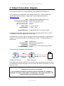
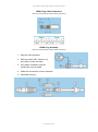
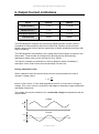
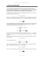
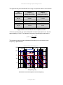
PiezoDrive PDQ High-Speed Charge Drives PDQ Charge Drives Manual and Specifications PiezoDrive Newcastle Innovation Ltd. Industry Development Centre University Drive, Callaghan NSW 2308, Australia www.piezodrive.com V4 August 2011 PiezoDrive PDQ High-Speed Charge Drives Warnings / Notes 1) The only connection to the output should be a capacitive load or piezoelectric actuator. The output of a charge drive is high-impedance and cannot be connected to instruments such as a multimeter or oscilloscope. 2) Charge drives work differently than voltage amplifiers. Section 1 of this manual should be thoroughly reviewed before attempting to operate a charge drive. 3) This device produces hazardous potentials and should only be used by suitably qualified personnel under the supervision of an observer with appropriate first-aid training. Do not operate the device when there are exposed conductors. High-Voltage V4 August 2011 PiezoDrive PDQ High-Speed Charge Drives PDQ Series High-Speed Charge Drives Manual and Specifications Contents 1. Using a Charge Drive a. b. c. d. e. 2. 3. 4. 5. 6. 7. 8. 9. 10. 11. 12. 13. Introduction Setting the DC Gain Basic use Example application Considerations when using a charge drive Brief Specifications Output Connection Diagram Inputs and Outputs Bandwidth Output Current Limitations Power Bandwidth Noise Performance Overload Protection Enclosure and Thermal Considerations Power Supply Options Warranty / Support Confidential Information This document contains confidential information. It cannot be distributed without consent. This document is subject to change at any time. V4 August 2011 PiezoDrive PDQ High-Speed Charge Drives 1. Using a Charge Drive A. Introduction It has been known since the 1980's that piezoelectric transducers respond more linearly to current or charge rather than voltage [1]. However, problems with drift and the floating nature of the load have only been solved recently [2] [3]. Since then, charge drives have been demonstrated to reduce the hysteresis of piezoelectric actuators by up to 93% [4]. This corresponds to a maximum non-linearity of less than 1% that can reduce or eliminate the need for feedback or feedforward control in dynamic applications. The simplified schematic diagram of a charge drive is shown below: Simplified schematic diagram of a charge drive. The piezoelectric load, modelled as a capacitor and voltage source , is shaded in gray. The high-gain feedback loop works to equate the applied reference voltage to the voltage across a sensing capacitor . Neglecting the resistances and , the output charge is That is, the gain is ⁄ V/V. Coulombs/V. This implies an input-to-output voltage gain of A major problem with charge drives is the finite output impedance and dielectric leakage, modelled by and . These resistances cause the output voltage to drift at low frequencies. However, by setting the ratio of resistances equal to the ratio of capacitances, low-frequency error can be avoided. To maintain a constant voltage gain, the required resistance ratio is V4 August 2011 PiezoDrive PDQ High-Speed Charge Drives The parallel resistances effectively turn the charge drive into a voltage amplifier at frequencies below Although the parallel resistances act to stabilize the voltage gain at low frequencies, the amplifier now operates as a voltage source below and a charge drive above. A consequence is that reduction of non-linearity only occurs at frequencies above . Practical values of can range from 0.01 Hz to greater than 10 Hz. The cut-off frequency can be reduced by increasing the parallel resistances; however, a practical limit is imposed by the dielectric leakage of the transducer. In addition, excessively high resistance values also reduce the immunity to drift and result in long settling times after turn-on and other transient events. The settling time is approximately seconds. An ideal compromise between excessively long settling times and good lowfrequency performance is Hz, implying a settling time of 8 seconds after turnon. This value of is adopted in the PDQ charge drives which have a cut-off frequency of between 0.03 Hz and 0.1 Hz, depending on the load capacitance. PiezoDrive charge drives are designed for both high-performance and ease-of-use. Compared to a standard voltage amplifier, there is only one additional control, the DC-gain, which sets the voltage-gain at low-frequencies. The PDQ Charge Drives are preconfigured during manufacture to drive a certain range of capacitance values. This means that the charge-gain, resistance ratios, and transition frequency are all optimally preconfigured and do not require user adjustment. The standard capacitance ranges and associated charge-gain, voltage-gain and cut-off frequencies are tabulated below. Load Capacitance Range Cut-off Freq. Voltage Gain Charge Gain 30 - 100 nF 100 - 300 nF 0.3 - 1.0 uF 1.0 - 3.0 uF 0.3 - 0.1 Hz 0.1 - 0.03 Hz 0.1 - 0.03 Hz 0.1 - 0.03 Hz 3.0 - 10 uF 10 - 1000 uF 0.1 - 0.03 Hz 0.1 Hz 66 – 22 60 – 20 66 – 22 60 – 20 66 – 22 40 2.2 uC/V 6.2 uC/V 22 uC/V 62 uC/V 220 uC/V Custom Load capacitance ranges of the PDQ drives From the above table, it can be observed that the equivalent voltage gain and cut-off frequency are both inversely proportional to load capacitance. Thus, at the smaller end of the load capacitance range, the voltage gain and cut-off frequency are both near the maximum of 66 and 0.1 Hz respectively. Only connect load capacitances of within the specified range. For ease-of-use, the PDQ drives are configured during manufacture for a specific range of load V4 August 2011 PiezoDrive PDQ High-Speed Charge Drives capacitances, which are printed on the rear panel. A smaller load capacitance is permissible but not recommended since the voltage gain and cut-off frequency will be excessively high. A load capacitance larger than the specified maximum should never be connected to the output. This may result in instability, will reduce the output voltage range, and can trigger an internal shutdown. Always ensure the load capacitance is within the specified range before turning the drive on. B. Setting the DC Gain Since the charge gain of a PDQ drive is fixed, the input-to-output voltage gain depends on the load capacitance. At frequencies above , the voltage gain is where is the charge gain and is the load capacitance. If the load capacitance is within the specified range, the voltage gain will be between 20 and 66. At frequencies below , the voltage gain is determined by the DC-gain knob on the front-panel. In most applications it is desirable to have a constant gain over all frequencies, so the DC-gain should be equated to the AC-gain at frequencies above . This can be achieved by following the procedure below. Procedure for setting the DC-gain 1) Connect the actuator or load capacitance. 2) Set the offset-voltage to zero by turning the knob counter-clockwise. 3) Set the DC-gain to zero by turning the knob counter-clockwise. 4) Use a signal generator to produce a 20 Hz, 1 V peak-to-peak (0.34 Vrms) sine-wave with an offset voltage of 1 V. The signal should resemble the plot below. Input Signal Voltage 1.5V 1.0V 0.5V 5) Turn the amplifier on, connect the input signal, and observe the output voltage using the Voltage Monitor. Turn the DC-gain knob clockwise until the offset-voltage is equal to the peak-to-peak voltage. The output voltage waveform should resemble the input signal plotted above. This calibration can be performed with an oscilloscope or multimeter. V4 August 2011 PiezoDrive PDQ High-Speed Charge Drives When using a multimeter, the DC-gain knob should be turned clockwise until the DC voltage is equal to √ AC voltage. When using an oscilloscope, ensure that the input coupling is set to “DC”. The above procedure will equate the voltage gain at DC and 20 Hz. It is important to note that many piezoelectric actuators exhibit a significant amount of creep. Creep is a non-linearity phenomenon that effectively increases the actuator sensitivity and capacitance at low-frequencies. This may result in increased gain at low frequencies when using the calibration procedure discussed above. To avoid the effects of creep, the procedure discussed above can be modified. Rather than equating the voltage gain at DC and 20 Hz, the voltage gain can be equated at 1 Hz and 20 Hz. In this case, Step 5 is replaced by: 5) Turn the amplifier on and observe the output voltage using the Voltage Monitor. Record the peak-to-peak or RMS output voltage. Reduce the input signal frequency to 1 Hz. Turn the DC-gain knob clockwise until the output voltage reaches the previously recorded value. The voltage gain at 1 Hz and 20 Hz are now equal. Since the input and output voltages are known or measured in the above procedure, the voltage gain can also be calculated. This gain is useful for calculating the maximum input voltage that can be applied before saturation occurs. Alternative Procedure for setting the DC-gain An alternative method for calibrating the DC gain is to: 1) Follow steps (1) to (3) above 2) Apply a 1-Hz square wave to the input with a minimum value of 0V and a maximum value of 1V. 3) Observe the load voltage by connecting the voltage monitor to an oscilloscope. (Ensure that the oscilloscope coupling is set to “DC”). 4) Turn the DC-Gain knob clockwise until the measured output voltage is a flat square-wave proportional to the input. C. Basic Use As the voltage gain of a charge drive is not fixed, this should first be measured using the technique described in the previous section, or predicted from the specifications. The voltage gain determines the maximum input signal that can be applied before saturation occurs V4 August 2011 PiezoDrive PDQ High-Speed Charge Drives Setting the Offset Voltage Piezoelectric actuators are usually biased at half their maximum voltage. To set the offset voltage, connect the Voltage Monitor output to a multimeter using a BNC to 4mm-Plug cable, or suitable adaptor. Leave the input grounded or unconnected then turn the device on. Keeping in mind that the Voltage Monitor output has a gain of 1/20 V/V, rotate the offset adjustment until the desired offset voltage is reached. D. Example Application In this example, we compare the response of a Noliac SCMAP07 piezoelectric stack actuator (10 mm long) when driven with a voltage amplifier and charge drive. The full displacement range of this actuator is 10.5 um at 200 V. As the actuator capacitance is 330 nF, the 22 uC/V charge range was selected. This corresponds to a voltage gain of 66 and a cut-off frequency of 0.1 Hz. The voltage- and charge-driven displacement response to a 100-Hz 150-V sine wave is plotted below. Voltage Driven (14.3% Error) Charge Driven (0.65% Error) Normalized Input Voltage The voltage- and charge-driven response of a Noliac SCMAP07 actuator. The applied signal was a 100-Hz, 150-V sine wave. Using a voltage amplifier, the maximum difference in position between two points with the same applied voltage is 1.1 um, or 14.3% of the range. Alternatively, when the voltage amplifier is replaced by a charge drive, the non-linearity is reduced to 0.05 um or 0.65% of the range. In many applications, this magnitude of non-linearity can avoid the necessity for feedback or feedforward hysteresis compensation. Other examples of charge linearization can be found in the reference list. V4 August 2011 PiezoDrive PDQ High-Speed Charge Drives (This example was reproduced with permission from [5]) E. Considerations when using a charge drive In many respects, a charge drive is similar to a voltage amplifier; however, there are some important differences that should be considered: The PDQ charge drives use a floating-load configuration as illustrated by the circuit diagram in Section 1.A. In this configuration, the return signal path is not ground; rather it may float by up to 10 V. This means that the actuator load voltage is not exactly the output voltage, but the difference between the output voltage and the return path. As the charge-monitor output is the voltage across the sensing capacitor, the exact differential load voltage can be measured using the following equation: It is also important to keep in mind that the return signal path is high-impedance. This means that any resistive or capacitive loads connected to the return path will cause an error. This includes multimeters, oscilloscopes, other instrumentation, and especially any ground connectors. The return path is also susceptible to electromagnetic interference so it should be kept well shielded. The only connection to the output of a charge drive should be the actuator. Since charge drives work like a voltage amplifier at frequencies below control over extremely low-frequency non-linearity such as creep. there is no References: [1] C. V. Newcomb and I. Flinn, “Improving the linearity of piezoelectric ceramic actuators,” IEE Electronics Letters, vol. 18, no. 11, pp. 442–443, May 1982. [2] K. A. Yi and R. J. Veillette, “A charge controller for linear operation of a piezoelectric stack actuator,” IEEE Transactions on Control Systems Technology, vol. 13, no. 4, pp. 517–526, July 2005. [3] A. J. Fleming and S. O. R. Moheimani, “Sensorless vibration suppression and scan compensation for piezoelectric tube nanopositioners,” IEEE Transactions on Control Systems Technology, vol. 14, no. 1, pp. 33–44, January 2006. [4] A. J. Fleming and K. K. Leang, “Charge drives for scanning probe microscope positioning stages,” Ultramicroscopy, vol. 108, no. 12, pp. 1551–1557, November 2008. [5] A. J. Fleming, “Quantitative SPM topographies by charge linearization of the vertical actuator,” Review of Scientific Instruments, vol. 81, no. 10, pp. 103701(1–5), October 2010. V4 August 2011 PiezoDrive PDQ High-Speed Charge Drives 2. Brief Specifications The PDQ drives are designed to optimize the performance of multilayer piezoelectric stack actuators. Brief specifications are listed below. Detailed specifications are contained in the following sections. Model Inputs PDQ150b PDQ200b Differential (to eliminate ground loops and noise). Zin = 22 kΩ Voltage -30 to 150V* -30 to 200V* Current +/- 2A Peak, Dynamic Current Limiting™ +/-1.5A Peak Dynamic Current Limiting™ Charge Gain 2.2, 6.2, 22, 62, 220 uC/V or Custom Voltage Gain 20 – 66 V/V Offset From 0V to Full-Range with front panel adjustment Connectors BNC input, BNC Monitor Outputs, LEMO 0B HV Output Bandwidth Greater than 80 kHz (1uF Load) Power Bandwidth 9.5 kHz 7.2 kHz Overload Thermal, current and voltage overload protection Noise Low noise, < 3 mV RMS Environment 0 - 40C (32-104F) Non-condensing humidity Enclosure Rugged desktop enclosure. 19 inch rack compatible * Minimum voltage range V4 August 2011 PiezoDrive PDQ High-Speed Charge Drives 3. Output Connection Diagram The output connector is a 2-way LEMO 0B socket (LEMO EGG.0B.302.CLL). The mating plug is a LEMO 0B 2-Way Straight Cable Plug. Ordering details and specifications are listed below. These parts can be obtained directly from www.mouser.com Plug Crimp Terminal Version Solder Tag Version Max Conductor Size LEMO 0B 2-Way Straight Cable Plug *LEMO FGG.0B.302.CYCZ LEMO FGG.0B.302.CLAZ AWG22 Cable Collet *FGG.0B.742.DN Cable Diameter *3.1mm – 4mm Strain Relief Boot *GMA.0B.035.DN (3.5–3.9mm Cable) * Supplied with amplifier. Note that the crimp terminal plug requires a tool, if this is not available, the solder tag plug should be used. A shielded two conductor cable is required to connect the amplifier to a piezoelectric actuator. A recommended cable is the Belden 8451 cable. The specifications are listed below. Cable Conductor Size Resistance Capacitance Outside Diameter *Belden 8451 AWG22 (0.64mm diameter) 53 mOhms/m 115 pF/m core–core, 220 pF/m core-shield 3.5mm The actuator wiring diagram is shown below. HV + + - Return Female Panel Socket Male Cable Plug Actuator If the cable has a shield, it should be connected to the body of the plug via the collet as described on the following page. Do not connect the shield to the load or use it as a ground return. The Return connection is not ground. Do not connect the Return conductor to Earth or Ground, for example to measure the output voltage with an oscilloscope. The only connection to the output should be the piezoelectric actuator V4 August 2011 PiezoDrive PDQ High-Speed Charge Drives LEMO Plug Cable Preparation (Taken from LEMO B Series Cable Assembly Instructions) LEMO Plug Assembly (Taken from LEMO B Series Cable Assembly Instructions) 1. Strip the cable as above 2. Slide the strain relief, collet nut (1) and collet (3) onto the cable. 3. If the cable is shielded, fold the shield back over the cable 4. Solder the conductors onto the contacts. 5. Assemble the plug, V4 August 2011 PiezoDrive PDQ High-Speed Charge Drives 4. Inputs and Outputs Input + 1/20 Voltage Monitor Offset Piezoelectric Load 1 Charge Monitor 10 Current Monitor 0.1 Ohm Simplified schematic of the charge drive inputs and outputs Input Circuit The input circuit has a function similar to a unity gain differential amplifier. This circuit is designed to eliminate ground-loops and noise resulting from the connection of instruments with different power supplies. The full scale range of the input circuit is +/- 10V. The signal ground is allowed to float by approximately +/- 0.6V before it is electrically connected to ground. The input impedance is 22kOhm. Offset Voltage After the input stage, an optional offset voltage is added to produce an electrical bias of between 0V and 200V. A typical stack actuator should be biased at half of the full scale voltage. Monitor Outputs There are three monitor outputs on the front panel. The voltage monitor has a gain of 1/20 V/V; the charge monitor has a gain equal to the sensitivity of the drive; and the current monitor has a gain of 1 V/A. The maximum output current from the monitor outputs is 10 mA. V4 August 2011 PiezoDrive PDQ High-Speed Charge Drives 5. Small Signal Bandwidth Magnitude (dB) 30 1uF 0.1uF 25 10uF 20 15 2 10 3 4 10 5 10 10 Phase (deg.) 0 -50 10uF -100 1uF -150 2 10 3 4 10 0.1uF 5 10 Frequency (Hz) 10 Frequency response for a range of load capacitances The small-signal frequency response for a range of capacitive loads is plotted in the above Figure. The load capacitances are the maximum permitted under each charge range which results in a voltage gain of 20. When the load capacitance is lower and the voltage gain is increased, the bandwidth may be reduced. The -3dB bandwidths are listed below Load Capacitance Bandwidth 0.1 uF 200 kHz 1.0 μF 84 kHz 10 μF 27 kHz 100 μF 2.7 kHz Approximate bandwidth versus load capacitance. V4 August 2011 PiezoDrive PDQ High-Speed Charge Drives Actuator Capacitance versus Bias Voltage and Temperature The power bandwidth, slew-rate and small-signal bandwidth of a piezoelectric amplifier are all primarily limited by the actuator capacitance. Larger actuators and actuators with a greater number of internal layers have a higher capacitance. Care must be taken when interpreting the capacitance values specified by actuator manufacturers. These values are measured at room temperature and with zero bias voltage. Due to the non-linearity of piezoelectric dielectrics, the small-signal capacitance increases with higher electric field. A capacitance increase of up to 300% has been reported over the full voltage range of a common piezoelectric actuator. Hence, when predicting the performance of piezoelectric amplifiers, a conservative estimate of the actual operating capacitance should be used. In typical applications where the bias voltage is half the full-range voltage, the capacitance value specified by the manufacturer should be multiplied by a factor of 2. In addition to capacitance non-linearity, piezoelectric dielectrics are also highly temperature dependant. For example, the sensitivity and capacitance of common piezoelectric actuators can double with every 50 degrees Celsius increase in temperature. If the ambient temperature is above 25 degrees Celsius, the capacitance increase must be taken into account. Due to dielectric heating, large temperature increases can also occur when driving piezoelectric actuators at highspeed or full-range. This is particularly true of small actuators with a low thermalmass; a 50 degree temperature increase can occur in just a few seconds of heavy excitation. V4 August 2011 PiezoDrive PDQ High-Speed Charge Drives 6. Output Current Limitations Model PDQ150 PDQ200 Peak Current +/- 2 A +/- 1.5 A RMS Current 1.6 A 1.1 A Average DC Current +/- 0.7 A +/- 0.5 A 100ms 100ms Overload Time The PDQ amplifiers contain a new technology called Dynamic Current Control™. Compared to other amplifiers with fixed current limits, Dynamic Current Control allows a larger peak current and the reproduction of larger amplitude waveforms with higher frequency. The PDQ amplifiers are available in two voltage and current ranges, as shown in the above table. These models are designed for general purpose and scanning applications where peak current may last for up to 100ms. This section contains an introduction to driving capacitive loads, followed by a description of the Peak Current Limit and Average Current Limit. Driving Capacitive Loads With a capacitive load, the required output current is proportional to the rate of change in voltage, that is where I is the current, C is the load capacitance and is the rate of change in voltage. Thus, more current is required for fast edges or transitions, larger amplitudes and higher frequencies. The voltage and current waveforms for a sinusoidal voltage and capacitive load are shown below. Voltage Vpp Current +Imax -Imax V4 August 2011 PiezoDrive PDQ High-Speed Charge Drives The maximum required current is where is the maximum positive and negative current, is the peak-to-peak amplitude (i.e. double the amplitude), f is the frequency and C is the load capacitance. For a triangular signal, the voltage and current waveforms with a capacitive load are shown below. Voltage Vpp Current +Imax -Imax The maximum required current is where is the maximum positive and negative current, is the peak-to-peak amplitude (i.e. double the amplitude), f is the frequency and C is the load capacitance. V4 August 2011 PiezoDrive PDQ High-Speed Charge Drives Peak Current Limit During normal operating conditions with a capacitive load, the amplifier is protected a peak current limit. If the maximum output current is exceeded, the amplifier will behave like a constant current source and the ‘Overload’ indicator on the front panel will light. As an example, consider a capacitive load driven by a square wave. The output voltage and current wave forms are shown below. At each transition, the amplifier enters current limit. Voltage Vpp Current +Imax -Imax Average Current Limit In addition to the peak current limit, there is also an average current limit that protects the amplifier from short circuit. If the average current limit engages, the amplifier will enter an overload condition and the output circuit will be disabled for approximately 5 seconds. The positive average current is computed by measuring the current flowing out of the amplifier. The current measurement is rectified then averaged with a leaky integrator. An identical circuit exists for the negative average current. The time-constant of the leaky integrator is 270ms which is equivalent to a maximum pulse length of approximately 100ms. A benefit of the average current limit is that current pulses less than the peak current are allowed for longer periods of time. The maximum non-repetitive pulse duration versus the output current is shown below. V4 August 2011 Max Pulse Durati 20 10 0 PiezoDrive PDQ High-Speed Charge Drives 0.5 1 1.5 2 2.5 3 3.5 Maximum Pulse Duration Times 4 4.5 5 Max Pulse Duration (ms) 2A Current Limit 1000 500 0 0.5 1 1.5 2 Max Pulse Duration (ms) 1.5A Current Limit 800 600 400 200 0 0.5 0.6 0.7 0.8 0.9 1 1.1 Peak Current (A) 1.2 1.3 1.4 1.5 Fold-back current limiting Versus PiezoDrive Dynamic Current Control Some high-voltage amplifiers use a current-limiting technique referred to as fold-back current limiting. This technique implies a current limit that changes with the output voltage. When the output voltage is high, more current can be delivered compared to when the output voltage is zero or negative. This is due to the lower power dissipation that occurs when the output voltage is high. Since the maximum current is only available at the maximum voltage, fold-back current limiting is suitable for resistive loads but not capacitive loads like piezoelectric actuators. The peak current for a capacitive load can occur at any voltage. Fold-back current limiting can result in unreliable performance when driving piezoelectric actuators. A waveform that may be successfully reproduced with a certain bias voltage may become distorted when the bias voltage is reduced. In addition, the step-response of the amplifier changes depending on the output voltage of the amplifier. V4 August 2011 PiezoDrive PDQ High-Speed Charge Drives 7. Power Bandwidth The PDQ amplifiers are designed to maximize the power bandwidth in general purpose and scanning applications. The power bandwidth is the maximum frequency sine-wave that can be reproduced at full voltage. For capacitive loads, the power bandwidth is primarily limited by the load capacitance and current limit. An expression for the maximum current of a capacitive load driven by a sine-wave was derived in the previous section, Where is the peak-to-peak output voltage, C is the load capacitance, and f is the frequency. Given a peak current limit of , the maximum frequency sine-wave is Since the PDQ amplifiers limit both the peak and average current, it is also important to consider the average current requirements. The average positive or negative current for a sine-wave with a peak current of is ∫ [ ] Hence, the maximum possible sine-wave with a peak current of requires an average current of which is guaranteed by the specifications of the PDQ amplifiers. The situation is different for triangular waveforms. A triangular waveform requires a peak current of and an average current of ∫ Hence, a triangular waveform is limited by average current, not peak current. The peak current should not exceed , which implies Thus, the maximum frequency of a triangular wave is similar to that of a sine wave: V4 August 2011 PiezoDrive PDQ High-Speed Charge Drives The approximate power bandwidth for a range of capacitive loads is shown below. Load Capacitance PDQ150 Power Bandwidth (150Vp-p Sine-wave) PDQ200 Power Bandwidth (200Vp-p Sine-wave) 100 nF *9.5 kHz *7.2 kHz 300 nF 9.2 kHz *7.2 kHz 1.0 μF 4.2 kHz 2.3 kHz 3.0 μF 1.4 kHz 790 Hz 10 μF 424 Hz 230 Hz 30 μF 141 Hz 79 Hz 100 μF 42 Hz 23 Hz Approximate Power Bandwidth Versus Capacitive Load * With very small loads, the power bandwidth is limited by the slew-rate, which is approximately 4.5 V/uS. The maximum frequency imposed by the slew-rate is The maximum peak-to-peak amplitude and frequency of a sine-wave versus frequency is plotted below. Maximum Peak-to-Peak Voltage (in V) 250 100uF 200 3uF 30uF 10uF PDQ200b PDX200b 1uF 300nF PDQ150b PDX150b 150 100 50 0 1 10 2 10 3 10 Frequency (Hz) 4 10 Maximum sine-wave amplitude versus frequency V4 August 2011 PiezoDrive PDQ High-Speed Charge Drives 8. Noise Performance The PDQ drives provide extremely low noise and are designed to exceed the requirements of positioning and imaging systems with sub-atomic resolution. The table below lists some experimentally measured output noise voltages. These values were recorded with a load capacitance equal to the maximum permitted in that charge range. Smaller load capacitances may result in higher noise voltages due to the greater voltage gain. Load Capacitance Bandwidth Measured Noise (RMS) 0.1 uF 200 kHz 3 mV 1.0 μF 84 kHz 1.5 mV 10 μF 27 kHz 1 mV Measured noise versus load capacitance. The noise was measured with a FLUKE189 TrueRMS Multimeter. The bias-voltage was 30V and the input was short-circuited. V4 August 2011 PiezoDrive PDQ High-Speed Charge Drives 9. Overload Protection There are two overload indicators on the front panel: Overheat and Overload. The Overload indicator will illuminate if there is more than 2 Volts difference between the desired output voltage and the actual output voltage. This can occur if the maximum current limit is exceeded or if the bandwidth of the input signal is too high. This overload indicator does not represent a fault condition and is present mainly to alert the user that the input signal is not being faithfully reproduced. The Overheat indicator will illuminate during a shutdown caused by an average current overload or if the amplifier overheats as a result of excessive ambient temperature, poor air-flow, or fan failure. None of these conditions should occur during normal operation. Hence, if an overheat shutdown occurs, the amplifier and attached actuator should be thoroughly inspected. The most common cause of an overheat shutdown is intermittent short-circuits produced by a damaged actuator. The behaviour of the amplifier during an average current overload is discussed in Output Current Limitations. If the amplifier overheats, the output stage is immediately disabled. When the temperature returns to a safe level, the amplifier will automatically reset. This may take a few minutes. During an Overheat shutdown caused by excessive average current or temperature, the output current reduces to a few mA. It is important to note that this does not mean that the output voltage will be zero. Dangerous potentials may still exist. External Shutdown In addition to the internal shutdown triggers, the output stage of the amplifier can also be disabled by applying a positive voltage to the external shutdown connector (+2V to +12V). The impedance of the external shutdown input is approximately 2.5kΩ. The external shutdown is useful for implementing thermal protection of an actuator or for disabling a feedback system. V4 August 2011 PiezoDrive PDQ High-Speed Charge Drives 10. Enclosure The PDQ amplifiers are housed in a rugged aluminium desktop enclosure. The dimensions are shown below. 132.6 mm (5.22 in) 304.8 mm (12.0 in) 212.6 mm (8.37 in) The PDQ amplifiers have a rear air intake and side exhaust vents for cooling. These should not be obstructed. If sufficient air-flow is not available, the amplifier will enter a thermal overload state as discussed in the previous section. The PDQ amplifiers can be bolted together in a side-by-side two-channel arrangement. With the addition of rack-mount handles, this configuration can be mounted into a standard 19-inch rack. A 19-inch rack-mount kit is also available for a single amplifier. V4 August 2011 PiezoDrive PDQ High-Speed Charge Drives 11. Power Supply Line Voltage 3AG Fuse (6.35 x 32 mm) 115 Vac (50-60 Hz) 5A 250V Time Delay 230 Vac (50-60 Hz) 2.5A 250V Time Delay Mains power is supplied through an IEC connector on the back panel. The IEC socket also contains the fuses and operating voltage selector switch. Two fuses are required, one for each of the active and neutral lines. The fuses are located in the back panel power connector and can be accessed by removing the power connecter and lifting out the fuse holder with a screw driver. When changing the fuses, be certain that the supply voltage selector remains at the correct voltage. Maximum power consumption is 200W The PDQ amplifiers require an earthed supply for safe operation. 12. Options - 19 inch rack mounting kit for two amplifiers 19 inch rack mounting kit for a single amplifier 13. Warranty / Support PiezoDrive amplifiers are guaranteed against manufacturing defects for a period of 3 months. Technical support contacts can be found at www.piezodrive.com V4 August 2011