1
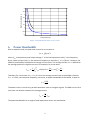
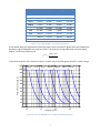
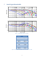
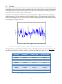
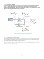
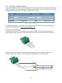
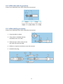
PD200 – 60 Watt Voltage Amplifier Manual and Specifications PiezoDrive Pty. Ltd. www.piezodrive.com 1 Contents 1 Introduction ................................................................................................................................... 3 2 Warnings / Notes ........................................................................................................................... 3 3 Specifications ................................................................................................................................. 4 4 Output Voltage Range.................................................................................................................... 5 5 Output Current Range.................................................................................................................... 5 6 Power Bandwidth........................................................................................................................... 6 7 Small Signal Bandwidth .................................................................................................................. 8 8 Noise .............................................................................................................................................. 9 9 Input and Offset Configuration .................................................................................................... 10 10 Bridged Mode .............................................................................................................................. 11 11 Overload Protection ..................................................................................................................... 11 12 Output Connections ..................................................................................................................... 12 12.1 Screw Terminals................................................................................................................. 12 12.2 LEMO OB Cable Preparation .............................................................................................. 13 12.3 LEMO OB Plug Assembly.................................................................................................... 13 13 Enclosure ...................................................................................................................................... 14 14 Warranty ...................................................................................................................................... 14 2 1 Introduction The PD200 is a high bandwidth, low-noise linear amplifier for driving piezoelectric actuators. The output voltage range can be switched between bipolar or unipolar modes with a range of 200V, -50V to +150V, or ±100V. Up to ±200V can be achieved in the bridged configuration. The PD200 can drive unlimited capacitive loads such as stack actuators; standard piezoelectric actuators; two wire benders; and three-wire piezoelectric benders requiring a 200V bias voltage. Compatible Actuators Stack Actuators 100V, 120V, 150V, 200V Plates and Tubes up to ± 100V Two Wire Benders up to ± 100V Three Wire Benders 0 to 200V with 200V bias ± 100V with ± 100V bias The PD200 is highly user configurable with jumpers for options such as the voltage range, polarity, and gain control. Two potentiometers are also provided to limit the positive and negative voltages to any arbitrary value between zero and full range. Due to the extensive configuration options, the PD200 is suited to a wide range of applications including electro-optics, ultrasound, vibration control, nanopositioning systems, and piezoelectric motors. There are four output connectors including Lemo 00, Lemo 0B, BNC, and screw terminals that allow the direct connection to almost any commercially available piezoelectric actuator, including those from PI, Piezomechanic, PiezoSystems, etc. 2 Warnings / Notes This device produces hazardous potentials and should be used by suitably qualified personnel under the supervision of an observer with appropriate first-aid training. Do not operate the device when there are exposed conductors. High-Voltage 3 3 Specifications Electrical Output Voltage Ranges +200V +150V -50 to 150V ±100V RMS Current 570 mA Peak Current 2 Amps or 10 Amps Gain 20 V/V Slew Rate 150 V/us Signal Bandwidth 680 kHz Power Bandwidth 230 kHz (200 Vp-p sine-wave) Max Power 60 W Dissipation Offset 0V to Full Range with front panel adjustment Load Stable with any load Noise 665 uV RMS (10uF Load) Overload Over-current protection Analog Outputs Voltage monitor 1/20 V/V (BNC) Current monitor 1 V/A (BNC) Analog Input Signal input (BNC, 𝒁𝒊𝒏 = 27k) Output Connectors BNC, LEMO 00, LEMO 0B, 4mm Banana Sockets Power Supply 90 Vac to 250 Vac Mechanical Environment 0 to 40C (32 to 104F) Non-condensing humidity Dimensions 275 x 141 x 64 mm (10.8 x 5.5 x 2.5 in) Weight 1 kg (2.2 lb) 4 4 Output Voltage Range The output voltage range can be configured by disconnecting the amplifier from mains power then removing the top panel. The following voltage ranges can be obtained with the correct combination of installed jumpers. Note that incorrect jumper settings may destroy the amplifier. The standard output voltage range is 0V to 200V. However, the amplifier can be supplied with any voltage range by appending the order code with the voltage range code, for example, the standard configuration is PD200-V200. The voltage range jumper locations are labelled with the LP, LG, and LN prefixes on the PCB. Voltage Range Code LP LG LN LK10 and LK12 0V to +200 0V to +150 0V to +100 0V to +50 -V200 -V150 -V100 -V50 LP1 LP2 LP2 LP2 LG3 LG3 LG2 LG1 -50 to +50 -50 to +100 -50 to +150 -V50,50 -V50,100 -V50,150 LP2 LP2 LP1 LG1 LG2 LG2 LN1 LN2 LN2 Position B Position B Position B -100 to +100 -V100,100 LP1 LG1 LN2 Position B Position A Position A Position A Position A Table 1. Voltage range configuration (Standard) 5 Output Current Range The standard peak output current is ±2 Amps; however, for applications that require very fast step changes in voltage, the amplifier can be configured in pulse mode with a 10 Amp current limit. The maximum pulse time for each mode is listed in Table 2 and plotted against current in Figure 1. The output current range can be configured by disconnecting the amplifier from mains power then removing the front and top panel. The amplifier can be supplied preconfigured to any current range by appending the order code with the current range code, for example, the standard configuration is PD200-C2. Peak Current Code Peak Limit Overload Timer Max Pulse Time 2A 10 A -C2 -C10 LK16 LK18 LK19 and LK20 Out LK19 and LK20 In 1 ms 100 us Table 2. Current range configuration (Standard) 5 4 Max Pulse Duration (ms) 3.5 3 2.5 2 1.5 1 0.5 0 0 2 4 6 Peak Current (A) 8 10 Figure 1. Maximum pulse time versus current 6 Power Bandwidth With a capacitive load, the peak load current for a sine-wave is 𝐼𝑝𝑘 = ±𝑉𝑝𝑝 𝜋𝐶𝑓 where 𝑉𝑝𝑝 is the peak-to-peak output voltage, 𝐶 is the load capacitance and 𝑓 is the frequency. Given a peak current limit 𝐼𝑝𝑘 , the maximum frequency is therefore 𝑓 = 𝐼𝑝𝑘 /𝑉𝑝𝑝 𝜋𝐶. However, the PX200 is protected by both peak and average current limits. The average current 𝐼𝑎𝑣+ is defined as the average positive or negative current. For example, for a sine-wave 𝐼𝑎𝑣+ = 𝐼𝑝𝑘 𝐼𝑝𝑘 1 𝜋 [−𝑐𝑜𝑠]𝜋0 = ∫ 𝐼𝑝𝑘 sin(𝜃) 𝑑𝜃 = . 2𝜋 0 2𝜋 𝜋 Therefore, for a sine-wave 𝐼𝑎𝑣+ = 𝐼𝑝𝑘 /𝜋. Since the average current limit of the PD200 is fixed at 𝐼𝑎𝑣+ = 0.26 A, the maximum frequency sine-wave, or power bandwidth of the PX200, is equal to 𝑓= 0.26 . 𝑉𝑝𝑝 𝐶 The above result is true for any periodic waveform such as triangular signals. The RMS current for a sine-wave can also be related to the average current, 𝐼𝑎𝑣 = √2 𝐼 . 𝜋 𝑟𝑚𝑠 The power bandwidths for a range of load capacitance values are listed below. 6 Load Peak to Peak Voltage Cap. No Load 200 230 kHz 150 310 kHz 100 470 kHz 50 520 kHz 10 nF 130 kHz 173 kHz 260 kHz 520 kHz 30 nF 43 kHz 58 kHz 87 kHz 173 kHz 100 nF 13 kHz 17 kHz 26 kHz 52 kHz 300 nF 4.3 kHz 5.8 kHz 8.7 kHz 17 kHz 1 uF 1.3 kHz 1.7 kHz 2.6 kHz 5.2 kHz 3 uF 430 Hz 570 Hz 870 Hz 1.7 kHz 10 uF 130 Hz 170 Hz 260 Hz 520 Hz 30 uF 43 Hz 57 Hz 87 Hz 170 Hz Table 3. Power Bandwidth versus Load Capacitance In the above table, the frequencies limited by slew-rate are marked in green while the frequencies limited by signal bandwidth are marked in blue. The slew-rate is approximately 150 V/uS which implies a maximum frequency of 𝑓 𝑚𝑎𝑥 = 150 × 106 𝜋𝑉𝑝𝑝 In the following figure, the maximum frequency periodic signal is plotted against the peak-to-peak voltage. 220 10 uF 3 uF 1 uF 300 nF 100 nF 30 nF 10 nF 200 Peak to Peak Voltage (V) 180 160 140 120 100 80 60 40 20 0 2 10 3 10 4 10 Frequency (Hz) 5 10 Figure 2. Power bandwidth versus voltage and load capacitance 7 7 Small Signal Bandwidth 40 3 uF Magnitude (dB) 30 1 uF 300 nF 100 nF 30 nF 20 30 uF 10 10 uF 0 -10 3 10 4 5 10 10 6 10 100 Phase (deg.) 50 0 -50 -100 -150 -200 3 10 4 5 10 10 Frequency (Hz) Figure 3. Small signal frequency response. Load Cap. No Load 10 nF 30 nF 100 nF 300 nF 1 uF 3 uF 10 uF 30 uF 110 uF Bandwidth 684 kHz 759 kHz 720 kHz 388 kHz 172 kHz 60 kHz 21 kHz 6.4 kHz 2.4 kHz 940 Hz Figure 4. Small signal bandwidth versus load capacitance (-3dB) 8 6 10 10 nF 8 Noise The output noise contains a low frequency component (0.03 Hz to 20 Hz) that is independent of the load capacitance; and a high frequency component (20 Hz to 1 MHz) that is inversely related to the load capacitance. Many manufacturers quote only the AC noise measured by a multimeter (20 Hz to 100 kHz) which is usually a gross underestimate. The noise is measured with an SR560 low-noise amplifier (Gain = 1000), oscilloscope, and Agilent 34461A Voltmeter. The low-frequency noise is plotted in Figure 5. The RMS value is 650 uV with a peak-to-peak voltage of 4.3 mV. The noise level is approximately equal to the least significant bit of a 16-bit digital-to-analog converter. 3 2 LF Noise (mV) 1 0 -1 -2 -3 0 5 10 15 20 t (s) 25 30 35 40 Figure 5. Low frequency noise from 0.03 Hz to 20 Hz. The RMS value is 650 uV, or 4.3 mVp-p. The high frequency noise (20 Hz to 1 MHz) is listed in the table below versus load capacitance. The 2 2 total noise from 0.03 Hz to 1 MHz is found by summing the RMS values, that is 𝜎 = √𝜎𝐿𝐹 + 𝜎𝐻𝐹 . Load Cap. No Load 10 nF 30 nF 100 nF 300 nF 1 uF 3 uF 10 uF 30 uF 110 uF Bandwidth 684 kHz 759 kHz 720 kHz 388 kHz 172 kHz 60 kHz 21 kHz 6.4 kHz 2.4 kHz 940 Hz HF Noise RMS 240 uV 241 uV 243 uV 234 uV 171 uV 133 uV 115 uV 112 uV 98 uV 85 uV Total Noise RMS 698 uV 698 uV 699 uV 696 uV 677 uV 668 uV 665 uV 665 uV 662 uV 660 uV Table 4. RMS noise versus load capacitance (0.03 Hz to 1 MHz) 9 9 Input and Offset Configuration The input stage is normally non-inverting; however, it can be configured as inverting by changing LK14 and LK15 to their “B” position. The default jumper position is “A” which is marked with a white bar on PCB overlay. The amplifier can be supplied with an inverting input by appending the order code with –INV. Input Configuration Non-inverting (default) Inverting Code Link Positions -INV LK14 and LK15 Both “A” LK14 and LK15 Both “B” Table 5. Input polarity configuration The input offset source is also configurable. When LK21 is in the “B” position, the offset is derived from the on-board trim-pot R15, which is adjustable from zero to full-scale. The default configuration for LK21 is in the “A” position where the offset voltage is derived from the front-panel potentiometer. The standard offset voltage range is from zero volts to full-scale; however, for applications that require negative offset voltages, LK13 can be moved from the “A” to “B” position. In the “B” position, the offset range is from -100V to full-scale. Offset Configuration 0V to +200V Range (def.) -100V to +200V Range Front panel source (def.) PCB trim-pot source Code -OR2 -OS2 Link Positions LK13 “A” Position LK13 “B” Position LK21 “A” Position LK21 “B” Position Table 6. Offset voltage source configuration 10 10 Bridged Mode In bridged mode, two amplifiers are connected in series to double the output voltage range and power. To obtain ±200V at the load, the amplifiers are configured as illustrated below. Both amplifiers are configured in the ±100V range and the lower amplifier is also inverting. A ±5V signal applied to both inputs will develop ±200V at the output. ±100V ±5V Non-inverting Signal Generator 20 Voltage across load PD200-V100,100 ±200V + -20 PD200-V100,100-INV Inverting ±100V Figure 6. Bridged configuration for obtaining +/-200 V 11 Overload Protection The Shutdown indicator will illuminate during a shutdown caused by an average current overload. During shutdown, the amplifier output current is limited to a few mA and may float to the high or low voltage rail if the load impedance is high or capacitive. When the amplifier is turned on, the overload protection circuit is engaged by default and will take approximately three seconds to reset. 11 12 Output Connections An actuator can be connected to the amplifier by either screw terminals or the LEMO 00, LEMO 0B, or BNC connectors. The recommended connectors are listed below. The full connector part number will depend on the diameter of the cable and desired strain relief. Output Recommended Connector Manufacturer PCB Connector BNC Any BNC Connector TE 1-1634613-0 Terminals 20020004-D041B01LF FCI 20020110-D041A01LF LEMO 00 FFA.00.250 LEMO EPL.00.250 LEMO 0B FGG.0B.302 LEMO EPG.0B.302 Table 7. Output connectors The LEMO 0B connector is recommended in high power applications. Preassembled LEMO cable assemblies are available from www.PiezoDriveOnline.com 12.1 Screw Terminals The plug-in screw terminal has contacts for the output voltage, ground, and the positive and negative high-voltage supply rails, which are useful when driving piezoelectric bender actuators. HV- HV+ Ground Output Bender actuators can be driven with a single bias voltage, for example 200 V, or bipolar bias voltages, for example ± 100 V. The 200 V unipolar configuration is illustrated below. +200V 0 to 200V 0V 12 12.2 LEMO OB Cable Preparation (Taken from LEMO 0B Series Cable Assembly Instructions) 12.3 LEMO OB Plug Assembly (Taken from LEMO 0B Series Cable Assembly Instructions) 1. Strip the cable as above 2. If the cable is shielded, fold the shield back over the cable 3. Slide the strain relief, collet nut (1) and collet (3) onto the cable. 4. Solder or crimp the conductors onto the contacts. 5. Assemble the plug, 13 13 Enclosure The PD200 enclosure has a side air intake and rear exhaust. These vents should not be obstructed. The PD200 amplifiers can be rack-mounted in a three channel arrangement as shown below. The rack panel (19-inch X 2U) is supplied separately and requires some user assembly to mount between one and three channels. The rack order code is PD200-RackPanel. 14 Warranty PiezoDrive amplifiers are guaranteed for a period of 3 months. The warranty does not cover damage due to misuse or incorrect user configuration of the amplifier. 14