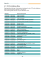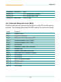
1
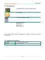
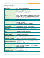
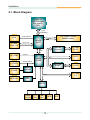
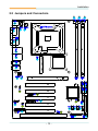
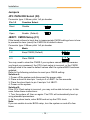
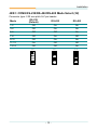
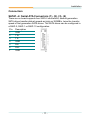
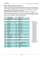
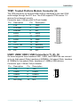
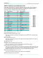
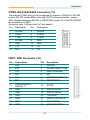
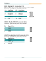
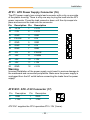
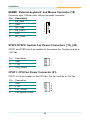
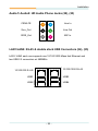
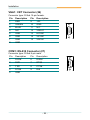
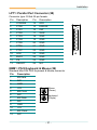
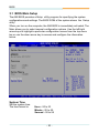
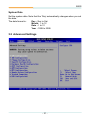
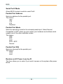
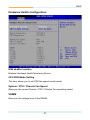
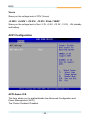
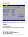
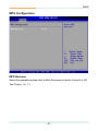
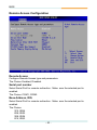
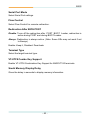
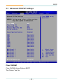
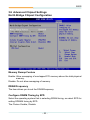
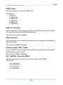
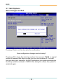
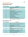
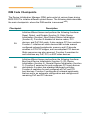
MB-i965Q
ATX Industrial Motherboard
User’s Manual
Version 1.0
2008.07
This page is intentionally left blank.
Index
Table of Contents
Chapter 1 - Introduction............................................. 1
1.1 Copyright Notice....................................................2
1.2 About this User’s Manual......................................2
1.3 Warning..................................................................2
1.4 Replacing the lithium battery...............................3
1.5 Technical Support..................................................3
1.6 Warranty.................................................................4
1.7 Packing List............................................................5
1.8 Ordering Information.............................................5
1.9 Specification..........................................................6
1.10 Board Dimensions...............................................7
1.11 Installing the CPU................................................8
1.12 Installing the Memory..........................................9
Chapter 2 - Installation............................................. 11
2.1 Block Diagram......................................................12
2.2 Jumpers and Connectors...................................13
Jumpers.......................................................................14
JP3: PATA IDE Select.............................................14
JBAT1: CMOS Setup..............................................14
JRS1: COM2 RS-232/422/485 Mode Select...........15
JP2: AT/ATX Power Mode Select...........................16
JP1: BIOS Write Protect.........................................16
Connectors..................................................................17
SATA1 ~4: Serial ATA Connectors.........................17
IDE1: Primary IDE Connector................................18
TPM1: Trusted Platform Module Connector.........19
USB1 ~3: USB Connectors....................................19
JFRT1: Switches and Indicators...........................20
COM2: RS-232/422/485 Connector........................21
FDD1: FDD Connector............................................21
DIO1: Digital I/O Connector...................................22
CDIN1: Audio CD IN Connector.............................22
--
Index
LOUT1: Audio Line Out Connector.......................22
ATX1: ATX Power Supply Connector....................23
ATX12V1: ATX +12V Connector.............................23
EKB1: External Keyboard/ Mouse Connector.....24
SYSF1/SYSF2: System Fan Power Connectors..24
CPUF1: CPU Fan Power Connector......................24
Audio1/ Audio2: HD Audio Phone Jacks..............25
LAN1/LAN2: RJ-45 & double stack USB
Connectors.......................................25
VGA1: CRT Connector...........................................26
COM1: RS-232 Connector......................................26
LPT1: Parallel Port Connector..............................27
KBM1: PS/2 Keyboard & Mouse Connectors.......27
2.3 The Installation Paths of CD Driver....................28
Chapter 3 - BIOS....................................................... 29
3.1 BIOS Main Setup..................................................30
3.2 Advanced Settings..............................................31
CPU Configuration.................................................32
IDE Configuration...................................................33
Floppy Configuration.............................................34
Super IO Configuration..........................................35
Hardware Health Configuration.............................37
ACPI Configuration................................................38
APM Configuration.................................................39
MPS Configuration.................................................41
Remote Access Configuration..............................42
Trusted Computing.................................................44
USB Configuration.................................................45
3.3 Advanced PCI/PnP Settings...............................47
3.4 Boot Settings.......................................................49
Boot Settings Configuration..................................50
3.5 Security.................................................................51
- ii -
Index
3.6 Advanced Chipset Settings................................53
North Bridge Chipset Configuration.....................53
South Bridge Chipset Configuration....................54
3.7 Exit Options..........................................................56
3.8 Beep Sound codes list........................................61
Boot Block Beep codes.........................................61
POST BIOS Beep codes.........................................61
Troubleshooting POST BIOS Beep codes............62
3.9 AMI BIOS Checkpoints........................................63
Bootblock Initialization Code Checkpoints..........63
Bootblock Recovery Code Checkpoints..............65
POST Code Checkpoints.......................................67
DIM Code Checkpoints..........................................71
ACPI Runtime Checkpoints...................................73
Chapter 4 - Appendix............................................... 75
4.1 I/O Port Address Map..........................................76
4.2 Interrupt Request Lines (IRQ).............................77
- iii -
Index
This page is intentionally left blank.
- iv -
Introduction
1
Chapter 1
Introduction
Chapter 1 - Introduction
--
Introduction
1.1 Copyright Notice
All Rights Reserved.
The information in this document is subject to change without prior notice in
order to improve the reliability, design and function. It does not represent a
commitment on the part of the manufacturer.
Under no circumstances will the manufacturer be liable for any direct,
indirect, special, incidental, or consequential damages arising from the
use or inability to use the product or documentation, even if advised of the
possibility of such damages.
This document contains proprietary information protected by copyright.
All rights are reserved. No part of this manual may be reproduced by any
mechanical, electronic, or other means in any form without prior written
permission of the manufacturer.
1.2 About this User’s Manual
This User’s Manual is intended for experienced users and integrators with
hardware knowledge of personal computers. If you are not sure about any
description in this User’s Manual, please consult your vendor before further
handling.
1.3 Warning
Single Board Computers and their components contain very delicate
Integrated Circuits (IC). To protect the Single Board Computer and its
components against damage from static electricity, you should always follow
the following precautions when handling it :
1. Disconnect your Single Board Computer from the power source when you
want to work on the inside.
2. Hold the board by the edges and try not to touch the IC chips, leads or
circuitry.
3. Use a grounded wrist strap when handling computer components.
4. Place components on a grounded antistatic pad or on the bag that came
with the Single Board Computer, whenever components are separated
from the system.
--
Introduction
1.4 Replacing the lithium battery
Incorrect replacement of the lithium battery may lead to a risk of explosion.
The lithium battery must be replaced with an identical battery or a battery
type recommended by the manufacturer.
Do not throw lithium batteries into the trashcan. It must be disposed of in
accordance with local regulations concerning special waste.
1.5 Technical Support
If you have any technical difficulties, please consult the user’s manual first
at:
ftp://ftp.arbor.com.tw/pub/manual
Please do not hesitate to call or e-mail our customer service when you still
can not find out the answer.
http://www.arbor.com.tw
E-mail:[email protected]
--
Introduction
1.6 Warranty
This product is warranted to be in good working order for a period of two
years from the date of purchase. Should this product fail to be in good
working order at any time during this period, we will, at our option, replace
or repair it at no additional charge except as set forth in the following terms.
This warranty does not apply to products damaged by misuse, modifications,
accident or disaster.
Vendor assumes no liability for any damages, lost profits, lost savings or any
other incidental or consequential damage resulting from the use, misuse of,
or inability to use this product. Vendor will not be liable for any claim made
by any other related party.
Vendors disclaim all other warranties, either expressed or implied, including
but not limited to implied warranties of merchantibility and fitness for
a particular purpose, with respect to the hardware, the accompanying
product’s manual(s) and written materials, and any accompanying
hardware. This limited warranty gives you specific legal rights.
Return authorization must be obtained from the vendor before returned
merchandise will be accepted. Authorization can be obtained by calling or
faxing the vendor and requesting a Return Merchandise Authorization (RMA)
number. Returned goods should always be accompanied by a clear problem
description.
--
Introduction
1.7 Packing List
1 x MB-i965Q ATX Industrial Motherboard
1 x Driver CD
1 x Quick Installation Guide
COM Port Cable x 1
IDE Cable x 1
USB Cable x 1
SATA Cable x 2
If any of the above items is damaged or missing, contact your vendor
immediately.
1.8 Ordering Information
MB-i965Q
ATX Industrial Motherboard
Cable Kit
CBK-04-965Q-00
--
Introduction
1.9 Specifications
Form Factor
Processor
Chipset
System Memory
VGA Controller
Ethernet
I/O Chips
BIOS
Audio
Serial ATA
IDE Interface
Serial Port
ATX Industrial Motherboard
Socket for Intel® Core™ 2 Duo/ Pentium®
D/ Celeron® D/ Pentium® 4 processor, with
1066/800/533MHz FSB, w/ HT
Intel® Q965 + Intel® ICH8R
2 x 240-pin DIMM socket up to 4GB
Intel® Graphics Media Accelerator (GMA) 3000
graphics core w/ CRT (Dual independent display)
2 x Realtek 8111B 10/100/1000 base-T Ethernet
ITE-8718
AMI PnP Flash BIOS
ALC888 HD Codec
7.1 channel/MIC-in/Line-in/Line-out
4 x Serial ATA with 300MB/s HDD transfer rate
1 x ATA 66/100, support 1 IDE device
2 x COM port
(COM1: RS-232, COM2: RS-232/422/485)
Parallel Port
FDD
KBMS
External KBMS
Universal Serial Bus
Digital I/O
Expansion Interface
1 x SPP/EPP/ECP mode
1 x Slim type Floppy connector
PS/2 Keyboard and Mouse
1 x 6-pin wafer connector
10 x USB 2.0 (6 ports by pin header)
Onboard 8-bit Digital I/O Interface
1 x PCIe*16 slot, 5 x PCI slot, 1 x ISA slot
♦ CPU/System temperature and over heat Alarm
12V/5V/3.3V/Vcore/Vbat/5Vsb/3.3Vsb Voltage
Hardware Monitor Chip ♦
♦ CPU/System Fan speed
♦ CPU over heat Protection
RTC
Real Time Clock
ATX power connector & +12V 4-pin ATX
Power Input Connector 24-pin
Power Connector
Operating Temp.
0ºC ~ 60ºC (-32ºF ~ 140ºF)
Watchdog Timer
255-level Reset
Dimension (L x W)
305 x 220mm (12” x 8.6”)
--
Introduction
1.10 Board Dimensions
16.51
41.28
132.08
124.46
10.16
33.02
219.96
157.48
23.37
18.03
18.03
26.42
20.57
17.53
Parallel Port
Mouse
COM1 Port
VGA
ø4
45.72
304.8
Keyboard
7-
14.35 14.99
157.48
USB1
USB3
USB2
USB4
--
78.74
16.51
.00
Unit : mm
Introduction
1.11 Installing the CPU
The LGA775 processor socket comes with a lever to secure the
processor. Please refer to the pictures step by step as below.
Please note that the cover of the LGA775 socket must always be installed
during transport to avoid damage to the socket.
1
2
3
4
5
6
7
8
9
Make sure that heat sink of the CPU top surface is in complete contact to
avoid the CPU overheating problem.
If not, it would cause your system or CPU to be hanged, unstable, damaged.
--
Introduction
1.12 Installing the Memory
To install the Memory module, locate the Memory DIMM slot on the board
and perform as below:
1. Hold the Memory module so that the key of the Memory module align
with those on the Memory DIMM slot.
2. Gently push the Memory module in an upright position and a right way
until the clips of the DIMM slot close to lock the Memory module in place,
when the Memory module touches the bottom of the DIMM slot.
3. To remove the Memory module, just pressing the clips of DIMM slot with
both hands.
Lock
Lock
--
Introduction
This page is intentionally left blank.
- 10 -
Installation
2
Chapter 2
Installation
Chapter 2 - Installation
- 11 -
Installation
2.1 Block Diagram
LGA775
CPU Socket
For Intel®
CPU
FSB
533/800MHz
VGA
1 x slot
PCIe x 16
Analog R.G.B.
PCIe x 16
Intel®
Q965
4 x SATA
1 x IDE
USB I/F
Serial ATA I/F
5 x PCI
PCI Bus
Intel®
ICH8R
PCI-to-ISA
Bridge
PATA
Controller
HD
Codec
Super IO
COM1
COM2
LPT1
FDD
KB
MS
- 12 -
ISA Bus
1 x ISA
1 x TPM
1.2
LPC I/F
HD Audio
2 x LAN
RJ-45
PCI LAN
Controller
DMI
10 x USB
2 x 240pin DDRII
DIMM socket
DDRII
IrDA
DIO
Installation
2.2 Jumpers and Connectors
21
20
19
CPUF1 SYSF1 SYSF2
KBM1
29
LGA775 socket
EKBM1 ATX12V1
COM1
18
27
17
LPT1
VGA1
26
28
LAN1
25
LAN2
24
ATX1
16
AUDIO1
23
AUDIO2
22
LOUT1 CDIN1
15
14
DIMM1
DIMM2
SATA3
SATA1
SATA4
SATA2
3
JP1
4
34
JRS1
13
JP3
11
30
TPM1
6
JP2
33
FDD1
2
32
COM2
DIO1
1
USB4
9
12
JBAT1
8
USB5
7
31
JFRT1
- 13 -
USB3
10
IDE1
5
Installation
Jumpers
JP3: PATA IDE Select (30)
Connector type: 2.54mm pitch 1x2 pin header.
Pin 1-2
Function Select
Short
Disable
1
2
Open
Enable (Default)
1
2
JBAT1: CMOS Setup (31)
If the board refuses to boot due to inappropriate CMOS settings here is how
to proceed to clear (reset) the CMOS to its default values.
Connector type: 2.54mm pitch 1x3 pin header
Pin
Mode
1-2
Keep CMOS (Default)
2-3
Clear CMOS
3
2
1
3
2
1
You may need to clear the CMOS if your system cannot boot up because
you forgot your password, the CPU clock setup is incorrect, or the CMOS
settings need to be reset to default values after the system BIOS has been
updated.
Refer to the following solutions to reset your CMOS setting:
Solution A:
1. Power off the system and disconnect the power cable.
2. Place a shunt to short pin 1 and pin 2 of JBAT1 for five seconds.
3. Place the shunt back to pin 2 and pin 3 of JBAT1.
4. Power on the system.
Solution B:
If the CPU Clock setup is incorrect, you may not be able to boot up. In this
case, follow these instructions:
1. Turn the system off, then on again. The CPU will automatically boot up
using standard parameters.
2. As the system boots, enter BIOS and set up the CPU clock.
Note:
If you are unable to enter BIOS setup, turn the system on and off a few
times.
- 14 -
Installation
JRS1: COM2 RS-232/RS-422/RS-485 Mode Select (32)
Connector type: 2.00 mm pitch 2x7 pin header
RS-232
(Default)
RS-422
RS-485
1-2
Off
On
On
3-4
Off
On
On
5-6
Off
Off
On
7-8
Off
On
Off
9-10
Off
On
On
11-12
On
Off
Off
13-14
Off
Off
On
Mode
1 2
1 2
1 2
13 14
13 14
13 14
- 15 -
Installation
JP2: AT/ATX Power Mode Select (33)
The power mode jumper selects the power mode for the system.
Connector type: 2.54mm pitch 1x2 pin header.
Pin 1-2
Mode
Short
AT Mode
1
2
Open
ATX Mode (Default)
1
2
JP1: BIOS Write protect (34)
Connector type: 2.54mm pitch 1x3 pin header.
Pin
Mode
1-2
Write protect (default)
2-3
Write Enable
- 16 -
3
2
1
3
2
1
Installation
Connectors
SATA1~4: Serial ATA Connectors (1), (2), (3), (4)
There are on board supports four SATA II connectors, second generation
SATA drives transfer data at speeds as high as 300MB/s, twice the transfer
speed of first generation SATA drives. The SATA drives can be configured in
a RAID 0, RAID 1 or RAID 10 configuration.
Pin
Description
1
GND
2
TX+
3
TX-
4
GND
5
RX-
6
RX+
7
GND
- 17 -
Installation
IDE1: Primary IDE Connector (5)
An IDE drive ribbon cable has two connectors to support two IDE devices. If
a ribbon cable connects to two IDE drives at the same time, one of them has
to be configured as Master and the other has to be configured as Slave by
setting the drive select jumpers on the drive.
Consult the documentation that came with your IDE drive for details on
jumper locations and settings. You must orient the cable connector so that
the pin 1 (color) edge of the cable corresponds to pin 1 of the IDE connector.
Connector type: 2.54mm pitch 2x20 box header
Pin
Description
Pin
Description
1
IDE RESET
2
GND
3
DATA7
4
DATA8
5
DATA6
6
DATA9
7
DATA5
8
DATA10
9
DATA4
10
DATA11
11
DATA3
12
DATA12
13
DATA2
14
DATA13
15
DATA1
16
DATA14
17
DATA0
18
DATA15
19
GND
20
N/C (Key)
21
REQ
22
GND
23
IO WRITE
24
GND
25
IO READ
26
GND
27
IO READY
28
IDESEL
29
DACK
30
GND
31
IRQ14
32
N/C
33
ADDR1
34
ATA66 DETECT
35
ADDR0
36
ADDR2
37
CS0#
38
CS1# (HDSELET1)
39
IDEACTP
40
GND
- 18 -
Installation
TPM1: Trusted Platform Module Connector (6)
The TPM connector on the EmCORE-i35Q is interfaced to the Intel ICH9
south bridge through the LPC bus. The ICH9 supports TPM version 1.2
devices for enhanced security.
Connector type: 2.54mm pitch 2x10 pin header
Pin
Description
Pin
Description
1
CLK
2
GND
3
LFRAME
4
N/C
5
LRESET
6
N/C
7
LAD3
8
LAD2
9
+3.3V
10
LAD1
11
LAD0
12
GND
13
N/C
14
N/C
15
+3.3V_SB
16
SERIRQ
17
GND
18
CLKRUN
19
PD
20
N/C
USB1/ USB2/ USB3: USB Connectors (7), (8), (9)
On board supports three headers USB1, USB2, and USB3 that can connect
up to six high-speed (Data transfers at 480MB/s), full-speed (Data transfers
at 12MB/s) or low-speed (Data transfers at 1.5MB/s) USB devices.
Connector type: 2.54mm 2x5 pin header
Pin
Description
Pin
Description
1
+5V
2
+5V
3
USBD-
4
USBD-
5
USBD+
6
USBD+
7
GND
8
GND
9
N/C (Key)
10
N/C
- 19 -
1
2
9
10
Installation
JFRT1: Switches and Indicators (10)
It provides connectors for system indicators that provides light indication
of the computer activities and switches to change the computer status.
Connector type: 2.54mm pitch 2x13 pin header
Pin
Description
Pin
Description
1
+5V
2
RESET+
3
N/C
4
RESET-
5
IRRX
6
N/C
7
GND
8
SPKR
9
IRTX
10
BUZZ
11
N/C
12
GND
13
HDD_LED+
14
+5V
15
HDD_LED-
16
N/C
17
TB_LED+
18
POWER_LED+
19
TB_LED-
20
N/C
21
N/C
22
POWER_LED-
23
PWRBTN+
24
KBLOCK
25
PWRBTN-
26
GND
IrDA: Infrared connector, pin 1, 3, 5, 7, 9
HLED: HDD LED Connector, pin 13-15.
This 2-pin connector connects to the case-mounted HDD LED to indicate hard
disk activity.
RES: Reset Button, pin 2-4.
This 2-pin connector connects to the case-mounted reset switch and is used to
reboot the system.
TB_LED: pin 17-19
PWRBTN: ATX soft power switch, pin 23-25.
This 2-pin connector connects to the case-mounted Power button.
PLED: Power LED Connector, pin 18, 20, 22.
This 3-pin connector connects to the case-mounted power LED. Power LED can
be indicated when the CPU card is on or off. And keyboard lock can be used to
disable the keyboard function so the PC will not respond by any input.
SPK: External Speaker, pin 8, 10, 12, 14.
This 4-pin connector connects to the case-mounted speaker.
KBLOCK: Keyboard Lock, pin 24-26.
- 20 -
Installation
COM2: RS-232/422/485 Connector (11)
The onboard COM2 port can be configured to operate in RS-422 or RS-485
modes. RS-422 modes differ in the way RX/TX is being handled. Jumper
JRS1 switches between RS-232 or RS-422/485 mode. All of the RS-422/485
are available on COM2.
Connector type: 2.54mm pitch 2x7 box header.
Pin
Description
Pin
Description
1
DCD2#
2
DSR2#
3
RXD2
4
RTS2#
5
TXD2
6
CTS2#
7
DTR2#
8
RI2#
9
GND
10
GND
11
TX+
12
TX-
13
RX+
14
RX-
FDD1: FDD Connector (12)
Pin
Description
Pin
Description
1
+5V
2
INDEX#
3
+5V
4
DRIVER SELECT A#
5
+5V
6
DISK CHANGE#
7
N/C
8
N/C
9
N/C
10
MOTOR ENABLE A#
11
N/C
12
DIRECTION#
13
DRIVE DENSITY
SELECT 0
14
STEP#
15
GND
16
WRITE DATA#
17
GND
18
WRITE GATE#
19
GND
20
TRACK0#
21
GND
22
WRITE PROTECT#
23
GND
24
READ DATA#
25
GND
26
HEAD SELECT#
- 21 -
Installation
DIO1: Digital I/O Connector (13)
DIO1 is a 8-bit DIO connector that supports 4-bit In/ 4-bit Out.
Connector type: 2.54mm pitch 2x5 pin header
Pin
Description
Pin
Description
1
OUTPUT1
2
INPUT1
3
OUTPUT2
4
INPUT2
5
OUTPUT3
6
INPUT3
7
OUTPUT4
8
INPUT4
9
+5V
10
GND
CDIN1: Audio CD IN Connector (14)
Connector type: 2.54mm pitch 1x4 pin header.
Pin
1
2
3
4
Description
CD-L
GND
GND
CD-R
LOUT1: Audio Line Out Connector (15)
Connector type: 2.54mm pitch 1x4 pin header.
Pin
Description
1
LOUT-L
2
GND
3
LOUT_JD
4
LOUT-R
- 22 -
Installation
ATX1: ATX Power Supply Connector (16)
The ATX power supply has a single lead connector with a clip on one side
of the plastic housing. There is only one way to plug the lead into the ATX
power connector. Press the lead connector down until the clip snaps into
place and secures the lead onto the connector.
Pin Description Pin Description
13
+3.3V
1
+3.3V
14
-12V
2
+3.3V
15
GND
3
GND
16
PS-ON
4
+5V
17
GND
5
GND
18
GND
6
+5V
19
GND
7
GND
20
-5V
8
PW-OK
21
+5V
9
+5VSB
22
+5V
10
+12V
23
+5V
11
+12V
24
GND
12
+3.3V
Warning
13
1
24
12
Incorrect installation of the power supply could result in serious damage to
the mainboard and connected peripherals. Make sure the power supply is
unplugged from the AC outlet before connecting the leads from the power
supply.
ATX12V1: ATX +12V Connector (17)
Pin
Description
Pin
Description
2
GND
1
GND
4
+12V
3
+12V
2
1
4
3
ATX12V1 supplies the CPU operation ATX +12V (Vcore).
- 23 -
Installation
EKBM1: External keyboard and Mouse Connector (18)
Connector type: 2.50mm pitch 1x6-pin box wafer connector
Pin
Description
1
KB_Data
2
GND
3
MS_Data
4
KB_Clock
5
+5V
6
MS_Clock
1
2
3
4
5
6
SYSF1/SYSF2: System Fan Power Connectors (19), (20)
SYSF1 and SYSF2 are 3-pin header for the system fan. The fan must be a
+12V fan.
Pin
Description
1
GND
2
+12V
3
FAN_Detect
CPUF1: CPU Fan Power Connector (21)
CPUF1 is a 4-pin header for the CPU fan. The fan must be a +12V fan.
Pin
Description
1
GND
2
+12V
3
Fan_ Detect
4
Fan Speed Control
- 24 -
Installation
Audio1/ Audio2: HD Audio Phone Jacks (22), (23)
CEN/LFE
Line In
Surr_Out
Line Out
SIDE_Out
MIC In
LAN1/LAN2: RJ-45 & double stack USB Connectors (24), (25)
LAN1/ LAN2 each one supports one 10/100/1000 Mbps fast Ethernet and
two USB 2.0 connectors w/ 480MB/s.
10/100/1000 RJ-45
10/100/100 RJ-45
USB1
USB3
USB2
USB4
- 25 -
Installation
VGA1: CRT Connector (26)
Connector type: D-Sub 15-pin female.
Pin
Description
Pin
Description
1
RED
9
+5V
2
GREEN
10
GND
3
BLUE
11
N/C
4
N/C
12
VDDAT
5
GND
13
HSYNC
6
GND
14
VSYNC
7
GND
15
VDCLK
8
GND
1
11
5
15
COM1: RS-232 Connector (27)
Connector type: D-Sub 9-pin male.
Pin
Description
Pin
Description
1
DCD#
6
DSR#
2
RXD
7
RTS#
3
TXD
8
CTS#
4
DTR#
9
RI#
5
GND
6
9
- 26 -
1
5
Installation
LPT1: Parallel Port Connector (28)
Connector type: D-Sub 25-pin female.
Pin
Description
Pin
Description
1
STROBE
14
AFD
2
PTD0
15
ERROR
3
PTD1
16
INIT
4
PTD2
17
SLIN
5
PTD3
18
GND
6
PTD4
19
GND
7
PTD5
20
GND
8
PTD6
21
GND
9
PTD7
22
GND
10
ACK
23
GND
11
BUSY
24
GND
12
PE
25
GND
13
SELECT
26
N/C
KBM1: PS/2 Keyboard & Mouse (29)
Standard Mini-DIN PS/2 Keyboard & Mouse connector
Pin
Description
1
KB Data
2
N/C
3
GND
4
+5V
5
KB Clock
6
N/C
7
MS Data
8
N/C
9
GND
10
+5V
11
MS Clock
12
N/C
12
11
10
6
9
8
7
4
5
3
2
Mouse
(Green)
Keyboard
(Purple)
1
- 27 -
1
14
13
25
Installation
2.3 The Installation Paths of CD Driver
Driver
AUDIO
CHIPSET
LAN
VGA
Path
\AUDIO\REALTEK_HD\WINDOWS_R178
\CHIPSET\INTEL\INF 8.1
\ETHERNET\REALTEK\8111B_WIN5640
\GRAPHICS\INTEL_2K_XP_32\1431
\GRAPHICS\INTEL_VISTA_32\1561
- 28 -
BIOS
3
Chapter 3
BIOS
Chapter 3 - BIOS
- 29 -
BIOS
3.1 BIOS Main Setup
The AMI BIOS provides a Setup utility program for specifying the system
configurations and settings. The BIOS ROM of the system stores the Setup
utility.
When you turn on the computer, the AMI BIOS is immediately activated. The
Main allows you to select several configuration options. Use the left/right
arrow keys to highlight a particular configuration screen from the top menu
bar or use the down arrow key to access and configure the information
below.
System Time
Set the system time.
The time format is:
Hour : 00 to 23
Minute : 00 to 59
Second : 00 to 59
- 30 -
BIOS
System Date
Set the system date. Note that the ‘Day’ automatically changes when you set
the date.
The date format is:
Day : Sun to Sat
Month : 1 to 12
Date : 1 to 31
Year : 1999 to 2099
3.2 Advanced Settings
- 31 -
BIOS
CPU Configuration
The CPU Configuration setup screen varies depending on the installed
processor.
Ratio CMOS Setting
Sets the ratio between CPU Core Clock and the FSB Frequency.
Note: Only available when SpeedStep Technology is disabled.
Max CPUID Value Limit
Disabled for Windows XP.
- 32 -
BIOS
IDE Configuration
SATA#1 Configuration
Enable - Enable SATA configuration.
Disabled - Disable SATA configuration
Configure SATA#1 as
This BIOS feature controls the SATA controller’s operating mode.
There are two available modes - IDE and RAID. When set to:
RAID - the SATA controller enables its RAID and AHCI functions when
the computer boots up.
IDE - the SATA controller disables its RAID and AHCI functions when
the computer boots up.
Primary/Secondary IDE Master/Slave, Third/ Fourth IDE master
Select one of the hard disk drives to configure it. Press <Enter> to access its
the sub menu.
- 33 -
BIOS
Floppy Configuration
Select the type of floppy disk drive installed in your system.
The choice:
None
360K 5.25”
1.2M 5.25”
720K 3.5”
1.44M 3.5”
2.88M 3.5”
- 34 -
BIOS
Super IO Configuration
Onboard Floppy Controller
Select “Enabled” if your system has a floppy disk controller (FDC) installed
on the system board and you wish to use it. If you install and-in FDC or the
system has no floppy drive, select Disabled in this field.
The Choice: Enabled, Disabled
Serial Port1 / Port2 Address
Select an address and corresponding interrupt for the first and second serial
ports.
The choice:
3F8/IRQ4
2E8/IRQ3
3E8/IRQ4
2F8/IRQ3
Disabled
Auto
- 35 -
BIOS
Serial Port2 Mode
Allows BIOS to select mode for serial Port2.
Parallel Port Address
Select an address for the parallel port.
The choice:
3BC
378
278
Disabled
Parallel Port Mode
Select an operating mode for the onboard parallel port. Select Normal,
Compatible or SPP unless you are certain your hardware and software both
support one of the other available modes.
The choice:
SPP
EPP
ECP
ECP + EPP
Normal
Parallel Port IRQ
Select an interrupt for the parallel port.
The choice:
IRQ5
IRQ7
Restore on AC Power Loss by IO
This item allows you to select if you want to power on the system after power
failure.
- 36 -
BIOS
Hardware Health Configuration
H/W Health Function
Enables Hardware Health Monitoring Device.
CPU FAN Mode Setting
This item allows you to set CPU fan speed control mode.
System / CPU / Chassis Fan Speed
Show you the current System / CPU / Chassis Fan operating speed.
VDIMM
Show you the voltage level of the DRAM.
- 37 -
BIOS
Vcore
Show you the voltage level of CPU (Vcore).
+3.30V / +5.00V / +12.0V / -12.0V / 5Vsb / VBAT
Show you the voltage level of the +3.3V, +5.0V, +12.0V, -12.0V, +5V standby
and battery.
ACPI Configuration
ACPI Aware O/S
This item allows you to enable/disable the Advanced Configuration and
Power Management (ACPI)
The Choice: Enabled, Disabled.
- 38 -
BIOS
APM Configuration
Power Management/APM
This category allows you to select the type (or degree) of power saving and
is directly related to the following modes:
1. HDD Power Down
2. Doze Mode
3. Suspend Mode
Video Power Down Mode
This option defines the level of power-saving mode requires in to power
down the video display. As a default, the video powers down both in suspend
mode and standby mode.
The Choice: Enabled, Disabled
Hard Diks Power Down Mode
Power Down Hard Disk in Suspend or Standby Mode.
The Choice: Enabled, Disabled
- 39 -
BIOS
Suspend Time Out
Go into Suspend in the specified time.
The Choice: Enabled, Disabled
Throttle Slow Clock Ratio
Select the Duty Cycle in Throttle mode.
The choice:
12.5%
25.0%
37.5%
50.0%
62.5%
75.0%
87.5%
Keyboard & PS/2 Mouse
Monitor KBC ports 60/64.
Power Button Mode
Pressing the power button for more than 4 seconds forces the system to
enter the Soft-Off state when the system has “hang”.
The Choice: Delay 4 Sec, On/Off
Advanced Resume Event Controls
Resume On Ring
An input signal on the serial Ring Indicator (RI) line (in other words an
incoming call on the modem) awakens the system from a soft off state.
The Choice: Enabled, Disabled
Resume On PME#
An input signal from a PME on the PCI card awakens the system from a soft
off state.
The Choice: Enabled, Disabled
Resume On RTC Alarm
When “Enabled”, you can set the date and time at which the RTC (real-time
clock) alarm awakens the system from Suspend mode.
The Choice: Enabled, Disabled
- 40 -
BIOS
MPS Configuration
MPS Revision
Select the operating system that is Multi-Processors Version Control for OS.
The Choice: 1.4, 1.1.
- 41 -
BIOS
Remote Access Configuration
Remote Access
Configure Remote Access type and parameters.
The Choice: Enabled, Disabled.
Serial port number
Select Serial Port for console redirection. Make sure the selected port is
enabled.
The Choice: COM1, COM2.
Base Address, IRQ
Select Serial Port for console redirection. Make sure the selected port is
enabled.
The Choice:
3F8, IRQ4
2E8, IRQ3
3E8, IRQ4
2F8, IRQ3
- 42 -
BIOS
Serial Port Mode
Select Serial Port settings.
Flow Control
Select Flow Control for console redirection.
Redirection After BIOS POST
Disable: Turns off the redirection after POST BOOT Loader, redirection is
active during POST and during BOOT Loader.
Always: Redirection is always active. (Note: Some OSs may not work if set
to Always)
Enable: Keep it, Disabled: Deactivate
Terminal Type
Select the target terminal type.
VT-UTF8 Combo Key Support
Enable VT-UTF8 Combination Key Support for ANSI/VT100 terminals.
Sredir Memory Display Delay
Gives the delay in seconds to display memory information.
- 43 -
BIOS
Trusted Computing
TCG/TPM Support
Enable/Disable TPM / TCG (TPM 1.1/1.2) supports in BIOS.
- 44 -
BIOS
USB Configuration
ACPI Function
It supports ACPI (Advance Configuration and Power Interface).
Setting: Enabled (Default), Disabled.
- 45 -
BIOS
Legacy USB Support
Enables support for legacy USB. AUTO option disables legacy support if no
USB devices are connected.
Port 64/60 Emulation
Enables I/O port 60h/64h emulation support. This should be enabled for the
complete USB keyboard legacy support for non-USB aware OSs.
USB 2.0 Controller Mode
Configures the USB 2.0 controller in High Speed (480Mbps) or Full Speed
(12MBPS).
BIOS EHCI Hand-Off
This is a work around for OSs without EHCI hand-Off support. The EHCI
ownership change should claim by EHCI driver.
USB Mass Storage Reset Delay
Number of seconds POST waits for the USB mass storage device after start
unit command.
Emulation Type
If Auto, USB devices less than 530MB will be emulated as Floppy and
remaining as hard drive. Forced FDD option can be used to force a HDD
formatted drive to BOOT as FDD. (Ex. ZIP drive).
- 46 -
BIOS
3.3 Advanced PCI/PnP Settings
Clear NVRAM
Clear NVRAM during System BOOT.
The Choice: Yes, No.
- 47 -
BIOS
Plug & Play O/S
No: Lets the BIOS configure all the devices in the system.
Yes: lets the operating system configure Plug and Play (PnP) devices not
required for BOOT if your system has a Plug and Play operating system.
PCI Latency Timer
Value in units of PCI clocks for PCI device latency timer register.
Allocate IRQ to PCI VGA
Yes: Assigns IRQ to PCI VGA card if card requests IRQ.
No: Does not assign IRQ to PCI VGA card even if card requests an IRQ.
PCI IDE BusMaster
Enabled: BIOS uses PCI busMastering for reading / writing to IDE drives.
Spread Spectrum Function
This item allows you to enable/disable the spread spectrum function.
The Choice: Enabled, Disabled.
IRQ3 - IRQ15
Available: Specified IRQ is available to be used by PCI/PnP devices.
Reserved: Specified IRQ is reserved for use by Legacy ISA devices.
DMA Channel 0 - DMA Channel 7
Available: Specified DMA is available to be used by PCI/PnP devices.
Reserved: Specified DMA is reserved for use by Legacy ISA devices.
Reserved Memory Size
Size of memory block to reserve for legacy ISA devices.
- 48 -
BIOS
3.4 Boot Settings
Boot Device Priority
Press Enter and it shows Bootable add-in devices.
Removable Drives
Press Enter and it shows Bootable and Removable drives.
- 49 -
BIOS
Boot Settings Configuration
Quick Boot
Allows BIOS to skip certain tests while booting. This will decrease the time
needed to boot the system.
Bootup Num-Lock
Set this value to allow the Number Lock setting to be modified during boot
up.
LAN Boot Function
Set this option to LAN add-on Boot ROM function.
- 50 -
BIOS
3.5 Security
Auto Detect PCI Clk
It enables or disables the auto detection of the PCI clock.
Setting: Enabled (Default), Disabled.
Supervisor Password & User Password
You can set either supervisor or user password, or both of then.
The differences between are:
Set Supervisor Password: Can enter and change the options of the
setup menus.
Set User Password: Just can only enter but do not have the right to
change the options of the setup menus. When you select this function, the
following message will appear at the center of the screen to assist you in
creating a password.
ENTER PASSWORD:
- 51 -
BIOS
Type the password, up to eight characters in length, and press <Enter>.
The password typed now will clear any previously entered password from
CMOS memory. You will be asked to confirm the password. Type the password
again and press <Enter>. You may also press <ESC> to abort the selection
and not enter a password.
To disable a password, just press <Enter> when you are prompted to
enter the password. A message will confirm the password will be disabled.
Once the password is disabled, the system will boot and you can enter Setup
freely.
PASSWORD DISABLED.
When a password has been enabled, you will be prompted to enter it
every time you try to enter Setup. This prevents an unauthorized person from
changing any part of your system configuration.
Additionally, when a password is enabled, you can also require the BIOS
to request a password every time your system is rebooted. This would prevent
unauthorized use of your computer.
You determine when the password is required within the BIOS Features
Setup Menu and its Security option. If the Security option is set to “System”,
the password will be required both at boot and at entry to Setup. If set to
“Setup”, prompting only occurs when trying to enter Setup.
Boot Sector Virus Protection
Enable/Disable Boot Sector Virus Protection.
- 52 -
BIOS
3.6 Advanced Chipset Settings
North Bridge Chipset Configuration
Memory Remap Feature
Enable: Allow remapping of overlapped PCI memory above the total physical
memory.
Disable: Do not allow remapping of memory.
DRAM Frequency
The item allows you to set the DRAM frequency.
Configure DRAM Timing by SPD
Select the operating system that is selecting SRAM timing, so select SPD for
setting SDRAM timing by SPD.
The Choice: Enable, Disable
- 53 -
BIOS
Initate Graphic Adapter
Select which graphics controller to use as the primary boot device.
Internal Graphic Mode Select
Select the amount of system memory used by the Internal graphics device.
PEG Port Configuration
This item allows you to control the PEG or on-chip VGA.
The Choice: Auto, Disabled.
South Bridge Chipset Configuration
- 54 -
BIOS
USB Funtion
This item allows you to active USB ports.
The Choice:
Disabled
2 USB Ports
4 USB Ports
6 USB Ports
8 USB Ports
10 USB Ports
USB 2.0 Controller
Select “Enabled” if your system contains a Universal Serial Bus 2.0 (USB
2.0) controller and you have USB peripherals.
The Choice: Enabled, Disabled.
HDA Controller
This item allows you to select the chipset family to support High Definition
Audio Controller.
The Choice: Enabled, Disabled.
Onboard Giga LAN1 / LAN2
Select “Enabled” if your system has a LAN device installed on the system
board and you wish to use it.
The Choice: Enabled, Disabled.
SLP_S4# Min. Assertion Width
The item allows you to select the assertion width of SLP_S4#.
The Choice:
4 to 5 Seconds.
3 to 4 Seconds.
2 to 3 Seconds.
1 to 2 Seconds.
- 55 -
BIOS
3.7 Exit Options
Save Changes and Exit
Pressing <Enter> on this item asks for confirmation:
Save configuration changes and exit setup?
Pressing <OK> stores the selection made in the menus in CMOS - a special
section of memory that stays on after you turn your system off. The next
time you boot your computer, the BIOS configures your system according to
the Setup selections stored in CMOS. After saving the values the system is
restarted again.
- 56 -
BIOS
Discard Changes and Exit
Exit system setup without saving any changes.
<ESC> key can be used for this operation.
- 57 -
BIOS
Discard Changes
Discards changes done so far to any of the setup questions.
<F7> can be used for this operation.
- 58 -
BIOS
Load Optimal Defaults
When you press <Enter> on this item you get a confirmation dialog box with
a message:
Load Optimal Defaults?
[OK]
[Cancel]
Pressing [OK] loads the BIOS Optimal Default values for all the setup
questions.
<F9> key can be used for this operation.
- 59 -
BIOS
Load Failsafe Defaults
When you press <Enter> on this item you get a confirmation dialog box with
a message:
Load Failsafe Defaults?
[OK]
[Cancel]
Pressing [OK] loads the BIOS Failsafe Default values for all the setup
questions.
<F8> key can be used for this operation.
- 60 -
BIOS
3.8 Beep Sound codes list
Boot Block Beep codes
Number of Beeps
Description
1
Insert diskette in floppy drive A:
2
‘AMIBOOT.ROM’ file not found in root directory of
diskette in A:
4
Flash Programming successful
5
Floppy read error
6
Keyboard controller BAT command failed
7
No Flash EPROM detected
8
Floppy controller failure
9
Boot Block BIOS checksum error
10
Flash Erase error
11
Flash Program error
12
‘AMIBOOT.ROM’ file size error
13
BIOS ROM image mismatch (file layout does not
match image present in flash device)
POST BIOS Beep codes
Number of Beeps
Description
1
Memory refresh timer error.
2
Parity error in base memory (first 64KB block)
4
Motherboard timer not operational
5
8
Processor error
8042 Gate A20 test error (cannot switch to protected
mode)
General exception error (processor exception
interrupt error)
Display memory error (system video adapter)
9
AMIBIOS ROM checksum error
10
CMOS shutdown register read/write error
11
Cache memory test failed
6
7
- 61 -
BIOS
Troubleshooting POST BIOS Beep codes
Number of Beeps
Description
1, 2 or 3
Reseat the memory, or replace with known good
modules.
4-7, 9-11
Fatal error indicating a serious problem with the
system. Consult your system manufacturer. Before
declaring the motherboard beyond all hope, eliminate
the possibility of interference by a malfunctioning
add-in card. Remove all expansion cards except the
video adapter.
• If beep codes are generated when all other expansion
cards are absent, consult your system manufacturer’s
technical support.
• If beep codes are not generated when all other
expansion cards are absent, one of the add-in cards
is causing the malfunction. Insert the cards back into
the system one at a time until the problem
8
If the system video adapter is an add-in card,
replace or reset the video adapter. If the video
adapter is an integrated part of the system board,
the board may be faulty.
- 62 -
BIOS
3.9 AMI BIOS Checkpoints
Bootblock Initialization Code Checkpoints
The Bootblock initialization code sets up the chipset, memory and other
components before system memory is available. The following table
describes the type of checkpoints that may occur during the bootblock
initialization portion of the BIOS (Note):
Checkpoint
Before D0
Description
If boot block debugger is enabled, CPU cache-as-RAM
functionality is enabled at this point. Stack will be enabled
from this point.
D0
Early Boot Strap Processo (BSP) initialization like
microcode update, frequency and other CPU cirtical
initialization. Early chipset initialization is done.
D1
Early super I/O initialization is done including RTC and
keyboard controller. Serial port is enabled at this point if
needed for debugging. NMI is deisabled. Perfrom keyboard
controller BAT test. Save power-on CPUID value in scretch
CMOS. Go to flat mode with 4GB limit and GA20 enabled.
D2
Verify the boot block checksum. System will hang here if
checksum is bad.
D3
Disable CACHE before memory detection. Execute full
memory sizing module. If memory sizing module not
executed, start memory refresh and do memory sizing in
Boot block code. Do additional chipset initialization. Reenabled CACHE. Verify that flat mode is enabled.
D4
Test base 512KB memory. Adjust policies and cache first
8MB. Set stack.
D5
Bootblock code is copied from ROM to lower system
memory and control is given to it. BIOS now executes out
of RAM. Copies compressed boot block code to memory
in right segments. Copies BIOS from ROM to RAM for
faster access. Perfroms main BIOS checksum and updates
recovery status accordingly.
- 63 -
BIOS
D6
Both key sequence and OEM specific method is checked
to determine if BIOS recovery is forced. If BIOS recovery is
necessary, control flows tocheckpoint E0. Seed Bootblock
Recovery Code Checkpoints section of document for more
information.
D7
Restore CPUID value back into register. The BootblockRuntime interface module is moved to system memory and
control is given to it. Determine whether in memory.
D8
The Tuntime module is uncompressed into memory. CPUID
information is stored in memory.
D9
Store the Uncompressed pointer for future use in PMM.
Copying Main BIOS into memory. Leaves all RAM below
1MB Read-Write including E000 and F000 shadow areas
but closing SMRAM.
DA
Restore CPUID value back into register. Give control
to BIOS POS (ExecutePOSTKernel). See POST Code
Checkpoints section of document for more information.
DC
System is saking from ACPI S3 state.
E1 - E8
EC - EE
OEM memory detection / configuration error. This range is
reserved for chipset vendors & system manufacturers. The
error associated with this value may be different from one
platform to be next.
- 64 -
BIOS
Bootblock Recovery Code Checkpoints
The Bootblock recovery code gets control when the BIOS determines that
a BIOS recovery needs to occur because the user has forced the update
or the BIOS checksum is corrupt. The following table describes the type of
checkpoints that may occur during the Bootblock recovery portion of the
BIOS (Note):
Checkpoint
Description
E0
Initialize the floppy controller in the super I/O. Some interrupt
vectors are initialized. DMA controller is initialized. 8259
interrupt controller is initialized. L2 cache is enabled.
E9
Set up floppy controller and data. Attempt to red from floppy.
EA
Enable ATAPI hardware. Attempt to read from ARMD and
ATAPI CDROM.
EB
Disable ATAPI hardware. Jump back to checkpoint E9.
EF
Read error occurred on media. Jump back to checkpoint EB.
F0
Search for pre-defined recovery file name in root directory.
F1
Recovery file not found.
F2
Start reading FAT table and analyze FAT to find the clusters
occupied by the recovery file.
F3
Start reading the recovery file cluster by cluster.
F5
Disable L1 cache.
FA
Check the validity of the recovery file configuration to the
current configuration of the flash part.
FB
Make flash write enabled through chipset and OEM specific
method. Detect proper flash part. Verify that the found flash
part size equals the recovery file size.
F4
The recovery file size does not equal the found flash part size.
- 65 -
BIOS
FC
Erase the flash part.
FD
Program the flash part.
FF
The flash has been updated successfully. Make flash write
disabled. Disable ATAPI hardware. Restore CPUID value back
into register. Give control to F000 ROM at F000:FFF0h.
- 66 -
BIOS
POST Code Checkpoints
The POST code checkpoints are the largest set of checkpoints during
the BIOS pre-boot process. The following table describes the type of
checkpoints that may occur during the POST portion of the BIOS (Note):
Checkpoint
Description
03
Disable NMI, Parity, video for EGA, and DMA controllers.
Initialize BIOS, POST, Runtime data area. Also initialize BIOS
modules on POST entry and GPNV area. Initialized CMOS as
mentioned in the Kernel Variable "wCMOSFlags."
Check CMOS diagnostic byte to determine if battery power
is OK and CMOS checksum is OK. Verify CMOS checksum
manually by reading storage area.
04
If the CMOS checksum is bad, update CMOS with power-on
default values and clear passwords. Initialize status register A.
Initializes data variables that are based on CMOS setup
questions.
Initializes both the 8259 compatible PICs in the system.
05
06
Initializes the interrupt controlling hardware (generally PIC)
and interrupt vector table.
Do R/W test to CH-2 count reg. Initialize CH-0 as system
timer. Install the POSTINT1Ch handler. Enable IRQ-0 in PIC
for system timer interrupt.
Traps INT1Ch vector to "POSTINT1ChHandlerBlock."
07
Fixes CPU POST interface calling pointer.
08
Initializes the CPU. The BAT test is being done on KBC.
Program the
keyboard controller command byte is being done after Auto
detection of KB/MS using AMI KB-5.
C0
Early CPU Init Start -- Disable Cache - Init Local APIC
C1
Set up boot strap processor Information
C2
Set up boot strap processor for POST
C5
Enumerate and set up application processors
C6
Re-enable cache for boot strap processor
- 67 -
BIOS
C7
Early CPU Init Exit
0A
Initializes the 8042 compatible Key Board Controller.
0B
Detects the presence of PS/2 mouse.
0C
Detects the presence of Keyboard in KBC port.
0E
Testing and initialization of different Input Devices. Also,
update the
Kernel Variables.
Traps the INT09h vector, so that the POST INT09h handler
gets control for IRQ1. Uncompress all available language,
BIOS logo, and Silent logo modules.
13
Early POST initialization of chipset registers.
20
Relocate System Management Interrupt vector for all CPU in
the system.
24
Uncompress and initialize any platform specific BIOS
modules. GPNV is initialized at this checkpoint.
2A
Initializes different devices through DIM.
See DIM Code Checkpoints section of document for more
information.
2C
Initializes different devices. Detects and initializes the video
adapter
installed in the system that have optional ROMs.
2E
Initializes all the output devices.
31
Allocate memory for ADM module and uncompress it. Give
control to ADM module for initialization. Initialize language and
font modules for ADM.
Activate ADM module.
33
Initializes the silent boot module. Set the window for
displaying text
information.
37
Displaying sign-on message, CPU information, setup key
message, and any OEM specific information.
- 68 -
BIOS
38
Initializes different devices through DIM. See DIM Code
Checkpoints
section of document for more information. USB controllers are
initialized at this point.
39
Initializes DMAC-1 & DMAC-2.
3A
Initialize RTC date/time.
3B
Test for total memory installed in the system. Also, Check for
DEL
keys to limit memory test. Display total memory in the system.
3C
Mid POST initialization of chipset registers.
40
Detect different devices (Parallel ports, serial ports, and
coprocessor in CPU, … etc.) successfully installed in the
system and update the BDA, EBDA…etc.
52
Updates CMOS memory size from memory found in memory
test. Allocates memory for Extended BIOS Data Area from
base memory. Programming the memory hole or any kind of
implementation that needs an adjustment in system RAM size
if needed.
60
Initializes NUM-LOCK status and programs the KBD
typematic rate.
75
Initialize Int-13 and prepare for IPL detection.
78
Initializes IPL devices controlled by BIOS and option ROMs.
7C
Generate and write contents of ESCD in NVRam.
84
Log errors encountered during POST.
85
Display errors to theuser and gets the user response for error.
87
Execute BIOS setup if needed / requested. Check boot
password if installed.
8C
Late POST initialization of chipset registers.
8D
Build ACPI tables (if ACPI is supported)
8E
Program the peripheral parameters. Enable/Disalbe NMI as
selected.
90
Initialization of system management interrupt by invoking all
handlers.
A1
Lian-up work needed before booting to OS.
- 69 -
BIOS
A2
Takes care of runtime image preparation for different BIOS
modules. Fill the free area in F000h segment with 0FFh.
Initializes the Microsoft IRQ Routing Table. Prepares the
runtime language module. Disables the system configuration
display if needed.
A4
Initialize runtime language module. Display boot option popup
menu.
A7
Displays the system configuration screen if enabled. Initialize
the CPU’s before boot, which includes the programming of the
MTRR’s.
A9
Wait for userinput at config display if needed.
AA
Uninstall POST INT1Ch vector and INT09h vector.
AB
Prepare BBS for Int 19 boot. Init MP tables.
AC
End of POST initialization of chipset registers. De-initializes
the ADM
module.
B1
Save system context for ACPI. Prepare CPU for OS boot
including final MTRR values.
00
Passes control to OS Loader (typically INT19h).
- 70 -
BIOS
DIM Code Checkpoints
The Device Initialization Manager (DIM) gets control at various times during
BIOS POST to initialize different system buses. The following table describes
the main checkpoints where the DIM module is accessed (Note):
Checkpoint
Description
2A
Initialize different buses and perform the following functions:
Reset, Detect, and Disable (function 0); Static Device
Initialization (function); Boot Output Device Initialization
(function 2). Function 0 disables all device nodes, PCI
devices, and PnP ISA cards. It also assigns PCI bus numbers.
Function 1 initializes all static devices that include manual
configured onboard peripherals, memory and I/O decode
windows in PCI-PCI bridges, and noncompliant PCI devices.
Static resources are also reserved. Function 2 searches for
and initializes any PnP, PCI, or AGP video devices.
38
Initialize different buses and perform the following functions:
Boot Input Device Initialization (function 3); IPL Device
Initialization (function 4); General Device Initialization (function
5). Function 3 searches for and configures PCI input devices
and detects if system has standard keyboard controller.
Function 4 searches for and configures all PnP and PCI
boot devices. Function 5 configures all onboard peripherals
that are set to an automatic configuration and configures all
remaining PnP and PCI devices.
- 71 -
BIOS
While control is in the different functions, additional checkpoints are output
to port 80h as a word value to identify the routines under execution. The
low byte value indicates the main POST Code Checkpoint. The high byte is
divided into two nibbles and contains two fields. The details of the high byte
of these checkpoints are as follows:
HIGH BYTE XY
The upper nibble “X” indicates the function number that is being executed.
“X” can be from 0 to 7.
0 = func#0, disable all devices on the BUS concerned.
2 = func#2, output device initialization on the BUS concerned.
3 = func#3, input device initialization on the BUS concerned.
4 = func#4, IPL device initialization on the BUS concerned.
5 = func#5, general device initialization on the BUS concerned.
6 = func#6, error reporting for the BUS concerned.
7 = func#7, add-on ROM initialization for all BUSes.
8 = func#8, BBS ROM initialization for all BUSes.
The lower nibble 'Y' indicates the BUS on which the different routines are
being executed. 'Y' can be from 0 to 5.
0 = Generic DIM (Device Initialization Manager).
1 = On-board System devices.
2 = ISA devices.
3 = EISA devices.
4 = ISA PnP devices.
5 = PCI devices.
- 72 -
BIOS
ACPI Runtime Checkpoints
ACPI checkpoints are displayed when an ACPI capable operating system
either enters or leaves a sleep state. The following table describes the type
of checkpoints that may occur during ACPI sleep or wake events (Note):
Checkpoint
Description
AC
First ASL check point. Indicates the system is running
in ACPI mode.
AA
System is running in APIC mode.
01, 02, 03, 04, 05 Entering sleep state S1, S2, S3, S4, or S5.
10, 20, 30, 40, 50 Waking from sleep state S1, S2, S3, S4, or S5.
Note:
Please note that checkpoints may differ between different platforms
based on system configuration. Checkpoints may change due to vendor
requirements, system chipset or option ROMs from add-in PCI devices.
- 73 -
BIOS
This page is intentionally left blank.
- 74 -
Appendix
4
Chapter 4
Appendix
Chapter 4 - Appendix
- 75 -
Appendix
4.1 I/O Port Address Map
Each peripheral device in the system is assigned a set of I/O port addresses
which also becomes the identity of the device.
The following table lists the I/O port addresses used.
Address
Device Description
00000000 - 0000000F
DMA Controller
00000080 - 0000009F
DMA Controller
000000C0 - 000000DF
DMA Controller
00000020 - 00000021
Programmable Interrupt Controller
000000A0 - 000000A1
Programmable Interrupt Controller
00000040 - 00000043
System Timer
00000044 - 00000047
System Timer
00000060 - 00000064
Keyboard Controller
00000070 - 00000073
System CMOS/Real Time Clock
000000F0 - 000000FF
Math Co-processor
00000274 - 00000277
ISAPNP Read Data Port
00000279 - 00000279
ISAPNP Configuration
000002F8 - 000002FF
Communications Port (COM2, If use)
00000378 - 0000037A
Parallel Port (If use)
000003B0 - 000003BF
MDA/MGA
000003C0 - 000003CF
EGA/VGA
000003D4 - 000003D9
CGA CRT register
000003F0 - 000003F7
Floppy Diskette
000003F8 - 000003FF
Communications Port (COM1, If use)
00000400 - 0000041F
South Bridge SMB
00000480 - 000004BF
South Bridge GPIO
000004D0 - 000004D1
IRQ Edge/Level Control Ports
00000800 - 0000087F
ACPI
00000A00 - 00000A07
PME
00000A10 - 00000A17
Hardware Monitor
00000A20 - 00000A27
Digital I/O
- 76 -
Appendix
00000A30 - 00000A37
SFIF
00000CF8
PCI Configuration Address
00000CFC
PCI Configuration Data
00004700 - 0000470B
TPM (If use)
4.2 Interrupt Request Lines (IRQ)
Peripheral devices use interrupt request lines to notify CPU for the service
required. The following table shows the IRQ used by the devices on board.
Level
Function
IRQ 0
System Timer
IRQ 1
Keyboard Controller
IRQ 2
VGA and Link to Secondary PIC
IRQ 3
Communications Port (COM2)
IRQ 4
Communications Port (COM1)
IRQ 5
PCI Device
IRQ 6
Standard Floppy Disk Controller
IRQ 7
Parallel Port
IRQ 8
System CMOS/real time clock
IRQ 9
Microsoft ACPI-Compliant System
IRQ 10
PCI Device
IRQ 11
PCI Device
IRQ 12
PS/2 Compatible Mouse
IRQ 13
FPU Exception
IRQ 14
PCI Device
IRQ 15
PCI Device
- 77 -
Appendix
4.3 BIOS memory mapping
Address
Device Description
00000h - 9FFFFh
DOS Kernel Area
A0000h, BFFFFh
EGA and VGA Video Buffer (128KB)
C00000h - CFFFFh
EGA/VGA ROM
D0000h - DFFFFh
Adaptor ROM
E00000h - FFFFFh
System BIOS
EFD40000h - FED44FFFFh
TPM (If use)
- 78 -