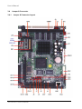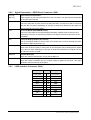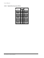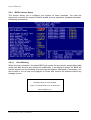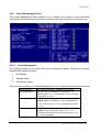
1
User’s Manual EBC5410 All-in-One NS Geode GX1 Single Board with LCD, AC97 Audio, 10/100Base-Tx Ethernet Interface, 4COMs, & Optional LVDS, DSTN Companion Chip . EBC5410 FCC STATEMENT THIS DEVICE COMPLIES WITH PART 15 FCC RULES. OPERATION IS SUBJECT TO THE FOLLOWING TWO CONDITIONS: (1) THIS DEVICE MAY NOT CAUSE HARMFUL INTERFERENCE. (2) THIS DEVICE MUST ACCEPT ANY INTERFERENCE RECEIVED INCLUDING OPERATION. INTERFERENCE THAT MAY CAUSE UNDESIRED THIS EQUIPMENT HAS BEEN TESTED AND FOUND TO COMPLY WITH THE LIMITS FOR A CLASS "A" DIGITAL DEVICE, PURSUANT TO PART 15 OF THE FCC RULES. THESE LIMITS ARE DESIGNED TO PROVIDE REASONABLE PROTECTION AGAINTST HARMFUL INTERFERENCE WHEN THE EQUIPMENT IS OPERATED IN A COMMERCIAL ENVIRONMENT. THIS EQUIPMENT GENERATES, USES, AND CAN RADIATE RADIO FREQUENCY ENERGY AND, IF NOT INSTATLLED AND USED IN ACCORDANCE WITH THE INSTRUCTION MANUAL, MAY CAUSE HARMFUL INTERFERENCE TO RADIO COMMUNICATIONS. OPERATION OF THIS EQUIPMENT IN A RESIDENTIAL AREA IS LIKELY TO CAUSE HARMFUL INTERFERENCE IN WHICH CASE THE USER WILL BE REQUIRED TO CORRECT THE INTERFERENCE AT HIS OWN EXPENSE. BCM Advanced Research User’s Manual Copyright Notice Copyright 2001, BCM Advanced Research, ALL RIGHTS RESERVED. No part of this document may be reproduced, copied, translated, or transmitted in any form or by any means, electronic or mechanical, for any purpose, without the prior written permission of the original manufacturer. Trademark Acknowledgement Brand and product names are trademarks or registered trademarks of their respective owners. Disclaimer BCM Advanced Research reserves the right to make changes, without notice, to any product, including circuits and/or software described or contained in this manual in order to improve design and/or performance. BCM Technology assumes no responsibility or liability for the use of the described product(s), conveys no license or title under any patent, copyright, or mask work rights to these products, and makes no representations or warranties that these products are free from patent, copyright, or mask work right infringement, unless otherwise specified. Applications that are described in this manual are for illustration purposes only. BCM Advanced Research makes no representation or warranty that such application will be suitable for the specified use without further testing or modification. Life Support Policy BCM Technology’s PRODUCTS ARE NOT FOR USE AS CRITICAL COMPONENTS IN LIFE SUPPORT DEVICES OR SYSTEMS WITHOUT THE PRIOR WRITTEN APPROVAL OF BCM Advanced Research As used herein: 1. Life support devices or systems are devices or systems which, (a) are intended for surgical implant into body, or (b) support or sustain life and whose failure to perform, when properly used in accordance with instructions for use provided in the labelling, can be reasonably expected to result in significant injury to the user. 2. A critical component is any component of a life support device or system whose failure to perform can be reasonably expected to cause the failure of the life support device or system, or to affect its safety or effectiveness. BCM Advanced Research EBC5410 A Message to the Customer BCM Customer Services Each and every BCM’S product is built to the most exacting specifications to ensure reliable performance in the harsh and demanding conditions typical of industrial environments. Whether your new BCM device is destined for the laboratory or the factory floor, you can be assured that your product will provide the reliability and ease of operation for which the name BCM has come to be known. Your satisfaction is our primary concern. Here is a guide to BCM’S customer services. To ensure you get the full benefit of our services, please follow the instructions below carefully. Technical Support We want you to get the maximum performance from your products. So if you run into technical difficulties, we are here to help. For the most frequently asked questions, you can easily find answers in your product documentation. These answers are normally a lot more detailed than the ones we can give over the phone. So please consult this manual first. To receive the latest version of the user manual, please visit our Web site at: http://www.bcmcom.com/ If you still cannot find the answer, gather all the information or questions that apply to your problem, and with the product close at hand, call your dealer. Our dealers are well trained and ready to give you the support you need to get the most from your BCM’S products. In fact, most problems reported are minor and are able to be easily solved over the phone. In addition, free technical support is available from BCM’S engineers every business day. We are always ready to give advice on application requirements or specific information on the installation and operation of any of our products. Please do not hesitate to call or email us. Headquarters BCM Advanced Research Tel: 949-470-1888 Fax: 949-470-0971 http://www.bcmcom.com E-mail: [email protected] BCM Advanced Research User’s Manual Product Warranty BCM warrants to you, the original purchaser, that each of its products will be free from defects in materials and workmanship for two years from the date of purchase. This warranty does not apply to any products which have been repaired or altered by persons other than repair personnel authorized by BCM, or which have been subject to misuse, abuse, accident or improper installation. BCM assumes no liability under the terms of this warranty as a consequence of such events. Because of BCM’S high qualitycontrol standards and rigorous testing, most of our customers never need to use our repair service. If a BCM’S product is defective, it will be repaired or replaced at no charge during the warranty period. For out-of-warranty repairs, you will be billed according to the cost of replacement materials, service time, and freight. Please consult your dealer for more details. If you think you have a defective product, follow these steps: 1. Collect all the information about the problem encountered. (For example, CPU type and speed, BCM’S products model name, hardware & BIOS revision number, other hardware and software used, etc.) Note anything abnormal and list any on-screen messages you get when the problem occurs. 2. Call your dealer and describe the problem. Please have your manual, product, and any helpful information readily available. 3. If your product is diagnosed as defective, obtain an RMA (return material authorization) number from your dealer. This allows us to process your good return more quickly. 4. Carefully pack the defective product, a complete Repair and Replacement Order Card and a photocopy proof of purchase date (such as your sales receipt) in a shippable container. A product returned without proof of the purchase date is not eligible for warranty service. 5. Write the RMA number visibly on the outside of the package and ship it prepaid to your dealer. BCM Advanced Research EBC5410 Packing List Before you begin installing your single board, please make sure that the following materials have been shipped: 1 EBC5410 All-in-One NS Geode GX1 Computing Module 1 Quick Installation Guide 1 CD-ROM contains the followings: — User’s Manual (this manual in PDF file) — Ethernet driver and utilities — VGA drivers and utilities — Audio drivers and utilities — Latest BIOS (as of the CD-ROM was made) If any of these items are missing or damaged, please contact your distributor or sales representative immediately. BCM Advanced Research User’s Manual 1. MANUAL OBJECTIVES .............................................................................................1 2. INTRODUCTION.........................................................................................................2 2.1 System Overview ...................................................................................................2 2.2 System Specifications ...........................................................................................3 2.3 Architecture Overview ...........................................................................................6 2.3.1 2.3.2 2.3.3 2.3.4 2.3.5 2.3.6 2.3.7 2.3.8 2.3.9 2.3.10 2.3.11 2.3.12 2.3.13 2.3.14 2.3.15 2.3.16 3. CPU/GX1 and CS5530A .............................................................................................. 7 XPRESS Graphics ....................................................................................................... 7 PCI Bus ....................................................................................................................... 7 PC/104 Interface.......................................................................................................... 8 SDRAM Interface ......................................................................................................... 8 TFT Panel Interface ..................................................................................................... 8 Audio ........................................................................................................................... 8 IDE Interface................................................................................................................ 8 USB ............................................................................................................................. 9 Realtek RTL8139C Ethernet Controller........................................................................ 9 NS PC97317VUL ......................................................................................................... 9 Winbond W83977EF-AW ............................................................................................ 9 M-Systems DiskOnChip Socket (Optional)................................................................. 10 Compact Flash Interface............................................................................................ 10 NS CS9211 DSTN Companion Chip (EBC-5410D Only) ........................................... 11 NS DS90363A LVDS Transmitter Chip (EBC-5410V Only) ........................................ 11 HARDWARE CONFIGURATION ..............................................................................12 3.1 Installation Procedure .........................................................................................12 3.2 Safety Precautions ...............................................................................................12 3.2.1 3.2.2 3.3 Installing DRAM (DIMMs).....................................................................................13 3.3.1 3.3.2 3.3.3 3.4 System Memory ......................................................................................................... 13 Supplementary Information About DIMM ................................................................... 13 Memory Installation Procedures................................................................................. 13 Jumper & Connector............................................................................................14 3.4.1 3.4.2 3.5 Warning! .................................................................................................................... 12 Caution! ..................................................................................................................... 12 Jumper & Connector Layout ...................................................................................... 14 Jumper & Connector List ........................................................................................... 15 Setting Jumpers ...................................................................................................17 3.5.1 3.5.2 3.5.3 3.5.4 3.5.5 3.5.6 3.5.7 LCD Driving & Backlight Voltage Select (J2).............................................................. 17 Clear CMOS (J3 / Pin 1, 3, 5) .................................................................................... 18 LCD Clock Signal Select (J3 / Pin 2, 4, 6).................................................................. 18 COM3 / 4 Pin 9 Signal Select (J5 / J6)....................................................................... 19 COM2 RS-232/422/485 Select (J7, J8) ...................................................................... 19 LVDS VDD Voltage Select (JP3, EBC-5410V Only)................................................... 20 M-Systems DiskOnChip Memory Address Select (JP4, Optional) .............................. 20 BCM Advanced Research EBC5410 3.6 Connector Definitions..........................................................................................21 3.6.1 3.6.2 3.6.3 3.6.4 3.6.5 3.6.6 3.6.7 3.6.8 3.6.9 3.6.10 3.6.11 3.6.12 3.6.13 3.6.14 3.6.15 3.6.16 3.6.17 3.6.18 3.6.19 3.6.20 3.6.21 3.6.22 3.6.23 3.6.24 3.6.25 3.6.26 3.6.27 3.6.28 3.6.29 3.6.30 3.6.31 3.6.32 3.6.33 3.6.34 3.6.35 3.6.36 3.6.37 3.6.38 3.6.39 3.6.40 3.6.41 3.6.42 3.6.43 3.6.44 4. LCD Inverter Connector (CN1)................................................................................... 21 TFT Panel Connector (CN2) ...................................................................................... 22 Signal Description – TFT Panel Connector (CN2)...................................................... 23 Signal Configuration – TFT Panel Displays................................................................ 23 DSTN Panel Connector (CN2, EBC-5410D Only) ...................................................... 24 Signal Description – DSTN Panel Connector (CN2)................................................... 25 LVDS Interface Connector (CN3)............................................................................... 25 CRT Connector (CN4) ............................................................................................... 26 Signal Description – CRT Connector (CN4) ............................................................... 26 Audio Output Connector (CN5) .................................................................................. 27 Signal Description – Audio Connector (CN5) ............................................................. 27 IrDA Connector (CN6)................................................................................................ 27 Signal Configuration – IrDA Connector (CN6)............................................................ 27 Fan Connector (CN8)................................................................................................. 28 Pin Header Serial Port 1 / 2 / 3 / 4 Connector in RS-232 Mode (CN9) ....................... 28 Serial Port 1 / 2 / 3 / 4 with External DB9 Connector.................................................. 29 Signal Description – Serial Port 1 / 2 / 3 / 4 Connector in RS-232 Mode (CN9) ......... 29 Pin Header Serial Port 2 Connector in RS-422 Mode (CN9 / Pin 11~20) ................... 30 Signal Description – Serial Port 2 in RS-422 Mode (CN9 / Pin 11~20)....................... 30 Pin Header Serial Port 2 Connector in RS-485 Mode (CN9 / Pin 11~20) ................... 31 Signal Description – Serial Port 2 in RS-485 Mode (CN9 / Pin 11~20)....................... 31 Parallel Port Connector (CN10) ................................................................................. 32 DB25 Parallel Port Connector .................................................................................... 33 Signal Description – Parallel Port (CN10) .................................................................. 34 PC/104 Connector (CN11, CN12) .............................................................................. 35 Signal Description – PC/104 Connector (CN11, CN12).............................................. 36 Keyboard and PS/2 Mouse Connector (CN13)........................................................... 39 Signal Description – Keyboard and PS/2 Mouse Connector (CN13) .......................... 39 IDE Device Connector (CN14) ................................................................................... 40 Signal Description – IDE Device Connector (CN14)................................................... 41 USB Connector (CN15) ............................................................................................. 42 Signal Description – USB Connector (CN15) ............................................................. 42 Auxiliary Power Connector (J1).................................................................................. 42 CD-ROM Audio Input Connector (J4)......................................................................... 42 Signal Configuration – CD-ROM Input Connector (J4)............................................... 42 Front Panel Connector (JP1) ..................................................................................... 43 Signal Description – Front Panel Connector (JP1) ..................................................... 43 LCD Backlight Brightness Adjustment Connector (JP2)............................................. 44 Digital Input / Output Connector (JP5) ....................................................................... 45 Digital Input / Output Programming (JP5) .................................................................. 45 10/100 BASE-Tx Ethernet Connector (LAN1) ............................................................ 46 Signal Description – 10/100Base-Tx Ethernet Connector (LAN1) .............................. 46 Power Connector 1 (PWR1) ...................................................................................... 47 STN LCD Contrast Adjustment Connector (VR1)....................................................... 47 AWARD BIOS SETUP..............................................................................................48 4.1 Starting Setup.......................................................................................................48 4.2 Using Setup ..........................................................................................................49 BCM Advanced Research User’s Manual 4.3 Getting Help..........................................................................................................49 4.4 In Case of Problems.............................................................................................49 4.5 Main Menu.............................................................................................................50 4.5.1 4.5.2 4.5.3 4.5.4 4.5.5 4.5.6 4.5.7 4.5.8 4.5.9 5. DRIVER INSTALLATION..........................................................................................75 5.1 Driver installation for Ethernet Adapter .............................................................75 5.1.1 5.1.2 5.2 5.3 Windows 9x ............................................................................................................... 75 Windows NT 4.0 Ethernet Installation ........................................................................ 80 Driver Installation for Display Adapter ...............................................................86 5.2.1 5.2.2 Windows 9x ............................................................................................................... 86 Windows NT 4.0 Display Installation .......................................................................... 91 Driver Installation for Audio Adapter..................................................................95 5.3.1 5.3.2 6. Setup Items ............................................................................................................... 50 Standard CMOS Setup .............................................................................................. 52 BIOS Features Setup................................................................................................. 56 Chipset Features Setup ............................................................................................. 61 Power Management Setup......................................................................................... 63 PnP/PCI Configuration Setup..................................................................................... 66 Integrated Peripherals Features Setup ...................................................................... 68 Supervisor/User Password Setting............................................................................. 72 Exit Selecting ............................................................................................................. 73 Windows 9x ............................................................................................................... 95 Windows NT 4.0 Audio Installation .......................................................................... 104 MEASUREMENT DRAWING..................................................................................108 BCM Advanced Research EBC5410 APPENDIX A: BIOS REVISIONS....................................................................................109 APPENDIX B: SYSTEM RESOURCES...........................................................................110 Memory Map......................................................................................................................... 110 I/O – Map.............................................................................................................................. 111 Interrupt Usage..................................................................................................................... 112 DMA-channel Usage............................................................................................................. 113 APPENDIX C: PROGRAMMING THE WATCHDOG TIMER...........................................114 Introduction........................................................................................................................... 114 Configure Register................................................................................................................ 114 Programming Watchdog Timer............................................................................................. 115 Demo Program 1 (Micro-Assembly Language) ..................................................................... 117 Demo Program 2 (C Language)............................................................................................ 120 APPENDIX D: AWARD BIOS ERROR MESSAGE .........................................................122 Beep 122 BIOS ROM Checksum Error – System Halted ...................................................................... 122 CMOS Battery Failed ............................................................................................................ 122 CMOS Checksum Error ........................................................................................................ 122 Disk Boot Failure, Insert System Disk and Press Enter ........................................................ 122 Diskette Drives or Types Mismatch Error – Run Setup ......................................................... 122 Display Switch is Set Incorrectly. .......................................................................................... 122 Display Type has Changed Since Last Boot ......................................................................... 123 EISA Configuration Checksum Error Please Run EISA Configuration Utility......................... 123 EISA Configuration Is Not Complete Please Run EISA Configuration Utility......................... 123 Error Encountered Initializing Hard Drive .............................................................................. 123 Error Initializing Hard Disk Controller .................................................................................... 123 Floppy Disk(s) Fail ................................................................................................................ 123 Floppy Disk(s) fail (80) → Unable To Reset Floppy Subsystem............................................ 123 Floppy Disk(s) fail (40) → Floppy Type Dismatch ................................................................. 123 Hard Disk(s) fail (80) → HDD Reset Failed....................................................................... 123 Hard Disk(s) fail (40) → HDD Controller Diagnostics Failed ............................................. 123 Hard Disk(s) fail (20) → HDD Initialization Error ............................................................... 123 Hard Disk(s) fail (10) → Unable To Recalibrate Fixed Disk............................................... 123 Hard Disk(s) fail (08) → Sector Verify Failed .................................................................... 123 Invalid EISA Configuration Please Run EISA Configuration Utility ........................................ 124 Keyboard is Locked Out – Unlock the Key............................................................................ 124 Keyboard Error or No Keyboard Present .............................................................................. 124 Keyboard Error or No Keyboard Present .............................................................................. 124 Memory Address Error at ..................................................................................................... 124 Memory parity Error at ... ...................................................................................................... 124 Memory Size Has Changed Since Last Boot ........................................................................ 124 Memory Verify Error at ......................................................................................................... 124 Manufacturing Post Loop...................................................................................................... 124 Memory Test Fail .................................................................................................................. 125 Offending Address Not Found .............................................................................................. 125 Offending Segement............................................................................................................. 125 Press a Key To Reboot......................................................................................................... 125 BCM Advanced Research User’s Manual Press F1 To Disable NMI, F2 To Reboot .............................................................................. 125 RAM Parity Error - Checking for Segment ... ........................................................................ 125 Should Be Empty But EISA Board Found Please Run EISA Configuration UTILITY............. 125 Should Have EISA Board But Not Found Please Run EISA Configuration Utility.................. 125 Slot Not Empty...................................................................................................................... 125 System Halted, (CTRL-Alt-Del) To Reboot ... ....................................................................... 126 Wrong Board In Slot Please Run EISA Configuration Utility ................................................. 126 APPENDIX E: AWARD BIOS POST CODES .................................................................127 BCM Advanced Research EBC5410 Document Amendment History Revision 1st Date Oct. ‘01. By Philip Chang 1. BCM Advanced Research Comment Initial Release EBC5410 1. Manual Objectives This manual describes in detail the BCM Technology EBC-5410 Single Board. We have tried to include as much information as possible but we have not duplicated information that is provided in the standard IBM Technical References, unless it proved to be necessary to aid in the understanding of this board. We strongly recommend that you study this manual carefully before attempting to interface with EBC-5410 or change the standard configurations. Whilst all the necessary information is available in this manual we would recommend that unless you are confident, you contact your supplier for guidance. Please be aware that it is possible to create configurations within the CMOS RAM that make booting impossible. If this should happen, clear the CMOS settings, (see the description of the Jumper Settings for details). If you have any suggestions or find any errors concerning this manual and want to inform us of these, please contact our Customer Service department with the relevant details. EBC5410 User’s Manual 1 User’s Manual 2. 2.1 Introduction System Overview The EBC-5410 is a compact 5.25" CD-ROM size Single Board Computer that equips with NS Geode GX1 processor, LCD interface, AC97 Audio, PCI-bus Ethernet interface, and 64MB SDRAM onboard. Targeting on the rapid growing information appliance and embedded system markets, the EBC-5410 comes designed with a PCI-bus Realtek RTL8139C 10/100Base-Tx Ethernet controller, TFT flat panel interface, and 4 serial ports. Making it a perfect solution for not only popular information appliance devices like WBT (Windows Based Terminal), Thin Client, STB (Set Top Box), Web Phone but also Retail/Financial Transaction Terminals. Unlike others in its kind, the EBC-5410 comes with an optional companion NS CS9211 DSTN LCD controller, which allows you to connect EBC-5410 with low-cost DSTN color or mono LCD’s. In addition, a 4-bit TTL digital input & 4-bit TTL digital output interface is also implemented. These make the EBC-5410 also ideal for multimedia POS/KIOSK Terminals that require low-cost but reliable Single Board Computer. Further more, the optional 18-bit LVDS transmitter and onboard 64MB SDRAM make the EBC-5410 also an excellent fit for wide-range embedded system requirements. Other impressive features include a built-in AC97 Audio, a Compact Flash socket for type I/II Compact Flash storage card, one optional 32-pin DIP socket that supports M-Systems DiskOnChip 2000 series flash memory up to 288MB, one parallel port, and a 168-pin DIMM socket allowing for up to 256 MB of SDRAM to be installed, and a PCI slot for future expansion. 2 3 4 5 5 6 7 8 2 EBC5410 User’s Manual EBC5410 2.2 System Specifications General Functions ‧CPU: Onboard NS Geode GX1 300MHz (available in different speeds by special order), BGA package ‧BIOS: Award 256KB Flash BIOS ‧Chipset: NS Geode CS5530A ‧I/O Chipset: NS PC97317VUL, Winbond W83977EF-AW ‧Memory: Onboard 64MB SDRAM and one 168-pin DIMM socket supports up to 320 Mbytes SDRAM ‧ Enhanced IDE: Supports two IDE devices. Supports Ultra DMA/33 mode with data transfer rate up to 33MB/sec. ‧FDD interface: Supports up to two floppy disk drives, 5.25" (360KB and 1.2MB) and/or 3.5" (720KB, 1.44MB, and 2.88MB) ‧Parallel port: Internal header for bi-directional parallel port x 1. Supports SPP, ECP, and EPP modes ‧ Serial port: Three RS-232 and one RS-232/422/485 serial port. Ports can be configured as COM1, COM2, COM3, COM4, or disabled individually. (16C550 equivalent) ‧IR interface: Supports one IrDA Tx/Rx header ‧KB/Mouse connector: 8-pin (4 x 2) connector supports PS/2 keyboard and mouse ‧USB connectors: One 5 x 2 header onboard supports dual USB ports ‧Watchdog Timer: Can generate a system reset, IRQ15 or NMI. Software selectable time out interval (32 sec. ~ 254 min., 1 min./step) ‧DMA: 7 DMA channels (8237 equivalent) ‧Interrupt: 15 interrupt levels (8259 equivalent) ‧Power management: Supports ATX power supply. Supports PC97, LAN wake up and modem ring-in functions. I/O peripheral devices support power saving and doze/standby/suspend modes. APM 1.2 compliant. EBC5410 User’s Manual 3 User’s Manual Flat Panel/CRT Interface (EBC-5410/EBC-5410V) ‧Chipset: NS Geode CS5530A ‧Display memory: Shared display memory up to 4MB ‧Display type: Supports non-interlaced CRT and up to 18-bit TFT LCD displays. Can display both CRT and flat panel simultaneously ‧Resolution: Up to 1280 x 1024 x 8 bpp and 1024 x 768 x 16 bpp Flat Panel/CRT Interface (EBC-5410D) ‧Chipset: NS Geode CS5530A / NS CS9211 ‧Display memory: 1MB display frame buffer ‧Display type: Simultaneously supports CRT and flat panel (EL, LCD and gas plasma) displays LVDS Interface (EBC-5410V Only) ‧Chipset: NS DS90C363A or equivalents ‧Display type: Supports 18-bit LVDS TFT panels Audio Interface ‧Chipset: NS Geode CS5530A ‧ Audio controller: AC97 ver.2.0 compliant interface, Multi-stream Direct Sound and Direct Sound 3D acceleration ‧Audio interface: Microphone in, Line in, CD audio in, line out Ethernet Interface ‧Chipset: Realtek RTL8139C PCI-bus Ethernet controllers onboard ‧Ethernet interface: PCI 100/10 Mbps, IEEE 802.3U compatible ‧Remote Boot-ROM: For diskless system SSD Interface One CF socket supports Type I / II Compact Flash Card Digital I/O Interface 4-bit TTL digital input and 4-bits TTL digital output 4 EBC5410 User’s Manual EBC5410 Expansion Interface ‧PC/104 connector: One 16-bit 104-pin connector onboard ‧PCI slot: One 32-bit PCI slot onboard Mechanical and Environmental ‧Power supply voltage: +5V (4.75V to 5.25V) ‧Typical power requirement: 5V @ 2A w/ GX1 300MHz ‧Operating temperature: 32 to 140°F (0 to 60°C) ‧Board size: 8”(L) x 5.75”(W) (203mm x 146mm) ‧Weight: 0.4 Kg EBC5410 User’s Manual 5 User’s Manual 2.3 Architecture Overview The following block diagram shows the architecture and main components of EBC-5410 series. The two key components on board are the NS Geode GX1 CPU and the CS5530A companion chip. These two devices provide the ISA and PCI bus to which all the major components are attached. The following sections provide detail information about the functions provided onboard. 6 EBC5410 User’s Manual EBC5410 2.3.1 CPU/GX1 and CS5530A The NS Geode GX1 along with the CS5530A companion chip provide the basic functionality and buses of the system: Interface to SDRAM, 64-bit data bus. PC100 compliant SDRAM must be used. PCI interface provided by GX1 CPU. PCI to ISA Bridge provided by CS5530A. VGA controller with video memory shared with system memory (UMA). The image data is transferred to the companion chip by means of Pixel bus. CRT and TFT interface. Data provided by the Pixel and Video interface from the CPU. The TFT interface and SA part of the ISA bus share pins as described later. Video interface from GX1 to the CS5530A. This data-stream is buffered and multiplexed with the Pixel bus for windowed video viewing. This interface may assist the processor in connection motion picture decoding. USB integrated in the CS5530A. IDE interface support Ultra DMA. Tow connectors are provided: A 44 pin pitch 2.0mm standard IDE interface on the primary controller and a Compact Flash connector on the secondary controller. Digital audio interface to an AC97 compliant audio codec. 2.3.2 XPRESS Graphics The XPRESS Graphics is based on the GX1 CPU and the CS5530A Companion chip and this graphics controller is very cost efficient since almost no additional components are required. This is achieved by using the SDRAM as frame-buffer and by integrating the graphics engine and display interface in the GX1 CPU and the CS5530A companion chip. This controller provides a CRT as well as a TFT interface which support the modes listed below: The TFT panel interface is available as a parallel interface in the CN2 connector. 2.3.3 PCI Bus The PCI-bus on the board is provided by the GX1 CPU and will always run at 33MHz. The GX1 CPU provides support for up to three bus masters. The CS5530A and Realtek RTL8139C Ethernet controller uses these bus-mastering signals. EBC5410 User’s Manual 7 User’s Manual 2.3.4 PC/104 Interface The CS5530A companion chip provides a PCI-ISA Bridge that may operate in master or slave mode. EBC-5410 series only support ISA slave mode. ISA master mode allows an ISA board to grant the bus and thereby get the bus master status. The bus master has the ability to generate bus cycles and thereby transfer data without involvement of the CPU or DMA (Direct memory access). However, ISA add-on card, which utilizes the bus master mode, is very rare today. A 104-pin PC/104 connector is equipped onboard for future expansion. 2.3.5 SDRAM Interface This board uses SDRAM in the 168-pin DIMM form factor. 3.3V PC 100 SDRAM modules are recommended. 2.3.6 TFT Panel Interface An alternative display to the standard CRT monitor is a digital flat panel interface in which the color of each pixel is digitally encoded. The panel data may be transferred in parallel where the color of each pixel is transferred over a number of signal lines at rates up to 65MHz. The parallel interface is only suitable for short distance (less than 50 cm) and is typically implemented by using of ribbon cables. One should be careful in the EMC design of the box and cabling when this interface is used. It should also be noted that the signal level of this interface is 3.3V, but does comply with the TTL signal levels. Some - most older displays require 5V signal level. 2.3.7 Audio The CS5530A companion chip provides audio support through an AC97 codec interface. The audio codec provides mixing of the analog signals as well as Digital/Analog conversion. The following analog interfaces are provided. Line-in, stereo. CD-ROM input, stereo. Microphone, single input with microphone bias circuit. Line-Out, stereo. Access to the audio signals is provided by an 8 x 2 header (CN5) or by an optional audio bracket. 2.3.8 IDE Interface A primary as well as a secondary IDE controller is provided by the CS5530A companion chip which supports Ultra DMA mode and PCI bus mastering for the data transfer. A standard IDE 40-pin connector and a Compact Flash type II connector provide access to these controllers. 8 EBC5410 User’s Manual EBC5410 2.3.9 USB The USB interface provides two USB channels that are controlled by the CS5530A. The signals are provided by means of a 5 x 2 header, an optional USB bracket adapter is been use. 2.3.10 Realtek RTL8139C Ethernet Controller The Realtek RTL8139C is a highly integrated and cost-effective single-chip Fast Ethernet controller that provides 32-bit performance, PCI bus master capability, and full compliance with IEEE 802.3u 100Base-T specifications and IEEE 802.3x Full Duplex Flow Control. It also supports Advanced Configuration Power management Interface (ACPI), PCI power management for modern operating systems that is capable of Operating System Directed Power Management (OSPM) to achieve the most efficient power management. 2.3.11 NS PC97317VUL The NS PC97317VUL Super I/O chip provides most input / output interfaces of the system as the following: COM 1. Operates in RS-232 mode through a charge pump driver. Only 5V supply is required COM 2. A RS-232/RS-422/RS-485 driver is used whereby RS-232, RS-422 and RS485 are provided. Using hardware jumper to makes mode selections. Driver uses charge pumps whereby only +5V is required LPT. Support for SPP, EPP and ECP modes Floppy interface Keyboard interface PS/2 Mouse interface IrDA interface for infrared communication. This interface shares the controller of COM2 Provision of buffered ISA data bus for BIOS (denoted XDBus) NVRAM with battery backup for BIOS configuration and real time clock ACPI Controller/Extender that supports the requirements of the ACPI spec (rev 1.0) An APC that controls the main power supply to the system using open-drain output 2.3.12 Winbond W83977EF-AW The Winbond W83977EF-AW Super I/O chip provides COM3 / COM4 serial port and Watchdog timer of the system as the following: COM 3. Operates in RS-232 mode through a charge pump driver. Only 5V supply is required COM 4. Operates in RS-232 mode through a charge pump driver. Only 5V supply is required EBC5410 User’s Manual 9 User’s Manual Watchdog timer 2.3.13 M-Systems DiskOnChip Socket (Optional) M-Systems DiskOnChip 2000 is a high performance flash disk in a standard 32-pin DIP package. This unique data storage solution offers cost effective data storage beyond that of traditional hard disks. Perfect for applications with limited space and varying capacity requirements. The DiskOnChip 2000 is simply integrated into your CPU board and you have a bootable flash disk. The DiskOnChip 2000 includes M-Systems proprietary TrueFFS® (True Flash File System) technology built-in, providing complete read/write capability and hard disk emulation. TrueFFS provides hard disk compatibility at both the sector and file level. The DiskOnChip 2000 works in all major operating systems including DOS, Windows Embedded NT/CE/2000, Linux, pSOS+, VxWorks, QNX, BE and more. It is also relatively easy to customize to work in O/S-less and non-x86 environments. The use of TrueFFS, in conjunction with the built-in EDC/ECC, provides maximum data reliability, even under harsh operating conditions such as power failures. Advanced wear leveling ensures long flash life for maximum usage. 2.3.14 Compact Flash Interface A Compact Flash type II connector is connected to the secondary IDE controller. The Compact Flash storage card is IDE compatible. It is an ideal replacement for standard IDE hard drives. The solid-state design offers no seek errors even under extreme shock and vibration conditions. The Compact Flash storage card is extremely small and highly suitable for rugged environments, thus providing an excellent solution for mobile applications with space limitations. It is fully compatible with all consumer applications designed for data storage PC card, PDA, and Smart Cellular Phones, allowing simple use for the end user. The Compact Flash storage card is O/S independent, thus offering an optimal solution for embedded systems operating in non-standard computing environments. The Compact Flash storage card is IDE compatible and offers various capacities. 10 EBC5410 User’s Manual EBC5410 2.3.15 NS CS9211 DSTN Companion Chip (EBC-5410D Only) The National Semiconductor ® Geode™ CS9211 graphics companion is suitable for systems that use any GX-series processor (e.g., GX1, GXLV, GXm) along with the CS5530A I/O companion, also members of the Geode family of products. The CS9211 converts the digital pixel stream output of the CS5530A to the digital RGB inputs used by standard single and dual-scan STN LCD display panels. Support is provided for both color and monochrome dual-scan STN (DSTN) flat panels up to 1024x768 resolution, and for color single-scan panels up to 640x480 resolution. 2.3.16 NS DS90363A LVDS Transmitter Chip (EBC-5410V Only) The DS90C363A/DS90CF363A transmitter converts 21 bits of CMOS/TTL data into three LVDS (Low Voltage Differential Signaling) data streams. A phase-locked transmit clock is transmitted in parallel with the data streams over a fourth LVDS link. Every cycle of the transmit clock 21 bits of input data are sampled and transmitted. At a transmit clock frequency of 65 MHz, 18 bits of RGB data and 3 bits of LCD timing and control data (FPLINE, FPFRAME, DRDY) are transmitted at a rate of 455 Mbps per LVDS data channel. Using a 65 MHz clock, the data throughput is 170 Mbytes/sec. The DS90C363A transmitter can be programmed for Rising edge strobe or Falling edge strobe through a dedicated pin. The DS90CF363A is fixed as a Falling edge strobe transmitter. A Rising edge or Falling edge strobe transmitter will interoperate with a Falling edge strobe Receiver (DS90CF364) without any translation logic. This chipset is an ideal means to solve EMI and cable size problems associated with wide, high speed TTL interfaces. EBC5410 User’s Manual 11 User’s Manual 3. Hardware Configuration 3.1 Installation Procedure 1. Turn off the power supply. 2. Insert the DIMM module (be careful with the orientation). 3. Insert all external cables for hard disk, floppy, keyboard, mouse, USB etc. except for flat panel. A CRT monitor must be connected in order to change CMOS settings to support flat panel. 4. Connect power supply to the board via the PWR1. 5. Turn on the power. 6. Enter the BIOS setup by pressing the delete key during boot up. Use the “LOAD BIOS DEFAULTS” feature. The Integrated Peripheral Setup and the Standard CMOS Setup Window must be entered and configured correctly to match the particular system configuration. 7. If TFT panel display is to be utilised, make sure the panel voltage is correctly set before connecting the display cable and turning on the power. 3.2 3.2.1 Safety Precautions Warning! Always completely disconnect the power cord from your chassis or power cable from your board whenever you work with the hardware. Do not make connections while the power is on. Sensitive electronic components can be damaged by sudden power surges. Only experienced electronics personnel should open the PC chassis. 3.2.2 Caution! Always ground yourself to remove any static charge before touching the board. Modern electronic devices are very sensitive to static electric charges. As a safety precaution, use a grounding wrist strap at all times. Place all electronic components in a static-dissipative surface or staticshielded bag when they are not in the chassis. 12 EBC5410 User’s Manual EBC5410 3.3 3.3.1 Installing DRAM (DIMMs) System Memory The reverse side of the EBC-5410 series contains a socket for 144-pin dual inline memory module (DIMM). The socket uses 3.3 V unbuffered synchronous DRAM (SDRAM). DIMM module is available in capacities of 32, 64, 128, or 256 MB. The socket can be filled in the DIMM of any size, giving your EBC-5410 series single board between 32 and 256 MB of memory. 3.3.2 Supplementary Information About DIMM Your EBC-5410 series accepts both regular and PC-100 SDRAM DIMM Module (with or without parity). Single-sided modules are typically 64 MB; double-sided modules are usually 32 or 128 MB. 3.3.3 Memory Installation Procedures Press the DIMM module right down into the socket, until you hear a click. This is when the two handles have automatically locked the memory module into the correct position of the DIMM socket. (See Figure below) To take away the memory module, just push both handles outward, and the memory module will be ejected by the mechanism in the socket. EBC5410 User’s Manual 13 User’s Manual 3.4 3.4.1 Jumper & Connector Jumper & Connector Layout 14 EBC5410 User’s Manual EBC5410 3.4.2 Jumper & Connector List Connectors on the board are linked to external devices such as hard disk drives, keyboard, mouse, or floppy drives. In addition, the board has a number of jumpers that allow you to configure your system to suit your application. The following tables list the function of each of the board's jumpers and connectors. Jumpers Label J2 J3 J5 J6 J7, J8 Function LCD driving & backlight voltage select Clear CMOS / LCD clock signal select COM3 pin 9 signal select COM4 pin 9 signal select COM2 RS-232/422/485 select JP3 LVDS VDD voltage select JP4 DOC memory address select (optional) Note 3 x 2 header, pitch 2.0mm 3 x 2 header, pitch 2.0mm 3 x 2 header, pitch 2.0mm 3 x 2 header, pitch 2.0mm 3 x 2 header, pitch 2.0mm 4 x 3 header, pitch 2.0mm (J8) 3 x 1 header, pitch 2.54mm (EBC-5410V only) 2 x 2 header, pitch 2.0mm EBC5410 User’s Manual 15 User’s Manual Connectors Label Function CN1 LCD inverter connector 5 x 1 wafer, pitch 2.0mm CN2 TFT/DSTN panel connector CN3 LVDS interface connector CN4 CRT connector HIROSE DF13-40DP-1.25V (Only EBC-5410D supports DSTN Panels) 10 x 2 header, pitch 2.54mm (EBC-5410V only) 8 x 2 header, pitch 2.54mm CN5 CN6 Audio output connector IrDA connector 8 x 2 header, pitch 2.54mm 5 x 1 header, pitch 2.54mm CN7 Floppy connector 17 x 2 header, pitch 2.54mm CN8 Fan connector CN9 CN10 Serial port 1 / 2 / 3 / 4 connector Parallel port connector CN11, CN12 PC/104 connector CN13 Keyboard and PS/2 mouse connector 4 x 2 header, pitch 2.54mm CN14 IDE connector 20 x 2 header, pitch 2.54mm CN15 USB connector 5 x 2 header, pitch 2.54mm J1 Auxiliary power connector 3 x 1 wafer, pitch 2.54mm J4 CD-ROM audio input connector 4 x 1 wafer, pitch 2.0mm JP1 JP2 Front panel connector 8 x 2 header, pitch 2.54mm 3 x 1 header, pitch 2.54mm JP5 LCD Backlight brightness adjustment connector Digital input / output connector LAN1 PWR1 10/100Base-Tx Ethernet 1 connector Power connector RJ-45 SN1 Compact Flash connector U25 M-Systems DOC socket (optional) VR1 STN LCD contrast adjustment connector DIMM1 168-pin DIMM socket 16 EBC5410 User’s Manual Note 20 x 2 header, pitch 2.54mm 13 x 2 header, pitch 2.54mm 4 x 2 header, pitch 2.54mm 3 x 1 header, pitch 2.54mm (EBC-5410D only) EBC5410 3.5 Setting Jumpers You can configure your board to match the needs of your application by setting jumpers. A jumper is the simplest kind of electric switch. It consists of two metal pins and a small metal clip (often protected by a plastic cover) that slides over the pins to connect them. To “close” a jumper you connect the pins with the clip. To “open” a jumper you remove the clip. Sometimes a jumper will have three pins, labeled 1, 2, and 3. In this case, you would connect either two pins. The jumper settings are schematically depicted in this manual as follows: A pair of needle-nose pliers may be helpful when working with jumpers. If you have any doubts about the best hardware configuration for your application, contact your local distributor or sales representative before you make any changes. 3.5.1 LCD Driving & Backlight Voltage Select (J2) You can select the LCD connector CN2 driving (pin 5 and pin 6) and backlight (pin 1 and pin 2) voltage by setting J2. The configurations are as follows. LCD Driving Voltage Select (J2 / Pin 1,3,5) +5V +3.3V* 1 3 5 1 3 5 2 4 6 2 4 6 J2 * default LCD Backlight Voltage Select (J2 / Pin 2,4,6) +5V* +12V 1 3 5 1 3 5 2 4 6 2 4 6 J2 * default EBC5410 User’s Manual 17 User’s Manual 3.5.2 Clear CMOS (J3 / Pin 1, 3, 5) You can use J3 to clear the CMOS data if necessary. To reset the CMOS data, set J3 to 3-5 closed for just a few seconds, and then move the jumper back to 1-3 closed. Clear CMOS (J3 / Pin 1, 3, 5) Protect* Clear CMOS 1 3 5 1 3 5 2 4 6 2 4 6 J3 * default 3.5.3 LCD Clock Signal Select (J3 / Pin 2, 4, 6) You can select the LCD control signal by setting J3. The following charts show the available option. LCD Clock Signal Select (J3 / Pin 2, 4, 6) SHFCLK* -SHFCLK 1 3 5 1 3 5 2 4 6 2 4 6 J3 * default 18 EBC5410 User’s Manual EBC5410 3.5.4 COM3 / 4 Pin 9 Signal Select (J5 / J6) The EBC5410 COM3 / 4 pin 9 signal can be selected as +12V, +5V, or Ring by setting J5 / J6 respectively. COM3 Select (J5) Ring* +5V +12V 6 4 2 6 4 2 6 4 2 5 3 1 5 3 1 5 3 1 +5V +12V 6 4 2 6 4 2 6 4 2 5 3 1 5 3 1 5 3 1 J5 * default COM4 Select (J6) Ring* J6 * default 3.5.5 COM2 RS-232/422/485 Select (J7, J8) The EBC5410 COM2 serial port can be selected as RS-232, RS-422, or RS-485 by setting J7 & J8. COM2 RS-232/422/485 Select (J7, J8) RS-485 RS-422 RS-232* 6 4 2 6 4 2 6 4 2 5 3 1 5 3 1 5 3 1 J7 J8 12 9 6 3 10 12 7 9 4 6 1 3 10 12 7 9 4 6 1 3 10 7 4 1 * default EBC5410 User’s Manual 19 User’s Manual 3.5.6 LVDS VDD Voltage Select (JP3, EBC-5410V Only) You can use JP3 to select the LVDS VDD Voltage. LVDS VDD Voltage Select (JP3) +5V or +12V +3.3V or +5V* 1 2 3 1 2 3 JP3 * default 3.5.7 M-Systems DiskOnChip Memory Address Select (JP4, Optional) The M-systems DiskOnChip memory address can be selected by JP4. The choice is D0000~D1FFF, D4000~D5FFF, D8000~D9FFF, or Disabled. M-systems DiskOnChip Memory Address Select (JP4) D4000 D0000* D8000 JP4 Disabled 4 3 4 3 4 3 4 3 2 1 2 1 2 1 2 1 * default 20 EBC5410 User’s Manual EBC5410 3.6 3.6.1 Connector Definitions LCD Inverter Connector (CN1) Signal PIN VCC 5 VR 4 ENBKL 3 GND 2 +12V 1 Note: For inverters with adjustable Backlight function, it is possible to control the LCD brightness through the VR signal (pin 4) controlled by JP2. Please see the JP2 section for detailed circuitry information. EBC5410 User’s Manual 21 User’s Manual 3.6.2 TFT Panel Connector (CN2) Signal 22 EBC5410 User’s Manual PIN Signal VDDSAFE5 2 1 VDDSAFE5 GND 4 3 GND VDDSAFE3 6 5 VDDSAFE3 GND 8 7 Vcon P1 10 9 P0 P3 12 11 P2 P5 14 13 P4 P7 16 15 P6 P9 18 17 P8 P11 20 19 P10 P13 22 21 P12 P15 24 23 P14 P17 26 25 P16 P19 28 27 P18 P21 30 29 P20 P23 32 31 P22 GND 34 33 GND FLM 36 35 SHFCLK LP 38 37 M ENVEE 40 39 ENBKL EBC5410 3.6.3 Signal Description – TFT Panel Connector (CN2) P [23:18] Flat panel data output for 9, 12, or 18 bit TFT flat panels. Refer to table below for P [15:10] configurations for various panel types. The flat panel data and control outputs are all on- P [7:2] board controlled for secure power-on/off sequencing SHFCLK Shift Clock. Pixel clock for flat panel data LP Latch Pulse. Flat panel equivalent of HSYNC (horizontal synchronization) FLM First Line Marker. Flat panel equivalent of VSYNC (vertical synchronization) M Multipurpose signal, function depends on panel type. May be used as AC drive control signal or as BLANK# or Display Enable signal ENBKL Enable backlight signal. This signal is controlled as a part of the panel power sequencing ENVEE Enable VEE. Signal to control the panel power-on/off sequencing. A high level may turn on the VEE (LCD bias voltage) supply to the panel VDDSAFE5 LCD Backlight Voltage +5V* or +12V selected by J2 / Pin 2, 4, 6 VDDSAFE3 LCD Driving Voltage +5V or 3.3V* selected by J2 / Pin 1, 3, 5 * Default 3.6.4 Signal Configuration – TFT Panel Displays Pin name 18 Bit TFT 12 Bit TFT 9 Bit TFT/ 640 x 480 9 Bit TFT/ 1024 x 768 P23 P22 P21 P20 P19 P18 P15 P14 P13 P12 P11 P10 P7 P6 P5 P4 P3 P2 R5 R4 R3 R2 R1 R0 G5 G4 G3 G2 G1 G0 B5 B4 B3 B2 B1 B0 R5 R4 R3 R2 G5 G4 G3 G2 B5 B4 B3 B2 - R5 R4 R3 G5 G4 G3 B5 B4 B3 - R5 ( Even) R4 ( Even) R3 ( Even) R5 ( Odd ) R4 ( Odd ) R3 ( Odd ) G5 ( Even) G4 ( Even) G3 ( Even) G5 ( Odd ) G4 ( Odd ) G3 ( Odd ) B5 ( Even) B4 ( Even) B3 ( Even) B5 ( Odd ) B4 ( Odd ) B3 ( Odd ) Note: The principle of attachment of TFT panels is that the bits for red, green, and blue use the most significant bits and skip the least significant bits if the display interface width of the TFT panel is insufficient. EBC5410 User’s Manual 23 User’s Manual 3.6.5 DSTN Panel Connector (CN2, EBC-5410D Only) Signal 24 EBC5410 User’s Manual PIN Signal VDDSAFE5 2 1 VDDSAFE5 GND 4 3 GND VDDSAFE3 6 5 VDDSAFE3 GND 8 7 VCON UD1 10 9 UD0 UD3 12 11 UD2 UD5 14 13 UD4 UD7 16 15 UD6 UD9 18 17 UD8 UD11 20 19 UD10 LD1 22 21 LD0 LD3 24 23 LD2 LD5 26 25 LD4 LD7 28 27 LD6 LD9 30 29 LD8 LD11 32 31 LD10 GND 34 33 GND FLM 36 35 SHFCLK LP 38 37 LDE VCON 40 39 DISPOFF EBC5410 3.6.6 Signal Description – DSTN Panel Connector (CN2) LD[11:0], Upper and Lower Scan Data UD[11:0] These outputs are the panel pixel data bus to the LCD panel. The data format is dependent on the panel type selected. SHFCLK Panel Clock (Shift Clock) This is the shift clock or pixel clock for the flat panel data. This signal is used to clock pixel data into the LCD panel. Depending on the type of panel being interfaced, this signal can also be referred to as CL2 or SHIFT. FLM First Line Marker (SSTN/DSTN Panels) This is the frame pulse for the flat panel data indicating a display frame is about to start. Depending on the type of panel being interfaced, this signal can also be referred to as FP or FRAME. LDE Flat Panel Display Enable (TFT Panels) LDE is the display enable for active-matrix TFT panels and is used to indicate the active pixel data on UD[11:0] and LD[11:0]. LP Latch Pulse (SSTN/DSTN Panels) Latch Pulse is the line pulse or latch pulse for the flat panel data, indicating that a display line is about to start. Depending on the type of panel being interfaced, this signal can also be referred to as CL1 or LINE. DISPOFF Disables Backlight When this output is asserted low, it turns the backlight off. VCON Controls LCD Bias Voltage Enable When this output is asserted high, the contrast voltage is applied to the panel. This signal should be connected directly to the panel. 3.6.7 LVDS Interface Connector (CN3) Signal PIN Signal LVDS VDD 1 2 LVDS VDD GND 3 4 GND Tx0- 5 6 Tx0+ GND 7 8 Tx1- Tx1+ 9 10 GND Tx2- 11 12 Tx2+ GND 13 14 TxCLK- TxCLK+ 15 16 GND NC 17 18 NC GND 19 20 LVDS VDD EBC5410 User’s Manual 25 User’s Manual 3.6.8 CRT Connector (CN4) Signal 3.6.9 PIN Signal NC 16 8 GND DDCCLK 15 7 GND VSYNC 14 6 GND HSYNC 13 5 GND DDCDAT 12 4 NC NC 11 3 BLUE GND 10 2 GREEN VCC 9 1 RED Signal Description – CRT Connector (CN4) HSYNC CRT horizontal synchronisation output. VSYNC CRT vertical synchronisation output. DDCCLK Display Data Channel Clock. Used as clock signal to/from monitors with DDC interface. DDCDAT Display Data Channel Data. Used as data signal to/from monitors with DDC interface. RED Analog output carrying the red colour signal to the CRT. For 75 Ω cable impedance. GREEN Analog output carrying the green colour signal to the CRT. For 75 Ω cable impedance. BLUE Analog output carrying the blue colour signal to the CRT. For 75 Ω cable impedance. 26 EBC5410 User’s Manual EBC5410 3.6.10 Audio Output Connector (CN5) Signal 3.6.11 PIN Signal NC 16 15 GND NC 14 13 GND NC 12 11 AGND Line-In R 10 9 Line-In L NC 8 7 NC Line-Out R 6 5 Line-Out L AGND 4 3 AGND Mic Bias 2 1 Mic Signal Description – Audio Connector (CN5) Mic / Mic Bias The MIC signal is used for microphone input. This input is fed to the left microphone channel. Mic Bias provides 3.3V supplied through 3.2K Ω with capacitive decoupling to GND. This signal may be used for bias of some microphone types. Line-In L/R Left and right line in signals. Line-Out L/R Left and right line out signals. Both signals are capacitor coupled and should have GND as return. 3.6.12 3.6.13 IrDA Connector (CN6) Signal PIN VCC 1 CIRRX 2 IRRX 3 GND 4 IRTX 5 Signal Configuration – IrDA Connector (CN6) IRRX Infrared Receiver input IRTX Infrared Transmitter output EBC5410 User’s Manual 27 User’s Manual 3.6.14 3.6.15 Fan Connector (CN8) Signal PIN GND 2 VCC 1 Pin Header Serial Port 1 / 2 / 3 / 4 Connector in RS-232 Mode (CN9) Signal 28 EBC5410 User’s Manual PIN Signal NC 40 39 GND RI4/5V/12V 38 37 DTR4 CTS4 36 35 TxD4 RTS4 34 33 RxD4 DSR4 32 31 DCD4 NC 30 29 GND RI3/5V/12V 28 27 DTR3 CTS3 26 25 TxD3 RTS3 24 23 RxD3 DSR3 22 21 DCD3 NC 20 19 GND RI2 18 17 DTR2 CTS2 16 15 TxD2 RTS2 14 13 RxD2 DSR2 12 11 DCD2 NC 10 9 GND RI1 8 7 DTR1 CTS1 6 5 TxD1 RTS1 4 3 RxD1 DSR1 2 1 DCD1 EBC5410 3.6.16 Serial Port 1 / 2 / 3 / 4 with External DB9 Connector Signal GND DTR TxD RxD DCD 3.6.17 TxD PIN Signal 5 9 RI 8 CTS 7 RTS 6 DSR 4 3 2 1 Signal Description – Serial Port 1 / 2 / 3 / 4 Connector in RS-232 Mode (CN9) Serial output. This signal sends serial data to the communication link. The signal is set to a marking state on hardware reset when the transmitter is empty or when loop mode operation is initiated. RxD Serial input. This signal receives serial data from the communication link. DTR Data Terminal Ready. This signal indicates to the modem or data set that the on-board UART is ready to establish a communication link. DSR Data Set Ready. This signal indicates that the modem or data set is ready to establish a communication link. RTS Request To Send. This signal indicates to the modem or data set that the on-board UART is ready to exchange data. CTS Clear To Send. This signal indicates that the modem or data set is ready to exchange data. DCD Data Carrier Detect. This signal indicates that the modem or data set has detected the data carrier. RI Ring Indicator. This signal indicates that the modem has received a telephone ringing signal. EBC5410 User’s Manual 29 User’s Manual 3.6.18 Pin Header Serial Port 2 Connector in RS-422 Mode (CN9 / Pin 11~20) Signal 3.6.19 Tx +/- PIN Signal NC 20 19 GND NC 18 17 Rx- NC 16 15 Tx+ NC 14 13 Rx+ NC 12 11 Tx- Signal Description – Serial Port 2 in RS-422 Mode (CN9 / Pin 11~20) Serial output. This differential signal pair sends serial data to the communication link. Data is transferred from Serial Port 2 Transmit Buffer Register to the communication link, if the RTS register of the Serial Port 2 is set to LOW. Rx +/- Serial input. This differential signal pair receives serial data from the communication link. Received data is available in Serial Port 2 Receiver Buffer Register. 30 EBC5410 User’s Manual EBC5410 3.6.20 Pin Header Serial Port 2 Connector in RS-485 Mode (CN9 / Pin 11~20) Signal 3.6.21 DATA +/- PIN Signal NC 20 19 GND NC 18 17 NC NC 16 15 DATA+ NC 14 13 NC NC 12 11 DATA- Signal Description – Serial Port 2 in RS-485 Mode (CN9 / Pin 11~20) This differential signal pair sends and receives serial data to the communication link. The mode of this differential signal pair is controlled through the RTS register of Serial Port 2. Set the RTS register of the Serial Port 2 to LOW for transmitting, HIGH for receiving. Warning: Do not select a mode different from the one used by the connected peripheral, as this may damage CPU board and/or peripheral. The transmitter drivers in the port are short circuit protected by a thermal protection circuit. The circuit disables the drivers when the die temperature reach 150 °C. RS-422 mode is typically used in point to point communication. Data and control signal pairs should be terminated in the receiver end with a resistor matching the cable impedance (typ. 100-120 Ω). The resistors could be placed in the connector housing. RS-485 mode is typically used in multi drop applications, where more than 2 units are communicating. The data and control signal pairs should be terminated in each end of the communication line with a resistor matching the cable impedance (typical 100-120 Ω). Stubs to substations should be avoided. EBC5410 User’s Manual 31 User’s Manual 3.6.22 Parallel Port Connector (CN10) Signal 32 EBC5410 User’s Manual PIN Signal GND 26 25 SLCT GND 24 23 PE GND 22 21 BUSY GND 20 19 ACK# GND 18 17 PD7 GND 16 15 PD6 GND 14 13 PD5 GND 12 11 PD4 GND 10 9 PD3 SLIN# 8 7 PD2 INIT# 6 5 PD1 ERR# 4 3 PD0 AFD# 2 1 STB# EBC5410 3.6.23 DB25 Parallel Port Connector Signal STB# PD0 PD1 PD2 PD3 PIN 1 PE# SLCT ERR# 16 INIT# 17 SLIN# 18 GND 19 GND 20 GND 21 GND 22 GND 23 GND 24 GND 25 GND 5 7 BUSY 15 4 PD5 ACK# AFD# 3 6 PD7 14 2 PD4 PD6 Signal 8 9 10 11 12 13 EBC5410 User’s Manual 33 User’s Manual 3.6.24 Signal Description – Parallel Port (CN10) The following signal description covers the signal definitions, when the parallel port is operated in standard centronic mode. The parallel port controller also supports the fast EPP and ECP modes. PD [7:0] Parallel data bus from PC board to printer. The data lines are able to operate in PS/2 SLIN# Output line for detection of printer selection. This pin is pulled high internally. SLCT An active high input on this pin indicates that the printer is selected. This pin is pulled high compatible bi-directional mode. internally. STB# An active low output is used to latch the parallel data into the printer. This pin is pulled high internally. BUSY An active high input indicates that the printer is not ready to receive data. This pin is pulled high internally. ACK# An active low input on this pin indicates that the printer has received data and is ready to accept more data. This pin is pulled high internally. INIT# Output line for the printer initialization. This pin is pulled high internally. AFD# An active low output from this pin causes the printer to auto feed a line after a line is printed. This pin is pulled high internally. ERR# An active low input on this pin indicates that the printer has encountered an error condition. This pin is pulled high internally. PE# An active high input on this pin indicates that the printer has detected the end of the paper. This pin is pulled high internally. 34 EBC5410 User’s Manual EBC5410 3.6.25 PC/104 Connector (CN11, CN12) Signal PIN PIN GND GND OSC VCC B32 B31 B30 B29 A32 A31 A30 A29 BALE NC TC SD15 DACK2# SD14 IRQ3 SD13 IRQ4 SD12 IRQ5 SD11 IRQ6 SD10 IRQ7 SD9 SYSCLK SD8 REFRESH# SMEMW# DRQ1 SMEMR# DACK1# LA17 DRQ3 LA18 DACK3# LA19 IOR# LA20 IOW# LA21 SMEMR# LA22 SMEMW# LA23 GND SBHE# + 12 V GND B28 A28 OWS# - 12 V DRQ2 -5V IRQ9 VCC RESETDRV GND B8 B7 B6 B5 B4 B3 B2 B1 B27 A27 B26 A26 B25 A25 B24 A24 B23 A23 B22 A22 B21 A21 B20 A20 B19 A19 B18 A18 B17 A17 B16 A16 B15 A15 B14 A14 B13 A13 B12 A12 B11 A11 B10 A10 B9 A9 A8 A7 A6 A5 A4 A3 A2 A1 Signal GND SA0 SA1 SA2 C19 D19 C18 D18 C17 D17 C16 D16 C15 D15 C14 D14 C13 D13 C12 D12 C11 D11 C10 D10 C9 D9 C8 D8 C7 D7 C6 D6 C5 D5 C4 D4 C3 D3 C2 D2 C1 D1 C0 D0 SA3 GND SA4 GND SA5 MASTER# SA6 VCC SA7 DRQ7 SA8 DACK7# SA9 DRQ6 SA10 DACK6# SA11 DRQ5 SA12 DACK5# SA13 DRQ0 SA14 DACK0# SA15 IRQ14 SA16 IRQ15 SA17 IRQ12 SA18 IRQ11 SA19 IRQ10 AEN IOCS16# IOCHRDY MEMCS16# SD0 GND SD1 SD2 SD3 SD4 SD5 SD6 SD7 IOCHCHK# EBC5410 User’s Manual 35 User’s Manual 3.6.26 3.6.26.1 LA [23:17] Signal Description – PC/104 Connector (CN11, CN12) Address The address signals LA [23:17] define the selection of a 128KB section of memory space within the 16MB address range of the 16-bit data bus. These signals are active high. The validity of the MEMCS16# depends on these signals only. These address lines are presented to the system with tri-state drivers. The permanent master drives these lines except when an alternate master cycle occurs; in this case, the temporary master drives these lines. The LA signals are not defined for I/O accesses. SA [19:0] System address. Address lines for the first one Megabyte of memory. SA [9:0] used for I/O addresses. SA0 is the least significant bit SBHE# This signal is an active low signal, that indicates that a byte is being transferred on the upper byte (SD [15:8)) of the 16 bit bus. All bus masters will drive this line with a tri-state driver. 3.6.26.2 Data SD [15:8] These signals are defined for the high order byte of the 16-bit data bus. Memory or I/O SD [7:0] These signals are defined for the low order byte of the 16-bit data bus being the only bus for 8 transfers on this part of the bus are defined when SBHE# is active. bit PC-AT/PC104 adapter boards. Memory or I/O transfers on this part of the data bus are defined for 8-bit operations with even or odd addresses and for 16-bit operations for odd addresses only. The signals SA0 and SBHE# are used to define the data present on this bus: SBHE# SA0 SD15-SD8 SD7-SD0 Action 0 0 ODD EVEN Word transfer 0 1 ODD ODD Byte transfer on SD15SD8 1 0 - EVEN Byte transfer on SD7SD0 1 1 - ODD Byte transfer on SD7SD0 36 EBC5410 User’s Manual EBC5410 3.6.26.3 BALE Commands This is an active high signal used to latch valid addresses from the current bus master on the falling edge of BALE. During DMA, refresh and alternate master cycles, BALE is forced high for the duration of the transfer. BALE is driven by the permanent master with a totem-pole driver. IOR# This is an active low signal driven by the current master to indicate an I/O read operation. I/O mapped devices using this strobe for selection should decode addresses SA [15:0] and AEN. Additionally, DMA devices will use IOR# in conjunction with DACKn# to decode a DMA transfer from the I/O device. The current bus master will drive this line with a tri-state driver. IOW# This is an active low signal driven by the current master to indicate an I/O write operation. I/O mapped devices using this strobe for selection should decode addresses SA [15:0] and AEN. Additionally, DMA devices will use IOR# in conjunction with DACKn# to decode a DMA transfer from the I/O device. The current bus master will drive this line with a tri-state driver. SMEMR# This is an active low signal driven by the permanent master to indicate a memory read operation in the first 1MB of system memory. Memory mapped devices using this strobe should decode addresses SA [19:0] only. If an alternate master drives MEMR#, the permanent master will drive SMEMR# delayed by internal logic. The permanent master ties this line to VCC through a pull-up resistor to ensure that it is inactive during the exchange of bus masters. SMEMW# This is an active low signal driven by the permanent master to indicate a memory write operation in the first 1MB of system memory. Memory mapped devices using this strobe should decode addresses SA [19:0] only. If an alternate master drives MEMR#, the permanent master will drive SMEMR# delayed by internal logic. The permanent master ties this line to VCC through a pull-up resistor to ensure that it is inactive during the exchange of bus masters. MEMR# This is an active low signal driven by the current master to indicate a memory read operation. Memory mapped devices using this strobe should decode addresses LA [23:17] and SA [19:0]. All bus masters will drive this line with a tri-state driver. The permanent master ties this line to VCC through a pull-up resistor to ensure that it is inactive during the exchange of bus masters. MEMW# This is an active low signal driven by the current master to indicate a memory write operation. Memory mapped devices using this strobe should decode addresses LA [23:17] and SA [19:0]. All bus masters will drive this line with a tri-state driver. The permanent master ties this line to VCC through a pull-up resistor to ensure that it is inactive during the exchange of bus masters. EBC5410 User’s Manual 37 User’s Manual 3.6.26.4 IOCS16# Transfer Response This is an active low signal driven by an I/O-mapped PC-AT/PC104 adapter indicating that the I/O device located at the address is a 16-bit device. This open collector signal is driven, based on SA [15:0] only (not IOR# and IOW#) when AEN is not asserted. MEMCS16# This is an active low signal driven by a memory mapped PC-AT/PC104 adapter indicating that the memory device located at the address is a 16-bit device. This open collector signal is driven, based on LA [23:17] only. 0WS# This signal is an active low open-collector signal asserted by a 16-bit memory mapped device that may cause an early termination of the current transfer. It should be gated with MEMR# or MEMW# and is not valid during DMA transfers. IOCHRDY precedes 0WS#. IOCHRDY This is an active high signal driven inactive by the target of either a memory or an I/O operation to extend the current cycle. This open collector signal is driven based on the system address and the appropriate control strobe. IOCHRDY precedes 0WS#. IOCHCK# This is an active low signal driven active by a PC-AT/PC104 adapter detecting a fatal error during bus operation. When this open collector signal is driven low it will typically cause a nonmaskable interrupt. 3.6.26.5 SYSCLK Controls This clock signal may vary in frequency from 2.5 MHz to 25.0 MHz depending on the setup made in the BIOS. Frequencies above 16 MHz are not recommended. The standard states 6 MHz to 8.33 MHz, but most new adapters are able to handle higher frequencies. The PCAT/PC104 bus timing is based on this clock signal. OSC This is a clock signal with a 14.31818 MHz ± 50 ppm frequency and a 50 ± 5% duty cycle. RESETDRV This active high signal indicates that the adapter should be brought to an initial reset condition. The signal is driven by the permanent master. This signal will be asserted by the permanent master on the bus for at least 100 ms at powerup or watchdog time-out to ensure that adapters in the system are properly reset. When active, all adapters should turn off or tri-state all drivers connected to the bus. 3.6.26.6 Interrupts IRQ [3:7], These signals are active high signals, which indicate the presence of an interrupting PC- IRQ [9:12], AT/PC104 bus adapter. Due to the use of pull-ups, unused interrupt inputs must be masked. IRQ [14:15] 38 EBC5410 User’s Manual EBC5410 3.6.26.7 Bus Arbitration DRQ [0:3], These signals are active high signals driven by a DMA bus adapter to indicate a request for a DRQ [5:7] DMA bus operation. DRQ [0:3] request 8 bit DMA operations, while DRQ [5:7] request 16 bit operations. All bus DMA adapters will drive these lines with a tri-state driver. The permanent master monitors these signals to determine which of the DMA devices, if any, are requesting the bus. DACK [0:3]#, These signals are active low signals driven by the permanent master to indicate that a DMA DACK [5:7]# operation can begin. They are continuously driven by a totem pole driver for DMA channels attached. AEN This signal is an active high totem pole signal driven by the permanent master to indicate that the address lines are driven by the DMA controller. The assertion of AEN disables response to I/O port addresses when I/O command strobes are asserted. AEN being asserted, only the device with active DACKn# should respond. REFRESH# This is an active low signal driven by the current master to indicate a memory refresh operation. The current master will drive this line with a tri-state driver. TC This active high signal is asserted during a read or write command indicating that the DMA controller has reached a terminal count for the current transfer. DACKn# must be presented by the bus adapter to validate the TC signal. MASTER# 3.6.27 This signal is not supported by the chipset. Keyboard and PS/2 Mouse Connector (CN13) Signal 3.6.28 PIN Signal 4 NC MCLK 7 3 MDAT VCC 6 2 GND KCLK 5 1 KDAT Signal Description – Keyboard and PS/2 Mouse Connector (CN13) KCLK Bi-directional clock signal used to strobe data/commands from/to the PC-AT keyboard. KDAT Bi-directional serial data line used to transfer data from or commands to the PC-AT keyboard. MCLK Bi-directional clock signal used to strobe data/commands from/to the PS/2 mouse. MDAT Bi-directional serial data line used to transfer data from or commands to the PS/2 mouse. EBC5410 User’s Manual 39 User’s Manual 3.6.29 IDE Device Connector (CN14) Signal 40 EBC5410 User’s Manual PIN Signal GND 40 39 PDDACT# PDCS3# 38 37 PDCS1# PDA2 36 35 PDA0 NC 34 33 PDA1 NC 32 31 IRQ14 GND 30 29 PDDACK# GND 28 27 PDRDY GND 26 25 PDIOR# GND 24 23 PDIOW# GND 22 21 PDDRQ NC 20 19 GND PDD15 18 17 PDD0 PDD14 16 15 PDD1 PDD13 14 13 PDD2 PDD12 12 11 PDD3 PDD11 10 9 PDD4 PDD10 8 7 PDD5 PDD9 6 5 PDD6 PDD8 4 3 PDD7 GND 2 1 RESET# EBC5410 3.6.30 Signal Description – IDE Device Connector (CN14) PDA [2:0] Primary Disk Address. PDA [2:0] are used to indicate which byte in either the ATA command block or control block is being accessed. PDCS1# Primary Master Chip Select. This signal corresponds to CS1FX# on the primary IDE connector. PDCS3# Primary Slave Chip Select. This signal corresponds to CS3FX# on the primary IDE connector. PDD [15:0] Primary Disk Data. PDIOR# EIDE Mode: Primary Device I/O Read. Device read strobe. UltraDMA Mode: Primary Host DMA Ready. Primary channel input flow control. The host may assert HDMARDY to pause input transfers Primary Host Strobe. Output data strobe (both edges). The host may stop HSTROBE to pause output data transfers PDIOW# EIDE Mode: Primary Device I/O Write. Device write strobe. UltraDMA Mode: Primary Stop. Stop transfer: Asserted by the host prior to initiation of an UltraDMA burst; negated by the host before data is transferred in an UltraDMA burst. Assertion of STOP by the host during or after data transfer in UltraDMA mode signals the termination of the burst. PDRDY# EIDE Mode: Primary I/O Channel Ready. Device ready indicator. UltraDMA Mode: Primary Device DMA Ready. Output flow control. The device may assert DDMARDY to pause output transfers. Primary Device Strobe. Input data strobe (both edges). The device may stop DSTROBE to pause input data transfers. RESET# IDE Reset. This signal resets all the devices that are attached to the IDE interface. IRQ14 Interrupt line from IDE device. Connected directly to PC-AT bus. PDDRQ Primary Device DMA Request. Primary channel DMA request. PDDACK# Primary Device DMA Acknowledge. Primary channel DMA acknowledge. PDDACT# Signal from IDE device indicating IDE device activity. The signal level depends on the IDE device type, normally active low. EBC5410 User’s Manual 41 User’s Manual 3.6.31 USB Connector (CN15) PIN 3.6.32 D1+ / D1- Signal CH2 CH1 Signal VCC2 10 9 GND D2- 8 7 GND D2+ 6 5 D1+ GND 4 3 D1- GND 2 1 VCC1 Signal Description – USB Connector (CN15) Differential bi-directional data signal for USB channel 0. Clock is transmitted along with the data using NRZI encoding. The signalling bit rate is up to 12 Mbs. D2+ / D2- Differential bi-directional data signal for USB channel 1. Clock is transmitted along with the data using NRZI encoding. The signalling bit rate is up to 12 Mbs. VCC 3.6.33 5 V DC supply for external devices. Maximum load according to USB standard. Auxiliary Power Connector (J1) Signal PIN VCCSB 3 VCC 2 PSON# 1 Note: Set J1 to 2-3 closed. If AT power supply is to be used. 3.6.34 3.6.35 CD-ROM Audio Input Connector (J4) Signal PIN CD_R 4 CD_GND 3 CD_L 2 CD_GND 1 Signal Configuration – CD-ROM Input Connector (J4) CD L/R Left and right CD audio input lines. CD_GND GND for left and right CD. This GND level is not connected to the board GND. 42 EBC5410 User’s Manual EBC5410 3.6.36 Front Panel Connector (JP1) Signal 3.6.37 PIN Signal NC 16 15 NC VCC 14 13 HDD LED VCC 12 11 Suspend LED GND 10 9 Reset in GND 8 7 Suspend SW GND 6 5 Power Button VCC3SB 4 3 LED Link VCC3SB 2 1 LED Tx Signal Description – Front Panel Connector (JP1) HDD LED IDE device activity signal Power Button Power Button Reset in System Reset SPK External Speaker VCC3SB 3.3V Standby Power Suspend LED Suspend Mode LED. When suspend mode is activated, the Suspend LED starts to blink. The Suspend LED remains on when no activity is present, the activity LED is off. Suspend SW Suspend Switch. LED Link Link Integrity LED. The Link Integrity LED pin indicates link integrity. If the link is valid in either 10 or 100 Mbps, the LED is on; if link is invalid, the LED is off. LED Tx Activity LED. The Activity LED pin indicates either transmit or receive activity. When activity is present, the activity LED is on; when no activity is present, the activity LED is off. EBC5410 User’s Manual 43 User’s Manual 3.6.38 LCD Backlight Brightness Adjustment Connector (JP2) Signal PIN GND 1 VBR 2 VCC 3 VCC JP2 3 CN1 pin 4 2 1 Variation Resistor (Recommended: 4.7KΩ, >1/16W) 44 EBC5410 User’s Manual EBC5410 3.6.39 Digital Input / Output Connector (JP5) Signal PIN Signal DI0 2 1 DO0 DI1 4 3 DO1 DI2 6 5 DO2 DI3 8 7 DO3 3.6.40 Digital Input / Output Programming (JP5) The EBC-5410 series uses digital I/O to customize its configuration to your control needs. For example, you may configure the digital I/O to control the opening and closing of the cash drawer or to sense the warning signal from a tripped UPS. The following is a detailed description of how the digital I/O is controlled via software programming: Digital Inputs DI1 Address 281 Bit 1 DI2 281 2 DI3 281 3 DI4 281 4 Address 280 Bit 1 DO2 280 2 DO3 280 3 DO4 280 4 Digital Outputs DO1 EBC5410 User’s Manual 45 User’s Manual 3.6.41 3.6.42 10/100 BASE-Tx Ethernet Connector (LAN1) Signal PIN NC 8 NC 7 RXD- 6 NC 5 NC 4 RXD+ 3 TXD- 2 TXD+ 1 Signal Description – 10/100Base-Tx Ethernet Connector (LAN1) TXD+ / TXD- Ethernet 10/100Base-Tx differential transmitter outputs. RXD+ / RXD- Ethernet 10/100Base-Tx differential receiver inputs. 46 EBC5410 User’s Manual EBC5410 3.6.43 3.6.44 Power Connector 1 (PWR1) Signal PIN NC 1 VCC 2 +12V 3 -12V 4 GND 5 GND 6 GND 7 GND 8 -5V 9 VCC 10 VCC 11 VCC 12 STN LCD Contrast Adjustment Connector (VR1) Signal PIN GND 1 Vcon 2 VCC3 3 EBC5410 User’s Manual 47 User’s Manual 4. 4.1 AWARD BIOS Setup Starting Setup The Award BIOS is immediately activated when you first power on the computer. The BIOS reads the system information contained in the CMOS and begins the process of checking out the system and configuring it. When it finishes, the BIOS will seek an operating system on one of the disks and then launch and turn control over to the operating system. By pressing <Del> immediately after switching the system on, or By pressing the <Del> key when the following message appears briefly at the bottom of the screen during the POST (Power On Self Test). Press DEL to enter SETUP If the message disappears before you respond and you still wish to enter “Setup”, restart the system to try again by turning it OFF then ON or pressing the "RESET" button on the system case. You may also restart by simultaneously pressing <Ctrl>, <Alt>, and <Delete> keys. If you do not press the keys at the correct time and the system does not boot, an error message will be displayed and you will again be asked to. Press F1 To Continue, DEL to enter SETUP 48 EBC5410 User’s Manual EBC5410 4.2 Using Setup In general, you use the arrow keys to highlight items, press <Enter> to select, use the PageUp and PageDown keys to change entries, press <F1> for help and press <Esc> to quit. The following table provides more detail about how to navigate in the Setup program using the keyboard. Up arrow Move to previous item Down arrow Move to next item Left arrow Move to the item in the left hand Right arrow Move to the item in the right hand Esc key Main Menu -- Quit and not save changes into CMOS Status Page Setup Menu and Option Page Setup Menu -- Exit current page and return to Main Menu PgUp key Increase the numeric value or make changes PgDn key Decrease the numeric value or make changes + key Increase the numeric value or make changes - key Decrease the numeric value or make changes F1 key General help, only for Status Page Setup Menu and Option Page Setup Menu (Shift) F2 key Change color from total 16 colors. F2 to select color forward, (Shift) F2 to select color backward F3 key Calendar, only for Status Page Setup Menu F4 key Reserved F5 key Restore the previous CMOS value from CMOS, only for Option Page Setup Menu F6 key Load the default CMOS value from BIOS default table, only for Option Page Setup Menu 4.3 F7 key Load the default F8 key Reserved F9 key Reserved F10 key Save all the CMOS changes, only for Main Menu Getting Help Press F1 to pop up a small help window that describes the appropriate keys to use and the possible selections for the highlighted item. To exit the Help Window press <Esc> or the F1 key again. 4.4 In Case of Problems If, after making and saving system changes with Setup, you discover that your computer no longer is able to boot, the Award BIOS supports an override to the CMOS settings, which resets your system to its defaults. EBC5410 User’s Manual 49 User’s Manual 4.5 Main Menu Once you enter the Award BIOS CMOS Setup Utility, the Main Menu will appear on the screen. The Main Menu allows you to select from several Setup functions and two exit choices. Use the arrow keys to select among the items and press <Enter> to accept and enter the sub-menu. 4.5.1 Setup Items The main menu includes the following main Setup categories. Recall that some systems may not include all entries. 4.5.1.1 Standard CMOS Setup This Setup page includes all the items in a standard, AT-compatible BIOS. 4.5.1.2 BIOS Features Setup This Setup page includes all the items of Award special enhanced features. 4.5.1.3 Chipset Features Setup This Setup page includes all the items of chipset special features. 50 EBC5410 User’s Manual EBC5410 4.5.1.4 Power Management Setup This entry only appears if your system supports Power Management, “Green PC”, standards. 4.5.1.5 PNP / PCI Configuration Setup This entry appears if your system supports PNP / PCI. 4.5.1.6 Load BIOS Defaults The BIOS defaults have been set by BCM and represent settings, which provide the minimum requirements for your system to operate. 4.5.1.7 Load Setup Defaults The chipset defaults are settings, which provide for maximum system performance. While Award has designed the custom BIOS to maximize performance, the manufacturer has the right to change these defaults to meet their needs. 4.5.1.8 Integrated Peripherals This section page includes all the items of IDE hard drive and Programmed Input / Output features. 4.5.1.9 Super / User Password Setting Change, set, or disable password. It allows you to limit access to the system and Setup, or just to Setup. 4.5.1.10 IDE HDD Auto Detection Automatically detect and configure hard disk parameters. The Award BIOS includes this ability in the event you are uncertain of your hard disk’s parameters. 4.5.1.11 Save & Exit Setup Save CMOS value changes to CMOS and exit Setup. 4.5.1.12 Exit Without Save Abandon all CMOS value changes and exit Setup. EBC5410 User’s Manual 51 User’s Manual 4.5.2 Standard CMOS Setup The items in Standard CMOS Setup Menu are divided into 10 categories. Each category includes no, one or more than one Setup items. Use the arrow keys to highlight the item and then use the <PgUp> or <PgDn> keys to select the value you want in each item. 4.5.2.1 Date The date format is <day>, <date> <month> <year>. Press <F3> to show the calendar. 4.5.2.2 day The day, from Sun to Sat, determined by the BIOS and is display-only date The date, from 1 to 31 (or the maximum allowed in the month) month The month, Jan through Dec. year The year, from 1900 through 2099 Time The time format is <hour> <minute> <second>. The time is calculated based on the 24hour military-time clock. For example, 1 p.m. is 13:00:00. 4.5.2.3 Daylight Saving The category adds one hour to the clock when daylight-saving time begins. It also subtracts one hour when standard time returns. Enabled Enable daylight-saving Disabled Disable daylight-saving 52 EBC5410 User’s Manual EBC5410 4.5.2.4 Primary Master/Primary Slave/Secondary Master/Secondary Slave The categories identify the types of 2 channels that have been installed in the computer. There are 45 predefined types and 4 users definable types are for Enhanced IDE BIOS. Type 1 to Type 45 are predefined. Type user is user-definable. Press PgUp or PgDn to select a numbered hard disk type or type the number and press <Enter>. Note that the specifications of your drive must match with the drive table. The hard disk will not work properly if you enter improper information for this category. If your hard disk drive type is not matched or listed, you can use Type “User” to define your own drive type manually. If you select Type “User”, you will need to know the information listed below. Enter the information directly from the keyboard and press <Enter>. This information should be included in the documentation from your hard disk vendor or the system manufacturer. If the controller of HDD interface is ESDI, the selection shall be “Type 1”. If the controller of HDD interface is SCSI, the selection shall be “None”. If you select Type “Auto”, BIOS will Auto-Detect the HDD & CD-ROM Drive at the POST stage and showing the IDE for HDD & CD-ROM Drive. TYPE drive type CYLS. number of cylinders HEADS number of heads PRECOMP write precomp LANDZONE landing zone SECTORS number of sectors MODE mode type If a hard disk has not been installed select NONE and press <Enter>. 4.5.2.5 Drive A Type / Drive B Type The category identifies the types of floppy disk drive A or drive B that have been installed in the computer. None No floppy drive installed 360K, 5.25 in 5-1/4 inch PC-type standard drive; 360 kilobyte capacity 1.2M, 5.25 in 5-1/4 inch AT-type high-density drive; 1.2 megabyte capacity 720K, 3.5 in 3-1/2 inch double-sided drive; 720 kilobyte capacity 1.44M, 3.5 in 3-1/2 inch double-sided drive; 1.44 megabyte capacity 2.88M, 3.5 in 3-1/2 inch double-sided drive; 2.88 megabyte capacity EBC5410 User’s Manual 53 User’s Manual 4.5.2.6 Video The category selects the type of video adapter used for the primary system monitor. Although secondary monitors are supported, you do not have to select the type in Setup. EGA/VGA Enhanced Graphics Adapter/Video Graphics Array. For EGA, VGA, SEGA, SVGA or PGA monitor adapters. CGA 40 Color Graphics Adapter, power up in 40 column mode CGA 80 Color Graphics Adapter, power up in 80 column mode MONO Monochrome adapter, includes high resolution monochrome adapters 4.5.2.7 Halt On The category determines whether the computer will stop if an error is detected during power up. No errors The system boot will not be stopped for any error that may be detected. All errors Whenever the BIOS detect a non-fatal error the system will be stopped and you will be prompted. All, The system boot will not stop for a keyboard error; it will stop But Keyboard for all other errors. All, But Diskette The system boot will not stop for a disk error; it will stop for all other errors. All, But Disk/Key The system boot will not stop for a keyboard or disk error; it will stop for all other errors. 54 EBC5410 User’s Manual EBC5410 4.5.2.8 Memory The category is display-only which is determined by POST (Power On Self Test) of the BIOS. 4.5.2.9 Base Memory The POST will determine the amount of base (or conventional) memory installed in the system. The value of the base memory is typically 512K for systems with 512K memory installed on the SBC, or 640K for systems with 640K or more memory installed on the SBC. 4.5.2.10 Extended Memory The BIOS determines how much extended memory is present during the POST. This is the amount of memory located above 1MB in the CPU's memory address map. 4.5.2.11 Other Memory This refers to the memory located in the 640K to 1024K-address space. This is memory that can be used for different applications. DOS uses this area to load device drivers in an effort to keep as much base memory free for application programs. The BIOS is the most frequent user of this RAM area since this is where it shadows RAM. EBC5410 User’s Manual 55 User’s Manual 4.5.3 BIOS Features Setup This section allows you to configure your system for basic operation. You have the opportunity to select the system’s default speed, boot-up sequence, keyboard operation, shadowing and security. 4.5.3.1 Virus Warning When this item is enabled, the Award BIOS will monitor the boot sector and partition table of the hard disk drive for any attempt at modification. If an attempt is made, the BIOS will halt the system and the following error message will appear. Afterwards, if necessary, you will be able to run an anti-virus program to locate and remove the problem before any damage is done. ! WARNING! Disk boot sector is to be modified Type "Y" to accept write or "N" to abort write Award Software, Inc. 56 EBC5410 User’s Manual EBC5410 4.5.3.2 CPU Internal Cache This category speeds up memory access. However, it depends on CPU/chipset design. The default value is en able. 4.5.3.3 Enabled Enable cache Disabled Disable cache Quick Power On Self Test This category speeds up Power On Self Test (POST) after you power up the computer. If it is set to Enable, BIOS will shorten or skip some check items during POST. 4.5.3.4 Enabled Enable quick POST Disabled Normal POST Boot Sequence This category determines which drive to search first for the disk operating system (i.e., DOS). Default value is A, C. C, A System will first search for hard disk drive then floppy disk drive. A, C System will first search for floppy disk drive then hard disk drive. CDROM, C, A System will first search for CDROM drive, then hard disk drive and the next is floppy disk drive. C, CDROM, A System will first search for hard disk drive, then CDROM drive, and the next is floppy disk drive. 4.5.3.5 Swap Floppy Drive This item allows you to determine whether enable the swap floppy drive or not. The choice: Enabled/Disabled. 4.5.3.6 Boot Up Floppy Seek During POST, BIOS will determine if the floppy disk drive installed is 40 or 80 tracks. 360K type is 40 tracks while 760K, 1.2M and 1.44M are all 80 tracks. Enabled BIOS searches for floppy disk drive to determine if it is 40 or 80 tracks. Note that BIOS cannot tell from 720K, 1.2M or 1.44M drive type as they are all 80 tracks. Disabled BIOS will not search for the type of floppy disk drive by track number. Note that there will not be any warning message if the drive installed is 360K. EBC5410 User’s Manual 57 User’s Manual 4.5.3.7 Boot Up NumLock Status This allows you to determine the default state of the numeric keypad. By default, the system boots up with NumLock on. 4.5.3.8 On Keypad is number keys Off Keypad is arrow keys Boot Up System Speed Selects the default system speed -- the normal operating speed at power up. 4.5.3.9 High Set the speed to high Low Set the speed to low Gate A20 Option This entry allows you to select how the gate A20 is handled. The gate A20 is a device used to address memory above 1 Mbytes. Initially, the gate A20 was handled via a pin on the keyboard. Today, while keyboards still provide this support, it is more common, and much faster, for the system chipset to provide support for gate A20. 4.5.3.10 Normal Keyboard Fast Chipset Typematic Rate Setting This determines if the typematic rate is to be used. When disabled, continually holding down a key on your keyboard will generate only one instance. In other words, the BIOS will only report that the key is down. When the typematic rate is enabled, the BIOS will report as before, but it will then wait a moment, and, if the key is still down, it will begin the report that the key has been depressed repeatedly. For example, you would use such a feature to accelerate cursor movements with the arrow keys. 4.5.3.11 Enabled Enable typematic rate Disabled Disable typematic rate Typematic Rate (Chars/Sec) When the typematic rate is enabled, this selection allows you select the rate at which the keys are accelerated. 6 6 characters per second 8 8 characters per second 10 10 characters per second 12 12 characters per second 15 15 characters per second 20 20 characters per second 24 24 characters per second 30 30 characters per second 58 EBC5410 User’s Manual EBC5410 4.5.3.12 Typematic Delay (Msec) When the typematic rate is enabled, this selection allows you to select the delay between when the key was first depressed and when the acceleration begins. 4.5.3.13 250 250 msec 500 500 msec 750 750 msec 1000 1000 msec Security Option This category allows you to limit access to the system and Setup, or just to Setup. System The system will not boot and access to Setup will be denied if the correct password is not entered at the prompt. Setup The system will boot, but access to Setup will be denied if the correct password is not entered at the prompt. Note: To disable security, select PASSWORD SETTING at Main Menu and then you will be asked to enter password. Do not type anything and just press <Enter>, it will disable security. Once the security is disabled, the system will boot and you can enter Setup freely. 4.5.3.14 PCI / VGA Palette Snoop It determines whether the MPEG ISA/VESA VGA Cards can work with PCI/VGA or not. Enabled When PCI/VGA working with MPEG ISA/VESA VGA Card. Disabled When PCI/VGA not working with MPEG ISA/VESA VGA Card. 4.5.3.15 OS Select for DRAM > 64 This item allows you to access the memory that over 64MB in OS/2. The choice: Non-OS2, OS2. 4.5.3.16 Report No FDD for WIN95 4.5.3.17 Video BIOS Shadow Determines whether video BIOS will be copied to RAM. However, it is optional depending on chipset design. Video Shadow will increase the video speed. Enabled Video shadow is enabled Disabled Video shadow is disabled EBC5410 User’s Manual 59 User’s Manual 4.5.3.18 C8000 – CBFFF Shadow/DC000 – DFFFF Shadow These categories determine whether option ROMs will be copied to RAM. An example of such option ROM would be support of on-board SCSI. Enabled Optional shadow is enabled Disabled Optional shadow is disabled 60 EBC5410 User’s Manual EBC5410 4.5.4 Chipset Features Setup CHIPSET OPTIONS. The parameters in this screen are for system designers, service personnel, and technically competent users only. Do not reset these values unless you understand the consequences of your changes. 4.5.4.1 SDRAM CAS Latency Time When synchronous DRAM is installed, the number of clock cycles of CAS latency depends on the DRAM timing. Do not reset this field from the default value specified by the system designer. The choice: Auto, 2T, 3T. 4.5.4.2 SDRAM Clock Ratio Div By This item allows user to set the DRAM timing. SDRAM timing = CPU Freq. / Ratio The choice: 3, 4 4.5.4.3 16-bit I/O Recovery (CLK) The I/O recovery mechanism adds bus clock cycles between PCI-originated I/O cycles to the ISA bus. This delay takes place because the PCI bus is so much faster than the ISA bus. The choice: from 1 to 16 CPU clocks. EBC5410 User’s Manual 61 User’s Manual 4.5.4.4 8-bit I/O Recovery (CLK) The I/O recovery mechanism adds bus clock cycles between PCI-originated I/O cycles to the ISA bus. This delay takes place because the PCI bus is so much faster than the ISA bus. This item allows you to determine the recovery time allowed for 8-bit I/O. The choice: from 1 to 16 CPU clocks. 4.5.4.5 USB Controller / USB Legacy Support Select Enabled if your system contains a Universal Serial Bus (USB) controller and you have a USB keyboard. The choice: Enabled, Disabled. 4.5.4.6 CS9211 Panel Support This item only show in EBC-5410D model, it could let you to select the type and resolution of Flat Panel. The choice: 640x480 8B DSTN MONO 640x480 8 Bits DSTN MONO 640x480 8B DSTN COLOR 640x480 8 Bits DSTN COLOR 640x480 16B DSTN COLOR 640x480 16Bits DSTN COLOR 640x480 18B TFT COLOR 640x480 18Bits TFT COLOR 800x600 16B DSTN COLOR 800x600 16Bits DSTN COLOR 800x600 18B TFT COLOR 800x600 18Bits TFT COLOR 1024x768 24B DSTN COLOR 1024x768 24Bits DSTN COLOR 1024x768 18B TFT COLOR 1024x768 18Bits TFT COLOR 62 EBC5410 User’s Manual EBC5410 4.5.5 Power Management Setup The Power Management Setup allows you to configure you system to most effectively save energy while operating in a manner consistent with your own style of computer use. 4.5.5.1 Power Management This category allows you to select the type (or degree) of power saving and is directly related to the following modes: 1. Doze Mode 2. Standby Mode 3. HDD Power Down There are four selections for Power Management, three of which have fixed mode settings. Disable (default) No power management. Disables all four modes Min. Power Saving Minimum power management. Doze Mode = 1 hr. Standby Mode = 1 hr., Suspend Mode = 1 hr., and HDD Power Down = 15 min. Max. Power Saving Maximum power management -- ONLY AVAILABLE FOR SL CPU’s. Doze Mode = 1 min., Standby Mode = 1 min., Suspend Mode = 1 min., and HDD Power Down = 1 min. User Defined Allow you to set each mode individually. When not disabled, each of the ranges is from 1 min. to 1 hr. except for HDD Power Down, which ranges from 1 min. to 15 min. and disable. EBC5410 User’s Manual 63 User’s Manual 4.5.5.2 PM Timers The following four modes are Green PC power saving functions which are only user configurable when User Defined Power Management has been selected. See above for available selections. 4.5.5.2.1 Doze Mode When enabled and after the set time of system inactivity, the CPU clock will run at slower speed while all other devices still operate at full speed. 4.5.5.2.2 Standby Mode When enabled and after the set time of system inactivity, the fixed disk drive and the video would be shut off while all other devices still operate at full speed. 4.5.5.2.3 HDD Power Down When enabled and after the set time of system inactivity, the hard disk drive will be powered down while all other devices remain active. 4.5.5.2.4 Modem Use IRQ This determines the IRQ in which the MODEM can use. The choice: 3, 4, 5, 7, 9, 10, 11, NA. 4.5.5.2.5 Throttle Duty Cycle Select the throttle duty cycle. The choice: 12.5%, 33.3%, 50%, 75%. 64 EBC5410 User’s Manual EBC5410 4.5.5.3 Power Down & Resume Events Power Down and Resume events are I/O events whose occurrence can prevent the system from entering a power saving mode or can awaken the system from such a mode. In effect, the system remains alert for anything, which occurs to a device which is configured as On, even when the system is in a power down mode. The following is a list of IRQ’s, Interrupt ReQuests, which can be exempted much as the COM ports and LPT ports above can. When an I/O device wants to gain the attention of the operating system, it signals this by causing an IRQ to occur. When the operating system is ready to respond to the request, it interrupts itself and performs the service. As above, the choices are On and Off. Off is the default. When set Off, activity will neither prevent the system from going into a power management mode nor awaken it. • • • • • • • • • • • • • IRQ1 (Keyboard) IRQ3 (COM 2) IRQ4 (COM1) IRQ5 (LPT 2) IRQ6 (Floppy Disk) IRQ7 (LPT 1) IRQ9 (IRQ2 Redir) IRQ10 (Reserved) IRQ11 (Reserved) IRQ12 (PS/2 Mouse) IRQ13 (Coprocessor) IRQ14 (Hard Disk) IRQ15 (Reserved) 4.5.5.3.1 Ring Power on Controller An input signal on the serial Ring Indicator (RI) line (in other words, an incoming call on the modem) awakens the system from a soft off state. The choice: enable, disabled. 4.5.5.3.2 Soft-Off by PWR-BTTN Pressing the power button for more than 4 seconds forces the system to enter the Soft-Off state when the system has “hung”. The choice: Delay 4 Sec, Instant-Off. EBC5410 User’s Manual 65 User’s Manual 4.5.6 PnP/PCI Configuration Setup This section describes configuring the PCI bus system. PCI, or Personal Computer Interconnect, is a system, which allows I/O devices to operate at speeds nearing the speed the CPU itself, uses when communicating with its own special components. This section covers some very technical items and it is strongly recommended that only experienced users should make any changes to the default settings. 4.5.6.1 PnP OS Installed This determines whether the PnP OS is installed or not. Choices are Yes and No. 4.5.6.2 Resource Controlled By The Award Plug and Play BIOS has the capacity to automatically configure all of the boot and Plug and Play compatible devices. However, this capability means absolutely nothing unless you are using a Plug and Play operating system such as Windows 95. Choices are Auto and Manual. 4.5.6.3 Reset Configuration Data This item allows you to determine reset the configuration data or not. Choices are Enabled and Disabled. 66 EBC5410 User’s Manual EBC5410 4.5.6.4 IRQ - X / DMA – X Assigned To This item allows you to determine the IRQ / DMA assigned to the ISA bus and is not available to any PCI slot. Choices are Legacy ISA and PCI/ISA PnP. 4.5.6.5 PCI IRQ Activated By This sets the method by which the PCI bus recognizes that an IRQ service is being requested by a device. Under all circumstances, you should retain the default configuration unless advised otherwise by your system’s manufacturer. Choices are Level and Edge. 4.5.6.6 Used MEM Base Addr 4.5.6.7 Used MEM Length EBC5410 User’s Manual 67 User’s Manual 4.5.7 4.5.7.1 Integrated Peripherals Features Setup IDE HDD Block Mode This allows your hard disk controller to use the fast block mode to transfer data to and from your hard disk drive (HDD). 4.5.7.2 Enabled IDE controller uses block mode. Disabled IDE controller uses standard mode. Primary/Secondary IDE Channel You may separately disable the primary/second channel on an IDE interface installed in a PCI expansion slot. 4.5.7.3 IDE Primary/Secondary Master/Slave PIO Mode The four IDE PIO (Programmed Input/Output) fields let you set a PIO mode (0-4) for each of the four IDE devices that the onboard IDE interface supports. Modes 0 through 4 provide successively increased performance. In Auto mode, the system automatically determines the best mode for each device. 4.5.7.4 IDE Primary/Secondary Master/Slave UDMA This item allows you to enable/disable the IDE Primary/Secondary Master / Slave UDMA mode. The Choice: Auto, Disabled 68 EBC5410 User’s Manual EBC5410 4.5.7.5 KBC Input Clock This item allows you to select the KBC input clock frequency. The Choice: 6MHz, 8MHz, 12MHz, 16MHz. 4.5.7.6 Onboard FDC Controller This should be enabled if your system has a floppy disk drive (FDD) installed on the system board and you wish to use it. Even when so equipped, if you add a higher performance controller, you will need to disable this feature. The Choice: Enabled, Disabled. 4.5.7.7 Onboard Serial Port 1/Port 2 This item allows you to determine access onboard serial port 1/port 2 controller with which I/O address. The Choice: 3F8/IRQ4, 2F8/IRQ3, 3E8/IRQ4, 2E8/IRQ3, Disabled, Auto. 4.5.7.8 UR2 Mode This item allows you to determine the UART2 mode. The Choice: Standard, Sharp IR, IrDA SIR. 4.5.7.9 Onboard Parallel Port Select a logical LPT port name and matching address for the physical parallel (printer) port. The choice: 378H/IRQ7, 278H/IRQ5, 3BCH/IRQ7, Disabled. 4.5.7.10 Parallel Port Mode Select an operating mode for the onboard parallel port. Select Compatible or Extended unless you are certain both your hardware and software support EPP or ECP mode. The choice: ECP+EPP1.7, EPP1.7+SPP, EPP1.9+SPP, ECP+EPP1.9, ECP, Normal, SPP,. 4.5.7.11 ECP Mode Use DMA Select a DMA channel for the port. The choice: 3, 1. EBC5410 User’s Manual 69 User’s Manual 4.5.7.12 Onboard Serial Port 3/Port 4 This item allows you to determine access onboard serial port 1/port 2 controller with which I/O address. The Choice: 3F8/IRQ5, 2F8/IRQ10, 3E8/IRQ5, 2E8/IRQ10, Disabled. 4.5.7.13 Build in CPU Audio This item allows you to select the option of the build in CPU Audio function. The choice: Enable, Disable. 4.5.7.14 Audio I/O Base Address This chipset traps I/O accesses for Sound Blaster compatibility at 220H, 240H, 260H, or 280H. The choice: 220H, 240H, 260H, 280H. 4.5.7.15 MPU-401 I/O Base Address This chipset traps I/O accesses for ROLAND MPU 401 UART interface at 330H, 300H, or Disable. The choice: 330H, 300H, Disable. 4.5.7.16 Audio IRQ Select Select an interrupt for the audio port. The choice: IRQ 9, IRQ 5, IRQ 7, IRQ 10, Disable. 4.5.7.17 Audio Low DMA Select This chipset supports I/O trapping for low DMA accesses and allows you to select the Audio Low DMA type. The choice: DMA 0, DMA 1, DMA 3, Disable. 4.5.7.18 Audio High DMA Select This chipset supports I/O trapping for high DMA accesses and allows you to select the Audio High DMA type. The choice: DMA 5, DMA 6, DMA 7, Disable. 70 EBC5410 User’s Manual EBC5410 4.5.7.19 Multiple Monitor Support When you using external PCI VGA card, the chipset could supports dual display function in Windows 98 or Me. The choice: PCI First Support Dual display, PCI VGA is Master, Onboard VGA Secondary 4.5.7.20 M/B First Only using Onboard VGA. NO Onboard Only using PCI VGA , disable onboard VGA function. Video Memory Size Select the Video memory size. The choice: 1M, 2M, 3M, 4M. 4.5.7.21 Flat Panel Status This item allows you to select the option of the build in flat panel controller. The choice: Enable, Disable. 4.5.7.22 Flat Panel Resolution Select the flat panel resolution. The choice: 640 x 480, 800 x 600, 1024 x 768. EBC5410 User’s Manual 71 User’s Manual 4.5.8 Supervisor/User Password Setting You can set either supervisor or user password, or both of then. The differences between are: Supervisor password: can enter and change the options of the Setup menus. User password: just can only enter but do not have the right to change the options of the Setup menus. When you select this function, the following message will appear at the centre of the screen to assist you in creating a password. ENTER PASSWORD: Type the password, up to eight characters in length, and press <Enter>. The password typed now will clear any previously entered password from CMOS memory. You will be asked to confirm the password. Type the password again and press <Enter>. You may also press <Esc> to abort the selection and not enter a password. To disable a password, just press <Enter> when you are prompted to enter the password. A message will confirm the password will be disabled. Once the password is disabled, the system will boot and you can enter Setup freely. PASSWORD DISABLED. When a password has been enabled, you will be prompted to enter it every time you try to enter Setup. This prevents an unauthorized person from changing any part of your system configuration. Additionally, when a password is enabled, you can also require the BIOS to request a password every time your system is rebooted. This would prevent unauthorized use of your computer. You determine when the password is required within the BIOS Features Setup Menu and its Security option. If the Security option is set to “System”, the password will be required both at boot and at entry to Setup. If set to “Setup”, prompting only occurs when trying to enter Setup. 72 EBC5410 User’s Manual EBC5410 4.5.9 4.5.9.1 Exit Selecting Save & Exit Setup Pressing <Enter> on this item asks for confirmation: Save to CMOS and EXIT (Y/N)? Y Pressing “Y” stores the selections made in the menus in CMOS – a special section of memory that stays on after you turn your system off. The next time you boot your computer, the BIOS configures your system according to the Setup selections stored in CMOS. After saving the values the system is restarted again. EBC5410 User’s Manual 73 User’s Manual 4.5.9.2 Exit Without Saving Pressing <Enter> on this item asks for confirmation: Quit without saving (Y/N)? Y This allows you to exit Setup without storing in CMOS any change. The previous selections remain in effect. This exits the Setup utility and restarts your computer. 74 EBC5410 User’s Manual EBC5410 5. Driver Installation 5.1 Driver installation for Ethernet Adapter 5.1.1 Windows 9x The best way to install the driver for the Ethernet controller is to use the plug and play system of Windows 9x. The following procedures illustrate how the installation can be done. 1. If a driver for the Ethernet controller is already installed this must be removed first. This can be done by the following steps shown below. • Click the ‘Start’ button, click on ‘Settings’ and on ‘Control panel’ to open the control panel. Your display should now look as below (possibly with different size and icons): • Double click the ‘System’ icon (highlighted above). • Select the ‘Device Manager’ tab. EBC5410 User’s Manual 75 User’s Manual • If the ‘Network adapters’ line is present, expand the line and remove the PCI Ethernet Controller adapters. This is done by selecting the line and clicking the ‘Remove’ button. Before removal of the adapter(s), your screen might look like this: • When all adapters are removed (or none were present), a new driver can be installed. 2. Reboot the computer. 76 EBC5410 User’s Manual EBC5410 3. During the boot the network adapter should be detected as shown below: EBC5410 User’s Manual 77 User’s Manual 4. Specify the location of network adapter and click ‘Next’ (see below). 5. Click the ‘Next’ button. 78 EBC5410 User’s Manual EBC5410 6. Click the ‘Finish’ button. 7. Depending on the configuration, a request for the windows disks or CD-ROM may be necessary. Insert the disk / CD-ROM and click the ‘OK’ button. An entry of the directory for the files may then be required. After typing the path name, click the ‘OK’ button. 8. To complete the installation, reboot the computer by clicking the ‘Yes’ button in the window shown below. 9. After the system restarts, the network adapter should be installed. Protocols, clients etc. may now be installed for the network in use. 10. Further configuration of the adapter may be made in the ‘Advanced’ section of the driver properties. These options may be accessed through the ‘Network’ icon in the control panel (Select the network adapter, click the ‘Properties’ button and select the ‘Advanced’ tab). EBC5410 User’s Manual 79 User’s Manual 5.1.2 Windows NT 4.0 Ethernet Installation A driver for the Realtek RTL8139C Ethernet controller on board is included in the attached supporting CD-ROM. The driver for this adapter is denoted ’Realtek RTL8139(A/B/C) PCI Fast Ethernet Adapter’. This driver may be installed in two ways: • During the installation process where the network may be configured as an integrated part. In this case the adapter may be chosen or auto-detected when the network adapter is to be installed. • In the network settings after Windows NT 4.0 is installed. The following procedures describe the steps to install the Network adapter driver on Windows NT 4.0. 1. Click the ‘Start’ button on the task bar. Select ‘Settings’ and ‘Control Panel’ to start the control panel shown below: 80 EBC5410 User’s Manual EBC5410 2. Double click the ‘Network’ icon and then click the ‘Adapters’ tab on the following window. A window as the one shown below should now appear. 3. Click the ‘Add...’ button, and the following window should appear. EBC5410 User’s Manual 81 User’s Manual 4. Click the ‘Have Disk…’ button to install the Network adapter driver from CD-ROM. A window as the one shown below should now appear. 5. Locate the path of Network adapter driver and click the ‘OK’ button. 6. Select the ‘Realtek RTL8139(A/B/C) PCI Fast Ethernet Adapter’ from the list (as shown below) and click the ‘OK’ button. 82 EBC5410 User’s Manual EBC5410 7. Select the ‘(1) Auto’ to set RTL8139C Ethernet controller to Auto Duplex Mode (as shown below) and click the ‘OK’ button. 8. Click ‘Close’ to accept the settings. EBC5410 User’s Manual 83 User’s Manual 9. Protocols, Services etc. may now be installed and configured for the network to be used. An example is shown below. 84 EBC5410 User’s Manual EBC5410 10.To complete the installation, reboot the computer by clicking the ‘Yes’ button in the window shown below. EBC5410 User’s Manual 85 User’s Manual 5.2 5.2.1 Driver Installation for Display Adapter Windows 9x The following steps will install the XpressGRAPHICS’ display controller. display driver for the ‘National Geode 1. Click the ‘Start’ button on the task bar, select ‘Settings’ and ‘Control Panel’ from the sub-menu. This should start the Control Panel as shown below: 2. Double click the ‘Display’ icon and select the ‘Settings’ tab as shown below. 86 EBC5410 User’s Manual EBC5410 3. Click the ‘Advanced…’ button. This will show the following window. Click the ‘Change…’ button in the Adapter Type frame to select another driver. Your display will probably have another driver then the ‘Standard PCI Graphics Adapter (VGA)’ installed at this moment. 4. Click the ‘Next’ to update the display driver. EBC5410 User’s Manual 87 User’s Manual 5. Click the ‘Next’ to continue the display driver installation. 6. Locate the path of Graphics adapter driver and click the ‘Next’ button. 88 EBC5410 User’s Manual EBC5410 7. The driver files will now be read and the display adapter is shown as the following. Click the ‘Next’ button to install the display driver. 8. Click the ‘Finish’ button. EBC5410 User’s Manual 89 User’s Manual 9. To complete the display driver installation, reboot the computer by clicking the ‘Yes’ button in the window shown below. 10.Further configuration of the display adapter may be made from the ‘Display Properties’ window (follow step 1 above). The ‘Settings’ tab allows you to change resolution, number of colours etc. 90 EBC5410 User’s Manual EBC5410 5.2.2 Windows NT 4.0 Display Installation A display driver for Windows NT 4.0 is supplied with the system on the supporting CDROM. The driver installation may be performed according to the following steps. 1. Start the control panel by clicking the ‘Start’ button, click ‘Settings’ and ‘Control Panel’ from the sub-menu. 2. Double click the ‘Display’ icon in the control panel as shown below: 3. On the Display properties window, select the ‘Settings’ tab as shown below: EBC5410 User’s Manual 91 User’s Manual 4. Click the ‘Display Type’ button and the following window should appear. 5. Click the ‘Change’ button to select another driver. The following window should then appear. 6. Since the driver should be supplied separately, click the ‘Have Disk’ button. 92 EBC5410 User’s Manual EBC5410 7. Insert the attached supporting CD-ROM. The directory for the VGA driver may now be entered. 8. The display driver should now be listed as shown below. Click ‘OK’ to accept. 9. The driver will now be installed, and the following message should be shown shortly after: EBC5410 User’s Manual 93 User’s Manual 10.Click ‘OK’ and close the ‘Display Type’ and ‘Display Properties’ windows by clicking the ‘Close’ button in each window. 11.After closing the ‘Display Properties’ window, the computer must be restarted for the changes to take effect. 12.After the reboot, display resolution etc. may be changed in the ‘Display Properties’ window (opened by following steps 1 and 2 above). An example is shown below: 13.Before accepting the new settings by pressing ‘OK’, a test should be performed by clicking the ‘Test’ button. 94 EBC5410 User’s Manual EBC5410 5.3 5.3.1 Driver Installation for Audio Adapter Windows 9x The following steps will install the XpressGRAPHICS’ display controller. display driver for the ‘National Geode 1. Click the ‘Start’ button on the task bar, select ‘Settings’ and ‘Control Panel’ from the sub-menu. This should start the Control Panel as shown below: 2. Double click the ‘System’ icon and select the ‘Device Manager’ tab as shown below. EBC5410 User’s Manual 95 User’s Manual 3. Select ‘PCI Multimedia Audio Device’. This will show the following window. Click the ‘Reinstall Driver’ button. 4. Click the ‘Next’ to update the audio driver. 96 EBC5410 User’s Manual EBC5410 5. Click the ‘Next’ to continue the audio driver installation. 6. Locate the path of Audio adapter driver and click the ‘Next’ button. EBC5410 User’s Manual 97 User’s Manual 7. The driver files will now be read and the audio adapter is shown as the following. Click the ‘Next’ button to install the audio driver. 8. Click the ‘Finish’ button. 98 EBC5410 User’s Manual EBC5410 9. Click the ‘Close’ button to close the ‘National XpressAUDIO PCI Bridge Properties’ window. 10.Select the ‘Device Manager’ tab in the ‘System Properties’ windows as shown below. EBC5410 User’s Manual 99 User’s Manual 11.Select ‘Unknown Device’. This will show the following window. Click the ‘Reinstall Driver’ button. 12.Click the ‘Next’ to update the audio driver. 100 EBC5410 User’s Manual EBC5410 13.Click the ‘Next’ to continue the audio driver installation. 14.Locate the path of Audio adapter driver and click the ‘Next’ button. EBC5410 User’s Manual 101 User’s Manual 15.The driver files will now be read and the audio adapter is shown as the following. Click the ‘Next’ button to install the audio driver. 16.Click the ‘Finish’ button. 102 EBC5410 User’s Manual EBC5410 17.Click the ‘Close’ button to close the ‘National XpressAUDIO 16-bit Sound Properties’ window. 18.To complete the audio driver installation, reboot the computer by clicking the ‘Yes’ button in the window shown below. EBC5410 User’s Manual 103 User’s Manual 5.3.2 Windows NT 4.0 Audio Installation An audio driver for Windows NT 4.0 is supplied with the system on the supporting CDROM. The driver installation may be performed by the following steps: 1. Start the control panel by clicking the ‘Start’ button, click ‘Settings’ and ‘Control Panel’ from the sub-menu. 2. Double click the ‘Multimedia’ icon in the control panel as shown below: 3. On the Multimedia properties window, select the ‘Devices’ tab as shown below: 104 EBC5410 User’s Manual EBC5410 4. Click the ‘Add…’ button and the following window should appear. 5. Select the ‘Unlisted or Updated Driver’ to install the Audio driver from the supporting CD-ROM. The following window should then appear. 6. Click ‘Browse…’ to specify the directory of Audio driver as shown below. EBC5410 User’s Manual 105 User’s Manual 7. Insert the attached supporting CD-ROM. The directory of Audio driver may now be entered. 8. The Audio driver should now be listed as shown below. Click ‘OK’ to accept. 106 EBC5410 User’s Manual EBC5410 9. I/O address, interrupt, and DMA channel may now be configured. But the MPU401 I/O Address need to set disable. An example is shown below. 10.Click ‘OK’ and close the ‘Install Driver’ and ‘Multimedia Properties’ windows by clicking the ‘Close’ button in each window. 11.After closing the ‘Multimedia Properties’ window, the computer must be restarted for the changes to take effect. EBC5410 User’s Manual 107 User’s Manual 6. Measurement Drawing 108 EBC5410 User’s Manual EBC5410 Appendix A: BIOS Revisions BIOS Rev. New Features Bugs/Problems Solved Known Problems EBC5410 User’s Manual 109 User’s Manual Appendix B: System Resources Memory Map The following table indicates memory map of EBC-5410. The address ranges specify the runtime code length. Address Range Description 00000000h-0009FFFFh System board extension for PnP BIOS 000A0000h-000AFFFFh National Semiconductor XpressGRAPHICS ™ 000B0000h-000BFFFFh National Semiconductor XpressGRAPHICS ™ 000C0000h-000C7FFFh National Semiconductor XpressGRAPHICS ™ 000C8000h+000C9FFFh Motherboard resources 000CA000h-000CBFFFh Motherboard resources 000E0000h-000EFFFFh Motherboard resources 000F0000h-000F3FFFh Motherboard resources 000F4000h-000FFFFFh Motherboard resources 00100000h-07BFFFFFh System board extension for PnP BIOS 40008000h-4000FFFFh System board extension for PnP BIOS 40010000h-40010FFFh System board extension for PnP BIOS 40011000h-4001107Fh National XpressAUDIO ™ PCI bridge 40012000h-400120FFh National Cx5530 ACPI bridge 40018000h-407FFFFFh System board extension for PnP BIOS 40800000h-40FFFFFFh National Semiconductor XpressGRAPHICS ™ 41000000h-41017FFFh System board extension for PnP BIOS D8000000h-D80000FFh Realtek RTL8139(A/B/C/8130) PCI Fast Ethernet NIC D8004000h-D8004FFFh Compaq PCI to USB open host controller FFFC0000h-FFFFFFFFh System board extension for PnP BIOS Note Note: The usage of these I/O addresses depends on the choices made in the BCM setup screen. The I/O addresses are fully usable for PC/104 interface if the corresponding on-board unit is disabled in the setup screen. 110 EBC5410 User’s Manual EBC5410 I/O – Map The board incorporates a fully ISA Bus Compatible slave interface. The drive capabilities allow for up to four external PC/104 modules to be driven without external data buffers. The accessible I/O area on the ISA-bus is 64Kbytes with 16 address bits, whereas the accessible memory area is 16Mbytes with 24 address bits. Certain I/O addresses are subject to change during boot as PnP managers may relocate devices or functions. The addresses shown in the table are typical locations. I/O Port 0000h-000Fh 0020h-0021h 0040h-0043h 0060h-0060h 0061h-0061h 0064h-0064h 0070h-0071h 0081h-0083h 0087h-0087h 0089h-008Bh 008Fh-0091h 00A0h-00A1h 00C0h-00DFh 00F0h-00FFh 01F0h-01F7h 01F0h-01F7h 0220h-022Fh 02E8h-02EFh 02F8h-02FFh 0330h-0331h 0378h-037Fh 0388h-038Bh 03B0h-03BBh 03C0h-03DFh 03E8h-03EFh 03F2h-03F5h 03F6h-03F6h 03F6h-03F6h 03F8h-03FFh 0400h-0407h 0480h-048Fh 04D0h-04D1h 0778h-077Ah 0800h-0807h 0CF8h-0CFFh E000h-E0FFh Description Direct memory access controller Programmable interrupt controller System timer Standard 101/102-Key or Microsoft natural keyboard System speaker Standard 101/102-Key or Microsoft natural keyboard System CMOS/Real time clock Direct memory access controller Direct memory access controller Direct memory access controller Direct memory access controller Programmable interrupt controller Direct memory access controller Numeric data processor Primary IDE controller (single fifo) Standard dual PCI IDE controller National XperssAUDIO™ 16-bit sound Communications Port (COM4) Communications Ports (COM2) National XpressAUDIO™ 16-bit sound ECP printer port (LPT1) National XpressAUDIO™ 16-bit sound National Semiconductor XpressGRAPHICS™ National Semiconductor XpressGRAPHICS™ Communications port (COM3) Standard floppy disk controller Primary IDE controller (single fifo) Standard dual PCI IDE controller Communications port (COM1) Motherboard resources PCI bus PCI bus ECP printer port (LPT1) Motherboard resources PCI bus Realtek RTL8139(A/B/C/8130) PCI Fast Ethernet NIC Note Note: The usage of these I/O addresses depends on the choices made in the BCM setup screen. The I/O addresses are fully usable for PC/104 interface if the corresponding on-board unit is disabled in the setup screen. EBC5410 User’s Manual 111 User’s Manual Interrupt Usage The onboard CS5530A provides an ISA compatible interrupt controller with functionality as two 8259A interrupt controllers. The two controllers are cascaded to provide 13 external interrupts. Most of these are used by onboard devices, but a few are available through the PC/104 interface. The actual interrupt settings depend on the PnP handler, the table below indicates the typical settings. Interrupt Description IRQ0 System timer IRQ1 Standard 101/102-Key or Microsoft natural keyboard IRQ2 Programmable interrupt controller IRQ3 Communications port (COM2) IRQ4 Communications port (COM1) IRQ5 Communications port (COM3) IRQ6 Standard floppy disk controller IRQ7 ECP printer port (LPT1) IRQ8 System CMOS/Real time clock IRQ9 National XpressAUDIO™ 16-bit sound IRQ10 Communications port (COM4) IRQ10 IRQ holder for PCI steering IRQ11 Realtek RTL8139(A/B/C/8130) PCI Fast Ethernet NIC IRQ11 IRQ holder for PCI steering IRQ11 Compaq PCI to USB open host controller IRQ12 PS/2 compatible mouse port IRQ13 Numeric data processor IRQ14 Primary IDE controller (single fifo) IRQ14 Standard dual PCI IDE controller Note Note: 1. The usage of these interrupts depends on the choices made in the BCM setup screen. The interrupts are fully useable for PC/104 interface if the corresponding on-board unit is disabled in the BIOS setup. 2. These interrupt lines are managed by the PnP handler and are subject to change during system initialisation. 3. IRQ14 is routed directly from the IDE hard disk connector to the PC-AT bus. 4. Disabling the hard disk controller in the BCM setup screen may not release the interrupt line. 112 EBC5410 User’s Manual EBC5410 DMA-channel Usage The DMA circuitry incorporates the functionality of two 8237 DMA controllers with seven programmable channels. The controllers are referenced DMA Controller 1 for channels 03 and DMA Controller 2 for channels 4-7. Channel 4 is by default used to cascade the two controllers. Channels 0-3 are hardwired to 8-bit count-by-bytes transfers and channels 5-7 to 16-bit count-by-bytes transfers. The onboard CS5530A provides 24-bit addressing with the 16 least significant bits [15:0] in the Current register and the most significant bits [24:16] in the Page register. DMA-channel Description Note DMA0 Available in PC/104 interface DMA1 National XpressAUDIO™ 16-bit sound DMA2 Standard floppy disk controller 1 DMA3 Parallel port, if using ECP mode 1 DMA4 Used for cascading DMA5 National XpressAUDIO 16-bit sound DMA6 Available for PC/104 interface DMA7 Available for PC/104 interface Note: The usage of these DMA-channels depends on the choices made in the BCM setup screen. The DMA-channels are fully usable for PC/104 interface if the corresponding on-board unit is disabled in the setup screen. EBC5410 User’s Manual 113 User’s Manual Appendix C: Programming the Watchdog Timer Introduction The EBC-5410 onboard watchdog timer uses a 8-bit counter, so it has 256 resolution and the time range is from 32 seconds to 254 minutes with a resolution of 1 minute. When the timer is setting and time-out occur, it will trigger the hardware reset signal, a system reset will happen. Configure Register The EBC-5410 onboard watchdog timer function is carried by the I/O chip Winbond W83977EF. If you want to use this function in your program, you have to know how to read/write the W83977EF configuration register. The onboard W83977EF I/O chip decode address is 370h, it is index port and data port is 371h. The read/write register methods are write register number to index port ,then read/ write data from/to data port. About how to program the W83977EF register and the procedure of using watchdog function are describe as follow. Program W83977EF register : 1. Unlock W83977EF I/O chip and enter configuration mode 2. Select Logical Device. 3. Select register number. 4. Read/Write data from/to register. 5. Lock W83977EF I/O chip and exit from configuration mode. 114 EBC5410 User’s Manual EBC5410 Programming Watchdog Timer To Unlock/Lock the W83977EF and Enter/exit configuration mode is to write a specific value to I/O Port 370h. Unlock W83977EF : write value 87h to I/O port 370h twice. Lock W83977EF : write value aah to I/O port 370h. Program watchdog procedure : 1. Unlock W83977EF I/O chip and enter configuration mode. write twice unlock value(87h) to port 370h ex: outportb(0x370, 0x87); outportb(0x370, 0x87); 2. Set register 30h of logical device 8 to 1 to activate the timer. Logical Device 8: Register number 30h (CR30) 00h : timer inactive 01h : timer active write value 7 to port 370 /* register 7(logical device switch register)*/ write value 8 to port 371 /* write value 8 to enter logical device 8 */ write value 30 to port 370 write value 01 to port 371 ex: outportb(0x370, 0x07); outportb(0x371, 0x08); outportb(0x370, 0x30); outportb(0x371, 0x01); 3. write time-out value(01h ~ FFh) to timer register (F2h). Logical Device 8: Register number F2h (CRF2) 00h : Time-out Disable 01h : Time-out occurs after 32 seconds 02h : Time-out occurs after 1 minute 32 seconds 03h : Time-out occurs after 2 minute 32 seconds 04h : Time-out occurs after 3 minute 32 seconds 05h : Time-out occurs after 4 minutes 32 seconds . . FFh : Time-out occurs after 127 minutes 16 seconds write register number F2h to port 370h write time-out value to port 371h ex: outportb(0x370, 0xF2); /* register F2 (Watchdog Timer) */ outportb(0x371, 0x01); /* time-out value 01 == 32 seconds */ EBC5410 User’s Manual 115 User’s Manual 4. Lock W83977EF I/O chip, exit configuration mode write lock value (AAh) to port 370h ex: outportb(0x370, 0xAA); Followings show two examples of programming the watchdog timer with 32 seconds time interval in both Micro-assembly and C language. 116 EBC5410 User’s Manual EBC5410 Demo Program 1 (Micro-Assembly Language) ;;============================================================== ;; Title : EBC-5410 WatchDog Timer Demo Program (32 seconds) ;; Company : BCM Advanced Research ;; Date : 06/26/2001 ;;============================================================== .model small .code W83977_IO_PORT DW 370H UNLOCK_ID DB 087h LOCK_ID DB 0AAH ;;--------------------------------------------------;; Main Program start ;;--------------------------------------------------WatchDog PROC ;; Set Logic Device 8 Active mov bl, 8 ;; Logic Device 8 mov al, 30h ;; Register 30h mov ah, 01h ;; Active --> 01h, InActive --> 00h call W977_Register_Set ;; Set watchdog time-out value = 1 (16 seconds) mov bl, 8 ;; Logic Device 8 mov al, 0F2h ;; Register F2h mov ah, 01h ;; 01h ~ FFh == 0:32 ~ 254:32 call W977_Register_Set mov ah,4ch ;; Retuen to DOS int 21h ret WatchDog ENDP ;;--------------------------------------------------- EBC5410 User’s Manual 117 User’s Manual ;;--------------------------------------------------;; unlock W83977 register program mode ;;--------------------------------------------------Unlock_977 proc cli push ax push dx mov al, UNLOCK_ID mov dx, cs:W83977_IO_PORT out dx, al ;; write Unlock_ID to w83977 twice out dx, al jmp $+2 jmp $+2 pop dx pop ax ret Unlock_977 endp ;;--------------------------------------------------;;--------------------------------------------------;; lock w83977 register program mode ;;--------------------------------------------------Lock_977 proc push ax push dx mov dx, cs:W83977_IO_PORT mov al, LOCK_ID out dx, al pop dx pop ax ret Lock_977 endp ;;--------------------------------------------------- 118 EBC5410 User’s Manual EBC5410 ;;--------------------------------------------------;; Select W83977 I/O chip Logic Device ;; bl : Device Number ;;--------------------------------------------------Set_Device proc push ax push dx mov dx, cs:W83977_IO_PORT mov al, 07h out dx, al inc dx mov al, bl out dx, al pop dx pop ax ret Set_Device endp ;;--------------------------------------------------;;--------------------------------------------------;; Write data to W83977 Register ;; al : register number ;; ah : data ;; bl : device number ;;--------------------------------------------------W977_Register_Set PROC push dx call Unlock_977 call Set_Device mov dx, cs: W83977_IO_PORT out dx, al mov al, ah inc dx out dx, al call Lock_977 pop dx ret W977_Register_Set ENDP ;;--------------------------------------------------end WatchDog EBC5410 User’s Manual 119 User’s Manual Demo Program 2 (C Language) //============================================================== // Title : EBC-5410 WatchDog Timer Test Utility // Company : BCM Advanced Research // Programer: Winston Kang // Version : 1.0 // Date : 06/26/2001 // Compiler : Borland C ++ //============================================================== #include <stdio.h> #include <stdlib.h> #include <conio.h> #define IO_INDEX_PORT 0x370 #define IO_DATA_PORT 0x371 #define UNLOCK_DATA 0x87 #define LOCK_DATA 0xAA #define DEVICE_REGISTER 0x07 void EnterConfigMode() { outportb(IO_INDEX_PORT, UNLOCK_DATA); outportb(IO_INDEX_PORT, UNLOCK_DATA); } void ExitConfigMode() { outportb(IO_INDEX_PORT, LOCK_DATA); } void SelectDevice(unsigned char device) { outportb(IO_INDEX_PORT, DEVICE_REGISTER); outportb(IO_DATA_PORT, device); } unsigned char ReadAData(short int reg) { outportb(IO_INDEX_PORT, reg); return (inportb(IO_DATA_PORT)); } void WriteAData(unsigned char reg, unsigned char data) { outportb(IO_INDEX_PORT, reg); outportb(IO_DATA_PORT, data); } 120 EBC5410 User’s Manual EBC5410 void SetWatchDogTime(unsigned char time_val) { EnterConfigMode(); SelectDevice(8); //Set Register 30 //Set Device Mode to Active WriteAData(0x30, 0x01); //Set Register F2 //Set Watch-Dog Timer 1~ 256 steps WriteAData(0xF2, time_val); ExitConfigMode(); } void main(int argc, char* argv[]) { int time_value=0; char *ptr; printf("WinBond 83977EF WatchDog Timer Test Utility Version 1.0 \n"); printf("Copyright (c) 2000 BCM Advanced Research\n"); printf("(only support EBC-5410 board and will reset the system)\n"); if (argc == 1) { printf("\n Syntax: 5410WD [step] \n"); printf(" step range : 1 ~ 255 steps \n"); printf(" timer range: 0:32 ~ 254:32 (min:sec) \n"); return ; } if (argc > 1) { ptr = argv[1]; time_value = atoi(ptr); } if (time_value > 0 && time_value < 256) { SetWatchDogTime((unsigned char) time_value); printf("Watch Dog reset Timer set up : %02d:%02d ",(time_value-1), 32); } } EBC5410 User’s Manual 121 User’s Manual Appendix D: AWARD BIOS Error Message During the power-on self test (POST), the BIOS either sounds a beep code or displays a message when it detects a correctable error. Following is a list of POST messages for the ISA BIOS kernel. Specific chipset ports and BIOS extensions may include additional messages. An error message may be followed by a prompt to press F1 to continue or press DEL to enter Setup. Beep Currently the only beep code indicates that a video error has occurred and the BIOS cannot initialize the video screen to display any additional information. This beep code consists of a single long beep followed by two short beeps. BIOS ROM Checksum Error – System Halted The checksum of ROM address F0000H-FFFFFH is bad. CMOS Battery Failed CMOS battery is no longer functional. Contact your system dealer for a replacement battery. CMOS Checksum Error Checksum of CMOS is incorrect. This can indicate that CMOS has become corrupt. This error may have been caused by a weak battery. Check the battery and replace if necessary. Disk Boot Failure, Insert System Disk and Press Enter No boot device was found. This could mean that either a boot drive was not detected or the drive does not contain proper system boot files. Insert a system disk into Drive A: and press <Enter>. If you assumed the system would boot from the hard drive, make sure the controller is inserted correctly and all cables are properly attached. Also be sure the disk is formatted as a boot device. Then reboot the system. Diskette Drives or Types Mismatch Error – Run Setup Type of diskette drive installed in the system is different from the CMOS definition. Run Setup to reconfigure the drive type correctly. Display Switch is Set Incorrectly. The display switch on the motherboard can be set to either monochrome or color. This message indicates the switch is set to a different setting than indicated in Setup. Determine which setting is correct, and then either turn off the system and change the jumper, or enter Setup and change the VIDEO selection. 122 EBC5410 User’s Manual EBC5410 Display Type has Changed Since Last Boot Since last powering off the system, the display adapter has been changed. You must configure the system for the new display type. EISA Configuration Checksum Error Please Run EISA Configuration Utility The EISA non-volatile RAM checksum is incorrect or cannot correctly read the EISA slot. This can indicate either the EISA non-volatile memory has become corrupt or the slot has been configured incorrectly. Also be sure the card is installed firmly in the slot. EISA Configuration Is Not Complete Please Run EISA Configuration Utility The slot configuration information stored in the EISA non-volatile memory is incomplete. Note: When either of these errors appear, the system will boot in ISA mode, which allows you to run the EISA Configuration Utility. Error Encountered Initializing Hard Drive Hard drive cannot be initialized. Be sure the adapter is installed correctly and all cables are correctly and firmly attached. Also be sure the correct hard drive type is selected in Setup. Error Initializing Hard Disk Controller Cannot initialize controller. Make sure the cord is correctly and firmly installed in the bus. Be sure the correct hard drive type is selected in Setup. Also check to see if any jumper needs to be set correctly on the hard drive. Floppy Disk(s) Fail Cannot find or initialize the floppy drive controller or the drive. Make sure the controller is installed correctly. If no floppy drives are installed, be sure the Diskette Drive selection in Setup is set to NONE or AUTO. Floppy Disk(s) fail (80) → Unable To Reset Floppy Subsystem Floppy Disk(s) fail (40) → Floppy Type Dismatch Hard Disk(s) fail (80) → HDD Reset Failed Hard Disk(s) fail (40) → HDD Controller Diagnostics Failed Hard Disk(s) fail (20) → HDD Initialization Error Hard Disk(s) fail (10) → Unable To Recalibrate Fixed Disk Hard Disk(s) fail (08) → Sector Verify Failed EBC5410 User’s Manual 123 User’s Manual Invalid EISA Configuration Please Run EISA Configuration Utility The non-volatile memory containing EISA configuration information was programmed incorrectly or has become corrupt. Re-run EISA configuration utility to correctly program the memory. NOTE: When this error appears, the system will boot in ISA mode, which allows you to run the EISA Configuration Utility. Keyboard is Locked Out – Unlock the Key BIOS detect the keyboard is locked. P17 of keyboard controller is pulled low. Keyboard Error or No Keyboard Present Cannot initialize the keyboard. Make sure the keyboard is attached correctly and no keys are being pressed during the boot. Keyboard Error or No Keyboard Present Cannot initialize the keyboard. Make sure the keyboard is attached correctly and no keys are pressed during POST. To purposely configure the system without a keyboard, set the error halt condition in Setup to HALT ON ALL, BUT KEYBOARD. The BIOS then ignores the missing keyboard during POST. Memory Address Error at ... Indicates a memory address error at a specific location. You can use this location along with the memory map for your system to find and replace the bad memory chips. Memory parity Error at ... Indicates a memory parity error at a specific location. You can use this location along with the memory map for your system to find and replace the bad memory chips. Memory Size Has Changed Since Last Boot Memory has been added or removed since the last boot. In EISA mode use Configuration Utility to reconfigure the memory configuration. In ISA mode enter Setup and enter the new memory size in the memory fields. Memory Verify Error at ... Indicates an error verifying a value already written to memory. Use the location along with your system's memory map to locate the bad chip. Manufacturing Post Loop System will repeat POST procedure infinitely while the P15 of keyboard controller is pull low. This is also used for M/B burn in test. 124 EBC5410 User’s Manual EBC5410 Memory Test Fail BIOS reports the memory test fail if the onboard memory is tested error. Offending Address Not Found This message is used in conjunction with the I/O CHANNEL CHECK and RAM PARITY ERROR messages when the segment that has caused the problem cannot be isolated. Offending Segement This message is used in conjunction with the I/O CHANNEL CHECK and RAM PARITY ERROR messages when the segment that has caused the problem has been isolated. Press a Key To Reboot This will be displayed at the bottom screen when an error occurs that requires you to reboot. Press any key and the system will reboot. Press F1 To Disable NMI, F2 To Reboot When BIOS detects a Non-maskable Interrupt condition during boot, this will allow you to disable the NMI and continue to boot, or you can reboot the system with the NMI enabled. RAM Parity Error - Checking for Segment ... Indicates a parity error in Random Access Memory. Should Be Empty But EISA Board Found Please Run EISA Configuration UTILITY A valid board ID was found in a slot that was configured as having no board ID. NOTE; When this error appears, the system will boot in ISA mode, which allows you to run the EISA Configuration Utility. Should Have EISA Board But Not Found Please Run EISA Configuration Utility The board installed is not responding to the ID request, or no board ID has been found in the indicated slot. NOTE: When this error appears, the system will boot in ISA mode, which allows you to run the EISA Configuration Utility. Slot Not Empty Indicates that a slot designated as empty by the EISA Configuration Utility actually contains a board. NOTE: When this error appears, the system will boot in ISA mode, which allows you to run the EISA Configuration Utility. EBC5410 User’s Manual 125 User’s Manual System Halted, (CTRL-Alt-Del) To Reboot ... Indicates the present boot attempt has been aborted and the system must be rebooted. Press and hold down the CTRL and ALT keys and press DEL. Wrong Board In Slot Please Run EISA Configuration Utility The board ID does not match the ID stored in the EISA non-volatile memory. NOTE: When this error appears, the system will boot in ISA mode, which allows you to run the EISA Configuration Utility. 126 EBC5410 User’s Manual EBC5410 Appendix E: AWARD BIOS POST Codes Note: ISA POST codes are outputted to port address 80h Code (hex) C0 C1 C3 C5 01-02 03 04 05 06 07 BE 09 0A Description 1. Turn off OEM specific cache, shadow... 2. Initialize all the standard devices with default values standard devices includes: -DMA controller (8237) -Programmable Interrupt Controller (8259) -Programmable Interval Timer (8254) -RTC chip Auto-detection of onboard DRAM & Cache 1. Test system BIOS checksum 2. Test the first 256K DRAM 3. Expand the compressed codes into temporary DRAM area including the compressed System BIOS & Option ROMs Copy the BIOS from ROM into E0000-FFFFF shadow RAM so that POST will go faster Reserved Initialize EISA registers (EISA BIOS only) Reserved 1. Keyboard Controller Self-Test 2. Enable Keyboard Interface Reserved Verifies CMOS’s basic R/W functionality Program defaults values into chipset according to the MODBINable Chipset Default Table 1. Program the configuration register of Cyrix CPU according to the MODBINable Cyrix Register Table 2. OEM specific cache initialisation (if needed) 1. Initialize the first 32 interrupt vectors with corresponding Interrupt handlers Initialize INT no from 33-120 with Dummy(Spurious) Interrupt Handler 2. Issue CPUID instruction to identify CPU type 3. Early Power Management initialization (OEM specific) EBC5410 User’s Manual 127 User’s Manual Note: This POST codes is for boot block Code (hex) C0 C1 C3 C5 01 0C 0D 41H FFH Description 1. Turn off OEM specific cache, shadow... 2. Initialize all the standard devices with default values standard devices includes: -DMA controller (8237) -Programmable Interrupt Controller (8259) -Programmable Interval Timer (8254) -RTC chip Auto-detection of onboard DRAM & Cache Checking checksum of compressed code Copy the BIOS from ROM into E0000-FFFFF shadow RAM so that POST will go faster Clear base memory 0~640K Initial interrupt vector 00-1FH Initial ISA VGA Enable FDD and detect media type Boot from FDD 128 EBC5410 User’s Manual EBC5410 Note: This POST codes is for Non-Compressed Version only Code (hex) 01-02 C0 03 04 05 06 07 BE C1 C5 08 09 0A Description Reserved Turn off OEM specific cache, shadow... 1. Initialize EISA registers (EISA BIOS only) 2. Initialize all the standard devices with default values Standard devices includes: -DMA controller (8237) -Programmable Interrupt Controller (8259) -Programmable Interval Timer (8254) -RTC chip Reserved 1. Keyboard Controller Self-Test 2. Enable Keyboard Interface Reserved Verifies CMOS’s basic R/W functionality Program defaults values into chipset according to the MODBINable Chipset Default Table Auto-detection of onboard DRAM & Cache Copy the BIOS from ROM into E0000-FFFFF shadow RAM so that POST will go faster Test the first 256K DRAM 1. Program the configuration register of Cyrix CPU according to the MODBINable Cyrix Register Table 2. OEM specific cache initialization (if needed) 1. Initialize the first 32 interrupt vectors with corresponding Interrupt handlers Initialize INT no from 33-120 with Dummy(Suprious) Interrupt Handler 2. Issue CPUID instruction to identify CPU type 3. Early Power Management initialization (OEM specific) EBC5410 User’s Manual 129 User’s Manual Note: This POST codes all of Compress Version & Non-Compress Version Code (hex) 0B 0C 0D 0E 0F 10 11 12-13 14 15 16 17 19 1A-1D 1E 1F-29 30 31 Description 1. Verify the RTC time is valid or not 2. Detect bad battery 3. Read CMOS data into BIOS stack area 4. PnP initializations including (PnP BIOS only) -Assign CSN to PnP ISA card -Create resource map from ESCD 5. Assign IO & Memory for PCI devices (PCI BIOS only) Initialization of the BIOS Data Area (40 : 00 − 40:FF) 1. Program some of the Chipset’s value according to Setup. (Early Setup Value Program) 2. Measure CPU speed for display & decide the system clock speed 3. Video initialization including Monochrome, CGA, EGA/VGA. If no display device found, the speaker will beep which consists of one single long beep followed by two short beeps. 1. Initialize the APIC (Multi-Processor BIOS only) 2. Test video RAM (If Monochrome display device found) 3. Show messages including: -Award Logo, Copyright string, BIOS Date code & Part No. -OEM specific sign on messages -Energy Star Logo (Green BIOS ONLY) -CPU brand, type & speed -Test system BIOS checksum(Non-Compress Version only) DMA channel 0 test DMA channel 1 test DMA page registers test Reserved Test 8254 Timer 0 Counter 2. Test 8259 interrupt mask bits for channel 1 Test 8259 interrupt mask bits for channel 2 Reserved Test 8259 functionality Reserved If EISA NVM checksum is good, execute EISA initialization (EISA BIOS only) Reserved Detect Base Memory & Extended Memory Size 1. Test Base Memory from 256K to 640K 2. Test Extended Memory from 1M to the top of memory 130 EBC5410 User’s Manual EBC5410 Code (hex) 32 33-3B 3C 3D 3E BF 41 42 43 44 45 46-4D 4E 4F 50 51 Description 1. Display the Award Plug & Play BIOS Extension message (PnP BIOS only) 2. Program all onboard super I/O chips (if any) including COM ports, LPT ports, FDD port... according to setup value Reserved Set flag to allow users to enter CMOS Setup Utility 1. Initialize Keyboard 2. Install PS2 mouse Try to turn on Level 2 cache Note: Some chipset may need to turn on the L2 cache in this stage. But usually, the cache is turn on later in POST 61h 1. Program the rest of the Chipset’s value according to Setup. (Later Setup Value Program) 2. If auto-configuration is enabled, programmed the chipset with pre-defined values in the MODBINable Auto-Table Initialize floppy disk drive controller Initialize Hard drive controller If it is a PnP BIOS, initialize serial & parallel ports Reserved Initialize math coprocessor. Reserved If there is any error detected (such as video, kb...), show all the error messages on the screen & wait for user to press <F1> key 1. If password is needed, ask for password 2. Clear the Energy Star Logo (Green BIOS only) Write all CMOS values currently in the BIOS stack area back into the CMOS Reserved EBC5410 User’s Manual 131 User’s Manual Code (hex) 52 53 60 Description 1. Initialize all ISA ROMs 2. Later PCI initializations (PCI BIOS only) -assign IRQ to PCI devices -initialize all PCI ROMs 3. PnP Initializations (PnP BIOS only) -assign IO, Memory, IRQ & DMA to PnP ISA devices -initialize all PnP ISA ROMs 4. Program shadows RAM according to Setup settings 5. Program parity according to Setup setting 6. Power Management Initialization -Enable/Disable global PM -APM interface initialization 1. If it is NOT a PnP BIOS, initialize serial & parallel ports 2. Initialize time value in BIOS data area by translate the RTC time value into a timer tick value Setup Virus Protection (Boot Sector Protection) functionality according to Setup setting 132 EBC5410 User’s Manual