1
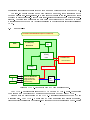
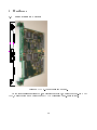
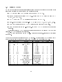
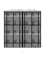
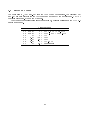
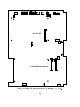
COMPASS-Note 2000-12
CATCH-X Users Manual
H. Fischer, J. Franz, A. Grunemaier,
F.H. Heinsius, L. Hennig, K. Konigsmann, M. Niebuhr,
T. Schmidt, H. Schmitt, J. Urban
Fakultat fur Physik, Universitat Freiburg, 79104 Freiburg, Germany
July 19, 2000
The CATCH-X module is a 6U one-mezzanine version of the 9U four-mezzanine CATCH
module. The CATCH module is used in the COMPASS experiment as the driver of the front-end
boards and serves as a data concentrator and mini-event builder before the data are transmitted
to the readout buer. The CATCH-X module facilitates the testing of the readout of the
front-end electronics. It can be used either with the COMPASS trigger control system or
independently of it, e.g. for test beam activities.
1
Contents
1 Introduction and Overview
1.1
1.2
1.3
1.4
COMPASS readout
CATCH-X . . . . .
Contents . . . . . .
Literature . . . . .
.
.
.
.
.
.
.
.
.
.
.
.
2 Installation
2.1
2.2
2.3
2.4
CATCH Mezzanine Card
TCS Receiver . . . . . .
S-Link LSC . . . . . . .
Jumper and Switches . .
3 Software
3.1
3.2
3.3
3.4
3.5
VME Access . . . . .
User Interface . . . .
FPGA-Programming
F1 initialisation . . .
Data Format . . . .
.
.
.
.
.
.
.
.
.
.
.
.
.
.
.
.
.
.
.
.
.
.
.
.
.
.
.
.
.
.
.
.
.
.
.
.
.
.
.
.
.
.
.
.
.
.
.
.
.
.
.
.
.
.
.
.
.
.
.
.
.
.
.
.
.
.
.
.
.
.
.
.
.
.
.
.
.
.
.
.
.
.
.
.
.
.
.
.
.
.
.
.
.
.
.
.
.
.
.
.
.
.
.
.
.
.
.
.
.
.
.
.
.
.
.
.
.
.
.
.
.
.
.
.
.
.
.
.
.
.
.
.
.
.
.
.
.
.
.
.
.
.
.
.
.
.
.
.
.
.
.
.
.
.
.
.
.
.
.
.
.
.
.
.
.
.
.
.
.
.
.
.
.
.
.
.
.
.
.
.
.
.
.
.
.
.
.
.
.
.
.
.
.
.
.
.
.
.
.
.
.
.
.
.
.
.
.
.
.
.
.
.
.
.
.
.
.
.
.
.
.
.
.
.
.
.
.
.
.
.
.
.
.
.
.
.
.
.
.
.
.
.
.
.
.
.
.
.
.
.
.
.
.
.
.
.
.
.
.
.
.
.
.
.
.
.
.
.
.
.
.
.
.
.
.
.
.
.
.
.
.
.
.
.
.
.
.
.
.
.
.
.
.
.
.
.
.
.
.
.
.
.
.
.
.
.
.
.
.
.
.
.
.
.
.
.
.
.
.
.
.
.
.
.
.
.
.
.
.
.
.
.
.
.
.
.
.
.
.
.
.
.
.
.
.
.
.
.
.
.
.
.
.
.
.
.
.
.
.
.
.
.
.
.
.
.
.
.
.
.
.
.
.
.
.
.
.
.
.
.
.
.
.
.
.
.
.
.
.
.
.
.
.
.
.
.
.
.
.
.
.
.
.
.
.
.
.
.
3
3
4
5
5
6
6
6
7
7
9
. 9
. 9
. 9
. 15
. 15
4 Hardware
16
5 Appendix
23
4.1 Front Panel and LEDs . . . . . . . . . . . . . . . . . . . . . . . . . . . . . . . . 16
4.2 Pin-Out Tables . . . . . . . . . . . . . . . . . . . . . . . . . . . . . . . . . . . . 18
4.3 Power and Fuses . . . . . . . . . . . . . . . . . . . . . . . . . . . . . . . . . . . 21
5.1 CMC-HOTlink . . . . . . .
5.1.1 Connector and LEDs
5.1.2 Data Format . . . .
5.2 TDC-CMC . . . . . . . . .
5.2.1 Connector and LEDs
5.2.2 Data Format . . . .
.
.
.
.
.
.
.
.
.
.
.
.
.
.
.
.
.
.
.
.
.
.
.
.
.
.
.
.
.
.
.
.
.
.
.
.
References
.
.
.
.
.
.
.
.
.
.
.
.
.
.
.
.
.
.
.
.
.
.
.
.
.
.
.
.
.
.
.
.
.
.
.
.
.
.
.
.
.
.
.
.
.
.
.
.
.
.
.
.
.
.
.
.
.
.
.
.
.
.
.
.
.
.
.
.
.
.
.
.
.
.
.
.
.
.
.
.
.
.
.
.
.
.
.
.
.
.
.
.
.
.
.
.
.
.
.
.
.
.
.
.
.
.
.
.
.
.
.
.
.
.
.
.
.
.
.
.
.
.
.
.
.
.
.
.
.
.
.
.
.
.
.
.
.
.
23
23
23
24
24
25
25
2
1 Introduction and Overview
1.1 COMPASS readout
)
(Fibre
The CATCH-X (CATCH = COMPASS Accumulate, Transfer and Control Hardware), a multipurpose frontend-electronic driver and readout module, has been developed in the scope of
the COMPASS experiment located at CERN. This state-of-the-art xed target spectrometer is
capable of standing beam intensities of up to 2 108 particles/spill. At a maximum trigger rate
of 105 events/s several Gigabyte of data has to be read every second with negligible dead time.
The readout architecture of the
LAT
Calorimeter
RICH
SAT
COMPASS experiment is summaAPV 6
ASD8b
QVC
GASSIPLEX
rized in Figure 1. Data are digiF1 TDC
DSP
tized right at the detector by the
front-end electronics wherever pos1
16
FE-boards
sible. In case of analog readout the
(detector mounted)
...
pedestal subtraction and zero supmax. 40 MB/s/link
pression is performed by the front(CAT 5+)
(~ 20 m)
end at the detector. To suppress
(Trigger, Clock, event id)
TCS
background for time measurements
(Fibre)
CATCH
only those hits are transfered to the
(9U VME)
(Setup data)
VMEbus
data recording units which have a
(~ 150 m)
correlation to a trigger time.
S-Link
The data are transmitted from
max. 100 MB/s/link
the front-end to the CATCH modules through twisted pair cables or
optical bres. The FPGA based
...
...
...
...
ROB
VME module serves as an interface
between the front-end of the detector systems and an optical S-LINK,
GigaBit
which transmits the data to the
100 MB/s/link
Central
Readout Buer (ROB). It also acts
(Fibre)
Data
GigaBit Switch
as an fan-out for the COMPASS trigRecording
ger distribution and time synchroni(~ 5 km)
sation system (TCS). The readoutdriver monitors the trigger and data
Filter
Filter
Filter
Filter
ow to and from the front-ends. In
addition a specic data buer structure and sophisticated data ow con- Figure 1: The architecture of the COMPASS detector
trol is used to pursue local pre-event readout.
building. At startup the module controls all necessary front-end initialisations.
From the CATCH data are transmitted via a standardized link to the read-out buers
(ROB) which can store all data from at least one spill. The backbone of this data transfer is
the S-link 1] interface and the S-LINK data transfer protocol. Presently about 128 S-LINK
C
P
U
3
G
i
g
a
B
i
t
R
O
B
C
P
U
G
i
g
a
B
i
t
R
O
B
C
P
U
G
i
g
a
B
i
t
R
O
B
C
P
U
G
i
g
a
B
i
t
R
O
B
connections are foreseen to transmit data with a maximum total bandwidth of about 12 GB/s.
The read-out buers combine data which belong to one event, check consistency of the
data and perform sub-event-building. In a next step they transmit the sub-events via Gigabit
Ethernet to lter computers. Here the nal event-building is performed and events are reconstructed. The lter farm will reduce the data based on physics cuts by a factor of 5 to 10 and
a continuous rate of 12 to 30 MB/s will be transfered to the central data recording facilities at
CERN.
1.2 CATCH-X
CATCH-X 6U VME board (16 cm x 23.3 cm)
ROB
S-LINK (LSC)
Output
FIFO
Mezzanine
Merge & Filter
Formatting
Control
TCS-Receiver
via P2 connector
Sort/Merge
FE-Board
FE-Board
Trigger & Clock distr.
HOTLink Mezzanine
4 HOTLink Receiver
Trigger & Clock distr.
FE-board setup
VME
Interface
Figure 2: CATCH-X schematic with HOTLink mezzanine card.
The CATCH-X is designed similar to the CATCH but as a 6U VME-module. This reduces
the maximum number of inputs by a factor of four compared to the 9U sized CATCH.
Figure 2 shows a block diagram of the CATCH-X overall architecture with the HOTLink
mezzanine card. The CATCH-X module with HOTLink mezzanine card performs the setup,
trigger and clock distribution to the front-end boards and the data transfer from the FE-boards
4
via CAT 5+ (Ethernet) cable. The data from 4 connected front-end-boards are received at a
rate of up to 40 MByte/s per link. Alternative mezzanine cards are available for data transmission through optical bres, for time-to-digital conversion on the CATCH and deadtime free
scalers. Trigger timing is received from a trigger control-system mezzanine card. For standalone
operation a Dummy TCS-card with NIM-input and local clock is available. The trigger, time
synchronization, reset and one user signal are distributed to the front-end-boards. The event
number is added to the event header. Programmable logic chips perform event sorting, header
suppression, adding of geographic identications and mini-event building. Formatted events
are sent to the readout-buers using S-link with a rate of about 100 MByte/s. All or prescaled
events can be sent through the VME-bus at a speed of 10 MByte/s.
1.3 Contents
This document describes the CATCH-X for the general user and can be used mainly as a
reference guide. Chapter 2 shows the required steps before installing the module in a VME
crate. An introduction to the software to control the module via the VMEbus and a list of
registers can be found in chapter 3. Also the current version of the output data format can be
found here. The chapter 4 lists the pin assignments for all connectors, the front-panel, fuses,
switches, and jumpers.
As a quick reference the HOTLink Mezzanine card and the TDC mezzanine card is documented in the Appendix.
1.4 Literature
For further reading the following literature is recommended:
An introduction to the COMPASS readout scheme:
TDC Chip and Readout Driver Developments for COMPASS and LHC-Experiments 2].
The description of the F1 TDC:
An Eight Channel Time-to-Digital Converter Chip for High Rate Experiments 3] and A
8 channel time to digital and latch integrated circuit for the COMPASS experiment at
CERN 4].
The front-end board connection to the CATCH/CATCH-X through the HOTLink:
Designing Front-End Boards for use with the CATCH-HOTLink Interface, COMPASS
note 1999-7 5].
The specications of the CATCH (9U version): em CATCH and CMC-HOTLink Readout
Driver Specication 6].
The COMPASS Online Data Format (COMPASS-Note 2000-8) 7].
The newest software and documentation can be found on the web page:
http://hpfr02.physik.uni-freiburg.de/compass
5
2 Installation
Before the installation of the CATCH-X 6U VME-board one has to mount the following cards:
The input is provided through the CATCH Mezzanine Cards. Currently one has the option
between a CMC-HOTLink card to connect front-end boards via twisted pair cables and a
TDC-CMC which provides up to 32 TDC channels.
The output data stream can either ow through the S-Link LSC card mounted on top or
through the VME bus, in which case the S-Link card is not required.
The trigger and synchronisation signals are either received through the standard COMPASS
trigger control system (TCS) and the TCS-Receiver or through NIM pulses converted in the
TCS-Dummy receiver.
2.1 CATCH Mezzanine Card
CATCH mezzanine cards have the size of standardized common mezzanine cards 8] and are
mounted on the lower part of the CATCH-X to which it connects through two mezzanine
connectors.
Several types are currently foreseen:
HOTLink-CMC with RJ-45 connector for cable interface.
HOTLink-CMC with bre interface
(development in cooperation with Trieste group).
TDC-CMC with four F1 chips.
Fast dead-time free scaler on FPGA.
Some features of the HOTLink-CMC and the TDC-CMC are summarised in the Appendix
5.1 and 5.2, respectively.
Details on the CATCH mezzanine card specication can be found in 9].
2.2 TCS Receiver
The trigger control system interface (TCS) can be plugged into the P2 connector on the back.
The TCS-receiver transient card gets the trigger and timing information from the Compass
trigger distribution system via optical bre. This board has outputs for the main clock (38.88
MHz), trigger, reset, begin of burst, end of burst, data enable and error bits as well as data
bits.
Alternatively a TCS-dummy receiver can be plugged into the P2 backplane connector. This
board has NIM inputs (including trigger, begin/end of burst, reset) and one local 38.88 MHz
clock to provide TCS functionality in standalone operations. It is pin compatible to the Compass TCS-receiver card (Table 13).
6
2.3 S-Link LSC
The CATCH-X board is designed such that a standard duplex S-LINK Link Source Card (LSC)
can be plugged in at the upper part of the CATCH-X and connects through one mezzanine
plug to the main board. Details can be found in the S-LINK interface specications 1]. The
pin out can be found in that documentation in table 21 (page 49). The size of these cards are
based on single size Common Mezzanine Cards as dened in Ref. 8].
The S-Link card provides a bre connection to the spill buer PCI-cards, which reside in
the readout buer PCs (ROB).
The S-Link card is optional, alternatively the data can be read out via VME bus at a lower
speed.
2.4 Jumper and Switches
The jumpers have to be set according to table 1 to the default positions, except for the TDCCMC, which requires jumper 3 in position 2-3.
The base address of the board can be selected by two rotary switches SW1 and SW2. For
specics refer to section 3.
7
Table 1: CATCH-X jumper positions. The default positions are for the CMC-HOTLink and
the TDC-CMC, except jumper 3, which has to be set to position 2-3 for the TDC-CMC. For
the locations of the jumpers see gure 4
Jumper default alternate description
JP 1
2-3,4-5
(no VME-Interrupt)
JP 2
open
(no VME-Interrupt)
JP28
2-3
Sync Trigger
1-2
async Trigger for RICH
JP 3
1-2
CMC-TCLK: 40 MHz local osc.
2-3
CMC-TCLK: 38.88 MHz from TCS
For on board clock distribution (debugging only):
JP16
1-2
JP 8
open
JP 4
open
JP 5
open
JP 6
open
JP 7
open
JP 9
open
JP10
open
JP12
open
JP11
open
JP18
open
JP13
open
JP14
open
JP15
open
JP17
open
JP19
open
JP20
open
JP22
open
JP21
open
8
3 Software
A compilation of the software mentioned here can be found in the compass project space
at /afs/cern.ch/compass/online/util/catch/. Executables are available in bin, bin/AIX,
bin/Linux for MVME PowerPCs and Intel-VMIC, respectively.
3.1 VME Access
The CATCH-X can be accessed through a standard VME interface using the A32/D32 address
mode. The base address is in hexadecimal notation:
E0 ab 00 00
where the byte ab can be selected by the two address selectors on the board. Switch 1 and 2
are corresponding to the value a and b, respectively. In the following tables (2-10) all registers
are described together with their oset to the base address and whether read or write access is
possible. Do not try to access any other addresses as this may hang your software. Note that
some registers are only available after programming the FPGAs (Tab. 3-9).
The spy buer can be read out using normal transfers or block transfers. In case the spy
buer is empty a 0x00 00 00 00 is returned. It is recommended to check the ags and/or the
number of values in the spy-buer before reading a block of data.
3.2 User Interface
For the convenience of the user two types of interfaces are provided.
A full screen interface written in tcl/tk named CatchX-o-Matic provides access to all registers through a several windows. Details can be found in ref. 10].
Through a command line interface each register can be read or written to:
vme read address
vme write address value
where address and value is given as a hexadecimal value. Do not forget the base address
0xE0 00 00 00 of the CATCH.
For example the command
vme read E00A0000
reads the identication and serial number of the CATCH-X whose the address switch is set
to 10. While the command
vme write E0010800 100
resets the CMC-card mounted on the CATCH-X with the address set to 1.
3.3 FPGA-Programming
The functionality of the CATCH-X board is provided through the use of six eld programmable
gate arrays (FPGA). Because the programming is stored in RAM, they have to be reprogrammed after every power up.
The programming is done by executing the command
9
Oset
00 00
00 04
00 10
00 20
00 40
00 80
01 00
02 00
Table 2: VME registers always available (in CPLD).
Read/Write Bits Description
R
0-15 CATCH-X serial number
16-31 'CA01' CATCH-X identication
R
27
TRIGGER (unused) CATCH-X status
26
FPGA pin TDO (JTAG)
25
CMC pin TDO (JTAG)
24
FPGA programming busy
23
FPGA INIT (programming pin)
22
FPGA DONE (programming pin)
21,20 Spy buer FIFO 1/2 empty
19
Spy buer FIFO almost empty) 4 words)
18
Spy buer FIFO half full (2048 words)
17
Spy buer FIFO almost full (4092 words)
16
Spy buer FIFO full
15- 00 Number if words in Spy FIFO (+2)
W
0
1 = Enable FPGA programming pins (PROG)
1
1 = Disable FPGA programming pins (PROG)
2
1 = set FPGA PROG pin (low)
3
1 = reset FPGA PROG pin (high)
4
1 = enable FPGA JTAG pins (TCK,TDI,TMS)
5
1 = disable FPGA JTAG pins (TCK,TDI,TMS)
6
1 = enable CMC JTAG pins (TCK,TDI,TMS)
7
1 = disable CMC JTAG pins (TCK,TDI,TMS)
W
0-31 Send 32 bits of programming data to FPGA via DIN/CCLK
W
0
TCK = 1 JTAG interface to FPGAs
W
1
TCK = 0
W
2
DIN = 1
W
3
DIN = 0
W
4
TMS = 1
W
5
TMS = 0
W
0
TCK = 1 JTAG interface to CMC
W
1
TCK = 0
W
2
DIN = 1
W
3
DIN = 0
W
4
TMS = 1
W
5
TMS = 0
W
0
1 = enable FPGA programming (DIN, CCLK)
1
1 = disable FPGA programming (DIN, CCLK)
4
CCLK = 1
5
CCLK = 0
6
DIN = 1
7
DIN = 0
W
Reset FPGAs
10
Table 3: SERIAL-FPGA VME registers (available after FPGA programming).
Oset Read/Write Bits Description
04 00
W
11..0 Serial setup bits 23..12 for 1st FE-board (store bits)
04 10
W
11..0 Serial setup bits 11..0 for 1st FE-board (send all 24 bits)
04 04
W
11..0 Serial setup bits 23..12 for 2nd FE-board (store bits)
04 14
W
11..0 Serial setup bits 11..0 for 2nd FE-board (send all 24 bits)
04 08
W
11..0 Serial setup bits 23..12 for 3rd FE-board (store bits)
04 18
W
11..0 Serial setup bits 11..0 for 3rd FE-board (send all 24 bits)
04 0C
W
11..0 Serial setup bits 23..12 for 4th FE-board (store bits)
04 1C
W
11..0 Serial setup bits 11..0 for 4th FE-board (send all 24 bits)
Table 4: CONTROL-FPGA VME registers (available after FPGA programming).
Oset Read/Write Bits Description
08 00
R
0-7 CONTROL FPGA design version number
8
BUSMODE of CMC card
9
IS24 (CMC-HOTLINK receiving 24 bit data)
10 BUSY 0 (serial interface 0 busy)
11 BUSY 1 (serial interface 1 busy)
12 BUSY 2 (serial interface 2 busy)
13 BUSY 3 (serial interface 3 busy)
08 00
W
0-3 LED 1-4 "OFF" on
4-7 LED 1-4 "IDs" on
8
reset CMC-card
9
reset SLINK-FPGA
10 reset TCS-FPGA
11 reset FORMAT-FPGA
12 reset MERGE-FPGA
13 reset SERIAL-FPGA
Table 5: FORMAT-FPGA VME registers (available after FPGA programming).
Oset Read/Write Bits Description
10 00
R
0-7 Formatter FPGA design version number
8-15 Data format identication
10 04
R/W
0-9 source id (as given in the S-link header
10 08
10 0C
10 10
R/W
R/W
R/W
10 14
R/W
0-15
0-15
0-7
8-15
0-7
Following numbers need to be set for
begin of run event:
CMC id
CATCH S/N
TCS design version
SLINK design version
MERGE design version
11
Table 6: TCS-FPGA VME registers (available after FPGA programming). Part I
Oset Read/Write Bits
Description
14 00
W
0
0: USR3=End of Burst, 1: USR3 = Pretrigger
1
1: TCS dummy connected select ONLY when TCS clock a
14 04
W
0
1 send USR4 25 ns (front end reset)
1
1 send USR4 400 ns (front end reset for CMC)
14 00
R
Status Register:
0-7
TCS FPGA design version number
8
Pretrigger as USR3
9
encoded USR signal output enable
10
TCS Ready
11
TCS Error
12
Currently Burst
13
RESET
14 04
R
0-15
trigger counter in current spill
14 08
R
0-15
trigger counter in last spill
14 0C
R
0-7
TCS receiver id
8-15
TCS status register after last error
14 10
R
14 14
14 18
R
R
14 1C
R
0-4
5-15
0-15
0-3
8-15
0
1
2
3
4
5
6
7
8
9
10
11
12
13
7 numbers below are from current event:
trigger mask
spill number
event number bit 0-15
event number bit 16-19
error word
skip current event
mode of current event
Status FIFO empty
Status FIFO full
Data FIFO empty
Data FIFO full
FILLED = TCS data ready for current event
EREADY (Merge ready)
FREADY (Format ready)
HDEF (Header buer empty ag)
MEVTRDY (Event number ready ag)
THREADY (TCS Header ready)
MEVTSEL (Merger)
HDREN (Formatter)
12
Table 7: TCS-FPGA VME registers (available after FPGA programming). Part II
Oset Read/Write Bits Description
14 20
R
0-3 addr 0 from tcs fo
4-7 addr 1 from tcs fo
8-11 addr 2 from tcs fo
12-15 addr 3 from tcs fo
14 24
R
0-3 addr 4 from tcs fo
4-7 addr 5 from tcs fo
8-11 tcs data fo counter
12-15 status fo counter
14 28
R
0-15 TCS header in counter in last spill
14 2C
R
0-15 TCS header out counter in last spill
Table 8: SLINK-FPGA VME registers (available after FPGA programming).
Oset Read/Write Bits Description
18 00
W
0-1 0: Spymode write 1 event if FIFO empty
1: Spymode write events until FIFO full
2: Spymode write every 4 event until FIFO full
3: Spymode write every 8 event until FIFO full
2
send URESET
3
send 3 testwords
4
send UTEST (32x SLINK test pattern)
5
Reset spy FIFO
18 00
R
0-7 SLINK FPGA design version number
18 04
R
3
HeaderEF
4
DataEF
5
SpyEF
6
LFF (link full ag)
7
LDOWN (link down)
13
Table 9: MERGE-FPGA VME registers (available after FPGA programming).
Oset Read/Write Bits Description
20 00
R
0-7 MERGE FGPA design version number
20 10
W
0-3 '0' for FIFO on
'1' for FIFO o
20 10
R
0-3 Status: FIFO on (1) or o (0)
4-7 Status: FIFO empty (1) or not (0)
8
'1' Is TDC-CMC
9
'1' Is HOTLink-CMC
10 '1' Is HOTFibre-CMC
11 '1' Is Scaler-CMC
12 '0' = TDC locked, '1' = TDC not locked
13 (debug) FIFO 0 last
14 (debug) FIFO 1 last
15 (debug) FIFO 2 last
20 20
R
15-0 16 bit id of the CMC-card
20 30
R
15-0 16 bit of number of received events
20 30
W
5-0 denition of trailer for TDC readout (24 bit)
Table 10: Spy buer readout.
Oset Read/Write Bits Description
80 00 R
0-31 Read data from spy buer (block transfer possible)
8F FF
14
catch-x-n.nn.hex boardid
on the command line of the VME computer. The le catch-x-n.nn.hex is provided with the
user interface software. The boardid is the CATCH-X board id in hex, as selected by the two
rotary switches. It can take values between 0 and FF.
In case the PROG LED lits red an error has occurred. Check, that you have used the correct
le and not interrupted the programming.
progcatch
3.4 F1 initialisation
A F1 frontend board or TDC-CMC connected to the CATCH-X can be initialised by the
command:
f1setup tdc.f1 boardid -port
where tdc.f1 is the le as generated by f1conf, boardid is the CATCH-X board id in hex,
-port is the input port number.
3.5 Data Format
The format of the output data is given in Tab. 11. The data in the Data Block depends on the
connected front-end electronics and the version of the format programmed in the FPGAs.
For details see 7].
Table 11: Format of data send through the S-Link or spy buer. The event size counts all
words (32 bit) excluding the two CTRL words (rst and last word).
31
SLINK-Header
0000000 (28)
error ev. type (5)
source ID (10)
status
spill nr. (11)
format version (8)
0
0=CTRL (4)
event size, excl. CTRL words (16)
event nr. ( 20)
Format Identier
#err words (8)
TCS error (8)
status (8)
Data Block
Data, format dened by format version
SLINK-Trailer
CFED120 (28)
15
0=CTRL(4)
4 Hardware
4.1 Front Panel and LEDs
Figure 3: CATCH-X front panel and module.
On the front panel are several LEDs, as described in table 12, a cutout for the S-LINK LSC
CMC, a reset button and a cutout for the CATCH Mezzanine Card. Reset switch.
16
Name
PWR
VME
PRG
ID
color
green
yellow
red
green
Table 12: LEDs on front panel.
Description
5 V Power available
Board is currently accessed through VME
If lit the FPGA's are not correctly programmed
'-' if FPGAs are not programmed.
Otherwise shows the selected board address (lower 4 bits).
TCS
red Red, if the synchronisation clock is generated internally.
O, if the clock is received through the TCS system.
TRG green On if triggers are received from the TCS system.
24
yellow On if CATCH-Mezzanine card produces 24 bit data (e.g. from TDC)
O, if 32 bit data is received (e.g. through HOTLink from RICH).
OFF
red On, if port 1,2,3 or 4 is disabled.
IDs
red On, if setup data is received on port 1-4 of the HOTlink-CMC.
FF
red On, if the FIFO on port 1-4 is full.
17
4.2 Pin-Out Tables
On the mother board are connectors for initial programming and debugging of the programmable
logic chips as well as the connectors to the mezzanine cards:
JTAG port for Xilinx CPLD programming (9 pins CPLD JTAG).
Program connectors for Xilinx FPGAs (X-Checker and JTAG) cable (18 pins FPGA
PROG, FPGA JTAG).
A JTAG port to the CATCH mezzanine card (9 pin CMC JTAG).
An ISP-Port to program the Lattice-ispGAL (4 pins SCLK/GAL, MODE, SDO, SDI).
Two 64 pin connectors for the CATCH mezzanine card (see table 14 and 9]).
One 64 pin connector for the S-Link card. (In the 9U CATCH module the J3 connector
is used.)
Additionally standard VME backplane connectors are used to implement A32/D32 data
transfers. No VME interrupts are generated.
The TCS card is connected via the VME-J2 backplane connector. Signal names are listed
in table 13.
Table 13: P2 connector pin assignment for TCS receiver. Note that signal C12 (Receiver Ready)
can be switched from active low to active high by setting bit 1 in register 0x14 00.
Pin Active I/O
Symbol
Symbol
I/O Active Pin
A1
+
I
+PECL clock
GND
C1
A2
I
-PECL clock
GND
C2
A3
GND
GND
C3
A4
H
I
Data 0
Data1
I
H
C4
A5
H
I
Data 2
Data3
I
H
C5
A6
H
I
Data 4
Data5
I
H
C6
A7
H
I
Data 6
Data7
I
H
C7
A8
H I/O
Address 0
Address 1 I/O H
C8
A9
H I/O
Address 2
Address 3 I/O H
C9
A10
L
I
Header ready
Header enable O
L
C10
A11 H
I
TTL clock
Status enable O
L
C11
A12
L
I
Data mode
Receiver ready I
L* C12
A13 H
I (Synch) Start of burst End of burst
I
H C13
A14 H
I
SynchTrigger
PreTrigger
I
H C14
A15
L
I
(Synch)Reset
Error
I
L
C15
A16
L
I
Skip data
AsynchTrigger I
H C16
18
Table 14: Pin denitions of the CATCH mezzanine card 9].
Pin Symbol
D31..0]
DX3..0]
Pin Name
Data outputs
Data extension
I/O Description
O
O
Data outputs.
Additional bits used for
error information.
RCLK#
Read clock
I The rising edge clocks data D, DX out of the
module when REN3..0]# is LOW.
REN3..0]#
Read enable
I REN# enables the RCLK input.
OE3..0]#
Output enable
I When OE# is LOW D,DX drive the bus,
(=REN3..0]#)
when HIGH D,DX are in high impedance state.
EF3..0]#
Empty ag
O When LOW no data available,
synchronized to RCLK.
PAE3..0]#
Programmable
O When LOW almost no data available,
empty ag
synchronized to RCLK, the minimum
amount of available data has to be specied.
FF3..0]#
Full ag
O When LOW internal buers are full,
not synchronized to RCLK.
RST#
Reset
I Asynchronous reset.
BUSMODE1
Busmode 1
O Busmode, identies card type.
BUSMODE4..2] Busmode
I Busmode, questions card type.
DEVID
Device id
I If HIGH puts device identication on D15..0].
DEVST
Device status
O If LOW signal error condition of card.
SND3..0]
Serial input
I Four independent 10 Mbaud serial links.
synchronous to TCLK.
TCLK
time clock
I Time distribution 38.88 MHz TTL clock.
DTCLK
di clock
I Dierential low jitter TCLK signal.
USR3..0]
User signals
I Trigger, time zero and user signals
synchronous to TCLK.
USRC
User coded
I Length coded USR3..0] signals,
synchronous to TCLK.
TDI
Test data input
I JTAG TDI
TMS
Test mode select I JTAG TMS
TDO
Test data output O JTAG TDO
TCK
Test data clock
I JTAG TCK
TRST#
Test data reset I/O Test reset
19
Table 15: Connector pin-outs of the CATCH mezzanine card 9].
Pn1/Jn1
Pn2/Jn2
Pin Signal Name Signal Name Pin Pin Signal Name Signal Name Pin
1
3
5
7
9
11
13
15
17
19
21
23
25
27
29
31
33
35
37
39
41
43
45
47
49
51
53
55
57
59
61
63
TCK
Ground
EF1]#
BUSMODE1#
DEVID
Ground
RCLK
Ground
DX2]
+5V
D28]
D25]
Ground
D22]
D19]
+5V
EF0]#
Ground
EF2]#
Ground
PAE0]#
DX0]
+5V
D12]
D9]
Ground
D6]
D4]
+5V
D2]
D0]
Ground
-12V
FF1]#
PAE1]#
+5V
USR0]
USR1]
Ground
DX3]
+5V
D31]
D27]
Ground
REN3]#
D21]
+5V
D17]
Ground
FF3]#
+5V
FF0]#
DX1]
Ground
D15]
D11]
+5V
REN0]#
D5]
Ground
D3]
D1]
+5V
USRC
2
4
6
8
10
12
14
16
18
20
22
24
26
28
30
32
34
36
38
40
42
44
46
48
50
52
54
56
58
60
62
64
1
3
5
7
9
11
13
15
17
19
21
23
25
27
29
31
33
35
37
39
41
43
45
47
49
51
53
55
57
59
61
63
20
+12V
TMS
TDI
Ground
USR2]
BUSMODE2#
RST#
3.3V
USR3]
D30]
Ground
D24]
EF3]#
3.3V
D18]
D16]
Ground
PAE2]#
Ground
PAE3]#
3.3V
REN1]#
D14]
Ground
D8]
D7]
3.3V
SND2]
TCLK
Ground
DTCLK+
Ground
TRST#
TDO
Ground
LVDS low
LVDS high
+3.3V
BUSMODE3#
BUSMODE4#
Ground
D29]
D26]
+3.3V
D23]
D20]
Ground
REN2]#
+3.3V
FF2]#
Ground
DEVST
Ground
D13]
D10]
+3.3V
SND0]
SND1]
Ground
SND3]
+3.3V
DTCLK-
2
4
6
8
10
12
14
16
18
20
22
24
26
28
30
32
34
36
38
40
42
44
46
48
50
52
54
56
58
60
62
64
4.3 Power and Fuses
The board uses 5V, +12V and -12V from the VME P1 and P2 connector. The voltages +12V
and -12V are only provided for the CMC board and not used by the motherboard. A DC/DC
converter produces 3.3V from the 5V supply.
The types of the dierent fuses are given in table 16, while its positions on the CATCH-X
is shown in gure 4.
Table 16: Fuses
Name Value Voltage Used for
F1 250 mA
5 V FPGA-JTAG / CMC-JTAG
F2 250 mA
5 V FGPA-PROG / CPLD-JTAG
F3
5A
5 V VCC
F4
0.5 A +12 V CMC
F5
0.5 A -12 V CMC
F6
0.5 A
5 V VCC-PECL
F7
5 A 3.3 V Power supply
21
F2
SW2
SW1
S-LINK LSC
F3
F5
F4
F7
CATCH Mezzanine Card
F1
F6
Figure 4: Positions of fuses, jumpers and switches on CATCH-X.
22
5 Appendix
5.1 CMC-HOTlink
The CMC-HOTLink cards serve as a general interface to the front-end boards:
Each CMC cards connects up to four front-end boards
Receive data through HOTLink deserialiser chips at a maximum rate of 40 MByte/s on
each of the four channels
Convert data from 8 bit HOTLink transmission format to 24 or 32 bits (1 word) depending
on front-end board
Word boundaries are automatically resynchronized at each received SYNC character
The most signicant byte is received rst (bits 31-24)
Receive errors are marked by special error codes
Store data in four independent 1k 4byte FIFOs for nal event building
Maximum CMC output rate 160 MByte/s
5.1.1 Connector and LEDs
Each CMC-HOTLink has four RJ-45 connectors for CAT5+ cable (Table 17) to the front-end
board. The ports are number from top to bottom 1 to 4. Details on the connection can be
found in Ref. 5].
The four red LEDs correspond to port 1 to 4 counted from left to right. They are lit in case
of errors are transmitted through the cable. During normal operation the LEDs are o.
Table 17: RJ-45 front-end board connector.
Pin Description
1 38.88 MHz clock, PECL 2 38.88 MHz clock, PECL +
3 10 Mbaud serial line, active low signal
6 10 Mbaud serial line, +5 V
power supply for opto coupler
5 Trigger/User (coded 25-100 ns), LVDS 4 Trigger/User (coded 25-100 ns), LVDS +
7 400 MHz HOTLink, PECL 8 400 MHz HOTLink, PECL +
5.1.2 Data Format
The data format is dened according to Ref. 5].
23
5.2 TDC-CMC
The TDC-CMC contains four F1 TDC chips numbered from 0 to 3. Channels 0-7 are connected
to TDC '0', whereas channels 24-31 are connected to TDC '3'. The details of the TDC operation
can be found in Ref. 4].
5.2.1 Connector and LEDs
A 68 pin connector from Robinson-Nugent has been chosen as the input interface to the four
F1 TDCs on the TDC-CMC. Two 34-wire twisted pair cables (AWG-28, 0.05") t to a single
socket. A special latching eject mechanism facilitates mating and unmating.
The socket, which goes on the cable is available from Robinson Nugent1 part number P50E068S-TGF or CERN self service number 09.55.21.071.4.
The four red LEDs show the following signals (from left to right): FIFO full, Token, PLL
locked, TDC Be-INIT. Upon power on reset all four LEDs are on.
Table 18: TDC-CMC 68-pin Robinson Nugent input connector. If the F1 TDC-CMC board is
used in the high resolution mode only the pins marked by '*' are active. All other inputs will
be ignored.
Pin
Signal
Pin
Signal
A01 In 0 + * B01 In 16 + *
A02 In 0 * B02 In 16 - *
A03 In 1 +
B03 In 17 +
A04 In 1 B04 In 17 A05 In 2 + * B05 In 18 + *
A06 In 2 * B06 In 18 - *
A07 In 3 +
B07 In 19 +
A08 In 3 B08 In 19 . .
. .
. .
. .
. .
. .
A31 In 14 + * B31 In 31 + *
A31 In 14 - * B31 In 31 + *
A31 In 15 +
B31 In 32 +
A32 In 15 B32 In 32 A33
GND
B33
GND
A34
GND
B34
GND
Input level is either: LVDS, LVPECL or dierential TTL (second line: +2.5V xed). On
board input termination: '+' 3.6k to 5V, '-' 1k to GND, between '-' and '+' 100.
1 Robinson Nugent (Europe) B.V.,P.O. Box 70062,NL-5201 DZ 's-Hertogenbosch, The Netherlands.
http://www.robinsonnugent.com.
24
5.2.2 Data Format
The 24-bit output data of the TDC chips as described in the F1 TDC manual 4] are mapped
to bits 8-31. Bit 0-3 indicates whether the TDC 0,1,2 or 3 is locked (active high). Bits 4-7 are
always zero.
Table 19: Incoming TDC data format. Shown is the format of the header and data. For each
event one header is followed by n data words and one trailer, which has the same format and
event number as the header. The event data may be intercepted by more headers, e.g. in case
of the trigger buer overow error is set. l0 - l3 corresponds to the TDC locked signals of TDC
0 to 3.
31
30
29
24 23
15 14 13 12 9 8 7-4 3 2 1 0
0 trigger buer
Event
Trigger XOR chip/channel 0 l3 l2 l1 l0
overow (1) number (6)
time (9)
address (6) (4)
1
0
chip/channel
data (time measured relative
0 l3 l2 l1 l0
address (6)
to last reference signal) (16)
(4)
References
1] Bowle et al., The S-LINK Interface Specication, http://www.cern.ch/HSI/s-link/, ECP
Dvision, CERN, 1997.
2] G. Braun et al., TDC Chip and Readout Driver Developments for COMPASS and LHCExperiments, Fourth Workshop on Electronics for LHC-Experiments, Rome, September
21-25 1998 CERN/LHCC/98-36.
3] G. Braun et al., An Eight Channel Time-to-Digital Converter Chip for High Rate Experiments. Fifth Workshop on Electronics for LHC-Experiments, Snowmass, September 20-24,
1999.
4] Braun et al., A 8 channel time to digital and latch integrated circuit for the COMPASS
experiment at CERN, Universitat Freiburg, 1999.
5] Braun et al., Designing Front-End Boards for use with the CATCH-HOTLink Interface,
COMPASS note 1999-7, Universitat Freiburg, 1999.
6] G. Braun et al., CATCH and CMC-HOTLink Readout Driver Specication , COMPASS
note 1999-15, Universitat Freiburg, 1999.
7] H. Fischer et al., The COMPASS Online Data Format, COMPASS note 2000-8, Universitat
Freiburg, TU Munchen, 2000.
8] IEEE P1386/Draft 2.0 04-APR-1995, Standard for a Common Mezzanine Card Family:
CMC (the CMC Standard).
25
9] Braun et al., Draft Standard for CATCH Mezzanine Cards: CATCH/OPEN , Universitat
Freiburg, 1999.
10] Braun et al., CatchX-o-Matic User Manual,
HTML: http://hpfr02.physik.uni-freiburg.de/~hennigla/manual/
26