1
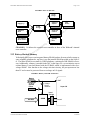
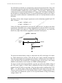
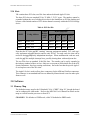
Yellowknife Hardware Reference Manual
Page 1 /1
Yellowknife
Reference Platform Hardware Design Manual
C
IN
CH
R
A
ED
V
I
BY
EE
R
F
LE
A
SC
.
R,
O
Board Revision
Level
CT
U
Document
NDRevision Level
O
IC
M
SE
X4
1.0
Registration Number:
Registration Name
c
Copyright 1998 by Motorola Incorporated. All rights reserved.
Motorola Inc.
Unrestricted Distribution Permitted
98 Feb 20
Yellowknife Hardware Reference Manual
1.0
Introduction..............................................................................................................5
1.1
2.0
2.6
2.7
2.8
2.9
2.10
2.11
2.12
2.13
2.14
E
Memory Map.....................................................................................................................
16
BY
D
Board Configuration...............................................................................................17
VE
4.1
4.2
5.0
Processor ............................................................................................................................. 5
PCI Bridge/Memory Controller .......................................................................................... 5
Memory Architecture .......................................................................................................... 6
L2 Cache Memory............................................................................................................... 7
Power Supply ...................................................................................................................... 7
2.5.1
Power Key Control................................................................................................
8
C.
N
I
Clock System.......................................................................................................................
9
R,
PCI-to-ISA Bridge.............................................................................................................
10
O
T
C
Hydra .................................................................................................................................
11
DU
Super I/O ...........................................................................................................................
11
N
O
Interrupt Architecture ........................................................................................................
12
IC
M
Reset Architecture .............................................................................................................
12
SE
Battery-Backed Memory ...................................................................................................
13
E
L
I/O Ports ............................................................................................................................
15
CA
S
Slots...................................................................................................................................
16
E
Software .................................................................................................................16
FR
3.1
4.0
Features ............................................................................................................................... 5
Functional Description.............................................................................................5
2.1
2.2
2.3
2.4
2.5
3.0
Page 2 /2
I
User-Settable
CH Jumpers....................................................................................................... 17
R
4.1.1
A System Frequency Selection ............................................................................... 17
4.1.2
Processor Frequency Selection ........................................................................... 17
4.1.3
MPC106 Frequency Selection ............................................................................ 18
4.1.4
COP Function Jumper......................................................................................... 18
4.1.5
Interrupt Flow Jumper......................................................................................... 19
4.1.6
Processor Voltage Selection ................................................................................ 19
4.1.7
Soft-start Override .............................................................................................. 19
Permanent Jumpers ........................................................................................................... 20
4.2.1
Processor Drive Strength .................................................................................... 20
4.2.2
Map Selection ..................................................................................................... 20
4.2.3
Cache Size Selection........................................................................................... 20
Layout Issues .........................................................................................................21
5.1
5.2
Swappable Pins.................................................................................................................. 21
Documentation .................................................................................................................. 22
Motorola Inc.
Unrestricted Distribution Permitted
98 Feb 20
Yellowknife Hardware Reference Manual
TABLE 1.
TABLE 2.
TABLE 3.
TABLE 4.
TABLE 5.
TABLE 6.
TABLE 7.
TABLE 8.
TABLE 9.
TABLE 10.
TABLE 11.
TABLE 12.
TABLE 13.
TABLE 14.
TABLE 15.
TABLE 16.
TABLE 17.
TABLE 18.
TABLE 19.
TABLE 20.
TABLE 21.
TABLE 22.
TABLE 23.
TABLE 24.
TABLE 25.
TABLE 26.
TABLE 27.
TABLE 28.
TABLE 29.
TABLE 30.
TABLE 31.
TABLE 32.
TABLE 33.
TABLE 34.
TABLE 35.
TABLE 36.
TABLE 37.
TABLE 38.
TABLE 39.
TABLE 40.
Page 5 /6
Reference Documentation............................................................................7
MPC10X PLL Configuration.....................................................................14
Floppy Connector Changes........................................................................20
PCI Slot IDs ...............................................................................................21
Processor Memory Map.............................................................................22
I/O Memory Map .......................................................................................22
System Frequency Configuration...............................................................26
Processor Frequency Configuration ...........................................................26
C.
N
Cache Size Configuration ..........................................................................27
,I
R
Memory Type Configuration......................................................................28
TO
C
Reset Configuration ...................................................................................28
DU
N
Soft Start Override .....................................................................................28
O
IC
Voltage Output Override ............................................................................29
M
CPU Drive Strength ...................................................................................29
SE
LE
Map Selection ............................................................................................29
A
Board ID.....................................................................................................29
SC
E
E
ATX Power ConnectorR
...............................................................................30
F
Fan Power Connector.................................................................................30
BY
D
Soft-Start Power
E Switch Connector ...........................................................31
V
CPU Socket................................................................................................31
HI
C
COASt
Socket ............................................................................................33
AR
SIMM Socket .............................................................................................35
Toolbox ROM Socket ................................................................................35
Apple I/O Port Connector ..........................................................................37
SCSI Disk Port Connector .........................................................................37
IDE Disk Port Connector ...........................................................................38
Disk Activity LED Connector....................................................................39
System Power LED Connector ..................................................................39
Keyboard Connector ..................................................................................39
Mouse Connector .......................................................................................40
Floppy Disk Connector ..............................................................................40
Parallel Port Connector ..............................................................................41
Serial Connectors .......................................................................................42
Battery Connector ......................................................................................42
PCI Connectors ..........................................................................................42
ISA Connectors..........................................................................................44
Reset Switch Connector.............................................................................46
ESP/COP Connector ..................................................................................46
Standby Power LED Connector.................................................................46
Routing Information...................................................................................47
Motorola Inc.
Unrestricted Distribution Permitted
98 Feb 20
Yellowknife Hardware Reference Manual
TABLE 41.
Page 6 /6
Routing Power ...........................................................................................48
CH
R
A
ED
V
I
BY
EE
R
F
LE
A
SC
S
O
IC
EM
R,
O
CT
U
ND
C
IN
.
Motorola Inc.
Unrestricted Distribution Permitted
98 Feb 20
Yellowknife Hardware Reference Manual
FIGURE 1.
FIGURE 2.
FIGURE 3.
FIGURE 4.
FIGURE 5.
FIGURE 6.
FIGURE 7.
Page 4 /4
Memory Architecture ...................................................................................6
Cache Architecture.......................................................................................7
Clock Architecture .......................................................................................9
Interrupt Architecture.................................................................................12
Reset Architecture......................................................................................13
Battery /NVRAM Architecture ..................................................................13
VBAT Trim ................................................................................................14
CH
R
A
ED
V
I
BY
EE
R
F
LE
A
SC
S
O
IC
EM
R,
O
CT
U
ND
C
IN
.
Motorola Inc.
Unrestricted Distribution Permitted
98 Feb 20
Yellowknife X4 Hardware Reference Manual
Page 5 /22
1.0 Introduction
The Yellowknife (“YK”) X4 platform is a fourth-generation PowerPC/CHRP reference
design. The design goals are to create a high-speed platform for use in embedded markets
as well as evaluation of a MacOS licensable platform.
This document decsribes the basic architecture of the X4 version, as well as changes
between the X2 and X4 platforms (which are otherwise very similar).
C
IN
1.1 Features
.
R,
O
CT
U
• PGA Socket allows easy installation of multiple types
of
D PowerPC processors.
N
O processor voltage selection.
• Processor module automatically selects appropriate
IC
• Supports two SDRAM DIMM modulesSup
to 100 MHz.
EM
E
• Supports on-board L2 (or L3) cache.
AL
C
S
• Supports MacOS (for testingEpurposes
only).
E
R
F
Y
B
2.0 Functional Description
ED
V
The following block
HI diagram shows the architecture of the Yellowknife in detail.
C
AR
2.1 Processor
Several features of the Yellowknife X4 platform are:
The Power PC processor is provided on Yellowknife through a 17-by-17 PGA ZIF socket.
This allows the easy installation of PowerPC 603, 604 and 750-class processor modules
(the latter including the back-side L2 cache). This adapter, referred to as an “interposer”,
identifies the level of voltage needed for the core of the processor (between 1.2V to 3.6V).
The socket also contains extra pins that allow it to support multiprocessing, and query an
I2C ROM or encoded pattern on the interposer to access interposer configuration information.
The core frequency is set using 4 jumpers to select the proper PLL setting for a given
clock frequency.
CHANGES: X4 adds compliance with the 5-bit voltage encoding standard of the secondgeneration interposers (X2 supported only the first generation, which had only 1 bit). Also
added are access to the I2C/parallel interposer ID, and elimination of Doubletake support.
2.2 PCI Bridge/Memory Controller
The PCI Bridge/Memory controller is the MPC106 V4, which now supports SDRAM and
higher processor bus speeds. The MPC106 connects directly to the CPU bus with no additional logic required. The MPC106 responds to all CPU transactions, forwarding them to
the memory controller or the PCI bus.
Motorola Inc.
Unrestricted Distribution Permitted
98 Feb 20
Yellowknife X4 Hardware Reference Manual
Page 6 /22
CHANGES: X4 replaces the automatic PLL settings with manual jumpers. This accomodates the new PCI/bus speed ratios supported by the MPC106 version 4.0. Processor
bus speeds up to 100 MHz are supported.
2.3 Memory Architecture
The local bus (i.e. processor bus) is the primary interface to all of the system memory. The
MPC106 serves as a memory controller for an array of SDRAM, as also as a ROM controller. The memory data bus is 64-bits wide, with additional bits optional to. serve as parity checks (the MPC106 does not support ECC when using SDRAM). INC
R,
O
CT
U
ND
FIGURE 1. Memory Architecture
SRAM
SRAM
PowerPC
MPC60X
CH
R
A
ED
V
I
BY
EE
R
F
O
IC
M
TagRAM
SE
LE
A
SC
ADDR
64 BIT DATA BUS
Grackle
MPC106
Registered
Tranceivers
Memory
Control
Signals
MacOS ROM
DIMM
DIMMMemory
Memory
The MPC106 requires that the processor/cache data bus be separated from the DRAM
array, so a 64-bit memory buffer is required. Because the memory bus may operate at very
high speeds, with potentially high loading (~100 pF), registered transceivers are used. The
design of the Yellowknife X4 memory system is described in great detail in application
note AN17xx, “SDRAM System Design using the MPC106”.
CHANGES: X4 replaces 4 SIMM sockets (which were paired) with 2 DIMM sockets.
The X4 only supports SDRAM, while X2 supported only EDO. X4 is tuned to operate at
83 MHz or above, and uses registered transceivers to accomplish this. To minimize loading at high speeds, the boot ROM has been moved to the ISA bus.
Motorola Inc.
Unrestricted Distribution Permitted
98 Feb 20
Yellowknife X4 Hardware Reference Manual
Page 7 /22
2.4 L2 Cache Memory
Cache for the YK system is provided through an on-board “TAGRAM” memory and a pair
of high-speed SRAM memories. The IDT71216 provides the cache tag RAM and address
comparator for the cache module. The SRAM parts are selected for the maximum speed
available; if cache is desired, the SRAM parts must match the speed of the processor and
SDRAM data bus.
FIGURE 2. Cache Architecture
IDT
Motorola
TAGRAM
SRAM
PowerPC
MPC60X
ED
V
I
BY
EE
R
F
LE
A
SC
S
R,
O
IDT
CT
TAGRAMU
ND
O
IC
M
E
C
IN
.
HIT
Grackle
MPC106
CH
R
CHANGES
A : X4 replaces the L2 COAST socket with on-board 100-pin TQFP SRAM.
This is both cheaper and faster, allowing faster operation (83 MHz or greater). Since the
cache is fixed at 512K, jumpers are no-longer needed.
2.5 Power Supply
Up to 7A of power is supplied to the processor’s core logic, using a 5-bit DAC-trimmed
switching regulator. The regulator is contained on a daughter-card called the Voltage Regulator Module (VRM). Using the VID(4:0) control signals present on all second-generation modules, the appropriate voltage level for the processor is automatically selected.
This voltage may range anywhere from 1.3V to 3.6V.
Uninstalled jumpers on the PCB may be installed to allow trimming the voltage for test
purposes. To trim the voltage, cut the top-level trace between pins 1 and 2 and install
three-position “Berg” headers at locations J45, J46, J47, J55, and J56. Once done, the following controls are possible:
Table 1: Optional VID Control
J45
J46
J47
J48
J49
VID4
VID3
VID2
VID1
VID0
1-2
out
out
1-2
out
out
1-2
out
out
1-2
out
out
1-2
out
2-3
Result
Interposer controls voltage settings.
No Interposer Installed
2.10V Core
Motorola Inc.
Unrestricted Distribution Permitted
98 Feb 20
Yellowknife X4 Hardware Reference Manual
Page 8 /22
Table 1: Optional VID Control
J45
J46
J47
J48
J49
VID4
VID3
VID2
VID1
VID0
out
out
out
out
out
out
out
out
out
out
out
out
out
out
2-3
2-3
2-3
2-3
2-3
2-3
2-3
2-3
2-3
2-3
2-3
2-3
2-3
2-3
2-3
2-3
out
out
out
out
out
2-3
out
2-3
out
2-3
out
2-3
2-3
out
2-3
out
2-3
out
2-3
out
2-3
2-3
2-3
2-3
2-3
2-3
2-3
2-3
out
out
out
out
out
out
out
out
ED
V
out
HI 2-3
C
out
2-3
R
Aout
2-3
out
2-3
2-3
out
2-3
out
2-3
out
2-3
out
2-3
2-3
2-3
2-3
2-3
2-3
2-3
2-3
Result
2-3
out
2.20V Core
2-3
2-3
2.30V Core
out
out
2.40V Core
out
2-3
2.50V Core
2-3
out
2.60V Core
2-3
2-3
2.70V Core
out
out
2.80V Core
R,
O
out
2-3
2.90V Core
CT
U
2-3
out
3.00V Core
D
2-3
2-3
3.10V Core ON
IC
out
out
3.20V Core
M
out
2-3
3.30V
SE Core
2-3
out LE3.40V Core
2-3
2-3
CA 3.50V Core
S
out
1.30V Core
EEout
R
out
2-3
1.35V Core
F
Y
2-3
out
1.40V Core
B
2-3
2-3
1.45V Core
out
out
1.50V Core
out
2-3
1.55V Core
2-3
out
1.60V Core
2-3
2-3
1.65V Core
out
out
1.70V Core
out
2-3
1.75V Core
2-3
out
1.80V Core
2-3
2-3
1.85V Core
out
out
1.90V Core
out
2-3
1.95V Core
2-3
out
2.00V Core
2-3
2-3
2.05V Core
C
IN
.
CHANGES: X4 replaces the on-board regulator with a VRM.
2.5.1 Power Key Control
Yellowknife X4 implements the MacOS compatible power control for ADB keyboards.
When the power is off, a transition on the ADB_POWER* signal (to ground) controls the
APC of the Super I/O, turning the system on. Once power is on, a MOSFET clamps the
control signals using system power, preventing other transitions on the ADB_POWER*
signal from affecting the APC. This prevents the ADB keyboard power button from turing
off power before software has an opportunity to intervene.
CHANGES: X4 implements the correct MacOS behavior for the ADB power key.
Motorola Inc.
Unrestricted Distribution Permitted
98 Feb 20
Yellowknife X4 Hardware Reference Manual
Page 9 /22
2.6 Clock System
Yellowknife uses two clock synthesizer IC’s to create all of the clock frequencies needed.
The first part is a CDC9843, an inexpensive device which uses a single 14.31818MHz
crystal to synthesize a selectable system “base” clock of 50, 60, or 66 MHz. This device
also generates 14.31818 MHz for ISA bus use, 24 MHz for the keyboard/mouse controller
(within the Super I/O), and 48 MHz which is used to operate the MESH SCSI within the
Hydra device. Although this devices also generates many 1X/2X clocks which might at
first glance appear useful for generating the CPU, SDRAM and PCI clocks, this is not the
.
C
case. The CDC9843 is unsuitable for such a purpose as it cannot not meet
the tight restricN
tions on allowable skew between the 1X and 2X clocks which the MPC106
PCI/Memory
,I
R
O
controller demands.
T
C
To generate the tightly-controlled clocks for the CPU, SDRAM
DU and PCI subsystems, the
N
base clock generated by the CDC9843 is connected to
CO a Motorola MPC972, which conI
tains numerous dividers attached to an internal PLL-based
clock synthesizer. Using this
M
SE
part, the skew-controlled clocks may be generated
at virtually any speed combination
E
desired.
AL
ED
V
I
CDC
9843
CH
R
A
SC
E
FIGURE
E 3. Clock Architecture
R
F
INTERPOSER
BY
MPC
CACHE
972
MEMORY REGISTERS
SDRAM SOCKETS
MPC106
PCI SLOTS
SYSTEM
FREQUENCY
SELECT
PAL
PCI/ISA BRIDGE
HYDRA
OSC
SCSI
OSC
HYDRA
Controlling the MPC972 is performed by selecting numerous feedback divider ratios.
There are too many combinations to control them with jumpers (or even to list them all
here); instead, the Yellowknife X4 uses a PAL to set the dividers based upon a simple
three-position jumper header.
Table 2: Clock Options
J61
J34
J32
FS0
FS1
FS2
IN
IN
IN
CDC9843
MPC972
Base
Clock
25 MHz
Bus
Clock
50 MHz
SDRAM
Clock
50 MHz
PCI
Clock
25 MHz
Motorola Inc.
Unrestricted Distribution Permitted
98 Feb 20
Yellowknife X4 Hardware Reference Manual
Page 10 /22
Table 2: Clock Options
J61
J34
J32
FS0
FS1
FS2
IN
IN
IN
out
out
out
out
IN
out
out
IN
IN
out
out
out
IN
out
IN
out
IN
out
CDC9843
MPC972
Base
Clock
30 MHz
33 MHz
25 MHz
33 MHz
30 MHz
33 MHz
25 MHz
Bus
Clock
60 MHz
66 MHz
75 MHz
83 MHz
90 MHz
100 MHz
100 MHz
SDRAM
Clock
PCI
Clock
60 MHz
30 MHz
66 MHz
33 MHz
75 MHz
37 MHz
83 MHz
33 MHz
C.
N
90 MHz
30
, IMHz
R
100 MHz O 39 MHz
100 MHz
CT 50 MHz
DU
N
Separate 31.3344 MHz and 50 MHz oscillators are provided
for the Hydra device, which
O
ICI/O, MESH SCSI controller, timers,
is used exclusively MacOS related functions (Apple
M
etc.).
SE
E
AL
All clocks have unoccupied pads forC0805-type
devices which can be used to attenuate
S
clocks or adjust skew. These partsE are not installed unless needed to meet radiated emisE
sions standards.
FR
BY changes the clocking system to accomodate the faster bus
CHANGES: X4 extensively
D
speeds, different PLL
VE multipliers of the MPC106 (3:2 and 5:2 modes are added), and the
I
need for many H
C more clock signals for SDRAM support. Additionally, to support board
R
testing below
A 50 MHz bus speeds, an external clock can be supplied to the MPC972,
which can generate the proper bus, SDRAM and PCI clocks. Note that the PAL controlling the MPC972 dividers may need to be re-programmed to maintain the proper relationships between bus and PCI clocks that the MPC106 requires.
2.7 PCI-to-ISA Bridge
The PCI-to-ISA bridge provides a means of accessing ISA devices as well as integrating
several system using the W83C553 component from Winbond. Pullup resistors configure
this part to operate in “PowerPC Mode”, which configures the part to generate HRESET
and adds the additional REQ4#/GNT4# arbiter controls.
An external 74F138 is used to convert the encoded DMA acknowledge signals to individual strobes (this saves a few pins on the bridge devices). A Fast part was specified solely
due to its availability. Due to the relatively slow speed of the ISA bus, an LS138 or other
equivalent-speed technology would be acceptable.
A small transistor drives a connector that would be attached to an 8-ohm speaker, to create
the power-up “beep” or other low-quality sounds.
CHANGES: X4 removes the separate reset controller and uses the reset circuitry in the
Winbond part. The Winbond also controls the access to the boot EPROM, which is now
located on the ISA bus. The bridge chip responds to memory accesses immediately after
reset.
Motorola Inc.
Unrestricted Distribution Permitted
98 Feb 20
Yellowknife X4 Hardware Reference Manual
Page 11 /22
2.8 Hydra
The Hydra ASIC from Apple implements several systems needed for MacOS compliance:
MPIC interrupt controller, MESC SCSI controller, ADB controller, SCC GeoPort controller, and timers. This device requires three special clocks: a standard PCI clock, a 4050MHz clock for the SCSI controller, and a 31.3344 MHz clock for the timers, etc.
Since there is no agreed-upon standard for Mac-style connectors on a PC chassis, and
since these devices are not strictly necessary to support Windows-NT nor MacOS, Yel.
lowknife places the ADB and SCC/GeoPort connectors on a dedicated C
connector
card.
N
This connector physically replaces one of the ISA slots on board. This
allows a small
I
,
Rdrivers
plug-in board to contain the GeoPort drivers for the serial ports, and
for the Apple
O
T
Desktop Bus (ADB).
C
DU
N
The MCCS142236 provides the chassis-internal termination of the SCSI bus. The termiO
nation shares power via the connector for remotelyIC
powering termination. This power is
M
limited to 1A, and is controlled via a self-resetting
SE polyswitch fuse (in compliance with
PC’97 guidelines, no destructive fuses areLused).
E
A
CHANGES: X4 allows the interrupt
SC signals to bypass the Hydra and connect directly
E
from the Winbond into the processor.
This allows configuring the board for embedded
RE
F
modes, where the Hydra isYnot needed.
B
D
VE
2.9 Super I/O
I
CH
The SuperI/O
controller is based upon the National PC87308VUL/IBN device, which
R
A
contains the serial, parallel, and floppy I/O controllers. The suffix “IBN” indicates that it
contains the “Phoenix BIOS” implementation of the keyboard/mouse controller. Other
parts are available but “IBN” is the current preferred BIOS for MacOS purposes.
The controller is a Plug-and-Play (PnP) device, which allows the internal controllers to be
logically connected to any desired interrupt line. Additionally, this device contains the
advanced power controller (APC), real-time clock (RTC) and a small array of RAM. All
of these latter devices require battery voltage to maintain state while the power is switched
off. This power is taken from the NVRAM battery (see Section 2.12 on page 13). The
NVRAM in the Super I/O is too small for CHRP purposes and must be disabled by the
firmware so as to eliminate interference with the external NVRAM.
The GPIO ports are used to implement miscellaneous status/control information such as:
•F_EJECT*
floppy eject control.
•SDA/SCK
allows access to DIMM presence detect I2C EEPROMs.
• PID(0:2)
allows access to parallel/serial interposer presence detect
information.
•C512K*
code can detect size of L2: 256K or 512K.
CHANGES: X4 allows installation of the compatible PC87307 Additionally, unused
GPIO pins now allow access to the PID signals from the processor and to the I2C ports of
the DIMM modules (through programmed I/O).
Motorola Inc.
Unrestricted Distribution Permitted
98 Feb 20
Yellowknife X4 Hardware Reference Manual
Page 12 /22
2.10 Interrupt Architecture
The following diagram shows the interrupt architecture for the Yellowknife. The use of
the MPIC allows the possibility of multi-processor interposers, though at this time none
are anticipated.
FIGURE 4. Interrupt Architecture
Super I/O
Key
Mse
Par
Flop
Hydra
PCI
SLOTS
PCI/ISA Bridge
8259
ISA
SLOTS
IDE
EE
R
F
15
LE
A
SC
S
C
IN
R,
O
JMPR
T
MPIC C
U
ND
O
IC
M
E
.
PowerPC
MPC60X
CHANGES: X4 adds a jumper
to allow interrupts to from through the MPIC in Hydra
Y
B
(for MacOS) or to bypass
D Hydra and connect the 8259 core in the Winbond bridge directly
to the processor. IThe
VE latter is needed for embedded customers which will not need Hydra
H to program for it.
and so do notCwish
AR
2.11 Reset Architecture
The reset circuitry controls the global reset signals based upon the following sources:
◆ PWRGOOD
Low until the power supply has been stabilized; high thereafter.
◆ ADB_RESET#
Pulsed low by the ADB controller (due to a keyboard
sequence).
◆ RSTHDR#
Connected to ground by an external pushbutton switch (on
the chassis).
These reset sources are merged and connected to the South Bridge, which in turn resets the
rest of the system peripherals.
Motorola Inc.
Unrestricted Distribution Permitted
98 Feb 20
Yellowknife X4 Hardware Reference Manual
Page 13 /22
FIGURE 5. Reset Architecture
North
Bridge
ATX Power
Supply Up
Apple I/O
“Hydra”
CPU
Socket
South
Bridge
R,
O
CT
U
ND
ADB Port
Reset
Super I/O
Control
ATX Chassis
Reset Switch
PCI/ISA
O
IC
Slots
SE
C
IN
.
M
LE
A
CHANGES: X4 deletes the external
SCreset controller in favor of the Winbond’s internal
E
E
reset controller.
FR
BY
2.12 Battery-Backed Memory
D
E
V
I
Yellowknife does
not
use an integrated battery/SRAM product for non-volatile storage as
H
C
some reference
platforms
do, nor does it use the internal SRAM provided on the Super I/
R
A
O. The latter SRAM is too small for CHRP platforms; a minimum of 8K SRAM is necessary. Additionally, a battery is needed for the APC in the Super I/O , so to minimize cost an
external battery is used and shared with the NVRAM, which is implemented with a lowvoltage SRAM. Note that due to the voltage selection circuitry, the part operates on less
than 5V and so must be protected from overvoltage on I/O signals.
FIGURE 6. Battery /NVRAM Architecture
Battery
VBAT
System
Power
Voltage
Select
Network
Super I/O
Level
Change
ISA BUS
SRAM
Control
Motorola Inc.
Unrestricted Distribution Permitted
98 Feb 20
Yellowknife X4 Hardware Reference Manual
Page 14 /22
The NVRAM is provided by an external battery and an on-board static RAM. This is different from the previous generation of Motorola platforms which used integrated battery/
crystal/NVRAM/RTC modules from various vendors. A four-pin “Berg” header provides
a connection to an external (usually lithium) 4.5V battery pack. The header is designed so
that orientation is unimportant; however it is also diode-protected against reverse connections in the event the connector is installed offset by one, or if a two-pin header is used on
the battery.
The Super I/O has rather stringent requirements on the relationship of VBAT
. and VSTC
DBY, as follows:
N
,I
R
TO
C
U
ND
•VBAT < VSTDBY - 0.5V
•VBAT < VSTDBY * 1.2
Unless all of these requirements are met, the APC will
O not work. In order to meet these
IC
requirements, Yellowknife uses a voltage dividerM
network
to trim the VBAT to an acceptE
able level needed by the Super I/O. Since the
S current requirements are very small (less
E to minimize wasted power.
than 20 uA), high-valued resistors can be Lused
BY
D
VSTDBY
VE
I
CHBattery
R
A
CA
S
FIGURE
EE 7. VBAT Trim
R
F
VSRAM
Conn.
15K
VBAT
100K
The protected, trimmed battery voltage is connected to the APC of the Super I/O controller, which maintains the real-time clock and the power supply controller management.
That subsystem handles the switching between battery and main power, but similar circuitry is needed for the external RAM. To maintain storage at lower power, a low-voltage
SRAM is used (made by several vendors in a JEDEC standard package).
The above networks shows that the SRAM is typically powered by the standby voltage of
the ATX power supply, so VBAT drain is minimized as long as the power supply is
plugged in and AC mains are operating. Only when the system is unplugged does VSTDBY = 0V, and the supply current for the SRAM+RTC+APC drops to less than 5uA.
This low current results in a VF of the Schottky diodes (1N5817) of approximately 0.25V,
so the battery can maintain the system over its expected lifetime as long as the battery
voltage is above 3.0V.
Motorola Inc.
Unrestricted Distribution Permitted
98 Feb 20
Yellowknife X4 Hardware Reference Manual
Page 15 /22
In full operating mode, VCC = 5V, and the supply current is exclusively due to the SRAM
(the APC does not draw power from the battery in this state) so the current demand is less
than 20mA. VBAT will be supplied through the VCC-to-VBAT diode. The battery protection diode will be reverse biased so no current drain will occur until VCC drops below
4.15V.
Note also that since the SRAM is not operated at VCC, but at VCC-VF, it is necessary to
insure that inputs do not exceed the SRAM’s maximum ratings of VCC-0.3V by using
low-voltage TTL components to isolate the SRAM from the rest of the system.
. When the
C
system is battery powered, the inputs are not driven so limits are cannot
N be exceeded.
, I at high currents
Under system power, the voltage to the SRAM is within this rangeReven
and low temperatures due to the 3.3V TTL drivers. Variations in
TOthe system VCC supply
C
will match variations in the VSRAM so the SRAM is safe from
U overvoltages.
N
O
IC
M
E
2.13 I/O Ports
D
S platform. Some are connectors located
There are numerous I/O ports on the Yellowknife
E
L
on the back panel in accordance withAATX chassis guidelines, others are attached via
SC and two serial connectors are on the back panel of
cables. The parallel, keyboard , mouse,
E
the ATX chassis, eliminating cabling.
These connectors are equivalent with standard PCRE
F
type connectors. Inside theYchassis, the motherboard containsconnectors for cables to IDE
B
and SCSI disk drives,Da floppy
disk, and an IrDA transciever.
VE
The floppy connector
HI is a standard CHRP connector, which is not the same as that used on
C
a PC, though
R it is very similar. In particular, several pins have been redefined:
A
Table 3: Floppy Connector Changes
Pin
Old
Function
New
Function
Description
1
GND
F_EJECT#
Low strobe ejects the floppy.
3
GND
NC
Key
4
NC
MSEN0
Media sense 0.
The keyboard and mouse connections are 6-pin mini-DIN connectors for PS/2-type
devices, similar to most modern PCs. The voltage supply for the keyboard and mouse is
protected by a self-resetting fuse instead of the typical self-destructive fuse, as specified
by the PC’97 guidelines.
The two serial ports are driven with the 75LP185. The ‘LP185 is preferred because it has
the ability to withstand 15kV ESD discharges without external circuitry. Equivalent parts
such as the 75C185 are also available, but without the ESD protection. Many other manufacturers make suitable parts that may be used, such as the Maxim MAX211. If non-ESD
protected parts are chosen, additional protection will be needed on the serial port signals.
The IrDA connector allows cabling to a standard IrDA modules available from a wide
variety of sources, such as Hewlett-Packard, Novalog, etc.
Motorola Inc.
Unrestricted Distribution Permitted
98 Feb 20
Yellowknife X4 Hardware Reference Manual
Page 16 /22
2.14 Slots
YK contains three PCI slots, two ISA slots and one dedicated Apple I/O slot.
The three PCI slots are standard 32-bit, 33 MHz, 3.3V/5V types. The number cannot be
expanded without the use of a bridge device due to the limitations on PCI bus loading and
because of the limited number of PCI arbiter channels currently within the PCI-ISA bridge
device.
Table 4: PCI Slot IDs
IDSEL
Config Address
AD14
0x8080_4000
AD15
0x8080_8000
AD16
0x8081_0000
South
Bridge
REQ/
GNT
0
LE
A
S3C
2
EE
R
F
C
IN
.
Hydra Interrupt
R,
TO
C
INTA INTB
INTC INTD
D#U
#
#
#
N
O
IC
M
XINT1
XINT2 XINT3 XINT4
SE
XINT2
XINT3
XINT4
XINT1
XINT3
XINT4
XINT1
XINT2
Note that the PCI slots use
the “rotating” interrupt assignment method. PCI cards typiBY
cally implement only D
one
function, and use only INTA#. For such cards, the slots can be
treated as having completely
independant interrupts. When multifunction cards are used,
VE
I
H multiple interrupt lines, possibly sharing them with an adjacent slot.
each slot mayCuse
R
A slots are standard 16-bit ISA slots. The number can be easily expanded to
The two ISA
the industry standard of three or four. Only two are present on Yellowknife due to the ATX
chassis limitations, four-layer routing restrictions, and to the fact that the special Apple I/
O card replaces one of the ISA slots.
The Apple I/O slot is used to allow place connectors for the ADB and GeoPort connectors.
This connector is not standardized but was defined by Motorola and is used on other platforms as well.
3.0 Software
3.1 Memory Map
The default memory map for the Yellowknife X4 is “CHRP”, Map “B”, though the board
can be configured to either mode. Refer to the MPC106 User’s Manual for details on the
maps as viewed from the processor or from PCI.
CHANGES: X4 defaults to CHRP mode, while X2 defaulted to PREP mode.
Motorola Inc.
Unrestricted Distribution Permitted
98 Feb 20
Yellowknife X4 Hardware Reference Manual
Page 17 /22
4.0 Board Configuration
One design goal of the reference platform was the minimization of configuration jumpers.
Some are regrettably necessary due to the need to support a wide variety of processors.
The following sections describe all the jumpers in detail.
4.1 User-Settable Jumpers
Two or three pin “Berg” jumpers are used when user-changable options must. be set.
NC
I
4.1.1 System Frequency Selection
R,
O
Jumpers J61, J34, and J32 ar e used to set the operating frequencies
CT of the processor bus
U
and the PCI bus.
ND
O
IC
Table 5: Clock Settings
M
SE
PCI
J61
J34
J32 E Bus
L Clock
A
FS0
FS1
FS2
Clock
C
S
IN
IN
IN
50 MHz
25 MHz
E
E
R
IN
INF
out
60 MHz
30 MHz
IN BYout
IN
66 MHz
33 MHz
D
IN
out
out
75 MHz
37 MHz
E
Vout
I
IN
IN
83 MHz
33 MHz
H
C
out
IN
out
90 MHz
30 MHz
AR
out
out
IN
100 MHz
39 MHz
out
out
out
100 MHz
50 MHz
4.1.2 Processor Frequency Selection
Jumpers J35, J36, J38 and J40 are used to set the core, or internal, operating speed of the
processor. This is the speed at which the processor performs instructions, as opposed to
the speed at which it performs memory accesses. The core speed is always an integer or
half-integer multiple of the “Bus Clock” speed selected with the System Frequency jumpers.
Table 6: Processor Clock Settings
J35
J36
CP0
CP1
IN
IN
IN
IN
IN
IN
IN
IN
IN
IN
IN
IN
out
out
out
out
J38
CP2
IN
IN
out
out
IN
IN
out
out
J40
CP3
IN
out
IN
out
IN
out
IN
out
PLL
Bus
Clock
Core
Clock
60 ... 100
120 ... 200
50 ... 100
50 ... 60
125 ... 250
225 ... 300
7X
BYPASS
2X
6.5X
2.5X
4.5X
Motorola Inc.
Unrestricted Distribution Permitted
98 Feb 20
Yellowknife X4 Hardware Reference Manual
Page 18 /22
Table 6: Processor Clock Settings
J35
J36
CP0
CP1
out
out
out
out
out
out
out
out
IN
IN
IN
IN
out
out
out
out
J38
CP2
IN
IN
out
out
IN
IN
out
out
J40
CP3
PLL
IN
out
IN
out
IN
out
IN
out
3X
5.5X
4X
5X
6X
3.5X
OFF
Bus
Clock
Core
Clock
50 ... 83
150 ... 250
50 ... 66
50
200 ... 266
250
C
IN
.
175
R,... 262
O
CT
U
ND
50 ... 75
NOTE: Not all processors support all options. Additionally, since the Yellowknife does
O
not directly support clock speeds below 50 MHz, many
IC of the PLL settings are not directly
M
usable.
SE
LE
A
SC
4.1.3 MPC106 Frequency Selection
EEused to set the ratio of the PCI bus clock to the procesJumpers J57, J59, J58 and J60Rare
F
sor bus clock, so the MPC106
Y can communicate in sync. with both. The core speed is
B
always an integer or half-integer
multiple of the “Bus Clock” speed selected with the SysD
E
tem Frequency jumpers.
V
HI
C
AR
Table 7: Processor Clock Settings
J35
J36
CP0
CP1
IN
IN
IN
IN
IN
IN
IN
IN
out
out
out
out
out
out
out
out
IN
IN
IN
IN
out
out
out
out
IN
IN
IN
IN
out
out
out
out
J38
CP2
IN
IN
out
out
IN
IN
out
out
IN
IN
out
out
IN
IN
out
out
J40
CP3
IN
out
IN
out
IN
out
IN
out
IN
out
IN
out
IN
out
IN
out
PLL
1X
1X
BYPASS
2X
2X
2.5X
2.5X
3X
3X
PCI
Clock
Bus
Clock
33
16 ... 25
33
16 ... 25
33
16 ... 25
33
16 ... 20
25 ... 33
16
66
33 ... 50
83
40 ... 50
75 ... 100
50
OFF
4.1.4 COP Function Jumper
Jumper J39 must be installed to allow full operation of the COP processor debugging fea-
Motorola Inc.
Unrestricted Distribution Permitted
98 Feb 20
Yellowknife X4 Hardware Reference Manual
Page 19 /22
ture; in particular, the soft-start/soft-stop functions of COP will not work unless the
jumper is installed properly.
Table 8: COP Jumper Settings
J39
1
2
Function
3
Normal operation; power management uses QREQ*/QACK*
.
NC
I
COP operation; QACK* forced low.
R,
O
CT
U
4.1.5 Interrupt Flow Jumper
ND
O
Jumper Jx is used to control the routing of interruptICsignals to the processor. In positions
1-2, interrupts flow from the Winbond and Super
I/O ISA and PCI interrupt into the Hydra
EM
S
MPIC core, merging with internal Hydra interrupt,
and then on to the processor. In posiE
AL and go directly to the processor.
tions 2-3, interrupts bypass the HydraCMPIC
ES
E
Table 9:
Interrupt
Jumper Settings
FR
J39
BY
Function
D
1
2 VE 3
HI
C
MacOS mode: Interrupts flow through Hydra MPIC.
AR
Embedded mode: Interrupts bypass Hydra MPIC
Note that to allow the embedde mode, PCI interrupts are connected to both the Hydra and
the Winbond. Generally, only one or the other of these devices should be programmed to
sense the PCI interrupt lines.
4.1.6 Processor Voltage Selection
Jumpers J45, J46, J47, J55, and J56 are used to optionally override the interposer voltage
setting and impose a user-selected setting. To accomodate this, the top-level trace between
pins 1 and 2 of all of these jumpers must be cut (use an X-acto knife); then, the jumpers
(which are usually not installed) must be soldered in (use 3-position Berg headers). Once
done, the jumpers allow forcing a VID(0:4) signal high, forcing low, or allowing the interposer to control. For more details, refer to Figure 1, “Optional VID Control,” on page 7.
4.1.7 Soft-start Override
By installing a shorting-plug on Header J44, pins 20 to pins 22 (i.e. on the side), the ATX
power supply is forced on. This allows embedded customer s to ignore APC power control issues, and the MacOS related power signals.
Motorola Inc.
Unrestricted Distribution Permitted
98 Feb 20
Yellowknife X4 Hardware Reference Manual
Page 20 /22
4.2 Permanent Jumpers
Permanent jumpers are implemented with zero-ohm resistors permanently soldered to the
motherboard to select certain configurations. To change these settings, these resistors
must be added, changed or removed. This is no normally done by the end-user.
4.2.1 Processor Drive Strength
These resistors are used to modify the drive strength of the processor. The standard setting
is “Normal” mode. Higher drive strengths can clear some problems but could
C. cause othN
ers.
I
R,
O
Table 10: CPU Drive Strength
CT
U
ND
R38
O
Meaning
DS1
IC
M
SE
IN
CPU is tri-stated
E
AL strength
out
1X : Normal
drive
C
ES
IN
1.5XE
: Strong drive strength
FR
out
BY 2X : Herculean drive strength
D
E
IV
R14
DS0
IN
IN
out
out
4.2.2 Map Selection H
C
This resistor
ARis used to select the memory map used by the MPC106. The default is “Map
B” for CHRP compatibility.
Table 11: Map Selection
R10
Meaning
IN
Map “B”: CHRP
out
Map “A”: PREP
4.2.3 Cache Size Selection
These jumpers are used to set the size of the cache installed. Because the cache SRAM is
soldered directly to the motherboard, changing the cache size is an involved operation.
Still, for completeness, here are the settings.
Table 12: Cache Size Configuration
R350
CRB
R351
CRA
R352
CRB
Cache
Size
out
IN
out
256K
IN
out
IN
512K
Motorola Inc.
Unrestricted Distribution Permitted
98 Feb 20
Yellowknife X4 Hardware Reference Manual
Page 21 /22
5.0 Layout Issues
The guidelines detailed in the Yellowknife X2 hardware reference manual may be of help,
but the majority of the Yellowknife X4 layout is covered in great detail in the application
note AN17xx, “SDRAM System Design using the MPC106”. Here are some general
guidelines:
• The VRM power supply module should be positioned close to the PGA socket,
such that the current flows through a heavy plane from the ATX power supply.
C. header if
Insure placement of the VRM does not interfere with the HP analyzer
N
debugging is desired.
,I
OR
T
• The VRM power supply capacitors should be positioned
C very near the CPU socket.
U
D
The following traces should be routed to carry additionalNcurrent
capacity:
O
IC
Table 13: Routing Power
M
SE
E
Signal
Power
AL
C
CORE_VDD
Sufficient for 7A.
ES
E
R1.5A.
TERMPWR
SufficientFfor
BY
J4
1A
of
+12V power (for fan).
D
E
IV 300mA
J42-24
H
C
U11-28
100mA
AR
VBAT
100mA
5.1 Swappable Pins
The following groups may be pin-swapped (excluding the obvious swappable discrete
gates). Each line is considered a separate group.
MPC972
QA(0:3), QC(0:3)
QA/QC clock groups are swappable, as are
split-terminated outputs.
MPC972
QB(0:3)
QB clock groups are swappable, as are
split-terminated outputs.
IDT71216
A(12:0), TAG(11:1)
All except A13/TA13/TD13
MCM69P737
A(0:16)
Cache addresses swappable.
MCM69P737
DQ(0:63)
Cache data swappable (byte mode not used).
74ALVCH16601
A(1:18) :: B(1:18)
Input and output pairs swappable.
DIMM
D(0:7) :: DQMB0
Byte lanes and associated controls.
Motorola Inc.
Unrestricted Distribution Permitted
98 Feb 20
Yellowknife X4 Hardware Reference Manual
Page 22 /22
D(8:15) :: DQMB1
...
D(56:63) :: DQMB7
SRAM
A(12:0)
All swappable.
SRAM
D(7:0)
All swappable.
RPAK
All swappable.
R,
5.2 Documentation
C
IN
.
The following manuals may be of use for understanding some of
the components used on
TO
C
Yellowknife:
U
ND
O
Table 14: Reference Documentation
IC
M
SE
Manual
Source
Document
E
L
SDRAM System Design using the
Motorola
AN17xx
CA
S
MPC106
E
E
Motorola MPC603 User’s Manual
Motorola
MPC603UM/AD
FR
Y
Motorola MPC604 User’s ManualD BMotorola
MPC604UM/AD
E
IV
Motorola MPC750 User’s Manual
Motorola
MPC750UM/AD
H
C
Yellowknife X2 User’s
Motorola
YKX2UM/AD
ARManual
Yellowknife Home Page
Motorola
www.mot.com/SPS/PowerPC/teksupport/refdesigns/yk.html
Motorola Processor/Cache Module Hardware Reference Manual
Motorola
MPCMAE/AD
PC87308VUL
National Semiconductor
N/A
WB83C553
Winbond
2565
Hydra ERS
Apple Computer
P/N 343S0181
Motorola Inc.
Unrestricted Distribution Permitted
98 Feb 20
Yellowknife Hardware Reference Manual
CH
R
A
ED
V
I
Page 23 /23
BY
EE
R
F
LE
A
SC
S
O
IC
EM
R,
O
CT
U
ND
C
IN
.
Motorola Inc.
Unrestricted Distribution Permitted
98 Feb 20