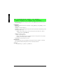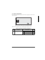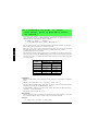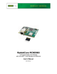
1
RabbitNet Peripheral Cards
RabbitNet LAN Cards
User’s Manual
019–0146 •
070629–D
RabbitNet Peripheral Cards User’s Manual
Part Number 019-0146 • 07029–D • Printed in U.S.A.
©2005–2007 Rabbit Semiconductor Inc. • All rights reserved.
No part of the contents of this manual may be reproduced or transmitted in any form or by any means
without the express written permission of Rabbit Semiconductor.
Permission is granted to make one or more copies as long as the copyright page contained therein is
included. These copies of the manuals may not be let or sold for any reason without the express written
permission of Rabbit Semiconductor.
Rabbit Semiconductor reserves the right to make changes and
improvements to its products without providing notice.
Trademarks
Rabbit and Dynamic C are registered trademarks of Rabbit Semiconductor Inc.
RabbitNet is a trademark of Rabbit Semiconductor Inc.
The latest revision of this manual is available on the Rabbit Semiconductor Web site,
www.rabbit.com, for free, unregistered download.
Rabbit Semiconductor Inc.
www.rabbit.com
RabbitNet Peripheral Cards
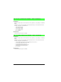
TABLE OF CONTENTS
Chapter 1. The RabbitNet Protocol
1
1.1 General RabbitNet Description.............................................................................................................1
1.1.1 RabbitNet Connections .................................................................................................................1
1.1.2 RabbitNet Peripheral Cards ..........................................................................................................2
1.1.3 Connectivity Tools........................................................................................................................3
1.1.4 DIN Rail Mounting .......................................................................................................................4
1.2 Physical Implementation.......................................................................................................................5
1.2.1 Control and Routing......................................................................................................................5
1.3 Dynamic C ............................................................................................................................................6
1.3.1 Dynamic C Libraries.....................................................................................................................6
1.3.1.1 Accessing and Downloading Dynamic C Libraries ............................................................. 7
1.3.2 Sample Programs ..........................................................................................................................8
1.3.3 General RabbitNet Operation........................................................................................................8
1.3.4 General RabbitNet Function Calls ................................................................................................9
1.3.5 Status Byte ..................................................................................................................................15
Chapter 2. Digital I/O Card
17
2.1 Features ...............................................................................................................................................18
2.1.1 Software ......................................................................................................................................18
2.2 Connections ........................................................................................................................................19
2.2.1 Power Supply ..............................................................................................................................20
2.3 Pinout ..................................................................................................................................................22
2.3.1 Headers........................................................................................................................................22
2.3.2 Indicator LED .............................................................................................................................22
2.4 Digital I/O ...........................................................................................................................................23
2.4.1 Digital Inputs...............................................................................................................................23
2.4.2 Digital Outputs............................................................................................................................24
2.5 Analog Inputs......................................................................................................................................26
2.5.1 Single-Ended Inputs....................................................................................................................27
2.5.2 Differential Inputs .......................................................................................................................27
2.5.3 Calibrating the Analog Inputs .....................................................................................................27
2.5.3.1 Calibration Constants ......................................................................................................... 28
2.5.3.2 Calibration Recommendations ........................................................................................... 28
2.5.3.3 Factory Calibration............................................................................................................. 29
2.6 Software ..............................................................................................................................................30
2.6.1 Dynamic C Libraries...................................................................................................................30
2.6.2 Sample Programs ........................................................................................................................30
2.6.2.1 Digital I/O .......................................................................................................................... 30
2.6.2.2 Analog Inputs ..................................................................................................................... 32
2.6.3 Digital I/O Card Function Calls ..................................................................................................34
2.6.3.1 Digital Input Function Calls............................................................................................... 34
2.6.3.2 Digital Output Function Calls ............................................................................................ 35
2.6.3.3 Analog Input Function Calls .............................................................................................. 37
2.6.4 Status Byte ..................................................................................................................................44
2.7 Specifications......................................................................................................................................45
2.7.1 Electrical and Mechanical Specifications ...................................................................................45
2.7.1.1 Physical Mounting.............................................................................................................. 47
2.7.2 Jumper Configurations ................................................................................................................48
User’s Manual
Chapter 3. A/D Converter Card
51
3.1 Features .............................................................................................................................................. 52
3.1.1 Software...................................................................................................................................... 52
3.2 Connections ........................................................................................................................................ 53
3.2.1 Power Supply.............................................................................................................................. 54
3.3 Pinout ................................................................................................................................................. 55
3.3.1 Headers ....................................................................................................................................... 55
3.3.2 Indicator LED............................................................................................................................. 55
3.4 Analog Inputs ..................................................................................................................................... 56
3.4.1 Analog Current Measurements................................................................................................... 58
3.4.2 Calibrating the A/D Converter Chip........................................................................................... 59
3.4.2.1 Modes ................................................................................................................................ 59
3.4.2.2 Calibration Constants ........................................................................................................ 59
3.4.2.3 Calibration Recommendations........................................................................................... 60
3.4.2.4 Factory Calibration ............................................................................................................ 61
3.5 Software ............................................................................................................................................. 62
3.5.1 Dynamic C Libraries .................................................................................................................. 62
3.5.2 Sample Programs........................................................................................................................ 62
3.5.3 A/D Converter Card Function Calls ........................................................................................... 65
3.5.4 Status Byte.................................................................................................................................. 77
3.6 Specifications ..................................................................................................................................... 78
3.6.1 Electrical and Mechanical Specifications................................................................................... 78
3.6.2 Physical Mounting...................................................................................................................... 80
3.7 Jumper Configurations ....................................................................................................................... 81
Chapter 4. D/A Converter Card
83
4.1 Features .............................................................................................................................................. 84
4.1.1 Software...................................................................................................................................... 84
4.2 Connections ........................................................................................................................................ 85
4.2.1 Power Supply.............................................................................................................................. 86
4.3 Pinout ................................................................................................................................................. 87
4.3.1 Headers ....................................................................................................................................... 87
4.3.2 Indicator LED............................................................................................................................. 87
4.4 D/A Converter Outputs ...................................................................................................................... 88
4.4.1 Calibration .................................................................................................................................. 89
4.5 Software ............................................................................................................................................. 90
4.5.1 Dynamic C Libraries .................................................................................................................. 90
4.5.2 Sample Programs........................................................................................................................ 90
4.5.3 D/A Converter Card Function Calls ........................................................................................... 92
4.5.4 Status Byte.................................................................................................................................. 99
4.6 Specifications ................................................................................................................................... 100
4.6.1 Electrical and Mechanical Specifications................................................................................. 100
4.6.2 Physical Mounting.................................................................................................................... 102
Chapter 5. Relay Card
103
5.1 Features ............................................................................................................................................ 104
5.1.1 Software.................................................................................................................................... 104
5.2 Connections ...................................................................................................................................... 105
5.2.1 Power Supply............................................................................................................................ 106
5.3 Pinout ............................................................................................................................................... 108
5.3.1 Headers ..................................................................................................................................... 108
5.3.2 Indicator LEDs ......................................................................................................................... 108
5.4 Relay Outputs ................................................................................................................................... 109
5.5 Software ........................................................................................................................................... 110
5.5.1 Dynamic C Libraries ................................................................................................................ 110
5.5.2 Sample Programs...................................................................................................................... 110
5.5.3 Relay Card Function Calls........................................................................................................ 112
5.5.4 Status Byte................................................................................................................................ 115
RabbitNet Peripheral Cards
5.6 Specifications....................................................................................................................................116
5.6.1 Electrical and Mechanical Specifications .................................................................................116
5.6.2 Physical Mounting ....................................................................................................................118
Chapter 6. Keypad/Display Interface
119
6.1 Features .............................................................................................................................................120
6.1.1 Software ....................................................................................................................................120
6.2 Connections ......................................................................................................................................121
6.2.1 Power Supply ............................................................................................................................122
6.3 Key RabbitNet Keypad/Display Interface Components ...................................................................123
6.3.1 Headers and Jacks .....................................................................................................................123
6.3.1.1 Keypads............................................................................................................................ 123
6.3.1.2 Liquid Crystal Displays.................................................................................................... 124
6.3.2 LEDs .........................................................................................................................................124
6.3.3 Buzzer .......................................................................................................................................124
6.4 Liquid Crystal Display Backlights....................................................................................................125
6.5 Display Contrast ...............................................................................................................................127
6.6 Software ............................................................................................................................................128
6.6.1 Dynamic C Libraries.................................................................................................................128
6.6.2 Sample Programs ......................................................................................................................128
6.6.3 RabbitNet Keypad/Display interface Function Calls................................................................130
6.6.3.1 Buzzer............................................................................................................................... 130
6.6.3.2 LEDs................................................................................................................................. 131
6.6.3.3 Keypad ............................................................................................................................. 132
6.6.3.4 Display ............................................................................................................................. 135
6.6.4 Status Byte ................................................................................................................................141
6.7 Specifications....................................................................................................................................142
6.8 Electrical and Mechanical Specifications .........................................................................................142
6.8.1 Physical Mounting ....................................................................................................................144
Appendix A. Keypad/Display Interface Expansion Kit
145
A.1 Keypads............................................................................................................................................146
A.1.1 Keypad Templates....................................................................................................................147
A.2 LCD Displays...................................................................................................................................150
A.2.1 2 × 20 Character LCD ..............................................................................................................151
A.2.2 4 × 20 Character LCD ..............................................................................................................151
A.3 ZMENU.C........................................................................................................................................152
A.4 Configuring Key Code Indexes and Physical Keypad Arrangement...............................................156
A.4.1 Basics of Assigning Key Code Indexes ...................................................................................156
A.4.2 Expansion Kit Keypads............................................................................................................158
A.4.2.1 3 × 4 Keypad ................................................................................................................... 158
A.4.2.2 2 × 6 Keypad ................................................................................................................... 159
A.4.2.3 4 × 10 Keypad ................................................................................................................. 160
A.5 2 × 6 Keypad Datasheet ...................................................................................................................161
A.6 3 × 4 Keypad Datasheet ...................................................................................................................162
A.7 4 × 10 Keypad Datasheet .................................................................................................................163
A.8 2 × 20 Character LCD Datasheet .....................................................................................................164
A.9 4 × 20 Character LCD Datasheet .....................................................................................................188
Index
195
Schematics
199
User’s Manual
RabbitNet Peripheral Cards
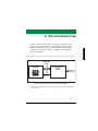
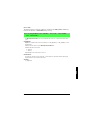
1. THE RABBITNET PROTOCOL
1.1 General RabbitNet Description
RabbitNet is a high-speed synchronous protocol developed by Rabbit Semiconductor to
connect peripheral cards to a master and to allow them to communicate with each other.
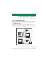
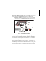
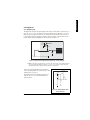
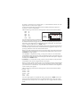
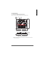
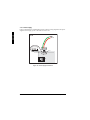
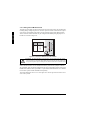
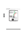
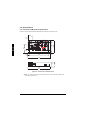
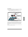
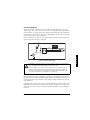
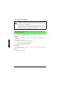
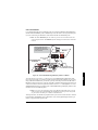
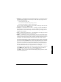
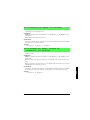
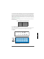
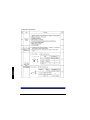
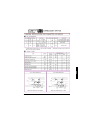
1.1.1 RabbitNet Connections
All RabbitNet connections are made point to point. A RabbitNet master port can only be
connected directly to a peripheral card, and the number of peripheral cards is limited by
the number of available RabbitNet ports on the master.
SLAVE
Straight-through
CAT 5/6 Ethernet cable
SLAVE
Rabbit 3000®
Microprocessor
MASTER
Crossover
CAT 5/6 Ethernet cable
MASTER
SLAVE
Power
Supply
Straight-through
CAT 5/6 Ethernet cable
Figure 1. Connecting Peripheral Cards to a Master
User’s Manual
1
A typical RabbitNet™ system consists of a master single-board computer and one or two
peripheral cards. A high-performance Rabbit 3000® or Rabbit 2000® microprocessor on
the master provides fast data processing, and a BL2500 or a BL2600 master also provides
the DCIN and +5 V power for the peripheral cards. Use a straight-through CAT 5/6 Ethernet cable to connect the master to slave peripheral cards, unless you are using a device such
as the OP7200 that could be used either as a master or a slave. In this case you would use a
crossover CAT 5/6 Ethernet cable to connect an OP7200 that is being used as a slave.
NOTE: Even though CAT 5/6 Ethernet cables are used for the RabbitNet connections,
never connect a RabbitNet port to an Ethernet network. Doing so could destroy the
RabbitNet SPI driver.
Distances between a master unit and peripheral cards can be up to 10 m or 33 ft.
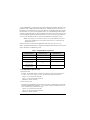
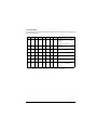
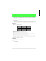
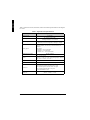
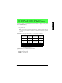
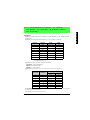
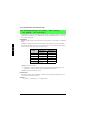
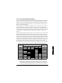
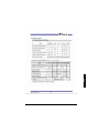
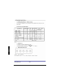
Table 1 lists Rabbit Semiconductor’s single-board computers and other devices that can be
used as the master in a RabbitNet system.
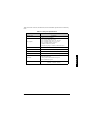
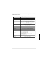
Table 1. RabbitNet Master Capabilities
RabbitNet Masters
Master Supplies Power to
Peripheral Cards
Number of
RabbitNet Ports
BL2500
Yes
2
BL2600
Yes
2
OP7200
No
1
RCM3300/RCM3360
Prototyping Board
No
1
PowerCore FLEX
Prototyping Board
No
1
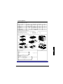
1.1.2 RabbitNet Peripheral Cards
• Digital I/O Card
24 inputs, 16 push/pull outputs, 4 channels of 10-bit A/D conversion with ranges of
0 to 10 V, 0 to 1 V, and -0.25 to +0.25 V. The following connectors are used:
Signal = 0.1" friction-lock connectors
Power = 0.156" friction-lock connectors
RabbitNet = RJ-45 connector
• A/D Converter Card
8 channels of programmable-gain 12-bit A/D conversion, configurable as current measurement and differential-input pairs. 2.5 V reference voltage is available on the connector. The following connectors are used:
Signal = 0.1" friction-lock connectors
Power = 0.156" friction-lock connectors
RabbitNet = RJ-45 connector
2
RabbitNet Peripheral Cards
• D/A Converter Card
8 channels of 0–10 V 12-bit D/A conversion. The following connectors are used:
Signal = 0.1" friction-lock connectors
Power = 0.156" friction-lock connectors
RabbitNet = RJ-45 connector
• Display/Keypad interface
Allows you to connect your own keypad with up to 64 keys and one character liquid
crystal display from 1 × 8 to 4 × 20 characters with or without backlight using standard
1 × 16 or 2 × 8 connectors. The following connectors are used:
Signal = 0.1" headers or sockets
Power = 0.156" friction-lock connectors
RabbitNet = RJ-45 connector
• Relay Card
6 relays rated at 250 V AC, 1200 V·A or 100 V DC up to 240 W. The following connectors are
used:
Relay contacts = screw-terminal connectors
Power = 0.156" friction-lock connectors
RabbitNet = RJ-45 connector
The OP7200 operator interface may serve as a RabbitNet peripheral card “display” in a
RabbitNet system.
Visit our Web site for up-to-date information about additional cards and features as they
become available. The Web site also has the latest revision of this user’s manual.
1.1.3 Connectivity Tools
Rabbit Semiconductor also has available additional tools and parts to allow you to make
your own wiring assemblies to interface with the friction-lock connectors on the RabbitNet peripheral cards.
• Connectivity Kit (Part No. 101-0581)—Six 1 × 10 friction-lock connectors (0.1" pitch)
with sixty 0.1" crimp terminals; and two 1 × 4 friction-lock connectors (0.156" pitch)
and two 1 × 2 friction-lock connectors (0.156" pitch) with fifteen 0.156" crimp terminals. Each kit contains sufficient parts to interface with one or more RabbitNet peripheral cards.
• Crimp tool (Part No. 998-0013) to secure wire in crimp terminals.
Contact your authorized Rabbit Semiconductor distributor or your Rabbit Semiconductor
Sales Representative for more information.
User’s Manual
3
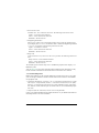
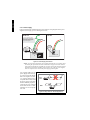
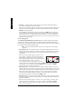
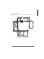
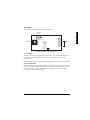
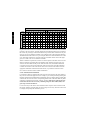
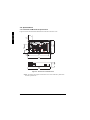
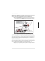
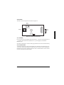
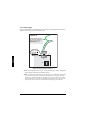
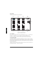
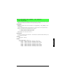
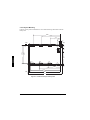
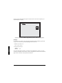
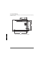
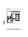
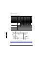
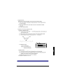
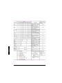
1.1.4 DIN Rail Mounting
RabbitNet peripheral cards and the BL2500 master may be mounted in 100 mm DIN rail
trays as shown in Figure 2.
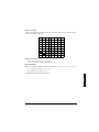
3
AI
0
R7
3
C7
8
R8
AG
ND
AI
1
2
R7
5
J11
R7
C7 4
9
GN
D
U4
J1
C1
C2
U2
U5
O1
1
C7
O1
2
O1
3
C6
O1
4
C5
O1
5
C4
+K
2
C3
J2
+K
2
U8
U7
+
D1
1
O1
0
O9
0
C1
1
U1
J8
0
J1
0
U6
U3
U11
C1
0
8
C4
Q4
O6
3
Q
32
O5
5
JP
D
16
C1
D
O4
4
GN
J5
+K1
J9
DCIN
+K
1
8
J4
GN
D
C1
O0
O1
6
O2
C1
2
O3
2
C1
+K
DC
IN
C1
C
Q1
6
O7
2
VC
+
3
JP
VCC
GND
C4
1
+K
1
O8
J3
C1
9
5
C3
RP
Q
64
GN
D
GN
D
U9
U1
Q
R14
R30
9
4 IN1
5
1
JP
J6
17
R15
R31
C9
C4
IN
PU 8-1
LL 5
3IN1
Q
33
4
7
C4
2
C8
RP
2 IN1
1 IN2
2 IN2
3
Q
7
8 RP
C5
R16
R32
8
C4
8
8
10
0 IN1
1 IN1
7
49
RP
C3
R4 7
7 C3
R4
2
5 RP
C6
IN1
8 IN1
9IN2
0 IN2
Q
C3
R4 6
C3
R4 5
5
6
9
C5
3 RP
IN9
C1
C3
R4 3
3
C3
R4 4
4
5 C6
RP
RP11
R6 12
6
C6
IN8
RP
2
IN
GN PU 16
+K D
LL -2
3
2
R24 R8
1
C3
R4 1
1 C3
R4 2
2
R25 R9
R21 R5
DC
C2
R3 7
7
0
C3
R4 0
9
R10
R26
R22 R6
RP
R19 R3
C2
R3 6
6
C2
R3 9
9
R4
5
J7
GN
D
RP
3
C1
C2 9
C2 0
C2 1
2
R18 R2
C2
R3 5
5
8
C2
R3 8
0
4
C7
IN
PU 0LL 7
D
B IG
O IT
A A
R L
D I/O
R12
R28
R13
R29
R11
R27
R17 R1
C2
R3 4
4
C5
R5
2
C6
R5
R5
4
6
C5
0
R23 R7
R20 R4
IN
VC
C
C6
0
9
9
2
C7
C5
2
C4
6
3
R8
R7
+
C5
3
C4
C4 3
C4 4
C5 5 R3C2
3
1
3
13 C6
R5
R6
2
3
65 C7
1
R6
Q
+
R5
1
7
+
7
6
RP
7
Y
1
C7
2
R6
PO
W
ER
IN0
6 IN0
C5
4
RP
C8
R5
R5 5
R5 6
R58 7
0
CR Q66
1
RA
BB
IT
3 IN0
4IN
05
9
7
4
NE
T
0 IN0
1 IN0
2 IN0
R5
Q6
C7
R6 0
5
9
R8
RA
BB
IT
IN0
C73
R7
1
C6
6
R6
0
9
R7
R6
R7 9
0
4
DC
IN
R7
7
C6
R6 8
1 C6
R6
AI
3+
R7
8
IN1
6 IN1
7 IN1
AI
2
+5
RE
FAI
3-
R8
7
R88
R85
R86
C7
R7 7
6
R8
N/
C
RabbitNet I/O
Card
Tray Side
Modular PC
Board Trays
DIN Rail
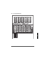
Figure 2. Mounting RabbitNet Peripheral Card in DIN Rail Trays
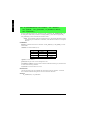
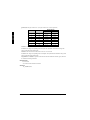
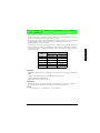
DIN rail trays are typically mounted on DIN rails with “feet.” Table 2 lists Phoenix Contact
part numbers for the DIN rail trays, rails, and feet. The tray side elements are used to keep
the RabbitNet peripheral card in place once it is inserted in a DIN rail tray, and the feet are
used to mount the plastic tray on a DIN rail.
Table 2. Phoenix Contact DIN Rail Mounting Components
DIN Rail Mounting
Component
Phoenix Contact
Part Description
Phoenix Contact
Part Number
Trays
UM 100-PROFIL cm*
19 59 87 4
Tray Side Elements
UM 108-SE
29 59 47 6
Foot Elements
UM 108-FE
29 59 46 3
* Length of DIN rail tray in cm
NOTE: Other major suppliers besides Phoenix Contact also offer DIN rail mounting hardware. Note that the width of the plastic tray should be 100 mm (3.95") since that is the
width of a RabbitNet peripheral card. 108 mm plastic trays may be used with spacers.
4
RabbitNet Peripheral Cards
1.2 Physical Implementation
There are four signaling functions associated with a RabbitNet connection. From the master’s point of view, the transmit function carries information and commands to the peripheral card. The receive function is used to read back information sent to the master by the
peripheral card. A clock is used to synchronize data going between the two devices at high
speed. The master is the source of this clock. A slave select (SS) function originates at the
master, and when detected by a peripheral card causes it to become selected and respond
to commands received from the master.
The signals themselves are differential RS-422, which are series-terminated at the source.
With this type of termination, the maximum frequency is limited by the round-trip delay
time of the cable. Although a peripheral card could theoretically be up to 45 m (150 ft)
from the master for a data rate of 1 MHz, Rabbit Semiconductor recommends a practical
limit of 10 m (33 ft).
Connections between peripheral cards and masters are done using standard 8-conductor
CAT 5/6 Ethernet cables. Masters and peripheral cards are equipped with RJ-45 8-pin
female connectors. The cables may be swapped end for end without affecting functionality.
1.2.1 Control and Routing
Control starts at the master when the master asserts the slave select signal (SS). Then it
simultaneously sends a serial command and clock. The first byte of a command contains
the address of the peripheral card if more than one peripheral card is connected.
A peripheral card assumes it is selected as soon as it receives the select signal. For direct
master-to-peripheral-card connections, this is as soon as the master asserts the select signal. The connection is established once the select signal reaches the addressed slave. At
this point communication between the master and the selected peripheral card is established, and data can flow in both directions simultaneously. The connection is maintained
so long as the master asserts the select signal.
User’s Manual
5
1.3 Dynamic C
Dynamic C is an integrated development system for writing embedded software. It runs on
an IBM-compatible PC and is designed for use with Rabbit Semiconductor single-board
computers and other devices based on the Rabbit microprocessor.
1.3.1 Dynamic C Libraries
In addition to the library associated with the master single-board computer such as the
BL2500 or OP7200, several other libraries are needed to provide function calls for RabbitNet peripheral cards.
• RN_CFG_BL25.LIB—used to configure the BL2500 for use with RabbitNet peripheral
cards. Function calls for this library are discussed in the Coyote (BL2500) User’s
Manual.
• RN_CFG_BL26.LIB—used to configure the BL2600 for use with RabbitNet peripheral
cards. Function calls for this library are discussed in the Wolf (BL2600) User’s
Manual.
• RN_CFG_OP72.LIB—used to configure the OP7200 for use with RabbitNet peripheral
cards. Function calls for this library are discussed in the eDisplay (OP7200) User’s
Manual.
• RN_CFG_PowerCoreFLEX.LIB—used to configure the PowerCore FLEX modules
for use with RabbitNet peripheral boards on the PowerCore FLEX Prototyping Board.
Function calls for this library are discussed in the PowerCore FLEX User’s Manual.
• RN_CFG_RCM33.LIB—used to configure the RCM3300, RCM3310, RCM3360, and
RCM3370 for use with RabbitNet peripheral boards on the RCM3300 Prototyping
Board. Function calls for this library are discussed in the RCM3300/RCM3310 User’s
Manual and in the RCM3360/RCM3370 User’s Manual.
• RNET.LIB—provides functions unique to the RabbitNet protocol. Function calls for
this library are presented below.
• RNET_DRIVER.LIB—provides background functions unique to the RabbitNet data
transmission protocol.
Function calls specific to individual RabbitNet peripheral cards are described in the chapters specific to the individual RabbitNet peripheral card. Other functions applicable to all
devices based on Rabbit microprocessors are described in the Dynamic C Function
Reference User’s Manual. More complete information on Dynamic C is provided in the
Dynamic C User’s Manual.
6
RabbitNet Peripheral Cards
1.3.1.1 Accessing and Downloading Dynamic C Libraries
The libraries needed to run the RabbitNet peripheral cards are available on the CD
included with the Development Kit for the master single-board computer, or they may be
downloaded from http://www.rabbit.com/support/downloads/ on Rabbit Semiconductor’s
Web site.
When downloading the libraries from the Web site, click on the product-specific links
until you reach the links for the RabbitNet peripheral cards download. Once you have
downloaded the file, double-click on the file name to begin the installation. InstallShield
will install the files for you at a location you designate, and a pop-up readme file will
explain the available options to add the files to your existing Dynamic C installation or to
modify the relevant files in your existing Dynamic C installation.
You will be able to use the revamped Dynamic C installation with the RabbitNet peripheral card and you will continue to be able to use this installation with all the other Rabbit
Semiconductor products you used before.
User’s Manual
7
1.3.2 Sample Programs
Sample programs are provided in the Dynamic C SAMPLES folder.
The various folders contain specific sample programs that illustrate the use of the corresponding Dynamic C libraries. For example, the sample program PONG.C demonstrates
the output to the STDIO window.
The RABBITNET folder provides sample programs specific to the RabbitNet peripheral
cards. Each sample program has comments that describe the purpose and function of the
program. Follow the instructions at the beginning of the sample program.
To run a sample program, open it with the File menu (if it is not still open), then compile
and run it by pressing F9 or by selecting Run in the Run menu. The RabbitNet peripheral
card must be connected to a master such as the BL2500 with its Demonstration Board connected as explained in the Coyote (BL2500) User’s Manual or other user’s manual. The
BL2500 or other master must be in Program Mode, and must be connected via the programming cable to a PC.
More complete information on Dynamic C is provided in the Dynamic C User’s Manual.
1.3.3 General RabbitNet Operation
The SAMPLES\RABBITNET\ subdirectory contains the following sample programs. When
running these sample programs, the RabbitNet peripheral card may be connected to either
RabbitNet port on a master such as the BL2500 that has two RabbitNet ports. The sample
program will use rn_device() to first look for peripheral cards connected to the master.
The last peripheral card found will run the sample program. The sample program will also
display the serial number(s) of the peripheral cards connected to which RabbitNet port on
the master using the STDIO window, or that no card is connected to a particular port.
• ECHOCHAR.C—Demonstrates a simple character echo to any RabbitNet peripheral card. A
character is sent to the RabbitNet peripheral card connected at a physical node address of
0x00 or 0000 octal. If a peripheral card is connected, the character will be returned back
along with the status of the peripheral card. Otherwise, the status byte will indicate there is
no connection.
• ECHOTERM.C—Demonstrates a simple character echo to any RabbitNet peripheral card
through a serial terminal on the master. A character is sent to the RabbitNet peripheral card
connected at a physical-node address of 0x00 or 0000 octal. If a card is connected, the character will be returned back along with the status of the peripheral card. Otherwise, the status byte will indicate there is no connection.
• HWATCHDOG.C—Demonstrates setting the hardware watchdog on a RabbitNet peripheral
card. This sample program will first look for a peripheral card that matches the search criteria. The hardware watchdog will be set and a hardware reset should occur in approximately
1.5 seconds. The hardware watchdog will be disabled after the reset is done.
• SWATCHDOG.C—Demonstrates setting and hitting the software watchdog on a RabbitNet
peripheral card using costatements. This program will first look for a peripheral card
matching the search criteria. The software watchdog will be set for 2.5 seconds. The watchdog will be hit at every increasing timeout until the timeout is past 2.5 seconds. A software
reset will occur and the software watchdog will be disabled.
8
RabbitNet Peripheral Cards
1.3.4 General RabbitNet Function Calls
The function calls described in this section are used with all RabbitNet peripheral cards,
and are available in the RNET.LIB library in the Dynamic C RABBITNET folder.
int rn_init(char portflag, char servicetype);
Resets, initializes, or disables a specified RabbitNet port on the master single-board computer. During
initialization, the network is enumerated and relevant tables are filled in. If the port is already initialized,
calling this function forces a re-enumeration of all devices on that port.
Call this function first before using other RabbitNet functions.
PARAMETERS
portflag is a bit that represents a RabbitNet port on the master single-board computer (from 0 to the
maximum number of ports). A set bit requires a service. If portflag = 0x03, both RabbitNet ports 0
and 1 will need to be serviced.
servicetype enables or disables each RabbitNet port as set by the port flags.
0 = disable port
1 = enable port
RETURN VALUE
0
int rn_device(char pna);
Returns an address index to device information from a given physical node address. This function will
check device information to determine that the peripheral card is connected to a master.
PARAMETER
pna is the physical node address, indicated as a byte.
7,6—2-bit binary representation of the port number on the master
5,4,3—Level 1 router downstream port
2,1,0—Level 2 router downstream port
RETURN VALUE
Pointer to device information. -1 indicates that the peripheral card either cannot be identified or is not
connected to the master.
SEE ALSO
rn_find
User’s Manual
9
int rn_find(rn_search *srch);
Locates the first active device that matches the search criteria.
PARAMETER
srch is the search criteria structure rn_search:
unsigned int flags;
unsigned int ports;
char pna
char productid;
char productrev;
char coderev;
long serialnum;
//
//
//
//
//
//
//
status flags see MATCH macros below
port bitmask
physical node address
product id
product rev
code rev
serial number
Use a maximum of 3 macros for the search criteria:
RN_MATCH_PORT
RN_MATCH_PNA
RN_MATCH_HANDLE
RN_MATCH_PRDID
RN_MATCH_PRDREV
RN_MATCH_CODEREV
RN_MATCH_SN
//
//
//
//
//
//
//
match
match
match
match
match
match
match
port bitmask
physical node address
instance (reg 3)
id/version (reg 1)
product revision
code revision
serial number
For example:
rn_search newdev;
newdev.flags = RN_MATCH_PORT|RN_MATCH_SN;
newdev.ports = 0x03; // search ports 0 and 1
newdev.serialnum = E3446C01L;
handle = rn_find(&newdev);
RETURN VALUE
Returns the handle of the first device matching the criteria. -1 indicates no such devices were found.
SEE ALSO
rn_device
int rn_echo(int handle, char sendecho,
char *recdata);
The peripheral card sends back the character the master sent. This function will check device information
to determine that the peripheral card is connected to a master.
PARAMETERS
handle is an address index to device information. Use rn_device() or rn_find() to establish the
handle.
sendecho is the character to echo back.
recdata is a pointer to the return address of the character from the device.
RETURN VALUE
The status byte from the previous command. -1 means that device information indicates the peripheral
card is not connected to the master.
10
RabbitNet Peripheral Cards
int rn_write(int handle, int regno, char *data,
int datalen);
Writes a string to the specified device and register. Waits for results. This function will check device information to determine that the peripheral card is connected to a master.
PARAMETERS
handle is an address index to device information. Use rn_device() or rn_find() to establish the
handle.
regno is the command register number as designated by each device.
data is a pointer to the address of the string to write to the device.
datalen is the number of bytes to write (0–15).
NOTE: A data length of 0 will transmit the one-byte command register number.
RETURN VALUE
The status byte from the previous command. -1 means that device information indicates the peripheral
card is not connected to the master, and -2 means that the data length was greater than 15.
SEE ALSO
rn_read
int rn_read(int handle, int regno, char *recdata,
int datalen);
Reads a string from the specified device and register. Waits for results. This function will check device
information to determine that the peripheral card is connected to a master.
PARAMETERS
handle is an address index to device information. Use rn_device() or rn_find() to establish the
handle.
regno is the command register number as designated by each device.
recdata is a pointer to the address of the string to read from the device.
datalen is the number of bytes to read (0–15).
NOTE: A data length of 0 will transmit the one-byte command register number.
RETURN VALUE
The status byte from the previous command. -1 means that device information indicates the peripheral
card is not connected to the master, and -2 means that the data length was greater than 15.
SEE ALSO
rn_write
User’s Manual
11
int rn_reset(int handle, int resettype);
Sends a reset sequence to the specified peripheral card. The reset takes approximately 25 ms before the
peripheral card will once again execute the application. Allow 1.5 seconds after the reset has completed
before accessing the peripheral card. This function will check peripheral card information to determine
that the peripheral card is connected to a master.
PARAMETERS
handle is an address index to device information. Use rn_device() or rn_find() to establish the
handle.
resettype describes the type of reset.
0 = hard reset—equivalent to power-up. All logic is reset.
1 = soft reset—only the microprocessor logic is reset.
RETURN VALUE
The status byte from the previous command. -1 means that device information indicates the peripheral
card is not connected to the master.
int rn_sw_wdt(int handle, float timeout);
Sets software watchdog timeout period. Call this function prior to enabling the software watchdog timer.
This function will check device information to determine that the peripheral card is connected to a master.
PARAMETERS
handle is an address index to device information. Use rn_device() or rn_find() to establish the
handle.
timeout is a timeout period from 0.025 to 6.375 seconds in increments of 0.025 seconds. Entering a
zero value will disable the software watchdog timer.
RETURN VALUE
The status byte from the previous command. -1 means that device information indicates the peripheral
card is not connected to the master.
12
RabbitNet Peripheral Cards
int rn_enable_wdt(int handle, int wdttype);
Enables the hardware and/or software watchdog timers on a peripheral card. The software on the peripheral card will keep the hardware watchdog timer updated, but will hard reset if the time expires. The
hardware watchdog cannot be disabled except by a hard reset on the peripheral card. The software watchdog timer must be updated by software on the master. The peripheral card will soft reset if the timeout set
by rn_sw_wdt() expires. This function will check device information to determine that the peripheral
card is connected to a master.
PARAMETERS
handle is an address index to device information. Use rn_device() or rn_find() to establish the
handle.
wdttype
0 enables both hardware and software watchdog timers
1 enables hardware watchdog timer
2 enables software watchdog timer
RETURN VALUE
The status byte from the previous command. -1 means that device information indicates the peripheral
card is not connected to the master.
SEE ALSO
rn_hitwd, rn_sw_wdt
int rn_hitwd(int handle, char *count);
Hits software watchdog. Set the timeout period and enable the software watchdog prior to using this
function. This function will check device information to determine that the peripheral card is connected to
a master.
PARAMETERS
handle is an address index to device information. Use rn_device() or rn_find() to establish the
handle.
count is a pointer to return the present count of the software watchdog timer. The equivalent time left in
seconds can be determined from count × 0.025 seconds.
RETURN VALUE
The status byte from the previous command. -1 means that device information indicates the peripheral
card is not connected to the master.
SEE ALSO
rn_enable_wdt, rn_sw_wdt
User’s Manual
13
int rn_rst_status(int handle, char *retdata);
Reads the status of which reset occurred and whether any watchdogs are enabled.
PARAMETERS
handle is an address index to device information. Use rn_device() or rn_find() to establish the
handle.
retdata is a pointer to the return address of the communication byte. A set bit indicates which error
occurred. This register is cleared when read.
7—HW reset has occurred
6—SW reset has occurred
5—HW watchdog enabled
4—SW watchdog enabled
3,2,1,0—Reserved
RETURN VALUE
The status byte from the previous command.
int rn_comm_status(int handle, char *retdata);
PARAMETERS
handle is an address index to device information. Use rn_device() or rn_find() to establish the
handle.
retdata is a pointer to the return address of the communication byte. A set bit indicates which error
occurred. This register is cleared when read.
7—Data available and waiting to be processed MOSI (master out, slave in)
6—Write collision MISO (master in, slave out)
5—Overrun MOSI (master out, slave in)
4—Mode fault, device detected hardware fault
3—Data compare error detected by device
2,1,0—Reserved
RETURN VALUE
The status byte from the previous command.
14
RabbitNet Peripheral Cards
1.3.5 Status Byte
Unless otherwise specified, functions returning a status byte will have the following format
for each designated bit.
7
×
6
5
4
3
2
1
0
00 = Reserved
01 = Ready
10 = Busy
11 = Device not connected
×
0 = Device
1 = Router
×
0 = No error
×
1 = Communication error*
Reserved for individual peripheral
cards
×
Reserved for individual peripheral
cards
×
0 = Last command accepted
1 = Last command unexecuted
×
×
0 = Not expired
1 = HW or SW watchdog timer
expired†
* Use the function rn_comm_status() to determine which error occurred.
† Use the function rn_rst_status() to determine which timer expired.
User’s Manual
15
16
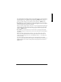
RabbitNet Peripheral Cards
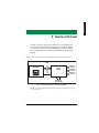
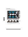
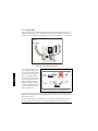
Digital I/O Card
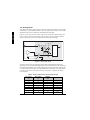
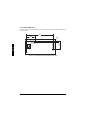
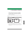
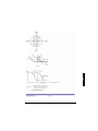
2. DIGITAL I/O CARD
Chapter 2 describes the features and the use of the Digital I/O
Card, one of the peripheral cards designed for use with the RabbitNet expansion ports on selected Rabbit Semiconductor singleboard computers, operator interfaces, and RabbitCore Prototyping
Boards.
Figure 3 shows a conceptual view of the Digital I/O Card connected to a master.
RabbitNet
LAN
Digital I/O
Card
SLAVE
MASTER
Rabbit 3000®
Microprocessor
DIGITAL
INPUTS
DIGITAL
OUTPUTS
ANALOG
INPUTS
DCIN, +5 V
EXTERNAL
+K SUPPLIES
Figure 3. Digital I/O Card (Slave) Connected to Master
NOTE: The OP7200 master and the RabbitCore Prototyping Boards do not supply any
power to the slave.
User’s Manual
17
RN1100
2.1 Features
• 24 protected and filtered digital inputs
• 16 high-speed protected digital outputs, individually configurable as sinking or sourcing
up to 200 mA at up to 36 V DC
• four 10-bit analog input channels:
2 buffered, 0 – 10 V, single-ended
1 buffered, 0 – 1 V, single-ended
1 buffered, -0.25 – +0.25 V, differential
• can be mounted in standard 100 mm DIN rail trays sold by other suppliers
• interfaces with master through RabbitNet™ serial protocol at 1 Megabit per second
using standard CAT 5/6 Ethernet cable, can be up to 10 m (33 ft) away from master
2.1.1 Software
The Digital I/O Card is a slave; the master to which it is connected is programmed using
version 8.01 or later of Rabbit Semiconductor’s Dynamic C. If you are using a master with
an earlier version of Dynamic C, Rabbit Semiconductor recommends that you upgrade
your Dynamic C installation. Contact your authorized Rabbit Semiconductor distributor or
your Rabbit Semiconductor Sales Representative for more information on Dynamic C
upgrades.
18
RabbitNet Peripheral Cards
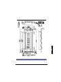
Use a straight-through CAT 5/6 Ethernet cable to connect the Digital I/O Card’s RJ-45
RabbitNet jack to a RabbitNet port on the master. You may use either port if you are connecting to a master such as the BL2500 that has more than one RabbitNet port.
NOTE: The RJ-45 RabbitNet jacks are serial I/O ports for use with a master and a network of peripheral cards. The RabbitNet jacks do not support Ethernet connections.
C14
O5
C13
C15
O6
O7
+K1
O9 O10 O11 O12 O13 O14 O15
J3 O8
+K2
J2
GND
+K2
D1
Q1
DCIN
J10
J8
RABBIT NET
JP2
Digital I/O
Card
RP7
GN
D
RP8 C57
RP9 C62 RP10
U11
GND
+K1
C75
VCC
IN 0-7
PULL
C76
RP5
IN8
IN9
IN10
IN11
IN12
IN13
IN14
IN15
RP4 C49
DC
IN
R72
C40
C42
R15
R31
R16
R32
R13
R29
R14
R30
C66
U10
C73
R71
R89
+
Q66
CR1
R86
AI3+
IN 8PULL15
Q48
C72
R88
R85 R
78
AI0 AGNDAI1 AI2 +5REFAI3-
C80
R84
C55
C63
C65
RP11
RP12
R66
R67
Y1
R79 Q67
U3
U6
R52
R54
R63 C71
Q65
C37 C38
R47 R48 C48
R49
C64
R62
C36
R46
C52
U5 U2
+
U8
C35
R45
C34
R44
JP3DIGITAL I/O
BOARD
IN00
IN01
IN02
IN03
IN04
IN05
IN06
IN07
R50
R51
R55
R56
R57
R58
C59
C33
R43
Power-supply
cable
J7
U7
C32
R42
C31
R41
C53
C30
R40
R11
R27
R12
R28
R8
R24
R9
R25
R10
R26
C29
R39
R53
C67
R69
R70
R77
R75
N/C
R74
C79
RP13
R87
R60
C70
R65
J11
C28
R38
C27
R37
C50
R3
R19
R4
R20
R5
R21
R6
R22
R7
R23
C26
R36
+
C78
C25
R35
C60
GN
D
R73
R1
R17
R2
R18
C54
IN22
IN23
R82
C41
C39
C46
RP3
IN21
R83
Q64
C43
C44 C23 C24
C45 R33 R34
C51
U1
U4
GND
+K2
DC
IN
VCC
RP2
IN16
IN17
IN18
IN19
IN20
RP6
U9
C77
R76
Q33
Q49
C19
C20
C21
C22
R59
J5
+
Q32
Q17
C17
RP1
C68 C69
R61 R64
C18
Q16
+
D16
GND
+K2
DC
IN
VCC
J6
+K1
C16
GN
D
O4
C12
O3
C11
O2
C10
C9
O1
C8
O0
C7
C6
GND
J1
IN 16-23
JP1PULL
C5
C4
C3
+K1
C2
C1
J4
+K2
J9
RABBIT POWER
Master
Some masters have only
one RabbitNet port and
do not have a friction-lock
power terminal.
Straight-through
CAT 5/6 Ethernet cable
RabbitNet
X
Ethernet
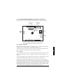
Figure 4. Connect Digital I/O Card to Master
You will also have to provide two separate DC power supplies to your Digital I/O Card:
+5 V and a DCIN of 9–32 V. These power supplies are connected via the polarized
friction-lock terminal at header J9. You may assemble a suitable cable using the frictionlock connectors from the Connectivity Kit described in Section 1.1.3. If you are using a
BL2500 or BL2600 as your master, you may draw this power from the BL2500 or
BL2600 as shown in Figure 4.
If you are using the digital outputs, you will need two additional external power supplies
up to 36 V that can each handle up to 1.6 A for +K1 and +K2. The actual voltage and
current depend on the requirements of the loads you plan to connect to the digital outputs.
These power supplies are connected to friction-lock terminals J1 and J4 on the Digital I/O
Card. You may assemble suitable cables using the friction-lock connectors from the Connectivity Kit described in Section 1.1.3. See Section 2.2.1 for detailed wiring diagrams.
User’s Manual
19
Digital I/O Card
2.2 Connections
Figure 5 illustrates the assembled friction-lock connector wiring diagram for the power
supplies used to supply power to the Digital I/O Card.
GND
DCIN/+5 V
GND
+5 V
DCIN
GND
+K
GND
+K
DCIN
n.c.
+5 V
GND
If you are not drawing power
from the master, connect the
power-supply grounds of the
DCIN and 5 V power supplies
at the power supplies.
+K1/+K2
RABBIT NET
RN1100
2.2.1 Power Supply
J1 or J4
J9
J8
Figure 5. Power-Supply Connections
NOTE: If you are using separate DC power supplies for DCIN and +5 V because you are
not drawing this power from the master, note that the crimp pins used in the fractionlock connector assembly can only hold one wire each. Connect the one GND wire from
the fraction-lock connector assembly to the ground on one of the two power supplies,
then use a separate wire to connect the power-supply grounds together.
Use 18-gauge (AWG) wire for
power-supply connections up
to 10 m away from the master.
If the wire length is less than
3 m, 22 gauge (AWG) wire is
acceptable. Do not daisy-chain
the power supply connections
between different peripheral
cards, but use a star configuration from the master or router
when there are several peripheral cards.
Daisy
Chain
X
Star
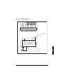
Figure 6. Daisy Chain vs. Star Configurations
20
RabbitNet Peripheral Cards
Large transient currents flow in the ground and positive supply wires when the digital output
drivers are switched on/off, and it is imperative that any ground differential resulting from
resistive or inductive loss in the ground wire be kept as low as possible (<4 V). Use the
GND pin on header J1, J4, or J9 on the Digital I/O Card if you have separate power supplies. Rabbit Semiconductor also recommends that you have a physical ground connection
between the Digital I/O Card and the master, which you will have if the power to header
J9 on the Digital I/O Card already comes from the master.
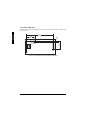
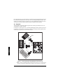
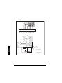
For development purposes, it is possible to draw the +K1/+K2 power from DCIN, as long
as you are careful to use only one digital output at a time to avoid exceeding the maximum
current-output capability of the DCIN supply. You can use a 3-way or a 4-way splice (for
example, Molex Series 19204), connector shells, or a terminal block to split the DCIN
supply from the master. Remember to do the same for the GND.
+K1
DCIN
DCIN
(from master)
+K2
Figure 7. Example of 4-way Splice for DCIN (used for development purposes only)
User’s Manual
21
Digital I/O Card
It is best to use a type of cable where the wires for the ground and positive(s) of any power
supply are bound together or twisted, and ideally the power-supply wires should not be
bundled with other wires.
The Digital I/O Card pinouts are shown in Figure 8.
DCIN
n.c.
AIN3+
AIN3
+5VREF
AIN2
AIN1
AGND
AIN0
AGND
DCIN
RabbitNet
Analog
Input
J11
J10
J7
Digital
Inputs
+5 V
GND
Power
Supply
ST Microcontroller
Program
Port
Analog Analog
Inputs Ground
RABBIT NET
J9
IN00
IN01
IN02
IN03
IN04
IN05
IN06
IN07
DS1
J8
J6
GND
GND
Digital
Inputs
IN23
IN22
IN21
IN20
IN19
IN18
IN17
IN16
IN08
IN09
IN10
IN11
IN12
IN13
IN14
IN15
Digital
Inputs
GND
K1
Digital
Outputs
+K2
+K2
Digital
Outputs
OUT08
OUT09
OUT10
OUT11
OUT12
OUT13
OUT14
OUT15
K1
Supply
GND
J1
J2
J3
+K1
+K1
J4
OUT00
OUT01
OUT02
OUT03
OUT04
OUT05
OUT06
OUT07
J5
GND
RN1100
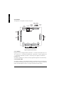
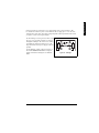
2.3 Pinout
K2
Supply
K2
Figure 8. Digital I/O Card Pinouts
2.3.1 Headers
Digital I/O Cards are equipped with six polarized 1 × 9 friction-lock terminals (J2, J3, J5,
J6, J7, and J11), a 1 × 4 friction-lock terminal (J9—DCIN and +5 V power supplies), two
1 × 2 friction-lock terminals (J1 and J4—external +K power supplies), and an RJ-45
RabbitNet jack.
No header is installed at J10, which is used to program the Digital I/O Card at the factory.
2.3.2 Indicator LED
An indicator LED (DS1) located under the header J10 location turns on when the Digital
I/O Card is powered up, then goes off once the Digital I/O Card is running. The LED will
flicker when the Digital I/O Card is receiving a transmission from the master.
22
RabbitNet Peripheral Cards
Digital I/O Card
2.4 Digital I/O
2.4.1 Digital Inputs
The Digital I/O Card has 24 digital inputs, IN00–IN23, each of which is protected over a
range of –36 V to +36 V. The inputs are factory-configured to be pulled up to +5 V, but
they can also be pulled up to DCIN or +K1 (IN00–IN15)/+K2 (IN16–IN23) or down to
0 V in banks of eight by changing a jumper as shown in Figure 9. The locations of the
headers and the jumper configurations are described in Section 2.7.2.
+5 V
DCIN
+K1/+K2
Factory
Default
27 kW
Microprocessor
100 kW
10 nF
GND
Figure 9. Digital I/O Card Digital Inputs [Pulled Up—Factory Default]
NOTE: If the inputs are pulled up to +K1/+K2, the voltage range over which the digital
inputs are protected changes to (K1/K2 – 36 V) to +36 V in order to keep the power
dissipation through the pull-up resistor below the rated 62 mW.
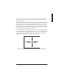
The actual switching threshold is approximately
2.40 V. Anything below this value is a logic 0, and
anything above is a logic 1.
+40 V
Digital Input Voltage
The digital inputs are each fully protected over a
range of -36 V to +36 V, and can handle short
spikes of ±40 V.
Normal Voltage
Levels
+36 V
Spikes
Spikes
+5 V
40 V
Spikes
Figure 10. RN1100 Digital Input
Protected Range
User’s Manual
23
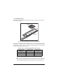
RN1100
2.4.2 Digital Outputs
The Digital I/O Card has 16 digital outputs, OUT00–OUT15, which can each sink or
source up to 200 mA. Figure 11 shows a wiring diagram for using the digital outputs in a
sinking or a souring configuration.
The rn_digOutConfig() function call simultaneously configures all the output channels to a “safe state” on power-up for sinking or sourcing outputs by setting the channels
to a high impedance. The “safe state” is considered to be all zeros, a disabled state for
sourcing outputs.
All the digital outputs sink and source actively. They can be used as high-side drivers,
low-side drivers, or as an H-bridge driver. When the Digital I/O Card is first powered up
or reset, all the outputs are disabled, that is, at a high-impedance status, until the rn_
digOutConfig() software function call is made. The rn_digOutConfig() call sets
the initial state of each digital output according to the configuration specified by the user,
and enables the digital outputs to their initial status.
SINKING OUTPUT
K1 or K2
D-REF
OUTPUT[0015]
SOURCING OUTPUT
K1 or K2
D-REF
OUTPUT[0015]
Figure 11. Digital I/O Card Digital Outputs
24
RabbitNet Peripheral Cards
Digital I/O Card
OUT00–OUT07 are powered by to +K1, and OUT08–OUT15 are powered by +K2.
K1 and K2 can each be up to 36 V, and should be able to supply up to 1.6 A. +K1 and
+K2 don't have to be same. The actual voltage depends on the requirements of the loads
you plan to connect to the digital outputs.
All the sinking or sourcing current, which could
be up to 1.6 A per bank of outputs, is returned
through the GND pins. Be sure to use a suitably
sized GND as explained in Section 2.2.1, and
keep the distance to the power supply as short as
possible.
For the H bridge, which is shown in Figure 12,
K1 and K2 should be the same if two digital
outputs used for the H bridge are on different
banks.
User’s Manual
+K1
A
B
+K2
LOAD
B
A
Figure 12. H Bridge
25
The microprocessor on the Digital I/O Card has four 10-bit A/D converter channels. Each
channel is identical, and can convert a range of voltages between 0 V and Vcc, where Vcc
is the +5 V reference that powers the microprocessor.
These four channels are configured as follows on the Digital I/O Card:
• 2 buffered channels, 0 – 10 V raw input voltage range, single-ended
• 1 buffered channel, 0 – 1 V raw input voltage range, single-ended
• 1 buffered channel, -0.25 – +0.25 V raw input voltage range, differential
010 V single-ended
AIN[0...1]
100 kW
+
100 kW
1 nF
10 kW
ADC
1 kW
47 kW
01 V single-ended
AIN[2]
25.5 kW
+
10 kW
ADC
1 kW
102 kW
25.5 kW
1 nF
-025 V +0.25 V differential
1 nF
10 kW
1 MW
AIN[3]
AIN[3+]
100 kW
100 kW
ADC
1 kW
+
1 MW
1 nF
47 kW
+
RN1100
2.5 Analog Inputs
+2.5 V
Figure 13. Digital I/O Card Analog Inputs
26
RabbitNet Peripheral Cards
Digital I/O Card
2.5.1 Single-Ended Inputs
There are three single-ended A/D converter inputs on the Digital I/O Card. A 5 V reference voltage is used for the single-ended inputs.
Two single-ended inputs that handle 0–10 V are filtered by a network of resistors and a
capacitor. The resistors form a 2:1 attenuator, and the capacitor protects the A/D converter
input against electrostatic transients. The input impedance is approximately 200 kΩ.
The third single-ended input handles 0–1 V and is filtered by a network of resistors and a
capacitor, which stabilize the circuit against oscillation and electrostatic transients. The
op-amp and feedback resistors form a ×5 amplifier. The input impedance is of the order of
several megohms.
2.5.2 Differential Inputs
Differential measurements actually require two analog inputs. As the name differential
implies, the difference in voltage between the two inputs is measured rather than the
difference between the input and ground.
A 2.5 V reference voltage is used for the differential inputs to shift the center point of
operation to 2.5 V. The input impedance of each differential input is at least 1 MΩ.
The differential input circuit of the Digital I/O Card was designed to measure voltages over a
range of ±250 mV. If the negative input is -250 mV, and the positive input is +250 mV, the
output to the A/D converter will be 5 V. If both inputs are tied together and to ground, the
output to the A/D converter will be 2.5 V. The output to the A/D converter will drop to 0 V
when the negative input reaches +250 mV and the positive input reaches -250 mV.
2.5.3 Calibrating the Analog Inputs
Manufacturing tolerances for resistors, bias currents, offset voltages, gain, and the like
introduce errors into the A/D conversions. Ideally there would be a one-to-one straightline relationship between the input voltage and the output of the A/D converter, and a
graph of such a line would have a slope of 1 and would pass through the (0,0) coordinate.
However, the errors arising from manufacturing tolerances introduce a deviation between
the input voltage that is actually applied and the voltage measurement that is output by the
A/D converter. The actual plot of voltage in vs. the voltage out from A/D converter is not
actually a straight line. However, a straight line is a very good first-order approximation,
and the calibration routines provided for the Digital I/O Card are based on a straight line
with a slope of 1 and an offset from (0,0). The calibration routines use two known measurement points on the voltage-in vs. voltage-out line as the basis to calculate calibration
constants that will be used to adjust for the slope of the line and the offset from (0,0). The
calibration routines typically use input voltage points that are 10% of the voltage range
less than the maximum and 10% of the voltage range more than the minimum readings
possible for the A/D converter on any given range.
User’s Manual
27
RN1100
When calibrating the A/D converter. its output depends on the accuracy of the meter used
to measure the voltage source used in the calibration process. Therefore, use the best digital
voltmeter available that meets or exceeds the 10-bit accuracy of the A/D converter chip.
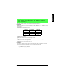
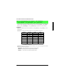
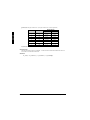
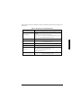
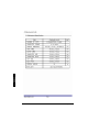
2.5.3.1 Calibration Constants
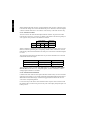
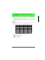
The A/D converter has four individual input channels available. To get the best results
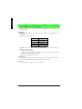
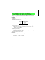
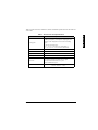
form the A/D converter, it is necessary to calibrate each channel. The following table provides a grid for each possible set of calibration constants.
Single-Ended
Channel
AIN0
AIN1
AIN2
Differential
AIN3– AIN3+
Input
When a calibration is performed, it fills in one of the squares in the table with a set of calibration constants representing the corresponding channel. These constants are stored in
flash memory, and are thus maintained even when power is been removed from the Digital
I/O Card.
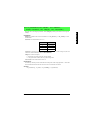
The sample programs listed in the table below are provided to illustrate how to read and
calibrate the various A/D inputs.
Mode
Read
Calibrate
Single-Ended, one channel
AIN_RDSE_CH.C
AIN_CALSE_CH.C
Differential, analog ground
AIN_RDDIFF_CH.C
AIN_CALDIFF_CH.C
These sample programs are found in the AIN subdirectory in SAMPLES\RABBITNET\
RN1100\ADC. See Section 2.6.2, “Sample Programs,” for more information on these
sample programs and how to use them.
2.5.3.2 Calibration Recommendations
Calibrate each of the A/D converter inputs in the same manner as they are to be used in the
application. For example, if you will be performing floating differential measurements or
differential measurements using a common analog ground, then calibrate the A/D converter in the corresponding manner.
It is not necessary to fill out the entire calibration table. Only the entries associated with
the channels that you will be using are necessary. This will simplify and speed up the calibration process.
28
RabbitNet Peripheral Cards
2.5.3.3 Factory Calibration
Calibration constants are not measured and loaded at the factory for individual Digital I/O
Cards. Default calibration constants (gain of 1, offset 0) are stored in flash memory, which
will allow you to use the analog inputs with a typical accuracy of about 2%. This is sufficient for many closed-loop applications. Rabbit Semiconductor recommends that you calibrate your card as described above only if you have to get the highest accuracy possible
when performing analog conversions.
User’s Manual
29
Digital I/O Card
Each calibration is normally done at 10% less than the maximum and 10% more than the
minimum within a given voltage range defined by the channel. However, if an application
is known to use only portion of a particular range, it is possible to obtain improved accuracy by using calibration points that are 10% less than the expected maximum and 10%
greater than the expected minimum.
RN1100
2.6 Software
This section provides the libraries, function calls, and sample programs related to the
Digital I/O Card.
2.6.1 Dynamic C Libraries
In addition to the library associated with the master, two other libraries have function calls
for the Digital I/O Card.
• RNET_DIO.LIB—provides functions unique to the digital I/O on the Digital I/O Card.
Function calls for this library are discussed in this chapter.
• RNET_AIN.LIB—provides functions unique to the analog inputs on the Digital I/O
Card and the A/D Converter Card. Function calls for this library are discussed in this
chapter.
Functions relevant to RabbitNet peripheral cards in general are described in Section 1.3.4.
Other functions applicable to all devices based on Rabbit microprocessors are described in
the Dynamic C Function Reference User’s Manual.
2.6.2 Sample Programs
Sample programs are provided in the Dynamic C SAMPLES folder.
The various folders contain specific sample programs that illustrate the use of the corresponding Dynamic C libraries. For example, the sample program PONG.C demonstrates
the output to the STDIO window.
To run a sample program, open it with the File menu (if it is not still open), then compile
and run it by pressing F9 or by selecting Run in the Run menu. The RabbitNet peripheral
card must be connected to a master such as the BL2500 with its Demonstration Board connected as explained in the Coyote (BL2500) User’s Manual or other user’s manual. The
BL2500 or other master must be in Program Mode, and must be connected via the programming cable to a PC.
2.6.2.1 Digital I/O
The SAMPLES\RABBITNET\RN1100\DIO subdirectory contains the following sample
programs. When running these sample programs, the Digital I/O Card may be connected to
either RabbitNet port on a master such as the BL2500 that has two RabbitNet ports. The
sample program will use rn_find() and the product RN1100 as the search criteria to
first find any Digital I/O Cards connected to the master. The first Digital I/O Card found
will run the sample program.
• DIGBANKIN.C—Demonstrates the use of the digital inputs by using the Demonstration
Board to read a bank of input channels while an individual channel is toggled from high to
low by pressing a pushbutton switch on the Demonstration Board.
Before you run this sample program, connect +K1 and GND on connector J4 of the Digital
I/O card to an external +5 V power supply. Make sure the digital inputs are pulled up with a
jumper across pins 1–2 on headers JP1, JP2, and JP3. If you are not drawing power from
30
RabbitNet Peripheral Cards
On the Demonstration Board, check that the factory-default positioning of jumpers is
across pins 3–5 and 4–6 of header H2.
Make the following connections from the Digital I/O Card to the Demonstration Board.
J1
·
·
·
·
·
·
·
·
·
·
·
·
LED1 LED2 LED3 LED4
BUZZER
LED4
LED3
LED2
LED1
K
+5V
SW4
1-2
3-4
5-6
DEMO BOARD
BUZZER
H1
··
··
··
··
··
··
··
SW3
H2
SW2
Jumpers:
H1: None
H2: As shown
SW1
GND
IN00 — S1
IN01 — S2
IN02 — S3
IN03 — S4
+K1 — +5 V
GND — GND
8-7
4-3
6-5
2-1
SW1
SW2
SW3
SW4
Once this sample program is compiled and
running, you may press switches S1–S4 on
the Demonstration Board to toggle the input low on the corresponding channel. Inputs
IN04–IN23 can be toggled low by touching the line with a GND signal. The status of the
inputs is displayed in the Dynamic C STDIO window.
• DIGIN.C—Demonstrates the use of the digital inputs by using the Demonstration Board to
read individual input channels while an individual channel is toggled from high to low by
pressing a pushbutton switch on the Demonstration Board.
Before you run this sample program, use the same power-supply connections and the same
connections between the Digital I/O Card and the Demonstration Board as shown for the
DIGBANKIN.C sample program.
Once DIGIN.C is compiled and running, you may press switches S1–S4 on the Demonstration Board to toggle the input low on the corresponding channel. Inputs IN04–IN23 can
be toggled low by touching the line with a GND signal. The status of the inputs is displayed
in the Dynamic C STDIO window.
• DIGBANKOUT.C—Demonstrates writing values to a bank of outputs by using the Demonstration Board whose LEDs are toggled on/off via the outputs.
Before you run this sample program, connect +K1 and GND on connector J4 of the Digital
I/O Card to an external +5 V power supply. If you are not drawing power from the master,
you will also have to connect DCIN, +5 V, and GND from connector J9 on the Digital I/O
Card to external power supplies.
Make the following connections from the Digital I/O Card to the Demonstration Board.
• OUT00 — DS1
OUT01 — DS2
OUT02 — DS3
OUT03 — DS4
+K1 — +5 V
GND — GND
Once this sample program is compiled and running, the Dynamic C STDIO window will
prompt to select an output bank. Select 1 for outputs OUT00–OUT07. Next you will be
prompted to enter a hex byte value—for example, enter AA to toggle LEDs DS1 and DS3
on/off.
User’s Manual
31
Digital I/O Card
the master, you will also have to connect DCIN, +5 V, and GND from connector J9 on the
Digital I/O Card to external power supplies.
RN1100
• DIGOUT.C—Demonstrates the use of the outputs by using the Demonstration Board
whose LEDs are toggled on/off via the outputs.
Before you run this sample program, use the same power-supply connections and the same
connections between the Digital I/O Card and the Demonstration Board as for the DIGBANKOUT.C sample program.
Once DIGOUT.C is compiled and running, the Dynamic C STDIO window will prompt
you for a channel selection. Select output channel OUT00. Next you will be prompted to
select the logic level—set a high logic level to turn LED DS1 on. You can repeat these
steps for OUT01–OUT03 and LEDs DS2–DS4. You can use a voltmeter to check the voltages on the remaining outputs.
2.6.2.2 Analog Inputs
The SAMPLES\RABBITNET\RN1100\AIN subdirectory contains the following sample
programs. The sample program will use rn_find() and the product RN1100 as the
search criteria to first find any Digital I/O Cards connected to the master. The first Digital
I/O Card found will run the sample program.
NOTE: The Demonstration Board does not have to be connected to run these sample
programs.
• AIN_CALDIFF_CH.C—Demonstrates how to recalibrate the differential A/D converter
channel using two known voltages to generate constants for that channel that are rewritten
into the Digital I/O Card flash memory. The voltages being monitored will be displayed
continuously.
Before you run this sample program, connect a 0–10 V
power supply, a voltmeter, and a network of resistors to
inputs AIN03+ and AIN03– as shown in the diagram.
Adjust the power supply starting at 0 V until the voltmeter shows approximately +0.235 V at AIN03+.
1.2 kW
010 V
AIN03+
51 W
1.2 kW
AIN03
Now compile and run the sample program. Enter the
voltage reading when prompted by the Dynamic C STDIO window. Then reverse the
power supply + and – connections and hit the Return key in the Dynamic C STDIO
window. Now enter the voltage reading again.
• AIN_CALSE_CH.C—Demonstrates how to recalibrate one single-ended A/D converter
channel using two known voltages to generate constants for that channel that are rewritten
into the Digital I/O Card flash. The voltages being monitored will be displayed continuously.
Before you run this sample program, connect a 0–10 V power supply and a voltmeter
between the selected analog channel and ground. Now compile and run the sample program. Follow the prompts in the Dynamic C STDIO window.
• AIN_RDDIFF_CH.C—Demonstrates reading the differential A/D converter channel using
two known voltages and constants for that channel. The voltage being monitored will be
displayed continuously.
Before you run this sample program, connect a 0–10 V power supply, a voltmeter, and a
network of resistors to inputs AIN03+ and AIN03– as shown for the AIN_CALDIFF_
CH.C sample program. Adjust the power supply on until the voltmeter shows approximately +0.20 V at AIN03+.
32
RabbitNet Peripheral Cards
• AIN_RDSE_CH.C—Reads and displays the voltage and equivalent values of one singleended analog input channel. Coefficients are read from the Digital I/O Card. The computed
raw data and equivalent voltages will be displayed.
Before you run this sample program, connect a 0–10 V power supply between analog input
AIN00 or AIN01 and GND. Connect a second 0–1 V power supply between analog input
AIN02 and GND. Now compile and run the sample program. Follow the prompts in the
Dynamic C STDIO window.
• AIN_SAMPLE.C—Demonstrates how to use the A/D driver on the single-ended inputs.
The voltage (average of 10 samples) that is present on the A/D channels will be displayed
continuously.
Before you run this sample program, connect a 0–10 V power supply and a voltmeter
between the analog input and GND of the analog input channel you will be using. The
analog input voltage range can be 0–10 V for AIN00 and AIN01, 0–1 V for AIN02, and
±0.25 V for AIN03.
Now power up the master and the Digital I/O Card, and compile and run the sample
program. Vary the voltage from the power supply over the design range for the channel you
are using and observe the voltmeter reading and the reading displayed in the Dynamic C
STDIO window.
User’s Manual
33
Digital I/O Card
Now compile and run the sample program. Vary the voltage from 0 to +0.25V and observe
the voltage readings on the voltmeter and in the Dynamic C STDIO window. Then reverse
the power supply + and – connections. Again vary the voltage from 0 to +0.25V and
observe the voltage readings on the voltmeter and in the Dynamic C STDIO window.
RN1100
2.6.3 Digital I/O Card Function Calls
2.6.3.1 Digital Input Function Calls
int rn_digIn(int handle, int channel,
char *retdata, int reserved);
Reads the undeglitched or raw data state of the selected digital input channel.
PARAMETERS
handle is an address index to device information. Use rn_device() or rn_find() to establish the handle.
channel is the digital input channel (0–23) to read.
retdata is a pointer to the return data address of the logic state.
reserved is reserved for future use. Set to 0.
RETURN VALUE
The status byte from the previous command, and a pointer to the return data logic state (0 or 1) of the
input. -1 means that device information indicates the Digital I/O Card is not connected to the master.
SEE ALSO
rn_digOut, rn_digBankIn
int rn_digBankIn(int handle, int bank,
char *retdata, int reserved);
Reads the undeglitched or raw data state of a block of designated digital input channels. The first bank
consists of channels 0–7, the second bank consists of channels 8–15, and the third bank consists of
channels 16–23.
PARAMETERS
handle is an address index to device information. Use rn_device() or rn_find() to establish the handle.
bank is the bank to read.
0 for all banks on the card
1 for bank of digital inputs 0–7
2 for bank of digital inputs 8–15
3 for bank of digital inputs 16–23
retdata is a pointer to the return data address of the logic state.
reserved is reserved for future use. Set to 0.
RETURN VALUE
The status byte from previous command, and a pointer to the return data byte where each bit corresponds
to one channel. Channels 0, 8, and 16 are considered to be the bit 0 positions. If all the banks are
requested, the pointer to the bank 1 data byte is returned with subsequent byte pointers to the next two
banks. -1 means that device information indicates the Digital I/O Card is not connected to the master.
SEE ALSO
rn_digIn, rn_digBankOut
34
RabbitNet Peripheral Cards
Digital I/O Card
2.6.3.2 Digital Output Function Calls
int rn_digOutConfig(int handle, int senddata);
Configures output channels 0 to 15 to a “safe state” on power-up for sinking or sourcing outputs. The
channels are set to a high impedance at power-up. The factory default sets the safe state as zeros, considered a disabled state for sourcing outputs.
This function will first compare the requested states and values in the “safe state” register. If there is a
match, the requested states will not be rewritten to the device to eliminate unnecessary writes. Otherwise
this function saves states to flash, and therefore should be called only once. A hardware reset, rn_
reset(), and a read of the reset register, rn_rst_status(), must be issued after this function is
called.
PARAMETERS
handle is an address index to device information. Use rn_device() or rn_find() to establish the handle.
senddata is a bitwise logic representing a state of 0 or 1 for each channel. The most significant bit
represents channel 15.
0 = disable sourcing outputs
1 = disable sinking outputs
RETURN VALUE
The status byte from the previous command. -1 means that device information indicates the Digital I/O
Card is not connected to the master.
SEE ALSO
rn_digOut
int rn_digOut(int handle, int channel,
char senddata, int reserved);
Sets the state of a digital output.
PARAMETERS
handle is an address index to device information. Use rn_device() or rn_find() to establish the handle.
channel is the output channel number (0 to 15)
senddata is the output data.
1 = set bit
0 = reset bit
reserved is reserved for future use. Set to 0.
RETURN VALUE
The status byte from the previous command. -1 means that device information indicates the Digital I/O
Card is not connected to the master.
SEE ALSO
rn_digOutConfig, rn_digBankOut, rn_digIn
User’s Manual
35
RN1100
int rn_digBankOut(int handle, int bank,
char senddata, int reserved);
Writes the state of a block of designated digital output channels. The first bank consists of channels 0–7,
and the second bank consists of channels 8–15.
PARAMETERS
handle is an address index to device information. Use rn_device() or rn_find() to establish the handle.
bank is the bank of digital output channels to write.
0 for all the digital outputs 0 to 15 in both banks
1 for bank of digital outputs 0 to 7
2 for bank of digital outputs 8 to 15
senddata is a 16-bit output value, where each bit corresponds to one channel. Channel 0 and channel 8 are
considered the least significant bit 0 when using single-bank access. When accessing both banks, channel
0 is the least significant bit 0 and channel 15 is the most significant bit 15.
reserved is reserved for future use. Set to 0.
RETURN VALUE
The status byte from the previous command. -1 means that device information indicates the Digital I/O
Card is not connected to the master.
SEE ALSO
rn_digOutConfig, rn_digOut, rn_digBankIn
36
RabbitNet Peripheral Cards
Digital I/O Card
2.6.3.3 Analog Input Function Calls
int rn_anaInConfig(int handle, int channel,
int opmode, int gaincode, int reserved);
Configures each analog input channel to the desired operation at the desired gain. Once all channels have
been set to single-ended voltages or differential voltages, use rn_anaIn(), rn_anaInVolts(),
or rn_anaInDiff() to read an A/D converter channel.
PARAMETERS
handle is an address index to device information. Use rn_device() or rn_find() to establish the handle.
channel is the channel number (0 to3).
Channel
Single-Ended
Differential
0
+AIN0
—
1
+AIN1
—
2
+AIN2
—
3
—
+AIN3 -AIN3
opmode is the mode of operation for the specified channel:
ADCENABLE—enables conversions
ADCDISABLE—disables conversions
gaincode is the gain code. Use 0 for the Digital I/O Card.
reserved is reserved for future use. Set to 0.
RETURN VALUE
The status byte from the previous command. -1 means that device information indicates the Digital I/O
Card is not connected to the master.
SEE ALSO
rn_anaIn, rn_anaInVolts, rn_anaInDiff
User’s Manual
37
RN1100
int rn_anaIn(int handle, int channel, int *retdata,
int sample, int reserved);
Reads the raw data value of an analog input channel. Set the sample parameter greater than one to
average the readings.
PARAMETERS
handle is an address index to device information. Use rn_device() or rn_find() to establish the handle.
channel is the channel number (0 to 3).
Channel
Voltage Range
0
0 to +10 V
1
0 to +10 V
2
0 to +1 V
3
±250 mV
retdata is a pointer to the return address of a raw data value (0–1023) for 10-bit A/D conversions
sample is x number of samples
1 sample = approximately 500 µs
>1 sample = each sampling will wait for an updated conversion—this may take 40 to 160 µs longer
depending on how many channels are enabled
reserved is reserved for future use. Set to 0.
RETURN VALUE
The status byte from the previous command and a return pointer to the raw input data. -1 means that
device information indicates the Digital I/O Card is not connected to the master.
SEE ALSO
rn_anaInConfig, rn_anaInVolts, rn_anaInDiff
38
RabbitNet Peripheral Cards
Digital I/O Card
int rn_anaInVolts(int handle, int channel,
float *retdata, int sample, int reserved);
Reads the state of a single-ended analog input channel. Set the sample parameter greater than one to
average the readings.
PARAMETERS
handle is an address index to device information. Use rn_device() or rn_find() to establish the handle.
channel is the channel number (0 to 2).
Channel
Voltage Range
0
0 to +10 V
1
0 to +10 V
2
0 to +1 V
retdata is a pointer to a floating-point voltage value, which is updated for the channel being accessed
(represented in units of volts)
NOTE: If there is a data overflow or an out-of-range error, the value will be set to -4096 (as
defined by the macro ADOVERFLOW).
sample is x number of samples
1 sample = approximately 675 µs
>1 sample = each sampling will wait for an updated conversion—this may take 40 to 160 µs longer
depending on how many channels are enabled
reserved is reserved for future use. Set to 0.
RETURN VALUE
The status byte from the previous command and a return pointer to the raw input data. -1 means that
device information indicates the Digital I/O Card is not connected to the master.
SEE ALSO
rn_anaInConfig, rn_anaIn, rn_anaInDiff
User’s Manual
39
RN1100
int rn_anaInDiff(int handle, int channel,
float *retdata, int sample, int reserved);
Reads the state of a differential analog input channel. Set the sample parameter greater than one to
average the readings.
PARAMETERS
handle is an address index to device information. Use rn_device() or rn_find() to establish the handle.
channel is the channel number (3).
retdata is a pointer to a floating-point voltage value, which is updated for the channel being accessed
(represented in units of volts)
NOTE: If there is a data overflow or an out-of-range error, the value will be set to -4096 (as
defined by the macro ADOVERFLOW).
sample is x number of samples
1 sample = approximately 675 µs
>1 sample = each sampling will wait for an updated conversion—this may take 40 to 160 µs longer
depending on how many channels are enabled
reserved is reserved for future use. Set to 0.
RETURN VALUE
The status byte from the previous command and a return pointer to the raw input data. -1 means that
device information indicates the Digital I/O Card is not connected to the master.
SEE ALSO
rn_anaInConfig, rn_anaIn, rn_anaInVolts
40
RabbitNet Peripheral Cards
Digital I/O Card
int rn_anaInCalib(int channel, int opmode,
int gaincode, int value1, float volts1,
int value2, float volts2, rn_AinData *adata);
Calibrates the response of an analog input channel as a linear function using the two conversion points
provided. Four values are calculated, and the results are sent later to the analog input device using the
function anaInWrCalib().
Each channel will have the following information:
a linear constant or gain,
a voltage offset.
NOTE: Typical calibration constants are loaded at the factory. This function should be used when
you need more precise calibration or recalibration, or the calibration constants were corrupted in
the device.
PARAMETERS
channel is the channel number (0 to3).
Channel
Single-Ended
Differential
0
AIN00
—
1
AIN01
—
2
AIN02
—
3
—
AIN03
opmode is not used. Set to 0.
gaincode is the gain code. Use 0 for the Digital I/O Card.
value1 is the first raw data value read from the A/D converter channel.
volts1 is the voltage corresponding to the first input value (0 to +10 V, 0 to +1 V, or ± 250 mV).
value2 is the second raw data value read from the A/D converter channel.
volts2 is the voltage corresponding to the second input value (0 to +10 V, 0 to +1 V, or ± 250 mV).
rn_AinData *adata is a structure pointer to where the calibration constants, gain, and offset
values are to be written after being calculated.
RETURN VALUE
0, if successful.
-1 if not able to make calibration constants.
SEE ALSO
rn_anaInWrCalib
User’s Manual
41
RN1100
int rn_anaInWrCalib(int handle, int channel,
int opmode, int gaincode, rn_AinData adata,
int reserved);
Writes the calibration constants, gain, and offset previously calculated by rn_anaInCalib() into
the analog device flash memory. A hardware reset (rn_reset()) and a read reset register (rn_
rst_status()) must be issued after this function is called.
NOTE: Typical calibration constants are loaded at the factory. This function should be used when
you need more precise calibration or recalibration, or the calibration constants were corrupted in
the device.
PARAMETERS
handle is an address index to device information. Use rn_device() or rn_find() to establish the handle.
channel is the channel number (0 to3).
Channel
Single-Ended
Differential
0
AIN00
—
1
AIN01
—
2
AIN02
—
3
—
AIN03
opmode is not used. Set to 0.
gaincode is the gain code. Use 0 for the Digital I/O Card.
rn_AinData adata is a structure pointer to where the calibration constants, gain, and offset values
are to be written after being calculated.
reserved is reserved for future use. Set to 0.
RETURN VALUE
The status byte from the previous command and a return pointer to the raw input data. -1 means that
device information indicates the Digital I/O Card is not connected to the master.
SEE ALSO
rn_anaInRdCalib, rn_anaInCalib
42
RabbitNet Peripheral Cards
Digital I/O Card
int rn_anaInRdCalib(int handle, int channel,
int opmode, int gaincode, rn_AinData *adata,
int reserved);
Reads the calibration constants, gain, and offset from the analog input device.
PARAMETERS
handle is an address index to device information. Use rn_device() or rn_find() to establish the handle.
channel is the channel number (0 to3).
Channel
Single-Ended
Differential
0
AIN00
—
1
AIN01
—
2
AIN02
—
3
—
AIN03
opmode is not used. Set to 0.
gaincode is the gain code. Use 0 for the Digital I/O Card.
rn_AinData *adata is a structure pointer to where the calibration constants, gain, and offset
values are to be written after being calculated.
reserved is reserved for future use. Set to 0.
RETURN VALUE
The status byte from the previous command and a return pointer to the raw input data. -1 means that
device information indicates the Digital I/O Card is not connected to the master.
SEE ALSO
rn_anaInWrCalib, rn_anaInCalib
User’s Manual
43
RN1100
2.6.4 Status Byte
Section 1.3.5
44
provides information on the status bytes returned by various function calls.
RabbitNet Peripheral Cards
User’s Manual
45
NOTE: All diagram and graphic measurements are in inches followed by millimeters
enclosed in parentheses.
Figure 14. Digital I/O Card Dimensions
(100)
3.95
(16)
0.65
(17)
0.67
(100)
3.95
C4
C3
C2
C1
C5
C7
C6
C8 C9
C13
C12
C11
C10
C15
C14
C16
D1
Q1
D16
GND
J5
+
+K2
Q32
DC
IN
GND
Q17
C17
VCC
RP1
Q33
IN16 17 18 19
C39 C41 C40
(90)
3.55
3.05
23
(77.5)
20 21 22
C25
R35
C26
R36
C27
R37
C28
R38
C29
R39
C30
R40
GND
C59 R50
C60
J6
C68 C69
R61 R64
U4
R59
C31
R41
C32
R42
C33
R43
C35
C34 R45
R44
C36
R46
C37
R47
C38
RP4 C49 RP5
R48 C48
U3
U2
C65
R52
U10
R89
R62
R63 C71
Q65
C63
RP8 C57 RP7
RP9 C62 RP10
+K1
DC
IN
C75
R72
R84
R90
GND
RP11
RP12
R66
U11
R67
Y1
J8
C80 Q66
Q68
R79 Q67
C55
R49
U6
C64
R54
U8
R74
C79
J11
U5
U7
R53
C67
RP13
C70
R65
U9
C77
R76
R82
R69
R70
R87 R77
R88 R78
R85
R86
VCC
IN 0-7
PULL
C76
JP3DIGITAL I/O
BOARD
J9
J10
R83
DC
IN
VCC
Q64
C43
C44 C23 C24
R34
C45 R33
C51
RP6
U1
C54
C72
CR1
R60
+K2
Q49
C19
C20
C21
C22
RP2
RP3
C46
R5
R21
R9
R25
R8
R24
R51
R55
R56
R57
R58
C50
C53
C73
R71
DS1
R73
C18
Q16
C42
R16
R32
+
C78
JP2
C52
C66
+
R75
IN 8-15
PULL
GND
Q48
14 15
11 12 13
IN08 09 10
GND
04 05 06
07
03
IN00 01 02
J7
(6.4)
+
J1
GND
IN 16-23
+K2
JP1PULL
R1
R17
J2
R2
R18
+K2
R3
R19
09 10 11 12 13 14 15
R4
R20
J3OUT08
R6
R22
+K1
R7
R23
R11
R27
R10
R26
07
R13
R29
03 04 05 06
R12
R28
R14
R30
OUT00 01 02
0.250
(88)
3.45
GND
R15
R31
(6.4)
0.250
+K1
J4
+
AIN1 +5REF
AIN0
- AIN3 +
AIN2
AGND AGND
DCIN
RABBIT NET
RABBIT POWER
(30.7)
1.21
(46.5)
1.83
Figure 14 shows the mechanical dimensions for the Digital I/O Card.
Digital I/O Card
2.7.1 Electrical and Mechanical Specifications
2.7 Specifications
RN1100
Table 3 lists the electrical, mechanical, and environmental specifications for the Digital
I/O Card.
Table 3. Digital I/O Card Specifications
Feature
Microprocessor
Digital Inputs
Digital Outputs
Analog Inputs
RabbitNet™ Serial Port
Power
Temperature
Humidity
Connectors
Board Size
46
Specification
ST72F264G
24, protected to ±40 V DC,
switching threshold is 1.5 V nominal
16, sink or source up to 200 mA each, 40 V DC max.,
individually software-configurable as sinking or sourcing
Four buffered channels:
10-bit resolution, 8-bit accuracy, conversion time 28 µs/
channel
Input ranges:
2 channels 0–10 V, single-ended
1 channel 0–1 V, single-ended
1 channel -0.25 – +0.25 V, differential
RS-422, 1 Mbits/s
Vcc: +5 V DC, 20 mA
DCIN: 9–32 V DC (12 V min. if using analog inputs), 500 mW
+K1, +K2: 5–36 V DC, 1.6 A each
-40°C to +70°C
5% to 95%, noncondensing
Friction-lock connectors:
six polarized 9-position terminals with 0.1" pitch
two 2-position power terminals with 0.156" pitch
one 4-position terminal with 0.156" pitch
One RJ-45 RabbitNet™ jack
3.55" × 3.95" × 0.67"
(90 mm × 100 mm × 17 mm)
RabbitNet Peripheral Cards
Digital I/O Card
2.7.1.1 Physical Mounting
Figure 15 shows position information to assist with interfacing other boards with the
Digital I/O Card.
3.500
(88.9)
3.100
(78.7)
0.025
(1.5)
(12.7)
0.500
(0.6)
0.025
(20.3)
0.060
0.800
(0.6)
J11
J7
J9
(53.3)
(75.4)
2.970
(78.7)
3.100
J6
2.100
(39.4)
1.550
J8
J5
J4
J3
J2
J1
0.315
(8.0)
0.750
(19.0)
1.850
(47.0)
3.000
(76.2)
Figure 15. User Board Footprint for Digital I/O Card
User’s Manual
47
RN1100
2.7.2 Jumper Configurations
Figure 16 shows the header and jumper locations used to configure the various Digital I/O
Card options.
JP3
JP2
JP1
Figure 16. Location of Digital I/O Card Configurable Positions
48
RabbitNet Peripheral Cards
Digital I/O Card
Table 4 lists the configuration options. Standard pluggable jumpers are used.
Table 4. Digital I/O Card Jumper Configurations
Header
JP1
JP2
JP3
Description
IN16–IN23
IN08–IN15
IN00–IN07
User’s Manual
Pins Connected
1–2
Pulled up to +5 V
3–4
Pulled up to DCIN
5–6
Pulled up to +K2
7–8
Pulled down
1–2
Pulled up to +5 V
3–4
Pulled up to DCIN
5–6
Pulled up to +K1
7–8
Pulled down
1–2
Pulled up to +5 V
3–4
Pulled up to DCIN
5–6
Pulled up to +K1
7–8
Pulled down
Factory
Default
×
×
×
49
RN1100
50
RabbitNet Peripheral Cards
Chapter 3 describes the features and the use of the A/D Converter Card, one of the peripheral cards designed for use with the
RabbitNet expansion ports on selected Rabbit Semiconductor
single-board computers, operator interfaces, and RabbitCore
Prototyping Boards.
Figure 17 shows a conceptual view of the A/D Converter Card connected to a master.
RabbitNet
LAN
A/D Converter
Card
SLAVE
MASTER
Rabbit ® 3000
Microprocessor
ANALOG
INPUTS
+5 V
Figure 17. A/D Converter Card (Slave) Connected to Master
NOTE: The OP7200 master and the RabbitCore Prototyping Boards do not supply any
power to the slave.
User’s Manual
51
A/D Converter Card
3. A/D CONVERTER CARD
3.1 Features
• 8 single-ended 11-bit or 4 differential 12-bit analog inputs
RN1200
• 4 channels can be set with jumpers to be 11-bit 4–20 mA analog inputs, all 8 channels
can be special-ordered in quantity to be 11-bit 4–20 mA analog inputs
• 1 MΩ input impedance
• 2.5 ksamples/s sampling rate
• software-controlled voltage ranges: 0–1 V, 2 V, 5 V 10 V, 20 V DC (single-ended) or
±1 V, ±2 V, ±5 V, ±10 V, ±20 V DC (differential)
• can be mounted in standard 100 mm DIN rail trays sold by other suppliers
• interfaces with master through RabbitNet™ serial protocol at 1 Megabit per second
using standard Ethernet cable up to 10 m (33 ft) long
3.1.1 Software
The A/D Converter Card is a slave; the master to which it is connected is programmed
using version 8.01 or later of Rabbit Semiconductor’s Dynamic C. If you are using a
BL2500 or an OP7200 as your master with an earlier version of Dynamic C, Rabbit Semiconductor recommends that you upgrade your Dynamic C installation. Contact your authorized Rabbit Semiconductor distributor or your Rabbit Semiconductor Sales Representative
for more information on Dynamic C upgrades.
52
RabbitNet Peripheral Cards
Use a straight-through CAT 5/6 Ethernet cable to connect the A/D Converter Card’s RJ-45
RabbitNet jack to a RabbitNet port on the master. You may use either port if you are connecting to a master such as the BL2500 that has more than one RabbitNet port.
NOTE: The RJ-45 RabbitNet jacks are serial I/O ports for use with a master and a network of peripheral boards. The RabbitNet jacks do not support Ethernet connections.
Some masters have only
one RabbitNet port and
do not have a friction-lock
power terminal.
Master
RabbitNet
Power-supply
cable
A/D Converter
Card
X
Ethernet
DS1
J3
C3
U1
R1
R2
R3
R4
R12
Y1
RP1
RA
BB
ITN
R5
R51
C18
R28
RP4
R29
Q6
C19 Q2 R21 R27
C20
R30
R31
Q3 R22 R25 Q7
C13
C14
R32
RP3
R1
J1
JP1
C9
C8
C7
ET
U2
R33
Q5 R23 R26 Q9
C15
C16
R34
R35
Q4
Q8
C17
U3
C4
C2
R16
R17
R18
R19
Q1
RP2
J4
C5
3
2
AIN
AIN
A
IN1
0
42
AIN
0m
A
5
R10
C6
C21
R11
U5
U4
0
R20
C11
C1
R24
C1
R8
R36
GND
SEQ
3
R7
AIN7
AIN6
AIN5
AIN4
AIN3
AIN2
AIN1
AIN0
2 R
1
VCC GND
RABBIT POWER
C1
R6
J2
4
R9
R1
DCIN
Straight-through
CAT 5/6 Ethernet cable
Figure 18. Connect A/D Converter Card to Master
You will also have to provide +5 V DC power to your A/D Converter Card. The power
supply is connected via the friction-lock terminal at header J2. If you are using a BL2500
or BL2600 as your master, you may draw this power from the BL2500 or BL2600 as
shown in Figure 18. You may assemble a suitable cable using the friction-lock connectors
from the Connectivity Kit described in Section 1.1.3. Although there is a standard RabbitNet DCIN power-supply input on the A/D Converter Card, the A/D Converter Card does
not need DCIN power.
NOTE: Even if you are not drawing power from a master, you will need to connect the
A/D Converter Card ground to the ground on your master. The GND pin on header J2
should be used.
At the present time, you are limited by the number of RabbitNet ports on the master as to
how many peripheral boards may be connected to that master.
User’s Manual
53
A/D Converter Card
3.2 Connections
3.2.1 Power Supply
Figure 19 illustrates the assembled friction-lock connector wiring diagram for the power
supplies used to supply power to the A/D Converter Card.
DCIN
n.c.
GND
+5 V
+5V
GND
RN1200
+5 V
Pin 1
RABBIT NET
J2
J1
Figure 19. Power-Supply Connections
54
RabbitNet Peripheral Cards
3.3 Pinout
A/D Converter Card
The A/D Converter Card pinouts are shown in Figure 20.
Power
Supply
DCIN
n.c.
+5V
GND
RABBIT POWER
J4
GND
J2
RabbitNet
J1
AIN7
AIN6
AIN5
AIN4
AIN3
AIN2
AIN1
AIN0
ST Microcontroller
Program
Port
J3
Analog
Inputs
DS1
Figure 20. A/D Converter Card Pinouts
3.3.1 Headers
A/D Converter Cards are equipped with one polarized 1 × 9 friction-lock terminals at J4, a
1 × 4 friction-lock terminal at J2 (DCIN and +5 V power supplies), and an RJ-45
RabbitNet jack.
No header is installed at J3, which is used to program the A/D Converter Card at the factory.
3.3.2 Indicator LED
An indicator LED (DS1) located near the header J3 location turns on when the A/D Converter
Card is powered up, then goes off when the A/D Converter Card has completed its initialization process and is running. The LED will be on while the A/D Converter Card is
receiving a transmission from the master.
User’s Manual
55
3.4 Analog Inputs
Figure 21 shows a pair of A/D converter input circuits. Each A/D converter input essentially consists of resistors and a capacitor. The resistors form a10:1 attenuator, and the
capacitor protects the A/D converter input against electrostatic discharges.
+V
User Circuits
2.048 V
953 kW
AIN1
953 kW
AGND
0W
1 nF
0W
ADC
105 kW
AIN0
105 kW
RN1200
The single A/D converter used in the A/D Converter Card has a resolution of 11 bits (singleended mode) or 12 bits (differential mode). There are eight channels of A/D conversion; the
differential mode uses two channels for each differential-mode input.
1 nF
Figure 21. A/D Converter Inputs
The A/D converter chip can make either single-ended or differential measurements
depending on the value of the opmode parameter in the software function call, which turns
the appropriate MOSFETs on or off and configures the A/D converter chip. Adjacent A/D
converter inputs are paired when you make differential measurements. For single-ended
conversions, the A/D converter chip works only with positive voltages for the ranges
listed in Table 5.
Table 5. Positive A/D Converter Input Voltage Ranges
56
Min. Voltage
(V)
Max. Voltage
(V)
Amplifier
0.0
+20.0
1
10
0.0
+10.0
2
5
0.0
+5.0
4
2.5
0.0
+4.0
5
2.0
0.0
+2.5
8
1.25
0.0
+2.0
10
1.0
0.0
+1.25
16
0.625
0.0
+1.0
20
0.500
Gain
mV per Tick
RabbitNet Peripheral Cards
Differential measurements require two channels. As the name differential implies, the difference in voltage between the two adjacent channels is measured rather than the difference between the input and analog ground. Voltage measurements taken in the differential
mode have a resolution of 12 bits, with the 12th bit indicating whether the difference is
positive or negative.
When using the differential mode, the input can be either positive or negative, but do not
exceed the maximum range by more than 20%.
If a device such as a battery is
connected across two channels
AIN0
for a differential measurement,
ADC
0
and it is not referenced to
2.048 V
Device +
analog ground, then the current
I
+
from the device will flow
through both sets of attenuator
AIN1
1
resistors as shown in Figure 22.
This will generate a negative
voltage at one of the inputs,
Figure 22. Current Flow from Ungrounded
ADC1, which will almost ceror Floating Source
tainly lead to inaccurate A/D
conversions. To allow for such
differential measurements, the A/D Converter Card uses a 2.048 V reference voltage. This
allows input voltages that are negative with respect to analog ground. Table 6 provides the
differential voltage ranges for this setup.
Table 6. Differential Voltage Ranges
Min. Differential
Voltage
(V)
Max. Differential
Voltage
(V)
Amplifier
0
±20.0
×1
10
0
±10.0
×2
5
0
±5.0
×4
2.5
0
±4.0
×5
2.0
0
±2.5
×8
1.25
0
±2.0
×10
1.00
0
±1.25
×16
0.625
0
±1.0
×20
0.500
Gain
mV per Tick
The differential mode described above may also be used to measure negative voltages.
User’s Manual
57
A/D Converter Card
Many other possible ranges are possible by physically changing the resistor values that
make up the attenuator circuit.
The A/D converter inputs can also be used with 4–20 mA current sources by measuring the
resulting analog voltage drop across a 100 Ω 1% precision resistor. These 100 Ω 1% precision resistors are included on the A/D Converter Card for analog input channels AIN0–
AIN3, and each of these channels may be configured individually using the jumpers on
header JP1 as shown in Figure 23.
SEQ
R36
GND
AIN7
AIN6
AIN5
AIN4
AIN3
AIN2
R47
AIN0
R51
J4
JP1
AIN1
R49
R50
420 mA
AIN0
AIN1
AIN2
AIN3
AIN4
AIN5
AIN6
AIN7
AIN0
R50
R49
R47
R44
R36
R37
R38
R39
R40
R41
R42
R43
R44
AIN1
ANALOG INPUT
CHANNEL
AIN2
0W
RESISTORS
INSTALLED
AIN3
RN1200
3.4.1 Analog Current Measurements
Figure 23. Locations of Resistors for 4–20 mA Mode
CAUTION: The input impedance is low for the 4–20 mA current mode. Be careful
not to exceed 2.5 V across the input when using the 4–20 mA current mode to keep
the power dissipation by the 100 Ω precision resistors below their maximum rating.
For volume orders of A/D Converter Cards configured as 4–20 mA analog inputs, 0 Ω
surface-mounted resistors can be installed at the factory instead of the jumpers on header
JP1, and AIN4–AIN7 can also be configured for use as 4–20 mA analog inputs. Contact your
Rabbit Semiconductor Sales representative or your authorized distributor for more information on these options and the minimum order quantity.
The single-ended scale of 0–2.56 V with a gain of 8 is used to get an A/D current conversion of 12.5 µA/tick.
58
RabbitNet Peripheral Cards
Manufacturing tolerances for resistors, bias currents, offset voltages, gain, and the like
introduce errors into the A/D conversions. Ideally there would be a one-to-one straightline relationship between the input voltage and the output of the A/D converter, and a
graph of such a line would have a slope of 1 and would pass through the (0,0) coordinate.
However, the errors arising from manufacturing tolerances introduce a deviation between
the applied input voltage and the voltage that is output by the A/D converter. The actual
plot of voltage in vs. the voltage out from A/D converter is not actually a straight line.
However, a straight line is a very good first-order approximation, and the calibration routines provided for the A/D Converter Card are based on a straight line with a slope of 1
and an offset from (0,0). The calibration routines use two known measurement points on
the voltage-in vs. voltage-out line as the basis to calculate calibration constants that will be
used to adjust for the slope of the line and the offset from (0,0). The calibration routines
typically use input voltage points that are 10% less then the maximum and 10% more than
the minimum readings possible for the A/D converter on any given range.
Quality calibration procedures are extremely important in obtaining good A/D converter
results. No matter how high a resolution the A/D converter has, it cannot compensate for
improper calibration. A/D converter results will never be more accurate than the meter
used in the calibration process. Therefore, use the best digital volt and milli-amp meter
available that meets or exceeds the accuracy of the A/D converter chip.
3.4.2.1 Modes
The A/D converter operates in three different modes:
• the single-ended mode,
• the differential mode, and
• the 4–20 mA current mode
The calibration and read routines provided correspond to these three modes.
3.4.2.2 Calibration Constants
The A/D converter has eight individual input channels, and each channel has eight programmable gains. Additionally, the A/D converter has the capability for adjacent inputs to
be paired to make differential measurements with eight different gains, and provision is
also made to convert 4–20 mA analog current measurements.
To get the best results from the A/D converter, it is necessary to calibrate each mode for
each of its gains. The following table provides a grid for each possible set of calibration
constants.
User’s Manual
59
A/D Converter Card
3.4.2 Calibrating the A/D Converter Chip
Mode
Single-Ended
Gain
1
2
4
5
8
10
mA
16
20
4
Differential
1
2
4
5
8
10
16
20
1
2
Input
RN1200
0
3
4
5
6
7
For the single-ended mode there are calibration constants for each channel and for each of
its gains, for a total of 64 sets of calibration constants. The 4–20 mA mode covers 4–20 mA
(actually 0–25 mA) currents. Separate calibration and read-back routines are provided for
this. Since only one range of current measurement is provided, these routines use only one
gain (4). One set of calibration constants is provided for each of the eight input channels.
The differential-mode routines use a pair of input channels to make measurements. In this
case, calibration constants are stored for each pair of channels and for each of the eight
gains, for a total of 32 sets of calibration constants.
When a calibration is performed, it fills in one of the squares in the table with a set of calibration constants representing the corresponding mode, channel, and gain. These constants are stored in flash memory on the A/D Converter Card, and are thus maintained
even when power is been removed from the A/D Converter Card. Note that calibration
constants are stored for each of the modes. Since A/D converter read routines select the
appropriate calibration constants based on the mode, it is possible for software calls to
move from one mode to another without recalibration.
3.4.2.3 Calibration Recommendations
It is imperative that you calibrate each of the A/D converter inputs in the same manner as
they are to be used in the application. For example, if you will be performing floating differential measurements or differential measurements using a common analog ground, then
calibrate the A/D converter in the corresponding manner. The calibration table only holds
calibration constants based on mode, channel, and gain. Other factors affecting the calibration must be taken into account by calibrating using the same method, mode, and
gain setup as in the intended use.
It is not necessary to fill out the entire calibration table. Only the entries associated with
the modes, channels, and gains that you will be using are necessary. This fact can be used
to simplify and speed up the calibration process.
60
RabbitNet Peripheral Cards
3.4.2.4 Factory Calibration
Because of the large number of possible calibrations, the factory performs only a rudimentary calibration on the A/D Converter Card. The factory performs a single-ended calibration on each of the eight channels with a gain of 1 (0–20 V range). The remaining singleended calibration constants for the other seven gains are approximated and are filled in
based on the initial calibration. The milli-amp and differential portions of the table are
filled in using typical expected values. All read routines will work properly with these factory-initialized calibration constants, but only the single-ended mode should be expected
to return accurate results over a range of 0–20 V until you recalibrate the A/D Converter
Card for your use.
Sample programs are provided to illustrate how to read and calibrate the various A/D
inputs.
Mode
Single-Ended, one channel
Single-Ended, all channels
Read
AIN_RDSE_CH.C
—
Calibrate
AIN_CALSE_CH.C
AIN_CALSE_ALL.C
4–20 mA Current
AIN_RDMA_CH.C
AIN_CALMA_CH.C
Differential
AIN_RDDIFF_CH.C
AIN_CALDIFF_CH.C
These sample programs are found in the in the SAMPLES\RABBITNET\RN1200 directory.
See Section 3.5.2, “Sample Programs,” for more information on these sample programs
and how to use them.
User’s Manual
61
A/D Converter Card
Each calibration is normally done at 10% less than the maximum and 10% more than the
minimum within a given voltage range defined by the mode, channel, and gain. However,
if an application is known to use only portion of a particular range, it is possible to obtain
improved accuracy by using calibration points that are 10% less than the expected maximum and 10% greater than the expected minimum.
3.5 Software
This section provides the libraries, function calls, and sample programs related to the A/D
Converter Card.
RN1200
3.5.1 Dynamic C Libraries
In addition to the library associated with the master single-board computer such as the
BL2500 or OP7200, one other library is needed to provide function calls for the A/D
Converter Card.
• RNET_AIN.LIB—provides functions unique to the analog inputs on the Digital I/O
Card and the A/D Converter Card. Function calls for this library are discussed in this
chapter.
Functions relevant to RabbitNet peripheral cards in general are described in Section 1.3.4.
Other functions applicable to all devices based on Rabbit microprocessors are described in
the Dynamic C Function Reference User’s Manual.
3.5.2 Sample Programs
Sample programs are provided in the Dynamic C SAMPLES folder.
The various folders contain specific sample programs that illustrate the use of the corresponding Dynamic C libraries. For example, the sample program PONG.C demonstrates
the output to the STDIO window.
To run a sample program, open it with the File menu (if it is not still open), then compile
and run it by pressing F9 or by selecting Run in the Run menu. The RabbitNet peripheral
card must be connected to a master such as the BL2500 with its Demonstration Board connected as explained in the Coyote (BL2500) User’s Manual or other user’s manual. The
BL2500 or other master must be in Program Mode, and must be connected via the programming cable to a PC.
The SAMPLES\RABBITNET\RN1200 subdirectory contains the following sample programs. When running these sample programs, the A/D Converter Card may be connected to
either RabbitNet port on a master such as the BL2500 that has two RabbitNet ports. The
sample program will use rn_find() and the product RN1200 as the search criteria to
first find any A/D Converter Cards connected to the master. The first A/D Converter Card
found will run the sample program.
• AIN_CALDIFF_CH.C—Demonstrates how to recalibrate a differential A/D converter
channel using two known voltages to generate constants for that channel that are rewritten
into the A/D Converter Card flash memory. The voltages being monitored will be displayed
continuously.
Before you run this sample program, make sure your 0–10 V external power supply is off
and is set to 0 V. Connect the power supply to one of the differential channel pairs such as
+AIN0 and –AIN1.
Now power up the master and the A/D Converter Card, and compile and run the sample
program. Turn the external power supply on and follow the prompts in the Dynamic C
STDIO window.
62
RabbitNet Peripheral Cards
0
Now power up the master and the A/D Converter Card, and compile and run the sample
program. Turn the external power supply on and follow the prompts in the Dynamic C
STDIO window.
• AIN_CALSE_ALL.C—Demonstrates how to recalibrate all the single-ended A/D converter channels for one gain using two known voltages to generate constants for each channel that are rewritten into the A/D Converter Card flash memory. A hardware reset will be
issued to complete writes to flash memory once the constants are written, and the hardware
watchdog will be set.
Before you run this sample program, make sure your 0–10 V external power supply is off
and is set to 0 V. Connect the power supply between one of the AIN00–AIN07 analog
channels and GND. Connect a voltmeter across the power-supply connections.
Now power up the master and the A/D Converter Card, and compile and run the sample
program. Turn the external power supply on and follow the prompts in the Dynamic C
STDIO window.
• AIN_CALSE_CH.C—Demonstrates how to recalibrate one single-ended A/D converter
channel using two known voltages to generate constants for that channel that are rewritten
into the A/D Converter Card flash memory. A hardware reset will be issued to complete
writes to flash memory once the constants are written, and the hardware watchdog will be set.
Before you run this sample program, make sure your 0–10 V external power supply is off
and is set to 0 V. Connect the power supply between one of the AIN00–AIN07 analog
channels and GND. Connect a voltmeter across the power supply connections.
Now power up the master and the A/D Converter Card, and compile and run the sample
program. Turn the external power supply on and follow the prompts in the Dynamic C
STDIO window.
• AIN_RDDIFF_CH.C—Demonstrates reading a differential A/D converter channel using
two known voltages and constants for that channel. The voltage being monitored will be
displayed continuously in the STDIO window.
Before you run this sample program, make sure your 0–10 V floating-point external power
supply is off and is set to 0 V. Connect the power supply to one of the differential channel
pairs such as +AIN0 and –AIN1.
Now power up the master and the A/D Converter Card, and compile and run the sample
program. Turn the external power supply on and follow the prompts in the Dynamic C
STDIO window.
User’s Manual
63
A/D Converter Card
• AIN_CALMA_CH.C—Demonstrates how to recalibrate a 4–20 mA A/D converter channel
using two known currents to generate constants for that channel that are rewritten into the
A/D Converter Card flash memory. The currents being monitored will be displayed continuously.
Before you run this sample program, place jumpers across pins
500 W
1–2, 3–4, 5–6, and 7–8 of header JP1 on the A/D Converter
AINx
A
Card. Connect an external power supply (make sure the power
010 V
supply is set at 0 V and is turned off) between one of the analog
GND
input channels and GND with a 500 Ω resistor and an ammeter
connected as shown in the diagram. If you do not use the 500 Ω
resistor to simulate a 4–20 mA current source from a voltage
swing of 0–10 V, your power supply voltage output cannot exceed 2.0 V.
• AIN_RDMA_CH.C—Demonstrates reading a 4–20 mA A/D converter channel. The current
being monitored will be displayed continuously in the STDIO window.
RN1200
Before you run this sample program, place jumpers across pins 1–2, 3–4, 5–6, and 7–8 of
header JP1 on the A/D Converter Card. Connect an external power supply (make sure the
power supply is set at 0 V and is turned off) between one of the analog input channels and
GND with a 500 Ω resistor and an ammeter connected as shown for the AIN_CALMA_
CH.C sample program. If you do not use the 500 Ω resistor to simulate a 4–20 mA current
source from a voltage swing of 0–10 V, your power supply voltage output cannot exceed
2.0 V.
Now power up the master and the A/D Converter Card, and compile and run the sample
program. Turn the external power supply on and follow the prompts in the Dynamic C
STDIO window.
• AIN_RDSE_ALL.C—Reads and displays the voltage and equivalent values of all singleended analog input channels. Coefficients are read from the A/D Converter Card. The
computed raw data and equivalent voltages will be displayed.
Before you run this sample program, make sure your 0–10 V external power supply is off
and is set to 0 V. Connect the power supply between one of the AIN00–AIN07 analog
channels and GND. Connect a voltmeter across the power supply connections.
Now power up the master and the A/D Converter Card, and compile and run the sample
program. Turn the external power supply on and follow the prompts in the Dynamic C
STDIO window.
• AIN_RDSE_CH.C—Reads and displays the voltage and equivalent values of one singleended analog input channel. Coefficients are read from the A/D Converter Card. The computed raw data and equivalent voltages will be displayed.
Before you run this sample program, make sure your 0–10 V external power supply is off
and is set to 0 V. Connect the power supply between one of the AIN00–AIN07 analog
channels and GND. Connect a voltmeter across the power supply connections.
Now power up the master and the A/D Converter Card, and compile and run the sample
program. Turn the external power supply on and follow the prompts in the Dynamic C
STDIO window.
• AIN_READ_CALDATA.C—Dumps the calibration data for all the A/D converter channels
and the modes of operation. The calibration gain factor, offset values, and mode of operation will be displayed for each channel via the Dynamic C STDIO window.
64
RabbitNet Peripheral Cards
int rn_anaInConfig(int handle, int channel,
int opmode, int gaincode, int reserved);
Configures each analog input channel to the desired operation at the desired gain. Once all channels have
been set to single-ended voltages, differential voltages, or current, use rn_anaIn(), rn_anaInVolts(), rn_anaInmAmps(), or rn_anaInDiff() to read an A/D converter channel.
PARAMETERS
handle is an address index to device information. Use rn_device() or rn_find() to establish the handle.
channel is the analog input channel number (0 to 7) corresponding to AIN0–AIN7
channel
SINGLE
DIFF
mAMP
0
+AIN0
+AIN0 -AIN1
+AIN0
1
+AIN1
—
+AIN1
2
+AIN2
+AIN2 -AIN3
+AIN2
3
+AIN3
—
+AIN3
4
+AIN4
+AIN4 -AIN5
+AIN4*
5
+AIN5
—
+AIN5*
6
+AIN6
+AIN6 -AIN7
+AIN6*
7
+AIN7
—
+AIN7*
* These channels need to be configured for current measurements
as explained in Section 3.4.1.
opmode is the mode of operation for the specified channel. Use one of the following macros to set the
mode for the channel being configured.
RNSINGLE—single-ended input line, background sampling enabled
RNDIFF—differential input line, background sampling enabled
RNmAMP—4–20 mA input line, background sampling enabled
User’s Manual
65
A/D Converter Card
3.5.3 A/D Converter Card Function Calls
RN1200
gaincode is the gain code of 0 to 7 (use a gain code of 4 for 4–20 mA operation)
Gain Code
Multiplier
0
Voltage Range
Single-Ended
Differential
×1
0–20 V
± 20 V
1
×2
0–10 V
± 10 V
2
×4
0–5 V
±5V
3
×5
0–4 V
±4V
4
×8
0–2.5 V
± 2.5 V
5
×10
0–2 V
±2V
6
×16
0–1.25 V
± 1.25 V
7
×20
0–1 V
±1V
reserved is reserved for future use. Set to 0.
RETURN VALUE
The status byte from the previous command. -1 means that device information indicates the A/D Converter Card is not connected to the master.
SEE ALSO
rn_anaIn, rn_anaInVolts, rn_anaInDiff, rn_anaInmAmps
66
RabbitNet Peripheral Cards
Reads the raw data value of an analog input channel. Set the sample parameter greater than one to
average the readings.
This function provides the fastest A/D conversion rate.
PARAMETERS
handle is an address index to device information. Use rn_device() or rn_find() to establish the handle.
channel is the channel number (0 to 7) corresponding to AIN0–AIN7
retdata is a pointer to a raw data value of 0–2047 for 11-bit A/D conversions with a signed 12th bit
sample is x number of samples
1 = read current value of the given A/D converter channel
>1 = read given channel x times, and average the readings taken
reserved is reserved for future use. Set to 0.
RETURN VALUE
The status byte from the previous command and a return pointer to the raw input data. -1 means that
device information indicates the A/D Converter Card is not connected to the master.
SEE ALSO
rn_anaInConfig, rn_anaInVolts, rn_anaInmAmps, rn_anaInDiff
User’s Manual
67
A/D Converter Card
int rn_anaIn(int handle, int channel, int *retdata,
int sample, int reserved);
int rn_anaInVolts(int handle, int channel,
float *retdata, int sample, int reserved);
RN1200
Reads the state of an analog input channel. Set the sample parameter greater than one to average the
readings.
PARAMETERS
handle is an address index to device information. Use rn_device() or rn_find() to establish the handle.
channel is the channel number (0 to 7) corresponding to AIN0–AIN7
retdata is a pointer to the voltage value (if there is a data overflow or an out-of-range error, the value
will be set to -4096 as defined by the macro ADOVERFLOW)
sample is x number of samples
1 = read current value of the given A/D converter channel
>1 = read given channel x times, and average the readings taken
reserved is reserved for future use. Set to 0.
RETURN VALUE
The status byte from the previous command and a return pointer to the voltage input data. -1 means that
device information indicates the A/D Converter Card is not connected to the master.
SEE ALSO
rn_anaInConfig, rn_anaIn, rn_anaInmAmps, rn_anaInDiff
68
RabbitNet Peripheral Cards
Reads the state of an analog input channel. Set the sample parameter greater than one to average the
readings.
PARAMETERS
handle is an address index to device information. Use rn_device() or rn_find() to establish the handle.
channel is the channel number (0, 2, 4, 6)
channel
DIFF
0
+AIN0 -AIN1
2
+AIN2 -AIN3
4
+AIN4 -AIN5
6
+AIN6 -AIN7
retdata is a pointer to the voltage value (if there is a data overflow or an out-of-range error, the value
will be set to -4096 as defined by the macro ADOVERFLOW)
sample is x number of samples
1 = read current value of the given A/D converter channel
>1 = read given channel x times, and average the readings taken
reserved is reserved for future use. Set to 0.
RETURN VALUE
The status byte from the previous command and a return pointer to the voltage input data. -1 means that
device information indicates the A/D Converter Card is not connected to the master.
SEE ALSO
rn_anaInConfig, rn_anaIn, rn_anaInmAmps, rn_anaInVolts
User’s Manual
69
A/D Converter Card
int rn_anaInDiff(int handle, int channel,
float *retdata, int sample, int reserved);
int rn_anaInmAmps(int handle, int channel,
float *retdata, int sample, int reserved);
RN1200
Reads the state of a 4–20 mA analog input channel. Set the sample parameter greater than one to average the readings.
PARAMETERS
handle is an address index to device information. Use rn_device() or rn_find() to establish the handle.
channel is the channel number (0 to 7) corresponding to AIN0–AIN7
retdata is a pointer to the 4–20 mA value (if there is a data overflow or an out-of-range error, the
value will be set to -4096 as defined by the macro ADOVERFLOW)
sample is x number of samples
1 = read current value of the given A/D converter channel
>1 = read given channel x times, and average the readings taken
reserved is reserved for future use. Set to 0.
RETURN VALUE
The status byte from the previous command and a return pointer to the 4–20 mA input data. -1 means that
device information indicates the A/D Converter Card is not connected to the master.
SEE ALSO
rn_anaInConfig, rn_anaIn, rn_anaInVolts, rn_anaInDiff
70
RabbitNet Peripheral Cards
Calibrates the response of an analog input channel as a linear function using the two conversion points
provided. Four values are calculated, and the results are sent later to the analog input device using the
function anaInWrCalib().
Each channel will have the following information:
a linear constant or gain,
a voltage offset.
NOTE: Typical calibration constants are loaded at the factory. This function should be used when
you need more precise calibration or recalibration, or the calibration constants were corrupted in
the device.
PARAMETERS
channel is the analog input channel number (0 to 7) corresponding to AIN0–AIN7
channel
SINGLE
DIFF
mAMP
0
+AIN0
+AIN0 -AIN1
+AIN0
1
+AIN1
—
+AIN1
2
+AIN2
+AIN2 -AIN3
+AIN2
3
+AIN3
—
+AIN3
4
+AIN4
+AIN4 -AIN5
+AIN4*
5
+AIN5
—
+AIN5*
6
+AIN6
+AIN6 -AIN7
+AIN6*
7
+AIN7
—
+AIN7*
* These channels need to be configured for current measurements
as explained in Section 3.4.1.
opmode is the mode of operation for the specified channel:
RNSINGLE—single-ended input line
RNDIFF—differential input line
RNmAMP—4–20 mA input line
User’s Manual
71
A/D Converter Card
int rn_anaInCalib(int channel, int opmode,
int gaincode, int value1, float volts1,
int value2, float volts2, rn_AinData *adata);
RN1200
gaincode is the gain code of 0 to 7 (use a gain code of 4 for 4–20 mA operation)
Gain Code
Multiplier
0
Voltage Range
Single-Ended
Differential
×1
0–20 V
± 20 V
1
×2
0–10 V
± 10 V
2
×4
0–5 V
±5V
3
×5
0–4 V
±4V
4
×8
0–2.5 V
± 2.5 V
5
×10
0–2 V
±2V
6
×16
0–1.25 V
± 1.25 V
7
×20
0–1 V
±1V
value1 is the first raw data value read from the A/D converter channel
volts1 is the voltage corresponding to the first input value (minimum and maximum voltage with
respect to the limits of the analog input)
value2 is the second raw data value read from the A/D converter channel
volts2 is the voltage corresponding to the second input value ((minimum and maximum voltage with
respect to the limits of the analog input)
rn_AinData *adata is a pointer to the structure where the calibration constants, gain, and offset
are written to after being calculated
RETURN VALUE
0, if successful.
-1 if not able to make calibration constants.
SEE ALSO
rn_anaInWrCalib
72
RabbitNet Peripheral Cards
Writes the calibration constants, gain, and offset previously calculated by rn_anaInCalib() into
the analog device flash memory. A hardware reset (rn_reset()) and a read reset register (rn_
rst_status()) must be issued after this function is called.
NOTE: Typical calibration constants are loaded at the factory. This function should be used when
you need more precise calibration or recalibration, or the calibration constants were corrupted in
the device.
PARAMETERS
handle is an address index to device information. Use rn_device() or rn_find() to establish the handle.
channel is the analog input channel number (0 to 7) corresponding to AIN0–AIN7
channel
SINGLE
DIFF
mAMP
0
+AIN0
+AIN0 -AIN1
+AIN0
1
+AIN1
—
+AIN1
2
+AIN2
+AIN2 -AIN3
+AIN2
3
+AIN3
—
+AIN3
4
+AIN4
+AIN4 -AIN5
+AIN4*
5
+AIN5
—
+AIN5*
6
+AIN6
+AIN6 -AIN7
+AIN6*
7
+AIN7
—
+AIN7*
* These channels need to be configured for current measurements
as explained in Section 3.4.1.
opmode is the mode of operation for the specified channel:
RNSINGLE—single-ended input line
RNDIFF—differential input line
RNmAMP—4–20 mA input line
User’s Manual
73
A/D Converter Card
int rn_anaInWrCalib(int handle, int channel,
int opmode, int gaincode, rn_AinData adata,
int reserved);
RN1200
gaincode is the gain code of 0 to 7 (use a gain code of 4 for 4–20 mA operation)
Gain Code
Multiplier
0
Voltage Range
Single-Ended
Differential
×1
0–20 V
± 20 V
1
×2
0–10 V
± 10 V
2
×4
0–5 V
±5V
3
×5
0–4 V
±4V
4
×8
0–2.5 V
± 2.5 V
5
×10
0–2 V
±2V
6
×16
0–1.25 V
± 1.25 V
7
×20
0–1 V
±1V
rn_AinData adata is a pointer to the structure where the calibration constants, gain, and offset
are written to after being calculated
reserved is reserved for future use. Set to 0.
RETURN VALUE
The status byte from the previous command and a return pointer to the raw input data. -1 means that
device information indicates the A/D Converter Card is not connected to the master.
SEE ALSO
rn_anaInRdCalib, rn_anaInCalib
74
RabbitNet Peripheral Cards
Reads the calibration constants, gain, and offset from a device with analog inputs.
PARAMETERS
handle is an address index to device information. Use rn_device() or rn_find() to establish the handle.
channel is the analog input channel number (0 to 7) corresponding to AIN0–AIN7
channel
SINGLE
DIFF
mAMP
0
+AIN0
+AIN0 -AIN1
+AIN0
1
+AIN1
—
+AIN1
2
+AIN2
+AIN2 -AIN3
+AIN2
3
+AIN3
—
+AIN3
4
+AIN4
+AIN4 -AIN5
+AIN4*
5
+AIN5
—
+AIN5*
6
+AIN6
+AIN6 -AIN7
+AIN6*
7
+AIN7
—
+AIN7*
* These channels need to be configured for current measurements
as explained in Section 3.4.1.
opmode is the mode of operation for the specified channel:
RNSINGLE—single-ended input line
RNDIFF—differential input line
RNmAMP—4–20 mA input line
gaincode is the gain code of 0 to 7 (use a gain code of 4 for 4–20 mA operation)
Gain Code
Multiplier
0
Voltage Range
Single-Ended
Differential
×1
0–20 V
± 20 V
1
×2
0–10 V
± 10 V
2
×4
0–5 V
±5V
3
×5
0–4 V
±4V
4
×8
0–2.5 V
± 2.5 V
5
×10
0–2 V
±2V
6
×16
0–1.25 V
± 1.25 V
7
×20
0–1 V
±1V
rn_AinData *adata is a pointer to the structure where the calibration constants, gain, and offset
are written to after being calculated
reserved is reserved for future use. Set to 0.
User’s Manual
75
A/D Converter Card
int rn_anaInRdCalib(int handle, int channel,
int opmode, int gaincode, rn_AinData *adata,
int reserved);
RETURN VALUE
The status byte from the previous command and a return pointer to the raw input data. -1 means that
device information indicates the A/D Converter Card is not connected to the master.
RN1200
SEE ALSO
rn_anaInWrCalib, rn_anaInCalib
76
RabbitNet Peripheral Cards
3.5.4 Status Byte
provides information on the status bytes returned by various function calls.
A/D Converter Card
Section 1.3.5
User’s Manual
77
3.6 Specifications
3.6.1 Electrical and Mechanical Specifications
Figure 24 shows the mechanical dimensions for the A/D Converter Card.
RN1200
0.80
(20)
0.125
(3.2)
R13
C12
R12
J3
Q1
DS1
0.250
(6.4)
3.438
(87)
R16
R17
R18
R19
JP1
(50.0)
AIN3
(37.3)
AIN4
1.968
AIN5
1.468
AIN6
AIN2
AIN1
AIN0
R51
(6.4)
RP2
U3
AIN7
0.250
C3
R3
R2
R1
C5
GND
J4
(34)
(18)
U1
Y1
R36
420 mA
1.33
C9
C4
R4
R15
R5
RABBITNET
C8
C7
RP1
U2
U5
RP3
R24
C18
R28
R29
Q2 R21 R27Q6
C19
C20
R30
R31
Q3 R22 R25 Q7
C13
C14
R32
R33
Q5 R23 R26 Q9
C15
C16
R34
R35
Q8
C17 Q4
AIN0
R11
R10
C2
0.70
RP4
U4
C21
R6
J1
C11
C10
J2
SEQ
R20
R14
R9
C6
AIN1
VCC GND
C1
AIN2
DCIN
R8
AIN3
RABBIT POWER
R7
3.938
(16)
0.65
(100)
0.67
(17)
3.938
(100)
Figure 24. A/D Converter Card Dimensions
NOTE: All diagram and graphic measurements are in inches followed by millimeters
enclosed in parentheses.
78
RabbitNet Peripheral Cards
Table 7 lists the electrical, mechanical, and environmental specifications for the A/D Converter Card.
Feature
A/D Converter Card
Table 7. A/D Converter Card Specifications
Specification
8 single-ended 11-bit or 4 differential 12-bit analog inputs,
1 MΩ input impedance, 2.5 ksamples/s sampling rate, all 8
channels can be configured as 11-bit 4–20 mA analog
Analog Inputs
inputs
• software-controlled ranges:
0–1 V, 2 V, 5 V 10 V, 20 V DC (single-ended) or
±1 V, ±2 V, ±5 V, ±10 V, ±20 V DC (differential)
RabbitNet™ Serial Port
RS-422 SPI, 1 Mbits/s
Power
Vcc: +5 V DC, 100 mA
Temperature
Humidity
Connectors
Board Size
User’s Manual
-40°C to +70°C
5% to 95%, noncondensing
Friction-lock connectors:
one polarized 9-position terminals with 0.1" pitch
one 4-position terminal with 0.156" pitch
One RJ-45 RabbitNet™ jack
1.97" × 3.94" × 0.67"
(50 mm × 100 mm × 17 mm)
79
3.6.2 Physical Mounting
Figure 25 shows position information to assist with interfacing other boards with the A/D
Converter Card.
RN1200
3.375
(85.7)
1.000
(2.5)
0.100
(25.4)
DCIN
VCC GND
J4
(29.2)
1.150
J2
J1
Figure 25. User Board Footprint for A/D Converter Card
80
RabbitNet Peripheral Cards
Figure 26 shows the header and jumper locations used to configure the various A/D Converter Card options.
JP1
Figure 26. Location of A/D Converter Card Configurable Positions
Table 8 lists the configuration options. Standard pluggable jumpers are used.
Table 8. A/D Converter Card Jumper Configurations
Header
JP1
Description
Pins Connected
Factory
Default
1–2
Connect for 4–20 mA option on AIN0
n.c.
3–4
Connect for 4–20 mA option on AIN1
n.c.
5–6
Connect for 4–20 mA option on AIN2
n.c.
7–8
Connect for 4–20 mA option on AIN3
n.c.
Analog Voltage/4–20 mA Options
User’s Manual
81
A/D Converter Card
3.7 Jumper Configurations
RN1200
82
RabbitNet Peripheral Cards
4. D/A CONVERTER CARD
D/A Converter Card
Chapter 4 describes the features and the use of the D/A Converter Card, one of the peripheral cards designed for use with the
RabbitNet expansion ports on selected Rabbit Semiconductor
single-board computers, operator interfaces, and RabbitCore
Prototyping Boards.
Figure 27 shows a conceptual view of the D/A Converter Card connected to a master.
RabbitNet
LAN
D/A Converter
Card
SLAVE
MASTER
Rabbit 3000®
Microprocessor
ANALOG
OUTPUTS
DCIN, +5 V
Figure 27. A/D Converter Card (Slave) Connected to Master
NOTE: The OP7200 master and the RabbitCore Prototyping Boards do not supply any
power to the slave.
User’s Manual
83
4.1 Features
• 8 channels of 12-bit analog outputs
• 2 channels are software-configurable for output voltage ranges of 0–2.5 V, 0–5 V, 0–10 V,
or 0–20 V, remaining 6 channels have software-configurable output voltage ranges of
0–10 V or 0–20 V
• 2.5 kHz update rate
• output impedance 8 Ω
• can be mounted in standard 100 mm DIN rail trays sold by other suppliers
• interfaces with master through RabbitNet™ serial protocol at 1 Megabit per second
using standard Ethernet cable up to 10 m (33 ft) long
RN1300
4.1.1 Software
The D/A Converter Card is a slave; the master to which it is connected is programmed
using version 8.01 or later of Rabbit Semiconductor’s Dynamic C. If you are using a
BL2500 or an OP7200 as your master with an earlier version of Dynamic C, Rabbit Semiconductor recommends that you upgrade your Dynamic C installation. Contact your authorized Rabbit Semiconductor distributor or your Rabbit Semiconductor Sales Representative
for more information on Dynamic C upgrades.
84
RabbitNet Peripheral Cards
4.2 Connections
Use a straight-through CAT 5/6 Ethernet cable to connect the D/A Converter Card’s RJ-45
RabbitNet jack to a RabbitNet port on the master. You may use either port if you are connecting to a master such as the BL2500 that has more than one RabbitNet port.
Some masters have only
one RabbitNet port and
do not have a friction-lock
power terminal.
D/A Converter Card
NOTE: The RJ-45 RabbitNet jacks are serial I/O ports for use with a master and a network of peripheral boards. The RabbitNet jacks do not support Ethernet connections.
Master
RabbitNet
Power-supply
cable
X
Ethernet
D/A Converter
Card
U3
DS1
C2
R1
0
R1
3
R8
R7
C6
C4
U1
Q9
T
R29
NE
BB
IT
RA
C14
R48
U5
46
RP14
R84
Q67
R14
C13
R30
RP13
RP15
5R
CR1
R37
R38
AOUT7
AOUT6
AOUT5
AOUT4
AOUT3
AOUT2
AOUT1
AOUT0
C24
C3
R12
C1
R11
C1
2
7
0
R3
C2
U4
6
R53
GND
R54
R4
9
R5
8
R5
1
C2
6
C2
7
R5
2
R5
9
R5
0
R31
U7
5
C1
Q10
Y1
R9
R1
C11
C1
2
C1
GND
RABBIT POWER
J1
Q11
U6
3
U2
C10
C2
C5
C9
R18 R19
4
R47
R2
4
R2
5
R3
3
C7
R2
7
C8
C1
8
R R4
2
8 1
C 1 R3 5
9
R3 R3 9
4
R2 C21
6
C2
2
R4
0
R3
6
R4
2
+5V
J2
Q8
Q1
R
22
7
3
R4
R1
R2
J3
R2
0
R4
3
R1
6
R2
1
R4
5
J4
DCIN
Straight-through
CAT 5/6 Ethernet cable
Figure 28. Connect D/A Converter Card to Master
You will also have to provide two separate DC power supplies to your D/A Converter
Card: +5 V and a DCIN of 9–32 V. These power supplies are connected via the polarized
friction-lock terminal at header J1. You may assemble a suitable cable using the frictionlock connectors from the Connectivity Kit described in Section 1.1.3. If you are using a
BL2500 or BL2600 as your master, you may draw this power from the BL2500 or
BL2600 as shown in Figure 28.
When selecting DCIN, note that DCIN must be at least 3 V more than the voltage of the
D/A converter output. For example, if AOUT0 is configured for 0–20 V, DCIN must be at
least 23 V, otherwise the maximum D/A converter output will be DCIN – 3 V.
NOTE: Even if you are not drawing power from a master, you will need to connect the
D/A Converter Card ground to the ground on your master. The GND pin on header J3
should be used.
User’s Manual
85
4.2.1 Power Supply
Figure 29 illustrates the assembled friction-lock connector wiring diagram for the power
supplies used to supply power to the D/A Converter Card.
GND
DCIN/+5 V
GND
+5 V
DCIN
DCIN
n.c.
+5 V
GND
RN1300
If you are not drawing power
from the master, connect the
grounds of the two power
supplies together at the
power supplies.
Pin 1
RABBIT NET
J1
J2
Figure 29. Power-Supply Connections
86
RabbitNet Peripheral Cards
4.3 Pinout
The D/A Converter Card pinouts are shown in Figure 30.
Power
Supply
DCIN
n.c.
+5V
GND
RABBIT POWER
J4
GND
RabbitNet
J2
AOUT7
AOUT6
AOUT5
AOUT4
AOUT3
AOUT2
AOUT1
AOUT0
ST Microcontroller
Program
Port
J3
Analog
Outputs
D/A Converter Card
J1
DS1
Figure 30. D/A Converter Card Pinouts
4.3.1 Headers
D/A Converter Cards are equipped with one polarized 1 × 9 friction-lock terminals at J4, a
1 × 4 friction-lock terminal at J1 (DCIN and +5 V power supplies), and an RJ-45
RabbitNet jack.
No header is installed at J3, which is used to program the D/A Converter Card at the factory.
4.3.2 Indicator LED
An indicator LED (DS1) located near the header J3 location turns on when the D/A Converter Card is powered up, then goes off when the D/A Converter Card has completed its
initialization process and is running. The LED will be on while the D/A Converter Card is
receiving a transmission from the master.
User’s Manual
87
4.4 D/A Converter Outputs
Figure 31 shows the D/A converter outputs.
User Circuits
DAC
10 kW
AOUT[0,1]
LM324
1 nF
14 kW
133 kW
7.87 kW
33 kW
10 kW
Channels
AOUT[0,1]
BSS138
27 kW
2N7002
PB[1,3]
RN1300
PB[0,2]
DAC
+V
AGND
+V
10 kW
1 nF
Channels
27 kW
7.87 kW
AOUT[2,7]
LM324
33 kW
10 kW
AOUT[2,7]
AGND
Figure 31. D/A Converter Outputs
The D/A converter outputs are buffered and scaled to provide outputs that are softwareconfigurable for voltage ranges of 0–10 V and 0–20 V. Channels AOUT0 and AOUT1 can
also be configured in software to provide output ranges of 0–5 V.
NOTE: The D/A converter output voltage depends on the original power-supply voltage,
DCIN, which must be at least 3 V more than the voltage of the D/A converter output.
For example, if AOUT0 is configured for 0–20 V, DCIN must be at least 23 V, otherwise the maximum D/A converter output will be DCIN – 3 V.
While each D/A converter channel can output up to 10 mA, the total power dissipation by
the LM324 op-amp at any instant must be kept below 400 mW, or (400 mW)/(DCIN × 4)
mA per channel.
The D/A Converter Card outputs can be updated asynchronously as raw data are processed
and written, or they may be updated simultaneously by executing the rn_anaOutStrobe()
function call with the opmode parameter in the rn_anaOutConfig() function call set
for synchronous operation. Further details are provided in Section 4.5.3, “D/A Converter
Card Function Calls.”
88
RabbitNet Peripheral Cards
4.4.1 Calibration
The D/A converter outputs are factory-calibrated for the 0–10 V output range, and typical
calibration constants are stored in the flash memory for the other voltage ranges. You may
recalibrate the D/A converter outputs at a later time using the rn_anaOutCalib() software function described in Section 4.5.3, “D/A Converter Card Function Calls.”
The DAC_CAL.C sample program illustrates how to perform the calibration and save the
calibration data. The sample program is found in the in the SAMPLES\RABBITNET\
RN1300 directory. See Section 4.5.2, “Sample Programs,” for more information on sample programs and how to use them.
User’s Manual
89
D/A Converter Card
The calibration constants are stored in flash memory in a table form. When you recalibrate
your D/A Converter Card, only the calibration constants related to the voltage range you
recalibrated will be overwritten.
4.5 Software
This section provides the libraries, function calls, and sample programs related to the D/A
Converter Card.
4.5.1 Dynamic C Libraries
In addition to the library associated with the master single-board computer such as the
BL2500 or OP7200, one other library is needed to provide function calls for the D/A
Converter Card.
RN1300
• RNET_AOUT.LIB—provides functions unique to the analog outputs on the D/A Converter Card. Function calls for this library are discussed in this chapter.
Functions relevant to RabbitNet peripheral cards in general are described in Section 1.3.4.
Other functions applicable to all devices based on Rabbit microprocessors are described in
the Dynamic C Function Reference User’s Manual.
4.5.2 Sample Programs
Sample programs are provided in the Dynamic C SAMPLES folder.
The various folders contain specific sample programs that illustrate the use of the corresponding Dynamic C libraries. For example, the sample program PONG.C demonstrates
the output to the STDIO window.
To run a sample program, open it with the File menu (if it is not still open), then compile
and run it by pressing F9 or by selecting Run in the Run menu. The RabbitNet peripheral
card must be connected to a master such as the BL2500 with its Demonstration Board connected as explained in the Coyote (BL2500) User’s Manual or other user’s manual. The
BL2500 or other master must be in Program Mode, and must be connected via the programming cable to a PC.
The SAMPLES\RABBITNET\RN1300 subdirectory contains the following sample programs. When running these sample programs, the D/A Converter Card may be connected to
either RabbitNet port on a master such as the BL2500 that has two RabbitNet ports. The
sample program will use rn_find() and the product RN1300 as the search criteria to
first find any D/A Converter Cards connected to the master. The first D/A Converter Card
found will run the sample program.
• DAC_ASYNC.C—This sample program outputs a voltage that can be read with a voltmeter. The output voltage is calculated using the calibration constants located on the D/A
Converter Card EEPROM (simulated in flash memory).
The D/A Converter Card is set up for the asynchronous mode of operation, which updates a
D/A converter output at the time it is being accessed via the anaOutVolts() or
anaOut() functions. (i.e., the anaOutStrobe() function is not used to update the D/A
converter outputs).
The sample program DAC_SYNC.C illustrates the synchronous mode of operation.
Before you run this sample program, make sure that the DCIN for the D/A Converter Card
is at least 3 V more than the maximum voltage of the D/A converter output voltage range you
90
RabbitNet Peripheral Cards
will be selecting. Connect a voltmeter to the output channel (DAC0–DAC7) you are going
to be using, then compile and run this program. You will prompted with additional instructions via the Dynamic C STDIO window during the execution of this sample program.
NOTE: This sample program must be compiled to flash.
The D/A Converter Card is set up for the synchronous mode of operation, which updates all
D/A converter outputs at the same time when the anaOutStrobe() function executes.
The outputs are all updated with values previously written using the anaOutVolts()
and/or anaOut() functions.
Before you run this sample program, make sure that the DCIN for the D/A Converter Card is
at least 3 V more than the maximum voltage of the D/A converter output voltage range you
will be selecting. Connect a voltmeter to the output channel (DAC0–DAC7) you are going
to be using, then compile and run this program. You will prompted with additional instructions via the Dynamic C STDIO window during the execution of this sample program.
NOTE: This sample program must be compiled to flash.
• DAC_CAL.C—This program demonstrates how to recalibrate a D/A converter channel
using two known voltages, and defines the two coefficients, gain, and offset, that will be
rewritten into the D/A Converter Card's EEPROM (simulated in flash memory).
This program will first look for a device using rn_find() and the product RN1300 as
the search criteria, and will use the first D/A Converter Card found.
Before you run this sample program, make sure that the DCIN for the D/A Converter Card is
at least 3 V more than the maximum voltage of the D/A converter output voltage range you
will be selecting. Connect a voltmeter to the output channel (DAC0–DAC7) you are going
to be using, then compile and run this program. You will prompted with additional instructions via the Dynamic C STDIO window during the execution of this sample program.
NOTE: The calibration constants set at the factory will be overwritten when you run this
sample program.
• DAC_READ_CALDATA.C—Dumps the calibration data for all the D/A converter channels.
The calibration gain factor, offset values, and mode of operation will be displayed for each
channel via the Dynamic C STDIO window.
User’s Manual
91
D/A Converter Card
• DAC_SYNC.C—This sample program outputs a voltage that can be read with a voltmeter.
The output voltage is calculated using the calibration constants located on the D/A Converter Card EEPROM (simulated in flash memory).
4.5.3 D/A Converter Card Function Calls
int rn_anaOutConfig(int handle, char config,
int opmode, int reserved);
Configures the D/A Converter Card to the desired voltage range. Once the D/A Converter Card has been
configured, use rn_anaOut(), rn_anaOutVolts(), and rn_anaOutStrobe() to control the
D/A Converter Card outputs.
PARAMETERS
handle is an address index to device information. Use rn_device() or rn_find() to establish the
handle.
config is a configuration code used to set the voltage ranges for the D/A Converter Card channels.
RN1300
Make sure that the DCIN for the D/A Converter Card is at least 3 V more than the maximum voltage of
the D/A converter output voltage range you will be selecting.
Voltage Ranges
Configuration
Code
Channels 0–1
Channels 2–7
0
0–2.5 V
0–10 V
1
0–5 V
0–10 V
0–10 V
0–10 V
3
0–5 V
0–20 V
4
0–10 V
0–20 V
5
0–20 V
0–20 V
2
*
* Default setting after reset
opmode is the mode of operation
0 = asynchronous—outputs are updated at the time raw data are written (default mode after reset)
1 = synchronous—outputs are updated when rn_anaOutStrobe is executed
reserved is reserved for future use. Set to 0.
RETURN VALUE
The status byte from the previous command. -1 means that device information indicates the D/A Converter Card is not connected to the master.
SEE ALSO
rn_anaOut, rn_anaOutVolts, rn_anaOutStrobe
92
RabbitNet Peripheral Cards
int rn_anaOut(int handle, int channel, int rawdata,
int reserved);
Sets an analog output channel to a voltage that corresponds to the raw data value.
If the D/A Converter Card is set to the asynchronous mode of operation (the default mode), the output
channel will be updated at the time the raw data are being written.
The voltage range of the D/A converter outputs will be 0–10 V (default) or one of the other voltage range
options previously set with the rn_anaInConfig() function. Make sure that the DCIN for the D/A
Converter Card is at least 3 V more than the maximum voltage of the D/A converter output voltage range
you will be selecting.
Voltage Ranges
Configuration
Code
Channels 0–1
Channels 2–7
0
0–2.5 V
0–10 V
1
0–5 V
0–10 V
2*
0–10 V
0–10 V
3
0–5 V
0–20 V
4
0–10 V
0–20 V
5
0–20 V
0–20 V
* Default setting after reset
PARAMETERS
handle is an address index to device information. Use rn_device() or rn_find() to establish the
handle.
channel is the channel number (0 to 7) corresponding to AOUT0–AOUT7
rawdata is the raw-data value (2 bytes)
reserved is reserved for future use. Set to 0.
RETURN VALUE
The status byte from the previous command and a return pointer to the raw input data. -1 means that
device information indicates the D/A Converter Card is not connected to the master.
SEE ALSO
rn_anaOutConfig, rn_anaOutVolts, rn_anaOutStrobe
User’s Manual
93
D/A Converter Card
If the D/A Converter Card is set to the synchronous mode of operation, all the D/A converter outputs will
be updated with the raw data values previously written (or default value of zero) when the
rn_anaOutStrobe function is executed.
int rn_anaOutVolts(int handle, int channel,
float voltage, struct rn_dacCalTable *tables,
int reserved);
Sets an analog output channel to a voltage using previously set calibration constants to obtain the desired
voltage. Remember to run the rn_anaOutRdCalib() function before executing this function so the
calibration table will contain valid data. Here's an example.
for(channel=0; channel < 8; channel++) {
rn_anaOutRdCalib(device0, channel, &DacCalTable1, 0);
}
If the D/A Converter Card is set to the asynchronous mode of operation (the default mode), the output
channel will be updated at the time the raw data are being written.
RN1300
If the D/A Converter Card is set to the synchronous mode of operation, all the D/A converter outputs will
be updated with the raw data values previously written (or default value of zero) when the
rn_anaOutStrobe function is executed.
The voltage range of the D/A converter outputs will be 0–10 V (default) or one of the other voltage range
options previously set with the rn_anaInConfig() function. Make sure that the DCIN for the D/A
Converter Card is at least 3 V more than the maximum voltage of the D/A converter output voltage range
you will be selecting.
Voltage Ranges
Configuration
Code
Channels 0–1
Channels 2–7
0
0–2.5 V
0–10 V
1
0–5 V
0–10 V
2*
0–10 V
0–10 V
3
0–5 V
0–20 V
4
0–10 V
0–20 V
5
0–20 V
0–20 V
* Default setting after reset
PARAMETERS
handle is an address index to device information. Use rn_device() or rn_find() to establish the
handle.
channel is the channel number (0 to 7) corresponding to AOUT0–AOUT7
voltage is the desired output voltage, which must be less than or equal to the maximum voltage in the
voltage range specified by the rn_anaInConfig() function
rn_dacCalTable *tables is a pointer to a table structure that contains the calibration constants
for channels 0–7 for the selected mode
reserved is reserved for future use. Set to 0.
RETURN VALUE
The status byte from the previous command and a return pointer to the voltage input data. -1 means that
device information indicates the D/A Converter Card is not connected to the master.
SEE ALSO
rn_anaOutConfig, rn_anaOut, rn_anaOutStrobe
94
RabbitNet Peripheral Cards
int rn_anaOutStrobe(int handle, int reserved);
Strobes the D/A Converter Card to update all the D/A converter outputs with the raw data values previously written (or a default value of zero).
NOTE: This function is only valid if the D/A Converter Card is set to the synchronous
mode of operation using the rn_anaOutConfig function call.
PARAMETERS
handle is an address index to device information. Use rn_device() or rn_find() to establish the
handle.
RETURN VALUE
The status byte from the previous command and a return pointer to the voltage input data. -1 means that
device information indicates the D/A Converter Card is not connected to the master.
SEE ALSO
rn_anaOutConfig, rn_anaOut, rn_anaOutVolts
User’s Manual
95
D/A Converter Card
reserved is reserved for future use. Set to 0.
int rn_anaOutCalib(int channel, int value1,
float volts1, int value2, float volts2,
DacCal *table, int reserved);
Calibrates the response of the desired analog output channel as a linear function using the two conversion
points provided. Values are calculated and the results are sent to the analog output device using the function anaOutWrCalib().
Each channel will have the following information:
linear constant or gain
voltage offset
RN1300
NOTE: Typical calibration constants are loaded at the factory. This function should be used when
you need more precise calibration or recalibration, or the calibration constants in the device
were corrupted.
PARAMETERS
channel is the channel number (0 to 7) corresponding to AOUT0–AOUT7
value1 is the first raw analog output value (0–4095)
volts1 is the voltage corresponding to the first output value
value2 is the second raw analog output value (0–4095)
volts2 is the voltage corresponding to the second output value
DacCal *table is a pointer to a table structure that contains the calibration constants
reserved is reserved for future use. Set to 0.
RETURN VALUE
0, if successful.
-1 if not able to make calibration constants.
SEE ALSO
rn_anaOutWrCalib, rn_anaOutRdCalib
96
RabbitNet Peripheral Cards
int rn_anaOutWrCalib(int handle, int channel,
DacCal *table, int reserved);
Writes the calibration constants, gain, and offset previously calculated by rn_anaOutCalib() into
the device flash memory.
NOTE: Typical calibration constants are loaded at the factory. This function should be used when
you need more precise calibration or recalibration, or the calibration constants in the device
were corrupted.
PARAMETERS
D/A Converter Card
handle is an address index to device information. Use rn_device() or rn_find() to establish the
handle.
channel is the channel number (0 to 7) corresponding to AOUT0–AOUT7
DacCal *table is a pointer to a table structure that contains the calibration constants
reserved is reserved for future use. Set to 0.
RETURN VALUE
The status byte from the previous command and a return pointer to the raw input data. -1 means that
device information indicates the D/A Converter Card is not connected to the master.
SEE ALSO
rn_anaOutRdCalib, rn_anaOutCalib
User’s Manual
97
int rn_anaOutRdCalib(int handle, int channel,
DacCal *table, int reserved);
Reads the calibration constants, gain, and offset into a calibration descriptor table rn_dacCalTable.
PARAMETERS
handle is an address index to device information. Use rn_device() or rn_find() to establish the
handle.
channel is the channel number (0 to 7) corresponding to AOUT0–AOUT7
DacCal *table is a pointer to a table structure that contains the calibration constants
reserved is reserved for future use. Set to 0.
RN1300
RETURN VALUE
The status byte from the previous command and a return pointer to the raw input data. -1 means that
device information indicates the D/A Converter Card is not connected to the master.
SEE ALSO
rn_anaOutWrCalib, rn_anaOutCalib
98
RabbitNet Peripheral Cards
4.5.4 Status Byte
provides information on the status bytes returned by various function calls.
D/A Converter Card
Section 1.3.5
User’s Manual
99
4.6 Specifications
4.6.1 Electrical and Mechanical Specifications
Figure 32 shows the mechanical dimensions for the D/A Converter Card.
0.80
(20)
0.125
R14
R15
R16
C16
C17
R17
R18
R19
C13
R13
03
02
R30
01
J4
R45
R46
R42
00
AOUT
R43 R44
Q4
C26 C27
Q6
(6.4)
(87)
Q2
Q5
0.250
3.438
R10
U7
R47
R48
C9
C10
Q3
U3
C25
Y1
DS1
(50)
04
(37.3)
R25
R32
R33
R34
C23
R35
C24
R36
R37
05
1.968
C14
C15
C19
C20
C6
C7
R3
R4
06
R29
J3
C11
R8
R9
AOUT
07
RP3
C8 U2
R7
R6
(18)
U5
R23
R41
(34)
0.70
(6.4)
RP2
R5
U1
GND
C5
Q1
RP1
1.33
RN1300
RABBITNET
C4
J2
0.250
C15
R2
R1
R21
U6
R24
CR1
R22
R40
J1 C3
C2
R49
R50
R51
+5V GND
C1
R26
R27
R28
C21
C22
R29
R30
R31
DCIN
R11
1.468
R11
R20
RABBIT POWER
U4
C12
(3.2)
3.938
(16)
0.65
(100)
0.67
(17)
3.938
(100)
Figure 32. D/A Converter Card Dimensions
NOTE: All diagram and graphic measurements are in inches followed by millimeters
enclosed in parentheses.
100
RabbitNet Peripheral Cards
Table 9 lists the electrical, mechanical, and environmental specifications for the D/A Converter Card.
Table 9. D/A Converter Card Specifications
Feature
Specification
8 channels of 12-bit analog outputs, 8 Ω output impedance, 2.5 kHz
update rate
Analog Outputs
• software-controlled output-voltage ranges:
RabbitNet™ Serial Port
RS-422 SPI, 1 Mbits/s
Power
Vcc: +5 V DC, 20 mA
DCIN: 9–32 V, 100 mA
Temperature
Humidity
Connectors
Board Size
User’s Manual
D/A Converter Card
0–2.5 V, 0–5 V, 0–10 V, 0–20 V DC (channels AOUT0–AOUT1)
0–10 V, 0–20 V DC (channels AOUT2–AOUT7)
-40°C to +85°C
5% to 95%, noncondensing
Friction-lock connectors:
one polarized 9-position terminals with 0.1" pitch
one 4-position terminal with 0.156" pitch
One RJ-45 RabbitNet™ jack
1.97" × 3.94" × 0.67"
(50 mm × 100 mm × 17 mm)
101
4.6.2 Physical Mounting
Figure 33 shows position information to assist with interfacing other boards with the D/A
Converter Card.
3.375
(85.7)
1.000
(2.5)
0.100
(25.4)
DCIN
VCC GND
J4
(29.2)
1.150
J1
RN1300
J2
Figure 33. User Board Footprint for D/A Converter Card
102
RabbitNet Peripheral Cards
5. RELAY CARD
Chapter 5 describes the features and the use of the Relay Card,
one of the peripheral cards designed for use with the RabbitNet
expansion ports on selected Rabbit Semiconductor single-board
computers, operator interfaces, and RabbitCore Prototyping
Boards.
RabbitNet
LAN
Relay
Card
SLAVE
MASTER
Rabbit 3000®
Microprocessor
RELAY
OUTPUTS
+5 V
Figure 34. Relay Card (Slave) Connected to Master
NOTE: The OP7200 master and the RabbitCore Prototyping Boards do not supply any
power to the slave.
User’s Manual
103
Relay Card
Figure 34 shows a conceptual view of the Relay Card connected to a master.
5.1 Features
• 6 SPDT relays rated at 250 V AC, 1200 V·A (30 V DC up to 240 W) with built-in snubbers
• can be mounted in standard 100 mm DIN rail trays sold by other suppliers
• interfaces with master through RabbitNet™ serial protocol at 1 Megabit per second
using standard Ethernet cable, can be up to 10 m (33 ft) away from master
5.1.1 Software
RN1400
The Relay Card is a slave; the master to which it is connected is programmed using version 8.01 or later of Rabbit Semiconductor’s Dynamic C. If you are using a BL2500 or an
OP7200 as your master with an earlier version of Dynamic C, Rabbit Semiconductor recommends that you upgrade your Dynamic C installation. Contact your authorized Rabbit
Semiconductor distributor or your Rabbit Semiconductor Sales Representative for more
information on Dynamic C upgrades.
104
RabbitNet Peripheral Cards
5.2 Connections
Use a straight-through CAT 5/6 Ethernet cable to connect the Relay Card’s RJ-45 RabbitNet jack to a RabbitNet port on the master. You may use either port if you are connecting
to a master such as the BL2500 that has more than one RabbitNet port.
NOTE: The RJ-45 RabbitNet jacks are serial I/O ports for use with a master and a network of peripheral cards. The RabbitNet jacks do not support Ethernet connections.
Power-supply
cable
Master
X
Ethernet
RabbitNet
Some masters have only
one RabbitNet port and
do not have a friction-lock
power terminal.
Relay Card
RABBIT POWER
DCIN
+5V
GND
NO K1 CM K1 NC K1
NO K0 CM K0 NC K0
J7
C14
C13
J1
J8
Relay Card
NO K2 CM K2 NC K2
J2
J3
C2
C4
C5
C6
R16
RAB
R6
Q4
R24
R28
R20
R21
R22
R23
DS7
R19
Q1
Q2
Q3
K5
Q5
K4
Q6
R12
D6
R17
R11
R15
R14
C7
DS6
D5
C15
U2
C16
U1
RP1
RP3
C8
C9
C10
C11
C12
RP2
R25
J4
J5
J6
C17
C18
U3
Y1
R29
R30
R18
DS5
K3
R13
DS3
D4
R10
R26
DS2
DS1
DS4
R9 D3
R27
K2
R8 D2
R7 D1
R1
K0
K1
R4
R3
R5
BIT
NET
C3
R2
C1
Q7
Straight-through
CAT 5/6 Ethernet cable
J9
NO K3 CM K3 NC K3
NO K4 CM K4 NC K4
NO K5 CM K5 NC K5
Figure 35. Connect Relay Card to Master
You will also have to provide a separate +5 V DC power supply to your Relay Card. This
power supply is connected via the polarized friction-lock terminal at header J7. You may
assemble a suitable cable using the friction-lock connectors from the Connectivity Kit
described in Section 1.1.3. If you are using a BL2500 as your master, you may draw this
power from the BL2500 as shown in Figure 35. See Section 5.2.1 for detailed wiring
diagrams.
At the present time, the number of peripheral cards you can use with one master is limited
by the number of RabbitNet ports on the master.
User’s Manual
105
5.2.1 Power Supply
Figure 36 illustrates the assembled friction-lock connector wiring diagram for the power
supplies used to supply power to the Relay Card.
GND
DCIN/+5 V
GND
+5 V
DCIN
n.c.
+5 V
GND
If you are not drawing power
from the master, connect the
grounds of the two power
supplies together at the
power supplies.
Pin 1
RN1400
J7
J8
Figure 36. Power-Supply Connections
NOTE: The DCIN connection on pin 1 is not used. Only the +5 V DC and ground
power supply connections are needed as shown.
NOTE: If you are using a separate DC power supply for +5 V to the Relay Card because
you are not drawing this power from the master, note that the crimp pins used in the
friction-lock connector assembly can only hold one wire each. Connect the one GND
wire from the friction-lock connector assembly to the ground on one of the two power
supplies, then use a separate wire to connect the power-supply grounds together.
106
RabbitNet Peripheral Cards
Use 18-gauge (AWG) wire (1
mm2) for power-supply connections up to 10 m away from the
master or router. If the wire
length is less than 3 m, 22
gauge (AWG) wire (0.4 mm2) is
acceptable. Do not daisy-chain
the power supply connections
between different peripheral
cards, but use a star configuration from the master or router
when there are several peripheral cards.
Daisy
Chain
X
Star
Figure 37. Daisy Chain vs. Star Configurations
Large transient currents flow in the ground and positive supply wires when the relay output
drivers are switched on/off, and it is imperative that any ground differential resulting from
resistive or inductive loss in the ground wire be kept as low as possible (<4 V). Use the
GND pin on header J7 on the Relay Card if you have separate power supplies. Rabbit
Semiconductor also recommends that you have a physical ground connection between the
Relay Card and the master, which you will have if the power to header J7 on the Relay
Card already comes from the master.
User’s Manual
107
Relay Card
It is best to use a type of cable where the wires for the ground and positive(s) of any power
supply are bound together or twisted, and ideally the power-supply wires should not be bundled with other wires.
5.3 Pinout
The Relay Card pinouts are shown in Figure 38.
+5V GND
J2
J1
DCIN
n.c.
+5 V
Power
Supply
GND
NO K0
CM K0
Relay 0
NC K0
NO K1
CM K1
NC K1
NO K2
CM K2
NC K2
Relay 1
DCIN
Relay 2
J7
J3
RabbitNet
J8
DS2
Relay 3
Relay 4
J9
NO K5
NC K5
J6
NO K4
NC K4
CM K4
J5
NO K3
NC K3
CM K3
RN1400
DS6
DS5
J4
DS7
DS3
CM K5
DS4 DS1
Relay 5
ST Microcontroller
Program
Port
Figure 38. Relay Card Pinouts
5.3.1 Headers
Relay Cards are equipped with six screw-terminal headers (J1–J6), a 1 × 4 friction-lock
terminal (J7—DCIN and +5 V power supplies), and an RJ-45 RabbitNet jack.
No header is installed at J9, which is used to program the Relay Card at the factory.
5.3.2 Indicator LEDs
An indicator LED (DS7) located below the RabbitNet connector at J8 turns on when the
Relay Card is powered up, then goes off when the Relay Card has completed its initialization process and is running. The LED will be on while the Relay Card is receiving a transmission from the master.
Additional indicator LEDs (DS1–DS6) located near each relay will turn on while the corresponding relay (Relay 1 – Relay 6) is energized.
108
RabbitNet Peripheral Cards
5.4 Relay Outputs
The Relay Card has six SPDT relays, each of which is rated to handle up to 250 V AC,
1200 V·A (max. 10 A) or up to 30 V DC, 240 W (max. 8 A). Each relay draws approximately
83 mA from the +5 V power supply when energized. This current draw can be reduced by
approximately a factor of two by using the rn_RelayPwr() function call to engage the
power-save mode once a relay is energized.
Figure 39 illustrates one of the six relay output circuits. An LED is associated with each
relay, and is on while the relay is energized.
+5 V
5
1 kW
1
COM
3
NO
4
NC
2
2
3
100 nF
47 W
100 nF
47 W
Figure 39. Relay Output Circuit
CAUTION: Voltages up to 250 V AC may be present on the screw-terminal headers.
Exercise appropriate care when handling a wired Relay Card.
Since a wired Relay Card is likely to be installed as part of an assembly inside an
enclosure, Rabbit Semiconductor recommends that appropriate warning labels be
placed on the enclosure to alert the end-user of the high-voltage hazard and to refer
any repairs or maintenance to a qualified service technician.
Each relay has built-in snubbers, which consist of a resistor and a capacitor in parallel with
the contacts to reduce arcing. Although the original role of the snubbers was to preserve
the life of the relay contacts by reducing arcing, snubbers are particularly beneficial in circuits driving inductive loads, where they limit voltage transients and reduce electromagnetic interference.
Depending on the reactive load you plan to operate with the Relay Card, you may want to
change the resistor and capacitor values used for the built-in snubber circuit. This can be
done easily since all the resistors and capacitors used in the snubber circuits are throughhole parts.
User’s Manual
109
Relay Card
1
5.5 Software
This section provides the libraries, function calls, and sample programs related to the
Relay Card.
5.5.1 Dynamic C Libraries
In addition to the library associated with the master single-board computer such as the
BL2500 or OP7200, one other library is needed to provide function calls for the Relay
Card.
• RNET_RELAY.LIB—provides functions unique to the Relay Card. Function calls for
this library are discussed in this chapter.
Functions relevant to RabbitNet peripheral cards in general are described in Section 1.3.4.
Other functions applicable to all devices based on Rabbit microprocessors are described in
the Dynamic C Function Reference User’s Manual.
5.5.2 Sample Programs
Sample programs are provided in the Dynamic C SAMPLES folder.
RN1400
The various folders contain specific sample programs that illustrate the use of the corresponding Dynamic C libraries. For example, the sample program PONG.C demonstrates
the output to the STDIO window.
To run a sample program, open it with the File menu (if it is not still open), then compile
and run it by pressing F9 or by selecting Run in the Run menu. The RabbitNet peripheral
card must be connected to a master such as the BL2500 with its Demonstration Board connected as explained in the Coyote (BL2500) User’s Manual or other user’s manual. The
BL2500 or other master must be in Program Mode, and must be connected via the programming cable to a PC.
The SAMPLES\RABBITNET\RN1400 subdirectory contains the following sample programs. When running these sample programs, the Relay Card may be connected to either
RabbitNet port on a master such as the BL2500 that has two RabbitNet ports. The sample
program will use rn_find() and the product RN1400 as the search criteria to first find
any Relay Cards connected to the master. The first Relay Card found will run the sample
program.
• RELAY_ALL.C—Demonstrates how to activate all the relays in parallel using the
rn_RelayAll() function call.
CAUTION: Activating several relays in a short period of time may cause a power
surge that may exceed the peak power rating of your power supply. Be sure that your
power supply can handle at least 500 mA when using this sample program.
110
RabbitNet Peripheral Cards
Once you have compiled this sample program and it is running, use F2 to set a breakpoint
on either of the following two statements in mainline for a given relay to verify the
relay connections:
printf("All Relays COM is connected to its NO contact\n");
or
printf("All Relays COM is connected to its NC contact\n");
Once you hit the breakpoint use an ohmmeter to verify that the contacts are connected,
the ohmmeter reading should be ~0 Ω for contacts that are connected and high impedance for the contacts that are not connected.
NOTE: When the relays are toggled, the LED for the given relay will also be toggled.
• RELAY_LOW_PWR.C—Demonstrates how to configure the relays to operate in the powersave mode. A relay is first activated normally for 50 ms, and is then pulsed every millisecond with a 50% duty-cycle square wave, which essentially cuts the power required to keep
the relay energized in half. Since the operation of a relay in the power-save mode will
reduce the relay-holding force, this mode is not recommended when the relay may be subject to shock and vibration.
Before you run this sample program, place an ammeter in series with the power-supply
GND lead going to the Relay Card to verify that current drawn by the relay is in fact
reduced in the power-save mode.
Now compile and run this program. Watch the ammeter and the Dynamic C STDIO
window to view the current readings for the various relay states.
• RELAY_SEQUENCE.C—Demonstrates how to activate the relays sequenually to keep the
peak power surges to a minimum while the relays are being activated.
Once you have compiled this sample program and it is running, select the set of relays to
activate in the Dynamic C STDIO window. Watch the relay LEDs to verify visually that
the relays are being sequenced.
User’s Manual
111
Relay Card
The normal relay-activation current is ~80 mA, which is reduced to ~40 mA for a given
relay with the power-save mode.
5.5.3 Relay Card Function Calls
CAUTION: Activating several relays in a short period of time may cause a power
surge that may exceed the peak power rating of your power supply. It is ultimately the
responsibility of the application designer to ensure that the power supply meets the
requirements for the intended application.
Also note that the power-save mode will reduce the holding force for the relay contacts. Rabbit Semiconductor recommends that you not use the power-save mode when
the Relay Card is expected to be subject to shock and vibration.
int rn_Relay(int handle, int relay, int value,
int reserved);
Sets the state of a given relay by connecting the relay common contact to either the relay normally closed
contact or to the relay normally open contact.
PARAMETERS
handle is an address index to device information. Use rn_device() or rn_find() to establish the handle.
RN1400
relay is the selected relay (0–5).
value is used to set a given relay connection as follows:
0 = common connected to normally closed contact
1 = common connected to normally open contact
reserved is reserved for future use. Set to 0.
RETURN VALUE
The status byte from the previous command. -1 means that device information indicates the Relay Card
is not connected to the master.
SEE ALSO
rnRelayAll, rnRelayPwr
112
RabbitNet Peripheral Cards
int rn_RelayAll(int handle, int control,
int reserved);
Sets the state of all the relays with the given bitwise control value. Connects the relay common contact to
either the relay normally closed contact or to the relay normally open contact.
PARAMETERS
handle is an address index to device information. Use rn_device() or rn_find() to establish the handle.
control establishes the bitwise control of Relays 0–5. The bit positions 0–5 correspond directly to
Relays 0–5, with the bit value controlling the relay as follows:
0 = common connected to normally closed contact
1 = common connected to normally open contact
reserved is reserved for future use. Set to 0.
RETURN VALUE
The status byte from the previous command. -1 means that device information indicates the Relay Card
is not connected to the master.
SEE ALSO
rnRelayPwr, rnRelay
// Sets the relays to have the
Relay0...Common connected
Relay1...Common connected
Relay2...Common connected
Relay3...Common connected
Relay4...Common connected
Relay5...Common connected
User’s Manual
Relay Card
EXAMPLE
rn_RelayAll(handle, 0x05, 0);
following connections:
to Normally Open contact
to Normally Closed contact
to Normally Open contact
to Normally Closed contact
to Normally Closed contact
to Normally-Closed contact
113
void rn_RelayPwr(int handle, int control,
int reserved);
Sets the specified relays to be in a power reduction/save mode. The power-save mode is activated after
the relay has been active for at least 50 ms, after which the relay will be pulsed every 1 ms with a 50%
duty cycle square wave, which should provide a power reduction of 50% for the given relay.
If this function isn’t called, the relays will operate without going into the power-save mode of operation.
PARAMETERS
handle is an address index to device information. Use rn_device() or rn_find() to establish the handle.
control establishes the bitwise control of Relays 0–5. The bit positions 0–5 correspond directly to
Relays 0–5, with the bit value controlling the relay as follows:
0 = set relay for normal operation
1 = set relay for power-save mode
reserved is reserved for future use. Set to 0.
RETURN VALUE
The status byte from the previous command. -1 means that device information indicates the Relay Card
is not connected to the master.
RN1400
SEE ALSO
rnRelayAll, rnRelay
EXAMPLE
rn_RelayPwr(handle, 0x05, 0);
// Sets the relays for the following operation:
Relay0.....Set to power-save mode
Relay1.....Set for normal operation
Relay2.....Set to power-save mode
Relay3.....Set for normal operation
Relay4.....Set for normal operation
Relay5.....Set for normal operation
114
RabbitNet Peripheral Cards
5.5.4 Status Byte
provides information on the status bytes returned by various function calls.
Relay Card
Section 1.3.5
User’s Manual
115
5.6 Specifications
5.6.1 Electrical and Mechanical Specifications
Figure 40 shows the mechanical dimensions for the Relay Card.
RABBIT POWER
DCIN
NO K1 CM K1 NC K1
NO K0 CM K0 NC K0
+5V GND
J2
(15)
0.60
RABBITNET
U2
3.94
R29
Q7
R30
(56)
2.20
C16
U1
(100)
R28 DS7
R26
Q2
Q3
R24
C15
R18
R22
R23
R27
K5
R17
R16
R15
R14
K4
K3
C7
D6
R12
Q4
DS6
D5
R20
R21
Q5
DS5
R11
R19
Q6
DS3
D4
R10
R13
R9 D3
DS2
DS1
DS4
Q1
K0
K2
R8 D2
R7 D1
R1
C6
R6
C5
R5
R3
C4
R4
C3
K1
C1
C2
R2
J8
C14
(16)
J1
C13
J3
0.64
NO K2 CM K2 NC K2
J7
RP1
RP3
C8
C9
C10
C11
C12
RP2
R25
J6
J5
C17
C18
U3
J4
Y1
J9
5.37
(136)
(6.4)
(6.4)
NO K5 CM K5 NC K5
0.250
0.250
NO K4 CM K4 NC K4
5.87
(150)
(19)
0.75
RN1400
NO K3 CM K3 NC K3
0.82
(21)
5.87
(150)
Figure 40. Relay Card Dimensions
NOTE: All diagram and graphic measurements are in inches followed by millimeters
enclosed in parentheses.
116
RabbitNet Peripheral Cards
Table 10 lists the electrical, mechanical, and environmental specifications for the Relay
Card.
Table 10. Relay Card Specifications
Microprocessor
Relay Outputs
RabbitNet™ Serial Port
Power
Temperature
Humidity
Connectors
Board Size
User’s Manual
Specification
ST72F264G
Six SPDT relays with snubbers:
• max. contact settling time: 10 ms
• max. switching voltage: 250 V AC, 30 V DC
• max. switching current: 10 A AC, 8 A DC
• max. switching capability: 1200 V·A
• snubbers: built-in 47 Ω, 100 nF
• terminal wire gauge: #14 AWG (1.628 mm dia.) max.
RS-422, 1 Mbits/s
Vcc: +5 V DC, 500 mA (all relays energized)
-40°C to +70°C
5% to 95%, noncondensing
Six screw-terminal headers
Friction-lock connectors:
• one 4-position terminal with 0.156" pitch
One RJ-45 RabbitNet™ jack
Relay Card
Feature
3.94" × 5.87" × 0.82"
(100 mm × 150 mm × 21 mm)
117
5.6.2 Physical Mounting
Figure 41 shows position information to assist with interfacing other boards with the
Relay Card.
4.670
(118.6)
3.175
(80.6)
1.690
(43.0)
0.53
(8.0)
0.316
(13.5)
(0.25)
J7
(16)
J3
J5
J6
J9
2.090
3.565
5.070
(53.1)
(6.4)
J4
0.250
RN1400
(56)
2.20
(86.3)
(87.6)
3.397
J8
3.447
(0.5)
0.64
J2
0.020
(15)
J1
(2.3)
0.60
(1.0)
+5V GND
0.040
DCIN
0.010
0.09
(90.6)
(128.8)
0.250
(6.4)
5.37
(136)
5.87
(150)
Figure 41. User Board Footprint for Relay Card
118
RabbitNet Peripheral Cards
6. KEYPAD/DISPLAY INTERFACE
Chapter 6 describes the features and the use of the RabbitNet
Keypad/Display interface, one of the peripheral cards designed
for use with the RabbitNet expansion ports on selected Rabbit
Semiconductor single-board computers, operator interfaces, and
RabbitCore Prototyping Boards.
Figure 42 shows a conceptual view of the RabbitNet Keypad/Display interface connected
to a master.
RabbitNet
LAN
Keypad/Display
Interface
Card
SLAVE
MASTER
DISPLAY
+5 V
KDIF
Rabbit 3000®
Microprocessor
KEYPAD
Figure 42. RabbitNet Keypad/Display Interface (Slave) Connected to Master
NOTE: Only one RabbitNet Keypad/Display interface per master is supported at this time.
NOTE: The OP7200 master and the RabbitCore Prototyping Boards do not supply any
power to the slave.
User’s Manual
119
6.1 Features
• accepts one generic keypad with a maximum of 16 terminals, a maximum of 64 keys in
an 8 × 8 matrix, and with a flex connector tail whose traces are spaced 0.1" center-tocenter.
• supports one character liquid crystal display with up to 4 × 20 characters with or without a backlight, accepts standard 1 × 16 or 2 × 8 connectors with 0.1" pitch.
• onboard series resistance configuration for backlight LEDs on liquid crystal display
• onboard contrast adjustment for liquid crystal display
• 5 LED status indicators.
• can be mounted in standard 100 mm DIN rail trays sold by other suppliers
• Interfaces with master through RabbitNet™ serial protocol at 1 Megabit per second
using standard Ethernet cable, can be up to 10 m (33 ft) away from master
6.1.1 Software
RN1600
The RabbitNet Keypad/Display interface is a preprogrammed slave; the master to which it
is connected is programmed using version 8.50 or later of Rabbit Semiconductor’s
Dynamic C. If you are using a BL2500 or an OP7200 as your master with an earlier version of Dynamic C, Rabbit Semiconductor recommends that you upgrade your Dynamic C
installation. Contact your authorized Rabbit Semiconductor distributor or your Rabbit
Semiconductor Sales Representative for more information on Dynamic C upgrades.
120
RabbitNet Peripheral Cards
6.2 Connections
Use a straight-through CAT 5/6 Ethernet cable to connect the RabbitNet Keypad/Display
interface RJ-45 RabbitNet jack to a RabbitNet port on the master. You may use either port
if you are connecting to a BL2500 or other master that has two RabbitNet ports.
NOTE: The RJ-45 RabbitNet jacks are serial I/O ports for use with a master and a network of peripheral cards. The RabbitNet jacks do not support connections to an Ethernet
network.
Some masters have only
one RabbitNet port and
do not have a friction-lock
power terminal.
Master
RabbitNet
Power-supply
cable
Keypad/Display
Interface
AUX LCDM INTERFACE
J5
CLOCKED SERIAL INTERFACE
J7
MAIN LCDM INTERFACE
U3
Y1
POR
T
J2
U1
RP4
R4
R2
RP3
J3
ICP
PRO
GRA
MMIN
G
RAB
BITN
ET U
PST
REA
M
C3
R13
R12
U2
R11
C10
Q3
J8
U4
R14
RP2
LS1
R10
R16
R17R9
R18
R19
C5
C11
J4
Q4
R15
RP1
C6
R6
U10 C7
DCIN
Straight-through
CAT 5/6 Ethernet cable
J1
PWR
GOOD
DS1
DS3
DS5
µP
BAD
R1
R3
DS2
DS4
J6
BACK ACTIVITY ALIVE
LIGHT
Q1
Q2
R8
R5
R7
D7
D8
D6
D4
D5
D2
D3
D1
KEYPAD INTERFACE
C1
C2
RP7
D16
D15
D13
D14
D11
D12
D9
D10
C8
C13
U9
C9
U7
U8
U6
RP6
+5V
RAB
GND
BITN
ET P
OWE
R
C4
RP8
RP5
C12
X
Ethernet
You will also have to provide +5 V DC power to your RabbitNet Keypad/Display interface. The power supply is connected via the friction-lock terminal at header J1. If you are
using a BL2500 or BL2600 as your master, you may draw this power from the BL2500 or
BL2600 as shown in Figure 43. You may assemble a suitable cable using the friction-lock
connectors from the Connectivity Kit described in Section 1.1.3. Although there is a standard RabbitNet DCIN power-supply input on the RabbitNet Keypad/Display interface, the
interface does not need DCIN power.
NOTE: Even if you are not drawing power from a BL2500 or BL2600 master, you will
need to at least connect the RabbitNet Keypad/Display interface ground to the ground
on your master. The GND pin on header J1 should be used.
At the present time, the number of peripheral cards you can use with one master is limited
by the number of RabbitNet ports on the master. Only one Keypad/Display interface per
master is supported at the present time.
User’s Manual
121
KDIF
Figure 43. Connect RabbitNet Keypad/Display Interface to Master
6.2.1 Power Supply
Figure 44 illustrates the assembled friction-lock connector wiring diagram for the power
supplies used to supply power to the RabbitNet Keypad/Display interface. DCIN (pin 1 on
header J1) is not used by the Keypad/Display interface, and does not have to be connected.
+5 V
+5 V GND
GND
+5V
J2
n.c.
DCIN
J1
Pin 1
Figure 44. Power-Supply Connections
RN1600
Use 18-gauge (AWG) wire (1
mm2) for power-supply connections up to 10 m away from the
master. If the wire length is less
than 3 m, 22 gauge (AWG)
wire (0.4 mm2) is acceptable.
Do not daisy-chain the power
supply connections between
different peripheral cards, but
use a star configuration from
the master when there are several peripheral cards.
Daisy
Chain
X
Star
Figure 45. Daisy Chain vs. Star Configurations
It is best to use a type of cable where the wires for the ground and positive(s) of any power
supply are bound together or twisted, and ideally the power-supply wires should not be bundled with other wires.
If you are not drawing power from the master, we strongly recommend that you have a
physical ground connection between the Keypad/Display interface and the master.
122
RabbitNet Peripheral Cards
6.3 Key RabbitNet Keypad/Display Interface Components
Figure 46 shows the locations of key RabbitNet Keypad/Display interface components.
Auxiliary LCDM
Interface
Vcc
GND
SPI_MOSI
SPI_MISO
SPI_CLK
SPI_CS
BL
+BL
DB7
DB6
DB5
DB4
DB3
DB2
DB1_R
DB0_R
DISP_ENAB
/WR
A0
VL
Vcc
GND
Clocked Serial
Interface
+BL
DB6
DB4
DB2
DB0_R
/WR
VL
GND
J5
ST Microcontroller
Program
Port
BL
DB7
DB5
DB3
DB1_R
DISP_ENAB
A0
Vcc
J4
J8
Main LCDM
Interface
Contrast
Adjustment
R12
RabbitNet
J2
J3
Buzzer
GND
J1
+5 V
n.c.
Power
Supply
1 2 3 4 5 6 7 8 9 10 11 12 13 14 15 16
Keypad Interface
DS1
DS3
DS5
DS2
J6
DS4
DCIN
PWR
BACK ACT ALIVE µP
BAD GOOD
LIGHT
Figure 46. RabbitNet Keypad/Display Interface Pinouts
6.3.1 Headers and Jacks
RabbitNet Keypad/Display interfaces are equipped with one 1 × 4 friction-lock terminal at
J1 (DCIN and +5 V power supplies), and an RJ-45 RabbitNet jack.
KDIF
No header is installed at J3, which is used to program the onboard microcontroller at the
factory. No header is installed at J8, which is reserved for future use.
6.3.1.1 Keypads
A 1 × 16 IDC header at J6 with a 0.1" pitch provides the keypad interface, and can accommodate keypads with up to 16 leads. A maximum of 64 keys can be handled in an 8 × 8
matrix.
To insure compatibility with the software driver routines, pin 1 on header J6 must always
be connected to a keypad strobe or data line; do not leave pin 1 unconnected.
Manufacturers typically supply keypads with flex connector tails, and can usually be
ordered with or without a connector on the flex connector tail. The traces on the connector
tails are most often spaced 0.1" center-to-center, and this is the only spacing supported by
the RabbitNet Keypad/Display interface since the pins on header J6 are spaced 0.1" apart.
Suitable keypads will not necessarily use all the pins that are available on header J6, but
will work as long as they meet the other criteria described in this section.
User’s Manual
123
FCI/Berg is one manufacturer of connectors that may be used to connect the flex connector
tails from the keypad to header J6 on the Keypad/Display interface. Their connectors,
called series 65801 “Clincher,” are available in various widths and may be purchased
online from Mouser Electronics.
It is expensive to develop a custom keypad, particularly if the anticipated volume will be
low. A good source for generic keypads is Xymox Technologies Inc. 9099 W. Dean Rd.,
Milwaukee, WI 53224. Their available keypads can be viewed online by visiting their
Web site at www.xymox.com and searching for “stock membrane switches.”
6.3.1.2 Liquid Crystal Displays
A 2 × 8 IDC header at J4 and a 1 × 16 socket at J5 with a 0.1" pitch provide the interface
for character liquid crystal displays either with or without a backlight. A standard signal
pin assignment is used by most manufacturers for each of the two types of connectors. The
command set is the same across all character liquid crystal displays.
Pins 15 and 16 are reserved for the backlight function. In some cases when there is no
backlight or the backlight is internal to the liquid crystal display, the manufacturer sometimes uses a 1 × 14 in-line or a 2 × 14 dual-row connector. In this case, pins 15 and 16 on
the Keypad/Display interface are not used, and you need to only connect pins 1–14 to the
corresponding pins on the liquid crystal display.
6.3.2 LEDs
The RabbitNet Keypad/Display interface has five status LEDs: Backlight, Activity,
Alive, Microprocessor Bad, and Power Good.
The Backlight LED at DS4 turns on to indicate that the backlight was turned on by the
rn_dispBacklight() software function call.
RN1600
The Activity LED at DS2 indicates network activity in that data are being transferred
between the Keypad/Display interface and the master.
The Alive LED at DS5 blinks continuously once the onboard microprocessor has performed its self-tests and is running properly. The microprocessor is not working properly
if this LED remains either on or off.
The red Microprocessor Bad LED at DS3 indicates the status of the RabbitNet Keypad/
Display interface. Following a reset, DS4 will be ON and will remain ON while the microcode on the onboard microprocessor performs its self-tests. This LED is turned off if the
self-test completes successfully, and can subsequently be user-controlled in the application.
The green Power Good LED at DS1 indicates when power is applied to the RabbitNet
Keypad/Display interface and that Vcc is above 3.6 V. The LED turns off when the RabbitNet Keypad/Display interface is being reset.
6.3.3 Buzzer
An audible buzzer can be turned on in software for variable intervals of time.
124
RabbitNet Peripheral Cards
6.4 Liquid Crystal Display Backlights
Liquid crystal displays are manufactured with and without backlighting. Electroluminescent (EL), cold-cathode fluorescent (CCFL), vacuum fluorescent (VFD), or LED backlighting are the types of backlighting available. The RabbitNet Keypad/Display interface
supports only LED backlighting because this is the most common type and is the most
likely to require external support.
Liquid crystal displays with LED backlighting derive their voltage or current via pins 15
and 16 of header J4 or J5. In those cases where a voltage source is used, the Keypad/
Display interface can be configured to supply 5 V to the liquid crystal display. Series resistors on the liquid crystal display limit the current to the LED backlight and set its intensity.
To provide the 5 V voltage source, install 2-pin jumpers across pins 7–8 and 9–10 on
header J7.
When the LCD backlight specifications call for a current source, the series resistors on the
Keypad/Display interface are used to limit the current. The series resistance can be set
from 3.3 Ω to 20 Ω with the 2-pin jumpers on header J7. The liquid crystal display specifications list the voltage required across its internal LEDs and indicate the allowable range
of current corresponding to the LED intensity. Subtract this LED voltage from 5 V, then
divide that by the current for the selected LED intensity to determine the required series
resistance. Install 2-pin jumpers on header J7 to configure the resistance value closest to
that calculated without exceeding the maximum current in the specification. Table 11
gives the resistance values and maximum current corresponding to various jumper settings.
Table 11. Header J7 Pins to Jumper to Configure LCD Series Resistance
1–2
3–4
5–6
7–8
9–10
Max. Current
(mA)
0.00 Ω
350
3.33 Ω
333
5.00 Ω*
222
10.0 Ω
111
13.3 Ω
111
15.0 Ω
111
20.0 Ω
111
infinite
0
KDIF
Header J7 Pins
Resistance
* Factory default.
NOTE: Make sure that the jumpers are set appropriately before connecting the liquid
crystal display to the Keypad/Display interface. The backlight on your liquid crystal
display may be destroyed when subjected to a current above the maximum specified.
Pay close attention when using the 0 Ω resistance setting to source 5 V to the LCD.
User’s Manual
125
Figure 47 shows the header and jumper locations used to set the current required by an
LED backlight on a display.
9 7 5 3 1
J7
10 8 6 4 2
Figure 47. Location of RabbitNet Keypad/Display Interface Resistor Configurations
Example
For example, let’s consider a case where the specifications indicate that the typical LED
voltage is 4.2 V and the typical LED backlight current is 200 mA.
1. Subtract 4.2 V from 5 V:
5.0 V - 4.2 V = 0.8 V.
RN1600
2. Divide by the current:
0.8 V
------------------- = 4 Ω
200 mA
Choose the next higher resistance, 5 Ω, which is the default factory setting. As a sanity
check, the maximum current in Table 11 for this configuration is 222 mA, and so the backlight current of 200 mA is safely below the maximum.
126
RabbitNet Peripheral Cards
6.5 Display Contrast
Each different size and configuration of a liquid crystal display often requires a unique
contrast setting. Even otherwise identical liquid crystal displays with the same part number from the same vendor sometimes require different settings The contrast or viewing
angle of the liquid crystal display can be adjusted using potentiometer R12 on the Keypad/
Display interface.
KDIF
The contrast setting is sensitive and can be somewhat difficult to achieve until some experience is obtained. A good way to set the contrast is to first connect the liquid crystal display to the RabbitNet Keypad/Display interface, and then power up the complete
RabbitNet system. Do not run any of the sample programs at this time. Adjust the contrast
potentiometer until the liquid crystal display shows 1 or 2 rows of fully filled character
cells. Now run one of the sample programs that corresponds to the liquid crystal display
being used and further adjust R12 for optimum contrast.
User’s Manual
127
6.6 Software
This section provides the libraries, function calls, and sample programs related to the
RabbitNet Keypad/Display interface.
6.6.1 Dynamic C Libraries
In addition to the library associated with the master single-board computer such as the
BL2500 or OP7200, two other libraries are needed to provide function calls for the
RabbitNet Keypad/Display interface.
• RNET_KEYIF.LIB—provides function calls for the RabbitNet Keypad/Display keypad
interface. These function calls are described in this chapter.
• RNET_LCDIF.LIB—provides function calls for the RabbitNet Keypad/Display LCD
display interface. These function calls are described in this chapter.
Functions relevant to RabbitNet peripheral cards in general are described in Section 1.3.4.
Other functions applicable to all devices based on Rabbit microprocessors are described in
the Dynamic C Function Reference User’s Manual.
6.6.2 Sample Programs
Sample programs are provided in the Dynamic C SAMPLES folder.
The various folders contain specific sample programs that illustrate the use of the corresponding Dynamic C libraries. For example, the sample program PONG.C demonstrates
the output to the STDIO window.
RN1600
To run a sample program, open it with the File menu (if it is not still open), then compile
and run it by pressing F9 or by selecting Run in the Run menu. The RabbitNet peripheral
card must be connected to a master such as the BL2500 with its Demonstration Board connected as explained in the Coyote (BL2500) User’s Manual or other user’s manual. The
BL2500 or other master must be in Program Mode, and must be connected via the programming cable to a PC.
The SAMPLES\RABBITNET\RN1600 subdirectory contains the following sample programs. You will need to install the specified keypad and/or the specified display provided
in the RabbitNet Keypad/Display Interface Expansion Kit before you run these sample
programs. Appendix A provides details and diagrams showing how to attach the appropriate keypad or LCD display needed to run a sample program. Each sample program has
complete setup and operating instructions.
• ALPHANUM.C—Demonstrates the use of the 2 × 6 keypad and the 4 × 20 display provided in the RabbitNet Keypad/Display Interface Expansion Kit. The sample program
demonstrates how you can create messages with the keypad and then display them on
the LCD.
• BUZZER.C—Demonstrates control of the buzzer on the RabbitNet Keypad/Display
interface by using the function calls rn_keyBuzzer() and rn_keyBuzzerAct().
Although the buzzer is monotone, some pitch and motorboat effects can be demonstrated with this sample program.
128
RabbitNet Peripheral Cards
• KEYBASIC.C—Demonstrates the keypad function using the 4 × 10 keypad provided in
the RabbitNet Keypad/Display Interface Expansion Kit. The sample program demonstrates the following features.
• Custom ASCII keypad return values.
• Use of the buzzer on the RabbitNet Keypad/Display interface.
• Keypad character assignment for a specific example provided.
Once you compile and run this program, press each key on the keypad. The results are
displayed in the Dynamic C STDIO window.
• LCDBASIC.C—Demonstrates the use of the 2 × 20 display provided in the RabbitNet
Keypad/Display Interface Expansion Kit. The sample program demonstrates various
display functions. Note that the backlight function will work only on displays that are
equipped with a backlight.
• PONG.C—Demonstrates the use of the 3 × 4 keypad and the 2 × 20 display provided in
the RabbitNet Keypad/Display Interface Expansion Kit.
• ZMENU.C—Demonstrates a menu system that allows you to list a set of action options
for an operator to choose from. Keypads and character displays included in the Expansion Kit are used with this program. All the parameters required for the menu system can
be changed via the Zmenu_Config() function included with the sample program.
This sample program has three menus, a main menu, a data-entry menu, and a TCP/IP
menu. The main menu allows you to select either of the other two menus, and includes
provisions for erasing the STDIO window and for turning the backlight on or off if the
character display is equipped with a backlight. Depending on the actual display, you
may have to scroll down to see all the options. The data-entry menu demonstrates the
data-entry capability for longs, floats, strings, passwords, and a time/date stamp. The
TCP/IP menu demonstrates how to change IP addresses via the keypad.
The ZMENU.C sample program is built around the Zmenu_Config() function, which
is described in Appendix A.3.
User’s Manual
129
KDIF
As selections are made, the current menu number and the selection made are displayed
in the STDIO window. When a data entry or a TCP/IP menu selection is made, the
appropriate values entered are also be displayed in the STDIO window.
6.6.3 RabbitNet Keypad/Display interface Function Calls
The RabbitNet Keypad/Display interface uses keypad function calls that are similar to
those used by other Rabbit Semiconductor devices such as the OP6800, the OP7200, and
the LCD/keypad module.
6.6.3.1 Buzzer
The buzzer on the RabbitNet Keypad/Display interface can be programmed in software to
sound for specified time intervals or to provide an audible click when a keypress occurs.
These function calls are provided in the RNET_KEYIF.LIB library.
int rn_keyBuzzer(int handle, int onOff, int
reserved);
Turns the buzzer on or off. This function will override any setting by rn_keyBuzzerAct. Calling
rn_keyBuzzer does not affect the keypress buzzer setting.
PARAMETERS
handle is an address index to device information. Use rn_device() or rn_find() to establish the handle.
onOff is the buzzer on/off control
0—buzzer off
1—buzzer on
reserved is reserved for future use. Set to 0.
RETURN VALUE
The status byte from the previous command. -1 means that device information indicates the Keypad/
Display interface is not connected to the master.
RN1600
SEE ALSO
rn_keyBuzzerAct
int rn_keyBuzzerAct(int handle, unsigned int
period, int reserved);
Activates the buzzer for a specified interval of time. rn_Buzzer() will override this function. Calling rn_keyBuzzerAct() does not affect the keypress buzzer setting.
PARAMETERS
handle is an address index to device information. Use rn_device() or rn_find() to establish the handle.
period is the length of time the buzzer will be activated. Select 1–65535 ms
reserved is reserved for future use. Set to 0.
RETURN VALUE
The status byte from the previous command. -1 means that device information indicates the Keypad/
Display interface is not connected to the master.
SEE ALSO
rn_keyBuzzer
130
RabbitNet Peripheral Cards
6.6.3.2 LEDs
The functions used to control any LEDs are contained in the RNET_KEYIF.LIB library
located in the Dynamic C RABBITNET library directory.
int rn_keyLedOut(int handle, int led, int onOff,
int reserved);
The Microprocessor Bad LED is user-controllable and can be set to a specified state until called
again.
PARAMETERS
handle is an address index to device information. Use rn_device() or rn_find() to establish the handle.
led is the LED to control. Use 0 for Microprocessor Bad LED.
onOff is the LED on/off control.
0 = LED Off
1 = LED On
reserved is reserved for future use. Set to 0.
RETURN VALUE
The status byte from the previous command. -1 means that device information indicates the Keypad/
Display interface is not connected to the master.
SEE ALSO
KDIF
rn_keyBuzzer
User’s Manual
131
6.6.3.3 Keypad
The functions used to control the keypad are contained in the RNET_KEYIF.LIB library
located in the Dynamic C RABBITNET library directory. This library supports keypads
with up to 64 keys.
int rn_keyInit(int handle, unsigned int iobits,
int buzzerperiod);
Initializes keypad and buzzer control for when a key is pressed. Call this function prior to any keypad
operations. Calling this function more than once will reinitialize key-processing queues.
To ensure keypad driver compatibility, the keypad must be installed so that a strobe line or data line
starts on J6 pin 1.
PARAMETERS
handle is an address index to device information. Use rn_device() or rn_find() to establish the handle.
iobits is a 16-bit number that consists of 1’s for outputs and 0’s for inputs. Each bit represents one of
the 16 lines available for a keypad interface. For example, a value of 0x1F00 (= 0001111100000000)
assigns strobe lines to 13, 12, 11, 10, and 9 on header J6 of the Keypad/Display interface to serve as the
output strobe lines. The other bit lines are either inputs or are unused.
buzzerperiod indicates how long the buzzer remains activated whenever a key is pressed.
0 = buzzer does not sound when a key is pressed
1–255 ms = enable the buzzer for the specified period for each keypress detected (a value of 10 produces a short click)
RETURN VALUE
RN1600
-1 means that device information indicates the Keypad/Display interface is not connected to the master.
void rn_keyConfig(int handle, char cRaw,
char cPress, char cRelease, char cCntHold,
char cSpdLo, char cCntLo, char cSpdHi);
Assigns each key with key press and release codes, and hold and repeat ticks for auto repeat and
debouncing.
To ensure keypad driver compatibility, the keypad must be installed so that a strobe line or data line
starts on J6 pin 1.
PARAMETERS
handle is an address index to device information. Use rn_device() or rn_find() to establish the handle.
cRaw is a raw key code index, 0–63 for 1–64 keys. Because keypad configurations will differ, assign the
raw code indexes according to your keypad configuration. For example:
2 × 6 keypad matrix with raw key code index assignments [in brackets]
[ 13 ] [ 12 ] [ 11 ] [ 10 ] [ 9 ] [ 8 ]
[ 5] [ 4] [ 3] [ 2][ 1][ 0]
132
RabbitNet Peripheral Cards
4 × 10 keypad matrix with raw key code index assignments [in brackets]
[ 32 ] [ 33 ] [ 24 ] [ 25 ] [ 16 ] [ 17 ] [ 8 ] [ 9 ] [ 0 ] [ 1 ]
[ 34 ] [ 35 ] [ 26 ] [ 27 ] [ 18 ] [ 19 ] [ 10 ] [ 11 ] [ 2 ] [ 3 ]
[ 36 ] [ 39 ] [ 28 ] [ 31 ] [ 20 ] [ 23 ] [ 12 ] [ 15 ] [ 4 ] [ 7 ]
[ 38 ] [ 37 ] [ 30 ] [ 29 ] [ 22 ] [ 21 ] [ 14 ] [ 13 ] [ 6 ] [ 5 ]
cPress is a keypress code.
An 8-bit value or character is returned when a key is pressed.
0 = Unused.
For example:
[ 1 ][ 2 ][ 3 ][ 4 ][ 5 ][ ]
[ 6 ][ 7 ][ 8 ][ 9 ][ 0 ][ E ]
or
[1][2][ 3][ 4][ 5][ 6][ 7][ 8][ 9][ 0]
[A][B][C][D][E][F][G][H][I][J]
[K][L][M][N][O][P][Q][R][S][T]
[U][V][W][X][Y][Z][*][#][<][>]
cRelease is a key-release code.
An 8-bit value or character (not necessarily the one in cPress) is returned when a key is released.
0 = Unused.
cCntHold is a hold tick.
How long to hold before repeating.
0 = No Repeat.
cSpdLo is a low-speed repeat tick.
How many times to repeat.
0 = None.
cCntLo is a low-speed hold tick.
How long to hold before going to high-speed repeat.
0 = Slow Only.
cSpdHi is a high-speed repeat tick.
KDIF
How many times to repeat after low-speed repeat.
0 = None.
RETURN VALUE
None.
SEE ALSO
rn_keyProcess
User’s Manual
133
int rn_keyProcess(int handle, int reserved);
Scans and processes keypad data for key assignment, debouncing, press and release, and repeat. This
function is able to process a maximum of 64 keys organized as an 8 × 8 matrix. Key processing will abort
if a busy or -1 status byte is detected.
To ensure keypad driver compatibility, the keypad must be installed so that a strobe line or data line
starts on J6 pin 1.
PARAMETERS
handle is an address index to device information. Use rn_device() or rn_find() to establish the handle.
reserved is reserved for future use. Set to 0.
RETURN VALUE
The status byte from the previous command. -1 means that device information indicates the Keypad/Display interface is not connected to the master.
SEE ALSO
rn_keyConfig, rn_keyGet
char rn_keyGet(int handle, int reserved);
Get the next keypress.
PARAMETERS
handle is an address index to device information. Use rn_device() or rn_find() to establish the handle.
reserved is reserved for future use. Set to 0.
RETURN VALUE
The next keypress, or 0 if none
RN1600
SEE ALSO
rn_keyProcess, rn_keyUnget
void rn_keyUnget(int handle, char cKey,
int reserved);
Pushes the value of cKey to the top of the input queue, which is 16 bytes deep.
PARAMETERS
handle is an address index to device information. Use rn_device() or rn_find() to establish the handle.
cKey is the value to be pushed.
reserved is reserved for future use. Set to 0.
RETURN VALUE
None.
SEE ALSO
rn_keyProcess, rn_keyGet
134
RabbitNet Peripheral Cards
6.6.3.4 Display
The functions used to control the character display are contained in the RNET_LCDIF.LIB
library located in the Dynamic C RABBITNET library directory.
int rn_dispInit(int handle, int nrows, int ncols);
Initializes the display. Specifically, the function call reinitializes the display controller by:
1. sending an 8-bit interface command 3 times to reset,
2. setting the display to 1 or 2 lines or rows,
3. setting 5 × 7 dots,
4. disabling display shift,
5. setting the display on and cursor off, and
6. clearing the display and putting the cursor in the upper left corner.
Call this function before invoking any display operations. This function may be altered to suit your display type. Remember to check your display specifications to match the connector pinouts.
PARAMETERS
handle is an address index to device information. Use rn_device() or rn_find() to establish the handle.
nrows is the number of lines or rows in the display (max. 4 rows).
ncols is the number of columns in the display (max. 20 columns).
RETURN VALUE
The status byte from the previous command. -1 means that device information indicates the Keypad/Display interface is not connected to the master.
KDIF
SEE ALSO
rn_dispCmd, rn_dispClear
User’s Manual
135
int rn_dispBacklight(int handle, int onOff,
int reserved);
Turns the display backlight on or off. This is not supported on some LCDs or vacuum fluorescent displays.
PARAMETERS
handle is an address index to device information. Use rn_device() or rn_find() to establish the handle.
onOff turns the backlight on or off
1—turn the backlight on
0—turn the backlight off
reserved is reserved for future use. Set to 0.
RETURN VALUE
The status byte from the previous command. -1 means that device information indicates the Keypad/Display interface is not connected to the master.
SEE ALSO
rn_dispOnoff
int rn_dispOnoff(int handle, int onOff,
int reserved);
Sets the display screen on or off. Data are preserved when the screen is off.
PARAMETERS
handle is an address index to device information. Use rn_device() or rn_find() to establish the handle.
RN1600
onOff turns the display screen on or off
1—turn the display screen on
0—turn the display screen off
reserved is reserved for future use. Set to 0.
RETURN VALUE
The status byte from the previous command. -1 means that device information indicates the Keypad/Display interface is not connected to the master.
SEE ALSO
rn_dispBacklight, rn_dispClear
136
RabbitNet Peripheral Cards
int rn_dispClear(int handle, int reserved);
Clears the display and homes cursor to the upper left corner of the display. This function will wait
approximately 3 ms for the display to settle.
PARAMETERS
handle is an address index to device information. Use rn_device() or rn_find() to establish the handle.
reserved is reserved for future use. Set to 0.
RETURN VALUE
The status byte from the previous command. -1 means that device information indicates the Keypad/Display interface is not connected to the master.
SEE ALSO
rn_dispOnoff, rn_dispGoto, rn_dispCursor
int rn_dispGoto(int handle, unsigned wX,
unsigned wY, int reserved);
Positions the cursor.
PARAMETERS
handle is an address index to device information. Use rn_device() or rn_find() to establish the handle.
wX is the column position—the typical range is 0 to 19, and depends on the actual display type you are
using.
wY is the row position—the typical range is 0 to 3, and depends on the actual display type you are using.
reserved is reserved for future use. Set to 0.
RETURN VALUE
KDIF
The status byte from the previous command. -1 means that device information indicates the Keypad/Display interface is not connected to the master. -2 means that the row or column position is not valid.
SEE ALSO
rn_dispClear, rn_dispCursor
User’s Manual
137
int rn_dispCursor(int handle, unsigned int style,
int reserved);
Sets cursor type to be on, off, or blinking.
PARAMETERS
handle is an address index to device information. Use rn_device() or rn_find() to establish the handle.
style is one of the following cursor macros:
RNDISP_CUROFF—cursor off
RNDISP_CURON—cursor on
RNDISP_CURBLINKOFF—cursor blink off
RNDISP_CURBLINKON—cursor blink on
reserved is reserved for future use. Set to 0.
RETURN VALUE
The status byte from the previous command. -1 means that device information indicates the Keypad/Display interface is not connected to the master. -2 means that the cursor style is not valid.
SEE ALSO
rn_dispClear, rn_dispGoto, rn_dispCmd
int rn_dispPrintf(int handle, int reserved,
char *pcFormat, ...);
Prints a formatted string to the display, and will line-wrap. The format is similar to that in the
printf() call.
This function will block approximately 1 ms per character byte. Therefore, the size of the formatted
string should be kept to a minimum.
RN1600
PARAMETERS
handle is an address index to device information. Use rn_device() or rn_find() to establish the handle.
reserved is reserved for future use. Set to 0.
pcFormat is the formatted output string whose character buffer size should not exceed 128 bytes.
Any other parameters are arguments.
RETURN VALUE
The status byte from the previous command. -1 means that device information indicates the Keypad/Display interface is not connected to the master.
SEE ALSO
rn_dispPutc, rn_dispData
138
RabbitNet Peripheral Cards
int rn_dispPutc(int handle, char cByte,
int reserved);
Puts a character on the display, and will automatically increment to next cursor position and line-wrap.
PARAMETERS
handle is an address index to device information. Use rn_device() or rn_find() to establish the handle.
cByte is the character to display.
reserved is reserved for future use. Set to 0.
RETURN VALUE
The status byte from the previous command. -1 means that device information indicates the Keypad/Display interface is not connected to the master.
SEE ALSO
rn_dispPrintf, rn_dispData
int rn_dispData(int handle, char cData,
char msdelay, int reserved);
This function is a low-level routine to send a byte to the display data register.
PARAMETERS
handle is an address index to device information. Use rn_device() or rn_find() to establish the handle.
cData is the character to display.
msdelay is the delay from 0 to 255 ms that is needed between each command; 1 delay of 1 ms is recommended unless otherwise specified.
reserved is reserved for future use. Set to 0.
RETURN VALUE
KDIF
The status byte from the previous command.
SEE ALSO
rn_dispPutc, rn_dispPrintf, rn_dispCmd
User’s Manual
139
int rn_dispCmd(int handle, char cmd, char msdelay,
int reserved);
This function is a low-level routine to send a command to the display control register.
PARAMETERS
handle is an address index to device information. Use rn_device() or rn_find() to establish the handle.
cmd is the command to send to the display.
msdelay is the delay from 0 to 255 ms that is needed between each command; 1 delay of 1 ms is recommended unless otherwise specified.
reserved is reserved for future use. Set to 0.
RETURN VALUE
The status byte from the previous command.
RN1600
SEE ALSO
rn_dispData
140
RabbitNet Peripheral Cards
6.6.4 Status Byte
provides information on the status bytes returned by various function calls.
KDIF
Section 1.3.5
User’s Manual
141
6.7 Specifications
6.8 Electrical and Mechanical Specifications
Figure 48 shows the mechanical dimensions for the RabbitNet Keypad/Display interface.
0.79
(20)
0.16
(4)
AUX LCDM INTERFACE
CLOCKED SERIAL INTERFACE
J5
(14)
0.55
(75)
U3
C6
DCIN
RP7
DS1
R1 DS3
PWR
GOOD
(6.4)
DS4
DS2
R3 DS5
R8
R5
R7
D7
D8
D6
J6
(88)
µP
BAD
Q1
Q2
D16
D15
D13
D14
D4
D5
D2
D3
D1
BACK ACTIVITY ALIVE
LIGHT
3.44
(33)
J1
0.250
U9
U7
C9
D11
D12
D9
D10
C8
C13
1.30
C2
C1
C7
U8
U6
RP6
+5V GND
R6
U10
C4
RP8
KEYPAD INTERFACE
(6.4)
2.95
U1
Y1
C12
(15)
R4
R2
RP3
J3
ICP PROGRAMMING
RP4
0.60
C3
LS1
C5
RP5
0.250
RABBITNET UPSTREAM PORT
J2
U2
R12
R13
C10
Q3
R11
RP2
J8
C11
R14
R10
R16
R9
R17
R18
R19
RP1
U4
J4
Q4
R15
RABBITNET POWER
J7
MAIN LCDM INTERFACE
3.94
(19)
0.75
(100)
0.77
(20)
RN1600
3.94
(100)
Figure 48. RabbitNet Keypad/Display Interface Dimensions
NOTE: All diagram and graphic measurements are in inches followed by millimeters
enclosed in parentheses.
142
RabbitNet Peripheral Cards
Table 12 lists the electrical, mechanical, and environmental specifications for the RabbitNet Keypad/Display interface.
Table 12. RabbitNet Keypad/Display Interface Specifications
Microprocessor
Specification
ST72F264G
Keypad
Handles any keypad with up to 16 pins and with up to 64 keys;
traces on flex connector tail are at a 0.1" pitch
Display
Accepts one character liquid crystal display
from 1 × 8 to 4 × 20 characters with or without backlight
using standard 1 × 16 or 2 × 8 connectors with 0.1" pitch,
Vcc = 5.0 V.
Contrast and backlight support are provided.
LEDs
RabbitNet™ Serial Port
Power
Temperature
Humidity
Connectors
Board Size
5 hardware- or software-driven:
1 red, 1 green, 3 yellow
RS-422 SPI, 1 Mbits/s
Vcc: +5 V DC, 60 mA maximum*
–40°C to +70°C
0°C to +50°C typ. with customer-supplied LCD
5% to 95%, noncondensing
IDC connectors:
one 1 × 16 header with 0.1" pitch
one 1 × 16 socket with 0.1" pitch
one 2 × 8 header with 0.1" pitch
Friction-lock connectors:
one polarized 4-position header with 0.156" pitch
One RJ-45 RabbitNet™ jack
2.95" × 3.94" × 0.77"
(75 mm × 100 mm × 20 mm)
KDIF
Feature
* Current specified does not included current consumed by LCD or backlight.
User’s Manual
143
6.8.1 Physical Mounting
Figure 49 shows position information to assist with interfacing other boards with the Keypad/Display interface.
1.770
(45.0)
1.370
(34.8)
J5
J4
(65.5)
2.577
(11.5)
J1
0.452
(60.4)
2.377
J2
(1.8)
(2.6)
0.070
0.103
J6
3.125
(79.4)
RN1600
Figure 49. Board Footprint for Keypad/Display Interface
144
RabbitNet Peripheral Cards
APPENDIX A. KEYPAD/DISPLAY
INTERFACE EXPANSION KIT
Rabbit Semiconductor offers a Keypad/Display Interface Expansion Kit for that includes a
Keypad/Display interface (Part No. 101-0879) and provides the necessary hardware components required to run the sample programs and to demonstrate the functionality of the
Keypad/Display interface. Table A-1 lists the items in the Expansion Kit along with their
part numbers.
Table A-1. Keypad/Display Interface Card Expansion Kit Parts
Description
Quantity
Supplier
Part Number
Rubber Foot
4
Rabbit Semiconductor 804-0023
4 × 20 Character Display
1
Rabbit Semiconductor 535-0026
2 × 20 Character Display
1
Rabbit Semiconductor 535-0031
3 × 4 Keypad
1
Rabbit Semiconductor 505-0013
2 × 6 Keypad
1
Rabbit Semiconductor 505-0027
10-position Flex Connector for above
keypads
2
FCI/Berg
4 × 10 Keypad
1
Rabbit Semiconductor 505-0004
13-position Flex Connector for above
keypad
1
FCI/Berg
65801-013
2 × 8 IDC Header
2
Pinrex
PH1S-208GB-1160
2 × 8 IDC Socket
2
Pinrex
SBQ-16P-D-100-TG
1 × 16 Male-Male Hi-Rel Pin Strip
1
MilMax
800-10-016-10-0001
1 × 16 Hi-Rel Socket Strip
2
Pinrex
MSS-116SB
6" 2 × 8 F-F IDC Ribbon Cable
1
DigiKey
M3AAA-1606J-ND
1 × 16 Male-Male 4" Flex Strip
1
Amp/Tyco
5-1437145-7
1 × 16 IDC Header
2
Pinrex
PH1S-116GB-1160
0.156" 4-position Friction-Lock Housing
2
Molex
09-50-3041
0.156" Crimp Pins
8
Molex
08-50-0108
0.1" 2-pin Jumper
2
Pinrex
MJ1B-BGB
Straight-Through Ethernet Cable
1
Rabbit Semiconductor 540-0076
User’s Manual
KDIF
65801-010
145
Peel off the backing to expose the adhesive on the rubber feet included with the Expansion
Kit, and attach the rubber feet to the bottom side of your Keypad/Display interface. The
rubber feet will help protect the bottom side of your Keypad/Display interface from abrasion while you run the sample programs and do your application development.
A.1 Keypads
Three keypads are supplied with the Expansion Kit. Each keypad already has its corresponding flex connector installed.
Connect pin 1 of the keypad to pin 1 of the Keypad/Display interface header J6 as shown
in Figure A-1. Follow the pin 1 locations as shown in the diagram and disregard the blue
dot that may be present on one side of the connector.
Pin 1
Pin 1
ICP PROGRAMMING
J3
R15
C8
Y1
R17
U3
U8
U10
J4
C7
D3
D11
D4
D12
D5
D13
D6
D14
D7
D15
U9
D16
D8
R11
R12
R13
D2
D10
C9
U7
LS1
C10
U4
D1
D9
R10
R16
AUX LCDM INTERFACE
C11
RP7
RP8
R7
RP3
DS4
U1
U2
R5
R6
R2
DS2
R8
R4
C3
R3 DS5
C6
Q2
R1 DS3
C2
Q1
C1
J8
RABBITNET UPSTREAM PORT
J2
DS1
J1
+5V GND
RABBITNET POWER
CLOCKED SERIAL INTERFACE
PWR
GOOD
DCIN
MAIN LCDM INTERFACE
R14
Q3
Q4
J6
U6
C4
R9
RP2
RP4
C13
µP
BAD
RN1600
R19
R18
C5
RP5
RP6
BACK ACTIVITY ALIVE
LIGHT
Pin 1
J7
RP1
C12
KEYPAD INTERFACE
J6
J5
Pin 1
Figure A-1. Connecting Keypads to Keypad/Display Interface Header J6
NOTE: To insure compatibility with the software driver routines, pin 1 on header J6 must
always be connected to a keypad strobe or data line; do not leave pin 1 unconnected.
146
RabbitNet Peripheral Cards
Two of the keypads supplied with the kit use 10-pin connectors, and the third keypad uses
a 13-pin connector. Since the Keypad/Display interface can support a keypad with up to
16 lines, some of the connection points on header J6 will remain unused when using the
keypads from the Expansion Kit. Flex connectors of this style can be obtained in various
widths that will accommodate most keypads with 0.1" trace spacing. The connectors are
made by FCI/Berg and are referred to as series 65801 “Clincher.” They can be purchased
online from Mouser Electronics.
When running one of the sample programs be sure to attach the keypad associated with
that sample program.
Table A-2. Keypads Used In Sample Programs
Keypad
Sample Program
3×4
PONG.C
2×6
ALPHANUM.C
4 × 10
KEYBASIC.C
A.1.1 Keypad Templates
You may wish to print out, then cut and insert the keypad templates into your keypads to
facilitate your interactions with the keypad while running the sample programs.
A B
C D E
KDIF
<
< >
+
<
2 × 6 Keypad
INSERT
THIS
SIDE
User’s Manual
147
3 × 4 Keypad
1
2
3
+
4
5
6
7
8
9
0
RN1600
INSERT
THIS
SIDE
148
RabbitNet Peripheral Cards
Remove adhesive backing,
then stick on character
template.
1
A
K
U
2
B
L
V
KDIF
3
C
M
W
4
D
N
X
5
E
O
Y
6
F
P
Z
7 8 9 0
G H I J
Q R S T
* # < >
4 × 10 Keypad
User’s Manual
149
A.2 LCD Displays
Two LCD displays are supplied with the Expansion Kit. The displays do not have any connectors attached so that you may select connectors from the Expansion Kit that will be
convenient for your testing.
2 × 20
J4
Pin 1
J3
U3
R18
J5
C8
Y1
R19
R10
R16
R9
R17
AUX LCDM INTERFACE
U8
U10
C7
J4
D3
D11
D4
D5
C9
D13
U7
LS1
D6
D14
D7
D15
U9
D16
D8
R11
R12
RP8
R13
D2
D10
D12
C10
RP7
U4
D1
D9
C11
MAIN LCDM INTERFACE
R14
Q3
Q4
J6
U6
C4
RP2
RP4
C13
R7
RP3
DS4
U1
U2
R5
R6
R2
DS2
R8
R4
C3
R3 DS5
C6
Q2
R1 DS3
C2
Q1
C1
J8
Pin 1
DS1
J1
RABBITNET UPSTREAM PORT
J2
PWR
GOOD
+5V GND
RABBITNET POWER
CLOCKED SERIAL INTERFACE
µP
BAD
RN1600
J7
C5
RP5
RP6
BACK ACTIVITY ALIVE
LIGHT
DCIN
4 × 20
ICP PROGRAMMING
R15
RP1
C12
KEYPAD INTERFACE
Pin 1
J5
Figure A-2. Connecting Displays to Keypad/Display Interface Headers J4 and J5
150
RabbitNet Peripheral Cards
A.2.1 2 × 20 Character LCD
The 2 × 20 display does not have a backlight, so the jumpers on header J7 do not need to
be set, and may be left in place as is. This display uses the dual-row 2 × 8 connector. Two
ways are available to attach the display to the Keypad/Display interface.
1. To attach the 2 × 20 display directly to the Keypad/Display interface, solder a 2 × 8
socket to the bottom side of the display printed circuit board (the side that does not
have the actual display). The display can now be attached to the Keypad/Display interface at header J4. Make sure that pin one on the display is aligned with pin 1 on J4.
2. A 6" flat ribbon cable (included with the Expansion Kit) can also be used to attach the
2 × 20 display. The cable has 2 × 8 female IDC connectors at each end. To use the
cable, solder a 2 × 8 header to the top side of the display printed circuit board (the same
side that has the actual display). Now you can use the 6" flat ribbon cable to connect the
display to header J4 on the Keypad/Display interface, making sure that pin 1 is connected to pin 1 on both sides.
When you port this design to your own use, the ribbon cable can be up to 2 m long.
The LCDBASIC.C and PONG.C sample programs illustrate the use of the 2 × 20 display.
A.2.2 4 × 20 Character LCD
The 4 × 20 display has an LED backlight, and the factory-default jumpers at J7 are already
set to provide the necessary series resistance for the LED backlight. (The factory default is
for 2-pin jumpers across pins 3–4, 5–6, and 9–10, which provides a series resistance of
5.0 Ω.)
1. Solder one end of the 1 × 16 male-male 4" flex strip into either the top or bottom side of
the LCD display printed circuit board. Press the other end is into the socket strip at J5
on the Keypad/Display interface. When installing the flex strip into J5, work from one
end towards the other, inserting 3 or 4 pins as you go. The flex strip provides a tight fit
to the socket strip. Make sure that pin 1 is connected to pin 1 on both ends of the cable.
When you port this design to your own use, the flex strip can be up to 2 m long.
2. The display can be connected directly to the Keypad/Display interface by first soldering
a 1 × 16 Hi-Rel pin strip onto the bottom side of the display printed circuit board (the
side that does not have the actual display). The pins on one side of the pin strip have a
slightly larger diameter than the pins on the other side. Solder the larger pins into the
display. Next press the display with the pin strip installed into J5 on the Keypad/Display
interface. Make sure that pin 1 is connected to pin 1 on both sides. The pin strip provides a tight fit. Working from the display side of the display, press directly above the
pins while working back and forth across the connector until it is fully seated into J5 on
the Keypad/Display interface. The connection was designed to be tighter than normal
so the display can stand off the side of the Keypad/Display interface without bending.
The ALPHANUM.C sample program illustrates the use of the 4 × 20 character display.
User’s Manual
151
KDIF
The 4 × 20 display uses a 1 × 16 in-line connector interface. Three ways are available to
attach the display to the Keypad/Display interface.
A.3 ZMENU.C
ZMENU.C demonstrates a menu system that allows you to list a set of action options for an
operator to choose from. Keypads and character displays included in the Expansion Kit
are used with this program. All the parameters required for the menu system can be set
dynamically while the sample program is running, and can be changed via the
Zmenu_Config() function included with the sample program.
The instructions below explain how to set up the hardware and then run ZMENU.C.
1. Connect pin 1 of the 2 × 6 keypad to pin 1 of the Keypad/Display interface header J6 as
shown in Figure A-1.
The 2 × 6 keypad character assignment is as follows.
[ U ][ S ][ L ][ R ][
[ D ][ P ][ – ][ + ][
][ ]
][ E ]
where
U scrolls up one menu option
D scrolls down one menu option
S pages up to the next set of menu items
P pages down to the next set of menu items
L—cursor left, used in the data-entry section to move the cursor to the next character for selection.
R—cursor right, used in the data-entry section to move the cursor to the next character for selection.
– —delete item,used in the data-entry section to delete the last character selected.
+ —add item, used in the data-entry section to select the character highlighted.
E selects the highlighted item.
A keypad template is provided below for your convenience.
RN1600
U S L R
D P +
E
INSERT
THIS
SIDE
152
RabbitNet Peripheral Cards
2. Connect the 4 × 20 display to header J5 on the Keypad/Display interface as shown in
Figure A-2.
3. Compile and run ZMENU.C.
4. The LCD will display Menu Title, followed by user-selectable options. Use the scrolling
and paging keys to view all the items in the menu. Choose an item to select, then press
the E[nter] key to select the item.
This sample program can also be used with a 3 × 4 keypad (included in the Expansion Kit)
and with a 4 × 6 keypad (not included in the Expansion Kit). Uncomment the appropriate
ZMENU_KEYSTROBELINES macro in the configuration section in the sample program.
Once ZMENU.C has compiled, the menu display
information can also be viewed via HyperTerminal,
Tera Term, or another serial port emulator by moving the programming cable connector on the master
single-board computer from PROG to DIAG and
then cycling the power. The HyperTerminal setup is
shown here.
KDIF
The ZMENU_COLUMNS and ZMENU_ROWS macros
are used to define the size of the display, and can be
changed in the configuration section in the sample
program.
User’s Manual
153
The function Zmenu_KeyConfig() is available in the sample program to allow you to lay
out your own keypad character assignment.
int Zmenu_Config(int MenuNumber, ...);
Sets up a menu for use with keypads and character displays. The function uses identifiers to determine the
course of action. Each call to Zmenu_Config() must incorporate one of the two identifiers,
ZMENU_TITLE or ZMENU_OPTION, and must end with the identifier ZMENU_END.
PARAMETERS
MenuNumber is the menu number to configure.
The remaining parameters are identifiers and parameters used for the menu.
IDENTIFIER MACROS
ZMENU_TITLE identifies the next set of settings to be associated with the menu parameters. A 1 parameter following the identifier is the title of the menu, a 2 parameter specifies the characteristics of the menu.
The following characteristics are allowed.
ZMENU_BORDER places a border around the menu.
ZMENU_KEYPAD uses the keypad to control the menu.
These parameters can be OR'ed together as needed.
A 3 parameter after ZMENU_TITLE is a pointer to the font that will be used for the menu and its associated items. NULL can be used if the menu is being used on a character-style LCD that has no fonts.
ZMENU_OPTION identifies the next set of parameters to be associated with a particular option within the
menu. A 1 parameter following the identifier is always the title of the option. A 2 parameter is the item
action that will be taken if the item is selected. The parameter following the action parameter depends on
the action parameter itself. The following action parameters are allowed.
ZMENU_FUNCTION—The next parameter is a pointer to a user-defined function that will be called
when the item is selected. The function must return a non-zero when completed, and must be nonblocking.
RN1600
ZMENU_SUBMENU—The next parameter is the menu number to be displayed when the item is
selected.
ZMENU_LASTMENU—No parameter is entered. The item selected will display the previous menu.
ZMENU_SET_FLAG—Two parameters are required. The first parameter is a pointer to an int that this
item is associated with; the next parameter is the value to place in that int.
ZMENU_LONG is a data-entry function. Two parameters are required. The first parameter is a long
pointer to a long value that will be used for data entry. The second parameter is the maximum number
of digits that the long value will have (in decimal format) when this item is selected. A data-entry
window will be displayed to allow the operator to enter a numeric value.
ZMENU_FLOAT is a data-entry function. Two parameters are required. The first parameter is a float
pointer to a float value that will be used for data entry. The second parameter is the maximum number
of digits that the float value will have (in decimal format) when this item is selected. A data-entry
window will be displayed to allow the operator to enter a numeric value.
154
RabbitNet Peripheral Cards
ZMENU_STRING is a data-entry function. Two parameters are required. The first parameter is a char
pointer to a char array value that will be used for data entry. The second parameter is the maximum
number of digits that the char array value will have (in decimal format) when this item is selected. A
data-entry window will be displayed to allow the operator to enter an alphanumeric value.
ZMENU_TIMEDATE is a data-entry function. The only parameter required is a pointer to the time
structure that will be used for the data entry. When this item is selected, a data-entry window will be
displayed to allow the operator to enter a time/date value.
ZMENU_PASSWORD can be OR’ed with the above data-entry functions to enable password protection.
KDIF
EXAMPLE
int Zmenu_Config(0, ZMENU_TITLE,"MAIN MENU", ZMENU_KEYPAD | ZMENU_BORDER,
NULL, 20,4,0,0,3, ZMENU_ITEM,"Toggle Backlight", ZMENU_FUNCTION,zbacklight,
ZMENU_ITEM,"Increment LEDs", ZMENU_SET_INT,&ledState,1,
ZMENU_ITEM,"Turn Off LEDs", ZMENU_SET_INT,&ledState,0,
ZMENU_ITEM,"GOTO DATA MENU",ZMENU_SUBMENU,1,
ZMENU_ITEM,"GOTO LOG MENU",ZMENU_SUBMENU,2, ZMENU_END);
User’s Manual
155
A.4 Configuring Key Code Indexes and Physical Keypad
Arrangement
The keypads supplied in the Expansion Kit and the sample programs use a keypad driver
scheme that has an 8 × 8 matrix array with a maximum of 8 strobe pins. This allows a maximum of 64 keys in a keypad.
There is no standard keypad layout, and you should check the manufacturer’s specifications
for the physical key arrangement and for the strobe and data lines. Regardless of the keypad
you chose, a data or strobe pin must be connected to J6 pin 1 of the Keypad/Display
interface connector for the keypad drivers to work properly. The examples in this section
explain how to assign key code indexes for the keypads supplied in the Expansion Kit.
A.4.1 Basics of Assigning Key Code Indexes
The sample programs have already set up the key code index assignments and character
keypresses for the keypads supplied in the Expansion Kit. The cRaw key code index in the
rn_keyConfig() function does this for you.
The key code index parameter which is explained further in this section. First, let’s look at
some basics.
The keypad interface connector contains 16 pins, which you configure as strobe pins and
data pins using the rn_keyInit() function.
15
14
13
12
11
10
9
8
7
6
5
4
3
2
1
0
RN1600
Keypad drivers follow a scheme that assigns key code indexes in a 8 × 8 matrix array. The
table below shows a representation of the array with the key code index ranging from 0 to 63
in an 8 × 8 matrix.
156
63
62
61
60
59
58
57
56
55
54
53
52
51
50
49
48
47
46
45
44
43
42
41
40
39
38
37
36
35
34
33
32
31
30
29
28
27
26
25
24
23
22
21
20
19
18
17
16
15
14
13
12
11
10
9
8
7
6
5
4
3
2
1
0
RabbitNet Peripheral Cards
Combining the two tables, our indexing table might look like this.
15
14
13
12
11
10
9
8
63
62
61
60
59
58
57
56
55
54
53
52
51
50
49
48
47
46
45
44
43
42
41
40
39
38
37
36
35
34
33
32
31
30
29
28
27
26
25
24
23
22
21
20
19
18
17
16
15
14
13
12
11
10
9
8
7
6
5
4
3
2
1
0
7
6
5
4
3
2
1
0
The shaded blocks describe how key code indexes are arrived at using strobe and data pins
in a 4 × 6 arrangement of keys.
Physical Connections
Pins 15 through 10 are shown, but are unused.
Pins 9, 8, 7 and 6 are strobe pins.
Pins 5 through 0 are data pins.
Assigning Key Code Indexes
Data pins 5 through 0 determine the key code indexes (shaded area):
Pin 0 is networked to 0, 8, 16, 24.
Pin 1 is networked to 1, 9, 17, 25.
Pin 2 is networked to 2, 10, 18, 26.
KDIF
Pin 3 is networked to 3, 11, 19, 27.
Pin 4 is networked to 4, 12, 20, 28.
Pin 5 is networked to 5, 13, 21, 29.
Strobe pins 9 through 6 strobe the key code indexes (black blocks):
Pin 9 strobes key indexes 29 through 24.
Pin 8 strobes key indexes 21 through 16.
Pin 7 strobes key indexes 13 through 8.
Pin 6 strobes key indexes 5 through 0.
The remaining pins and indexes are unused.
User’s Manual
157
A.4.2 Expansion Kit Keypads
A.4.2.1 3 × 4 Keypad
The physical arrangement of the keys has the 3 × 4 arrangement of key code indexing as
shown in the shaded area below.
63
62
61
60
59
58
57
56
55
54
53
52
51
50
49
48
47
46
45
44
43
42
41
40
39
38
37
36
35
34
33
32
31
30
29
28
27
26
25
24
21
20
19
18
17
16
12
11
10
9
8
3
2
1
0
3
2
1
0
23
15
14
7
6
5
7
6
5
4
Physical Connections
Pins 15 through 8 are not shown, and are unused.
Pins 6, 5, 4 are strobe pins, and pins 3 through 0 are data pins.
Key Code Indexes
Data pins 3 through 0 determine the key code indexes—19, 18, 17, 16; 11, 10, 9, 8; 3, 2, 1, 0.
Pin 6 strobes key code indexes 19, 18, 17, 16.
Pin 5 strobes key code indexes 11, 10, 9, 8.
RN1600
Pin 4 strobes key code indexes 3, 2, 1, 0.
The remaining pins and indexes are unused.
158
RabbitNet Peripheral Cards
A.4.2.2 2 × 6 Keypad
The physical arrangement of the keys has the 2 × 6 arrangement of key coding indexing as
shown in the shaded area below.
63
62
61
60
59
58
57
56
55
54
53
52
51
50
49
48
47
46
45
44
43
42
41
40
39
38
37
36
35
34
33
32
31
30
29
28
27
26
25
24
23
22
21
20
19
18
17
16
14
13
12
11
10
9
8
5
4
3
2
1
0
5
4
3
2
1
0
7
7
6
Physical Connections
Pins 15 through 8 are not shown, and are unused.
Pins 7, 6 are strobe pins, and pins 5 through 0 are data pins.
Key Code Indexes
Data pins 5 through 0 determines the key code indexes—13, 12, 11, 10, 9, 8; 5, 4, 3, 2, 1, 0.
Pin 7 strobes key code indexes 13, 12, 11, 10, 9, 8.
Pin 6 strobes key code indexes 5, 4, 3, 2, 1, 0.
KDIF
The remaining pins and indexes are unused.
User’s Manual
159
A.4.2.3 4 × 10 Keypad
The physical arrangement of the keys has a different arrangement of key code indexing.
Because of the manufacturer’s design, the physical arrangement of key indexes will have the
following arrangement.
32
33
24
25
16
17
8
9
0
1
34
35
26
27
18
19
10
11
2
3
36
39
28
31
20
23
12
15
4
7
38
37
30
29
22
21
14
13
6
5
The 4 × 10 key code indexing is still derived in the same way as the other two keypads.
Although the diagram below appears to be a 5 × 8 keypad arrangement, note that the strobe
pins still strobe the same key code indexes as in the 4 × 10 arrangement above.
RN1600
12
11
10
9
8
63
62
61
60
59
58
57
56
55
54
53
52
51
50
49
48
47
46
45
44
43
42
41
40
39
38
37
36
35
34
33
32
31
30
29
28
27
26
25
24
23
22
21
20
19
18
17
16
15
14
13
12
11
10
9
8
7
6
5
4
3
2
1
0
7
6
5
4
3
2
1
0
Physical Connections
Pins 15 through 13 are not shown, and are unused.
Pins 12, 11, 10, 9, 8 are strobe pins, and pins 7 through 0 are data pins.
Key Code Indexes
Data pins 7 through 0 determines the key code indexes—39 through 0.
Pin 12 strobes key code indexes 39 through 32.
Pin 11 strobes key code indexes 31 through 24.
Pin 10 strobes key code indexes 23 through 16.
Pin 9 strobes key code indexes 15 through 8.
Pin 8 strobes key code indexes 7 through 0.
The remaining pins and indexes are unused.
160
RabbitNet Peripheral Cards
A.5 2 × 6 Keypad Datasheet
10 9 8 7 6
5 4
3
2 1
FLEX CABLE CONTACTS
0.4 × 0.4 pocket window,
12 places
0.62 R
typ.
3.725
0.550
1.495
0.525 typ.
0.525 typ.
0.485
0.200
1.500
0.31 R, 2 places
KDIF
0.250
exposed contact area,
near side
User’s Manual
161
A.6 3 × 4 Keypad Datasheet
10 9 8 7 6
5 4
3
2 1
FLEX CABLE CONTACTS
2.50
2.09
1.69
1.29
0.89
0.317
0.717
1.117
1.500
RN1600
0.95
0.62 R
corners
0.25 × 0.25 window,
12 places
1.75
0.250
exposed contact area,
top side
162
RabbitNet Peripheral Cards
KDIF
A.7 4 × 10 Keypad Datasheet
13 11
9
7
5
3
1
FLEX CABLE CONTACTS
User’s Manual
163
RN1600
A.8 2 × 20 Character LCD Datasheet
164
RabbitNet Peripheral Cards
History of Version
Version
Chap.
d1
-
d2
-
d3
-
Contents
New Version
Change as follow by: Wintek
1.Modified Spec. Style
Note
06.May.1996
SPEC.
20.Aug.1996
SPEC. &
Sample
30.Nov.1996
SPEC. &
Sample
d4
Contents
Change as follow by: Wintek
1.1
1.Modified IC:
1.2
KS0066UP-00CCШST7066-0A
1.5
13.Jul.2000
SPEC. &
Sample
d5
Contents
Change as follow by: Wintek
1.1
1.Modified IC:
1.2
ST7066-0AШKS0066UP-00CC
1.5
15.Jan.2001
SPEC. &
Sample
d6
Contents Change as follow by: Wintek
1.1
1.Modified IC:
1.2
KS0066UP-00CCШST7066U-0A
1.5
28.Apr.2001
SPEC. &
Sample
16.Oct.2001
SPEC. &
Sample
-
Change as follow by: Wintek
1.Modify Spec. Style
KDIF
d7
Change as follow by: Wintek
1.Modified Spec. Style
Date
WM-C2002M-1GLYd
User’s Manual
2/24
165
Contents
Page
(1) Electronic Units ............................................................................................... 4
1.1 Absolute Maximum Ratings ........................................................................ 4
1.3 Interface Pin Function................................................................................. 5
1.4 Power Supply for LCD Module ................................................................... 6
1.5 Block Diagram with Display RAM Address
and Initialization Table ............................................... 7
1.6 CGROM Map .............................................................................................. 8
(2) Electro-optical Units........................................................................................ 9
2.1 Electro-optical Characteristics .................................................................... 9
2.2 Optical Definitions....................................................................................... 9
(3) Mechanical Units ........................................................................................... 11
3.1 Mechanical Specification .......................................................................... 11
3.2 Mechanical Diagram ................................................................................. 12
3.3 Back-light Specification............................................................................. 13
3.4 Packing Method ........................................................................................ 14
(4) Quality Units .................................................................................................. 15
4.1 Specification of Quality Assurance............................................................ 15
4.2 Standard Specification for Reliability......................................................... 22
RN1600
4.3 Precautions in Use of LCM ....................................................................... 24
Reference Data :
Sitronix ST7066U-0A&ST7063 Specifications
WM-C2002M-1GLYd
166
3/24
RabbitNet Peripheral Cards
KDIF
User’s Manual
167
1.3 Interface Pin Function
JP1:
NO
SYMBOL
I/O
FUNCTION
1.
VSS
P
POWER SUPPLY FOR LOGIC ( 0V )
2.
VDD
P
POWER SUPPLY FOR LOGIC ( +5V ̈́5% )
3.
VO
P
CONTRAST ADJUSTMENT
4.
RS
I
REGISTER
5.
R/W
I
READ / WRITE
6.
E
I
ENABLE
7.
DB0
I/O
8.
DB1
I/O
9.
DB2
I/O
10.
DB3
I/O
11.
DB4
I/O
12.
DB5
I/O
13.
DB6
I/O
14.
DB7
I/O
15.
N.C.
-
NO CONNECTION
16.
N.C.
-
NO CONNECTION
1.
LED+
P
POWER SUPPLY FOR LED (+4.2V)
2.
LEDA
-
CONNECTED TO LED
3.
LEDK
-
CONNECTED TO LED
4.
LED-
P
POWER SUPPLY FOR LED (0V)
SELECT SIGNAL
SELECTION
SIGNAL
DATA BUS
RN1600
JP2:
WM-C2002M-1GLYd
168
5/24
RabbitNet Peripheral Cards
1.4 Power Supply for LCD Module
1.Signal
Supply Voltage
Types
VDD
VDD-VO
WEE
V0
LCM
VR
VSS
VDD-VOΚLCD Driving Voltage
VR=10k~20k
2. Dual
Supply Voltage
Types
WEE
WEE
WEE.WP
WP
WS
MDN
KDIF
WFF
WTT
VDD-VOΚLCD Driving Voltage
VR=10k~20k
WM-C2002M-1GLYd
User’s Manual
6/24
169
1.5 Block Diagram with Display RAM Address and Initialization Table
LCD PANEL (100*16DOTS)
COM1
COM8
1 2 3 4 5 6 7 8 9 10 11 12 13 14 15 16 17 18 19 20
00 01 02 03 04 05 06 07 08 09 0A 0B 0C 0D 0E 0F 10 11 12 13
COM9
40 41 42 43 44 45 46 47 48 49 4A 4B 4C 4D 4E 4F 50 51 52 53
COM16
SEG1
SEG40
SEG41
SEG100
SEG41
79(PAD)
SEG100
ST7063
19(PAD)
LED
DL1 CL1 CL2 M SHL1SHL2GND
SEG1 SEG40
COM8
COM1
22(PAD)
54(PAD)
63(PAD)
47(PAD)
RN1600
VSSVDD V0
D
CL1 CL2 M GND
COM16
62(PAD)
ST7066U-0A
RS R/W E
COM9
55(PAD)
LED+
DB0-DB7
LED-
Relation between DD RAM addresses and positions on the are
shown above.
The DD RAM address(ADD) is set in the address counter(AC)
and is represented in hexadecimal.
Initialization Table:
Instruction
Setting Command Description
Function Set
Duty=1/16,8-bit mode,2-line display,
00111***
5x8 dots format display mode
WM-C2002M-1GLYd
170
7/24
RabbitNet Peripheral Cards
KDIF
1.6 CGROM Map
WM-C2002M-1GLYd
User’s Manual
8/24
171
(2) Electro-optical Units
2.1 Electro-optical Characteristics
ITEM
SYMBOL
CONDITION
MIN.
TYP.
MAX.
UNIT
VIEW ANGLE (V)
Ӱ
CRЊ2
-40
-
+40
deg.
VIEW ANGLE (H)
ӿ
CRЊ2
-40
-
+40
deg.
CONTRAST RATIO
CR
Ta=25к
-
5
-
-
RESPONSE TIME
tr
Ta=25к
-
200
300
ms
RESPONSE TIME
td
Ta=25к
-
200
300
ms
Ta=0к
-
4.8
-
Ta=25к
-
4.5
-
Ta=50к
-
4.2
-
OPERATING VOLTAGE
FOR LCD
VLCD
DUTY
1/16
BIAS
1/5
V
DRIVE METHOD
LCD TYPE
STN-Gray (Positive / Transflective )
VIEWING DIRECTION
6 O’CLOCK
2.2 Optical Definitions
RN1600
Nonselected
Condition
Nonselected
Condition
Selected
Condition
Brightness
90%
100%
10%
tr
td
Rise Time
Decay Time (fall time tf)
Response Time
WM-C2002M-1GLYd
172
9/24
RabbitNet Peripheral Cards
KDIF
User’s Manual
173
RN1600
174
RabbitNet Peripheral Cards
KDIF
WM-C2002M-1GLYd
User’s Manual
12/24
175
RN1600
176
RabbitNet Peripheral Cards
3.4 Packing Method
1. Packaging Material : (per carton)
NO
Item
Model
Dimensions (mm)
Unit Weight (Kg)
Quantity
116.0*37.0
0.054
240
320*217
0.06
40
0.131
10
1
LCM Module
2
Tray
3
Product Box
C01
4
Carton
C61
475*345*389
1.208
1
5
Package Bag
C5
467*321*0.08
0.023
10
6
Total Weight
WM-C2002M-1GLYd
PETA
V146
320*219*70
Kg± 5%
Kgf5%
17.9
2. Packaging Specifications and Quantity :
(1) LCM quantity per tray : no per row
2
x no per column
4
=
8
(2) LCM quantity per box : no of trays
8
x quantity per tray
3
=
24
(3) Total LCM quantity in carton : no of boxes
24
x quantity per box
10
=
240
Use package bag
Use empty tray
ʾ
Put products into the tray
ː
Tray stacking
The tape to seal carton
Carton label
A
Detail B
B
Scotch tape
Tray
Tray
Tray
Tray
A
4
3
2
1
Rotate tray 180 degrees and place on top of stack.
Check the tray stack using Fig. B.
QC inspection label
KDIF
Remark
3. Label Specifications :
(1) QC Inspection Label
MODEL:
ˆ˅ˁ˃
LOT NO:
QC CHECK:
Label Color----Green
DATE:
ˌ˃ˁ˃
(2) Carton Label
WM-C2002M-1GLYd
Purchase Order No: (According to each order)
Q'ty:
ˇ˅ˁˇ
Wintek Part No:
Label Color----White
(According to shipping)
˄˃ˈˁ˃
WM-C2002M-1GLYd
User’s Manual
14/24
177
RN1600
4.1 Specification of Quality Assurance
WM-C2002M-1GLYd
178
15/24
RabbitNet Peripheral Cards
KDIF
WM-C2002M-1GLYd
User’s Manual
16/24
179
RN1600
6. Inspection specification
WM-C2002M-1GLYd
180
17/24
RabbitNet Peripheral Cards
KDIF
WM-C2002M-1GLYd
User’s Manual
18/24
181
RN1600
WM-C2002M-1GLYd
182
19/24
RabbitNet Peripheral Cards
KDIF
WM-C2002M-1GLYd
User’s Manual
20/24
183
RN1600
WM-C2002M-1GLYd
184
21/24
RabbitNet Peripheral Cards
4.2 Standard Specification for Reliability
50
0
70
-20к
90
KDIF
40к
WM-C2002M-1GLYd
User’s Manual
22/24
185
RN1600
WM-C2002M-1GLYd
186
23/24
RabbitNet Peripheral Cards
KDIF
4.3 Precautions in Use of LCM
WM-C2002M-1GLYd
User’s Manual
24/24
187
RN1600
A.9 4 × 20 Character LCD Datasheet
188
RabbitNet Peripheral Cards
KDIF
User’s Manual
189
RN1600
190
RabbitNet Peripheral Cards
KDIF
User’s Manual
191
RN1600
192
RabbitNet Peripheral Cards
Electrical Characteristics
Item
Symbol
Condition
Min
Typ
Max
Input Voltage (high)
Vih
H Level
2.2 V
—
Vdd
Input Voltage (low)
Vil
L Level
0V
—
0.6 V
0°C
—
4.8 V
5.4 V
25°C
4.2 V
4.6 V
—
50°C
3.9 V
4.3 V
—
-20°C
—
6.4 V
7.2 V
0°C
—
4.8 V
—
50°C
—
4.3 V
—
70°C
3.7 V
4.2 V
—
Recommended LCD
Driving Voltage
(Standard Temp.)
Recommended LCD
Driving Voltage
(Wide Temp.)
Vdd - Vo
Vdd - Vo
Idd
Vdd = 5.0 V
ν = 270 kHz
—
0.5 mA
1.0 mA
LED Backlight
Voltage
Vf
R = 6.8 Ω
—
4.6 V
5.0 V
LED Backlight
Current
If
R = 6.8 Ω
—
240 mA
480 mA
KDIF
Power Supply
Current
User’s Manual
193
RN1600
194
RabbitNet Peripheral Cards
INDEX
A
A/D Converter Card
A/D converter inputs
4–20 mA current measurements .......................... 58
calibration .......... 59, 60, 61
differential measurements .
57
sample programs ........... 61
single-ended measurements
56
analog input function calls
rn_anaIn ........................ 67
rn_anaInCalib ................ 71
rn_anaInConfig ............. 65
rn_anaInDiff .................. 69
rn_anaInmAmps ............ 70
rn_anaInRdCalib ........... 75
rn_anaInVolts ................ 68
rn_anaInWrCalib ........... 73
connection to master
........................... 51, 53, 83
power supplies .................. 53
sample programs ............... 62
C
connectivity tools
Connectivity Kit .................. 3
crimp tool ............................ 3
D
D/A Converter Card
connection to master ......... 85
D/A converter outputs ....... 88
asynchronous updating .. 88
calibration ...................... 89
sample program ......... 89
calibration constants ...... 89
power limits .................. 88
simultaneous updating .. 88
User’s Manual
function calls
rn_anaOut ...................... 93
rn_anaOutCalib ............. 96
rn_anaOutConfig ..... 88, 92
rn_anaOutRdCalib .. 94, 98
rn_anaOutStrobe ..... 88, 95
rn_anaOutVolts ............. 94
rn_anaOutWrCalib ........ 97
power supplies .......... 85, 105
sample programs ............... 90
Digital I/O Card
A/D converter inputs ......... 27
calibration ..................... 27
analog input function calls 37
rn_anaIn ........................ 38
rn_anaInCalib ................ 41
rn_anaInConfig ............. 37
rn_anaInDiff .................. 40
rn_anaInRdCalib ........... 43
rn_anaInVolts ................ 39
rn_anaInWrCalib ........... 42
connection to master ... 17, 19
digital I/O function calls
................................. 34, 35
rn_digBankIn ................ 34
rn_digBankOut .............. 36
rn_digIn ......................... 34
rn_digOut ...................... 35
rn_digOutConfig ..... 24, 35
digital inputs ..................... 23
switching threshold ....... 23
digital outputs ................... 24
sinking or sourcing ........ 24
power supplies .................. 19
sample programs ............... 30
dimensions
A/D Converter Card .......... 78
D/A Converter Card ........ 100
Digital I/O Card ................ 45
Keypad/Display interface 142
Relay Card ...................... 116
DIN rail mounting .................. 4
components ......................... 4
Dynamic C 18, 52, 84, 104, 120
downloading RabbitNet
libraries ........................... 7
libraries 6, 30, 62, 90, 110, 128
F
features
A/D Converter Card .......... 52
D/A Converter Card .......... 84
Digital I/O Card ................ 18
Keypad/Display interface 120
Relay Card ...................... 104
I
indicator LED
A/D Converter Card .......... 55
D/A Converter Card .......... 87
Digital I/O Card ................ 22
Keypad/Display interface 124
Relay Card ...................... 108
J
jumper configurations
A/D Converter Card .......... 81
JP1 (analog voltage/4–20
mA measurement options)
..................................... 81
jumper locations ............ 81
Digital I/O Card ................ 49
digital inputs .................. 49
JP1 (RS-485 bias and termination resistors) .......... 49
jumper locations ............ 48
Keypad/Display interface
jumper locations .......... 126
195
K
R
K
RabbitNet
Ethernet cables to connect
peripheral cards ...........1, 2
general description ..............1
peripheral cards ...................2
A/D converter ..................2
D/A converter ..................3
digital I/O ........................2
display/keypad interface ..3
OP7200 display ...............3
relay card .........................3
physical implementation .....5
RabbitNet Keypad/Display
interface
buzzer
function calls
rn_keyBuzzer ...........130
rn_keyBuzzerAct .....130
connection to master .......121
display
function calls
rn_dispBacklight ......136
rn_dispClear ............137
rn_dispCmd .............140
rn_dispCursor ..........138
rn_dispData ..............139
rn_dispGoto .............137
rn_dispInit ................135
rn_dispOnoff ............136
rn_dispPrintf ............138
rn_dispPutc ..............139
keypad
function calls
rn_keyConfig ...........132
rn_keyGet ................134
rn_keyInit ................132
rn_keyProcess ..........134
rn_keyUnget ............134
LEDs
function calls
rn_keyLedOut ..........131
power supplies .................121
sample programs .............128
Relay Card
connection to master 103, 105
function calls
rn_Relay ......................112
rn_RelayAll .................113
rn_RelayPwr ........109, 114
power supplies .................105
relay output ......................109
sample programs .............110
Digital I/O Card .................25
Keypad/Display Interface Expansion Kit
datasheets
2 × 20 character LCD ..164
2 × 6 keypad ................161
3 × 4 keypad ................162
4 × 10 keypad ..............163
4 × 20 character LCD ..188
keypad connections .........146
LCD connections .............150
2 × 20 character LCD ..151
4 × 20 character LCD ..151
templates
2 × 6 keypad ................147
3 × 4 keypad ................148
4 × 10 keypad ..............149
P
peripheral cards
connection to master ........1, 2
physical mounting
A/D Converter Card ..........80
D/A Converter Card ........102
Digital I/O Card .................47
Keypad/Display interface 144
Relay Card .......................118
pinout
A/D Converter headers ......55
D/A Converter headers ......87
Digital I/O Card headers ...22
RabbitNet Keypad/Display interface headers ............123
Relay Card headers ..........108
power supplies
A/D Converter Card ..........53
D/A Converter Card ..85, 105
Digital I/O Card .................19
RabbitNet Keypad/Display
interface .......................121
Relay Card .......................105
wiring diagram
A/D Converter Card ......54
D/A Converter Card ......86
Digital I/O Card .............20
Keypad/Display interface ..
122
Relay Card ...................106
196
RNET.LIB
function calls
rn_comm_status .............14
rn_device .....................8, 9
rn_echo ..........................10
rn_enable_wdt ...............13
rn_find
.....10, 30, 32, 62, 90, 110
rn_hitwd .........................13
rn_init ..............................9
rn_read ...........................11
rn_reset ..........................12
rn_rst_status ...................14
rn_sw_wdt .....................12
rn_write .........................11
S
sample programs .....................8
A/D Converter Card ..........62
A/D converter inputs
AIN_CALDIFF_CH.C
...........................61, 62
AIN_CALMA_CH.C
...........................61, 63
AIN_CALSE_ALL.C
...........................61, 63
AIN_CALSE_CH.C
...........................61, 63
AIN_RDDIFF_CH.C
...........................61, 63
AIN_RDMA_CH.C
...........................61, 64
AIN_RDSE_ALL.C ...64
AIN_RDSE_CH.C 61, 64
AIN_READ_CALDATA.C .................64
D/A Converter Card ..........90
calibration constants
GETCALIB.C ............89
DAC_ASYNC.C ...........90
DAC_CAL.C .................91
DAC_READ_CALDATA.C .....................91
DAC_SYNC.C ..............91
Digital I/O Card .................30
A/D converter inputs
AIN_CALDIFF_CH.C
...........................28, 32
AIN_CALSE_CH.C
...........................28, 32
AIN_RDDIFF_CH.C
...........................28, 32
AIN_RDSE_CH.C 28, 33
AIN_SAMPLE.C .......33
RabbitNet Peripheral Cards
sample programs
Digital I/O Card (continued)
digital I/O
DIGBANKIN.C ........ 30
DIGBANKOUT.C .... 31
DIGIN.C .................... 31
DIGOUT.C ................ 32
RabbitNet Keypad/Display
interface ...................... 128
ALPHANUM.C
................... 128, 147, 151
BUZZER.C ................. 128
KEYBASIC.C ..... 129, 147
LCDBASIC.C ..... 129, 151
PONG.C ...... 129, 147, 151
ZMENU.C ........... 129, 152
RabbitNet operation ............ 8
ECHOCHAR.C ............... 8
ECHOTERM.C ............... 8
HWATCHDOG.C ........... 8
SWATCHDOG.C ........... 8
Relay Card ...................... 110
RELAY_ALL.C .......... 110
RELAY_LOW_PWR.C
................................... 111
RELAY_SEQUENCE.C
................................... 111
software ..... 18, 52, 84, 104, 120
downloading RabbitNet
libraries ........................... 7
libraries ............................... 6
A/D Converter Card ...... 62
D/A Converter Card ...... 90
Digital I/O Card ............ 30
RabbitNet Keypad/Display
interface .................... 128
Relay Card ................... 110
RN_CFG_BL26.LIB ....... 6
RNET_AIN.LIB ...... 30, 62
RNET_AOUT.LIB ........ 90
RNET_DIO.LIB ............ 30
RNET_KEYIF.LIB ..... 128
RNET_LCDIF.LIB ..... 128
RNET_RELAY.LIB ... 110
RabbitNet operation ............ 9
supporting libraries ............. 6
RN_CFG_BL25.LIB ....... 6
RN_CFG_OP72.LIB ....... 6
RN_CFG_PowerCoreFLEX.LIB .................... 6
RN_CFG_RCM33.LIB ... 6
RNET.LIB ....................... 6
RNET_DRIVER.LIB ...... 6
User’s Manual
specifications
A/D Converter Card .......... 78
dimensions .................... 78
electrical ........................ 79
header footprint ............. 80
physical mounting ......... 80
relative pin 1 locations .. 80
temperature ................... 79
D/A Converter Card ........ 100
dimensions .................. 100
electrical ...................... 101
header footprint ........... 102
physical mounting ....... 102
relative pin 1 locations 102
temperature ................. 101
Digital I/O Card ................ 45
dimensions .................... 45
electrical ........................ 46
header footprint ............. 47
physical mounting ......... 47
relative pin 1 locations .. 47
temperature ................... 46
Keypad/Display interface 142
dimensions .................. 142
electrical ...................... 143
header footprint ........... 144
physical mounting ....... 144
relative pin 1 locations 144
temperature ................. 143
Relay Card ...................... 116
dimensions .................. 116
electrical ...................... 117
header footprint ........... 118
physical mounting ....... 118
relative pin 1 locations 118
temperature ................. 117
status byte ............................. 15
Z
ZMENU
function calls
Zmenu_Config ............ 154
197
198
RabbitNet Peripheral Cards
SCHEMATICS
090-0175 Digital I/O Card Schematic
www.rabbit.com/documentation/schemat/090-0175.pdf
090-0178 A/D Converter Card Schematic
www.rabbit.com/documentation/schemat/090-0178.pdf
090-0179 D/A Converter Card Schematic
www.rabbit.com/documentation/schemat/090-0179.pdf
090-0184 Relay Card Schematic
www.rabbit.com/documentation/schemat/090-0184.pdf
090-0192 RabbitNet Keypad/Display Interface Schematic
www.rabbit.com/documentation/schemat/090-0192.pdf
You may use the URL information provided above to access the latest schematics directly.
User’s Manual
199