1
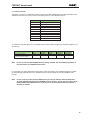
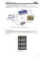
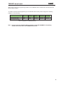
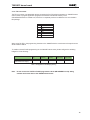
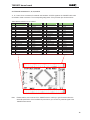
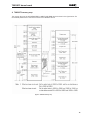
User’s Manual 78K0/KF2 Demo Board Campaign Board Demonstration Board for the NEC QB-78K0MINI On-Chip Debug Emulator Document No. 78K0KF2DEMOV100 Date Published September 2005 NEC Electronics (Europe) GmbH 78K0/KF2 demo board ・ The information in this document is current as of date of its publication. The information is subject to change without notice. For actual design-in, refer to the latest publications of NEC Electronics data sheets or data books, etc., for the most up-to-date specifications of NEC Electronics products. Not all products and/or types are available in every country. Please check with an NEC sales representative for availability and additional information. ・ No part of this document may be copied or reproduced in any form or by any means without prior written consent of NEC Electronics. NEC Electronics assumes no responsibility for any errors that may appear in this document. ・ NEC Electronics does not assume any liability for infringement of patents, copyrights or other intellectual property rights of third parties by or arising from the use of NEC Electronics products listed in this document or any other liability arising from the use of such NEC Electronics products. No license, express, implied or otherwise, is granted under any patents, copyrights or other intellectual property rights of NEC Electronics or others. ・ Descriptions of circuits, software and other related information in this document are provided for illustrative purposes in semiconductor product operation and application examples. The incorporation of these circuits, software and information in the design of customer's equipment shall be done under the full responsibility of customer. NEC Electronics no responsibility for any losses incurred by customers or third parties arising from the use of these circuits, software and information. ・ While NEC Electronics endeavors to enhance the quality, reliability and safety of NEC Electronics products, customers agree and acknowledge that the possibility of defects thereof cannot be eliminated entirely. To minimize risks of damage to property or injury (including death) to persons arising from defects in NEC Electronics products, customers must incorporate sufficient safety measures in their design, such as redundancy, fire-containment and anti-failure features. ・ NEC Electronics products are classified into the following three quality grades: “Standard”, “Special” and “Specific”. The "Specific" quality grade applies only to NEC Electronics products developed based on a customerdesignated “quality assurance program” for a specific application. The recommended applications of NEC Electronics product depend on its quality grade, as indicated below. Customers must check the quality grade of each NEC Electronics product before using it in a particular application. "Standard": Computers, office equipment, communications equipment, test and measurement equipment, audio and visual equipment, home electronic appliances, machine tools, personal electronic equipment and industrial robots. "Special": Transportation equipment (automobiles, trains, ships, etc.), traffic control systems, antidisaster systems, anti-crime systems, safety equipment and medical equipment (not specifically designed for life support). "Specific": Aircraft, aerospace equipment, submersible repeaters, nuclear reactor control systems, life support systems and medical equipment for life support, etc. The quality grade of NEC Electronics products is “Standard” unless otherwise expressly specified in NEC Electronics data sheets or data books, etc. If customers wish to use NEC Electronics products in applications not intended by NEC Electronics, they must contact NEC Electronics sales representative in advance to determine NEC Electronics 's willingness to support a given application. Notes: 1." NEC Electronics" as used in this statement means NEC Electronics Corporation and also includes its majority-owned subsidiaries. 2. " NEC Electronics products" means any product developed or manufactured by or for NEC Electronics (as defined above). M8E 02.10 2 78K0/KF2 demo board CAUTION This is a Test- and Measurement equipment with possibility to be significantly altered by user through hardware enhancements/modifications and/or test or application software. Thus, with respect to Council Directive 89/336/EEC (Directive on compliance with the EMC protection requirements), this equipment has no autonomous function. Consequently this equipment is not marked by the CE-symbol. EEDT-ST-0005-10 Redemption of Waste Electrical and Electronic Equipment (WEEE) in accordance with legal regulations applicable in the European Union only: This equipment (including all accessories) is not intended for household use. After use the equipment cannot be disposed of as household waste. NEC Electronics (Europe) GmbH offers to take back the equipment. All you need to do is register at www.eu.necel.com/weee. 3 78K0/KF2 demo board Revision History Date 07-09-2005 Revision V1.00 Chapter --- Description First release 4 78K0/KF2 demo board Table of Contents 1. Introduction ............................................................................................................................7 1.1 Main features of 78K0/KF2 demo board...........................................................................................7 2. 78K0/KF2 demo board system configuration .......................................................................8 2.1 78K0/KF2 demo board.......................................................................................................................8 3. 78K0/KF2 demo board components......................................................................................9 3.1 3.2 3.3 3.3.1 3.3.2 3.4 3.5 3.6 Configuration, soldering bridges P1-P5 ..........................................................................................9 OCD1 connector ..............................................................................................................................10 78K0/KF2 demo board FLASH programming configuration .........................................................11 FP4 connector ................................................................................................................................11 FPL3 connector ..............................................................................................................................13 AD converter reference voltage input ............................................................................................14 External LED’s 1–2 ..........................................................................................................................14 External connectors J1, J2, J3, and J4 ..........................................................................................15 4. 78K0/KF2 memory map........................................................................................................16 5. Schematics ...........................................................................................................................17 5 78K0/KF2 demo board List of Figures Figure 1: 78K0/KF2 demo board system configuration............................................................................. 8 Figure 2: 78K0/KF2 demo board connectors, soldering bridges and LED’s .............................................. 9 Figure 3: 78K0/KF2 demo board FLASH programming configuration..................................................... 11 Figure 4: 78K0/KF2 memory map.......................................................................................................... 16 Figure 5: 78K0/KF2 demo board schematics ......................................................................................... 17 List of Tables Table 1: Table 2: Table 3: Table 4: Table 5: Table 6: Table 7: Table 8: Table 9: Configuration, soldering bridges P1-P5 ...................................................................................... 9 OCD1 connector ...................................................................................................................... 10 Configuration for OCD ............................................................................................................. 10 FP4 connector ......................................................................................................................... 11 Configuration for FLASH programming .................................................................................... 12 FPL3 connector ....................................................................................................................... 13 Configuration for FLASH programming .................................................................................... 13 LED1-2 connection .................................................................................................................. 14 External connectors J1, J2, J3 and J4...................................................................................... 15 6 78K0/KF2 demo board 1. Introduction The 78K0/KF2 demo board is a demonstration kit for the evaluation of the On-Chip debugging feature by using the QB-78K0MINI On-Chip debug emulator. It supports onboard FLASH programming and real time execution of application programs up to 128 KB based on the 78K0/KF2 microcontroller. The board is prepared to be connected to user hardware parts such as digital I/O or analogue signals. 1.1 Main features of 78K0/KF2 demo board • On-Chip debugging support by using QB-78K0MINI emulator • Easy to use device demonstration capabilities of the 78K0/KF2 device • FLASH programming support by using PG-FPL3 or PG-FP4 FLASH programmer • All microcontroller signals assigned to external connectors • Analogue to digital signal conversion is supported • Various input / output signals available, such as ° ° ° ° ° All I/O ports prepared to be connected to user hardware Timer input / output signals SIO/UART interfaces 8 analogue input lines 2 I/O ports connected to LED’s 78K0/KF2 demo board is not intended for code development. NEC does not allow and does not support in any way any attempt to use 78K0/KF2 demo board in a commercial or technical product. 7 78K0/KF2 demo board 2. 78K0/KF2 demo board system configuration The 78K0/KF2 demo board system configuration is given in the diagram below: Figure 1: 78K0/KF2 demo board system configuration 2.1 78K0/KF2 demo board The 78K0/KF2 demo board is a demonstration kit for the evaluation of the On-Chip debugging feature by using the QB-78K0MINI On-Chip debug emulator. The uPD78F0547DGC microcontroller is a typical device with On-Chip debugging support and has been used to realize the 78K0/KF2 demo board. The uPD78F0547DGC contains 128 KB internal FLASH ROM and 7 KB internal RAM and operates at a maximum frequency of 20 MHz. 8 78K0/KF2 demo board 3. 78K0/KF2 demo board components The 78K0/KF2 demo board is equipped with two LED’s and several connectors in order to be connected to a dedicated FLASH programmer or connect any target hardware. P2 P4 P5 LED2 LED1 OCD1 FP4 P1 P3 FPL3 Figure 2: 78K0/KF2 demo board connectors, soldering bridges and LED’s All of the 78K0/KF2 On-Chip resources are free for user application hardware and software. Please read the user’s manual of the 78K0/KF2 device carefully to get information about the electrical specification of the available I/O ports before you connect any external signal to the 78K0/KF2 demo board! 3.1 Configuration, soldering bridges P1-P5 The different operation modes of the 78K0/KF2 demo board can be set by the soldering bridges P1-P5. The different configuration modes are shown in the table below: Modes On-Chip Debug Mode On-Chip Debug Mode (with External Power Supply) Flash Programmer Mode Flash Programmer Mode (with External Power Supply) Normal Mode (with External Power Supply) P1 (5V) SHORT OPEN P2 (AVREF) SHORT OPEN P3 (RESET) OPEN OPEN P4 (P32 / LED1) Don’t Care Don’t Care P5 (P33 / LED2) Don’t Care Don’t Care Don’t Care OPEN SHORT OPEN Don’t Care Don’t Care Don’t Care Don’t Care Don’t Care Don’t Care OPEN OPEN Don’t Care Don’t Care Don’t Care Table 1: Configuration, soldering bridges P1-P5 9 78K0/KF2 demo board 3.2 OCD1 connector The OCD1 connector (not assembled) allows connecting the QB-78K0MINI On-Chip debug emulator to the 78K0/KF2 demo board in order to use On-Chip debug function of the 78K0/KF2 device. OCD1 1 2 3 4 5 6 7 8 9 10 Function RESET_IN RESET_OUT FLMD0 VDD_IN X2 / PortA GND X1 / PortB GND Reserved 5Vout (max. 50 mA) Table 2: OCD1 connector To enable On-Chip debugging for the 78K0/KF2 demo board, please configure the soldering bridges P1-P5 as following: Modes On-Chip Debug Mode On-Chip Debug Mode (with External Power Supply) P1 (5V) SHORT OPEN P2 (AVREF) SHORT OPEN P3 (RESET) OPEN OPEN P4 (P32 / LED1) Don’t Care Don’t Care P5 (P33 / LED2) Don’t Care Don’t Care Table 3: Configuration for OCD Note: Do not connect the QB-78K0MINI On-Chip debug emulator and the FLASH programmer at the same time to the 78K0/KF2 demo board. For information on Option Byte and FLASH memory security ID setting of the 78K0/KF2 device to enable On-Chip debugging please refer to the 78K0/KF2 user’s manual respectively the QB-78K0MINI user’s manual. Note: In case of wrong setting of the FLASH memory security ID, address 0x84 and 0x85-0x8e, On-Chip debugging by using QB-78K0MINI becomes inactive. In this case erase the internal FLASH ROM of the 78K0/KF2 device by using one of the dedicated FLASH programmer’s, PG-FPL3 or PG-FP4. 10 78K0/KF2 demo board 3.3 78K0/KF2 demo board FLASH programming configuration The internal FLASH ROM of the 78K0/KF2 device can be reprogrammed by using the PG-FPL3 or alternative the PG-FP4 FLASH programmer. The configuration for on-board FLASH programming is shown in figure below. Figure 3: 78K0/KF2 demo board FLASH programming configuration 3.3.1 FP4 connector The FP4 connector (not assembled) allows connecting the PG-FP4 flash programmer to 78K0/KF2 demo board in order to program application programs into the CPU internal flash memory of the uPD78F0547DGC device. Please note, PG-FP4 is a separate product from NEC and it is not included in this package. FP4 1 2 3 4 5 6 7 8 9 10 11 12 13 14 15 16 Signal GND RESET SI / RXD VDD SO / TXD N.C. N.C. N.C. CLK N.C. N.C. FLMD1 N.C. FLMD0 N.C. N.C. Table 4: FP4 connector (N.C. = Not Connected) 11 78K0/KF2 demo board When using PG-FP4, the programming interface to the 78K0/KF2 device must be set to the asynchronous serial interface UART6. To enable on-board FLASH programming for the 78K0/KF2 demo board, please configure the soldering bridges P1-P5 as following: Modes Flash Programmer Mode Flash Programmer Mode (with External Power Supply) P1 (5V) Don’t Care OPEN P2 (AVREF) SHORT OPEN P3 (RESET) Don’t Care Don’t Care P4 (P32 / LED1) Don’t Care Don’t Care P5 (P33 / LED2) Don’t Care Don’t Care Table 5: Configuration for FLASH programming Note: Do not connect the PG-FP4 FLASH programmer and the QB-78K0MINI On-Chip debug emulator at the same time to the 78K0/KF2 demo board. 12 78K0/KF2 demo board 3.3.2 FPL3 connector The FPL3 connector (not assembled) allows connecting the PG-FPL3 flash programmer to 78K0/KF2 demo board in order to program application programs into the CPU internal flash memory of the uPD78F0547DGC device. Please note, PG-FPL3 is a separate product from NEC and it is not included in this package. FPL3 1 2 3 4 5 6 7 Signal GND VDD CLK RESET TXD RXD FLMD0 Table 6: FPL3 connector When using PG-FPL3, the programming interface to the 78K0/KF2 device must be set to the asynchronous serial interface UART6. To enable on-board FLASH programming for the 78K0/KF2 demo board, please configure the soldering bridges P1-P5 as following: Modes Flash Programmer Mode Flash Programmer Mode (with External Power Supply) P1 (5V) Don’t Care OPEN P2 (AVREF) SHORT OPEN P3 (RESET) Don’t Care Don’t Care P4 (P32 / LED1) Don’t Care Don’t Care P5 (P33 / LED2) Don’t Care Don’t Care Table 7: Configuration for FLASH programming Note: Do not connect the PG-FPL3 FLASH programmer and the QB-78K0MINI on-chip debug emulator at the same time to the 78K0/KF2 demo board. 13 78K0/KF2 demo board 3.4 AD converter reference voltage input The reference voltage input AVREF of the 78K0/KF2 device is connected to VDD by the soldering bridge P2. 3.5 External LED’s 1–2 The LED’s 1-2 are connected to the 78K0/KF2 device and are free for user application purposes. The LED’s are connected via a 620 Ω resistor to VDD and therefore active low. Port P32 P33 LED LED1 LED2 Table 8: LED1-2 connection For disconnecting a LED from a port for alternative usage open the connection of the corresponding soldering bridge P4 respectively P5. 14 78K0/KF2 demo board 3.6 External connectors J1, J2, J3, and J4 J1, J2, J3 and J4 are connectors for external user hardware. All CPU signals of the 78K0/KF2 device are connected to these connectors. The corresponding assignment of the processor pins is shown below. Table 9: External connectors J1, J2, J3 and J4 J1 1 2 3 4 5 6 7 8 9 10 11 12 13 14 15 16 17 18 19 20 Note: Function P120/INTP0/EXLVI P47 P46 P45 P44 P43 P42 P41 P40 RESET P124/XT2/EXCLKS P123/XT1 IC/FLMD0 P122/X2/EXCLK P121/X1 REGC VSS EVSS VDD EVDD J2 21 22 23 24 25 26 27 28 29 30 31 32 33 34 35 36 37 38 39 40 Function P60/SCL0 P61/SDA0 P62/EXSCL0 P63 P33/TI51/TO51/INTP4 P64 P65 P66 P67 P77/KR7 P76/KR6 P75/KR5 P74/KR4 P73/KR3 P72/KR2 P71/KR1 P70/KR0 P06/TI011/TO01 P05/TI001/SSI11 P32/INTP3 (PortB) J3 41 42 43 44 45 46 47 48 49 50 51 52 53 54 55 56 57 58 59 60 Function P31/INTP2 (PortA) P50 P51 P52 P53 P30/INTP1 P17/TI50/TO50 P16/TOH1/INTP5 P15/TOH0 P14/RXD6 P13/TXD6 P12/SO10 P11/SI10/RXD0 P10/SCK10/TXD0 P54 P55 P56 P57 AVREF AVSS J4 61 62 63 64 65 66 67 68 69 70 71 72 73 74 75 76 77 78 79 80 Function P27/ANI7 P26/ANI6 P25/ANI5 P24/ANI4 P23/ANI3 P22/ANI2 P21/ANI1 P20/ANI0 P130 P04/SCK11 P03/SI11 P02/SO11 P01/TI010/TO00 P00/TI000 P145/STB0 P144/SOA0 P143/SIA0 P142/SCKA0 P141/BUZ/BUSY0/INTP7 P140/PCL/INTP6 Please read the user’s manual of the 78K0/KF2 device carefully to get information about the electrical specification of the available I/O ports before you connect any external signal to the 78K0/KF2 demo board! 15 78K0/KF2 demo board 4. 78K0/KF2 memory map The memory layout of the µPD78F0547DGC 128KB FLASH ROM device is shown in the figure below. For more details please refer to the user’s manual of the 78K0/KF2 device. Figure 4: 78K0/KF2 memory map 16 78K0/KF2 demo board 5. Schematics Figure 5: 78K0/KF2 demo board schematics 17