1
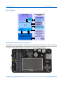
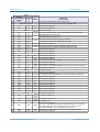
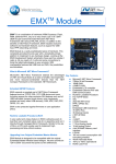
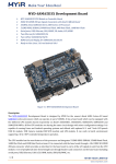
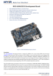
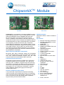
ChipworkX
TM
Module
Back View
Top View
ChipworkX™ is a combination of hardware (ARM9 Processor,
Flash, RAM, Ethernet PHY...etc) on a small (67.6mm x47mm)
OEM board MINI9261I with SO-DIMM200 slot that hosts
Microsoft .NET Micro Framework with various PAL/HAL
drivers. In addition to the benefits of .NET Micro Framework,
ChipworkX includes exclusive software and hardware features.
ChipworkX Module is a vastly sophisticated piece of hardware.
This complexity provides the end-user with a remarkably
simple platform to implement in any hardware design. Looking
at the ChipworkX Development System schematic shows just
how simple it really is. All you need is 3.3 volts and some
connections to bring the latest technologies to your products.
With manageable features like USB host, database and WiFi,
the possibilities are boundless.
What is Microsoft .NET Micro Framework?
Microsoft's .NET Micro Framework extends the advantages
of .NET and Visual Studio to a class of smaller, less expensive,
and more resource-constrained devices than the .NET
Compact Framework or the standard .NET framework.
Extended Framework Features
ChipworkX™module supports a complete set of .NET Micro
Framework features such as TCP/IP,SSL, FAT, USB device
and many more. In addition, it supports many other exclusive
GHI features, for example, full USB host stack (access thumb
drives, mice, keyboards, printers and many other devices),
PPP, GPRS, 3G...etc. Furthermore, ChipworkX™ supports
SQLite database, allowing fast logging and retrieving of
standard SQL queries.
Runtime Loadable Procedure (RLP)
A very useful and unique feature in ChipworkX is allowing
users to load their own compiled native code (C or assembly)
and run it directly through managed Micro Framework. Similar
to the use of DLLs on PCs and usually used to implement
high-processing and time-critical routines.
SideShow Support
ChipworkX module is ideal for SideShow
devices.
Key Features
●
●
●
●
●
●
●
●
●
●
●
●
●
●
●
●
●
●
●
●
●
●
●
●
●
●
●
●
Microsoft .NET Micro Framework.
200 MHz 32-bit ARM9 Processor
AT91SAM9261S
64MB RAM
8MB NOR FLASH
256MB Internal NAND Flash with
File System
4MB Serial DataFlash
SQLite Database
Runtime Loadable Procedure
JTAG Access
In field programmable
LCD controller
Ethernet with Full TCP/IP Stack
SSL
DPWS
USB Device
USB Host with 2 ports
80 GPIO Pins with interrupt
capabilities
Real Time Clock
2 SPI (8/16bit)
I2C
3 UART
1 PWM
One-wire interface
WiFi Support
3.3V IOs voltage
0ºC to +70ºC Operational
Easily attached with SODIMM200 slot.
RoHS, Lead Free
GHI Electronics,LLC
ChipworkX Module
Block Diagram
.NET and GHI
Managed Library
GHI RLP
loader
.NET Micro Framework
CLR
ChipworkX Module
Hardware
64 MB SDRAM
User Runtime Loadable
Procedure (compiled C or
assembly) region
8MB NOR Flash for
User Managed
Code
8MB Flash
256MB NAND FLASH
With FAT File System
PAL
HAL
GHI Extended features:
USB Drivers, Hardw are Access
AT91SAM 9261S
200MHz ARM9 CPU
Peripherals:GPIO,
Interrupts, PWM,USB HC,
USB Device,
LCD Controller,
Ethernet Controller ...etc
10/100
Ethernet PHY
Getting Started with ChipworkX Modules
GHI Electronics offers a development system for ChipworkX Modules. The development system exposes all
peripherals and includes 480x272 4.3" display with touch screen . We highly recommend starting up with the
development system. With this option, you will have a running system out-of-the-box.
Copyright © 2009 GHI Electronics, LLC
www.ghielectronics.com
GHI Electronics,LLC
ChipworkX Module
SODIMM200 Pin-out
Pins marked with IOxx are general purpose digital I/O. These pins might have other features.
Name
MINI9261I
ChipworkX
2nd
ChipworkX
No. AT91SAM9261S
IO
Feature
Pin Description
H/W Name
1
GND_BG
Connect to GroundConnect to Ground
2
ENET_TX-
3
ENET_2.5
4
ENET_TX+
5
GND
6
ENET_RX-
8
ENET_RX+
11
ENET_LED1
12
ENET_LED2
Ethernet transmit data minus.
Recommended
Connect to Ethernet Connector Magnet TCT and RCT pins. Ethernet connector is
J0026D21. Please
Ethernet transmit data plus.
refer to ChipworkX
Connect to Ground
Development System
schematic.
Ethernet receive data minus.
Ethernet PHY is not
Ethernet receive data plus.
needed since it is
Ethernet interface connection indicator LED
embedded in
ChipworkX
hardware.
Ethernet interface activity indicator LED
13
GND3
Connect to Ground
20
3.3V_0
Connect to 3.3 volt source.
27
GND4
Connect to Ground
32
3.3V_1
Connect to 3.3 volt source.
40
GND16
Connect to Ground
41
GND5
Connect to Ground
46
3.3V_2
Connect to 3.3 volt source.
51
GND6
Connect to Ground
60
3.3V_3
Connect to 3.3 volt source.
65
GND7
Connect to Ground
72
3.3V_4
Connect to 3.3 volt source.
79
GND8
Connect to Ground
88
3.3V_5
Connect to 3.3 volt source.
89
NAND_RE (PC0)*
90
NAND_WE (PC1)*
Leave unconnected. Reserved for ChipworkX's NAND Flash use.
Leave unconnected. Reserved for ChipworkX's NAND Flash use.
91
PC2 (IRQ0)
IO66
N/A
General purpose digital I/O
92
PC3
IO67
N/A
General purpose digital I/O
93
PC4
IO68
N/A
General purpose digital I/O
94
PC5
IO69
N/A
General purpose digital I/O
95
GND9
Connect to Ground
96
PC6
IO70
N/A
General purpose digital I/O
97
PC7
IO71
N/A
General purpose digital I/O
98
PC8
IO72
99
PC9
IO73
100
PC10
IO74
101
COM2
N/A
MAC_INT(PC11)*
102
PC12
IO76
103
PC13
IO77
Serial port (UART) TXD transmit signal (Out) for COM2.
Serial port (UART) RXD receive signal (In) for COM2.
General purpose digital I/O
Leave unconnected. Reserved for ChipworkX's Ethernet PHY use.
COM3
Serial port (UART) TXD transmit signal (Out) for COM3.
Serial port (UART) RXD receive signal (In) for COM3.
104
NAND_CS(PC14)*
Leave unconnected. Reserved for ChipworkX's NAND Flash use.
105
NAND_BSY(PC15)*
Leave unconnected. Reserved for ChipworkX's NAND Flash use.
106
3.3V_6
107
PA0
IO0
108
PA1
IO1
SPI1
Copyright © 2009 GHI Electronics, LLC
Connect to 3.3 volt source.
SPI master bus interface MISO signal (Master In Slave Out) SPI1 is shared with
for SPI1.
SD card driver, touch
SPI master bus interface MOSI signal (Master Out Slave In) screen controller.
for SPI1.
www.ghielectronics.com
GHI Electronics,LLC
ChipworkX Module
Name
MINI9261I
ChipworkX
2nd
ChipworkX
No. AT91SAM9261S
IO
Feature
Pin Description
H/W Name
109
PA2
IO2
SPI master bus interface SCK signal (Clock)for SPI1.
110
DataFlash_CS (PA3)*
Leave unconnected. Reserved for ChipworkX's DataFlash use.
111
PA4
IO4
N/A
General purpose digital I/O
112
PA5
IO5
N/A
General purpose digital I/O
113
GND10
114
PA6
IO6
115
PA7
IO7
116
PA8
IO8
Connect to Ground
SDCard_
Used as a Chip Select signal for SPI-based SD/MMC card communication.
CS
(open drain pin) I2C Interface SDA
I2C
(open drain pin) I2C Interface SCL
117
PA9
IO9
118
PA10
IO10
119
PA11
IO11
120
PA12
IO12
121
PA13
IO13
122
PA14
IO14
N/A
General purpose digital I/O
123
PA15
IO15
N/A
General purpose digital I/O
124
COM1
N/A
General purpose digital I/O
Connect to 3.3 volt source.
125
PA16
IO16
N/A
126
PA17
IO17
127
PA18
IO18
128
PA19
IO19
129
PA20
IO20
130
PA21
N/A
Down
Button
N/A
Select
Button
N/A
IO21
Serial port (UART) TXD transmit signal (Out) for COM1.
COM3 Serial port (UART) RTS hardware handshaking signal for COM3.
HW HS Serial port (UART) CTS hardware handshaking signal for COM3.
3.3V_7
131
Serial port (UART) RXD receive signal (In) for COM1.
GND11
General purpose digital I/O
General purpose digital I/O
General purpose digital I/O
and TinyBooter/Firmware Down Button (Check hardware design consideration).
General purpose digital I/O
General purpose digital I/O
and TinyBooter/Firmware Select Button (Check hardware design consideration).
General purpose digital I/O
Connect to Ground
132
PA22
IO22
133
PA23
IO23
134
PA24
IO24
135
PA25
IO25
N/A
General purpose digital I/O
136
PA26
IO26
N/A
General purpose digital I/O
137
PA27
IO27
N/A
General purpose digital I/O
138
PA28
IO28
N/A
General purpose digital I/O
139
PA29
IO29
N/A
General purpose digital I/O
140
PA30
IO30
N/A
General purpose digital I/O
141
PA31
IO31
N/A
General purpose digital I/O
142
3.3V_8
143
PB0
IO32
144
PB1
IO33
145
PB2
IO34
146
PB3
IO35
147
PB4
IO36
148
PB5
IO37
N/A
General purpose digital I/O
General purpose digital I/O
Up Button
and TinyBooter/Firmware Up Button (Check hardware design consideration).
N/A
General purpose digital I/O
Connect to 3.3 volt source.
LCD
TFT Display, Vertical sync.
V-Sync
LCD
TFT Display, Horizontal sync.
H-Sync
LCD CLK TFT Display, Clock.
General purpose digital I/O
but this pin is multiplexed with BMS (Boot Mode Select)signal. Care should be
BMS
taken during reset time. and it should not be set high on reset. For more
information about BMS, check AT91SAM9261S user manual.
PWM PWM feature is mainly utilized to control the LCD back light illumination.
N/A
Copyright © 2009 GHI Electronics, LLC
General purpose digital I/O
www.ghielectronics.com
GHI Electronics,LLC
ChipworkX Module
Name
MINI9261I
ChipworkX
2nd
No. AT91SAM9261S
IO
Feature
H/W Name
149
PB6
150
PB7
IO38
IO39
151
ChipworkX
Pin Description
If TSC2046 touch controller chip (similar to the one on the Development System) is
TOUCH used then wire this pin to PENIRQ at the controller's side (pin 11). Refer to
IRQ
ChipworkX Development System schematic.
TSC2046's communication interface is SPI. (connect to SPI1 on ChipworkX)
N/A
General purpose digital I/O
GND12
Connect to Ground
152
PB8
IO40
LCD B0 TFT Display, Blue signal bit 0.
153
PB9
IO41
LCD B1 TFT Display, Blue signal bit 1.
154
PB10
IO42
LCD B2 TFT Display, Blue signal bit 2.
155
PB11
IO43
LCD B3 TFT Display, Blue signal bit 3.
156
PB12
IO44
LCD B4 TFT Display, Blue signal bit 4.
157
PB13
IO45
158
159
N/A
1WIRE_EEPROM (PB14)*
PB15
IO47
160
General purpose digital I/O
Leave unconnected. Reserved for ChipworkX's EEPROM use.
N/A
3.3V_9
General purpose digital I/O
Connect to 3.3 volt source.
161
PB16
IO48
LCD G0 TFT Display, Green signal bit 0.
162
PB17
IO49
LCD G1 TFT Display, Green signal bit 1.
163
PB18
IO50
LCD G2 TFT Display, Green signal bit 2.
164
PB19
IO51
LCD G3 TFT Display, Green signal bit 3.
165
PB20
IO52
LCD G4 TFT Display, Green signal bit 4.
166
PB21
IO53
167
PB22
IO54
168
PB23
IO55
169
N/A
General purpose digital I/O
If TSC2046 touch controller chip (similar to the one on the Development System) is
TOUCH used then wire this pin to CS at the controller's side (pin 15). Refer to ChipworkX
CS
Development System schematic.
TSC2046's communication interface is SPI. (connect to SPI1 on ChipworkX)
LCD R4 TFT Display, Red signal bit 4.
GND13
Connect to Ground
170
PB24
IO56
LCD G5 TFT Display, Green signal bit 5.
171
PB25
IO57
LCD R0 TFT Display, Red signal bit 0.
172
PB26
IO58
LCD R1 TFT Display, Red signal bit 1.
173
PB27
IO59
LCD R2 TFT Display, Red signal bit 2.
174
PB28
IO60
LCD R3 TFT Display, Red signal bit 3.
175
PB29 (IRQ2)
IO61
176
PB30 (IRQ1)
IO62
177
178
SPI2
WKUP
PB31
IO63
SPI2
179
SHDN
180
3.3V_10
181
EN_1.2V
182
USBD+ Port B USB Host Feature
SPI master bus interface SCK signal (Clock)for SPI2.
SPI master bus interface MISO signal (Master In Slave Out) for SPI2.
Wake Up (Input). Falling edge signal would wake up the processor and clear the
Shut Down signal.
If Sleep feature is not required, pull down this pin to ground.
SPI master bus interface MOSI signal (Master Out Slave In) for SPI2.
Shut Down (Output) can be wired to sleep circuit. Refer to ChipworkX
Development System schematic.
If Sleep feature is not required, leave this pin unconnected.
Connect to 3.3 volt source.
ChipworkX's Internal power supply circuit enable. this pin can be wired to sleep
circuit. Refer to ChipworkX Development System schematic.
If Sleep feature is not required, pull down this pin to ground.
USB positive data line of the USB hosting feature, Port B.
183
VBAT
184
USBD- Port B USB Host Feature
185
GND14
Connect to Ground
186
GND17
Connect to Ground
187
JTAG NRST
Copyright © 2009 GHI Electronics, LLC
Connect to 3.3 volt backup battery to keep the real-time clock running.
USB negative data line of the USB hosting feature, Port B.
JTAG NRST signal. Connect to TRST.
www.ghielectronics.com
GHI Electronics,LLC
ChipworkX Module
Name
MINI9261I
ChipworkX
2nd
ChipworkX
No. AT91SAM9261S
IO
Feature
Pin Description
H/W Name
188
USBD+ Port A USB Host Feature
USB positive data line of the USB hosting feature, Port A.
189
JTAG RTCK
JTAG RTCK signal.
190
USBD- Port A USB Host Feature
191
JTAG TDO
192
3.3V_11
Connect to 3.3 volt source.
193
NTRST
194
USBD+ USB client feature
195
JTAG TDI
196
USBD- USB client feature
197
JTAG TCK
JTAG NTRST signal. Connect to TRST.
USB positive data line of the USB debugging interface (access interface) and for
the USB client feature.
JTAG TDI signal.
USB negative data line of the USB debugging interface (access interface) and for
the USB client feature.
JTAG TCK signal.
USB negative data line of the USB hosting feature, Port A.
JTAG TDO signal.
198
GND18
Connect to Ground
199
JTAG TMS
JTAG TMS signal.
200
PIN200
Pull up with 10K resistor
N/A and * : Reserved pins, user should NOT connect or use.
For further Information:
Related Documents:
ChipworkX Development System Brochure and Pinout
ChipworkX User Manual
Weblinks:
http://www.chipworkx.com/
http://www.ghielectronics.com/
Customer Support:
http://www.ghielectronics.com/forum
35555 Garfield Rd. Suite #2
Clinton township, MI 48035
USA
PH: +1 586 693 2696
FAX: +1 586 693 3449
www.ghielectronics.com
www.chipworkx.com
Copyright © 2009 GHI Electronics, LLC
www.ghielectronics.com