1
IB940
LGA775 Core™ 2 Duo
Intel® Q965 Chipset
Full Size CPU Card
USER’S MANUAL
Version 1.0A
Acknowledgments
Award is a registered trademark of Award Software International,
Inc.
PS/2 is a trademark of International Business Machines
Corporation.
Intel and Core 2 Duo are registered trademarks of Intel
Corporation.
Microsoft Windows is a registered trademark of Microsoft
Corporation.
Winbond is a registered trademark of Winbond Electronics
Corporation.
All other product names or trademarks are properties of their
respective owners.
ii
IB940 User’s Manual
Table of Contents
Introduction .......................................................1
Product Description............................................................. 1
Checklist.............................................................................. 2
Specifications ...................................................................... 3
Board Dimensions ............................................................... 4
Installations .......................................................5
Installing the CPU ............................................................... 6
Installing the Memory ......................................................... 7
Setting the Jumpers ............................................................. 8
Connectors on IB940......................................................... 12
BIOS Setup .......................................................25
Drivers Installation ......................................45
Intel Q965 Chipset Software Installation Utility............... 46
Intel Q965 Chipset Graphics Driver.................................. 48
Realtek Codec Audio Driver Installation .......................... 50
Intel LAN Drivers Installation .......................................... 51
Appendix ...........................................................53
A. I/O Port Address Map................................................... 53
B. Interrupt Request Lines (IRQ) ...................................... 54
C. Watchdog Timer Configuration.................................... 55
D. Digital I/O Sample Code .............................................. 59
IB940 User’s Manual
iii
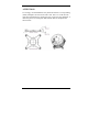
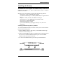
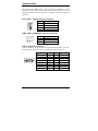
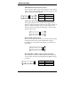
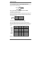
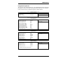
ATTENTION:
It is strongly recommended that only heatsinks that have corresponding
(metal) backplates be used on the CPU card. This is to avoid the CPU
card being bent/distorted, causing the CPU card to become damaged. A
reference picture of a backplate and heatsink that has backplate are
shown below.
iv
IB940 User’s Manual
INTRODUCTION
Introduction
Product Description
The IB940 CPU card is based on the Intel Q965 chipset and supports the
Intel® Core™2 Duo processor with 1066/800/533 MHz System Bus. It
supports the PCI Express x16 graphics interface for the latest
high-performance graphics cards. The PCI Express x1 I/O ports offer up
to 3.5X the bandwidth over traditional PCI architecture, delivering faster
access to peripheral I/O devices.
The Intel GMA 3000 graphics on board supports Dual Independent
Display and delivers richer visual color and picture clarity without the
need for additional discrete graphics cards, and the integrated audio
support enables premium digital sound and delivers advanced features
such as multiple audio.
The CPU card also supports Dual-Channel DDR2 memory in four
DIMM sockets and delivers up to 12.8 GB/s of bandwidth and 8 GB
memory addressability for faster system responsiveness. Dimensions of
the board are 338mm x 126mm.
The main features of the CPU card are:
y Intel® Q965 Express Chipset Based
y Support LGA775 Intel® Core™2 Duo Processors
y Support FSB 1066/800/533MHz
y Support up to 4GB DDRII 800/667/533 memory
y 1 x Mini PCI Express Slot
y Support one 10/100 or two Gigabit LAN on board
y 4 x SATA II, 1 x IDE, 1x Floppy, 6 x USB 2.0, 2 x
COM, 1 x Parallel,
y 5.1Ch. Audio, 1 x TMDS
y Dual channel LVDS support 18/24 bit
IB940 User’s Manual
1
INTRODUCTION
Checklist
Your IB940 Core 2 Duo CPU Card package should include the items
listed below:
• The IB940 Card
• This User’s manual
• 1 x IDE cable
• 1 x Floppy cable
• 1 x SATA cable
• 1 x TMDS cable
• 2 Serial Port Ribbon Cable and 1 Parallel Port Attached to a
Mounting Bracket
• 1 Y-Cable supporting a PS/2 Keyboard and a PS/2 Mouse
• Audio cable with bracket (Audio-18K)
• USB cable with bracket (USB2K-4)
• 1 CD containing the following:
• Chipset Drivers
• Flash Memory Utility
• Optional SATA Power Cord (PW34)
2
IB940 User’s Manual
INTRODUCTION
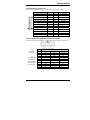
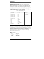
Specifications
Form Factor
Processor
FSB
Chipset
BIOS
Memory
Video
DVI
LVDS
LAN
Audio
LPC I/O
USB
SATA II
IDE
PCI-to-ISA
bridge
Expansion
Edge Connector
On Board
Headers /
Connectors
RTC
Watchdog Timer
Digital IO
System Voltage
Board Size
Full Size CPU Card (PICMG1.0)
Support for Intel Core 2 Duo processor (Conroe core) in
LGA775 socket
533/800/1066 MHz
Intel Broadwater (Q965) Chipset consisting of:
• Intel Q965 Graphics Memory Controller Hub (GMCH)
• Intel ICH8/ICH8DO I/O Controller Hub
• Award BIOS: footprint for both SPI & LPC I/F
• Support for ACPI, SMBIOS
2x 240-pin DDRII 533/667/800 DIMM sockets, supports
single channel, max. 4 GB
Intel Q965 integrated graphics subsystem GMA3000
Chrontel CH7307C x1 for DVI
Chrontel CH7308B x1 for 24-bit single/dual channel LVDS
LAN1: dual footprint support option:
• Intel 82566DM Nineveh 10/100/1000 (IB940F)
• Intel 82562V Ekron-N 10/100 (IB940)
LAN2: Intel 82573L PCI-e gigabit LAN (IB940F)
Intel ICH8 built-in high definition audio w/ Realtek ALC888
Codec supports 5.1 CH audio (line-out, line-in & mic)
Winbond W83627EHG: IrDA x1, Parallel x1, COM1 (RS232),
COM2 (RS232/422/485), floppy, Hardware monitor (3
thermal inputs, 4 voltage monitor inputs & 2 fan headers)
Intel ICH8 built-in two High Speed USB host controller,
supports 6 USB 2.0 ports (support for USB port disable) w/
over-current protection
Intel ICH8 built-in SATA II controller (3.0Gb/sec) w/ 4 ports
JMicron JM368 (PCI-e to PATA) x1 for 1 PATA channel
ITE IT8888G x1 for high drive ISA bus
Mini PCI-express socket x1 for Wireless LAN or other
module
• PS/2 connector x1 for PS/2 keyboard & Mouse, DB15 x1
for VGA, RJ45 x2 for LAN 1, 2
• Standard SATA (7-pin shrouded vertical) connector x4
• 40 pins, 0.1” pitch, standard box-header x1 for IDE
• DF13-20 header x2 for LVDS
• DF11-20 header x1 for DVI
• 34 pins box-header x1 for floppy
• 26 pins box-header x1 for printer
• 5x2 pins box-header x2 for COM1-2
• 4 pins pin-header x1 for CPU fan
• 3 pins pin-header x1 for system fan
• 4x2 pins pin-header x3 for USB1-6
ICH8 built-in RTC with on-board lithium battery
Yes (256 segments, 0, 1, 2…255 sec/min)
4 in and 4 out
+5V, +3.3V, +12V, -12V & 5VSB
338 x 122mm
IB940 User’s Manual
3
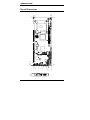
INTRODUCTION
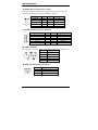
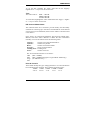
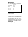
Board Dimensions
121.92
116.84
O
4
.06
5.08
0
0
5.07
0
5.08
JP8
J24
313.18
333.17
338.25
338.25
IB940 User’s Manual
121.92
100.34
90.07
53.95
65.07
36.93
17.78
5.08
0
4
INSTALLATIONS
Installations
This section provides information on how to use the jumpers and
connectors on the IB940 in order to set up a workable system. The topics
covered are:
Installing the CPU........................................................................ 6
Installing the Memory.................................................................. 7
Setting the Jumpers ...................................................................... 8
Connectors on IB940 ................................................................. 12
IB940 User’s Manual
5
INSTALLATIONS
Installing the CPU
The IB940 CPU Card supports an LGA 775 processor socket for Intel®
Core 2 Duo processors.
The LGA 775 processor socket comes with a lever to secure the
processor. Refer to the pictures below, from left to right, on how to place
the processor into the CPU socket. Please note that the cover of the
LGA775 socket must always be installed during transport to avoid
damage to the socket.
6
IB940 User’s Manual
INSTALLATIONS
Installing the Memory
The IB940 CPU Card supports four DDR2 memory sockets for a
maximum total memory of 4GB in DDR memory type. It supports
DDR2 533/667/800.
Basically, the system memory interface has the following features:
Supports two 64-bit wide DDR data channels
Available bandwidth up to 6.4GB/s (DDR2 800) for single-channel
mode.
Supports 256Mb, 512Mb, 1Gb DDR2 technologies.
Supports only x8, x16, DDR2 devices with four banks
Supports only unbuffered DIMMs
Supports opportunistic refresh
Up to 32 simultaneously open pages (four per row, four rows
maximum)
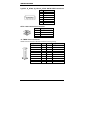
Installing and Removing Memory Modules
To install the DDR2 modules, locate the memory slot on the board and
perform the following steps:
1. Hold the DDR2 module so that the key of the DDR2 module align
with those on the memory slot.
2. Gently push the DDR2 module in an upright position until the clips of
the slot close to hold the DDR2 module in place when the DDR
module touches the bottom of the slot.
3. To remove the DDR2 module, press the clips with both hands.
Lock
DDR2 Module
Lock
Lock
Lock
IB940 User’s Manual
7
INSTALLATIONS
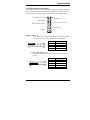
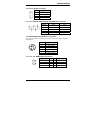
Setting the Jumpers
Jumpers are used on IB940 to select various settings and features
according to your needs and applications. Contact your supplier if you
have doubts about the best configuration for your needs. The following
lists the connectors on IB940 and their respective functions.
Jumper Locations on IB940................................................................... 9
JBAT1: Clear CMOS Contents............................................................ 10
JP1, JP2, JP3: RS232/422/485 (COM2) Selection .............................. 10
JP4, JP5: COM1 / COM2 RS232 +5V/+12V Power Setting............... 10
JP7: Processor Setting.......................................................................... 11
JP8: LVDS Panel Power Select ........................................................... 11
J25: Power Supply Type Select ........................................................... 11
8
IB940 User’s Manual
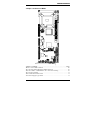
INSTALLATIONS
Jumper Locations on IB940
CPU_FAN1
ATX1
BZ1
J2
J25
CPU1
DDRII2
J24
J20 J21
DDRII1
JP8
J22
JP7
J19
J1
FAN1
J9
J18
JBAT1
BAT1
SATA3
J14
J15
J17
SATA4
SATA1
SATA2
IDE1
J6 FDC1
J8
JP6
J4
J7
J5
VGA1
J13
JP4 JP5
J11
J3
J10
J12
JP1
JP2
JP3
Jumpers on IB940.............................................................................Page
JBAT1: Clear CMOS Contents........................................................................ 10
JP1, JP2, JP3: RS232/422/485 (COM2) Selection........................................... 10
JP4, JP5: COM1 / COM2 RS232 +5V/+12V Power Setting ........................... 10
JP7: Processor Setting...................................................................................... 11
JP8: LVDS Panel Power Select ....................................................................... 11
J25: Power Supply Type Select ....................................................................... 11
IB940 User’s Manual
9
INSTALLATIONS
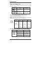
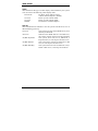
JBAT1: Clear CMOS Contents
Use JBAT1, a 3-pin header, to clear the CMOS contents. Note that the
ATX-power connector should be disconnected from the CPU Card
before clearing CMOS.
JBAT1
Setting
Function
Pin 1-2
Short/Closed
Normal
Pin 2-3
Short/Closed
Clear CMOS
JP1, JP2, JP3: RS232/422/485 (COM2) Selection
COM1 is fixed for RS-232 use only.
COM2 is selectable for RS232, RS-422 and RS-485.
ID394: COM3 and COM4 are fixed for RS-232 use only. The following
table describes the jumper settings for COM2 selection.
COM2
Function
Jumper
Setting
(pin closed)
RS-232
RS-422
RS-485
JP1:
1-2
JP1:
3-4
JP1:
5-6
JP2:
3-5 & 4-6
JP2:
1-3 & 2-4
JP2:
1-3 & 2-4
JP3:
3-5 & 4-6
JP3:
1-3 & 2-4
JP3:
1-3 & 2-4
JP4, JP5: COM1 / COM2 RS232 +5V/+12V Power Setting
JP4 / JP5
Setting
Pin 1-2
Short/Closed
Pin 3-4
Short/Closed
Pin 5-6
Short/Closed
10
IB940 User’s Manual
Function
+12V
Normal
+5V
INSTALLATIONS
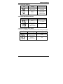
JP7: Processor Setting
JP7
Setting
Processor Used
Pin 1-2
Short/Closed
Celeron D
Pin 1-2
Open
Core 2 Duo,
Pentium D,
Pentium 4 HT
JP8: LVDS Panel Power Select
JP8
Setting
Panel Voltage
Pin 1-2
Short/Closed
3.3V (default)
Pin 2-3
Short/Closed
5V
J25: Power Supply Type Select
Use J25, a 3-pin header, to select between AT and ATX power supply.
J25
Setting
Power Supply Type
Pin 1-2
Short/Closed
ATX
Pin 2-3
Short/Closed
AT
IB940 User’s Manual
11
INSTALLATIONS
[
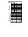
Connectors on IB940
The connectors on IB940 allows you to connect external devices such as
keyboard, floppy disk drives, hard disk drives, printers, etc. The
following table lists the connectors on IB940 and their respective
functions.
Jumper Locations on IB940................................................................. 13
CPU_FAN1: CPU Fan Power Connector ........................................... 14
PWR_FAN1: SYSTEM Fan Power Connectors.................................. 14
VGA1: VGA CRT Connector.............................................................. 14
FDC1: Floppy Drive Connector .......................................................... 15
IDE1: Primary IDE Connectors ........................................................... 15
S_ATA1, S_ATA2, S_ATA3, S_ATA4: SATA HDD Connectors .... 16
ATX1: 12V/+12V Power Connector ................................................... 16
J1: TMDS Panel Connector ................................................................. 16
J2: System Function Connector ........................................................... 17
J3: Parallel Port Connector .................................................................. 19
J4, J5: COM1 and COM2 Serial Ports Connector ............................... 19
J6: Digital I/O Connector (4 in, 4 out)................................................. 20
J7: Audio Connector for 5.1 channel ................................................... 20
J8: IrDA Connector.............................................................................. 20
J9: External ATX Power Connector .................................................... 20
J10: CD-In Audio Connector............................................................... 21
J11, J12: External PS/2 Keyboard and Mouse Connector ................... 21
J13: PS/2 Keyboard and Mouse Connector ......................................... 21
J17, J15, J14: USB0/USB1 Connector ................................................ 21
J16: Intel 82562V 10/100 or Intel 82566DC GbE RJ-45 .................... 22
Note: 10/100 LAN for IB940; Gigabit LAN for IB940F...................... 22
J18: Wake On LAN Connector............................................................ 22
J19: SPI Flash Connector (factory use only) ....................................... 22
J20, J21: LVDS Connectors (1st channel, 2nd channel) ..................... 22
J22: Panel Inverter Power Connector .................................................. 23
J23: Intel PCI Express GbE RJ45 Connector ...................................... 23
U46: x1 Mini PCI Express Slot ........................................................... 23
12
IB940 User’s Manual
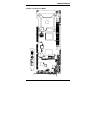
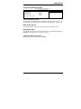
INSTALLATIONS
Jumper Locations on IB940
BZ1
J2
J25
DDRII2
DDRII1
J20 J21
J22
JP7
J19
J1
FAN1
J9
J18
JBAT1
BAT1
J14
J17
J15
IDE1
J6 FDC1
J8
JP6
J4
J7
J11
J5
J13
VGA1
JP4 JP5
J3
J10
J12
13
IB940 User’s Manual
CPU_FAN1
ATX1
CPU1
JP8
J24
SATA2
SATA4
SATA1
SATA3
JP1
JP2
JP3
INSTALLATIONS
The connectors on IB940 allows you to connect external devices such as
keyboard, floppy disk drives, hard disk drives, printers, etc. The
following table lists the connectors on IB940 and their respective
functions.
CPU_FAN1: CPU Fan Power Connector
Pin #
4
3
2
1
Signal Name
Control
Sense
+12V
Ground
PWR_FAN1: SYSTEM Fan Power Connectors
Pin #
1
2
3
Signal Name
Sense
+12V
Rotation detection
VGA1: VGA CRT Connector
VGA1 is a DB-15 VGA connector located beside the COM1 port. The
following table shows the pin-out assignments of this connector.
Signal Name
Red
Blue
GND
GND
VCC
N.C.
HSYNC
DDCCLK
14
Pin #
1
3
5
7
9
11
13
15
IB940 User’s Manual
Pin # Signal Name
2
Green
4
N.C.
6
GND
8
GND
10
GND
12
DDCDATA
14
VSYNC
INSTALLATIONS
FDC1: Floppy Drive Connector
Signal Name
Pin #
Pin #
Signal Name
Ground
Ground
Ground
Ground
Ground
Ground
Ground
Ground
Ground
Ground
Ground
Ground
Ground
Ground
Ground
Ground
Ground
1
3
5
7
9
11
13
15
17
19
21
23
25
27
29
31
33
2
4
6
8
10
12
14
16
18
20
22
24
26
28
30
32
34
RM/LC
No connect
No connect
Index
Motor enable 0
Drive select 1
Drive select 0
Motor enable 1
Direction
Step
Write data
Write gate
Track 00
Write protect
Read data
Side 1 select
Diskette change
IDE1: Primary IDE Connectors
Signal Name
Pin #
Reset IDE
1
Host data 7
3
Host data 6
5
Host data 5
7
Host data 4
9
Host data 3
11
Host data 2
13
Host data 1
15
Host data 0
17
Ground
19
DRQ0
21
Host IOW
23
Host IOR
25
IOCHRDY
27
DACK0
29
IRQ14
31
IDE1
Address 1
33
Address 0
35
Chip select 0
37
Activity
39
Pin #
2
4
6
8
10
12
14
16
18
20
22
24
26
28
30
32
34
36
38
40
IB940 User’s Manual
Signal Name
Ground
Host data 8
Host data 9
Host data 10
Host data 11
Host data 12
Host data 13
Host data 14
Host data 15
Protect pin
Ground
Ground
Ground
Host ALE
Ground
No connect
No connect
Address 2
Chip select 1
Ground
15
INSTALLATIONS
S_ATA1, S_ATA2, S_ATA3, S_ATA4: SATA HDD Connectors
Pin # Signal Name
1
Ground
2
TX+
3
TX4
Ground
5
RX6
RX+
7
Ground
ATX1: 12V/+12V Power Connector
Pin #
1
2
3
4
Signal Name
Ground
Ground
+12V
+12V
J1: TMDS Panel Connector
TMDS stands Transition Minimized Differential Signaling.
J1
16
Signal Name
TX1P
TXIN
GND
GND
TXCP
TXCN
GND
+5v
HTPG
NC
Pin #
1
2
3
4
5
6
7
8
9
10
Pin #
11
12
13
14
15
16
17
18
19
20
IB940 User’s Manual
Signal Name
TX2P
TX2N
GND
GND
TX0P
TX0N
NC
NC
DDCDATA
DDCCLK
INSTALLATIONS
J2: System Function Connector
J2 provides connectors for system indicators that provide light indication
of the computer activities and switches to change the computer status. J1
is a 20-pin header that provides interfaces for the following functions.
Hard Disk Drive LED
Reset Switch
Not Defined
ATX Power On Switch
SMI / Hardware Switch
Power LED
Speaker
Speaker: Pins 1 - 4
This connector provides an interface to a speaker for audio
tone generation. An 8-ohm speaker is recommended.
Pin #
1
2
3
4
Signal Name
Speaker out
No connect
Ground
+5V
Power LED: Pins 11 - 15
The power LED indicates the status of the main power
switch.
Pin #
11
12
13
14
15
IB940 User’s Manual
Signal Name
Power LED
No connect
Ground
No connect
Ground
17
INSTALLATIONS
SMI/Hardware Switch: Pins 6 and 16
This connector supports the "Green Switch" on the control
panel, which, when pressed, will force the system into the
power-saving mode immediately.
Pin #
6
Signal Name
16
Ground
SMI
ATX Power ON Switch: Pins 7 and 17
This 2-pin connector is an “ATX Power Supply On/Off
Switch” on the system that connects to the power switch on
the case. When pressed, the power switch will force the
system to power on. When pressed again, it will force the
system to power off.
Reset Switch: Pins 9 and 19
The reset switch allows the user to reset the system without
turning the main power switch off and then on again.
Orientation is not required when making a connection to
this header.
Hard Disk Drive LED Connector: Pins 10 and 20
This connector connects to the hard drive activity LED on
control panel. This LED will flash when the HDD is being
accessed.
Pin #
10
20
18
IB940 User’s Manual
Signal Name
HDD Active
5V
INSTALLATIONS
J3: Parallel Port Connector
The following table describes the pin out assignments of this connector.
J3
Signal Name
Line printer strobe
PD0, parallel data 0
PD1, parallel data 1
PD2, parallel data 2
PD3, parallel data 3
PD4, parallel data 4
PD5, parallel data 5
PD6, parallel data 6
PD7, parallel data 7
ACK, acknowledge
Busy
Paper empty
Select
Pin #
1
2
3
4
5
6
7
8
9
10
11
12
13
Pin #
14
15
16
17
18
19
20
21
22
23
24
25
N/A
Signal Name
AutoFeed
Error
Initialize
Select
Ground
Ground
Ground
Ground
Ground
Ground
Ground
Ground
N/A
J4, J5: COM1 and COM2 Serial Ports Connector
J4 and J5 both 10-pin headers, are the onboard serial port connectors.
J4
Fixed as
RS-232
J5
Configurable
as RS-232/
RS-422/485
with jumpers
JP1/JP2/JP3
Pin #
1
2
3
4
5
6
7
8
9
10
Signal Name
RS-232
DCD
RX
TX
DTR
GND
DSR
RTS
CTS
RI
NC
RS-422
TXTX+
RX+
RXGND
NC
NC
NC
NC
NC
IB940 User’s Manual
RS-485
DATADATA+
NC
NC
GND
NC
NC
NC
NC
NC
19
INSTALLATIONS
J6: Digital I/O Connector (4 in, 4 out)
This 10-pin digital I/O connector supports TTL levels and is used to
control external devices requiring ON/OFF circuitry.
Signal Name
Ground
Out3
Out2
IN3
IN2
Pin #
1
3
5
7
9
Pin #
2
4
6
8
10
Signal Name
+5V
Out1
Out0
IN1
IN0
J7: Audio Connector for 5.1 channel
Signal Name
LINEOUT_L
LINEOUT Detect
LINEIN_L
LINEIN Detect
MIC1
MIC1 Detect
Pin #
1
3
5
7
9
11
Pin #
2
4
6
8
10
12
Signal Name
LINEOUT_R
Ground
LINEIN_R
Ground
VREFOUT
Ground
J8: IrDA Connector
J8 is used for an optional IrDA connector for wireless communication.
Pin #
Signal Name
1
+5V
2
No connect
3
Ir RX
4
Ground
5
Ir TX
J9: External ATX Power Connector
Pin #
1
2
3
20
Signal Name
Ground
PS-ON (soft on/off)
5VSB (Standby +5V)
IB940 User’s Manual
INSTALLATIONS
J10: CD-In Audio Connector
Pin #
1
2
3
4
Signal Name
CD Audio R
Ground
Ground
CD Audio L
J11, J12: External PS/2 Keyboard and Mouse Connector
Pin #
1
2
3
4
5
J11
KB clock
KB data
N.C.
Ground
Vcc
J12
Mouse data
N.C.
Ground
Vcc
Mouse clock
J13: PS/2 Keyboard and Mouse Connector
J13 uses a Y-cable with dual D-connectors for a PS/2 keyboard and a
PS/2 mouse.
Pin #
1
2
3
4
5
6
Signal Name
Keyboard data
Mouse data
Ground
Vcc
Keyboard Clock
Mouse Clock
J17, J15, J14: USB0/USB1 Connector
Signal Name Pin Pin
Vcc
1
2
USB03
4
USB0+
5
6
Ground
7
8
IB940 User’s Manual
Signal Name
Ground
USB1+
USB1Vcc
21
INSTALLATIONS
J16: Intel 82562V 10/100 or Intel 82566DC GbE RJ-45
J16 is the 10/100 or Gigabit LAN RJ45 connector based on the Intel PCI
Express 10/100 or GbE controller.
Note: 10/100 LAN for IB940; Gigabit LAN for IB940F
J18: Wake On LAN Connector
J18 is a 3-pin header for the Wake On LAN function on the CPU Card.
The following table shows the pin out assignments of this connector.
Wake On LAN will function properly only with an ATX power supply
with 5VSB that has 1A.
Pin #
Signal Name
1
+5VSB
2
Ground
3
LAN Wakeup
J19: SPI Flash Connector (factory use only)
J20, J21: LVDS Connectors (1st channel, 2nd channel)
The LVDS connectors, DF13 20-pin mating connectors, are composed
of the first channel (J5) and second channel (J10) to support 24-bit or
48-bit.
Signal Name Pin # Pin # Signal Name
TX02
1
TX0+
Ground
4
3
Ground
TX16
5
TX1+
5V/3.3V
8
7
Ground
TX310
9
TX3+
TX212
11
TX2+
Ground
14
13
Ground
TXC16
15
TXC+
5V/3.3V
18
17
ENABKL
+12V
20
19
+12V
Remarks: Maximum current for +12V is 1A.
22
IB940 User’s Manual
INSTALLATIONS
J22: Panel Inverter Power Connector
Pin #
Signal Name
1
+12V
2
ENABKL
3
Ground
Remarks: Maximum current is 1A.
J23: Intel PCI Express GbE RJ45 Connector
J23 is the Gigabit LAN RJ45 connector based on the Intel PCI Express
GbE controller.
U46: x1 Mini PCI Express Slot
IB940 User’s Manual
23
INSTALLATIONS
This page is intentionally left blank.
24
IB940 User’s Manual
BIOS SETUP
BIOS Setup
This chapter describes the different settings available in the Award
BIOS that comes with the board. The topics covered in this chapter are
as follows:
BIOS Introduction ........................................................................ 26
BIOS Setup................................................................................... 26
Standard CMOS Setup ................................................................. 28
Advanced BIOS Features ............................................................. 31
Advanced Chipset Features .......................................................... 34
Integrated Peripherals................................................................... 35
Power Management Setup............................................................ 38
PNP/PCI Configurations .............................................................. 41
PC Health Status........................................................................... 42
Frequency/Voltage Control .......................................................... 43
Load Fail-Safe Defaults................................................................ 44
Load Optimized Defaults ............................................................. 44
Set Supervisor/User Password...................................................... 44
Save & Exit Setup ........................................................................ 44
Exit Without Saving ..................................................................... 44
IB940 User’s Manual
25
BIOS SETUP
BIOS Introduction
The Award BIOS (Basic Input/Output System) installed in your
computer system’s ROM supports Intel processors. The BIOS provides
critical low-level support for a standard device such as disk drives, serial
ports and parallel ports. It also adds virus and password protection as
well as special support for detailed fine-tuning of the chipset controlling
the entire system.
BIOS Setup
The Award BIOS provides a Setup utility program for specifying the
system configurations and settings. The BIOS ROM of the system stores
the Setup utility. When you turn on the computer, the Award BIOS is
immediately activated. Pressing the <Del> key immediately allows you
to enter the Setup utility. If you are a little bit late pressing the <Del>
key, POST (Power On Self Test) will continue with its test routines, thus
preventing you from invoking the Setup. If you still wish to enter Setup,
restart the system by pressing the ”Reset” button or simultaneously
pressing the <Ctrl>, <Alt> and <Delete> keys. You can also restart by
turning the system Off and back On again. The following message will
appear on the screen:
Press
<DEL>
to
Enter
Setup
In general, you press the arrow keys to highlight items, <Enter> to
select, the <PgUp> and <PgDn> keys to change entries, <F1> for help
and <Esc> to quit.
When you enter the Setup utility, the Main Menu screen will appear on
the screen. The Main Menu allows you to select from various setup
functions and exit choices.
26
IB940 User’s Manual
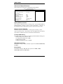
BIOS SETUP
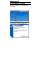
Phoenix - AwardBIOS CMOS Setup Utility
Standard CMOS Features
Advanced BIOS Features
Advanced Chipset Features
Integrated Peripherals
Power Management Setup
PnP/PCI Configurations
PC Health Status
Frequency/Voltage Control
Load Fail-Safe Defaults
Load Optimized Defaults
Set Supervisor Password
Set User Password
Save & Exit Setup
Exit Without Saving
ESC : Quit
F10 : Save & Exit Setup
Ç È Æ Å : Select Item
Time, Date, Hard Disk Type…
The section below the setup items of the Main Menu displays the control
keys for this menu. At the bottom of the Main Menu just below the
control keys section, there is another section, which displays information
on the currently highlighted item in the list.
Note:
If the system cannot boot after making and saving system
changes with Setup, the Award BIOS supports an override to
the CMOS settings that resets your system to its default.
Warning: It is strongly recommended that you avoid making any
changes to the chipset defaults. These defaults have been
carefully chosen by both Award and your system
manufacturer to provide the absolute maximum performance
and reliability. Changing the defaults could cause the system
to become unstable and crash in some cases.
IB940 User’s Manual
27
BIOS SETUP
Standard CMOS Setup
“Standard CMOS Setup” choice allows you to record some basic
hardware configurations in your computer system and set the system
clock and error handling. If the motherboard is already installed in a
working system, you will not need to select this option. You will need to
run the Standard CMOS option, however, if you change your system
hardware configurations, the onboard battery fails, or the configuration
stored in the CMOS memory was lost or damaged.
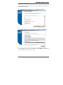
Phoenix - AwardBIOS CMOS Setup Utility
Standard CMOS Features
Date (mm:dd:yy)
Fri, Oct 20, 2006
Time (hh:mm:ss)
16 : 11 : 00
Menu Level >
Item Help
IDE Channel 0 Master
IDE Channel 0 Slave
IDE Channel 1 Master
IDE Channel 1 Slave
IDE Channel 2 Master
IDE Channel 3 Master
IDE Channel 4 Master
IDE Channel 4 Slave
None
None
None
None
None
None
None
None
Change the day, month,
Year and century
Drive A
Drive B
1.44M, 3.5 in
None
Video
Halt On
EGA/VGA
All , But Keyboard
Base Memory
Extended Memory
Total Memory
640K
2086912K
2087936K
At the bottom of the menu are the control keys for use on this menu. If
you need any help in each item field, you can press the <F1> key. It will
display the relevant information to help you. The memory display at the
lower right-hand side of the menu is read-only. It will adjust
automatically according to the memory changed. The following
describes each item of this menu.
Date
The date format is:
Day :
Month :
Date :
Year :
28
Sun to Sat
1 to 12
1 to 31
1999 to 2099
IB940 User’s Manual
BIOS SETUP
To set the date, highlight the “Date” field and use the PageUp/
PageDown or +/- keys to set the current time.
Time
The time format is:
Hour : 00 to 23
Minute : 00 to 59
Second : 00 to 59
To set the time, highlight the “Time” field and use the <PgUp>/ <PgDn>
or +/- keys to set the current time.
IDE Channel Master/Slave
The onboard Serial ATA connectors provide Primary and Secondary
channels for connecting up to four Serial ATA hard disks . Each channel
can support up to two hard disks; the first is the “Master” and the second
is the “Slave”.
Press <Enter> to configure the hard disk. The selections include Auto,
Manual, and None. Select ‘Manual’ to define the drive information
manually. You will be asked to enter the following items.
Capacity :
Cylinder :
Head :
Precomp :
Landing Zone :
Sector :
Capacity/size of the hard disk drive
Number of cylinders
Number of read/write heads
Write precompensation
Landing zone
Number of sectors
The Access Mode selections are as follows:
CHS
(HD < 528MB)
LBA
(HD > 528MB and supports Logical Block Addressing)
Large (for MS-DOS only)
Auto
Drive A / Drive B
These fields identify the types of floppy disk drive A or drive B that has
been installed in the computer. The available specifications are:
360KB 1.2MB 720KB 1.44MB 2.88MB
5.25 in. 5.25 in. 3.5 in.
3.5 in.
3.5 in.
IB940 User’s Manual
29
BIOS SETUP
Video
This field selects the type of video display card installed in your system.
You can choose the following video display cards:
EGA/VGA
For EGA, VGA, SEGA, SVGA
or PGA monitor adapters. (default)
CGA 40
Power up in 40 column mode.
CGA 80
Power up in 80 column mode.
MONO
For Hercules or MDA adapters.
Halt On
This field determines whether or not the system will halt if an error is
detected during power up.
No errors
The system boot will not be halted for any error
that may be detected.
All errors
Whenever the BIOS detects a non-fatal error,
the system will stop and you will be prompted.
All, But Keyboard
The system boot will not be halted for a
keyboard error; it will stop for all other errors
All, But Diskette
The system boot will not be halted for a disk
error; it will stop for all other errors.
All, But Disk/Key
The system boot will not be halted for a keyboard or disk error; it will stop for all others.
30
IB940 User’s Manual
BIOS SETUP
Advanced BIOS Features
This section allows you to configure and improve your system and
allows you to set up some system features according to your preference.
Phoenix - AwardBIOS CMOS Setup Utility
Advanced BIOS Features
CPU Feature
Hard Disk Boot Priority
Virus Warning
CPU L1 and L2 Cache
CPU L3 Cache
Quick Power On Self Test
First Boot Device
Second Boot Device
Third Boot Device
Boot Other Device
Swap Floppy Drive
Boot up Floppy Seek
Boot Up NumLock Status
Gate A20 Option
Typematic Rate Setting
Typematic Rate (Chars/Sec)
Typematic Delay (Msec)
Security Option
APIC Mode
MPS Version Control for OS
OS Select For DRAM>64MB
Report No FDD for Win95
Small Logo (EPA) Show
Press Enter
Press Enter
Disabled
Enabled
Enabled
Enabled
Floppy
Hard Disk
CDROM
Enabled
Disabled
Disabled
On
Fast
Disabled
6
250
Setup
Enabled
1.4
Non-OS2
Yes
Disabled
ITEM HELP
Menu Level >
CPU Feature
Press Enter to configure the settings relevant to CPU Feature.
Hard Disk Boot Priority
With the field, there is the option to choose, aside from the hard disks connected,
“Bootable add-in Cards” which refers to other external devices.
Virus Warning
If this option is enabled, an alarm message will be displayed when trying to write
on the boot sector or on the partition table on the disk, which is typical of the
virus.
CPU L1 / L2 / L3 Cache
Cache memory is additional memory that is much faster than conventional
DRAM (system memory). CPUs from 486-type on up contain internal cache
memory, and most, but not all, modern PCs have additional (external) cache
memory. When the CPU requests data, the system transfers the requested data
from the main DRAM into cache memory, for even faster access by the CPU.
These items allow you to enable (speed up memory access) or disable the cache
function. By default, these items are Enabled.
IB940 User’s Manual
31
BIOS SETUP
Hyper-Threading Technology
Hyper-Threading Technology enables two logical processors on a single
physical processor by replicating, partitioning, and sharing the resources
within the Intel NetBurst microarchitecture pipeline.
Quick Power On Self Test
When enabled, this field speeds up the Power On Self Test (POST) after
the system is turned on. If it is set to Enabled, BIOS will skip some
items.
First/Second/Third Boot Device
These fields determine the drive that the system searches first for an
operating system. The options available include LS120, Hard Disk,
CDROM, ZIP100, USB-FDD, USB-ZIP, USB-CDROM and Disabled.
Boot Other Device
These fields allow the system to search for an OS from other devices
other than the ones selected in the First/Second/Third Boot Device.
Swap Floppy Drive
The default setting is Disabled.
Boot up Floppy Seek
The default setting is Disabled.
Boot Up NumLock Status
This allows you to activate the NumLock function after you power up
the system.
Gate A20 Option
This field allows you to select how Gate A20 is worked. Gate A20 is a
device used to address memory above 1 MB.
Typematic Rate Setting
When disabled, continually holding down a key on your keyboard will
generate only one instance. When enabled, you can set the two typematic
controls listed next. By default, this field is set to Disabled.
Typematic Rate (Chars/Sec)
When the typematic rate is enabled, the system registers repeated
keystrokes speeds. Settings are from 6 to 30 characters per second.
32
IB940 User’s Manual
BIOS SETUP
Typematic Delay (Msec)
When the typematic rate is enabled, this item allows you to set the time
interval for displaying the first and second characters. By default, this
item is set to 250msec.
Security Option
This field allows you to limit access to the System and Setup. The default
value is Setup. When you select System, the system prompts for the User
Password every time you boot up. When you select Setup, the system
always boots up and prompts for the Supervisor Password only when the
Setup utility is called up.
APIC Mode
APIC stands for Advanced Programmable Interrupt Controller. The
default setting is Enabled.
MPS Version Control for OS
This option is specifies the MPS (Multiprocessor Specification) version
for the OS. MPS version 1.4 added extended configuration tables to
improve support for multiple PCI bus configurations and improve future
expandability. The default setting is 1.4.
OS Select for DRAM > 64MB
This option allows the system to access greater than 64MB of DRAM
memory when used with OS/2 that depends on certain BIOS calls to
access memory. The default setting is Non-OS/2.
Report No FDD for Win95
The default setting is Yes.
Small Logo (EPA) Show
The EPA logo appears at the right side of the monitor screen when the
system is boot up. The default setting is Disabled.
IB940 User’s Manual
33
BIOS SETUP
Advanced Chipset Features
This Setup menu controls the configuration of the chipset.
Phoenix - AwardBIOS CMOS Setup Utility
Advanced Chipset Features
System BIOS Cacheable
Memory Hole at 15M-16M
PCI Express Root Port Func
Enabled
Disabled
Press Enter
** VGA Setting **
PEG/On Chip VGA Control
On-Chip Frame Buffer Size
DVMT Mode
DVMT/FIXED memory Size
SDVO Device Setting
SDVO LVDS Protocol
SDVO Panel Number
Boot Display
Auto
8MB
DVMT
128MB
None
1 Ch SPWG 18bit
1024 x 768
Auto
ITEM HELP
Menu Level >
System BIOS Cacheable
The setting of Enabled allows caching of the system BIOS ROM at
F000h-FFFFFh, resulting in better system performance. However, if
any program writes to this memory area, a system error may result.
Memory Hole At 15M-16M
In order to improve performance, certain space in memory can be
reserved for ISA cards. This memory must be mapped into the memory
space below 16 MB. The choices are Enabled and Disabled.
On-Chip VGA Setting
The fields under the On-Chip VGA Setting and their default settings are:
PEG/On Chip VGA Control: Auto
On-Chip Frame Buffer Size: 8MB
DVMT Mode: DVMT
DVMT/Fixed Memory Size: 128MB
SDVO Device Setting
The default setting is None, and other options are LVDS, LVDS+DVI,
and DVI.
Boot Display
The default setting is Auto and other options are CRT, LVDS,
CRT+LVDS, DVI, and CRT+DVI.
34
IB940 User’s Manual
BIOS SETUP
Integrated Peripherals
This section sets configurations for your hard disk and other integrated
peripherals. The first screen shows three main items for user to select.
Once an item selected, a submenu appears. Details follow.
Phoenix - AwardBIOS CMOS Setup Utility
Integrated Peripherals
OnChip IDE Device
SuperIO Device
USB Device Setting
Press Enter
Press Enter
Press Enter
ITEM HELP
Menu Level >
Phoenix - AwardBIOS CMOS Setup Utility
OnChip IDE Device
IDE HDD Block Mode
IDE DMA transfer access
IDE Primary Master PIO
IDE Primary Slave PIO
IDE Primary Master UDMA
IDE Primary Slave UDMA
On-Chip Secondary PCI IDE
IDE Secondary Master PIO
IDE Secondary Slave PIO
IDE Secondary Master UDMA
IDE Secondary Slave UDMA
LEGACY Mode Support
Enabled
Enabled
Auto
Auto
Auto
Auto
Enabled
Auto
Auto
Auto
Auto
Enabled
ITEM HELP
Menu Level >
Phoenix - AwardBIOS CMOS Setup Utility
SuperIO Device
POWER ON Function
KB Power ON Password
Hot Key power ON
Onboard Serial Port 1
Onboard Serial Port 2
UART Mode Select
Onboard Parallel Port
Parallel Port Mode
PWRON After PWR-Fail
BUTTON ONLY
Enter
Ctrl-F1
3F8/IRQ4
2F8/IRQ3
Normal
378/IRQ7
SPP
Off
ITEM HELP
Menu Level >
Phoenix - AwardBIOS CMOS Setup Utility
USB Device Setting
USB 1.0 Controller
USB 2.0 Controller
USB Keyboard Function
USB Mouse Function
USB Storage Function
Enabled
Enabled
Disabled
Disabled
Enabled
ITEM HELP
Menu Level >
*** USB Mass Storage Device Boot Setting ***
IB940 User’s Manual
35
BIOS SETUP
IDE HDD Block Mode
This field allows your hard disk controller to use the fast block mode to
transfer data to and from your hard disk drive.
IDE DMA Transfer Access
This field, by default, is enabled
OnChip Secondary PCI IDE
This field, by default, is enabled
IDE Primary/Secondary Master/Slave PIO
These fields allow your system hard disk controller to work faster.
Rather than have the BIOS issue a series of commands that transfer to or
from the disk drive, PIO (Programmed Input/Output) allows the BIOS to
communicate with the controller and CPU directly.
The system supports five modes, numbered from 0 (default) to 4, which
primarily differ in timing. When Auto is selected, the BIOS will select
the best available mode.
IDE Primary/Secondary Master/Slave UDMA
These fields allow your system to improve disk I/O throughput to
33Mb/sec with the Ultra DMA/33 feature. The options are Auto and
Disabled.
LEGACY Mode Support
When the Serial ATA (SATA) is set with the legacy mode enabled, then
the SATA is set to the conventional IDE mode. Legacy mode is
otherwise known as compatible mode.
Power ON Function
This field is related to how the system is powered on – such as with the
use of conventional power button, keyboard or hot keys. The default is
BUTTON ONLY.
KB Power ON Password
This field allows users to set the password when keyboard power on is
the mode of the Power ON function.
Hot Key Power ON
This field sets certain keys, also known as hot keys, on the keyboard that
can be used as a ‘switch’ to power on the system.
36
IB940 User’s Manual
BIOS SETUP
Onboard Serial/Parallel Port
These fields allow you to select the onboard serial and parallel ports and
their addresses. The default values for these ports are:
Serial Port 1
3F8/IRQ4
Serial Port 2
2F8/IRQ3
Parallel Port
378H/IRQ7
UART Mode Select
This field determines the UART 2 mode in your computer. The default
value is Normal. Other options include IrDA and ASKIR.
Parallel Port Mode
This field allows you to determine parallel port mode function.
SPP
Standard Printer Port
EPP
Enhanced Parallel Port
ECP
Extended Capabilities Port
PWRON After PWR-Fail
This field sets the system power status whether on or off when power
returns to the system from a power failure situation.
USB 1.0 Controller
The options for this field are Enabled and Disabled. By default, this field
is set to Enabled.
USB 2.0 Controller
The options for this field are Enabled and Disabled. By default, this field
is set to Enabled. In order to use USB 2.0, necessary OS drivers must be
installed first. Please update your system to Windows 2000 SP4 or
Windows XP SP2.
USB Keyboard/Mouse/Storage Function
The options for this field are Enabled and Disabled. By default, this field
is set to Disabled.
IB940 User’s Manual
37
BIOS SETUP
Power Management Setup
Phoenix - AwardBIOS CMOS Setup Utility
Power Management Setup
ACPI Function
Enabled
ACPI Suspend
Power Management
Video Off Method
Video Off In Suspend
Suspend Type
Modem Use IRQ
Suspend Mode
HDD Power Down
Soft-Off by PWR-BTTN
CPU THRM-Throttling
Wake Up by PCI card
Power On by Ring
Resume by Alarm
Date (of Month) Alarm
Time (hh:mm:ss) Alarm
S3(STR)
User Define
V/H SYNC+Blank
Yes
Stop Grant
3
Disabled
Disabled
Instant-Off
75.0%
Disabled
Disabled
Disabled
0
0:0:0
** Reload Global Timer Events **
Primary IDE 0
Primary IDE 1
Secondary IDE 0
Secondary IDE 1
FDD, COM, LPT Port
PCI PIRQ[A-D] #
Disabled
Disabled
Disabled
Disabled
Disabled
Disabled
ITEM HELP
Menu Level >
ACPI Function
Enable this function to support ACPI (Advance Configuration and
Power Interface).
ACPI Suspend
The default setting of the ACPI Suspend mode is S3(STR).
Power Management
This field allows you to select the type of power saving management
modes. There are four selections for Power Management.
Min. Power Saving
Minimum power management
Max. Power Saving
Maximum power management.
User Define
Each of the ranges is from 1 min. to
1hr. Except for HDD Power Down
which ranges from 1 min. to 15 min.
38
IB940 User’s Manual
BIOS SETUP
Video Off Method
This field defines the Video Off features. There are three options.
V/H SYNC + Blank
Default setting, blank the screen and turn
off vertical and horizontal scanning.
DPMS
Allows BIOS to control the video display.
Blank Screen
Writes blanks to the video buffer.
Video Off In Suspend
When enabled, the video is off in suspend mode.
Suspend Type
The default setting for the Suspend Type field is Stop Grant.
Modem Use IRQ
This field sets the IRQ used by the Modem. By default, the setting is 3.
Suspend Mode
When enabled, and after the set time of system inactivity, all devices
except the CPU will be shut off.
HDD Power Down
When enabled, and after the set time of system inactivity, the hard disk
drive will be powered down while all other devices remain active.
Soft-Off by PWRBTN
This field defines the power-off mode when using an ATX power
supply. The Instant Off mode allows powering off immediately upon
pressing the power button. In the Delay 4 Sec mode, the system powers
off when the power button is pressed for more than four seconds or
enters the suspend mode when pressed for less than 4 seconds.
CPU THRM-Throttling
When the system enters Doze mode, the CPU clock runs only part of the
time. You may select the percent of time that the clock runs.
Wake Up by PCI card
The default setting is Disabled.
Power On by Ring
The default setting is Disabled.
IB940 User’s Manual
39
BIOS SETUP
Resume by Alarm
This field enables or disables the resumption of the system operation.
When enabled, the user is allowed to set the Date and Time.
Reload Global Timer Events
The HDD, FDD, COM, LPT Ports, and PCI PIRQ are I/O events that can
prevent the system from entering a power saving mode or can awaken
the system from such a mode. When an I/O device wants to gain the
attention of the operating system, it signals this by causing an IRQ to
occur. When the operating system is ready to respond to the request, it
interrupts itself and performs the service.
40
IB940 User’s Manual
BIOS SETUP
PNP/PCI Configurations
This option configures the PCI bus system. All PCI bus systems on the
system use INT#, thus all installed PCI cards must be set to this value.
Phoenix - AwardBIOS CMOS Setup Utility
PnP/PCI Configurations
Init Display First
PCI Slot
Reset Configuration Data
Disabled
Resources Controlled By
IRQ Resources
Auto (ESCD)
Press Enter
PCI/VGA Palette Snoop
INT Pin 1 Assignment
INT Pin 2 Assignment
INT Pin 3 Assignment
INT Pin 4 Assignment
INT Pin 5 Assignment
INT Pin 6 Assignment
INT Pin 7 Assignment
INT Pin 8 Assignment
Disabled
Auto
Auto
Auto
Auto
Auto
Auto
Auto
Auto
**PCI Express relative items**
Maximum Payload Size
128
ITEM HELP
Menu Level >
Init Display First
The default setting is PCI Card.
Reset Configuration Data
The default value is Disabled.
Resources Controlled by
This PnP BIOS can configure all of the boot and compatible devices
with the use of a PnP operating system such as Windows 95.
PCI/VGA Palette Snoop
Some non-standard VGA display cards may not show colors properly.
This field allows you to set whether or not MPEG ISA/VESA VGA
cards can work with PCI/VGA. When this field is enabled, a PCI/VGA
can work with an MPEG ISA/VESA VGA card. When this field is
disabled, a PCI/VGA cannot work with an MPEG ISA/VESA card.
Maximum Payload Size
The default setting of the PCI Express Maximum Payload Size is 128.
IB940 User’s Manual
41
BIOS SETUP
PC Health Status
Phoenix - AwardBIOS CMOS Setup Utility
PC Health Status
Shutdown Temperature
CPU Warning Temperature
System Temp
CPU Temp
System Fan Speed
CPU Fan Speed
Vcore
12 V
1.8 V
5 V
3.3 V
VBAT (V)
5VSB(V)
Disabled
Disabled
32°C/89°F
39°C/102°F
4000 RPM
4000 RPM
1.24 V
12.03 V
1.92 V
4.99 V
3.15 V
3.13 V
5.29 V
ITEM HELP
Menu Level >
CPU Warning Temperature
This field allows the user to set the temperature so that when the
temperature is reached, the system sounds a warning. This function can
help prevent damage to the system that is caused by overheating.
Shutdown Temperature
This field allows the user to set the temperature by which the system
automatically shuts down once the threshold temperature is reached.
This function can help prevent damage to the system that is caused by
overheating.
Temperatures/Fan Speeds/Voltages
These fields are the parameters of the hardware monitoring function
feature of the board. The values are read-only values as monitored by the
system and show the PC health status.
42
IB940 User’s Manual
BIOS SETUP
Frequency/Voltage Control
Phoenix - AwardBIOS CMOS Setup Utility
Frequency/Voltage Control
CPU Clock Ratio Unlock
Disabled
CPU Clock Ratio
Auto Detect PCI Clk
Spread Spectrum
CPU Host / SRC / PCI Clock
8x
Disabled
Disabled
Default
ITEM HELP
Menu Level >
CPU Clock Ratio Unlock
This field has a default setting of Disabled. When enabled, it allows the
CPU clock ratio setting in the next field to be changed to a ‘lower’ ratio.
Auto Detect PCI Clk
This field enables or disables the auto detection of the PCI clock.
Spread Spectrum
This field sets the value of the spread spectrum. The default setting is
Disabled. This field is for CE testing use only.
CPU Host / SRC / PCI Clock
This field has a default setting of Default.
IB940 User’s Manual
43
BIOS SETUP
Load Fail-Safe Defaults
This option allows you to load the troubleshooting default values
permanently stored in the BIOS ROM. These default settings are
non-optimal and disable all high-performance features.
Load Optimized Defaults
This option allows you to load the default values to your system
configuration. These default settings are optimal and enable all high
performance features.
Set Supervisor/User Password
These two options set the system password. Supervisor Password sets a
password that will be used to protect the system and Setup utility. User
Password sets a password that will be used exclusively on the system. To
specify a password, highlight the type you want and press <Enter>. The
Enter Password: message prompts on the screen. Type the password, up
to eight characters in length, and press <Enter>. The system confirms
your password by asking you to type it again. After setting a password,
the screen automatically returns to the main screen.
To disable a password, just press the <Enter> key when you are
prompted to enter the password. A message will confirm the password to
be disabled. Once the password is disabled, the system will boot and you
can enter Setup freely.
Save & Exit Setup
This option allows you to determine whether or not to accept the
modifications. If you type “Y”, you will quit the setup utility and save all
changes into the CMOS memory. If you type “N”, you will return to
Setup utility.
Exit Without Saving
Select this option to exit the Setup utility without saving the changes you
have made in this session. Typing “Y” will quit the Setup utility without
saving the modifications. Typing “N” will return you to Setup utility.
44
IB940 User’s Manual
DRIVERS INSTALLATION
Drivers Installation
This section describes the installation procedures for software and
drivers under the Windows 2000 and Windows XP. The software and
drivers are included with the board. If you find the items missing, please
contact the vendor where you made the purchase. The contents of this
section include the following:
Intel Q965 Chipset Software Installation Utility............... 46
Intel Q965 Chipset Graphics Driver.................................. 48
Realtek Codec Audio Driver Installation .......................... 50
Intel LAN Drivers Installation .......................................... 51
IMPORTANT NOTE:
After installing your Windows operating system (Windows 2000/XP),
you must install first the Intel Chipset Software Installation Utility
before proceeding with the drivers installation.
IB940 User’s Manual
45
DRIVERS INSTALLATION
Intel Q965 Chipset Software Installation Utility
The Intel® Q965 Chipset Drivers should be installed first before the
software drivers to enable Plug & Play INF support for Intel chipset
components. Follow the instructions below to complete the installation
under Windows 2000/XP. (Before installed Intel Chipset Software
Installation Utility,Please update your system to Windows 2000 SP4 or
Windows XP SP1A)
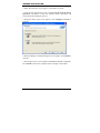
1. Insert the CD that comes with the board and the screen below would
appear. Click Intel (R) Q965 Chipset Drivers, then Intel(R) Chipset
Software Installation Utility.
46
IB940 User’s Manual
DRIVERS INSTALLATION
2. When the Welcome screen appears, click Next to continue.
3. Click Yes to accept the software license agreement and proceed with
the installation process.
4. On the Readme Information screen, click Next to continue the
installation.
5. The Setup process is now complete. Click Finish to restart the
computer and for changes to take effect.
IB940 User’s Manual
47
DRIVERS INSTALLATION
Intel Q965 Chipset Graphics Driver
Follow the instructions below to complete the installation under
Windows 2000/XP.
1. Insert the CD that comes with the board and the screen below would
appear. Click Intel (R) Q965 Chipset Drivers, then Intel (R) Q965
Chipset Family Graphics Driver.
2. When the Welcome screen appears, click Next to continue.
48
IB940 User’s Manual
DRIVERS INSTALLATION
3. Click Yes to accept the software license agreement and proceed with
the installation process.
4. On Readme File Information screen, click Next to continue.
5. On Setup Progress screen, click Next to continue the installation.
6. The Setup process is now complete. Click Finish to restart the
computer and for changes to take effect.
IB940 User’s Manual
49
DRIVERS INSTALLATION
Realtek Codec Audio Driver Installation
1. Insert the CD that comes with the board and the screen below would
appear. Click Intel (R) Q965 Chipset Drivers, then Realtek High
Definition Codec Audio Driver.
2. When the Welcome screen appears, click Next to continue.
3. The Setup process is now complete. Restart the computer when
prompted for changes to take effect.
50
IB940 User’s Manual
DRIVERS INSTALLATION
Intel LAN Drivers Installation
Follow the steps below to start installing the Intel PCI Express Gigabit
LAN drivers.
1. Insert the CD that comes with the board. On the initial screen, Click
Intel (R) Q965 Chipset Drivers, then Intel(R) PRO LAN Network
Drivers.
2. On the next screen, click Install Drivers to start the drivers
installation.
IB940 User’s Manual
51
DRIVERS INSTALLATION
3. When the Welcome screen appears, click Next to continue.
4. In the License Agreement screen, click I accept the terms in license
agreement and Next to accept the software license agreement and
proceed with the installation process.
5. When the Setup Type screen appears, click Complete and Next to
continue.
6. When the Ready to Install the Program screen appears, click Install to
continue.
7. The Setup process is now complete (InstallShield Wizard Completed).
Click Finish to restart the computer and for changes to take effect.
52
IB940 User’s Manual
APPENDIX
Appendix
A. I/O Port Address Map
Each peripheral device in the system is assigned a set of I/O port
addresses that also becomes the identity of the device. The following
table lists the I/O port addresses used.
Address
000h - 01Fh
020h - 03Fh
040h - 05Fh
060h - 06Fh
070h - 07Fh
080h - 09Fh
0A0h - 0BFh
0C0h - 0DFh
0F0h
0F1h
1F0h - 1F7h
278h - 27Fh
2F8h - 2FFh
2B0h - 2DFh
378h - 3FFh
360h - 36Fh
3B0h - 3BFh
3C0h - 3CFh
3D0h - 3DFh
3F0h - 3F7h
3F8h - 3FFh
Device Description
DMA Controller #1
Interrupt Controller #1
Timer
Keyboard Controller
Real Time Clock, NMI
DMA Page Register
Interrupt Controller #2
DMA Controller #2
Clear Math Coprocessor Busy Signal
Reset Math Coprocessor
IDE Interface
Parallel Port #2(LPT2)
Serial Port #2(COM2)
Graphics adapter Controller
Parallel Port #1(LPT1)
Network Ports
Monochrome & Printer adapter
EGA adapter
CGA adapter
Floppy Disk Controller
Serial Port #1(COM1)
IB940 User’s Manual
53
APPENDIX
B. Interrupt Request Lines (IRQ)
Peripheral devices use interrupt request lines to notify CPU for the
service required. The following table shows the IRQ used by the devices
on board.
Level
IRQ0
IRQ1
IRQ2
IRQ3
IRQ4
IRQ5
IRQ6
IRQ7
IRQ8
IRQ9
IRQ10
IRQ11
IRQ12
IRQ13
IRQ14
IRQ15
54
Function
System Timer Output
Keyboard
Interrupt Cascade
Serial Port #2
Serial Port #1
Reserved
Floppy Disk Controller
Parallel Port #1
Real Time Clock
Reserved
Reserved
Reserved
PS/2 Mouse
80287
Primary IDE
Secondary IDE
IB940 User’s Manual
APPENDIX
C. Watchdog Timer Configuration
The WDT is used to generate a variety of output signals after a user
programmable count. The WDT is suitable for use in the prevention of
system lock-up, such as when software becomes trapped in a deadlock.
Under these sorts of circumstances, the timer will count to zero and the
selected outputs will be driven. Under normal circumstance, the user
will restart the WDT at regular intervals before the timer counts to zero.
SAMPLE CODE:
//=======================================================================
//
// THIS CODE AND INFORMATION IS PROVIDED "AS IS" WITHOUT WARRANTY OF ANY
// KIND, EITHER EXPRESSED OR IMPLIED, INCLUDING BUT NOT LIMITED TO THE
// IMPLIED WARRANTIES OF MERCHANTABILITY AND/OR FITNESS FOR A PARTICULAR
// PURPOSE.
//
//=======================================================================
====
#include <stdio.h>
#include <stdlib.h>
#include "W627EHF.H"
//=======================================================================
====
int main (int argc, char *argv[]);
void copyright(void);
void EnableWDT(int);
void DisableWDT(void);
//=======================================================================
====
int main (int argc, char *argv[])
{
unsigned char bBuf;
unsigned char bTime;
char **endptr;
copyright();
if (argc != 2)
{
printf(" Parameter incorrect!!\n");
return 1;
}
if (Init_W627EHF() == 0)
{
printf(" Winbond 83627HF is not detected, program abort.\n");
return 1;
}
bTime = strtol (argv[1], endptr, 10);
IB940 User’s Manual
55
APPENDIX
printf("System will reset after %d seconds\n", bTime);
EnableWDT(bTime);
return 0;
}
//=======================================================================
void copyright(void)
{
printf("\n======== Winbond 83627EHF Watch Timer Tester (AUTO DETECT)
========\n"\
"
Usage : W627E_WD reset_time\n"\
"
Ex : W627E_WD 3 => reset system after 3 second\n"\
"
W627E_WD 0 => disable watch dog timer\n");
}
//=======================================================================
void EnableWDT(int interval)
{
unsigned char bBuf;
bBuf = Get_W627EHF_Reg( 0x2D);
bBuf &= (!0x01);
Set_W627EHF_Reg( 0x2D, bBuf);
//Enable WDTO
Set_W627EHF_LD( 0x08);
Set_W627EHF_Reg( 0x30, 0x01);
//switch to logic device 8
//enable timer
bBuf = Get_W627EHF_Reg( 0xF5);
bBuf &= (!0x08);
Set_W627EHF_Reg( 0xF5, bBuf);
//count mode is second
Set_W627EHF_Reg( 0xF6, interval);
//set timer
}
//=======================================================================
void DisableWDT(void)
{
Set_W627EHF_LD(0x08);
//switch to logic device 8
Set_W627EHF_Reg(0xF6, 0x00);
//clear watchdog timer
Set_W627EHF_Reg(0x30, 0x00);
//watchdog disabled
}
//=======================================================================
56
IB940 User’s Manual
APPENDIX
//=======================================================================
//
// THIS CODE AND INFORMATION IS PROVIDED "AS IS" WITHOUT WARRANTY OF ANY
// KIND, EITHER EXPRESSED OR IMPLIED, INCLUDING BUT NOT LIMITED TO THE
// IMPLIED WARRANTIES OF MERCHANTABILITY AND/OR FITNESS FOR A PARTICULAR
// PURPOSE.
//
//=======================================================================
====
#include "W627EHF.H"
#include <dos.h>
//=======================================================================
====
unsigned int W627EHF_BASE;
void Unlock_W627EHF (void);
void Lock_W627EHF (void);
//=======================================================================
unsigned int Init_W627EHF(void)
{
unsigned int result;
unsigned char ucDid;
W627EHF_BASE = 0x2E;
result = W627EHF_BASE;
ucDid = Get_W627EHF_Reg(0x20);
if (ucDid == 0x88)
{
goto Init_Finish; }
W627EHF_BASE = 0x4E;
result = W627EHF_BASE;
ucDid = Get_W627EHF_Reg(0x20);
if (ucDid == 0x88)
{
goto Init_Finish; }
W627EHF_BASE = 0x00;
result = W627EHF_BASE;
Init_Finish:
return (result);
}
//=======================================================================
void Unlock_W627EHF (void)
{
outportb(W627EHF_INDEX_PORT, W627EHF_UNLOCK);
outportb(W627EHF_INDEX_PORT, W627EHF_UNLOCK);
}
//=======================================================================
====
void Lock_W627EHF (void)
{
outportb(W627EHF_INDEX_PORT, W627EHF_LOCK);
}
//=======================================================================
void Set_W627EHF_LD( unsigned char LD)
{
Unlock_W627EHF();
outportb(W627EHF_INDEX_PORT, W627EHF_REG_LD);
outportb(W627EHF_DATA_PORT, LD);
IB940 User’s Manual
57
APPENDIX
Lock_W627EHF();
}
//=======================================================================
void Set_W627EHF_Reg( unsigned char REG, unsigned char DATA)
{
Unlock_W627EHF();
outportb(W627EHF_INDEX_PORT, REG);
outportb(W627EHF_DATA_PORT, DATA);
Lock_W627EHF();
}
//=======================================================================
unsigned char Get_W627EHF_Reg(unsigned char REG)
{
unsigned char Result;
Unlock_W627EHF();
outportb(W627EHF_INDEX_PORT, REG);
Result = inportb(W627EHF_DATA_PORT);
Lock_W627EHF();
return Result;
}
//=======================================================================
//=======================================================================
//
// THIS CODE AND INFORMATION IS PROVIDED "AS IS" WITHOUT WARRANTY OF ANY
// KIND, EITHER EXPRESSED OR IMPLIED, INCLUDING BUT NOT LIMITED TO THE
// IMPLIED WARRANTIES OF MERCHANTABILITY AND/OR FITNESS FOR A PARTICULAR
// PURPOSE.
//
//=======================================================================
#ifndef __W627EHF_H
#define __W627EHF_H
1
//=======================================================================
#define
W627EHF_INDEX_PORT
(W627EHF_BASE)
#define
W627EHF_DATA_PORT
(W627EHF_BASE+1)
//=======================================================================
#define
W627EHF_REG_LD
0x07
//=======================================================================
#define W627EHF_UNLOCK
0x87
#define
W627EHF_LOCK
0xAA
//=======================================================================
unsigned int Init_W627EHF(void);
void Set_W627EHF_LD( unsigned char);
void Set_W627EHF_Reg( unsigned char, unsigned char);
unsigned char Get_W627EHF_Reg( unsigned char);
//=======================================================================
#endif
//__W627EHF_H
58
IB940 User’s Manual
APPENDIX
D. Digital I/O Sample Code
Filename: W627hf.h
//=====================================================================
//
// THIS CODE AND INFORMATION IS PROVIDED "AS IS" WITHOUT WARRANTY OF ANY
// KIND, EITHER EXPRESSED OR IMPLIED, INCLUDING BUT NOT LIMITED TO THE
// IMPLIED WARRANTIES OF MERCHANTABILITY AND/OR FITNESS FOR A PARTICULAR
// PURPOSE.
//
//=====================================================================
#ifndef __W627HF_H
#define __W627HF_H
1
//=======================================================================
#define
W627HF_INDEX_PORT
(W627HF_BASE)
#define
W627HF_DATA_PORT
(W627HF_BASE+1)
//=======================================================================
#define
W627HF_REG_LD
0x07
//=======================================================================
#define W627HF_UNLOCK
0x87
#define
W627HF_LOCK
0xAA
//=======================================================================
unsigned int Init_W627HF(void);
void Set_W627HF_LD( unsigned char);
void Set_W627HF_Reg( unsigned char, unsigned char);
unsigned char Get_W627HF_Reg( unsigned char);
//=======================================================================
#endif
//__W627HF_H
IB940 User’s Manual
59
APPENDIX
Filename: W627hf.cpp
//=====================================================================
//
// THIS CODE AND INFORMATION IS PROVIDED "AS IS" WITHOUT WARRANTY OF ANY
// KIND, EITHER EXPRESSED OR IMPLIED, INCLUDING BUT NOT LIMITED TO THE
// IMPLIED WARRANTIES OF MERCHANTABILITY AND/OR FITNESS FOR A PARTICULAR
// PURPOSE.
//
//=====================================================================
unsigned int W627HF_BASE;
void Unlock_W627HF (void);
void Lock_W627HF (void);
//=======================================================================
unsigned int Init_W627HF(void)
{
unsigned int result;
//0=NA, 1=627HF, 2=627THF, 4=627EHF
//
W627HF_BASE = 0x2E;
W627HF_BASE = 0x4E;
result = Get_W627HF_Reg(0x20);
if (result == 0x52)
{
result = 1;
goto Init_Finish;
}
else if (result == 0x82)
{
result = 2;
goto Init_Finish;
}
else if (result == 0x88)
{
result = 4;
goto Init_Finish;
}
//
W627HF_BASE = 0x4E;
W627HF_BASE = 0x2E;
result = Get_W627HF_Reg(0x20);
if (result == 0x52)
{
result = 1;
goto Init_Finish;
}
else if (result == 0x82)
{
result = 2;
goto Init_Finish;
}
else if (result == 0x88)
{
result = 4;
goto Init_Finish;
}
60
IB940 User’s Manual
APPENDIX
W627HF_BASE = 0x00;
result = 0;
Init_Finish:
return (result);
}
//=======================================================================
void Unlock_W627HF (void)
{
outportb(W627HF_INDEX_PORT, W627HF_UNLOCK);
outportb(W627HF_INDEX_PORT, W627HF_UNLOCK);
}
//=======================================================================
void Lock_W627HF (void)
{
outportb(W627HF_INDEX_PORT, W627HF_LOCK);
}
//=======================================================================
void Set_W627HF_LD( unsigned char LD)
{
Unlock_W627HF();
outportb(W627HF_INDEX_PORT, W627HF_REG_LD);
outportb(W627HF_DATA_PORT, LD);
Lock_W627HF();
}
//=======================================================================
void Set_W627HF_Reg( unsigned char REG, unsigned char DATA)
{
Unlock_W627HF();
outportb(W627HF_INDEX_PORT, REG);
outportb(W627HF_DATA_PORT, DATA);
Lock_W627HF();
}
//=======================================================================
unsigned char Get_W627HF_Reg(unsigned char REG)
{
unsigned char Result;
Unlock_W627HF();
outportb(W627HF_INDEX_PORT, REG);
Result = inportb(W627HF_DATA_PORT);
Lock_W627HF();
return Result;
}
//=======================================================================
IB940 User’s Manual
61
APPENDIX
File of the Main.cpp
//=====================================================================
// THIS CODE AND INFORMATION IS PROVIDED "AS IS" WITHOUT WARRANTY OF ANY
// KIND, EITHER EXPRESSED OR IMPLIED, INCLUDING BUT NOT LIMITED TO THE
// IMPLIED WARRANTIES OF MERCHANTABILITY AND/OR FITNESS FOR A PARTICULAR
// PURPOSE.
//=====================================================================
#include <dos.h>
#include <conio.h>
#include <stdio.h>
#include <stdlib.h>
#include "W627HF.H"
//--------------------------------------------------------------------------void ClrKbBuf(void);
int main (void);
unsigned char GetDI(unsigned char);
void SetDo(unsigned char, unsigned char);
//--------------------------------------------------------------------------int main (void)
{
unsigned char ucDO = 0;
//data for digital output
unsigned char ucDI;
//data for digital input
unsigned char ucBuf;
char SIO;
SIO = Init_W627HF();
if (SIO == 0)
{
printf("Can not detect Winbond 83627HF/83627THF/83627EHF, program abort.\n");
return(1);
}
switch (SIO)
{
//------------------------------------------------------------------case 1:
printf("Winbond 83627HF is detected .\n");
break;
//------------------------------------------------------------------case 2:
printf("Winbond 83627THF is detected.\n");
break;
//------------------------------------------------------------------case 4:
printf("Winbond 83627EHF is detected.\n");
break;
//------------------------------------------------------------------}
//bit 0..3 = input signal
//bit 4..7 = output signal
ucDI = GetDI(0x0F);
SetDo(ucDO, 0xF0);
return 0;
//get current DI status
//set current DO status
}
//--------------------------------------------------------------------------unsigned char GetDI(unsigned char Mask)
{
62
IB940 User’s Manual
APPENDIX
unsigned char result;
Set_W627HF_LD(0x07);
Set_W627HF_Reg(0xF0, Mask);
result = Get_W627HF_Reg(0xF1) & Mask;
return (result);
//switch to logic device 7
//set the DIO direction
}
//--------------------------------------------------------------------------void SetDo(unsigned char NewData, unsigned char Mask)
{
Set_W627HF_LD(0x07);
//switch to logic device 7
Set_W627HF_Reg(0xF0, ~Mask);
//set the DIO direction
Set_W627HF_Reg(0xF1, NewData & Mask);
}
//--------------------------------------------------------------------------void ClrKbBuf(void)
{
while(kbhit())
{
getch();
}
}
//---------------------------------------------------------------------------
IB940 User’s Manual
63
APPENDIX
This page is intentionally left blank.
64
IB940 User’s Manual