1
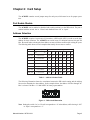
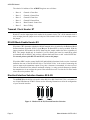
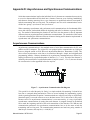
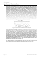
ACB2/EX Series Product Manual MANUAL NUMBER : 00750-128-1C FOREWORD This product manual provides information to install, operate and/or program the referenced product(s) manufactured or distributed by ICS Advent. The following pages contain information regarding the warranty and repair policies. Check our Web site (http://www.icsadvent.com/techsupport) for technical information, manual, and BIOS updates. Technical assistance is also available at: 800-480-0044 (U.S. and Canada) or 858-677-0877 (international). Manual errors, omissions, bugs, and/or comments: A Customer Comments section is included at the end of this manual. If you experience any problems with the manual or just want to give us some feedback, please review the information in this section. It will tell you how to easily access our web site and provide immediate feedback online. The information in this document is provided for reference only. ICS Advent does not assume any liability arising from the application or use of the information or products described herein. This document may contain or reference information and products protected by copyrights or patents and does not convey any license under the patent rights of ICS Advent, nor the rights of others. Copyright © 1999, a California Corporation, 6260 Sequence Drive, San Diego, CA 92121-4371. ICS Advent is a Registered Trademark of ICS Advent. All trademarks and registered trademarks are the property of their respective owners. All rights reserved. Printed in the United States of America. No part of this publication may be reproduced, stored in a retrieval system, or transmitted, in any form or by any means, electronic, mechanical, photocopying, recording , or otherwise, without the prior written permission of the publisher. Page - iii Guarantee A thirty day money-back guarantee is provided on all standard products sold. Special order products are covered by our Limited Warranty, however they may not be returned for refund or credit. EPROMs, RAM, Flash EPROMs or other forms of solid electronic media are not returnable for credit - but for replacement only. Extended Warranty available. Consult factory. Refunds In order to receive refund on a product purchase price, the product must not have been damaged by the customer or by the common carrier chosen by the customer to return the goods, and the product must be returned complete (meaning all manuals, software, cables, etc.) within 30 days of receipt and in as-new and resalable condition. The Return Procedure must be followed to assure prompt refund. Restocking Charges Product returned after 30 days, and before 60 days, of the purchase will be subject to a minimum 20% restocking charge and any charges for damaged or missing parts. Products not returned within 60 days of purchase, or products which are not in as-new and resaleable condition, are not eligible for credit return and will be returned to the customer. Limited Warranty Effective April 1, 1998, all products carry a two-year limited warranty with the exception of the “Performance Series” I/O products, which are warranted to the original purchaser for as long as they own the product, subject to all other conditions below, including those regarding neglect, misuse and acts of God. Within two years of purchase, ICS Advent will repair or replace, at our option, any defective product. At any time after two years, we will repair or replace, at our option, any defective “Performance Series” I/O product sold. This does not include products damaged in shipment, or damaged through customer neglect or misuse. ICS Advent will service the warranty for all standard catalog products for the first two years from the date of shipment. After the second year, for products not manufactured by ICS Advent, the remainder of the manufacturer's warranty, if any, will be serviced by the manufacturer directly. The Return Procedure must be followed to assure repair or replacement. ICS Advent will normally return your replacement or repaired item via Second Day Air. Overnight delivery or delivery via other carriers is available at additional charge. The limited warranty is void if the product has been subjected to alteration, neglect, misuse, or abuse; if any repairs have been attempted by anyone other than ICS Advent or its authorized agent; or if the failure is caused by accident, acts of God, or other causes beyond the control of ICS Advent or the manufacturer. Neglect, misuse, and abuse shall include any installation, operation, or maintenance of the product other than in accordance with the owners’ manual. No agent, dealer, distributor, service company, or other party is authorized to change, modify, or extend the terms of this Limited Warranty in any manner whatsoever. ICS Advent reserves the right to make changes or improvements in any product without incurring any obligation to similarly alter products previously purchased. Shipments not in compliance with this Guarantee and Limited Warranty Return Policy will not be accepted by ICS Advent. Page - iv Return Procedure For any Guarantee or Limited Warranty return, please contact ICS Advent's Customer Service at 800-480-0044 (U.S.) or 858-677-0877 (international) and obtain a Return Material Authorization (RMA) Number. All product(s) returned to ICS Advent for service or credit must be accompanied by a Return Material Authorization (RMA) Number. Freight on all returned items must be prepaid by the customer who is responsible for any loss or damage caused by common carrier in transit. Returns for Warranty must include a Failure Report for each unit, by serial number(s), as well as a copy of the original invoice showing date of purchase. To reduce risk of damage, returns of product must be in an ICS Advent shipping container. If the original container has been lost or damaged, new shipping containers may be obtained from ICS Advent Customer Service at a nominal cost. ICS Advent owns all parts removed from repaired products. ICS Advent uses new and reconditioned parts made by various manufacturers in performing warranty repairs and building replacement products. If ICS Advent repairs or replaces a product, its warranty term is not extended. ICS Advent will normally return your replacement or repaired items via Second Day Air. Overnight delivery or delivery via other carriers is available at an additional charge. Limitation of Liability In no event shall ICS Advent be liable for any defect in hardware, software, loss, or inadequacy of data of any kind, or for any direct, indirect, incidental, or consequential damages in connection with or arising out of the performance or use of any product furnished hereunder. ICS Advent liability shall in no event exceed the purchase price of the product purchased hereunder. The foregoing limitation of liability shall be equally applicable to any service provided by ICS Advent or its authorized agent. Some Sales Items and Customized Systems are not subject to the guarantee and limited warranty. However in these instances , any deviations will be disclosed prior to sales and noted in the original invoice. ICS Advent reserves the right to refuse returns or credits on software or special order items. Page - v Advisories Three types of advisories are used throughout the manual to stress important points or warn of potential hazards to the user or the system. They are the Note, the Caution, and the Warning. Following is an example of each type of advisory: Note: The note is used to present special instruction, or to provide extra information which may help to simplify the use of the product. CAUTION! A Caution is used to alert you to a situation which if ignored may cause injury or damage equipment. WARNING! A Warning is used to alert you of a situation which if ignored will cause serious injury. Cautions and Warnings are accented with triangular symbols. The exclamation symbol is used in all cautions and warnings to help alert you to the important instructions. The lightning flash symbol is used on the left hand side of a caution or a warning if the advisory relates to the presence of voltage which may be of sufficient magnitude to cause electrical shock. Use caution when servicing any electrical component. We have tried to identify the areas which may pose a Caution or Warning condition in this manual; however, ICS Advent does not claim to have covered all situations which might require the use of a Caution or Warning. You must refer to the documentation for any component you install into a computer system to ensure proper precautions and procedures are followed. Page - vi Table of Contents Chapter 1: Introduction ................................................................................................ 1 Overview ............................................................................................................................................... 1 What’s Included .................................................................................................................................... 1 Factory Default Settings ....................................................................................................................... 1 How To Remain CE Compliant Chapter 2: Card Setup ................................................................................................. 3 Port Enable Disable .............................................................................................................................. 3 Address Selection ................................................................................................................................ 3 Transmit Clock Header E7 .................................................................................................................... 4 RS-485 Mode Enable Header E2 .......................................................................................................... 4 Electrical Interface Selection Headers E8 & E9 .................................................................................... 4 DMA Channel Selection Headers E3 & E4 ............................................................................................ 5 DMA Jumper Option Tables ................................................................................................................... 5 No DMA ......................................................................................................................................... 5 Single Channel DMA (Half Duplex Only) ......................................................................................... 5 Full Duplex ..................................................................................................................................... 6 DMA Enable Header E1 ........................................................................................................................ 6 IRQ Selection Header E6 ...................................................................................................................... 6 IRQ Mode Header E5 ............................................................................................................................ 7 Chapter 3: Installation .................................................................................................. 9 Cabling Options .................................................................................................................................... 9 Chapter 4: Technical Description.............................................................................. 11 Programming the ACB2/EX .................................................................................................................. 11 Control/Status Port ........................................................................................................................ 11 Software Examples .......................................................................................................................12 DMA Terminal Count ............................................................................................................................ 12 Connector P1 Pin Assignments ...........................................................................................................12 RS-232 Signals .............................................................................................................................12 RS-530/422/485 Pin Assignments................................................................................................. 13 RS-530/422/485 Line Termination ..................................................................................................13 Chapter 5: Specifications .......................................................................................... 15 Environmental Specifications ......................................................................................................... 15 Temperature Range .......................................................................................................................15 Humidity Range ............................................................................................................................ 15 Power Consumption ...................................................................................................................... 15 Mean Time Between Failures (MTBF) ........................................................................................... 15 Physical Dimensions ....................................................................................................................15 Page - vii Appendix A: Troubleshooting ................................................................................... 17 Appendix B: Electrical Interface ................................................................................ 19 RS-232 .......................................................................................................................................... 19 RS-422 .......................................................................................................................................... 19 RS-530 ........................................................................................................................................... 9 RS-449 .......................................................................................................................................... 20 RS-485 .......................................................................................................................................... 20 Appendix C: Direct Memory Access ......................................................................... 21 Appendix D: Asynchronous and Synchronous Communications ........................ 23 Asynchronous Communications .......................................................................................................... 23 Synchronous Communications ............................................................................................................ 24 Appendix E: ACB Developer Toolkit Diskette and ACB Resource Kit ................... 25 Appendix F: Silk-Screen ............................................................................................ 27 CE Declaration of Conformity List of Figures Figure 1: DIP-switch Illustration .................................................................................................................. 3 Figure 2: Headers E8 & E9, Electrical Interface Selection .......................................................................... 4 Figure 3: DMA Selection Headers E3 & E4 ................................................................................................ 5 Figure 4: DMA Enable Header E1 ............................................................................................................... 6 Figure 5: IRQ Header E6 ............................................................................................................................ 6 Figure 6: IRQ Mode Header ........................................................................................................................ 7 Figure 7: Asynchronous Communications Bit Diagram .............................................................................. 23 Figure 8: Synchronous Communications Bit Diagram ................................................................................ 24 List of Tables Table 1: Address Selection Table ................................................................................................................ 3 Current Revision 1C December 2000 Page - viii Chapter 1: Introduction Overview The Model ACB2/EX provides the PC with one high-speed RS-232/530/422/485 synchronous/ asynchronous port. The ACB2/EX can be used in a variety of sophisticated communications applications such as SDLC, HDLC, X.25, Bi-Sync, Mono-Sync, and high-speed asynchronous. Whats Included The ACB2/EX is shipped with the following items. If any of these items are missing or damaged, contact the supplier. ACB2/EX Serial Interface Adapter ACB Developers Software User Manual Factory Default Settings The ACB2/EX factory default settings are as follows: Base Address DMA SelectionIRQ Electrical Specification 238 TX: 1 / RX: 3 5 RS-530/422 To install the ACB2/EX using factory default settings, refer to the section on Installation. For your reference, record installed ACB2/EX settings below: Base Address DMA SelectionIRQ Electrical Specification How to Remain CE Compliant For computer systems to remain CE compliant, only CE compliant parts may be used. To keep a chassis compliant it must contain only compliant cards, and for cards to remain compliant they must be used in compliant chassis. Any modifications made to the equipment may affect the CE compliance standards and should not be done unless approved in writing by . The ACB2/EX is designed to be CE compliant when used in a CE compliant chassis. Maintaining CE compliance also requires proper cabling techniques. The user is advised to follow proper cabling techniques from external devices to the interface to ensure a complete CE compliant system. does not offer engineering services for designing cabling systems. Although offers accessories, it is the user's responsibility to ensure they are installed with proper shielding to maintain CE compliance. Manual Number: 00750-128-1 Page 1 ACB2/EX Manual This page intentionally left blank Page 2 Manual Number: 00750-128-1 Chapter 2: Card Setup The ACB2/EX contains several jumper straps for each port, which must be set for proper operation. Port Enable Disable The ACB2/EX can be enabled or disabled with switch position 8 on the DIP-switch. The port is enabled with the switch On or Closed and disabled when Off or Open. Address Selection The ACB2/EX occupies 8 consecutive I/O locations. A DIP-switch (SW1) is used to set the base address for these locations. The ACB2/EX can reside in any I/O location between 100 and 3F8 Hex. Be careful when selecting the base address as some selections conflict with existing PC ports. The following table shows several examples that usually do not cause a conflict. Addre s s Binary Switch Se ttings A9—————A0 1 2 3 4 5 6 7 238- 23F 1000111XXX Off On On On Off Off Off 280- 287 1010000XXX Off On Off On On On On 2A0- 2A7 1010100XXX Off On Off On Off On On 2E8- 2EF 1011101XXX Off On Off Off Off On Off 300- 307 1100000XXX Off Off On On On On On 328- 32F 1100101XXX Off Off On On Off On Off 3E8- 3EF 1111101XXX Off Off Off Off Off On Off Table 1: Address Selection Table The following illustration shows the correlation between the DIP-switch setting and the address bits used to determine the base address. In the example below, the address 300 Hex through 307 Hex is selected. 300 Hex = 11 0000 0XXX in binary representation. $ $ ( 21 2)) Figure 1: DIP-switch Illustration Note: Setting the switch On or Closed corresponds to a 0 in the address, while leaving it Off or Open corresponds to a 1. Manual Number: 00750-128-1 Page 3 ACB2/EX Manual The relative I/O address of the ACB2/EX registers are as follows: Base+0 Channel A Data Port Base+1 Channel A Control Port Base+2 Channel B Data Port Base+3 Channel B Control Port Base+4 Board Control / Status Port Base+5 Reset TCIRQ Transmit Clock Header E7 Header E7 sets the input/output clock modes for the transmit clock (TXC). If the transmit clock is to be an input, place the jumper to cover both pins. If the transmit clock is to be an output, remove the jumper. RS-485 Mode Enable Header E2 E2 position TE determines whether the RS-485 transmit driver is enabled by the Enhanced Serial Communications Controller (ESCC) signal Request To Send (RTS) or always enabled. With the jumper installed, RTS enables the driver. Removing the jumper enables the driver regardless of RTS. This jumper should only be installed if you are running the board in a multi-drop polled environment such as RS-485, and you have software that knows how to talk on the RS-485 bus. For normal point-to-point RS-530 and RS-422, remove this jumper. E2 position ED is used to control the RS-485 enable/disable functions for the receiver circuit and determine the state of the RS-422/485 driver. The RS-485 Echo is the result of connecting the receiver inputs to the transmitter outputs. Every time a character is transmitted; it is also received. This can be beneficial if the software can handle echoing (i.e. using received characters to throttle the transmitter) or it can confuse the system if the software does not. To select the No Echo mode select silk-screen position ED. Electrical Interface Selection Headers E8 & E9 The ACB2/EX has the ability to be used in either RS-232 or RS-530/422/485. This is selectable via two 24 pin DIP-shunts at E8 & E9. Please use the following illustration to aid in the configuration of your electrical interface. 56 56 56 ( ( ( ( Figure 2: Headers E8 & E9, Electrical Interface Selection Page 4 Manual Number: 00750-128-1 DMA Channel Selection Headers E3 & E4 Headers E3 & E4 select Direct Memory Access (DMA) mode of operation. Each channel of the Enhanced Serial Communications Controller (ESCC) will function in half duplex or full duplex DMA modes. Full duplex means that DMA can be used for simultaneous transmit and receive. Half-duplex DMA means that you can either transmit or receive with DMA, but not simultaneously. The 85230 has two signals that correspond to DMA request signals, WAIT/REQ and DTR/REQ. E3 corresponds to the SCC signal WAIT/REQ and E4 corresponds to DTR/REQ. WAIT/REQ and DTR/REQ can be programmed to serve as DMA request lines (DRQ) by setting the appropriate bits in Write Register 1 and Write Register 14 in the 85230. WAIT/REQ (E3) can be programmed for Transmit or Receive DMA transfers and DTR/REQ (E4) can be programmed for Transmit Only. For additional information on the programming of the 85230 please refer to the Zilog ESCC Users Manual. Please note that each DMA channel is selected by two jumpers. Only one DMA channel may be selected for each header block. Note: If DMA is not used, remove all of the jumpers on E3 and E4 and remove jumper at E1 ( ( Figure 3: DMA Selection Headers E3 & E4 Note: DMA Channel 2 can only be used if the floppy disk DMA drivers are turned off. Please refer to the toolkit disk for software examples. DMA Jumper Option Tables The following tables show the jumper setting examples for each mode of DMA: No DMA Option E3 E4 Ch.A No DMA None None Single Channel DMA (Half Duplex Only) Option E3 E4 DMA Channel 0 00 None DMA Channel 1 11 None DMA Channel 2 22 None DMA Channel 3 33 None Manual Number: 00750-128-1 Page 5 ACB2/EX Manual Full Duplex Option E3 E4 DMA Ch.1 Receive Data DMA Ch.3 Transmit Data 11 33 DMA Ch.0 Receive Data DMA Ch.2 Transmit Data 00 22 Note: DMA Channel 2 can only be used if the floppy disk DMA drivers are turned off. Please refer to the Toolkit disk for software examples. DMA Enable Header E1 Header E1 selects whether the DMA tri-state drivers are enabled permanently (position A), disabled permanently (jumpers removed), or which DMA enable control port bit is used to enable the DMA hardware request and acknowledge signals. Removing the jumper disables the drivers and no DMA can be performed. Note: The power on reset signal resets or disables the DMA software enable signal. 66$ ( Figure 4: DMA Enable Header E1 S1 Base+4 Position D7 enables DMA S2 RTSB enables DMA A Selects Always Enable Note: Please refer to Section 4 for software bit definitions and examples of DMA driver control. IRQ Selection Header E6 Header E6 selects the interrupt request (IRQ) line for the card. If no interrupt is desired, remove the jumper. Figure 5: IRQ Header E6 Page 6 Manual Number: 00750-128-1 IRQ Mode Header E5 Header E5 N indicates the (N)ormal, single interrupt mode. Position M indicates the inclusion of a 1K ohm pull-down resistor required on one port when sharing interrupts with another card. For shared interrupt mode, set one board to M and all other adapters sharing an IRQ should have neither N or M in place. This mode allows more than one board to access a single IRQ. Position T on E5 enables the DMA Terminal Count Interrupt. Setting this jumper allows the selected DMA channel to generate an interrupt once the DMA Terminal Count has been reached. See Section 4 for the status bit (TC STAT) position and refer to the toolkit disk for software examples. Note: When using multiple cards on one IRQ in shared mode, be sure that only one port has the M jumper set, providing the necessary pull-down resistor. 710 ( Figure 6: IRQ Mode Header Manual Number: 00750-128-1 Page 7 ACB2/EX Manual This page intentionally left blank Page 8 Manual Number: 00750-128-1 Chapter 3: Installation The ACB2/EX can be installed in any of the PC expansion slots The ACB2/EX contains several jumper straps for each port, which must be set for proper operation. 1. Turn off PC power. Disconnect the power cord. 2. Remove the PC case cover. 3. Locate two available slots and remove the blank metal slot covers. 4. Replace the cover. 5. Connect the power cord. Installation is complete. Cabling Options The ACB2/EX has a number of cabling options available. These options include: CAB-104 - This cable provides a 6' extension for use with RS-530/422 Manual Number: 00750-128-1 Page 9 ACB2/EX Manual This page intentionally left blank Page 10 Manual Number: 00750-128-1 Chapter 4: Technical Description The ACB2/EX utilizes the Zilog 85230 Enhanced Serial Communications Controller (ESCC). This chip features programmable baud rate, data format and interrupt control, as well as DMA control. Refer to the ESCC Users Manual for details on programming the 85230 ESCC chip. Features One channel of sync/async communications using 85230 chip DMA supports data rate greater than 1 million bits per second (bps) Selectable Port Address, IRQ level ( 3, 4, 5, 7, 9, 10, 11, 12, 15) Selectable DMA channels (0, 1, 2, 3) EIA-232 interface with full modem control signals TD, RD, RTS, CTS, DSR, DCD, DTR, TXC, RXC, TSET signals EIA-530 interface with modem control signals TD, RD, RTS, CTS, DTR, TXC, RXC, TSET signals Jumper options for Transmit clock as input or output Software programmable baud rate Internal Baud Rate Generator The baud rate of the ESCC is programmed under software control. The standard oscillator supplied with the board is 7.3728 MHz. However, other oscillator values can be substituted to achieve different baud rates. Programming the ACB2/EX Control/Status Port The ACB2/EX occupies eight input/output (I/O) addresses. The ESCC chip uses the first four, while the fifth address (Base+4) is the address of the on-board Control/Status Port. This port is used to set the Data Terminal Ready (DTR) and to enable or disable DMA under program control, and to monitor the Data Set Ready (DSR) input signals from the modem. Bit Output Port Bits Input Port Bits 0 DTR A 1=On, 0=Off DSR A 1=Off, 0=On 1 Unused bit Unused bit 2 Unused bit Unused bit 3 Unused bit ESCC INT 1=Off, 0=On 4 Unused bit Unused bit 5 Unused bit TC STAT 1=Off, 0=On 6 Unused bit Unused bit 7 CH. A DMA Enable ESCC CH.A 1=On, 0=Off Ch.A DMA 1=Off, 0=On Manual Number: 00750-128-1 Page 11 ACB2/EX Manual Software Examples Function Program Bits Turn On CH.A DTR Out (Base+4), XXXX XXX1 Turn Off CH.A DTR Out (Base+4), XXXX XXX0 Enable DMA Drivers Out (Base+4), 1XXX XXXX Disable DMA Drivers Out (Base+4), 0XXX XXXX Test CH.A DSR In (Base+4), Mask=0000 0001 DMA Terminal Count The ACB2/EX can be setup to operate using a polling method, interrupts, or system DMA. The most efficient method is a combination of DMA and interrupts. The ACB2/EX has been optimized to generate an interrupt at the end of a DMA transfer. This will allow DMA initialization and buffer management to take place at interrupt time and provide a virtually seamless communication channel. If the T option on header E5 is selected, an onboard latch will be set when Terminal Count for the selected DMA channel(s) is reached. This latch will cause an interrupt to be generated and program execution will be transferred to the application Interrupt Service Routine (ISR). The DMA Terminal Count Interrupt condition should be reset from the ISR by writing to BASE+5. The value that is written to this I/O location is irrelevant. If your application or driver is interrupting on multiple conditions, reading the Status Register located at Base+4 will determine the source of the interrupt (ESCC or DMA Terminal Count generated). Bit D3 in the Status Port corresponds to a ESCC generated interrupt and bit D5 corresponds to an interrupt generated by the end of a DMA transfer. Bit D3 can only be reset by polling the ESCC to determine the interrupt source and required action necessary to reset the interrupt. Please refer to the Software Toolkit and the 85230 Technical Manual for details and examples on interrupt driven and DMA programming examples. Connector P1 Pin Assignments RS-232 Signals Signal Name Pin # Mode GND Ground 7 RD Receive Data 3 Input RS-232 CTS Clear To Send 5 Input RS-232 DSR Data Set Ready 6 Input RS-232 TXC Transmit Clock 15 Input RS-232 RXC Receive Clock 17 Input RS-232 DCD Data Carrier. Detect 8 Output RS-232 TD Transmit Data 2 Output RS-232 RTS Request to Send 4 Output RS-232 TSET Transmit Signal Element Timing 24 Output RS-232 DTR Data Terminal Ready 20 Output RS-232 Note: These assignments meet the EIA/TIA/ANSI-232E DTE Specification. Page 12 Manual Number: 00750-128-1 RS-530/422/485 Pin Assignments Signal GND Name Pin # Ground 7 Mode RDB RX+ Receive Data Positive 16 Input RDA RX- Receive Data Negative 3 Input CTSB CTS+ Clear To Send Positive 13 Input CTSA CTS- 5 Input TXCB TXC+ Transmit Clock Positive 12 Input TXCA TXC- Transmit Clock Negative 15 Input RXCB RXC+ Receive Clock Positive 9 Input RXCA RXC- Receive Clock Negative TDB TX+ Transmit Data Positive 14 Output TDA TX- Transmit Data Negative 2 Output RTSB RTS+ Request To Send Positive 19 Output RTSA RTS- 4 Output DTRB DTR+ Data Terminal. Ready Positive 23 Output DTRA DTR- Data Terminal Ready Negative 20 Output TSETB TSET+ Terminal Timing Positive 11 Output TSETA TSET- Terminal Timing Negative 24 Output Clear To Send Negative Request To Send Negative 17 Input Note: These assignments meet the EIA/TIA/ANSI-530A DTE Specification. RS-530/422/485 Line Termination Typically, each end of the RS-530/422/485 bus must have line-terminating resistors. A 120-ohm resistor is across each RS-530/422/485 input in addition to a 1K ohm pull-up/pull-down combination that biases the receiver inputs. The RS-530 specification calls for a 100-ohm 1/2-watt resistor between the signal ground and the chassis ground. On the IBM PC, these two grounds are already connected together, therefore this resistor is omitted. Manual Number: 00750-128-1 Page 13 ACB2/EX Manual This page intentionally left blank Page 14 Manual Number: 00750-128-1 Chapter 5: Specifications Environmental Specifications Temperature Range Operating 0º to 50º C (32º to 122º F ) Storage -20º to 70º C (-4º to 158º F) Humidity Range Operating 10 to 90% R.H. Non-Condensing Storage 10 to 90% R.H. Non-Condensing Power Consumption Supply line +12V -12V +5 VDC Rating 40mA 40mA 350 mA Mean Time Between Failures (MTBF) Greater than 150,000 hours. (Calculated) Physical Dimensions Board length 5.2 inches (13.21 cm) Board height including goldfingers 3.5 inches (8.89 cm) Board height excluding goldfingers 3.2 inches (8.12 cm) Please see Appendix F for board layout and dimensions. Manual Number: 00750-128-1 Page 15 ACB2/EX Manual This page intentionally left blank Page 16 Manual Number: 00750-128-1 Appendix A: Troubleshooting An ACB Developers Toolkit Diskette is supplied with the adapter and will be used in the troubleshooting procedures. By using this diskette and following these simple steps, most common problems can be eliminated without the need to call Technical Support. 1. Identify all I/O adapters currently installed in your system. This includes your on-board serial ports, controller cards, sound cards etc. The I/O addresses used by these adapters, as well as the IRQ (if any) should be identified. 2. Configure your adapter so that there is no conflict with currently installed adapters. No two adapters can occupy the same I/O address. 3. Make sure the adapter is using a unique IRQ. While the adapter does allow the sharing of IRQs, many other adapters (i.e. SCSI adapters and on-board serial ports) do not. The IRQ is typically selected via an on-board header block. Refer to the section on Card Setup for help in choosing an I/O address and IRQ. 4. Make sure the adapter is securely installed in a motherboard slot. 5. Use the supplied diskette and User Manual to verify that the adapter is configured correctly. The supplied diskette contains a diagnostic program SSDACB that will verify if an adapter is configured properly. Refer to the UTIL.txt file found in the \UTIL sub-directory on the supplied diskette for detailed instructions on using SSDACB. 6. The following are known I/O conflicts: 3F8-3FF is typically reserved for COM1: 2F8-2FF is typically reserved for COM2: 3E8-3EF is typically reserved for COM3: 2E8-2EF is typically reserved for COM4: Manual Number: 00750-128-1 Page 17 ACB2/EX Manual This page intentionally left blank Page 18 Manual Number: 00750-128-1 Appendix B: Electrical Interface RS-232 Quite possibly the most widely used communication standard is RS-232. This implementation has been defined and revised several times and is often referred to as RS-232 or EIA/TIA-232. It is defined by the EIA as the interface between data terminal equipment and data circuit- terminating equipment employing serial binary data interchange. The mechanical implementation of RS-232 is on a 25 pin D sub connector. The IBM PC computer defined the RS-232 port on a 9 pin D-sub connector and subsequently the EIA/TIA approved this implementation as the EIA/TIA-574 standard. This standard is defined as the nine-position non-synchronous interface between data terminal equipment and data circuit-terminating equipment employing serial binary data interchange. Both implementations are in wide spread use and will be referred to as RS-232 in this document. RS-232 is capable of operating at data rates up to 20 Kbps at distances less than 50 ft. The absolute maximum data rate may vary due to line conditions and cable lengths. The voltage levels defined by RS-232 range from -12 to +12 volts. RS-232 is a single ended or unbalanced interface, meaning that a single electrical signal is compared to a common signal (ground) to determine binary logic states. A voltage of +12 volts (usually +3 to +10 volts) represents a binary 0 (space) and -12 volts (-3 to -10 volts) denotes a binary 1 (mark). The RS-232 and the EIA/TIA-574 specification defines two type of interface circuits, Data Terminal Equipment (DTE) and Data Circuit-Terminating Equipment (DCE). The ACB2/EX adapter is an RS-232 Synchronous DTE interface. RS-422 The RS-422 specification defines the electrical characteristics of balanced voltage digital interface circuits. RS-422 is a differential interface that defines voltage levels and driver/receiver electrical specifications. On a differential interface, logic levels are defined by the difference in voltage between a pair of outputs or inputs. In contrast, a single ended interface, for example RS-232, defines the logic levels as the difference in voltage between a single signal and a common ground connection. Differential interfaces are typically more immune to noise or voltage spikes that may occur on the communication lines. Differential interfaces also have greater drive capabilities that allow for longer cable lengths. RS-422 is rated up to 10 Megabits per second and can have cabling 4000 feet long. RS-422 also defines driver and receiver electrical characteristics that will allow 1 driver and up to 32 receivers on the line at once. RS-422 signal levels range from 0 to +5 volts. RS-422 does not define a physical connector. RS-530 RS-530 (a.k.a. EIA-530) compatibility means that RS-422 signal levels are met, and the pin-out for the DB-25 connector is specified. The Electronic Industry Association (EIA) created the RS-530 specification to detail the pin-out, and define a full set of modem control signals that can be used for regulating flow control and line status. The RS-530 specification defines two types of interface circuits, Data Terminal Equipment (DTE) and Data Circuit-Terminating Equipment (DCE). The Model ACB2/EX adapter is a DTE interface. Manual Number: 00750-128-1 Page 19 ACB2/EX Manual RS-449 RS-449 (a.k.a. EIA-449) compatibility means that RS-422 signal levels are met, and the pin-out for the DB-37 connector is specified. The EIA created the RS-449 specification to detail the pin-out, and define a full set of modem control signals that can be used for regulating flow control and line status. RS-485 RS-485 is backward compatible with RS-422; however, it is optimized for partyline or multi-drop applications. The output of the RS-422/485 driver is capable of being Active (enabled) or Tri-State (disabled). This capability allows multiple ports to be connected in a multi-drop bus and selectively polled. RS-485 allows cable lengths up to 4000 feet and data rates up to 10 Megabits per second. The signal levels for RS-485 are the same as those defined by RS-422. RS-485 has electrical characteristics that allow for 32 drivers and 32 receivers to be connected to one line. This interface is ideal for multi-drop or network environments. RS-485 tri-state driver (not dual-state) will allow the electrical presence of the driver to be removed from the line. The driver is in a tri-state or high impedance condition when this occurs. Only one driver may be active at a time and the other driver(s) must be tri-stated. The output modem control signal Request to Send (RTS) controls the state of the driver. Some communication software packages refer to RS-485 as RTS enable or RTS block mode transfer. RS-485 can be cabled in two ways, two wire and four wire mode. Two wire mode does not allow for full duplex communication, and requires that data be transferred in only one direction at a time. For half-duplex operation, the two transmit pins should be connected to the two receive pins (Tx+ to Rx+ and Tx- to Rx-). Four wire mode allows full duplex data transfers. RS-485 does not define a connector pin-out or a set of modem control signals. RS-485 does not define a physical connector. Page 20 Manual Number: 00750-128-1 Appendix C: Direct Memory Access In many instances it is necessary to transmit and receive data at greater rates than would be possible with simple port I/O. In order to provide a means for higher rate data transfers, a special function called Direct Memory Access (DMA) was built into the original IBM PC. The DMA function allows the ACB2/EX (or any other DMA compatible interface) to read or write data to or from memory without using the microprocessor. This function was originally controlled by the Intel 8237 DMA controller chip, but may now be a combined function of the peripheral support chip sets (i.e. Chips & Technology or Symphony chip sets). During a DMA cycle, the DMA controller chip is driving the system bus in place of the microprocessor, providing address and control information. When an interface uses DMA, it activates a DMA request signal (DRQ) to the DMA controller, which in turn sends a DMA hold request to the microprocessor. When the microprocessor receives the hold request it will respond with an acknowledge to the DMA controller chip. The DMA controller chip then becomes the owner of the system bus providing the necessary control signals to complete a Memory to I/O or I/O to Memory transfer. When the data transfer is started, an acknowledge signal (DACK) is sent by the DMA controller chip to the ACB2/EX. Once the data has been transferred to or from the ACB2/EX, the DMA controller returns control to the microprocessor. To use DMA with the ACB2/EX requires a thorough understanding of the PC DMA functions. The ACB Developers Toolkit demonstrates the setup and use of DMA with several source code and high-level language demo programs. Please refer to the ESCC Users Manual for more information. Manual Number: 00750-128-1 Page 21 ACB2/EX Manual This page intentionally left blank Page 22 Manual Number: 00750-128-1 Appendix D: Asynchronous and Synchronous Communications Serial data communications implies that individual bits of a character are transmitted consecutively to a receiver that assembles the bits back into a character. Data rate, error checking, handshaking, and character framing (start/stop bits or sync characters) are predefined and must correspond at both the transmitting and receiving ends. The techniques used for serial communications can be divided two groups, asynchronous and synchronous. When contrasting asynchronous and synchronous serial communications, the fundamental differences deal with how each method defines the beginning and end of a character or group of characters. The method of determining the duration of each bit in the data stream is also an important difference between asynchronous and synchronous communications. The remainder of this section is devoted to detailing the differences between character framing and bit duration implemented in asynchronous and synchronous communications. Asynchronous Communications Asynchronous communications is the standard means of serial data communication for PC compatibles and PS/2 computers. The original PC was equipped with a communication or COM: port that was designed around an 8250 Universal Asynchronous Receiver Transmitter (UART). This device allows asynchronous serial data to be transferred through a simple and straightforward programming interface. Character boundaries for asynchronous communications are defined by a starting bit followed by a predefined number of data bits (5, 6, 7, or 8). The end of the character is defined by the transmission of a predefined number of stop bits (usual 1, 1.5 or 2). An extra bit used for error detection is often appended before the stop bits. 2GG (YHQ ,GOH6WDWH 5HP DLQ,GOH RU RI RU 8QXVHG /LQH 1H[W6WDUW%L W WR'DWD%LWV 3DULW\ %LW 6WRS%LWV Figure 7: Asynchronous Communications Bit Diagram This special bit is called the parity bit. Parity is a simple method of determining if a data bit has been lost or corrupted during transmission. There are several methods for implementing a parity check to guard against data corruption. Common methods are called (E)ven Parity or (O)dd Parity. Sometimes parity is not used to detect errors on the data stream. This is referred to as (N)o parity. Because each bit in asynchronous communications is sent consecutively, it is easy to generalize asynchronous communications by stating that each character is wrapped (framed) by predefined bits to mark the beginning and end of the serial transmission of the character. The data rate and communication parameters for asynchronous communications have to be the same at both the transmitting and receiving ends. The communication parameters are baud rate, parity, number of data bits per character, and stop bits (i.e. 9600,N,8,1). Manual Number: 00750-128-1 Page 23 ACB2/EX Manual Synchronous Communications Synchronous Communications is used for applications that require higher data rates and greater error checking procedures. Character synchronization and bit duration are handled differently from asynchronous communications. Bit duration in synchronous communications is not necessarily predefined at both the transmitting and receiving ends. Typically, in addition to the data signal, a clock signal is provided. This clock signal will mark the beginning of a bit cell on a predefined transmission. The source of the clock is predetermined and sometimes multiple clock signals are available. For example, if two nodes want to establish synchronous communications, point A could supply a clock to point B that would define all bit boundaries that A transmitted to B. Point B could also supply a clock to point A that would correspond to the data that A received from B. This example demonstrates how communications could take place between two nodes at completely different data rates. Character synchronization with synchronous communications is also very different than the asynchronous method of using start and stop bits to define the beginning and end of a character. When using synchronous communications a predefined character or sequence of characters is used to let the receiving end know when to start character assembly. Figure 8: Synchronous Communications Bit Diagram This predefined character is called a sync character or sync flag. Once the sync flag is received, the communications device will start character assembly. Sync characters are typically transmitted while the communications line is idle or immediately before a block of information is transmitted. To illustrate with an example, lets assume that we are communicating using eight bits per character. Point A is receiving a clock from point B and sampling the receive data pin on every upward clock transition. Once point A receives the predefined bit pattern (sync flag), the next eight bits are assembled into a valid character. The following eight bits are also assembled into a character. This will repeat until another predefined sequence of bits is received (either another sync flag or a bit combination that signals the end of the text, e.g., EOT). The actual sync flag and protocol varies depending on the sync format (SDLC, BISYNC, etc.). For a detailed explanation of serial communications, please refer to the book Technical Aspects of Data Communications by John E. McNamara, published by Digital Press (DEC), 1982. Page 24 Manual Number: 00750-128-1 Appendix E: ACB Developer Toolkit Diskette and ACB Resource Kit The ACB Developer Toolkit diskette provides sample software, a DOS version of the SeaMAC Driver, and technical insight to aid in the development of reliable applications for the ACB family of communication cards. The goal in publishing this collection of source code and technical information is twofold. First, to provide the developer with ample information to develop ACB based applications; second, to provide a channel for suggestions into the technical support efforts. The ACB Resource Kit provides a detailed overview of the ACB product line and is available at your request. Topics concerning applications and integration are covered to provide a complete overview of the versatile ACB family. Manual Number: 00750-128-1 Page 25 ACB2/EX Manual This page intentionally left blank Page 26 Manual Number: 00750-128-1 Appendix F: Silk-Screen Manual Number: 00750-128-1 Page 27 ACB2/EX Manual This page intentionally left blank Page 28 Manual Number: 00750-128-1 Declaration of Conformity Information Technology Equipment 6260 Sequence Drive San Diego, CA 92121-4371 (800) 523-2320 / (858) 677-0877 The product(s) covered by this declaration: ACB2/EX The European Union directives covered by this declaration: EMC Directive 89/336/EEC and Low Voltage Directive 73/23/EEC The basis on which conformity is declared: EN 50081-1:1992 Emissions, Generic Requirements -EN 55022 Limits and Methods of Measurement of Radio Disturbance Characteristics of Information Technology Equipment EN 50082-1:1992 Immunity, Generic Requirements -EN61000-4-2:1995 Electrostatic Discharge (ESD) Immunity -EN61000-4-3:1995 Radiated RF Field Immunity -EN61000-4-4:1995 EFT Immunity for AC and I/O Lines EN 60950:1992 Safety of Information Technology Equipment The technical documentation required to demonstrate this product meets the requirements of the EMC Directive and the Low Voltage Directive has been compiled by ICS Advent and is available for inspection by the relevant enforcement authorities. The CE mark was first applied in 2000. Attention The attention of the specifier, purchaser, installer, or user is drawn to special measures and limitations for use which must be observed when the product is taken into service to maintain compliance with the above directives. Details of these special measures and limitations are in the product manual. Mr. Jim Jameson President & Chief Executive Officer ICS Advent Europe Ben Turner Industrial Road Oving Road Chichester, West Sussex PO19 4ET, UK