1
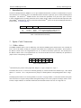
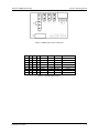
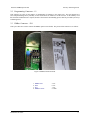
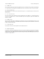
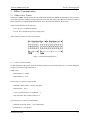
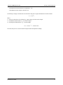
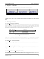
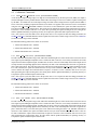
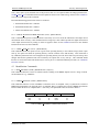
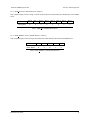
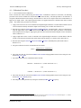
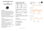
XS Series PMBus Option Card
XS S E RI ES
Document: 40110r03
Excelsys Technologies Ltd.
TM
PMB U S
TM
O PT I O N C A RD
1
XS Series PMBus Option Card
Excelsys Technologies Ltd.
Contents
1
Introduction
2
Option Card Connectors
2.1 PMBus Address . . . . . . . . .
2.2 Programming Connector - J1 . .
2.3 PMBus Connector - PL1 . . . .
2.3.1 PMBus Alert . . . . . .
2.3.2 SDA - Serial Data Line .
2.3.3 SCL - Serial Clock Line
2.3.4 PMBus Control . . . . .
2.3.5 GND - Signal GND . . .
2.4 Parallel Operation . . . . . . . .
4
.
.
.
.
.
.
.
.
.
4
4
6
6
7
7
7
7
7
7
3
PMBus Communication
3.1 PMBus Linear Format . . . . . . . . . . . . . . . . . . . . . . . . . . . . . . . . . . . . . . . . . .
3.1.1 Linear Format Decoding . . . . . . . . . . . . . . . . . . . . . . . . . . . . . . . . . . . . .
8
8
8
4
Supported Commands
4.1 Monitoring Commands . . . . . . . . . . . . . . . . . . . . . . . . . . . .
4.1.1 VOUT MODE (0x20) - [READ BYTE] . . . . . . . . . . . . . . .
4.1.2 READ VOUT (0x8B) - [READ WORD] . . . . . . . . . . . . . .
4.1.3 READ IOUT (0x8C) - [READ WORD] . . . . . . . . . . . . . . .
4.1.4 READ TEMPERATURE 1 (0x8D) - [READ WORD] . . . . . . .
4.2 Calibration Commands . . . . . . . . . . . . . . . . . . . . . . . . . . . .
4.2.1 VOUT SCALE MONITOR (0x2A) - [READ/WRITE WORD] . .
4.2.2 IOUT CAL GAIN (0x38) - [READ/WRITE WORD] . . . . . . . .
4.2.3 IOUT CAL OFFSET (0x39) - [READ/WRITE WORD] . . . . . .
4.2.4 STATUS MANUFACTURER SPECIFIC (0x80) - [READ BYTE] .
4.2.5 STORE USER ALL (0x15) - [SEND BYTE] . . . . . . . . . . . .
4.3 Identification Commands . . . . . . . . . . . . . . . . . . . . . . . . . . .
4.3.1 MFR REVISION (0x9B) - [READ BLOCK (8 Bytes)] . . . . . . .
4.3.2 PMBUS REVISION (0x9D) - [READ BYTE] . . . . . . . . . . .
4.3.3 MFR ID (0x99) - [READ BLOCK (8 Bytes)] . . . . . . . . . . . .
4.3.4 MFR MODEL (0x99) - [READ BLOCK (5 Bytes)] . . . . . . . . .
4.4 Calibration Procedure . . . . . . . . . . . . . . . . . . . . . . . . . . . . .
4.4.1 Current Measurement Calibration . . . . . . . . . . . . . . . . . .
4.4.2 Current Calibration Example . . . . . . . . . . . . . . . . . . . . .
4.4.3 Voltage Measurement Calibration . . . . . . . . . . . . . . . . . .
4.4.4 Voltage Calibration Example . . . . . . . . . . . . . . . . . . . . .
4.5 Packet Error Checking . . . . . . . . . . . . . . . . . . . . . . . . . . . .
5
.
.
.
.
.
.
.
.
.
.
.
.
.
.
.
.
.
.
.
.
.
.
.
.
.
.
.
.
.
.
.
.
.
.
.
.
.
.
.
.
.
.
.
.
.
.
.
.
.
.
.
.
.
.
.
.
.
.
.
.
.
.
.
.
.
.
.
.
.
.
.
.
.
.
.
.
.
.
.
.
.
.
.
.
.
.
.
.
.
.
.
.
.
.
.
.
.
.
.
.
.
.
.
.
.
.
.
.
.
.
.
.
.
.
.
.
.
.
.
.
.
.
.
.
.
.
.
.
.
.
.
.
.
.
.
.
.
.
.
.
.
.
.
.
.
.
.
.
.
.
.
.
.
.
.
.
.
.
.
.
.
.
.
.
.
.
.
.
.
.
.
.
.
.
.
.
.
.
.
.
.
.
.
.
.
.
.
.
.
.
.
.
.
.
.
.
.
.
.
.
.
.
.
.
.
.
.
.
.
.
.
.
.
.
.
.
.
.
.
.
.
.
.
.
.
.
.
.
.
.
.
.
.
.
.
.
.
.
.
.
.
.
.
.
.
.
.
.
.
.
.
.
.
.
.
.
.
.
.
.
.
.
.
.
.
.
.
.
.
.
.
.
.
.
.
.
.
.
.
.
.
.
.
.
.
.
.
.
.
.
.
.
.
.
.
.
.
.
.
.
.
.
.
.
.
.
.
.
.
.
.
.
.
.
.
.
.
.
.
.
.
.
.
.
.
.
.
.
.
.
.
.
.
.
.
.
.
.
.
.
.
.
.
.
.
.
.
.
.
.
.
.
.
.
.
.
.
.
.
.
.
.
.
.
.
.
.
.
.
.
.
.
.
.
.
.
.
.
.
.
.
.
.
.
.
.
.
.
.
.
.
.
.
.
.
.
.
.
.
.
.
.
.
.
.
.
.
.
.
.
.
.
.
.
.
.
.
.
.
.
.
.
.
.
.
.
.
.
.
.
.
.
.
.
.
.
.
.
.
.
.
.
.
.
.
.
.
.
.
.
.
.
.
.
.
.
.
.
.
.
.
.
.
.
.
.
.
.
.
.
.
.
.
.
.
.
.
.
.
.
.
.
.
.
.
.
.
.
.
.
.
.
.
.
.
.
.
.
.
.
.
.
.
.
.
.
.
.
.
.
.
.
.
.
.
.
.
.
.
.
.
.
.
.
.
.
.
.
.
.
.
.
.
.
.
.
.
.
.
.
.
.
.
.
.
.
.
.
.
.
.
.
.
.
.
.
.
.
.
.
.
.
.
.
.
.
.
.
.
.
.
.
.
.
.
.
.
.
.
.
.
.
.
.
.
.
.
.
.
.
.
.
.
.
.
.
.
.
.
.
.
.
.
.
.
.
.
.
.
.
.
.
.
.
.
.
.
.
.
.
.
.
.
.
.
.
.
.
.
.
.
.
Troubleshooting
10
10
10
10
10
10
11
11
11
11
12
12
12
12
12
13
13
14
14
15
16
17
17
17
List of Figures
1
2
3
4
PMBus Option Card Connections
PMBus Connector Pinout . . . . .
Linear Format Data Structure . . .
Two-point Calibration Procedure .
Document: 40110r03
.
.
.
.
.
.
.
.
.
.
.
.
.
.
.
.
.
.
.
.
.
.
.
.
.
.
.
.
.
.
.
.
.
.
.
.
.
.
.
.
.
.
.
.
.
.
.
.
.
.
.
.
.
.
.
.
.
.
.
.
.
.
.
.
.
.
.
.
.
.
.
.
.
.
.
.
.
.
.
.
.
.
.
.
.
.
.
.
.
.
.
.
.
.
.
.
.
.
.
.
.
.
.
.
.
.
.
.
.
.
.
.
.
.
.
.
.
.
.
.
.
.
.
.
.
.
.
.
.
.
.
.
.
.
.
.
.
.
.
.
.
.
.
.
5
6
8
15
2
XS Series PMBus Option Card
Excelsys Technologies Ltd.
List of Tables
1
2
3
4
5
6
7
8
Document Revision History . . . . . . . . . . .
Address Structure . . . . . . . . . . . . . . . .
Available Address Space . . . . . . . . . . . .
Command Table . . . . . . . . . . . . . . . . .
VOUT MODE Command Data Structure . . .
PMBUS REVISION Command Data Structure
MFR ID Command Data Structure . . . . . . .
MFR MODEL Command Data Structure . . .
Document: 40110r03
.
.
.
.
.
.
.
.
.
.
.
.
.
.
.
.
.
.
.
.
.
.
.
.
.
.
.
.
.
.
.
.
.
.
.
.
.
.
.
.
.
.
.
.
.
.
.
.
.
.
.
.
.
.
.
.
.
.
.
.
.
.
.
.
.
.
.
.
.
.
.
.
.
.
.
.
.
.
.
.
.
.
.
.
.
.
.
.
.
.
.
.
.
.
.
.
.
.
.
.
.
.
.
.
.
.
.
.
.
.
.
.
.
.
.
.
.
.
.
.
.
.
.
.
.
.
.
.
.
.
.
.
.
.
.
.
.
.
.
.
.
.
.
.
.
.
.
.
.
.
.
.
.
.
.
.
.
.
.
.
.
.
.
.
.
.
.
.
.
.
.
.
.
.
.
.
.
.
.
.
.
.
.
.
.
.
.
.
.
.
.
.
.
.
.
.
.
.
.
.
.
.
.
.
.
.
.
.
.
.
.
.
.
.
.
.
.
.
.
.
.
.
.
.
.
.
.
.
.
.
.
.
4
4
5
10
10
12
13
13
3
XS Series PMBus Option Card
1
Excelsys Technologies Ltd.
Introduction
The Power Management Bus (PMBusTM ) is an open standard which defines a means of communication for power
conversion devices. It defines a full set of commands and data structures required by power control and management
components. The XS SeriesTM PMBus interface card extends the capabilities of any XS Series power converter
to allow communication of operating parameters such as output voltage, output current and internal temperature with
other PMBusTM enabled devices. For more information about PMBusTM , please see the System Management Interface
Forum website www.PowerSIG.org.
Revision
00
01
02
Date
20.06.14
19.08.14
15.01.15
ECN #
n/a
E0560
E0584
Details
First Release
Update for new PCB layout and functions.
Added calibration functions.
Table 1: Document Revision History
2
Option Card Connectors
2.1 PMBus Address
The PMBus standard utilizes 7 bits for addressing. The XS Series PMBus option card allows the user to modify the
lower 3 bits of this address, leading to a fixed part of the address and a variable part of the address. The fixed part of
the address consists of the 4 most significant bits A6, A5, A4 and A3 and always equals 0010. The variable part of
the address consists of the 3 least significant bits A2, A1 and A0 and these bits can be modified by the placement of
jumpers on the corresponding 3 pin headers.
A6
0
A5
0
A4
1
A3
0
A2
A2∗
A1
A1∗
A0
A0∗
Table 2: Address Structure
∗
Determined by the position of the jumper link. Jumper in = logic 0; Jumper out = logic 1.
The address lines for A2, A1 and A0 are internally pulled up by resistors and therefore default to logic 1 (the default
address ⇒ = 0010111 = 0x17). The placement of a jumper on a header pulls the corresponding address line to a logic
0.
If multiple option cards are to be used in parallel (see section 2.4 on page number 7) on the same bus then each option
card will need to be assigned a unique address through the fitting of one or more jumpers according to Table 3 below.
In total, 8 unique addresses are available which limits the maximum amount of devices on a single bus to 8.
Document: 40110r03
4
XS Series PMBus Option Card
Excelsys Technologies Ltd.
Figure 1: PMBus Option Card Connections
A6
0
0
0
0
0
0
0
0
A5
0
0
0
0
0
0
0
0
A4
1
1
1
1
1
1
1
1
A3
0
0
0
0
0
0
0
0
A2
1 / OUT
1 / OUT
1 / OUT
1 / OUT
0 / IN
0 / IN
0 / IN
0 / IN
A1
1 / OUT
1 / OUT
0 / IN
0 / IN
1 / OUT
1 / OUT
0 / IN
0 / IN
A0
1 / OUT
0 / IN
1 / OUT
0 / IN
1 / OUT
0 / IN
1 / OUT
0 / IN
PMBus Address
0x17
0x16
0x15
0x14
0x13
0x12
0x11
0x10
Table 3: Available Address Space
Document: 40110r03
5
XS Series PMBus Option Card
Excelsys Technologies Ltd.
2.2 Programming Connector - J1
This connector is solely for the purpose of downloading of firmware to the option card. This will already have
been completed during factory assembly so this connector has no further use for the end user. In the unlikely event
that firmware modifications are required, details of the firmware downloading process shall be provided by Excelsys
Technologies Ltd.
2.3 PMBus Connector - PL1
This 8 pin connector is used to connect the PMBus option card to the bus. The pinout of this connector is as follows:
;
Figure 2: PMBus Connector Pinout
1. PMBus Alert.
2. SDA.
3. SCL.
4. PMBus Control.
Document: 40110r03
5. NC
6. NC
7. NC
8. GND
6
XS Series PMBus Option Card
Excelsys Technologies Ltd.
2.3.1 PMBus Alert
This is an optional output signal which allows a PMBus slave device to interrupt the host in response to status changes
etc. As this behaviour is not supported by the PMBus option card, it is unnecessary to make a connection to this pin.
2.3.2 SDA - Serial Data Line
This is the data line over which all serial communication takes place. It is essential that this pin is connected to the
PMBus SDA line.
2.3.3 SCL - Serial Clock Line
This is the clock line which synchronizes all serial communication over the PMBus. It is essential that this pin is
connected to the PMBus SCL line. The XS Series PMBus option card is designed to operate with a PMBus clock
frequency of 100KHz.
2.3.4 PMBus Control
This is an optional input signal on a PMBus device which allows to unit to be enabled/disabled in response to commands received over the serial bus. As the PMBus option card does not support any such commands, it is unnecessary
to make a connection to this signal.
2.3.5 GND - Signal GND
This should be connected to GND or Signal Return of the PMBus Host device.
2.4 Parallel Operation
It is possible to connect up to 8 PMBus option cards on the same bus for simultaneous communication with multiple
XS Series power converters from a single host. To do this, simply connect all required PMBus signals (i.e. SDA, SCL
& GND) in parallel. Each PMBus option card must then be assigned a unique address following the procedure shown
in section 2.1 on page number 4.
Document: 40110r03
7
XS Series PMBus Option Card
3
Excelsys Technologies Ltd.
PMBus Communication
3.1 PMBus Linear Format
The XS Series PMBus interface utilizes the linear data format defined in the PMBus Specification to represent voltage,
current and temperature readings. This format presents real world units (Amps, Volts, Degrees) to the host system in a
manner which is less computationally difficult for the host system than the alternative direct system.
The data returned consists of the following:
• An 11 bit, two’s complement mantissa.
• A 5 bit, two’s complement exponent (scaling factor).
These combine to form a two byte word as follows:
Figure 3: Linear Format Data Structure
3.1.1 Linear Format Decoding
To understand the decoding of the linear format data to obtain the real-world measurement, we will work through an
example of an output voltage measurement:
Sample Data:
• Returned Byte 1 = 0xDB
• Returned Byte 2 = 0x12
The first step is to extract the exponent data:
• 0xDB12 in binary format= 1101101100010010.
• Exponent bits = 11011
• 11011 converted from two’s complement = -5.
• The exponent in this example is therefore -5.
The second step is to extract the mantissa data:
• 0xDB12 converted to binary = 1101101100010010
• Mantissa bits = 01100010010
Document: 40110r03
8
XS Series PMBus Option Card
Excelsys Technologies Ltd.
• 01100010010 converted from two’s complement = 786.
• The Mantissa in this example is therefore 786.
The final step is simply to calculate the real world value using the two figures obtained above and the formula:
Y = X ∗ (2N )
Where:
Y = The real-world value to be calculated e.g. output voltage (in Volts) in this example.
X = The Mantissa obtained above e.g. 768 in this example.
N = The Exponent obtained above e.g. -5 in this example.
Vout = 768 ∗ (2−5 ) = 24.5625 Volt s
The exact same process is used to calculate output current and temperature readings.
Document: 40110r03
9
XS Series PMBus Option Card
4
Excelsys Technologies Ltd.
Supported Commands
The full list of commands currently supported by the XS Series PMBus interface are as follows:
Monitoring Commands
VOUT MODE (0x20)
READ VOUT (0x8B)
READ IOUT (0x8C)
READ TEMPERATURE 1 (0x8D)
Calibration Commands
VOUT SCALE MONITOR (0x2A)
IOUT CAL OFFSET (0x39)
IOUT CAL GAIN (0x38)
STORE USER ALL (0x15)
STATUS MFR SPECIFIC (0x80)
Identification Commands
PMBUS REVISION (0x98)
MFR ID (0x99)
MFR MODEL (0x9A)
MFR REVISION (0x9B)
Table 4: Command Table
Commands can return either: a BYTE, a WORD or a BLOCK (multiple bytes including a byte count) as indicated
below.
4.1 Monitoring Commands
4.1.1 VOUT MODE (0x20) - [READ BYTE]
The VOUT MODE command is used to obtain information about the format of voltage measurements which are
returned by a PMBusTM device if this information is not already known. The data returned from this command
consists of a single byte. The first three bits determine if the device is using the Linear, VID or direct modes for data
representation. The remaining five bits give additional information, depending on the data format.
Mode
Linear
VID
Direct
Bits [7:5]
000
001
010
Bits [4:0]
5 bit mantissa which is returned as part of the output voltage data.
VID Code Identifier
Always set to 00000.
Table 5: VOUT MODE Command Data Structure
For this device, the data format is fixed as linear mode with an exponent of -5 so the data returned by this command
shall always be 00011011 = 0x1B. Attempts to write to this parameter shall be negatively acknowledged (NACKed).
4.1.2 READ VOUT (0x8B) - [READ WORD]
This command returns an output voltage measurement (in Volts) formatted in linear format as described in section 3.1
on page 8.
4.1.3 READ IOUT (0x8C) - [READ WORD]
This command returns an output current measurement (in Amps) formatted in linear format as described in section 3.1
on page 8.
4.1.4 READ TEMPERATURE 1 (0x8D) - [READ WORD]
This command returns a temperature measurement (in degrees celsius) from the on-board temperature sensor of the
interface module. It is formatted in linear format as described in section 3.1 on page 8.
Document: 40110r03
10
XS Series PMBus Option Card
Excelsys Technologies Ltd.
4.2 Calibration Commands
4.2.1 VOUT SCALE MONITOR (0x2A) - [READ/WRITE WORD]
As the XS Series output voltage range is too high to be measured directly by the microprocessor (MPU), the output is
measured through a resistive potential divider which reduces the voltage to a lower level which is capable of being read
by the MPU. To calculate the real-world output voltage from this reduced voltage therefore requires that the MPU is
aware of the exact (including component tolerances) scale factor to be applied. This scale factor can be viewed/edited
using the VOUT SCALE MONITOR command. If issued as a read command, the option card shall return the two
byte linear formatted voltage scaling factor. This can be used to calibrate the output voltage measurement if required.
If issued as a write command, with one or two bytes data representing the required scaling factor, the scaling factor
shall be updated immediately in operating memory. If accepted, the option card shall respond with an ACK.
Note: After a power cycle, this shall revert to the previous value. If it is required to make the change permanent, the
STORE USER ALL command should be issued to update the value in non-volatile storage. Please see the Calibration
section for correct usage of this command.
Recommended starting points for this factor are as follows:
1. XS500-24N/XS1000-24N = 0xD968.
2. XS500-48N/XS1000-48N = 0xDA00.
3. XS200-36N/XS1000-36N = 0xDA0A.
4.2.2 IOUT CAL GAIN (0x38) - [READ/WRITE WORD]
In order to maximize the dynamic range of the ADC while minimizing the size of the current sense resistor, the current
sense signal is passed through an amplifier before it reaches the ADC. Therefore, to accurately calculate the real-world
output current from this amplified signal, the MPU must be aware of the exact relationship between the output current
in Amps and the corresponding digitized value returned by the ADC. This relationship takes the form of a gain factor
plus a small offset factor. The gain factor part can be edited/viewed using the IOUT CAL GAIN command. If issued
as a read command, the option card shall return the two byte linear formatted current scaling factor. This can be
used to calibrate the output current measurement if required. If issued as a write command, with one or two bytes
data representing the required scaling factor, the scaling factor shall be updated immediately in operating memory. If
accepted, the option card shall respond with an ACK.
Note: After a power cycle, this shall revert to the previous value. If it is required to make the change permanent, the
STORE USER ALL command should be issued to update the value in non-volatile storage. Please see the Calibration
section for correct usage of this command.
Recommended starting points for this factor are as follows:
1. XS500-24N/XS1000-24N = 0xB0C2.
2. XS500-48N/XS1000-48N = 0xB10E.
3. XS500-36N/XS1000-36N = 0xB086.
4.2.3 IOUT CAL OFFSET (0x39) - [READ/WRITE WORD]
In order to maximize the dynamic range of the ADC while minimizing the size of the current sense resistor, the current
sense signal is passed through an amplifier before it reaches the ADC. Therefore, to accurately calculate the real-world
output current from this amplified signal, the MPU must be aware of the exact relationship between the output current
in Amps and the corresponding digitized value returned by the ADC. This relationship takes the form of a gain factor
plus a small offset factor. The offset factor part can be edited/viewed using the IOUT CAL OFFSET command. If
issued as a read command, the option card shall return the two byte linear formatted current offset factor. This can
be used to calibrate the output current measurement if required. If issued as a write command, with one or two bytes
data representing the required offset factor, the offset factor shall be updated immediately in operating memory. If
accepted, the option card shall respond with an ACK.
Document: 40110r03
11
XS Series PMBus Option Card
Excelsys Technologies Ltd.
Note: After a power cycle, this shall revert to the previous value. If it is required to make the change permanent, the
STORE USER ALL command should be issued to update the value in non-volatile storage. Please see the Calibration
section for correct usage of this command.
Recommended starting points for this factor are as follows:
1. XS500-24N/XS1000-24N = 0xB10E.
2. XS500-48N/XS1000-48N = 0xB078.
3. XS500-36N/XS1000-36N = 0xB069
4.2.4 STATUS MANUFACTURER SPECIFIC (0x80) - [READ BYTE]
This is a manufacturer specific command which is used solely as a tool to aid in the calibration of the output current
measurement where necessary. This command returns a single byte value which represents the digital measurement
of the output current before any scaling or offsets are applied. Please see the Calibration section for more detailed
instructions on how to use this command.
4.2.5 STORE USER ALL (0x15) - [SEND BYTE]
This command instructs the option card to copy the entire operating memory to non-volatile storage (flash). Upon
start up, the option card loads the operating memory with the contents of the flash memory. This means that if
any calibration parameters have been changed in the operating memory since the device has been powered up, these
changes shall become permanent and will be loaded by the option card at every start up. This command should
therefore be used with caution and should only be used as part of a controlled calibration procedure (see Calibration
Procedure section).
4.3 Identification Commands
4.3.1 MFR REVISION (0x9B) - [READ BLOCK (8 Bytes)]
This command returns the revision of firmware which is running on the PMBus Option Card as a string of ASCII
encoded characters e.g. ”80002r02”.
4.3.2 PMBUS REVISION (0x9D) - [READ BYTE]
This command returns the revision of PMBus to which the device is compliant. Bits [7:5] indicate the revision of
PMBus Specification Part I to which the device is compliant. Bits [3:0] indicate the revision of PMBus Specification
Part II to which the device is compliant (Bit 4 = don’t care]). The permissible values are shown in Table 6.
Bits [7:5]
000
001
010
Part I Revision
1.0
1.1
1.2
Bit [4]
X
X
X
Bits [3:0]
0000
0001
0010
Part II Revision
1.0.
1.2.
1.2.
Table 6: PMBUS REVISION Command Data Structure
Document: 40110r03
12
XS Series PMBus Option Card
Excelsys Technologies Ltd.
4.3.3 MFR ID (0x99) - [READ BLOCK (8 Bytes)]
This command simply returns a string of ASCII encoded characters which identify the manufacturer of the PMBus
device.
HEX DATA
ASCII DATA
Byte 0
0x45
E
Byte 1
0x58
X
Byte 2
0x43
C
Byte 3
0x45
E
Byte 4
0x4c
L
Byte 5
0x53
S
Byte 6
0x59
Y
Byte 7
0x53
S
Table 7: MFR ID Command Data Structure
4.3.4 MFR MODEL (0x99) - [READ BLOCK (5 Bytes)]
This command simply returns a string of ASCII characters which identifies the model of the PMBus device.
HEX DATA
ASCII DATA
Byte 0
0x58
X
Byte 1
0x53
S
Byte 2
0x4F
O
Byte 3
0x4C
L
Byte 4
0x4F
O
Table 8: MFR MODEL Command Data Structure
Document: 40110r03
13
XS Series PMBus Option Card
Excelsys Technologies Ltd.
4.4 Calibration Procedure
4.4.1 Current Measurement Calibration
In the event that the values returned using the READ IOUT command are found to be inaccurate, the following
procedure can be used to calibrate the measurement for increased accuracy. The ideal procedure to be followed is a
two-point calibration which involves taking a measurement at a low level of output current and a measurement at a
high level of output current. The required gain and offset to be applied can then be calculated from these two data
points. 1 The details of the procedure are as follows:
1. Apply a low load of 10% or less of nominal to the output through an ammeter or current-shunt so that the current
can be measured externally. Record the output current reading. Let’s call this value ANALOG LOW .
2. Read one byte using the STATUS MANUFACTURER SPECIFIC command [0x80]. The byte returned represents the digital value of the output current measurement. This is the value used by the MCU to calculate the
actual output current in amps by applying the gain and offset associated with the amplifier circuit. Record this
value as DIGIT AL LOW .
3. Apply a high load of 90% or more of nominal to the output through an ammeter or current-shunt so that the
current can be measured externally. Record the output current reading. Let’s call this value ANALOG H IGH .
4. Read one byte using the STATUS MANUFACTURER SPECIFIC command [0x80]. Record this value as
DIGIT AL H IGH .
5. The gain coefficient can now be calculated from the formula:
GAIN =
ANALOG H I GH −ANALOG LOW
DIGIT AL H IGH − DIGIT AL LOW
6. This value must then be converted to PMBUS Linear Format and programmed into the device using the command IOUT CAL GAIN.
7. The offset coefficient can be calculated from the formula:
OF F SE T = ANALOG H IGH − (GAIN ∗ DIGIT AL H IGH )
OR
OF F SE T = ANALOG LOW − (GAIN ∗ DIGIT AL LOW )
8. This value must then be converted to PMBUS Linear Format and programmed into the device using the command IOUT CAL OFFSET [0x39].
9. The changes are made permanent by issuing the command STORE USER ALL [0x15].
1 A Microsoft Excel TM worksheet is available for download from the Excelsys website www.excelsys.com (“Technical Support” → “Calculators”) to automatically calculate the calibration coefficients from two given data points.
Document: 40110r03
14
XS Series PMBus Option Card
Excelsys Technologies Ltd.
4.4.2 Current Calibration Example
Sample output current calibration for XS1000-24N:
1. Applied load = 1A. Iout measured with ammeter = 1.022A ⇒ ANALOG LOW = 1.022.
2. STATUS MANUFACTURER SPECIFIC returned 0x04 ⇒ DIGIT AL LOW = 4.
3. Applied load = 40A. Iout measured with ammeter = 40.062A ⇒ ANALOG H IGH = 40.062.
4. STATUS MANUFACTURER SPECIFIC returned 0xD2 (210 decimal) ⇒ DIGIT AL H IGH = 210.
5. The Gain coefficient is calculated:
GAIN =
40.062 −1.022
210 − 4
= 0.1895
6. Converted to linear (-10 Exponent) = 0xB0C2 ⇒ IOUT CAL GAIN = 0xB0C2.
7. The Offset coefficient is calculated:
OF F SE T = 40.062 − (0.1895 ∗ 210) = 0.267
8. Converted to linear (-10 Exponent) = 0xB111 ⇒ IOUT CAL OFFSET = 0xB111.
Output
Current
(Amps)
Calibration point 2 (x2,y2) =
HIGH, ANALOG_HIGH)
(DIGITAL_
OFFSET
= y1 - (Slope * x1)
GAIN = Slope
= y2-y1
x2-x1
OR
y2 - (Slope * x2
Calibration point 1 (x1,y1) =
(DIGITAL_LOW, ANALOG_LOW)
0
0
STATUS_MANUFACTURER_SPECIFIC
(DIGITAL IOUT STATUS)
255
Figure 4: Two-point Calibration Procedure
Document: 40110r03
15
XS Series PMBus Option Card
Excelsys Technologies Ltd.
4.4.3 Voltage Measurement Calibration
In the event that the values returned using the READ VOUT command are found to be inaccurate, the following
procedure can be used to calibrate the measurement for increased accuracy. The procedure to be followed is a simple
one point calibration procedure which involves taking one external output voltage measurement and reading a couple of
values from the unit in order to calculate the exact scaling factor to be applied to bring the output voltage measurement
within range. 2 The details of the procedure are as follows:
1. Power up the unit and measure the output voltage at the output terminals using a Voltmeter. Record this value
as VOU T −ACT UAL .
2. Read one word from the device using the command READ VOUT [0x8B]. Convert this linear-mode word to
real-world voltage and record this value as VOU T −PMBU S . This is the actual output voltage being reported over
the PMBusTM . We will compare this to the actual output voltage and use it calculate the required scaling factor.
3. Read one word from the device using the command VOUT SCALE MONITOR [0x2A]. Convert this linearmode word to real-world gain and record this value as V OU T SCALE MONIT OROLD . This tells us the current
scaling factor which is being applied.
4. The new scaling factor can now be calculated :
First, calculate the actual voltage present on the ADC for the current output voltage:
V
SE N SE
=
VOU T −PMBU S
V OU T SCALE MONIT OROLD
Now calculate the scaling factor which is required by dividing the actual output voltage (VOU T −ACT UAL ) by the
voltage seen by the ADC (VSE N SE ):
SCALE − FACT OR = VOU T −ACT U AL
VSE N SE
5. This scale factor must then converted to a linear-mode word and written to the unit using the command
VOUT SCALE MONITOR [0x2A].
6. The change is made permanent by issuing the command STORE USER ALL [0x15].
2 A Microsoft Excel TM worksheet is available for download from the Excelsys Technologies Ltd. website www.excelsys.com (“Technical
Support” → “Calculators”) to automatically calculate the scaling factor from the given data.
Document: 40110r03
16
XS Series PMBus Option Card
Excelsys Technologies Ltd.
4.4.4 Voltage Calibration Example
Sample output voltage calibration for XS1000-24N:
1. VOU T −ACT UAL measured with voltmeter = 24.050 V
2. VOU T −PMBU S returned = 0xDA68 = 19.25 V
3. V OU T SCALE MONIT OROLD returned = 0xD920 = 9.0
4. The required scale factor is calculated:
VSE N SE =
19.25V
= 2.139V
9.0
SCALE− FACT OR =
24.05V
= 11.244
2.139V
5. 11.244 converted to linear-mode = 0xE0B4 ⇒ VOUT SCALE MONITOR = 0xE0B4
4.5 Packet Error Checking
Packet Error Checking (PEC) is an optional feature of SMBus/PMBus in which an error code byte is appended to each
transaction. The PMBus option card is designed to operate without PEC so this feature should be disabled if present
on the PMBus host device.
5
Troubleshooting
No data is returned from the PMBus option card in response to issued commands (i.e. no ACK or NACK):
1. Check that the address which the PMBus host is trying to communicate with has been correctly programmed
on the PMBus option card according to the procedure in section 2.1 on page 4. The simplest configuration
is obtained by ensuring all 3 links are removed which will guarantee an address of 0x17 (hexadecimal) or 23
(decimal).
2. Verify that the signals SDA, SCL and GND have been correctly connected to the PMBus host.
3. Verify that the PMBus host device is not configured to use Packet Error Checking (PEC) as this is unsupported
by the PMBus option card. Note: PMBus compliant master devices are required to be able to auto-detect the
PEC status and act accordingly however some SMBus/PMBus interface GUIs have the option to fix the PEC
mode which would cause communication failure.
4. Verify that the PMBus host device is configured to use a bus speed of 100KHz.
5. Verify that the PMBus host device is configured to pull up the signals SDA and SCL.
The returned output voltage and/or current measurements are very inaccurate:
1. See the Calibration Procedure section for instructions on how to calibrate the output measurements.
For other support options, please visit
Document: 40110r03
www.excelsys.com.
17