1
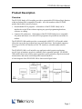
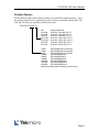
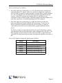
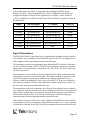
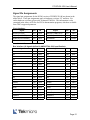
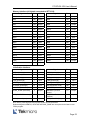
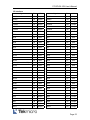
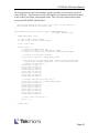
FastPack Products
FP-DFLEX-10K
Customizable FLEX10K I/O Module
User’s Manual
TEK/TM-250B
September 2001
FP-DFLEX-10K User’s Manual
TEK Microsystems has made every effort to ensure that this manual is accurate and complete.
However, TEK reserves the right to make changes and improvements to the products described
in this manual at any time and without notice.
This product is covered by a limited warranty which is described in the manual. Other than the
stated limited warranty, TEK disclaims all other warranties, including the warranties of
merchantability and of fitness for a particular purpose. In the event of a failure of the hardware
or software described in this manual, TEK’s obligation is limited to repair or replacement of the
defective item, or, if the item cannot be repaired or replaced, a refund of the purchase price for
the item. TEK assumes no liability arising out of the application or use of the hardware or
software, and assumes no responsibility for direct, indirect, incidental or consequential damages
of any kind.
The electronic equipment described in this manual generates, uses, and can radiate radio
frequency energy. Operation of this equipment in a residential area is likely to cause radio
interference, in which case the user, at his own expense, will be required to take whatever
measures may be required to correct the interference.
TEK Microsystems’ products are not authorized for use as critical components in life support
devices or systems without the express written agreement of an officer of TEK Microsystems.
This manual is Copyright © 1997-2001, TEK Microsystems, Incorporated. All Rights Reserved.
FastPack is a trademarks of TEK Microsystems, Incorporated.
IndustryPack is a registered trademark of GreenSpring Computers, Inc.
Altera, MAX+Plus II and FLEX10K are trademarks of Altera Corporation.
Other trademarks and registered trademarks used are owned by their respective manufacturers.
Revision Information:
This manual describes hardware revisions “D” and later of the FP-DFLEX-10K. For earlier
hardware revisions, please refer to manual TM250A.
Document ordering code and release information:
URL: http://www.tekmicro.com/tm250b.pdf
TEK/TM-250B
Released September 2001
FP-DFLEX-10K User’s Manual
Table of Contents
Product Description ......................................................................................................1
Overview ................................................................................................................................... 1
Product Options......................................................................................................................... 2
Organization ..................................................................................................................3
Specifications & Support Information .........................................................................4
Performance Specifications....................................................................................................... 4
Warranty Information................................................................................................................ 5
Contact Information .................................................................................................................. 5
I/O Interface ...................................................................................................................6
I/O Pinout .................................................................................................................................. 6
Signal Configurations ............................................................................................................... 7
Signal Functions........................................................................................................................ 8
Signal Terminations ................................................................................................................ 10
IP Logic Interface ........................................................................................................12
Operating Modes..................................................................................................................... 12
Compliant FPGA Programs .................................................................................................... 13
Configuration Options............................................................................................................. 14
Download Sequence - Compliant FPGA Programs ................................................................ 16
Download Sequence - Non-Compliant FPGA Programs ........................................................ 17
ID Space - Controller .............................................................................................................. 18
I/O Space - Controller ............................................................................................................. 20
ID Register (Offset 0x00 D[7:0]) ..................................................................................... 20
Revision Register (Offset 0x01 D[7:0]) ........................................................................... 21
Initialization Control Register (Offset 0x02 D[7:0])........................................................ 21
Initialization Status Register (Offset 0x03 D[7:0]) .......................................................... 22
Initialization Data Register (Offset 0x04 D[7:0]) ............................................................ 22
I/O Space - FPGA ................................................................................................................... 23
Interrupt Space ........................................................................................................................ 23
DMA I/O Space....................................................................................................................... 23
Memory Space ........................................................................................................................ 23
Error Conditions...................................................................................................................... 23
Internal Architecture ...................................................................................................24
Overview ................................................................................................................................. 24
Clock Interface ........................................................................................................................ 26
Bus Interface ........................................................................................................................... 27
Memory Interface.................................................................................................................... 28
Initialization Interface ............................................................................................................. 28
I/O Interface ............................................................................................................................ 30
Signal Pin Assignments........................................................................................................... 31
Optional Accessories ..................................................................................................34
FP-DFLEX-10K User’s Manual
Appendix A: Clock Synthesizer Programming ..........................................................35
Appendix B: Non-Standard IP Clock Frequencies ....................................................39
Appendix C: Data Sheets ............................................................................................40
FP-DFLEX-10K User’s Manual
Product Description
Overview
The FP-FLEX family of I/O modules provides a customizable FPGA-based logic function
within an IndustryPack-compatible IP module. All of the members of the FP-FLEX
product family share some key features:
•
Downloadable FPGA programs. All members of the FP-FLEX family can be
initialized over the IP bus without requiring any special programming hardware,
software, or cabling.
•
Common I/O architecture. All members of the FP-FLEX family have a compatible
I/O pinout and feature set to allow FPGA programs to be ported from one model to
another.
The FP-DFLEX-10K module provides a customizable ANSI/VITA 4 IP module which
allows the user to develop custom logic in a small form factor. Each module supports a
mix of up to 24 EIA-485 interfaces or 48 TTL interfaces, selectable under software
control.
The FP-DFLEX-10K is well suited for any application which requires applicationspecific logic at hardware speeds in an Industry Pack compatible package. FP-DFLEX10K modules have been used for pattern generators, pulse generators, edge detection and
measurement, and various serial and parallel custom interfaces.
A block diagram of the FP-DFLEX-10K is shown in the figure below.
Page 1
FP-DFLEX-10K User’s Manual
Product Options
The FP-DFLEX-10K product family includes several different ordering options. All of
the options listed below are supported, but only a subset of available options (PIO, FIO0/48 and FIO-24/0) are typically available from stock.
FP-DFLEX–device–i/o
PIO
FIO-0/48
FIO-4/40
FIO-8/32
FIO-12/24
FIO-16/16
FIO-20/8
FIO-24/0
Programmable I/O
Fixed I/O, 0 EIA-485, 48 TTL
Fixed I/O, 4 EIA-485, 40 TTL
Fixed I/O, 8 EIA-485, 32 TTL
Fixed I/O, 12 EIA-485, 24 TTL
Fixed I/O, 16 EIA-485, 16 TTL
Fixed I/O, 20 EIA-485, 8 TTL
Fixed I/O, 24 EIA-485, 0 TTL
10K20
EPF10K20RC240-3 [obsolete]
10K50
EPF10K50RC240-3 [obsolete]
10K70
EPF10K70RC240-3 [obsolete]
10K30A
EPF10K30AQC240-3
10K50V
EPF10K50VRC240-3
10K50E
EPF10K50EQC240-3
10K100E
EPF10K100EQC240-3
10K130E
EPF10K130EQC240-3
10K200S
EPF10K200SRC240-3
[alternate speed grades available by special order]
Page 2
FP-DFLEX-10K User’s Manual
Organization
This User’s Manual is divided into the following sections:
•
Specifications and Warranty/Support Information. This section outlines the
FP-DFLEX-10K specifications and provides information about the warranty and
technical support programs.
•
I/O Interface. This section defines the I/O interface for the FP-DFLEX-10K.
FP-DFLEX-10K models may be ordered with either the Programmable I/O (PIO) or
Fixed I/O (FIO) architecture. Both architectures have compatible I/O pinouts with
different I/O interface capabilities. The FPGA device program determines the
functions performed by the I/O signals.
•
IP Logic Interface and Programming Information. This section defines the generic
control and status registers that are present in all FP-DFLEX-10K models. This
includes information about how to download a logic program to the FPGA device.
•
Internal Architecture. This section defines the internal clock and control signal
architecture. This section is primarily of interest if you are developing a custom logic
program for a FP-DFLEX-10K module.
Each off-the-shelf FPGA program includes documentation that defines the programming
interface to the FPGA and the functions of the various I/O signals.
Page 3
FP-DFLEX-10K User’s Manual
Specifications & Support Information
Performance Specifications
Clock Speed
8 or 32 MHz; wait states determined by FPGA
ID Space
Supported per ANSI/VITA 4-1995 specification,
Format I
I/O Space
Byte and word accesses supported per ANSI/VITA
4-1995 specification
Memory Space
Byte and word accesses supported per ANSI/VITA
4-1995 specification
Interrupt Capability
Interrupt requests 0 and 1 supported; function
determined by FPGA
DMA Capability
DMA request levels 0 and 1 supported; function
determined by FPGA
Mechanical
Type I IP module per ANSI/VITA 4-1995
specification
Operating Temperature
0 to 70 degrees C.
Storage Temperature
-40 to +85 degrees C.
Page 4
FP-DFLEX-10K User’s Manual
Warranty Information
The FP-DFLEX-10K is warranted against defects in material or workmanship for a period
of three years from the original date of purchase. If a failure occurs within the warranty
period, TEK will repair or replace the product at no cost to the user. For warranty repair,
please contact TEK as described below and obtain an RMA number and return shipping
instructions.
Contact Information
If technical support or repair assistance is required, please contact TEK through one of
the following methods:
Internet
http://www.tekmicro.com
Email
[email protected]
Telephone
+1 781 270 0808
Facsimile
+1 781 270 0813
Mail
TEK Microsystems, Incorporated
One North Avenue
Burlington, MA 01803-3313
Page 5
FP-DFLEX-10K User’s Manual
I/O Interface
I/O Pinout
The FP-DFLEX-10K external interface consists of the signals listed below:
Signal Name
I/O Pin
Signal Name
I/O Pin
A[1]
1
B[13]
26
B[1]
2
A[14]
27
A[2]
3
B[14]
28
B[2]
4
A[15]
29
A[3]
5
B[15]
30
B[3]
6
A[16]
31
A[4]
7
B[16]
32
B[4]
8
A[17]
33
A[5]
9
B[17]
34
B[5]
10
A[18]
35
A[6]
11
B[18]
36
B[6]
12
A[19]
37
A[7]
13
B[10]
38
B[7]
14
A[20]
39
A[8]
15
B[20]
40
B[8]
16
A[21]
41
A[9]
17
B[21]
42
B[9]
18
A[22]
43
A[10]
19
B[22]
44
B[10]
20
A[23]
45
A[11]
21
B[23]
46
B[11]
22
A[24]
47
A[12]
23
B[24]
48
B[12]
24
Reserved
49
A[13]
25
GND
50
The I/O Pin column shows the pin numbers on the IP I/O connector. These pin numbers
typically correspond directly to the IP carrier’s external interface connector pin numbers.
For example, a Motorola MVME162 VMEbus carrier maps each IP module’s 50 I/O pins
to a 2x25 header connector with the same pin numbering as the IP I/O connector.
Page 6
FP-DFLEX-10K User’s Manual
Signal Configurations
FP-DFLEX-10K modules are available with two different types of I/O functions. The
first type of function, “Programmable I/O”, may be configured for single-ended or
differential operation under FPGA control. The Programmable I/O functions use EIA485 transceivers but are not compatible with the full common-mode voltage range of
EIA-485 due to the presence of the programmable single-ended circuitry on the I/O
signals.
The second type of I/O function, “Fixed I/O”, is configured at the factory for either EIA485 or TTL operation in blocks of 8 lines. The EIA-485 interfaces are completely
compatible with all EIA-485 requirements, including common mode voltage range. All
EIA-485 receivers have 100 Ω (nominal) termination resistors that can be dynamically
connected or disconnected, under FPGA or host control.
The supported ordering codes are shown below:
Suffix
Description
-PIO
Programmable I/O. Each 4 pair group of the 24 A/B pairs may be
configured by the FPGA as four bidirectional differential signals or as
eight bidirectional single-ended TTL signals.
-FIO-0/48
Fixed I/O. No EIA-485 signals, 48 bidirectional TTL signals.
-FIO-4/40
Fixed I/O. 4 bidirectional EIA-485 signals, 40 bidirectional TTL signals.
-FIO-8/32
Fixed I/O. 8 bidirectional EIA-485 signals, 32 bidirectional TTL signals.
-FIO-12/24
Fixed I/O. 12 bidirectional EIA-485 signals, 24 bidirectional TTL signals.
-FIO-16/16
Fixed I/O. 16 bidirectional EIA-485 signals, 16 bidirectional TTL signals.
-FIO-20/8
Fixed I/O. 20 bidirectional EIA-485 signals, 8 bidirectional TTL signals.
-FIO-24/0
Fixed I/O. 24 bidirectional EIA-485 signals, no TTL signals.
Page 7
FP-DFLEX-10K User’s Manual
Signal Functions
The FP-DFLEX-10K I/O signals consist of 24 external signal pairs, designated A[1:24]
and B[1:24]. The I/O functions are controlled by three signals (DE, DO and RI) for each
A/B signal pair and a S485 signal for each group of four A/B pairs.
A block diagram of a single A/B pair is shown below:
MAX1484
DE[x]
A[x]
EXTERNAL I/O
DO[x]
B[x]
nS485
RI[x]
TERMINATION
CONTROL
S485
IDT74FST3245
MAX335
Each S485 signal has a corresponding nS485 signal which must always be set as the
inversion of the S485 signal.
The I/O functions are implemented with the following devices:
•
Maxim EIA-485 Transceiver, p/n MAX1484, used for EIA-485 interfacing.
•
Maxim Octal SPST Switch, p/n MAX335, used for EIA-485 termination.
•
IDT Octal Bus Switch, p/n IDT74FST3245, used for TTL signal connections.
Copies of the data sheets for the above devices are included in Appendix C.
Page 8
FP-DFLEX-10K User’s Manual
The I/O control logic is as follows:
•
If the S485 signal for a signal group [x:y] is low, the signal group is configured as
eight bidirectional TTL signals. In this case, the DO[x:y] signals are connected to
A[x:y], the RI[x:y] signals are connected to B[x:y], and the DE[x:y] signals should be
low. The switching between A/B and DO/RI is performed using bidirectional bus
switches, so the FPGA program may configure DO[x:y] and RI[x:y] as any
combination of input or output signals, with output signals being either standard TTL,
open drain, open source, or tristated depending on the FPGA program.
•
If the S485 signal for a signal group [x:y] is high, the interface provides four
bidirectional differential signals with EIA-485 characteristics. In this case, the
DO[x:y] signals are connected to the EIA-485 drivers, the RI[x:y] signals are
connected to the EIA-485 receivers and the DE[x:y] signals enable the EIA-485
drivers.
The DO[x:y] signals are outputs from the FPGA; the state of each DO[x:y] signal is
only significant if the associated DE signal is high, enabling the EIA-485 driver. The
RI[x:y] signals are inputs to the FPGA; the state of each RI[x:y] signal reflects the
current EIA-485 input state of the associated A/B signal pair regardless of the state of
DE.
The six S485 signals are mapped to signal groups as follows:
S485[x]
Description
S485[1]
Controls A[1:4] and B[1:4]
S485[2]
Controls A[5:8] and B[5:8]
S485[3]
Controls A[9:12] and B[9:12]
S485[4]
Controls A[13:16] and B[13:16]
S485[5]
Controls A[17:20] and B[17:20]
S485[6]
Controls A[21:24] and B[21:24]
Page 9
FP-DFLEX-10K User’s Manual
In all configurations, the FPGA is responsible for controlling the S485[1:6] and
nS485[1:6] signals. In the Programmable I/O (“PIO”) configuration, the FPGA may
configure the signals as desired for the application’s I/O interface. In the Fixed I/O
(“FIO”) configuration, the FPGA should always drive the S485[1:6] signals as shown in
the table below.
Model
EIA-485 Signals
TTL Signals
S485[1:6]
PIO
Programmable
Programmable
Programmable
FIO-0/48
None
A[1:24] and B[1:24]
000000
FIO-4/40
A[1:4] and B[1:4]
A[5:24] and B[5:24]
100000
FIO-8/32
A[1:8] and B[1:8]
A[9:24] and B[9:24]
110000
FIO-12/24
A[1:12] and B[1:12]
A[13:24] and B[13:24]
111000
FIO-16/16
A[1:16] and B[1:16]
A[17:24] and B[17:24]
111100
FIO-20/8
A[1:20] and B[1:20]
A[21:24] and B[21:24]
111110
FIO-24/0
A[1:24] and B[1:24]
None
111111
Signal Terminations
The FP-DFLEX-10K I/O signal pairs have a programmable termination resistor between
each A/B pair. The termination resistor should be turned on for EIA-485 signals that are
at the endpoint of the signal cabling and turned off otherwise.
The termination resistors are implemented using Maxim MAX335 switches, which have
an “on” resistance between 100 and 150 Ohms. The termination resistors are controlled
using a three wire serial interface, consisting of TR_CLK (clock), TR_DATA (data) and
TR_nCS (chip select).
The termination resistor interface is directly controlled by the FPGA, making the details
of the interface up to the user FPGA program. The simplest method of control is for the
user FPGA program to provide three control bits in a control register and to use a
software routine to download the 24-bit value to the MAX335s. If the user would like a
more automated method, TEK has a macrofunction available which accepts a clock, 24bit value and a start signal and downloads the value.
The termination resistors are connected to the A/B pairs in an arbitrary order to optimize
trace lengths on the printed circuit board. If the termination resistors are being configured
under software control, the user will need to rearrange the bit sequence as the 24 bits are
downloaded to the MAX335s. The software routine shown on the following page
demonstrates the download algorithm and the required bit order.
If the software routine is called with a ‘value’ argument of 0x000001 the result would be
to turn on the A[1] to B[1] termination resistor and turn all others off; a ‘value’ argument
of 0x800000 would turn on the A[24] to B[24] termination resistor and turn all others off.
Page 10
FP-DFLEX-10K User’s Manual
TEK’s hardware macrofunction for configuration of the termination resistors performs
the bit sequence rearrangement automatically as a part of the download function.
Upon power-up, the MAX335s are guaranteed to be in the off condition.
static RESULT tekfp_dflex10k_set_term (TEKFP_HANDLE fph, WORD32 value)
{
TEKFP_DFLEX10K_GENERIC_IOREG ioreg_fpga;
static const int term_lookup[] = {
11, 12, 9, 8, 23, 21, 18, 10, 16, 3, 20, 2,
0, 1, 15, 13, 22, 7, 17, 6, 4, 14, 5, 19
};
int i;
if (fph == NULL) return (FAIL);
if (fph->ioptr == NULL) return (FAIL);
ioreg_fpga = fph->ioptr;
if (ioreg_fpga->rev.reg.w & CTLR_REV_IS_EPLD) return (FAIL);
ioreg_fpga->cr1.reg.w &= ~FPGA_CR1_TR_DATA;
ioreg_fpga->cr1.reg.w &= ~FPGA_CR1_TR_CLK;
ioreg_fpga->cr1.reg.w &= ~FPGA_CR1_TR_nCS;
for (i = 0; i < 24; i++) {
if (value & (1 << term_lookup[i]))
ioreg_fpga->cr1.reg.w |= FPGA_CR1_TR_DATA;
else ioreg_fpga->cr1.reg.w &= ~FPGA_CR1_TR_DATA;
ioreg_fpga->cr1.reg.w;
ioreg_fpga->cr1.reg.w;
ioreg_fpga->cr1.reg.w;
ioreg_fpga->cr1.reg.w |= FPGA_CR1_TR_CLK;
ioreg_fpga->cr1.reg.w;
ioreg_fpga->cr1.reg.w;
ioreg_fpga->cr1.reg.w;
ioreg_fpga->cr1.reg.w &= ~FPGA_CR1_TR_CLK;
}
ioreg_fpga->cr1.reg.w &= ~FPGA_CR1_TR_DATA;
ioreg_fpga->cr1.reg.w |= FPGA_CR1_TR_nCS;
return (OK);
}
Page 11
FP-DFLEX-10K User’s Manual
IP Logic Interface
Operating Modes
The FP-DFLEX-10K controller has four operating modes which determine the
configuration state of the FPGA and whether the EPLD controller or the FPGA responds
to IP bus cycles.
The operating modes are:
•
Reset. This is the mode after power-up initialization and is usually the mode after an
IP bus reset. In Reset mode, the EPLD controller has control of the IP bus and the
FPGA is held in the uninitialized condition (nCONFIG asserted low). All external
I/O signals are tristated.
The host typically uses Reset mode to restart the FPGA and then switches to Config
mode to download an FPGA program image to the FPGA.
•
Config. In Config mode, the EPLD controller has control of the IP bus and the FPGA
is ready to accept programming information from the IP bus.
The host uses Config mode to download an FPGA program image to the FPGA.
When the download is completed, the FPGA will assert CONF_DONE and the EPLD
controller will automatically switch to either Idle or User mode depending on the state
of the Auto-User-Start configuration bit (ICR[02]).
•
Idle. In Idle mode, the EPLD controller has control of the IP bus and the FPGA is
configured and running. Idle mode is only supported with a compliant FPGA
program; the definition of a compliant FPGA is outlined below.
If the FPGA is compliant, the host will typically not use the Auto-User-Start bit and
allow the EPLD controller to switch to Idle mode after the FPGA program image has
been downloaded. The host can then verify that CONF_DONE is asserted and that
nSTATUS is not asserted, configure any desired modes in the ICR register, and then
switch to User mode under host control.
•
User. In User mode, the EPLD controller has relinquished control of the IP bus to the
FPGA and the user FPGA program is configured and running.
Page 12
FP-DFLEX-10K User’s Manual
The current mode determines the state of several internal signals as shown in the table
below.
Mode
IP Bus Cycles
nCONFIG
CS
nCS
Reset
All cycles under EPLD control
Low; forces FPGA into
initialization mode
High
Low
Config
All cycles under EPLD control
High
High
Low
Idle
All cycles under EPLD control
High
Low
CLKFAST
User
All cycles under FPGA control;
ID cycles handled by EPLD if
Disable-ID-Cycles
configuration bit is low.
High
High
CLKFAST
CLKFAST: Low for 8 MHz IP clock, high for 32 MHz IP clock.
Compliant FPGA Programs
To be considered “compliant” for the purposes of the discussion in the manual, an FPGA
program is required to:
•
Monitor the CS input and disable IP bus cycles and tristate all IP bus control outputs
when the CS input is low.
•
Implement a read-only ID register at offset zero. The ID register may contain any
value selected by the user.
•
Implement a read-only or read-write revision register at offset one. The revision
register may contain any value selected by the user provided that the 0x0080 bit is not
set.
Most of these functions are built into TEK’s IP bus interface macrofunction; user FPGA
programs which use TEK’s macrofunction for the IP bus interface are automatically
compliant FPGA programs.
Page 13
FP-DFLEX-10K User’s Manual
Configuration Options
The FP-DFLEX-10K EPLD controller has several configuration control bits which
determine how the EPLD controller interacts with the FPGA and the IP bus. The control
bits are designed to accommodate the widest possible range of user FPGA programs,
including “legacy” designs from other applications.
Through configuration options, the host can configure how the FP-DFLEX-10K handles
reset conditions, whether the EPLD or FPGA responds to ID cycles, and whether to
enable a “back door” to return control of the IP bus to the EPLD.
All of the configuration control bits must be configured by the host before the FPDFLEX-10K enters User mode. Once the module is in User mode, the EPLD ICR
register is no longer directly accessible because the FPGA has control of the IP bus.
The configuration options are:
•
Auto-User-Start (ICR[2]). The EPLD controller automatically leaves Config mode
when a rising edge on CONF_DONE is detected, which happens after the last byte of
FPGA configuration information is written by the host. The mode that the EPLD
controller changes to is controlled by the Auto-User-Start bit; if the bit is set, the
EPLD controller will change to User mode and if the bit is cleared the EPLD
controller will change to Idle mode.
If the FPGA is compliant, it will monitor the CS signal and ignore IP bus cycles and
tristate IP bus control signals if CS is low. A compliant FPGA is compatible with
both Idle and User modes because it allows the EPLD controller, through the CS
signal, to dynamically enable or disable FPGA control of the IP bus.
If the FPGA is not compliant, it is not required to monitor the CS signal and may
assume that it always has control of the IP bus after initialization. Because a noncompliant FPGA provides no mechanism to arbitrate control of the IP bus, the EPLD
controller must transition from Config to User mode to avoid bus contention between
the FPGA program and the EPLD controller.
This bit should be set if the FPGA program is non-compliant.
•
No-Clear-FPGA (ICR[3]). If this bit is cleared, the EPLD controller enters the Reset
mode after an IP bus reset. This has the side effect of asserting the FPGA nCONFIG
signal which places the FPGA device into initialization mode, clearing the existing
FPGA program image and tristating all I/O signals. If this bit is set, the EPLD
controller enters either Idle or User mode after an IP bus reset.
Typically, the host will always reinitialize all hardware and reload the FPGA program
image after a system or IP bus reset. If this bit is set, the FPGA program will continue
running after an IP bus reset. This is provided for applications that either need to
continue operation after an IP bus reset or which need to perform a controlled
shutdown under FPGA control.
Page 14
FP-DFLEX-10K User’s Manual
•
No-Set-Idle (ICR[4]). This bit is only significant if the No-Clear-FPGA is set. If the
No-Clear-FPGA bit is set and the No-Set-Idle bit is set, the EPLD controller will
remain in the current mode after an IP bus reset. If the No-Clear-FPGA bit is set and
the No-Set-Idle bit is cleared, the EPLD controller will enter Idle mode after an IP bus
reset. This bit should be set if the FPGA program is non-compliant.
•
Disable-ID-Space (ICR[5]). This bit controls whether the EPLD controller or the
FPGA responds to ID cycles in User mode. The EPLD controller always responds to
ID cycles in non-User modes.
If this bit is cleared, the EPLD controller monitors the IP bus and dynamically
switches from FPGA to EPLD control of the IP bus to respond to ID cycles. This
allows the FPGA program to avoid the need for supporting ID cycles, and also
ensures that a consistent set of ID data is provided before and after FPGA
initialization.
If this bit is set, the EPLD controller ignores ID cycles in User mode. The FPGA may
or may not respond to ID cycles depending on the user’s application requirements.
This bit should be set if the FPGA program is non-compliant.
•
Disable-Back-Door (ICR[6]). This bit controls whether a write to I/O register zero
with a value of 0xXX4A causes the EPLD controller to switch from User to Idle
mode. This “back door” may be used to regain control from the FPGA program after
entering User mode.
If this bit is cleared, the EPLD controller monitors the IP bus and switches from User
to Idle mode when an IP I/O write cycle is detected to address zero with D[7:0] equal
to 0x4A. If this bit is set, the EPLD controller never switches from User to Idle
mode, except possibly through an IP bus reset.
If the user FPGA program is compliant, register zero contains a read-only ID value for
the FPGA. This makes a write to register zero a “safe” back door because the host
would have no reason to perform this operation.
If the user FPGA program uses register zero as a read/write register or if otherwise
non-compliant, this bit should be set to disable the back door function.
All of the configuration bits are controlled through the ICR register. The ICR register is
guaranteed to power up in the cleared state, but is not modified by an IP bus reset. The
host software should set the ICR register to the desired state as a part of module
initialization.
Note that if the No-Clear-FPGA, No-Set-Idle and Disable-Back-Door bits are all set,
there is no method to leave User mode other than powering down the FP-DFLEX-10K
module.
Page 15
FP-DFLEX-10K User’s Manual
Download Sequence - Compliant FPGA Programs
The following download sequence may be used to initialize the FP-DFLEX-10K module
and download the user FPGA program when the program is compliant:
1. Start with either IP bus reset or power-up reset. Steps 2 through 4 may be deleted for
power-up resets and if the host never sets the No-Clear-FPGA configuration bit.
2. Read the revision register (offset 1). If the 0x80 bit is set, the EPLD controller has
control of the bus; proceed to step 5. If the 0x80 bit is not set, the FPGA has control
of the bus.
3. Write the value 0x4A to the ID register (offset 0). If the Disable-Back-Door bit is
cleared, this will relinquish control of the IP bus back to the EPLD controller.
4. Read the revision register (offset 1). If the 0x80 bit is set, the EPLD controller has
control of the bus; proceed to the next step. If the 0x80 bit is not set, the back door is
not enabled or a hardware failure has occurred; stop and report an error.
5. Set the Initialization Control Register (ICR) to zero.
6. Set the ICR[6:2] bits to the desired operating configuration. Because the FPGA is
compliant, the No-Clear-FPGA bit is the only optional bit.
7. Set the ICR[1:0] bits to Config mode (01b). Be sure to maintain the desired state of
ICR[7:2].
8. Read the Initialization Status Register (ISR) and verify that nSTATUS (ISR[1]) is
high. If nSTATUS is low, stop and report an error.
9. Poll the Initialization Status Register (ISR) until RDYnBSY (ISR[3]) is high. If the
RDYnBSY bit is not high within 35 polls, stop and report an error.
10. Write a byte of the FPGA program image to the Initialization Data Register.
11. Repeat steps 8 through 10 until all bits have been downloaded.
12. Read the ICR and verify that the EPLD controller has entered Idle mode (ICR[1:0]
equals 10b).
13. Read the ISR and verify that nSTATUS is high and CONF_DONE (ISR[2]) is high).
14. Set ICR[1:0] to User mode (11b). Be sure to maintain the desired state of ICR[7:2].
15. Read the ID and revision registers of the FPGA and verify that the correct values are
reported.
Page 16
FP-DFLEX-10K User’s Manual
Download Sequence - Non-Compliant FPGA Programs
The following download sequence may be used to initialize the FP-DFLEX-10K module
and download the user FPGA program when the FPGA program is non-compliant:
1. Start with either IP bus reset or power-up reset. With a non-compliant FPGA, there is
no guaranteed method of confirming that the EPLD controller has control of the IP
bus. This procedure assumes that the No-Clear-FPGA configuration bit is not set and
that the EPLD controller therefore has control of the IP bus.
2. Set the Initialization Control Register (ICR) to zero.
3. Set the ICR[6:2] bits to the desired operating configuration. Because the FPGA is
non-compliant, the Auto-User-Mode, No-Set-Idle, Disable-ID-Space and DisableBack-Door bits should be set. Depending on the specific features of the noncompliant FPGA program, the host may be able to leave some of these bits cleared.
The No-Clear-FPGA bit is the only bit which is always optional.
4. Set the ICR[1:0] bits to Config mode (01b). Be sure to maintain the desired state of
ICR[7:2].
5. Read the Initialization Status Register (ISR) and verify that nSTATUS (ISR[1]) is
high. If nSTATUS is low, report an error.
6. Poll the Initialization Status Register (ISR) until RDYnBSY (ISR[3]) is high. If the
RDYnBSY bit is not high within 100 polls, report an error.
7. Write a byte of the FPGA program image to the Initialization Data Register.
8. Repeat steps 5 through 7 until all bits have been downloaded.
9. The EPLD controller should now be in User mode and the FPGA should have control
of the IP bus. Perform whatever power-up checks are valid for the FPGA program.
Page 17
FP-DFLEX-10K User’s Manual
ID Space - Controller
The FP-DFLEX-10K EPLD controller generated ID space contains the following
information at the addresses shown:
Address
ID Data
Description
0x00
0x49
Signature (ASCII “I”)
0x01
0x50
Signature (ASCII “P”)
0x02
0x41
Signature (ASCII “A”)
0x03
0x48
Signature (ASCII “H”)
0x04
0x33
Manufacturer ID (0x33 = TEK Microsystems)
0x05
0x50
Model Number (0x50 = FP-DFLEX)
0x06
0x00
Revision (0x00 for Type I cards, 0x01 for
Type II rev B cards)
0x07
0x00
Reserved (set to 0x00)
0x08
0x00
Driver ID, low byte (currently 0x00)
0x09
0x00
Driver ID, high byte (currently 0x00)
0x0A
0x10
Number of bytes used (currently 16)
0x0B
0xXX
CRC of ID information (bytes 0x00 through
0x0F)
0x0C
Installed FPGA type
(0x11 = 6016, 0x22 = 10K20, 0x25 = 10K50,
0x27 = 10K70, 0x33 = 10K30A, 0x35 =
10K50V, 0x45 = 10K50E, 0x4A = 10K100E,
0x4D = 10K130E)
0x0D
Installed FPGA speed (1 = -1, 2 = -2, 3 = -3)
0x0E
Installed Memory:
SRAM (0x00 = none, 0x01 = 16K x 16, 0x03
= 64K x 16)
0x0F
Installed I/O:
00 = PIO, Fx = FIO-N/(24-N) where x = N/4
Example: FIO-0/48 = 0xF0, FIO-24/0 = 0xF6
0x10 - 0x3F
Reserved
Future revisions of the FP-DFLEX-10K will have different data in the revision field and
may include a non-zero driver ID. The manufacturer ID and model number will remain
as shown above.
Page 18
FP-DFLEX-10K User’s Manual
The exact values of ID bytes 12 through 15 for each of the current FP-DFLEX-10K
models is shown in the table below.
Model
ID Data Bytes
12 - 15
Model
ID Data Bytes
12 - 15
FP-DFLEX-10K20-PIO
22 03 03 00
FP-DFLEX-10K50E-PIO
45 03 03 00
FP-DFLEX-10K20-FIO-0/48
22 03 03 F0
FP-DFLEX-10K50E-FIO-0/48
45 03 03 F0
FP-DFLEX-10K20-FIO-4/40
22 03 03 F1
FP-DFLEX-10K50E-FIO-4/40
45 03 03 F1
FP-DFLEX-10K20-FIO-8/32
22 03 03 F2
FP-DFLEX-10K50E-FIO-8/32
45 03 03 F2
FP-DFLEX-10K20-FIO-12/24
22 03 03 F3
FP-DFLEX-10K50E-FIO-12/24
45 03 03 F3
FP-DFLEX-10K20-FIO-16/16
22 03 03 F4
FP-DFLEX-10K50E-FIO-16/16
45 03 03 F4
FP-DFLEX-10K20-FIO-20/8
22 03 03 F5
FP-DFLEX-10K50E-FIO-20/8
45 03 03 F5
FP-DFLEX-10K20-FIO-24/0
22 03 03 F6
FP-DFLEX-10K50E-FIO-24/0
45 03 03 F6
FP-DFLEX-10K50-PIO
25 03 03 00
FP-DFLEX-10K100E-PIO
4A 03 03 00
FP-DFLEX-10K50-FIO-0/48
25 03 03 F0
FP-DFLEX-10K100E-FIO-0/48
4A 03 03 F0
FP-DFLEX-10K50-FIO-4/40
25 03 03 F1
FP-DFLEX-10K100E-FIO-4/40
4A 03 03 F1
FP-DFLEX-10K50-FIO-8/32
25 03 03 F2
FP-DFLEX-10K100E-FIO-8/32
4A 03 03 F2
FP-DFLEX-10K50-FIO-12/24
25 03 03 F3
FP-DFLEX-10K100E-FIO-12/24
4A 03 03 F3
FP-DFLEX-10K50-FIO-16/16
25 03 03 F4
FP-DFLEX-10K100E-FIO-16/16
4A 03 03 F4
FP-DFLEX-10K50-FIO-20/8
25 03 03 F5
FP-DFLEX-10K100E-FIO-20/8
4A 03 03 F5
FP-DFLEX-10K50-FIO-24/0
25 03 03 F6
FP-DFLEX-10K100E-FIO-24/0
4A 03 03 F6
FP-DFLEX-10K70-PIO
27 03 03 00
FP-DFLEX-10K130E-PIO
4D 03 03 00
FP-DFLEX-10K70-FIO-0/48
27 03 03 F0
FP-DFLEX-10K130E-FIO-0/48
4D 03 03 F0
FP-DFLEX-10K70-FIO-4/40
27 03 03 F1
FP-DFLEX-10K130E-FIO-4/40
4D 03 03 F1
FP-DFLEX-10K70-FIO-8/32
27 03 03 F2
FP-DFLEX-10K130E-FIO-8/32
4D 03 03 F2
FP-DFLEX-10K70-FIO-12/24
27 03 03 F3
FP-DFLEX-10K130E-FIO-12/24
4D 03 03 F3
FP-DFLEX-10K70-FIO-16/16
27 03 03 F4
FP-DFLEX-10K130E-FIO-16/16
4D 03 03 F4
FP-DFLEX-10K70-FIO-20/8
27 03 03 F5
FP-DFLEX-10K130E-FIO-20/8
4D 03 03 F5
FP-DFLEX-10K70-FIO-24/0
27 03 03 F6
FP-DFLEX-10K130E-FIO-24/0
4D 03 03 F6
FP-DFLEX-10K30A-PIO
33 03 03 00
FP-DFLEX-10K30A-FIO-0/48
33 03 03 F0
FP-DFLEX-10K30A-FIO-4/40
33 03 03 F1
FP-DFLEX-10K30A-FIO-8/32
33 03 03 F2
FP-DFLEX-10K30A-FIO-12/24
33 03 03 F3
FP-DFLEX-10K30A-FIO-16/16
33 03 03 F4
FP-DFLEX-10K30A-FIO-20/8
33 03 03 F5
FP-DFLEX-10K30A-FIO-24/0
33 03 03 F6
Page 19
FP-DFLEX-10K User’s Manual
I/O Space - Controller
The FP-DFLEX-10K implements the registers shown below when the EPLD controller
has control of the IP bus.
Address
Name
Size
Description
0x00 D[7:0]
ID
8
ID register
0x01 D[7:0]
REV
8
Revision register
0x02 D[7:0]
ICR
8
Initialization Control Register
0x03 D[7:0]
ISR
8
Initialization Status Register
0x04 D[7:0]
IDR
8
Initialization Data Register
0x05 - 0x3F
–
–
Reserved
The EPLD controller implements the D[7:0] portion of the IP bus. Host software
accessing the EPLD controller I/O space should observe the following rules:
•
8-bit bus cycles to D[7:0] are valid.
•
8-bit bus cycles to D[15:8] are invalid but will be acknowledged. Read cycles will
return indeterminate data and write cycles will write spurious data to D[7:0] and
therefore should not be performed.
•
16-bit bus cycles to D[15:0] are valid; the D[15:8] data is indeterminate when read
and should be set to zero when written.
Accesses to reserved registers should be avoided for compatibility with future versions of
the FP-DFLEX-10K. In the current version of the FP-DFLEX-10K, the controller I/O
space registers are mapped to both 0x00 - 0x1F and 0x20 - 0x3F, but this may be changed
in future versions.
ID Register (Offset 0x00 D[7:0])
The ID Register (ID) provides the following function:
Name
Access
ID[7:0]
R/O
Description
EPLD controller ID value (currently 0xFA)
The ID register indicates the type of EPLD controller installed in the FP-DFLEX-10K.
Page 20
FP-DFLEX-10K User’s Manual
Revision Register (Offset 0x01 D[7:0])
The Revision Register (REV) provides the following functions:
Name
Access
Description
REV[7]
R/O
Always set to one. Compliant FPGAs are required to have this
bit set to zero, allowing host software to determine whether the
FPGA or EPLD has control of the IP bus by examining this bit.
REV[6:0]
R/O
EPLD controller revision value (currently 0x0C)
The REV register indicates the specific revision of EPLD controller installed in the
FP-DFLEX-10K.
Initialization Control Register (Offset 0x02 D[7:0])
The Initialization Control Register (ICR) provides the following functions:
Name
Access
Description
ICR[7]
R/O
Reserved; do not use.
ICR[6]
R/W
Disable-Back-Door configuration bit. See Configuration Options
for more information.
ICR[5]
R/W
Disable-ID-Space configuration bit. See Configuration Options
for more information.
ICR[4]
R/W
No-Set-Idle configuration bit. See Configuration Options for
more information.
ICR[3]
R/W
No-Clear-FPGA configuration bit. See Configuration Options
for more information.
ICR[2]
R/W
Auto-User-Mode configuration bit. See Configuration Options
for more information.
ICR[1:0]
R/W
Current mode; 00 = Reset, 01 = Config, 10 = Idle, 11 = User.
The Initialization Control Register is cleared upon power-up reset of the FP-DFLEX-10K
but is not modified by IP bus reset except as noted in Configuration Options.
Page 21
FP-DFLEX-10K User’s Manual
Initialization Status Register (Offset 0x03 D[7:0])
The Initialization Status Register (ISR) provides the following functions:
Name
Access
Description
ISR[7:5]
R/O
Reserved
ISR[4]
R/O
FPGA program ready. This bit is set by a rising edge of
CONF_DONE and reset when CONF_DONE is cleared.
ISR[3]
R/O
FPGA pin RDYnBSY. 1 = FPGA can accept another byte of
data; 0 = FPGA is busy with previous byte of data.
SR[2]
R/O
FPGA pin CONF_DONE. 1 = FPGA has been successfully
programmed; 0 = FPGA has not been programmed yet.
SR[1]
R/O
FPGA pin nSTATUS. During configuration, this bit is high if
configuration is proceeding normally and low if an error occurs.
SR[0]
R/O
Frequency of IP clock: 0 = 8 MHz, 1 = 32 MHz
For a detailed definition of the meaning of the FPGA initialization pins, refer to Altera
Application Note AN-59, a copy of which is included in Appendix C.
Initialization Data Register (Offset 0x04 D[7:0])
The Initialization Data Register (IDR) provides the following functions:
Name
Access
IDR[7:0]
W/O
Description
FPGA initialization data. In Config mode, each byte of data
written to IDR[7:0] is downloaded to the FPGA using Passive
Parallel Asynchronous (PPA) download.
This register cannot be read.
Page 22
FP-DFLEX-10K User’s Manual
I/O Space - FPGA
When the FP-DFLEX-10K is in User mode, the FPGA program has control of the IP bus.
All I/O space interfaces to the FP-DFLEX-10K are defined by the FPGA program.
Interrupt Space
The FP-DFLEX-10K supports FPGA-generated interrupt requests on both levels 0 and 1.
The meaning of each interrupt request and the vector returned during the interrupt
acknowledge cycle are determined by the FPGA program and/or the host.
DMA I/O Space
The FP-DFLEX-10K supports FPGA-generated DMA requests on both levels 0 and 1.
The meaning of each DMA request and the data access performed during DMA
acknowledge cycles are determined by the FPGA program.
Memory Space
The FP-DFLEX-10K supports IP memory cycles by forwarding the cycles to the FPGA.
The definition of the memory address space is determined by the FPGA program. If the
FPGA program does not implement IP memory accesses, IP memory cycles may be not
acknowledged and may generate a bus error.
Error Conditions
Generally, accesses to I/O space which are undefined are acknowledged without effect
while accesses which would result in loss of data are not acknowledged (i.e. will cause a
bus timeout). The specific undefined/invalid accesses are listed below.
Access
Action Taken
Read from reserved
I/O address
Cycle is acknowledged normally but data is indeterminate.
Write to reserved I/O
address
Cycle is acknowledged normally with an undefined result.
Writes to reserved addresses invoke undefined behavior and
should not be performed.
Read from
unimplemented
FPGA register
Action depends on FPGA program. The recommended
approach is to acknowledge the cycle but return indeterminate
or zero data.
Write to
unimplemented
FPGA register
Action depends on FPGA program. The recommended
approach is to acknowledge the cycle without any effect on
FPGA operation.
Page 23
FP-DFLEX-10K User’s Manual
Internal Architecture
Overview
The FP-DFLEX-10K internal architecture provides a consistent set of interfaces to the
FPGA device for all FP-DFLEX-10K models. The internal interfaces to the FPGA are
divided into the following areas:
•
Clock Interface. The FP-DFLEX-10K provides a number of possible global clock
sources which are configured by the user FPGA program.
•
Bus Interface. The FP-DFLEX-10K provides a direct connection to all of the IP
Logic bus signals. The bus interface therefore supports all IP bus cycles, including
I/O, Memory, Interrupt Acknowledge and DMA Acknowledge cycles. The user’s
FPGA program may use a macrofunction provided by TEK for the IP bus interface, or
the user may supply their own IP bus program.
•
Memory Interface. All of the FP-DFLEX-10K models include a 64K x 16 local
memory accessible from the FPGA.
•
Initialization Interface. The FP-DFLEX-10K supports Passive Parallel Asynchronous
download to the FLEX10K FPGA device. Download is performed by the host
processor through the controller’s Control Register (CR) and Status Register (SR).
•
I/O Interface. The FP-DFLEX-10K provides an I/O interface which is common
across all members of the FP-FLEX family.
An interface diagram for the FPGA device is shown below.
Page 24
FP-DFLEX-10K User’s Manual
Clock Interface:
Memory Interface:
GCLK1
REFCLK
SCLK
SDATA
SYNCLK
GCLK2OUT
GCLK2
MA[16..1]
MD[15..0]
M_nCS
nOE
nWE
nBHE
nBLE
Bus Interface:
nRESET
D[15..0]
A[6..1]
nBS[1..0]
RnW
nIDSel
nIOSel
nMemSel
nIntSel
nDMAck
nDMAend
I/O Interface:
nDEV_CLR
DATA[7..0]+
DO[1..24]
DE[1..24]
RI[1..24]
FPGA
EPF10K20RC240
EPF10K50RC240
EPF10K70RC240
S485[1..6]
nS485[1..6]
TR_CLK
TR_DATA
TR_nCS
nACK
nIntReq[1..0]
nDMAReq[1..0]
nError
nStrobe
Init Interface:
VCC
VCC
GND
VCC
nCONFIG
nCS
CS
nSTATUS
RDYnBSY
CONF_DONE
nWS
MSEL1
MSEL0
nCE
nRS
nCONFIG
nCS
CS
nSTATUS
RDYnBSY
CONF_DONE
nWS
Page 25
FP-DFLEX-10K User’s Manual
Clock Interface
The Clock interface consists of the following signals:
Signal
Direction
Connection
Description
GCLK1
To FPGA
IP bus clock
PLL regenerated version of IP clock.
8 or 32 MHz.
REFCLK
To FPGA
From EPLD
4 MHz reference clock generated from
IP clock by EPLD. Used as reference
clock input to ICD2053 clock
synthesizer.
S_CLK
From FPGA
ICD2053 SCLK
Serial clock to ICD2053 for
programming SYNCLK frequency
S_DATA
From FPGA
ICD2053 DATA
Serial data to ICD2053 for
programming SYNCLK frequency
SYNCLK
To FPGA
ICD2053 CLKOUT
PLL synthesized clock from ICD2053
GCLK2OUT
From FPGA
Loopback to GCLK2
FPGA output
GCLK2
To FPGA
Loopback from
GCLK2OUT
FPGA global clock input
The clock interface is designed to support two architectures:
•
For user FPGA programs that have all functions synchronous to the IP clock, the
GCLK1 clock may be used for all timing functions. In this case, the ICD2053 can be
left unprogrammed and the SYNCLK input ignored.
•
For user FPGA programs that operate a portion of internal logic at an arbitrary clock
frequency, the ICD2053 can be programmed to generate the desired clock rate and
SYNCLK output on GCLK2OUT. This results in one global clock from the IP bus
clock and a second global clock at the clock synthesizer frequency, providing
improved internal timing over using SYNCLK directly. Because SYNCLK has no
timing relationship to other signals, the logic delay through the FPGA is not
significant. If the user requires an extremely low clock frequency (to reduce power,
for example), the user FPGA program can divide SYNCLK and generate a lower
frequency output on GCLK2OUT.
The algorithm for programming the ICD2053 is described in Appendix A. The function
and timing requirements of the ICD2053 signals are described in the ICD2053 data sheet,
included in Appendix C.
Page 26
FP-DFLEX-10K User’s Manual
Bus Interface
The Bus interface consists of the following signals:
Signal
Direction
Connection
Description
D[15..0]
To/From
FPGA
P1 connector
IP data bus
A[6..1]
To FPGA
P1 connector
IP address bus
nBS[1..0]
To FPGA
P1 connector
IP Byte Strobe controls
RnW
To FPGA
P1 connector
IP Read/Write control
nIDSel
To FPGA
P1 connector
IP ID Select
nIOSel
To FPGA
P1 connector
IP I/O Select
nMemSel
To FPGA
P1 connector
IP Memory Select
nIntSel
To FPGA
P1 connector
IP Interrupt Acknowledge Select
nDMAck
To FPGA
P1 connector
IP DMA Acknowledge Select
nDMAend
To/From
FPGA
P1 connector
IP DMA end-of-transfer indicator
nACK
From FPGA
P1 connector
IP Acknowledge
nIntReq[1..0]
From FPGA
P1 connector
IP Interrupt Requests
nDMAReq[1..0]
From FPGA
P1 connector
IP DMA Requests
nError
From FPGA
P1 connector
IP Error
nStrobe
To/From
FPGA
P1 connector
IP Strobe
The function and timing requirements of all signals are specified in the ANSI/VITA 41995 specification. Copies of ANSI/VITA 4-1995 are available from VITA
(http://www.vita.com).
Page 27
FP-DFLEX-10K User’s Manual
Memory Interface
The Memory interface consists of the following signals:
Signal
Direction
Connection
Description
MA[16..1]
From FPGA
IDT71016 A[15..0]
Memory address bus
MD[15..0]
To/From
FPGA
IDT71016 D[15..0]
Memory data bus
M_nCS
From FPGA
IDT71016 nCS
Memory Chip Select
nOE
From FPGA
IDT71016 nOE
Memory Output Enable
nWE
From FPGA
IDT71016 nWE
Memory Write Enable
nBHE
From FPGA
IDT71016 nBHE
Memory High Byte Enable (MD[15..8])
nBLE
From FPGA
IDT71016 nBLE
Memory Low Byte Enable (MD[7..0])
The function and timing requirements of all signals are determined by the memory
device. A copy of the IDT71016 data sheet is included in Appendix C.
Initialization Interface
The Initialization interface for FLEX10K devices consists of the following signals:
Static signals:
Signal
Direction
Connection
Description
MSEL1
To FPGA
FPGA MSEL1
Tied to VCC.
MSEL0
To FPGA
FPGA MSEL0
Tied to VCC.
nCE
To FPGA
FPGA nCE
Tied to GND.
nRS
To FPGA
FPGA nRS
Pulled high during initialization.
CLKUSR
To FPGA
FPGA CLKUSR
Unused; pulled high.
INIT_DONE
From FPGA
User I/O DE[6]
Not supported by FP-DFLEX-10K;
user FPGA program should disable
this feature.
DEV_OE
To FPGA
User I/O MD[11]
Not supported by FP-DFLEX-10K;
user FPGA program should disable
this feature.
Dynamic signals:
Signal
Direction
Connection
Description
nCONFIG
To FPGA
FPGA nCONFIG input
Configuration start. Asserted low by
EPLD controller in Reset mode.
nCS
To FPGA
FPGA nCS
Driven low by EPLD controller in
Reset or Config modes. Provides
CLKFAST function in Idle and User
modes.
Page 28
FP-DFLEX-10K User’s Manual
Signal
Direction
CS
To FPGA
nSTATUS
Connection
Description
FPGA CS
Driven high by EPLD controller in
Reset or Config modes. Provides IP
Bus Enable function in Idle and User
modes.
From FPGA
FPGA nSTATUS
Configuration Status. Indicates that
FPGA configuration is in process.
Tested by host in ISR[1].
RDYnBSY
From FPGA
FPGA RDYnBSY
Configuration Status. Indicates that
FPGA is busy processing last byte of
data. Tested by host in ISR[3].
CONF_DONE
From FPGA
FPGA CONF_DONE
Configuration Done. Indicates that
FPGA configuration is complete.
Tested by host in ISR[2].
nWS
To FPGA
FPGA nWS
Asserted low by EPLD controller in
Config mode when writes are
performed to the FPGA data register.
DATA[7..1]
To FPGA
FPGA DATA[7..1]
Connected to IP bus D[7..1]. This
supports PPA download in Config
mode when writes are performed to
the Initialization Data Register.
DATA[0]
To FPGA
FPGA DATA[0]
Connected to controller’s DATA[0].
This supports PPA download in
Config mode when writes are
performed to the Initialization Data
Register.
nRESET
To FPGA
FPGA nDEV_CLR
Connected to IP bus reset. User
FPGA program may enable or disable
DEV_CLRn function based on user’s
requirements.
The function and timing requirements of all signals are determined by the Altera
FLEX10K configuration requirements in Passive Parallel Asynchronous mode. A copy
of Altera Application Note 59, Configuring FLEX 10K Devices, is included in Appendix
C.
Page 29
FP-DFLEX-10K User’s Manual
I/O Interface
The I/O interface consists of the following signals:
Signal
Direction
Connection
Description
DO[1..24]
To/From
FPGA
I/O blocks 1..24
Driver Output. Connected to A[1..24]
in TTL mode, EIA-485 transceiver
data input in EIA-485 mode.
DE[1..24]
From FPGA
I/O blocks 1..24
Driver Enable. Connected to EIA-485
transceiver driver enable.
RI[1..24]
To/From
FPGA
I/O blocks 1..24
Receiver Input. Connected to B[1..24]
in TTL mode, EIA-485 transceiver
data output in EIA-485 mode.
S485[1..6]
From FPGA
I/O blocks 1..24
TTL vs. EIA-485 selection
nS485[1..6]
From FPGA
I/O blocks 1..24
TTL vs. EIA-485 selection. nS485[x]
must always equal the negation of
S485[x].
TR_CLK
From FPGA
MAX335 serial clock
Termination resistors, serial clock.
TR_DATA
From FPGA
MAX335 serial data
Termination resistors, serial data in.
TR_nCS
From FPGA
MAX335 chip select
Termination resistors, serial input chip
select.
The function and timing requirements of the I/O signals are described in the I/O Interface
Signal Functions section on page 8.
Page 30
FP-DFLEX-10K User’s Manual
Signal Pin Assignments
The signal pin assignments for the RC240 version of FP-DFLEX-10K are shown in the
tables below. These pin assignments apply to hardware revisions “D” and later. For
earlier hardware revisions, please refer to manual TM250A. This information is also
contained in the Altera ACF files for FPGA demonstration programs, which are available
from TEK’s support department.
Clock Interface:
Signal
Pin
I/O
GCLK1 (IP clock)
211
Input
S_CLK (to ICD2053)
98
Output
SYNCLK (from ICD2053)
210
Input
GCLK2
91
Input
Signal
Pin
I/O
REFCLK (4 MHz clock)
212
Input
S_DATA (to ICD2053)
99
Output
GCLK2OUT
94
Output
Pin
I/O
Note: GCLK2OUT is connected to GCLK2.
Bus Interface (all signals defined in ANSI/VITA 4-1995 specification):
Signal
Pin
I/O
Signal
D0
175
Bidir
D1
181
Bidir
D2
182
Bidir
D3
183
Bidir
D4
185
Bidir
D5
186
Bidir
D6
188
Bidir
D7
190
Bidir
D8
158
Bidir
D9
157
Bidir
D10
154
Bidir
D11
152
Bidir
D12
149
Bidir
D13
147
Bidir
D14
144
Bidir
D15
142
Bidir
A1
171
Input
A2
156
Input
A3
151
Input
A4
146
Input
A5
141
Input
A6
137
Input
nBS0
138
Input
nBS1
136
Input
nIOSel
167
Input
nIDSel
174
Input
nMemSel
173
Input
nIntSel
184
Input
RnW
169
Input
nACK
133
Output
nIntReq0
143
Output
nIntReq1
117
Output
nDMAReq0
172
Output
nDMAReq1
168
Output
nDMAck
166
Input
nDMAend
153
Bidir
nError
148
Output
nStrobe
134
Bidir
Page 31
FP-DFLEX-10K User’s Manual
Memory Interface (all signals connected to IDT71016):
Signal
Pin
I/O
MA1
118
Output
MA3
120
MA5
Signal
Pin
I/O
MA2
119
Output
Output
MA4
126
Output
127
Output
MA6
128
Output
MA7
129
Output
MA8
131
Output
MA9
132
Output
MA10
115
Output
MA11
161
Output
MA12
162
Output
MA13
163
Output
MA14
164
Output
MA15
113
Output
MA16
191
Output
MD0
196
Bidir
MD1
198
Bidir
MD2
199
Bidir
MD3
200
Bidir
MD4
201
Bidir
MD5
202
Bidir
MD6
203
Bidir
MD7
204
Bidir
MD8
206
Bidir
MD9
207
Bidir
MD10
208
Bidir
MD11
213
Bidir
MD12
214
Bidir
MD13
215
Bidir
MD14
217
Bidir
MD15
218
Bidir
M_nCS
219
Output
nOE
195
Output
nWE
194
Output
nBHE
192
Output
nBLE
193
Output
Pin
I/O
Pin
I/O
MSEL1 (tied high)
123
Input
MSEL0 (tied high)
124
Input
nCE (tied low)
178
Input
nCEO (unconnected)
3
Output
TDI (pulled high)
177
Input
TDO (pulled high)
4
Output
TCK (pulled high)
1
Input
TMS (pulled high)
58
Input
nTRST (pulled high)
59
Input
DCLK (pulled high)
179
Input
CLKUSR (pulled high)
11
Input
DATA0 (follows IP D0)
180
Input
nCONFIG (dedicated)
121
Input
nSTATUS (dedicated)
60
Output
CONF_DONE (dedicated)
2
Output
RDYnBSY (Unused
output)
23
Output
nCS (CLKFAST function)
240
Input
CS (IP Bus Enable
function)
239
Input
nWS (Unused input)
238
Input
nRS (User I/O DO[13])
236
Input
Initialization Interface:
Signal
Signal
Note: nRS is pulled high and used as DO[13] after FPGA initialization.
Dedicated signals nCONFIG, nSTATUS and CONF_DONE are not required to be listed in user
FPGA program.
Page 32
FP-DFLEX-10K User’s Manual
I/O Interface:
Signal
Pin
I/O
S4851
53
Output
S4853
55
S4855
Signal
Pin
I/O
S4852
54
Output
Output
S4854
103
Output
95
Output
S4856
97
Output
nS4851
56
Output
nS4852
110
Output
nS4853
62
Output
nS4854
87
Output
nS4855
88
Output
nS4856
105
Output
DO1
7
Bidir
RI1
8
Bidir
DO2
12
Bidir
RI2
13
Bidir
DO3
15
Bidir
RI3
17
Bidir
DO4
19
Bidir
RI4
108
Bidir
DO5
24
Bidir
RI5
25
Bidir
DO6
28
Bidir
RI6
29
Bidir
DO7
31
Bidir
RI7
33
Bidir
DO8
35
Bidir
RI8
36
Bidir
DO9
39
Bidir
RI9
61
Bidir
DO10
43
Bidir
RI10
44
Bidir
DO11
46
Bidir
RI11
48
Bidir
DO12
50
Bidir
RI12
51
Bidir
DO13 (shared with nRS)
236
Bidir
RI13
235
Bidir
DO14
233
Bidir
RI14
231
Bidir
DO15
229
Bidir
RI15
228
Bidir
DO16
226
Bidir
RI16
220
Bidir
DO17
222
Bidir
RI17
221
Bidir
DO18
84
Bidir
RI18
86
Bidir
DO19
81
Bidir
RI19
82
Bidir
DO20
78
Bidir
RI20
79
Bidir
DO21
74
Bidir
RI21
75
Bidir
DO22
71
Bidir
RI22
72
Bidir
DO23
67
Bidir
RI23
68
Bidir
DO24
64
Bidir
RI24
65
Bidir
DE1
6
Output
DE2
9
Output
DE3
14
Output
DE4
18
Output
DE5
21
Output
DE6
26
Output
DE7
30
Output
DE8
34
Output
DE9
38
Output
DE10
41
Output
DE11
45
Output
DE12
49
Output
Page 33
FP-DFLEX-10K User’s Manual
Signal
Pin
I/O
DE13
237
Output
DE15
230
DE17
Signal
Pin
I/O
DE14
234
Output
Output
DE16
227
Output
223
Output
DE18
83
Output
DE19
80
Output
DE20
106
Output
DE21
73
Output
DE22
70
Output
DE23
66
Output
DE24
63
Output
TR_CLK
100
Output
TR_DATA
101
Output
TR_nCS
102
Output
Optional Accessories
The FP-DFLEX-10K is supported by the following optional accessories:
Part Number
Description
13530-3
Cable Assembly, FastPack I/O to D50S, 3 feet
13534-3
Cable Assembly, FastPack I/O to D50P, 3 feet
Software drivers and sample application software may be requested from TEK’s technical
support department.
Page 34
FP-DFLEX-10K User’s Manual
Appendix A:
Clock Synthesizer Programming
The FP-DFLEX-10K generates one of the possible FPGA global clocks using a Cypress
ICD2053BSC clock synthesizer. The ICD2053 is programmed through two control
signals, SCLK and SDATA, which are under control of the FPGA.
Configuration of the ICD2053 requires two separate operations:
1. Generate a program word based on the reference frequency and desired output
frequency.
2. Download the program word to the ICD2053.
The first step is most easily performed using Cypress’s BitCalc software. BitCalc is a
free Windows-based program which generates ICD2053 program words based on the
reference frequency and desired output frequency. BitCalc is available on Cypress’s Web
site at http://www.cypress.com.
The second step is performed by toggling the appropriate FPGA control register bits to
control the ICD2053 SDATA and SCLK inputs respectively. The ICD2053 accepts and
processes serial control data on the SDATA input for each rising edge of the SCLK input.
The programming sequence requires downloading the following bits in sequence:
•
ICD2053 8-bit control word to switch to REFCLK output
•
ICD2053 6-bit control word flag
•
ICD2053 22-bit program word with “bit-stuffing”
•
ICD2053 8-bit control word to accept program word
•
ICD2053 6-bit control word flag
•
ICD2053 8-bit control word to switch to clock synthesizer output
•
ICD2053 6-bit control word flag
The FP-DFLEX-10K software drivers include C language functions to generate ICD2053
program words and to download the program word to the FP-DFLEX-10K. The
ICD2053 specific portions of the software drivers are shown for reference on the
following pages.
The current release of the FP-DFLEX-10K software drivers are available from TEK’s
technical support department.
Page 35
FP-DFLEX-10K User’s Manual
The first function is used to download the specified number of bits from the specified
value, LSB first. This function is used by the higher-level functions to download control
words, control word flags, and program words. This is the only function that actually
accesses the FP-DFLEX-10K hardware.
/*
This routine downloads ‘count’ bits from ‘value’ to the ICD2053 in
the FastPack defined by the handle ‘fph’.
*/
static RESULT tekfp_flex_icd2053_cfg_bits (TEKFP_HANDLE fph,
int count, WORD32 value)
{
TEKFP_FLEX_IOREG ioreg;
if (fph == NULL) return (FAIL);
if (fph->ioptr == NULL) return (FAIL);
ioreg = fph->ioptr;
while (count--) {
/* Update the SDATA output bit */
ioreg->clkr_cr.reg.b.h &= ~CLKR_ICD2053_SDATA;
if (value & 1) ioreg->clkr_cr.reg.b.h |= CLKR_ICD2053_SDATA;
/* Generate a rising edge on SCLK */
ioreg->clkr_cr.reg.b.h |= CLKR_ICD2053_SCLK;
/* Make sure that we meet setup/hold. This is pretty brute-force;
it guarantees required setup/hold for any CPU based on fastest
possible IP cycle time. */
ioreg->clkr_cr.reg.b.h;
ioreg->clkr_cr.reg.b.h;
ioreg->clkr_cr.reg.b.h;
ioreg->clkr_cr.reg.b.h;
ioreg->clkr_cr.reg.b.h;
ioreg->clkr_cr.reg.b.h;
ioreg->clkr_cr.reg.b.h;
ioreg->clkr_cr.reg.b.h;
/* Deassert SCLK and spin some more */
ioreg->clkr_cr.reg.b.h &= ~CLKR_ICD2053_SCLK;
ioreg->clkr_cr.reg.b.h;
ioreg->clkr_cr.reg.b.h;
ioreg->clkr_cr.reg.b.h;
ioreg->clkr_cr.reg.b.h;
ioreg->clkr_cr.reg.b.h;
ioreg->clkr_cr.reg.b.h;
ioreg->clkr_cr.reg.b.h;
ioreg->clkr_cr.reg.b.h;
/* Shift value for next bit */
value >>= 1;
}
return (OK);
}
Page 36
FP-DFLEX-10K User’s Manual
The second function configures the ICD2053 with the computed program word and sets
the control word to generate CLKINT using the specified program word. This function
performs all of the required steps to disable, program, and enable the ICD2053.
/*
This routine downloads the ICD2053 program word (contained in
fph->H_PARM_INTCLK_ICD2053_CTL) to the FastPack.
*/
static RESULT tekfp_flex_icd2053_cfg (TEKFP_HANDLE fph)
{
TEKFP_FLEX_IOREG ioreg;
WORD32 cvalue;
int i, bit1_count;
if (fph == NULL) return (FAIL);
if (fph->ioptr == NULL) return (FAIL);
ioreg = fph->ioptr;
cvalue = fph->H_PARM_INTCLK_ICD2053_CTL;
ioreg->clkr_cr.reg.b.h &= ~CLKR_ICD2053_SCLK;
/* Send control word (00100101 binary) */
tekfp_flex_icd2053_cfg_bits (fph, 8, 0x25);
/* Send control word flag (011110 binary) */
tekfp_flex_icd2053_cfg_bits (fph, 6, 0x1E);
/* Send program word */
bit1_count = 0;
for (i = 0; i < 22; i++) {
tekfp_flex_icd2053_cfg_bits (fph, 1, cvalue & 1);
if (cvalue & 1) bit1_count++;
else bit1_count = 0;
if (bit1_count == 3) {
tekfp_flex_icd2053_cfg_bits (fph, 1, 0);
bit1_count = 0;
}
cvalue >>= 1;
}
/* Send control word (00100100 binary) */
tekfp_flex_icd2053_cfg_bits (fph, 8, 0x24);
/* Send control word flag (011110 binary) */
tekfp_flex_icd2053_cfg_bits (fph, 6, 0x1E);
for (i = 0; i < 25000; i++) ioreg->clkr_cr.reg.b.h;
/* Send control word (00100000 binary) */
tekfp_flex_icd2053_cfg_bits (fph, 8, 0x20);
/* Send control word flag (011110 binary) */
tekfp_flex_icd2053_cfg_bits (fph, 6, 0x1E);
ioreg->clkr_cr.reg.b.h &= ~CLKR_ICD2053_SDATA;
return (OK);
}
Page 37
FP-DFLEX-10K User’s Manual
This function is intended to implement an algorithm equivalent to the Cypress BitCalc
program. The function accepts a desired frequency and, based on the FP-DFLEX-10K
reference frequency of 4 MHz, generates the corresponding ICD2053 program word that
is closest to the desired frequency. The function also computes the actual output
frequency.
/* Internal function:
Set ICD2051 to specific frequency */
static RESULT tekfp_flex_icd2053_compute (TEKFP_HANDLE fph, int freq)
{
WORD32 mask, I, P, M, Q;
WORD32 Q_trial, P_trial, f_vco, f_trial, e_best, e;
int refclk = 4000000;
if (fph == NULL) return (FAIL);
if (fph->ioptr == NULL) return (FAIL);
if (freq < 391000) return (FAIL);
if (freq > 90000000) return (FAIL);
fph->H_PARM_INTCLK_REQ_FREQ = freq;
/* Calculate f_vco and M such that (f_vco = 2^M * f_out) >= 40000000 */
f_vco = fph->H_PARM_INTCLK_REQ_FREQ;
for (M = 0; f_vco < 50000000; M++) f_vco *= 2;
/* Find appropriate index I corresponding to f_vco */
if (f_vco >= 80000000) I = 8; else I = 0;
/* Find best P and Q such that error e is reduced where: */
/* f_vco = 2 * f_ref * P/Q + e */
e_best = f_vco;
/* Start with Q_trial at min Q that has f_ref/Q < 1 MHz */
/* Try Q values up to the case where f_ref / Q < 200 KHz */
for (Q_trial = (refclk + 999999) / 1000000; Q_trial <= 129; Q_trial++) {
if (refclk / Q_trial < 200000) break;
for (P_trial = 4; P_trial <= 130; P_trial++) {
f_trial = 2 * refclk * P_trial;
f_trial /= Q_trial;
e = (f_vco > f_trial) ? f_vco - f_trial : f_trial - f_vco;
if (e < e_best) {
e_best = e;
P = P_trial;
Q = Q_trial;
}
}
}
/* Compute actual frequency
fph->H_PARM_INTCLK_ACT_FREQ
fph->H_PARM_INTCLK_ACT_FREQ
fph->H_PARM_INTCLK_ACT_FREQ
*/
= 2 * refclk * P;
/= Q;
/= 1 << M;
/* Construct control word W */
fph->H_PARM_INTCLK_ICD2053_CTL
fph->H_PARM_INTCLK_ICD2053_CTL
fph->H_PARM_INTCLK_ICD2053_CTL
fph->H_PARM_INTCLK_ICD2053_CTL
= (P - 3) << 15;
|= M << 11;
|= (Q - 2) << 4;
|= I;
/* Download program word to the ICD2053 */
if (tekfp_flex_icd2053_cfg (fph) != OK) return (FAIL);
return (OK);}
Page 38
FP-DFLEX-10K User’s Manual
Appendix B:
Non-Standard IP Clock Frequencies
The ANSI/VITA 4-1995 specification allows the IP clock signal to operate at either 8 or
32 MHz. Some carrier cards have the ability to operate at other clock frequencies. For
example, the Motorola MVME162-4xx series has a 25 MHz 68040 processor and the IP
interface controller can operate at either 8 or 25 MHz. Operation at 25 MHz does not
conform to the IP specification, but may be desirable if the user assesses the risks
involved.
This Appendix discusses the performance of the FP-DFLEX-10K when using a nonstandard IP clock frequency. These performance characteristics may be changed with
future revisions of the card.
There is one implementation area where the FP-DFLEX-10K is affected by the IP clock
frequency:
•
The ICD2053 reference clock divisor is determined by the ISR[0] status bit, which is
in turn determined by a precision time delay circuit which discriminates between 8
and 32 MHz. The automatic setting of ISR[0] is only valid at IP clock frequencies of
8 and 32 MHz. If a non-standard IP clock frequency is being used, the user should
read ISR[0] after reset to determine the divisor being used to generate the 4 MHz
reference clock and verify that the resulting clock is between 1 and 25 MHz.
Wait state performance of FPGA-based registers may be affected by non-standard IP bus
clock frequencies. If the FPGA program requires wait states, and the IP bus clock
frequencies are not known, the recommended approach is to have the FPGA program
assume 32 MHz operation and therefore generate sufficient wait states for any lower
clock frequency.
Page 39
FP-DFLEX-10K User’s Manual
Appendix C:
Data Sheets
This Appendix provides copies of the manufacturer’s data sheets for the devices listed
below. In each case, a URL for the Adobe Acrobat PDF data from the manufacturer’s
Web page is provided; the URLs were current as of the date of this manual.
•
Altera “Application Note 59: Configuring FLEX 10K Devices”. The FP-DFLEX-10K
uses Passive Parallel Asynchronous configuration.
URL: http://www.altera.com/document/an/an059_01.pdf
•
Cypress single-channel PLL clock synthesizer, p/n ICD2053BSC. The
FP-DFLEX-10K uses an ICD2053 to generate the alternate FPGA global clock.
URL (ICD2053): http://www.cypress.com/pub/datasheets/icd2053b.pdf
URL (BitCalc): http://www.cypress.com/pub/software/bc_3e.exe
•
IDT 64K x 16 static RAM, p/n IDT71016L15PH. The 71016 is used to provide local
static RAM memory for the FPGA.
URL: http://www.idt.com/docs/3210.pdf
•
IDT Octal Bus Switch, p/n IDT74FST3245. The 3245 is used to switch TTL signals
between the A/B external I/O signals and the DO/RI FPGA signals.
URL: http://www.idt.com/docs/3256.pdf
•
Maxim Serial Controlled 8-Channel SPST Switch, p/n MAX335. The MAX335 is
used to provide programmable termination resistors for the EIA-485 signal pairs.
Web page: http://www.maxim-ic.com
URL: http://209.1.238.250/arpdf/1077.pdf
•
Maxim EIA-485 Transceiver, p/n MAX1484. The MAX1484 is used to interface
with external EIA-485 signals.
Web page: http://www.maxim-ic.com
URL: http://209.1.238.250/arpdf/1790.pdf
Page 40