1
f
•
•
-~~- -~- ~:-=-:======-=======
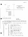
INDEX
PAGE
ISS U E
*18
ACE 1980/1981 EXECUTIVE ...........•......•.....••.. ··10,2
EDITORIAL COMMENTS •.•••.•....•....•.•......•..•......... 3
A CHEAP PRINTER! ••.••••••••..••..••.••••••••••...••. ····-
LETTERS TO THE EDITOR ...••.....•••••••...•••......•..... 6
ENHANCEMENTS TO UT_ ...•...•.......•..••......•... · •• ·.~·7
ANOT HER STEPPER. • • • • • . • • • • • • • • • • • • • • • • • . • • • • • • • . • • • • • •• 12
•
AN AUDIBLE CONTINUITY TESTER ...•..•...•...•..••.•...... 13
GAMES 1802S PLAYI ••....•.•..•.••••..•..••...•• ·.·······1ITEMS FOR SALE .••....•.•.........•.•••...••.•...• ·•· 26, 18
HARDWARE BUG I N THE 1802.•....••..•...•..•••.•..•••...• 25
TO "VIP" AN El.F ............................•.. · ..... ··· 27
SOM E BASIC BUGS .•••.•••.••.•.••.••.••.••.•••• • .. •·•••·• 29
MINI-RCABUG (BAUDOT STyLE) .....•.•....•..•.•.•...•....• 30
A.C.E. COLOUR VIDEO BOARD .....•.•••.••.•.......••.•...• 32
ANALOG OUTPUT BOARD ..•...•......•••....•.•.•..•.•• ·····35
ERRATA--BUILDING A BETTER BASIC ......•..••......•.....• -5
THE DOUBTING THOMAS MEMORY TEST ..••...•.•.............. 51
MEMBERSHIP/RENEWAL/CHANGE OF ADDRESS FORM .•....••••.••. 52
IPSO FACTO is published by the ASSOCIATION OF COMPUTER
EXPERIMENTERS
(A.C.E),
a
non-profit,
eduoational
organization. Information contained in IPSO FACTO is
believed
to be accurate and reliable. However, no
responsibility is assumed by
IPSO
FACTO
or
the
ASSOCIATION OF COMPUTER EXPERIMENTERS for its use; nor
for any infringements of patents or other rights of third
part~es which may result from its use.
Send ALL A.C.E. correspondenoe to
-------------------------
•
Bernie Murphy,
102 MoCraney St.,
Oakville, Ontario,
Canada.
L6H 1H6
.
ASSOCIATION OF COMPUTER EXPERIMENTERS 1980-81 EXECUTIVE
•
PRESIDENT:
John Norris
3 Country Club
Toronto, Onto
416-239-8567
PAST
Pres ident:
Ken Bevis
220 Cherry Post Rd.,
Mississauga,Ont., L5A 1H9
416-277-2495
SECRETARY I
Treasurer:
Mike FranKlin
24 Duby Rd.,
Acton,Ont.,
519-853- 3421
EDITOR:
John VanLierde
40 Arlington Ave.,
Toronto, Ont., M6G 3K8
416-656-3185
ASSISTANT
EDITOR:
John Myszkowski
99 Augusta St.,
Hami1ton,Ont.,
416-529-0250
Fred Feaver
105 Townsend Ave.,
Burlington,Ont., L7T 1Y8
416-637-2513
CONSULTANT:
Bob Silcox
562 Forestwood Cr.,
Burlington, Ont., L7L 4K3
416-845-1630
DRAUGHTSMAN:
John Myszkowski
MEMBERSHIP
COORDINATOR:
Bernie Murphy
102 McCraney St.,
Oakvi 11 e, On t . , L6H 1H6
416-845-1630
Don MacKenzie
3124 Bonaventure Dr.,
Mississauga, Ont., L4T 2J2
416-676-9084
PROGRAM
COORDINATOR:
Jeff Davis
8 Hillview Dr.,
Grimsby,Ont., L3M 4E5
TRAINING
COORDINATOR:
Fred Feaver
L7J 2P1
•
A.C.E. EXECUTIVE
Ken Bevis
SOFTWARE
COORDINATOR:
continued on Page 10
Wayne Bowdish
149 East 33rd. St.,
Hamilton,Ont., L8V 3T5
416-388-7116
•
PAGE:
•
3
EDITORIAL COMMENTS
Great news! 'II
w~ are pleas~d to announce that we are now in a position to
take orders for not only De Facto (as promised last time), but also
for three club-designed boards.
DE
FACTO
This book collects in one volume all of the best material in
issues 1-18, with all known errata corrections incorporated into
the articles, many diagrams improved, and a comprehensive table of
contents. It is, therefore, not just of interest to those who are
missing back issues.
De Facto is unbound, but is three-hole punched to fit standard
binders, comes in a plastic shrink wrapping, and has a three-colour
cover.
•
The price for De Facto is as follows:
- to Canadian addresses -- $15 Canadian funds.
- to U.S.A. addresses ---- $18 American funds.
- to overseas addresses -- $20 American funds. (sent airmail)
De Facto is a truly great collection of 1802-related material,
and, at the price, the best bargain around.
BOARDS
1) 8K EPROM Board (as depicted in issue 17, and described in
issue 16).
2) Kluge Board (also depicted in issue 17).
3) Club Backplane (also depicted in issue 17).
The list of parts for the EPROM board was given with the article
on it in issue 16, page 28.
All boards are sold as bare boards. (schematics and parts lists
enclosed) .
The price for each board 1s
--to Canadian addresses - $20 Canadian.
--to U. S. and overseas - $20 American.
All orders (boards and De Facto) should be sent to:
Bernie Murphy
102 McCraney Street
Oakville, Ontario
Canada.
L6H 1H6
EXTRA! See pg. 32 for Colour
Video Board offer !
'1
PAGE:
4
...
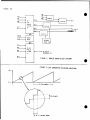
A CHEAP PRINTER
R. N. Thornton
1403 Mormac Road
Richmond, Va. 23229
•
I recently decided to add a printer to my micro, a home-brew ELF based on
the Popular Electronics articles. Naturally, I wanted manuscript quality, quiet
operation, low power, variable paper width up to 14 inches, tractor and/or pinch
feed, high reliability, etc., etc. After writing to a number of suppliers, I
found that such a printer would cost roughly 20 times my total computer investment to date. Even a used Selectric typewriter was $350 without interface.
Finally, I saw an advertisement in ON-LINE (now the Computer Shopper) for a 32
character per line printer for $95. This represented quite a compromise relative
to my original desires, but was affordable. After further consideration, I
realized the printer would be a perfect companion for a 32 character per line
video display. I ordered the printer from:
Carl Poulson
1601 Roder Ct.
Streamwood, Illinois 60103
sending my money order for $95.00 (U.S.). The printer arrived in about 3 weeks
via U.P.S. It was well packed, and weighed about 45 pounds. The printer is a
used, reconditioned model made by Bunker Ramo, and contains a dot matrix print
mechanism made by the Victor Comptometer Company. The cabinet is about 18"x16"x6~",
and contains the power supply, printer mechanism, and electronics for the ASCII
interface. The cabinet top lifts for e~s, maintenance access, and all parts are
fastened with twist lock screws for fast removal. The printer mechanism is a 5x7
dot matrix mechanism which prints 80 characters per second in 32 columns on 3.5
inch wide adding machine paper. A complete set of schematics and adjustment
procedures is supplied with the printer.
•
The ASCII interface uses 7-Bit ASCII in parallel. To use the printer, the
buffer must be loaded with 32 characters, one at a time, and then a print command
is issued.
To load a character into the buffer, the character is presented in parallel
on the data lines, and the print command line is brought high. The computer must
then wait until the printer busy line goes high and back to low before loading
the next character. After all 32 characters are loaded into the buffer, an ASCII
carriage return (hex 0n) is placed on the data lines, and the print command line
is brought high. Loading for the next line may begin after the print busy line
goes high and then low. Since the print mechanism works right to left, if fewer
than 32 characters are loaded, they will be right justified on the line. The
print character set includes 0-9, A-Z (upper case only), blank, and 19 special
characters. A 2516 ROM is used to generate the print characters. I believe a
2708 EPROM could be used to change/expand the character set, though I haven't tried
this yet.
•
p~GE:
•
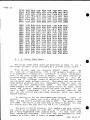
I)
----------PRIHT SANPLE---------8J2J4S6789RBCDEF
HEX 28-2F:
. "'$%&(1( >*+1 -."
HEX J8-JF: 8123456789$-+.
HEX 40-4F: . ABCDEF'QlIJKUtHO
HEX 58-SF: PQRSTUUIrIXYZ: '=of'?
.
-------------------------------I used the following routine to test printer operation.
cation, it should be usable as a print subroutine.
•
LOC
HEX
00
01
03
06
07
0A
0B
0D
0F
10
90
B3B4
F8lEA3
E3
F820A4
62
360B
3E0D
24
84
3A0A
F81DA3
62
3617
3E19
3003
0D
11
13
16
17
19
lB
lD
1E
LABEL
START
LOAD
WAITBSY
WAITIDL
WAITPRT
WAITFRE
CR
DATA
With some modifi-
MNEMONIC
REMARKS
GHI
PHI,PHI
LDI,PLO
SEX
LDI,PLO
OUT2
B3 WAITBSY
BN3 WAITIDL
DEC
GLO
BNZ LOAD
LDI,PLO
OUT2
B3 WAITPRT
BN3 WAITFRE
B START
D-0
R3.l-0, R4.l=0
R3-DATA ADDRESS
X-3
R4-32 , LOAD COUNTER
LOAD DATA TO BUFFER
LOOP UNTIL PRINTER BUSY
LOOP UNTIL PRINTER IDLE
DECREMENT COUNTER
D=LOAD COUNT
CONTINUE LOAD IF NONZERO
R4-C.R. ADDRESS
PRINT THE LINE
LOOP UNTIL PRINTER BUSY
LOOP UNTIL PRINTER IDLE
REPEAT
CARRIAGE RETURN
32 BYTES OF PRINT DATA
This routine is written to mate with the hardware interface used: if a
different N-line is used for print command, the OUT2 instructions must be changed;
if EF3 is not used for printer busy, the B3 and BN3 instructions must be changed.
The instruction at 1B will have to be changed to a valid exit except for testing.
As written, the 32 bytes located at IE-3D will be printed over and over.
•
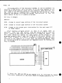
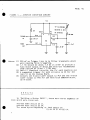
The hardware interface I used is shown below. It was necessary to buffer the
data lines, as the printer uses TTL logic. I had trouble with the interface until
reading the RCA 1802 manual which clearly stated the requirement for AND'ing N1,
MRD, and TPB to insure memory data is available when the print command line is
brought high .
PAGE:
6
PA.INrER
•
PwR Co"'..
PROS'
8
PROb
P
])5
PR07
R
1)4- lL
P 0
s
])3
o
T
D2.
PR10
U
PRll
V
PRN&S
.D
PRC.M.D
'1
10
12
CDPl802.
13
141S"
22.
F
I'll.
C
MRJ)
J
TPB
18
7
33
Dear Bernie:
•
\~l~ I ve had several articles on EPROM Programmers. but nothing on erasers.
There is an EPROM Eraser kit available for $25.00 (U.S.) from:
R. W. Electronics, Inc.
3203 North Western Avenue
Chicago, Illinois 60618
The kit includes a G.E. Ultraviolet bulb #G4T4.l, lamp socket, switch, and G.E.
ballast #89G489. Instructions included with the parts show how to build the eraser.
Additional parts required include a line cord, bread pan, and small parts which are
easily fabricated. A 2708 can be erased in 15-20 minutes with the assembled eraser.
The best buy I've seen on 2708's is $6.95 for the 450 NSEC version from:
Active Electronic Sales Corp.
P. O. Box 1035
Framingham, Mass. 01701
My thanks to all on the Executive Staff who produce this outstanding newsletter.
Sincerely,
Dick Thornton
1403 Mormac Road
Richmond, Virginia
23229
•
PAGE:
•
ENHANCEMENTS TO UT4
7
Frederick K. Hannan
10 Fi10si Road
East Lyme, Connecticut 06)))
Shortly after Mike Franklin's article on the UT4 program appeared
in IPSO FACTO, he was kind enough to send me a tape of his program.
Subsequently, I purchased the RCA Manual MPM 224 and found both to be
very valuable tools.
However, after using the UT4 program for SoMe time, I found it
contained some i11.ogica1, impraotioal, or just plain dumb commands
and routines.:' Inc"order to fit it to my own personal quirks, I have
made some changes to the program which might be of use to others.
First, although I did not experience any problems with the TIMALC
routine, I thought it was best to load the time constant into RE.1
after initi1ization, similar to the manner suggested by Dave Taylor
in IPSO FACTO #11. This will help overcome any future problems as
equipment ages, .tc.
•
I also felt it was rather dumb to put my machine through the
REGISTER SAVE routine when there was no valid reason for doing this.
Consequently, I established a new initialization routine at the beginning of UT4, again, identical to Dave Taylor's routine on Page 42,
IPSO FACTO #11.
The result of this is to free up addresses XX16 through XX)8 for
other changes or new routines (XX is high order address of UT4).
My next thought was to bring some sense and logic to the three
command symbols. After all, :M and $p do not really represent their
true funotions of Writing to memory (:) or Running program ($). Only
1M comes close to its function of Dump memory.
My solution was to use "W" for Write to memory, "D" for Dump
memory and "R" for Run program. This is aooomplished by the following
changes.
Address
XX4A
XX52
from FB24 to FB 52
from FB1E to FB1)
Further, I felt it was superfluous to have to enter the character "M"
or "PM when entering a command. The changes to eliminate the "M" and
"P" are.
Address
XX4C
xx 56
from)2D6 to )2DB
from D) to 305B
Now the three commands are.
•
W XXXX
D XXXX
R XXXX
A
A
Data - Write to memory
/I 0 f Bytes - Dump memory
- Run program
PAGE:
8
The second change was to add a space after the prompt symbol
and to change the prompt symbol from "*" to ">,, (my personal favorite).
The change of the prompt symbol is easily accomplished by substituting
)E for the 2A at address XX4l.
•
I had a little difficulty in getting a space after the prompt,
however. At first I merely moved the beginning of the "START" routine
from location XXj9 to XXj7 and added "Dj20" to the end of the prompt
print string. For some reason. I have yet to figure out, this would
not work. My final fix was to add another TYPE routine pointer after
the first two "DjXX" SEP SUBS.
Thus, my start is nows
Address
XXj4
XXj7
XXj9
XXjB
XXjE
XX40
F-89CAj
OjOO
OjOA
F89CAj
OjjE
Oj20
TYPE routine pointer
TYPE CR
TYPE LF
TYPE }
TYPE space
The branch instruction at address XX14 must be changed to )Oj4
for the new "START" address. Also, the RESTART branch instructions
at addresses XX99 and XXB9 should be changed to j2j4.
Lastly, I felt it was rather stupid to have to manually input a
•
LINE FEED after the use of a COMMA/CR in the Write to memory mode.
After all, our machines are pretty smart and can do this kind of simple
task with ease.
In order to make any changes in the area of the program concerned
with the COMMA input, some room was needed to fit in a subroutine to
automatically insert a CR/LF after a comma was typed.
Initially, I thought I could free enough space by moving the SYNTAX
error routine from address XXCA through XXdl to the now free area at
address XX2B through XX)). Although this did not give me enough room
for my SUbroutine, I proceeded with the relocation of the error routine
as it gave me the opportunity to consOlidate the present two routines
"( XXCA to XXDI and XYFS" to XYFE) into one. Als 0, by placing the routine
immediately ahead of the START routine, the ERROR routine would naturally
fall through to the START routine. These changes ares
Address
XX2B
XX2E
XX)O
XX)2
F89CAj
D)OD
D)OA
D))F
TYPE routine pointer
TYPE CR
TYPE LF
TYPE?
•
I
•
PAGE:
•
9
Several branch instructions must also be changed as follows a
Address
XX59
xX6J
XX?5
XXAF
XXD9
XXEO
from
from
from
trom
from
from
JACA
JACA
3ACA
JBCA
JACA
JACA
to
to
to
to
to
to
3A2B
3A2B
3A2B
3B2B
3A2B
JA2B
Now, to automatically insert the CR/LF after a comma in the Write
to memory routine, I inserted a new subroutine at XX16 as followsl
Address
XXl6 F89CA3
D30D
D30A
F8)BAJ
F8ABA5
D5
TYPE routine pointer
TYPE CR
TYPE LF
Set subroutine pointer to
Set main Pc for return
Return
Address XXBD should be changed to 3216. The program will now
branch to the new subroutine on input of a comma, do a CR/LF and
return to address XXAB, ready for more input.
•
This completes my present modifioations to UT4. A future change
will be the insertion of a counter into the Write to memory routine to
automatically perform a CR/LF after every 16 bytes of input and completely eliminate the COMMA routine. Right now, I am busy using UT4
to help in implementing a Serial I/O interface for "The Monitor" presented by Steve Nies in a past IPSO FACTO. (Note to Steve - by all
means, keep us advised of your changes to your monitor.)
Finally, I must express my feelings about Netronic's Full Basic
and Quest's Super Basic.
Although I run Tiny Basic, Full Basic, and Super Basic, I find
that Super Basic, in spite of its length, offers so much more versatility
that Tiny and Full are virtually unused. The availability of the two
dimension arrays in Super is a prime requisite for me.
Also, perhaps it is ignorance on my part, but I find the steps
necessary to perform a very oomplex equation in RPN is a painful and
time consuming task. Although I leave the Math Board in my ELF II
permanently (I use the empty 16 pin socket locations for termination
points for the interconneoting oables to my backplane.), it is very
seldom used. In faot, if it did not offer 8K of Eprom sookets, I would
leave it out altogether.
•
With regard to the LOAD problem with Full Basic, I have installed
a switch on my Giant Board which allows me to jumper bypass the mods
required by the Math Board (Full Basic will run without the mods if ftO
math function is required.) For normal use of the Giant Board
CASSETTE LOAD or Full Basic "LOAD", I close the switch. If I am
RUNning Full Basic, the switch is opened.
•
The switch is a simple SPST slide switch Super-Glued to the top
left corner of my Giant Board. I drilled a small hole in the plastic
cover to accomodate a push/pull wire (bent paperclip). The switch
reconnects the cut foil trace to restore the Giant Board to its
original configuration. When the switch is opened, the Math Board
modifications take effect.
Postsc;:i.:e:t
After writing this, I decided to change the SEMI-COLON input in
the same manner as the COMMA input. This was easily accomplished by
adding the following to the previous changes.
Address XXC3
F89CA3
D30D
D30A
F83BA3
F85BA5
D5
C4
Type Routine Pointer
Type CR
Type LF
Set Subroutine Pointer to READAH
Set Main PC for Return
Return
NOP
•
This change is not listed in the summary.
._----•
----------- -----------....-_-
CONTINUED [<"ROM PAGE 2
HARDWARE
COORDINATOR:
Anthony Tekatch
RR 1
Caistor Centre, Ont.,
416-957-7556
LOR lEO
HARDWARE
PRODUCTION
AND SALES:
Fred Pluthero
1013 Upper Wellington St.,
Hami1ton,Ont., L9A 3S4
416-389-4070
PUBLISHING
COMMITEE:
Dennis Mildon
44 Wildewood Ave.,
Hami1ton,Ont., L8T 1X3
416-385-0798
John Hanson
955 Harvey Place,
Burlington,Ont.,
416-637-1076
L7T 3E9
•
PAGE:
•
•
•
11
SUMMARY OF UT4 CHANGES
High Order Address)
ADDRESS
NEW DATA
(XX
XXOO
0407
08
09
OB
OD
10
11
14
F8xXB3B5
F80BA5
D5
E5
7155
6101
F8FEA3
D3
F82l.4-BE
3034
Relocate "Start" routine - See
Da~e Taylor letter, Ipso Facto
#17, page 42
XX16
19
lB
1D
20
23
F89CA3
D30D
D30A
F83BA3
F8ABA5
D5
Comma/CR/LF Subroutine
XX2B
2E
30
32
F89CA3
D30D
D30A
D33F
Syntax Error Routine
XX34
37
39
3B
3E
40
F89CA3
D30D
D30A
F89CA3
D33E
D320
Initialize Routine
xX4A
52
FB52
FB13
Change of Command., Symbols
($ now R, : now W, ? now D)
XX4C
56
32DB
30SB
New Branches to Eliminate need of
..P" and ~M"
XXBD
3216
Branch to Comma Subroutine
XX59
6;
75
AF
D9
New Syntax Error Branches
. EO
3A2B
3A2B
3A2B
)B2B
3A2B
3A2B
XX99
B9
)234
3234
New Restart Branches
PAGE:
12
Ge".
A.D ........1.
1601 Clayton Avenue
Lynchburg, VA 2..503
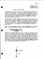
ANOTHER STEPPER
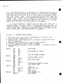
•
After readial the artiele by Mr. Airhart in ilsu~ 19•. 1 de.i.ed to
luhmit the en.l.led oircuit, which I have been usine t.r quite .eme ti.e.
IC1, a 555 timer chip, 1. wired to run a. an ast.ble eloill.ter.
Speed v.riaticil 11 accomplished with R2, whick b . : tr,-erH.D er•• r~te
save space.
My computer, a Quest Super ilf, alr.ady has previsi.n fer .tep~i.1
threugh .emery when the c..puter i, i. LOAD, ~y r•••• t'.ly pUlhial the
Input hutto.. Therefore 1 .imply een•••ted the output ef this cirouit
t. the i.put ..it,h. Thi.
the ••
re.llter tel' .,.e• •re the
aain .ifferenees betwe.n my d'lllft ... that et Mr. Airhart.
an.
1'1.".
Te u.e the clrcult en a Super Elf, pre•• Re.et, Lead, Memery Prete.t,
... the flip the teccle tWitch. When the ••slred leeatle. appr••,hel,
flip the t'l!le Iwitoh acaia. The. pr••• the Input IWitch ...ual11 te
reach the till•• t· l ...tU*. > • Te alter ••mory, Ite, te the loea ti.. aefere
th.t which i. t. De ehanle., pre•• the Wait autton,
precee. te 1•••
'.ta noraally.
aB.
s••• Super Elfs may require a buffer em the out.ut of the C1drouit.
J .... bt if, thla .ev18. e.uU be.,.·u".' at aU' D, .., ••eqwi\h a TEC u.alt, but
thell whe ewn the Super Elf will find it an 1••••penllal••evice.
REJl'JRENOES
1.
2.
I
8u,er Elt U.er. Manual
R••le SDaak 555 data sh.et
•
+!5v
RI
PARTS LIST
2
ICI
C1
C2
RI
R2
Sl
7
6
8
IC I
3
555 timer chip
.2 mfd
.1 mfd
5K
500K trill1T1er
SPST toggle
C2
CI
-
~.-.-.II
""
INPUT PULSER DIAGRAM
•
PAGE:
•
Richa.rcl N. Thornton
1403 )brac Road
Richmond, Va. 23229
AUDIBLE CONTINUITY
ll~STiR
This device can be used to test continuity, and provide some indication of
the amount of resistance in a circuit. In operation, the probes are touched
to the points to be tested. If the circu.it is open, the speaker is silent.
If there is continuity, even at high resistance (10 megohms or more), a tone
will be heard. The tone decreases in frequency as reeistmce between the
probe tips increase•• A noticeable decrease in frequency can be noted at
resistances as low as 1,000 ohms.
As drawn below, the aUdible tone is about 5kHz with the probes shorted. If a
lower frequency is desired, f'_GiAIIlIIII the value ofU, or play with the value s
of C and H,2. To increase the volulne, reduce the Value ot R4, or increase the
value of C2 end reduce R3. I use a 9 V transistor radio battery, but the
circuit works well at 5 V. With probes disconnected, power supply drain is
not measurable with a 0-50 InA meter. With probes shorted, the current is
about 20 mAo
The circuit is essentially that shown in National Semiconductor's "CK>S DATA
!OOK" from AN-llSftCX)S OecillatoJls", where tb4t·~yi-e given a&'"
•
1
f
s= ...---.-ooj~-----~
2C(JUtU) (.49*2 , +•693)
\ IU+Rlt+R2
Observations: The probes appear to be open (no tone) when connected across a
d:1oJCie, or a capacitor of less than about .04 uF. Capacitors greater than .04
uF produce a tone similar to 8 short circuit. With the probes connected to
the input to my oscilloscope, I see a differentiated sQUBre wave with g, out
30-35 V peak-to-peak.When the 'scope input is DC, the pulses are continuous.
When the 'scope input is switched to sc, the pulse train dies out in about
15 seconds, but repeats if the meter leads are reversed. I don't understand
these things, just report them. Perhaps someone more knOWle~.eable can supply
some insight. The high voltage P'U8es might ~ Mnsitive device., but
don't seem to h.~ the 4001 IC in the circuit.
+
•
13
1
-"='
ts-9v BATTERY
" \ ON-OFF
1--
pAGE: 14
•
+
c
.01
R2
-
lOOK
SMALL SPEAKER
PROBES
~
RX
GAMES 1802s PLAY!
P. Thyssen,
Julianastead 39,
5951CH Belfeld,
Netherlands (Limburg)
•
The following are several games I have just written. The Orthogame
is the first I have ever written in Assembler SO be careful with it!
Till yet, I am just writing games for fun. I've also a lot of Tiny
Basic programs but most of them have a Dutch text. The nicest ones are:
a word guessing game (2K RAM like WORD in David Ahl's 101 BASIC
programs
+ Coldik. Escape from a war prisoner's camp. This one I wrote after
analyzing the Quest game (The first is in Dutch but the second
has the same text as in Byte, July 1979). A problem is that I have
them only on tape. They require at least 4-5K RAM without Tiny
Basic.
+
Maybe someone can rewrite the Dutch games. If someone sends me
one or both items below, I'll send him my games on cassette tape. I'll
pay also for the copy cost by sending a post check:
(1) The RCA CHIP-8 language and copy of programs and user manual.
I've tried to get it in Holland and wrote RCA (USA) but never
heard anything.
(2) The PILOT 2K language (also terminal and tape routines) and
copy of user manual for my ELF II and vi~eo display
(Netronics).
•
PAGE: 1;
•
•
•
RUSSIAN ROULETTE:
00 90
05 B9
07 F8
OA F8
00 F8
10 03
11
72
12 70
13
22
15 22
17 C4
1A F8
10 F 8
20 80
22 E2
25 E2
28 E2
2B 3C
20 30
2F E2
31
F8
34 9F
36
39
3C
3F
40
41
43
45
47
49
48
4E
4F
51
52
54
55
57
59
58
50
5E
62
65
67
B1 B2 B3 B8
BF
2F A3
C7 A2
13 A 1
78
52
C4
00
00
E2
20
20
20
20
C4
BO
AO
,
,,
I
AO
AO
AO
11
69
80 AF
B4
F8 C3 A4
F8 01 54
F8 50 B6
26
96
3A 3F
OMA transfer TV
I
,I
E4 64
9F OF
3F 47
37 49
F8 01 OF
04
FE FE
F4
FC 01
54
37 59
30 4E
FF 06
33 67
24
04 FC 01 54
F8 02 OF
30 3C
F8 03 OF
,
I
,,
-,
I
I
I
MAIN;
(SUBF)
M(C3): COUNTER
M(C4):
RNO NUMBER
I
-,
I
TIME
I
I
I
I
DELAY
-,,
DISPLAY NUMBER ON LEOS
11
Rn
= Rn-1 *
) 216 HIT!!!
COUNTER
KhK!
AGAIN
bANG! !
+
1
5 + 1
'till input key
=
1
PAGE: 16
6A
6D
10
13
15
78
19
1A
1C
1E
1F
80
81
84
81
89
88
8D
91
95
91
99
98
A3
AB
B3
B8
D2
DA
E2
EA
F2
Fa DB A8
F8 80 58
08 F6 58
32 31
F8 OF B6
26
96
3A 18
30 10
00
D3
FE
FC 9B A8
F8 D4 A9
08 59
18 19
08 59
88 FC 01 A8
89 FC 01 A9
FB FC
3A 81
30 1F
EO EO AE EO
20 20 CA AD
40 40 8E EO
00 00 CC CO
40 40 AA A5
80
1F
10
CO
CO
•
: BULLET
,
I
AGAIN
-,,
I
I
TIME
I
I
DELAY
-,,
SUBF:
CONVERSION TO
TV-DISPLA Y
A8
C8
88
C8
AE
8A
DC
88
8C
8A
11
55
11
45
45
11
55
51
51
51
-,,
I
I
,
,
I
I
PISTOL
•
-,
I
KALEIDOSCOPE:
00
02
05
08
DB
OE
11
12
13
14
16
18
1B
1E
20
23
26
29
28
2D
90 B3
F8 83 AF
F8 6D AE
F8 20 A3
F8 6B A2
F8 14 A1
D3
12
10
22 18
22 52
C4 C4 C4
93 BO AD
80 E2
E2 20 AD
E2 20 AD
E2 20 AD
3C 1E
30 12
E2 69
(SUBF) (SUBE)
(MAIN)
(STACK)
(CNTT)
DMA TRANSFER
FOR TV
,,
-,,
•
i
PAGE: 17
•
2F
30
33
34
35
36
38
E9
F8 10 A6
00
26
86
I
-I
I
I
1
I
I
-I
3A 33
37 38
F8 67 A9
3D 14
3E 84
3F 3A 42
41 DE
42 DE
43 AA A5
45 80 AB
47 19
48 DE AC
4A OF 80 DF
4D 8B A5 8C
53 8C A5 8A
59 8D A5 8A
5F 30 30
61 00 00 00
67 RND1
68 RND2
69 00 00 00
6C D3
6D 09
6E FE FE
70 F4
71 FC 01
73 59
74 A6
75 FF 05
77 33 74
79 AD
7A 86 FD 04
7D 30 6C
7F 86
80 F3
81 59
82 D3
83 FC 08 A7
86 FE FE FE
8A FC D2 A9
8D 87
8E A8
8F 19
90 88
91 FF 08
93 33 8E
95 F8 80
97 A6
98 88
99 32 7F
9B 28
9C 86 F6
9E 30 97
STOP!
3A
•
•
TIME DELAY
COMPUTE: Y-X:
X-5:
Y-Y:
Y-5:
AA
AB
AC
AD
DF 80 OF
DF 8B OF
DF 8B OF
00 00 00
BACK
random seed value ( 1 byt.a)
random seed value ( 1 byte)
(STACK)
Rn MOD 5
ad (=) x-5
D (=) y-x
LOOK AT GIVEN BIT BY R7 AND R9
IF BIT EQUALS ZERO MAKE 1
IF BIT EQUALS 1 MAKE ZERO
RETURN
PAGE:
18
Flip/Plop.
•
The object of this g~ne is to change a row of eight XIS
(XXXXXXXX) to a row of eigth O's (00000000).
E3y typing the das i.r-ed rownumber plus Input-key you can
change an X to 0 (or reverse),but it will also change
another position too.
Can you figure out a minimum strategy?
User' remnrks:
1) [jet/reset 'WN and the Q-led c;oes on. Tip the Input-key
and the line of XiS will appear on the bottom of the
illVscreen.
2) 'llor.eset tho line to all XiS (sarne game l ) type 100. To
start a new game (new set flip/flops) type a value greater
than 108 plus twice the Input-key.
3 ) 'llhe hexadecimal Led I s will display the numbe l' of guesses.
4- ) 'J\lhen you've got all 0 I s the C:~-led goes on. The program
will now reset like typin~ 100.
5) If there is no solution(?) use twice the same number.
rPhe second time you'll get another' flip/flop.
The secret of this pr-ogr-am lies in the "nasty" property of
pseudorandomgenerators, that they always need a starting
value. Each starting value correspond to one set of flip/flops,
so totally you'll have about 256 play variants. For more
change the l'andomgeneratorroutine.
•
Nuch XOXXOOXO.
Id.terature: David Ahl, Bas i c Computer Games. 19?8,page 63
ITEMS FOR SAtE;
1802 Full Basic leTel III board and tape.
Netron1cs ASCII v1di0 board,Y1deo mon1tor,
ftome made ASCII key board,and power supply.
Are all in one cab1net,with matoA1n! table.
All tor $250
Tom Pollard
Grotoll St.
Dunstable,Mass.
U.8.A.
01827
(617) (649-6641)
•
•
•
PAGE: 19
81 B2 133
OLIB5 13B BC
Bf~ Bli'
08
on
AD AF
subE
138 AE ISUb~l
os
11 11'8 36 A3 (main
14 F8 AS A2 ~stack)
intrpt)
17 F8 1D A1
1A D3
1B 72 70
1D 22 78
1 H' 22 52
21 OL~ 04 04
24 91" BO AO
27 80 1~~2
29 FQ 20 AO
20 1~;2 20 AO
2B' 1~;2 20 AO
32 ~O 27
34 30 1B
36 82 69
38 F8 A5 A4 ( ImD)
3B 7B
30 J)F
3D 3F ,~O
: starter
3F AA
40 7A
L~1
TI'S A6 A5:counter
44 9li' 55 A6 AS
L~8
86
49 FO B8 AB: load row
'+0 F8 1t 5B of X's
4F 16
50 86 DE
52 86
53 FF os
55 308 L~8
57 37 57
59 E5 64
58 3F 5B
5]) 37 5D
:reset
on
5F 31 40
61 60
62 32 40
: r-e se t same
game
6'+ FF 09
:reset new
66 33 3B
flip/flops
68 05 DE
6A 88 ]'3
60 3A 72
68 88 FE A8
71 08
'12 05 A8
74 A7
00
90
B4
13D
D'8
[i18
.~
•
: compute other
75 8A 54
flip/flop
77 Dli'
78 27
79 87
7A 3A 77
70 04
:mod9
7D A7
7"8 87
7F PF 09
81 33 7D
83 E5
,(3L~
87
85 32 6E
(37 F3
88 32 6E
8A 87 DE
80 05 A8
8E 25
8F' 05
90 PO 01 55: count.ezwt
93 Il8 E8 AB: test for
all O':s
96 OB
97 .1m 10
99 3A 59
9B 1B
90 8B
9D FF FO
91i' 3B 96
:if yes
A1 7B
Q on
A2 30 59
A5 RND
A6 counter
AB stack
AO D3
subroutine
AD E4 04
pseudorandom
AF FE FE
B1 F4
Rn=Rn-1x5+1
132 FO 01
134 54
135 30 AO
87 D3
B8 [i'0 87 AB: subroutine X... 0
0., X
BB FO 08 AO
BT;1
FO 08 AD
. ' ...
01 OB
02 FB 10
04 3A OF
C6 F8 14 5B $D :load X
OA .8'8 08 50
CD 30 B7
OF F8 10 5B 5D :load 0
D3 F8 14 50
D6 30B7
remain zero
PAGE: 20
--ORTHO--
•
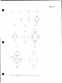
'l'he game was originally invented by the mathematician 3tanislaw
Ulam. On may points there is correspondence with the Game of Life,
but while Life simulates the complex world of living organism,
imitates Ortho growth. In nature, we find frequently that this
happens through symmetrical ground patterns.(like crystals)
The subject of this game is an orthogonal symmetry.
Definition: - You play on a grid of squares or cells(chessboard).
A cell has finite states of appearence(bl/wh,colors)
- In the beginning of the U;ame you can occupy
cells or not.
- Any further course is fully determined through a
defined set~of playing rules.
Ortho: In the next generation is always that
cell occupied, which has perpendicular only one
neighbour. All cells of generation n dies, when
generation n+i appears. So, there are always
i generations visible.
There is chosen for a 15x15 matrix, but theoretical there will
be a continued growth on an infinite grid. An advantage of
Ortho as caleidoscope are the many starting possibillities,
but the nicest results you will ~et with symmetrical patterns.
In the figure you see the development of one point for i=2.
Each generation could be r-epr eae nt ed by a color, but if you
have only black/white 'FV?
The program is written in Assembler and will run on a ELFII,
1K HM1 and 1861 'J,V-chip.
Some suggestions: In M(00B9) the value 103 is similar to i=1,
104 to i=2, I with i=3 etc.
In M(OOA2) you could change the condition "one neighbour".'
User descriptions: If you set/reset RUN the Q-IJed goes on.
Put in the desired coordinates (Y,X from
0 •• S,/23 is Y=2 and X=3)~followed~by the
Input-key, and the cell will appear on
the TV-screen. If there was already a cell
on that place it will disappear, so errors
could be corrected. The hexadecimal Led's
will display your inputvalue.
You can go on until the value is greater
than lEE. Then the game will start and the
computed patterns will appear on the screen.
If you want a new game set/reset RUN and ••••
•
•
PAGE: 21
•
(0
x
x+x
x
x
+x
X+
x x
x+x
X
(( )
( 7)
x
'X"
+
+
+':'H
X+ +x
'")
X
,)J11
-+'1
+
X
')
x
+
X")
'")
X
•
X
I")
..,
~I
..,
x
x
x+
+x
~
X+ xx
-") l-
x:x +x
x+
+x
+
x
X
'{
x
()
+-"1+
+
( 9)
f")
.,
'"IX"
,')
'")
'1/'
'X
'"lX
'"'
'"1
f)
X'
xxx
'"1
I")
,'")
I")
'<
I")
XX'"' .,XX
X,.,
X
f")
X
f")
,x
Xi')
J(
')
XXX
')
,..,
f)
()
")
-, JE ()
')
'")
'")
t)
+
')
-")
---
'")
'j
I)
+
f)
X
x
,X
•
.:<xx
x
X X
'"'
-"'I
++
')
'")
,.,
I")
-")
.,
+
+
'")
')
()
f)
")
')
'")
'"'I
++
'")
I)
.,
I')
PAGE: 22
0000
0001
0002
0003
0004
0005
0006
0007
0008
0009
OOOA
OOOC
OOOD
OOOE
OOOF
DMA
IN'l'
SPR
MFC
MEM
GNE
VRX
VRY
CNT
TMP
RGT
TVS
CEL
CPE
PLT
0000
001C
001E
002B
0046
0050
005D
0072
0079
008A
0090
0098
OOAO
00A7
00B5
3rpA!~'p
HETURN
INTRI>T
REFRSH
MAIN
LOOP
INPUT
BEGIN
LOOP1
OUT1
OUT2
OUT3
OUT4
BACK
CYCLUS
OOBF
00D7
00D8
00D9
OODA
0100
0107
010D
010E
0112
011D
0126
0200
0300
•
:LOOP2
S'PACK
GNHCrIE
RErl'MPC
COfljprrE
TERUG
QUIT
RTNMPC
PLOT
MOD16
MOD4
SHIFT
rrVSCHN
MEMOHY
OBJ'EC'l' LIST.
0000
0000
0000
0000
0000
0000
0000
0000
0000
0000
0000
0000
0000
0000
0000
0000
0000
0000
0000
0000
0000
0000
0000
0000
0000
0000
0000
0002
0004
0006
0008
0009
OOOB
•• --ORTHO-••
•• P.THIJS3EN
•• BEL.f!'EIJD
•• NETREf~LANDS
••
•• HEGISrrERS
...
DMA=O ,~.lmA pointer
INT=1 •• interrupt
SPC=2 •• stack pointer
MPC=3 •• main prog. counter
MEM~4 •• dataarea
GNE=5 •• adres gen. counter
VRX=6 •• counter X
VRY-=7 •• counter" Y
CNT=8 •• counter neighbours
TMP=9 •• workregister
:~G'r=lO •• workregister
TVS=12 •• TV-area
CEL=13 •• examined cell
CPE=14 •• sub "compute"
PLT=15 •• sub "plot"
••
ORG ¢
•• initialization
90Bl START: GHI DMA;PHI INT
B2B3
PHI SPR;PHI MPC
B5BE
PHI GNE;'PHI CPE
F801
I,DI A.1 (PLOT)
[IB"
PHI PLT
F80E
IJDI A.O(PIJOT)
AF
Pl,O PIJT
OOOC
OOOE
OOOF
0011
0012
0014
0015
0017
0018
001A
001B
001C
001C
001E
0020
0022
0023
0024
0025
0027
0028
002A
002B
002D
002F
0030
0032
0033
0035
0036
0038
0039
003B
003C
F81E
A1
F8D7
A2
F846
A3
F8D8
A5
F8DA
AE
D3
7270
2278
2252
C4
C4
C4
F802
BO
F800
AO
80E2
E220
AO
E220
AO
E220
AO
E220
AO
E220
AO
E220
LDI INTRPT
PLO INT
LDT STACK
PLO SPR
LDI MAIN
PLO MPC
LDI GNRTIE
PLO GNE
LDI COMPTE
PLO CPE
SEP MPC
•• interrupt routine
RETURN:LDXAjRET
INTRPT:DEC SPRjSAV
DEC SPR;STR SPR
NOP
NOP
NOP
LDI A.1(TVSCRN)
PHI DMA
LDI A.O(~VSCRN)
PLO DMA
REFRSH:GLO DMA;SEX SPR
SEX SPR;DEC DMA
PLO DMA
S~X SPR;DEC DMA
PLO DMA
SEX SPH;DEC DMA
PLO DMA
SEX SPR;DEC DMA
PLO DMA
SEX SPR;DEC DMA
PLO DMA
SEX SPR;DEC DMA
•
•
PAGE: 23
•
•
•
003E
003F
0041
001+2
004/+
0046
0046
0048
004A
004B
004D
004E
0050
0051
0053
0054
0055
0056
0058
005A
005C
005C
005D
005F
0061
0062
0064
0066
0068
006A
006B
006D
0061i1
0070
0072
0072
0074
0075
0077
0079
007B
0070
007E
007F
0081
0082
0084
0085
0087
0088
008A
OOSB
008D
OOSE
0090
0091
0093
PLO
SEX
}'LO
BN1
DMA
SPR;DEC DMA
DMA
REFHSH
0095 17
0096 DE27
0098 86
0099 FFOE
BH H~I.rur(N
009B 33AO
•• clear memory+tvscreen 009D 16
009E DE26
E269 MAIN: SEX SPIt; INP 1
OOAO 88
LDI A.1 O~Ef'10RY)
F803
PHI M}o;Vl
00A1 FB01
B4
IJDI A.1 (TVSCHN)
"F802
00A3 3AA7
BO
PHI TVS
OOA5 055D
00A7 16
92A4
GHI SJ?R ; PIJO MEM
00A8 00
IJOOP: PIn TVS
AC
GUI SPR; nTH ~1EM
00A9 86
9254
L)lrH TV8
OOAA FFOF
50
INC MEM
OOAO 3B7B
14
GIJO MEM
OOAE 17
84
BNZ 1J()OP
OOAF 87
3A50
OOBO FFOF
IIDI A.1 (MEMORY)
F80,
PHI fJIEM; PHI CEL
B4BD
00B2 31379
•• input data
00B4
00B4 05
8EQ
713
00135 FC01
3F5D INPu'r: 13N4 x
BL~
x
00137 55
375F
SEX SER
00138 FF04
E2
INP 4; PIJO MEV]
6CA/+
OOBA 33B5
OOBC
6422
OUT 4;;'DEC SPR
OOBO.)?A
FFEF
8MI ~EF
BPZ
TmGIN
OOBD 92A4
3372
SEX MI;;M
OOBF FC02
£4
00C1 AC
F801
IJDI 101
8M
;slrr<
r,mr·1
00C2 E5
F754
SEP PLT
00C3 04
DF
BR INPUT
0004 F3
3050
•• compute new generation 00C5 3AC9
li'802 13EGIN: 'LDI 102
00C7 9254
13TH GNE
00C9 925C
55
BL~
OOCB DF
x
3775
GHI 8PR;FIJO VRY
OOCC 14
92A7
OOOD 84
92A6 LOOP1: GEl 8PR;PLO VRX
("-;'l'Q
L.I
OOCE 3A13F
713
G"!:!:P CPE ;1'1JO CEL
DEAD
OODO F803
00D2 134
LDN OEL
OD
BNZ BAOK
3AA7
00D3 3075
OOD:y
R8(~
7A
SI~R
;
PLO
CNT
92A8
GEl
00D5
GI,O VHY
87
00D7 00
1~Z
OUT1
00D8 00
32[)A
DEC VRY
00D9
27
S I~P CPE; INC VHY
00D9 D3
DE17
nODA E2
OtJfr1 : GLO VHX
86
BZ OUT2
OODB 87
3290
OODC FEFE
26
DEC vex
DE16
ser CPE; INC VHX OODE FEFE
OOEO 52
OUT2: GLO VRY
87
li'FOE
00£1 86
StU 14
BPI.', OU'113
OOE2 F4
3398
AO
8220
AO
3C2B
301C
j..)
INC VRY
SEP CPE;DEC VRY
OUT3: GLO VRX
8MI 14
BPZ OUT4
INC VRX
SEP CPE;DEO VFtX
OUT4: GLO CNT
XRI 101
BNZ BACK
LDN GNE;STH CEL
BACK: INC VRX
IDL
GLO VRX
8MI 15
BL Loep1+2
INC VRY
GIJO VRY
8MI 15
BL LOOP1
• .next generation?
IJDN GNE
CYCLU8:ADI 101
8TR GNE
8MI 104
13PZ CYCLU8
• .plot generations
REQ
GHI 8PR ;PLO T'lET'1
LOOP2: ADI 102
PLO TVS
SEX GNE
LDN MEM
XOR
BNZ x+4
GHI 8PR;8TR f'1E1"I
GHI 8PH; 8']IR TV8
GEP PLT
INO 1\1EM
GI.JO pnEM
BNZ LOOP2
I.JDI A.1 U1~MORY)
PHI MEM
13R BEGIN+3
••
ORG x+2
8TACK: ,0
GNRTlE: ,0
•• compute+testroutine
RETMPC:8EP MPC
COMPTE:8EX 8PR
GLO VRY
8HL;SHIJ
SHL;8HL
8TR 8PR
GLO VRX
ADD
PAGE: 24
J>I,() 1\1l';lV\
lLL RE/:PIVll '0
00"83 A4OOl;;l~ 31DC)
00j~6f~5
,\K< GNE
LDN MEJV1
00E7 04-
00 ;,;r), 32D9
BZ
OOEA F3
OOEB 32D9
OOED 18
XO!~
001~E
OOFO
30D9
0100
0100 L~O
0101 3907
0103 8A
O"l.Ol~ li'3
0105 3000
0107 04010(3 320D
010A SA
010B [i'40100 50
010D D3
010E: F81i'9
0110 AC
0111 840112 A9
0113 8C
0-114 F008
0116 AC
0117 89
0118 F1i'10
011_\ 3312
011C 89
011"0 A9
011i~ 10
0111 89
BZ
r.rERUG: SEX TV;:)
BNQ i~UrrL'
GI,O lW'r
XOH
BR HTNMPC-1
QUIrr:
ADD
STR rvs
rrRNMPO : SEP MPC
PJJorr:
0200
0201
0300
0301
TVS
GI,O
Mt~M
1'1,0 'flV:3
GLO r11)''11'
8MI 16
•
BPZ 1"1OD16
MOD4-:
GIlO Irr·1P
PIlO TMP
TNC
GT,O
0TU
BFZ
T,DT
CPVS
rI'M:F
4f·lOD4
ICO
SHIFT: P1JO Y{GT
GI,O rrMP
3200
29
SA
012E 3026
IJD1 ,llt'9
})],O
1'-10])16: l)LO rpI'-'jp
GLO TVS
ADI 8
Tr;~
rJ'EHUG
Ir~c
rL'MP
GIl) •,'Gre
0120 :D'6 :;'6
0130
f~'.rNt·1PC
GIlO LW'J:l
1)
89
LDN MEM
BZ
0120FFOL~
0127
0128
012A
01213
:~.~rrMi>C
BH HETf'1PO
PAGE
•• plotroutine
0122 331
01;~4 F8CO
AA
•
INC CNrr
1'
0126
Cm rrr'1pC
mIH;SHl"t
Bit SHIFrr
PAGE
TVr:;CRN: ,0
PAGE
f18I'WHY: ,0
END
•
P~GE:
•
PLOT:
*
*
EIGHT F'OLD MIRROR
SYMMETRY
+--> Y
I
I
I
I
(cycle time Kaleidoscope
2S6x2S6 display!)
V X
*
25
*
*
(y-x,u-y)
------------------------------------------------*
PLOT: (y-x,y-y)
(u-x,y-5)
(x-S,u-y)
(x-S,y-S)
(u-y,u-x)
(u-Y,x-S)
(y-S,u-x)
(y-S,x-S)
*
*
>
•
A Hardware Bug in the 1802
G. Pick
Box 1023,
Botwood, Nfld.
If your system uses interrupts and you are also outputting data
using R2 as your X register, you may find the data at M(R(X» destroyed
under certain circumstances.
The following section of a telemetry program brought
to my attention.
•
00
01
02
03
04
05
06
07
08
09
OA
OB
OC
00
OF'
10
11
12
13
14
Bsel
[
DB
32
]
F'D
02
3B
[00]
Alarm
63
22
22
6B
64
22
F'8 00
52
63
37
[00]
30
[01]
this
Call hex keybd inp. sub.
B2 exit -- exit this function
if input = '00'
SDI
02 -- Do not accept input over 02
BNrSsel
Out 3 Output bank select data
Dec. R2 Point R2 to clear area
Input 3 Input alarm data
Output alarm data to display
Dec R2
LDI 00
Str R2 - output 00 to reset alarms
Out 3
84 - Br. to input rtn. if 'input' on
Ssel
Br to Alarm - Output bank select again
problem
PAGE: 26
The X register for this program was R2, and while it was running,
an
interrupt-driven
real-time
clock
was
also running, at 60
interrupts/second. When the hex keyboard data was entered the correct
output data would be displayed for a fraction of a second and then would
change to 00. A scope showed that output port 63 data was changing from
Xl or X2 to X3 for no apparent reason. (63 is only a 4 bit output, so X
means not significant).
After some chip replacement and thought, the reason was found,
was not a failure or direct program error.
4It
and
In the 1802, an interrupt can occur between any 2 instructions, and
output instructions are self incrementing. Therefore, if an interrupt
occurs directly after an output instruction, as at address 07, the stack
pointer (R2) now points 1 byte above the output data.
The interrupt
then decrements the stack pointer and stores T (the interrupted
program's X and PC values, 23 in this case) in the stack position
occupied by the (now deceased) output data. On the next trip around the
loop, the output will be 23 and the program is shot.
Once known about, you can program around this bug, but I have not
yet seen any warnings or information on this from RCA, who surely must
know about it.
(Additional material on the subject of interrupt processing
was presented in issue 14, p. 28, and '5, p. 44 - Editor)
4It1
>
FEELING POWERLESS 111
---------------------
For sale, one power supply with the following specifications:
+
600 v @ 1/4 amp military supply
+
150 v bias supply
+
5 and 6 v AC filament supply
This supply uses oil filled transformers and is loaded with all
sorts of impressive front panel sWitches, dials, meters and etc.
Asking $40 or best offer.
Contact:
>
L.· Dun lop,
Apt. 1501,
36 Torrance St.,
Burlington, Ont., Canada.
L7R 2R9
4It
a
p
PAGE: 27
•
TO "VIP" AN ELF
Dave Taylor,
2114 Comm Sq.,
Box 5718,
APO San Francisco,
Calif. USA 96519
I performed minor surgery on my ELF II in the summer of last
year in order to adapt it to the VIP format. Basically I readdressed
the operating system so that it would fit into the first 4K of my
RAM, then interfaced a Hex keyboard to one of my free bus
connectors. This arrangement was recently modified to utilize the
output port on Giant Board in order to open up the bus position. The
keyboard I constructed was designed along the same lines as the RCA
keyboard shown in the VIP users manual. I have enclosed a listing of
the address changes I made and a drawing of the keyboard interface.
I have also utilized the Chip 8 program written by Paul Meows, but I
found it to be too slow when running programs which required a fast
keyboard response (such as "Lunar Lander" in the VP-710 manual).
•
The key ass ignments for game 1111 (VI P Card Match Game) are
located at addresses 0375 through 0384 (Hex) at the end of the
program listing. Just by looking at RCA's listing compared to the
shuffling I did to match my keyboard arrangement, I can see no
logical arrangement (but I know that it's there somewhere). My
recommendation would be to start shoving in new values between 00
and OF in those address locations and see what popped up on the
screen. This method may seem unprofessional, but it is quick and
easy.
Concerning one other thing in the VIP users manual, I found that
the tape LED wired across the tape in the line, to be one of the
most useful additions I have made to my ELF II when loading tapes
which mny contain several programs.
VIP
Operatin~
system changes:
address
•
8001
change to new first page of relocated program
8056
change to address of second page of relocated system
800A
change to the output port instruction for port used (67 on
Giant Board)
819C
change to the output port instruction for port used (67 on
Gian t Bo ar d )
NOTE: Do not use the highest two pages of RAM when relocating this
program as the highest page will be written over when the system is
called, and the second highest page will be written over when the
Chip 8 bumps the stack down one page.
PAGE: 28
Following entry of the relocated system, it can be accessed by
entering a long branch (CO xx 00 where xx is the high address of the
first page of the system) using the ELF keyboard. Then hold the "C"
key down on the· VIP keyboard when flipping the RUN switch up. After
entering the system, utilized the system instructions in the VIP
users manual to key in or examine programs.
•
VIP Chip 8 Changes
address
OOOA
change to second page address of the relocated system
010B
change to second page adsress of the relocated system
019A
change to the output port instrcution for the port used (61
on Giant Board)
After loading a program witten in Chip 8 in pages 0200 to
Wherever, flip the RUN switch down and reload 9B B1 FF into the
first 3 bytes of RAM. When the RUN switch is flipped up again, the
VIP game should be running. For some reason, my ELF refused to run
programs properly when I used the 91 BB FF in the users manual for
the first 3 bytes. If a Chip 8 program is loaded on tape and then
reloaded to the computer at a later date, the Operating System MUST
be called up first to initialize the registers prior to running the
Chip 8 program.
o
1 213
-
E F3
41~16
789 A
Blc
0
m
ElF
16
5
4
18 17 2J9 14 13
CD4eae
"6
)
<
0
1HHHHHHH1HHHHHHH
II 19110 817
I&J
..J
EL.F II GIANT BOARD
~
m
(
~
I
I~
I
8
24
I I
6
1223
I
I
7
2
I
I
5
3
I
I
II
21
I I
22
I
I
Ate
4
I
12
I
I
I
"'"
l/
* Since +5v, GND and EF3 do not appear
A 15 t
from other locations on the Giant Board °ton
,hey must be jumper
unused pins on A 15.
>
•
•
PAGE: 29
•
Tom Pollard
Groton St.
Dunl9table,Mass.
U.S.A. 01827
SOME BASIC BUGS
I have found lome bU!8 in the netroniC8 full basic.
1.
10
20
30
40
50
2.
•
Let command.
Let (Yar1able)=(e~pression)
Try,
E=4
B=5
A=E
Print
----------
A#B+
END
A=the letter E not the variable E.
Now chan~e 11ne 30 to :: 30 A=E#
INT command
The problem is that when a
The ne~at1ve sine is lost.
ne~ative
Whole number is INT.
Try,
10 A=4.0000920 INT A
:30 PR A
40 INT A
50 PR A
60 END
Now add line 35
35 If A 0 Let A=A#.OOOOOOlNote only use up to 6 zeros
<
3.
FOR/NEXT command
When the NEXT is encountered the
be!innin~..L
10
20
:30
40
50
60
70
•
Try,
FOR A= 1
PR "LOOP
NEXT A
FOR A= 1
PR "LOOP
NEXT A
,.", u
must scan from the
the ~ command to the
pro~ram
be~inning-ro-the ~~ommand.Not from
TO 3
I"
TO 3
2"
40 FOR B 1 TO 3
=
60 NEXT B
END
The only way to stop this is to use a d1fferent variable for line
40 and line 60
Ma~~~ some
bu~s.
one with a disassembled basic pro!ram could help
the basic
PAGE:
30
•
Now for the HARD WARE.
In RADIO ELECTRONICS DEC 1978 a math board very close to netronics
was shown. The clock for the math chip ran at 400KHZ. With a
scope I found out that my clock ran at 200KHZ. So I ran this PRo~ram;
10
20
30
40
For A= 1 TO 1000
NEXT A
'PR "END"
END
It took 6min. 44sec. So to ~et the osci1ater up to 400KHZ. I chan~ed
C1 from 100pf to a 47pf. Now the program ran in 4min. 22sec.
Now with out a data sheet I kept on going unti11 I ~ot a math error.
When I did a math operation. So I went back to A 18pf cap.
With a clock of 833KHZ. the time is now 3min. 10eec.
To see if ,our clock is running slow try the program. It should be
about 4min. 22sec. If not get a hold of a scope and a junk bok
of caps.
MINI - nCABUG (Baudot Style)
Eric Chong
Noord Cura Cabai 491
Box 151 - San Nicolas
ARUBA (Neth. Antilles)
After having read two fine articles on the UT-4 (Mike Franklin and
Dave Taylor) serial monitor I worked them out and have ever since
enjoyed the Tiny Pilot and Text Editor from Kilobaud.
Being a radio-amateur and still in the proud possession of an old
Model-15 Teletype Printer (60 wpm) I would like to get my hands on
a hex dump program in UT-4 style listing. With an awful slow printer a listing as UT-4 is the only way to speed up the dump a little o
So by combining two excellent articles (#I.F.IO RCABUG by Tom Crawford and I.F.6 Baudot Teletype by Brian Millier) and some small
changes I brewed a mini-monitor with memory change and hex dump
possibilities. I left the Cload and Cwrite subroutines out as the
main purpose is machine dump listings.
The memory change routines are the same as RCABUG. The printed Dump
routine has been modified to eet a UT-4 style listing like:
Loc. Data
0000 xxxx yyyy zzzz iiii aaaa bbbb ccco dddd
Also after each page an extra blank line is entered to seperate the
•
•
PAGE: 31
•
pages from each other. If you wish this can be changed:
1 page 2ebc Fl, ! page 2EBC 7F, i page 2EBC 3F.
The GJ~THDR subroutine has been changed to first ask for the location
and then how many bytes. This to keep up the tradition of UT-4.
Rest me only to thank Tom Crawford and Brian Millier for their
wonderful ideas.
--------------------------------------------------------------------ma~ Mini - Rcabug.
Memory
2EOO - 2K
•• Init.
2E45 - 2E59
2E68 - 2E74
•• Return
•.•PRTADR
.AREQADR
••PRINTED DUMP
•• Outbyt lA
•.• Outbyt lB
••ASCII PRINT
••messages
•• Outees (6)
••DELAY Baudot
•• Look-up
••Hemory Change
•• Stack area
2E7E - 2E86
2E99
2FOO
2F13
2F2b
2F60
2F82
2Fdf
3000
30A5
30RD
-
2ED3
2F07
2F24
2F36
2F6A
2FB8
2FEC
307F
30CB
30FF
2E2E - 2E44
2E6l - 2E67
2E75 - 2E7d
..Call
• .BRKCHK
•• 2 x CRCRLF
2ED4
2F08
2F25
2F37
2F6B
2FB9
!FFO
3080
30CC
•• Input Hex
••Build Address
•• 1 x CRCRLF
• .GETIIDR
•• Ineee
••Print BAUDOT
• .messages
••Mini Executive Loop
••QUEST
2E87 - 2E98
-
2EFO
2F12
2F2a
2F5F
2F8l
2FDE
2FFF
309E
30D2
• .Input :Byte
..------. '.." .- ..
---------------------------------------------------------------------
•
S
CT'
2F00
2E10
2[~0
2E30
. ~F4e
2FS0
2F~0
2£70
2FP:0
2E90
2EA0
2£80
2EC0
2£1')0
2EE0
2FF0
•
2f 00
2F10
2F?Z
2f~Z
\ 2F 40
2fr;0
2f61
2F70
2F g0
lOe., 2E00 !YTES I 0300
C49 0
8447
7AC0
7124
F470
12A6
~3f C
D42F
282f
73 T'4
2f25
3Af5
9
6
2f25
073e
D536
cr
B3l! 7 F 80 ~
A447 f247
3080 2£46
~FS6 7386
2430 2£')3
F086 9fE5
0031 67FF
~220 DSD4
f0D4 2F0?:
2FD4 603~
n42E 681'14
9P.32 C9~9
33~ 8' D42£
30f 1 1'I4~E
n:FF 0633
F~3f F 16F
73 T) 4 2 f 13
87A9 f15f6
F"C07 C0~F
322A r42F
A 199 B 7D4
B g87 A997
0D01'l 0A3F
r rrr 3!7!
C4C4 46AF.
60F 0
F6F6
~3n!1
5E30
2F2!
5989
0000
n
~ 3 3 F 824
B5 47 A5 4 1
A247
2E2F
7393
£571
7025
00D5
2f25
D5D4
9 er It
2£70
8047
00f'!J
B346
86A3
6!46
89D4
2£99
7030
5Aff
FFfC
Fe0D
A74 7
f1b7 ,0147
~,0fF 2E00
E6«3 A~46
25BF 9~E3
3045 C02F
99 D4
00
NI2F 25C0
2£D4 3398
D5 D4 2f 37
49D4 2f00
,3,aC1 8'9F A
A8'D4 2f25
303l:
06FC 0AfC
3AF 1 'C030
3 01 1
F6F.A
~F2::
2FD4
2fF 1
5288
D4 2 E
0Ff9
2FC6
2E70
D42F
F 499
FA0F
ar
rrrr
873 3
3052
1);1;6
D42[
0833
5298
0001) 0A00 0036
f£~!7!f~ 20FS 38F0
FB20 32AF 8FFr Fr3!
rrrr
J)42f
C4C4
fF3~.
D42f
0A3B
00D5
8000
~0F.2
D~E4
A39f
F212
C02f
00'
D42f
rrr r
25D4
2888
9f30
25 D4
£9Ff
ff0l1
0000
zr
12 B9 D42£
FD.39 02CF
EB46
7E33
43R9
7433
6f3f'
D42f
A.2~C
AB4l!
3189
A 899
43D5
6l!6i
83D5
rsrr
PAGE: 32
2F90
?'A0
2,!QI
2FC0
2FD0
2F[0
2;,0
3000
3e10
3020
~030
.3 040
3050
30~0
~07r2l
.3 0~0
3090
.3 0A0
30ee
30C0
~0Y'l0
~. eF0
3fi'0
32~r F~7A '042F
~F ')5
2F89
F EfE
2F T)F
,prc
4C4F
~CF B
FPFf
7en4
30C6
FF01
432F
8930 ArgJi D42F B9F! 00AC
0032 99F g 6"Tl4 2F89 3099 Sf 04
~.C30 A0C4 C4AF F~30 BrC4 C40r
F£32 D43~ CF7A 30CF 7!D4
2F 1"F
7A T14
C4C4
3A20
2r ')F D42F DF 'Os C4C4 C4!C'
C4C4 C43A F-29C D500 0000
~020 4259 5445 533A 2000
3701 0101 0101 0129
0101 0101 0101 0101
(921) 23U~ 25011735
IB3! 3321 1503 2E3'
0131 271n 2521 2n17
1538 1529 0339 If33
0101 0101 0101 0101
0101 0101 0101 0101
D42F '207 D42f 25D4
2[70 ~0F" FI b D .32A5
0101 0101 01 T14 2F.7F
09D4 2F00 ~42F 10D4
8133 CC59 5209 F5.3A
6030 8401 0101 0101
0101 0101 0101 .3101
2F 7F 2Fn7 2re2 2F~D
0101
0101
3D13
1907
0B19
2F2!
0101
0101
2F82
FF 44
33CC
2E5~
CC19
0101
0101
l\204
•
1101 0105 0101
0101 0101 0101
0117 0D31 012F
IDIF 3DID 1321
353Y'l 130F 0D01
2301 0101 0109
0101 0137 0101 .
3F01 0101 0101
3A.J:'4 2ESA 73D4
CA2F 9930 CC01
D42F 251)4 2F.6g
,r20 3AC9 D42E
30AA D42F 2B2F
0101 0101 0101
0101 019D 2F90
142F C12E 1£30
A. C. E. Colour Video Board
The colour video board which was described in issue 13 (as a
wirp.-wrap project) is now available as a printed circuit board.
•
This circuit uses the Motorola MC6847
Chip,
and
can
be
used as a hi~h-density (256 x 192) graphics display, a 32
x 16 alphanumeric display with intermixed 8 colour semigraphic
mode, or any other graphic mode in between. The board contains an
on-board colour video RF modulator which outputs to
any
TV.
There are 27 different modes of operation, and anyone of them
can be called under software control. This means that you can ~ix
high density graphics with the alphanumeric mode to give you
access
to very sophisticated games.
The mode control is
memory-mapped at FFOO. The video display starts at EOOO, which
makes the display compatible with the Quest 12K BASIC." If you
have a BASIC interpreter (12K or 6K version), then you can
us~
all the readily available game programs which use memory
mapped displays.
In addition t? all the above-mentioned features,
there
is
another.
The board can hold a total of 16K bytes of static
RAM. The RAM starts at COOO and ends at FFFF.
The memory uses
2114 RAMs. The b08rd is the same size as Tektron boards, and uses
the Tektron bus (and also fits the new A.C.E. backplane).
The price is $3-5.00 Canadian. (U.S. members see note below).
The parts can be bought for under $50, sa for under $100, you can
get a fully expandable video display board.
At this time only
bare boards are available. Full kits may be available to local
members at a later date if there is enough demand.
cont. on pg. 37
•
•
•.
•
,
~0DDDDDDDDDDDDDDD
~~0 DO DOD 00DOD 00DOD
x «>
«:»
c:»
«>
«:»
C/
C::>
«:»
C>
C>
C>
<::>
<::>
c:»
<>
c»
a:i Lr o
~9~~
o
f
4Q9
21
f
4019
31
f
4019
41
f~401951
4515
P
f
MC137271 O.lpF
14
J~~I
05.~
~--al
f---='404991
4508
,
I
,
r::::m
~
8
r=:J2I
~
=t=1RFMP\lT
Cf,d"" Oc!> 750R
~6
•
13
4508
f
.1)£
MC6847
1
g:~:;pF
~22
""0
=-o
A-C-E VDU 1802 VERSION 2
rq
w
w
•
•
•
1
+lk-,
III I
=m 4066"1.i
13
2114
:J[I40661
"I
5
1.9
W
'. '""
'.6.12,13
';:1
13
<D
~w9.
9.10
4
~
t3
F £ 0 CB
o
-=-
11,1
4'5 7 '"
1.98765
432 I 0
@
4515
2
17 ••
13 14 17
11:
L=t::t:+=R--t-t-t--r-r
1,2
@
•
III
DO
Me
4 X 4019
rs.14,!,2,1
•
"~-I.j'J..I'';_-''''''~'
~(g)~
3/
@
•
(";l
I
.-=--
--
I
~'"
..
Q
Si~~:-\!~'<
~>--rr::i
N
68~i~"''''~'C~
AC
75R
TPA
--
~~'I~
AO~
61C)
=T
(V)
w
o
<I:
0..
~
-
6
l,t~7
6
A7
AI
1.0
n;
~
71@")O
00
N)
Ii&
u 110 113
51
10
1.7
1.6
1.5
1.4
1.3
1.2
2114
13
'5
06
05
04
03
02
D.
.
10
00
CLK
~i I~;:
t
I I 1•
~4
iiiiii
is
.
+5(VccI--Q
91@
r +lk
I
I
I
II
I
II
a ....
-yyy
240R
A-C-E VDU ·1802
PAGE: 35
•
ANALOG OUTPUT BOARD
Tom Crawford
General Description:
This board was designed to meet my requirement for analog outputs suitable for experimenting with graphics on an oscilloscope.
The board provides 3 Digital to Analog (D-A) converters. Two of them
are 8 bit converters, the third is 4 bits. The output voltage range
can be setup as either unipolar' or bipolar, up to about +/-10V, by
adjusting gain and offset resistors. (The 4 bit D-A has no provision
for offset resistors.) As shown in the schematic, all 3 D-A's provide 0 to +5V output.
The board also provids blanking logic, which can be used with
the 4 bit D-A for Z-axis (intensity) blanking for the time between
outputting to one of the 8 bit D-A's, and outputting the other.
•
As part of the same 24 line I/O port used to output to the
D-A's, there are 4 extra lines, which can be programmed as either
inputs or outputs. In the future I plan to use these lines to provide handshaking with some vector generation hardware. Currently, I
use them to read a joystick interface.
Finally, this board provides an extra 24 line programmable parallel I/O port, which can be accessed via a 24 pin DIP header on the
board.
Figure I provides a block diagram of the Analog board. The board
can be mapped inbto any contiguous 8 bytes in the memory-mapped I/O
Page, by appropriate settings of the 5-pole DIP switch.
•
Just about any oscilloscope can be used for display purposes. A
bandwidth of about 100KHz is adequate, and the scope can be AC or DC
coupled. Two points are woth noting though. First, be sure the scope
common is grounded, to the same ground as your computer. Some older
scopes (such as my DTI scope) have the chassis common capacitively
coupled to BOTH lines of the incoming 110V AC power, and NOT grounded. This generates a SUbstantial ground current when it is connected to the computer ground. The second point concerns AC coupling, especially the AC coupling used for Intensity or Z-axis inputs
on most scopes. This is simplly a capacitor with one end sitting at
several hundred volts, and the other end hanging around waiting for
you to hook it up to your computer. When you do so, the surge current into the capacitor burns out the output op amp on the Analog
Board. (It can also give you a healthy shock!) The solution is to
hook a lOOK resistor between the scope's Z-axis input and ground
BEFORE hooking up to your computer. This same rule applies to the X
and Y axis inputs of AC coupled scopes (like mine).
PAGE: 36
AD-I
WR
_f
AD-I
00-7
BLANKING
'rnJ
MRD
RiiA
.....
.....
PCO-3
24
LINE
PARALLEL
I/O PORT
....
PBO-7
~
8 BIT O/A
MO
PC4-7
PR
PAD-7
Vy
4 LJrlES OF
E I/O
8 BIT CIA
lCSO
I/o SEL
A2-A7
Vz
4 BIT O/A
•
T
ADDRESS
DECODE
REFERENCE
SOURCE I MA
~CSI
AD-I
MRD
mffi
24 LINE
PARALLEl
I/O PORT
....
24 LINES OF
PROGRA~MABLE
11
I/O
.9,.0-7
FIGURE 1: ANALOG BOARD BLOCK DIAGRAM
FIGURE 2: D/A CONVERTOR STAIRCASE WAVEFORM
•
+5 v
o
V~----
+---------9.2 ms apprx-------+
r·
:
.
O
•••
00
.........
.
'''f 20 mV apprx
............
..
=+--.:
36 uS @ 1.789 MHz CLOCK
•
PAGE: 31
•
AO
A,
A2
E>
E>
e
0
17
.,.
ru»: (A. r)
ItS
It.
A3
A'fo
As
A6
A7
nm
MRb
~
•
eLE Il(
(£)
~
I
~I'
00
bl
oz.
03
O~
05
b6
ANALOG OUT PUT BOARD SCHEMATIC: PART
/)']
cant. from pg. 32
A full set of instructions will be included with each
Delivery is four to six weeks. S~nd all orders to:
•
board.
Bernie Murphy
102 McCraney St.
Oa kv ill e, On t .
CANADA
L6H 1H6
Note to U.S. members:
In the event that conversion of your money to Canadian
currency is a problem (either in terms of convenience, or
cost), please feel free to remit in the equivalent amount
in U.S. funds. ($30.50 in the case of this board). This
applies to all club offers, and to membership dues as well.
PAGE: 38
•
I,
V.
f>-.-..--------t 13
Vy
Dl.....L..-
8ZH
---;
~O.7 ~+--i
leG
.~',ffot7
""
.....-~
...
Pao-,
Ad
,,-U
H1-++---=-49 AI
Pc II
~
-
~ ~"OF' (,F ~~b)
r
...
Ali
.
-12V
Pc'
Pc a
Pc 3_
}.1w~
"
f
Mi5
/of
U5tT
i
"017
II
>!..-....-+------------\/'1
,
I
DH7
PC".
Pc·-'
'rr
Vz
~CS
11-10
PC6
I
~C7
HY. -H-++-l~ C1 scssP~a-,I-.'-- ....
Ilf PIN MP CONNEC
1..-
Ie
---------
....
.,.".,."
t't PIN
'-t-H-'H AI
s»
COIl/Vc(ro No
PAD
&-.~~YAO
H~
.-Ie,
H1
_ .......H-~'~'
PH.
f
~
~
J(
«sir
PA If
PH
Hg
---+t8':"'fOO~87
/'fo"
Pe0-' W-~-----------------,
~~U~ 8
no
~_~
~
Ptt.
PBfI.
let
PH
rca
AN~LOG
OUTPUT BOARD SCHEMATIC: PART 2
~a.
PC,,"
Pet
•
PAGe: 39
•
Power Consumption
1-----------,-----------1---------1
-12V
+12V
+5V
1-----------1-----------1-----------,
: TYP
MAX: TYP : MAX : TYP I MAX : (rnA)
,.----- -----1-----1-----'-----1-----'
"
.,
I
,
•
I
1
I
I
I
I
•
I
I
I
I
1
4030 (x2)
4011
7430
8255
1408L8 (x2)
4028
4027
1458 (x2)
•,
I
1
'
1
I
•
I
.1
::
::
15: 26 :
I
1
1
1
1
•1
I
II
11
II
:
4.6 : 16
I
,4.6: 16
:
I
•
1-----.---------1-----'-----.-----1
:
: 150. 4.6: 16 : 20 : 42 :
1----------- -----------,-----------,
I
•
•
1
1
•
•
I
•
,
6 I:
120 : :
44:
:
: '3
:
: 21
•
TOTAL
I
I
I
1
270 rnA with two 8255s installed
Address Assignments
ADDRESS
------0
1
2
3
4
5
6
7
USE
---------------------------------(Vx D-A)
IC5, PORT A
(Vy D-A)
IC5, PORT B
PORT
C
(CO3 = Vz D-A)
IC5,
IC5 CONTROL PORT
IC6, PORT A
IC6, PORT B
IC6, PORT C
IC6 CONTROL PORT
---I,
,
I
1
I
Spare I/O
Lines
---I
Analog Output Board Parts List
IC 1,2
IC3
IC4
IC5,6
IC7,9
rC8
•
IC10
IC11,12
4030
1430
4011
8255
1408L 8
4028
4027
1458
QUAD XOR GATES
8-INPUT NAND GATE (TTL)
QUAD 2-INPUT NAND GATES
INTEL 24-LINE PROG.' PARALLEL I/O PORT
8-BIT OAC (CURRENT OUTPUT)
BCD TO DECIMAL DECODER
DUAL JK M/S rF WITH SET AND RESET
DUAL 141-TYPE OP AMPS
PAGE: 40
D1
IN752A
5.6V ZENER DIODE, 400 mW
C1-9, 12-16
Cl0,11
0.01 ufd
27 pfd
CAPACITORS (POWER SUPPLY BYPASS)
CAPACITORS
R 1-5
R6,7,18,19
R8,17,20,22,23
R9, 10,15,16
Rll,21
R12
R13
R14
R24
47 K ohms
1/4 w RESISTORS
OFFSET RESISTORS (OPTIONAL SEE TEXT)
5 K ohms
1/4 w RESISTORS
2 K ohms
1/4 w RESISTORS
10 K ohms
1/4 w RESISTORS
20 K ohms
1/4 w RESISTORS
43 K ohms
1/4 w RESISTORS
82 K ohms
1/4 w RESISTORS
12 K ohms
1/4 w RESISTORS
MISC:
24 PIN Drp CONNECTOR
14 PIN DIP CONNECTOR
5 POLE DIP SWITCH
PC BOARD
•
External I/O Connector
i . 14 Pin DIP Connector
1
2
3
4
5
6
7
8
9
10
11
12
13
14
PC 4, IC5 I/O
PC5, IC5 I/O
PC6, IC5 I/O
PC7, IC5 I/O
GROUND
+5V
N. C.
N. C.:
N. C.
-12V
+12V
Vx (OUTPUT OF
Vy (OUT PUT OF
Vz (OUTPUT OF
LINE
LINE
LINE
LINE
•
PORT A DAC)
PORT B DAC)
PORT C DAC)
ii. 24 Pin DIP Connector
1-4
5
6
7
8
9-12
13-16
17
18
19
20
21-24
PB4-7,
PC2,
PCO,
PC5,
PC7,
PA4-7,
PAO-3,
PC6,
PC4,
PC 1,
PC 3,
PBO-3,
IC6
IC6
IC6
IC6
IC6
IC6
IC6
IC6
IC6
IC6
IC6
IC6
I/O LINES
•
PAGE: 41
•
Software
General Description:
The 8255 progra~mable 1/0 port must be initialized to the desired configuration before it can be used. This is a very simple
process, which involves writing a byte to the control port of the
8255 (AO=A1=1).
The 8255 has numerous 1/0 options available; the
reader is referred to the Intel Data Catalog (1978, pages 12-76 to
12-94) for further details.
For our purposes, it is necessary to setup the 8255 for Mode 0
set for outputs. Port C (high) can be
set for either outputs or inputs, since it is spare. Control byte
H80 sets all the ports as outputs, while control byte U88 sets C
(high) as inputs, and all the rest as outputs. Assuming the board is
mapped into the low end of the 1/0 Page, the following code will
perform the intitialization of the 8255 used for the D-As:
1/0, with Port A,B and C (low)
•
LDI
PHI
LDI
PLO
LOI
STR
OFF
RE
;POINT TO 1/0 PAGE
003
RE
;POINT TO 8255 CONTROL PORT
H88
RE
;INIT. THE 8255
Testing
Prior to testing the board, it
assembled as follows:
-all three-hole
and shorts, as
through)
-all resistors,
(except offset
-all IC sockets
-the 5-pole DIP
is
assumed
that
it
has
been
jumpers soldered in place and checked for contin
applicable (this assumes the board is not plated
capacitors and diode 01 are soldered into place
resistors)
are soldered into place, if used
switch is installed
A-Buss Interface Checks
•
The first stage in testing the completed Analog Output Board is
to check out the address decoding and control buffering logic. This
involves installiing only IC number 1,2,3 and 4 on the board, then
plugging it into the system buss. Using variants of the program loop
in Listing 1, exercise the board and test for proper board select
(IC3, pin g) and chip select signals (IC4, pins 10 and 11), using a
logic probe or preferrable an oscilloscope. Try different settings
of the address select switches on the board, in combination with
PAGE: 42
different low byte values in RE. Check that the control signals used
on the board (MRD,MWR,AO,A1) all appear correctly. Since there are
no data buss buffers on this board, no further checks of the buss
interface are necessary.
•
B-I/O Port Checks
Install IC5 on the board. Using the program in Listing 2, exercise the I/O Port. Check that all 24 lines (mapped as outputs for
this test) appear as both a 0 and a 1. If a problem appears, then
modify the test routine to exercise only the bad lines and their
adjacent pins and PCB runs in different ways. The problem is most
likely an open or shorted connection on the PCB and can be quickly
tracked down by observing the pattern of the errors produced. Be
sure also the test the I/O lines right at the point where the IC
pins go into the IC package, as well as on the associated PCB connections.
If IC6 is to be used, install it now and repeat the above test.
Be sure to add 4 to the low byte of all I/O addresses used in Listing 2, so as to address the correct IC.
Listing 1- Address Decoding and Read Check:
LOOP1:
LDI
PHI
LDI
PLO
LDN
BR
OFF
RE
1100
RE
RE
LOOP1
;SETUP RE TO POINT TO MEMORY-MAPPED
I/O PAGE,
AND ANALOG OUTPUT BOARD
•
;READ THE BOARD REPEATEDLY
Listing 2- 8255 I/O Port Output Test
LOOP2
LDI
PH I
LDI
PLO
LDI
STR
LDI
PLO
LDI
STR
DEC
STR
DEC
STR
LDI
PLO
LDI
STR
IIFF
RA
1103
RA
1180
RA
1102
;SETUP RA TO POINT TO MEMORY-MAPPED
, I/O PAGE
AND ANALOG OUTPUT BOARD,
,
I/O PORT CONTROL BYTE
;INIT.' I/O PORT AS ALL OUTPUTS
;POINT TO PORT C
RA
IIFF
RA
RA
RA
RA
RA
/102
RA
1100
RA
;STORE FF INTO
PORT C,
PORT B,
,
AND PORT A.
;POINT TO PORT C AGAIN
;STORE 00 INTO
PORT C,
•
PAGE: 43
•
DEC
STR
DEC
STR
BR
RA
RA
RA
RA
LOOP2
PORT B,
;
AND PORT A.
;GO DO IT AGAIN, SAM.
D/A Converter Checks
Install IC12. Using a DC voltmeter, check pin 1 of IC12. It
should read approximately +2V. This is the reference voltage for the
D/A Converters. Its absolute value isn't important; it must be
stable, however. In case of problems, check 01, R20, R23 and R24:
Also check that the same voltage appears at pin 14 of the sockets
for IC9 and IC1.
•
Install IC9, the D/A converter chip connected to Port A of IC5.
Do not install any offset resistors yet (R6,R1). Load the test program in Listing 3, and execute it. This will cause the D/A to generate a staircase waveform, at IC12 pin 1, covering its entire output range, and including every step. Check this wavefom carefully
using a scope, to ensure it's correctness. It should look approximately as in Figure 2.
If the staircase pattern is not as shown,
look for
a pattern which might signify which of the 8 input bits
could be bad. Check the 8 input bits all look OK, then check the
op-amp which is used to convert the output of IC9 from a current to
a voltage. Remember that IC12 pin 2 is a virtual ground, and hence
should be at ground potential!
Once the first D/A is working, install IC1 and IC11, and check
out the Port B D/A. Remember to change the address from Port A in
the test program in Listing 3.'
Finally check out the 4 bit converter connected to Port C (low).
Note that the staircase produced will have only 16 steps, instead of
256 and that the output ranges from OV to about -10V.
Blanking Logic Check
If blanking of Vz is required between setting new values of Vx
and Vy, then install ICB and IC10. The blanking mechanism simply
forces Vz into its negative voltage limit whenever IC10 pin 1 (Q
output of FF2) is at +5V. This occurs between outputting to Port A,
and outputting to Port B of IC5.
Listing 3--D/A Converter Staircase Test
•
Lor
PHI
LDI
#FF
RA
#03
;SETUP RA TO POINT TO MEMORY-MAPPED
I/O PAGE
P~GE:
44
PLO
LDI
STR
Lor
LOOP3
PLO
GLO
STR
INC
BR
RA
R80
RA
#00
RA
RB
RA
RB
LOOP3
AND ANALOG OUTPUT BOARD
j(I/0 PORT CONTROL BYTES)
;INIT. 1.0 PORT AS ALL OUTPUTS
jPOINT TO PORT A
•
jGET REGISTER VALUE
;
OUTPUT IT
jINCREMENT THE REGISTER
AND KEEP DOING IT
Simple Applications
A-Introduction
As a demonstration of the capabilities of the Analog Output
board, I have put together a simple application. This consists of a
small cross-hairs type of cursor, which can be moved around on an
oscilloscope screen using a surplus 2-axis joystick. The oscilloscope's X and Y inputs are driven from the Vx and Vy outputs of the
analog board. The joystick is read using 2 of the spare Port C bits.
These are set up as inputs and connected to some simple interface
circuitry. The software presented here is modular. It consists of a
joystick position reading SUbroutine and a SUb-picture display subroutine. Either of these can be used to interface the joystick or
the scope display to other applications with virtually no changes.
•
B-Joystick Interface
The joystick interface is simply a pair of 555 timers wired up
as one-shots. The variable resistance elements of the joystick are
used as the resistances in the timer RC network. Therefore, when the
timers are triggered, the durations of the reSUlting pulses are proportlnal to the position of the joystick. The timers are calibrated
so that the maximum pulse width corresponds to about 250 counts of a
software counting loop. The timer circuitry I used is shown in
Figure 3. A subroutine to read the position of a selected axis of
the joystick is given in Listing 4. As noted in the Notes to Figure
3, I used the CS signal to IC6 to trigger the timers.
There are a few tricks involved in the coding of the joystick
read SUbroutines. The first one concerns the fact that the subroutine only reads one axis at a time. It is therefore necessary to
•
PAGE: 45
•
FIGURE 3 -- JOYSTICK INTERFACE CIRCUIT
-------------------------------------+5 V
"R" 5K VARIABLE
RESISTOR
27K
TRIGGER
IN
RESET
TRIG. 2
I
TIMER
OUT
Vee
4
8
OF JOYSTICK)
7
100 ohm
6
THR
555
3
5
C.V.
I .01.'
--
•
AXIS
DIS
250 pF
OUT
(l
"C"
I-
1.5 uF
.
Notes: (1) 250 pf on Trigger line is to filter transients which
were causing false triggering.
(2) 1." RC should be about 7.5 mS in order to provide a
full-scale output of about 250 with the recommended
read routine at Clock = 1.789 Mhz.
(3) Build 2 identical circuits, one for each joystick axi
(4) A suggested trigger for both circuits is CS for IC6
(pin 6) on the Analog Board.
(5) Connect the X-axis tim~r output to PC7 and the Y-axis
timer output to PC6 for use with this demonstration,
as written.
ERR A T A
In 'Building a Better BASIC', there were three segments of
code which were incorrect.
•
A~dress 00E8 should be C1.
Address 0202 should be D4.
Th~ seven bytes beginning at 14B4 3hould be
23 AO OD 21 AO EE C4.
)
PAGE: 46
call the subroutine twice in succession in order to get the X and Y
positions of the joystick handle. Since all the timers are triggered
every time anyone of them is to be read, then it is possible that,
~ay,
the Y-axis timer is still timing after the X-axis timer has
finished. The next call to the joystick read routine, to read the
Y-axis timer, would return an incorrect value, unless the routine
checks to ensure that the Y-axis timer is off before it is triggered. This is done in the read routine in Listing 4.
•
It is also necessary to ensure that the timer has been off a
minimum amount of time (about 300 micro-seconds in my case), to
allow the timing capacitor to be completely discharged by the
timer's Reset line. Otherwise an incorrect value will again result.
This is also done in the read routine in Listing 4.'
LISTING 4 -- JOYSTICK READ ROUTINE
1. Pass mask in D, with set bit indicating which timer to read.
2. Result (0-255) passed back in D.
3. Register RA.'1, RB.1 must point to I/O Page. Registers RA.U and
RB.O are destroyed.
4. Register RC.D is destroyed (used as timer counter).
5. IC6 CS is assumed to be the timer's trigger.
6. SCRT mechanism, modified to save D-register , is used for CALL an
RETURN.'
READ-R :
READ5:
STR
LDI
PLO
LDI
PLO
LDN
AND
BNZ
LDr
REA D10:
SMI
BNZ
PLO
LDN
READ15:
READ20:
LDN
AND
BZ
INC
BR
GLO
RETURN
R2
1102
RA
•
;SAVE MASK
,
jINITIALIZE RA (INPUT)
'04
RB
RA
,
READ5
.,jENSURE
nOE
1101
READ10
RC
RB
RA
READ20
RC
READ15
RC
;AND RB (TIMER TRIGGER)
TIMER IS OFF,
jAND FULLY RESET
,
jINITIALIZE COUNTER TO ZERO,
jAND START TIMER
.,
jTIME IT.
jDONE YET? YES.
;NO.
jKEEP GOING
;PUT RESULTS IN D,
;AND RETURN
•
PAGE: 47
•
•
•
C-Sub-Picture
Di~play
Subroutine
The Analog Output Board, when used as an X-Y graphics display on
a scope, provides the capability of displaying more than 55,000
individual points. To provide storage for the ON/OFF state of each
of these points would equire 8KB of memory, plus software to do the
mapping between bits in memory and points on the screen. This would
also require a storage scope, since it would take many seconds to
output the contents of memory to the display just once.
For many graphics applications, most of the bits in memory are
OFF, since
most of the display screen points are not lit. This
would result in inefficient use of memory, and of the time required
to output all those OFF bits. An alternative technique is to store
only the X and Y values of the points which are to be ON. Although
it now takes 16 bits of memory to describe each point in the list,
substantial memory savings occur for displays with only a few percent, or less, of the display points turned ON. There is also an
execution time saving since no mapping of stored information to
display points needs to be done. The data bytes in memory are output directly to the Analog Output board, as X and Y data values. It
is also possible to use and ordinary scope as a display device,
since outputting the list can be done repetitively, fast enough to
provide a visually continuous display .
When considering the movement of images in the display, however,
another problem becomes apparent. Whenever an image is to be moved,
it is necessary to stop the display, calculate the new values of
all the X and Y points in the display list, then resume displaying,
with the image now in the new position. This is a cumbersome, timeconsuming process.
A simpler way to provide moveable images involves the concept of
a "local origin". This is not the same as the display origin at
(X,Y)=(O,O). In fact, it is not directly related at all to the analog output display. Instead, it is related to the image, or "subpicture" Which it provides an origin for. Figures 4 and 5 illustrate
the difference between the display origin and a local origin.
•
Several ways have been developed to describe a SUb-picture in
the form of a display list which is relative to a local origin.
After due consideration of the impact of these methods on the software required for such future enhancements as sub-picture rotationa
and zoom, I elected to use X-Y pairs of 2's complement 8 bit
integers. This is illustrated in Figure 5, where the end-points of
the cross h3irs are labelled, relative to the local origin. Table 1
provides the display list for the cross hair SUb-picture to be used
in this demonstration. Th~ display list is simply a list of X-Y
pairs of 8-bit integers, which the co-ordinates of the points to be
displayed, relative to the local origin. The list is terminated by
80 hex (-127 base 10) in the byte normally occupied by the next X
co-ordinate. Therefore every display list should contain an odd number of bytes.
PAGE: 48
•
The sUb-picture display list is related to the display origin at
the time it is output to the display. This provides for simple, fast
movements of sUb-pictures around the display
an important
requirement for dynamic displays. The subroutine to output the subpicture at a selected point on the display is given in Listing 5. A
feature of this routine is that it will always move the beam to the
required display point before outputting the sub-picture and will
move the beam back to the display origin (0,0) afterwards. This is
required for AC coupled scopes (like mine).
•
------------------------------------------------------------."SUb-Picture
origin
y
------------------------------------------------------------(0,0) display origin
X
--->
•
FIGURE 4: Sub-Picture Relative to Display Origin
-----------------------------------------------(0,8)
(-8,0)
.................
(8,0)
local origin of
sub-picture at (0,0)
(0,-8)
FIGURE 5: Sub-Picture Relative to Local Origin
•
•
Pf\GE:
•
TA\3LF.:
1:
Cross-hair
49
Sub-Picture Display List
-------------------------------------------CRSIUS:
N:JTE:
;LE~T
IIFB,II'JO, IIFA, 1100
IIFC,lIao, liFE, II').'J, 1100, II'JO
.BYTE
• BYTE
.BYTE
.BYTE
• BYTE
• BYTE
.BYTE
• BYTE
.BYTE
II ) 0, II
r 8,
II 0 0, II
rA
; LOW ER A R~
1I00,IIFC,1I0.'J,nFE,nOO,noo
11')3, I/'JO, 1106,1100
1I04,1I00,1I02,1I0.'J,000,1I00
IIJO, 1103, 1100, lIa6
#JO,1I04, 1100, 1102, 1100,#00
1180
Every s e c o nd
ARM
;RIGHT ARM
;UPPER ARII.1
;LIST TER~INATION
display dot used.
DISPLY--SUB-PICTURE DISPLAY ROUrINS
----------------------------------1.
2.
3.
•
RA.l and RB.l must. point to I/O page. RI\.O and RB.O are
d e s t r o ye d •
Re must point to s t ar t, of display list. Li.st terminator is X=80 f-l.
RD must point to th~ display ari~in of the su~-pictu~e in 3-bit
a b so 1 ut e val u e s •
DISPL Y:
[)[S P5:
LDI
?LO
LOI
PLO
3EX
LDXA
3TR
I. OX
STR
DEC
LON
XR I
BZ
LOA
1\ DO
[H X
3TR
LOA
1\ DD
STR
Dr~c
[1 R
Dr:~Pl0:
•
IIJ 'J
RA
II 'J 1
iW
HD
,
;AND Rg TO Y OUTPUT
;3ET X TO HD
,
RA
;MOVE CRT B EA~ TO LOCAL ORIGIN
RB
RD
R':
; RESTORE RD, AND START DISPL.l\ YING
;THF.: SUBPICTURE
,
1130
,
D[SP10
RC
;DONE YET? (X=80) YES.
; • NO. ADD X VALUE TO ORIGIN,
,
RA
Re
RB
IW
nr s p t.>
L[)[
110 o
:~TR
RA
STR
Rf3
;;EX
R2
RET UH N
L.[sTIN~
; INITIALIZE
; RA TO PO INT TO X OUTPUT
; A NO OUTPUT IT
; A DO Y VALUE TO ORIGIN,
,
;AND OUTPUT
IT.
BACK FOR NEXT POINT
; MO\ : CRT BEA~ BACK TO (0,0)
, (FOR AC-COUPLED SCOPES) ,
; GI)
.,
;RESTORE RX,
, AND HETURN
.
5: SUB-PICTURE [)[SPLA Y ROUTINE
-----------------------------------
..
P~GE:
50
MOVEABLE CURSOR ROUTINE
"
-------~---------------
Listing 6 combines the joystick reading subroutine and the
sUb-picture display routine withe some initialization logic, to
actually produce the moveable cross hairs display on an oscilloscope. Some possible improvements to this routine might include:
•
-entering it via a 30 Hz or 60 Hz interrupt, to provide a
constant refresh rate, and hence a constant intensity display
-addition of "turtle" logic to allow the cursor to leave a
trail behind it as it is moved around the screen
-addition of a straight-line calcul.ator routine to allow the
generation and display of a straight line between 2 points
selected using the cursor and an additional pushbutton wire
into PC5.'
CURSOR- Cursor Display Centred at Joystick Position
1. This routine reads the joystick, displays the cursor and repeats.
2. Cursor location (from joystick) is stored at 01FE (X) and 01FF
(Y), pointed to by RD.
3. Cursor pattern (sub-picture) is stored at 0200. RC points to (t.
4. RA and RB are used as I/O Page pointers.
CURSOR:
CURS5:
CRSHRS
CRSTOR
ORG
/10100
LDI
IFF
PHI
RA
PH I
RB
LDI
n03
PLO
RA
LDI
fl88
STR
RA
CRSTOR.1
LDI
PHI
RD
CRSTOR.D
LDI
PLO
RD
LDI
1180
READR
CALL
STR
RD
RD
INC
1140
LDI
CALL
READR
STR
RD
RD
DEC
CRSHRS.1
LOr
PHI
RC
CRSHRS.O
LDI
RC
PLO
CALL DISPLY
BR
CURS5
. EQL
.EQL
110200
fJ01FE
LISTING 6:Moveable Cursor Routine
>
;ASSEMBLE ~T 0100
;INITIALIZE R~.·1 AND RB.1 TO POINT
;TO I/O .PAGE
,
•
jPOINT TO I/O PORT CONTROL BYTE,
,
jAND INITIALIZE IT
,
;POINT RD AT CURSOR STORAGE LOCATIONS
;GET X CO-ORDINATE,
·,;AND
,
SAVE IT.
jGET Y CO-ORDINATE,
,
jAND SAVE IT.
jRESTORE 0.'
·,;POINT
.
·,;AND
RC TO
DISPL~Y
IT,
GO SHOW IT AT CURSOR POSITION
;GO DO IT ALL AGAIN.'
;LOCATION OF CROSSHAIRS DISPLAY LIST
;LOCATION OF CURSOR STORAGE (X, THEN Y)
•