1
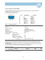
APPLIED ELECTRONICS, Co Ltd.
USER MANUAL
A power supply for the magnetron
sputtering systems
APEL-M-5PDC
Please, carefully read this instruction before use and save it.
1
Contents
1. Introduction ......................................................................................................................................3
2. Function............................................................................................................................................3
3. Safety precaution..............................................................................................................................3
4. Package contents ..............................................................................................................................3
5. Operating principle...........................................................................................................................3
6. Specification.....................................................................................................................................5
7. General guidance before use ............................................................................................................6
7.1. Unpacking of power supply ......................................................................................................6
7.2. Installation procedure................................................................................................................6
7.3. Setting-up procedures................................................................................................................6
8. Operating procedure.........................................................................................................................6
8.1. Start-up procedures ...................................................................................................................6
8.2. Arrangement and appointment of control and adjustment ........................................................7
8.3. Information in LCD display ......................................................................................................8
8.4. Sockets and slots arrangement ..................................................................................................8
8.5. Power supply in use...................................................................................................................9
9. Design...............................................................................................................................................9
10. Circuit scheme description .............................................................................................................9
10.1 Force diagram description (Annex B)......................................................................................9
10.2 Control logic and drivers description (Annex C) ...................................................................10
10.3 Controller scheme description................................................................................................12
11. Troubleshooting ...........................................................................................................................16
12. Maintenance .................................................................................................................................16
13. Storage regulation ........................................................................................................................17
14. Transportation ..............................................................................................................................17
15. Guarantee maintenance ................................................................................................................17
Annex A. Interface controller RS485.................................................................................................18
Annex B. Force diagram ....................................................................................................................22
Annex C. Inverter schematic..............................................................................................................23
Annex D. Inverter driver ....................................................................................................................24
Annex E. Output switch schematic ....................................................................................................25
Annex F. Output switch driver...........................................................................................................26
Annex G. Contactor’s driver ..............................................................................................................27
Annex H Ignition board schematic ....................................................................................................28
Annex I. Analog controller schematic................................................................................................29
Annex J. Digital controller schematic ................................................................................................30
2
1. Introduction
Thank you for purchasing the power supply APEL-M-5PDC series!
Before operating, please read this operation manual carefully. The manual should then be stored
for future reference in case of operating difficulties or functional descriptions.
2. Function
The power supply APEL- M-5PDC is designed for supply regulated voltage DC and pulsed current
for the magnetron sputtering systems up to 5 kW which are used in the process of vacuum
deposition of thin film coatings.
Operating conditions:
1) Temperature of air from a minus 10 to plus 25 0С;
2) Relative humidity of air up to 95 % at temperature plus 25 0С.
The power supply is made in a standard (19 inches) case.
Can be used in a vacuum sputtering system, as well as for scientific purposes in the study of
vacuum discharges.
3. Safety precaution
Place the power supply only in closed rooms with controlled temperature and humidity.
Before turning on the power supply must be grounded through the terminal located at the back
panel “ “
For maintenance and repairs are not allowed contact with current-carrying
elements, as on a power supply terminal block, there is an alternating voltage (200 V) and a output
voltage amplitude up to 650 V.
Do not attempt to service this power supply yourself. Please refer any service to the service centre.
Be sure to turn the unit off and disconnect the AC power cord before maintaining the unit.
4. Package contents
A delivery set includes:
•
Power supply APEL-M-5PDC;
•
Connection cable for three-phase mains (3 meters)
•
Output cable for the load supply (3 meters);
•
User manual;
•
Diagram manual.
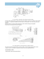
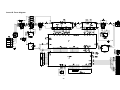
5. Operating principle
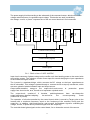
3
Load
Output circuit
Output switch
HF
transformer
Invertor
Diode bridge
Input circuit
~ 200 В
The power supply is built according to the schematic of the resonant inverter, which converts the
voltage mains frequency in regulated output voltage. This device can work in stabilizing
the voltage, current, or power. response time of the arc control less that 0.5 microsecond
Control board (analog)
Control board (digital)
Control panel
Pic. 1. Block-schem of APEL-M-5PDC.
Input circuit commutes 3-phase voltage on the rectifier unit, then handing power to the control units
and cooling system. The inclusion consist of two steps for smooth charging the input capacitance
of the inverter through a rectifier.
The inverter is a transistor bridge, which converts the DC voltage at the input capacitances to
the AC sinusoidal. This voltage is passed through a resonant circuit to step-up transformer, which
acts as a galvanic isolation between input and output source.
Output switch transfers energy to the output circuit, and serves
supply from short circuits, arcs, as well as to implement a pulsed mode.
The output circuit consists of 2
output inductance, therefore adapting
(continuous or pulsed).
to
protect the
power
throttles, switching between them can change the
the source for
the
correct operating
mode
The operation of all units controlled by the control board, which is served by Target pulse to the
inverter (with a maximum frequency equal to the frequency of the resonant circuit) and the
output key. In addition, this board receives and converts the feedback signal for stabilizing the
voltage, current, or power and a protection signal from the output key.
The controller board gives signals to the control board, for an interactive control of the source.
4
6. Specification
Table 1. Performance specification for APEL- M-5PDC
Value
Characteristic
Output voltage
3х200V, 50/60 Hz
Output power
5 kW
Power consumption
5,6 kW
Output voltage adjustment range
65 - 650 V
Control range of the average output current
0,1 - 8 A
Control range of the average output power
0,5 - 5 kW
An amplitude of the ignition impulse
1000 V
Output voltage type
Negative DC or pulsed
Control range of the impulse frequency
1 - 100 kHz with step 1 kHz
Control range of the duty factor
10 - 80 % with step 1%
Stabilization mode
by voltage, current, or power
Stabilization accuracy
The amplitude of the current protection
<5%
12А in DC mode
10 А in pulsed mode
The reaction time for arcing
<0,5 microsecond
Indication
LCD display
Cooling
Air
Blocking input
Yes
Weight
20 kg
Case
4 U, 19”
Interface
RS 485
5
7. General guidance before use
7.1. Unpacking of power supply
For power supply unpacking it is necessary to open the top cover of a transport box, after removing
steel belts from a box and to take out the power supply. The operational documentation and power
cables are laid inside the transport box. After unpacking power supply to check up completeness
according to section 3. By external survey to be convinced of absence of defects and breakages.
At repeated packing PS together with power cables and the operational documentation are
packed into a polyethylene film and are located in a transport box. Amortizing materials in a
transport box are pads and supplementary sheets from goffered cardboard or foam.
7.2. Installation procedure
It is necessary to make external survey:
• Completeness according to section 3;
• Absence of visible mechanical damages;
• Presence and durability of fastening of control systems;
• Cleanliness of sockets, connectors and plugs.
7.3. Setting-up procedures
Before you begin, carefully examine the technical description and operating instructions, as well
as get acquainted with the location and purpose of management and control on the front and rear
of the unit. Then to place the power supply at the desk and providing conditions for the natural
ventilation.
Set "Network" switch on the back and switch on the front panel to the bottom position. Set
grounding on the device and connect AC 3-phase output cables.
Note: a terminal “+” is connected with the ground inside a case of the power supply.
8. Operating procedure
8.1. Start-up procedures
Automatic main switch and power switch set at the up position, it’s should light up the LCD display
and LEDs on the front. Set using encoder the options and modes.
By REGULATION button choose a stabilization mode of voltage, current, or power
6
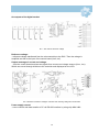
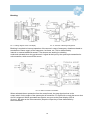
8.2. Arrangement and appointment of control and adjustment
Pic. 2 Power supply control panel
Control panel buttons function
“ON”
“OFF”
“TIMER START/STOP”
“TIMER RESET”
“F1”
“F2”
“REGULATION ”
Output voltage, on and off buttons:
After pressing the button On, output voltage is applied
After pressing the button Off, output voltage is removed
Timer control buttons
Start/stop timer
Timer reset
Other buttons:
Switch synchronization mode
Not used
Chose a stabilization mode:
by power, current, or voltage
Note: Activation of the button, take place after release
(pressing followed by a LED indicator and a single sound signal).
LED indication
“ARC”
“RAMP”
“VOLTAGE”
“CURRENT”
“POWER”
Arc defense LED. Lights when the magnetron discharge passes at an
arc shape, or the current exceeds the maximum value of the
magnetron
Indicator of compliance with the current value of voltage, current, or
power setpoint.
If the indicator blinks, the discrepancy exceeds 10%, which indicates
the failure mode in chamber. For example, you set the mode at
stabilization current value of 6A, but this current is not achieved at the
maximum output voltage (1000V).
LED of the chosen stabilization mode
Voltage
Current
Power
Encoder operarion
Encoder - control knob for changing the output power source parameters
Decrease / increase the selected parameter
Rotation
Choosing a variable parameters
Pressing
7
8.3. Information in LCD display
Pic.3 LCD display at the work mode, impulse (right) and DC mode (left)
Information on the LCD display in impulse (left) and DC (right) modes
Information about the state of the power supply is reflected in two columns by 4 rows. The
left column is information about the set parameters of power source in the right column information about current settings.
Symbol
Description
Symbol
Description
Ur, (Ir, Pr)=000 V
U=000 V
A setting of the stabilized parameter, for changing
Current value of the output voltage
turn the encoder.
Depending on the selected mode of
stabilization is reflected a setpoint
voltage (Ur), current (Ir), or power (Pr)
I =0.00 A
Mode= LF (DC)
Current value of the output current
Indicator of the working mode: pulse mode with a
In pulse mode is a value of an average
low frequency or DC mode, for changing turn the
current
encoder.
If the power supply is in work a regime change is
not possible
P=0.00 kW
F=00 kHz
Current value of the output power. In
A setting of the impulse repeat frequency in the
pulse mode is a value of an average
pulse mode, for changing turn the encoder.
power
If the power supply is in work a frequency
change is also possible. In DC mode is not
available.
T=00%
00:00 (min:sec)
Duty cycle, for changing turn the encoder.
Timer
If the power supply is in work a duty cycle
change is also possible. In DC mode is not
available.
The cursor indicates the parameter that will vary with the rotation of the encoder.
Moves by pressing the encoder.
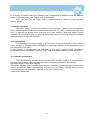
8.4. Sockets and slots arrangement
Pic. 4 Power supply back panel
8
An appointment of the installation connectors and terminals
POWER
ABC
N
“+ –“
RS-485
Automatic power switch
Terminals for the mains (AC 3-phase)
Neutral
Terminals for the load
Connectors of remote control and blocking contacts (connected in
parallel )
Grounding
8.5. Power supply in use
The power supply control can be performed locally or a from remote control via RS-485.
9. Design
Power supply APEL-M-5PDC is design as a separate portable unit. Elements of the unit's body are
held together with screws.
Partial disassembly:
- Unscrew 4 screws on the top cover unit;
- Remove a bottom cover if it needs
- Assembly in the reverse order
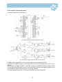
10. Circuit scheme description
10.1 Force diagram description (Annex B)
The power supply is connected to the 3-phase network through an automatic switch A1.
When switching button A4 closes contactor K1, turn the electric supply on, block A5, which feeds
the fans, control board and the controller. The input capacitance of the inverter A7 begins to
charge through a resistors R1 and R2 . Then from the control board comes impulse to
a drivers contactor A3, which switch on a contactor K2. Resistors are shorted and the inverter is
fed full voltage through a rectifier A2. Resistor R3 is connected via contactor K1 on a normally
closed contact. R3 is a discharge resistor for the capacitance of the inverter.
Inductance L1 and the input capacitance of the inverter input is a surge filter.
The inverter is a transistor bridge, which converts the DC voltage at the input capacitances to the
alternating sinusoidal (inverter circuit in Appendix 2.1). Each part of the inverter is controlled by 2channel driver, A14 and A15 (Annex 2.2).
Transformer TR1 performs the function of electrical isolation, but also increases the input voltage
to the required level. Choke L4-inductance of the resonant circuit.
Output switch A17 (Annex 2.3) transfers energy to the output circuit, and serves to protect the
power
supply from short
circuits
and to
implement a
pulsed mode. Management by
driver output switch A16(Annex 2.4).
The output circuit consists of 2 chokes L2 and L3, switching between them can change the
output inductor, thereby adapting
the source for
the
correct operating
mode
(continuous or pulsed). Switching occurs downstream contactor K3, which is controlled by the
driver A12(Annex 2.5).
9
The work of all blocks controlled by the control board A8, which gives a target pulse to the
inverter (with a maximum frequency equal to the frequency of the resonant circuit) and the
output switch. In addition, this board receives and converts the feedback signal for the stabilization
of voltage and current. And a protection signal from the output switch to suspend an operation of
the inverter.
Analogue controller A9 generates signals to digital controller, providing interactive control with the
remote A11 (raising output parameters, switching modes of operation) and carries the indication.
10.2 Control logic and drivers description (Annex C)
Voltage stabilization schematic:
Voltage divider is installed at the output capacity, which serves as a voltage sensor. From lowresistance part of the voltage divider is taking off a voltage(1 - 10V), and is put on
the connector XT9. Next is a divider arrangement for fine-tuning the signal from the sensor
voltage. DA1, O1, DA5 consists of 2 operational amplifiers (op amp), which function as input and
output buffers for the opto-coupler O1(following the documentation requirements for IL300). O1 is
a linear optocoupler, the input voltage is equal at its output. Optocoupler is needed for galvanic
isolation of circuit control board and power schemes. Microcircuits power supply is galvanically
isolated.
The output signal of the sensor voltage DA5 follows on the operational amplifier DA2, and on the
controller board to convert and display as an values of output voltage through a repeater DA6. If
the level will exceed 10 V, the comparator DA11 will put "0" input circuits DD6: 2, which turns
off the inverter control. At the input of the comparator 2, the reference voltage 10V is formed
by resistor R13, at the input 3 a resistor R29 is setting to exceed 10V. DA2 has 2
inputs: 2 output signal from the DA5, to pin 3 signal from the controller board. The signal from
the controller board is a setting (a constant voltage -10V). DA2 converts both signal Vout = (U2U1) x Koc, where U2 -setting, U1 - signal from the voltage sensor, Koc - coefficient. of feedback.
If U2 <(=) U1, Vout is reset to 0. Koc is given by nominal resistance R2 (100k, which corresponds
to Koc = 10). A time constant of the feedback (~ 10ms) is determined by the capacitor C1. A
voltage reference diode at the output is set for the limiting an output voltage to 10V.
DA2 output goes to analog switch DA3, which is managed by a board of control, which works like a
normal key. DA2 output goes to analog switch DA3, which is managed by a board of
control, which works like a normal key. If pin 1 will be put "0" - this means that pins 2 and 3 are
closed (according to the selected mode).
From DA3 signal is applied to the converter voltage-frequency DA8,which in the presence
of voltage
at
the
input generates
a square
wave.
If the input voltage increases - increases the output pulse frequency to the maximum, which is
set by the clock.
The clock generator is a multivibrator, built on a 3-logic elements"2NAND" DD9 :1-9: 3. A
frequency range is selected by the resistor R32 and capacitor C30. Resistor R33 adjusted
the frequency (200 kHz).
At the output of is a trigger DA8 DD3: 2, which serves to disable the inverter control: pin
1 connector XT17. Through the intermediate cascades required for other parts of the
scheme, which will be described below, includes a trigger DD3: 2. If the trigger input 2 DD3:2 set to
"0", it means that its output will be a constant "0". An integrated circuit "2I" DD4:1 will expose the
constant "0" on the output - this means a ban on the passage of impulses from the DA8.
Gate multivibrator DD1:1 is located after DD4:1. At the output of 5 and 12 are always "0" and "1",
respectively. It is included so that at the input 9 by changing from "1" to "0" - 5 is formed at the
output of a single pulse of "0" to "1", the output 12 of the "1" to "0" duration determined by the RC chain of C16, R53 (~ 6us). The output of the gate multivibrator is connected to the trigger DD3: 1,
which switches between an inverter control channels (O3-O6, O4-O5). The maximum operating
10
frequency of the inverter is determined by the half-frequency clock generator. Control arranged
through the optocouplers O3-O6
Current stabilization schematic:
1. Stabilize the current scheme is similar to the voltage stabilization circuit.
For the current stabilization standard current probe is used, which is powered from the control
board by bipolar ± 15V and provides an output DC voltage of 1 -10V to connector XT13. Next is a
divider R20, R27 for fine-tuning the signal from the sensor voltage. Immediately after
the divider signal via repeater DA10 displayed on the controller board.
Then the signal applied to the operational amplifier DA4, which has 2 inputs. The second
output signal from the current sensor goes to pin 3 with the controller board. The signal from
the controller board is a setting (a constant voltage - 10V). DA4 converts both signals on the basis
of Vout = (U2-U1) x Koc, where U2 - setting, U1 - the signal from the voltage sensor, Koc coefficient. of feedback.
If U2 <(=) U1, Uout is reset to 0, otherwise it is a formula. Koc is set by nominal resistance R21
(100k, which corresponds to Koc = 10). A capacitor C4 is determined by the time constant of the
feedback. Stabilitron at the output is set to limit the output voltage to 10V.
Similarly, stabilization scheme for voltage from the output DA4 , signal applied to the voltagefrequency converter via analog switch, which is included in the current stabilization mode.
Power stabilization schematic:
- the
multiplier DA7 fed signals from
the
sensors voltage
and
current,
where they multiply and get "feedback signal power." Further, the same modes of stabilization of
current and voltage at the input of the operational amplifier is fed DA9 setting for power and signal
from the multiplier.
Output switch control:
The control is performed by signals from the controller board: depending on the mode of the
source (continuous or pulsed) through the connector XT15. Signals have logical form (DC mode fixed signal amplitude 5V, LF mode pulse sequence with a given frequency and duty
cycle). Through intermediate stages, and served optocoupler plug XT10 and then on the switch
driver.
Power supply protection:
When driver output key protection is activated on the connector XT12 comes with
a driver signal "fault". At the output of the optocoupler O10 find a permanently logical "1", and
when ignited the optocoupler LED is reset to "0". This signal goes to the monostable DD8: 2, which
includes the decay of the input 1 is included at the time determined by R9 and C27. This time the time intervals between tripping of protection, it adjusts to the desired value resistor R9 (2-3ms).
Monostable generates the outputs of 13 and 4, "1" and "0", respectively. The signal from the output
4 goes to the input of DD2:2, which breaks the chain of key management, and therefore stops
the work, as well as DD7: 3, which stops the inverter. The outputsignal 13 goes to the controller
board to display the current protection on the panel display and resets the current set point,
exposing the "1" at pin 16 DA3 (in the case of mode stabilization by current).
Other:
The scheme was built DD1: 2 is used to test the inverter control circuit phase adjustment. To do
this, jumper J2. And closing
the
findings J1 generate one-time control
pulses.
DD6: 1 is used for generating control pulse to activate the contactor through time 1s after
power source.
11
10.3 Controller scheme description
Controller schematic is in the annex 4.
Pic. 5 Microcontroller Atmega128. Signal generation:
Pic. 6 Scheme of control signals formation for output switch
Forming of the output switch control signals making by the chipCD74HC221E.
At the inputs R and B is always 1, the output pulse occurs at the transition from 1 to 0 on the
input A.
In the absence of signal PROTECT_SWITCH, formed an impulse low duration of about 10 ms.
Control signals are generated by the key of these pulses and the control signal (PWM1) to the
microcontroller, which receives the input of the chip 74HC00.
The received signals are sent to the input circuits 6N137 for their separation.
12
An outputs of the digital socket:
Pic. 7 The chain of reference voltage
Reference voltage:
- reference voltage transferred from the microcontroller to the DAC. Then the voltage is
amplified and fed to the input of the control board (Uref, Iref).
Output meterage of current and voltage:
- from the control board receives two signals from current and voltage sensors (Ucur, Icur).
Which are served through dividers to the controller and displayed on the LCD.
Pic. 8 Scheme of reference voltages formation and receiving voltage and current data
Power supply control:
- source control and data transfer to PC via RS-485 interface by using chip MAX1480.
13
Pic. 9 The scheme of organization and management (interface RS485)
Circuits mode is determined by state input and control signals. Outputs A and B of a chip included
by setting 1. If outputs are enabled, the device acts as a transmitter. If on the contrary, then the
receiver.
Survey of button on the front panel implement by the controller through an expander.
Each button is accompanied by sound signals
Pic. 10 Wiring diagram for control panel buttons, encoders and buzzer
The source control is implemented by encoder rotation, which changes supports the current,
voltage or power, and switch an operation modes of the source (pulsed and DC).
Current Data on LCD:
- Data transfer via the LCD chip 74HC244.
14
Blocking:
Pic. 11 Wiring diagram of the LCD display
Pic. 12 Scheme of blocking arrangement
Blocking is required to interrupt operation of the source in case of emergency situations related to
termination of water supply to the magnetron, hot items, etc. This is determined by
internal or external additional sensors. The sensors are working in switching
mode and activated when the gap shorted. A signal at the input by the optocouple transmitted to
microcontroller, which turns off the source.
Pic. 13 Button connection schematic
When activated the arc protection from the control board, the stop signal arrives to the
output switch. At the output of the optocoupler is formed the "0" signal with a result that a one-shot
circuit is triggered. Which generates two signals: one goes to the panel display (LED is
lit «arc»), the other on the microcontroller (stops the output key to time determined by
the monostable).
15
An ignition and the output switch
Pic. 14 An ignition control schematic
The controller generates ignition control pulses (30ms with a pause of 1s), which run through
the optocoupler to ignition.
An inductance is changed by the output switch with switching modes (impulse or DC)
A control impulse is given by the controller through the optocoupler to the output switch driver.
11. Troubleshooting
Do not attempt to service this power supply yourself. Please refer any service to the service centre.
Be sure to turn the unit off and disconnect the AC power cord before maintaining the unit.
Most possible problems and instructions for their removal are shown in the tabl. 2
Table 2. Most possible problems and instructions for their removal
Problem
Possible reason
Suggested Solution
LCD display works incorrect or
didn’t work
Power supply works only in DC
mode (output voltage in impulse
mode is similar DC mode)
There is no flick when the power
supply switchs in impulse mode.
Interference induction
Check case grounding
Fault of output switch
transistor
Replace output switch
transistor
1) Contactor’s driver works
incorrect
2) Open circuit
1) Needs to check and
repair a drivers board
2) Search the open circuit
12. Maintenance
Maintenance works are should be at least 1 time a year. For the maintenance of a device during
term of its operation needs to include following works:
a) External survey of the device condition;
1. Check a fastening of control and adjustment units
2. Check a completeness of the device;
3. Check a condition of paint and galvanic coverings;
16
b) To survey an internal state of an assembly and a components is carried out after the warranty
period. A fastening of the units, remove a dirt and corrosion.
Note: The dust from the power supply is recommended to remove by the household
vacuum cleaner.
13. Storage regulation
The power supply, arrived to the customer for long storage, contains in the transportation
box in capital heated premises with the temperature of air from 5 to 300С at relative humidity up to
85 %. In premises for storage there should not be a dust, steams of acids and alkalis, causing
corrosion. At commissioning it is necessary to release the device from packing and to put in normal
conditions within not less than one hour.
14. Transportation
Transportation of the power supply to the consumer in transport container can be carried
out by all types of transport without acceptance of additional measures at the temperature of air
from minus 50 to plus 500С.
In the process of transportation the protection of the device against falling, atmospheric
precipitation and dust should be provided. It is not supposed racking and turning over the device.
15. Guarantee maintenance
The manufacturer guarantees that the product APEL-M-5PDC conform to requirements of
technical documentation. follow all terms and rules of operation described in this manual.
Guarantee period 2 years after shipping.
This limited warranty covers manufacturing defects in materials and workmanship encountered in
normal, and shall not apply to the following, including, but not limited to: damage which occurs in
shipment; delivery and installation; applications and uses for which this
product was not intended.
17
Annex A. Interface controller RS485
Using RS 485 interface is possible to control the power supply from PC. Synchronization is
available only on the bottom connector.
Assigning RS 485 connector pin:
5 4 3 2 1
Pin
9 8 7 6
Table 1. Coupling parameters
Designation
A
B
GND
Blocking+
Blocking Synch. out Synch. out +
Synch. in Synch. in +
1
2
3
4
5
6
7
8
9
Element
Function
Receive
Transmit
Ground
Blocking+
Blocking Synch. out Synch. out +
Synch. in Synch. in +
Control object
Interface
Rate of exchange
RS-485
19200 BPS
Protocol
Digit capacity
Method of interaction
Modified ModBus RTU
8-Bit binary-number system
Half-duplex
Communication
parameters
Symbol table
No
Number of stop bits
2
Data format
Mode of Parity check
inspecti
Formatting check
on
Checksum
8
No
No
Always available - CRC
Push OFF button and turn on power supply to check the port address. If necessary, you can
change the actual port address using encoder. For the saving a new address push OFF button
one more time.
The power supply is controlled by remote PC with modified Modbus RTU protocol. Actual protocol
using two function F3 and F6, power supply address on default equal 1.
Table 2. F3 function
Data
Byte number
Address
Slave(1)
1
Function(3)
Numbers of
registers
3
2
F3 function can be read in the following form:
18
Upper byte
CRC
4
Lower byte
CRC
5
Table 3. Inquiry answer (F3 function)
Data
Address
(Master)
Function
(3)
Numbers of
registers
Upper byte
Ucur
Lower byte
Ucur
Byte number
1
2
3
4
5
Upper byte
Icur
Lower byte
Icur
Register
LED
Register
STATUS
Upper byte
CRC
Lower Byte
CRC
6
7
8 (tabl. 4)
9(tabl. 5)
10
11
Note: Function F3 can be readied in 15 ms after last operation.
Table 4. Register LED
Byte number
Value
0 LED on, current stabilization
1 LED on, voltage stabilization
2 Output LED on “stand by” (Ramp)
3 Not used (F2)
4 LED, power supply ON
5 LED, power supply OFF
6 LED, synchronization ON
7 LED on, stabilization by power
Note: LED is glow if byte value is equal zero.
Таблица 5. Register STATUS
Byte number
0 Run mode
0-DC mode
1-HF mode
1 Not used
2 Not used
Value
3 Locking
0-OFF
1-ON
4 Not used
5 Not used
6 Not used
7 Not used
The power supply controller works correctly if:
1 Port address is correctly defined
2 Checksum is correctly defined
3 Working address is 255
19
The power supply parameters realize by F6 function
Table 6. F6 function
Data
Address
Function
Register
(Master)
(6)
address
(Upper byte)
Byte number
1
2
3
Data Upper register
Lower
Register
register
(always
zero)
Byte number
5
6
7
Register address
(Lower byte)
Upper byte
CRC
4 (табл. 7)
Lower byte
CRC
8
9
An equivalence between register address (lower byte) and register value is in the next table.
Table 7. An equivalence between register address (lower byte) and register value
Data
3
4
5
6
Equivalence
Not used
Register status (quantized input)
0ON
1OFF
2Not used
3Reset the timer
4HF mode
5Synchronization mode is turning off
6Synchronization mode is turning on
7DC mode
Register mode switcher
0- voltage stabilization
1- current stabilization
2- stabilization by power
Setting value (voltage) 100 ..650 (100-650 V)
Setting value (current) 10..80 (1.. 8А)
Setting value (Power) (5..50) (0.5..5 kWt)
Setting value (frequency) 1..50 (1..50kHz)
7
Setting value (time of the impulse) 10..80 (10..80%)
0
1
2
Checksum function complies with ModBus RTU standart.
An example calculation is given below:
// CRC - cyclic redundance check – only in RTU mode
unsigned int mbfCRC(int cnt,unsigned char volatile * buf)
{
int
i,j;
unsigned f;
mbCRC = 0xFFFF;
for (i = 0; i<cnt; i++)
{
mbCRC = mbCRC ^ buf[i];
for (j = 1; j <= 8; j++)
{
f = mbCRC & 0x0001;
20
mbCRC = mbCRC >> 1;
if (f) mbCRC = mbCRC ^ 0xA001;
}
}
f= mbCRC >> 8;
mbCRC = (mbCRC << 8) | f;
return(mbCRC);
//**
Reverse byte order.
21
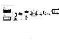
Annex B. Force diagram
Конт
Цепь
Цепь
Конт
Фаза А
Фаза В
Фаза С
N
GND
Конт
Цепь
RXD
TXD
SHUTTER
BLOK BLOK +
Конт
Цепь
RXD
TXD
SHUTTER
BLOK BLOK +
22
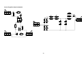
Annex C. Inverter schematic
Конт
1
2
Цепь
23
Annex D. Inverter driver
Цепь
Конт
1
2
1
Конт
2
Цепь
Цепь
Конт
1
2
3
2
1
Конт
Цепь
Конт
1
2
3
24
Цепь
Annex E. Output switch schematic
Цепь
Конт
1
2
Цепь
Конт
Цепь
1
2
25
Конт
1
2
3
Annex F. Output switch driver
Цепь
Цепь
Цепь
Конт
1
2
Конт Цепь
1
2
3
4
5
Конт
1
2
3
Конт
1
2
26
Annex G. Contactor’s driver
Цепь
Конт
1
2
1
Конт
2
Цепь
Конт
1
2
27
Цепь
Annex H Ignition board schematic
Цепь
Конт
1
2
Конт
1
2
Цепь
Цепь
Конт
1
2
Конт
Конт
1
2
Цепь
1
2
28
Цепь
Annex I. Analog controller schematic
цепь
контакт
цепь
контакт
цепь
контакт
цепь
контакт
цепь
контакт
R74 100k
цепь
контакт
контакт
цепь
цепь
цепь
контакт
цепь
контакт
цепь
контакт
контакт
контакт
контакт
29
цепь
контакт
цепь
контакт
цепь
цепь
контакт
цепь
контакт
цепь
Annex J. Digital controller schematic
Конт.
1
2
3
4
5
6
7
8
9
10
11
12
Цепь
Цепь
Конт
1
2
Конт
1
Конт.
Конт.
1
2
Цепь
Цепь
1
2
3
3
4
5
3
6
7
8
4
5
6
7
9
10
11
8
9
10
12
13
14
Цепь
2
3
Конт.
1
2
Цепь
3
4
5
6
7
8
9
10
11
12
13
14
15
16
Конт
1
1
&
3
&
6
Цепь
2
3
2
1.5k
1
2
3
14
15
A
B
R
CX
RCX
Q
nQ
13
4
4
Конт
1
2
Цепь
3
5
Конт
1
9
&
Цепь
2
3
8
10
5
Цепь
Конт
1
2
12
Q
nQ
A
B
R
CX
RCX
9
10
11
6
7
Конт
1
Цепь
2
3
Конт
1
Цепь
2
3
Конт
1
Цепь
2
Конт
1
Цепь
2
Цепь
Конт
1
2
Конт.
1
2
3
4
5
6
7
8
9
10
Конт
1
2
3
Цепь
Конт
1
Цепь
2
3
Цепь
Конт
1
2
3
4
5
6
30
Цепь
Конт.
1
2
3
4
5
6
7
8
9
10
11
12
13
14
15
16
Цепь
APPLIED ELECTRONICS, Co Ltd. Tomsk, Russia.
Academichesky ave. 15 office 80, Tomsk, 634055, Russia. Tel.: +7(3822) 597451, Fax:
+7(3822) 491295
e-mail: [email protected], www.pronika.ru
31