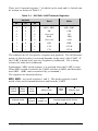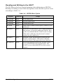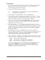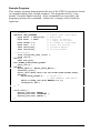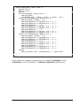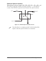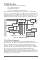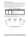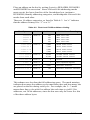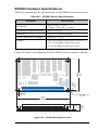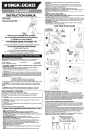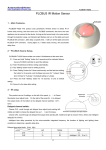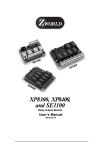
1
00 88 XP XP8700 and XP8800 RS-232 and Motion Control Expansion Boards Users Manual 000921 - D XP8700 and XP8800 Users Manual Part Number 019-0056 000921 - D Printed in U.S.A. Copyright © 1999 Z-World, Inc. All rights reserved. Z-World reserves the right to make changes and improvements to its products without providing notice. Trademarks ® Dynamic C is a registered trademark of Z-World, Inc. ® Windows is a registered trademark of Microsoft Corporation PLCBus is a trademark of Z-World, Inc. ® Hayes Smart Modem is a registered trademark of Hayes Microcomputer Products, Inc. Notice to Users When a system failure may cause serious consequences, protecting life and property against such consequences with a backup system or safety device is essential. The buyer agrees that protection against consequences resulting from system failure is the buyers responsibility. This device is not approved for life-support or medical systems. All Z-World products are 100 percent functionally tested. Additional testing may include visual quality control inspections or mechanical defects analyzer inspections. Specifications are based on characterization of tested sample units rather than testing over temperature and voltage of each unit. Z-World may qualify components to operate within a range of parameters that is different from the manufacturers recommended range. This strategy is believed to be more economical and effective. Additional testing or burn-in of an individual unit is available by special arrangement. Company Address Z-World, Inc. 2900 Spafford Street Davis, California 95616-6800 USA Telephone: Facsimile: Web Site: E-Mail: (530) 757-3737 (530) 753-5141 http://www. z w orld.c om [email protected] TABLE OF CONTENTS About This Manual vii XP8700 Chapter 1: Overview 13 Chapter 2: Getting Started 15 Chapter 3: I/O Configurations 19 Chapter 4: Software Reference 33 XP8700 Components ........................................................................... 16 Connecting Expansion Boards to a Z-World Controller ...................... 17 Setting Expansion Board Addresses .................................................... 18 XP8700 Addresses .......................................................................... 18 Power ................................................................................................... 18 XP8700 Pin Assignments ..................................................................... 20 Using Expansion Boards ...................................................................... 20 XP8700 Operation ............................................................................... 21 Signetics SCC2691 UART .............................................................. 21 Reading and Writing to the UART .................................................. 26 Controlling the UART .................................................................. 27 Communicating ............................................................................... 29 Interrupts ......................................................................................... 30 Delays ............................................................................................. 31 Expansion Board Addresses ................................................................ 34 Logical Addresses ........................................................................... 34 Dynamic C Libraries ............................................................................ 35 XP8700 Software ................................................................................. 36 General Functions in DRIVERS.LIB .............................................. 36 UART Support Functions ................................................................ 37 RS-232 Communication Support .................................................... 38 XMODEM Support ......................................................................... 40 Miscellaneous Functions ................................................................. 41 Sample Project ................................................................................ 42 XP8700/XP8800 Table of Contents s iii XP8800 Chapter 5: Overview 49 Chapter 6: Getting Started 51 Chapter 7: I/O Configurations 55 Chapter 8: Software Reference 73 XP8800 Overview ............................................................................... 50 Features ........................................................................................... 50 XP8800 Components ........................................................................... 52 Connecting Expansion Boards to a Z-World Controller ...................... 53 Setting Expansion Board Addresses .................................................... 54 XP8800 Addresses .......................................................................... 54 Power ................................................................................................... 54 XP8800 Pin Assignments ..................................................................... 56 Header H5 Signals .......................................................................... 56 Screw Terminal Block H6 Signals .................................................. 57 Sample XP8800 Connections .......................................................... 58 Optional Optical Isolation ............................................................... 59 Using Expansion Boards ...................................................................... 60 Resetting XP8800 Expansion Boards ........................................... 60 XP8800 Operation ............................................................................... 62 PCL-AK Pulse Generator ................................................................ 62 Communicating with the PCL-AK ................................................ 63 Registers ....................................................................................... 64 Acceleration/Deceleration Rate (ADR) Register ....................... 65 Status Bits ..................................................................................... 66 UCN5804 Motor Driver IC ............................................................. 67 Driver Power................................................................................. 68 Quadrature Decoder/Counter .......................................................... 69 Control Register .............................................................................. 70 PLCBus Interrupts ........................................................................... 71 Expansion Board Addresses ................................................................ 74 Logical Addresses ......................................................................... 75 Dynamic C Libraries ............................................................................ 76 XP8800 Software ................................................................................. 77 Data Structures ................................................................................ 77 Interrupts ......................................................................................... 78 XP8800 Driver Functions ............................................................... 79 Miscellaneous XP8800 Function Descriptions ............................... 81 Sample Program .............................................................................. 87 iv s Table of Contents XP8700/XP8800 APPENDICES Appendix A: PLCBus 93 PLCBus Overview ............................................................................... 94 Allocation of Devices on the Bus ........................................................ 98 4-Bit Devices .................................................................................. 98 8-Bit Devices .................................................................................. 99 Expansion Bus Software ...................................................................... 99 Appendix B: Specifications 105 XP8700 Hardware Specifications ...................................................... 106 XP8800 Hardware Specifications ...................................................... 107 Appendix C: Connecting and Mounting Multiple Boards 109 Connecting Multiple Boards .............................................................. 110 Mounting Expansion Boards .............................................................. 112 Index XP8700/XP8800 113 Table of Contents s v Blank vi s Table of Contents XP8700/XP8800 ABOUT THIS MANUAL This manual provides instructions for installing, testing, configuring, and interconnecting the Z-World XP8700 RS-232 and XP8800 motion control expansion boards. Instructions are also provided for using Dynamic C functions. Assumptions Assumptions are made regarding the user's knowledge and experience in the following areas. Ability to design and engineer the target system that the controller used with the XP8700 or XP8800 expansion boards will control. Understanding of the basics of operating a software program and editing files under Windows on a PC. Knowledge of the basics of C programming. $ The C Programming Language by Kernighan and Ritchie C: A Reference Manual by Harbison and Steel Knowledge of basic Z80 assembly language and architecture for controllers with a Z180 microprocessor. $ For a full treatment of C, refer to the following texts. For documentation from Zilog, refer to the following texts. Z180 MPU User's Manual Z180 Serial Communication Controllers Z80 Microprocessor Family User's Manual Knowledge of basic Intel assembly language and architecture for controllers with an Intel386 EX processor. $ For documentation from Intel, refer to the following texts. Intel386 EX Embedded Microprocessor Users Manual Intel386 SX Microprocessor Programmers Reference Manual XP8700/XP8800 About This Manual s vii Acronyms Table 1 lists and defines the acronyms that may be used in this manual. Table 1. Acronyms Acronym Meaning EPROM Erasable Programmable Read-Only Memory EEPROM Electronically Erasable Programmable Read-Only Memory LCD Liquid Crystal Display LED Light-Emitting Diode NMI Nonmaskable Interrupt PIO Parallel Input/Output Circuit (Individually Programmable Input/Output) PRT Programmable Reload Timer RAM Random Access Memory RTC Real-Time Clock SIB Serial Interface Board SRAM Static Random Access Memory UART Universal Asynchronous Receiver Transmitter Icons Table 2 displays and defines icons that may be used in this manual. Table 2. Icons Icon $ ( Meaning Meaning Refer to or see ! Note Please contact 7LS Tip Caution )' Icon High Voltage Factory Default viii s About This Manual XP8700/XP8800 Conventions Table 3 lists and defines the typographical conventions that may be used in this manual. Table 3. Typographical Conventions Example Description while Courier font (bold) indicates a program, a fragment of a program, or a Dynamic C keyword or phrase. // IN-01… Program comments are written in Courier font, plain face. Italics Indicates that something should be typed instead of the italicized words (e.g., in place of filename, type a file’s name). Edit Sans serif font (bold) signifies a menu or menu selection. ... An ellipsis indicates that (1) irrelevant program text is omitted for brevity or that (2) preceding program text may be repeated indefinitely. [ ] Brackets in a C function’s definition or program segment indicate that the enclosed directive is optional. < > Angle brackets occasionally enclose classes of terms. a | b | c A vertical bar indicates that a choice should be made from among the items listed. A black square indicates pin 1 of all headers. Pin 1 J1 Pin Number 1 Measurements All diagram and graphic measurements are in inches followed by millimeters enclosed in parenthesis. XP8700/XP8800 About This Manual s ix Blank x s About This Manual XP8700/XP8800 XP8700 Blank This page is intentionally blank. CHAPTER 1: OVERVIEW Chapter 1 provides an overview and description of the XP8700 RS-232 expansion board. XP8700 Overview s 13 Z-Worlds XP8700 expansion board provides a simple way to add a UART to a control system built around a Z-World controller. The XP8700 connects directly to a PLCBus port. The XP8700 does not have the software drivers to enable it to be used with other Z-World controllers. The XP8700 may be connected on the PLCBus with other expansion boards. Up to four XP8700s can be addressed on a single bus. Unlike most other expansion boards, which take 12-bit addresses (4 bits at a time), XP8700s have 15-bit addresses, placed on the bus five bits at a time. The XP8700 features a Signetics SCC2691 UART, which is described briefly. The UART is operated by reading and writing to two registers on the XP8700, the control register (CTRL) and data register (DATA). In addition, the XP8700 may be used as an additional programming board for controllers with a PLCBus port. This frees up the existing RS-232 ports on the controller. The XP8700 also can raise a processor interrupt INT1. The manual discusses methods for dealing with several interrupting devices. Like other Z-World expansion boards, the XP8700 can be installed in modular plastic circuit-board holders attached to a DIN rail. The XP8700 can also be mounted, with plastic standoffs, on any surface that will accept screws. ! The XP8700 expansion board cannot be used as a Dynamic C interface to program the BL1700 controller. Such an interface is not supported by the BIOS. The Serial Interface Board 2 is available to program the BL1700 if there is a need to have all the BL1700 communication ports used by the application. The XP8700 expansion board may still be used on the BL1700s PLCBus to provide another RS-232 port. 14 s Overview XP8700 CHAPTER 2: GETTING STARTED Chapter 2 provides instructions for connecting XP8700 expansion boards to a Z-World controller. The following sections are included. XP8700 Components Connecting Expansion Boards to a Z-World Controller Setting Expansion Board Addresses XP8700 Getting Started s 15 XP8700 Components The XP8700 boards offer a modular RJ-12 jack (H2) and a standard 10pin header H1) to interface with other devices. Figure 2-1 illustrates the basic layout and orientation of components, headers, and connectors. U6 PAL U4 PAL U1 SCC2691 UART 3.686 MHz P1 P2 U5 Latch RN1 U2 RS-232 Driver C1 C3 C4 C2 R1 R2 D1 D2 H1 RS-232 Jack J1 H2 Figure 2-1. XP8700 Board Layout 16 s Getting Started XP8700 Connecting Expansion Boards to a Z-World Controller Use the 26-conductor ribbon cable supplied with the XP8700 to connect the XP8700 to the PLCBus on a Z-World controller. See Figure 2-2. The XP8700s two 26-pin PLCBus connectors, P1 and P2, are used with the ribbon cable. Z-World recommends using the cable supplied to avoid any connection problems. Controller PLCBus Port Pin 1 P1 1 P2 XP8700 Controller With PLCBus Figure 2-2. Connecting XP8700 Expansion Board to Controller PLCBus Be sure power to the controller is disconnected before adding any expansion board to the PLCBus. Follow these steps to connect an expansion board to a Z-World controller. 1. Attach the 26-pin ribbon cable to the expansion boards P2 or H2 PLCBus header. 2. Connect the other end of the ribbon cable to the PLCBus port of the controller. Be sure pin 1 of the connector cable matches up with pin 1 of both the controller and the expansion board(s). 3. If additional expansion boards are to be added, connect header P2/H2 on the new board to header P1/H1 of the board that is already connected. Lay the expansion boards side by side with headers P1/H1 and P2/H2 on adjacent boards close together, and make sure that all expansion boards are facing right side up. $ XP8700 See Appendix C, Connecting and Mounting Multiple Boards, for more information on connecting multiple expansion boards. Getting Started s 17 4. Each expansion board comes with a factory-default board address. If more than one expansion board of each type is to be used, be sure to set a unique address for each board. following section on Setting Expansion Board Ad$ The dresses, and Chapter 4, Software Reference, provide details on how to set and use expansion board addresses. 5. Power may be applied to the controller once the controller and the expansion boards are properly connected using the PLCBus ribbon cable. Setting Expansion Board Addresses Z-World has established an addressing scheme for the PLCBus on its controllers to allow multiple expansion boards to be connected to a controller. ! Remember that each expansion board must have a unique PLCBus address if multiple boards are to be connected. If two boards have the same address, communication problems will occur that may go undetected by the controller. XP8700 Addresses XP8700 expansion boards are shipped from the factory with no pins on header J1 connected. Each of the two registers on the XP8700 board is addressable on the PLCBus, with the jumper connections on pins 14 of header J1 determining the address of the register, as explained in Chapter 4. $ See Chapter 4, Software Reference, for further details on how to determine the physical address for XP8700 expansion boards. Power Z-Worlds expansion boards receive power from the controller over the +24 V and VCC lines of the PLCBus. XP8700 expansion boards use VCC, which is +5 V. The XP8700 typically draws about 80 mA at 5 V. 18 s Getting Started XP8700 CHAPTER 3: I/O CONFIGURATIONS Chapter 3 describes the built-in flexibility of the XP8700 expansion boards, and describes how to configure the available inputs/outputs. The following sections are included. XP8700 Pin Assignments Using D/A Converter Boards XP8700 I/O Configurations s 19 XP8700 Pin Assignments There are two RS-232 connectors on the XP8700 expansion board. One is a 10-pin header, H1, and the other is a 6-wire RJ-12 phone jack, H2. Either one can be used. Figure 3-1 shows the pin assignments for header H1 and RJ-12 jack H2. / OUT (/ RTS) GND / TXD / RXD / IN (/ CTS) 1 2 / TXD 3 4 / IN (/ CTS) /RXD 5 6 / OUT (/ RTS) 7 1 2 3 4 5 6 8 GND 9 10 Header H1 RJ-12 Jack H2 Figure 3-1. XP8700 Header H1 and RJ-12 Jack H2 Using Expansion Boards The following steps summarize how to use the XP8700 expansion boards. 1. Send a reset command to the PLCBus. 2. Place the address of the XP8700 registers on the PLCBus. Write a reset command to a CTRL register. 3. Write to the XP8700 registers as needed to control the XP8700. Read the internal registers to monitor what is happening. 4. Read the receive holding register (RHR) or write to the transmit holding register to communicate. These steps are done using software drivers in Dynamic C function libraries. $ Refer to Chapter 4, Software Reference, for the applicable libraries and where they are used. 20 s I/O Configurations XP8700 XP8700 Operation The XP8700 can be connected on the PLCBus with other expansion boards. Up to four XP8700s can be addressed on a single PLCBus. XP8700 expansion boards have 15-bit addresses, placed on the PLCBus five bits at a time. The XP8700 uses a Signetics SCC2691 UART, which is described briefly below. Two registers on the XP8700, the control register and the data register, are used to read and write to the UART. The XP8700 can also raise a processor interrupt, INT1. Methods for dealing with many interrupting devices are discussed. Signetics SCC2691 UART The SCC2691 UART is a full-duplex asynchronous receiver/transmitter. It supports 18 baud rates from 50 bps to 38,400 bps. Data may be framed with 5 to 8 data bits, four parity modes, and 1, 1.5, or 2 stop bits. The UART provides error detection (framing errors, parity errors, and overrun errors), break detection and generation, and echo. There are two diagnostic modes. The chip also has a multifunction 16-bit counter/time. The SCC2691 chip generates interrupts under seven maskable conditions. It has a low-power mode and a wake-up mode. Receiver data are quadruple-buffered (FIFO). The SCC2691 is controlled by reading or writing its internal registers. A counter or timer may be set up, RS-232 communication may be initiated, or control interrupts may be initiated. Options include setting baud rates, parity, and ot Figure 3-2 shows a block diagram of the SCC2691 architecture. D0D7 8 /READ /WRITE A0A2 RESET Bus Buffer Operation Control 3 Address Decode Read/Write Control /ENABLE Interrupt Control /INTR IMR ISR I/O Pins MPI Change of State Detector MPO Function Select Logic Communication Transmit Holding Register TxD Receiver Holding Registers (3) RxD MR1 & MR2 CR SR Timing Baud Rate Generator Clock Selectors Counter/Timer X1/CLK X2 CSR ACR CTUR CTLR Figure 3-5. SCC2691 Architectural Block Diagram XP8700 I/O Configurations s 21 There are 14 internal registers, 7 of which can be read, and 9 of which can be written, as shown in Table 3-1. Table 3-1. SCC2691 UART Internal Registers Address Read Write MR1, MR2 MR1, MR2 1 SR CSR 0 Reserved CR 1 1 RHR THR 1 0 0 Reserved ACR 1 0 1 ISR IMR 1 1 0 CTU CTUR 1 1 1 CTL CTLR A2 A1 A0 0 0 0 0 0 0 1 0 The address bits A2A0 specify a register only partially. The full determination of which register is accessed depends on the state of the UART. If the UART is being read, one set of registers is addressed. If it is being written, the other set is addressed. Furthermore, MR1 (mode register 1) is selected when the UART is reset. When MR1 is read or written, the UART switches to MR2, and thereafter uses MR2. (MR1 can be reselected by a command.) The registers are described below. MR1, MR2are mode registers 1 and 2. The mode registers control much of the serial communication to and from the UART. RxRTS control RxInt select channel mode error mode TxRTS control 22 s I/O Configurations parity mode CTS enable Tx parity type bits per char stop bit length (9/16–2 bits) XP8700 SRis the channel status register. The upper half of this register represents communication conditions. The lower half represents the condition of the receive and transmit buffers. MR1 bit 6 controls whether FIFO full (FFULL) or Receiver ready (RxRDY) is reported. received break framing error parity error overrun error TxEMT TxRDY FIFO full RxRDY disable Tx enable Tx disable Rx enable Rx CRis the RS-232 command register. miscellaneous commands The upper half of the CR register represents the commands, listed in Table 3-2, that can be given to the RS-232 channel. Table 3-2. CR Register Commands for RS-232 Channel CR[7:4] Command 0000 No command. 0001 Reset mode register pointer to MR1. 0010 Reset receiver. FIFO is flushed. 0011 Reset transmitter. 0100 Reset error status. 0101 Reset break change interrupt. 0110 Start break. Forces TxD output low (spacing). 0111 Stop break. 1000 Start counter/timer. Counter/timer registers must have been loaded. 1001 Stop counter. 1010 Assert /RTS on the MPO pin. 1011 Negate /RTS (on the MPO pin). 1100 Reset MPI change interrupt. 1101 Reserved. 111x Reserved. The lower half of the command register disables or enables the receiver and transmitter. XP8700 I/O Configurations s 23 CSRis the clock select register. receiver clock select transmitter clock select The upper half of the CSR register selects the baud rate of the receiver, while the lower half selects the baud rate of the transmitter. The two sets of baud rates, selectable by ACR bit 7 on the auxiliary control register, are listed in Table 3-3. Table 3-3. CSR Baud Rates Selected by ACR Bit 7 CSR Code ACR[7] = 0 ACR[7] = 1 0000 50 50 0001 110 110 0010 134.5 134.5 0011 200 150 0100 300 300 0101 600 600 0110 1,200 1,200 0111 1,050 1,050 1000 2,400 2,400 1001 4,800 4,800 1010 7,200 1,800 1011 9,600 9,600 1100 38,400 19,200 1101 timer timer 1110 MPI–16X MPI–16X 1111 MPI–1X MPI–1X 24 s I/O Configurations XP8700 CTU, CTL, CTUR, CTLRare the counter/timer registers. Register pairs CTUR/CTLR and CTU/CTL are the upper and lower halves of 16-bit counter/timer values. The counter/timer value is set through CTUR/CTLR and is read through CTU/CTL. THRis the transmitter holding register. It holds one character. RHRis the receiver holding register. RHR is actually the frontmost entry in a 3-character FIFO queue. (A receiver shift register constitutes the fourth buffer in a quadruple-buffering scheme.) IMR, ISRare the interrupt mask register and interrupt status registers. The interrupt mask register selectively enables or disables interrupts. MPI change MPI level — counter ready delta break RxRDY /FFULL TxEMT TxRDY The interrupt status register can be read to determine what caused the interrupt. MPI pin change MPI pin state — counter ready delta break RxRDY /FFULL TxEMT TxRDY The upper halves of both the IMR and the ISR reflect the I/O pins and the counter. The lower halves represent the state of RS-232 communication. MR1 bit 6 controls whether FIFO full (FFULL) or Receiver Ready (RxRDY) is reported. ACRis the auxiliary control register. BRG set select counter/timer mode, source low power MPO pin function select ACR bit 7 controls which set of baud rates is selected. The CSR (clock select register) specifies one rate from the selected set for the receiver and a separate rate from the selected set for the transmitter. $ XP8700 Refer to the Signetics SCC2691 product description for a description of other bits in this register and in other registers. I/O Configurations s 25 Reading and Writing to the UART The PLCBus cycles have special meaning when addressing an XP8700. Reading or writing to one of the bus registers causes the bus cycle to occur according to Table 3-4. Table 3-4. XP8700 Bus Cycles Register Address Usage BUSADR0 0xC8 First address byte. BUSADR1 0xCA Second address byte. BUSADR2 0xCC Third address byte. BUSWR 0xCE Write data to control or data register, whichever was addressed. BUSRD0 0xC0 Read XP8700 information. Bit 0 (when 0) indicates the presence of a properly addressed XP8700. Bit 1 (when set) indicates that the UART needs servicing. This read is valid only when the board’s control register has been addressed. BUSRD1 0xC2 Read the UART internal register selected by the board’s control register. This read is valid only when the board’s data register has been addressed. BUSRESET 0xC6 Resets all expansion cards on the PLCBus. However, an XP8700 does not respond to this. The UART is reset with the RESET bit of the control register. 26 s I/O Configurations XP8700 Controlling the UART To control the UART on the XP8700, data are sent to, or read data from, one of its internal registers. This uses the XP8700s control and data registers. The control register looks like this. — — /CE A0 RESET A1 LT1180 on A2 Table 3-5 explains the meaning of the control bits. Table 3-5. Explanation of XP8700 Control Register Bits Bit Meaning /CE Enables the UART chip when low. The UART must be enabled to read from it or write to it. A0–A2 Select one of the UART’s internal registers. The register selection depends also on whether you are reading or writing, and on whether MR1 or MR2 has been selected. RESET Resets the UART. LT1180 on When set, enables the LT1180 RS-232 driver. When clear, reduces power consumption. Place one of the constants in Table 3-6 into the XP8700s control register to select a UART internal register. These constants are defined in UART232.LIB. When the UART is reset, it uses MR1 (mode register 1). The UART automatically switches to MR2 whenever MR1 is read or written to, and thereafter uses MR2. You can switch back to MR1 with a command to the command register (CR). All of the constants in Table 3-6 have bit 1 set to enable the LT1180 chip. To reset the UART, call uart_reset(). Examples The following examples suppose that there is one XP8700 on the bus and that its addresses are 0x040018 (control register) and 0x040019 (data register). The examples show the basics. Higher level functions are available. XP8700 I/O Configurations s 27 Table 3-6. XP8700 Control Register Constants to Select UART Internal Register Name Internal Register Usage A2–A0 Control Value UART_MR1 Mode reg 1 R/W 000 0x02 = 00 0010 UART_MR2 Mode reg 2 R/W 000 0x02 = 00 0010 UART_SR Channel status reg R 001 0x12 = 01 0010 UART_CSR Clock select reg W 001 0x12 = 01 0010 UART_CR Command reg W 010 0x06 = 00 0110 UART_RHR Receive holding reg R 011 0x16 = 01 0110 UART_THR Transmit holding reg W 011 0x16 = 01 0110 UART_ACR Aux control reg W 100 0x03 = 00 0011 UART_ISR Interrupt status reg R 101 0x13 = 01 0011 UART_IMR Interrupt mask reg W 101 0x13 = 01 0011 UART_CTU Counter/timer, upper R 110 0x07 = 00 0111 UART_CTUR C/T reload, upper W 110 0x07 = 00 0111 UART_CTL Counter/timer, lower R 111 0x17 = 01 0111 UART_CTLR C/T reload, lower W 111 0x17 = 01 0111 Example 1. Write the clock select register (CSR) to set the UART to 9600 bps. ld out0 ld out0 ld out0 ld a,0x04 (BUSADR0),a a,0x00 (BUSADR1),a a,0x18 (BUSADR2),a a,UART_CSR ;1st address byte (5x3 mode) ;2nd address byte (5x3 mode) ;3rd address byte (5x3 mode) ;UART’s clock select register ;selected ld a,0x19 ;address byte for out0 (BUSADR2),a ;DATA register, = CTRL+1 ld a,0xCC ;9600 baud for receive & transmit out0 (BUSWR),a 28 s I/O Configurations XP8700 Example 2. Read the RHR (receiver holding register). ld out0 ld out0 ld out0 ld out0 ld out0 in0 a,0x04 (BUSADR0),a a,0x00 (BUSADR1),a a,0x18 (BUSADR2),a a,UART_RHR (BUSWR),a a,0x19 (BUSADR2),a (BUSRD1),a ;1st address byte (5x3 mode) ;2nd address byte (5x3 mode) ;3rd address byte (5x3 mode) ;UART’s receive holding register ;selected ;address byte for ;DATA register, = CTRL+1 ;get the character from RHR Communicating The XP8700 can communicate with any RS-232 device such as a COM port on a PC, a dumb terminal, or a modem. Figure 3-6 shows typical RS-232 communication arrangements for the XP8700. Z-World Controller Z-World Controller PC or dumb terminal XP8700 XP8700 Modem Null Modem Modem Computer Phone Line Figure 3-6. Placement of UART in Communication Sequence Z-World recommends using a Hayes SmartModem or compatible modem. Otherwise, the RTS, CTS and DTR lines must be tied together. A null modem between the XP8700 and the modem takes care of this. When programming the UART to communicate with a modem, set ismodem = 1 when calling Dinit_uart. The baud rate must be 2400 bps or 1200 bps. The library software will then handle modem communication commands transparently and pass data directly to the application. $ XP8700 Refer to Chapter 4, Software Reference, for details. I/O Configurations s 29 Interrupts The XP8700 has the capability of interrupting the controller through the INT1 line whenever a character has been received (RxRDY), or the transmit buffer is empty (TxEMT). When such an interrupt occurs, the application may check for errors (parity, framing, and overrun errors). The /AT line of the PLCBus is connected to INT1 of the Z180. Since there may be more than one interrupting device on the PLCBus, Z-World provides a framework for handling more than one device through the same (INT1) line. The following function from DRIVERS.LIB illustrates the framework. #INT_VEC INT1_VEC plcbus_isr #asm root plcbus_isr:: push af ;protect general registers in0 a,(CBR) ;and save CBR push af push hl push bc push de in0 a,(ITC) ;disable INT1. prevents bus and 11111101b ;interrupts on /AT out0 (ITC),a ;(ITC=Interrupt Trap Control 0x34) #ifdef USE_UARTEXP call Duart_circ_int #endif ;service UART interrupt ...insert calls to other INT1 service routines here as needed in0 a,(ITC) or 00000010b out0 (ITC),a ei pop de pop bc pop hl pop af out0 (CBR),a pop af ret #endasm 30 s I/O Configurations ;enable INT1 ;enable interrupts ;restore general registers ;and CBR XP8700 The framework consists of a single interrupt service routine (plcbus_isr) that responds to the interrupt. It then checks all devices that could possibly have caused the interrupt, and services the devices that need service. It is also possible to determine whether an XP8700 expansion board is responding to interrupts by executing a BUSRD0 cycle. Use the following sample program with a control register address of 0x040018. ld out0 ld out0 ld out0 in0 and jp a,0x04 ;1st address byte (5x3 mode) (BUSADR0),a a,0x00 ;2nd address byte... (BUSADR1),a a,0x18 ;3rd address byte... (BUSADR2),a ;...of CTRL reg (BUSRD0),a ;get condition bits 00000010b ;test for interrupt requests z,done process any interrupts here done: ret Z-World supports Dynamic C programming of a controller through the XP8700 expansion board. Since all expansion boards share the same INT1 interrupt, the following protocol maintains control of the INT1 interrupt. 1. Load the address of the interrupt service routine into vector location 0x18. 2. Place a jump opcode (0xC3) in location 0x17. 3. Place the location of the jump instruction in the INT1 vector location. The following function and declaration will accomplish this. #INT_VEC 0x18 plcbus_isr // isr now at 2018 nodebug relocate_int1(){ *((int*)(0x2000))=0x2017 // jump addr in INT1 vector *((char*)(0x2017))=0xC3 // jump instr in 2017 } Do not use the above function when generating code to download to ROM or to RAM. Simply make the following declaration. #INT_VEC INT1_VEC plcbus_isr Delays Delays in the software are implemented with calls to suspend() if the real-time kernel is in use (that is, when RUNKERNEL is defined). XP8700 I/O Configurations s 31 Blank 32 s I/O Configurations XP8700 CHAPTER 4: SOFTWARE REFERENCE Chapter 4 describes the Dynamic C functions used to initialize the XP8700 expansion boards and to control the resulting outputs. The following major sections are included. Expansion Board Addresses Dynamic C Libraries XP8700 Software XP8700 Software Reference s 33 Expansion Board Addresses There are two registers on an XP8700the control register and the data register. Each is addressable on the PLCBus. The 15-bit address is determined by jumpers across header J1. J1 can be set four different ways, giving four boards per bus. Each registers address has the following format. 00100 00000 xy00R where R = 0 for the control register, 1 for the data register, x = 0 when pins 34 on J1 are connected, and y = 0 when pins 12 on J1 are connected. The 15-bit address can be placed on the bus using the functions set24adr, read24datax, and write24data in DRIVERS.LIB. Logical Addresses PLCBus expansion boards have logical addresses. RS-232-specific software defines four integer board addresses, 03. The following formula maps the physical address to the logical address. logical address = xy where x and y (jumper bits) are defined above. For example, consider an XP8700 with pins 12 on J1 connected. This is the physical address of its control register. 00100 00000 xy000 = 00100 00000 10000 The XP8700s logical address is 10B = 2. Table 4-1 shows how to address the registers on the four XP8700s that can exist on a single PLCBus. Table 4-1. XP8700 Register Addresses Header J1 pins 1–2 pins 3–4 Logical Address Control Register Data Register connected connected 0 0x040000 0x040001 unconnected connected 1 0x040008 0x040009 connected unconnected 2 0x040010 0x040011 unconnected unconnected. 3 0x040018 0x040019 The 15-bit addresses are placed on the bus as 3 bytes using the lower 5 bits of each byte. In each case, data address = control address + 1. 34 s Software Reference XP8700 Dynamic C Libraries Several Dynamic C function libraries contain the software functions described in this chapter. The chart in Table 4-2 identifies which libraries must be used with particular Z-World controllers. Table 4-2. Dynamic C Libraries Required by Z-World Controllers for XP8700 Expansion Boards Library Needed Controller DRIVERS.LIB BL1200, BL1600, PK2100, PK2200 EZIOCMMN.LIB BL1200, BL1600, PK2100, PK2200 EZIOPBDV.LIB BL1200, BL1600, PK2100, PK2200 EZIOPLC.LIB BL1200, BL1600, PK2100, PK2200 EZIOPLC2.LIB BL1700 EZIOBL17.LIB BL1700 PLC_EXP.LIB BL1200, BL1600, PK2100, PK2200 ! The XP8700 expansion board cannot be used as a Dynamic C interface to program the BL1700 controller because the interface is not supported by the BIOS. Before using one of these libraries in an application, first include the library name in a #use command. For example, to use functions in the library PLC_EXP.LIB, be sure there is a line at the beginning of the program in the following format. #use plc_exp.lib XP8700 Software Reference s 35 XP8700 Software There are several levels of software for operating the XP8700. The basic functions may be found in DRIVERS.LIB. Other functions are more specific. The highest level functions relate to serial communication. They support circular buffering, modem communication, and uploading and downloading data. Table 4-3 lists these other libraries. Table 4-3. XP8700-Related Libraries Library Use UART232.LIB Used with first XP8700 board connected to BL1200, PK2100, and PK2200 controllers UART2.LIB Used with second XP8700 board connected to BL1200, PK2100, and PK2200 controllers MODEM232.LIB Support library for other communication libraries AASCUART.LIB Operates up to four XP8700 boards for most controllers with 8-bit PLCBus addressing AASCURT2.LIB Operates up to four XP8700 boards for controllers with 16-bit PLCBus addressing (e.g., BL1700) XP8700 addresses are 15-bit addresses encoded in the lower 5 bits of three bytes. When using these functions, interchange the first and third byte of the address. For example, if the bus address is 0x040018, pass 0x180004. General Functions in DRIVERS.LIB void set24adr( long address ) Places the 3-byte address on the PLCBus. void set8adr( long address ) Places the third byte of the address on the PLCBus. This function assumes that the first two bytes of the address have already been sent. void write24data( long address, byte value ) Writes value at the specified bus address. The address will be either that of the XP8700s control register or data register. void write8data( long address, byte value ) This is an abbreviated form of write24data, and is used when only the third byte of the address needs to be sent. 36 s Software Reference XP8700 int read24data0( long address ) Returns a value read (using the BUSRD0 cycle) from the specified bus address. The address must be that of the control register. Bit 0 of the returned value (when 0) indicates that the addressed board actually exists. Bit 1 (when set) indicates that the UART on the board is interrupting. int read8data0( long address ) This is an abbreviated form of read24data0, and is used when only the third byte of the address needs to be sent. int read24data1( long address ) Returns a value read (using the BUSRD1 cycle) from the specified bus address. The address must be that of the data register. The data to be read is one of the UARTs internal registers, such as the channel status register (SR) or the receiver holding register (RHR). Specify which register with a prior write to the boards control register. int read8data1( long address ) This is an abbreviated form of read24data1, and is used when only the third byte of the address needs to be sent. UART Support Functions void uart_reset( long uart_addr ) Resets the addressed XP8700 at uart_addr. Unlike other PLCBus boards, which can be reset by reading BUSRESET, the XP8700 must be reset by pulsing the RESET bit of the boards control register. The minimum reset pulse time is 100 ns. long uart_addr( int logical_board ) Returns the PLCBus address of the control register of the XP8700 whose logical address is logical_board. int find_uart( long uart_addr ) Returns 1 if an XP8700 exists at the specified address uart_addr. Otherwise, the function returns 0. int uart_reg_rd( long uart_addr, char regnum ) Reads the UART register regnum from the SCC on the XP8700 at PLCBus address uart_addr. Does not check to see if the board exists. The value regnum represents the intended register, and is sent to the boards control register. The codes in UART232.LIB can be used. For example, use UART_SR to read the channel status register. The function returns data from the register. XP8700 Software Reference s 37 void uart_reg_wr( long uart_addr, char regnum, char data ) Writes data to the SCC register regnum on the specified XP8700 at PLCBus address uart_addr. Does not check to see if the board exists. The value regnum represents the intended register, and is sent to the boards control register. The codes in UART232.LIB can be used. For example, use UART_CR to write to the command register. void uartbinaryset( void ) Puts the serial receiver in binary mode. This means that all characters received are placed in the receive buffer. void uartbinaryreset() Places the serial receiver in ASCII mode, where the BACKSPACE character (0x08) is parsed out of the receive buffer. Character echo also resumes if it was selected. int uartmodemstat() Returns the status of the modem. RETURN VALUE: 1 if the modem is in command mode, 0 if the modem is in data mode (i.e., open to communication). int uartmodemset() Returns information about modem selection. RETURN VALUE: 1 if the modem option is selected, otherwise 0. RS-232 Communication Support These functions from UART232.LIB support RS-232 communication by the XP8700 expansion board. Be sure to include the following definition when using these functions in an application. #define USE_UARTEXP This declaration ensures that the communication service routine Duart_circ_int is called within plcbus_isr, which responds to PLCBus interrupts. The UART232.LIB library assumes that there is only one XP8700 in the system. Its address is defined as shown here #define UARTADDR 0x040018 // no jumpers at J1 This constant must be changed if the XP8700 uses a different address. If there is more than one XP8700, some of the UART232.LIB library may have to be rewritten to handle multiple boards. Call Dinit_uart before using any of the other functions described here. 38 s Software Reference XP8700 int Dinit_uart( char *rbuf, char *tbuf, int rsize, int tsize, char mode, char baud, char ismodem, char isecho ) Initializes the XP8700 and software for RS-232 communication. This library uses circular receive and transmit buffers, which are allocated by the programmer. This function tells the software what the setup is. PARAMETERS: rbuf is a pointer to the receive buffer. tbufpointer to the transmit buffer rsize is the size, in bytes, of the receive buffer. tsize is the size, in bytes, of the transmit buffer. mode selects communication criteria as follows. bit 0 bit 1 bit 2 bit 3 bit 4 0 1 0 1 0 1 0 1 0 1 1 stop bit 2 stop bits no parity with parity 7 data bits 8 data bits even parity odd parity no CTS/RTS control CTS/RTS enabled baud selects the baud rate in multiples of 1200 bps. Valid multipliers are 1, 2, 4, 8, 16, 24, 32, 48 and 64. Pass a value of 8 to get 9600 bps. ismodem if 1, modem communication is supported. Otherwise is 0. isecho if 1, every character is echoed. Otherwise is 0. If CTS/RTS handshaking is selected, the software negates RTS when the receive buffer is 80% full. It will reassert RTS when the receive buffer falls below 20% capacity. RETURN VALUE: 1 when the XP8700 is found and initialized, 1 otherwise. int Dread_uart( char *buf, char terminate ) Copies the contents of the receive buffer to buf until the specified terminating character is reached or until the buffer is empty. The terminating character is replaced with a null byte in buf. RETURN VALUE: 1 if it is successful, 0 if the buffer is empty or becomes empty before the terminating character can be found. XP8700 Software Reference s 39 int Dread_uart1ch( char *data ) Reads one character from the receive buffer and stores it in location pointed to by data. RETURN VALUE: 1 if successful, 0 if the receive buffer is empty. int Dwrite_uart( char *buf, int count ) Copies count characters from buf to the transmit buffer. If the transmitter is not already transmitting, the function initiates transmission. RETURN VALUE: 1 if successful, 0 if the transmit buffer does not have enough space for count bytes. int Dwrite_uart1ch( char data ) Writes one character (data) into the transmit buffer. The function initiates transmission if the transmit interrupt was off. RETURN VALUE: 1 if successful, 0 if the transmit buffer is full. void Duartsend_prompt() Sends CR, LF, and > to the transmit buffer. The assumption here is that the receiver is a dumb terminal. The function fails without warning if the transmit buffer is full. void Dkill_uart() Resets the XP8700. ! The library assumes there is only one board on the bus with an address of 0x040018. void Dreset_uartrbuf() void Dreset_uarttbuf() These functions reset the circular receive and transmit buffers, respectively. Be sure to call Dinit_uart at least once before one of these calls. Otherwise the reset functions will use uninitialized pointers. XMODEM Support These two functions use the XMODEM protocol. int Dxmodem_uartdown( char *buf, int count ) Sends (downloads) count 128-byte blocks from buf. RETURN VALUE: 0timed out (no transfer). 1successful transfer. 2transfer canceled by receiver. 40 s Software Reference XP8700 int Dxmodem_uartup( unsigned long address, int *pages, int dest, int(*handler)() ) Receives (uploads) a file using the XMODEM protocol. PARAMETERS: address is the physical address in RAM where the received characters are to be stored. If the receive buffer is created using xdata, the base name of the array may be used for the base address. Otherwise, the logical address of the buffer must be converted to a physical address using the library function phy_adr. pages is a pointer to an integer storing the number of 4K blocks that have been transferred. dest is the destination of the transfer when a RS-485 master-slave network has been set up. If dest = 0, the destination is the network master. If dest is from 1 to 9, the upload is intended for a network slave. handler is a pointer to a function that handles the uploaded data. It is the nature of the data that determines what sort of handler is needed. If a handler is not needed, build a handler that does nothing and use it. $ Examine Dxmodem_uartup in the UART232.LIB library for further details. RETURN VALUE: 0timed out (no transfer). 1successful transfer. 2transfer canceled by sender. Miscellaneous Functions These functions are found in UART232.LIB and MODEM232.LIB. int Dget_modem_command( char *buffer ) Scans buffer for a (Hayes-compatible) modem command. RETURN VALUE: 1no command present 5CONNECT 1200 0OK 6NO DIALTONE 1CONNECT 7BUSY 2RING 8NO ANSWER 3NO CARRIER 9CONNECT 2400 4ERROR 10\n just a new line XP8700 Software Reference s 41 ! A Hayes SmartModem or compatible modem is recommended. A null modem cable is needed between the XP8700 expansion board and the modem. Some modems require that the RTS, CTS, and DTR lines be tied together. The XP8700 does not support DTR. void Drestart_uartmodem() Restarts a modem during startup or because of abnormal operation. int Duartmodem_chk( char *buf ) Checks the buffer buf for a valid modem command. buf points to a stream terminated by <CR> that was copied from the receive buffer. RETURN VALUE: 0 if a valid modem command is present, 1 otherwise. void Ddelay_1sec() void Ddelay_100ms() void Ddelay_5sec() Produces a delay of approximately 1 second, 100 ms, or 5 seconds, respectively. The function Ddelay_1sec uses suspend(50) if RUNKERNEL is defined. The function Ddelay_5sec calls Ddelay_1sec five times. interrupt Duart_circ_int() This is the interrupt service routine for the XP8700. The interrupt service routine plcbus_isr in DRIVERS.LIB responds to the interrupt and calls Duart_circ_int. Sample Project The sample project presented here demonstrates the use of the XP8700 expansion board in communicating with a dumb terminal. The program solicits commands from the dumb terminal. If the command is recognizable, the program performs the command. Otherwise, it simply writes back the input line. Connecting a dumb terminal to a Z-World controller and being able to issue commands or make inquiries to the controller has obvious advantages. Remember that this is only one of many tasks to which an XP8700 can be applied. Setting up this demo requires some care and requires that you make your PC operate like a dumb terminal. There is a terminal-emulation program in WindowsTERMINALthat does this. Other programs, such as PROCOM, will work too. The instructions that follow are detailed and assume that you are using TERMINAL in Windows to emulate a dumb terminal. 42 s Software Reference XP8700 Instructions 1. Power up your controller and make sure it is working properly. If you encounter problems, consult the controllers users manual. Now disconnect power from the controller. 2. Connect the XP8700 to the controller. $ See Chapter 2, Getting Started, for more information on installing expansion boards. 3. Check header J1 on the XP8700. Leave it unjumpered. 4. Power up the controller and bring up Dynamic C on your PC. If you encounter problems re-establishing communications between your PC and the controller, consult the controllers users manual. 5. Open and run the sample program UARTDEMO.C that appears below. After a few seconds, the word Running will appear in the upper right-hand corner of the screen. 6. Exit from Dynamic C. The sample program will continue to run on the controller. Disconnect the cable from the RS-232 connector on the controller and plug it into the RS-232 jack on the XP8700 expansion board. Use the 10-pin connector or RJ-12 jack, whichever matches the cable you have. 7. Run Windows and start up TERMINAL, the terminal emulation program. Make sure that you are communicating at 9600 bps with one stop bit and no parity. If you do not have Windows, use another terminal-emulation program such as PROCOM. 8. Type somethinganything. The sample program will respond. If you type one of these commands, the controller will execute the command. help time date deliver a short help message print the time (according to the controller) print the date (according to the controller) If you type anything else, the controller will simply repeat what you typed. Press ALT-F4 to get out of the Windows TERMINAL program. The controller will continue to run the sample program indefinitely until the controller is reset. XP8700 Software Reference s 43 Sample Program This sample program demonstrates the use of the XP8700 expansion board in communicating with a dumb terminal. The program solicits commands from the dumb terminal. If the command is recognizable, the program performs the command. Otherwise, it simply writes back the input line. UARTDEMO.C // globals #define USE_UARTEXP // enable uart interrupts byte baud = 9600/1200; // 9600 baud byte mode = 0x04; // 1 stop, no parity, // 7 data, no cts/rts byte modem = 0; // no modem is connected byte echo = 1; // chars are echoed. char tbuf[100]; // transmit buffer char rbuf[100]; // receive buffer // prototypes void interpret_cmd( char* ); void crlf(); main(){ char buf[100]; #if BOARD_TYPE==CPLC_BOARD uplc_init(); #endif Reset_PBus(); Reset_PBus_Wait(); relocate_int1(); Dinit_uart(rbuf,tbuf,100,100,mode,baud,modem,echo); while(1) Duartsend_prompt(); // CR,LF,”>” // read command & take action while( Dread_uart(buf,ENTER)==0 ){} interpret( buf ); } } void crlf(){ Dwrite_uart1ch( ENTER ); Dwrite_uart1ch( LINEFEED ); Dwrite_uart1ch( SPACE ); } 44 s Software Reference XP8700 void interpret( char* buf ){ struct tm x; tmc_rd( &x ); crlf(); if( strcmp(buf,”help”)==0 ){ Dwrite_uart( “Commands are: ‘help’ ‘time’ & ‘date’”,36 ); }else if( strcmp(buf,”time”)==0 ){ Dwrite_uart( “Time: “,6 ); Dwrite_uart1ch( x.tm_hour/10 + ‘0’ ); Dwrite_uart1ch( x.tm_hour%10 + ‘0’ ); Dwrite_uart1ch( ‘:’ ); Dwrite_uart1ch( x.tm_min /10 + ‘0’ ); Dwrite_uart1ch( x.tm_min %10 + ‘0’ ); Dwrite_uart1ch( ‘:’ ); Dwrite_uart1ch( x.tm_sec /10 + ‘0’ ); Dwrite_uart1ch( x.tm_sec %10 + ‘0’ ); }else if( strcmp(buf,”date”)==0 ){ Dwrite_uart( “Date: “,6 ); Dwrite_uart1ch( x.tm_mday/10 + ‘0’ ); Dwrite_uart1ch( x.tm_mday%10 + ‘0’ ); Dwrite_uart1ch( ‘-’ ); Dwrite_uart1ch( x.tm_mon /10 + ‘0’ ); Dwrite_uart1ch( x.tm_mon %10 + ‘0’ ); Dwrite_uart1ch( ‘-’ ); Dwrite_uart1ch( x.tm_year/10 + ‘0’ ); Dwrite_uart1ch( x.tm_year%10 + ‘0’ ); }else{ Dwrite_uart( buf, strlen(buf) ); //put buf! } } More elaborate sample programs may be found in UARTREM.C and CUARTREM.C.in the Dynamic C SAMPLES\NETWORK subdirectory. XP8700 Software Reference s 45 Blank 46 s Software Reference XP8700 XP8800 Blank This page is intentionally blank. CHAPTER 5: OVERVIEW Chapter 5 provides an overview and description of the XP8800 motion control expansion boards. XP8800 Overview s 49 XP8800 Overview Z-Worlds XP8800 expansion board may be attached to a Z-World controller with a PLCBus port. The XP8800 does not have the software drivers to enable it to be used with other Z-World controllers. The XP8800 controls a single axis of motion. Multiple XP8800s may be connected to provide up to four axes of control. The benefit of the XP8800 is that it can handle motor control operations, leaving the master controller free to perform other tasks. The onboard motor driver IC (UCN5804) is capable of driving 1 A per phase and motor voltages up to 35 V. The driver automatically generates the sequencing for 1-phase, 2-phase, and half-step operations. The XP8800 includes a 16-bit quadrature decoder / counter (HCTL-2016) that can count at speeds up to 3 MHz. An XP8810 version of the XP8800 expansion board is available. The XP8810 offers optical isolation for the quadrature and sense inputs. ! Note that there is a common ground for the board and the inputs. Therefore the optical isolation is not absolute. Like other Z-World expansion boards, the XP8800 can be installed in modular plastic circuit board holders attached to a DIN rail. The XP8800 can also be mounted, with plastic standoffs, on any surface that will accept screws. Features Continuous (manual), preset (counted), or origin-seeking modes of operation. Switching between high-speed and low-speed operation, with or without acceleration and deceleration. Bidirectional pulse output modes. Sensing of origin, end-limit, and slowdown signals. Interrupt generation. 13-bit (8,191) step rate resolution, 18-bit (256K) counter. User-definable output speed range up to 16 kHz. Single-phase, dual-phase, and half-step modes. 16-bit quadrature decoder/counter. Watchdog reset. Optional optical isolation for quadrature and sense inputs. 50 s Overview XP8800 CHAPTER 6: GETTING STARTED Chapter 6 provides instructions for connecting XP8800 expansion boards to a Z-World controller. The following sections are included. XP8800 Series Components Connecting Expansion Boards to a Z-World Controller Setting Expansion Board Addresses XP8800 Getting Started s 51 XP8800 Components The XP8800 stepper motor control expansion board controls a single axis of motion. Figure 6-1 shows the basic layout and orientation of components, headers, and connectors. Quadrature Decoder & Counter RN1 Control Reg. U3 PAL PCL-AK U2 (U7) U4 U5 RN3 H1 J1 U8 RN4 X1 U6 PAL U1 D3 D4 D5 D6 RN2 R1 D1 D2 H2 H3 R2 H5 R3 H4 Motor Driver U9 H6 Screw Terminals Figure 6-1. XP8800 Board Layout 52 s Getting Started XP8800 Connecting Expansion Boards to a Z-World Controller Use the 26-conductor ribbon cable supplied with an expansion board to connect the expansion board to the PLCBus on a Z-World controller. See Figure 6-2. The expansion boards two 26-pin PLCBus connectors, P1 and P2, are used with the ribbon cable. Z-World recommends using the cable supplied to avoid any connection problems. Controller PLCBus Port Pin 1 H1 J1 X1 1 H3 H5 H4 H2 H6 XP8800 Controller With PLCBus Figure 6-2. Connecting XP8800 Expansion Board to Controller PLCBus Be sure power to the controller is disconnected before adding any expansion board to the PLCBus. Follow these steps to connect an expansion board to a Z-World controller. 1. Attach the 26-pin ribbon cable to the expansion boards P2 or H2 PLCBus header. 2. Connect the other end of the ribbon cable to the PLCBus port of the controller. Be sure pin 1 of the connector cable matches up with pin 1 of both the controller and the expansion board(s). 3. If additional expansion boards are to be added, connect header P2/H2 on the new board to header P1/H1 of the board that is already connected. Lay the expansion boards side by side with headers P1/H1 and P2/H2 on adjacent boards close together, and make sure that all expansion boards are facing right side up. $ XP8800 See Appendix C, Connecting and Mounting Multiple Boards, for more information on connecting multiple expansion boards. Getting Started s 53 4. Each expansion board comes with a factory-default board address. If more than one expansion board of each type is to be used, be sure to set a unique address for each board. $ The following section on Setting Expansion Board Addresses, and Chapter 8, Software Reference, provide details on how to set and use expansion board addresses. 5. Power may be applied to the controller once the controller and the expansion boards are properly connected using the PLCBus ribbon cable. Setting Expansion Board Addresses Z-World has established an addressing scheme for the PLCBus on its controllers to allow multiple expansion boards to be connected to a controller. ! Remember that each expansion board must have a unique PLCBus address if multiple boards are to be connected. If two boards have the same address, communication problems will occur that may go undetected by the controller. XP8800 Addresses XP8800 expansion boards are shipped from the factory with no pins on header H4 connected. An XP8800 expansion board may be assigned any one of 16 addresses using jumpers on the pins of header H4. The LED at D2 lights up whenever the XP8800 is addressed on the PLCBus. $ See Chapter 8, Software Reference, for further details on how to determine the physical address for XP8800 expansion boards. Power Z-Worlds expansion boards receive power from the controller over the +24 V and VCC lines of the PLCBus. The XP8800 expansion boards use VCC, which is +5 V. The XP8700 draws from 40 mA (quiescent) to a maximum of 105 mA. 54 s Getting Started XP8800 CHAPTER 7: I/O CONFIGURATIONS Chapter 7 describes the built-in flexibility of the XP8800 expansion boards, and describes how to configure the available inputs/outputs. The following sections are included. XP8800 Series Pin Assignments Using D/A Converter Boards XP8800 I/O Configurations s 55 XP8800 Pin Assignments External connections are made to the XP8800 expansion board using H5, a 14-pin header, and H6, a 16-screw terminal block. Figure 7-1 shows the pin assignments. GND 1 4 13 GND 11 /PULSE /WDO 12 Header H5 /PFO 10 PFI 9 PDIR 7 /DRVOE 8 +5 V 6 5 HSTEP 3 WAVE 4 +24 V 2 Motor Drive Quadrature 1 Sense Input Power H6 PHA PHC PHB GND PHD BIN AIN /ORG /EL+ /SD+ /EL /SD K GND +5 V +24 V Figure 7-1. XP8800 Output Header H5 and Terminal Block H6 Header H5 Signals H5 provides connection points for motor control signals, power and ground, power failure, and watchdog signals. The motor control signals are usually used with an amplifier to drive the motor. /DRVOEA low signal enables output from the TTL motor driver IC. GNDis the PLCBus ground, common to the entire system. ! Connect the motor power supply ground only to GND on the screw terminal block (H6). HSTEPTogether with the WAVE signal, HSTEP determines the operation of the TTL motor driver IC: single-phase, two-phase, or half-step. PDIRThis signal indicates in which direction the TTL motor driver IC is to move. A high level means movement in the + direction. A low level means movement in the direction. PFIis an analog signal input to the power-fail comparator. The /PFO line becomes active when PFI drops below 1.25 V (±0.05 V). 56 s I/O Configurations XP8800 /PFOis the open-collector power-failure indicator. /PFO goes low when PFI goes below 1.25 V (±0.05 V). /PFO can be connected to the NMI or interrupt line on the master controller. /PULSE A low pulse on this line signals a one-step move to the TTL motor driver IC. WAVETogether with the HSTEP signal, WAVE determines the operation of the TTL motor driver IC: single-phase, two-phase, or half-step. /WDOThis is the active low, open-collector watchdog output line. When the watchdog is enabled, this line will go lowupon a watchdog timeoutto generate a hard reset at the PCL-AK pulse generator. +5 Vis the regulated PLCBus +5 V digital power supply. This supply should not be used for motor power, but can be used to power external logic. +24 Vis the unregulated PLCBus +24 V supply. Though nominally 24 V, this can be anywhere from 9 V to 30 V DC. This supply may be used to drive the motor if the controllers power supply can handle the current requirements. Screw Terminal Block H6 Signals PHA, PHB, PHC, PHDare the open-collector motor control outputs. They connect to the motor phase lines, and can sink up to 1 A, depending on the ambient temperature. AIN, BINare the TTL-compatible quadrature-encoded input signals. /ORGis the active-low origin pulse input. /ORG goes directly to the PCL-AK pulse generator, thereby allowing the PCL-AK to generate pulses until it receives an origin signal. /ORG is readable in the PCL-AK (address 0) status bits. /EL+, /EL are the active-low end-limit inputs, one for the + direction, the other for the direction. These signals go directly to PCL-AK pulse generator, where they are typically used to indicate end-of-travel, usually to stop pulse generation. These signals are readable in the PCL-AK (address 0) status bits. /SD+, /SD are the active-low slowdown inputs, one for the + direction, the other for the direction. These signals go directly to PCL-AK pulse generator, where they are typically used to force the PCL-AK to decelerate to its slower speed. These signals are readable in the PCL-AK (address 3) status bits. XP8800 I/O Configurations s 57 Kis protection for the driver chip. K is connected to the motor control voltage source through protective diodes. Be sure to connect K to the motors voltage source. Damage can occur or performance can degrade if this connection is not made. +5 Vis the regulated PLCBus +5 V digital power supply. This supply should not be used for motor power, but can be used to power external logic. +24 Vis the unregulated PLCBus +24 V supply. Though nominally 24 V, this can be anywhere from 9 V to 30 V DC. This supply may be used to drive the motor if the controllers power supply can handle the current requirements. GNDis the PLCBus ground, common to the entire system. The motors power supply ground should be connected here only. There are two GND connections on H6. Sample XP8800 Connections Figure 7-2 shows an example of a stepper motor connected to an XP8800 expansion board. PLCBus Motor Power Supply / EL / SD / SD+ / EL+ / ORG AIN BIN GND +5 V K PHA PHB PHC PHD PFI / PFO GND XP8800 / INT0 Z-World Controller + Mechanical Switches and Optical sensors g vin m Mo latfor P Gears Quadrature Encoder Stepper Motor Figure 7-2. Sample Stepper Motor Connection to XP8800 58 s I/O Configurations XP8800 Optional Optical Isolation The quadrature and sense inputs (AIN, BIN, /ORG, /EL+, /EL-, /SD+, and /SD-) may be optically isolated, as shown in Figure 7-3. The XP8810 version of the XP8800 expansion board features this optical isolation. +5 V 470 Ω OUT 1 6 5 4N26 2 4 IN Figure 3-4. XP8810 Optical Isolation Circuit ! XP8800 Note that there is a common ground for the board and the inputs so that the optical isolation is not absolute. I/O Configurations s 59 Using Expansion Boards The following steps summarize how to use the XP8800 boards. 1. Send a reset command to the PLCBus. 2. Place the address of the XP8800 registers on the PLCBus. The address will actually be the address of one of the components, the PCL-AK pulse generator, or the quadrature decoder/counter. 3. Operate the XP8800. The following operations are the ones done most frequently. Set XP8800 control register. Issue command to PCL-AK pulse generator. Set PCL-AK parameters or read PCL-AK registers or status. Reset the quadrature counter or read its value. Wait for interrupt requests. 4. Once the XP8800 operation is done, issue a soft reset to the PCL-AK pulse generator. The Dynamic C STEP.LIB library handles the details of operating the XP8800. Resetting XP8800 Expansion Boards There are many ways to reset the XP8800 and its components. 1. Power-Up Reset On power-up, both the PCL-AK pulse generator chip and the quadrature decoder/counter undergo a hardware reset. The control register powers up to an unknown state, making it necessary for the application to initialize the control register before using anything else on the board. (Use the function sm_find_boards to do this.) 2. PLCBus Reset A PLCBus reset command strobes both the PCL-AK and quadrature decoder/counter reset lines, forcing hardware resets for both. The control register and motor driver IC are not affected by a PLCBus reset. 3. Watchdog Reset The watchdog timer is a safety feature that halts the PCL-AK (and therefore motion) in the event of a system crash. When the watchdog is turned on, the application must hit the watchdog at least every 1.5 seconds. The watchdog is hit every time the application reads the quadrature counter (the actual chip need not be present), writes the control register, or calls the function sm_hitwd. The quadrature counter is not reset in the event of a watchdog timeout. 60 s I/O Configurations XP8800 Once reset this way, the PCL-AK pulse generator chip will stay reset until the application hits the watchdog again. Connecting the jumper on header J1 enables the watchdog. The watchdog is disabled if this jumper is not connected. 4. PCL-AK Reset In addition to the watchdog reset and the power-up reset, there are two other ways to reset the PCL-AK pulse generator: To achieve a hardware reset, drive the PCL-AK reset line low. This line is connected to the control register (bit 1). A hardware reset halts all activity of the controller and resets all internal counters and registers. The function smc_hardreset will pulse this line and generate the reset. To achieve a software reset, write a reset command to the controller. A software reset immediately stops pulse generation and deactivates the PCL-AKs interrupt request line if it is active. The contents of PCL-AK registers are not affected. A software reset is typically used at the end of a programmed operation that generates an interrupt when it finishes. The function smc_softreset is used to generate a software reset. 5. Quadrature Counter Reset The quadrature counter is reset to zero on power-up. Use the function smq_hardreset at any time to reset the quadrature counter. XP8800 I/O Configurations s 61 XP8800 Operation The XP8800 has these three major components. 1. PCL-AK pulse generator. 2. UCN5804 motor driver. 3. HCTL-2016 quadrature decoder/counter. These components are coupled with a control register (U3) and control logic (U2, U4), as shown in Figure 7-4. One or more of these components may be left unused. For example, the XP8800 can be used solely as a quadrature counter by ignoring the PCL-AK and the motor driver ICs. The XP8800 can even be used as a timer by ignoring or disabling its outputs. interrupt request data PCL-AK Pulse Generator 8 Pulse & Dir 2 Motor Driver Reset PLCBus 2 control byte 8 Control A B C D Phase Output mode: 1 phase 2 phase half-step (U2, U3, U4) Watchdog Reset 8 data Expansion Header Quadrature Decoder/Counter A B from external quadrature encoder ORG SD EL SD+ EL+ from external sensors SD: slow down EL: end limit ORG: origin + Positive direction Negative direction Figure 7-4. XP8800 Block Diagram PCL-AK Pulse Generator The PCL-AK pulse generator at the heart of the XP8800 controls the motor driver IC. The bidirectional /PULSE output signal steps a motor. If PDIR is 1, the move is in the + direction, 0 means the move is in the direction. The PCL-AK can generate thousands of different pulse rates. The PCL-AK can sense external signals such as slow down, end limit, and origin, and can accelerate and decelerate the motor driver IC between high-speed and low-speed settings. The PCL-AK is able to generate interrupt requests in response to certain conditions such as the end of the operation. The PCL-AK chip can signal the stepper motor to stop immediately or decelerate to a stop. 62 s I/O Configurations XP8800 The PCL-AK has the following three basic modes of operation. 1. Continuous ModeThe PCL-AK continues to generate pulses until instructed to stop or an external signal arrives. 2. Preset ModeThe PCL-AK generates pulses until its preset counter decrements to 0 or an external signal arrives. 3. Origin ModeThe PCL-AK generates pulses until an origin pulse arrives. 4. Stop ModeThe PCL-AK either generates pulses for the stepper motor chip to bring the stepper motor to an immediate stop or it generates pulses leading to a deceleration to a stop. Figure 7-5 shows a block diagram of the PCL-AK. 8 2 command & data in status and data out address /WR /RD /CS /RESET clock PCL-AK /PULSE FL FH CTR RD MUL ADR Control Registers PDIR /ORG /EL /EL+ /SD /SD+ /INT Figure 7-5. Block Diagram of PCL-AK Pulse Generator Chip Communicating with the PCL-AK The PCL-AK is controlled by writing to its command buffer and by writing values to its control registers. The chip can be monitored to find out what it is doing by reading the status register or a control register. Only the counter and ramp-down point registers are readable. The internal registers of the PCL-AK can be reset by pulsing the /RESET line. A software reset does not reset the internal registers. XP8800 I/O Configurations s 63 Table 7-1 provides the meanings for commands used with the PCL-AK. Table 7-1. PCL-AK Commands PCL-AK Signals Meaning /CS A1 A0 /RD /WR 0 0 0 1 0 Write command buffer. 0 0 1 1 0 Write register bits 0–7. 0 1 0 1 0 Write bits 8–15. 0 1 1 1 0 Write register bits 16–17 (counter). 0 0 0 0 1 Read status. 0 0 1 0 1 Read register bits 0–7. 0 1 0 0 1 Read register bits 8–15. 0 1 1 0 1 Read register bits 16–17 (counter) with assorted status bits. 1 × × × × D0–D7 at high impedance. 0 × × 0 0 Inhibit. Registers Table 7-2 lists the PCL-AK registers. Table 7-2. PCL-AK Registers Register Bits Description CTR 18 Down counter, gives the number of pulses to generate for Preset Mode. This register is readable. When read, it gives the number of remaining pulses. FL 13 Low frequency from which to accelerate or decelerate. FH 13 High frequency from which to decelerate or accelerate. ADR 10 Acceleration/deceleration rate. RD 16 Ramp-down point. When the PCL-AK is generating pulses in the Preset Mode, the ramp-down point is the point (number of pulses before end-of-count) at which the PCL-AK will start ramping down (decelerating) from high speed to low speed. This register is readable. MUL 10 Multiplier register, interacts with FL and FH to give various pulse rates. 64 s I/O Configurations XP8800 Acceleration/Deceleration Rate (ADR) Register The ADR registerwith settings from 2 to 1023governs the ramping-up (acceleration) and ramping-down (deceleration) characteristics. When started in a high-speed mode, the PCL-AK pulse generator starts with the speed set in the FL register and accelerates to reach the speed set in the FH register. The Z-World reference clock frequency is 6 MHz. Thus, a clock period is 1/6 µs. The time it takes to accelerate or decelerate is TRAMP = (FH FL) × (rate in ADR)/6 µs. The relationship between acceleration and the rate in ADR is CLOCK pulses/s2. rate in ADR The stepper motor might not operate if the ADR rate is too small because the acceleration will then be too fast. acceleration = The relationship between the value of a speed register (FL or FH varies from 1 to 8191) and the actual output frequency of PCK-AL is ν HIGH = FH CLOCK pulses/s. × 8192 MUL FL CLOCK × 8192 MUL The term MUL is the value of the multiplier register, and can be from 2 to 1023. With Z-Worlds 6 MHz reference clock, MUL = 732 (732.421875 rounded off). pulses/s. ν LOW = Frequency Referring to Figure 7-6, the number of pulses output during TDEC is represented by the area of the shaded trapezoid. νHIGH νLOW Time TDEC Figure 7-6. Calculating the Number of Pulses Number of pulses = = XP8800 ramp-down point (ν HIGH +ν LOW )× TDEC (FH 2 ) − FL2 × ADR 16,384 × MUL 2 pulses pulses. I/O Configurations s 65 Status Bits Status bits are available at PCL-AK address 0 and 3. The status bits for address 0 are explained below. D7 D6 D5 D4 D3 D2 D1 D0 1/EL (end limit) signal D1 1/EL+ signal D2 1/ORG (origin) signal D3 1counter output = 0 D4 1ramp-down point register (RD) selected 0other register selected D5 1frequency stabilized after ramp down or ramp up D6 1operation in progress D7 0/INT (interrupt request) active D0 Bits 0 and 1 of the address 3 status depend on whether the RD (ramp-down point) register was selected prior to reading the status. The status bits for address 3 are explained below. D0 If RD register is selected 0stop interrupt signal is being output elsebit 16 of counter is output D1 If RD register is selected 0ramp-down point interrupt signal is being output elsebit 17 of counter is output D2 1/SD (slow down) signal D3 1/SD+ signal D4 1Ramp up in progress D5 1Ramp down in progress D6 1counter < ramp-down point D7 0/PULSE signal is not active 1/PULSE signal is active $ See Z-World Technical Note 101, Operating the PLC-AK High-Speed Pulse Generator, for more information on the PCL-AK chip. 66 s I/O Configurations XP8800 UCN5804 Motor Driver IC The motor driver chip (UCN5804) receives two pulse signals from the PCL-AK pulse generator. One signal, /PULSE, steps the motor. The other signal, PDIR, specifies the motor rotation (high = forward, low = reverse). The driver receives two mode signals from the control register. Their meanings are summarized in Table 7-3. The 0s in the table indicate that the driver line is ON, that is, it is sinking current. Table 7-3. Motor Driver Chip Modes Bit 7 Bit 6 Mode 0 0 Two phase 0 1 Half-step 1 0 Single phase 1 1 Undefined–Do not use The motor driver chip generates phase signals A, B, C, and D to produce these modes according to the chart in Figure 7-7. The top line of each sequence indicates the state of the driver at power-up. Two Phase Half-Step A B C D A B C D A B C D 0 1 1 1 0 0 1 1 0 0 1 1 1 1 1 0 1 1 1 1 0 1 1 1 1 0 1 0 0 1 1 1 0 0 0 1 1 0 1 0 0 0 1 1 1 1 1 0 0 0 1 1 1 1 1 0 Reverse Forward Single Phase 1 1 1 0 0 1 1 0 Figure 7-7. Illustration of Phase Signals A, B, C, and D Produced by Motor Driver Chip XP8800 I/O Configurations s 67 Figure 7-8 shows how the phase lines are connected to the motors windings. VD D6 D Motor Driver C B D4 D5 D3 A Figure 7-8. Connection of Phase Lines to Motor Driver Power To select a voltage for the motor driver chip, be sure to consider the various losses in the drive circuit, including the collector/emitter voltage and the voltage of the blocking diode. Figure 7-9 illustrates these voltages. VD Drive voltage VM Motor-specific voltage VF Diode forward voltage, typically 0.7 V UCN5804 VCE Collector-emitter voltage Figure 7-9. Voltage Drops Associated with UCN5804 Motor Driver Chip 68 s I/O Configurations XP8800 Table 7-4 lists typical ratings for the UCN5804 motor driver chip. Table 7-4. Typical Ratings UCN5804 Motor Driver IC ID VCE 0.7 A 1.0 V 1.0 A 1.1 V 1.25 A 1.2 V For example, consider a 5 V, 1 A motor. VD = VM + VCE + VF = 5 V + 1.1 V + 0.7 V = 6.8 V You would need a 6.8 V, 2 A power supply (for 2-phase drive) in addition to the power required by the logic. ! Remember to connect the K line on the screw connector block (H6) to the high side of the drive voltage. Quadrature Decoder/Counter The HCTL-2016 is a 16-bit quadrature decoder and counter. Its two lines, A and B, accept two quadrature encoded signals, that is, two square waves 90° out of phase. The order in which these signals make transitions determines the direction that is counted. Figure 7-10 illustrates this counting operation. Forward Quadrature (Counting Up) A B Time A B Reverse Quadrature (Counting Down) Figure 7-10. HCTL-2016 Quadrature Counting Operation XP8800 I/O Configurations s 69 There are four states of lines A and B, as shown in Figure 7-11. The counter counts up or down, depending on the state transition. C O U N T UP 1 4 Valid State Transitions 2 CH A CH B STATE 1 0 1 1 1 2 0 0 1 0 3 4 3 CO UNT DO W N Figure 7-11. HCTL-2016 Quadrature Counting Operation The speed at which the counter can operate is limited by the reference clock (12 MHz). The counter can operate at up to one quarter of this frequency. Thus, the maximum reliable counting frequency is 3 MHz. The counter can be read as two successive bytes. Control Register The control register is an 8-bit write-only latch that controls the operation of the XP8800. Table 7-5 explains the meaning of each bit in the register (bit 0 is the least significant bit). Table 7-5. Control Register Bits Bit Name Meaning 0 RESCNT Reset quadrature decoder/counter. Low means reset. 1 RESCTL Reset the PCL-AK. Low means reset. 2 LED LED. Low means ON. 3 SEL0 Local address line. 4 SEL1 Local address line. 5 DRVOE Enable motor driver IC output. Low means ON. 6 HSTEP Half-step mode for motor driver IC when this bit is 1 and bit 7 is 0. 7 WAVE • Single-phase mode for motor driver IC when this bit is 1 and bit 6 is 0. • Two-phase mode when this bit is 0 and bit 6 is 0. 70 s I/O Configurations XP8800 The select lines SEL0 and SEL1 have a specific meaning. They are connected to the two address lines of the PCL-AK pulse generator. SEL0 is also connected to the quadrature decoder/counter. Coupled with PAL logic, these select lines allow you to read and write to the PCL-AK and to read the 16-bit counter value. (The function library STEP.LIB takes care of the details.) PLCBus Interrupts Be careful when processing interrupts from the PLCBus. Interrupts can come from any source, including other expansion boards. A PLCBus interrupt service routine must determine where the interrupt originated and what to do. XP8800 I/O Configurations s 71 Blank 72 s I/O Configurations XP8800 CHAPTER 8: SOFTWARE REFERENCE Chapter 8 describes the Dynamic C functions used to initialize the XP8800 Series expansion boards and to control the resulting outputs. The following major sections are included. Expansion Board Addresses Dynamic C Libraries XP8800 Software XP8800 Software Reference s 73 Expansion Board Addresses Up to 16 XP8800 addresses are possible on the PLCBus. Power constraints usually limit the number of XP8800 expansion boards to four, allowing four axes of control. Each XP8800 has three addressable components: the PCL-AK pulse generator, the quadrature decoder/counter, and the control register. The address of a particular XP8800 is determined by jumpers on header H4 as shown here. abcd1100 x0000Rxx where a = 0 if H4 pins 12 are connected, and 1 if not b = 0 if H4 pins 34 are connected, and 1 if not c = 0 if H4 pins 56 are connected, and 1 if not d = 0 if H4 pins 78 are connected, and 1 if not x = does not matter R = 0 to read or write PCL-AK pulse generator R = 1 to read the quadrature counter R = 1 to write the control register The address is placed on the PLCBus as 2 bytes using two bus cycles, BUSADR0 and BUSADR1. The lower four bits of the first byte (1100) identify the address as being 8×2 format. The address is placed on the bus using the functions set82adr and set81adr. The LED (D2) will light up on the XP8800 that matches the address the software placed on the PLCBus. Examples 1. Write the control register on the XP8800 whose address jumpers are 3 (abcd = 0011). out0 (BUSADR0), 3Ch ; 00111100 1st addr byte out0 (BUSADR1), 04h ; 00000100 2nd addr byte Set shadow variable = control register value, then... out0 (BUSWR), shadow ; control bits 74 s Software Reference XP8800 2. Write a command to the PCL-AK on the XP8800 whose address jumpers are 8 (abcd = 1000). ;first, make select lines 00 out0 (BUSADR0), 3Ch ; 00111100 1st addr byte out0 (BUSADR1), 04h ; 00000100 2nd addr byte Set shadow variable = AND( shadow variable, 0xE7 ), then ... out0 (BUSWR), shadow ; control bits ;now address the PCL-AK and send command out0 (BUSADR1), 00h ; 00000000 2nd addr byte out0 (BUSWR), command ; command 3. Read the 16-bit quadrature counter on the XP8800 whose address jumpers are 13 (abcd = 1101). ;first, make select lines 00 to get high byte out0 (BUSADR0), 3Ch ; 00111100 1st addr byte out0 (BUSADR1), 04h ; 00000100 2nd addr byte Set shadow variable = AND( shadow variable, 0xE7 ), then ... out0 (BUSWR), shadow ; control bits in0 high, (BUSRD0) ; get high byte ;next, make select lines 01 to get low byte Set shadow variable = OR( shadow variable, 0x08 ), then ... out0 (BUSWR), shadow ; control bits in0 low, (BUSRD0) ; get low byte Return counter value = high << 8 + low In general there is no need to program the XP8800 at these low levels. Software in the Dynamic C STEP.LIB library takes care of these details. Logical Addresses Software in the Dynamic C STEP.LIB library keeps information for all XP8800s on the PLCBus in a table, sorted by XP8800 address. Thus, XP8800s have logical addresses that are simply indexes in the table. For example, suppose there are three XP8800s on the PLCBus with addresses of 3 (0011), 8 (1000), and 13 (1101). Table 8-1 shows the table used by the software. The logical addresses for these 3 boards would be 0, 1, and 2. The physical addresses are stored in the table. The function sm_find_boards sets up this table. XP8800 Software Reference s 75 Table 8-1. Example of STEP.LIB Table for XP8800 Logical Addresses Index Address 0 0011 1 1000 2 1101 marker — Dynamic C Libraries Several Dynamic C function libraries contain the software functions described in this chapter. The chart in Table 8-2 identifies which libraries must be used with particular Z-World controllers. Table 8-2. Dynamic C Libraries Required by Z-World Controllers for XP8800 Expansion Boards Library Needed Controller DRIVERS.LIB BL1200, BL1600, PK2100, PK2200 EZIOCMMN.LIB BL1200, BL1600, PK2100, PK2200 EZIOPBDV.LIB BL1200, BL1600, PK2100, PK2200 EZIOPLC.LIB BL1200, BL1600, PK2100, PK2200 EZIOPLC2.LIB BL1700 EZIOBL17.LIB BL1700 PLC_EXP.LIB BL1200, BL1600, PK2100, PK2200 Before using one of these libraries in an application, first include the library name in a #use command. For example, to use functions in the library PLC_EXP.LIB, be sure there is a line at the beginning of the program in the following format. #use PLC_EXP.LIB 76 s Software Reference XP8800 XP8800 Software The sample programs SM_DEMO1.C, SM_DEMO2.C, and SM_DEMO3.C in the Dynamic C SAMPLES\PLCBUS subdirectory illustrate the use of these functions. The software is designed to simplify the task of using the XP8800 on the PLCBus. Z-World recommends using the software or at least following the guidelines for the software structure. 1. Only access the control register using driver functions. These functions keep track of the shadow variables that prevent inadvertently changing other control lines. 2. Initialize and use the arrays designated for handling multiple board addresses and status. These are described in detail. 3. If using interrupts, make the declaration #define USE_STEPPER early in the main program. This tells the PLCBus interrupt service to call the function sm_int. 4. Also, if using interrupts, add the call relocate_int1(); This connects the proper PLCBus interrupt service routine to the interrupt vector. Data Structures The XP8800 driver software uses a table to represent all the XP8800s in a system. There can be up to four XP8800s, and other PLCBus expansion boards may also be used, subject to power constraints. Table 4-2 shows how the Dynamic C STEP.LIB library assigns and sorts the XP8800 logical addresses. These XP8800 logical addresses are simply indexes in the table. For example, the logical addresses for the three boards in Table 8-1 are 0, 1, and 2. The physical addresses are stored in the table. Call sm_find_boards before doing anything else. This function searches the PLCBus and initializes the table to represent the state of the XP8800s. These four arrays define the table. sm_addr [17]; char sm_stat [16]; char sm_flag [16]; int char sm_shadow[16]; XP8800 Software Reference s 77 The array sm_addr holds the PLCBus address of each XP8800 existing on the PLCBus. This array has one extra element, because the software places a marker (address = 1 or 0xFFFF) following the last real board address in the array. The array sm_stat contains copies of the address 0 status bits of the PCL-AK pulse generator for each XP8800 on the PLCBus. The array is updated by the motor control interrupt service routine (ISR) every time a PLCBus interrupt is generated. The array sm_flag is updated at the same time as sm_stat and represents whether a board is awaiting service (its interrupt line asserted). The array sm_shadow holds shadow variables for the XP8800 control registers. Control registers are write-only. If software fails to remember how control lines are set, chances are good that control lines will become set incorrectly. The shadow variables provide the memory. Interrupts Since the PLCBus has a single shared interrupt line, special care must be taken when servicing interrupts across it. During PLCBus interrupt service, all possible interrupt sources must be checked to see if they are currently awaiting service. These include other PLCBus expansion boards. The interrupt function sm_int polls all XP8800s on the PLCBus and updates the arrays sm_stat and sm_flag for each. It also sends a software reset to each XP8800 that is asserting an interrupt request. The software reset clears the interrupt request. If this reset is not issued, the system would lock up since the interrupt line would never go inactive. By including the statement #define USE_STEPPER early in the main program, the PLCBus interrupt service routine will call sm_int. Your application should periodically check the status of the interrupt request flags in the sm_flag array to determine when to service the XP8800. Although the function sm_int does what it is supposed to do, it probably does not do what you would want it to do. Z-World has provided sm_int to demonstrate how to use the XP8800 in an interrupt-driven system. Since sm_int requires polling flags to provide service, it is not as efficient as a true interrupt-controlled driver would be. What this function does is guarantee that interrupts generated by a motor controller are serviced so that the PLCBus interrupt is not held active by the controller, locking up the system. If you wish to do all motor processing in the background, replace the code in the function sm_int (between the labels mirq and fin) with your own code. 78 s Software Reference XP8800 XP8800 Driver Functions Tables 8-3, 8-4, 8-5, 8-6, and 8-7 list the various XP8800 software drivers in the Dynamic C STEP.LIB library. Table 8-3. XP8800 General and Initialization Functions Type Function Description int sm_bdaddr Generates address from jumper value void sm_board_reset Issues full board reset int sm_find_boards Finds and initialize all XP8800s void sm_hitwd Hits watchdog timer void sm_int General ISR for XP8800s int sm_poll Polls specified XP8800 Table 8-4. XP8800 Control Register Functions Type Function Description void sm_ctlreg Writes control register and updates shadow variable void sm_drvoe Turns motor driver IC output on or off void sm_led Turns LED (D1) on or off void sm_sel00 Sets select lines to 00 void sm_sel01 Sets select lines to 01 void sm_sel10 Sets select lines to 10 void sm_sel11 Sets select lines to 11 XP8800 Software Reference s 79 Table 8-5. XP8800 Motor Controller Functions Type Function Description void smc_cmd Writes to PCL-AK command register void smc_hardreset Pulses PCL-AK reset line, registers are reset void smc_manual_move Starts continuous movement, movement continues until told to stop void smc_seek_origin Starts continuous movement, movement continues until origin pulse (/ORG) void smc_setmove Sets PCL-AK registers for a move operation void smc_setspeed Sets PCL-AK’s two speed registers void smc_softreset Sends reset command to PCL-AK, registers are not reset char smc_stat0 Reads PCL-AK status register (at address 0) char smc_stat3 Reads PCL-AK status register (at address 3) Table 8-6. XP8800 Quadrature Counter Functions Type Function Description void smq_hardreset Pulses quadrature counter reset line unsigned int smq_read16 Reads entire 16-bit counter value char smq_read8 Reads counter’s lower 8 bits Table 8-7. Miscellaneous XP8800 Functions Type Function Description void set81adr Places XP8800 address on bus (shortcut) void set82adr Places XP8800 address on bus unsigned int smcq_moveto Uses the motor’s quadrature decoder to move to location 80 s Software Reference XP8800 Miscellaneous XP8800 Function Descriptions In all the following function descriptions, the parameter index is a number from 0 to 15 that represents the sequence of boards found by sm_find_boards. The board with the lowest jumper setting is at position 0, and so on. void set82adr( int addr ) Places the specified address on the PLCBus in 8×2 addressing mode. The term addr is a physical board address. Its upper byte must be xxxx1100 (binary), and the lower byte should be 0 to read or write the PCL-AK pulse generator, or 1 to read the quadrature counter or to write the control register. The upper 4 bits of the address correspond to the jumpers on the intended XP8800. The execution time for this function is 87 cycles, assuming 0 wait states, that is 14.16 µs at 6.144 MHz (71 kHz) 9.44 µs at 9.216 MHz (109 kHz) void set81adr( int addr ) Places the specified address on the PLCBus in 8×2 addressing mode. The term addr is the lower byte a physical board address. This function assumes that the upper byte has already been placed on the bus. The lower byte should be 0 to read or write the PCL-AK pulse generator, or 1 to read the quadrature counter or to write the control register. The main purpose of this function is to save PLCBus cycles. The execution time for this function is 60 cycles, assuming 0 wait states, that is 9.77 µs at 6.144 MHz (102 kHz) 6.50 µs at 9.216 MHz (154 kHz) int sm_bdaddr( int jumpers ) Returns the physical PLCBus address for an XP8800 that has the specified jumper settings on header H4. The term jumpers must be an integer from 0 to 15. The function returns the physical PLCBus address in a form directly passable to set82adr. void sm_board_reset( int index ) Performs a hardware reset XP8800 identified by index. This resets the PCL-AK pulse generator and the quadrature decoder/counter, and disables the motor driver IC and sets it to two-phase mode. The function also sets the control registers two select lines to 00. XP8800 Software Reference s 81 void sm_ctlreg( int index, int value ) Writes value to the control register on the XP8800 specified by index. The function updates the shadow variable for the control register. void sm_drvoe( int index, int onoff ) Turns the motor driver IC of the XP8800 specified by index on or off. The term onoff is Boolean: when zero, the motor driver IC gets turned off. Otherwise, it gets turned on. int sm_find_boards() Searches for all possible XP8800s and fills in the XP8800 table, which is sorted according to physical board address. The table holds physical addresses in the array sm_addr. The table also holds status bytes and interrupt service flags, which this function initializes. The function return is the number of boards found. The function places a marker (1 or 0xFFFF) following the last entry in the table. The function sends a control register value of 0xA7 (1010 0111) to all XP8800s found. This puts the motor driver IC in two-phase mode and turns it off, makes the select lines 00, turns the LED (D2) on, and resets both the PCL-AK pulse generator and the quadrature counter. The function return is the number of XP8800 boards on the PLCBus that respond to the search. The XP8800 table consists of these four arrays. sm_addr a boards physical PLCBus address. sm_stat holds the last status (address 0) read from the boards PCL-AK. sm_flag, when non-zero, indicates the XP8800 has requested an interrupt and is awaiting service. sm_shadow holds the last value written to the boards control register. This function is among the first to call when operating XP8800 expansion boards. After the table is initialized, function calls will generally refer to XP8800s by their table index. void sm_hitwd( int index ) Resets the watchdog timer on the XP8800 specified by index. It does this by reading the quadrature counter. (The quadrature chip does not have to be present.) 82 s Software Reference XP8800 void sm_int() This is a general-purpose XP8800 function that can be called by the PLCBus interrupt service routine (ISR). This function checks the status (at PCL-AK address 0) of all boards, updating the sm_stat array. When an interrupt request is detected, the appropriate sm_flag value is set and the function issues a software reset to the PCL-AK to deactivate the interrupt request. The application must then monitor the interrupt service flags to determine when an operation has been completed. To use this function, do the following. 1. Call sm_find_boards at the beginning of the application to initialize the XP8800 table. 2. Add the following statement early in the application to link sm_int to the PLCBus ISR. #define USE_STEPPER // activate sm_int 3. Add the following statement early in the application to ensure that the PLCBus interrupt line is activated. outport( ITC, (inport(ITC)&OxFD) ); // enable INT1 If all motor processing is to be done in the background (that is, as part of the interrupt service), open and edit STEP.LIB. Find sm_int and replace the code between the labels mirq and fin with your own code. void sm_led( int index, int onoff ) Turns the LED (D1) on the XP8800 specified by index on or off. The value onoff is Boolean: when zero, the function turns the LED off. Otherwise, it turns the LED on. int sm_poll( unsigned int address ) Returns 0 if the XP8800 specified by address is present (and responding) on the PLCBus. The parameter address must be a physical board address, such as that returned by sm_bdaddr (jumpers). All PLCBus expansion boards respond to a BUSRD1 cycle by sinking data line 0 (normally high). The board is not present if a 1 is returned. void sm_sel00( int index ) Sets the select lines to 00 on the XP8800 specified by index. void sm_sel01( int index ) Sets the select lines to 01 on the XP8800 specified by index. XP8800 Software Reference s 83 void sm_sel10( int index ) Sets the select lines to 10 on the XP8800 specified by index. void sm_sel11( int index ) Sets the select lines to 11 on the XP8800 specified by index. void smc_cmd( int index, int data ) Writes data to the command register of the PCL-AK pulse generator on the XP8800 specified by index. void smc_hardreset( int index ) Causes a hardware reset of the PCL-AK on the XP8800 specified by index. This stops any pulse output (that is, motor movement) and clears the internal registers of the PCL-AK. It does this by giving a negative pulse on bit 1 of the control register. void smc_manual_move( int index, int dir, int speed ) Starts a manual (or continuous) move operation on the XP8800 specified by index. The motor will move until the application issues a decelerating stop command, a software or hardware reset, or until the application detects an end-limit or origin signal (if these are enabled). The terms dir and speed are Boolean. If dir is non-zero, movement is in the + direction. Otherwise, movement is in the direction. If speed is zero, the PCL-AK pulse generator operates at low speed. (Pulses are generated at the rate in the FL register.) Otherwise, the PCL-AK pulse generator operates at high speed. (Pulses are generated at the rate in the FH register.) It is important to note that this function starts the movement and does not wait for the movement to complete. The application may then perform other tasks while the movement takes place. void smc_seek_origin( int index, int dir, int speed ) Starts an origin mode operation on the XP8800 specified by index. The PCL-AK will generate pulses, expecting an origin pulse to occur. The motor will move until the application issues a decelerating stop command, a software or hardware reset, or until the application detects an end-limit or origin signal (if these are enabled). The terms dir and speed are Boolean. If dir is non-zero, movement is in the + direction. Otherwise, movement is in the direction. If speed is zero, the PCL-AK pulse generator operates at low speed. 84 s Software Reference XP8800 (Pulses are generated at the rate in the FL register.) Otherwise, the PCL-AK pulse generator operates at high speed. (Pulses are generated at the rate in the FH register.) It is important to note that this function starts the movement and does not wait for the movement to complete. The application may then perform other tasks while the movement takes place. The function issues a software reset to the board before proceeding. void smc_setmove( int index, long CTR, int FL, int FH,int ADR, int RD, int MUL ) Sets up the registers of the PCL-AK pulse generator on the XP8800 specified by index. The meaning of the registers (listed in Table 7-2) and their interaction is complex. $ See Z-World Technical Note 101, Operating the PLC-AK High-Speed Pulse Generator, for more information on the PCL-AK chip. When the value of the MUL register is 732, the values of the FL and FH registers approximate pulses per second, that is, when MUL = 732, the actual pulse frequency is freq H = FH × 1.000576331967 pulses per second freq L = FL × 1.000576331967 pulses per second void smc_setspeed( int index, int fast, int slow ) Sets the high (FH) and low (FL) speed registers of PCL-AK pulse generator on the XP8800 specified by index. The parameter fast is for the FH register and the parameter slow is for the FL register. Both must be in the range 18191. void smc_softreset( int index ) Sends a software reset command to the PCL-AK pulse generator on the XP8800 specified by index. This stops pulse output (and therefore, motion) without clearing the internal registers. char smc_stat0( int index ) Reads the 8-bit status register at address 0 (A1 = A0 = 0) on the PCL-AK pulse generator on the XP8800 specified by index. The function returns the status bits D0D7 explained in Chapter 7, Status Bits. XP8800 Software Reference s 85 char smc_stat3( int index ) Reads the 8-bit status register at address 3 (A1 = A0 = 1) of the PCL-AK pulse generator on the XP8800 specified by index. If the RD register (ramp-down point) is selected before reading the status with address = 3, bits 0 and 1 are status bits. If any other register is selected, bits 0 and 1 represent bits 16 and 17, respectively, of the counter register. The function returns the status bits D0D7 explained in Chapter 7, Status Bits. unsigned int smcq_moveto( int index, unsigned dest, int dir, unsigned accuracy ) Steps the motor on the XP8800 specified by index until the quadrature decoder/counter reaches the specified dest ± accuracy. The movement is done at the slow rate (specified in the FL register) of the PCL-AK pulse generator. The movement continues until the quadrature counter reaches the zone of acceptance and then stops. The parameter dir is Boolean: if non-zero, motion is in the + direction. Otherwise, motion is in the direction. The function returns the reading of the quadrature counter when the function finally stops motion. Inertia and step locations may make this value different from the final resting place of the motors encoder. The function issues a software reset to the PCL-AK following the operation. Example main(){ ... uplc_init(); sm_find_boards(); // init master // init all XP8800s smc_setspeed(0,100,200); // move at 200 pps smcq_moveto(0,5000,1,25); // to location 5000±25 delay to allow time for motor to stop fully loc=smq_read16(0); // check final pos if(loc>5025){ // overshot? smc_setspeed(0,100,20); // move back at 20 pps smcq_moveto(0,5000,0,25);// to location 5000±25 } ... 86 s Software Reference XP8800 ! The function smcq_moveto is not a PID loop. It is the applications responsibility to manage the final position of the motor. The move speed, encoder resolution, and motor degrees/ phase will affect how precise you can get. It is possible to miss a stop point if you specify too much precision. Read the quadrature counter after the operation (allowing time for the motor to come to a stop) to obtain its correct location. void smq_hardreset( int index ) Sends a hardware reset command to the quadrature counter on the XP8800 specified by index. The function resets the counter to zero. unsigned int smq_read16( int index ) Returns the entire 16-bit value of the quadrature counter on the XP8800 specified by index. char smq_read8( int index ); Returns the lower 8 bits of the quadrature counter on the XP8800 specified by index, a number from 0 to 15 as in smq_read16. Sample Program The sample program simulates a single-axis system with end-limit and slowdown sensors in both directions. After initialization, the XP8800 first seeks the origin. Then the motor goes back and forth a few times, moving in one direction until an end-limit signal occurs, then switches direction. As the motor moves, it responds to any slowdown signal it receives. The following items are needed to run this program. A stepper motor connected to an XP8800 connected, via the PLCBus, to a Z-World PK2200 or PK2100 controller. A length of wire or a test probe to connect various signals to ground. This simulates the occurrence of end-limit, slowdown or origin conditions. The sample program prompts you to make the appropriate connections. XP8800 Software Reference s 87 /***************************************************** Simulate origin signal. *****************************************************/ void wait_origin( int id ){ #define ORG 0x04 // bit 2 printf(“Connect /ORG to GND “); printf(“to simulate origin signal... “); while(!( smc_stat0(id) & ORG )) runwatch(); printf( “ORG detected.\n” ); } /***************************************************** Simulates end-limit signal. Dir = CW or CCW. *****************************************************/ void wait_EL( int id, int dir ){ int mask; // bit 0 for EL-, bit 1 for EL+ char sign; // “+” or “-” if( dir ){ mask = 2; sign = ‘+’; // + direction (CW) }else{ mask = 1; sign = ‘-’; // - direction (CCW) } printf( “Connect /EL%c to GND “, sign ); printf( “to simulate end-limit... “); while(!( smc_stat0(id) & mask ))runwatch(); printf( “end-limit detected.\n” ); } /************************************************/ #define CCW 0 // counterclockwise direction (-) #define CW 1 // clockwise direction (+) /************************************************/ main(){ int FL = 10; // low speed 10 pps int FH = 100; // high speed 100 pps int ADR = 500; // accel/decel “rate” = 500 int MUL = 732; // makes FL and FH units “pps” int ID = 0; // board index int i; uplc_init(); // assume PK2200 or PK2100 Reset_PBus(); // reset PLCBus with delay Reset_PBus_Wait(); // Search PLCBus. Build table if( sm_find_boards() == 0 ){ printf( “No XP8800s.” ); exit(0); } // Use first board. Set up operation sm_board_reset( ID ); sm_drvoe( ID, 1 ); // motor driver on sm_led ( ID, 1 ); // LED on smc_setmove( ID,0L,FL,FH,ADR,0,MUL ); // registers 88 s Software Reference XP8800 // find origin smc_seek_origin( ID, CCW, 1 ); // high speed wait_origin( ID ); smc_softreset( ID ); // back & forth for( i=0; i<3; i++ ){ // move till EL+ slowing down upon SD+ // 0x42 = 01xx 0010. // Op-mode: pos. dir. not preset. SD yes. ORG no. smc_cmd( ID, 0x42 ); // 0x15 = 00x 10 101. // Start. High-speed. FH register smc_cmd( ID, 0x15 ); wait_EL( ID, CW ); // wait for EL signal smc_softreset( ID ); // move till EL- slowing down upon SD// 0x4A = 01xx 1010. // Op-mode: neg. dir. not preset. SD yes. ORG no. smc_cmd( ID, 0x4A ); // 0x15 = 00x 10 101. // Start. High-speed. FH register smc_cmd( ID, 0x15 ); wait_EL( ID, CCW ); // wait for EL signal smc_softreset( ID ); } sm_board_reset( ID ); // cleanup }/*end*/ XP8800 Software Reference s 89 Blank 90 s Software Reference XP8800 APPENDICES Blank This page is intentionally blank. APPENDIX A: PLCBUS Appendix A provides the pin assignments for the PLCBus, describes the registers, and lists the software drivers. XP8700/XP8800 PLCBus s 93 PLCBus Overview The PLCBus is a general-purpose expansion bus for Z-World controllers. The PLCBus is available on the BL1200, BL1600, BL1700, PK2100, and PK2200 controllers. The BL1000, BL1100, BL1300, BL1400, and BL1500 controllers support the XP8300, XP8400, XP8600, and XP8900 expansion boards using the controllers parallel input/output port. The BL1400 and BL1500 also support the XP8200 and XP8500 expansion boards. The ZB4100s PLCBus supports most expansion boards, except for the XP8700 and the XP8800. The SE1100 adds expansion capability to boards with or without a PLCBus interface. Table A-1 lists Z-Worlds expansion devices that are supported on the PLCBus. Table A-1. Z-World PLCBus Expansion Devices Device Description Exp-A/D12 Eight channels of 12-bit A/D converters SE1100 Four SPDT relays for use with all Z-World controllers XP8100 Series 32 digital inputs/outputs XP8200 “Universal Input/Output Board” —16 universal inputs, 6 high-current digital outputs XP8300 Two high-power SPDT and four high-power SPST relays XP8400 Eight low-power SPST DIP relays XP8500 11 channels of 12-bit A/D converters XP8600 Two channels of 12-bit D/A converters XP8700 One full-duplex asynchronous RS-232 port XP8800 One-axis stepper motor control XP8900 Eight channels of 12-bit D/A converters Multiple expansion boards may be linked together and connected to a Z-World controller to form an extended system. Figure A-1 shows the pin layout for the PLCBus connector. GND A0X LCDX D1X D3X D5X D7X GND GND GND GND +24 V (+5 V) VCC 26 24 22 20 18 16 14 12 10 8 6 4 2 25 23 21 19 17 15 13 11 9 7 5 3 1 VCC (+5 V) /RDX /WRX D0X D2X D4X D6X A1X A2X A3X strobe /STBX attention /AT GND Figure A-1. PLCBus Pin Diagram 94 s PLCBus XP8700/XP8800 Two independent buses, the LCD bus and the PLCBus, exist on the single connector. The LCD bus consists of the following lines. LCDXpositive-going strobe. /RDXnegative-going strobe for read. /WRXnegative-going strobe for write. A0Xaddress line for LCD register selection. D0X-D7Xbidirectional data lines (shared with expansion bus). The LCD bus is used to connect Z-Worlds OP6000 series interfaces or to drive certain small liquid crystal displays directly. Figure A-2 illustrates the connection of an OP6000 interface to a PLCBus header. Yellow wire on top PLCBus Header Note position of connector relative to pin 1. From OP6000 KLB Interface Card Header J2 Pin 1 Figure A-2. OP6000 Connection to PLCBus Header The PLCBus consists of the following lines. /STBXnegative-going strobe. A1XA3Xthree control lines for selecting bus operation. D0XD3Xfour bidirectional data lines used for 4-bit operations. D4XD7Xfour additional data lines for 8-bit operations. /ATattention line (open drain) that may be pulled low by any device, causing an interrupt. The PLCBus may be used as a 4-bit bus (D0XD3X) or as an 8-bit bus (D0XD7X). Whether it is used as a 4-bit bus or an 8-bit bus depends on the encoding of the address placed on the bus. Some PLCBus expansion cards require 4-bit addressing and others (such as the XP8700) require 8-bit addressing. These devices may be mixed on a single bus. XP8700/XP8800 PLCBus s 95 There are eight registers corresponding to the modes determined by bus lines A1X, A2X, and A3X. The registers are listed in Table A-2. Table A-2. PLCBus Registers Register Address A3 A2 A1 Meaning BUSRD0 C0 0 0 0 Read data, one way BUSRD1 C2 0 0 1 Read data, another way BUSRD2 C4 0 1 0 Spare, or read data BUSRESET C6 0 1 1 Read this register to reset the PLCBus BUSADR0 C8 1 0 0 First address nibble or byte BUSADR1 CA 1 0 1 Second address nibble or byte BUSADR2 CC 1 1 0 Third address nibble or byte BUSWR CE 1 1 1 Write data Writing or reading one of these registers takes care of all the bus details. Functions are available in Z-Worlds software libraries to read from or write to expansion bus devices. To communicate with a device on the expansion bus, first select a register associated with the device. Then read or write from/to the register. The register is selected by placing its address on the bus. Each device recognizes its own address and latches itself internally. A typical device has three internal latches corresponding to the three address bytes. The first is latched when a matching BUSADR0 is detected. The second is latched when the first is latched and a matching BUSADR1 is detected. The third is latched if the first two are latched and a matching BUSADR2 is detected. If 4-bit addressing is used, then there are three 4-bit address nibbles, giving 12-bit addresses. In addition, a special register address is reserved for address expansion. This address, if ever used, would provide an additional four bits of addressing when using the 4-bit convention. If eight data lines are used, then the addressing possibilities of the bus become much greatermore than 256 million addresses according to the conventions established for the bus. 96 s PLCBus XP8700/XP8800 Place an address on the bus by writing (bytes) to BUSADR0, BUSADR1 and BUSADR2 in succession. Since 4-bit and 8-bit addressing modes must coexist, the lower four bits of the first address byte (written to BUSADR0) identify addressing categories, and distinguish 4-bit and 8-bit modes from each other. There are 16 address categories, as listed in Table A-3. An x indicates that the address bit may be a 1 or a 0. Table A-3. First-Level PLCBus Address Coding First Byte Mode Addresses Full Address Encoding – – – – – – – – – – – – – – – – 0 0 0 0 0 0 0 0 0 0 1 1 0 1 0 1 4 bits × 3 256 256 256 256 0000 0001 0010 0011 xxxx xxxx xxxx xxxx – – – – – – – – – – – – x x x x 0 0 0 0 1 1 1 1 0 0 1 1 0 1 0 1 5 bits × 3 2,048 2,048 2,048 2,048 – – x x 1 0 0 0 – – x x 1 0 0 1 6 bits × 3 16,384 16,384 – – x x 1 0 1 0 6 bits × 1 4 xx1010 – – – – 1 0 1 1 4 bits × 1 1 1011 (expansion register) x x x x 1 1 0 0 8 bits × 2 4,096 x x x x 1 1 0 1 8 bits × 3 1M x x x x 1 1 1 0 8 bits × 1 16 xxxx1110 x x x x 1 1 1 1 8 bits × 1 16 xxxx1111 x0100 x0101 x0110 x0111 xxxx xxxx xxxx xxxx xxxxx xxxxx xxxxx xxxxx xxxxx xxxxx xxxxx xxxxx xx1000 xxxxxx xxxxxx xx1001 xxxxxx xxxxxx xxxx1100 xxxxxxxx xxxx1101 xxxxxxxx xxxxxxxx This scheme uses less than the full addressing space. The mode notation indicates how many bus address cycles must take place and how many bits are placed on the bus during each cycle. For example, the 5 × 3 mode means three bus cycles with five address bits each time to yield 15-bit addresses, not 24-bit addresses, since the bus uses only the lower five bits of the three address bytes. XP8700/XP8800 PLCBus s 97 Z-World provides software drivers that access the PLCBus. To allow access to bus devices in a multiprocessing environment, the expansion register and the address registers are shadowed with memory locations known as shadow registers. The 4-byte shadow registers, which are saved at predefined memory addresses, are as follows. SHBUS0 Bus expansion SHBUS0+1 BUSADR0 SHBUS1 SHBUS0+2 BUSADR1 SHBUS1+1 SHBUS0+3 BUSADR2 Before the new addresses or expansion register values are output to the bus, their values are stored in the shadow registers. All interrupts that use the bus save the four shadow registers on the stack. Then, when exiting the interrupt routine, they restore the shadow registers and output the three address registers and the expansion registers to the bus. This allows an interrupt routine to access the bus without disturbing the activity of a background routine that also accesses the bus. To work reliably, bus devices must be designed according to the following rules. 1. The device must not rely on critical timing such as a minimum delay between two successive register accesses. 2. The device must be capable of being selected and deselected without adversely affecting the internal operation of the controller. Allocation of Devices on the Bus 4-Bit Devices Table A-4 provides the address allocations for the registers of 4-bit devices. Table A-4. Allocation of Registers A1 A2 A3 Meaning 000j 000j xxxj digital output registers, 64 registers 64 × 8 = 512 1-bit registers 000j 001j xxxj analog output modules, 64 registers 000j 01xj xxxj digital input registers, 128 registers 128 × 4 = 512 input bits 000j 10xj xxxj analog input modules, 128 registers 000j 11xj xxxj 128 spare registers (customer) 001j xxxj xxxj 512 spare registers (Z-World) j controlled by board jumper x controlled by PAL 98 s PLCBus XP8700/XP8800 Digital output devices, such as relay drivers, should be addressed with three 4-bit addresses followed by a 4-bit data write to the control register. The control registers are configured as follows bit 3 A2 bit 2 A1 bit 1 A0 bit 0 D The three address lines determine which output bit is to be written. The output is set as either 1 or 0, according to D. If the device exists on the bus, reading the register drives bit 0 low. Otherwise bit 0 is a 1. For digital input, each register (BUSRD0) returns four bits. The read register, BUSRD1, drives bit 0 low if the device exists on the bus. 8-Bit Devices Z-Worlds XP8700 and XP8800 expansion boards use 8-bit addressing. Expansion Bus Software The expansion bus provides a convenient way to interface Z-Worlds controllers with expansion boards or other specially designed boards. The expansion bus may be accessed by using input functions. Follow the suggested protocol. The software drivers are easier to use, but are less efficient in some cases. Table A-5 lists the libraries. Table A-5. Dynamic C PLCBus Libraries Library Controller DRIVERS.LIB All controllers EZIOTGPL.LIB BL1000 EZIOLGPL.LIB BL1100 EZIOMGPL.LIB BL1400, BL1500 EZIOPLC.LIB BL1200, BL1600, PK2100, PK2200, ZB4100 EZIOPLC2.LIB BL1700 EZIOBL17.LIB BL1700 PBUS_TG.LIB BL1000 PBUS_LG.LIB BL1100, BL1300 PLC_EXP.LIB BL1200, BL1600, PK2100, PK2200 XP8700/XP8800 PLCBus s 99 There are 4-bit and 8-bit drivers. The 4-bit drivers employ the following calls. void eioResetPlcBus() Resets all expansion boards on the PLCBus. When using this call, make sure there is sufficient delay between this call and the first access to an expansion board. LIBRARY: EZIOPLC.LIB, EZIOPLC2.LIB, EZIOMGPL.LIB. void eioPlcAdr12( unsigned addr ) Specifies the address to be written to the PLCBus using cycles BUSADR0, BUSADR1, and BUSADR2. PARAMETER: addr is broken into three nibbles, and one nibble is written in each BUSADRx cycle. LIBRARY: EZIOPLC.LIB, EZIOPLC2.LIB, EZIOMGPL.LIB. void set16adr( int adr ) Sets the current address for the PLCBus. All read and write operations access this address until a new address is set. PARAMETER: adr is a 16-bit physical address. The high-order nibble contains the value for the expansion register, and the remaining three 4-bit nibbles form a 12-bit address (the first and last nibbles must be swapped). LIBRARY: DRIVERS.LIB. void set12adr( int adr ) Sets the current address for the PLCBus. All read and write operations access this address until a new address is set. PARAMETER: adr is a 12-bit physical address (three 4-bit nibbles) with the first and third nibbles swapped. LIBRARY: DRIVERS.LIB. void eioPlcAdr4( unsigned addr ) Specifies the address to be written to the PLCBus using only cycle BUSADR2. PARAMETER: addr is the nibble corresponding to BUSADR2. LIBRARY: EZIOPLC.LIB, EZIOPLC2.LIB, EZIOMGPL.LIB. 100 s PLCBus XP8700/XP8800 void set4adr( int adr ) Sets the current address for the PLCBus. All read and write operations access this address until a new address is set. A 12-bit address may be passed to this function, but only the last four bits will be set. Call this function only if the first eight bits of the address are the same as the address in the previous call to set12adr. PARAMETER: adr contains the last four bits (bits 811) of the physical address. LIBRARY: DRIVERS.LIB. char _eioReadD0( ) Reads the data on the PLCBus in the BUSADR0 cycle. RETURN VALUE: the byte read on the PLCBus in the BUSADR0 cycle. LIBRARY: EZIOPLC.LIB, EZIOPLC2.LIB, EZIOMGPL.LIB. char _eioReadD1( ) Reads the data on the PLCBus in the BUSADR1 cycle. RETURN VALUE: the byte read on the PLCBus in the BUSADR1 cycle. LIBRARY: EZIOPLC.LIB, EZIOPLC2.LIB, EZIOMGPL.LIB. char _eioReadD2( ) Reads the data on the PLCBus in the BUSADR2 cycle. RETURN VALUE: the byte read on the PLCBus in the BUSADR2 cycle. LIBRARY: EZIOPLC.LIB, EZIOPLC2.LIB, EZIOMGPL.LIB. char read12data( int adr ) Sets the current PLCBus address using the 12-bit adr, then reads four bits of data from the PLCBus with BUSADR0 cycle. RETURN VALUE: PLCBus data in the lower four bits; the upper bits are undefined. LIBRARY: DRIVERS.LIB. XP8700/XP8800 PLCBus s 101 char read4data( int adr ) Sets the last four bits of the current PLCBus address using adr bits 8 11, then reads four bits of data from the bus with BUSADR0 cycle. PARAMETER: adr bits 811 specifies the address to read. RETURN VALUE: PLCBus data in the lower four bits; the upper bits are undefined. LIBRARY: DRIVERS.LIB. void _eioWriteWR( char ch) Writes information to the PLCBus during the BUSWR cycle. PARAMETER: ch is the character to be written to the PLCBus. LIBRARY: EZIOPLC.LIB, EZIOPLC2.LIB, EZIOMGPL.LIB. void write12data( int adr, char dat ) Sets the current PLCBus address, then writes four bits of data to the PLCBus. PARAMETER: adr is the 12-bit address to which the PLCBus is set. dat (bits 03) specifies the data to write to the PLCBus. LIBRARY: DRIVERS.LIB. void write4data( int address, char data ) Sets the last four bits of the current PLCBus address, then writes four bits of data to the PLCBus. PARAMETER: adr contains the last four bits of the physical address (bits 811). dat (bits 03) specifies the data to write to the PLCBus. LIBRARY: DRIVERS.LIB. The 8-bit drivers employ the following calls. void set24adr( long address ) Sets a 24-bit address (three 8-bit nibbles) on the PLCBus. All read and write operations will access this address until a new address is set. PARAMETER: address is a 24-bit physical address (for 8-bit bus) with the first and third bytes swapped (low byte most significant). LIBRARY: DRIVERS.LIB. 102 s PLCBus XP8700/XP8800 void set8adr( long address ) Sets the current address on the PLCBus. All read and write operations will access this address until a new address is set. PARAMETER: address contains the last eight bits of the physical address in bits 1623. A 24-bit address may be passed to this function, but only the last eight bits will be set. Call this function only if the first 16 bits of the address are the same as the address in the previous call to set24adr. LIBRARY: DRIVERS.LIB. int read24data0( long address ) Sets the current PLCBus address using the 24-bit address, then reads eight bits of data from the PLCBus with a BUSRD0 cycle. RETURN VALUE: PLCBus data in lower eight bits (upper bits 0). LIBRARY: DRIVERS.LIB. int read8data0( long address ) Sets the last eight bits of the current PLCBus address using address bits 1623, then reads eight bits of data from the PLCBus with a BUSRD0 cycle. PARAMETER: address bits 1623 are read. RETURN VALUE: PLCBus data in lower eight bits (upper bits 0). LIBRARY: DRIVERS.LIB. void write24data( long address, char data ) Sets the current PLCBus address using the 24-bit address, then writes eight bits of data to the PLCBus. PARAMETERS: address is 24-bit address to write to. data is data to write to the PLCBus. LIBRARY: DRIVERS.LIB. void write8data( long address, char data ) Sets the last eight bits of the current PLCBus address using address bits 1623, then writes eight bits of data to the PLCBus. PARAMETERS: address bits 1623 are the address of the PLCBus to write. data is data to write to the PLCBus. LIBRARY: DRIVERS.LIB. XP8700/XP8800 PLCBus s 103 Blank 104 s PLCBus XP8700/XP8800 APPENDIX B: SPECIFICATIONS XP8700/XP8800 Specifications s 105 XP8700 Hardware Specifications Table B-1 summarizes the specifications for the XP8700 expansion board. Table B-1. XP8700 Specifications Parameter Specification Board Size 2.835" × 2.2" × 0.58" (72 mm × 56 mm × 15 mm) Operating Temperature Range -40°C to +70°C Humidity 5% to 95%, noncondensing Power (quiescent, no output) 80 mA @ 5 V DC I/O One full-duplex asynchronous RS-232 port, baud rate up to 57,600 bps 0.125 typ (3.2) 2.835 (72) Figure B-1 shows the dimensions of the XP8700 expansion board. ~0.45 (12) 2.2 (56) 0.187 dia, 4x (4.7) ~0.58 (15) 0.125 typ (3.2) Figure B-1. XP8700 Board Dimensions 106 s Specifications XP8700/XP8800 XP8800 Hardware Specifications Table B-2 summarizes the specifications for the XP8800 expansion board. Table B-2. XP8800 Series Specifications Parameter Specification Board Size 2.835" × 4.0" × 0.58" (72 mm × 102 mm × 15 mm) Operating Temperature Range -40°C to +70°C Humidity 5% to 95%, noncondensing Power (quiescent, no output) 40 mA @ 5 V DC Output One-axis stepper motor control rated at 35 V • 1.25 A per phase in full-step mode • 1.0 A per phase in half-step mode 0.1425 (3.6) 2.835 (72) Figure B-2 shows the dimensions of the XP8800 Series expansion boards. ~0.58 (15) 0.187 dia, 4x (4.7) 4.0 (102) ~0.45 (12) 0.1625 (4.1) Figure B-2. XP8800 Board Dimensions XP8700/XP8800 Specifications s 107 Blank 108 s Specifications XP8700/XP8800 CONNECTING AND MOUNTING MULTIPLE BOARDS APPENDIX C: XP8700/XP880 Connecting and Mounting Multiple Boards s 109 Connecting Multiple Boards Eight or more expansion boards can be connected (daisy chained) at one time. The actual number of expansion boards may be limited by capacitative loading on the PLCBus. Be sure that each expansion board has a unique address to prevent communication problems between the controller and the expansion board. Follow these steps to install several expansion boards on a single PLCBus. 1. Place all expansion boards right side up. 2. Use the ribbon cable supplied with the boards. 3. Connect one board to the main controller. 4. Connect another expansion board to the first expansion board, connecting each boards header P1 to the adjacent boards header P2. Figure C-1 illustrates a controller with expansion boards attached. P2 P1 P1 P2 Relay 6 Relay 7 Relay 4 Relay 3 RAM Relay 5 Relay 0 XP8700 Z180 Relay 2 Relay 1 EPROM XP8400 PIO Controller Figure C-1. Connecting Multiple Expansion Boards Do not twist the ribbon cable or mount the expansion boards upside down! Damage may occur. Be sure Pin 1 of P1 and P2 of each board matches up with Pin 1 of the previous board. Pin 1 should be at the lower right when the expansion board is right side up, that is, the board markings are right side up. When several expansion boards are connected, there may be a voltage drop along the network of expansion boards. No action is necessary as long as the digital voltage, VCC, is greater than 4.9 V on the last board. ! VCC can be measured at pin 2 on header P1, and GND is pin 1 on header P1. 110 s Connecting and Mounting Multiple Boards XP8700/XP8800 There are two ways to compensate for the voltage dropoff. The easiest way is to connect +5 V DC and ground from the host controller to pins 2 and 1 of header P1 on the last expansion board. Another solution, which can approximately double the number of boards that could otherwise be connected to a single controller, is a Y cable available from Z-World. Figure C-2 illustrates the use of the Y cable. P1 P1 J3 J3 C11 C11 H2 H2 P2 P2 Relay 0 Relay 2 Relay 4 P1 Relay 1 Relay 2 Relay 3 Relay 4 Relay 6 P1 Relay 1 Relay 3 Relay 6 Relay 5 Relay 5 Relay 7 Relay 0 P2 Relay 7 P2 EPROM RAM PIO Z180 Controller Figure C-2. Use of Y Cable to Connect Multiple Expansion Boards ( For more information, call your Z-World Technical Support Representative at (530) 757-3737. XP8700/XP880 Connecting and Mounting Multiple Boards s 111 Mounting Expansion Boards The XP8700 and XP8800 expansion boards can be installed in modular plastic circuit-board holders attached to a DIN rail, a widely used mounting system, as shown in Figure C-3. The circuit-board holders are 77 mm wide and come in lengths of 11.25 mm, 22.5 mm, and 45 mm. The holders, available from Z-World, snap together to form a tray of almost any length. Z-Worlds expansion boards are 72 mm wide and fit directly in these circuit-board holders. Z-Worlds expansion boards can also be mounted with plastic standoffs to any flat surface that accepts screws. The mounting holes are 0.125 inches (1/8 inch) in from the edge of a board, and have a diameter of 0.190 inches. Bus Connectors Controller Modular PC Board Holders Expansion Boards DIN Rail Figure C-2. Mounting Expansion Boards on DIN Rail ( For information on ordering DIN rail mounts, call your Z-World Sales Representative at (530) 757-3737. 112 s Connecting and Mounting Multiple Boards XP8700/XP8800 INDEX Symbols #INT_VEC .................................. #use ................................... 35, /AT ....................................... 30, /DRVOE ..................................... /EL+ .................................... 57, /EL- ..................................... 57, /ORG ................................... 57, /PFO ........................................... /PULSE ...................................... /RDX .......................................... /SD+ .................................... 57, /SD- ..................................... 57, /STBX ........................................ /WDO ......................................... /WRX .......................................... 31 76 95 56 59 59 59 57 57 95 59 59 95 57 95 4-bit bus operations ..... 95, 96, 98 5 × 3 addressing mode ............... 97 8-bit bus operations ..... 95, 97, 99 A A0X ............................................ 95 A1X, A2X, A3X ................... 95, 96 acceleration XP8800 .................................. 65 ACR .................................... 24, 25 addresses encoding ................................. 97 logical XP8700 .............................. 34 XP8800 .............................. 75 modes ..................................... 97 physical XP8700 .............................. 34 XP8800 .............................. 74 PLCBus ............. 18, 54, 96, 97 XP8700 ........................... 18, 34 XP8800 ........................... 54, 74 AIN ...................................... 57, 59 XP8700/XP8800 attention line .............................. 95 auxiliary control register ..... 24, 25 B background routine .................... 98 baud rates XP8700 .................................. 21 bidirectional data lines ............... 95 BIN ...................................... 57, 59 block diagram XP8800 .................................. 62 board layout XP8700 .................................. 16 XP8800 .................................. 52 bus control registers ..................... 99 expansion .............................. 94, ................ 95, 96, 97, 98, 99 4-bit drivers ..................... 100 8-bit drivers ..................... 102 addresses ............................ 98 devices ........................ 98, 99 functions .. 100, 101, 102, 103 rules for devices ................. 98 software drivers ................. 99 LCD ....................................... 95 operations 4-bit ...................... 95, 96, 98 8-bit ............................. 95, 99 BUSADR0 ................... 74, 96, 97 BUSADR1 ................... 74, 96, 97 BUSADR2 .......................... 96, 97 BUSADR3 ...................... 102, 103 BUSRD0 ................................... 31, ......... 37, 99, 100, 101, 103 BUSRD1 .................... 37, 99, 100 BUSRESET ............................... 37 BUSWR ................................... 100 Index s 113 C Dinit_uart ............... 29, 38, 40 cabling special ............................. 17, 53 channel status register ................ 37 circular buffer ............................ 36 clock select register ................... 24 COM port ................................... 29 connectors 26-pin pin assignments .................. 94 control register ........................... 99 XP8700 .................... 14, 21, 34 XP8800 ...... 60, 70, 74, 77, 78 counter XP8800 .................................. 66 counter/timer registers ............... 25 CR ................................ 23, 27, 38 CSR ........................................... 24 CTL ............................................ 25 CTLR ......................................... 25 CTS/RTS XP8700 .................................. 39 CTU ............................................ 25 CTUR ......................................... 25 CUARTREM.C ............................. 45 DIP relays .................................. 94 display liquid crystal .......................... 95 Dkill_uart ............................. 40 downloading XP8700 ........................... 36, 40 Dread_uart ............................. 39 Dread_uart1ch ....................... 40 Dreset_uartrbuf ................... 40 Dreset_uarttbuf ................... 40 Drestart_uartmodem ............ 42 drivers expansion bus ........................ 99 4-bit .................................. 100 8-bit .................................. 102 relay ....................................... 99 DRIVERS.LIB ...... 35, 36, 76, 99 Duart_circ_int .............. 38, 42 Duartmodem_chk ..................... 42 Duartsend_prompt ................. 40 dumb terminal ....... 29, 40, 42, 44 Dwrite_uart ........................... 40 Dwrite_uart1ch ..................... 40 Dxmodem_uartdown ................. 40 Dxmodem_uartup ..................... 41 D E D0XD7X ................................... 95 eioPlcAdr12 ......................... 100 eioReadD0 .............................. 101 eioReadD1 .............................. 101 eioReadD2 .............................. 101 eioResetPlcBus ................... 100 eioWriteWR ........................... 102 daisy chaining ............ 18, 54, 110 data register XP8700 .................... 28, 29, 34 Ddelay_1sec ........................... 42 Ddelay_5sec ........................... 42 deceleration XP8800 .................................. 65 delay XP8700 .................................. 31 Dget_modem_command ............ 41 digital inputs .............................. 99 dimensions XP8600 ................................ 106 XP8900 ................................ 107 DIN rails .................................. 112 114 s Index Exp-A/D12 ................................. 94 expansion boards connection to PLCBus .... 17, 53 reset ...................................... 100 expansion bus ........................... 94, ............... 95, 96, 97, 98, 99 4-bit drivers ......................... 100 8-bit drivers ......................... 102 addresses ................................ 98 devices ............................ 98, 99 XP8700/XP8800 expansion bus functions ... 100, 101, 102, 103 rules for devices ..................... 98 software drivers ..................... 99 expansion register ...................... 98 EZIOBL17.LIB ......................... 99 EZIOLGPL.LIB ......................... 99 EZIOMGPL.LIB ......................... 99 EZIOPL2.LIB ........................... 99 EZIOPLC.LIB ........................... 99 EZIOTGPL.LIB ......................... 99 F FFULL ................................. 23, FIFO ........................................... FIFO full ............................. 23, fin ............................................. find_uart ................................ 25 25 25 78 37 framing errors ............................ 21 function libraries ........................ 96 interrupt service routine ...... 31, 42 interrupt status register .............. 25 interrupts ............................. 95, 98 routines .................................. 98 XP8700 ........................... 14, 30 XP8800 .................... 71, 77, 78 ismodem ..................................... 29 ISR ............................................. 25 J jumper settings XP8700 board address ........... 34 K K ................................................ 58 L half-step mode XP8800 .................................. 57 hardware reset XP8800 .................... 60, 61, 63 Hayes compatible modem ... 29, 41 HSTEP ....................................... 56 LCD ........................................... 95 bus .......................................... 95 LCDX ..................................... 95 LEDs XP8800 .................................. 74 libraries function .................................. 96 liquid crystal display. See LCD logical addresses XP8700 .................................. 34 XP8800 ........................... 75, 77 I M H IMR ............................................ 25 inport .................. 100, 101, 103 inputs digital ..................................... 99 installation expansion boards ....................... ...................17, 53, 110, 111 INT1 framework .............................. 30 XP8700 .................... 14, 30, 31 interrupt mask register ............... 25 interrupt service request XP8800 .................................. 78 XP8700/XP8800 memory-mapped I/O register ..... 96 mirq .......................................... 78 mode addressing .............................. 97 mode register 2 .......................... 27 modem ....................................... 29 commands .............................. 42 communication ......... 36, 41, 42 motor driver IC ............ 50, 62, 67 modes ..................................... 67 mounting expansion baords ..... 112 DIN rails .............................. 112 end caps ............................... 112 Index s 115 MR1 ............................. 22, 23, 25 MR2 .................................... 22, 27 multiplier register XP8800 .................................. 65 N null byte ..................................... 39 null modem ................................ 29 O outport ................ 100, 101, 103 overrun errors ............................ 21 overview XP8700 .................................. 14 XP8800 .................................. 50 P P1 ............................................. 110 P2 ............................................. 110 parity errors ............................... 21 PBUS_LG.LIB .................... 35, 76 PBUS_TG.LIB .................... 35, 76 PCL-AK pulse generator chip ....... .................................... 62, 63 commands .............................. 64 control registers ..................... 63 modes ..................................... 63 modes of operation ................ 63 speed registers ....................... 65 status ...................................... 66 PDIR ................................... 56, 67 PFI ............................................. 56 PHA ..................................... 57, 67 PHB .................................... 57, 67 PHC .................................... 57, 67 PHD .................................... 57, 67 phy_adr .................................... 41 physical addresses XP8700 .................................. 34 XP8800 .................................. 74 pin layout XP8700 .................................. 20 XP8800 .................................. 56 116 s Index PLC_EXP.LIB .................... 35, 74 PLCBus ... 74, 94, 95, 96, 98, 99 26-pin connector pin assignments .................. 94 4-bit operations ............... 95, 97 8-bit operations ............... 95, 97 addresses ......................... 96, 97 installing boards ..... 17, 53, 110 interrupt service request ......... 77 reading data ........................... 96 reset ........................................ 60 ribbon cables ........................ 110 special cabling ................ 17, 53 writing data ............................ 96 Y cable .................................. 111 plcbus_isr ............... 31, 38, 42 power consumption ............. 18, 54 power failure XP8800 ........................... 56, 57 power-up XP8800 .................................. 60 PROCOM ........................... 42, 43 prompt ........................................ 40 pulse generator chip ............ 62, 74 reset ........................................ 61 Q quadrature decoder ................... 50, ...................... 60, 62, 69, 74 reference clock ....................... 70 reset ................................. 60, 61 quadrature inputs ................ 57, 59 R ramp-down point XP8800 .................................. 66 read12data ........................... 101 read24data ........................... 103 read24data0 .................... 34, 37 read24data1 ........................... 37 read4data .............................. 102 read8data .............................. 103 read8data0 ............................. 37 XP8700/XP8800 read8data1 ............................. 37 reading data on the PLCBus .......... .................................. 96, 101 receive buffer ............................. 39 receiver holding register ............ 25 receiver ready ..................... 23, 25 reference clock quadrature decoder ................ 70 relays DIP ......................................... 94 drivers .................................... 99 relocate_int1 ................ 31, 77 reset expansion boards ................. 100 XP8700 .................................. 40 XP8800 .................................. 60 RHR ........................................... 25 ribbon cables ............................ 110 ROM code ................................. 31 RS-232 command register ........ 23, .................................... 27, 38 RS-232 communication ............ 29, ............... 34, 40, 41, 42, 44 baud rates ............................... 24 CTS/RTS control ................... 39 downloading .......................... 40 uploading ............................... 41 RTS ............................................ 39 Rx .............................................. 29 RxRDY ......................... 23, 25, 30 S sample programs XP8700 .................................. 42 XP8800 .................................. 87 SCC2691 .................................... 21 screw terminal block XP8800 .................................. 56 SE1100 ....................................... 94 select PLCBus address ............. 100 sense inputs ................................ 59 set12adr ................................ 100 set16adr ................................ 100 set24adr .................. 34, 36, 102 XP8700/XP8800 set4adr .................................. 101 set81adr ........................... 74, 81 set82adr ........................... 74, 81 set8adr ........................... 36, 103 shadow registers......................... 98 shadow variables XP8800 ........................... 77, 78 single-phase mode XP8800 .................................. 57 slow down XP8800 .................................. 66 sm_addr .................................... 78 sm_bdaddr ................................ 81 sm_board_reset ..................... 81 sm_ctlreg ................................ 82 SM_DEMO1.C ............................. 77 SM_DEMO2.C ............................. 77 SM_DEMO3.C ............................. 77 sm_drvoe .................................. 82 sm_find_boards ... 60, 75, 77, 82 sm_flag .................................... 78 sm_hitwd ........................... 60, 82 sm_int ........................ 77, 78, 83 sm_led ...................................... 83 sm_poll .................................... 83 sm_sel00 .................................. 83 sm_sel01 .................................. 83 sm_sel10 .................................. 84 sm_sel11 .................................. 84 sm_shadow ................................ 78 sm_stat .................................... 78 smc_cmd .................................... 84 smc_hardreset ................ 61, 84 smc_manual_move ................... 84 smc_seek_origin ................... 84 smc_setmove ........................... 85 smc_setspeed .................. 85, 86 smc_softreset ................ 61, 85 smc_stat0 ................................ 85 smc_stat3 ................................ 86 smcq_moveto ........................... 86 smq_hardreset ................ 61, 87 smq_read16 ............................. 87 smq_read8 ................................ 87 Index s 117 software functions ......................... 35, 76 libraries .................... 35, 76, 96 XP8700 .. 29, 36, 37, 38, 40, 41 XP8800 .................... 77, 79, 81 software reset XP8800 ........................... 63, 78 specifications XP8600 ................................ 106 XP8900 ................................ 107 SR .............................................. 37 status bits PCL-AK ................................. 66 STEP.LIB .................................. 75 stepper motor controller ............ 50 suspend ............................. 31, 42 T TERMINAL ....................... 42, 43 terminating character ................. 39 THR ............................................ 25 time delay .................................. 42 transmitter holding register ........ 25 two-phase mode XP8800 .................................. 57 Tx ............................................... 29 TxEMT ....................................... 30 U UART .......................... 40, 41, 42 internal register ...................... 27 reading ............... 26, 37, 39, 40 writing ................ 26, 38, 39, 40 UART.LIB .................................. 27 uart_addr ................................ 37 UART_CR .................................... 38 uart_reg_rd ........................... 37 uart_reg_wr ........................... 38 uart_reset ...................... 27, 37 UART_SR .................................... 37 UART232.LIB ........................... 38 UARTADDR definition ................................ 38 118 s Index uartbinaryreset ................... uartbinaryset ....................... uartmodemset ......................... uartmodemstat ....................... UARTREM.C ................................ 38 38 38 38 45 UCN5804 typical specifications ............. 69 uploading XP8700 ........................... 36, 41 USE_STEPPER .................... 77, 78 using XP8700 and XP8800 boards .................................... 20, 60 W watchdog timer XP8800 ........................... 60, 61 WAVE ........................................ 57 write12data ......................... 102 write24data ........... 34, 36, 103 write4data ........................... 102 write8data .................... 36, 103 writing data on the PLCBus ........... .................................. 96, 102 X xdata ........................................ 41 XMODEM protocol ............ 40, 41 XP8200 ...................................... 94 XP8300 ...................................... 94 XP8400 ...................................... 94 XP8600 ...................................... 94 XP8700 ................... 14, 54, 94, 95 addresses ......................... 34, 38 baud rates ............................... 21 connections ............................ 20 control register ........... 14, 21, 34 data register . 14, 21, 28, 29, 34 H1 pin layout ........................... 20 H2 pin layout ........................... 20 headers H1 ...................................... 20 H2 ...................................... 20 XP8700/XP8800 XP8700 input power ............................ 18 initialization ........................... 39 interrupts ......................... 30, 42 INT1 ............................... 30, 31 jumper settings J1 ....................................... 34 logical addresses .................... 34 multiple boards ...................... 38 reading ............................. 39, 40 reset ........................................ 40 sample projgram .................... 42 software ................................ 29, ............... 36, 37, 38, 40, 41 writing .................................... 40 XP8800 ...................................... 50 +24 V .............................. 57, 58 +5 V ................................ 57, 58 /DRVOE ................................. 56 /EL .......................................... 57 /EL+ ....................................... 57 /ORG ...................................... 57 /PFO ....................................... 57 /PULSE .................... 62, 66, 67 /RESET .................................. 63 /SD ......................................... 57 /SD+ ....................................... 57 addresses ......................... 74, 75 ADR ....................................... 65 AIN ......................................... 57 aternate uses ........................... 62 BIN ......................................... 57 block diagram ........................ 62 board layout ........................... 52 control register ......... 60, 70, 74 XP8700/XP8800 XP8800 end limits ............................... 62 features ................................... 50 FL ........................................... 65 GND ................................ 56, 58 hardware reset ........................ 61 headers H4 ...................................... 74 H5 ...................................... 56 H6 ...................................... 57 HSTEP ............................ 56, 57 input power ............................ 54 interrupts ......................... 71, 78 jumper settings J1 ....................................... 61 K ............................................ 58 LEDs ...................................... 74 MUL ....................................... 65 optically isolated inputs ......... 59 origin ...................................... 62 PDIR ............................... 56, 62 PFI ......................................... 56 RD .......................................... 66 reset ........................................ 60 sample connections ................ 58 SEL0 ...................................... 71 SEL1 ...................................... 71 slow down .............................. 62 software ................... 77, 79, 81 watchdog ................................ 57 WAVE ............................. 56, 57 XP8900 ...................................... 94 Y Y cables .................................... 111 Index s 119 Blank 120 s Index XP8700/XP8800 Z-World, Inc. 2900 Spafford Street Davis, California 95616-6800 USA Telephone: Facsimile: Web Site: E-Mail: (530) 757-3737 (530) 753-5141 http://www.z w orld.com [email protected] Part No. 019-0056 000921 - D Printed in U.S.A.