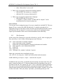
1
MICRF405
User Manual for Development System
315MHz
433MHz
868MHz
915MHz
FW v.2
Micrel Norway AS
Strandveien 13 * 1366 LYSAKER * Norway
Tel: +47 67 83 08 00 * Fax: +47 67 83 08 10
MCRF405: User Manual for Development System, FW v.2
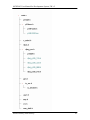
Table of contents:
1.
2.
Introduction................................................................................................................. 2
Development Board Inputs/Outputs ........................................................................... 5
2.1.
Summary of DIP-Switch Settings....................................................................... 6
3. Getting Started ............................................................................................................ 7
4. RF Test Modes............................................................................................................ 8
5. Packet format in “Link Test” and “Simple Byte Transfer” Modes .......................... 12
5.1.
Packet format, Type 1 and Type 2 .................................................................... 12
Packet format, Type 1 ............................................................................................... 13
Packet format, Type 2 ............................................................................................... 14
6. Link Test Mode......................................................................................................... 15
7. Interface in Simple Byte Transfer Mode .................................................................. 17
8. Simple Byte Transfer Mode...................................................................................... 19
9. PC program “RF TestBench”.................................................................................... 21
10.
Firmware change/upgrade..................................................................................... 23
11.
Changes in this Firmware Version........................................................................ 24
12.
MICRF405 Development System: Firmware Description ................................... 25
12.1.
Project ........................................................................................................... 25
12.2.
Tools ............................................................................................................. 25
12.3.
File Structure................................................................................................. 26
12.4.
#defines in Source Files ................................................................................ 27
12.5.
Source File Description................................................................................. 27
12.6.
Flow Charts................................................................................................... 34
Micrel Norway, Oslo Norway
1
MCRF405: User Manual for Development System, FW v.2
1. Introduction
This document, “MICRF405 User Manual for Development System” describes the
features of the development system for MICRF405. For details on the MICRF405
transmitter (a product in the RadioWireTM product line): Please refer to the appropriate
data sheet. For the latest updates on products related to RadioWireTM, please visit
www.micrel.com.
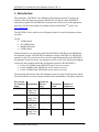
The MICRF405 can be used in several frequency bands. Several development systems
are made:
For the
• 315MHz band,
• 433.92MHz band,
• 868MHz band and
• 915MHz band
Default frequencies are selected to match the MICRF600, MICRF610 and MICRF620
development systems. The MICRF6x0 modules are using a MICRF505 or MICRF506
transceiver chip. They can be used to receive the signals transmitted by the MICRF405
development system (of course, any adequate receiver can be used, but the development
systems for these modules match the development system for the MICRF405):
• For the 433.92MHz band, MICRF620 can be used as a receiver
• For the 868MHz band, MICRF610 can be used as a receiver
• For the 915MHz band, MICRF600 can be used as a receiver
The operation and features of the development system are equal for all frequency bands.
The main differences are the frequency band, bit rate and number of frequency channels:
Dev System
for frequency
band
315MHz
433.92MHz
868MHz
915MHz
Modulation
Modulation
using 2 sets
of dividers
Modulation
using 2 sets
of dividers
Modulation
using 2 sets
of dividers
Modulation
using 2 sets
of dividers
Micrel Norway, Oslo Norway
On-the-air
bit rate
(bps)
19231
Manchester
coded
No
Number of
frequencies
1
19231
No
4
15152
No
2
19231
No
25
2
MCRF405: User Manual for Development System, FW v.2
Note that all development systems for MICRF405 have the same firmware1 version, and
all source files are available in a common set of files (a “Project”).
Outline of this document:
Following this introduction, an overview of the board’s inputs/outputs is given. Then a
Get-started chapter is included, and the different modes of operation are described. An
overview of how to program/update the firmware is also included. Finally, a list of
changes for this firmware version is given, as well as a description of the firmware.
Purpose of the Development system:
The development system provides hands-on experience with the MICRF405 transmitter.
The user can use the included firmware and hardware, or make a new program and flash
it into the micro controller. That is, the user can use the boards both to evaluate the
MICRF405, and as an aid in the development of a radio communication system.
A separate PC program is available. Through this program, it is possible to set the
programming word for the MICRF405 (both the frequency dividers and the control bits
can be set). This program is referred to as “RF TestBench”. Please observe: It is possible
to read out the firmware version of the development board via RF TestBench.
Main modes of operation of the Development system:
•
RF Test Modes. The user can test the RF properties of the transmitter. It is possible
to transmit a 1010… pattern, a random pattern or a carrier. In addition, the user can
select to bypass the micro controller (MCU) completely (i.e. tristate all IOs of the
MCU), and control the RF part via header pins, e.g. by an external micro controller.
In addition, transmitting packets using ASK is one of the test modes.
•
Link-Test Mode. In this mode of operation, the development board is a “Master”.
“Messages” (5 printable ascii characters) are transmitted. This mode is useful when
testing radio communication in different environments, testing antennas, testing
encapsulation etc. MICRF6x0 development systems can be used to receive the
messages.
•
Simple Byte Transfer Mode. In this mode, the user can enter a number of bytes into
a development board (using e.g. a PC). The board will then transmit the bytes. A 64byte deep buffer is implemented. Only 1 frequency is used. MICRF6x0 development
systems can be used to receive the transmitted bytes.
1
“Firmware” (FW) = the program used in the micro controller
Micrel Norway, Oslo Norway
3
MCRF405: User Manual for Development System, FW v.2
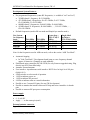
Development System Features:
•
•
Pre-programmed frequencies (centre RF frequencies, i.e. middle of “tx0” and “tx1”)
• 315MHz band: 1 frequency, f0=315.00MHz
• 433.92MHz band: 4 frequencies, f0=433.43MHz, f1=433.71MHz,
f2=434.00MHz, f3=434.29 MHz
• 868MHz band: 2 frequencies, f0=868.31MHz, f1=868.95MHz
• 915MHz band: 25 frequencies, f0=904.30MHz, …, f12=915.25MHz, … ,
f24=926.25MHz
Default frequencies (used in RF test mode and Simple byte transfer mode):
Dev System
for frequency
band
315MHz
433.92MHz
868MHz
915MHz
TX0 (MHz)
314.909091
433.333333
868.210526
915.151515
TX1 (MHz)
315.087719
433.517241
868.400000
915.354839
Centre freq =
(TX1+TX0)/2
(MHz)
314.998405
433.425287
868.305263
915.253177
Single-sided
deviation =
(TX1-TX0)/2 (kHz)
89
92
95
102
Note: for the frequencies used in ASK test mode, refer to the section “ASK Test Mode”.
•
•
•
•
•
•
•
•
•
•
•
Automatic hopping
• In ”Link Test Mode”: Development board jump to a new frequency channel
approx 10 times/sec. Channels are used randomly
Flash-based micro controller (PIC18LF4320) for easy firmware upgrade/testing. Plug
directly into ICD2 from Microchip.
Antenna: External antenna
User interface: Asynchronous serial interface: RS232-level or logic level I/O pins
(9600-8-N-1)
4 DIP switches to select mode of operation
1 LED to indicate power on
1 LED to indicate RF powered
4 LEDs to indicate status or control information
Possible to use 5 external I/O pins (for user FW development)
Possible to monitor the interface between RF chip and micro controller via header
pins
Possible to measure RF-part power consumption
Power supply:
•
•
6 - 9 volt DC
Apply “ - “ to the centre pin (note!)
External antenna connector:
Type: SMA
Micrel Norway, Oslo Norway
4
MCRF405: User Manual for Development System, FW v.2
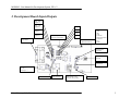
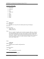
2. Development Board Inputs/Outputs
DTE_RTS
jumper A
DTE_CTS
jumper B
LED1
DTE_RX
jumper C
LED2
LED3
DTE_TX
jumper D
Header for optional external I/O (not mounted)
LED4
RS232 connector
9-pin D-sub
Header for
MICRF405 interface
1: SRV
2: SEN
3: SIO
4: SCK
5: DATAIN
6: RDY/DATACLK
7: CLKOUT
8: LD
9: GND
MICRF405 RF
Transmitter
SMA antenna
connector
RF power
measurement
Power supply/battery
6-9 volt
Center pin: “-“
Power LED
Micrel Norway, Oslo Norway
ICSP connector
DIP-switches 1,2,3,4
Note the “ON” position
RF Power LED
5
MCRF405: User Manual for Development System, FW v.2
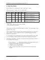
2.1. Summary of DIP-Switch Settings
To select mode of operation, bring DIP-switches ON or OFF according to the table
below.
The modes of operation (described in detail in the following sections) are:
• “RF Test Modes”: Enter TX mode, TX a carrier, TX 1010… or a random pattern,
enter PC-configurable mode or bypass (tristate) micro controller for useroperation of the RF part, enter ASK test mode
• “Link Test Mode”: Use a development board to transmit a fixed packet
• “Simple Byte Transfer Mode”: Construct a packet based on user input (from e.g. a
PC) and transmit it
The 4 DIP-switches (labelled 1 2 3 4) are placed in a single component. In addition “ON”
is written on the component. In the table below, “1” means “ON”, “0” means “OFF”.
DIP1 DIP2 DIP3 DIP4
Mode of operation
-----------------------------------------------------------------0
0
0
0
0
0
0
0
0
0
1
1
0
1
0
1
Simple byte transfer mode, type 1
Simple byte transfer mode, type 2
not used
not used
0
0
0
0
1
1
1
1
0
0
1
1
0
1
0
1
RF Test, Tristate all uC I/Os
RF Test, Transmit a random pattern
RF Test, ASK Test Mode
not used
1
1
1
1
0
0
0
0
0
0
1
1
0
1
0
1
Link
Link
Link
Link
1
1
1
1
1
1
1
1
0
0
1
1
0
1
0
1
not used
RF Test, Transmit 1010 ...
RF Test, Transmit carrier
RF Test, PC-mode
Test, 5 bytes
Test, 5 bytes
Test, 26 bytes
Test, 26 bytes
payload,
payload,
payload,
payload,
type
type
type
type
1
2
1
2
"Type 1": (this refers to the format of the packets transmitted)
"Framelength" = length of "Framelength", "Payload" and "CRC".
CRC (2 bytes) is calc'ed by firmware on "Framelength" and "Payload" fields
Compatible with MICRF6x0 Link Test/Simple byte transfer mode
"Type 2": (this refers to the format of the packets transmitted)
"Framelength" = length of "Payload" and "CRC"
CRC (0, 1 or 2 bytes) is calc'ed on-chip (by MICRF405) on "Payload" field
"Packet Engine" data interface used in "Simple byte transfer mode" and "Link Test"
"Bitwise" data interface used in "Transmit 1010 ..." and "Transmit random"
Micrel Norway, Oslo Norway
6
MCRF405: User Manual for Development System, FW v.2
3. Getting Started
Before power-up of the development board:
•
•
•
Get familiar with the inputs/outputs (refer to “Development Board
Inputs/Outputs”)
Select mode of operation via DIP-switches
If Simple Byte Transfer Mode is selected: Select interface to user data. Insert the
4 jumpers “DTE_RTS”, “DTE_CTS”, “DTE_RX”, “DTE_TX” to select RS232
interface. Remove the jumpers to select “logic level” interface (connect to e.g.
another micro controller).
As a first step, it is suggested to set the development board in transmit 1010… mode
(DIP1, 2 and 4 ON). Use an oscilloscope, a spectrum analyzer, a MICRF6x0 dev system
or your own receiver board to monitor/receive the transmitted signals.
Enter PC-mode (all DIPs ON) and use the PC-program (RF TestBench) to change the
frequency, output power and bitrate.
If you are using a development system for the 433.92MHz, 868MHz or 915MHz band,
and you have the corresponding MICRF6x0 development system available, you can try
the Link Test Mode (only DIP1 ON). On the MICRF6x0 board, make sure DIP1 and
DIP4 are ON. This will be the “Slave”. Try to increase/decrease the distance between the
boards, and observe LED1 on the MICRF6x0 board. LED1 (MICRF6x0 board) will be
on as long as the link is OK.
Set the board in Simple Byte Transfer Mode (all DIPs OFF). Connect it to a PC running
HyperTerminal. Send characters or text files via the board. Note: No ARQ is used –
number of “data packets” getting through depends on link quality. Make sure the cable is
1:1, and that RTS, CTS, TX, RX and GND are used. Make sure the data format is 96008-N-1 and hardware handshake is used. Also make sure the jumpers for RS232-use are in
place.
Micrel Norway, Oslo Norway
7
MCRF405: User Manual for Development System, FW v.2
4. RF Test Modes
In the RF Test Modes, only 1 frequency is used. If not changed via the PC program2, the
frequency is:
•
•
•
•
315MHz band:
433.92MHz band:
868MHz band:
915MHz band:
315.00MHz
433.43MHz
868.31MHz
915.25MHz
Note: for the frequencies used in ASK test mode, refer to the section “ASK Test Mode”.
DIP-switch setting (“1” means “ON”, “0” means “OFF”):
Combin. #
1
2
3
4
5
6
7
DIP1
1
1
1
1
0
0
0
DIP2
1
1
1
1
1
1
1
DIP3
0
0
1
1
0
0
1
DIP4
0
1
0
1
0
1
0
Text
Not used in this firmware version
Transmit 1010 …
Transmit carrier
Enable configuration via PC
Bypass micro controller
Transmit a random pattern
ASK Test Mode
Use of LEDs:
LED1, LED2, LED3, LED4: Not used in RF Test Modes.
Combination #1, Not used
Combination #2, Transmit 1010… :
The board will enter transmit mode and transmit a 1010… pattern. Combination #2 can
be used to test parameters like deviation and transmit spectrum. Use a MICRF6x0
development board or your own rx-board to receive the signals, or observe the spectrum
on a spectrum analyzer.
Combination #3, Transmit carrier:
The board will enter transmit mode and transmit a carrier, that is: no modulation is
applied. This can be used to check the frequency spectrum, the output power, and the
current consumption. Note that the “TX0” frequency is used for the MICRF405.
2
Refer to chapter 9 and chapter 4 (“Combination #4”).
Micrel Norway, Oslo Norway
8
MCRF405: User Manual for Development System, FW v.2
Combination #4, Enable configuration via PC:
This setting is also referred to as “PC mode”.
Refer to the chapter called “PC-Program” (chapter 9) for details on the PC program.
Make sure the 4 jumpers “DTE_RTS”, “DTE_CTS”, “DTE_RX” and “DTE_TX” are in
place.
If the power-LEDs are off: Make sure the board is powered-on without the RS232 cable
connected, and then connect the RS232 cable.
Entering “PC mode”: Before any command is given from the PC, the RF chip will stay in
the mode selected before “PC mode” was selected (transmit/standby etc).
While in “PC mode”: When a control word is sent from the PC to the board, the board
will store the entered word in EEPROM and program the RF chip with it. The complete
control word is written into the MICRF405 in a single operation.
It is possible to transfer a control word from any of the 3 “Transfer” buttons (PC program
buttons, refer to the RF TestBench user guide):
•
•
•
Quick Setup or
Complete Setup or
Control Word
When leaving “PC mode”: The board will use the default control word already
programmed into the FLASH program memory, or it will use the control word entered
from the PC program and stored in the EEPROM. Which one to select (the source of the
control word) is selected in the PC program (selectÆTools ÆDevelopment Board
Commands)3.
From the PC program, try e.g. to change the output power level (PA setting) and observe
the effect on spectrum, power consumption and link range.
Note: If using the PC program to read out the contents of the MICRF405 registers: Make
sure to have no external load on the SIO and SCK pins, or else you might get some
unwanted results.
3
The “EEPROM control word” can be used in “RF Test Modes”, “Link Test Mode” and “Simple Byte
Transfer Mode”. If the “EEPROM control word” is used in “Link Test Mode”: No frequency jumping is
done – only the user-entered control word stored in EEPROM will be used.
Micrel Norway, Oslo Norway
9
MCRF405: User Manual for Development System, FW v.2
Combination #5, Bypass Micro Controller:
Using this combination, it is possible to use an external micro controller to control the RF
part. Connect to the interface pins as described in “Development Board Inputs/Outputs”.
The interface pins are connected to the “MCU” side of the MCU-RF connection.
All I/O pins of the on-board micro are tristated. None of the MCU’s IOs are set as output
at power-on, if this combination is selected. That is: The User has full control, without
the MCU interacting at all (not programming the RF chip etc). The DIPs are tested before
the IOs are initiated.
Note: When using this mode, first make sure DIPs are set correctly, then apply power to
the board.
Combination #6, Transmit a Random Pattern:
The board will enter transmit mode and transmit a random, Manchester-coded pattern
(i.e. without a DC component). Combination #6 can be used to test parameters like
deviation and transmit spectrum.
Combination #7, ASK Test Mode:
In this test mode, the board will transmit packets with a defined format. ASK modulation
is used. The ASK modulation type is OOK (on-off-keying), and the bit rate is 1200bps
(1202bps). The board will transmit a new packet every 100msec approx, and enter
power-down between transmissions.
For every frequency band, a single frequency is used:
• 915.000MHz,
• 868.308MHz,
• 434.000MHz,
• 315.000MHz
The packets have this format:
• 3 bytes
Preamble
• 3 bytes
Sync
• 1 byte
Length
• 5 bytes
Payload
• 2 bytes
CRC
(1010…)
(11001100…)
(length of payload and CRC fields = 7)
(5 printable ascii characters)
(calculated using the Payload field as input)
The purpose of this mode is to demonstrate the ASK feature. If you have an ASK
receiver, you can search for packets with this format and e.g. bring a LED ON if you
receive a packet. This can be used for range/environment testing.
Micrel Norway, Oslo Norway
10
MCRF405: User Manual for Development System, FW v.2
Suggestions for RF Testing:
1) Set the development board to transmit a carrier. Use a spectrum analyser to
observe the frequency spectrum
2) Repeat for transmit 1010…
3) Use a MICRF6x0 dev board or your own board as receiver, and use the
MICRF405 board in “transmit 1010…” mode. Use an oscilloscope to observe the
tx’ed and rx’ed data (Data I/O). Set tx’ed data as the trigger source.
Micrel Norway, Oslo Norway
11
MCRF405: User Manual for Development System, FW v.2
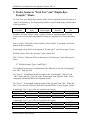
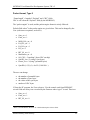
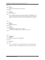
5. Packet format in “Link Test” and “Simple Byte
Transfer” Modes
In “Link Test” and “Simple Byte transfer mode”, the development board will construct a
“packet” and transmit it. The format of the packets is equal in both modes, and described
in the figure below.
Preamble
Sync
Framelength
Payload
CRC
Preamble: 1-4 bytes, always a 1010… pattern. Used as a “training sequence” by the
receiver; the receiver can use this pattern to adjust it’s sampling clock for the incoming
data
Sync: 1-4 bytes. This field is used to identify “Start of frame”. It can hold a fixed syncpattern, an ID or an address.
Framelength: 1 byte. Refer to description of “Packet type 1” and “Packet type 2” below.
Payload: n bytes. This is the “message” or the “useful data”.
CRC: 0-2 bytes. Checksum. Refer to description of “Packet type 1” and “Packet type 2”
below.
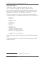
5.1. Packet format, Type 1 and Type 2
Two different format types are implemented. The difference is how the “Framelength”
and “CRC” fields are used.
For “Type 1”, “Framelength” holds the length of the “Framelength”, “Payload” and
“CRC” fields, and CRC is calc’ed on the “Framelength” and “Payload” fields. This is
compatible with the MICRF6x0 development system.
For “Type 2”, “Framelength” holds the length of the “Payload” and “CRC” fields, and
CRC is calc’ed on the “Payload” field (this is the MICRF405 “Packet Engine” format).
Framelength, Type 1 (grey fields are included in the length):
Framelength
Payload
Preamble
Sync
CRC, Type 1 (grey fields are included in CRC calculations):
Preamble
Sync
Framelength
Payload
Framelength, Type 2 (grey fields are included in the length):
Preamble
Sync
Framelength
Payload
CRC, Type 2 (grey fields are included in CRC calculations):
Preamble
Sync
Framelength
Payload
Micrel Norway, Oslo Norway
CRC
CRC
CRC
CRC
12
MCRF405: User Manual for Development System, FW v.2
Packet format, Type 1
“Framelength” = length of “Framelength”, “Payload” and “CRC” fields.
CRC is calc’ed on the “Framelength” and “Payload” fields by the firmware.
The “packet engine” is used, but this format violates the packet-engine format. In the
packet-engine, “Framelength” is “not counting itself”. To overcome this, an additional
dummy-byte is sent, and a 16-bit CRC is calculated by the firmware.
If, from the PC program, the User selects to “Use the control word from EEPROM”,
several fields are in any case overruled by the firmware when “type 1”is used. These are4:
•
•
Sync_en = 1
Load_en = 1
•
•
•
•
MOD_LDc_en = 0
PA_FEc_en = 1
PA_LDc_en = 1
LD_en = 1
•
•
•
•
•
BIT_IO_en = 0
Manchester_en = 0
Sel_CRC = 0 (making CRC in MCU)
SyncID_Len = 2 (txing 3 sync bytes)
Pream_Len = 2 (txing 3 preamble bytes)
•
SyncIDi (i=2,1,0) = 0xCC (11001100...)
Note that this format is compatible with the format used in the MICRF6x0 development
system.
In addition, it shows that the User is not restricted to the “packet engine format” when
using the packet engine.
4
Refer to the MICRF405 data sheet for a detailed description of these fields.
Micrel Norway, Oslo Norway
13
MCRF405: User Manual for Development System, FW v.2
Packet format, Type 2
“Framelength” = length of “Payload” and “CRC” fields.
CRC is calc’ed on the “Payload” field (by the MICRF405).
The “packet engine” is used, and the packet-engine format is strictly followed.
Default field-values5 in the packet engine are given below. This can be changed by the
User (with some exceptions, see below).
•
•
Sync_en = 1
Load_en = 1
•
•
•
•
MOD_LDc_en = 0
PA_FEc_en = 1
PA_LDc_en = 1
LD_en = 1
•
•
•
•
•
BIT_IO_en = 0
Manchester_en = 0
Sel_CRC = 3 (making 2 bytes CRC on-chip)
SyncID_Len = 2 (txing 3 sync bytes)
Pream_Len = 2 (txing 3 preamble bytes)
•
SyncIDi (i=3,2,1,0) = 0xCC (11001100...)
The user can change:
•
•
•
•
the number of preamble bytes
the number of sync bytes
the values of the sync bytes
number of CRC bytes
If, from the PC program, the User selects to “Use the control word from EEPROM”,
several fields are in any case overruled by the firmware when “type 2”is used. These are:
•
•
•
5
Sync_en = 1
Load_en = 1
BIT_IO_en = 0
Refer to the MICRF405 data sheet for a detailed description of these fields.
Micrel Norway, Oslo Norway
14
MCRF405: User Manual for Development System, FW v.2
6. Link Test Mode
Refer to chapter 5 for a description of “Type 1” and “Type 2” format.
DIP-switch setting (“1” means “ON”, “0” means “OFF”):
Combin. #
1
DIP1
1
DIP2
0
DIP3
0
DIP4
0
2
1
0
0
1
3
1
0
1
0
4
1
0
1
1
Text
5 bytes payload, Type 1 format,
compatible with MICRF6x0
5 bytes payload, Type 2 format, not
compatible with MICRF6x0
26 bytes payload, Type 1 format,
compatible with MICRF6x0
26 bytes payload, Type 2 format, not
compatible with MICRF6x0
Use of LEDs:
LED2, LED3, LED4: Not used in Link Test Mode
LED1: On while tx’ing a packet
In this mode of operation, the MICRF405 board is a “Master”. The “packet engine” in the
MICRF405 chip is used.
If not overruled from the PC-program, all pre-programmed frequencies are used (refer to
“RF Test Modes”, “Enable configuration via PC”. Automatic hopping between the
frequencies is implemented.
If < 25 frequencies are pre-programmed: The frequency table still holds 25 entries. That
is, several “frequency indexes” points to the same frequency (refer to “Introduction”.)
In this mode of operation, a “Message” is sent from the board. The message is build of 5
(or 26) printable ascii characters:
•
•
•
•
First, a character ‘a’… ‘y’, indicating the frequency index for the frequency used
(not the frequency number, but the index in a look-up table)
2 characters = “BC” (or 21 characters)
‘m’ (the message is sent from a master)
Finally, carriage return (0x0D) is tx’ed as the last byte of the message (=the
payload)
Micrel Norway, Oslo Norway
15
MCRF405: User Manual for Development System, FW v.2
The following procedure is implemented for “Link Test”:
LOOP
Enter transmit mode on frequency n
Transmit “Message” and CRC checksum
Enter power-down mode
Wait for timer period (approx 100msec)
Use “next frequency” (from a randomly ordered list) and repeat
END_LOOP
Micrel Norway, Oslo Norway
16
MCRF405: User Manual for Development System, FW v.2
CTS is an input to the DTE. It is used to control data flow from DTE to DCE. DCE
brings CTS active to signal “DCE ready for bytes from DTE”. DCE brings CTS inactive
to signal “DCE not ready for bytes from DTE”. Before DTE outputs bytes to DCE, the
CTS line is tested. If CTS is active, DTE knows that DCE is ready to receive bytes, and
DTE transfer the bytes on the TXD line.
Maximum number of bytes to transmit in one “data frame” is 64 bytes. The board will
tell user to “stop enter bytes” by setting CTS inactive when the “bytes-from-user buffer”
holds 64 bytes. Note: the board can buffer 2 additional bytes. Other bytes will be lost.
The bytes can be entered with random delay between them. As soon as a byte is entered,
the board enters transmit mode and sends the presently entered bytes, while still buffering
new bytes from user (note that the board does not wait until buffer is full or until user
stops entering bytes).
Micrel Norway, Oslo Norway
18
MCRF405: User Manual for Development System, FW v.2
8. Simple Byte Transfer Mode
Refer to chapter 5 for a description of “Type 1” and “Type 2” format.
DIP-switch setting (“1” means “ON”, “0” means “OFF”):
Combin. #
1
DIP1
0
DIP2
0
DIP3
0
DIP4
0
2
0
0
0
1
Text
Type 1 format, compatible with
MICRF6x0
Type 2 format, not compatible with
MICRF6x0
Note: There is no “Master” or “Slave” in this mode of operation.
Use of LEDs:
LED1, LED2, LED4: Not used in Simple Byte Transfer Mode
LED3: On while tx’ing a packet
Combination #1:
Refer to interface description in “Interface in Simple Byte Transfer Mode”.
•
•
•
•
There is no difference between “master” and “slave” in this mode.
Error detection is implemented (through CRC check)
Only 1 frequency is used (no frequency hopping)
Duplicate control or ARQ (packets being acknowledged or re-transmitted) are not
implemented in this mode
Data flow from user (“User A”) to development board (“Board A”), then via RF:
1) If Board A is ready to get bytes (CTS is active): User A enters bytes into Board A
2) Bytes are buffered in Board A. When 1 or more bytes are entered, Board A
constructs a frame (it adds preamble, sync, length and CRC to the presently
entered bytes). Board A then transmits the frame. If >= 64 bytes in buffer, then
user is told to stop entering bytes (CTS goes inactive).
Combination #2:
Refer to “Combination #1” above. The main difference is the packet format (refer to
chapter 5).
In addition to the different packet format, the following should be noted:
When the packet engine is used and CRC is generated on-chip, then the payload must be
>1 byte. Because of this, a frame is transmitted when >1 byte is entered. Observe the
consequence: The last entered user-byte may not be transmitted until user enters another
byte.
Micrel Norway, Oslo Norway
19
MCRF405: User Manual for Development System, FW v.2
Example, how to use Simple Byte Transfer Mode:
User A (connected to board A) wants to transfer 6 bytes (= “Hello!”). User B (connected
to a receive board) receives the bytes.
User A:
•
•
Board A:
•
•
•
•
•
Test if CTS at board A is active. If CTS is active, the board is ready to accept
bytes from the user.
Transfer “Hello!” into the board, using 9600-8-N-1. Transfer lsb of every byte
first (after the start-bit).
Read bytes from User A
Format a packet to transmit 1, 2, 3, 4, 5 or 6 bytes of “Hello!”
Enter transmit mode
Transmit the packet
If more bytes entered by user: Format a new packet and transmit it
Receiver board
• Receive a packet
• Un-pack the bytes from the packet
• Test that the number of bytes is a legal number of bytes (1-64)
• Test that CRC is OK
• Test if RTS is active. If RTS is active, the user is ready to accept bytes from
the board.
• Transfer the bytes to User B. Transfer lsb of every byte first.
User B:
Read bytes from board
Note:
Since no addressing is used, other users (let’s say User C, User D and User E) will
receive the 6 bytes as well. If the boards are used in a network, the message has to
include some address information (and the user’s protocol has to handle it).
Micrel Norway, Oslo Norway
20
MCRF405: User Manual for Development System, FW v.2
9. PC program “RF TestBench”
The PC program is referred to as “RF TestBench”.
RF TestBench can be used with or without the development board. It can be used to
calculate fields in the control word to enter into MICRF405. Examples: Find settings for
a specific bit rate, or get the frequency dividers for a number of frequencies.
“RF TestBench” should be self-explaining, refer to the user guide for the PC program as
well.
Installation and running are straightforward, simply double-click “setup.exe” and follow
the on-screen instructions.
If using RF TestBench together with a development board:
Make sure the DIP-switches are set like this: (All ON)
Combin. #
1
DIP1
1
DIP2
1
DIP3
1
DIP4
1
Text
Using RF TestBench:
•
Connect the development board to a PC via a cable:
o 1:1 RS232 cable
o Make sure RTS, CTS, TX, RX and GND are included in the cable (pins 2,
3, 5, 7, 8)
o Note: Power-on the board before connecting the cable to the board if the
power-LEDs do not get on
•
•
•
•
•
Power on the board
Start RF TestBench by double-clicking “RF TestBench”
Read the text in the welcome-window
From the main window, select “Dev Board Connection” (COM1 or COM2)
From the main window, select “RF Device”. Select MICRF405. Then select the
appropriate frequency band.
From the main window, use the “Quick Setup” or “Complete Setup” or “Control
Word” sections:
o Use “Quick Setup” if you want the program to calculate parameters based
on basic parameters like xtal frequency, RF frequency and bit rate. Enter
values and press the “Calc!” button in the Quick Setup section.
o Use “Complete Setup” to enter the control word fields manually. Press the
“Calc!” button in the Complete Section to see resulting frequencies etc.
o Use the “Control Word” section to change the control word on a registerbasis.
•
Micrel Norway, Oslo Norway
21
MCRF405: User Manual for Development System, FW v.2
•
To transfer a control word to the development board: Enter/change the fields and
press “Transfer!” (in the appropriate section). The entered values are stored in the
micro’s EEPROM.
•
Observe the “Information” field. If “Success!” is not displayed, please check
connections/power and try again.
In the following, some suggestions are made for the user to get familiar with “RF
TestBench”.
•
Experiment with e.g. power levels. Suggestion: Change power level, press
“Transfer!” and then give a “Transmit 1010…” command (refer to next
paragraph). Observe the result on a spectrum analyser, or use a receiver-board and
observe change in range (distance between transmitter and receiver).
•
The “Transmit 1010…” command is found here: ÆTools ÆCommands to Dev
Board …
•
It is possible to use the firmware pre-programmed settings (stored in the FLASH
program memory) or the settings stored in EEPROM for the other modes of
operation as well (that is: not only in “PC-mode”)6. Select “FLASH” or
“EEPROM” via a command in RF TestBench (ÆTools ÆCommands to Dev
Board …). If EEPROM settings are used in Link Test Mode, no frequency
hopping will be done – only the frequency and control bits stored in EEPROM
will be used.
•
If “EEPROM settings” is selected, the board can be disconnected from the PC,
and the different modes of operation can be run- and now the settings stored in
EEPROM are used. To use the pre-programmed settings again: Enter “PC-Mode”
(DIP-setting described above) and give command from RF TestBench: Instruct
the board to use the FLASH memory as the source (where to get the control word
from).
•
•
Other possibilities are (ÆTools ÆDevelopment Board Commands):
Read out the firmware version number (the firmware stored in flash program
memory of the micro controller)
Restart micro controller (MCU) program (like a power-on reset). Note: This does
not reset the MICRF405 transmitter chip
Reset EEPROM control word - settings to “default” (= pre-programmed settings
from firmware)
Read out the present EEPROM control word
Read out the present MICRF405 register values
•
•
•
•
6
In PC-mode, the settings entered by the User (and stored in EEPROM) are always used.
Micrel Norway, Oslo Norway
22
MCRF405: User Manual for Development System, FW v.2
10. Firmware change/upgrade
The development boards are equipped with a socket for ICSP (in-circuit serial
programming).
Through ICSP, it is possible to download new firmware into the micro controller.
The download feature is made for use with MPLAB ICD2 from Microchip. Connect the
development board directly to the ICD2 using the cable from the ICD2 kit.
Via ICD2, it’s possible to step through and debug firmware code as well. That is: Make
your own program, download it, debug it and run it!
MPLAB IDE (integrated development environment) is available for free from
Microchip’s homepage. (C-compiler must be bought7, but you do not need it for firmware
upgrading, that is, if you have a new .hex file to download).
How to upgrade firmware (“xxx.hex”, xxx=firmware name) (skip reading this if you are
familiar with ICD2):
• Connect ICD2 to your PC and to power (please refer to ICD2 user manual)
• Connect ICD2 and development board via the “standard ICD2 cable”
• Start MPLAB IDE 8 (menu selections below refer to the MPLAB IDE program)
• Select Configure Æ Select Device… Æ “PIC18F4320” Æ OK
• File Æ Import… Æ “xxx.hex” Æ Open
• Programmer Æ Select Programmer Æ MPLAB ICD2
• Programmer Æ Settings Æ Power Tab : Make sure ”Power target circuit from
MPLAB ICD2” is checked
• Programmer Æ Settings Æ Program Tab: Make sure “Allow ICD 2 to select
memories and ranges” is checked Æ OK
• Identify and press the “Reset and connect to ICD” button in the main menu field.
• If the “Target not found” warning pops up, repeat steps above.
• Identify and press the “Program target device” button in the main menu field
• Wait for programming to finish (refer to the “Output” window) and remove the
development board from ICD2.
• Optional: Confirm firmware version via RF TestBench
7
A demo version is available for free.
Assumes correct drivers for MPLAB ICD2 are installed (when connected to the USB port for the first
time, your PC should detect the new device and guide you through the installation, note: 2 drivers will be
installed).
8
Micrel Norway, Oslo Norway
23
MCRF405: User Manual for Development System, FW v.2
11. Changes in this Firmware Version
V2 2006 03 03 PKB
Included ASK modulation test mode
By default, MOD_LDc is not used for the packet engine
The SEN line is kept high a minimum time (> 1 fc-period)
RFPRG_Wait_Lock() procedure updated
RFPRG_Enter_Tx() procedure updated
ClkOut_en default value = 0
In Init_Main: Always reset USART-registers (user input will be ignored in RF
test modes and Link test)
When tx1010... or a random pattern (uing bit-banging): Change DATAIN asap
after a raising edge of DATACLK (MICRF405 samples DATAIN at raising edge
of DATACLK, and then it’s OK to change it)
Make sure that the INT0IF flag is cleared when starting to tx1010... or a random
pattern
Testing RTS active ("low") before giving data out to user
Changed/updated comments
V1 2006 02 06 PKB
Initial release
Micrel Norway, Oslo Norway
24
MCRF405: User Manual for Development System, FW v.2
12. MICRF405 Development System: Firmware
Description
The development board has a micro controller unit (MCU) on-board. The MCU is a
PIC18LF4320 from Microchip, which is in-circuit re-programmable (this process is
referred to as “flashing the MCU”).
The program flashed into the MCU is described below. This program is also referred to
as “firmware” (FW).
Note: All FW is free of charge. The intention of the FW is to provide
examples/suggestions to the user. No guarantee is implied as to the suitableness of the
firmware in a given application. All code must be tested in the application at hand.
12.1.
Project
The source, header and link files are put together in a project. The C programming
language is used (with some exceptions, refer to file descriptions below).
The FW can be made to operate in the 315, 433, 868 or 915 MHz bands. The frequency
band is selected in a header file via a #define” statement (“p18def.h”). The necessary files
for all frequency-bands are included in the project. In “pa8def.h”, include 1 and only 1 of
the following defines:
#define MICRF405_315
#define MICRF405_433
#define MICRF405_868
#define MICRF405_915
12.2.
Tools
“What do you want to do?” The tools you need depend on your answer to this question.
Below, some suggestions are given.
If you want to
• Open up the source files to get hints/ideas to your own program:
o Any text editor can be used
•
Control the development-board MICRF405 chip by your own, external MCU:
o Make sure the DIP switches are set to “Tristate on-board MCU mode” and
connect to the development board header pins, then power-on the
development board.
•
Flash the on-board MCU with a new .hex file:
o Install MPLAB IDE (free of charge from microchip.com)
o Get and install a MPLAB ICD 2 (in-circuit debugger/programmer). This is
a “box” between the PC running MPLAB IDE and the development board.
Micrel Norway, Oslo Norway
25
MCRF405: User Manual for Development System, FW v.2
o Other “flash utilities” exist as well
•
Make your own program, based on the assembly language:
o MPLAB IDE: This includes an “assembler”
o MPLAB ICD2: Use this to flash the MCU
•
Make your own program, based on the C language:
o MPLAB IDE and ICD2 (as above)
o C-compiler. A “demo-version” of “MPLAB C18 compiler” can be
downloaded for free from microchip.com.
Notes on Tools:
You may get errors/warnings/messages if you try to compile the included FW. This may
happen if a new version of the MPLAB and/or the C-compiler is introduced. It is
suggested to always use the latest versions, but these may be different from the versions
used when the FW was released. To correct errors, and to test if warnings/messages
require special attention: Please refer to the documentation from Microchip.
12.3.
File Structure
All the project files (firmware) are typically collected in a .zip file. After un-zipping the
files, you will see “a lot” of files. Several types are used. These are:
.asm
.c
.h
.hex
.lkr
.mcp
.mcw
Source files based on assembly language
Source files based on the C-language
Header files, includes definitions, prototype declarations and variables
Main output file, can be flashed into the MCU
Linker file
Project file
Workspace file, contains 1 (and only 1) project
Other types, generated when compiling the project:
.cod, .coff, .err, .lst, .map, mcs, .o (these are not described in this document).
In MPLAB IDE, go to Project -> Open … and select the .mcp file.
In addition to the type of file, you should notice the naming convention used. Every file
name is started (or made of) a 3-5 character abbreviation corresponding to the type of
procedures in the file. For example, the “gen.c” file is a collection of general procedures
and “gen.h” is the corresponding definitions, prototype declarations and variables. This
character abbreviation is also used in the procedures and variables. Example: If you want
to take a look at the “GEN_Init_Ports()” procedure, you should open the gen.c file.
Micrel Norway, Oslo Norway
26
MCRF405: User Manual for Development System, FW v.2
12.4.
#defines in Source Files
In all source files, some definitions are made before the code is started.
In all .c – files, the following definition is included:
• #define C_FILE
In all .asm – files, the following definition is included:
• #define ASM_FILE
The “C_FILE” or “ASM_FILE” definition is used to include the correct header file
(standard Microchip definitions of registers and bits).
In addition, a #define is included to identify the file name. Example: In “gen.c”, the
following is included:
•
#define GEN_FILE
This definition is tested in the header-files. If the definition is made, then procedure
prototypes and variables are declared in the header file. If not def’ed, then procedures and
variables are included as an “extern” type.
Example: “gen.h” can be #included in all source files; procedures/variables will be
declared only 1 time (when included in the “gen.c” file).
12.5.
Source File Description
Below, the source files and header files are described.
Refer to the flowcharts of the main procedures as well.
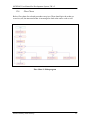
The source files typically include several header files. The “include-tree” for main.c is
given in the figure below.
In particular, the following header files are included in several source file:
•
p18def.h
o Here, the frequency band is #def’ed
o Other, general def’s are made as well
•
p18xxxx.h
o Here, the correct header file (standard definitions of registers and flags) is
included. The “c” header file or the “asm” header file for the selected
micro controller is included. Note: p18f4320.h (for .c files) and
p18f4320.inc (for .asm files) are files made by Microchip, they are
typically located where you have installed MPLAB.
•
c_subst.h
Micrel Norway, Oslo Norway
27
MCRF405: User Manual for Development System, FW v.2
o Here, some practical macro definitions are made, like the type definition
“uint8” for “unsigned char”
•
io_xxx.h
o Here, the correct IO definitions are included. If you make your own
program with other IOs, simply replace the #included file in io_xxx.h
(only done at this single place, not in every file that uses the IOs).
Micrel Norway, Oslo Norway
28
MCRF405: User Manual for Development System, FW v.2
Micrel Norway, Oslo Norway
29
MCRF405: User Manual for Development System, FW v.2
Overview of source files:
•
•
•
•
•
•
•
•
•
•
405asm.asm
config.asm
crc.c
eep.c
eepinit.asm
gen.c
main.c
rfpck.c
rfprg.c
usart.c
Name:
405asm.asm
Short description:
Procedures for tx’ing 1010 and a random pattern using “bit-banging”
Header file:
Typical procedures:
Toggle_Data_Out
Random_Data_Out
Notes:
This is an .asm file. Assembly code is selected to maximize efficiency; tx’ing bitby-bit up to 200kbps, while at the same time testing DIP switches and user input
from USART. At 200kbps, the number of instruction cycles/bit is “small” (13)9.
At bit rates < 20kbps, a .c file can easily be made, but the procedures are designed
for max bitrates (note that the dev boards, without hw changes, are made for
bitrates up to 20kbps only).
Name:
config.asm
Short description:
Setting up micro controller configuration bits.
Header file:
Typical procedures:
None
Notes:
This is, and should be, an .asm file
9
For the selected MCU with the selected xtal.
Micrel Norway, Oslo Norway
30
MCRF405: User Manual for Development System, FW v.2
Name:
crc.c
Short description:
CRC (cyclic redundancy check) calculations
Header file:
"crc.h"
Typical procedures:
CRC_Byte( void)
Notes:
CRC calculations can be made by the “packet engine” in MICRF405 as well.
However, if the user does not want to follow the frame structure of the packet
engine, but still wants to use CRC, the user must make the CRC in firmware.
Name:
eep.c
Short description:
EEPROM procedures
Header file:
"eep.h"
Typical procedures:
uint8 EEP_Read_EEprom( uint8 ee_address)
void EEP_Write_EEprom( uint8 ee_address, uint8 ee_data)
Notes:
Name:
eepinit.asm
Short description:
Init some parameters stored in EEPROM
Header file:
Typical procedures:
None
Notes:
This is, and should be, an .asm file. When the program is compiled and then
flashed into the MCU, some EEPROM values are set to their default values.
Micrel Norway, Oslo Norway
31
MCRF405: User Manual for Development System, FW v.2
Name:
gen.c
Short description:
General procedures for use in all types of applications
Header file:
"gen.h"
Typical procedures:
GEN_Enable_Int( void)
GEN_Init_Ports( void)
Notes:
Name:
main.c
Short description:
Main program, including initial set-up and interrupt vectors
Header file:
Typical procedures:
Main( void)
Notes:
Includes all files to make the main program work
Name:
rfpck.c
Short description:
RF-chip procedures for tx'ing "packets" with a defined format
Header file:
"rfpck.h”
Typical procedures:
RFPCK_Tx_Packet( void)
Notes:
Name:
rfprg.c
Short description:
RF-chip procedures for programming RF chip
Header file:
"rfprg.h”
Typical procedures:
RFPRG_Enter_Tx( void)
Notes:
Micrel Norway, Oslo Norway
32
MCRF405: User Manual for Development System, FW v.2
Name:
usart.c
Short description:
USART interface procedures, including handshaking
Header file:
"usart.h"
Typical procedures:
USART_Output_Byte( uint8 usart_byte)
USART_Init( void)
USART_Enable_Input_From_DTE( void)
Notes:
“USART” = Universal synchronous asynchronous receiver transmitter”, an on-board
micro-controller module made for serial communication via e.g. RS232
Micrel Norway, Oslo Norway
33
MCRF405: User Manual for Development System, FW v.2
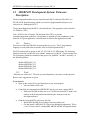
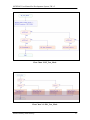
12.6.
Flow Charts
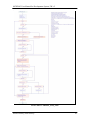
Below, flow charts for selected procedures are given. These should give the reader an
overview; still, the interested reader is encouraged to look at the source code as well.
Flow Chart 1: Main program
Micrel Norway, Oslo Norway
34
MCRF405: User Manual for Development System, FW v.2
Flow Chart 2: RF_Test_Mode
Flow Chart 3: LINK_Test_Mode
Micrel Norway, Oslo Norway
35
MCRF405: User Manual for Development System, FW v.2
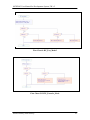
Flow Chart 4: RF_Test_Mode2
Flow Chart 5: BYTE_Transfer_Mode
Micrel Norway, Oslo Norway
36
MCRF405: User Manual for Development System, FW v.2
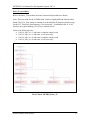
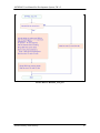
Enter_Tx procedure:
Below, the Enter_Tx procedure and some selected sub-procedures are shown.
Note: These are made for the 915MHz band, which is slightly different from the other
bands: The VCO_Freq setting is constant over-the-band for all frequency bands except
for the 915. Therefore, when entering “a few bytes only”: In addition to the A, N, M
dividers, the register holding VCO_Freq is entered as well.
Observe the following cases:
• Use PA_LDc_en = 1 and enter a complete control word
• Use PA_LDc_en = 1 and enter “a few bytes only”
• Use PA_LDc_en = 0 and enter a complete control word
• Use PA_LDc_en = 0 and enter “a few bytes only”
Flow Chart 6: RFPRG_Enter_Tx
Micrel Norway, Oslo Norway
37
MCRF405: User Manual for Development System, FW v.2
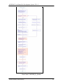
Flow Chart 7: RFPRG_Tx_1_Complete
A screen capture is shown below. Observe:
• Only 1 “programming sequence” (SEN going low then high)
• The RF chip turns on PA when LD goes high
• Modulation starts when LD goes high after PA is turned on, DATAIN is kept in
tristate until modulation starts
Screen Capture 1: For RFPRG_Tx_1_Complete
Micrel Norway, Oslo Norway
38
MCRF405: User Manual for Development System, FW v.2
Flow Chart 8: RFPRG_Tx_1_Sub
Micrel Norway, Oslo Norway
39
MCRF405: User Manual for Development System, FW v.2
A screen capture is shown below.
Observe:
• 2 “programming sequences”
(SEN going low then high);
first enter tx with PA off,
then enter tx with PA on
• MCU turns on PA when LD
goes high (then SEN is
brought high)
• Modulation starts when LD
goes high after PA is turned
on, DATAIN is kept in
tristate until modulation
starts
Flow Chart 9: RFPRG_Tx_0_Complete
Screen Capture 2: For RFPRG_Tx_0_Complete
Micrel Norway, Oslo Norway
40
MCRF405: User Manual for Development System, FW v.2
Flow Chart 10: RFPRG_Tx_0_Sub
Micrel Norway, Oslo Norway
41
MCRF405: User Manual for Development System, FW v.2
Flow Chart 11: RFPRG_Wait_Lock
Micrel Norway, Oslo Norway
42
MCRF405: User Manual for Development System, FW v.2
Flow Chart 12: RFPRG_Test_PA
Micrel Norway, Oslo Norway
43
MCRF405: User Manual for Development System, FW v.2
Flow Chart 13: RFPCK_Tx_Packet
Micrel Norway, Oslo Norway
44