1
Fit the Design into a Lattice Part
You have completed the design and the simulation of your mixed schematic and
ABEL-HDL design. The only step remaining is to fit the design into a Lattice
Semiconductor ispLSI part. Since you selected a part in the beginning steps, the
remaining steps are straightforward.
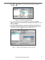
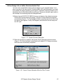
58. From the Sources in Project portion of the Synario Project Navigator, select the
ispLSI 2032-150 TQFP44 source and observe the related processes that have
been created.
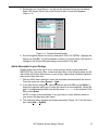
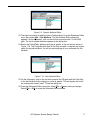
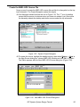
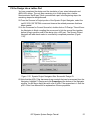
59. In the Processes for Current Source list, double-click on Fit Design. This will force
the Navigator to finish compiling the source and to link the source files together
before trying to partition and fit the design into a LSC part. The Synario Project
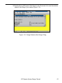
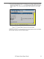
Navigator will add check marks to successfully completed processes (Figure
1-32).
Figure 1-32. Synario Project Navigator After Successful Design Fit
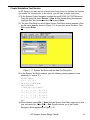
60. Note that the pDS+ Fitter has several user controls that can be accessed from the
Navigator; highlight Fit Design and click Properties at the bottom of the Navigator
window. You will see a dialog box with a list of pDS+ Fitter properties in it. See the
pDS+ Fitter User Manual for an explanation of these properties.
ISP Synario System Design Tutorial
33