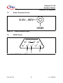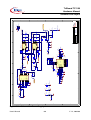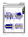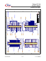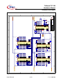
1
U s er’s Ma nual, V 1.2, Ju ne 2004
TriBoard TC1130
H a r d w a r e M an u a l T C 1 1 3 0 - 3 0 0
M i c r o c o n t ro l le r s
N e v e r
s t o p
t h i n k i n g .
Edition 2004-06
Published by Infineon Technologies AG,
St.-Martin-Strasse 53,
D-81541 München, Germany
© Infineon Technologies AG 2004.
All Rights Reserved.
Attention please!
The information herein is given to describe certain components and shall not be considered as warranted
characteristics.
Terms of delivery and rights to technical change reserved.
We hereby disclaim any and all warranties, including but not limited to warranties of non-infringement, regarding
circuits, descriptions and charts stated herein.
Infineon Technologies is an approved CECC manufacturer.
Information
For further information on technology, delivery terms and conditions and prices please contact your nearest
Infineon Technologies Office in Germany or our Infineon Technologies Representatives worldwide (see address
list).
Warnings
Due to technical requirements components may contain dangerous substances. For information on the types in
question please contact your nearest Infineon Technologies Office.
Infineon Technologies Components may only be used in life-support devices or systems with the express written
approval of Infineon Technologies, if a failure of such components can reasonably be expected to cause the failure
of that life-support device or system, or to affect the safety or effectiveness of that device or system. Life support
devices or systems are intended to be implanted in the human body, or to support and/or maintain and sustain
and/or protect human life. If they fail, it is reasonable to assume that the health of the user or other persons may
be endangered.
U s er’s Ma nual, V 1.2, Ju ne 2004
TriBoard TC1130
H a r d w a r e M a n ua l T C 1 1 3 0 - 3 0 0
M i c r o c o n t ro l le r s
N e v e r
s t o p
t h i n k i n g .
TriBoard TC1130 Hardware Manual TC1130-100
Revision History:
2004-06
Previous Version:
-
Page
V 1.2
Subjects (major changes since last revision)
Controller Area Network (CAN): License of Robert Bosch GmbH
We Listen to Your Comments
Any information within this document that you feel is wrong, unclear or missing at all?
Your feedback will help us to continuously improve the quality of this document.
Please send your proposal (including a reference to this document) to:
[email protected]
TriBoard TC1130
Hardware Manual
Table of Contents
Page
1
Introduction . . . . . . . . . . . . . . . . . . . . . . . . . . . . . . . . . . . . . . . . . . . . . . 1-1
2
2.1
2.2
TriBoard Features . . . . . . . . . . . . . . . . . . . . . . . . . . . . . . . . . . . . . . . . . 2-1
Block Diagram . . . . . . . . . . . . . . . . . . . . . . . . . . . . . . . . . . . . . . . . . . . . . 2-2
Placement . . . . . . . . . . . . . . . . . . . . . . . . . . . . . . . . . . . . . . . . . . . . . . . . 2-3
3
3.1
3.2
3.3
3.4
3.5
3.6
3.7
3.8
3.9
3.10
3.11
3.12
3.13
3.14
3.15
3.15.1
3.15.2
TriBoard Information . . . . . . . . . . . . . . . . . . . . . . . . . . . . . . . . . . . . . . .
Power Supply . . . . . . . . . . . . . . . . . . . . . . . . . . . . . . . . . . . . . . . . . . . . . .
Clock . . . . . . . . . . . . . . . . . . . . . . . . . . . . . . . . . . . . . . . . . . . . . . . . . . . .
Memory . . . . . . . . . . . . . . . . . . . . . . . . . . . . . . . . . . . . . . . . . . . . . . . . . .
FLASH . . . . . . . . . . . . . . . . . . . . . . . . . . . . . . . . . . . . . . . . . . . . . . . . . . .
SDRAM . . . . . . . . . . . . . . . . . . . . . . . . . . . . . . . . . . . . . . . . . . . . . . . . . .
Peripherals . . . . . . . . . . . . . . . . . . . . . . . . . . . . . . . . . . . . . . . . . . . . . . . .
ASC . . . . . . . . . . . . . . . . . . . . . . . . . . . . . . . . . . . . . . . . . . . . . . . . . . . . .
SSC . . . . . . . . . . . . . . . . . . . . . . . . . . . . . . . . . . . . . . . . . . . . . . . . . . . . .
MultiCAN . . . . . . . . . . . . . . . . . . . . . . . . . . . . . . . . . . . . . . . . . . . . . . . . .
USB . . . . . . . . . . . . . . . . . . . . . . . . . . . . . . . . . . . . . . . . . . . . . . . . . . . . .
Ethernet . . . . . . . . . . . . . . . . . . . . . . . . . . . . . . . . . . . . . . . . . . . . . . . . . .
ADC (optional) . . . . . . . . . . . . . . . . . . . . . . . . . . . . . . . . . . . . . . . . . . . . .
Other peripherals . . . . . . . . . . . . . . . . . . . . . . . . . . . . . . . . . . . . . . . . . . .
Toggle LED . . . . . . . . . . . . . . . . . . . . . . . . . . . . . . . . . . . . . . . . . . . . . . .
Debug System . . . . . . . . . . . . . . . . . . . . . . . . . . . . . . . . . . . . . . . . . . . . .
OCDS . . . . . . . . . . . . . . . . . . . . . . . . . . . . . . . . . . . . . . . . . . . . . . . . .
On Board Wiggler . . . . . . . . . . . . . . . . . . . . . . . . . . . . . . . . . . . . . . . .
4-1
4-1
4-1
4-1
4-2
4-2
4-2
4-3
4-3
4-3
4-3
4-3
4-4
4-4
4-4
4-4
4-4
4-5
4
4.1
4.1.1
4.2
4.3
4.4
4.5
TriBoard Configuration . . . . . . . . . . . . . . . . . . . . . . . . . . . . . . . . . . . . .
Boot Configuration . . . . . . . . . . . . . . . . . . . . . . . . . . . . . . . . . . . . . . . . . .
TC1130 Boot Configuration . . . . . . . . . . . . . . . . . . . . . . . . . . . . . . . . .
SW Boot Configuration . . . . . . . . . . . . . . . . . . . . . . . . . . . . . . . . . . . . . .
Clock Selection . . . . . . . . . . . . . . . . . . . . . . . . . . . . . . . . . . . . . . . . . . . .
Jumper Settings. . . . . . . . . . . . . . . . . . . . . . . . . . . . . . . . . . . . . . . . . . . .
Optional Resistors . . . . . . . . . . . . . . . . . . . . . . . . . . . . . . . . . . . . . . . . . .
5-1
5-1
5-2
5-2
5-3
5-3
5-3
5
5.1
5.2
5.3
TriBoard Software . . . . . . . . . . . . . . . . . . . . . . . . . . . . . . . . . . . . . . . . .
Requirements . . . . . . . . . . . . . . . . . . . . . . . . . . . . . . . . . . . . . . . . . . . . .
Software Overview . . . . . . . . . . . . . . . . . . . . . . . . . . . . . . . . . . . . . . . . . .
Software Installation . . . . . . . . . . . . . . . . . . . . . . . . . . . . . . . . . . . . . . . .
6-1
6-1
6-1
6-1
6
Signal Description . . . . . . . . . . . . . . . . . . . . . . . . . . . . . . . . . . . . . . . . . 7-1
7
7.1
7.2
7.3
7.4
Connector Pin Assignment . . . . . . . . . . . . . . . . . . . . . . . . . . . . . . . . . .
TC1130 Connector . . . . . . . . . . . . . . . . . . . . . . . . . . . . . . . . . . . . . . . . .
General Connector . . . . . . . . . . . . . . . . . . . . . . . . . . . . . . . . . . . . . . . . .
Power Connector Pinout . . . . . . . . . . . . . . . . . . . . . . . . . . . . . . . . . . . . .
RS232 Pinout . . . . . . . . . . . . . . . . . . . . . . . . . . . . . . . . . . . . . . . . . . . . . .
User’s Manual
I-1
8-1
8-2
8-4
8-6
8-6
V 1.2, 2004-06
TriBoard TC1130
Hardware Manual
Table of Contents
Page
7.5
7.6
CAN Pinou . . . . . . . . . . . . . . . . . . . . . . . . . . . . . . . . . . . . . . . . . . . . . . . . 8-8
OCDS Pinout . . . . . . . . . . . . . . . . . . . . . . . . . . . . . . . . . . . . . . . . . . . . . . 8-8
8
8.1
8.1.1
8.2
8.3
Schematic and Layout . . . . . . . . . . . . . . . . . . . . . . . . . . . . . . . . . . . . . . 9-1
Schematic . . . . . . . . . . . . . . . . . . . . . . . . . . . . . . . . . . . . . . . . . . . . . . . . 9-1
Changes to the Schematic . . . . . . . . . . . . . . . . . . . . . . . . . . . . . . . . . . 9-1
Layout . . . . . . . . . . . . . . . . . . . . . . . . . . . . . . . . . . . . . . . . . . . . . . . . . . 9-13
Layout with Dimensioning . . . . . . . . . . . . . . . . . . . . . . . . . . . . . . . . . . . 9-15
9
Keyword Index . . . . . . . . . . . . . . . . . . . . . . . . . . . . . . . . . . . . . . . . . Index-1
User’s Manual
I-2
V 1.2, 2004-06
TriBoard TC1130
Hardware Manual
List of Figures
Figure 2-1
Figure 2-2
Figure 3-1
Figure 4-1
Figure 7-1
Figure 7-2
Figure 7-3
Figure 7-4
Figure 7-5
Figure 7-6
Figure 7-7
Figure 7-8
Figure 7-9
Figure 7-10
Figure 7-11
Figure 8-1
Figure 8-2
Figure 8-3
Figure 8-4
Figure 8-5
Figure 8-6
Figure 8-7
Figure 8-8
Figure 8-9
Figure 8-10
Figure 8-11
Figure 8-12
Figure 8-13
Figure 8-14
Figure 8-15
User’s Manual
Page
TriBoard Block Schematic . . . . . . . . . . . . . . . . . . . . . . . . . . . . . . . . . 2-2
TriBoard-TC1130.300 Placement . . . . . . . . . . . . . . . . . . . . . . . . . . . 2-3
Clock socket usage (XT301) . . . . . . . . . . . . . . . . . . . . . . . . . . . . . . . 4-1
Configuration DIP-Switch . . . . . . . . . . . . . . . . . . . . . . . . . . . . . . . . . . 5-1
Connector for TC1130 - Pinout (Part I) . . . . . . . . . . . . . . . . . . . . . . . 8-2
Connector for TC1130 - Pinout (Part II) . . . . . . . . . . . . . . . . . . . . . . . 8-3
General Connector - Pinout (Part I) . . . . . . . . . . . . . . . . . . . . . . . . . . 8-4
General Connector - Pinout (Part II) . . . . . . . . . . . . . . . . . . . . . . . . . 8-5
Power Connector Pinout . . . . . . . . . . . . . . . . . . . . . . . . . . . . . . . . . . 8-6
RS232-0 Pinout (DB9) . . . . . . . . . . . . . . . . . . . . . . . . . . . . . . . . . . . . 8-6
ASC1 Pinout (BERG10). . . . . . . . . . . . . . . . . . . . . . . . . . . . . . . . . . . 8-7
CAN Pinout (BERG10). . . . . . . . . . . . . . . . . . . . . . . . . . . . . . . . . . . . 8-8
3.3V OCDS1 Pinout (BERG16) . . . . . . . . . . . . . . . . . . . . . . . . . . . . . 8-8
3.3V OCDS2 Pinout (SAMTEC QSH) . . . . . . . . . . . . . . . . . . . . . . . . 8-9
On Board Wiggler Pinout (DB25) . . . . . . . . . . . . . . . . . . . . . . . . . . . . 8-9
Schematic - Project . . . . . . . . . . . . . . . . . . . . . . . . . . . . . . . . . . . . . . 9-2
Schematic - Bussystem . . . . . . . . . . . . . . . . . . . . . . . . . . . . . . . . . . . 9-3
Schematic - external SDRAM and Flash Memory . . . . . . . . . . . . . . . 9-4
Schematic - Clock, OCDS1 and Config . . . . . . . . . . . . . . . . . . . . . . 9-5
Schematic - Peripherals (CAN and Ethernet PH4) . . . . . . . . . . . . . . 9-6
Schematic - Debug System (OCDS1 and OCDS2) . . . . . . . . . . . . . . 9-7
Schematic - Peripherals (ASC, SSC, ADC and USB) . . . . . . . . . . . . 9-8
Schematic - Power Supply . . . . . . . . . . . . . . . . . . . . . . . . . . . . . . . . . 9-9
Schematic - Connectors (Plug) . . . . . . . . . . . . . . . . . . . . . . . . . . . . 9-10
Schematic - Connectors (Socket) . . . . . . . . . . . . . . . . . . . . . . . . . . 9-11
Schematic - Busdriver . . . . . . . . . . . . . . . . . . . . . . . . . . . . . . . . . . . 9-12
Component Plot Top Layer . . . . . . . . . . . . . . . . . . . . . . . . . . . . . . . 9-13
Component Plot Bottom Layer. . . . . . . . . . . . . . . . . . . . . . . . . . . . . 9-14
Dimensioning (mil) . . . . . . . . . . . . . . . . . . . . . . . . . . . . . . . . . . . . . . 9-15
Dimensioning (mm) . . . . . . . . . . . . . . . . . . . . . . . . . . . . . . . . . . . . . 9-16
II-1
V 1.2, 2004-06
TriBoard TC1130
Hardware Manual
List of Figures
User’s Manual
Page
II-2
V 1.2, 2004-06
TriBoard TC1130
Hardware Manual
List of Tables
Table 4-1
Table 4-2
Table 4-3
Table 6-1
Table 6-2
Table 6-3
Table 6-4
Table 6-5
Table 6-6
Table 6-7
Table 6-8
Table 6-9
User’s Manual
Page
Boot Configuration for TC1130 . . . . . . . . . . . . . . . . . . . . . . . . . . . . .
Jumper for On Board Wiggler . . . . . . . . . . . . . . . . . . . . . . . . . . . . . .
Resistors for XTAL1 Operation . . . . . . . . . . . . . . . . . . . . . . . . . . . . .
Power Signals . . . . . . . . . . . . . . . . . . . . . . . . . . . . . . . . . . . . . . . . . .
Reset Signals. . . . . . . . . . . . . . . . . . . . . . . . . . . . . . . . . . . . . . . . . . .
Interrupt Signals. . . . . . . . . . . . . . . . . . . . . . . . . . . . . . . . . . . . . . . . .
Clock Signals . . . . . . . . . . . . . . . . . . . . . . . . . . . . . . . . . . . . . . . . . . .
BUS Signals. . . . . . . . . . . . . . . . . . . . . . . . . . . . . . . . . . . . . . . . . . . .
BUS Control Signals . . . . . . . . . . . . . . . . . . . . . . . . . . . . . . . . . . . . .
Debug Signals . . . . . . . . . . . . . . . . . . . . . . . . . . . . . . . . . . . . . . . . . .
Peripheral Signals . . . . . . . . . . . . . . . . . . . . . . . . . . . . . . . . . . . . . . .
Analog Signals (optional) . . . . . . . . . . . . . . . . . . . . . . . . . . . . . . . . . .
III-3
5-2
5-3
5-3
7-1
7-1
7-1
7-1
7-2
7-2
7-2
7-3
7-3
V 1.2, 2004-06
TriBoard TC1130
Hardware Manual
List of Tables
User’s Manual
Page
III-4
V 1.2, 2004-06
TriBoard TC1130
Hardware Manual
Introduction
1
Introduction
We congratulate you on your purchase of the TriCore Evaluation Board. This kit is a
versatile tool, providing quick access to the capabilities of TriCore's powerful
architecture.
Applications can be developed easily. The Evaluation Board is equipped with a variety
of memories and peripherals for connection to the environment. There is also an
interface for the On Chip Debugging Features (OCDS1 and OCDS2). The kit also
includes several sets of development tools, which are stored on the included Evaluation
Board CD-ROM.
The Evaluation Board allows easily the development of TriCore applications with the
corresponding tools.
Subsequently, the applications can be downloaded and can be tested with the powerful
debugger software.
This TriBoard Hardware Manual familiarizes you with the TriCore Evaluation Board and
guides you through the initial setup of the TriBoard and the installation of the
development software tool chain.
User’s Manual
1-1
V 1.2, 2004-06
TriBoard TC1130
Hardware Manual
Introduction
User’s Manual
1-2
V 1.2, 2004-06
TriBoard TC1130
Hardware Manual
TriBoard Features
2
TriBoard Features
• CPU:
• MEMORY:
• CLOCK:
• INTERFACE:
• POWER:
• DIMENSION:
User’s Manual
- TC1130 (TriCore)
- Burst FLASH up to 64 MBytes (default: 32 MBytes)
- PC100 SDRAM 2 banks up to 64 MBytes per bank (default: 1
banks with 64 MBytes) or
- Micron SyncFlash 2 banks with 16 MBytes per bank
- Crystal 20MHz (default), Oscillator or External Clock
- DB9 for RS232-0
- BERG10 for RS232-1
- two BERG10 for CAN-0/1 with Transceiver
- BERG16 for OCDS1
- SAMTEC QSH-030-01-F-D-A for OCDS2
- RJ45 Connector with LED’s for Ethernet
- USB connector (type B) for USB connections
- DB25 On Board Wiggler for OCDS1
- four 80-pin connectors (male) with all I/O signals
- four 80-pin connectors (female) with all I/O signals
- 5.5V to 60V
- generated internally 5V for CAN, on board Wiggler
- generated internally 3.3V
- generated internally 1.5V
- Power On Reset circuit used from power devices
- 100mm x 160mm (EURO-Board)
2-1
V 1.2, 2004-06
TriBoard TC1130
Hardware Manual
TriBoard Features
2.1
Block Diagram
XTAL
CAN0
PLL
TxCAN0
RJ45
MII
RxCAN0
Transceiver
CAN1
Twisted Pair
PHY
TxCAN1
RxCAN1
TC1130
USB type B
USB lines
ASC0
Transceiver
TxD1
TriCore
CPU
BUS
RxD1
e
W iggler
O CDS1
BUS
Buffe r
/CS0
BUS
OCDS2
W iggler
OCDS1
BUS
ADDRESS and DATA BUS
TxD0
RxD0
/CS1 and /CS2
Figure 2-1
User’s Manual
Burst
FLASH
32 Bit
PC100
SDRAM
32 Bit
2 banks
TriBoard Block Schematic
2-2
V 1.2, 2004-06
TriBoard TC1130
Hardware Manual
TriBoard Features
CAPCOM / GPTU
X801
1
Burst
FLASH
OCDS2
CAN0
JP501
1
1
8
SDRAM
Clock
CAN1
1
OCDS1
1V5
3V3
5V
Burst
FLASH
S301
1
TC1130
USB
RESET
TOGGLE
A1
XT301
Reset
S303
8
Power
X803
1
S302
1 8
1
User’s Manual
RJ45
1
ADC
1
Figure 2-2
SDRAM
Wiggler
BUS EXPANSION
1
1
1
X804
1
RS232-1
Placement
RS232-0
2.2
X802
PERIPHERALS
1
TriBoard-TC1130.300 Placement
2-3
V 1.2, 2004-06
TriBoard TC1130
Hardware Manual
TriBoard Features
User’s Manual
2-4
V 1.2, 2004-06
TriBoard TC1130
Hardware Manual
TriBoard Information
3
TriBoard Information
3.1
Power Supply
The Board has to be connected to a single power supply with 5.5V to 60V DC. The
TriBoard generates internally 3.3V and 1.5V. As a guide, a supply of 7V and 500mA is
deemed sufficient for operation. The pinout for the supply connector is shown in
Figure 7-5. There can be used any standard power pack with a connector where the
positive line is surrounded by the ground line.
Applying a stable supply voltage causes the power on reset after a short period. Three
LED's indicate the status of the on board generated voltage.
A manual reset is executed by pressing the reset button.
3.2
Clock
There are three possibilities to apply the CPU clock.
•
•
•
•
Large oscillator circuit (DIP14)
Small oscillator circuit (DIP8)
Crystal oscillator (default)
External clock generator
The crystal oscillator and the oscillator circuit use the socket XT301. It's possible to apply
a 14pol DIP oscillator package or an 8pol DIP oscillator package.
OSCILLATOR
DIP14
XTAL
OSCILLATOR
DIP8
Figure 3-1
3.3
GND
External
Clock Input
Clock socket usage (XT301)
Memory
The TriBoard supports the following memory configurations:
•
•
•
•
•
8 MBytes external ST Burst Flash
16 MBytes external ST Burst Flash
16 MBytes external Intel Burst Flash
32 MBytes external Intel Burst Flash (default)
64 MBytes external Intel Burst Flash
User’s Manual
3-1
V 1.2, 2004-06
TriBoard TC1130
Hardware Manual
TriBoard Information
•
•
•
•
16 MBytes external SDRAM per bank or
32 MBytes external SDRAM per bank or
64 MBytes external SDRAM per bank (default, 1 bank) or
16 MBytes external Micron SyncFlash per bank
The Board supports programming though the JTAG port (OCDS1).
3.4
FLASH
The Flash uses 32 Data Bits (AD0...AD31) and 24 Address Bits (A0...A23). It’s accessed
via /CS0.
3.5
SDRAM
The SDRAM uses 32 Data Bits (AD0...AD31) and 18 Address Bits (A2...A16). Bank0
(U201 and U202) is connected to /CS1 and Bank1 (U203 and U204) to /CS2.
If Bank0 is equipped with 256MBit devices then remove R204 and R205 and assemble
R201, R202 and R203.
If Bank1 is equipped with 256MBit devices then remove R209 and R210 and assemble
R206, R207 and R208.
If Bank0 is equipped with Micron SyncFlash devices then assemble R211, R212 and
R213.
If Bank1 is equipped with Micron SyncFlash devices then assemble R214, R215 and
R216.
The board is always equipped with 256MBit devices on Bank0. Bank1 is not assembled.
Please refer to schematic Figure 8-3 for more information.
3.6
Peripherals
The available peripherals on the TC1130 are
•
•
•
•
•
•
•
•
•
•
System Timer
General Purpose Timer Unit (GPTU)
Asynchronous Serial Interface (ASC0, ASC1 and ASC2)
Synchronous Serial Interface (SSC0 and SSC1)
MultiCAN (CAN)
I2C Module (I2C)
Capture/Compare Unit 6 (CCU6)
Micro Link Serial Bus Interface (MLI0 and MLI1)
Ethernet (ETH)
USB_11D (USB)
User’s Manual
3-2
V 1.2, 2004-06
TriBoard TC1130
Hardware Manual
TriBoard Information
3.7
ASC
There are three ASC interfaces possible. ASC0 (via P2.1 and P2.0) is connected to the
DB9 socket and ASC1(via P0.1 and P0.0) is connected to the BERG10 plug. ASC0 and
ASC1 are driven via the RS232 Transceiver MAX3225. The DB9 socket can be
connected to the serial port of a PC with a 1 to 1 RS232 cable.
To use the ASC interfaces via the plug X802 (without Transceiver) or connect another
ASC to DB9 and BERG10 plug change the resistors R601, R602, R603, R605 and R614
up to R621. For more information look at the TC1130 User’s Manual. for ports and the
TriBoard schematics for the resistors (Figure 8-7).
3.8
SSC
On the TC1130 there are two synchronous serial interfaces available but there is no
special plug on board. To connect peripherals to SSC’s the connector X802
(Peripherals) can be used.
The SSC of the TC1130 is connected to a serial EEPROM with a size of 128K (16.384
x 8). As chip select for this EEPROM is used the I/O line P2.9. To disable the EEPROM
remove resistor R604. Optional it is possible to have an AD converter connected to the
SSC’s. See “ADC (optional)” on Page 3-4 for more information
3.9
MultiCAN
On the board are two CAN transceiver connected to the MultiCAN on TC1130. The
transceivers are connected to two BERG10 plug. For the pinout of BERG10 plug see
Figure 7-8 on page 8.
To use the interfaces via the plug X802 (without Transceiver) or connect another CANnode to the transceiver . Change the resistors R406 up to R413 and R454 up to R457.
For more information look at the TC1130 User’s Manual. for ports and the TriBoard
schematics for the resistors (Figure 8-5).
3.10
USB
The TriBoard provide an USB type B connector (X602). Optional, this USB connector
can be used with an on board transceiver (see Figure 8-7).
3.11
Ethernet
The TriBoard provide a RJ45 connector (X401) for twisted pair ethernet connections.
The TriBoard use a Intel LXT941A as physical interface device. For more information
about the ethernet modul see TC1130 User’s Manual, about the PHY see the LXT941A
datasheet.
User’s Manual
3-3
V 1.2, 2004-06
TriBoard TC1130
Hardware Manual
TriBoard Information
3.12
ADC (optional)
The TriBoard is prepared for a 10 channel AD converter with 16-Bit resolution. To use
this AD converter you must assemble the following devices:
•
•
•
•
•
•
•
AD7708BR (U603)
Crystal 32,786kHz size TQEC45
2 SMD capacitor 18pF size 0603 (C605, C606)
HF-coil 10µH (L601)
SMD Tantal capacitor 10µF/10V size A (C607)
3 SMD capacitor 100nF size 0603 (CB603, CB604, CB605)
3 SMD resistor 0R size 0603 (R606, R607, R612)
To connect the device to port 2 (SSC0) you need:
• 4 SMD resistor 0R size 0603 (R608, R609, R610, R611)
To connect the device to port 3 (SSC1) you need:
• 4 SMD resistor 0R size 0603 (R622, R623, R624, R630)
It is possible to connect the RDY pin of AD converter to P0.14. To do this you need:
• 1 SMD resistor 0R size 0603 (R613)
For more information about the AD converter, programming and access please see the
datasheet of AD7708 and the user’s manual of TC1130. For the needed devices please
see Figure 8-7 and their locations see Figure 8-12 and Figure 8-13.
3.13
Other peripherals
For all other peripherals there are no special plugs on the board. The peripheral signals
are available on the different connectors. See “Connector Pin Assignment” on
Page 7-1
NOTE:
- I/O P2.9 is used as chip select for the serial eeprom on board.
3.14
Toggle LED
P0.7 is connected to a single LED (D401) and can be controlled by Software. This status
LED is low active.
3.15
Debug System
3.15.1
OCDS
The OCDS1 signals are connected to the BERG16 plug (X501). They work with the port
supply of 3.3V.
User’s Manual
3-4
V 1.2, 2004-06
TriBoard TC1130
Hardware Manual
TriBoard Information
The OCDS2 signals are connected to the SAMTEC HighSpeed plug (X502). They also
work with the port supply of 3.3V.
The clock signal for OCDS1 and OCDS2 is always TRCLK.
3.15.2
On Board Wiggler
The On Board Wiggler is used to connect a PC to the TriBoard OCDS1 via the 5V parallel
port.
The Wiggler can be enabled or disabled by setting the jumper JP501 (see Table 4-2 and
Figure 8-12).
User’s Manual
3-5
V 1.2, 2004-06
TriBoard TC1130
Hardware Manual
TriBoard Information
User’s Manual
3-6
V 1.2, 2004-06
TriBoard TC1130
Hardware Manual
HIGH
Figure 4-1
on
2
6
7
se
tu
n’
Do
Do
n’
tu
se
1,
5V
DN
SH
S
5
DN
4
SH
3
BY
HW
1
HW
CF
G
HW
LOW
PA
S
Boot Configuration
CF
G
2
4.1
CF
G
1
TriBoard Configuration
0
4
3,
3V
TriBoard Configuration
8
Configuration DIP-Switch
The picture above shows the definition of the boot configuration switch. The meaning of
the switches will be described in the following table (Table 4-1).
Note: The ON position of the switch is equal to a logical LOW at the dedicated pin.
User’s Manual
4-1
V 1.2, 2004-06
TriBoard TC1130
Hardware Manual
TriBoard Configuration
4.1.1
TC1130 Boot Configuration
Table 4-1
Boot Configuration for TC1130
Note: The shadowed line indicates the default setting.
Note: ’x’ represents the don’t care state.
Note: The two signals /OCDS_E and /BRK_IN will be set by the Debugger via OCDSInterface.
/BRK_IN
CFG[2...0]
Type of Boot
PC Start value
1
000
Serial boot from ASC to PMI
scratchpad, run loaded program
0xD4000000
1
001
Serial boot from CAN to PMI
scratchpad, run loaded program
0xDFFFFFFC
1
010
Serial boot from SSC to PMI
scratchpad, run loaded program
0xDFFFFFFC
1
011
External memory, EBU as master
0xA0000000
1
100
External memory, EBU as slave
0xA0000000
1
101
External memory, EBU as master
0xA0000000
1
110
PMI scratchpad
0xD4000000
1
111
reserved; don’t use this combination
-
0
01x
1xx
reserved; don’t use this combination
-
0
001
go to external emulator space
0xDE000000
0
000
put chip in tristate (deep sleep)
-
4.2
SW Boot Configuration
The TC1130 has 16 inputs (Port 1) which are latched with the /HDRST signal. This
latched value can be used as SW configuration. On the Topside (see Figure 8-12) from
the TriBoard exist two Dipswitches which can be used for SW configuration. The
Dipswitches are connected to a driver which drive the signals from the Dipswitches
during /HDRST is activ. If the Dipswitch is closed the the corresponding bit is low
otherwise high.
Refer to Users Manual TC1130 for more information.
All pins can be used by your own software.
User’s Manual
4-2
V 1.2, 2004-06
TriBoard TC1130
Hardware Manual
TriBoard Configuration
4.3
Clock Selection
The resulting CPU clock is:
N
• f CPUCLK = -------- ⋅ f OSC without Bypass (switch is ON)
PK
• f CPUCLK = f OSC with Bypass (switch is OFF)
Note: The factors K, P and N are controlled via bitfields in register PLL_CLC located in
the SCU.
The resulting system clock is:
f CPUCLK
• f SYSTEMCLK = --------------------- if SYSFS cleared (default after reset)
2
• f SYSTEMCLK = f CPUCLK if SYSFS is set
Note: The bit SYSFS is controlled via bit 2 in register PLL_CLC located in the SCU.
4.4
Jumper Settings.
Table 4-2
Jumper for On Board Wiggler
Note: The shadowed line indicates the default setting
Setting
On Board Wiggler
1-2
Enable On Board Wiggler
2-3
Disable On Board Wiggler
4.5
Optional Resistors
Table 4-3
Resistors for XTAL1 Operation
R315
use XT301 (default: short)
R317
Rserial (default: short)
R316
Rparallel (default: open)
User’s Manual
4-3
V 1.2, 2004-06
TriBoard TC1130
Hardware Manual
TriBoard Configuration
User’s Manual
4-4
V 1.2, 2004-06
TriBoard TC1130
Hardware Manual
TriBoard Software
5
TriBoard Software
5.1
Requirements
To install the software from your TriBoard or Starterkit CD you need a PC with
Windows95/98/ME, WindowsNT4.0 or Windows 2000.
5.2
Software Overview
The CD does not contain any tool. For the availablity for Demo Versions of the different
Tools, please contact the toolvendor directly (e.g. Ashling, GreenHills, HighTec, Hitex,
Lauterbach, Tasking, PLS...). To install tools for compiling and debugging use seperat
CD’s from Toolvendors. There are also some application notes and software examples.
The directory “Schematics” contains libraries and some examples of extension boards
in the Protel file format. The data sheets of all used parts can be found in the
“TriBoard_Components” directory. The manuals for the microcontrollers and the
TriBoard are located in the “Manual” folder.
The current Errata Sheet can be found in the directory “Erata Sheet”. To make sure you
have always the most recent one, please contact your local FAE.
Note: For more details see the file ReadMe.txt.
5.3
Software Installation
To install tools for the TriCore insert the CD from the Toolvendor and start the file
“setup.exe” if the CD is not automatically started. Follow the instructions of the
installationprogram.
User’s Manual
5-1
V 1.2, 2004-06
TriBoard TC1130
Hardware Manual
TriBoard Software
User’s Manual
5-2
V 1.2, 2004-06
TriBoard TC1130
Hardware Manual
Signal Description
6
Signal Description
Table 6-1
Power Signals
Short Name
Description
VCC_IN
Supply Input (5,5V...60V)
GND
Ground
VDDL
Core Logic Supply Voltage (1.5V)
VDDM
Core Memory Supply Voltage (1.5V)
VDDP
Port Supply Voltage (3.3V)
VDDOSC3
Main Oscillator Power Supply Voltage (3.3V)
VDDOSC
Main Oscillator Power Supply Voltage (1.5V)
Table 6-2
Reset Signals
Short Name
Description
/PORST
External Power On Reset
/HDRST
Hardware Reset
HWCFG0
Hardware Configuration Input 0
HWCFG1
Hardware Configuration Input 1
HWCFG2
Hardware Configuration Input 2
Table 6-3
Interrupt Signals
Short Name
Description
/NMI
Non Maskable Interrupt
Table 6-4
Clock Signals
Short Name
Description
XTAL1
Crystal Oscillator Input
XTAL2
Crystal Oscillator Output
SDCLKO
SDRAM Clock Output
SDCLKI
SDRAM Clock Input
BFCLKO
Burst Mode Flash Clock Output
BFCLKI
Burst Mode Flash Clock Input
TRCLK
Trace Clock Output
User’s Manual
6-1
V 1.2, 2004-06
TriBoard TC1130
Hardware Manual
Signal Description
Table 6-5
BUS Signals
Short Name
Description
AD[0...31]
Data Bus
A[0...23]
Address Bus
Table 6-6
BUS Control Signals
Short Name
Description
/CS[0...3]
Chip Selects
/CSCOMB
Combined Chip Select Output
/BC[0...3]
Byte Controls
/RD
Read
/WR
Write
MR/W
Motorola-style Read/Write
/BAA
Burst address advance output
/ADV
Address Valid
/BREQ
Bus Request Output
/HOLD
Hold Request Input
/HLDA
Hold Acknowledge
/WAIT
Wait Input
ALE
Address Latch Enable
/RAS
Row Address Strobe
/CAS
Column Address Strobe
CKE
Clock Enable Output
/BREQ
Bus Request Output
/HOLD
Hold Request Input
/HLDA
Hold Acknowledge
/WAIT
Wait
Table 6-7
Debug Signals
Short Name
Description
/TRST
Test Reset
TCLK
Test Clock
TMS
Test Mode Select
User’s Manual
6-2
V 1.2, 2004-06
TriBoard TC1130
Hardware Manual
Signal Description
Table 6-7
Debug Signals (cont’d)
TDI
Test Data Input
TDO
Test Data Output
TESTMODE
Test Mode Select Input
/BRK_IN
TriCore Breakpoint Input
/BRK_OUT
TriCore Breakpoint Output
BRKPT[0...2]
TriCore Breakpoint
STATUS[0...4]
TriCore Status
IND_PC[0...7]
TriCore Indirect Program Counter
Table 6-8
Peripheral Signals
Short Name
Description
RXD0
Receive Data ASC0
RXD0
Receive Data ASC0
TXD1
Transmit Data ASC1
RXD1
Receive Data ASC1
P0 [0...15]
General Purpose I/O Port 0.0 ... 0.15
P1 [0...15]
General Purpose I/O Port 1.0 ... 1.15
P2 [0...15]
General Purpose I/O Port 2.0 ... 2.15
P3 [0...15]
General Purpose I/O Port 3.0 ... 3.15
P4 [0...7]
General Purpose I/O Port 4.0 ... 4.7
MII_TXCLK
MII Transmit Clock
MII_RXCLK
MII Receive Clock
MII_MDIO
MII Data Input / Output
D+
USB Dataline +
D-
USB Dataline -
Table 6-9
Analog Signals (optional)
Short Name
Description
AN [0...9]
Analog Input 0 ... 9
ANCOM
Optional Reference Voltage Input
VAREF
Analog Reference Voltage Supply
VAGND
Analog Reference Voltage Supply Ground
User’s Manual
6-3
V 1.2, 2004-06
TriBoard TC1130
Hardware Manual
Signal Description
Table 6-9
Analog Signals (optional)
VADC
Power Supply ADC Converter
VSSA
Power Supply Ground ADC Converter
User’s Manual
6-4
V 1.2, 2004-06
TriBoard TC1130
Hardware Manual
Connector Pin Assignment
7
Connector Pin Assignment
The TriBoard is shipped with four male (plug) connectors on top layer and four female
(socket) connectors on bottom layer. The default connectors are 80-pol. Board to Board
connectors from Samtec:
http://www.samtec.com
Plug:
FTSH-140-02-L-DV-ES-A
Socket:
FLE-140-01-G-DV-A
Alternative there can be used the Board to Board System from Robinson Nugent:
http://www.robinsonnugent.com
Plug:
P50L-80P-AS-TGF
Socket:
P50L-80S-AS-TGF
User’s Manual
7-1
V 1.2, 2004-06
TriBoard TC1130
Hardware Manual
Connector Pin Assignment
7.1
TC1130 Connector
BUS EXPANSION (X801,X901)
GND
GND
D0
D1
D2
D3
D4
D5
D6
D7
D8
D9
D10
D11
D12
D13
D14
D15
D16
D17
D18
D19
D20
D21
D22
D23
D24
D25
D26
D27
D28
D29
D30
D31
/RD
/WR
MR/W
P0.6
P0.5
Figure 7-1
User’s Manual
1 2
3 4
5 6
7 8
9 10
11 12
13 14
15 16
17 18
19 20
21 22
23 24
25 26
27 28
29 30
31 32
33 34
35 36
37 38
39 40
41 42
43 44
45 46
47 48
49 50
51 52
53 54
55 56
57 58
59 60
61 62
63 64
65 66
67 68
69 70
71 72
73 74
75 76
77 78
79 80
PERIPHERALS (X802,X902)
GND
GND
A0
A1
A2
A3
A4
A5
A6
A7
A8
A9
A10
A11
A12
A13
A14
A15
A16
A17
A18
A19
A20
A21
A22
A23
GND
GND
VCC_IN
VCC_IN
/ADV
BFCLKO
/CSEMU
/NMI
GND
P1.10
P1.11
P1.12
P1.13
MII_TXCLK
MII_RXCLK
P1.7
P1.8
P1.9
GND
P0.6
P2.10
P2.14
P2.12
GND
XTAL1
XTAL2
P2.0
P2.1
P0.8
P0.9
P2.4
P2.3
P2.2
P0.12
P0.8
P0.10
/CS2
/CS0
/BC3
/BC2
/BC1
/BC0
ALE
/WAIT
P0.4
/CS3
3V3
3V3
1 2
3 4
5 6
7 8
9 10
11 12
13 14
15 16
17 18
19 20
21 22
23 24
25 26
27 28
29 30
31 32
33 34
35 36
37 38
39 40
41 42
43 44
45 46
47 48
49 50
51 52
53 54
55 56
57 58
59 60
61 62
63 64
65 66
67 68
69 70
71 72
73 74
75 76
77 78
79 80
GND
GND
VCC_IN
VCC_IN
/BAA
RMW
/HDRST
GND
/PORST
P1.0
P1.1
P1.2
P1.3
MII_MDIO
P1.5
P1.6
P1.4
P1.14
GND
P2.11
P2.15
P2.13
GND
BFCLKI
P2.8
P2.9
P0.10
P0.11
P2.7
P2.6
P2.5
P0.13
P0.9
P0.11
GND
3V3
3V3
Connector for TC1130 - Pinout (Part I)
7-2
V 1.2, 2004-06
TriBoard TC1130
Hardware Manual
Connector Pin Assignment
ADC (X803, X903)
VSSA
VSSA
AN0
AN1
AN2
AN3
AN4
AN5
AN6
AN7
AN8
AN9
ANCOM
VSSA
VADC
VAGND
VAREF
GND
3V3
P0.13
P1.15
P0.15
Figure 7-2
User’s Manual
1 2
3 4
5 6
7 8
9 10
11 12
13 14
15 16
17 18
19 20
21 22
23 24
25 26
27 28
29 30
31 32
33 34
35 36
37 38
39 40
41 42
43 44
45 46
47 48
49 50
51 52
53 54
55 56
57 58
59 60
61 62
63 64
65 66
67 68
69 70
71 72
73 74
75 76
77 78
79 80
CAPCOM / GPTU / MLI (X804,X904)
VSSA
VSSA
GND
GND
P2.6
P2.7
P2.8
P2.9
P2.10
P2.11
P2.5
P0.5
P0.6
P2.13
P2.14
P2.15
P2.12
P3.1
P3.2
P3.3
P3.4
P3.5
P3.6
P3.0
P3.11
P3.12
P3.8
P3.9
P3.10
P3.7
VSSA
VADC
GND
P0.0
P0.1
P0.2
P0.3
P4.0
P4.1
P4.2
P4.3
3V3
3V3
3V3
P0.12
P0.14
1 2
3 4
5 6
7 8
9 10
11 12
13 14
15 16
17 18
19 20
21 22
23 24
25 26
27 28
29 30
31 32
33 34
35 36
37 38
39 40
41 42
43 44
45 46
47 48
49 50
51 52
53 54
55 56
57 58
59 60
61 62
63 64
65 66
67 68
69 70
71 72
73 74
75 76
77 78
79 80
GND
GND
P2.13
P2.12
P2.15
P2.14
P3.8
P3.9
P3.10
P3.11
P3.12
P3.13
P3.14
P3.15
P0.4
P0.5
P0.6
P0.7
P4.7
P4.6
P4.5
P4.4
3V3
3V3
Connector for TC1130 - Pinout (Part II)
7-3
V 1.2, 2004-06
TriBoard TC1130
Hardware Manual
Connector Pin Assignment
7.2
General Connector
The general connector is defined as an standard for future releases of boards like the
TriBoard. There have been borne in mind yet another TriCore based CPUs.
BUS EXPANSION (X801,X901)
GND
GND
AD0
AD1
AD2
AD3
AD4
AD5
AD6
AD7
AD8
AD9
AD10
AD11
AD12
AD13
AD14
AD15
AD16
AD17
AD18
AD19
AD20
AD21
AD22
AD23
AD24
AD25
AD26
AD27
AD28
AD29
AD30
AD31
/RD
/WR
/RAS
/HLDA
/CSFPI
/HOLD
Figure 7-3
User’s Manual
1
3
5
7
9
11
13
15
17
19
21
23
25
27
29
31
33
35
37
39
41
43
45
47
49
51
53
55
57
59
61
63
65
67
69
71
73
75
77
79
2
4
6
8
10
12
14
16
18
20
22
24
26
28
30
32
34
36
38
40
42
44
46
48
50
52
54
56
58
60
62
64
66
68
70
72
74
76
78
80
PERIPHERALS / OCDS (X802,X902)
GND
GND
A0
A1
A2
A3
A4
A5
A6
A7
A8
A9
A10
A11
A12
A13
A14
A15
A16
A17
A18
A19
A20
A21
A22
A23
A24
A25
/CS2
/CS1
/CS0
/BC3
/BC2
/BC1
/BC0
ALE
/CAS
/WAIT
/BREQ
/CS3
GND
GND
VCC_IN
VCC_IN
/ADV
EBUCLK_OUT
/CSEMU
/NMI
SVM
GND
/TRST
TCLK
TMS
TDI
TDO
/OCDS_E
/BRK_IN
/BRK_OUT
FT-ANALOG
BRKPT1
IND_PC0
IND_PC2
IND_PC4
IND_PC6
GND
XTAL1
XTAL2
RXD0_EXT
TXD0
RXCAN0
TXCAN0
SCLK0
MTSR0
MRST0
RXJ1850
P13.12
P13.14
VDDSTBY
VDDPERI
VDDPERI
1
3
5
7
9
11
13
15
17
19
21
23
25
27
29
31
33
35
37
39
41
43
45
47
49
51
53
55
57
59
61
63
65
67
69
71
73
75
77
79
2
4
6
8
10
12
14
16
18
20
22
24
26
28
30
32
34
36
38
40
42
44
46
48
50
52
54
56
58
60
62
64
66
68
70
72
74
76
78
80
GND
GND
VCC_IN
VCC_IN
/BAA
/CODE
/CSOVL
/HRST
VDDFLT
GND
/PORST
STATUS0
STATUS1
STATUS2
STATUS3
STATUS4
/TESTMODE
SCAN_E
BRKPT0
BRKPT2
IND_PC1
IND_PC3
IND_PC5
IND_PC7
GND
XTAL3
EBUCLK_IN
RXD1_EXT
TXD1
RXCAN1
TXCAN1
SCLK1
MTSR1
MRST1
TXRJ1850
P13.13
P13.15
GND
VDDBUS
VDDBUS
General Connector - Pinout (Part I)
7-4
V 1.2, 2004-06
TriBoard TC1130
Hardware Manual
Connector Pin Assignment
ADC / GPIO (X803, X903)
VSSA
VSSA
AN0
AN1
AN2
AN3
AN4
AN5
AN6
AN7
AN8
AN9
AN10
AN11
AN12
AN13
AN14
AN15
VSSA
VDDA2
VDDA2
VSSAREF0
VDDAREF0
GND
GPTU1.0
GPTU1.2
GPTU1.4
GPTU1.6
PCP_PC0
PCP_PC2
PCP_PC4
PCP_PC6
PCP_PC8
/PCP_BRK_O
VDDPERI
AD0EMUX0
AD0EMUX1
AD0EMUX2
AD0EXTIN0
AD1EXTIN0
Figure 7-4
User’s Manual
GPTU / GPTA (X804,X904)
1 2
VSSA
3 4
VSSA
5 6
AN16
7 8
AN17
9 10
AN18
11 12
AN19
13 14
AN20
15 16
AN21
17 18
AN22
19 20
AN23
21 22
AN24
23 24
AN25
25 26
AN26
27 28
AN27
29 30
AN28
31 32
AN29
33 34
AN30
35 36
AN31
37 38
VSSA
39 40
VDDA2
41 42
VDDA2
43 44 VSSAREF1
45 46 VDDAREF1
47 48
GND
49 50
GPTU1.1
51 52
GPTU1.3
53 54
GPTU1.5
55 56
GPTU1.7
57 58
PCP_PC1
59 60
PCP_PC3
61 62
PCP_PC5
63 64
PCP_PC7
65 66
P2.0
67 68 PCP_PC_OR
69 70
VDDBUS
71 72 AD1EMUX0
73 74 AD1EMUX1
75 76 AD1EMUX2
77 78 AD0EXTIN1
79 80 AD1EXTIN1
GND
GND
GPTA0
GPTA1
GPTA2
GPTA3
GPTA4
GPTA5
GPTA6
GPTA7
GPTA8
GPTA9
GPTA10
GPTA11
GPTA12
GPTA13
GPTA14
GPTA15
GPTA16
GPTA17
GPTA18
GPTA19
GPTA20
GPTA21
GPTA22
GPTA23
GPTA24
GPTA25
GPTA26
GPTA27
GPTA28
GPTA29
GPTA30
GPTA31
GPTU0.0
GPTU0.1
GPTU0.2
GPTU0.3
VDDPERI
VDDPERI
1 2
3 4
5 6
7 8
9 10
11 12
13 14
15 16
17 18
19 20
21 22
23 24
25 26
27 28
29 30
31 32
33 34
35 36
37 38
39 40
41 42
43 44
45 46
47 48
49 50
51 52
53 54
55 56
57 58
59 60
61 62
63 64
65 66
67 68
69 70
71 72
73 74
75 76
77 78
79 80
GND
GND
GPTA32
GPTA33
GPTA34
GPTA35
GPTA36
GPTA37
GPTA38
GPTA39
GPTA40
GPTA41
GPTA42
GPTA43
GPTA44
GPTA45
GPTA46
GPTA47
GPTA48
GPTA49
GPTA50
GPTA51
GPTA52
GPTA53
GPTA54
GPTA55
GPTA56
GPTA57
GPTA58
GPTA59
GPTA60
GPTA61
GPTA62
GPTA63
GPTU0.4
GPTU0.5
GPTU0.6
GPTU0.7
VDDBUS
VDDBUS
General Connector - Pinout (Part II)
7-5
V 1.2, 2004-06
TriBoard TC1130
Hardware Manual
Connector Pin Assignment
7.3
Power Connector Pinout
5.5V...60V
GND
Figure 7-5
RS232 Pinout
2
TxD0
1
Figure 7-6
User’s Manual
7
8
3
9
4
5
GND
6
RxD0
7.4
Power Connector Pinout
RS232-0 Pinout (DB9)
7-6
V 1.2, 2004-06
TriBoard TC1130
Hardware Manual
Connector Pin Assignment
8
10
1
3
5
7
9
Figure 7-7
User’s Manual
GND
6
RxD1
4
TxD1
2
ASC1 Pinout (BERG10)
7-7
V 1.2, 2004-06
TriBoard TC1130
Hardware Manual
Connector Pin Assignment
CAN Pinou
Figure 7-8
4
6
8
10
1
3
5
7
9
GND
CAN Pinout (BERG10)
User’s Manual
/OCDS_E
GND
/BRK_OUT
/MR
12
14
16
1
3
5
7
9
11
13
15
/BRK_IN
10
TCLK
8
/TRST
6
TDI
4
EBUCLK
2
TDO
TMS
Figure 7-9
GND
GND
OCDS Pinout
3V3
7.6
2
CAN
H
CANL
GND
7.5
3.3V OCDS1 Pinout (BERG16)
7-8
V 1.2, 2004-06
TriBoard TC1130
Hardware Manual
3
6
5
7
CPUCLK
+3V3
IND_PC0
IND_PC1
IND_PC2
IND_PC3
IND_PC4
IND_PC5
IND_PC6
IND_PC7
STATUS0
STATUS1
STATUS2
STATUS3
STATUS4
BRKPT0
8
10
12
14
16
18
20
22
24
26
28
30
32
34
36
38
40
42
44
46
48
50
52
54
56
58
60
9
11
13
15
17
19
21
23
25
27
29
31
33
35
37
39
41
43
45
47
49
51
53
55
57
59
/BRK_OUT
/PORST
1
4
/BRK_IN
2
+3V3
BRKPT2
BRKPT1
Connector Pin Assignment
8
1
0
9
GND
GND
2
3
2
4
1
1
2
5
1
2
1
3
TDO
7
/BRK_OUT
6
2
2
(PullDown)
2
1
GND
GND
GND
GND
GND
2
0
/
OCDS_E
5
1
9
/
MR
1
8
/
BRK_IN
1
7
4
TCLK
3
TMS
TDI
2
1
6
/TRST
1
5
14
1
GND
PullUp
(
)
Figure 7-10 3.3V OCDS2 Pinout (SAMTEC QSH)
Figure 7-11 On Board Wiggler Pinout (DB25)
User’s Manual
7-9
V 1.2, 2004-06
TriBoard TC1130
Hardware Manual
Connector Pin Assignment
User’s Manual
7-10
V 1.2, 2004-06
TriBoard TC1130
Hardware Manual
Schematic and Layout
8
Schematic and Layout
8.1
Schematic
8.1.1
Changes to the Schematic
1. No changes to Schematic.
User’s Manual
8-1
V 1.2, 2004-06
Figure 8-1
User’s Manual
8-2
A
B
C
1
XTAL[1..2]
P1[0..15]
P2[0..15]
2
Clock and Config
Clock.sch
OCDS[1..2]
BUS..CTRL
SHDN_1V5
SHDN_3V3
BUS..INT
INT_A[0..23]
INT_AD[0..31]
Power Supply
Bussystem
BUS..CTRL
Bus.sch
BUS..CTRL
SHDN_1V5
SHDN_3V3
Supply.sch
2
3
3
BUS..CTRL
P2[0..15]
BUS..CTRL
Peripherie
Peripherie.sch
OCDS[1..2]
BUS..CTRL
P4[0..7]
P4[0..7]
MII..
P0[0..15]
P1[0..15]
P1[0..15]
P0[0..15]
P3[0..15]
6
MII..
P0[0..15]
P1[0..15]
P4[0..7]
P3[0..15]
AD[0..31]
A[0..23]
AN[0..10]
AN[0..10]
XTAL[1..2]
NC1[1..80]
NC2[1..80]
NC3[1..80]
NC4[1..80]
NC4[1..80]
NC3[1..80]
NC2[1..80]
NC1[1..80]
XTAL[1..2]
7
11 of 11
Infineon Technologies AG
8
7
8
AI MC MA TM
Thomasiusplatz
Number:
Revision: 1.2
D-81541 Munich
Tel.: +49-89-234-0
Date:
27-Apr-2004
File: G:\Technical_Support\TriCore\TriBoard\EDA\TriBoard TC1130\TriBoard TC1130.ddb - TriBoard TC1130 V1.20\TriBoard_TC1130.prj
Sheet:
TriBoard TC1130 Project
BUS..CTRL
Connectf.sch
BUS..CTRL
A[0..23]
AD[0..31]
P2[0..15]
P3[0..15]
P4[0..7]
P1[0..15]
P0[0..15]
MII..
Connectm.sch
P3[0..15]
5
6
P2[0..15]
4
5
P2[0..15]
OCDS1 and OCDS2
OCDS.sch
AN[0..10]
BUS..CTRL
Peripherie2
P0[0..15]
A[0..23]
peripherie2.sch
AD[0..31]
P1[0..15]
EBU-Bus Driver
AD[0..31]
A[0..23]
BUS..INT
INT_A[0..23]
INT_AD[0..31]
EBU-Driver.sch
BUS..INT
INT_A[0..23]
BUS..CTRL
OnBoard Memory
INT_AD[0..31]
Memory.sch
4
Connector Plug
Connector Socket
D
1
A
B
C
D
TriBoard TC1130
Hardware Manual
Schematic and Layout
Schematic - Project
V 1.2, 2004-06
Figure 8-2
User’s Manual
8-3
A
B
C
D
1
1
2
2
INT_AD3
INT_AD2
INT_AD1
INT_AD0
INT_AD4
INT_AD5
INT_AD7
INT_AD6
INT_AD8
INT_AD9
INT_AD10
INT_AD11
INT_AD12
INT_AD13
INT_AD14
INT_AD15
INT_AD16
INT_AD17
INT_AD18
INT_AD19
INT_AD20
INT_AD21
INT_AD22
INT_AD23
INT_AD24
INT_AD25
INT_AD26
INT_AD27
INT_AD28
INT_AD29
INT_AD30
INT_AD31
0R
RN119
TC1130
AD3
AD2
AD1
AD0
AD4
AD5
AD7
AD6
AD8
AD9
AD10
AD11
AD12
AD13
AD14
AD15
AD16
AD17
AD18
AD19
AD20
AD21
AD22
AD23
AD24
AD25
AD26
AD27
AD28
AD29
AD30
AD31
SDCLKI
BFCLKI
WAIT
NMI
PORST
A0
A1
A2
A3
A10
A11
A5
A6
A8
A9
A7
A4
A12
A13
A14
A15
A19
A17
A18
A16
A20
A21
A22
A23
SDCLKO
BFCLKO
MR / W
RD
CKE
CAS
RAS
RD / WR
BC3
BC2
BC1
BC0
ALE
ADV
BAA
CSCOMB
CS0
CS1
CS2
CS3
HDRST
U101C
BUS INTERFACE
K1
L1
M1
N1
J3
K3
J2
K2
M2
N2
L2
P1
L3
M3
K4
A8
C10
A10
B10
A9
D10
T4
R4
P4
H1
E1
P3
P2
L4
D5
D6
T3
A7
B7
A6
A5
R3
B11
A11
N3
D9
D8
C9
B8
N5
RN111
RN110
RN109
RN108
RN107
RN106
20R
R114
/HDRST
4
0R
0R
0R
0R
0R
0R
R115
0R
INT_A0
INT_A1
INT_A2
INT_A3
INT_A10
INT_A11
INT_A5
INT_A6
INT_A8
INT_A9
INT_A7
INT_A4
INT_A12
INT_A13
INT_A14
INT_A15
INT_A19
INT_A17
INT_A18
INT_A16
INT_A20
INT_A21
INT_A22
INT_A23
RN105
RN104
RN103
RN102
RN101
INT_/WR
INT_/CAS
INT_/RAS
INT_MR/W
INT_/BC3
INT_/BC2
INT_/BC1
INT_/BC0
INT_/ADV
INT_/BAA
INT_/CS0
INT_/CS1
INT_/CS2
INT_/CS3
5
3
4
all serial resistors and arrays near to the TC1130 to prevent reflections.
5
all signals without prefix 'INT_' are directly connected to connectors or are the buffered 'INT_' signals.
INT_SDCLK
INT_/RD
INT_CKE
INT_/CSCOMB
INT_ALE
0R INT_BFCLKO
0R
0R
0R
0R
NOTE: all signals with prefix 'INT_' are internal signals.
These signals are connected to connectors via buffer or only to sdram.
0R
0R
RN118
0R
RN116
0R
0R
RN115
RN117
0R
RN114
C6
B6
C7
C8
C5
A3
C3
A2
C2
D2
F1
E3
F3
G1
H2
G3
D7
B5
A4
B4
C4
B3
B2
B1
C1
D3
E2
F2
F4
G4
H3
G2
RN112
0R
J1
RN113
D1
B9
INT_/WAIT
INT_SDCLK
T7
/NMI
INT_BFCLKI
R5
/PORST
3
/NMI
4K7
R101
+3V3
6
6
1
of
11
GND
Infineon Technologies AG
100K
100K
R113
100K
R112
100K
R111
100K
R110
100K
R109
100K
R108
100K
R107
100K
R106
100K
R105
100K
R104
100K
R103
R102
+3V3
7
8
8
INT_AD[0..31]
INT_A[0..23]
BUS..CTRL
BUS..INT
AI MC MA TM
Thomasiusplatz
Number:
D-81541 Munich
Revision: 1.2
Tel.: +49-89-234-0
Date:
27-Apr-2004
File: G:\Technical_Support\TriCore\TriBoard\EDA\TriBoard TC1130\TriBoard TC1130.ddb - TriBoard TC1130 V1.20\Bus.sch
Sheet:
TriBoard TC1130 Bussystem
INT_ALE
INT_/WAIT
INT_/RD
INT_/WR
INT_MR/W
INT_/BAA
INT_/ADV
INT_/CSCOMB
INT_/CS3
INT_/CS2
INT_/CS1
INT_/CS0
7
A
B
C
D
TriBoard TC1130
Hardware Manual
Schematic and Layout
Schematic - Bussystem
V 1.2, 2004-06
A
B
C
INT_SDCLK
0R_opt
0R
R211
0R_opt
R203
A12_B0
0R
R205
GND
C202
opt
R227
opt
INT_SDCLK
GND
C201
opt
R226
opt
1
BA1_B0
INT_A14
INT_A15
INT_A16
0R_opt
R202
BA0_B0
0R
R204
R201
BUS..INT
+3V3
R226 and C201 near to U201/38
R227 and C202 near to U202/38
D
INT_CKE
INT_SDCLK
INT_/CS1
INT_/RAS
INT_/CAS
INT_/WR
INT_/BC0
INT_/BC1
INT_A2
INT_A3
INT_A4
INT_A5
INT_A6
INT_A7
INT_A8
INT_A9
INT_A10
INT_A11
INT_A12
INT_A13
A12_B0
BA0_B0
BA1_B0
INT_CKE
INT_SDCLK
INT_/CS1
INT_/RAS
INT_/CAS
INT_/WR
INT_/BC2
INT_/BC3
INT_A2
INT_A3
INT_A4
INT_A5
INT_A6
INT_A7
INT_A8
INT_A9
INT_A10
INT_A11
INT_A12
INT_A13
A12_B0
BA0_B0
BA1_B0
CB203 100n
CB226 100n
INT_A[0..23]
GND
28
41
54
+3V3
1
14
27
37
38
19
18
17
16
15
39
23
24
25
26
29
30
31
32
33
34
22
35
36
20
21
GND
28
41
54
+3V3
1
14
27
37
38
19
18
17
16
15
39
23
24
25
26
29
30
31
32
33
34
22
35
36
20
21
2
VSSQ
VSSQ
VSSQ
VSSQ
VDDQ
VDDQ
VDDQ
VDDQ
NC/RP
DQ8
DQ9
DQ10
DQ11
DQ12
DQ13
DQ14
DQ15
DQ0
DQ1
DQ2
DQ3
DQ4
DQ5
DQ6
DQ7
VSSQ
VSSQ
VSSQ
VSSQ
VDDQ
VDDQ
VDDQ
VDDQ
NC/RP
DQ8
DQ9
DQ10
DQ11
DQ12
DQ13
DQ14
DQ15
DQ0
DQ1
DQ2
DQ3
DQ4
DQ5
DQ6
DQ7
0R_opt
GND
6
12
46
52
3
9
43
49
+3V3
0R_opt
R213
+3V3
INT_AD24
INT_AD25
INT_AD26
INT_AD27
INT_AD28
INT_AD29
INT_AD30
INT_AD31
42
44
45
47
48
50
51
53
40
INT_AD16
INT_AD17
INT_AD18
INT_AD19
INT_AD20
INT_AD21
INT_AD22
INT_AD23
2
4
5
7
8
10
11
13
GND
6
12
46
52
+3V3
3
9
43
49
40
+3V3
INT_AD8
INT_AD9
INT_AD10
INT_AD11
INT_AD12
INT_AD13
INT_AD14
INT_AD15
42
44
45
47
48
50
51
53
R212
INT_AD0
INT_AD1
INT_AD2
INT_AD3
INT_AD4
INT_AD5
INT_AD6
INT_AD7
2
4
5
7
8
10
11
13
+3V3
BA1_B1
GND
C204
opt
R229
opt
INT_SDCLK
GND
C203
opt
R228
opt
INT_SDCLK
0R_opt
0R
R214
0R_opt
R208
A12_B1
0R
R210
0R_opt
R207
BA0_B1
0R
R209
R206
INT_A14
INT_A15
INT_A16
INT_CKE
INT_SDCLK
INT_/CS2
INT_/RAS
INT_/CAS
INT_/WR
INT_/BC0
INT_/BC1
INT_A2
INT_A3
INT_A4
INT_A5
INT_A6
INT_A7
INT_A8
INT_A9
INT_A10
INT_A11
INT_A12
INT_A13
A12_B1
BA0_B1
BA1_B1
4
INT_CKE
INT_SDCLK
INT_/CS2
INT_/RAS
INT_/CAS
INT_/WR
INT_/BC2
INT_/BC3
INT_A2
INT_A3
INT_A4
INT_A5
INT_A6
INT_A7
INT_A8
INT_A9
INT_A10
INT_A11
INT_A12
INT_A13
A12_B1
BA0_B1
BA1_B1
GND
28
41
54
+3V3
1
14
27
37
38
19
18
17
16
15
39
23
24
25
26
29
30
31
32
33
34
22
35
36
20
21
GND
28
41
54
+3V3
1
14
27
37
38
19
18
17
16
15
39
23
24
25
26
29
30
31
32
33
34
22
35
36
20
21
VSSQ
VSSQ
VSSQ
VSSQ
VDDQ
VDDQ
VDDQ
VDDQ
NC/RP
DQ8
DQ9
DQ10
DQ11
DQ12
DQ13
DQ14
DQ15
DQ0
DQ1
DQ2
DQ3
DQ4
DQ5
DQ6
DQ7
VSSQ
VSSQ
VSSQ
VSSQ
VDDQ
VDDQ
VDDQ
VDDQ
NC/RP
DQ8
DQ9
DQ10
DQ11
DQ12
DQ13
DQ14
DQ15
DQ0
DQ1
DQ2
DQ3
DQ4
DQ5
DQ6
DQ7
HYB39S256160CT_opt
VSS
VSS
VSS
VDD
VDD
VDD
CKE
CLK
CS
RAS
CAS
WE
LDQM
UDQM
A0
A1
A2
A3
A4
A5
A6
A7
A8
A9
A10
A11
A12/VCCP
BA0
BA1
U204
HYB39S256160CT_opt
VSS
VSS
VSS
VDD
VDD
VDD
CKE
CLK
CS
RAS
CAS
WE
LDQM
UDQM
A0
A1
A2
A3
A4
A5
A6
A7
A8
A9
A10
A11
A12/VCCP
BA0
BA1
U203
3
4
If U201 and U202 are 128MBit devices then remove R201, R202 and R203 and assemble R204 and R205.
If U203 and U204 are 128MBit devices then remove R206, R207 and R208 and assemble R209 and R210.
If U201 and U202 are Micron SyncFlash devices then assemble R211, R212 and R213.
If U203 and U204 are Micron SyncFlash devices then assemble R214, R215 and R216.
all signals without prefix 'INT_' are directly connected to connectors or are the buffered 'INT_' signals.
NOTE: all signals with prefix 'INT_' are internal signals.
These signals are connected to connectors via buffer or only to sdram.
HYB39S256160DT-7
VSS
VSS
VSS
VDD
VDD
VDD
CKE
CLK
CS
RAS
CAS
WE
LDQM
UDQM
A0
A1
A2
A3
A4
A5
A6
A7
A8
A9
A10
A11
A12/VCCP
BA0
BA1
U202
HYB39S256160DT-7
VSS
VSS
VSS
VDD
VDD
VDD
CKE
CLK
CS
RAS
CAS
WE
LDQM
UDQM
A0
A1
A2
A3
A4
A5
A6
A7
A8
A9
A10
A11
A12/VCCP
BA0
BA1
U201
CB204 100n
CB227 100n
CB201 100n
CB224 100n
CB205 100n
CB218 100n
CB207 100n
CB220 100n
R228 and C203 near to U203/38
R229 and C204 near to U204/38
3
CB210 100n
CB230 100n
CB202 100n
CB225 100n
CB206 100n
CB219 100n
0R_opt
0R_opt
5
BUS..CTRL
GND
6
12
46
52
3
9
43
49
+3V3
R216
+3V3
INT_AD24
INT_AD25
INT_AD26
INT_AD27
INT_AD28
INT_AD29
INT_AD30
INT_AD31
42
44
45
47
48
50
51
53
40
INT_AD16
INT_AD17
INT_AD18
INT_AD19
INT_AD20
INT_AD21
INT_AD22
INT_AD23
2
4
5
7
8
10
11
13
GND
6
12
46
52
+3V3
3
9
43
49
40
+3V3
INT_AD8
INT_AD9
INT_AD10
INT_AD11
INT_AD12
INT_AD13
INT_AD14
INT_AD15
42
44
45
47
48
50
51
53
R215
INT_AD0
INT_AD1
INT_AD2
INT_AD3
INT_AD4
INT_AD5
INT_AD6
INT_AD7
2
4
5
7
8
10
11
13
5
CB211 100n
CB231 100n
CB208 100n
CB228 100n
CB212 100n
CB221 100n
CB214 100n
CB223 100n
CB209 100n
CB229 100n
CB213 100n
CB222 100n
+3V3
0R
0R
NC_/WP
VPP_VPEN
R221
R220
6
K_NC
0R_opt
NC_CLK
0R
/L_NC
0R_opt
R222
NC_/ADV
0R
R223
/B_NC
0R_opt
R219
R218
R217
A[0..23]
AD[0..31]
6
/WAIT
A1
B1
C1
D1
D2
A2
C2
A3
B3
C3
D3
C4
A5
B5
C5
D7
D8
A7
B7
C7
C8
A8
G1
H8
A1
B1
C1
D1
D2
A2
C2
A3
B3
C3
D3
C4
A5
B5
C5
D7
D8
A7
B7
C7
C8
A8
G1
H8
R / NC
NC / WAIT
RB / STS
DQ8
DQ9
DQ10
DQ11
DQ12
DQ13
DQ14
DQ15
DQ0
DQ1
DQ2
DQ3
DQ4
DQ5
DQ6
DQ7
R / NC
NC / WAIT
RB / STS
DQ8
DQ9
DQ10
DQ11
DQ12
DQ13
DQ14
DQ15
DQ0
DQ1
DQ2
DQ3
DQ4
DQ5
DQ6
DQ7
RC28F128K3C115
VDD
VDD
RESET
VPP / VPEN
NC / WP
VSS
K / NC
VSS
NC / CLK
L / NC
NC / VDDQ
NC / ADV
NC / VDDQ
B / NC
VDDQ
CE
OE
VSSQ
WE
NC / VSSQ
A1
A2
A3
A4
A5
A6
A7
A8
A9
A10
A11
A12
A13
A14
A15
A16
A17
A18
A19
A20
A21
A22
NC / A23
NC / A24
U206
RC28F128K3C115
VDD
VDD
RESET
VPP / VPEN
NC / WP
VSS
K / NC
VSS
NC / CLK
L / NC
NC / VDDQ
NC / ADV
NC / VDDQ
B / NC
VDDQ
CE
OE
VSSQ
WE
NC / VSSQ
A1
A2
A3
A4
A5
A6
A7
A8
A9
A10
A11
A12
A13
A14
A15
A16
A17
A18
A19
A20
A21
A22
NC / A23
NC / A24
U205
H6
H2
D5
D6
G4
B2
H4
A6
H3
2
of
11
Infineon Technologies AG
GND
GND
8
7
8
AI MC MA TM
Thomasiusplatz
Number:
D-81541 Munich
Revision: 1.2
Tel.: +49-89-234-0
Date:
27-Apr-2004
File: G:\Technical_Support\TriCore\TriBoard\EDA\TriBoard TC1130\TriBoard TC1130.ddb - TriBoard TC1130 V1.20\Memory.sch
Sheet:
+3V3
AD24
AD25
AD26
AD27
AD28
AD29
AD30
AD31
E1
E3
F3
F4
F5
H5
G7
E7
B8
F7
E8
CB217 100n
GND
AD16
AD17
AD18
AD19
AD20
AD21
AD22
AD23
GND
F2
E2
G3
E4
E5
G5
G6
H7
H6
H2
D5
D6
G4
B2
H4
A6
H3
+3V3
AD8
AD9
AD10
AD11
AD12
AD13
AD14
AD15
E1
E3
F3
F4
F5
H5
G7
E7
B8
F7
E8
AD0
AD1
AD2
AD3
AD4
AD5
AD6
AD7
F2
E2
G3
E4
E5
G5
G6
H7
TriBoard TC1130 On board Memory
/HDRST D4
VPP_VPEN A4
NC_/WP C6
K_NC
F1
NC_CLK E6
/L_NC
H1
NC_/ADV F6
/B_NC
G2
/CS0
B4
/RD
F8
/WR
G8
A0
A1
A2
A3
A4
A5
A6
A7
A8
A9
A10
A11
A12
A13
A14
A15
A16
A17
A18
A19
A20
A21
A22
A23
/HDRST D4
VPP_VPEN A4
NC_/WP C6
K_NC
F1
NC_CLK E6
/L_NC
H1
NC_/ADV F6
/B_NC
G2
/CS0
B4
/RD
F8
/WR
G8
A0
A1
A2
A3
A4
A5
A6
A7
A8
A9
A10
A11
A12
A13
A14
A15
A16
A17
A18
A19
A20
A21
A22
A23
7
CB216 100n
INT_AD[0..31]
2
BFCLKO
/ADV
/BAA
CB215 100n
CB232 100n
8-4
CB233 100n
User’s Manual
CB234 100n
Figure 8-3
R224
0R
/WAIT
1
R225
0R_opt
A
B
C
D
TriBoard TC1130
Hardware Manual
Schematic and Layout
Schematic - external SDRAM and Flash Memory
V 1.2, 2004-06
A
B
C
GND
1
2
3
4
5
6
7
8
1
2
3
4
5
6
7
8
RN301
4K7
1
+3V3
1
16
15
14
13
12
11
10
9
16
15
14
13
12
11
10
9
4K7
RN304
4K7
RN303
SWCFG_H
S303
SWCFG_L
4K7
S302
1
+3V3
RN302
R332
0R_opt
0R_opt
XTAL2
Crystal 20MHz
R331
0R_opt
R337
0R_opt
R336
GND
0R_opt
R335
VCC
VCC
GND
0R_opt
R338
11
14
7
R330
0R_opt
CB301
100n
R333
0R_opt
XTAL1
0R_opt
R339
OE
OE
R329
0R_opt
1
4
10
8
2
CB303
100n
GND
4
10
15
21
13
14
16
17
19
20
22
23
2
3
5
6
8
9
11
12
7
18
+3V3
CB302
GND100n
GND
0R
0R
R317
R315
C304
18pF
GND
GND
C303
18pF
GND
0R_opt
XT301
R328
0R_opt
+3V3
R327
0R_opt
XTAL[1..2]
0R_opt
R341
D
0R_opt
R340
2
0R_opt
8-5
R342
GND
GND
GND
GND
1OE
1DIR
2OE
2DIR
2A1
2A2
2A3
2A4
2A5
2A6
2A7
2A8
1A1
1A2
1A3
1A4
1A5
1A6
1A7
1A8
VCC
VCC
XTAL1
74ALVCH16245
GND
GND
GND
GND
2B1
2B2
2B3
2B4
2B5
2B6
2B7
2B8
1B1
1B2
1B3
1B4
1B5
1B6
1B7
1B8
VCC
VCC
U301
R316
opt
28
39
45
34
48
1
25
24
36
35
33
32
30
29
27
26
47
46
44
43
41
40
38
37
31
42
3
GND
CB305
XTAL2
+1V5
+3V3
GND
4K7
C305
18pF
R313
P1_8
P1_9
P1_10
P1_11
P1_12
P1_13
P1_14
P1_15
100n GND
P1_0
P1_1
P1_2
P1_3
P1_4
P1_5
P1_6
P1_7
100n
GND
+3V3
CB304
49R9_opt
R314
XTAL1
/HDRST
10uH
L302
10uH
L301
C309
10n
+3V3
10n
HWCFG0
HWCFG1
HWCFG2
/BRK_IN
4
/BRK_IN
/TRST
TCLK
TMS
TDI
GND
C302
10u/10V
P16
M16
N16
P1[0..15]
T5
T11
T12
T9
T13
CB307
100n L15
L16
CB306
100n R16
VDDOSC
C301
10u/10V
VDDOSC3
XTAL1
XTAL2
GND
GND
CB308
100n
C308
10n
C307
10n
C306
GND
HWCFG0 M14
HWCFG1 L14
HWCFG2 T6
GND
GND
GND
4
G
A/B
4B
3B
2B
1B
4A
3A
2A
1A
74LVC157A
GND
VCC
4Y
3Y
2Y
1Y
TC1130
BRKIN
TRST
TCK
TMS
TDI
VSSOSC
OCDS
JTAG
VDDOSC
VSSOSC3
VDDOSC3
XTAL1
XTAL2
HWCFG0
HWCFG1
HWCFG2
TRCLK
TDO
U101B
CLOCK & CONFIG
8
16
12
9
7
4
U302
0R_opt
0R_opt
R325
0R_opt
R324
R323
5
15
1
13
10
6
3
14
11
5
2
5
T8
T10
0R_opt
R326
GND
+3V3
R305
100K
BC858C
Q301
2
10K
R312
1
2
3
4
5
6
7
8
DIPSW-8
S301
1
16
15
GND
14
13
12
+5V
11
10
9 /PORST
Switch OFF means the corresponding signal is high.
R301
100K
TRCLK
/BRK_IN
/TRST
TCLK
TMS
TDI
6
/BRK_IN_EXT
100K
100K
R322
100K
R321
100K
R320
100K
R319
R318
10K
10K
R310
R309
GND
0R_opt
0R_opt
R308
0R_opt
R307
R306
3
of
11
Infineon Technologies AG
7
AI MC MA TM
Number:
Thomasiusplatz
Revision: 1.2
D-81541 Munich
Date:
27-Apr-2004
Tel.: +49-89-234-0
File: G:\Technical_Support\TriCore\TriBoard\EDA\TriBoard TC1130\TriBoard TC1130.ddb - TriBoard TC1130 V1.20\Clock.sch
Sheet:
TriBoard TC1130 Clock, Config and OCDS
GND
+3V3
NOTE: U302 and Q301 only for internal testing.
For normal operation R323,R324, R325 and R326 are assembled.
+3V3
7
Switch ON means the corresponding signal is low.
SHDN_3V3
SHDN_1V5
R302
100K
P2[0..15]
SHDN_1V5
6
NOTE: S301 is for boot configuration (about configuration see the TC1130 manual).
+3V3
R303
100K
SHDN_3V3
R304
100K
/BRK_IN_EXT
TDO
R311
100K
P2_1
3
1
2
1
2
3
1
User’s Manual
/PORST
Figure 8-4
/HDRST
1
8
OCDS[1..2]
BUS..CTRL
8
A
B
C
D
TriBoard TC1130
Hardware Manual
Schematic and Layout
Schematic - Clock, OCDS1 and Config
V 1.2, 2004-06
R334
A
B
C
1
P1[0..15]
D11
C12
D12
B12
C11
C13
A12
B13
A13
A14
B14
C14
F13
E14
D14
F14
MII_TXCLK T2
MII_RXCLK R2
MII_MDIO
R1
P1_0
P1_1
P1_2
P1_3
P1_4
P1_5
P1_6
P1_7
P1_8
P1_9
P1_10
P1_11
P1_12
P1_13
P1_14
P1_15
MII_TXCLK
MII_RXCLK
MII_MDIO
TC1130
2
PORT1
P0.0 / GPTU0 / RXD1B
P0.1 / GPTU1 / TXD1B
P0.2 / GPTU2 / RXD2B
P0.3 / GPTU3 / TXD2B
P0.4 / GPTU4 / SLSI1 / BREQ
P0.5 / GPTU5 / HOLD / CC60_T12HR / BRKOUT_B
P0.6 / GPTU6 / HOLDA / CC60_T13HR / SLSO0_0
P0.7 / GPTU7 / SLSO1_0
P0.8 / RXDCAN0_A / REQ0 / TCLK0A
P0.9 / TXDCAN0_A / REQ1 / TREADY0A
P0.10 / RXDCAN1_A / REQ2 / TVALID0A
P0.11 / TXDCAN1_A / REQ3 / TDATA0A
P0.12 / RXDCAN2 / REQ4 / RCLK0A
P0.13 / TXDCAN2 / REQ5 / RREADY0A
P0.14 / RXDCAN3 / REQ6 / RVALID0A
P0.15 / TXDCAN3 / REQ7 / RDATA0A
PERIPHERALS1
PORT0
3
P1.0 / MII_TXD0 / RXDCAN0_B / SWCFG0 / OCDSA_0
P1.1 / MII_TXD1 / TXDCAN0_B / SWCFG1 / OCDSA_1
P1.2 / MII_TXD2 / RXDCAN1_B / SWCFG2 / OCDSA_2
P1.3 / MII_TXD3 / TXDCAN1_B / SWCFG3 / OCDSA_3
P1.4 / MII_TXER / SWCFG4 / OCDSA_4
P1.5 / MII_TXEN / SWCFG5 / OCDSA_5
P1.6 / MII_MDC / SWCFG6 / OCDSA_6
P1.7 / MII_RXDV / SWCFG7 / OCDSA_7
P1.8 / MII_CRS / SWCFG8 / OCDSA_8
P1.9 / MII_COL / SWCFG9 / OCDSA_9
P1.10 / MII_RXD0 / SWCFG10 / OCDSA_10
P1.11 / MII_RXD1 / SLSO0_1 / SWCFG11 / OCDSA_11
P1.12 / MII_RXD2 / SLSO1_1 / SWCFG12 / OCDSA_12
P1.13 / MII_RXD3 / SLSO0_2 / SWCFG13 / OCDSA_13
P1.14 / MII_RXER / SLSO1_2 / SWCFG14 / OCDSA_14
P1.15 / SLSI0 / RMW / SWCFG15 / OCDSA_15
U101D
BUS..CTRL
N11
P15
P10
M15
R11
R12
R10
N10
R13
R15
R14
N9
P9
P8
N8
P7
P0_0
P0_1
P0_2
P0_3
P0_4
P0_5
P0_6
P0_7
P0_8
P0_9
P0_10
P0_11
P0_12
P0_13
P0_14
P0_15
P0_15
2
BC858C
Q401
2
GND
+3V3
GND
GND
10K
R452
opt
R404
opt
R417
4K7
R416
4K7
R453
100K
+3V3
4
P0_7
39
32
33
17
5
6
12
13
14
15
16
4
1
2
0R
5
+3V3
PWRDWN
SLEEP
PAUSE
RBIAS
TXSLEW0
TXSLEW1
ADDR0
ADDR1
ADDR2
ADDR3
ADDR4
GND
R414
4K7
R402
opt
RESET
XI
XO
+3V3
R401
R446
22K1 1%
R423
4K7
R424
4K7
R425
4K7
GND
R421
4K7
R405
opt
R422
4K7
GND
R418
4K7
R419
4K7
R420
4K7
GND
GND
+3V3
GND
C402
18pF
NOTE: D401 is a toggle LED
D401
LED yellow
R451
120R
+3V3
1
3
R403
GND
GND
C401
18pF
Y401
25MHz
P0_15
5
P0_15
P1_3
P0_11
P0_14
P1_2
P0_10
P0_13
P1_1
P0_9
P0_12
P1_0
P0_8
6
opt
P0[0..15]
opt
R411
R413
opt
R456
0R
R412
0R
R457
opt
R409
opt
R408
0R
R455
100n
opt
R410
opt
R407
0R
R454
opt
R406
GND
100n
CB403
CB405
FERRITE
6
100n GND
CB404
100n
FB401
LXT971A
100n CB402
CB401
VCCD
4
+3V3
/HDRST
4
51
3
VCCIO
VCCIO
8
40
2
1
3
2
8-6
1
VCCA
VCCA
64
3
TDI
TDO
TMS
TCK
TRST
27
28
29
30
31
57
58
59
60
54
56
43
49
63
62
48
47
46
45
53
TXD0
TXD1
TXD2
TXD3
TX_ER
TX_EN
MDC
RX_DV
CRS
COL
RXD0
RXD1
RXD2
RXD3
RX_ER
21
22
MDINT
MDDIS
P1_0
P1_1
P1_2
P1_3
P1_4
P1_5
P1_6
P1_7
P1_8
P1_9
P1_10
P1_11
P1_12
P1_13
P1_14
R429
22R
R431
22R
R433
22R
R435
22R
R437
22R
R439
22R
R441
22R
R415
4K7
R428
22R
R430
22R
R432
22R
R434
22R
R436
22R
R438
22R
R440
22R
R442
22R
R443 MII_TXCLK
22R MII_RXCLK
R445 MII_MDIO
22R
R444
22R
55
52
42
LED / CFG1
LED / CFG2
LED / CFG3
SD / TP
TPFOP
TPFON
TPFIP
TPFIN
TX_CLK
RX_CLK
MDIO
User’s Manual
GND
GND
GND
GND
GND
GND
GND
GND
GND
Figure 8-5
1
2
3
4
1
2
3
4
GND
+5V
GND
+5V
C404
270pF
C403
6
8
5
7
6
8
5
7
R463
0R
+3V3
R459
0R
+3V3
R460
0R
R467 0R
120R R465
R464
0R
R466 0R
120R R461
DJLXT971ALC.A4
FERRITE
FB402
GND
120R
4K7
R448
R427
4
of
11
Infineon Technologies AG
CAN1
1
3
5
7
9
X403
CAN0
1
3
5
7
9
X402
GND
R468
0R
S
7
8
+3V3
10
9
4
6
5
2
1
3
7
MII..
2
4
6
8
10
2
4
6
8
10
8
GND
GND
P36-103-11R9
SHIELD
RK
RA
LA
LK
RX+
RCT
RX-
TX+
TCT
TX-
X401
8
AI MC MA TM
Thomasiusplatz
Number:
Revision: 1.2
D-81541 Munich
Tel.: +49-89-234-0
Date:
27-Apr-2004
File: G:\Technical_Support\TriCore\TriBoard\EDA\TriBoard TC1130\TriBoard TC1130.ddb - TriBoard TC1130 V1.20\Peripherie.sch
Sheet:
100n
C406
R450 10n GND
49R9
R449
49R9 C405
120R
R447
R426 270pF
4K7
38 GND
37
36
26
19
20
23
24
U401
7
TriBoard TC1130 Peripherals
0R
R462
TLE6250GV33
TXD CANL
GND
Rs
VCC
3V3
RXD CANH
U403
0R
R458
TLE6250GV33
TXD CANL
GND
Rs
VCC
3V3
RXD CANH
U402
GND
7
11
18
25
34
35
41
50
61
D
1
A
B
C
D
TriBoard TC1130
Hardware Manual
Schematic and Layout
Schematic - Peripherals (CAN and Ethernet PH4)
V 1.2, 2004-06
Figure 8-6
User’s Manual
8-7
A
B
C
D
1
BUS..CTRL
OCDS[1..2]
2
2
R524
0R
R522
0R_opt
GND
0R_opt
R523
/BRK_OUT
TDI
TCLK
/BRK_IN_EXT
/TRST
/PORST
TMS
TDO
TRCLK
TDI
/TRST
TCLK
/BRK_IN_EXT
1
3
5
7
9
11
13
15
17
19
21
23
25
27
29
31
33
35
37
39
41
43
45
47
49
51
53
55
57
59
P4[0..7]
P0[0..15]
OCDS2_HS
3
PORST
EVTI
RSTI
MDI3
MDI2
MDI1
MDI0
MCKI
MSEI
MCKO
MSEO1
MSEO0
VREF
EVTO
PCP_PC_OR
PCP_BRK_OUT
BRK_OUT
BRK_IN
PORT11
PCP_PC8
PCP_PC7
PCP_PC6
PCP_PC5
PCP_PC4
PCP_PC3
PORT4
PORT3
PCP_PC2
PCP_PC1
PCP_PC0
P0_5
P4_7
BRKPT2
BRKPT1
MDO7
VCC IO
BRKPT0
STATUS4
STATUS3
STATUS2
STATUS1
STATUS0
MDO6
MDO5
MDO4
MDO3
MDO2
MDO1
MDO0
IND_PC7
IND_PC6
IND_PC5
IND_PC4
V. def.
V. def.
IND_PC3
IND_PC2
IND_PC1
IND_PC0
VCC IO
OCDS_L2_EN
EMUCLK
TMS
VCC
TDO
GND
CPU_CLOCK
GND
TDI
PORST
TRST
BRK_OUT
TCLK
GND
BRK_IN
OCDS_E
NC
KEY
OCDS1
X502
1
3
5
7
9
11
13
15
X501
3
2
4
6
8
10
12
14
16
2
4
6
8
10
12
14
16
18
20
22
24
26
28
30
32
34
36
38
40
42
44
46
48
50
52
54
56
58
60
BRKPT2
BRKPT1
/PORST
/BRK_OUT
/BRK_OUT
R558
0R
TRCLK
+3V3
IND_PC3
IND_PC2
IND_PC1
IND_PC0
IND_PC7
IND_PC6
IND_PC5
IND_PC4
TMS
TDO
+3V3
BRKPT0
STATUS4
STATUS3
STATUS2
STATUS1
STATUS0
R557
opt
GND
GND
+3V3
4
4
IND_PC7
IND_PC6
IND_PC5
IND_PC4
IND_PC3
IND_PC2
IND_PC1
IND_PC0
BRKPT2
BRKPT1
BRKPT0
STATUS4
STATUS3
STATUS2
STATUS1
STATUS0
/BRK_OUT
TDO
TCLK
2
/BRK_IN_EXT
/TRST
TMS
TDI
R541
0R
R542
0R
R543
0R
R544
0R
R545
0R
R546
0R
R547
0R
R548
0R
R549
0R
R550
0R
R551
0R
R552
0R
R553
0R
R554
0R
R555
0R
R556
0R
P1[0..15]
R525
opt
R526
opt
R527
opt
R528
opt
R529
opt
R530
opt
R531
opt
R532
opt
R533
opt
R534
opt
R535
opt
R536
opt
R537
opt
R538
opt
R539
opt
R540
opt
82R
R515
1 R514
82R
BAT42
D501
82R
R513
82R
R512
5
82R
R518
82R
R517
82R
R516
5
P1_0
P3_0
P1_1
P3_1
P1_2
P3_2
P1_3
P3_3
P1_4
P3_4
P1_5
P3_5
P1_6
P3_6
P1_7
P3_7
P1_8
P3_8
P1_9
P3_9
P1_10
P3_10
P1_11
P3_11
P1_12
P3_12
P1_13
P3_13
P1_14
P3_14
P1_15
P3_15
+3V3
BRK_LOOP
TCK_LOOP
GND
CB501
100n
2
4
6
8
11
13
15
17
1
19
18
16
14
12
9
7
5
3
20
10
1A1
1A2
1A3
1A4
2A1
2A2
2A3
2A4
G
G
1Y1
1Y2
1Y3
1Y4
2Y1
2Y2
2Y3
2Y4
VCC
GND
P3[0..15]
6
SN74AHCT244DW
1A1
1A2
1A3
1A4
2A1
2A2
2A3
2A4
G
G
U502
SN74AHC244DW
1Y1
1Y2
1Y3
1Y4
2Y1
2Y2
2Y3
2Y4
VCC
GND
U501
18
16
14
12
9
7
5
3
20
10
2
4
6
8
11
13
15
17
1
19
R502
10K
+5V
GND
On Board Wiggler
JP501 1
2
3
6
R503
10K
10K
GND
C502
10n
R521
2K2
+5V
47R
R519
R507
10K
10K
GND
BRK_LOOP
47R
R520
5/OCDS_E
5/PORST
5/BRK_IN
5/TRST
5TCLK
5TMS
5TDI
10K
R511
10K
5TDO
GND
26
27
R510
10K 1
14
2
15
3
16
4
17
5
18
6
19
7
20
8
21
9
22
10
23
11
24
12
25
13
+5V
5/BRKOUT
TCK_LOOP
R509
10K
5
of
11
Infineon Technologies AG
OCDS1
P501
7
AI MC MA TM
Thomasiusplatz
Number:
D-81541 Munich
Revision: 1.2
Tel.: +49-89-234-0
Date:
27-Apr-2004
File: G:\Technical_Support\TriCore\TriBoard\EDA\TriBoard TC1130\TriBoard TC1130.ddb - TriBoard TC1130 V1.20\OCDS.sch
Sheet:
TriBoard TC1130 OCDS1 and OCDS2
GND
10K
R501
R506
120R
C501
3n3
R505
GND
R504
CB502
100n
+5V
+5V
7
R508
1
8
8
A
B
C
D
TriBoard TC1130
Hardware Manual
Schematic and Layout
Schematic - Debug System (OCDS1 and OCDS2)
V 1.2, 2004-06
/BRK_IN_EXT
A
B
C
D
GND
2
+3V3
1
GND
2
+3V3
1
1
BAV99
D602
BAV99
D601
P3[0..15]
P2[0..15]
3
3
R637
1K5
+3V3
opt
R625
P3_0
P3_1
P3_2
P3_3
P3_4
P3_5
P3_6
P3_7
P3_8
P3_9
P3_10
P3_11
P3_12
P3_13
P3_14
P3_15
P2_9
+3V3
T14
T15
A15
B15
D15
E15
G14
G15
F15
H14
C15
H15
B16
C16
D16
K13
J14
J15
10K
R631
GND
CS
SCK
SI
SO
AT25128N-10SI2.7
HOLD
WP
VCC
GND
1
6
5
2
PORT3
P2.0 / RXD0 / CSEMU
P2.1 / TXD0 / TESTMODE
P2.2 / MRST0
P2.3 / MTSR0
P2.4 / SCLK0
P2.5 / MRST1A / COUT60_3
P2.6 / MTSR1A / CC60_0
P2.7 / SCLK1A / COUT60_0
P2.8 / RXD1A / CC60_1
P2.9 / TXD1A / COUT60_1
P2.10 / RXD2A / CC60_2
P2.11 / TXD2A / COUT60_2
P2.12 / SDA0 / CTRAP0 / SLSO0_3
P2.13 / SCL0 / CCPOS0_0 / SLSO1_3
P2.14 / SDA1 / CCPOS0_1 / SLSO0_4
P2.15 / SCL1 / CCPOS0_2 / SLSO1_4
PERIPHERALS2
PORT2
7
3
8
4
U601
TC1130
D+
D-
22R
22R
R641
2
+3V3
0R_opt
R639
GND
USB Connector
4
3
2
1
X602
R8
R9
N7
N6
P6
R7
R6
P5
P12
P11
P13
P14
N15
N14
N12
K16
J16
H16
L13
G16
K15
K14
F16
E16
3
P4_0
P4_1
P4_2
P4_3
P4_4
P4_5
P4_6
P4_7
P2_0
P2_1
P2_2
P2_3
P2_4
P2_5
P2_6
P2_7
P2_8
P2_9
P2_10
P2_11
P2_12
P2_13
P2_14
P2_15
R643
1K5_opt
R636
100K
+3V3
P2_4
P2_3
P2_2
R642
1K5_opt
P4.0 / USBCLK / TCLK0B
P4.1 / RCV1 / TREADY0B
P4.2 / VPI / TVALID0B
P4.3 / VMI / TDATA0B
P4.4 / VPO / RCLK0B
P4.5 / VMO / RREADY0B
P4.6 / USBOE / RVALID0B
P4.7 / BRKOUT_A / TDATA0B
PORT4
P3.0 / COUT61_3 / OCDSB_0
P3.1 / CC61_0 / OCDSB_1
P3.2 / COUT61_0 / OCDSB_2
P3.3 / CC61_1 / OCDSB_3
P3.4 / COUT61_1 / OCDSB_4
P3.5 / CC61_2 / OCDSB_5
P3.6 / COUT61_2 / OCDSB_6
P3.7 / CTRAP1 / SLSO0_5 / OCDSB_7
P3.8 / CCPOS1_0 / TCLK1 / SLSO1_5 / OCDSB_8
P3.9 / CCPOS1_1 / TREADY1 / SLSO0_6 / OCDSB_9
P3.10 / CCPOS1_2 / TVALID1 / SLSO1_6 / OCDSB_10
P3.11 / CC61_T12HR / TDATA1 / SLSO0_7 / OCDSB_11
P3.12 / CC61_T13HR / RCLK1 / SLSO1_7 / OCDSB_12
P3.13 / MRST1B / RREADY1 / OCDSB_13
P3.14 / MTSR1B / RVALID1 / OCDSB_14
P3.15 / SCLK1B / RDATA1 / OCDSB_15
U101E
R640
0R
R604
10K
R632
CB601
100n
+3V3
3
33R_opt
33R_opt
R645
R644
P4_4
P4_5
P4_2
P4_3
P4_1
P4_6
P4_0
P2_12
P2_13
P2_14
P2_15
12
11
1
13
14
5
6
4
4
VCC
OE
VSSA
VADC
GND
VCC
VREG
VCCIO
OE
SOFTCON
SUSPND
SPEED
48MHz_opt
GND
OUT
XT601
R653
10K
ISP1106DH_opt
D+
D-
VPU
VPO
VMO
VP
VM
RCV
U604
0R_opt
R638
GND
2
3
P4[0..7]
P0_0
P0_1
P0_2
P0_3
AN[0..10]
+3V3
R652
10K
+3V3
R651
10K
+3V3
R650
10K
+3V3
P2_10
P2_8
P2_11
P2_9
P2_10
P2_0
P2_11
P2_1
4
4
1
8
16
15
9
3
2
7
10
opt
R621
opt
R620
opt
VAGND
CB604
100n_opt
VAREF
GND
CB607
100n_opt
+3V3
GND
CB606
100n_opt
+3V3
0R_opt
0R_opt
R607
R606
0R
R619
opt
0R
R605
R618
opt
opt
R603
R615
0R
R617
opt
R614
opt
R602
R616
0R
R601
5
5
CB608
100n_opt
GND
R626
opt
+3V3
GND
GND
R627
opt
GND
GND
CB602
100n
C601
100n
6
19
18
2
4
14
20
12
10
13
15
R649
4K7_opt
+3V3
AD7708BR_opt
XTAL1
XTAL2
REFIN1-
REFIN1+
GND
6
CS
SCLK
DIN
DOUT
RDY
RESET
AIN1
DVDD
AIN2
AIN3
AIN4
DGND
AIN5
AIN6
AVDD
AIN7
AIN8
AGND
AIN9 / REFIN2+ AGND
AIN10 / REFIN2P1
AINCOM
P2
U603
+3V3
TXD1
RXD1
TXD0
RXD0
R648
R629
4K7_opt opt
R647
R628
4K7_opt opt
+3V3
R646
4K7_opt
+3V3
GND
C605
C606
18pF_opt 18pF_opt
Y601
32,786kHz_opt
28
27
5
6
12
ANCOM
10K
R634
10K
R633
7
8
9
10
11
15
1
2
13
14
+3V3
+3V3
P0[0..15]
AN0
AN1
AN2
AN3
AN4
AN5
AN6
AN7
AN8
AN9
2
2
1
8-8
3
User’s Manual
4
Figure 8-7
T2 OUT
R2 IN
T1 OUT
R1 IN
21
20
24
23
22
19
18
16
4
17
3
25
26
V+
V-
C2+
C2 3
7
5
6
11
1
8
9
17
16
7
L601
GND
/HDRST
opt
P0_14
P3_13
P2_5
P3_14
P2_6
P3_15
P2_7
P3_10
P2_15
0R_opt
GND
GND
6
of
11
Infineon Technologies AG
ASC1
1
3
5
7
9
X601
P0[0..15]
P3[0..15]
P2[0..15]
BUS..CTRL
2
4
6
8
10
RS232-female (ASC 0)
P601
8
7
8
AI MC MA TM
Number:
Thomasiusplatz
D-81541 Munich
Revision: 1.2
Date:
27-Apr-2004
Tel.: +49-89-234-0
File: G:\Technical_Support\TriCore\TriBoard\EDA\TriBoard TC1130\TriBoard TC1130.ddb - TriBoard TC1130 V1.20\peripherie2.sch
Sheet:
1
6
2
7
3
8
4
9
5
11
10
GND
TriBoard TC1130 Peripherals and ADC
0R_opt
R613
opt
0R_opt R630
R611
opt
0R_opt R624
R610
opt
0R_opt R623
R609
0R_opt R622
R608
VSSA
C603
100n
GND
GND
+3V3
C604
100n
C602
100n
10K
R635
10uH_opt
C607
CB605
R612
100n_opt 10u/10V_opt
CB603
100n_opt
VADC
GND
+3V3
ICL3225EIA
VCC
GND
C1+
C1 -
NC/FORCEON NC/INVALID
SHDN/FORCEOFF EN/READY
T2 IN
R2 OUT
T1 IN
R1 OUT
U602
1
2
1
A
B
C
D
TriBoard TC1130
Hardware Manual
Schematic and Layout
Schematic - Peripherals (ASC, SSC, ADC and USB)
V 1.2, 2004-06
A
B
C
D
1
+1V5
82K
R724
VCC_IN
GND
BC848C
2
D701
1
GND
GND
GND
2
GND
CS
ENABLE / SI_EN SO
SYNC
RD
GND
RO
FB
VOUT
GDRV
3
2
CB709
100n
GND
CB708
100n
0R
R707
+1V5
GND
4
D4
H4
M4
D13
J13
N13
VDDP
0R
VDDP
VDDP
VDDP
VDDP
VDDP
VDDP
VDDL
R733
10K
+5V
TP704
VDDL_opt
0R_opt
R732
0R
R731
GND
L701
2
GND
POWER
GND
C704
100n
+5V
GND
R736
VDDM
VDDM
VDDM
VDDM
100n
5
TC1130
VDDM
+3V3
1K
R739
opt
R725
10K
5
6
7
EN
IN
IN
82R
6
FB/NC
OUT
OUT
GND
16
15
13
14
16
15
13
14
Q702
BC848C
0R_opt
R711
0R
R710
0R
R730
R728
24K 1%
R727
43K 1%
0R_opt
R729
R716
30K 1%
R715
8K2 1%
R720
4K7
+3V3
R719
4K7
+3V3
C709
10u/10V
VCC
C707
10u/10V
7
10K
R712
/HDRST
/PORST
CB703
100n
+3V3
/PORST
7
of
11
+3V3
POWER_opt
TP701
GND
D706
LED red (RESET)
R722
120R
Q703
BC858C
Infineon Technologies AG
2
+3V3
1
2
3
4
7
8
8
BUS..CTRL
GND
+5V
AI MC MA TM
Thomasiusplatz
Number:
D-81541 Munich
Revision: 1.2
Tel.: +49-89-234-0
Date:
27-Apr-2004
File: G:\Technical_Support\TriCore\TriBoard\EDA\TriBoard TC1130\TriBoard TC1130.ddb - TriBoard TC1130 V1.20\Supply.sch
Sheet:
1
+3V3
+1V5
PRLL5817
D707
CB702
100n
+1V5
2
TriBoard TC1130 Power supply
GND
C708
4,7u/10V
2
RESET/PG
R703
10K
GND
FB/NC
OUT
OUT
RESET/PG
U703
TPS76701QPWP
EN
IN
IN
R721
TP705
VDDM_opt
RESET
S701
GND
6
U702
TPS76801QPWP
R726
10K_opt
5
6
7
GND
1R5 1W
R741
R740
CB718
100n
CB717
100n
CB716
100n
CB715
GND
100n
GND
GND
GND
R709
0R
+1V5
SHDN_3V3
K7
K8
K9
G13
U101A
GND
CB714
CB712 100n
100n
CB711 100n
CB713
SHDN_3V3
100n
1K
R738
0R_opt
0R
C706
100u/6.3V
GND
5
R735
SHDN_1V5
CB710
Q705
BC848C
R734
10K
+5V
SHDN_1V5
47uH/2A (DO3340P-473)
D702
MBRS340T3
Q701
SPD09P06PL
R708
R714
27K 1%
R706
82K 1%
+5V
2
TP703
VDDP_opt
BAT42_opt
D708
1
GND
0R_opt
GND
CB707
100n
+3V3
GND
CB706
100n
GND
CB705
100n
/NMI
4
9
10
2
3
12
14
R737
TLE6389GV / TLE6389G50-1
GND
CB704
100n
GND
0R05
R713
SI_GND
SI
BDS
VS
U701
BUS..CTRL
C703
100n
1
5
8
6
7
11
13
D705
LED green (3V3)
R718
270R
+3V3
GND
R705
0R
R702
100K
R701 220nF/100V
402K
C702
220nF/100V
D704
LED green (5V)
R704
10K
C705
47u/60V
R717
620R
+5V
MBRS360T3
D703
LED green (+1V5)
R723
240R
+3V3
Q704
2
GND
2
1
3
C701
1
2
1
2
4
1
2
X701
POWER
1
5,5V..60V
2
3
1
1
2
1
2
1
GND
GND
3
1
3
3
3
1
2
1
2
2
1
1
2
3
1
1
G7
G8
G9
G10
K10
VDDL
VDDL
VDDL
VDDL
VDDL
VSS
VSS
VSS
VSS
VSS
VSS
VSS
VSS
VSS
VSS
VSS
VSS
VSS
VSS
E4
J4
N4
E13
H13
M13
H7
H8
H9
H10
J7
J8
J9
J10
1
1
8-9
3
User’s Manual
2
Figure 8-8
1
1
A
B
C
D
TriBoard TC1130
Hardware Manual
Schematic and Layout
Schematic - Power Supply
V 1.2, 2004-06
Figure 8-9
User’s Manual
8-10
A
B
C
D
A[0..23]
1
NC3[1..80]
P0[0..15]
P1[0..15]
ADC
P0[0..15]
BUS..CTRL
BUS EXPANSION
AD[0..31]
1
2
NC3_71
NC3_73
P0_13
P1_15
P0_15
NC3_49
NC3_51
NC3_53
NC3_55
NC3_57
NC3_59
NC3_61
NC3_63
NC3_65
NC3_67
NC3_41
AN0
AN1
AN2
AN3
AN4
AN5
AN6
AN7
AN8
AN9
ANCOM
NC3_27
NC3_29
NC3_31
NC3_33
NC3_35
VSSA
VADC
+3V3
VAGND
VAREF
GND
AN[0..10]
AD0
AD1
AD2
AD3
AD4
AD5
AD6
AD7
AD8
AD9
AD10
AD11
AD12
AD13
AD14
AD15
AD16
AD17
AD18
AD19
AD20
AD21
AD22
AD23
AD24
AD25
AD26
AD27
AD28
AD29
AD30
AD31
/RD
/WR
MR/W
P0_6
NC1_77
P0_5
2
+3V3
GND
VSSA
VADC
SAMTEC50MIL_80/M
X803
PLUG
1
2
3
4
5
6
7
8
9
10
11
12
13
14
15
16
17
18
19
20
21
22
23
24
25
26
27
28
29
30
31
32
33
34
35
36
37
38
39
40
41
42
43
44
45
46
47
48
49
50
51
52
53
54
55
56
57
58
59
60
61
62
63
64
65
66
67
68
69
70
71
72
73
74
75
76
77
78
79
80
VSSA
A0
A1
A2
A3
A4
A5
A6
A7
A8
A9
A10
A11
A12
A13
A14
A15
A16
A17
A18
A19
A20
A21
A22
A23
NC1_54
NC1_56
/CS2
NC1_60
/CS0
/BC3
/BC2
/BC1
/BC0
ALE
NC1_74
/WAIT
P0_4
/CS3
GND
SAMTEC50MIL_80/M
X801
PLUG
1
2
3
4
5
6
7
8
9
10
11
12
13
14
15
16
17
18
19
20
21
22
23
24
25
26
27
28
29
30
31
32
33
34
35
36
37
38
39
40
41
42
43
44
45
46
47
48
49
50
51
52
53
54
55
56
57
58
59
60
61
62
63
64
65
66
67
68
69
70
71
72
73
74
75
76
77
78
79
80
3
NC3_72
NC3_74
NC3_76
P0_12
P0_14
NC3_50
NC3_52
NC3_54
NC3_56
NC3_58
NC3_60
NC3_62
NC3_64
NC3_66
NC3_68
NC3_42
NC3_44
NC3_46
NC3_6
NC3_8
NC3_10
NC3_12
NC3_14
NC3_16
NC3_18
NC3_20
NC3_22
NC3_24
NC3_26
NC3_28
NC3_30
NC3_32
NC3_34
NC3_36
3
NC1[1..80]
4
P4[0..7]
NC4[1..80]
P3[0..15]
P2[0..15]
XTAL[1..2]
MII..
NC2[1..80]
BUS..CTRL
4
5
5
GND
+3V3
P2_6
P2_7
P2_8
P2_9
P2_10
P2_11
P2_5
P0_5
P0_6
P2_13
P2_14
P2_15
P2_12
P3_1
P3_2
P3_3
P3_4
P3_5
P3_6
P3_0
P3_11
P3_12
P3_8
P3_9
P3_10
P3_7
NC4_57
NC4_59
P0_0
P0_1
P0_2
P0_3
P4_0
P4_1
P4_2
P4_3
+3V3
GND
XTAL1
XTAL2
P2_0
P2_1
P0_8
P0_9
P2_4
P2_3
P2_2
P0_12
P0_8
P0_10
NC2_75
P0_6
P2_10
P2_14
P2_12
GND
P1_10
P1_11
P1_12
P1_13
MII_TXCLK
MII_RXCLK
P1_7
P1_8
P1_9
/ADV
BFCLKO
/CSEMU
/NMI
NC2_17
VCC_IN
GND
6
+3V3
P2_13
P2_12
P2_15
P2_14
NC4_14
NC4_16
NC4_18
NC4_20
P3_8
P3_9
P3_10
P3_11
P3_12
P3_13
P3_14
P3_15
NC4_38
NC4_40
NC4_42
NC4_44
NC4_46
NC4_48
NC4_50
NC4_52
NC4_54
NC4_56
NC4_58
NC4_60
P0_4
P0_5
P0_6
P0_7
P4_7
P4_6
P4_5
P4_4
GND
SAMTEC50MIL_80/M
X804
PLUG
1
2
3
4
5
6
7
8
9
10
11
12
13
14
15
16
17
18
19
20
21
22
23
24
25
26
27
28
29
30
31
32
33
34
35
36
37
38
39
40
41
42
43
44
45
46
47
48
49
50
51
52
53
54
55
56
57
58
59
60
61
62
63
64
65
66
67
68
69
70
71
72
73
74
75
76
77
78
79
80
NC2_52
BFCLKI
P2_8
P2_9
P0_10
P0_11
P2_7
P2_6
P2_5
P0_13
P0_9
P0_11
P2_11
P2_15
P2_13
/PORST
P1_0
P1_1
P1_2
P1_3
MII_MDIO
P1_5
P1_6
P1_4
P1_14
+3V3
GND
GND
GND
GND
/BAA
RMW
NC2_14
/HDRST
NC2_18
VCC_IN
SAMTEC50MIL_80/M
X802
PLUG
1
2
3
4
5
6
7
8
9
10
11
12
13
14
15
16
17
18
19
20
21
22
23
24
25
26
27
28
29
30
31
32
33
34
35
36
37
38
39
40
41
42
43
44
45
46
47
48
49
50
51
52
53
54
55
56
57
58
59
60
61
62
63
64
65
66
67
68
69
70
71
72
73
74
75
76
77
78
79
80
6
NC4[1..80]
P0[0..15]
PERIPHERALS
MII..
NC2[1..80]
P1[0..15]
8
of
11
Infineon Technologies AG
7
8
AI MC MA TM
Thomasiusplatz
Number:
D-81541 Munich
Revision: 1.2
Tel.: +49-89-234-0
Date:
27-Apr-2004
File: G:\Technical_Support\TriCore\TriBoard\EDA\TriBoard TC1130\TriBoard TC1130.ddb - TriBoard TC1130 V1.20\Connectm.sch
Sheet:
TriBoard TC1130 Connectors plug
8
TOP
CAPCOM / GPTU / MLI
7
A
B
C
D
TriBoard TC1130
Hardware Manual
Schematic and Layout
Schematic - Connectors (Plug)
V 1.2, 2004-06
User’s Manual
8-11
A
B
C
D
A[0..23]
1
NC3[1..80]
P0[0..15]
P1[0..15]
ADC
P0[0..15]
BUS..CTRL
BUS EXPANSION
AD[0..31]
1
2
NC3_71
NC3_73
P0_13
P1_15
P0_15
NC3_49
NC3_51
NC3_53
NC3_55
NC3_57
NC3_59
NC3_61
NC3_63
NC3_65
NC3_67
NC3_41
AN0
AN1
AN2
AN3
AN4
AN5
AN6
AN7
AN8
AN9
ANCOM
NC3_27
NC3_29
NC3_31
NC3_33
NC3_35
VSSA
VADC
+3V3
VAGND
VAREF
GND
AN[0..10]
AD0
AD1
AD2
AD3
AD4
AD5
AD6
AD7
AD8
AD9
AD10
AD11
AD12
AD13
AD14
AD15
AD16
AD17
AD18
AD19
AD20
AD21
AD22
AD23
AD24
AD25
AD26
AD27
AD28
AD29
AD30
AD31
/RD
/WR
MR/W
P0_6
NC1_77
P0_5
2
+3V3
GND
VSSA
VADC
SAMTEC50MIL_80/F
X903
SOCKET
1
2
3
4
5
6
7
8
9
10
11
12
13
14
15
16
17
18
19
20
21
22
23
24
25
26
27
28
29
30
31
32
33
34
35
36
37
38
39
40
41
42
43
44
45
46
47
48
49
50
51
52
53
54
55
56
57
58
59
60
61
62
63
64
65
66
67
68
69
70
71
72
73
74
75
76
77
78
79
80
VSSA
A0
A1
A2
A3
A4
A5
A6
A7
A8
A9
A10
A11
A12
A13
A14
A15
A16
A17
A18
A19
A20
A21
A22
A23
NC1_54
NC1_56
/CS2
NC1_60
/CS0
/BC3
/BC2
/BC1
/BC0
ALE
NC1_74
/WAIT
P0_4
/CS3
GND
SAMTEC50MIL_80/F
X901
SOCKET
1
2
3
4
5
6
7
8
9
10
11
12
13
14
15
16
17
18
19
20
21
22
23
24
25
26
27
28
29
30
31
32
33
34
35
36
37
38
39
40
41
42
43
44
45
46
47
48
49
50
51
52
53
54
55
56
57
58
59
60
61
62
63
64
65
66
67
68
69
70
71
72
73
74
75
76
77
78
79
80
3
NC3_72
NC3_74
NC3_76
P0_12
P0_14
NC3_50
NC3_52
NC3_54
NC3_56
NC3_58
NC3_60
NC3_62
NC3_64
NC3_66
NC3_68
NC3_42
NC3_44
NC3_46
NC3_6
NC3_8
NC3_10
NC3_12
NC3_14
NC3_16
NC3_18
NC3_20
NC3_22
NC3_24
NC3_26
NC3_28
NC3_30
NC3_32
NC3_34
NC3_36
3
NC1[1..80]
4
P4[0..7]
NC4[1..80]
P3[0..15]
P2[0..15]
XTAL[1..2]
MII..
NC2[1..80]
BUS..CTRL
4
5
5
GND
+3V3
P2_6
P2_7
P2_8
P2_9
P2_10
P2_11
P2_5
P0_5
P0_6
P2_13
P2_14
P2_15
P2_12
P3_1
P3_2
P3_3
P3_4
P3_5
P3_6
P3_0
P3_11
P3_12
P3_8
P3_9
P3_10
P3_7
NC4_57
NC4_59
P0_0
P0_1
P0_2
P0_3
P4_0
P4_1
P4_2
P4_3
+3V3
GND
XTAL1
XTAL2
P2_0
P2_1
P0_8
P0_9
P2_4
P2_3
P2_2
P0_12
P0_8
P0_10
NC2_75
P0_6
P2_10
P2_14
P2_12
GND
P1_10
P1_11
P1_12
P1_13
MII_TXCLK
MII_RXCLK
P1_7
P1_8
P1_9
/ADV
BFCLKO
/CSEMU
/NMI
NC2_17
VCC_IN
GND
6
+3V3
P2_13
P2_12
P2_15
P2_14
NC4_14
NC4_16
NC4_18
NC4_20
P3_8
P3_9
P3_10
P3_11
P3_12
P3_13
P3_14
P3_15
NC4_38
NC4_40
NC4_42
NC4_44
NC4_46
NC4_48
NC4_50
NC4_52
NC4_54
NC4_56
NC4_58
NC4_60
P0_4
P0_5
P0_6
P0_7
P4_7
P4_6
P4_5
P4_4
GND
SAMTEC50MIL_80/F
X904
SOCKET
1
2
3
4
5
6
7
8
9
10
11
12
13
14
15
16
17
18
19
20
21
22
23
24
25
26
27
28
29
30
31
32
33
34
35
36
37
38
39
40
41
42
43
44
45
46
47
48
49
50
51
52
53
54
55
56
57
58
59
60
61
62
63
64
65
66
67
68
69
70
71
72
73
74
75
76
77
78
79
80
NC2_52
BFCLKI
P2_8
P2_9
P0_10
P0_11
P2_7
P2_6
P2_5
P0_13
P0_9
P0_11
P2_11
P2_15
P2_13
/PORST
P1_0
P1_1
P1_2
P1_3
MII_MDIO
P1_5
P1_6
P1_4
P1_14
+3V3
GND
GND
GND
GND
/BAA
RMW
NC2_14
/HDRST
NC2_18
VCC_IN
SAMTEC50MIL_80/F
X902
SOCKET
1
2
3
4
5
6
7
8
9
10
11
12
13
14
15
16
17
18
19
20
21
22
23
24
25
26
27
28
29
30
31
32
33
34
35
36
37
38
39
40
41
42
43
44
45
46
47
48
49
50
51
52
53
54
55
56
57
58
59
60
61
62
63
64
65
66
67
68
69
70
71
72
73
74
75
76
77
78
79
80
6
NC4[1..80]
P0[0..15]
of 11
Infineon Technologies AG
7
8
AI MC MA TM
Number:
Thomasiusplatz
D-81541 Munich
Revision: 1.2
Date:
27-Apr-2004
Tel.: +49-89-234-0
File: G:\Technical_Support\TriCore\TriBoard\EDA\TriBoard TC1130\TriBoard TC1130.ddb - TriBoard TC1130 V1.20\Connectf.sch
9
TriBoard TC1130 Connectors socket
Sheet:
8
BOTTOM
PERIPHERALS
MII..
NC2[1..80]
P1[0..15]
CAPCOM / GPTU / MLI
7
A
B
C
D
TriBoard TC1130
Hardware Manual
Schematic and Layout
Figure 8-10 Schematic - Connectors (Socket)
V 1.2, 2004-06
8-12
A
B
C
D
1
BUS..INT
INT_A[0..23]
INT_AD[0..31]
+3V3
0R
R1003
GND
2
GND
28
39
45
34
INT_/CSCOMB48
1
25
24
36
35
33
32
30
29
27
26
INT_A5
INT_A6
INT_A7
INT_A8
INT_A9
INT_A10
INT_A11
INT_A13
31
42
47
46
44
43
41
40
38
37
100n
100n
INT_A0
INT_A1
INT_A14
INT_A15
INT_A12
INT_A2
INT_A3
INT_A4
CB1010
+3V3
GND
28
39
45
34
INT_/CSCOMB 48
INT_/RD
1
25
24
36
35
33
32
30
29
27
26
INT_AD8
INT_AD9
INT_AD10
INT_AD11
INT_AD12
INT_AD13
INT_AD14
INT_AD15
31
42
47
46
44
43
41
40
38
37
100n
+3V3
100n
INT_AD0
INT_AD1
INT_AD2
INT_AD3
INT_AD4
INT_AD5
INT_AD6
INT_AD7
CB1009
GND
CB1002
CB1001
2
GND
GND
GND
GND
2B1
2B2
2B3
2B4
2B5
2B6
2B7
2B8
1B1
1B2
1B3
1B4
1B5
1B6
1B7
1B8
VCC
VCC
GND
GND
GND
GND
2B1
2B2
2B3
2B4
2B5
2B6
2B7
2B8
1B1
1B2
1B3
1B4
1B5
1B6
1B7
1B8
VCC
VCC
74LVCH16245ADGG
GND
GND
GND
GND
1OE
1DIR
2OE
2DIR
2A1
2A2
2A3
2A4
2A5
2A6
2A7
2A8
1A1
1A2
1A3
1A4
1A5
1A6
1A7
1A8
VCC
VCC
U1003
74LVCH16245ADGG
GND
GND
GND
GND
1OE
1DIR
2OE
2DIR
2A1
2A2
2A3
2A4
2A5
2A6
2A7
2A8
1A1
1A2
1A3
1A4
1A5
1A6
1A7
1A8
VCC
VCC
U1001
4
10
15
21
13
14
16
17
19
20
22
23
2
3
5
6
8
9
11
12
7
18
100n GND
100n
GND
GND
A5
A6
A7
A8
A9
A10
A11
A13
A0
A1
A14
A15
A12
A2
A3
A4
CB1012
3
100n GND
100n
AD8
AD9
AD10
AD11
AD12
AD13
AD14
AD15
AD0
AD1
AD2
AD3
AD4
AD5
AD6
AD7
+3V3
CB1011
4
10
15
21
13
14
16
17
19
20
22
23
2
3
5
6
8
9
11
12
7
18
CB1004
+3V3
CB1003
3
36
35
33
32
30
29
27
26
47
46
44
43
41
40
38
37
31
42
28
39
45
34
4
36
35
33
32
30
29
27
26
47
46
44
43
41
40
38
37
31
42
+3V3
GND
GND
GND
GND
2B1
2B2
2B3
2B4
2B5
2B6
2B7
2B8
1B1
1B2
1B3
1B4
1B5
1B6
1B7
1B8
VCC
VCC
GND
GND
GND
GND
2B1
2B2
2B3
2B4
2B5
2B6
2B7
2B8
1B1
1B2
1B3
1B4
1B5
1B6
1B7
1B8
VCC
VCC
4
10
15
21
13
14
16
17
19
20
22
23
2
3
5
6
8
9
11
12
7
18
GND
GND
AD24
AD25
AD26
AD27
AD31
AD30
AD29
AD28
5
R1001
100K /WAIT
+3V3
100n
100n GND
AD16
AD17
AD18
AD19
AD20
AD21
AD22
AD23
CB1008
100n GND
100n
4
10
15
21
13
14
16
17
19
20
22
23
2
3
5
6
8
9
11
12
7
18
+3V3
CB1007
5
INT_/WAIT
/RD
/WR
/BC0
/BC1
/BC2
/BC3
A16
A17
A18
A19
A20
A21
A22
A23
CB1016
+3V3
CB1015
74LVCH16245ADGG
GND
GND
GND
GND
1OE
1DIR
2OE
2DIR
2A1
2A2
2A3
2A4
2A5
2A6
2A7
2A8
1A1
1A2
1A3
1A4
1A5
1A6
1A7
1A8
VCC
VCC
U1002
74LVCH16245ADGG
GND
GND
GND
GND
1OE
1DIR
2OE
2DIR
2A1
2A2
2A3
2A4
2A5
2A6
2A7
2A8
1A1
1A2
1A3
1A4
1A5
1A6
1A7
1A8
VCC
VCC
U1004
GND
28
39
45
34
INT_/CSCOMB 48
INT_/RD
1
25
24
INT_AD24
INT_AD25
INT_AD26
INT_AD27
INT_AD31
INT_AD30
INT_AD29
INT_AD28
+3V3
GND
100n
100n
INT_AD16
INT_AD17
INT_AD18
INT_AD19
INT_AD20
INT_AD21
INT_AD22
INT_AD23
INT_/CSCOMB48
1
25
24
/WAIT
INT_/RD
INT_/WR
INT_/BC0
INT_/BC1
INT_/BC2
INT_/BC3
R1004 0R
+3V3
GND
100n
100n
INT_A16
INT_A17
INT_A18
INT_A19
INT_A20
INT_A21
INT_A22
INT_A23
CB1014
CB1013
GND
CB1006
CB1005
4
P1[0..15]
P2[0..15]
INT_/RD
INT_/CSCOMB
6
100n
P1_15
4
10
15
21
13
14
16
17
19
20
22
23
GND
GND
GND
GND
1OE
1DIR
2OE
2DIR
2A1
2A2
2A3
2A4
2A5
2A6
2A7
2A8
1A1
1A2
1A3
1A4
1A5
1A6
1A7
1A8
VCC
VCC
74LVCH16245ADGG
GND
GND
GND
GND
2B1
2B2
2B3
2B4
2B5
2B6
2B7
2B8
1B1
1B2
1B3
1B4
1B5
1B6
1B7
1B8
VCC
VCC
U1005
7
28
39
45
34
48
1
25
24
36
35
33
32
30
29
27
26
47
46
44
43
41
40
38
37
31
42
100n
GND
68R
0R
R1005
GND
EN_U1005
R1002 INT_BFCLKI
/CSEMU
RMW
100n GND
/CS0
/CS2
/CS3
/ADV
/BAA
ALE
MR/W
BFCLKO
CB1020
+3V3
CB1019
10 of
11
Infineon Technologies AG
R1006
0R
GND
R1007
4K7
J1001
DIS_U1005
+3V3
BFCLKI
BFCLKO
BUS..CTRL
A[0..23]
AD[0..31]
8
7
8
AI MC MA TM
Thomasiusplatz
Number:
D-81541 Munich
Revision: 1.2
Tel.: +49-89-234-0
Date:
27-Apr-2004
File: G:\Technical_Support\TriCore\TriBoard\EDA\TriBoard TC1130\TriBoard TC1130.ddb - TriBoard TC1130 V1.20\EBU-Driver.sch
Sheet:
TriBoard TC1130 EBU Port Drivers
GND
BFCLKI
P2_0
2
3
5
6
8
9
11
12
7
18
+3V3
100n
INT_/CS0
INT_/CS2
INT_/CS3
INT_/ADV
INT_/BAA
INT_ALE
INT_MR/W
INT_BFCLKO
CB1018
CB1017
GND
6
1
User’s Manual
2
1
A
B
C
D
TriBoard TC1130
Hardware Manual
Schematic and Layout
Figure 8-11 Schematic - Busdriver
V 1.2, 2004-06
TriBoard TC1130
Hardware Manual
Schematic and Layout
8.2
Layout
Figure 8-12 Component Plot Top Layer
User’s Manual
8-13
V 1.2, 2004-06
TriBoard TC1130
Hardware Manual
Schematic and Layout
Figure 8-13 Component Plot Bottom Layer
User’s Manual
8-14
V 1.2, 2004-06
TriBoard TC1130
Hardware Manual
Schematic and Layout
8.3
Layout with Dimensioning
The following dimensions should be used for development of extension boards.
Note: these are the pictures from the TriBoard TC10GP. Connectors X801...X804 are on
the same place.
Figure 8-14 Dimensioning (mil)
User’s Manual
8-15
V 1.2, 2004-06
TriBoard TC1130
Hardware Manual
Schematic and Layout
Figure 8-15 Dimensioning (mm)
User’s Manual
8-16
V 1.2, 2004-06
TriBoard TC1130
Hardware Manual
Keyword Index
9
Keyword Index
This section lists a number of keywords which refer to specific details of the TriBoard
TC1130 in terms of its architecture, its functional units or functions. This helps to quickly
find the answer to specific questions about the TriBoard TC1130.
Symbols
/BRK_IN 5-2
Numerics
16 MBytes external Intel Burst Flash 4-1
16 MBytes external Micron SyncFlash 4-2
16 MBytes external SDRAM 4-2
16 MBytes external ST Burst Flash 4-1
CFG 5-2
32 MBytes external Intel Burst Flash 4-1
32 MBytes external SDRAM 4-2
64 MBytes external Intel Burst Flash 4-1
64 MBytes external SDRAM 4-2
8 MBytes external ST Burst Flash 4-1
A
ADC (optional) 4-4
Analog Signals (optional) 7-3
ASC 4-3
Connector for TC1130 8-2
Connector Pin Assignment 8-1
CPU 2-1
CPU clock 4-1
Crystal oscillator 4-1
D
Debug Signals 7-2
Debug System 4-4
DIMENSION 2-1
Dimensioning 9-15
E
Ethernet 4-3
External clock 4-1
F
FLASH 4-2
Flash 4-1
B
G
Boot Configuration 5-1
Burst FLASH 2-1
Burst Flash 4-1
BUS Control Signals 7-2
BUS Signals 7-2
General Connector 8-4
C
J
CAN Pinout 8-8
CLOCK 2-1
Clock 4-1
Clock Selection 5-3
Clock Signals 7-1
Configuration 5-1
configuration switch 5-1
Jumper for On Board Wiggler 5-3
Jumper Settings 5-3
User’s Manual
I
INTERFACE 2-1
Interrupt Signals 7-1
L
Layout 9-2, 9-13
LED 4-4
9-1
V 1.2, 2004-06
TriBoard TC1130
Hardware Manual
Keyword Index
M
manual reset 4-1
MEMORY 2-1
Memory 4-1
memory configurations 4-1
MultiCAN 4-3
O
OCDS Pinout 8-8
OCDS1 2-1
OCDS2 2-1
On Board Wiggler 4-5, 5-3
Optional Resistors 5-3
oscillator circuit 4-1
Other peripherals 4-4
P
PC Start value 5-2
PC100 SDRAM 2-1
Peripheral Signals 7-3
Peripherals 4-2
PLL_CLC 5-3
POWER 2-1
Power Connector 8-6
Power Signals 7-1
power supply 4-1
Serial EEPROM 4-3
Signal Description 7-1
Software 6-1
SSC 4-3
status LED 4-4
Supply 4-1
SW Boot Configuration 5-2
SyncFlash 2-1
synchronous serial interface 4-3
T
TC1130 2-1
Toggle LED 4-4
Transceiver 4-3
TriBoard Software 6-1
TriCore 2-1
Type of Boot 5-2
U
USB 4-3
W
Wiggler 4-5
R
reset 4-1
Reset Signals 7-1
Resistors for XTAL1 Operation 5-3
Robinson Nugent 8-1
RS232 2-1
RS232 cable 4-3
RS232 Pinout 8-6
RS232 Transceiver 4-3
S
Samtec 8-1
Schematic 9-1
Schematic and Layout 9-1
SDRAM 4-2
User’s Manual
9-2
V 1.2, 2004-06
TriBoard TC1130
Hardware Manual
Keyword Index
User’s Manual
9-3
V 1.2, 2004-06
TriBoard TC1130
Hardware Manual
Keyword Index
User’s Manual
9-4
V 1.2, 2004-06
http://www.infineon.com
Published by Infineon Technologies AG