1
IMS B008 User Guide
and Reference Manual
User Manual
INMOS Limited
January 1988
72-TRN-138-00
You may not:
1. Modify the Materials or use them for any commercial purpose, or any public
display, performance, sale or rental;
2. Remove any copyright or other proprietary notices from the Materials;
This document is distributed in the hope that it will be useful, but WITHOUT
ANY WARRANTY; without even the implied warranty of MERCHANTABILITY
or FITNESS FOR A PARTICULAR PURPOSE.
INMOS, IMS, OCCAM are trademarks of INMOS Limited.
INMOS Limited is a member of the SGS-THOMSON Microelectronics Group.
2
Contents
1 Introduction
6
2 Hardware Description
2.1 Processor Pipeline . . . . . . . . . . . . . . . . . . .
2.1.1 Pipehead and Pipetail . . . . . . . . . . . . .
2.1.2 Physical Location . . . . . . . . . . . . . . .
2.1.3 Pipe Jumpers . . . . . . . . . . . . . . . . . .
2.2 The IMS C004, the IMS T212 and ”Softwired” Links
2.2.1 The IMS C004 . . . . . . . . . . . . . . . . .
2.2.2 Control of the IMS C004 . . . . . . . . . . .
2.2.3 The Module/Motherboard Software (MMS2)
2.3 Multi-Transputer Systems . . . . . . . . . . . . . . .
2.3.1 TRAM Hierarchy . . . . . . . . . . . . . . . .
2.4 Examples . . . . . . . . . . . . . . . . . . . . . . . .
2.4.1 A Single Board for Developing Software . . .
2.4.2 A Single Board as a Target System . . . . . .
2.4.3 Cascaded Boards . . . . . . . . . . . . . . . .
2.4.4 Cascading more boards . . . . . . . . . . . .
2.5 The IBM Bus Interface . . . . . . . . . . . . . . . . .
2.5.1 Polling . . . . . . . . . . . . . . . . . . . . . .
2.5.2 Direct Memory Access (DMA) . . . . . . . .
2.5.3 Example Programs . . . . . . . . . . . . . . .
2.6 Interrupts . . . . . . . . . . . . . . . . . . . . . . . .
2.6.1 Why Interrupts? . . . . . . . . . . . . . . . .
2.6.2 IMS B008 Interrupt Capability . . . . . . . .
2.6.3 Examples . . . . . . . . . . . . . . . . . . . .
2.7 The Patch Area . . . . . . . . . . . . . . . . . . . . .
2.8 Link Speed Selection . . . . . . . . . . . . . . . . . .
.
.
.
.
.
.
.
.
.
.
.
.
.
.
.
.
.
.
.
.
.
.
.
.
.
.
.
.
.
.
.
.
.
.
.
.
.
.
.
.
.
.
.
.
.
.
.
.
.
.
.
.
.
.
.
.
.
.
.
.
.
.
.
.
.
.
.
.
.
.
.
.
.
.
.
.
.
.
.
.
.
.
.
.
.
.
.
.
.
.
.
.
.
.
.
.
.
.
.
.
.
.
.
.
.
.
.
.
.
.
.
.
.
.
.
.
.
.
.
.
.
.
.
.
.
6
6
8
8
8
9
9
9
10
10
11
11
11
13
14
16
17
17
17
18
20
20
20
21
22
22
3 Configuration
3.1 Default Switch and Jumper Settings
3.1.1 Board Address . . . . . . . .
3.1.2 Interrupt Setting . . . . . . .
3.1.3 DMA Channel Setting . . . .
3.1.4 Link Speed Selection . . . . .
3.1.5 Jumper Positions . . . . . . .
.
.
.
.
.
.
.
.
.
.
.
.
.
.
.
.
.
.
.
.
.
.
.
.
.
.
.
.
.
.
23
23
23
23
24
24
24
.
.
.
.
24
24
25
25
26
.
.
.
.
.
.
.
.
.
.
.
.
.
.
.
.
.
.
.
.
.
.
.
.
.
.
.
.
.
.
.
.
.
.
.
.
.
.
.
.
.
.
.
.
.
.
.
.
.
.
.
.
.
.
4 Unpacking and Handling
4.1 Unpacking the IMS B008 . . . . . . . . . . . . . . .
4.2 Handling Precautions . . . . . . . . . . . . . . . . .
4.3 TRAM Fitting and Handling . . . . . . . . . . . . .
4.4 Installing an IMS B008 (with a single TRAM fitted)
3
.
.
.
.
.
.
.
.
.
.
.
.
.
.
.
.
5 Testing
27
5.1 Powering up . . . . . . . . . . . . . . . . . . . . . . . . . . . . 27
5.2 Running the test software . . . . . . . . . . . . . . . . . . . . 27
A Switch Settings
A.1 DMA Channel (Switches 1,2) . . . .
A.2 Interrupt Channel (Switch 3) . . . .
A.3 Board Address (Switches 5,6) . . . .
A.4 Link Speed Selection (Switches 6..8)
B IMS B008 Registers
B.1 Location in Memory . . . . . . .
B.2 Functional Description . . . . . .
B.2.1 Reset Register . . . . . .
B.2.2 Analyse Register . . . . .
B.2.3 Error Location . . . . . .
B.2.4 DMA Request Register .
B.2.5 Interrupt Control Register
.
.
.
.
.
.
.
.
.
.
.
.
.
.
.
.
.
.
.
.
.
.
.
.
.
.
.
.
.
.
.
.
.
.
.
.
.
.
.
.
.
.
.
.
.
.
.
.
.
.
.
.
.
.
.
.
.
.
.
.
.
.
.
.
.
.
.
.
.
.
.
.
.
.
.
.
.
.
.
.
.
.
.
.
.
.
.
.
.
.
.
.
.
.
.
.
.
.
.
.
.
.
.
.
.
.
.
.
.
.
.
.
.
.
.
.
.
.
.
.
.
.
.
.
.
.
.
.
.
.
.
.
.
.
.
.
.
.
.
.
.
.
.
.
.
.
.
.
.
.
.
.
.
.
.
.
.
.
.
.
.
29
29
29
29
30
.
.
.
.
.
.
.
30
30
31
31
31
31
31
31
C Program Listings
32
C.1 Listing I - Basic Data Transfer Routines . . . . . . . . . . . . 32
C.2 Listing II - Occam Buffer Program . . . . . . . . . . . . . . . 33
C.3 Listing III - DMA Transfer Program . . . . . . . . . . . . . . 34
D HL1 Description of IMS B008 Link Connections
44
E Example Transputer Networks
45
E.1 Square . . . . . . . . . . . . . . . . . . . . . . . . . . . . . . . 45
E.2 Cube . . . . . . . . . . . . . . . . . . . . . . . . . . . . . . . . 45
E.3 Petersen Graph . . . . . . . . . . . . . . . . . . . . . . . . . . 47
F Patch Area Pin Out
48
G D-Connector Pin Out
48
H Circuit Diagram
49
I
54
PAL Equations
4
Preface
The IMS B008 is a TRAM (TRAnsputer Module) motherboard that enables
users to build multi-transputer systems that can be plugged into an IBM
PC-XT or PC-AT.
The board is a member of a family of TRAM motherboards which have
a compatible architecture. External signals are available which enable it
to control a subsystem of motherboards, or to be a component of such a
subsystem.
For a general description of TRAMs and motherboards, refer to the specification Dual-In-Line Transputer Modules (TRAMs), published as INMOS
Technical Note 29, and the Module Motherboard Architecture manual. For
information on the transputer itself, refer to the Transputer Reference Manual.
The IMS B008 is designed to be compatible with the Transputer Development System (TDS) and the Module Motherboard Software (MMS2). These
can run either on a suitable TRAM plugged into the IMS B008, or on another piece of hardware connected to the IMS B008 via an INMOS link.
Reference should be made to the TDS User Manuals and the MMS2 User
Manual for details of how to compile and load programs onto networks of
TRAMs plugged into motherboards.
NOTE: Details of how to unpack and install the IMS B008 are given in
chapter 4. This chapter should be read carefully before any power is applied
to the board.
Disclaimer
Every effort has been made to test the correct operation of this product.
INMOS reserves the right to make changes in specifications at any time and without
notice. The information furnished by INMOS in this publication is believed to be
accurate, but no responsibility is assumed for its use, nor any infringements of
patents or other rights of third parties resulting from its use. No licence is granted
under any patents, trademarks or other rights of the INMOS group of companies.
5
1
Introduction
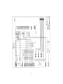
The IMS B008 is a TRAM motherboard which plugs into the IBM PCXT or PC-AT. It has slots for up to ten TRAMs (TRAMs are board-level
transputers that integrate processor, memory and peripheral functions, and
which communicate with the outside world by means of INMOS serial links,
arranged in a standard DIL pin-out). Links 1 and 2 from each of the TRAM
slots are hard wired on the IMS B008, such that the TRAMs, when plugged
in, form a pipeline of processing elements. The remaining links can be ”softwired” using an INMOS IMS C004 programmable link switch, incorporated
on the IMS B008. This arrangement allows a large variety of networks to
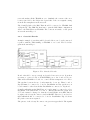
be created under software control. A full block diagram of the IMS B008 is
shown in Fig. 1.
The IMS C004 device is controlled by an IMS T212 16-bit transputer. Configuration data for the IMS C004 is fed into link 1 of the IMS T212, which
then passes it on to the, IMS C004 on link 3. The same data is also passed
out of the IMS T212 link 2 to the 37-way D-connector on the edge of the
board. In this way, IMS B008 boards can be cascaded with the IMS T212’s
forming a chain. Configuration data passes down this chain, with each
IMS T212 sending the appropriate data to the IMS C004 to which it is
connected.
An interface to the IBM bus is provided so that a program running on the
IBM PC can control the TRAMs on the IMS B008 and pass data to or
from them. Data communication can take place by means of a software
routine which uses polling, or via a DMA mechanism which gives a higher
data rate. Different events on the IMS B008, selectable by the programmer,
can generate an interrupt on the IBM PC. This eliminates the need for the
processor in the PC to continuously poll status registers on the IMS B008,
so that the PC can carry on with other tasks while programs are running
on the IMS B008.
2
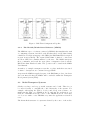
2.1
Hardware Description
Processor Pipeline
The IMS B008 TRAM motherboard has 10 TRAM slots, sufficient to accommodate a maximum of 10 TRAMs. The IMS B008 is hard wired such
that TRAM(N), link 2 is connected to TRAM(N+1), link 1, producing a 10
TRAM pipeline configuration. However, TRAM3, link 2 and TRAM4, link
1 are taken to the patch area so that this pipeline can be broken if the user
application so demands.
6
7
Figure 1: IMS B008 Functional Block Diagram
2.1.1
Pipehead and Pipetail
The link entering the first TRAM of the pipeline (TRAM0, link 1) is termed
Pipehead, and the link leaving the last TRAM (TRAM9, link 2) is called
Pipetail. Pipehead is connected to the patch area so that the source of data
entering the pipeline may be selected from the IBM PC (via the IMS C012)
or another transputer board (via the 37-way D-connector). Pipetail is taken
to the 37-Way D-connector so that it may also be connected to another
transputer board. In this way a pipeline of many motherboards, each containing many transputers can very easily be constructed. More sophisticated
processing structures can also be built by using the remaining links of the
TRAMs (links 0 and 3). See section 2.2.
2.1.2
Physical Location
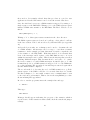
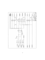
The physical location of the TRAM slots on the IMS B008 is as shown in
Fig. 2. The alternate orientation of adjacent TRAM slots is to improve the
cooling effect of the air flow over the TRAMs. It also means that, if at
any stage in the future a need is identified for Single-In-Line TRAMs, they
would be compatible with the existing motherboards.
Figure 2: IMS B008 TRAM Slot Location
2.1.3
Pipe Jumpers
Some TRAMs physically cover more than one slot on the IMS B008, although they only connect to the signals of one position. In most cases it
is possible to stack other TRAMs on top so that the covered slots are not
wasted. However, if stacking is not required, the pipeline will be broken at
the slots that are underneath the larger TRAMs. Special 8-pin plugs, called
pipe jumpers, are provided to combat this problem. These plug into the
unused slot and connect the signals for links 1 and 2 together, thus continuing the pipeline through to the next TRAM in the chain. A pipe jumper
is required at one end of each empty slot only, with its marker band lining
up with the triangle on the motherboard.
8
2.2
The IMS C004, the IMS T212 and ”Softwired” Links
Links 1 and 2 of each TRAM slot are used in the formation of the processor
pipeline. This leaves links 0 and 3 of each TRAM for connection to other
processors so that more topologically complex systems can be constructed.
The method of control of these connections is explained in the following
sections.
2.2.1
The IMS C004
The IMS B008 has been designed such that TRAM0, link 3 and TRAMs(1..9),
links 0 and 3 are taken directly to the IMS C004, a 32-way link switch. (In
fact, TRAM0, link 0 can also be connected to the IMS C004, but only via
the patch area. This is to enable TRAM0, link 0 to be connected to the
IBM bus, via the IMS C012 device, if so required. Full details of the patch
area are given in section 2.7 and appendix F.)
The IMS C004 has 32 link inputs, 32 link outputs and a configuration link.
Any of the 32 links may be connected to any other by sending the appropriate
control data to the IMS C004 along its configuration link. Thus, link 0 or
3 of any TRAM on the board maybe connected to any other. In addition,
since 8 links are taken from the IMS C004 to the 37-way D-connector (in
addition to Pipetail), it is possible to interconnect links from a great many
boards in a very complex manner.
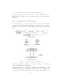
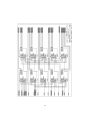
2.2.2
Control of the IMS C004
The configuration link of the IMS C004 is connected to an IMS T212 16-bit
transputer. Links 1 and 2 of the IMS T212 are taken to the D-connector so
that they can be ”pipelined” in the same manner as the TRAMs. Configuration data is passed in on link 1, and then passed out again on link 2 to the
next IMS T212 (and the next board) in the chain. Any configuration data
appropriate to the board is sent to the IMS C004 on link 3. This mechanism
is illustrated in Fig. 3.
On the first board in the chain, ConfigUp is connected to Pipehead so that
the configuration data is passed into the IMS T212 chain from the IBM
PC via the TRAM in slot 0. This architecture is maintained on all INMOS
motherboards so that a pipeline can be constructed from a variety of different
boards.
9
Figure 3: IMS T212 Configuration Pipeline
2.2.3
The Module/Motherboard Software (MMS2)
The MMS2 is a piece of software, written by INMOS, that simplifies the task
of configuring a system of motherboards. Each motherboard is defined using
a hardware description language called HL1 (the IMS B008 HL1 description
is given in appendix D). The required IMS C004 ”softwired” connections
are then defined in a similar manner by the user. The MMS2 interprets
these commands, and sends the appropriate configuration data down the
IMS T212 chain. Further details of its operation can be found in the MMS2
User Manual.
A number of example transputer networks, together with their associated
”softwire” descriptions, are contained in appendix E.
At present the MMS2 is supplied as part of the IMS B008 product. At a later
date it is intended that the MMS2 will be included within the Transputer
Development System (TDS).
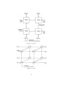
2.3
Multi-Transputer Systems
Clearly very large, and very powerful, systems can be built. Therefore, it
becomes necessary to establish the control hierarchy of the system. For
example, when using the TDS to develop and debug some software, one
might run the TDS on a TRAM in slot 0, and run the application on a
network of TRAMs under the control of the TRAM in slot 0. Obviously,
one does not wish to reset TRAM0 every time the application network is
reset.
The hierarchical structure of a system is defined by the source of the notRe10
set and notAnalyse control signals. JP1 determines the control of TRAM0,
while JP2 determines the control of TRAMs(1..9).
2.3.1
TRAM Hierarchy
The TRAM in slot 0 may be reset (and analysed) by either the IBM PC,
or by another board via the 37-way D-connector. This choice is made by
selecting the position of JP1. Three jumpers are provided, one for each of
the notReset, notAnalyse and notError signals. Setting JP1 to ”PC” (see
Fig. 4b) gives the PC the ability to reset and analyse TRAM0. In addition,
the PC will also be able to read the error flag of TRAM0. Alternatively,
all these functions can be controlled via the 37-way ’D’ connector by setting
JP1 to ”EDGE” (Fig. 7b).
Similarly, the TRAMs in slots 1-9 maybe controlled by the subsystem port
of TRAM0, or they may be put on the same hierarchical level as TRAM0,
in which case their control depends upon the position of JP1. Setting
JP2 to ”SUBSYS” (Fig. 4c) puts the reset, analyse and error functions of
TRAMs(1..9) under control of TRAM0. Setting JP2 to ”DOWN” (Fig. 5c)
puts TRAMs(1..9) at the same level as TRAM0.
It is defined in Dual-In-Line Transputer Modules (TRAMs), Technical Note
29 that any TRAM that has a subsystem port must reset that port if it is
itself reset. Thus, a reset signal will always propagate to all TRAMs at a
lower hierarchical level.
2.4
Examples
In order to aid the understanding of the way in which a hierarchy is established, the selection of TRAM hierarchy on a single board will first be
explained. Three examples of board hierarchy are then described in the
sections which follow.
2.4.1
A Single Board for Developing Software
A block diagram of an IMS B008 configured in this way is shown in Fig. 4a.
This is the configuration in which the board is supplied and is explained in
the following paragraphs.
It is assumed that the Transputer Development System (TDS) is being used
for software development. The TDS should be run on a TRAM plugged into
TRAM slot 0 of the IMS B008. Consequently, the reset, analyse and error
functions of this TRAM must be under control of a program running on the
11
Figure 4: Single Development Board Configuration
IBM PC. Jumper plug 1 should therefore be connected to ”PC”, as shown
in Fig. 4b.
TRAMs(1..9), as well as the IMS T212, must be connected as a subsystem
of TRAM0. This means that TRAM0 can reset and analyse all the other
transputers in the system as well as read their error status. To facilitate
this, jumper plug 2 should be connected to ”SUBSYS”, as shown in Fig. 4c.
The ConfigUp link of the IMS T212 (link 1) must be connected directly
to link 1 of TRAM0. (This link is known as Pipehead). This enables the
TRAM running the TDS and MMS2 to feed configuration data directly to
the IMS T212, which passes it on to the IMS C004. This connection is made
via the patch area as shown in Fig. 4d. (A full description of the patch area
is given in appendix F).
The IMS C012 link is connected to link 0 of TRAM0 so that TRAM0 always
12
boots down this link. This connection is also shown in Fig. 4d.
The other essential patch area connection is that of TRAM3, link 2 to
TRAM4, link 1. This is part of the pipeline, which is routed through the
patch area.
2.4.2
A Single Board as a Target System
In this application, a bootable code file is sent directly to the transputer
network from the IBM PC. All the TRAMs are on the same level of hierarchy,
all under control of the PC. A block diagram of this scheme is shown in
Fig. 5a.
Figure 5: Single Board Target Configuration
Jumper plug 1 should be set to ”PC”, as shown in Fig. 5b. This allows
control of TRAM0 from the IBM bus.
Jumper plug 2 should be connected to ”DOWN”, as shown in Fig. 5c. This
ensures the signals controlling TRAM0 propagate directly to TRAMs(1..9),
as well as the IMS T212. Thus the program running on the IBM PC can
13
reset and analyse all the TRAMs at once. Similarly, the content of the error
location (as read by the PC) is the logical OR of the error signals coming
from all the transputers in the network.
The ConfigUp link of the IMS T212 should be connected to TRAM0, link
1 (Pipehead). The IBM PC then has to pass the IMS C004 configuration
data to the IMS T212 via TRAM0. The connection is made on the patch
area as shown in Fig. 5d.
2.4.3
Cascaded Boards
A simple example of cascading will be described here: two boards connected
together, with the TDS running on TRAM0 of one board. The block diagram is shown in Fig. 6.
Figure 6: Two Cascaded Boards
Board 1 should be set up exactly as described in section 2.4.1. It is then
necessary to connect board 1, SUBSYSTEM port to the board 2, UP port.
This enables TRAM0 on board 1 to control all the transputers on board 2.
The pipeline between the two boards must also be set up. Thus, board 1,
Pipetail must be connected to board 2, PatchLink1 and the patch area on
board 2 must be altered such that PatchLink1 is connected to Pipehead.
ConfigDownLink from the IMS T212 on board 1 must be connected to ConfigUpLink of the IMS T212 on board 2. This means that the patch area
on board 2 must be changed so that the ConfigUpLink on its IMS T212 is
brought to the 37-way D-connector via PatchLink0. Therefore board 1, ConfigDownLink should be connected to board 2, PatchLink0. Fig. 7d shows
the patch connections required.
The pinout of the 37-way D-connector is given in appendix G. The signals
14
that need connecting together are shown in Table 1.
Board 1
notSubSystemReset
notSubSystemAnalyse
notSubSystemError
PipetailLinkOut
PipetailLinkln
ConfigDownLinkOut
ConfigDownLinkln
Pin No.
(33)
(15)
(34)
(16)
(35)
(17)
(36)
→
→
→
→
→
→
→
Board 2
notUpReset
notUpAnalyse
notUpError
PatchLinkln1
PatchLinkOut1
PatchLinkln0
PatchLinkOut0
Pin No.
(20)
(2)
(21)
(14)
(32)
(13)
(31)
Table 1:
Figure 7: Cascaded Boards:Board 2 Switch and Jumper Settings
Board 2 should be invisible to the IBM bus. Its link adapter and system
registers should therefore be disabled. This is done by setting switches 4
and 5 to ”ON”, as shown in Fig. 7a.
TRAM0 on board 2 should be controlled by the signals coming in on the
UP port. Hence jumper plug 1 should be set to ”UP”, as shown in Fig. 7b.
15
In this example, the IMS T212 and TRAMs(1..9) on board 2 are on the
same level of hierarchy as TRAM0. Therefore jumper plug 2 should be set
to ”DOWN”, as shown in Fig. 7c.
2.4.4
Cascading more boards
More boards may, of course, be cascaded. Other INMOS boards (e.g.
IMS B004, IMS B012) can be present in the cascade. Many boards on
the same level of hierarchy can be controlled by TRAM0 on one board. The
boards on the same level should be linked by connecting the DOWN port of
one to the UP port of the next. See Fig. 8. Multiple levels of hierarchy can
be created by extending the principles outlined earlier in this chapter. See
Fig. 9.
Figure 8: Two level board cascade
Figure 9: Multiple levels of hierarchy
16
2.5
2.5.1
The IBM Bus Interface
Polling
This is the simplest method of data transfer between the IBM PC and the
IMS B008. Earlier INMOS boards, the IMS B004 for example, have this
as the only data transfer mechanism. The interface on the IMS B008 is
completely compatible with these.
For details of how to use this interface, the operation of the IMS C012 link
adapter must be understood. The details of this device are included in
the Transputer Reference Manual. Example procedures for accessing the
IMS B008, written in Turbo Pascal’, are given in appendix C, listing I. The
source code is also included on the ”Test/Examples” disc with the filename
ladp.pas.
Before any data can be sent to the IMS B008, the board must first be reset
by software. This can be done by using the procedure called doReset in
appendix C, listing I.
For a summary of the IMS B008 registers and where they appear in the I/0
address space, see appendix B.
2.5.2
Direct Memory Access (DMA)
For higher data rates, a DMA interface has been incorporated into the
IMS B008. In order to use this mechanism, it is useful to understand the
operation of the 8237 DMA controller chip present in the IBM PC. Details
can be found in an 8237 data sheet.
Once the DMA controller has been initialised, the DMA interface may be
used in several different ways. In the example software (appendix C) a
process is started on TRAM0 to input and output data down its link 0,
which is connected to the PC bus via the IMS C012. The transfer is then
triggered off by the program running on the PC, which must write to the
DMA control register on the IMS B008. The value ”0” is written to transfer
from the PC to the IMS B008; a ”1” is written to transfer in the other
direction.
The transfer proceeds with the IMS B008 making a DMA request for a single
byte at a time. In this way, a byte is transferred in between the execution of
each instruction of the processor on the PC. Therefore this processor appears
to be running code at the same time as the DMA transfer is taking place.
It is mainly for this reason that it is difficult to specify the improvement in
data throughput. One example will be given: for an 8 MHz iAPX 286 CPU
17
and a 5 MHz DMA controller, a DMA transfer has approximately twice the
data rate of an optimised assembly code routine which uses polling. This
figure was derived with the processor doing nothing other than waiting for
the end of the DMA transfer.
The end of the DMA transfer is signalled in one of two ways. The DMA
controller can be polled by reading its status register. This gives information about which DMA channels have a transfer pending and which have
completed a transfer. See an 8237 datasheet for further information. Alternatively an interrupt can be set up to signal the end of a DMA transfer. See
section 2.6.
2.5.3
Example Programs
A buffer process, written in occam, runs on the transputer on TRAM0. Its
source code is given in appendix C, listing II. This process inputs data down
link 0 and stores it in memory as a queue. When another device (in this case
the IMS C012 on the IMS B008) becomes ready to read this data, TRAM0
sends it back down link 0. Thus, when the DMA controller transfers data
to the IMS B008, the queue fills up. It is then emptied by a DMA transfer
from the IMS B008 to the PC.
A program on the IBM PC is also required to load up TRAM0 with the
buffer program, set up the DMA controller and initiate the transfer.
The outline of this program is as follows:
Set up constants
Initialise interrupt vectors and controller chip
Reset TRAM0 on IMS B008
Initialise IMS C012 on IMS B008
Boot up TRAM0 with buffer program
REPEAT TWICE:
Enable interrupts from IMS B008
Set up DMA controller for transfer to IMS B008
Trigger DMA transfer to IMS B008
Wait for interrupt to signal transfer complete
Set up DMA controller for transfer to IBM PC
Trigger DMA transfer to IBM PC
Poll DMA controller status to determine end of transfer
Compare received data with original transmitted data
The code is written in Turbo Pascal and shown in appendix C, listing Ill.
The setupDMAC procedure initialises the various registers of the 8237 for
the required mode of operation. No attempt will be made here to describe
18
these modes. It is simply advised that this procedure is copied for user
applications. Detailed information can be found in an 8237 data sheet.
Once the 8237 has been set up, a DMA transfer is triggered by writing to a
single register on the IMS B008. Writing a ”0” to the DMA request register
initiates a DMA write transfer to the IMS B008. The Turbo Pascal code for
this is:
PORT [DMArequest] := 0;
Writing a ”1” to this register starts a transfer in the other direction.
The DMA request register is located at boardbase + $12, where boardbase
is the base address of the board as selected by SW4 and SW5 (see appendix
A).
As described previously, two techniques can be used to determine the end
of a DMA transfer. An interrupt can be set up to occur when a transfer
terminates - in the example program, this method is used to signal the end
of the transfer to the IMS B008. With this method, it is essential that
bit 0 of the interrupt enable register on the IMS B008 is reset to ’0” from
within the interrupt service routine. This clears the interrupt line as well as
disabling DMA interrupts. This bit must then be set back to ”1” outside
the service routine to re-enable DMA interrupts. A suitable place to do this
is immediately before a DMA transfer is triggered off - see the DMAwrite
procedure in listing III, appendix C. An interrupt is asserted again when
another DMA transfer completes.
The second method of detecting the end of a DMA transfer is to poll the
status register of the DMA controller. See an 8237 data sheet for details.
For this technique to be successful, a master reset command must be sent
to the 8237 after each transfer. This is done in the setupDMAC procedure
shown in listing III, appendix C.
In order to run the programs, insert the examples disc and type
a: <Enter>.
Then type
DMA <Enter>
Messages should appear indicating the progress of the transfer, which is
repeated twice. If the transfer is unsuccessful, check the switch and jumper
settings.
19
Source code is also included on the ”Test/Examples” disc so that these
procedures can be incorporated into user programs. The occam source for
the buffer is called buffer. tar and should be manipulated with the INMOS
folding editor. It has been compiled and made into a bootable code file (see
TDS documentation) called buffer.bcf, which is loaded into the transputer
on TRAM0 by the Turbo Pascal program.
Any popular editor (e.g. Wordstar) can be used on the pascal source for the
DMA controller program.
The software has been written to use DMA channel 0. If it is desired to use
a different channel, enter the channel number when the program is run. The
switch settings must also be changed to select the channel of your choice.
See appendix A for details.
2.6
2.6.1
Interrupts
Why Interrupts?
It is sometimes undesirable to tie up CPU time on the IBM PC by continuously polling the IMS B008 status registers. Clearly it may be useful to
put the host processor to work while the transputer array on the IMS B008
is running code. For example, the CPU on the PC could be updating the
graphics screen while the transputer array performs a awesome numbercrunching computation. The array could then signal the end of the computation with a link transfer, which can be made to interrupt the host CPU
from its mundane task and tell it that the answer to the question is now
available.
2.6.2
IMS B008 Interrupt Capability
The IMS B008 can interrupt the IBM PC on any of four events:
1. A DMA transfer has completed;
2. An error has occurred on the IMS B008;
3. The IMS B008 is ready to receive a byte of data via the IMS C012;
4. The IMS B008 is ready to send a byte of data via the IMS C012.
The interrupt control register, located at boardbase + $13, is used to determine which of these events cause an interrupt. Four bits in this write-only
register are used, one for each event (see Table 2).
20
Bit 0
Bit 1
Bit 2
Bit 3
Enable interrupt on DMA end
Enable interrupt on error
Enable interrupt when IMS B008 is ready to receive byte
(OutputInt on IMS C012 is active)
Enable interrupt when IMS B008 is ready to send byte
(Inputlnt on IMS C012 is active)
Table 2: Interrupt Control Register Function
All other bits at this location are unused. In all cases, setting a bit to
”1” enables interrupts on the corresponding event. Clearing a bit disables
interrupts on that event. Note that any number of these events can be
programmed to cause an interrupt, but that the interrupt will occur on the
same channel regardless of the event. It is a simple matter for the interrupt
service routine to read a few status registers to determine the cause of the
interrupt. The error flag, OutputInt and InputInt are all status bits present
in IMS B008 registers (see appendix B). Interrupt on end of DMA can be
detected by reading the status register of the 8237 DMA controller.
Note that when the IMS B008 powers up, all these control bits are at ”0”.
In this situation, the selected IMS B008 interrupt line is tri-stated. As soon
as any of the control bits are set to ”1”, the selected line is driven to logic
”0”. It is driven to logic ”1” when the chosen event occurs. It is therefore
important that this register is not written to if other peripherals in your
PC use interrupt lines 3 and 5. The IMS B008 may be damaged if this
instruction is not followed.
Switch 3 should be ”ON” to select IRQ3, ”OFF” to select IRQ5.
2.6.3
Examples
Section 2.5.3 illustrates how to use interrupts to signal the end of the DMA
transfer. It is vitally important that the interrupt service routine clears bit
0 of the interrupt control register to disable the interrupt signal. If this bit
is then set back to ”1” outside the service routine, interrupt on DMA is
re-enabled but not reasserted until another DMA transfer completes.
Interrupts can also be used to signal when the IMS B008 has data to transfer
to the IBM PC (InputInt from IMS C012 is asserted), or when it is ready to
receive data (OutputInt asserted). In both cases the interrupt line will remain asserted until the data has been read from or written to the IMS B008,
or until interrupts are disabled altogether.
21
2.7
The Patch Area
The patch area consists of a 24-pin DIL header block that can be wired according to the users requirements. An INMOS link is a two wire connection,
implying that 12 links are taken to the patch area. These are:
C012Link, TRAM0Link0 These two links should be connected together
when it is intended that the IMS B008 is to transfer data between
itself and the IBM bus. In order to maintain compatibility with INMOS software, it is highly recommended that C01121-ink is only ever
connected to TRAM0Link0, and never to Pipehead, which is in effect
TRAM0Link1.
Pipehead This is TRAM0Link1, the beginning of the pipeline of processors.
ConfigUp This is IMS T212 link1. It is the link upon which the IMS C004
configuration data is received. It may be connected via the patch area
to either one of the 37-way D-connector links, or to Pipehead if the
configuration data is to come from the IBM bus via TRAM0.
PatchLink0, PatchLink1 These two links are connected to the 37-way Dconnector. Generally, if they are used they are connected to ConfigUp
and Pipehead respectively, although they may be connected to any of
the other links available.
C004Link0, C004Link28, C004Link29 These three links are connected
to the IMS C004 link switch. They can be used, for example, to provide
extra IMS C004 links to the D-connector, or to connect TRAM0Link0
to the IMS C004 on a board which does not ”talk” directly to the
IBM.
T2Link0 This is the spare link of the T212. Its speed may be set independently of the other links on the board (see section 2.8).
TRAM3Link2, TRAM4Link1 These two links enable the 10 slot pipeline
to be broken between TRAMs 3 and 4 if so required (see section 2.1).
A pin out of the patch area header block can be found in appendix F.
2.8
Link Speed Selection
The link speed of all the TRAMs on a board is switchable between 10 Mbits/s
and 20 Mbits/s by means of the switch labelled Boardspeed. However, link 0
22
of the IMS T212 can run at a different speed to the TRAMs; either 5 Mbits/s,
10 Mbits/s or 20 Mbits/s. This could be useful for communicating with an
external system whose links run at a different speed to that of the TRAMs.
Appendix A shows the combinations possible.
3
Configuration
3.1
Default Switch and Jumper Settings
The switches and jumpers on the IMS B008 enable a large variety of operating modes. The default settings are shown in Fig. 10 and are described in
the following sections.
Figure 10: Default Switch Settings
3.1.1
Board Address
As supplied, the board is set up to use locations $150 to $16F (a ”$” sign
indicates a hexadecimal number) in the I/0 address space of the PC. If this
clashes with other cards present in your PC, then the appropriate switch
settings will have to be changed. Refer to appendix A for details. If the
address is changed, the new address will have to be specified when the TDS
is invoked from MS-DOS. The required format is:
TDS2 -l <address>
where <address> is the base address of the board. If the parameters are
omitted then the base address defaults to $150. (N.B. Throughout this
manual the symbol ”$” is used to indicate a hexadecimal number. However,
MS-DOS does not recognise this notation and a ”#” symbol must be used
for this purpose in the <address> term above.)
3.1.2
Interrupt Setting
The board as supplied is set to use interrupt channel 3. If required, channel
5 can be selected by switching Switch 3 to ”OFF”. This should not be done
23
if the board is being used in a PC-XT because channel 5 is used by the hard
disc. It is important to ensure that the interrupt line used by the IMS B008
is not used by any other device present in the PC.
In order to enable the IMS B008 to assert an interrupt, its interrupt control
register must be accessed. See section 2.6.2 for details.
3.1.3
DMA Channel Setting
DMA channel 0 is selected by default. This will not operate on the PC-XT
because channel 0 is not available on the XT bus. However, this default
setting will not affect the normal operation of the PC-XT. Only channel 1
can be used by the IMS B008 on a PC-XT, but only if SDLC (or another
networking system which uses this channel) is not present.
Channels 0 and 3 are normally free on the PC-AT. As with the PC-XT,
channel 1 is reserved by IBM for SDLC, but again it may be used if this (or
another network) is not fitted.
See appendix A for details of the switch settings required to select the appropriate DMA channel. Alternatively, DMA may be disabled altogether.
3.1.4
Link Speed Selection
All links are set to run at 20 Mbits/s. See appendix A for information on
changing the link speed settings.
3.1.5
Jumper Positions
It is assumed that, at this stage, the TDS is being run on a TRAM plugged
into slot 0. In this case, the jumper blocks and patch area should not be
disturbed. For details of other possible board configurations, see section
2.3.1.
4
4.1
Unpacking and Handling
Unpacking the IMS B008
When you open the packing box in which the IMS B008 is shipped, you will
find:
24
1. A packing list which you should check against the box contents immediately.
2. A documentation pack, including this manual.
3. A floppy disk entitled ”IMS B008 Examples/Test’, which contains
some example routines and some test software.
4. An anti-static bag containing the IMS B008 board.
5. A link breakout board.
6. An IMS B008 cable set.
Do not open the bag containing the IMS B008 until you have read the section
on handling.
4.2
Handling Precautions
To prevent damage from static discharge, certain precautions should be
taken when removing the board from its protective bag:
1. While holding the board in one hand, still in its bag, touch a metal
part of your PC with the other hand.
2. Carefully remove the board from the bag, holding the board by the
edges only. Avoid touching any components or connections.
3. While manipulating switches and jumpers on the board and when
inserting it into the PC, hold the board by its edges only.
4. If the board is being stored or shipped, standard anti-static handling
precautions should be observed.
N.B. Under no circumstances plug or unplug a TRAM with power applied to
the IMS B008. Permanent damage to both the TRAM and the motherboard
could occur.
4.3
TRAM Fitting and Handling
TRAMs must be carefully installed and removed from the IMS B008, taking
special care not to bend any of the TRAM’s pins. The slots on the IMS B008
have pin 1 marked on the board by a silk-screened legend (a triangle). Pin
1 on the TRAM to be installed will also be marked in a similar manner.
25
N.B. Plugging in a TRAM the wrong way round may result in the destruction of the TRAM or the motherboard.
The IMS B008 has some components mounted on the top (as opposed to the
underside) of the board in the positions occupied by some TRAM slots (slots
8 and 9). When plugging a TRAM into these positions, it will be necessary
to fit ”stand-off” strips to the TRAM pins. These are 8-way pin strips which
plug into the IMS B008, and raise the TRAM above the motherboard. These
”stand-off” strips are supplied fitted to INMOS TRAMs.
4.4
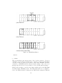
Installing an IMS B008 (with a single TRAM fitted)
The following procedure should be followed:
1. Remove the TRAM that is to run the TDS from its protective packaging, observing the appropriate handling precautions.
2. Plug this TRAM into slot 0 of the IMS B008. Ensure that the pin
1 indicator on this TRAM lines up with the triangle on TRAM slot
0 of the IMS B008. Note that the 16 pins on the TRAM that carry
the signals should plug into the required slot. Thus, for example, a
size 4 TRAM to plug into slot 0 will occupy slots 0, 4, 7 and 3 (see
Fig. 11a); a size 2 TRAM to plug into slot 1 will occupy slots 1 and 5
(see Fig. 11b).
3. Insert link jumper plugs on top of this TRAM in all the slots that do
not carry any signals. This is to ensure continuity of the pipeline. A
jumper is required at one end of each empty slot only, with its marker
band lining up with the triangle on the motherboard. This is also
illustrated by Fig. 11. If TRAMs are to be stacked on top of each
other, the link jumpers have to be removed from the slots which are
to be used for stacking.
4. Fill the other slots on the IMS B008 with TRAMs as required. They
need not be filled in numerical order so long as the pipe is maintained
using pipe jumpers.
5. Fit link jumper plugs (supplied) into the slots on the motherboard
that are not being used. This stops the pipeline from being broken.
This is illustrated in Fig. 11c, in which the empty slots (8 and 9) have
been ”jumped out” to complete the pipeline.
6. Remove the cover of the IBM PC.
7. Choose the expansion slot into which the IMS B008 is to be inserted.
Do not use the slot nearest the edge in a PC-AT, because it does not
26
provide the full set of signals from the AT bus. If the board is being
used in a PC-XT, then the smaller set of edge connectors will hang in
mid-air. Don’t panic! This does no harm.
8. Remove the expansion slot cover from the chosen slot. Retain the
fixing screw.
9. Carefully, holding the board by its edges, insert it into the chosen
expansion slot.
10. Secure the bracket on the IMS B008 to the chassis of the PC using the
fixing screw.
11. Replace the cover on the PC.
5
Testing
5.1
Powering up
Switch the PC on. If it fails to boot up, then either the selected IMS B008
address or DMA channel clashes with another device present. Check the
settings described in appendix A.
5.2
Running the test software
Insert the ”Examples/Test’ disc into drive a: and select this drive by typing
a: <Enter>
The test program can now be run by typing
test <Enter>
A prompt will appear asking whether the default switch settings have been
changed. If not, press <Enter>. Otherwise type
yes <Enter>
and enter the board setup according to the prompts received.
A diagram will then appear on the screen indicating how the switch settings
should look. Press
27
Figure 11: TRAM Installation
<Enter>
to continue.
The program then tests various parts of the board in sequence. It is not
exhaustive, but it will check whether the board has been set up and installed
correctly. If the program reports that it cannot find TRAM0, check the
orientation of TRAM0 and the address switch settings. Any other error
messages should bear an obvious relation to the relevant switch settings.
If all is well, it is time to use the test software which explores the IMS B008
and finds all the TRAMs present. The TDS must therefore be installed refer to the TDS literature for instructions. Full details of using the TDS and
28
the MMS2 are given in the appropriate manuals. This is the correct time
to examine those manuals and try some programming examples. Return to
this manual when more advanced features specific to the IMS B008 are to
be used, e.g. cascading boards and using the DMA interface.
A
A.1
Switch Settings
DMA Channel (Switches 1,2)
This is selected according to Table 3.
SW1
ON
OFF
ON
OFF
SW2
ON
ON
OFF
OFF
DMA Channel
0
1
DMA disabled
3
Table 3: DMA Channel Selection
A.2
Interrupt Channel (Switch 3)
This is selected according to Table 4.
SW3
ON
OFF
Interrupt Channel
3
5
Table 4: Interrupt Channel Selection
A.3
Board Address (Switches 5,6)
Two switches are used to select the base location in the I/0 address space
at which the IMS B008 appears, or to disable the board from the IBM bus
altogether. The following table shows the options available.
SW4
ON
OFF
ON
OFF
SW5
ON
ON
OFF
OFF
Address (hexadecimal)
Not selected
$150
$200
$300
Table 5: Base Address Selection
29
A.4
Link Speed Selection (Switches 6..8)
All the TRAMs and the IMS C004 must have identical link speeds. The
IMS T212 can, however, have its link 0 running at different speeds. Table 6
shows the combinations possible.
SW6
ON
ON
ON
ON
OFF
OFF
OFF
OFF
SW7
ON
ON
OFF
OFF
ON
ON
OFF
OFF
SW8
ON
OFF
ON
OFF
ON
OFF
ON
OFF
T212 Link 0 All Other Links
10 Mbits/s
10 Mbits/s
5 Mbits/s
10 Mbits/s
10 Mbits/s
10 Mbits/s
20 Mbits/s
10 Mbits/s
NON-FUNCTIONAL
NON-FUNCTIONAL
10 Mbits/s
20 Mbits/s
20 Mbits/s
20 Mbits/s
Table 6: Link Speed Selection
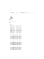
B
IMS B008 Registers
This appendix contains a summary of the registers of the IMS B008 and
the locations in the I/O address space at which they appear. In Table 7,
boardbase is as selected by SW4 and SW5 - see appendix A.
B.1
Location in Memory
Board address
boardbase + $00
boardbase + $01
boardbase + $02
boardbase + $03
boardbase + $10
boardbase + $11
boardbase + $10
boardbase + $12
boardbase + $13
Register
Input data register
Output data register
Input status register
Output status register
Reset register (write only)
Analyse register (write only)
Error location (read only)
DMA request register
Interrupt control register
Table 7: IMS B008 Register Memory Location
30
B.2
Functional Description
A description of the IMS C012 registers (the first four IMS B008 address
locations) can be found in the Transputer Reference Manual. The other
registers, which are specific to the IMS B008, are described below.
B.2.1
Reset Register
Setting bit 0 to ”1” asserts the Reset signal;
Resetting bit 0 to ”0” deasserts the Reset signal.
B.2.2
Analyse Register
Setting bit 0 to ”1” asserts the Analyse signal;
Resetting bit 0 to ”0” deasserts to Analyse signal.
B.2.3
Error Location
Reading a ”1” in bit 0 indicates that Error is asserted;
Reading a ”0” in bit 0 indicates that Error is not asserted.
B.2.4
DMA Request Register
Writing ”0” into bit 0 triggers a DMA transfer from the PC to the IMS B008;
Writing ”1” into bit 0 triggers a DMA transfer to the PC from the IMS B008.
B.2.5
Interrupt Control Register
Four bits are used in this register, the functions of which are as follows:
Bit 0
Bit 1
Bit 2
Bit 3
Enable interrupt on DMA end
Enable interrupt on error
Enable interrupt when IMS B008 is ready to receive byte
(OutputInt on IMS C012 is active)
Enable interrupt when IMS B008 is ready to send byte
(Inputlnt on IMS C012 is active)
Table 8: Functional Description of the Interrupt Control Register
31
C
C.1
Program Listings
Listing I - Basic Data Transfer Routines
{This is a set of procedures for communicating with the IMS B008
via the IMS C012 link adaptor.}
CONST
linkBase
inputData
outputData
inputStatus
outputStatus
resetT414
analyseT414
=
=
=
=
=
=
=
$0150;
$0150;
$0151;
$0152;
$0153;
$0160;
$0161;
PROCEDURE initC012;
BEGIN
Port [ inputStatus] := 0;
Port [ outputStatus] := 0;
END;
{inputInt disabled}
{outputInt disabled}
FUNCTION dataPresent : BOOLEAN;
BEGIN
dataPresent := ODD ( Port [ inputStatus]);
END;
FUNCTION outputReady : BOOLEAN;
BEGIN
outputReady := ODD ( Port [ outputStatus]);
END;
PROCEDURE outByte ( b : INTEGER );
BEGIN
Port [ outputData] := b;
WHILE NOT ODD ( Port [outputStatus] ) DO BEGIN
END;
END;
32
FUNCTION inByte : INTEGER;
BEGIN
WHILE NOT ODD(Port[inputStatus]) DO BEGIN
END;
inByte := Port [ inputData];
END;
PROCEDURE loopFor ( i : INTEGER );
BEGIN
WHILE i <> 0 DO
i := i - 1;
END;
PROCEDURE doAnalyse;
BEGIN
Port [ analyseT414] := 1;
loopFor ( 10000);
Port [ resetT414] := 1;
loopFor ( 10000);
Port [ resetT414] := 0;
loopFor ( 10000);
Port [ analyseT414] := 0;
loopFor ( 5000);
END;
PROCEDURE doReset;
BEGIN
Port [ analyseT414] := 0;
loopFor ( 800);
Port [ resetT414] := 1;
loopFor ( 3000);
Port [ resetT414] := 0;
loopFor ( 1000);
END;
C.2
Listing II - Occam Buffer Program
PROC listener ()
--declarations
VAL Link0out IS 0 :
33
VAL
VAL
VAL
VAL
VAL
VAL
VAL
VAL
Link1out IS 1 :
Link2out IS 2 :
Link3out IS 3 :
Link0in IS 4 :
Link1in IS 5 :
Link1in IS 6 :
Link3in IS 7 :
size IS 50 :
CHAN OF BYTE to.C012, from.C012 :
[size + 1] CHAN OF BYTE pipes :
PLACE to.C012 AT Link0out :
PLACE from.C012 AT Link0in :
PAR
PAR i = 0 FOR size
BYTE data:
WHILE TRUE
SEQ
pipes [i] ? data
pipes [i+1] ! data
PAR
BYTE data:
SEQ
WHILE TRUE
SEQ
from.C012 ? data
pipes [0] ! data
BYTE data:
SEQ
WHILE TRUE
SEQ
pipes [size] ? data
to.C012 ! data
-- Create one process
-- per queue position
-- Shift character up in queue
-- Get data from C012
-- Put at bottom of queue
-- Take data off top of queue
-- Send data to C012
:
PLACED PAR
PROCESSOR 0 T4
listener ()
C.3
Listing III - DMA Transfer Program
PROGRAM dma;
{ This program sands a string of characters to the transputer on
34
the IMS B008 via the DMA interface, then reads them back and
prints them out. A buffer process sits on the transputer which
inputs characters and puts them into a queue.
It also takes characters out of the other end of the queue and
sends them back to the link adaptor.
This process is present on the ’examples’ floppy as a bootable
code file; it is sent to TRAM0 on the IMS B008 by the turbo
pascal procedure called ’loadT4code’.}
CONST
{B008 registers}
boardbase:
INTEGER
inputData:
INTEGER
outputData:
INTEGER
inputStatus: INTEGER
outputStatus: INTEGER
resetT414:
INTEGER
analyseT414: INTEGER
DMArequest:
INTEGER
INTenable:
INTEGER
{Some useful
writeDMA
readDMA
maxlength
IBMtoB008
B008toIBM
chan0
chan1
chan3
DMAchannel:
=
=
=
=
=
=
=
=
=
$150;
0;
0;
0;
0;
0;
0;
0;
0;
DMA constants}
= 0;
= 1;
= 50;
{maxlength := length of string + 1}
= 8;
= 4;
= $0;
= $1;
= $3;
INTEGER = chan0;
{IBM DMA controller registers}
DMAstatus
= $08;
DMAcommand
= $08;
softDRQ
= $09;
DMAsingmask = $0A;
DMAmode
= $0B;
DMAffclear
= $0C;
DMAmastclr
= $0D;
DMAallmask
= $0F;
addrch0
= $00;
wordch0
= $01;
addrch1
= $02;
wordch1
= $03;
addrch3
= $06;
wordch3
= $07;
pagech0
= $87;
35
pagech1
pagech3
= $83;
= $82;
{Interrupt constants}
PICbase
= $20;
spurioustuff = 7;
DMAInt
= 1;
Intchannel:BYTE
= 3;
intmask:
BYTE
= $F7;
intvec:
BYTE
= $2C;
eoi:
BYTE
= $63;
flagint:
BOOLEAN = FALSE;
int count: INTEGER = 0;
intdata:
BYTE
= 0;
TYPE
text = STRING [maxlength];
VAR
teststring, default: text;
datablock: ARRAY [0..maxlength] OF BYTE ABSOLUTE teststring;
i, j, x, transfers, counter, blocklength: INTEGER;
stringlength: BYTE ABSOLUTE teststring;
switchpic : ARRAY [1-9, 1..35] OF CHAR;
PROCEDURE initConst;
{Initialise typed constants)
BEGIN
inputData
outputData
inputStatus
outputStatus
resetT414
analyseT414
DMArequest
INTenable
:=
:=
:=
:=
:=
:=
:=
:=
CASE intchannel
5:
BEGIN
intmask :=
intvec
:=
eoi
:=
END {5};
boardbase;
boardbase +
boardbase +
boardbase +
boardbase +
boardbase +
boardbase +
boardbase +
1;
2;
3;
$10;
$11;
$12;
$13;
OF
$DF;
$34;
$65;
3:
36
BEGIN
intmask
intvec
eoi
END {3};
END {case};
END;
:= $F7;
:= $2C;
:= $63;
PROCEDURE IntDMA;
{Interrupt service routine for end of DMA transfer.
Sets flagint TRUE.}
BEGIN
INLINE ($50/$53/$51/$52/$56/$57/$1E/$06/$FB); {Stack registers}
flagint := TRUE;
PORT [INTenable] := 0;
PORT [PICbase]
:= eoi;
{Flag that DMA has ended.}
{Toggle INTenable to clear interrupt}
{Send specific EOI to PIC}
INLINE ($07/$1F/$5F/$5E/$5A/$59/$5B/$58/$CF); {Unstack}
END;
PROCEDURE initINT;
{Set up interrupt stuff}
VAR
IntServAddr: INTEGER;
OldMask: BYTE;
BEGIN
IntServAddr := OFS (IntDMA) + spurioustuff;
MEM
MEM
MEM
MEM
[$0000:intvec
[$0000:intvec
[$0000:intvec
[$0000:intvec
+
+
+
+
0]
1]
2]
3]
:=
:=
:=
:=
IntServAddr AND $FF;
IntServAddr SHR 8;
CSEG AND $FF;
CSEG SHR 8;
OldMask := PORT [PICbase + 1];
{Clear mask for IRQ3 or 5}
PORT [PICbase + 1] := OldMask AND IntMask;
PORT [INTenable] := 0; {Disable interrupts from B008}
END;
PROCEDURE initC012;
37
BEGIN
Port [ inputStatus] := 2; {Enable inputInt}
Port [ outputStatus] := 2; {Enable outputInt}
END;
FUNCTION dataPresent : BOOLEAN;
BEGIN
dataPresent := ODD ( Port [ inputStatus]);
END;
FUNCTION outputReady : BOOLEAN;
BEGIN
outputReady := ODD (Port [ outputStatus]);
END;
PROCEDURE outByte (b : BYTE );
BEGIN
Port [ outputData] := b;
WHILE NOT ODD ( Port [outputStatus] ) DO BEGIN
END;
END;
PROCEDURE loopFor (i : INTEGER);
BEGIN
WHILE i <> 0 DO
i := i - 1;
END;
PROCEDURE doReset;
BEGIN
Port [ analyseT414] := 0;
loopFor ( 800);
Port [ resetT414] := 1;
loopFor ( 3000);
Port [ resetT414] := 0;
loopFor (1000);
END;
38
PROCEDURE loadT4code;
VAR
data: BYTE;
bootcode: FILE OF BYTE;
BEGIN
ASSIGN (bootcode, ’buffer.bcf’);
RESET (bootcode);
WRITELN (’Loading boot code to transputer...’);
REPEAT
READ (bootcode, data);
outByte (data);
UNTIL EOF (bootcode) = TRUE;
WRITELN (’Loaded code’);
END;
PROCEDURE add24bit (segment, offset: INTEGER;
VAR byte0, byte1, byte2: BYTE)
{ Produce a 24 bit address from a 16-bit segment and a
16-bit offset. Pass the result out as three bytes using
variable parameters.}
VAR
result, temp: INTEGER;
a, b, carry: BYTE;
BEGIN
temp
:= segment SHL 4; {Bottom 12 bits of segment.}
a
b
result
byte0
carry
:=
:=
:=
:=
:=
temp AND $FF;
offset AND $FF;
a + b;
result AND $FF;
result SHR 8;
a
b
result
byte1
carry
:=
:=
:=
:=
:=
temp SHR 8;
offset SHR 8;
a + b + carry;
result AND $FF;
result SHR 8;
temp
byte2
END;
:= segment SHR 12; {Top 4 bits of segment.}
:= temp + carry;
39
PROCEDURE setupDMAC (readnotwrite: BYTE;
length, segdata, ofsdata: INTEGER);
VAR
addr0, addr1, addr2, direction: BYTE;
PROCEDURE addressandcount (addrch, pagech, wordch: BYTE);
{Set up start address and length of transfer in DMAC for
apt channel.}
BEGIN
port [addrch] := addr0; {Set up address ls byte)
port [addrch] := addr1; {Set up address middle byte}
port [pagech] := addr2; {Put address msb in page reg}
port [wordch] := length AND $FF; {Length of data block}
port [wordch] := length SHR 8;
END;
BEGIN
PORT [DMAmastclr] := 0;
{Reset DMAC}
add24bit (segdata, ofsdata, addr0, addr1, addr2);
CASE DMAchannel OF
0: addressandcount (addrch0, pagech0, wordch0);
1: addressandcount (addrch1, pagech1, wordch1);
3: addressandcount (addrch3, pagech3, wordch3);
END {case};
PORT [DMAmode] := ($00 OR readnotwrite OR DMAchannel);
{Set up mode register:
ch0 select;
read or write transfer;
autoinit disable;
address increment;
demand mode.
Binary mode word = 0000 10cc IBM -> B008
= 0000 01cc B008 -> IBM}
PORT [DMAcommand] := $00; {Set up command register:
mem-to-mem off;
ch0 address hold disable;
controller enable;
normal timing;
fixed priority;
late write;
DREQ active high;
40
DACK active low.
Binary command word = 0000 0000}
PORT [DMAallmask] := 0;
{Clear apt channel mask bit}
END;
PROCEDURE pol1DMAC;
{Poll DMAC status register until transfer has completed}
VAR
chanmask: BYTE;
BEGIN
chanmask := 1 SHL DMAchannel;
WRITELN (’Polling DMA controller...’); {Bit for apt channel}
WHILE ((PORT [DMAstatus] AND chanmask) = 0) DO;
WRITELN (’Finished polling’);
WRITELN;
END;
PROCEDURE polllntflag;
BEGIN
WRITELN (’Waiting for interrupt...’);
WHILE flagint = FALSE DO;
WRITELN (’Interrupt complete’);
WRITELN;
END;
PROCEDURE DMAwrite;
BEGIN
flagint := FALSE;
setupDMAC (IBMtoB008, stringlength, SEG (datablock [0])
, OFS (datablock [0]));
WRITELN (’Transferring data to B008...’);
PORT [DMArequest] := writeDMA; {Trigger off DMA transfer}
polllntFlag;
{Wait for interrupts}
END;
PROCEDURE DMARead;
{Read the data block back from the T414 using DMA}
VAR
strcount: BYTE;
41
msgback: text;
msgbackarr: ARRAY [0..maxlength] OF BYTE ABSOLUTE msgback;
BEGIN
flagint := FALSE;
setupDMAC (B008toIBM, stringlength, SEG (msgbackarr [0])
, OFS (msgbackarr [0]));
WRITELN (’Reading data from B008...’);
PORT [DMArequest] := readDMA;
{Trigger off DMA transfer}
pol1DMAC;
WRITELN (’Message received is: ’,msgback);
IF (msgback = teststring) THEN
WRITELN (’Transfer ’,counter,’ successful.’);
END;
PROCEDURE drawswitches (dmach, badd, intch : INTEGER );
{This procedure draws the appropriate switch settings, but is}
{not produced here because it is excessively long and drawn out}
{Details of the source code can be found on the}
{"Test/Examples" Disc}
PROCEDURE switches;
{Input the board setup and adjust constants accordingly}
BEGIN
WRITE (’Base address of board: ($150, $200 or $300): ’);
READLN (boardbase);
WHILE (boardbase<>$150) AND (boardbase<>$200) AND (boardbase<>$300) DO
BEGIN
WRITE (’Base address of board: ($150, $200 or $300): ’);
READLN (boardbase);
END;
WRITE (’DMA channel selected (0, 1 or 3): ’);
READLN (DMAchannel);
WHILE (DMAchannel<>O) AND (DMAchannel<>1) AND (DMAchannel<>3) DO
BEGIN
WRITE (’DMA channel selected (0, 1 or 3): ’);
READLN (DMAchannel);
END;
WRITE (’Interrupt level (3 or 5): ’);
READLN (intchannel);
WHILE (intchannel<>3) AND (intchannel<>5) DO
BEGIN
WRITE (’Interrupt level (3 or 5): ’);
42
READLN (intchannel); END;
WRITELN;
END;
BEGIN {Program Body}
WRITELN (’This software is designed to test the DMA operation’);
WRITELN (’of the INMOS IMS B008 module motherboard. In order’);
WRITELN (’to run the test it is necessary to provide the’);
WRITELN (’software with the base address of the board, and the’);
WRITELN (’DMA and interupt channels used.’);
WRITELN (’The default values for these parameters are :-’);
WRITELN;
WRITE (’
Base address
= $’);
CASE boardbase OF
$150 : WRITELN (’150’);
$200 : WRITELN (’200’);
$300 : WRITELN (’300’);
END;
WRITE (’
DMA channel
= ’);
WRITELN (DMAchannel);
WRITE (’
Interupt channel = ’);
WRITELN (intchannel);
WRITELN;
WRITE (’Do you wish to change these default values ? ’);
READLN (default);
IF (default = ’yes’) OR (default = ’YES’) OR (default = ’y’)
OR (default = ’Y’) THEN switches;
WRITELN (’The switch settings on the board should be as follows :-’);
WRITELN;
drawswitches (DMAchannel, boardbase, intchannel);
WRITE (’Press <ENTER> when switches are correctly set’);
READLN (default);
initConst;
initINT;
transfers := 0;
teststring := ’This is a DMA test’;
doReset;
initC012;
loadT4code;
FOR counter := 1 TO 2 DO
BEGIN
WRITELN (’__________________________________________________’);
WRITELN;
PORT [INTenable] := DMAInt;
{Enable interupts}
DMAwrite;
DMAread;
43
END;
END.
D
HL1 Description of IMS B008 Link Connections
SIZES
T2 1
C4 1
SLOT 10
EDGE 10
END
T2 CHAIN
T2 0, LINK 3 C4 0
END
HARDWIRE
SLOT 0,LINK
SLOT 1,LINK
SLOT 2,LINK
SLOT 3,LINK
SLOT 4,LINK
SLOT 5,LINK
SLOT 6,LINK
SLOT 7,LINK
SLOT 8,LINK
C4
C4
C4
C4
C4
C4
C4
C4
C4
C4
C4
C4
C4
C4
C4
C4
C4
C4
C4
0,LINK
0,LINK
0,LINK
0,LINK
0,LINK
0,LINK
0,LINK
0,LINK
0,LINK
0,LINK
0,LINK
0,LINK
0,LINK
0,LINK
0,LINK
0,LINK
0,LINK
0,LINK
0,LINK
10
1
11
2
12
3
13
4
14
5
15
6
16
7
17
8
18
9
19
2
2
2
2
2
2
2
2
2
TO
TO
TO
TO
TO
TO
TO
TO
TO
TO
TO
TO
TO
TO
TO
TO
TO
TO
TO
TO
TO
TO
TO
TO
TO
TO
TO
TO
SLOT
SLOT
SLOT
SLOT
SLOT
SLOT
SLOT
SLOT
SLOT
SLOT
SLOT
SLOT
SLOT
SLOT
SLOT
SLOT
SLOT
SLOT
SLOT
SLOT
SLOT
SLOT
SLOT
SLOT
SLOT
SLOT
SLOT
SLOT
1,LINK
2,LINK
3,LINK
4,LINK
5,LINK
6,LINK
7,LINK
8,LINK
9,LINK
0,LINK
1,LINK
1,LINK
2,LINK
2,LINK
3,LINK
3,LINK
4,LINK
4,LINK
5,LINK
5,LINK
6,LINK
6,LINK
7,LINK
7,LINK
8,LINK
8,LINK
9,LINK
9,LINK
1
1
1
1
1
1
1
1
1
3
0
3
0
3
0
3
0
3
0
3
0
3
0
3
0
3
0
3
44
C4
C4
C4
C4
C4
C4
C4
C4
C4
C4
END
E
0,LINK
0,LINK
0,LINK
0,LINK
0,LINK
0,LINK
0,LINK
0,LINK
0,LINK
0,LINK
20
21
22
23
24
25
26
27
28
29
TO
TO
TO
TO
TO
TO
TO
TO
TO
TO
EDGE
EDGE
EDGE
EDGE
EDGE
EDGE
EDGE
EDGE
EDGE
EDGE
0
1
2
3
4
5
6
7
8
9
Example Transputer Networks
This appendix contains some example transputer networks together with
their HL1 descriptions. See the MMS User Manual for a description of HL1.
E.1
Square
SOFTWIRE
SLOT 1,
SLOT 1,
SLOT 2,
SLOT 2,
SLOT 5,
SLOT 5,
SLOT 6,
END
E.2
LINK
LINK
LINK
LINK
LINK
LINK
LINK
3
0
0
3
0
3
3
TO
TO
TO
TO
TO
TO
TO
SLOT
EDGE
EDGE
EDGE
EDGE
EDGE
EDGE
6, LINK 0
0
1
2
3
4
5
0
0
0
0
0
0
0
0
3
3
3
TO
TO
TO
TO
TO
TO
TO
TO
TO
TO
TO
SLOT
EDGE
EDGE
EDGE
SLOT
SLOT
SLOT
SLOT
EDGE
EDGE
EDGE
4,
0
1
2
8,
3,
2,
1,
3
4
5
Cube
SOFTWIRE
SLOT 1,
SLOT 2,
SLOT 3,
SLOT 4,
SLOT 5,
SLOT 6,
SLOT 7,
SLOT 8,
SLOT 5,
SLOT 6,
SLOT 7,
END
LINK
LINK
LINK
LINK
LINK
LINK
LINK
LINK
LINK
LINK
LINK
LINK 3
LINK
LINK
LINK
LINK
3
3
3
3
45
Figure 12: Square
Figure 13: Cube
46
E.3
Petersen Graph
All ten slots are used by this network, which does not leave a slot for a
TRAM to run the TDS and MMS. Therefore a second IMS B008, or another
transputer board, is required for this purpose. No HL1 description for this
network is included.
Figure 14: Petersen Net
47
F
Patch Area Pin Out
This appendix shows the links which go to the 24-pin patch header and the
default connections. If any changes need to be made, a new header should
be plugged in with the new connections made.
Figure 15: 24-way Patch Header Connections
G
D-Connector Pin Out
Figure 16: 37-way D-Connector Pin Out
48
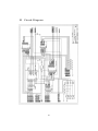
H
Circuit Diagram
49
50
51
52
53
I
PAL Equations
NAME
REVISION
DATE
DESIGNER
COMPANY
ASSEMBLY
DEVICE
IC5 ; /* IBM Address Select */
01 ;
17/6/87 ;
C. Cytera ;
Inmos Ltd ;
B008 ;
P16L8 ;
/** Inputs **/
PIN
PIN
PIN
PIN
PIN
PIN
PIN
PIN
PIN
PIN
PIN
PIN
PIN
1
2
3
4
5
6
7
8
9
11
13
14
15
=
=
=
=
=
=
=
=
=
=
=
=
=
SA4 ;
SA5 ;
SA6 ;
SA7 ;
SA8 ;
SA9 ;
AEN ;
SEL0 ;
SEL1 ;
DACK ;
direction ;
SA0 ;
SA1 ;
/** Outputs **/
PIN
PIN
PIN
PIN
12
17
18
19
=
=
=
=
RS0 ;
!notSYS ;
!notLADP ;
RS1 ;
FIELD IBMaddr = [SA9..SA4] ;
FIELD Select = [SEL1..SEL0] ;
/** Define Board Address Spaces **/
notLADP =
notSYS =
IBMaddr:[150] & Select:[1] & !AEN
# IBMaddr:[200] & Select:[2] & !AEN
# IBMaddr:[300] & Select:[3] & !AEN
# DACK ;
IBMaddr:[160] & Select:[1] & !AEN
# IBMaddr:[210] & Select:[2] & !AEN
# IBMaddr:[310] & Select:[3] & !AEN ;
/** Generate RS0 and RS1 for link adaptor Normal access: RS0 = SA0, RS1 = SA1.
54
DMA access: RS0 = !direction, RS1 = 0.
(For B008 -> IBM, direction = 0;
for IBM -> B008, direction = 1.) **/
RS0 = SA0 & !DACK # !direction & DACK ;
RS1 = SA1 & !DACK ;
NAME
REVISION
DATE
DESIGNER
COMPANY
ASSEMBLY
DEVICE
IC6 ; /** IBM interface **/
01 ;
17/6/87 ;
C. Cytera ;
Inmos Ltd
B008 ;
P22V10 ;
/** Inputs **/
PIN
PIN
PIN
PIN
PIN
PIN
PIN
PIN
PIN
PIN
PIN
1
2
3
4
5
6
7
8
9
10
11
=
=
=
=
=
=
=
=
=
=
=
PClk ;
nc1 ;
notLADP ;
notSYS ;
notIOR ;
notIOW ;
notIBMError ;
nc2 ;
SA0 ;
SA1 ;
Mod0notError ;
/** Outputs **/
PIN
PIN
PIN
PIN
PIN
PIN
PIN
PIN
PIN
14
15
16
17
18
19
20
21
22
=
=
=
=
=
=
=
=
=
notBoardError ;
writeInt ;
!notIBMReset ;
!notIBMAnalyse ;
!notWrite ;
!notCS ;
SD0 ;
writeDMA ;
notStatWR ;
FIELD Register = [SA1..SA0] ;
FIELD output = [notIBMReset, notIBMAnalyse, notStatWR] ;
/** Turn off asynchronous reset **/
output.ar = ’b’0 ;
55
/** Turn off synchronous preset **/
output.sp = ’b’0 ;
/** Read and Write Declarations **/
readsys
writesys
readlink
writelink
=
=
=
=
!notIOR
!notIOW
!notIOR
!notIOW
writeReset
writeAnalyse
writeDMA
writeInt
=
=
=
=
&
&
&
&
!notSYS ;
!notSYS ;
!notLADP ;
!notLADP ;
writesys
writesys
writesys
writesys
&
&
&
&
Register:[0]
Register:[1]
Register:[2]
Register:[3]
;
;
;
;
/** Staticise notIOW **/
notStatWR.d = notIOW
/** Link Adaptor Timing Logic **/
notCS
= writelink & !notStatWR # readlink ;
notWrite = !notLADP & !notStatWR # writelink ;
/** Buffer wired-or error signal to go off board **/
notBoardError = Mod0notError ;
/** Error Flag Propogation to IBM **/
SD0 = notIBMError ;
SD0.oe = readsys ;
/** Latch reset and analyse registers from IBM bus **/
notIBMReset.d
= SD0 & writeReset
# notIBMReset
& !writeReset ;
notIBMAnalyse.d = SD0 & writeAnalyse # notIBMAnalyse & !writeAnalyse ;
NAME
REVISION
DATE
DESIGNER
COMPANY
ASSEMBLY
DEVICE
IC7 ; /** Interrupt control **/
01 ;
17/6/87 ;
C. Cytera ;
Inmos Ltd ;
B008 ;
P22V10 ;
/** Inputs **/
56
PIN
PIN
PIN
PIN
PIN
PIN
PIN
PIN
PIN
PIN
PIN
PIN
1
2
3
4
5
6
7
8
9
10
11
13
=
=
=
=
=
=
=
=
=
=
=
=
PClk ;
SD0 ;
SD1 ;
SD2 ;
SD3 ;
notIOW ;
EndDMA ;
writeInt ;
InputInt ;
OutputInt ;
!notIBMError ;
IntLevelSelect ; /** 0 -> IRQ3, 1 -> IRQ5. **/
/** Outputs **/
PIN
PIN
PIN
PIN
PIN
PIN
PIN
PIN
PIN
PIN
14
15
16
17
18
19
20
21
22
23
=
=
=
=
=
=
=
=
=
=
InIntSelect ;
OutIntSelect ;
ErrIntSelect ;
DMAIntSelect ;
StatEndDMA ;
IntEnable ;
EndDMAFallEdge ;
IRQ5 ;
IRQ3 ;
EndDMALatched ;
FIELD output = [InIntSelect, OutIntSelect, ErrIntSelect, DMAIntSelect,
notStatWR, StatEndDMA, EndDMAFallEdge, EndDMALatched] ;
/** Switch off all async resets **
output.ar = ’b’0 ;
/** Switch off all sync presets **/
output.sp = ’b’0 ;
/** Have to write this out again because of yet another CUPL bug **/
output.ar = ’b’0 ;
/** Staticise ’EndDMA’ pulse **/
StatEndDMA.d = EndDMA ;
/** Produce pulse on falling edge of EndDMA **/
EndDMAFallEdge.d = StatEndDMA & !EndDMA ;
57
/** Set ’EndDMALatched’ on ’EndDMAFallEdge’;
clear it when software clears DMAIntSelect bit. **/
EndDMALatched.d = DMAIntSelect & (EndDMAFallEdge # EndDMALatched) ;
/** Interrupt source selection latches **/
InIntSelect.d
OutIntSelect.d
ErrIntSelect.d
DMAIntSelect.d
=
=
=
=
SD3
SD2
SD1
SD0
&
&
&
&
writeInt
writeInt
writeInt
writeInt
#
#
#
#
InIntSelect
OutIntSelect
ErrIntSelect
DMAIntSelect
&
&
&
&
!writeInt
!writeInt
!writeInt
!writeInt
;
;
;
;
/** Define Interrupt Signals **/
IRQ = InputInt & InIntSelect
# OutputInt & OutIntSelect
# notIBMError & ErrIntSelect
# EndDMALatched & DMAIntSelect ;
IRQ3 = IRQ ;
IRQ5 = IRQ ;
/** Exclusively Enable Relevant Interrupt line **/
IntEnable = InIntSelect # OutIntSelect # ErrIntSelect # DMAIntSelect
IRQ3.oe = !IntLevelSelect & IntEnable ;
IRQ5.oe = IntLevelSelect & IntEnable ;
NAME
REVISION
DATE
DESIGNER
COMPANY
ASSEMBLY
DEVICE
IC8 ; /** DMA control **/
01 ;
17/6/87 ;
C. Cytera ;
Inmos Ltd ;
B008 ;
P16L8 ;
/** Inputs **/
PIN
PIN
PIN
PIN
PIN
PIN
PIN
PIN
PIN
PIN
PIN
1
2
3
4
5
6
7
8
9
11
14
=
=
=
=
=
=
=
=
=
=
=
DACK0
SD0 ;
DACK1 ;
DACK3 ;
inputInt ;
outputInt ;
nc ;
writeDMA ;
DMASel10 ;
EndDMAFallEdge ;
resetDRV ;
58
PIN 17 = DMASel1 ;
/** Outputs **/
PIN
PIN
PIN
PIN
PIN
PIN
12
13
15
16
18
19
=
=
=
=
=
=
DACK ;
DRQ3 ;
DMAactive ;
direction ;
DRQ1 ;
DRQ0 ;
/** 0 = IBM -> C012, 1 = C012 -> IBM **/
/** Make field for switches as follows:
DMASel1 DMASel0
---------------0
0
Channel 0 enabled
0
1
Channel 1 enabled
1
0
DMA disabled
1
1
Channel 3 enabled
**/
FIELD SWITCH = [DMASel0..DMASel1] ;
/** Latch direction of DMA transfer **/
direction = SD0 & writeDMA # direction & !writeDMA # SD0 & direction ;
/** Select acknowledge for channel being used **/
DACK = !DACK0 & SWITCH:0
# !DACK1 & SWITCH:1
# !DACK3 & SWITCH:3 ;
/** Set DMAactive when ’writeDMA’ is active
Clear DMAactive at end of DMA cycle or at power-on **/
DMAactive = (writeDMA # DMAactive) & !(EndDMAFallEdge # resetDRV) ;
/** Generate DMA requests **/
DRQ = (inputInt & direction # outputInt & !direction) & DMAactive ;
DRQ0 = DRQ & SWITCH:0 ;
DRQ1 = DRQ & SWITCH:1 ;
DRQ3 = DRQ & SWITCH:3 ;
DRQ0.oe = SWITCH:0 ;
DRQ1.oe = SWITCH:1 ;
DRQ3.oe = SWITCH:3 ;
59