1
UM-TS02E**-E001
PROGRAMMABLE CONTROLLER
PROSEC
USER’S MANUAL
- Basic Hardware and Function -
Main Menu
Contents
Toshiba Corporation
T2E
Important Information
Misuse of this equipment can result in property damage or human injury.
Because controlled system applications vary widely, you should satisfy yourself
as to the acceptability of this equipment for your intended purpose.
In no event will Toshiba Corporation be responsible or liable for either indirect
or consequential damage or injury that may result from the use of this equipment.
No patent liability is assumed by Toshiba Corporation with respect to use of
information, illustrations, circuits, equipment or examples of application in this
publication.
Toshiba Corporation reserves the right to make changes and improvements to this
publication and/or related products at any time without notice. No obligation shall be
incurred other than as noted in this publication.
This publication is copyrighted and contains proprietary material. No part of this book
may be reproduced, stored in a retrieval system, or transmitted, in any form or by any
means electrical, mechanical, photocopying, recording, or otherwise without
obtaining prior written permission from Toshiba Corporation.
© TOSHIBA Corporation 1997. All rights reserved
PROSEC and TOSLINE are registered trademarks of TOSHIBA Corporation.
IBM is a registered trademark of International Business Machines Corporation.
MS-DOS is a registered trademark, and Windows is a trademark, of Microsoft Corporation.
DeviceNet is a trademark of the Open DeviceNet Vender Association, Inc.
Publication number: UM-TS02E∗∗-E001
1st edition May 1997
2st edition Jan 1998
-i-
Introduction
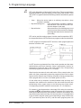
CE Marking
The Programmable Controller PROSEC T2E (hereafter called T2E) complies with the
requirements of the EMC Directive 89/336/EEC and the Low Voltage Directive 72/23/EEC under
the condition of use according to the instructions described in this manual.
The contents of the conformity are shown below.
Application of
Council Directive
:
:
EMC - 89/336/EEC(as amended by 91/263/EEC and 92/31/EEC)
LVD - 72/23/EEC
Manufacture’s Name
:
TOSHIBA CORPORATION, FUCHU WORKS
Manufacture’s address :
1, TOSHIBA-CHO,
FUCHU-SHI, TOKYO 183,
JAPAN
declares, that the product
Product Name
:
Programmable Controller , T2E Series
Model Number
:
TPU234E*S,TCM231EAS,TCM232EAS,TBT231EAS
Product Options
:
All
conforms to the following Product Specifications:
EMC
: Radiated Interference
Mains Interference
Radiated Susceptibility
Conducted RFI Susceptibility
Electrostatic Discharge
Electrical Fast Transient
LVD
: EN61131-2 : 1995
EN55011 Class A Group 1
EN55011 Class A Group 1
ENV50140
ENV50141, IEC1000-4-6
IEC1000-4-2
IEC1000-4-4
3,10
4
- ii -
Dielectric Properties
Mechanical Requirements
Introduction
Safety Precautions
This manual is prepared for users of Toshiba’s Programmable Controller T2E.
Read this manual thoroughly before using the T2E. Also, keep this manual and related manuals so
that you can read them anytime while the T2E is in operation.
General Information
1. The T2E has been designed and manufactured for use in an industrial environment.
However, the T2E is not intended to be used for systems which may endanger human
life. Consult Toshiba if you intend to use the T2E for a special application, such as
transportation machines, medical apparatus, aviation and space systems, nuclear
controls, submarine systems, etc.
2. The T2E has been manufactured under strict quality control. However, to keep safety of
overall automated system, fail-safe systems should be considered outside the T2E.
3. In installation, wiring, operation and maintenance of the T2E, it is assumed that the users
have general knowledge of industrial electric control systems.
If this product is handled or operated improperly, electrical shock, fire or damage to this
product could result.
4. This manual has been written for users who are familiar with Programmable Controllers
and industrial control equipment. Contact Toshiba if you have any questions about this
manual.
5. Sample programs and circuits described in this manual are provided for explaining the
operations and applications of the T2E. You should test completely if you use them as a
part of your application system.
Hazard Classifications
In this manual, the following two hazard classifications are used to explain the safety
precautions.
! WARNING
Indicates a potentially hazardous situation which, if not avoided, could
result in death or serious injury.
! CAUTION
Indicates a potentially hazardous situation which, if not avoided, may
result in minor or moderate injury. It may also be used to alert
against unsafe practices.
Even a precaution is classified as CAUTION, it may cause serious results depending on the
situation. Observe all the safety precautions described on this manual.
- iii -
Introduction
Safety Precautions
Safety Precautions
Installation:
! CAUTION
1. Excess temperature, humidity, vibration, shocks, or dusty and corrosive gas
environment can cause electrical shock, fire or malfunction. Install and use the T2E
and related equipment in the environment described in this manual.
2. Improper installation directions or insufficient installation can cause fire or the units to
drop. Install the T2E and related equipment in accordance with the instructions
described in this manual.
3. Turn off power before installing or removing any units, modules, racks or terminal
blocks. Failure to do so can cause electrical shock or damage to the T2E and related
equipment.
4. Entering wire scraps or other foreign debris into to the T2E and related equipment can
cause fire or malfunction. Pay attention to prevent entering them into the T2E and
related equipment during installation and wiring.
5. Turn off power immediately if the T2E or related equipment is emitting smoke or odor.
Operation under such situation can cause fire or electrical shock. Also unauthorized
repairing will cause fire or serious accidents. Do not attempt to repair. Contact Toshiba
for repairing.
6. The T2E must be installed in an enclosure. The user should consider to prevent contact
with careless touch to the live parts of this product in during operation or maintenance.
7. The Protective ground terminal of the T2E must be connected to an external protective
earth.
8. The computer which is connected to the T2E must be connected to an external
protective earth properly.
9. The external cables, including for data transmission, which are prepared by the user
are outside of the scope of this document.
- iv -
Introduction
Safety Precautions
Wiring:
! CAUTION
1. Turn off power before wiring to minimize the risk of electrical shock.
2. Exposed conductive parts of wire can cause electrical shock. Use crimp-style terminals
with insulating sheath or insulating tape to cover the conductive parts. Also close the
terminal covers securely on the terminal blocks when wiring has been completed.
3. Operation without grounding may cause electrical shock or malfunction. Connect the
ground terminal on the T2E to the system ground.
4. Applying excess power voltage to the T2E can cause explosion or fire. Apply power of
the specified ratings described in the manual.
5. Improper wiring can cause fire, electrical shock or malfunction. Observe local
regulations on wiring and grounding.
Operation:
! WARNING
1. Configure emergency stop and safety interlocking circuits outside the T2E. Otherwise,
malfunction of the T2E can cause injury or serious accidents.
! CAUTION
2. Operate the T2E and the related modules with closing the terminal covers. Keep hands
away from terminals while power on, to avoid the risk of electrical shock.
3. When you attempt to perform force outputs, RUN/HALT controls, etc. during operation,
carefully check for safety.
4. Turn on power to the T2E before turning on power to the loads. Failure to do so may
cause unexpected behavior of the loads.
5. Do not use any modules of the T2E for the purpose other than specified. This can
cause electrical shock or injury.
6. Do not modify the T2E and related equipment in hardware nor software. This can
cause fire, electrical shock or injury.
7. Configure the external circuit so that the external power required for output modules
and power to the loads are switched on/off simultaneously.
Also, turn off power to the loads before turning off power to the T2E.
-v-
Introduction
Safety Precautions
Operation (continued):
! CAUTION
8.
Install fuses appropriate to the load current in the external circuits for the outputs.
Failure to do so can cause fire in case of load over-current.
9. Check for proper connections on wires, connectors and modules. Insufficient contact
can cause malfunction or damage to the T2E and related equipment.
Maintenance:
! WARNING
1. Do not charge, disassemble, dispose in a fire nor short-circuit the batteries. It can be
cause explosion or fire. Observe local regulations for disposal of them.
! CAUTION
2. Turn off power before removing or replacing units, modules, terminal blocks or wires.
Failure to do so can cause electrical shock or damage to the T2E and related
equipment.
3. Replace a blown fuse with a specified one. Failure to do so can cause fire or damage
to the T2E.
4. Do not insert your finger into the rack’s ventilation hole during power on. This can
cause electrical shock.
5. Do not disassemble the T2E because there are hazardous voltage parts inside.
6. Perform daily checks, periodical checks and cleaning to maintain the system in normal
condition and to prevent unnecessary troubles.
7. Check by referring “Troubleshooting” section of this manual when operating
improperly. Contact Toshiba for repairing if the T2E or related equipment is failed.
Toshiba will not guarantee proper operation nor safety for unauthorized repairing.
8. The contact reliability of the output relays will reduce if the switching exceeds the
specified life. Replace the unit or module if exceeded.
9. Replace batteries in accordance with instructions described in the manual.
Failure to do so can cause system accidents.
- vi -
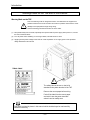
Introduction
Markings used on the T2E and in this manual
Warning Mark on the T2E
This is the warning mark for dengerous location. It is attached to the equipment in
!
positions where there is a risk of electric shock and in positions where there is a risk
damage to the equipment through wrong wiring.
Take the following precautions where there is this mark.
(1) Keep hands away from terminals ,especially the input terminall of power supply while power on, to avoid
the risk of electrical shock.
(2) Turn off power before installing or removing modules, terminal blocks or wires.
(3) Applying excess power voltage to the T2E can cause exploasion or fire. Apply power of the specified
ratings described in this manual.
Safety Label
!
The safety label as shown on the left is
attached to the power terminal of the T2E.
Remove the mount paper before wiring.
Peel off the label from the mount paper
and stick it near the power terminals
where it can be readily seen.
NOTE
This mark is printed in places in this manual which should always be read carefully.
Read them carefully.
- vii -
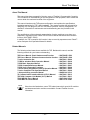
About This Manual
About This Manual
This manual has been prepared for first-time users of Toshiba’s Programmable Controller
T2E to enable a full understanding of the configuration of the equipment, and to enable the
user to obtain the maximum benefits of the equipment.
This manual introduces the T2E system configuration, and explains the specifications,
installation and wiring for T2E’s basic hardware. This manual provides the information for
designing T2E user program, such as T2E internal operation, memory configuration, I/O
allocation. Information for maintenance and troubleshooting are also provided in this
manual.
The specifications of the enhanced communication function, and how to use them, are
explained in separate manual. Read T2E/T2N User’s Manual-Enhanced communication
function. (UM-TS02E**-E003)
In addition, the T2E’s computer link function is also covered by separate manual. Read Tseries Computer Link Operation Manual for details.
Related Manuals
The following related manuals are available for T2E. Besides this manual, read the
following manuals for your better understanding.
T2E User’s Manual - Basic Hardware and Function
T2E User’s Manual - Enhanced communication function
T-series Instruction Set
T-PDS for windows Basic Operation Manual
T-PDS Basic Operation Manual
T-PDS Command Reference Manual
T-PDS Ver.2.0 Expanded Functions
T-Series Handy Programmer (HP911) Operation Manual
T-series Computer Link Operation Manual
1 Axis positioning controller Manual
T2 Communication Interface Module (CF211) Manual
T2/EX100 Computer Link Module (CL11) Manual
TOSLINE-S20 User’s Manual
TOSLINE-F10 User’s Manual
NOTE
- UM-TS02E**-E001
- UM-TS02E**-E003
- UM-TS03***-E004
- UM-TS03***-E038
- UM-TS03***-E006
- UM-TS03***-E007
- UM-TS03***-E028
- UM-TS03***-E025
- UM-TS03***-E008
- UM-EX100**-E011
- UM-TS02***-E013
- UG-TS02***-E015
- UM-TLS20**-E001
- UM-TLF10**-E001
Other than the listed above, some T2E related manuals for special I/O modules
and data transmission modules are available. Contact Toshiba for more
information.
- viii -
About This Manual
Terminology
The following is a list of abbreviations and acronyms used in this manual.
µs
ASCII
AWG
BCC
CCW
CPU
CW
EEPROM
H
I/O
LED
LSB
ms
MSB
PWM
RAM
ROM
Vac
Vdc
microsecond
American Standard Code For Information Interchange
American Wire Gage
Block Check Code
Counter-Clockwise
Central Processing Unit
Clockwise
Electrically Erasable Programmable Read Only Memory
hexadecimal (when it appears in front of an alphanumeric string)
Input/Output
Light Emitting Diode
Least Significant Bit
millisecond
Most Significant Bit
Pulse Width Modulation
Random Access Memory
Read Only Memory
AC voltage
DC voltage
- ix -
Contents
Contents
Important Information
Introduction
About This Manual
PART 1
HARDWARE
1.SYSTEM CONFIGURATION
1.1 System Configuration ....................................................................................................................................................................... 3
1.2 Power Supply Module ...................................................................................................................................................................... 6
1.3 CPU Module ............................................................................................................................................................................................ 8
1.4 Optional Communication Card ............................................................................................................................................... 13
1.5 Racks ......................................................................................................................................................................................................... 15
1.6 Expansion Cable .............................................................................................................................................................................. 16
1.7 I/O Modules .......................................................................................................................................................................................... 17
1.8 Data Transmission Modules .................................................................................................................................................... 18
2.SPECIFICATION
2.1 General Specifications ................................................................................................................................................................. 21
2.2 External Dimensions (mm) ........................................................................................................................................................ 22
2.3 I/O Module Specifications .......................................................................................................................................................... 23
3.APPLICATION PRECAUTIONS FOR I/O MODULES
3.1 Input Modules - Application Precautions ....................................................................................................................... 51
3.2 Transistor Output Module - Application Precautions ............................................................................................ 53
3.3 Triac Output Module - Application Precautions ........................................................................................................ 56
3.4 Relay Output Module - Application Precautions ...................................................................................................... 56
3.5 Analog Input Module - Application Precautions ....................................................................................................... 57
3.6 Analog Output Module - Application Precautions ................................................................................................... 58
-x-
Contents
4.INSTALLATION AND WIRING
4.1 Operating Environment................................................................................................................................................................ 59
4.2 Installing the Rack ........................................................................................................................................................................... 60
4.3 Mounting the Modules .................................................................................................................................................................. 60
4.4 Connecting the Expansion Unit............................................................................................................................................. 61
4.5 Grounding .............................................................................................................................................................................................. 62
4.6 Grounding Methods ........................................................................................................................................................................ 63
4.7 Wiring the Power Supply ............................................................................................................................................................ 65
4.8 I/O Wiring ............................................................................................................................................................................................... 66
4.9 Power up/down Sequence ........................................................................................................................................................ 68
4.10 Safty Circuit ....................................................................................................................................................................................... 69
5.MAINTENANCE AND CHECKS
5.1 Daily Checks ........................................................................................................................................................................................ 70
5.2 Periodic Checks ................................................................................................................................................................................ 72
5.3 Spare Parts to Keep in Stock ................................................................................................................................................. 73
5.4 Battery Replacement ..................................................................................................................................................................... 74
5.5 Fuse Replacement .......................................................................................................................................................................... 76
6.TROUBLESHOOTING
6.1 Troubleshooting Procedure ...................................................................................................................................................... 77
6.2 Power Supply Check ..................................................................................................................................................................... 78
6.3 CPU Check ........................................................................................................................................................................................... 79
6.4 Program Check .................................................................................................................................................................................. 79
6.5 Input Check........................................................................................................................................................................................... 80
6.6 Output Check ...................................................................................................................................................................................... 81
6.7 Faults Due to External Problems ......................................................................................................................................... 82
6.8 List of Self-Diagnostic Check Items ................................................................................................................................... 83
- xi -
Contents
PART 2
FUNCTIONS
1.OVERVIEW
1.1 T2E System Configuration ........................................................................................................................................................ 95
1.2 Functional Specifications ........................................................................................................................................................... 97
2.OPERATIONS
2.1 Basic Internal Operation Chart .............................................................................................................................................. 98
2.2 System Initialization ........................................................................................................................................................................ 99
2.3 Mode Control ..................................................................................................................................................................................... 101
2.4 Scan Control ...................................................................................................................................................................................... 104
2.4.1 Scan Mode ........................................................................................................................................................................ 106
2.4.2 Batch I/O Processing ................................................................................................................................................ 108
2.4.3 Timer Update................................................................................................................................................................... 110
2.5 Peripheral Support ........................................................................................................................................................................ 111
2.6 Programming Support Functions ....................................................................................................................................... 112
3.USER PROGRAM RUNNING CONTROL
3.1 Program Classification ............................................................................................................................................................... 115
3.2 Run Sub-Program #1 .................................................................................................................................................................. 116
3.3 Run Interrupt Program................................................................................................................................................................ 116
4.PERIPHERAL MEMORY SUPPORT
4.1 EEPROM Support.......................................................................................................................................................................... 117
5.RAS FUNCTION
5.1 Overview ............................................................................................................................................................................................... 118
5.2 Diagnostics .......................................................................................................................................................................................... 118
5.3 Event History...................................................................................................................................................................................... 121
5.4 Memory Protect Function ......................................................................................................................................................... 123
5.5 Execution State Monitoring .................................................................................................................................................... 124
5.6 Debug Support Function .......................................................................................................................................................... 126
5.7 System Diagnostics ...................................................................................................................................................................... 128
- xii -
Contents
PART 3
USER PROGRAMS
1.OVERVIEW
1.1 Aim of Part 3 ...................................................................................................................................................................................... 135
1.2 User Memory Configuration ................................................................................................................................................... 135
2.USER PROGRAM CONFIGURATION
2.1 Overview ............................................................................................................................................................................................... 137
2.2 System Information ....................................................................................................................................................................... 139
2.3 User Program .................................................................................................................................................................................... 142
2.3.1 Main Program ................................................................................................................................................................. 143
2.3.2 Sub-Program ................................................................................................................................................................... 144
2.3.3 Interrupt Program......................................................................................................................................................... 145
2.3.4 Sub-Routines .................................................................................................................................................................. 146
3.USER DATA
3.1 Overview ............................................................................................................................................................................................... 149
3.2 Registers and Devices ............................................................................................................................................................... 152
3.3 Processing Register Data ........................................................................................................................................................ 178
3.4 Index Modification .......................................................................................................................................................................... 184
3.5 Digit Designation............................................................................................................................................................................. 187
4.I/O ALLOCATION
4.1 Overview ............................................................................................................................................................................................... 190
4.2 Setting of Unit No. ......................................................................................................................................................................... 192
4.3 Methods of Input/Output Allocation.................................................................................................................................. 193
4.4 Register and Module Correspondence ......................................................................................................................... 198
5.PROGRAM LANGUAGE
5.1 Overview ............................................................................................................................................................................................... 200
5.2 Laddser Diagram ............................................................................................................................................................................ 203
5.3 SFC ........................................................................................................................................................................................................... 210
5.4 Programming Precautions ....................................................................................................................................................... 225
5.5 List of Instructions.......................................................................................................................................................................... 227
Order List.................................................................................................................................................................................................................... 255
Index................................................................................................................................................................................................................................ 257
- xiii -
Contents
Features & Software revision history
Features
Easy communication PLC
Easy to use high technology
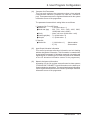
There are three types of optional cards for the T2E.
CM231E : RS-485 communication port w/ a battery
CM232E : RS-232C communication port w/ a battery
BT231E : a battery
n Enhanced communication
One of the following communication functions can be used in the T2E by mounting
CM231E/CM232E.
lComputer link mode
:Connection with higher level computer, MMI/SCADA system,
modem, etc.
lData link mode
:Easy data linkage between two T2Es or T2N or Super T1-40.
lFree ASCII mode
:Active communication between serial ASCII devices. (bar code
readers, etc.).
n Programmer port function
The T2E’s RS-232C programmer port supports the T-series link protocol. This results in
easy connection to a higher level computer, an operator interface unit, a modem, etc.
n Battery-less operation
The user-program is saved in a built-in Flash memory. No battery maintenance is required.
nNetworking
lHigh speed industrial LAN
The T2E can be connected to Toshiba’s high speed industrial LANs (Local Area Networks)
TOSLINE-S20 and TOSLINE-F10. The TOSLINE series are suited for real time control data
linkage. Through these networks, the T2E can exchange data with Toshiba’s various
equipment, such as, DCS system, other T-series PLCs, Inverters, etc.
lDeviceNet support
A DeviceNet scanner module is available for the T2E. The DeviceNet scanner module
can read/write data to any other manufacturer’s OVDA certified devices (I/O blocks,
Inverters to include Toshiba’s G3, air manifold, sensors, etc.).
n High speed processing
The T2E excels at applications where high speed processing is required.
l 0.33µs/contact
l 0.44µs/coil
l 1.2µs/16-bit transfer
l 1.63µs/16-bit addition
- xiv -
Contents
n Advanced instruction set
The T2E offers 24 basic relay-ladder instructions and 192 function block instructions,
including the following.
l Arithmetic operation l Data manipulations
l Trigonometric functions
l PID/ramp/integral
l Subroutine call
l For-Next loop
l Averaging/filtering l ASCII↔Hex conversion
l Floating-point math
n Two programming Languages
The T2E supports two programming languages: Ladder Diagram (LD) and Sequential
Function Chart (SFC). By selecting the appropriate language, or combination of the two,
program development time can be greatly reduced.
T2E’s software revision history
The T2E has the following expnaded functions according to software version.
T2E
Items
Functions
after
V1.1*
1 Floating point math.
Addition of 12 Floating point math.instructions.
m
Logical operation, compare and conversion
2 Response delay mode Sending back the response on the programmer port
m
or optional serial port after waiting for specified time
3 2-wire system in Free Selecting either 2-wire or 4-wire system using
ASCII mode *1
4 The trailing code
changing timing *1
m
RS-485 in Free ASCII mode
Can change the trailing code in Free ASCII mode
m
programming in main-program
NOTES *1 : Refer to the T2E/T2N’ User’s Manual - Enhanced communication function (UMTS02E**-E003) for the detail.
- xv -
PART1
HARDWARE
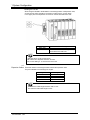
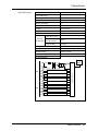
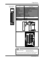
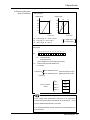
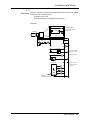
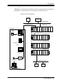
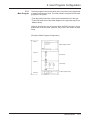
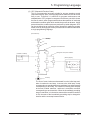
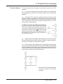
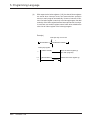
1.System Configuration
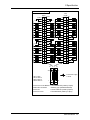
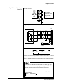
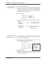
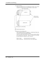
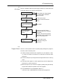
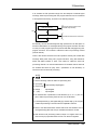
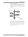
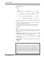
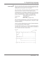
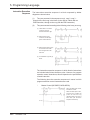
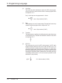
1.1
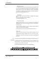
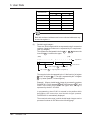
System Configuration
Vacant
C
P
U
Expansion Cable
Personal
Computer
Expansion Unit
Power Supply
T-series Program
Development
System(T-PDS)*1
software which
runs on IBM or
Compatible
personal computer
Power Supply
Peripherals
Basic Unit
Handy Programmer
HP911
Power Supply
Expansion Unit
The following functions can be
available only using CM231/CM232.
Power Supply
Expansion Unit
LCD Display etc.
T
L
30
T
L
F
•Computer Link
•Serial I/F
Personal •Data Link
Computer (Dual T2E/T2Ns can be
communicated each other)
T
L
S
D
N
Data transmission module
DeviceNet Scanner
TOSLINE-S20(Optic/wire)
TOSLINE-F10(wire)
TOSLINE-30(Optic/wire)
Up to a maximum of 3 expansion units can be connected.
Note *1:T-PDS(MS-DOS) software V2.06 or later is available for the T2E.
T-PDS(Windows) software V1.1 or later is available for the T2E.
User’s manual 3
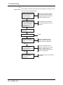
1.System Configuration
•Basic Configuration
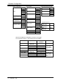
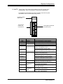
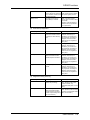
Rack
Power Supply
Module
CPU Module
Communication
Card(w/ Battery)
Battery Card
Expansion Cable
BU218
BU268
BU266
UBA1
UBA2
UBB1
UBB2
PS261
PS31
PU234E
CM231E
CM232E
BT231E
CAR3
CAR5
CAR7
CS2RF
•I/O module
DC input
AC input
Transistor output
Triac output
Relay output
Analog input
Analog output
Pulse input
Positioning module
Serial Interface
DI31
DI32
DI235
IN51
IN61
DO31
DO32
DO235
DO233P
AC61
RO61
RO62
AI21
AI31
AI22
AI32
AO31
AO22
AO32
PI21
MC11
CF211
•Data transmission Module
DeviceNet scanner
DN211
SN221
TOSLINE-S20
SN222
TOSLINE-F10
MS211
RS211
LK11
TOSLINE-30
LK12
•Programming Tool
T-PDS
MM33I1
(for MS-DOS)
T-PDS
MW33E1
(for Windows)
Handy
HP911
Programmer
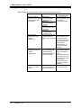
Minimum and Maximum configuration are shown on next page.
As mentioned in Section 1.4 ,the following racks are available.
Part Number
Application
TBU218**S
Dedicated to the
Basic unit
For basic unit
For expansion unit
For basic unit
For expansion unit
Dedicated to the
Basic unit
For basic unit
For expansion unit
For basic unit
For expansion unit
TBU268**S
TBU266**S
EX10*UBA1
EX10*UBA2
EX10*UBB1
EX10*UBB2
4 PROSEC T2E
Number of Module
Installation
8
Remarks
7
8
5
6
4
7
4
5
7
8
For either the
basic unit or
the expansion
unit
Not expandable
For either the
basic unit or
the expansion
unit
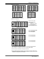
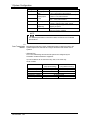
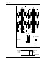
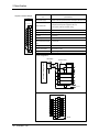
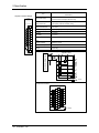
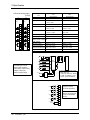
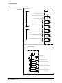
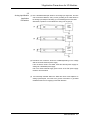
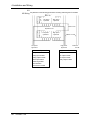
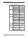
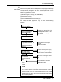
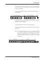
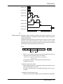
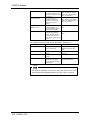
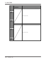
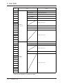
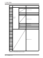
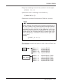
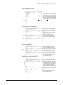
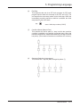
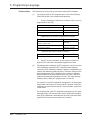
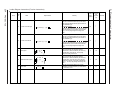
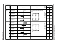
1.System Configuration
Basic unit with 5 I/O modules(BU266)
/
I/O
/
/
I/O
/
I/O
/
I/O
/
I/O
I/O
/
I/O
CPU
Power Supply
I/O
/
I/O
/
I/O
/
I/O
/
Basic unit with 4 I/O modules
(UBA1,UBB1)
Number of I/O module
8 I/O modules(BU218)
7 I/O modules
(BU268,UBA2,UBB2)
5 I/O modules(BU266)
4 I/O modules(UBA1,UBB1)
I/O
/
I/O
/
I/O
/
I/O
/
I/O
/
I/O
/
I/O
/
I/O
/
Basic unit
Vacant
CPU
Power Supply
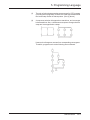
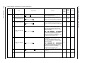
2)Maximum Configuration
Basic unit with 7 I/O modules
(BU268,UBA2,UBB2)
CPU
I/O
/
I/O
/
I/O
/
I/O
/
I/O
/
CPU
Power Supply
Basic unit with 8 I/O modules(BU218)
Power Supply
/
I/O
/
I/O
/
I/O
/
I/O
/
I/O
O
I/O
I/O
/
I/O
Vacant
CPU
Power Supply
1)Minimum Configuration
I/O
/
I/O
/
I/O
/
I/O
/
I/O
/
I/O
/
I/O
/
I/O
/
Power Supply
Expansion Unit No.1
8 I/O modules(BU268,UBB2)
6 I/O modules(BU266)
5 I/O modules(UBB1)
8 I/O modules(BU268)
6 I/O modules(BU266)
I/O
/
I/O
/
I/O
/
I/O
/
I/O
/
I/O
/
I/O
/
I/O
/
Power Supply
Expansion Unit No.2
8 I/O modules(BU268)
6 I/O modules(BU266)
I/O
/
I/O
/
I/O
/
I/O
/
I/O
/
I/O
/
I/O
/
I/O
/
Power Supply
Expansion Unit No.3
• Up to a maximum of 3 expansion units can be connected.:BU218,BU268,BU266
Up to a maximum of 1 expansion units can be connected.:UBB1,UBB2
• There is no limit on combinations of the types of the rack.
• When one BU218 and three BU268 are used ,a maximum of 32 I/O modules can be
controlled by the T2E CPU. If 32 points of I/O modules are mounted on every I/O slot,
a maximum of 1024 points can be controlled.
User’s manual 5
1.System Configuration
1.2
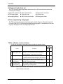
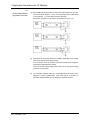
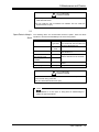
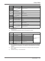
Power Supply Module
Power supply modules are mounted on the left -end slots of all units. There are
two types according to the power voltage. Select one as required.
Model
TPS261**S
EX10*MPS31
Power Voltage
100 - 240Vac
(+10%/-15%)
24Vdc
(+20%/-15%)
Output Rating
Internal control power supply : 2.5A (max.)
External power supply : 24V,+10%/-10%
0.5A (max.)
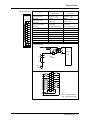
(Internal + external total 15W or less)
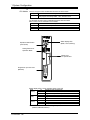
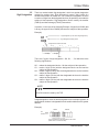
TOSHIBA
Power LED
POWER
24Vdc
+
OUT
RUN
Terminal block
eject levers
OUT
External 24Vdc
output terminals
Run signal output
terminals
NC
NC
L
IN N
LG
FG
Power supply
terminals
Line filter ground terminal
Frame ground terminal
• External 24Vdc Output Terminals
These are terminals for supplying 24Vdc to external equipment such as sensors and
to relay output modules. 24Vdc(±10%)-0.5A(max.)
• Run Signal Output Terminals
When the T2E is in the operating mode(RUN),built in contact is closed.
240Vac(+10%)/24Vdc(+20%)-2A(max.)
(Can also be used on expansion units)
• Power Supply Terminals
Connect to the power supply line. (See 4.7 Wiring the power supply).
• Line Filter Ground Terminal / Frame Ground Terminal
These are grounding terminals. (See 4.6 Grounding methods).
NOTE
1. The maximum rated output of 1 power supply is 15W, this includes the internal 5Vdc
and external 24Vdc output combined. Configure the system, referring to the Module
Current Consumption Table on the next page, so that the following equation is satisfied.
15W≥5V × Total 5V current (max. 2.5A) + 24V × external 24V current (max. 0.5V)
2. Do not connect the external 24V supply terminals to the other power supply systems,
and do not run the wiring over long distances.
3. This power supply module is dedicated power supply for the T2E and T2/EX100.
Do not use it by itself for other purposes.
6 PROSEC T2E
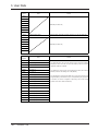
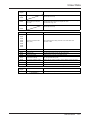
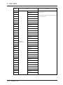
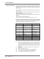
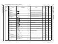
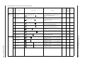
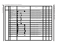
1.System Configuration
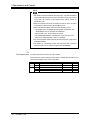
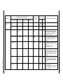
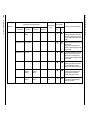
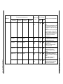
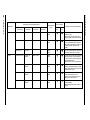
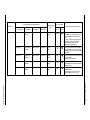
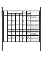
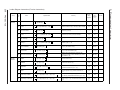
Module Current
Consumption Table
Name
CPU
Communication Card w/ Battery
Communication Card w/ Battery
Battery Card
Rack
16-point DC/AC input(12-24V)
32-point DC input(24V)
64-point DC input(24V)
16-point AC input(100-120V)
16-point AC input(200-240V)
12-point relay output
8-point isolated relay output
16-point transistor output
32-point transistor output
64-point transistor output
16-point transistor (PNP)
12-point triac output
4ch analog input (8bit)
(4-20mA/1-5V)
4ch analog input (12bit)
(4-20mA/1-5V)
4ch analog input (8bit)
(0-10V)
4ch analog input (12bit)
(±10V)
2ch analog output (8bit)
(4-20mA/1-5V/0-10V)
2ch analog output (12bit)
(4-20mA/1-5V)
2ch analog output (12bit)
(±10V)
1ch pulse input
Position control
Serial Interface
TOSLINE-30(wire)
TOSLINE-30(optical)
TOSLINE-S20(wire)
TOSLINE-S20(optical)
TOSLINE-F10(Master Station)
TOSLINE-F10(Remote Station)
Devicenet scanner
Model
Internal 5Vdc
External 24Vdc
PU234E
CM231E
CM232E
BT231E
BU218
BU268
BU266
UBA1
UBA2
UBB1
UBB2
DI31
DI32
DI235
IN51
IN61
RO61
RO62
DO31
DO32
DO235
DO233P
AC61
AI21
600mA or less
200mA or less
200mA or less
50mA or less
50mA or less
50mA or less
50mA or less
50mA or less
50mA or less
50mA or less
15mA or less
80mA or less
100mA or less
15mA or less
15mA or less
50mA or less
40mA or less
60mA or less
250mA or less
250mA or less
60mA or less
300mA or less
50mA or less
DC24V, 140mA
DC24V, 100mA
DC5-24V, 35mA
DC5-24V, 100mA
DC12/24V, 50mA
Weight
(approx.)
200g
100g
100g
100g
1600g
1500g
1400g
1400g
1400g
1500g
1500g
200g
200g
250g
250g
250g
250g
250g
200g
200g
250g
200g
200g
200g
AI22
50mA or less
DC24V, 50mA
200g
AI31
50mA or less
DC12/24V, 50mA
200g
AI32
50mA or less
DC24V, 50mA
200g
AO31
70mA or less
DC24V, 90mA
200g
AO22
170mA or less
DC24V, 90mA
200g
AO32
170mA or less
DC24V, 90mA
200g
PI21
MC11
CF211
LK11
LK12
SN221
SN222A
MS211
RS211
DN211
80mA or less
200mA or less
550mA or less
250mA or less
200mA or less
600mA or less
700mA or less
600mA or less
600mA or less
500mA or less
DC12/24V, 100mA
-
200g
250g
200g
200g
200g
250g
250g
250g
250g
200g
NOTE
The external 24Vdc in the Table are not power supplies for input/output signals.
They are the power supplies required for module operation.
User’s manual 7
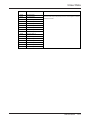
1.System Configuration
1.3
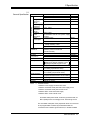
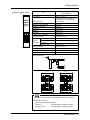
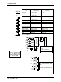
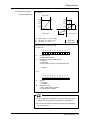
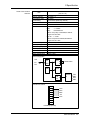
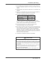
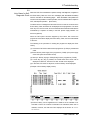
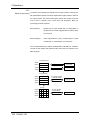
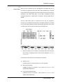
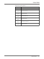
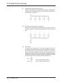
CPU Module There is one type of CPU module with functions as shown below.
Type
PU234E
Specification
RAM(capacitor back-up) + EEPROM,
User program 9.5k step, ladder , SFC ,real time clock
The PU234E has three types of dedicated optional cards as follows.
Either of them can be mounted on the PU234E.
Type
Specification
CM231E RS485, built-in battery
CM232E RS232, built-in battery
BT231E Battery
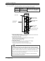
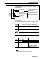
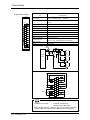
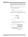
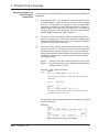
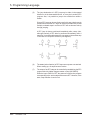
Operation Mode Switch
(HALT,RUN)
Status display LED
(RUN ,FauLT ,BATtery)
Setting Switches of
Operation Mode
Blank cover
for optional card
Programmer port connector
(RS232C)
Status display LEDs : Show operation states of the T2E
RUN
Lit
Operating state (RUN Mode)
(Green)
Blink
HOLD Mode
Out
Stopped state (HALT Mode) or Error Mode
FAULT
Lit
CPU abnormal
(Red)
Blink
Program abnormal
Out
Normal
BATT
Lit
Battery normal
(Green)
Blink
Battery getting abnormal
*2
Out
Battery abnormal or no option card
*2 : This LED is available when mounting an optional card
(CM231E,CM232E,BT231E).
8 PROSEC T2E
1.System Configuration
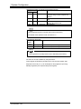
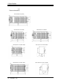
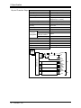
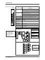
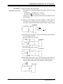
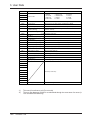
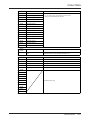
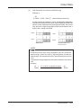
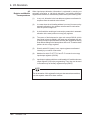
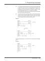
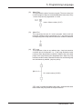
• Setting Switches of Operation Mode
These switches are provided on the CPU front panel. They control the
following functions.
OFF
1
2
Protect RUN Switch
R/S
3
RUN/Stand-by Switch
CM0
CM1
4
Selection Switch of optional
Communication function
COM
6
P
ROM
ROM/RAM Switch
5
Programmer Port
Parity
This switch can be changed anytime
during CPU’s running.
CPU reads this status when power
is changed from OFF to ON or when
operation mode is changed to RUN.
CPU reads these switches status
only when power turns to ON.
(1) Protect RUN Switch
For details of the operation mode, see Operation mode switch in this Section.
(2) ROM/RAM Switch
Setting
Function CPU operation
Position
at power up and at the beginning of the RUN mode
SW.2
OFF
ROM Starts up after the content of the EEPROM has been
transferred to the RAM.
(Transfer is not executed when Protect RUN Switch,
SW1 is ON.)
ON
RAM Starts up on the content of the RAM.
(No program transfer)
NOTE
The ROM/RAM switch is set to ROM at the factory.
(3) RUN/Stand-by Switch
Setting
Function Operation Mode after
Remarks
Position
Mode
power up
SW.3
Switch
OFF
Automatic
HALT
HALT
RUN
RUN
RUN
Automatic RUN start occurs.
ON
Stand-by
HALT
HALT
RUN
Starts up in HALT mode. Ready
to start operation by an operate
command from the programmer
or by shifting the operational
mode switch.(→HALT→RUN)
NOTE
The RUN/Stand-by switch is set to RUN at the factory.
User’s Manual 9
1.System Configuration
(4)(5)Selection Switch of optional Communication function
Setting Position
Operation
Function
SW.4
SW.5
OFF
OFF
Computer Link The T2E can communicate with a master
computer using T-series computer link
protocol.
ON
OFF
Data Link
The T2E executes data link with other
T2E.
OFF
ON
Serial Interface The T2E is communicate with external
devices using ASCII code.
ON
ON
Reserved
No operation
NOTE
1. These switches are set to computer link function at the factory.
2. For details of the operation mode, see Section 1.4.
(6)Programmer Port Parity
Setting
Function
Position
SW.6
OFF
Odd Parity
ON
No Parity
Remarks
8 bit Data, 9600bps, Data length is 11bit.
8 bit Data, 9600bps, Data length is 10bit.
NOTE
The Programmer Port Parity switch is set to Odd Parity at the factory.
The T2E can connect to Modem by using this switch.
Control signals (CTS,DTR,etc) should be set to No Use at the modem side.
Response of the T2E (V1.1∼) can be delayed on the programmer port using
SW38 (Programmer port response delay mode register).
10 PROSEC T2E
1.System Configuration
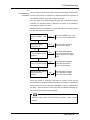
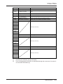
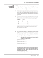
• Operation Mode Switch
The Operation Mode Switch is provided on the CPU panel.
This switch controls T2E operation (RUN/HALT).
HALT
RUN
CPU status is shown below after power up or after the operation mode is
changed to RUN mode from HALT mode.
Setting
User
Operation
Position Program
Mode
HALT
Stopped
HALT
RUN
Executed
RUN
Initial Load
Program
exe : executed
- :not executed
SW.1 SW.2:OFF exe
:OFF SW.2:ON
SW.1 SW.2:OFF exe
:ON
SW.2:ON
SW.1 SW.2:OFF exe
:OFF SW.2:ON
SW.1 SW.2:OFF
:ON
SW.2:ON
Memory
Operation
Protection Mode Change
by the
programmer
none
not available
none
available
available
As shown the above table, initial load (program transfer into EEPROM from RAM)
performs in the RUN mode when setting both SW.1 and SW.2 to OFF.
Therefore both SW.1 and SW.2 should be set to OFF when the battery isn’t mounted
on the T2E.
NOTE
1. The operation mode switch is set to HALT at the factory.
2. “P-RUN” is state that SW.1 is ON in the RUN mode.
The user program and the first half of data register (D0000 to D2047) are
in the write protect mode and user can’t write or change them.
3. Normally, the programming is carried out in the HALT mode.
4. When shifting to the RUN mode with the ROM/RAM switch in the ROM
position , operation will commerce after program transfer has been
executed. (that is, it is called initial load.)
5. For details of the operation mode, see Part2, Section 2.3.
6. Do not change SW.1 quickly when the operation mode switch is changed
from HALT to RUN or after power up. Turn to P-RUN after the RUN LED
is lit.
7. The RAM is back-up by internal capacitor of the T2E. When the capacity
goes down and the T2E can’t keep retentive area in the RAM, CPU clears all
data.
Then CPU checks user program BCC. If error is occurred, CPU registered
error.
User’s Manual 11
1.System Configuration
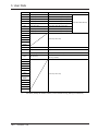
Programmer Port
The programmer (T-PDS or HP911) is connected to this programmer port.
Connector type of CPU side is female , 9-pin D-SUB connector.
The T2E’s RS232C programmer port can accept the computer link protocol
(data read/write). This results in easy connection to a higher level computer,
an operator interface unit, etc. directly.
General specifications and the connector pin assignment of programmer port
are shown below.
For details of T-series computer link protocol, see T-series User’s manual
- Computer Link (UM-TS03***-E008).
General specifications
Item
Interface
Configuration
Transmission distance
Transmission speed
Frame format
Supported command
Specifications
Conforms to RS232C
One to One
15m max.
9600bps (fixed)
Start bit
1bit
Data
8bit
Parity
odd/none (selected by SW.6)
stop bit
1bit
DR (Data Read)
DW (Data Write)
ST (Status read)
Pin assignment of programmer port
Signals
No. of pins
Transmission data
3
Receive data
2
Signal ground
5
Request To Send
7
Clear To Send
8
Symbols
TXD
RXD
SG
RTS
CTS
Direction
T2E → Host
T2E ← Host
T2E -- Host
T2E → Host
T2E ← Host
NOTE
Other pins except the above table should not be connected.
12 PROSEC T2E
1.System Configuration
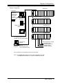
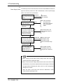
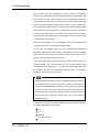
1.4
Optional communication There are two types of optional communication cards in the T2E as shown
below. These cards have built-in battery for back-up RAM.
cards
The BT231E is prepared only for battery usage.
Type
Specification
CM231E RS485, Three Communication Functions, built-in battery
CM232E RS232, Three Communication Functions, built-in battery
BT231E Battery
For battery replacement, see Section 5.4.
For mounting optional cards on the T2E CPU module, see next page.
CM231E/CM232E
There are three communication functions in the T2E.
One of them can be selected by setting swithches CM0/CM1 (SW.4/SW.5).
Function
Operation
Computer Link
This performs to connect between a Host computer and
up to 32 the T2Es, using the CM231E.
(one to one ,using the CM232E)
Data Link
This performs to connect two T2E/T2N.
They share 32W data with each other.
Serial Interface
This performs to connect between the external devices
such as inverter, etc. and the T2E.
For details of these functions and usage method, see T2E/T2N User’s manual
- Enhanced communication function -(UM-TS02E**-E003).
User’s Manual 13
1.System Configuration
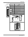
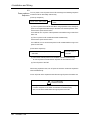
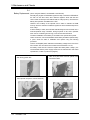
<Installation>
1) Take off a terminal block for communication from optional
card.(in the case of CM231E)
Take off black cover on the front of CPU panel.
2) Taking care that optional card is mounted in the correct direction, insert it into CPU pancel
3) Corresponding with position of connectors, connect CPU
module and optional card.
4) By using the part which is atttached with optional card, connect both CPU module and optional card to fix.
5) Put a terminal block for communion into optional card.
(in the case of CM231E)
14 PROSEC T2E
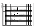
1.System Configuration
1.5
Racks As mentioned in Section 1.1, the rack is available in the seven types.
The rack has two kinds of types racks, for dedicated to the Basic unit
and for Basic/Expansion unit.
Type
Application
BU218
Dedicated to the
Basic unit
For basic unit
For expansion unit
For basic unit
For expansion unit
Dedicated to the
Basic unit
For basic unit
For expansion unit
For basic unit
For expansion unit
BU268
BU266
UBA1
UBA2
UBB1
UBB2
Number of Module
Installation
8
Remarks
7
8
5
6
4
7
4
5
7
8
For either the
basic unit or the
expansion unit
Not expandable
For either the
basic unit or the
expansion unit
BU218
BU268
BU266
NOTE
1. Two expansion connectors are provided in the BU268 and the BU266. The right side
connector is for connecting the basic unit/previous expansion unit.
The left side connector is for connecting the next expansion unit.
2. Use a blind slot cover (EX10*ABP1) to prevent debris from collecting in the rack
where no I/O modules is mounted and PU234E is mounted in BU218.
3. When the UBB1 or the UBB2 is used as expansion unit, only one expansion unit
can be connected to the basic unit.
User’s Manual 15
1.System Configuration
• Setting the Unit No.
When using the BU268 or the BU266 for combined type basic unit/expansion units,
set the Unit No. before operating. The setting is carried out by a rotary switch
in the upper part of the expansion connector on the left hand side of the rack.
The rack used for :
Basic Unit
Expansion Units
Switch Setting
0
Set in the order 1>2>3, starting from the
unit closest to the basic unit
NOTE
1.Switches will be set at 0 at the factory.
2.Be careful not to duplicate Unit Nos. on units.
3.Do not use setting 4 - 9, as these are not for use.
1.6
Expansion Cables These are used for connecting the basic unit and the expansion units.
They are available in the following four lengths.
Type
CAR3
CAR5
CAR7
CS2RF
Length
30cm
50cm
70cm
1.5m
NOTE
The maximum cable length between units is 1.5m.
The maximum total cable length is 4.5m.
16 PROSEC T2E
1.System Configuration
1.7
I/O Modules Various types of I/O modules are available for the T2E, as shown in the
following Table. Thus, it can respond to a wide variety of applications.
I/O modules can be mounted in any slot in the base unit, and in any order.
(See Section 4.8 for recommended arrangements)
Input/Output status
display LEDs
Terminal block
insertion and
removal levers
Type
DI31
DI32
DI235 *1
IN51
IN61
RO61
Input/Output terminal block
(10-point/18-point)
Description
DC/AC input
DC input
DC input
AC input
Relay output
RO62
DO31
Transistor output
DO32
DO235 *1
DO233P *1
AC61
Triac output
AI21
AI31
Analog input
(8bit)
AI22
AI32
Analog input
(12bit)
Specification
16-point (16 points per common),12-24V dc/ac
32-point (8 points per common),24Vdc
64-point (8 points per common),24Vdc
16-points (16 points per common),100-120Vac
16-points (16 points per common),200-240Vac
12-point (4 points per common),
240Vac(+10%)/DC24V(+20%),
2A/point,4A/4 points common (max.)
8-point (each point isolated),
240Vac(+10%)/DC24V(+20%), 2A/point (max.)
16-point (16 points per common),5-24Vdc
1A/point, 1.2A/4 points (max.)
32-point (8 points per common),5-24Vdc
0.1A/point, 0.8A/8 points common (max.)
64-point (8 points per common),5-24Vdc
0.1A/point, 0.8A/8 points common (max.)
16-point (16 points per common),12-24Vdc
12-point (4 points per common),100-240Vac
0.5A/point, 0.6A/2-element SSR (max.)
4-channel (not isolated between channels),
1-5V/4-20mA, 8bit resolution
4-channel (not isolated between channels),
0-10V ,8bit resolution
4-channel (not isolated between channels),
1-5V/4-20mA, 12bit resolution
4-channel (not isolated between channels),
-10V - +10V ,12bit resolution
User’s Manual 17
1.System Configuration
Type
AO31
Description
Analog output
(8bit)
AO22
AO32
Analog output
(12bit)
PI21
Pulse input
MC11
CF211
Single-axis
positioning
Serial Interface
Specification
2-channel (not isolated between channels),
1-5V/1-10V/4-20mA, 8bit resolution
4-channel (not isolated between channels),
4-20mA /1-5V,12bit resolution
4-channel (not isolated between channels),
-10V - +10V,12bit resolution
1-channel (two phase, with zero marker),
5/12Vdc, 100kpps (max), 24bit counter
1 axis, 100kpps(max.), position data memory
capacity 64 points
RS-232C 1port,
Common memory 160W×2
NOTE
For detailed specifications of each I/O module, see Section 2.3 I/O Module
Specifications.
1.8
Data Transmission By applying the following 4 types of data transmission module according to the
Module system requirements, the T2E can configure the flexible and efficient control
systems.
• TOSLINE-F10
PLC to PLC data linkage and remote I/O systems are configured by the
TOSLINE-F10 data transmission equipment.
Up to 8 T2 stations can be mounted in any slots, in the same way
as I/O modules.
Topology
Transmission speed
Transmission Distance
Number of stations
Transmission capacity
Response speed
18 PROSEC T2E
MS211/RS211
MS211/RS211
(High-speed setting)
(Long-distance setting)
Bus (twisted-pair cable)
750kbps
250kbps
500m
1km
max. 32stations
32 words (L/LW)
7ms(when 32 words)
12ms(when 32 words)
1.System Configuration
• TOSLINE-S20
The TOSLINE-S20 is a Local Area Network (LAN) for factory automation systems.
It can achieve high-speed data linkage between PLCs and communication between
industrial computers.
One T2 station can be mounted in any slot, in the same way as an I/O module.
SN221
SN222
(Co-Axial Cable)
(Optical Fiber Cable)
Topology
Bus
Transmission speed
2 Mbps
Transmission Distance
1km
10km
(1km between stations)
Number of stations
Max. 64 stations
Transmission capacity
Max. 1024 words W0000-W1023(Z/W)
Response speed
Minimum 5ms in scan transmission
• TOSLINE-30
The T2E can use the TOSLINE-30.
It is effective when connecting EX series systems to the T2E.
Up to 4 T2 stations can be mounted in any slots, in the same way
as for I/O modules.
The link relay/register(Z/W) is assigned for the TOSLINE-30, the same as the
TOSLINE-S20. If the TOSLINE-S20 is used together with the TOSLINE-30,
the link registers assigned to the TOSLINE-30 (starting with W0000) should not
allocate for the TOSLINE-S20.
LK11
LK12
(Twisted-pair Cable)
(Optical Fiber Cable)
Topology
Bus
Star
Transmission speed
187.5kbps
375kbps
Transmission Distance
1km
2km
(1km between stations)
Number of stations
MAX. 17 stations
MAX. 16 stations
Transmission capacity
8/16/32 words W0000-W0127
Response speed
25ms(when 32words)
19.2ms(when 32words)
• DeviceNet (Scanner) : Under development
The DeviceNet is a field network. It can achieve data linkage between PLCs and
remote I/O communication.
The T2E can use the DeviceNet scanner module.
It is effective when connecting DeviceNet systems to the T2E.
The T2E station can be mounted in any slots, in the same way as for I/O modules.
DN211
(Twisted-pair Cable)
Topology
Bus
Transmission speed
125kHz
250kHz
500kHz
Transmission Distance
500m
250m
100m
Number of stations
Max. 64 stations
User’s Manual 19
1.System Configuration
20 PROSEC T2E
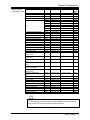
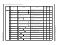
2.Specification
2.1
General Specification
Power Supply
Item
Rated Voltage
Voltage
Fluctuation
Range
Power Supply
Frequency
Frequency
Fluctuation
Range
Retentive
power
interruption
Power
consumption
Inrush current
Insulation
resistance
Withstand voltage
Ambient
temperature
Ambient humidity
Atmosphere
Dust
Vibration immunity
Shock immunity
Noise immunity
Grounding
Construction
Cooling
Specification
(1)100-240Vac
(2)24Vdc
(1)85 - 264Vac
(2)20.4 - 28.8Vdc
Remarks
PS261
PS31
PS261
PS31
(1)50/60Hz
(1)47 - 63Hz
10ms or less
(at maximum load for one power supply
module)
(1)53VA or less
PS261
(2)22W or less
(1)15A(at 100Vac)
/35A(at 240Vac) or less
(2)30A/10ms or less
10MΩor more
(between power terminals and
ground terminals)
1500Vac - 1minute
0 to 55°C
-20 to 75°C
20∼90%RH
no condensation
No corrosive gases
Sulphurous acid gas 0.05ppm or less
Hydrogen sulphide .01ppm or less
10mg/m3 or less
16.7Hz-3mm p-p
(3 mutually perpendicular awes)
98m/s2 (10g)
(3 shocks per axis,
on 3 mutually perpendicular awes)
1000Vp-p /1µs
Complied for EMC Directive of CE marking
Grounding resistance 100Ω or less
Installed in control panel
Natural air cooling
PS31
PS261
PS31
*1
operation
storage
Notes *1 Insulated Circuits
• between Power supply circuit and I/O circuit
• between Accessible metal parts and Power supply circuit
• between Accessible metal parts and I/O circuit
• between SELV circuit and Power supply
• between SELV circuit and I/O circuit
Accessible metal parts: Racks, Protective ground terminal, etc.
SELV (Safety Extra Low Voltage) circuit: Internal logic circuit
The accessible metal parts of the peripherals which are connected
to the programmable controller by the standard cable are
connected to the Protective ground terminal, or double insulated.
User’s manual 21
2.Specification
2.2
External dimensions
Basic dedicated unit (BU218)
Basic/expansion unit (BU266)
Basic/expansion unit (BU268)
Basic/expansion unit (UBA2, UBB2)
When 16-point I/O module installed
Basic/expansion unit (UBA1, UBB1)
When 32/64-point I/O, MC11 installed
22 PROSEC T2E
2.Specification
2.3
I/O Module
Specifications
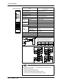
16-point DC/AC input
DI31
01234567
........
........
89ABCDEF
4
5
6
7
8
9
A
B
C
D
E
F
(EX10*MDI31)
+ 10 %
− 15 %
Input Voltage Range
12 - 24V
Minimum ON Voltage
9.6V or more
Maximum OFF Voltage
3.6V or less (leak current 0.7mA or less)
Input Current(Typ.)
Approx.8mA (at 24Vdc)
No. of input point
16 points/common
ON Delay
N Mode
10ms or less (dc) / 20ms or less (ac)
H Mode
1.5ms or less (dc)
0
1
2
3
DI31
Item
OFF Delay N Mode
dc/ac(50/60Hz)
10ms or less (dc) / 15ms or less (ac)
H Mode
1.5ms or less (dc)
Withstand Voltage
1500Vac / 1minute
Current Consumption
15mA (5Vdc) or less
Weight
Approx. 200g
* Filter
Selection
Circuit Configuration
CO
0
H
N
Internal Circuit
12-24Vac/dc IN
1
2
LED Display
F
COM
COM
* Filter Selection(jumper plug setting)
N ; Standard DC/AC common use(set at the factory)
H ; High-speed DC input only
Terminal Connections
0
1
2
3
4
5
7
9
B
D
6
8
A
C
E
F
COM
12-24V
User’s manual 23
2.Specification
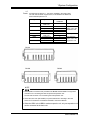
32-point DC input
DI32
Item
(EX10*MD132)
DI32
CN1
01234567
89ABCDEF
01234567
89ABCDEF
Input Voltage Range
24Vdc ± 10% - 15%
Minimum ON Voltage
18.0V
Maximum OFF Voltage
6.0V
Input Current
Approx 5mA(at 24Vdc)
Number of Input point
32points
CN2
ON Delay
B
CN1
CN2
A A
B
12
1
OFF Delay
N Mode
10msec or less
H Mode
1.5msec or less
N Mode
10msec or less
H Mode
1.5msec or less
External Connections
2 x 24pin connectors
Number of commons
4
12
1
Common
Number of Input points
Configuration
per Common
Common Polarity
24Vdc IN
8 points
No Polarity
Withstand voltage
1500Vac / 1 minute
Current Consumption
80mA (5Vdc) or less
Weight
Appro x 200 g
Circuit Configuration
LED display
Selection of the filter constant can be set in
16-point units (CN1, CN2) by DIP switch
setting. (set on N mode at the factory)
Internal circuit
0
1
Switch
No.
1
2
7
COM
Terminal Connections
OFF
ON
N mode
N mode
Application
H mode CN1(XWn)
H mode CN1(XWn+1)
CN1(XWn)
CN2(XWn+1)
+
NC
F
B
A
12
12
11
11
10
10
D
B
9
NC
NC
NC
7
5
3
1
+
COMl
9
9
8
8
7
7
6
6
0
+
E
2
C
4
A
6
8
NC
NC
+
COM2
NC
+
+
5
4
4
3
3
2
2
1
1
6
B
1
1
2
2
3
3
4
4
5
5
NC
6
6
NC
7
7
NC
9
+
A
4
C
8
8
9
9
2
E
10
10
0
11
11
+
COM3
12
12 NC
1
3
5
7
8
COM0
5
NC
A
B
D
F
+
NOTE
Connectors on the Module:
FCN-365P024-AU (made by Fujitsu)
Cable side connectors:
Soldering type (standard attached)
Connector FCN-361J024-AU (made by Fujitsu)
Connector cover FCN-360C024-E (made by Fujitsu)
24 PROSEC T2E
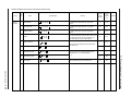
2.Specification
64-point DC input.
Item
DI235
+ 10 %
− 15 %
Input Voltage Range
24Vdc
Input Current
Apporx.4mA(at 24Vdc)
Input Impedance
5.8kΩ(24Vdc)
Minimum ON Voltage
16V
Maximum OFF Voltage
5V
ON delay
10ms or less than
OFF delay
15ms or less than
External Connections
2 × 40 pin connectors
Number of Commons
Common
Number of Input
Configuration Points per Common
Common Polarity
8
8 points
No Polarity
Derating Condition
See next page
Current Consumption
100mA (5Vdc) or less
Withstand voltage
1500Vac/ 1 minute
Weight
Approx. 250g
Circuit Configuration
LED
display
0L
∼
CN1
CN2
0L
LC0
8L
LC1
0H
HC0
8H
HC1
Internal Circuit
7L
LC0
8L
LC1
0H
HC0
8H
HC1
User’s manual 25
2.Specification
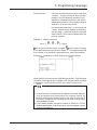
Terminal Connections
CN2
(A)(B)
CN1
(B)(A)
0L
NC 20 20 NC
PS
PS
NC 19
HC1
18
FH
17
EH
16
DH
15
CH
14
BH
13
AH
12
9H
11
8H
10
HC0
9
7H
8
6H
7
5H
6
4H
5
3H
4
2H
3
1H
2
0H
1
H
1L
19 NC
LC1
18
FL
17
EL
16
DL
15
CL
14
BL
13
AL
12
9L
11
8L
10
LC0
9
7L
8
6L
7
5L
6
4L
5
3L
4
2L
3
1L
2
0L
1
2L
PS
3L
4L
5L
6L
7L
LC0
PS
8L
9L
AL
PS
BL
CL
DL
EL
FL
LC1
PS
1
1
2
2
3
3
4
4
5
5
6
6
7
7
8
8
9
9
10 10
11 11
12 12
13 13
14 14
15 15
16 16
17 17
18 18
0H
1H
2H
3H
4H
5H
6H
7H
HC0
PS
8H
9H
AH
BH
CH
DH
EH
FH
HC1
PS
NC 19 19 NC
NC 20 20 NC
L
L
H
CN1 CN2
B
A A
B
20
1
PS
CN1-L=XWn
CN1-H=XWn+1
CN2-L=XWn+2
CN2-H=XWn+3
1
Connectors on the Module :
Cable side connectors
:
Connector
:
Connector cover
:
: Power Supply
20
24Vdc
FCN-365P040/AU (made by Fujitsu)
Soldering type (standard attached)
FCN-361J040-AU (made by Fujitsu)
FCN-360C040-E (made by Fujitsu)
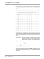
Derating Condition
Number of input ON points (per 1 conncctor)
32 (100%)
21.6Vdc or less
26 (80%)
20 (60%)
24Vdc
26.4Vdc
Ambient temperature
0
26 PROSEC T2E
10
20
30
40
50
60
2.Specification
16-point AC input
Item
IN51
01234567
........
........
89ABCDEF
Input Voltage Range
(Sine wave)
Minimum ON voltage
(Sine wave)
IN51
IN61
(EX10*MIN51)
(EX10*MIN61)
100-120Vac + 10%
- 15%
(50/60Hz)
200-240Vac + 10%
- 15%
(50/60Hz)
80Vac or more
160Vac or more
0
1
2
Maximum OFF voltage
30Vac or less
60Vac or less
3
(Sine wave)
(leak current 2mA or less)
(leak current 2mA or less)
Input Current(Sine wave)
Approx 7mA (100V-50Hz)
Approx 6mA (200V-50Hz)
Number of Input Points
16 points (single common)
16 points (single common)
ON Delay (Sine wave)
20mS or less
20mS or less
OFF Delay (Sine wave)
15mS or less
15mS or less
C
D
E
Voltage lnsulation
1500Vac / 1 minute
1500Vac / 1 minute
F
Current Consumption
15mA (5Vdc) or less
15mA (5Vdc) or less
Weight
Approx 250g
Approx 250g
4
5
6
7
8
9
A
B
COM
Circuit Configuration
100-120Vac IN
0
Intermal
circuit
1
2
LED
indication
F
COM
COM
Terminal connections
0
1
3
5
7
9
B
D
2
4
6
8
A
C
E
F
*
COM
*
IN51 : 100-120Vac (50/60HZ)
IN61 : 200-240Vac (50/60HZ)
User’s manual 27
2.Specification
RO61
12-point Relay Output
Item
(EX10*MRO61)
RO61
.0 .1 .2 .3 .4 .5 .6 .7
....
Load voltage
24Vdc, +20%(MAX)/240Vac, + 10%(MAX)
Maximum load
2A/point (resistive load), 1A/point (inductive load), 4A/4points
common
89AB
0
1
2
3
CI
NC
4
5
6
7
C2
+
8
9
A
B
C3
-
Minmum load
50mW (5V or more)
Number of output points
12 points (4 points / common)
ON delay
10ms or less
OFF delay
15ms or less
Leakage current When OFF
0mA
Withstand voltage
1500Vac / 1 minute
Current consumption
50mA (5Vdc) or less
External relay Coil
24Vdc +/- 10% - 140mA/all points ON (10mA/point)
Power required
Weight
COIL
24Vd
c
Approx 250g
Circuit Configuration
LED
display
RELAY OUT
1
2
3
C
4
Internal
circuit
7
C
8
B
C
Terminal Connections Drawing
0
1
3
2
C1
4
5
7
+
9
24V
B
6
C2
8
A
C3
-
NOTE
1.ON/OFF life of relays:
Electrical 100,000 times
Mechanical 20 million times
2.No overload protection fuses are built into this module.Therefore
always make sure to insert fuses suitable to the current capacity.
28 PROSEC T2E
2.Specification
8-point Isolated
Relay Output
RO62
Item
(EX10*MRO62)
Load voltage
24Vdc, +20%(MAX)/240Vac, +10%(MAX)
Maximum load
2A/point (resistive load), 1A/point (inductive load)
Minimum load
50mW (5V or more)
Number of output points
8 points (each point isolated)
ON Delay
10msec or less
0
OFF Delay
15msec or less
RO62
01234567
........
1
Leakage current When OFF 0mA
2
Voltage insulation
1500Vac / 1 minute
3
Current consumption
40mA (5Vdc) or less
5
External Relay Coil Power
Required
24Vdc +/- 10% - 100mA/all points ON
(10mA/point)
6
Weight
Approx 250g
Circuit Configuration
LED display
4
7
24V
dc
0
1
Internal Circuit
RELAY OUT
2
Terminal Connections
0
1
2
3
4
5
6
7
24Vdc
NOTE
1.ON/OFF life of relays:
Electrical 100,000 times
Mechanical 20 million time
2.No overload protection fuses are built into this module. Therefore
always make sure to insert fuses suitable to the current capacity.
User’s manual 29
2.Specification
DO31
16-point Transistor Output
Item
(EX10*MDO31)
DO31
01234567
........
........
Load power supply
5-24Vdc+10%/-5% (Internal current consumption 35mA or less)
1A/point (external power supply 7V or more)
89ABCDEF
0
1
2
0.3A/point (external power supply less than 7V)
Output ON current
1.2A/4 points (4-element transistor array)
Output ON resistance
1.5Ω or less
Number of output points
16 points (single minus common)
On Delay
1ms or less
OFF Delay
1ms or less
Leak current when Output
0.1mA or less
3
4
5
6
7
8
9
A
B
C
D
E
F
OFF
+
-
Voltage insulation
1500Vac/ 1 minute
Current consumption
60mA (5Vdc) or less
Weight
Approx 200g
5-24Vdc OUT
Circuit Configuration
LED display
Constant voltage circuit
Transistor array
0
1
2
3
4
8
C
F
+
Fuse
(5A)
Connections Drawing
0
1
3
5
7
9
B
D
F
2
4
6
8
A
C
E
+
5 - 24Vdc
30 PROSEC T2E
Common
2.Specification
32-point Transistor Output
DO32
Item
(EX10*MDO32)
DO32
Load voltage
5-24Vdc +10%/-5%
CN1
100mA/point (when load voltage 24V)
20mA/point (when load voltage 5V)
800mA/common
01234567
Output ON current
89ABCDEF
01234567
89ABCDEF
Saturation voltage when ON
0.4V or less
CN2
Number of output points
32 points
Output type
Current sinking
ON Delay
1msec or less
OFF Delay
2msec or less
Leakage current When OFF
0.1mA or less
External connections
2 x 24 pin connectors
CN1
CN2
B
B
A A
12
1
Number of Common
12
1
Common
Number of output points
configuration per common
Common polarity
8 points
minus common
Withstand voltage
1500Vac / 1 minute
Current consumption
250mA (5Vdc) or less
Built-in fuse
2A/common x 4
Weight
Approx 250g
Circuit Configuration
LED display
Vin
0
Internal Circuit
5-24Vdc OUT
4
1
7
COM
2A
External Connections Drawing
CN2(Ywn+1)
CN1(YWn)
+
B
A
12
12
11
11
10
10
9
9
8
8
NC
7
7
NC
NC
COM0
6
6
5
5
NC
Vin
4
4
3
3
2
2
1
1
COM1
F
D
B
9
+
7
5
3
1
A
B
1
1
2
2
3
3
4
4
5
5
NC
6
6
NC
NC
8
7
7
NC
9
8
8
Vin
0
E
2
C
4
A
6
B
Vin
6
A
4
C
2
E
0
Vin
9
9
10
10
11
11
12
12
1
3
5
7
COM2
+
B
D
F
COM3
+
NOTE
Connectors on the Module : FCN-365P024-AU (made by Fujitsu)
Cable side connectors
Soldering type (standard attached)
Connector
: FCN-361J024-AU (made by Fujitsu)
Connector cover
: FCN-360C024-E (made by Fujitsu)
User’s manual 31
2.Specification
64-point Transistor Output
Item
Output type
Number of output
Load Voltage
Output ON Current
DO235
Current sinking
64 points
5-24Vdc +10%/-5%
0.1A/point (9.6 - 26.4Vdc)
0.05A/point (4.5 - 9.5Vdc)
Saturation voltage when ON
0.4V or less
Leakage current when OFF
0.1mA or less (24Vdc)
ON delay
1ms or less
OFF delay
1ms or less
External Connections
2 x 40pin connectors
Number of Common 8
Common Number of Output
8 points
Configuration points per common
Common Polainty
minus
Current Consumption
250mA (5Vdc) or less
Withstand voltage
1500Vac/1 minute
Built-in fuse
none
Surge Protection
Diode
Weight
Approx. 250g
Circuit Configuration
LED
display
P24L0
0L
Internal Circuit
∼
7L
LC0
P24L1
8L
LC1
P24H0
0H
HC0
P24H1
8H
HC1
P24L0
CN1
CN2
HC1
32 PROSEC T2E
2.Specification
Terminal Connecting
CN2
(A)(B)
CN1
(B)(A)
P24H1
HC1
FH
EH
DH
CH
BH
AH
9H
8H
P24H0
P24L1
20 20
19 19
18 18
17 17
16 16
15 15
14 14
13 13
12 12
11 11
0L
LC1
1L
FL
2L
EL
3L
DL
4L
CL
5L
BL
6L
AL
7L
9L
LC0
8L
P24L0
P24L0
8L
10 10
HC0
7H
6H
5H
4H
3H
2H
1H
0H
9
9
8
8
7
7
6
6
5
5
4
4
3
3
2
2
1
1
H
L
LC0
9L
7L
AL
6L
BL
5L
CL
4L
DL
3L
EL
2L
FL
1L
LC1
0L
P24L1
0H
1
1
2
2
3
3
4
4
5
5
6
6
7
7
8
8
9
9
10 10
11 11
12 12
13 13
14 14
15 15
16 16
17 17
18 18
1H
2H
3H
4H
5H
6H
7H
HC0
P24H
08H
9H
AH
BH
CH
DH
EH
FH
HC1
19 19
P24H
20 20
1
L H
CN1 CN2
B
A A
B
20
CN1-L=XWn
CN1-H=XWn+1
CN2-L=XWn+2
CN2-H=XWn+3
1
: Load Power Supply
5-24Vdc
1
Connectors on the Module
Cable side connectors
Connector
Connector cover
20
:
:
:
:
FCN-365P040/AU (made by Fujitsu)
Soldering type (standard attached)
FCN-361J040-AU (made by Fujitsu)
FCN-360C040-E (made by Fujitsu)
User’s manual 33
2.Specification
DO233P
Item
(TDO233P*S)
16-point Transistor Output
DO233P
Load power supply
12-24Vdc+10%/-5%
(Internal current consumption 35mA or less)
01234567
........
........
89ABCDEF
0
1
2
3
4
5
6
7
8
9
A
B
C
D
E
F
1A/point (external power supply 7V or more)
Output ON current
1.2A/4 points (4-element transistor array)
Output ON resistance
1.5Ω or less
Number of output points
16 points (single plus common)
On Delay
1ms or less
OFF Delay
1ms or less
Leak current when Output
0.1mA or less
OFF
+
-
Voltage insulation
1500Vac/ 1 minute
Current consumption
60mA (5Vdc) or less
Weight
Approx 200g
Circuit Configuration
LED display
Transistor array
Constant voltage circuit
12-24Vdc OUT
0
1
2
3
4
8
C
F
+
Fuse
−
(5A)
Terminal Connections
0
1
3
5
7
9
B
D
F
2
4
6
8
A
C
E
+
12 - 24Vdc
34 PROSEC T2E
Common
2.Specification
12-point Triac Output
AC61
Item
(EX10*MAC61)
AC61
01234567
........
... .
Load voltage
100-240Vac +10%/-5%(50/60Hz sine wave)
Output ON current
0.5A/point, 0.6A(2-element SSR)
Saturated ON voltage
1.5V or less (0.3A load)
Number of output points
12 points (4 points / common)
ON Delay
1msec or less
OFF Delay
1/2 cycle of load power supply + 1msec or less
89AB
0
1
2
3
C1
4
5
6
7
C2
8
9
A
B
C2
Leakage Current When OFF 1.2mA (100Vac) or less, 3mA (240Vac) or less
Withstand voltage
1500Vac / 1 minute
Current consumption
300mA (5Vdc) or less (20mA/point)
Weight
Approx. 250g
Circuit Configuration
100-240Vac OUT
2-element SSR
LED display
0
1
Internal Circuit
2
3
C1
4
C2
8
Fuse
(2A)
C3
Terminal Connections Drawing
0
1
3
C1
5
7
C2
9
B
2
C1
4
6
C2
8
A
C3
C3
User’s manual 35
2.Specification
4-Channel Analog Input
Input(8-bit)
AI21
A121
Item
A131
(EX10*MA121)
(EX10*MA131)
Input range
1 - 5V or 4 - 20mA
0 - 10V
Input Impedance
1 - 5V : 500KΩ or more
500KΩ or more
4 - 20mA : 250Ω
RUN
Number of input points
4 points (N side common)
4 points (N side common)
Resolution
1 - 5V : 0 - 250
0 - 10V : 0 - 250
1P
4 - 20mA : 0 - 250
CH1
1N
1P
CH2
1N
1P
CH3
1N
1P
CH4
1N
12-24Vdc+
-
4-20mA/1-5V
±1% (FS)
Overall Accuracy
±1% (FS)
4 point (N side common) Approx. 1msec
Approx. 1msec
Wire breakage detection Only possible for 4-20mA
External Power
-
Yes
Yes
Withstand voltage
500Vac / 1 minute
500Vac / 1 minute
Current consumption
50mA 5Vdc or less
50mA 5Vdc or less
External power required
12 - 24Vdc±10% - 50mA
12 - 24Vdc±10% - 50mA
Weight
Approx. 200g
Approx. 200g
Supply failure detection
Circuit Configuration
V
I
V
I
J2
CH2
V
I
V
I
CH3
J3
J4
CH4
Constant voltage circuit
J1, J2, J3, J4 jumper plugs are AI21
type only.
• I side : for current (4 - 20mA)
• V side : for voltage (1-5V)
12-24Vdc
(50mA)
The AI21 type is set to
current input (4-20mA)
at the factory. For
voltage (1-5V) input, set
J1 - J4 to the V side.
Internal Circuit
J1
A/D Converter
CH1
Power source display LED
Set for current at the factory
Terminal Connections Drawing
P
CH1
N
CH2
N
P
P
CH3
N
CH4
N
P
+
12-24Vdc
(50mA)
36 PROSEC T2E
-
Isolate external power supply line
(12 - 24Vdc) from other signal
lines.
Use shielded twisted-pair cables
for analog signals, and ground
the shields securely.
2.Specification
4-Channel Analog Input
(8-bit) (Continued)
A/D Conversion
Digital Values
Digital Values
250
200
200
150
150
100
100
50
50
0
(a)
(b)
(c)
4
10
(b)
250
(a)
0
20(mA)
Analog value
1
(c)
5
10(V)
Analog value
4-20mA range : D = 15.625 x A-62.5
1-5V range : D = 62.5 x A-62.5
D = Digital Value
0-10V range : D = 25 x A
A = Analog Value
Data Format
F E D C B A 9 8 7 6 5 4 3 2 1 0
XW
B * *
* * *
* *
D D D D D D D D
D:
B:
Data bit (8 bits)
0-250 (H00-HFA)
(Over-voltage/over-current input 255 counts)
External line abnormal detection bit
0 = Normal
1 =Abnormal
When all data bits are 0
Current input line open
When all data bits are 1
External power is OFF
* : Always 0
F
4 words occupied
(X4W)
O
XWn
CH1
XWn+1
CH2
XWn+2
CH3
XWn+3
CH4
NOTE
1.In the voltage input specification, when there is an open-circuit
between the input terminals, the data bits do not become 0. (They
become indeterminate between 1 and 250).
2.It is recommended that unused channels be shorted between the
input terminals.
User’s manual 37
2.Specification
4-Channel Analog Input
(12-bit)
AI22
RUN
Item
AI22
AI32
(EX10*MA122)
(EX10*MA132)
AI32
RUN
Input Range
1 - 5V or 4 - 20mA
-10 - +10V
Input Impedance
1 - 5V : 1MΩ or more
1MΩ or more
4 - 20mA : 250Ω
P
CH1
N
P
CH1
P
CH2
N
P
CH3
N
P
CH4
N
N
P
CH4
N
24Vdc+
24Vdc+
-
-
4-20mA/1-5V
4 points (N side common)
± 0.5% : 25ºC
± 0.5% : 25ºC
± 1%FS / 0 - 55ºC
± 1%FS / 0 - 55ºC
1 - 5V : 0 - 4000
-10 - +10C :
4 - 20mA : 0 - 4000
-2000 - 2000
Approx. 9.6msec/4 channels
Approx. 9.6mS/4 channels
Resolution
N
P
CH3
4 points (N side common)
Overall Accuracy
N
P
CH2
Number of Input Points
±10V
Conversion Cycle
Wire Breakage Detection Only possible for 4 - 20mA
External Power Supply Yes
Yes
Break Detection
Withstand Voltage
1500Vac / 1 minute
Current consumption
1500Vac / 1 minute
50mA (5Vdc) or less
50mA (5Vdc) or less
External Power Required 24Vdc ±10% - 50mA
24Vdc ±10% - 50mA
Weight
Approx. 200g
Approx. 200g
Circuit Configuration
P
V
I
CH1
N
JI1
A/D
Converter
P
CH2
N
JI2
P
The AI22 type is set to
current input (4-20mA)
at the factory. When using
voltage (1-5V) input,
reset the jumper plugs
CH3
N
JI3
P
CH4
N
JI4
JI1, JI2, JI3, JI4 (jumper plugs)
are AI22 type only
* I side : for current (4 - 20mA)
* V side : for voltage (1 - 5V)
* Set for current on delivery
24Vdc+
LED
DC/DC Converter
Terminal Connections Drawing
P
CH1
N
P
CH2
N
CH3
N
CH4
N
P
P
+
DC24Vdc
(50mA)
38 PROSEC T2E
-
Isolate external power
supply line (24Vdc)
from other signal lines.
Use shielded twisted-pair
cables for analog signals,
and ground the shields
securely.
2.Specification
4-Channel Analog Input
(12-bit) (Continued)
A/D Conversion
Digital Values
4000
3000
3000
2000
2000
1000
1000
0
4
10
20(mA)
(b)
4000
(a)
-10
Analog Values
(a) 4-20mA range : D = 250 x A-1000
(b) 1-5V range : D = 1000 x A-1000
(c) ±10V range : D = 200 x A
-5
0
-1000
(c)
1
-2000
5
10(V)
Analog Values
D = Digital value
A = Analog value
Data Format (Input occupies 4 words)
• 4-20mA/1-5V
F E D C B A 9 8 7 6 5 4 3 2 1 0
B * *
D:
B:
* D D D D D D D D D D D D
Data bit (12 bits)
0-4000 (H0000-H0FA0)
External line abnormal detection bit
0 = Normal
1 = Abnormal
(Current input line open, or external power OFF)
* : Always 0
• ±10V
F E D C B A 9 8 7 6 5 4 3 2 1 0
S S S S S D D D D D D D D D D D
S:
D:
Sign bit
0 = Positive
1 = Negative
Data bit (11 bits)
- 2000 - 2000 (HF830 - H07D0)
2's complement if negative
NOTE
1.In the voltage input specification, when there is an open-circuit
between the input terminals, the data bits do not become 0.
2.It is recommended that unused channels be shorted between
the input terminals.
User’s manual 39
2.Specification
2-Channel Analog Output
(8-bit)
AO31
Item
(EX10*MA031)
A031
1 - 5V, 4 - 20mA paired output
Output Range
RUN
0 - 10V
0 - 5V
V
5V full-scale terminal : 5KΩ or more
1P
Load Impedance
10V full scale terminal: 10KΩ or more
1N
CH
20mA full-scale terminal : 600Ω or less
1P
I
Number of Output Points 2 points (each voltage, current pair) (each N side common)
1N
V
1P
1N
CH
I
Resolution
0 - 250 (full-scale)
Overall Accuracy
± 1% (FS)
Conversion Cycle
Approx. 1msec
External Power Supply
No
1P
1N
24Vdc+
Break Failure
−
5/10V
20mA
Voltage Insulation
1500Vac / 1 minute
Current Consumption
70mA (5Vdc) or less
External Power Supply
24Vdc ± 10%-90mA
Weight
Approx. 200g
Circuit Configuration
J1, J2 switching jumpers
J2 short : Reference value 0V (0mA)
J1 short : Reference value 1V (4mA)
(CH1, CH2 operation)
+V1
Internal circuit
The A031 type is set to
1-5V, 4-20mA setting
at the factory. Refer to the
circuit configuration for
other settings.
D/A
CH1
Converter
J11
+I1
J2
+V2
J1
CH2
P
N
J21
+I2
J11 switching jumper
N
Output voltage level for CH1
Up side short : 5V
Down side short : 10V
P
J12 switching jumper
N
Output voltage level for CH2
Up side short : 5V
Down side short : 10V
P
P
N
Constant-voltage
circuit
+24Vdc
0V
-
Power supply display LED
Terminal Connections
P
N
V1
CH1
P
N
Isolate external power
supply line (24Vdc)
from other signal lines.
I1
P
N
V2
CH2
P
N
I2
+
-
40 PROSEC T2E
24Vdc
(90mA)
Use shielded twisted-pair
cables for analog signals.
2.Specification
2-Channel Analog Output
(8-bit) (Continued)
D/A Conversion
Analog Values (V)
Analog Values (mA)
10
(c)
10
5
(b)
4
0
1
0
20
(a)
50 100 150 200 250
50 100 150 200 250
Digital Values
(a)
(b)
(c)
Digital Values
4-20mA range : A = 0.064 x D + 4
1-5V range : A = 0.016 x D + 1
0-10V range : A = 0.04 x D
A = Analog value
D = Digital value
Data Format
F E D C B A 9 8 7 6 5 4 3 2 1 0
YW
D:
*:
* *
*
* * *
* * D D D D D D D D
Data bit (8 bits)
0-250 (H00-HFA)
No effect (No effect on D/A conversion)
F
2 words occupied
(Y2W)
0
YWn
CH1
Ywn+1
CH2
NOTE
When executing direct output, two registers (both channels)
should be specified to output.
User’s manual 41
2.Specification
2-Channel Analog Output
(12-bit)
AO22
RUN
AO32
AO22
Item
AO32
(EX10*MAO22)
(EX10*MAO32)
Output Range
1 - 5V or 4 - 20mA
− 10 − + 10V
Load Impedance
1-5V : 5KΩ or more
5KΩ or more
RUN
4-20mA : 600Ω or less
Number of Output Points 2 points (each N side common) 2 points (each N side common)
P
V
CH
(voltage, current pair)
P
V
N
CH
N
Resolution
4~20mA : 0~4000
P
I
V
± 0.5%FS/25°C
± 0.5%FS/25°C
± 1% FS/0~55°Cv
± 1% FS/0~55°Cv
Approx. 1mS
Approx. 1mS
No
No
Withstand voltage
1500Vac/ 1 minute
1500Vac / 1 minute
Current Consumption
170mA (5Vdc) or less
170mA (5Vdc) or less
Overall Accuracy
N
P
CH
P
V
N
CH
I
N
Conversion Cycle
P
External Power Supply
N
FailureDetection
24Vdc+
24Vdc+
−
−
4-20mA/1-5V
−10~ + 10V :−2000~2000
1~5V : 0~4000
± 10V
External Power Required 24Vdc ± 10%-90mA
24Vdc ± 10%-90mA
Weight
Approx. 200g
Approx. 200g
Circuit Configuration
V1
CH1
•
I1
Internal circuit
*
D/A
converter
•
V2
CH2
•
I2
*
•
•
P
N
CH1
P
N
P
N CH2
P
N
*AO22 only
•
24Vdc
LED
•
DC / DCconverter
Terminal Connections Drawing
P
N
*AO22 only
V1
P
N
CH1
I1
*
Isolate external 24Vdc
line from other signal
lines.
P
N
V2
CH2
P
N
I2
+
−
42 PROSEC T2E
24Vdc
(90mA)
*
Use shielded twistedpair cables for analog
signals.
2.Specification
2-Channel Analog Output
(12-bit) (Continued)
D/A Conversion
Analog Values (mA)
Analog Values (V)
(a)
20
10
10
(c)
5
(b)
4
1
2000
4000
-2000
Digital Values
0
2000
4000
Digital Values
-5
-10
(a)
(b)
(c)
4-20mA range : A = 0.004 x D + 4
1-5V range : A = 0.001 x D + 1
±10V range : A = 0.005 x D
A = Analog value
D = Digital value
Data Format (Output occupies 2 words)
• 4-20mA / 1-50
F E D C B A 9 8 7 6 5 4 3 2 1 0
YW
* * *
D:
*
D D D D D D D D D D D D
Data bit (12 bits)
0-4000 (H0000-H0FA0)
*:
No effect (No effect on D/A conversion)
• ± 10V
F E D C B A 9 8 7 6 5 4 3 2 1 0
YW
* * *
S:
*
S D D D D D D D D D D D
Sign bit
0 = Positive
1 = Negative
D:
Data bit (11 bits)
- 2000 - 2000 (HF830 - H07D0)
2's complement if negative
NOTE
When executing direct output, two registers (both channels) should
be specified to output
User’s manual 43
2.Specification
Single-Channel Pulse
Input
PI21
(EX10*MP121)
Item
Input Voltage
PI21
Range
EXT
A
A, B, M
12V ± 10% / -5% (12V setting), 5V +10% / -5% (5V setting)
EXT
12~24Vdc +10% -15%
A, B, M
9V (12V setting), 3.5V (5V setting)
EXT
9.6V
A, B, M
2V (12V setting), 1V (5V setting)
EXT
3.6V
A, B, M
12V-7.5mA (12V setting), 5V-10mA (5V setting)
EXT
24V-10mA, 12V-5mA
B
Minimum ON
Voltage
+A
Maximum OFF
Voltage
−A
+B
Input Current
−B
+M
−M
EXT
Number of Input Points
1 point phase A, B, M and ETX
Pulse Counting Speed
100Kpps (max) (pulse-width 4µ sec or more)
Counter Configuration
24-bit binary
Quadrature Phase A, B (90 degree phase shift), up/down
Pulse Input Mode
12-24Vdc
Up/Down
Phase A: count up / phase B: count down
Normal
Counter clears at simultaneous ON timing of phase M and
EXT input (edge), always executes count apart from this.
Counter Operation
5/12V PULSE IN
Hold
Mode
Executes count only when both phase M and EXT input are ON,
count stops when either is OFF (Count value maintained).
(Counter clear is at the same timing as the Normal Mode).
External (EXT) Input Operation Counter clears at simultaneous ON timing of phase M and
At the factory setting, the
PI2 is set to 12V input,
quadrature and normal
counter operation. See
the Circuit Configuration for
other settings
EXT input (edge)
External (EXT) Input Delay
ON-OFF, OFF-ON each 5mS or less
Withstand Voltage
1500Vac / 1 minute (but except between each of the A, B, M
phases)
Current Consumption
80mA (5Vdc) or less
Weight
Approx. 200g
Circuit Configuration
Current when ON
A
A5
A12
BUD
UNV
B5
B12
BIP
UPDW
M5
M12
B
-A
+B
-B
+M
-M
Operation
setting
Input circuit
Counter re-set
(edge detection)
EXT
Counter (0 when power
supply seitched ON)
+A
EXT
_5/_12 Switching Jumper
5 : 5V input
12 : 12V input
sets all 3 A, B, M
points identically.
shows setting on
delivery
44 PROSEC T2E
BIP/UPDW Switching Jumper
BIP : Quadrature
UPDW : Up/down
BUD/UNV Switching Jumper
BUD : Normal mode
UNV : Hold mode
2.Specification
Single-Channel Pulse Input
(Continued)
Terminal Connection
+A
-A
12Vdc
(5Vdc)
+B
Use shielded
twisted-pair cables
for pulse signals,
and ground the
shields securely.
-B
+M
Pulse
encoder
-M
EXT
12-24Vdc
Wiring Example
Encoder
PI21
power
+A
A
-A
+B
B
-B
+M
M
-M
EXT
OV
5/12Vdc
12-24Vdc
Data Format
XWn
F
Occupies 2 words
8 7
All bits S S6
XWn+1
0F
Count
0
Count
2 23 -----------2 16 2 15 -----------------20
For the count values (24 bits), the lower 16 bits are read as XWn + 1, and the
upper 8 bits as the bit 0 to bit 7.
Count = -8388608 to 8388609 (or 0 to 16777215 if upper 8 bits are masked).
NOTE
Bit 8 to bit F of XWn are the same as bit 7 of XWn (sign bit). In
order to match the double-length register configuration of the T2E,
use after exchanging the upper word and the lower word.
(Example : Store count value in the double-length register of
D0101 • D0100)
[XWn
MOV D0101]
[XWn+1 MOV D0100]
User’s manual 45
2.Specification
Single-Channel Pulse Input
(Continued)
Pulse Input Mode
< Quadrature >
A
B
Count down
Count up
< Up/down >
A
B
Count up
Count down
Count Operation Mode
< Normal >
Phase A/B
Up
Down
phase M
EXT
16777215
Count value
0
< Hold >
Phase A/B
Up
Down
phase M
EXT
(Holding)
Count value
(Holding)
0
NOTE
When executing direct input, two registers should be specified to
input.
46 PROSEC T2E
2.Specification
Single-Axis Position
Control
Number of Control Axes
1 axis
Control Units
Pulse, inch, mm, etc.
Control Range
± 999,999
Point Data Capacity
64 points
Maximum Speed
200kpps
Operating Speed Selection
Origin return speed, Maximum speed,
Minimum speed
Acceleration/deceleration System
Automatic trapezoidal / triangular system
Acceleration/deceleration Time
0 - 26 seconds
Backlash Compensation
0 - 1000 pulses
Zero Position Offset Amount
± 999,999 command units
Dwell Time
0 - 99 seconds
I/O occupancy points
X + Y 4 W (64 bits)
Parameter Storage
EEPROM
External Input Voltage
Input Input Current
ON/OFF Voltage
12/24Vdc (zero marker: 5/12/24V)
MC11
PROGMR
RUN
ZLS
OT
PLS
CN
A
B
PC
1
PROGMR
12
MC11
(EX10*MMC11)
Item
ON/OFF Delay
External
Output
10mA (when 24V input)
9.6V / 3.2V
5msec (zero marker: 1msec)
1.CW/CCW error counter clear
Pulse Mode Switch Setting 2.PULSE/DIR (pulse/direction), error counter clear
Output Output Method
Open collector (5-24V, 50mA)
ON/OFF Delay
2µS
RUN Output Method
Output Operation
Current
Consumption
Open collector (5-24V, 50mA)
ON during normal operation
Internal
200mA
400mA- (when HP connected)-5Vdc
External
100mA-12 / 24Vdc
Connector Arrangement
A
B
HUN output (0V)
1
1 RUN output
CW pulse/pulse output (0V)
2
2 CW pulse/pulse output
CCW pulse/direction output (0V)
3
3 CCW pulse/direction output
Error counter clear output (0V)
4
4 Error counter clear output
Zero marker pulse input (0V)
5
5 Zero marker pulse input (DC5V)
Zero marker pulse input (0V)
6
6 Zero marker pulse input (DC12/24V)
Ongin position input
7
7 Ongin position input(DC12/24V)
HOLD input
8
8 HOLD input (DC12/24V)
Emergency stop input
9
9 Emergency stop input (DC12/24V)
CW side overtravel limit SW input
10 10 CW side overtravel limit SW input (DC12/24V)
CCW side overtravel limit SW input
11 11 CCW side overtravel limit SW input (DC12/24V)
Extemal power supply (0V)
12 12 Extemal power supply (DC12/24V)
NOTE
Connector on the Module:
FCN-365P024-AU (made by Fujitsu)
Cables side connectors
Soldering type (standard attached)
Connector FCN-361J024-AU (made by Fujitsu)
Connector cover FCN-360Co24-E (made by Fujitsu)
User’s manual 47
2.Specification
Single-Axis Position Control
(Continued)
Input Circuit
Zero marker pulse input (5Vdc) : B5
Normally Open-Contact Use
Zero marker pulse input (0V) : A5
Zero marker pulse input (12/24Vdc) : B6
Zero marker pulse input (0V) : A6
B7
Origin position input (12/24Vdc)
A7
B8
HOLD input (12/24Vdc)
A8
Normally Closed-Contact Use
B9
Emergency stop input (12/24Vdc)
A9
B10
CW overtravel limit SW input (12/24Vdc)
A10
B11
CCW overtravel limit SW input (12/24Vdc)
A11
Note : For the Zero marker pulse input use only one of
5Vdc or 12/24Vdc.
Output Circuit
Constant-voltage circuit
B12 : External power supply (12/24Vdc)
B1 : RUN output
A1 : RUN output (0V)
B2 : CW pulse / pulse output
A2 :CW pulse / pulse output (0V)
B3 : CCW pulse / direction output
A3 : CCW pulse / direction output (0V)
B4 : Error counter clear output
A4 : Error counter clear output (0V)
A12 : External power supply (0V)
48 PROSEC T2E
2.Specification
Serial Communication
Interface
CF211
(TCF211**S)
Item
Common memory
Transmission mode
Synchronizing
Interface
Transmission Code
Frame Format
160 words × 2
Full-duplex
asynchrounus (Start-stop method)
Conforms to RS232C 1CH
ASCII
Start bit : 1bit
Data
: 7 or 8bits
Parity
: even/odd/none
When none parity is selected,the data bit
length must be 8 bits.
Stop bit : 1 or 2bit
When 2 stop bits is selected,the data bit
length must be 7 bits.
Transmission Speed
300,600,1200,2400,4800,9600,19200bps
I/O occupancy points i X+Y 4W
Data exchange system By READ/WRITE instructions of the T2E
LED Display
Transmission data
Isolation
none(between RS232C Port and internal circuit)
Current Consumption 550mA or less
Circuit Configuration
T2E
I/O
CPU
2port
Reset switeh
buffer
bus
RAM
ROM
RS232C
I/O
I/F
I/F
TXD
RXD
DTR
DSR
External Connections
1
2
3
4
5
6
7
8
9
RXD
TXD
DTR
SG
DSR
5Vdc
TXD
RXD
DSR
SG
DTR
D-SUB 9pin(female)
User’s manual 49
2.Specification
50 PROSEC T2E
3.Application Precautions for I/O Modules
3.1
Input Modules
Application Precautions
(1) Minimum ON/OFF time of input signal
The conditions for guaranteed reading of the ON/OFF states of the input
signal are:
Input ON time
ON delay time + 1 scan time
Input OFF time
OFF delay time + 1 scan time
Therefore, be sure to use longer times than these for the ON/OFF times of
the input signal.
(2) There are some contacts for which the reliability of contact cannot be
guaranteed at the specified input current, depending on the contacts. In
such cases, install an external bleeder resistor and pass a dummy current.
Input Module
I
I1
R=
V
V
I − I1
Wattage P>
I2
V2
X3
R
(3) The following are examples of connection with transistor output equipment
(such as proximity switches).
•
NPN open collector type (+common)
Input Module
•
PNP open collector type (-common)
Input Module
(4) When using a switch with an LED, if the LED-lighting current flows even
when the switch is OFF, it sometimes cannot be recognised as OFF. In
this case install bleeder resistor R and decrease the input impedance.
r LED
Input module
R
User’s manual 51
3.Application Precautions for I/O Modules
(5) When applying an AC input signal, if the external cables are long or if the
number of cores of a multi-core cable is large, a current induced from the
charged wires will flow in the open wire, depending on the mutual
capacitance between the cables.
Sometimes a voltage may be
generated which reaches the ON level despite the contacts being open.
In this case, the general method is to decrease the input impedance and
lower the input ON level due to the induced current. Install a resistor or a
resistor + capacitor between input and common, or use a multi-core
shielded cable with a small cable capacitance.
Contacts open
Current induced from charged wires flow through
cable capacitance
Current induced from charged wires flows through cable capacitance
For the maximum distance of external cable to an AC input module, it is
necessary either to take the above countermeasure within 100m length in
the condition that, out of 20 cores, 19 are charged wires and 1 is an open
wire, or to check whether the input voltage in this condition is less than the
OFF voltage. When handling large numbers of AC input signals,
precautions such as the above are required. Therefore, taking account of
cost of the system as a whole, one method is to study the interface by DC
signals.
(6) When connecting AC output type sensors, sometimes it is not possible to
detect the OFF state due to the leak current when the sensor is OFF.
In this case, counter by installing an external bleeder resistor as shown in
the drawing below.
Bleeder resistor
AC output type
sensor
Input
module
Select bleeder resistors using the following points as a guide.
1) When the sensor is OFF, the voltage between the input
terminals must be less than the residual voltage in the OFF state
2) The current when the sensor is ON within the allowable value for
the sensor
3) Determine the wattage of the bleeder resistor by making an
allowance of approximately 3 times the current when the sensor is ON.
52 PROSEC T2E
3.Application Precautions for I/O Modules
3.2
Precautions for DC (1) The DC output module needs an external power supply to drive
output modules
output transistors. For each common, connect the load power to
the approprite terminal.(For details, see 2.3 I/O module
specifications)
If the wrong polarity of the power supply to the terminal is
connected,the module will be damaged. Check the polarity
before connection.
(2) Protection coordination against over-current of DC output module
Type of module
DO31
(16-point
output)
DO32
(32-point
output)
DO235
(64-point
output)
Protection
A fuse of 5A per common(16 points) is built in this
DC output module. For an overload and load
short-circuit, the transistor will not be
protected. This fuse,however,protects the DC
output module and the external cable from burn-out.
A fuse of 2A per common(8 points) is built in this
DC output module. For an overload and load
short-circuit, the transistor will not be
protected. This fuse,however,protects the DC
output module and the external cable from burn-out.
The load short-circuit,etc. will cause burn-out of the
module and external cable,because a protection fuse is
not built in this DC output module. Therfore, install an
appropriate fuse on the outside to prevent accidental
burn-out.
(3) A diode as shown in the figure below is built in to protect the
transistor from transient overvoltage.
D
D:Bypasses transient overvoltage to the power supply and suppresses
the voltage between the collector and emitter of the transistor.
User’s manual 53
3.Application Precautions for I/O Modules
(4) For applying a doide to protect the transistor,
pay attention as shown below.
〈Case1〉
When connecting to the external equipment in which DC power supply
is provided from internal,if the voltage of P1 is higher than one of P2 or
if P2 turns to OFF when P1 is ON, the external equipment may turn to
ON in spite of the output status.
Because a load current flows through D:a diode.
DC Output module
D
External eguipment
IN
OUT
+
P1
-
A
P24
+
P2
-
COM
COM
A power supply should be basically used for P1 and P2.
In the above case,insert a diode for preventing a back current
in the position A so that a back current is prevented from
flowing into P2.
〈Case2〉
When the power cable connected to a P24 terminal of DC output
module,is cut off,external load may be driven because the load current
of OFF output circuit(OUT0) flows through a diode and a transistor of
ON output circuit(OUT1) as shown below.
DC Output module
OFF
ON
OUT0
•
•
OUT1
P24
Load
L
Load
L
Cutting off
COM
Pay attention for preventing a P24 line from cutting off.
54 PROSEC T2E
24Vdc
3.Application Precautions for I/O Modules
(5) If a capacitive load is connected, rush current will flow when
output is charged to ON.
At that time, necessary measures must be taken to protect the output
transistor from being destroyed by the rush current.
To limit the rush current there are two effective measures. One is to
connect a resistor to the load in series. The other is to apply dummy current
to the load by conncting a resistor between the output terminals.
(6) If an inductive load is connected, transient overvoltage will occur when the
output is changed to OFF.
This surge voltage will be absorbed into the diode D mentioned
before so that the transistor will be protected. However,if the output cable
is installed closely to other signal lines, the surge voltage may cause other
problem. In this case, install a flywheel diode in parallel with the inductive
load (as near as possible to the load).
Transistor
L
Output
module
A suitable surge absorption element should be selected according to the
application.
•Flywheel diode
(for voltage clamping)
Peak inverse voltage:
3 times the power supply
voltage or more
Forward current:
Load current or more
‚Varistor
(for voltage clamping)
Rated voltage about
twice the maximum(peak)
power supply voltage.
ƒSnubber(CR)
voltage circuit(for high
frequency attenuation)
R:0.5 - 1Ωper 1V coil
voltage
C:0.5 - 1µF per 1A coil
current
(Non-polar capacitor)
User’s manual 55
3.Application Precautions for I/O Modules
3.3
Triac Output Module (1) Over-Current Protection Coordination
Application Precautions
One 2A fuse per 4 output points is mounted in the triac output module.
Although, taking account of protecting elements by the fuse blowing even
in load short circuits, when the fuse blows the semiconductors are
subjected to considerable damage. Therefore, take care in handling and
wiring so that short circuits will not occur.
(2) Output Surge Protection
Triac
output
module
L
Surge absorption element
A suitable surge absorption element should be selected according to the
application.
1.
Varistor (for voltage
clamping)
(peak) voltage
Rated voltage about 1.2 times
the maximum power supply
2. Snubber (CR) circuit
(for high-frequency
attenuation)
R : 0.5-1Ω per 1V coil voltage
C : 0.5-1µF per 1A coil
current
(Non-polar capacitor)
3.4
Relay Output Module (1) It is necessary to supply a +24V power supply to the internal control circuit of
the relay output module. Therefore, connect a 24Vdc + 10% power
Application Precautions
supply between the + and - terminals.
(2) No overload protection fuse is built into the relay output module. Therefore,
always install a fuse suited to the current capacity.
12-point relay output module
NOTE
Fuse
Please note that, if it is
not protected with a
fuse, the nodule
pattern will burn out
when there is a load
short-circuit.
(3) Output Surge Protection
The installation of a surge absorption element for the induced load, as
described in the paragraphs on the transistor output module and the triac
output module, is recommended.
56 PROSEC T2E
3.Application Precautions for I/O Modules
3.5
Analog Input Module
Application
Precautions
(1) Use a shielded twisted-pair cable for the analog input signal line, and wire
over the minimum distance. Carry out the grounding of the cable shield on
the analog input side(the T2E side).(1) in the dwawing below is the basic.
Sometimes, operation is more stable if the wiring is as in (2)or(3).
(1)
Analog
input
module
(2)
Analog
input
module
(3)
Analog
input
module
(2) Sometimes the conversion values are unstable,depending on the voltage
state of the external 24Vdc power supply.
If the conversion result is not stable, make the external power supply for
analog use a dedicated power supply.
Use of the 24Vdc external supply power source of the T2E power supply
module is recommended.
(3) All intrinsically shielded cables are fitted with ferrite choke adjacent to
analog inputs/outputs, and must have ground connections to grounded
metalwork within 5cm for applying to the EMC Directive.
User’s manual 57
3.Application Precautions for I/O Modules
3.6
Analog Output Module
Application Precaution
(1) Use a shielded twisted-pair cable for the analog output signal line, and wire
over the minimum distance. Carry out the grounding of the cable shield
on the load side. (1) in the drawing below is the basic.
Sometimes, operation is more stable if the wiring is as in (2) or (3).
Analog
output
module
Analog
output
module
Analog
output
module
(2) Sometimes the conversion values are unstable, depending on the voltage
state of the external 24Vdc power supply.
If the conversion result is not stable, make the external power supply for
analog use a dedicated power supply.
Use of the 24Vdc external supply power source of the T2E power supply
module is recommended.
(3) All intrinsically shielded cables are occasionally fitted with ferrite choke
adjacent to analog inputs/outputs, must have ground connections to
grounded metalwork within 5cm for applying to the EMC directive.
58 PROSEC T2E
4.Installation and Wiring
4.1
Operating Enviroment When installing the T2E,avoid the following locations.
(1) Where the ambient temperature exceeds the 0-55°C range.
(2) Where the relative humidity exceeds the 20-90% range.
(3) Where there is condensation due to sharp temperature variations.
(4) Locations subject to vibration in excess of the permissible value.
(5) Locations subject to shock in excess of the permissible value.
(6) Where there are corrosive gases or flammable gases.
(7) Where there is dust,salinity or iron particles.
(8) Locations exposed to direct sunlight.
When installing the panel which houses the T2E, take note of following items.
(1) Install as far away as possible from high-voltage panels and power
panels.(200mm or more)
(2) When there are high-frequency machines or equipment,securely ground the
housing panel.
(3) When using the same channel base as other panels,ensure there are no
leakage current from the other panels and equipment.
User’s manual 59
4.Installation and Wiring
4.2
Power line
Installing the Rack
Installation dimensions
200mm
or more
70mm
or more
Basic unit
248(BU266)
Expansion unit
314(BU268,UBA2,UBB2)
380(BU218)
215(UBA1,UBB1)
Installation Precautions
(1) Since the T2E is not of dust-proof construction, install it in a dust-proof
control panel.
(2) Avoid installing the units directly above equipment which generates large
amounts of heat (such as heaters, transformers and large capacity
resistors).
(3) Taking account of safety in maintenance and operation, either isolate at
least 200mm from high-voltage equipment and power equipment, or
separate by shielding, such as steel plate.
(4) Separate at least 200mm from high-voltage lines and high power lines.
(5) For ventilation, leave an air space of at least 70mm around the units.
(6) In paticular, in the vicinity of high-voltage and power equipment, it is
necessary to give consideration to grounding.(See 4.5 Grounding)
(7) In the units, the power supply modules are always positioned on the lefthand side. Install them vertically on the mounting frame.
(8) Mount the units securely, using the rack mounting screws of M4 size.
(Screws torque : approx.1.47N ⋅ m=15kgf ⋅ cm)
60 PROSEC T2E
4.Installation and Wiring
4.3
Mounting the Modules Always mount the power supply module in the left end slot of the rack.
Also, mount the CPU module in the slot next to the power supply module of the
basic unit.
Execute the following procedure for module installation.
(1) Taking care that they are securely
inserted in the slots of the base unit,
install modules in sequence starting with
the power source module at the left end.
(2) Push securely until the front panel of the
module clicks into the base unit.
NOTE
1.For safety, always turn power OFF before installing and removing
modules or installing and removing terminal blocks.
2.After installing the modules, secure the unit so that it can be mounted
vertically, including when in transport.
4.4
Connecting the
Expansion Unit
Up to three expansion units (8-slot or 6-slot) can be connected in the T2E. For
the expansion units, use BU268 (8-slot) or BU266 (6-slot) common-use
basic/expansion units.
CPU module
Expansion connectors
Basic unit
Expansion
cable
(optional)
Power supply modules
70mm or
more(for
ventilation)
Expansion unit
FG terminals (Single-point grounding)
(For details, see 4.5 Grounding)
NOTE
2 expansion connectors are fitted on the 5-slot I/O type (BU266) and the
7-slot I/O type (BU268) racks. The right-hand connector is for input from
the previous unit, the left-hand is for output to the next unit.
User’s manual 61
4.Installation and Wiring
NOTE
1.Separate the expansion cables as far as possible from other cables. In
particular, isolate them at least 200mm from power lines.
2.4 types of expansion cables are available - 0.3m, 0.5m, 0.7m and 1.5m.
Select according to the positions of the units.
4.5
Grounding
Grounding Point
It is advisable, for the grounding of electronic devices to carry out dedicated
grounding which is isolated from that of power systems, and to carry out
single-point grounding between 2 or more electronic devices. In the T2E,
noise-proofing is designed which takes the actual application into account, and
it has a satisfactory noise-immunity without carrying out grounding of the device
itself. However, as a precaution, correct grounding is recommended from the
viewpoint of reliability.
Carrying out grounding, check against the following criteria.
(1) The electronic equipment case must not become a path for a ground current.
(High-frequency currents are particularly harmful)
(2) Equalise the ground potentials when 2 or more units of electronic equipment
are to be connected. (Single-point grounding is best)
(3) Do not connect to power system earths.
necessary)
(High-frequency isolation is
(4) Do not connect to unstable earths. (parts with unstable impedance such
as painted screws, and parts subject to vibration)
62 PROSEC T2E
4.Installation and Wiring
4.6
Grounding Methods (1) Installation of a Conductive Panel.
When the mounting frame itself has good conductivity, and is not in
common use with the earths of other power systems, proceed as below.
Power supply module
Conductive panel
(mounting frame)
Screws in 4 locations
(unpainted)
FG connection (when not on the same panel)
Dedicated ground
When not on the
same frame as
the basic unit,
insulate the
installed portion
and connect
between FG
terminals, via the
shortest distance
NOTE
When the mounting frame does not possess good conductivity, or when
the frameground is a power system earth or is an unstable ground, use
the insulated installation shown in (2).
User’s manual 63
4.Installation and Wiring
(2) Isolated Installation
When the mounting frame has an unstable earth potential, or when it is not
conductive, securely mount the unit with isolation, as shown below.
Power supply modules
Basic unit
Isolate from the
mounting surface
Expansion unit
2
FG wiring (2mm ) shortest wiring
Dedicated single-point ground
(3) When there is no grounding point
When suitable grounding is not available (no dedicated grounding point),
mount by the method of (2) Isolated Installation.
There is no problem with operation if there is mutual connection between
the FG terminals of the T2E itself. However, for safety, carry out singlepoint grounding via an impedance* close to the frame.
*;
64 PROSEC T2E
When a resistor
: Ground the frame via 1W-1Ω approx.
When an inductance : Ground to the frame via 2A-100µH approx.
4.Installation and Wiring
4.7
Wiring Wire the external power supply to the T2E power supply module in the following
manner.
the Power Supply When using expansion units, arrange for power to be supplied simultaneouly to
the basic unit and the expansion units (or to the expansion units before the
basic unit).
PS31 (24Vdc input)
PS261 (100 - 240Vac input)
RUN
contact
output
RUN
contact
output
NC
NC
Input
power supply
24Vdc
+
NC
Input
power supply
-
24Vdc output *3
(Total power of the
internal 5V and 24V
output must be
within 15W.
Do not connect it to
other power supply
systems.)
NC
LG
FG
FG
FG
Line filters ground *1 (Connected to the supply
line via capacitors)
Frame ground *2 (Connected to the unit
case)
*1 : Line Filter Ground(LG)
5000PF or less
Input
power supply
5000PF or less
LG
Normally, the LG and FG terminals are
shorted.
However, depending on grounding
environment (such as when there is a
problem with leakage current or when the
power supply ground is separate), open the
LG terminal or provide a dedicated ground.
*2 : Frame Gounds(FG)
See 4.5 Grounding for details.
*3 : 24Vdc output
The 24Vdc power cables must be suppressed with ferrite cores, immediately
adjacent to the power supply module(s).
NOTE
Use crimp-style terminals with sheaths as far as possible for wiring to the
power supply module. When it is not possible to use crimp-style terminals
with sheaths, cover with insulating tape so that the conductive parts are not
exposed.
User’s manual 65
4.Installation and Wiring
4.8
I/O Wiring Pay attention to the following points when mounting and wiring the I/O modules.
power supply
Basic unit
C
P
U
Low-power
systemI/O
High-power
systemI/O
70mm or more
power supply
Expansion unit
Low-power
systemI/O
Low-power
signal duct
Low-Power System I/O
200mm or more
High-power
signal duct
AC input module
Analog input module
DC output module
Analog output module
AC output module
Pulse input module
Relay output module
Serial Interface
Transmission module
Power line
High-Power System I/O
DC input module
Positioning module
66 PROSEC T2E
High-power
systemI/O
4.Installation and Wiring
(1) For the positioning of the I/O modules, arrange the low-power system I/O to
the left and high-power system I/O to the right, and keep the wiring
separate.
(2) The gap between units should be at least 70mm for maintenance and
ventilation.
(3) Separate by at least 200mm from power lines and power equipment, or
shield with a steel plate (the steel plate must be grounded).
(4) For the sizes of input/output wiring, see the Table below.
Numbers of Points in Modules
Wire Sizes to Use
16-point module
0.5 ∼ 1.25mm2
32/64-point module
0.1 ∼ 0.3mm2
However, for common lines, use a thicker size which takes account of
the current capacity. Also, for cables outside the panel, the use of cable of
at least 1.25mm2 is recommended to keep the impedance low.
(5) The terminal screws are M3.5. For suitable crimp-style terminals,
use terminals with width 7mm or less for M3.5 screws.
(6) Both inside and outside the panel, always avoid wiring input/output signal
lines in bundles with, in proximity, or in parallel with high-voltage lines and
power lines. When separation is difficult, use multi-core shielded cable
depending on the type of input/output signals, and make a single-point
ground for the shield at the service entrance in the panel (in the cases of AC
I/O,DC I/O and relay output modules).
(7) Pay attention to 3.Application Precautions for I/O Modules.
! CAUTION
1.Turn off power before wiring to minimize the risk of electrical shock.
2.Use crimp-style terminals with sheaths as far as possible for wiring to the
power supply module. When it is not possible to use crimp-style terminals
with sheaths, cover with insulating tape so that the conductive parts are
not exposed.
3.Operation without grounding may cause electrical shock or malfunction.
Connect the ground terminal on the T2E to the system ground.
4.Apply power of the specified rating.
Applying excess power voltage to the T2E can cause explosion or fire.
User’s manual 67
4.Installation and Wiring
4.9
Power up/down Turn on power or turn off power of the T2E according to the following sequence
Sequence so that the T2E is used safely and securely.
(Power up sequence)
(2) Turn on the power for I/O modules and
loads
(1)Turn on the T2E’s power
(1) Turn on power of the T2E at first. When using expansion units, arrange for
power to be supplied simultaneously to the basic unit and the expansion units.
Use the same power lines for them.
If it is difficult, turn on power of the expansion units before turing on that of the
basic unit.
(2) Turn on power for I/O modules and loads simultaneously.
Use the same power lines for them.
If it is difficult, turn on the external power for I/O modules before turing on the
power for the loads.
(Power down sequence)
(1) Turn off the external power for I/O modules
and loads.
(2)Turn off power to
the T2E.
(1) Turn off the external power for I/O modules and loads simultaneously.
Or turn off power for loads and turn off power for I/O modules in turn.
(2) Turn off power of the T2E.
When using expansion units, turn off power of the basic unit and the expansion
units simulataneously
Or turn off power of the expansion units after turning off power of the basic unit.
! CAUTION
1.Configure the external circuit so that the external power required for output
modules and power to the loads are switched off simultaneously.
Also, turn off to the loads before turning off power to the T2E.
68 PROSEC T2E
4.Installation and Wiring
4.10
Safty circuit Configure emergency stop and safty interlocking circuits out of the T2E against
faulty of the T2E or breaking wires.
• Emergency stop circuit
‚ Safty interlocking circuit (forward and reverse etc.)
(Example)
Ym
S004F
Ym is ON during RUN
Xm
Wating for power up of the
DC power supply
0.5s TON Tm
Tm
transformer
T2E
starter
MCS
emergency
stop
R1
DC power
supply
MC
MC
(+)
(-)
R2
Relay
Input module
R2
Xm is turned to ON aftor
the DC power supply is
set up.
Xm
R1
Rl is ON during RUN
output module
Ym
MC
output module
MC
The power for loads is
OFF when emergency
stop is active.
MC2
MC1
MC1
MC2
interlocking
(forward and reverse etc.)
User’s manual 69
5.Maintenance and Checks
5.1
Daily Checks Recommended daily checks for optimum system performance
Item
Content of Check
Countermeasure
when Abnormal
When the state of an
LED is not normal, follow
the procedure
in 6.Trouble-shooting.
Check the LEDs on
POWER(Red)
the front of the power :Lit when 5V power
supply modules and
supply normal
CPU module
RUN(Green)
:Lit when operating
normally
FLT(Red)
:Out when CPU and
I/O normal
BAT(Green)
:Lit when battery
voltage normal
Check the LED
The corresponding LED •Check whether the
displays of the input
should be lit when an
input voltage is within
modules
external input signal is the specified value.
(Digital input)
ON.
•Check whether there is
any slack in the input
terminal block.
•Check whether the
module is securely
mounted.
Check the LED
When the output is ON, •Check whether the
displays of the output
the corresponding LED
external load voltage is
modules
should be lit and the
within the specified
(Digital output)
corresponding external
value
load should operate.
•Check the built-in fuse.
•Check whether there is
any slack in the output
terminal block.
•Check whether the
module is securely
mounted.
Check the switch
Operation is executed
Put the switch to
position on the CPU
when the operation mode the specified position.
module
switch(HALT/RUN) is to
Run.
70 PROSEC T2E
5.Maintenance and Checks
NOTE
When a serious error (such as system RAM abnormal) is detected
after power is switched ON, the FAULT LED on the CPU will blink.
In this condition, communication with programmer cannnot be
executed. When this condition does not change even if the power is
switched ON again, exchange CPU modules.
User’s manual 71
5.Maintenance and Checks
5.2
Periodic Checks Check the following items periodically (about once every 6 months).Check also
when the operating conditions/enviroment change.
Item
Power Supply
Mounting
Condition
Programmer
I/O Modules
Environment
Program
Battery
72 PROSEC T2E
Check
Power supply voltage (measure
at the module’s power supply
terminals.)
Is there any slack in the power
supply terminal block screws ?
Is there any damage to
the wires and cables ?
Is the basic unit firmly secured ?
Criteria
85 ∼ 264Vac
20.4 ∼ 28.8Vdc
Must not be loose.
Must not be damaged.
Must not be any slack or
play.
Are the expansion units firmly
Must not be any slack or
secured ?
play.
Is each module firmly installed ? Must not be any slack or
play.
Is there any slack in the
Must not be any slack or
expansion cable connctors or
damage.
any damage to the cables ?
Is there any problem with the Execute simple
programmer functions ?
operations.
Is there any slack in the
Must not be any slack or
connectors or damage to
damage.
the cable.
Measure the voltage at each I/O Must be within
terminal block.
the specified values.
Check the input state display
Must light when normal.
LEDs.
Check the output state display Must light when normal.
LEDs.
Are the I/O terminal blocks
Must not be any slack or
firmly secured ?
play.
Is there any slack in the terminal There must not be any
screws, or is there any risk of
slack or risk of mutual
adjacent terminals touching
contact.
each other ?
Is there any damage to
Must not be any damage.
the wires and cables ?
Check that temperature,
Must be within the
humidity, vibration,dust,etc are general specifications.
within the specified values.
Check that the contents of the
Contents must agree
basic program and the master
when carrying out
program (kept on a floppy disk a comparative check
or the like) agree.
Does the battery require
A change is
changing ? (The battery
recommended if 2 years
installation date is recorded on have elapsed.
the optional card cover).
Are the battery connctors firmly Must not be any slack.
connected ?
5.Maintenance and Checks
! CAUTION
1. Turn off power before checking voltage on terminals. Failure to do so can
cause electrical shock.
2.Do not modify the T2E in hardware nor software. This can cause fire,
electrical shock or injury.
5.3
Spare Parts to Keep in The following items are recommended minimum spares. These will allow
Stock operation to be resumed immediately in the event of any failure.
Part
I/O modules
Quantity
One of each
type used
Remarks
For the relay contact output,
the contact life must be taken into
account. See Section 2.3.
Fuses
Number to be See Section 5.5.
used
Batteries
1
For emergency use.
See Section 5.4.
CPU modules included
1
Keep a minimum of 1 each to
with optional cards
reduce down-time to the minimum.
Power supply
1
modules
Programmer
1set
Useful for detecting the cause of a
failure.
Master programs
As required Keep on FD or the like.
! CAUTION
Do not touch activated terminals of I/O modules and units. Keep the terminal
covers closed during power ON.
This can cause electrical shock or injury.
NOTE
Store batteries in a cool (25°C or less) place as self-descharge is
greater at high temperatures.
User’s manual 73
5.Maintenance and Checks
5.4
Battery Replacement (when using the CM231E, the CM232E or the BT231E)
Normally the program and 2kw data register are kept in the built-in EEPROM of
the T2E. On the other hand, other retentive registers’ value and real time
clock’s value can be kept in the RAM at least for 3 days (at 25°C). Therefore the
battery-less operation is available in the T2E.
However use a battery of the optional card in order to maintain the RAM
memory when the contents of retentive registers or others should be kept more
than 3 days.
A lithium battery is used, which has little self-discharge and can be used over a
wide temperature range. Therefore, during its period of use, and in paticular
when the non-conducting time is long, it can be used with assurance.
The date of istallation of the battery is recorded on the optional card’s panel.
Under normal use, it is recommended that the battery should be replaced every
2 years. Check the date of installation and replace using the following
procedure.
There is an LED(BAT) which indicates normal battery voltage on the front of the
CPU module. This is lit when normal. When this LED flashes or is out,
the battery comes into life. Therefore replace the battery within 14days. (It is
recommended that the power supply should not be switched OFF until actual
replacement, in order to protect the program.)
• Remove the CPU module from the basic unit
after turning power OFF.
‚ Take off a part which connects optional card
with CPU module.
ƒ Take off a terminal block for communication
from optional card.(in the case of CM231E)
„ Remove an optional card from CPU module.
74 PROSEC T2E
5.Maintenance and Checks
… Pull off a connector of the battery.
† Inserting a finger into the hole under battery
holder, take off a battery like pushing out.
‡ Insert a new battery into the holder, supporting
it from the hole by a finger.
ˆ Connect the new battery’s connector.
‰ Corresponding with position of connectors,
connect CPU module and optional card.
Š By using the part which is taken off in the ‚, connect
both CPU module and optional card to fix.
• Disposal of the battery
Dispose of the battery in the same way as general-purpose dry batteries.
There is a risk of explosion if dismantled or burnt.
If the + and - of a lithium battery are allowed to short, this may lead to igniting
and fumes.
Don not cut the lead wires and do not dismantle the connectors.
User’s manual 75
5.Maintenance and Checks
NOTE
1.The battery should be replaced with power OFF. The time with battery
removed should be within 5 minutes. If the battery is kept removed for
a long time, the contents of the RAM memory will be erased, so
please take care.
2.When the optional card is not mounted in the T2E or when connector
of the battery is disconnected, an LED (BAT) is out.
3.When handling the battery, take care of the following points.
* The voltage is not compatible with manganese dry batteries and
alkali batteries. Do not use these as substitutes.
* Never let the + and - of the battery be shorted.
* Never dismantle batteries, overheat them or put them into a fire.
* Never try to charge a battery. This is not possible.
4.Do not use a battery which has been stocked more than 3 years since
manufactured date.
5.The battery is a dedicated product with lead wires and connectors
attached. Order it from Toshiba.(Product Code:EX25SER6)
5.5
Fuse Replacement
The following fuses are used in the T2E modules.
These fuses are recommended minimum spares and will allow operation to be
resumed immediately in the event of any failure.
Module
Fuse Rating
Power PS31 Glass tube 125V-2A(normal fusion)
Supply PS261 Glass tube 250V-3A(normal fusion)
Output DO31 Glass tube 250V-5A(quick fusion)
DO32 Glass tube 250V-2A(quick fusion)
AC61 Glass tube 250V-2A(normal fusion)
76 PROSEC T2E
Model
Quantity
EX10*SFB20
1
TFU923*AS
1
EX10*SFA50
1
EX10*SFA20
4
EX10*SFC20
3
6.Troubleshooting
6.1
Troubleshooting When a problem occurs in the system, having first thoroughly understood the
Procedure content of the problem, it is important to determine whether the cause lies on
the mechanical side or on the control system (PLC) side.
Also, the cause of one problem frequently gives rise to secondary problems.
Therefore it is important clearly to determine the cause of the problem by
considering the system as a whole.
When the problem is considered to be in the T2E itself or in the input/ output of
the T2E, first check the following items.
Is the power supply
module “POWER” LED
lit?
OUT
When the “POWER” LED is out,
refer to 6.2 “Power Supply Check”
OUT
When the “RUN” LED is out,
refer to 6.3 “CPU Check”
Lit
Is the CPU module
“RUN ” LED lit?
Lit
Does the problem appear
to be in operation of user
program?
YES
When the problem appears
to be in the operation of user
program, refer to 6.4 “Program
Check”.
NO
Does the problem appear
to be in the input module?
YES
When the problem appears
to be in the input module,
refer to 6.5 “Input Check”
NO
Does the problem appear
to be in the output
module?
YES
When the problem appears
to be in the output module,
refer to 6.6 “Output Check”
When the problem is temporary, and when the problem occurs with the
synchronisation of system/mechanical operations, the influence of the external
environment (such as noise and power fluctuations) may be considered to be
the cause. Since the items to check in this case are collated in paragraph 6.7,
carry out a check referring to that paragraph.
NOTE
When the cause cannot be determined by the above checks, consult
Toshiba.
User’s manual 77
6.Troubleshooting
6.2
Power Supply Check The following is a flow-chart of checks for use when the POWER LED does not
light even when the power to the T2E is switched ON, or when a power supply
failure occurs after some specified time.
Outside the
Is the supplied power
85~264Vac,
voltage within the specified specified values 20.4~28.8Vdc,
values?
Within the
allowable values.
Has the power
supply fuse blown?
Blown
Not blown
Will the POWER LED light
Out
when all the modules and
the expansion cables other
than the power supply
module are removed?
Note: After eliminating
the cause of the
blown fuse, replace it.
See the following
NOTE.
The problem lies in the
power supply module or
the rack.
Lit
Make to total current
Outside the
Re-check whether the
allowed range. consumption of the
internal 5V and external
CPU and I/O come
24V current consumption is
within the allowable range.
within the allowable values.
Within the
allowable values.
Mount the modules one
by one, and determine
the state where the
POWER LED goes out.
The module mounted
immediately before the
light goes out is defective.
NOTE
1.When carrying out the above checks, always check each step after
switching the power supply OFF again.
2.When a fuse has blown, always determine the cause of the blown fuse
and eliminate it. If the fuse is replaced and the power supply is switched
ON again without eliminating the cause, there is a risk of progressive
damage to the module.
When the cause of the blown fuse cannot be determined, consult
Toshiba without replacing the fuse.
78 PROSEC T2E
6.Troubleshooting
6.3
CPU Check When the “POWER” LED of the power supply module is lit, but the “RUN” LED
of the CPU module is out, check the following items.
Is the FLT LED blinking? Blinking
Out or lit.
Is the FLT LED lit?
Lit
Out
NO
Is the CPU module
operation mode switch to
RUN?
When it blinks even if power supply
is on, CPU module is defective.
Replace the CPU.
An error has occurred.
Check the content of the Event
History.
Shift to RUN.
YES
Is the RUN/Stand-By
switch set to OFF
(RUN)?
NO
OFF
(RUN)
Is the RUN LED
blinking?
Blinking
It starts up in the HALT mode
despite the setting of the operation
mode switch.
Therefore, either shift the operation
mode switch→HALT→ RUN or start
RUN from the programmer.
It is in the HOLD mode.
Release HOLD using the
programmer.
6.4
Program Check When the control operation does not operate properly although the program is
executed, check the following items.
(1) Is there an output to the same coil or register at 2 or more places in 1 scan,
or, is there an overlap of the device for coil instruction and function block
instruction?
(2) Is there an attempt to input a signal which changes faster than the scanning
cycle?
(3) Is the same timer register or counter register being used for multiple timer
instructions or counter instructions?
(4) When interrupt is in use, is a device or register operating during the interrupt
program which affects the operation of the main program?
(5) Is any EEPROM error occured?(S0039, S0051 is 1.)
In this case, carry out EEPROM write command by the programmer.
User’s manual 79
6.Troubleshooting
6.5
Input Check When unable to read the input signal correctly although the program is being
executed, check the following items.
Does the LED on the input
module go ON/OFF when NO
external equipment is
switched ON/OFF?
When there is a problem with the
state of the LED, check the input
voltage when ON/OFF and check
the terminal block for slack.
YES
Does the actual I/O module
mounting state agree with YES
the input/output allocation
information monitored by
the programmer?
NO
When it agrees, it is functionally
normal. Error input due to noise is
suspected.
Try executing Automatic
I/O allocation.
NO
Was the allocation normal? YES
Normal
NO
Is the problem only the
YES
allocation of a certain input
module?
Check the installation of input
modules. A problem with input
module can also be suspected.
NO
Is there an allocation
YES
problem with all the I/O on
the expansion units?
NO
YES
Is there an allocation
problem with all the I/O on
the basic unit?
80 PROSEC T2E
Check the connections of the
expansion cables and unit number
settings. A problem with the
expansion cables or the expansion
units can be suspected.
The problem lies in the CPU module
or the rack.
6.Troubleshooting
6.6
Output Check When there is a problem with the actual operation of output equipment although
correctly outputting to registers and devices on the program, carry out the
following in preparation for checks.
(1) Save the program.(In a floppy disk, EEPROM, etc)
(2) Clear the CPU memory.
(3) Put the ROM/RAM shift switch to RAM (ON).
After making the above preparations, carry out checks in the following
sequence.
Apply power and operate
automatic I/O allocation.
NO
Does the I/O allocation
information agree with the
module mounting state?
YES
A problem with the unit, CPU, I/O
module expansion cables can be
suspected. (See the paragraph on
input checks)
Write the END command
only and turn to RUN.
Does the output module
LED go ON/OFF when the NO
output from the data
setting of the programmer
is ON/OFF?
YES
Is the external power
supply voltage of the
output module normal?
Abnormal
The problem lies in the output
module.
Replace the module.
Adjust the external power supply
voltage to the specified voltages
of the respective output modules.
Normal
Has a fuse blown?
(When there is no fuse,
proceed as if fuse not
blown)
Fuse not
blown.
A fuse
Note: After eliminating the cause
has blown
of the blown fuse, replace the
fuse.
The problem lies in the output
element.
Replace the module.
NOTE
When a fuse blows, always investigate and eliminate the cause. If the
fuse is replaced without eliminating the cause and the power supply is
switched ON again, there is a risk of progressive damage to the module.
When the cause of the blown fuse cannot be determined, consult Toshiba
without replacing the fuse.
User’s manual 81
6.Troubleshooting
6.7
Faults Due to External When a problem with the T2E system occurs as one of the following
Problems phenomena, external factors should be suspected.
(1) When the problem occurs in synchronisation with the operation of
input/output equipment
In this case, there is a possibility that the cause is noise generated when
the output equipment switches ON/OFF. Apply the noise countermeasures described in Section 3 Application Precautions for I/O Modules.
(2) When the problem occurs in synchronisation with the operation of peripheral
power equipment and high-frequency equipment
In this case, the effect of noise induced in the input/output signal lines may
be suspected. Also, depending on the power supply system and the
grounding system, the cause may sometimes be surges or voltage
fluctuations in the power supply and fluctuations in the ground potential.
Check with the Notes described in Section 4 Installation and Wiring.
Depending on the case, one method is to try the effect of disconnecting the
ground.
(3) When the problem occurs in synchronisation with the operation of
machinery, the effect of vibration may be considered. Check the state of
installation of units/modules and, at the same time, study vibration
countermeasures, such as the use of vibration-proofing rubber.
(4) When similar problems re-occur even after replacing faulty modules,
thoroughly check that there is no risk of entry of metal particles or drops of
water.
Apart from the above causes, if, for instance, the ambient temperature exceeds
the specified range, stable operation of the system cannot be guaranteed. Take
thorough precautions over the environmental conditions.
82 PROSEC T2E
6.Troubleshooting
6.8
List of Items for Self- When the T2E CPU has detected a problem through self-diagnosis, it registers in
Diagnostic Check the Event History Table one of the error messages (and associated information)
shown in the Table on the following pages.
When the details of the problem are
such that it is not possible to continue operation, the CPU switches all the outputs to
OFF, and stops the operation. (Error Down)
The latest 30 error messages and the times of their occurrence are stored in the
Event History Table, and these can be displayed on the programmer. The times
when any error were occured, can be recorded while the RAM and calendar are
maintained by a capacitor or battery in the T2E. (Power supply ON/OFF can
also be registered)
When the T2E system has been stopped by Error Down, first connect the
programmer and make it display the Event History Table, then check the details
of the error.
The following is the procedure for making the programmer display the Event
History.
(1) Connect the T2E CPU module and the programmer (T-PDS) by a dedicated
cable.
(2) Switch ON the power supply of the programmer (T-PDS). (The power supply
of the T2E system should also be ON)
(3) Start up T-PDS by keying-in TPDS [Enter] from the programmer (T-PDS).
(4) If some key (any key) is pressed, the T-PDS initial menu screen will be
displayed. At this time, “Receive Time Out” should not be displayed.
(5) In this state, if S and E are keyed-in, the Event History will be displayed.
(Example of Event History display screen)
*)The Event History can be registered even if initial set of the calendar is not
executed or even if the contents of calendar is not maintained, which has no
calendar, However, the Date and Time displays will be shown as “??-???? ??:??:??”.
User’s manual 83
6.Troubleshooting
When “Receive Time Out” is displayed in Step (4) above, communication
between the programmer and the T2E system has not been established. When
the FLT LED on the CPU module is blinking, there is a malfunction in the CPU
module. When this state does not change even if the power supply of the T2E
system is switched ON again, replace the CPU module. When “Receive Time
Out” is displayed in states without FLT blinking, check the Connection method
of the setup options of the programmer (T-PDS) and the connection state of the
connector cable. When there is no problem with the environmental setting or
the connector cable, a malfunction of communication circuit in the T2E system
or the programmer is suspected.
When the Event History has been displayed, check the registered error
message (“Event”) (No.1 is the latest registered details).
On the next and following pages, the error messages and associated
information registered in the Event History, related special relays, LED display
states after the event and their meaning are collated. When an error occurs,
check its cause and take the necessary steps.
In the “Error Down” state, operations such as program correction will not be
possible. Therefore, carry out operations such as correction after executing
“Error Reset” from the programmer. In order to start up RUN again, either shift
the operation mode switch to RUN after first shifting it to HALT, or execute the
Operation command from the programmer.
NOTE
If RUN is started in the state in which the ROM/RAM shift switch has been
set to ROM (other than when the protect run switch is at P-RUN), the
contents of the EEPROM will be transferred to the RAM memory, and any
corrected contents of the RAM memory will be erased. Therefore, when
setting to RUN after correcting the program in order to check its operation,
start up RUN after executing “program write” by a T-PDS Memory
Management menu.
In the Table on the next and following pages, the meanings of the symbols for
the system LED displays are as follows::Lit
:Out
:Blinking
:No effect on state.
84 PROSEC T2E
Error Message and Associated Information
Classification
Error Message
Power
Supply
Memory
Information 1
Information 2
Information 3.
Related Special
Relays
CPU LED Display
Meaning of Error and Countermeasures
RUN
FLT
System
power on
Power supply ON (No error)
System
power off
Power supply OFF (No error)
RAM check error
Generated
address
Program BCC error
BCC error data
Batt voltage drop
Error data
Test data
S0004
S0012
A fault has been detected by a read/write
check of the user data memory (RAM).
When the state does not change through
switching ON the power supply again,
replace the CPU module.
S0006
S0030
A fault has been detected by a BCC check of
the user program memory (RAM) After
executing Memory Clear, re-load the
program.
S000F
A voltage drop has been found in the RAM
memory back-up battery when the power
supply is ON.
(BATT LED out. No Error Down.)
Replace the battery.
BCC error data
S0004
S0013
A BCC fault has been detected in the user
program in the EEPROM when transferring
from EEPROM to RAM (when carrying out
Inital Load, etc). (Transfer not executed).
After checking the program, rewrite to
EEPROM
EEPROM warning
Number of times
of writing
exceeded
S0007
Writing to the EEPROM has exceeded life
(100,000 times). (No Error Down). Hereafter,
the possibility of an EEPROM write fault
occurring is high. Therefore replace CPU
module.
S0039
Any error has been occured during writing
data to an EEPROM.
(Included with operation of XFER instruction)
Carry out EEPROM write command by the
programmer again.
EEPROM
write error
6.Troubleshooting
User’s manual 85
EEPROM BCC error
Error Message
CPU
Information 1
Information 2
Error data
Information 3.
Related Special
Relays
Test data
CPU LED Display
Meaning of Error and Countermeasures
RUN
FLT
Sys RAM check err
Generated
address
A fault has been detected by a read/write
check of the system memory (RAM). When
the state is not changed even by switching
on the power supply again, replace the CPU
module.
Sys ROM BCC error
BCC error data
A fault has been detected by a BCC check of
the system ROM.
When the state is not changed even by
switching on the power supply again, replace
the CPU module.
Peripheral LSI error
Error code
A fault has been detected by a check of the
peripheral control LSI in the CPU module.
When the state is not changed even by
switching on the power supply again, replace
the CPU module.
Clock-Calendar error
A fault has been detected in the built-in
calendar LSI data. (No Error Down) When
the error is generated even when the
calendar is reset, replace the CPU module.
Illegal sys interrupt
Interrupt
generated
address 1
Interrupt
generated
address 2
WD timer error
Generated
address 1
Generated
address 2
An unregistered interrupt request has been
received by the CPU module. (No Error
Down) If it appears to be generated
frequently, replace the CPU module.
S0004
S001F
A watchdog timer fault has been detected.
If it appears to be generated frequently,
replace the CPU module.
6.Troubleshooting
86 PROSEC T2E
Error Message and Associated Information
Classification
Error Message and Associated Information
Classification
Error Message
I/O
Information 1
Information 2
Information 3.
Related Special
Relays
CPU LED Display
Meaning of Error and Countermeasures
RUN
FLT
Unit No.
Data
S0005
S0020
A fault has been detected by an I/O bus
check.
Remove all the I/O modules and switch ON
the power supply again. When an error is
generated even so, replace in the sequence
rack CPU.
When the error is restored by switching ON
the power supply again, switch the power
supply OFF and insert I/O modules one by
one, switching the power supply ON each
time. Replace the I/O module which
generated the error.
I/O mismatch
Unit No. -Slot No.
Register
S0005
S0021
The input/output allocation information and
the mounted state of the I/Os differ. Set the
input/output allocation correctly.
I/O no answer
Unit No. -Slot No.
Register
S0005
S0022
An I/O module has not been mounted in a
slot allocated to I/O.
Mount an I/O, or start up in the RUN-F
(forced operation) mode.
I/O parity error
Unit No. -Slot No.
Register No.
S0005
S0023
A parity error has been detected when data
is transferred to an I/O module.
Check if the I/O modules are installed
properly.
Duplicate I/O reg
Unit No. -Slot No.
Register
S0005
S0021
A duplication has been detected in the
allocation of I/O modules to the input/output
register.
Re-set so that the unit first register
assignment is not duplicated.
Illegal I/O reg
Unit No. -Slot No.
Register
S0005
S0021
The allocation of I/O modules to the
input/output register has exceeded 64W.
Reduce the I/O module allocation.
6.Troubleshooting
User’s manual 87
I/O bus error
Error Message
Processing
LP function error
Information 1
Error code
Information 2
Error data
LP execution timeout
Program
Information 3.
Related Special
Relays
CPU LED Display
Meaning of Error and Countermeasures
RUN
FLT
S0004
S0015
A fault has been detected in the language
processor for (LP).
When the state does not change even on
starting up again, replace the CPU module.
S0004
S0015
The operation of the language processor
(LP) is not completed within the specified
time. When the state does not change even
on starting up again, replace the CPU
module.
S0006
S0031
The scan time exceeds 200ms. Shorten the
scan time or use the “WDT” instruction
Scan time over
Scan time
No END /IRET error
Program type Block No.
Address in block
S0006
S0030
No "END" instruction has been programmed
in the main program or the sub program, or
no "IRET" instruction as been programmed
in the interrupt program.
Insert the "END", or the "IRET" instruction.
Pair inst error
Program type Block No.
Address in block
S0006
S0030
There is a fault in the method of using
instruction combinations MCS/R and JCS/R.
Check that the MCS/R and JCS/R command
combinations are correct.
Operand
Program typeBlock No.
Address in block
S0006
S0030
There is a fault in the operand assignment
for the Coil instruction or the FUN
instruction. Check whether an input (X) is
allocated to an output operand.
Invalid program
Program type Block No.
S0006
S0030
A fault has been detected in the program
control information.
After executing Memory Clear, reload the
program.
6.Troubleshooting
88 PROSEC T2E
Error Message and Associated Information
Classification
Error Message and Associated Information
Classification
Error Message
Program
Information 1
Information 2
Information 3.
Related Special
Relays
CPU LED Display
Meaning of Error and Countermeasures
RUN
FLT
Jump target error
Program type Block No.
Address in block
Jump label No.
S0006
S0030
The “LBL” instruction for the label No.
designated by a “JUMP” instruction has not
been programmed in the same program
type.
Or a “LBL” instruction is programmed on a
point before by the “JUMP” instruction.
(Backward jump) Program the “LBL”
instruction in a regular position.
No sub entry
Program type Block No.
Address in block
Sub-routine No.
S0006
S0030
The “SUBR” instruction for the sub-routine
No. designated by a “CALL” instruction has
not been programmed. Program the “SUBR”
Instruction.
No RET error
Program type Block No.
Address in block
Sub-routine No.
S0006
S0030
No “RET” instruction has been programmed
in the sub-routine.
Program the “RET” instruction
Sub nesting err
Program type Block No.
Address in block
Sub-routine No.
S0006
S0030
Sub-routine nesting has exceeded 6 layers.
Alter the program so that sub-routine nesting
is 6 layers or less.
Loop nesting error
Program type Block No.
Address in block
S0006
S0030
“FOR”, “NEXT” instruction nesting has
exceeded 6 layers.
Alter the program so that “FOR”, “NEXT”
instruction nesting is 6 layers or less.
6.Troubleshooting
User’s manual 89
Error Message
Program
Information 1
Information 2
Information 3.
Related Special
Relays
CPU LED Display
Meaning of Error and Countermeasures
RUN
FLT
SFC step No. error
Program type Block No.
Step No.
S0006
S0030
Is there multiple use of step Nos. in the SFC
program, or do the steps No.
designated by the initial step and the end
step not agree?. Change the step Nos. or
check the step No. of the end step.
SFC marco No. err
Program type Block No.
Macro No.
S0006
S0030
There is multiple use of a macro No. Or the
same macro program is called in 2 or more
places. Change the macro Nos. Or arrange
for the macro
program to be called in only 1 place.
No SFC macro entry
Program type Block No.
Macro No.
S0006
S0030
The macro program of the macro No.
designated by a macro step has not been
programmed. Check whether the macro
program has been programmed, or whether
the macro program No. is not in error.
SFC jump label err
Program type Block No.
SFC jump label
No.
S0006
S0030
There is multiple use of an SFC jump label
No.Change the SFC jump label No.
No SFC jump label
Program type Block No.
SFC label No.
S0006
S0030
The SFC label instruction for a jump label
No. designated by an SFC jump instruction
has not been programmed.
Program the SFC label instruction.
Duplicate SFC No.
Program type Block No.
SFC program No.
S0006
S0030
There is multiple use of an SFC program No.
Change the SFC program No.
Invalid SFC prog
Program type Block No.
S0006
S0030
The initial step/end step or end, or the
macro/macro end, do not correspond. Alter
the program so that the initial step/end step
or end, or the macro/ macro end correspond.
6.Troubleshooting
90 PROSEC T2E
Error Message and Associated Information
Classification
Error Message and Associated Information
Classification
Error Message
Program
Information 1
Information 2
Illegal inst
Program type Block No.
Address in block
Invalid Fun Inst
Program type Block No.
Address in block
Boundary error
Program type Block No.
Duplicate entry No.
Program type Block No.
Information 3.
Related Special
Relays
CPU LED Display
Meaning of Error and Countermeasures
RUN
FLT
S0006
S0060
An illegal instruction has been detected in a
program.
After Memory Clear, re-load the program.
FUN instruction
S0006
S0030
An instruction has been detected which is
not supported by the T2. Erase the relevant
instruction.
Address in block
FUN instruction
No.
S0064
or
S0065
The index value when qualifying the index by
a FUN instruction has exceeded the register
No. limit. (No Error Down)
Change the program so that the index value
comes within the register No. limit.
Address in block
Entry No.
S0006
S0030
There is multiple designation of the entry No.
of an LBL instruction and an SUBR
instruction. Set the entry Nos. so that there
is no overlap.
6.Troubleshooting
User’s manual 91
PART2
FUNCTIONS
1.Overview
1.1
T2E System The T2E system configuration is shown in the figure below. Part 2 explains the
Configuration T2E system functions, concentrating on the T2E CPU functions.
Example.1 System configuration
T2E
Serial I/F
TOSLINE-S20
Programmer Port
PS C
Peripherals
P
T-PDS
VACANT
Basic unit
T
L
S
Software
Expansion cable Expansion unit
Computer
PS
Expansion unit
Handy Programmer
HP911
PS
Expansion unit
Operator I/F
etc.
Telephone
PS
T
L
F
Modem
TOSLINE-F10(wire)
T2E
Remote
I/O
Remote Supervising
User’s manual 95
1.Overview
Example.2 Computer Link Function (with CM231E or CM232E)
One-to-N configuration
(T2E with CM231E)
Master computer
Master computer
RS232C
RS485
T2E
One-to-one configuration
(T2E with CM232E)
T3
T2E
Example.3 Data Link Function (with CM231E or CM232E)
CM231E:RS485
CM232E:RS232C
T2E
T2E
Example.4 Free ASCII Function (with CM231E or CM232E)
One-to-N configuration
One-to-one configuration
(T2E with CM231E)
(T2E with CM232E)
T2E
Serial ASCII
device
T2E
Serial ASCII
device
T2E
T2E
96 PROSEC T2E
T3
Inverter
1.Overview
1.2
Item
Functional Specifications
Specifications
Control Method
Stored program, cyclic scan system
I/O Method
Batch I/O(refresh), Direct I/O, or combination
Number of I/O points
1,024 points / 64 words
Program
language
Ladder diagram (relay symbol + function block)
SFC (Sequential Function Chart)
Program
capacity
9.5K steps
Memory
RAM memory
back-up
Main memory
: RAM (capacitor back up)
Optional memory : EEPROM
Built-in capacitor
(more than 3 days/ 25°C)
Optional battery
(more than 5 years/ 25°C)
Instructions
Basic ladder instructions:24, function block instructions:180
transfer(single length/double length/registertable)
arithmetic calculation(single length/double length/binary/BCD)
logical operation(single length/double length/binary/BCD)
comparison(single length/double length,sign/unsign)
program control(jump/FOR-NEXT/subroutine and others)
function(limit/trigonometric integral/PID/function generator
and others)
conversion(ASCII/BCD/7 segment/HEX-ASCII/ASCII-HEX
and others)
Other functions
Execution
speed
0.33µs / contact,0.44µs / coil
1.2µs / transfer,1.6µs / addition
User
Program
Scanning system
Floating scan/constant scan (interval : 10-200ms, 10ms units)
Multitasking
1 main program, 1sub program
1 timer interrupt (5-1000ms, 5ms units)
I/O
device/register
Auxiliary
device/register
Special
device/register
Timer
1,024 points/64words
2,048 points / 128words (R/RW)
4,096 points / 256words (S/SW)
256 points (T./T) (T000-T063 : 10ms)
device/register
Counter
(X / Y, XW / YW batch I/O)
(I / O, IW / OW direct I/O)
(1 word is 16 bit.)
(T064-T255 : 0.1sec.)
256 points (C./C)
User
device/register
data
Data register
4,096 words (D)
Link
8,192 points / 1,024words (Z/W)
(for TOSLINE-S20,TOSLINE-30)
device/register
Link
relay/register
RAS
4,096 points / 256words (L/LW)
(for TOSLINE-F10)
File register
1,024words (F)
Expansion
register
24,576words (8,192 words∗ 3banks
,can be accessed by using XFER instruction)
Index register
I, J, K (total 3words)
Retentive
memoory
User specified for RW,T,C and D
Diagnosis
Battery level, I/O bus check, I/O respomse, I/O parity,
Watch dog timer, illegal instruction, LP check, others
Monitoring
Event history record, scantime measurment, others
Debugging
Online trace monitor, force, sampling trace, status latch, others
User’s manual 97
2.Operations
2.1
Basic Internal The T2E basic operation flow chart is shown below.
Operation Flow
Power on
System
initialization
Diagnostics
Peripheral
support
Mode control
HALT mode
RUN mode
Scan control
T2E performs diagnostics following power on and the first system initialization.
In the absence of abnormalities, peripheral support is processed. However, if
the programmer and the computer link is not required, this operation is not
executed.
Next, if the RUN mode transitional condition is fulfilled, the scan control begins.
The scan control is the basic function of the T2E for the user program execution
operation. And if the RUN mode transitional condition is not fulfilled, T2E enters
HALT mode and does not execute the program.
The details of these processes are explained in this section.
diagnostics are explained in 5 RAS functions.
98 PROSEC T2E
Also, the
2.Operations
2.2
System Initialization The system initialization is performed after power ON. That is, Hardware
diagnostics and initialization followed by system initialization as follows.
The sequence of process is shown below.
•
CPU hardware diagnostics and
initialization
‚
Power OFF time,
Power ON time registration
ƒ
Battery check
„
Initial load
…
User data initialization
†
User program check
The system initialization from power
ON to completion :
approx. 2 seconds
(without initial load)
approx. 2-3 seconds
(with initial load)
• CPU hardware diagnostics and initialization
The system ROM check, the system RAM check and initial set up, the
peripheral LSI check and initial set up, the calendar LSI, and the language
processor (LP) check take place.
‚ Power OFF time, Power ON time registration
The last time the power was switched OFF is registered in the event history
table, and the present date and time of Power ON read from the calendar
LSI is recorded. Also, the special register (SW0007-SW013) are set into
the present date and time. (when the contents of RAM is kept by built-in
capacitor or optional battery)
ƒ Battery cheak
The battery voltage is checked for the user program and the user data back
up. If the battery voltage is lower than the specified value a message is
recorded in the event hystory table ‘batt voltage drop’ together with the
special relay battery alarm flag (S000F) setting.
The battery isn’t built in the standard CPU module on which optional card
isn’t mounted. In that case, CPU checks the contents of RAM and the
above take place if any error is detected.
„ Initial load
The initial load means the term for the transfer of the contents of the user
program and the first 2K words of the data register (D0000-D2047), from
the peripheral memory (EEPROM) to the main memory (RAM), prior to
running the user program.
The initial load is performed or not, depending on the position of
operation mode switch and operation mode setting switches (DIP
switches) when the power is turned ON.
The performance table of initial load is shown below.
User’s manual 99
2.Operations
Performance table of initial load(power on)
Operation
mode switch
RUN
HALT
Protect
switch
(DIP SW.1)
OFF
ON
(write protect)
(don’t care)
ROM/RAM
switch
(DIP SW.2)
OFF(ROM)
ON(RAM)
OFF(ROM)
ON(RAM)
OFF(ROM)
ON(RAM)
Initial load
performance
performed
not performed
performed
not performed
NOTE
When the initial load is performed, the contents of EEPROM is
transfered to RAM. That is, the contents of RAM is overwritten.
Therefore it is necessary to write to EEPROM before power OFF
when the user program is changed.
… User data initialization
The user data (registers and devices) is initialized according to the
conditions in the following table. :
Register/Device
Input register/device
Force area
(XW/X)
Other area except the above
Output register/device Force area
(YW/Y)
Other area except the above
Link register/device
Force transmission area
(W/Z)
Other area except the above
Link relay register/relay Force transmission area
(LW/L)
Other area except the above
Special register/device SW0-063
CPU specified
(SW/S)
User specified
SW064File register(F)
Expanded internal memory
Index register(I,J,K)
Auxiliary register/device Specified retentive area
(RW/R)
Force area
Other area except the above
Timer register/device
Specified retentive area
(T/T.)
Other area except the above
Counter register/device Specified retentive area
(C/C.)
Other area except the above
Specified retentive area
Data register
Other area D0-D2047 Normal
(D)
except the
P-RUN
above
D2048-
Initialization
retained
0 clear
retained
0 clear
retained
0 clear
retained
0 clear
Initialization
retained
0 clear
retained
0 clear
0 clear
retained
retained
0 clear
retained
0 clear
retained
0 clear
retained
0 clear
retained
0 clear
NOTE
Refer to 5.6 Debug Support Function for forced functions.
Refer to Part.3 2.2 for power failure support specification.
† User program check
The content of the user program is checked by the main memory (RAM) on
BCC.
100 PROSEC T2E
2.Operations
2.3
Mode Control The T2E operation mode is selected according to the status of the mode switch
on the CPU module and mode change requests from the peripherals
(programmer,computer link,data transmission system).
The T2E operation mode is basically divided into three, the RUN mode, the
HALT mode and the ERROR mode. The ERROR mode is when diagnostic
checks conclude that normal operation can not continue. This is a mode
transition condition. Also, within the RUN mode, other than the usual RUN
mode, there are also RUN-F, HOLD and DEBUG modes mainly for debugging.
Mode change request
by operation mode switch
HALT mode
RUN mode
Mode change request
by programmer peripherals
RUN-F mode
RUN mode
HOLD mode
DEBUG mode
Result of self diagnostics
ERROR mode
User’s manual 101
2.Operations
The operation of each mode and the mode transition condition are shown
below.
102 PROSEC T2E
HALT
: External all output OFF, user program execution and I/O
processing halted. In HALT mode, the mode control is
performed periodically (every 50ms). Peripheral support and
self-diagostics are performed for the idle time. This is the
mode for user to edit/change user program.
RUN
: After initial load (when neccesary), user data initialization, I/O
module setting up, user program check and scan mode
decisions, the T2E goes into RUN mode.
Mode control, batch I/O, timer update and user program
execution are repeatedly performed in RUN mode. This
operation is called scan control.
There are two kinds of scanning system, the floating scan
repeats program execution continuously and the constant
scan repeats program execution constantly according to user
specified time. The selection is called scan mode selection.
Scan control is explained in detail in 2.4 and 3.
RUN-F
: This is the forced run mode. It differ from the above RUN
mode in that scan control begins even if the allocated I/O
modules appearing on the status check initially are not
actually mounted. (If other modules are mounted instead, the
mode does not run.)
Otherwise the action is the same as the above RUN mode.
HOLD
: This is the scan hold mode. Only the batch I/O is run, but the
timer update and the user program execution are halted. The
scan mode continues previous scan mode.
The I/O module test is performed by the data monitor and set
up function.
DEBUG
: This is the program debugging mode. Program bebugging
functions(single step execution, single rung execution, run N
scan execution, break point set up, prohibition of external I/O
update, etc.) can be used this mode.
Refer to 5.6 for details of debug function..
ERROR
: This is the error mode. The T2E goes to this ERROR mode
when any error is detected in the self diagnostic checks,
operation cannot be resumed by the prescribed retry action
and operation cannot be continued correctly. In ERROR
mode, all output are OFF and the error reset command from
the programmer is effective (the error reset command will
recover from ERROR mode to HALT mode). Refer to 5.
RAS Functions for details of diagnostic.
2.Operations
The transition conditions for each mode are shown below.
• When power turns to ON
Operation mode
switch
RUN
HALT
RUN/stand-by
switch
(DIP SW.3)
OFF(RUN)
ON(Stand-by)
mode transition factor
power on
power on
power on
operation
mode after
transition
RUN
HALT
HALT
• When operation mode switch is changed
mode before transition
mode transition factor
operation mode
operation mode
switch
HALT
HALT
mode switch → RUN
RUN
mode switch → HALT
operation
mode after
transition
RUN
HALT
• When command is executed by peripherals (it is available only in RUN
position of operation mode switch.)
mode before transition
operation mode
operation mode
switch
RUN
HALT
RUN
RUN
RUN
RUN/RUN-F
RUN
command HALT
command RUN
command Force RUN
command DEBUG
command HOLD
HOLD
RUN
command HOLD cancel
D-HALT
D-RUN
RUN
RUN
command DEBUG
detection break point or
command Force Stop
Debug function
command D-HALT
RUN
D-STOP
RUN
mode transition factor
operation
mode after
transition
HALT
RUN
RUN-F
D-HALT
HOLD
RUN/RUN-F
(to previous
mode)
D-RUN
D-STOP
D-RUN
D-HALT
ERROR
command ERROR RESET HALT
In the above table, the symbol ‘’ means that mode transition is performed
independing on switchs’ setting or previous operation mode.
NOTE
Refer to 5.6 for details of bedug mode. The FLT LED of the T2E CPU
module is blinking in DEBUG mode.
User’s manual 103
2.Operations
2.4
Scan control As explained in 2.3, when the RUN mode transition conditions are set up, the
initial load (when necessary), the user data initialization, the I/O mounting check,
the program check and scan mode selection are performed, and scan control
begins. In scan control, mode control, batch I/O processing, timer update and
user program executions are repeated. The following diagram shows the scan
control flow chart.
RUN mode transition conditions
set up in mode control
•
initial load (when necessary)
‚
user data initialization
ƒ
I/O mounting check
„
user program check
…
scan mode set up
†
batch I/O processing
‡
timer update
ˆ
running user program
‰
mode control
Š
batch I/O processing
RUN mode transition
first scan
second scan and thereafter
(repeated)
timer update
running user program
104 PROSEC T2E
2.Operations
•
Initial load
When RUN start up is taking place, with the protect RUN switch (Dip
SW.1) and the ROM/RAM switch (Dip SW.2) on the front of the CPU
module switched to OFF, the T2E will transfer the contents of the user
program and the first 2K words of the data register (D0000 to D2047) from
peripheral memory (EEPROM) to the main memory (RAM).
• The initial load is not performed if the user program is written in the
EEPROM but the contents thereof are destroyed (BCC error detection).
The T2E goes to ERROR mode.
‚
User data initialization
User data initialization takes place after transfer from HALT mode to RUN
mode.
Refer to 2.2 System initialization for details of initialization.
ƒ
I/O mounting check
The I/O module mounting is checked basing on the I/O allocation
information.
Refer to 5.RAS functions for details.
„
User program check
A BCC check is performed on the user program in the main memory
(RAM).
Refer to 5.RAS functions for details.
…
Scan mode set up
Setting of the scan mode (floating scan or constant scan) is performed.
The scan mode is explained in 2.4.1.
User’s manual 105
2.Operations
†
Š Batch I/O processing
The data exchange between the I/O image table (I/O register/device) and
the I/O module is performed on the basis of the I/O allocation information.
Data exchange with the data transmission module (TOSLINE-S20,
TOSLINE-F10, TOSLINE-30) also takes place. The first scan is input only.
Batch I/O processing is explained in 2.4.2.
‡
Timer update
The timer register using the timer instruction is updated and the special
relay timing relay (S0040 - S0047) is updated.
Timer update is explained in 2.4.3.
ˆ
Running user program
The user program instruction word is run in sequence from the beginning
to the END instruction. Here, the user program consists of a main program
and sub program.
When the interrupt conditions are set up, interrupt programs halt other
operations and are activated immediately.
The user program running control is explained in detail in section 3.
‰
Mode control
Checks the mode switch and for mode change commands from the
programmer and changes operation mode. Also, scan timing control,
measurement of the scan cycle and the user program running time are
performed.
2.4.1 In the T2E the scan mode enables a choice of floating scan and constant scan.
Scan mode The floating scan mode is that, immediately after one scan is complete the next
scan commences. It is the shortest scan cycle but the scan cycle varies
according to the user program running state.
The action of the floating scan is shown in the following diagram.
scan cycle
mode
I/O
Timer
scan cycle
User program
Mode
I/O
Timer
next scan begins mmediately
106 PROSEC T2E
User program
2.Operations
The constant scan mode has a specified time cycle for scanning. The set up
range of the cycle is 10 - 200ms (10ms units). Use this scan cycle to avoid
variation in scan intervals.
The action of the constant scan when the cycle is fixed at 50ms is shown in the
following diagram.
scan cycle (fixed at 50ms)
mode
I/O
timer
scan cycle (fixed at 50ms)
user program
mode
I/O
timer
user program
Scan mode selection is performed by setting up the scan cycle in the system
information menu of the programmer.
To select floating scan, do not set up a scan time (leave blank).
With the constant scan the scan time can be set up within the range 10 - 200ms
(10ms units).
Note)
In the constant scan if the time for one scan is exceeded in a specified
cycle it becomes a floating scan, and the fixed time scan retard flag
(special relay - S0008) comes ON. Also, when the scan time reverts
to within the specified cycle the scan cycle returns to the original
constant scan.
fixed time scan
mode
I/O
timer
fixed time scan
user program
mode
I/O
immediately to next can
timer
user program
mode
returns to constant scan
User’s manual 107
2.Operations
2.4.2
Batch I/O processing The status of the external input signals from the input module is read onto the
I/O register/device (XW/X), the output register/device (YW/Y) status is output to
the output module. This process takes place before user program execution
and is done in batches, hence name batch I/O processing. Batch I/O
processing proceeds as follows.
Batch inputting
··· signals from the input module with no i specification on
I/O allocation and input registers/devices (XW/X) which
are not forced
Batch outputting ··· output register/device (YW/Y) corresponding to output
modules with no i specification on I/O allocation
Also, the data transmission module (TOSLINE-S20, TOSLINE-F10, TOSLINE30) and the link register relay (W/Z and LW/L) within the CPU module run the
data exchange.
I/O register/device
XW000
input module
XW001
YW002
output module
YW003
link register/relay
link register allocated
to TOSLINE-S20/30
W0000
W0001
TOSLINE-S20
W0002
W0003
link relay
LW000 L0F
LW001 L1F
LW002 L2F
LW003 L3F
108 PROSEC T2E
···
···
···
···
L01 L00
L11 L10
L21 L20
L31 L30
link relay allocated
to TOSLINE-F10
TOSLINE-F10
2.Operations
If we consider the T2E operation simply from the viewpoint of external signal
exchange, batch I/O processing and user program execution can be considered
to be repeated continuously, as shown in the following diagram.
batch I/O processing
latest input data incorporated in XW
YW data output externally
scan
running user program
YW data fixed with reference to XW data
So basically, this has the advantage that high speed scans can take place so
that I/O module data is not exchanged during user program execution and also
it is easy to create program logic which prevents XW data changing during user
program execution. This method is called the batch I/O processing method
(refresh method).
There is also another method of the T2E operation whereby I/O module data
exchange takes place during user program execution, using IW/I instead of
XW/X and OW/O instead of YW/Y. This method is called the direct I/O
processing method. It is recommended that the I/O modules used in direct I/O
are inhibited the batch I/O (they have i specification on I/O allocation) so
shorten the time for batch I/O processing.
NOTE
1.Use the following criteria for batch I/O processing time.
2.input (XW)
... approximately 45µs/register
3.output (YW)
4.link(W) ...
22µs/register
5. (LW) ...
22µs/register
6.I/O modules with i specification on I/O allocation (iX, iY, iX + Y) are not
part of batch I/O processing. Refer to Part 3 for I/O allocation.
7. Forced input device (X), link register relay (Z), and link relay (L) are not part
of batch I/O processing. The force function is explained in section 5.
8.Refer to the data transmission module manual for the allocation of the
link register/relay (W/Z and L/LW) to the data transmission module.
9.With the direct I/O processing method, output is in register units even
when the bit (O) is specified. Refer to Part 3 for direct I/O registers.
User’s manual 109
2.Operations
2.4.3
Timer update The timer register used in the timer instruction is updated (increased), and the
timing relay within the special relays (S0040 - S0047) is updated.
• updating the timer register
10msec system interrupt
scan
timer
scan cycle
timer update
timer
timer
scan cycle
timer update
The number of system interrupts which occur during the timer update cycle
(=scan cycle) are counted and these counts are added up in the timer register
which is started up by the timer instruction (TON, TOF, SS, TRG).
The 10msec interrupt is used in the 0.01 second timer (T000 -T063), and the
100ms interrupts are used in the 0.1 second timer (T064 - T255). The 10 msec
system interrupt is used for the timer update. The timer reset and the time up
processing are performed when running the timer instruction.
timer
classification
timer register
(timer device)
preset range
0.01 second
timer
T000~T063
(T.000~T.063)
0~32767
(0~327.67 seconds)
0.1 second
timer
T064~T255
(T.064~T.255)
0~32767
(0~3276.7 seconds)
*)
Notes
on delay timer (TON)
off delay timer (TOF)
single shot timer (SS)
timer trigger (TRG)
Take the criteria for the time for performing the timer register update
as follows.
22µs/timer register (update time)
• Timing relay update
The timing relay (S0040 - S0047) ON/OFF status is controlled by using the
10msec system interrupt. The binary counter is configured as shown on the
next page. (When RUN is started up, they are all OFF.)
110 PROSEC T2E
2.Operations
S0040 (0.1sec)
S0041 (0.2sec)
···
···
···
S0042 (0.4sec)
···
S0043 (0.8sec)
0.8sec
···
S0044 (1.0sec)
···
S0045 (2.0sec)
S0046 (4.0sec)
S0047 (8.0sec)
4.0sec
2.5
Peripheral support Peripheral support processing interprets the request commands from the
periphrals (programmer, computer link, data transmission module), process the
requests and responds.
Peripheral support processing time is limited up to 2.5ms per one scan so that
scan time is as constant as possible. If it takes more than 2.5ms to process
peripheral support, this processing is stopped once within 2.5ms and remained
processing is continuously performed in the next scan.
SCAN
Mode
I/O
Timer Peripheral Support
User program
Mode
2.5ms
(max.)
*)
When 2 or more request commands are received simultaneously from the
request source, the processing priority is as follows.
Programmer Port > Optional communication port > TOSLINE-S20
(Computer Link)
As for data link processing, it may take 0.5ms at the worst case
in addition to the above.
<Peripheral support priority mode>
When special relay S158 is ON, peripheral support processing time is not
limited and takes place in one scan.
It results in swift response for the peripherals although the scan time is
extended.
<Computer link response delay mode>
Response of the T2E can be delayed on the communication port using SW57.
User’s manual 111
2.Operations
2.6
Programming support
functions
The programming support functions form part of the functions realised as a
result of peripheral support processing. Details of the programming support
functions are explained in separate manuals for the programmer. The
explanation here relates to an overview of the functions and their relation to the
T2E operation modes.
(1) Memory clear
When the memory clear command is received, the content of the user
program memory (RAM) is initialized and the content of the user data
memory (RAM) is cleared to 0.
(2) I/O automatic allocation
When the I/O automatic allocation command is received, the types of I/O
modules mounted are read and the I/O allocation information is stored on
the system information. (System information is in the user program
memory.)
(3) Reading the I/O allocation information
The I/O allocation information is read from the system information, and
sent to the peripherals.
(4) Writing I/O allocation information
I/O allocation information received from peripherals is stored on the
system information.
(5) Reading the system information
The system information (program ID, retentive memory specification,
number of steps used, scan mode specification, other) is read and sent to
the peripherals.
(6) Writing system information
The system information (user set up items) received from the peripherals
is stored in the system information.
(7) Reading the program
In response to a request from peripherals, a specified range of instructions
is read from the user program memory, and sent to the peripherals.
(8) Writing the program
A specified range of instructions is received from peripherals and written
onto the user program memory. After writing, a BCC (check code)
correction is carried out immediately.
112 PROSEC T2E
2.Operations
(9) On-line program change
A BCC (check code) correction is carried out immediately after rewriting
the content of the user program memory (adding / changing / inserting /
deleting) in RUN mode. This action is performed after completion of one
scan, so the scan cycle is extended while this is processed.
Changing the program on-line is subject to the following restrictions.
•
You can not change the number or running order of instructions which
are related to the program execution (see below).
END, MCS, MCR, JCS, JCR, JUMP, LBL, FOR, NEXT, CALL, SUBR,
RET, IRET
•
You can not change SFC structure in the SFC program section, but you
can change the action part corresponding to a step and a transitional
condition. (Ladder diagram part).
(10) Batch reading of program
The content of the user program memory (including the system
information) is read and sent to the peripherals.
It is used for the program uploading (T2E→Programmer→FD).
(11) Batch writing the program
The user program (including the system information) is received from the
peripherals and stored in the user program memory.
It is used for the program download (FD→programmer→T2E).
(12) Search
The instruction operand specified by the peripherals is extracted from the
user program memory and sent the address to the peripherals.
(13) Program check
When the program check command is received the user program syntax is
checked. The results of this check are sent to the peripherals.
(14) Reading data
The specified data is read from the user data memory in response to a
request from the peripherals, and sent to the peripherals.
User’s manual 113
2.Operations
(15) Writing data
User data address and data content received from the periphrals is stored
in the user data memory.
(16) Program reading from the EEPROM
The checked EEPROM contents are transferred to the user program
memory and user data memory (RW, T, C, D) of the main memory (RAM).
(17) Program writing to the EEPROM
The content of the user program memory and user data memory (RW, T, C,
D) of the main memory (RAM) are transferred to the EEPROM.
The execution conditions for these functions are shown below.
Function
Execution conditions
Reading the I/O allocation
Possible always in any mode
information
except in the case of communication impossible
Reading the system information with the periphrals when detecting error in the
initialization
Reading the program
Reading data
Batch reading the program
Search
Possible except in ERROR mode
Program check
Program writing to EEPROM
Possible in HALT mode
Memory clear
I/O automatic allocation
Possible when in HALT mode
, except when operation mode switch is
RUN and DIP SW1 is ON
Writing the I/O allocation
information
Writing the system information
Writing the program
Batch writing the program
Program reading the EEPROM
114 PROSEC T2E
On-line program changing
Possible except in ERROR mode and except in
P-RUN
Wriitng data
Possible except in ERROR mode,
however writing into D0000-D2047 is
prohibited in P-RUN.
3.User Program Running Control
3.1
Program classification The T2E can run several different types of program, main program, sub
program and interrupt program in parallel (this function is called the multitask
function). This function can be used to realize the optimal response time for
each application.
The programs are classified into the following 3 types, there are a total of 3
programs.
•Main program (one)
This program is executed every scan and forms the main part of the scan.
•Sub program (one)
This program is called the sub program #1. When RUN starts up, it is executed
once only before the main program and after batch I/O processing and timer
update.
•Interrupt program (one)
When the interrupt condition is set up, the interrupt program stops other
operations and is executed immediately. One program (fixed cycle timer
interrupt program) starts up at user specified intervals.
By using the timer interrupt, it results in taking place time critical control and
effective multitask control.
Sub program #1 and the interrupt program running method and the execution
conditions are explained in this section.
User’s manual 115
3.User Program Running Control
3.2
Sub program control When RUN starts up, sub program #1 is run once only before the main program
is executed on the first scan. Therefore, use sub program #1 as the initial
setting program at the starting of the operation.
The first scan operation is shown in the following diagram.
HALT mode or
RUN mode
transition
system initialization
first scan
mode mode transition
I/O
timer Sub #1
main
mode
3.3
Interrupt program control
When the interrupt condition is set up, the interrupt program stops other
operations and is executed immediately. One program (fixed cycle timer
interrupt program) which starts up at user specified intervals can be registered.
Interrupt program
Fixed cycle
timer interrupt
Operation
Runs according to the user specified interruption
cycle time in system information. The interruption
cycle time is set at 5-1,000ms (units 5ms)
Cycle time
timer
scan
scan
Cycle time
timer
scan
scan
timer
scan
scan
Fixed cycle timer
interrupt
(1) Interrupt enable/disable
You can switch between interrupt enable and disable by executing DI
instruction (interrupt disable) or EI instruction (interrupt enable) in the user
program. The interrupt request is hold during interrupt is prohibited after
executing the DI instruction. After the EI instruction is executed and this
request is permitted.
Also, interrupt is prohibited in the first scan after the transition to RUN mode
and it is permitted from the second scan.
116 PROSEC T2E
4.Peripheral Memory Support
4.1
EEPROM Support The contents of the user program and the register data (D) can be stored in the
EEPROM and they can be read into the main memory (RAM) by the initial load
function in the T2E or programmer operation (for maintanance).
The register data (D) in the EEPROM can be written to internal registers or be
read out from them in the T2E during RUN operation by using special
instruction XFER. The T2E can run without batteries and can be recovered
easily from error down if user program is destroyed by using the EEPROM.
The following functions are available with the EEPROM.
Function
Initial load
Read/write
the data registers
in EEPROM
Write EEPROM
(by programmer)
Read EEPROM
(by programmer)
Operation
transfers the contents of the EEPROM to
the user program memory and data
registers (D0000-2047) in the main
memory (RAM).
However when the mode is transited from
HALT to RUN, other registers except
retentive specified memory is cleared.
Execution condition
at system initialization
when power is turned on and
ROM/RAM switch is set to
ROM
(not executed in the P-RUN
mode)
at transition to the RUN mode
when transited to the RUN
mode and ROM/RAM switch is
set to ROM
(not executed in the P-RUN
mode)
Reads out the data registers (D) in the accessed by expanded data
EEPROM and stores in the main memory transfer instruction (XFER).
by user program.
Writes the specified data of the main
memory into the data registers in the
EEPROM by user program.
Writes the contents of the user program Executed by programmer
(including the system information) and command “Program write to IC
the data registers(D), the timer card EEPROM” in the HALT
registers(T), the counter registers(C) and mode
the auxiliary relay registers(RW) in the
main memory(RAM) into the EEPROM.
Transfers the contents OF the EEPROM Executed by programmer
to the user program (including the system command “Program read from
information) and the data registers(D), IC card EEPROM” in the HALT
the timer registers(T), the counter mode
registers(C) and the auxiliary relay (not executed in the P-RUN
registers(RW) in the main memory(RAM). mode)
*The P-RUN mode is when the operation switch is RUN and the protect switch (SW.1) is ON.
NOTE
1.Refer to 2.2 System initialization and 2.4 Scan control for details of the
initial load function.
2.The EEPROM can be written up to 100,000 times(guaranteed)
depending on the hardware. The EEPROM alarm flag(S0039) comes
ON if the EEPROM is written more than the limitation. Thereafter
operation is not guaranteed.
S0039 may come ON when power is turned OFF during writing into
EEPROM. In this case, carry out Write EEPROM command once.
Nevertherless if S0039 is ON, it is recommended that the CPU
module should be changed.
User’s manual 117
5.RAS Functions
5.1
Overview The meaning of RAS is Reliability, Availability and Serviceability, the RAS
function is the general term used for the functions installed in the T2E which
increase the reliability and serviceability of the applied systems and support the
operation of the system.
This section explains the self-diagnostic functions installed in the T2E, the
maintenance functions, the debugging functions and the system checks which
can be run by the T2E user.
5.2
Diagnostics The T2E runs checks on itself. The details of these self-diagnostics which are
designed to prevent abnormal operation, the timing of the diagnosis and
procedure when malfunctions are detected are shown below.
In building up the system, consider the system operation safety should a in
case of a T2E shut down (fail safe) and the system operation backup function.
In the following explanation, error registration means the storing of the details of
the error and the time when it occurred on the event history table; error down
means that all the outputs turn OFF and ERROR mode is entered; alarm
means that the erroris registered, the special relay is set, and running is
continued.
(1) Diagnostics at system initialization (when power supply is turned on)
Diagnostics
118 PROSEC T2E
Diagnostics details
Processing when error detected
System ROM BCC check
BCC check on the correctness
of the system ROM
Error registration takes place,
FLT LED flash. (Programmer
communication impossible)
System RAM check
The system RAM read/write is
checked.
Error registration takes place,
the FLT LED flashes.
(Programmer communication
impossible)
Peripheral LSI check
Peripheral LSI checked for
Error registration takes place,
normal initialization. (Read back the FLT LED flashes.
check)
(Programmer communication
impossible)
LP check
LP ( language processor) is
Error registration takes place,
checked for normal initialization. ERROR mode is entered. (Error
reset command invalid)
User program memory
check
BCC check on the correctness Error registration takes place,
of the content of the user
ERROR mode is entered.
program memory. (Checked
after initial load when peripheral
memory is present)
User data memory check
The user data memory
read/write is checked.
Error registration takes place,
ERROR mode is entered. (Error
reset command invalid)
Peripheral memory check
BCC check on initial loading of
the peripheral memory
(EEPROM).
Error registration takes place,
ERROR mode is entered.
5.RAS Functions
Calendar LSI check
The accuracy of the data read
Alarm. Until the calendar is
from the calendar LSI (date and reset, the date and time data (in
time) is checked, the data is set the special register) are HFF.
in the special register.
Battery check
The voltage of the memory
backup battery is checked.
Alarm. If the user program
memory BCC is normal, it starts
up normally.
(However, user data without in
retentive memory specification
is not guaranteed.)
(2) RUN start up diagnostics
Diagnostics
Diagnostics details
Processing when error detected
I/O verify check
The I/O allocation information
and the I/O modules mounted
are verified, to check that they
agree.
Error registration, error down.
However, when start up is
activated by a command from
the programmer a message is
displayed, it remains in HALT
mode and no error registration
takes place.
I/O bus check
Checks that I/O bus is correct.
Error registration, error down.
However, when start up is
activated by a command from
the programmer a message is
displayed, it remains in HALT
mode and no error registration
takes place.
I/O response check
Checks that response when I/O Error registration, error down.
module is accessed is within
However, when start up is
specified response time limits.
activated by a command from
the programmer a message is
displayed, it remains in HALT
mode and no error registration
takes place.
Program check
User program syntax is
checked.
Error registration, error down.
However, when start up is
activated by a command from
the programmer a message is
displayed, it remains in HALT
mode and no error registration
takes place.
(3) Diagnostics during scanning
Diagnostics
I/O bus check
I/O response check
Diagnostics details
Processing when error detected
Error registration then error
down. (However, after a fixed
number of retries, only
registration takes place; no error
down.)
Checks that response when I/O Error registration then error
down. (However, after recovered
module is accessed is within
by retries, only registration takes
specified response time limits.
(At batch I/O processing and at place; no error down.)
direct I/O instruction)
Checks that I/O bus is normal.
(at batch I/O processing)
User’s manual 119
5.RAS Functions
I/O bus parity check
Bus parity is checked when the
I/O module is accessed. ( At
batch I/O processing and direct
I/O instruction)
Error registration then error
down. (However, recovere by
retries, only registration takes
place; no error down.)
LP function check
Test program run in LP
(language processor) and
checked for correct results.
(When running the user
program)
Error registration then error
down. (However, recovered by
retries, only registration takes
place; no error down.)
LP illegal instruction
detection check
Checks whether or not illegal
command detected in LP
(language processor). (When
running the user program)
Checks that scan cycle does not
exceed set value (200ms).
However, set value can be
changed by user instruction
(WDT). (When running the user
program)
Error registration then error
down.
Scan time over check
Error registration then error
down.
(4) Diagnostics during normal running (take place in background)
Diagnostics
Diagnostics details
Processing when error detected
Watchdog timer check
Watchdog timer system runaway Error registration, transition to
check. (Set at 350ms)
ERROR mode after system
reset.
User memory check
User memory (RAM) read/write
checked.
Battery check
Memory backup battery voltage Alarm
checked.
Alarm. Until calendar reset, date
Date and time data read from
and time data are HFF.
calendar LSI every 300ms,
accuracy checked, data set in
special register.
Calendar LSI check
Error down after error register
(with retry)
NOTE
For details of registration in the event history table when a error occurs
and the special relay addresses that are set, refer to Part 1, section 6.
120 PROSEC T2E
5.RAS Functions
5.3
Event history When an error is detected by the T2E diagnostics the details and time of
occurrence are registered in the event history table (besides errors, the times
power ON/OFF are also registered). The 30 recentest occurrences of errors are
registered in the event history table. As new data is registered, the data
registered previously is shifted down in sequence, and the oldest data is
deleted.
Use the event history table for maintenance since with the programmer
connected you can display and details as on the following diagram. The details
on the event history table are stored until executing the event history clear
command or the memory clear command from the programmer.
*)
When the calendar is not set initially or the calendar data is not backed up,
event history is registered with the date and time displayed as “??-???? ??:??:??”.
The meaning of each item on the screen above is as follows.
(1) Number (1-30)
Indicates order of occurrence. Number one is the recentest.
(2) Date (year-month-day)
Indicates the date of occurrence. This is shown as “??-??-??” if the
calendar data malfunctions.
(3) Time (hours:minutes:seconds)
Indicates the time of occurrence.
This is shown as “??-??-??” if the
calendar data malfunctions.
User’s manual 121
5.RAS Functions
(4) Event
Indicates the what sort of error has been detected. (System power on
indicates when system power is turned on and system power off when
system power is turned off.)
(5) Count
Indicates the number of times the error was detected. For example, an
error is detected during a process, the retry is repeated 3 times, the
malfunction does not change and it goes to error down. This is indicated as
a count of 4 and DOWN is displayed under the Mode.
(6) Information 1, Information 2, Information 3
Indicates supplementary information regarding malfunction. For example,
with an I/O malfunction the I/O module position (unit No, slot No) where
the malfunction occurred and the read/write register address etc are
indicated.
(7) Mode
Indicates the actual mode when the error was detected. Also displays
DOWN when error down occurs. On the mode display, INIT. indicates
system initialization after power is turned on.
*) Refer to Part 1 section 6 for display details of detected errors and methods
of proceeding.
122 PROSEC T2E
5.RAS Functions
5.4
Memory Protect Function Memory Protect function is effective when the operation switch on the front of
the CPU module is RUN and the protect switch (DIP SW.1) is ON. This is called
memory protection.
The following operations cannot be carried out by programmer in the memory
protection. The message “Memory protected” will be displayed on the
programmer screen if you try to do so.
The following operations are prohibited in the memory protection.
(1) Memory clear
(2) I/O automatic allocation
(3) Write I/O allocation information
(4) Write system information
(5) Program editing (incliding on-line changes)
(6) Program download to the T2E from FDD etc.
(7) Program read from EEPROM (including initial load)
(8) Write data to first 2K words of data register (D0000-D2047)
The memory protect function can prevent the program from being destroyed
due to incorrect operation of the programmer.
Initial load is not performed in the memory protection as shown the above.
Therefore it is recommended that password protect function should be used
instead of this function when the T2E isn’t mounted any batteries on.
(standard type)
NOTE
Memory Protect function is effective when the operation switch on the
front of the CPU module is RUN and the protect switch (DIP SW.1) is
ON.
User’s manual 123
5.RAS Functions
5.5
Execution status The T2E support functions to monitor the status of T2E scan control, are as
monitoring follows. (Refer to separate manuals for the programmer for these operation.)
(1) Execution time measurement function
Measures the following execution times. This data can be verified by
reading the programmer.
•
Scan cycle ... present value, maximum value, minimum value(1ms
units)
•
Main program execution time ... present value, maximum value,
minimum value (1ms units)
• Sub program execution time (sub program No. 1) ... present value,
maximum value, minimum value are all the same values (1ms units)
•
Timer interrupt execution time ... latest value, maximum value,
minimum value (0.1ms units)
NOTE
1.The scan cycle value includes the scan overhead and all interrupts
occurring during the scan.
2.With the main program and the sub program execution times the
interrupt time for any interrupts occurring are excluded.
(2) On-line trace function
This function traces the status during program execution and displays on
the programmer screen (power flow display, register value display) in the
circuit range being monitored by the programmer.
Since this displays data from the point in time that the instruction is
executed rather than at the end of a scan cycle, it is also useful for
program debugging.
(3) Status monitor function
Collects and displays the status of up to 8 points of devices/registers
specified using the auxiliary display functions of the programmer on-line
trace screen, immediately after the point in time when the above on-line
trace is run.
124 PROSEC T2E
5.RAS Functions
(4) Sampling trace function
Collects data from specified devices/registers when the sampling
conditions set by the programmer are realized, and stores it in the
sampling buffer. Also, the number of sampling data may be selected:
•
3 registers + 8 devices ... 2048 times
‚
7 registers + 8 devices ... 1024 times
The evaluation of the sampling trace conditions and the data collection are
executed at the bottom of the scan.
The sampling data read by the programmer can be displayed in timing
charts.
(5) Status latch function
Transfers specified device/register data in batches to the latch data store
area when the latch conditions set by the programmer are realised or when
the latch instruction is run.
The latch conditions are evaluated and data collected at the bottom of the
scan. However, when the latch instruction is run, the data is collected
when the instruction is executed. Latched data can be displayed on the
programmer.
NOTE
Any setting for the sampling trace function is not needed in the T2E.
The T2E has built-in sampling buffer (8K words).
User’s manual 125
5.RAS Functions
5.6
Debug Support Function The following T2E support functions enable the user program to be debugged.
(Refer to separate manuals for programmers for operation of these.)
(1) Input force/coil force function
Batch input data is not updated in the input force specified register/device.
The registers/devices which can be specified for forced input are the input
register/device(XW/X), link register/relay (W/Z) in the receiver area and
link register/relay (LW/L) in the receiver area.
On the other hand, coil force specified coil instruction can not be
processed when the program is running, so despite the run state of the
circuit, the coil device maintains its previous state. The coil force devices
which can be specified as forced coil are the output device (Y), the
auxiliary relay (R), the transmitter area link register relay (Z), and the
transmitter area link relay (L).
Simulated input and simulated output are made possible by the combined
use of the I/O force/coil force function and the data setting function.
(2) Constant operand change function
This function enables to change the constant values of timer and counter
instructions (preset values) and the constant values used in function
instructions in on-line mode (during RUN) .
The constant values for the timer and the counter can also be changed
while in memory protect mode (P-RUN).
(3) On-line program change function
This function enables to change the user program on-line (during RUN).
The changes are made after completion of one scan, so it extends the
inter-scan cycle.
On-line program change is subject to the following conditions.
•
You cannot make changes to the number or order of run control related
instructions (below).
END, MCS, MCR, JCS, JCR, JUMP, LBL, FOR, NEXT, CALL, SUBR,
RET, IRET
•
You cannot change the SFC structure in the SFC program section, but
you can change the run detail sections (ladder diagram) which relate to
steps and transitions.
126 PROSEC T2E
5.RAS Functions
The following functions are available only when in the DEBUG mode.
(4) Single step execution function
Starts and halts in units of one instruction. The trace of run state is
displayed on the screen being monitored by the programmer.
(5) Single rung execution function
Starts and halts in units of one rung. The trace of run state is displayed on
the screen being monitored by the programmer.
(6) N scan execution function
Starts and halts only with respect to the number of times the specified scan
is run. The trace of run state is displayed on the screen being monitored by
the programmer.
(7) Break point set up function
Starts and halts up to the instruction which is set uo as the break point.
The break point can be set in one location only. The trace of run state is
displayed on the screen being monitored by the programmer.
(8) I/O simulation
No batch I/O processing is not performed during scan control. Also if you
run direct I/O instruction, the data exchange with the I/O module does not
take place, and the image table (XW/YW) data is used.
This is used when the program debug is run and is not output to the
external output. The input state can be set up from the programmer. Also
the run state is displayed as on-line trace.
(9) Trace back function
The on-line trace information of the latest 5 scan is stored in the DEBUG
mode except single step execution funtion and single rung execution
function.
The information (line monitor and registers) displayed on the screen is
stored by this function.
(Refer to T-PDS commnad reference manual for details of operation in the
DEBUG mode.)
User’s manual 127
5.RAS Functions
5.7
System diagnostics The following functions are provided for diagnosis of operation/status. The
system can be monitored easily using of these functions.
(1) Diagnostics display function
Use of the diagnostics display instruction (DIAG) in the user program
displays the relevant error code (1-64) and error message (maximum 12
characters per message) can be displayed on the programmer screen
should a malfunction occur. Also, the error code generated is stored in the
special register (SW016-SW033) in order of generation up to a maximum
of 16 codes and the annunciator relay (S0340-S037F) corresponding to
the error code goes ON. It is possible to use the special register/relay to
display the error code on an external display monitor.
The error codes registered can be reset one at a time (shift up after
erased) using the programmer or by the diagnostics display reset
instruction (DIAR).
This function may also be used effectively in conjunction with the bit
pattern check and the sequence time over detection mentioned below.
(Refer to details of diagnosis display command in other manual on
instruction set.)
display on programmer
(first error code and
corresponding error
message)
SW016
first error code
SW017
number of codes
SW018
first error code
SW019
error code 2
SW020
error code 3
SW021
error code 4
diagnostics display instruction run
(error codes registered to the end)
diagnostics display reset instruction
run or reset by programmer
∼
SW033
When error codes are registered, for example 3, 10, 29, 58, each
corresponding annunciator relay, S0342, S0349, S035C, S0379 comes
ON.
(Annunciator relay)
F E D C B
A
9
8
7
6
5 4
3
2
1 0
SW034 16 15 14 13 12 11 10 9
8
7
6
4
3
2
5
1
SW035 32 31 30 29 28 27 26 25 24 23 22 21 20 19 18 17
SW036 48 47 46 45 44 43 42 41 40 39 38 37 36 35 34 33
SW037 64 63 62 61 60 59 58 57 56 55 54 53 52 51 50 49
128 PROSEC T2E
5.RAS Functions
(2) Bit pattern check function
This function checks that the device ON/OFF status for a number of
devices are in the normal combinations (pattern). For example, checks
that not more than 2 from device 1, 2 and 3 are ON simultaneously.
When a maximum of 8 devices are registered up to a maximum of 16
patterns are possible. The check is carried out immediately before starting
a scan, the results are reflected in the special relay S0142.
device registered
(maximum 8)
bit pattern register
(maximum 16 patterns)
X000
• • • • •
X003
• • • • •
X015
• • • • •
present device
status
comparison
Y08A
• • • • •
result
agrees with the register pattern
... S0142 = 0
does not agree with the register pattern ... S0142 = 1
Also, within the register pattern OFF is shown as
, ON is shown as
and do not care is shown as X.
The device and bit pattern registration takes place in programmer system
diagnosis mode.
User’s manual 129
5.RAS Functions
(3) Register value validity check function
This function checks that the register value is within the specified
numerical value range. There can be up to a maximum of 4 registers, a
minimum and maximum value is registered for each. Also, it is possible to
select the register value to be taken as an integer (signed) or as a positive
integer (unsigned).
The check is carried out immediately before starting a scan, the results are
stored in the special relay S0143-S0146 (within the range: 0, outside the
range: 1).
registered
register
type
XW034
unsigned
XW035
minimum
maximum
present register
value
0
400
200
signed
-1500
1500
2000
D0011
unsigned
H0200
H9000
W0100
signed
-300
600
comparison
H1234
-1000
result
register 1 (XW034) .... S0143 = 0
register 2 (XW035) .... S0144 = 1
register 3 (D0011) ..... S0145 = 0
register 4 (W0100) .... S0146 = 1
The register and the numerical value range are registered in programmer
system diagnosis mode.
130 PROSEC T2E
5.RAS Functions
(4) Sequence time over detection function
The alarm step is provided for one of SFC (sequential function chart)
instructions. This Alarm step turns ON the specified device when the
following transition is not come true within the preset time from the start of
the step.
This function allows easy detection of operation holds up in sequential
control process.
(SFC structure)
(action part)
(transition conditions
120
work
Processing
completed
121
T003
1000
R1000
A
work transport
Transport
completed
122
Alarm step
monitor timer = T003
monitor time = 10 seconds
alarm device = R1000
With the above example, if the transport has not been completed (work
arrived signal ON etc) within 10 seconds from when the work processing
started, the specified alarm device (R1000) comes ON. By this means a
malfunction generated by the work drive or the sensor can be detected.
Refer to Part 3 of this manual and the other instruction set manual for
explanation with respect to SFC.
User’s manual 131
1. Overview
PART 3
USER PROGRAMS
User's manual
133
1. Overview
134
PROSEC T2E
1. Overview
1.1
Aims of Part 3
The main functions of the T2E are to store the user program, to execute the
stored user program and to control and monitor the operation/state of
machines/processes which are the result of such execution.
The user program records such items as operation sequences for achieving
the request control function, operation conditions, data processing and the
interface with the operator by using a series of instructions. It is stored in the
user program memory. The execution of the user program is the sequential
performance of the processes of reading user data in which external input/
output data and control parameters are stored, processing the respective
instructions and storing the results of this in the user data memory.
Part 2 described the types of processing which are executed by the T2E
internally, how the user program is executed, and also the internal
configuration of the T2E and the types of functions which the T2E supports
to maintain the machines/processes which are controlled by the T2E in the
correct state. Part 3 describes the required information for creating user
programs, that is to say detailed user data, detail of the input/output
allocation and the programming languages. Also, the user program
configuration in the T2E is described in order.
1.2
User Memory
Configuration
The following diagram shows the user memory configuration of the T2E.
Main Memory
(RAM)
Peripheral Memory
(EEPROM)
User program
memory
User program
memory
(10K steps)
(10K steps)
User data memory
User data memory
(D,RW,T,C)
User's manual
135
1. Overview
The memory are which can be used by user is called user memory. The
user meomery can be divided by configuration into main memory and
peripheral memory. And the user memory can be devided by function
into user program memory and user data memory.
The main memory is a built-in RAM memory with capacitor backed up.
On the other hand, the peripheral memory is a memory configured by
EEPROM. The peripheral memory can be used as back up for main
memorry (user program and register data) .
The user program memory has a capacity of 10K steps (step is a unit
for instruction storage), and stores the user program configureed by a
series of instructions.
The user data memory stores variable data for user program execution.
It is separated by function into input/output registers, data registers,
etc.
136
PROSEC T2E
2. User Program Configuration
2.1
Overview
The user program memory can be divided into the system information
storage area and the user program storage area, as shown below.
User Program Memory Configuration
0.5K steps
9.5K steps
System information
User program
System information is the area which stores execution control parameters
for executing the user program and user program control information, and
it always occupies 0.5K steps.
The user program is divided into the program types of main program, subprograms, interrupt programs and sub-routines, depending on the function.
Of these, the main program is the core of the user program.
On the other hand, when it is difficult to achieve the requested control
functions by the main program alone, sub-programs and interrupt programs
are used as required, but need not be provided.
Also, sub-routines are used when repetition of the same process in a
program is required, or in order to see the program more easily by making
one function into a block, but may not be provided if not required.
User's manual
137
2. User Program Configuration
User Program Configuration
(Program Types)
Program Type Internal Configuration
(Blocks)
Main program
Block 1
Sub-program #1
Timer interrupt program
Block 2
Sub-routine
Block 3
Block n
(n = max. 256)
Block 1
~
~
Also, in each program type, the user program is arranged by units called
‘blocks’.
Internally, a block definition label is present at the head of each block. The
program type, block number and programming language information are in
the block definition label (there is no need for the user to be concerned with
the block definition label).
Although the 2 programming languages of ladder diagram and SFC can be
used in combination in the T2E, only 1 language can be used in any 1 block.
NOTE
1. In each program type and block, there is no limit to the program
capacity (number of steps). The only limit is the total capacity (9.5K
steps).
2. The block numbers need not be consecutive. In other words, there
may be vacant blocks in the sequence.
138
PROSEC T2E
2. User Program Configuration
2.2
System Information
System information is the area which stores execution control parameters
and user program management information when executing a user program,
and occupies 0.5K of the user program memory. The following details are
included in system information.
(1)
Program ID
This is the user program identification. A setting of up to 10
alphanumeric characters can be set. The program ID can be
registered/monitored on the system information screen of the
programmer.
(2)
System Comments
These are comments attached to the user program. A setting of up
to 30 alphanumeric characters can be set. The system comments
can be registered/monitored on the system information screen of the
programmer.
(3)
Memory Capacity
This stores the memory type (user program capacity/data register
capacity). Since the system side will be automatically registered,
registration by the user is not required. The memory capacity can be
monitored on the system information screen of the programmer.
(4)
Steps Used
This stores the number of steps used in the user program. Since the
system side performs automatic up-dating every time a user program
is written, registration by the user is not required. The number of
steps used can be monitored on the system information screen of the
programmer.
(5)
PLC Type
This stores the model type. Since the system side performs automatic
registration, registration by the user is not required. The PLC type
can be monitored on the system information screen of the
programmer.
(6)
Program Size Setting
The T2E is fixed at 10K steps. The program capacity can be
registered/monitored on the system information screen of the
programmer. (no need to set for T2E)
(7)
Sampling Buffer Setting
This performs the setting and registration of the storage capacity of
the sampling data from the sampling trace function. In I/O allocation
it automatically performs the setting of 8K words. The sampling
buffer capacity can be monitored on the system information screen
of the programmer. (Setting is not needed in the T2E.)
User's manual
139
2. User Program Configuration
140
PROSEC T2E
(8)
Retentive memory area Designation
This sets and registers the address limits for the auxiliary register
(RW), timer register(T), counter register(C) and data register(D)
which retain pre-power cut data out of the user data when there is a
power cut/power restoration. The limits registered here are outside
the subjects of the user initialization process. For each of these
registers, the limits from the leading address(0) to the designated
address are the retentive memory areas. The power cut retention
limit designations can be registered /monitored on the system
information screen of the programmer.
(9)
10ms Timer Range Setting
This is invalid (setting is not needed.) in the T2E.
(10)
Start Mode
This is invalid (setting is not needed.) in the T2E.
(11)
Scan Time Settting
This sets and registerd the scan mode (floating/constant). When no
scan time is registered (blank), the mode becomes the floating scan
mode. When a numerical value is set for the scan time, the mode
becomes a constant scan mode which takes that time as the scan
cycle. The setting for the scan cycle is 10-200ms (in 10ms units). The
scan time setting can be registered/monitored on the system
information screen of the programmer.
(12)
Sub-Program Execution Time
This is invalid (setting is not needed.) in the T2E.
(13)
Fixed cycle Timer Interrupt Interval
This sets and registers the interrupt cycle of the time interrupt
program. The setting limits are 5-1000ms (in 5ms units). The fixed
timer interrupt cycle can be registered /monitored on the system
information screen of the programmer.
2. User Program Configuration
(14)
Computer Link Parameters
This sets and registers the parameters when using optional
communication functions (Computer link, Data link, Free ASCII
port). These parameters can be registered/monitored on the system
information screen of the programmer.
The parameter items and their setting limits are as follows.
i) Computer link, Free ASCII port
● Station No.
... 1-32 (initial value = 1)
● Baud rate (bps) ... 300, 600, 1200, 2400, 4800, 9600,
19200(initial value = 9600)
● Parity
... None, odd, even (initial value = odd)
● Data length(bits) ... 7,8 (initial value = 8)
● Stop bit
... 1,2 (initial value = 1)
ii) Data link
● Station No.
... 1 (initial value = 1)
... 2 (-32)
: Master station
: Slave station
(15)
Input/Output Allocation Information
This stores input/output allocation information and unit leading
address designation information. This information is created either
by executing the automatic I/O allocation command or by setting and
registering an I/O module type for each slot (manual I/O allocation
on the I/O allocation information screen of the programmer.)
(16)
Network Assignment Information
Information on the link register areas allocated to data systems
(TOSLINE-S20,TOSLINE-F10) and information on the data input/
output methods are stored here. The network assignment information
can be registered/monitored on the transfer input/output allocation
information screen of the programmer.
User's manual
141
2. User Program Configuration
2.3
User Program
The user program is composed of each of the program types of main
program, sub-program #1, interrupt program (Timer) and sub-routines. Of
these program types, a main program must always be present. However,
the other program types may not be present at all if they are not used.
Therefore, needless to say, a user program can be configured with a main
program only.
Also, among the program types, the programs can be divided into units
called ‘blocks’ (block division is not necessary unless required). Block
division is required in the following cases.
*
When using languages other than ladder diagrams (1 language/
block)
*
When creating multiple SFC programs (1 SFC/block, see Section
5.3)
*
When block division by control function units makes the program
easier to see.
There are no restrictions on program capacities (numbers of steps) by
program types and blocks. (Except in the case of SFC)
As block numbers, 1 to 256 are available. However, the block numbers need
not be consecutive. When executing the program, the program is executed
in sequence from the block with the lowest number.
In programming, the program type and block number is designated by the
program read function of the programmer, and the specified portion is
displayed on the screen. Then, the required program editing can be
performed.
NOTE
Whether it is possible to use ladder diagram and SFC is shown below by
program types.
142
PROSEC T2E
Program Type
Ladder
SFC
Main program
Yes
Yes
Interrupt program
Yes
No
Sub-program
Yes
No
Sub-routine
Yes
No
2. User Program Configuration
2.3.1
Main Program
The main program is the portion which is the core of the user program and
is always executed every scan. The limits of what is recognised as the main
program are as follows.
*From the leading instruction of the lowest numbered block in the type
*To the END instruction of the ladder diagram in the type (this may be in a
different block)
Although instructions may be present after the END instruction, these
portions will not be executed. (However, they count in the number of steps
used)
(Example of Main Program Configuration)
Block 1
(Ladder diagram block)
Block 10
(SFC block)
Block 11
(SFC block)
Block 20
(Ladder diagram block)
User's manual
143
2. User Program Configuration
2.3.2
Sub-Program
Sub-program #1 can be created which is executed only once at the head of
the first scan when the T2E starts to RUN.
Therefore, when used for the initial value setting of registers, in order that
it may not be programmed in the main program, it also has the effect of
reducing the total scan time.
144
PROSEC T2E
*)
For details of sub-program operation, see Part2 Section 3.2.
●
Input Procedure for Sub-Program #1
When first ccreating the program, if the program editing mode is
entered without designation, main program edit is selected.
Therefore, when editing sub-program #1, select sub-program edit
with the following procedure when starting to edit. (T-PDS operation)
(1)
(2)
(3)
(4)
(5)
(6)
Press “[F2] Read” with the program edit screen.
Select “Sub-program” from the window.
Select “Block designation” from the window.
Designate the program number. Always designate “1”.
After designating the block number (usually “1”), create the program
in the same way as for the main program.
Enter the END instruction at the end of the sub-program as well.
*)
For details, see “T-PDS operation manuals.
2. User Program Configuration
2.3.3
Interrupt Program
There is one type of interrupt program. This is 1 fixed cycle interrupt program
which is executed cyclically with specified cycle time in system information.
There is one type of interrupt program. This is 1 fixed cycle interrupt program
which is executed cyclically with specified cycle time in system information.
Fixed cycle Timer interrupt program
This is executed cyclically with a cycle of 5-1000ms which is registered in
system information. When no cycle is registered (blank), it is not executed.
Set the interval setting of the timer interrupt with 5ms units in item 16 of the
T-PDS system control information screen.
For details, see T-PDS operation manuals.
NOTE
For details of interrupt program operation, see Part 2 Section 3.3.
For an interrupt program.
● From the leading instruction of the lowest block number in fixed cycle
interrupt program
● To the IRET instruction of the ladder diagram in fixed cycle interrupt
program (this may be either in the same block or in a different block) is
registered as fixed cycle timer interrupt program.
Input Procedure for Interrupt Programs
When first creating the program, if the program editing mode is entered
without designation, main program edit is selected. Therefore when editing
without an interrupt program, select interrupt program edit with the following
procedure when starting to edit. (T-PDS operation)
(1)
(2)
(3)
(4)
Press “[F2]Read” on the program edit screen.
Select “Timer interrupt program” from the window.
Select “Block designation” from the window.
After designating the block number (usually “1”), create the
program in the same way as for the main program.
*)
For details, see T-PDS operation manuals.
When it is necessary to execute repetitions of the same process in a
User's manual
145
2. User Program Configuration
2.3.4
Sub-Routines
program, this process can be registered as a sub-routine. This sub-routine
can be executed by calling it (this is referred to as ‘sub-routine calling’) at
the required location. By this means, the number of program steps can be
reduced and, at the same time, the program becomes easier to see since
the functions have been put in order.
Sub-routines can be called from other program types (main program, subprograms, interrupt program) and from other sub-routines (they can also be
called from the action part portion of SFC).
For sub-routines,
*from the SUBR instruction of the ladder diagrams in a type (sub-routine)
*to the RET instruction of the ladder diagrams in the type (this may be either
in the same block or in a different block)
is registered as 1 sub-routine. A maximum of 256 registrations is possible.
It is necessary to assign a sub-routine number to the SUBR instruction (subroutine entry instruction). The limits of effective numbers are from 0 to 255.
SUBR (000)
▲
Sub-routine number
The RET instruction (sub-routine return instruction) has no sub-routine
number.
The instruction which calls a registered sub-routine is the CALL instruction
146
PROSEC T2E
2. User Program Configuration
(sub-routine call instruction) of ladder diagrams. The CALL instruction
requires the number of the sub-routine it calls.
CALL N.000
▲
Sub-routine number
The following is an execution sequence when sub-routines are included.
Program under execution
Flow of execution
Sub-routines
By the sub-routine 001 CALL instruction execution, the execution
shifts to sub-routine 001
When it has proceeded to the RET instruction, the execution returns
to the instruction following the CALL instruction in 1
When device A is ON, the CALL instruction is executed, and the
execution shifts to sub-routine 001
When it has proceeded to the RET instruction, the execution returns
to the instruction following the CALL instruction in 3
When device B is ON, the CALL instruction is executed, and the
execution shifts to sub-routine 031
When it has proceeded to the RET instruction, the execution returns
to the instruction following the CALL instruction in 5 (the MOV
instruction in this example)
User's manual
147
2. User Program Configuration
NOTE
1. Multiple sub-routines can be programmed in a block. However for
execution monitor by programmer, 1 sub-routine on 1 block is
recommended.
2. SFC cannot be used in a sub-routine.
3. Other sub-routines can be called from a sub-routine (nesting), up to 6
layers.
4. Since the operation will become abnormal in cases such as calling the
same sub-routine during the execution of a sub-routine, take care that
the following do not occur.
* The case of an interrupt occurring during the execution of a subroutine by the main program and the same sub-routine being
called in the interrupt
●
Input procedure for sub-routine programs
When first creating the program, if the program editing mode is
entered without designation, main program edit is selected.
Therefore, when editing a sub-routine program, select sub-routine
program edit with the following procedure when starting to edit. (TPDS operation)
(1)
(2)
(3)
(4)
*)
148
PROSEC T2E
Press “[F2] Read” with the program edit screen.
Select “Sub-routine” from the window.
Select “Block designation” from the window.
After designating the block number (usually “1”), create the
program in the same way as for the main program.
For details, see T-PDS opeartion manuals.
3.User Data
The area which stores the external input/output data, current values of timer
instructions and counter instructions which are used in user programs and
the values of the variables for data processing is called the ‘user data’ area.
For user data, the storage location of the data is expressed by a combination
of ‘function type’ and a sequence of numbers which starts from 0 (this is
called the ‘address’).
XW 005
{
{
Example)
Address 005 (in this case it is the register address)
Function type XW = Input register
To say that the content of XW005 is 100 is to say that the numerical
value 100 is stored in a location in the user data memory indicated
by XW005.
Also, user data is divided into registers and devices according to the type
of data to be stored. (Although the expression ‘relay’ is also used, a relay
should be regarded as one type of device)
A ‘register’ is area which stores 16 bits of data (provided it is a positive
integer, the register can express any numerical value from 0 to 65535) and
it is expressed as a combination of a function type and a register address.
(the register address is a decimal number)
{
D 1024
{
Example)
Register address (decimal number)
Function type D = Data register
On the other hand a ‘device’ is an area which stores 1 bit of data (it
expresses 1 or 0, in other words ON or OFF), and it is expressed as a
combination of a function type and a device address. However, a device
does not use an independent memory area. It is allocated as 1 bit in the 16
bits of the corresponding register. Therefore, the device address is expressed
in the form of the corresponding register address + bit position.
{
X 005 6
{
Example)
{
3.1
Overview
Bit position (there are 16 positions 0-F)
Register address (decimal number)
Function type X = Input device (corresponds to
input register XW
User's manual
149
3. User Data
The correspondence between register data and device data should be
considered as follows.
Example)
When it is said that the content of XW005 is 100, since the
decimal number 100 is expressed as 1100100 in binary
notation, this indicates that each of the bits of XW005 will be
as follows.
(MSB)
F E
XW005
0
0
D
C
B
A
9
8
7
6
5
4
3
2
1
(LSB)
0
0
0
0
0
0
0
0
1
1
0
0
1
0
0
Bit position
X0056 is ON (1)
At this time, the data of device X0056 corresponding to bit position “6” of
XW005 is 1, that is to say X0056 is ON.
The correspondence of registers and devices is shown by function types.
●
●
●
●
●
●
Input device (X) ... corresponds to 1 bit of input register (XW)
Output device (Y) ... corresponds to 1 bit of output register (YW)
Auxiliary device (R) ... corresponds to 1 bit of auxiliary register (RW)
Special device (S) ... corresponds to 1 bit of special register (SW)
Link device (Z) ... corresponds to 1 bit of link register (W)
(but only in the leading 512 words)
Link relay (L) ... corresponds to 1 bit of link register (LW)
The treatment of the other devices, I, O, T. and C., is slightly different. It is
described in detail in Section 3.2.
150
PROSEC T2E
3.User Data
The following Table shows the types of registers and devices and their
address ranges. Their functions and methods of use are described in
Section 3.2.
Function Type
Type Code
Input register
XW
Output register
YW
Address Range
Quantity
Expression
Example
XW001
YW034
000~063
Total 64 words
Direct input
register
IW
IW001
Direct output
register
OW
OW034
Input device
X
X001A
Output device
Y
Y0348
0000~063F
Total 1024 points
Direct input device
I
I0012
Direct output
device
O
O0340
Auxiliary register
RW
000~127
128 words
RW100
Auxiliary device
R
0000~127F
2048 points
R1001
Special register
SW
000~255
256 words
SW014
Special device
S
0000~255F
4096 points
S0140
Timer register
T
000~255
256 words
T030
Timer device
T.
000~255
256 points
T.030
Counter register
C
000~255
256 words
C199
Counter device
C.
000~255
256 points
C.199
Data register
D
0000~4095
4096 words
D4055
Link register
W
0000~1023
1024 words
W0200
Link device
Z
0000~511F
8192 points
Z2001
0000~255
256 words
LW123
Link relay register
LW
Link relay
L
0000~255F
4096 points
L123F
File register
F
0000~1023
1024 words
F0500
I
None
1 word
I
J
None
1 word
J
K
None
1 word
K
Index register
NOTE
In the T2E, 1 word is treated as equal to 16 bits, and the number of
registers is counted in word units.
User's manual
151
3. User Data
3.2
Registers and Devices
Input Registers and
Input Devices
Output Registers and
Output Devices
152
PROSEC T2E
The following Tables describe the functions and address ranges for each
function type of registers and devices.
Codes
Input registers... XW
Input devices ... X
Addresses
Input registers... 000-063 (64 words)
Input devices ... 0000-063F (1024 points)
Functions
These are allocated in the input module as register units (word units) by performing
input/output allocation. The signal state inputted to the input module is stored in the
corresponding input register by batch input/output timing (except for modules which
have the designation i attached when allocating). An input device expresses 1 bit of
the corresponding input register.
The data of input registers/input devices basically do not change during 1 scan.
However, when executing a direct I/O instruction (FUN235), data is read from the
corresponding input module when the instruction is executed and is stored in an input
register/input device (XW/X). Thus, the data changes during the scan.
Codes
Output registers ... YW
Output devices ... Y
Addresses
Output registers ... 000-063 (64 words)
Output devices ... 0000-063F (1024 points)
Functions
These are allocated in the output module as register units (word units) by performing
input/output allocation. The data stored in the output register is written to the
corresponding output module by batch input/output timing, and the state of the output
signal of the output module is determined (except for modules which have the
designation i attached when allocating). An output device expresses 1 bit of an output
register.
use as output
} Common
registers/output devices
}
Common use as output
registers/output devices
3.User Data
Direct Input Registers
and Direct Input Devices
Codes
Addresses
Direct input registers ... IW
Direct input devices ... I
Direct input registers ... 000-063 (correspond to input registers (XW))
Direct input devices ... 0000-063F (correspond to input devices (X))
Direct input registers/direct input devices do not themselves indicate specific
memories. When the instruction word which uses these registers/ devices is executed,
they operate and read data directly from the input module corresponding to the
address. These registers/devices are used when using the T2E by the direct
input/output system (direct system) and not the batch input/output system (refresh
system).
Example)
I0000
NO contact instruction of I0000
Functions
When executing the instruction, the bit data corresponding to X0000 is read from the
input module corresponding to XW000, and the instruction is executed by this data.
(The X0000 data is not affected)
–[ IW005 MOV RW100 ]– Transfer instruction from IW005 to RW100
When executing the instruction, the word data corresponding to XW005 is read from
the input module corresponding to XW005 and is transferred to RW100.
(The XW005 data is not affected)
Direct Output Registers
and Direct Output Devices
Codes
Addresses
Direct output registers ... OW
Direct output devices ... O
Direct input registers ... 000-063 (correspond to input registers (YW))
Direct input devices ... 0000-063F (correspond to input devices (Y))
When instructions are executed using direct output registers/direct output devices,
data is stored in the corresponding output registers/output devices (YW/Y). Then, this
output register (YW) data is written directly to the corresponding output module. These
registers/devices are used when using the T2E by the direct input/output system
(direct system) and not the batch intput/output system (refresh system).
Example)
O0020
Functions
Coil O0020
When the instruction is executed, the data (ON/OFF data) corresponding to the left
link state is stored in Y0020. Then the 16-bit data of YW002 is written to the
corresponding output module.
User's manual
153
3. User Data
Auxiliary Registers and
Auxiliary Devices
Special Registers
and Special Devices
Timer Registers and
Timer Devices
Counter Registers
and Counter Devices
154
PROSEC T2E
Codes
Auxiliary registers ... RW
Auxiliary devices... R
Addresses
Output registers... 000-127 (128 words)
Output devices... 0000-127F (corresponding to one bit in a register, 2048 points)
Functions
These are general purpose registers/general purpose devices which can be used for
temporary storage of execution results during a program.An auxiliary register is used
for storing 16-bit data. An auxiliary relay indicates 1 bit in an auxiliary register.
Auxiliary registers/relays can be designated as retentive memory areas.
Codes
Special registers... SW
Special devices... S
Addresses
Special registers... 000-255 (256 words)
Special devices... 0000-255F (corresponding to one bit in a register, 4096 points)
Functions
These are registers/devices which have special functions such as fault flags (Error
down/Warning) which are set when the CPU detects a malfunction; timing relays and
clock calendar data (year, month, day, hour, minute, second, day of week) which are
updated by the CPU; flags/data which the user sets for executing operational control
of the sub-programs. For details, see the Table
Codes
Timer registers... T
Timer devices... T.
Addresses
Timer registers... 000-255 (256 words)
Timer devices... 000-255 (256 points)
Functions
The timer registers are used together with timer instructions (TON, TOF, SS, TRG),
and store elapsed time (increment system) when the timer is operating. Also, the timer
devices are linked to the operation of the timer registers with the same address, and
store the output results of timer instructions. T000 to T063 works as 0.01 sec timers
and T064 to T255 works as 0.1 sec timers. The timer registers can be designated as
retentive memory areas.
Codes
Counter registers... C
Counter devices... C.
Addresses
Counter registers... 000-255 (256 words)
Counter devices... 000-255 (256 points)
Functions
The counter registers are used together with counter instructions (CNT, U/D), and
store the count current value when the counter is operating. Also, the counter devices
are linked to the operation of the counter registers with the same address, and store
the output results of counter instructions. The counter registers can be designated as
power cut retention areas.
3.User Data
Data Registers
Link Registers and
Link Device
(TOSLINE-S20/30)
Link Registers and
Link Relays
(TOSLINE-F10)
File Registers
Index Registers
Code
D
Addresses
0000-4095 (4096 words)
Functions
General-purpose registers which can be used for such purposes as a temporary
memory for arithmetic results and the storage of control parameters. Apart from the
fact that bit designation is not possible, they can be used in the same way as auxiliary
registers. Data registers can be designated as retentive memory areas. Also, when a
peripheral memory is used, D0000 - D2047 become subjects for the initial load. In the
P-RUN state, data writing to D0000-D2047 is prohibited.
Codes
Link registers
Link devices
Addresses
Link registers
... 0000-1023 (1024 words)
Link devices ... 0000-511F, corresponding to the leading 512 words of the register,
8192 points)
Functions
Used for a data link by the TOSLINE-S20 or the TOSLINE - 30. For the leading 512
words (W0000-W0511) of the link registers, bit designation is possible as link register
relays (Z0000-Z511F).
For areas not allocated to TOSLINE-S20/30 even when it is used, they can be used in
the same way as auxiliary registers and data registers.
Codes
Link registers
Link relays
... LW
... L
Addresses
Link registers
Link relays
... 000-255 (256 words)
... 0000-255F (4096)
Functions
Used as relays for I/O by the TOSLINE-F10.
When TOSLINE-F10 is not used, they can be used in the same way as auxiliary
relays.
Code
F
Addresses
0000-1023 (1024 words)
Functions
Can be used in the same way as data registers for such as storing control parameters
and storing field collection data. Bit designation is not possible. The whole file register
area is retained for power off.
The T2E has additional 24K words (8192 words x 3 banks) expanded file registers in
the memory.
The expanded file registers can be read/written by using expanded data transfer
instruction (XFER).
The expanded file registers are not retentive.
Codes
I, J, K (3 types, 3 words)
Addresses
None
Functions
When registers (apart from index registers) are used by instructions, apart from the
normal address designation system (direct address designation, for instance D0100),
indirect designation (indirect address designation, for instance D0100.I) is possible by
using the index registers.
(If, for instance the content of I is 5, D0100. I indicates D0105) For indirect address
designation, see Section 3.4.
... W
... Z
User's manual
155
3. User Data
Tables of special registers/special relays are shown below.
Map of all the special registers
Register
Content
SW000
Operation mode, error flag, waring flag
SW001
Flag related to CPU error
SW002
Flag related to I/O error
SW003
Flag related to Program error
SW004
Timing relay
SW005
Carry flag, Error flag
SW006
Flag related to error during program execution
~
SW007
SW013
Clock calendar data
(Year, month, day, hour, minute, second, day of the week)
SW014
Reserved (for future use)
SW015
Flag related to periphral support
~
SW016
Registration for Diagnosis display (system diagnosis)
SW033
~
SW034
Annunciator relay (system diagnosis)
SW037
SW038
Reserved (for future use)
SW039
Interrupt program execution status
SW040
HOLD device
SW041
Sub-program execution status
~
SW042
Reserved (for future use)
SW067
SW068
Related to optional communication card
SW069
Reserved (for future use)
~
SW070
TOSLINE-30 Scan healthy status
SW077
~
SW078
TOSLINE-F10 Command/status
SW93
~
SW94
SW109
156
PROSEC T2E
TOSLINE-F10 Scan error map
3.User Data
Map of all the special registers
Register
Content
SW110
TOSLINE-S20 Station status
SW111
Reserved (for future use)
~
SW112
TOSLINE-S20 On line map
SW115
~
SW116
Reserved (for future use)
SW119
~
SW120
TOSLINE-S20 Stand-by map
SW123
~
SW124
Reserved (for future use)
SW127
~
SW128
TOSLINE-S20 Scan healty map
SW191
~
SW192
Reserved (for future use)
SW255
User's manual
157
3. User Data
Special Device
Name
Function
S0000
Operation mode
0: Initializing
1: HALT mode
2: RUN mode
3: RUN-F mode
CPU error (Down)
ON when error occurs (OR condition of related flag in SW001)
S0001
S0002
4: HOLD mode
6: ERROR mode
9: D-HALT
A: D-RUN
B: D-STOP
D: S-HALT
E: S-RUN
F: S-STOP
S0003
S0004
S0005
I/O error (Down)
ON when error occurs (OR condition of related flag in SW002)
S0006
Program error (Down)
ON when error occurs (OR condition of related flag in SW003)
S0007
EEPROM number of writing times
execeeded (Warning)
ON when EEPROM number of writing times 100,000 exceeded
(operation contiunes)
S0008
Conststant scan delay (Warning)
ON when actual scan time exceeds the constant scan time setting
S0009
S000A
Reserved (for future use)
Calendar LSI error (Warning)
S000B
On when calendar timer data fault (operation continues)
Reserved (for future use)
S000C
TOSLINE-30 error (Warning)
ON when TOSLINE-30 error (operation continues)
S000D
TOSLINE-F10 fault (Warning)
ON when TOSLINE F10 error (operation continues)
S000E
TOSLINE-20 error (Warning)
ON when TOSLINE-S20 error (operation continues)
S000F
Battery voltage low (Warning)
ON when battery voltage low (operation continues)
S0010
System ROM error (Down)
ON when when system ROM error
S0011
Sytem RAM error (Down)
ON when system RAM error
S0012
Program memory error (Down)
On when program memory (RAM) error
S0013
EEPROM error (Down)
ON when EEPROM error
S0014
S0015
Reserved (for future use)
LP error (Down)
ON when language processor (LP) error
S0016
S0017
S0018
S0019
S001A
Reserved (for future use)
S001B
S001C
S001E
S001F
S001E
S001F
*1)
*2)
158
Watch-dog timer error (Down)
ON when watch-dog timer error occurs
This area is for reference only (Do not write)
The error flag becomes ON and is so maintained through the occurrence of a cause (it
is re-set when RUN starts-up)
PROSEC T2E
3.User Data
Special Device
Name
Function
S0020
I/O bus error (Down)
ON when I/O bus error
S0021
I/O collation error (Down)
ON when I/O collation error (allocation information and mounting state do not
agree)
S0022
I/O response error (Down)
ON when no I/O response
S0023
I/O parity error (Down)
ON when I/O data parity error occurs.
S0024
Reserve (for future use)
S0025
I/O interrupt error (Warning)
ON when unused I/O interrupt occurs (operation continues)
S0026
Special module error (Warning)
ON when fault occurs in special module (operation continues)
S0027
S0028
S0029
S002A
Reserved (for future use)
S002B
S002C
S002D
S002E
S002F
S0030
Program error
ON when program fault occurs (OR condition of SW006-related flag)
S0031
Scan time error (Down)
ON when scan cycle exceeds the limit value
S0032
S0033
S0034
Reserved (for future use)
S0035
S0036
S0037
S0038
EEPROM Initialization
O:Normal 1:Initializing
S0039
EEPROM Error
O:Normal 1:Error
S003A
S003B
S003C
Reserved (for future use)
S003D
S003E
S003F
*1)
*2)
This area is for reference only (Do not write)
The error flag becomes ON and is so maintained through the occurrence of a cause (it
is re-set when RUN starts-up)
User's manual
159
3. User Data
Special Device
Name
Function
S0040
Timing relay 0.1sec
0.05sec OFF/0.05sec ON (Cycle 0.1sec)
S0041
Timing relay 0.2sec
0.1sec OFF/0.1sec ON (Cycle 0.2sec)
S0042
Timing relay 0.4sec
0.2sec OFF/0.2sec ON (Cycle 0.4sec)
S0043
Timing relay 0.8sec
0.4sec OFF/0.4sec ON (Cycle 0.8sec)
S0044
Timing relay 1.0sec
0.5sec OFF/0.5sec ON (Cycle 1.0sec)
S0045
Timing relay 2.0sec
1.0sec OFF/1.0sec ON (Cycle 2.0sec)
S0046
Timing relay 4.0sec
2.0sec OFF/2.0sec ON (Cycle 4.0sec)
S0047
Timing relay 8.0sec
4.0sec OFF/4.0sec ON (Cycle 8.0sec)
All OFF when RUN starts up
S0048
S0049
S004A
Reserved (for future use)
S004B
S004C
S004D
S004E
Alway OFF
Always OFF
S004F
Alway ON
Always ON
S0050
CF (carry flag)
Used by instructions with carry
S0050
ERF (Error flag)
ON through error occurrence when executing instructions (linked with each
error flag of SW006)
S0052
S0053
S0054
S0055
S0056
S0057
S0058
Reserved (for future use)
S0059
S005A
S005B
S005C
S005D
S005E
S005F
*)
160
This area (except for S0050, S0051) is for reference only (writing is ineffective)
PROSEC T2E
3.User Data
Special Device
Name
S0060
Illegal instruction detection (Down)
Function
ON when illegal instruction detected
S0061
S0062
Reserved (for future use)
S0063
S0064
Boundary error (Warning)
ON when address range exceeded by indirect address designation (operation
continues)
S0065
Address boundary error (Warning)
ON when destination (indirect) error by CALL instruction or JUMP instruction
(operation continues)
S0066
Reserved (for future use)
S0067
S0068
Division error (Warning)
ON when error occurs by division instruction (operation continues)
S0069
BCD data error (Warning)
ON when fault data detected by BCD instruction (operation continues)
S006A
Table operation error (Warning)
ON when table limits exceeded by table operation instruction (operation
continues)
S006B
Encode error (Warning)
ON when error occurs by encode instruction (operation continues)
S006C
Address registration error
(Warning)
ON when destination by CALL instruction or JUMP instruction unregistered
(operation continues)
S006D
Nesting error (Warning)
ON when nesting exceeded by CALL instruction, FOR instruction or MCSn
instruction (operation continues)
S006E
Reserved (for future use)
S006F
*1)
*2)
Becomes ON and is so maintained through the occurrence of a cause (it is re-set when
RUN starts-up)
Re-setting of warning flag executed by user program as required.
Special
Register
Name
SW007
Calendar data (Year)
Last 2 digits of the calendar year (91, 92, ...)
SW008
Calendar data (Month)
Month (01-12)
SW009
Calendar data (Day)
Day (01-31)
SW010
Calendar data (Hour)
Hour (00-23)
SW011
Calendar data (Minute)
Minute (00-59)
SW012
Calendar data (Second)
Second (00-59)
SW013
Calendar data (Day of the week)
Day of the week (Sunday = 00, Monday =
01, ... Saturday = 06)
SW014
*1)
*2)
*3)
Function
The lower 8 bits are stored
in BCD code
Reserved (for future use)
The calendar data setting is performed by calendar setting instruction or by calendar
settingoperation by programmer. (It is ineffective to write data directly to the special
registers)
When the data cannot be read correctly due to a calendar LSI fault, these registers
become H00FF.
Calendar accuracy is ± 30 seconds/month.
User's manual
161
3. User Data
Special
Device
Name
Function
S0150
S0151
S0152
S0153
Reserved (for future use)
S0154
S0155
S0156
S0157
S0158
Periphral support priority
Periphral support processing has been carried out in one scan when ON.
S0159
S015A
S015B
Reserved (for future use)
S015C
S015D
S015E
S015F
Special
Register
Name
Function
SW016
First error code
SW017
Number of registration
SW018
Error code first
SW019
Error code (2)
SW020
Error code (3)
SW021
Error code (4)
SW022
Error code (5)
SW023
Error code (6)
SW024
Error code (7)
At this time, the number of registers is reduced by one and the storage
SW025
Error code (8)
positions of the error codes are shifted up.
SW026
Error code (9)
SW027
Error code (10)
SW028
Error code (11)
SW029
Error code (12)
SW030
Error code (13)
SW031
Error code (14)
SW032
Error code (15)
SW033
Error code (16)
. The designated error code (1-64) are stored in order of execution in SW018SW033 (the earlier the code, the lower the address), and the number of
registration (SW017) is updated.
162
PROSEC T2E
. The earliest error code occuring in the registered error codes (the content of
SW018) is stored in the leading error code (SW016).
. The registered error codes are cancelled one by one by the execution of the
diagnostic display re-set instruction or by a re-set operation by the programmer.
3.User Data
Special Device
Name
S0340
Annunciator relay 1
S0341
Annunciator relay 2
S0342
Annunciator relay 3
S0343
Annunciator relay 4
S0344
Annunciator relay 5
S0345
Annunciator relay 6
S0346
Annunciator relay 7
S0347
Annunciator relay 8
S0348
Annunciator relay 9
S0349
Annunciator relay 10
S034A
Annunciator relay 11
S034B
Annunciator relay 12
S034C
Annunciator relay 13
S034D
Annunciator relay 14
S034E
Annunciator relay 15
S034F
Annunciator relay 16
Function
. The annunciator relays corresponding to the error codes registered in SW018SW033 become ON.
User's manual
163
3. User Data
Special Device
164
S0350
Annunciator relay 17
S0351
Annunciator relay 18
S0352
Annunciator relay 19
S0353
Annunciator relay 20
S0354
Annunciator relay 21
S0355
Annunciator relay 22
S0356
Annunciator relay 23
S0357
Annunciator relay 24
S0358
Annunciator relay 25
S0359
Annunciator relay 26
S035A
Annunciator relay 27
S035B
Annunciator relay 28
S035C
Annunciator relay 29
S035D
Annunciator relay 30
S035E
Annunciator relay 31
S035F
Annunciator relay 32
S0360
Annunciator relay 33
S0361
Annunciator relay 34
S0362
Annunciator relay 35
S0363
Annunciator relay 36
S0364
Annunciator relay 37
S0365
Annunciator relay 38
S0366
Annunciator relay 39
S0367
Annunciator relay 40
S0368
Annunciator relay 41
S0369
Annunciator relay 42
S036A
Annunciator relay 43
S036B
Annunciator relay 44
S036C
Annunciator relay 45
S036D
Annunciator relay 46
S036E
Annunciator relay 47
S036F
Annunciator relay 48
PROSEC T2E
Function
Name
. The annunciator relays corresponding to the error codes registered in
SW018-SW033 become ON
3.User Data
Special Device
Name
S0370
Annunciator relay 49
S0371
Annunciator relay 50
S0372
Annunciator relay 51
S0373
Annunciator relay 52
S0374
Annunciator relay 53
S0375
Annunciator relay 54
S0376
Annunciator relay 55
S0377
Annunciator relay 56
S0378
Annunciator relay 57
S0379
Annunciator relay 58
S037A
Annunciator relay 59
S037B
Annunciator relay 60
S037C
Annunciator relay 61
S037D
Annunciator relay 62
S037E
Annunciator relay 63
S037F
Annunciator relay 64
Special
Register
SW038
Special Device
Function
. The annunciator relays corresponding to the error codes
registered in SW018-SW033 become ON
Name
Programmer port response delay
mode
Function
The T2E sends back the response on the programmer port after waiting for
specified time (value * 10ms) specified value range : 0-30
Name
Function
S0390
Timer interrupt execution status
ON during execution
S0391
I/O interrupt #1 execution status
ON during execution
S0392
I/O interrupt #2 execution status
ON during execution
S0393
I/O interrupt #3 execution status
ON during execution
S0394
I/O interrupt #4execution status
ON during execution
S0395
S0396
S0397
S0398
S0399
S039A
Reserved (for future use)
S039B
S039C
S039D
SO39E
S036F
User's manual
165
3. User Data
Special Device
Name
S0400
S0401
Function
Reserved (for future use)
HOLD device
ON during HOLD mode (transition to HOLD even if ON by program)
S0402
S0403
S0404
S0405
S0406
S0407
S0408
Reserved (for future use)
S0409
S040A
S040B
S040C
S040D
S040E
S040F
S0410
Sub-program #1 execution status
ON during sub-program #1 execution
S0411
S0412
S0413
S0414
S0415
S0416
S0417
S0418
S0419
S041A
S041B
S041C
S041D
S041E
S041F
166
PROSEC T2E
Reserved (for future use)
3.User Data
Special
Register
Name
Function
SW042
~
Reserved (for future use)
SW056
SW057
Communication port response
delay mode
The T2E sends back the response on the communication port after waiting for
specified time (value*10ms) in the computer link mode.
specified value range :0-30
SW058
Reserved (for future use)
SW067
Special Device
Name
Function
S0680
S0681
S0682
S0683
S0684
End text for Free ASCII mode
(trailing code)
Can be changed as the trailing code when in the Free ASCII mode
Initial value = 0DH
S0685
S0686
S0687
S0688
Two wired system mode
Can connect to two wired system when this flag is ON in the Free ASCll mode
S0689
FIS communication status
ON when communication is normal in the FIS mode.
S068A
FIS start up flag
The FIS mode is started up when this flag is set to ON.
S068B
FIS connection status
ON when the FIS connection is completed normally.
S068C
FIS operation mode flag
OFF : default setting mode
ON : user specified setting mode
S068D
Link partner‘s operation mode
ON when the link partner‘s operation mode is RUN in the data link mode.
S068E
Data link status
ON when communication is normal in the data link mode.
S068F
Free ASCII reset
The Free ASCII mode is reset when this flag is set to ON.
Special
Register
SW069
Name
Function
Reserved (for future use)
User's manual
167
3. User Data
Special Device
Name
Function
S0700
ON when W0000 transmission normal
S0701
ON when W0001 transmission normal
S0702
ON when W0002 transmission normal
S0703
ON when W0003 transmission normal
S0704
ON when W0004 transmission normal
S0705
ON when W0005 transmission normal
S0706
ON when W0006 transmission normal
S0707
ON when W0007 transmission normal
S0708
ON when W0008 transmission normal
S0709
ON when W0009 transmission normal
S070A
ON when W0010 transmission normal
S070B
ON when W0011 transmission normal
S070C
ON when W0012 transmission normal
S070D
ON when W0013 transmission normal
S070E
ON when W0014 transmission normal
S070F
ON when W0015 transmission normal
Scan healty map for TOSLINE-30
168
S0710
ON when W0016 transmission normal
S0711
ON when W0017 transmission normal
S0712
ON when W0018 transmission normal
S0713
ON when W0019 transmission normal
S0714
ON when W0020 transmission normal
S0715
ON when W0021 transmission normal
S0716
ON when W0022 transmission normal
S0717
ON when W0023 transmission normal
S0718
ON when W0024 transmission normal
S0719
ON when W0025 transmission normal
S071A
ON when W0026 transmission normal
S071B
ON when W0027 transmission normal
S071C
ON when W0028 transmission normal
S071D
ON when W0029 transmission normal
S071E
ON when W0030 transmission normal
S071F
ON when W0031 transmission normal
PROSEC T2E
3.User Data
Special Device
Name
Function
S0720
ON when W0032 transmission normal
S0721
ON when W0033 transmission normal
S0722
ON when W0034 transmission normal
S0723
ON when W0035 transmission normal
S0724
ON when W0036 transmission normal
S0725
ON when W0037 transmission normal
S0726
ON when W0038 transmission normal
S0727
ON when W0039 transmission normal
S0728
ON when W0040 transmission normal
S0729
ON when W0041 transmission normal
S072A
ON when W0042 transmission normal
S072B
ON when W0043 transmission normal
S072C
ON when W0044 transmission normal
S072D
ON when W0045 transmission normal
S072E
ON when W0046 transmission normal
ON when W0047 transmission normal
S072F
Scan healty map for TOSLINE-30
S0730
ON when W0048 transmission normal
S0731
ON when W0049 transmission normal
S0732
ON when W0050 transmission normal
S0733
ON when W0051 transmission normal
S0734
ON when W0052 transmission normal
S0735
ON when W0053 transmission normal
S0736
ON when W0054 transmission normal
S0737
ON when W0055 transmission normal
S0738
ON when W0056 transmission normal
S0739
ON when W0057 transmission normal
S073A
ON when W0058 transmission normal
S073B
ON when W0059 transmission normal
S073C
ON when W0060 transmission normal
S073D
ON when W0061 transmission normal
S073E
ON when W0062 transmission normal
S073F
ON when W0063 transmission normal
User's manual
169
3. User Data
Special Device
Name
Function
S0740
ON when W0064 transmission normal
S0741
ON when W0065 transmission normal
S0742
ON when W0066 transmission normal
S0743
ON when W0067 transmission normal
S0744
ON when W0068 transmission normal
S0745
ON when W0069 transmission normal
S0746
ON when W0070 transmission normal
S0747
ON when W0071 transmission normal
S0748
ON when W0072 transmission normal
S0749
ON when W0073 transmission normal
S074A
ON when W0074 transmission normal
S074B
ON when W0075 transmission normal
S074C
ON when W0076 transmission normal
S074D
ON when W0077 transmission normal
S074E
ON when W0078 transmission normal
S074F
ON when W0079 transmission normal
Scan healty map for TOSLINE-30
170
S0750
ON when W0080 transmission normal
S0751
ON when W0081 transmission normal
S0752
ON when W0082 transmission normal
S0753
ON when W0083 transmission normal
S0754
ON when W0084 transmission normal
S0755
ON when W0085 transmission normal
S0756
ON when W0086 transmission normal
S0757
ON when W0087 transmission normal
S0758
ON when W0088 transmission normal
S0759
ON when W0089 transmission normal
S075A
ON when W0090 transmission normal
S075B
ON when W0091 transmission normal
S075C
ON when W0092 transmission normal
S075D
ON when W0093 transmission normal
S075E
ON when W0094 transmission normal
S075F
ON when W0095 transmission normal
PROSEC T2E
3.User Data
Special Device
Name
Function
S0760
ON when W0096 transmission normal
S0761
ON when W0097 transmission normal
S0762
ON when W0098 transmission normal
S0763
ON when W0099 transmission normal
S0764
ON when W0100 transmission normal
S0765
ON when W0101 transmission normal
S0766
ON when W0102 transmission normal
S0767
ON when W0103 transmission normal
S0768
ON when W0104 transmission normal
S0769
ON when W0105 transmission normal
S076A
ON when W0106 transmission normal
S076B
ON when W0107 transmission normal
S076C
ON when W0108 transmission normal
S076D
ON when W0109 transmission normal
S076E
ON when W0110 transmission normal
S076F
ON when W0111 transmission normal
Scan healty map for TOSLINE-30
S0770
ON when W0112 transmission normal
S0771
ON when W0113 transmission normal
S0772
ON when W0114 transmission normal
S0773
ON when W0115 transmission normal
S0774
ON when W0116 transmission normal
S0775
ON when W0117 transmission normal
S0776
ON when W0118 transmission normal
S0777
ON when W0119 transmission normal
S0778
ON when W0120 transmission normal
S0779
ON when W0121 transmission normal
S077A
ON when W0122 transmission normal
S077B
ON when W0123 transmission normal
S077C
ON when W0124 transmission normal
S077D
ON when W0125 transmission normal
S077E
ON when W0126 transmission normal
S077F
ON when W0127 transmission normal
User's manual
171
3. User Data
Special
Device
Name
Function
S0780
Trancemission status
ON during transmission
S0781
Output inhibit status
ON when output inhibit mode
S0782
Re-configuration
ON during re-configuration
S0783
Reserved (for future use)
S0784
Scan transmission error
ON when scan transmission error occurs
S0785
S0786
S0787
S0788
Reserved (for future use)
TOSLINE-F10
CH1 command
S0789
Transmission stop
Transmission stop by setting ON
Output inhibit
Output inhibit by setting ON
S078A
S078B
S078C
Reserved (for future use)
S078D
S078E
S078F
S0790
Transmission status
ON during transmission
S0791
Scan transmission
ON during scan transmission
S0792
S0793
Reserved (for future use)
S0794
S0795
MS operation mode
OFF:Normal mode ON:Test mode
S0796
S0797
S0798
TOSLINE-F10
CH1 status
S0799
S079A
Reserved (for future use)
S079B
S079C
S079D
S079E
S079F
*) Refer to the TOSLINE-F10 manual for details.
172
PROSEC T2E
3.User Data
Special
Register
Name
SW080
TOSLINE-F10
SW081
TOSLINE-F10 CH2 status
SW082
TOSLINE-F10
SW083
TOSLINE-F10 CH3 status
SW084
TOSLINE-F10
SW085
TOSLINE-F10 CH4 status
SW086
TOSLINE-F10
SW087
TOSLINE-F10 CH5 status
SW088
TOSLINE-F10
SW089
TOSLINE-F10 CH6 status
SW090
TOSLINE-F10
SW091
TOSLINE-F10 CH7 status
SW092
TOSLINE-F10
SW093
TOSLINE-F10 CH8 status
Function
. Biti assignment in the register is the same as SW078 and
CH2 command
SW079.
Special
Register
CH3 command
CH4 command
CH5 command
CH6 command
CH7 command
CH8 command
Name
SW094
LW000~LW015
SW095
LW016~LW031
SW096
LW032~LW047
SW097
LW048~LW063
SW098
LW064~LW079
SW099
LW080~LW095
SW100
LW096~LW111
SW101
SW102
TOSLINE-F10
scan error map
Function
. The corresponding bit comes ON when the LW register is
not updated normally.
. The lowest adress of LW register corresponds to bit 0 in
the SW register, and in the order.
LW112~LW127
LW128~LW143
SW103
LW144~LW159
SW104
LW160~LW175
SW105
LW176~LW191
SW106
LW192~LW207
SW107
LW208~LW223
SW108
LW224~LW239
SW109
LW240~LW255
*) Refer to the TOSLINE-F10 manual for details.
User's manual
173
3. User Data
Special
Device
Name
S1100
Test mode
Function
ON when test mode
S1101
S1102
Reserved (for future use)
S1103
S1104
Master/slave
ON when master station
S1105
Scan inhibit
ON when scan transmission inhibit
S1106
S1107
S1108
TOSLINE-S20
station status
Reserved (for future use)
S1109
S110A
S110B
S110C
Online
ON when online mode
S110D
Standby
ON when standby mode
S110E
Offline
ON when offline mode
S110F
Down
ON when down mode
S1110
S1111
S1112
S1113
S1114
S1115
S1116
S1117
Reserved (for future use)
S1118
S1119
S111A
S111B
S111C
S111D
S111E
S111F
*) Refer to the TOSLINE-S20 manual for details.
174
PROSEC T2E
3.User Data
Special
Register
Name
SW112
SW113
SW114
TOSLINE-S20
Online map
SW115
Function
station No.1~No.16
. The corresponding bit is ON when the station is online.
station No.17~No.32
. The lowest station number corresponds to bit 0 in the SW
station No.33~No.48
register, and in the order.
station No.49~No.64
SW116
SW117
Reserved (for future use)
SW118
SW119
SW120
SW121
SW122
TOSLINE-S20
Standby map
SW123
station No.1~No.16
. The corresponding bit is ON when the station is standby.
station No.17~No.32
. The lowest station number corresponds to bit 0 in the SW
station No.33~No.48
register, and in the order.
station No.49~No.64
SW124
SW125
Reserved (for future use)
SW126
SW127
Special
Register
Name
SW128
W0000~W0015
SW129
W0016~W0031
SW130
W0032~W0047
SW131
W0048~W0063
SW132
W0064~W0079
SW133
W0080~W0095
SW134
W0096~W0111
SW135
SW136
TOSLINE-S20
scan healty map
Function
. The corresponding bit is ON when the W register is
updated normally.
. The lowest station number corresponds to bit 0 in the SW
register, and in the order.
W0112~W0127
W0128~W0143
SW137
W0144~W0159
SW138
W0160~W0175
SW139
W0176~W0191
SW140
W0192~W0207
SW141
W0208~W0223
SW142
W0224~W0239
SW143
W0240~W0255
User's manual
175
3. User Data
Special
Register
Name
SW144
W0256~W0271
SW145
W0272~W0287
SW146
W0288~W0303
SW147
W0304~W0319
SW148
W0320~W0335
SW149
W0336~W0351
SW150
W0352~W0367
SW151
W0368~W0383
SW152
W0384~W0399
SW153
W0400~W0415
SW154
W0416~W0431
SW155
W0432~W0447
SW156
W0448~W0463
SW157
W0464~W0479
SW158
W0480~W0495
Function
. The corresponding bit is ON when the W register is
updated normally.
SW159
SW160
176
TOSLINE-S20
scan healty map
W0496~W0511
W0512~W0527
SW161
W0528~W0543
SW162
W0544~W0559
SW163
W0560~W0575
SW164
W0576~W0591
SW165
W0592~W0607
SW166
W0608~W0623
SW167
W0624~W0639
SW168
W0640~W0655
SW169
W0656~W0671
SW170
W0672~W0687
SW171
W0688~W0703
SW172
W0704~W0719
SW173
W0720~W0735
SW174
W0736~W0751
SW175
W0752~W0767
PROSEC T2E
. The lowest address of W register corresponds to bit 0 in the
SW, and in the order.
3.User Data
Special
Register
Name
SW176
W0768~W0783
SW177
W0784~W0799
SW178
W0800~W0815
SW179
W0816~W0831
SW180
W0832~W0847
SW181
W0848~W0863
SW182
W0864~W0879
SW183
SW184
TOSLINE-S20
scan healty map
Function
. The corresponding bit is ON when the W register is
updated normally.
. The lowest address of W register corresponds to bit 0 in the
SW, and in the order.
W0880~W0895
W0896~W0911
SW185
W0912~W0927
SW186
W0928~W0943
SW187
W0944~W0959
SW188
W0960~W0975
SW189
W0976~W0991
SW190
W0992~W1007
SW191
W1008~W1023
User's manual
177
3. User Data
3.3
Processing Register Data
It has already been explained the a register is “a location which houses 16
bits of data”. In the T2E instruction words, the the following types of data can
be processed using single registers or multiple consecutive registers.
*
Unsigned integers (integers in the range 0 to 65535)
*
Integers (integers in the range -32768 to 32767)
*
BCD (integers in the range 0 to 9999 expressed by BCD code)
*
Unsigned double-length integers (integers in the range 0 to
4294967295)
*
Double-length integers (integers in the range -2147483648 to
2147483647)
*
Double-length BCD (integers in the range 0 to 99999999 expressed
by BCD code)
However, there are no dedicated registers corresponding to the types for
processing these types of data. The processing of the register data varies
according to which instruction word is used.
In other words, as shown in the following example, even when the same
register is used, if the data type of the instruction word differs, the
processing of the register data will also differ.
Example)
When the value of D0005 is HFFFF (hexadecimal FFFF):(1)
In a comparison instruction (greater) without sign,
–[ D0005 U > 100 ]– decision output (ON when true)
The value of D0005 is regarded as 65535 (unsigned integer),
therefore it is judged to be greater than the compared value (100)
and the output of the instruction becomes ON.
(2)
In a comparison instruction (greater) with sign,
–[ D0005 > 100 ]–
decision output (ON when true)
The value of D0005 is regarded as -1 (integer), therefore it is judged
not to be greater than the compared value (100) and the output of the
instruction becomes OFF.
In this way, since there is no classification of registers by data type, it is
possible to execute complex data operations provided their use is thoroughly
understood. However, in order to make the program easier to see, it is
recommended that registers be used by allocation by data types (1 register
is processed by 1 data type) as far as possible.
178
PROSEC T2E
3.User Data
(1)
Unsigned Integer
This is a 16-bit unsigned integer expressed by 1 register. The bit
configuration inside the register is as shown below
(MSB)
E
D
C
B
A
9
8
7
6
5
4
3
2
1
0
▼
F
(LSB)
Bit positions
Register
Bit 0 is the least significant bit (LSB), and bit F is the most significant
bit (MSB). The processable numerical value ranges are as shown in
the following Table.
Numerical Value
(Decimal)
Binary Expression
Hexadecimal
Expression
65535
1111 1111 1111 1111
FFFF
65534
1111 1111 1111 1110
FFFE
∫
∫
∫
1
0000 0000 0000 0001
0001
0
0000 0000 0000 0000
0000
NOTE
When programming and when program monitoring, it is possible to
shift between decimal numbers and hexadecimal numbers for
displaying/setting register data. When using a hexadecimal display,
“H” is attached before the numerical value.
Example) H89AB (hexadecimal 89AB)
Integer
This is a 16-bit integer expressed by 1 register. A negative number
is expressed by 2’s complements.
(MSB)
E
(LSB)
D
C
B
A
9
8
7
6
5
4
3
2
1
0
▼
F
Bit positions
Register
▼
(2)
Data 15 bits
Sign bit
The numerical value is expressed by the 15 bits from bit 0 to bit E.
Bit F expresses the sign (0 when positive, 1 when negative)
User's manual
179
3. User Data
Processable numerical ranges and expression formats are shown in
the following Table.
Numerical Value
(Decimal)
Binary Expression
Hexadecimal
Expression
32767
0111 1111 1111 1111
7FFF
32766
0111 1111 1111 1110
7FFE
∫
∫
∫
1
0000 0000 0000 0001
0001
1
0000 0000 0000 0000
0001
–1
1111 1111 1111 1111
FFFF
∫
∫
∫
– 32767
1000 0000 0000 0001
8001
– 32768
1000 0000 0000 0000
8000
The numerical value when two complementary expressions are
added together is a value in which the lower 16 bits are all 0.
Example)
1
0111 1111 1111 1111
(Binary) = 322767
1000 0000 0000 0001
(Binary) = 322767
0000 0000 0000 0000
In calculation, the 2’s complements of a numerical value can be
found by the operation of inverting each bit of that numerical value
and adding 1.
Example)
0111 1111 1111 1111
(Binary) =
32767
(bit inversion)
1000 0000 0000 0001
(Binary)
(add 1)
0000 0000 0000 0000
(3)
(Binary) = – 32767
BCD
BCD is the abbreviation of Binary Coded Decimal. BCD expresses
1 digit (0 - 9) of a decimal number by 4 bits of a binary number.
Therefore, 1 register can express the numerical value of a 4-digit
decimal number.
(MSB)
E
D
C
B
A
9
8
7
6
5
4
3
2
1
0
180
PROSEC T2E
102
101
103
Register
100
▼
F
(LSB)
Bit positions
3.User Data
Processable numerical ranges and expression formats are shown in
the following Table.
Numerical Value
(Decimal)
Binary Expression
Hexadecimal
Expression
9999
1001 1001 1001 1001
9999
9998
1001 1001 1001 1000
9998
∫
∫
∫
10
0000 0000 0001 0000
0010
9
0000 0000 0000 1001
0009
∫
∫
∫
1
0000 0000 0000 0001
0001
0
0000 0000 0000 0000
0000
NOTE
Basically, BCD is a data format used for data inputs from BCD-output
type numerical setting devices and data outputs to BCD-input type
numerical display devices. However, the T2E is provided with dedicated
instructions which execute the 4 arithmetic calculations on BCD data
as they stand.
Unsigned Double-Length Integers
These are 32-bit unsigned integers which are expressed using 2
consecutive registers. In the case of double-length data, the registers
are designated in the form A + 1 • A . A indicates the lower 16
bits and A + 1 shows the upper 16 bits. ( A + 1 is the register
following register A )
(MSB)
–
–
–
–
–
–
0
F
–
–
–
–
–
–
0
▼
F
(LSB)
Bit positions
▼
▼
(4)
Register A = Lower 16 bits
Register A +1 = Upper 16 bits
Example) When processing a Unsigned double-length integer in
double length register D0201•D0200, D0200 becomes A and
D0201 becomes A +1. D0200 becomes the lower side and D0201
becomes the upper side.
In programming, when D0200 is entered in the position which
designates the instruction double-length operand, D0201•D0200 is
automatically displayed.
The numerical value range in which unsigned double-length integers
can be processed is shown in the Table on the following page.
User's manual
181
3. User Data
Hexadecimal Expression
Numerical Value
Register A +1
Register A
4294967295
FFFF
FFFF
∫
∫
∫
65536
0001
0000
65535
0000
FFFF
∫
∫
∫
0
0000
0000
NOTE
Both odd-numbered addresses and even-numbered addresses may
be used as register A .
(5)
Double-Length Integers
These are 32-bit integers which are expressed using 2 consecutive
registers. Negative numbers are expressed by 2's complement.
(See (2) ‘Integers’)
The registers are designated in the form A +1 A . A becomes the
lower and A +1 becomes the upper.
(MSB)
–
–
–
–
–
0
F
–
–
–
–
–
–
0
Bit positions
▼
E
▼
▼
F
(LSB)
▼
Register A = Lower 16 bits
0 - E bits of register A +1 = Upper 15 bits
F bit of register A +1 = Sign bit (positive: 0, negative: 1)
The numerical value is expressed by the 31 bits from bit 0 of register
A to bit E of register A +1. The sign is expressed by bit F of register
A +1 (0 when positive, 1 when negative).
Example) When a double-length integer is processed by registers
D1002•D1001, D1001 becomes A and D1002 becomes A +1, and
D1001 is the lower and D1002 is the upper. Also, the sign is
expressed by the bit F of D1002.
In programming, when D1001 is entered in the position which
designates the instruction word double-length operand,
D1002•D1001 is automatically displayed.
The numerical value range in which double-length integers can be
processed is shown in the Table on the following page
182
PROSEC T2E
3.User Data
Hexadecimal Expression
Numerical Value
Register A
2147483647
7FFF
FFFF
∫
∫
∫
65536
0001
0000
65535
0000
FFFF
∫
∫
∫
0
0000
0000
-1
FFFF
FFFF
∫
∫
∫
- 65536
FFFF
0000
- 65537
FFFE
FFFF
∫
∫
∫
- 2147483648
8000
0000
Double-Length BCD
This is 8-digit BCD data which is expressed by using consecutive
registers.
(MSB)
(LSB)
7--4
3--0
F--C
106
105
7--4
3--0
Bit positions
104
103
102
101
100
107
B--8
B--8
▼
F--C
(6)
Register A +1
Register A +1
Register A
The registers are designated in the form A +1 A , and A becomes
the lower 4 digits while A +1 becomes the upper 4 digits.
Example) When processing a double-length BCD by registers
XW001*XW000, XW000 becomes A while XW001 becomes A +1
and XW000 becomes the lower 4 digits while XW001 becomes the
upper 4 digits.
The following Table shows the numerical range and the expression
format in which double-length BCD data can be processed.
Hexadecimal Expression
Numerical Value
Register A +1’
Register A
99999999
9999
9999
∫
∫
∫
1
0000
0001
0
0000
0000
User's manual
183
3. User Data
3.4
Index Modification
When registers are used by instructions, the method of directly designating
the register address as shown in Example 1) below is called ‘direct
addressing’.
As opposed to this, the method of indirectly designating the register by
combination with the contents of the index registers (I, J, K) as shown in
Example 2) below is called the ‘indirect addressing’. In particular, in this
case, since the address is modified using an index register, this is called
‘index modification’.
Example 1)
–[
RW100 MOV D3500
]–
Data transfer instruction
Transfer content of RW100 to D3500
Example 2)
–[
I
J
RW100 MVO D3500
]–
Data transfer instruction (index modification attached)
Transfer content of RW(100 + I) to D(3500 + J)
(If I =3 and J = 200, the content of RW103 is transferred to D3700)
There are 3 types of index register - I, J and K. Each type processes 16- bit
integers (-32768 to 32767). There are no particular differences in function
between these 3 types of index register.
There is no special instruction for substituting values in these index
registers. These are designated as normal transfer instructions or as
destination for operation instructions.
Example 1) Substituting a constant in an index register
–[
64 MOV I
–[
- 2 MOV J
]–
]–
(Substitute 64 in index register I)
(Substitute -2 in index register J)
Example 2) Substituting register data in an index register
184
PROSEC T2E
–[
D0035 MOV K
]–(Substitute the value of D0035 in index register K)
–[
RW078 MOV I
]–
(Substitute the value of RW078 in index
register I)
3.User Data
Example 3) Substituting the result of an operation in an index register
–[
RW200 - 30 → I ]–
(Substitute the result of subtracting 30 from RW200 in I)
–[
XW004 ENC (4) J
]–
(Substitute the uppermost ON bit position of XW004 in J (encode))
NOTE
Although, basically, index registers are processed as single-length (16
bits), when, for instance, using an index register as the storage destination
for a instruction which becomes double-length as the result of a
multiplication instruction or the like, only the combinations J•I or K•J are
effective. In this case, it becomes J•I by designating I in the double-length
operand position, and J becomes upper while I becomes lower. In the
same, by designating J, it becomes K•J, and K becomes upper while J
becomes lower.
Example)
–[ D1357 * 10 → J • I ]–
The following are examples of registers in which index modification has
been executed.
I
RW100
When I = 0,
When I = 1,
When I = -1,
When I = 100,
When I = -100,
expresses RW100
expresses RW101
expresses RW099
expresses RW200
expresses RW000
J
D0201 · D0200
When J = 0,
When J = 1,
When J = 2,
When J = -1,
When J = -2,
expresses D0201 · D0200
expresses D0202 · D0201
expresses D0203 · D0202
expresses D0200 · D0199
expresses D0199 · D0198
User's manual
185
3. User Data
The following shows an example of the operation when index modification
is applied to a program.
Example)
The following processing is carried out when X0010 changes from OFF to
ON
Substitute 3 times the value of the content of C000 in index register I
Store content of XW005 in D(3000 + I)
Add 1 to the content of I and store content of XW010 in D(3000 + I)
Add a further 1 to the content of I and store content of XW012 in
=D(3000 + I)
Incidentally,
A
—P —
is a positive pulse contact which becomes ON once only when
device A starts-up from OFF to ON (up to the instruction execution of the
following scan)
—[ A ✳ B → C + 1• C ]—is multiplication instruction which multiplies A
by B and stores it in double-length register C + 1• C
—[ +1 A ]— is an increment instruction which adds 1 to the content of A
and stores it in A
—[ A MOV B ]— is a data transfer instruction which substitutes the content
of A in B .
NOTE
1. Substitutions of values to index registers and index modification may
be carried out any number of times during a program. Therefore,
normally, the program will be easier to see if a value substitution to an
index register is executed immediately before index modification.
2. Be careful that the registers do not exceed the address range through
index modification. When the results of index modification exceed the
address range, the instruction becomes non-executable, and special
relays (S0051 and S0064) which indicate ‘boundary error’ become
ON.
186
PROSEC T2E
3.User Data
3.5
Digit Designation
There is a method called ‘digit designation’ which is a special designation
method for register data. ‘Digit designation’ treats 1 digit (4 bits) of a
hexadecimal number as a data unit. It is a method of designation in which
a number of digits from the designated devices (bit positions) are made the
subject of data operation. Digit designation can be used by the transfer
(FUN18) and data echange (FUN22) instructions.
In practice, in the case of the following Example, 2 digits from X0008 (that
is to say, the upper 8 bits of XW000) become the subject of data operation.
Example)
Digit designation (in this case 2-digit designation)
Digit designation leading device
designates the hatched line area
F
C B
2nd digit
8 7
4 3
0
1st digit
X008
There are 5 types of digit designation - Q0, Q1, ..., Q4 which have the
following significations
Q0 ... makes the designated device 1 bit the subject of data operation
Q1 ... makes 1 digit (4 bits) with the designated device as the lead the
subject of data operation
Q2 ... makes 2 digits (8 bits) with the designated device as the lead the
subject of data operation
Q3 ... makes 3 digits (12 bits) with the designated device as the lead the
subject of data operation
Q4 ... makes 4 digits (16 bits) with the designated device as the lead the
subject of data operation
NOTE
Q5 to Q8 cannot be used by the T2E.
In digit designation, when the area designated covers multiple registers, as
shown below, the area is designated from the smaller address to the greater
address.
Example)
Q4
R030C
F
RW031
B
RW030
0
FC
0
The 16 bits R030C to R031B (R030C is the lowest
position bit as a numerical value)
User's manual
187
3. User Data
Below, the operation of digit designation is described for the case when digit
designation is executed as a source operand (a register for executing a
instruction using its data) and the case when digit designation is executed
as a destination operand (a register which stores the result of instruction
execution).
It is possible to carry out digit designation for both a reference operand and
a transfer destination operand with 1 instruction.
(1)
Digit Designation for MOV Instruction
Example 1)
Q1
–[ X0054 MOV D1000
]–
(data transfer instruction)
The tranfer data of 1 digit (4 bits) data starting with X0054 as the lower 4 bits,
and apper 12 bits which are 0. Then, the transfer data is stored in D1000.
F
7
4
0
XW005
F
D1000
0
3
0
0
0
Example 2)
–[
Q2
XW000 MOV R10018
]–
(data transfer instruction)
The data of the lower 2 digits (8 bits) of XW000 is transferred to the
2 digits (8 bits) which start from R0018.
F
8
4
XW000
Transfer data
RW001
The value of RW001 before
transfer remains.
188
PROSEC T2E
0
3.User Data
(2)
Digit Designation for instruction Data Exchange
Example 3)
Q2
R0000 XCHG D000
–[
]–
(data exchange instruction)
It is like a mixture of examples 1) and 2). 2 digits (8bits) datastarting
with R000 are transferred to the lower 8 bits of D0000 and 8 bits data
which are 0 are transferred to the upper 8 bits of D0000. At the same
time, the lower 2 digits (8 bits) data of D000 are tranferred to the 2
digits (8 bits) stating with R0000.
F
7
0
RW000
F
7
0
F
7
0
D0000
F
7
D0000
0
RW000
Substitute by 0
The value of RW000 before
exchange remains.
NOTE
Q1 I
R0000
If I = H001C, it signifies the same
▼
1. Be careful that the result of digit designation does not exceed the
address range. When the result of digit designation exceeds the
address range, the excess portion will be ignored a boundary error will
occur.
2. A combination of digit designation and index modification can also be
used.
Example)
Q1
R001C
User's manual
189
4. I/O Allocation
4.1
Overview
The state of external input signals inputted to T2E input modules is read via
the input registers/devices (XW/X or IW/I) when scan control is executed.
On the other hand, the output data determined in user program execution
are outputted to output modules via output registers/devices (YW/Y or OW/
O) and outputs from the output modules to external loads are based on
these data.
Input/output allocation is the execution of mapping between input registers/
devices and input modules and of mapping between output registers/
devices and output modules. In other words, physical devices called I/O
modules are allocated to logic devices called registers/devices.
Input registers/devices and output registers/devices do not use their own
independent memory areas. They use a series of memory areas which can
be said to be input/output registers/devices (a register address range of 64
words from 000 to 063).
By executing input/output allocation, function type determination is carried
out by making addresses allocated to input modules input registers/devices
and addresses allocated to output modules output registers/devices.
Input/Output Registers
I/O Modules
Input/output
allocation
execution
32-point input
Input signal ‘A’
Input signal ‘B’
16-point output
Output signal ‘C’
16-point output
Output signal ‘D’
Input/Output Registers
Note)
190
PROSEC T2E
Addresses not allocated to I/O modules are output (YW)
internally.
4. I/O Allocation
The input/output registers are composed of 16bits. There are 64 input/
output registers in the T2E. (Therefore 16 input/output signals are stored in
one register)
The input/output register is expressed as follows in user program.
Input Register : XW
Output Register : YW
The above
is address of the register (or it is called number of the
register), decimal number from 000 to 063.
Also, each bit of input/output registers (it is called “Device”) is expressed as
follows.
Bit in the input register (input device)
:X
Bit in the output register (output device)
:Y
The above
is address of register and the above is bit position of
the register.
As for bit position, there are 16 positions (0,1,••••,9,A,B,C,D,E,F).
For example, the input devices (X050-X05F) are assigned corresponding
to the input signals as shown below when the 16-point input module is
allocated to input register XW05.
16-point input module
0
X050
1
X051
2
X052
3
X053
F
X05F
COM
(XW05)
User's manual
191
4. I/O Allocation
4.2
Setting of
Base Unit No.
As explained in Part 1 Section 1.5, when the BU268 or the BU266 for
combined type basic unit/expansion units, set the Unit No. before operating.
The setting is carried out by a rotary switch in the upper part of the expansion
connector on the left hand side of the rack.
(Example)
BU268
(Basic Unit)
BU268
(Expansion Unit #1)
BU268
(Expansion Unit #2)
BU266
(Expansion Unit #3)
The rack used for
Basic Unit
Expansion Units
Switch Setting
0
Set in the order 1,2,3, starting from the unit closest
to the basic unit
NOTE
1. Switches will be set at o at the factory.
2. Be careful not to duplicate Unit Nos. on units.
3. Do not use setting 4-9, as these are not for use.
192
PROSEC T2E
4. I/O Allocation
4.3
Methods of Input/Output
Allocation
The execution of input/output allocation can be said in other words to be the
carrying out of the registration of input/output allocation information in
system information. The T2E CPU checks whether the I/O modules are
correctly mounted based on this input/output allocation information when
RUN starts-up. Also, at the same time, the correspondence between the
input/output registers (XW/YW) and the I/O modules is determined based
on this input/output allocation information. On the other hand, the programmer
reads this input/output allocation information when communicating with the
T2E and recognizes the assignment whether input (XW) or output (YW) for
every input/output register address.
There are 2 methods for the registration of input/output allocation information
in system information. These are automatic I/O allocation and manual I/O
allocation.
The registration of input/output allocation information is only available when
the T2E is in the HALT mode but not in the ‘memory protect’ state (with the
exception of the protect RUN switch being to P-RUN).
Automatic I/O Allocation
This is a method of causing the T2E to execute the registration of input/
output allocation information. It is carried out by selecting and executing the
Autoset command on the I/O allocation screen of the programmer, (T-PDS).
When the automatic I/O allocation is executed, the T2E CPU reads out state
of the I/O modules which are mounted (what type of module is mounted in
which position) and registers the input/output allocation information.
Each I/O module has one of the module types shown on the following page.
User's manual
193
4. I/O Allocation
Type
16-point 12-24V DC/AC input
X 1W
DI32
32-point 24VDC input
X 2W
DI235
64-point 24VDC input
X 4W
IN51
16-point 100-120VAV input
X 1W
IN61
16-point 200-240VAC input
X 1W
RO61
12-point relay output (240VAD/24VDC)
Y 1W
RO62
8-point islated relay output (240VAC/24VDC)
Y 1W
DO31
16-point transistor output (5-24VDC
sink
Y 1W
DO32
32-point transistor output (5-24VDC)
sink
Y 2W
DO235
64-point transistor output (5-24VDC)
sink
Y 4W
DO233P
16-point transistor output (12-24VDC)
source
AC61
12-point triac output (100-240VAC)
Y 1W
AI21
4ch analog input (4-20mA/1-5V)
X 4W
AI31
4ch analog input (0-10V)
X 4W
AI22
4ch analog input (4-20mA/1-5V)
X 4W
AI32
4ch analog input (? 10V)
X 4W
AO31
2ch analog output (5/10V, 20mA)
Y 2W
AO22
2ch analog output (4-20mA/1-5V)
Y 2W
AO32
2ch analog output (?10V)
Y 2W
PI21
1ch pulse input (5/12V)
X 2W
Y 1W
MC11
Single axis position control
CF211
Serial Interface
SN221
TOSLINE-S20 (co-axial cable)
TL-S
SN222
TOSLINE-S20 (optic fibre)
TL-S
MS211
TOSLINE-F10 master station (twisted pair)
TL-F
RS211
TOSLINE-F10 slare station (twisted pair)
TL-F
LK12
DN211
*1)
PROSEC T2E
Module Type
DI31
LK11
194
Specification
TOSLINE-30
(twisted pair)
TOSLINE-30
(optic fibre)
Device Net
X + Y 4W
X + Y 4W *1
Transmission capacity
8W setting
Z 8W
Transmission capacity
16W setting
Z 16W
Transmission capacity
32W setting
Z 32W
Transmission capacity
8W setting
Z 8W
Transmission capacity
16W setting
Z 16W
Transmission capacity
32W setting
Z 32W
Scanner module
OPT
When executing automatic allocation in the state with a CF211
mounted in the unit, it is registered as X+Y 4W.
However it is necessary to modify this to iX+Y 4W in manual I/O
allocation.
4. I/O Allocation
For instance, when automatic I/O allocation is executed with the I/O module
mounting state shown below, the CPU reads the I/O module types which are
mounted and creates input/output allocation information and it registers it
in system information.
* Module Mounting State
PU
Basic Unit (Unit 0)
●
Expansion Unit #1
(Unit 1)
●
Expansion Unit #2
(Unit 2)
●
Expansion Unit #3
(Unit 3)
●
●
●
●
Power
supply
C
P
U
Vacant
0
T
L
I
F
1
2
3
4
5
6
7
16point
input
16point
input
16point
input
16point
input
32point
input
32point
input
32point
input
0
1
2
3
4
5
6
7
4ch
4ch
4ch
2ch
2ch
Power
analog analog analog Vacant Vacant analog analog Vacant
supply
input input input
output output
0
1
2
3
4
5
6
7
1616161632323232Power point point point point point point point point
supply
output output output output output output output output
Power
supply
0
1
2
3
4
5
6
7
161616point point point Vacant Vacant Vacant Vacant Vacant
output output output
* Input/Output Allocation Information
Unit 0
Slot
Unit 1
Module
Type
PU
Unit 2
Slot
Module
Type
0
Unit 3
Slot
Module
Type
Slot
Module
Type
X 4W
0
Y 1W
0
Y 1W
0
TL-F
1
X 4W
1
Y 1W
1
Y 1W
1
X 1W
2
X 4W
2
Y 1W
2
Y1W
2
X 1W
3
3
Y 1W
3
3
X 1W
4
4
Y 2W
4
4
X 1W
5
Y 2W
5
Y 2W
6
5
X 2W
6
Y 2W
6
X 2W
7
7
X 2W
6
Y 2W
6
7
Y 2W
7
NOTE
When the rack other than the BU218 is used for the basic unit, slot 0 is
regarded as vacant.
User's manual
195
4. I/O Allocation
Manual I/O Allocation
This is the method by which the user edits the input/output allocation
information on the I/O allocation information screen of the programmer
(T-PDS) and writes it to the T2E. The manual I/O allocation is used in the
following cases.
*When carrying out programming in a state in which the I/O modules are not
fully mounted
*When it is desired to remove a special module from the the subjects of
batch input/output
*When using the starting address setting function
*When allocating a specified number of registers to slot left vacant for future
addition
*When carrying out off-line programming
*When using a serial interface module which requires iX +Y 4W
For manual I/O allocation, module types are set for each slot. The module
types which can be set at this time are as shown below. Module types are
expressed by combinations of function classifications and numbers of
registers occupied. (except for MMR, TL-S, TL-F and OPT)
Function Classification
(2)
(3)
(4)
(5)
(6)
196
PROSEC T2E
Remarks
X
01, 02, 04,08
Input (batch input/output subject)
Y
01, 02, 04, 08
Output (batch input/output
subject)
02, 04, 08
Input + output (batch input/output
subject)
iX
01, 02, 04, 08
Input (other than batch
input/output subject)
iY
01, 02, 04, 08
Output (other than batch
input/output subject)
iX + Y
02, 04, 08
Input + output (other than batch
input/output subject)
Z
08, 16, 32
When TOSLINE-30 used
SP
01, 02, 04, 08
X+Y
(1)
Number of Registers Occupied
Space
MMR
–
Memory type (not used)
TL-S
–
For TOSLINE-S20
TL-F
–
For TOSLINE-F10
OPT
–
Option type
Allocations to input/output modules are:- X and iX to input modules,
Y and iY to output modules and X+Y and iX+Y to input/output mixed
modules. The input/output registers which correspond to modules
with the designation i attached are not included in batch input/output
subjects.
SP is used when allocating an arbitrary number of registers to a
vacant slot.
MMR is not used in the T2E.
TL-S is allocated to data transfer device TOSLINE-S20.
TL-F is allocated to data transfer device TOSLINE-F10.
Z is allocated to data transfer device TOSLINE-30.
4. I/O Allocation
NOTE
Input/output allocation information can be freely edited and registered by
carrying out manual I/O allocation. However, it is necessary that the
registered input/output allocation information and the I/O module mounting
state should agree for starting-up RUN.
When executing the ‘forced run’command, operation (RUN-F mode) is
possible even if the modules registered in the allocation information are
not in the mounted state. However, in this case also, operation cannot be
executed when a module of a different type to the registered module is
mounted (I/O mismatch).
NOTE
Be careful of the followings when executing manual I/0 allocation.
When either base unit except BU218 is used for the basic unit, slot 0 is
regarded as vacant.
Unit Leading Address
Setting
In manual I/O allocation, the starting register address (input/output registers)
of each unit can be set and registered.
The register addresses can be arranged for every unit by using this function.
Also, when an I/O module is added in a vacant slot in the future, it is possible
to avoid affecting the register addresses of other units.
(Unit Starting Address Setting/Display Screenon T-PDS)
Unit #0
Unit #1
Top Register No.
[
0
]
Unit #2
Top Register No.
[
15
Unit #3
Top Register No.
]
[
35
]
Top Register No.
[
50
]
In the case of this screen example, address allocations can be carried out
from XW/YW000 for the basic unit
from XW/YW015 for expansion unit #1
from XW/YW035 for expansion unit #2
from XW/YW050 for expansion unit #3.
NOTE
Settings by which latter stage units become lower register addresses
cannot be made.
User's manual
197
4. I/O Allocation
4.3
Register and Module
Correspondence
When input/output allocation information is registered by carrying out
automatic allocation or individual allocation, equivalence between
registersnand modules is automatically determined by the following rules.
(1)
In any unit, allocation is the low address registers are allocated in
sequence from the module at the left end.
(2)
In a case when the unit leading address is not set (it is never set by
automatic allocation), the registers are allocated in continuation
from the previous stage unit.
(3)
A slot for which a module type is not set (any vacant slot in automatic
allocation is the same) does not occupy any registers
(4)
The cases of basic/expansion type rack except BU218 (which
has 8 slots) also are handled in the same way as standard size rack
(8 slots) for input/output allocation,and they are regarded as having
slots without settings in the latter portions of the unit. Therefore these
portions do not occupy registers.
(5)
Slots for which SP (space) is set, output registers are allocated
internally by a number of set words.
(6)
Modules for which Z, OPT, TL-S and TL-F are set do not occupy
input/output registers (XW/YW).
(7)
Input/output registers which are not allocated to I/O modules become
output registers (YW) in the programming. Thus, they can be used
in the same way as auxiliary registers/relays (RW/R).
NOTE
For the allocation of link registers/link relays to data transmisson modules,
see the separate manual for these modules.
198
PROSEC T2E
4. I/O Allocation
The following Tables show the allocation of registers when input/output
allocation information is registered.
Example)
* Input/Output Allocation Information
Unit 0
Slot
Unit 1
Module
Type
Unit 3
Module
Type
Slot
0
X 4W
0
Y 1W
0
Y 1W
TL-F
1
X 4W
1
Y 1W
1
Y 1W
X 4W
Y1W
PU
0
Unit 2
Slot
Module
Type
Module
Type
Slot
1
X 1W
2
2
Y 1W
2
2
X 1W
3
3
Y 1W
3
3
X 1W
4
4
Y 2W
4
4
X 1W
5
Y 2W
5
Y 2W
6
5
X 2W
6
Y 2W
6
Y 2W
6
6
X 2W
7
7
Y 2W
7
7
X 2W
* Register Allocation
Unit 0
Slot
Register
PU
0
(Note)
Unit 1
Slot
Register
Unit 2
Slot
Register
Unit 3
Slot
Register
0
XW010~XW013
0
YW026
0
YW038
1
XW014~XW017
1
YW027
1
YW039
XW018~XW021
YW040
1
XW000
2
2
XW001
3
3
XW002
4
4
XW003
5
YW022, YW023
5
XW004, XW005
6
YW024,YW025
6
XW006, XW007
7
7
XW008, XW009
2
YW028
2
3
YW029
3
4
YW030, YW031
4
5
YW032, YW033
5
6
YW034, YW035
6
7
YW036, YW037
7
(Note) LW000 to LW031 are alloctated to the TOSLINE-F10.
User's manual
199
5. Programming Language
5.1
Overview
The T2E supports 2 types of programming language for the user programs
- ladder diagram and SFC. Multiple programming languages can be used
in mixed by a single user program by separating blocks of the program.
Thus, the optimum program configuration for the control functions can be
achieved.
(1) Ladder Diagram
This is the language which is core programming language for the T2E. The
program is configured by a combination of relay symbols and function
blocks. This language is suitable for logic control and time control.
Relay Symbols ....These are no contact, NC contact, coil, etc.
Function Blocks ...These are box type instructions which express single
functions. They can be freely positioned in a ladder
diagram network by treating them in a similar way to
relay contacts. The output of one function block can be
connected to the input of another function block.
Example)
200
PROSEC T2E
5. Programming Language
(2) SFC (Sequential Function Chart)
This is a programming language suitable for process stepping control
(sequential control). Also, it is a language which makes the flow of control
easy to see. Therefore, it is effective for program maintenance and
standardization. SFC program is composed of structure part which shows
the flow of control, action program which shows the operation of each step
and transition condition parts which enable the process to advance. Action
part and transition condition parts are produced by ladder diagrams. SFC
can be considered as an execution control element for making a program
easier to see by arranging the control processes and conditions rather than
a single programming language.
(SFC Structure)
Initial step
Transition
Step
Divergence of simultaneous
Divergence of sequence selection
(Transition condition)
(Action program)
End step
The flow of control advances downward from the initial step and,
when it reaches the end step, it returns to the initial step. A step
corresponds to an operational process, and there is an actionprogram
corresponding to each step. The condition of shifting from one step
to the next is called ‘transition’, and there is a transition condition
corresponding to each transition. When the immediately preceding
step of a transition is in the active state and the transition condition
is ON, the state of the immediately preceding step is changed to
inactive and the next step becomes active.
User's manual
201
5. Programming Language
The following Table shows the programming languages which are usable
for each program type/part.
Program Type/Block
Ladder Diagrams
SFC
Main program
❍
❍
Sub-program
❍
❍
Interrupt program
❍
X
Sub-routine
❍
X*
SFC active program part
❍
X*
SFC transition condition part
❍
X
❍ : Usable
X : Not usable
*)
202
PROSEC T2E
SFC can be made an hierarchical structure (other SFC can be made
to correspond to 1 step of SFC). In this case a macro-step (equivalent
to an SFC sub-routine) is used.
5. Programming Language
5.2
Ladder Diagram
Mixed use can be made of the two types of programming language, ladder
diagram and SFC in the T2E. However, of these, ladder diagram is the basic
language which must be present in the user program.
Here, the structure, execution sequence and general items of ladder
diagram instructions are explained for ladder diagram programs.
As explained before, a user program is registered by every functional type
which is called a program type. Furthermore, in each program type the user
program is registered by one or a multiple of units called ‘blocks’.
Main program, sub-program #1, timer
Program Types ...
interrupt program,
sub-routine.
Blocks ..........
Blocks 1-256 (1 language/1 block).
When commencing programming in a block to be newly registered, that
program is designated by the language which is used (this is called
‘language designation’).
However, in the case of ladder diagram, the operation of language designation
is not required (the default is ladder diagram).
The ladder diagram program in any one block is registered/arranged by
units called ‘rung’. A rung is defined as 1 network which is a combination of
lines connected to each other, as shown below.
Rung number
Rung
User's manual
203
5. Programming Language
The rung numbers are a series of numbers (decimal numbers) starting from
1, and rung numbers cannot be skipped. There is no limit to the number of
rungs.
The size of any one rung is limited to 11 lines x 12 columns, as shown below.
Ladder diagram is a language which composes programs using relay
symbols as a base in an image similar to a hard-wired relay sequence. In
the T2E, in order to achieve an efficient data-processing program, ladder
diagram which are combinations of relay symbols and function blocks are
used.
Relay Symbols ... These are NO contacts, NC contacts, coils and contacts
and coils to which special functions are given. Each of
these is called an ‘instruction’. (Basic ladder instructions)
Example)
NO contact
Input
Output
When device A is ON, the input side and the output side become
conductive.
Viewed from the aspect of program execution, the operation is such that
when the input is ON and the content of device A is also ON, the output will
become ON.
204
PROSEC T2E
5. Programming Language
Function Blocks ....
These are expressed as boxes which each show
1 function. As types of function, there are data
transfers, the four arithmetic operations, logic
operations, comparative decisions, and various
mathematical functions. Each of these is called an
‘instruction’. (Function instructions)
In a function block there are 1 or more inputs and
1 output. When a certain condition is satisfied by
the input state, a specified function is executed
and the ON/OFF of the output is determined by the
result of execution.
Example 1) Addition Instruction
Input
–[
A + B → C
]– Output
When the input is ON the content of register A and the content of register
B are added and the result is stored in register C . The output becomes ON
if an overflow or an underflow is generated as the result of the addition.
Example 2) Combination of Relay Symbols and Function Blocks
When X0030 is ON or the content of XW004 exceeds 500, Y0105 becomes
ON. When Y0105 stays on even if X0030 is OFF and the content of XW004
is 500 or less, Y0105 will become OFF when X0027 becomes ON.
NOTE
1. If a function block is considered as the operation of a ladder diagram,
it can be regarded as a contact which has a special function. By
carefully arranging the function blocks in the order of execution of
instructions, complex control functions can be achieved by an easily
understandable program.
2. A list of ladder diagram instructions is shown in Section 5.5. For the
detailed specifications of each instruction, see the separate volume,
‘Instruction set Manual’.
User's manual
205
5. Programming Language
Instruction Execution
Sequence
The instructions execution sequence in a block composed by ladder
diagram are shown below.
(1)
They are executed in the sequence rung1, rung 2, rung 3 ...
through to the final rung in the block (in the case of a block with an
END instruction, through to the rung with the END instruction).
(2)
They are executed according to the following rules in any one rung.
(1) When there is no vertical
connection, they are
executed from left to right.
(2) When there is an OR
connection, the OR logic
portion is executed first.
(3) When there is a branch, they
are executed in the order
from the upper line to the
lower line.
(4) A combination of (2) and (3)
above
The instructions execution sequence in which function instructions
are included also follows the above rules. However, for program
execution control instructions, this will depend on the specification
of each instruction.
The following show the execution sequences in cases in which
program execution control instructions are used.
*
Master Control (MCS/MCR, MCSn/MCRn)
When the MCS input is ON,
execution is normal.
When the MCS input is OFF,
execution is by making the
power rail from the rung
following MCS to the rung of
MCR OFF (the execution
sequence is the same).
206
PROSEC T2E
5. Programming Language
*Jump Control (JCS/JCR)
When the JCS input is ON, the
instructions from the rung following
JCS to the rung of JCR are read and
skipped at high speed (instructions are
only read and not executed). When the
JCS input is OFF, execution is normal.
*Conditional Jump (JUMP/LBL)
When the JUMP instruction input is
ON, execution shifts to the rung
following the LBL instruction with the
designated label number (03 in the
example on the left) (the numbers in
the diagram on the left are the
execution sequence at this time).
When the JUMP instruction input is
OFF, execution is normal.
*Repeat (FOR/NEXT)
When the FOR instruction input is ON,
the instructions between FOR and
NEXT are repeatedly executed the
designated number of times (10 times
in the example on the left), and when
the designated number of times is
reached, execution is shifted to the
rung following the NEXT instruction.
When the FOR instruction input is
OFF, execution is normal.
10 times
*Sub-Routine (CALL/SUBR/RET)
(Sub-routine)
When the CALL instruction input is
ON, execution is shifted to the rung
following the SUBR instruction with the
designated sub-routine number (20 in
the example in the left). When the RET
instruction is reached, execution is
returned to the instruction following the
CALL instruction destination (the
numbers in the diagram on the left are
the execution sequence at this time).
When the CALL instruction input is
OFF, execution is normal.
User's manual
207
5. Programming Language
General Information on
Ladder Diagram
Instructions
The general facts required for designing programs with ladder diagrams are
listed below.
(1)
In all program types, it is necessary to create at least one block
by ladder diagram. In other words, the ends of the main program
and each sub-program are judged by ladder diagram END
instruction. Also, the end of each interrupt program is judged by a
ladder diagram IRET instruction. Furthermore, it is necessary to
compose the entry to and exit from a sub-routine by the ladder
diagram SUBR instruction and RET instruction.
(2)
The group of instructions which includes the timer instructions (4
types), counter instruction, jump control instruction, master control
instruction and END instruction in the relay symbol type instructions
is called the ‘basic ladder instructions’.
(3)
Instructions other than the basic laddeer instructions are called
‘function instructions’. The function instructions have respective
individual function numbers (FUN No.). Also, even if instructions
have the same function number, selection of the execution conditions
is possible as shown below. (There are some instructions which
cannot be selected)
Normal ... Executed every scan while the instruction input is ON.
Edged ... Executed only in the scan in which the instruction input
changes from OFF to ON.
Example) Data Transfer Instruction
Normal
The MOV instruction (substitute 10 in D1000) is executed every scan while
R0000 is ON.
Edged
Edged symbol
The MOV instruction (substitute 10 in D1000) is executed only in the scan in
which R0000 changes from OFF to ON.
Any instructions cannot be positioned after (to the right of) a edged
function instruction.
Example)
Neither of these two rung can be created.
208
PROSEC T2E
5. Programming Language
(4)
The number of steps required for one instruction differs depending
on the type of instruction. Also, even with the same instruction, the
number of steps occupied varies depending on whether digit
designation is used in the operand, a constant or a register is used
in a double-length operand, etc (1-10 steps/1 instruction).
Also, basically step numbers are not required for vertical connection
lines and horizontal connection lines.
(5)
In a instruction which has multiple inputs, a vertical connection line
cannot be placed immediately before an input. In this case, insert a
dummy contact (such as the NO contact of special relay S004F
which is always ON) immediately before the input.
Example)
Not possible
Modification
Possible
The above arrangement is not required for the lowest input of multiple
inputs.
Example)
Possible
User's manual
209
5. Programming Language
5.3
SFC
SFC is the abbreviation of Sequential Function Chart. This is a programming
language suitable for process stepping control (sequential control). In the
T2E, an SFC is applied in which the following functions are added to general
SFC.
*
*
*
Jump ... Moves the active state to an arbitrary step when a jump
condition is satisfied.
Step with waiting time... Even if the transition condition is satisfied,
step transition is not carried out until a set
time has elapsed. (wait step)
Step with alam ...
When transition to the following step is not
carried out even if the set time has elapsed,
the designated alarm device becomes ON.
(Alam step)
SFC can be used in the main program. Here the overall composition of SFC,
the composition factors of SFC and notes on program creation are described.
An SFC program is composed of SFC structure, action program parts and
transition condition units.
Step unit)
program
(SFC structure)
)
(Transition condition unit)
(Action
Step
Step number
An SFC structure regulates the flow of the control operation and has steps
and transitions as its basic elements. A step is expressed by one box, as
shown above. Each step has its own step number. Also, corresponding
execution programs are annexed 1 to 1 to steps.
Steps have the two states of active and inactive. When a step is active, the
power rail of the corresponding execution program will be in the live state
(power rail ON). When a step is inactive, the power rail of the corresponding
action program will be in in the cut off state (power rail OFF).
On the other hand, a transition is located between step and step, and
expresses the conditions for transition of the active state from the step
immediately before (upper step) to the following step (lower step).
Corresponding transition conditions are annexed 1 to 1 to transitions.
For instance, in the diagram above, when step 120 is active, the execution
program power rail corresponding to step 120 becomes ON. In this state,
when device A becomes ON, the transition conditions are satisfied, and
step 120 becomes inactive and step 121 becomes active. In accompaniment
to this, theaction program power rail corresponding to step 120 becomes
OFF (executed as power rail OFF), and the action program power rail
210
PROSEC T2E
5. Programming Language
Overall Configuration
corresponding to step 121 becomes ON.
The following illustrates the overall configuration of an SFC program.
(Macro Program)
(SFC Main Program)
SFC initialization
Initial step
Macro entry
Macro number
Label
Macro step
Macro number
Step
Step number
Transition
Simultaneous
sequences
Macro end
Sequence selection
End
The overall SFC program cam be considered as divided into an SFC main
program and a macro program.
The SFC main program has an initial step in its structure. In the T2E, a
maximum of 64 SFC main programs can be cerated.
User's manual
211
5. Programming Language
On the other hand a macro program is a sub-squence which starts from
‘macro entry’ and finishes at ‘macro end’. Each macro program has its own
macro number, and corresponds 1 to 1 to macro steps which are present
in the SFC main program or other macro programs. Macro programs are
used for rendering the program easy to see by making the SFC program an
hierarchical structure. In all, 128 macro programs can be created.
Macro entry
Macro step
Exactly the same
operation
Macro end
NOTE
(1)
(2)
Macro steps can be used in macro programs (SFC multi-level
hierarchy). There is no limit to the number of levels.
Macro programs and macro steps must correspond 1 to 1. That is
to say, macro steps designated with the same macro number
cannot be used in multiple locations.
SFC programming becomes possible by designating blocks and then
selecting SFC by language designation.
Only one SFC main program or one macro program can be created in 1
block. (1 SFC/block)
Also, the maximum number of SFC steps per block is 128.
212
PROSEC T2E
5. Programming Language
SFC Composition
Elements
The following is a description of the elements which compose an SFC
program.
(1)
SFC Initialization
This is the function which starts-up (makes active) the designated
initial step by making the steps in a designated area inactive. Either
of the two methods of an SFC instruction or a ladder diagram
instruction is used. One SFC initialization is required for 1 SFC main
program.
➀
SFC Instruction
SFC initialization
This instruction connects to the
initial step
Initial step
Operands: xx = Program number (0-63)
A = Start-up device (except T. and C.)
nnnn = Number of initialized steps (1-2048)
Function:
When the device (with the exception of a timer device or
acounter device) designated by A changes from OFF to ON,
the number of steps following the initial step (ssss)which are
designatedby nnnn (from step number ssss to ssss + nnnn 1), are made inactive, and the initial step (ssss) is made active.
➁
Ladder Diagram Instruction
Input
–[
SFIZ (nnnn) ssss
]–
Output
Operands: nnnn = Number of initialized steps (1-2048)
ssss = Step number of initial step (0-2047)
Function:
When the input changes from OFF to ON, the initial step the
number of steps designated by nnnn from the step number
designated by ssss (from step number ssss to ssss + nnnn 1), and made inactive, and the initial designated by ssss is
made active.
User's manual
213
5. Programming Language
(2)
Initial Step
This is the step which indicates the start of an SFC main program.
It has its own step number and can have an action program which
corresponds 1 to 1.
Only 1 initial step can be programmed in 1 block.
ssss = Step number (0-2047)
(3)
Step
This expresses one unit of contral steps. The step has its own step
numbers and has program which corresponds 1 to 1.
ssss = Step number (0-2047)
(4)
Transition
This expresses the conditions for shifting the active state from a step
to the following step. Transition has transition condition units which
corresponds 1 to 1.
(5)
SFC End
This expresses the end of an SFC main program. An SFC main
program requires either this ‘SFC end’ or the ‘end step’ of (6). The
‘end’ has a transition condition which corresponds 1 to 1 and a return
destination label number. When transition condition is satisfied with
the step immediately before being in the active state, the step
following the designation label is made active with making the step
immediately before inactive. (This is the same operation as that
described in ‘jump’ below).
@ IIII
214
PROSEC T2E
IIII = Label number (0-1023)
5. Programming Language
(6)
End Step
This expresses the end of an SFC main program. An SFC main
program requires either this ‘end step’ or the ‘SFC end’ of (5). The
end step has the same step number as the initial step. When the
immediately preceding transition condition is satisfied, the initial
step returns to the active state.
ssss = Initial step number (0-2047)
(7)
Condition Branch (Branch Flow)
This transfers the active state to 1 step in which the transition
condition is satisfied out of multiple connected steps. When the
transition conditions are satisfied simultaneously, the step on the left
has priority. (The number of branches is a maximum of 5 columns).
(8)
Sequence Selection (convergence)
This collects into 1 step the paths diverged by above (7).
User's manual
215
5. Programming Language
(9)
Simultaneous Sequences (divergence)
After the immediately preceding transition condition is satisfied, this
makes all the connected steps active. (The number of branches is
a maximum of 5 columns).
(10)
Simultaneous Sequences (convergence)
When all the immediately preceding steps are active and the
transition condition is satisfied, this shifts the active state to the next
step.
(11)
Macro Step
A macro step corresponds to one macro program. When the
immediately preceding transition condition is satisfied, this shifts the
active state to macro program with the designated macro number.
When the transition advances through the macro program and
reaches the macro end, the active state is shifted to the step
following the macro step. A macro step is accompanied by a dummy
transition which has no transition condition (always true).
ssss = Step number (0-2047)
mmm = Macro number (0-127)
216
PROSEC T2E
5. Programming Language
(12)
Macro Entry
This expresses the start of a macro program. The macro entry has
no action program. Steps are connected below the macro entry. Only
1 macro entry can be programmed in 1 block.
mmm = Macro number (0-127)
(13)
Macro End
This expresses the end of a macro program. Macro end has
transition condition which corresponds 1 to 1, and returns to the
corresponding macro step when this transition condition is satisfied.
(14)
SFC Jump
This expresses a jump to any arbitrary step. Jump has transition
condition which corresponds 1 to 1, and jump destination label
numbers. When the transition condition is satisfied, the active state
jumps to the step following the designated label. When the jump
transition condition and the transition condition for the following step
are simultaneously satisfed, jump has priority.
llll = Label number (0-1023)
‘SFC Jump’ is located immediately after a step. Jumps with the same
label number may be present in multiple locations.
User's manual
217
5. Programming Language
(15)
SFC Label
This expresses the return destination from an ‘SFC end’ and the
jump destination from a ‘SFC jump’. Label is located immediately
after transitions.
llll = Label number (0-1023)
NOTE
Note that, when labels corresponding to ‘SFC’ and ‘SFC’ are mot
present, or when labels with the same label number are present in
multiple locations, an error will occur when RUN starts-up.
(16)
Wait Step
This is a step which measures the time after becoming active and
does not execute transition, even if the following transition condition
is satisfied, until a set time has elapsed. It has an action program
corresponding 1 to 1.
ssss = Step number (0-2047)
T = Timer register (T000-T255)
xxxxx = Set time (0-65535)
(Note)
(17)
T000-T063 are 0.01 second timers
T064-T255 are 0.1 second timers
Alarm Step
This is a step which measures the time after becoming active and,
when the transition condition is not satisfied within a set time,
switches ON a designated alarm device. It has an action program
corresponding 1 to 1. Also, when the transition condition is satisfied
and the alarm step becomes inactive, the alarm device also becomes
OFF.
ssss = Step number (0-2047)
T = Timer register (T000-T255)
xxxxx = Set time (0-65535)
A = Alarm device (other than X, T., C.)
(Note)
218
PROSEC T2E
T000-T063 are 0.01 second timers
T064-T255 are 0.1 second timers
5. Programming Language
Action Program and
Transition Condition
The action program corresponds to 1 step, and the transition condition
corresponds to 1 transition.
These are programmed by ladder diagram.
(1)
Action Program
The size of 1 action program is 11 lines x 11 columns as shown below,
and the number of instruction steps is a maximum of 121 steps.
In a case when a larger size than the above is required as an action
program, a sub-routine is used. (CALL instruction)
Even if there is no action corresponding to a step, this does not affect
SFC operation. In this case, the step becomes a dummy step (a step
which waits only the next transition condition will be satisfied).
In programming, by designating the step on the SFC screen and
selecting the detail display mode, the monitor/edit screen for the
action program corresponding to that step will appear.
In the case when the content of the action program is only 1
instruction out of the SET instruction, the RST instruction, coil, invert
coil, positive pulse coil and negative transition-sensing coil, direct
editing can be carried out without putting up the detail display screen.
See the programmer (T-PDs) operation manual in a separate
volume for this operation.
User's manual
219
5. Programming Language
(2)
Transition Condition
The size of 1 transition condition is 11 lines x 10 columns, and the
number of instruction steps is a maximum of 110 steps.
When there is no transition condition corresponding to a certain
transition, that transition condition is always regarded as true.
(Dummy transition)
In programming, by designating the transition on the SFC screen
and selecting the detail display mode, the monitor/edit screen for the
transition condition corresponding to that transition will appear.
In the case when the content of the transition condition is only 1
instruction of NO contact or NC contact, direct editing can be carried
out without putting up the detail unit display screen. See the
programmer (T-PDS) operation manual in a separate volume for this
operation.
NOTE
The following execution control instructions cannot be used in action
programs and transition conditions.
Jump (JSC/JCR, JUMP/LBL)
*
Master control (MCS/MCR, MCSn/MCRn)
*
End (END)
*
FOR - NEXT (FOR/NEXT)
*
The invert contact and various coil instructions cannot be used in
transition conditions
220
PROSEC T2E
5. Programming Language
Execution System
The following shows the concept of the execution system in one SFC
program.
(1)
In one scan, evaluation of the transition condition, the step transition
processing and the execution of the action program unit are sequentially
operated.
(2)
Evaluation of the transition condition means the execution of the
transition condition connected to an active step and carrying out a check for
transition condition establishment. At this time, since evaluation is made
only for active step, there are no multiple step transitions by 1 scan in
consecutively connected steps.
For instance, as shown in the diagram on the right, in
a program in which the transition condition from step
100 to 101 and the transition condition from step 101
to 102 are the same, step 100 becomes active in the
previous scan, and when device A has been switched
ON in the present scan, there is transition to step 101
in the present scan. (Transition to step 102 will be from
the next scan onward)
(3)
Step transition processing means making the previous step inactive
and the following step active if the transition condition is satisfied, based on
the result of evaluation of the transition condition.
(4)
Execution of the action program unit corresponding to the active step
is carried out by switching the power rail ON, and executing the actionprogram
unit corresponding to the inactive step by switching the power rail OFF. At
this time, as shown in the following diagram, the execution sequence is from
top to bottom, and from left to right in branches.
The numerals in the diagram show the
execution sequence of theaction
programs.
User's manual
221
5. Programming Language
Points to Note
The following is a list of points to note when creating SFC programs.
(1)
The capacity limits of SFC programs are set out in the following
Tables. Be careful not to exceed these capacities.
*
Overall Capacities (Maximum numbers which can be
programmed in the T2E)
Number of SFC main programs
64 (0-63)
Number of macro programs
128 (0-127)
Number of SFC steps
2048 (0-2047)
Number of SFC labels
1024 (0-1023)
*
Capacities per SFC Main Program/Macro Program
Number of SFC steps
128
Number of instruction steps (SFC, actions and
transition conditions total)
1024 steps*
Number of simultaneous branches
5
SFC edit screen capacity
128 lines by 5 columns
*
Capacities per Action/Transition condition
Action program capacity
121 steps*
Transition condition capacity
110 steps*
*)
See 5.5 ‘List of Instructions’ for the required numbers of
steps for SFC instructions and ladder diagram instructions.
(2)
The starting and re-setting of an SFC program is carried out by the
SFC initialization instruction (SFC instruction/ladder diagram
instruction). SFC initialization makes the steps in a designated area
inactive and makes the initial step active. Therefore, the area of the
steps designated by SFC initialization (the number of initialized
steps) includes all the step numbers which are used in that SFC
program (including macro programs as well). Take care that step
numbers used in other SFC programs are not involved.
For instance, if the SFC initialization designation is 50 steps from
step number 0 and step 50 is used in that SFC program, when SFC
initialization is executed with step 50 in the active state, step 50 will
remain active.
On the other hand, if the SFC initialization designation is 201 steps
from step number 100 and step 300 is used in another SFC program,
when SFC initialization is executed with step 300 in the active state,
step 300 will become inactive without any condition.
222
PROSEC T2E
5. Programming Language
(3)
There is no limit to the step number sequence used in 1 SFC program
(including macro programs). However, the initial step must be made
the lowest step number in that sequence. (See (2) above)
(4)
A sequence selection diverges above transitions, and converges
below transitions. Also, a simultaneous sequence diverges above a
steps and converges below a steps.
However, the divergence must end in a corresponding convergence.
Therefore, programs such as the following are not allowed.
User's manual
223
5. Programming Language
(5)
The jump destination of a SFC jump may be either in the upward
direction or in the downward direction, or it may be in another SFC
program. Also, it is possible to jump to the outside from within a
branch.
Since a SFC jump can be very freely used in this way, take thorough
precautions so that the SFC logic will not become abnornal (so that
multiple unrelated steps in a series of SFC will not become active)
through jumping.
A SFC jump is always positioned immediately after a step. Also,
although basically a SFC label is positioned immediately after a
transition, it is positioned between the convergence line and the step
in the case of a sequence selection (convergence).
224
PROSEC T2E
(6)
The states (active/inactive) of SFC steps are not power-cut retained.
When starting-up, all steps become inactive.
(7)
The output of an SFC step can be controlled by sandwiching the SFC
program block by ladder diagram master control (MCS/MCR).
When the input of MCS is OFF, the power rail of the action program
corresponding to the active step also becomes OFF. However, in the
state, step transition is carried out.
5. Programming Language
5.4
Programming
Precautions
The T2E supports multi-task functions. When interrupt programs are used
there is the possibility of the main program being interrupted by an interrupt
program. Precautionary notes arising from this are given below, and should
be taken into account when creating programs.
(1)
Avoid using the same sub-routine in the main program and an
interrupt program. When the main program exection is interrupted
during a sub -routije is being executed and the same sub-routine is
executed in that state, the results after re-starting are sometimes not
as expected.
(2)
There is no classification of user data (register/device) by program
type. Therefore, take thorough precautions over individual data do
that there is no erroneous mixed use between program types.
Example)
interrupt
Interrupt occurs through the timing in the above diagram. And when the content of R0 is
modified in the interrupt, the simultaneous ON (or the simultaneous OFF) of Y0 and Y1,
which normally could not occur, happens.
(3)
Try to execute the exchange of data between main and interrupt
programs by 1 instruction, such as the data transfer instruction
(MOV) or the table transfer instruction (TMOV) or by using the
interrupt disble (DI) and the interrupt enable (EI) instruction Otherwise,
the same thing as in (2) above may happen.
Example) Composition of the main program when transferring the
three data, D1000, D1001 and D1002, from an interrupt
program to the main program.
In the above program, when an interrupt occurs between instructions,
synchronisation between D2000, D2001 and D2002 cannot be
guaranteed. In this case, make 1 instruction by using the table
transfer instruction, as follows.
|–[
D1000
TMOV (3) D2000 ]––––––|
User's manual
225
5. Programming Language
(4)
With respect to the index registers (I,J,K), the data of these registers
are saved when interrupt occurs and restored when operation
returns to main program automatically. However, beacuse of this,
even if an index register is used only in an interrupt program, the data
continuity of the index register between interrupt intervals is not kept.
In such case, use another register to store index value substitute the
value into an index register in the interrupt program.
Example)
Interrupt may occur here
[ RW30 MOV I ]
I
[ D2000 MOV RW50 ]
Interrupt program
1
[ I MOV D1000 ]
n-1
[ D1000 MOV I ]
n
226
PROSEC T2E
store the index register (I)
(for main program)
restore the index register (I)
[ IRET ]
5. Programming Language
5.5
List of instructions
An instruction list is given in the sequence of ladder diagram instructions
and SFC instructions on the next page and thereafter.
The groups in the list correspond to the group classifications of function
instructions adopted by the programmer (T-PDS). (Except for SFC).
The required numbers of steps signify the size of memory required for
storing these instructions. The showing of the required number of steps by
a range such as 4-7, is because the number of steps changes due to the
following conditions, even for the same instruction.
● When using digit designation, there is an increase of 1 step per 1
operand.
● When a constant is used in a double-length operand, there is an
increase of 1 step.
● When executing index modification in a constant, there is an
increase of 1 step.
NOTE
Here, an overview of each instruction is given. See the instruction
manual in a separate volume for details.
The execution time shows the required time when the T2E fetches the
instruction on memory and performs required operation.
The execution time shown on the next page and thereafter is normal case
value. i.e. when no index modification, no digit designation and normal
registers are used for each operand.
The execution time is subject to increase due to using index modification,
digit designation, direct input register/device (IW/I), direct output register/
device (OW/O) for each operand.
User's manual
227
PROSEC T2E
Group
Sequence
instructions
FUN
No.
Number of
steps
required
Execution
time
required
(µs)
NO contact of device (A) (contact normally open)
1
0.33
NC contact of device (A) (contact normally closed
open)
1
0.33
↑
Switches output ON only when input in the previous
scan is OFF and the input for this scan is ON.
1
0.33
(A)
Switches output ON only when input in the previous
scan is ON and input in this scan is OFF.
1
0.33
Switches device (A) on when input is ON.
1
0.44
Retains state of device (A) when force is applied,
regardless of whether input is ON or OFF.
1
0.33
Inverts the input state
1
0.22
Name
Representation
Summary
(A)
NO contact
(A)
NC contact
Transitional contact (rising)
Transitional contact
(falling)
↓
(A)
Coil
(A)
Forced coil
(A)
Inverter
Invert coil
(A)
I
Stores [data] in device (A), in reverse state to input.
1
0.44
Positive
Transition-sensing contact
(A)
P
Inverts the input state and stores it in device (A).
1
0.54
Negative Transitionsensing contact
N
Turns output ON for 1 scan only, when input is ON
and device (A) has been changed from ON to OFF.
1
0.54
Positive
Transition-sensing coil
(A)
P
Turns device (A) ON for 1 scan only, when input has
been changed from OFF to ON.
1
0.54
Negative Transitionsensing coil
(A)
N
Turns device (A) ON for 1 scan only, when input has
been changed from ON to OFF.
1
0.54
Jump control set
JCS
1
0.22
1
0.22
1
—
Carries out high-speed skipping on instructions
between JCS and JCR when JCS input is ON.
Jump control reset
JCR
End
END
Indicates end of main program and sub-program.
Remarks
5. Programming Language
228
Ladder Diagram Instructions (Sequence Instructions)
Ladder Diagram Instructions (Sequence Instructions)
Group
FUN
No.
Sequence
instructions
Name
Representation
ON delay timer
(A) TON (B)
OFF delay timer
(A) TOF (B)
Single shot timer
(A) SS (B)
Counter
C CNT Q
E (A) (B)
Master control set
MCS
Summary
Turns output ON when set period specified by (A)
has elapsed since input came ON. (B) is timer
register.
Turns output OFF when set period specified by (A)
has elapsed since input went OFF. (B) is timer
register.
Turns output ON only for the set period, specified by
(A), starting when input comes ON. (B) is timer
register.
When enable input (E) is ON, counts the number of
times the count input (C) has come ON. When count
value becomes equal to set value specifiedby (A),
turns output (Q) ON. (B) is counter register.
Number of
steps
required
Execution
time
required
(µs)
2
0.44
2
0.44
2
0.44
2
0.44
1
0.22
1
0.22
2
61
2
58
2
153
Remarks
Turns ON power rail between MCS and MCR when
MCS input is ON.
MCR
134
Master control set
(with nesting number
MCS n
135
Master control reset
(with nesting number
MCR n
148
Timer trigger
TRG (A)
Turns on power rail to corresponding MCR when
MCS input is ON. n is a nesting number.
(1 - 7).
When input is changed from OFF to ON, clears timer
register specified by (A) and activates timer.
User's manual
229
5. Programming Language
Master control reset
PROSEC T2E
Group
Transfer
instructions
Arithmetic
operations
FUN
No.
Name
Representation
Summary
Number of
steps
required
Execution
time
required
(µs)
18
Data transfer
(A) MOV (B)
Transfers contents of (A) to (B).
3~5
1.20
19
Double-length data
transfer
(A)+1·(A) DMOV (B) + 1·(B)
Transfers contents of (A)+1 and (A) to (B)+1 and (B).
3~4
79
20
Invert and transfer
(A) NOT (B)
Transfers the bit-reversed data comprising the
contents of (A) to (B).
3
60
21
Double-length invert and
transfer
(A) + 1·(A) DNOT (B) +1·(B)
Transfers the bit-reversed data comprising the
contents of (A)+1 and (A) to (B)+1 and (B).
3~4
82
22
Data exchange
(A) XCHG (B)
Exchanges the contents of (A) with the contents of
(B).
3~5
144
23
Double-length data
exchange
(A) + 1·(A) DXCH (B)+1·(B)
Exchanges the contents of (A)+ • (A)1 with the
contents of (B)+1 • (B)
3
168
24
Table initialization
(A) TINZ (n) (B)
Initializes the contents of the table of size n, headed
by (B), by the contents of (A).
4
134+2n
25
Table transfer
(A) TMOV (n) (B)
Transfers the contents of the table of size n, headed
by (A), to the table headed by (B).
4
206+3.5n
26
Table invert and transfer
(A) TNOT (n) (B)
Transfers the bit-reversed data comprising the
contents of the table of size n headed by (A) to the
table headed by (B).
4
206+8.5n
27
Addition
(A) + (B) → (C)
Adds the contents of (B) to the contents of (A), and
stores the result in (C).
4~6
1.63
28
Subtraction
(A) - (B) → (C)
Subtracts the contents of (B) from the contents of (A),
and stores the result in (C).
4~6
1.63
29
Multiplication
(A) ✳ (B) → (C) +1·(C)
Multiplies the contents of (A) by the contents of (B)
and stores the result in (C)+1 • (C).
4~6
84
30
Division
(A) / (B) → (C)
Divides the contents of (A) by the contents of (B),
stores the quotient in (C), and the remainder in
(C)+1.
4~6
95
31
Double-length addition
(A) +1·(A) D+(B) +1· (b) → (C)+1·(C)
Adds the contents of (B)+1 • (B) to the contents of
(A)+1 and (A), and stores the result in (C)+1 • (C).
4~8
102
32
Double-length subtraction
(A) +1·(A) D–(B) +1· (b) → (C)+1·(C)
Subtracts the contents of (B)+1 and (B) from the
content of (A)+1 • (A), and stores the result in (C)+1
• (C).
4~8
103
Remarks
5. Programming Language
230
Ladder Diagram Instructions (Function Instructions)
Ladder Diagram Instructions (Function Instructions)
Group
Arithmetic
operations
FUN
No.
Name
Representation
Summary
Number of
steps
required
Execution
time
required
(µs)
231
Double-length
multiplication
(A) +1·(A) D✳·(B) +1· (B) → (C)+1·(C)
Multiplies the contents of (A)+1•(A) by the contents
of (B)+1•(B), and stores the result in (C)+1, (C)+2,
(C)+1•(C).
4~8
184
34
Double-length division
(A) +1·(A) D/·(B) +1· (B) → (C)+1·(C)
Divides the contents of (A)+1 and (A) by the contents
of (B)+1•(B), and stores the quotient in (C)+1•(C)
and the remainder in (C)+4•(C)+3.
4~8
170
35
Addition with carry
(A) +C (B) → (C)
Adds the contents of the carry flag and the contents
of (B) to the contents of (A), and stores the result in
(C). The carry flag changes according to the
operation result.
4~6
87
36
Subtraction with carry
(A) –C (B) → (C)
Subtracts the contents of (B) and the contents of the
carry flag from the contents of (A), and stores the
result in (C). The carry flag changes according to the
operation result.
4~6
87
37
Double-length addition with
carry
(A) +1·(A) D+C (B) +1·(B) → (C)+1·(C)
Adds the contents of the carry flag to the contents of
(A)+1•(A) and the contents of (B)+1•(B), and
stores the result in (C)+1•C). The carry flag
changes according to the operation result.
4~8
125
38
Double-length subtraction
with carry
(A) +1·(A) D-C (B) +1·(B) → (C)+1·(C)
Subtracts the contents of (B)+1•(B) plus the
contents of the carry flag from the contents of (A)+1
and (A), and stores the result in (C)+1•(C). The
carry flag changes according to the operation result.
4~8
124
39
Unsigned multiplication
(A) U✳ (B) → (C) +1·(C)
Multiplies the contents of (A) by the contents of (B),
and stores the result in (C)+1 (unsigned integer
calculation).
4~6
82
40
Unsigned division
(A) U/ (B) → (C)
4~6
85
41
Unsigned double/single
division
(A)+1·(A) DIV (B) → (C)
4~7
111
43
Increment
+ 1 (A)
Increments the contents of (A) by 1.
2
52
44
Double-length increment
D + 1 (A) + 1·(A)
Increments the contents of (A)+1 and (A) by1.
2
81
45
Decrement
–1 (A)
Decrements the contents of (A) by 1.
2
52
46
Double-length decrement
D – 1 (A) +1·(A)
Decrements the contents of (A)+1•(A) by just 1.
2
81
Divides the contents of (A) by the contents of (B),
and stores the quotient in (C), and the remainder in
(C)+1 (unsigned integer operation).
Divides the contents of (A)+1•(A) by the contents of
(B), stores the quotient in (C), and the remainder in
(C)+1 (unsigned integer operation).
5. Programming Language
User's manual
33
Remarks
PROSEC T2E
Summary
Number of
steps
required
Execution
time
required
(µs)
Remarks
(A) +1· (A) F+(B)+1·(B) → (C) +1·(C)
Adds the floating point data of (A)+1 • (A) and (B)+1
•(B), and stores the result in (C)+1 • (C).
4
107
396µs
(max)
Floating point subtraction
(A) +1· (A) F-(B)+1·(B) → (C) +1·(C)
Subtracts the floating point data of (B)+1•(B)from
(A)+1 • (A) ,and stores the result in (C)+1 • (C).
4
108
399µs
(max)
210
Floating point multiplication
(A) +1· (A) F*(B)+1·(B) → (C) +1·(C)
Multiplies the floating point data of (A)+1 • (A) by
(B)+1•(B), and stores the result in (C)+1 • (C).
4
132
533µs
(max)
211
Floating point division
(A) +1·(A) F/(B)+1·(B) → (C) +1·(C)
Divides the floating point data of (A)+1 • (A) by
(B)+1•(B), and stores the result in (C)+1 • (C).
4
133
728µs
(max)
48
AN D
(A) AND (B) → (C)
Finds the logical AND of (A) and (B) and stores it in
(C).
4~6
67
49
Double-length AND
(A) +1· DAND (B)+1·(B) → (C) +1·(C)
Finds the logical AND of (A)+1 and (A) and (B)+1
•(B) and stores it in (C)+1 and (C).
4~8
100
50
OR
(A) OR (B) → (C)
Finds the logical OR of (A) and (B) and stores in (C).
4~6
66
51
Double-length OR
(A) +1·(A) DOR (B)+1·(B) → (C)+1·(C)
Finds the logical OR of (A)+1 and (A) and (B)+1•(B)
and stores it in (C)+1 and (C).
4~8
100
52
Exclusive OR
(A) EOR (B) → (C)
Finds the exclusive logical OR of (A) and (B) and
stores it in (C).
4~6
66
53
Double-length exclusive
OR
(A)+1·(A) DEOR (B)+1·(B) → (C)+1·(C)
Finds the exclusive logical OR of (A)+1• (A) and
(B)+1 and (B) and stores it in (C)+1•(C).
4~8
100
54
Not exclusive OR
(A) ENR (B) → (C)
Fins the negative exclusive logical OR of (A) and (B)
and stores it in (C).
4~6
66
55
Double-length
Notexclusive OR
(A)+1·(A) DENR (B)+1·(B) → (C)+1·(C)
Finds the negative exclusive logical OR of (A)+1•(A)
and (B)+1 and (B) and stores it in (C)+1•(C).
4~8
101
Group
FUN
No.
Arithmetic
operations
208
Floating point addition
209
Logical
operations
Name
Representation
5. Programming Language
232
Ladder Diagram Instructions (Function Instructions)
Ladder Diagram Instructions (Function Instructions)
Group
Logical
operations
Name
Representation
Summary
Number of
steps
required
Execution
time
required
(µs)
User's manual
57
Table AND
(A) TAND (n) (B) → (C)
Finds the logical AND of the table of size n headed
by (A) and the table of size n headed by (B), and
stores it in the location headed
by (C).
5
301+8.5n
58
Table OR
(A) TOR (n) (B) → (C)
Finds the logical OR of the table of size n headed by
(A) and the table of size n headed by (B), and stores
it in the location headed
by (C).
5
301+8.5n
59
Table exclusive OR
(A) TEOR (n) (B) → (C)
Finds the exclusive lOR of the table of size n headed
by (A) and the table of size n headed by (B), and
stores it in the location headed by (C).
5
301+8.5n
60
Table Not exclusive OR
(A) TENR (n) (B) → (C)
Finds the NOT exclusive OR of the table of size n
headed by (A) and the table of size n headed by (B)
and stores it in the location headed by (C).
5
301+8.5n
64
Test
(A) TEST (B)
Turns the output ON if the logical AND of (A) and (B)
is other than 0.
3~5
80
65
Double-length test
(A) +1·(A) DTST (B)+1·(B)
Turns the output ON if the logical AND of (A)+1•(A)
plus (B)+1•(B) is other
than 0.
3~7
113
66
Bit file bit test
(A) TTST (n) (B)
Decides the ON/OFF state of the (A)th bit of the bit
table size n headed by (B).
5~6
148
SHR 1 (A)
Shifts the data in (A) 1 bit to the right (LSB direction)
and stores the result in (A). The carry flag changes
according to the result.
2
92
2
92
4~5
97
4~5
97
68
1 bit shift right
69
1 bit shift left
SHL 1 (A)
70
1 bit shift right
(A) SHR n → (B)
71
1 bit shift left
(A) SHL n → (B)
Shifts the data in (A) 1 bit to the left (MSB direction)
and stores the result in (A). The carry flag changes
according to the result.
Shifts the data in (A) n bits to the right (LSB direction)
and stores the result in (B). The carry flag changes
according to the result.
Shifts the data in (A) n bits to the left (MSB direction)
and stores the result in (B). The carry flag changes
according to the result.
Remarks
233
5. Programming Language
Shifts
FUN
No.
PROSEC T2E
Group
FUN
No.
Name
Representation
Number of
steps
required
Execution
time
required
(µs)
4~5
*
4~5
*
If the enable input (E) is ON, then when the shift
input (S) comes ON, the instruction takes the
contents of the n devices headed by the device (A)
and shifts them 1 bit to the left. The carry flag
changes according to the result.
3
116
If the enable input (E) is ON, then when the shift
input (S) comes ON, the instruction takes the
contents of the n devices headed by the device (A)
and shifts them 1 bit to the left or to the right (the
shift direction depends on the state of the direction
input (L)). The carry flag changes according to the
result.
3
120
Takes the contents of the device ((A)-1) which
immediatety precedes the device (A), stores them in
(A), and sets (A)-1 to 0
2
94
Summary
When (B) is a register:
Takes the m-word table headed by (B), and shifts it
to the right (low address direction) by the number of
words indicated by (A).
Shift
72
m bit file n bits shift right
(A) TSHR (m) → (B)
When (B) is a device:
Takes the m-bit file headed by (B), and shifts it to the
right (LSB direction) by the number of bits indicated
by (A). The carry flag changes according to the
result.
When (B) is a register:
Takes the m-word table headed by (B), and shifts it
to the left (high address direction) by the number of
words indicated by (A).
73
74
m bit file n bits shift left
(A) TSHL (m) → (B)
Shift register
D SR Q
S (n)
E
(A)
75
Bidirectional shift register
76
Device shift
D DSR Q
S (n)
E
L
(A)
SFT (A)
When (B) is a device:
Takes the m-bit file headed by (B), and shifts it to the
left (MSB direction) by the number of bits indicated
by (A). The carry flag changes according to the
result.
Remarks
5. Programming Language
234
Ladder Diagram Instructions (Function Instructions)
Ladder Diagram Instructions (Function Instructions)
Group
Rotate
FUN
No.
Name
Representation
78
1 bit rotate right
79
1 bit rotate left
80
n bits rotate right
(A) RTR n → (B)
81
n bits rotate left
(A) RTL n → (B)
RTR 1 (A)
RTL 1 (A)
Summary
Rotates the data in (A) 1 bit to the right (LSB
direction). The carry flag changes according to the
result.
Rotates the data in (A) 1 bit to the left (MSB
direction). The carry flag changes according to the
result.
Rotates the data in (A) n bits to the right (LSB
direction). The carry flag changes according to the
result.
Rotates the data in (A) n bits to the left (MSB
direction). The carry flag changes according to the
result.
Number of
steps
required
Execution
time
required
(µs)
2
92
2
92
4~5
97
4~5
97
4~5
*
4~5
*
2
102
Remarks
When (B) is a register:
Takes the table of m words, headed by (B), and
rotates it to the right (low address direction) by the
number of words specified by (A).
82
m-it file n bits rotate right
(A) TRTR (m) (B)
When (B) is a device:
Takes the bit file of m bits, headed by (B), and
rotates it to the right (LSB direction) by the number of
bits specified by (A). The carry flag changes
according to the result.
User's manual
83
m-bit file n bits rotate left
(A) TRTL (m) (B)
84
1 bit rotate right with carry
RRC 1 (A)
When (B) is a device:
Takes the bit file of m bits, headed by (B), and
rotates it to the left (MSB direction) by the number of
bits specified by (A). The carry flag changes
according to the result.
Rotates the data in (A) 1 bit to the right (LSB
direction) including the carry flag. The carry flag
changes according to the result.
235
5. Programming Language
When (B) is a register:
Takes the table of m words, headed by (B), and
rotates it to the left (high address direction) by the
number of words specified by (A).
PROSEC T2E
Group
Rotate
FUN
No.
85
1 bit rotate left with carry
86
n bits rotate right with carry
87
n bits rotate left with carry
88
89
90
Number of
steps
required
Execution
time
required
(µs)
2
102
(A) RRC n → (B)
Rotates the data in (A) n bits to the right (LSB
direction) including the carry flag, and stores the
result in (B). The carry flag changes according to the
result.
4~5
109
(A) RLC n → (B)
Rotates the data in (A) n bits to the left (MSB
direction), including the carry flag, and stores the
result in (B). The carry flag changes according to the
result.
4~5
109
4~5
*
4~5
*
7~9
139
Name
m-bit file n bits rotate right
with carry
Representation
RLC 1 (A)
Summary
Rotates the data in (A) 1 bit to the left (MSB
direction) including the carry flag. The carry flag
changes according to the result.
If (B) is a register:
Takes the table of m words headed by (B) and
rotates it to the right (low address direction) by the
number of words indicated by (A). (Same as register
specification in FUN82.)
(A) TRRC (m) (B)
If (B) is a device:
Takes the bit file of m bits headed by (B), including
the carry flag, and rotates it to the right (LSB
direction) by the number of bits indicated by (A). The
carry flag changes according to the result.
If (B) is a register:
Takes the table of m words headed by (B) and
rotates it to the left (high address direction) by the
number of words indicated by (A). (Same as register
specification in FUN83.)
m-bit file n bits rotate left
with carry
(A) TRLC (m) (B)
Multiplexer
(A) MPX (n) (B) → (C)
If (B) is a device:
Takes the bit file of m bits headed by (B), including
the carry flag, and rotates it to the left (MSB
direction) by the number of bits indicated by (A). The
carry flag changes according to the result.
Takes the contents of the (B)th register in the table of
size n headed by the register (A), and stores them in
the register (C).
Remarks
5. Programming Language
236
Ladder Diagram Instructions (Function Instructions)
Ladder Diagram Instructions (Function Instructions)
Group
Rotate
FUN
No.
Name
Representation
91
Demultiplexer
(A) DPX (n) (B) → (C)
92
Table -> bit transfer
(A) TBM (n) (B) → (C)
93
Bit -> table transfer
(A) BTM (n) (B) → (C)
Summary
Stores the contents of the register (A) in the (B)th
register of the table of size n headed by the register
(C).
Takes the (B)th bit from the head of the table of size
n words headed by the register (A) and stores it in
the device (C).
Takes the contents of the device (A) and stores them
in the (B)th bit of the table of size n headed by the
register (C).
Number of
steps
required
Execution
time
required
(µs)
7~9
154
6~7
206
6~7
189
Remarks
237
5. Programming Language
User's manual
PROSEC T2E
Group
Compare
FUN
No.
Name
Representation
Number of
steps
required
Execution
time
required
(µs)
Compares the register tables starting from (A) and
(B), and stores the non-matching bits in (C).
3~5
*
Turns output ON if (A) > (B) (integer comparison).
3~5
61
Turns output ON if (A) ≥ (B) (integer comparison).
3~5
60
Summary
95
Bit file comparison
96
Greater than
97
Greater than or equal to
98
Equal to
(A) = (B)
Turn output ON if (A) = (B) (integer comparison).
3~5
60
99
Not equal to
(A) < > (B)
Turns output ON if (A) ≠ (B) (integer comparison).
3~5
60
100
Smaller than
(A) < (B)
Turns output ON if (A) < (B) (integer comparison).
3~5
61
101
Smaller than or equal to
(A) < = (B)
Turns output ON if (A) ≤ (B) (integer comparison).
3~5
61
102
Double-length greater than
(A) +1·(A) D> (B)+1·(B)
Turns output ON if (A)+1 and (A) > (B)+1•(B)
(double- length integer comparison).
3~7
89
103
Double-length greater than
or equal to
(A) +1·(A) D>= (B)+1·(B)
Turns output ON if (A)+1 and (A) ≥ (B)+1•(B)
(double- length integer comparison).
3~7
88
104
Double-length equal to
(A) +1·(A) D= (B) +1·(B)
Turns output ON if (A)+1 and (A) = (B)+1•(B)
(double- length integer comparison).
3~7
83
105
Double-length not equal to
(A) +1·(A) D< > (B)+1·(B)
Turns output ON if (A)+1 and (A) ≠ (B)+1•(B)
(double- length integer comparison).
3~7
83
106
Double-length smaller than
(A) +1·(A) D< (B)+1·(B)
Turns output ON if (A)+1 and (A) < (B)+1•(B)
(double- length integer comparison).
3~7
89
107
Double-length smaller than
or equal to
(A) +1·(A) D< = (B)+1·(B)
Turns output ON if (A)+1 and (A) ≤ (B)+1•(B)
(double- length integer comparison).
3~7
89
(A) TCMP (n) (B) → (C)
(A) > (B)
(A) > = (B)
Remarks
5. Programming Language
238
Ladder Diagram Instructions (Function Instructions)
Ladder Diagram Instructions (Function Instructions)
Execution
time
required
(µs)
Turns output ON if (A) > (B) (unsigned integer
comparison).
3~5
61
(A) U > = (B)
Turns output ON if (A) ≥ (B) (unsigned integer
comparison).
3~5
61
Unsigned equal to
(A) U = (B)
Turns output ON if (A) = (B) (unsigned integer
comparison).
3~5
61
111
Unsigned not equal to
(A) U < > (B)
Turns output ON if (A) ≠ (B) (unsigned integer
comparison).
3~5
61
112
Unsigned smaller than
(A) U < (B)
Turns output ON if (A) < (B) (unsigned integer
comparison).
3~5
61
113
Unsigned smaller than or
equal to
(A) U < = (B)
Turns output ON if (A) ≤ (B) (unsigned integer
comparison).
3~5
61
212
Floating point greater than
(A) +1·(A) F> (B)+1·(B)
Turns output ON if (A)+1•(A) > (B)+1•(B) (floating
point data comparison).
3
84
208µs
(max)
213
Floating point greater than
or equal
(A) +1·(A) F> = (B)+1·(B)
Turns output ON if (A)+1•(A) ≥ (B)+1•(B) (floating
point data comparison).
3
84
206µs
(max)
214
Floating point equal
(A) +1·(A) F = (B)+1·(B)
Turns output ON if (A)+1•(A) = (B)+1•(B) (floating
point data comparison).
3
83
158µs
(max)
215
Floating point not equal
(A) +1·(A) F< > (B)+1·(B)
Turns output ON if (A)+1•(A) ≠ (B)+1•(B) (floating
point data comparison).
3
84
159µs
(max)
216
Floating point less than
(A) +1·(A) F< (B)+1·(B)
Turns output ON if (A)+1•(A) < (B)+1•(B) (floating
point data comparison).
3
84
206µs
(max)
217
Floating point less than or
equal
(A) +1·(A) F< = (B)+1·(B)
Turns output ON if (A)+1•(A) ≤ (B)+1•(B) (floating
point data comparison).
3
84
208µs
(max)
FUN
No.
Compare
108
Unsigned greater than
(A) U > (B)
109
Unsigned greater than or
equal to
110
Name
Representation
Summary
Remarks
239
5. Programming Language
User's manual
Number of
steps
required
Group
PROSEC T2E
Group
Special data
processing
FUN
No.
Name
Representation
Summary
Number of
steps
required
If (A) is a device:
Sets device (A) to ON.
114
Set device/register
93
2
SET (A)
If (A) is a register:
Stores HFFFF in register (A).
78
If (A) is a device:
Resets device (A) to OFF.
115
Rerest device/register
If (A) is a register:
Stores 0 in register (A).
From the bit file of n words, headed by the register
(B), the instruction takes the bit in the location
indicated by (A) and sets it to ON.
Table bit set
(A) TSET (n) (B)
117
Table bit reset
(A) TRST (n) (B)
From the bit file of n words, headed by the register
(B), the instruction takes the bit in the position
indicated by (A) and resets it to OFF.
118
Set carry
SETC
RSTC
Reset carry reset
93
2
RST (A)
116
119
Execution
time
required
(µs)
78
4~5
131
4~5
131
Sets the carry flag.
1
41
Resets the carry flag.
1
41
3~4
210
3~4
190
In the bit file of size 2n bits headed by (A), the
instruction stores the uppermost ON bit position in
register (B).
Takes the bit filen of size 2n bits headed by (B), sets
the bit position indicated by the lower n bits of
register (A) to ON, and sets all the rest to OFF.
120
Encode
(A) ENC (n) (B)
121
Decode
(A) DEC (n) (B)
122
Bit count
(A) BC (B)
Counts the number of ON bits in the data in (A) and
stores the result in (B).
3~4
170
123
Double-length bit count
(A) DBC (B)
Counts the number of ON bits in the double-length
data in (A)+1•(A), and stores the result in (B).
3~5
285
n
Remarks
5. Programming Language
240
Ladder Diagram Instructions (Function Instructions)
Ladder Diagram Instructions (Function Instructions)
Group
Special data
processing
FUN
No.
Name
Representation
Summary
Number of
steps
required
Execution
time
required
(µs)
124
Data search
(A) SCH (n) (B) → (C)
Searches through data table of n words headed by
(B) for data matching the contents of (A). Stores the
number of matches in (C), and stores the lowest
register address of the matching registers in (C)+1.
5~6
176
125
Push
(A) PUSH (n) (B) → (C)
Pushes the data in (A) into the table of n words
headed by (C), and increments the value of (B) by 1.
5~6
147
126
Pop last
(A) POPL (n) (B) → (C)
5
143
127
Pop first
(A) POPF (n) (B) → (C)
5
133
147
Flip-flop
S F/F Q
R (A)
2
73
2
59
149
Up-down counter
U U/D Q
C
E (A)
Takes out the data pushed in last to the table of n
words headed by (A) and stores it in (C). Also
decrements the value of (B) by 1.
Takes out from the table of n words headed by (A)
the data which was pushed in first, and stores it in
(C). Also decrements the value of (B) by 1.
When the set input (S) is ON, the instruction sets the
device (A) to ON; when the reset input (R) is ON, it
resets the device (A) to OFF. (Reset takes priority)
User's manual
241
5. Programming Language
If the enable input (E) is ON, the instruction counts
the number of times the count input (C) has come
ON and stores it in the counter register (A). The
selection of the count direction
(increment/decrement) is made according to the state
of the up/down selection input (U) (see below).
ON: UP count (increment)
OFF: DOWN count (decrement)
Remarks
PROSEC T2E
Group
Program
control
FUN
No.
Name
Representation
Summary
Number of
steps
required
Execution
time
required
(µs)
2~3
92
1
73
2~3
67
2
40
2
90
1
55
40
128
Subroutine call
CALL N. nn
If the input is ON, the instruction calls the subroutine for
the subroutine number nn.
129
Subroutine return
RET
Indicates the end of the subroutine.
130
Conditional jump
JUMP N. nn
If the input is ON, jumps directly to the label for the label
number nn.
136
Jump label
LBL (nn)
Indicates the jump destination for the conditional jump.
132
FOR-NEXT loop
FOR n
Executes the section from FOR to NEXT the number of
times specified by n.
133
NEXT NEXT loop
NEXT
137
Subroutine entry
SUBR (nn)
Indicates the entrance to the subroutine (number nn).
2
138
STOP
STOP
Stops the program
1
140
Enable interrupt
EI
Enables execution of the interrupt program.
1
41
141
Disable interrupt
DI
Disables execution of the interrupt program.
1
61
142
Interrupt program end
IRET
Indicates the end of the interrupt program.
1
41
143
Watchdog timer reset
WDT n
Extends the scan time over detection time
2
68
144
Step sequence initialize
STIZ (n) (A)
Turns OFF the n devices headed
by device (A), and turns (A) ON
(activation of step sequence).
3
124
145
Step sequence input
STIZ (A)
Turns output ON when input is
ON and device (A) is ON.
2
97
2
70
3
113
These comprise
one step
sequence.
146
Step sequence output
STIZ (A)
When input is ON, the instruction
turns OFF the devices with step
sequence input instructions on the
same route, and turns device (A)
ON.
241
SFC initialize
SFIZ (n) (A)
When input is changed from OFF to ON, the instruction
resets the n steps from the SFC step (A), and activates
step (A) (activation of SFC).
Remarks
5. Programming Language
242
Ladder Diagram Instructions (Function Instructions)
Ladder Diagram Instructions (Function Instructions)
Group
FUN
No.
Number of
steps
required
Execution
time
required
(µs)
When input has changed from OFF to ON, the
instruction records the error code indicated by (A) in
the special register, and turns ON the corresponding
annunciator relay. The error messages (max 12
characters) recorded in the register tables headed by
(B) can be monitored on the peripheral devices.
3~4
116
Erases the error code (A) from the error code list
recorded by the diagnostic display instruction
(FUN150) and from the annunciator relay.
2~3
96
Takes the devices/registers (max 32) previously set
by the programmer and stores them in the latch area.
1
416
Cancels the state of the status latch.
1
42
(A) CLDS
Takes the 6 words of data headed by the register A
and sets them in the calendar LSI (date and time
setting).
2
194
(A) CLNBD (B)
Subtracts the 6 words of date and time data headed
by (A), from the current date and time, and stores the
result in the 6 words starting with (B).
3
222
Compares the count value (B) with the count value
setting table ((A)+2n onwards), then decides the step
number and stores it in (B)+1.
Using the data output pattern table (A), the
instruction looks up the output pattern corresponding
to this step number and outputs it to the bit table (C).
6
*
Compares the register (B) with the activation and
deactivation setting value for table (A), and carries
out ON/OFF control on the corresponding devices.
5
*
Representation
RAS
150
Diagnostic display
151
Diagnostic display reset
152
Status latch set
153
Status latch reset
154
Set Calendar
155
Calendar operation
User's manual
158
Drum sequencer
159
Cam sequencer
DIAG (A) (B)
DIAR (A)
STLS
STLR
(A) DRUM (n) (Β) → (C) (m)
(A) CAM (n) (B) → (C)
Remarks
243
5. Programming Language
Summary
Name
PROSEC T2E
Group
Function
FUN
No.
Name
Representation
Summary
Number of
steps
required
Execution
time
required
(µs)
56
Moving average
(A) MAVE (n) (B) → (C)
Moves the data of (A) to the n-word data table
headed by (B) and calculates the average value and
stores it in (C).
5
237+18.4n
61
Digital Filter
(A) DFL (B) → (C)
Calculates the data of (A) by the value of (B)
according to the filtering function and stores it in (C).
4
109
160
Upper limit
(A) UL (B) → (C)
Applies an upper limit to the contents of (A) using the
value of (B), and stores the results in (C).
4~6
88
161
Lower limit
(A) LL (B) → (C)
Applies a lower limit to the contents of (A), using the
value of (B), and stores the results in (C).
4~6
88
162
Maximum value
(A) MAX (n) (B)
Searches the n-word data table headed by (A) for the
maximum value, stores the maximum value in (B),
and stores the pointer with the maximum value in
(B)+1.
4
150+18n
163
Minimum value
(A) MIN (n) (B)
Searches the n-word data table headed by (A) for the
minimum value, stores the minimum value in (A), and
stores the pointer with the minimum value in (B)+1.
4
150+18n
164
Average value
(A) AVE (n) (B)
Calculates the average value for the n-word data
table headed by (A), and stores it in (B).
4
138+17n
5~6
140
165
Function generator
(A) FG (n) (B) → (C)
Using the function defined by the 2x n parameters
headed by (B), finds the function value which takes
the contents of (A) as its argument, and stores it in
(C).
166
Dead band
(A) DB (B) → (C)
Finds the value which gives the dead band indicated
by (B) for the contents of (A), and stores it in (C).
4~6
91
167
Square root
(A)+1·(A) RT (B)
Finds the square root of the double-length data (A)+1
and (A), and stores it in (B).
3~5
102
168
Integral
(A) INTG (B) → (C)
Calculates the integral for the value of (A) from the
integral constant for (B)+1 and (B), and stores the
result in (C)+1•(C).
4~5
154
(A) RAMP (B) → (C)
Generates the ramp function for the value of (A) the
parameters starting with (B), and stores it in (C).
4~5
246
169
Ramp function
Remarks
5. Programming Language
244
Ladder Diagram Instructions (Function Instructions)
Ladder Diagram Instructions (Function Instructions)
Group
Function
FUN
No.
Name
Representation
Summary
Number of
steps
required
Execution
time
required
(µs)
PID
(A) PID (B) → (C)
Carries out the PID calculation for the value of (A) by
the parameters starting with (B), and stores it in (C).
4
475
171
Deviation square PID
(A) PID2 (B) → (C)
Carries out the deviation square PID calculation for
the value of (A) using the parameters starting with
(B), and stores it in (C).
4
*
156
Essential PID
(A) PID3 (B) → (C)
Carries out the essential PID calculation for the value
of (A) using the parameters starting with (B), and
stores it in (C)
4
*
172
Sine function (SIN)
(A) SIN (B)
Stores in (B) the value obtained by taking the angle
(degree) obtained by dividing the value of (A) by 100
and multiplying its sine value by 10000.
3~4
110
173
Cosine function (COS)
(A) COS (B)
Stores in (B) the value obtained by taking the angle
(degree) obtained by dividing the value of (A) by 100
and multiplying its cosine value by 10000.
3~4
111
174
Tangent function (TAN)
(A) TAN (B)
Stores in (B) the value obtained by taking the angle
(degree) obtained by dividing the value of (A) by 100
and multiplying its tangent value by 10000.
3~4
*
175
Arc sine function (SIN-1)
(A) ASIN (B)
Divides the value of (A) by 10000, multiplies the arc
sine value by 100, then stores it in (B).
3~4
78
176
Arc cosine function
(COS-1)
(A) ACOS (B)
Divides the value of (A) by 10000, multiplies the arc
cosine value by 100, then stores it in (B).
3~4
74
177
Arc tangent function
(TAN-1)
(A) ATAN (B)
Divides the value of (A) by 10000, multiplies the arc
tangent value by 100, then stores it in (B).
3~4
*
178
Exponential function
(A) EXP (B)+1·(B)
Finds the exponential of 1/1000 of the absolute value
of (A) and stores it in (B)+1•(B).
3~4
*
179
Logarithm
(A) LOG (B)
Calculates the common logarithm of the absolute
value of (A), multiplies it by 1000 and stores the
result in (B).
3~4
*
245
5. Programming Language
User's manual
170
Remarks
PROSEC T2E
Group
Conversion
FUN
No.
Name
Representation
Summary
Number of
steps
required
Execution
time
required
(µs)
Remarks
62
HEX-ASCII conversion
(A) HTOA (n) (B)
Converts the HEX data in n registers headed by (A)
into ASCII data and stores them in the registers
headed by (B).
4
160+75.5n
63
ASCII-HEX conversion
(A) ATOH (n) (B)
Converts the ASCII data in n registers headed by (A)
into HEX data and stores them in the registers
headed by (B).
4
143+39.4n
180
Absolute value
(A) ABS (B)
Stores the absolute value of (A) in (B).
3~4
70
181
Double-length absolute
value
(A) +1· (A) DABS (B) +1· (B)
Stores the absolute value of (A)+1 and (A) in
(B)+1•(B).
3~5
103
182
2's complement
(A) NEG (B)
Stores the 2's complement of (A) in (B).
3~4
68
183
Double-length 2's
complement
(A) +1· (A) DNEG (B) +1· (B)
Stores the 2's complement of (A)+1•(A) in
(A)+1• (B).
3~5
103
184
Double lenght conversion
(A) DW (B) +1· (B)
Converts the signed data in (A) into double-length
data, and stores in (B)+1•(B).
3~4
85
185
7-segment decode
(A) 7 SEG (B)
Converts the bottom 4 bits of (A) into 7-segment
code, and code stores in (B).
3~4
73
186
ASCII conversion
(A) ASC (B)
Takes the alphanumerics (maximum 16 characters)
indicated by (A) and converts them into ASCII code.
Stores the result in the location headed by (B).
3~10
262
188
Binary conversion
(A) BIN (B)
Converts the BCD data in (A) into binary data and
stores it in (B).
3~4
105
189
Double-length binary
conversion
(A) +1· (A) DBIN (B) +1· (B)
Converts the double-length BCD data in (A)+1•(A)
into binary data and stores it in (B)+1•(B).
3~5
175
190
BCD conversion
(A) BCD (B)
Converts the binary data in (A) into BCD data and
stores in in (B).
3~4
101
191
Double-length BCD
conversion
(A) +1·(A) DBCD (B) +1· (B)
Converts the binary data in (A)+1•(A) into BCD data
and stores it in (B)+1•B).
3~5
169
204
Floating point conversion
(A) +1· (A) FLT (B) +1· (B)
Converts the double-length integer of (A)+1•(A) into
floating point data and stores it in (B)+1•(B).
3~5
106
363µs
(max)
205
Fixed point conversion
(A) +1· (A) FIX (B) +1· (B)
Converts the floating point data of (A)+1•(A) into
double-length integer data and stores it in (B)+1•(B).
3
96
320µs
(max)
5. Programming Language
246
Ladder Diagram Instructions (Function Instructions)
Ladder Diagram Instructions (Function Instructions)
247
Execution
time
required
(µs)
Carries out BCD addition of the contents of (A) and
(B), and stores the result in (C).
4~6
205
(A) B – (B) → (C)
Subtracts the contents of (B) from the contents of (A)
in BCD, and stores the result in (C).
4~6
197
BCD multiplication
(A) B ✳ (B) → (C) +1·(C)
Multiplies the contents of (A) and (B) together in
BCD, and stores the result in (C)+1•(C).
4~6
247
195
BCD division
(A) B / (B) → (C)
Divides the contents of (A) by the contents of (B) in
BCD, and stores the quotient in (C) and the
remainder in (C)+1.
4~6
250
196
Double-length BCD
addition
(A) +1·(A) DB + (B) +1·(B) → (C)+1· (C)
Adds the contents of (B)+1 •(B) to the contents of
(A)+1 and (A) in BCD, and stores the result in
(C)+1 •(C).
4~8
372
197
Double-length BCD
subtraction
(A) +1·(A) DB – (B) +1·(B) → (C)+1· (C)
Subtracts the contents of (B)+1•(B) from the
contents of (A)+1 and (A) in BCD, and stores the
result in (C)+1•(C).
4~8
365
198
Double-length BCD
multiplication
(A) +1·(A) DB* (B) +1·(B) → (C)+1· (C)
Multiplies the contents of (A)+1•(A) by the contents
of (B)+1•(B) in BCD, and stores the result in (C)+3,
(C)+2, (C)+1•(C).
4~8
672
199
Double-length BCD
division
(A) +1·(A) DB / (B) +1·(B) → (C)+1· (C)
Divides the contents of (A)+1•(A) by the contents of
(B)+1•(B) in BCD, and stores the quotient in (C)+1
•(C) and the remainder in (C)+3•(C)+2.
4~8
539
200
BCD addition with carry
(A) B +C (B) →(C)
Adds (B) plus the contents of the carry flag to (A) in
BCD, and stores the result in (C). The carry flag
changes according to the operation result.
4~6
222
201
BCD subtraction with carry
(A) B – C (B) → (C)
Subtracts (B) plus the contents of the carry flag from
(A) in BCD, and stores the result in (C). The carry
flag changes according to the operation result.
4~6
216
202
Double-length BCD
addition with carry
(A) +1· (A) DB +C (B) +1·(B) → (C) +1· (C)
Adds the contents of (B)+1•(B), plus the contents of
the carry flag, to (A)+1•(A) in BCD, and stores the
result in (C)+1•(C). The carry flag changes
according to the operation result.
4~8
390
203
Double-length BCD
subtraction with carry
(A) +1· (A) DB – C (B) +1·(B) → (C) +1· (C)
Subtracts (B)+1 and (B) plus the contents of the carry
flag from (A)+1•(A) in BCD, and stores the result in
(C)+1•(C). The carry flag changes according to the
operation result.
4~8
383
FUN
No.
BCD
operation
192
BCD additon
(A) B + (B) → (C)
193
BCD subtraction
194
Name
Representation
Summary
Remarks
5. Programming Language
User's manual
Number of
steps
required
Group
PROSEC T2E
Group
Input/
output
FUN
No.
Name
Representation
Number of
steps
required
Execution
time
required
(µs)
Using the n-word register range headed by the
input/output register (A), the instruction carries out
input/output of data from/to the corresponding I/O
module.
3
163+63n
Transfers the word block of size (B) from the transfer
source indirectly specified by the register (A) to the
transfer destination indirectly specified by the register
(C) or has special functions.
4
*
Summary
235
Direct I/O
236
Expanded data transfer
237
Special module data
read
(A) READ (B) → (C)
Carries out data transfer from the expanded memory
of the special module to the user register area.
4
430+5.6n
238
Special module data
write
(A) WRITE (B) → (C)
Transfers the contents of the user register area to the
expanded memory area of the special module.
4
427+10.6n
I / O (n) (A)
(A) XFER (B) → (C)
Remarks
5. Programming Language
248
Ladder Diagram Instructions (Function Instructions)
SFC Instructions
Group
FUN
No.
Name
SFC
initialize
SFC initialize
SFC
step
Representation
Nxx
(A)
A
nnnn
ssss
Initial step
Step
ssss
End step
ssss
ssss
mmm
M
(T)
Wait step
User's manual
Alarm step
ssss
(T)
T
xxxx
(A)
A
A
Execution time required
(µs)
Inactive
Active
When the device (A) has changed from OFF to ON,
the instruction inactivates the nnnn steps of the
succeeding SFC program, and activates the initial
step (SFC activation).
4
81
212+10.6
INT
(hn/16–1)
Indicates the start of the SFC program and contains
action program which correspond on a one-to-one
basis. ssss is the step address.
2
(excluding
action)
98
127
This is the single unit of control. It contains action
program which correspond on a one-to-one basis.
ssss is the step address.
1
(excluding
action)
0.44
84
Indicates the end of the SFC program. Returns
processing to the corresponding initial step when the
immediately preceding transition condition holds true.
ssss is the initial step address.
2
0.54
78
Corresponds on a one-to-one basis to the macro
program indicated by mmm. ssss is the step
address, and mmm is the macro address.
3
63
110
Even if the immediately preceding transition condition
holds true, this instruction does not carry out the
transition until the set period has elapsed. It has
action program which correspond on a one-to-one
basis. ssss is the step address, {T} is the timer
register, and xxxx is the set period.
4
(excluding
action
88
95
Monitors the active period, and if the transition has
not been made within the set period, sets the alarm
device (A) to ON. Contains execution action program
which correspond on a one-to-one basis. ssss is the
step address, {T} is the timer register, and xxxx is the
set period.
4
(excluding
action)
105
115
249
5. Programming Language
Macro step
Summary
Number of
steps
required
PROSEC T2E
Group
FUN
No.
Name
Representation
Summary
Number of
steps
required
Execution time required
(µs)
Inactive
Active
Transition
Transition
ndicates the condition for transition between steps.
Contains transition condition which correspond on a
one-to-one basis.
1
(excluding
condition)
0.32
96
SFC End
Indicates end of SFC program. Jumps to the label
indicated by IIII when the transition condition holds
true. Contains transition condition which correspond
on a one-to-one basis.
2
(excluding
condition)
0.54
114
Indicates jump to desired step. Jumps to the step
indicated by IIII when the condition holds true.
Contains jump condition details which correspond on
a one-to-one basis.
5
(excluding
condition)
1.19
120
Indicates the end of the macro program. Contains
transition condition which correspond on a one-toone basis.
2
(excluding
condition)
0.54
117
Indicates the return destination from the SFC end, or
the jump destination from the SFC jump.
2
55
117
Indicates start of macro program.
1
0.43
0.43
@||||
SFC Jump
@||||
Macro end
E
Label
SFC Label
@||||
mmm
Macro entry
M
5. Programming Language
250
SFC Instructions
SFC Instructions
Group
Sequence
selection
FUN
No.
Name
Representation
Summary
Number of
steps
required
Inactive
Active
0.54
118
0.54
118
0.54
96
0.22
0.22
0.22
0.22
0.22
0.22
0.22
0.22
Simultaneous sequence
Convergence (I)
49
56
Simultaneous sequence
Convergence (II)
0.22
197
Sequence selection
Divergence (I)
From among several connected steps, activates the
step for which the transition conditions hold true (left
priority).
Sequence selection
Divergence (II)
2 x n-1
n is the
branch
count
(Excluding
transitions,
steps, and
individual
details
within the
branch)
Sequence selection
Divergence (III)
Sequence selection
Convergence
Simultaneous
sequence
Execution time required
(µs)
Simultaneous sequence
Divergence (I)
Simultaneous sequence
Divergence (III)
n+3
n is the
branch
count
(Excluding
transitions,
steps, and
individual
details
within the
branch)
User's manual
251
5. Programming Language
Simultaneous sequence
Divergence (II)
Activates all the connected steps.
5. Programming Language
Supplementary
information
of instructions
execution time
The instruction execution time in the T2E is subject to increase due to
operand modification condition. (per one operand)
single-length
double-length
Index modification
58
140
Didit designation
54
–
Direct I/O (IW / OW)
94
172
Direct I/O with digit designation(IW / OW)
130
–
Operand condition
Supplementary information
Remarks No.
252
PROSEC T2E
FNC018
(MOV)
Register to register
FNC027
(+)
Register + register
FNC028
(-)
Register - register
Constant value to register
Constant value + register
Constant value - register
execution time (µs)
1.20
59
1.63
67
1.63
67
APPENDICES
Ordering Information
Name
Specifications
Type
Part number
BU218
TBU218**S
BU268
BU266
UBB2
UBA2
UBB1
UBA1
PS261
PS31
PU234E
TBU268**S
TBU266**S
EX10*UBB2
EX10*UBA2
EX10*UBB1
EX10*UBA1
TPS261**S
EX10*MPS31
TPU234E*S
CM231E
CM232E
BT231E
TCM231EAS
TCM232EAS
TBT231EAS
DI31
EX10*MD131
32-point 24VDC, 5mA
DI32
EX10*MD132
64-point 24VDC, 4mA
DI235
TDI235**S
16-point 100-120VAC, 7mA
IN51
EX10*MIN51
Basic configuration
Rack
Power supply
module
CPU module
8-slot I/O dedicated basic unit (expansion
connectable)
7/8-slot basic/expansion unit
5/6-slot basic/expansion unit
7/8-slot basic/expansion unit
7-slot dedicated basic unit (not expandable)
4/5-slot basic/expansion unit
4-slot dedicated basic unit (not expandable)
100-240VAC
24VDC
9.5K steps , calendar, EEPROM
Dedicated options for the T2E
RS485 with built-in battery
Optional cards
RS232C with built-in battery
Battery card
built-in battery
Input/output module
DC/AC input
DC input
AC input
16-point 12-24VDC/AC, 8mA
16-point 200 ∼ 240VAC, 6mA
IN61
EX10*MIN61
Relay output
12-point 240VAC/24VDC, 2A/point (MAX)
RO61
EX10*MRO61
Isolated relay output
8-point 240VAC/24VDC, 2A/point(MAX)
RO62
EX10*MRO62
16-point 5-24VDC, 1A/point (MAX)
DO31
EX10*MDO31
32-point 5-24VDC, 100mA/point
DO32
EX10*MDO32
64-point 5-24VDC, 100mA/point
DO235
TDO235**S
DO233P
TDO233P**S
12-point 100-240VAC, 0.5A/point (MAX)
AC61
EX10*MAC61
4ch, 4-20mA / 1-5V, 8bits resolution
AI21
EX10*MAI21
4ch, 4-20mA / 1-5V, 12bits resolution
AI22
EX10*MAI22
4ch, 0-10V, 8bits resolution
AI31
EX10*MAI31
4ch, -10 - +10V, 12bits resolution
AI32
EX10*MAI32
2ch, 4-20mA / 0-5V / 1-5V / 0-10V, 8bits resolution
AO31
EX10*MAO31
2ch, 4-20mA / 1-5V, 12bits resolution
AO22
EX10*MAO22
2ch, -10 - +10V, 12bits resolution
AO32
EX10*MAO32
Pulse input
1ch, 5 / 12V, 100kpps (MAX), 24bit counter
PI21
EX10*MPI21
Position control
A pulse output type (MAX, 200kpps)
MC11
EX10*MMC11
Serial interface
RS232C 1ch, 160wards*2
CF211
TCF211**S
Transisitor output
(Sink type)
16-point 12-24VDC, 1A/point (MAX)
Triac
Analogue input
Analogue output
Source type
User’s manual 255
Ordering Information
Data transmission module
TOSLINE-S20
TOSLINE-F10
TOSLINE-30
Coaxial cable
SN221
SSN221*MS
Optical fiber
SN222A
SSN222AMS
Twisted pair : Master station
MS221
FMS221AM
Twisted pair : Slave station
RS211
FRS211AM
LK11
EX10*MLK11
LK12
DN211
EX10*MLK12
TDN211**S
0.3m
CAR3
EX10*CAR3
0.5m
CAR5
EX10*CAR5
0.7m
CAR7
EX10*CAR7
1.5m
CS2RF
TCS2RF*CS
-
EX10*ABP1
Twisted pair
Optical fiber
DeviceNet
DeviceNet Scanner module
Cables and others
Expansion
Slot cover
Cover for empty slot : one slot length
peripherals
MS-DOS vorsion (English)
MM33I1
TMM33I1SS
Windows version (English)
MW33E1
TMW33E1SS
Handy programmer attached 2m cable between programmer and PC
HP911
THP911**S
MS-DOS vorsion (English)
MM23I
SMM23I*SS
IBM-PC or compatible
CJ905
TCJ905*CS
ADP-6237B
EX25PADP6237B
Programming
software (T-PDS)
TOSLINE-S20
support software
(S-LS)
Programmer cable
(for T-PDS, S-LS)
RS232C/RS485
converter
RS232C/RS485 converter for computer link
Accessories
CPU Battery
Fuses
ER6
-
EX25SER6
For PS31
-
EX10*SFB20
For PS261
-
TFU923*AS
For DO31
-
EX10*SFA50
For DO32
-
EX10*SFA20
For AC61
-
EX10*SFC20
256 PROSEC T2E
Index
[A]
Annuciator Relay ................................................................................................................................. 128, 163
Action Program........................................................................................................................................... 219
Automatic I/O Allocation ............................................................................................................................. 193
Auxiliary Device(R) ..................................................................................................................................... 154
Auxiliary Register(RW) ............................................................................................................................... 154
[B]
Batch Input/Output....................................................................................................................................... 108
Batch Input/Output Processing .................................................................................................................... 108
Batch Input/Output method.......................................................................................................................... 109
Bit Pattern Check Function .......................................................................................................................... 129
Breakpoint Function..................................................................................................................................... 127
[C]
Constant Scan ............................................................................................................................................. 107
Counter Device (C.) ..................................................................................................................................... 154
Counter Register (C).................................................................................................................................... 154
[D]
Data Initialization ......................................................................................................................................... 100
Data Register (D.)........................................................................................................................................ 155
DEBUG Mode.............................................................................................................................................. 101
Device ......................................................................................................................................................... 149
Diagnostics Item List...................................................................................................................................... 83
Diagnostics Display Function ....................................................................................................................... 128
Digit Designation.......................................................................................................................................... 187
Direct Input/Output Processing ............................................................................................................. 109,153
Double Length BCD..................................................................................................................................... 183
Double Length Integer ................................................................................................................................. 182
[E]
Edged Modification ...................................................................................................................................... 208
End Step...................................................................................................................................................... 215
EEPROM Write ........................................................................................................................................... 117
EEPROM Read ........................................................................................................................................... 117
Error Mode .................................................................................................................................................. 101
Event History .......................................................................................................................................... 83,121
Execution Time Measurement Function....................................................................................................... 124
Expanded File Register ........................................................................................................................ 151,155
User’s manual 257
Index
[F]
File Register (F)........................................................................................................................................... 155
Floating Scan............................................................................................................................................... 106
Force Function............................................................................................................................................. 126
Function Block ............................................................................................................................................. 205
Function Instruction ..................................................................................................................................... 208
Functional Specifications ............................................................................................................................... 97
[H]
HALT Mode ................................................................................................................................................. 101
HOLD Mode................................................................................................................................................. 101
[I]
I/O Allocation ............................................................................................................................................... 190
I/O Mounting Check ..................................................................................................................................... 105
Index Modification........................................................................................................................................ 184
Index Registers............................................................................................................................................ 155
Initial Load ....................................................................................................................................... 11,100,105
Initial Step.................................................................................................................................................... 214
Input Device (X)........................................................................................................................................... 152
Input Register (XW)..................................................................................................................................... 152
Inreger ......................................................................................................................................................... 179
Interrupt Enable/Disable .............................................................................................................................. 116
Interrupt Program ................................................................................................................................. 115,145
[L]
Ladder Diagram........................................................................................................................................... 203
Link Device (Z) ............................................................................................................................................ 155
Link Register (LW)....................................................................................................................................... 155
Link Register (W)......................................................................................................................................... 155
Link Relay (L) .............................................................................................................................................. 155
[M]
Macro Program............................................................................................................................................ 211
Main Program ....................................................................................................................................... 115,137
Manual, I/O Allocation.................................................................................................................................. 196
Memory Capacity......................................................................................................................................... 139
Memory Protect Function............................................................................................................................. 123
Mode Control ............................................................................................................................................... 101
Mode Transition Condition ........................................................................................................................... 103
Module Type................................................................................................................................................ 194
258 PROSEC T2E
Index
[N]
Network Assignment Information ................................................................................................................. 141
[O]
On-line Program Change ...................................................................................................................... 113,126
On-line Trace Function ................................................................................................................................ 124
Operation Flow .............................................................................................................................................. 98
Operation Mode........................................................................................................................................... 101
Operation Mode Switch ...................................................................................................................................8
Output Device (Y) ........................................................................................................................................ 152
Output Register (YW) .................................................................................................................................. 152
[P]
Peripheral Support....................................................................................................................................... 111
Program ID .................................................................................................................................................. 139
Program Type....................................................................................................................................... 115,137
Programming Language .............................................................................................................................. 200
Programming Procedure.............................................................................................................................. 206
Program Memory Capacity .......................................................................................................................... 139
[R]
ROM/RAM Switch............................................................................................................................................9
RAS Function .............................................................................................................................................. 118
Register ....................................................................................................................................................... 149
Register Data Validity Check Function......................................................................................................... 130
Relay Symbol............................................................................................................................................... 200
Retentive Memory Area ............................................................................................................................... 140
RUN Mode................................................................................................................................................... 101
RUN-F Mode ............................................................................................................................................... 101
Rung Number .............................................................................................................................................. 203
[S]
Sampling Buffer ........................................................................................................................................... 139
Sampling Trace Function ............................................................................................................................. 125
Scan Control................................................................................................................................................ 104
Scan Cycle .................................................................................................................................................. 106
Scan Mode .................................................................................................................................................. 106
Scan Time Setting ....................................................................................................................................... 140
Sequence Selection..................................................................................................................................... 215
Sequence Time Over Detection................................................................................................................... 131
SFC ...................................................................................................................................................... 201,210
User’s manual 259
Index
SFC Capacity .............................................................................................................................................. 222
Single Rung Execution Function .................................................................................................................. 127
Single Step Execution Function ................................................................................................................... 127
Special Device (S) ....................................................................................................................................... 156
Special Register (SW) ................................................................................................................................. 156
Status Latch Function .................................................................................................................................. 125
Status Monitor Function............................................................................................................................... 124
Step Number ............................................................................................................................................... 210
Step Used.................................................................................................................................................... 139
Sub-program......................................................................................................................................... 116,144
Sub-routine .................................................................................................................................................. 146
System Comments ...................................................................................................................................... 139
System Configuration ................................................................................................................................. 3,95
System Information...................................................................................................................................... 139
System Initialization ....................................................................................................................................... 99
[T]
Timer Device (T.) ......................................................................................................................................... 154
Timer Interrupt ............................................................................................................................................. 116
Timer Interrupt Interval ................................................................................................................................ 140
Timer Register (T)........................................................................................................................................ 154
Timer Update............................................................................................................................................... 110
Timing Relay......................................................................................................................................... 110,160
Transition..................................................................................................................................................... 214
[U]
Unit Address Setting Function ..................................................................................................................... 197
Unsigned Double-length Integer .................................................................................................................. 181
Unsigned Integer ......................................................................................................................................... 179
User Data Initialization................................................................................................................................. 100
User Program Check ................................................................................................................................... 105
User Program Memory ................................................................................................................................ 135
[W]
Wait Step..................................................................................................................................................... 218
260 PROSEC T2E
TOSHIBA INTERNATIONAL (EUROPE) LTD.
1 Roundwood Avenue
Stockley Park, Uxbridge
Middlesex, ENGLAND UB11 1AR
Tel: 0181-756-6000 Fax: 0181-848 4969
TOSHIBA INTERNATIONAL CORPORATION
Industrial Division
13131 West Little York Road
Houston, TX. 77041, U.S.A.
Tel: 713-466-0277 Fax: 713-466-8773
TOSHIBA INTERNATIONAL
CORPORATION PTY. LTD.
Unit 1, 9 Orion Road, Lane Cove
N.S.W. 2066, AUSTRALIA
Tel: 02-428-2077
TOSHIBA CORPORATION
Industrial Equipment Department
1-1, Shibaura 1-chome, Minato-ku
Tokyo 105, JAPAN
Tel: 03-3457-4900