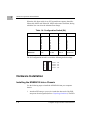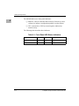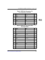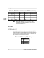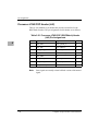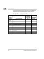
1
MVME6100
Single-Board Computer
Installation and Use
V6100A/IH1
June 2004 Edition
© Copyright 2004 Motorola Inc.
All rights reserved.
Printed in the United States of America.
Motorola and the stylized M logo are trademarks of Motorola, Inc., registered in the U.S.
Patent and Trademark Office.
All other product or service names mentioned in this document are the property of their
respective owners.
Safety Summary
The following general safety precautions must be observed during all phases of operation, service, and repair of
this equipment. Failure to comply with these precautions or with specific warnings elsewhere in this manual
could result in personal injury or damage to the equipment.
The safety precautions listed below represent warnings of certain dangers of which Motorola is aware. You, as
the user of the product, should follow these warnings and all other safety precautions necessary for the safe
operation of the equipment in your operating environment.
Ground the Instrument.
To minimize shock hazard, the equipment chassis and enclosure must be connected to an electrical ground. If the
equipment is supplied with a three-conductor AC power cable, the power cable must be plugged into an approved
three-contact electrical outlet, with the grounding wire (green/yellow) reliably connected to an electrical ground
(safety ground) at the power outlet. The power jack and mating plug of the power cable meet International
Electrotechnical Commission (IEC) safety standards and local electrical regulatory codes.
Do Not Operate in an Explosive Atmosphere.
Do not operate the equipment in any explosive atmosphere such as in the presence of flammable gases or fumes.
Operation of any electrical equipment in such an environment could result in an explosion and cause injury or
damage.
Keep Away From Live Circuits Inside the Equipment.
Operating personnel must not remove equipment covers. Only Factory Authorized Service Personnel or other
qualified service personnel may remove equipment covers for internal subassembly or component replacement
or any internal adjustment. Service personnel should not replace components with power cable connected. Under
certain conditions, dangerous voltages may exist even with the power cable removed. To avoid injuries, such
personnel should always disconnect power and discharge circuits before touching components.
Use Caution When Exposing or Handling a CRT.
Breakage of a Cathode-Ray Tube (CRT) causes a high-velocity scattering of glass fragments (implosion). To
prevent CRT implosion, do not handle the CRT and avoid rough handling or jarring of the equipment. Handling
of a CRT should be done only by qualified service personnel using approved safety mask and gloves.
Do Not Substitute Parts or Modify Equipment.
Do not install substitute parts or perform any unauthorized modification of the equipment. Contact your local
Motorola representative for service and repair to ensure that all safety features are maintained.
Observe Warnings in Manual.
Warnings, such as the example below, precede potentially dangerous procedures throughout this manual.
Instructions contained in the warnings must be followed. You should also employ all other safety precautions
which you deem necessary for the operation of the equipment in your operating environment.
Warning
Warning
To prevent serious injury or death from dangerous voltages, use extreme
caution when handling, testing, and adjusting this equipment and its
components.
Flammability
All Motorola PWBs (printed wiring boards) are manufactured with a flammability rating
of 94V-0 by UL-recognized manufacturers.
EMI Caution
Caution
!
Caution
This equipment generates, uses and can radiate electromagnetic energy. It
may cause or be susceptible to electromagnetic interference (EMI) if not
installed and used with adequate EMI protection.
Lithium Battery Caution
This product contains a lithium battery to power the clock and calendar circuitry.
Caution
!
Caution
Caution
!
Attention
Caution
!
Vorsicht
Danger of explosion if battery is replaced incorrectly. Replace battery only
with the same or equivalent type recommended by the equipment
manufacturer. Dispose of used batteries according to the manufacturer’s
instructions.
Il y a danger d’explosion s’il y a remplacement incorrect de la batterie.
Remplacer uniquement avec une batterie du même type ou d’un type
équivalent recommandé par le constructeur. Mettre au rebut les batteries
usagées conformément aux instructions du fabricant.
Explosionsgefahr bei unsachgemäßem Austausch der Batterie. Ersatz nur
durch denselben oder einen vom Hersteller empfohlenen Typ. Entsorgung
gebrauchter Batterien nach Angaben des Herstellers.
CE Notice (European Community)
Warning
!
Warning
This is a Class A product. In a domestic environment, this product may
cause radio interference, in which case the user may be required to take
adequate measures.
Motorola Computer Group products with the CE marking comply with the EMC Directive
(89/336/EEC). Compliance with this directive implies conformity to the following
European Norms:
EN55022 “Limits and Methods of Measurement of Radio Interference Characteristics
of Information Technology Equipment”; this product tested to Equipment Class A
EN55024 “Information technology equipment—Immunity characteristics—Limits and
methods of measurement”
Board products are tested in a representative system to show compliance with the above
mentioned requirements. A proper installation in a CE-marked system will maintain the
required EMC performance.
In accordance with European Community directives, a “Declaration of Conformity” has
been made and is available on request. Please contact your sales representative.
Notice
While reasonable efforts have been made to assure the accuracy of this document,
Motorola, Inc. assumes no liability resulting from any omissions in this document, or from
the use of the information obtained therein. Motorola reserves the right to revise this
document and to make changes from time to time in the content hereof without obligation
of Motorola to notify any person of such revision or changes.
Electronic versions of this material may be read online, downloaded for personal use, or
referenced in another document as a URL to the Motorola Computer Group Web site. The
text itself may not be published commercially in print or electronic form, edited, translated,
or otherwise altered without the permission of Motorola, Inc.
It is possible that this publication may contain reference to or information about Motorola
products (machines and programs), programming, or services that are not available in your
country. Such references or information must not be construed to mean that Motorola
intends to announce such Motorola products, programming, or services in your country.
Limited and Restricted Rights Legend
If the documentation contained herein is supplied, directly or indirectly, to the U.S.
Government, the following notice shall apply unless otherwise agreed to in writing by
Motorola, Inc.
Use, duplication, or disclosure by the Government is subject to restrictions as set forth in
subparagraph (b)(3) of the Rights in Technical Data clause at DFARS 252.227-7013 (Nov.
1995) and of the Rights in Noncommercial Computer Software and Documentation clause
at DFARS 252.227-7014 (Jun. 1995).
Motorola, Inc.
Computer Group
2900 South Diablo Way
Tempe, Arizona 85282
Contents
About This Manual
Overview of Contents ................................................................................................xvi
Comments and Suggestions .....................................................................................xvii
Conventions Used in This Manual ...........................................................................xvii
CHAPTER 1
Hardware Preparation and Installation
Introduction .............................................................................................................. 1-1
Description ............................................................................................................... 1-1
Getting Started ......................................................................................................... 1-3
Overview of Startup Procedures ....................................................................... 1-3
Unpacking Guidelines ....................................................................................... 1-4
Hardware Configuration ........................................................................................... 1-5
MVME6100 Preparation ................................................................................... 1-5
SCON Header (J7) ............................................................................................ 1-8
PMC/IPMC Selection Headers (J10, J15 – J18, J25 – J28) .............................. 1-8
Front/Rear Ethernet and Transition Module Options Header (J30) .................. 1-9
SROM Configuration Switch (S3) .................................................................. 1-10
Flash Boot Bank Select Configuration Switch (S4) ........................................ 1-11
Hardware Installation ............................................................................................. 1-12
Installing the MVME6100 into a Chassis ....................................................... 1-12
Connection to Peripherals ...................................................................................... 1-13
Completing the Installation .................................................................................... 1-14
CHAPTER 2
Startup and Operation
Introduction .............................................................................................................. 2-1
Applying Power ........................................................................................................ 2-1
Switches and Indicators ............................................................................................ 2-1
CHAPTER 3
MOTLoad Firmware
Introduction .............................................................................................................. 3-1
Overview ........................................................................................................... 3-1
MOTLoad Implementation and Memory Requirements ................................... 3-1
MOTLoad Commands ...................................................................................... 3-2
vii
MOTLoad Utility Applications ......................................................................... 3-2
MOTLoad Tests ................................................................................................. 3-2
Using MOTLoad ............................................................................................... 3-4
Command Line Interface ................................................................................... 3-4
Command Line Help ......................................................................................... 3-5
Command Line Rules ........................................................................................ 3-6
MOTLoad Command List ........................................................................................ 3-7
Default VME Settings ............................................................................................ 3-12
Firmware Settings ................................................................................................... 3-16
CR/CSR Settings ............................................................................................. 3-16
Displaying VME Settings ................................................................................ 3-16
Editing VME Settings ..................................................................................... 3-17
Deleting VME Settings ................................................................................... 3-18
Restoring Default VME Settings ..................................................................... 3-18
Remote Start ........................................................................................................... 3-19
Alternate Boot Images and Safe Start ..................................................................... 3-20
Firmware Startup Sequence Following Reset ......................................................... 3-20
Firmware Scan for Boot Image .............................................................................. 3-21
Valid Boot Images .................................................................................................. 3-23
Checksum Algorithm ...................................................................................... 3-24
MOTLoad Image Flags ................................................................................... 3-24
USER Images .................................................................................................. 3-25
Alternate Boot Data Structure ......................................................................... 3-26
CHAPTER 4
Functional Description
Features ..................................................................................................................... 4-1
Block Diagram .......................................................................................................... 4-3
Processor ................................................................................................................... 4-3
L3 Cache ................................................................................................................... 4-4
System Controller ..................................................................................................... 4-4
CPU Bus Interface ............................................................................................. 4-5
Memory Controller Interface ............................................................................. 4-5
Device Controller Interface ............................................................................... 4-6
PCI/PCI-X Interfaces ........................................................................................ 4-6
Gigabit Ethernet MACs ..................................................................................... 4-7
SRAM ................................................................................................................ 4-7
General-Purpose Timers/Counters .................................................................... 4-8
Watchdog Timer ................................................................................................ 4-8
I2O Message Unit .............................................................................................. 4-8
Four Channel Independent DMA Controller ..................................................... 4-8
viii
I2C Serial Interface and Devices ....................................................................... 4-9
Interrupt Controller ........................................................................................... 4-9
PCI Bus Arbitration ........................................................................................ 4-10
VMEbus Interface .................................................................................................. 4-11
PMCspan Interface ................................................................................................. 4-11
Flash Memory ........................................................................................................ 4-11
System Memory ..................................................................................................... 4-11
Asynchronous Serial Ports ..................................................................................... 4-11
PCI Mezzanine Card Slots ..................................................................................... 4-12
Real-Time Clock/NVRAM/Watchdog Timer ........................................................ 4-13
IDSEL Routing ....................................................................................................... 4-14
Reset Control Logic ............................................................................................... 4-14
Debug Support ........................................................................................................ 4-14
Processor JTAG/COP Headers ............................................................................... 4-14
CHAPTER 5
Pin Assignments
Introduction .............................................................................................................. 5-1
Connectors ................................................................................................................ 5-1
PMC Expansion Connector (J4) ....................................................................... 5-1
Gigabit Ethernet Connectors (J9, J93) .............................................................. 5-5
PCI Mezzanine Card (PMC) Connectors (J11 – J14, J21 – J24) ...................... 5-6
COM1 Connector (J19) ................................................................................... 5-18
VMEbus P1 Connector ................................................................................... 5-18
VMEBus P2 Connector (PMC Mode) ............................................................ 5-20
VMEbus P2 Connector (IPMC Mode) ............................................................ 5-23
Headers ................................................................................................................... 5-26
SCON Header (J7) .......................................................................................... 5-26
Boundary Scan Header (J8) ............................................................................ 5-27
PMC/IPMC Selection Headers (J10, J15 – J18, J25 – J28) ............................ 5-27
COM2 Header (J29) ........................................................................................ 5-28
Front/Rear Ethernet and Transition Module Options Header (J30) ................ 5-29
Processor JTAG/COP Header (J42) ................................................................ 5-30
APPENDIX A
Specifications
Power Requirements ................................................................................................A-1
Supply Current Requirements ...........................................................................A-1
Environmental Specifications ...................................................................................A-2
ix
APPENDIX B
Thermal Validation
Thermally Significant Components ......................................................................... B-1
Component Temperature Measurement ................................................................... B-5
Preparation ........................................................................................................ B-5
Measuring Junction Temperature ..................................................................... B-5
Measuring Case Temperature ........................................................................... B-5
Measuring Local Air Temperature ................................................................... B-8
APPENDIX C
Related Documentation
Motorola Computer Group Documents ................................................................... C-1
Manufacturers’ Documents ..................................................................................... C-2
Related Specifications ............................................................................................. C-5
x
List of Figures
Figure 1-1.
Figure 4-1.
Figure B-1.
Figure B-2.
Figure B-3.
Figure B-4.
MVME6100 Layout ............................................................................. 1-7
MVME6100 Block Diagram ................................................................ 4-3
Thermally Significant Components—Primary Side ............................B-3
Thermally Significant Components—Secondary Side ........................B-4
Mounting a Thermocouple Under a Heatsink .....................................B-7
Measuring Local Air Temperature .......................................................B-8
xi
List of Tables
Table 1-1. Startup Overview .................................................................................... 1-3
Table 1-2. MVME6100 Jumper and Switch Settings .............................................. 1-6
Table 1-3. SROM Configuration Switch (S3) ....................................................... 1-10
Table 1-4. Configuration Switch (S4) ................................................................... 1-12
Table 1-5. MVME6100 Connectors ...................................................................... 1-14
Table 2-1. Front-Panel LED Status Indicators ........................................................ 2-2
Table 3-1. MOTLoad Commands ............................................................................ 3-7
Table 3-2. MOTLoad Image Flags ........................................................................ 3-24
Table 4-1. MVME6100 Features Summary ............................................................ 4-1
Table 4-2. Device Bus Parameters ........................................................................... 4-6
Table 5-1. PMC Expansion Connector (J4) Pin Assignments ................................ 5-2
Table 5-2. Gigabit Ethernet Connectors (J9, J93) Pin Assignment ......................... 5-5
Table 5-3. PMC Slot 1 Connector (J11) Pin Assignments ...................................... 5-6
Table 5-4. PMC Slot 1 Connector (J12) Pin Assignments ...................................... 5-7
Table 5-5. PMC Slot 1 Connector (J13) Pin Assignments ...................................... 5-9
Table 5-6. PMC Slot 1 Connector (J14) Pin Assignments .................................... 5-10
Table 5-7. PMC Slot 2 Connector (J21) Pin Assignments .................................... 5-12
Table 5-8. PMC Slot 2 Connector (J22) Pin Assignments .................................... 5-13
Table 5-9. PMC Slot 2 Connector (J23) Pin Assignments .................................... 5-15
Table 5-10. PMC Slot 2 Connector (J24) Pin Assignments .................................. 5-16
Table 5-11. COM1 Connector (J19) Pin Assignments .......................................... 5-18
Table 5-12. VMEbus P1 Connector Pin Assignments .......................................... 5-18
Table 5-13. VMEbus P2 Connector Pin Assignments (PMC Mode) .................... 5-20
Table 5-14. VME P2 Connector Pinouts with IPMC712 ...................................... 5-23
Table 5-15. VME P2 Connector Pinouts with IPMC761 ...................................... 5-24
Table 5-16. SCON Header (J7) Pin Assignments ................................................. 5-26
Table 5-17. Boundary Scan Header (J8) Pin Assignments ................................... 5-27
Table 5-18. PMC/IPMC Configuration Jumper Block .......................................... 5-27
Table 5-19. COM2 Planar Serial Port Header (J29) Pin Assignments .................. 5-28
Table 5-20. Front/Rear Ethernet and Transition Module Options Header
(J30) Pin Assignment ............................................................................................. 5-29
Table 5-21. Processor JTAG/COP (RISCWatch) Header (J42) Pin
Assignments ........................................................................................................... 5-30
Table A-1. Power Requirements .............................................................................A-1
xiii
Table A-2.
Table B-1.
Table C-1.
Table C-2.
Table C-3.
xiv
MVME6100 Specifications .................................................................. A-2
Thermally Significant Components ...................................................... B-2
Motorola Computer Group Documents ................................................ C-1
Manufacturers’ Documents ................................................................... C-2
Related Specifications ........................................................................... C-5
About This Manual
The MVME6100 Single-Board Computer Installation and Use manual
provides the information you will need to install and configure your
MVME6100 single-board computer. It provides specific preparation and
installation information, and data applicable to the board.
As of the printing date of this manual, the MVME6100 supports the
models listed below.
Model Number
Description
MVME6100-0161
1.267 GHz MPC7457 processor, 512MB DDR
memory, 128MB Flash, Scanbe handles
MVME6100-0163
1.267 GHz MPC7457 processor, 512MB DDR
memory,128MB Flash, IEEE handles
MVME6100-0171
1.267 GHz MPC7457 processor, 1GB DDR
memory, 128MB Flash, Scanbe handles
MVME6100-0173
1.267 GHz MPC7457 processor, 1GB DDR
memory, 128MB Flash, IEEE handles
xv
Overview of Contents
This manual is divided into the following chapters and appendices:
Chapter 1, Hardware Preparation and Installation, provides MVME6100
board preparation and installation instructions, as well as ESD
precautionary notes.
Chapter 2, Startup and Operation, provides the power-up procedure and
identifies the switches and indicators on the MVMEM6100.
Chapter 3, MOTLoad Firmware, describes the basic features of the
MOTLoad firmware product.
Chapter 4, Functional Description, describes the MVME6100 on a block
diagram level.
Chapter 5, Pin Assignments, provides pin assignments for various headers
and connectors on the MMVE6100 single-board computer.
Appendix A, Specifications, provides power requirements and
environmental specifications.
Appendix B, Thermal Validation, provides information to conduct thermal
evaluations and identifies thermally significant components along with
their maximum allowable operating temperatures.
Appendix C, Related Documentation, provides a listing of related
Motorola manuals, vendor documentation, and industry specifications.
xvi
Comments and Suggestions
Motorola welcomes and appreciates your comments on its documentation.
We want to know what you think about our manuals and how we can make
them better. Mail comments to:
Motorola Computer Group
Reader Comments DW164
2900 S. Diablo Way
Tempe, Arizona 85282
You can also submit comments to the following e-mail address:
[email protected]
In all your correspondence, please list your name, position, and company.
Be sure to include the title and part number of the manual and tell how you
used it. Then tell us your feelings about its strengths and weaknesses and
any recommendations for improvements.
Conventions Used in This Manual
The following typographical conventions are used in this document:
bold
is used for user input that you type just as it appears; it is also used for
commands, options and arguments to commands, and names of
programs, directories and files.
italic
is used for names of variables to which you assign values, for function
parameters, and for structure names and fields. Italic is also used for
comments in screen displays and examples, and to introduce new
terms.
courier
is used for system output (for example, screen displays, reports),
examples, and system prompts.
xvii
<Enter>, <Return> or <CR>
represents the carriage return or Enter key.
Ctrl
represents the Control key. Execute control characters by pressing the
Ctrl key and the letter simultaneously, for example, Ctrl-d.
xviii
1Hardware Preparation and
Installation
1
Introduction
This chapter contains the following information:
❏ Board preparation and installation instructions
❏ ESD precautionary notes
Description
The MVME6100 is a single-slot, single-board computer based on the
MPC7457 processor, the MV64360 system controller, the Tsi148 VME
Bridge ASIC, up to 1 GB of ECC-protected DDR DRAM, up to 128MB of
flash memory, and a dual Gigabit Ethernet interface.
Front panel connectors on the MVME6100 board include: two RJ-45
connectors for the Gigabit Ethernet, one RJ-45 connector for the
asynchronous serial port with integrated LEDs for BRDFAIL and CPU run
indication, and a combined reset and abort switch.
The MVME6100 is shipped with one additional asynchronous serial port
routed to an on-board header.
The MVME6100 contains two IEEE1386.1 PCI, PCI-X capable
mezzanine card slots. The PMC slots are 64-bit capable and support both
front and rear I/O. All I/O pins of PMC slot 1 and 46 I/O pins of PMC slot
2 are routed to the 5-row DIN, P2 connector. I/O pins 1 through 64 from
J14 of PMC slot 1 are routed to row C and row A of P2. I/O pins 1 through
46 from J24 of PMC slot 2 are routed to row D and row Z of P2.
The MVME6100 has two planar PCI buses (PCI0 and PCI1). In order to
support a more generic PCI bus hierarchy nomenclature, the MV64360
PCI buses will be referred to in this document as PCI bus 0 (root bridge
instance 0, bus 0) and PCI bus 1 (root bridge instance 1, bus 0). PCI bus 1
connects to PMC slots 1 and 2 of the board. PCI bus 0 connects to the
Tsi148 VME Bridge ASIC and PMCspan bridge (PCI6520). This interface
1-1
1
Hardware Preparation and Installation
operates at PCI-X (133 MHz) speed. Both PCI planar buses are controlled
by the MV64360 system controller.
Voltage Input/Output (VIO) for PCI bus 1 is set by the location of the PMC
keying pins; both pins should be set to designate the same VIO, either
+3.3V or +5V.
The MVME6100 board interfaces to the VMEbus via the P1 and P2
connectors, which use 5-row 160-pin connectors as specified in the
VME64 Extension Standard. It also draws +12V and +5V power from the
VMEbus backplane through these two connectors. The +3.3V, +2.5V,
+1.8V, and processor core supplies are regulated on-board from the +5V
power.
Note
For maximum VMEbus performance, the MVME6100 should be
mounted in a VME64x compatible backplane (5-row). 2eSST
transfers are not supported when a 3-row backplane is used.
The MVME6100 supports multiple modes of I/O operation. By default, the
board is configured for Ethernet port 2 to the front panel (non-specific
transition module), and PMC slot 1 in IPMC mode. The board can be
configured to route Ethernet port 2 to P2 and support MVME712M or
MVME761 transition modules. The front/rear Ethernet and transition
module options are configured by jumper block J30.
Selection of PMC slot 1 in PMC or IPMC mode is done by the jumper
blocks J10, J15-J18, and J25-J28 (see Table 1-2 on page 1-6). IPMC mode
is selected when an IPMC712 or IPMC761 module is used. If an IPMC is
used, J30 should be configured for the appropriate transition module (see
J30 configuration options as illustrated in Front/Rear Ethernet and
Transition Module Options Header (J30) on page 1-9).
The IPMC712 and IPMC761 use AD11 as the IDSEL line for the Winbond
PCI-ISA bridge device. This device supplies the four serial and one
parallel port of the IPMC7xx module. The Discovery II PHB (MV64360)
does not recognize address lines below AD16. For this reason, although an
IPMC7xx module may be used on an MVME6100, the serial and parallel
ports are not available, nor addressable. This issue will be resolved by
MCG at a later date.
1-2
Computer Group Literature Center Web Site
Getting Started
Note
Other functions, such as Ethernet and SCSI interfaces, are
function independent of the Winbond IDSEL line. The wide
SCSI interface can only be supported through IPMC connector
J3.
PMC mode is backwards compatible with the MVME5100 and
MVME5500 and is accomplished by configuring the on-board jumpers.
Getting Started
This section provides an overview of the steps necessary to install and
power up the MVME6100 and a brief section on unpacking and ESD
precautions.
Overview of Startup Procedures
The following table lists the things you will need to do before you can use
this board and tells where to find the information you need to perform each
step. Be sure to read this entire chapter, including all Caution and Warning
notes, before you begin.
Table 1-1. Startup Overview
What you need to do...
Refer to...
Unpack the hardware.
Unpacking Guidelines on page 1-4
Configure the hardware by
setting jumpers on the board.
MVME6100 Preparation on page 1-5
Install the MVME6100 board in
a chassis.
Installing the MVME6100 into a Chassis on
page 1-12
Connect any other equipment
you will be using
Connection to Peripherals on page 1-13
Verify the hardware is installed.
Completing the Installation on page 1-14
http://www.motorola.com/computer/literature
1-3
1
1
Hardware Preparation and Installation
Unpacking Guidelines
Unpack the equipment from the shipping carton. Refer to the packing list
and verify that all items are present. Save the packing material for storing
and reshipping of equipment.
Note
Caution
!
If the shipping carton is damaged upon receipt, request that the
carrier’s agent be present during the unpacking and inspection of
the equipment.
Avoid touching areas of integrated circuitry; static discharge can damage
circuits.
Caution
ESD
Use ESD
Wrist Strap
Motorola strongly recommends that you use an antistatic wrist strap and a
conductive foam pad when installing or upgrading a system. Electronic
components, such as disk drives, computer boards, and memory modules
can be extremely sensitive to electrostatic discharge (ESD). After
removing the component from its protective wrapper or from the system,
place the component flat on a grounded, static-free surface (and, in the case
of a board, component side up). Do not slide the component over any
surface.
If an ESD station is not available, you can avoid damage resulting from
ESD by wearing an antistatic wrist strap (available at electronics stores)
that is attached to an active electrical ground. Note that a system chassis
may not be grounded if it is unplugged.
Caution
!
Inserting or removing modules with power applied may result in damage
to module components.
Caution
Dangerous voltages, capable of causing death, are present in this
equipment. Use extreme caution when handling, testing, and adjusting.
Warning
Warning
1-4
Computer Group Literature Center Web Site
Hardware Configuration
Hardware Configuration
This section discusses certain hardware and software tasks that may need
to be performed prior to installing the board in a chassis.
To produce the desired configuration and ensure proper operation of the
MVME6100, you may need to carry out certain hardware modifications
before installing the module.
Most options on the MVME6100 are software configurable. Configuration
changes are made by setting bits in control registers after the board is
installed in a system.
Jumpers/switches are used to control those options that are not software
configurable. These jumper settings are described further on in this
section. If you are resetting the board jumpers from their default settings,
it is important to verify that all settings are reset properly.
MVME6100 Preparation
Figure 1-1 illustrates the placement of the jumpers, headers, connectors,
switches, and various other components on the MVME6100. There are
several manually configurable headers on the MVME6100 and their
settings are shown in Table 1-2. Each header’s default setting is enclosed
in brackets. For pin assignments on the MVME6100, refer to Chapter 5,
Pin Assignments.
http://www.motorola.com/computer/literature
1-5
1
1
Hardware Preparation and Installation
Table 1-2. MVME6100 Jumper and Switch Settings
Jumper/
Switch
Function
Settings
J7
SCON Header
[No jumper installed]
1-2
2-3
J10,
J15–J18,
J25–J28
PMC/IPMC Selection
Headers
[Jumper installed]
1-2
[2-3]
J30
Front/Rear Ethernet and
Transition Module Options
Header
Refer to Front/Rear Ethernet and Transition
Module Options Header (J30) on page 1-9 for
details.
S3
SROM Configuration Switch,
sets board Geographical
Address
Refer to SROM Configuration Switch (S3) on page
1-10 for details.
S4
Flash Boot Bank Select
Configuration Switch, sets
Write Protect A, Write Protect
B, Boot Bank Select, and Safe
Start
Refer to Flash Boot Bank Select Configuration
Switch (S4) on page 1-11 for details.
Note
Auto-SCON
Always SCON
No SCON
PMC I/O
IPMC I/O for IPMC7xx
support (default)
Items in brackets are factory default settings.
The MVME6100 is factory tested and shipped with the configuration
described in the following sections.
1-6
Computer Group Literature Center Web Site
MVME6100 Preparation
J42
J7
J8
J29
J21
J22
J23
J24
S4
1 2 3 4 5 6 7 8
1 2 3 4 5 6 7 8
1 2 3 4
PCI MEZZANINE CARD
S1
S3
P1
J11
J12
PCI MEZZANINE CARD
J3
PMC
IPMC
J30
J13
LAN 2
LAN 1
10/100/1000 10/100/1000
J9
J93
U32
U12
J14
P2
DEBUG
J19
ABT/RST
S2
J4
4296 0604
Figure 1-1. MVME6100 Layout
http://www.motorola.com/computer/literature
1-7
1
1
Hardware Preparation and Installation
SCON Header (J7)
A 3-pin planar header allows the choice for auto/enable/disable SCON
VME configuration. A jumper installed across pins 1 and 2 configures for
SCON always enabled. A jumper installed across pins 2 and 3 configures
for SCON disabled. No jumper installed configures for auto SCON.
J7
J7
J7
1
1
1
2
2
2
3
3
3
Auto-SCON
(factory configuration)
Always SCON
No SCON
PMC/IPMC Selection Headers (J10, J15 – J18, J25 – J28)
Nine 3-pin planar headers are for PMC/IPMC mode I/O selection for PMC
slot 1. These nine headers can also be combined into one single header
block where a block shunt can be used as a jumper.
A jumper installed across pins 1 and 2 on all nine headers selects PMC1
for PMC I/O mode. A jumper across pins 2 and 3 on all nine headers
selects IPMC I/O mode.
1-8
Computer Group Literature Center Web Site
Front/Rear Ethernet and Transition Module Options Header (J30)
IPMC P2 I/O for IPMC Mode
(factory configuration)
J10
J15
J17
J16
J18
J25
J26
J27
J28
1
1
1
1
1
1
1
1
1
2
2
2
2
2
2
2
2
2
3
3
3
3
3
3
3
3
3
PMC1 P2 I/O for PMC Mode
J10
J15
J16
J17
J18
J25
J26
J27
J28
1
1
1
1
1
1
1
1
1
2
2
2
2
2
2
2
2
2
3
3
3
3
3
3
3
3
3
Front/Rear Ethernet and Transition Module Options Header
(J30)
A 40-pin planar header allows for selecting P2 options. Jumpers installed
across Row A pins 3-10 and Row B pins 3-10 enable front Ethernet access.
Jumpers installed across Row B pins 3-10 and Row C pins 3-10 enable P2
(rear) Gigabit Ethernet. Only when front Ethernet is enabled can the
jumpers be installed across Row C and Row D on pins 1-10 to enable P2
(rear) PMC I/O. Note that all jumpers must be installed across the same
two rows (all between Row A and Row B and/or Row C and Row D, or all
between Row B and Row C).
http://www.motorola.com/computer/literature
1-9
1
1
Hardware Preparation and Installation
The following illustration shows jumper setting options for J30. The
factory default is shown where applicable:
J30 Options
1
11
21
31
10
20
30
40
1
11
21
31
10
20
30
40
Front Ethernet
(Default)
1
11
21
31
1
11
21
31
Rear Ethernet
10
20
30
40
PMC I/O TO P2
(Default)
1
11
21
31
10
20
30
40
Non-Specific Transition Module
(Default)
10
20
30
40
1
11
21
31
MVME 712M
Transition Module
10
20
30
40
MVME 761
Transition Module
4294 0604
Refer to Front/Rear Ethernet and Transition Module Options Header (J30)
on page 5-29 for connector pin assignments.
SROM Configuration Switch (S3)
A part of the 8-position SMT switch, S3 enables/disables the MV64360
SROM initialization and all I2C EEPROM write protection.
The SROM Init switch is OFF to disable the MV64360 device
initialization via the I2C SROM. The switch is ON to enable this sequence.
The SROM WP switch is OFF to enable write protection on all I2C. The
switch is ON to disable the I2C EEPROM write protection.
Table 1-3. SROM Configuration Switch (S3)
1-10
POSITION
2
1
FUNCTION
SROM WP
SROM_INIT
DEFAULT (OFF)
WP
No SROM_INIT
Computer Group Literature Center Web Site
Flash Boot Bank Select Configuration Switch (S4)
S3 position 3-8 defines the VME Geographical Address if the MVME6100
is installed in a 3-row backplane. The following is the pinout:
Position
Function
3
VMEGAP_L
4
VMEGA4_L
5
VMEGA3_L
6
VMEGA2_L
7
VMEGA1_L
8
VMEGA0_L
Setting the individual position to ON forces the corresponding signal to
zero. If the board is installed in a 5-row backplane, the geographical
address is defined by the backplane and positions 3-8 of S3 should be set
to OFF. The default setting is OFF.
Flash Boot Bank Select Configuration Switch (S4)
A 4-position SMT configuration switch is located on the board to control
Flash Bank B Boot block write-protect and Flash Bank A write-protect.
Select the Flash Boot bank and the programmed/safe start ENV settings.
Note
It is recommended that Bank B Write Protect always be enabled.
The Bank B Boot WP switch is OFF to indicate that the Flash Bank B Boot
block is write-protected. The switch is ON to indicate no write-protection
of Bank B Boot block.
The Bank A WP switch is OFF to indicate that the entire Flash Bank A is
write-protected. The switch is ON to indicate no write-protection of Bank
A Boot block.
When the Boot Bank Sel Switch is ON, the board boots from Bank B,
when OFF, the board boots from Bank A. Default is ON (boot from Bank
B).
http://www.motorola.com/computer/literature
1-11
1
Hardware Preparation and Installation
When the Safe Start switch is set OFF, normal boot sequence should be
followed by MOTLoad. When ON, MOTLoad executes Safe Start, during
which the user can select the Alternate Boot Image.
POSITION
4
3
2
1
FUNCTION
BANK A WP
BOOT BANK SEL
SAFE START
Table 1-4. Configuration Switch (S4)
BANK B BOOT WP
1
FACTORY
DEFAULT
OFF
WP
ON
No WP
ON
Bank B
OFF
Norm ENV
The S4 Configuration Switch is set with the following default settings:
ON
1
Switch 1 - OFF
2
Switch 2 - ON
3
Switch 3 - ON
4
Switch 4 - OFF
4295 0604
Hardware Installation
Installing the MVME6100 into a Chassis
Use the following steps to install the MVME6100 into your computer
chassis.
1. Attach an ESD strap to your wrist. Attach the other end of the ESD
strap to an electrical ground (refer to Unpacking Guidelines). The ESD
1-12
Computer Group Literature Center Web Site
Connection to Peripherals
strap must be secured to your wrist and to ground throughout the
procedure.
2. Remove any filler panel that might fill that slot.
3. Install the top and bottom edge of the MVME6100 into the guides of
the chassis.
Warning
!
Warning
Only use injector handles for board insertion to avoid
damage/deformation to the front panel and/or PCB. Deformation of
the front panel can cause an electrical short or other board
malfunction.
4. Ensure that the levers of the two injector/ejectors are in the outward
position.
5. Slide the MVME6100 into the chassis until resistance is felt.
6. Simultaneously move the injector/ejector levers in an inward direction.
7. Verify that the MVME6100 is properly seated and secure it to the
chassis using the two screws located adjacent to the injector/ejector
levers.
8. Connect the appropriate cables to the MVME6100.
To remove the board from the chassis, press the red locking tabs (IEEE
handles only) and reverse the procedure.
Connection to Peripherals
When the MVME6100 is installed in a chassis, you are ready to connect
peripherals and apply power to the board.
http://www.motorola.com/computer/literature
1-13
1
1
Hardware Preparation and Installation
Figure 1-1 on page 1-7 shows the locations of the various connectors while
Table 1-5 lists them for you. Refer to Chapter 5, Pin Assignments for the
pin assignments of the connectors listed below.
Table 1-5. MVME6100 Connectors
Connector
Function
J3
IPMC761/712 connector
J4
PMC expansion connector
J9, J93
Gigabit Ethernet connectors
J11, J12, J13, J14
PCI mezzanine card (PMC) slot 1 connector
J19
COM1 connector
J21, J22, J23, J24
PCI mezzanine card (PMC) slot 2 connector
J29
COM2 planar connector
P1, P2
VME rear panel connectors
Completing the Installation
Verify that hardware is installed and the power/peripheral cables connected
are appropriate for your system configuration.
Replace the chassis or system cover, reconnect the system to the AC or DC
power source, and turn the equipment power on.
1-14
Computer Group Literature Center Web Site
2Startup and Operation
2
Introduction
This chapter gives you information about the:
❏ Power-up procedure
❏ Switches and indicators
Applying Power
After you verify that all necessary hardware preparation is complete and
all connections are made correctly, you can apply power to the system.
When you are ready to apply power to the MVME6100:
❏ Verify that the chassis power supply voltage setting matches the
voltage present in the country of use (if the power supply in your
system is not auto-sensing)
❏ On powering up, the MVME6100 brings up the MOTLoad
prompt, MVME6100>
Switches and Indicators
The MVME6100 board provides a single pushbutton switch that provides
both abort and reset (ABT/RST) functions. When the switch is depressed
for less than three seconds, an abort interrupt is generated to the processor.
If the switch is held for more than three seconds, a board hard reset is
generated. The board hard reset will reset the MPC7457, MV64360,
Tsi148 VME Bridge ASIC, PCI6520, PMC1/2 slots, both Ethernet PHYs,
serial ports, PMCspan slot, both flash banks, and the device bus control
PLD. If the MVME6100 is enabled for VME system controller, the VME
bus will be reset and local reset input is sent to the Tsi148 VME controller.
2-1
Startup and Operation
The MVME6100 has two front-panel indicators:
2
❏ BDFAIL, software controlled and asserted by firmware (or other
software) to indicate a configuration problem (or other failure)
❏ CPU, connected to a CPU bus control signal to indicate bus
transfer activity
The following table describes these indicators:
Table 2-1. Front-Panel LED Status Indicators
2-2
Function
Label
Color
Description
CPU Bus Activity
CPU
Green
CPU bus is busy
Board Fail
BDFAIL
Yellow
Board has a failure
Computer Group Literature Center Web Site
3MOTLoad Firmware
3
Introduction
This chapter describes the basic features of the MOTLoad firmware
product, designed by Motorola as the next generation initialization,
debugger, and diagnostic tool for high-performance embedded board
products using state-of-the-art system memory controllers and bridge
chips, such as the MV64360.
In addition to an overview of the product, this chapter includes a list of
standard MOTLoad commands, the default VME and firmware settings
that are changeable by the user, remote start, and the alternate boot
procedure.
Overview
The MOTLoad firmware package serves as a board power-up and
initialization package, as well as a vehicle from which user applications
can be booted. A secondary function of the MOTLoad firmware is to serve
in some respects as a test suite providing individual tests for certain
devices.
MOTLoad is controlled through an easy-to-use, UNIX-like, command line
interface. The MOTLoad software package is similar to many end-user
applications designed for the embedded market, such as the real time
operating systems currently available.
Refer to the MOTLoad Firmware Package User’s Manual, listed in
Appendix C, Related Documentation, for more details.
MOTLoad Implementation and Memory Requirements
The implementation of MOTLoad and its memory requirements are
product specific. The MVME6100 single-board computer (SBC) is offered
with a wide range of memory (for example, DRAM, external cache, flash).
Typically, the smallest amount of on-board DRAM that a Motorola SBC
3-1
MOTLoad Firmware
has is 32MB. Each supported Motorola product line has its own unique
MOTLoad binary image(s). Currently the largest MOTLoad compressed
image is less than 1MB in size.
3
MOTLoad Commands
MOTLoad supports two types of commands (applications): utilities and
tests. Both types of commands are invoked from the MOTLoad command
line in a similar fashion. Beyond that, MOTLoad utilities and MOTLoad
tests are distinctly different.
MOTLoad Utility Applications
The definition of a MOTLoad utility application is very broad. Simply
stated, it is considered a MOTLoad command, if it is not a MOTLoad test.
Typically, MOTLoad utility applications are applications that aid the user
in some way (that is, they do something useful). From the perspective of
MOTLoad, examples of utility applications are: configuration, data/status
displays, data manipulation, help routines, data/status monitors, etc.
Operationally, MOTLoad utility applications differ from MOTLoad test
applications in several ways:
❏ Only one utility application operates at any given time (that is,
multiple utility applications cannot be executing concurrently)
❏ Utility applications may interact with the user. Most test
applications do not.
MOTLoad Tests
A MOTLoad test application determines whether or not the hardware
meets a given standard. Test applications are validation tests. Validation is
conformance to a specification. Most MOTLoad tests are designed to
directly validate the functionality of a specific SBC subsystem or
component. These tests validate the operation of such SBC modules as:
dynamic memory, external cache, NVRAM, real time clock, etc.
3-2
Computer Group Literature Center Web Site
MOTLoad Tests
All MOTLoad tests are designed to validate functionality with minimum
user interaction. Once launched, most MOTLoad tests operate
automatically without any user interaction. There are a few tests where the
functionality being validated requires user interaction (that is, switch tests,
interactive plug-in hardware modules, etc.). Most MOTLoad test results
(error-data/status-data) are logged, not printed. All MOTLoad
tests/commands have complete and separate descriptions (refer to the
MOTLoad Firmware Package User’s Manual for this information).
All devices that are available to MOTLoad for validation/verification
testing are represented by a unique device path string. Most MOTLoad
tests require the operator to specify a test device at the MOTLoad
command line when invoking the test.
A listing of all device path strings can be displayed through the devShow
command. If an SBC device does not have a device path string, it is not
supported by MOTLoad and can not be directly tested. There are a few
exceptions to the device path string requirement, like testing RAM, which
is not considered a true device and can be directly tested without a device
path string. Refer to the devShow command description page in the
MOTLoad Firmware Package User’s Manual.
Most MOTLoad tests can be organized to execute as a group of related
tests (a testSuite) through the use of the testSuite command. The expert
operator can customize their testing by defining and creating a custom
testSuite(s). The list of built-in and user-defined MOTLoad testSuites, and
their test contents, can be obtained by entering testSuite -d at the
MOTLoad prompt. All testSuites that are included as part of a product
specific MOTLoad firmware package are product specific. For more
information, refer to the testSuite command description page in the
MOTLoad Firmware Package User’s Manual.
Test results and test status are obtained through the testStatus,
errorDisplay, and taskActive commands. Refer to the appropriate
command description page in the MOTLoad Firmware Package User’s
Manual for more information.
http://www.motorola.com/computer/literature
3-3
3
MOTLoad Firmware
Using MOTLoad
Interaction with MOTLoad is performed via a command line interface
through a serial port on the SBC, which is connected to a terminal or
terminal emulator (for example, Window’s Hypercomm). The default
MOTLoad serial port settings are: 9600 baud, 8 bits, no parity.
3
Command Line Interface
The MOTLoad command line interface is similar to a UNIX command line
shell interface. Commands are initiated by entering a valid MOTLoad
command (a text string) at the MOTLoad command line prompt and
pressing the carriage-return key to signify the end of input. MOTLoad then
performs the specified action. An example of a MOTLoad command line
prompt is shown below. The MOTLoad prompt changes according to what
product it is used on (for example, MVME5500, MVME6100).
Example:
MVME6100>
If an invalid MOTLoad command is entered at the MOTLoad command
line prompt, MOTLoad displays a message that the command was not
found.
Example:
MVME6100> mytest
"mytest" not found
MVME6100>
If the user enters a partial MOTLoad command string that can be resolved
to a unique valid MOTLoad command and presses the carriage-return key,
the command will be executed as if the entire command string had been
entered. This feature is a user-input shortcut that minimizes the required
amount of command line input. MOTLoad is an ever changing firmware
package, so user-input shortcuts may change as command additions are
made.
3-4
Computer Group Literature Center Web Site
Command Line Help
Example:
MVME6100> version
3
Copyright: Motorola Inc.1999-2002, All Rights Reserved
MOTLoad RTOS Version 2.0
PAL Version 0.1 (Motorola MVME6100)
Example:
MVME6100> ver
Copyright: Motorola Inc. 1999-2002, All Rights Reserved
MOTLoad RTOS Version 2.0
PAL Version 0.1 (Motorola MVME6100)
If the partial command string cannot be resolved to a single unique
command, MOTLoad will inform the user that the command was
ambiguous.
Example:
MVME6100> te
"te" ambiguous
MVME6100>
Command Line Help
Each MOTLoad firmware package has an extensive, product-specific help
facility that can be accessed through the help command. The user can enter
help at the MOTLoad command line to display a complete listing of all
available tests and utilities.
Example
MVME6100> help
For help with a specific test or utility the user can enter the following at the
MOTLoad prompt:
help <command_name>
http://www.motorola.com/computer/literature
3-5
MOTLoad Firmware
The help command also supports a limited form of pattern matching. Refer
to the help command page.
Example
3
MVME6100> help testRam
Usage: testRam [-aPh] [-bPh] [-iPd] [-nPh] [-tPd] [-v]
Description: RAM Test [Directory]
Argument/Option Description
-a Ph: Address to Start (Default = Dynamic Allocation)
-b Ph: Block Size (Default = 16KB)
-i Pd: Iterations (Default = 1)
-n Ph: Number of Bytes (Default = 1MB)
-t Ph: Time Delay Between Blocks in OS Ticks (Default = 1)
-v O : Verbose Output
MVME6100>
Command Line Rules
There are a few things to remember when entering a MOTLoad command:
❏ Multiple commands are permitted on a single command line,
provided they are separated by a single semicolon (;)
❏ Spaces separate the various fields on the command line
(command/arguments/options)
❏ The argument/option identifier character is always preceded by a
hyphen (-) character
❏ Options are identified by a single character
❏ Option arguments immediately follow (no spaces) the option
❏ All commands, command options, and device tree strings are case
sensitive
Example:
MVME6100> flashProgram –d/dev/flash0 –n00100000
For more information on MOTLoad operation and function, refer to the
MOTLoad Firmware Package User’s Manual.
3-6
Computer Group Literature Center Web Site
MOTLoad Command List
MOTLoad Command List
The following table provides a list of all current MOTLoad commands.
Products supported by MOTLoad may or may not employ the full
command set. Typing help at the MOTLoad command prompt will display
all commands supported by MOTLoad for a given product.
Table 3-1. MOTLoad Commands
Command
Description
as
One-Line Instruction Assembler
bcb bch bcw
Block Compare Byte/Halfword/Word
bdTempShow
Display Current Board Temperature
bfb bfh bfw
Block Fill Byte/Halfword/Word
blkCp
Block Copy
blkFmt
Block Format
blkRd
Block Read
blkShow
Block Show Device Configuration Data
blkVe
Block Verify
blkWr
Block Write
bmb bmh bmw
Block Move Byte/Halfword/Word
br
Assign/Delete/Display User-Program Break-Points
bsb bsh bsw
Block Search Byte/Halfword/Word
bvb bvh bvw
Block Verify Byte/Halfword/Word
cdDir
ISO9660 File System Directory Listing
cdGet
ISO9660 File System File Load
clear
Clear the Specified Status/History Table(s)
cm
Turns on Concurrent Mode
csb csh csw
Calculates a Checksum Specified by Command-line Options
devShow
Display (Show) Device/Node Table
http://www.motorola.com/computer/literature
3-7
3
MOTLoad Firmware
Table 3-1. MOTLoad Commands (continued)
Command
3
3-8
Description
diskBoot
Disk Boot (Direct-Access Mass-Storage Device)
downLoad
Down Load S-Record from Host
ds
One-Line Instruction Disassembler
echo
Echo a Line of Text
elfLoader
ELF Object File Loader
errorDisplay
Display the Contents of the Test Error Status Table
eval
Evaluate Expression
execProgram
Execute Program
fatDir
FAT File System Directory Listing
fatGet
FAT File System File Load
fdShow
Display (Show) File Discriptor
flashProgram
Flash Memory Program
flashShow
Display Flash Memory Device Configuration Data
gd
Go Execute User-Program Direct (Ignore Break-Points)
gevDelete
Global Environment Variable Delete
gevDump
Global Environment Variable(s) Dump (NVRAM Header + Data)
gevEdit
Global Environment Variable Edit
gevInit
Global Environment Variable Area Initialize (NVRAM Header)
gevList
Global Environment Variable Labels (Names) Listing
gevShow
Global Environment Variable Show
gn
Go Execute User-Program to Next Instruction
go
Go Execute User-Program
gt
Go Execute User-Program to Temporary Break-Point
hbd
Display History Buffer
hbx
Execute History Buffer Entry
Computer Group Literature Center Web Site
MOTLoad Command List
Table 3-1. MOTLoad Commands (continued)
Command
Description
help
Display Command/Test Help Strings
l2CacheShow
Display state of L2 Cache and L2CR register contents
l3CacheShow
Display state of L3 Cache and L3CR register contents
mdb mdh mdw
Memory Display Bytes/Halfwords/Words
memShow
Display Memory Allocation
mmb mmh mmw
Memory Modify Bytes/Halfwords/Words
netBoot
Network Boot (BOOT/TFTP)
netShow
Display Network Interface Configuration Data
netShut
Disable (Shutdown) Network Interface
netStats
Display Network Interface Statistics Data
noCm
Turns off Concurrent Mode
pciDataRd
Read PCI Device Configuration Header Register
pciDataWr
Write PCI Device Configuration Header Register
pciDump
Dump PCI Device Configuration Header Register
pciShow
Display PCI Device Configuration Header Register
pciSpace
Display PCI Device Address Space Allocation
ping
Ping Network Host
portSet
Port Set
portShow
Display Port Device Configuration Data
rd
User Program Register Display
reset
Reset System
rs
User Program Register Set
set
Set Date and Time
sromRead
SROM Read
sromWrite
SROM Write
http://www.motorola.com/computer/literature
3
3-9
MOTLoad Firmware
Table 3-1. MOTLoad Commands (continued)
Command
3
Description
sta
Symbol Table Attach
stl
Symbol Table Lookup
stop
Stop Date and Time (Power-Save Mode)
taskActive
Display the Contents of the Active Task Table
tc
Trace (Single-Step) User Program
td
Trace (Single-Step) User Program to Address
testDisk
Test Disk
testEnetPtP
Ethernet Point-to-Point
testNvramRd
NVRAM Read
testNvramRdWr
NVRAM Read/Write (Destructive)
testRam
RAM Test (Directory)
testRamAddr
RAM Addressing
testRamAlt
RAM Alternating
testRamBitToggle
RAM Bit Toggle
testRamBounce
RAM Bounce
testRamCodeCopy
RAM Code Copy and Execute
testRamEccMonitor
Monitor for ECC Errors
testRamMarch
RAM March
testRamPatterns
RAM Patterns
testRamPerm
RAM Permutations
testRamQuick
RAM Quick
testRamRandom
RAM Random Data Patterns
testRtcAlarm
RTC Alarm
testRtcReset
RTC Reset
testRtcRollOver
RTC Rollover
3-10
Computer Group Literature Center Web Site
MOTLoad Command List
Table 3-1. MOTLoad Commands (continued)
Command
Description
testRtcTick
RTC Tick
testSerialExtLoop
Serial External Loopback
testSeriallntLoop
Serial Internal Loopback
testStatus
Display the Contents of the Test Status Table
testSuite
Execute Test Suite
testSuiteMake
Make (Create) Test Suite
testThermoOp
Thermometer Temp Limit Operational Test
testThermoQ
Thermometer Temp Limit Quick Test
testThermoRange
Tests That Board Thermometer is Within Range
testWatchdogTimer
Tests the Accuracy of the Watchdog Timer Device
tftpGet
TFTP Get
tftpPut
TFTP Put
time
Display Date and Time
transparentMode
Transparent Mode (Connect to Host)
tsShow
Display Task Status
upLoad
Up Load Binary Data from Target
version
Display Version String(s)
vmeCfg
Manages user specified VME configuration parameters
vpdDisplay
VPD Display
vpdEdit
VPD Edit
waitProbe
Wait for I/O Probe to Complete
http://www.motorola.com/computer/literature
3
3-11
MOTLoad Firmware
Default VME Settings
As shipped from the factory, the MVME6100 has the following VME
configuration programmed via Global Environment Variables (GEVs) for
the Tsi148 VME controller. The firmware allows certain VME settings to
be changed in order for the user to customize the environment. The
following is a description of the default VME settings that are changeable
by the user. For more information, refer to the MOTLoad User’s Manual
and Tundra’s Tsi148 User Manual, listed in Appendix C, Related
Documentation.
3
❏
MVME6100> vmeCfg –s –m
Displaying the selected Default VME Setting
- interpreted as follows:
VME PCI Master Enable [Y/N] = Y
MVME6100>
The PCI Master is enabled.
❏
MVME6100> vmeCfg –s –r234
Displaying the selected Default VME Setting
- interpreted as follows:
VMEbus Master Control Register = 00000003
MVME6100>
The VMEbus Master Control Register is set to the default
(RESET) condition.
❏
MVME6100> vmeCfg –s –r238
Displaying the selected Default VME Setting
- interpreted as follows:
VMEbus Control Register = 00000008
MVME6100>
The VMEbus Control Register is set to a Global Timeout of 2048
µseconds.
❏
MVME6100> vmeCfg –s –r414
Displaying the selected Default VME Setting
- interpreted as follows:
CRG Attribute Register = 00000000
CRG Base Address Upper Register = 00000000
3-12
Computer Group Literature Center Web Site
Default VME Settings
CRG Base Address Lower Register = 00000000
MVME6100>
The CRG Attribute Register is set to the default (RESET)
condition.
❏
3
MVME6100> vmeCfg –s –i0
Displaying the selected Default VME Setting
- interpreted as follows:
Inbound Image 0 Attribute Register = 000227AF
Inbound Image 0 Starting Address Upper Register = 00000000
Inbound Image 0 Starting Address Lower Register = 00000000
Inbound Image 0 Ending Address Upper Register = 00000000
Inbound Image 0 Ending Address Lower Register = 1FFF0000
Inbound Image 0 Translation Offset Upper Register = 00000000
Inbound Image 0 Translation Offset Lower Register = 00000000
MVME6100>
Inbound window 0 (ITAT0) is not enabled; Virtual FIFO at 256
bytes, 2eSST timing at SST320, respond to 2eSST, 2eVME,
MBLT, and BLT cycles, A32 address space, respond to Supervisor,
User, Program, and Data cycles. Image maps from 0x00000000 to
0x1FFF0000 on the VMbus, translates 1x1 to the PCI-X bus (thus
1x1 to local memory). To enable this window, set bit 31 of ITAT0
to 1.
Note
❏
For Inbound Translations, the Upper Translation Offset
Register needs to be set to 0xFFFFFFFF to ensure proper
translations to the PCI-X Local Bus.
MVME6100> vmeCfg –s –o1
Displaying the selected Default VME Setting
- interpreted as follows:
Outbound Image 1 Attribute Register = 80001462
Outbound Image 1 Starting Address Upper Register = 00000000
Outbound Image 1 Starting Address Lower Register = 91000000
Outbound Image 1 Ending Address Upper Register = 00000000
Outbound Image 1 Ending Address Lower Register = AFFF0000
Outbound Image 1 Translation Offset Upper Register = 00000000
Outbound Image 1 Translation Offset Lower Register = 70000000
Outbound Image 1 2eSST Broadcast Select Register = 00000000
MVME6100>
http://www.motorola.com/computer/literature
3-13
MOTLoad Firmware
Outbound window 1 (OTAT1) is enabled, 2eSST timing at
SST320, transfer mode of 2eSST, A32/D32 Supervisory access.
The window accepts transfers on the PCI-X Local Bus from
0x91000000-0xAFFF0000 and translates them onto the VMEbus
using an offset of 0x70000000, thus an access to 0x91000000 on
the PCI-X Local Bus becomes an access to 0x01000000 on the
VMEbus.
3
❏
MVME6100> vmeCfg –s –o2
Displaying the selected Default VME Setting
- interpreted as follows:
Outbound Image 2 Attribute Register = 80001061
Outbound Image 2 Starting Address Upper Register = 00000000
Outbound Image 2 Starting Address Lower Register = B0000000
Outbound Image 2 Ending Address Upper Register = 00000000
Outbound Image 2 Ending Address Lower Register = B0FF0000
Outbound Image 2 Translation Offset Upper Register = 00000000
Outbound Image 2 Translation Offset Lower Register = 40000000
Outbound Image 2 2eSST Broadcast Select Register = 00000000
MVME6100>
Outbound window 2 (OTAT2) is enabled, 2eSST timing at
SST320, transfer mode of SCT, A24/D32 Supervisory access. The
window accepts transfers on the PCI-X Local Bus from
0xB0000000-0xB0FF0000 and translates them onto the VMEbus
using an offset of 0x40000000, thus an access to 0xB0000000 on
the PCI-X Local Bus becomes an access to 0xF0000000 on the
VMEbus.
❏
MVME6100> vmeCfg –s –o3
Displaying the selected Default VME Setting
- interpreted as follows:
Outbound Image 3 Attribute Register = 80001061
Outbound Image 3 Starting Address Upper Register = 00000000
Outbound Image 3 Starting Address Lower Register = B3FF0000
Outbound Image 3 Ending Address Upper Register = 00000000
Outbound Image 3 Ending Address Lower Register = B3FF0000
Outbound Image 3 Translation Offset Upper Register = 00000000
Outbound Image 3 Translation Offset Lower Register = 4C000000
Outbound Image 3 2eSST Broadcast Select Register = 00000000
MVME6100>
3-14
Computer Group Literature Center Web Site
Default VME Settings
Outbound window 3 (OTAT3) is enabled, 2eSST timing at
SST320, transfer mode of SCT, A16/D32 Supervisory access. The
window accepts transfers on the PCI-X Local Bus from
0xB3FF0000-0xB3FF0000 and translates them onto the VMEbus
using an offset of 0x4C000000, thus an access to 0xB3FF0000 on
the PCI-X Local Bus becomes an access to 0xFFFF0000 on the
VMEbus.
❏
MVME6100> vmeCfg –s –o7
Displaying the selected Default VME Setting
- interpreted as follows:
Outbound Image 7 Attribute Register = 80001065
Outbound Image 7 Starting Address Upper Register = 00000000
Outbound Image 7 Starting Address Lower Register = B1000000
Outbound Image 7 Ending Address Upper Register = 00000000
Outbound Image 7 Ending Address Lower Register = B1FF0000
Outbound Image 7 Translation Offset Upper Register = 00000000
Outbound Image 7 Translation Offset Lower Register = 4F000000
Outbound Image 7 2eSST Broadcast Select Register = 00000000
MVME6100>
Outbound window 7 (OTAT7) is enabled, 2eSST timing at
SST320, transfer mode of SCT, CR/CSR Supervisory access. The
window accepts transfers on the PCI-X Local Bus from
0xB1000000-0xB1FF0000 and translates them onto the VMEbus
using an offset of 0x4F000000, thus an access to 0xB1000000 on
the PCI-X Local Bus becomes an access to 0x00000000 on the
VMEbus.
http://www.motorola.com/computer/literature
3-15
3
MOTLoad Firmware
Firmware Settings
The following sections provide additional information pertaining to the
VME firmware settings of the MVME6100. A few VME settings are
controlled by hardware jumpers while the majority of the VME settings are
managed by the firmware command utility vmeCfg.
3
CR/CSR Settings
The CR/CSR base address is initialized to the appropriate setting based on
the Geographical address; that is, the VME slot number. See the VME64
Specification and the VME64 Extensions for details. As a result, a 512K
byte CR/CSR area can be accessed from the VMEbus using the CR/CSR
AM code.
Displaying VME Settings
To display the changeable VME setting, type the following at the firmware
prompt:
❏ vmeCfg –s –m
Displays Master Enable state
❏ vmeCfg –s –i(0 - 7)
Displays selected Inbound Window state
❏ vmeCfg –s –o(0 - 7)
Displays selected Outbound Window state
❏ vmeCfg –s –r184
Displays PCI Miscellaneous Register state
❏ vmeCfg –s –r188
Displays Special PCI Target Image Register state
❏ vmeCfg –s –r400
Displays Master Control Register state
3-16
Computer Group Literature Center Web Site
Editing VME Settings
❏ vmeCfg –s –r404
Displays Miscellaneous Control Register state
❏ vmeCfg –s –r40C
3
Displays User AM Codes Register state
❏ vmeCfg –s –rF70
Displays VMEbus Register Access Image Control Register state
Editing VME Settings
To edit the changeable VME setting, type the following at the firmware
prompt:
❏ vmeCfg –e –m
Edits Master Enable state
❏ vmeCfg –e –i(0 - 7)
Edits selected Inbound Window state
❏ vmeCfg –e –o(0 - 7)
Edits selected Outbound Window state
❏ vmeCfg –e –r184
Edits PCI Miscellaneous Register state
❏ vmeCfg –e –r188
Edits Special PCI Target Image Register state
❏ vmeCfg –e –r400
Edits Master Control Register state
❏ vmeCfg –e –r404
Edits Miscellaneous Control Register state
❏ vmeCfg –e –r40C
Edits User AM Codes Register state
❏ vmeCfg –e –rF70
Edits VMEbus Register Access Image Control Register state
http://www.motorola.com/computer/literature
3-17
MOTLoad Firmware
Deleting VME Settings
To delete the changeable VME setting (restore default value), type the
following at the firmware prompt:
3
❏ vmeCfg –d –m
Deletes Master Enable state
❏ vmeCfg –d –i(0 - 7)
Deletes selected Inbound Window state
❏ vmeCfg –d –o(0 - 7)
Deletes selected Outbound Window state
❏ vmeCfg –d –r184
Deletes PCI Miscellaneous Register state
❏ vmeCfg –d –r188
Deletes Special PCI Target Image Register state
❏ vmeCfg –d –r400
Deletes Master Control Register state
❏ vmeCfg –d –r404
Deletes Miscellaneous Control Register state
❏ vmeCfg –d –r40C
Deletes User AM Codes Register state
❏ vmeCfg –d –rF70
Deletes VMEbus Register Access Image Control Register state
Restoring Default VME Settings
To restore all of the changeable VME setting back to their default settings,
type the following at the firmware prompt:
vmeCfg –z
3-18
Computer Group Literature Center Web Site
Remote Start
Remote Start
As described in the MOTLoad Firmware Package User's Manual, listed in
Appendix C, Related Documentation, remote start allows the user to obtain
information about the target board, download code and/or data, modify
memory on the target, and execute a downloaded program. These
transactions occur across the VMEbus in the case of the MVME6100.
MOTLoad uses one of four mailboxes in the Tsi148 VME controller as the
inter-board communication address (IBCA) between the host and the
target.
CR/CSR slave addresses configured by MOTLoad are assigned according
to the installation slot in the backplane, as indicated by the VME64
Specification. For reference, the following values are provided:
Slot Position
CS/CSR Starting Address
1
0x0008.0000
2
0x0010.0000
3
0x0018.0000
4
0x0020.0000
5
0x0028.0000
6
0x0030.0000
7
0x0038.0000
8
0x0040.0000
9
0x0048.0000
A
0x0050.0000
B
0x0058.0000
C
0x0060.0000
For further details on CR/CSR space, please refer to the VME64
Specification, listed in Appendix C, Related Documentation.
The MVME6100 uses a Discovery II for its VME bridge. The offsets of the
mailboxes in the Discovery II are defined in the Discovery II User Manual,
http://www.motorola.com/computer/literature
3-19
3
MOTLoad Firmware
listed in Appendix C, Related Documentation, but are noted here for
reference:
Mailbox 0 is at offset 7f348 in the CR/CSR space
Mailbox 1 is at offset 7f34C in the CR/CSR space
Mailbox 2 is at offset 7f350 in the CR/CSR space
Mailbox 3 is at offset 7f354 in the CR/CSR space
3
The selection of the mailbox used by remote start on an individual
MVME6100 is determined by the setting of a global environment variable
(GEV). The default mailbox is zero. Another GEV controls whether
remote start is enabled (default) or disabled. Refer to the Remote Start
appendix in the MOTLoad Firmware Package User's Manual for remote
start GEV definitions.
The MVME6100’s IBCA needs to be mapped appropriately through the
master’s VMEbus bridge. For example, to use remote start using mailbox
0 on an MVME6100 installed in slot 5, the master would need a mapping
to support reads and writes of address 0x002ff348 in VME CR/CSR space
(0x280000 + 0x7f348).
Alternate Boot Images and Safe Start
Some later versions of MOTLoad support Alternate Boot Images and a
Safe Start recovery procedure. If Safe Start is available on the
MVME6100, Alternate Boot Images are supported. With Alternate Boot
Image support, the bootloader code in the boot block examines the upper
8MB of the flash bank for Alternate Boot images. If an image is found,
control is passed to the image.
Firmware Startup Sequence Following Reset
The firmware startup sequence following reset of MOTLoad is to:
❏ Initialize cache, MMU, FPU, and other CPU internal items
❏ Initialize the memory controller
3-20
Computer Group Literature Center Web Site
Firmware Scan for Boot Image
❏ Search the active flash bank, possibly interactively, for a valid
POST image. If found, the POST images executes. Once
completed, the POST image returns and startup continues.
❏ Search the active flash bank, possibly interactively, for a valid
USER boot image. If found, the USER boot image executes. A
return to the boot block code is not anticipated.
❏ If a valid USER boot image is not found, search the active flash
bank, possibly interactively, for a valid MCG boot image;
anticipated to be upgrade of MCG firmware. If found, the image is
executed. A return to the boot block code is not anticipated.
❏ Execute the recovery image of the firmware in the boot block if no
valid USER or MCG image is found
During startup, interactive mode may be entered by either setting the Safe
Start jumper/switch or by sending an <ESC> to the console serial port
within five seconds of the board reset. During interactive mode, the user
has the option to display locations at which valid boot images were
discovered, specify which discovered image is to be executed, or specify
that the recovery image in the boot block of the active Flash bank is to be
executed.
Firmware Scan for Boot Image
The scan is performed by examining each 1MB boundary for a defined set
of flags that identify the image as being Power On Self Test (POST),
USER, or MCG. MOTLoad is an MCG image. POST is a user-developed
Power On Self Test that would perform a set of diagnostics and then return
to the bootloader image. User would be a boot image, such as the VxWorks
bootrom, which would perform board initialization. A bootable VxWorks
kernel would also be a USER image. Boot images are not restricted to
being MB or less in size; however, they must begin on a 1MB boundary
within the 8MB of the scanned flash bank. The Flash Bank Structure is
shown below:
http://www.motorola.com/computer/literature
3-21
3
MOTLoad Firmware
3
Address
Usage
0xFFF00000 to 0xFFFFFFFF
Boot block. Recovery code
0xFFE00000 to 0XFFFFFFFF
Reserved for MCG use.
(MOTLoad update image)
0xFFD00000 to 0xFFDFFFFF
(FBD00000 or F7D00000)
First possible alternate image
(Bank B / Bank A actual)
0xFFC00000 to 0xFFCFFFFF
(FBC00000 or F7C00000)
Second possible alternate image
(Bank B / Bank A actual)
....
Alternate boot images
0xFF899999 to 0xFF8FFFFF
(Fb800000 or F3800000)
Last possible alternate image
(Bank B / Bank A actual)
The scan is performed downwards from boot block image and searches
first for POST, then USER, and finally MCG images. In the case of
multiple images of the same type, control is passed to the first image
encountered in the scan.
Safe Start, whether invoked by hitting ESC on the console within the first
five seconds following power-on reset or by setting the Safe Start jumper,
interrupts the scan process. The user may then display the available boot
images and select the desired image. The feature is provided to enable
recovery in cases when the programmed Alternate Boot Image is no longer
desired. The following output is an example of an interactive Safe Start:
ABCDEInteractive Boot Mode Entered
boot> ?
Interactive boot commands:
'd':show directory of alternate boot images
'c':continue with normal startup
'q':quit without executing any alternate boot image
'r [address]':execute specified (or default) alternate image
'p [address]':execute specified (or default) POST image
'?':this help screen
'h':this help screen
boot> d
Addr FFE00000 Size 00100000 Flags 00000003 Name: MOTLoad
3-22
Computer Group Literature Center Web Site
Valid Boot Images
Addr FFD00000 Size 00100000 Flags 00000003 Name: MOTLoad
boot> c
NOPQRSTUVabcdefghijk#lmn3opqrsstuvxyzaWXZ
Copyright Motorola Inc. 1999-2004, All Rights Reserved
MOTLoad RTOS Version 2.0, PAL Version 0.b EA02
3
...
MVME6100>
Valid Boot Images
Valid boot images whether POST, USER, or MCG, are located on 1MB
boundaries within flash. The image may exceed 1MB in size. An image is
determined valid through the presence of two "valid image keys" and other
sanity checks. A valid boot image begins with a structure as defined in the
following table:
Name
Type
Size
Notes
UserDefined
unsigned integer
8
User defined
ImageKey 1
unsigned integer
1
0x414c5420
ImageKey 2
unsigned integer
1
0x424f4f54
ImageChecksum
unsigned integer
1
Image checksum
ImageSize
unsigned integer
1
Must be a multiple of 4
ImageName
unsigned character
20
User defined
ImageRamAddress
unsigned integer
1
RAM address
ImageOffset
unsigned integer
1
Offset from header start to entry
ImageFlags
unsigned integer
1
Refer to MOTLoad Image Flags on page
3-24
ImageVersion
unsigned integer
1
User defined
Reserved
unsigned integer
8
Reserved for expansion
http://www.motorola.com/computer/literature
3-23
MOTLoad Firmware
Checksum Algorithm
The checksum algorithm is a simple unsigned word add of each word (4
byte) location in the image. The image must be a multiple of 4 bytes in
length (word-aligned). The content of the checksum location in the header
is not part of the checksum calculation. The calculation assumes the
location to be zero. The algorithm is implemented using the following
code:
3
Unsigned int checksum(
Unsigned int *startPtr, /* starting address */
Unsigned int endPtr
/* ending address */
) {
unsigned int checksum=0;
while (startPtr < endPtr) {
checksum += *startPtr;
startPtr++;
}
return(checksum);
}
MOTLoad Image Flags
The image flags of the header define various bit options that control how
the image will be executed.
Table 3-2. MOTLoad Image Flags
Name
Value
Interpretation
COPY_TO_RAM
0x00000001
Copy image to RAM at ImageRamAddress
before execution
IMAGE_MCG
0x00000002
MCG-specific image
IMAGE_POST
0x00000004
POST image
DONT_AUTO_RUN
0x00000008
Image not to be executed
3-24
Computer Group Literature Center Web Site
USER Images
COPY_TO_RAM
If set, this flag indicates that the image is to be copied to RAM at the
address specified in the header before control is passed. If not set, the
image will be executed in Flash. In both instances, control will be
passed at the image offset specified in the header from the base of the
image.
IMAGE_MCG
If set, this flag defines the image as being an MCG, as opposed to
USER, image. This bit should not be set by developers of alternate
boot images.
IMAGE_POST
If set, this flag defines the image as being a power-on self-test image.
This bit flag is used to indicate that the image is a diagnostic and
should be run prior to running either USER or MCG boot images.
POST images are expected, but not required, to return to the boot block
code upon completion.
DONT_AUTO_RUN
If set, this flag indicates that the image is not to be selected for
automatic execution. A user, through the interactive command facility,
may specify the image to be executed.
USER Images
These images are user-developer boot code; for example, a VxWorks
bootrom image. Such images may expect the system software state to be
as follows upon entry:
❏ The MMU is disabled.
❏ L1 instruction cache has been initialized and is enabled.
❏ L1 data cache has been initialized (invalidated) and is disabled.
❏ L2 cache is disabled.
❏ L3 cache is disabled.
http://www.motorola.com/computer/literature
3-25
3
MOTLoad Firmware
❏ RAM has been initialized and is mapped starting at CPU address
0.
❏ If RAM ECC or parity is supported, RAM has been scrubbed of
ECC or parity errors.
3
❏ The active Flash bank (boot) is mapped from the upper end of the
address space.
❏ If specified by COPY_TO_RAM, the image has been copied to
RAM at the address specified by ImageRamAddress.
❏ CPU register R1 (the stack pointer) has been initialized to a value
near the end of RAM.
❏ CPU register R3 is added to the following structure:
typedef struct altBootData {
unsigned int ramSize;
/*
void flashPtr;
/*
char boardType[16];
/*
void globalData;
/*
unsigned int reserved[12];
} altBootData_t;
board's RAM size in MB */
ptr to this image in flash */
name string, eg MVME6100 */
16K, zeroed, user defined */
Alternate Boot Data Structure
The globalData field of the alternate boot data structure points to an area
of RAM which was initialized to zeroes by the boot loader. This area of
RAM is not cleared by the boot loader after execution of a POST image,
or other alternate boot image, is executed. It is intended to provide a user a
mechanism to pass POST image results to subsequent boot images.
The boot loader performs no other initialization of the board than that
specified prior to the transfer of control to either a POST, USER, or MCG
image. Alternate boot images need to initialize the board to whatever state
the image may further require for its execution.
POST images are expected, but not required, to return to the boot loader.
Upon return, the boot loader proceeds with the scan for an executable
alternate boot image. POST images that return control to the boot loader
must ensure that upon return, the state of the board is consistent with the
3-26
Computer Group Literature Center Web Site
Alternate Boot Data Structure
state that the board was in at POST entry. USER images should not return
control to the boot loader.
3
http://www.motorola.com/computer/literature
3-27
4Functional Description
4
This chapter describes the MVME6100 on a block diagram level.
Features
The following table lists the features of the MVME6100.
Table 4-1. MVME6100 Features Summary
Feature
Description
Processor
– Single 1.267 GHz MPC7457 processor
– Bus clock frequency at 133 MHz
– 36-bit address, 64-bit data buses
– Integrated L1 and L2 cache
L3 Cache
– Bus clock frequency at 211 MHz (when supported by processor)
– Up to 2MB using DDR SRAM
Flash
– Two banks (A & B) of soldered Intel StrataFlash devices
– 8 to 64MB supported on each bank
– Boot bank is switch selectable between banks
– Bank A has combination of software and hardware write-protect
scheme
– Bank B top 1MB block can be write-protected through
software/hardware write-protect control
System Memory
– Two banks on board for up to 1Gb using 256Mb or 512Mb
devices
– Bus clock frequency at 133 MHz
Memory Controller
PCI Host Bridge
Dual 10/100/1000 Ethernet
Interrupt Controller
PCI Interface
I2C Interface
– Provided by Marvell MV64360 system controller
4-1
Functional Description
Table 4-1. MVME6100 Features Summary (continued)
4
Feature
Description
NVRAM
Real-Time Clock
Watchdog Timer
– 32KB provided by MK48T37 with SnapHat battery backup
On-board Peripheral
Support
– Dual 10/100/1000 Ethernet ports routed to front panel RJ-45
connectors, one optionally routed to P2 backplane
– Two asynchronous serial ports provided by an ST16C554D; one
serial port is routed to a front panel RJ-45 connector and the second
serial port is routed to an on-board header (J29, as factory default
build configuration).
PCI/PMC
– Two 32/64-bit PMC slots with front-panel I/O plus P2 rear I/O as
specified by IEEE P1386
– 33/66 MHz PCI or 66/100 MHz PCI-X
VME Interface
– Tsi148 VME 2eSST ASIC provides:
❏
Eight programmable VMEbus map decoders
❏
A16, A24, A32, and A64 address
❏
8-bit, 16-bit, and 32-bit single cycle data transfers
❏
8-bit, 16-bit, 32-bit, and 64-bit block transfers
❏
Supports SCT, BLT, MBLT, 2eVME, and 2eSST protocols
❏
8 entry command and 4KB data write post buffer
❏
4KB read ahead buffer
PMCspan Support
– One PMCspan slot
– Supports 33/66 MHz, 32/64-bit PCI bus
– Access through PCI6520 bridge to PMCspan
Form Factor
– Standard 6U VME
Miscellaneous
– Combined reset and abort switch
– Status LEDs
– 8-bit software-readable switch (S1)
– VME geographical address switch (S3)
– Boundary Scan header (J8)
– CPU RISCWatch COP header (J42)
4-2
Computer Group Literature Center Web Site
Block Diagram
Block Diagram
Figure 4-1 shows a block diagram of the overall board architecture.
L3 Cache
2MB
DDR RAM
512MB-1GB
Soldered
Flash
Bank A
64MB
211 MHz DDR
DDR RAM
512MB-1GB
MPC7457
1.267 GHz
133 MHz
Processor Bus
RTC
NVRAM
133 MHz
Memory Bus
Discovery II
Host
Bridge
RJ-45
Serial
header
64-bit/33/66/100 MHz PCI-X
FP I/O
FP I/O
P-P Bridge
RJ-45
PMC
Slot 1
Gigabit
Ethernet
Jumper
Selectable
RJ-45
Soldered
Flash
Bank B
64MB
Device Bus
64-bit/133 MHz PCI-X
Gigabit
Ethernet
4
Rows A&C
64-pins
IPMC
Slot 2
VME
TSI148
Rows D&Z
46-pins
P2
32/64-bit,
33/66 MHz PCI
PMC Span
Connector
P1
4250 0604
Figure 4-1. MVME6100 Block Diagram
Processor
The MVME6100 supports the MPC7457 with adjustable core voltage
supply. The maximum external processor bus speed is 133 MHz. The
processor core frequency runs at 1.267 GHz or the highest speed
MPC7457 can support, which is determined by the processor core voltage,
the external speed, and the internal VCO frequency. MPX bus protocols
are supported on the board. The MPC7457 has integrated L1 and L2 caches
(as the factory build configuration) and supports an L3 cache interface with
on-chip tags to support up to 2MB of off-chip cache. +2.5V signal levels
are used on the processor bus.
http://www.motorola.com/computer/literature
4-3
Functional Description
L3 Cache
The MVME6100 external L3 cache is implemented using two 8Mb DDR
SRAM devices. The L3 cache bus is 72-bits wide (64 bits of data and 8 bits
of parity) and operates at 211 MHz. The L3 cache interface is implemented
with an on-chip, 8-way, set-associative tag memory. The external SRAMs
are accessed through a dedicated L3 cache port that supports one bank of
SRAM. The L3 cache normally operates in copyback mode and supports
system cache coherency through snooping. Parity generation and checking
may be disabled by programming the L3CR register. Refer to the PowerPC
Apollo Microprocessor Implementation Definition Book IV listed in
Appendix C, Related Documentation.
4
System Controller
The MV64360 is an integrated system controller for high performance
embedded control applications. The following features of the MV64360
are supported by the MVME6100:
The MV64360 has a five-bus architecture comprised of:
❏ A 72-bit interface to the CPU bus (includes parity)
❏ A 72-bit interface to DDR SDRAM (double data rate-synchronous
DRAM) with ECC
❏ A 32-bit interface to devices
❏ Two 64-bit PCI/PCI-X interfaces
In addition to the above, the MV64360 integrates:
❏ Three Gigabit Ethernet MACs (only two are used on the
MVME6100)
❏ 2Mb SRAM
❏ Interrupt controller
❏ Four general-purpose 32-bit timers/counters
❏ I2C interface
❏ Four channel independent DMA controller
4-4
Computer Group Literature Center Web Site
CPU Bus Interface
All of the above interfaces are connected through a cross bar fabric. The
cross bar enables concurrent transactions between units. For example, the
cross bar can simultaneously control:
❏ A Gigabit Ethernet MAC fetching a descriptor from the integrated
SRAM
❏ The CPU reading from the DRAM
4
❏ The DMA moving data from the device bus to the PCI bus
CPU Bus Interface
The CPU interface (master and slave) operates at 133 MHz and +2.5V
signal levels using MPX bus modes. The CPU bus has a 36-bit address and
64-bit data buses. The MV64360 supports up to eight pipelined
transactions per processor. There are 21 address windows supported in the
CPU interface:
❏ Four for SDRAM chip selects
❏ Five for device chip selects
❏ Five for the PCI_0 interface (four memory + one I/O)
❏ Five for the PCI_1 interface (four memory + one I/O)
❏ One for the MV64360 integrated SRAM
❏ One for the MV64360 internal registers space
Each window is defined by base and size registers and can decode up to
4GB space (except for the integrated SRAM, which is fixed to 256KB).
Refer to the MV64360 Data Sheet, listed in Appendix C, Related
Documentation, for additional information and programming details.
Memory Controller Interface
The MVME6100 supports two banks of DDR SDRAM using 256Mb/
512Mb DDR SDRAM devices on-board. 1Gb DDR non-stacked SDRAM
devices may be used when available. 133 MHz operation should be used
for all memory options. The SDRAM supports ECC and the MV64360
http://www.motorola.com/computer/literature
4-5
Functional Description
supports single-bit and double-bit error detection and single-bit error
correction of all SDRAM reads and writes.
The SDRAM controller supports a wide range of SDRAM timing
parameters. These parameters can be configured through the SDRAM
Mode register and the SDRAM Timing Parameters register. Refer to the
MV64360 Data Sheet, listed in Appendix C, Related Documentation, for
additional information and programming details.
4
The DRAM controller contains four transaction queues—two write buffers
and two read buffers. The DRAM controller does not necessarily issue
DRAM transactions in the same order that it receives the transactions. The
MV64360 is targeted to support full PowerPC cache coherency between
CPU L1/L2 caches and DRAM.
Device Controller Interface
The device controller supports up to five banks of devices, three of which
are used for Flash Banks A and B, NVRAM/RTC. Each bank supports up
to 512MB of address space, resulting in total device space of 1.5GB. Serial
ports are the fourth and fifth devices on the MVME6100. Each bank has its
own parameters register as shown in the following table.
Table 4-2. Device Bus Parameters
Flash Bank A
Device Bus Bank 0
Bank width 32-bit, parity disabled
Flash Bank B
Device Bus Boot Bank
Bank width 32-bit, parity disabled
Real-Time Clock
Serial Ports
Board Specific Registers
Device Bus Bank 1
Bank width 8-bit, parity disabled
PCI/PCI-X Interfaces
The MVME6100 provides two 32/64-bit PCI/PCI-X buses, operating at a
maximum frequency of 100 MHz when configured to PCI-X mode, and
run at 33 or 66 MHz when running conventional PCI mode. PCI bus 1 is
connected to the PMC slots 1 and 2.
4-6
Computer Group Literature Center Web Site
Gigabit Ethernet MACs
The maximum PCI-X frequency of 100 MHz supported by PCI bus 1 may
be reduced depending on the number and/or type of PMC/PrPMC
installed. If PCI bus 1 is set to +5V VIO, it runs at 33 MHz. VIO is set by
the keying pins (they are both a keying pin and jumper). Both pins must be
set for the same VIO on the PCI-X bus.
PCI bus 0 is connected to the Tsi148 device and PMCspan bridge. PCI bus
0 is configured for 133 MHz PCI-X mode.
The MV64360 PCI interfaces are fully PCI rev. 2.2 and PCI-X rev 1.0
compliant and support both address and data parity checking. The
MV64360 contains all of the required PCI configuration registers. All
internal registers, including the PCI configuration registers, are accessible
from the CPU bus or the PCI buses.
Gigabit Ethernet MACs
The MVME6100 supports two 10/100/1000Mb/s full duplex Ethernet
ports connected to the front panel via the MV64360 system controller.
Ethernet access is provided by front panel RJ-45 connectors with
integrated magnetics and LEDs. Port 1 is a dedicated Gigabit Ethernet port
while a configuration header is provided for port 2 front or rear P2 access
Refer to Front/Rear Ethernet and Transition Module Options Header (J30)
for more information.
Each Ethernet interface is assigned an Ethernet Station Address. The
address is unique for each device. The Ethernet Station Addresses are
displayed on labels attached to the PMC front-panel keep-out area.
The MV64360 is not integrated with a PHY for the Ethernet interfaces.
External PHY is the Broadcom BCM5421S (51NW9663B83 117BGA)
10/100/1000BaseT Gigabit transceiver with SERDES interface. Refer to
Appendix C, Related Documentation for more information.
SRAM
The MV64360 integrates 2Mb of general-purpose SRAM. It is accessible
from the CPU or any of the other interfaces. It can be used as fast CPU
access memory (6 cycles latency) and for off loading DRAM traffic. A
http://www.motorola.com/computer/literature
4-7
4
Functional Description
typical usage of the SRAM can be a descriptor RAM for the Gigabit
Ethernet ports.
General-Purpose Timers/Counters
There are four 32-bit wide timers/counters on the MV64360. Each
timer/counter can be selected to operate as a timer or as a counter. The
timing reference is based on the MV64360 Tclk input, which is set at
133 MHz. Each timer/counter is capable of generating an interrupt. Refer
to the MV64360 Data Sheet, listed in Appendix C, Related
Documentation, for additional information and programming details.
4
Watchdog Timer
The MV64360 internal watchdog timer is a 32-bit count-down counter that
can be used to generate a non-maskable interrupt or reset the system in the
event of unpredictable software behavior. After the watchdog timer is
enabled, it becomes a free running counter that must be serviced
periodically to keep it from expiring. Refer to the MV64360 Data Sheet,
listed in Appendix C, Related Documentation, for additional information
and programming details.
I2O Message Unit
I2O compliant messaging for the MVME6100 board is provided by an I2O
messaging unit integrated into the MV64360 system controller. The
MV64360 messaging unit includes hardware hooks for message transfers
between PCI devices and the CPU. This includes all of the registers
required for implementing the I2O messaging, as defined in the Intelligent
I/O (I2O) Standard specification. For additional details regarding the I2O
messaging unit, refer to the MV64360 Data Sheet, listed in Appendix C,
Related Documentation.
Four Channel Independent DMA Controller
The MV64360 incorporates four independent direct memory access
(IDMA) engines. Each IDMA engine has the capability to transfer data
4-8
Computer Group Literature Center Web Site
I2C Serial Interface and Devices
between any two interfaces. Refer to the MV64360 Data Sheet, listed in
Appendix C, Related Documentation, for additional information and
programming details.
I2C Serial Interface and Devices
A two-wire serial interface for the MVME6100 board is provided by a
master/slave capable I2C serial controller integrated into the MV64360
device. The I2C serial controller provides two basic functions. The first
function is to optionally provide MV64360 register initialization following
a reset. The MV64360 can be configured (by switch setting) to
automatically read data out of a serial EEPROM following a reset and
initialize any number of internal registers. In the second function, the
controller is used by the system software to read the contents of the VPD
EEPROM contained on the MVME6100 board, along with the SPD
EEPROMs for on-board memory to further initialize the memory
controller and other interfaces.
The MVME6100 board contains the following I2C serial devices:
❏ 8KB EEPROM for user-defined MV64360 initialization
❏ 8KB EEPROM for VPD
❏ 8KB EEPROM for user data
❏ Two 256 byte EEPROMs for SPD
❏ DS1621 temperature sensor
❏ One 256 byte EEPROM for PMCspan PCIx-PCIx bridge use
The 8KB EEPROM devices are implemented using Atmel AT24C64A
devices or similar parts. These devices use two byte addressing to address
the 8KB of the device.
Interrupt Controller
The MVME6100 uses the interrupt controller integrated into the
MV64360 device to manage the MV64360 internal interrupts as well as the
external interrupt requests. The interrupts are routed to the MV64360 MPP
http://www.motorola.com/computer/literature
4-9
4
Functional Description
pins from on-board resources as shown in the MVME6100 Programmer’s
Guide. The external interrupt sources include the following:
❏ On-board PCI device interrupts
❏ PMC slot interrupts
❏ VME interrupts
4
❏ RTC interrupt
❏ Watchdog timer interrupts
❏ Abort switch interrupt
❏ External UART interrupts
❏ Ethernet PHY interrupts
❏ IPMC761 interrupts
❏ PMCspan interrupts
For additional details regarding the external interrupt assignments, refer to
the MVME6100 Programmer’s Guide.
PCI Bus Arbitration
PCI arbitration is performed by the MV64360 system controller. The
MV64360 integrates two PCI arbiters, one for each PCI interface (PCI bus
0/1). Each arbiter can handle up to six external agents plus one internal
agent (PCI bus 0/1 master). The internal PCI arbiter REQ#/GNT# signals
are multiplexed on the MV64360 MPP pins. The internal PCI arbiter is
disabled by default (the MPP pins function as general-purpose inputs).
Software configures the MPP pins to function as request/grant pairs for the
internal PCI arbiter. The arbitration pairs for the MVME6100 are assigned
to the MPP pins as shown in the MVME6100 Programmer’s Guide.
4-10
Computer Group Literature Center Web Site
VMEbus Interface
VMEbus Interface
The VMEbus interface is provided by the Tsi148 ASIC. Refer to the
Tsi148 User’s Manual available from Tundra Semiconductor for
additional information as listed in Appendix C, Related Documentation.
2eSST operations are not supported on 3-row backplanes. You must use
VME64x (VITA 1.5) compatible backplanes, such as 5-row backplanes, to
achieve maximum VMEbus performance.
PMCspan Interface
The MVME6100 provides a PCI expansion connector to add more PMC
interfaces than the two on the MVME6100 board. The PMCspan interface
is provided through the PCI6520 PCIx/PCIx bridge.
Flash Memory
The MVME6100 contains two banks of flash memory accessed via the
device controller bus contained within the MV64360 device. Both banks
are soldered on board and have different write-protection schemes.
System Memory
MVME6100 system memory consists of double-data-rate SDRAMs. The
DDR SDRAMs support two data transfers per clock cycle. The memory
device is a standard monolithic (32M x 8 or 64M x 8) DDR, 8-bit wide, 66pin, TSSOPII package. Both banks are provided on board the MVME6100
and operate at 133 MHz clock frequency with both banks populated.
Asynchronous Serial Ports
The MVME6100 board contains one EXAR ST16C554D quad UART
(QUART) device connected to the MV64360 device controller bus to
provide asynchronous debug ports. The QUART supports up to four
asynchronous serial ports, two of which are used on the MVME6100.
http://www.motorola.com/computer/literature
4-11
4
Functional Description
COM1 is an RS232 port and the TTL- level signals are routed through
appropriate EIA-232 drivers and receivers to an RJ-45 connector on the
front panel. COM2 is also an RS232 port that is routed to an on-board
planar header (as factory default build configuration) or to the P2
connector for rear I/O access via optional inductors/resistors. Unused
control inputs on COM1 and COM2 are wired active. The reference clock
frequency for the QUART is 1.8432 MHz. All UART ports are capable of
signaling at up to 115 Kbaud.
4
PCI Mezzanine Card Slots
The MVME6100 board supports two PMC slots. Two sets of four EIAE700 AAAB connectors are located on the MVME6100 board to interface
to the 32-bit/64-bit IEEE P1386.1 PMC to add any desirable function. The
PMC slots are PCI/PCI-X 33/66/100 capable.
PMC/IPMC slot 1 supports:
Mezzanine Type:
PMC/IPMC = PCI Mezzanine Card
Mezzanine Size:
S1B = Single width and standard depth
(75mm x 150mm) with front panel
PMC Connectors:
J11, J12, J13, and J14 (32/64-bit PCI with front and
rear I/O)
Signaling Voltage:
VIO = +3.3V (+5V tolerant) or +5V, selected by
keying pin
PMC slot 2 supports:
4-12
Mezzanine Type:
PMC = PCI Mezzanine Card
Mezzanine Size:
S1B = Single width and standard depth
(75mm x 150mm) with front panel
PMC Connectors:
J21, J22, J23, and J24 (32/64-bit PCI with front and
rear I/O)
Signalling Voltage:
VIO = +3.3V (+5V tolerant) or +5V, selected by
keying pin
Computer Group Literature Center Web Site
Real-Time Clock/NVRAM/Watchdog Timer
Note
You cannot use 3.3V and 5V PMCs together; the voltage keying
pin on slots 1 and 2 must be identical. When in 5V mode, the bus
runs at 33 MHz.
In addition, the PMC connectors are located such that a double-width PMC
may be installed in place of the two single-width PMCs.
4
In this case, the MVME6100 supports:
Mezzanine Type:
PMC = PCI Mezzanine Card
Mezzanine Size:
Double width and standard depth
(150mm x 150mm) with front panel
PMC Connectors:
J11, J12, J13, J14, J21, J22, J23, and J24
(32/64-bit PCI with front and rear I/O)
Signaling Voltage:
VIO = +3.3V (+5V tolerant) or +5V, selected by keying
pin
Note
On either PMC site, the user I/O – Jn4 signals will only support
the low-current, high-speed signals and not for any current
bearing power supply usage. The maximum current rating of
each pin/signal is 250 mA.
Real-Time Clock/NVRAM/Watchdog Timer
The real-time clock/NVRAM/watchdog timer is implemented using an
integrated SGS-Thompson M48T37V Timekeeper SRAM and Snaphat
battery. The minimum M48T37V watchdog timer time-out resolution is
62.5 msec (1/16s) and maximum time-out period is 124 seconds. The
interface for the Timekeeper and SRAM is connected to the MV64360
device controller bus on the MVME6100 board. Refer to the MV64360
Data Sheet, listed in Appendix C, Related Documentation, for additional
information and programming details.
http://www.motorola.com/computer/literature
4-13
Functional Description
IDSEL Routing
PCI device configuration registers are accessed by using the IDSEL signal
of each PCI agent to an A/D signal as defined in version 2.2 of the PCI
specification. IDSEL assignments to on-board resources are specified in
the MVME6100 Programmer’s Guide.
4
Reset Control Logic
The sources of reset on the MVME6100 are the following:
❏ Powerup
❏ Reset Switch
❏ NVRAM Watchdog Timer
❏ MV64360 Watchdog Timer
❏ VMEbus controller – Tsi148 ASIC
❏ System Control register bit
❏ PCI Bus 0 reset via System Control register
❏ PCI Bus 1 reset via System Control register
Debug Support
The MVME6100 provides JTAG/COP headers for debug capability for
Processor as well as PCI0 bus use. These connectors are not populated as
factory build configuration.
Processor JTAG/COP Headers
The MVME6100 provides JTAG/COP connectors for JTAG/COP
emulator support (RISCWatch COP J42), as well as supporting board
boundary scan capabilities (Boundary Scan header J8).
4-14
Computer Group Literature Center Web Site
5Pin Assignments
5
Introduction
This chapter provides pin assignments for various headers and connectors
on the MMVE6100 single-board computer.
❏ PMC Expansion Connector (J4)
❏ Gigabit Ethernet Connectors (J9, J93)
❏ PCI Mezzanine Card (PMC) Connectors (J11 – J14, J21 – J24)
❏ COM1 Connector (J19)
❏ VMEbus P1 Connector
❏ VMEbus P2 Connector (IPMC Mode)
The following headers are described in this chapter:
❏ SCON Header (J7)
❏ Boundary Scan Header (J8)
❏ PMC/IPMC Selection Headers (J10, J15 – J18, J25 – J28)
❏ COM2 Header (J29)
❏ Front/Rear Ethernet and Transition Module Options Header (J30)
❏ Processor JTAG/COP Header (J42)
Connectors
PMC Expansion Connector (J4)
One 114-pin Mictor connector with a center row of power and ground pins
is used to provide PCI expansion capability. The pin assignments for this
connector are as follows:
5-1
Pin Assignments
Table 5-1. PMC Expansion Connector (J4)
Pin Assignments
5
5-2
Pin
Signal
Signal
Pin
1
+3.3V
+3.3V
2
3
PCICLK
PMCINTA#
4
5
GND
PMCINTB#
6
7
PURST#
PMCINTC#
8
9
HRESET#
PMCINTD#
10
11
TDO
TDI
12
13
TMS
TCK
14
15
TRST#
PCIXP#
16
17
PCIXGNT#
PCIXREQ#
18
19
+12V
-12V
20
21
PERR#
SERR#
22
23
LOCK#
SDONE
24
25
DEVSEL#
SBO#
26
27
GND
GND
28
29
TRDY#
IRDY#
30
31
STOP#
FRAME#
32
33
GND
M66EN
34
35
ACK64#
Reserved
36
37
REQ64#
Reserved
38
GND
Computer Group Literature Center Web Site
PMC Expansion Connector (J4)
Table 5-1. PMC Expansion Connector (J4)
Pin Assignments (continued)
Pin
Signal
Signal
Pin
39
PAR
PCIRST#
40
41
C/BE1#
C/BE0#
42
43
C/BE3#
C/BE2#
44
45
AD1
AD0
46
47
AD3
AD2
48
49
AD5
AD4
50
51
AD7
AD6
52
53
AD9
AD8
54
55
AD11
AD10
56
57
AD13
AD12
58
59
AD15
AD14
60
61
AD17
AD16
62
63
AD19
AD18
64
65
AD21
AD20
66
67
AD23
AD22
68
69
AD25
AD24
70
71
AD27
AD26
72
73
AD29
AD28
74
75
AD31
AD30
76
http://www.motorola.com/computer/literature
+5V
5
5-3
Pin Assignments
Table 5-1. PMC Expansion Connector (J4)
Pin Assignments (continued)
5
Pin
Signal
Signal
Pin
77
PAR64
Reserved
78
79
C/BE5#
C/BE4#
80
81
C/BE7#
C/BE6#
82
83
AD33
AD32
84
85
AD35
AD34
86
87
AD37
AD36
88
89
AD39
AD38
90
91
AD41
AD40
92
93
AD43
AD42
94
95
AD45
AD44
96
97
AD47
AD46
98
99
AD49
AD48
100
101
AD51
AD50
102
103
AD53
AD52
104
105
AD55
AD54
106
107
AD57
AD56
108
109
AD59
AD58
110
111
AD61
AD60
112
113
AD63
AD62
114
GND
All PMC expansion signals are dedicated PMC expansion PCI bus signals.
5-4
Computer Group Literature Center Web Site
Gigabit Ethernet Connectors (J9, J93)
Gigabit Ethernet Connectors (J9, J93)
Access to the dual Gigabit Ethernet is provided by two transpower RJ-45
connectors with integrated magnetics and LEDs located on the front panel
of the MVME6100. The pin assignments for these connectors are as
follows:
Table 5-2. Gigabit Ethernet Connectors (J9, J93)
Pin Assignment
Pin #
Signal
1000 Mb/s
10/100 Mb/s
1
CT_BOARD
+2.5V
+2.5V
2
MDIO0+
B1_DA+1
TD+
3
MDIO0-
B1_DA-
TD-
4
MDIO1+
B1_DB+
RD+
5
MDIO1-
B1_DC+
Not Used
6
MDIO2+
B1-DC-
Not Used
7
MDIO2-
B1_DB-
RD-
8
MDIO3+
B1_DD+
Not Used
9
MDIO3-
B1_DD-
Not Used
10
CT_CONNECTOR
GNDC
GNDC
DS1
LED1A
PHY_10_100_LINK_L2
PHY_10_100_LINK_L
DS2
LED1B
PHY_1000_LINK_L
PHY_1000_LINK_L
DS3
LED2A
PHY_XMT_L
PHY_XMT_L
DS4
LED2B
PHY_RCV_L
PHY_RCV_L
Notes
5
1. Pin 2-9 on the connector is connected to PHY BCM5421S.
2. DS1 and DS2 signals are controlled by the on-board Reset
PLD.
http://www.motorola.com/computer/literature
5-5
Pin Assignments
PCI Mezzanine Card (PMC) Connectors (J11 – J14, J21 – J24)
There are eight 64-pin SMT connectors on the MVME6100 to provide
32/64-bit PCI interfaces and P2 I/O for two optional add-on PMCs.
Note
PMC slot connectors J14 and J24 contain the signals that go to
VME P2 I/O rows A, C, D, and Z.
The pin assignments for these connectors are as follows.
5
Table 5-3. PMC Slot 1 Connector (J11)
Pin Assignments
5-6
Pin
Signal
Signal
Pin
1
TCK
-12V
2
3
GND
INTA#
4
5
INTB#
INTC#
6
7
PMCPRSNT1#
+5V
8
9
INTD#
PCI_RSVD
10
11
GND
+3.3Vaux
12
13
CLK
GND
14
15
GND
PMCGNT1#
16
17
PMCREQ1#
+5V
18
19
+3.3V (VIO)
AD31
20
21
AD28
AD27
22
23
AD25
GND
24
25
GND
C/BE3#
26
27
AD22
AD21
28
29
AD19
+5V
30
31
+3.3V (VIO)
AD17
32
33
FRAME#
GND
34
35
GND
IRDY#
36
Computer Group Literature Center Web Site
PCI Mezzanine Card (PMC) Connectors (J11 – J14, J21 – J24)
Table 5-3. PMC Slot 1 Connector (J11)
Pin Assignments (continued)
Pin
Signal
Signal
Pin
37
DEVSEL#
+5V
38
39
GND
LOCK#
40
41
PCI_RSVD
PCI_RSVD
42
43
PAR
GND
44
45
+3.3V (VIO)
AD15
46
47
AD12
AD11
48
49
AD09
+5V
50
51
GND
C/BE0#
52
53
AD06
AD05
54
55
AD04
GND
56
57
+3.3V (VIO)
AD03
58
59
AD02
AD01
60
61
AD00
+5V
62
63
GND
REQ64#
64
5
Table 5-4. PMC Slot 1 Connector (J12)
Pin Assignments
Pin
Signal
Signal
Pin
1
+12V
TRST#
2
3
TMS
TDO
4
5
TDI
GND
6
7
GND
Not Used
8
9
Not Used
Not Used
10
11
Pull-up
+3.3V
12
13
RST#
Pull-down
14
http://www.motorola.com/computer/literature
5-7
Pin Assignments
Table 5-4. PMC Slot 1 Connector (J12)
Pin Assignments (continued)
5
5-8
Pin
Signal
Signal
Pin
15
+3.3V
Pull-down
16
17
Not Used
GND
18
19
AD30
AD29
20
21
GND
AD26
22
23
AD24
+3.3V
24
25
IDSEL1
AD23
26
27
+3.3V
AD20
28
29
AD18
GND
30
31
AD16
C/BE2#
32
33
GND
IDSEL1B
34
35
TRDY#
+3.3V
36
37
GND
STOP#
38
39
PERR#
GND
40
41
+3.3V
SERR#
42
43
C/BE1#
GND
44
45
AD14
AD13
46
47
M66EN
AD10
48
49
AD08
+3.3V
50
51
AD07
REQ1B#
52
53
+3.3V
GNT1B#
54
55
Not Used
GND
56
57
Not Used
EREADY0
58
59
GND
Not Used
60
61
ACK64#
+3.3V
62
63
GND
No Connect (MONARCH#)
64
Computer Group Literature Center Web Site
PCI Mezzanine Card (PMC) Connectors (J11 – J14, J21 – J24)
Table 5-5. PMC Slot 1 Connector (J13)
Pin Assignments
Pin
Signal
Signal
Pin
1
Reserved
GND
2
3
GND
C/BE7#
4
5
C/BE6#
C/BE5#
6
7
C/BE4#
GND
8
9
+3.3V (VIO)
PAR64
10
11
AD63
AD62
12
13
AD61
GND
14
15
GND
AD60
16
17
AD59
AD58
18
19
AD57
GND
20
21
+3.3V (VIO)
AD56
22
23
AD55
AD54
24
25
AD53
GND
26
27
GND
AD52
28
29
AD51
AD50
30
31
AD49
GND
32
33
GND
AD48
34
35
AD47
AD46
36
37
AD45
GND
38
39
+3.3V (VIO)
AD44
40
41
AD43
AD42
42
43
AD41
GND
44
45
GND
AD40
46
47
AD39
AD38
48
49
AD37
GND
50
http://www.motorola.com/computer/literature
5
5-9
Pin Assignments
Table 5-5. PMC Slot 1 Connector (J13)
Pin Assignments (continued)
5
Pin
Signal
Signal
Pin
51
GND
AD36
52
53
AD35
AD34
54
55
AD33
GND
56
57
+3.3V (VIO)
AD32
58
59
Reserved
Reserved
60
61
Reserved
GND
62
63
GND
Reserved
64
Table 5-6. PMC Slot 1 Connector (J14)
Pin Assignments
5-10
Pin
Signal
Signal
Pin
1
PMC0_1 (P2-C1)
PMC0_2 (P2-A1)
2
3
PMC0_3 (P2-C2)
PMC0_4 (P2-A2)
4
5
PMC0_5 (P2-C3)
PMC0_6 (P2-A3)
6
7
PMC0_7 (P2-C4)
PMC0_8 (P2-A4)
8
9
PMC1 _9 (P2-C5)
PMC0_10 (P2-A5)
10
11
PMC0_11 (P2-C6)
PMC0_12 (P2-A6)
12
13
PMC0_13 (P2-C7)
PMC0_14 (P2-A7)
14
15
PMC0_15 (P2-C8)
PMC0_16 (P2-A8)
16
17
PMC0_17 (P2-C9)
PMC0_18 (P2-A9)
18
19
PMC0_19 (P2-C10)
PMC0_20 (P2-A10)
20
21
PMC0_21 (P2-C11)
PMC0_22 (P2-A11)
22
23
PMC0_23 (P2-C12)
PMC0_24 (P2-A12)
24
25
PMC0_25 (P2-C13)
PMC0_26 (P2-A13)
26
27
PMC0_27 (P2-C14)
PMC0_28 (P2-A14)
28
Computer Group Literature Center Web Site
PCI Mezzanine Card (PMC) Connectors (J11 – J14, J21 – J24)
Table 5-6. PMC Slot 1 Connector (J14)
Pin Assignments (continued)
Pin
Signal
Signal
Pin
29
PMC0_29 (P2-C15)
PMC0_30 (P2-A15)
30
31
PMC0_31 (P2-C16)
PMC0_32 (P2-A16)
32
33
PMC0_33 (P2-C17)
PMC0_34 (P2-A17)
34
35
PMC0_35 (P2-C18)
PMC0_36 (P2-A18)
36
37
PMC0_37 (P2-C19)
PMC0_38 (P2-A19)
38
39
PMC0_39 (P2-C20)
PMC0_40 (P2-A20)
40
41
PMC0_41 (P2-C21)
PMC0_42 (P2-A21)
42
43
PMC0_43 (P2-C22)
PMC0_44 (P2-A22)
44
45
PMC0_45 (P2-C23)
PMC0_46 (P2-A23)
46
47
PMC0_47 (P2-C24)
PMC0_48 (P2-A24)
48
49
PMC0_49 (P2-C25)
PMC0_50 (P2-A25)
50
51
PMC0_51 (P2-C26)
PMC0_52 (P2-A26)
52
53
PMC0_53 (P2-C27)
PMC0_54 (P2-A27)
54
55
PMC0_55 (P2-C28)
PMC0_56 (P2-A28)
56
57
PMC0_57 (P2-C29)
PMC0_58 (P2-A29)
58
59
PMC0_59 (P2-C30)
PMC0_60 (P2-A30)
60
61
PMC0_61 (P2-C31)
PMC0_62 (P2-A31)
62
63
PMC0_63 (P2-C32)
PMC0_64 (P2-A32)
64
http://www.motorola.com/computer/literature
5
5-11
Pin Assignments
Table 5-7. PMC Slot 2 Connector (J21)
Pin Assignments
5
5-12
Pin
Signal
Signal
Pin
1
TCK
-12V
2
3
GND
INTC#
4
5
INTD#
INTA#
6
7
PMCPRSNT1#
+5V
8
9
INTB#
PCI_RSVD
10
11
GND
+3.3Vaux
12
13
CLK
GND
14
15
GND
PMCGNT1#
16
17
PMCREQ1#
+5V
18
19
+3.3V (VIO)
AD31
20
21
AD28
AD27
22
23
AD25
GND
24
25
GND
C/BE3#
26
27
AD22
AD21
28
29
AD19
+5V
30
31
+3.3V (VIO)
AD17
32
33
FRAME#
GND
34
35
GND
IRDY#
36
37
DEVSEL#
+5V
38
39
GND
LOCK#
40
41
PCI_RSVD
PCI_RSVD
42
43
PAR
GND
44
45
+3.3V (VIO)
AD15
46
47
AD12
AD11
48
49
AD09
+5V
50
Computer Group Literature Center Web Site
PCI Mezzanine Card (PMC) Connectors (J11 – J14, J21 – J24)
Table 5-7. PMC Slot 2 Connector (J21)
Pin Assignments (continued)
Pin
Signal
Signal
Pin
51
GND
C/BE0#
52
53
AD06
AD05
54
55
AD04
GND
56
57
+3.3V (VIO)
AD03
58
59
AD02
AD01
60
61
AD00
+5V
62
63
GND
REQ64#
64
5
Table 5-8. PMC Slot 2 Connector (J22)
Pin Assignments
Pin
Signal
Signal
Pin
1
+12V
TRST#
2
3
TMS
TDO
4
5
TDI
GND
6
7
GND
Not Used
8
9
Not Used
Not Used
10
11
Pull-up
+3.3V
12
13
RST#
Pull-down
14
15
+3.3V
Pull-down
16
17
Not Used
GND
18
19
AD30
AD29
20
21
GND
AD26
22
23
AD24
+3.3V
24
25
IDSEL1
AD23
26
27
+3.3V
AD20
28
http://www.motorola.com/computer/literature
5-13
Pin Assignments
Table 5-8. PMC Slot 2 Connector (J22)
Pin Assignments (continued)
5
5-14
Pin
Signal
Signal
Pin
29
AD18
GND
30
31
AD16
C/BE2#
32
33
GND
IDSEL1B
34
35
TRDY#
+3.3V
36
37
GND
STOP#
38
39
PERR#
GND
40
41
+3.3V
SERR#
42
43
C/BE1#
GND
44
45
AD14
AD13
46
47
M66EN
AD10
48
49
AD08
+3.3V
50
51
AD07
REQ1B#
52
53
+3.3V
GNT1B#
54
55
Not Used
GND
56
57
Not Used
EREADY1
58
59
GND
Not Used
60
61
ACK64#
+3.3V
62
63
GND
No Connect (MONARCH#)
64
Computer Group Literature Center Web Site
PCI Mezzanine Card (PMC) Connectors (J11 – J14, J21 – J24)
Table 5-9. PMC Slot 2 Connector (J23)
Pin Assignments
Pin
Signal
Signal
Pin
1
Reserved
GND
2
3
GND
C/BE7#
4
5
C/BE6#
C/BE5#
6
7
C/BE4#
GND
8
9
+3.3V (VIO)
PAR64
10
11
AD63
AD62
12
13
AD61
GND
14
15
GND
AD60
16
17
AD59
AD58
18
19
AD57
GND
20
21
+3.3V (VIO)
AD56
22
23
AD55
AD54
24
25
AD53
GND
26
27
GND
AD52
28
29
AD51
AD50
30
31
AD49
GND
32
33
GND
AD48
34
35
AD47
AD46
36
37
AD45
GND
38
39
+3.3V (VIO)
AD44
40
41
AD43
AD42
42
43
AD41
GND
44
45
GND
AD40
46
47
AD39
AD38
48
49
AD37
GND
50
http://www.motorola.com/computer/literature
5
5-15
Pin Assignments
Table 5-9. PMC Slot 2 Connector (J23)
Pin Assignments (continued)
5
Pin
Signal
Signal
Pin
51
GND
AD36
52
53
AD35
AD34
54
55
AD33
GND
56
57
+3.3V (VIO)
AD32
58
59
Reserved
Reserved
60
61
Reserved
GND
62
63
GND
Reserved
64
Table 5-10. PMC Slot 2 Connector (J24)
Pin Assignments
5-16
Pin
Signal
Signal
Pin
1
PMC1_1 (P2-D1)
PMC1_2 (P2-Z1)
2
3
PMC1_3 (P2-D2)
PMC1_4 (P2-D3)
4
5
PMC1_5 (P2-Z3)
PMC1_6 (P2-D4)
6
7
PMC1_7 (P2-D5)
PMC1_8 (P2-Z5)
8
9
PMC1_9 (P2-D6)
PMC1_10 (P2-D7)
10
11
PMC1_11 (P2-Z7)
PMC1_12 (P2-D8)
12
13
PMC1_13 (P2-D9)
PMC1_14 (P2-Z9)
14
15
PMC1_15 (P2-D10
PMC1_16 (P2-D11)
16
17
PMC1_17 (P2-Z11)
PMC1_18 (P2-D12)
18
19
PMC1_19 (P2-D13)
PMC1_20 (P2-Z13)
20
21
PMC1_21 (P2-D14)
PMC1_22 (P2-D15)
22
23
PMC1_23 (P2-Z15)
PMC1_24 (P2-D16)
24
25
PMC1_25 (P2-D17)
PMC1_26 (P2-Z17)
26
27
PMC1_27 (P2-D18)
PMC1_28 (P2-D19)
28
Computer Group Literature Center Web Site
PCI Mezzanine Card (PMC) Connectors (J11 – J14, J21 – J24)
Table 5-10. PMC Slot 2 Connector (J24)
Pin Assignments (continued)
Pin
Signal
Signal
Pin
29
PMC1_29 (P2-Z19)
PMC1_30 (P2-D20)
30
31
PMC1_31 (P2-D21)
PMC1_32 (P2-Z21)
32
33
PMC1_33 (P2-D22
PMC1_34 (P2-D23)
34
35
PMC1_35 (P2-Z23)
PMC1_36 (P2-D24)
36
37
PMC1_37 (P2-D25)
PMC1_38 (P2-Z25
38
39
PMC1_39 (P2-D26)
PMC1_40 (P2-D27)
40
41
PMC1_41 (P2-Z27)
PMC1_42 (P2-D28)
42
43
PMC1_43 (P2-D29)
PMC1_44 (P2-Z29)
44
45
PMC1_45 (P2-D30)
PMC1_46 (P2-Z31)
46
47
Not Used
Not Used
48
49
Not Used
Not Used
50
51
Not Used
Not Used
52
53
Not Used
Not Used
54
55
Not Used
Not Used
56
57
Not Used
Not Used
58
59
Not Used
Not Used
60
61
Not Used
Not Used
62
63
Not Used
Not Used
64
http://www.motorola.com/computer/literature
5
5-17
Pin Assignments
COM1 Connector (J19)
A standard RJ-45 connector located on the front panel of the MVME6100
provides the interface to the asynchronous serial debug port. The pin
assignments for this connector are as follows:
Table 5-11. COM1 Connector (J19) Pin Assignments
5
Pin
Signal
1
DCD
2
RTS
3
GNDC
4
TX
5
RX
6
GNDC
7
CTS
8
DTR
VMEbus P1 Connector
The VME P1 connector is an 160-pin DIN. The P1 connector provides
power and VME signals for 24-bit address and 16-bit data. The pin
assignments for the P1 connector is as follows:
Table 5-12. VMEbus P1 Connector Pin Assignments
ROW Z
ROW A
ROW B
ROW C
ROW D
1
Reserved
D00
BBSY*
D08
Reserved
1
2
GND
D01
BCLR*
D09
Reserved
2
3
Reserved
D02
ACFAIL*
D10
Reserved
3
4
GND
D03
BG0IN*
D11
Reserved
4
5
Reserved
D04
BG0OUT*
D12
Reserved
5
5-18
Computer Group Literature Center Web Site
VMEbus P1 Connector
Table 5-12. VMEbus P1 Connector Pin Assignments (continued)
ROW Z
ROW A
ROW B
ROW C
ROW D
6
GND
D05
BG1IN*
D13
Reserved
6
7
Reserved
D06
BG1OUT*
D14
Reserved
7
8
GND
D07
BG2IN*
D15
Reserved
8
9
Reserved
GND
BG2OUT*
GND
Reserved
9
10
GND
SYSCLK
BG3IN*
SYSFAIL*
Reserved
10
11
Reserved
GND
BG3OUT*
BERR*
Reserved
11
12
GND
DS1*
BR0*
SYSRESET*
Reserved
12
13
Reserved
DS0*
BR1*
LWORD*
Reserved
13
14
GND
WRITE*
BR2*
AM5
Reserved
14
15
Reserved
GND
BR3*
A23
Reserved
15
16
GND
DTACK*
AM0
A22
Reserved
16
17
Reserved
GND
AM1
A21
Reserved
17
18
GND
AS*
AM2
A20
Reserved
18
19
Reserved
GND
AM3
A19
Reserved
19
20
GND
IACK*
GND
A18
Reserved
20
21
Reserved
IACKIN*
SERA
A17
Reserved
21
22
GND
IACKOUT*
SERB
A16
Reserved
22
23
Reserved
AM4
GND
A15
Reserved
23
24
GND
A07
IRQ7*
A14
Reserved
24
25
Reserved
A06
IRQ6*
A13
Reserved
25
26
GND
A05
IRQ5*
A12
Reserved
26
27
Reserved
A04
IRQ4*
A11
Reserved
27
28
GND
A03
IRQ3*
A10
Reserved
28
http://www.motorola.com/computer/literature
5
5-19
Pin Assignments
Table 5-12. VMEbus P1 Connector Pin Assignments (continued)
ROW Z
ROW A
ROW B
ROW C
ROW D
29
Reserved
A02
IRQ2*
A09
Reserved
29
30
GND
A01
IRQ1*
A08
Reserved
30
31
Reserved
-12V
+5VSTDBY
+12V
Reserved
31
32
GND
+5V
+5V
+5V
Reserved
32
5
VMEBus P2 Connector (PMC Mode)
The VME P2 connector is an 160-pin DIN. Row B of the P2 connector
provides power to the MVME6100 and to the upper eight VMEbus address
lines and additional 16 VMEbus data lines. The pin assignments for the P2
connector are as follows:
Table 5-13. VMEbus P2 Connector
Pin Assignments (PMC Mode)
ROW Z
ROW A
ROW B
ROW C
ROW D
1
PMC1_2
(J24-2)
PMC0_2
(J14-2)
+5V
P2_IO_GLAN1_
MDIO_1-
PMC1_1
(J24-1)
1
2
GND
PMC0_4
(J14-4)
GND
P2_IO_GLAN1_
MDIO_1+
PMC1_3
(J24-3)
2
3
PMC1_5
(J4-5)
PMC0_6
(J14-6)
RETRY#
P2_IO_GLAN1_
MDIO_0-
PMC1_4
(J24-4)
3
4
GND
PMC0_8
(J14-8)
VA24
P2_IO_GLAN1_
MDIO_0+
PMC1_6
(J24-6)
4
5
PMC1_8
(J24-8)
PMC0_10
(J14-10)
VA25
PMC0_9
(J14-9)
PMC1_7
(J24-7)
5
6
GND
PMC0_12
(J14-12)
VA26
PMC0_11
(J14-11)
PMC1_9
(J24-9)
6
7
PMC1_11
(J24-11)
PMC0_14
(J14-14)
VA27
PMC0_13
(J14-13)
PMC1_10
(J24-10)
7
5-20
Computer Group Literature Center Web Site
VMEBus P2 Connector (PMC Mode)
Table 5-13. VMEbus P2 Connector
Pin Assignments (PMC Mode) (continued)
ROW Z
ROW A
ROW B
ROW C
ROW D
8
GND
PMC0_16
(J14-16)
VA28
PMC0_15
(J14-15)
PMC1_12
(J24-12)
8
9
PMC1_14
(J24-14)
PMC0_18
(J14-18)
VA29
PMC0_17
(J14-17)
PMC1_13
(J24-13)
9
10
GND
PMC0_20
(J14-20)
VA30
PMC0_19
(J14-19)
PMC1_15
(J24-15)
10
11
PMC1_17
(J24-17)
PMC0_22
(J14-22)
VA31
PMC0_21
(J14-21)
PMC1_16
(J24-16)
11
12
GND
PMC0_24
(J14-24)
GND
PMC0_23
(J14-23)
PMC1_18
(J24-18)
12
13
PMC1_20
(J24-20)
PMC0_26
(J14-26)
+5V
PMC0_25
(J14-25)
PMC1_19
(J24-19)
13
14
GND
PMC0_28
(J14-28)
VD16
PMC0_27
(J14-27)
PMC1_21
(J24-21)
14
15
PMC1_23
(J24-J23)
PMC0_30
(J14-30)
VD17
PMC0_29
(J14-29)
PMC1_22
(J24-22)
15
16
GND
PMC0_32
(J14-32)
VD18
PMC0_31
(J14-31)
PMC1_24
(J24-24)
16
17
PMC1_26
(J24-J26)
PMC0_34
(J14-34)
VD19
PMC0_33
(J14-33)
PMC1_25
(J24-25)
17
18
GND
PMC0_36
(J14-36)
VD20
PMC0_35
(J14-35)
PMC1_27
(J24-27)
18
19
PMC1_29
(J24-29)
PMC0_38
(J14-38)
VD21
PMC0_37
(J14-37)
PMC1_28
(J24-28)
19
20
GND
PMC0_40
(J14-40)
VD22
PMC0_39
(J14-39)
PMC1_30
(J24-30)
20
21
PMC1_32
(J24-32)
PMC0_42
(J14-42)
VD23
PMC0_41
(J14-41)
PMC1_31
(J24-31)
21
22
GND
PMC0_44
(J14-44)
GND
PMC0_43
(J14-43)
PMC1_33
(J24-33)
22
http://www.motorola.com/computer/literature
5
5-21
Pin Assignments
Table 5-13. VMEbus P2 Connector
Pin Assignments (PMC Mode) (continued)
ROW Z
ROW A
ROW B
ROW C
ROW D
PMC1_35
(J24-35)
PMC0_46
(J14-46)
VD24
PMC0_45
23
(J14-45)
PMC1_34
(J24-34)
24
GND
PMC0_48
(J14-48)
VD25
PMC0_47
(J14-47)
PMC1_36
(J24-36)
24
25
P2_IO_GLAN1_
MDIO_2+
PMC0_50
(J14-50)
VD26
PMC0_49
(J14-49)
PMC1_37
(J24-37)
25
26
GND
PMC0_52
(J14-52)
VD27
PMC0_51
(J14-51)
PMC1_39
(J24-39)
26
27
P2_IO_GLAN1_
MDIO_2-
PMC0_54
(J14-54)
VD28
PMC0_53
(J14-53)/TXB
PMC1_40
(J24-40)
27
28
GND
PMC0_56
(J14-56)
VD29
PMC0_55
(J14-55)/RXB
PMC1_42
(J24-42)
28
29
P2_IO_GLAN1_
MDIO_3+
PMC0_58
(J14-58)
VD30
PMC0_57
(J14-57)/RTSB
PMC1_43
(J24-43)
29
30
GND
PMC0_60
(J14-60)
VD31
PMC0_59
(J14-59)/CTSB
PMC1_45
(J24-45)
30
31
P2_IO_GLAN1_
MDIO_3-
PMC0_62
(J14-62)
GND
PMC0_61
(J14-61)
GND
31
32
GND
PMC0_64
(J14-64)
+5V
PMC0_63
(J14-63)
VPC
32
23
5
Note
5-22
The default configuration for P2, C27-C30 are connected to
PMC0_IO (53,55,57,59).
Computer Group Literature Center Web Site
VMEbus P2 Connector (IPMC Mode)
VMEbus P2 Connector (IPMC Mode)
The VME P2 connector is an 160-pin DIN. Row B of the P2 connector
provides power to the MVME6100 and to the upper eight VMEbus address
lines and additional 16 VMEbus data lines. The pin assignments for the P2
connector are as follows:
Table 5-14. VME P2 Connector Pinouts with IPMC712
Pin
Row Z
Row A
Row B
Row C
Row D
1
PMC2_2
DB0#
+5V
RD-
PMC2_1 (J24-1)
2
GND
DB1#
GND
RD+
PMC2_3 (J24-3)
3
PMC2_5
DB2#
N/C
TD-
PMC2_4 (J24-4)
4
GND
DB3#
VA24
TD+
PMC2_6 (J24-6)
5
PMC2_8
DB4#
VA25
NOT USED
PMC2_7 (J24-7)
6
GND
DB5#
VA26
NOT USED
PMC2_9 (J24-9)
7
PMC2_11
DB6#
VA27
+12V
(LAN)
PMC2_10 (J24-10)
8
GND
DB7#
VA28
PRSTB#
PMC2_12 (J24-12)
9
PMC2-14
DBP#
VA29
P DB0
PMC2_13 (J24-13)
10
GND
ATN#
VA30
P DB1
PMC2_15 (J24-15)
11
PMC2_17
BSY#
VA31
P DB2
PMC2_16 (J24-16)
12
GND
ACK#
GND
P DB3
PMC2_18 (J24-18)
13
PMC2_20
RST#
+5V
P DB4
PMC2_19 (J24-19)
14
GND
MSG#
VD16
P DB5
PMC2_21 (J24-21)
15
PMC2_23
SEL#
VD17
P DB6
PMC2_22 (J24-22)
16
GND
D/C#
VD18
P DB7
PMC2_24 (J24-24)
17
PMC2_26
REQ#
VD19
P ACK#
PMC2_25 (J24-25)
18
GND
I/O#
VD20
P BSY
PMC2_27 (J24-27)
19
PMC2_29 (J24-29)
TXD3
VD21
P PE
PMC2_28 (J24-28)
20
GND
RXD3
VD22
P SEL
PMC2_30 (J24-30)
http://www.motorola.com/computer/literature
5
5-23
Pin Assignments
Table 5-14. VME P2 Connector Pinouts with IPMC712 (continued)
5
Pin
Row Z
Row A
Row B
Row C
Row D
21
PMC2_32 (J24-32)
RTS3
VD23
P IME
PMC2_31 (J24-31)
22
GND
CTS3
GND
P FAULT#
PMC2_33 (J24-33)
23
PMC2_35 (J24-35)
DTR3
VD24
TXD1_232
PMC2_34 (J24-34)
24
GND
DCD3
VD25
RXD1
PMC2_36 (J24-36)
25
PMC2_38 (J24-38)
TXD4
VD26
RTS1
PMC2_37 (J24-37)
26
GND
RXD4
VD27
CTS1
PMC2_39 (J24-39)
27
PMC2_41 (J24-41)
RTS4
VD28
TXD2
PMC2_40 (J24-40)
28
GND
TRXC4
VD29
RXD2
PMC2_42 (J24-42)
29
PMC2_44 (J24-44)
CTS4
VD30
RTS2
PMC2_43 (J24-43)
30
GND
DTR4
VD31
CTS2
PMC2_45 (J24-45)
31
PMC2_46 (J24-46)
DCD4
GND
DTR2
GND
32
GND
RTXC4
+5V
DCD2
VPC
Table 5-15. VME P2 Connector Pinouts with IPMC761
Pin
Row Z
Row A
Row B
Row C
Row D
1
DB8#
DB0#
+5V
RD- (10/100)
PMC2_1 (J24-1)
2
GND
DB1#
GND
RD+ (10/100)
PMC2_3 (J24-3)
3
DB9#
DB2#
RETRY#
TD- (10/100)
PMC2_4 (J24-4)
4
GND
DB3#
VA24
TD+ (10/100)
PMC2_6 (J24-6)
5
DB10#
DB4#
VA25
Not Used
PMC2_7 (J24-7)
6
GND
DB5#
VA26
Not Used
PMC2_9 (J24-9)
7
DB11#
DB6#
VA27
+12VF
PMC2_10 (J24-10)
8
GND
DB7#
VA28
PRSTB#
PMC2_12 (J24-12)
9
DB12#
DBP#
VA29
PRD0
PMC2_13 (J24-13)
10
GND
ATN#
VA30
PRD1
PMC2_15 (J24-15)
5-24
Computer Group Literature Center Web Site
VMEbus P2 Connector (IPMC Mode)
Table 5-15. VME P2 Connector Pinouts with IPMC761 (continued)
Pin
Row Z
Row A
Row B
Row C
Row D
11
DB13#
BSY#
VA31
PRD2
PMC2_16 (J24-16)
12
GND
ACK#
GND
PRD3
PMC2_18 (J24-18)
13
DB14#
RST#
+5V
PRD4
PMC2_19 (J24-19)
14
GND
MSG#
VD16
PRD5
PMC2_21 (J24-21)
15
DB15#
SEL#
VD17
PRD6
PMC2_22 (J24-22)
16
GND
D/C#
VD18
PRD7
PMC2_24 (J24-24)
17
DBP1#
REQ#
VD19
PRACK#
PMC2_25 (J24-25)
18
GND
O/I#
VD20
PRBSY
PMC2_27 (J24-27)
19
PMC2_29
(J24-29)
AFD#
VD21
PRPE
PMC2_28 (J24-28)
20
GND
SLIN#
VD22
PRSEL
PMC2_30 (J24-30)
21
PMC2_32
(J24-32)
TXD3
VD23
INIT#
PMC2_31 (J24-31)
22
GND
RXD3
GND
PRFLT#
PMC2_33 (J24-33)
23
PMC2_35
(J24-35)
RTXC3
VD24
TXD1_232
PMC2_34 (J24-34)
24
GND
TRXC3
VD25
RXD1_232
PMC2_36 (J24-36)
25
PMC2_38
(J24-38)
TXD4
VD26
RTS1_232
PMC2_37 (J24-37)
26
GND
RXD4
VD27
CTS1_232
PMC2_39 (J24-39)
27
PMC2_41
(J24-41)
RTXC4
VD28
TXD2_232
PMC2_40 (J24-40)
28
GND
TRXC4
VD29
RXD2_232
PMC2_42 (J24-42)
http://www.motorola.com/computer/literature
5-25
5
Pin Assignments
Table 5-15. VME P2 Connector Pinouts with IPMC761 (continued)
5
Pin
Row Z
Row A
Row B
Row C
Row D
29
PMC2_44
(J24-44)
VD30
RTS2_232
PMC2_43 (J24-43)
30
GND
-12VF
VD31
CTS2_232
PMC2_45 (J24-45)
31
PMC2_46
(J24-46)
MSYNC#
GND
MDO
GND
32
GND
MCLK
+5V
MDI
VPC
Note
Rows A and C and Zs (Z1, 3, 5, 7, 9, 11, 13, 15, and 17)
functionality is provided by the IPMC761 in slot 1 and the
MVME6100 Ethernet port 2.
Headers
SCON Header (J7)
A 3-pin planar header allows the choice for auto/enable/disable SCON
VME configuration. A jumper installed across pins 1 and 2 configures for
SCON always enabled. A jumper installed across pins 2 and 3 configures
for SCON disabled. No jumper installed configures for auto SCON. The
pin assignments for this connector are as follows:
Table 5-16. SCON Header (J7) Pin Assignments
5-26
Pin
Signal
1
SCONEN_L
2
GND
3
SCONDIS_L
Computer Group Literature Center Web Site
Boundary Scan Header (J8)
Boundary Scan Header (J8)
The 14-pin boundary scan header provides an interface for programming
the on-board PLDs and for boundary scan testing/debug purposes. The pin
assignments for this header are as follows:
Table 5-17. Boundary Scan Header (J8) Pin Assignments
Pin
Signal
Signal
Pin
1
TRST_L
GND
2
3
TDO
GND
4
5
TDI
GND
6
7
TMS
GND
8
9
TCLK
GND
10
11
NC
CPU_BSCAN_L
12
13
AW_L
GND
14
5
PMC/IPMC Selection Headers (J10, J15 – J18, J25 – J28)
Nine 3-pin 2 mm planar headers allow for PMC/IPMC I/O selection. These
nine headers can also be combined into one single header block where a
block shunt can be used as a jumper. The pin assignments for these
connectors are as follows:
Table 5-18. PMC/IPMC Configuration Jumper Block
Pin/Row 1
(PMC I/O)
Pin/Row 2
(P2 Pins)
Pin/Row 3
(IPMC Pins)
J28
PMC1_IO(2)
P2_PMC1_IO(2)
IPMC DB8_L
J16
PMC1_IO(5)
P2_PMC1_IO(5)
IPMC DB9_L
J18
PMC1_IO(8)
P2_PMC1_IO(8)
IPMC DB10_L
J25
PMC1_IO(11)
P2_PMC1_IO(11)
IPMC DB11_L
J27
PMC1_IO(14)
P2_PMC1_IO(14)
IPMC DB12_L
http://www.motorola.com/computer/literature
5-27
Pin Assignments
Table 5-18. PMC/IPMC Configuration Jumper Block
5
Pin/Row 1
(PMC I/O)
Pin/Row 2
(P2 Pins)
Pin/Row 3
(IPMC Pins)
J26
PMC1_IO(17)
P2_PMC1_IO(17)
IPMC DB13_L
J17
PMC1_IO(20)
P2_PMC1_IO(20)
IPMC DB14_L
J10
PMC1_IO(23)
P2_PMC1_IO(23)
IPMC DB15_L
J15
PMC1_IO(26)
P2_PMC1_IO(26)
IPMC DBP1_L
A jumper installed across pins 2 and 3 on all nine headers selects PMC1
I/O for IPMC mode.
COM2 Header (J29)
A 10-pin 0.100" planar header provides the interface to a second
asynchronous serial debug port. COM2 only goes to the on-board header
as the default configuration. The pin assignments for this header are as
follows:
Table 5-19. COM2 Planar Serial Port Header (J29) Pin
Assignments
5-28
Pin
Signal
Signal
Pin
1
COM2_DCD
COM2_DSR
2
3
COM2_RX
COM2_RTS
4
5
COM2_TX
COM2_CTS
6
7
COM2_DTR
COM2_RI
8
9
GND
KEY (no pin)
10
Computer Group Literature Center Web Site
Front/Rear Ethernet and Transition Module Options Header (J30)
Front/Rear Ethernet and Transition Module Options Header
(J30)
The pin assignments for this connector are as follows:
Table 5-20. Front/Rear Ethernet and Transition Module Options Header
(J30) Pin Assignment
Pin
Row D
(From PMC
I/O)
Row C
(To P2 Connector)
Row B
(From LAN2
Controller)
Row A
(To Front Panel
Ethernet)
1
PMC0_IO(13)
P21_C7
Fused +12V
No Connect
2
PMC0_IO(60)
P2_A30
Fused -12V
No Connect
T22-23
MDI_0P (J93-2)
3
PMC0_IO(7)
P2_C4(P2_IO_GLAN1_
MDIO_0+)
magnetic
4
PMC0_IO(5)
P2_C3(P2_IO_GLAN1_
MDIO_0-)
magnetic T2-22
MDI_0N (J9-3)
5
PMC0_IO(3)
P2_C2(P2_IO_GLAN1_
MDIO_1+)
magnetic T2-20
MDI_1P (J9-4)
6
PMC0_IO(1)
P2_C1(P2_IO_GLAN1_
MDIO_1-)
magnetic T2-19
MDI_1N (J9-5)
7
PMC1_IO(38)
P2_Z25(P2_IO_GLAN1_
MDIO_2+)
magnetic T2-17
MDI_2P (J9-6)
8
PMC1_IO(41)
P2_Z27(P2_IO_GLAN1_
MDIO_2-)
magnetic T2-16
MDI_2N (J9-7)
9
PMC1_IO(44)
P2_Z29(P2_IO_GLAN1_
MDIO_3+)
magnetic T2-14
MDI_3P (J9-8)
10
PMC1_IO(46)
P2_Z31(P2_IO_GLAN1_
MDIO_3-)
magnetic T2-13
MDI_3N (J9-9)
Notes
1. VME P2.
2. Transformer for Ethernet port #2.
3. Ethernet port #2 front connector.
http://www.motorola.com/computer/literature
5-29
5
Pin Assignments
Processor JTAG/COP Header (J42)
There is one standard 16-pin header that provides an interface for the
RISCWatch function. The pin assignments for this header are as follows:
Table 5-21. Processor JTAG/COP (RISCWatch) Header
(J42) Pin Assignments
5
Pin
Signal
Signal
Pin
1
CPU_TDO
CPU_QACK_L
2
3
CPU_TDI
CPU_TRST_L
4
5
CPU_QREQ_L
PU CPU_VIO
6
7
CPU_TCK
OPT PU CPU_VIO
8
9
CPU_TMS
NC
10
11
CPU_SRST_L
OPTPD_GND
12
13
CPU_HRST_L
KEY (no pin)
14
15
CPU_CKSTPO_L
GND
16
Note
5-30
Some signals are actually resistor buffered versions of the named
signal.
Computer Group Literature Center Web Site
ASpecifications
A
Power Requirements
In its standard configuration, the MVME6100 requires +5V, +12V, and
–12V for operation. On-board converters supply the processor core
voltage, +3.3V, +1.8V, and +2.5V.
Supply Current Requirements
Table A-1 provides an estimate of the typical and maximum current
required from each of the input supply voltages.
Table A-1. Power Requirements
Model
Power
MVME6100-0163
Typical: 42W @ +5V
Maximum: 51W@ +5V
MVME6100-0163 with
IPMC712/761
Typical: 46W @ +5V
Maximum: 55W @ +5V
Note
In a 3-row chassis, PMC current should be limited to 19.8 watts
(total of both PMC slots). In a 5-row chassis, PMC current should
be limited to 46.2 watts (total of both PMC slots).
A-1
A
Specifications
Environmental Specifications
Table A-2 lists the environmental specifications, along with the board
dimensions.
Table A-2. MVME6100 Specifications
A-2
Characteristics
Specifications
Operating Temperature
0° to +55° C or 32° to 131° F (forced air
cooling required)
400 LFM (linear feet per minute) of forced
air cooling is recommended for operation in
the upper temperature range.
Storage Temperature
–40° to +70° C or –40° to +158° F
Relative Humidity
Operating: 5% to 90% non-condensing
Non-operating: 5% to 90% non-condensing
Vibration
Non-operating: 1 G sine sweep, 5–100 Hz,
horizontal and vertical (NEBS1)
Physical Dimensions
6U, 4HP wide (233 mm x 160 mm x 20 mm)
(9.2 in. x 6.3 in. x 0.8 in)
MTBF
328,698 hours (calculated based on BellCore
Issue 6, Method 1, case 3 for the central
office or environmentally controlled remote
shelters or customer premise areas)
Computer Group Literature Center Web Site
BThermal Validation
B
Board component temperatures are affected by ambient temperature, air
flow, board electrical operation, and software operation. In order to
evaluate the thermal performance of a circuit board assembly, it is
necessary to test the board under actual operating conditions. These
operating conditions vary depending on system design.
While Motorola Computer Group performs thermal analysis in a
representative system to verify operation within specified ranges, refer to
Appendix A, Specifications, you should evaluate the thermal performance
of the board in your application.
This appendix provides systems integrators with information which can be
used to conduct thermal evaluations of the board in their specific system
configuration. It identifies thermally significant components and lists the
corresponding maximum allowable component operating temperatures. It
also provides example procedures for component-level temperature
measurements.
Thermally Significant Components
The following table summarizes components that exhibit significant
temperature rises. These are the components that should be monitored in
order to assess thermal performance. The table also supplies the
component reference designator and the maximum allowable operating
temperature.
You can find components on the board by their reference designators as
shown in Figure B-1 and Figure B-2. Versions of the board that are not
fully populated may not contain some of these components.
The preferred measurement location for a component may be junction,
case, or air as specified in the table. Junction temperature refers to the
temperature measured by an on-chip thermal device. Case temperature
B-1
B
Thermal Validation
refers to the temperature at the top, center surface of the component. Air
temperature refers to the ambient temperature near the component.
Table B-1. Thermally Significant Components
Reference
Designator
Generic Description
Max. Allowable
Component
Temperature
(deg. C)
Measurement
Location
U3-U11,
U64-U72
DDR SDRAM
70
Air
U84, U95
Gigabit Ethernet Transceiver
129
Case
U82, U83
Cache
115
Case
U45, U46
Programmable Logic Device
70
Air
U32
PCI Bridge
70
Air
U20
Discovery II
110
Case
U15
Clock Generator
85
Air
U14, U22
Clock Buffer
85
Air
U12
MC7457RX, 1.267 GHz Processor
103
Case
U21
Tsi148 VME Bridge ASIC
100
B-2
Computer Group Literature Center Web Site
Thermally Significant Components
J42
J8
J7
U17
J29
PCI MEZZANINE CARD
J21
J22
J23
J24
U19
U16
P1
U27
U25
U23
U22
U11
U15
J11
J12
U10
U14
PCI MEZZANINE CARD
U9
U21
U30
U18
J3
PMC
IPMC
U8
U13
J30
U20
U7
U6
J13
J14
LAN 1
J9
LAN 2
10/100/1000 10/100/1000
U5
J93
U4
U3
U32
U12
P2
DEBUG
J19
U1
ABT/RST
J4
4248 0504
Figure B-1. Thermally Significant Components—Primary Side
http://www.motorola.com/computer/literature
B-3
B
B
Thermal Validation
U72
U71
U70
U46
U69
U68
U45
U67
U66
U83
U65
U64
U82
U95
U84
4292 0504
Figure B-2. Thermally Significant Components—Secondary Side
B-4
Computer Group Literature Center Web Site
Component Temperature Measurement
Component Temperature Measurement
The following sections outline general temperature measurement methods.
For the specific types of measurements required for thermal evaluation of
this board, see Table B-1.
Preparation
We recommend 40 AWG (American wire gauge) thermocouples for all
thermal measurements. Larger gauge thermocouples can wick heat away
from the components and disturb air flowing past the board.
Allow the board to reach thermal equilibrium before taking measurements.
Most circuit boards will reach thermal equilibrium within 30 minutes.
After the warm up period, monitor a small number of components over
time to assure that equilibrium has been reached.
Measuring Junction Temperature
Some components have an on-chip thermal measuring device such as a
thermal diode. For instructions on measuring temperatures using the onboard device, refer to the component manufacturer’s documentation listed
in Appendix C, Related Documentation.
Measuring Case Temperature
Measure the case temperature at the center of the top of the component.
Make sure there is good thermal contact between the thermocouple
junction and the component. We recommend you use a thermally
conductive adhesive such as Loctite 384.
If components are covered by mechanical parts such as heatsinks, you will
need to machine these parts to route the thermocouple wire. Make sure that
the thermocouple junction contacts only the electrical component. Also
make sure that heatsinks lay flat on electrical components. The following
figure shows one method of machining a heatsink base to provide a
thermocouple routing path.
http://www.motorola.com/computer/literature
B-5
B
B
Thermal Validation
Note
B-6
Machining a heatsink base reduces the contact area between the
heatsink and the electrical component. You can partially
compensate for this effect by filling the machined areas with
thermal grease. The grease should not contact the thermocouple
junction.
Computer Group Literature Center Web Site
Measuring Case Temperature
Machined groove for
thermocouple wire
routing
Thermocouple
junction bonded
to component
ISOMETRIC VIEW
Machined groove for
thermocouple wire
routing
Through hole for thermocouple
junction clearance (may require
removal of fin material)
Also use for alignment guidance
during heatsink installation
Thermal pad
Heatsink base
HEATSINK BOTTOM VIEW
Figure B-3. Mounting a Thermocouple Under a Heatsink
http://www.motorola.com/computer/literature
B-7
B
B
Thermal Validation
Measuring Local Air Temperature
Measure local component ambient temperature by placing the
thermocouple downstream of the component. This method is conservative
since it includes heating of the air by the component. The following figure
illustrates one method of mounting the thermocouple.
Tape thermocouple wire to
top of component
Thermocouple
junction
Air flow
PWB
Figure B-4. Measuring Local Air Temperature
B-8
Computer Group Literature Center Web Site
CRelated Documentation
C
Motorola Computer Group Documents
The Motorola publications listed below are referenced in this manual. You
can obtain electronic copies of Motorola Computer Group publications by:
❏ Contacting your local Motorola sales office
❏ Visiting Motorola Computer Group’s World Wide Web literature
site, http://www.motorola.com/computer/literature
Table C-1. Motorola Computer Group Documents
Document Title
Motorola Publication
Number
MVME6100 Single-Board Computer Programmer’s
Reference Guide
V6100A/PG
MOTLoad Firmware Package User’s Manual
MOTLODA/UM
IPMC712/761 I/O Module Installation and Use
VIPMCA/IH
PMCspan PMC Adapter Carrier Board Installation
and Use
PMCSPANA/IH
To obtain the most up-to-date product information in PDF or HTML
format, visit http://www.motorola.com/computer/literature.
C-1
Related Documentation
Manufacturers’ Documents
For additional information, refer to the following table for manufacturers’
data sheets or user’s manuals. As an additional help, a source for the listed
document is provided. Please note that, while these sources have been
verified, the information is subject to change without notice.
C
Table C-2. Manufacturers’ Documents
Document Title and Source
Publication Number
MPC7457 RISC Microprocessor Hardware Specification
Literature Distribution Center for Motorola
Telephone: 1-800- 441-2447
FAX: (602) 994-6430 or (303) 675-2150
MPC7457EC/D
Rev. 1.3,3/2003
Web Site: http://ewww.motorola.com/webapp/sps/library/prod_lib.jsp
E-mail: [email protected]
80A3020_MA001_02
Tsi148 PCI/X to VME Bus Bridge User Manual
Tundra Semiconductor Corporation
603 March Road
Ottawa, Ontario, Canada
K2K 2M5
Web Site: www.tundra.com
PowerPC™ Apollo Microprocessor Implementation Definition Book
IV
Literature Distribution Center for Motorola
Telephone: 1-800- 441-2447
FAX: (602) 994-6430 or (303) 675-2150
Addendum to SC-Vger
Book IV Version - 1.0
04/21/00
Web Site: http://ewww.motorola.com/webapp/sps/library/prod_lib.jsp
E-mail: [email protected]
MV64360 System Controller for PowerPC Processors Data Sheet
MV-S100414-00C
Marvell Technologies, Ltd.
Web Site: http://www.marvell.com/
C-2
Computer Group Literature Center Web Site
Manufacturers’ Documents
Table C-2. Manufacturers’ Documents (continued)
Document Title and Source
Publication Number
BCM5421S 10/100/1000BASE-T Gigabit Transceiver with SERDES
Interface
5421S-DS05-D2
10/25/02
C
Broadcom Corporation
Web Site: http://www.broadcom.com
3 Volt Intel StrataFlash Memory
28F256K3
290737
Intel Corporation
Literature Center
19521 E. 32nd Parkway
Aurora CO 80011-8141
Web Site:
http://developer.intel.com/design/flcomp/datashts/290737.htm
PCI6520 (HB7) Transparent PCIx/PCIx Bridge Preliminary Data
Book
PCI6520
Ver. 0.992
PLX Technology, Inc.
870 Maude Avenue
Sunnyvale, California 94085
Web Site: http://www.hintcorp.com/products/hint/default.asp
EXAR ST16C554/554D, ST68C554 Quad UART with 16-Byte
FIFOs
ST16C554/554D
Rev. 3.10
EXAR Corporation
48720 Kato Road
Fremont, CA 94538
Web Site: http://www.exar.com
http://www.motorola.com/computer/literature
C-3
Related Documentation
Table C-2. Manufacturers’ Documents (continued)
C
Document Title and Source
Publication Number
3.3V-5V 256Kbit (32Kx8) Timekeeper SRAM
M48T37V
ST Microelectronics
1000 East Bell Road
Phoenix, AZ 85022
Web Site: http://www.st.com/stonline/books/toc/index.htm
AT24C02N
AT24C64A
2-Wire Serial CMOS EEPROM
Atmel Corporation
San Jose, CA
Web Site: http://www.atmel.com/atmel/support/
Dallas Semiconductor DS1621Digital Thermometer and Thermostat
DS1621
Dallas Semiconductor
Web Site: http://www.dalsemi.com
TSOP Type I Shielded Metal Cover SMT
Yamaichi Electronics USA
Web Site: http://www.yeu.com
C-4
Computer Group Literature Center Web Site
Related Specifications
Related Specifications
For additional information, refer to the following table for related
specifications. For your convenience, a source for the listed document is
also provided. It is important to note that in many cases, the information is
preliminary and the revision levels of the documents are subject to change
without notice.
Table C-3. Related Specifications
Document Title and Source
Publication Number
VITA http://www.vita.com/
VME64 Specification
ANSI/VITA 1-1994
VME64 Extensions
ANSI/VITA 1.1-1997
2eSST Source Synchronous Transfer
VITA 1.5-199x
PCI Special Interest Group (PCI SIG) http://www.pcisig.com/
Peripheral Component Interconnect (PCI) Local Bus Specification,
Revision 2.0, 2.1, 2.2
PCI Local Bus
Specification
PCI-X Addendum to the PCI Local Bus Specification
Rev 1.0b
IEEE http://standards.ieee.org/catalog/
IEEE - Common Mezzanine Card Specification (CMC) Institute of
Electrical and Electronics Engineers, Inc.
P1386 Draft 2.0
IEEE - PCI Mezzanine Card Specification (PMC)
P1386.1 Draft 2.0
Institute of Electrical and Electronics Engineers, Inc.
http://www.motorola.com/computer/literature
C-5
C
Index
A
abort/reset switch 2-1
air temperature range A-2
ambient temperature, measuring B-8
ambient temperatures B-2
applying power 2-1
B
block diagram 4-3
board
component temperatures B-1
connectors 1-13
description 1-1
dimensions A-2
installation 1-12
board fail LED 2-1
boundary scan header (J18) 4-14
C
command line rules
MOTLoad 3-6
comments, sending xvii
completing the installation 1-14
connectors, list of 1-13
conventions used in the manual xvii
CPU bus activity LED 2-1
D
debug 4-14
default VME settings 3-12
delete 3-18
display 3-16
edit 3-17
restore 3-18
delete VME settings 3-18
dimensions A-2
display VME settings 3-16
documentation, related C-1
E
edit VME settings 3-17
environmental specifications A-2
ESD precautions 1-4
evaluating thermal performance B-1
F
features, hardware 4-1
firmware command utility 3-16
Flash memory 4-11
G
GT-64260A
CPU bus interface 4-5
I2C serial interface/devices 4-9
interrupt controller 4-9
memory controller interface 4-5
GT-64260B 4-4
H
hardware features 4-1
hardware preparations 1-5
headers, setting 1-6
heatsink, machining B-5
help command
MOTLoad 3-5
humidity A-2
I
indicators 2-1
install
MVME5500 1-12
installation, completing 1-14
IN-1
J
jumper settings 1-6
L
L3 cache 4-4
LEDs
board fail 2-1
CPU bus activity 2-1
LFM A-2
list of commands
MOTLoad 3-7
M
manual conventions xvii
manufacturers’ documents C-2
memory
Flash 4-11
system 4-11
MOTLoad
command characteristics 3-4
command line help 3-5
command line rules 3-6
command types 3-2
command versus test 3-2
described 3-1
how employed 3-1
interface 3-4
list of commands 3-7
memory requirements 3-1
prompt explained 3-4
test suites 3-3
tests described 3-2
MPC7457 processor 4-3
I
N
D
E
X
processor 4-3
R
related documentation C-1
relative humidity A-2
remote start 3-19
restore VME settings 3-18
S
settings, VME 3-12
specifications A-2
startup overview 1-3
suggestions, submitting xvii
switch, abort/reset 2-1
system controller 4-4
CPU bus interface 4-5
I2C serial interface/devices 4-9
interrupt controller 4-9
memory controller interface 4-5
system memory 4-11
T
temperature measurement B-1, B-5
temperature range A-2
temperatures, component B-1
thermal performance B-1
thermocouple, mounting B-7
typeface, meaning of xvii
U
unpacking guidelines 1-4
V
physical dimensions A-2
power requirements A-1
power, apply 2-1
vibration A-2
VME settings 3-12
delete 3-18
display 3-16
edit 3-17
restore 3-18
vmeCfg 3-16
IN-2
Computer Group Literature Center Web Site
O
operating temperatures, maximum B-1
P