1
9 6M5990o
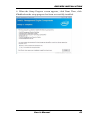
Intel
®
4th Generation Core / QM87 PCH
Mini ITX Motherboard
USER’S MANUAL
Version 1.0
Acknowledgments
AMI is a registered trademark of American Megatrends Inc.
PS/2 is a trademark of International Business Machines
Corporation.
th
Intel and Intel® 4 Generation Core DC/QC Processor are
registered trademarks of Intel Corporation.
Microsoft Windows is a registered trademark of Microsoft
Corporation.
Fintek is a registered trademark of Fintek Electronics Corporation.
All other product names or trademarks are properties of their
respective owners.
ii
User’s Manual
Table of Contents
Introduction . ...................................................... 1
Product Description............................................................. 1
Checklist .............................................................................. 1
96M5990o Specifications . .................................................. 2
Board Dimensions ............................................................... 4
Installations . ...................................................... 5
Installing the Memory ......................................................... 6
Setting the Jumpers ............................................................. 7
Connectors on 96M5990o . ................................................ 12
BIOS Setup . ...................................................... 25
Drivers Installation . ..................................... 51
Intel Chipset Software Installation Utility ........................ 52
VGA Drivers Installation .................................................. 54
Realtek HD Audio Driver Installation .............................. 56
LAN Drivers Installation................................................... 58
Intel® Management Engine Interface ............................... 61
Intel® USB 3.0 Drivers ..................................................... 64
Appendix. ........................................................... 67
A. I/O Port Address Map .................................................. 67
B. Interrupt Request Lines (IRQ) ...................................... 68
C. Watchdog Timer Configuration ................................... 69
User’s Manual
iii
This page is intentionally left blank.
iv
User’s Manual
INTRODUCTION
Introduction
Product Description
®
The 96M5990o Mini ITX motherboard is based on the latest Intel
®
QM87 chipset. The platform supports onboard 4th generation Intel
Core processor family features an integrated dual-channel DDR3
memory controller as well as a graphics core.
®
The latest Intel processors provide advanced performance in both
computing and graphics quality. This meets the requirement of customers
in the gaming, POS, digital signage and server market segment.
The QM87 platform is made with 22-nanometer technology that supports
Intel’s first processor architecture to unite the CPU and the graphics core
on the transistor level. The 96M5990o Mini ITX board utilizes the
dramatic increase in performance provided this Intel’s latest cuttingedge technology. Measuring 170mm x 170mm, the 96M5990o offers
fast 6Gbps SATA support, USB3.0 and interfaces for DVI-D, DVI-I,
LVDS and DP displays.
Checklist
Your 96M5990o package should include the items listed below.
The 96M5990o MINI ITX motherboard
This User’s Manual
1 CD containing chipset drivers and flash memory utility
Serial ATA cable
User’s Manual
1
INTRODUCTION
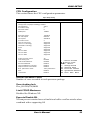
96M5990o Specifications
Product Name
Form Factor
CPU Type
Cache
Chipset
BIOS
Memory
VGA
LAN
USB
Serial ATA
Audio
LPC I/O
Digital IO
TPM 1.2
iAMT
Expansion Slots
2
96M5990o [Supports iAMT 9.0 & vPro]
Mini-ITX
® th
- Intel 4 Generation Core mobile processors (22nm monolithic)
- BGA1364 , Package= 37.5 mmx 32 mm [Performance Halo SKUs]
- TDP = 47W (QC) / 37W(DC)
Up to 8MB
Intel® QM87 PCH Mobile Platform Controller Hub Package
=23 mm x 22 mm, 0.65 mm ball pitch; TDP = 3W
AMI BIOS [16MB SPI ROM]
Intel® 4th Generation Core mobile processors integrated memory
controller
DDRIII 1600 MHz (supports dual channel DDR3/DDR3L)
- SO-DIMM [204-pin vertical type] x 2 (Non-ECC), Max. 16GB
®
Intel 4th Generation Core mobile processor integrated HD Gfx,
supports 3 independent displays, Direct X 11.1, OpenGL 3.2, Open CL
1.2
DVI-I X 1 (Thru port B, via VGA@ QM87 PCH+ Level shifter
ASM1442)
DVI-D x 1 (Thru port C, with level shifter ASM1442)
DisplayPort x 1 (Thru port D)
LVDS (Thru eDP, via NXP PTN3460)
1. Intel® Clarkville I217LM GbE PHY
** Package = 6mm x 6mm, QFN48**
2. Intel® Pearsonville I211AT as 2nd GbE
USB 2.0 host controller [QM87 PCH integrated], supports 8 ports
- 2 ports in the rear panel
- 4 ports via onboard pin header (2.0mm pitch)
- 2 ports via MiniPCIe sockets
USB 3.0 host controller [QM87 PCH integrated] supports 4 ports
- 4 ports in the rear panel
Intel® QM87 PCH built-in SATA controller, supports 6 ports
4 x SATA (3.0) 6Gbps & shared mSATA for 1 port (SATA port #5)
2 x SATA (2.0) 3Gbps
Intel® Mobile QM87 PCH built-in High Definition Audio controller +
Realtek ALC892 w/ 7.1 channels
Fintek F81866AD-I (128-pin LQFP [14mm x 14 mm])
- COM #1 (RS232/422/485) supports ring-in with power @500mA
(selectable for 5V or 12V) [EXAR SP339EER1 232/422/485
transceiver x 1 for jumper-less]
- COM #2 (RS232 only), supports ring-in with power @500mA
(selectable for 5V or 12V)
- COM #3~COM #6 (RS232 only)
Hardware Monitor (2 thermal, 4 voltage monitor inputs & 2 fan headers)
- CPU fan x 1(PWM fan type, 4-pin connector)
- SYS fan x 1 (DC/PWM Auto-Detect fan type, 4-pin connector)]
4 in & 4 out
Nuvoton WPCT210AA0WX
**Operation temperature for 0 ~ +60 degree C only**
Intel® Mobile QM87 PCH built-in
- Intel® Active Management Technology, version 9.0
- PCI-Express (16x) x1 [Gen 3.0 PEG]
- Mini PCI-Express x 2 port [Full-sized], both support USB 2.0
- One slot supports mSATA (6Gbps)
User’s Manual
INTRODUCTION
Edge Connectors
Onboard
Header/Connector
Watchdog Timer
System Voltage
Others
Board Size
Dual DB9 stack connector for COM #1 / #2
DVI-D + DVI-I stack connector x 1
DisplayPort + dual USB (2.0) stack connector x 1
RJ-45 + dual USB (3.0) stack connector x 2
Triplet type Jack 3 x 1 for HD Audio
4 ports x SATA III [Blue color]
2 ports x SATA II
DF-11 8-pin connector x 2 for 4 ports USB 2.0
DF-20 20-pin connector x 2 for dual –channel LVDS
eDP LVDS panel connector x 1
2x5 pin-header x 1 for front panel audio [supports 7.1 Channel]
DF-11 10-pin header x 4 for COM3 ~ COM6
2x5 pin-header x 1 for Digital IO
4-pin box header x 1 for LCD backlight control
Yes (256 segments, 0, 1, 2…255 sec/min)
ATX standard 20-pin type
4 pin type (+12V only)[For full system loading usage]
- vPro
nd
- ErP feature (F81866AD-I integrated, WOL from 2 GbE)
- iSMART ( via TI MSP430G2433 MCU)
- AT24C02C EEPROM [SO8 type] via SMbus (Reserved)
170mm x 170mm
User’s Manual
3
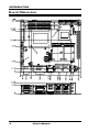
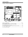
INTRODUCTION
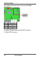
[
Board Dimensions
4
User’s Manual
INSTALLATIONS
Installations
This section provides information on how to use the jumpers and
connectors on the 96M5990o in order to set up a workable system. The
topics covered are:
Installing the Memory ............................................................................. 6
Setting the Jumpers ................................................................................. 7
Connectors on 96M5990o . ................................................................... 12
User’s Manual
5
INSTALLATIONS
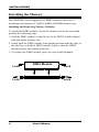
Installing the Memory
The 96M5990o board supports two DDR3 memory socket for a
maximum total memory of 16GB in DDR3 SODIMM memory type.
Installing and Removing Memory Modules
To install the DDR3 modules, locate the memory slot on the board and
perform the following steps:
1. Hold the DDR3 module so that the key of the DDR3 module aligned
with that on the memory slot.
2. Gently push the DDR3 module in an upright position until the clips of
the slot close to hold the DDR3 module in place when the DDR3
module touches the bottom of the slot.
3. To remove the DDR3 module, press the clips with both hands.
Lock
DDR3 Module
Lock
6
Lock
Lock
User’s Manual
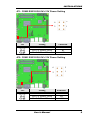
INSTALLATIONS
Setting the Jumpers
Jumpers are used on 96M5990o to select various settings and features
according to your needs and applications. Contact your supplier if you
have doubts about the best configuration for your needs. The following
lists the connectors on 96M5990o and their respective functions.
Jumper Locations on 96M5990o ............................................................ 8
JP1: COM2 RS232 RI/+5V/+12V Power Setting . ................................. 9
JP2: COM1 RS232 RI/+5V/+12V Power Setting . ................................. 9
J13: LCD Panel Power Selection . ........................................................ 10
J16: Flash Descriptor Security Override (Factory use only) ................ 10
J17: Clear CMOS Contents................................................................... 11
J18: Clear ME Contents ........................................................................ 11
User’s Manual
7
INSTALLATIONS
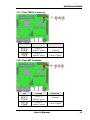
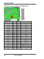
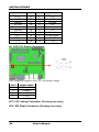
Jumper Locations on 96M5990o
Jumpers on 96M5990o . .................................................................... Page
JP1: COM2 RS232 RI/+5V/+12V Power Setting . ................................. 9
JP2: COM1 RS232 RI/+5V/+12V Power Setting . ................................. 9
J13: LCD Panel Power Selection . ........................................................ 10
J16: Flash Descriptor Security Override (Factory use only) ................ 10
J17: Clear CMOS Contents ................................................................... 11
J18: Clear ME Contents ........................................................................ 11
8
User’s Manual
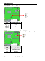
INSTALLATIONS
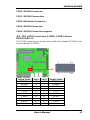
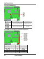
JP1: COM2 RS232 RI/+5V/+12V Power Setting
JP1
6
5
2
1
Setting
Function
Pin 1-3, Short/Closed
Pin 3-4, Short/Closed
Pin 3-5, Short/Closed
+12V
RI
+5V
JP2: COM1 RS232 RI/+5V/+12V Power Setting
JP2
6
5
2
1
Setting
Function
Pin 1-3, Short/Closed
Pin 3-4, Short/Closed
Pin 3-5, Short/Closed
+12V
RI
+5V
User’s Manual
9
INSTALLATIONS
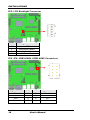
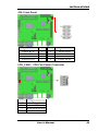
J13: LCD Panel Power Selection
1
3
J13
LCD Panel Power
3.3V
5V
J16: Flash Descriptor Security Override (Factory use only)
2
1
J16
10
Flash Descriptor
Security Override
Open
Disabled (Default)
Close
Enabled
User’s Manual
INSTALLATIONS
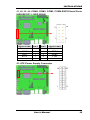
J17: Clear CMOS Contents
3
J17
Setting
Pin 1-2
Short/Closed
Pin 2-3
Short/Closed
1
Function
Normal
Clear CMOS
J18: Clear ME Contents
3
J18
Setting
Function
Pin 1-2
Short/Closed
Normal
Pin 2-3
Short/Closed
Clear CMOS
User’s Manual
1
11
INSTALLATIONS
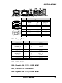
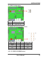
Connectors on 96M5990o
Connector Locations on 96M5990o ..................................................... 13
CN2: DVI-I and DVI-D Connector . ..................................................... 14
CN1: COM1 and COM2 Serial Ports. .................................................. 15
CN4: Display Port ................................................................................. 15
CN5: USB2 #6/#7 ................................................................................. 15
CN6: Gigabit LAN (I217) + USB3 #0/#1 . ........................................... 15
CN7, CN8: SATA3 Connectors . .......................................................... 15
CN9: Gigabit LAN (I211) + USB3 #2/#3 . ........................................... 15
CN3: eDP Connector (JAE_FI-TD44SB-E-R750) . ............................. 16
CN10: SATA2 Connector . ................................................................... 17
CN11: SATA2 Connectors ................................................................... 17
CN12: HD Audio Connector ................................................................. 17
CN13: SATA3 Connector . ................................................................... 17
CN14: SATA3 Connector ..................................................................... 17
JP3, JP4: LVDS Connectors (LVDS2, LVDS1) . ................................. 17
JP5: LCD Backlight Connector . ........................................................... 18
JP6, JP8: USB2 #8/#9, USB2 #4/#5 Connectors . ................................ 18
J1, J2, J3, J4: COM6, COM5, COM3, COM4 RS232 Serial Ports ...... 19
J5: ATX Power Supply Connector . ...................................................... 19
J6: ATX 12V Power Connector . .......................................................... 20
JP7: LPC debug Connector (Factory use only) . ................................... 20
JP9: SPI Flash Connector (Factory use only) . ...................................... 20
J7: PCIE1 Configuration ....................................................................... 21
J8: Digital I/O Connector (4 in, 4 out) . ................................................ 21
J10, J11: DDR3 SO-DIMM Socket . .................................................... 21
J12: LVDS/eDP Select .......................................................................... 22
J21: Audio Pin Header for Chassis Front Panel . .................................. 22
J22: Front Panel .................................................................................... 23
CPU_FAN1: CPU Fan Power Connector . .......................................... 23
SYS_FAN2: System Fan Power Connector (DC/PWM Auto-Detect) .24
J14: Mini PCIE/mSATA (share with CN7) Connector ........................ 24
J15: Mini PCIE Connector .................................................................... 24
12
User’s Manual
INSTALLATIONS
Connector Locations on 96M5990o
User’s Manual
13
INSTALLATIONS
CN2: DVI-I and DVI-D Connector
Signal Name
Pin #
Pin #
Signal Name
DATA 2DATA 2+
Shield 2/4
DATA 4DATA 4+
DDC CLOCK
DDC DATA
Analog VSYNC
DATA 1DATA 1+
SHIELD 1/3
DATA 3DATA 3+
DDC POWER
A GROUND 1
1
2
3
4
5
6
7
8
9
10
11
12
13
14
15
16
17
18
19
20
21
22
23
24
C1
C2
C3
C4
C5
C6
HOT POWER
DATA 0DATA 0+
SHIELD 0/5
DATA 5DATA 5+
SHIELD CLK
CLOCK CLOCK +
Analog Red
Analog Green
Analog Blue
Analog HSYNC
A GROUND2
A GROUND3
Signal Name
Pin #
Pin #
Signal Name
DATA 2DATA 2+
Shield 2/4
DATA 4DATA 4+
DDC CLOCK
DDC DATA
N.C
DATA 1DATA 1+
SHIELD 1/3
DATA 3DATA 3+
DDC POWER
A GROUND 1
1
2
3
4
5
6
7
8
9
10
11
12
13
14
15
16
17
18
19
20
21
22
23
24
C1
C2
C3
C4
C5
C6
HOT POWER
DATA 0DATA 0+
SHIELD 0/5
DATA 5DATA 5+
SHIELD CLK
CLOCK CLOCK +
N.C.
N.C.
N.C.
N.C.
N.C.
N.C.
[
14
User’s Manual
INSTALLATIONS
CN1: COM1 and COM2 Serial Ports
[
Pin #
RS-232
1
2
3
4
5
6
7
8
9
10
Signal Name
R2-422
RS-485
DCD
RX
TX
DTR
Ground
DSR
RTS
CTS
RI
NC
TXTX+
RX+
RXGround
NC
NC
NC
NC
NC
DATADATA+
NC
NC
Ground
NC
NC
NC
NC
NC
CN4: Display Port
Signal Name
LANE0_P
GND
LANE0_N
LANE1_P
GND
LANE1_N
LANE2_P
GND
LANE2_N
LANE3_P
Pin #
1
2
3
4
5
6
7
8
9
10
Pin #
11
12
13
14
15
16
17
18
19
20
Signal Name
GND
LANE3_N
GND
GND
AUX_P
GND
AUX_N
HPD
GND
VCC3.
CN5: USB2 #6/#7
CN6: Gigabit LAN (I217) + USB3 #0/#1
CN7, CN8: SATA3 Connectors
CN9: Gigabit LAN (I211) + USB3 #2/#3
User’s Manual
15
INSTALLATIONS
CN3: eDP Connector (JAE_FI-TD44SB-E-R750)
1
44
Signal Name
3.3V
3.3V
3.3V
3.3V
3.3V
GND
GND
GND
GND
HPD
NC
NC
GND
NC
NC
GND
NC
NC
GND
TXN1
TXP1
GND
16
Pin #
1
2
3
4
5
6
7
8
9
10
11
12
13
14
15
16
17
18
19
20
21
22
Pin #
23
24
25
26
27
28
29
30
31
32
33
34
35
36
37
38
39
40
41
42
43
44
Signal Name
TXN0
TXP0
GND
AUXP
AUXN
NC
VCC3
NC
VCC12
NC
GND
VCC5
NC
Brightness
BKLT_EN
VCC12
VCC3
GND
SMB_THRM_CLK
SMB_THRM_DATA
NC
NC
User’s Manual
INSTALLATIONS
CN10: SATA2 Connector
CN11: SATA2 Connectors
CN12: HD Audio Connector
CN13: SATA3 Connector
CN14: SATA3 Connector support
JP3, JP4: LVDS Connectors (LVDS2, LVDS1) Hirose
DF20G-20DP-1V
The LVDS connectors on board consist of the first channel (LVDS1) and
second channel (LVDS2).
Signal Name
TX0N
Ground
TX1N
Ground
TX2N
Ground
CLKN
Ground
TX3N
Power
Pin #
2
4
6
8
10
12
14
16
18
20
Pin #
1
3
5
7
9
11
13
15
17
19
1
19
2
20
Signal Name
TX0P
Ground
TX1P
Ground
TX2P
Ground
CLKP
Ground
TX3P
Power
User’s Manual
17
INSTALLATIONS
JP5: LCD Backlight Connector
1
4
Pin #
1
2
3
4
Signal Name
+12V
Backlight Enable
Brightness Control
Ground
JP6, JP8: USB2 #8/#9, USB2 #4/#5 Connectors
Signal Name
Vcc
D0D0+
Ground
18
Pin #
1
3
5
7
Pin #
2
4
6
8
2
1
8
7
Signal Name
Ground
D1+
D1Vcc
User’s Manual
INSTALLATIONS
J1, J2, J3, J4: COM6, COM5, COM3, COM4 RS232 Serial Ports
(HIROSE DF11-10DP-2DSA)
Signal Name
DCD#
SOUT
GND
RTS#
RI#
Pin #
1
3
5
7
9
Pin #
2
4
6
8
X
9
10
1
2
Signal Name
SIN#
DTR#
DSR#
CTS#
KEY
J5: ATX Power Supply Connector
User’s Manual
10
20
1
11
19
INSTALLATIONS
Signal Name
3.3V
-12V
Ground
PS-ON
Ground
Ground
Ground
-5V
+5V
+5V
Pin #
11
12
13
14
15
16
17
18
19
20
Pin #
1
2
3
4
5
6
7
8
9
10
Signal Name
3.3V
3.3V
Ground
+5V
Ground
+5V
Ground
Power good
5VSB
+12V
J6: ATX 12V Power Connector
3
4
1
2
This connector supplies the CPU operating voltage.
Pin #
1
2
3
4
Signal Name
Ground
Ground
+12V
+12V
JP7: LPC debug Connector (Factory use only)
JP9: SPI Flash Connector (Factory use only)
20
User’s Manual
INSTALLATIONS
J7: PCIE1 Configuration
J7
Open
Short
PCIE1 Configuration
PCIE X16 (Default)
PCIE X8, X8
J8: Digital I/O Connector (4 in, 4 out)
Signal Name
Ground
Out3
Out2
IN3
IN2
Pin #
1
3
5
7
9
Pin #
2
4
6
8
10
9
10
1
2
Signal Name
+5V
Out1
Out0
IN1
IN0
J10, J11: DDR3 SO-DIMM Socket
User’s Manual
21
INSTALLATIONS
J12: LVDS/eDP Select
1
3
J12
Setting
Function
Pin 1-2, Short/Closed
eDP Connector
Pin 2-3, Short/Closed
LVDS
J21: Audio Pin Header for Chassis Front Panel
Signal Name
MIC IN_L
MIC IN_R
LINE_R
Sense
LINE_L
22
Pin #
1
3
5
7
9
Pin #
2
4
6
8
10
10
9
2
1
Signal Name
Ground
DET
Ground
KEY
Ground
User’s Manual
INSTALLATIONS
J22: Front Panel
Signal Name
Power BTN
HDD LED+
Reset BTN
Power LED+
Pin #
1
3
5
7
Pin #
2
4
6
8
8
7
2
1
Signal Name
Power BTN
HDD LEDReset BTN
Power LED-
CPU_FAN1: CPU Fan Power Connector
4
1
Pin #
Signal Name
1
Ground
2
+12V
3
Rotation detection
4
Control
User’s Manual
23
INSTALLATIONS
SYS_FAN2: System Fan Power Connector (DC/PWM
Auto-Detect)
1
4
Pin #
Signal Name
1
Ground
2
+12V
3
Rotation detection
4
Control
J14: Mini PCIE/mSATA (share with CN7) Connector
J15: Mini PCIE Connector
24
User’s Manual
BIOS SETUP
BIOS Setup
This chapter describes the different settings available in the AMI BIOS
that comes with the board. The topics covered in this chapter are as
follows:
BIOS Introduction ................................................................................ 26
BIOS Setup . .......................................................................................... 26
Advanced Settings ................................................................................ 28
Chipset Settings .................................................................................... 40
Boot Settings. ........................................................................................ 47
CSM parameters ................................................................................... 48
Security Settings ................................................................................... 49
Save & Exit Settings ............................................................................. 50
User’s Manual
25
BIOS SETUP
BIOS Introduction
The BIOS (Basic Input/Output System) installed in your computer
system’s ROM supports Intel processors. The BIOS provides critical
low-level support for a standard device such as disk drives, serial ports
and parallel ports. It also password protection as well as special support
for detailed fine-tuning of the chipset controlling the entire system.
BIOS Setup
The BIOS provides a Setup utility program for specifying the system
configurations and settings. The BIOS ROM of the system stores the
Setup utility. When you turn on the computer, the BIOS is immediately
activated. Pressing the <Del> key immediately allows you to enter the
Setup utility. If you are a little bit late pressing the <Del> key, POST
(Power On Self Test) will continue with its test routines, thus preventing
you from invoking the Setup. If you still wish to enter Setup, restart the
system by pressing the ”Reset” button or simultaneously pressing the
<Ctrl>, <Alt> and <Delete> keys. You can also restart by turning the
system Off and back On again. The following message will appear on the
screen:
Press
<DEL>
to
Enter
Setup
In general, you press the arrow keys to highlight items, <Enter> to select,
the <PgUp> and <PgDn> keys to change entries, <F1> for help and
<Esc> to quit.
When you enter the Setup utility, the Main Menu screen will appear on
the screen. The Main Menu allows you to select from various setup
functions and exit choices.
Warning: It is strongly recommended that you avoid making any
changes to the chipset defaults. These defaults have been
carefully chosen by both AMI and your system manufacturer
to provide the absolute maximum performance and
reliability. Changing the defaults could cause the system to
become unstable and crash in some cases.
26
User’s Manual
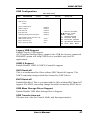
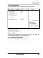
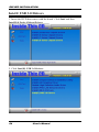
BIOS SETUP
Main Settings
Aptio Setup Utility – Copyright © 2013 American Megatrends, Inc.
Main
Advanced
Chipset
Boot
BIOS Information
Security
Save & Exit
Choose the system default
language
Total Memory
Momory Frequency
4096 MB (DDR3)
1333 Mhz
System Date
System Time
[Tue 01/20/2009]
[21:52:06]
Access Level
Administrator
→ ← Select
Screen
↑↓ Select Item
Enter: Select
+- Change Field
F1: General Help
F2: Previous Values
F3: Optimized Default
F4: Save ESC: Exit
System Date
Set the Date. Use Tab to switch between Data elements.
System Time
Set the Time. Use Tab to switch between Data elements.
User’s Manual
27
BIOS SETUP
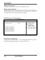
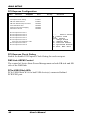
Advanced Settings
This section allows you to configure and improve your system and allows
you to set up some system features according to your preference.
Aptio Setup Utility
Main
Advanced
Chipset
Boot
Security
Save & Exit
► PCI Subsystem Settings
► ACPI Settings
► Wake up event setting
► Trusted Computing
► CPU Configuration
► SATA Configuration
► Shutdown Temperature Configuration
► iSmart Controller
► AMT Configuration
► USB Configuration
► F81866 Super IO Configuration
► F81866 H/W Monitor
→ ← Select
Screen
↑↓ Select Item
Enter: Select
+- Change Field
F1: General Help
F2: Previous Values
F3: Optimized Default
F4: Save ESC: Exit
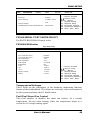
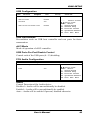
PCI Subsystem Settings
Aptio Setup Utility
Main
Advanced
PCI Bus Driver Version
Chipset
Boot
Security
Save & Exit
V 2.0502
→ ← Select
PCI Common Settings
PCI Latency Timer
VGA Palette Snoop
PERR# Generation
SERR# Generation
32 PCI Bus Clocks
Disabled
Disabled
Disabled
► PCI Express Settings
28
User’s Manual
Screen
↑↓ Select Item
Enter: Select
+- Change Field
F1: General Help
F2: Previous Values
F3: Optimized Default
F4: Save ESC: Exit
BIOS SETUP
PCI Latency Timer
Value to be programmed into PCI Latency Timer Register.
VGA Palette Snoop
Enables or disables VGA Palette Registers Snooping.
PERR# Generation
Enables or disables PCI device to generate PERR#.
SERR# Generation
Enables or disables PCI device to generate SERR#.
PCI Express Settings
Change PCI Express devices settings.
PCI Express Settings
Aptio Setup Utility
Main
Advanced
Chipset
PCI Express Device Register Settings
Relaxed Ordering
Extended Tag
No Snoop
Maximum Payload
Maximum Read Request
Boot
Disabled
Disabled
Enabled
Auto
Auto
PCI Express Link Register Settings
ASPM Support
Disabled
WARNING: Enabling ASPM may cause
Disabled
some PCI-E devices to fail
Extended Synch
Disabled
Link Training Retry
Link Training Timeout (uS)
Unpopulated Links
5
100
Keep Link ON
Restore PCIE Registers
Disabled
Security
Save & Exit
→ ← Select
Screen
↑↓ Select Item
Enter: Select +Change Field F1:
General Help
F2: Previous Values
F3: Optimized Default
F4: Save ESC: Exit
Relaxed Ordering
Enables or disables PCI Express Device Relaxed Ordering.
Extended Tag
If ENABLED allows device to use 8-bit Tag field as a requester.
No Snoop
Enables or disables PCI Express Device No Snoop option.
User’s Manual
29
BIOS SETUP
Maximum Payload
Set Maximum Payload of PCI Express Device or allow System BIOS to
select the value.
Maximum Read Request
Set Maximum Read Request Size of PCI Express Device or allow System
BIOS to select the value.
ASPM Support
Set the ASPM Level: Force L0s – Force all links to L0s State:
AUTO – BIOS auto configure: DISABLE – Disables ASPM.
Extended Synch
If ENABLED allows generation of Extended Synchronization patterns.
Link Training Retry
Defines number of Retry Attempts software will take to retrain the link if
previous training attempt was unsuccessful.
Link Training Timeout (uS)
Defines number of Microseconds software will wait before polling ‘Link
Training’ bit in Link Status register. Value range from 10 to 1000 uS.
Unpopulated Links
In order to save power, software will disable unpopulated PCI Express
links, if this option set to ‘Disable Link’.
Restore PCIE Registers
On non-PCI Express aware OS’s (Pre Windows Vista) some devices may
not be correctly reinitialized after S3.Enabling this restore PCI Express
device configuration on S3 resume
Warning: Enabling this may cause issues with other hardware after S3
resume.
30
User’s Manual
BIOS SETUP
ACPI Settings
Aptio Setup Utility
Main
Advanced
Chipset
Boot
Security
Save & Exit
ACPI Settings
→ ← Select
Enable Hibernation
ACPI Sleep State
Lock Legacy Resources
S3 Video Repost
Enabled
S3 (Suspend to R…)
Disabled
Disabled
Screen
↑↓ Select Item
Enter: Select
+- Change Field
F1: General Help
F2: Previous Values
F3: Optimized Default
F4: Save ESC: Exit
Enable Hibernation
Enables or Disables System ability to Hibernate (OS/S4 Sleep State).
This option may be not effective with some OS.
ACPI Sleep State
Select ACPI sleep state the system will enter, when the SUSPEND button
is pressed.
Lock Legacy Resources
Enabled or Disabled Lock of Legacy Resources.
S3 Video Repost
Enable or disable S3 Video Repost.
User’s Manual
31
BIOS SETUP
Wake up event settings
Aptio Setup Utility
Main
Advanced
Chipset
Wake on PCIE Wake Event
Boot
Security
Save & Exit
Disabled
→ ← Select
Screen
↑↓ Select Item
Enter: Select
+- Change Field
F1: General Help
F2: Previous Values
F3: Optimized Default
F4: Save ESC: Exit
Wake on PCIE PME Wake Event
The options are Disabled and Enabled.
Trusted Computing
Aptio Setup Utility
Main
Advanced
Chipset
TPM Configuration
TPM SUPPORT
Boot
Disabled
Security
Save & Exit
→ ← Select
Screen
↑↓ Select Item
Enter: Select
+- Change Field
F1: General Help
F2: Previous Values
F3: Optimized Default
F4: Save ESC: Exit
Current TPM Status Information
TPM SUPPORT OFF
TPM Support
Enables or Disables TPM support. O.S. will not show TPM. Reset of
platform is required.
Security Device Support
Enables or disables BIOS support for security device. O.S. will not show
Security Device. TCG EFI protocol and INT1A interface will not be
available.
32
User’s Manual
BIOS SETUP
CPU Configuration
This section shows the CPU configuration parameters.
Aptio Setup Utility
Main
Advanced
Chipset
Boot
Security
Save & Exit
CPU Configuration
Intel(R) CPU Core(TM)i5-4402E @ 1.60GHz
CPU Signature
306c3
Processor Family
6
Microcode Patch
8
FSB Speed
100MHz
Max CPU Speed
Min CPU Speed
CPU Speed
1600 MHz
800 MHz
2600 MHz
Processor Cores
Intel HT Technology
Intel VT-x Technology
Intel SMX Technology
64-bit
EIST
CPU C3 State
CPU C6 State
CPU C7 State
2
Supported
Supported
Supported
Supported
Supported
Supported
Supported
Supported
Active Processor Cores
Overclocking lock
Limit CPUID Maximum
Execute Disable Bit
Intel Virtualization Technology
All
Disabled
Disabled
Enabled
Enabled
Adjacent Cache Line Prefetch
Boot performance mode
EIST
Enabled
Turbo performance
Enabled
Turbo Mode
Enabled
→ ← Select
Screen
↑↓ Select Item
Enter: Select
+- Change Field
F1: General Help
F2: Previous Values
F3: Optimized Default
F4: Save ESC: Exit
Active Processor Cores
Number of cores to enable in each processor package.
Overclocking lock
Flex_RATIO(194)MSR
Limit CPUID Maximum
Disabled for Windows XP.
Execute Disable Bit
XD can prevent certain classes of malicious buffer overflow attacks when
combined with a supporting OS
User’s Manual
33
BIOS SETUP
Intel Virtualization Technology
When enabled, a VMM can utilize the additional hardware capabilities
provided by Vanderpool Technology.
Adjacent Cache Line Prefetch
To turn on/off prefetching of adjacent cache lines.
Boot Performance Mode
Select the performance state that the BIOS will set before OS handoff.
EIST
Enabled/Disabled Intel Speedstep.
SATA Configuration
SATA Devices Configuration.
Aptio Setup Utility
Main
Advanced
Chipset
Boot
SATA Controller(s)
SATA Mode Selection
Enabled
IDE
SATA Port0
Software Preserve
SATA Port1
Software Preserve
SATA Port2
Software Preserve
SATA Port3
Software Preserve
SATA Port4
Software Preserve
SATA Port5
Software Preserve
Empty
Unknown
Empty
Unknown
Empty
Unknown
Empty
Unknown
Empty
Unknown
Empty
Unknown
SATA Controller(s)
Enable / Disable Serial ATA Controller.
SATA Mode Selection
(1) IDE Mode.
(2) AHCI Mode.
(3) RAID Mode.
34
User’s Manual
Security
Save & Exit
→ ← Select
Screen
↑↓ Select Item
Enter: Select
+- Change Field
F1: General Help
F2: Previous Values
F3: Optimized Default
F4: Save ESC: Exit
BIOS SETUP
Shutdown Temperature Configuration
Aptio Setup Utility
Main
Advanced
Chipset
APCI Shutdown Temperature
Boot
Security
Save & Exit
→ ← Select
Disabled
Screen
↑↓ Select Item
Enter: Select
+- Change Field
F1: General Help
F2: Previous Values
F3: Optimized Default
F4: Save ESC: Exit
ACPI Shutdown Temperature
The default setting is Disabled.
iSmart Controller
Aptio Setup Utility
Main
Advanced
Chipset
Boot
Security
Save & Exit
iSmart Controller
→ ← Select
Power-On after Power failure
Disable
Schedule Slot 1
Schedule Slot 2
None
None
Screen
↑↓ Select Item
Enter: Select
+- Change Field
F1: General Help
F2: Previous Values
F3: Optimized Default
F4: Save ESC: Exit
iSmart Controller
Setup the power on time for the system.
Schedule Slot 1 / 2
Setup the hour/minute for system power on.
User’s Manual
35
BIOS SETUP
AMT Configuration
Aptio Setup Utility
Main
Advanced
Chipset
Intel AMT
BIOS Hotkey Pressed
MEBx Selection Screen
Hide Un-Configure ME Confirmation
Un-Configure ME
Amt Wait Timer
Activate Remote Assistance Process
USB Configure
PET Progress
AMT CIRA Timeout
Watchdog
OS Timer
BIOS Timer
Boot
Security
Enabled
Disabled
Disabled
Disabled
Disabled
0
Disabled
Enabled
Enabled
0
Disabled
0
0
Save & Exit
→ ← Select
Screen
↑↓ Select Item
Enter: Select
+- Change Field
F1: General Help
F2: Previous Values
F3: Optimized Default
F4: Save ESC: Exit
AMT Configuration
Options are Enabled and Disabled.
Note: iAMT H/W is always enabled. This option just controls the BIOS
extension execution. If enabled, this requires additional firmware in the
SPI device.
Unconfigure ME
Perform AMT/ME unconfigure without password operation.
Amt Wait Timer
Set timer to wait before sending ASF_GET_BOOT_OPTIONS.
Activate Remote Assistance Process
Trigger CIRA boot.
PET Progress
User can Enable/Disable PET Events progress to receive PET events or
not.
Watchdog Timer
Enable/Disable Watchdog Timer.
36
User’s Manual
BIOS SETUP
USB Configuration
Aptio Setup Utility
Main
Advanced
Chipset
Boot
Security
Save & Exit
USB Configuration
USB Devices:
2 Hubs
Legacy USB Support
USB3.0 Support
XHCI Hand-off
EHCI Hand-off
USB Mass Storage Driver Support
Enabled
Enabled
Enabled
Enabled
Enabled
USB hardware delays and time-outs:
USB Transfer time-out
Device reset tine-out
Device power-up delay
20 sec
20 sec
Auto
→ ← Select
Screen
↑↓ Select Item
Enter: Select
+- Change Field
F1: General Help
F2: Previous Values
F3: Optimized Default
F4: Save ESC: Exit
Legacy USB Support
Enables Legacy USB support.
AUTO option disables legacy support if no USB devices are connected.
DISABLE option will keep USB devices available only for EFI
applications.
USB3.0 Support
Enable/Disable USB3.0 (XHCI) Controller support.
XHCI Hand-off
This is a workaround for OSes without XHCI hand-off support. The
XHCI ownership change should be claimed by XHCI driver.
EHCI Hand-off
Enabled/Disabled. This is a workaround for OSes without EHCI hand-off
support. The EHCI ownership change should be claimed by EHCI driver.
USB Mass Storage Driver Support
Enable/Disable USB Mass Storage Driver Support.
USB Transfer time-out
The time-out value for Control, Bulk, and Interrupt transfers.
User’s Manual
37
BIOS SETUP
Device reset tine-out
USB mass Storage device start Unit command time-out.
Device power-up delay
Maximum time the device will take before it properly reports itself to the
Host Controller. ‘Auto’ uses default value: for a Root port it is 100ms, for
a Hub port the delay is taken from Hub descriptor.
F81866 Super IO Configuration
Aptio Setup Utility
Main
Advanced
Chipset
Boot
Security
Save & Exit
Super IO Configuration
→ ← Select
F81866 Super IO Chip
F81866
► Serial Port 1 Configuration
► Serial Port 2 Configuration
► Serial Port 3 Configuration
► Serial Port 4 Configuration
► Serial Port 5 Configuration
► Serial Port 6 Configuration
Screen
↑↓ Select Item
Enter: Select
+- Change Field
F1: General Help
F2: Previous Values
F3: Optimized Default
F4: Save ESC: Exit
Serial Port Configuration
Set Parameters of Serial Ports. User can Enable/Disable the serial port
and Select an optimal settings for the Super IO Device.
38
User’s Manual
BIOS SETUP
Main
Advanced
Chipset
Boot
Security
Save & Exit
Serial port 0 Configuration
→ ← Select
Serial port
Enabled
Device Settings
IO=3F8h ; IRQ=4
Change Settings
Auto
F81866 SERIAL PORT1 MODE SELECT
RS232 Mode
Screen
↑↓ Select Item
Enter: Select
+- Change Field
F1: General Help
F2: Previous Values
F3: Optimized Default
F4: Save ESC: Exit
F81866 SERIAL PORT1 MODE SELECT
For RS232/RS422/RS485 mode select
F81866 H/W Monitor
Aptio Setup Utility
Main
Advanced
Chipset
Boot
Security
Save & Exit
PC Health Status
Fan 1 smart fan control
Fan 2 smart fan control
CPU temperature
SYS temperature
FAN1 Speed
FAN2 Speed
Vcore
Disabled
Disabled
+33 C
+34 C
2170 RPM
N/A
+1.800 V
+5V
+12V
Memory Voltage
VSB5V
+5.087 V
+12.408 V
+1.392 V
+5.016 V
→ ← Select
Screen
↑↓ Select Item
Enter: Select
+- Change Field
F1: General Help
F2: Previous Values
F3: Optimized Default
F4: Save ESC: Exit
Temperatures/Voltages
These fields are the parameters of the hardware monitoring function
feature of the motherboard. The values are read-only values as monitored
by the system and show the PC health status.
Fan1/Fan2 Smart Fan Control
This field enables or disables the smart fan feature. At a certain
temperature, the fan starts turning. Once the temperature drops to a
certain level, it stops turning again.
User’s Manual
39
BIOS SETUP
Chipset Settings
This section allows you to configure and improve your system and allows
you to set up some system features according to your preference.
Aptio Setup Utility
Main
Advanced
Chipset
Boot
Security
Save & Exit
► PCH-IO Configuration
► System Agent (SA) Configuration
→ ← Select
Screen
↑↓ Select Item
Enter: Select +Change Field F1:
General Help
F2: Previous Values
F3: Optimized Default
F4: Save ESC: Exit
40
User’s Manual
BIOS SETUP
PCH-IO Configuration
This section allows you to configure the North Bridge Chipset.
Aptio Setup Utility
Main
Advanced
Chipset
Intel PCH RC Version
Intel PCH SKU Name
Intel PCH Rev ID
Boot
Security
Save & Exit
1.5.0.0
QM87
04/C1
► PCI Express Configuration
► USB Configuration
► PCH Azalia Configuration
PCH LAN Controller
Wake on LAN
Enabled
Disabled
SLP_LAN# Low on DC Power
Enabled
→ ←
Select Screen
↑↓ Select Item
Enter: Select
+- Change Field
F1: General Help
F2: Previous Values
F3: Optimized Default
F4: Save ESC: Exit
PCH LAN Controller
Enable or disable onboard NIC.
Wake on LAN
Enable or disable integrated LAN to wake the system. (The Wake On
LAN cannot be disabled if ME is on at Sx state.)
SLP_LAN# Low on DC Power
Enable or Disable SLP_LAN# Low on DC Power
User’s Manual
41
BIOS SETUP
PCI Express Configuration
Main
Advanced
Chipset
Boot
Security
Save & Exit
PCI Express Configuration
PCI Express Clock Gating
DMI Link ASPM Control
DMI Link Extended Synch Control
PCIe-USB Glitch W/A
PCIE Root Function Swapping
Subtractive Decode
Enabled
Enabled
Disabled
Disabled
Disabled
Disabled
► PCI Express Root Port 1
► PCI Express Root Port 2
► PCI Express Root Port 3
► PCI Express Root Port 4
► PCI Express Root Port 5
→ ←
PCI-E Port 6 is assigned to LAN
► PCI Express Root Port 7
► PCI Express Root Port 8
Select Screen
↑↓ Select Item
Enter: Select
+- Change Field
F1: General Help
F2: Previous Values
F3: Optimized Default
F4: Save ESC: Exit
PCI Express Clock Gating
Enable or disable PCI Express Clock Gating for each root port.
DMI Link ASPM Control
The control of Active State Power Management on both NB side and SB
side of the DMI link.
PCIe-USB Glitch W/A
PCIe-USB Glitch W/A for bad USB device(s) connected behind
PCIE/PEG port.
42
User’s Manual
BIOS SETUP
USB Configuration
Main
Advanced
Chipset
Boot
Security
Save & Exit
USB Configuration
USB Precondition
xHCI Mode
Disabled
Auto
USB Ports Per-Port Disable Control
Disabled
→ ←
Select Screen
↑↓ Select Item
Enter: Select
+- Change Field
F1: General Help
F2: Previous Values
F3: Optimized Default
F4: Save ESC: Exit
USB Precondition
Precondition work on USB host controller and root ports for faster
enumeration.
xHCI Mode
Mode of operation of xHCI controller.
USB Ports Per-Port Disable Control
Control each of the USB ports (0~13) disabling.
PCH Azalia Configuration
Main
Advanced
Chipset
Boot
Azalia
Security
Save & Exit
→ ←
PCH Azalia Configuration
Auto
Select Screen
↑↓ Select Item
Enter: Select
+- Change Field
F1: General Help
F2: Previous Values
F3: Optimized Default
F4: Save ESC: Exit
Azalia
Control Detection of the Azalia device.
Disabled = Azalia will be unconditionally be disabled.
Enabled = Azalia will be unconditionally be enabled.
Auto = Azalia will be enabled if present, disabled otherwise.
User’s Manual
43
BIOS SETUP
System Agent (SA) Configuration
Aptio Setup Utility
Main
Advanced
Chipset
Boot
System Agent Bridge Name
Haswell
System Agent RC Version
VT-d Capability
1.5.0.0
Supported
VT-d
CHAP Device (B0:D7:F0)
Thermal Device (B0:D4:F0)
CPU SA Audio Device (B0:D3:F0)
Enable NB CRID
Enabled
Disabled
Disabled
Enabled
BDAT ACPI Table Support
Disabled
Disabled
► Graphics Configuration
► Memory Configuration
VT-d
Check to enable VT-d function on MCH.
Enable NB CRID
Enable or disable NB CRID WorkAround.
44
User’s Manual
Security
Save & Exit
→ ← Select
Screen
↑↓ Select Item
Enter: Select
+- Change Field
F1: General Help
F2: Previous Values
F3: Optimized Default
F4: Save ESC: Exit
BIOS SETUP
Graphics Configuration
Aptio Setup Utility
Main
Advanced
Chipset
Boot
Graphics Configuration
IGFX VBIOS Version
IGfx Frequency
2166
800 MHz
Primary Display
Primary PEG
Primary PCIE
Internal Graphics
Aperture Size
DVMT Pre-Allocated
DVMT Total Gfx Mem
Primary IGFX Boot Display
Auto
Auto
Auto
Auto
256MB
64M
256MB
VBIOS Default
LVDS/EDP Control
Gfx Low Power Mode
Disabled
Disabled
Security
Save & Exit
→ ← Select
Screen
↑↓ Select Item
Enter: Select
+- Change Field
F1: General Help
F2: Previous Values
F3: Optimized Default
F4: Save ESC: Exit
Primary Display
Select which of IGFX/PEG/PCI graphics device should be primary
display or select SG for switchable Gfx.
Primary PEG
Select PEGO/PEG1/PEG2/PEG3 Graphics device should be Primary
PEG.
Primary PCIE
Select PCIE0/PCIE1/PCIE2/PCIE3/PCIE4/PCIE5/PCIE6PCIE7
Graphics device should be primary PCIE.
Internal Graphics
Keep IGD enabled based on the setup options.
DVMT Pre-Allocated
Select DVMT 5.0 Pre-Allocated (Fixed) graphics memory size used by
the internal graphics device.
User’s Manual
45
BIOS SETUP
DVMT Total Gfx Mem
Select DVMT 5.0 total graphics memory size used by the internal
graphics device.
Primary IGFX Boot Display
Select the Video Device that will be activated during POST. This has no
effect if external graphics present. Secondary booty display selection will
appear based on your selection. VGA modes will be supported only on
primary display.
LVDS/EDP Control
LVDS/EDP Control
Gfx Low Power Mode
This option is applicable for SFF only.
Memory Configuration
Aptio Setup Utility
Main
Advanced
Chipset
Boot
Security
Save & Exit
Memory Information
Memory Frequency
Total Memory
1333 MHz
4096 MB (DDR3)
DIMM#0
DIMM#1
CAS Latency (tCL)
Minimum delay time
CAS to RAS (tRCDmin)
Row Precharge (tRPmin)
Active to Precharge (tRASmin)
2048 MB (DDR3)
2048 MB (DDR3)
11
46
11
11
28
User’s Manual
→ ← Select
Screen
↑↓ Select Item
Enter: Select
+- Change Field
F1: General Help
F2: Previous Values
F3: Optimized Default
F4: Save ESC: Exit
BIOS SETUP
Boot Settings
This section allows you to configure the boot settings.
Aptio Setup Utility
Main
Advanced
Chipset
Boot
Boot Configuration
Setup Prompt Timeout
Bootup NumLock State
1
On
Quiet Boot
Fast Boot
Disabled
Disabled
Security
Save & Exit
→ ← Select
Boot Option Priorities
Screen
↑↓ Select Item
Enter: Select
+- Change Field
F1: General Help
F2: Previous Values
F3: Optimized Default
F4: Save ESC: Exit
Boot Option #1
Hard Drive BBS Priorities
► CSM16 Parameters
CSM Parameters
Setup Prompt Timeout
Number of seconds to wait for setup activation key.
65535(0xFFFF) means indefinite waiting.
Bootup NumLock State
Select the keyboard NumLock state.
Quiet Boot
Enables/Disables Quiet Boot option.
Fast Boot
Enables/Disables boot with initialization of a minimal set of devices
required to launch active boot option. Has no effect for BBS boot
options.
Boot Option Priorities
Sets the system boot order.
User’s Manual
47
BIOS SETUP
CSM parameters
This section allows you to configure the boot settings.
Aptio Setup Utility
Main
Advanced
Chipset
Boot
Security
Launch CSM
Boot option filter
Launch PXE OpROM policy
Launch Storage OpROM policy
Launch Video OpROM policy
Always
UEFI and Legacy
Do not launch
Legacy only
Legacy only
Other PCI device ROM priority
Legacy OpROM
Save & Exit
→ ← Select
Screen
↑↓ Select Item
Enter: Select
+- Change Field
F1: General Help
F2: Previous Values
F3: Optimized Default
F4: Save ESC: Exit
Boot Option Filter
This option controls what devices system can boot to.
Launch PXE OpROM Policy
Controls the execution of UEFI and Legacy PXE OpROM.
Launch Storatge OpROM Policy
Controls the execution of UEFI and Legacy Storage OpROM.
Launch Video OpROM Policy
Controls the execution of UEFI and Legacy Video OpROM.
Other PCI Device ROM Priority
For PCI devices other than Network, Mass storage or Video defines
which OpROM to launch.
48
User’s Manual
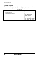
BIOS SETUP
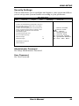
Security Settings
This section allows you to configure and improve your system and allows
you to set up some system features according to your preference.
Aptio Setup Utility
Main
Advanced
Chipset
Boot
Security
Save & Exit
Password Description
If ONLY the Administrator’s password is set, then
this only limit access to Setup and is only asked
for when entering Setup.
If ONLY the User’s password is set, then this is a
power on password and must be entered to boot
or enter Setup. In Setup the User will have
Administrator rights
The password length must
be in the following range:
Minimum length
3
Maximum length
20
→ ← Select
Screen
↑↓ Select Item
Enter: Select
+- Change Field
F1: General Help
F2: Previous Values
F3: Optimized Default
F4: Save ESC: Exit
Administrator Password
User Password
Administrator Password
Set Setup Administrator Password.
User Password
Set User Password.
User’s Manual
49
BIOS SETUP
Save & Exit Settings
Aptio Setup Utility
Main
Advanced
Chipset
Boot
Security
Save Changes and Exit
Discard Changes and Exit
Save Changes and Reset
Discard Changes and Reset
Save & Exit
→ ← Select
Save Options
Save Changes
Discard Changes
Restore Defaults
Save as User Defaults
Restore User Defaults
Save Changes and Exit
Exit system setup after saving the changes.
Discard Changes and Exit
Exit system setup without saving any changes.
Save Changes and Reset
Reset the system after saving the changes.
Discard Changes and Reset
Reset system setup without saving any changes.
Save Changes
Save Changes done so far to any of the setup options.
Discard Changes
Discard Changes done so far to any of the setup options.
Restore Defaults
Restore/Load Defaults values for all the setup options.
Save as User Defaults
Save the changes done so far as User Defaults.
Restore User Defaults
Restore the User Defaults to all the setup options.
50
Screen
↑↓ Select Item
Enter: Select
+- Change Field
F1: General Help
F2: Previous Values
F3: Optimized Default
F4: Save ESC: Exit
User’s Manual
DRIVERS INSTALLATION
Drivers Installation
This section describes the installation procedures for software and
drivers. The software and drivers are included with the motherboard. If
you find the items missing, please contact the vendor where you made the
purchase. The contents of this section include the following:
Intel Chipset Software Installation Utility . .......................................... 52
VGA Drivers Installation ...................................................................... 54
Realtek HD Audio Driver Installation . ................................................ 56
LAN Drivers Installation ...................................................................... 58
Intel® Management Engine Interface . ................................................. 61
Intel® USB 3.0 Drivers ........................................................................ 64
IMPORTANT NOTE:
After installing your Windows operating system, you must install first the
Intel Chipset Software Installation Utility before proceeding with the
drivers installation.
User’s Manual
51
DRIVER INSTALLATION
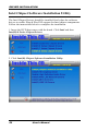
Intel Chipset Software Installation Utility
The Intel Chipset Drivers should be installed first before the software
drivers to enable Plug & Play INF support for Intel chipset components.
Follow the instructions below to complete the installation.
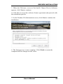
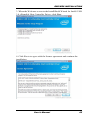
1. Insert the DVD that comes with the board. Click Intel and then
Intel(R) 8 Series Chipset Drivers.
2. Click Intel(R) Chipset Software Installation Utility.
52
User’s Manual
DRIVERS INSTALLATION
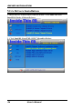
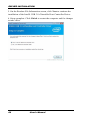
3. When the Welcome screen to the Intel® Chipset Device Software
appears, click Next to continue.
4. Click Yes to accept the software license agreement and proceed with
the installation process.
5. On the Readme File Information screen, click Next to continue the
installation.
6. The Setup process is now complete. Click Finish to restart the
computer and for changes to take effect.
User’s Manual
53
DRIVER INSTALLATION
VGA Drivers Installation
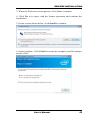
1. Insert the DVD that comes with the board. Click Intel and then
Intel(R) 8 Series Chipset Drivers.
2. Click Intel(R) Core(TM) i3/i5/i7 Graphics Driver.
54
User’s Manual
DRIVERS INSTALLATION
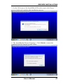
3. When the Welcome screen appears, click Next to continue.
4. Click Yes to to agree with the license agreement and continue the
installation.
5. On the screen shown below, click Install to continue.
6. Setup complete. Click Finish to restart the computer and for changes
to take effect.
User’s Manual
55
DRIVER INSTALLATION
Realtek HD Audio Driver Installation
1. Insert the DVD that comes with the board. Click Intel and then
Intel(R) 8 Series Chipset Drivers.
2. Click Realtek High Definition Audio Driver.
56
User’s Manual
DRIVERS INSTALLATION
3. On the Welcome to the InstallShield Wizard screen, click Yes to
proceed with and complete the installation process.
4. The InstallShield Wizard Complete. Click Finish to restart the
computer and for changes to take effect.
User’s Manual
57
DRIVER INSTALLATION
LAN Drivers Installation
1. Insert the DVD that comes with the board. Click Intel and then
Intel(R) 8 Series Chipset Drivers.
2. Click Intel(R) PRO LAN Network Driver.
58
User’s Manual
DRIVERS INSTALLATION
3. Click Install Drivers and Software.
4. When the Welcome screen appears, click Next.
5. Click Next to to agree with the license agreement.
6. Click the checkbox for Drivers in the Setup Options screen to select it
and click Next to continue.
User’s Manual
59
DRIVER INSTALLATION
7. The wizard is ready to begin installation. Click Install to begin the
installation.
8. When InstallShield Wizard is complete, click Finish.
60
User’s Manual
DRIVERS INSTALLATION
Intel® Management Engine Interface
Follow the steps below to install the Intel Management Engine.
1. Insert the DVD that comes with the board. Click Intel and then
Intel(R) 8 Series Chipset Drivers and then Intel(R) AMT 9.0 Drivers.
User’s Manual
61
DRIVER INSTALLATION
2. When the Welcome screen to the InstallShield Wizard for Intel®
Management Engine Components, click the checkbox for Install Intel®
Control Center & click Next.
3. Click Yes to to agree with the license agreement.
62
User’s Manual
DRIVERS INSTALLATION
4. When the Setup Progress screen appears, click Next. Then, click
Finish when the setup progress has been successfully installed.
User’s Manual
63
DRIVER INSTALLATION
Intel® USB 3.0 Drivers
1. Insert the DVD that comes with the board. Click Intel and then
Intel(R) 8 Series Chipset Drivers.
2. Click Intel(R) USB 3.0 Drivers.
64
User’s Manual
DRIVERS INSTALLATION
3. When the Welcome screen to the InstallShield Wizard for Intel® USB
3.0 eXtensible Host Controller Driver, click Next.
4. Click Yes to to agree with the license agreement and continue the
installation.
User’s Manual
65
DRIVER INSTALLATION
5. On the Readme File Information screen, click Next to continue the
installation of the Intel® USB 3.0 eXtensible Host Controller Driver.
6. Setup complete. Click Finish to restart the computer and for changes
to take effect.
66
User’s Manual
APPENDIX
Appendix
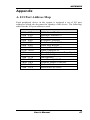
A. I/O Port Address Map
Each peripheral device in the system is assigned a set of I/O port
addresses which also becomes the identity of the device. The following
table lists the I/O port addresses used.
Address
000h - 01Fh
020h - 03Fh
040h - 05Fh
060h - 06Fh
070h - 07Fh
080h - 09Fh
0A0h - 0BFh
0C0h - 0DFh
0F0h
0F1h
1F0h - 1F7h
2F8h - 2FFh
2B0h- 2DFh
360h - 36Fh
3F8h - 3FFh
Device Description
DMA Controller #1
Interrupt Controller #1
Timer
Keyboard Controller
Real Time Clock, NMI
DMA Page Register
Interrupt Controller #2
DMA Controller #2
Clear Math Coprocessor Busy Signal
Reset Math Coprocessor
IDE Interface
Serial Port #2(COM2)
Graphics adapter Controller
Network Ports
Serial Port #1(COM1)
User’s Manual
67
APPENDIX
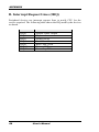
B. Interrupt Request Lines (IRQ)
Peripheral devices use interrupt request lines to notify CPU for the
service required. The following table shows the IRQ used by the devices
on board.
Level
IRQ0
IRQ1
IRQ3
IRQ4
IRQ8
IRQ14
IRQ15
68
Function
System Timer Output
Keyboard
Serial Port #2
Serial Port #1
Real Time Clock
Primary IDE
Secondary IDE
User’s Manual
APPENDIX
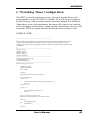
C. Watchdog Timer Configuration
The WDT is used to generate a variety of output signals after a user
programmable count. The WDT is suitable for use in the prevention of
system lock-up, such as when software becomes trapped in a deadlock.
Under these sorts of circumstances, the timer will count to zero and the
selected outputs will be driven. Under normal circumstance, the user will
restart the WDT at regular intervals before the timer counts to zero.
SAMPLE CODE:
//--------------------------------------------------------------------------//
// THIS CODE AND INFORMATION IS PROVIDED "AS IS" WITHOUT WARRANTY OF ANY
// KIND, EITHER EXPRESSED OR IMPLIED, INCLUDING BUT NOT LIMITED TO THE
// IMPLIED WARRANTIES OF MERCHANTABILITY AND/OR FITNESS FOR A PARTICULAR
// PURPOSE.
//
//--------------------------------------------------------------------------#include <dos.h>
#include <conio.h>
#include <stdio.h>
#include <stdlib.h>
#include "F81866.H"
//--------------------------------------------------------------------------int main (int argc, char *argv[]);
void EnableWDT(int);
void DisableWDT(void);
//--------------------------------------------------------------------------int main (int argc, char *argv[])
{
unsigned char bBuf;
unsigned char bTime;
char **endptr;
char SIO;
printf("Fintek 81866 watch dog program\n");
SIO = Init_F81866();
if (SIO == 0)
{
printf("Can not detect Fintek 81866, program abort.\n");
return(1);
}//if (SIO == 0)
if (argc != 2)
{
printf(" Parameter incorrect!!\n");
return (1);
}
bTime = strtol (argv[1], endptr, 10);
printf("System will reset after %d seconds\n", bTime);
if (bTime)
{
EnableWDT(bTime); }
else
{
DisableWDT();
}
return 0;
User’s Manual
69
APPENDIX
}
//--------------------------------------------------------------------------void EnableWDT(int interval)
{
unsigned char bBuf;
bBuf = Get_F81866_Reg(0x2B);
bBuf &= (~0x20);
Set_F81866_Reg(0x2B, bBuf);
//Enable WDTO
Set_F81866_LD(0x07);
Set_F81866_Reg(0x30, 0x01);
//switch to logic device 7
//enable timer
bBuf = Get_F81866_Reg(0xF5);
bBuf &= (~0x0F);
bBuf |= 0x52;
Set_F81866_Reg(0xF5, bBuf);
Set_F81866_Reg(0xF6, interval);
//count mode is second
//set timer
bBuf = Get_F81866_Reg(0xFA);
bBuf |= 0x01;
Set_F81866_Reg(0xFA, bBuf);
//enable WDTO output
bBuf = Get_F81866_Reg(0xF5);
bBuf |= 0x20;
Set_F81866_Reg(0xF5, bBuf);
//start counting
}
//--------------------------------------------------------------------------void DisableWDT(void)
{
unsigned char bBuf;
Set_F81866_LD(0x07);
//switch to logic device 7
bBuf = Get_F81866_Reg(0xFA);
bBuf &= ~0x01;
Set_F81866_Reg(0xFA, bBuf);
//disable WDTO output
bBuf = Get_F81866_Reg(0xF5);
bBuf &= ~0x20;
bBuf |= 0x40;
Set_F81866_Reg(0xF5, bBuf);
}
//-------------------------------------------------------------------------
70
User’s Manual
//disable WDT
APPENDIX
//--------------------------------------------------------------------------//
// THIS CODE AND INFORMATION IS PROVIDED "AS IS" WITHOUT WARRANTY OF ANY
// KIND, EITHER EXPRESSED OR IMPLIED, INCLUDING BUT NOT LIMITED TO THE
// IMPLIED WARRANTIES OF MERCHANTABILITY AND/OR FITNESS FOR A PARTICULAR
// PURPOSE.
//
//--------------------------------------------------------------------------#include "F81866.H"
#include <dos.h>
//--------------------------------------------------------------------------unsigned int F81866_BASE;
void Unlock_F81866 (void);
void Lock_F81866 (void);
//--------------------------------------------------------------------------unsigned int Init_F81866(void)
{
unsigned int result;
unsigned char ucDid;
F81866_BASE = 0x4E;
result = F81866_BASE;
ucDid = Get_F81866_Reg(0x20);
if (ucDid == 0x07)
{
goto Init_Finish;
}
//Fintek 81866
F81866_BASE = 0x2E;
result = F81866_BASE;
ucDid = Get_F81866_Reg(0x20);
if (ucDid == 0x07)
{
goto Init_Finish;
}
//Fintek 81866
F81866_BASE = 0x00;
result = F81866_BASE;
Init_Finish:
return (result);
}
//--------------------------------------------------------------------------void Unlock_F81866 (void)
{
outportb(F81866_INDEX_PORT, F81866_UNLOCK);
outportb(F81866_INDEX_PORT, F81866_UNLOCK);
}
//--------------------------------------------------------------------------void Lock_F81866 (void)
{
outportb(F81866_INDEX_PORT, F81866_LOCK);
}
//--------------------------------------------------------------------------void Set_F81866_LD( unsigned char LD)
{
Unlock_F81866();
outportb(F81866_INDEX_PORT, F81866_REG_LD);
outportb(F81866_DATA_PORT, LD);
Lock_F81866();
}
//--------------------------------------------------------------------------void Set_F81866_Reg( unsigned char REG, unsigned char DATA)
{
Unlock_F81866();
outportb(F81866_INDEX_PORT, REG);
outportb(F81866_DATA_PORT, DATA);
Lock_F81866();
}
//---------------------------------------------------------------------------
User’s Manual
71
APPENDIX
unsigned char Get_F81866_Reg(unsigned char REG)
{
unsigned char Result;
Unlock_F81866();
outportb(F81866_INDEX_PORT, REG);
Result = inportb(F81866_DATA_PORT);
Lock_F81866();
return Result;
}
//---------------------------------------------------------------------------
//--------------------------------------------------------------------------//
// THIS CODE AND INFORMATION IS PROVIDED "AS IS" WITHOUT WARRANTY OF ANY
// KIND, EITHER EXPRESSED OR IMPLIED, INCLUDING BUT NOT LIMITED TO THE
// IMPLIED WARRANTIES OF MERCHANTABILITY AND/OR FITNESS FOR A PARTICULAR
// PURPOSE.
//
//--------------------------------------------------------------------------#ifndef __F81866_H
#define __F81866_H
1
//--------------------------------------------------------------------------#define F81866_INDEX_PORT
(F81866_BASE)
#define F81866_DATA_PORT
(F81866_BASE+1)
//--------------------------------------------------------------------------#define F81866_REG_LD
0x07
//--------------------------------------------------------------------------#define F81866_UNLOCK
0x87
#define F81866_LOCK
0xAA
//--------------------------------------------------------------------------unsigned int Init_F81866(void);
void Set_F81866_LD( unsigned char);
void Set_F81866_Reg( unsigned char, unsigned char);
unsigned char Get_F81866_Reg( unsigned char);
//--------------------------------------------------------------------------#endif //__F81866_H
72
User’s Manual