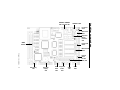
1
PCM-4862
All-in-One 486 Single Board
Computer with SVGA, Ethernet,
and SSD
Copyright Notice
This document is copyrighted, 1996. All rights are reserved. The
original manufacturer reserves the right to make improvements to
the products described in this manual at any time without notice.
No part of this manual may be reproduced, copied, translated or
transmitted in any form or by any means without the prior written
permission of the original manufacturer. Information provided in
this manual is intended to be accurate and reliable. However, the
original manufacturer assumes no responsibility for its use, nor for
any infringements upon the rights of third parties which may result
from its use.
Acknowledgements
VIA is a trademark of VIA Technology, Inc.
AMD is a trademark of Advanced Micro Devices, Inc.
Award is a trademark of Award Software International, Inc.
Cyrix is a trademark of Cyrix Corporation.
IBM, PC/AT, PS/2 and VGA are trademarks of International
Business Machines Corporation.
Intel and Pentium are trademarks of Intel Corporation.
Microsoft Windows ® is a registered trademark of Microsoft Corp.
SMC is a trademark of Standard Microsystems Corporation.
RTL is a trademark of Realtek Semi-Conductor Co., Ltd.
C&T is a trademark of Chips and Technologies, Inc.
UMC is a trademark of United Microelectronics Corporation.
All other product names or trademarks are properties of their
respective owners.
Part No. 2006862020 3rd Edition
Printed in Taiwan September 1997
Packing list
Before you begin installing your card, please make sure that the
following materials have been shipped:
• 1 PCM-4862 All-in-One Single Board Computer
• 1 utility disk with system BIOS, VGA BIOS, and Ethernet
utility programs
• 1 utility disk with SVGA utility programs and drivers for
Windows 3.1 and Windows 95
• 1 utility disk with Ethernet drivers
If any of these items are missing or damaged, contact your
distributor or sales representative immediately.
Contents
Chapter 1 General Information ................................. 1
Introduction ............................................................................ 2
Features ................................................................................... 3
Specifications .......................................................................... 3
Standard SBC functions ....................................................... 3
Local-bus flat panel/VGA interface ..................................... 4
Ethernet controller function ................................................. 5
Solid state disk function ....................................................... 5
PC/104 bus expansion .......................................................... 5
Mechanical and environmental ............................................ 5
Board layout and dimensions ................................................ 6
Chapter 2 Installation ................................................ 7
Jumpers and connectors ........................................................ 8
Locating jumpers ................................................................. 10
Locating connectors ............................................................. 11
Setting jumpers .................................................................... 12
Safety precautions ................................................................ 13
Installing the CPU ................................................................ 13
Removing a CPU ................................................................ 13
Installing a CPU ................................................................. 14
CPU type select (J1-J13, J17-J19) ..................................... 15
CPU power supply select (J4, J6) ....................................... 17
CPU clock select (J1, J2, J3) .............................................. 17
CMOS setup (J14) .............................................................. 17
Buzzer enabled/disabled (J21) ........................................... 17
Installing DRAM (SIMMs) ................................................. 18
Installing SIMMs ............................................................... 18
IDE hard drive connector (CN12) ...................................... 19
Connecting the hard drive .................................................. 19
Floppy drive connector (CN15) ........................................... 20
Connecting the floppy drive ............................................... 20
Parallel port connector (CN16) ........................................... 21
Parallel port IRQ ................................................................ 21
Keyboard and PS/2 connector (CN9) ................................. 21
Front panel connector (CN4) .............................................. 22
Power connectors (CN6, CN11, CN14) ............................... 22
Peripheral power connector, -5V, -12V (CN6) ................... 22
Main power connector, +5V, +12V (CN11) ....................... 22
Fan power supply connector (CN14) .................................. 22
Serial ports (CN13, CN8) .................................................... 23
COM1 RS-232 port (CN13) ............................................... 23
COM2 RS-232/422/485 selection (CN8) ........................... 23
VGA interface connections .................................................. 24
CRT display connector (CN1) ............................................ 24
Flat panel display connector (CN2) ................................... 24
Ethernet configuration ........................................................ 25
10BASE-2/10BASE-5 AUI connector (CN7) .................... 25
10BASE-T connector (CN10) ............................................ 26
Network boot ...................................................................... 26
Watchdog timer configuration ............................................ 26
Watchdog timer enable/disable .......................................... 26
Watchdog timer action (J23, J24) ....................................... 26
Solid State Disk Configuration ........................................... 27
Memory devices ................................................................. 28
Memory address selection (J27) ........................................ 29
I/O address selection (J27) ................................................. 29
Drive emulated (J27) .......................................................... 30
SSD device and size selection (J31, J30) ........................... 31
SSD hardware enable/disable (J29) .................................... 31
DOS 5.0 .............................................................................. 32
DOS 3.3 .............................................................................. 32
Booting from the Flash/ROM disk ..................................... 33
Inserting memory devices .................................................. 33
Using a memory manager (EMM386.EXE) ...................... 34
Chapter 3 Software Configuration ......................... 33
Introduction .......................................................................... 34
Utility disk ............................................................................ 34
VGA display software configuration .................................. 36
Connections for four standard LCDs ................................. 38
Connections to Sharp LM64183P
(640 x 480 DSTN MONO LCD) ........................................ 38
Connections to PLANAR EL
(640 x 480 AD4 EL) ........................................................... 39
Connections to Toshiba LTM09C016
(640 x 480 TFT Color LCD) .............................................. 40
Connections to Sharp LM64C142
(640 x 480 DSTN Color LCD) ........................................... 41
Ethernet software configuration ......................................... 42
Chapter 4 Award BIOS Setup .................................... 45
System test and initialization .............................................. 46
System configuration verification ..................................... 46
AWARD BIOS setup............................................................. 47
Entering setup..................................................................... 47
Standard CMOS setup ........................................................ 48
BIOS features setup............................................................ 49
CHIPSET features setup .................................................... 50
Power management setup ................................................... 51
Load BIOS defaults ............................................................ 52
Change password ................................................................ 53
Auto detect hard disk ......................................................... 54
Save & exit setup ................................................................ 54
Exit without saving............................................................. 54
Chapter 5 SVGA Setup ............................................... 55
Simultaneous display mode ................................................. 56
Sleep mode ............................................................................ 56
Software support .................................................................. 57
Driver installation ................................................................ 58
Windows setup ................................................................... 59
AutoCAD R12 .................................................................... 62
Lotus 1-2-3 and Lotus Symphony ...................................... 64
VESA ................................................................................. 66
Word ................................................................................... 67
WordPerfect ........................................................................ 68
Appendix A Programming the Watchdog Timer .... 71
Appendix B Installing PC/104 Modules .................... 73
Installing PC/104 modules................................................... 74
Appendix C Pin Assignments ................................... 77
CRT display connector (CN1) ............................................ 78
Flat panel display connector (CN2) ................................... 78
PC/104 connectors (CN3, CN5) ......................................... 79
Front panel connector (CN4) ............................................. 80
Peripheral power connector (CN6) ..................................... 80
10BASE-2/10BASE-5 AUI connector (CN7) .................... 80
COM2 RS-232/422/485 serial port (CN8) ......................... 81
Keyboard and mouse connector (CN9) .............................. 81
Ethernet 10BASE-T connector (CN10) ............................. 82
Main power connector (CN11) ........................................... 82
IDE hard drive connector (CN12) ...................................... 82
COM1 RS-232 serial port (CN13) ..................................... 83
Fan power connector (CN14) ............................................. 83
Floppy drive connector (CN15) ......................................... 84
Parallel port connector (CN16) .......................................... 85
Appendix D Optional Extras ..................................... 87
PCM-10586-1 Cable kit for PCM-4862/5860 .................... 88
PCM-20486-1 Boot ROM binary files for ............................
PCM-4860/4862 ................................................................. 88
CHAPTER
General
Information
1
This chapter gives background information on the PCM-4862.
Sections include:
• Card specifications
• Card layout and dimensions
Chapter 1 General Information
1
Introduction
The PCM-4862 is an enhanced, all-in-one single board 486
computer with an on-board Ethernet interface, local-bus SVGA
controller and solid state disk. The PCM-4862 offers all the
functions of an AT-compatible industrial computer on a single
board, but it fits in the space of a 5¼" floppy drive (only 5.75" x
8"). For maximum performance, the PCM-4862 also supports 2nd
level cache sizes from 128 KB to 512 KB (32 KB x 8, 64 KB x 8,
or 128 KB x 8).
On-board features include two serial ports (RS-232 and RS-232/
422/485), one parallel port, an enhanced IDE hard-drive controller
(for up to two drives), a floppy-drive controller and a keyboard/PS/
2 mouse interface. The board's watchdog timer can automatically
reset the system or generate an interrupt if it stops due to a program
bug or EMI problem.
An on-board solid state disk (SSD) emulates a floppy drive using
EPROM or Flash memory devices. You access the SSD using
standard DOS commands or BIOS I/O. The system can even boot
from the SSD. Disk capacity is up to 1.44 MB, depending on the
size of the memory chips. If you use Flash memory, you can read
and write to the disk just like a floppy. If you use EPROM, the disk
is read-only and you must program the chips with an EPROM
programmer.
The PCM-4862 also complies with the "Green Function" standard
and supports three types of power saving features: Doze mode,
Standby mode, and Suspend mode.
All display and Ethernet configuration is done through software. A
single Flash chip holds the system BIOS, VGA BIOS and the
network boot ROM image. This minimizes the number of chips and
eases configuration. You can change the display BIOS or install a
boot ROM simply by programming the Flash chip.
If you need any additional functions, you can add up to six
industry-standard PC/104 expansion modules. For those who
require special functions, we have developed a PC/104 to ISA
adaptor so you can use your standard ISA card.
2
PCM-4862 User's Manual
Features
• 80486SX/DX/DX2/DX4 processor, selectable clock speed
• Up to 512 KB 2nd level cache
• 16-bit Ethernet interface on-board, Novell NE2000 compatible
• Local-bus SVGA display controller (LCD, EL and CRT displays), flat
panel type configured by programming the Flash chip
• Sockets for 1.44 MB solid state disk using Flash memory or EPROM
• Supports M-Systems DiskOnChip (DOC) 2000
• Up to 64 MB of on-board DRAM
• Built-in enhanced IDE (AT bus) hard disk drive interface
• Built-in floppy disk drive controller
• On-board keyboard/PS/2 mouse connector
• Two serial ports: one RS-232, one RS-232/422/485 selectable (uses
16C550 UARTs with 16 byte FIFO)
• One multi-mode parallel port (ECP/EPP/SPP)
• Watchdog timer
• ISA-bus expansion with PC/104 modules
• Dimensions: 5.75" x 8" (146 mm x 203 mm)
• Power management
• Single +5 V power supply
Specifications
Standard SBC functions
• CPU: 80486SX/DX/DX2/DX4-25/33/40/66/80/100/120
• BIOS: AWARD 128 KB Flash memory
• Chipset: VIA VT82C496G
• 2nd level cache: On-board 128 KB, up to 512 KB (SOJ package)
• RAM memory: 1 MB to 64 MB. Two 72-pin SIMM sockets (accepts 1
MB, 2 MB, 4 MB, 8 MB, 16 MB and 32 MB)
Chapter 1 General Information
3
• Enhanced IDE hard disk drive interface: Supports up to two IDE
(VL- bus) hard disks. BIOS auto-detect
• Floppy disk drive interface: Supports up to two floppy disk drives,
3½" (720 KB, 1.44 and 2.88 MB) and/or 5¼" (360 KB and 1.2 MB)
• Multi-mode parallel port: Configured to LPT1, LPT2, LPT3 or
disabled. Supports SPP/ECP/EPP
• Serial ports: One serial RS-232 port, one serial RS-232/422/485 port.
Ports can be configured as COM1, COM2, COM3, COM4 or disabled
individually. Two 16550 serial UARTs
• Battery: 3.6 V @ 600 mAh lithium battery for up to 10 years of data
retention
• Watchdog timer: Can generate a system reset or IRQ15. Software
enabled/disabled. Time interval is 1.6 seconds
• DMA channels: 7
• Interrupt levels:15
• Keyboard/mouse connector: 8-pin connector supports standard PC/AT
keyboard and a PS/2 mouse
• Power management: I/O peripheral devices support power saving and
doze/standby/suspend modes. AMP 1.1 compliant
Local-bus flat panel/VGA interface
• Chipset: C&T 65545
• Display memory: 512 KB VRAM (standard), 1 MB VRAM (optional)
• Display type: Supports CRT and flat panel (EL, LCD and gas plasma
flat panel) display. Can display CRT and flat panel simultaneously
• CRT display mode: Supports resolutions up to 1024 x 768. Noninterlaced CRT monitors resolutions up to 1024 x 768 @ 256 colors.
True-color and Hi-color display capability with flat panels and CRT
monitors at 640 x 480 resolution.
• Panel display modes: Supports resolutions up to 800 x 600 @ 256
colors (1 MB VRAM)
4
PCM-4862 User's Manual
Ethernet controller function
• Chipset: Realtek RTL8019AS
• Type: 16-bit Ethernet, Novell NE 2000 compatible
• Connector: 10BASE-T and AUI connector on-board
Solid state disk function
• Sockets: Three 32-pin sockets for FLASH/EPROM
• FLASH type: ATMEL 29C010/29C040/29C040A (+5 V); AMD/
INTEL 28F010 (+12 V)
• Size: 360 KB/720 KB/1.2 MB/1.44 MB
• Utility software: Includes software to prepare files for EPROM
• Supports M-Systems DiskOnChip (DOC) 2000
PC/104 bus expansion
• PC/104: 104-pin connector for a 16-bit bus
• Driving capacity: Six PC/104 modules
Mechanical and environmental
• Power supply voltage: +5 V (4.75 V to 5.25 V)
• Max. power requirements: +5 V @ 2 A (typical)
• Operating temperature: 32 to 140°F (0 to 60°C)
• Board size: 8" (L) x 5.75" (W) (203 mm x 146 mm)
• Weight: 0.5 kg
Chapter 1 General Information
5
å 9.53
95.25
135.89
140.97
146.05
å
å
å
å
Board layout and dimensions
å
å
å
å
å
å
å
å
40.64
å
å
5.08
5.08 å
å
å
3.56
å
97.16
å
100.97
å
119.38
å
å
å
å
å
å
å
174.63
å
å
177.17
å
å
193.04
å
å
198.12
å
å
203.20
Dimensions in mm
PCM-4862 dimensions
6
PCM-4862 User's Manual
CHAPTER
2
Installation
This chapter tells how to set up the PCM-4862
hardware, including instructions on setting
jumpers and connecting peripherals, switches
and indicators. Be sure to read all the safety
precautions before you begin the installation
procedure.
Chapter 2 Installation
7
Jumpers and connectors
Connectors on the board link it to external devices such as hard
disk drives, a keyboard, or floppy drives. In addition, the board has
a number of jumpers that allow you to configure your system to
suit your application.
The table below lists the function of each of the board jumpers and
connectors:
Jumpers
Label
J1
J2
J3
J4
J5
J6
J7
J8
J9
J10
J11
J12
J13
J14
J15
J16
J17
J18
J19
J20
J21
J22
J23
J24
J25
J26
8
PCM-4862 User's Manual
Function
System clock setting
System clock setting
System clock setting
CPU power supply
CPU type select
CPU power supply
CPU type select
CPU type select
CPU type select
CPU type select
CPU type select
CPU type select
CPU type select
CMOS setup
ECP/EPP DMA channel
ECP/EPP DMA channel
CPU type select
CPU type select
CPU type select
Parallel port IRQ
Buzzer enable/disable
Factory reserved
Watchdog timer invokes IRQ15
Watchdog timer invokes system reset
External battery input for CMOS data retention
Ethernet CRS LED
Jumpers, cont.
Label
J27 (1,2)
J27 (3,4)
J27 (5,6)
J27 (7,8)
J27 (9,10)
J27 (11,12)
J28
J29
J30
J31
J32
Function
SSD I/O address selection
SSD I/O address selection
SSD memory address selection
SSD memory address selection
SSD drive emulated
SSD drive emulated
Ethernet BNC LED
SSD hardware enable/disable
SSD device type and selection
SSD device type and selection
COM2 RS-232/422/485 selection
Connectors
Label
CN1
CN2
CN3
CN4
CN5
CN6
CN7
CN8
CN9
CN10
CN11
CN12
CN13
CN14
CN15
CN16
Function
CRT display connector
Flat panel display connector
PC/104 ISA-bus expansion
Front panel connector
PC/104 ISA-bus expansion
Peripheral power connector (-5V, -12V)
Ethernet 10BASE-2/10BASE-5 AUI connector
Serial port COM2 (RS-232/422/485)
Keyboard and mouse connector
Ethernet 10BASE-T connector
Main power connector (+5V, +12V)
IDE hard drive connector
Serial port COM1 (RS-232)
Fan Power connector
Floppy drive connector
Parallel port connector
Chapter 2 Installation
9
10
PCM-4862 User's Manual
J1, J2,
J3
J4
J5
J7 J6
J8 J10
J9
J11
J12
J19
J14, J15, J20 J21, J22, J25
J16
J23, J24
J13 J18
J17
J26 J27 J28
J32
J31
J29
J30
Locating jumpers
10BASE-T CN10
Fan Power
CN14
Main Power
CN11
Keyboard/
Mouse
connector
CN9
SIMM
Sockets
Floppy Disk
CN15
Locating connectors
10BASE-2/10BASE-5
AUI Connector CN7
IDE Hard Disk
CN12
Chapter 2 Installation
Parallel
CN16
PC/104
CN3, CN5
11
CRT Display
CN1
Flat Panel
Display
CN2
Front
Panel
CN4
Peripheral
Power
CN6
COM2
CN8
COM1
CN13
Setting jumpers
You configure your card to match the needs of your application by
setting jumpers. A jumper is the simplest kind of electric switch. It
consists of two metal pins and a small metal clip (often protected
by a plastic cover) that slides over the pins to connect them. To
“close” a jumper you connect the pins with the clip. To “open” a
jumper you remove the clip. Sometimes a jumper will have three
pins, labeled 1, 2, and 3. In this case you would connect either pins
1 and 2 or 2 and 3.
1
Open
Closed
2
3
Closed 2-3
The jumper settings are schematically depicted in this manual as
follows:
1 2 3
Open
Closed
Closed 2-3
A pair of needle-nose pliers may be helpful when working with
jumpers.
If you have any doubts about the best hardware configuration for
your application, contact your local distributor or sales representative before you make any changes.
12
PCM-4862 User's Manual
Safety precautions
Warning! Always completely disconnect the power cord
from your chassis whenever you are working on it.
Do not make connections while the power is on
because sensitive electronic components can be
damaged by the sudden rush of power. Only
experienced electronics personnel should open
the PC chassis.
Caution!
Always ground yourself to remove any static
charge before touching the CPU card. Modern
electronic devices are very sensitive to static
electric charges. Use a grounding wrist strap at all
times. Place all electronic components on a
static-dissipative surface or in a static-shielded
bag when they are not in the chassis.
Installing the CPU
The PCM-4862 all-in-one CPU module supports most 486 CPUs.
The system's performance depends on the CPU you choose. You
can install or upgrade the CPU in the board's PGA socket by
following the procedures outlined below. If your system has an
existing CPU, you need to remove it before installing the new CPU.
Removing a CPU
1. Disconnect power from the chassis, and unplug all connections
to the CPU card. Then, remove the CPU card from the chassis
by following the instructions in the user's manual for your
chassis.
2. Lift the CPU out of the PGA socket. The old chip may be
difficult to remove. You may find spray chip lubricant, designed
for pin-grid-array (PGA) devices, and a chip puller helpful.
These are available at electronics hobbyists' supply stores.
Chapter 2 Installation
13
Installing a CPU
To install the CPU, follow the instructions that came with it. If no
documentation was provided, the general procedures for installing
a CPU are outlined below:
1. Lubricate the pins on the CPU with lubricant for PGA devices.
This makes the CPU slide in much easier and greatly reduces
the chance of damaging the pins and other components.
2. Carefully align the CPU so that it is parallel to the socket. Make
sure that the notch on the corner of the CPU matches the notch
on the inside of the socket.
3. Gently push the CPU into the socket. There will probably be a
small gap between the CPU and the socket even when it is fully
seated. DO NOT USE EXCESSIVE FORCE!
When you install a new CPU, you may have to adjust other
settings on the board, such as CPU type, CPU clock, and PCI
speed, to accommodate it. Make sure that the settings are correct
for your CPU. Improper settings may damage the CPU.
14
PCM-4862 User's Manual
CPU type select (J1-J13, J17-J19)
The following chart shows the proper jumper settings for their respective
CPUs.
CPU type select
AMD 486DX2-66 (3 V) and
AMD 486DX4-100
TI 486DX-66
J13 J17 J18
1
1
2
2 3
J1
J6
J2
3
J9
J3
5
J10
J4
1
J5
5
2 3
1
2
2
3
3
3
4
4
J2
3
J9
4
4
5
5
J3
5
J10
5
5
6
6
6
6
1
J4
J7 J8 J11 J12
7
1
8
3
2
9
1
5
3
10
2
1
1
8
2
9
1
10
2
3
J6
1
J1
7
J7 J8 J11 J12
3
1
2
3
1
J13 J17 J18
1
J19
J5
AMD 486DX4-120
AMD 5x86-P75
J13 J17 J18
J13 J17 J18
1
1
2 3
J1
1
2
J6
1
1
2
3
3
J1
2 3
J6
1
1
1
2
2
3
3
J2
3
J9
4
4
J2
3
J9
4
4
J3
5
J10
5
5
J3
5
J10
5
5
6
6
6
6
J4
1
J7 J8 J11 J12
7
J4
1
1
8
3
2
9
1
5
3
10
2
J5
J19
J7 J8 J11 J12
7
J5
1
8
3
2
9
1
5
3
10
2
Cyrix 486DX2-66
2 3
J1
J6
1
J13 J17 J18
1
1
2
2
3
3
J1
1
2 3
J6
1
1
1
2
2
3
3
J2
3
J9
4
4
J2
3
J9
4
4
J3
5
J10
5
5
J3
5
J10
5
5
6
6
6
6
J4
1
J7 J8 J11 J12
7
J4
1
1
8
3
2
9
1
5
3
10
2
J5
J19
Cyrix 486DX2-V80GP
J13 J17 J18
1
J19
J19
J5
J7 J8 J11 J12
7
1
8
3
2
9
1
5
3
10
2
Chapter 2 Installation
15
J19
Cyrix 486DX4-100
Cyrix 5x86-100
J13 J17 J18
J13 J17 J18
1
2 3
J1
J6
1
1
1
2
2
3
3
J1
1
2 3
J6
1
1
1
2
2
3
3
J2
3
J9
4
4
J2
3
J9
4
4
J3
5
J10
5
5
J3
5
J10
5
5
6
6
6
6
J4
J7 J8 J11 J12
7
J4
8
2
9
1
5
3
10
2
1
J5
J19
7
1
8
3
2
9
1
5
3
10
2
1
1
3
J7 J8 J11 J12
J5
Cyrix 5x86-120
IBM 486DX4
J13 J17 J18
J13 J17 J18
1
2 3
J1
J6
1
1
1
2
2
3
3
J1
1
2 3
J6
1
1
1
2
2
3
3
J2
3
J9
4
4
J2
3
J9
4
4
J3
5
J10
5
5
J3
5
J10
5
5
6
6
6
6
J4
1
J7 J8 J11 J12
7
J4
1
1
8
3
2
9
1
5
3
10
2
J5
J19
J7 J8 J11 J12
7
1
8
3
J5
2
9
1
5
3
10
2
Intel 486DX-25
2 3
J1
J6
1
J13 J17 J18
1
1
2
2
3
3
J1
1
2 3
J6
1
1
1
2
2
3
3
J2
3
J9
4
4
J2
3
J9
4
4
J3
5
J10
5
5
J3
5
J10
5
5
6
6
6
6
J4
1
J7 J8 J11 J12
7
J4
1
1
8
3
2
9
1
5
3
10
2
J5
J19
J7 J8 J11 J12
7
1
8
3
2
9
1
5
3
10
2
J5
*Intel 486DX4-100 (default)
J13 J17 J18
1
1
2
2
1
3
3
J1
J2
3
4
4
J2
3
J3
5
5
5
J3
5
6
6
2 3
J1
J4
1
J6
J9
J10
J7 J8 J11 J12
7
1
1
8
2
9
1
5
3
10
2
16
PCM-4862 User's Manual
1
2 3
J19
1
1
2
2
3
3
J9
4
4
J10
5
5
6
6
J6
1
J4
3
J5
J19
SGS 486DX2-66
J13 J17 J18
1
J19
Intel 486DX2-66
J13 J17 J18
1
J19
J5
J7 J8 J11 J12
7
1
8
3
2
9
1
5
3
10
2
J19
CPU power supply select (J4, J6)
J4 and J6 must be set to match the CPU type. The chart below
shows the proper jumper settings for their respective VCC.
CPU power supply select
J4
J6
*3.3 V
1-3
2-4
1-2
3.45 V
1-3
2-4
3-4
3.6 V
1-3
2-4
5-6
5V
3-5
4-6
—
CPU clock select (J1, J2, J3)
J1, J2, and J3 are used to synchronize the CPU clock with the CPU
type. Set the CPU clock according to the base CPU speed.
CPU clock select
J1
J2
J3
25 MHz
2-3
2-3
1-2
*33 MHz
1-2
2-3
2-3
40 MHz
2-3
1-2
1-2
CMOS setup (J14)
CMOS setup
J14
*3.6V Battery On
1-2
Clear CMOS
2-3
Buzzer enabled/disabled (J21)
Buzzer enabled/disabled
Enable
Disable
J21
* default setting
*
Chapter 2 Installation
17
Installing DRAM (SIMMs)
You can install anywhere from 1 MB to 32 MB of on-board DRAM
memory using 1, 2, 4, 8 or 16 MB 72-pin SIMMs (Single In-Line
Memory Modules). Access time should be 70 nsec. or less.
Memory installs in two banks composed of one SIMM socket each.
The banks are designated as Bank0 and Bank1. See the figure on
page 11 for help identifying the banks. It supports both single and
dual insertion
Installing SIMMs
NOTE:
The modules can only fit into a socket one way.
Their chips must face the CPU, and their gold
pins must point down into the SIMM socket.
The procedure for installing SIMMs appears below. Please follow
these steps carefully.
1. Ensure that all power supplies to the system are switched Off.
2. Locate the board's memory banks, shown in the figure on
page 11.
3. Install the SIMM cards. Install each SIMM so that its chips
face away from the CPU and its gold pins point down into the
SIMM socket.
4. Slip each SIMM into a socket at a 45 degree angle and carefully
fit the bottom of the card against the connectors.
5. Gently push the SIMM into a perpendicular position until the
clips on the ends of the SIMM sockets snap into place.
6. Check to ensure that each SIMM is correctly seated and all
connector contacts touch. The SIMM should not move around
in its socket.
18
PCM-4862 User's Manual
IDE hard drive connector (CN12)
The built-in Enhanced IDE (Integrated Device Electronics) controller supports up to two IDE devices, including CD-ROM drives, tape
backup drives, a large hard disk drive and other IDE devices. It also
supports faster data transfer rates and allows the IDE hard disk
drive to exceed 528 MB.
Connecting the hard drive
Connecting drives is done in a daisy-chain fashion and requires
one of two cables, depending on the drive size. 1.8" and 2.5" drives
need a 1 x 44-pin to 2 x 44-pin flat-cable connector. 3.5" drives use a
1 x 44-pin to 2 x 40-pin connector.
Wire number 1 on the cable is red or blue, and the other wires are
gray.
1. Connect one end of the cable to CN12. Make sure that the red
(or blue) wire corresponds to pin 1 on the connector, which is
labeled on the board (on the right side).
2. Plug the other end of the cable to the Enhanced IDE hard drive,
with pin 1 on the cable corresponding to pin 1 on the hard
drive. (See your hard drive's documentation for the location of
the connector.)
Connect a second drive as described above.
Unlike floppy drives, IDE hard drives can connect to either end of
the cable. If you install two drives, you will need to set one as the
master and one as the slave by using jumpers on the drives. If you
install just one drive, set it as the master.
Chapter 2 Installation
19
Floppy drive connector (CN15)
You can attach up to two floppy disks to the PCM-4862's on-board
controller. You can use any combination of 5¼" (360 KB and 1.2
MB) and/or 3½" (720 KB, 1.44 MB, and 2.88 MB) drives.
A 34-pin daisy-chain drive connector cable is required for a dualdrive system. On one end of the cable is a 34-pin flat-cable connector. On the other end are two sets of floppy disk drive connectors.
Each set consists of a 34-pin flat-cable connector (usually used for
3½" drives) and a printed-circuit board connector (usually used for
5¼" drives).
Connecting the floppy drive
1. Plug the 34-pin flat-cable connector into CN15. Make sure that
the red wire corresponds to pin one on the connector.
2. Attach the appropriate connector on the other end of the cable
to the floppy drive(s). You can use only one connector in the
set. The set on the end (after the twist in the cable) connects to
the A: drive. The set in the middle connects to the B: drive.
3. If you are connecting a 5¼" floppy drive, line up the slot in the
printed circuit board with the blocked-off part of the cable
connector.
If you are connecting a 3½" floppy drive, you may have trouble
determining which pin is pin number one. Look for a number
printed on the circuit board indicating pin number one. Also,
the connector on the floppy drive connector may have a slot.
When the slot is up, pin number one should be on the right.
Check the documentation that came with the drive for more
information.
If you desire, connect the B: drive to the connectors in the
middle of the cable as described above.
If you need to make your own cable, you can find the pin assignments for the card’s connector in Appendix C.
20
PCM-4862 User's Manual
Parallel port connector (CN16)
Normally, the parallel port is used to connect the card to a printer.
The PCM-4862 includes an on-board parallel port, accessed
through CN16, a 26-pin flat-cable connector. You will need an
adapter cable if you use a traditional DB-25 connector. The cable
has a 26-pin connector on one end and a DB-25 connector on the
other.
Parallel port IRQ
The PCM-4862 supports one parallel port. The port is designated
as LPT1 and can be disabled or changed to LPT2 or LPT3 in the
system BIOS setup.
Parallel port IRQ selection
IRQ5
*IRQ7
J20
1
2
2
3
You can select ECP/EPP DMA channel by setting J15 and J16.
ECP/EPP DMA channel
*DMA1
DMA3
J15
J16
1
2
2
3
* default setting
Keyboard and PS/2 connector (CN9)
The PCM-4862 board provides a keyboard connector which
supports both a keyboard and a PS/2 style mouse. In most cases,
especially in embedded applications, a keyboard is not used. The
standard PC/AT BIOS will report an error or fail during power-on
self test (POST) after a reset if the keyboard is not present. The
PCM-4862's BIOS standard setup menu allows you to select "All,
But Keyboard" under the "Halt On" selection. This allows nokeyboard operation in embedded system applications without the
system halting under POST (power-on-self-test).
Chapter 2 Installation
21
Front panel connector (CN4)
Next you may want to install external switches to monitor and
control the PCM-4862. These features are completely optional —
install them only if you need them. The front panel connector (CN4)
is an 8-pin male, dual in-line header and provides connections for a
speaker, hard disk access indicator and an input switch for resetting the card.
Speaker
The PCM-4862 can drive an 8 Ω speaker at 0.5 watts. Ensure that
alternatives to this specification do not overload the card.
LED interface
The front panel LED indicator for hard disk access is an active low
signal (24 mA sink rate).
Reset switch
If you install a reset switch, it should be a open single pole switch.
Momentarily pressing the switch will activate a reset. The switch
should be rated for 10 mA, 5 V.
If you need to make your own cable, you can find the pin assignments for the card’s connector in Appendix C.
Power connectors (CN6, CN11, CN14)
Peripheral power connector, -5V, -12V
(CN6)
Supplies secondary power to devices that require -5 V and -12 V.
Main power connector, +5V, +12V (CN11)
Supplies main power to the PCM-4862 (+5 V) and devices that
require +12 V.
Fan power supply connector (CN14)
Provides power supply to optional CPU cooling fan. Only present
22
PCM-4862 User's Manual
when +5 V and +12 V power is supplied to the board.
Serial ports (CN13, CN8)
The PCM-4862 offers two serial ports: one RS-232 and one RS-232/
422/485. These ports let you connect to serial devices (a mouse,
printers, etc.) or a communication network.
COM1 RS-232 port (CN13)
The serial port connectors are mounted on the bottom edge of the
card. The 10-pin, dual-in-line, male header to the right of the card is
the RS-232 port.
COM2 RS-232/422/485 selection (CN8)
The secondary port, to the left of COM1, consists of a 14-pin, dualin-line, male header and can be configured to operate in RS-232, RS422, or RS-485 mode. This is done via J32.
COM2 selection
1
1
2
1
2
*RS-2324
3
RS-422
4
3
RS-4854
5
5
6
5
6
2
3
6
J32
* default setting
The IRQ and address range for both ports are fixed. However if you
wish to disable the port or change these parameters later you can
do this in the system BIOS setup. The table below shows the
settings for the PCM-4862's ports.
PCM-4862 Serial port default settings
Port
COM1
Address Range
2E8~3F8
Interrupt
IRQ4
Default
3F8
Chapter 2 Installation
23
COM2
2E8~3F8
IRQ3
2F8
VGA interface connections
The PCM-4862's SVGA interface can drive conventional CRT
displays and is capable of driving a wide range of flat panel
displays, including electroluminescent (EL), gas plasma, passive
LCD and active LCD displays. The card has two connectors to
support these displays, one for standard CRT VGA monitors and
one for flat panel displays.
CRT display connector (CN1)
CN1 is a 16-pin, dual-in-line header used for conventional CRT
displays. A simple one-to-one adapter can be used to match CN1 to
a standard 15-pin D-SUB connector commonly used for VGA.
Pin assignments for CRT display connector CN1 are detailed in
Appendix C.
Flat panel display connector (CN2)
CN2 consists of a 44-pin, dual-in-line header. Power supplies
(+12 V) present on CN2 depend the supply connected to the board.
Ensure that CN11 is connected for +12 V power supply.
The PCM-4862 provides a bias control signal on CN2 which can be
used to control the LCD bias voltage. It is recommended that the
LCD bias voltage not be applied to the panel until the logic supply
voltage (+5 V) and panel video signals are stable. Under normal
operation the control signal (ENAVEE) is active high. When the
PCM-4862's power is applied, the control signal is low until just
after the relevant flat panel signals are present.
Configuration of the VGA interface is done completely via the
software utility. You don't have to set any jumpers. Refer to Chapter
3 for software setup details.
Refer to Chapter 3 for details on connecting the four standard
LCD's: Sharp LM64183P, Toshiba LTM09C016, Sharp 64C142, and
Planor EL Display.
24
PCM-4862 User's Manual
Ethernet configuration
The PCM-4862 is equipped with a high performance 16-bit Ethernet
interface which is fully compliant with IEEE 802.3 10Mbps CSMA/
CD standards. It is supported by all major network operating
systems and is 100% Novell NE-2000 compatible.
Configuration of the Ethernet is very easy and can be done via the
RSET8019.EXE program included on the utility disk. This program
enables you to: view the current Ethernet configuration, to reconfigure the Ethernet interface (IRQ, I/O address, etc.), and to execute
useful diagnostic functions. (See Chapter 3 for detailed information)
The RSET8019.EXE program provides two ways to configure the
Ethernet interface. Configuration can be done automatically when
you choose PNP (plug and play) option; or, when you choose the
Jumperless option, the following IRQ and I/O address settings are
available.
PCM-4862 Ethernet settings
IRQ option
Jumperless
2, 3, 4, 5, 10,
Configuration
11, 12, 15
Default Settings: IRQ = 3 ; I/O Address = 300H
Note:
I/O address range
200 - 300 EFH
1. You can select an IRQ from the options shown
above, but make sure your selection does not
conflict with other I/O devices.
2. When Boot ROM is installed, the
RSET8019.EXE program does not support PNP
mode configuration.
10BASE-2/10BASE-5 AUI connector (CN7)
10BASE-2 and 10BASE-5 coax connections are made via an
attachment unit interface or AUI (CN7). This consists of a 16-pin,
dual-in-line male header.
Chapter 2 Installation
25
10BASE-T connector (CN10)
10BASE-T connects to the PCM-4862 via an adapter cable to a 10pin polarized header (CN10). For 10BASE-T RJ-45 operation, an
adapter cable converting CN10 into a standard RJ-45 jack is
required.
Network boot
The Network Boot feature can be utilized by incorporating the Boot
ROM image files for the appropriate network operating system. The
Boot ROM BIOS files are available from your supplier. They can be
programmed into the BIOS, similar to the VGA BIOS file, using the
AWDFLASH.EXE program detailed in Chapter 3.
Watchdog timer configuration
An on-board watchdog timer reduces the chance of disruptions
which EMP (electro-magnetic pulse) interference can cause. This is
an invaluable protective device for standalone or unmanned
applications. Setup involves two jumpers and running the control
software (refer to Appendix A).
Watchdog timer enable/disable
You can enable or disable the watchdog timer by reading the card's
I/O ports with your program. Read address 443 hex to enable and
refresh the watchdog or address 043 to disable the watchdog. For
information on programming the watchdog timer see Appendix A.
Watchdog timer action (J23, J24)
When the watchdog timer activates (CPU processing has come to a
halt), it can reset the system or generate an interrupt on IRQ15.
This can be set via two 2-pin jumpers (J23, J24) as shown below:
26
PCM-4862 User's Manual
Watchdog timer system reset/IRQ15
*System reset
IRQ15
J23
J24
* default setting
Solid State Disk Configuration
This section will explain the function and configuration of the
jumpers necessary for the operation of the PCM-4862's solid state
disk (SSD). The SSD is optional and can be utilized by inserting
memory devices onto the board. Jumpers relevant to SSD configuration are:
PCM-4862 SSD Jumpers
Number
J27 (1,2)
J27 (3,4)
J27 (5,6)
J27 (7,8)
J27 (9,10)
J27 (11,12)
J29
J30
J31
Function
SSD I/O address selection
SSD I/O address selection
SSD memory address selection
SSD memory address selection
SSD drive emulated
SSD drive emulated
SSD harware enable/disable
SSD ROM device selection
SSD memory type selection
The PCM-4862 features an internal Flash/ROM disk drive. This
drive emulates a floppy disk drive by using solid-state memory
chips (Flash or EPROM) to store programs and data instead of the
magnetic particles on the mechanical drive’s disk. The Flash/ROM
disk offers much faster access times than a floppy or hard disk and
greatly increased reliability in harsh environments.
Chapter 2 Installation
27
The Flash/ROM disk works by modifying the BIOS INT-13 disk
I/O routine on boot-up. The routine then translates read and write
commands to the disk so that they will correctly access the memory
chips. You don’t need any special drivers. You simply set the drive
to act as a DOS drive (e.g. A: or C:) and use standard DOS commands (COPY, DIR, etc.) to manipulate your data.
Before you use the Flash/ROM disk, you will need to enable it with
J29 and the BIOS Chipset Features Setup Program as detailed in
Chapter 4.
Memory devices
The Flash/ROM disk supports the following memory devices, or
their equivalents:
• 27C010 128 KB x 8 EPROM
• 27C040 512 KB x 8 EPROM
• 28F010 128 KB x 8 +12 V Flash Memory (AMD/INTEL)
• 29C010 128 KB x 8 +5 V Flash Memory (ATMEL only)
• 29C040 512 KB x 8 +5 V Flash Memory (ATMEL only)
• 29C040A 512 KB x 8 +5 V Flash Memory (ATMEL only)
If you use EPROM, files on the disk are read only. You will need an
external programmer to load your program and data files on the
EPROMs.
If you use +5 V Flash memories (29C010) for the solid state disk,
you can read or write data just like a floppy disk; you need not use
an external programmer. If you use +12 V Flash memories (28F010)
you will still need an external programmer to write data.
Before you activate the Flash/ROM drive (using the BIOS Chipset
Features Setup program), you will need to set the drive's I/O and
memory addresses to avoid conflicts with other plug-in cards. You
will also need to set the DOS drive designation to be used by the
Flash/ROM drive. The following jumpers sets the configuration of
the SSD as described in the following sections:
28
PCM-4862 User's Manual
Memory address selection (J27)
The SSD occupies a 8 Kbyte window in the upper memory address
range of D6000 to D7FFF. You should ensure this does not conflict
with any other device's memory address. Jumpers J27 (5-6, 7-8)
control the Flash/ROM disk’s memory address. If you select
"Disabled", the disk will not function.
D6000 to D7FFF (default)
6
8
5
7
J27
PCM-4862 SSD memory address
Memory address (HEX)
Disabled
DE000 to DFFFF
D6000 to D7FFF*
¡ = Open
l= Closed
5, 6
7, 8
¡
¡
l
¡
¡
l
* = Default
These addresses might conflict with the ROM BIOS on some of
your other boards (i.e. PC/104 modules). Read the manuals for
these modules to ensure there is no memory conflict.
I/O address selection (J27)
Jumpers J27 (1-2, 3-4) control the disk's I/O address. The default is
set to 200~204 but should be set as to not conflict with the I/O
address of other devices. Jumpers are set as shown below:
200~204 (default)
2
1
4
3
J27
Chapter 2 Installation
29
PCM-4862 SSD I/O address
I/O address (HEX)
2C0-2C4
240-244
280-284
200-204*
1, 2
¡
l
¡
l
¡ = Open
* = Default
l= Closed
3, 4
¡
¡
l
l
Drive emulated (J27)
Jumpers J27 (9-10, 11-12) control the DOS drive emulated by the
Flash/ROM disk as 1st, 2nd, 3rd or 4th as shown below:
3rd Drive (default)
10
12
9
11
J27
PCM-4862 SSD drive designation
Drive
1st
2nd
3rd*
4th
¡ = Open
9, 10
l
l
¡
¡
l= Closed
11, 12
l
¡
l
¡
* = Default
The actual drive letter assigned by DOS to the Flash/ROM disk
depends on the floppy or hard disks installed in the system and the
DOS version.
30
PCM-4862 User's Manual
SSD device and size selection (J31, J30)
The size of the emulated drive depends on the size and number of
the chips you install. For example, if you install three 512 KB chips,
you will have 3 x 512 KB = 1.5 MB, equivalent to a 1.44 MB floppy.
The following table shows the memory chips you will need to
emulate 360 KB, 720 KB, 1.2 KB and 1.44 floppy drives.
You will need to set jumpers J31 and J30 to match the type (Flash or
ROM) and size (128 KB or 512 KB) of the devices you use. All the
devices must be the same type and size.
EPROM 1.44 MB (default)
J30
J31
1
2
3
The following table shows the size and number of devices you will
need for each size emulated disk. It also shows the corresponding
settings of jumpers J31 (Flash/ROM) and J30 (size 128 KB/512 KB).
PCM-4862 SSD device type and selection
J30
1-2
2-3
2-3
1-2
J31
1-2
1-2
2-3
2-3
Device
ROM
ROM
Flash
Flash
360KB
512KBx1
128KBx3
128KBx3
512KBx1
720KB
512KBx2
—
—
512KBx2
1.2MB
512KBx3
—
—
512KBx3
1.44MB
512KBx3
—
—
512KBx3
SSD hardware enable/disable (J29)
As previously mentioned, before you use the SSD you have to
enable it. This is done via the BIOS and a single three pin jumper
(J29). The jumper overrides the BIOS, even if you set the SSD to
enable in BIOS, it will not work unless the jumper is in place as the
table shows below:
SSD enabled (default)
J29
1
2
3
Chapter 2 Installation
31
PCM-4862 SSD hardware enable/disable
J29
Enable*
1
2
3
Disable
1
2
3
* = Default
DOS 5.0
Floppy disks
The Flash/ROM disk will replace the corresponding floppy disk.
For example, if you have a single floppy disk (drive A:) and assign
the Flash/ROM disk to be the 1st drive, any drive operations
directed at drive A: will go to the Flash/ROM disk. You will not be
able to access the floppy drive.
Hard disks
The Flash/ROM disk will not replace corresponding hard disks.
Instead, DOS will assign the Flash/ROM disk to the next free drive
designation. For example, if you have a single hard disk (drive C:)
and assign the Flash/ROM disk to be the 3rd drive, the Flash/ROM
drive will become drive D:. If you have two hard disks, the Flash/
ROM drive will become drive E:.
DOS 3.3
Floppy disks
The Flash/ROM disk will replace the corresponding floppy disk.
For example, if you have a single floppy disk (drive A:) and assign
the Flash/ROM disk to be the 1st drive, any drive operations
directed at drive A: will go to the Flash/ROM disk. You will not be
able to access the floppy drive.
Hard disks
The Flash/ROM disk will take the drive letter of the hard disk and
DOS will assign the hard disk to the next available drive letter. For
example, if you have a single hard disk (drive C:) and assign the
Flash/ROM disk to be the 3rd drive, the Flash/ROM drive will
become drive C: and the hard disk will become drive D:. If you have
two hard disks, the Flash/ROM drive will become drive C:, the first
32
PCM-4862 User's Manual
hard disk will become drive D: and the second hard disk will
become drive E:.
Example
Before installing Flash/ROM disk
DOS 5.0
DOS 3.3
A
FDD
FDD
B
FDD
FDD
C
HDD
HDD
After installing Flash/ROM disk
DOS 5.0
DOS 3.3
A
FDD
FDD
B
FDD
FDD
C
HDD
Flash/ROM
D
Flash/ROM
HDD
Booting from the Flash/ROM disk
If you wish to have the system boot from the Flash/ROM disk,
simply set both J27(9-10, 11-12) closed to select the 1st FDD. Copy
your application files to the disk along with the standard system
files required to boot (command.com, io.sys, autoexec.bat, etc). The
next time you start the system, it will boot from the solid state disk.
Inserting memory devices
After you’ve set all the jumpers on the PCM-4862, insert the
appropriate memory devices into the card’s sockets. Remember that
you will need to program EPROMs before you insert them.
1. Make sure that the pins of the memory chips are perpendicular
to the case and both rows are parallel to each other. Often the
chips come with the pins spread out slightly. Place the chip on a
table top and carefully bend each line of pins together until
they point directly down.
2. Insert each chip. Align the chips so their pins are perpendicular
to the connector and the semicircular notch on the end of the
chip matches the notch on the end of the socket. There will
probably be a gap between the chip body and the socket when
it is fully seated – Do not push too hard!.
Chapter 2 Installation
33
Notches
Using a memory manager (EMM386.EXE)
If you are using an extended or expanded memory manager (such
as EMM386 or QEMM386), you will need to configure it to avoid
the addresses used by the Flash/ROM disk (set by jumpers J30 and
J31). Otherwise, the memory manager will attempt to use these
addresses, causing unreliable operation.
For example, the line in your CONFIG.SYS file that invokes
EMM386, the DOS memory manager, might be the following:
DEVICE=EMM386.SYS X=D600-D7FF
This excludes a 8 KB range for the card from D6000 to D7FFF (the
default addresses).
If you are using expanded memory, you will need to make sure that
the memory manager is not putting the page frame in the disk's
addresses. For example,
DEVICE=EMM386.EXE X=D600-D7FF FRAME = D800
You should also make sure that the disk's memory address is not
shadowed in the BIOS.
User's Note: Sometimes, it is better to assign the sectors and tracks
when formatting an SSD. For different disk sizes, you must use
different assignments, for example:
Format drive:/u/n:9/t:40
(for 360K disk)
Format drive:/u/n:18/t:80
(for 1.44M disk)
(drive is the disk label, such as A or B)
After formatting, please read the on-screen message carefully. DOS
will provide information on total and available disk space, bad
sectors, etc. If the disk size does not match your assignment,
please check the system settings again, such as the switches and
jumpers. If you need a bootable disk, you should do the system
transfer by typing:
SYS drive
(drive is the disk label, such as A: or B:)
34
PCM-4862 User's Manual
CHAPTER
3
Software
Configuration
This chapter details the software configuration information. It shows you how to
configure the card to match your application requirements. AWARD System BIOS
is covered in Chapter 4.
Sections include:
• LCD display configuration
• Connections for four standard LCDs
• Ethernet interface configuration
Chapter 3 Software Configuration
35
Introduction
The PCM-4862 system BIOS and custom drivers are located in a
128 Kbyte, 32-pin (JEDEC spec.) Flash ROM device, designated
U28. A single Flash chip holds the system BIOS, VGA BIOS, and
network Boot ROM image. The display can be configured via
software. This method minimizes the number of chips and eases
configuration. You can change the display BIOS simply by
reprogramming the Flash chip.
Utility disk
The PCM-4862 is supplied with a software utility disk. This disk
contains the necessary file for setting up the VGA display and
Ethernet controller. Directories and files on the disk are as follows:
README.DOC
COOKROM.EXE
DISPLAY (Dir)
AWDFLASH.EXE
4862_SYS.BIN
4862_CRT.BIN
4862_TFT.BIN
4862_STN.BIN
4862_ST5.BIN
4862_MON.BIN
4862_EL.BIN
CBROM.EXE
COOKROM.EXE
A program that converts application files into binary files (files
with a .BIN extension). These are then written into the SSD Flash
ROM devices.
RSET8019.EXE
This program enables you to view the current Ethernet configuration, reconfigure the Ethernet interface (medium type, etc.), and
execute useful diagnostic functions.
36
PCM-4862 User's Manual
AWDFLASH.EXE
This program allows you to write the VGA BIOS files to the BIOS
Flash ROM. The VGA files all come ready formatted for the PCM4862 with .BIN extensions. See README.DOC. These files
support various CRT and flat panel displays. They are custom
written and can be made available upon request.
4862-SYS.BIN
This binary file contains the system BIOS.
4862-CRT.BIN
Supports CRT only.
4862-TFT.BIN (default)
Supports 640 x 480 18 bit or 24 bit color TFT LCD panel
(Sharp LQ9D011, Toshiba LTM10C042).
4862-STN.BIN (1 MB VRAM)
Supports 640 x 480 color STN DD 8/16-bit displays
(Sharp LM64C142).
4862-ST5.BIN (512 KB VRAM)
Supports 640 x 480 color STN DD 8/16-bit displays
(Sharp LM64C142).
NOTE:
This BIOS does not support simultaneous CRT
and flat panel display with 512 KB VRAM
4862-MON.BIN
Supports 640 x 480 dual scan monochrome displays
(Sharp LM64P8X/837).
4862-EL.BIN
Supports 640 x 480 EL displays (PLANAR EL640480 - A Series).
CBROM.EXE
This program allows you to combine your own VGA BIOS with
system BIOS (4862_SYS.BIN).
Chapter 3 Software Configuration
37
VGA display software configuration
The PCM-4862’s on-board VGA interface supports a wide range
of popular LCD, EL, gas plasma flat panel displays and traditional
analog CRT monitors. The interface can drive CRT displays with
resolutions up to 1024 x 768 in 256 colors. It is also capable of
driving color panel displays with resolutions of 640 x 480 in 64K
colors. The VGA interface is configured completely via the
software utility, so you don’t have to set any jumpers. Configure
the VGA display as follows:
1. Apply power to the PCM-4862 with a color TFT display
attached. This is the default setting for the PCM-4862. Ensure
that the AWDFLASH.EXE and *.BIN files are located in the
working drive.
NOTE:
Ensure that you do not run AWDFLASH.EXE
while your system is operating in EMM386 mode.
2. At the prompt, type AWDFLASH.EXE and press <Enter>. The
VGA configuration program will then display the following:
38
PCM-4862 User's Manual
VGA Setup screen
3. At the prompt, type in the BIN file which supports your display.
When you are sure that you have entered the file name correctly
press <Enter>. The screen will ask “Do you want to save?” If
you wish to continue press Y. If you change your mind or have
made a mistake press N to abort and end the setup procedure.
4. If you decide to continue, the program will create a BIOS.OLD
file which contains the existing BIOS configuration. The
prompt will then ask “Are you sure you want to save new
configuration?” Press Y if you want the new file to be written
into the BIOS. Press N to exit the program.
The new VGA configuration will then write to the ROM BIOS
chip. This configuration will remain the same until you run the
AWDFLASH.EXE program and change the settings.
Chapter 3 Software Configuration
39
Connections for four standard LCDs
Connections to Sharp LM64183P
(640 x 480 DSTN MONO LCD)
LM64P83
Pin
CN1-1
CN1-2
CN1-3
CN1-4
CN1-5
CN1-6
CN1-7
CN1-8
CN1-9
CN1-10
CN1-11
CN1-12
CN1-13
CN1-14
CN1-15
40
PCM-4862 CN2
Pin name
S
CP1
CP2
DISP
VDD
VSS
VEE
DU0
DU1
DU2
DU3
DL0
DL1
DL2
DL3
PCM-4862 User's Manual
Pin
36
38
35
5
6
3
12
11
10
9
16
15
14
13
Pin name
FLM
LP
SHFCLK
+5 V
+5 V
GND
-17 V (external power)
P3
P2
P1
P0
P7
P6
P5
P4
Connections to PLANAR EL
(640 x 480 AD4 EL)
PLANAR 640 x 480 AD4
PCM-4862 CN2
Pin
1
2
3
4
5
6
7
8
9
10
11
12
13
14
15
16
17
18
19
20
21
22
23
24
25
26
27
28
29
30
31,32
33
34
Pin
3
21
3
22
3
23
—
24
—
17
—
18
—
19
4
20
4
42
4
—
8
37
—
36
—
39
39
—
—
—
—
—
—
Pin name
GND
DO
GND
D1
GND
D2
NC
D3
NC
D4
NC
D5
NC
D6
GND
D7
GND
VCLK
GND
/BLANK
GND
HS
NC
VS
NC
SELFTST
COLMAP
ENABLE
RESERVED
/LOWPOW
NC
RESERVED
NC
Pin name
GND
P12
GND
P13
GND
P14
—
P15
—
P8
—
P9
—
P10
GND
P11
GND
ASHFCLK
GND
—
GND
M
—
FLM
—
GND
GND
—
—
—
—
—
—
Chapter 3 Software Configuration
41
Connections to Toshiba LTM09C016
(640 x 480 TFT Color LCD)
42
LTM09C016
PCM-4862 CN2
Pin
CN1-1
CN1-2
CN1-3
CN1-4
CN1-5
CN1-6
CN1-7
CN1-8
CN1-9
CN1-10
CN1-11
CN1-12
CN1-13
CN1-14
CN1-15
Pin name
NCLK
GND
R0
GND
R1
GND
R2
GND
G0
GND
G1
GND
G2
GMD
NC
Pin
35
3
22
3
23
4
24
4
17
8
18
8
19
33
—
Pin name
SHFCLK
GND
P13
GND
P14
GND
P15
GND
P8
GND
P9
GND
P10
GND
—
CN2-1
CN2-2
CN2-3
CN2-4
CN2-5
CN2-6
CN2-7
CN2-8
CN2-9
CN2-10
B0
GND
B1
GND
B2
GND
ENAB
GND
VDD
VDD
11
33
12
34
13
34
37
39
5
6
P2
GND
P3
GND
P4
GND
M
GND
+5 V
+5 V
PCM-4862 User's Manual
Connections to Sharp LM64C142
(640 x 480 DSTN Color LCD)
LM64C142
PCM-4862 CN2
Pin
CN1-1
CN1-2
CN1-3
CN1-4
CN1-5
CN1-6
CN1-7
CN1-8
CN1-9
CN1-10
CN1-11
CN1-12
CN1-13
CN1-14
CN1-15
Pin name
YD
LP
XCX
DISP
VDD
VSS
VEE
DU0
DU1
DU2
DU3
DU4
DU5
DU6
DU7
Pin
36
38
35
5
6
3
20
19
18
17
12
11
10
9
Pin name
FLM
LP
SHFCLK
+5 V
+5 V
GND
+27 V (external power)
P11
P10
P9
P8
P3
P2
P1
P0
CN2-1
CN2-2
CN2-3
CN2-4
CN2-5
CN2-6
CN2-7
CN2-8
CN2-9
CN2-10
VSS
DL0
DL1
DL2
DL3
DL4
DL5
DL6
DL7
VSS
4
24
23
22
21
16
15
14
13
8
GND
P15
P14
P13
P12
P7
P6
P5
P4
GND
Chapter 3 Software Configuration
43
Ethernet software configuration
The PCM-4862’s on-board Ethernet interface supports all major
network operating systems. I/O addresses and interrupts are easily
configured via the RSET8019.EXE program (either by jumperless
mode or PNP mode). To execute the configuration, to view the
current configuration, or to run diagnostics, do the following:
1. Power the PCM-4862 on. Ensure that the RSET8019.EXE file
is located in the working drive.
2. At the prompt type RSET8019.EXE and press <Enter>. The
Ethernet configuration program will then be displayed.
3. This simple screen shows all the available options for the
Ethernet interface. Just highlight the option you wish to change
by using the Up and Down keys. To change a selected item,
press <Enter>, and a screen will appear with the available
options. Highlight your option and press <Enter>. Each
highlighted option has a helpful message guide displayed at the
bottom of the screen for additional information.
4. After you have made your selections and your are sure that this
is the configuration you want, press ESC. A prompt will appear
asking if you want to save the configuration. Press Y if you
want to save.
The Ethernet Setup Menu also offers three very useful diagnostic
functions. These are:
1. Run EEPROM test
2. Run Diagnostics on Board
3. Run Diagnostics on Network
Each option has its own display screen which shows the format and
result of any diagnostic tests undertaken.
44
PCM-4862 User's Manual
CHAPTER
4
Award BIOS Setup
This chapter describes how to set BIOS
configuration data.
Chapter 4 Award BIOS Setup
45
System test and initialization
These routines test and initialize board hardware. If the routines
encounter an error in during the tests, you will either hear a few
short beeps or see an error message on the screen. There are two
kinds of errors: fatal and non-fatal. The system can usually
continue the boot up sequence with non-fatal errors. Non-fatal
error messages usually appear on the screen along with the
following instructions:
press <F1> to RESUME
Write down the message and press the F1 key to continue the
bootup sequence.
System configuration verification
These routines check the current system configuration against the
values stored in the card’s CMOS memory. If they don’t match, the
program outputs an error message. You will then need to run the
BIOS setup program to set the configuration information in
memory.
There are three situations in which you will need to change the
CMOS settings:
1. You are starting your system for the first time
2. You have changed the hardware attached to your system
3. The CMOS memory has lost power and the configuration
information has been erased.
The PCM-4862’s CMOS memory has an integral lithium battery
backup. The battery backup should last ten years in normal
service, but when it finally runs down, you will need to replace the
complete unit.
46
PCM-4862 User's Manual
AWARD BIOS setup
ROM ISA BIOS (2C4L6AKA)
CMOS SETUP UTILITY
AWARD SOFTWARE, INC.
STANDARD CMOS SETUP
PASSWORD SETTING
BIOS FEATURES SETUP
IDE HDD AUTO DETECTION
CHIPSET FEATURES SETUP
SAVE & EXIT SETUP
POWER MANAGEMENT SETUP
EXIT WITHOUT SAVING
LOAD BIOS DEFAULTS
ESC: QUIT
ßàáâ: SELECT ITEM
F10: Save & Exit Setup
(Shift)F2: Change Color
Time, Date, Hard Disk Type....
Setup program initial screen
Award’s BIOS ROM has a built-in Setup program that allows users
to modify the basic system configuration. This type of information
is stored in battery-backed CMOS RAM so that it retains the Setup
information when the power is turned off.
Entering setup
Power on the computer and press <Del> immediately. This will
allow you to enter Setup.
Chapter 4 Award BIOS Setup
47
Standard CMOS setup
When you choose the STANDARD CMOS SETUP option from
the INITIAL SETUP SCREEN menu, the screen shown below is
displayed. This standard Setup Menu allows users to configure
system components such as date, time, hard disk drive, floppy
drive, display, and memory. Once a field is highlighted, on-line
help information is displayed in the left bottom of the Menu
screen.
ROM ISA BIOS (2C4L6AKA)
STANDARD CMOS SETUP
AWARD SOFTWARE, INC.
Date (mm:dd:yy)
Time (hh:mm:ss)
:
:
Wed, Jan 17 1996
12 : 19 : 58
HARD DISKS
TYPE SIZE CYLS.
Primary Master
Primary Slave
Secondary Ma.
Secondary Sl.
none
none
none
none
Drive A : None
Drive B : None
Video : EGA/VGA
Halt On : All Errors
ESC : Quit
F1 : Help
0
0
0
0
0
0
0
0
HEADS PRECOMP LANDZONE SECTORS MODE
0
0
0
0
0
0
0
0
0
0
0
0
PCM-4862 User's Manual
NORMAL
N/A
N/A
N/A
Base Memory :
Extended Memory :
Other Memory :
640K
3072K
384K
Total Memory :
4096K
ßàáâ : Select Item
(Shift)F2 : Change Color
CMOS setup screen
48
0
0
0
0
PU / PD / + / - : Modify
BIOS features setup
By choosing the BIOS FEATURES SETUP option from the
INITIAL SETUP SCREEN menu, the screen below is displayed.
This sample screen contains the manufacturer’s default values for
the PCM-4862.
ROM ISA BIOS (2C4L6AKA)
BIOS FEATURES SETUP
AWARD SOFTWARE, INC.
Virus Warning
CPU Internal Cache
External Cache
Quick Power On Self Test
Boot Sequence
Swap Floppy Drive
Boot Up Floppy Seek
Boot Up NumLock Status
Boot Up System Speed
IDE HDD Block Mode
Gate A20 Option
Memory Parity Check
Typematic Rate Setting
Typematic Rate (Chars/Sec)
Typematic Delay (Msec)
Security Option
:
:
:
:
:
:
:
:
:
:
:
:
:
:
:
:
Enabled
Enabled
Enabled
Disabled
A,C
Disabled
Enabled
On
High
Disabled
Normal
Enabled
Disabled
6
250
Setup
Video BIOS Shadow
C8000-CBFFF Shadow
CC000-CFFFF Shadow
D0000-D3FFF Shadow
D4000-D7FFF Shadow
D8000-DBFFF Shadow
DC000-DFFFF Shadow
Esc
F1
F5
F6
:
:
:
:
:
:
:
Enabled
Disabled
Disabled
Disabled
Disabled
Disabled
Disabled
: Quit
ßàáâ: Select Item
: Help
PU / PD / + / - : Modify
: Old Values
(Shift)F2
: Color
: Load BIOS Defaults
BIOS features setup
Chapter 4 Award BIOS Setup
49
CHIPSET features setup
By choosing the CHIPSET FEATURES SETUP option from the
INITIAL SETUP SCREEN menu, the screen below is displayed.
This sample screen contains the manufacturer’s default values for
the PCM-4862.
ROM ISA BIOS (2C4L6AKA)
CMOS SETUP UTILITY
CHIPSET FEATURES SETUP
Auto Configuration
Decoupled Refresh
Relocate 256K/384K
Video BIOS Cacheable
System BIOS Cacheable
:
:
:
:
:
Enabled
Disabled
Disabled
Enabled
Enabled
External Cache Scheme
Combine Alter & Tag Bits
CHRDY for ISA Master
Memory Hole At 15 MB Addr.
Cache Timing Control
DRAM Timing Control
Fast DRAM
Burst Write
CPU Write Back Cache
Set Turbo Pin Function
Set Mouse Lock
:
:
:
:
:
:
:
:
:
:
:
Write Back
Disabled
Enabled
Disabled
Fast
Normal
Disabled
Disabled
Disabled
Suspend
Disabled
On-Board Local-Bus IDE
IDEPrimary Master PIO
IDE Primary Slave PIO
: Enabled
: Auto
: Auto
On-Board FDC Controller
On-Board Serial Port 1
On-Board Serial Port 2
COM3 & COM4 Address
On-Board Parallel Port
Parallel Extended Mode
:
:
:
:
:
:
Solid State Disk
: Disabled
Esc
F1
F5
F6
: Quit
ßàáâ: Select Item
: Help
PU/PD/+/- : Modify
: Old Values
(Shift)F2 : Color
: Load BIOS Defaults
CHIPSET features setup
50
PCM-4862 User's Manual
Enabled
COM1
COM2
3E8H,2E8H
278H
Standard
Power management setup
By choosing the POWER MANAGEMENT SETUP option from
the INITIAL SETUP SCREEN menu, the screen below is displayed. This sample screen contains the manufacturer’s default
values for the PCM-4862.
ROM ISA BIOS (2C4L6AKA)
CMOS SETUP UTILITY
POWER MANAGEMENT SETUP
Power Management
Doze Mode
: Disabled
: 8 sec
Sleep Timer
Sleep Mode
HDD Power Management
VGA Activity Wakeup
:
:
:
:
IO Activity
: Disabled
2 min
Suspend
1 min
Disabled
IRQ3 Activity
IRQ4 Activity
IRQ5 Activity
IRQ7 Activity
IRQ8 Activity
IRQ10 Activity
IRQ11 Activity
IRQ12 Activity
:
:
:
:
:
:
:
:
Primary
Primary
Primary
Primary
Secondary
Primary
Primary
Primary
Esc
: Quit
ßàáâ
: Select Item
F1 : Help
PU/PD/+/- : Modify
F5 : Old Values (Shift)F2 : Color
F6 : Load BIOS Defaults
Power management setup
Chapter 4 Award BIOS Setup
51
Load BIOS defaults
LOAD BIOS DEFAULTS loads the default system values directly
from ROM. If the stored record created by the Setup program
becomes corrupted (and therefore unusable), these defaults will
load automatically when you turn the PCM-4862 on.
ROM ISA BIOS (2C4L6AKA)
CMOS SETUP UTILITY
AWARD SOFTWARE, INC.
STANDARD CMOS SETUP
PASSWORD SETTING
BIOS FEATURES SETUP
IDE HDD AUTO DETECTION
CHIPSET FEATURES SETUP
SAVE & EXIT SETUP
POWER MANAGEMENT SETUP
EXIT WITHOUT SAVING
LOAD BIOS DEFAULTS
Load BIOS Defaults (Y/N)? Y
ESC: QUIT
ßàáâ:SELECT ITEM
F10:Save & Exit Setup
(Shift)F2:Change Color
Load BIOS defaults except standard CMOS SETUP
Load BIOS defaults screen
52
PCM-4862 User's Manual
Change password
To change the password, choose the PASSWORD SETTING
option form the Setup main menu and press <Enter>.
1. If the CMOS is bad or this option has never been used, there is
default password which is stored in the ROM. The screen will
display the following messages:
Enter Password:
Press <Enter>.
2. If the CMOS is good or this option has been used to change the
default password, the user is asked for the password stored in
the CMOS. The screen will display thefollowing message:
Confirm Password:
Enter the current password and press <Enter>.
3. After pressing <Enter> (ROM password) or the current
password (user-defined), you can change the password stored
in the CMOS. The password can be at most 8 characters long.
Remember - to enable this feature, you must first select either
Setup or System in the BIOS FEATURES SETUP.
Chapter 4 Award BIOS Setup
53
Auto detect hard disk
The IDE HDD AUTO DETECTION utility can automatically
detect the IDE hard disk installed in your system. You can use it to
self-detect and/or correct the hard disk type configuration.
ROM ISA BIOS (2C4L6AKA)
CMOS SETUP UTILITY
AWARD SOFTWARE, INC.
HARD DISK TYPE
Drive C
:
SIZE
CYLS.
HEADS
PRECOMP
LANDZ
SECTORS MODE
(MB)
790
15
65535
789
57
Select Secondry Slave Option (N=Skip) : N
ESC = SKIP
IDE HDD auto detection screen
Save & exit setup
If you select this option and press <Enter>, the values entered in
the setup utilities will be recorded in the chipset's CMOS memory.
The microprocessor will check this every time you turn your
system on and compare this to what it finds as it checks the
system. This record is required for the system to operate.
Exit without saving
Selecting this option and pressing <Enter> lets you exit the Setup
program without recording any new values or changing old ones.
54
PCM-4862 User's Manual
CHAPTER
SVGA Setup
5
The PCM-4862 features an on-board flat
panel/VGA interface. This chapter
provides instructions for installing and
operating the software drivers on the
included display driver diskette.
Chapter 5 SVGA Setup
55
Simultaneous display mode
The 65545 VGA BIOS supports monochrome LCD, EL, color TFT
and STN LCD flat panel displays. It also supports interlaced and
non-interlaced analog monitors (VGA color and VGA monochrome) in high-resolution modes while maintaining complete
IBM VGA compatibility. Digital monitors (i.e. MDA, CGA, and
EGA) are NOT supported. Multiple frequency (multisync)
monitors are supported as analog monitors.
Both CRT and panel displays can be used simultaneously. The
PCM-4862 can be set in one of three configurations: on a CRT, on
a flat panel display, or on both simultaneously. The system is
initially set to simultaneous display mode. In the utility diskette,
there are three .COM files which can be used to select the display.
Simply type the filename at the DOS prompt:
CT.COM Enables CRT display only
FP.COM Enables panel display only
SM.COM Enables both displays at the same time.
Sleep mode
The display driver diskette contains two files that support sleep
mode. Simply type the filename at the DOS prompt:
ON.COM switches to normal display mode.
OFF.COM switches to sleep mode.
56
PCM-4862 User's Manual
Software support
The drivers support the following applications using the filenames
and resolutions listed:
Application
Windows 3.1
Filename
LINEAR4.DRV
LINEAR8.DRV
AutoCAD R12
LINEAR16.DRV
LINEAR24.DRV
RCTURBOC.EXP
Resolution
640x480
800x600
1024x768
640x480
800x600
1024x768
640x480
640x480
640x480
800x600
1024x768
640x480
800x600
1024x768
640x480
640x480
640x480
Lotus 1-2-3 2.0 and Lotus Symphony 1.0,1.1
V132X25.DRV
132x25 (Text)
V132X50.DRV
132x50 (Text)
VESA 1.2
VESA.COM
800x600
1024x768
640x400
640x480
800x600
1024x768
640x480
640x480
Colors
16
16
16
256
256
256
64K
16M
16
16
16
256
256
256
32K
64K
16M
16
16
16
16
256
256
256
256
32K
64K
Chapter 5 SVGA Setup
57
Word 5.0
Word 5.5
WordPerfect 5.0
WordPerfect 5.1
VGA600.VID
VGA768.VID
VGA55600.VID
VGA55768.VID
CHIPS600.WPD
CHIPS768.WPD
VGA600.VRS
VGA768.VRS
800x600
1024x768
800x600
1024x768
800x600
1024x768
800x600
1024x768
16
16
16
16
16
16
16
16
Driver installation
Necessary prerequisites
The instructions in this manual assume that you understand
elementary concepts of MS-DOS and the IBM Personal Computer.
Before you attempt to install any driver or utility you should: know
how to copy files from a floppy disk to a directory on the hard
disk, understand the MS-DOS directory structure, and know how
to format a floppy disk. If you are uncertain about any of these
concepts, please refer to the DOS or Windows user reference
guides for more information before you proceed with the installation.
Before you begin
Before you begin installing software drivers, you should make a
backup copy of the display driver diskette and store the original in
a safe place. The display driver diskette contains drivers for several
versions of certain applications. You must install the correct
version in order for the driver to work properly so make sure you
know which version of the application you have.
58
PCM-4862 User's Manual
Windows setup
These drivers are designed to work with Microsoft Windows 3.1.
You may install these drivers through Windows or in DOS.
Step 1: Install Windows as you normally would for a VGA display.
Run Windows to make sure that it is working correctly.
Step 2: Place the display driver diskette in drive A. In Windows
Program Manager, choose File from the Options Menu. Then from
the pull-down menu, choose Run . . . . At the command line
prompt, type A:\WINSETUP. Press the <ENTER> key or click
OK to begin the installation. At this point the setup program
locates the directory where Windows is installed. For proper
operation, the drivers must be installed in the Windows subdirectory. Press <ENTER> to complete the installation. Once completed,
the Display Driver Control Panel appears on the screen. This
Control Panel allows you to select and load the installed drivers.
Another method of installing these drivers is through the File
Manager. Click on Drive A:. Then double-click on
WINSETUP.EXE to begin installation.
Changing Display Drivers in Windows
To change display drivers in Windows, select the Windows Setup
icon from the Main window. You will be shown the current setup
configuration. Select Change System Settings from the Option
menu. Click on the arrow at the end of the Display line. You will
be shown a list of display drivers. Click on the driver you want.
Then click on the OK button. Follow the directions to complete the
setup.
Changing Color Schemes
After you change display drivers, you may notice that the color
scheme used by Windows looks strange. This is because different
drivers have different default colors. To change the color scheme,
select the Control Panel from the Main window. Select the Color
icon. You will be shown the current color scheme. Choose a new
color scheme and click the OK button.
Chapter 5 SVGA Setup
59
DOS Setup
Step 1: Install Windows as you normally would for a VGA display.
Run Windows to make sure that it is working correctly. Then exit
Windows.
Step 2: Place the display driver diskette in drive A. Type A:
<ENTER> to make this the default drive. Type SETUP <ENTER>
to run the driver SETUP program. Press any key to get to the
applications list. Using the arrow keys, select Windows Version 3.1
and press the <ENTER> key. Press the <ENTER> key to select All
Resolutions, and then press <END> to begin the installation. At
this point you will be asked for the path to your Windows System
directory (default C:\WINDOWS). When the installation is
complete, press any key to continue. Press <ESC> followed by Y
to exit to DOS.
Step 3: Change to the directory where you installed Windows
(usually C:\WINDOWS).
Step 4: Type SETUP <ENTER> to run the Windows Setup
program. It will show the current Windows configuration. Use the
up arrow key to move to the Display line and press <ENTER>. A
list of display drivers will be shown. Use the arrow keys to select
one of the drivers starting with an asterisk (*) and press <ENTER>.
Step 5: Follow the directions on the screen to complete the setup.
In most cases, you may press <ENTER> to accept the suggested
option. When Setup is done, it will return to DOS. Type WIN
<ENTER> to start Windows with the new display driver.
Changing Display Drivers in DOS
To change display drivers from DOS, change to the Windows
directory and run Setup, repeating steps 4 and 5 from the previous
page. Besides the special display drivers marked by an asterisk (*),
you should be able to use the following standard drivers:
60
VGA
640x480, 16 colors
Super VGA
800x600, 16 colors
PCM-4862 User's Manual
Panning Drivers
Special panning drivers are provided to allow high-resolution
modes to be displayed on a flat panel or CRT. These drivers will
show a section of a larger screen and will automatically pan, or
scroll, the screen horizontally and vertically when the mouse
reaches the edge of the display.
Linear Acceleration Drivers
A special high-performance linear acceleration driver is provided
for 256-color modes. This driver may require special hardware and
may not be supported on all systems. It is only available for
Windows3.1.
Chapter 5 SVGA Setup
61
AutoCAD R12
These drivers are designed to work with Autodesk AutoCAD R12.
They conform to the Autodesk Device Interface (ADI) for Rendering drivers and Display drivers. These display list drivers accelerate redraw, pan, and zoom functions.
Driver installation
Step 1: Place the display driver diskette in drive A. Type A:
<ENTER> to make this the default drive. Type SETUP <ENTER>
to run the SETUP program. Press any key to get to the applications
list. Using the arrow keys, select AutoCAD Release 12 and press
<ENTER>. This will display a list of supported driver resolutions.
Using the arrow keys and the <ENTER> key, select the resolutions
that are appropriate for your monitor. When all of the desired
resolutions have been selected, press <END> to begin the installation. At this point you will be asked for a drive and directory to
copy the driver files. Enter the drive and directory that contains the
installed AutoCAD R12. If the destination directory does not exist
you will be asked for confirmation. When the installation is
complete, press any key to continue. Press <ESC> followed by Y
to exit to DOS.
Step 2: Go to the AutoCAD directory where the new drivers were
installed and run the driver installation program by typing
ACAD12 -r <ENTER>. This program will configure your
AutoCAD R12 to use the new display drivers. Select TurboDLD
Classic.
Configuring TurboDLD
Select Configure Video Display. In Display Device Configuration
choose Select Graphics Board/Resolution. Then choose Select
Display Graphics Board. After choosing a graphics board, go to
Select Display Resolution. After selecting the display resolution,
save the new configuration, and return to the main menu.
62
PCM-4862 User's Manual
Basic Configuration Menu
This menu allows you to modify:
Number of AutoCAD Command Lines
Font Size
6x8/8x8/8x14/8x16/12x20/12x24
Dual Screen
Enable/Disable
User Interface Configuration
Double Click Interval Time
BP Button
BP Highlight
Patt Line/Xor Rect/Both
BP Refresh
Enable/Disable
BP Cache
Enable/Disable
Expert Configuration Menu
This menu allows you to modify:
Display List
Enable/Disable
Drawing Cache
Enable/Disable
Use Acad 31 bit space?
Yes/No
Internal Command Echo
Enable/Disable
BP Zoom Mode
Freeze/Float
Regen Mode
Incremental/Fast
If your previously installed driver is not TurboDLD, you will have
to reconfigure the RENDER command the first time you use it.
Chapter 5 SVGA Setup
63
Lotus 1-2-3 and Lotus Symphony
These drivers are designed to work with Lotus 1-2-3 versions 2.0,
2.01 and 2.2, and with Lotus Symphony versions 1.0 and 1.1.
Driver installation
Step 1: Place the display driver diskette into drive A. Make A the
default drive by typing A: <ENTER>. Run the SETUP program by
typing SETUP <ENTER>. Press any key to display a list of
supported applications. Use the arrow keys to select Lotus/
Symphony, and press <ENTER>. A list of supported screen
resolutions will be displayed. Use the arrow keys to select the
desired screen resolution and press <ENTER>. (Make sure your
monitor is able to display the resolution desired) Press <END> to
begin the driver installation process. A default drive and directory
path will be displayed. Use the backspace key to erase this default
and type in the 123 directory. At this point you may be asked to
create the target directory if it does not already exist. After the
files have been installed, press any key to return to the list of
supported applications. Press <ESC> followed by Y to exit to
DOS. Copy all the files that were just created in the temporary
directory onto a formatted floppy diskette.
Step 2: Go to your 123 directory, and start the installation program. Type the following commands:
C: <ENTER>
INSTALL <ENTER>
Step 3: The Lotus installation program will load and present the
installation menu. From this menu, select Advanced Options. From
the Advanced Options menu, select Add New Drivers To Library.
From the Add New Drivers Menu, select Modify Current Driver
Set. From the Modify Driver Set Menu, select Text Display. From
the Text Display menu, select one of drivers.
Step 4: After the selection of the appropriate VGA display driver,
you will need to exit this menu and return to the Main Lotus
Installation Menu. Do this by selecting Return To Menu.
Step 5: At the Main Lotus Installation Menu, select Save Changes.
64
PCM-4862 User's Manual
Step 6: At this point the Installation Menu will prompt you for the
name of your new Lotus configuration file. The Lotus system will
prompt you with the default value — 123.SET, but you may want
to use a filename that indicates the resolution of its driver. For
example, if you installed the 132 column by 25 line driver, you
could name this driver 132X25.SET, or if you installed the 80 by
50 driver, you may want to call the file 80X50.SET.
Step 7: The installation of your Lotus 1-2-3 driver is now complete. You will need to exit the Lotus installation program at this
point. At the main Lotus Installation Menu, select Exit.
NOTE: If your driver set is not 123.SET, you have to type the
filename of your driver set in the command line when you start
Lotus 1-2-3. For example, if you named your driver set
132X25.SET, type the following to start Lotus 1-2-3:
123 132X25.SET <ENTER>
Chapter 5 SVGA Setup
65
VESA
The Video Electronics Standards Association (VESA) has created
a standard for a Super VGA BIOS Extension (VBE). This defines a
standard software interface to allow application programs to set
and control extended video modes, such as 800x600 graphics, on
video adapters from different manufacturers.
The VESA driver adds this Super VGA BIOS Extension to the
VGA BIOS. Any application program which supports the VESA
standard driver interface can be used with this driver. This VESA
driver conforms to the VESA Super VGA Standard #VS891001.
Driver installation
Step 1: Place the display driver diskette into drive A. Make A the
default drive by typing A: <ENTER>. Run the SETUP program by
typing SETUP <ENTER>. Press any key to display a list of
supported applications. Use the arrow keys to select VESA Driver
Version 1.2 and press <ENTER>. Press the <ENTER> key to
select All Resolutions, and press <END> to begin the installation.
A default drive and directory path will be displayed. Use the
backspace key to erase this and type in a directory that is in the
directory path (such as C:\BIN or C:\UTILS). After the files have
been installed, press any key to return to the list of supported
applications. Press <ESC> followed by Y to exit to DOS.
Step 2: To install the VESA driver, type either VESA <ENTER>
or VESA + <ENTER> at the DOS prompt. The optional + command line parameter enables all of the available modes. Make sure
that your monitor is capable of displaying these high resolution
modes before enabling them.
NOTE: If the video BIOS already supports VBE extended video
modes, DO NOT use this driver. Run the VTEST.EXE program to
see if the video BIOS supports the VBE modes.
66
PCM-4862 User's Manual
Word
These drivers are designed to work with Microsoft Word 5.0 and
5.5.
Driver installation
If you have already installed Word on your computer, go to Step 2
to install the new video driver.
Step 1: Install Word as normal.
Step 2: After you complete the Word installation, place the display
driver diskette into drive A. Make A the default drive by typing A:
<ENTER>. Run the SETUP program by typing SETUP <ENTER>. Press any key to display a list of supported applications.
Use the arrow keys to select Word and press <ENTER>. Use the
arrow keys to select the desired screen resolution and press
<ENTER> (make sure your monitor is able to display the resolution desired). Press <END> to begin the driver installation process.
A default drive and directory path will be displayed. Use the
backspace key to erase this and type in your Word directory. After
the files have been installed, press any key to return to the list of
supported applications. Press <ESC> followed by Y to exit to
DOS.
Step 3: Copy the driver file for the desired resolution that was just
installed to SCREEN.VID.
Chapter 5 SVGA Setup
67
WordPerfect
These drivers are designed to work with WordPerfect 5.0 or 5.1.
They support 132-column display in editing mode, and highresolution graphics display in PreView mode.
Driver installation
Step 1: Place the display driver diskette into drive A. Make A the
default drive by typing A: <ENTER>. Run the SETUP program by
typing SETUP <ENTER>. Press any key to display a list of
supported applications. Use the arrow keys to select WordPerfect
and press <ENTER>. A list of supported screen resolutions will be
displayed. Use the arrow keys to select the desired screen resolution and press <ENTER> (make sure your monitor is able to
display the resolution desired). Press <END> to begin the driver
installation process. A default drive and directory path will be
displayed. Use the backspace key to erase this default and type in
the WordPerfect directory. At this point you may be asked to
create the target directory if it does not already exist. After the
files have been installed, press any key to return to the list of
supported applications. Press <ESC> followed by Y to exit to
DOS.
Step 2: Start WordPerfect, and press <SHIFT>+<F1> to enter the
setup menu. Select D for Display and G for Graphics Screen Type,
and then choose the desired Chips VGA resolution.
68
PCM-4862 User's Manual
Configuring WordPerfect 5.0 for 132 columns
Follow these instructions to configure WordPerfect 5.0 for 132
column text mode:
Step 1: To use the SETCOL program to set 132 columns and 25
rows, type the following command:
SETCOL 132, 25 <ENTER>
Step 2: Start WordPerfect. The program will detect the number of
rows and columns automatically. If for some reason WordPerfect is
unable to adapt to 132 columns by 25 rows, start WordPerfect with
the following command:
WP /SS=25,132 <ENTER>
Configuring WordPerfect 5.1 for 132 columns
Start WordPerfect and press <SHIFT>+<F1> to enter the setup
menu. Select D for Display and T for Text Screen Type and then
select Chips 132 Column Text.
Chapter 5 SVGA Setup
69
70
PCM-4862 User's Manual
APPENDIX
A
Programming the
Watchdog Timer
The PCM-4862 is equipped with a
watchdog timer that resets the CPU or
generates an interrupt if processing comes
to a standstill for whatever reason. This
feature ensures system reliability in
industrial standalone, or unmanned,
environments.
Appendix A Programming the Watchdog Timer
71
Jumpers J23 and J24 control the watchdog settings. The default
configuration of the timer is enabled with system reset.
To enable the watchdog timer, you must write a program which
reads I/O port address 443 (hex) at regular intervals. The first time
your program reads the port, it enables the watchdog timer. After
that, your program must read the port at time interval of less than
1.6 seconds, otherwise the watchdog timer will activate and reset
the CPU or generate an interrupt on IRQ15. When you want to
disable the watchdog timer, your program should read I/O port 043
(hex).
If CPU processing comes to a standstill because of EMI or a
software bug, your program's signals to I/O port address 443 to the
timer will be interrupted. The timer will then automatically reset
the CPU or invoke an IRQ, and data processing will continue
normally.
You must write your program so that it reads I/O port address 443
at an interval shorter than the timer's preset interval. The timer's
intervals have a tolerance of ±30%, so you should program an
instruction that will refresh the timer about every second.
The following program shows how you might program the
watchdog timer in BASIC:
10
20
30
40
50
60
70
1000
1070
2000
2090
72
REM Watchdog timer example program
X=INP (&H443) REM Enable and refresh the watchdog
GOSUB 1000 REM Task #1, takes 1 second to complete
X=INP (&H443) REM Refresh the watchdog
GOSUB 2000 REM Task #2, takes 1 second to complete
X=INP (&H043) REM Disable the watchdog
END
REM Subroutine #1, takes 1 second to complete
.
.
.
RETURN
REM Subroutine #2, takes 1 second to complete
.
.
.
RETURN
PCM-4862 User's Manual
APPENDIX
B
Installing PC/104
Modules
This appendix gives instructions for
installing PC/104 modules.
Appendix B Installing PC/104 Modules
73
Installing PC/104 modules
The PCM-4862's PC/104 connectors give you the flexibility to
attach PC/104 expansion modules. These modules perform the
functions of traditional plug-in expansion cards, but save space
and valuable slots. Modules include:
• PCM-3290
GPS Module
• PCM-3810
Solid State Disk Module
• PCM-3820
High Density Flash Disk Module
• PCM-3110
PCMCIA Module
• PCM-3111
Secondary PCMCIA Module
• PCM-3610
Isolated RS-232 and RS-422/485 Module
• PCM-3660
Ethernet Module
• PCM-3718
30 KHz A/D Module
• PCM-3724
48-Channel DIO Module
• PCM-3640
4-Port RS-232 Module
• PCM-3680
Dual Port CAN Module
Installing these modules on the PCM-4862 is quick and simple.
The following steps show how to mount the PC/104 modules:
1. Remove the PCM-4862 from your system paying particular
attention to the safety instructions already mentioned above.
2. Make any jumper or link changes required to the CPU card
now. Once the PC/104 module is mounted you may have
difficulty in accessing these.
3. Normal PC/104 modules have male connectors and mount
directly onto the main card. However, to ensure better bus
matching, the connectors on the PCM-4862 and the PC/104
module are both female. For this reason, you may need to use
the "male-male" adapter included with the PCM-4862 in order
to properly connect your PC/104 module. (Refer to the diagram
on the following page.)
4. Mount the PC/104 module onto the CPU card by pressing the
module firmly but carefully onto the mounting connectors.
5. Secure the PC/104 module onto the CPU card using the four
mounting spacers and srews.
74
PCM-4862 User's Manual
PC/104
Mounting Support
Female
Male
PC/104 Module
PCM-4860
PC/104 Module Mounting Diagram
3.500
3.250
3.775
3.575
3.575
0.200
0.200
0
0.200
0
3.350
3.550
PC/104 module dimensions (inches ±5 %)
Appendix B Installing PC/104 Modules
75
76
PCM-4862 User's Manual
APPENDIX
C
Pin Assignments
This appendix contains information of a
detailed or specialized nature. It includes:
•
•
•
•
•
•
•
•
•
•
•
•
•
•
•
CRT display connector
Flat panel display connector
PC/104 connector
Front panel connector
Main power connector
10BASE-2/10BASE-5 AUI connector
RS-232/422/485 serial port connector
Keyboard and mouse connector
10BASE-T connector
Peripheral power connector
IDE connector
RS-232 serial port connector
CPU fan power connector
Floppy drive connector
Printer/parallel port connector
Appendix C Pin Assignments
77
CRT display connector (CN1)
PCM-4862 CRT display connector
Pin
1
2
3
4
5
6
7
8
Signal
RED
N/C
GREEN
SIGNAL GND
BLUE
N/C
N/C
N/C
Pin
9
10
11
12
13
14
15
16
Signal
SIGNAL GND
H-SYNC
CHASSIS GND
V-SYNC
CHASSIS GND
N/C
CHASSIS GND
N/C
Flat panel display connector (CN2)
PCM-4862 Flat panel display connector
Pin
1
3
5
7
9
11
13
15
17
19
21
23
25
27
29
31
33
35
37
39
41
43
78
Function
+12 V
GND
Vcc
ENAVEE•
P0
P2
P4
P6
P8
P10
P12
P14
P16
P18
P20
P22
GND
SHFCLK
M
GND
GND
Vcc
PCM-4862 User's Manual
Pin
2
4
6
8
10
12
14
16
18
20
22
24
26
28
30
32
34
36
38
40
42
44
Function
+12 V
GND
Vcc
GND
P1
P3
P5
P7
P9
P11
P13
P15
P17
P19
P21
P23
GND
FLM
LP
ENABKL
ASHFCLK
Vcc
PC/104 connectors (CN3, CN5)
PCM-4862 PC/104 connectors
Pin
Number
0
1
2
3
4
5
6
7
8
9
10
11
12
13
14
15
16
17
18
19
20
21
22
23
24
25
26
27
28
29
30
31
32
Signal (CN3)
RowA
—
IOCHCHK
SD7
SD6
SD5
SD4
SD3
SD2
SD1
SD0
IOCHRDY
AEN
SA19
SA18
SA17
SA16
SA15
SA14
SA13
SA12
SA11
SA10
SA9
SA8
SA7
SA6
SA5
SA4
SA3
SA2
SA1
SA0
0V
RowB
—
0V
RESETDRV
+5V
IRQ9
-5V
DRQ2
-12V
ENDXFR
+12
(KEY)
SMEMW
SMEMR
IOW
IOR
DACK3
DRQ3
DACK1
DRQ1
REFRESH
SYSCLK
IRQ7
IRQ6
IRQ5
IRQ4
IRQ3
DACK2
TC
BALE
+5V
OSC
0V
0V
Signal (CN5)
RowA
0V
SBHE
LA23
LA22
LA21
LA20
LA19
LA18
LA17
MEMR
MEMW
SD8
SD9
SD10
SD11
SD12
SD13
SD14
SD15
(KEY)
—
—
—
—
—
—
—
—
—
—
—
—
—
RowB
0V
MEMCS16
IOCS16
IRQ10
IRQ11
IRQ12
IRQ15
IRQ14
DACK0
DRQ0
DACK5
DRQ5
DACK6
DRQ6
DACK7
DRQ7
+5V
MASTER
0V
0V
—
—
—
—
—
—
—
—
—
—
—
—
—
Appendix C Pin Assignments
79
Front panel connector (CN4)
PCM-4862 Front panel connector
Pin
1
2
3
4
5
6
7
8
Signal
HDD LED- (HARD DISK ACTIVE)
HDD LED+ (VCC)
SPEAKER+
SPEAKER- (GND)
GND
WATCHDOG TIMER OUT
RESET SWITCH- (GND)
RESET SWITCH+
Peripheral power connector (CN6)
PCM-4862 Peripheral power connector
Pin
1
2
3
4
Function
GND
-5 V
GND
-12 V
10BASE-2/10BASE-5 AUI connector (CN7)
PCM-4862 Ethernet 10BASE-2/10BASE-5 AUI connector
Pin
1
2
3
4
5
6
7
8
9
10
11
12
80
PCM-4862 User's Manual
Signal
GND
CDCD+
TxTx+
GND
GND
RxRx+
+12 V
GND
GND
PCM-4862 Ethernet 10BASE-2/10BASE-5 AUI connector
Pin
13
14
15
16
Signal
N/C
N/C
N/C
+5 V
COM2 RS-232/422/485 serial port (CN8)
PCM-4862 COM2 RS-232/422/485 serial port
Pin
1
2
3
4
5
6
7
8
9
10
11
12
13
14
Signal
DCD
DSR
RxD
RTS
TxD
CTS
DTR
RI
GND
N/C
485 TxD+
485 TxD485 RxD+
485 RxD-
Keyboard and mouse connector (CN9)
PCM-4862 Keyboard and mouse connector
Pin
1
2
3
4
5
6
7
8
Signal
GND
MS VCC
MS DATA
MS CLOCK
GND
KB VCC
KB DATA
KB CLOCK
Appendix C Pin Assignments
81
Ethernet 10BASE-T connector (CN10)
PCM-4862 Ethernet 10BASE-T connector
Pin
1
2
3
4
5
6
7
8
9
10
Signal
VCC
CRS LED
RCV+
RCVBNC LED
GND
N/C
GND
XMT+
XMT-
Main power connector (CN11)
PCM-4862 Main power connector
Pin
1
2
3
4
Signal
+12 V
GND
GND
+5 V
IDE hard drive connector (CN12)
PCM-4862 IDE hard drive connector
Pin
1
3
5
7
9
11
13
15
17
19
82
Signal
IDE RESET
DATA 7
DATA 6
DATA 5
DATA 4
DATA 3
DATA 2
DATA 1
DATA 0
SIGNAL GND
PCM-4862 User's Manual
Pin
2
4
6
8
10
12
14
16
18
20
Signal
GND
DATA 8
DATA 9
DATA 10
DATA 11
DATA 12
DATA 13
DATA 14
DATA 15
N/C
PCM-4862 IDE hard drive connector, cont.
Pin
21
23
25
27
29
31
33
35
37
39
41
43
Signal
N/C
IO WRITE
IO READ
IO CHANNEL READY
N/C
IRQ14
ADDR 1
ADDR 0
HARD DISK SELECT 0
IDE ACTIVE
VCC
GND
Pin
22
24
26
28
30
32
34
36
38
40
42
44
Signal
GND
GND
GND
N/C
GND
IOCS16
N/C
ADDR 2
HARD DISK SELECT 1
MGND
MVCC
N/C
COM1 RS-232 serial port (CN13)
PCM-4862 COM1 RS-232 serial port
Pin
1
2
3
4
5
6
7
8
9
10
Signal
DCD
DSR
RxD
RTS
TxD
CTS
DTR
RI
GND
N/C
Fan power connector (CN14)
PCM-4862 Fan power connector
Pin
1
2
3
Signal
+5 V
GND
+12 V
Appendix C Pin Assignments
83
Floppy drive connector (CN15)
PCM-4862 Floppy drive connector
Pin
1
3
5
7
9
11
13
15
17
19
21
23
25
27
29
31
33
84
PCM-4862 User's Manual
Signal
GND
GND
GND
GND
GND
GND
GND
GND
GND
GND
GND
GND
GND
GND
GND
GND
GND
Pin
2
4
6
8
10
12
14
16
18
20
22
24
26
28
30
32
34
Signal
DENSITY SELECT
N/C
DRIVE TYPE
INDEX
MOTOR 0
DRIVE SELECT 1
DRIVE SELECT 2
MOTOR 1
DIRECTION
STEP
WRITE DATA
WRITE GATE
TRACK 0
WRITE PROTECT
READ DATA
HEAD SELECT
DISK CHANGE
Parallel port connector (CN16)
PCM-4862 Parallel port connector
Pin
1
2
3
4
5
6
7
8
9
10
11
12
13
14
15
16
17
18
19
20
21
22
23
24
25
26
Signal
\STROBE
\AUTOFD
D0
ERR
D1
\INIT
D2
\SLCTINI
D3
GND
D4
GND
D5
GND
D6
GND
D7
GND
\ACK
GND
BUSY
GND
PE
GND
SLCT
N/C
Appendix C Pin Assignments
85
86
PCM-4862 User's Manual
APPENDIX
D
Optional Extras
Appendix D Optional Extras
87
PCM-10586-1 Cable kit for PCM-4862/5860
The PCM-4862 requires several cables for normal operation. You
can make them yourself or purchase an optional cable kit assembly
which includes the following:
Part No.
Cable description
PCM-5860 connector
1701440350
2.5" and 1.8" IDE
CN12
1701440500
3.5" IDE (40P)
CN12
1701340700
1701100300
1701140200
Dual floppy, 3.5" and
5.25" (34P)
Primary serial (COM1)
RS-232
Secondary serial (COM2)
RS-232/422/485
Termination connector
44-pin, 2 mm, female IDC
(350 mm)
40-pin, 2.54 mm, female
IDC (500 mm)
CN15
34-pin dual floppy
CN13
9-pin male DSUB
CN8
9-pin male DSUB * 2
1709612600
Parallel port
CN16
25-pin female DSUB
1701100200
Network 10BASE-T
CN10
RJ-45 8-pin modular jack
VGA CRT
CN1
15-pin DSUB
CN9
5-pin circular DIN
6-pin circular DIN
CN6
4-conductor type
1701150150
1700060200
1703040301
Keyboard and
PS/2 mouse
Peripheral power
(-5 V, -12 V)
1701440300
LCD cable
CN2
44-pin, 2 mm, 300 mm
1701080300
Front panel
CN4
8-conductor pigtail
PCM-20486-1 Boot ROM binary files for
PCM-4860/4862
Boot ROM binary files required for network remote boot-up are
available. Please contact your sales rep for detailed information.
88
PCM-4862 User's Manual